1
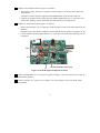
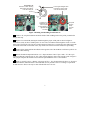
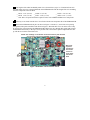
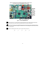
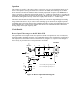
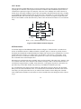
ELECRAFT KXB3080 30 and 80 METER ADAPTER
Assembly and Operating Instructions
Revision A, March 2006
Copyright © 2006, Elecraft; All Rights Reserved
Introduction
The KXB3080 adds 30 and 80-meter capability to the Elecraft KX1 transceiver. It also improves the
receiver sensitivity on the other bands. High-performance PIN-diode switches are used to minimize
insertion loss and ensure good sensitivity.
The KXB3080 consists of two printed-circuit boards (PCBs). The main PCB sits between the main KX1
PCB and the front panel, directly below the encoder shaft. It is held securely in place by the leads attaching
it to the main PCB. If your KX1 is currently equipped with the KXB30 adapter, the KXB3080 will replace
it. A smaller PCB contains two toroidal inductors and a relay that replaces existing toroidal inductors L1
and L2 in the KX1. Because it must be extremely compact to fit in the space available, the main PCB uses a
number of surface mounted devices (SMDs). All of the SMDs are pre-installed for easy assembly.
Specifications
30-m coverage
80-m coverage
Added current drain
Size
Transmit/receive: 10100-10150 kHz; receive only: 8000-12500 kHz.
Transmit/receive: 3500-4000 kHz; receive only: 1000 – 5500 kHz
Approx. 3 mA except approx. 18 mA on 80 meters.
KXB3080 main PCB: 1-9/16” x 1-1/32” (40 mm x 26 mm)
LPF1 PCB: 13/16” x 13/32” (20 mm x 10 mm)
Tools Required
•
•
•
•
•
•
•
•
Desoldering tool: An effective desoldering tool is essential. You will need to remove or replace
several parts on the KX1 PCB. A good vacuum desoldering tool such as the Soldapullt® model
DS017LS is strongly recommended to avoid damaging the PCB.
Fine-tip temperature-controlled ESD-safe soldering station with 700 to 800°F tip (370-430°C).
Recommend a spade tip approx. 0.05” (0.13 mm) wide. Do not use a high-wattage iron or
soldering gun since this can damage pads, traces, or the parts themselves.
Solder: IC-grade, small-diameter (.031”) (Kester #44 or equivalent) is recommended.
DO NOT use acid-core solder, water-soluble flux solder, additional flux or solvents of any
kind. Use of any of these will void your warranty.
Screwdrivers: A small #2 Phillips, a small flat-blade for slotted screws and a very small flatblade (about 0.1” or 2.5 mm wide) with an insulated handle to adjust the trimmer caps.
Needle-nose pliers.
Small-point diagonal cutters. Flush-cutting type is required (Xcelite MS54-5J or equivalent).
Hobby knife or similar tool to cut a PCB trace.
50-ohm dummy load capable of handling 5 watts, minimum.
Elecraft
•
www.elecraft.com
•
831-662-8345
•
•
Digital Multimeter (DMM) for voltage checks and confirming resistor values. A DMM with
capacitance measurement capability is desirable, but not required.
Magnifying glass or visor.
Preventing Electrostatic Discharge Damage
The KXB8030 main PCB is sensitive to electrostatic discharge (ESD) damage. Also, the individual PCBs
in your KX1 may be vulnerable when they are unplugged.
•
Keep parts in their ESD-safe packaging until called for in the assembly instructions. Do not place
individual PCBs in Styrofoam™ or similar containers. If possible, place loose PCBs inside ESDsafe bags when you are not working on them.
•
Wear a conductive wrist strap with a series 1 megohm resistor. If you do not have a wrist strap,
touch a ground briefly before touching any sensitive parts to discharge your body. Do this
frequently while you are working. You can collect a destructive static charge on your body just
sitting at the work bench. DO NOT attach a ground directly to yourself as this poses a serious
shock hazard.
•
Make sure your soldering iron is ESD-safe and has a grounded tip
•
Use a grounded antistatic mat on your work bench.
Parts Inventory
The table below lists the leaded parts to be installed, the pc boards, toroid cores, wire and
miscellaneous hardware required. The KX1 Owner's manual has photographs of similar parts.
Ref.
C1, C4
C1 (see Note 1)
C26
C1 (see Note 1)
C9
K1
L6
L1, L2, T1
MISC (See Note 2)
MISC (see Note 2)
MISC
MISC
MISC
MISC
MISC
MISC
Description
Capacitor, 1-40 pF trimmer
Capacitor, 0.1 µF (104), 0.1” lead spacing
Capacitor, 56 pF, (56) disc ceramic
Capacitor, 15 pF, (150) disc ceramic
Capacitor, Electrolytic, 10 µF, 35V (10)
Relay, DPDT (G6K-2P)
RF choke, 6.8 µH (blu-gry-gld)
Toroidal core, T37-2
KXB3080 PCB with SMD devices pre-mounted.
i Caution: ESD sensitive! See page 2.
LPF1 PCB
Kynar® wire, white, #24 solid
Solid, insulated hookup wire, green, #24
Toroid wire, green #26
Toroid wire, red, #26
Toroid wire, red, #28
Rubber bumper, .04" thick x 0.3" square
Qty
2
1
1
1
1
1
1
3
Part No.
E540002
E530020
E530146
E530140
E530045
E640029
E690044
E680006
1
E120000
1
1 ft.
6”
2 ft.
4 ft.
4 ft.
2
E120001
E760032
E760008
E760004
E760002
E760003
E980017
Note 1 : Duplicate reference designators are for parts on different PCBs. The parts are clearly identified in the text.
Note 2: The PCBs may have rough places along the edges. This is a normal result of the manufacturing process and will not
interfere with installation.
2
For reference, the table below lists the pre-mounted surface-mounted devices.
Ref.
C3, C6, C7, C8, C10
C9
C2, C5
D1, D2
D3
L1, L2, L3, L4, L5
Q1
R1, R2, R6, R7
R3, R4, R5
R8
Description
Capacitor, 0.1 µF
Capacitor, 10 uF,10V, 20%
Capacitor, 300 pF 5% NPO
PIN diode, dual, common cathode
Small Signal Diode
RF choke, 47 µH
Transistor, PNP, 2N3906
Resistor, 470 ohms 1/10 W, 5%
Resistor, 240 ohms, 1/10 W, 5%
Resistor, 15 k-ohm, 1/10W, 5%
Qty
5
1
2
2
1
5
1
4
3
1
Part No.
E530222
E530223
E530221
E560026
E560027
E690063
E580030
E500187
E500188
E500189
Assembly and Installation
There are four major steps in the procedure. Follow them carefully and in the order given.
1. Modify the KXB1 PCB to install a new receiver input circuit.
2. Assemble and install the KXB3080 option PCB. Install new firmware if needed.
3. Assemble and install Low-Pass Filter LPF1.
4. Reassemble, test and align the KX1 with the KXB3080 module.
Part I: Modify the KX1 PCB
Disassemble your KX1 and remove the main PCB from the enclosure. If you have the KXAT1
antenna tuner option, remove it and place it in a safe place where it will be free from ESD damage. Use an
ESD-safe bag if you have one available.
i
Very important:
1. Be careful to avoid accidentally touching components with your soldering iron. Relays
and potentiometer shafts are especially vulnerable to heat damage.
2. Clear pads of all solder before attempting to install new parts.
3. As you install new components, clip all leads flush with the PCB on the reverse side.
Bend C15 (near the crystals on the KX1 board) up to gain access to solder pad G under it.
If present, remove the KXB30 module. Remove the KXB30 wires from the KX1 main PCB and clear
the pads on the KX1 main PCB of all solder.
3
Replace C26 on the KX1 PCB (see Figure 1) as follows:
Remove the existing 120 pF (121) capacitor. It will no longer be used. Clear all the solder from
the pad holes.
Install the 56 pF (56) capacitor supplied with the KXB3080 kit. Form the leads of the new
capacitor as needed to fit. Be sure the capacitor stands no higher than 5/16” (7.9 mm) above the
board. After soldering, trim the leads flush. Save the leads for use as jumpers later.
Replace C1 on the KX1 PCB (see Figure 1) as follows:
Remove the existing 4.7 pF (4.7) capacitor. It will no longer be used. Clear all the solder from the
pad holes.
Install the 15 pF (150) capacitor supplied. Form the leads of the new capacitor as needed to fit. Be
sure the capacitor stands no higher than 5/16” (7.9 mm) above the board. After soldering, trim the
leads flush.
C26
C27
C1
L6 (Partially hidden behind pot)
L7
Figure 1. KX1 PCB Original Component Locations.
Remove molded inductor L7, 4.7 µH (yel-vio-gold) (see Figure 1). It will no longer be used. Clear all
the solder from the pad holes.
Remove capacitor C27, 150 pf (151) (see Figure 1). It will no longer be used. Clear all the solder
from the pad holes.
4
Turn the KX1 PCB over and cut the trace from CB to C27/R1 as shown in Figure 2. Use a sharp
hobby knife and cut across the trace several times as needed to cut through the metal.
Jumper from Trace
to Grounded Pad of
Trimmer Capacitor CC
Cut Circuit
Trace Here
Figure 2. Modifying Trace From Capacitor CB.
Use your DMM to confirm that the cut trace is an open circuit. Check the resistance between a solder
pad on one part of the cut trace and a solder pad on the other part. It should be greater than 1 megohm.
Scrape off the green coating and tin a short length of the trace adjacent to the pad for trimmer
capacitor CC. Use a cut lead to form a short jumper between the trace and the grounded end of CC as
shown in Figure 2.
Remove molded inductor L6 from the top side of the PCB (see Figure 1) and reinstall it on the bottom
of the PCB as shown in Figure 3. Be sure you place the leads in the same solder pads L6 originally
occupied. In case you damage the inductor while removing it, a replacement is provided: 6.8 µH (blu-grygld). When soldering L6 in place, do not fill the pad for connection A. This pad will be needed later to
attach the KXB3080 module. Trim L6’s leads flush with the top of the PCB.
Keep
Pad "A"
Clear.
L6
Figure 3. L6 Relocated on Bottom of KX1 PCB.
5
Rotate potentiometer R1 fully clockwise and check the resistance between ground and the part of the
cut trace that goes to the open solder pad for C27 and the center terminal of potentiometer R1. The
resistance must be greater than 800 ohms. If the resistance is low, check for a solder bridge between the pad
for capacitor CC and solder pad A or the adjacent pad for L6.
Cut a 20” (51 cm) length of the #28 red toroid wire. (The #28 is the smaller red wire.)
“Sew” the long end of the wire through the hole in one of the T37-2 toroid cores (red) for a total of 33
turns exactly as shown in Figure 4. Be sure you wind the turns the direction shown in the figure. Count one
turn for each time the wire passes through the center of the core. There are no half or quarter turns when
winding a toroid. The turns should fill about 90% of the toroid core as shown in the figure.
Cut a 3” (7.6 cm) length of the #26 green toroid wire. Strip the insulation from 1/2” (13mm) at one
end of the green wire (you’ll strip the insulation from the other end later). Use one of the following
methods to remove the insulation and tin the lead:
1. Heat Stripping:
a. Place a small amount of solder (a.k.a. a “blob” of solder) on your soldering iron.
b. Insert the clipped end of the wire into the hot solder so it touches the bare end of the wire. If
the iron is hot enough, you should see the insulation bubble and vaporize after 4 to 6 seconds.
c. Add solder and feed more wire into the solder as the enamel melts. After reaching the point
where you want the tinning to stop, slowly pull the wire out of the solder.
d. If any burnt enamel remains on the lead, scrape it away using your thumbnail or sharp tool.
2. Burning: The insulation can be burned off by heating it with a butane lighter for a few seconds.
Use sandpaper to remove the residue, then tin the bare wires.
3. Scraping: Use a sharp tool to scrape the insulation away. Work carefully and gently: do not nick
the wire. Remove all the enamel around the circumference of the wire, then tin the bare wire.
The stripped end of the green wire is end 2 as shown in Figure 4. Position the green wire so the
stripped end extends right up to the point where the wire passes into the center of the core, then wrap the
long end of the wire around the toroid and through the center one more time to make two turns.
Position T2 between potentiometers R1 and R2 as shown in Figure 4 with the leads passing through
the pads for C27 and L7 as shown in Figure 4. Mark each lead where it enters the pad. Use a marker or
place a slight bend in the wire at that point.
6
Transformer T2
Direction of each winding
and position of windings
must be exactly as
shown.
2
Lead 2 goes straight down
through the center of the
core into the solder pad.
1
Installed Transformer
Lead Connection Points
1
2
3
4
4
3
Position T2 so
Solder Pad CC
and Via (Hole
through PCB) on
opposite side
are clear.
Via (Hole
through
PCB)
must be
clear.
Figure 4. Winding and Installing Transformer T2.
Remove T2, strip the insulation and tin the leads of both windings back to the points you marked in
the previous step.
Replace T2 on the PCB, drawing the leads through the proper solder pads as shown in Figure 4.
Position T2 exactly as shown. Solder pad CC on one side of T2 and the hole through the circuit via on the
other side of T2 must be clear. Be sure a small segment of tinned wire is visible above the solder pad on the
toroid side of the PCB on each lead. If not, strip a little more enamel off of that lead before proceeding.
Solder all four leads and trim them flush on the opposite side of the PCB. Be careful not to pull T2 out
of position while soldering.
Bend a discarded component lead into a “U” shape and insert it into J7 pins 1 and 3. J7 is the 3-pin
connector adjacent to antenna jack J2. It is visible with the jumper in place at the top left corner of Figure 2.
This jumper completes the antenna circuit when the optional KXAT1 ATU is not installed.
Refer to your KX1 Owner’s Manual, Alignment and Test – Part II and perform the Receiver Alignment
to confirm that the modifications have been installed correctly and the receiver is working as expected on
40 and 20 meters. These tests may be done with the KX1 out of its case.
7
Part II: Assemble and Install the KXB3080 Option PCB
Figure 5 shows the layout of the parts on both of the PCBs. Refer to these figures as needed while
performing the following procedures.
R1
Reference designators
with arrows not printed
on boards.
D1
L1
C6
KXB3080 Module Board
Low-Pass Filter Board
(LPF1)
Figure 5. Parts Placement Diagrams.
i
Observe ESD precautions when handling the KX1 microcontroller (MCU) or the KXB3080
PCB. See Preventing Electrostatic Discharge Damage on page 2 for details.
Check the revision of the KX1 firmware supplied with your KXB3080 option against the firmware
currently installed in your KX1. The version is shown on a label attached to MCU U1 on the KX1 PCB.
The KXB3080 option requires version 1.02 or later. If you have an older version, new firmware should
have been supplied with your KXB3080 kit. If necessary follow the instructions supplied with your
firmware to replace it and re-enter your menu settings.
Install the two trimmer caps on the KXB3080 PCB. The orientation is important! Align the trimmers
with the outlines silk-screened on the PCB (see Figure 5).
__ C1. Flush cut the pins after soldering.
__ C4. Flush cut the pins after soldering.
Strip the insulation from 3” (7.6 cm) of the #24 green hookup wire, and cut the wire into three 1” (2.5
cm) lengths.
Solder the three bare wires in pads G, C and G along the upper edge of the KXB3080 PCB. Position
the wires flush with the bottom (non-component) side of the PCB and sticking up from the component side.
Note that the G pad on the opposite edge of the PCB is not used.
8
Cut lengths of the white-insulated Kynar® wire as shown below, strip 1/8” of insulation from each
end, and solder each wire to the pad indicated on the KXB3080 PCB with the length of the wire extending
from the component side of the PCB.
__ Pad A: 1-1/8” (2.8 cm)
__ Pad E: 1-1/4” (3.2 cm)
__ Pad B: 1” (2.5 cm)
__ Pad 5: 1-3/8” (3.5 cm)
__ Pad F: 3-1/4” (8.3 cm)
__ Pad D 1-3/8” (3.5 cm)
Note: Wires for pads 5 and D not required if wires from a KXB30 installation are still present.
Trim any excess leads from the above wires flush with the non-component side of the KXB3080 PCB.
Position the KXB3080 PCB in place as shown in Figure 7 with the G, C, and G bare wires passing
through the solder pads on the KX1 PCB shown in Figure 6. Bend the other wires out to the sides so they
do not interfere with positioning the KXB3080 PCB. Pull the bare wires through their solder pads to hold
the KXB3080 PCB closely to the top of U6 as possible and so the trimmer capacitor adjustment slots line
up with the access holes in the KX1 PCB.
NOTE: The markings on the bottom of the KX1 PCB for pads A and B
are incorrect. Connect the KXB3080 as shown here.
A
E
D
G
C
B
G
5
Figure 6. KXB3080 Connection Points on KX1.
9
Wire from
F passes
through the
hole in this
circuit via
to the other
side of the
PCB.
NOTE: The markings on the bottom of the KX1 PCB for pads A and B
are incorrect. Connect the KXB3080 as shown here.
Pass wire
from pad F
through
the hole in
this circuit
via to the
other side
of the PCB.
It will be
connected
later.
Bend C4 toward L8, if needed,
to clear the KXB3080 PCB.
Figure 7. Installed KXB3080 PCB.
Make sure the bare G, C and G leads are passing through the correct solder pads and the KXB3080
module is in position, then solder all three leads and trim the excess flush with the PCB.
Route the white Kynar® wire from KXB3080 pad F around potentiometer R2 and through the hole in
the circuit via next to T2 as shown in Figure 7. Pull all the excess wire through to the other side of the PCB.
It will be connected later.
Solder the remaining leads to their respective pads as shown in Figure 6.
__ D
__ 5
__ E
10
__ B
__A
Verify that your KXB3080 PCB is properly connected as follows:
Make sure the loose end of the wire attached to pad F of the KX3080 PCB and routed through the
hole in the circuit via is not touching anything. It will be connected later.
Insert a milliammeter, preferably a digital multimeter (DMM), in series with a fused 8 to 14 vdc
power source connected to the KX1’s external power jack (J1).
Apply power to your KX1 and turn it on. Verify that the display lights as expected and the
milliammeter shows about 34 to 37 mA after the LED times out. If necessary, set the LED menu
entry to a value below infinite (INF) so it will turn off for the current measurement. If the current
is much higher than 34 to 37 mA, it could indicate a short.
Enable both 30 and 80 meters in the Menu as described in the instructions supplied with the
firmware.
Use your DMM to verify about 5 vdc between KXB3080 pad 5 and ground.
Between pad D and ground, verify about 5 vdc on 30 and 80 meters, and 0 vdc on 20 meters.
Between pad D and ground, verify about 5 vdc on 40 meters below 6715 kHz and 0 vdc above
6715 kHz.
Between pad F and ground, verify about 5 vdc on 80 meters and 0 vdc on all other bands.
Disconnect power from the KX1.
Bend C15, on the bottom of the KX1 PCB, down against the PCB away from the access opening for
the C30A adjustment trimmer. This is the capacitor you stood up to access solder pad G near the encoder.
Peel the paper packing off of the two rubber pads and affix them to the KXB3080 PCB as shown in
Figure 7. The pads ensure the KXB3080 PCB does not touch the top cover when the case is reassembled.
11
Part III: Assemble and Install Low-Pass Filter LPF1
The LPF1 Low-Pass filter replaces L1 and L2 on the KX1 PCB. The completed and installed LPF1 is
shown in Figure 8. Follow the assembly procedure closely to ensure that the finished LPF1 fits as shown.
C1
White Wire from
KXB3080 Module
K1
C9
L1
Ground Wire
L2
Inductor Common Wire
Figure 8. LPF1 Installed.
Locate the LPF1 PCB and the 0.1 µF (104) capacitor C1.
Position C1’s leads through the holes in the LPF1 PCB as shown in Figure 9. The capacitor body
must be on the side of the PCB with the circular outlines for the toroids. Use your needle-nose pliers to
straighten the leads as needed so the capacitor sits as close to the PCB as the epoxy coating allows (see
Figure 8). The top of the capacitor must sit no more than 3/16” (5mm) above the PCB.
Capacitor C1 Mounts in
Round Pads
3
2 L1
4
C1
3
L2 2
4
Toroid side of PCB
Capacitor and inductor common
wire are mounted on this side of
the PCB.
Inductor Common Wire
(Bare) Connects Here
Figure 9. C1 and Inductor Common Wire Connections to LPF1.
Trim C1’s leads flush with the relay side of the PCB. They must not stick out of the pads.
12
Solder C1 in position, working from C1’s side of the PCB. Use minimal solder to ensure no fillet or
solder bump forms on the relay side. The relay will mount over C1’s pads and must rest directly against the
PCB. Take care not to fill the adjacent solder pads.
Strip the insulation from a 1” length of the green hook-up wire.
Use your needle-nose pliers to bend the wire at right angles about 1/16” (1.5 mm) from one end. Place
the short end in the inductor common wire solder pad (see Figure 9) and verify that the wire does not stick
out on the relay side of the PCB. If it does, trim the short end as needed.
Lay the PCB down so the circular toroid outlines are facing upward and position the short end of the
wire in the inductor common wire pad with the wire extending off the nearest edge of the board. The wire
is shown in place in the right hand photo in Figure 8.
Solder from the toroid side of the PCB just as you did for C1. Like C1, there must be no excess lead
or bump of solder on the relay side of the PCB.
i
When installing relay K1 in the following steps, be sure the relay is oriented correctly before
soldering. Otherwise your KX1 will not work.
Identify pin 1 on relay K1 (G6K-2P). There should be a dark grey bar on the relay top over the corner
above pin 1. You can confirm pin 1 by using your DMM to measure the resistance between it and pin 8 at
the same end. The resistance should be about 230 ohms.
Position K1 on the LPF1 PCB inside the rectangular outline with pin 1 next to the number 1 silkscreened on the PCB. Be sure the relay is resting against the PCB and not against any excess solder or leads
left from installing C1 or the common inductor wire. Most relays have small raised feet on the sides that
touch the PCB when it is properly mounted, leaving a very tiny gap between the rest of the relay case and
the PCB. This is normal.
Solder only two opposite corner pins of the relay and verify that the relay is flat against the PCB. If
not, reheat the soldered pins while pressing the relay against the PCB until it is fully seated.
Solder the remaining pins and trim them flush with the PCB.
Strip the insulation from a 1” (2.5 cm) length of the green hookup wire. Save the insulation. Solder the
1” (2.5 cm) bare wire into the “+” pad on the LPF1 PCB (see Figure 8) with the wire extending out of the
pad on the relay side. Flush cut any excess wire or solder from the toroid side of the PCB.
13
The ground wire goes to the + pad as shown.
The + and - marks were printed on the PCB
incorrectly during fabrication.
Bare Ground Wire Connects
Here and Extends from this
(Relay) Side of the PCB
+
LPF1
Rev A
K1
Elecraft
1
RELAY
-
Figure 10. LPF1 Ground Wire Connection.
Cut two 9” (23 cm) lengths of the green toroid wire and two 13” (33 cm) lengths of the larger #26 red
toroid wire.
Wind L1 and L2 on the remaining T37-2 (red) toroid cores as shown in Figure 11. Note that each core
has two separate windings: one with 9 turns of green toroid wire and one with 15 turns of red toroid wire.
Be sure the direction and orientation of the windings are exactly as shown. Although L1 and L2 are actually
identical, they are shown oriented as they will be mounted on the LPF1 PCB.
After winding, cut all leads to at least 1” (2.5 cm), then strip and tin each lead from the end up to the
point described below:
L1-1: Where the lead leaves the front edge of the core in Figure 11.
L1-2: Where the wire exits the center of the core.
L1-3: About 1/8” (3 mm) from where the wire leaves the front edge of the core in the figure.
L1-4: Where the lead leaves the back edge of the core in the figure.
L2-1: About 1/8” (3 mm) from where the wire leaves the back edge of the core in the figure.
L2-2: About 1/8” (3 mm) from where the wire leaves the front edge of the core in the figure.
L2-3: Where the wire exits the center of the core.
L2-4: About 1/8” (3 mm) from where the wire leaves the front edge of the core in the figure.
2
L1
3
9 Turns
Green
1
4
15 Turns
Red
L2
3 2
4
Toroids Oriented
For Mounting on PCB
9 Turns
Green
1
3
2 L1
4
L2 2
4
LPF1 PCB
Toroid Side
Figure 11. LPF1 Toroid Inductors L1 and L2.
14
3
C1
Thread leads 2, 3 and 4 of each core through their respective solder pads on the LPF1 PCB (see Figure
11). Lead 1 to each toroid will be connected directly to the KX1 PCB later. Position the toroids against the
LPF1 PCB and directly over the circles drawn on the PCB as shown in Figure 8. Be sure the toroids are
centered and do not extend farther over one edge than the other. On the relay side of the PCB, be sure
clean, tinned lead is visible in each solder pad, then solder and trim all six leads.
Identify the negative lead of electrolytic capacitor C9, 10 µF, 35V (10). The negative lead is the
shorter lead and there will be a stripe with a minus (-) sign on the capacitor next to that lead. Position the
capacitor against the LPF1 PCB alongside the relay next to the ground wire exactly as shown in Figure 12.
Solder the negative lead to the ground wire on the LPF1 PCB as shown.
Cut to length the green hook up wire insulation you saved and slip it over the positive lead from C9
as shown in Figure 12. Route the positive lead of C9 over the top of K2 to the pad shown in Figure 12, so it
rests against the relay. Do not solder yet.
Insulation from green wire on
capacitor lead (see text). Wire
must rest against top of relay.
Capacitor - lead
soldered to bare
ground wire at
+ pad
Pass Capacitor + lead
through the - pad. Do
not solder yet.
Note that the + and - marks were printed on the PCB incorrectly
during fabrication. Connect the capacitor as shown.
Figure 12. Installing C9 on LPF1.
Remove L1 and L2 from the KX1 PCB. Clear all the solder from the pad holes and flush trim to the
KX1 PCB all the capacitor leads in the area near where L1 and L2 were removed.
Fit the LPF1 module in the space formerly occupied by L1 and L2. Place the L1-1, L2-1 and inductor
common leads through the solder pads on the KX1 PCB shown in Figure 13. The module must be
positioned against the KX1 PCB and J7 exactly as shown in Figure 8, with the windings on the toroids
flush with the edge of the KX1 PCB. Lead L2-1 fits between the LPF1 PCB and J7 to reach the solder pad
on the KX1 PCB directly behind the LPF1 PCB. If you have a KXAT1 antenna tuner, ensure it fits in place
as shown in Figure 14 before soldering the LPF1 leads. When you are satisfied with the fit, solder the
inductor common and ground leads to hold the LPF1 PCB in place. The ground lead is soldered to the lug
for potentiometer R1. It does not pass through the PCB.
15
Inductor Common
LPF1
L1-1
L2-1
Ground
L2-1
Ground
Inductor
Common
L1-1
KX1 PCB
Figure 13. LPF1 Connection Points.
LPF1
Toroids Aligned
with Edge of
KX1 PCB
KX1 PCB
KXAT1 PCB
Lead From C9 Must
Clear KXAT1 PCB
KXAT1 Transformer T1
Must Clear End of LPF1 PCB
Figure 14. LPF1 Installed With KXAT1.
Route the white wire from the KXB3080 module to the LPF1 PCB and solder it to the LPF1 PCB
along with the positive lead to C9 as shown in Figure 8. The wire must be placed against the KX1 PCB
until it reaches the LPF1 PCB to allow clearance for components on the KXAT1.
16
Part IV: Reassemble, Test and Align the KX1 with KX3080 Module
Check the signal path through the LPF1 module as follows:
Attach an 8 to 14 vdc power supply to the KX1’s external power jack (J1) with a milliammeter,
preferably a DMM, in series with the supply.
Apply power and verify that the display lights as expected. The milliammeter should show about
45 mA after the LED times out (except on 80 meters where it will be about 65 mA). If necessary,
set the LED menu entry to a value below infinite (INF) so it will turn off quickly for the current
measurement. If the current is much higher than expected, disconnect power and look for a short
circuit.
Connect headphones and an antenna or a signal source to the KX1 and verify that the jumper is in
place across the outer pins of J7 (see Figure 13). If the wiring is correct you should hear signals
on 40 and 20 meters, at least.
Reassemble your KX1 according to the instructions in the Owner’s Manual. If it is equipped with
the KXAT1 antenna tuner, leave the tuner module out for now so you can access the trimmer
capacitor adjustments.
Reconnect power to the KX1 as above and turn the unit on while monitoring the current. The
current should be about 45 mA except on 80 meters where it will be about 65 mA after the LED times
out. If it is much higher, turn the unit off immediately and look for a short. The most likely place will
be at final amplifier mounting to the KX1 case.
Perform the receive alignment procedure for 20 and 40 meters as described in the KX1 Owner’s
manual under Alignment and Test Part II. The KXB3080 module adds capacity to the circuit that can
affect the tuning on those bands.
Switch to 30 meters and align the two trimmers on the KXB3080. You can peak them while
listening to signals or noise. The peaks on these trimmers are rather broad, compared to the 20 and 40
meter alignment, because they only represent part of the capacitance in the circuit. That completes the
receiver alignment. The 80 meter band was optimized for receive when you set the 30 meter trimmers.
Perform the 20-Meter and 40-Meter transmitter tests described in the KX1 Owner’s manual
under Alignment and Test Part III. If adjustment of L2 is needed, use a plastic probe to adjust only the
green, 9-turn winding on L2 (the winding nearest the antenna connector). These adjustments must be
made with the KX1 top cover in place so the final amplifier has a suitable heat sink.
That completes test and alignment. If so equipped, replace the KXAT1 antenna tuner, then attach
the battery connector and replace the KX1 bottom cover. Be very careful not to pinch the battery wires
between the bottom cover and the ATU module or the nearby long standoff.
17
Operation
The operation of your KX1 is the same as before, except now when you cycle through the bands you will
also have the option of selecting 30 and 80 meters. Like the other bands, the tuning range on 30 and 80
meters extends well outside the Amateur bands to include popular SWL frequencies. The KXB3080 also
improves sensitivity in the popular 49-meter SWL band (5.9 – 6.2 MHz) by automatically re-resonating the
input circuit when tuning those frequencies. On 80 meters, the tuning range extends from 5.5 MHz down to
about 1 MHz, although the sensitivity will decrease rapidly outside of the 3.5 – 4.0 MHz range.
The KXAT1 antenna tuner also functions normally on the 80 and 30 meter ranges, although its matching
range is limited on 80 meters. If you want a greater matching range on 80 meters, you might experiment
with adding turns to the toroids in the KXAT1. Doubling the number of turns on toroidal inductors L1, L2
and L3 in the KXAT1 will improve the matching range on 80 meters substantially, while reducing the
matching range on the higher frequency bands.
Circuit Details
Receiver Input Filter Changes on the KX1 Main PCB
The original KX1 receiver input circuit uses a capacitive divider. It is optimized for ease of construction,
and can be tuned to 40 through 20 meters. To accommodate 80 meters, the circuit must be reconfigured as
link-coupled; this is the function of the new transformer T2 (see Figure 15). Capacitor value changes are
also necessary to provide the best overall performance on all bands.
Rcv Mixer
R1
1K
C1
15
C
RF Gain
T2
3
CB
1
4
V+
2
4
1
2
4
L6
6.8 µH
3
3
2
K1B
Q7
2N4124
5
V-
CC
50
C56
6
6
C15
.01
6T_2
R2
1.K
A
5
6
CA
20
7
B
K1A
1 & 2: Solder pads originally for C27.
C26
56
3 & 4: Solder pads originally for L7.
RX ANT
Figure 15. Receiver Input Schematic Diagram.
18
7
U6
NE602
LPF1 Module
The low-pass filter module adds 80 meter coverage to the filter network at the output of the transmitter by
replacing the two inductors in the original circuit with four inductors and an additional capacitor that are
switched in as required (see Figure 16). Relay K1 selects one of two windings on L1 and L2. On 40, 30,
and 20 meters, the smaller winding is selected. This corresponds to the OFF position of the relay, resulting
in zero added current drain on these bands. On 80 meters, K1 is turned ON via 5 volts from point F on the
KXB3080 module. This selects the larger winding on each of L1 and L2, moving the low-pass filter knee
down to about 4 MHz. Current drain increases by about 15 mA on 80 meters because K1 is a conventional
relay.
C9
Y
+
X
C1
1
3
3
3
4
4
2
2
6
L1
K1
5
7
2
1
-
+
8
1
4
L2
1-2: Green
3-4: Red
COMMON
NOTE: "+" and "-" labels are reversed on Rev A LPF1 board.
Figure 16. LPF1 Module Schematic Diagram.
KXB3080 Module
A schematic diagram of the KXB3080 module is shown in Figure 17. When the KX1 is switched to 30
meters (or tuned below about 6.7 MHz on 40 meters), the MCU places 5 volts DC on point D, forward
biasing the associated diode of dual PIN diodes D1 and D2. This inserts the series combination of C3/C4 in
parallel with points A and B, i.e. in parallel with CA on the KX1; it also inserts C1 from point C to RF
ground, or across L7 on the KX1. At other times point D is at 0 volts, reverse biasing the diodes so they
have a minimal effect on the band-pass filter.
When the rig is switched to 80 meters, the MCU places 0 volts on point E. This turns on Q1, placing 5 volts
at its collector. This turns on the other half of D1 and D2, inserting C2 and C5 into the tuned circuits to reresonate them at approximately 3.6 MHz. At the same time, 5 volts appears on point F to turn on the lowpass filter relay (on the LPF1 module). D3 protects Q1 from inductive kickback by the relay.
Q1 is needed because the signal at point E cannot drive PIN diodes or the relay directly. The associated
MCU pin is also used as the SPI-bus clock, for communication with the DDS IC. R8 and C9 filter out the
short duty-cycle clock pulses that occur as you tune the VFO. Firmware sets the idling state of the SPI
clock signal based on whether or not 80 meters is selected, and this is the state that appears at the collector
of Q1.
19
C
G
A
B
C1
C2
0.1
40
300
C3
D2
G
C4
C5
40
300
ON diode Current
D1
with 30 or 80 m caps
enabled: ~2 mA;
both enabled: ~1.2 mA
R1
R2
L3
L4
470
470
47µH
47µH
L1
47µH
D
L2
R3
R4
R5
47µH
240
240
240
5V, 30M
C6
L5
47µH
C7
0.1
0.1
R6
5
3.5V ON, 2.5V OFF
470
R7
470
5V
Q1
C8
0.1
5V, 80 M
2N3906
F
C10
0.1
D3
1N4148
E
R8
15K
C9
10 µF
G
Figure 17. KXB3080 Module Schematic.
20