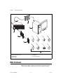
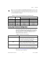
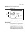
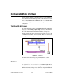
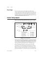
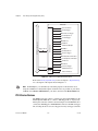
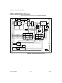
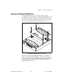
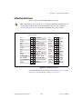
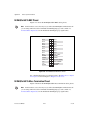
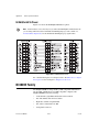
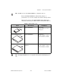
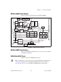
1
DAQ E Series
E Series User Manual
E Series User Manual
February 2007
370503K-01
Support
Worldwide Technical Support and Product Information
ni.com
National Instruments Corporate Headquarters
11500 North Mopac Expressway
Austin, Texas 787593504
USA Tel: 512 683 0100
Worldwide Offices
Australia 1800 300 800, Austria 43 662 457990-0, Belgium 32 (0) 2 757 0020, Brazil 55 11 3262 3599,
Canada 800 433 3488, China 86 21 5050 9800, Czech Republic 420 224 235 774, Denmark 45 45 76 26 00,
Finland 385 (0) 9 725 72511, France 33 (0) 1 48 14 24 24, Germany 49 89 7413130, India 91 80 41190000,
Israel 972 3 6393737, Italy 39 02 413091, Japan 81 3 5472 2970, Korea 82 02 3451 3400,
Lebanon 961 (0) 1 33 28 28, Malaysia 1800 887710, Mexico 01 800 010 0793, Netherlands 31 (0) 348 433 466,
New Zealand 0800 553 322, Norway 47 (0) 66 90 76 60, Poland 48 22 3390150, Portugal 351 210 311 210,
Russia 7 495 783 6851, Singapore 1800 226 5886, Slovenia 386 3 425 42 00, South Africa 27 0 11 805 8197,
Spain 34 91 640 0085, Sweden 46 (0) 8 587 895 00, Switzerland 41 56 2005151, Taiwan 886 02 2377 2222,
Thailand 662 278 6777, Turkey 90 212 279 3031, United Kingdom 44 (0) 1635 523545
For further support information, refer to the Technical Support and Professional Services appendix. To comment
on National Instruments documentation, refer to the National Instruments Web site at ni.com/info and enter
the info code feedback.
© 1997–2007 National Instruments Corporation. All rights reserved.
Important Information
Warranty
The E Series devices are warranted against defects in materials and workmanship for a period of one year from the date of shipment, as
evidenced by receipts or other documentation. National Instruments will, at its option, repair or replace equipment that proves to be defective
during the warranty period. This warranty includes parts and labor.
The media on which you receive National Instruments software are warranted not to fail to execute programming instructions, due to defects in
materials and workmanship, for a period of 90 days from date of shipment, as evidenced by receipts or other documentation. National Instruments
will, at its option, repair or replace software media that do not execute programming instructions if National Instruments receives notice of such defects
during the warranty period. National Instruments does not warrant that the operation of the software shall be uninterrupted or error free.
A Return Material Authorization (RMA) number must be obtained from the factory and clearly marked on the outside of the package before any
equipment will be accepted for warranty work. National Instruments will pay the shipping costs of returning to the owner parts which are covered by
warranty.
National Instruments believes that the information in this document is accurate. The document has been carefully reviewed for technical accuracy. In
the event that technical or typographical errors exist, National Instruments reserves the right to make changes to subsequent editions of this document
without prior notice to holders of this edition. The reader should consult National Instruments if errors are suspected. In no event shall National
Instruments be liable for any damages arising out of or related to this document or the information contained in it.
EXCEPT AS SPECIFIED HEREIN, NATIONAL INSTRUMENTS MAKES NO WARRANTIES, EXPRESS OR IMPLIED, AND SPECIFICALLY DISCLAIMS ANY WARRANTY OF
MERCHANTABILITY OR FITNESS FOR A PARTICULAR PURPOSE. CUSTOMER’S RIGHT TO RECOVER DAMAGES CAUSED BY FAULT OR NEGLIGENCE ON THE PART OF NATIONAL
INSTRUMENTS SHALL BE LIMITED TO THE AMOUNT THERETOFORE PAID BY THE CUSTOMER. NATIONAL INSTRUMENTS WILL NOT BE LIABLE FOR DAMAGES RESULTING
FROM LOSS OF DATA, PROFITS, USE OF PRODUCTS, OR INCIDENTAL OR CONSEQUENTIAL DAMAGES, EVEN IF ADVISED OF THE POSSIBILITY THEREOF. This limitation of
the liability of National Instruments will apply regardless of the form of action, whether in contract or tort, including negligence. Any action against
National Instruments must be brought within one year after the cause of action accrues. National Instruments shall not be liable for any delay in
performance due to causes beyond its reasonable control. The warranty provided herein does not cover damages, defects, malfunctions, or service
failures caused by owner’s failure to follow the National Instruments installation, operation, or maintenance instructions; owner’s modification of the
product; owner’s abuse, misuse, or negligent acts; and power failure or surges, fire, flood, accident, actions of third parties, or other events outside
reasonable control.
Copyright
Under the copyright laws, this publication may not be reproduced or transmitted in any form, electronic or mechanical, including photocopying,
recording, storing in an information retrieval system, or translating, in whole or in part, without the prior written consent of National
Instruments Corporation.
National Instruments respects the intellectual property of others, and we ask our users to do the same. NI software is protected by copyright and other
intellectual property laws. Where NI software may be used to reproduce software or other materials belonging to others, you may use NI software only
to reproduce materials that you may reproduce in accordance with the terms of any applicable license or other legal restriction.
Trademarks
National Instruments, NI, ni.com, and LabVIEW are trademarks of National Instruments Corporation. Refer to the Terms of Use section
on ni.com/legal for more information about National Instruments trademarks.
FireWire® is the registered trademark of Apple Computer, Inc. Other product and company names mentioned herein are trademarks or trade names
of their respective companies.
Members of the National Instruments Alliance Partner Program are business entities independent from National Instruments and have no agency,
partnership, or joint-venture relationship with National Instruments.
Patents
For patents covering National Instruments products, refer to the appropriate location: Help»Patents in your software, the patents.txt file
on your CD, or ni.com/patents.
WARNING REGARDING USE OF NATIONAL INSTRUMENTS PRODUCTS
(1) NATIONAL INSTRUMENTS PRODUCTS ARE NOT DESIGNED WITH COMPONENTS AND TESTING FOR A LEVEL OF
RELIABILITY SUITABLE FOR USE IN OR IN CONNECTION WITH SURGICAL IMPLANTS OR AS CRITICAL COMPONENTS IN
ANY LIFE SUPPORT SYSTEMS WHOSE FAILURE TO PERFORM CAN REASONABLY BE EXPECTED TO CAUSE SIGNIFICANT
INJURY TO A HUMAN.
(2) IN ANY APPLICATION, INCLUDING THE ABOVE, RELIABILITY OF OPERATION OF THE SOFTWARE PRODUCTS CAN BE
IMPAIRED BY ADVERSE FACTORS, INCLUDING BUT NOT LIMITED TO FLUCTUATIONS IN ELECTRICAL POWER SUPPLY,
COMPUTER HARDWARE MALFUNCTIONS, COMPUTER OPERATING SYSTEM SOFTWARE FITNESS, FITNESS OF COMPILERS
AND DEVELOPMENT SOFTWARE USED TO DEVELOP AN APPLICATION, INSTALLATION ERRORS, SOFTWARE AND HARDWARE
COMPATIBILITY PROBLEMS, MALFUNCTIONS OR FAILURES OF ELECTRONIC MONITORING OR CONTROL DEVICES,
TRANSIENT FAILURES OF ELECTRONIC SYSTEMS (HARDWARE AND/OR SOFTWARE), UNANTICIPATED USES OR MISUSES, OR
ERRORS ON THE PART OF THE USER OR APPLICATIONS DESIGNER (ADVERSE FACTORS SUCH AS THESE ARE HEREAFTER
COLLECTIVELY TERMED “SYSTEM FAILURES”). ANY APPLICATION WHERE A SYSTEM FAILURE WOULD CREATE A RISK OF
HARM TO PROPERTY OR PERSONS (INCLUDING THE RISK OF BODILY INJURY AND DEATH) SHOULD NOT BE RELIANT SOLELY
UPON ONE FORM OF ELECTRONIC SYSTEM DUE TO THE RISK OF SYSTEM FAILURE. TO AVOID DAMAGE, INJURY, OR DEATH,
THE USER OR APPLICATION DESIGNER MUST TAKE REASONABLY PRUDENT STEPS TO PROTECT AGAINST SYSTEM FAILURES,
INCLUDING BUT NOT LIMITED TO BACK-UP OR SHUT DOWN MECHANISMS. BECAUSE EACH END-USER SYSTEM IS
CUSTOMIZED AND DIFFERS FROM NATIONAL INSTRUMENTS' TESTING PLATFORMS AND BECAUSE A USER OR APPLICATION
DESIGNER MAY USE NATIONAL INSTRUMENTS PRODUCTS IN COMBINATION WITH OTHER PRODUCTS IN A MANNER NOT
EVALUATED OR CONTEMPLATED BY NATIONAL INSTRUMENTS, THE USER OR APPLICATION DESIGNER IS ULTIMATELY
RESPONSIBLE FOR VERIFYING AND VALIDATING THE SUITABILITY OF NATIONAL INSTRUMENTS PRODUCTS WHENEVER
NATIONAL INSTRUMENTS PRODUCTS ARE INCORPORATED IN A SYSTEM OR APPLICATION, INCLUDING, WITHOUT
LIMITATION, THE APPROPRIATE DESIGN, PROCESS AND SAFETY LEVEL OF SUCH SYSTEM OR APPLICATION.
Compliance
Compliance with FCC/Canada Radio Frequency Interference
Regulations
Determining FCC Class
The Federal Communications Commission (FCC) has rules to protect wireless communications from interference. The FCC
places digital electronics into two classes. These classes are known as Class A (for use in industrial commercial locations only)
or Class B (for use in residential or commercial locations). All National Instruments (NI) products are FCC Class A products.
Depending on where it is operated, this Class A product could be subject to restrictions in the FCC rules. (In Canada, the
Department of Communications (DOC), of Industry Canada, regulates wireless interference in much the same way.) Digital
electronics emit weak signals during normal operation that can affect radio, television, or other wireless products.
All Class A products display a simple warning statement of one paragraph in length regarding interference and undesired
operation. The FCC rules have restrictions regarding the locations where FCC Class A products can be operated.
Consult the FCC Web site at www.fcc.gov for more information.
FCC/DOC Warnings
This equipment generates and uses radio frequency energy and, if not installed and used in strict accordance with the instructions
in this manual and the CE marking Declaration of Conformity*, may cause interference to radio and television reception.
Classification requirements are the same for the Federal Communications Commission (FCC) and the Canadian Department
of Communications (DOC).
Changes or modifications not expressly approved by NI could void the user’s authority to operate the equipment under the
FCC Rules.
Class A
Federal Communications Commission
This equipment has been tested and found to comply with the limits for a Class A digital device, pursuant to part 15 of the FCC
Rules. These limits are designed to provide reasonable protection against harmful interference when the equipment is operated
in a commercial environment. This equipment generates, uses, and can radiate radio frequency energy and, if not installed and
used in accordance with the instruction manual, may cause harmful interference to radio communications. Operation of this
equipment in a residential area is likely to cause harmful interference in which case the user is required to correct the interference
at their own expense.
Canadian Department of Communications
This Class A digital apparatus meets all requirements of the Canadian InterferenceCausing Equipment Regulations.
Cet appareil numérique de la classe A respecte toutes les exigences du Règlement sur le matériel brouilleur du Canada.
Compliance with EU Directives
Users in the European Union (EU) should refer to the Declaration of Conformity (DoC) for information* pertaining to the
CE marking. Refer to the Declaration of Conformity (DoC) for this product for any additional regulatory compliance
information. To obtain the DoC for this product, visit ni.com/certification, search by model number or product line,
and click the appropriate link in the Certification column.
* The CE marking Declaration of Conformity contains important supplementary information and instructions for the user or
installer.
Contents
About This Manual
Conventions ...................................................................................................................xv
Related Documentation..................................................................................................xvi
NI-DAQ for Windows.....................................................................................xvi
NI-DAQmx for Linux......................................................................................xvi
NI-DAQmx Base .............................................................................................xvii
LabVIEW ........................................................................................................xvii
LabWindows/CVI............................................................................................xviii
Measurement Studio........................................................................................xviii
ANSI C without NI Application Software ......................................................xix
.NET Languages without NI Application Software ........................................xix
Device Documentation and Specifications......................................................xx
Training Courses .............................................................................................xx
Technical Support on the Web ........................................................................xx
Chapter 1
DAQ System Overview
DAQ Hardware ..............................................................................................................1-2
DAQ-STC........................................................................................................1-3
Calibration Circuitry........................................................................................1-3
Internal or Self-Calibration ...............................................................1-4
External Calibration ..........................................................................1-4
Signal Conditioning .......................................................................................................1-4
Sensors and Transducers .................................................................................1-4
Signal Conditioning Options ...........................................................................1-5
SCXI..................................................................................................1-5
SCC ...................................................................................................1-6
5B Series ...........................................................................................1-6
Cables and Accessories..................................................................................................1-6
Using Accessories with Devices .....................................................................1-7
Custom Cabling ...............................................................................................1-9
Programming Devices in Software ................................................................................1-10
I/O Connector Signal Descriptions ................................................................................1-11
Terminal Name Equivalents ..........................................................................................1-14
+5 V Power Source ........................................................................................................1-16
© National Instruments Corporation
vii
E Series User Manual
Contents
Chapter 2
Analog Input
Analog Input Circuitry .................................................................................................. 2-1
Mux ................................................................................................................. 2-1
Instrumentation Amplifier (NI-PGIA) ............................................................ 2-2
A/D Converter................................................................................................. 2-2
AI FIFO........................................................................................................... 2-2
Analog Trigger ................................................................................................ 2-2
AI Timing Signals ........................................................................................... 2-2
Input Polarity and Range ............................................................................................... 2-2
Analog Input Terminal Configuration........................................................................... 2-5
Dither............................................................................................................................. 2-8
Multichannel Scanning Considerations......................................................................... 2-9
Use Low Impedance Sources .......................................................................... 2-10
Use Short High-Quality Cabling..................................................................... 2-11
Carefully Choose the Channel Scanning Order .............................................. 2-11
Avoid Switching from a Large to a Small Input Range ................... 2-11
Insert Grounded Channel between Signal Channels ........................ 2-11
Minimize Voltage Step between Adjacent Channels ....................... 2-12
Avoid Scanning Faster than Necessary........................................................... 2-12
Example 1 ......................................................................................... 2-12
Example 2 ......................................................................................... 2-13
AI Data Acquisition Methods ......................................................................... 2-13
Software-Timed Acquisitions........................................................... 2-13
Hardware-Timed Acquisitions ......................................................... 2-13
Analog Input Triggering................................................................................................ 2-14
AI Start Trigger Signal.................................................................................... 2-15
Using a Digital Source...................................................................... 2-15
Using an Analog Source ................................................................... 2-15
Outputting the AI Start Trigger Signal ........................................................... 2-16
AI Reference Trigger Signal ........................................................................... 2-16
Using a Digital Source...................................................................... 2-18
Using an Analog Source ................................................................... 2-18
Outputting the AI Reference Trigger Signal .................................... 2-18
AI Pause Trigger Signal .................................................................................. 2-19
Using a Digital Source...................................................................... 2-19
Using an Analog Source ................................................................... 2-19
Connecting Analog Input Signals.................................................................................. 2-20
Types of Signal Sources.................................................................................. 2-22
Floating Signal Sources .................................................................... 2-22
Ground-Referenced Signal Sources.................................................. 2-22
E Series User Manual
viii
ni.com
Contents
Differential Connection Considerations ........................................................................2-22
Differential Connections for Ground-Referenced Signal Sources ..................2-23
Common-Mode Signal Rejection Considerations.............................2-24
Differential Connections for Non-Referenced or
Floating Signal Sources ................................................................................2-24
Single-Ended Connection Considerations .....................................................................2-26
Common-Mode Signal Rejection Considerations ...........................................2-26
Single-Ended Connections for Floating Signal Sources
(RSE Configuration).....................................................................................2-27
Single-Ended Connections for Grounded Signal Sources
(NRSE Configuration)..................................................................................2-27
Field Wiring Considerations ..........................................................................................2-28
Configuring AI Modes in Software ...............................................................................2-29
Traditional NI-DAQ (Legacy).........................................................................2-29
NI-DAQmx......................................................................................................2-29
Analog Input Timing Signals.........................................................................................2-30
AI Start Trigger Signal ....................................................................................2-32
Using a Digital Source ......................................................................2-33
Using an Analog Source ...................................................................2-33
Outputting the AI Start Trigger Signal .............................................2-33
AI Reference Trigger Signal ...........................................................................2-34
Using a Digital Source ......................................................................2-35
Using an Analog Source ...................................................................2-36
Outputting the AI Reference Trigger Signal.....................................2-36
AI Pause Trigger Signal ..................................................................................2-36
Using a Digital Source ......................................................................2-36
Using an Analog Source ...................................................................2-37
AI Sample Clock Signal ..................................................................................2-37
Using an Internal Source...................................................................2-37
Using an External Source..................................................................2-37
Outputting the AI Sample Clock Signal ...........................................2-38
Other Timing Requirements..............................................................2-39
AI Sample Clock Timebase Signal..................................................................2-40
AI Convert Clock Signal .................................................................................2-41
Using an Internal Source...................................................................2-41
Using an External Source..................................................................2-42
Outputting the AI Convert Clock Signal...........................................2-42
Using a Delay from Sample Clock to Convert Clock .......................2-43
Other Timing Requirements..............................................................2-43
AI Convert Clock Timebase Signal.................................................................2-45
Master Timebase Signal ..................................................................................2-45
AI Hold Complete Event Signal......................................................................2-46
External Strobe Signal.....................................................................................2-46
Getting Started with AI Applications in Software.........................................................2-47
© National Instruments Corporation
ix
E Series User Manual
Contents
Chapter 3
Analog Output
Analog Output Circuitry................................................................................................ 3-1
DACs............................................................................................................... 3-1
DAC FIFO....................................................................................................... 3-1
AO Sample Clock ........................................................................................... 3-2
Polarity and Reference Selection .................................................................... 3-2
Reference Selection ....................................................................................................... 3-2
Polarity Selection........................................................................................................... 3-3
Reglitch Selection.......................................................................................................... 3-3
Minimizing Glitches on the Output Signal.................................................................... 3-3
AO Data Generation Methods ....................................................................................... 3-4
Software-Timed Generations .......................................................................... 3-4
Hardware-Timed Generations......................................................................... 3-4
Buffered ............................................................................................ 3-4
Non-Buffered.................................................................................... 3-5
Analog Output Triggering ............................................................................................. 3-5
AO Start Trigger Signal .................................................................................. 3-6
Using a Digital Source...................................................................... 3-6
Using an Analog Source ................................................................... 3-6
Outputting the AO Start Trigger Signal ........................................... 3-6
AO Pause Trigger Signal ................................................................................ 3-7
Using a Digital Source...................................................................... 3-7
Using an Analog Source ................................................................... 3-7
Connecting Analog Output Signals ............................................................................... 3-8
Waveform Generation Timing Signals.......................................................................... 3-9
AO Start Trigger Signal .................................................................................. 3-9
Using a Digital Source...................................................................... 3-9
Using an Analog Source ................................................................... 3-10
Outputting the AO Start Trigger Signal ........................................... 3-10
AO Pause Trigger Signal ................................................................................ 3-10
Using a Digital Source...................................................................... 3-10
Using an Analog Source ................................................................... 3-11
AO Sample Clock Signal ................................................................................ 3-11
Using an Internal Source .................................................................. 3-11
Using an External Source ................................................................. 3-11
Outputting the AO Sample Clock Signal ......................................... 3-12
Other Timing Requirements ............................................................. 3-12
AO Sample Clock Timebase Signal................................................................ 3-13
Master Timebase Signal.................................................................................. 3-14
Getting Started with AO Applications in Software....................................................... 3-15
E Series User Manual
x
ni.com
Contents
Chapter 4
Digital I/O
Extended Digital I/O ......................................................................................................4-2
Port 3 Signal Assignments...............................................................................4-2
Power-On State................................................................................................4-3
Changing DIO Power-On State to Pulled Low .................................4-3
Timing Specifications......................................................................................4-4
Mode 1 Input Timing.......................................................................................4-6
Mode 1 Output Timing....................................................................................4-7
Mode 2 Bidirectional Timing ..........................................................................4-8
Power-On States of the PFI and DIO Lines...................................................................4-9
Connecting Digital I/O Signals......................................................................................4-9
Getting Started with DIO Applications in Software ......................................................4-10
Chapter 5
Counters
Counter Triggering ........................................................................................................5-1
Start Trigger.....................................................................................................5-1
Pause Trigger...................................................................................................5-2
Counter Timing Signals .................................................................................................5-2
Counter 0 Source Signal..................................................................................5-3
Counter 0 Gate Signal .....................................................................................5-4
Counter 0 Internal Output Signal ....................................................................5-5
CTR 0 OUT Pin ................................................................................5-6
Counter 0 Up/Down Signal .............................................................................5-6
Counter 1 Source Signal..................................................................................5-6
Counter 1 Gate Signal .....................................................................................5-7
Counter 1 Internal Output Signal ....................................................................5-8
Counter 1 Up/Down Signal .............................................................................5-9
Frequency Output Signal.................................................................................5-9
Master Timebase Signal ..................................................................................5-9
Getting Started with Counter Applications in Software ................................................5-10
Chapter 6
Programmable Function Interfaces (PFI)
Inputs .............................................................................................................................6-1
Outputs...........................................................................................................................6-1
© National Instruments Corporation
xi
E Series User Manual
Contents
Chapter 7
Digital Routing
Timing Signal Routing .................................................................................................. 7-1
Connecting Timing Signals ........................................................................................... 7-4
Routing Signals in Software.......................................................................................... 7-5
Chapter 8
Real-Time System Integration Bus (RTSI)
RTSI Triggers................................................................................................................ 8-1
PCI E Series Devices ...................................................................................... 8-1
PXI E Series Devices ...................................................................................... 8-2
Device and RTSI Clocks ............................................................................................... 8-4
Synchronizing Multiple Devices ................................................................................... 8-4
Chapter 9
Bus Interface
MITE and DAQPnP ...................................................................................................... 9-1
Using PXI with CompactPCI ........................................................................................ 9-1
Data Transfer Methods .................................................................................................. 9-2
Direct Memory Access (DMA)....................................................................... 9-2
Interrupt Request (IRQ) .................................................................................. 9-2
Programmed I/O.............................................................................................. 9-2
Changing Data Transfer Methods between DMA and IRQ............................ 9-3
Chapter 10
Triggering
Triggering with a Digital Source................................................................................... 10-1
Triggering with an Analog Source ................................................................................ 10-2
PFI 0/AI START TRIG Pin ............................................................................ 10-3
Analog Input Channel ..................................................................................... 10-3
Analog Trigger Actions .................................................................................. 10-3
Analog Trigger Types.................................................................................................... 10-4
Level Triggering ............................................................................................. 10-4
Level Triggering with Hysteresis.................................................................... 10-5
Window Triggering......................................................................................... 10-5
Analog Trigger Accuracy .............................................................................................. 10-6
Appendix A
Device-Specific Information
E Series User Manual
xii
ni.com
Contents
Appendix B
I/O Connector Pinouts
Appendix C
Troubleshooting
Appendix D
Technical Support and Professional Services
Glossary
Index
© National Instruments Corporation
xiii
E Series User Manual
About This Manual
The E Series User Manual contains information about using the National
Instruments E Series and several B Series data acquisition (DAQ) devices
with NI-DAQ 8.0 or later. E Series devices feature up to 64 analog input
(AI) channels, two counters, eight or 32 lines of digital input/output (DIO),
and up to two analog output (AO) channels. The B Series devices discussed
in this document are similar to E Series devices, but do not support SCXI,
RTSI, or referenced single-ended AI mode.
Conventions
The following conventions are used in this manual:
<>
Angle brackets indicate function keys. Angle brackets that contain numbers
separated by an ellipsis represent a range of values associated with a bit or
signal name—for example, P0.<3..0>.
»
The » symbol leads you through nested menu items and dialog box options
to a final action. The sequence File»Page Setup»Options directs you to
pull down the File menu, select the Page Setup item, and select Options
from the last dialog box.
This icon denotes a note, which alerts you to important information.
This icon denotes a caution, which advises you of precautions to take to
avoid injury, data loss, or a system crash. When this symbol is marked
on the product, refer to the Read Me First: Safety and Radio-Frequency
Interference document shipped with the product for precautions to take.
bold
Bold text denotes items that you must select or click in the software, such
as menu items and dialog box options. Bold text also denotes parameter
names.
italic
Italic text denotes variables, emphasis, a cross-reference, or an introduction
to a key concept. Italic text also denotes text that is a placeholder for a word
or value that you must supply.
monospace
Text in this font denotes text or characters you should enter from the
keyboard, the proper names of disk drives, paths, directories, programs,
functions, filenames, and extensions.
© National Instruments Corporation
xv
E Series User Manual
About This Manual
monospace italic
Italic text in this font denotes text that is a placeholder for a word or value
that you must supply.
Platform
Text in this font denotes a specific platform and indicates that the text
following it applies only to that platform.
Related Documentation
Each application software package and driver includes information about
writing applications for taking measurements and controlling measurement
devices. The following references to documents assume you have
NI-DAQ 8.0 or later, and where applicable, version 7.0 or later of the NI
application software.
NI-DAQ for Windows
The DAQ Getting Started Guide describes how to install your NI-DAQmx
for Windows software, how to install your NI-DAQmx-supported DAQ
device, and how to confirm that your device is operating properly. Select
Start»All Programs»National Instruments»NI-DAQ»DAQ Getting
Started Guide.
The NI-DAQ Readme lists which devices are supported by this version of
NI-DAQ. Select Start»All Programs»National Instruments»NI-DAQ»
NI-DAQ Readme.
The NI-DAQmx Help contains general information about measurement
concepts, key NI-DAQmx concepts, and common applications that are
applicable to all programming environments. Select Start»All Programs»
National Instruments»NI-DAQ»NI-DAQmx Help.
The Traditional NI-DAQ (Legacy) User Manual contains an API overview
and general information about measurement concepts. Select Start»All
Programs»National Instruments»NI-DAQ»Traditional NI-DAQ
(Legacy) User Manual.
NI-DAQmx for Linux
The DAQ Getting Started Guide describes how to install your
NI-DAQmx-supported DAQ device and confirm that your device is
operating properly.
E Series User Manual
xvi
ni.com
About This Manual
The NI-DAQ Readme for Linux lists supported devices and includes
software installation instructions, frequently asked questions, and known
issues.
The C Function Reference Help describes functions and attributes.
The NI-DAQmx for Linux Configuration Guide provides configuration
instructions, templates, and instructions for using test panels.
Note All NI-DAQmx documentation for Linux is installed at /usr/local/natinst/
NI-DAQmx/docs.
NI-DAQmx Base
The NI-DAQmx Base Getting Started Guide describes how to install your
NI-DAQmx Base software, your NI-DAQmx Base-supported DAQ device,
and how to confirm that your device is operating properly. Select Start»All
Programs»National Instruments»NI-DAQmx Base»Documentation»
Getting Started Guide.
The NI-DAQmx Base Readme lists which devices are supported by this
version of NI-DAQmx Base. Select Start»All Programs»National
Instruments»NI-DAQmx Base»DAQmx Base Readme.
The NI-DAQmx Base VI Reference Help contains VI reference and general
information about measurement concepts. In LabVIEW, select Help»
NI-DAQmx Base VI Reference Help.
The NI-DAQmx Base C Reference Help contains C reference and general
information about measurement concepts. Select Start»All Programs»
National Instruments»NI-DAQmx Base»Documentation»C Function
Reference Help.
LabVIEW
If you are a new user, use the Getting Started with LabVIEW manual to
familiarize yourself with the LabVIEW graphical programming
environment and the basic LabVIEW features you use to build data
acquisition and instrument control applications. Open the Getting Started
with LabVIEW manual by selecting Start»All Programs»National
Instruments»LabVIEW»LabVIEW Manuals or by navigating to the
labview\manuals directory and opening LV_Getting_Started.pdf.
Use the LabVIEW Help, available by selecting Help»Search the
LabVIEW Help in LabVIEW, to access information about LabVIEW
© National Instruments Corporation
xvii
E Series User Manual
About This Manual
programming concepts, step-by-step instructions for using LabVIEW, and
reference information about LabVIEW VIs, functions, palettes, menus, and
tools. Refer to the following locations on the Contents tab of the LabVIEW
Help for information about NI-DAQmx:
•
Getting Started»Getting Started with DAQ—Includes overview
information and a tutorial to learn how to take an NI-DAQmx
measurement in LabVIEW using the DAQ Assistant.
•
VI and Function Reference»Measurement I/O VIs and
Functions—Describes the LabVIEW NI-DAQmx VIs and properties.
•
Taking Measurements—Contains the conceptual and how-to
information you need to acquire and analyze measurement data in
LabVIEW, including common measurements, measurement
fundamentals, NI-DAQmx key concepts, and device considerations.
LabWindows/CVI
The Data Acquisition book of the LabWindows/CVI Help contains
measurement concepts for NI-DAQmx. This book also contains Taking an
NI-DAQmx Measurement in LabWindows/CVI, which includes
step-by-step instructions about creating a measurement task using the DAQ
Assistant. In LabWindows™/CVI™, select Help»Contents, then select
Using LabWindows/CVI»Data Acquisition.
The NI-DAQmx Library book of the LabWindows/CVI Help contains API
overviews and function reference for NI-DAQmx. Select Library
Reference»NI-DAQmx Library in the LabWindows/CVI Help.
Measurement Studio
If you program your NI-DAQmx-supported device in Measurement Studio
using Visual C++, Visual C#, or Visual Basic .NET, you can interactively
create channels and tasks by launching the DAQ Assistant from MAX or
from within Visual Studio .NET. You can generate the configuration code
based on your task or channel in Measurement Studio. Refer to the DAQ
Assistant Help for additional information about generating code. You also
can create channels and tasks, and write your own applications in your
ADE using the NI-DAQmx API.
For help with NI-DAQmx methods and properties, refer to the NI-DAQmx
.NET Class Library or the NI-DAQmx Visual C++ Class Library included
in the NI Measurement Studio Help. For general help with programming in
Measurement Studio, refer to the NI Measurement Studio Help, which is
fully integrated with the Microsoft Visual Studio .NET help. To view
E Series User Manual
xviii
ni.com
About This Manual
this help file in Visual Studio. NET, select Measurement Studio»
NI Measurement Studio Help.
To create an application in Visual C++, Visual C#, or Visual Basic .NET,
follow these general steps:
1.
In Visual Studio .NET, select File»New»Project to launch the New
Project dialog box.
2.
Find the Measurement Studio folder for the language you want to
create a program in.
3.
Choose a project type. You add DAQ tasks as a part of this step.
The Measurement Studio Reference contains the Traditional NI-DAQ
(Legacy) API overview, measurement concepts, and function reference. In
Visual Studio .NET, select Measurement Studio»Measurement Studio
Reference.
ANSI C without NI Application Software
The Traditional NI-DAQ (Legacy) User Manual and the NI-DAQmx Help
contain API overviews. The NI-DAQmx Help also contains general
information about measurement concepts. Traditional NI-DAQ (Legacy)
Function Reference Help and NI-DAQmx C Reference Help describe the
C functions and attributes. Select Start»All Programs»National
Instruments»NI-DAQ and the document title for the NI-DAQ API you are
using.
.NET Languages without NI Application Software
With the Microsoft .NET Framework version 1.1 or later, you can use
NI-DAQmx to create applications using Visual C# and Visual Basic .NET
without Measurement Studio. You need Microsoft Visual Studio
.NET 2003 or Microsoft Visual Studio 2005 for the API documentation
to be installed.
The installed documentation contains the NI-DAQmx API overview,
measurement tasks and concepts, and function reference. This help is fully
integrated into the Visual Studio .NET documentation. To view the
NI-DAQmx .NET documentation, go to Start»Programs»National
Instruments»NI-DAQ»NI-DAQmx .NET Reference Help. Expand
NI Measurement Studio Help»NI Measurement Studio .NET Class
Library»Reference to view the function reference. Expand NI
Measurement Studio Help»NI Measurement Studio .NET Class
Library»Using the Measurement Studio .NET Class Libraries to view
© National Instruments Corporation
xix
E Series User Manual
About This Manual
conceptual topics for using NI-DAQmx with Visual C# and Visual Basic
.NET.
To get to the same help topics from within Visual Studio, go to Help»
Contents. Select Measurement Studio from the Filtered By drop-down
list and follow the previous instructions.
Device Documentation and Specifications
NI-DAQmx includes the Device Document Browser, which contains online
documentation for supported DAQ and SCXI devices, such as documents
describing device pinouts, features, and operation. You can find, view,
and/or print the documents for each device using the Device Document
Browser at any time by inserting the CD. After installing the Device
Document Browser, device documents are accessible from Start»
All Programs»National Instruments»NI-DAQ»Browse Device
Documentation.
Training Courses
If you need more help getting started developing an application with
NI products, NI offers training courses. To enroll in a course or obtain a
detailed course outline, refer to ni.com/training.
Technical Support on the Web
For additional support, refer to ni.com/support or zone.ni.com.
Note
You can download these documents at ni.com/manuals.
DAQ specifications and some DAQ manuals are available as PDFs. You
must have Adobe Acrobat Reader with Search and Accessibility 5.0.5 or
later installed to view the PDFs. Refer to the Adobe Systems Incorporated
Web site at www.adobe.com to download Acrobat Reader. Refer to the
National Instruments Product Manuals Library at ni.com/manuals for
updated documentation resources.
E Series User Manual
xx
ni.com
DAQ System Overview
1
Figure 1-1 shows a typical DAQ system setup, which includes transducers,
signal conditioning, cables that connect the various devices to the
accessories, the E Series device, and the programming software. Refer to
the Using Accessories with Devices section for a list of devices and their
compatible accessories.
© National Instruments Corporation
1-1
E Series User Manual
Chapter 1
DAQ System Overview
5
6
7
4
3
+
V
–
2
+
HV
–
+
–
+
mV
–
1
1
2
3
4
Sensors and Transducers
Terminal Block Accessory
SCXI Module
SCXI Chassis
5
6
7
Cable Assembly
DAQ Device
Personal Computer
Figure 1-1. DAQ System Overview
DAQ Hardware
DAQ hardware digitizes signals, performs D/A conversions to generate
analog output signals, and measures and controls digital I/O signals.
E Series User Manual
1-2
ni.com
Chapter 1
DAQ System Overview
DAQ-STC
E Series devices use the National Instruments DAQ system timing
controller (DAQ-STC) for time-related functions. The DAQ-STC consists
of the following timing groups.
•
AI—Two 24-bit, two 16-bit counters
•
AO—Three 24-bit, one 16-bit counter
•
General-purpose counter/timer functions—Two 24-bit counters
You can independently configure the groups for timing resolutions of 50 ns
or 10 μs. With the DAQ-STC, you can interconnect a wide variety of
internal timing signals to other internal blocks. The interconnection scheme
is flexible and completely software-configurable.
The DAQ-STC offers PFI lines to import external timing and trigger signals
or to export internally generated clocks and triggers. The DAQ-STC also
supports buffered operations, such as buffered waveform acquisition,
buffered waveform generation, and buffered period measurement. It also
supports numerous non-buffered operations, such as single pulse or pulse
train generation, digital input, and digital output.
Calibration Circuitry
Calibration is the process of making adjustments to a measurement device
to reduce errors associated with measurements. Without calibration, the
measurement results of your device will drift over time and temperature.
Calibration adjusts for these changes to improve measurement accuracy
and ensure that your product meets its required specifications.
DAQ devices have high precision analog circuits that must be adjusted to
obtain optimum accuracy in your measurements. Calibration determines
what adjustments these analog circuits should make to the device
measurements. During calibration, the value of a known, high precision
measurement source is compared to the value your device acquires or
generates. The adjustment values needed to minimize the difference
between the known and measured values are stored in the EEPROM of the
device as calibration constants. Before performing a measurement, these
constants are read out of the EEPROM and are used to adjust the calibration
hardware on the device. NI-DAQ determines when this is necessary and
does it automatically. If you are not using NI-DAQ, you must load these
values yourself.
You can calibrate E Series devices using either internal calibration or
external calibration.
© National Instruments Corporation
1-3
E Series User Manual
Chapter 1
DAQ System Overview
Internal or Self-Calibration
Self-calibration is a process to adjust the device relative to a highly accurate
and stable internal reference on the device. Self-calibration is similar to the
auto-calibration or auto-zero found on some instruments. You should
perform a self-calibration whenever environmental conditions, such as
ambient temperature, change significantly. To perform self-calibration, use
the self-calibrate function or VI that is included with your driver software.
Self-calibration requires no external connections.
External Calibration
External calibration is a process to adjust the device relative to a traceable,
high precision calibration standard. The accuracy specifications of your
device change depending on how long it has been since your last external
calibration. National Instruments recommends that you calibrate your
device at least as often as the intervals listed in the accuracy specifications.
For a detailed calibration procedure for E Series devices (and B Series
devices such as the NI 6013, NI 6014, NI 6015, and NI 6016) using
NI-DAQmx, refer to the E/S/M/B Series Calibration Procedure for
NI-DAQmx. For a detailed calibration procedure for B/E Series devices
using Traditional NI-DAQ (Legacy), refer to the E Series Calibration
Procedure. These documents can be found by selecting Manual
Calibration Procedures at ni.com/calibration.
Signal Conditioning
Many sensors and transducers require signal conditioning before a
computer-based measurement system can effectively and accurately
acquire the signal. The front-end signal conditioning system can include
functions such as signal amplification, attenuation, filtering, electrical
isolation, simultaneous sampling, and multiplexing. In addition, many
transducers require excitation currents or voltages, bridge completion,
linearization, or high amplification for proper and accurate operation.
Therefore, most computer-based measurement systems include some form
of signal conditioning in addition to plug-in data acquisition DAQ devices.
Sensors and Transducers
Sensors can generate electrical signals to measure physical phenomena,
such as temperature, force, sound, or light. Some commonly used sensors
are strain gauges, thermocouples, thermistors, angular encoders, linear
encoders, and resistance temperature detectors (RTDs).
E Series User Manual
1-4
ni.com
Chapter 1
DAQ System Overview
To measure signals from these various transducers, you must convert them
into a form that a DAQ device can accept. For example, the output voltage
of most thermocouples is very small and susceptible to noise. Therefore,
you may need to amplify or filter the thermocouple output before digitizing
it. The manipulation of signals to prepare them for digitizing is called
signal conditioning.
For more information about sensors, refer to the following documents.
•
For general information about sensors, visit ni.com/sensors.
•
If you are using LabVIEW, refer to the LabVIEW Help by selecting
Help»Search the LabVIEW Help in LabVIEW, and then navigate to
the Taking Measurements book on the Contents tab.
•
If you are using other application software, refer to Common Sensors
in the NI-DAQmx Help, which you can access from Start»All
Programs»National Instruments»NI-DAQ»NI-DAQmx Help, or
the LabVIEW 8.x Help.
Signal Conditioning Options
SCXI
SCXI is a front-end signal conditioning and switching system for various
measurement devices, including E Series devices. An SCXI system
consists of a rugged chassis that houses shielded signal conditioning
modules that amplify, filter, isolate, and multiplex analog signals from
thermocouples or other transducers. SCXI is designed for large
measurement systems or systems requiring high-speed acquisition.
System features include:
•
Modular architecture—Choose your measurement technology
•
Expandability—Expand your system to 3,072 channels
•
Integration—Combine analog input, analog output, digital I/O, and
switching into a single, unified platform
•
High bandwidth—Acquire signals at an aggregate rate of up to
333 kHz
•
Connectivity—Select from SCXI modules with thermocouple
connectors or terminal blocks
© National Instruments Corporation
1-5
E Series User Manual
Chapter 1
DAQ System Overview
SCC
SCC is a front-end signal conditioning system for E Series plug-in data
acquisition devices. A SCC system consists of a shielded carrier that holds
up to 20 single or dual-channel SCC modules for conditioning
thermocouples and other transducers. SCC is designed for small
measurement systems where you need only a few channels of each signal
type, or for portable applications. SCC systems also offer the most
comprehensive and flexible signal connectivity options.
System features include:
•
Modular architecture—Select your measurement technology on a
per-channel basis
•
Small-channel systems—Condition up to 16 analog input and eight
digital I/O lines
•
Low-profile/portable—Integrates well with other laptop computer
measurement technologies
•
High bandwidth—Acquire signals at rates up to 1.25 MHz
•
Connectivity—Incorporates panelette technology to offer custom
connectivity to thermocouple, BNC, LEMO™ (B Series), and MIL
Spec connectors
5B Series
5B is a front-end signal conditioning system for plug-in data acquisition
devices. A 5B system consists of eight or 16 single-channel modules that
plug into a backplane for conditioning thermocouples and other analog
signals. National Instruments offers a complete line of 5B modules,
carriers, backplanes, and accessories.
Note For more information about SCXI, SCC, and 5B series products, refer to ni.com/
signalconditioning.
Cables and Accessories
NI offers a variety of products to use with E Series devices, such as:
E Series User Manual
•
Cables and cable assemblies, shielded and ribbon
•
Connector blocks, shielded and unshielded 50- and 68-pin screw
terminals
•
RTSI bus cables
1-6
ni.com
Chapter 1
DAQ System Overview
•
SCXI modules and accessories for isolating, amplifying, exciting, and
multiplexing signals for relays and analog output; with SCXI you can
condition and acquire up to 3,072 channels
•
Low-channel-count signal conditioning modules, devices, and
accessories, including conditioning for strain gauges and RTDs,
simultaneous sample-and-hold circuitry, and relays
For more specific information about these products, refer to ni.com.
Using Accessories with Devices
Complete the following steps to choose a cable to connect an E Series
device and an accessory:
1.
Select an E Series device.
2.
Using Table 1-1 or Table 1-2 as a guide, determine which accessories
are appropriate for that device. Select an accessory. Table 1-3 provides
descriptions for E Series device accessories.
3.
Using Table 1-1 or Table 1-2 as a guide, determine which cable is
required to connect your selected device and accessory.
Table 1-1. 68-Pin and DAQCard E Series Accessories and Recommended Cables
Acessories and Recommended Cables
Device
TBX-68, CB-68LP,
CB-68LPR, DAQ Signal
Accessory, CA-1000,
BNC-2110, BNC-2111,
BNC-2120, BNC-2090,
SCB-68
68-pin E Series
(except DAQCard)
SH6868EP (shielded)
R6868 (unshielded)
E Series DAQCards:
NI 6024E, NI 6036E,
NI 6062E
SHC6868EP/M (shielded)
RC6868 (unshielded)
© National Instruments Corporation
1-7
TB-2705
Connects directly to the device
(PXI only)
—
E Series User Manual
Chapter 1
DAQ System Overview
Table 1-2. 100-Pin E Series Accessories and Recommended Cables
Acessories and Recommended Cables
TBX-68,
CB-68LP,
CB-68LPR,
DAQ Signal
Accessory,
CA-1000,
BNC-2110,
BNC-2111,
BNC-2120,
BNC-2090,
SCB-68
BNC-2115
TBX-68,
CB-68LP,
CB-68LPR,
CA-1000,
SCB-68
100-pin E Series
with 64 AI
channels:
NI 6071E,
NI 6031E,
NI 6033E
SH1006868
(shielded); splits
into two 68-pin
connectors; these
accessories are
used with the
first 68-pin
connector
SH1006868
(shielded); splits
into two 68-pin
connectors; these
accessories are
used with the
second 68-pin
connector
SH1006868
(shielded); splits
into two 68-pin
connectors; these
accessories are
used with the
second 68-pin
connector
SH100100
(shielded)
100-pin E Series
with 16 AI
channels and
32 DIO lines:
NI PCI-6025E
SH1006868
(shielded); splits
into two 68-pin
connectors; these
accessories are
used with the
first 68-pin
connector
SH1006868
(shielded); splits
into two 68-pin
connectors; these
accessories are
used with the
second 68-pin
connector
SH1006868
(shielded); splits
into two 68-pin
connectors; these
accessories are
used with the
second 68-pin
connector
SH100100
(shielded)
Device
SCB-100
Table 1-3. E Series DAQ Accessories Overview
Accessory
Description
SCXI Signal Conditioning
High-channel-count signal conditioning platform
SCC Modular Signal Conditioning
Single or dual-channel signal conditioning modules
AMUX-64T, 5B, SSR, ER, and
SC-204x Signal Conditioning
External signal conditioning accessories
BNC-2110
BNC accessory for 68-pin E Series devices
E Series User Manual
1-8
ni.com
Chapter 1
DAQ System Overview
Table 1-3. E Series DAQ Accessories Overview (Continued)
Accessory
Description
BNC-2111
BNC accessory for 68- or 100-pin E Series devices
BNC-2115
BNC accessory for extended I/O on 100-pin E Series
devices
BNC-2120
BNC accessory with function generator
(for 68-pin E Series devices)
BNC-2090
Rack-mountable BNC accessory (for 68-pin E Series
devices)
CA-1000 enclosure
Configurable connectivity enclosure
TB-2705
Latching screw terminal block for PXI E Series modules
SCB-100
100-pin, shielded screw terminal block with breadboard
areas
SCB-68
68-pin, shielded screw terminal block with breadboard
areas
TBX-68
68-pin, DIN rail-mountable screw terminal block
CB-68LP, CB-68LPR
68-pin, low-cost screw terminal block
Signal Source and Demo Accessory
DAQ signal accessory to demo and test analog, digital,
and counter/timer functions
Custom Cabling
NI offers a variety of cables and accessories to help you prototype your
application or to use if you frequently change device interconnections.
However, if you want to develop your own cable, adhere to the following
guidelines for best results.
•
Use shielded twisted-pair wires for each differential AI pair. Connect
the shield for each signal pair to the ground reference at the source.
•
Route the analog lines separately from the digital lines.
•
When using a cable shield, use separate shields for the analog and
digital halves of the cable. Failure to do so results in noise coupling
into the analog signals from transient digital signals.
Mating connectors and a back-shell kit for making custom 68-pin cables
are available from NI. For more information about the 68- and 100-pin
© National Instruments Corporation
1-9
E Series User Manual
Chapter 1
DAQ System Overview
connectors used for DAQ devices, refer to the KnowledgeBase document,
Specifications and Manufacturers for Board Mating Connectors.
Programming Devices in Software
National Instruments measurement devices are packaged with NI-DAQ
driver software, an extensive library of functions and VIs you can call from
your application software, such as LabVIEW or LabWindows/CVI, to
program all the features of your NI measurement devices. Driver software
has an application programming interface (API), which is a library of VIs,
functions, classes, attributes, and properties for creating applications for
your device.
NI-DAQ includes two NI-DAQ drivers, Traditional NI-DAQ (Legacy) and
NI-DAQmx. Each driver has its own API, hardware configuration, and
software configuration. Refer to the DAQ Getting Started Guide for more
information about the two drivers.
Traditional NI-DAQ (Legacy) and NI-DAQmx each include a collection of
programming examples to help you get started developing an application.
You can modify example code and save it in an application. You can use
examples to develop a new application or add example code to an existing
application.
To locate LabVIEW and LabWindows/CVI examples, open the National
Instruments Example Finder:
•
In LabVIEW, select Help»Find Examples.
•
In LabWindows/CVI, select Help»NI Example Finder.
Measurement Studio, Visual Basic, and ANSI C examples are in the
following directories:
•
•
NI-DAQmx examples for Measurement Studio-supported languages
are in the following directories:
–
MeasurementStudio\VCNET\Examples\NI-DAQ
–
MeasurementStudio\DotNET\Examples\NI-DAQ
Traditional NI-DAQ (Legacy) examples for Visual Basic are in the
following two directories:
–
NI-DAQ\Examples\Visual Basic with Measurement
Studio directory contains a link to the ActiveX control examples
for use with Measurement Studio
E Series User Manual
1-10
ni.com
Chapter 1
–
DAQ System Overview
NI-DAQ\Examples\VBasic directory contains the examples not
associated with Measurement Studio
•
NI-DAQmx examples for ANSI C are in the NI-DAQ\Examples\
DAQmx ANSI C Dev directory
•
Traditional NI-DAQ (Legacy) examples for ANSI C are in the
NI-DAQ\Examples\VisualC directory
For additional examples, refer to zone.ni.com.
I/O Connector Signal Descriptions
Table 1-4 describes the signals found on the I/O connectors. For a summary
of the I/O signals by device family, refer to the specifications document for
your device. Refer to Appendix A, Device-Specific Information, for the I/O
pinout for your device.
Table 1-4. I/O Connector Signal Descriptions
Signal Name
AI GND
Reference
Direction
Description
—
—
AI Ground—These pins are the reference point for
single-ended AI measurements in RSE mode and the bias
current return point for DIFF measurements. All three
ground references—AI GND, AO GND, and D GND—are
connected on the device.
AI <0..15>
AI GND
Input
AI Channels 0 through 15—You can configure each
channel pair, AI <i, i+8> (i = 0..7), as either one differential
input or two single-ended inputs.
AI <16..63>
AI GND
Input
AI Channels 16 through 63
(NI PCI-6031E/6033E/6071E only)—Each channel pair,
AI <i, i +8> (i = 16..23, 32..39, 48..55), can be configured
as either one differential input or two single-ended inputs.
AI SENSE
—
Input
AI Sense—This pin is the reference node for AI <0..15> in
NRSE mode.
AI SENSE 2
—
Input
AI Sense 2—This pin is the reference node for
AI <16..63> in NRSE mode.
AO 0
AO GND
Output
Analog Channel 0 Output—This pin supplies the voltage
output of AO channel 0.
AO 1
AO GND
Output
Analog Channel 1 Output—This pin supplies the voltage
output of AO channel 1.
AO GND
—
© National Instruments Corporation
—
AO Ground—The AO voltages are referenced to these
pins. All three ground references—AI GND, AO GND,
and D GND—are connected on the device.
1-11
E Series User Manual
Chapter 1
DAQ System Overview
Table 1-4. I/O Connector Signal Descriptions (Continued)
Signal Name
D GND
Reference
Direction
Description
—
—
Digital Ground—These pins supply the reference for the
digital signals at the I/O connector as well as the +5 VDC
supply. All three ground references—AI GND, AO GND,
and D GND—are connected on the device.
P0.<0..7>
D GND
Input or
Output
Digital I/O Signals—You can individually configure each
signal as an input or output. P0.6 and P0.7 can also control
the up/down signal of Counters 0 and 1, respectively.
AO EXT REF
AO GND
Input
External Reference—This is the external reference input
for the AO circuitry.
P1.<0..7>
D GND
Input or
Output
NI 6025E only—Port 1 bidirectional digital data lines for
the 82C55A programmable peripheral interface. P1.7 is the
most significant bit (MSB). P1.0 is the least significant bit
(LSB).
P2.<0..7>
D GND
Input or
Output
NI 6025E only—Port 2 bidirectional digital data lines for
the 82C55A programmable peripheral interface. P2.7 is the
MSB. P2.0 is the LSB.
P3.<0..7>
D GND
Input or
Output
NI 6025E only—Port 3 bidirectional digital data lines for
the 82C55A programmable peripheral interface. P3.7 is the
MSB. P3.0 is the LSB.
+5 V
D GND
Output
+5 V Power Source—These pins provide +5 V power.
AI HOLD COMP
D GND
Output
AI Hold Complete Event Signal—When enabled, this
signal pulses once for each A/D conversion in sampling
mode. The low-to-high edge indicates when the input
signal can be removed from the input or switched to
another signal.
EXT STROBE
D GND
Output
External Strobe Signal—You can toggle this output with
software controls to latch signals or trigger events on
external devices. This functionality is not available in
LabVIEW or NI-DAQ. EXT STROBE is used for
controlling SCXI chassis, and it is not a general-purpose
signal. If you want to use or control this signal, you must
perform register-level programming.
PFI 0/AI START
TRIG
D GND
Input
PFI 0—As an input, this pin is a programmable function
interface (PFI).
Output
AI Start Trigger Signal—As an output, this pin is the
ai/StartTrigger signal. In post-trigger DAQ sequences, a
low-to-high transition indicates the initiation of the
acquisition sequence. In applications with pre-trigger
samples, a low-to-high transition indicates the initiation of
the pre-trigger samples.
E Series User Manual
1-12
ni.com
Chapter 1
DAQ System Overview
Table 1-4. I/O Connector Signal Descriptions (Continued)
Signal Name
Reference
PFI 1/AI REF
TRIG, PFI 1
D GND
PFI 2/AI CONV
CLK
D GND
PFI 3/CTR 1 SRC
D GND
PFI 4/CTR 1
GATE
D GND
CTR 1 OUT
D GND
PFI 5/AO SAMP
CLK
D GND
PFI 6/AO START
TRIG
D GND
PFI 7/AI SAMP
CLK
D GND
© National Instruments Corporation
Direction
Description
Input
PFI 1—As an input, this pin is a PFI.
Output
AI Reference Trigger Signal—As an output, this pin is
the ai/ReferenceTrigger signal. In applications with
pre-trigger samples, a low-to-high transition indicates the
initiation of the post-trigger samples. AI Reference Trigger
is not used in applications with post-trigger samples.
Input
PFI 2—As an input, this pin is a PFI.
Output
AI Convert Clock Signal—As an output, this pin is the
ai/ConvertClock signal. A high-to-low edge on AI CONV
indicates that an A/D conversion is occurring.
Input
PFI 3—As an input, this pin is a PFI.
Output
Counter 1 Source Signal—As an output, this pin is the
Ctr1Source signal. This signal reflects the actual source
connected to the general-purpose Counter 1.
Input
PFI 4—As an input, this pin is a PFI.
Output
Counter 1 Gate Signal—As an output, this pin is the
Ctr1Gate signal. This signal reflects the actual gate signal
connected to the general-purpose Counter 1.
Input
CTR 1 OUT—As an input, this pin can be used to route
signals directly to the RTSI bus.
Output
Counter 1 Output Signal—As an output, this pin emits
the Ctr1InternalOutput signal.
Input
PFI 5—As an input, this pin is a PFI.
Output
AO Sample Clock Signal—As an output, this pin is the
ao/SampleClock signal. A high-to-low edge on AO SAMP
indicates that the AO primary group is being updated.
Input
PFI 6—As an input, this pin is a PFI.
Output
AO Start Trigger Signal—As an output, this pin is the
ao/StartTrigger signal. In timed AO sequences, a
low-to-high transition indicates the initiation of the
waveform generation.
Input
PFI 7—As an input, this pin is a PFI.
Output
AI Sample Clock Signal—As an output, this pin is the
ai/SampleClock signal. This pin pulses once at the start of
each AI sample in the interval sample. A low-to-high
transition indicates the start of the sample.
1-13
E Series User Manual
Chapter 1
DAQ System Overview
Table 1-4. I/O Connector Signal Descriptions (Continued)
Signal Name
PFI 8/CTR 0 SRC
Reference
D GND
PFI 9/CTR 0
GATE
D GND
CTR 1 OUT
D GND
FREQ OUT/USER
<1..2>
D GND
Direction
Description
Input
PFI 8—As an input, this pin is a PFI.
Output
Counter 0 Source Signal—As an output, this pin is the
Ctr0Source signal. This signal reflects the actual source
connected to the general-purpose Counter 0.
Input
PFI 9—As an input, this pin is a PFI.
Output
Counter 0 Gate Signal—As an output, this pin is the
Ctr0Gate signal. This signal reflects the actual gate signal
connected to the general-purpose Counter 0.
Input
Counter 1 Output Signal—As an input, this pin can be
used to route signals directly to the RTSI bus.
Output
As an output, this pin emits the Ctr0InternalOutput signal.
Output
Frequency Output Signal—This output is from the
frequency generator.
I/O
User <1..2>—On BNC devices, these signals connect
directly from a screw terminal to a BNC. For example, if
you connect CTR 0 OUT to the USER 1 screw terminal
with a wire, the Ctr0Out signal also is driven to the User 1
BNC.
Terminal Name Equivalents
With NI-DAQmx, National Instruments has revised its terminal names
so they are easier to understand and more consistent among National
Instruments hardware and software products. The revised terminal names
used in this document are usually similar to the names they replace. Refer
to Table 1-5 for a list of Traditional NI-DAQ (Legacy) terminal names and
their NI-DAQmx equivalents.
Table 1-5. Terminal Name Equivalents
Traditional NI-DAQ (Legacy)
NI-DAQmx
ACH#
AI #
ACH# +
AI # +
ACH# –
AI # –
ACHGND
AI GND
ACK#
PFI #
E Series User Manual
1-14
ni.com
Chapter 1
DAQ System Overview
Table 1-5. Terminal Name Equivalents (Continued)
Traditional NI-DAQ (Legacy)
NI-DAQmx
AIGND
AI GND
AISENSE
AI SENSE
AISENSE2
AI SENSE 2
AOGND
AO GND
CONVERT*
AI CONV CLK or AI CONV
DAC0OUT
AO 0
DAC1OUT
AO 1
DGND
D GND
DIO_#
P0.#
DIO#
P0.#
DIOA#, DIOB#, DIOC#...
P0.#, P1.#, P2.#...
EXTREF
AO EXT REF or EXT REF
EXT_STROBE
EXT STROBE
EXT_TRIG
EXT TRIG
EXT_CONV
EXT CONV
FREQ_OUT
FREQ OUT or F OUT
GPCTR0_GATE
CTR 0 GATE
GPCTR0_OUT
CTR 0 OUT
GPCTR0_SOURCE
CTR 0 SOURCE or CTR 0 SRC
GPCTR1_GATE
CTR 1 GATE
GPCTR1_OUT
CTR 1 OUT
GPCTR1_SOURCE
CTR 1 SOURCE or CTR 1 SRC
PA#, PB#, PC#...
P0.#, P1.#, P2.#...
PFI#
PFI #
PFI_#
PFI #
PCLK#
PFI #
© National Instruments Corporation
1-15
E Series User Manual
Chapter 1
DAQ System Overview
Table 1-5. Terminal Name Equivalents (Continued)
Traditional NI-DAQ (Legacy)
NI-DAQmx
REQ#
PFI #
SCANCLK
AI HOLD COMP or AI HOLD
SISOURCE
AI Sample Clock Timebase
STARTSCAN
AI SAMP CLK or AI SAMP
STOPTRIG#
PFI #
TRIG1
AI START TRIG or AI START
TRIG2
AI REF TRIG or REF TRIG
UISOURCE
AO Sample Clock Timebase
UPDATE
AO SAMP CLK or AO SAMP
WFTRIG
AO START TRIG or AO START
+5 V Power Source
The +5 V pins on the I/O connector supply +5 V power on the plug-in cards
or from an internal step-down voltage regulator on DAQPads. You can
use these pins, referenced to D GND, to power external circuitry. A
self-resetting fuse protects the supply from overcurrent conditions. The
fuse resets automatically within a few seconds after the overcurrent
condition is removed.
Power rating (most devices): +4.65 to +5.25 VDC at 1 A.
To find your device power rating, refer to the specifications document for
your device.
Never connect these +5 V power pins to analog or digital ground or to any other
voltage source on the E Series device or any other device. Doing so can damage the device
and the computer. NI is not liable for damage resulting from such a connection.
Caution
E Series User Manual
1-16
ni.com
2
Analog Input
Figure 2-1 shows the analog input circuitry of E Series devices.
AI+
AI+
ADC
ADC
NI-PGIA
NI-PGIA
Mux
Mux
AI
AI FIFO
FIFO
AI
AI Data
Data
AI–
AI–
Analog
Analog
Trigger
Trigger
AI
AI Timing
Timing Signals
Signals
Figure 2-1. Analog Input Circuitry Block Diagram
E Series AI signals include the following signals: AI <0..15>, AI SENSE,
and AI GND. The NI 6031E/6033E/6071E devices include AI <16..63>
and AI SENSE 2 in addition to the previous list of signals. The type of input
signal source and the configuration of the AI channels being used
determine how you connect these AI signals to the E Series devices. This
chapter provides an overview of the different types of signal sources and AI
configuration modes.
Analog Input Circuitry
Mux
Each E Series device has one analog-to-digital converter (ADC). The
multiplexer (mux) routes one AI channel at a time to the ADC through the
NI-PGIA. The mux also gives you the ability to use three different analog
input terminal configuration. For more information, refer to the Analog
Input Terminal Configuration section.
© National Instruments Corporation
2-1
E Series User Manual
Chapter 2
Analog Input
Instrumentation Amplifier (NI-PGIA)
The NI programmable gain instrumentation amplifier (NI-PGIA) is a
measurement and instrument class amplifier that guarantees minimum
settling times at all gains. The NI-PGIA can amplify or attenuate an AI
signal to ensure that you use the maximum resolution of the ADC.
E Series devices use the NI-PGIA to deliver full 16- and 12-bit accuracy
when sampling multiple channels at high gains and fast rates. E Series
devices can sample channels in any order at the maximum conversion rate,
and you can individually program each channel with a different input
polarity and range, as discussed in the Input Polarity and Range section.
A/D Converter
The analog-to-digital converter (ADC) digitizes the AI signal by
converting the analog voltage into a digital number.
AI FIFO
A large first-in-first-out (FIFO) buffer holds data during A/D conversions
to ensure that no data is lost. E Series devices can handle multiple A/D
conversion operations with DMA, interrupts, or programmed I/O.
Analog Trigger
Refer to the Analog Input Triggering section for information about the
trigger circuitry of E Series devices.
AI Timing Signals
Refer to the Analog Input Timing Signals section for information about the
analog input timing signals available on E Series devices.
Input Polarity and Range
You can individually program the input range of each AI channel on your
E Series device. Input range refers to the set of input voltages that an analog
input channel can digitize with the specified accuracy.
The input range affects the resolution of the E Series device for an AI
channel. Resolution refers to the voltage of one ADC code. For example, a
16-bit ADC converts analog inputs into one of 65,536 (= 216) codes that is
one of 65,536 possible digital values. These values are spread fairly evenly
E Series User Manual
2-2
ni.com
Chapter 2
Analog Input
across the input range. So, for an input range of 0 to 10 V, the voltage of
each code of a 16-bit ADC is
10 V – 0 V
--------------------------- = 153 μV
16
2
Some E Series devices support both unipolar and bipolar input ranges. A
unipolar input range means that the input voltage range is between 0 and
Vref, where Vref is a positive reference voltage. A bipolar input range means
that the input voltage range is between –Vref and Vref.
The NI-PGIA applies a different gain setting to the AI signal depending on
the input range. Gain refers to the factor by which the NI-PGIA multiplies
(amplifies) the input signal before sending it to the ADC. For example, for
the input range 0 to 100 mV, the NI-PGIA applies a gain of 100 to the
signal; for an input range of 0 to 5 V, the NI-PGIA applies a gain of 2.
Choose an input range that matches the expected input range of your signal.
A large input range can accommodate a large signal variation, but reduces
the voltage resolution. Choosing a smaller input range improves the voltage
resolution, but may result in the input signal going out of range.
For more information about programming these settings, refer to the
NI-DAQmx Help or the LabVIEW 8.x Help.
Tables 2-1, 2-2, and 2-3 show the input ranges and resolutions supported
by each E Series device.
Table 2-1. Input Ranges for NI 6020E, NI 6040E, NI 6052E, NI 6062E, and NI 6070E/6071E
Precision
Input Range
Gain
Polarity
NI 6052E
NI 6062E
NI 6070E/
6071E
2.44 mV
2.44 mV
153 μV
2.44 mV
2.44 mV
0 to +10 V
1
0 to +5 V
2
1.22 mV
1.22 mV
76.3 μV
1.22 mV
1.22 mV
0 to +2V
5
488 μV
488 μV
30.5 μV
488 μV
488 μV
0 to +1 V
10
244 μV
244 μV
15.3 μV
244 μV
244 μV
0 to +500 mV
20
122 μV
122 μV
7.63 μV
122 μV
122 μV
0 to +200 mV
50
48.8 μV
48.8 μV
3.05 μV
48.8 μV
48.8 μV
0 to +100 mV
100
24.4 μV
24.4 μV
1.53 μV
24.4 μV
24.4 μV
© National Instruments Corporation
Unipolar
NI 6040E
NI 6020E
2-3
E Series User Manual
Chapter 2
Analog Input
Table 2-1. Input Ranges for NI 6020E, NI 6040E, NI 6052E, NI 6062E, and NI 6070E/6071E (Continued)
Precision
Input Range
Gain
Polarity
Bipolar
NI 6040E
NI 6052E
NI 6062E
NI 6070E/
6071E
4.88 mV
4.88 mV
305 μV
4.88 mV
4.88 mV
NI 6020E
–10 to +10 V
0.5
–5 to +5 V
1
2.44 mV
2.44 mV
153 μV
2.44 mV
2.44 mV
–2.5 to +2.5 V
2
1.22 mV
1.22 mV
76.3 μV
1.22 mV
1.22 mV
–1 to +1 V
5
488 μV
488 μV
30.5 μV
488 μV
488 μV
–500 to +500 mV
10
244 μV
244 μV
15.3 μV
244 μV
244 μV
–250 to +250 mV
20
122 μV
122 μV
7.63 μV
122 μV
122 μV
–100 to +100 mV
50
48.8 μV
48.8 μV
3.05 μV
48.8 μV
48.8 μV
–50 to +50 mV
100
24.4 μV
24.4 μV
1.53 μV
24.4 μV
24.4 μV
Table 2-2. Input Ranges for NI 6011E and NI 6030E/6031E/6032E/6033E
Precision
Input Range
Gain
Polarity
NI 6030E/6030E/
6032E/6033E
153 μV
153 μV
76.3 μV
76.3 μV
0 to +10 V
1
0 to +5 V
2
0 to +2 V
5
0 to +1 V
10
0 to +500 mV
20
—
7.63 μV
0 to +200 mV
50
—
3.05 μV
0 to +100 mV
100
–10 to +10 V
1
–5 to +5 V
2
–2 to +2 V
5
–1 to +1 V
10
–500 to +500 mV
20
—
15.3 μV
–200 to +200 mV
50
—
6.10 μV
–100 to +100 mV
100
E Series User Manual
Unipolar
NI 6011E
—
15.3 μV
15.3 μV
Bipolar
1.53 μV
1.53 mV
305 μV
305 μV
153 μV
153 μV
—
3.05 μV
61.0 μV
30.5 μV
30.5 μV
2-4
30.5 μV
3.05 μV
ni.com
Chapter 2
Analog Input
Note You can calibrate NI 6011E and NI 6030E/6031E/6032E/6033E circuitry for either
unipolar or bipolar polarity. If you mix unipolar and bipolar channels in the scan list and
you are using NI-DAQ, NI-DAQ loads the calibration constants appropriate to the polarity
for which AI channel 0 is configured.
Table 2-3. Input Ranges for NI 6023E/6024E/6025E and NI 6034E/6035E/6036E
Resolution
Input Range
Gain
NI 6023E/6024E/6025E
NI 6034E/6035E/6036E
–10 to +10 V
0.5
4.88 mV
305 μV
–5 to +5 V
1
2.44 mV
153 μV
–500 to +500 mV
10
244 μV
15.3 μV
–50 to +50 mV
100
24.4 μV
1.53 μV
Analog Input Terminal Configuration
To be flexible enough to interface with various signal sources, E Series
devices have three different terminal configurations, also referred to as
input modes: Non-Referenced Single-Ended (NRSE) input, Referenced
Single-Ended (RSE) input, and differential (DIFF) input. Table 2-4
describes the three input configurations.
Table 2-4. Analog Input Terminal Configuration
AI Terminal Configuration
Description
DIFF
A channel configured in DIFF mode uses two AI lines.
One line connects to the positive input of the device
programmable gain instrumentation amplifier (PGIA), and the
other connects to the negative input of the PGIA.
RSE
A channel configured in RSE mode uses one AI line, which
connects to the positive input of the PGIA. The negative input
of the PGIA is internally tied to AI ground (AI GND).
NRSE
A channel configured in NRSE mode uses one AI line, which
connects to the positive input of the PGIA. The negative input
of the PGIA connects to the AI sense (AI SENSE) input.
Refer to the Connecting Analog Input Signals section for more information
about using these input configurations.
© National Instruments Corporation
2-5
E Series User Manual
Chapter 2
Analog Input
The single-ended input configurations provide up to 16 channels
(64 channels on the NI 6031E, NI 6033E, and NI 6071E). The DIFF input
configuration provides up to eight channels (32 channels on the NI 6031E,
NI 6033E, and NI 6071E). Input modes are programmed on a per channel
basis for multi-mode scanning. For example, you can configure the
circuitry to scan 12 channels—four differentially-configured channels and
eight single-ended channels.
With each input mode configuration, you use the PGIA in a different way.
The PGIA applies gain and common-mode voltage rejection and presents
high-input impedance to the AI signals connected to the device. Signals are
routed to the positive and negative inputs of the PGIA through input
multiplexers on the device. The PGIA converts two input signals to a new
signal by taking the difference between the two input signals and
multiplying the difference by the gain setting of the amplifier. The amplifier
output voltage is referenced to the ground for the device. The device A/D
converter (ADC) measures this output voltage when it performs A/D
conversions. Figure 2-2 shows a diagram of the PGIA.
Vin+
+
Instrumentation
Amplifier
+
PGIA
–
Vin–
Vm
Measured
Voltage
–
Vm = [Vin+ – Vin–] × Gain
Figure 2-2. E Series PGIA
E Series User Manual
2-6
ni.com
Chapter 2
Analog Input
Table 2-5 shows how signals are routed to the NI-PGIA.
Table 2-5. NI-PGIA Signal
AI Terminal Configuration
Signals Routed to the
Positive Input of the
NI-PGIA
Signals Routed to the
Negative Input of the
NI-PGIA
RSE
AI <0..15>
AI GND
NRSE
AI <0..15>
AI SENSE
DIFF
AI <0..7>
AI <8..15>
Reference all signals to ground either at the source or at the DAQ device. If
you have a floating source, reference the signal to ground by using RSE
mode or DIFF mode with bias resistors. Refer to the Differential
Connections for Non-Referenced or Floating Signal Sources section for
more information. If you have a grounded source, do not reference the
signal to AI GND. You can avoid this reference by using DIFF or NRSE
input modes.
Exceeding the DIFF and common-mode input ranges distorts the input signals.
Exceeding the maximum input voltage rating can damage the device and the computer. NI
is not liable for any damage resulting from such signal connections. The maximum input
voltage ratings are listed in the specifications document for each E Series family.
Caution
(NI 6031E, NI 6033E, and NI 6071E Only) For these extended AI devices, the AI
signals are AI <0..63>, AI SENSE, AI SENSE 2, and AI GND. In
single-ended mode, signals connected to AI <0..63> are routed to the
positive input of the PGIA. In differential mode, signals connected to
AI <0..7, 16..23, 32..39, 48..55> are routed to the positive input of the
PGIA, and signals connected to AI <8..15, 24..31, 40..47, 56..63> are
routed to the negative input of the PGIA.
(NI 6013/6014 Only) These devices do not support RSE mode. To measure
single-ended signals relative to AI GND, connect AI SENSE to AI GND on
your accessory and use NRSE mode.
© National Instruments Corporation
2-7
E Series User Manual
Chapter 2
Analog Input
Dither
With 12-bit E Series devices, you can improve resolution by enabling the
Gaussian dither generator and averaging acquired samples. Dithering is a
feature on all 12-bit E Series devices. When you enable dithering, you add
approximately 0.5 LSBrms of white Gaussian noise to the signal to be
converted by the ADC. This addition is useful for applications involving
averaging to increase device resolution, as in calibration or spectral
analysis. In such applications, noise modulation decreases and differential
linearity improves with the addition of dithering. When taking DC
measurements, such as when checking device calibration, enable dithering
and average about 1,000 points for a single reading. This process removes
the effects of quantization and reduces measurement noise, resulting in
improved resolution. For high-speed applications not involving averaging
or spectral analysis, you may want to disable dithering to reduce noise. The
software enables and disables the dithering circuitry.
Figure 2-3 illustrates the effect of dithering on signal acquisition. Graph A
shows a small (±4 LSB) sine wave acquired with dithering off. The ADC
quantization is clearly visible. Graph B shows 50 such acquisitions
averaged together; quantization is still plainly visible. Graph C shows the
sine wave acquired with dithering on. There is a considerable amount of
visible noise, but averaging about 50 such acquisitions, as shown in graph
D, eliminates both the added noise and the effects of quantization.
Dithering has the effect of forcing quantization noise to become a
zero-mean random variable rather than a deterministic function of the input
signal.
E Series User Manual
2-8
ni.com
Chapter 2
LSBs
6.0
LSBs
6.0
4.0
4.0
2.0
2.0
0.0
0.0
–2.0
–2.0
–4.0
–4.0
Analog Input
–6.0
–6.0
0
100
200
300
400
500
0
a. Dither Disabled; No Averaging
100
200
300
400
500
b. Dither Disabled; Average of 50 Acquisitions
LSBs
6.0
LSBs
6.0
4.0
4.0
2.0
2.0
0.0
0.0
–2.0
–2.0
–4.0
–4.0
–6.0
–6.0
0
100
200
300
400
500
0
c. Dither Enabled; No Averaging
100
200
300
400
500
d. Dither Enabled; Average of 50 Acquisitions
Figure 2-3. Dither
Dither cannot be disabled on devices with 16-bit ADCs.
Multichannel Scanning Considerations
E Series devices can scan multiple channels at high rates and digitize the
signals accurately. However, you should consider several issues when
designing your measurement system to ensure the high accuracy of your
measurements.
In multichannel scanning applications, accuracy is affected by settling
time. When your E Series device switches from one AI channel to another
AI channel, the device configures the NI-PGIA with the input range of the
new channel. The NI-PGIA then amplifies the input signal with the gain
and polarity for the new input range. Settling time refers to the time it takes
the NI-PGIA to amplify the input signal to the desired accuracy before it is
sampled by the ADC. The specification document for your DAQ device
shows its settling time.
© National Instruments Corporation
2-9
E Series User Manual
Chapter 2
Analog Input
E Series devices are designed to have fast settling times. Several factors
can increase the settling time, which decreases the accuracy of your
measurements. To ensure fast settling times, you should (in order of
importance):
•
Use Low Impedance Sources
•
Use Short High-Quality Cabling
•
Carefully Choose the Channel Scanning Order
•
Avoid Scanning Faster than Necessary
All E Series devices can acquire data in the interval-scanning mode, which
fully accommodates multichannel acquisition in both round-robin and
pseudo-simultaneous fashions. In multichannel scanning mode, the
maximum conversion rate of the device is distributed among the number of
channels scanned. With the addition of external signal conditioners, such as
the SCXI-1140 or the SC-2040, you can perform true simultaneous
sample-and-hold acquisition of eight channels.
Use Low Impedance Sources
To ensure fast settling times, your signal sources should have an
impedances of <1 kΩ. The settling time specifications for your device
assume a 1 kΩ source. Large source impedances increase the settling time
of the PGIA, and so decrease the accuracy at fast scanning rates.
Settling times increase when scanning high-impedance signals due to a
phenomenon called charge injection. Multiplexers contain switches,
usually made of switched capacitors. When one of the channels, for
example channel 0, is selected in a multiplexer, those capacitors
accumulate charge. When the next channel, for example channel 1, is
selected, the accumulated charge leaks backward through that channel. If
the output impedance of the source connected to channel 1 is high enough,
the resulting reading of channel 1 can partially reflect the voltage on
channel 0. This is referred to as ghosting, or crosstalk.
If your source impedance is high, you can decrease the scan rate to allow
the PGIA more time to settle. Another option is to use a voltage follower
circuit external to your DAQ device to decrease the impedance seen by the
DAQ device. Refer to the KnowledgeBase document, How Do I Create a
Buffer to Decrease the Source Impedance of My Analog Input Signal?, for
more information.
E Series User Manual
2-10
ni.com
Chapter 2
Analog Input
Use Short High-Quality Cabling
Using short high-quality cables can decrease several effects that decrease
accuracy including crosstalk, transmission line effects, and noise. The
capacitance of the cable can also effectively increase the settling time.
National Instruments recommends using individually shielded,
twisted-pair wires that are 2 m or less to connect AI signals to the device.
Refer to the Connecting Analog Input Signals section for more information.
Carefully Choose the Channel Scanning Order
Avoid Switching from a Large to a Small Input Range
Switching from a channel with a large input range to a channel with a small
input range can greatly increase the settling time.
Suppose a 4 V signal is connected to channel 0 and a 1 mV signal is
connected to channel 1. The input range for channel 0 is 0–10 V and the
input range of channel 1 is 0–100 mV.
When the multiplexer switches from channel 0 to channel 1, the input to the
PGIA switches from 4 V to 1 mV. The approximately 4 V step from 4 V to
1 mV is 4,000% of the new full-scale range. For a 12-bit device to settle
within 0.012% (120 ppm or 1/2 LSB) of the 100 mV full-scale range on
channel 1, the input circuitry must settle to within 0.0003% (3 ppm or
1/80 LSB) of the 4 V step. Some devices can take as long as 100 μs for the
circuitry to settle this much.
To avoid this effect, you should arrange your channel scanning order so that
transitions from large to small input ranges are infrequent. Another useful
technique is to insert a grounded channel between signal channels.
In general, you do not need this extra settling time when the PGIA is
switching from a small input range to a larger input range.
Insert Grounded Channel between Signal Channels
Another technique to improve settling time is to connect an input channel
to ground. Then insert this channel in the scan list between two of your
signal channels. The input range of the grounded channel should match the
input range of the signal after the grounded channel in the scan list.
Consider again the example above where a 4 V signal is connected to
channel 0 and a 1 mV signal is connected to channel 1. The input range for
channel 0 is 0–10 V and the input range of channel 1 is 0–100 mV.
© National Instruments Corporation
2-11
E Series User Manual
Chapter 2
Analog Input
Connect channel 2 to AI GND (or you can use the internal ground signal;
refer to Internal Channels for E Series Devices in the NI-DAQmx Help or
the LabVIEW 8.x Help. Set the input range of channel 2 to 0–100 mV to
match channel 1. Then scan channels in the order: 0, 2, 1.
Inserting a grounded channel between signal channels improves settling
time because the NI-PGIA adjusts to the new input range setting faster
when the input is grounded.
Minimize Voltage Step between Adjacent Channels
When scanning between channels, the settling time increases when the
voltage step is larger between channels. This is true even if all channels
being scanned have the same input range. If you know the expected input
range of your signals, you can group signals with similar expected ranges
together in your scan list.
For example, suppose all channels in a system use a –5 to 5 V input range.
The signals on channels 0, 2, and 4 vary between 4.3 V and 5 V. The signals
on channels 1, 3, and 5 vary between –4 V and 0 V. Scanning channels in
the order 0, 2, 4, 1, 3, 5 will produce more accurate results than scanning
channels in the order 0, 1, 2, 3, 4, 5.
Avoid Scanning Faster than Necessary
Designing your system to scan at slower speeds gives the PGIA more time
to settle to a more accurate level. Consider the following examples.
Example 1
Averaging many AI samples can increase the accuracy of the reading by
decreasing noise effects. In general, the more points you average, the more
accurate the final result will be. However, you may choose to decrease the
number of points you average and slow down the scanning rate.
Suppose you want to sample 10 channels over a period of 20 ms and
average the results. You could acquire 500 points from each channel at a
scan rate of 250 kS/s. Another method would be to acquire 1,000 points
from each channel at a scan rate of 500 kS/s. Both methods take the same
amount of time. Doubling the number of samples averaged (from 500 to
1,000) decreases the effect of noise by a factor of 1.4 (the square root of 2).
However, doubling the number of samples (in this example) decreases the
time the PGIA has to settle from 4 μs to 2 μs. In some cases, the slower scan
rate system returns more accurate results.
E Series User Manual
2-12
ni.com
Chapter 2
Analog Input
Example 2
If the time relationship between channels is not critical, you can sample
from the same channel multiple times and scan less frequently. For
example, suppose an application requires averaging 100 points from
channel 0 and averaging 100 points from channel 1. You could alternate
reading between channels
that is, read one point from channel 0, then one point from channel 1, and
so on. You also could read all 100 points from channel 0 and then read
100 points from channel 1. The second method switches between channels
much less often and is affected much less by settling time.
AI Data Acquisition Methods
When performing analog input measurements, there are several different
data acquisition methods available. You can either perform software-timed
or hardware-timed acquisitions. hardware-timed acquisitions can be
buffered or non-buffered.
Software-Timed Acquisitions
With a software-timed acquisition, software controls the rate of the
acquisition. Software sends a separate command to the hardware to initiate
each ADC conversion. In NI-DAQmx, software-timed acquisitions are
referred to as having On Demand timing. software-timed acquisitions are
also referred to as immediate or static acquisitions and are typically used
for reading a single point of data.
Hardware-Timed Acquisitions
With hardware-timed acquisitions, a digital hardware signal controls the
rate of the acquisition. This signal can be generated internally on your
device or provided externally.
Hardware-timed acquisitions have several advantages over software-timed
acquisitions:
•
The time between samples can be much shorter.
•
The timing between samples can be deterministic.
Hardware-timed acquisitions can use hardware triggering.
Hardware-timed operations can be buffered or non-buffered. A buffer is a
temporary storage in the computer memory where acquired samples are
stored.
© National Instruments Corporation
2-13
E Series User Manual
Chapter 2
Analog Input
Buffered
In a buffered acquisition, data is moved from the DAQ device onboard
FIFO memory to a PC buffer using DMA or interrupts before it is
transferred to ADE memory. Buffered acquisitions typically allow for
much faster transfer rates than non-buffered acquisitions because data is
moved in large blocks, rather than one point at a time. For more
information, refer to the Data Transfer Methods section of Chapter 9, Bus
Interface.
One property of buffered I/O operations is the sample mode. The sample
mode can be either finite or continuous.
Finite sample mode acquisition refers to the acquisitions of a specific,
predetermined number of data samples. Once the specified number of
samples has been collected into the buffer, the acquisition stops. If you use
a reference trigger, you must use finite sample mode.
Continuous acquisition refers to the acquisition of an unspecified number
of samples. Instead of acquiring a set number of data samples and stopping,
a continuous acquisition continues until you stop the operation. A
continuous acquisition is also referred to as double-buffered or
circular-buffered acquisition.
If data cannot be transferred across the bus fast enough, the data in the FIFO
will be overwritten and an error will be generated. With continuous
operations, if the user program does not read data out of the PC buffer fast
enough to keep up with the data transfer, the buffer could reach an overflow
condition, causing an error to be generated.
Non-Buffered
In non-buffered acquisitions, data is read directly from the FIFO on the
device. Typically, hardware-timed non-buffered operations are used to read
single samples with good latency and known time increments between
them.
Analog Input Triggering
Analog input supports three different triggering actions: start, reference,
and pause. An analog or digital hardware trigger can initiate these actions.
All E Series devices support digital triggering, and some also support
analog triggering. Refer to Chapter 10, Triggering, for more information
on analog and digital triggering. Refer to Appendix A, Device-Specific
Information, to find your device triggering options.
E Series User Manual
2-14
ni.com
Chapter 2
Analog Input
AI Start Trigger Signal
You can use the AI Start Trigger (ai/StartTrigger) signal to begin a
measurement acquisition. A measurement acquisition consists of one or
more samples. If you do not use triggers, you begin a measurement with a
software command. Once the acquisition begins, you can configure the
acquisition to stop when one of the following conditions apply:
•
When a certain number of points are sampled (in finite mode)
•
After a hardware reference trigger (in finite mode)
•
With a software command (in continuous mode)
Using a Digital Source
To use ai/StartTrigger with a digital source, specify a source and an edge.
The source can be an external signal connected to any PFI or RTSI <0..6>
pin. The source can also be one of several internal signals on your DAQ
device. Refer to Device Routing in MAX in the NI-DAQmx Help or the
LabVIEW 8.x Help for more information.
Also, specify whether the measurement acquisition begins on the rising
edge or falling edge of the ai/StartTrigger signal.
Figure 2-4 shows the timing requirements of the ai/StartTrigger source.
tw
Rising-Edge
Polarity
Falling-Edge
Polarity
tw = 10 ns minimum
Figure 2-4. ai/StartTrigger Source Timing Requirements
Using an Analog Source
When you use an analog trigger source, the acquisition begins on the first
rising edge of the Analog Comparison Event signal. Refer to the Triggering
with an Analog Source section of Chapter 10, Triggering, for more
information on analog trigger sources.
© National Instruments Corporation
2-15
E Series User Manual
Chapter 2
Analog Input
Outputting the AI Start Trigger Signal
You can configure the PFI 0/AI START TRIG pin to output the
ai/StartTrigger signal. The output pin reflects the ai/StartTrigger signal
regardless of what signal you specify as its source.
The output is an active high pulse. Figure 2-5 shows the timing behavior of
the PFI 0/AI START TRIG pin configured as an output.
tw
tw = 50 to 100 ns
Figure 2-5. PFI 0/AI START TRIG Timing Behavior
The PFI 0/AI START TRIG pin is configured as an input by default.
When acquisitions use a start trigger without a reference trigger, they are
posttrigger acquisitions because data is acquired only after the trigger. The
device also uses ai/StartTrigger to initiate pretrigger DAQ operations. In
most pretrigger applications, a software trigger generates ai/StartTrigger.
Refer to the AI Reference Trigger Signal section for a complete description
of the use of ai/StartTrigger and ai/ReferenceTrigger in a pretrigger DAQ
operation.
AI Reference Trigger Signal
You can use the AI Reference Trigger (ai/ReferenceTrigger) signal to stop
a measurement acquisition. In Traditional NI-DAQ (Legacy), a reference
trigger is referred to as a stop trigger. To use a reference trigger, specify a
buffer of finite size and a number of pretrigger samples (samples that occur
before the reference trigger). The desired number of posttrigger samples
(samples that occur after the reference trigger) is the buffer size minus the
number of pretrigger samples.
Once the acquisition begins, the DAQ device writes samples to the buffer.
After the DAQ device captures the specified number of pretrigger samples,
the DAQ device begins to look for the reference trigger condition. If the
reference trigger condition occurs before the DAQ device captures the
specified number of pretrigger samples, the DAQ device ignores the
condition.
E Series User Manual
2-16
ni.com
Chapter 2
Analog Input
If the buffer becomes full, the DAQ device continuously discards the oldest
samples in the buffer to make space for the next sample. You can access this
data (with some limitations) before the DAQ device discards it. Refer to the
KnowledgeBase document, Can a Pretriggered Acquisition be
Continuous?, for more information.
When the reference trigger occurs, the DAQ device continues to write
samples to the buffer until the buffer contains the desired number of
posttrigger samples. Figure 2-6 shows the final buffer.
Reference Trigger
Pre-Trigger Samples
Post-Trigger Samples
Complete Buffer
Figure 2-6. Reference Trigger Final Buffer
© National Instruments Corporation
2-17
E Series User Manual
Chapter 2
Analog Input
Using a Digital Source
To use ai/ReferenceTrigger with a digital source, specify a source and an
edge. The source can be an external signal connected to any PFI or
RTSI <0..6> pin. The source can also be one of several internal signals on
your DAQ device. Refer to Device Routing in MAX in the NI-DAQmx Help
or the LabVIEW 8.x Help for more information.
Also, specify whether the measurement acquisition stops on the rising edge
or falling edge of the ai/ReferenceTrigger signal.
Figure 2-7 shows the timing requirements of the ai/ReferenceTrigger
source.
tw
Rising-Edge
Polarity
Falling-Edge
Polarity
tw = 10 ns minimum
Figure 2-7. ai/ReferenceTrigger Source Timing Requirements
Using an Analog Source
When you use an analog trigger source, the acquisition stops on the first
rising edge of the Analog Comparison Event signal. Refer to the Triggering
with an Analog Source section of Chapter 10, Triggering, for more
information on analog trigger sources.
Outputting the AI Reference Trigger Signal
You can configure the PFI 1/AI REF TRIG pin to output the
ai/ReferenceTrigger signal. The output pin reflects the ai/ReferenceTrigger
signal regardless of what signal you specify as its source.
E Series User Manual
2-18
ni.com
Chapter 2
Analog Input
The output is an active high pulse. Figure 2-8 shows the timing behavior of
the PFI 1/AI REF TRIG pin configured as an output.
tw
tw = 50 to 100 ns
Figure 2-8. PFI 1/AI REF TRIG Timing Behavior
The PFI 1/AI REF TRIG pin is configured as an input by default.
AI Pause Trigger Signal
You can use the AI Pause Trigger (ai/PauseTrigger) signal to pause and
resume a measurement acquisition. This signal is not available as an output.
Using a Digital Source
To use ai/PauseTrigger, specify a source and a polarity. The source can be
an external signal connected to any PFI or RTSI <0..6> pin. The source can
also be one of several other internal signals on your DAQ device. Refer to
Device Routing in MAX in the NI-DAQmx Help or the LabVIEW 8.x Help
for more information.
Also, specify whether the measurement sample is paused when
ai/PauseTrigger is at a logic high or low level.
Using an Analog Source
When you use an analog trigger source, the internal sample clock pauses
when the Analog Comparison Event signal is low and resumes when the
signal goes high (or vice versa). Refer to the Triggering with an Analog
Source section of Chapter 10, Triggering, for more information on analog
trigger sources.
Note
Pause triggers are only sensitive to the level of the source, not the edge.
© National Instruments Corporation
2-19
E Series User Manual
Chapter 2
Analog Input
Connecting Analog Input Signals
The following sections discuss the types of signal sources, specify the use
of single-ended and DIFF measurements, and provide recommendations
for measuring both floating and ground-referenced signal sources.
Table 2-6 summarizes the recommended input configuration for both types
of signal sources.
E Series User Manual
2-20
ni.com
Chapter 2
Analog Input
Table 2-6. Recommended Input Configurations
Signal Source Type
Floating Signal Sources
(Not Connect To Building
Ground)
Examples
Examples
• Ungrounded thermocouples
• Plug-in instruments
with non-isolated outputs
• Signal conditioning with
isolated outputs
Input
Ground-Referenced Signal
Sources
• Battery devices
Differential (DIFF)
AI +
+ Vs
–
AI +
+
AI –
+ V
s
–
–
Rext
AI GND
Single-Ended—
Ground Referenced
(RSE)
Vs
–
AI GND
NOT RECOMMENDED
AI
+
–
+
AI –
+
AI GND
–
AI
+
+ V1
–
+ Vg –
–
AI GND
Ground-loop losses, Vg, are added
to measured signal.
Single-Ended—
Non-Referenced
(NRSE)
AI
+
+ Vs
AI
SENSE
–
–
AI
+
+ Vs
AI
SENSE
–
–
Rext
AI GND
AI GND
AI GND
Refer to the Analog Input Terminal Configuration section for descriptions
of the input modes.
© National Instruments Corporation
2-21
E Series User Manual
Chapter 2
Analog Input
Types of Signal Sources
When configuring the input channels and making signal connections, first
determine whether the signal sources are floating or ground-referenced.
Floating Signal Sources
A floating signal source is not connected to the building ground system, but
has an isolated ground-reference point. Some examples of floating signal
sources are outputs of transformers, thermocouples, battery-powered
devices, optical isolators, and isolation amplifiers. An instrument or device
that has an isolated output is a floating signal source. You must connect the
ground reference of a floating signal to the AI ground of the device to
establish a local or onboard reference for the signal. Otherwise, the
measured input signal varies as the source floats outside the common-mode
input range.
Ground-Referenced Signal Sources
A ground-referenced signal source is connected to the building system
ground, so it is already connected to a common ground point with respect
to the device, assuming that the computer is plugged into the same power
system as the source. Non-isolated outputs of instruments and devices that
plug into the building power system fall into this category.
The difference in ground potential between two instruments connected to
the same building power system is typically between 1 and 100 mV, but the
difference can be much higher if power distribution circuits are improperly
connected. If a grounded signal source is incorrectly measured, this
difference can appear as measurement error. Follow the connection
instructions for grounded signal sources to eliminate this ground potential
difference from the measured signal.
Differential Connection Considerations
A DIFF connection is one in which the AI signal has its own reference
signal or signal return path. These connections are available when the
selected channel is configured in DIFF input mode. The input signal is
connected to the positive input of the PGIA, and its reference signal, or
return, is connected to the negative input of the PGIA.
When you configure a channel for DIFF input, each signal uses
two multiplexer inputs one for the signal and one for its reference signal.
E Series User Manual
2-22
ni.com
Chapter 2
Analog Input
Therefore, half as many DIFF channel pairs are available compared to
individual channels.
Use DIFF input connections for any channel that meets any of the following
conditions:
•
The input signal is low-level (less than 1 V).
•
The leads connecting the signal to the device are greater than 3 m
(10 ft.).
•
The input signal requires a separate ground-reference point or return
signal.
•
The signal leads travel through noisy environments.
DIFF signal connections reduce noise pickup and increase common-mode
noise rejection. DIFF signal connections also allow input signals to float
within the common-mode limits of the PGIA.
Differential Connections for Ground-Referenced Signal Sources
Figure 2-9 shows how to connect a ground-referenced signal source to a
channel on the device configured in DIFF mode.
AI +
GroundReferenced
Signal
Source
+
Vs
+
–
Instrumentation
Amplifier
PGIA
AI –
–
CommonMode
Noise and
Ground
Potential
+
+
Vm Measured
Voltage
–
Vcm
–
Input Multiplexers
AI SENSE
AI GND
I/O Connector
E Series Device Configured in DIFF Mode
Figure 2-9. Differential Connections for Ground-Referenced Signal Sources
© National Instruments Corporation
2-23
E Series User Manual
Chapter 2
Analog Input
With this type of connection, the PGIA rejects both the common-mode
noise in the signal and the ground potential difference between the signal
source and the device ground, shown as Vcm in this figure.
Common-Mode Signal Rejection Considerations
Ground-referenced signal sources with differential connections to the
device are referenced to some ground point with respect to the device. In
this case, the PGIA can reject any voltage caused by ground potential
differences between the signal source and the device. In addition, with
DIFF input connections, the PGIA can reject common-mode noise pickup
in the leads connecting the signal sources to the device. The PGIA can
reject common-mode signals as long as AI + and AI – (input signals) are
both within ±11 V of AI GND.
Differential Connections for Non-Referenced or Floating Signal Sources
Figure 2-10 shows how to connect a floating signal source to a channel
configured in DIFF mode.
AI +
Bias
Resistors
(see text)
+
GroundReferenced
Signal
Source
Vs
+
Instrumentation
Amplifier
–
PGIA
+
AI –
–
Measured
Voltage
Vm
–
Bias
Current
Return
Paths
Input Multiplexers
AI SENSE
AI GND
E Series Device Configured in DIFF Mode
I/O Connector
Figure 2-10. Connecting a Floating Signal Source to a DIFF Mode Channel
E Series User Manual
2-24
ni.com
Chapter 2
Analog Input
The previous figure shows two bias resistors connected in parallel with the
signal leads of a floating signal source. If you do not use the resistors and
the source is truly floating, the source is not likely to remain within the
common-mode signal range of the PGIA. The PGIA then saturates, causing
erroneous readings.
You must reference the source to AI GND. The easiest way to make this
reference is to connect the positive side of the signal to the positive input of
the PGIA and connect the negative side of the signal to AI GND as well as
to the negative input of the PGIA, without using resistors. This connection
works well for DC-coupled sources with low source impedance (less than
100 Ω).
However, for larger source impedances, this connection leaves the DIFF
signal path significantly off balance. Noise that couples electrostatically
onto the positive line does not couple onto the negative line because it is
connected to ground. Hence, this noise appears as a DIFF-mode signal
instead of a common-mode signal, and the PGIA does not reject it. In this
case, instead of directly connecting the negative line to AI GND, connect
the negative line to AI GND through a resistor that is about 100 times the
equivalent source impedance. The resistor puts the signal path nearly in
balance, so that about the same amount of noise couples onto both
connections, yielding better rejection of electrostatically coupled noise.
This configuration does not load down the source (other than the very high
input impedance of the PGIA).
You can fully balance the signal path by connecting another resistor of the
same value between the positive input and AI GND, as shown in this figure.
This fully balanced configuration offers slightly better noise rejection but
has the disadvantage of loading the source down with the series
combination (sum) of the two resistors. If, for example, the source
impedance is 2 kΩ and each of the two resistors is 100 kΩ, the resistors
load down the source with 200 kΩ and produce a –1% gain error.
Both inputs of the PGIA require a DC path to ground in order for the PGIA
to work. If the source is AC coupled (capacitively coupled), the PGIA needs
a resistor between the positive input and AI GND. If the source has
low-impedance, choose a resistor that is large enough not to significantly
load the source but small enough not to produce significant input offset
voltage as a result of input bias current (typically 100 kΩ to 1 MΩ). In this
case, connect the negative input directly to AI GND. If the source has high
output impedance, balance the signal path as previously described using the
same value resistor on both the positive and negative inputs; be aware that
there is some gain error from loading down the source.
© National Instruments Corporation
2-25
E Series User Manual
Chapter 2
Analog Input
Single-Ended Connection Considerations
A single-ended connection is one in which the device AI signal is
referenced to a ground that it can share with other input signals. The input
signal connects to the positive input of the PGIA, and the ground connects
to the negative input of the PGIA.
When every channel is configured for single-ended input, up to 64 AI
channels are available.
You can use single-ended input connections for any input signal that meets
the following conditions:
•
The input signal is high-level (greater than 1 V).
•
The leads connecting the signal to the device are less than 10 ft. (3 m).
•
The input signal can share a common reference point with other
signals.
DIFF input connections are recommended for greater signal integrity for
any input signal that does not meet the preceding conditions.
Using the DAQ Assistant, you can configure the channels for RSE or NRSE
input modes. RSE mode is used for floating signal sources; in this case, the
device provides the reference ground point for the external signal. NRSE
input mode is used for ground-referenced signal sources; in this case, the
external signal supplies its own reference ground point and the device
should not supply one. Refer to the DAQ Assistant Help for more
information about the DAQ Assistant.
In the single-ended modes, more electrostatic and magnetic noise couples
into the signal connections than in DIFF configurations. The coupling is the
result of differences in the signal path. Magnetic coupling is proportional
to the area between the two signal conductors. Electrical coupling is a
function of how much the electric field differs between the two conductors.
With this type of connection, the PGIA rejects both the common-mode
noise in the signal and the ground potential difference between the signal
source and the device ground, shown as Vcm in Figure 2-11.
Common-Mode Signal Rejection Considerations
Ground-referenced signal sources with single-ended connections to a
device are referenced to some ground point with respect to the device. In
this case, the PGIA can reject any voltage caused by ground potential
differences between the signal source and the device.
E Series User Manual
2-26
ni.com
Chapter 2
Analog Input
Single-Ended Connections for Floating Signal Sources
(RSE Configuration)
Figure 2-11 shows how to connect a floating signal source to a channel
configured for RSE mode.
AI
Floating
Signal
Source
Programmable Gain
Instrumentation
Amplifier
+
+
Vs
–
PGIA
Input Multiplexers
–
AI SENSE
+
Measured
Voltage
Vm
–
AIGND
I/O Connector
Selected Channel in RSE Configuration
Figure 2-11. Single-Ended Connections for Floating Signal Sources
(RSE Configuration)
Single-Ended Connections for Grounded Signal Sources
(NRSE Configuration)
To measure a grounded signal source with a single-ended configuration,
you must configure your device in the NRSE input configuration. Connect
the signal to the positive input of the PGIA, and connect the signal local
ground reference to the negative input of the PGIA. The ground point of the
signal, therefore, connects to the AI SENSE pin, as shown in Figure 2-12.
Any potential difference between the device ground and the signal ground
appears as a common-mode signal at both the positive and negative inputs
of the PGIA, and this difference is rejected by the amplifier. If the input
circuitry of a device were referenced to ground, as it is in the RSE input
configuration, this difference in ground potentials would appear as an error
in the measured voltage.
© National Instruments Corporation
2-27
E Series User Manual
Chapter 2
Analog Input
I/O Connector
AI <0..15>
GroundReferenced
Signal
Source
+
+
Vs
–
Instrumentation
Amplifier
+
PGIA
Input Multiplexers
CommonMode
Noise
and Ground
Potential
AI SENSE
AI GND
+
Vcm
–
Vm Measured
Voltage
–
–
E Series Device Configured in NRSE Mode
Figure 2-12. Single-Ended Connections for Grounded Signal Sources
(NRSE Configuration)
Field Wiring Considerations
Environmental noise can seriously affect the measurement accuracy of the
device if you do not take proper care when running signal wires between
signal sources and the device. The following recommendations apply
mainly to AI signal routing to the device, although they also apply to signal
routing in general.
Minimize noise pickup and maximize measurement accuracy by taking the
following precautions:
•
Use DIFF AI connections to reject common-mode noise.
•
Use individually shielded, twisted-pair wires to connect AI signals to
the device. With this type of wire, the signals attached to the positive
and negative input channels are twisted together and then covered with
a shield. You then connect this shield only at one point to the signal
source ground. This kind of connection is required for signals traveling
through areas with large magnetic fields or high electromagnetic
interference.
Refer to the NI Developer Zone document, Field Wiring and Noise
Considerations for Analog Signals, for more information.
E Series User Manual
2-28
ni.com
Chapter 2
Analog Input
Configuring AI Modes in Software
You can program channels on an E Series device to acquire in different
modes, but once a channel mode is specified, it cannot be reused for another
mode. For example, to configure AI 0 for DIFF mode and AI 1 for RSE
mode, configure AI 0 and AI 8 in DIFF mode and AI 1 and AI GND in RSE
mode. In this configuration, AI 8 is not used in a single-ended
configuration.
Traditional NI-DAQ (Legacy)
To enable multi-mode scanning in LabVIEW using Traditional NI-DAQ
(Legacy), use the coupling & input config control of the AI Config VI.
This input has a one-to-one correspondence with the channels control of
the VI. You must list all channels either individually or in groups of
channels with the same input configuration. For example, if you want AI 0
to be differential, and AI 1 and AI 2 to be RSE, Figure 2-13 demonstrates
how to program this configuration in LabVIEW.
Figure 2-13. AI Config VI
To enable multi-mode scanning using NI-DAQ functions, call the
AI_Configure function for each channel.
NI-DAQmx
To enable multi-mode scanning in LabVIEW using NI-DAQmx, use the
NI-DAQmx Create Virtual Channel.vi of the NI-DAQmx API. You
must use a new VI for each channel or group of channels configured in a
different input mode. In Figure 2-14, channel 0 is configured in differential
mode, and channel 1 is configured in RSE mode.
© National Instruments Corporation
2-29
E Series User Manual
Chapter 2
Analog Input
Figure 2-14. NI-DAQmx Create Virtual Channel.vi
Analog Input Timing Signals
In order to provide all of the timing functionality described throughout this
section, the DAQ-STC provides an extremely powerful and flexible timing
engine. Figure 2-15 summarizes all of the clock routing and timing options
provided by the analog input timing engine.
RTSI 7
Master
Timebase
20 MHz
Timebase
PFI 0–9,
Onboard RTSI 0–6
Clock
ai/SampleClock
Timebase
÷200
Ctr0InternalOutput
PFI 0–9,
RTSI 0–6
Onboard
Clock
Divisor
÷
Onboard
Clock
Divisor
ai/ConvertClock
Timebase
ai/SampleClock
÷
ai/Convert
Clock
PFI 0–9,
RTSI 0–6
Ctr0InternalOutput
Figure 2-15. Analog Input Timing Engine Clock Routing and Timing Options.
E Series devices use the ai/SampleClock and ai/ConvertClock signals to
perform interval sampling. As Figure 2-16 shows, ai/SampleClock controls
the sample period, which is determined by the following equation:
1/sample period = sample rate
E Series User Manual
2-30
ni.com
Chapter 2
Analog Input
Channel 0
Channel 1
Convert Period
Sample Period
Figure 2-16. Interval Sample
The ai/ConvertClock signal controls the convert period, which is
determined by the following equation:
1/convert period = convert rate
NI-DAQmx chooses the default convert rate to allow for the maximum
settling time between conversions. Typically, this rate is the sampling rate
for the task multiplied by the number of channels in the task.
The sampling rate is the fastest you can acquire data on the device and still
achieve accurate results. For example, if an E Series device has a sampling
rate of 200 kS/s, this sampling rate is aggregate one channel at 200 kS/s or
two channels at 100 kS/s per channel illustrates the relationship.
An acquisition with posttrigger data allows you to view data that is acquired
after a trigger event is received. A typical posttrigger DAQ sequence is
shown in Figure 2-17. The sample counter is loaded with the specified
number of posttrigger samples, in this example, five. The value decrements
with each pulse on ai/SampleClock, until the value reaches zero and all
desired samples have been acquired.
ai/StartTrigger
ai/SampleClock
ai/ConvertClock
4
Sample Counter
3
2
1
0
Figure 2-17. Typical Posttrigger Acquisition
© National Instruments Corporation
2-31
E Series User Manual
Chapter 2
Analog Input
An acquisition with pretrigger data allows you to view data that is acquired
before the trigger of interest, in addition to data acquired after the trigger.
Figure 2-18 shows a typical pretrigger DAQ sequence. The ai/StartTrigger
signal can be either a hardware or software signal. If ai/StartTrigger is set
up to be a software start trigger, an output pulse appears on the AI START
TRIG line when the acquisition begins. When the ai/StartTrigger pulse
occurs, the sample counter is loaded with the number of pretrigger samples,
in this example, four. The value decrements with each pulse on
ai/SampleClock, until the value reaches zero. The sample counter is then
loaded with the number of posttrigger samples, in this example, three.
ai/StartTrigger
ai/Reference Trigger
Don't Care
ai/SampleClock
3
Sample Counter
2
1
0
2
2
2
1
0
Figure 2-18. Typical Pretrigger Acquisition
If an ai/ReferenceTrigger pulse occurs before the specified number of
pretrigger samples are acquired, the trigger pulse is ignored. Otherwise,
when the ai/ReferenceTrigger pulse occurs, the sample counter value
decrements until the specified number of posttrigger samples have been
acquired. Refer to the Analog Input Triggering section for more
information about start and reference triggers.
AI Start Trigger Signal
You can use the AI Start Trigger (ai/StartTrigger) signal to begin a
measurement acquisition. A measurement acquisition consists of one or
more samples. If you do not use triggers, you begin a measurement with a
software command. Once the acquisition begins, you can configure the
acquisition to stop when one of the following conditions apply:
E Series User Manual
•
When a certain number of points are sampled (in finite mode)
•
After a hardware reference trigger (in finite mode)
•
With a software command (in continuous mode)
2-32
ni.com
Chapter 2
Analog Input
Using a Digital Source
To use ai/StartTrigger with a digital source, specify a source and an edge.
The source can be an external signal connected to any PFI or RTSI <0..6>
pin. The source can also be one of several internal signals on your DAQ
device. Refer to Device Routing in MAX in the NI-DAQmx Help or the
LabVIEW 8.x Help for more information.
Also, specify whether the measurement acquisition begins on the rising
edge or falling edge of the ai/StartTrigger signal.
Figure 2-19 shows the timing requirements of the ai/StartTrigger source.
tw
Rising-Edge
Polarity
Falling-Edge
Polarity
tw = 10 ns minimum
Figure 2-19. ai/StartTrigger Timing Requirements
Using an Analog Source
When you use an analog trigger source, the acquisition begins on the first
rising edge of the Analog Comparison Event signal. Refer to Chapter 10,
Triggering, for more information on analog triggering.
Outputting the AI Start Trigger Signal
You can configure the PFI 0/AI START TRIG pin to output the
ai/StartTrigger signal. The output pin reflects the ai/StartTrigger signal
regardless of what signal you specify as its source.
© National Instruments Corporation
2-33
E Series User Manual
Chapter 2
Analog Input
The output is an active high pulse. Figure 2-20 shows the timing behavior
of the PFI 0/AI START TRIG pin configured as an output.
tw
tw = 50 to 100 ns
Figure 2-20. PFI 0/AI START TRIG Timing Behavior
The PFI 0/AI START TRIG pin is configured as an input by default.
When acquisitions use a start trigger without a reference trigger, they are
posttrigger acquisitions because data is acquired only after the trigger. The
device also uses ai/StartTrigger to initiate pretrigger DAQ operations. In
most pretrigger applications, a software trigger generates ai/StartTrigger.
Refer to the AI Reference Trigger Signal section for a complete description
of the use of ai/StartTrigger and ai/ReferenceTrigger in a pretrigger DAQ
operation.
AI Reference Trigger Signal
You can use the AI Reference Trigger (ai/ReferenceTrigger) signal to stop
a measurement acquisition. In Traditional NI-DAQ (Legacy), a reference
trigger is referred to as a stop trigger. To use a reference trigger, specify a
buffer of finite size and a number of pretrigger samples (samples that occur
before the reference trigger). The desired number of posttrigger samples
(samples that occur after the reference trigger) is the buffer size minus the
number of pretrigger samples.
Once the acquisition begins, the DAQ device writes samples to the buffer.
After the DAQ device captures the specified number of pretrigger samples,
the DAQ device begins to look for the reference trigger condition. If the
reference trigger condition occurs before the DAQ device captures the
specified number of pretrigger samples, the DAQ device ignores the
condition.
If the buffer becomes full, the DAQ device continuously discards the oldest
samples in the buffer to make space for the next sample. You can access this
data (with some limitations) before the DAQ device discards it. Refer to
the KnowledgeBase document, Can a Pretriggered Acquisition be
Continuous?, for more information.
E Series User Manual
2-34
ni.com
Chapter 2
Analog Input
When the reference trigger occurs, the DAQ device continues to write
samples to the buffer until the buffer contains the desired number of
posttrigger samples. Figure 2-21 shows the final buffer.
Reference Trigger
Post-Trigger Samples
Pre-Trigger Samples
Complete Buffer
Figure 2-21. Reference Trigger Final Buffer
Using a Digital Source
To use ai/ReferenceTrigger with a digital source, specify a source and an
edge. The source can be an external signal connected to any PFI or
RTSI <0..6> pin. The source can also be one of several internal signals on
your DAQ device. Refer to Device Routing in MAX in the NI-DAQmx Help
or the LabVIEW 8.x Help for more information.
Also, specify whether the measurement acquisition stops on the rising edge
or falling edge of the ai/ReferenceTrigger signal.
Figure 2-22 shows the timing requirements of the ai/ReferenceTrigger
source.
tw
Rising-Edge
Polarity
Falling-Edge
Polarity
tw = 10 ns minimum
Figure 2-22. ai/ReferenceTrigger Source Timing Requirements
© National Instruments Corporation
2-35
E Series User Manual
Chapter 2
Analog Input
Using an Analog Source
When you use an analog trigger source, the acquisition stops on the first
rising edge of the Analog Comparison Event signal. Refer to Chapter 10,
Triggering, for more information on analog triggering.
Outputting the AI Reference Trigger Signal
You can configure the PFI 1/AI REF TRIG pin to output the
ai/ReferenceTrigger signal. The output pin reflects the ai/ReferenceTrigger
signal regardless of what signal you specify as its source.
The output is an active high pulse. Figure 2-23 shows the timing behavior
of the PFI 1/AI REF TRIG pin configured as an output.
tw
tw = 50 to 100 ns
Figure 2-23. PFI 1/AI REF TRIG Timing Behavior
The PFI 1/AI REF TRIG pin is configured as an input by default.
AI Pause Trigger Signal
You can use the AI Pause Trigger (ai/PauseTrigger) signal to pause and
resume a measurement acquisition. This signal is not available as an output.
Using a Digital Source
To use ai/PauseTrigger, specify a source and a polarity. The source can be
an external signal connected to any PFI or RTSI <0..6> pin. The source can
also be one of several other internal signals on your DAQ device. Refer to
Device Routing in MAX in the NI-DAQmx Help or the LabVIEW 8.x Help
for more information.
Also, specify whether the measurement sample is paused when
ai/PauseTrigger is at a logic high or low level.
E Series User Manual
2-36
ni.com
Chapter 2
Analog Input
Using an Analog Source
When you use an analog trigger source, the internal sample clock pauses
when the Analog Comparison Event signal is low and resumes when the
signal goes high (or vice versa). Refer to Chapter 10, Triggering, for more
information on analog triggering.
Note
Pause triggers are only sensitive to the level of the source, not the edge.
AI Sample Clock Signal
You can use the AI Sample Clock (ai/SampleClock) signal to initiate a set
of measurements. Your E Series device samples the AI signals of every
channel in the scan list once for every ai/SampleClock. A measurement
acquisition consists of one or more samples.
The source of the ai/SampleClock signal can be internal or external. You
specify whether the measurement sample begins on the rising edge or
falling edge of the ai/SampleClock signal.
Using an Internal Source
By default, ai/SampleClock is created internally by dividing down the
ai/SampleClockTimebase. Refer to the AI Sample Clock Timebase Signal
section for more information.
Several other internal signals can be routed to the sample clock. Refer to
Device Routing in MAX in the NI-DAQmx Help or the LabVIEW 8.x Help
for more information.
Using an External Source
You can use a signal connected to any PFI or RTSI <0..6> pin as the source
of ai/SampleClock. Figure 2-24 shows the timing requirements of the
ai/SampleClock source.
© National Instruments Corporation
2-37
E Series User Manual
Chapter 2
Analog Input
tw
Rising-Edge
Polarity
Falling-Edge
Polarity
tw = 10 ns minimum
Figure 2-24. ai/SampleClock Timing Requirements
Outputting the AI Sample Clock Signal
You can configure the PFI 7/AI SAMP CLK pin to output the
ai/SampleClock signal. The output pin reflects the ai/SampleClock signal
regardless of what signal you specify as its source.
You specify the output to have one of two behaviors. With the pulse
behavior, your DAQ device briefly pulses the PFI 7/AI SAMP CLK pin
once for every occurrence of ai/SampleClock.
With level behavior, your DAQ device drives PFI 7/AI SAMP CLK high
during the entire sample. The device drives the pin high in response to the
ai/StartTrigger signal. The device drives the pin low in response to the last
ai/ConvertClock of the sample.
Figures 2-25 and 2-26 show the timing of pulse and level behavior of the
PFI 7/AI SAMP CLK pin.
tw
ai/SampleClock
tw = 50 to 100 ns
a. Pulse Behavior
Figure 2-25. ai/SampleClock Input
E Series User Manual
2-38
ni.com
Chapter 2
Analog Input
ai/StartTrigger
ai/ConvertClock
ai/SampleClock
toff = 10 ns minimum
toff
b. Level Behavior. Two Conversions per Sample.
Figure 2-26. ai/SampleClock Output
The PFI 7/AI SAMP CLK pin is configured as an input by default.
Other Timing Requirements
A counter on your device internally generates ai/SampleClock unless you
select some external source. The ai/StartTrigger signal starts this counter.
It is stopped automatically by hardware once a finite acquisition completes
or manually through software. When using an internally generated
ai/SampleClock, you can also specify a configurable delay from the
ai/StartTrigger to the first ai/SampleClock pulse. By default, this delay is
two ticks of the ai/SampleClockTimebase signal. When using an externally
generated ai/SampleClock in NI-DAQmx, you must ensure the clock signal
is matched with respect to the timing requirements of the ai/ConvertClock
signal. Failure to do so may result in ai/SampleClock pulses that are
masked off and acquisitions with erratic sampling intervals. Refer to the AI
Convert Clock Signal section for more information about the timing
requirements between ai/ConvertClock and ai/SampleClock.
© National Instruments Corporation
2-39
E Series User Manual
Chapter 2
Analog Input
Figure 2-27 shows the relationship of the ai/SampleClock signal to the
ai/StartTrigger signal.
ai/SampleClockTimebase
ai/StartTrigger
ai/SampleClock
Delay
From
Start
Trigger
Figure 2-27. ai/SampleClock and ai/StartTrigger
AI Sample Clock Timebase Signal
Any PFI can externally input the AI Sample Clock Timebase
(ai/SampleClockTimebase) signal, which is not available as an output on
the I/O connector. The ai/SampleClockTimebase is divided down to
provide the Onboard Clock source for the ai/SampleClock. You can
configure the polarity selection for ai/SampleClockTimebase as either
rising or falling edge.
The maximum allowed frequency is 20 MHz, with a minimum pulse width
of 23 ns high or low. There is no minimum frequency limitation.
The 20MHzTimebase or the 100kHzTimebase generates
ai/SampleClockTimebase unless you select some external source.
Figure 2-28 shows the timing requirements for ai/SampleClockTimebase.
tp
tw
tw
tp = 50 ns minimum
tw = 23 ns minimum
Figure 2-28. ai/SampleClockTimebase Timing Requirements
E Series User Manual
2-40
ni.com
Chapter 2
Analog Input
AI Convert Clock Signal
You can use the AI Convert Clock (ai/ConvertClock) signal to initiate a
single A/D conversion on a single channel. A sample (controlled by the
AI Sample Clock) consists of one or more conversions.
You specify either an internal or external signal as the source of
ai/ConvertClock. You also specify whether the measurement sample begins
on the rising edge or falling edge of the ai/ConvertClock signal.
By default, NI-DAQmx will choose a conversion rate so the pulses are
evenly spaced throughout the sample. This allows for the maximum settling
time between conversions. To approximate simultaneous sampling, you can
manually increase the conversion rate. By default, Traditional NI-DAQ
(Legacy) chooses the fastest conversion rate possible for the device with
10 μs of delay added between each conversion to allow the channel to some
time settle.
Setting the conversion rate higher than the maximum rate specified for your
device will result in errors.
Caution
Using an Internal Source
One of the following internal signals can drive ai/ConvertClock:
•
CTR 0 OUT (the output of Counter 0)
•
AI Convert Clock Timebase (divided down)
The AI Convert Clock Timebase is driven by either the AI Sample Clock
Timebase or the Master Timebase. A programmable internal counter then
divides down the AI Convert Clock Timebase to generate ai/ConvertClock.
The counter is started by the ai/SampleClock signal and continues to count
down and reload itself until the sample is finished. It then reloads itself in
preparation for the next ai/SampleClock pulse.
Several other internal signals can be routed to convert clock timebase
through RTSI. Refer to Device Routing in MAX in the NI-DAQmx Help or
the LabVIEW 8.x Help for more information.
© National Instruments Corporation
2-41
E Series User Manual
Chapter 2
Analog Input
Using an External Source
You can use a signal connected to any PFI or RTSI <0..6> pin as the source
of ai/ConvertClock. Figure 2-29 shows the timing requirements of the
ai/ConvertClock source.
tw
Rising-Edge
Polarity
Falling-Edge
Polarity
tw = 10 ns minimum
Figure 2-29. ai/ConvertClock Source Timing Requirements
Outputting the AI Convert Clock Signal
You can configure the PFI 2/AI CONV CLK pin to output the
ai/ConvertClock signal. The output pin reflects the ai/ConvertClock signal
regardless of what signal you specify as its source.
Figure 2-30 shows the timing of behavior of the PFI 2/AI CONV CLK pin
configured as an output.
tw
tw = 50 to 150 ns
Figure 2-30. PFI 2/AI CONV CLK Timing Behavior
The PFI 2/AI CONV CLK pin is configured as an input by default.
E Series User Manual
2-42
ni.com
Chapter 2
Analog Input
Using a Delay from Sample Clock to Convert Clock
When using an internally generated ai/ConvertClock, you can also specify
a configurable delay from the ai/SampleClock to the first ai/ConvertClock
pulse within the sample. By default, this delay is two ticks of the
ai/ConvertClockTimebase signal.
Figure 2-31 shows the relationship of the ai/SampleClock signal to the
ai/ConvertClock signal.
ai/ConvertClockTimebase
ai/SampleClock
ai/ConvertClock
Delay Convert
From Period
Sample
Clock
Figure 2-31. ai/SampleClock and ai/ConvertClock
Other Timing Requirements
The sample and conversion level timing of the DAQ-STC work such that
clock signals are gated off unless the proper timing requirements are met.
For example, the device ignores both the ai/SampleClock and
ai/ConvertClock until it receives a valid ai/StartTrigger signal. Once the
device recognizes an ai/SampleClock pulse, it ignores subsequent
ai/SampleClock pulses until it receives the correct number of
ai/ConvertClock pulses.
Similarly, the device ignores all ai/ConvertClock pulses until it recognizes
an ai/SampleClock pulse. Once the device receives the correct number of
ai/ConvertClock pulses, it ignores subsequent ai/ConvertClock pulses until
it receives another ai/SampleClock. Figure 2-32 shows timing sequences
for a four-channel acquisition and demonstrate proper and improper
sequencing of the ai/SampleClock and ai/ConvertClock signals.
© National Instruments Corporation
2-43
E Series User Manual
Chapter 2
Analog Input
ai/SampleClock
ai/ConvertClock
1
2
3
Sample Clock too fast for Convert Clock.
Sample Clock pulses are gated off.
ai/SampleClock
ai/ConvertClock
1
2
3
Convert Clock too fast for Sample Clock.
Convert Clock pulses are gated off.
ai/SampleClock
ai/ConvertClock
1
2
3
Improperly matched Sample Clock and Convert Clock.
Leads to aperiodic sampling.
ai/SampleClock
ai/ConvertClock
1
2
3
Properly matched Sample Clock and Convert Clock.
Figure 2-32. ai/SampleClock and ai/ConvertClock Signals
E Series User Manual
2-44
ni.com
Chapter 2
Analog Input
AI Convert Clock Timebase Signal
Either the ai/SampleClockTimebase or the MasterTimebase signal can
serve as the source of the AI Convert Clock Timebase signal
(ai/ConvertClockTimebase), which is not available as an output on the I/O
connector. The ai/ConvertClockTimebase is divided down to provide the
Onboard Clock source for the ai/ConvertClock.
Master Timebase Signal
The Master Timebase (MasterTimebase) signal, or Onboard Clock, is the
timebase from which all other internally generated clocks and timebases on
the board are derived. It controls the timing for the analog input, analog
output, and counter subsystems. It is available as an output on the I/O
connector, but you must use one or more counters to do so.
The maximum allowed frequency for the MasterTimebase is 20 MHz, with
a minimum pulse width of 23 ns high or low. There is no minimum
frequency limitation.
The two possible sources for the MasterTimebase signal are the internal
20MHzTimebase signal or an external signal through RTSI 7. Typically the
20MHzTimebase signal is used as the MasterTimebase unless you wish to
synchronize multiple devices, in which case, you should use RTSI 7. Refer
to Chapter 8, Real-Time System Integration Bus (RTSI), for more
information about which signals are available through RTSI.
Figure 2-33 shows the timing requirements for MasterTimebase.
tp
tw
tw
tp = 50 ns minimum
tw = 23 ns minimum
Figure 2-33. MasterTimebase Timing Requirements
© National Instruments Corporation
2-45
E Series User Manual
Chapter 2
Analog Input
AI Hold Complete Event Signal
AI Hold Complete Event (ai/HoldCompleteEvent) is an output-only signal
that generates a pulse with the leading edge occurring approximately 50 to
100 ns after an A/D conversion begins. The polarity of this output is
software-selectable, but is typically configured so that a low-to-high
leading edge can clock external AI multiplexers indicating when the input
signal has been sampled and can be removed. This signal has a 400 to
500 ns pulse width and is software-enabled. Figure 2-34 shows the timing
for ai/HoldCompleteEvent.
ai/ConvertClock
td
ai/HoldCompleteEvent
tw
td = 50 to 100 ns
tw = 400 to 500 ns
Figure 2-34. ai/HoldCompleteEvent Timing
External Strobe Signal
External Strobe is an output-only signal on the EXT STROBE pin that
generates either a single pulse or a sequence of eight pulses in the
hardware-strobe mode. An external device can use this signal to latch
signals or to trigger events. In the single-pulse mode, software controls the
level of External Strobe. A 10 ms and a 1.2 μs clock are available for
generating a sequence of eight pulses in the hardware-strobe mode.
Figure 2-35 shows the timing for the hardware-strobe mode External
Strobe signal.
VOH
VOL
tw
tw
tw = 600 ns or 5 μs
Figure 2-35. External Strobe Timing
External Strobe is used for signal conditioning with SCXI and is not available for
use with NI-DAQmx.
Note
E Series User Manual
2-46
ni.com
Chapter 2
Analog Input
Getting Started with AI Applications in Software
You can use the E Series device in the following analog input applications:
•
Single-Point Analog Input
•
Finite Analog Input
•
Continuous Analog Input
You can perform these applications through DMA, interrupt, or
programmed I/O data transfer mechanisms. Some of the applications also
use start, reference, and pause triggers.
For more information about programming analog input applications and
triggers in software, refer to the NI-DAQmx Help or the LabVIEW 8.x Help.
© National Instruments Corporation
2-47
E Series User Manual
3
Analog Output
Figure 3-1 shows the analog output circuitry of E Series devices.
AO 0
DAC0
AO FIFO
AO 1
AO Data
DAC1
AO Sample Clock
Polarity Select
Reference Select
Figure 3-1. Analog Output Block Diagram
Many E Series boards have analog output functionality. E Series boards
that support analog output have two AO channels that are controlled by a
single clock and are capable of waveform generation. Refer to Appendix A,
Device-Specific Information, for specific information about the capabilities
of your device.
Analog Output Circuitry
DACs
Digital-to-analog converters (DACs) convert digital codes to analog
voltages.
DAC FIFO
The DAC FIFO enables analog output waveform generation. It is a
first-in-first-out (FIFO) memory buffer between the computer and the
DACs that allows you to download all the points of a waveform to your
board without host computer interaction.
© National Instruments Corporation
3-1
E Series User Manual
Chapter 3
Analog Output
AO Sample Clock
The DAC reads a sample from the FIFO with every cycle of the AO Sample
Clock signal and generates the AO voltage.
Polarity and Reference Selection
Polarity and reference selection allow you to set the AO range. Refer to
Table 3-1 to set the range for your device. Refer to the Polarity Selection
and the Reference Selection sections for more information.
Table 3-1. Polarity and Reference Range
AO Range
Polarity Select
Reference Select
±10 V
Bipolar
Internal
0–10 V
Unipolar
Internal
±EXT REF
Bipolar
AO External Reference Signal
0–EXT REF
Unipolar
AO External Reference Signal
To generate the AO External Reference signal, drive an analog voltage on
the AO EXT REF pin.
Not all E Series devices have every polarity and reference select option. For
example, devices such as the NI 6013/6014 and NI 6015/6016 are bipolar only with an
internal reference. Refer to the specifications document for your device for more
information about range-setting options.
Note
Reference Selection
(NI 6020E, NI PXI-6040E, NI 6052E, NI 6062E, NI 6070E/6071E, and
PCI-MIO-16E-4 Devices Only) You can connect each DAC to the device
internal reference of 10 V or to the external reference signal connected to
the external reference (AO EXT REF) pin on the I/O connector. This signal
applied to EXT REF should be within ±11 V. You do not need to configure
both channels for the same mode.
E Series User Manual
3-2
ni.com
Chapter 3
Analog Output
Polarity Selection
(NI 6020E, NI PXI-6030E, NI PCI-6031E, NI PXI-6040E, NI 6052E, PCI-MIO-16E-4,
and PCI-MIO-16XE-10 Devices Only) With these devices, you can configure
each AO channel for either unipolar or bipolar output. All other E Series
devices are configured for bipolar output only. A unipolar configuration
has a range of 0 to Vref at the analog output. A bipolar configuration has a
range of –Vref to +Vref at the analog output. Vref is the voltage reference
used by the DACs in the AO circuitry and can be either the +10 V onboard
reference or for supported devices, an externally supplied reference within
±11 V. You do not need to configure both channels for the same range.
Selecting a bipolar range for a particular DAC means that any data written
to that DAC is interpreted as two’s complement format. In two’s
complement format, data values written to the AO channel can be either
positive or negative. If you select unipolar range, data is interpreted in
straight binary format. In straight binary mode, data values written to the
AO channel range must be positive.
Reglitch Selection
(NI 6052E and NI 6070E/6071E Devices Only) In normal operation, a DAC
output glitches whenever it is updated with a new value. The glitch energy
differs from code to code and appears as distortion in the frequency
spectrum. Each analog output contains a reglitch circuit that generates
uniform glitch energy at every code rather than large glitches at the major
code transitions. This uniform glitch energy appears as a multiple of the
update rate in the frequency spectrum. Notice that this reglitch circuit does
not eliminate the glitches; it only makes them more uniform in size.
Reglitching is normally disabled at startup and the software can
independently enable each channel.
Minimizing Glitches on the Output Signal
When you use a DAC to generate a waveform, you may observe glitches
on the output signal. These glitches are normal; when a DAC switches from
one voltage to another, it produces glitches due to released charges. The
largest glitches occur when the most significant bit (MSB) of the DACcode
switches. You can build a lowpass deglitching filter to remove some of
these glitches, depending on the frequency and nature of the output signal.
Visit ni.com/support for more information about minimizing glitches.
© National Instruments Corporation
3-3
E Series User Manual
Chapter 3
Analog Output
AO Data Generation Methods
When performing an analog output operation, there are several different
data generation methods available. You can either perform software-timed
or hardware-timed generations. Hardware-timed generations can be
non-buffered or buffered.
Software-Timed Generations
With a software-timed generation, software controls the rate at which data
is generated. Software sends a separate command to the hardware to initiate
each DAC conversion. In NI-DAQmx, software-timed generations are
referred to as On Demand timing. software-timed generations are also
referred to as immediate or static operations. They are typically used for
writing a single value out, such as a constant DC voltage.
Hardware-Timed Generations
With a hardware-timed generation, a digital hardware signal controls the
rate of the generation. This signal can be generated internally on your
device or provided externally.
Hardware-timed generations have several advantages over software-timed
generations:
•
The time between samples can be much shorter.
•
The timing between samples can be deterministic.
•
Hardware-timed generations can use hardware triggering.
Hardware-timed operations can be buffered or non-buffered. A buffer is a
temporary storage in computer memory for acquired or to-be-generated
samples.
Buffered
In a buffered generation, data is moved from a PC buffer to the DAQ device
onboard FIFO using DMA or interrupts before it is written to the DACs one
sample at a time. Buffered generations typically allow for much faster
transfer rates than non-buffered generations because data is moved in large
blocks, rather than one point at a time. Refer to Chapter 9, Bus Interface,
for more information on data transfer methods.
One property of buffered I/O operations is the sample mode. The sample
mode can be either finite or continuous.
E Series User Manual
3-4
ni.com
Chapter 3
Analog Output
Finite sample mode generation refers to the generation of a specific,
predetermined number of data samples. Once the specified number of
samples has been written out, the generation stops.
Continuous generation refers to the generation of an unspecified number of
samples. Instead of generating a set number of data samples and stopping,
a continuous generation continues until you stop the operation. There are
several different methods of continuous generation that control what data is
written. These methods are regeneration, FIFO regeneration, and
non-regeneration modes.
Regeneration is the repetition of the data that is already in the buffer.
Standard regeneration is when data from the PC buffer is continually
downloaded to the FIFO to be written out. New data can be written to the
PC buffer at any time without disrupting the output.
With FIFO regeneration, the entire buffer is downloaded to the FIFO and
regenerated from there. Once the data is downloaded, new data cannot be
written to the FIFO. To use FIFO regeneration, the entire buffer must fit
within the FIFO size. The advantage of using FIFO regeneration is that it
does not require communication with the main host memory once the
operation is started, thereby preventing any problems that may occur due to
excessive bus traffic.
With non-regeneration, old data will not be repeated. New data must be
continually written to the buffer. If the program does not write new data to
the buffer at a fast enough rate to keep up with the generation, the buffer
will underflow and cause an error.
Non-Buffered
In hardware-timed non-buffered generations, data is written directly to the
FIFO on the device. Typically, hardware-timed non-buffered operations
are used to write single samples with known time increments between them
and good latency.
Analog Output Triggering
Analog output supports two different triggering actions: start and pause. An
analog or digital hardware trigger can initiate these actions. All E Series
devices support digital triggering, and some also support analog triggering.
Refer to Appendix A, Device-Specific Information, to find your device
triggering options.
© National Instruments Corporation
3-5
E Series User Manual
Chapter 3
Analog Output
AO Start Trigger Signal
You can use the AO Start Trigger (ao/StartTrigger) signal to initiate a
waveform generation. If you do not use triggers, you begin a generation
with a software command.
Using a Digital Source
To use ao/StartTrigger, specify a source and an edge. The source can be an
external signal connected to any PFI or RTSI <0..6> pin. The source can
also be one of several internal signal on your DAQ device. Refer to Device
Routing in MAX in the NI-DAQmx Help or the LabVIEW 8.x Help for more
information.
Figure 3-2 shows the timing requirements of the ao/StartTrigger digital
source.
tw
Rising-Edge
Polarity
Falling-Edge
Polarity
tw = 10 ns minimum
Figure 3-2. ao/StartTrigger Digital Source Timing Requirements
Using an Analog Source
When you use an analog trigger source, the waveform generation begins on
the first rising edge of the Analog Comparison Event signal. Refer to
Chapter 10, Triggering, for more information on analog triggering.
Outputting the AO Start Trigger Signal
You can configure the PFI 6/AO START TRIG pin to output the
ao/StartTrigger signal. The output pin reflects the ao/StartTrigger signal
regardless of what signal you specify as its source.
E Series User Manual
3-6
ni.com
Chapter 3
Analog Output
The output is an active high pulse. Figure 3-3 shows the timing behavior of
the PFI 6/AO START TRIG pin configured as an output.
tw
tw = 25 to 50 ns
Figure 3-3. PFI 6/AO START TRIG Timing Behavior
The PFI 6/AO START TRIG pin is configured as an input by default.
AO Pause Trigger Signal
You can use the AO Pause trigger signal (ao/PauseTrigger) to mask off
samples in a DAQ sequence. That is, when ao/PauseTrigger is active, no
samples occur.
The ao/PauseTrigger does not stop a sample that is in progress. The pause
does not take effect until the beginning of the next sample. This signal is
not available as an output.
Using a Digital Source
To use ao/PauseTrigger, specify a source and a polarity. The source can be
an external signal connected to any PFI or RTSI <0..6> pin. The source can
also be one of several other internal signals on your DAQ device. Refer to
Device Routing in MAX in the NI-DAQmx Help or the LabVIEW 8.x Help
for more information.
Also, specify whether the samples are paused when ao/PauseTrigger is at a
logic high or low level.
Using an Analog Source
When you use an analog trigger source, the samples are paused when the
Analog Comparison Event signal is at a high level. Refer to Chapter 10,
Triggering, for more information on analog triggering.
© National Instruments Corporation
3-7
E Series User Manual
Chapter 3
Analog Output
Connecting Analog Output Signals
The AO signals are AO 0, AO 1, and AO GND. AO 0 is the voltage output
signal for AO channel 0. AO 1 is the voltage output signal for
AO channel 1.
AO GND is the ground reference signal for both AO channels and the
external reference signal. Figure 3-4 shows how to make AO connections
to the device.
AO 0
Channel 0
+
Load
V OUT
–
AO GND
–
Load
V OUT
AO 1
Channel 1
+
Analog Output Channels
I/O Connector
E Series Device
Figure 3-4. Analog Output Connections
Note Not all E Series devices use the external reference signal. Refer to the specifications
document for your device.
E Series User Manual
3-8
ni.com
Chapter 3
Analog Output
Waveform Generation Timing Signals
There is one AO Sample Clock that causes all AO channels to update
simultaneously. Figure 3-5 summarizes the timing and routing options
provided by the analog output timing engine.
RTSI 7
Master
Timebase
PFI 0–9,
Onboard RTSI 0–6
Clock
ao/SampleClock
Timebase
÷200
20 MHz
Timebase
Ctr1InternalOutput
PFI 0–9,
RTSI 0–6
Onboard
Clock
ao/SampleClock
÷
Divisor
Figure 3-5. Analog Output Timing Engine
AO Start Trigger Signal
You can use the AO Start Trigger (ao/StartTrigger) signal to initiate a
waveform generation. If you do not use triggers, you begin a generation
with a software command.
Using a Digital Source
To use ao/StartTrigger, specify a source and an edge. The source can be an
external signal connected to any PFI or RTSI <0..6> pin. The source can
also be one of several internal signal on your DAQ device. Refer to Device
Routing in MAX in the NI-DAQmx Help or the LabVIEW 8.x Help for more
information.
Figure 3-6 shows the timing requirements of the ao/StartTrigger digital
source.
tw
Rising-Edge
Polarity
Falling-Edge
Polarity
tw = 10 ns minimum
Figure 3-6. ao/StartTrigger Digital Source Timing Requirements
© National Instruments Corporation
3-9
E Series User Manual
Chapter 3
Analog Output
Using an Analog Source
When you use an analog trigger source, the waveform generation begins on
the first rising edge of the Analog Comparison Event signal. Refer to
Chapter 10, Triggering, for more information on analog triggering.
Outputting the AO Start Trigger Signal
You can configure the PFI 6/AO START TRIG pin to output the
ao/StartTrigger signal. The output pin reflects the ao/StartTrigger signal
regardless of what signal you specify as its source.
The output is an active high pulse. Figure 3-7 shows the timing behavior of
the PFI 6/AO START TRIG pin configured as an output.
tw
tw = 25 to 50 ns
Figure 3-7. PFI 6/AO START TRIG Timing Behavior
The PFI 6/AO START TRIG pin is configured as an input by default.
AO Pause Trigger Signal
You can use the AO Pause trigger signal (ao/PauseTrigger) to mask off
samples in a DAQ sequence. That is, when ao/PauseTrigger is active, no
samples occur.
The ao/PauseTrigger does not stop a sample that is in progress. The pause
does not take effect until the beginning of the next sample. This signal is
not available as an output.
Using a Digital Source
To use ao/Pause Trigger, specify a source and a polarity. The source can be
an external signal connected to any PFI or RTSI <0..6> pin. The source can
also be one of several other internal signals on your DAQ device. Refer to
Device Routing in MAX in the NI-DAQmx Help or the LabVIEW 8.x Help
for more information.
Also, specify whether the samples are paused when ao/PauseTrigger is at a
logic high or low level.
E Series User Manual
3-10
ni.com
Chapter 3
Analog Output
Using an Analog Source
When you use an analog trigger source, the samples are paused when the
Analog Comparison Event signal is at a high level. Refer to Chapter 10,
Triggering, for more information on analog triggering.
AO Sample Clock Signal
You can use the AO Sample Clock (ao/SampleClock) signal to initiate AO
samples. Each sample updates the outputs of all the DACs.
The source of the ao/SampleClock signal can be internal or external. You
can specify whether the DAC update begins on the rising edge or falling
edge of the ao/SampleClock signal.
Using an Internal Source
By default, ao/SampleClock is created internally by dividing down the
ao/SampleClockTimebase.
Several other internal signals can be routed to the sample clock. Refer to
Device Routing in MAX in the NI-DAQmx Help or the LabVIEW 8.x Help
for more information.
Using an External Source
You can use a signal connected to any PFI or RTSI <0..6> pin as the source
of ao/SampleClock. Figure 3-8 shows the timing requirements of the
ao/SampleClock source.
tw
Rising-Edge
Polarity
Falling-Edge
Polarity
tw = 10 ns minimum
Figure 3-8. ao/SampleClock Source Timing Requirements
© National Instruments Corporation
3-11
E Series User Manual
Chapter 3
Analog Output
Outputting the AO Sample Clock Signal
You can configure the PFI 5/AO SAMP CLK pin to output the
ao/SampleClock signal. The output pin reflects the ao/SampleClock signal
regardless of what signal you specify as its source.
The output is an active high pulse. Figure 3-9 shows the timing behavior of
the PFI 5/AO SAMP CLK pin configured as an output.
tw
tw = 50 to 75 ns
Figure 3-9. PFI 5/AO SAMP CLK Timing Behavior
The PFI 5/AO SAMP CLK is configured as an input by default.
Other Timing Requirements
A counter on your device internally generates ao/SampleClock unless you
select some external source. The ao/StartTrigger signal starts this counter.
It is stopped automatically by hardware once a finite acquisition completes
or manually through software. When using an internally generated
ao/SampleClock in NI-DAQmx, you can also specify a configurable delay
from the ao/StartTrigger to the first ao/SampleClock pulse. By default, this
delay is two ticks of the ao/SampleClockTimebase signal.
E Series User Manual
3-12
ni.com
Chapter 3
Analog Output
Figure 3-10 shows the relationship of the ao/SampleClock signal to the
ao/StartTrigger signal.
ao/SampleClockTimebase
ao/StartTrigger
ao/SampleClock
Delay
From
Start
Trigger
Figure 3-10. ao/SampleClock and ao/StartTrigger
AO Sample Clock Timebase Signal
You can select any PFI or RTSI pin as well as many other internal signals
as the AO Sample Clock Timebase (ao/SampleClockTimebase) signal.
This signal is not available as an output on the I/O connector. The
ao/SampleClockTimebase is divided down to provide the Onboard Clock
source for the ao/SampleClock. You specify whether the samples begin on
the rising or falling edge of ao/SampleClockTimebase.
You might use the ao/SampleClockTimebase signal if you want to use an
external sample clock signal, but need to divide the signal down. If you
want to use an external sample clock signal, but do not need to divide the
signal, then you should use the ao/SampleClock signal rather than the
ao/SampleClockTimebase. If you do not specify an external sample clock
timebase, NI-DAQ uses the Onboard Clock.
© National Instruments Corporation
3-13
E Series User Manual
Chapter 3
Analog Output
Figure 3-11 shows the timing requirements for the
ao/SampleClockTimebase signal.
tp
tw
tw
tp = 50 ns minimum
tw = 23 ns minimum
Figure 3-11. ao/SampleClockTimebase Signal Timing Requirements
The maximum allowed frequency is 20 MHz, with a minimum pulse width
of 10 ns high or low. There is no minimum frequency.
Unless you select an external source, either the 20MHzTimebase or
100kHzTimebase generates the ao/SampleClockTimebase signal.
Master Timebase Signal
The Master Timebase (MasterTimebase) signal, or Onboard Clock, is the
timebase from which all other internally generated clocks and timebases on
the board are derived. It controls the timing for the analog input, analog
output, and counter subsystems. It is available as an output on the I/O
connector, but you must use one or more counters to do so.
The maximum allowed frequency for the MasterTimebase is 20 MHz, with
a minimum pulse width of 23 ns high or low. There is no minimum
frequency limitation.
The two possible sources for the MasterTimebase signal are the internal
20MHzTimebase signal or an external signal through RTSI 7. Typically the
20MHzTimebase signal is used as the MasterTimebase unless you wish to
synchronize multiple devices, in which case, you should use RTSI 7. Refer
to Chapter 8, Real-Time System Integration Bus (RTSI), for more
information about which signals are available through RTSI.
E Series User Manual
3-14
ni.com
Chapter 3
Analog Output
Figure 3-12 shows the timing requirements for MasterTimebase.
tp
tw
tw
tp = 50 ns minimum
tw = 23 ns minimum
Figure 3-12. MasterTimebase Timing Requirements
Getting Started with AO Applications in Software
You can use the E Series device in the following analog output
applications:
•
Single-Point Generation
•
Finite Generation
•
Continuous Generation
•
Waveform Generation
You can perform these generations through DMA, interrupt, or
programmed I/O data transfer mechanisms. Some of the applications also
use start triggers and pause triggers.
For more information about programming analog output applications and triggers in
software, refer to the NI-DAQmx Help or the LabVIEW 8.x Help.
Note
© National Instruments Corporation
3-15
E Series User Manual
4
Digital I/O
Figure 4-1 shows the DIO circuitry of the E Series device.
Protection
Data Out
Output Enable
Data In
Protection
Data Out
Output Enable
Data In
Figure 4-1. DIO Circuitry Block Diagram
E Series devices contain eight lines of DIO (P0.<0..7>) for general-purpose
use. You can individually configure each line with software for either input
© National Instruments Corporation
4-1
E Series User Manual
Chapter 4
Digital I/O
or output. At system startup and reset, the DIO ports are all
high-impedance.
The hardware up/down control for general-purpose Counters 0 and 1 are
connected onboard to P0.6 and P0.7, respectively. Thus, you can use P0.6
and P0.7 to control the general-purpose counters. The up/down control
signals, Counter 0 Up/Down and Counter 1 Up/Down, are input-only and
do not affect the operation of the DIO lines. Refer to Chapter 5, Counters,
for more information on counters.
(NI 6016 and NI 6025E Devices Only) The NI 6016 and NI 6025E use an
82C55A programmable peripheral interface to provide additional lines of
digital I/O that represent three 8-bit ports. Refer to the Extended Digital I/O
section for more information.
Extended Digital I/O
(NI 6016 and NI 6025E Devices Only) The NI 6016 and NI 6025E use an
82C55A programmable peripheral interface (PPI) to provide an additional
24 lines of DIO that represent three 8-bit ports: P1, P2, and P3. The
82C55A has three modes of operation: simple I/O (mode 0), strobed I/O
(mode 1), and bidirectional I/O (mode 2). In modes 1 and 2, the three ports
are divided into two groups: group A and group B. Each group has eight
data bits, plus control and status bits from Port 3 (P3). Modes 1 and 2 use
handshaking signals from the computer to synchronize data transfers.
NI-DAQmx does not currently support mode 2.
The Example Finder contains examples for programming the 82C55A in
both Traditional NI-DAQ (Legacy) and NI-DAQmx. To locate the
examples, use the keywords 8255 or handshaking.
Port 3 Signal Assignments
(NI 6016 and NI 6025E Devices Only) The signals assigned to port 3 depend on
how the 82C55A is configured. In mode 0, or no handshaking
configuration, port 3 is configured as two 4-bit I/O ports. In modes 1 and 2,
or handshaking configuration, port 3 is used for status and handshaking
signals with any leftover lines available for general-purpose I/O. Table 4-1
summarizes the port 3 signal assignments for each configuration. You can
also use ports 1 and 2 in different modes; Table 4-1 does not show every
possible combination.
Table 4-1 shows both the port 3 signal assignments and the terminology correlation
between different documentation sources. The 82C55A terminology refers to the different
Note
E Series User Manual
4-2
ni.com
Chapter 4
Digital I/O
82C55A configurations as modes, whereas NI-DAQ, LabWindows/CVI, and LabVIEW
documentation refers to them as handshaking and no handshaking.
Table 4-1. Configuration Terminology and Signal Assignments
Configuration Terminology
NI 6016 or
NI 6025E
National
Instruments
Software
Signal Assignments
P3.7
P3.6
P3.5
P3.4
P3.3
P3.2
P3.1
P3.0
Mode 0
(Basic I/O)
No
Handshaking
I/O
I/O
I/O
I/O
I/O
I/O
I/O
I/O
Mode 1
(Strobed Input)
Handshaking
I/O
I/O
IBF1
STB*1
INTR1
STB*2
IBFB2
INTR2
Mode 1
(Strobed Output)
Handshaking
OBF*1
ACK*1
I/O
I/O
INTR1
ACK*2
OBF*2
INTR2
Mode 2
(Bidirectional Bus)
Handshaking
OBF*1
ACK*1
IBF1
STB*1
INTR1
I/O
I/O
I/O
*
Indicates that the signal is active low.
1 Denotes
port 1 handshaking signals.
2 Denotes
port 2 handshaking signals.
Power-On State
(NI 6016 and NI 6025E Devices Only) The NI 6016 and NI 6025E contain bias
resistors that control the state of the DIO lines, P1.<0..7>, P2.<0..7>,
P3.<0..7>. At power-on, each DIO line is configured as an input and pulled
high.
You can change the power-on state of individual lines from pulled high to
pulled low by adding your own external resistors.
Changing DIO Power-On State to Pulled Low
Each DIO line is pulled to Vcc (approximately +5 VDC) with a 100 kΩ
resistor. To pull a specific line low, add a pull-down resistor (RL) between
the line and ground so the maximum value on the line is 0.4 VDC. The DIO
lines provide a maximum of 2.5 mA at 3.7 V in the high state. Using the
largest possible resistor ensures that you do not use more current than
necessary to perform the pull-down task.
Ensure the value of the resistor is not so large that leakage current from the
DIO line, along with the current from the 100 kΩ pull-up resistor, drives the
© National Instruments Corporation
4-3
E Series User Manual
Chapter 4
Digital I/O
voltage across the pull-down resistor above a TTL-low level of 0.4 VDC.
Figure 4-2 shows the DIO configuration for high DIO power-on state.
+5 V
Device
100 k
82C55
Digital I/O Line
RL
GND
Figure 4-2. DIO Configuration for High DIO Power-On State
The following steps show how to calculate the value of RL needed to
achieve a TTL-low power-on state for a single DIO line.
Using the following formula, calculate the largest possible load to maintain
a logic low level of 0.4 V and supply the maximum driving current:
V = I × RL → RL = V/I
where:
V = 0.4 V Voltage across RL
I = 46 μA (4.6 V across the 100 kΩ pull-up resistor) + 10 μA (10 μA
maximum leakage current)
Therefore:
RL = 7.1 kΩ (0.4 V/56 μA)
This resistor value, 7.1 kΩ, provides a maximum of 0.4 V on the DIO line
at power-on. You can substitute smaller resistor values to lower the voltage
or to provide a margin for Vcc variations and other factors.
Timing Specifications
(NI 6016 and NI 6025E Devices Only) This section lists the timing
specifications for handshaking with the P3.<0..7> lines. The handshaking
lines STB* and IBF synchronize input transfers. The handshaking lines
OBF* and ACK* synchronize output transfers. Table 4-2 describes signals
appearing in the handshaking diagrams.
E Series User Manual
4-4
ni.com
Chapter 4
Digital I/O
Table 4-2. Signal Descriptions
Name
Type
Description
STB*
Input
Strobe input—A low signal on this handshaking line
loads data into the input latch.
IBF
Output
Input buffer full—A high signal on this handshaking
line indicates that data has been loaded into the input
latch. A low signal indicates the device is ready for
more data. This is an input acknowledge signal.
ACK*
Input
Acknowledge input—A low signal on this
handshaking line indicates that the data written to the
port has been accepted. This signal is a response from
the external device indicating that it has received the
data from your DIO device.
OBF*
Output
Output buffer full—A low signal on this handshaking
line indicates that data has been written to the port.
INTR
Output
Interrupt request—This signal becomes high when
the 82C55A requests service during a data transfer. You
must set the appropriate interrupt enable bits to
generate this signal.
RD*
Internal
Read—This signal is the read signal generated from
the control lines of the computer I/O expansion bus.
WR*
Internal
Write—This signal is the write signal generated from
the control lines of the computer I/O expansion bus.
DATA
Bidirectional
Data lines at the specified port—For output mode,
this signal indicates the availability of data on the data
line. For input mode, this signal indicates when the data
on the data lines should be valid.
© National Instruments Corporation
4-5
E Series User Manual
Chapter 4
Digital I/O
Mode 1 Input Timing
(NI 6016 and NI 6025E Devices Only) Figure 4-3 and Table 4-3 show timing
specifications for an input transfer in mode 1.
T1
T2
T4
STB*
T7
T6
IBF
INTR
RD*
T3
T5
DATA
Figure 4-3. Input Transfer in Mode 1 Timing Specifications
Table 4-3. Input Transfer in Mode 1 Timing Specifications
Name
Description
Minimum (ns)
Maximum (ns)
T1
STB* Pulse Width
100
—
T2
STB* = 0 to IBF = 1
—
150
T3
Data before STB* = 1
20
—
T4
STB* = 1 to INTR = 1
—
150
T5
Data after STB* = 1
50
—
T6
RD* = 0 to INTR = 0
—
200
T7
STB* Pulse Width
—
150
E Series User Manual
4-6
ni.com
Chapter 4
Digital I/O
Mode 1 Output Timing
(NI 6016 and NI 6025E Devices Only) Figure 4-4 and Table 4-4 show timing
specifications for an output transfer in mode 1.
T3
T3
WR*
WR*
T4
T4
OBF*
OBF*
T1
T1
T6
T6
INTR
INTR
T5
T5
ACK*
ACK*
DATA
DATA
T2
T2
Figure 4-4. Output Transfer in Mode 1 Timing Specifications
Table 4-4. Output Transfer in Mode 1 Timing Specifications
Name
Description
Minimum (ns)
Maximum (ns)
T1
WR* = 0 to INTR = 0
—
250
T2
WR* = 1 to Output
—
200
T3
WR* = 1 to OBF* = 0
—
150
T4
ACK* = 0 to OBF* = 1
—
150
T5
ACK* Pulse Width
100
—
T6
ACK* = 1 to INTR = 1
—
150
© National Instruments Corporation
4-7
E Series User Manual
Chapter 4
Digital I/O
Mode 2 Bidirectional Timing
(NI 6016 and NI 6025E Devices Only) Figure 4-5 and Table 4-5 show timing
specifications for a bidirectional transfer in mode 2.
T1
WR *
T6
OBF *
INTR
T7
ACK *
T3
STB *
T10
T4
IBF
RD *
T2
T5
T8
T9
DATA
Figure 4-5. Bidirectional Transfer Timing Specifications
Table 4-5. Bidirectional Transfer Timing Specification
Name
Description
Minimum (ns)
Maximum (ns)
T1
WR* = 1 to OBF* = 0
—
150
T2
Data before STB* = 1
20
—
T3
STB* Pulse Width
100
—
T4
STB* = 0 to IBF = 1
—
150
T5
Data after STB* = 1
50
—
T6
ACK* = 0 to OBF* = 1
—
150
T7
ACK* Pulse Width
100
—
T8
ACK* = 0 to Output
—
150
T9
ACK* = 1 to Output Float
20
250
T10
RD* = 1 to IBF = 0
—
150
E Series User Manual
4-8
ni.com
Chapter 4
Digital I/O
Power-On States of the PFI and DIO Lines
At system startup and reset, the hardware sets both the PFI and digital lines
to high-impedance. This setting means that the device circuitry is not
actively driving the output either high or low. However, these lines might
have pull-up or pull-down resistors connected to them, as shown in the
I/O Terminal Summary table in the specifications of each device. These
resistors weakly pull the output to either a logic high or logic low state.
For example, P0.0 is in the high-impedance state after startup, and the
I/O Terminal Summary table shows that there is a 50 kΩ pull-up resistor.
This pull-up resistor sets the P0.0 pin to a logic high when the output is in
a high-impedance state.
If you enable a PFI line for output, do not connect any external signal source to
it. Doing so could damage the device, the computer, and the connected equipment.
Caution
Connecting Digital I/O Signals
All devices have DIO signals P0.<0..7> and D GND. P0.<0..7> are the
eight digital lines making up the DIO port, and D GND is the
ground-reference signal for the DIO port. You can individually program all
lines as inputs or outputs. Figure 4-6 shows P0.<0..3> configured for
digital input and P0.<4..7> configured for digital output. Digital input
applications include receiving TTL signals and sensing external device
states such as the state of the switch shown in the Figure 4-6. Digital output
applications include sending TTL signals and driving external devices,
such as the LED shown in Figure 4-6.
© National Instruments Corporation
4-9
E Series User Manual
Chapter 4
Digital I/O
+5 V
LED
P0.<4..7>
TTL Signal
P0.<0..3>
+5 V
Switch
D GND
I/O Connector
E Series Device
Figure 4-6. P0.<0..3> Configured for Digital Input, P0.<4..7>
Configured for Digital Output
Caution Exceeding the maximum input voltage ratings, which are listed in the I/O
Terminal Summary table in the specifications document for each E Series family, can
damage the DAQ device and the computer. NI is not liable for any damage resulting from
such signal connections.
Getting Started with DIO Applications in Software
You can use the E Series device in the following digital I/O applications:
•
Static Digital Input
•
Static Digital Output
•
(NI 6016 and NI 6025E Devices Only) Handshaking
For more information about programming digital I/O applications and triggers in
software, refer to the NI-DAQmx Help or the LabVIEW 8.x Help.
Note
E Series User Manual
4-10
ni.com
5
Counters
Figure 5-1 shows a counter on the E Series device.
Source
Out
Gate
Software Registers
Figure 5-1. Counter Block Diagram
Counters 0 and 1 each have two inputs (source and gate), one output, and
two software registers, which are used to perform different operations.
Counter functionality is built into the DAQ-STC.
Counter Triggering
Counters support two different triggering actions: start and pause. A digital
trigger can directly initiate these actions. An analog trigger can indirectly
initiate these actions by routing the Analog Comparison Event from a
triggered analog input or output task to the counter as a digital trigger.
Start Trigger
A start trigger begins a finite or continuous pulse generation. Once a
continuous generation is initiated, the pulses continue to generate until you
stop the operation in software. The specified number of pulses are
generated for finite generations unless the retriggerable attribute is used.
The retriggerable attribute causes the generation to restart on a subsequent
start trigger.
© National Instruments Corporation
5-1
E Series User Manual
Chapter 5
Counters
Pause Trigger
You can use pause triggers in edge counting and continuous pulse
generation applications. For edge counting acquisitions, the counter stops
counting edges while the external trigger signal is low and resumes when
the signal goes high or vice versa. For continuous pulse generations, the
counter stops generating pulses while the external trigger signal is low and
resumes when the signal goes high or vice versa.
Counter Timing Signals
Figure 5-2 shows the timing requirements for the gate and source input
signals and the timing specifications for the output signals on your device.
SOURCE
tsp
tsc
VIH
tsp
VIL
tgh
tgsu
GATE VIH
VIL
tgw
OUT
tout
VOH
VOL
Source Clock Period
Source Pulse Width
Gate Setup Time
Gate Hold Time
Gate Pulse Width
Output Delay Time
tsc
tsp
tgsu
tgh
tgw
tout
50 ns minimum
10 ns minimum
10 ns minimum
0 ns minimum
10 ns minimum
80 ns maximum
Figure 5-2. Counter Timing Signals
The gate and out signal transitions shown above are referenced to the rising
edge of the source signal. This timing diagram assumes that the counters
are programmed to count rising edges. The same timing diagram, but with
the source signal inverted and referenced to the falling edge of the source
signal, applies when you program the counter to count falling edges.
The gate input timing parameters are referenced to the signal at the
source input or to one of the internally generated signals on your device.
Figure 5-2 shows the gate signal referenced to the rising edge of a source
signal. The gate must be valid (either high or low) for at least 10 ns before
the rising or falling edge of a source signal so the gate can take effect at that
E Series User Manual
5-2
ni.com
Chapter 5
Counters
source edge, as shown by tgsu and tgh. The gate signal is not required after
the active edge of the source signal.
If you use an internal timebase clock, you cannot synchronize the gate
signal with the clock. In this case, gates applied close to a source edge take
effect either on that source edge or on the next one. This arrangement
results in an uncertainty of one source clock period with respect to
unsynchronized gating sources.
The output timing parameters are referenced to the signal at the source
input or to one of the internally generated clock signals on the device.
Figure 5-2 shows the out signal referenced to the rising edge of a source
signal. Any out signal state changes occur within 80 ns after the rising or
falling edge of the source signal.
For information about the internal routing available on the DAQ-STC
counter/timers, refer to Counter Parts in NI-DAQmx in the NI-DAQmx
Help or the LabVIEW 8.x Help.
Counter 0 Source Signal
You can select any PFI as well as many other internal signals as the
Counter 0 Source (Ctr0Source) signal. The Ctr0Source signal is configured
in edge-detection mode on either the rising or falling edge. The selected
edge of the Ctr0Source signal increments and decrements the counter value
depending on the application the counter is performing.
You can export the Ctr0Source signal to the PFI 8/CTR 0 SOURCE pin,
even if another PFI is inputting the Ctr0Source signal. This output is set to
high-impedance at startup.
Figure 5-3 shows the timing requirements for the Ctr0Source signal.
tp
tw
tw
tp = 50 ns minimum
tw = 10 ns minimum
Figure 5-3. Ctr0Source Timing Requirements
© National Instruments Corporation
5-3
E Series User Manual
Chapter 5
Counters
The maximum allowed frequency is 20 MHz, with a minimum pulse width
of 10 ns high or low. There is no minimum frequency.
For most applications, unless you select an external source, the
20MHzTimebase signal or the 100kHzTimebase signal generates the
Ctr0Source signal.
Counter 0 Gate Signal
You can select any PFI as well as many other internal signals like the
Counter 0 Gate (Ctr0Gate) signal. The Ctr0Gate signal is configured in
edge-detection or level-detection mode depending on the application
performed by the counter. The gate signal can perform many different
operations including starting and stopping the counter, generating
interrupts, and saving the counter contents.
You can export the gate signal connected to Counter 0 to the PFI 9/CTR
0 GATE pin, even if another PFI is inputting the Ctr0Gate signal. This
output is set to high-impedance at startup.
Figure 5-4 shows the timing requirements for the Ctr0Gate signal.
tw
Rising-Edge
Polarity
Falling-Edge
Polarity
tw = 10 ns minimum
Figure 5-4. Ctr0Gate Timing Requirements
E Series User Manual
5-4
ni.com
Chapter 5
Counters
Counter 0 Internal Output Signal
The Counter 0 Internal Output (Ctr0InternalOutput) signal is the output of
Counter 0. This signal reflects the terminal count (TC) of Counter 0. The
counter generates a terminal count when its count value rolls over. The
two software-selectable output options are pulse on TC and toggle output
polarity on TC. The output polarity is software-selectable for both options.
Figure 5-5 shows the behavior of the Ctr0InternalOutput signal.
TC
Ctr0Source
Ctr0InternalOutput
(Pulse on TC)
Ctr0InternalOutput
(Toggle Output on TC)
Figure 5-5. Ctr0InternalOutput Signal Behavior
You can use Ctr0InternalOutput in the following applications:
•
In pulse generation mode, the counter drives Ctr0InternalOutput with
the generated pulses. To enable this behavior, software configures the
counter to toggle Ctr0InternalOutput on TC.
•
Ctr0InternalOutput can control the timing of analog input acquisitions
by driving the following signals:
–
ai/SampleClock
–
ai/StartTrigger
–
ai/ConvertClock
•
Counter 0 and 1 can be daisy-chained together by routing
Ctr0InternalOutput to Ctr1Gate.
•
Ctr0InternalOutput can drive any of the RTSI <0..6> signals to control
the behavior of other devices in the system.
•
Ctr0InternalOutput drives the CTR 0 OUT pin to trigger or control
external devices.
•
Ctr0InternalOutput can drive other internal signals.
Refer to Device Routing in MAX in the NI-DAQmx Help or the
LabVIEW 8.x Help for more information.
© National Instruments Corporation
5-5
E Series User Manual
Chapter 5
Counters
CTR 0 OUT Pin
When the CTR 0 OUT pin is configured as an output, the
Ctr0InternalOutput signal drives the pin. As an input, CTR 0 OUT can
drive any of the RTSI <0..6> signals. CTR 0 OUT is set to high-impedance
at startup. Figure 5-6 shows the relationship of CTR 0 OUT and
Ctr0InternalOutput.
Can Drive RTSI <0..6>,
ai/SampleClock,
ai/StartTrigger,
or other signals
Ctr0Gate
Counter 0
Ctr0InternalOutput
CTR 0 OUT
Ctr0Source
Ctr0Up/Down
Ctr0Out
Can Drive RTSI <0..6>
Figure 5-6. CTR 0 OUT and Ctr0InternalOutput
Counter 0 Up/Down Signal
You can externally input this signal on the P0.6 pin, but it is not available
as an output on the I/O connector. When you enable externally controlled
count direction, Counter 0 counts down when this pin is at a logic low and
counts up when it is at a logic high. If you are using an external signal to
control the count direction, do not use the P0.6 pin for output. If you do not
enable externally controlled count direction, the P0.6 pin is free for general
use.
Counter 1 Source Signal
You can select any PFI as well as many other internal signals as the Counter
1 Source (Ctr1Source) signal. The Ctr1Source signal is configured in
edge-detection mode on either rising or falling edge. The selected edge of
the Ctr1Source signal increments and decrements the counter value
depending on the application the counter is performing.
You can export the Counter 1 signal to the PFI 3/CTR 1 SOURCE pin, even
if another PFI is inputting the Ctr1Source signal. This output is set to
high-impedance at startup.
E Series User Manual
5-6
ni.com
Chapter 5
Counters
Figure 5-7 shows the timing requirements for the Ctr1Source signal.
tp
tw
tw
tp = 50 ns minimum
tw = 10 ns minimum
Figure 5-7. Ctr1Source Signal Timing Requirements
The maximum allowed frequency is 20 MHz, with a minimum pulse width
of 10 ns high or low. There is no minimum frequency.
For most applications, unless you select an external source, the
20MHzTimebase signal or the 100kHzTimebase signal generates the
Ctr1Source signal.
Counter 1 Gate Signal
You can select any PFI as well as many other internal signals like the
Counter 1 Gate (Ctr1Gate) signal. The Ctr1Gate signal is configured in
edge-detection or level-detection mode depending on the application
performed by the counter. The gate signal can perform many different
operations including starting and stopping the counter, generating
interrupts, and saving the counter contents.
You can export the gate signal connected to Counter 1 to the PFI 4/CTR 1
GATE pin, even if another PFI is inputting the Ctr1Gate signal. This output
is set to high-impedance at startup.
© National Instruments Corporation
5-7
E Series User Manual
Chapter 5
Counters
Figure 5-8 shows the timing requirements for the Ctr1Gate signal.
tw
Rising-Edge
Polarity
Falling-Edge
Polarity
tw = 10 ns minimum
Figure 5-8. Ctr1Gate Signal Timing Requirements
Counter 1 Internal Output Signal
The Counter 1 Internal Output (Ctr1InternalOutput) signal is the output of
Counter 1. This signal reflects the terminal count (TC) of Counter 1. The
counter generates a terminal count when its count value rolls over. The
two software-selectable output options are pulse on TC and toggle output
polarity on TC. The output polarity is software-selectable for both options.
Figure 5-9 shows the behavior of the Ctr1InternalOutput signal.
TC
Ctr0Source
Ctr0InternalOutput
(Pulse on TC)
Ctr0InternalOutput
(Toggle Output on TC)
Figure 5-9. Ctr1InternalOutput Signal Behavior
You can use Ctr1InternalOutput in the following applications:
E Series User Manual
•
In pulse generation mode, the counter drives Ctr1InternalOutput with
the generated pulses. To enable this behavior, software configures the
counter to toggle Ctr1InternalOutput on TC.
•
Ctr1InternalOutput can control the timing of analog output
acquisitions by driving ao/SampleClock.
•
Counter 0 and 1 can be daisy-chained together by routing
Ctr1InternalOutput to Ctr0Gate.
5-8
ni.com
Chapter 5
Counters
•
Ctr1InternalOutput drives the CTR 1 OUT pin to trigger or control
external devices.
•
Ctr1InternalOutput can drive other internal signals.
Refer to Device Routing in MAX in the NI-DAQmx Help or the
LabVIEW 8.x Help for more information.
Counter 1 Up/Down Signal
You can externally input this signal on the P0.7 pin, but it is not available
as an output on the I/O connector. When you enable externally controlled
count direction, Counter 1 counts down when this pin is at a logic low and
counts up when it is at a logic high. If you do not enable externally
controlled count direction, the P0.7 pin is free for general use.
Frequency Output Signal
This signal is available only as an output on the FREQ OUT pin. The
frequency generator for the device outputs on the Frequency Output signal.
The frequency generator is a 4-bit counter that can divide its input clock by
the numbers one through 16. The input clock of the frequency generator is
software-selectable from the internal 10 MHz and 100 kHz timebases. The
output polarity is software-selectable. This output is set to high-impedance
at startup.
Master Timebase Signal
The Master Timebase (MasterTimebase) signal, or Onboard Clock, is the
timebase from which all other internally generated clocks and timebases on
the board are derived. It controls the timing for the analog input, analog
output, and counter subsystems. It is available as an output on the I/O
connector, but you must use one or more counters to do so.
The maximum allowed frequency for the MasterTimebase is 20 MHz, with
a minimum pulse width of 23 ns high or low. There is no minimum
frequency limitation.
The two possible sources for the MasterTimebase signal are the internal
20MHzTimebase signal or an external signal through RTSI 7. Typically the
20MHzTimebase signal is used as the MasterTimebase unless you wish to
synchronize multiple devices, in which case, you should use RTSI 7. Refer
to Chapter 8, Real-Time System Integration Bus (RTSI), for more
information about which signals are available through RTSI.
© National Instruments Corporation
5-9
E Series User Manual
Chapter 5
Counters
Figure 5-10 shows the timing requirements for MasterTimebase.
tp
tw
tw
tp = 50 ns minimum
tw = 23 ns minimum
Figure 5-10. MasterTimebase Timing Requirements
Getting Started with Counter Applications in Software
You can use the E Series device in the following counter-based
applications.
•
Counting Edges
•
Frequency Measurement
•
Period Measurement
•
Pulse Width Measurement
•
Semi-Period Measurement
•
Pulse Generation
You can perform these measurements through DMA, interrupt, or
programmed I/O data transfer mechanisms. The measurements can be
finite or continuous in duration. Some of the applications also use start
triggers and pause triggers.
For more information about programming counter applications and triggers in
software, refer to the NI-DAQmx Help or the LabVIEW 8.x Help.
Note
E Series User Manual
5-10
ni.com
Programmable Function
Interfaces (PFI)
6
The 10 Programmable Function Interface (PFI) pins allow timing signals to
be routed to and from the I/O connector of a device.
Inputs
An external timing signal can be input on any PFI pin and multiple timing
signals can simultaneously use the same PFI pin. This flexible routing
scheme reduces the need to change the physical connections to the I/O
connector for different applications. Refer to the Timing Signal Routing
section of Chapter 7, Digital Routing, for more information.
When using the PFI pin as an input, you can individually configure each
PFI for edge or level detection and for polarity selection. You can use the
polarity selection for any of the timing signals, but the edge or level
detection depends upon the particular timing signal being controlled. The
detection requirements for each timing signal are listed within the section
that discusses that signal.
In edge-detection mode, the minimum pulse width required is 10 ns. This
applies for both rising-edge and falling-edge polarity settings. There is no
maximum pulse width requirement in edge-detect mode.
In level-detection mode, there are no minimum or maximum pulse width
requirements imposed by the PFI signals, but there can be limits imposed
by the particular timing signal being controlled.
Outputs
You can also individually enable each PFI pin to output a specific internal
timing signal. For example, if you need the Counter 0 Source signal as an
output on the I/O connector, software can turn on the output driver for the
PFI 8/CTR 0 SRC pin. This signal, however, cannot be output on any other
PFI pin.
© National Instruments Corporation
6-1
E Series User Manual
Chapter 6
Programmable Function Interfaces (PFI)
Not all timing signals can be output. PFI pins are labeled with the timing
signal that can be output on it. For example, PFI 8 is labeled PFI 8/CTR 0
Source. The following timing signals can be output on PFI pins:
Caution
•
AI Start Trigger Signal
•
AI Reference Trigger Signal
•
AI Sample Clock Signal
•
AI Convert Clock Signal
•
AO Start Trigger Signal
•
AO Sample Clock Signal
•
Counter 0 Source Signal
•
Counter 0 Gate Signal
•
Counter 1 Source Signal
•
Counter 1 Gate Signal
Do not drive a PFI signal externally when it is configured as an output.
Refer to the Power-On States of the PFI and DIO Lines section of
Chapter 4, Digital I/O, for more information about PFI lines.
E Series User Manual
6-2
ni.com
7
Digital Routing
The digital routing circuitry manages the flow of data between the bus
interface and the acquisition subsystems (analog input circuitry, digital I/O
and the counters). The digital routing circuitry uses FIFOs (if present) in
each subsystem to ensure efficient data movement.
The digital routing circuitry also routes timing and control signals. The
acquisition subsystems use these signals to manage acquisitions. These
signals can come from the following:
•
Your E Series device
•
Other devices in your system through RTSI
•
User input through the PFI pins
For a detailed description of which routes are possible on your device,
in Measurement & Automation Explorer (MAX), select Devices and
Interfaces, your device, then select the Device Routes tab.
Timing Signal Routing
The DAQ-STC provides a flexible interface for connecting timing signals
to other devices or external circuitry. The E Series devices use the RTSI
bus to interconnect timing signals between devices (PCI and PXI buses
only) and the PFI pins on the I/O connector to connect the device to
external circuitry. These connections enable the device both to control and
be controlled by other devices and circuits.
You can control 17 timing signals internal to the DAQ-STC by an external
source:
•
AI Start Trigger Signal
•
AI Reference Trigger Signal
•
AI Sample Clock Signal
•
AI Convert Clock Signal
•
AI Pause Trigger Signal
•
AI Sample Clock Timebase Signal
© National Instruments Corporation
7-1
E Series User Manual
Chapter 7
Digital Routing
•
AO Start Trigger Signal
•
AO Sample Clock Signal
•
AO Pause Trigger Signal
•
AO Sample Clock Timebase Signal
•
Counter 0 Source Signal
•
Counter 0 Gate Signal
•
Counter 0 Up/Down Signal
•
Counter 1 Source Signal
•
Counter 1 Gate Signal
•
Counter 1 Up/Down Signal
•
Master Timebase Signal
You also can control these timing signals by signals generated internally to
the DAQ-STC, and these selections are fully software-configurable.
Figure 7-1 shows an example of the signal routing multiplexer controlling
the ai/ConvertClock signal.
E Series User Manual
7-2
ni.com
Chapter 7
Digital Routing
RTSI Trigger <0..6>
ai/ConvertClock
PFI <0..9>
Onboard Clock
Ctr0InternalOutput
Figure 7-1. ai/ConvertClock Signal Routing
Figure 7-1 shows that ai/Convert Clock can be generated from a number of
sources, including the external signals RTSI <0..6> (PCI and PXI buses
only) and PFI <0..9> and the internal signals, Onboard Clock and
Ctr0InternalOutput.
On PCI and PXI devices, many of these timing signals are also available as
outputs on the PFI pins.
The Master Timebase signal can only be accepted as an external signal over RTSI.
Refer to the Device and RTSI Clocks section of Chapter 8, Real-Time System Integration
Bus (RTSI), for information about routing this signal.
Note
© National Instruments Corporation
7-3
E Series User Manual
Chapter 7
Digital Routing
Connecting Timing Signals
Caution Exceeding the maximum input voltage ratings, which are listed in the I/O
Terminal Summary table in the specifications document for each E Series family, can
damage the DAQ device and the computer. NI is not liable for any damage resulting from
such signal connections.
The 10 PFI pins labeled PFI <0..9> route all external control over the
timing of the device. These lines serve as connections to virtually all
internal timing signals. These PFIs are bidirectional. As outputs they are
not programmable and reflect the state of many analog input, waveform
generation timing summary and counter timing signals. There are five other
dedicated outputs for the remainder of the timing signals. As inputs, the PFI
signals are programmable and can control all analog input, waveform
generation, and counter timing signals.
All digital timing connections are referenced to D GND. Figure 7-2 shows
this reference, and how to connect an external PFI 0 source and an external
PFI 2 source to two PFI pins.
E Series User Manual
7-4
ni.com
Chapter 7
Digital Routing
PFI 0
PFI 2
PFI 0
Source
PFI 2
Source
D GND
I/O Connector
E Series Device
Figure 7-2. Connecting Timing Signals
Routing Signals in Software
Table 7-1 lists the basic functions you can use to route signals.
Table 7-1. Functions For Routing Signals.
Language
LabVIEW
C
Program
Function
NI-DAQmx
DAQmx Export Signal.vi and
DAQmx Connect Terminals.vi
Traditional NI-DAQ (Legacy)
Route Signal.vi
NI-DAQmx
Export_Signal and
DAQmx_Connect_Terminals
Traditional NI-DAQ (Legacy)
Select_Signal
For more information about routing signals in software, refer to the NI-DAQmx Help
or the LabVIEW 8.x Help.
Note
© National Instruments Corporation
7-5
E Series User Manual
Real-Time System Integration
Bus (RTSI)
8
NI-DAQ devices use the Real-Time System Integration (RTSI) bus to
easily synchronize several measurement functions to a common trigger or
timing event. In a PCI system, the RTSI bus consists of the RTSI bus
interface and a ribbon cable. The bus can route timing and trigger signals
between several functions on as many as five DAQ devices in the
computer. In a PXI system, the RTSI bus consists of the RTSI bus interface
and the PXI trigger signals on the PXI backplane. This bus can route timing
and trigger signals between several functions on as many as seven DAQ
devices in the system. Refer to the KnowledgeBase document, RTSI
Connector Pinout, for more information.
Note
DAQCard and DAQPad devices do not use the RTSI bus.
RTSI Triggers
The seven RTSI trigger lines on the RTSI bus provide a flexible
interconnection scheme for any E Series device sharing the RTSI bus.
These bidirectional lines can drive or receive any of the timing and
triggering signals directly to or from the trigger bus.
PCI E Series Devices
This signal connection scheme for PCI E Series devices is shown in
Figure 8-1.
© National Instruments Corporation
8-1
E Series User Manual
Chapter 8
Real-Time System Integration Bus (RTSI)
DAQ-STC
ai/ConvertClock
ai/StartTrigger
ai/ReferenceTrigger
ao/SampleClock
ao/StartTrigger
Ctr0Gate
RTSI Switch
RTSI Bus Connector
Ctr0Source
Trigger <0..6>
Ctr0InternalOutput
Ctr0Out
ai/SampleClock
ai/PauseTrigger
ai/SampleClockTimebase
ao/SampleClockTimebase
Ctr1Source
Ctr1Gate
ao/PauseTrigger
RTSI Trigger 7
20MHz Timebase
Switch
Master Timebase
Figure 8-1. PCI E Series Signal Connection Scheme
Refer to the Timing Signal Routing section of Chapter 7, Digital Routing,
for a description of the signals shown in Figure 8-1.
In NI-DAQmx, you can indirectly route timing signals not shown in the above
diagrams to RTSI. For a detailed description of which routes are possible on your device,
in MAX, select Devices and Interfaces, your device, then select the Device Routes tab.
Note
PXI E Series Devices
The RTSI trigger lines connect to other devices through the PXI bus on the
PXI backplane. RTSI <0..5> connect to PXI Trigger <0..5>, respectively.
This signal connection scheme is shown in Figure 8-2. The RTSI Clock is
connected to PXI Trigger 7. In PXI, RTSI 6 connects to the PXI star trigger
line, allowing the device to receive triggers from any star trigger controller
E Series User Manual
8-2
ni.com
Chapter 8
Real-Time System Integration Bus (RTSI)
plugged into Slot 2 of the chassis. E Series devices can accept timing
signals from the PXI star trigger line, but they cannot drive signals onto it.
For more information about the star trigger, refer to the PXI Hardware
Specification Revision 2.1.
DAQ-STC
ai/ConvertClock
ai/StartTrigger
ai/ReferenceTrigger
ao/SampleClock
ao/StartTrigger
PXI Star 6
Ctr0Gate
RTSI Switch
PXI Bus Connector
Ctr0Source
PXI Trigger <0..5>
6
Ctr0InternalOutput
Ctr0Out
ai/SampleClock
ai/PauseTrigger
ai/SampleClockTimebase
ao/SampleClockTimebase
Ctr1Source
Ctr1Gate
ao/PauseTrigger
PXI Trigger 7
20MHz Timebase
Switch
Master Timebase
Figure 8-2. PXI E Series Signal Connection Scheme
Refer to the Timing Signal Routing section of Chapter 7, Digital Routing,
for a description of the signals shown in Figure 8-2.
In NI-DAQmx, you can indirectly route timing signals not shown in the above
diagrams to RTSI. For a detailed description of which routes are possible on your device,
in MAX, select Devices and Interfaces, your device, then select the Device Routes tab.
Note
© National Instruments Corporation
8-3
E Series User Manual
Chapter 8
Real-Time System Integration Bus (RTSI)
Device and RTSI Clocks
Many E Series device functions require a frequency timebase to generate
the necessary timing signals for controlling A/D conversions, DAC
updates, or general-purpose signals at the I/O connector. This timebase is
also called the Master Timebase or Onboard Clock. Refer to the Master
Timebase Signal section of Chapter 5, Counters, for more information.
Most E Series devices can use either their internal 20 MHz or 100 kHz
timebase or a timebase received over the RTSI bus. The timebase can only
be routed to or received from RTSI 7, or the RTSI clock. The device
directly uses this clock source, whether local or from the RTSI bus, as the
primary frequency source. If you configure the device to use the internal
timebase, you also can program the device to drive its internal timebase
over the RTSI bus to another device that is programmed to receive this
timebase signal. The default configuration at startup is to use the internal
timebase without driving the RTSI bus timebase signal.
Note
DAQCard and DAQPad devices do not interface to the RTSI bus.
Synchronizing Multiple Devices
With the RTSI bus and the routing capabilities of the DAQ-STC, there are
several ways to synchronize multiple devices depending on your
application. NI recommends that you use a common timebase as the
MasterTimebase signal and share any common triggers in the application.
One device is designated as the master device and all other devices are
designated as slave devices.
The 20MHzTimebase on the master device is the MasterTimebase signal
for all devices. The slave devices pull this signal from the master device
across the RTSI Trigger 7 line. Slave devices also pull any shared triggers
across an available RTSI trigger line from the master device. When you
start all of the slave devices before starting the master device, you have
successfully synchronized your application across multiple devices.
For more information, refer to Synchronizing E Series Devices in the
NI-DAQmx Help or the LabVIEW 8.x Help.
E Series User Manual
8-4
ni.com
9
Bus Interface
Each E Series device is designed on a complete hardware architecture that
is deployed on one of the following platforms:
•
PCI
•
PXI
•
PCMCIA (DAQCard)
•
USB (DAQPad)
•
IEEE 1394 (DAQPad)
Using NI-DAQ driver software, you have the flexibility to change hardware
platforms and operating systems with little or no change to software code.
MITE and DAQPnP
PCI and PXI E Series devices use the MITE application-specific integrated
circuit (ASIC) as a bus master interface to the PCI bus. PCI, PXI, and
DAQCard E Series devices are inherently Plug-and-Play (PnP) compatible.
On all devices, the operating system automatically assigns the base address
of the device. The MITE implements the PCI Local Bus Specification so
that the interrupts and base memory addresses are all software-configured.
Using PXI with CompactPCI
Using PXI-compatible products with standard CompactPCI products is an
important feature provided by PXI Hardware Specification Revision 2.1.
If you use a PXI-compatible plug-in module in a standard CompactPCI
chassis, you cannot use PXI-specific functions, but you can still use the
basic plug-in device functions. For example, the RTSI bus on a
PXI E Series device is available in a PXI chassis, but not in a CompactPCI
chassis.
The CompactPCI specification permits vendors to develop sub-buses that
coexist with the basic PCI interface on the CompactPCI bus. Compatible
operation is not guaranteed between CompactPCI devices with different
sub-buses nor between CompactPCI devices with sub-buses and PXI. The
© National Instruments Corporation
9-1
E Series User Manual
Chapter 9
Bus Interface
standard implementation for CompactPCI does not include these
sub-buses. The PXI E Series device works in any standard CompactPCI
chassis adhering to the PICMG CompactPCI 2.0 R3.0 core specification.
PXI-specific features are implemented on the J2 connector of the
CompactPCI bus. The PXI device is compatible with any CompactPCI
chassis with a sub-bus that does not drive the lines used by that device. Even
if the sub-bus is capable of driving these lines, the PXI device is still
compatible as long as those pins on the sub-bus are disabled by default and
never enabled.
Caution Damage can result if these lines are driven by the sub-bus. NI is not liable for any
damage resulting from improper signal connections.
Data Transfer Methods
There are three primary ways to transfer data across the PCI bus: Direct
Memory Access (DMA), interrupt request (IRQ), and programmed I/O.
Direct Memory Access (DMA)
DMA is a method to transfer data between the device and computer
memory without the involvement of the CPU. This method makes DMA
the fastest available data transfer method. National Instruments uses DMA
hardware and software technology to achieve high throughput rates and to
increase system utilization. DMA is the default method of data transfer for
DAQ devices that support it.
Note
DAQCard devices do not support DMA.
Interrupt Request (IRQ)
IRQ transfers rely on the CPU to service data transfer requests. The device
notifies the CPU when it is ready to transfer data. The data transfer speed
is tightly coupled to the rate at which the CPU can service the interrupt
requests. If you are using interrupts to acquire data at a rate faster than the
rate the CPU can service the interrupts, your systems may start to freeze.
Programmed I/O
Programmed I/O is a data transfer mechanism where the user program is
responsible for transferring data. Each read or write call in the program
initiates the transfer of data. Programmed I/O is typically used in
software-timed (on demand) operations.
E Series User Manual
9-2
ni.com
Chapter 9
Bus Interface
Changing Data Transfer Methods between DMA and IRQ
There are a limited number of DMA channels per device. Refer to
Appendix A, Device-Specific Information, for the specifications document
for your device. Each operation (for example, AI, AO, and so on) that
requires a DMA channel uses that method until all of the DMA channels
are used. Once all of the DMA channels are used, you will get an error if
you try to run another operation requesting a DMA channel. If appropriate,
you can change one of the operations to use interrupts. For NI-DAQmx, use
the Data Transfer Mechanism property node. For Traditional NI-DAQ
(Legacy), use the Set DAQ Device Information VI or function.
© National Instruments Corporation
9-3
E Series User Manual
10
Triggering
A trigger is a signal that causes a device to perform an action, such as
starting an acquisition. You can program your DAQ device to generate
triggers on the following:
•
A software command
•
A condition on an external digital signal
•
A condition on an external analog signal
You can also program your DAQ device to perform an action in response to
a trigger. This action can affect the following:
•
Analog input acquisitions
•
Analog output generation
•
Counter behavior
Not all E Series devices support analog triggering. Refer to Appendix A,
Device-Specific Information, for information about the triggering capabilities of your
device.
Note
Triggering with a Digital Source
Your DAQ device can generate a trigger on a digital signal. You must
specify a source and an edge. The digital source can be any of the PFI or
RTSI <0..6> signals.
The edge can be either the rising edge or falling edge of the digital signal.
A rising edge is a transition from a low logic level to a high logic level.
A falling edge is a high-to-low transition.
© National Instruments Corporation
10-1
E Series User Manual
Chapter 10
Triggering
Figure 10-1 shows a falling-edge trigger.
5V
Digital Trigger
0V
Falling edge initiates acquisition
Figure 10-1. Falling-Edge Trigger
You can also program your DAQ device to perform an action in response to
a trigger from a digital source. This action can affect the following:
•
Analog input acquisitions
•
Analog output generation
•
Counter behavior
Triggering with an Analog Source
Some E Series devices can generate a trigger on an analog signal.
Figure 10-2 shows the analog trigger circuit.
Analog
Input
Channels
+
PGIA
ADC
–
AI Circuitry
Mux
PFI 0/AI
START TRIG
Analog
Trigger
Detection
Analog Comparison
Event
(Analog Trigger
Circuitry Output)
AO Circuitry
Counter Circuitry
Figure 10-2. Analog Trigger Circuit
You must specify a source and an analog trigger type. The source can be
either the PFI 0/AI START TRIG pin or an analog input channel. Refer to
the Analog Trigger Types section for more information.
E Series User Manual
10-2
ni.com
Chapter 10
Triggering
PFI 0/AI START TRIG Pin
This pin is an analog input when configured as an analog trigger. Therefore,
it is susceptible to crosstalk from adjacent pins, resulting in false triggering
when the pin is unconnected. To avoid false triggering, ensure that this pin
is connected to a low-impedance signal source (less than 1 kΩ source
impedance) if you plan to enable this input using the application software.
Analog Input Channel
You can select any analog input channel to drive the PGIA. The PGIA
amplifies the signal as determined by the input mode and the input polarity
and range. The output of the PGIA then drives the analog trigger detection
circuit. By using the PGIA, you can trigger on very small voltage changes
in the input signal.
When the DAQ device is waiting for an analog trigger with a AI channel as
the source, the AI muxes should not route different AI channels to the
PGIA. If a different channel is routed to the PGIA, the trigger condition on
the desired channel could be missed. The other channels could also
generate false triggers.
This behavior places some restrictions on using AI channels as trigger
sources. When you use an analog start trigger, the trigger channel must be
the first channel in the channel list. When you use an analog reference or
pause trigger, and the analog channel is the source of the trigger, there can
be only one channel in the channel list. Refer to the Analog Trigger
Accuracy section for more information.
Analog Trigger Actions
The output of the Analog Trigger Detection circuit is the Analog
Comparison Event signal. In Traditional NI-DAQ (Legacy), this signal is
called the Analog Trigger Output Circuitry (ATCOUT). You can program
your DAQ device to perform an action in response to the Analog
Comparison Event signal. This action can affect the following:
Note
•
Analog input acquisitions
•
Analog output generation
•
Counter behavior
Refer to the NI-DAQmx Help or the LabVIEW 8.x Help for more information.
© National Instruments Corporation
10-3
E Series User Manual
Chapter 10
Triggering
Analog Trigger Types
You can configure the analog trigger circuitry to different triggering
modes. Refer to the Triggering with an Analog Source section for more
information.
Level Triggering
You can configure the analog trigger circuitry to detect when the analog
signal is below or above a level you specify.
In below-level analog triggering mode, the trigger is generated when the
signal value is less than Level, as shown in Figure 10-3.
Level
Analog Comparison Event
Figure 10-3. Below-Level Analog Triggering Mode
In above-level analog triggering mode, the trigger is generated when the
signal value is greater than Level, as shown in Figure 10-4.
Level
Analog Comparison Event
Figure 10-4. Above-Level Analog Triggering Mode
E Series User Manual
10-4
ni.com
Chapter 10
Triggering
Level Triggering with Hysteresis
Hysteresis adds a programmable window above or below the trigger level
that a valid trigger signal must pass through and is often used to reduce
false triggering due to noise or jitter in the signal.
When using Hysteresis with a rising slope, the trigger asserts when the
signal starts below Level and then crosses above Level. The trigger
deasserts when the signal crosses below Level minus hysteresis as shown
in Figure 10-5.
Level
Hysteresis
Analog Comparison Event
Figure 10-5. High Hysteresis
When using Hysteresis with a falling slope, the trigger asserts when the
signal starts above Level and then crosses below Level. The trigger
deasserts when the signal crosses above Level plus hysteresis, as shown in
Figure 10-6.
Level
Hysteresis
Analog Comparison Event
Figure 10-6. Low Hysteresis
Window Triggering
A window trigger occurs when an analog signal either passes into (enters)
or passes out of (leaves) a window defined by two voltage levels. Specify
the levels by setting the window Top value and the window Bottom value.
© National Instruments Corporation
10-5
E Series User Manual
Chapter 10
Triggering
Figure 10-7 demonstrates a trigger that asserts when the signal enters the
window.
Top
Bottom
Analog Comparison Event
Figure 10-7. Window Triggering
Analog Trigger Accuracy
The analog trigger circuitry compares the voltage of the trigger source to
the output of programmable trigger DACs. When you configure the level
(or the high and low limits in window trigger mode), the device adjusts the
output of the trigger DACs. Refer to the specifications document for your
device to find the accuracy and resolution of the analog trigger DACs.
To improve accuracy you can use one of the following methods:
E Series User Manual
•
Use an AI channel (with a small input range) instead of PFI 0/AI
START TRIG as your trigger source. The DAQ device does not
amplify the PFI 0/AI START TRIG signal. When using an AI channel,
the PGIA amplifies the AI channel signal before driving the analog
trigger circuitry. If you configure the AI channel to have a small input
range, you can trigger on very small voltage changes in the input
signal.
•
Software-calibrate the analog trigger circuitry. No hardware
calibration is provided for the analog trigger circuitry. In addition, the
propagation delay from when a valid trigger condition is met to when
the analog trigger circuitry emits the Analog Comparison Event may
have an impact on your measurements if the trigger signal has a high
slew rate. If you find these conditions have a noticeable impact on your
measurements, you can perform software calibration on the analog
trigger circuitry by configuring your task as normal and applying a
known signal for your analog trigger. Comparing the observed results
against the expected results, you can calculate the necessary offsets to
apply in software to fine-tune the desired triggering behavior.
10-6
ni.com
A
Device-Specific Information
This appendix includes device- and family-specific information about the
following E Series device families:
Note
•
NI 6011E (NI PCI-MIO-16XE-50)
•
NI 6013/6014 Family
•
NI 6015/6016 Family
•
NI 6020E Family
•
NI 6023E/6024E/6025E Family
•
NI 6030E/6031E/6032E/6033E Family
•
NI 6034E/6035E/6036E Family
•
NI 6040E Family
•
NI 6052E Family
•
NI DAQCard-6062E
•
NI 6070E/6071E Family
To obtain documentation for devices not listed here, refer to ni.com/manuals.
NI 6011E (NI PCI-MIO-16XE-50)
The NI 6011E (NI PCI-MIO-16XE-50) is a Plug-and-Play, multifunction
analog I/O, DIO, and TIO device for PCI bus computers. The
PCI-MIO-16XE-50 features the following:
•
16 AI channels (eight differential) with 16-bit resolution
•
Two AO channels with 12-bit resolution
•
Eight lines of TTL-compatible DIO
•
Two 24-bit counter/timers for TIO
•
A 68-pin I/O connector
Because the PCI-MIO-16XE-50 has no DIP switches, jumpers, or
potentiometers, you can easily configure and calibrate it through software.
© National Instruments Corporation
A-1
E Series User Manual
Appendix A
Device-Specific Information
NI 6011E (NI PCI-MIO-16XE-50) Dither
You cannot disable dither on the NI 6011E (NI PCI-MIO-16XE-50). The
ADC resolution on this device is so fine that the ADC and the PGIA
inherently produce almost 0.5 LSBrms of noise. This configuration is
equivalent to having a dither circuit that is always enabled.
NI 6011E (NI PCI-MIO-16XE-50) Block Diagram
Figure A-1 shows a block diagram of the NI 6011E
(NI PCI-MIO-16XE-50).
Voltage
REF
Calibration
DACs
2
2
Muxes
16-Bit
Sampling
A/D
Converter
Programmable
Gain
Amplifier
–
Calibration
Mux
Configuration
Memory
AI Control
IRQ
Control
PCI
Generic
Bus
MITE
Bus
Interface
Interface
ADC
FIFO
Address/Data
EEPROM
I/O Connector
DMA
Analog Input
Timing/Control
DMA/
Interrupt
Request
Timing
Counter/
Timing I/O
DAQ - STC
Bus
Interface
Digital I/O (8)
Digital I/O
Analog Output
Timing/Control
RTSI Bus
Interface
Trigger
PFI / Trigger
Analog EEPROM
DMA
Input
Control Interface
Control
DAQ-STC
MIO
Bus
Interface Interface
I/O
Analog
Bus
Output
Interface
Control
PCI Bus
Mux Mode
Selection
Switches
Address (5)
(8)
+
Analog
Data (16)
(16)
Data
(8)
AO Control
DAC0
Data (16)
DAC1
RTSI Bus
4
Calibration
DACs
Figure A-1. NI 6011E (NI PCI-MIO-16XE-50) Block Diagram
E Series User Manual
A-2
ni.com
Appendix A
Device-Specific Information
NI 6011E (NI PCI-MIO-16XE-50) Specifications
Refer to the NI PCI-MIO-16XE-50 (NI 6011E) Specifications for more
detailed information on the device.
NI 6011E (NI PCI-MIO-16XE-50) Pinout
Figure A-2 shows the NI 6011E (NI PCI-MIO-16XE-50) device pinout.
Note Some hardware accessories may not yet reflect the NI-DAQmx terminal names. If
you are using an E Series device in Traditional NI-DAQ (Legacy), refer to Table 1-5,
Terminal Name Equivalents, for the Traditional NI-DAQ (Legacy) signal names.
© National Instruments Corporation
A-3
E Series User Manual
Appendix A
Device-Specific Information
AI 8
34 68
AI 0
AI 1
33 67
AI GND
AI GND
32 66
AI 9
AI 10
31 65
AI 2
AI 3
30 64
AI GND
AI GND
29 63
AI 11
AI 4
28 62
AI SENSE
AI GND
27 61
AI 12
AI 13
26 60
AI 5
AI 6
25 59
AI GND
AI GND
24 58
AI 14
AI 15
23 57
AI 7
AO 0
22 56
AI GND
AO 1
21 55
AO GND
AO EXT REF
P0.4
20 54
19 53
AO GND
D GND
D GND
18 52
P0.0
P0.1
17 51
P0.5
P0.6
16 50
D GND
D GND
15 49
P0.2
+5 V
14 48
P0.7
D GND
13 47
P0.3
D GND
12 46
AI HOLD COMP
PFI 0/AI START TRIG
11 45
EXT STROBE
PFI 1/AI REF TRIG
10 44
D GND
D GND
9
43
PFI 2/AI CONV CLK
+5 V
8
42
PFI 3/CTR 1 SRC
D GND
7
41
PFI 4/CTR 1 GATE
PFI 5/AO SAMP CLK
6
40
CTR 1 OUT
PFI 6/AO START TRIG
5
39
D GND
D GND
4
38
PFI 7/AI SAMP CLK
PFI 9/CTR 0 GATE
3
37
PFI 8/CTR 0 SRC
CTR 0 OUT
2
36
D GND
FREQ OUT
1
35
D GND
Figure A-2. NI 6011E (NI PCI-MIO-16XE-50) Pinout
For a detailed description of each signal, refer to the I/O Connector Signal
Descriptions section of Chapter 1, DAQ System Overview.
E Series User Manual
A-4
ni.com
Appendix A
Device-Specific Information
NI 6013/6014 Family
The NI 6013/6014 are basic multifunction AI, AO, DIO, and TIO devices
for PCI bus computers.
The NI 6013 features the following:
•
16 AI channels (eight differential) with 16-bit resolution
•
Eight lines of TTL-compatible DIO
•
Two 24-bit counter/timers for TIO
•
A 68-pin I/O connector
The NI 6014 features the following:
•
16 AI channels (eight differential) with 16-bit resolution
•
Two AO channels with 16-bit resolution
•
Eight lines of TTL-compatible DIO
•
Two 24-bit counter/timers for TIO
•
A 68-pin I/O connector
The NI 6013/6014 does not support SCXI, RTSI, or referenced single-ended (RSE)
AI mode.
Note
© National Instruments Corporation
A-5
E Series User Manual
Appendix A
Device-Specific Information
NI 6013/6014 Block Diagram
Figure A-3 shows a block diagram of the NI 6013/6014.
Calibration
DACs
Voltage
REF
(8)
(8)
Analog
Input
Muxes
Analog Mode
Multiplexer
EEPROM
A/D
Converter
PGIA
ADC
FIFO
Generic
MINI- PCI/PXI
Bus MITE Bus
Interface
Interface
Data
Control
Address/
Data
AI Control
I/O Connector
Trigger
Interface
PFI / Trigger
Analog Input
Timing/Control
DMA/
Interrupt
Request
Bus
Interface
Timing
Counter/
Timing I/O
DAQ - STC
Digital I/O
Digital I/O
Analog Output
Timing/Control
Analog
DMA
Input EEPROM Interface
Control Control
Plug
DAQ-STC
and
Bus
DAQ - APE
Play
Interface
82C55
Analog
Bus
Output Interface DIO
Control
Control
PCI Connector
EEPROM
IRQ
DMA
Address
Configuration
Memory
AO Control
DAC0
DAC1
Calibration DACs
NI 6014 Only
Figure A-3. NI 6013/6014 Block Diagram
NI 6013/6014 Specifications
Refer to the NI 6013/6014 Family Specifications for more detailed
information on the devices.
NI 6013 Pinout
Figure A-4 shows the NI 6013 device pinout.
Note Some hardware accessories may not yet reflect the NI-DAQmx terminal names. If
you are using an E Series device in Traditional NI-DAQ (Legacy), refer to Table 1-5,
Terminal Name Equivalents, for the Traditional NI-DAQ (Legacy) signal names.
E Series User Manual
A-6
ni.com
Appendix A
AI 8
AI 1
AI GND
AI 10
AI 3
AI GND
AI 4
AI GND
AI 13
AI 6
AI GND
AI 15
NC
NC
NC
P0.4
D GND
P0.1
P0.6
D GND
+5 V
D GND
D GND
PFI 0/AI START TRIG
PFI 1/AI REF TRIG
D GND
+5 V
D GND
PFI 5/AO SAMP CLK
PFI 6/AO START TRIG
D GND
PFI 9/CTR 0 GATE
CTR 0 OUT
FREQ OUT
34
33
32
31
30
29
28
27
26
25
24
23
22
21
20
19
18
17
16
15
14
13
12
11
10
9
8
7
6
5
4
3
2
1
68
67
66
65
64
63
62
61
60
59
58
57
56
55
54
53
52
51
50
49
48
47
46
45
44
43
42
41
40
39
38
37
36
35
Device-Specific Information
AI 0
AI GND
AI 9
AI 2
AI GND
AI 11
AI SENSE
AI 12
AI 5
AI GND
AI 14
AI 7
AI GND
AO GND
AO GND
D GND
P0.0
P0.5
D GND
P0.2
P0.7
P0.3
AI HOLD COMP
EXT STROBE
D GND
PFI 2/AI CONV CLK
PFI 3/CTR 1 SRC
PFI 4/CTR 1 GATE
CTR 1 OUT
D GND
PFI 7/AI SAMP CLK
PFI 8/CTR 0 SRC
D GND
D GND
NC = No Connect
Figure A-4. NI 6013 Pinout
For a detailed description of each signal, refer to the I/O Connector Signal
Descriptions section of Chapter 1, DAQ System Overview.
© National Instruments Corporation
A-7
E Series User Manual
Appendix A
Device-Specific Information
NI 6014 Pinout
Figure A-5 shows the NI 6014 device pinout.
Note Some hardware accessories may not yet reflect the NI-DAQmx terminal names. If
you are using an E Series device in Traditional NI-DAQ (Legacy), refer to Table 1-5,
Terminal Name Equivalents, for the Traditional NI-DAQ (Legacy) signal names.
E Series User Manual
A-8
ni.com
Appendix A
Device-Specific Information
AI 8
34 68
AI 0
AI 1
33 67
AI GND
AI GND
32 66
AI 9
AI 10
31 65
AI 2
AI 3
30 64
AI GND
AI GND
29 63
AI 11
AI 4
28 62
AI SENSE
AI GND
27 61
AI 12
AI 13
26 60
AI 5
AI 6
25 59
AI GND
AI GND
24 58
AI 14
AI 15
23 57
AI 7
AO 0
22 56
AI GND
AO 1
21 55
AO GND
NC
P0.4
20 54
19 53
AO GND
D GND
D GND
18 52
P0.0
P0.1
17 51
P0.5
P0.6
16 50
D GND
D GND
15 49
P0.2
+5 V
14 48
P0.7
D GND
13 47
P0.3
D GND
12 46
AI HOLD COMP
PFI 0/AI START TRIG
11 45
EXT STROBE
PFI 1/AI REF TRIG
10 44
D GND
D GND
9
43
PFI 2/AI CONV CLK
+5 V
8
42
PFI 3/CTR 1 SRC
D GND
7
41
PFI 4/CTR 1 GATE
PFI 5/AO SAMP CLK
6
40
CTR 1 OUT
PFI 6/AO START TRIG
5
39
D GND
D GND
4
38
PFI 7/AI SAMP CLK
PFI 9/CTR 0 GATE
3
37
PFI 8/CTR 0 SRC
CTR 0 OUT
2
36
D GND
FREQ OUT
1
35
D GND
NC = No Connect
Figure A-5. NI 6014 Pinout
For a detailed description of each signal, refer to the I/O Connector Signal
Descriptions section of Chapter 1, DAQ System Overview.
© National Instruments Corporation
A-9
E Series User Manual
Appendix A
Device-Specific Information
NI 6015/6016 Family
The DAQPad-6015/6016 are Plug-and-Play, USB-compatible
multifunction AI, AO, DIO, and TIO devices for USB-compatible
computers. The DAQPad-6015/6016 family of devices features the
following:
•
16 AI channels (eight differential) with 16-bit resolution
•
Two AO channels with 16-bit resolution
•
(DAQPad-6015) Eight lines of TTL-compatible DIO.
•
(DAQPad-6016) 32 lines of TTL-compatible DIO.
•
Two 24-bit counter/timers for TIO
Because the DAQPad-6015/6016 have no DIP switches, jumpers, or
potentiometers, you can easily configure and calibrate them through
software.
Table A-1 shows the I/O connectivity and form factors of the
DAQPad-6015/6016 devices.
E Series User Manual
A-10
ni.com
Appendix A
Device-Specific Information
Table A-1. NI DAQPad-6015/6016 Versions
Model
I/O Connector
Form Factor
DAQPad-6015:
64 screw terminals
DAQPad-6016:
96 screw terminals
Prototyping areas
(8.0 in. × 6.75 in. × 1.4 in.)
Stackable
Integrated strain relief
A removable lid
DAQPad-6015 BNC
Eight AI BNCs
Two AO BNCs
Four digital BNCs
A spring-loaded Combicon
connector for other digital
signals
(12.1 in. × 10 in. × 1.7 in.)
Rack-mountable, stackable
DAQPad-6015 mass
termination
68-pin SCSI-II connector to
connect to an SCC system or
other accessories
(12.1 in. × 10 in × 1.7 in.)
Rack-mountable, stackable
DAQPad-6015/6016
L S
A T
N EN
IO UM
AT R
N ST
IN
NA
INS TIONA
TR L
UM
EN
TS
16
Inp
Mu uts DA
ltifu , 16- QP
nct bit, adion 200601
I/O kS/5
for s
US
B
The devices in the DAQPad-6015/6016 family do not support SCXI, RTSI, or
referenced single-ended (RSE) AI mode.
Note
© National Instruments Corporation
A-11
E Series User Manual
Appendix A
Device-Specific Information
DAQPad-6015/6016 Block Diagram
Figure A-6 shows a block diagram of the DAQPad-6015/6016.
Voltage
REF
(8)
(8)
Analog
Input
Multiplexer
Calibration
DACs
+
Analog
Mode
Multiplexer
Data
A/D
Converter
PGIA
ADC
FIFO
USB
Microcontroller
Data
–
IRQ
Calibrate
EEPROM
CPLD
I/O Connectors
DMA
PFI / Trigger
Timing
Digital I/O (8)
Analog Input
Timing/Control
DMA/
Interrupt
Request
DAQ - STC
Bus
Interface
Analog Output
Digital I/O
Timing/Control
RTSI Bus
Interface
Trigger
Interface
Counter/
Timing I/O
Analog EEPROM
DMA
Input
Control Interface
Control
DAQ-STC
Bus
DAQ-APE
Interface
I/O
Bus
Interface
USB Connector
AI Control
Config
EEPROM
Firmware
Flash
Address
Config
Memory
Data (16)
(16)
Data
Program
SRAM
Address
AO Control
DAC0
Data (16)
Calibration
DACs
DIO (24)
82C55
DIO Control
(NI 6016 Only)
1 A Fuse
5V
Supply
External Power
DAC1
Figure A-6. DAQPad-6015/6016 Block Diagram
E Series User Manual
A-12
ni.com
Appendix A
Device-Specific Information
Connecting Signals to the NI DAQPad-6015 BNC
Analog Input
You can use each analog input BNC connector for one differential signal or
two single-ended signals.
Differential Signals
To connect differential signals, determine the type of signal source you are
using: a floating signal source or a ground-referenced signal source. Refer
to the Differential Connection Considerations and Connecting Analog
Input Signals sections of Chapter 2, Analog Input, for more information on
connecting analog input signals and differential connection considerations.
To measure a floating signal source, move the switch to the FS position. To
measure a ground-referenced signal source, move the switch to the GS
position. Figure A-7 shows the source type switch locations on the front
panel of the BNC DAQPads.
Source Type
Switch
FS = Floating Source
GS = Grounded Source
CTR 0
OUT
USER 2
PWR
COM
1
3
5
7
EXT
REF
PFI 0/
TRIG 1
2
4
6
DAC 0
OUT
FS GS
ACH 6
FS GS
ACH 4
FS GS
ACH 2
FS GS
ACH 0
9 11 13 15 17 19 21 23 25 27 29
DAC 1
OUT
ACH 7
FS GS
8 10 12 14 16 18 20 22 24 26 28 30
FS
ACH 5
FS GS
ACH 1
ACH 3
FS GS
FS GS
GS
USER 1
FLOATING SOURCE
GND REF SOURCE
Source Type
Switch
FS GS
Figure A-7. BNC DAQPads Front Panel
Figure A-8 shows the analog input circuitry on BNC DAQPads. When the
switch is in the FS position, AI x – is grounded through a 0.1 μF capacitor
in parallel with a 5 kΩ resistor.
© National Instruments Corporation
A-13
E Series User Manual
Appendix A
Device-Specific Information
AI x +
AI x –
GS
FS
0.1 µF
5 kΩ
AI GND
Figure A-8. BNC DAQPad Analog Input Circuitry
Single-Ended Signals
For each BNC connector that you use for two single-ended channels, set the
source type switch to the GS position. This setting disconnects the built-in
ground reference resistor from the negative terminal of the BNC connector,
allowing the connector to be used as a single-ended channel, as shown in
Figure A-9.
AI x + 8
AI x
GS
FS
0.1 µF
5 kΩ
AI GND
Figure A-9. BNC DACPads Single-Ended Connections
When you set the source type to the GS position and software-configure the
device for single-ended input, each BNC connector provides access to
two single-ended channels, AI x and AI x+8. For example, the BNC
connector labeled AI 0 provides access to single-ended channels AI 0 and
AI 8, the BNC connector labeled AI 1 provides access to single-ended
channels AI 1 and AI 9, and so on. Up to 16 single-ended channels are
available in single-ended measurement modes.
For a detailed description of each signal, refer to the I/O Connector Signal
Descriptions section of Chapter 1, DAQ System Overview.
E Series User Manual
A-14
ni.com
Appendix A
Device-Specific Information
Analog Output
You can access analog output signals on the BNC connectors labeled AO 0
and AO 1. Figure A-10 shows the analog output circuitry on BNC
DAQPads.
AO
AO GND
Figure A-10. BNC DAQPads Analog Output Circuitry
Refer to the Connecting Analog Output Signals section of Chapter 3,
Analog Output, for more information.
Counter 0 Out and PFI 0/AI Start Trigger
You can access the Counter 0 Out and PFI 0/AI Start Trigger signals
through their respective pins on BNC DAQPads, as shown in Figures A-11
and A-12.
CTR 0 OUT
D GND
Figure A-11. Counter 0 Out
PFI 0/AI START TRIG
D GND
Figure A-12. PFI 0/AI Start Trigger
© National Instruments Corporation
A-15
E Series User Manual
Appendix A
Device-Specific Information
User <1..2>
The User <1..2> signals connect directly from a screw terminal to a BNC.
They allow you to use a BNC connector for a digital or timing I/O signal of
your choice. The USER 1 BNC is internally connected to pin 21 and the
USER 2 BNC is internally connected to pin 22 on the 30-pin I/O connector.
Figure A-13 shows the connection of the User <1..2> BNCs.
User 1 BNC
Pin 21
User 2 BNC
D GND
30-Pin I/O Connector
D GND
Pin 22
Figure A-13. User <1..2> BNC Connection
Pin 21
Counter 1 Out
Signal
User 1 BNC
Connector
BNC Cable
Internal Connection
Pin 17
Figure A-14 shows another example of how to use the User <1..2> BNCs.
To access the Ctr1Out signal from a BNC, connect pin 21 (USER 1) to
pin 17 (CTR 1 OUT) with a wire.
Wire
Figure A-14. BNC User <1..2> Example
E Series User Manual
A-16
ni.com
Appendix A
Device-Specific Information
Other Signals
You can access other signals on BNC DAQPads through a 30-pin
Combicon connector.
To connect to one of these signals, use a small screwdriver to press down
the orange spring release button at a terminal and insert a wire. Releasing
the orange spring release button will lock the wire securely in place.
You can remove the Combicon plugs to assist in connecting wires.
Loosening the screws on either side of the two Combicon plugs allows you
to detach the Combicon plugs from the BNC DAQPad device, as shown in
Figure A-15.
Figure A-15. Removing the BNC DAQPad Combicons
© National Instruments Corporation
A-17
E Series User Manual
Appendix A
Device-Specific Information
DAQPad-6015/6016 LED Patterns
The DAQPad-6015/6016 devices have two LEDs labeled ACTIVE and
READY. The ACTIVE LED indicates activity over the bus. The READY
LED indicates whether or not the device is configured. The DAQPad-6015
BNC and mass termination devices have a READY LED only. Table A-2
shows the behavior of the LEDs.
Table A-2. LEDs Behavior
ACTIVE
READY
Off
Off
The device is not powered.
Off
On
The device is configured, but
there is no activity over the
bus.
On
On
Blinking
On
The device is configured and
there is activity over the bus.
Off
Blinking
The device is not configured
and there is no activity over the
bus.
On
Blinking
Blinking
Blinking
The device is not configured,
but there is activity over the
bus.
E Series User Manual
DAQPad-6015/6016 State
Blinking simultaneously
Both LEDs blinking in the
same pattern simultaneously
indicates an error state. You
must power off and power on
your device.
Blinking alternately
If both LEDs blink in the same
pattern alternately, contact
National Instruments.
A-18
ni.com
Appendix A
Device-Specific Information
Replacing the DAQPad-6015/6016 Fuse
The DAQPad-6015/6016 devices have a replaceable F 2 A 250 V
(5 × 20 mm) fuse. To remove the fuse from the DAQPad-6015/6016, loosen
the four flathead Phillips screws that attach the back lid to the enclosure,
and remove the lid as shown in Figure A-16. The fuse is located between
the power connector and switch near the back of the device.
L S
A T
N EN
O M
TI U
A R
N ST
IN
N
T
INA
ST IONA
RU L
ME
NT
S
16
In
Mu puts DA
ltifu , 16 QP
ncti -bit ad
on , 20 -60
I/O 0 k 15
for S/s
US
B
Figure A-16. DAQPad-6015/6016 Fuse Removal
To remove the fuse from the DAQPad-6015 BNC or mass termination
devices, loosen the eight flathead Phillips screws that attach the lid to the
enclosure, and remove the lid. The DAQPad-6015 mass termination device
is shown in Figure A-17. The procedure for removing the lid from the
DAQPad-6015 BNC is the same.
© National Instruments Corporation
A-19
E Series User Manual
Appendix A
Device-Specific Information
Figure A-17. DAQPad-6015 Mass Termination Device
DAQPad-6015/6016 Specifications
Refer to the NI DAQPad-6015/6016 Family Specifications for more
detailed information on the devices.
E Series User Manual
A-20
ni.com
Appendix A
Device-Specific Information
NI DAQPad-6015 Pinout
Figure A-18 shows the NI DAQPad-6015 device pinout.
Note Some hardware accessories may not yet reflect the NI-DAQmx terminal names. If
you are using an E Series device in Traditional NI-DAQ (Legacy), refer to Table 1-5,
Terminal Name Equivalents, for the Traditional NI-DAQ (Legacy) signal names.
Digital and Timing
Analog
P0.0
33 49 CTR 0 OUT
AI 0
1
17 AI 4
P0.1
34 50 PFI 8/CTR 0 SOURCE
AI 8
2
18 AI 12
D GND
35 51 D GND
AI GND
3
19 AI GND
P0.2
36 52 PFI 9/CTR 0 GATE
AI 1
4
20 AI 5
P0.3
37 53 PFI 5/AO SAMP CLK
AI 9
5
21 AI 13
P0.4
38 54 PFI 6/AO START TRIG
AI GND
6
22 AI GND
D GND
39 55 D GND
AI 2
7
23 AI 6
P0.5
40 56 PFI 7/AI SAMP CLK
AI 10
8
24 AI 14
P0.6
41 57 CTR 1 OUT
AI GND
9
25 AI GND
P0.7
42 58 PFI 3/CTR 1 SOURCE
AI 3
10 26 AI 7
D GND
43 59 D GND
AI 11
11 27 AI 15
AI HOLD COMP
44 60 PFI 4/CTR 1 GATE
AI GND
12 28 AI GND
EXT STROBE
45 61 PFI 1/AI REF TRIG
AI SENSE 13 29 AI GND
PFI 2/AI CONV CLK 46 62 PFI 0/AI START TRIG
AI GND
14 30 AI GND
+5 V
47 63 D GND
AO 0
15 31 AO 1
D GND
48 64 FREQ OUT
AO GND
16 32 AO GND
Figure A-18. NI DAQPad-6015 Pinout
For a detailed description of each signal, refer to the I/O Connector Signal
Descriptions section of Chapter 1, DAQ System Overview.
© National Instruments Corporation
A-21
E Series User Manual
Appendix A
Device-Specific Information
NI DAQPad-6015 BNC Pinout
Figure A-19 shows the NI DAQPad-6015 BNC device pinout.
Note Some hardware accessories may not yet reflect the NI-DAQmx terminal names. If
you are using an E Series device in Traditional NI-DAQ (Legacy), refer to Table 1-5,
Terminal Name Equivalents, for the Traditional NI-DAQ (Legacy) signal names.
PFI 9
PFI 8
PFI 7
PFI 6
PFI 5
PFI 4
PFI 3
PFI 2
PFI 1
D GND
USER 2
FREQ OUT
+5 V
+5 V
D GND
2
4
6
8
10
12
14
16
18
20
22
24
26
28
30
1
3
5
7
9
11
13
15
17
19
21
23
25
27
29
P0.7
P0.6
P0.5
P0.4
P0.3
P0.2
P0.1
P0.0
CTR 1 OUT
D GND
USER 1
AI HOLD COMP
EXT STROBE
AI SENSE
AI GND
Figure A-19. NI DAQPad-6015 BNC Device Pinout
For a detailed description of each signal, refer to the I/O Connector Signal
Descriptions section of Chapter 1, DAQ System Overview.
NI DAQPad-6015 Mass Termination Pinout
Figure A-20 shows the NI DAQPad-6015 mass termination device pinout.
Note Some hardware accessories may not yet reflect the NI-DAQmx terminal names. If
you are using an E Series device in Traditional NI-DAQ (Legacy), refer to Table 1-5,
Terminal Name Equivalents, for the Traditional NI-DAQ (Legacy) signal names.
E Series User Manual
A-22
ni.com
Appendix A
Device-Specific Information
AI 8
34 68
AI 0
AI 1
33 67
AI GND
AI GND
32 66
AI 9
AI 10
31 65
AI 2
AI 3
30 64
AI GND
AI GND
29 63
AI 11
AI 4
28 62
AI SENSE
AI GND
27 61
AI 12
AI 13
26 60
AI 5
AI 6
25 59
AI GND
AI GND
24 58
AI 14
AI 15
23 57
AI 7
AO 0
22 56
AI GND
AO 1
21 55
AO GND
NC
P0.4
20 54
19 53
AO GND
D GND
D GND
18 52
P0.0
P0.1
17 51
P0.5
P0.6
16 50
D GND
D GND
15 49
P0.2
+5 V
14 48
P0.7
D GND
13 47
P0.3
D GND
12 46
AI HOLD COMP
PFI 0/AI START TRIG
11 45
EXT STROBE
PFI 1/AI REF TRIG
10 44
D GND
D GND
9
43
PFI 2/AI CONV CLK
+5 V
8
42
PFI 3/CTR 1 SRC
D GND
7
41
PFI 4/CTR 1 GATE
PFI 5/AO SAMP CLK
6
40
CTR 1 OUT
PFI 6/AO START TRIG
5
39
D GND
D GND
4
38
PFI 7/AI SAMP CLK
PFI 9/CTR 0 GATE
3
37
PFI 8/CTR 0 SRC
CTR 0 OUT
2
36
D GND
FREQ OUT
1
35
D GND
NC = No Connect
Figure A-20. NI DAQPad-6015 Mass Termination Pinout
For a detailed description of each signal, refer to the I/O Connector Signal
Descriptions section of Chapter 1, DAQ System Overview.
© National Instruments Corporation
A-23
E Series User Manual
Appendix A
Device-Specific Information
NI DAQPad-6016 Pinout
Figure A-21 shows the NI DAQPad-6016 device pinout.
Note Some hardware accessories may not yet reflect the NI-DAQmx terminal names. If
you are using an E Series device in Traditional NI-DAQ (Legacy), refer to Table 1-5,
Terminal Name Equivalents, for the Traditional NI-DAQ (Legacy) signal names.
Figure A-21. NI DAQPad-6016 Pinout
For a detailed description of each signal, refer to the I/O Connector Signal
Descriptions section of Chapter 1, DAQ System Overview.
NI 6020E Family
The DAQPad-6020E is a Plug-and-Play, USB-compatible multifunction
AI, AO, DIO, and TIO device for USB-compatible computers. The
DAQPad-6020E features the following:
E Series User Manual
•
16 AI channels (eight differential) with 12-bit resolution
•
Two AO channels with 12-bit resolution
•
Eight lines of TTL-compatible DIO
•
Two 24-bit counter/timers for TIO
•
A 68-pin I/O connector
A-24
ni.com
Appendix A
Note
Device-Specific Information
The BNC version of the DAQPad-6020E has a 30-pin I/O connector.
Because the DAQPad-6020E has no DIP switches, jumpers, or
potentiometers, you can easily configure and calibrate it through software.
There are three versions of the DAQPad-6020E offering different I/O
connectivity and form factors. These versions are illustrated in Table A-3.
Table A-3. DAQPad-6020E Versions
Model
I/O Connector
Form Factor
DAQPad-6020E Half-Size
68-pin SCSI-II Male
Half-size box
(5.8 in. × 8.4 in. × 1.5 in.)
Desktop use
DAQPad-6020E Full-Size
68-pin SCSI-II Male
Full-size box
(12.1 in. × 10 in. × 1.7 in.)
Rack-mountable, stackable
DAQPad-6020E BNC
BNC and removable screw
terminals
Full-size box
(12.1 in. × 10 in. × 1.7 in.)
Rack-mountable, stackable
Note
The DAQPad-6020E devices are compatible with Traditional NI-DAQ (Legacy)
only.
© National Instruments Corporation
A-25
E Series User Manual
Appendix A
Device-Specific Information
DAQPad-6020E Block Diagram
Figure A-22 shows a block diagram of the DAQPad-6020E.
Calibration
DACs
Voltage
REF
4
+
NI-PGIA
Gain
Amplifier
–
Mux Mode
Selection
Switches
Muxes
12-Bit
Sampling
A/D
Converter
ADC
FIFO
Data
Transceivers
Dither
Circuitry
Calibration
Mux
Configuration
Memory
AI Control
Bus
USB
Interface
Port
USB Micro
Controller
Interrupt EEPROM
Request
Control
EEPROM
IRQ
I/O Connector
1
Trigger
Analog Input
Timing/Control
Interrupt
Request
Timing
Counter/
Timing I/O
DAQ - STC
Bus
Interface
Digital I/O (8)
Digital I/O
Analog Output
Timing/Control
PFI / Trigger
Analog
Input EEPROM
Control Control
DAQ-STC
DAQ-PnP
Bus
Interface
Analog
Bus
Output
Interface
Control
2
USB Connector
(8)
Analog
Data (16)
(8)
AO Control
DAC0
DAC1
6
Calibration
DACs
1 A Fuse
5V
Supply
External Power
Data (16)
Figure A-22. DAQPad-6020E Block Diagram
Connecting Signals to the DAQPad-6020E BNC
Analog Input
You can use each analog input BNC connector for one differential signal or
two single-ended signals.
Differential Signals
To connect differential signals, determine the type of signal source you are
using: a floating signal source or a ground-referenced signal source. Refer
to the Differential Connection Considerations and Connecting Analog
Input Signals sections of Chapter 2, Analog Input, for more information.
To measure a floating signal source, move the switch to the FS position. To
measure a ground-referenced signal source, move the switch to the GS
E Series User Manual
A-26
ni.com
Appendix A
Device-Specific Information
position. Figure A-23 shows the source type switch locations on the front
panel of the BNC DAQPads.
Source Type
Switch
FS = Floating Source
GS = Grounded Source
CTR 0
OUT
USER 2
PWR
COM
1
3
5
7
EXT
REF
PFI 0/
TRIG 1
2
4
6
DAC 0
OUT
FS GS
ACH 6
FS GS
ACH 4
FS GS
ACH 2
FS GS
ACH 0
9 11 13 15 17 19 21 23 25 27 29
DAC 1
OUT
ACH 7
FS GS
FS GS
8 10 12 14 16 18 20 22 24 26 28 30
FS
ACH 5
ACH 1
ACH 3
FS GS
FS GS
GS
USER 1
FLOATING SOURCE
GND REF SOURCE
Source Type
Switch
FS GS
Figure A-23. BNC DAQPad Front Panel
Figure A-24 shows the analog input circuitry on BNC DAQPads. When the
switch is in the FS position, AI x – is grounded through a 0.1 μF capacitor
in parallel with a 5 kΩ resistor.
AI x +
AI x –
GS
FS
0.1 µF
5 kΩ
AI GND
Figure A-24. BNC DAQPads Analog Input Circuitry
© National Instruments Corporation
A-27
E Series User Manual
Appendix A
Device-Specific Information
Single-Ended Signals
For each BNC connector that you use for two single-ended channels, set the
source type switch to the GS position. This setting disconnects the built-in
ground reference resistor from the negative terminal of the BNC connector,
allowing the connector to be used as a single-ended channel, as shown in
Figure A-25.
AI x + 8
AI x
GS
FS
0.1 µF
5 kΩ
AI GND
Figure A-25. BNC Single-Ended Signals
When you set the source type to the GS position and software-configure the
device for single-ended input, each BNC connector provides access to two
single-ended channels, AI x and AI x+8. For example, the BNC connector
labeled AI 0 provides access to single-ended channels AI 0 and AI 8, the
BNC connector labeled AI 1 provides access to single-ended channels AI 1
and AI 9, and so on. Up to 16 single-ended channels are available in
single-ended measurement modes.
For a detailed description of each signal, refer to the I/O Connector Signal
Descriptions section of Chapter 1, DAQ System Overview.
Analog Output
You can access analog output signals on the BNC connectors labeled AO 0
and AO 1. Figure A-26 shows the analog output circuitry on BNC
DAQPads.
AO
AO GND
Figure A-26. Analog Output
E Series User Manual
A-28
ni.com
Appendix A
Device-Specific Information
Refer to the Connecting Analog Output Signals section of Chapter 3,
Analog Output, for more information.
AO External Reference
The AO EXT REF input controls the voltage range of analog output signals.
Figure A-27 shows circuitry of the AO EXT REF on BNC DAQPads.
AO EXT REF
AI GND
Figure A-27. AO EXT REF
Refer to the Reference Selection section of Chapter 3, Analog Output, for
more information.
Counter 0 Out and PFI 0/AI Start Trigger
You can access the Counter 0 Out and PFI 0/AI Start Trigger signals
through their respective pins on BNC DAQPads, as shown in the
Figure A-28 and Figure A-29.
CTR 0 OUT
D GND
Figure A-28. Counter 0 Out
PFI 0/AI START TRIG
D GND
Figure A-29. PFI 0/AI Start Trigger
© National Instruments Corporation
A-29
E Series User Manual
Appendix A
Device-Specific Information
User <1..2>
The User <1..2> signals connect directly from a screw terminal to a BNC.
They allow you to use a BNC connector for a digital or timing I/O signal of
your choice. The USER 1 BNC is internally connected to pin 21 and the
USER 2 BNC is internally connected to pin 22 on the 30-pin I/O connector.
Figure A-30 shows the connection of the User <1..2> BNCs.
User 1 BNC
Pin 21
User 2 BNC
D GND
30-Pin I/O Connector
D GND
Pin 22
Figure A-30. BNC User <1..2> Connection
Pin 21
Counter 1 Out
Signal
User 1 BNC
Connector
BNC Cable
Internal Connection
Pin 17
Figure A-31 shows another example of how to use the User <1..2> BNCs.
To access the Ctr1Out signal from a BNC, connect pin 21 (USER 1) to
pin 17 (CTR 1 OUT) with a wire.
Wire
Figure A-31. BNC User <1..2> Example
E Series User Manual
A-30
ni.com
Appendix A
Device-Specific Information
Other Signals
You can access other signals on BNC DAQPads through a 30-pin
Combicon connector.
To connect to one of these signals, use a small screwdriver to press down
the orange spring release button at a terminal and insert a wire. Releasing
the orange spring release button will lock the wire securely in place.
You can remove the Combicon plugs to assist in connecting wires.
Loosening the screws on either side of the two Combicon plugs allows you
to detach the Combicon plugs from the BNC DAQPad device, as shown in
Figure A-32.
Figure A-32. Removing the BNC DAQPad Device Combicons
© National Instruments Corporation
A-31
E Series User Manual
Appendix A
Device-Specific Information
DAQPad-6020E LED Patterns
The DAQPad-6020E has an LED on the front panel. Refer to Table A-4 for
descriptions of each LED state.
Table A-4. DAQPad-6020E LEDs
LED
On
DAQPad-6020E State
The device is configured.
Dim
—
Off
The device turns off or goes into the low-power, suspend mode when
the computer is powered down.
1 blink
The device is recognized but not configured.
2 blinks
The device displays this pattern if the host computer detects the
DAQPad but cannot configure it. This problem arises if NI-DAQ is
not properly installed, or there are no system resources available.
4 blinks
If this pattern is displayed, contact National Instruments.
DAQPad-6020E Specifications
Refer to the NI DAQPad-6020E Family Specifications for more detailed
information on the devices.
NI DAQPad-6020E Pinout
Figure A-33 shows the NI DAQPad-6020E device pinout.
Note Some hardware accessories may not yet reflect the NI-DAQmx terminal names. If
you are using an E Series device in Traditional NI-DAQ (Legacy), refer to Table 1-5,
Terminal Name Equivalents, for the Traditional NI-DAQ (Legacy) signal names.
E Series User Manual
A-32
ni.com
Appendix A
Device-Specific Information
AI 8
34 68
AI 0
AI 1
33 67
AI GND
AI GND
32 66
AI 9
AI 10
31 65
AI 2
AI 3
30 64
AI GND
AI GND
29 63
AI 11
AI 4
28 62
AI SENSE
AI GND
27 61
AI 12
AI 13
26 60
AI 5
AI 6
25 59
AI GND
AI GND
24 58
AI 14
AI 15
23 57
AI 7
AO 0
22 56
AI GND
AO 1
21 55
AO GND
AO EXT REF
P0.4
20 54
19 53
AO GND
D GND
D GND
18 52
P0.0
P0.1
17 51
P0.5
P0.6
16 50
D GND
D GND
15 49
P0.2
+5 V
14 48
P0.7
D GND
13 47
P0.3
D GND
12 46
AI HOLD COMP
PFI 0/AI START TRIG
11 45
EXT STROBE
PFI 1/AI REF TRIG
10 44
D GND
D GND
9
43
PFI 2/AI CONV CLK
+5 V
8
42
PFI 3/CTR 1 SRC
D GND
7
41
PFI 4/CTR 1 GATE
PFI 5/AO SAMP CLK
6
40
CTR 1 OUT
PFI 6/AO START TRIG
5
39
D GND
D GND
4
38
PFI 7/AI SAMP CLK
PFI 9/CTR 0 GATE
3
37
PFI 8/CTR 0 SRC
CTR 0 OUT
2
36
D GND
FREQ OUT
1
35
D GND
Figure A-33. NI DAQPad-6020E Pinout
For a detailed description of each signal, refer to the I/O Connector Signal
Descriptions section of Chapter 1, DAQ System Overview.
© National Instruments Corporation
A-33
E Series User Manual
Appendix A
Device-Specific Information
NI DAQPad-6020E BNC Pinout
Figure A-34 shows the NI DAQPad-6020E BNC device pinout.
Note Some hardware accessories may not yet reflect the NI-DAQmx terminal names. If
you are using an E Series device in Traditional NI-DAQ (Legacy), refer to Table 1-5,
Terminal Name Equivalents, for the Traditional NI-DAQ (Legacy) signal names.
PFI 9
PFI 8
PFI 7
PFI 6
PFI 5
PFI 4
PFI 3
PFI 2
PFI 1
D GND
USER 2
FREQ OUT
+5 V
+5 V
D GND
2
4
6
8
10
12
14
16
18
20
22
24
26
28
30
1
3
5
7
9
11
13
15
17
19
21
23
25
27
29
P0.7
P0.6
P0.5
P0.4
P0.3
P0.2
P0.1
P0.0
CTR 1 OUT
D GND
USER 1
AI HOLD COMP
EXT STROBE
AI SENSE
AI GND
Figure A-34. NI DAQPad-6020E BNC Pinout
For a detailed description of each signal, refer to the I/O Connector Signal
Descriptions section of Chapter 1, DAQ System Overview.
E Series User Manual
A-34
ni.com
Appendix A
Device-Specific Information
NI 6023E/6024E/6025E Family
The NI 6023E/6024E/6025E are high-performance multifunction AI, AO,
DIO, and TIO devices for PCI, PXI, PCMCIA, and CompactPCI bus
computers.
The NI 6023E features the following:
•
16 AI channels (eight differential) with 12-bit resolution
•
Eight lines of TTL-compatible DIO
•
Two 24-bit counter/timers for TIO
•
A 68-pin I/O connector
The NI 6024E features the following:
•
16 AI channels (eight differential) with 12-bit resolution
•
Two AO channels with 12-bit resolution
•
Eight lines of TTL-compatible DIO
•
Two 24-bit counter/timers for TIO
•
A 68-pin I/O connector
The NI 6025E features the following:
•
16 AI channels (eight differential) with 12-bit resolution
•
Two AO channels with 12-bit resolution
•
32 DIO lines
•
Eight lines of TTL-compatible DIO
•
Two 24-bit counter/timers for TIO
•
A 100-pin extended DIO connector
For more information about the DIO lines on the NI 6025E, refer to the
Extended Digital I/O section of Chapter 4, Digital I/O.
© National Instruments Corporation
A-35
E Series User Manual
Appendix A
Device-Specific Information
NI 6023E/6024E/6025E Block Diagrams
Figure A-35 shows a block diagram of the NI PCI-6023E/6024E/6025E
and the NI PXI-6025E.
(8)
(8)
Analog
Calibration
DACs
Analog
Mode
Multiplexer
Muxes
Calibration
Mux
EEPROM
A/D
Converter
PGIA
ADC
FIFO
Data
Control
PCI
Generic
Bus
MITE
Bus
Interface
Interface
Address/Data
Dither
Circuitry
Configuration
Memory
AI Control
EEPROM
IRQ
DMA/
Interrupt
Request
DAQ - STC
Bus
Interface
Analog Output
Digital I/O
Timing/Control
RTSI Bus
Interface
Trigger
I/O Connector
PFI / Trigger
Counter/
Timing I/O
Timing
Digital I/O (8)
AO Control
DAC0
Calibration
DACs
DAC1
RTSI Connector
No AO
on NI 6023E
DIO (24)
82C55A
DIO Control
Address
DMA
Analog Input
Timing/Control
Analog
EEPROM
DMA
Input
Control Interface
Control
Plug
DAQ-STC
MIO
and
Bus
Play
Interface Interface
Analog
Output
Control
Bus
Interface
82C55
DIO
Control
PCI Connector for PCI-602X, PXI Connector for PXI-6025E
Voltage
REF
NI 6025 Only
Figure A-35. NI PCI-6023E/6024E/6025E and NI PXI-6025E Block Diagram
E Series User Manual
A-36
ni.com
Appendix A
Device-Specific Information
Figure A-36 shows the block diagram of the DAQCard-6024E.
Voltage
REF
Calibration
DACs
3
(8)
Muxes
+
NI-PGIA
Gain
Amplifier
–
Mux Mode
Selection
Switches
Calibration
Mux
12-Bit
Sampling
A/D
Converter
Dither
Circuitry
Configuration
Memory
I/O Connector
ADC
FIFO
AI Control
PCMCIA Connector
Analog
Data (16)
(8)
EEPROM
IRQ
PFI / Trigger
Trigger
Analog Input
Timing/Control
Interrupt
Request
Timing
Counter/
Timing I/O
DAQ - STC
Bus
Interface
Digital I/O (8)
Analog Output
Digital I/O Timing/Control
RTSI Bus
Interface
Analog
Input
Control
EEPROM
Control
DAQ-PCMCIA
DAQ-STC
Bus
Interface
Analog
Output
Control
Bus
Interface
DAC0
AO Control
DAC1
NI 6024E Only
6
Calibration
DACs
Figure A-36. DAQCard-6024E Block Diagram
NI 6023E/6024E/6025E Specifications
Refer to the NI 6023E/6024E/6025E Family Specifications for more
detailed information on the devices.
NI 6023E Pinout
Figure A-37 shows the NI 6023E device pinout.
Note Some hardware accessories may not yet reflect the NI-DAQmx terminal names. If
you are using an E Series device in Traditional NI-DAQ (Legacy), refer to Table 1-5,
Terminal Name Equivalents, for the Traditional NI-DAQ (Legacy) signal names.
© National Instruments Corporation
A-37
E Series User Manual
Appendix A
Device-Specific Information
AI 8
AI 1
AI GND
AI 10
AI 3
AI GND
AI 4
AI GND
AI 13
AI 6
AI GND
AI 15
NC
NC
NC
P0.4
D GND
P0.1
P0.6
D GND
+5 V
D GND
D GND
PFI 0/AI START TRIG
PFI 1/AI REF TRIG
D GND
+5 V
D GND
PFI 5/AO SAMP CLK
PFI 6/AO START TRIG
D GND
PFI 9/CTR 0 GATE
CTR 0 OUT
FREQ OUT
34
33
32
31
30
29
28
27
26
25
24
23
22
21
20
19
18
17
16
15
14
13
12
11
10
9
8
7
6
5
4
3
2
1
68
67
66
65
64
63
62
61
60
59
58
57
56
55
54
53
52
51
50
49
48
47
46
45
44
43
42
41
40
39
38
37
36
35
AI 0
AI GND
AI 9
AI 2
AI GND
AI 11
AI SENSE
AI 12
AI 5
AI GND
AI 14
AI 7
AI GND
AO GND
AO GND
D GND
P0.0
P0.5
D GND
P0.2
P0.7
P0.3
AI HOLD COMP
EXT STROBE
D GND
PFI 2/AI CONV CLK
PFI 3/CTR 1 SRC
PFI 4/CTR 1 GATE
CTR 1 OUT
D GND
PFI 7/AI SAMP CLK
PFI 8/CTR 0 SRC
D GND
D GND
NC = No Connect
Figure A-37. NI 6023E Pinout
For a detailed description of each signal, refer to the I/O Connector Signal
Descriptions section of Chapter 1, DAQ System Overview.
E Series User Manual
A-38
ni.com
Appendix A
Device-Specific Information
NI 6024E Pinout
Figure A-38 shows the NI 6024E device pinout.
Note Some hardware accessories may not yet reflect the NI-DAQmx terminal names. If
you are using an E Series device in Traditional NI-DAQ (Legacy), refer to Table 1-5,
Terminal Name Equivalents, for the Traditional NI-DAQ (Legacy) signal names.
© National Instruments Corporation
A-39
E Series User Manual
Appendix A
Device-Specific Information
AI 8
34 68
AI 0
AI 1
33 67
AI GND
AI GND
32 66
AI 9
AI 10
31 65
AI 2
AI 3
30 64
AI GND
AI GND
29 63
AI 11
AI 4
28 62
AI SENSE
AI GND
27 61
AI 12
AI 13
26 60
AI 5
AI 6
25 59
AI GND
AI GND
24 58
AI 14
AI 15
23 57
AI 7
AO 0
22 56
AI GND
AO 1
21 55
AO GND
NC
P0.4
20 54
19 53
AO GND
D GND
D GND
18 52
P0.0
P0.1
17 51
P0.5
P0.6
16 50
D GND
D GND
15 49
P0.2
+5 V
14 48
P0.7
D GND
13 47
P0.3
D GND
12 46
AI HOLD COMP
PFI 0/AI START TRIG
11 45
EXT STROBE
PFI 1/AI REF TRIG
10 44
D GND
D GND
9
43
PFI 2/AI CONV CLK
+5 V
8
42
PFI 3/CTR 1 SRC
D GND
7
41
PFI 4/CTR 1 GATE
PFI 5/AO SAMP CLK
6
40
CTR 1 OUT
PFI 6/AO START TRIG
5
39
D GND
D GND
4
38
PFI 7/AI SAMP CLK
PFI 9/CTR 0 GATE
3
37
PFI 8/CTR 0 SRC
CTR 0 OUT
2
36
D GND
FREQ OUT
1
35
D GND
NC = No Connect
Figure A-38. NI 6024E Pinout
For a detailed description of each signal, refer to the I/O Connector Signal
Descriptions section of Chapter 1, DAQ System Overview.
E Series User Manual
A-40
ni.com
Appendix A
Device-Specific Information
NI 6025E Pinout
Figure A-39 shows the NI 6025E device pinout.
Note Some hardware accessories may not yet reflect the NI-DAQmx terminal names. If
you are using an E Series device in Traditional NI-DAQ (Legacy), refer to Table 1-5,
Terminal Name Equivalents, for the Traditional NI-DAQ (Legacy) signal names.
© National Instruments Corporation
A-41
E Series User Manual
Appendix A
Device-Specific Information
AI GND
AI GND
AI 0
AI 8
AI 1
AI 9
AI 2
AI 10
AI 3
AI 11
AI 4
AI 12
AI 5
AI 13
AI 6
AI 14
AI 7
AI 15
AI SENSE
AO 0
AO 1
NC
AO GND
D GND
P0.0
P0.4
P0.1
P0.5
P0.2
P0.6
P0.3
P0.7
D GND
+5 V
+5 V
AI HOLD COMP
EXT STROBE
PFI 0/AI START TRIG
PFI 1/AI REF TRIG
PFI 2/AI CONV CLK
PFI 3/CTR 1 SRC
PFI 4/CTR 1 GATE
CTR 1 OUT
PFI 5/AO SAMP CLK
PFI 6/AO START TRIG
PFI 7/AI SAMP CLK
PFI 8/CTR 0 SRC
PFI 9/CTR 0 GATE
CTR 0 OUT
FREQ OUT
1
2
3
4
5
6
7
8
9
10
11
12
13
14
15
16
17
18
19
20
21
22
23
24
25
51
52
53
54
55
56
57
58
59
60
61
62
63
64
65
66
67
68
69
70
71
72
73
74
75
26
27
28
29
30
31
32
33
34
35
36
37
38
39
40
41
42
43
44
45
46
47
48
49
50
76
77
78
79
80
81
82
83
84
85
86
87
88
89
90
91
92
93
94
95
96
97
98
99
100
P3.7
D GND
P3.6
D GND
P3.5
D GND
P3.4
D GND
P3.3
D GND
P3.2
D GND
P3.1
D GND
P3.0
D GND
P2.7
D GND
P2.6
D GND
P2.5
D GND
P2.4
D GND
P2.3
D GND
P2.2
D GND
P2.1
D GND
P2.0
D GND
P1.7
D GND
P1.6
D GND
P1.5
D GND
P1.4
D GND
P1.3
D GND
P1.2
D GND
P1.1
D GND
P1.0
D GND
+5 V
D GND
NC = No Connect
Figure A-39. NI 6025E Pinout
E Series User Manual
A-42
ni.com
Appendix A
Device-Specific Information
For a detailed description of each signal, refer to the I/O Connector Signal
Descriptions section of Chapter 1, DAQ System Overview.
NI 6030E/6031E/6032E/6033E Family
The NI 6030E/6031E/6032E/6033E are Plug-and-Play, multifunction AI,
AO, DIO, and TIO devices for PCI bus computers.
The NI 6030E features the following:
•
16 AI channels (eight differential) with 16-bit resolution
•
Two AO channels with 16-bit resolution
•
Eight lines of TTL-compatible DIO
•
Two 24-bit counter/timers for TIO
•
A 68-pin I/O connector
The NI 6031E features the following:
•
64 AI channels (32 differential) with 16-bit resolution
•
Two AO channels with 16-bit resolution
•
Eight lines of TTL-compatible DIO
•
Two 24-bit counter/timers for TIO
•
A 100-pin extended AI connector
The NI 6032E features the following:
•
16 AI channels (eight differential) with 16-bit resolution
•
Eight lines of TTL-compatible DIO
•
Two 24-bit counter/timers for TIO
•
A 68-pin I/O connector
The NI 6033E features the following:
•
64 AI channels (32 differential) with 16-bit resolution
•
Eight lines of TTL-compatible DIO
•
Two 24-bit counter/timers for TIO
•
A 100-pin extended AI connector
Because the NI 6030E/6031E/6032E/6033E devices have no DIP switches,
jumpers, or potentiometers, you can easily configure and calibrate them
through software.
© National Instruments Corporation
A-43
E Series User Manual
Appendix A
Device-Specific Information
NI 6030E/6031E/6032E/6033E Dither
You cannot disable dither on the NI 6030E/6031E/6032E/6033E. The ADC
resolution is so fine that the ADC and the PGIA inherently produce almost
0.5 LSBrms of noise. This configuration is equivalent to having a dither
circuit that is always enabled.
NI 6030E/6031E/6032E/6033E Block Diagrams
Figure A-40 shows a block diagram of the NI 6030E/6031E.
Voltage
REF
Calibration
DACs
2
REF
Buffer
3
Muxes
12-Bit
Sampling
A/D
Converter
Programmable
Gain
Amplifier
–
Calibration
Mux
Configuration
Memory
I/O Connector
Trigger Level
DACs
2
AI Control
IRQ
Analog
Trigger
Circuitry
Trigger
Control
PCI
Generic
Bus
MITE
Bus
Interface
Interface
ADC
FIFO
Address/Data
EEPROM
DMA
Analog Input
Timing/Control
DMA/
Interrupt
Request
DAQ - STC
Bus
Interface
Analog Output
Digital I/O
Timing/Control
RTSI Bus
Interface
Trigger
PFI / Trigger
Counter/
Timing I/O
Timing
Digital I/O (8)
Analog EEPROM
DMA
Input
Control Interface
Control
DAQ-STC
MIO
Bus
Interface Interface
I/O
Analog
Bus
Output
Interface
Control
PCI/PXI Bus
Mux Mode
Selection
Switches
Address (5)
(8)*
+
Analog
Data (16)
(16)
Data
(8)*
AO Control
DAC
FIFO
DAC0
Data
(16)(16)
Data
DAC1
RTSI
4
Calibration
DACs
Figure A-40. NI 6030E/6031E Block Diagram
E Series User Manual
A-44
ni.com
Appendix A
Device-Specific Information
Figure A-41 shows a block diagram of the NI 6032E/6033E.
Voltage
REF
Calibration
DACs
2
3
Muxes
+
NI-PGIA
Gain
Amplifier
–
16-Bit
Sampling
A/D
Converter
I/O Connector
Calibration
Mux
Configuration
Memory
Trigger Level
DACs
2
Trigger
AI Control
IRQ
DMA
Analog
Trigger
Circuitry
Trigger
Analog Input
Timing/Control
DMA/
Interrupt
Request
Timing
Counter/
Timing I/O
DAQ - STC
Bus
Interface
Digital I/O (8)
Digital I/O
Analog Output
Timing/Control
RTSI Bus
Interface
PFI / Trigger
Control
PCI
Generic
Bus
MITE
Bus
Interface
Interface
ADC
FIFO
Address/Data
EEPROM
Analog EEPROM
DMA
Input
Control Interface
Control
DAQ-STC
MIO
Bus
Interface
Interface
I/O
Analog
Bus
Output
Interface
Control
PCI Bus
Mux Mode
Selection
Switches
Address (5)
8
Analog
Data (16)
8
RTSI Bus
* (32) for the PCI-6033E
Figure A-41. NI 6032E/6033E Block Diagram
NI 6030E/6031E/6032E/6033E Specifications
Refer to the NI 6030E/6031E/6032E/6033E Family Specifications for
more detailed information on the devices.
NI 6030E Pinout
Figure A-42 shows the NI 6030E device pinout.
Note Some hardware accessories may not yet reflect the NI-DAQmx terminal names. If
you are using an E Series device in Traditional NI-DAQ (Legacy), refer to Table 1-5,
Terminal Name Equivalents, for the Traditional NI-DAQ (Legacy) signal names.
© National Instruments Corporation
A-45
E Series User Manual
Appendix A
Device-Specific Information
AI 8
34 68
AI 0
AI 1
33 67
AI GND
AI GND
32 66
AI 9
AI 10
31 65
AI 2
AI 3
30 64
AI GND
AI GND
29 63
AI 11
AI 4
28 62
AI SENSE
AI GND
27 61
AI 12
AI 13
26 60
AI 5
AI 6
25 59
AI GND
AI GND
24 58
AI 14
AI 15
23 57
AI 7
AO 0
22 56
AI GND
AO 1
21 55
AO GND
AO EXT REF
P0.4
20 54
19 53
AO GND
D GND
D GND
18 52
P0.0
P0.1
17 51
P0.5
P0.6
16 50
D GND
D GND
15 49
P0.2
+5 V
14 48
P0.7
D GND
13 47
P0.3
D GND
12 46
AI HOLD COMP
PFI 0/AI START TRIG
11 45
EXT STROBE
PFI 1/AI REF TRIG
10 44
D GND
D GND
9
43
PFI 2/AI CONV CLK
+5 V
8
42
PFI 3/CTR 1 SRC
D GND
7
41
PFI 4/CTR 1 GATE
PFI 5/AO SAMP CLK
6
40
CTR 1 OUT
PFI 6/AO START TRIG
5
39
D GND
D GND
4
38
PFI 7/AI SAMP CLK
PFI 9/CTR 0 GATE
3
37
PFI 8/CTR 0 SRC
CTR 0 OUT
2
36
D GND
FREQ OUT
1
35
D GND
Figure A-42. NI 6030E Pinout
For a detailed description of each signal, refer to the I/O Connector Signal
Descriptions section of Chapter 1, DAQ System Overview.
E Series User Manual
A-46
ni.com
Appendix A
Device-Specific Information
NI PCI-MIO-16XE-10 (NI 6030E) Pinout
Figure A-43 shows the PCI-MIO-16XE-10 (NI 6030E) device pinout.
Note Some hardware accessories may not yet reflect the NI-DAQmx terminal names. If
you are using an E Series device in Traditional NI-DAQ (Legacy), refer to Table 1-5,
Terminal Name Equivalents, for the Traditional NI-DAQ (Legacy) signal names.
© National Instruments Corporation
A-47
E Series User Manual
Appendix A
Device-Specific Information
AI 8
34 68
AI 0
AI 1
33 67
AI GND
AI GND
32 66
AI 9
AI 10
31 65
AI 2
AI 3
30 64
AI GND
AI GND
29 63
AI 11
AI 4
28 62
AI SENSE
AI GND
27 61
AI 12
AI 13
26 60
AI 5
AI 6
25 59
AI GND
AI GND
24 58
AI 14
AI 15
23 57
AI 7
AO 0
22 56
AI GND
AO 1
21 55
AO GND
AO EXT REF
P0.4
20 54
19 53
AO GND
D GND
D GND
18 52
P0.0
P0.1
17 51
P0.5
P0.6
16 50
D GND
D GND
15 49
P0.2
+5 V
14 48
P0.7
D GND
13 47
P0.3
D GND
12 46
AI HOLD COMP
PFI 0/AI START TRIG
11 45
EXT STROBE
PFI 1/AI REF TRIG
10 44
D GND
D GND
9
43
PFI 2/AI CONV CLK
+5 V
8
42
PFI 3/CTR 1 SRC
D GND
7
41
PFI 4/CTR 1 GATE
PFI 5/AO SAMP CLK
6
40
CTR 1 OUT
PFI 6/AO START TRIG
5
39
D GND
D GND
4
38
PFI 7/AI SAMP CLK
PFI 9/CTR 0 GATE
3
37
PFI 8/CTR 0 SRC
CTR 0 OUT
2
36
D GND
FREQ OUT
1
35
D GND
Figure A-43. NI PCI-MIO-16XE-10 (NI 6030E) Pinout
For a detailed description of each signal, refer to the I/O Connector Signal
Descriptions section of Chapter 1, DAQ System Overview.
E Series User Manual
A-48
ni.com
Appendix A
Device-Specific Information
NI 6031E Pinout
Figure A-44 shows the NI 6031E device pinout.
Note Some hardware accessories may not yet reflect the NI-DAQmx terminal names. If
you are using an E Series device in Traditional NI-DAQ (Legacy), refer to Table 1-5,
Terminal Name Equivalents, for the Traditional NI-DAQ (Legacy) signal names.
© National Instruments Corporation
A-49
E Series User Manual
Appendix A
Device-Specific Information
AI GND
AI GND
AI 0
AI 8
AI 1
AI 9
AI 2
AI 10
AI 3
AI 11
AI 4
AI 12
AI 5
AI 13
AI 6
AI 14
AI 7
AI 15
AI SENSE
AO 0
AO 1
AO EXT REF
AO GND
D GND
P0.0
P0.4
P0.1
P0.5
P0.2
P0.6
P0.3
P0.7
D GND
+5 V
+5 V
AI HOLD COMP
EXT STROBE
PFI 0/AI START TRIG
PFI 1/AI REF TRIG
PFI 2/AI CONV CLK
PFI 3/CTR 1 SRC
PFI 4/CTR 1 GATE
CTR 1 OUT
PFI 5/AO SAMP CLK
PFI 6/AO START TRIG
PFI 7/AI SAMP CLK
PFI 8/CTR 0 SRC
PFI 9/CTR 0 GATE
CTR 0 OUT
FREQ OUT
1
2
3
4
5
6
7
8
9
10
11
12
13
14
15
16
17
18
19
20
21
22
23
24
25
26
27
28
29
30
31
32
33
34
35
36
37
38
39
40
41
42
43
44
45
46
47
48
49
50
51
52
53
54
55
56
57
58
59
60
61
62
63
64
65
66
67
68
69
70
71
72
73
74
75
76
77
78
79
80
81
82
83
84
85
86
87
88
89
90
91
92
93
94
95
96
97
98
99
100
AI 16
AI 24
AI 17
AI 25
AI 18
AI 26
AI 19
AI 27
AI 20
AI 28
AI 21
AI 29
AI 22
AI 30
AI 23
AI 31
AI 32
AI 40
AI 33
AI 41
AI 34
AI 42
AI 35
AI 43
AI SENSE 2
AI GND
AI 36
AI 44
AI 37
AI 45
AI 38
AI 46
AI 39
AI 47
AI 48
AI 56
AI 49
AI 57
AI 50
AI 58
AI 51
AI 59
AI 52
AI 60
AI 53
AI 61
AI 54
AI 62
AI 55
AI 63
Figure A-44. NI 6031E Pinout
E Series User Manual
A-50
ni.com
Appendix A
Device-Specific Information
For a detailed description of each signal, refer to the I/O Connector Signal
Descriptions section of Chapter 1, DAQ System Overview.
NI 6032E Pinout
Figure A-45 shows the NI 6032E device pinout.
Note Some hardware accessories may not yet reflect the NI-DAQmx terminal names. If
you are using an E Series device in Traditional NI-DAQ (Legacy), refer to Table 1-5,
Terminal Name Equivalents, for the Traditional NI-DAQ (Legacy) signal names.
© National Instruments Corporation
A-51
E Series User Manual
Appendix A
Device-Specific Information
AI 8
AI 1
AI GND
AI 10
AI 3
AI GND
AI 4
AI GND
AI 13
AI 6
AI GND
AI 15
NC
NC
NC
P0.4
D GND
P0.1
P0.6
D GND
+5 V
D GND
D GND
PFI 0/AI START TRIG
PFI 1/AI REF TRIG
D GND
+5 V
D GND
PFI 5/AO SAMP CLK
PFI 6/AO START TRIG
D GND
PFI 9/CTR 0 GATE
CTR 0 OUT
FREQ OUT
34
33
32
31
30
29
28
27
26
25
24
23
22
21
20
19
18
17
16
15
14
13
12
11
10
9
8
7
6
5
4
3
2
1
68
67
66
65
64
63
62
61
60
59
58
57
56
55
54
53
52
51
50
49
48
47
46
45
44
43
42
41
40
39
38
37
36
35
AI 0
AI GND
AI 9
AI 2
AI GND
AI 11
AI SENSE
AI 12
AI 5
AI GND
AI 14
AI 7
AI GND
AO GND
AO GND
D GND
P0.0
P0.5
D GND
P0.2
P0.7
P0.3
AI HOLD COMP
EXT STROBE
D GND
PFI 2/AI CONV CLK
PFI 3/CTR 1 SRC
PFI 4/CTR 1 GATE
CTR 1 OUT
D GND
PFI 7/AI SAMP CLK
PFI 8/CTR 0 SRC
D GND
D GND
NC = No Connect
Figure A-45. NI 6032E Pinout
For a detailed description of each signal, refer to the I/O Connector Signal
Descriptions section in Chapter 1, DAQ System Overview.
E Series User Manual
A-52
ni.com
Appendix A
Device-Specific Information
NI 6033E Pinout
Figure A-46 shows the NI 6033E device pinout.
Note Some hardware accessories may not yet reflect the NI-DAQmx terminal names. If
you are using an E Series device in Traditional NI-DAQ (Legacy), refer to Table 1-5,
Terminal Name Equivalents, for the Traditional NI-DAQ (Legacy) signal names.
© National Instruments Corporation
A-53
E Series User Manual
Appendix A
Device-Specific Information
AI GND
AI GND
AI 0
AI 8
AI 1
AI 9
AI 2
AI 10
AI 3
AI 11
AI 4
AI 12
AI 5
AI 13
AI 6
AI 14
AI 7
AI 15
AI SENSE
NC
NC
NC
AO GND
D GND
P0.0
P0.4
P0.1
P0.5
P0.2
P0.6
P0.3
P0.7
D GND
+5 V
+5 V
AI HOLD COMP
EXT STROBE
PFI 0/AI START TRIG
PFI 1/AI REF TRIG
PFI 2/AI CONV CLK
PFI 3/CTR 1 SRC
PFI 4/CTR 1 GATE
CTR 1 OUT
PFI 5/AO SAMP CLK
PFI 6/AO START TRIG
PFI 7/AI SAMP CLK
PFI 8/CTR 0 SRC
PFI 9/CTR 0 GATE
CTR 0 OUT
FREQ OUT
1
2
3
4
5
6
7
8
9
10
11
12
13
14
15
16
17
18
19
20
21
22
23
24
25
51
52
53
54
55
56
57
58
59
60
61
62
63
64
65
66
67
68
69
70
71
72
73
74
75
26
27
28
29
30
31
32
33
34
35
36
37
38
39
40
41
42
43
44
45
46
47
48
49
50
76
77
78
79
80
81
82
83
84
85
86
87
88
89
90
91
92
93
94
95
96
97
98
99
100
AI 16
AI 24
AI 17
AI 25
AI 18
AI 26
AI 19
AI 27
AI 20
AI 28
AI 21
AI 29
AI 22
AI 30
AI 23
AI 31
AI 32
AI 40
AI 33
AI 41
AI 34
AI 42
AI 35
AI 43
AI SENSE 2
AI GND
AI 36
AI 44
AI 37
AI 45
AI 38
AI 46
AI 39
AI 47
AI 48
AI 56
AI 49
AI 57
AI 50
AI 58
AI 51
AI 59
AI 52
AI 60
AI 53
AI 61
AI 54
AI 62
AI 55
AI 63
NC = No Connect
Figure A-46. NI 6033E Pinout
E Series User Manual
A-54
ni.com
Appendix A
Device-Specific Information
For a detailed description of each signal, refer to the I/O Connector Signal
Descriptions section of Chapter 1, DAQ System Overview.
NI 6034E/6035E/6036E Family
The NI 6034E/6035E/6036E are Plug-and-Play, multifunction AI, AO,
DIO, and TIO devices.
The NI 6034E features the following:
•
16 AI channels (eight differential) with 16-bit resolution
•
Eight lines of TTL-compatible DIO
•
Two 24-bit counter/timers for TIO
•
A 68-pin I/O connector
The NI 6035E features the following:
•
16 AI channels (eight differential) with 16-bit resolution
•
Two AO channels with 12-bit resolution
•
Eight lines of TTL-compatible DIO
•
Two 24-bit counter/timers for TIO
•
A 68-pin I/O connector
The NI 6036E features the following:
•
16 AI channels (eight differential) with 16-bit resolution
•
Two AO channels with 16-bit resolution
•
Eight lines of TTL-compatible DIO
•
Two 24-bit counter/timers for TIO
•
A 68-pin I/O connector
Because the NI 6034E/6035E/6036E devices have no DIP switches,
jumpers, or potentiometers, you can easily configure and calibrate them
through software.
The DAQCard-6036E is a low-power AI, AO, DIO, and TIO card for
computers equipped with a Type II PC Card slot. The low power
consumption of the DAQCard-6036E makes this card ideal for use in
portable computers and makes portable data acquisition practical.
© National Instruments Corporation
A-55
E Series User Manual
Appendix A
Device-Specific Information
NI 6034E/6035E/6036E Block Diagrams
Figure A-47 shows the block diagram of the NI PCI-6034E/6035E/6036E.
EEPROM
Calibration
DACs
Voltage
REF
(8)
(8)
Analog
Mode
Multiplexers
Analog
Input
Muxes
A/D
Converter
NI-PGIA
ADC
FIFO
Data
Control
Generic
PCI
MINI- Bus
Bus
MITE
Interface
Interface
Address/Data
Calibration
Mux
EEPROM
I/O Connector
IRQ
DMA
Analog Input
Timing/Control
DMA/
Interrupt
Request
Counter/
Timing I/O
DAQ - STC
Bus
Interface
Digital I/O
Analog Output
Timing/Control
RTSI Bus
Interface
Trigger
Interface
PFI/Trigger
Timing
Digital I/O
Analog EEPROM
DMA
Input
Control Interface
Control
Plug
DAQ-STC DAQand
Bus
APE
Play
Interface
Analog
Output
Control
Bus
Interface
82C55
DIO
Control
Address
AI Control
PCI Connector
Configuration
Memory
AO Control
DAC0
DAC1
Calibration DACs
RTSI Connector
No AO
on NI 6034E
Figure A-47. NI PCI-6034E/6035E/6036E Block Diagram
E Series User Manual
A-56
ni.com
Appendix A
Device-Specific Information
Figure A-48 shows the block diagram of the DAQCard-6036E.
Voltage
REF
Calibration
DACs
3
Muxes
Mux Mode
Selection
Switches
–
ADC
FIFO
Dither
Circuitry
Calibration
Mux
I/O Connector
16-Bit
Sampling
A/D
Converter
NI-PGIA
Configuration
Memory
AI Control
PCMCIA Connector
(8)
Analog
Data (16)
(8)
+
EEPROM
IRQ
Analog Input
Timing/Control
Interrupt
Request
Counter/
Timing I/O
DAQ - STC
Bus
Interface
Digital I/O
Analog Output
Timing/Control
RTSI Bus
Interface
PFI / Trigger
Trigger
Timing
Digital I/O (8)
DAC0
Analog
Input
Control
EEPROM
Control
DAQ-PCMCIA
DAQ-STC
Bus
Interface
Analog
Output
Control
Bus
Interface
AO Control
DAC1
Calibration DACs
Figure A-48. DAQCard-6036E Block Diagram
NI 6034E/6035E/6036E Specifications
Refer to the NI 6034E/6035E/6036E Family Specifications for more
detailed information on the devices.
NI 6034E Pinout
Figure A-49 shows the NI 6034E device pinout.
Note Some hardware accessories may not yet reflect the NI-DAQmx terminal names. If
you are using an E Series device in Traditional NI-DAQ (Legacy), refer to Table 1-5,
Terminal Name Equivalents, for the Traditional NI-DAQ (Legacy) signal names.
© National Instruments Corporation
A-57
E Series User Manual
Appendix A
Device-Specific Information
AI 8
AI 1
AI GND
AI 10
AI 3
AI GND
AI 4
AI GND
AI 13
AI 6
AI GND
AI 15
NC
NC
NC
P0.4
D GND
P0.1
P0.6
D GND
+5 V
D GND
D GND
PFI 0/AI START TRIG
PFI 1/AI REF TRIG
D GND
+5 V
D GND
PFI 5/AO SAMP CLK
PFI 6/AO START TRIG
D GND
PFI 9/CTR 0 GATE
CTR 0 OUT
FREQ OUT
34
33
32
31
30
29
28
27
26
25
24
23
22
21
20
19
18
17
16
15
14
13
12
11
10
9
8
7
6
5
4
3
2
1
68
67
66
65
64
63
62
61
60
59
58
57
56
55
54
53
52
51
50
49
48
47
46
45
44
43
42
41
40
39
38
37
36
35
AI 0
AI GND
AI 9
AI 2
AI GND
AI 11
AI SENSE
AI 12
AI 5
AI GND
AI 14
AI 7
AI GND
AO GND
AO GND
D GND
P0.0
P0.5
D GND
P0.2
P0.7
P0.3
AI HOLD COMP
EXT STROBE
D GND
PFI 2/AI CONV CLK
PFI 3/CTR 1 SRC
PFI 4/CTR 1 GATE
CTR 1 OUT
D GND
PFI 7/AI SAMP CLK
PFI 8/CTR 0 SRC
D GND
D GND
NC = No Connect
Figure A-49. NI 6034E Pinout
For a detailed description of each signal, refer to the I/O Connector Signal
Descriptions section of Chapter 1, DAQ System Overview.
ESeries User Manual
A-58
ni.com
Appendix A
Device-Specific Information
NI 6035E Pinout
Figure A-50 shows the NI 6035E device pinout.
Note Some hardware accessories may not yet reflect the NI-DAQmx terminal names. If
you are using an E Series device in Traditional NI-DAQ (Legacy), refer to Table 1-5,
Terminal Name Equivalents, for the Traditional NI-DAQ (Legacy) signal names.
© National Instruments Corporation
A-59
E Series User Manual
Appendix A
Device-Specific Information
AI 8
34 68
AI 0
AI 1
33 67
AI GND
AI GND
32 66
AI 9
AI 10
31 65
AI 2
AI 3
30 64
AI GND
AI GND
29 63
AI 11
AI 4
28 62
AI SENSE
AI GND
27 61
AI 12
AI 13
26 60
AI 5
AI 6
25 59
AI GND
AI GND
24 58
AI 14
AI 15
23 57
AI 7
AO 0
22 56
AI GND
AO 1
21 55
AO GND
NC
P0.4
20 54
19 53
AO GND
D GND
D GND
18 52
P0.0
P0.1
17 51
P0.5
P0.6
16 50
D GND
D GND
15 49
P0.2
+5 V
14 48
P0.7
D GND
13 47
P0.3
D GND
12 46
AI HOLD COMP
PFI 0/AI START TRIG
11 45
EXT STROBE
PFI 1/AI REF TRIG
10 44
D GND
D GND
9
43
PFI 2/AI CONV CLK
+5 V
8
42
PFI 3/CTR 1 SRC
D GND
7
41
PFI 4/CTR 1 GATE
PFI 5/AO SAMP CLK
6
40
CTR 1 OUT
PFI 6/AO START TRIG
5
39
D GND
D GND
4
38
PFI 7/AI SAMP CLK
PFI 9/CTR 0 GATE
3
37
PFI 8/CTR 0 SRC
CTR 0 OUT
2
36
D GND
FREQ OUT
1
35
D GND
NC = No Connect
Figure A-50. NI 6035E Pinout
For a detailed description of each signal, refer to the I/O Connector Signal
Descriptions section of Chapter 1, DAQ System Overview.
E Series User Manual
A-60
ni.com
Appendix A
Device-Specific Information
NI 6036E Pinout
Figure A-51 shows the NI 6036E device pinout.
Note Some hardware accessories may not yet reflect the NI-DAQmx terminal names. If
you are using an E Series device in Traditional NI-DAQ (Legacy), refer to Table 1-5,
Terminal Name Equivalents, for the Traditional NI-DAQ (Legacy) signal names.
© National Instruments Corporation
A-61
E Series User Manual
Appendix A
Device-Specific Information
s
AI 8
34 68
AI 0
AI 1
33 67
AI GND
AI GND
32 66
AI 9
AI 10
31 65
AI 2
AI 3
30 64
AI GND
AI GND
29 63
AI 11
AI 4
28 62
AI SENSE
AI GND
27 61
AI 12
AI 13
26 60
AI 5
AI 6
25 59
AI GND
AI GND
24 58
AI 14
AI 15
23 57
AI 7
AO 0
22 56
AI GND
AO 1
21 55
AO GND
NC
P0.4
20 54
19 53
AO GND
D GND
D GND
18 52
P0.0
P0.1
17 51
P0.5
P0.6
16 50
D GND
D GND
15 49
P0.2
+5 V
14 48
P0.7
D GND
13 47
P0.3
D GND
12 46
AI HOLD COMP
PFI 0/AI START TRIG
11 45
EXT STROBE
PFI 1/AI REF TRIG
10 44
D GND
D GND
9
43
PFI 2/AI CONV CLK
+5 V
8
42
PFI 3/CTR 1 SRC
D GND
7
41
PFI 4/CTR 1 GATE
PFI 5/AO SAMP CLK
6
40
CTR 1 OUT
PFI 6/AO START TRIG
5
39
D GND
D GND
4
38
PFI 7/AI SAMP CLK
PFI 9/CTR 0 GATE
3
37
PFI 8/CTR 0 SRC
CTR 0 OUT
2
36
D GND
FREQ OUT
1
35
D GND
NC = No Connect
Figure A-51. NI 6036E Pinout
For a detailed description of each signal, refer to the I/O Connector Signal
Descriptions section of Chapter 1, DAQ System Overview.
E Series User Manual
A-62
ni.com
Appendix A
Device-Specific Information
NI 6040E Family
NI PXI-6040E
The NI PXI-6040E is a Plug-and-Play, multifunction AI, AO, DIO, and
TIO device.
The NI PXI-6040E features the following:
•
16 AI channels (eight differential) with 12-bit resolution
•
Two AO channels with 12-bit resolution
•
Eight lines of TTL-compatible DIO
•
Two 24-bit counter/timers for TIO
•
A 68-pin I/O connector
Because the NI 6040E for PXI has no DIP switches, jumpers, or
potentiometers, you can easily configure and calibrate it through software.
NI PXI-6040E Block Diagram
Figure A-52 shows a block diagram of the NI PXI-6040E.
© National Instruments Corporation
A-63
E Series User Manual
Appendix A
Device-Specific Information
Calibration
DACs
Voltage
REF
3
Muxes
12-Bit
Sampling
A/D
Converter
NI-PGIA
Gain
Amplifier
–
Control
Dither
Circuitry
Calibration
Mux
Configuration
Memory
AI Control
I/O Connector
2
Trigger
PFI/Trigger
Trigger
Analog Input
Timing/Control
DMA/
Interrupt
Request
Timing
Counter/
Timing I/O
DAQ - STC
Bus
Interface
Digital I/O
Analog Output
Timing/Control
RTSI Bus
Interface
Digital I/O (8)
Address/
Data
EEPROM
IRQ
DMA
Analog
Trigger
Circuitry
Trigger Level
DACs
Generic MINIPCI
Bus
Bus
MITE
Interface
Interface
ADC
FIFO
Analog
EEPROM DMA
Input
Control Interface
Control
DAQ-STC
MIO
Bus
Interface
Interface
I/O
Analog
Bus
Output
Interface
Control
PXI Bus
Mux Mode
Selection
Switches
Address (5)
(8)*
+
Analog
Data(16)
(8)*
AO Control
DAC
FIFO
DAC0
Data (16)
DAC1
RTSI
Calibration DACs
*(32) for the PXI-6071E
6
Figure A-52. NI PXI-6040E Block Diagram
NI 6040E Pinout
Figure A-53 shows the NI 6040E device pinout.
Note Some hardware accessories may not yet reflect the NI-DAQmx terminal names. If
you are using an E Series device in Traditional NI-DAQ (Legacy), refer to Table 1-5,
Terminal Name Equivalents, for the Traditional NI-DAQ (Legacy) signal names.
E Series User Manual
A-64
ni.com
Appendix A
Device-Specific Information
AI 8
34 68
AI 0
AI 1
33 67
AI GND
AI GND
32 66
AI 9
AI 10
31 65
AI 2
AI 3
30 64
AI GND
AI GND
29 63
AI 11
AI 4
28 62
AI SENSE
AI GND
27 61
AI 12
AI 13
26 60
AI 5
AI 6
25 59
AI GND
AI GND
24 58
AI 14
AI 15
23 57
AI 7
AO 0
22 56
AI GND
AO 1
21 55
AO GND
AO EXT REF
P0.4
20 54
19 53
AO GND
D GND
D GND
18 52
P0.0
P0.1
17 51
P0.5
P0.6
16 50
D GND
D GND
15 49
P0.2
+5 V
14 48
P0.7
D GND
13 47
P0.3
D GND
12 46
AI HOLD COMP
PFI 0/AI START TRIG
11 45
EXT STROBE
PFI 1/AI REF TRIG
10 44
D GND
D GND
9
43
PFI 2/AI CONV CLK
+5 V
8
42
PFI 3/CTR 1 SRC
D GND
7
41
PFI 4/CTR 1 GATE
PFI 5/AO SAMP CLK
6
40
CTR 1 OUT
PFI 6/AO START TRIG
5
39
D GND
D GND
4
38
PFI 7/AI SAMP CLK
PFI 9/CTR 0 GATE
3
37
PFI 8/CTR 0 SRC
CTR 0 OUT
2
36
D GND
FREQ OUT
1
35
D GND
Figure A-53. NI 6040E Pinout
For a detailed description of each signal, refer to the I/O Connector Signal
Descriptions section of Chapter 1, DAQ System Overview.
© National Instruments Corporation
A-65
E Series User Manual
Appendix A
Device-Specific Information
PCI-MIO-16E-4
The PCI-MIO-16E-4 is a Plug-and-Play, multifunction AI, AO, DIO, and
TIO device for PCI bus computers.
The PCI-MIO-16E-4 features the following:
•
16 AI channels (eight differential) with 16-bit resolution
•
Two AO channels with 12-bit resolution
•
Eight lines of TTL-compatible DIO
•
Two 24-bit counter/timers for TIO
•
A 68-pin I/O connector
Because the PCI-MIO-16E-4 has no DIP switches, jumpers, or
potentiometers, you can easily configure and calibrate it through software.
E Series User Manual
A-66
ni.com
Appendix A
Device-Specific Information
PCI-MIO-16E-4 Block Diagram
Figure A-54 shows a block diagram of the PCI-MIO-16E-4.
Voltage
REF
Calibration
DACs
3
Muxes
12-Bit
Sampling
A/D
Converter
Calibration
Mux
Configuration
Memory
I/O Connector
Trigger Level
DACs
2
AI Control
IRQ
Analog
Trigger
Circuitry
Trigger
Control
PCI
Generic
Bus
MITE
Bus
Interface
Interface
ADC
FIFO
Address/Data
EEPROM
DMA
Analog Input
Timing/Control
DMA/
Interrupt
Request
Timing
Counter/
Timing I/O
DAQ - STC
Bus
Interface
Digital I/O (8)
Digital I/O
Analog Output
Timing/Control
RTSI Bus
Interface
Trigger
PFI / Trigger
Analog EEPROM
DMA
Input
Control Interface
Control
DAQ-STC
MIO
Bus
Interface Interface
I/O
Analog
Bus
Output
Interface
Control
PCI Bus
Mux Mode
Selection
Switches
Address (5)
(8)*
Analog
+
NI-PGIA
Gain
Amplifier
–
Data (16)
(16)
Data
(8)*
AO Control
DAC
FIFO
DAC0
Data
(16)(16)
Data
DAC1
RTSI Bus
Calibration
DACs
6
* (32) for the PCI-6071E
Figure A-54. PCI-MIO-16E-4 Block Diagram
NI PCI-MIO-16E-4 (NI 6040E) Pinout
Figure A-55 shows the PCI-MIO-16E-4 (NI 6040E) device pinout.
Note Some hardware accessories may not yet reflect the NI-DAQmx terminal names. If
you are using an E Series device in Traditional NI-DAQ (Legacy), refer to Table 1-5,
Terminal Name Equivalents, for the Traditional NI-DAQ (Legacy) signal names.
© National Instruments Corporation
A-67
E Series User Manual
Appendix A
Device-Specific Information
AI 8
34 68
AI 0
AI 1
33 67
AI GND
AI GND
32 66
AI 9
AI 10
31 65
AI 2
AI 3
30 64
AI GND
AI GND
29 63
AI 11
AI 4
28 62
AI SENSE
AI GND
27 61
AI 12
AI 13
26 60
AI 5
AI 6
25 59
AI GND
AI GND
24 58
AI 14
AI 15
23 57
AI 7
AO 0
22 56
AI GND
AO 1
21 55
AO GND
AO EXT REF
P0.4
20 54
19 53
AO GND
D GND
D GND
18 52
P0.0
P0.1
17 51
P0.5
P0.6
16 50
D GND
D GND
15 49
P0.2
+5 V
14 48
P0.7
D GND
13 47
P0.3
D GND
12 46
AI HOLD COMP
PFI 0/AI START TRIG
11 45
EXT STROBE
PFI 1/AI REF TRIG
10 44
D GND
D GND
9
43
PFI 2/AI CONV CLK
+5 V
8
42
PFI 3/CTR 1 SRC
D GND
7
41
PFI 4/CTR 1 GATE
PFI 5/AO SAMP CLK
6
40
CTR 1 OUT
PFI 6/AO START TRIG
5
39
D GND
D GND
4
38
PFI 7/AI SAMP CLK
PFI 9/CTR 0 GATE
3
37
PFI 8/CTR 0 SRC
CTR 0 OUT
2
36
D GND
FREQ OUT
1
35
D GND
Figure A-55. NI PCI-MIO-16E-4 (NI 6040E) Pinout
For a detailed description of each signal, refer to the I/O Connector Signal
Descriptions section of Chapter 1, DAQ System Overview.
E Series User Manual
A-68
ni.com
Appendix A
Device-Specific Information
NI 6040E Family Specifications
Refer to the NI 6040E Family Specifications for more detailed information
on the devices.
NI 6052E Family
DAQPad-6052E
The DAQPad-6052E is a Plug-and-Play, multifunction AI, AO, DIO, and
TIO device.
The DAQPad-6052E features the following:
Note
•
16 AI channels (eight differential) with 16-bit resolution
•
Two AO channels with 16-bit resolution
•
Eight lines of TTL-compatible DIO
•
Two 24-bit counter/timers for TIO
•
A 68-pin I/O connector
The BNC version of the DAQPad-6052E has a 30-pin I/O connector.
The NI DAQPad-6052E for 1394 is a high-performance, switchless,
jumperless, hot-pluggable DAQ device. The 1394 interface automatically
handles the assignment of all host resources and allows you to install the
device without powering off the computer. You can plug up to 64 National
Instruments DAQ devices into a single computer using 1394, although you
will run out of bus bandwidth if all devices operate at full rate. The
NI DAQPad-6052E for 1394 provides up to 250 V of DC functional
isolation from the computer.
The NI DAQPad-6052E for 1394 has an onboard watchdog timer that
continuously resets the device until the device successfully enumerates
with the host operating system and the device driver initiates transactions
to the device. To avoid continuous resets, make sure the device and host
computer are powered on, the 1394 cable is attached to the host computer,
and the device drivers are installed.
© National Instruments Corporation
A-69
E Series User Manual
Appendix A
Device-Specific Information
There are two versions of the NI DAQPad-6052E. Table A-5 illustrates the
different I/O connectivity and form factors of each version.
Table A-5. NI DAQPad-6052E Versions
Model
I/O Connector
Form Factor
DAQPad-6052E
68-pin SCSI-II male
Full-size box
(12.1 in. × 10 in. × 1.7 in.)
Rack-mountable, stackable
DAQPad-6052E BNC
BNC and removable screw
terminals
Full-size box
(12.1 in. × 10 in. × 1.7 in.)
Rack-mountable, stackable
E Series User Manual
A-70
ni.com
Appendix A
Device-Specific Information
DAQPad-6052E Block Diagram
IEEE 1394
Figure A-56 shows a block diagram of the DAQPad-6052E.
Data
Voltage
REF
Calibration
DACs
2
Control
400
Mbps
1394 PHY
Control
NI
Firephli
REF
Buffer
Address/Data
6
Muxes
16-Bit
Sampling
A/D
Converter
Programmable
Gain
Amplifier
–
Calibration
Mux
Configuration
Memory
I/O Connector
Trigger Level
DACs
2
AI Control
IRQ
Analog
Trigger
Circuitry
Trigger
Control
PCI
Generic
Bus
MITE
Bus
Interface
Interface
ADC
FIFO
Address/Data
EEPROM
DMA
Analog Input
Timing/Control
DMA/
Interrupt
Request
Timing
Counter/
Timing I/O
DAQ - STC
Bus
Interface
Digital I/O (8)
Digital I/O
Analog Output
Timing/Control
RTSI Bus
Interface
Trigger
PFI / Trigger
Analog EEPROM
DMA
Input
Control Interface
Control
DAQ-STC
MIO
Bus
Interface Interface
I/O
Analog
Bus
Output
Interface
Control
PCI/PXI Bus
Mux Mode
Selection
Switches
Address (5)
8
+
Analog
Data (16)
(16)
Data
8
AO Control
DAC
FIFO
DAC0
Data (16)
DAC1
Calibration
DACs
8
RTSI Bus
Figure A-56. DAQPad-6052E Block Diagram
Connecting Signals to the DAQPad-6052E BNC
Analog Input
You can use each analog input BNC connector for one differential signal or
two single-ended signals.
© National Instruments Corporation
A-71
E Series User Manual
Appendix A
Device-Specific Information
Differential Signals
To connect differential signals, determine the type of signal source you are
using: a floating signal source or a ground-referenced signal source. Refer
to the Differential Connection Considerations and Connecting Analog
Input Signals sections of Chapter 2, Analog Input, for more information on
AI signals.
To measure a floating signal source, move the switch to the FS position. To
measure a ground-referenced signal source, move the switch to the GS
position. Figure A-57 shows the source type switch locations on the front
panel of the BNC DAQPads.
Source Type
Switch
FS = Floating Source
GS = Grounded Source
CTR 0
OUT
USER 2
PWR
COM
1
3
5
7
EXT
REF
PFI 0/
TRIG 1
2
4
6
DAC 0
OUT
FS GS
ACH 6
FS GS
ACH 4
FS GS
ACH 2
FS GS
ACH 0
9 11 13 15 17 19 21 23 25 27 29
DAC 1
OUT
ACH 7
FS
ACH 5
FS GS
FS GS
8 10 12 14 16 18 20 22 24 26 28 30
ACH 1
ACH 3
FS GS
FS GS
GS
USER 1
FLOATING SOURCE
GND REF SOURCE
Source Type
Switch
FS GS
Figure A-57. BNC DAQPad Front Panel
Figure A-58 shows the analog input circuitry on BNC DAQPads. When the
switch is in the FS position, AI x – is grounded through a 0.1 μF capacitor
in parallel with a 5 kΩ resistor.
AI x +
AI x –
GS
FS
0.1 µF
5 kΩ
AI GND
Figure A-58. Analog Input Circuitry
E Series User Manual
A-72
ni.com
Appendix A
Device-Specific Information
Single-Ended Signals
For each BNC connector that you use for two single-ended channels, set the
source type switch to the GS position. This setting disconnects the built-in
ground reference resistor from the negative terminal of the BNC connector,
allowing the connector to be used as a single-ended channel, as shown in
Figure A-59.
AI x + 8
AI x
GS
FS
0.1 µF
5 kΩ
AI GND
Figure A-59. Single-Ended Signals
When you set the source type to the GS position and software-configure the
device for single-ended input, each BNC connector provides access to
two single-ended channels, AI x and AI x+8. For example, the BNC
connector labeled AI 0 provides access to single-ended channels AI 0 and
AI 8, the BNC connector labeled AI 1 provides access to single-ended
channels AI 1 and AI 9, and so on. Up to 16 single-ended channels are
available in single-ended measurement modes.
For a detailed description of each signal, refer to the I/O Connector Signal
Descriptions section of Chapter 1, DAQ System Overview.
Analog Output
You can access analog output signals on the BNC connectors labeled AO 0
and AO 1. Figure A-60 shows the analog output circuitry on BNC
DAQPads.
AO
AO GND
Figure A-60. Analog Output Circuitry
© National Instruments Corporation
A-73
E Series User Manual
Appendix A
Device-Specific Information
Refer to the Connecting Analog Output Signals section of Chapter 3,
Analog Output, for more information.
AO External Reference
The AO EXT REF input controls the voltage range of analog output signals.
Figure A-61 shows circuitry of the AO EXT REF on BNC DAQPads.
AO EXT REF
AI GND
Figure A-61. AO EXT REF
Refer to the Reference Selection section of Chapter 3, Analog Output, for
more information.
Counter 0 Out and PFI 0/AI Start Trigger
You can access the Counter 0 Out and PFI 0/AI Start Trigger signals
through their respective pins on BNC DAQPads, as shown in Figure A-62
and Figure A-63. Refer to the Counter 0 Internal Output Signal section of
Chapter 5, Counters, for more information on counter signals. Refer to
Chapter 6, Programmable Function Interfaces (PFI), for more information
on programmable function interface signals. Refer to the AI Start Trigger
Signal section of Chapter 2, Analog Input, for more information.
CTR 0 OUT
D GND
Figure A-62. Counter 0 Out
PFI 0/AI START TRIG
D GND
Figure A-63. PFI 0/AI Start Trigger
E Series User Manual
A-74
ni.com
Appendix A
Device-Specific Information
User <1..2>
The User <1..2> signals connect directly from a screw terminal to a BNC.
They allow you to use a BNC connector for a digital or timing I/O signal of
your choice. The USER 1 BNC is internally connected to pin 21 and the
USER 2 BNC is internally connected to pin 22 on the 30-pin I/O connector.
Figure A-64 shows the connection of the User <1..2> BNCs.
User 1 BNC
Pin 21
User 2 BNC
D GND
30-Pin I/O Connector
D GND
Pin 22
Figure A-64. User <1..2> BNCs
Pin 21
Counter 1 Out
Signal
User 1 BNC
Connector
BNC Cable
Internal Connection
Pin 17
Figure A-65 shows another example of how to use the User <1..2> BNCs.
To access the Ctr1Out signal from a BNC, connect pin 21 (USER 1) to
pin 17 (CTR 1 OUT) with a wire.
Wire
Figure A-65. User <1..2> BNC Example
© National Instruments Corporation
A-75
E Series User Manual
Appendix A
Device-Specific Information
Other Signals
You can access other signals on BNC DAQPads through a 30-pin
Combicon connector.
To connect to one of these signals, use a small screwdriver to press down
the orange spring release button at a terminal and insert a wire. Releasing
the orange spring release button will lock the wire securely in place.
You can remove the Combicon plugs to assist in connecting wires.
Loosening the screws on either side of the two Combicon plugs allows you
to detach the Combicon plugs from the BNC DAQPad device, as shown in
Figure A-66
Figure A-66. Removing the BNC Combicon
E Series User Manual
A-76
ni.com
Appendix A
Device-Specific Information
DAQPad-6052E LED Patterns
The DAQPad-6052E has an LED on its front panel. Refer to Table A-6 for
descriptions of each LED state.
Table A-6. DAQPad-6052E LEDs
LED
DAQPad-6052E State
On
The device is receiving power and is connected to an active 1394 port.
Dim
The device is receiving power but is not connected to an active 1394
port.
Off
No power is being provided to the device.
1 blink
—
2 blinks
4 blinks
NI DAQPad-6052E Pinout
Figure A-70 shows the NI DAQPad-6052E device pinout.
Note Some hardware accessories may not yet reflect the NI-DAQmx terminal names. If
you are using an E Series device in Traditional NI-DAQ (Legacy), refer to Table 1-5 in
Chapter 1 for the Traditional NI-DAQ (Legacy) signal names.
© National Instruments Corporation
A-77
E Series User Manual
Appendix A
Device-Specific Information
AI 8
34 68
AI 0
AI 1
33 67
AI GND
AI GND
32 66
AI 9
AI 10
31 65
AI 2
AI 3
30 64
AI GND
AI GND
29 63
AI 11
AI 4
28 62
AI SENSE
AI GND
27 61
AI 12
AI 13
26 60
AI 5
AI 6
25 59
AI GND
AI GND
24 58
AI 14
AI 15
23 57
AI 7
AO 0
22 56
AI GND
AO 1
21 55
AO GND
AO EXT REF
P0.4
20 54
19 53
AO GND
D GND
D GND
18 52
P0.0
P0.1
17 51
P0.5
P0.6
16 50
D GND
D GND
15 49
P0.2
+5 V
14 48
P0.7
D GND
13 47
P0.3
D GND
12 46
AI HOLD COMP
PFI 0/AI START TRIG
11 45
EXT STROBE
PFI 1/AI REF TRIG
10 44
D GND
D GND
9
43
PFI 2/AI CONV CLK
+5 V
8
42
PFI 3/CTR 1 SRC
D GND
7
41
PFI 4/CTR 1 GATE
PFI 5/AO SAMP CLK
6
40
CTR 1 OUT
PFI 6/AO START TRIG
5
39
D GND
D GND
4
38
PFI 7/AI SAMP CLK
PFI 9/CTR 0 GATE
3
37
PFI 8/CTR 0 SRC
CTR 0 OUT
2
36
D GND
FREQ OUT
1
35
D GND
Figure A-67. NI DAQPad-6052E Pinout
For a detailed description of each signal, refer to the I/O Connector Signal
Descriptions section of Chapter 1, DAQ System Overview.
E Series User Manual
A-78
ni.com
Appendix A
Device-Specific Information
NI DAQPad-6052E BNC Pinout
Figure A-68 shows the NI DAQPad-6052E BNC device pinout.
Note Some hardware accessories may not yet reflect the NI-DAQmx terminal names. If
you are using an E Series device in Traditional NI-DAQ (Legacy), refer to Table 1-5,
Terminal Name Equivalents, for the Traditional NI-DAQ (Legacy) signal names.
PFI 9
PFI 8
PFI 7
PFI 6
PFI 5
PFI 4
PFI 3
PFI 2
PFI 1
D GND
USER 2
FREQ OUT
+5 V
+5 V
D GND
2
4
6
8
10
12
14
16
18
20
22
24
26
28
30
1
3
5
7
9
11
13
15
17
19
21
23
25
27
29
P0.7
P0.6
P0.5
P0.4
P0.3
P0.2
P0.1
P0.0
CTR 1 OUT
D GND
USER 1
AI HOLD COMP
EXT STROBE
AI SENSE
AI GND
Figure A-68. NI DAQPad-6052E BNC Device Pinout
For a detailed description of each signal, refer to the I/O Connector Signal
Descriptions section of Chapter 1, DAQ System Overview.
NI PCI/PXI-6052E
The NI PCI/PXI-6052E are Plug-and-Play, multifunction AI, AO, DIO, and
TIO devices.
The NI PCI/PXI-6052E feature the following:
•
16 AI channels (eight differential) with 16-bit resolution
•
Two AO channels with 16-bit resolution
•
Eight lines of TTL-compatible DIO
© National Instruments Corporation
A-79
E Series User Manual
Appendix A
Device-Specific Information
•
Two 24-bit counter/timers for TIO
•
A 68-pin I/O connector
Because the NI 6052E devices have no DIP switches, jumpers, or
potentiometers, you can easily configure and calibrate them through
software.
NI PCI/PXI-6052E Block Diagram
Figure A-69 shows a block diagram of the NI PCI/PXI-6052E.
Voltage
REF
Calibration
DACs
2
REF
Buffer
6
Muxes
16-Bit
Sampling
A/D
Converter
Programmable
Gain
Amplifier
–
ADC
FIFO
Calibration
Mux
Configuration
Memory
I/O Connector
Trigger Level
DACs
AI Control
2
Analog
Trigger
Circuitry
Trigger
Control
PCI
Generic
Bus
MITE
Bus
Interface
Interface
Address/Data
EEPROM
IRQ
DMA
Analog Input
Timing/Control
DMA/
Interrupt
Request
DAQ - STC
Bus
Interface
Analog Output
Digital I/O
Timing/Control
RTSI Bus
Interface
Trigger
PFI / Trigger
Counter/
Timing I/O
Timing
Digital I/O (8)
Analog EEPROM
DMA
Input
Control Interface
Control
DAQ-STC
MIO
Bus
Interface Interface
I/O
Analog
Bus
Output
Interface
Control
PCI/PXI Bus
Mux Mode
Selection
Switches
Address (5)
8
Analog
Data (16)
(16)
Data
8
+
AO Control
DAC
FIFO
DAC0
Data (16)
DAC1
8
Calibration
DACs
RTSI Bus
Figure A-69. NI PCI/PXI-6052E Block Diagram
NI PCI/PXI-6052E Pinout
Figure A-70 shows the NI PCI/PXI-6052E device pinout.
Note Some hardware accessories may not yet reflect the NI-DAQmx terminal names. If
you are using an E Series device in Traditional NI-DAQ (Legacy), refer to Table 1-5 in
Chapter 1 for the Traditional NI-DAQ (Legacy) signal names.
E Series User Manual
A-80
ni.com
Appendix A
Device-Specific Information
AI 8
34 68
AI 0
AI 1
33 67
AI GND
AI GND
32 66
AI 9
AI 10
31 65
AI 2
AI 3
30 64
AI GND
AI GND
29 63
AI 11
AI 4
28 62
AI SENSE
AI GND
27 61
AI 12
AI 13
26 60
AI 5
AI 6
25 59
AI GND
AI GND
24 58
AI 14
AI 15
23 57
AI 7
AO 0
22 56
AI GND
AO 1
21 55
AO GND
AO EXT REF
P0.4
20 54
19 53
AO GND
D GND
D GND
18 52
P0.0
P0.1
17 51
P0.5
P0.6
16 50
D GND
D GND
15 49
P0.2
+5 V
14 48
P0.7
D GND
13 47
P0.3
D GND
12 46
AI HOLD COMP
PFI 0/AI START TRIG
11 45
EXT STROBE
PFI 1/AI REF TRIG
10 44
D GND
D GND
9
43
PFI 2/AI CONV CLK
+5 V
8
42
PFI 3/CTR 1 SRC
D GND
7
41
PFI 4/CTR 1 GATE
PFI 5/AO SAMP CLK
6
40
CTR 1 OUT
PFI 6/AO START TRIG
5
39
D GND
D GND
4
38
PFI 7/AI SAMP CLK
PFI 9/CTR 0 GATE
3
37
PFI 8/CTR 0 SRC
CTR 0 OUT
2
36
D GND
FREQ OUT
1
35
D GND
Figure A-70. NI PCI/PXI-6052E Pinout
For a detailed description of each signal, refer to the I/O Connector Signal
Descriptions section of Chapter 1, DAQ System Overview.
© National Instruments Corporation
A-81
E Series User Manual
Appendix A
Device-Specific Information
NI 6052E Family Specifications
Refer to the NI 6052E Family Specifications for more detailed information
on the devices.
NI DAQCard-6062E
The DAQCard-6062E is a multifunction AI, AO, DIO, and TIO DAQ
device for computers equipped with Type II PCMCIA slots.
The DAQCard-6062E features the following:
•
16 AI channels (eight differential) with 12-bit resolution
•
Two AO channels with 12-bit resolution
•
Eight lines of TTL-compatible DIO
•
Two 24-bit counter/timers for TIO
•
A 68-pin I/O connector
Because the DAQCard-6062E does not have DIP switches, jumpers, or
potentiometers, you can easily configure and calibrate it through software.
E Series User Manual
A-82
ni.com
Appendix A
Device-Specific Information
DAQCard-6062E Block Diagram
Figure A-71 shows a block diagram for the DAQCard-6062E.
Calibration
DACs
Voltage
REF
3
(8)
Muxes
Mux Mode
Selection
Switches
Configuration
Memory
Trigger Level
DACs
Trigger
ADC
FIFO
Dither
Circuitry
Calibration
Mux
I/O Connector
12-Bit
Sampling
A/D
Converter
AI Control
PCMCIA Connector
Analog
Data (16)
(8)
+
NI-PGIA
Gain
Amplifier
–
EEPROM
2
IRQ
Analog
Trigger
Circuitry
Analog Input
Timing/Control
Interrupt
Request
Counter/
Timing I/O
DAQ - STC
Bus
Interface
Digital I/O
Analog Output
Timing/Control
RTSI Bus
Interface
PFI / Trigger
Trigger
Timing
Digital I/O (8)
DAC0
AO Control
DAC1
DAC FIFO
6
Analog
Input
Control
EEPROM
Control
DAQ-PCMCIA
DAQ-STC
Bus
Interface
Analog
Output
Control
Bus
Interface
Calibration
DACs
Figure A-71. DAQCard-6062E Block Diagram
DAQCard-6062E Specifications
Refer to the NI DAQCard-6062E Family Specifications for more detailed
information on the device.
NI DAQCard-6062E Pinout
Figure A-72 shows the NI 6062E device pinout.
Note Some hardware accessories may not yet reflect the NI-DAQmx terminal names. If
you are using an E Series device in Traditional NI-DAQ (Legacy), refer to Table 1-5,
Terminal Name Equivalents, for the Traditional NI-DAQ (Legacy) signal names.
© National Instruments Corporation
A-83
E Series User Manual
Appendix A
Device-Specific Information
AI 8
34 68
AI 0
AI 1
33 67
AI GND
AI GND
32 66
AI 9
AI 10
31 65
AI 2
AI 3
30 64
AI GND
AI GND
29 63
AI 11
AI 4
28 62
AI SENSE
AI GND
27 61
AI 12
AI 13
26 60
AI 5
AI 6
25 59
AI GND
AI GND
24 58
AI 14
AI 15
23 57
AI 7
AO 0
22 56
AI GND
AO 1
21 55
AO GND
AO EXT REF
P0.4
20 54
19 53
AO GND
D GND
D GND
18 52
P0.0
P0.1
17 51
P0.5
P0.6
16 50
D GND
D GND
15 49
P0.2
+5 V
14 48
P0.7
D GND
13 47
P0.3
D GND
12 46
AI HOLD COMP
PFI 0/AI START TRIG
11 45
EXT STROBE
PFI 1/AI REF TRIG
10 44
D GND
D GND
9
43
PFI 2/AI CONV CLK
+5 V
8
42
PFI 3/CTR 1 SRC
D GND
7
41
PFI 4/CTR 1 GATE
PFI 5/AO SAMP CLK
6
40
CTR 1 OUT
PFI 6/AO START TRIG
5
39
D GND
D GND
4
38
PFI 7/AI SAMP CLK
PFI 9/CTR 0 GATE
3
37
PFI 8/CTR 0 SRC
CTR 0 OUT
2
36
D GND
FREQ OUT
1
35
D GND
Figure A-72. NI 6062E Pinout
For a detailed description of each signal, refer to the I/O Connector Signal
Descriptions section of Chapter 1, DAQ System Overview.
E Series User Manual
A-84
ni.com
Appendix A
Device-Specific Information
NI 6070E/6071E Family
DAQPad-6070E
The DAQPad-6070E is a Plug-and-Play, multifunction AI, AO, DIO, and
TIO device.
The DAQPad-6070E features the following:
Note
•
16 AI channels (eight differential) with 12-bit resolution
•
Two AO channels with 12-bit resolution
•
Eight lines of TTL-compatible DIO
•
Two 24-bit counter/timers for TIO
•
A 68-pin I/O connector
The BNC version of the DAQPad-6070E has a 30-pin I/O connector.
The DAQPad-6070E is a switchless, jumperless, hot-pluggable DAQ
device for 1394. The 1394 interface automatically handles the assignment
of all host resources, so you can install the device without powering off the
computer. You can connect up to 64 DAQ devices to a single computer
using 1394, although you will run out of bus bandwidth if all devices
operate at full rate. The DAQPad-6070E provides up to 250 V of DC
functional isolation from the PC.
The NI DAQPad-6070E has an onboard watchdog timer that continuously
resets the device until the device successfully enumerates with the host
operating system and the device driver initiates transactions to the device.
To avoid continuous resets, make sure the device and host computer are
powered on, the 1394 cable is attached to the host computer, and the device
drivers are installed.
There are two versions of the DAQPad-6070E: the DAQPad-6070E with a
68-pin SCSI male I/O connector and the DAQPad-6070E with BNC and
removable screw terminal connectors. Table A-7 illustrates the different
I/O connectivity and form factors of each version.
© National Instruments Corporation
A-85
E Series User Manual
Appendix A
Device-Specific Information
Table A-7. NI DAQPad-6070E Versions
DAQ Device
I/O Connector
Form Factor
DAQPad-6070E
68-pin SCSI-II male
Full-size box
(12.1 in. × 10 in. × 1.7 in.)
Rack-mountable, stackable
DAQPad-6070E BNC
BNC and removable screw
terminals
Full-size box
(12.1 in. × 10 in. × 1.7 in.)
Rack-mountable, stackable
E Series User Manual
A-86
ni.com
Appendix A
Device-Specific Information
DAQPad-6070E Block Diagram
IEEE 1394
Figure A-73 shows the block diagram of the DAQPad-6070E.
Data
Control
400
Mbps
1394 PHY
Control
NI
Firephli
Voltage
REF
Address/Data
Calibration
DACs
6
Mux Mode
Selection
Switches
Muxes
Calibration
Mux
12-Bit
Sampling
A/D
Converter
Dither
Circuitry
Configuration
Memory
I/O Connector
Trigger Level
DACs
AI Control
2
IRQ
Analog
Trigger
Circuitry
Trigger
Control
PCI
Generic
Bus
MITE
Bus
Interface
Interface
ADC
FIFO
Address/Data
EEPROM
DMA
Analog Input
Timing/Control
DMA/
Interrupt
Request
DAQ - STC
Bus
Interface
Analog Output
Digital I/O
Timing/Control
RTSI Bus
Interface
Trigger
PFI / Trigger
Counter/
Timing I/O
Timing
Digital I/O (8)
Analog EEPROM
DMA
Input
Control Interface
Control
DAQ-STC
MIO
Bus
Interface Interface
I/O
Analog
Bus
Output
Interface
Control
PCI/PXI Bus
(8)
Analog
+
NI-PGIA
Gain
Amplifier
–
Data (16)
(16)
Data
(8)
AO Control
DAC
FIFO
DAC0
Data
(16)
Data
(16)
DAC1
RTSI
Calibration
DACs
8
Figure A-73. DAQPad-6070E Block Diagram
Connecting Signals to the NI DAQPad-6070E
Analog Input
You can use each analog input BNC connector for one differential signal or
two single-ended signals.
© National Instruments Corporation
A-87
E Series User Manual
Appendix A
Device-Specific Information
Differential Signals
To connect differential signals, determine the type of signal source you are
using: a floating signal source or a ground-referenced signal source. Refer
to the Differential Connection Considerations and Connecting Analog
Input Signals sections of Chapter 2, Analog Input, for more information.
To measure a floating signal source, move the switch to the FS position. To
measure a ground-referenced signal source, move the switch to the GS
position. Figure A-74 shows the source type switch locations on the front
panel of the BNC DAQPads.
Source Type
Switch
FS = Floating Source
GS = Grounded Source
CTR 0
OUT
USER 2
PWR
COM
1
3
5
7
EXT
REF
PFI 0/
TRIG 1
2
4
6
DAC 0
OUT
FS GS
ACH 6
FS GS
ACH 4
FS GS
ACH 2
FS GS
ACH 0
9 11 13 15 17 19 21 23 25 27 29
DAC 1
OUT
ACH 7
FS
ACH 5
FS GS
FS GS
8 10 12 14 16 18 20 22 24 26 28 30
ACH 1
ACH 3
FS GS
FS GS
GS
USER 1
FLOATING SOURCE
GND REF SOURCE
Source Type
Switch
FS GS
Figure A-74. BNC DAQPad Front Panel
Figure A-75 shows the analog input circuitry on BNC DAQPads. When the
switch is in the FS position, AI x – is grounded through a 0.1 μF capacitor
in parallel with a 5 kΩ resistor.
AI x +
AI x –
GS
FS
0.1 µF
5 kΩ
AI GND
Figure A-75. Analog Input Circuitry
E Series User Manual
A-88
ni.com
Appendix A
Device-Specific Information
Single-Ended Signals
For each BNC connector that you use for two single-ended channels, set the
source type switch to the GS position. This setting disconnects the built-in
ground reference resistor from the negative terminal of the BNC connector,
allowing the connector to be used as a single-ended channel, as shown in
Figure A-76.
AI x + 8
AI x
GS
FS
0.1 µF
5 kΩ
AI GND
Figure A-76. Single-Ended Channel
When you set the source type to the GS position and software-configure the
device for single-ended input, each BNC connector provides access to two
single-ended channels, AI x and AI x+8. For example, the BNC connector
labeled AI 0 provides access to single-ended channels AI 0 and AI 8, the
BNC connector labeled AI 1 provides access to single-ended channels AI 1
and AI 9, and so on. Up to 16 single-ended channels are available in
single-ended measurement modes.
For a detailed description of each signal, refer to the I/O Connector Signal
Descriptions section of Chapter 1, DAQ System Overview.
Analog Output
You can access analog output signals on the BNC connectors labeled AO 0
and AO 1. Figure A-77 shows the analog output circuitry on BNC
DAQPads.
AO
AO GND
Figure A-77. Analog Output
© National Instruments Corporation
A-89
E Series User Manual
Appendix A
Device-Specific Information
Refer to the Connecting Analog Output Signals section of Chapter 3,
Analog Output, for more information.
AO External Reference
The AO EXT REF input controls the voltage range of analog output signals.
Figure A-78 shows circuitry of the AO EXT REF on BNC DAQPads.
AO EXT REF
AI GND
Figure A-78. AO EXT REF
Refer to the Reference Selection section of Chapter 3, Analog Output, for
more information.
Counter 0 Out and PFI 0/AI Start Trigger
You can access the Counter 0 Out and PFI 0/AI Start Trigger signals
through their respective pins on BNC DAQPads, as shown in Figure A-79
and Figure A-80.
CTR 0 OUT
D GND
Figure A-79. Counter 0 Out
PFI 0/AI START TRIG
D GND
Figure A-80. PFI 0/AI Start Trigger
E Series User Manual
A-90
ni.com
Appendix A
Device-Specific Information
User <1..2>
The User <1..2> signals connect directly from a screw terminal to a BNC.
They allow you to use a BNC connector for a digital or timing I/O signal of
your choice. The USER 1 BNC is internally connected to pin 21 and the
USER 2 BNC is internally connected to pin 22 on the 30-pin I/O connector.
Figure A-81 shows the connection of the User <1..2> BNCs.
User 1 BNC
Pin 21
User 2 BNC
D GND
30-Pin I/O Connector
Pin 22
D GND
Figure A-81. User <1..2> BNCs
Figure A-82 shows another example of how to use the User <1..2> BNCs.
To access the Ctr1Out signal from a BNC, connect pin 21
(USER 1) to pin 17 (CTR 1 OUT) with a wire.
User 1 BNC
Pin 21
User 2 BNC
D GND
30-Pin I/O Connector
D GND
Pin 22
Figure A-82. User <1..2> BNC Example
Other Signals
You can access other signals on BNC DAQPads through a 30-pin
Combicon connector.
To connect to one of these signals, use a small screwdriver to press down
the orange spring release button at a terminal and insert a wire. Releasing
the orange spring release button will lock the wire securely in place.
© National Instruments Corporation
A-91
E Series User Manual
Appendix A
Device-Specific Information
You can remove the Combicon plugs to assist in connecting wires.
Loosening the screws on either side of the two Combicon plugs allows you
to detach the Combicon plugs from the BNC DAQPad device, as shown in
Figure A-83.
Figure A-83. Removing the BNC Combicon
E Series User Manual
A-92
ni.com
Appendix A
Device-Specific Information
DAQPad-6070E LED Patterns
The DAQPad-6070E has an LED on its front panel. Refer to Table A-8 for
descriptions of each LED state.
Table A-8. DAQPad-6070E LEDs
LED
DAQPad-6070E State
On
The device is receiving power and is connected to an active 1394 port.
Dim
The device is receiving power but is not connected to an active 1394 port.
Off
No power is being provided to the device.
1 blink
—
2 blinks
4 blinks
NI DAQPad-6070E BNC Pinout
Figure A-84 shows the NI DAQPad-6070E BNC device pinout.
Note Some hardware accessories may not yet reflect the NI-DAQmx terminal names. If
you are using an E Series device in Traditional NI-DAQ (Legacy), refer to Table 1-5,
Terminal Name Equivalents, for the Traditional NI-DAQ (Legacy) signal names.
© National Instruments Corporation
A-93
E Series User Manual
Appendix A
Device-Specific Information
PFI 9
PFI 8
PFI 7
PFI 6
PFI 5
PFI 4
PFI 3
PFI 2
PFI 1
D GND
USER 2
FREQ OUT
+5 V
+5 V
D GND
2
4
6
8
10
12
14
16
18
20
22
24
26
28
30
1
3
5
7
9
11
13
15
17
19
21
23
25
27
29
P0.7
P0.6
P0.5
P0.4
P0.3
P0.2
P0.1
P0.0
CTR 1 OUT
D GND
USER 1
AI HOLD COMP
EXT STROBE
AI SENSE
AI GND
Figure A-84. NI DAQPad-6070E BNC Pinout
For a detailed description of each signal, refer to the I/O Connector Signal
Descriptions section of Chapter 1, DAQ System Overview.
NI PCI/PXI-6070E and NI PCI-6071E
The NI 6070E/6071E are Plug-and-Play, multifunction AI, AO, DIO, and
TIO devices.
The NI 6070E features the following:
•
16 AI channels (eight differential) with 12-bit resolution
•
Two AO channels with 12-bit resolution
•
Eight lines of TTL-compatible DIO
•
Two 24-bit counter/timers for TIO
•
A 68-pin I/O connector
The NI 6071E features the following:
E Series User Manual
•
64 AI channels (32 differential) with 12-bit resolution
•
Two AO channels with 12-bit resolution
•
Eight lines of TTL-compatible DIO
•
Two 24-bit counter/timers for TIO
•
A 100-pin extended AI connector
A-94
ni.com
Appendix A
Device-Specific Information
Because the NI 6070E/6071E have no DIP switches, jumpers, or
potentiometers, you can easily configure and calibrate them through
software.
NI 6070E/6071E Block Diagram
Figure A-85 shows a block diagram of the NI PCI/PXI-6070E and
NI PCI-6071E.
Calibration
DACs
Voltage
REF
3
Muxes
12-Bit
Sampling
A/D
Converter
NI-PGIA
Gain
Amplifier
–
Control
Dither
Circuitry
Calibration
Mux
Configuration
Memory
AI Control
I/O Connector
2
Trigger
PFI/Trigger
Trigger
Analog Input
Timing/Control
DMA/
Interrupt
Request
Timing
Counter/
Timing I/O
DAQ - STC
Bus
Interface
Digital I/O
Analog Output
Timing/Control
RTSI Bus
Interface
Digital I/O (8)
Address/
Data
EEPROM
IRQ
DMA
Analog
Trigger
Circuitry
Trigger Level
DACs
Generic MINIPCI
Bus
Bus
MITE
Interface
Interface
ADC
FIFO
Analog
EEPROM DMA
Input
Control Interface
Control
DAQ-STC
MIO
Bus
Interface
Interface
I/O
Analog
Bus
Output
Interface
Control
PXI Bus
Mux Mode
Selection
Switches
Address (5)
(8)*
+
Analog
Data(16)
(8)*
AO Control
DAC
FIFO
DAC0
Data (16)
DAC1
RTSI
Calibration DACs
*(32) for the PXI-6071E
6
Figure A-85. NI 6070E/6071E Block Diagram
NI PCI/PXI-6070E Pinout
Figure A-86 shows the NI 6070E device pinout.
Note Some hardware accessories may not yet reflect the NI-DAQmx terminal names. If
you are using an E Series device in Traditional NI-DAQ (Legacy), refer to Table 1-5,
Terminal Name Equivalents, for the Traditional NI-DAQ (Legacy) signal names.
© National Instruments Corporation
A-95
E Series User Manual
Appendix A
Device-Specific Information
AI 8
34 68
AI 0
AI 1
33 67
AI GND
AI GND
32 66
AI 9
AI 10
31 65
AI 2
AI 3
30 64
AI GND
AI GND
29 63
AI 11
AI 4
28 62
AI SENSE
AI GND
27 61
AI 12
AI 13
26 60
AI 5
AI 6
25 59
AI GND
AI GND
24 58
AI 14
AI 15
23 57
AI 7
AO 0
22 56
AI GND
AO 1
21 55
AO GND
AO EXT REF
P0.4
20 54
19 53
AO GND
D GND
D GND
18 52
P0.0
P0.1
17 51
P0.5
P0.6
16 50
D GND
D GND
15 49
P0.2
+5 V
14 48
P0.7
D GND
13 47
P0.3
D GND
12 46
AI HOLD COMP
PFI 0/AI START TRIG
11 45
EXT STROBE
PFI 1/AI REF TRIG
10 44
D GND
D GND
9
43
PFI 2/AI CONV CLK
+5 V
8
42
PFI 3/CTR 1 SRC
D GND
7
41
PFI 4/CTR 1 GATE
PFI 5/AO SAMP CLK
6
40
CTR 1 OUT
PFI 6/AO START TRIG
5
39
D GND
D GND
4
38
PFI 7/AI SAMP CLK
PFI 9/CTR 0 GATE
3
37
PFI 8/CTR 0 SRC
CTR 0 OUT
2
36
D GND
FREQ OUT
1
35
D GND
Figure A-86. NI PCI/PXI-6070E Pinout
For a detailed description of each signal, refer to the I/O Connector Signal
Descriptions section of Chapter 1, DAQ System Overview.
E Series User Manual
A-96
ni.com
Appendix A
Device-Specific Information
NI PCI-6071E Pinout
Figure A-87 shows the NI 6071E device pinout.
Note Some hardware accessories may not yet reflect the NI-DAQmx terminal names. If
you are using an E Series device in Traditional NI-DAQ (Legacy), refer to Table 1-5,
Terminal Name Equivalents, for the Traditional NI-DAQ (Legacy) signal names.
© National Instruments Corporation
A-97
E Series User Manual
Appendix A
Device-Specific Information
AI GND
AI GND
AI 0
AI 8
AI 1
AI 9
AI 2
AI 10
AI 3
AI 11
AI 4
AI 12
AI 5
AI 13
AI 6
AI 14
AI 7
AI 15
AI SENSE
AO 0
AO 1
AO EXT REF
AO GND
D GND
P0.0
P0.4
P0.1
P0.5
P0.2
P0.6
P0.3
P0.7
D GND
+5 V
+5 V
AI HOLD COMP
EXT STROBE
PFI 0/AI START TRIG
PFI 1/AI REF TRIG
PFI 2/AI CONV CLK
PFI 3/CTR 1 SRC
PFI 4/CTR 1 GATE
CTR 1 OUT
PFI 5/AO SAMP CLK
PFI 6/AO START TRIG
PFI 7/AI SAMP CLK
PFI 8/CTR 0 SRC
PFI 9/CTR 0 GATE
CTR 0 OUT
FREQ OUT
1
2
3
4
5
6
7
8
9
10
11
12
13
14
15
16
17
18
19
20
21
22
23
24
25
26
27
28
29
30
31
32
33
34
35
36
37
38
39
40
41
42
43
44
45
46
47
48
49
50
51
52
53
54
55
56
57
58
59
60
61
62
63
64
65
66
67
68
69
70
71
72
73
74
75
76
77
78
79
80
81
82
83
84
85
86
87
88
89
90
91
92
93
94
95
96
97
98
99
100
AI 16
AI 24
AI 17
AI 25
AI 18
AI 26
AI 19
AI 27
AI 20
AI 28
AI 21
AI 29
AI 22
AI 30
AI 23
AI 31
AI 32
AI 40
AI 33
AI 41
AI 34
AI 42
AI 35
AI 43
AI SENSE 2
AI GND
AI 36
AI 44
AI 37
AI 45
AI 38
AI 46
AI 39
AI 47
AI 48
AI 56
AI 49
AI 57
AI 50
AI 58
AI 51
AI 59
AI 52
AI 60
AI 53
AI 61
AI 54
AI 62
AI 55
AI 63
Figure A-87. NI PCI-6071E Pinout
E Series User Manual
A-98
ni.com
Appendix A
Device-Specific Information
For a detailed description of each signal, refer to the I/O Connector Signal
Descriptions section of Chapter 1, DAQ System Overview.
PCI-MIO-16E-1
The PCI-MIO-16E-1 is a Plug-and-Play, multifunction AI, AO, DIO, and
TIO device for PCI bus computers.
The PCI-MIO-16E-1 features the following:
•
16 AI channels (eight differential) with 12-bit resolution
•
Two AO channels with 12-bit resolution
•
Eight lines of TTL-compatible DIO
•
Two 24-bit counter/timers for TIO
•
A 68-pin I/O connector
Because the PCI-MIO-16E-1 has no DIP switches, jumpers, or
potentiometers, you can easily configure and calibrate it through software.
© National Instruments Corporation
A-99
E Series User Manual
Appendix A
Device-Specific Information
PCI-MIO-16E-1 Block Diagram
Figure A-88 shows a block diagram of the PCI-MIO-16E-1.
Voltage
REF
Calibration
DACs
3
Muxes
12-Bit
Sampling
A/D
Converter
Calibration
Mux
Configuration
Memory
I/O Connector
Trigger Level
DACs
2
AI Control
IRQ
Analog
Trigger
Circuitry
Trigger
Control
PCI
Generic
Bus
MITE
Bus
Interface
Interface
ADC
FIFO
Address/Data
EEPROM
DMA
Analog Input
Timing/Control
DMA/
Interrupt
Request
DAQ - STC
Bus
Interface
Analog Output
Digital I/O
Timing/Control
RTSI Bus
Interface
Trigger
PFI / Trigger
Counter/
Timing I/O
Timing
Digital I/O (8)
Analog EEPROM
DMA
Input
Control Interface
Control
DAQ-STC
MIO
Bus
Interface Interface
I/O
Analog
Bus
Output
Interface
Control
PCI Bus
Mux Mode
Selection
Switches
+
NI-PGIA
Gain
Amplifier
–
Address (5)
(8)*
Analog
Data (16)
(16)
Data
(8)*
AO Control
DAC
FIFO
DAC0
Data
(16)(16)
Data
DAC1
6
RTSI Bus
Calibration
DACs
* (32) for the PCI-6071E
Figure A-88. PCI-MIO-16E-1 Block Diagram
NI PCI-MIO-16E-1 (NI 6070E) Pinout
Figure A-89 shows the PCI-MIO-16E-1 (NI 6070E) device pinout.
Note Some hardware accessories may not yet reflect the NI-DAQmx terminal names. If
you are using an E Series device in Traditional NI-DAQ (Legacy), refer to Table 1-5,
Terminal Name Equivalents, for the Traditional NI-DAQ (Legacy) signal names.
E Series User Manual
A-100
ni.com
Appendix A
Device-Specific Information
AI 8
34 68
AI 0
AI 1
33 67
AI GND
AI GND
32 66
AI 9
AI 10
31 65
AI 2
AI 3
30 64
AI GND
AI GND
29 63
AI 11
AI 4
28 62
AI SENSE
AI GND
27 61
AI 12
AI 13
26 60
AI 5
AI 6
25 59
AI GND
AI GND
24 58
AI 14
AI 15
23 57
AI 7
AO 0
22 56
AI GND
AO 1
21 55
AO GND
AO EXT REF
P0.4
20 54
19 53
AO GND
D GND
D GND
18 52
P0.0
P0.1
17 51
P0.5
P0.6
16 50
D GND
D GND
15 49
P0.2
+5 V
14 48
P0.7
D GND
13 47
P0.3
D GND
12 46
AI HOLD COMP
PFI 0/AI START TRIG
11 45
EXT STROBE
PFI 1/AI REF TRIG
10 44
D GND
D GND
9
43
PFI 2/AI CONV CLK
+5 V
8
42
PFI 3/CTR 1 SRC
D GND
7
41
PFI 4/CTR 1 GATE
PFI 5/AO SAMP CLK
6
40
CTR 1 OUT
PFI 6/AO START TRIG
5
39
D GND
D GND
4
38
PFI 7/AI SAMP CLK
PFI 9/CTR 0 GATE
3
37
PFI 8/CTR 0 SRC
CTR 0 OUT
2
36
D GND
FREQ OUT
1
35
D GND
Figure A-89. NI PCI-MIO-16E-1 (NI 6070E) Pinout
For a detailed description of each signal, refer to the I/O Connector Signal
Descriptions section of Chapter 1, DAQ System Overview.
© National Instruments Corporation
A-101
E Series User Manual
Appendix A
Device-Specific Information
NI 6070E/6071E Specifications
Refer to the NI 6070E/6071E Family Specifications for more detailed
information on the devices.
E Series User Manual
A-102
ni.com
B
I/O Connector Pinouts
Table corresponds each E Series device to the associated I/O connector
pinouts for that device and compatible accessories.
Table B-1. E Series I/O Connector Pinouts
E Series Device
Typical Cable
Accessory
SH6868EP
Refer to Figure A-4.
SH6850
Refer to Figure B-4.
SH6868EP
Refer to Figure A-5.
SH6850
Refer to Figure B-4.
NI DAQPad-6015
—
—
NI DAQPad-6015 BNC
—
—
NI DAQPad-6015 Mass
Termination
—
—
NI DAQPad-6016
—
—
SH6868EP
Refer to Figure A-33.
SH6850
Refer to Figure B-4.
—
—
SH6868EP
Refer to Figure A-37.
SH6850
Refer to Figure B-4.
SH6868EP
Refer to Figure A-38.
SH6850
Refer to Figure B-4.
SH1006868
Refer to Figure B-2.
SH100100
Refer to Figure A-39.
R1005050
Refer to Figure B-3.
NI 6013
NI 6014
NI DAQPad-6020E
NI DAQPad-6020E BNC
NI 6023E
NI 6024E
NI 6025E
© National Instruments Corporation
B-1
E Series User Manual
Appendix B
I/O Connector Pinouts
Table B-1. E Series I/O Connector Pinouts (Continued)
E Series Device
NI 6030E
NI 6031E
NI 6032E
NI 6033E
NI 6034E
NI 6035E
NI 6036E
NI 6040E
NI 6052E
NI DAQPad-6052E BNC
NI 6062E
NI PCI/PXI-6070E
NI DAQPad-6070E BNC
E Series User Manual
Typical Cable
Accessory
SH6868EP
Refer to Figure A-42.
SH6850
Refer to Figure B-4.
SH1006868
Refer to Figure B-1.
SH100100
Refer to Figure A-44.
R1005050
Refer to Figure B-3.
SH6868EP
Refer to Figure A-45.
SH6850
Refer to Figure B-4.
SH1006868
Refer to Figure B-1.
SH100100
Refer to Figure A-46.
R1005050
Refer to Figure B-3.
SH6868EP
Refer to Figure A-49.
SH6850
Refer to Figure B-4.
SH6868EP
Refer to Figure A-50.
SH6850
Refer to Figure B-4.
SH6868EP
Refer to Figure A-51.
SH6850
Refer to Figure B-4.
SH6868EP
Refer to Figure A-53.
SH6850
Refer to Figure B-4.
SH6868EP
Refer to Figure A-70.
SH6850
Refer to Figure B-4.
—
—
SH6868EP
Refer to Figure A-72.
SH6850
Refer to Figure B-4.
SH6868EP
Refer to Figure A-86.
SH6850
Refer to Figure B-4.
—
—
B-2
ni.com
Appendix B
I/O Connector Pinouts
Table B-1. E Series I/O Connector Pinouts (Continued)
E Series Device
Typical Cable
Accessory
SH1006868
Refer to Figure B-1.
SH100100
Refer to Figure A-87.
R1005050
Refer to Figure B-3.
NI PCI-MIO-16E-1
(NI 6070E)
SH6868EP
Refer to Figure A-88.
SH6850
Refer to Figure B-4.
NI PCI-MIO-16E-4
(NI 6040E)
SH6868EP
Refer to Figure A-55.
SH6850
Refer to Figure B-4.
NI PCI-MIO-16XE-10
(NI 6030E)
SH6868EP
Refer to Figure A-43.
SH6850
Refer to Figure B-4.
NI PCI-MIO-16XE-50
(NI 6011E)
SH6868EP
Refer to Figure A-2.
SH6850
Refer to Figure B-4.
NI PCI-6071E
100-68-68-Pin
100-68-68-Pin Extended AI I/O Connector Pinout
When you use an NI 6031E/6033E/6071E with an SH1006868 cable, the
I/O signals appear on two 68-pin connectors. Figure B-1 shows the pinouts
of the two connectors.
100-68-68-Pin Extended DIO I/O Connector Pinout
When you use an NI 6025E with an SH1006868 cable, the I/O signals
appear on two 68-pin connectors. Figure B-2 shows the pinouts of the
two connectors.
© National Instruments Corporation
B-3
E Series User Manual
Appendix B
I/O Connector Pinouts
MIO-16 Connector
Extended I/O Connector
AI 8
34 68
AI 0
AI 24
34 68
AI 16
AI 1
33 67
AI GND
AI 17
33 67
AI 25
AI GND
32 66
AI 9
AI 18
32 66
AI 26
AI 10
31 65
AI 2
AI 3
30 64
AI GND
AI 27
31 65
AI 19
AI GND
29 63
AI 11
AI 20
30 64
AI 28
AI 4
28 62
AI SENSE
AI 21
29 63
AI 29
AI GND
27 61
AI 12
AI 30
28 62
AI 22
AI 13
26 60
AI 5
AI 23
27 61
AI 31
AI GND
AI 32
26 60
AI 40
AI 14
AI 41
25 59
AI 33
AI 7
AI 34
24 58
AI 42
AI GND
AI 35
23 57
AI 43
AO GND
AI GND
22 56
AI SENSE 2
21 55
AI 36
25 59
AI 6
24 58
AI GND
23 57
AI 15
1
22 56
1
21 55
AO 0
AO 1
AO EXT REF
P0.4
20 54
19 53
AO GND
D GND
AI 44
AI 37
20 54
AI 45
D GND
18 52
P0.0
AI 38
19 53
AI 46
P0.1
17 51
P0.5
AI 47
18 52
AI 39
P0.6
16 50
D GND
AI 48
17 51
AI 56
D GND
15 49
P0.2
AI 49
16 50
AI 57
+5 V
14 48
P0.7
AI 58
15 49
AI 50
D GND
13 47
P0.3
AI 51
14 48
AI 59
D GND
12 46
AI HOLD COMP
AI 52
13 47
AI 60
PFI 0/AI START TRIG
11 45
EXT STROBE
12 46
PFI 1/AI REF TRIG
10 44
D GND
AI 61
AI 53
D GND
9
43
PFI 2/AI CONV CLK
AI 54
11 45
AI 62
+5 V
8
42
PFI 3/CTR 1 SRC
AI 55
10 44
AI 63
D GND
7
41
PFI 4/CTR 1 GATE
NC
9
43
NC
PFI 5/AO SAMP CLK
6
40
CTR 1 OUT
NC
8
42
NC
NC
7
41
NC
PFI 7/AI SAMP CLK
NC
6
40
NC
PFI 8/CTR 0 SRC
NC
5
39
NC
D GND
NC
4
38
NC
D GND
NC
3
37
NC
NC
2
36
NC
NC
1
35
NC
1
PFI 6/AO START TRIG
D GND
PFI 9/CTR 0 GATE
CTR 0 OUT
FREQ OUT
5
4
3
2
1
39
38
37
36
35
D GND
NC = No connect
Figure B-1. 100-68-68-Pin Extended AI I/O Connector Pinout
E Series User Manual
B-4
ni.com
Appendix B
MIO-16 Connector
I/O Connector Pinouts
Extended I/O Connector
AI 8
34 68
AI 0
D GND
34 68
P3.7
AI 1
33 67
AI GND
P3.6
33 67
D GND
AI GND
32 66
AI 9
P3.5
32 66
D GND
AI 10
31 65
AI 2
D GND
31 65
P3.4
AI 3
30 64
AI GND
P3.3
30 64
D GND
AI GND
29 63
AI 11
P3.2
29 63
D GND
AI 4
28 62
AI SENSE
D GND
28 62
P3.1
AI GND
27 61
AI 12
P3.0
27 61
D GND
AI 13
26 60
AI 5
P2.7
26 60
D GND
AI 6
25 59
AI GND
D GND
25 59
P2.6
AI GND
24 58
AI 14
P2.5
24 58
D GND
AI 15
23 57
AI 7
P2.4
23 57
D GND
AO 0
22 56
AI GND
D GND
22 56
P2.3
AO 1
21 55
AO GND
D GND
21 55
P2.2
NC
P0.4
20 54
P2.1
20 54
D GND
19 53
AO GND
D GND
P2.0
19 53
D GND
D GND
18 52
P0.0
D GND
18 52
P1.7
P0.1
17 51
P0.5
P1.6
17 51
D GND
P0.6
16 50
D GND
P1.5
16 50
D GND
D GND
15 49
P0.2
D GND
15 49
P1.4
+5 V
14 48
P0.7
P1.3
14 48
D GND
D GND
13 47
P0.3
P1.2
13 47
D GND
D GND
12 46
AI HOLD COMP
D GND
12 46
P1.1
PFI 0/AI START TRIG
11 45
EXT STROBE
P1.0
11 45
D GND
PFI 1/AI REF TRIG
10 44
D GND
+5 V
10 44
D GND
D GND
9
43
PFI 2/AI CONV CLK
NC
9
43
NC
+5 V
8
42
PFI 3/CTR 1 SRC
NC
8
42
NC
D GND
7
41
PFI 4/CTR 1 GATE
NC
7
41
NC
PFI 5/AO SAMP CLK
6
40
CTR 1 OUT
NC
6
40
NC
PFI 6/AO START TRIG
5
39
D GND
NC
5
39
NC
D GND
4
38
PFI 7/AI SAMP CLK
NC
4
38
NC
PFI 9/CTR 0 GATE
3
37
PFI 8/CTR 0 SRC
NC
3
37
NC
CTR 0 OUT
2
36
D GND
NC
2
36
NC
FREQ OUT
1
35
D GND
NC
1
35
NC
NC = No connect
Figure B-2. 100-68-68-Pin Extended DIO I/O Connector Pinout
© National Instruments Corporation
B-5
E Series User Manual
Appendix B
I/O Connector Pinouts
100-50-50-Pin
100-50-50-Pin Extended AI I/O Connector Pinout
When you use the NI 6025E with an R1005050 cable assembly, the signals
appear on two 50-pin connectors. Figure B-3 shows the pinouts of the
50-pin connectors.
E Series User Manual
B-6
ni.com
Appendix B
I/O Connector Pinouts
100-50-50-Pin Extended DIO I/O Connector Pinout
When you use the NI 6025E with an R1005050 cable assembly, the signals
appear on two 50-pin connectors. Figure B-3 shows the pinouts of the
50-pin connectors.
Positions 1–50 Connector
1
Positions 51–100 Connector
AI GND
AI 8
AI 9
AI 10
AI 11
AI 12
AI 13
AI 14
AI 15
AO 01
AO EXT REF1
D GND
P0.4
P0.5
P0.6
P0.7
+5 V
AI HOLD COMP
PFI 0/AI START TRIG
PFI 2/AI CONV CLK
PFI 4/CTR 1 GATE
P3.7
1
2
D GND
P3.6
3
4
D GND
P3.5
5
6
D GND
P3.4
7
8
D GND
P3.3
9
10 D GND
P1.2 43 44 D GND
47 48
PFI 5/AI SAMP CLK
PFI 7/AI SAMP CLK
PFI 9/CTR 0 GATE
49 50
FREQ OUT
+5 V 49 50 D GND
AI GND
1
2
AI 0
AI 1
3
4
5
6
AI 2
AI 3
AI 4
AI 5
AI 6
AI 7
AI SENSE
AO 11
AO GND1
P0.0
P0.1
7
8
9
10
11 12
13 14
15 16
17 18
19 20
21 22
23 24
25 26
27 28
P0.2
P0.3
D GND
+5 V
EXT STROBE
29 30
PFI 1/AI REF TRIG
PFI 3/CTR 1 SRC
39 40
CTR 1 OUT
PFI 6/AO START TRIG
PFI 8/CTR 0 SRC
CTR 0 OUT
43 44
31 32
33 34
35 36
37 38
41 42
45 46
P3.2 11 12 D GND
P3.1 13 14 D GND
P3.0 15 16 D GND
P2.7 17 18 D GND
P2.6 19 20 D GND
P2.5 21 22 D GND
P2.4 23 24 D GND
P2.3 25 26 D GND
P2.2 27 28 D GND
P2.1 29 30 D GND
P2.0 31 32 D GND
P1.7 33 34 D GND
P1.6 35 36 D GND
P1.5 37 38 D GND
P1.4 39 40 D GND
P1.3 41 42 D GND
P1.1 45 46 D GND
P1.0 47 48 D GND
No connects appear on pins 20 through 23 of devices that do not support AO or use an external reference.
Figure B-3. 100-50-50-Pin Extended DIO I/O Connector Pinout
© National Instruments Corporation
B-7
E Series User Manual
Appendix B
I/O Connector Pinouts
50-Pin MIO I/O Connector Pinout
Figure B-4 shows the 50-pin I/O connector that is available when you use
the R6850 or SH6850 cable assemblies with 68-pin E Series devices.
AI GND
AI 0
1
2
3
4
AI 1
AI 2
5
6
7
8
AI 3
AI 4
AI 5
AI 6
AI 7
AI SENSE
AO 11
9
10
11 12
13 14
15 16
17 18
19 20
21 22
AO GND1
23 24
P0.0
P0.1
25 26
P0.2
P0.3
D GND
+5 V
EXT STROBE
29 30
PFI 1/AI REF TRIG
PFI 3/CTR 1 SRC
39 40
CTR 1 OUT
PFI 6/AO START TRIG
PFI 8/CTR 0 SRC
CTR 0 OUT
43 44
27 28
31 32
33 34
35 36
37 38
41 42
45 46
47 48
49 50
AI GND
AI 8
AI 9
AI 10
AI 11
AI 12
AI 13
AI 14
AI 15
AO 01
AO EXT REF1
D GND
P0.4
P0.5
P0.6
P0.7
+5 V
AI HOLD COMP
PFI 0/AI START TRIG
PFI 2/AI CONV CLK
PFI 4/CTR 1 GATE
PFI 5/AI SAMP CLK
PFI 7/AI SAMP CLK
PFI 9/CTR 0 GATE
FREQ OUT
1 No connects appear on pins 20 through 23 of devices that do not support AO or use an
external reference.
Figure B-4. 50-Pin MIO I/O Connector Pinout
E Series User Manual
B-8
ni.com
C
Troubleshooting
This appendix contains some common questions about E Series devices. If
your questions are not answered here, refer to the National Instruments
KnowledgeBase at ni.com. It contains thousands of documents that
answer frequently asked questions about NI products.
Analog Input
I am seeing crosstalk or ghost voltages when sampling multiple
channels. What does this mean?
You may be experiencing a phenomenon called charge injection, which
occurs when you sample a series of high-output impedance sources with a
multiplexer. Multiplexers contain switches, usually made of switched
capacitors. When a channel, for example AI 0, is selected in a multiplexer,
those capacitors accumulate charge. When the next channel, for example
AI 1, is selected, the accumulated current (or charge) leaks backward
through that channel. If the output impedance of the source connected to
AI 1 is high enough, the resulting reading can somewhat reflect the voltage
trends in AI 0. To circumvent this problem, use a voltage follower that has
operational amplifiers (op-amps) with unity gain for each high-impedance
source before connecting to an E Series device. Otherwise, you must
decrease the sample rate for each channel.
Another common cause of channel crosstalk is due to sampling among
multiple channels at various gains. In this situation, the settling times can
increase. For more information about charge injection and sampling
channels at different gains, refer to the Multichannel Scanning
Considerations section of Chapter 2, Analog Input.
I am using my device in differential analog input mode and I have
connected a differential input signal, but my readings are random and
drift rapidly. What is wrong?
In DIFF mode, if the readings from the DAQ device are random and drift
rapidly, you should check the ground-reference connections. The signal can
be referenced to a level that is considered floating with reference to the
device ground reference. Even if you are in DIFF mode, you must still
© National Instruments Corporation
C-1
E Series User Manual
Appendix C
Troubleshooting
reference the signal to the same ground level as the device reference. There
are various methods of achieving this reference while maintaining a high
common-mode Rejection Ratio (CMRR). These methods are outlined in
the Connecting Analog Input Signals section of Chapter 2, Analog Input.
AI GND is an AI common signal that routes directly to the ground
connection point on the devices. You can use this signal if you need a
general analog ground connection point to the device. Refer to the
Differential Connection Considerations section of Chapter 2, Analog
Input, for more information.
How can I use the AI Sample Clock and AI Convert Clock signals on
an E Series device to sample the AI channel(s)?
E Series devices use the ai/SampleClock and ai/ConvertClock signals to
perform interval sampling. As Figure C-1 shows, ai/SampleClock controls
the sample period, which is determined by the following equation:
1/sample period = sample rate
Channel 0
Channel 1
Convert Period
Sample Period
Figure C-1. Interval Sample
The ai/ConvertClock signal controls the convert period, which is
determined by the following equation:
1/convert period = convert rate
This method allows multiple channels to be sampled relatively quickly in
relationship to the overall scan rate, providing a nearly simultaneous effect
with a fixed delay between channels.
E Series User Manual
C-2
ni.com
Appendix C
Troubleshooting
Register-Level Programming Information
Caution NI is not liable for any damage or injury that results from register-level
programming the E Series devices.
Refer to ni.com/manuals for register-level programming manuals that
are available for E Series devices.
The National Instruments Measurement Hardware DDK provides
development tools and a register-level programming interface for NI data
acquisition hardware. The NI Measurement Hardware DDK provides
access to the full register map of each device and offers examples for
completing common measurement and control functions. The
Measurement Hardware DDK works with E Series multifunction, analog
output, digital I/O, and counter/timer I/O devices. Refer to ni.com for
more information.
Note Register-level programming documentation is not available for every E Series
device.
© National Instruments Corporation
C-3
E Series User Manual
Technical Support and
Professional Services
D
Visit the following sections of the National Instruments Web site at
ni.com for technical support and professional services:
•
Support—Online technical support resources at ni.com/support
include the following:
–
Self-Help Resources—For answers and solutions, visit the
award-winning National Instruments Web site for software drivers
and updates, a searchable KnowledgeBase, product manuals,
step-by-step troubleshooting wizards, thousands of example
programs, tutorials, application notes, instrument drivers, and
so on.
–
Free Technical Support—All registered users receive free Basic
Service, which includes access to hundreds of Application
Engineers worldwide in the NI Discussion Forums at
ni.com/forums. National Instruments Application Engineers
make sure every question receives an answer.
For information about other technical support options in your
area, visit ni.com/services or contact your local office at
ni.com/contact.
•
Training and Certification—Visit ni.com/training for
self-paced training, eLearning virtual classrooms, interactive CDs,
and Certification program information. You also can register for
instructor-led, hands-on courses at locations around the world.
•
System Integration—If you have time constraints, limited in-house
technical resources, or other project challenges, National Instruments
Alliance Partner members can help. To learn more, call your local
NI office or visit ni.com/alliance.
•
Declaration of Conformity (DoC)—A DoC is our claim of
compliance with the Council of the European Communities using
the manufacturer’s declaration of conformity. This system affords
the user protection for electronic compatibility (EMC) and product
safety. You can obtain the DoC for your product by visiting
ni.com/certification.
© National Instruments Corporation
D-1
E Series User Manual
Appendix D
Technical Support and Professional Services
•
Calibration Certificate—If your product supports calibration,
you can obtain the calibration certificate for your product at
ni.com/calibration.
If you searched ni.com and could not find the answers you need, contact
your local office or NI corporate headquarters. Phone numbers for our
worldwide offices are listed at the front of this manual. You also can visit
the Worldwide Offices section of ni.com/niglobal to access the branch
office Web sites, which provide up-to-date contact information, support
phone numbers, email addresses, and current events.
E Series User Manual
D-2
ni.com
Glossary
Symbol
Prefix
Value
p
pico
10 –12
n
nano
10 –9
μ
micro
10 – 6
m
milli
10 –3
k
kilo
10 3
M
mega
10 6
G
giga
10 9
T
tera
10 12
Symbols
%
Percent.
+
Positive of, or plus.
/
Per.
°
Degree.
Ω
Ohm.
A
A
Amperes—the unit of electric current.
AC
Alternating current.
ADE
Application development environment.
AI
Analog input. Analog input channel signal.
AI GND
Analog input ground signal.
© National Instruments Corporation
G-1
E Series User Manual
Glossary
AI SENSE
Analog input sense signal.
AO
Analog output.
AO 0
Analog channel 0 output signal.
AO 1
Analog channel 1 output signal.
AO GND
Analog output ground signal.
B
bipolar
A signal range that includes both positive and negative values
(for example, −5 to +5 V).
C
channel
Physical—a terminal or pin at which you can measure or generate an
analog or digital signal. A single physical channel can include more than
one terminal, as in the case of a differential analog input channel or a digital
port of eight lines. The name used for a counter physical channel is an
exception because that physical channel name is not the name of the
terminal where the counter measures or generates the digital signal.
Virtual—a collection of property settings that can include a name, a
physical channel, input terminal connections, the type of measurement or
generation, and scaling information. You can define NI-DAQmx virtual
channels outside a task (global) or inside a task (local). Configuring virtual
channels is optional in Traditional NI-DAQ (Legacy) and earlier versions,
but is integral to every measurement you take in NI-DAQmx. In Traditional
NI-DAQ (Legacy), you configure virtual channels in MAX. In NI-DAQmx,
you can configure virtual channels either in MAX or in a program, and you
can configure channels as part of a task or separately.
Switch—a switch channel represents any connection point on a switch. It
may be made up of one or more signal wires (commonly one, two, or four),
depending on the switch topology. A virtual channel cannot be created with
a switch channel. Switch channels may be used only in the NI-DAQmx
Switch functions and VIs.
channel rate
E Series User Manual
Reciprocal of the interchannel delay.
G-2
ni.com
Glossary
CMOS
Complementary metal-oxide semiconductor.
counter/timer
A circuit that counts external pulses or clock pulses (timing).
D
DAC
Digital-to-analog converter—an electronic device, often an integrated
circuit, that converts a digital number into a corresponding analog voltage
or current.
DAQ
See data acquisition (DAQ).
DAQ device
A device that acquires or generates data and can contain multiple channels
and conversion devices. DAQ devices include plug-in devices, PCMCIA
cards, and DAQPad devices, which connect to a computer USB or 1394
(FireWire®) port. SCXI modules are considered DAQ devices.
data acquisition
(DAQ)
Acquiring and measuring analog or digital electrical signals from sensors,
transducers, and test probes or fixtures. Generating analog or digital
electrical signals.
DC
Direct current—although the term speaks of current, many different types
of DC measurements are made, including DC Voltage, DC current, and DC
power.
device
An instrument or controller you can access as a single entity that controls
or monitors real-world I/O points. A device often is connected to a host
computer through some type of communication network. See also DAQ
device and measurement device.
DIO
Digital input/output.
driver
Software unique to the device or type of device, and includes the set of
commands the device accepts.
F
ft
Feet.
© National Instruments Corporation
G-3
E Series User Manual
Glossary
H
hysteresis
Lag between making a change and the effect of the change.
I
interchannel delay
Amount of time that passes between sampling consecutive channels. The
interchannel delay must be short enough to allow sampling of all the
channels in the channel list, within the scan interval. The greater the
interchannel delay, the more time the PGIA is allowed to settle before the
next channel is sampled. The interchannel delay is regulated by the
AI CONV signal.
L
LED
Light-Emitting Diode—a semiconductor light source.
M
m
Meter.
measurement device
DAQ devices such as the E Series multifunction I/O (MIO) devices, SCXI
signal conditioning modules, and switch modules.
module
A board assembly and its associated mechanical parts, front panel, optional
shields, and so on. A module contains everything required to occupy one or
more slots in a mainframe. SCXI and PXI devices are modules.
N
NI
National Instruments.
NI-DAQ
Driver software included with all NI measurement devices. NI-DAQ is an
extensive library of VIs and functions you can call from an application
development environment (ADE), such as LabVIEW, to program all the
features of an NI measurement device, such as configuring, acquiring and
generating data from, and sending data to the device. Includes two NI-DAQ
drivers—Traditional NI-DAQ (Legacy) and NI-DAQmx—each with its
own API, hardware configuration, and software configuration.
E Series User Manual
G-4
ni.com
Glossary
NI-DAQmx
The latest NI-DAQ driver with new VIs, functions, and development tools
for controlling measurement devices. The advantages of NI-DAQmx over
earlier versions of NI-DAQ include the DAQ Assistant for configuring
channels and measurement tasks for your device for use in LabVIEW,
LabWindows/CVI, and Measurement Studio; increased performance such
as faster single-point analog I/O; and a simpler API for creating DAQ
applications using fewer functions and VIs than earlier versions of
NI-DAQ.
NRSE
Non-Referenced Single-Ended mode—all measurements are made with
respect to a common (NRSE) measurement system reference, but the
voltage at this reference can vary with respect to the measurement system
ground.
O
OEM
Original Equipment Manufacturer.
offset
The unwanted DC voltage due to amplifier offset voltages added to a
signal.
P
PCI
Peripheral Component Interconnect—a high-performance expansion bus
architecture originally developed by Intel to replace ISA and EISA. It
offers a theoretical maximum transfer rate of 132 Mbytes/s.
PGIA
Programmable gain instrumentation amplifier.
physical channel
See channel.
PXI
PCI eXtensions for Instrumentation—PXI is an open specification that
builds off the CompactPCI specification by adding
instrumentation-specific features.
R
RSE
Referenced single-ended mode—all measurements are made with respect
to a common reference measurement system or a ground. Also called a
grounded measurement system.
© National Instruments Corporation
G-5
E Series User Manual
Glossary
RTSI
Real-Time System Integration—the National Instruments timing bus that
connects DAQ devices directly, by means of connectors on top of the
devices, for precise synchronization of functions.
S
s
Seconds.
S
Samples.
S/s
Samples per second—Used to express the rate at which a digitizer or D/A
converter or DAQ device samples an analog signal.
scan interval
Controls how often a scan is initialized; is regulated by the AI Sample
Clock signal.
scan rate
Reciprocal of the scan interval.
SCXI
Signal Conditioning eXtensions for Instrumentation—the National
Instruments product line for conditioning low-level signals within an
external chassis near sensors so that only high-level signals are sent to DAQ
devices in the noisy PC environment. SCXI is an open standard available
for all vendors.
sensor
A device that responds to a physical stimulus (heat, light, sound, pressure,
motion, flow, and so on) and produces a corresponding electrical signal.
signal conditioning
The manipulation of signals to prepare them for digitizing.
T
task
NI-DAQmx—a collection of one or more channels, timing, and triggering
and other properties that apply to the task itself. Conceptually, a task
represents a measurement or generation you want to perform.
terminal count
The highest value of a counter.
tgh
Gate hold time.
tgsu
Gate setup time.
tgw
Gate pulse width.
E Series User Manual
G-6
ni.com
Glossary
tout
Output delay time.
Traditional NI-DAQ
(Legacy)
An upgrade to the earlier version of NI-DAQ. Traditional NI-DAQ
(Legacy) has the same VIs and functions and works the same way as
NI-DAQ 6.9.x. You can use both Traditional NI-DAQ (Legacy) and
NI-DAQmx on the same computer, which is not possible with
NI-DAQ 6.9.x.
transducer
See sensor.
tsc
Source clock period.
tsp
Source pulse width.
TTL
Transistor-transistor logic—a digital circuit composed of bipolar
transistors wired in a certain manner. A typical medium-speed digital
technology. Nominal TTL logic levels are 0 and 5 V.
V
V
Volts.
Vcm
Common-mode voltage.
Vg
Ground loop voltage.
VIH
Volts, input high.
VIL
Volts, input low.
Vin
Volts in.
virtual channel
See channel.
Vm
Measured voltage.
VOH
Volts, output high.
VOL
Volts, output low.
Vs
Signal source voltage.
© National Instruments Corporation
G-7
E Series User Manual
Index
Numerics
analog trigger types, 10-4
and BNC, A-13, A-26, A-71, A-87
ANSI C documentation, xix
AO applications, 3-15
AO data generation, 3-4
AO External Reference, A-29, A-74, A-90
AO External Reference on BNC DAQPads,
A-29, A-74, A-90
AO Pause Trigger, 3-7, 3-10
AO Sample Clock, 3-11
AO Sample Clock Timebase, 3-13
AO Start Trigger, 3-6, 3-9
100-50-50-pin extended AI, B-6
100-68-68-pin extended AI, B-3
100-68-68-pin extended DIO, B-3
50-pin MIO connector, B-8
A
A/D conversion, 2-1
A/D converter, 2-1
about the I/O connector, A-17, A-31, A-76,
A-91
AI applications, 2-47
AI Convert Clock, 2-41
AI Convert Clock Timebase, 2-45
AI data acquisition, 2-13
AI Data Acquistion Methods, 2-13
AI Hold Complete Event, 2-46
AI Pause Trigger, 2-19, 2-36
AI Pause Trigger Signal, 2-19
AI Reference Trigger, 2-34
AI Reference Trigger Signal, 2-16
AI Sample Clock, 2-37
AI Start Trigger, 2-15, 2-32
AI Start Trigger Signal, 2-15
analog input, 2-14, 2-30, 2-47, A-13, A-26,
A-71, A-87, C-1
circuitry, 2-1
analog input on BNC DAQPads, A-13, A-26,
A-71, A-87
Analog Input Triggering, 2-14
analog output, 3-1, 3-5, 3-15, A-15, A-28,
A-73, A-89
circuitry, 3-1
analog output on BNC DAQPads, A-15, A-28,
A-73, A-89
analog trigger accuracy, 10-6
© National Instruments Corporation
B
bidirectional timing, 4-8
block diagram
DAQCard-6062E, A-83
DAQPad-6015/6016, A-12
DAQPad-6020E, A-26
DAQPad-6052E, A-71
DAQPad-6070E, A-87
NI 6011E (NI PCI-MIO-16XE-50), A-2
NI 6013/6014, A-6
NI 6030E/6031E, A-44
NI PCI/PXI-6052E, A-80
NI PCI-6023E/6024E/6025E, A-36
NI PCI-6034E/6035E/6036E, A-56
NI PXI-6040E, A-64
PCI-MIO-16E-1, A-100
PCI-MIO-16E-4, A-67
BNC DAQPads, A-13, A-15, A-26, A-28,
A-71, A-73, A-87, A-89
bus interface, 9-1
I-1
E Series User Manual
Index
C
D
cabling, 2-11
calibration certificate (NI resources), D-2
calibration circuitry, 1-4
circuitry, 2-1, 3-1
clocks, 8-4
Combicon connector, A-17, A-31, A-76, A-91
CompactPCI, 9-1
configuration, 4-2
configuring AI modes in, 2-29, 2-31
configuring PFIs, 6-1
connecting, 4-9, 7-4
Connecting Analog Input Signals, 2-20
connecting signals, 2-20, 3-8, A-13, A-26,
A-71
connecting signals on BNC DAQPads, A-13,
A-26, A-71
connections, 8-1
considerations, 2-22, 2-26
counter, 5-1, 5-2
Counter 0 Gate, 5-4
Counter 0 Internal Output, 5-5, 5-6, 5-7, 5-8,
5-10
Counter 0 Out, A-15, A-29, A-74, A-90
Counter 0 Out on BNC DAQPads, A-15, A-29,
A-74, A-90
Counter 0 Source, 5-3, 5-4, 5-5, 5-6, 5-7, 5-8,
5-10
Counter 0 Up/Down, 5-6
Counter 1 Gate, 5-7
Counter 1 Internal Output, 5-8
Counter 1 Source, 5-6
Counter 1 Up/Down, 5-9
counter applications, 5-10
counter timing summary, 5-2, 5-3, 5-4, 5-5,
5-6, 5-7, 5-8, 5-10
counters, 5-1, 5-10
DAC FIFO, 3-1
DACs, 3-1
DAQCard-6024E, A-35
DAQCard-6036E, A-55
DAQCard-6062E, A-82
DAQPad-6015, A-10
DAQPad-6015 BNC, A-10
DAQPad-6015 Mass Termination, A-10
DAQPad-6015/6016, A-18
DAQPad-6016, A-10
DAQPad-6020E, A-24, A-32
DAQPad-6020E BNC, A-24
DAQPad-6052E, A-69, A-77
DAQPad-6070E, A-85, A-93
DAQ-PnP, 9-1
data acquisition methods, 2-13
data generation methods, 3-4
data transfer methods, changing, 9-2
Declaration of Conformity (NI resources), D-1
device clocks, 8-4
device-specific information, A-1
diagnostic tools (NI resources), D-1
differential connections
considerations, 2-22
ground-referenced signal sources, 2-23
non-referenced or floating signal
sources, 2-24
single-ended considerations, 2-26
Differential Connections for
Ground-Referenced Signal Sources, 2-23
digital I/O, 4-1, 4-10
digital routing, 7-1
digital signals on BNC DAQPads, A-15, A-29,
A-74, A-90
DIO applications, 4-10
E Series User Manual
I-2
ni.com
Index
G
dither, 2-8, A-2, A-44
documentation
.NET languages, xix
NI resources, D-1
drivers (NI resources), D-1
driving AI signals to the PGIA, 10-2
ghost voltages, C-1
ground-referenced signal sources, 2-22
H
help, technical support, D-1
E
I
examples, 4-2
NI resources, D-1
extended digital I/O, 4-2
External Strobe, 2-46
I/O connector, B-1
I/O connector pinout, A-21, A-22, A-23, A-24,
A-32, A-34, A-77, A-78, A-80, A-81, A-95,
A-96
input polarity, 2-2
Input Polarity and Range, 2-2
input range, 2-2
input timing, 4-6
instrument drivers (NI resources), D-1
instrumentation amplifier, 2-1
interrupt request (IRQ), 9-2
F
features
DAQPad-6052E, A-69
DAQPad-6070E, A-85
NI 6011E (NI PCI-MIO-16XE-50), A-1
NI 6013/6014, A-5
NI 6015/6016, A-10
NI 6020E, A-24
NI 6023E/6024E/6025E, A-35
NI 6030E/6031E/6032E/6033E, A-43
NI 6034E/6035E/6036E, A-55
NI DAQCard-6062E, A-82
NI PCI/PXI 6052E, A-79
NI PCI/PXI-6070E, A-94
NI PCI-6071E, A-94
PCI-MIO-16E-1, A-99
PCI-MIO-16E-4, A-66
field wiring considerations, 2-28
FIFO, 2-1
floating signal sources, 2-22
floating signal sources (RSE configuration)
single-ended connections, 2-27
Frequency Output, 5-9
fundamentals, 3-1
fuse, A-19
© National Instruments Corporation
K
KnowledgeBase, D-1
L
LabWindows/CVI documentation, xviii
LED patterns, A-18, A-32, A-77, A-93
M
M Series, specifications, xx
Master Timebase, 2-45, 3-14, 5-9
Measurement Studio documentation, xviii
minimizing glitches on the output signal, 3-3
MITE, 9-1
multichannel scanning, 2-9
mux, 2-1
I-3
E Series User Manual
Index
N
NI 6036E, A-61, A-62
pinout, A-62
NI 6040E, A-64
family, A-63, A-69
NI 6040E (NI PCI-MIO-16E-4), A-67, A-68
NI 6052E, A-77, A-78, A-79, A-80, A-81
family, A-69, A-82
pinout, A-78, A-81
NI 6062E, A-82, A-83
family, A-83
pinout, A-84
NI 6070E, A-95, A-96
pinout, A-96
NI 6070E (NI PCI-MIO-16E-1), A-100,
A-101
NI 6070E/6071E, A-94, A-95
family, A-85
NI 6071E, A-97, A-98
pinout, A-98
NI DAQCard-6062E, A-82, A-83
NI DAQPad-6015, A-21
Mass Termination, A-22
pinout, A-23
pinout, A-21
NI DAQPad-6015 BNC, A-22
pinout, A-22
NI DAQPad-6015 BNC pinout, A-22
NI DAQPad-6015 Mass Termination, A-22
NI DAQPad-6015 mass termination
pinout, A-22
NI DAQPad-6015/6016, A-20
NI DAQPad-6016, A-24
pinout, A-24
NI DAQPad-6020E, A-24, A-26, A-32
pinout, A-33
NI DAQPad-6020E BNC, A-34
pinout, A-34
NI DAQPad-6052E BNC, A-79
pinout, A-79
National Instruments support and
services, D-1
NI 6011E, A-1, A-2, A-3
NI 6011E (NI PCI-MIO-16XE-50), A-1, A-3
NI 6013, A-6
pinout, A-7
NI 6013/6014, A-5, A-6
family, A-5, A-6
NI 6014, A-8
pinout, A-9
NI 6015/6016 family, A-10, A-20
NI 6020E family, A-24, A-32
NI 6023E, A-37, A-38
pinout, A-38
NI 6023E/6024E/6025E, A-35, A-36, A-37
NI 6023E/6024E/6025E family, A-35, A-37
NI 6024E, A-39, A-40
pinout, A-40
NI 6025E, A-41
pinout, A-42
NI 6030E, A-45
pinout, A-46
NI 6030E (NI PCI-MIO-16XE-10), A-47,
A-48
NI 6030E/6031E/6032E/6033E, A-43, A-44
family, A-43, A-45
NI 6031E, A-49
pinout, A-50
NI 6032E, A-51, A-52
pinout, A-52
NI 6033E, A-53, A-54
pinout, A-54
NI 6034E, A-57, A-58
pinout, A-58
NI 6034E/6035E/6036E, A-55, A-56
family, A-55, A-57
NI 6035E, A-59
pinout, A-60
E Series User Manual
I-4
ni.com
Index
PCI-6071E, A-85, A-94
PCI-MIO-16E-1 (NI 6070E/6071E
Family) A-99
PCI-MIO-16E-4, A-66
PCI-MIO-16E-4 (NI 6040E Family), A-66
PCI-MIO-16XE-10 (NI 6030E/6031E/
6032E/6033E Family), A-43
PCI-MIO-16XE-50, A-2
PCI-MIO-16XE-50 (NI 6011E), A-1
PFI, 6-1
PFI 0/AI START TRIG, 10-2
PFI 0/AI Start Trigger, A-15, A-29, A-74,
A-90
PFI 0/AI Start Trigger on BNC DAQPads,
A-15, A-29, A-74, A-90
PFI and DIO lines, 4-9
PFI connections, 6-1
pinout
100-50-50-pin extended I/O
connector, B-7
100-68-68-pin extended AI I/O
connector, B-4
100-68-68-pin extended DIO I/O
connector, B-5
50-pin MIO I/O connector, B-8
NI 6011E (NI PCI-MIO-16XE-50), A-4
NI 6013, A-7
NI 6014, A-9
NI 6023E, A-38
NI 6024E, A-40
NI 6025E, A-42
NI 6030E, A-46
NI 6031E, A-50
NI 6032E, A-52
NI 6033E, A-54
NI 6034E, A-58
NI 6035E, A-60
NI 6036E, A-62
NI 6040E, A-65
NI 6062E, A-84
NI DAQPad-6015, A-21
NI DAQPad-6070E, A-85, A-87
NI DAQPad-6070E BNC, A-93, A-94
pinout, A-94
NI PCI-MIO-16E-1, A-99, A-100
NI PCI-MIO-16E-1 (NI 6070E), A-100,
A-101
pinout, A-101
NI PCI-MIO-16E-4, A-66, A-67, A-69
NI PCI-MIO-16E-4 (NI 6040E), A-67, A-68
NI PCI-MIO-16XE-10 (NI 6030E), A-47,
A-48
pinout, A-48
NI PCI-MIO-16XE-50, A-1, A-2, A-3
NI PCI-MIO-16XE-50 (NI 6011E), A-3
NI PXI-6040E, A-63, A-64
pinout, A-65
NI support and services, D-1
NI-DAQ documentation, xvi
device documentation browser, xx
NI-DAQmx Base documentation, xvii
NI-PGIA, 2-1
O
on BNC DAQPads, A-16, A-30, A-75, A-91
output timing, 4-7
overview, 3-1, 4-1, 4-2
P
PCI-6023E, A-35
PCI-6024E, A-35
PCI-6025E, A-35
PCI-6031E, A-43
PCI-6032E, A-43
PCI-6033E, A-43
PCI-6034E, A-55
PCI-6035E, A-55
PCI-6036E, A-55
PCI-6052E, A-69, A-79
PCI-6070E, A-94
© National Instruments Corporation
I-5
E Series User Manual
Index
RTSI, 8-1
bus, 8-1
clocks, 8-4
triggers, 8-1
NI DAQPad-6015 BNC, A-22
NI DAQPad-6015 Mass
Termination, A-23
NI DAQPad-6016, A-24
NI DAQPad-6020E, A-33
NI DAQPad-6020E BNC, A-34
NI DAQPad-6052E, A-78
NI DAQPad-6052E BNC, A-79
NI DAQPad-6070E BNC, A-94
NI PCI/PXI-6052E, A-81
NI PCI/PXI-6070E, A-96
NI PCI-6071E, A-98
NI PCI-MIO-16E-1 (NI 6070E), A-101
NI PCI-MIO-16E-4 (NI 6040E), A-68
NI PCI-MIO-16XE-10 (NI 6030E), A-48
polarity selection, 3-3
port 3 signal assignments, 4-2
power-on state, 4-3
programmable function interfaces (PFI), 6-1
programmable gain instrumentation amplifier
(PGIA), 2-1
programmed I/O, 9-2
programming examples (NI resources), D-1
PXI, 9-1
PXI-6025E, A-35
PXI-6030E, A-43
PXI-6031E, A-43
PXI-6040E, A-63
PXI-6052E, A-69, A-79
PXI-6070E, A-85, A-94
PXI-6071E, A-85
S
sample clock, 3-1
selection, 3-3
setting the AO range on your device, 3-1
signal sources, 2-22
signals, single-ended, A-89
software (NI resources), D-1
specifications, A-20
DAQCard-6062E, A-83
DAQPad-6015/6016, A-20
DAQPad-6020E, A-32
DAQPad-6052E, A-69
M series, xx
NI 6011E (NI PCI-MIO-16XE-50), A-3
NI 6011E (NI-PCI-MIO-16XE-50), A-3
NI 6013/6014, A-6
NI 6023E/6024E/6025E, A-37
NI 6030E/6031E/6032E/6033E, A-45
NI 6034E/6035E/6036E, A-57
NI 6040E family, A-69
NI 6052E family, A-82
NI 6070E/6071E, A-102
support, technical, D-1
synchronizing multiple devices, 8-4
T
R
technical support, xx, D-1
terminal configuration, 2-5
timing
signal routing, 7-1
signals, 2-30
specifications, 4-4
extended DIO, 4-4
summary, 2-30, 3-9
reference selection, 3-2
register-level programming, C-3
reglitch selection, 3-3
routing, 7-1
routing signals in software, 7-5
RSE configuration, 2-27
E Series User Manual
I-6
ni.com
Index
W
training, xx
training and certification (NI resources), D-1
triggering, 2-14, 3-5, 10-1
triggers, 8-1
troubleshooting, C-1
NI resources, D-1
Types of Signal Sources, 2-22
Web resources, D-1
wiring, 2-28
with a digital source, 10-1
with an analog source, 10-2
U
User on BNC DAQPads, A-16, A-30, A-75,
A-91
User <1..2>, A-16, A-30, A-75, A-91
using PXI with CompactPCI, 9-1
© National Instruments Corporation
I-7
E Series User Manual