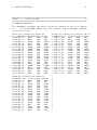
1
68HC11 Programmer’s Reference
Manual
Phillip Musumeci
[email protected]
November 1999
Version 1.7
Credits
• Engineer proofreading: Dr. Barbara La Scala;
• Cross Assembler for 68HC11: Motorola;
• University of Wollongong F1 system: Pete Dunster; and
• Many different public domain software tools: many helpful users.
References
1. Gene H. Miller, “Microcomputer Engineering”, Prentice Hall, Englewood Cliffs, NJ
07632, 1993. ISBN 0-13-584475-4.
2. Motorola, “HC11 — M68HC11 Reference Manual”, Part number M68HC11RM/AD.
3. Frederick F. Driscoll, Robert F. Coughlin, Robert S. Villanucci, “Data acquisition
and process control with the M68HC11 micro-controller”, Merrill/Macmillan International, 1994. ISBN 002330555X
4. Joseph L. Jones and Anita M. Flynn, “Mobile Robots: Inspiration to Implementation”, A.K. Peters, Wellesley, Massachusetts, 1993. ISBN 1-56881-011-3.
5. P. Dunster, “F1 System Reference Manual”, held in file F1V11DOC.PS in the archive
ftp://mirriwinni.cse.rmit.edu.au/pub/UoW/f1v11doc.zip
6. P. Musumeci, “Introduction to Microprocessor Systems”, lecture notes and data
packs are available from http://mirriwinni.cse.rmit.edu.au/~phillip/intro2up
Notes
• The latest release of this manual (PDF) is available from
http://mirriwinni.cse.rmit.edu.au/~phillip/intro2up.
• This document was prepared using the teTeX distribution of LATEX1 , dvips, and
xdvi. The diagrams were processed using the graphicx and pdftex packages of
LATEX, and the ps2pdf utility from ghostscript. The language aware editor xemacs
was used to prepare input text before checking with ispell. A (Free)BSD computing
environment has been employed.
Feedback
• Please email reports of errors in this document or suggestions for its improvement to
[email protected].
c
Phillip
Musumeci, November 1999
1
Feel the power of LATEX.
i
Contents
1 Introduction
1.1 Tools . . . . . . . . . . . . . . . . . . . .
1.2 Command Entry . . . . . . . . . . . . .
1.3 Program preparation . . . . . . . . . . .
1.4 Setting up your assembly language tools
1.4.1 Cross assembler — DOS . . . . .
1.4.2 Cross assembler — UNIX . . . .
2 Software development cycle
2.1 Understand the problem . . .
2.2 Plan Structure of Program . .
2.3 Data Structures . . . . . . . .
2.4 Coding . . . . . . . . . . . . .
2.5 Assembling . . . . . . . . . .
2.6 Downloading . . . . . . . . .
2.7 Target Machine Memory Map
3 Object File Downloading
3.1 System = HC11 board +
3.1.1 Procedure . . . .
3.2 System = HC11 board +
3.2.1 Procedure . . . .
3.3 System = HC11 board +
3.4 Troubleshooting . . . . .
.
.
.
.
.
.
.
.
.
.
.
.
.
.
.
.
.
.
.
.
.
.
.
.
.
.
.
.
.
.
.
.
.
.
.
.
.
.
.
.
.
.
.
.
.
.
.
.
.
.
.
.
.
.
.
.
.
.
.
.
.
.
.
.
.
.
.
.
.
.
.
.
.
.
.
.
.
.
.
.
.
.
.
.
.
.
.
.
.
.
.
.
.
.
.
.
.
.
.
.
.
.
.
.
.
.
.
.
.
.
.
.
.
.
.
.
.
.
.
.
.
.
.
.
.
.
.
.
.
.
.
.
.
.
.
.
.
.
.
.
.
.
.
.
.
.
.
.
.
.
.
.
.
.
.
.
.
.
.
.
.
.
.
.
.
.
.
.
.
.
.
.
.
.
.
.
.
.
.
.
.
.
.
.
.
.
.
.
.
.
.
.
.
.
.
.
.
.
.
.
.
.
.
.
.
.
.
.
.
.
.
.
.
.
.
.
.
.
.
.
.
.
.
.
.
.
.
.
.
.
.
.
.
.
.
.
.
.
.
.
.
.
.
.
.
.
.
.
.
.
.
.
.
.
.
.
.
.
.
.
.
.
.
.
.
.
.
.
.
.
.
.
.
.
.
.
.
.
.
.
.
.
1
2
3
3
4
4
4
.
.
.
.
.
.
.
5
5
5
5
6
6
7
7
.
.
.
.
.
.
.
.
.
.
.
.
.
.
.
.
.
.
.
.
.
.
.
.
.
.
.
.
.
.
.
.
.
.
.
.
.
.
.
.
.
.
.
.
.
.
.
.
10
10
10
11
11
11
12
4 Assembler directives
4.1 Setting the Program Location Counter . . . . . . . . . . . . .
4.1.1 ORG — SET PROGRAM LOCATION COUNTER . .
4.2 Setting Symbol and Label Values . . . . . . . . . . . . . . . .
4.2.1 EQU — EQUATE SYMBOL TO A VALUE . . . . . .
4.3 Memory Allocation . . . . . . . . . . . . . . . . . . . . . . . .
4.3.1 RMB — RESERVE MEMORY BYTES . . . . . . . .
4.3.2 FCC — FORM CONSTANT CHARACTER STRING
4.3.3 FCB — FORM CONSTANT BYTE . . . . . . . . . .
4.3.4 FDB — FORM DOUBLE BYTE CONSTANT . . . .
4.3.5 FILL — FILL MEMORY . . . . . . . . . . . . . . . .
4.3.6 BSZ — BLOCK STORAGE OF ZEROS . . . . . . . .
4.3.7 ZMB — ZERO MEMORY BYTES (same as BSZ) . .
4.4 Addressing Modes . . . . . . . . . . . . . . . . . . . . . . . . .
4.4.1 Register . . . . . . . . . . . . . . . . . . . . . . . . . .
4.4.2 Zero Page and Absolute Addressing . . . . . . . . . . .
.
.
.
.
.
.
.
.
.
.
.
.
.
.
.
.
.
.
.
.
.
.
.
.
.
.
.
.
.
.
.
.
.
.
.
.
.
.
.
.
.
.
.
.
.
.
.
.
.
.
.
.
.
.
.
.
.
.
.
.
.
.
.
.
.
.
.
.
.
.
.
.
.
.
.
.
.
.
.
.
.
.
.
.
.
.
.
.
.
.
.
.
.
.
.
.
.
.
.
.
.
.
.
.
.
14
14
14
14
15
15
15
15
16
16
16
16
16
17
17
17
PC/DOS + kermit . . . . . . . .
. . . . . . . . . . . . . . . . . . .
PC/DOS + procomm . . . . . .
. . . . . . . . . . . . . . . . . . .
FreeBSD + X-windows + kermit
. . . . . . . . . . . . . . . . . . .
ii
.
.
.
.
.
.
4.4.3
4.4.4
4.4.5
4.4.6
Immediate . . . . . . . . . . . . .
Register Indirect (with offset) . .
Bit Set/Clear . . . . . . . . . . .
Bit Test with Conditional Branch
.
.
.
.
.
.
.
.
.
.
.
.
.
.
.
.
.
.
.
.
.
.
.
.
.
.
.
.
.
.
.
.
.
.
.
.
.
.
.
.
.
.
.
.
.
.
.
.
.
.
.
.
.
.
.
.
.
.
.
.
.
.
.
.
.
.
.
.
.
.
.
.
.
.
.
.
17
18
18
19
5 Assembler listing file format
20
A 68HC11 CPU Registers
22
B 68HC11 Instruction Set
23
C 68HC11 Vectors
C.1 Jump Vectors . . . . . . . . . . . . . . . . . . . . . . . . . . . . . . . . . .
C.2 Buffalo Entry Points . . . . . . . . . . . . . . . . . . . . . . . . . . . . . .
27
28
32
D Monitor Symbol Definitions
D.1 F1 symbols . . . . . . . . . . . . . . . . . . . . . . . . . . . . . . . . . . .
35
35
E Makefile Example
39
F Real–Time Interrupt Example
40
G Miscellaneous Information
G.1 RESET Bootup Code in BUFFALO . . . .
G.1.1 EVBU and BUFFALO . . . . . . . .
G.1.2 F1 and RMIT/CSE BUFFALO . . . .
G.2 Recovering from BULKALL with RMIT/CSE
G.3 Enabling TRACE in BUFFALO . . . . . . .
G.4 Setting A/D voltage range . . . . . . . . .
G.5 Mode setting for expanded mode . . . . .
G.6 Summary of Port Signals used by BUFFALO
. . . . . .
. . . . . .
. . . . . .
BUFFALO
. . . . . .
. . . . . .
. . . . . .
. . . . .
.
.
.
.
.
.
.
.
.
.
.
.
.
.
.
.
.
.
.
.
.
.
.
.
.
.
.
.
.
.
.
.
.
.
.
.
.
.
.
.
.
.
.
.
.
.
.
.
.
.
.
.
.
.
.
.
.
.
.
.
.
.
.
.
.
.
.
.
.
.
.
.
.
.
.
.
.
.
.
.
.
.
.
.
.
.
.
.
.
.
.
.
.
.
.
.
43
43
43
43
43
43
43
44
44
H 68HC11 Net Resources
45
I
46
68HC11 Overview
List of Tables
1
2
68HC11F1 system memory map. . . . . . . . . . . . . . . . . . . . . . . . .
EVBU 68HC11E9 system memory map. . . . . . . . . . . . . . . . . . . .
iii
8
9
1 INTRODUCTION
1
1
Introduction
There are a large number of 68HC11 devices and 68HC11 development systems available. It
is possible for this generous choice to make initial use of a system confusing but fortunately,
most of the low cost systems make use of the same monitor program, BUFFALO, which
means that the programmer is presented with a common interface to the system and can
make use of a common set of subroutine routines in the on-board BUFFALO ROM. Another
characteristic of the 68HC11 family of devices, that they contain the same core set of
internal peripherals, means users are presented with a fairly uniform piece of hardware to
work with so confusion is avoided. Note that some recent devices now provide additional
internal peripherals or have more flexible input/output ports.
This document provides useful information for assembly language programmers who
are just beginning to use a 68HC11-based µprocessor system. Code assembly and downloading of object files is described for both UNIX and PC based software development
environments, and a summary of assembler directives is provided. Appendices include a
table of 68HC11 CPU instructions and a summary of important BUFFALO subroutine entry
points and vectors. Where appropriate, specific information for the Motorola Universal
Evaluation Board (EVBU) system and the University of Wollongong F1 system is given.
The Motorola EVBU system supports a number of MC68HC11 variants including A8,
E9, and 711E9 on a small PCB with a small prototyping area. These MC68HC11s have 512
bytes of EEPROM and 256 (A8) or 512 (E9,711E9) bytes of RAM. The A8 and E9 devices
usually contain BUFFALO in ROM while the 711E9 contains EPROM that the user may
program. Recently, the E series devices have had versions with larger EEPROM available,
e.g. the 811E2 has 2K of EEPROM, while the A8 is no longer manufactured. The EVBU
has an RS232 interface and a real time clock chip (MC68HC68T1) that is connected to the
CPU via the serial peripheral bus.
The Wollongong F1 system uses the MC68HC11F1FN device which contains similar
internal peripherals to the A8 and E9 devices and the same amount of EEPROM but it has
0K bytes of internal ROM and 1K bytes of internal RAM. In this system, BUFFALO (and
any other desired firmware) is stored in an external 32K EPROM. The board can also hold
a 32K RAM device so tasks requiring additional storage are feasible. Much of the design of
the system is in the public domain to assist the micro-controller enthusiast and the reference
manual includes the complete circuit diagram and describes operation and construction of
the CPU board plus the various configuration options (memory devices supported, etc).
A list of part suppliers is included, with Australian and U.S.A. sources available for the
(very) economical CPU PCB, a motor controller interface PCB, and a keypad and LCD
module interface PCB. The various PCBs are relatively small and stack together in a
compact manner suitable for mobile robot experiments. C language programming is also
supported. Note that the F1 variant of the 68HC11 is available with clock frequencies of
8MHz (MC68HC11F1FN), 12MHz (MC68HC11F1FN3) and 16MHz (MC68HC11F1FN4)
allowing a system “E” bus clock of 2MHz, 3MHz, and 4MHz respectively. Further details
on this system may be obtained from the following sources:
1 INTRODUCTION
2
• http://mirriwinni.cse.rmit.edu.au/~phillip/f1
• http://mirriwinni.cse.rmit.edu.au/~f1
• ftp://mirriwinni.cse.rmit.edu.au/pub/UoW
1.1
Tools
Many public domain tools exist for 68HC11 programmers, including:
• a 68HC11 assembler, as11, from Motorola;
• a number of 68HC11 simulators, sim68hc11 by [email protected] and SIM68 by P. J. Fisch;
• macro processors such as GNU m4 and GNU C cpp; and
• C language support such as ICn a native C (subset) compiler (beta), and GNU gcc
68HC11 port (no floats) by Otto Lind ([email protected]).
Note that the as11 assembler and m4 macro processor are available for PC hosts (executables) and UNIX hosts (source distribution).
Section H lists internet sites from where the various tools may be obtained. In particular, the ftp site ftp://mirriwinni.cse.rmit.edu.au/pub/uP/68HC11.local holds:
• zip archive files with names ending in .ZIP (uppercase) which contain copies of the tools
for PC hosts;
• files symbols.e9, symbols.f1w, symbols.f1p, and vectors which list symbols and
vectors for various 68HC11 systems;
• directory Sources which contains assembly language program examples, including file
memtest which is a basic memory test utility adapted from a Motorola 6800 monitor
(the instructions for use are at the beginning of the source file);
• directory 68HC11 User Manual Examples which contains some assembly language program examples distributed with the Motorola 68HC11 Reference Manual;
• directory buffalo-source which contains archives of the assembly language source and
hex files for various versions of the BUFFALO monitor program; and
• gzip–compressed tar archive file Motorola-8bit-asm-v2.09.tar.gz which is the source
for the cross assembler.
A number of very economical tools are available for 68HC11 programmers, including:
• the HITECH integrated development systems — see http://www.hitech.com.au;
1 INTRODUCTION
3
• the ImageCraft C compiler (ICC), which runs under DOS and OS/2, provides a documented near ANSI C compiler, assembler, linker, and librarian; and the Dunfield
Development Systems integrated development environment for the 68HC11 — for
details, see file
ftp://mirriwinni.cse.rmit.edu.au/pub/uP/FAQ/Microcontroller-primer+faq.
1.2
Command Entry
In the information that follows, ←- means to press the “Return” key to enter a command
line of text. A control key such as control e (where you hold the control key down while
typing the e key) will be represented as C-e. As typing C-m is equivalent to typing ←-,
we may also say C-m to indicate command entry.
1.3
Program preparation
You will be using a DOS or UNIX host to develop software for your 68HC11 system.
This host computer will supply you with tools such as an editor and assembler (described
shortly), and is quite separate to the target system with its 68HC11 CPU. Such an environment is called a cross development environment because the two computers, the host and
the target, are different (in this case, they have different CPUs). When you are developing
software and testing it on a real system, you will have to perform the following tasks:
1. Enter your program as source code on the development host using a plain text editor
to create a source file — the source code is where you describe (or prescribe) the data
storage and processor operations unique to your program for the target system;
2. Cross assemble the source file on the host to produce an object file and an optional
listing file — the listing file displays a merged representation of the source code
(written by you) and the binary codes (which are meant for the target CPU), and
the object file is a complete image of the required contents of the target system’s
memory (data and instructions) that must eventually be transferred to the target
CPU before it may execute your program;
3. Download the object file — this is the process whereby the object file is transferred
from the host system into the target system’s memory; and
4. Run your program — this is where you get to run your program on the target system,
possibly making use of program trace or single stepping execution.
It is possible to think of these stages from the view point of more “traditional” software
development — stage 2 is similar to running a compiler, stage 3 is similar to loading the
program into memory, and stage 4 is equivalent to dropping the start flag2 on the CPU.
2
In this document, we will attempt to highlight the F1’s position at the high speed, Grand Prix end
of 68HC11 micro-controller operation — the higher performance being partially due to the higher clock
speeds that are more easily accommodated without a multiplexed external memory system.
1 INTRODUCTION
1.4
1.4.1
4
Setting up your assembly language tools
Cross assembler — DOS
For DOS systems, the cross assembler is available in executable form. You must obtain a
copy of the cross assembler AS11.EXE and install it in a directory in your DOS PATH or the
directory where you intend to do your 68HC11 work. Obtain a copy of the zip archive
ftp://mirriwinni.cse.rmit.edu.au/pub/uP/68HC11.local/DOS-6811.ZIP.
An alternative archive with a newer version of the assembler is also available in archive
ftp://mirriwinni.cse.rmit.edu.au/pub/uP/68HC11.local/DOS-HC11.ZIP
but little work with this version has been done here. If you do not already have a tool for
extracting files from zip archives, take a copy of
ftp://mirriwinni.cse.rmit.edu.au/pub/uP/68HC11.local/unzip.exe.
You can install the assembler via commands such as:
cd \
mkdir 68hc11
cd 68hc11
a:\unzip a:\DOS-6811
where I have assumed that you have a copy of DOS-6811.ZIP and unzip.exe in the top
directory of drive A:. Before using as11, don’t forget to modify your autoexec.bat system
initialisation batch file so that directory 68hc11 is included in PATH if you intend to do
68HC11 work in a different directory.
1.4.2
Cross assembler — UNIX
For a UNIX system, you will usually have to compile your assembler. Take a copy of the
gzip compressed tar archive Motorola-8bit-asm-v2.09.tar.gz from
ftp://mirriwinni.cse.rmit.edu.au/pub/uP/68HC11.local/ and extract the source files
and compile via
gnutar xzvf Motorola-8bit-asm-v2.09.tar
cd asm-v2.09
make as11
Inspect the Makefile to see the cross assemblers that can be made for other 8bit Motorola
CPUs. This set of cross assemblers is known to compile with GNU C on SunOS-4 SPARC
and FreeBSD Intel systems. The executable as11 should be installed in a standard place
or where you keep your executables. One way to test the assembler would be to obtain
a copy of BUFFALO and assemble it, and then compare outputs — source and related files
are available from http://mirriwinni.cse.rmit.edu.au/~phillip/f1.
2 SOFTWARE DEVELOPMENT CYCLE
2
5
Software development cycle
2.1
Understand the problem
What is it you need to do? Identify the data inputs and data outputs that your program
will have. If you are controlling hardware (or interfacing to peripherals etc), make a note to
consider having a separate initialisation stage and data processing stage in your program.
Search the list3 of subroutines available in BUFFALO that is included in Section C — maybe
there are code fragments here that you can simply use. Are similar problems solved by
any of the code examples stored on the anonymous ftp sites (see Section H) or included in
the texts. Have a look!
2.2
Plan Structure of Program
Plan the program at a high level using a flowchart, pseudo-code or your favourite high
level language. It is important to understand the “big picture” and be able to describe
what you need to do. Only after you know the “big picture” should you even think about
writing code!
One way to break up a complex task into smaller more manageable parts is to use
subroutines — if subroutines are being used, such as your own and/or some of those in
BUFFALO, state what the necessary input parameters are, what the output values returned
are, and note any side effects such as CPU registers or memory locations that are modified.
Don’t be afraid to go over what you have done so far and check that it makes sense —
question how you divided the overall task up into smaller, more manageable parts. Are
the loop structures appropriate? You can have a loop continuation test ahead of the main
body of the loop like in a while do construct or a for( ; ; ) construct, or you can have
the loop continuation test at the end of loop like in a repeat until construct, etc. Of
course, in machine language, you can have as many loop exits anywhere you like so long
as Nicklaus Wirth4 never finds out!
2.3
Data Structures
Design the data representation and storage. Consider issues such as: whether variables can
be represented as single or double byte quantities or is a different data type appropriate;
what is the best form of data structure to use e.g. arrays, EOT terminated character strings,
a stack mechanism or a queue, etc.
If you plan to use subroutines, choose the format of the data exchanged between the
various sections of code (e.g. a data element on a stack or perhaps a global variable, etc).
3
4
Also available as file ftp://mirriwinni.cse.rmit.edu.au/pub/uP/68HC11.local/vectors.
Author of “PASCAL User Manual and Report” and “Programming in Modula-2”.
2 SOFTWARE DEVELOPMENT CYCLE
2.4
6
Coding
Start filling in the details by writing code for the algorithm(s) and program structure that
you have designed. So long as each program part has a known method of exchanging
information with the other parts of your program (you did plan this earlier, didn’t you?),
it is safe to write/edit the assembly language source file on the host computer:
1. Choose the position of code and data in memory. If your system has a version of
BUFFALO in ROM, you can usually take advantage of zero page storage in region
$0000. . .$0032 (the remaining memory up to $00FF is usually used by the BUFFALO
monitor). If you have a Wollongong F1 board running its modified buf32, you can
use memory in regions $0100. . .$03FF and $2000. . .$7CFF as shown in Table 1. If the
F1 board has the modified buf34, you can use memory in regions $0000. . .$032C and
all of $2000. . .$7FFF if the external RAM chip is fitted. Write the necessary ORG and
RMB,FCB,FDB,FCC assembler directive statements (see sections 4.1,4.3). You should
document these statements in terms of your data storage design and use.
The limited amount of storage in zero page memory (addresses $00xx) provides
slightly faster access times because most 68HC11 instructions accessing this memory region have a special form which only requires 1 operand byte to specify the
least significant byte xx of the address (the most significant byte is always 00).
Hence, for maximum speed, you should select variables which will be frequently
accessed for allocation in unused zero page memory. Note that the size of your
program will also shrink slightly (the instructions accessing zero page memory
have a smaller format hence are faster to fetch).
2. Use the EQU assembler directive (see section 4.2) to declare the names and addresses
of any external subroutines that you have decided to use — include at least a brief
description of what these subroutines do. Also define any symbolic constants that
you wish to use.
3. Write the CPU instructions. You should document these statements in terms of your
program plan (flowchart or pseudo-code or a HLL).
4. Finish with the END assembler directive statement. If you want execution of BUFFALO
to resume once your program finishes, include a JMP WARM at the end of your CPU
executable instructions.
2.5
Assembling
Assemble the program by entering the host command as11 prog -l > prog.lst ←-.
This command example shows the -l switch produce a listing which is redirected via
> prog.lst to the listing file. An object file called prog.s19 is created if assembly is
successful. Look at the listing file to confirm the arrangement of instructions and data
2 SOFTWARE DEVELOPMENT CYCLE
7
storage you chose and also to see any assembler errors5 messages next to the offending
source statements.
The object file or HEX file contains a complete description of the instructions and
constant data that you have prescribed by writing your assembly language program — in
effect, it is similar to an executable that you might have prepared by using a compiler on
the host computer. The HEX file is sometimes called an S19 file because of the particular
format used — display it and you will notice that for 68HC11 use, each line either begins
with the string S1 or S9 hence the name.
2.6
Downloading
In order to run the assembly language program, we must first transfer the information in this HEX file into the memory of the target 68HC11 system by a process called
downloading. The method used to download the HEX file varies according to the type of
host and choice of software tools that you have made.
In general, it is not possible to download into EEPROM storage (locations
$B600. . .$B7FF for the A8 and E9 and locations $EE00. . .$EFFF for the F1 in the
University of Wollongong board) because of the longer write times involved. However, it is possible to use BUFFALO to download data into RAM and then use the move
command to copy the data into EEPROM. For example, data downloaded into RAM
region $2000. . .$200F may be transferred to EEPROM via the BUFFALO command
move 2000 200f b600←-. However, unless this code is position-independent, you
must assemble the code in the EEPROM location, translate its HEX file to correspond to being in a RAM location, download it to RAM, and then use the block
move to translate/copy it back to the actual EEPROM.
2.7
Target Machine Memory Map
Motorola 68HC11 micro-controllers are constructed with varying amounts of internal RAM,
ROM, EPROM, and EEPROM. In the case of the MC68HC11F1FN, this storage can be
relocated in the memory space and this document describes the default storage locations
for A8 and E9 devices as setup from the factory and the default storage locations for the F1
as initialised by the modified version of BUFFALO supplied by the University of Wollongong
(Pete Dunster) and RMIT (Phillip Musumeci).
Note that when internal storage and external storage occupy the same locations, the
internal storage takes precedence. For example, suppose an MC68HC11 is run in expanded
mode whereby it can access a RAM device in the address region $0000. . .$7FFF. This
MC68HC11 will also contain some on-board zero-page RAM in locations $0000. . .$00FF
and any accesses to RAM will use this internal RAM. The user may indeed observe valid
5
All errors at this stage are assembly errors as we are using tools on the host system to determine
the binary representation of the target system’s program. Later on, when you are actually running your
program, then you will be able to have run-time errors!
2 SOFTWARE DEVELOPMENT CYCLE
8
external bus signals when the CPU is accessing its internal zero-page RAM but the data
used will be transferred to and from the internal storage. We say that the internal storage
is “overlaying” the external storage and hence takes precedence.
The memory map of the Wollongong F1 system operating with an MC68HC11F1FN
micro-controller is shown in Table 1. The default memory map of a Motorola EVBU system operating with an MC68HC11E9 micro-controller and running the standard BUFFALO
version 3.2 is shown in Table 2. If a 68HC811E2 is used, note that the 2K of EEPROM
can be mapped to the top of any 4K boundary.
It is possible to fit an additional 32K of RAM to the EVBU system. Some sample PCB
layouts and GAL equations are available at
http://mirriwinni.cse.rmit.edu.au/~phillip/evbu-mem-exp/index.html. At RMIT,
this RAM uniquely occupies $2000. . .$9FFF and a 4K segment may be mirrored to region
$Cxxx to allow the beginner to perform BUFFALO exercises exactly as described in Miller’s
“Microcomputer Engineering”, Appendix D.7.
$0000
$03FF
$0000
$03FF
$1000
$105F
$1800
$1FFF
$2000
$7FFF
$2000
$7FFF
$8000
$FFFF
Start of internal RAM (1K bytes) $0000
UoW buffalo 3.2 only
End of internal RAM
$03FF
Start of internal RAM (1K bytes) $0000
$032C
RMIT/cse buffalo 3.4 only
$032D
End of internal RAM
$03FF
Start of internal peripherals
End of internal peripherals
Start of external peripherals
End of external peripherals
Start of external RAM
$2000
$7CFF
UoW buffalo 3.2 only
$7D00
End of external RAM (part 2)
$7FFF
Start of external RAM
$2000
RMIT/cse buffalo 3.4 only
End of external RAM
$7FFF
Start of external EPROM
$8000
(512 byte internal
$EE00
EEPROM overlay)
$EFFF
End of external EPROM
$FFFF
Start of user RAM
End of internal user RAM
Start of user RAM
End of user RAM
Start of buffalo RAM
End of buffalo RAM
Memory
mapped
IO
peripherals
More external user RAM
End of external user RAM
Start of RAM used by BUFFALO
End of RAM used by BUFFALO
More external user RAM
End of external user RAM
Start of BUFFALO / apps.
Start of internal EEPROM
End of internal EEPROM
End of BUFFALO / apps.
Table 1: 68HC11F1 system memory map.
2 SOFTWARE DEVELOPMENT CYCLE
$0000
$00FF
$01FF
$1000
$103F
$B600
$B7FF
$D000
$FFFF
Start of internal RAM (512 bytes)
9
$0000
$0032
$0033
$00FF
$0100
$01FF
Start of page 0 user RAM
End of page 0 user RAM
Start of RAM used by BUFFALO
End of internal RAM (A8)
End of RAM used by BUFFALO
Cont. internal user RAM (E9)
End of internal RAM (E9)
End of internal user RAM (E9)
Start of internal peripherals
Memory mapped
End of internal peripherals
IO peripherals
Start of internal EEPROM (512 bytes) $B600 Start of internal EEPROM
End of internal EEPROM
$B7FF End of internal EEPROM
Start of internal ROM (12K bytes)
Start of BUFFALO
End of on-board ROM
End of BUFFALO
Table 2: EVBU 68HC11E9 system memory map.
3 OBJECT FILE DOWNLOADING
3
10
Object File Downloading
There are a variety of ways that you can connect a 68HC11 board to a variety of host
computers — hopefully, what you are using is covered here.
3.1
System = HC11 board + PC/DOS + kermit
The PC is connected to the HC11 board via a serial cable. Invoke the kermit communications program, select a port and serial communications speed and then connect via
commands:
set port com1
set baud 9600
set parity none
connect
You should now be communicating with the BUFFALO monitor program running on the
HC11 board. If your HC11 board is connected to some other port such as COM2, adjust
the first command above (and the instructions that follow) in the obvious way.
3.1.1
Procedure
1. Instruct BUFFALO to do a download from the terminal by typing load t←- or, equivalently, l t←-.
2. We now need to get the PC to send the file to the HC11 so first return to kermit
local command mode by typing C-] c . The control key that you need to type to
get kermit’s attention is displayed in the bottom left of the status line — the default
is C-] but kermit can be configured for a different key stroke.
3. Now use either of the following file transfer methods:
(a) Using DOS to transmit the file:
• To get a new DOS shell, enter push←- to kermit.
• Send the .s19 hex file out through port COM1 with DOS command
type prog.s19 > COM1←-.
• Return to kermit with the DOS command exit←-.
(b) Using kermit to transmit the file:
• Enter transmit prog.s19←-.
4. Reconnect to the HC11 system with command connect←- or, equivalently, c←-.
If the download was not successful, see the troubleshooting section 3.4. When you are
finished using kermit, return to local mode and quit from kermit by typing exit←-.
3 OBJECT FILE DOWNLOADING
3.2
11
System = HC11 board + PC/DOS + procomm
The PC is connected to the HC11 board via a serial cable. Invoke the procomm communications program and type Alt-P, then choose option 5, and then select the following serial
communications parameters:
9600 baud, no parity, 8-bits, 1-stop bit, full duplex
Then setup the text file transfer parameters by typing Alt-S, choose option 6, and then
select:
Echo Local
Expand Blank Lines
Pace Character
Character Pacing
Line Pacing
CR Translation
LF Translation
Yes
Yes
0
25 (1/1000 second)
10
None
None
Save the above settings to disk for future use.
3.2.1
Procedure
1. Instruct BUFFALO to do a download from the terminal by typing load t←- or, equivalently, l t←-.
2. Instruct procomm to send the HEX file by pressing the Pg Up and follow the instructions to select the HEX file to send. Use the ASCII transfer protocol.
3. A successful download results in the message Done from BUFFALO. If the download
failed, see section 3.4.
3.3
System = HC11 board + FreeBSD + X-windows + kermit
In this mode of operation, you perform all software development on the FreeBSD UNIX
host and use a communications program such as kermit or minicom to access the target
system. As you will have (most likely) compiled the cross assembler, you should also refer
to the relevant cross assembler documentation. If the kermit communications program is
used, run it with the -l switch to select a port e.g. kermit -l /dev/cuaa2, and make
sure that your serial port (e.g. /dev/cuaa2) can be read from and written to by group
dialer (as kermit changes its effective ID to dialer when run). The following default
settings can be placed in a file such as ~/.kermrc-hc11:
3 OBJECT FILE DOWNLOADING
set
set
set
set
set
set
set
set
12
transmit echo on
transmit linefeed off
transmit fill \32
transmit pause 25
transmit prompt 0
transmit eof \n
hand none
flow none
Kermit can be run via command kermit ~/.kermrc-hc11 -Y -l /dev/cuaa2. The procedure for downloads is similar to that of DOS + kermit, but only transmit prog.s19←is used to send an S19 file to the target system.
3.4
Troubleshooting
If you see a message about a ROM error, then this indicates that the system has been
unable to download your program’s HEX file into memory at the location reported in the
message. A common cause for this is that you are attempting to locate your program’s
instruction or constant data in a part of the memory space at which there is no storage
installed. For example, many 68HC11 systems do not have any RAM in the address range
$A000. . .$AFFF — if you set the assembler’s program location counter to this range (e.g.
via an org $a000) and then assemble code, you will obviously not be able to download
and then run your program. The obvious solution is to check that your program is located
or positioned in the regions corresponding to RAM.
Another common cause is to interfere with the download function itself. When a HEX
file is being downloaded, we are relying on a part of the BUFFALO monitor to receive each
character, interpret it, and eventually to store some data into RAM. To do this, BUFFALO
needs to have some temporary storage of its own and (for a BUFFALO held in internal ROM)
this RAM is located in the region $0033. . .$00FF. If your program downloads any data or
instructions in this region of memory, you may possibly overwrite storage being used by
BUFFALO and the download will fail. The obvious solution is to not store any constant
data or instructions in this memory region. Actually, if your program is taking advantage
of subroutines in BUFFALO, it is probably not a good idea to use any variable storage in
the region $0033. . .$00FF either unless you carefully read the relevant BUFFALO source and
verify the storage will not be used.
If the program was correctly positioned at a location where there is memory available,
then the download error might mean that the system has an internal hardware error. Since
BUFFALO is actually running, the 68HC11 CPU is obviously alive. You could try using the
memory modify command in BUFFALO to see if you can store/modify/read data in the
external RAM. It is sometimes the case that students bend CPU pins by inserting probes
into the CPU (and/or port replacement unit) socket that should not be inserted into these
sockets and this prevents CPU signals reaching devices such as the external address bus
and other external peripherals and memory. You might be able to detect this by observing
3 OBJECT FILE DOWNLOADING
13
that 1 of the bits in external memory is always read as a 0 or 1 no matter what you store.
Get a logic probe and verify that there is indeed life (or the absence of life) on the external
memory bus and data bus (touch the probe on a data bus leg of the chip in question if
you want to verify that CPU generated signals are reaching any particular chip). An item
that many people find they check last is the power supply — is the +5V regulator giving
the correct output?
4 ASSEMBLER DIRECTIVES
4
14
Assembler directives
Assembler directives are statements in the assembly language source file that specify how
you want the data storage and CPU instructions organised. Remember that they are
only “acted upon” by the assembler — they are not executable by the target CPU. The
assembler directives available with the Motorola Freeware assemblers are now described.
Note that items displayed within [square] brackets are optional while items displayed
within <triangle> brackets are mandatory. A plain text description of these assembler
directives is also available on-line in the file
ftp://mirriwinni.cse.rmit.edu.au/pub/uP/68HC11.local/asref.man.
4.1
Setting the Program Location Counter
Recall (from lecture notes) that the assembler processes the data storage declarations and
CPU instructions in your assembly language source file to create an image of the target
CPU’s memory contents, as required by your program. At any stage as your source file
is processed by the assembler, the program location counter (PLC) is the variable in the
assembler that represents where any output for the current source line will be deposited.
Since we may wish to position storage and instructions in particular locations in memory,
it is necessary to be able to set the assembler’s PLC.
4.1.1
ORG — SET PROGRAM LOCATION COUNTER
ORG <expression> [;comment]
The ORG directive changes the program location counter to the value specified by the expression in the operand field. Subsequent statements are assembled into memory locations
starting with the new program location counter value. If no ORG directive is encountered
in a source program, the program location counter is initialized to zero.
4.2
Setting Symbol and Label Values
When writing assembly language, it is advantageous to be able to refer to quantities via
a symbol or label. In particular, you should define symbols to represent constants at the
beginning of your program and then use these symbols and labels throughout the program
— if you ever need to change the value of the constant, it is only necessary to change one
line of code. Further, it is more meaningful to a reader to see alphanumeric symbols and
labels within the source code instead of binary values etc, because the symbols and labels
can be based on a word or phrase that helps a (human) reader recognise the quantity
involved.
In assembly language, we can use symbols to represent data constants and/or addresses.
4 ASSEMBLER DIRECTIVES
4.2.1
15
EQU — EQUATE SYMBOL TO A VALUE
LABEL
EQU <expression> [;comment]
The EQU directive assigns the value of the expression in the operand field to the label. In
the expression, the character * represents the current program location counter. Hence,
if the expression is simply the * character, then the EQU directive assigns the value of
the program location counter to the label. A label can only be defined once with the EQU
assembler directive.
4.3
Memory Allocation
Memory allocation may or may not involve initialisation i.e. you can direct the assembler
to set aside some storage and give it a name for easy reference when you code later (e.g. the
RMB assembler directive) or you can set aside some storage and prescribe what its contents
will be (e.g. all the other memory allocation directives including some for allocating storage
to hold messages or character strings, bytes of data, words of data, just zeros, etc).
4.3.1
RMB — RESERVE MEMORY BYTES
[LABEL] RMB <expression> [;comment]
The RMB directive causes the program location counter to be advanced by the value of the
expression in the operand field. This directive reserves a block of memory the length of
which in bytes is equal to the value of the expression. The block of memory reserved is
not initialized to any given value.
4.3.2
FCC — FORM CONSTANT CHARACTER STRING
[LABEL] FCC <delimiter><string><delimiter> [;comment]
The FCC directive is used to store ASCII strings into consecutive bytes of memory. The byte
storage begins at the current program location counter. The label is assigned to the first
byte in the string. Any of the printable ASCII characters can be contained in the string.
The string is specified between two identical delimiters which can be any printable ASCII
character. The first non-blank character after the FCC directive is used as the delimiter.
Example:
MSG1
ORG
FCC
FCB
$2200
"Hello world"
4
4 ASSEMBLER DIRECTIVES
4.3.3
16
FCB — FORM CONSTANT BYTE
[LABEL] FCB <expr>(,<expr>,...,<expr>) [;comment]
The FCB directive may have one or more operands separated by commas. The value of each
operand is truncated to eight bits, and is stored in a single byte of the object program.
Multiple operands are stored in successive bytes. The operand may be a numeric constant,
a character constant, a symbol, or an expression.
4.3.4
FDB — FORM DOUBLE BYTE CONSTANT
[LABEL] FDB <expr>(,<expr>,...,<expr>) [;comment]
The FDB directive may have one or more operands separated by commas. The 16-bit value
corresponding to each operand is stored into two consecutive bytes of the object program.
The storage begins at the current program location counter. The label is assigned to the
first 16-bit value. Multiple operands are stored in successive bytes. The operand may be
a numeric constant, a character constant, a symbol, or an expression.
4.3.5
FILL — FILL MEMORY
[LABEL] FILL <expression>,<expression>
The FILL directive causes the assembler to initialize an area of memory with a constant
value. The first expression signifies the one byte value to be placed in the memory and
the second expression indicates the total number of successive bytes to be initialized. The
first expression must evaluate to the range 0 . . . 255.
4.3.6
BSZ — BLOCK STORAGE OF ZEROS
[LABEL] BSZ <expression> [;comment]
The BSZ directive causes the Assembler to allocate a block of bytes. Each byte is assigned
the initial value of zero. The number of bytes allocated is given by the expression in the
operand field.
4.3.7
ZMB — ZERO MEMORY BYTES (same as BSZ)
[LABEL] ZMB <expression> [;comment]
The ZMB directive causes the Assembler to allocate a block of bytes. Each byte is assigned
the initial value of zero. The number of bytes allocated is given by the expression in the
operand field.
4 ASSEMBLER DIRECTIVES
4.4
17
Addressing Modes
The assembler interprets the syntax of the operands to allow us to specify the addressing
mode at assembly time. In the following description of addressing modes syntax, XXX
represents a generic instruction.
4.4.1
Register
Register addressing (A,B,D,X,Y) or inherent — there is no operand following the instruction. Example:
inca
decb
4.4.2
Zero Page and Absolute Addressing
Data accesses in zero page and elsewhere in memory — the instruction and operand have
the form
XXX
<expression>
which the assembler evaluates into 1 or 2 bytes of operand data following the op-code.
When the instruction is executed later, the CPU fetches these bytes and uses them to form
the effective address of the data to use. Example:
VAR1
VAR2
ORG
RMB
ORG
RMB
ORG
ldaa
ldaa
0
1
$2000
1
$3000
VAR1
VAR2
; access a zero page variable
; access a variable anywhere in memory
Observe that the assembly language instructions are exactly the same but the assembler
figures out that VAR1 is located in the first page of memory so the binary representation of
instruction LDAA VAR1 will use 2 bytes of storage (opcode byte plus least significant byte
of effective address) whereas LDAA VAR2 will require 3 bytes of storage (opcode byte plus
2 bytes of effective address). We say that for zero page addressing, the effective address
= $00xx where xx is the operand byte of data at location PC+1. For absolute addressing
(Motorola Extended addressing), the effective address = $xxyy where xx is the operand
byte of data at location PC+1 and yy is the operand byte of data at location PC+2.
4.4.3
Immediate
Immediate or constant — the instruction and operand have the form
XXX
#<expression>
4 ASSEMBLER DIRECTIVES
18
which the assembler evaluates into 1 or 2 bytes of data that follow the op-code. (When
the instruction is executed later, the CPU fetches these bytes and uses them as data.)
Example:
CONST
EQU
ldx
ldy
$1000
#CONST
; load X with a constant
#CONST+2 ; load Y with a different constant
We say that the effective address = PC+1 i.e. the location(s) immediately following the
opcode.
4.4.4
Register Indirect (with offset)
Register indirect — the instruction and operand have the form
XXX
<expression>,X
XXX
<expression>,Y
or
The assembler evaluates the <expression> into a 1 byte offset that follows the op-code.
When the instruction is executed later, the CPU fetches the offset byte and adds it to the
index register to form the effective address of the data byte(s) to use. Example:
CONST
EQU
ldx
ldd
$1000
#CONST
2,X
; load X with a base address
; load bytes at memory locations
; $1002,$1003 into register D
We say that the effective address = <expression> + index register contents.
4.4.5
Bit Set/Clear
Bit set or clear — the instruction and operands have the form
XXX
<expression1> <expression2>
XXX
<expression1> <expression2>,X
XXX
<expression1> <expression2>,Y
or
or
where in the first case, <expression2> is the address of the zero page byte whose bits are
being manipulated, and <expression1> is a mask in which each bit=1 identifies a bit that
will be set or cleared. In the other two cases, <expression2> is an offset that is added
to the designated index register to give the effective address of the byte to manipulate.
After the CPU fetches the operands, it interprets the second byte fetched after the op-code
as all or part of the effective address whose contents are masked with the byte fetched
immediately after the op-code fetch. The new value is written back to memory. Example
of clearing a bit in port A:
4 ASSEMBLER DIRECTIVES
REGBS
EQU
ldx
bclr
19
$1000
; location of on-board peripherals
#REGBS
; load X with a base address
%00000010 0,X ; clear bit 1 of portA and
; leave bits 0,2-7 unchanged
We say that the effective address of the target byte = <expression2> + index register
contents.
4.4.6
Bit Test with Conditional Branch
Bit test and branch — the instruction and operands have the form
XXX
<expression1> <expression2> <expression3>
XXX
<expression1> <expression2>,X <expression3>
XXX
<expression1> <expression2>,Y <expression3>
or
or
where <expression1> is the bit test mask and <expression2> specifies the data byte, as
for the bit set and bit clear modes described earlier. The <expression3> operand is the
branch offset. Here is an example of testing a bit in port A and branching if the bit is set:
REGBS
PAO
EQU
EQU
ldx
brset
$1000
; location of on-board peripherals
0
; port A offset from REGBS
#REGBS
; load X with a base address
%10000000 PAO,X DEST
; goto DEST if port A bit 7 high
We say that the effective address of the target byte = <expression2> + index register
contents, and that the effective address of the destination = <expression3> + PC.
5 ASSEMBLER LISTING FILE FORMAT
5
20
Assembler listing file format
The Assembler listing has the following format:
LINE#
ADDR
OBJECT CODE BYTES
[ # CYCLES]
SOURCE LINE
The LINE# is a 4 digit decimal number printed as a reference. This reference number is
used in the optional cross reference. The ADDR is the hex value of the address for the first
byte of the object code for this instruction. The OBJECT CODE BYTES are the assembled
object code of the source line in hex. If a source line causes more than 6 bytes to be output
(e.g. a long FCC directive), additional bytes (up to 64) are listed on succeeding lines with
no address preceding them. The # CYCLES will only appear in the listing if the c option is
in effect. It is enclosed in brackets which helps distinguish it from the source listing. The
SOURCE LINE is reprinted exactly from the source program, including labels.
The symbol table has the following format:
SYMBOL
ADDR
The symbol is taken directly from the label field in the source program. The ADDR is the
hexadecimal address of the location referenced by the symbol. An example follows.
Assembler release TER_2.0 version 2.09
(c) Motorola (free ware)
0001
; re-entry point for the buffalo monitor
0002 ff7c
WARM
EQU
$FF7C
0003
0004 0000
ORG
0
0005 0000
VAR1
RMB
1
0006
0007 2000
ORG
$2000
0008 2000
VAR2
RMB
1
0009
0010 3000
ORG
$3000
0011
; access a zero page variable
0012 3000 96 00
[ 3 ]
ldaa
VAR1
0013
; access a variable anywhere in memory
0014 3002 b6 20 00
[ 4 ]
ldaa
VAR2
0015
; load index registers
0016 3005 fe 43 2d
[ 5 ]
ldx
TMPX
0017 3008 18 fe 43 2f
[ 6 ]
ldy
TMPY
0018
; jump back to buffalo
0019 300c 7e ff 7c
[ 3 ]
jmp
WARM
0020
0021
; sample FCC for message string
0022 4321
ORG
$4321
0023 4321 48 65 6c 6c 6f 20
MSG1
FCC
"Hello world"
77 6f 72 6c 64
0024 432c 04
FCB
4
0025
5 ASSEMBLER LISTING FILE FORMAT
0026 432d
0027 432f
0028
Program + Init Data = 27 bytes
Error count = 0
MSG1
TMPX
TMPY
VAR1
VAR2
WARM
4321
432d
432f
0000
2000
ff7c
*0023
*0026
*0027
*0005
*0008
*0002
0016
0017
0012
0014
0019
TMPX
TMPY
21
RMB
RMB
END
2
2
A 68HC11 CPU REGISTERS
A
22
68HC11 CPU Registers
Figure 1 shows the CPU registers that we are primarily concerned with when programming. At the commencement of instruction execution, register PC holds the address of the
opcode. During the execution of an instruction (i.e. after the opcode has been fetched), it
can also hold the address of the next operand to be fetched. Once all of an instruction has
been fetched, it holds the address of the next instruction’s opcode (again).
The accumulator registers A and B can hold byte-sized (8 bit) data as it is being
manipulated. For word-sized (16 bit) data, the A and B registers may be used in a
concatenated form called D (for double accumulator). Index registers X and Y (also called
IX and IY) can be used to hold address-sized quantities — even their name suggests that
they are suitable for “indexing” a particular location in memory. Note that register X also
plays a role in handling word-sized data in association with the main word-sized register
D.
Register SP is used by the stack storage facility provided in the 68HC11 CPU. The
stack grows towards address $0000 and register SP points at the next location to hold
data (i.e. when a byte of data is retrieved from the stack, register SP is first incremented
and then a byte of data is read from memory at effective address given by the new value
in SP).
Accumulator A
7
Accumulator B
0
7
0
15
0
Accumulator D
15
0
Index Register X
15
0
Index Register Y
15
0
Program Counter PC
15
0
Stack Pointer SP
C
Condition Code Register CC
S
X
H
I
N
Z
V
Figure 1: 68HC11 CPU Registers.
B 68HC11 INSTRUCTION SET
23
The condition code register CC holds the current CPU state. Some bits hold a summary
of recent data manipulation performed by the arithmetic logic unit (ALU). In particular,
there are bits: N — last result was negative; Z — last result was zero; V — last result
incurred a 2’s complement overflow; and C — last result incurred a carry. Observe that the
conditional program flow control instructions simply check one or more of these bits and
add a 2’s complement offset to the PC register if program branching is to be performed.
For example, the beq offset instruction checks if the Z bit is set in the CC register and
if it is, the value offset is added to the contents of register PC. Note that the offset is
added to PC after the current branch instruction has been fetched (obviously) so that
means that the offset is added to the PC register when it contains the address of (what
would have been) the next instruction.
Instructions using the Y register will always take one extra execution cycle compared
to the equivalent instruction using the X register. If you compare the binary form of an
instruction in its “X” and “Y” forms, you will notice that the “Y” form has an extra byte
prefix included — this means that there is an extra cycle of instruction fetching involved.
B
68HC11 Instruction Set
The Motorola M68HC11 REFERENCE MANUAL provides a detailed discussion of the instruction
set of the 68HC11. Table 10-1 in this document summarises the instructions and this is
provided here.
A+M→A
B+M→B
D + M:M + 1 → D
A•M → A
B•M → B
ADDA (opr) Add Memory to A
ADDB (opr) Add Memory to B
ADDD (opr) Add 16-Bit to D
ANDA (opr) AND A with Memory
ANDB (opr) AND B with Memory
?C=1
?Z=1
?N⊕V=0
? Z + (N ⊕ V) = 0
Branch if Carry Set
Branch if = Zero
Branch if ≥ Zero
Branch if > Zero
Branch if Higher
Branch if Higher or Same
BCS (rel)
BEQ (rel)
BGE (rel)
BGT (rel)
BHI (rel)
BHS (rel)
ll
ll
ll
C9 ii
D9 dd
F9 hh
E9 ff
18 E9 ff
8B ii
9B dd
BB hh
AB ff
18 AB ff
CB ii
DB dd
FB hh
EB ff
18 EB ff
B IMM
B DIR
B EXT
B IND,X
B IND,Y
A IMM
A DIR
A EXT
A IND,X
A IND,Y
B IMM
B DIR
B EXT
B IND,X
B IND,Y
78 hh
68 ff
18 68 ff
48
58
05
EXT
IND,X
IND,Y
A INH
B INH
INH
22 rr
24 rr
25 rr
27 rr
2C rr
2E rr
24 rr
15 dd
1D ff
18 1D ff
mm
mm
mm
ll
ll
ll
2
2
2
2
2
2
2
3
3
4
3
2
3
1
1
1
3
2
3
1
1
2
2
3
2
3
2
2
3
2
3
3
2
3
2
3
3
3
3
3
3
3
3
6
7
8
6
6
7
2
2
3
6
6
7
2
2
2
3
4
4
5
2
3
4
4
5
4
5
6
6
7
2
3
4
4
5
2
3
4
4
5
2
3
4
4
5
2
3
4
4
5
8-1
8-1
8-1
8-1
8-1
8-1
8-1
4-10
6-13
7-10
5-8
6-3
7-3
2-1
2-1
2-2
5-8
6-3
7-3
2-1
2-1
3-1
4-1
5-2
6-2
7-2
3-1
4-1
5-2
6-2
7-2
3-3
4-7
5-10
6-10
7-8
3-1
4-1
5-2
6-2
7-2
3-1
4-1
5-2
6-2
7-2
3-1
4-1
5-2
6-2
7-2
3-1
4-1
5-2
6-2
7-2
-
-
-
-
0-
0-
---------------
-----------------------------
----------0-
----
----
----
----
----
----
--
--
--
--
10-6
MOTOROLA
CPU, ADDRESSING MODES, AND INSTRUCTION SET
TECHNICAL DATA
MC68HC11A8
*Cycle-by-cycle number provides a reference to Tables 10-2 through 10-8 which detail cycle-by-cycle operation.
Example: Table 10-1 Cycle-by-Cycle column reference number 2-4 equals Table 10-2 line item 2-4.
REL
REL
REL
REL
REL
REL
REL
DIR
IND,X
IND,Y
77 hh
67 ff
18 67 ff
47
57
C4 ii
D4 dd
F4 hh
E4 ff
18 E4 ff
B IMM
B DIR
B EXT
B IND,X
B IND,Y
EXT
IND,X
IND,Y
A INH
B INH
84 ii
94 dd
B4 hh
A4 ff
18 A4 ff
A IMM
A DIR
A EXT
A IND,X
A IND,Y
ll
C3 jj
kk
D3 dd
F3 hh ll
E3 ff
18 E3 ff
IMM
DIR
EXT
IND,X
IND,Y
2
2
3
2
3
2
2
3
2
3
2
2
3
2
3
2
2
3
2
3
Cycle
2
3
4
Cycle
Condition Codes
by
Cycle* S X H I N Z V C
2-1 - - 2-2 - - - - - - - 2-4 - - - - - - - -
Branch If < Zero
Branch if Minus
Branch if Not = Zero
Branch if Plus
BLT (rel)
BMI (rel)
BNE (rel)
BPL (rel)
A INH
B INH
IMM
DIR
EXT
IND,X
IND,Y
$FF – A → A
$FF – B → B
D – M:M + 1
COMA
COMB
CPD (opr)
Machine Coding
(Hexadecimal)
1A 83 jj kk
1A 93 dd
1A B3 hh ll
1A A3 ff
CD A3 ff
43
53
ll
ll
C1 ii
D1 dd
F1 hh
E1 ff
18 E1 ff
73 hh
63 ff
18 63 ff
2
2
3
2
3
ll
81 ii
91 dd
B1 hh
A1 ff
18 A1 ff
5
6
7
7
7
2
2
1
1
4
3
4
3
3
6
6
7
2
3
4
4
5
3
2
3
2
2
3
2
3
2
2
2
1
1
1
4F
5F
0A
2
3
4
4
5
6
6
7
3
2
3
7F hh
6F ff
18 6F ff
ll
2
2
2
1
1
1
11
0C
0E
6
7
8
3
3
4
6
3
3
3
6
7
8
3
6
7
8
2
4
4
5
2
4
4
5
3
3
3
3
3
3
3
2
3
4
4
5
2
2
2
8D rr
28 rr
29 rr
20 rr
13 dd mm rr
1F ff mm rr
18 1F ff mm rr
21 rr
12 dd mm rr
1E ff mm rr
18 1E ff mm rr
14 dd mm
1C ff mm
18 1C ff mm
2
2
2
2
2D rr
2B rr
26 rr
2A rr
2
2
3
2
3
2
2
2
ll
2
3
4
4
5
2
2
3
2
3
2F rr
25 rr
23 rr
C5 ii
D5 dd
F5 hh
E5 ff
18 E5 ff
Opcode Operand(s)
85 ii
95 dd
B5 hh ll
A5 ff
18 A5 ff
3-5
4-9
5-11
6-11
7-8
2-1
2-1
3-1
4-1
5-2
6-2
7-2
5-8
6-3
7-3
3-1
4-1
5-2
6-2
7-2
2-1
2-1
2-1
5-8
6-3
7-3
2-1
2-1
2-1
8-2
8-1
8-1
4-10
6-13
7-10
8-1
4-11
6-14
7-11
8-1
4-11
6-14 711
8-1
8-1
8-1
8-1
8-1
8-1
8-1
3-1
4-1
5-2
6-2
7-2
3-1
4-1
5-2
6-2
7-2
0-
0-
0-
----
-------
----
----
----
01
01
01
----0100
----0100
------0-
----0100
----------0
---0----
----------------------
----
---------------
---------------
-----------------------------
----------------------
----
----
Cycle
Condition Codes
by
Cycle* S X H I N Z V C
TECHNICAL DATA
MC68HC11A8
CPU, ADDRESSING MODES, AND INSTRUCTION SET
10-7
MOTOROLA
*Cycle-by-cycle number provides a reference to Tables 10-2 through 10-8 which detail cycle-by-cycle operation.
Example: Table 10-1 Cycle-by-Cycle column reference number 2-4 equals Table 10-2 line item 2-4.
1’s Complement A
1’s Complement B
Compare D to Memory 16-Bit
EXT
IND,X
IND,Y
B IMM
B DIR
B EXT
B IND,X
B IND,Y
1’s Complement Memory Byte $FF – M → M
B–M
A IMM
A DIR
A EXT
A IND,X
A IND,Y
A INH
B INH
INH
0→A
0→B
0→V
A–M
INH
INH
INH
EXT
IND,X
IND,Y
REL
REL
REL
A–B
0→C
0→l
0→M
See Special Ops
?V=0
?V=1
M + mm → M
? (M) • mm = 0
?1=0
REL
DIR
IND,X
IND,Y
REL
DIR
IND,X
IND,Y
DIR
IND,X
IND,Y
REL
REL
REL
REL
?N⊕V=1
?N=1
?Z=0
?N=0
?1=1
? M • mm = 0
REL
REL
REL
B IMM
B DIR
B EXT
B IND,X
B IND,Y
A IMM
A DIR
A EXT
A IND,X
A IND,Y
Addressing
Mode for
Operand
? Z + (N ⊕ V) = 1
?C=1
?C+Z=1
B•M
A•M
Boolean Expression
COM (opr)
CMPB (opr) Compare B to Memory
CMPA (opr) Compare A to Memory
Clear Accumulator A
Clear Accumulator B
CIear Overflow Flag
Compare A to B
Clear Carry Bit
Clear Interrupt Mask
Clear Memory Byte
CBA
CLC
CLI
CLR (opr)
CLRA
CLRB
CLV
Branch to Subroutine
Branch if Overflow Clear
Branch if Overflow Set
BSR (rel)
BVC (rel)
BVS (rel)
BRA (rel)
Branch Always
BRCLR(opr) Branch if Bit(s) Clear
(msk)
(rel)
BRN (rel)
Branch Never
BRSET(opr) Branch if Bit(s) Set
(msk)
(rel)
BSET(opr) Set Bit(s)
(msk)
Branch if ≤ Zero
Branch if Lower
Branch if Lower or Same
Bit(s) Test B with Memory
Bit(s) Test A with Memory
Operation
BLE (rel)
BLO (rel)
BLS (rel)
BITB (opr)
BITA (opr)
Source
Form(s)
?C+Z=0
?C=0
M•(mm) → M
?C=0
BCC (rel)
BCLR (opr) Clear Bit(s)
(msk)
Branch if Carry Clear
Arithmetic Shift Right
ASR (opr)
ASRA
ASRB
Arithmetic Shift Left Double
ASLD
ASLA
ASLB
ASL (opr)
ll
89 ii
99 dd
B9 hh
A9 ff
18 A9 ff
Opcode Operand(s)
1B
1
3A
1
18 3A
2
Machine Coding
(Hexadecimal)
INH
INH
INH
A IMM
A DIR
A EXT
A IND,X
A IND,Y
Addressing
Mode for
Operand
Arithmetic Shift Left
B+M+C→B
ABA
ABX
ABY
ADCA
(opr)
ADCB (opr) Add with Carry to B
Boolean Expression
A+B→A
IX + 00:B → IX
IY + 00:B → IY
A+M+C→A
Operation
Add Accumulators
Add B to X
Add B to Y
Add with Carry to A
Source
Form(s)
Bytes
Table 10-1 MC68HC11A8 Instructions, Addressing Modes, and Execution Times
(Sheet 2 of 6)
Cycle
Bytes
Table 10-1 MC68HC11A8 Instructions, Addressing Modes, and Execution Times
(Sheet 1 of 6)
B 68HC11 INSTRUCTION SET
24
INH
INH
EXT
IND,X
IND,Y
A INH
B INH
INH
INH
INH
EXT
IND,X
IND,Y
DIR
EXT
IND,X
IND,Y
D/IX → IX; r → D
D/IX → IX; r → D
M+1→M
A+1→A
B+1→B
SP + 1 → SP
IX + 1 → IX
IY + 1 → IY
See Special Ops
Fractional Divide 16 by 16
Integer Divide 16 by 16
Increment Memory Byte
Increment Accumulator A
Increment Accumulator B
Increment Stack Pointer
Increment Index Register X
Increment Index Register Y
Jump
Jump to Subroutine
FDIV
IDIV
INC (opr)
INCA
INCB
INS
INX
INY
JMP (opr)
JSR (opr)
IMM
DIR
EXT
IND,X
IND,Y
M → A,M + 1 → B
LDD (opr)
3
2
3
2
3
3
4
5
5
6
3-2
4-3
5-4
6-6
7-6
----
ll
kk
----
0-
0-
5-8
6-3
7-3
2-1
2-1
2-9
2-10
2-11
----
----------------------
-----------------------------
--------
0-
TECHNICAL DATA
MC68HC11A8
CPU, ADDRESSING MODES, AND INSTRUCTION SET
10-9
MOTOROLA
*Cycle-by-cycle number provides a reference to Tables 10-2 through 10-8 which detail cycle-by-cycle operation.
Example: Table 10-1 Cycle-by-Cycle column reference number 2-4 equals Table 10-2 line item 2-4.
6
6
7
2
2
4
5
6
2-6
2-7
2-8
2-9
MC68HC11A8
3
2
3
1
1
79 hh
69 ff
18 69 ff
49
59
ll
1
1
2
33
38
18 38
B INH
INH
INH
EXT
IND,X
IND,Y
A INH
B INH
3
4
5
4
3
----
TECHNICAL DATA
SP = SP + 1, B←Stk
SP = SP + 2, IX←Stk
SP = SP + 2, IY←Stk
1
1
2
1
B INH
INH
INH
A INH
1
36
37
3C
18 3C
32
A INH
3-1
4-1
5-2
6-2
7-2
2-6
0-
CPU, ADDRESSING MODES, AND INSTRUCTION SET
Pull B from Stack
Pull X from Stack (Hi First)
Pull Y from Stack (Hi First)
Rotate Left
PULB
PULX
PULY
ROL (opr)
A → Stk, SP = SP–1
B → Stk, SP = SP–1
IX → Stk, SP = SP–2
IY → Stk, SP = SP–2
SP = SP + 1, A←Stk
2
3
4
4
5
----
--------------
----
-------
10-8
Push B onto Stack
Push X onto Stack (Lo First)
Push Y onto Stack (Lo First)
Pull A from Stack
PSHB
PSHX
PSHY
PULA
ROLA
ROLB
Push A onto Stack
PSHA
ll
2
2
3
2
3
CA ii
DA dd
FA hh
EA ff
18 EA ff
3-1
4-1
5-2
6-2
7-2
B IMM
B DIR
B EXT
B IND,X
B IND,Y
2
3
4
4
5
2
2
3
2
3
8A ii
9A dd
BA hh
AA ff
18 AA ff
ll
5-8
6-3
7-3
2-1
2-1
2-1
6
6
7
2
2
2
3
2
3
1
1
1
----0
MOTOROLA
*Cycle-by-cycle number provides a reference to Tables 10-2 through 10-8 which detail cycle-by-cycle operation.
Example: Table 10-1 Cycle-by-Cycle column reference number 2-4 equals Table 10-2 line item 2-4.
CC jj
DC dd
FC hh
EC ff
18 EC ff
ll
3-1
4-1
5-2
6-2
7-2
2
3
4
4
5
ORAB (opr) OR Accumulator B (Inclusive) B + M → B
2
2
3
2
3
0-
C6 ii
D6 dd
F6 hh
E6 ff
18 E6 ff
----
Load Double Accumulator D
B IMM
B DIR
B EXT
B IND,X
B IND,Y
M→B
LDAB (opr) Load Accumulator B
ll
3-1
4-1
5-2
6-2
7-2
2
3
4
4
5
2
2
3
2
3
86 ii
96 dd
B6 hh
A6 ff
18 A6 ff
0–A→A
0–B→B
No Operation
A+M→A
2-13
10
1
3D
70 hh ll
60 ff
18 60 ff
40
50
01
INH
2-2
EXT
IND,X
IND,Y
A INH
B INH
INH
A IMM
A DIR
A EXT
A IND,X
A IND,Y
3
----
A IMM
A DIR
A EXT
A IND,X
A IND,Y
--------
2’s Complement A
2’s Complement B
No Operation
OR Accumulator A (Inclusive)
NEG (opr)
1
5-8
6-3
7-3
2-1
2-1
M→A
LDAA (opr) Load Accumulator A
4-8
5-12
6-12
7-9
5
6
6
7
2
3
2
3
NEGA
NEGB
NOP
ORAA (opr)
Multiply 8 by 8
2’s Complement Memory Byte 0 – M → M
MUL
04
INH
6
6
7
2
2
ll
ll
2-2
2-4
5-1
6-1
7-1
3
4
3
3
4
1
2
3
2
3
08
18 08
7E hh
6E ff
18 6E ff
9D dd
BD hh
AD ff
18 AD ff
------------------ ------ ---------
AxB → D
2-1
2-1
2-3
-
2
2
3
0
Logical Shift Right Double
1
1
1
LSRD
3
2
3
1
1
4C
5C
31
------------
ll
2-17
2-17
5-8
6-3
7-3
41
41
6
6
7
1
1
3
2
3
ll
----
74 hh
64 ff
18 64 ff
44
54
2-2
0-
0-
EXT
IND,X
IND,Y
A INH
B INH
3
----
----
03
02
7C hh
6C ff
18 6C ff
Logical Shift Right
1
5-8
6-3
3-7
2-1
2-1
3-4
4-5
5-6
6-7
7-6
----
0-
LSRA
LSRB
LSR (opr)
0-
----
05
INH
6
6
7
2
2
4
5
6
6
6
3-2
4-3
5-4
6-6
7-6
----
ll
Logical Shift Left Double
3
2
3
1
1
4
3
4
3
3
3
4
5
5
6
3-2
4-3
5-4
6-6
7-6
3-1
4-1
5-2
6-2
7-2
LSLD
78 hh
68 ff
18 68 ff
48
58
EXT
IND,X
IND,Y
A INH
B INH
ll
18 CE jj
kk
18 DE dd
18 FE hh ll
1A EE ff
18 EE ff
IMM
DIR
EXT
IND,X
IND,Y
3
2
3
2
3
Cycle
3
4
5
5
6
2
3
4
4
5
0-
M:M + 1 → IY
Bytes
3
2
3
2
3
2
2
3
2
3
----
Logical Shift Left
Load Index Register Y
CE jj kk
DE dd
FE hh ll
EE ff
CD EE ff
Machine Coding
(Hexadecimal)
Opcode Operand(s)
8E jj
kk
9E dd
BE hh ll
AE ff
18 AE ff
IMM
DIR
EXT
IND,X
IND,Y
IMM
DIR
EXT
IND,X
IND,Y
Addressing
Mode for
Operand
C8 ii
D8 dd
F8 hh
E8 ff
18 E8 ff
LSLA
LSLB
LSL (opr)
LDY (opr)
M:M + 1 → IX
M:M + 1 → SP
Boolean Expression
See Special Ops
B IMM
B DIR
B EXT
B IND,X
B IND,Y
B⊕M→B
EORB (opr) Exclusive OR B with Memory
-
Load Index Register X
Load Stack Pointer
Operation
3-1
4-1
5-2
6-2
7-2
------------------ ------ --
-------
LDX (opr)
LDS (opr)
Source
Form(s)
2
3
4
4
5
2-1
2-1
2-3
2-2
2-4
2-1
5-8
6-3
7-3
----
2
2
3
2
3
2
2
3
3
4
2
6
6
7
3-5
4-9
5-11
6-11
7-8
88 ii
98 dd
88 hh
A8 ff
18 A8 ff
1
3
2
3
5
6
7
7
7
----
1
1
1
1
2
ll
ll
4
3
4
3
3
3-3
4-7
5-10
6-10
7-8
4A
5A
34
09
18 09
19
7A hh
6A ff
18 6A ff
18 8C jj kk
18 9C dd
18 BC hh ll
1A AC ff
18 AC ff
Cycle
4
5
6
6
7
A INH
B INH
INH
INH
INH
A IMM
A DIR
A EXT
A IND,X
A IND,Y
Decrement Accumulator A
Decrement Accumulator B
Decrement Stack Pointer
Decrement Index Register X
Decrement Index Register Y
Exclusive OR A with Memory
DECA
DECB
DES
DEX
DEY
EORA (opr)
IMM
DIR
EXT
IND,X
IND,Y
Bytes
3
2
3
2
3
A–1→A
B–1→B
SP – 1 → SP
IX – 1 → IX
IY – 1 → IY
A⊕M→A
Decimal Adjust A
Decrement Memory Byte
DAA
DEC (opr)
IY – M:M + 1
IMM
DIR
EXT
IND,X
IND,Y
Machine Coding
(Hexadecimal)
Opcode Operand(s)
8C jj kk
9C dd
BC hh ll
AC ff
CD AC ff
INH
EXT
IND,X
IND,Y
Compare Y to Memory
16-Bit
CPY (opr)
IX – M:M + 1
Addressing
Mode for
Operand
Adjust Sum to BCD
M–1→M
Compare X to Memory 16-Bit
CPX (opr)
Boolean Expression
Cycle
Condition Codes
by
Cycle* S X H I N Z V C
Operation
Cycle
Condition Codes
by
Cycle* S X H I N Z V C
Source
Form(s)
Table 10-1 MC68HC11A8 Instructions, Addressing Modes, and Execution Times
(Sheet 4 of 6)
Table 10-1 MC68HC11A8 Instructions, Addressing Modes, and Execution Times
(Sheet 3 of 6)
B 68HC11 INSTRUCTION SET
25
Boolean Expression
Stop Internal Clocks
Store Stack Pointer
Store Index Register X
Store Index Register Y
STOP
STS (opr)
STX (opr)
STY (opr)
D – M:M + 1→ D
See Special Ops
A→B
A → CCR
B→A
SUBD (opr) Subtract Memory from D
SWI
TAB
TAP
TBA
3F
16
06
17
1
1
1
1
14
2
2
2
↓
----
- - - 1- - - 0----
----
0-
10-10
MOTOROLA
CPU, ADDRESSING MODES, AND INSTRUCTION SET
TECHNICAL DATA
MC68HC11A8
*Cycle-by-cycle number provides a reference to Tables 10-2 through 10-8 which detail cycle-by-cycle operation.
Example: Table 10-1 Cycle-by-Cycle column reference number 2-4 equals Table 10-2 line item 2-4.
INH
INH
INH
INH
3-3
4-7
5-10
6-10
7-8
2-15
2-1
2-1
2-1
4
5
6
6
7
----
0-
3
2
3
2
3
3-1
4-1
5-2
6-2
7-2
----
ll
2
3
4
4
5
3-1
4-1
5-2
6-2
7-2
----
83 jj
93 dd
B3 hh
A3 ff
18 A3 ff
2
2
3
2
3
2
3
4
4
5
4-6
5-7
6-9
7-7
kk
ll
C0 ii
D0 dd
F0 hh
E0 ff
18 E0 ff
2
2
3
2
3
5
6
6
6
0-
Software Interrupt
Transfer A to B
Transfer A to CC Register
Transfer B to A
B IMM
B DIR
B EXT
B IND,X
B IND,Y
B–M→B
SUBB (opr) Subtract Memory from B
lI
3
4
3
3
----
80 ii
90 dd
B0 hh
A0 ff
18 A0 ff
ll
0-
0-
-------0----
IMM
DlR
EXT
IND,X
IND,Y
A IMM
A DIR
A EXT
A IND,X
A IND,Y
A–M→A
SUBA (opr) Subtract Memory from A
18 DF dd
18 FF hh
1A EF ff
18 EF ff
ll
4-4
5-5
6-8
7-7
4-4
5-5
6-8
7-7
2-1
DIR
EXT
IND,X
IND,Y
2
3
2
3
2
3
2
3
4
5
5
6
4
5
5
6
2
1
9F dd
BF hh
AF ff
18 AF ff
DF dd
FF hh
EF ff
CD EF ff
ll
CF
----
IY → M:M + 1
IX → M:M + 1
INH
DIR
EXT
IND,X
IND,Y
DIR
EXT
IND,X
IND,Y
4-4
5-5
6-8
7-7
4
5
5
6
ll
----
------10-
----
2
3
2
3
DD dd
FD hh
ED ff
18 ED ff
ll
4-2
5-3
6-5
7-5
4-2
5-3
6-5
7-5
-------1
---1---
SP → M:M + 1
A → M, B → M + 1
Store Accumulator D
STD (opr)
DIR
EXT
IND,X
IND,Y
B→M
STAB (opr) Store Accumulator B
ll
3
4
4
5
3
4
4
5
2
3
2
3
2
3
2
3
97 dd
B7 hh
A7 ff
18 A7 ff
D7 dd
F7 hh
E7 ff
18 E7 ff
2-1
2-1
2-1
2
2
2
1
1
1
OB
OD
OF
----
INH
A DIR
A EXT
A IND,X
A IND,Y
B DIR
B EXT
B IND,X
B IND,Y
3-1
4-1
5-2
6-2
7-2
2
3
4
4
5
2
2
3
2
3
Exchange D with Y
XGDY
INH
INH
INH
INH
INH
INH
IY → D, D → IY
A INH
B INH
INH
INH
INH
EXT
IND,X
IND,Y
SP + 1 → IY
IX – 1 → SP
IY – 1 → SP
Stack Regs & WAlT
IX → D, D → IX
A–0
B–0
SP + 1 → IX
Address Bus Counts
CCR → A
M–0
Machine Coding
(Hexadecimal)
18 8F
18 30
35
18 35
3E
8F
4D
5D
30
Opcode Operand(s)
00
07
7D hh ll
6D ff
18 6D ff
2
2
1
2
1
1
1
1
1
1
1
3
2
3
4
3
4
2
2
3
**
2
6
6
7
4
3
2-4
2-5
2-2
2-4
2-16
2-2
Cycle
Condition Codes
by
Cycle* S X H I N Z V C
2-20 - - - - - - - 2-1 - - - - - - - 5-9 - - - 00
6-4
7-4
00
2-1 - - - 00
2-1 - - - 2-3 - - - - - - - -
--------
------------------------------------
TECHNICAL DATA
MC68HC11A8
CPU, ADDRESSING MODES, AND INSTRUCTION SET
10-11
MOTOROLA
**Infinity or Until Reset Occurs
***12 Cycles are used beginning with the opcode fetch. A wait state is entered which remains in effect for an integer
number of MPU E-clock cycles (n) until an interrupt is recognized. Finally, two additional cycles are used to fetch
the appropriate interrupt vector (14 + n total).
dd
= 8-Bit Direct Address ($0000 –$00FF) (High Byte Assumed to be $00)
ff
= 8-Bit Positive Offset $00 (0) to $FF (255) (Is Added to Index)
hh
= High Order Byte of 16-Bit Extended Address
ii
= One Byte of Immediate Data
jj
= High Order Byte of 16-Bit Immediate Data
kk
= Low Order Byte of 16-Bit Immediate Data
ll
= Low Order Byte of 16-Bit Extended Address
mm = 8-Bit Bit Mask (Set Bits to be Affected)
rr
= Signed Relative Offset $80 (– 128) to $7F (+ 127)
(Offset Relative to the Address Following the Machine Code Offset Byte)
*Cycle-by-cycle number provides a reference to Tables 10-2 through 10-8 which detail cycle-by-cycle operation.
Example: Table 10-1 Cycle-by-Cycle column reference number 2-4 equals Table 10-2 line item 2-4.
Transfer Stack Pointer to Y
Transfer X to Stack Pointer
Transfer Y to Stack Pointer
Wait for Interrupt
Exchange D with X
Transfer Stack Pointer to X
TSY
TXS
TYS
WAI
XGDX
TSTA
TSTB
TSX
TEST (Only in Test Modes)
Transfer CC Register to A
Test for Zero or Minus
Addressing
Mode for
Operand
INH
INH
ll
C2 ii
D2 dd
F2 hh
E2 ff
18 E2 ff
----
3-1
4-1
5-2
6-2
7-2
1→V
A→M
2
2
3
2
3
ll
82 ii
92 dd
B2 hh
A2 ff
18 A2 ff
----
2-1
↓
--------
TEST
TPA
TST (opr)
Boolean Expression
Set Carry
Set Interrupt Mask
2
1
10
2-14
2-12
----
Operation
1→C
1→I
SEC
SEI
12
5
1
1
5-8
6-3
7-3
2-1
2-1
Source
Form(s)
2
3
4
4
5
6
6
7
2
2
Cycle
Condition Codes
by
Cycle* S X H I N Z V C
SEV
Set Overflow Flag
STAA (opr) Store Accumulator A
B IMM
B DIR
B EXT
B IND,X
B IND,Y
B–M–C→B
SBCB (opr) Subtract with Carry from B
INH
A IMM
A DIR
A EXT
A IND,X
A IND,Y
A–B→A
A–M–C→A
SBA
Subtract B from A
SBCA (opr) Subtract with Carry from A
3B
39
Cycle
Bytes
3
2
3
1
1
Machine Coding
(Hexadecimal)
Opcode Operand(s)
76 hh ll
66 ff
18 66 ff
46
56
INH
INH
EXT
IND,X
IND,Y
A INH
B INH
Addressing
Mode for
Operand
See Special Ops
See Special Ops
Return from Interrupt
Return from Subroutine
Rotate Right
Operation
RTI
RTS
RORA
RORB
ROR (opr)
Source
Form(s)
Cycle
Table 10-1 MC68HC11A8 Instructions, Addressing Modes, and Execution Times
(Sheet 6 of 6)
Bytes
Table 10-1 MC68HC11A8 Instructions, Addressing Modes, and Execution Times
(Sheet 5 of 6)
B 68HC11 INSTRUCTION SET
26
C 68HC11 VECTORS
C
27
68HC11 Vectors
The permanent vectors in ROM location $FFD6. . .$FFFD point to locations 3 bytes apart
in RAM. After a reset, BUFFALO fills the locations pointed at with the opcode for a JMP
instruction and the following two locations with another default vector. These vectors are
located in RAM so that the user can manipulate them. The standard BUFFALO in a system
with an A8 or E8 68HC11 has its vectors located in memory region $00C4 to $00FF. An
F1 system running the RMIT/cse BUFFALO 3.4 has its vectors located $300 bytes higher
at the top of its internal 1K of RAM, in memory region $03C4 to $03FF. An F1 system
running the UoW BUFFALO 3.2 has its vectors located in memory region $7E00 to $7E3B.
For the case of the IRQ vector, the actions of the reset code in BUFFALO are now described for the standard A8 and E8 system with the F1 alternatives shown within (brackets).
The ROM locations $FFF2&$FFF3 contain $00EE ($03EE for the RMIT/cse F1/buf34
system or $7E2A for the UoW F1/buf32 system) and BUFFALO reset code will write $7E
(JMP absolute) into RAM location $00EE ($03EE or $7E2A for the F1 systems), and
then also write a suitable default destination for the JMP into the two following locations
$00EF&$00F0 ($03EF&$03F0 or $7E2B&$7E2C). The label UVIRQ is assigned to location
$00EF=$00EE+1 ($03EF=$03EE+1 or $7E2B=$7E2A+1) to indicate that this is the
vector that the user may adjust to handle IRQ events.
The comments in file vectors from the mirriwinni anonymous ftp site can be used to
define the 68HC11 vectors for a particular system. In particular, uncomment the line
VBASE
EQU
$03C4
if you wish to use this set of definitions for program development on the F1 board using
an RMIT/CSE BUFFALO. A copy is now included.
C 68HC11 VECTORS
C.1
28
Jump Vectors
***************************************************************************
* This file provides vector definitions for systems using either the
*
* standard buffalo (e.g. EVBU or systems with buffalo in internal ROM) or *
* the modified buffalo used in the Uni. of Wollongong F1 systems.
*
*
*
* Sources: buffalo listing files. *
*
*
* Version 1.0, 13
July 1995 [email protected]
*
* Version 1.1, 7 August 1996 [email protected]
*
* Version 1.2, 25 August 1996 [email protected]
*
***************************************************************************
*
** Uncomment ---ONE--- of the following EQU assembler directives to
** the location of interrupt vectors, according to which system and BUFFALO
** version you have.
**
**-->> using EVBU or 68HC11A8 or 68HC11E9 based system
*VBASE
EQU
$00C4
**
**-->> using University of Wollongong 68HC11F1 system running BUFFALO v3.2
**
as modified by Pete Dunster
*VBASE
EQU
$7E00
**
**-->> using University of Wollongong 68HC11F1 system running BUFFALO v3.4
**
as modified by Phillip Musumeci
*VBASE
EQU
$03C4
*
***************************************************************************
* RESET HANDLING
*
* (1) Reset note for systems using a standard buffalo
*
(e.g. 68HC11A8 & 68HC11E9 systems with buffalo in internal ROM):
*
*
The program buffalo checks the value of port E, bit 1, at reset and
*
if this bit =1, buffalo continues with execution of code in the
*
onboard EEPROM device starting at location $B600. Alternatively,
*
normal execution of buffalo occurs. A copy of the relevant part at
*
the start of buffalo that does this is included:
*
* e000 ce 10 0a
BUFFALO LDX
#PORTE
* e003 1f 00 01 03
BRCLR 0,X $01 BUFISIT if bit 0 of port e is 1
* e007 7e b6 00
JMP
$B600
then jump to EEPROM start
*
* (2) Reset note for University of Wollongong systems using a modified
*
buffalo (either the UoW or RMIT/cse version):
*
*
After initialising all of the on-chip resources and relocating the
*
EEPROM to $EE00..$EFFF, the system does a few writes to locations
*
$18xx as it initialises optional motor drive hardware.
*
C 68HC11 VECTORS
29
***************************************************************************
* PART 1 --- vectors in RAM
*
***************************************************************************
* INTERRUPT HANDLING
*
* The MC68HC11 interrupt and reset vectors are defined at the top of memory
* i.e. locations $FFD6..$FFFF, and the buffalo monitor program handles
* these as follows:
*(from the listing file buf32.lst
* for 68HC11A8 and 68HC11E9 systems)
* ffd6 00 c4
VSCI
FDB
JSCI
* ffd8 00 c7
VSPI
FDB
JSPI
* ffda 00 ca
VPAIE
FDB
JPAIE
* ffdc 00 cd
VPAO
FDB
JPAO
* ffde 00 d0
VTOF
FDB
JTOF
* ffe0 00 d3
VTOC5
FDB
JTOC5
* ffe2 00 d6
VTOC4
FDB
JTOC4
* ffe4 00 d9
VTOC3
FDB
JTOC3
* ffe6 00 dc
VTOC2
FDB
JTOC2
* ffe8 00 df
VTOC1
FDB
JTOC1
* ffea 00 e2
VTIC3
FDB
JTIC3
* ffec 00 e5
VTIC2
FDB
JTIC2
* ffee 00 e8
VTIC1
FDB
JTIC1
* fff0 00 eb
VRTI
FDB
JRTI
* fff2 00 ee
VIRQ
FDB
JIRQ
* fff4 00 f1
VXIRQ
FDB
JXIRQ
* fff6 00 f4
VSWI
FDB
JSWI
* fff8 00 f7
VILLOP
FDB
JILLOP
* fffa 00 fa
VCOP
FDB
JCOP
* fffc 00 fd
VCLM
FDB
JCLM
*(from the listing file buf32f1.lst for
* 68HC11F1 Uni. of Wollongong system)
| ffd6 7e 00
VSCI
FDB
JSCI
| ffd8 7e 03
VSPI
FDB
JSPI
| ffda 7e 06
VPAIE
FDB
JPAIE
| ffdc 7e 09
VPAO
FDB
JPAO
| ffde 7e 0c
VTOF
FDB
JTOF
| ffe0 7e 0f
VTOC5
FDB
JTOC5
| ffe2 7e 12
VTOC4
FDB
JTOC4
| ffe4 7e 15
VTOC3
FDB
JTOC3
| ffe6 7e 18
VTOC2
FDB
JTOC2
| ffe8 7e 1b
VTOC1
FDB
JTOC1
| ffea 7e 1e
VTIC3
FDB
JTIC3
| ffec 7e 21
VTIC2
FDB
JTIC2
| ffee 7e 24
VTIC1
FDB
JTIC1
| fff0 7e 27
VRTI
FDB
JRTI
| fff2 7e 2a
VIRQ
FDB
JIRQ
| fff4 7e 2d
VXIRQ
FDB
JXIRQ
| fff6 7e 30
VSWI
FDB
JSWI
| fff8 7e 33
VILLOP
FDB
JILLOP
| fffa 7e 36
VCOP
FDB
JCOP
| fffc 7e 39
VCLM
FDB
JCLM
*(from the listing file buf34.lst
* 68HC11F1 Uni. of Wollongong system)
* ffd6 03 c4
VSCI
FDB
JSCI
* ffd8 03 c7
VSPI
FDB
JSPI
* ffda 03 ca
VPAIE
FDB
JPAIE
* ffdc 03 cd
VPAO
FDB
JPAO
* ffde 03 d0
VTOF
FDB
JTOF
* ffe0 03 d3
VTOC5
FDB
JTOC5
* ffe2 03 d6
VTOC4
FDB
JTOC4
* ffe4 03 d9
VTOC3
FDB
JTOC3
* ffe6 03 dc
VTOC2
FDB
JTOC2
* ffe8 03 df
VTOC1
FDB
JTOC1
* ffea 03 e2
VTIC3
FDB
JTIC3
* ffec 03 e5
VTIC2
FDB
JTIC2
* ffee 03 e8
VTIC1
FDB
JTIC1
* fff0 03 eb
VRTI
FDB
JRTI
* fff2 03 ee
VIRQ
FDB
JIRQ
* fff4 03 f1
VXIRQ
FDB
JXIRQ
* fff6 03 f4
VSWI
FDB
JSWI
*
*
|
|
|
|
|
|
|
|
|
|
|
|
|
|
|
|
|
C 68HC11 VECTORS
*
*
*
*
fff8
fffa
fffc
fffe
03
03
03
dc
f7
fa
fd
00
VILLOP
VCOP
VCLM
VRST
30
FDB
FDB
FDB
FDB
JILLOP
JCOP
JCLM
BUFFALO
|
|
|
|
* Observe that the vectors have been standardised for all buffalo versions
* e.g. the vector VCLM is at location $FFFC in __all__ cases.
*
*
*
*
*
*
*
*
*
*
*
*
After a reset, buffalo initialises the region of ram that contains labels
JSCI through to JCLM so that each entry contains a JMP opcode followed by
a two byte operand specifying the destination STOPIT (to see how this is
initialised, look at the listing file at label VECINIT). The code at
STOPIT causes the 68HC11 to execute a STOP instruction so the default
behaviour of the 68HC11 board when an unexpected interrupt occurs is to
just STOP!
For example, this is achieved for an IRQ by having memory
location at label JIRQ contain byte $7E (a JMP opcode) and the two memory
locations at label UVIRQ contain the address of the STOPIT code. If you
wish, you can use the buffalo M command to have a look at memory contents
at location $00EE (location $7e2a for the F1 system) or better still, use
the asm command to disassemble code at this location.
* When you wish to run your own interrupt handler, you need to initialise
* the appropriate UVxxx vector e.g. to handle IRQ interrupts yourself, you
* simply have to store the address of your IRQ handler in location UVIRQ
* with code similar to "LDX #myIRQcode" followed by "STX UVIRQ" (enabling
* interrupts with a "CLI" would probably come in handy, too).
The EQU
* assembler directives below the various interrupt vectors that you
* might need to use.
*
VOFF
EQU
3
each JMP opcode and destination operand takes 3 bytes
JSCI
UVSCI
JSPI
UVSPI
JPAIE
UVPAIE
JPAO
UVPAO
JTOF
UVTOF
JTOC5
UVTOC5
JTOC4
UVTOC4
JTOC3
UVTOC3
JTOC2
UVTOC2
JTOC1
UVTOC1
EQU
EQU
EQU
EQU
EQU
EQU
EQU
EQU
EQU
EQU
EQU
EQU
EQU
EQU
EQU
EQU
EQU
EQU
EQU
EQU
VOFF*0+VBASE
VOFF*0+VBASE+1
VOFF*1+VBASE
VOFF*1+VBASE+1
VOFF*2+VBASE
VOFF*2+VBASE+1
VOFF*3+VBASE
VOFF*3+VBASE+1
VOFF*4+VBASE
VOFF*4+VBASE+1
VOFF*5+VBASE
VOFF*5+VBASE+1
VOFF*6+VBASE
VOFF*6+VBASE+1
VOFF*7+VBASE
VOFF*7+VBASE+1
VOFF*8+VBASE
VOFF*8+VBASE+1
VOFF*9+VBASE
VOFF*9+VBASE+1
C 68HC11 VECTORS
JTIC3
UVTIC3
JTIC2
UVTIC2
JTIC1
UVTIC1
JRTI
UVRTI
JIRQ
UVIRQ
JXIRQ
UVXIRQ
JSWI
UVSWI
JILLOP
UVILLOP
JCOP
UVCOP
JCLM
UVCLM
*
EQU
EQU
EQU
EQU
EQU
EQU
EQU
EQU
EQU
EQU
EQU
EQU
EQU
EQU
EQU
EQU
EQU
EQU
EQU
EQU
VOFF*10+VBASE
VOFF*10+VBASE+1
VOFF*11+VBASE
VOFF*11+VBASE+1
VOFF*12+VBASE
VOFF*12+VBASE+1
VOFF*13+VBASE
VOFF*13+VBASE+1
VOFF*14+VBASE
VOFF*14+VBASE+1
VOFF*15+VBASE
VOFF*15+VBASE+1
VOFF*16+VBASE
VOFF*16+VBASE+1
VOFF*17+VBASE
VOFF*17+VBASE+1
VOFF*18+VBASE
VOFF*18+VBASE+1
VOFF*19+VBASE
VOFF*19+VBASE+1
31
C 68HC11 VECTORS
C.2
32
Buffalo Entry Points
***************************************************************************
* PART 2 --- entry points in ROM
*
***************************************************************************
*
*
*
*
*
*
BUFFALO SUBROUTINES FOR GENERAL USE
The advantage of accessing the routines within buffalo via these entry
points is that successive versions of buffalo will retain this set of
entry points even though changes within buffalo may change the subroutine
start addresses.
.WARMST EQU
$FF7C
; = JMP MAIN
; Warm start for BUFFALO
; Go to ">" prompt point and skip start up message
.BPCLR
EQU
$FF7F
; = JMP BPCLR
; Clear breakpoint table
.RPRINT EQU
$FF82
; = JMP RPRINT
; Display user registers
.HEXBIN EQU
$FF85
;
;
;
;
;
;
.BUFFAR EQU
$FF88
; = JMP BUFFARG
; Read 4-digit hex argument from input buffer
; into SHFTREG.
.TERMAR EQU
$FF8B
; = JMP TERMARG
; Read 4-digit hex argument from terminal device
; into SHFTREG.
.CHGBYT EQU
$FF8E
; = JMP CHGBYT
; Write value from location SHFTREG+1 to memory
; location pointed to by X (handles EEPROM writes).
.READBU EQU
$FF91
.INCBUF EQU
$FF94
.DECBUF EQU
$FF97
.WSKIP
EQU
$FF9A
.CHKABR EQU
$FF9D
;
;
;
;
;
;
;
;
;
;
= JMP HEXBIN
Convert ascii hex char in A to 4-bit binary number.
Shift binary number into SHFTREG from the right.
SHFTREG is a 2-byte (4 hex digits) buffer. If A
register did not contain a hex character, location
TMP1 is incremented and SHFTREG is unchanged.
= JMP READBUFF
Read next character from buffer INBUFF.
= JMP INCBUFF
Increment pointer to input buffer.
= JMP DECBUFF
Decrement pointer to input buffer.
= JMP WSKIP
Read input buffer until non-whitespace char found.
= JMP CHKABRT
Monitor input for C-x, DELETE, or C-w requests.
C 68HC11 VECTORS
33
.UPCASE EQU
$FFA0
; = JMP UPCASE
; Convert any lower case alphabetic character in
; register A to upper case.
.WCHEK
EQU
$FFA3
; = JMP WCHEK
; Test character in register A and return Z bit set
; if character is white space (SPACE, COMMA, TAB).
.DCHEK
EQU
$FFA6
; = JMP DCHEK
; Test character in register A and return Z bit set
; if character is delimiter (RETURN or white space).
.INIT
EQU
$FFA9
.INPUT
EQU
$FFAC
.OUTPUT EQU
$FFAF
;
;
;
;
;
;
.OUTLHL EQU
$FFB2
; = JMP OUTLHLF
xxxx....
; Convert left nibble of register A contents to
; hex digit and output to terminal port. (A destroyed)
.OUTRHL EQU
$FFB5
; = JMP OUTRHLF
....xxxx
; Convert right nibble of register A contents to
; hex digit and output to terminal port. (A destroyed)
.OUTA
EQU
$FFB8
;
;
;
;
= JMP OUTA
Output character in register A to terminal.
A,B,X are preserved. Y is not used.
Location CHRCNT incremented.
.OUT1BY EQU
$FFBB
.OUT1BS EQU
$FFBE
.OUT2BS EQU
$FFC1
;
;
;
;
;
;
;
;
= JMP OUT1BYT
display the hex value of byte at X
outputs hex representing byte at memory location
pointed at by X.
On Exit: X incremented, A is preserved.
= JMP OUT1BSP
as for OUT1BYT, and output a trailing SPACE char.
On exit: X incremented, A = $20.
= JMP OUT2BSP == JSR OUT1BYT and then JSR OUT2BSP.
.OUTCRL EQU
.OUTSTR EQU
.OUTST0 EQU
$FFC4
$FFC7
$FFCA
; = JMP OUTCRLF
; = JMP OUTSTRG
; = JMP OUTSTRG0
.INCHAR EQU
$FFCD
; = JMP INCHAR
wait for and input a char from term
; (this routine loops until character is received)
.VECINT EQU
$FFD0
; = JMP VECINIT
; This routine is used during initialize to preset
= JMP INIT
initialize i/o device
= JMP INPUT
read from i/o device to register A
= JMP OUTPUT
write register A to i/o device
carr ret, line feed to terminal
display string at X (term with $04)
outstrg with no initial carr ret
C 68HC11 VECTORS
34
;
;
;
;
the indirect vector area in RAM. This routine or
a similar routine should be included in a user
program which is invoked by the jump to EEPROM
start address of BUFFALO.
* Alternative names for some of the above routines:
INCHR
UPCASE
EQU
EQU
$FFCD
$FFA0
; inputs character from user console to A
; converts char in A to upper case
OUTCHR
EQU
$FFB8
; Output character in register A to terminal.
; A,B,X are preserved. Y is not used.
; Location CHRCNT incremented.
OUTLHL
OUTRHL
EQU
EQU
$FFB2
$FFB5
; output left nibble of A as ASCII char (A destroyed)
; output right nibble of A as ASCII char (A destroyed)
OUTSTR
EQU
$FFCA
; outputs ASCII string from memory pointed at by X.
; On entry: X points to string start address.
;
The string must terminate with an EOT char.
; On exit: A is preserved, X points to EOT ($04) char.
NLSTR
EQU
$FFC7
; as for OUTSTR but first output a New Line.
; On exit: A is destroyed.
OUTCRL EQU
OUTCRLF EQU
NLOUT
EQU
$FFC4
$FFC4
$FFC4
; output CR followed by LF.
; as for OUTCRL
; as for OUTCRL
OUT1BYT EQU
$FFBB
OUT1BSP EQU
$FFBE
OUT2BSP EQU
$FFC1
;
;
;
;
;
;
On exit: A = CR
outputs hex representing byte at memory location
pointed at by X.
On Exit: X incremented, A is preserved.
as for OUT1BYT, and output a trailing SPACE char.
On exit: X incremented, A = $20.
= JSR OUT1BYT then JSR OUT2BSP.
WARM
EQU
$FF7C
; re-entry point for the buffalo monitor
* Note: you do a "JMP WARM" to exit from your program and restart buffalo.
***************************************************************************
D MONITOR SYMBOL DEFINITIONS
D
35
Monitor Symbol Definitions
Files symbols.e9, symbols.f1w, and symbols.f1p contain definitions of important 68HC11
IO registers and variables for A8/E9 systems, UoW F1 BUFFALO 3.2 systems, and RMIT/cse
F1 BUFFALO 3.4 systems, respectively. Current copies can be obtained from
ftp://mirriwinni.cse.rmit.edu.au/pub/uP/68HC11.local.
A copy of file symbols.f1p for an RMIT/cse BUFFALO 3.4 system is included here.
D.1
F1 symbols
***************************************************************************
* This file provides symbol definitions for systems using the 68HC11F1 with
* buffalo 3.4 as modified by Phillip Musumeci.
*
* Provided are:
*
* 1) Memory location symbols
* 2) Register Addresses
*
* Sources: modified buffalo revision 3.4 source code;
*
MC68HC11F1 Technical Data booklet and MC68HC11 Reference Manual;
*
various data sheets.
*
* Unified version 1.2.1 (built with m4), 2-october-1996 [email protected]
***************************************************************************
* MEMORY LOCATION - 68HC11 F1 in University of Wollongong "F1 board" using
*
modified buffalo 3.4.
*NOTES: 1 The 68HC11F1 has internal RAM $0000..$03FF which overlays anything
*
in the external memory map. BUFFALO uses only $032D..$03FF and
*
does not depend on any external RAM.
*
2 At startup, the modified buffalo relocates internal 68HC11 EEPROM
*
to a position where it overlays a 512 byte window in the external
*
EPROM space.
*
3 The IO devices and CSIO1 and CSIO2 are mapped to memory region
*
$1xxxx i.e. PORTA is at location $1000. The CSIOx chip selects
*
are active low, with CSIO1=$1080..$17FF and CSIO2=$1800..$1FFF.
RAMBS
BUFRAM
EQU
EQU
$0000
$032D
start of RAM
buffalo uses RAM at $032D..$03FF
STREE
ENDEE
EQU
EQU
$EE00
$EFFF
start of 68HC11F1 onboard EEPROM (relocated)
end of 68HC11F1 onboard EEPROM
ROMBS
EQU
$8000
start of 68HC11F1 external EPROM
***************************************************************************
D MONITOR SYMBOL DEFINITIONS
36
* A NOTE ON PORTS
*
*
*
*
*
*
If the 68HC11 is configured as a stand alone system (e.g. a Motorola EVBU
board where there is no external memory), then the user may access ports
B and
C. If the 68HC11
is running with an external memory system
(e.g. the Wollongong F1 board), then the pins reserved for ports B and C
(and F) are now being used by the external memory system
and are
obviously unavailable for interfacing.
***************************************************************************
* PERIPHERALS
REGBS
EQU
$1000
start of 68HC11 onboard peripheral registers
* Parallel I/O ports (68HC11F1 only).
PORTA
DDRA
PORTG
DDRG
PORTB
PORTF
PORTC
DDRC
PORTD
DDRD
PORTE
EQU
EQU
EQU
EQU
EQU
EQU
EQU
EQU
EQU
EQU
EQU
REGBS+$00
REGBS+$01
REGBS+$02
REGBS+$03
REGBS+$04
REGBS+$05
REGBS+$06
REGBS+$07
REGBS+$08
REGBS+$09
REGBS+$0A
port A
port A data direction
port G
port G data direction
port B
port F
port C
port C data direction
port D
port D data direction
input port E
* Timers, counters, and things.
CFORC
OC1M
OC1D
TCNT
TIC1
TIC2
TIC3
TOC1
TOC2
TOC3
TOC4
TOC5
TCTL1
TCTL2
TMSK1
TFLG1
TMSK2
TFLG2
PACTL
PACNT
EQU
EQU
EQU
EQU
EQU
EQU
EQU
EQU
EQU
EQU
EQU
EQU
EQU
EQU
EQU
EQU
EQU
EQU
EQU
EQU
REGBS+$0B
REGBS+$0C
REGBS+$0D
REGBS+$0E
REGBS+$10
REGBS+$12
REGBS+$14
REGBS+$16
REGBS+$18
REGBS+$1A
REGBS+$1C
REGBS+$1E
REGBS+$20
REGBS+$21
REGBS+$22
REGBS+$23
REGBS+$24
REGBS+$25
REGBS+$26
REGBS+$27
compare force register
OC1 action mask register
OC1 action data register
timer counter register
input capture 1 register
input capture 2 register
input capture 3 register
output compare 1 register
output compare 2 register
output compare 3 register
output compare 4 register
output compare 5 register
timer control register 1
timer control register 2
timer interrupt mask register 1
timer interrupt flag register 1
timer interrupt mask register 2
timer interrupt flag register 2
pulse accumulator control register (contains DDRA7)
pulse accumulator count register
D MONITOR SYMBOL DEFINITIONS
37
* Serial peripheral interface.
SPCR
SPSR
SPDR
EQU
EQU
EQU
REGBS+$28
REGBS+$29
REGBS+$2A
SPI control register
SPI status register
SPI data register
* Asynchronous serial port.
BAUD
SCCR1
SCCR2
SCSR
SCDAT
SCDR
EQU
EQU
EQU
EQU
EQU
EQU
REGBS+$2B
REGBS+$2C
REGBS+$2D
REGBS+$2E
REGBS+$2F
REGBS+$2F
SCI
SCI
SCI
SCI
SCI
SCI
baud register
control register 1
control register 2
status register
data register
data register
* Analogue to digital convertor.
ADCTL
ADR1
ADR2
ADR3
ADR4
EQU
EQU
EQU
EQU
EQU
REGBS+$30
REGBS+$31
REGBS+$32
REGBS+$33
REGBS+$34
A/D
A/D
A/D
A/D
A/D
control register
result register 1
result register 2
result register 3
result register 4
*-*-*-*-*-*-*-*-*-*-*-*-*-*-*-*-*-*-*-*-*
* MC68HC11 configuration and operation mode registers
* (best accessed _only_ when you are experienced)
BPROT
OPT2
OPTION
COPRST
PPROG
HPRIO
INIT
TEST1
CONFIG
EQU
EQU
EQU
EQU
EQU
EQU
EQU
EQU
EQU
REGBS+$35
REGBS+$38
REGBS+$39
REGBS+$3A
REGBS+$3B
REGBS+$3C
REGBS+$3D
REGBS+$3E
REGBS+$3F
block_protect[0 0 0 PTCON BPRT3 BPRT2 BPRT1 BPRT0]
bits[portG_Wire-OR portC_Wire-OR CLK4X 0 0 0 0 0]
sys_config[ADPU CSEL IRQE DLY CME FCME CR1 CR0]
COP_timer_register[7 6 5 4 3 2 1 0]
eeprom_control[ODD EVEN 0 BYTE ROW ERASE EELAT EEPGM]
bits[RBOOT SMOD MDA IRV PSEL3 PSEL2 PSEL1 PSEL0]
bits[RAM_addr bits 3 2 1 0 ; IO_REG_addr bits 3 2 1 0]
bits[TILOP 0 OCCR CBYP DISR FCM FCOP 0]
bits[EE3 EE2 EE1 EE0 1 NOCOP 1 EEON]
* 68HC11F1-specific registers
* New signals: CSIO1 allows expansion of peripherals in $x060..$x7ff
*
CSIO2 allows expansion of peripherals in $x800..$xfff
*
CSPROG is used with external memory holding vectors
*
CSGEN is a general purpose chip select (flexible)
*
*
Chip Select Clock Stretch Select
CSSTRH EQU REGBS+$5C bits[IO1SA IO1SB IO2SA IO2SB GSTHA GSTHB PSTHA PSTHB]
*
*
Chip Select Control
CSCTL
EQU REGBS+$5D bits[IO1EN IO1PL IO2EN IO2PL GCSPR PCSEN PSIZA PSIZB]
*
D MONITOR SYMBOL DEFINITIONS
*
CSGADR
*
*
CSGSIZ
38
EQU
REGBS+$5E
General Purpose Chip Select Address Register
bits[GA15 GA14 GA13 GA12 GA11 GA10 - -]
EQU
REGBS+$5F
General Purpose Chip Select Size Control
bits[IO1AV IO2AV - GNPOL GAVLD GSIZA GSIZB GSIZC]
***************************************************************************
* ASCII character constants and
* buffalo control characters (interpreted when you are entering commands)
CTLA
CTLB
CTLW
CTLX
DEL
EQU
EQU
EQU
EQU
EQU
’A-$40
’B-$40
’W-$40
’X-$40
$7F
C-a = exit host or assembler
C-b = send break to host
C-w = wait
C-x = abortuser input to buffalo
DELETE = abortuser input to buffalo
* the EOT character represents the end-of-string for subroutine OUTSTR so
* when it is detected as the next character to output, OUTSTR terminates.
EOT
EQU
’D-$40
end of text/table
***************************************************************************
* selected OPCODES bytes
OPCSWI EQU
$3F
OPCJMP EQU
$7E
OPCJSR EQU
$BD
Software Interrupt
Jump
Jump to subroutine
(3F)
(7E hh ll)
(BD hh ll)
***************************************************************************
* buffalo serial comms input/output related memory flags
*** using F1
SBASE
EQU
AUTOLF
IODEV
EXTDEV
HOSTDE
HOSTDEV
EQU
EQU
EQU
EQU
EQU
board with RMIT/cse buffalo 3.4
$03A6
location of serial IO control flag bytes
SBASE+0
SBASE+1
SBASE+2
SBASE+3
SBASE+3
auto lf
0=sci,
0=none,
0=sci,
flag for i/o
1=acia, 2=duartA, 3=duartB
1=acia, 2=duart,
1=acia,
3=duartB
***************************************************************************
E MAKEFILE EXAMPLE
E
39
Makefile Example
This Makefile can be used with the memory test program memtest available from
ftp://mirriwinni.cse.rmit.edu.au/pub/uP/68HC11.local/Sources. Note that other
Makefile and source files are available.
# General 68HC11 Makefile for program development.
# [email protected] v1.0 15-september-1995
.SUFFIXES: .asm .lst .hex
SHELL=/bin/sh
# help
all:
@echo
@echo
@echo
@echo
@echo
@echo
@echo
@echo
@echo
"Running the m4 macro processor and as11 cross assembler:"
" "
"make FILE.lst --- assemble FILE.asm to produce a listing in"
"
FILE.lst and downloadable hex in FILE.s19"
"
e.g. \"make demo.lst\""
" "
"To clean up and delete temporary files:"
" "
"make c
--- delete *.lst *.s19 tempasm"
# file clean ups
c:
/bin/rm -f *.lst *.hex hex tempasm snapshot.zip
#
# This suffix rule describes how a .asm file can be processed by the m4
# macro processor and the as11 cross assembler to produce a .lst file
# and, at the same time, produce a .hex file and a special hex file called
# "hex" with shorter text lines that is suitable for downloading.
#
.asm.lst:
m4 $< > tempasm
as11 tempasm -l > $*.lst
mv tempasm.s19 $*.s19
@ echo " "
@ echo "Files:"
@ ls -l $< $*.lst $*.s19
F REAL–TIME INTERRUPT EXAMPLE
F
40
Real–Time Interrupt Example
The following example shows how to setup the real–time interrupt facility to generate regular display of ”.” characters (one per interrupt) while running BUFFALO in the background.
In particular, note the description of how BUFFALO (which is held in ROM) arranges for
alternative vectors in RAM to provide us with the flexibility to switch interrupt handling
to our own code.
***************************************************************************
* File egrti version 1.3 - an example of real-time-interrupt use.
*
* This source code file is to be processed by m4 and as11.
*
* Phillip Musumeci, Oct’93/Sept’94/Oct’95.
*
*
*
* This program sets up the 68HC11 real-time-interrupt facility to
*
* generate interrupts every 32.77ms (= 2^16 / 8MHz) and, in this example, *
* a ’.’ is printed for each interrupt.
*
*
*
***************************************************************************
***************************************************************************
VBASE
EQU
$03C4
<<-- working on an F1 buffalo 3.4 system
include(‘vectors’)
***************************************************************************
* Timer related defines
REGBS
EQU
$1000
start of 68HC11 onboard peripheral register
TMSK2
EQU
REGBS+$24
timer interrupt mask register
TFLG2
EQU
REGBS+$25
timer interrupt flag register
PACTL
EQU
REGBS+$26
pulse accumulator control register
***************************************************************************
* Interrupt vector related defines
*
* The buffalo program in the 68HC11 executes a JMP to program location JRTI
* whenever an RTI interrupt occurs. Location JRTI is in zero-page RAM so
* this means that WE ARE FREE TO STORE WHATEVER INSTRUCTION WE WANT at this
* location. It is customary to have a jump instruction "pointing" to our
* own interrupt routine at this location hence we store the op-code for a
* JMP absolute in location JRTI and then store the address of *our* own
* interrupt routine in locations UVRTI/UVRTI+1 (it is called UVRTI because
* it is a User Vector for the RTI interrupt).
*
OPJMP
*
*
*
*
*
*
*
*
EQU
$7E
; opcode for JMP absolute (use later)
Vector Postscript
If we were able to program the contents of the ROM (read only memory)
inside the 68HC11 chip ourselves, we could arrange for the vector at
location $FFF0/$FFF1 to point to our desired interrupt handler. But
when the 68HC11 was manufactured (and the buffalo monitor program was
written into the permanent on-board memory), there was no way to
arrange for the RTI vector (or any other vector for that matter) to
*
*
*
*
*
*
*
*
F REAL–TIME INTERRUPT EXAMPLE
41
* point to a particular piece of *our* interrupt handler code. So the *
* simplest thing to do was just to arrange for the word at location *
* $FFF0/$FFF1 to contain the address of location JRTI which is read/write *
* memory and leave enough room at this point in memory to hold a JMP *
* SOMEWHERE instruction.
Because the JRTI location is in RAM, we can *
* store any instruction that we like at this location.
*
*
*
* In fact, most of the vectors in the top region of the 68HC11’s memory *
* space point at JMP instructions in the zero-page memory where the *
* 68HC11 has built-in RAM - you can see the definition of these vectors *
* by using an editor to open file buf32.lst and looking at the last part. *
* Notice how many of the vectors point to places in zero-page RAM that *
* are 3 bytes apart - this is because a JMP SOMEWHERE instruction takes 3 *
* bytes (1 for the JMP absolute op-code and 2 for the absolute address *
* SOMEWHERE). The listing file shows the assembled entry for the Real- *
* Time-Interrupt facility of the 68HC11 as
*
*
*
*
fff0 00 eb
VRTI
FDB
JRTI
*
*
*
* i.e. location $FFF0/$FFF1 contain the value $00EB. Moving to the start *
* of memory (and the beginning of the file), we see that location JRTI at *
* address $00EB contains
*
*
*
*
00eb
JRTI
RMB
3
*
*
*
* and the following code called SETUP is concerned with (amongst other *
* things) storing a suitable JMP SOMEWHERE in the 3 bytes of memory *
* reserved at location JRTI.
*
*
*
***************************************************************************
***************************************************************************
* Setup
*
* 1) initialise the timer hardware to generate regular interrupts at the
*
desired time interval,
* 2) set the UVRTI (real-time-interrupt User Vector) to point at the
*
desired interrupt handler, and
* 3) enable interrupt processing and return to the buffalo monitor.
org
setup
sei
$2000
; ensure IRQs disabled while setting up
*
* Setup the timer hardware to generate regular interrupts every 32.77ms.
*
* choose prescaler=8 for real-time-interrupt
*******
* NOTE- we are not actually achieving the /8 prescaling here because the
*
68HC11 locks out setting this register 64 clock cycles after power
F REAL–TIME INTERRUPT EXAMPLE
42
*
up as a robustness measure. However, this is how it would be done
*
if we were writing a real piece of RESET code.
*******
ldaa
PACTL
oraa
#%11
; set bits(RTR1,RTR0) of PACTL
staa
PACTL
* enable the RealTimeInterrupt facility
ldaa
TMSK2
oraa
#%01000000
; set bit(RTII) in TMSK2
staa
TMSK2
* set RTI vector so that our code is run each time
ldx
#rtihnd
stx
UVRTI
; set RTI vector
ldaa
#OPJMP
staa
JRTI
; ensure a JMP opcode preceeds the RTI vector
* enable CPU interrupt processing and return to buffalo
* (this means the program at location rtihnd is now being run every
* 32.77ms AND, at the same time, buffalo continues to run.)
cli
jmp
WARM
***************************************************************************
***************************************************************************
* sample interrupt code - this code will be run by each RTI trigger
* (every program using the RTI facility must do this to clear the interrupt
* so that it can re-occur at the next scheduled time instant).
rtihnd
ldaa
oraa
staa
TFLG2
#%01000000
TFLG2
; clear RTI IRQ flag
* now do something important for this event
* (in this example, we just print a ’.’ character)
ldaa
#’.
; indicate this to user
jsr
OUTCHR
* processing finished, return from interrupt
rti
***************************************************************************
end
G MISCELLANEOUS INFORMATION
G
43
Miscellaneous Information
G.1
RESET Bootup Code in BUFFALO
G.1.1
EVBU and BUFFALO
For EVBU boards, the RESET code in the 68HC11’s BUFFALO on-board monitor checks
the value of port E, bit 0, when deciding whether to execute BUFFALO or to start execution
of code in the on-board EEPROM. For normal BUFFALO operation, you must link port E,
bit 0 to GROUND.
G.1.2
F1 and RMIT/CSE BUFFALO
For F1 boards running the RMIT/CSE BUFFALO, a user RESET facility is implemented by
using the top 4 bytes of EEPROM for the user RESET vector. At startup, the RMIT/CSE
BUFFALOchecks if the word at memory locations $EFFE/$EFFF is equal to the complement
of memory locations $EFFC/$EFFD. If these words sum to $FFFF, the system assumes
that the word in memory locations $EFFE/$EFFF is the desired execution start address.
Associated with this change to RESET is the provision of code that is callable by a
user writing their own RESET handler. See source file embedded.asm, provided with the
BUFFALO source files, for an example of creating your own RESET code.
G.2
Recovering from BULKALL with RMIT/CSE BUFFALO
If you execute the BUFFALO command to bulk erase all of the internal EEPROM memory
in the 68HC11F1, your system loses its configuration (CONFIG) that allows it to execute
BUFFALO from external EPROM i.e. your system no longer boots up! A recovery for this
problem is built into BUFFALO by taking advantage of the expanded special test mode which
uses reset vectors located at {$BFFE/$BFFF}. Locate the JP3 jumper on the F1 board.
Jumper JP3, reset the board (you should see a BUFFALO prompt), remove the JP3 link,
and reset the board a final time. The system should now be reconfigured.
If this does not work, then you may wish to try the reconfiguration mode that loads a
program into the 68HC11 via bootstrap mode — see
http://mirriwinni.cse.rmit.edu.au/~phillip/f1/reconfig.
G.3
Enabling TRACE in BUFFALO
If you wish to use BUFFALO’s built-in TRACE command, then you need to link the XIRQ
signal to the OC5 signal on line PA3.
G.4
Setting A/D voltage range
The 68HC11 has input pins that allow the A/D voltage range to be set (i.e. you can specify
what voltages correspond to A/D output $00 and $FF).
G MISCELLANEOUS INFORMATION
G.5
44
Mode setting for expanded mode
The 68HC11 has two mode selection signals. The setting of MODA=1,MODB=1 results in the
A8 and E series 68HC11 operating in “expanded mode” where the CPU can access an
external memory system in parts of the memory map not occupied by internal memory
such as ROM or EEPROM or memory mapped IO devices. Also, note that signal MODA
goes low on every opcode fetch (which could easily be gated with an external RAM access
to produce a signal suitable for generating the XIRQ signal for smart user program tracing).
G.6
Summary of Port Signals used by BUFFALO
1. Serial Communications: PD0 and PD1 are in use (often connected to an RS232
interface IC such as MAX232). If you need direct access to these parallel IO pins on
port D, disable the SCI peripheral and set the data direction register in the usual
way.
2. BUFFALO Instruction Trace/Single Stepping: PA3 may be connected to the CPU
XIRQ signal to allow BUFFALO to provide single stepping capability. To regain full
access to port A, your program needs to disable the settings made to timer 1 by the
BUFFALO trace facility. Use the following code fragment:
REGBS
TCTL1
EQU
EQU
$1000
; base address of onboard peripheral reg.
REGBS+$20 ; timer control register 1
clr
TCTL1
; disable timer 1 PA3 control (buffalo TRACE)
If you wish to use PA3 on a 68HC11 system with BUFFALOEVBU, you must ensure
that PA3 is not connected to the XIRQ line.
3. Boot Program: for the EVBU, signal PE0 is used to select the program executed at
RESET.
H 68HC11 NET RESOURCES
H
45
68HC11 Net Resources
Some current sites that provide resources are:
• http://mirriwinni.cse.rmit.edu.au/~f1
documentation and software for the University of Wollongong 68HC11F1 system;
• http://mirriwinni.cse.rmit.edu.au/~phillip/intro2up provides the lectures
titled “Introduction to Microprocessor Systems”, based on the 68HC11;
• http://mirriwinni.cse.rmit.edu.au/~phillip/f1
additional information including F1 board construction details, BUFFALO monitor
source code and S19 code (with Makefile), and mirrors of useful Motorola on–line
manuals;
• Fred martin from the MIT Media Laboratory provides an interesting assortment of
material, some related to the 68HC11 and mobile robots, at
http://fredm.www.media.mit.edu/people/fredm;
• ftp://mirriwinni.cse.rmit.edu.au/pub/uP/68HC11
a collection of material taken from other sites;
• ftp://mirriwinni.cse.rmit.edu.au/pub/uP/68HC11.local
a collection of tools, source files, and other information used locally;
• ftp://mirriwinni.cse.rmit.edu.au/pub/uP/FAQ/
contains a recent 68hc11 micro-controller FAQ posted on the net, and also a microcontroller primer;
• ftp://mirriwinni.cse.rmit.edu.au/pub/uP/8-bit-chips
source code for a collection of 8bit µprocessors, including the UNIX source for the
as11 used locally on SunOS and FreeBSD systems (should compile on any system
with the GNU gcc compiler);
• ftp://ftp.ee.ualberta.ca/pub/motorola/68hc11 and
http://www.mcu.motsps.com/download/index.html
where Motorola public domain tools and other contributed software is kept, including
language systems such as forth, integer BASIC and a PC-hosted small-C;
• ftp.ai.sri.com:/pub/konolige/ICn-v1-2b.tar.gz
which is the current ICn source distribution.
I 68HC11 OVERVIEW
I
46
68HC11 Overview
Pulse Accumulator
TIMER
ROM
Periodic Interrupt
COP Watchdog
RAM
Data Direction
PD5/SSbar
PD4/SCK
PD3/MOSI
PD2/MISO
PD1/TxD
PD0/RxD
A/D
CONVERTER
Data & Address Bus
Vrefh
Vrefl
RESETbar
XIRQbar
IRQbar
SCI
(512 bytes)
PA7/PAI/OC1
PA6/OC2/OC1
PA5/OC3/OC1
PA4/OC4/OC1
PA3/OC5/OC1
PA2/IC1
PA1/IC2
PA0/IC3
SPI
EEPROM
PE7
PE6
PE5
PE4
PE3
PE2
PE1
PE0
PAI
OC2
OC3
OC4
OC5
IC1
IC2
IC3
Handshake I/O
INTERRUPT
HANDLING
Data Direction
STRB
STRA
RWbar
AS
PC7
PC6
PC5
PC4
PC3
PC2
PC1
PC0
POWER
AD7
AD6
AD5
AD4
AD3
AD2
AD1
AD0
SELECT
A9
A8
MODE
A15
A14
A13
A12
A11
A10
MODA
MODB
OSCILLATOR
PB7
PB6
PB5
PB4
PB3
PB2
PB1
PB0
XTAL
EXTAL
E
Figure 2: 68HC11 Functional Blocks.
Note that the F1 series 68HC11 provides all port A lines with bidirectional IO capability.