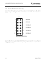
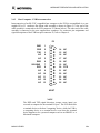
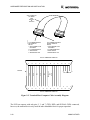
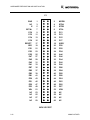
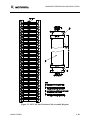
1
M68HC11EVB/D
REV 2
November 1996
M68HC11EVB
EVALUATION BOARD
USER'S MANUAL
Copyright 1986, 1996 by Motorola Inc.
Motorola reserves the right to make changes without further notice to any products herein to
improve reliability, function or design. Motorola does not assume any liability arising out of the
application or use of any product or circuit described herein; neither does it convey any license
under its patent rights nor the rights of others. Motorola products are not designed, intended, or
authorized for use as components in systems intended for surgical implant into the body, or other
applications intended to support or sustain life, or for any other application in which the failure of
the Motorola product could create a situation where personal injury or death may occur. Should
Buyer purchase or use Motorola products for any such unintended or unauthorized application,
Buyer shall indemnify and hold Motorola and its officers, employees, subsidiaries, affiliates, and
distributors harmless against all claims, costs, damages, and expenses, and reasonable attorney
fees arising out of, directly or indirectly, any claim of personal injury or death associated with
such unintended or unauthorized use, even if such claim alleges that Motorola was negligent
regarding the design or manufacture of the part.
Information contained in this document applies to
REVision (C) M68HC11EVB Evaluation Boards,
serial numbers 6000 through 99,999.
The computer program stored in the Read Only Memory of the device contains material
copyrighted by Motorola Inc., first published 1985, and may be used only under a license such as
the License For Computer Programs (Article 14) contained in Motorola's Terms and Conditions
of Sale, Rev. 1/79.
EXORciser is a trademark of Motorola Inc.
IBM-PC is a registered trademark of International Business Machines Corp.
Apple, MacTerminal, MacWrite are trademarks of Apple Computer, Inc.
Macintosh is a trademark licensed to Apple Computer, Inc.
Macintosh is a trademark of Macintosh Laboratory, Inc.
Red Ryder is a trademark of Freesoft Company
Motorola and the Motorola logo are registered trademarks of Motorola Inc.
Motorola Inc. is an Equal Opportunity/Affirmative Action Employer.
CAUTION
Caution should be observed when programming or erasing MCU
EEPROM locations. The EVB MCU configuration (CONFIG)
register ROMON bit is cleared to disable MCU internal ROM,
thereby allowing external EPROM containing the BUFFALO
program to control EVB operations.
CONTENTS
CONTENTS
CHAPTER 1
GENERAL INFORMATION
1.1
INTRODUCTION.......................................................................................................... 1-1
1.2
FEATURES ................................................................................................................... 1-1
1.3
SPECIFICATIONS ........................................................................................................ 1-2
1.4
GENERAL DESCRIPTION ........................................................................................... 1-3
1.5
EQUIPMENT REQUIRED ............................................................................................ 1-4
CHAPTER 2
HARDWARE PREPARATION AND INSTALLATION
2.1
INTRODUCTION.......................................................................................................... 2-1
2.2
UNPACKING INSTRUCTIONS.................................................................................... 2-1
2.3
HARDWARE PREPARATION...................................................................................... 2-1
2.3.1 Reset Select Header (J1) ....................................................................................... 2-2
2.3.2 Clock Select Header (J2) ...................................................................................... 2-3
2.3.3 Memory Select Headers (J3 and J7) ...................................................................... 2-4
2.3.4 Program Execution Select Header (J4).................................................................. 2-5
2.3.5 Terminal Baud Rate Select Header (J5)................................................................. 2-6
2.3.6 Host Port RX Signal Disable Header (J6).............................................................. 2-7
2.4 INSTALLATION INSTRUCTIONS .............................................................................. 2-7
2.4.1 Power Supply - EVB Interconnection ................................................................... 2-7
2.4.2 Terminal - EVB Interconnection ........................................................................... 2-8
2.4.3 Host Computer - EVB Interconnection ................................................................. 2-9
2.4.4 Target System - EVB Interconnection................................................................. 2-11
2.5 CHECKOUT PROCEDURE ........................................................................................ 2-14
M68HC11EVB/D
v
CONTENTS
CHAPTER 3
MONITOR PROGRAM
3.1
INTRODUCTION.......................................................................................................... 3-1
3.2
PROGRAM DESCRIPTION.......................................................................................... 3-1
3.2.1 Initialization.......................................................................................................... 3-1
3.2.2 Command Interpreter............................................................................................ 3-2
3.2.3 I/O Routines ......................................................................................................... 3-2
3.2.4 Utility Subroutines ................................................................................................ 3-3
3.2.5 Command Table.................................................................................................... 3-5
3.3 INTERRUPT VECTORS ............................................................................................... 3-5
CHAPTER 4
OPERATING INSTRUCTIONS
4.1
INTRODUCTION.......................................................................................................... 4-1
4.2
CONTROL SWITCH ..................................................................................................... 4-1
4.3
LIMITATIONS .............................................................................................................. 4-1
4.4
OPERATING PROCEDURES ....................................................................................... 4-3
4.4.1 Debugging Mode .................................................................................................. 4-3
4.4.2 Evaluation Mode................................................................................................... 4-3
4.4.3 Monitor Program .................................................................................................. 4-3
4.5 COMMAND LINE FORMAT........................................................................................ 4-4
4.6
MONITOR COMMANDS ............................................................................................. 4-5
4.6.1
4.6.2
4.6.3
4.6.4
4.6.5
4.6.6
4.6.7
4.6.8
4.6.9
4.6.10
4.6.11
4.6.12
vi
Assembler/Disassembler........................................................................................ 4-8
Block Fill ............................................................................................................ 4-11
Breakpoint Set.................................................................................................... 4-12
Bulk.................................................................................................................... 4-14
Bulkall ................................................................................................................ 4-15
Call..................................................................................................................... 4-16
EEPROM Modify Mapping................................................................................. 4-18
Go ...................................................................................................................... 4-19
Help.................................................................................................................... 4-20
Load ................................................................................................................... 4-21
Memory Display ................................................................................................. 4-22
Memory Modify.................................................................................................. 4-23
M68HC11EVB/D
CONTENTS
CHAPTER 4
OPERATING INSTRUCTIONS (continued)
4.6.13 Move .................................................................................................................. 4-25
4.6.14 Proceed/Continue ............................................................................................... 4-26
4.6.15 Register Modify .................................................................................................. 4-27
4.6.16 Stop at Address .................................................................................................. 4-28
4.6.17 Trace .................................................................................................................. 4-29
4.6.18 Transparent Mode............................................................................................... 4-30
4.6.19 Verify ................................................................................................................. 4-31
4.6.20 Transfer Data Bootstrap Mode............................................................................ 4-32
4.7 ASSEMBLY/DISASSEMBLY PROCEDURES........................................................... 4-34
4.8
DOWNLOADING PROCEDURES.............................................................................. 4-39
4.8.1
4.8.2
4.8.3
4.8.4
4.8.5
EXORciser to EVB............................................................................................. 4-40
Apple Macintosh (with MacTerminal) to EVB .................................................... 4-41
Apple Macintosh (with Red Ryder) to EVB ........................................................ 4-43
IBM-PC (with KERMIT) to EVB....................................................................... 4-44
IBM-PC (with PROCOMM) to EVB .................................................................. 4-45
CHAPTER 5
HARDWARE DESCRIPTION
5.1
INTRODUCTION.......................................................................................................... 5-1
5.2
GENERAL DESCRIPTION ........................................................................................... 5-1
5.2.1
5.2.2
5.2.3
5.2.4
5.2.5
Microcomputer ..................................................................................................... 5-1
Port Replacement Unit.......................................................................................... 5-2
Memory................................................................................................................ 5-4
Address Decoding/De-multiplexing ....................................................................... 5-4
RS-232C I/O Port Interface Circuits ..................................................................... 5-4
CHAPTER 6
SUPPORT INFORMATION
6.1
INTRODUCTION.......................................................................................................... 6-1
6.2
CONNECTOR SIGNAL DESCRIPTIONS .................................................................... 6-1
6.3
PARTS LIST.................................................................................................................. 6-7
6.4
DIAGRAMS................................................................................................................. 6-11
M68HC11EVB/D
vii
CONTENTS
APPENDIX A
S-RECORD INFORMATION
A.1 INTRODUCTION..........................................................................................................A-1
A.2 S-RECORD CONTENT.................................................................................................A-1
A.3 S-RECORD TYPES .......................................................................................................A-2
A.4 S-RECORD CREATION ...............................................................................................A-3
A.5 S-RECORD EXAMPLE.................................................................................................A-3
APPENDIX B
APPLICATIONS
B.1 INTRODUCTION..........................................................................................................B-1
FIGURES
1-1. EVB Block Diagram....................................................................................................... 1-4
2-1. EVB Connector, Switch, and Jumper Header Location Diagram ..................................... 2-2
2-2. Terminal/Host Computer Cable Assembly Diagram....................................................... 2-10
2-3. MCU I/O Port Extension Cable Assembly Diagram....................................................... 2-13
5-1. EVB Block Diagram....................................................................................................... 5-2
5-2. EVB Memory Map Diagram ........................................................................................... 5-3
6-1. EVB Parts Location Diagram.......................................................................................... 6-7
6-2. EVB Schematic Diagram (Sheet 1 of 2) ........................................................................ 6-11
6-2. EVB Schematic Diagram (Sheet 2 of 2) ........................................................................ 6-12
C-1. Single-Chip Mode Configuration.....................................................................................C-2
viii
M68HC11EVB/D
CONTENTS
TABLES
1-1. EVB Specifications......................................................................................................... 1-2
1-2. External Equipment Requirements .................................................................................. 1-4
3-1. Utility Subroutine Jump Table......................................................................................... 3-3
3-2. Interrupt Vector Jump Table........................................................................................... 3-6
4-1. Monitor Memory Map Limitations .................................................................................. 4-2
4-2. Monitor Program Commands.......................................................................................... 4-6
6-1. MCU I/O Port Connector (P1) Pin Assignments ............................................................. 6-2
6-2. Terminal I/O Port Connector (P2) Pin Assignments ........................................................ 6-4
6-3. Host I/O Port Connector (P3) Pin Assignments............................................................... 6-5
6-4. Input Power Connector (P4) Pin Assignments................................................................. 6-6
6-5. EVB Parts List................................................................................................................ 6-8
M68HC11EVB/D
ix
CONTENTS
x
M68HC11EVB/D
GENERAL INFORMATION
CHAPTER 1
GENERAL INFORMATION
1.1 INTRODUCTION
This manual provides general information, hardware preparation, installation instructions, monitor
program description, operating instructions, hardware description, and support information for
the M68HC11 Evaluation Board (EVB).
Downloading S-record information is contained in Appendix A. While a listing of the EVB
monitor program is stored on the diskettes supplied with the EVB (see file buf25.asm). (This file
may be viewed using any text reader capable of handling a 123K file.)
NOTE
Unless otherwise specified, all address references are in
hexadecimal throughout this manual.
An asterisk (*) following the signal name denotes that the signal is
true or valid when the signal is low.
1.2 FEATURES
EVB features include:
•
An economical means of debugging user assembled code and evaluating target systems
incorporating MC68HC11 microcomputer unit (MCU) device
•
One-line assembler/disassembler
•
Host computer downloading capability
•
MC68HC11 MCU based debugging/evaluating circuitry
•
MC68HC24 Port Replacement Unit (PRU) based MCU I/O expansion circuitry
•
MC6850 Asynchronous Communications Interface Adapter (ACIA) based terminal
I/O port circuitry
•
RS-232C compatible terminal/host computer I/O ports
M68HC11EVB/D
1-1
1
GENERAL INFORMATION
1.3 SPECIFICATIONS
Table 1-1 lists the EVB specifications.
Table 1-1. EVB Specifications
Characteristics
MCU
MC68HC11A1FN
PRU
MC68HC24FN
ACIA
MC68B50
I/O ports:
Terminal
Host computer
MCU extension
RS-232C compatible
RS-232C compatible
HCMOS-TTL compatible
Temperature:
Operating
Storage
+25 degrees C
-40 to +85 degrees C
Relative humidity
0 to 90% (non-condensing)
Power requirements
+5 Vdc @ 0.5 A (max)
+12 Vdc @ 0.1 A (max)
-12 Vdc @ 0.1 A (max)
Dimensions:
Width
Length
1-2
Specifications
7.062 in. (17.8 cm)
4.625 in. (11.75 cm)
M68HC11EVB/D
GENERAL INFORMATION
1.4 GENERAL DESCRIPTION
The MC68HC11 MCU device is an advanced single-chip MCU with on-chip memory and
peripheral functions. Refer to the MC68HC11 MCU data sheet for additional device information.
To demonstrate the capabilities of this MCU, the EVB functions with a debug monitor program
called BUFFALO (Bit User Fast Friendly Aid to Logical Operations). This monitor program is
contained within an on-board EPROM (external to the MCU).
The EVB provides a low cost tool for debugging and evaluation of MC68HC11 MCU-based
target system equipment (Figure 1-1 is a block diagram of the EVB). The EVB is not intended to
be a replacement for a much more powerful and flexible tool, such as the Motorola
M68HC11EVM Evaluation Module. The EVB operates in either the debugging or evaluation
(emulation) mode of operation.
The first mode of operation lets you debug your code using the BUFFALO monitor program.
User code is assembled on the EVB or on a host computer and then downloaded to the EVB
RAM via Motorola S-records. The second mode of operation lets you evaluate (emulate) user
code in a target system environment utilizing the memory of the MC68HC11 MCU. The EVB
emulates the single-chip mode of operation, even though the EVB operates in the expanded
multiplexed mode of operation at all times.
Overall evaluation/debugging control of the EVB is provided by the BUFFALO monitor program
via terminal interaction. The target system interface is provided by the MCU and PRU devices.
RS-232C terminal/host I/O port interface circuitry provides communication and data transfer
operations between the EVB and external terminal/host computer devices.
Independent baud rate selection capabilities are provided for the terminal and host I/O ports.
Hardware selectable (300-9600) baud rates are provided for the ACIA-based terminal port. A
non-selectable (fixed) 9600 baud rate is provided for the host port via the MCU Serial
Communications Interface (SCI).
The EVB requires a user-supplied +5, +12, and -12 Vdc power supply and an RS-232C
compatible terminal for operation. An RS-232C compatible host computer is used with the EVB
to download Motorola S-records via the BUFFALO monitor commands.
The Motorola S-record format was devised for the purpose of encoding programs or data files in
a printable format for transportation between computer systems. The transportation process can
therefore be monitored and the S-records can be easily edited. Refer to Appendix A for additional
S-record information.
M68HC11EVB/D
1-3
3
GENERAL INFORMATION
Figure 1-1. EVB Block Diagram
1.5 EQUIPMENT REQUIRED
Table 1-2 lists the external equipment requirements for EVB operation.
Table 1-2. External Equipment Requirements
External Equipment
+5, +12, -12 Vdc power supply(1)
Terminal (RS-232C compatible)
Host computer (RS-232C compatible)(2)
Terminal/host computer - EVB RS-232C cable assembly(1)
Target system - EVB MCU I/O port extension cable assembly(1)
1. Refer to Chapter 2 for details.
2. Optional - not required for basic operation
1-4
M68HC11EVB/D
HARDWARE PREPARATION AND INSTALLATION
CHAPTER 2
HARDWARE PREPARATION AND INSTALLATION
2.1 INTRODUCTION
This chapter provides unpacking instructions, hardware preparation, and installation instructions
for the EVB.
2.2 UNPACKING INSTRUCTIONS
After unpack EVM from shipping carton, refer to the packing list and verify that all items are
present. Save packing material for storing or reshipping the EVM.
2.3 HARDWARE PREPARATION
This section describes the inspection/preparation of EVB components prior to target system
installation. This description ensures that the EVB components are properly configured for target
system operation. The EVB has been factory-tested and is shipped with factory-installed jumpers.
Inspect the EVB for jumper placements prior to target system installation. Figure 2-1 illustrates
the EVB connector, switch, and jumper header locations.
Use connector P1 to connect the EVB to the target system. Use connectors P2 and P3 to connect
the EVB to the external terminal and host computer equipment, respectively. Use connector P4 to
connect an external power supply to the EVB. Use switch S1 to reset the EVB. Jumper header
locations J1 through J7 provide these capabilities:
•
Reset select (J1)
•
Clock select (J2)
•
Memory select (J3 and J7)
•
Program execution select (J4)
•
Terminal baud rate select (J5)
•
Host port RX signal disable (J6)
M68HC11EVB/D
2-1
1
HARDWARE PREPARATION AND INSTALLATION
Figure 2-1. EVB Connector, Switch, and Jumper Header Location Diagram
2.3.1
Reset Select Header (J1)
Jumper header J1 is used to connect an external reset signal from the target system (via MCU I/O
port connector P1, pin 17) to be used by the EVB. This is accomplished by the installation of a
fabricated jumper on pins 1 and 2. The EVB is factory-configured and shipped with the jumper
installed as shown below.
J1
1
2
This jumper is removed from pins 1 and 2 when the EVB reset circuitry is used without target
system intervention.
2-2
M68HC11EVB/D
HARDWARE PREPARATION AND INSTALLATION
2.3.2
Clock Select Header (J2)
Jumper header J2 is used to select either internal or external clock source to be used by the EVB.
The internal EVB clock source is an 8 MHz crystal for a bus rate of 2 MHz. The EVB is factoryconfigured and shipped with the clock input selected for internal clock source. This is
accomplished by the installation of a fabricated jumper on pins 2 and 3 as shown below.
J2
1
External
2
3
Internal
If an external TTL clock source from the target system (via MCU I/O port connector P1, pin 7)
is required, the jumper is repositioned between pins 1 and 2.
M68HC11EVB/D
2-3
3
HARDWARE PREPARATION AND INSTALLATION
2.3.3
Memory Select Headers (J3 and J7)
Jumper headers J3 and J7 are used to configure the EVB circuitry for an additional 8k memory
device (e.g., MCM6164) installed at location U4. This device is provided by the user if required.
If a RAM device is installed at location U4, a fabricated jumper is installed on pins 1 and 2 of
jumper header J3 or J7 as shown below.
J3
1
J7
1
2
2
NOTE
Jumper headers J3 and J7 should not have fabricated jumpers
installed at the same time.
Jumper header J7 is for factory use only.
Jumper header J3 or J7 applies a chip enable (CE*) signal to the RAM device installed at location
U4. The RAM device is selected or deselected by the installation of a fabricated jumper on either
jumper header J3 or J7. If the installed RAM device is not required, but left installed, both jumper
headers J3 and J7 should not have fabricated jumpers installed.
Installing a fabricated jumper on jumper header J3 causes the memory device at location U4 to be
mapped at locations $6000 to $7FFF. Installing a fabricated jumper on jumper header J7 causes
the memory device located at location U4 to be mapped at locations $A000 to $BFFF.
NOTE
MCU EEPROM may be located at $B600 to $B7FF.
2-4
M68HC11EVB/D
HARDWARE PREPARATION AND INSTALLATION
2.3.4
Program Execution Select Header (J4)
Jumper header J4 is used to determine whether the BUFFALO monitor prompt will be displayed,
or if a jump to internal EEPROM will be executed. Upon reset, the monitor detects the state of
the PE0 line. If a low state is detected, the monitor program is executed and the prompt
displayed. If a high state is detected, the monitor will automatically jump directly to EEPROM
(address location $B600) and execute user program code without displaying the monitor prompt.
The EVM is factory-configured and shipped with the program execution selected for BUFFALO
monitor operation as shown below. The user must configure the EVB for the type of program
execution required. If program execution out of EEPROM is desired, the jumper is repositioned
between pins 2 and 3.
J4
1
Monitor
(10K PULLDOWN)
2
3
EEPROM
(10K PULLUP)
If the PE0 line is used for A/D operations, the loading condition introduced by jumper header J4
may not be desired. To circumvent this condition, program the first three EEPROM locations
with $7E, $E0, and $0A, respectively. Next, remove installed jumper from jumper header J4
(removes load condition), and proceed into the A/D operation.
For additional information pertaining to the EEPROM jump operation described above, refer to
the buf25.asm file on the EVB diskettes.
M68HC11EVB/D
2-5
5
HARDWARE PREPARATION AND INSTALLATION
2.3.5
Terminal Baud Rate Select Header (J5)
Jumper header J5 is used to select the baud rate for the terminal (P2) I/O port. The EVB is
factory configured and shipped with the terminal baud rate selected for 9600 baud as shown
below.
J5
1
2
300 BAUD
3
4
600 BAUD
5
6
1200 BAUD
7
8
2400 BAUD
9
10
4800 BAUD
11
12
9600 BAUD
BAUD RATE SELECTION
The host (P3) I/O port is a fixed MCU SCI 9600 baud rate (non selectable). Refer to Chapter 6
EVB parts list notes for additional information pertaining to the host baud rate (crystal vs E-clock
vs MCU SCI operation).
2-6
M68HC11EVB/D
HARDWARE PREPARATION AND INSTALLATION
2.3.6
Host Port RX Signal Disable Header (J6)
Jumper header J6 is used to disable the host computer I/O port RX output signal line (connector
P3, pin 2) when using the EVB MCU SCI in a target system application. When performing a
downloading operation or communicating to a host computer in the transparent mode, a
fabricated jumper is installed on pins 1 and 2 as shown below.
J6
1
2
Signal disabling is accomplished by the removal of the fabricated jumper installed on pins 1 and 2.
2.4 INSTALLATION INSTRUCTIONS
The EVB is designed for table top operation. A user supplied power supply and RS-232C
compatible terminal are required for EVB operation. An RS-232C compatible host computer is
optional for downloading user assembled code to the EVB.
2.4.1
Power Supply - EVB Interconnection
The EVB requires +5 Vdc @ 0.5 A, +12 Vdc @ 0.1 A, -12 Vdc @ 0.1 A, and GND for
operation. Interconnection of the power supply wiring to the EVB power supply connector P4 is
shown below.
P4
1
-12 VDC
2
GND
3
4
+5 VDC
+12 VDC
The power supply cable simply consists of four 14-22 AWG wires that interconnect -12 VDC,
GND, +5 VDC, and +12 VDC, from the user supplied power supply to the EVB connector P4.
M68HC11EVB/D
2-7
7
HARDWARE PREPARATION AND INSTALLATION
2.4.2
Terminal - EVB Interconnection
Interconnection of an RS-232C compatible terminal to the EVB is accomplished via a user
supplied 20 or 25 conductor flat ribbon cable assembly as shown in Figure 2-2. One end of the
cable assembly is connected to the EVB connector P2 (shown below). The other end of the cable
assembly is connected to the user supplied terminal. For connector pin assignments and signal
descriptions of the EVB terminal port connector P2, refer to Chapter 6.
P2
GND
RXD
TXD
NC
CTS
DSR
SIG-GND
DCD
NC
NC
NC
NC
NC
1
2
3
4
5
6
7
8
9
10
11
12
13
14
15
16
17
18
19
20
21
22
23
24
25
NC
NC
NC
NC
NC
NC
DTR
NC
NC
NC
NC
NC
TERMINAL
NOTE
A dumb terminal or personal computer is always connected to the
terminal I/O port but it is very common not to have any external
equipment connected to the host I/O port.
2-8
M68HC11EVB/D
HARDWARE PREPARATION AND INSTALLATION
2.4.3
Host Computer - EVB Interconnection
Interconnection of an RS-232C compatible host computer to the EVB is accomplished via a user
supplied 20 or 25 conductor flat ribbon cable assembly as shown in Figure 2-2. One end of the
cable assembly is connected to the EVB connector P3 (shown below). The other end of the cable
assembly is connected to the user supplied host computer. For connector pin assignments and
signal descriptions of the EVB host port connector P3, refer to Chapter 6.
P3
GND
RXD
TXD
NC
NC
DSR
SIG-GND
DCD
NC
NC
NC
NC
NC
1
2
3
4
5
6
7
8
9
10
11
12
13
14
15
16
17
18
19
20
21
22
23
24
25
NC
NC
NC
NC
NC
NC
DTR
NC
NC
NC
NC
NC
HOST
NOTE
The RXD and TXD signal directions (output versus input) are
reversed as compared to the terminal I/O port.. The EVB looks like
a terminal device to the host "computing" device, while the EVB is
a computing device to a terminal device even when the terminal
device happens to be a personal computer such as an IBM-PC or a
Macintosh computer.
M68HC11EVB/D
2-9
9
HARDWARE PREPARATION AND INSTALLATION
20 OR 25 CONDUCTOR
FLAT RIBBON
CABLE
3M #3365-20
OR
3M #3365-25
25 "D" SUBMINIATURE MALE
(PIN) CONNECTOR
PART #'S:
25 "D" SUBMINIATURE FEMALE
(SOCKET) CONNECTOR
PART #'S:
1. CIRCUIT ASSEMBLY CORP
#CA•25•SMD•P
1. CIRCUIT ASSEMBLY CORP
#CA•25•SMD•S
2. ITT CANNON #DBSP-B25P
2. ITT CANNON #DBSP-B25S
3. ANSLEY #609•25P
3. ANSLEY #609•25S
4. WINCHESTER #49•1125P
4. WINCHESTER #49•1125S
25 PIN "D" SUBMINIATURE CONNECTOR
1
2
14
3
15
4
16
5
17
6
18
7
19
8
20
9
21
10
22
11
23
12
24
13
25
1
2
14
3
15
4
16
5
17
6
18
DTR
NOT CONNECTED
7
19
DCD
SIGNAL GND
DSR
CTS
RTS
RXD
TXD
RED WIRE
8
20
9
21
10
22
11
23
12
24
13
25
25 PIN "D" SUBMINIATURE CONNECTOR
Figure 2-2. Terminal/Host Computer Cable Assembly Diagram
The EVB can operate with only pins 2, 3, and 7 (TXD, RXD, and SIGNAL GND) connected,
however; the terminal device may need the other handshake lines for proper operation.
2-10
M68HC11EVB/D
HARDWARE PREPARATION AND INSTALLATION
2.4.4
Target System - EVB Interconnection
Target system to EVB interconnection is accomplished via the EVB MCU I/O port connector and
a 60 conductor flat ribbon extension cable assembly. This MCU I/O port connector P1 (shown on
the following page) is a 60-pin header that facilitates the interconnection of the cable assembly for
evaluation purposes. For connector pin assignments and signal descriptions of the EVB MCU I/O
port connector P1, refer to Chapter 6.
Two types of extension cable assembly construction techniques are available to the user. Cable
assembly construction is dependent upon the purpose or use of the EVB. The user must first
determine the primary application of the EVB in order to determine the type of cable assembly to
be constructed. Cable assembly types and construction methods are described in the following
paragraphs.
The first type of cable assembly (user supplied) is low cost and simplest to construct, and is
illustrated in Figure 2-3. This type of assembly provides an indirect connection of the EVB MCU
I/O port to the target system MCU device socket. Indirect connection is accomplished via a 60pin connector, installed on the target system board, that connects to the target system MCU
device socket. This connector is a double row post, 60-pin header type, Amptronics # 929715-0130. Target system wiring from the connector to the MCU device socket is implemented via wire
wrap or Printed Wiring Board (PWB) conductive land wiring. Uses for this type of cable assembly
are in the early development stages of the MC68HC11 MCU-based product.
The second type of cable assembly (not illustrated) is expensive and hardest to construct. This
type of assembly provides a direct connection of the EVB MCU I/O port to the target system
MCU device socket. Direct connection is accomplished via a specialized plug platform containing
a 52-lead plastic leaded chip carrier (PLCC) plug constructed by the user. This type of plug
platform mates directly with the target system MCU device socket. Uses for this type of cable
assembly are in the production stages of the developed MC68HC11 MCU-based product.
M68HC11EVB/D
2-11
11
HARDWARE PREPARATION AND INSTALLATION
P1
GND
NC
E
EXTAL
PC0
PC2
PC4
PC6
RESET*
IRQ*
PD1
PD3
PD5
PA7
PA5
PA3
PA1
PB7
PB5
PB3
1
3
5
7
9
11
13
15
17
19
21
23
25
27
29
31
33
35
37
39
2
4
6
8
10
12
14
16
18
20
22
24
26
28
30
32
34
36
38
40
MODB
STRA
STRB
XTAL
PC1
PC3
PC5
PC7
XIRQ*
PD0
PD2
PD4
Vdd
PA6
PA4
PA2
PA0
PB6
PB4
PB2
PB1
PE0
PE1
PE2
PE3
VRL
NC
NC
NC
NC
41
43
45
47
49
51
53
55
57
59
42
44
46
48
50
52
54
56
58
60
PB0
PE4
PE5
PE6
PE7
VRH
NC
NC
NC
NC
MCU I/O PORT
2-12
M68HC11EVB/D
HARDWARE PREPARATION AND INSTALLATION
Figure 2-3. MCU I/O Port Extension Cable Assembly Diagram
M68HC11EVB/D
2-13
13
HARDWARE PREPARATION AND INSTALLATION
2.5 CHECKOUT PROCEDURE
This procedure lets you perform a pre-operational checkout of the EVB for basic operation. Upon
completion of the EVB installation to an external power supply and terminal, check that the EVB
is configured for the proper terminal baud rate (refer to paragraph 2.3.5.).
Applying power to the EVB causes a power-on reset (POR) to occur. POR causes the MCU and
user I/O port circuitry to be reset, and the monitor invoked. The terminal monitor displays the
following EVB monitor prompt:
BUFFALO X.X (ext) - Bit User Fast Friendly Aid to Logical Operation
where:
X.X is the revision of the monitor program.
(ext) denotes monitor program residing in external EPROM (U3).
(int) denotes monitor program residing in EEPROM MCU (U10).
If the EVB monitor prompt is not displayed (as shown above), press the user reset switch S1. If
the monitor prompt cannot be displayed, the possibility exists that the EVB cannot communicate
via the terminal port because the CONFIG register NOSEC bit is enabled (logic 0). Erasing the
entire EEPROM array including the CONFIG register must be performed as follows:
1. Remove installed jumper from reset select header J1. Reinstall jumper on MCU I/O
port connector P1, pins 1 and 2 (top two pins).
2. Press reset switch S1.
3. Remove installed jumper from connector P1. Reinstall jumper on header J1 (pins 1 and
2).
4. Press reset switch S1. Internal (int) BUFFALO monitor prompt is displayed.
5. Memory modify (MM) command (refer to paragraph 4.6.11) is used to change
CONFIG register contents to $0D. BUFFALO monitor will respond with "rom"
message.
6. Press reset switch S1. External (ext) BUFFALO monitor prompt is displayed.
Proceed to Chapter 4 for complete operating instructions.
2-14
M68HC11EVB/D
MONITOR PROGRAM
CHAPTER 3
MONITOR PROGRAM
3.1 INTRODUCTION
This chapter provides the overall description of the monitor program. This description will enable
the user to understand the basic structure of the program, and to modify or customize the
program for specific applications.
3.2 PROGRAM DESCRIPTION
The monitor program supplied for the EVB is called BUFFALO (Bit User Fast Friendly Aid to
Logical Operations). This program communicates via the MC6850 Asynchronous
Communications Interface Adapter (ACIA) device and the MCU Serial Communications Interface
(SCI). Refer to the buf25.asm file on the EVB diskettes for additional information pertaining to
the monitor (BUFFALO) program.
The EVB monitor program is contained in EPROM (external to the MCU). The EVB resident
MCU have the configuration (CONFIG) register ROMON bit cleared thereby disabling the MCU
internal ROM. Having the monitor program in EPROM external to the MCU at locations $E000$FFFF is a great advantage because it allows the user to add instructions to customize the
monitor for specific requirements.
The BUFFALO monitor program consists of five parts (or sections) which are as follows:
3.2.1
•
Initialization
•
Command interpreter
•
I/O routines
•
Utility subroutines
•
Command table
Initialization
This part of BUFFALO contains all of the reset initialization code. In this section, internal RAM
locations are set up, and the I/O channel for the terminal is set up. To set up the terminal I/O port,
BUFFALO must determine if the terminal is connected to the SCI or to an external ACIA or
DUART. This is accomplished by sending a sign-on message to all ports and then waiting for the
user to type carriage return (RETURN) on whichever device is the terminal port. When
M68HC11EVB/D
3-1
1
MONITOR PROGRAM
BUFFALO recognizes a carriage return from a port, that port is then used for all subsequent
terminal I/O operations.
3.2.2
Command Interpreter
The next section of BUFFALO is the command interpreter. American Standard Code for
Information Interchange (ASCII) characters are read from the terminal into the input buffer until a
carriage return or a slash (/) is received. The command field is then parsed out of the input buffer
and placed into the command buffer. A table of commands is then searched and if a match is
found, the corresponding command module is called as a subroutine. All commands return control
back to the command interpreter upon completion of the operation.
3.2.3
I/O Routines
The I/O section of BUFFALO consists of a set of supervisor routines, and three sets of driver
routines. The supervisor routines are INIT, INPUT, and OUTPUT. These routines determine
which driver subroutine to call to perform the specific action. Each set of driver routines consists
of an initialization routine, an input routine, and an output routine. One set of drivers is for the
SCI port and these routines are called ONSCI, INSCI, and OUTSCI. The second set of drivers is
for a DUART and these routines are called ONUART, INUART, and OUTUART. The third set
of drivers is for an ACIA and these routines are called ONACIA, INACIA, and OUTACIA.
All I/O communications are controlled by three RAM locations (IODEV, EXTDEV, and
HOSTDEV). EXTDEV specifies the external device type (0=none, 1=ACIA, 2=DUART).
HOSTDEV specifies which I/O port is used for host communications (0=SCI, 1=ACIA,
3=DUARTB). IODEV instructs the supervisor routine which port/driver routine to use (0=SCI,
1=ACIA, 2=DUARTA, 3=DUARTB).
The INIT routines set up a serial transmission format of eight data bits, one stop bit, and no
parity. For the SCI, the baud rate is set to 9600 for an 8 MHz crystal (2 MHz E-clock). A
different baud rate can be achieved by modifying address location $102B (refer to MCU data
sheet, SCI baud rate selection).
The INPUT routine reads from the specified port. If a character is received, the character is
returned in accumulator A. If no character is received a zero (0) is returned in accumulator A.
This routine does not wait for a character to be received before returning (function is performed
by the INCHAR subroutine).
The OUTPUT routine takes the ASCII character in accumulator A and writes to the specified I/O
port. This routine waits until the character is transmitted before returning.
3-2
M68HC11EVB/D
MONITOR PROGRAM
3.2.4
Utility Subroutines
Several subroutines exist that are available for performing I/O tasks. A jump table has been set up
in ROM directly before the interrupt vectors. To use these subroutines, execute a jump to
subroutine (JSR) command to the appropriate entry in the jump table. By default, all I/O
performed with these routines are sent to the terminal port. Redirection of the I/O port is achieved
by placing the specified value (0=SCI, 1=ACIA, 2=DUARTA, 3=DUARTB) into RAM location
IODEV.
Utility subroutines available to the user are listed in Table 3-1.
Table 3-1. Utility Subroutine Jump Table
Address
Routine
Description
$FF7C
.WARMST
Go to ">" prompt point (skip BUFFALO... message).
$FF7F
.BPCLR
Clear breakpoint table.
$FF82
.RPRINT
Display user's registers.
$FF85
.HEXBIN
Convert ASCII character in A register to 4-bit binary number.
Shift binary number into SHFTREG from the right. SHFTREG
is a 2-byte (4 hexadecimal digits) buffer. If A register is not
hexadecimal, location TMP1 is incremented and SHFTREG is
unchanged.
$FF88
.BUFFAR
Read 4-digit hexadecimal argument from input buffer to
SHFTREG.
$FF8B
.TERMAR
Read 4-digit hexadecimal argument from terminal device to
SHFTREG.
$FF8E
.CHGBYT
Write value (if any) from SHFTREG+1 to memory location
pointed to by X. (Operation also applicable to EEPROM
locations.)
$FF91
.READBU
Read next character from INBUFF.
$FF94
.INCBUF
Increment pointer into input buffer.
$FF97
.DECBUF
Decrement pointer into input buffer.
$FF9A
.WSKIP
Read input buffer until non-white-space character found.
$FF9D
.CHKABR
Monitor input for (CTRL)X, (DELETE), or (CTRL)W requests.
$FFA0
.UPCASE
If character in accumulator A is lower case alpha, convert to
upper case.
M68HC11EVB/D
3-3
3
MONITOR PROGRAM
Table 3-1. Utility Subroutine Jump Table (continued)
Address
3-4
Routine
Description
$FFA3
.WCHEK
Test character in accumulator A and return with Z bit set if
character is white space (space, comma, tab).
$FFA6
.DCHEK
Test character in accumulator A and return with Z bit set if
character is delimiter (carriage return or white space).
$FFA9
.INIT
Initialize I/O device.
$FFAC
.INPUT
Read I/O device.
$FFAF
.OUTPUT
Write I/O device.
$FFB2
.OUTLHL
Convert left nibble of accumulator A contents to ASCII and
output to terminal port.
$FFB5
.OUTRHL
Convert right nibble of accumulator A contents to ASCII and
output to terminal port.
$FFB8
.OUTA
Output accumulator A ASCII character.
$FFBB
.OUT1BY
Convert binary byte at address in index register X to two
ASCII characters and output. Returns address in index
register X pointing to next byte.
$FFBE
.OUT1BS
Convert binary byte at address in index register X to two
ASCII characters and output followed by a space. Returns
address in index register X pointing to next byte.
$FFC1
.OUT2BS
Convert two consecutive binary bytes starting at address in
index register X to four ASCII characters and output followed
by a space. Returns address in index register X pointing to
next byte.
$FFC4
.OUTCRL
Output ASCII carriage return followed by a line feed.
$FFC7
.OUTSTR
Output string of ASCII bytes pointed to by address in index
register X until character is an end of transmission ($04).
$FFCA
.OUTST0
Same as OUTSTR except leading carriage return and line
feed is skipped.
$FFCD
.INCHAR
Input ASCII character to accumulator A and echo back. This
routine loops until character is actually received.
$FFD0
.VECINIT
Used during initialization to preset indirect interrupt vector
area in RAM. This routine or a similar routine should be
included in a user program which is invoked by the jump to
$B600 feature of BUFFALO.
M68HC11EVB/D
MONITOR PROGRAM
When accessing BUFFALO utility routines, always reference the routines by the applicable
address ($FF7C through $FFD0) in the jump table rather than the actual address in the
BUFFALO monitor program. Jump table addresses remain the same when a new version of
BUFFALO is developed even though the actual addresses of the routine may change. Programs
that reference routines by the jump table addresses are not required to be changed to operate on
revised versions of the BUFFALO monitor program.
3.2.5
Command Table
The command table consists of three lines for each entry. The first byte is the number of
characters in the command name. The second entry is the ASCII command name. The third entry
is the starting address of the command module. As an example:
FCB
FCC
FDB
3
'ASM'
#ASM
3 characters in command name
ASCII literal command name string
Jump address for command module
Each command in the BUFFALO program is a individual module. Thus, to add or delete
commands, all that is required is to include a new command module or delete an existing module
and/or delete the entry in the command table.
3.3 INTERRUPT VECTORS
Interrupt vectors residing in MCU internal ROM are accessible as follows. Each vector is
assigned a three byte field residing in EVB memory map locations $0000-$00FF. This is where
the monitor program expects the MCU RAM to reside. Each vector points to a three byte field
which is used as a jump table to the vector service routine. Table 3-2 lists the interrupt vectors
and associated three byte field.
M68HC11EVB/D
3-5
5
MONITOR PROGRAM
Table 3-2. Interrupt Vector Jump Table
Interrupt Vector
Field
Serial Communications Interface (SCI)
$00C4 - $00C6
Serial Peripheral Interface (SPI)
$00C7 - $00C9
Pulse Accumulator Input Edge
$00CA - $00CC
Pulse Accumulator Overflow
$00CD - $00CF
Timer Overflow
$00D0 - $00D2
Timer Output Compare 5
$00D3 - $00D5
Timer Output Compare 4
$00D6 - $00D8
Timer Output Compare 3
$00DC - $00DE
Timer Output Compare 1
$00DF - $00E1
Timer Input Capture 3
$00E2 - $00E4
Timer Input Capture 2
$00E5 - $00E7
Timer Input Capture 1
$00E8 - $00EA
Real Time Interrupt
$00EB - $00ED
IRQ
$00EE - $00F0
XIRQ
$00F1 - $00F3
Software Interrupt (SWI)
$00F4 - $00F6
Illegal Opcode
$00F7 - $00F9
Computer Operating Properly (COP)
$00FA - $00FC
Clock Monitor
$00FD - $00FF
To use vectors specified in Table 3-2, the user must insert a jump extended opcode in the three
byte field of the vector required. For an example, for the IRQ vector, the following is performed:
1. Place $7E (JMP) at location $00EE.
2. Place IRQ service routine address at locations $00EF and $00F0.
The following is an example where the IRQ service routine starts at $0100:
$00EE
3-6
7E
01
00
JMP IRQ SERVICE
M68HC11EVB/D
MONITOR PROGRAM
During initialization BUFFALO checks the first byte of each set of three locations.. If a $7E jump
opcode is not found, BUFFALO will install a jump to a routine called STOPIT. This assures there
will be no uninitialized interrupt vectors which would cause undesirable operation during power
up and power down. If an interrupt is accidentally encountered, the STOPIT routine will force a
STOP instruction sequence to be executed. A user may replace any of the JMP STOPIT
instructions with a JMP to a user written interrupt service routine. If reset is issued via switch S1,
BUFFALO will not overwrite these user jump instructions so they need not be re-initialized after
every reset.
M68HC11EVB/D
3-7
7
MONITOR PROGRAM
3-8
M68HC11EVB/D
OPERATING INSTRUCTIONS
CHAPTER 4
OPERATING INSTRUCTIONS
4.1 INTRODUCTION
This chapter provides the necessary information to initialize and operate the EVB in a target
system environment. Information consists of the control switch description, operating limitations,
command line format, monitor commands, and operating procedures. The operating procedures
consist of assembly/disassembly and downloading descriptions and examples.
4.2 CONTROL SWITCH
The EVB contains a user reset switch S1. This switch is a momentary action push-button switch
that resets the EVB MCU circuits.
4.3 LIMITATIONS
CAUTION
Caution should be observed when programming or erasing MCU
EEPROM locations. EVB MCU configuration (CONFIG) register
ROMON bit is cleared to disable MCU internal ROM, thereby
allowing external EPROM containing the BUFFALO program to
control EVB operations.
The MC68HC11 MCU SCI has been set for 9600 baud using a 2 MHz E clock external bus. This
baud rate can be changed by software by reprogramming the BAUD register in the ONSCI
subroutine of the BUFFALO monitor program. Refer to the buf25.asm file on the EVB diskettes
for additional information pertaining to the ONSCI subroutine.
As the RS-232C handshake lines are not used, a delay of approximately 300 milliseconds is
present between successive characters sent to the host computer during the execution of the
LOAD command in the monitor program.
The monitor program uses the MCU internal RAM located at $0048-$00FF. The control registers
are located at $1000-$103F. The monitor program also uses Output Compare 5 (OC5) for the
TRACE instruction, therefore OC5 should not be used in user routines being traced.
M68HC11EVB/D
4-1
1
OPERATING INSTRUCTIONS
The EVB allows the user to use all the features of the BUFFALO evaluation software, however it
should be noted (when designing code) that the BUFFALO uses the MCU on-chip RAM
locations $0048-$00FF leaving only 72 bytes for the user (i.e., $0000-$0047).
The user must be aware of the BUFFALO monitor address location restrictions. Table 4-1 lists
the monitor memory map limitations.
Table 4-1. Monitor Memory Map Limitations
Address
Restrictions
$0000-$0047
Available to user. (BUFFALO sets default value of the user stack
pointer at location $0047.)
$0048-$0065
BUFFALO monitor stack area.
$0066-$00C3
BUFFALO variables.
$00C4-$00FF
Interrupt pseudo vectors (jumps).
$0100-$01FF
User available.
$1000-$103F
MCU control registers. Although RAM and registers can be moved in
the memory map, BUFFALO expects RAM at $0000 (actually requires
$0048-$00FF) and registers at $1000-$103F.
$4000
Some versions of EVBs have a D flip-flop addressed at this location.
During initialization, BUFFALO 3.2 writes $00 to location $4000 and
various monitor operations cause $00 or $01 to be written to $4000.
(Refer to the buf25.asm file on the EVB diskette for the definitions of
DFLOP, TARGCO, and HOSTCO for additional information).
Since the EVB has no memory or peripherals located at $4000, these
writes should not concern most EVB users.
$D000-$D00F
4-2
BUFFALO supports serial I/O to a terminal and/or host via a DUART
(external IC) located at $D000 in the memory map. During
initialization, BUFFALO 3.2 reads and writes to location $D00C to see
if a DUART is present in the system. Refer to the buf25.asm file on
the EVB diskette.
M68HC11EVB/D
OPERATING INSTRUCTIONS
4.4 OPERATING PROCEDURES
The EVB is a simplified debugging/evaluating tool designed to operate in either the debugging or
evaluation (emulation) mode of operation. Jumper header J4 is used to determine whether the
BUFFALO monitor prompt will be displayed, or if a jump to internal EEPROM will be executed.
Refer to paragraph 2.3.4 for additional program execution selection information.
Upon reset, the monitor detects the state of the PE0 line. If a low state is detected, the monitor
program is executed and the prompt displayed. If a high state is detected, the monitor will
automatically jump directly to EEPROM (address location $B600) and execute user program
code without displaying the monitor prompt.
4.4.1
Debugging Mode
The first mode of operation allows the user to debug user code under control of the monitor
program. User code can be assembled in one of two methods. The first method is to assemble
code using the line assembler in the BUFFALO monitor program via the EVB user RAM ($C000$DFFF). The second method is to assemble code on a host computer and then download the code
to the EVB user RAM via Motorola S-records. The monitor program is then used to debug the
assembled user code. Having the monitor program in EPROM external to the MCU ($E000$FFFF) allows the user to add instructions to customize the monitor for specific requirements.
4.4.2
Evaluation Mode
The second mode of operation allows the user to evaluate (emulate) user code in a target system
environment utilizing the memory of the MC68HC11 MCU. This is accomplished by relocating
the code from locations $C000-$DFFF (EVB user RAM) to $E000-$FFFF (MCU 8k ROM).
MCU locations $0000-$00FF (RAM) and $B600-$B7FF (EEPROM) are also available to the
user. The EVB then emulates an EPROM equivalent of the masked ROM device in the single chip
mode of operation. The EVB emulates as if in a single-chip mode of operation, even though
operating in the expanded multiplexed mode of operation at all times.
4.4.3
Monitor Program
The monitor BUFFALO program is the resident firmware for the EVB, which provides a self
contained operating environment. The monitor interacts with the user through predefined
commands that are entered from a terminal. The user can use any of the commands supported by
the monitor.
M68HC11EVB/D
4-3
3
OPERATING INSTRUCTIONS
A standard input routine controls the EVB operation while the user types a command line.
Command processing begins only after the command line has been terminated by depressing the
keyboard carriage return (<CR>) key.
4.5 COMMAND LINE FORMAT
The command line format is as follows:
><command> [<parameters>]<CR>
where:
>
<command>
<parameters>
<CR>
EVB monitor prompt.
Command mnemonic (single letter for most commands).
Expression or address.
ENTER keyboard key - depressed to enter command.
NOTES
1. The command line format is defined using special characters which have the following
syntactical meanings:
<>
Enclose syntactical variable
[]
Enclose optional fields
[ ]...
Enclose optional fields repeated
These characters are not entered by the user, but are for definition purposes only.
2. Fields are separated by any number of space, comma, or tab characters.
3. All input numbers are interpreted as hexadecimal.
4. All input commands can be entered either upper or lower case lettering. All input
commands are converted automatically to upper case lettering except for downloading
commands sent to the host computer, or when operating in the transparent mode.
5. A maximum of 35 characters may be entered on a command line. After the 36th
character is entered, the monitor automatically terminates the command entry and the
terminal CRT displays the message "Too Long".
6. Command line errors may be corrected by backspacing (CTRL-H) or by aborting the
command (CTRL-X or DELETE).
7. After a command has been entered, pressing <CR> a second time will repeat the
command.
4-4
M68HC11EVB/D
OPERATING INSTRUCTIONS
4.6 MONITOR COMMANDS
The monitor BUFFALO program commands are listed alphabetically by mnemonic in Table 4-2.
Each of the commands are described in detail following the tabular command listing. In most
cases the initial single letter of the command mnemonic or a specific symbol (shown in Table 4-2)
can be used. A minimum number of characters must be entered to at least guarantee uniqueness
from other commands (i.e., MO = MOVE, ME = MEMORY). If the letter M is entered,
BUFFALO uses the first command in Table 4-2 that starts with M.
Additional terminal keyboard functions are as follows:
(CTRL)A
Exit transparent mode or assembler
(CTRL)B
Send break command to host in transparent mode
(CTRL)H
Backspace
(CTRL)J
Line feed <lf>
(CTRL)W
Wait/freeze screen (1)
(DELETE)
Abort/cancel command
<CR>
Enter command/repeat last command
NOTES
1. Execution is restarted by any terminal keyboard key.
2. When using the control key with a specialized command such as (CTRL)A, the
(CTRL) key is depressed and held, then the A key is depressed. Both keys are then
released.
Command line input examples in this chapter are amplified with the following:
•
Bold entries are user-entered on the terminal keyboard.
•
Command line input is entered when the keyboard <CR> key is depressed.
Typical example of this explanation is as follows:
>MD F000 F100<CR>
M68HC11EVB/D
4-5
5
OPERATING INSTRUCTIONS
Table 4-2. Monitor Program Commands
Command
4-6
Description
ASM [<address>]
Assembler/disassembler
ASSEM
(same as ASM)
BF <addr1> <addr2> <data>
Block fill memory with data
BR [-] [<address>]...
Breakpoint set
BREAK
(same as BR)
BULK
Bulk erase EEPROM
BULKA
(same as BULKALL)
BULKALL
Bulk erase EEPROM + CONFIG register(1)
CALL [<address>]
Execute subroutine
COPY
(same as MOVE)
DUMP
(same as MD)
EEMOD
Modify EEPROM mapping
ERASE
(same as BULK)
FILL
(same as BF)
G [<address>]
Execute program
GO
(same as G)
HELP
Display monitor commands
HOST
(same as TM)
LOAD <host download command>
Download (S-records*) via host port(2)
LOAD <T>
Download (S-records*) via terminal port(2)
MEMORY
(same as MM)
MD [<addr1> [<addr2>]]
Dump memory to terminal
MM [<address>]
Memory modify
MOVE <addr1> <addr2> [<dest>]
Move memory to new location
P
Proceed/continue from breakpoint
PROCEED
(same as P)
RD
(same as RM)
M68HC11EVB/D
OPERATING INSTRUCTIONS
Table 4-2. Monitor Program Commands (continued)
Command
Description
READ
(same as MOVE)
REGISTER
(same as RM)
RM [p,x,y,a,b,c,s]
Register modify/display user registers
STOPAT <address>
Stop at address
T [<n>]
Trace $1-$FF instructions
TM
Enter transparent mode
TRACE
(same as T)
VERIFY <host download command>
Compare memory to download data via host
port
VERIFY <T>
Compare memory to download data via
terminal port
XBOOT [<address1> [<address2>]]
Send program to another M68HC11 via
bootstrap mode
?
(same as HELP)
[<address>]/
(same as MM [<address>])
NOTES
1. On newer mask sets of MC68HC11, CONFIG can only be changed in special test or
bootstrap modes of operation.
2. * Refer to Appendix A for S-record information.
M68HC11EVB/D
4-7
7
OPERATING INSTRUCTIONS
ASM
4.6.1
Assembler/Disassembler
Assembler/Disassembler
ASM [<address>]
where:
<address>
The starting address for the assembler operation. Assembler operation
defaults to internal RAM if no address is given.
The assembler/disassembler is an interactive assembler/editor. Each source line is converted into
the proper machine language code and is stored in memory overwriting previous data on a lineby-line basis at the time of entry. In order to display an instruction, the machine code is
disassembled and the instruction mnemonic and operands are displayed. All valid opcodes are
converted to assembly language mnemonics. All invalid opcodes are displayed on the terminal
CRT as "ILLOP".
The syntax rules for the assembler are as follows: (a.) All numerical values are assumed to be
hexadecimal. Therefore no base designators (e.g., $ = hex, % = binary, etc.) are allowed. (b.)
Operands must be separated by one or more space or tab characters. (c.) Any characters after a
valid mnemonic and associated operands are assumed to be comments and are ignored.
Addressing modes are designated as follows: (a.) Immediate addressing is designated by
preceding the address with a # sign. (b.) Indexed addressing is designated by a comma. The
comma must be preceded a one byte relative offset (even if the offset is 00), and the comma must
be followed by an X or Y designating which index register to use (e.g., LDAA 00,X). (c.) Direct
and extended addressing is specified by the length of the address operand (1 or 2 digits specifies
direct, 3 or 4 digits specifies extended). Extended addressing can be forced by padding the
address operand with leading zeros. (d.) Relative offsets for branch instructions are computed by
the assembler. Therefore the valid operand for any branch instruction is the branch-if-true address,
not the relative offset.
4-8
M68HC11EVB/D
OPERATING INSTRUCTIONS
ASM
Assembler/Disassembler
When a new source line is assembled, the assembler overwrites what was previously in memory. If
no new source line is submitted, or if there is an error in the source line, then the contents of
memory remain unchanged. Four instruction pairs have the same opcode, so disassembly will
display the following mnemonics:
•
Arithmetic Shift Left (ASL)/Logical Shift Left (LSL) displays as ASL
•
Arithmetic Shift Left Double (ASLD)/Logical Shift Left Double (LSLD) displays as
LSLD
•
Branch if Carry Clear (BCC)/Branch if Higher or Same (BHS) displays as BCC
•
Branch if Carry Set (BCS)/Branch if Lower (BLO) displays as BCS
If the assembler tries to assemble at an address that is not in RAM or EEPROM, an invalid
address message "rom-xxxx" is displayed on the terminal CRT (xxxx = invalid address).
Assembler/disassembler subcommands are as follows. If the assembler detects an error in the new
source line, the assembler will output an error message and then reopen the same address
location.
/
Assemble the current line and then disassemble the same address location.
^
Assemble the current line and then disassemble the previous sequential
address location.
<CR>
(CTRL)J
(CTRL)A
M68HC11EVB/D
Assemble the current line and then disassemble the next opcode address.
Assemble the current line. If there isn't a new line to assemble, then
disassemble the next sequential address location. Otherwise, disassemble
the next opcode address.
Exit the assembler mode of operation.
4-9
9
OPERATING INSTRUCTIONS
ASM
Assembler/Disassembler
EXAMPLES
>ASM C000<CR>
C000 STX $FFFF
>LDAA #55<CR>
86 55
C002 STX $FFFF
>STAA C0<CR>
97 C0
C004 STX $FFFF
>LDS 0,X<CR>
AE 00
C006 STX $FFFF
>BRA C500<CR>
Branch out of range
C006 STX $FFFF
>BRA C030<CR>
20 28
C008 STX $FFFF
>(CTRL)A
>
DESCRIPTION
Immediate mode addressing, requires # before
operand.
Direct mode addressing.
Index mode, if offset = 0 (,X) will not be accepted.
Branch out of range message.
Branch offsets calculated automatically, address
required as branch operand.
Assembler operation terminated.
NOTE
Above example memory locations $C000-$C008 contain $FF data
which disassembles to STX $FFFF.
Refer to the end of this chapter for additional operational information pertaining to the use of the
assembler/disassembler.
4-10
M68HC11EVB/D
OPERATING INSTRUCTIONS
BF
4.6.2
Block Fill
Block Fill
BF <address1> <address2> <data>
where:
<address1>
Lower limit for fill operation.
<address2>
Upper limit for fill operation.
<data>
Fill pattern hexadecimal value.
The BF command allows the user to repeat a specific pattern throughout a determined user
memory range. If an invalid address is specified, an invalid address message "rom-xxxx" is
displayed on the terminal CRT (xxxx = invalid address).
EXAMPLES
DESCRIPTION
>BF C000 C030 FF<CR>
Fill each byte of memory from C000 through C030 with
data pattern FF.
>BF C000 C000 0
Set location C000 to 0.
M68HC11EVB/D
4-11
11
OPERATING INSTRUCTIONS
BR
4.6.3
Breakpoint Set
Breakpoint Set
BR [-][<address>]...
where:
- [<address>]...
removes (clears) all breakpoints.
removes individual or multiple addresses from breakpoint table.
The BR command sets the address into the breakpoint address table. During program execution, a
halt occurs to the program execution immediately preceding the execution of any instruction
address in the breakpoint table. A maximum of four breakpoints may be set. After setting the
breakpoint, the current breakpoint addresses, if any, are displayed. Whenever the G, CALL, or P
commands are invoked, the monitor program inserts breakpoints into the user code at the address
specified in the breakpoint table.
Breakpoints are accomplished by the placement of a software interrupt (SWI) at each address
specified in the breakpoint address table. The SWI service routine saves and displays the internal
machine state, then restores the original opcodes at the breakpoint location before returning
control back to the monitor program.
SWI opcode cannot be executed or breakpointed in user code because the monitor program uses
the SWI vector. Only RAM locations can be breakpointed. Branch on self instructions cannot be
breakpointed.
COMMAND FORMATS
BR
BR
BR
BR
BR
BR
BR
4-12
<address>
<addr1> <addr2> ...
-<addr1> <addr2>...
<addr1> - <addr2>...
<addr1> -<addr2>...
DESCRIPTION
Display all current breakpoints.
Set breakpoint.
Set several breakpoints.
Remove all breakpoints.
Remove <addr1> and add <addr2>.
Add <addr1>, clear all entries, then add <addr2>.
Add <addr1>, then remove <addr2>.
M68HC11EVB/D
OPERATING INSTRUCTIONS
BR
Breakpoint Set
EXAMPLES
>BR C003<CR>
DESCRIPTION
Set breakpoint at address location C003.
C003 0000 0000 0000
>
>BR C003 C005 C007 C009<CR>
C003 C005 C007 C009
>
Sets four breakpoints. Breakpoints at same address
will result in only one breakpoint being set.
>BR<CR>
Display all current breakpoints.
C003 C005 C007 C009
>
>BR -C009<CR>
Remove breakpoint at address location C009.
C003 C005 C007 0000
>
>BR - C009<CR>
Clear breakpoint table and add C009.
C009 0000 0000 0000
>
>BR -<CR>
Remove all breakpoints.
0000 0000 0000 0000
>
>BR E000<CR>
Only RAM locations can be breakpointed.
rom-E000
0000 0000 0000 0000
>
Invalid address message.
>BR C005 C007 C009 C011 C013<CR>Maximum of four breakpoints can be set.
Full
C005 C007 C009 C011
>
M68HC11EVB/D
Buffer full message.
4-13
13
OPERATING INSTRUCTIONS
BULK
4.6.4
BULK
Bulk
The BULK command allows the user to erase all MCU EEPROM locations ($B600-$B7FF). A
delay loop is built in such that the erase time is about 10 ms when running at 1 MHz E clock.
NOTE
No erase verification message will be displayed upon completion of
the bulk EEPROM erase operation. User must verify erase
operation by examining EEPROM locations using the MM or MD
command.
EXAMPLE
>BULK<CR>
>
4-14
DESCRIPTION
Bulk erase all MCU EEPROM locations ($B600-$B7FF).
Prompt indicates erase sequence completed.
M68HC11EVB/D
OPERATING INSTRUCTIONS
BULKALL
4.6.5
BULKALL
Bulkall
BULKALL
The BULKALL command allows the user to erase all MCU EEPROM locations ($B600-$B7FF)
including the configuration (CONFIG) register location ($103F). A delay loop is built in such that
the erase time is about 10 ms when running at 1 MHz E clock. This command is only applicable
for A38P and A95J mask sets. Newer mask sets do not allow CONFIG to be changed in normal
operating modes.
NOTE
No erase verification message will be displayed upon completion of
the bulkall EEPROM and configuration register erase operation.
User must verify erase operation by examining EEPROM locations
or the configuration register location using the MM or MD
command.
CAUTION
Caution should be observed when erasing MCU EEPROM
locations. EVB MCU configuration (CONFIG) register ROMON
bit is cleared to disable MCU internal ROM, thereby allowing
external EPROM containing the BUFFALO program to control
EVB operations.
EXAMPLE
>BULKALL<CR>
>
M68HC11EVB/D
DESCRIPTION
Bulk erase all MCU EEPROM ($B600-$B7FF) and
configuration register ($103F) locations.
Prompt indicates erase sequence completed.
4-15
15
OPERATING INSTRUCTIONS
CALL
4.6.6
CALL
Call
CALL [<address>]
where:
<address>
The starting address where user program subroutine execution begins.
The CALL command allows the user to execute a user program subroutine. Execution starts at
the current program counter (PC) address location, unless a starting address is specified. Two
extra bytes are placed onto the stack before the return from interrupt (RTI) is issued so that the
first unmatched return from subroutine (RTS) encountered will return control back to the monitor
program. Thus any user program subroutine can be called and executed via the monitor program.
Program execution continues until a breakpoint is encountered, or the EVB reset switch S1 is
activated (pressed).
Example program for CALL, G, and P command examples
>ASM C000<CR>
C000 STX $FFFF
>LDAA #44<CR>
86 44
C002 STX $FFFF
>STAA C7FC<CR>
B7 C7 FC
C005 STX $FFFF
>NOP<CR>
01
C006 STX $FFFF
>NOP<CR>
01
C007 STX $FFFF
>NOP<CR>
01
C008 STX $FFFF
>RTS<CR>
39
C009 STX $FFFF
>(CTRL)A
4-16
M68HC11EVB/D
OPERATING INSTRUCTIONS
CALL
CALL
EXAMPLE
>CALL C000<CR>
DESCRIPTION
Execute program subroutine.
P-C000 Y-DEFE X-F4FF A-44 B-FE C-D0 S-004A Displays register status at time
>
RTS encountered (except
P register contents).
M68HC11EVB/D
4-17
17
OPERATING INSTRUCTIONS
EEMOD
4.6.7
EEPROM Modify Mapping
EEPROM Modify Mapping
EEMOD [<address1>] [<address2>]
where:
None
Display current starting and ending EEPROM address.
<address1>
Specify new EEPROM starting address.
<address2>
Specify new EEPROM ending address.
The EEMOD command is only used when the EVB resident MCU is changed from
XC68HC11A1FN device to an XC68HC11A2FN, XC68HC11E2FN, or XC68HC811E2FN
device. The EEMOD command informs the monitor where the EEPROM resident MCU is
mapped.
If the starting address is specified and the ending address is not specified, the re-mapped address
location will end at <address1> + 2K bytes.
EXAMPLES
DESCRIPTION
>EEMOD<CR>
B600 B7FF
>
Displays current EEPROM starting and ending address
locations (XC68HC11A1 device).
>EEMOD E800<CR>
E800 EFFF
>
Specify remapped EEPROM starting address.
Starting address & ending address displayed.
Ending address automatically established via (<addr1> + 2K
bytes).
>EEMOD F800 FFFF<CR> Specify remapped EEPROM starting and ending address
for an XC68HC811E2 device.
F800 FFFF
>
4-18
M68HC11EVB/D
OPERATING INSTRUCTIONS
G
Go
4.6.8
Go
G [<address>]
where:
<address>
The starting address where program execution begins.
The G command allows the user to initiate user program execution (free run in real time). The
user may optionally specify a starting address where execution is to begin. Execution starts at the
current program counter (PC) address location, unless a starting address is specified. Program
execution continues until a breakpoint is encountered, or the EVB reset switch S1 is activated
(pressed).
NOTE
Refer to example program shown on page 4-15 and insert
breakpoints at locations $C005 and $C007 for the following G
command example.
EXAMPLE
DESCRIPTION
Begin program execution at PC address location C000.
>G C000<CR>
P-C005 Y-0000-X-00CD A-44 B-FB C-D0 S-004A Breakpoint encountered at
C005.
>
M68HC11EVB/D
4-19
19
OPERATING INSTRUCTIONS
HELP
4.6.9
HELP
Help
HELP
The HELP command enables the user available EVB command information to be displayed on the
terminal CRT for quick reference purposes.
EXAMPLE
>HELP
ASM [<addr>] Line assembler/disassembler.
/
Do same address.
^
Do previous address.
CTRL-J
Do next address.
RETURN
Do next opcode.
CTRL-A
Quit.
BF <addr1> <addr2> [<data>] Block fill.
BR [-][<addr>] Set up breakpoint table.
BULK Erase the EEPROM.
BULKALL Erase EEPROM and
CONFIG.
CALL [<addr>] Call user subroutine.
G [<addr>] Execute user
code.
LOAD, VERIFY <T> or <host download command> Load or Verify S-records.
MD [<addr1> [<addr2>]] Memory dump.
MM [<addr>] Memory modify.
/
Open same address.
CTRL-H or ^ Open previous
address.
CTRL-J
Open next address.
SPACE
Open next address.
RETURN
Quit.
<addr>O
Compute Offset to
<addr>.
MOVE <s1> <s2> [<d>] Block move.
P Proceed/continue execution.
RM [P, Y, X, A, B, C, or S] Register modify.
T [<n>] Trace n instructions.
TM Transparent mode (CTRL-A = exit, CTRL-B = send break).
CTRL-H Backspace.
CTRL-W Wait for any key.
CTRL-X or DELETE Abort/cancel command.
RETURN Repeat last command.
>
4-20
M68HC11EVB/D
OPERATING INSTRUCTIONS
LOAD
LOAD
4.6.10 Load
LOAD <host download command><T>
where:
<host download command> download S-records to EVB via host port.
<T> download S-records to EVB via terminal port.
The LOAD command moves (downloads) object data in S-record format (see Appendix A) from
an external host computer to EVB. As the EVB monitor processes only valid S-record data, it is
possible for the monitor to hang up during a load operation. If an S-record starting address points
to an invalid memory location, the invalid address message "error addr xxxx" is displayed on the
terminal CRT (xxxx = invalid address).
EXAMPLES
DESCRIPTION
>LOAD cat trial.out<CR>
cat trial.out
done
>
LOAD command entered to download data from host
computer to EVB via host port.
>LOAD cat trial.out<CR>
cat trial.out
error addr E000
>
LOAD command entered.
Invalid address message.
S-records must be downloaded into RAM.
Refer to the downloading procedures at the end of this chapter for additional information
pertaining to the use of the LOAD command.
M68HC11EVB/D
4-21
21
OPERATING INSTRUCTIONS
MD
Memory Display
4.6.11 Memory Display
MD [<address1> [<address2>]]
where:
<address1>
[<address2>]
Memory starting address (optional).
Memory ending address (optional).
The MD command allows the user to display a block of user memory beginning at address1 and
continuing to address2. If address2 is not entered, 9 lines of 16 bytes are displayed beginning at
address1. If address1 is greater than address2, the display will default to the first address. If no
addresses are specified, 9 lines of 16 bytes are displayed near the last memory location accessed.
EXAMPLES
>MD E61F<CR>
E61F
42 55 46 46 41 4C 4F 20 33 2E 32 20 28 69 6E 74 29 20 2D 20 42 69 74 20 55
73 65 72 20 46 61 73 74 20 46 72 69 65 6E 64 6C 79 20 41 69 64 20 74 6F 20
4C 6F 67 69 63 61 6C 20 4F 70 65 72 61
>
>MD C030 C020<CR>
C030
>
FF FF FF FF FF FF FF FF FF FF FF FF FF FF FF FF
>MD C000 C020<CR>
C000
C010
C020
>
4-22
86 04 B7 01 FC 01 01 01 39 FF FF FF FF FF FF FF
FF FF FF FF FF FF FF FF FF FF FF FF FF FF FF FF
FF FF FF FF FF FF FF FF FF FF FF FF FF FF FF FF
9
M68HC11EVB/D
OPERATING INSTRUCTIONS
MM
Memory Modify
4.6.12 Memory Modify
MM [<address>]
where:
<address>
is the memory location at which to start display/modify.
CAUTION
Caution should be observed when modifying EEPROM locations.
EVB MCU CONFIG register ROMON bit is cleared to disable
MCU internal ROM.
The MM command allows the user to examine/modify contents in user memory at specified
locations in an interactive manner. The MM command will also erase any EEPROM location, and
will reprogram the location with the corresponding value (EEPROM locations treated as if
RAM).
Once entered, the MM command has several sub-modes of operation that allow modification and
verification of data. The following subcommands are recognized.
(CTRL)J or (SPACE BAR) or +
Examine/modify next location.
(CTRL)H or ^ or -
Examine/modify previous location.
/
Examine/modify same location.
<CR>
Terminate MM operation.
O
Compute branch instruction relative offset.
If an invalid address is specified, the invalid address message "rom" is displayed on the terminal
CRT.
M68HC11EVB/D
4-23
23
OPERATING INSTRUCTIONS
MM
Memory Modify
CAUTION
Caution should be observed when modifying EEPROM locations.
EVB MCU CONFIG register ROMON bit is cleared to disable
MCU internal ROM.
EXAMPLES
DESCRIPTION
>MM C700<CR>
Display memory location C700.
C700 44 66/<CR>
C700 66 55 ^
C6FF FF AA<CR>
Change data at C700 and reexamine location.
Change data at C700 and backup one location.
Change data at C6FF and terminate MM operation.
>MM C13C<CR>
Display memory location.
C13C F7 C18EO 51<CR>
C13C F7
Compute offset, result = $51.
>MM C000<CR>
Examine location $C000.
C000 55 80 C2 00 CE C4
Examine next location(s) using (SPACE BAR).
>MM B600<CR>
Examine EEPROM location $B600.
B600 73 52<CR>
>MM B600<CR>
Change data at location $B600.
Reexamine EEPROM location $B600.
B600 52
>
4-24
M68HC11EVB/D
OPERATING INSTRUCTIONS
MOVE
MOVE
4.6.13 Move
MOVE <address1> <address2> [<dest>]
where:
<address1>
Memory starting address.
<address2>
Memory ending address.
[<dest>]
Destination starting address (optional).
The MOVE command allows the user to copy/move memory to new memory location. If the
destination is not specified, the block of data residing from address1 to address2 will be moved up
one byte. Using the MOVE command on EEPROM locations will program EEPROM cells.
The MOVE command is useful when programming EEPROM. As an example, a program is
created in user RAM using the assembler, debugged using the monitor, and then programmed into
EEPROM with the MOVE command.
No messages will be displayed on the terminal CRT upon completion of the copy/move operation,
only the prompt is displayed.
CAUTION
Caution should be observed when moving data into EEPROM
locations. EVB MCU CONFIG register ROMON bit is cleared to
disable MCU internal ROM.
EXAMPLE
>MOVE E000 E7FF C000<CR>
DESCRIPTION
Move data from locations $E000-$E7FF to
locations $C000-$C7FF.
>
M68HC11EVB/D
4-25
25
OPERATING INSTRUCTIONS
P
Proceed
4.6.14 Proceed/Continue
P
This command is used to proceed or continue program execution without having to remove
assigned breakpoints. This command is used to bypass assigned breakpoints in a program
executed by the G command.
NOTE
Refer to example program shown on page 4-15 for the following P
command example. Breakpoints have been inserted at locations
$C005 and $C007 (refer to example on page 4-17).
EXAMPLE
>G C000<CR>
DESCRIPTION
Start execution at C000.
P-C005 Y-7982 X-FF00 A-44 B-70 C-D0 S-004A
Breakpoint encountered at C005.
Continue execution.
>P<CR>
P-C007 Y-7982 X-FF00 A-44 B-70 C-C0 S-004A
Breakpoint encountered at C007.
>
4-26
M68HC11EVB/D
OPERATING INSTRUCTIONS
RM
Register Modify
4.6.15 Register Modify
RM [p, y, x, a, b, c, s]
The RM command is used to modify the MCU program counter (P), Y index (Y), X index (X), A
accumulator (A), B accumulator (B), C accumulator (C), and stack pointer (S) register contents.
EXAMPLES
DESCRIPTION
Display P register contents.
>RM<CR>
P-C007 Y-7982 X-FF00 A-44 B-70 C-C0 S-0054
Modify P register contents.
P-C007 C020<CR>
>
Display X register contents.
>RM X<CR>
P-C007 Y-7982 X-FF00 A-44 B-70 C-C0 S-0054
Modify X register contents.
X-FF00 C020<CR>
>
Display P register contents.
>RM<CR>
P-C020 Y-DEFE X-C020 A-DF B-DE C-D0 S-0054
Display remaining registers.
P-C020 (SPACE BAR)
Y-DEFE (SPACE BAR)
X-C020 (SPACE BAR)
A-DF (SPACE BAR)
B-DE (SPACE BAR)
C-D0 (SPACE BAR)
(SPACE BAR) entered following stack pointer
S-0054 (SPACE BAR)
display terminates RM command.
>
M68HC11EVB/D
4-27
27
OPERATING INSTRUCTIONS
STOPAT
Stop at Address
4.6.16 Stop at Address
STOPAT <address>
where:
<address>
The specified user program counter (PC) stop address.
The STOPAT command causes a user program to be executed one instruction at time until the
specified address is encountered. Execution begins with the current user PC address and stop just
before execution of the instruction at the specified stop address. The STOPAT command should
only be used when the current value of the user PC register is known. For example after a
breakpoint is reached or after an RD command is used to set the user PC.
The STOPAT command has an advantage over breakpoints in that a stop address can be a ROM
location while breakpoints only operate in RAM or EEPROM locations. Since the STOPAT
command traces one instruction at a time with a hidden return to the monitor after each user
instruction, some user programs will appear to execute slowly.
The stop address specified in the STOPAT command must be the address of an opcode just as
breakpoints can only be set at opcode addresses.
NOTE
Refer to example program shown on page 4-15 for the following
STOPAT command example. The RD command was used prior to
this example to set the user PC register to $C000.
EXAMPLE
DESCRIPTION
Execute example program until $0108 is reached.
>STOPAT 0108<CR>
P-0108 Y-DEFE X-F4FF A-04 B-FE C-90 S-0047
>
4-28
M68HC11EVB/D
OPERATING INSTRUCTIONS
T
Trace
4.6.17 Trace
T [<n>]
where:
<n>
The number (in hexadecimal, $1-FF max.) of instructions to execute.
The T command allows the user to monitor program execution on an instruction-by-instruction
basis. The user may optionally execute several instructions at a time by entering a count value (up
to $FF). Execution starts at the current program counter (PC). The PC displayed with the event
message is of the next instruction to be executed. The trace command operates by setting the OC5
interrupt to time out after the first cycle of the first opcode fetched.
NOTE
The RD command was used to set the user PC register to $FF85
prior to starting the following trace examples.
SINGLE TRACE EXAMPLE
>T<CR>
JMP $E1F7
>
P-E1F7 Y-FFFF X-FFFF A-04 B-FF C-10 S-0046
MULTIPLE TRACE EXAMPLES
>T 2<CR>
PSHA
PSHB
>T 3<CR>
PSHX
JSR $E19D
CMPA #$61
>T 4<CR>
BLT $E1A7
RTS
CMPA #$30
BLT $E223
>
M68HC11EVB/D
P-E1F8 Y-FFFF X-FFFF A-04 B-FF C-10 S-0046
P-E1F9 Y-FFFF X-FFFF A-04 B-FF C-10 S-0045
P-E1FA Y-FFFF X-FFFF A-04 B-FF C-10 S-0043
P-E19D Y-FFFF X-FFFF A-04 B-FF C-10 S-0041
P-E19F Y-FFFF X-FFFF A-04 B-FF C-19 S-0041
P-E1A7
P-E1FD
P-E1FF
P-E223
Y-FFFF
Y-FFFF
Y-FFFF
Y-FFFF
X-FFFF
X-FFFF
X-FFFF
X-FFFF
A-04
A-04
A-04
A-04
B-FF
B-FF
B-FF
B-FF
C-19
C-19
C-19
C-19
S-0041
S-0043
S-0043
S-0043
4-29
29
OPERATING INSTRUCTIONS
TM
Transparent Mode
4.6.18 Transparent Mode
TM
The TM command connects the EVB host port to the terminal port, which allows direct
communication between the terminal and the host computer. All I/O between the ports are
ignored by the EVB until the exit character is entered from the terminal.
The TM subcommands are as follows:
(CTRL)A
(CTRL)B
Exit from transparent mode.
Send break to host computer.
EXAMPLE
DESCRIPTION
>TM<CR>
Enter transparent mode.
appslab login: ED<CR>
Password:XXXX<CR>
Host computer login response.
XXXX = host computer password.
"System Message"
$
.
.
.
$(CTRL)A
>
Task completed. Enter exit command.
Exit transparent mode.
Refer to the downloading procedures at the end of this chapter for additional information
pertaining to the use of the TM command.
4-30
M68HC11EVB/D
OPERATING INSTRUCTIONS
VERF
Verify
4.6.19 Verify
VERIFY <host download command><T>
where:
<host download command>
<T>
Compare memory to host port download data.
compare memory to terminal port download data.
The VERIFY command is similar to the LOAD command except that the VERIFY command
instructs the EVB to compare the downloaded S-record data to the data stored in memory.
EXAMPLES
DESCRIPTION
>VERIFY cat trial.out<CR>
cat trial.out
done
>
Enter verify command.
>VERIFY cat trial.out<CR>
cat trial.out
Enter verify command.
Mismatch encountered.
error addr E000
>
Error message displaying first byte address.
Verification completed.
Refer to the downloading procedures at the end of this chapter for additional information
pertaining to the use of the LOAD command.
M68HC11EVB/D
4-31
31
OPERATING INSTRUCTIONS
XBOOT
Transfer Data Bootstrap Mode
4.6.20 Transfer Data Bootstrap Mode
XBOOT [<address1> [<address2>]]
where:
<address1>
Starting address.
<address2>
Ending address.
The XBOOT command loads/transfers a block of data from address1 through address2 via the
serial communications interface (SCI) to another MC68HC11 MCU device which has been reset
in the bootstrap mode. A leading control character of $FF is sent prior to sending the data block.
This control character is part of the bootstrap mode protocol and establishes the baud rate for the
rest of the transfer.
If only one address is provided, the address will be used as the starting address and the block size
will default to 256 bytes. If no addresses are provided, the block of addresses from $C000
through $C0FF is assumed by the BUFFALO monitor program.
NOTE
The MC68HC11A8 MCU requires a fixed block size of 256 bytes
for bootloading while the MC68HC11E9 MCU can accept a
variable length block of 1 to 512 bytes.
The XBOOT command generates SCI transmitter output signals at 7812.5 baud which are
intended for another MC68HC11 MCU device operating in the bootstrap mode. These signals
appear as nonsense data to the terminal display used for normal communication with the EVB.
After using the XBOOT command the EVB must be reset by pressing the reset switch S1 before
normal communications can resume.
4-32
M68HC11EVB/D
OPERATING INSTRUCTIONS
XBOOT
Transfer Data Bootstrap Mode
The following procedure describes the use of the XBOOT command:
1. Assemble or fill EVB MCU EEPROM (locations $B600-$B6FF) with program to be
bootloaded (transmitted/transferred) to target MC68HC11 MCU device.
2. Enter XBOOT command and addresses without pressing carriage return <CR> key as
follows:
>XBOOT B600 B6FF
(Do not press the RETURN key.)
3. Remove previously installed fabricated jumper from jumper header J6.
4. Connect jumper wire from jumper header J6 pin 1 to RxD input of target MC68HC11
MCU device.
5. Reset target MC68HC11 MCU device in bootstrap mode.
6. Press carriage return <CR> key to invoke XBOOT command.
Since TxD is not connected to the terminal, the user will not observe any changes on
the terminal display CRT. The bootload process takes approximately a third of a
second to finish.
7. Disconnect jumper wire installed in step d.
8. Install fabricated jumper removed in step c.
9. Press EVBU reset switch S1 to restore normal EVB operation.
M68HC11EVB/D
4-33
33
OPERATING INSTRUCTIONS
4.7 ASSEMBLY/DISASSEMBLY PROCEDURES
The assembler/disassembler is an interactive assembler/editor. Each source line is converted into
the proper machine language code and is stored in memory overwriting previous data on a lineby-line basis at the time of entry. In order to display an instruction, the machine code is
disassembled and the instruction mnemonic and operands are displayed. All valid opcodes are
converted to assembly language mnemonics. All invalid opcodes are displayed on the terminal
CRT as "ILLOP".
The syntax rules for the assembler are as follows: (a.) All numerical values are assumed to be
hexadecimal. Therefore no base designators (e.g., $ = hex, % = binary, etc.) are allowed. (b.)
Operands must be separated by one or more space or tab characters. (c.) Any characters after a
valid mnemonic and associated operands are assumed to be comments and are ignored.
Addressing modes are designated as follows: (a.) Immediate addressing is designated by
preceding the address with a # sign. (b.) Indexed addressing is designated by a comma. The
comma must be preceded a one byte relative offset (even if the offset is 00), and the comma must
be followed by an X or Y designating which index register to use (e.g., LDAA 00,X). (c.) Direct
and extended addressing is specified by the length of the address operand (1 or 2 digits specifies
direct, 3 or 4 digits specifies extended). Extended addressing can be forced by padding the
address operand with leading zeros. (d.) Relative offsets for branch instructions are computed by
the assembler. Therefore the valid operand for any branch instruction is the branch-if-true address,
not the relative offset.
Assembler/disassembler subcommands are as follows. If the assembler directs an error in the new
source line, the assembler will output an error message and then reopen the same address
location.
/
Assemble the current line and then disassemble the same address location.
^
Assemble the current line and then disassemble the previous sequential
address location.
<CR>
(CTRL)J
(CTRL)A
4-34
Assemble the current line and then disassemble the next opcode address.
Assemble the current line. If there isn't a new line to assemble, then
disassemble the next sequential address location. Otherwise, disassemble
the next opcode address.
Exit the assembler mode of operation.
M68HC11EVB/D
OPERATING INSTRUCTIONS
When a new source line is assembled, the assembler overwrites what was previously in memory. If
no new source line is submitted, or if there is an error in the source line, then the contents of
memory remain unchanged. Each of the instruction pairs Arithmetic Shift Left (ASL)/Logical
Shift Left (LSL) have the same opcode, so disassembly always displays the ASL mnemonic. If the
assembler tries to assemble at an address that is not in RAM, an invalid address message "romxxxx" is displayed on the terminal CRT (xxxx = invalid address).
The following pages describe how to operate the assembler/disassembler by creating a typical
program loop, and debugging the program by the use of the EVB monitor commands. A typical
Serial Communications Interface (SCI) program loop is first assembled. Routine examples are
then provided to illustrate how to perform breakpoint setting, proceeding from breakpoint,
register display and modification, and initiation of user program execution.
A program loop (that transmits RAM data from the SCI transmitter to the SCI receiver) is
assembled as follows:
EXAMPLE PROGRAM
PROGRAM DESCRIPTION
>BF C200 C21F 00<CR>
Clear memory space.
>ASM C000
Enter assembler/disassembler mode.
C000 CLR $0800
18 CE C2 00
C004 TEST
CE C4 00
C007 TEST
B6 10 2E
C00A TEST
A6 00
C00C TEST
B7 10 2F
C00F INX
B6 10 2E
C012 TEST
84 80
C014 TEST
27 F9
C016 BITB $80F6
B6 10 2E
C019 BVS $C01B
84 20
>LDY #C200<CR>
First byte where data is stored.
>LDX #C400<CR>
Point to data to be fetched.
>LDAA 102E<CR>
Clear RDRF bit if set.
>LDAA 0,X<CR>
Get first data byte.
>STAA 102F<CR>
Store data in SCI data register.
>LDAA 102E<CR>
Read SCI status register.
>ANDA #80<CR>
Send data byte.
>BEQ C00F<CR>
Wait for empty transmit data reg.
>LDAA 102E<CR>
Read SCI status register.
>ANDA #20<CR>
Extract RDRF bit from status reg.
(continued)
M68HC11EVB/D
4-35
35
OPERATING INSTRUCTIONS
EXAMPLE PROGRAM
C01B STX $00FF
27 F9
C01D STX $4D65
B6 10 2F
C020 STAA $00,Y
18 A7 00
C023 STX $00FF
08
C024 TEST
18 08
C026 ASRB
8C C4 1F
C029 ASLD
27 03
C02B STX $00FF
7E C0 0C
C02E MUL
20 FE
C030 ILLOP
>
PROGRAM DESCRIPTION
>LDAA 102F<CR>
Branch true = SCI RDR not full.
Branch false = SCI RDR full.
Read data from SCI RDR.
>STAA 0,Y<CR>
Store data byte.
>INX<CR>
Increment fetch pointer.
>INY<CR>
Increment storage pointer.
>CPX #C41F<CR>
Done sending data?
>BEQ C016<CR>
>BEQ C02E<CR>
>JMP C00C<CR>
No, get next data byte.
>BRA C02E<CR>
Yes, stop here.
>(CTRL)A
Exit assembler/dissembler mode.
The routines, on the next page, are performed on the SCI program loop just assembled:
NOTE
Connector P1 pins 20 and 21 are connected (connects SCI
transmitter to the receiver) in order to perform the following
routines.
4-36
M68HC11EVB/D
OPERATING INSTRUCTIONS
TERMINAL CRT/KEYBOARD
ROUTINE DESCRIPTION
>RM
Display user machine state.
P-C000 Y-E8CC X-6FD1 A-DF B-0F C-D0 S-0054
P-C000 C000
Y-E8CC (SPACE BAR)
X-6FD1 (SPACE BAR)
A-DF (SPACE BAR)
B-0F (SPACE BAR)
C-D0 FF
>BF C400 C41F 55<CR>
Block fill with $55.
>MD C400 C41F<CR>
Verify block fill.
C400 55 55 55 55 55 55 55 55 55 55 55 55 55 55 55 55 UUUUUUUUUUUUUUUU
C410 55 55 55 55 55 55 55 55 55 55 55 55 55 55 55 55 UUUUUUUUUUUUUUUU
>BF C200 C220 00<CR>
Clear data storage area.
>BR C004 C00A C02E<CR>
Set breakpoints.
C004 C00A C02E 0000
>G C000<CR>
Execute program.
P-C004 Y-C200 X-6FD1 A-DF B-0F C-F9 S-004A
>P<CR>
Proceed thru first breakpoint.
P-C00A Y-C200 X-C400 A-C0 B-0F C-E9 S-004A
>BR C024<CR>
Insert breakpoint.
C004 C00A C02E C024
>P<CR>
P-C024 Y-C200 X-C401 A-55 B-0F C-E1 S-004A
>MD C200 C210<CR>
Display machine state after first loop.
C200 55 00 00 00 00 00 00 00 00 00 00 00 00 00 00 00 U
C210 00 00 00 00 00 00 00 00 00 00 00 00 00 00 00 00
>P
P-C024 Y-C201 X-C402 A-55 B-0F C-E1 S-004A
>MD C200 C210<CR>
Display machine state after second loop.
C200 55 55 00 00 00 00 00 00 00 00 00 00 00 00 00 00 UU
C210 00 00 00 00 00 00 00 00 00 00 00 00 00 00 00 00
>BR -C024<CR>
Remove breakpoint.
C004 C00A C02E 0000
(continued)
M68HC11EVB/D
4-37
37
OPERATING INSTRUCTIONS
TERMINAL CRT/KEYBOARD
ROUTINE DESCRIPTION
>P<CR>
P-C02E Y-C21F X-C41F A-55 B-0F C-E4 S-004A
Display machine state after last breakpoint.
>MD C200 C210<CR>
C200 55 55 55 55 55 55 55 55 55 55 55 55 55 55 55 55 UUUUUUUUUUUUUUUU
C210 55 55 55 55 55 55 55 55 55 55 55 55 55 55 55 00 UUUUUUUUUUUUUUU
>
4-38
M68HC11EVB/D
OPERATING INSTRUCTIONS
4.8 DOWNLOADING PROCEDURES
This portion of text describes the EVB downloading procedures. The downloading operation
enables the user to transfer information from Motorola's EXORciser development station or a
host (personal) computer to the EVB (or target system memory). Specific downloading
procedures are described enabling the user to perform downloading operations with an
EXORciser development station and host personal computer (PC) systems.
EXORciser downloading operations are accomplished utilizing the TM and LOAD commands.
The TM (Transparent Mode) command connects the EVB host port to the terminal port, which
allows direct communication between the terminal and host computer. All I/O between the ports
are ignored by the EVB until the exit command (CTRL)A is entered from the terminal. The
LOAD command moves data information in S-record format (see Appendix A) from an external
host computer to the EVB user RAM. The VERIFY command is used to compare the S-record
data to memory data.
Ensure that a jumper is installed on pins 1 and 2 of the host port RX signal disabling header J4
during all downloading operations or when communicating to a host computer (e.g., EXORciser)
in the transparent mode. (Refer to paragraph 2.3.6.) The transparent mode of operation is not
applicable to the PC to EVB operations. Therefore the TM command is not utilized in the PC
(e.g., Apple Macintosh and IBM-PC) downloading procedures.
The following pages provide examples and descriptions of how to perform EVB downloading
operations in conjunction with an EXORciser development station, and Apple Macintosh and
IBM-PC host computer systems.
Downloading operations allow Motorola's S-record files to be transferred from a host computer
to the EVB or to be verified against data in EVB memory. S-record files are made up of data and
checksum values in a special format which facilitates downloading.
A software terminal emulator program is required for PC downloading S-record files. Some
typical terminal emulator programs for the IBM-PC include PROCOMM and KERMIT. Typical
terminal emulator programs for the Apple Macintosh include MacTerminal and Red Ryder.
S-record programs for downloading are created by assembling programs on the PC. The steps
needed to develop a program are described briefly as follows:
1. Assembly language program is entered into a text file on the PC. A text editor is used
to create this text file which is called a source program.
2. An assembler program operating on the PC is used to translate the source program
into an S-record object file and/or listing file. Buf25.asm file on the EVB diskette is an
example of a large listing.
3. After the creation of the S-record files, the files are downloaded to the EVB as shown
in the following step-by-step procedures.
M68HC11EVB/D
4-39
39
OPERATING INSTRUCTIONS
4.8.1
EXORciser to EVB
To perform the EXORciser to EVB downloading procedure, perform/observe the following:
EXAMPLES
>TM <CR>
<CR>
EXBUG09 2.1
*E MDOS <CR>
MDOS09 3.05
=(CTRL)A
>LOAD COPY TRIAL.LX:1,#CN<CR>
DESCRIPTION
EXORciser initialized into MDOS via TM
command to download S-records.
Exit transparent mode.
LOAD command entered to download data to
EVB through host port.
>LOAD COPY TRIAL.LX:1,#CN<CR>
COPY TRIAL.LX:1,#CN
done
>
LOAD command entered.
Downloading successful.
Data transfer completed.
>LOAD COPY TRIAL.LX:1,#CN<CR>
COPY TRIAL.LX:1,#CN
LOAD command entered.
Downloading unsuccessful.
Error address displayed.
error addr F800
>
>VERIFY COPY TRIAL.LX:1,#CN<CR> VERIFY command entered.
Compares S-records to RAM file.
COPY TRIAL.LX:1,#CN
Comparison verified.
done
>
>VERIFY COPY TRIAL.LX:1,#CN<CR> VERIFY command entered.
Verification unsuccessful.
COPY TRIAL.LX:1,#CN
Error address displayed.
error addr F800
>
4-40
M68HC11EVB/D
OPERATING INSTRUCTIONS
4.8.2
Apple Macintosh (with MacTerminal) to EVB
The MacTerminal downloading program in this application is used as a terminal emulator for the
Apple Macintosh computer. To download a Motorola S-record file from the Apple Macintosh
computer to the EVB, perform the following steps:
1. Select the following menu Terminal Settings:
Terminal:
TTY
Cursor Shape:
Underline
Line Width:
80 Columns
Select:
On Line
Auto Repeat
Click on:
OK
2. Select the following menu Compatibility Settings:
Baud rate:
9600 (same as EVBU)
Bits per Character:
8 Bits
Parity:
None
Handshake:
None
Connection:
Modem or Another Computer
Connection Port:
Modem or Printer
Click on:
OK
3. Select the following menu File Transfer Settings:
Settings for Pasting
or Sending Text:
Word Wrap Outgoing Text
File Transfer
Protocol:
Text
Settings for Saving
Lines Off Top:
Retain Line Breaks
Click on:
OK
4. Apply power to the EVB.
5. Press Apple Macintosh computer keyboard carriage return <CR> key to display
applicable EVB monitor prompt.
6. Apple Macintosh computer displays the > prompt.
M68HC11EVB/D
4-41
41
OPERATING INSTRUCTIONS
7. Enter EVB monitor download command as follows:
>LOAD T
(Press RETURN after entering LOAD T.)
8. Operate pull-down File menu, and select (choose): Send File ...
9. Use dialog box and select applicable S-record object file.
Click on:
Send
Motorola S-record file is now transferred to the EVB.
NOTE
S-record file will not be displayed during the file transfer to
the EVB.
Upon completion of the S-record transfer, the following message is displayed:
done
>
NOTE
The EVB may have to be reset to regain monitor control
depending on the version of BUFFALO and how the file
transfer program terminates the download operation.
There is a problem which occurs when using the EVB with the MacTerminal program when
performing a downloading operation. The MacTerminal program sends a carriage return and line
feed characters at the end of the downloaded S-record file. The EVB monitor treats this as a
erroneous command; you must RESET the EVB to regain control of the monitor.
4-42
M68HC11EVB/D
OPERATING INSTRUCTIONS
4.8.3
Apple Macintosh (with Red Ryder) to EVB
The Red Ryder downloading program in this application is also used as a terminal emulator for
the Apple Macintosh computer. To download a Motorola S-record file from the Apple Macintosh
computer to the EVB, perform the following steps:
1. Launch Red Ryder program.
2. Set up computer program to match EVB baud rate (typically) as follows:
9600 baud, no parity, 8-bits, 1-stop bit, full duplex
3. Apply power to EVB.
4. Press Apple Macintosh computer keyboard carriage return <CR> key to display
applicable EVB monitor prompt.
5. Enter EVB monitor download command as follows:
>LOAD T
(Press RETURN after entering LOAD T.)
6. Operate pull-down File menu, and select (choose):
Send File - ASCII...
7. Use dialog box and select applicable S-record object file.
Click on:
Send
Motorola S-record file is now transferred to the EVB.
NOTE
S-record file will not be displayed during the file transfer to
the EVB.
Upon completion of the S-record transfer, the following message is displayed:
done
>
M68HC11EVB/D
4-43
43
OPERATING INSTRUCTIONS
4.8.4
IBM-PC (with KERMIT) to EVB
Prior to performing any IBM-PC operation, ensure that both IBM-PC and EVB baud rates are
identical, and that the IBM-PC asynchronous port is configured for terminal mode of operation. If
the asynchronous port is hard wired for host mode of operation and cannot be reconfigured for a
terminal mode of operation, the use a null modem (transmit (TxD) and receive (RxD) and
associated handshake lines are cross coupled) is required.
NOTE
IBM-PC to EVB interconnection is accomplished by one RS-232C
cable assembly. This cable is connected to the EVB terminal I/O
port connector P2 for downloading operations.
To perform the IBM-PC to EVB downloading procedure, perform/observe the following:
EXAMPLE
DESCRIPTION
C>KERMIT<CR>
IBM-PC Kermit-MS VX.XX
Type ? for help
IBM-PC prompt. Enter Kermit program.
Kermit-MS>SET BAUD 9600<CR>
Kermit-MS>CONNECT<CR>
Set IBM-PC baud rate.
Connect IBM-PC to EVB.
[Connecting to host, type Control-] C to return to PC]
<CR>
>LOAD T<CR>
EVB download command (via terminal
port) entered.
(CTRL)C
Kermit-MS>PUSH<CR>
The IBM Personal Computer DOS
Version X.XX (C)Copyright IBM Corp 1981, 1982, 1983
4-44
C>TYPE (File Name) > COM1<CR>
Motorola S-record file name.
C>EXIT<CR>
S-record downloading completed.
Kermit-MS>CONNECT<CR>
Return to EVB monitor program.
>(CTRL)C
Kermit-MS>EXIT<CR>
Exit Kermit program.
M68HC11EVB/D
OPERATING INSTRUCTIONS
4.8.5
IBM-PC (with PROCOMM) to EVB
To perform the IBM-PC to EVB downloading procedure with PROCOMM, perform/observe the
following:
1. Invoke the PROCOMM.EXE program.
2. Setup PROCOMM to match EVB baud rate and protocol (type (Alt)S, then the
number 2) as follows:
9600 baud, no parity, 8-bits, 1-stop bit, full duplex
3. Setup ASCII transfer parameters (type (Alt)S, then the number 6) as follows:
Echo Local - Yes
Expand Blank Lines - Yes
Pace Character - 0
Character pacing - 25 (1/1000 second)
Line Pacing - 10
CR Translation - None
LF Translation - None
Save above settings to disk for future use.
4. Apply power to EVB.
5. Press IBM-PC keyboard carriage return <CR> key to display applicable EVB monitor
prompt.
6. Enter EVB monitor download command as:
>LOAD T
(Press RETURN after entering LOAD T.)
7. Instruct PROCOMM to send the S-record file by pressing the Pg Up key on the PC,
then follow PROCOMM instructions on the display screen to select the S-record file.
Motorola S-record file is now transferred to the EVB.
Upon completion of the S-record transfer, the following message is displayed:
done
>
M68HC11EVB/D
4-45
45
OPERATING INSTRUCTIONS
4-46
M68HC11EVB/D
HARDWARE DESCRIPTION
CHAPTER 5
HARDWARE DESCRIPTION
5.1 INTRODUCTION
This chapter provides an overall general description of the EVB hardware. This description is
supported by a simplified block diagram (Figure 5-1) and a memory map diagram (Figure 5-2).
The EVB schematic diagram, located in Chapter 6, can also be referred to for the following
descriptions.
5.2 GENERAL DESCRIPTION
Overall evaluation/debugging control of the EVB is provided by the monitor BUFFALO program
residing in EPROM (external to the MCU) via terminal intervention. The target system interface
is provided by the MCU and PRU devices. RS-232C terminal/host I/O port interface circuitry
provides communication and data transfer operations between the EVB and external terminal/host
computer devices.
5.2.1
Microcomputer
The M68HC11A1 MCU (U10) operates in the expanded mode of operation. This is accomplished
by +5 Vdc applied to the MCU MODA and MODB pins. The MCU configuration (CONFIG)
register (implemented in EEPROM) is programmed such that the ROMON bit is cleared for EVB
operations. When this bit is cleared, MCU internal ROM is disabled , and that memory space
becomes externally accessed space. This allows the memory at $E000-$FFFF to contain the
monitor BUFFALO program (or user program for emulation) in external EPROM.
The monitor program uses the MCU internal RAM located at $0048-$00FF. The control registers
are located at $1000-$103F.
The EVB allows the user to use all the features of the monitor BUFFALO program, however it
should be noted that the monitor program uses the MCU on-chip RAM locations $0048-$00FF
leaving only 72 bytes for the user (i.e., $0000-$0047). This should be remembered when writing
code.
M68HC11EVB/D
5-1
HARDWARE DESCRIPTION
5.2.2
Port Replacement Unit
The EVB operates in the expanded multiplexed mode of operation. An MC68HC24 PRU device
(U1) is used to replace the MCU I/O ports B and C (including STRA and STRB control lines)
used for single chip mode of operation. The PRU provides the required single chip mode I/O lines
for target system evaluation (emulation) via the EVB MCU extension I/O port connector P1.
Figure 5-1. EVB Block Diagram
5-2
M68HC11EVB/D
HARDWARE DESCRIPTION
INTERNAL RAM
(MCU RESERVED)
NOT USED
PRU+REG.DECODE
NOT USED
FLIP-FLOP DECODE
OPTIONAL 8K RAM
NOT USED
TERMINAL ACIA
NOT USED
EEPROM
NOT USED
USER RAM
MONITOR EPROM
$0000-$0032
$0033-$0047
$0048-$00C3
$00C4-$00FF
$0000
$00FF
$0100
$0FFF
$1000
$17FF
$1800
$3FFF
$4000
$5FFF
$6000
$7FFF
$8000
$97FF
$9800
$9FFF
$A000
$B5FF
$B600
$B7FF
$B800
$BFFF
$C000
$DFFF
$E000
$FFFF
USER RAM
USER STACK POINTER
MONITOR VARIABLES
VECTOR JUMP TABLE
Figure 5-2. EVB Memory Map Diagram
M68HC11EVB/D
5-3
HARDWARE DESCRIPTION
5.2.3
Memory
The EVB memory map is a single map design. User RAM resides at different address locations to
that of the MCU ROM. Any code debugged in the RAM which is not re-locatable will require
modification before being transferred to EPROM and executed instead of the monitor (evaluation
mode).
To evaluate programs normally held in ROM, an 8k byte RAM is provided (socket U5). An
access time of 250 nanoseconds is necessary for a bus frequency of 2.1 MHz. Jumper headers J3
and J7 configure socket U4 for an additional 8k byte RAM supplied by the user if required. Refer
to paragraph 2.3.3 for additional memory select information.
5.2.4
Address Decoding/De-multiplexing
Address decoding is accomplished via a MC74HC138 device (U6) and is segmented into 8k byte
blocks. The low order address and data lines are de-multiplexed using a MC74HC373 device
(U2), to communicate with ROM, RAM, and the ACIA. The PRU uses a multiplexed input direct
from the MCU.
5.2.5
RS-232C I/O Port Interface Circuits
The EVB uses an MC68B50 ACIA device (U9) to communicate to a terminal via an RS-232C
driver/receiver interface (terminal I/O port). The terminal I/O port baud rate is hardware
selectable (300-9600 baud) via jumper header J5.
A second RS-232C driver/receiver interface (host I/O port) is fixed at 9600 baud via the MCU
SCI using a 2 MHz E clock external bus. This baud rate can be changed by software by
reprogramming the BAUD register in the ONSCI subroutine of the BUFFALO monitor program.
Refer to the buf25.asm file on the EVB diskette for additional information pertaining to the
ONSCI subroutine.
The host I/O port is provided for downloading Motorola S-records via the BUFFALO monitor
commands. When using the host I/O port, either by executing the HOST or LOAD commands,
The target system Serial Communications Interface (SCI) is switched to the host I/O port via the
MC74HC4066 digital switch device (U7) and MC74HC74 latch device (U11). The receiver
connection from the host I/O port is now connected to the RXD port of the MCU. The switching
of the receiver line from the target system to the host I/O port is accomplished by writing a logic
one in the bit 0 to any address in the range $4000-$5FFF. Likewise, writing a zero in bit 0 to any
address in the same range results in the target system being connected to the RXD pin of the
MCU.
As the RS-232C handshake lines are not used, a delay of approximately 300 milliseconds is
present between successive characters sent to the host computer during the execution of the
LOAD command in the monitor program.
5-4
M68HC11EVB/D
SUPPORT INFORMATION
CHAPTER 6
SUPPORT INFORMATION
6.1 INTRODUCTION
This chapter provides the connector signal descriptions, parts list with associated parts location
diagram, and schematic diagrams for the EVB.
6.2 CONNECTOR SIGNAL DESCRIPTIONS
The EVB provides one input/output (I/O) connector that is used to interconnect the EVB to a
target system. Connector P1 facilitates this interconnection.
Connectors P2 and P3 are also provided to facilitate interconnection of a terminal and a host
computer, respectively. Connector P4 interconnects an external power supply to the EVB.
Pin assignments for the above connectors (P1 through P4) are identified in Tables 6-1 through 64, respectively. Connector signals are identified by pin number, signal mnemonic, and signal name
and description.
M68HC11EVB/D
6-1
1
SUPPORT INFORMATION
Table 6-1. MCU I/O Port Connector (P1) Pin Assignments
6-2
Pin Number
Signal
Mnemonic
1
GND
2
MODB
MODE B - An input control line used for MCU mode selection.
A high level enables the expanded multiplexed mode, and a
low level enables the special test mode of the EVB MCU.
3
MODA
MODE A - An input control line used for MCU mode selection
during reset. An open-drain output line used for LIR* status
indication.
4
STRA
STROBE A - An input control line used for parallel port I/O
operations.
5
E
ENABLE CLOCK - An output control line used for timing
reference. E clock frequency is one fourth the frequency of
the XTAL and EXTAL pins.
6
STRB
STROBE B - An output control line used for parallel port I/O
operations.
7
EXTAL
EXTAL - External MCU clock input line.
8
XTAL
9-16
PC0-PC7
PORT C (bits 0-7) - General purpose I/O lines.
17
RESET*
RESET - An active low bi-directional control line used to
initialize the MCU.
18
XIRQ*
Signal Name and Description
Ground
XTAL - Internal MCU clock line used to control the EVB clock
generator circuitry.
X INTERRUPT REQUEST - An active low input line used to
request asynchronous non-maskable interrupts to the MCU.
M68HC11EVB/D
SUPPORT INFORMATION
Table 6-1. MCU I/O Port Connector (P1) Pin Assignments (continued)
Pin Number
Signal
Mnemonic
Signal Name and Description
19
IRQ*
INTERRUPT REQUEST – An active low input line used to
request asynchronous interrupts to the MCU.
20
21
22
23
24
25
PD0
PD1
PD2
PD3
PD4
PD5
PORT D (bits 0-5) – General purpose I/O lines. These lines
can be used with the MCU Serial Communications
Interface(SCI) and Serial Peripheral Interface(SPI).
26
VDD
VDD – +5.0 Vdc power.
27-34
PA7-PA0
PORT A (bits 7-0) – General purpose I/O lines.
35-42
PB7-PB0
PORT B (bits 7-0) – General purpose output lines.
43
44
45
46
47
48
49
50
PE0
PE4
PE1
PE5
PE2
PE6
PE3
PE7
PORT E (bits 0-7) – General purpose input or A/D channel
input lines.
51
VRL
VOLTAGE REFERENCE LOW - Input reference supply
voltage (low) line for the MCU analog-to-digital (A/D)
converter. Used to increase accuracy of the A/D conversion.
52
VRH
VOLTAGE REFERENCE HIGH - Input reference supply
voltage (high) line. Same purpose as pin 51.
53-60
NC
Not connected.
M68HC11EVB/D
6-3
3
SUPPORT INFORMATION
Table 6-2. Terminal I/O Port Connector (P2) Pin Assignments
6-4
Pin Number
Signal
Mnemonic
1
GND
PROTECTIVE GROUND
2
RXD
RECEIVED DATA - Serial data input line.
3
TXD
TRANSMITTED DATA - Serial data output line.
4
NC
Not connected.
5
CTS
CLEAR TO SEND - An output signal used to indicate readyto-transfer data status. This pin is connected to both DSR pin
6 and DCD pin 8.
6
DSR
DATA SET READY - An output signal used to indicate an online/in-service/active status. This pin is connected to both
CTS pin 5 and DCD pin 8.
7
SIG-GND
8
DCD
9-19
NC
20
DTR
21-25
NC
Signal Name and Description
SIGNAL GROUND - This line provides signal ground or
common return connection (common ground reference)
between the EVB and RS-232C compatible terminal.
DATA CARRIER DETECT - An output signal used to indicate
an acceptable received line (carrier) signal has been detected.
This pin is connected to both CTS pin 5 and DSR pin 6.
Not connected.
DATA TERMINAL READY - An input line used to indicate an
on-line/in-service/active status.
Not connected.
M68HC11EVB/D
SUPPORT INFORMATION
Table 6-3. Host I/O Port Connector (P3) Pin Assignments
Pin Number
Signal
Mnemonic
1
GND
PROTECTIVE GROUND
2
RXD
RECEIVED DATA - Serial data output line.
3
TXD
TRANSMITTED DATA - Serial data input line.
4, 5
NC
Not connected.
6
DSR
7
SIG-GND
8
DCD
9-19
NC
20
DTR
21-25
NC
M68HC11EVB/D
Signal Name and Description
DATA SET READY - An output signal used to indicate an online/in-service/active status. This pin is connected to DCD pin
8.
SIGNAL GROUND - This line provides signal ground or
common return connection (common ground reference)
between the EVB and RS-232C compatible host computer.
DATA CARRIER DETECT - An output signal used to indicate
an acceptable received line (carrier) signal has been detected.
This pin is connected to DSR pin 6.
Not connected.
DATA TERMINAL READY - An input line used to indicate an
on-line/in-service/active status.
Not connected.
6-5
5
SUPPORT INFORMATION
Table 6-4. Input Power Connector (P4) Pin Assignments
6-6
Pin Number
Signal
Mnemonic
1
-12 V
-12 Vdc Power - Input voltage (-12 Vdc @ 0.1 A) used by the
EVB logic circuits.
2
GND
GROUND
3
+5 V
+5 Vdc Power - Input voltage (+5 Vdc @ 0.5 A) used by the
EVB logic circuits.
4
+12 V
+12 Vdc Power - Input voltage (+12 Vdc @ 0.1 A) used by the
EVB logic circuits.
Signal Name and Description
M68HC11EVB/D
SUPPORT INFORMATION
6.3 PARTS LIST
Table 6-5 lists the components of the EVB by reference designation order. The reference
designation is used to identify the particular part on the parts location diagram (Figure 6-1) that is
associated with the parts list table. This parts list reflects the latest issue of hardware at the time of
printing.
Figure 6-1. EVB Parts Location Diagram
M68HC11EVB/D
6-7
7
SUPPORT INFORMATION
Table 6-5. EVB Parts List
Reference Designation
Printed Wiring Board (PWB)
Component Description
M68HC11EVB
C1-C5, C8-C11, C13, C14, C17, C18
Capacitor, 0.1 uF @ 50 Vdc, +/-20%
C6, C7, C16
Capacitor, 24 pF @ 50 Vdc, +/-20%
C12
Capacitor, 1.0 uF @ 50 Vdc, +/-20%
C15
Capacitor, electrolytic, 100 uF @ 50 Vdc, +/-20%
J1, J3, J6
Header, jumper, single row post, 2 pin, Aptronics # 92970501-02
J2, J4
Header, jumper, single row post, 3 pin, Aptronics # 92970501-03
J5
Header, jumper, double row post, 12 pin, Aptronics # 92971501-06
P1
Header, double row post, 60 pin, Aptronics # 929715-01-30
(MCU I/O port connector)
P2, P3
P4
6-8
Connector, cable, 25-pin, ITT # DBP-25SAA (terminal/host I/O
port connector)
Terminal block, 4 position, Electrovert # 25.112.0453 (power
supply connector)
R1-R3, R5-R10
Resistor, 10k ohm, 5%, 1/4W
R4
Resistor, 10M ohm, 5%, 1/4W
R11, R13-R15
Resistor, 27k ohm, 5%, 1/4W
R12
Resistor, 620 ohm, 5%, 1/4W
M68HC11EVB/D
SUPPORT INFORMATION
Table 6-5. EVB Parts List (continued)
Reference Designation
Component Description
R16
Resistor, 100k ohm, 5%, 1/4W
R17, R18
Resistor, 2.2k ohm, 5%, 1/4W
M68HC11EVB/D
S1
Switch, push-button, SPDT, C&K #8125-R2/7527
U1
I.C., MC68HC24FN, PRU
U2
I.C., MC74HC373N, transparent latch
U3
I.C., 2764, 8k EPROM, 250 nS
U4
I.C., MCM6164, 8k RAM (user supplied)
U5
I.C., MCM6164, 8k RAM, 250 nS
U6
I.C., MC74HC138, decoder/de-multiplexer
U7
I.C., MC74HC4066/MC14066B, digital switch
U8
I.C., MC1488P, RS-232C driver
U9
I.C., MC68B50P, ACIA
U10
I.C., MC68HC11A1FN, MCU (Note 1)
U11
I.C., MC74HC74, D-type flip-flop
U12
I.C., MC74HC14, inverter
U13
I.C., MC74HC4040, binary ripple counter
U14
I.C., MC1489P, RS-232C receiver
U15
Voltage detector, 3.80-4.20 Vdc, Motorola #MC34064P or
Seiko # S-8054HN
XU1
Socket, PC mount, 44 pin, PLCC, AMP # 821-551-1 (use with
U1)
6-9
9
SUPPORT INFORMATION
Table 6-5. EVB Parts List (continued)
Reference Designation
Component Description
XU3-XU5
Socket, 28 pin, DIP, Robinson Nugent # ICL-286-S7-TG
(use with U3-U5)
XU9
Socket, 24 pin, DIP, Robinson Nugent # ICL-246-S7-TG
(use with U9)
XU10
Socket, PC mount, 52 pin, PLCC, AMP # 821-575-1
(use with U10)
Y1
Crystal, MCU, 8.0 MHz (Notes 2 & 3)
Y2
Crystal, ACIA, 2.4576 MHz
Fabricated jumper
Aptronics # 929955-00 (use with jumper headers J1-J6)
NOTES
1. MCU supplied with the EVB have the configuration (CONFIG) register ROMON bit
cleared to disable MCU internal ROM, thereby allowing external EPROM containing
the BUFFALO program to control EVB operations.
2. Crystal frequencies from 4 to 8 MHz (up to 8.4 MHz) can be used without any
changes to the 24 pF capacitors (C6 and C7) and 10M ohm resistor (R5) values.
3. 8 MHz crystal obtains 2 MHz E-clock/9600 baud MCU SCI operation. 4 MHz crystal
obtains 1 MHz E-clock/4800 baud MCU SCI operation.
6-10
M68HC11EVB/D
SUPPORT INFORMATION
6.4 DIAGRAMS
Figure 6-2 is the EVB schematic diagram.
Figure 6-2. EVB Schematic
Diagram (Sheet 1 of 2)
M68HC11EVB/D
6-11
11
SUPPORT INFORMATION
Figure 6-2. EVB Schematic
Diagram (Sheet 2 of 2)
6-12
M68HC11EVB/D
S-RECORD INFORMATION
APPENDIX A
S-RECORD INFORMATION
A.1 INTRODUCTION
The S-record format for output modules was devised for the purpose of encoding programs or
data files in a printable format for transportation between computer systems. The transportation
process can thus be visually monitored and the S-records can be more easily edited.
A.2 S-RECORD CONTENT
When viewed by the user, S-records are essentially character strings made of several fields which
identify the record type, record length, memory address, code/data, and checksum. Each byte of
binary data is encoded as a 2-character hexadecimal number: the first character representing the
high-order 4 bits, and the second the low-order 4 bits of the byte.
The 5 fields which comprise an S-record are shown below:
TYPE
RECORD LENGTH
ADDRESS
CODE/DATA
CHECKSUM
where the fields are composed as follows:
Field
Printable
Characters
Type
2
S-record type - S0, S1, etc.
Record length
2
The count of the character pairs in the record, excluding the type and
record length.
Address
4, 6, or 8
Code/data
0-2n
From 0 to n bytes of executable code, memory loadable data, or
descriptive information. For compatibility with teletypewriters, some
programs may limit the number of bytes to as few as 28 (56 printable
characters in the S-record).
Checksum
2
The least significant byte of the one's complement of the sum of the
values represented by the pairs of characters making up the record
length, address, and the code/data fields.
M68HC11EVB/D
Contents
The 2-, 3-, or 4-byte address at which the data field is to be loaded into
memory.
A-1
1
S-RECORD INFORMATION
Each record may be terminated with a CR/LF/NULL. Additionally, an S-record may have an
initial field to accommodate other data such as line numbers generated by some time-sharing
systems.
Accuracy of transmission is ensured by the record length (byte count) and checksum fields.
A.3 S-RECORD TYPES
Eight types of S-records have been defined to accommodate the several needs of the encoding,
transportation, and decoding functions. The various Motorola upload, download, and other
record transportation control programs, as well as cross assemblers, linkers, and other filecreating or debugging programs, utilize only those S-records which serve the purpose of the
program. For specific information on which S-records are supported by a particular program, the
user manual for that program must be consulted.
NOTE
The EVB monitor supports only the S1 and S9 records. All data
before the first S1 record is ignored. Thereafter, all records must
be S1 type until the S9 record terminates data transfer.
An S-record format module may contain S-records of the following types:
S0
The header record for each block of S-records. The code/data field may contain any
descriptive information identifying the following block of S-records. The address field is
normally zeroes.
S1
A record containing code/data and the 2-byte address at which the code/data is to reside.
S2-S8
S9
Not applicable to EVB.
A termination record for a block of S1 records. The address field may optionally contain the
2-byte address of the instruction to which control is to be passed. If not specified, the first
entry point specification encountered in the object module input will be used. There is no
code/data field.
Only one termination record is used for each block of S-records. Normally, only one header
record is used, although it is possible for multiple header records to occur.
A-2
M68HC11EVB/D
S-RECORD INFORMATION
A.4 S-RECORD CREATION
S-record format programs may be produced by several dump utilities, debuggers, or several cross
assemblers or cross linkers. Several programs are available for downloading a file in S-record
format from a host system to an 8-bit or 16-bit microprocessor-based system.
A.5 S-RECORD EXAMPLE
Shown below is a typical S-record format module, as printed or displayed:
S00600004844521B
S1130000285F245F2212226A000424290008237C2A
S11300100002000800082629001853812341001813
S113002041E900084E42234300182342000824A952
S107003000144ED492
S9030000FC
The above module consists of an S0 header record, four S1 code/data records, and an S9
termination record.
The S0 header record is comprised of the following character pairs:
S0
S-record type S0, indicating a header record.
06
Hexadecimal 06 (decimal 6), indicating six character pairs (or ASCII bytes)
follow.
00
00
Four-character 2-byte address field, zeroes.
48
44
52
ASCII H, D, and R - "HDR".
1B
Checksum of S0 record.
The first S1 code/data record is explained as follows:
S1
13
00
M68HC11EVB/D
S-record type S1, indicating a code/data record to be loaded/verified at a 2-byte
address.
Hexadecimal 13 (decimal 19), indicating 19 character pairs, representing 19
bytes of binary data, follow.
Four-character 2-byte address field; hexadecimal address 0000, indicates
location where the following data is to be loaded.
A-3
3
S-RECORD INFORMATION
The next 16 character pairs are the ASCII bytes of the actual program code/data. In this assembly
language example, the hexadecimal opcodes of the program are written in sequence in the
code/data fields of the S1 records:
Opcode
28
24
22
22
00
29
08
Instruction
5F
5F
12
6A
04 24
00
23 7C
BHCC
BCC
BHI
BHI
BRSET
BHCS
BRSET
$0161
$0163
$0118
$0172
0,$04,$012F
$010D
4,$23,$018C
.
.
.
(Balance of this code is continued in the code/data
fields of the remaining S1 records, and stored in
memory location 0010, etc..)
2A
Checksum of the first S1 record.
The second and third S1 code/data records each also contain $13 (19) character pairs and are
ended with checksums 13 and 52, respectively. The fourth S1 code/data record contains 07
character pairs and has a checksum of 92.
The S9 termination record is explained as follows:
S9
03
00
00
S-record type S9, indicating a termination record.
Hexadecimal 03, indicating three character pairs (3 bytes) follow.
Four-character 2-byte address field, zeroes.
FC
Checksum of S9 record.
Each printable character in an S-record is encoded in hexadecimal (ASCII in this example)
representation of the binary bits which are actually transmitted. For example, the first S1 record
above is sent as shown below.
TYPE
S
5
LENGTH
1
3
3
1
1
3
ADDRESS
3
1
3
0
3
3
0
0
3
CODE/DATA
0
0
3
0
0
3
2
0
3
8
2
3
CHECKSUM
5
8
3
F
5
4
•••
6
•••
0101 0011 0011 0001 0011 0001 0011 0011 0011 0000 0011 0000 0011 0000 0011 0000 0011 0010 0011 1000 0011 0101 0100 0110 •••
A-4
2
3
A
2
4
1
0011 0010 0100 0001
M68HC11EVB/D
APPLICATIONS
APPENDIX B
APPLICATIONS
B.1 INTRODUCTION
BUFFALO can be used with the MC68HC11 MCU in the single-chip mode as shown in Figure C1. The only terminal interface is through the SCI port. Internally there are 54 bytes of RAM
starting at $0000, and 512 bytes internal EEPROM which can be used for developing user
programs.
M68HC11EVB/D
B-1
1
APPLICATIONS
Figure C-1. Single-Chip Mode Configuration
B-2
M68HC11EVB/D