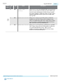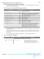
1
Arria 10 Transceiver PHY User Guide
Subscribe
Send Feedback
UG-01143
2015.05.11
101 Innovation Drive
San Jose, CA 95134
www.altera.com
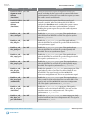
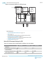
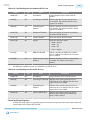
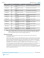
TOC-2
Arria 10 Transceiver PHY Overview
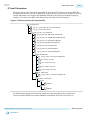
Contents
Arria 10 Transceiver PHY Overview ..................................................................1-1
Device Transceiver Layout......................................................................................................................... 1-3
Arria 10 GX Device Transceiver Layout.......................................................................................1-3
Arria 10 GT Device Transceiver Layout....................................................................................... 1-9
Arria 10 GX and GT Device Package Details ............................................................................1-12
Arria 10 SX Device Transceiver Layout......................................................................................1-13
Arria 10 SX Device Package Details............................................................................................ 1-16
Transceiver PHY Architecture Overview...............................................................................................1-16
Transceiver Bank Architecture.................................................................................................... 1-16
PHY Layer Transceiver Components......................................................................................... 1-20
Transceiver Phase-Locked Loops................................................................................................ 1-23
Clock Generation Block (CGB)................................................................................................... 1-24
Calibration.................................................................................................................................................. 1-24
Implementing Protocols in Arria 10 Transceivers............................................. 2-1
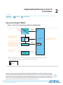
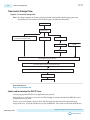
Transceiver Design IP Blocks.....................................................................................................................2-1
Transceiver Design Flow.............................................................................................................................2-2
Select and Instantiate the PHY IP Core........................................................................................ 2-2
Configure the PHY IP Core............................................................................................................2-4
Generate the PHY IP Core..............................................................................................................2-5
Select the PLL IP Core..................................................................................................................... 2-5
Configure the PLL IP Core............................................................................................................. 2-7
Generate the PLL IP Core .............................................................................................................. 2-8
Reset Controller ...............................................................................................................................2-8
Create Reconfiguration Logic.........................................................................................................2-8
Connect the PHY IP to the PLL IP and Reset Controller...........................................................2-9
Connect Datapath ........................................................................................................................... 2-9
Make Analog Parameter Settings ..................................................................................................2-9
Compile the Design......................................................................................................................... 2-9
Verify Design Functionality......................................................................................................... 2-10
Arria 10 Transceiver Protocols and PHY IP Support...........................................................................2-10
Using the Arria 10 Transceiver Native PHY IP Core........................................................................... 2-17
Presets..............................................................................................................................................2-19
General and Datapath Parameters ..............................................................................................2-19
PMA Parameters............................................................................................................................ 2-23
Enhanced PCS Parameters .......................................................................................................... 2-29
Standard PCS Parameters............................................................................................................. 2-39
PCS Direct ......................................................................................................................................2-46
Dynamic Reconfiguration Parameters........................................................................................2-46
PMA Ports.......................................................................................................................................2-49
Enhanced PCS Ports...................................................................................................................... 2-54
Standard PCS Ports........................................................................................................................2-68
Altera Corporation
Arria 10 Transceiver PHY Overview
TOC-3
IP Core File Locations................................................................................................................... 2-75
Interlaken.................................................................................................................................................... 2-76
Metaframe Format and Framing Layer Control Word............................................................ 2-78
Interlaken Configuration Clocking and Bonding..................................................................... 2-79
How to Implement Interlaken in Arria 10 Transceivers.......................................................... 2-86
Design Example..............................................................................................................................2-90
Native PHY IP Parameter Settings for Interlaken.....................................................................2-90
Ethernet....................................................................................................................................................... 2-97
Gigabit Ethernet (GbE) and GbE with IEEE 1588v2................................................................ 2-97
10GBASE-R, 10GBASE-R with IEEE 1588v2, and 10GBASE-R with FEC Variants......... 2-110
10GBASE-KR PHY IP Core ...................................................................................................... 2-125
1-Gigabit/10-Gigabit Ethernet (GbE) PHY IP Core...............................................................2-163
XAUI PHY IP Core..................................................................................................................... 2-211
Acronyms......................................................................................................................................2-227
PCI Express (PIPE)..................................................................................................................................2-228
Transceiver Channel Datapath for PIPE.................................................................................. 2-229
Supported PIPE Features............................................................................................................ 2-229
How to Connect TX PLLs for PIPE Gen1, Gen2, and Gen3 Modes.....................................2-239
How to Implement PCI Express (PIPE) in Arria 10 Transceivers........................................2-245
Native PHY IP Parameter Settings for PIPE ...........................................................................2-246
Native PHY IP Ports for PIPE....................................................................................................2-254
How to Place Channels for PIPE Configurations................................................................... 2-261
PHY IP Core for PCIe (PIPE) Link Equalization for Gen3 Data Rate.................................2-265
Design Example............................................................................................................................2-267
CPRI...........................................................................................................................................................2-268
Transceiver Channel Datapath and Clocking for CPRI......................................................... 2-268
Supported Features for CPRI .................................................................................................... 2-270
Word Aligner in Manual Mode for CPRI................................................................................ 2-271
How to Implement CPRI in Arria 10 Transceivers................................................................ 2-272
Native PHY IP Parameter Settings for CPRI........................................................................... 2-275
Other Protocols........................................................................................................................................ 2-279
Using the "Basic (Enhanced PCS)" and "Basic with KR FEC" Configurations of
Enhanced PCS.........................................................................................................................2-279
Using the Basic/Custom, Basic/Custom with Rate Match Configurations of Standard
PCS........................................................................................................................................... 2-290
Design Considerations for Data Rates Above 17.4 Gbps Using Arria 10 GT Channels....2-313
How to Implement PCS Direct Transceiver Configuration Rule..................................................... 2-321
Simulating the Transceiver Native PHY IP Core................................................................................ 2-322
NativeLink Simulation Flow...................................................................................................... 2-323
Custom Simulation Flow............................................................................................................ 2-328
PLLs and Clock Networks................................................................................... 3-1
PLLs................................................................................................................................................................3-3
ATX PLL............................................................................................................................................3-3
fPLL..................................................................................................................................................3-13
CMU PLL........................................................................................................................................ 3-21
Input Reference Clock Sources................................................................................................................ 3-27
Dedicated Reference Clock Pins.................................................................................................. 3-28
Altera Corporation
TOC-4
Arria 10 Transceiver PHY Overview
Receiver Input Pins........................................................................................................................3-29
PLL Cascading as an Input Reference Clock Source.................................................................3-30
Reference Clock Network............................................................................................................. 3-30
Global Clock or Core Clock as an Input Reference Clock....................................................... 3-30
Transmitter Clock Network..................................................................................................................... 3-30
x1 Clock Lines................................................................................................................................ 3-31
x6 Clock Lines................................................................................................................................ 3-32
xN Clock Lines............................................................................................................................... 3-33
GT Clock Lines...............................................................................................................................3-35
Clock Generation Block............................................................................................................................ 3-36
FPGA Fabric-Transceiver Interface Clocking....................................................................................... 3-39
Transmitter Data Path Interface Clocking............................................................................................. 3-41
Receiver Data Path Interface Clocking................................................................................................... 3-42
Channel Bonding....................................................................................................................................... 3-44
PMA Bonding.................................................................................................................................3-44
PMA and PCS Bonding.................................................................................................................3-45
Selecting Channel Bonding Schemes.......................................................................................... 3-47
Skew Calculations.......................................................................................................................... 3-47
PLL Feedback and Cascading Clock Network.......................................................................................3-47
Using PLLs and Clock Networks............................................................................................................. 3-49
Non-bonded Configurations........................................................................................................3-49
Bonded Configurations.................................................................................................................3-53
Implementing PLL Cascading......................................................................................................3-57
Mix and Match Example...............................................................................................................3-59
Timing Closure Recommendations............................................................................................ 3-62
Resetting Transceiver Channels..........................................................................4-1
When Is Reset Required? ........................................................................................................................... 4-2
How Do I Reset?...........................................................................................................................................4-2
Recommended Reset Sequence......................................................................................................4-3
Transceiver Blocks Affected by Reset and Powerdown Signals.................................................4-8
Using the Altera Transceiver PHY Reset Controller.............................................................................. 4-9
Parameterizing the Transceiver PHY Reset Controller IP.......................................................4-11
Transceiver PHY Reset Controller Parameters......................................................................... 4-11
Transceiver PHY Reset Controller Interfaces............................................................................4-13
Transceiver PHY Reset Controller Resource Utilization......................................................... 4-17
Using a User-Coded Reset Controller.................................................................................................... 4-18
User-Coded Reset Controller Signals..........................................................................................4-18
Combining Status or PLL Lock Signals ................................................................................................. 4-19
Timing Constraints for Bonded PCS and PMA Channels...................................................................4-20
Arria 10 Transceiver PHY Architecture............................................................. 5-1
Arria 10 PMA Architecture........................................................................................................................ 5-1
Transmitter....................................................................................................................................... 5-1
Receiver............................................................................................................................................. 5-4
Loopback......................................................................................................................................... 5-16
Arria 10 Enhanced PCS Architecture..................................................................................................... 5-18
Altera Corporation
Arria 10 Transceiver PHY Overview
TOC-5
Transmitter Datapath....................................................................................................................5-19
Receiver Datapath.......................................................................................................................... 5-29
Arria 10 Standard PCS Architecture....................................................................................................... 5-37
Transmitter Datapath....................................................................................................................5-37
Receiver Datapath.......................................................................................................................... 5-42
Arria 10 PCI Express Gen3 PCS Architecture....................................................................................... 5-53
Transmitter Datapath....................................................................................................................5-54
Receiver Datapath.......................................................................................................................... 5-55
PIPE Interface.................................................................................................................................5-56
Reconfiguration Interface and Dynamic Reconfiguration ............................... 6-1
Reconfiguring Channel and PLL Blocks...................................................................................................6-3
Interacting with the Reconfiguration Interface....................................................................................... 6-4
Reading from the Reconfiguration Interface............................................................................... 6-4
Writing to the Reconfiguration Interface..................................................................................... 6-5
Configuration Files...................................................................................................................................... 6-6
Multiple Reconfiguration Profiles............................................................................................................. 6-9
Embedded Reconfiguration Streamer.......................................................................................................6-9
Arbitration.................................................................................................................................................. 6-11
Steps to Perform Dynamic Reconfiguration.......................................................................................... 6-12
Direct Reconfiguration Flow....................................................................................................................6-13
Changing PMA Analog Parameters............................................................................................ 6-13
Changing CTLE Settings in Manual Mode................................................................................ 6-15
Enabling and Disabling Loopback Modes..................................................................................6-15
IP Guided Reconfiguration Flow.............................................................................................................6-18
Reconfiguration Flow for Special Cases..................................................................................................6-19
Switching Transmitter PLL ..........................................................................................................6-19
Switching Reference Clocks..........................................................................................................6-20
Ports and Parameters.................................................................................................................................6-24
Dynamic Reconfiguration Interface Merging Across Multiple IP Blocks......................................... 6-29
On-Die Instrumentation...........................................................................................................................6-31
Using ODI to Build On-chip Eye Process.................................................................................. 6-38
Start Pattern Checker ................................................................................................................... 6-39
Embedded Debug Features.......................................................................................................................6-40
Altera Debug Master Endpoint....................................................................................................6-40
Optional Reconfiguration Logic.................................................................................................. 6-40
Using Data Pattern Generators and Checkers.......................................................................................6-47
Using PRBS and Square Wave Data Pattern Generator and Checker....................................6-47
Using Pseudo Random Pattern Mode.........................................................................................6-54
Timing Closure Recommendations........................................................................................................ 6-55
Unsupported Features...............................................................................................................................6-58
Arria 10 Transceiver Register Map..........................................................................................................6-58
Calibration...........................................................................................................7-1
Reconfiguration Interface and Arbitration with PreSICE Calibration Engine .................................. 7-1
Calibration Registers................................................................................................................................... 7-2
Avalon-MM Interface Arbitration Registers................................................................................7-3
Altera Corporation
TOC-6
Arria 10 Transceiver PHY Overview
Transceiver Channel Calibration Registers..................................................................................7-3
Fractional PLL Calibration Registers............................................................................................ 7-4
ATX PLL Calibration Registers......................................................................................................7-4
Capability Registers......................................................................................................................... 7-4
Power-up Calibration..................................................................................................................................7-5
User Recalibration....................................................................................................................................... 7-7
Calibration Example.................................................................................................................................... 7-8
ATX PLL Recalibration................................................................................................................... 7-8
Fractional PLL Recalibration .........................................................................................................7-9
CDR/CMU PLL Recalibration....................................................................................................... 7-9
PMA Recalibration.......................................................................................................................... 7-9
Recalibration After Transceiver Reference Clock Frequency or Data Rate Change............ 7-10
Analog Parameter Settings..................................................................................8-1
Making Analog Parameter Settings using the Assignment Editor........................................................8-1
Updating Quartus Settings File with the Known Assignment.............................................................. 8-1
Analog Parameter Settings List.................................................................................................................. 8-2
Receiver General Analog Settings..............................................................................................................8-4
XCVR_A10_RX_LINK................................................................................................................... 8-4
XCVR_A10_RX_TERM_SEL........................................................................................................ 8-5
XCVR_VCCR_VCCT_VOLTAGE - RX......................................................................................8-6
Receiver Equalization Settings................................................................................................................... 8-6
CTLE Settings................................................................................................................................... 8-6
VGA Settings.................................................................................................................................... 8-9
Decision Feedback Equalizer (DFE) Settings.............................................................................8-10
Transmitter General Analog Settings......................................................................................................8-11
XCVR_A10_TX_LINK................................................................................................................. 8-11
XCVR_A10_TX_COMPENSATION_EN................................................................................. 8-12
XCVR_VCCR_VCCT_VOLTAGE - TX....................................................................................8-13
XCVR_A10_TX_SLEW_RATE_CTRL...................................................................................... 8-13
Transmitter Pre-Emphasis Settings.........................................................................................................8-15
XCVR_A10_TX_PRE_EMP_SIGN_PRE_TAP_1T................................................................. 8-15
XCVR_A10_TX_PRE_EMP_SIGN_PRE_TAP_2T................................................................. 8-15
XCVR_A10_TX_PRE_EMP_SIGN_1ST_POST_TAP............................................................ 8-16
XCVR_A10_TX_PRE_EMP_SIGN_2ND_POST_TAP...........................................................8-16
XCVR_A10_TX_PRE_EMP_SWITCHING_CTRL_PRE_TAP_1T..................................... 8-17
XCVR_A10_TX_PRE_EMP_SWITCHING_CTRL_PRE_TAP_2T..................................... 8-17
XCVR_A10_TX_PRE_EMP_SWITCHING_CTRL_1ST_POST_TAP.................................8-18
XCVR_A10_TX_PRE_EMP_SWITCHING_CTRL_2ND_POST_TAP...............................8-19
Transmitter VOD Settings........................................................................................................................8-19
XCVR_A10_TX_VOD_OUTPUT_SWING_CTRL.................................................................8-19
Dedicated Reference Clock Settings........................................................................................................8-20
XCVR_A10_REFCLK_TERM_TRISTATE............................................................................... 8-20
Document Revision History for Current Release ..............................................9-1
Document Revision History for Previous Releases...............................................................................9-12
Altera Corporation
1
Arria 10 Transceiver PHY Overview
2015.05.11
UG-01143
Subscribe
Send Feedback
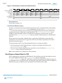
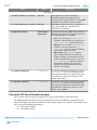
This user guide provides details about the Arria® 10 transceiver physical (PHY) layer architecture, PLLs,
clock networks and transceiver PHY IP. It also provides protocol specific implementation details and
describes features such as reset controller, and dynamic reconfiguration.
Altera’s Arria 10 devices offer up to 96 transceiver channels with integrated advanced high speed analog
signal conditioning and clock data recovery techniques for chip-to-chip, chip-to-module, and backplane
applications.
The Arria 10 GX and SX devices have GX transceiver channels that can support data rates up to 17.4 Gbps
for chip-to-chip applications and 16.0 Gbps for backplane applications.
The Arria 10 GT devices have up to 16 GT transceiver channels, that can support data rates up to 28.3
Gbps for short reach chip-to-chip and chip-to-module applications. Additionally, the GT devices have GX
transceiver channels that can support data rates up to 17.4 Gbps for both chip-to-chip and backplane
applications. If all 16 GT channels are used in GT mode, then the largest GT devices also have up to 72
GX transceiver channels.
The Arria 10 transceivers support reduced power modes with data rates up to 11.3 Gbps (chip-to-chip)
and 10.3125 Gbps (backplane) for critical power sensitive designs. In GX devices that have transceivers on
both sides of the device, each side can be operated independently in standard and reduced power modes.
You can achieve transmit data rates below 611 Mbps and receive data rates below 1.0 Gbps with oversam‐
pling.
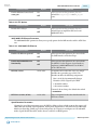
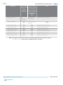
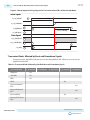
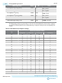
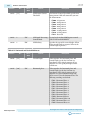
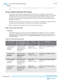
Table 1-1: Data Rates Supported by GX Transceiver Channel Type
Device
Variant
Standard Power Mode (1), (2), (3)
Chip-to-Chip
SX (4) 611 Mbps to 17.4 Gbps
(1)
(2)
(3)
Reduced Power Mode (1), (2), (3)
Backplane
Chip-to-Chip
611 Mbps to 16.0 Gbps
611 Mbps to 11.3 Gbps
Backplane
611 Mbps to 10.3125
Gbps
To operate GX transceiver channels at designated data rates in standard and reduced power modes, apply
the corresponding core and periphery power supplies. Refer to the Arria 10 Device Datasheet for more
details.
The Transmitter minimum operational data rate is 611 Mbps. For Transmitter data rates less than 611
Mbps, oversampling must be applied at the Transmitter.
The Receiver minimum operational data rate is 1.0 Gbps. For Receiver data rates less than 1.0 Gbps,
oversampling must be applied at the Receiver.
© 2015 Altera Corporation. All rights reserved. ALTERA, ARRIA, CYCLONE, ENPIRION, MAX, MEGACORE, NIOS, QUARTUS and STRATIX words and logos are
trademarks of Altera Corporation and registered in the U.S. Patent and Trademark Office and in other countries. All other words and logos identified as
trademarks or service marks are the property of their respective holders as described at www.altera.com/common/legal.html. Altera warrants performance
of its semiconductor products to current specifications in accordance with Altera's standard warranty, but reserves the right to make changes to any
products and services at any time without notice. Altera assumes no responsibility or liability arising out of the application or use of any information,
product, or service described herein except as expressly agreed to in writing by Altera. Altera customers are advised to obtain the latest version of device
specifications before relying on any published information and before placing orders for products or services.
www.altera.com
101 Innovation Drive, San Jose, CA 95134
ISO
9001:2008
Registered
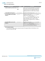
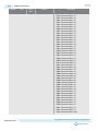
1-2
UG-01143
2015.05.11
Arria 10 Transceiver PHY Overview
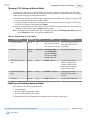
Standard Power Mode (1), (2), (3)
Device
Variant
Chip-to-Chip
Reduced Power Mode (1), (2), (3)
Backplane
Chip-to-Chip
GX( 611 Mbps to 17.4 Gbps
611 Mbps to 16.0 Gbps
611 Mbps to 11.3 Gbps
611 Mbps to 10.3125
Gbps
GT (5)611 Mbps to 17.4 Gbps
611 Mbps to 17.4 Gbps
611 Mbps to 11.3 Gbps
611 Mbps to 10.3125
Gbps
4)
Backplane
Table 1-2: Data Rates Supported by GT Transceiver Channel Type
Data Rates (2), (3), (6)
Device Variant (5)
GT
Chip-to-Chip
611 Mbps to 28.3 Gbps
Backplane
611 Mbps to 17.4 Gbps
Note: The device data rates depend on the device speed grade. Refer to Arria 10 Device Datasheet for
details on available speed grades and supported data rates.
Related Information
Arria 10 Device Datasheet
(1)
(2)
(3)
(4)
(5)
(6)
To operate GX transceiver channels at designated data rates in standard and reduced power modes, apply
the corresponding core and periphery power supplies. Refer to the Arria 10 Device Datasheet for more
details.
The Transmitter minimum operational data rate is 611 Mbps. For Transmitter data rates less than 611
Mbps, oversampling must be applied at the Transmitter.
The Receiver minimum operational data rate is 1.0 Gbps. For Receiver data rates less than 1.0 Gbps,
oversampling must be applied at the Receiver.
For SX and GX device variants, the maximum transceiver data rates are specified for the fastest (–1)
transceiver speed grade.
For GT device variants, the maximum transceiver data rates are specified for (-2) transceiver speed grade.
Because the GT transceiver channels are designed for peak performance, they do not have a reduced power
mode of operation.
Altera Corporation
Arria 10 Transceiver PHY Overview
Send Feedback
UG-01143
2015.05.11
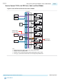
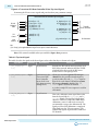
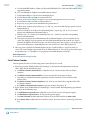
Device Transceiver Layout
1-3
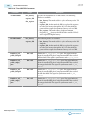
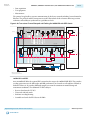
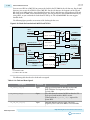
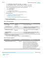
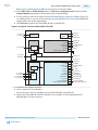
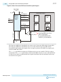
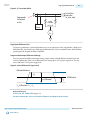
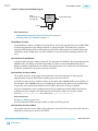
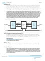
Device Transceiver Layout
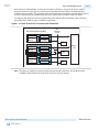
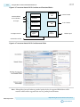
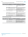
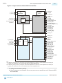
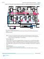
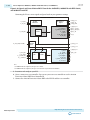
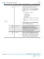
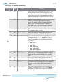
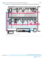
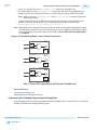
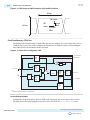
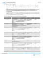
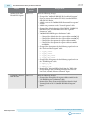
Figure 1-1: Arria 10 FPGA Architecture Block Diagram
PCI Express Gen3 Hard IP
PLLs
Hard IP Per Transceiver: Standard PCS, PCIe Gen3 PCS, Enhanced PCS
Transceiver Channels
PCI Express Gen3 Hard IP
Variable Precision DSP Blocks
M20K
M20K
Internal
Internal
Memory
Memory
Blocks
Blocks
Hard Memory Controllers, General-Purpose I/O Cells, LVDS
I/O PLLs
Core Logic Fabric
Variable Precision DSP Blocks
M20K
M20K
Internal
Internal
Memory
Memory
Blocks
Blocks
Core Logic Fabric
I/O PLLs
Hard Memory Controllers, General-Purpose I/O Cells, LVDS
Variable Precision DSP Blocks
M20K
M20K
Internal
Internal
Memory
Memory
Blocks
Blocks
Transceiver Channels
Hard IP Per Transceiver: Standard PCS, PCIe Gen3 PCS, Enhanced PCS
PLLs
PCI Express Gen3 Hard IP
PCI Express Gen3 Hard IP
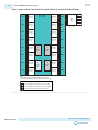
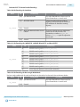
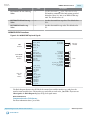
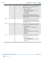
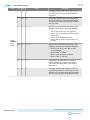
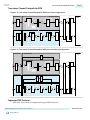
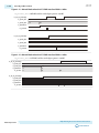
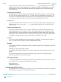
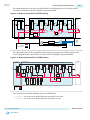
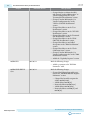
The transceiver channels are placed on the left side periphery in most Arria 10 devices. For larger Arria 10
devices, additional transceiver channels are placed on the right side periphery.
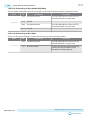
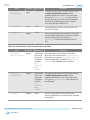
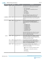
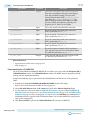
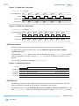
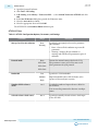
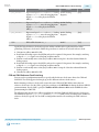
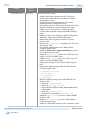
Arria 10 GX Device Transceiver Layout
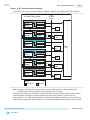
The largest Arria 10 GX device includes 96 transceiver channels. A column array of eight transceiver
banks on the left and the right side periphery of the device is shown in the following figure. Each
transceiver bank has six transceiver channels. Some devices have transceiver banks with only three
channels. The transceiver banks with only three channels are the uppermost transceiver banks. Arria 10
devices also include PCI Express Hard IP blocks.
The figures below illustrate different transceiver bank layouts for Arria 10 GX device variants.
For more information about PCIe Hard IP transceiver placements, refer to Related Information at the end
of this section.
Arria 10 Transceiver PHY Overview
Send Feedback
Altera Corporation
1-4
UG-01143
2015.05.11
Arria 10 GX Device Transceiver Layout
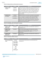
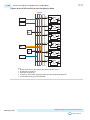
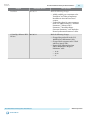
Figure 1-2: Arria 10 GX Devices with 96 Transceiver Channels and Four PCIe Hard IP Blocks
GXBL1J
Transceiver
Bank
GX 115 UF45
GX 090 UF45
Transceiver
Bank
GXBR4J
Transceiver
Bank
GXBL1I
Transceiver
Bank
Transceiver
Bank
GXBR4I
GXBL1H
Transceiver
Bank
Transceiver
Bank
GXBR4H
GXBL1G
Transceiver
Bank
Transceiver
Bank
GXBR4G
GXBL1F
Transceiver
Bank
Transceiver
Bank
GXBR4F
GXBL1E
Transceiver
Bank
Transceiver
Bank
GXBR4E
GXBL1D
Transceiver
Bank
Transceiver
Bank
GXBR4D
GXBL1C
(1)
Transceiver
Bank
Transceiver
Bank
GXBR4C
(2)
PCIe
Gen1 - Gen3
Hard IP
PCIe
Gen1 - Gen3
Hard IP
(with CvP)
PCIe
Gen1 - Gen3
Hard IP
PCIe
Gen1 - Gen3
Hard IP
CH5
CH4
CH3
CH2
CH1
CH0
Notes:
(1) Nomenclature of left column bottom transceiver banks always ends with “C”.
(2) Nomenclature of right column bottom transceiver banks may end with “C”, “D”, or “E”.
Legend:
PCIe Gen1 - Gen3 Hard IP blocks with Configuration via Protocol (CvP) capabilities.
PCIe Gen1 - Gen3 Hard IP blocks without Configuration via Protocol (CvP) capabilities.
Arria 10 GX device with 96 transceiver channels and four PCIe Hard IP blocks.
Altera Corporation
Arria 10 Transceiver PHY Overview
Send Feedback
UG-01143
2015.05.11
Arria 10 GX Device Transceiver Layout
1-5
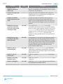
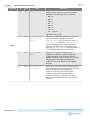
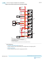
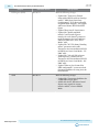
Figure 1-3: Arria 10 GX Devices with 72 and 48 Transceiver Channels and Four PCIe Hard IP Blocks.
GXBL1H
Transceiver
Bank
GXBL1G
Transceiver
Bank
GXBL1F
Transceiver
Bank
GXBL1E
Transceiver
Bank
GXBL1D
Transceiver
Bank
GXBL1C
(1)
GX 115 SF45
GX 090 SF45
PCIe
Gen1 - Gen3
Hard IP
Transceiver
Bank
PCIe
Gen1 - Gen3
Hard IP
GX 115 NF45
GX 090 NF45
PCIe
Gen1 - Gen3
Hard IP
(with CvP)
PCIe
Gen1 - Gen3
Hard IP
Transceiver
Bank
GXBR4H
Transceiver
Bank
GXBR4G
Transceiver
Bank
GXBR4F
Transceiver
Bank
GXBR4E
Transceiver
Bank
GXBR4D
Transceiver
Bank
Transceiver
Bank
CH5
CH4
CH3
CH2
CH1
CH0
GXBR4C
(2)
Notes:
(1) Nomenclature of left column bottom transceiver banks always ends with “C”.
(2) Nomenclature of right column bottom transceiver banks may end with “C”, “D”, or “E”.
Legend:
PCIe Gen1 - Gen3 Hard IP blocks with Configuration via Protocol (CvP) capabilities.
PCIe Gen1 - Gen3 Hard IP blocks without Configuration via Protocol (CvP) capabilities.
Arria 10 GX device with 72 transceiver channels and four PCIe Hard IP blocks.
Arria 10 GX device with 48 transceiver channels and four PCIe Hard IP blocks.
Arria 10 Transceiver PHY Overview
Send Feedback
Altera Corporation
1-6
UG-01143
2015.05.11
Arria 10 GX Device Transceiver Layout
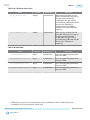
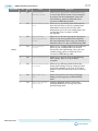
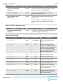
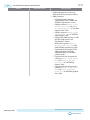
Figure 1-4: Arria 10 GX Devices with 66 Transceiver Channels and Three PCIe Hard IP Blocks
GXBL1H
GXBL1G
Transceiver
Bank
GX 115 RF40
GX 090 RF40
Transceiver
Bank
Transceiver
Bank
GXBL1F
Transceiver
Bank
GXBL1E
Transceiver
Bank
GXBL1D
Transceiver
Bank
GXBL1C
(1)
Transceiver
Bank
Transceiver
Bank
PCIe
Gen1 - Gen3
Hard IP
PCIe
Gen1 - Gen3
Hard IP
PCIe
Gen1 - Gen3
Hard IP
(with CvP)
GXBR4J
GXBR4I
Transceiver
Bank
GXBR4H
Transceiver
Bank
GXBR4G
Transceiver
Bank
GXBR4F
Transceiver
Bank
GXBR4E
Transceiver
Bank
CH2
CH1
CH0
Transceiver
Bank
CH5
CH4
CH3
CH2
CH1
CH0
(2)
Notes:
(1) Nomenclature of left column bottom transceiver banks always ends with “C”.
(2) Nomenclature of right column bottom transceiver banks may end with “C”, “D”, or “E”.
Legend:
PCIe Gen1 - Gen3 Hard IP blocks with Configuration via Protocol (CvP) capabilities.
PCIe Gen1 - Gen3 Hard IP blocks without Configuration via Protocol (CvP) capabilities.
Arria 10 GX device with 66 transceiver channels and three PCIe Hard IP blocks.
Altera Corporation
Arria 10 Transceiver PHY Overview
Send Feedback
UG-01143
2015.05.11
Arria 10 GX Device Transceiver Layout
1-7
Figure 1-5: Arria 10 GX Devices with 48, 36, and 24 Transceiver Channels and Two PCIe Hard IP Blocks
CH5
CH4
CH3
CH2
CH1
CH0
Transceiver
Bank
GXBL1J
GX 115 NF40
GX 090 NF40
GX 066 NF40
GX 057 NF40
Transceiver
Bank
GXBL1I
Transceiver
Bank
GXBL1H
Transceiver
Bank
GXBL1G
Transceiver
Bank
GXBL1F
Transceiver
Bank
GXBL1E
Transceiver
Bank
GXBL1D
Transceiver
Bank
GXBL1C
Transceiver
Bank
GX 066 KF40
GX 057 KF40
GX 115 KF36
GX 090 KF36
GX 066 KF36
GX 066 KF35
GX 057 KF36
GX 057 KF35
GX 048 KF35
PCIe
Gen1 - Gen3
Hard IP
GX 115 HF34
GX 090 HF34
GX 066 HF34
GX 057 HF34
GX 048 HF34
GX 032 HF35
GX 032 HF34
GX 027 HF35
GX 027 HF34
PCIe
Gen1 - Gen3
Hard IP
(with CvP)
Note:
(1) These devices have transceivers only on the left hand side of the device.
Legend:
PCIe Gen1 - Gen3 Hard IP blocks with Configuration via Protocol (CvP) capabilities.
PCIe Gen1 - Gen3 Hard IP blocks without Configuration via Protocol (CvP) capabilities.
Arria 10 GX device with 48 transceiver channels and two PCIe Hard IP blocks.
Arria 10 GX device with 36 transceiver channels and two PCIe Hard IP blocks.
Arria 10 GX device with 24 transceiver channels and two PCIe Hard IP blocks.
Arria 10 Transceiver PHY Overview
Send Feedback
Altera Corporation
1-8
UG-01143
2015.05.11
Arria 10 GX Device Transceiver Layout
Figure 1-6: Arria 10 GX Devices with 12 Transceiver Channels and One PCIe Hard IP Block
CH5
CH4
CH3
CH2
CH1
CH0
GXBL1D
Transceiver
Bank
GXBL1C
Transceiver
Bank
Transceiver
Bank
PCIe
Gen1 - Gen3
Hard IP
(with CvP)
GX 048 EF29
GX 032 EF29
GX 027 EF29
GX 032 EF27
GX 027 EF27
GX 022 EF29
GX 022 EF27
GX 016 EF29
GX 016 EF27
Note:
(1) These devices have transceivers only on the left hand side of the device.
Legend:
PCIe Gen1 - Gen3 HIP blocks with Configuration via Protocol (CvP) capabilities.
Arria 10 GX device with 12 transceiver channels and one PCIe Hard IP block.
Figure 1-7: Arria 10 GX Devices with 6 Transceiver Channels and One PCIe Hard IP Block
CH5
CH4
CH3
CH2
CH1
CH0
Transceiver
Bank
GXBL1C
Transceiver
Bank
PCIe Hard IP (1)
GX 022 CU19
GX 016 CU19
Note:
(1) Only CH5 and CH4 support PCIe Hard IP block with CvP capabilities.
(2) These devices have transceivers only on the left hand side of the device.
Legend:
PCIe Gen1 - Gen3 Hard IP block with Configuration via Protocol (CvP) capabilities.
Arria 10 GX device with six transceiver channels and one PCIe Hard IP block.
Related Information
•
•
•
•
Altera Corporation
Arria 10 Avalon-ST Interface for PCIe Datasheet
Arria 10 Avalon-MM Interface for PCIe Datasheet
Arria 10 Avalon-MM DMA Interface for PCIe Datasheet
Arria 10 Avalon-ST Interface with SR-IOV for PCIe Datasheet
Arria 10 Transceiver PHY Overview
Send Feedback
UG-01143
2015.05.11
1-9
Arria 10 GT Device Transceiver Layout
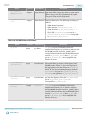
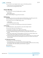
Arria 10 GT Device Transceiver Layout
The largest GT device has 96 transceiver channels and four PCI Express Hard IP blocks. All GT devices
have a total of 16 GT transceiver channels that can support data rates up to 28.3 Gbps.
In GT devices, transceiver banks GXBL1E, GXBL1F, GXBL1G, and GXBL1H each contain four GT
transceiver channels. Channels 0,1,3, and 4 can be used as GT or GX transceiver channels. Channels 2 and
5 are GX only transceiver channels.
For more information about PCIe Hard IP transceiver placements, refer to Related Information at the end
of this section.
Figure 1-8: Arria 10 GT Devices with 96 Transceiver Channels and Four PCIe Hard IP Blocks
GT Channels
Capable of Short
Reach 28.3 Gbps
CH5
CH4
CH3
CH2
CH1
CH0
GX or Restricted
GT or GX
GT or GX
GX or Restricted
GT or GX
GT or GX
GT 115 UF45
GT 090 UF45
Transceiver
Bank
GXBR4J
Transceiver
Bank
Transceiver
Bank
GXBR4I
GXBL1H
Transceiver
Bank
Transceiver
Bank
GXBR4H
GXBL1G
Transceiver
Bank
Transceiver
Bank
GXBR4G
GXBL1F
Transceiver
Bank
Transceiver
Bank
GXBR4F
GXBL1E
Transceiver
Bank
Transceiver
Bank
GXBR4E
Transceiver
Bank
GXBR4D
Transceiver
Bank
GXBR4C
GXBL1J
Transceiver
Bank
GXBL1I
Transceiver
Bank
GXBL1D
Transceiver
Bank
GXBL1C
(1)
Transceiver
Bank
PCIe
Gen1 - Gen3
Hard IP
PCIe
Gen1 - Gen3
Hard IP
(with CvP)
PCIe
Gen1 - Gen3
Hard IP
PCIe
Gen1 - Gen3
Hard IP
(2)
Notes:
(1) Nomenclature of left column bottom transceiver banks always ends with “C”.
(2) Nomenclature of right column bottom transceiver banks may end with “C”, “D”, or “E”.
Legend:
GT transceiver channels (channel 0, 1, 3, and 4)
GX transceiver channels (channel 2 and 5) with usage restrictions.
GX transceiver channels without usage restrictions.
PCIe Gen1 - Gen3 Hard IP blocks with Configuration via Protocol (CvP) capabilities.
PCIe Gen1 - Gen3 Hard IP blocks without Configuration via Protocol (CvP) capabilities.
Arria 10 Transceiver PHY Overview
Send Feedback
Altera Corporation
1-10
UG-01143
2015.05.11
Arria 10 GT Device Transceiver Layout
Note: Refer to Arria 10 GT Channel Usage on page 2-313 for details on Arria 10 GT channel usage
restrictions.
Figure 1-9: Arria 10 GT Devices with 72 Transceiver Channels and Four PCIe Hard IP Blocks
CH5
CH4
CH3
CH2
CH1
CH0
GX or Restricted
GT or GX
GT or GX
GX or Restricted
GT or GX
GT or GX
Transceiver
Bank
GXBL1H
Transceiver
Bank
GXBL1G
Transceiver
Bank
GXBL1F
Transceiver
Bank
GXBL1E
Transceiver
Bank
GXBL1D
Transceiver
Bank
GXBL1C
(1)
Transceiver
Bank
GT Channels
Capable of Short
Reach 28.3 Gbps
GT 115 SF45
GT 090 SF45
PCIe
Gen1 - Gen3
Hard IP
PCIe
Gen1 - Gen3
Hard IP
(with CvP)
Transceiver
Bank
PCIe
Gen1 - Gen3
Hard IP
PCIe
Gen1 - Gen3
Hard IP
GXBR4H
Transceiver
Bank
GXBR4G
Transceiver
Bank
GXBR4F
Transceiver
Bank
GXBR4E
Transceiver
Bank
GXBR4D
Transceiver
Bank
GXBR4C
(2)
Notes:
(1) Nomenclature of left column bottom transceiver banks always end with “C”.
(2) Nomenclature of right column bottom transceiver banks may end with “C”, “D”, or “E”.
Legend:
GT transceiver channels (channel 0, 1, 3, and 4).
GX transceiver channels (channel 2 and 5) with usage restrictions.
GX transceiver channels without usage restrictions.
PCIe Gen1 - Gen3 Hard IP blocks with Configuration via Protocol (CvP) capabilities.
PCIe Gen1 - Gen3 Hard IP blocks without Configuration via Protocol (CvP) capabilities.
Altera Corporation
Arria 10 Transceiver PHY Overview
Send Feedback
UG-01143
2015.05.11
Arria 10 GT Device Transceiver Layout
1-11
Figure 1-10: Arria 10 GT Devices with 48 Transceiver Channels and Two PCIe Hard IP Blocks
GT Channels
Capable of Short
Reach 28.3 Gbps
CH5
CH4
CH3
CH2
CH1
CH0
GX or Restricted
GT or GX
GT or GX
GX or Restricted
GT or GX
GT or GX
GXBL1J
Transceiver
Bank
GXBL1I
Transceiver
Bank
Transceiver
Bank
GXBL1H
Transceiver
Bank
GXBL1G
Transceiver
Bank
GXBL1F
Transceiver
Bank
GXBL1E
Transceiver
Bank
GXBL1D
Transceiver
Bank
GXBL1C
(1)
Transceiver
Bank
GT 115 NF40
GT 090 NF40
PCIe
Gen1 - Gen3
Hard IP
PCIe
Gen1 - Gen3
Hard IP
(with CvP)
Notes:
(1) Nomenclature of left column bottom transceiver banks always end with “C”.
(2) These devices have transceivers only on left hand side of the device.
Legend:
GT transceiver channels (channel 0, 1, 3, and 4).
GX transceiver channels (channel 2 and 5) with usage restrictions.
GX transceiver channels without usage restrictions.
PCIe Gen3 HIP blocks with Configuration via Protocol (CvP) capabilities.
PCIe Gen3 HIP blocks without Configuration via Protocol (CvP) capabilities.
Note: Refer to Arria 10 GT Channel Usage on page 2-313 for details on Arria 10 GT channel usage
restrictions.
The largest GT device has 96 transceiver channels, which include 16 GT transceiver channels supporting
data rates greater than 17.4 Gbps. If all 16 GT transceiver channels are used in GT mode, then there will
be 72 GX transceiver channels that can drive backplanes at data rates up to 17.4 Gbps and 8 GX channels
that are unusable. In contrast, the GX transceiver channels in SX and GX device variants can drive
backplanes at data rates up to 16.0 Gbps.
Arria 10 Transceiver PHY Overview
Send Feedback
Altera Corporation
1-12
UG-01143
2015.05.11
Arria 10 GX and GT Device Package Details
In GT devices that have transceivers on both sides of the device, the GX transceiver channels on the right
side can be used in reduced power mode. In GT devices where none of the GT channels are used, the
transceiver channels can be used as GX channels in standard or reduced power mode.
Related Information
• Arria 10 GT Channel Usage on page 2-313
For details about Arria 10 GT channel usage guidelines
• Arria 10 Avalon-ST Interface for PCIe Datasheet
• Arria 10 Avalon-MM Interface for PCIe Datasheet
• Arria 10 Avalon-MM DMA Interface for PCIe Datasheet
• Arria 10 Avalon-ST Interface with SR-IOV for PCIe Datasheet
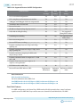
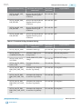
Arria 10 GX and GT Device Package Details
The following tables list package sizes, available transceiver channels, and PCI Express Hard IP blocks for
Arria 10 GX and GT devices.
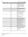
Table 1-3: Package Details for GX and GT Devices with Transceivers and HIP Blocks Located on the Left
Side Periphery of the Device
•
•
•
•
•
Package U19: 19mm x 19mm package; 484 pins.
Package F27: 27mm x 27mm package; 672 pins.
Package F29: 29mm x 29mm package; 780 pins.
Packages F34, F35, and F36: 35 mm x 35 mm package size; 1152 pins.
Package F40: 40 mm x 40 mm package size; 1517 pins.
Device
U19
F27
F29
F34
F35
F36
K F40
N F40
Transceiver Count, PCIe Hard IP Block Count
GX 016
6, 1
12, 1
12, 1
GX 022
6, 1
12, 1
12, 1
GX 027
12, 1
12, 1
24, 2
24, 2
GX 032
12, 1
12, 1
24, 2
24, 2
12, 1
24, 2
36, 2
GX 057
24, 2
36, 2
36, 2
36, 2
48, 2
GX 066
24, 2
36, 2
36, 2
36, 2
48, 2
GX 090
24, 2
36, 2
48, 2
GX 115
24, 2
36, 2
48, 2
GX 048
GT 090
48, 2
GT 115
48, 2
Altera Corporation
Arria 10 Transceiver PHY Overview
Send Feedback
UG-01143
2015.05.11
Arria 10 SX Device Transceiver Layout
1-13
Table 1-4: Package Details for GX and GT Devices with Transceivers and Hard IP Blocks Located on the Left
and Right Side Periphery of the Device
• Package F40: 40 mm x 40 mm package size; 1517 pins.
• Package F45: 45mm x 45mm package size; 1932 pins.
Device
R F40
N F45
S F45
U F45
Transceiver Count, PCIe Hard IP Block Count
GX 090
66, 3
48, 4
72, 4
96, 4
GX 115
66, 3
48, 4
72, 4
96, 4
GT 090
72, 4
96, 4
GT 115
72, 4
96, 4
Arria 10 SX Device Transceiver Layout
The largest SX device includes 48 transceiver channels. All SX devices include GX transceiver channel
type. The transceiver banks in SX devices are located on the left side periphery of the device.
For more information about PCIe Hard IP transceiver placements, refer to Related Information at the end
of this section.
Arria 10 Transceiver PHY Overview
Send Feedback
Altera Corporation
1-14
UG-01143
2015.05.11
Arria 10 SX Device Transceiver Layout
Figure 1-11: Arria 10 SX Device with 48, 36, and 24 Transceiver Channels and Two Hard IP Blocks
CH5
CH4
CH3
CH2
CH1
CH0
GXBL1J
Transceiver
Bank
GXBL1I
Transceiver
Bank
GXBL1H
Transceiver
Bank
GXBL1G
Transceiver
Bank
GXBL1F
Transceiver
Bank
GXBL1E
Transceiver
Bank
GXBL1D
Transceiver
Bank
GXBL1C
Transceiver
Bank
Transceiver
Bank
SX 066 NF40
SX 057 NF40
SX 066 KF40
SX 066 KF35
SX 057 KF40
SX 057 KF35
SX 048 KF35
PCIe
Gen1 - Gen3
Hard IP
SX 066 HF34
SX 057 HF34
SX 048 HF34
SX 032 HF35
SX 032 HF34
SX 027 HF35
SX 027 HF34
PCIe
Gen1 - Gen3
Hard IP
(with CvP)
Note:
(1) These devices have transceivers only on the left hand side of the device.
Legend:
PCIe Gen1- Gen3 Hard IP blocks with Configuration via Protocol (CvP) capabilities.
PCIe Gen1 - Gen3 Hard IP blocks without Configuration via Protocol (CvP) capabilities.
Arria 10 SX device with 48 transceiver channels and two PCIe Hard IP blocks.
Arria 10 SX device with 36 transceiver channels and two PCIe Hard IP blocks.
Arria 10 SX device with 24 transceiver channels and two PCIe Hard IP blocks.
Altera Corporation
Arria 10 Transceiver PHY Overview
Send Feedback
UG-01143
2015.05.11
Arria 10 SX Device Transceiver Layout
1-15
Figure 1-12: Arria 10 SX Device with 12 Transceiver Channels and One Hard IP Block
CH5
CH4
CH3
CH2
CH1
CH0
GXBL1D
Transceiver
Bank
GXBL1C
Transceiver
Bank
Transceiver
Bank
PCIe
Gen1 - Gen3
Hard IP
(with CvP)
SX 048 EF29
SX 032 EF29
SX 032 EF27
SX 027 EF29
SX 027 EF27
SX 022 EF29
SX 022 EF27
SX 016 EF29
SX 016 EF27
Note:
(1) These devices have transceivers only on the left hand side of the device.
Legend:
PCIe Gen1 - Gen3 Hard IP blocks with Configuration via Protocol (CvP) capabilities.
Arria 10 SX device with 12 transceiver channels and one Hard IP block.
Figure 1-13: Arria 10 SX Device with Six Transceiver Channels and One Hard IP Block
CH5
CH4
CH3
CH2
CH1
CH0
Transceiver
Bank
GXBL1C
Transceiver
Bank
PCIe Hard IP (1)
SX 022 CU19
SX 016 CU19
Note:
(1) Only CH5 and CH4 support PCIe Hard IP block with Configuration via Protocol (CvP) capabilities.
(2) These devices have transceivers only on the left hand side of the device.
Legend:
PCIe Gen1 - Gen3 Hard IP block with Configuration via Protocol (CvP) capabilities.
Arria 10 SX device with six transceiver channels and one PCIe Hard IP block.
Arria 10 Transceiver PHY Overview
Send Feedback
Altera Corporation
1-16
UG-01143
2015.05.11
Arria 10 SX Device Package Details
Related Information
•
•
•
•
Arria 10 Avalon-ST Interface for PCIe Datasheet
Arria 10 Avalon-MM Interface for PCIe Datasheet
Arria 10 Avalon-MM DMA Interface for PCIe Datasheet
Arria 10 Avalon-ST Interface with SR-IOV for PCIe Datasheet
Arria 10 SX Device Package Details
The following tables list package sizes, available transceiver channels, and PCI Express Hard IP blocks for
Arria 10 SX devices.
Table 1-5: Package Details for SX Devices with Transceivers and HIP Blocks Located on the Left Side
Periphery of the Device
Device
U19 (7)
F27 (8)
F29 (9)
F34 (10)
F35 (10)
K F40 (11)
N F40 (11)
Transceiver Count, PCIe Hard IP Block Count
SX 016
6, 1
12, 1
12, 1
SX 022
6, 1
12, 1
12, 1
SX 027
12, 1
12, 1
24, 2
24, 2
SX 032
12, 1
12, 1
24, 2
24, 2
12, 1
24, 2
36, 2
SX 057
24, 2
36, 2
36, 2
48, 2
SX 066
24, 2
36, 2
36, 2
48, 2
SX 048
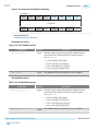
Transceiver PHY Architecture Overview
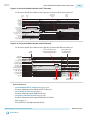
A link is defined as a single entity communication port. A link can have one or more transceiver channels.
A transceiver channel is synonymous with a transceiver lane.
For example, a 10GBASE-R link has one transceiver channel or lane with a data rate of 10.3125 Gbps. A
40GBASE-R link has four transceiver channels. Each transceiver channel operates at a lane data rate of
10.3125 Gbps. Four transceiver channels give a total collective link bandwidth of 41.25 Gbps (40 Gbps
before and after 64B/66B Physical Coding Sublayer (PCS) encoding and decoding).
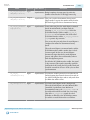
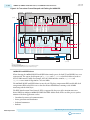
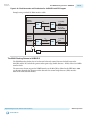
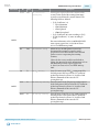
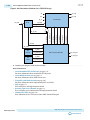
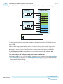
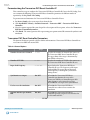
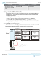
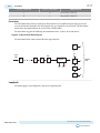
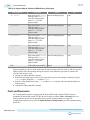
Transceiver Bank Architecture
The transceiver bank is the fundamental unit that contains all the functional blocks related to the device's
high speed serial transceivers.
(7)
(8)
(9)
(10)
(11)
Package U19: 19mm x 19mm package; 484 pins.
Package F27: 27mm x 27mm package; 672 pins.
Package F29: 29mm x 29mm package; 780 pins.
Packages F34 and F35: 35 mm x 35 mm package size ; 1152 pins.
Package F40: 40 mm x 40 mm package size ; 1517 pins.
Altera Corporation
Arria 10 Transceiver PHY Overview
Send Feedback
UG-01143
2015.05.11
Transceiver Bank Architecture
1-17
Each transceiver bank includes six transceiver channels in all devices except for the devices with 66
transceiver channels. These devices (with 66 transceiver channels) have both six channel and three
channel transceiver banks. The uppermost transceiver bank on the left and the right side of these devices
is a three channel transceiver bank. All other devices contain only six channel transceiver banks.
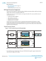
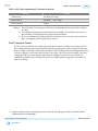
The figures below show the transceiver bank architecture with the phase locked loop (PLL) and clock
generation block (CGB) resources available in each bank.
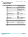
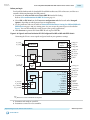
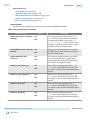
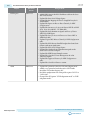
Figure 1-14: Three-Channel GX Transceiver Bank Architecture
Three-Channel GX Transceiver Bank
CH2
PMA
Channel PLL
(CDR Only)
Clock
Distribution
Network
PCS
Local CGB2
fPLL0
CH1
PMA
Channel PLL
(CMU/CDR)
CH0
PMA
Channel PLL
(CDR Only)
FPGA Core
Fabric
PCS
Local CGB1
Master
CGB0
PCS
Local CGB0
ATX
PLL0
Note: This figure is a high level overview of the transceiver bank architecture. For details about the
available clock networks refer to the PLLs and Clock Networks chapter.
Arria 10 Transceiver PHY Overview
Send Feedback
Altera Corporation
1-18
UG-01143
2015.05.11
Transceiver Bank Architecture
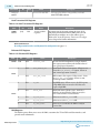
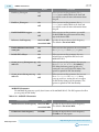
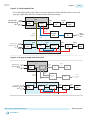
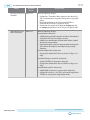
Figure 1-15: Six-Channel GX Transceiver Bank Architecture
Six-Channel GX Transceiver Bank
CH5
PMA
Channel PLL
(CDR Only)
Clock
Distribution
Network
PCS
Local CGB5
fPLL1
CH4
PMA
Channel PLL
(CMU/CDR)
CH3
PMA
Channel PLL
(CDR Only)
CH2
PMA
Channel PLL
(CDR Only)
PCS
Local CGB4
Master
CGB1
PCS
Local CGB3
ATX
PLL1
FPGA Core
Fabric
PCS
Local CGB2
fPLL0
CH1
PMA
Channel PLL
(CMU/CDR)
CH0
PMA
Channel PLL
(CDR Only)
PCS
Local CGB1
Master
CGB0
PCS
Local CGB0
ATX
PLL0
Note: This figure is a high level overview of the transceiver bank architecture. For details about the
available clock networks refer to the PLLs and Clock Networks chapter.
Altera Corporation
Arria 10 Transceiver PHY Overview
Send Feedback
UG-01143
2015.05.11
Transceiver Bank Architecture
1-19
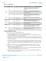
Figure 1-16: GT Transceiver Bank Architecture
In GT devices, the transceiver banks GXBL1E, GXBL1F, GXBL1G, and GXBL1H include GT channels.
Six-Channel GT Transceiver Bank
CH5
PMA
Channel PLL
(CDR Only)
Clock
Distribution
Network
PCS
Local CGB5
fPLL1
CH4
PMA
Channel PLL
(CMU/CDR)
CH3
PMA
Channel PLL
(CDR Only)
CH2
PMA
Channel PLL
(CDR Only)
PCS
Local CGB4
Master
CGB1
PCS
Local CGB3
ATX
PLL1
FPGA Core
Fabric
PCS
Local CGB2
fPLL0
CH1
PMA
Channel PLL
(CMU/CDR)
CH0
PMA
Channel PLL
(CDR Only)
PCS
Local CGB1
Master
CGB0
PCS
Local CGB0
ATX
PLL0
Legend
GT/GX Channel
GX Channel
Note: This figure is a high level overview of the transceiver bank architecture. For details about the
available clock networks refer to the PLLs and Clock Networks chapter.
The transceiver channels perform all the required PHY layer functions between the FPGA fabric and the
physical medium. The high speed clock required by the transceiver channels is generated by the
transceiver PLLs. The master and local clock generation blocks (CGBs) provide the necessary high speed
serial and low speed parallel clocks to drive the non-bonded and bonded channels in the transceiver bank.
Arria 10 Transceiver PHY Overview
Send Feedback
Altera Corporation
1-20
UG-01143
2015.05.11
PHY Layer Transceiver Components
Related Information
• PLLs and Clock Networks on page 3-1
• Transceiver Basics
Online training course for transceivers.
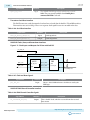
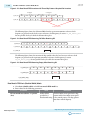
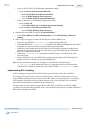
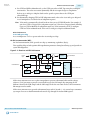
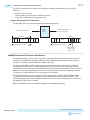
PHY Layer Transceiver Components
Transceivers in Arria 10 devices support both Physical Medium Attachment (PMA) and Physical Coding
Sublayer (PCS) functions at the physical (PHY) layer.
A PMA is the transceiver's electrical interface to the physical medium. The transceiver PMA consists of
standard blocks such as:
•
•
•
•
serializer/deserializer (SERDES)
clock and data recovery PLL
analog front end transmit drivers
analog front end receive buffers
The PCS can be bypassed with a PCS Direct configuration. Both the PMA and PCS blocks are fed by
multiple clock networks driven by high performance PLLs. In PCS Direct configuration, the data flow is
through the PCS block, but all the internal PCS blocks are bypassed. In this mode, the PCS functionality is
implemented in the FPGA fabric.
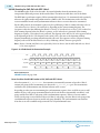
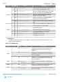
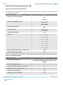
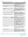
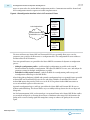
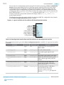
The GX Transceiver Channel
Figure 1-17: GX Transceiver Channel in Full Duplex Mode.
FPGA Fabric
Transmitter PCS
Transmitter PMA
Standard PCS
Serializer
PCIe Gen3 PCS
(1)
KR FEC
(1)
Enhanced PCS
Soft PIPE
(Optional)
HIP
(Optional)
PCS Direct
Receiver PMA
Receiver PCS
Standard PCS
CDR
Deserializer
(1)
PCIe Gen3 PCS
KR FEC
(1)
Enhanced PCS
PCS Direct
Notes:
(1) The FPGA Fabric - PCS and PCS-PMA interface widths are configurable.
Arria 10 GX transceiver channels have three types of PCS blocks that together support continuous data
rates between 611 Mbps and 17.4 Gbps.
Altera Corporation
Arria 10 Transceiver PHY Overview
Send Feedback
UG-01143
2015.05.11
The GT Transceiver Channel
1-21
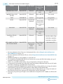
Table 1-6: PCS Types Supported by GX Transceiver Channels
PCS Type
Data Rate
Standard PCS
611 Mbps to 12 Gbps
Enhanced PCS
960 Mbps (12) to 17.4 Gbps
PCIe Gen3 PCS
8 Gbps
Note: 1. The GX channel can also operate in PCS Direct configuration for data rates from 611 Mbps to
17.4 Gbps.
2. The transmitter minimum operational data rate is 611 Mbps. For transmitter data rates less
than 611 Mbps, oversampling must be applied at the transmitter.
3. The receiver minimum operational data rate is 1.0 Gbps. For receiver data rates less than 1.0
Gbps, oversampling must be applied at the receiver.
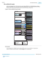
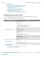
The GT Transceiver Channel
The GT transceiver channels are used for supporting data rates from 17.4 Gbps to 28.3 Gbps. The PCS
Direct datapath that bypasses all PCS blocks is the primary configuration used to support GT data rates
from 17.4 Gbps to 28.3 Gbps. Alternatively, the Enhanced PCS in Basic low latency configuration can also
be used to support GT data rates from 17.4 Gbps to 28.3 Gbps. The GT transceiver channels can also be
configured as GX transceiver channels. When they are configured as GX transceiver channels, the
Standard PCS, Enhanced PCS, and PCIe Gen3 PCS are available and they support data rates from 611
Mbps to 17.4 Gbps.
(12)
Applies when operating in reduced power modes. For mid- and high-power modes, the Enhanced PCS
minimum data rate is 1600 Mbps.
Arria 10 Transceiver PHY Overview
Send Feedback
Altera Corporation
1-22
UG-01143
2015.05.11
The GT Transceiver Channel
Figure 1-18: GT Transceiver Channel in Full Duplex Mode Operating Between 17.4 Gbps and 28.3 Gbps
Serializer
FPGA Fabric
Transmitter PCS
Transmitter PMA
(2)
KR FEC
Standard PCS
(3)
PCIe Gen3 PCS
(3)
Enhanced PCS
(1)
(2)
PCS Direct
Receiver PMA
CDR
Deserializer
Receiver PCS
(2)
KR FEC
Standard PCS
(3)
PCIe Gen3 PCS
(3)
Enhanced PCS
(2)
(1)
PCS Direct
Notes:
(1) The Enhanced PCS must be configured in Basic low latency mode to support data rate range from 17.4 Gbps to 28.3 Gbps.
(2) The FPGA Fabric - PCS and PCS-PMA interface widths are configurable.
(3) The Standard PCS and PCIe Gen3 PCS blocks are available when the GT channel is configured as a GX transceiver channel.
Table 1-7: PCS Types and Data Rates Supported by GT Channel Configurations
GT Channel Configuration
GT
GX
(13)
(14)
PCS Type
Data Rates Supported
Standard PCS
Not available for GT configuration
Enhanced PCS
17.4 Gbps to 28.3 Gbps(13)
PCIe Gen3 PCS
Not available for GT configuration
Standard PCS
611 Mbps to 12 Gbps
Enhanced PCS
960 Mbps (14) to 17.4 Gbps
PCIe Gen3 PCS
8 Gbps
The Enhanced PCS must be configured in Basic low latency mode to support data rate range from 17.4
Gbps to 28.3 Gbps.
Applies when operating in reduced power modes. For mid- and high-power modes, the Enhanced PCS
minimum data rate is 1600 Mbps.
Altera Corporation
Arria 10 Transceiver PHY Overview
Send Feedback
UG-01143
2015.05.11
Transceiver Phase-Locked Loops
1-23
Note: 1. The GT channels can also operate in PCS Direct configuration for data rates from 611 Mbps to
28.3 Gbps. The PCS Direct datapath that bypasses all PCS blocks is the primary configuration
used to support GT data rates from 17.4 Gbps to 28.3 Gbps.
2. The transmitter minimum operational data rate is 611 Mbps. For transmitter data rates less
than 611 Mbps, oversampling must be applied at the transmitter.
3. The receiver minimum operational data rate is 1.0 Gbps. For receiver data rates less than 1.0
Gbps, oversampling must be applied at the receiver.
Transceiver Phase-Locked Loops
Each transceiver channel in Arria 10 devices has direct access to three types of high performance PLLs:
• Advanced Transmit (ATX) PLL
• Fractional PLL (fPLL)
• Channel PLL / Clock Multiplier Unit (CMU) PLL.
These transceiver PLLs along with the Master or Local Clock Generation Blocks (CGB) drive the
transceiver channels.
Related Information
PLLs on page 3-3
For more information on transceiver PLLs in Arria 10 devices.
Advanced Transmit (ATX) PLL
An advanced transmit (ATX ) PLL is a high performance PLL. It supports both integer frequency
synthesis and coarse resolution fractional frequency synthesis. The ATX PLL is the transceiver channel’s
primary transmit PLL. It can operate over the full range of supported data rates required for high data rate
applications.
Related Information
• ATX PLL on page 3-3
For more information on ATX PLL.
• ATX PLL IP Core on page 3-6
For details on implementing the ATX PLL IP.
Fractional PLL (fPLL)
A fractional PLL (fPLL) is an alternate transmit PLL used for generating lower clock frequencies for low
data rate applications. fPLLs support both integer frequency synthesis and fine resolution fractional
frequency synthesis. Unlike the ATX PLL, the fPLL can also be used to synthesize frequencies that can
drive the core through the FPGA fabric clock networks.
Related Information
• fPLL on page 3-13
For more information on fPLL.
• fPLL IP Core on page 3-15
For details on implementing the fPLL IP.
Arria 10 Transceiver PHY Overview
Send Feedback
Altera Corporation
1-24
UG-01143
2015.05.11
Channel PLL (CMU/CDR PLL)
Channel PLL (CMU/CDR PLL)
A channel PLL resides locally within each transceiver channel. Its primary function is clock and data
recovery in the transceiver channel when the PLL is used in clock data recovery (CDR) mode. The
channel PLLs of channel 1 and 4 can be used as transmit PLLs when configured in clock multiplier unit
(CMU) mode. The channel PLLs of channel 0, 2, 3, and 5 cannot be configured in CMU mode and
therefore cannot be used as transmit PLLs.
Related Information
• CMU PLL on page 3-21
For more information on CMU PLL.
• CMU PLL IP Core on page 3-24
For information on implementing CMU PLL IP.
Clock Generation Block (CGB)
In Arria 10 devices, there are two types of clock generation blocks (CGBs):
• Master CGB
• Local CGB
Transceiver banks with six transceiver channels have two master CGBs. Master CGB1 is located at the top
of the transceiver bank and master CGB0 is located at the bottom of the transceiver bank. Transceiver
banks with three channels have only one master CGB. The master CGB divides and distributes bonded
clocks to a bonded channel group. It also distributes non-bonded clocks to non-bonded channels across
the x6/xN clock network.
Each transceiver channel has a local CGB. The local CGB is used for dividing and distributing nonbonded clocks to its own PCS and PMA blocks.
Related Information
Clock Generation Block on page 3-36
For more information on clock generation block.
Calibration
Arria 10 FPGAs contain a dedicated calibration engine to compensate for process variations. The
calibration engine calibrates the analog portion of the transceiver to allow both the transmitter and
receiver to operate at optimum performance.
The CLKUSR pin clocks the calibration engine. All transceiver reference clocks and the CLKUSR clock must
be free running and stable at the start of FPGA configuration to successfully complete the calibration
process and for optimal transceiver performance.
Note: For more information about CLKUSR electrical characteristics, refer to Arria 10 Device Datasheet.
The CLKUSR can also be used as an FPGA configuration clock. For information about configuration
requirements for the CLKUSR pin, refer to the Configuration, Design Security, and Remote System
Upgrades in Arria 10 Devices chapter in the Arria 10 Core Fabric and General-Purpose I/O
Handbook. For more information about calibration, refer to the Calibration chapter. For more
information about CLKUSR pin requirements, refer to the Arria 10 GX, GT, and SX Device Family
Pin Connection Guidelines.
Altera Corporation
Arria 10 Transceiver PHY Overview
Send Feedback
UG-01143
2015.05.11
Calibration
1-25
Related Information
•
•
•
•
Calibration on page 7-1
Arria 10 Device Datasheet
Configuration, Design Security, and Remote System Upgrades in Arria 10 Devices
Arria 10 GX, GT, and SX Device Family Pin Connection Guidelines
Arria 10 Transceiver PHY Overview
Send Feedback
Altera Corporation
Implementing Protocols in Arria 10
Transceivers
2
2015.05.11
UG-01143
Subscribe
Send Feedback
Transceiver Design IP Blocks
Figure 2-1: Arria 10 Transceiver Design Fundamental Building Blocks
Reset controller is used for resetting the
transceiver channels.
Transceiver
Reset Controller (2)
Transceiver PLL IP core provides a clock source
to clock networks that drive the transceiver
channels. In Arria 10 devices, PLL IP Core
is separate from the transceiver PHY IP core.
Avalon master allows access to Avalon-MM
reconfiguration registers via the Avalon
Memory Mapped interface. It enables PCS,
PMA , and PLL reconfiguration. To access
the reconfiguration registers, implement an
Avalon master in the FPGA fabric. This faciliates
reconfiguration by performing reads and writes
through the Avalon-MM interface.
This block can be either a MAC IP core, or
a frame generator / analyzer or a
data generator / analyzer.
Transceiver
PLL IP Core
Master/Local
Clock
Generation
Block
Avalon-MM Master
MAC IP Core /
Data Generator /
Data Analyzer
Analog and Digital
Reset Bus
Reset Ports
Transceiver PHY IP Core (1)
Non-Bonded and
Bonded Clocks
Avalon-MM
Interface
Transceiver PHY IP core controls the PCS and
PMA configurations and transceiver
channels functions for all communication
protocols.
Reconfiguration
Registers
Parallel Data Bus
Note:
(1) The Transceiver Native PHY IP core can be one of the supported PHY IP Cores ( For example: Native PHY IP Core/XAUI PHY IP Core, and so on)
(2) You can either design your own reset controller or use the Altera Transceiver PHY Reset Controller IP Core.
Legend:
Altera generated IP block
User created IP block
© 2015 Altera Corporation. All rights reserved. ALTERA, ARRIA, CYCLONE, ENPIRION, MAX, MEGACORE, NIOS, QUARTUS and STRATIX words and logos are
trademarks of Altera Corporation and registered in the U.S. Patent and Trademark Office and in other countries. All other words and logos identified as
trademarks or service marks are the property of their respective holders as described at www.altera.com/common/legal.html. Altera warrants performance
of its semiconductor products to current specifications in accordance with Altera's standard warranty, but reserves the right to make changes to any
products and services at any time without notice. Altera assumes no responsibility or liability arising out of the application or use of any information,
product, or service described herein except as expressly agreed to in writing by Altera. Altera customers are advised to obtain the latest version of device
specifications before relying on any published information and before placing orders for products or services.
www.altera.com
101 Innovation Drive, San Jose, CA 95134
ISO
9001:2008
Registered
2-2
UG-01143
2015.05.11
Transceiver Design Flow
Transceiver Design Flow
Figure 2-2: Transceiver Design Flow
Note: The design examples on the alterawiki page provide useful guidance for developing your own
design. However, the content on the alterawiki page is not guaranteed by Altera.
Select PHY IP Core
Configure the PHY IP Core
Generate the Altera Transceiver PHY Reset Controller IP Core
or create your own User-Coded Reset Controller
Generate PHY IP Core
Select PLL IP Core
Configure the PLL IP Core
Create reconfiguration logic
(if needed)
Generate PLL IP Core
Connect PHY IP Core to PLL IP Core, Reset Controller, and
connect reconfiguration logic via Avalon-MM interface
Connect Transceiver Datapath to MAC IP Core or to a Data Generator / Analyzer
Make analog parameter settings to I/O pins using the Assignment Editor or updating the Quartus II Settings File
Compile Design
Verify Design Functionality
Related Information
http://www.alterawiki.com
Select and Instantiate the PHY IP Core
Select the appropriate PHY IP core to implement your protocol.
Refer to the Arria 10 Transceiver Protocols and PHY IP Support section to decide which PHY IP to select
to implement your protocol.
You can create your Quartus® II project first, and then instantiate the various IPs required for your
design. In this case, specify the location to save your IP HDL files. The current version of the PHY IP does
Altera Corporation
Implementing Protocols in Arria 10 Transceivers
Send Feedback
UG-01143
2015.05.11
Select and Instantiate the PHY IP Core
2-3
not have the option to set the speed grade. Specify the device family and speed grade when you create the
Quartus II project.
You can also instantiate the PHY IP directly to evaluate the various features.
To instantiate a PHY IP:
1.
2.
3.
4.
Open the Quartus II software.
Click Tools > IP Catalog.
At the top of the IP Catalog window, select Arria 10 device family
In IP Catalog, under Library > Interface Protocols, select the appropriate PHY IP and then click
Add.
5. In the New IP Instance Dialog Box, provide the IP instance name.
6. Select Arria 10 device family.
7. Select the appropriate device and click OK.
The PHY IP Parameter Editor window opens.
Implementing Protocols in Arria 10 Transceivers
Send Feedback
Altera Corporation
2-4
UG-01143
2015.05.11
Configure the PHY IP Core
Figure 2-3: Arria 10 Transceiver PHY Types
Related Information
Arria 10 Transceiver Protocols and PHY IP Support on page 2-10
Configure the PHY IP Core
Configure the PHY IP core by selecting the valid parameters for your design. The valid parameter settings
are different for each protocol. Refer to the appropriate protocol's section for selecting valid parameters
for each protocol.
Altera Corporation
Implementing Protocols in Arria 10 Transceivers
Send Feedback
UG-01143
2015.05.11
Generate the PHY IP Core
2-5
Related Information
• Using the Arria 10 Transceiver Native PHY IP Core on page 2-17
For information on Native PHY IP.
• Interlaken on page 2-76
• Gigabit Ethernet (GbE) and GbE with IEEE 1588v2 on page 2-97
• 10GBASE-R, 10GBASE-R with IEEE 1588v2, and 10GBASE-R with FEC Variants on page 2-110
• 10GBASE-KR PHY IP Core on page 2-125
• 1-Gigabit/10-Gigabit Ethernet (GbE) PHY IP Core on page 2-163
• PCI Express (PIPE) on page 2-228
• CPRI on page 2-268
• Using the "Basic (Enhanced PCS)" and "Basic with KR FEC" Configurations of Enhanced PCS on
page 2-279
• Using the Basic/Custom, Basic/Custom with Rate Match Configurations of Standard PCS on page
2-290
• Design Considerations for Data Rates Above 17.4 Gbps Using Arria 10 GT Channels on page 2313
Generate the PHY IP Core
After configuring the PHY IP, complete the following steps to generate the PHY IP.
1. Click the Generate HDL button in the Parameter Editor window. The Generation dialog box opens.
2. In Synthesis options, under Create HDL design for synthesis select Verilog or VHDL.
3. Select appropriate Simulation options depending on the choice of the hardware description language
you selected under Synthesis options.
4. In Output Directory, select Clear output directories for selected generation targets if you want to
clear any previous IP generation files from the selected output directory.
5. Click Generate.
The Quartus II software generates a <phy ip instance name> folder, <phy ip instance name>_sim folder,
<phy ip instance name>.qip file, <phy ip instance name>.qsys file, and <phy ip instance name>.v file or
<phy ip instance name>.vhd file. This <phy ip instance name>.v file is the top level design file for the PHY
IP and is placed in the <phy ip instance name>/synth folder. The other folders contain lower level design
files used for simulation and compilation.
Related Information
IP Core File Locations on page 2-75
Select the PLL IP Core
Arria 10 devices have three types of PLL IP cores:
• Advanced Transmit (ATX) PLL IP core.
• Fractional PLL (fPLL) IP core.
• Channel PLL / Clock Multiplier Unit (CMU) PLL IP core.
Select the appropriate PLL IP for your design. For additional details, refer to the PLLs and Clock Networks
chapter.
Implementing Protocols in Arria 10 Transceivers
Send Feedback
Altera Corporation
2-6
Select the PLL IP Core
UG-01143
2015.05.11
To instantiate a PLL IP:
1.
2.
3.
4.
Open the Quartus II software.
Click Tools > IP Catalog.
At the top of the IP Catalog window, select Arria 10 device family
In IP Catalog, under Library > Basic Functions > Clocks, PLLs, and Resets > PLL choose the PLL IP
(Arria 10 fPLL, Arria 10 Transceiver ATX PLL, or Arria 10 Transceiver CMU PLL) you want to
include in your design and then click Add.
5. In the New IP Instance Dialog Box, provide the IP instance name.
6. Select Arria 10 device family.
7. Select the appropriate device and click OK.
The PLL IP GUI window opens.
Altera Corporation
Implementing Protocols in Arria 10 Transceivers
Send Feedback
UG-01143
2015.05.11
Configure the PLL IP Core
2-7
Figure 2-4: Arria 10 Transceiver PLL Types
Related Information
PLLs on page 3-3
Configure the PLL IP Core
Understand the available PLLs, clock networks, and the supported clocking configurations. Configure the
PLL IP to achieve the adequate data rate for your design.
Related Information
• ATX PLL IP Core on page 3-6
Implementing Protocols in Arria 10 Transceivers
Send Feedback
Altera Corporation
2-8
UG-01143
2015.05.11
Generate the PLL IP Core
• fPLL IP Core on page 3-15
• CMU PLL IP Core on page 3-24
• Using PLLs and Clock Networks on page 3-49
Generate the PLL IP Core
After configuring the PLL IP, complete the following steps to generate the PLL IP.
1. Click the Generate HDL button in the Parameter Editor window. The Generation dialog box opens.
2. In Synthesis options, under Create HDL design for synthesis select Verilog or VHDL.
3. Select appropriate Simulation options depending on the choice of the hardware description language
you selected under Synthesis options.
4. In Output Directory, select Clear output directories for selected generation targets if you want to
clear any previous IP generation files from the selected output directory.
5. Click Generate.
The Quartus ® II software generates a <pll ip instance name> folder, <pll ip instance name>_sim folder,
<pll ip instance name>.qip file, <pll ip instance name>.qsys, and <pll ip instance name>.v file or <pll ip
instance name>.vhd file. The <pll ip instance name>.v file is the top level design file for the PLL IP and is
placed in the <pll ip instance name>/ synth folder. The other folders contain lower level design files used
for simulation and compilation.
Related Information
IP Core File Locations on page 2-75
Reset Controller
There are two methods to reset the transceivers in Arria 10 devices:
• Use the Altera Transceiver PHY Reset Controller IP Core.
• Create your own reset controller that follows the recommended reset sequence.
Related Information
Resetting Transceiver Channels on page 4-1
Create Reconfiguration Logic
Dynamic reconfiguration is the ability to dynamically modify the transceiver channels and PLL settings
during device operation. To support dynamic reconfiguration, your design must include an Avalon
master that can access the dynamic reconfiguration registers using the Avalon-MM interface.
The Avalon-MM master enables PCS dynamic switching, PLL and channel reconfiguration. You can
dynamically adjust the PMA parameters, such as differential output voltage swing (Vod), and preemphasis settings. This adjustment can be done by writing to the Avalon-MM reconfiguration registers
through the user generated Avalon-MM master.
For detailed information on dynamic reconfiguration, refer to Reconfiguration Interface and Dynamic
Reconfiguration chapter.
Related Information
Reconfiguration Interface and Dynamic Reconfiguration on page 6-1
Altera Corporation
Implementing Protocols in Arria 10 Transceivers
Send Feedback
UG-01143
2015.05.11
Connect the PHY IP to the PLL IP and Reset Controller
2-9
Connect the PHY IP to the PLL IP and Reset Controller
Connect the PHY IP, PLL IP, and the reset controller. Write the top level module to connect all the IP
blocks.
All of the I/O ports for each IP, can be seen in the <phy instance name>.v file or <phy instance name>.vhd,
and in the <phy_instance_name>_bb.v file.
For more information about description of the ports, refer to the ports tables in the PLL IP and Reset
Controller, Using the Transceiver Native PHY IP Core, and Resetting Transceiver Channels chapters.
Related Information
•
•
•
•
•
Enhanced PCS Ports on page 2-54
Standard PCS Ports on page 2-68
Resetting Transceiver Channels on page 4-1
Using the Arria 10 Transceiver Native PHY IP Core on page 2-17
PLLs and Clock Networks on page 3-1
Connect Datapath
Connect the transceiver PHY layer design to the Media Access Controller (MAC) IP core or to a data
generator / analyzer or a frame generator / analyzer.
Make Analog Parameter Settings
Make analog parameter settings to I/O pins using the Assignment Editor or updating the Quartus II
Settings File.
After verifying your design functionality, make pin assignments and PMA analog parameter settings for
the transceiver pins.
1. Assign FPGA pins to all the transceiver and reference clock I/O pins. For more details, refer to the
Arria 10 Pin Connection Guidelines.
2. Set the analog parameters to the transmitter, receiver, and reference clock pins using the Assignment
Editor.
All of the pin assignments and analog parameters set using the Pin Planner and the Assignment
Editor are saved in the <top_level_project_name>.qsf file. You can also directly modify the Quartus
Settings file (.qsf) to set PMA analog parameters.
Related Information
• Analog Parameter Settings on page 8-1
• Arria 10 Pin Connection Guidelines
Compile the Design
To compile the transceiver design, add the <phy_instancename>.qip files for all the IP blocks generated
using the IP Catalog to the Quartus II project library. You can alternatively add the .qsys and .qip variants
of the IP cores.
Note: If you add both the .qsys and the .qip file into the Quartus II project, the software generates an
error.
Implementing Protocols in Arria 10 Transceivers
Send Feedback
Altera Corporation
2-10
UG-01143
2015.05.11
Verify Design Functionality
Related Information
Quartus II Incremental Compilation for Hierarchical and Team-Based Design
For more information about compilation details.
Verify Design Functionality
Simulate your design to verify the functionality of your design. For more details, refer to Simulating the
Native Transceiver PHY IP Core section.
Related Information
• Simulating the Transceiver Native PHY IP Core on page 2-322
• Quartus II Handbook - Volume 3: Verification
Information about design simulation and verification.
Arria 10 Transceiver Protocols and PHY IP Support
Table 2-1: Arria 10 Transceiver Protocols and PHY IP Support
Protocol
Transceiver IP
PCS Support
Transceiver
Configuration
Rule(15)
Protocol Preset (16)
PCIe Gen3 x1, x2, x4, x8
Native PHY IP
(PIPE)(17)
Standard and
Gen3
Gen3 PIPE
PCIe PIPE Gen3 x1
Native PHY IP
(PIPE) (17)
Standard
Gen2 PIPE
Native PHY IP
(PIPE) (17)
Standard
PCIe Gen2 x1, x2, x4, x8
PCIe Gen1 x1, x2, x4, x8
(15)
(16)
(17)
(18)
(19)
(20)
(21)
(22)
(23)
PCIe PIPE Gen3 x8
PCIe PIPE Gen2 x1
PCIe PIPE Gen2 x8
Gen1 PIPE
User created
For more information about Transceiver Configuration Rules, refer to Using the Arria 10 Transceiver
Native PHY IP Core on page 2-17.
For more information about Protocol Presets, refer to Using the Arria 10 Transceiver Native PHY IP Core
on page 2-17.
Hard IP for PCI Express is also available as a separate IP core.
The 1G/10GbE and 10GBASE-KR PHY IP core includes the necessary soft IP for link training, auto speed
negotiation, and sequencer functions.
Needs a user created IP for link training, auto speed negotiation, and sequencer functions.
A Transmit PCS soft bonding logic required for multi-lane bonding configuration and a Receive PCS multilane deskew control logic is provided in the design example.
To implement 40GBASE-R/100GBASE-R using the Low Latency Enhanced PCS preset, change the number
of data channels to four and select appropriate PCS- FPGA Fabric and PCS-PMA width.
To implement 100GBASE-R via CAUI using the Low Latency Enhanced PCS preset, change the number of
data channels to 10 and select appropriate PCS-FPGA Fabric and PCS-PMA width.
Low Latency GT protocol preset requires some modification to implement OTU-4 (100G) via OTL4.4/CEI28G-VSR.
Altera Corporation
Implementing Protocols in Arria 10 Transceivers
Send Feedback
UG-01143
2015.05.11
Arria 10 Transceiver Protocols and PHY IP Support
2-11
Protocol
Transceiver IP
PCS Support
Transceiver
Configuration
Rule(15)
Protocol Preset (16)
1000BASE-X Gigabit
Ethernet
Native PHY IP
Standard
GbE
GIGE - 1.25 Gbps
1000BASE-X Gigabit
Ethernet with 1588
Native PHY IP
Standard
GbE 1588
GIGE - 1.25 Gbps 1588
10GBASE-R
Native PHY IP
Enhanced
10GBASE-R
10GBASE-R
10GBASE-R Low Latency
Native PHY IP
Enhanced
10GBASE-R
10GBASE-R Low Latency
10GBASE-R 1588
Native PHY IP
Enhanced
10GBASE-R
1588
10GBASE-R 1588
10GBASE-R with KR FEC
Native PHY IP
Enhanced
10GBASE-R w/
KR FEC
10GBASE-R w/KR FEC
10GBASE-KR and
1000BASE-X
1G/10GbE and
10GBASE-KR
PHY IP(18)
Standard and
Enhanced
Not applicable
BackPlane_wo_1588
LineSide (optical)
LineSide(optical)_1588
40GBASE-R/100GBASE-R
Native PHY IP
Enhanced
Basic (Enhanced
PCS)
Low Latency Enhanced
PCS(23) (21)
40GBASE-R with FEC/
40GBASE-KR4 (19)
Native PHY IP
Enhanced
Basic w/KR FEC
User created
100GBASE-R via CAUI-4/
CPPI-4/BP-4
Native PHY IP
Enhanced PCS
(low latency
mode) PCS
Direct
Basic (Enhanced
PCS) / PCS
Direct
Low Latency GT(23)
(15)
(16)
(17)
(18)
(19)
(20)
(21)
(22)
(23)
For more information about Transceiver Configuration Rules, refer to Using the Arria 10 Transceiver
Native PHY IP Core on page 2-17.
For more information about Protocol Presets, refer to Using the Arria 10 Transceiver Native PHY IP Core
on page 2-17.
Hard IP for PCI Express is also available as a separate IP core.
The 1G/10GbE and 10GBASE-KR PHY IP core includes the necessary soft IP for link training, auto speed
negotiation, and sequencer functions.
Needs a user created IP for link training, auto speed negotiation, and sequencer functions.
A Transmit PCS soft bonding logic required for multi-lane bonding configuration and a Receive PCS multilane deskew control logic is provided in the design example.
To implement 40GBASE-R/100GBASE-R using the Low Latency Enhanced PCS preset, change the number
of data channels to four and select appropriate PCS- FPGA Fabric and PCS-PMA width.
To implement 100GBASE-R via CAUI using the Low Latency Enhanced PCS preset, change the number of
data channels to 10 and select appropriate PCS-FPGA Fabric and PCS-PMA width.
Low Latency GT protocol preset requires some modification to implement OTU-4 (100G) via OTL4.4/CEI28G-VSR.
Implementing Protocols in Arria 10 Transceivers
Send Feedback
Altera Corporation
2-12
UG-01143
2015.05.11
Arria 10 Transceiver Protocols and PHY IP Support
Protocol
Transceiver IP
PCS Support
Transceiver
Configuration
Rule(15)
Protocol Preset (16)
100GBASE-R via CAUI
Native PHY IP
Enhanced
Basic (Enhanced
PCS)
Low Latency Enhanced
PCS (22)
100GBASE-R via CAUI
with FEC
Native PHY IP
Enhanced
Basic w/KR FEC
User created
XAUI
XAUI PHY IP
Soft PCS
Not applicable
Not applicable
SPAUI
Native PHY IP
Standard and
Enhanced
Basic/Custom
(Standard PCS)
User created
Basic (Enhanced
PCS)
DDR XAUI
Native PHY IP
Standard and
Enhanced
Basic/Custom
(Standard PCS)
User created
Basic (Enhanced
PCS)
Interlaken (CEI-6G/
11G) (20)
Native PHY IP
Enhanced
Interlaken
Interlaken 10x12.5Gbps
Interlaken 6x10.3Gbps
Interlaken 1x6.25Gbps
OTU-4 (100G) via OTL4.4/
CEI-25G/28G VSR/SR
Native PHY IP
Enhanced PCS
(low latency
mode)
Basic (Enhanced
PCS) / PCS
Direct
Low Latency GT(23)
PCS Direct
(15)
(16)
(17)
(18)
(19)
(20)
(21)
(22)
(23)
For more information about Transceiver Configuration Rules, refer to Using the Arria 10 Transceiver
Native PHY IP Core on page 2-17.
For more information about Protocol Presets, refer to Using the Arria 10 Transceiver Native PHY IP Core
on page 2-17.
Hard IP for PCI Express is also available as a separate IP core.
The 1G/10GbE and 10GBASE-KR PHY IP core includes the necessary soft IP for link training, auto speed
negotiation, and sequencer functions.
Needs a user created IP for link training, auto speed negotiation, and sequencer functions.
A Transmit PCS soft bonding logic required for multi-lane bonding configuration and a Receive PCS multilane deskew control logic is provided in the design example.
To implement 40GBASE-R/100GBASE-R using the Low Latency Enhanced PCS preset, change the number
of data channels to four and select appropriate PCS- FPGA Fabric and PCS-PMA width.
To implement 100GBASE-R via CAUI using the Low Latency Enhanced PCS preset, change the number of
data channels to 10 and select appropriate PCS-FPGA Fabric and PCS-PMA width.
Low Latency GT protocol preset requires some modification to implement OTU-4 (100G) via OTL4.4/CEI28G-VSR.
Altera Corporation
Implementing Protocols in Arria 10 Transceivers
Send Feedback
UG-01143
2015.05.11
Arria 10 Transceiver Protocols and PHY IP Support
2-13
Protocol
Transceiver IP
PCS Support
Transceiver
Configuration
Rule(15)
Protocol Preset (16)
OTU-4 (100G) via
OTL4.10/OIF SFI-S
Native PHY IP
Enhanced
Basic (Enhanced
PCS)
SFI-S 64:64 4x11.3 Gbps
OTU-3 (40G) via OTL3.4/
OIF SFI-5.2/SFI-5.1
Native PHY IP
Enhanced
Basic (Enhanced
PCS)
User created
OTU-2 (10G) via SFP+/
SFF-8431/CEI-11G
Native PHY IP
Enhanced
Basic (Enhanced
PCS)
User created
OTU-2 (10G) via OIF SFI5.1s
Native PHY IP
Enhanced
Basic (Enhanced
PCS)
User created
OTU-1 (2.7G)
Native PHY IP
Standard
Basic/Custom
(Standard PCS)
User created
SONET/SDH STS-768/
STM-256 (40G) via OIF
SFI-5.2/STL256.4
Native PHY IP
Enhanced
Basic (Enhanced
PCS)
User created
SONET/SDH STS-768/
STM-256 (40G) via OIF
SFI-5.1
Native PHY IP
Enhanced
Basic (Enhanced
PCS)
User created
SONET/SDH STS-192/
STM-64 (10G) via SFP+/
SFF-8431/CEI-11G
Native PHY IP
Enhanced
Basic (Enhanced
PCS)
User created
SONET/SDH STS-192/
STM-64 (10G) via OIF SFI5.1s/SxI-5/SFI-4.2
Native PHY IP
Enhanced
Basic (Enhanced
PCS)
User created
(15)
(16)
(17)
(18)
(19)
(20)
(21)
(22)
(23)
For more information about Transceiver Configuration Rules, refer to Using the Arria 10 Transceiver
Native PHY IP Core on page 2-17.
For more information about Protocol Presets, refer to Using the Arria 10 Transceiver Native PHY IP Core
on page 2-17.
Hard IP for PCI Express is also available as a separate IP core.
The 1G/10GbE and 10GBASE-KR PHY IP core includes the necessary soft IP for link training, auto speed
negotiation, and sequencer functions.
Needs a user created IP for link training, auto speed negotiation, and sequencer functions.
A Transmit PCS soft bonding logic required for multi-lane bonding configuration and a Receive PCS multilane deskew control logic is provided in the design example.
To implement 40GBASE-R/100GBASE-R using the Low Latency Enhanced PCS preset, change the number
of data channels to four and select appropriate PCS- FPGA Fabric and PCS-PMA width.
To implement 100GBASE-R via CAUI using the Low Latency Enhanced PCS preset, change the number of
data channels to 10 and select appropriate PCS-FPGA Fabric and PCS-PMA width.
Low Latency GT protocol preset requires some modification to implement OTU-4 (100G) via OTL4.4/CEI28G-VSR.
Implementing Protocols in Arria 10 Transceivers
Send Feedback
Altera Corporation
2-14
UG-01143
2015.05.11
Arria 10 Transceiver Protocols and PHY IP Support
Protocol
Transceiver IP
PCS Support
Transceiver
Configuration
Rule(15)
Protocol Preset (16)
SONET STS-96 (5G) via
OIF SFI-5.1s
Native PHY IP
Enhanced
Basic/Custom
(Standard PCS)
SONET/SDH OC-96
SONET/SDH STS-48/
STM-16 (2.5G) via SFP/
TFI-5.1
Native PHY IP
Standard
Basic/Custom
(Standard PCS)
SONET/SDH OC-48
SONET/SDH STS-12/
STM-4 (0.622G) via SFP/
TFI-5.1
Native PHY IP
Standard
Basic/Custom
(Standard PCS)
SONET/SDH OC-12
Intel QPI 1.1/2.0
Native PHY IP
PCS Direct
PCS Direct
User created
SD-SDI/HD-SDI/3G-SDI
Native PHY IP
Standard
Basic/Custom
(Standard PCS)
3G/HD SDI NTSC
3G/HD SDI PAL
Vx1
Native PHY IP
Standard
Basic/Custom
(Standard PCS)
User created
DisplayPort
Native PHY IP
Standard
Basic/Custom
(Standard PCS)
User created
1.25G/ 2.5G
Native PHY IP
Enhanced
Basic (Enhanced
PCS)
User created
2.5G/1.25G GPON/EPON
Native PHY IP
Standard
Basic/Custom
(Standard PCS)
User created
16G/10G Fibre Channel
Native PHY IP
Enhanced
Basic (Enhanced
PCS)
User created
10G GPON/EPON
(15)
(16)
(17)
(18)
(19)
(20)
(21)
(22)
(23)
For more information about Transceiver Configuration Rules, refer to Using the Arria 10 Transceiver
Native PHY IP Core on page 2-17.
For more information about Protocol Presets, refer to Using the Arria 10 Transceiver Native PHY IP Core
on page 2-17.
Hard IP for PCI Express is also available as a separate IP core.
The 1G/10GbE and 10GBASE-KR PHY IP core includes the necessary soft IP for link training, auto speed
negotiation, and sequencer functions.
Needs a user created IP for link training, auto speed negotiation, and sequencer functions.
A Transmit PCS soft bonding logic required for multi-lane bonding configuration and a Receive PCS multilane deskew control logic is provided in the design example.
To implement 40GBASE-R/100GBASE-R using the Low Latency Enhanced PCS preset, change the number
of data channels to four and select appropriate PCS- FPGA Fabric and PCS-PMA width.
To implement 100GBASE-R via CAUI using the Low Latency Enhanced PCS preset, change the number of
data channels to 10 and select appropriate PCS-FPGA Fabric and PCS-PMA width.
Low Latency GT protocol preset requires some modification to implement OTU-4 (100G) via OTL4.4/CEI28G-VSR.
Altera Corporation
Implementing Protocols in Arria 10 Transceivers
Send Feedback
UG-01143
2015.05.11
Arria 10 Transceiver Protocols and PHY IP Support
2-15
Protocol
Transceiver IP
PCS Support
Transceiver
Configuration
Rule(15)
Protocol Preset (16)
8G/4G/2G/1G Fibre
Channel
Native PHY IP
Standard
Basic/Custom
(Standard PCS)
User created
EDR Infiniband x1, x4, x12
Native PHY IP
Enhanced (low
latency mode)
Basic (Enhanced
PCS)
User created
PCS Direct
PCS Direct
FDR/FDR-10 Infiniband
x1, x4, x12
Native PHY IP
Enhanced
Basic (Enhanced
PCS)
User created
SDR/DDR/QDR
Infiniband x1, x4, x12
Native PHY IP
Standard
Basic/Custom
(Standard PCS)
User created
CPRI 6.0 10.1376 Gbps
Native PHY IP
Enhanced
10GBASE-R
1588
User created
CPRI 4.2/OBSAI RP3 v4.2
Native PHY IP
Standard
CPRI (Auto) /
CPRI (Manual)
CPRI 9.8Gbps Auto Mode
(15)
(16)
(17)
(18)
(19)
(20)
(21)
(22)
(23)
CPRI 9.8 Gbps Manual
Mode
SRIO 2.2/1.3
Native PHY IP
Standard
Basic/Custom
with Rate
Match(Standard
PCS)
Serial Rapid IO 1.25 Gbps
SAS 3.0
Native PHY IP
Enhanced
Basic (Enhanced
PCS)
User created
For more information about Transceiver Configuration Rules, refer to Using the Arria 10 Transceiver
Native PHY IP Core on page 2-17.
For more information about Protocol Presets, refer to Using the Arria 10 Transceiver Native PHY IP Core
on page 2-17.
Hard IP for PCI Express is also available as a separate IP core.
The 1G/10GbE and 10GBASE-KR PHY IP core includes the necessary soft IP for link training, auto speed
negotiation, and sequencer functions.
Needs a user created IP for link training, auto speed negotiation, and sequencer functions.
A Transmit PCS soft bonding logic required for multi-lane bonding configuration and a Receive PCS multilane deskew control logic is provided in the design example.
To implement 40GBASE-R/100GBASE-R using the Low Latency Enhanced PCS preset, change the number
of data channels to four and select appropriate PCS- FPGA Fabric and PCS-PMA width.
To implement 100GBASE-R via CAUI using the Low Latency Enhanced PCS preset, change the number of
data channels to 10 and select appropriate PCS-FPGA Fabric and PCS-PMA width.
Low Latency GT protocol preset requires some modification to implement OTU-4 (100G) via OTL4.4/CEI28G-VSR.
Implementing Protocols in Arria 10 Transceivers
Send Feedback
Altera Corporation
2-16
UG-01143
2015.05.11
Arria 10 Transceiver Protocols and PHY IP Support
Protocol
Transceiver IP
PCS Support
Transceiver
Configuration
Rule(15)
Protocol Preset (16)
SATA 3.0/2.0/1.0 and SAS
2.0/1.1/1.0
Native PHY IP
Standard
Basic/Custom
(Standard PCS)
SAS Gen2/Gen1.1/Gen1
HiGig/HiGig+/HiGig2/
HiGig2+
Native PHY IP
Standard
Basic/Custom
(Standard PCS)
User created
JESD204A / JESD204B
Native PHY IP
Standard and
Enhanced
Basic/Custom
(Standard PCS)
Basic (Enhanced
PCS)(24)
User created
ASI
Native PHY IP
Standard
Basic/Custom
(Standard PCS)
User created
SPI-5 (100G) / SPI-5 (50G)
Native PHY IP
Enhanced
Basic (Enhanced
PCS)
User created
Custom and other
protocols
Native PHY IP
Standard and
Enhanced
Basis/Custom
(Standard PCS)
User created
PCS Direct
Basic (Enhanced
PCS)
SATA Gen3/Gen2/Gen1
Basic/Custom
with Rate Match
(Standard PCS)
PCS Direct
(15)
(16)
(17)
(18)
(19)
(20)
(21)
(22)
(23)
(24)
For more information about Transceiver Configuration Rules, refer to Using the Arria 10 Transceiver
Native PHY IP Core on page 2-17.
For more information about Protocol Presets, refer to Using the Arria 10 Transceiver Native PHY IP Core
on page 2-17.
Hard IP for PCI Express is also available as a separate IP core.
The 1G/10GbE and 10GBASE-KR PHY IP core includes the necessary soft IP for link training, auto speed
negotiation, and sequencer functions.
Needs a user created IP for link training, auto speed negotiation, and sequencer functions.
A Transmit PCS soft bonding logic required for multi-lane bonding configuration and a Receive PCS multilane deskew control logic is provided in the design example.
To implement 40GBASE-R/100GBASE-R using the Low Latency Enhanced PCS preset, change the number
of data channels to four and select appropriate PCS- FPGA Fabric and PCS-PMA width.
To implement 100GBASE-R via CAUI using the Low Latency Enhanced PCS preset, change the number of
data channels to 10 and select appropriate PCS-FPGA Fabric and PCS-PMA width.
Low Latency GT protocol preset requires some modification to implement OTU-4 (100G) via OTL4.4/CEI28G-VSR.
For JESD204B, Enhanced PCS is used when the data rate is above 12.0 Gbps
Altera Corporation
Implementing Protocols in Arria 10 Transceivers
Send Feedback
UG-01143
2015.05.11
Using the Arria 10 Transceiver Native PHY IP Core
2-17
Using the Arria 10 Transceiver Native PHY IP Core
This section describes the use of the Altera-provided Arria 10 Transceiver Native PHY IP core. This IP
core provides direct access to Arria 10 transceiver PHY features.
Use the Transceiver Native PHY IP core to configure the transceiver PHY for your protocol implementa‐
tion. To instantiate the IP, click Tools > IP Catalog to select your IP core variation. Use the Parameter
Editor to specify the IP parameters and configure the PHY IP for your protocol implementation. To
quickly configure the PHY IP, select a preset that matches your protocol configuration as a starting point.
Presets are PHY IP configuration settings for various protocols that are stored in the IP Parameter
Editor. Presets are explained in detail in the Presets section below.
You can also configure the PHY IP by selecting an appropriate Transceiver Configuration Rule. The
transceiver configuration rules check the valid combinations of the PCS and PMA blocks in the
transceiver PHY layer, and report errors or warnings for any invalid settings.
Use the Transceiver Native PHY IP core to instantiate the following PCS options:
•
•
•
•
Standard PCS
Enhanced PCS
PCIe Gen3 PCS
PCS Direct
Based on the Transceiver Configuration Rule that you select, the PHY IP core selects the appropriate PCS.
The PHY IP core allows you to select all the PCS blocks if you intend to dynamically reconfigure from one
PCS to another. Refer to General and Datapath Parameters section for more details on how to enable all
PCS blocks for dynamic reconfiguration.
After you configure the PHY IP core in the Parameter Editor, click Generate HDL to generate the IP
instance. The top level file generated with the IP instance includes all the available ports for your configu‐
ration. Use these ports to connect the PHY IP core to the PLL IP core, the reset controller IP core, and to
other IP cores in your design.
Implementing Protocols in Arria 10 Transceivers
Send Feedback
Altera Corporation
2-18
UG-01143
2015.05.11
Using the Arria 10 Transceiver Native PHY IP Core
Figure 2-5: Transceiver Native PHY IP Core Ports and Functional Blocks
Enhanced PCS
Transmit Parallel Data
Receive Parallel Data
Reset Signals
Transmit
PMA
Transmit Serial Data
Receive
PMA
Receive Serial Data
Standard PCS
PCIe Gen3 PCS
PCS-Direct
Reconfiguration Interface
Reconfiguration
Registers
Nios II
Calibration
Calibration Signals
Transmit and Receive Clocks
Figure 2-6: Transceiver Native PHY IP Core Parameter Editor
Note: Although the Quartus II software provides legality checks, the supported FPGA fabric to PCS
interface widths and the supported data rates are pending characterization.
Altera Corporation
Implementing Protocols in Arria 10 Transceivers
Send Feedback
UG-01143
2015.05.11
Presets
2-19
Related Information
•
•
•
•
•
•
•
•
•
•
•
•
•
•
•
•
•
Configure the PHY IP Core on page 2-4
Interlaken on page 2-76
Gigabit Ethernet (GbE) and GbE with IEEE 1588v2 on page 2-97
10GBASE-R, 10GBASE-R with IEEE 1588v2, and 10GBASE-R with FEC Variants on page 2-110
10GBASE-KR PHY IP Core on page 2-125
1-Gigabit/10-Gigabit Ethernet (GbE) PHY IP Core on page 2-163
PCI Express (PIPE) on page 2-228
CPRI on page 2-268
Using the "Basic (Enhanced PCS)" and "Basic with KR FEC" Configurations of Enhanced PCS on
page 2-279
Using the Basic/Custom, Basic/Custom with Rate Match Configurations of Standard PCS on page
2-290
Design Considerations for Data Rates Above 17.4 Gbps Using Arria 10 GT Channels on page 2313
PMA Parameters on page 2-23
Presets on page 2-19
General and Datapath Parameters on page 2-19
Enhanced PCS Ports on page 2-54
Standard PCS Ports on page 2-68
PMA Ports on page 2-49
Presets
You can select preset settings for the Transceiver Native PHY IP defined for each protocol. Use presets as
a starting point to specify parameters for your specific protocol or application.
To apply a preset to the Transceiver Native PHY IP, double-click on the preset name. When you apply a
preset, all relevant options and parameters are set in the current instance of the Transceiver Native PHY
IP. For example, selecting the Interlaken preset enables all parameters and ports that the Interlaken
protocol requires.
Selecting a preset does not prevent you from changing any parameter to meet the requirements of your
design. Any changes that you make are validated by the design rules for the transceiver configuration
rules you specified, not the selected preset.
Note: Selecting a preset clear removes any prior selections user has made so far.
General and Datapath Parameters
You can customize your instance of the Transceiver Native PHY IP by specifying parameter values. In the
Parameter Editor, the parameters are organized in the following sections for each functional block and
feature:
•
•
•
•
General and Datapath Options
TX PMA
RX PMA
Enhanced PCS
Implementing Protocols in Arria 10 Transceivers
Send Feedback
Altera Corporation
2-20
UG-01143
2015.05.11
General and Datapath Parameters
• Standard PCS
• PCS Direct
• Dynamic Reconfiguration
Table 2-2: General and Datapath Options
Parameter
Value
Description
Message level for error
rule violations
warning
Specifies the messaging level for parameter rule violations.
Selecting error causes all rule violations to prevent IP
generation. Selecting warning displays all rule violations as
warnings in the message window and allows IP generation
despite the violations. (25)
Transceiver
configuration
rules
Specifies the valid configuration rules for the transceiver.
User Selection
This parameter specifies the configuration rule against which
the Parameter Editor checks your PMA and PCS parameter
settings for specific protocols. Depending on the transceiver
configuration rule selected, the Parameter Editor validates the
parameters and options selected by you and generates error
messages or warnings for all invalid settings.
To determine the transceiver configuration rule to be selected
for your protocol, refer to Table 2-1 Transceiver Configuration
Rule Parameters table for more details about each transceiver
configuration rule.
This parameter is used for rule checking and is not a preset. You
need to set all parameters for your protocol implementation.
PMA configura‐ Basic
tion rules
SATA
QPI
GPON
Specifies the configuration rule for PMA.
Select Basic for all other protocol modes except for SATA,
GPON, and QPI.
SATA (Serial ATA) can be used only if the Transceiver
configuration rule is set to Basic/Custom (Standard PCS).
GPON can be used only if the Transceiver configuration rule
is set to Basic (Enhanced PCS).
QPI can be used only if the Transceiver configuration rule is
set to PCS Direct.
(25)
Although you can generate the PHY with warnings, you can not compile the PHY in Quartus II.
Altera Corporation
Implementing Protocols in Arria 10 Transceivers
Send Feedback
UG-01143
2015.05.11
General and Datapath Parameters
Parameter
Transceiver
mode
Value
Description
TX/RX Duplex
Specifies the operational mode of the transceiver.
TX Simplex
• TX/RX Duplex : Specifies a single channel that supports
both transmit and receive capabilities.
• TX Simplex : Specifies a single channel that supports only
transmission.
• RX Simplex : Specifies a single channel that supports only
reception.
RX Simplex
2-21
The default is TX/RX Duplex.
Number of data
channels
1 – <n>
Specifies the number of transceiver channels to be
implemented. The maximum number of channels available,
( <n> ), depends on the package you select.
The default value is 1.
Data rate
< valid Transceiver
data rate >
Enable datapath On/Off
and interface
reconfiguration
Specifies the data rate in megabits per second (Mbps).
When you turn this option on, you can preconfigure and
dynamically switch between the Standard PCS, Enhanced PCS,
and PCS direct datapaths.
The default value is Off.
Enable
simplified data
interface
On/Off
By default, all 128-bits are ports for the tx_parallel_data and
rx_parallel_data buses are exposed. You must understand
the mapping of data and control signals within the interface.
Refer to the Enhanced PCS TX and RX Control Ports section for
details about mapping of data and control signals.
When you turn on this option, the Transceiver Native PHY IP
presents a simplified data and control interface between the
FPGA fabric and transceiver. Only the sub-set of the 128-bits
that are active for a particular FPGA fabric width are ports.
The default value is Off.(26)
Table 2-3: Transceiver Configuration Rule Parameters
Transceiver Configuration
Setting
Basic/Custom (Standard
PCS)
(26)
Description
Enforces a standard set of rules within the Standard PCS. Select these rules
to implement custom protocols requiring blocks within the Standard PCS
or protocols not covered by the other configuration rules.
This option cannot be used, if you intend to dynamically reconfigure between PCS datapaths, or
reconfigure the interface of the transceiver.
Implementing Protocols in Arria 10 Transceivers
Send Feedback
Altera Corporation
2-22
UG-01143
2015.05.11
General and Datapath Parameters
Transceiver Configuration
Setting
Description
Basic/Custom w /Rate
Match (Standard PCS)
Enforces a standard set of rules including rules for the Rate Match FIFO
within the Standard PCS. Select these rules to implement custom protocols
requiring blocks within the Standard PCS or protocols not covered by the
other configuration rules.
CPRI (Auto)
Enforces rules required by the CPRI protocol. The receiver word aligner
mode is set to Auto. In Auto mode, the word aligner is set to deterministic
latency.
CPRI (Manual)
Enforces rules required by the CPRI protocol. The receiver word aligner
mode is set to Manual. In Manual mode, logic in the FPGA fabric controls
the word aligner.
GbE
Enforces rules that the 1 Gbps Ethernet (1 GbE) protocol requires.
GbE 1588
Enforces rules for the 1 GbE protocol with support for Precision time
protocol (PTP) as defined in the IEEE 1588 Standard.
Gen1 PIPE
Enforces rules for a Gen1 PCIe PIPE interface that you can connect to a
soft MAC and Data Link Layer.
Gen2 PIPE
Enforces rules for a Gen2 PCIe PIPE interface that you can connect to a
soft MAC and Data Link Layer.
Gen3 PIPE
Enforces rules for a Gen3 PCIe PIPE interface that you can connect to a
soft MAC and Data Link Layer.
Basic (Enhanced PCS)
Enforces a standard set of rules within the Enhanced PCS. Select these rules
to implement protocols requiring blocks within the Enhanced PCS or
protocols not covered by the other configuration rules.
Interlaken
Enforces rules required by the Interlaken protocol.
10GBASE-R
Enforces rules required by the 10GBASE-R protocol.
10GBASE-R 1588
Enforces rules required by the 10GBASE-R protocol with 1588 enabled.
10GBASE-R w/KR FEC
Enforces rules required by the 10GBASE-R protocol with KR FEC block
enabled.
40GBASE-R w/KR FEC
Enforces rules required by the 40GBASE-R protocol with the KR FEC
block enabled.
Basic w/KR FEC
Enforces a standard set of rules required by the Enhanced PCS when you
enable the KR FEC block. Select this rule to implement custom protocols
requiring blocks within the Enhanced PCS or protocols not covered by the
other configuration rules.
PCS Direct
Enforces rules required by the PCS Direct mode. In this configuration the
data flows through the PCS channel, but all the internal PCS blocks are
bypassed. If required, the PCS functionality can be implemented in the
FPGA fabric.
Altera Corporation
®
Implementing Protocols in Arria 10 Transceivers
Send Feedback
UG-01143
2015.05.11
PMA Parameters
2-23
Related Information
• Device Transceiver Layout on page 1-3
• Enhanced PCS TX and RX Control Ports on page 2-62
PMA Parameters
You can specify values for the following types of PMA parameters:
TX PMA
• TX Bonding Options
• TX PLL Options
• TX PMA Optional Ports
RX PMA
• RX CDR Options
• Equalization
• RX PMA Optional Ports
Implementing Protocols in Arria 10 Transceivers
Send Feedback
Altera Corporation
2-24
UG-01143
2015.05.11
PMA Parameters
Table 2-4: TX Bonding Options
Parameter
TX channel
bonding mode
Value
Not bonded
PMA only bonding
PMA and PCS
bonding
Description
Selects the bonding mode to be used for the channels specified.
Bonded channels use a single TX PLL to generate a clock that
drives multiple channels, reducing channel-to-channel skew.
The following options are available:
Not bonded: In a non-bonded configuration, only the high
speed serial clock is expected to be connected from the TX PLL
to the Native PHY. The low speed parallel clock is generated by
the local clock generation block (CGB) present in the
transceiver channel. For non-bonded configurations, because
the channels are not related to each other and the feedback path
is local to the PLL, the skew between channels cannot be
calculated.
PMA only bonding: In PMA bonding, the high speed serial
clock is routed from the transmitter PLL to the master CGBl.
The master CGB generates the high speed and low parallel
clocks and the local CGB for each channel is bypassed. Refer to
the Channel Bonding section for more details.
PMA and PCS bonding : In a PMA and PCS bonded configu‐
ration, the local CGB in each channel is bypassed and the
parallel clocks generated by the master CGB are used to clock
the network. The master CGB generates both the high and low
speed clocks. The master channel generates the PCS control
signals and distributes to other channels through a control
plane block.
The default value is Not bonded.
Refer to Channel Bonding section in PLLs and Clock Networks
chapter for more details.
PCS TX channel Auto, 0 to <number Specifies the master PCS channel for PCS bonded configura‐
bonding master of channels> -1
tions. Each Transceiver Native PHY IP instance configured
with bonding must specify a bonding master. If you select Auto,
the Transceiver Native PHY IP core automatically selects a
recommended channel.
The default value is Auto. Refer to the PLLs and Clock Networks
chapter for more information about the TX channel bonding
master.
Actual PCS TX 0 to <number of
channel bonding channels> -1
master
Altera Corporation
This parameter is automatically populated based on your
selection for the PCS TX channel bonding master parameter.
Indicates the selected master PCS channel for PCS bonded
configurations.
Implementing Protocols in Arria 10 Transceivers
Send Feedback
UG-01143
2015.05.11
PMA Parameters
2-25
Table 2-5: TX PLL Options
Parameter
TX local clock
division factor
Value
1, 2, 4, 8
Description
Specifies the value of the divider available in the transceiver
channels to divide the TX PLL output clock to generate the
correct frequencies for the parallel and serial clocks.
Number of TX
1, 2, 3 , 4
PLL clock inputs
per channel
Specifies the number of TX PLL clock inputs per channel. Use
this parameter when you plan to dynamically switch between
TX PLL clock sources. Up to four input sources are possible.
Initial TX PLL
clock input
selection
Specifies the initially selected TX PLL clock input. This
parameter is necessary when you plan to switch between
multiple TX PLL clock inputs.
0- <number of TX
PLL clock inputs> 1
Table 2-6: TX PMA Optional Ports
Parameter
Value
Description
Enable tx_pma_
clkout port
On/Off
Enables the optional tx_pma_clkout output clock. This is the
low speed parallel clock from the TX PMA. The source of this
clock is the serializer. It is driven by the PCS/PMA interface
block. (27)
Enable tx_pma_div_
clkout port
On/Off
Enables the optional tx_pma_div_clkout output clock. This
clock is generated by the serializer. You can use this to drive
core logic, to drive the FPGA - transceivers interface.
If you specify a tx_pma_div_clkout division factor of 1 or 2,
this clock output is derived from the PMA parallel clock. If you
specify a tx_pma_div_clkout division factor of 33, 40, or 66,
this clock is derived from the PMA high serial clock. This clock
is commonly used when the interface to the TX FIFO runs at a
different rate than the PMA parallel clock frequency, such as
66:40 applications.
Enable tx_pma_div_ Disabled , 1 , 2 , Specifies the division factor for the tx_pma_div_clkout output
clkout division factor 33 , 40 , 66
clock when this port is enabled.
port
Enable tx_pma_
iqtxrx_clkout port
(27)
On/Off
Enables the optional tx_pma_iqtxrx_clkout output clock.
This clock can be used to cascade the TX PMA output clock to
the input of a PLL.
This clock should not be used to clock the FPGA - transceivers interface. This clock may be used as a
reference clock to an external clock cleaner.
Implementing Protocols in Arria 10 Transceivers
Send Feedback
Altera Corporation
2-26
UG-01143
2015.05.11
PMA Parameters
Parameter
Value
Enable tx_pma_
elecidle port
On/Off
Description
Enables the tx_pma_elecidle port. When you assert this port,
the transmitter is forced into an electrical idle condition. This
port has no effect when the transceiver is configured for PCI
Express.
Enable tx_pma_
On/Off
qpipullup port (QPI)
Enables the tx_pma_qpipullup control input port. Use this
port only for Quick Path Interconnect (QPI) applications.
Enable tx_pma_
On/Off
qpipulldn port (QPI)
Enables the tx_pma_qpipulldn control input port. Use this
port only for QPI applications.
Enable tx_pma_
On/Off
txdetectrx port (QPI)
Enables the tx_pma_txdetectrx control input port. The
receiver detect block in the TX PMA detects the presence of a
receiver at the other end of the channel. After receiving a tx_
pma_txdetectrx request the receiver detect block initiates the
detection process. Use this port only in QPI applications.
Enable tx_pma_
rxfound port (QPI)
On/Off
Enables the tx_rxfound status output port. The receiver detect
block in TX PMA detects the presence of a receiver at the other
end by using the tx_pma_txdetectrx input. The tx_pma_
rxfound port reports the status of the detection operation. Use
this port only in QPI applications.
Enable rx_
seriallpbken port
On/Off
Enables the optional rx_seriallpbken control input port. The
assertion of this signal enables the TX to RX serial loopback
path within the transceiver. This is an asynchronous input
signal.
Table 2-7: RX CDR Options
Parameter
Value
Number of CDR 1 - 5
reference clocks
Description
Specifies the number of CDR reference clocks. Up to 5 sources
are possible.
The default value is 1.
Use this feature when you want to dynamically re-configure
CDR reference clock source.
Selected CDR
reference clock
Selected CDR
reference clock
frequency
Altera Corporation
0 to <number of
CDR reference
clocks> -1
Specifies the initial CDR reference clock. This parameter
determines the available CDR references used.
< data rate
dependent >
Specifies the CDR reference clock frequency. This value
depends on the data rate specified.
The default value is 0.
Implementing Protocols in Arria 10 Transceivers
Send Feedback
UG-01143
2015.05.11
PMA Parameters
Parameter
PPM detector
threshold
Value
2-27
Description
100
Specifies the PPM threshold for the CDR. If the PPM between
the incoming serial data and the CDR reference clock, exceeds
this threshold value, the CDR loses lock.
300
500
The default value is 1000.
1000
Table 2-8: Equalization
Parameters
CTLE adaptation mode
Value
Manual
Triggered
Description
Specifies the Continuous Time Linear Equaliza‐
tion (CTLE) operation mode.
For manual mode, set the CTLE options through
the Assignment Editor, or modify the Quartus
Settings File (.qsf), or write to the reconfiguration
registers using the Avalon Memory-Mapped
(Avalon-MM) interface.
Refer to Continuous Time Linear Equalization
(CTLE) on page 5-6 section in Arria 10
Transceiver Architecture chapter for more details
about CTLE architecture. Refer to How to Enable
CTLE and DFE on page 5-12 for more details on
supported adaptation modes.
DFE adaptation mode
Continuous
Manual
Disabled
Specifies the operating mode for the Decision
Feedback Equalization (DFE) block in the RX
PMA.
The default value is Disabled.
For manual mode, you can set the DFE options
through the Assignment Editor, or by modifying
the Quartus Settings File (.qsf), or write to the
reconfiguration registers using the Avalon-MM
interface.
Refer to the Decision Feedback Equalization
(DFE) on page 5-9 section in Arria10
Transceiver PHY Architecture chapter for more
details aqbout DFE. Refer to How to Enable CTLE
and DFE on page 5-12 for more details on
supported adaptation modes.
Implementing Protocols in Arria 10 Transceivers
Send Feedback
Altera Corporation
2-28
UG-01143
2015.05.11
PMA Parameters
Parameters
Value
Number of fixed DFE taps
3,7
Description
Specifies the number of fixed DFE taps. Select the
number of taps depending on the loss in your
transmission channel and the type of equalization
required.
Table 2-9: RX PMA Optional Ports
Parameters
Value
Description
Enable rx_pma_ On/Off
clkout port
Enables the optional rx_pma_clkout output clock. This port is
the recovered parallel clock from the RX clock data recovery
(CDR). (28)
Enable rx_pma_ On/Off
div_clkout port
Enables the optional rx_pma_div_clkout output clock. The
deserializer generates this clock. Use this to drive core logic, to
drive the RX PCS-to-FPGA fabric interface, or both.
If you specify a rx_pma_div_clkout division factor of 1 or 2,
this clock output is derived from the PMA parallel clock. If you
specify a rx_pma_div_clkout division factor of 33, 40, or 66,
this clock is derived from the PMA serial clock. This clock is
commonly used when the interface to the RX FIFO runs at a
different rate than the PMA parallel clock frequency, such as
66:40 applications.
(28)
Enable rx_pma_ Disabled, 1, 2, 33,
div_clkout
40, 66
division factor
port
Specifies the division factor for the rx_pma_div_clkout output
clock when this port is enabled.
Enable rx_pma_ On/Off
iqtxrx_clkout
port
Enables the optional rx_pma_iqtxrx_clkout output clock.
This clock can be used to cascade the RX PMA output clock to
the input of a PLL.
Enable rx_pma_ On/Off
clkslip port
Enables the optional rx_pma_clkslip control input port. A
rising edge on this signal causes the RX serializer to slip the
serial data by one clock cycle, or 2 unit intervals (UI).
Enable rx_pma_ On/Off
qpipulldn port
(QPI)
Enables the rx_pma_qpipulldn control input port. Use this
port only for QPI applications.
Enable rx_is_
lockedtodata
port
Enables the optional rx_is_lockedtodata status output port.
This signal indicates that the RX CDR is currently in lock to
data mode or is attempting to lock to the incoming data stream.
This is an asynchronous output signal.
On/Off
This clock should not be used to clock the FPGA - transceiver interface. This clock may be used as a
reference clock to an external clock cleaner.
Altera Corporation
Implementing Protocols in Arria 10 Transceivers
Send Feedback
UG-01143
2015.05.11
Enhanced PCS Parameters
Parameters
Value
2-29
Description
Enable rx_is_
On/Off
lockedtoref port
Enables the optional rx_is_lockedtoref status output port.
This signal indicates that the RX CDR is currently locked to the
CDR reference clock. This is an asynchronous output signal.
Enable rx_set_
On/Off
lockedtodata
port and rx_set_
lockedtoref
ports
Enables the optional rx_set_lockedtodata and rx_set_
lockedtoref control input ports. You can use these control
ports to manually control the lock mode of the RX CDR. These
are asynchronous input signals.
Enable rx_
seriallpbken
port
On/Off
Enables the optional rx_seriallpbken control input port. The
assertion of this signal enables the TX to RX serial loopback
path within the transceiver. This is an asynchronous input
signal.
Enable PRBS
(Pseudo
Random Bit
Sequence)
verifier control
and status port
On/Off
Enables the optional rx_prbs_err, rx_prbs_clr, and rx_
prbs_done control ports. These ports control and collect status
from the internal PRBS verifier.
Related Information
•
•
•
•
•
•
PLLs and Clock Networks on page 3-1
Channel Bonding on page 3-44
Continuous Time Linear Equalization (CTLE) on page 5-6
Decision Feedback Equalization (DFE) on page 5-9
Analog Parameter Settings on page 8-1
How to Enable CTLE and DFE on page 5-12
Enhanced PCS Parameters
This section defines parameters available in the Transceiver Native PHY GUI to customize the individual
blocks in the Enhanced PCS.
The following tables describe the available parameters. Based on the selection of the Transceiver
Configuration Rule , if the specified settings violate the protocol standard, the Transceiver Native PHY
IP core Parameter Editor prints error or warning messages.
Note: For detailed descriptions about the optional ports that you can enable or disable, refer to the
Enhanced PCS Ports section.
Table 2-10: Enhanced PCS Parameters
Parameter
Enhanced PCS /
PMA interface
width
Range
32 , 40 , 64
Implementing Protocols in Arria 10 Transceivers
Send Feedback
Description
Specifies the interface width between the Enhanced PCS
and the PMA.
Altera Corporation
2-30
UG-01143
2015.05.11
Enhanced PCS Parameters
Parameter
FPGA fabric /
Enhanced PCS
interface width
Range
32 , 40 , 50 , 64 , 66 ,
67
Description
Specifies the interface width between the Enhanced PCS
and the FPGA fabric.
The 66-bit FPGA fabric to PCS interface width uses 64-bits
from the TX and RX parallel data. The block synchronizer
determines the block boundary of the 66-bit word, with
lower 2 bits from the control bus.
The 67-bit FPGA fabric to PCS interface width uses the 64bits from the TX and RX parallel data. The block synchron‐
izer determines the block boundary of the 67-bit word with
lower 3 bits from the control bus.
Enable Enhanced
PCS low latency
mode
On/Off
Enables the low latency path for the Enhanced PCS. When
you turn on this option, the individual functional blocks
within the Enhanced PCS are bypassed to provide the
lowest latency path from the PMA through the Enhanced
PCS.
Enable RX/TX
FIFO double width
mode
On/Off
Enables the double width mode for the RX and TX FIFOs.
You can use double width mode to run the FPGA fabric at
half the frequency of the PCS.
Altera Corporation
Implementing Protocols in Arria 10 Transceivers
Send Feedback
UG-01143
2015.05.11
Enhanced PCS Parameters
2-31
Table 2-11: Enhanced PCS TX FIFO Parameters
Parameter
Range
Description
TX FIFO Mode
Phase-Compensation Specifies one of the following modes:
• Phase Compensation: The TX FIFO compensates for
Register
the clock phase difference between the read clock (rx_
Interlaken
clkout) and the write clocks (tx_coreclkin or tx_
clkout). TX FIFO write clock frequency and read clock
Basic
frequency depends on uneven gear ratios (like 64:40,
Fast Register
64:32 etc.), and tx_enh_data_valid control signal.
For uneven gear ratios, monitor the TX FIFO flags. For
the even gear ratios (like 64:64, 40:40 etc.), tie tx_enh_
data_valid to 1'b1.
• Register: The TX FIFO is bypassed. The tx_parallel_
data, tx_control and tx_enh_data_valid are
registered at the FIFO output. You must control tx_
enh_data_valid based on the gearbox ratio. If the gear
box ratio is uneven (like 66:40), control the tx_enh_
data_valid signal to inform gearbox that the TX data
is valid. Assert port 1'b1 at all times for even gearbox
ratio (like 64:64).
• Interlaken: The TX FIFO acts as an elastic buffer. In
this mode, there are additional signals to control the
data flow into the FIFO. Therefore, the FIFO write
clock frequency does not have to be the same as the
read clock frequency. You can control writes to the
FIFO with tx_enh_data_valid. By monitoring the
FIFO flags, you can avoid the FIFO full and empty
conditions. The Interlaken frame generator controls
reads.
• Basic: The TX FIFO acts as an elastic buffer to control
the input data flow, using tx_enh_data_valid. The
gearbox data valid flag controls the FIFO read enable.
• Fast Register: The TX FIFO allows a higher maximum
frequency (fMAX) between the FPGA fabric and the TX
PCS at the expense of higher latency.
TX FIFO partially
full threshold
10, 11, 12, 13, 14, 15
Specifies the partially full threshold for the Enhanced PCS
TX FIFO. Enter the value at which you want the TX FIFO
to flag a partially full status.
TX FIFO partially
empty threshold
1, 2, 3, 4, 5
Specifies the partially empty threshold for the Enhanced
PCS TX FIFO. Enter the value at which you want the TX
FIFO to flag a partially empty status.
Enable tx_enh_fifo_ On / Off
full port
Implementing Protocols in Arria 10 Transceivers
Send Feedback
Enables the tx_enh_fifo_full port. This signal indicates
when the TX FIFO reaches the specified full threshold.
This signal is synchronous to tx_coreclkin.
Altera Corporation
2-32
UG-01143
2015.05.11
Enhanced PCS Parameters
Parameter
Range
Description
Enable tx_enh_fifo_ On / Off
pfull port
Enables the tx_enh_fifo_pfull port. This signal
indicates when the TX FIFO reaches the specified partially
full threshold. This signal is synchronous to tx_
coreclkin.
Enable tx_enh_fifo_ On / Off
empty port
Enables the tx_enh_fifo_empty port. This signal
indicates when the TX FIFO reaches the specified empty
threshold. This is an asynchronous signal.
Enable tx_enh_fifo_ On / Off
pempty port
Enables the tx_enh_fifo_pempty port. This signal
indicates when the TX FIFO reaches the specified partially
empty threshold. This is an asynchronous signal.
Table 2-12: Enhanced PCS RX FIFO Parameters
Parameter
RX FIFO Mode
Range
Description
Phase-Compensa‐
tion
Specifies one of the following modes for Enhanced PCS RX
FIFO:
Register
• Phase Compensation: This mode compensates for the clock
phase difference between the read clocks (rx_coreclkin or
tx_clkout) and the write clock (rx_clkout).
• Register : The RX FIFO is bypassed. The rx_parallel_
data, rx_control, and rx_enh_data_valid are registered
at the FIFO output.
• Interlaken: Select this mode for the Interlaken protocol. To
implement the deskew process, you must implement an
FSM that controls the FIFO operation based on FIFO flags.
In this mode the FIFO acts as an elastic buffer.
• 10GBASE-R: In this mode, data passes through the FIFO
after block lock is achieved. OS (Ordered Sets) are deleted
and Idles are inserted to compensate for the clock difference
between the RX PMA clock and the fabric clock of +/- 100
ppm for a maximum packet length of 64000 bytes.
• Basic: In this mode, the RX FIFO acts as an elastic buffer.
The gearbox data valid flag controls the FIFO read enable.
You can monitor the rx_enh_fifo_pfull and rx_enh_
fifo_empty flags to determine whether or not to read from
the FIFO.
Interlaken
10GBASE-R
Basic
RX FIFO
partially full
threshold
0-31
Specifies the partially full threshold for the Enhanced PCS RX
FIFO. The default value is 23.
RX FIFO
partially empty
threshold
0-31
Specifies the partially empty threshold for the Enhanced PCS
RX FIFO. The default value is 2.
Altera Corporation
Implementing Protocols in Arria 10 Transceivers
Send Feedback
UG-01143
2015.05.11
Enhanced PCS Parameters
Parameter
Range
2-33
Description
Enable RX FIFO
alignment word
deletion
(Interlaken)
On / Off
When you turn on this option, all alignment words (sync
words), including the first sync word, are removed after frame
synchronization is achieved. If you enable this option, you must
also enable control word deletion.
Enable RX FIFO
control word
deletion
(Interlaken)
On / Off
When you turn on this option, Interlaken control word
removal is enabled. When the Enhanced PCS RX FIFO is
configured in Interlaken mode, enabling this option, removes
all control words after frame synchronization is achieved.
Enabling this option requires that you also enable alignment
word deletion.
Enable rx_enh_
data_valid port
On / Off
Enables the rx_enh_data_valid port. This signal indicates
when RX data from RX FIFO is valid. This signal is synchro‐
nous to rx_coreclkin.
Enable rx_enh_
fifo_full port
On / Off
Enables the rx_enh_fifo_full port. This signal indicates
when the RX FIFO has reached the specified full threshold. This
is an asynchronous signal.
Enable rx_enh_
fifo_pfull port
On / Off
Enables the rx_enh_fifo_pfull port. This signal indicates
when the RX FIFO has reached the specified partially full
threshold. This is an asynchronous signal.
Enable rx_enh_
fifo_empty port
On / Off
Enables the rx_enh_fifo_empty port. This signal indicates
when the RX FIFO has reached the specified empty threshold.
This signal is synchronous to rx_coreclkin.
Enable rx_enh_ On / Off
fifo_pempty port
Enables the rx_enh_fifo_pempty port. This signal indicates
when the RX FIFO has reached the specified partially empty
threshold. This signal is synchronous to rx_coreclkin.
Enable rx_enh_
fifo_del port
(10GBASE-R)
On / Off
Enables the optional rx_enh_fifo_del status output port. This
signal indicates when a word has been deleted from the rate
match FIFO. This signal is only used for 10GBASE-R
transceiver configuration rule. This is an asynchronous signal.
Enable rx_enh_
fifo_insert port
(10GBASE-R)
On / Off
Enables the rx_enh_fifo_insert port. This signal indicates
when a word has been inserted into the rate match FIFO. This
signal is only used for 10GBASE-R transceiver configuration
rule. This signal is synchronous to rx_coreclkin.
Enable rx_enh_
fifo_rd_en port
(Interlaken)
On / Off
Enables the rx_enh_fifo_rd_en input port. This signal is
enabled to read a word from the RX FIFO. It is only used for
Interlaken transceiver configuration rule. This signal is
synchronous to rx_coreclkin.
Enable rx_enh_ On / Off
fifo_align_val
port (Interlaken)
Implementing Protocols in Arria 10 Transceivers
Send Feedback
Enables the rx_enh_fifo_align_val status output port. Only
used for Interlaken transceiver configuration rule. This signal is
synchronous to rx_clkout.
Altera Corporation
2-34
UG-01143
2015.05.11
Enhanced PCS Parameters
Parameter
Range
Enable rx_enh_ On / Off
fifo_align_clr
port (Interlaken)
Description
Enables the rx_enh_fifo_align_clr input port. Only used for
Interlaken. This signal is synchronous to rx_clkout.
Table 2-13: Interlaken Frame Generator Parameters
Parameter
Range
Description
Enable
On / Off
Interlaken frame
generator
Enables the frame generator block of the Enhanced PCS.
Frame generator 5-8192
metaframe
length
Specifies the metaframe length of the frame generator. This
metaframe length includes 4 framing control words created by
the frame generator.
Enable Frame
On / Off
Generator Burst
Control
Enables frame generator burst. This determines whether the
frame generator reads data from the TX FIFO based on the
input of port tx_enh_frame_burst_en.
Enable tx_enh_
frame port
On / Off
Enables the tx_enh_frame status output port. When the
Interlaken frame generator is enabled, this signal indicates the
beginning of a new metaframe. This is an asynchronous signal.
Enable tx_enh_
frame_diag_
status port
On / Off
Enables the tx_enh_frame_diag_status 2-bit input port.
When the Interlaken frame generator is enabled, the value of
this signal contains the status message from the framing layer
diagnostic word. This signal is synchronous to tx_clkout.
Enable tx_enh_
frame_burst_en
port
On / Off
Enables the tx_enh_frame_burst_en input port. When burst
control is enabled for the Interlaken frame generator, this signal
is asserted to control the frame generator data reads from the
TX FIFO. This signal is synchronous to tx_clkout.
Table 2-14: Interlaken Frame Synchronizer Parameters
Parameter
Range
Description
Enable
On / Off
Interlaken frame
synchronizer
When you turn on this option, the Enhanced PCS frame
synchronizer is enabled.
Frame synchron‐ 5-8192
izer metaframe
length
Specifies the metaframe length of the frame synchronizer.
Enable rx_enh_
frame port
Enables the rx_enh_frame status output port. When the
Interlaken frame synchronizer is enabled, this signal indicates
the beginning of a new metaframe. This is an asynchronous
signal.
Altera Corporation
On / Off
Implementing Protocols in Arria 10 Transceivers
Send Feedback
UG-01143
2015.05.11
Enhanced PCS Parameters
Parameter
Range
2-35
Description
Enable rx_enh_ On / Off
frame_lock port
Enables the rx_enh_frame_lock output port. When the
Interlaken frame synchronizer is enabled, this signal is asserted
to indicate that the frame synchronizer has acheived metaframe
delineation. This is an asynchronous output signal.
Enable rx_enh_
frame_diag_
status port
Enables the rx_enh_frame_diag_status output port. When
the Interlaken frame synchronizer is enabled, this signal
contains the value of the framing layer diagnostic word (bits
[33:32]). This is a 2 bit per lane output signal. It is latched when
a valid diagnostic word is received. This is an asynchronous
signal.
On / Off
Table 2-15: Interlaken CRC32 Generator and Checker Parameters
Parameter
Range
Description
Enable
Interlaken TX
CRC-32
Generator
On / Off
When you turn on this option, the TX Enhanced PCS datapath
enables the CRC32 generator function. CRC32 can be used as a
diagnostic tool. The CRC contains the entire metaframe
including the diagnostic word.
Enable
Interlaken TX
CRC-32
generator error
insertion
On / Off
When you turn on this option, the error insertion of the
interlaken CRC-32 generator is enabled. Error insertion is
cycle-accurate. When this feature is enabled, the assertion of
tx_control[8] or tx_err_ins signal causes the CRC calcula‐
tion during that word is incorrectly inverted, and thus, the CRC
created for that metaframe is incorrect.
Enable
On / Off
Interlaken RX
CRC-32 checker
Enables the CRC-32 checker function.
Enable rx_enh_
crc32_err port
When you turn on this option, the Enhanced PCS enables the
rx_enh_crc32_err port. This signal is asserted to indicate that
the CRC checker has found an error in the current metaframe.
This is an asynchronous signal.
On / Off
Table 2-16: 10GBASE-R BER Checker Parameters
Parameter
Enable rx_enh_
highber port
(10GBASE-R)
Range
On / Off
Implementing Protocols in Arria 10 Transceivers
Send Feedback
Description
Enables the rx_enh_highber port. For 10GBASE-R transceiver
configuration rule, this signal is asserted to indicate a bit error
rate higher than 10 -4 . Per the 10GBASE-R specification, this
occurs when there are at least 16 errors within 125 us. This is an
asynchronous signal.
Altera Corporation
2-36
UG-01143
2015.05.11
Enhanced PCS Parameters
Parameter
Enable rx_enh_
highber_clr_cnt
port
(10GBASE-R)
Range
Description
On / Off
Enables the rx_enh_highber_clr_cnt input port. For the
10GBASE-R transceiver configuration rule, this signal is
asserted to clear the internal counter. This counter indicates the
number of times the BER state machine has entered the "BER_
BAD_SH" state. This is an asynchronous signal.
Enable rx_enh_ On / Off
clr_errblk_count
port
(10GBASE-R)
Enables the rx_enh_clr_errblk_count input port. For the
10GBASE-R transceiver configuration rule, this signal is
asserted to clear the internal counter. This counter indicates the
number of the times the RX state machine has entered the RX_
E state. For protocols with FEC block enabled, this signal is
asserted to reset the status counters within the RX FEC block.
This is an asynchronous signal.
Table 2-17: 64b/66b Encoder and Decoder Parameters
Parameter
Range
Description
Enable TX 64b/
66b encoder
On / Off
When you turn on this option, the Enhanced PCS enables the
TX 64b/66b encoder.
Enable RX 64b/
66b decoder
On / Off
When you turn on this option, the Enhanced PCS enables the
RX 64b/66b decoder.
Enable TX sync
header error
insertion
On / Off
When you turn on this option, the Enhanced PCS supports
cycle-accurate error creation to assist in exercising error
condition testing on the receiver. When error insertion is
enabled and the error flag is set, the encoding sync header for
the current word is generated incorrectly. If the correct sync
header is 2'b01 (control type), 2'b00 is encoded. If the correct
sync header is 2'b10 (data type), 2'b11 is encoded.
Table 2-18: Scrambler and Descrambler Parameters
Parameter
Enable TX
scrambler
(10GBASE-R/
Interlaken)
Range
On / Off
Description
Enables the scrambler function. This option is available for the
Basic (Enhanced PCS) mode, Interlaken, and 10GBASE-R
protocols. You can enable the scrambler in Basic (Enhanced
PCS) mode when the block synchronizer is enabled and with
66:32, 66:40, or 66:64 gear box ratios.
TX scrambler
User-specified 58-bit You must provide a non-zero seed for the Interlaken protocol.
seed (10GBASE- value
For a multi-lane Interlaken Transceiver Native PHY IP, the first
R/Interlaken)
lane scrambler has this seed. For other lanes' scrambler, this
seed is increased by 1 per each lane. The initial seed for
10GBASE-R is 0x03FFFFFFFFFFFFFF. This parameter is
required for the 10GBASE-R and Interlaken protocols.
Altera Corporation
Implementing Protocols in Arria 10 Transceivers
Send Feedback
UG-01143
2015.05.11
Enhanced PCS Parameters
Parameter
Enable RX
descrambler
(10GBASE-R/
Interlaken)
Range
On / Off
2-37
Description
Enables the descrambler function. This option is available for
Basic (Enhanced PCS) mode, Interlaken, and 10GBASE-R
protocols. You can enable the descrambler in Basic (Enhanced
PCS) mode with the block synchronizer enabled and with 66:32,
66:40, or 66:64 gear box ratios.
Table 2-19: Interlaken Disparity Generator and Checker Parameters
Parameter
Enable
Interlaken TX
disparity
generator
Range
Description
On / Off
When you turn on this option, the Enhanced PCS enables the
disparity generator. This option is available for the Interlaken
protocol.
Enable
On / Off
Interlaken RX
disparity checker
When you turn on this option, the Enhanced PCS enables the
disparity checker. This option is available for the Interlaken
protocol.
Enable
Interlaken TX
random
disparity bit
Enables the Interlaken random disparity bit. When enabled, a
random number is used as disparity bit which saves one cycle of
latency.
On / Off
Table 2-20: Block Synchronizer Parameters
Parameter
Range
Description
Enable RX block On / Off
synchronizer
When you turn on this option, the Enhanced PCS enables the
RX block synchronizer. This options is available for the Basic
(Enhanced PCS) mode, Interlaken, and 10GBASE-R protocols.
Enable rx_enh_
blk_lock port
Enables the rx_enh_blk_lock port. When you enable the block
synchronizer, this signal is asserted to indicate that the block
delineation has been achieved. This is an asynchronous output
signal.
On / Off
Table 2-21: Gearbox Parameters
Parameter
Range
Description
Enable TX data
bitslip
On / Off
When you turn on this option, the TX gearbox operates in
bitslip mode. The tx_enh_bitslip port controls number of
bits by which the TX parallel data slips before going to the
PMA.
Enable TX data
polarity
inversion
On / Off
When you turn on this option, the polarity of TX data is
inverted. This allows you to correct incorrect placement and
routing on the PCB.
Implementing Protocols in Arria 10 Transceivers
Send Feedback
Altera Corporation
2-38
UG-01143
2015.05.11
Enhanced PCS Parameters
Parameter
Range
Description
Enable RX data
bitslip
On / Off
When you turn on this option, the Enhanced PCS RX block
synchronizer operates in bitslip mode. When enabled, the rx_
bitslip port is asserted on the rising edge to ensure that RX
parallel data from the PMA slips by one bit before passing to the
PCS.
Enable RX data
polarity
inversion
On / Off
When you turn on this option, the polarity of the RX data is
inverted. This allows you to correct incorrect placement and
routing on the PCB.
Enable tx_enh_
bitslip port
On / Off
Enables the tx_enh_bitslip port. When TX bit slip is enabled,
this signal controls the number of bits by which the TX parallel
data slips before going to the PMA.
Enable rx_bitslip On / Off
port
Enables the rx_bitslip port. When RX bit slip is enabled, the
rx_bitslip port is asserted on the rising edge to ensure that
RX parallel data from the PMA slips by one bit before passing
to the PCS. This port is shared between Standard PCS and
Enhanced PCS.
Table 2-22: KR-FEC Parameters
Parameter
Range
Description
Enable RX KRFEC error
marking
On/Off
When you turn on this option, the decoder asserts both sync
bits (2'b11) when it detects an uncorrectable error. This feature
increases the latency through the KR-FEC decoder.
Error marking
type
On/Off
Specifies the error marking type (10G or 40G).
Enable KR-FEC
TX error
insertion
On/Off
Enables the error insertion feature of the KR-FEC encoder. This
feature allows you to insert errors by corrupting data starting a
bit 0 of the current word.
KR-FEC TX
error insertion
spacing
User Input (1 bit to
15 bit)
Specifies the spacing of the KR-FEC TX error insertion.
Enable tx_enh_
frame port
On/Off
Enables the tx_enh_frame port.
Enable rx_enh_
frame port
On/Off
Enables the rx_enh_frame port.
Enable rx_enh_
frame_diag_
status port
On/Off
Eables the rx_enh_frame_diag_status port.
Related Information
• Arria 10 Enhanced PCS Architecture on page 5-18
Altera Corporation
Implementing Protocols in Arria 10 Transceivers
Send Feedback
UG-01143
2015.05.11
Standard PCS Parameters
2-39
• Using the "Basic (Enhanced PCS)" and "Basic with KR FEC" Configurations of Enhanced PCS on
page 2-279
• Interlaken on page 2-76
• 10GBASE-R and 10GBASE-R 1588
• 10GBASE-KR PHY IP Core on page 2-125
• Enhanced PCS Ports on page 2-54
Standard PCS Parameters
This section provides descriptions of the parameters that you can specify to customize the Standard PCS.
For specific information about configuring the Standard PCS for these protocols, refer to the sections of
this user guide that describe support for these protocols.
Table 2-23: Standard PCS Parameters
Note: For detailed descriptions of the optional ports that you can enable or disable, refer to the Standard PCS
Ports on page 2-68 section.
Parameter
Range
Standard PCS/
PMA interface
width
8, 10, 16, 20
Description
Specifies the data interface width between the Standard PCS
and the transceiver PMA.
FPGA fabric/
Standard TX
PCS interface
width
8, 10, 16, 20, 32, 40 Shows the FPGA fabric to TX PCS interface width. This value is
determined by the current configuration of individual blocks
within the Standard TX PCS datapath.
FPGA fabric/
Standard RX
PCS interface
width
8, 10, 16, 20, 32, 40 Shows the FPGA fabric to RX PCS interface width. This value is
determined by the current configuration of individual blocks
within the Standard RX PCS datapath.
Enable Standard
PCS low latency
mode
On / Off
Implementing Protocols in Arria 10 Transceivers
Send Feedback
Enables the low latency path for the Standard PCS. Some of the
functional blocks within the Standard PCS are bypassed to
provide the lowest latency. You cannot turn on this parameter
while using the Basic/Custom w/Rate Match (Standard PCS)
specified for Transceiver configuration rules.
Altera Corporation
2-40
UG-01143
2015.05.11
Standard PCS Parameters
Table 2-24: TX and RX FIFO Parameters
Parameter
TX FIFO mode
Range
low_latency
register_fifo
fast_register
RX FIFO mode
Description
Specifies the Standard PCS TX FIFO mode. The following
modes are available:
• low_latency: This mode adds 2-3 cycles of latency to the TX
datapath.
• register_fifo: In this mode the FIFO is replaced by registers
to reduce the latency through the PCS. Use this mode for
protocols that require deterministic latency, such as CPRI.
• fast_register: This mode allows a higher maximum
frequency (fMAX) between the FPGA fabric and the TX PCS
at the expense of higher latency.
low_latency
The following modes are available:
register_fifo
• low_latency: This mode adds 2-3 cycles of latency to the RX
datapath.
• register_fifo: In this mode the FIFO is replaced by registers
to reduce the latency through the PCS. Use this mode for
protocols that require deterministic latency, such as CPRI.
Enable tx_std_
pcfifo_full port
On / Off
Enables the tx_std_pcfifo_full port. This signal indicates
when the standard TX phase compensation FIFO has reached
full threshold. This signal is synchronous with tx_std_clkout.
Enable tx_std_
pcfifo_empty
port
On / Off
Enables the tx_std_pcfifo_empty port. This signal indicates
when the standard TX phase compensation FIFO has reached
the empty threshold. This signal is synchronous with tx_std_
clkout.
Enable rx_std_
pcfifo_full port
On / Off
Enables the rx_std_pcfifo_full port. This signal indicates
when the standard RX phase compensation FIFO has reached
the full threshold. This signal is synchronous with rx_std_
clkout.
Enable rx_std_
pcfifo_empty
port
On / Off
Enables the rx_std_pcfifo_empty port. This signal indicates
when the standard RX phase compensation FIFO has reached
the empty threshold. This signal is synchronous with rx_std_
clkout.
Altera Corporation
Implementing Protocols in Arria 10 Transceivers
Send Feedback
UG-01143
2015.05.11
Standard PCS Parameters
2-41
Table 2-25: Byte Serializer and Deserializer Parameters
Parameter
Enable TX byte
serializer
Range
Disabled
Serialize x2
Serialize x4
Enable RX byte
deserializer
Disabled
Deserialize x2
Deserialize x4
Description
Specifies the TX byte serializer mode for the Standard PCS. The
transceiver architecture allows the Standard PCS to operate at
double or quadruple the data width of the PMA serializer. The
byte serializer allows the PCS to run at a lower internal clock
frequency to accommodate a wider range of FPGA interface
widths. Serialize x4 is only applicable for PCIe protocol
implementation.
Specifies the mode for the RX byte deserializer in the Standard
PCS. The transceiver architecture allows the Standard PCS to
operate at double or quadruple the data width of the PMA
deserializer. The byte deserializer allows the PCS to run at a
lower internal clock frequency to accommodate a wider range
of FPGA interface widths. Serialize x4 is only applicable for
PCIe protocol implementation.
Table 2-26: 8B/10B Encoder and Decoder Parameters
Parameter
Range
Description
Enable TX 8B/
10B encoder
On / Off
When you turn on this option, the Standard PCS enables the
TX 8B/10B encoder.
Enable TX 8B/
10B disparity
control
On / Off
When you turn on this option, the Standard PCS includes
disparity control for the 8B/10B encoder. You can force the
disparity of the 8B/10B encoder using the tx_forcedisp
control signal.
Enable RX 8B/
10B decoder
On / Off
When you turn on this option, the Standard PCS includes the
8B/10B decoder.
Table 2-27: Rate Match FIFO Parameters
Parameter
RX rate match FIFO
mode
Range
Disabled
Basic 10-bit
PMA width
Description
Specifies the operation of the RX rate match FIFO in the
Standard PCS.
Basic 20-bit
PMA width
GbE
PIPE
PIPE 0 ppm
Implementing Protocols in Arria 10 Transceivers
Send Feedback
Altera Corporation
2-42
UG-01143
2015.05.11
Standard PCS Parameters
Parameter
Range
Description
RX rate match
insert/delete +ve
pattern (hex)
User-specified 20 Specifies the +ve (positive) disparity value for the RX rate
bit pattern
match FIFO as a hexadecimal string.
RX rate match
insert/delete -ve
pattern (hex)
User-specified 20 Specifies the -ve (negative) disparity value for the RX rate
bit pattern
match FIFO as a hexadecimal string.
Enable rx_std_
rmfifo_full port
On / Off
Enables the optional rx_std_rmfifo_full port.
Enable rx_std_
rmfifo_empty port
On / Off
Enables the rx_std_rmfifo_empty port.
PCI Express Gen3
rate match FIFO
mode
Bypass
0 ppm
Specifies the PPM tolerance for the PCI Express Gen3 rate
match FIFO.
600 ppm
Table 2-28: Word Aligner and Bitslip Parameters
Parameter
Range
Description
Enable TX bitslip
On / Off
When you turn on this option, the PCS includes the bitslip
function. The outgoing TX data can be slipped by the
number of bits specified by the tx_std_bitslipboundarysel control signal.
Enable tx_std_bitslip‐
boundarysel port
On / Off
Enables the tx_std_bitslipboundarysel control signal.
RX word aligner mode
bitslip
Specifies the RX word aligner mode for the Standard PCS.
The word aligned width depends on the PCS and PMA
width, and whether or not 8B/10B is enabled.
manual (PLD
controlled)
synchronous
state machine
deterministic
latency
(29)
RX word aligner pattern
length
7, 8, 10, 16, 20, Specifies the length of the pattern the word aligner uses for
alignment. (29)
32, 40
RX word aligner pattern
(hex)
User-specified
Specifies the word alignment pattern in hex.
Refer toTable 2-11 in the Arria 10 Standard PCS Architecture chapter. It shows the possible values of
"Rx Word Aligner Pattern Length" in all available word aligner modes.
Altera Corporation
Implementing Protocols in Arria 10 Transceivers
Send Feedback
UG-01143
2015.05.11
Standard PCS Parameters
Parameter
Range
Number of word
alignment patterns to
achieve sync
0-255
Number of invalid words
to lose sync
0-63
Number of valid data
words to decrement error
count
0-255
2-43
Description
Specifies the number of valid word alignment patterns that
must be received before the word aligner achieves synchro‐
nization lock. The default is 3.
Specifies the number of invalid data codes or disparity
errors that must be received before the word aligner loses
synchronization. The default is 3.
Specifies the number of valid data codes that must be
received to decrement the error counter. If the word
aligner receives enough valid data codes to decrement the
error count to 0, the word aligner returns to synchroniza‐
tion lock.
Enable Fast Syncstatus
reporting for determin‐
istic latency SM after RXword aligner mode
On / Off
When enabled, the rx_syncstatus asserts high
immediately after the deserializer has completed slipping
the bits to achieve word alignment. When it is not selected,
rx_syncstatus will assert after the cycle slip operation is
complete and the word alignment pattern is detected by
the PCS (i.e. rx_patterndetect is asserted). This
parameter is only applicable when the selected protocol is
CPRI (Auto).
Enable fast sync status
reporting for determin‐
istic Latency SM
On / Off
If this parameter is selected, the word align status signal is
asserted high once cycle slip operation between PCS and
PMA is done. Otherwise, the word align status is asserted
after the cycle slip operation is done, and it is detected that
the word align pattern comes in aligned to the PCS. This
parameter selection takes effect only if the selected
protocol mode is CPRI (Auto).
Enable rx_std_wa_
patternalign port
On / Off
Enables the rx_std_wa_patternalign port. When the
word aligner is configured in manual mode and when this
signal is enabled, the word aligner aligns to next incoming
word alignment pattern.
Enable rx_std_wa_
a1a2size port
On / Off
Enables the optional rx_std_wa_a1a2size control input
port.
Enable rx_std_bitslip‐
boundarysel port
On / Off
Enables the optional rx_std_bitslipboundarysel status
output port.
Enable rx_bitslip port
On / Off
Enables the rx_bitslip port. This port is shared between
the Standard PCS and Enhanced PCS.
Implementing Protocols in Arria 10 Transceivers
Send Feedback
Altera Corporation
2-44
UG-01143
2015.05.11
Standard PCS Parameters
Table 2-29: Bit Reversal and Polarity Inversion
Parameter
Range
Description
Enable TX bit
reversal
On / Off
When you turn on this option, the 8B/10B Encoder reverses
TX parallel data before transmitting it to the PMA for seriali‐
zation. The transmitted TX data bit order is reversed. The
normal order is LSB to MSB. The reverse order is MSB to LSB.
During the operation of the circuit, this setting can be changed
through dynamic reconfiguration.
Enable TX byte
reversal
On / Off
When you turn on this option, the 8B/10B Encoder reverses
the byte order before transmitting data. This function allows
you to reverse the order of bytes that were erroneously
swapped. The PCS can swap the ordering of either one of the
8- or 10-bit words, when the PCS/PMA interface width is 16 or
20 bits. This option is not valid under certain Transceiver
configuration rules.
Enable TX polarity
inversion
On / Off
When you turn on this option, the tx_std_polinv port
controls polarity inversion of TX parallel data to the PMA.
When you turn on this parameter, you also need to turn on the
Enable tx_polinv port.
Enable tx_polinv
port
On / Off
When you turn on this option, the tx_polinv input control
port is enabled. You can use this control port to swap the
positive and negative signals of a serial differential link, if they
were erroneously swapped during board layout.
Enable RX bit
reversal
On / Off
When you turn on this option, the word aligner reverses RX
parallel data. The received RX data bit order is reversed. The
normal order is LSB to MSB. The reverse order is MSB to LSB.
This setting can be changed through dynamic reconfiguration.
When you enable Enable RX bit reversal, you must also
enable Enable rx_std_bitrev_ena port.
Enable rx_std_
bitrev_ena port
On / Off
When you turn on this option and assert the rx_std_bitrev_
ena control port, the RX data order is reversed. The normal
order is LSB to MSB. The reverse order is MSB to LSB.
Enable RX byte
reversal
On / Off
When you turn on this option, the word aligner reverses the
byte order, before storing the data in the RX FIFO. This
function allows you to reverse the order of bytes that are
erroneously swapped. The PCS can swap the ordering of either
one of the 8- or 10-bit words, when the PCS / PMA interface
width is 16 or 20 bits. This option is not valid under certain
Transceiver configuration rules.
When you enable Enable RX byte reversal, you must also
select the Enable rx_std_byterev_ena port.
Altera Corporation
Implementing Protocols in Arria 10 Transceivers
Send Feedback
UG-01143
2015.05.11
Standard PCS Parameters
2-45
Parameter
Range
Description
Enable rx_std_
byterev_ena port
On / Off
Enable RX polarity
inversion
On / Off
When you turn on this option, the rx_std_polinv port
inverts the polarity of RX parallel data. When you turn on this
parameter, you also need to enable Enable rx_polinv port.
Enable rx_polinv
port
On / Off
When you turn on this option, the rx_polinv input is enabled.
You can use this control port to swap the positive and negative
signals of a serial differential link if they were erroneously
swapped during board layout.
Enable rx_std_
signaldetect port
On / Off
When you turn on this option, the optional rx_std_
signaldetect output port is enabled. This signal is required
for the PCI Express protocol. If enabled, the signal threshold
detection circuitry senses whether the signal level present at
the RX input buffer is above the signal detect threshold voltage
that you specified. You can specify the signal detect threshold
using a Quartus II Assignment Editor / .qsf.
When you turn on this option and assert the rx_std_
byterev_ena input control port, the order of the individual 8or 10-bit words received from the PMA is swapped.
Table 2-30: PCIe Ports
Parameter
Range
Description
Enable PCIe
dynamic
datarate switch
ports
On / Off
When you turn on this option, the pipe_rate, pipe_sw, and
pipe_sw_done ports are enabled. You should connect these
ports to the PLL IP instance in multi-lane PCIe Gen2 and Gen3
configurations. The pipe_sw and pipe_sw_done ports are only
available for multi-lane bonded configurations.
Enable PCIe
pipe_hclk_in
and pipe_hclk_
out ports
On / Off
When you turn on this option, the pipe_hclk_in, and pipe_
hclk_out ports are enabled. These ports must be connected to
Enable PCIe
Gen3 analog
control ports
On / Off
When you turn on this option, the pipe_g3_txdeemph and
pipe_g3_rxpresenthint ports are enabled. You can use these
ports for equalization for Gen3 configurations.
Enable PCIe
electrical idle
control and
status ports
On / Off
When you turn on this option, the pipe_rx_eidleinfersel
and pipe_rx_elecidle ports are enabled. These ports are used
for PCI Express configurations.
the PLL IP instance for the PCI Express configurations.
Implementing Protocols in Arria 10 Transceivers
Send Feedback
Altera Corporation
2-46
UG-01143
2015.05.11
PCS Direct
Parameter
Range
Enable PCIe
pipe_rx_polarity
port
On / Off
Description
When you turn on this option, the pipe_rx_polarity input
control port is enabled. You can use this option to control
channel signal polarity for PCI Express configurations. When
the Standard PCS is configured for PCIe, the assertion of this
signal inverts the RX bit polarity. For other Transceiver
configuration rules the optional rx_polinv port inverts the
polarity of the RX bit stream.
Related Information
Standard PCS Ports on page 2-68
PCS Direct
Table 2-31: PCS Direct Datapath Parameters
Parameter
PCS Direct
interface width
Range
Description
8, 10, 16, 20, 32, 40, Specifies the data interface width between the PLD and the
64
transceiver PMA.
Dynamic Reconfiguration Parameters
Dynamic reconfiguration allows you to change the behavior of the transceiver channels and PLLs without
powering down the device. Each transceiver channel and PLL includes an Avalon-MM slave interface for
reconfiguration. This interface provides direct access to the programmable address space of each channel
and PLL. Because each channel and PLL includes a dedicated Avalon-MM slave interface, you can
dynamically modify channels either concurrently or sequentially. If your system does not require
concurrent reconfiguration, you can parameterize the Transceiver Native PHY IP to share a single
reconfiguration interface.
You can use dynamic reconfiguration to change many functions and features of the transceiver channels
and PLLs. For example, you can change the reference clock input to the TX PLL. You can also change
between the Standard and Enhanced datapaths.
Table 2-32: Dynamic Reconfiguration
Parameter
Value
Description
Enable dynamic
reconfiguration
On/Off
When you turn on this option, the dynamic reconfiguration
interface is enabled.
Share reconfigura‐
tion interface
On/Off
When you turn on this option, the Transceiver Native PHY IP
presents a single Avalon-MM slave interface for dynamic reconfigu‐
ration for all channels. In this configuration, the upper [n:10]
address bits of the reconfiguration address bus specify the channel.
The channel numbers are binary encoded. Address bits [9:0]
provide the register offset address within the reconfiguration space
for a channel.
Altera Corporation
Implementing Protocols in Arria 10 Transceivers
Send Feedback
UG-01143
2015.05.11
Dynamic Reconfiguration Parameters
2-47
Parameter
Value
Description
Enable Altera Debug
Master Endpoint
On/Off
When you turn on this option, the Transceiver Native PHY IP
includes an embedded Altera Debug Master Endpoint (ADME) that
connects internally to the Avalon-MM slave interface for dynamic
reconfiguration. The ADME can access the reconfiguration space of
the transceiver. It can perform certain test and debug functions via
JTAG using the System Console. This option requires you to enable
the Share reconfiguration interface option for configurations
using more than one channel.
Table 2-33: Optional Reconfiguration Logic
Parameter
Value
Description
Enable capability
registers
On/Off
Enables capability registers that provide high level information about the
configuration of the transceiver channel.
Set user-defined IP
identifier
User-defined
Sets a user-defined numeric identifier that can be read from the user_
identifier offset when the capability registers are enabled.
Enable control and
status registers
On/Off
Enables soft registers to read status signals and write control signals on the
PHY interface through the embedded debug.
Enable PRBS
(Pseudo Random
Binary Sequence)
soft accumulators
On/Off
Enables soft logic for performing PRBS bit and error accumulation when
the hard PRBS generator and checker are used.
Enable On-Die
Instrumentation
(ODI) acceleration
logic
On/Off
Enables soft logic for accelerating bit and error accumulation when using
ODI.
Table 2-34: Configuration Files
Parameter
Value
Description
Configuration file
prefix
<prefix>
Here, the file prefix to use for generated configuration files is
specified. Each variant of the Transceiver Native PHY IP should use
a unique prefix for configuration files.
Generate
SystemVerilog
package file
On/Off
When you turn on this option, the Transceiver Native PHY IP
generates a SystemVerilog package file, _reconfig_parameters.sv.
This file contains parameters defined with the attribute values
required for reconfiguration.
Generate C header
file
On/Off
When you turn on this option, the Transceiver Native PHY IP
generates a C header file, _reconfig_parameters.h. This file
contains macros defined with the attribute values required for
reconfiguration.
Implementing Protocols in Arria 10 Transceivers
Send Feedback
Altera Corporation
2-48
UG-01143
2015.05.11
Dynamic Reconfiguration Parameters
Parameter
Value
Description
Generate MIF
(Memory Initializa‐
tion File)
On/Off
When you turn on this option, the Transceiver Native PHY IP
generates a MIF, _reconfig_parameters.mif. This file contains the
attribute values required for reconfiguration in a data format.
Table 2-35: Configuration Profiles
Parameter
Value
Description
Enable
multiple
reconfigura‐
tion profiles
On/Off
When enabled, you can use the GUI to store multiple configurations. This
information is used by Quartus to include the necessary timing arcs for all
configurations during timing driven compilation. The Native PHY generates
reconfiguration files for all of the stored profiles. The Native PHY also checks
your multiple reconfiguration profiles for consistency to ensure you can
reconfigure between them. Among other things this checks that you have exposed
the same ports for each configuration.(30)
Enable
embedded
reconfigura‐
tion streamer
On/Off
Enables the embedded reconfiguration streamer, which automates the dynamic
reconfiguration process between multiple predefined configuration profiles. This
is optional and increases logic utilization. The PHY includes all of the logic and
data necessary to dynamically reconfigure between pre-configured profiles.
Generate
reduced
reconfigura‐
tion files
On/Off
When enabled, The Native PHY generates reconfiguration report files containing
only the attributes or RAM data that are different between the multiple
configured profiles. The reconfiguration time decreases with the use of
reduced .mif files.
Number of
reconfigura‐
tion profiles
1,2,3,4,5,6,7,8
Specifies the number of reconfiguration profiles to support when multiple
reconfiguration profiles are enabled.
Selected
reconfigura‐
tion profile
0,1,2,3,4,5,6,7
Selects which reconfiguration profile to store/load/clear/refresh, when clicking
the relevant button for the selected profile..
Store configu‐
ration to
selected
profile
-
Clicking this button saves or stores the current Native PHY parameter settings to
the profile specified by the “Selected reconfiguration profile” parameter.
Load configu‐
ration from
selected
profile
-
Clicking this button loads the current Native PHY with parameter settings from
the stored profile specified by the “Selected reconfiguration profile” parameter.
Clear selected
profile
-
Clicking this button clears or erases the stored Native PHY parameter settings for
the profile specified by the “Selected reconfiguration profile” parameter. An
empty profile will default to the current parameter settings of the Native PHY.
(30)
For more information on timing closure, refer to Timing Closure Recommendations section in the Dynamic
Reconfiguration chapter.
Altera Corporation
Implementing Protocols in Arria 10 Transceivers
Send Feedback
UG-01143
2015.05.11
PMA Ports
2-49
Parameter
Value
Description
Clear all
profiles
-
Clicking this button clears the Native PHY parameter settings for all the profiles.
Refresh
selected
profile
-
Clicking this button is equivalent to clicking the “Load configuration from
selected profile” and “Store configuration to selected profile” buttons in sequence.
This operation loads the Native PHY parameter settings from stored profile
specified by the “Selected reconfiguration profile” parameter and subsequently
stores or saves the parameters back to the profile.
Table 2-36: Generation Options
Parameter
Value
Description
Generate parameter
documentation file
On/Off
When you turn on this option, generation produces a CommaSeparated Value File (.csv ) with descriptions of the Transceiver
Native PHY IP parameters.
Related Information
Reconfiguration Interface and Dynamic Reconfiguration on page 6-1
PMA Ports
This section describes the PMA and calibration ports for the Arria 10 Transceiver Native PHY IP core.
The following tables, the variables represent these parameters:
•
•
•
•
<n>—The number of lanes
<d>—The serialization factor
<s>—The symbol size
<p>—The number of PLLs
Table 2-37: TX PMA Ports
Name
tx_serial_
data[<n>-1:0]
tx_serial_clk0
tx_bonding_
clocks[<n><6>1:0]
Direction
Clock Domain
Description
Input
N/A
This is the serial data output of the TX PMA.
Input
Clock
This is the serial clock from the TX PLL. The
frequency of this clock depends on the data rate and
clock division factor. This clock is for non bonded
channels only. For bonded channels use the tx_
bonding_clocks clock TX input.
Input
Clock
This is a 6-bit bus which carries the low speed
parallel clock per channel. These clocks are outputs
from the master CGB. Use these clocks for bonded
channels only.
Optional Ports
Implementing Protocols in Arria 10 Transceivers
Send Feedback
Altera Corporation
2-50
UG-01143
2015.05.11
PMA Ports
Name
tx_serial_clk1
Direction
Clock Domain
Description
Inputs
Clocks
These are the serial clocks from the TX PLL. The
frequency of these clocks depends on the data rate
and clock division factor. These additional ports are
enabled when you specify more than one TX PLL.
Output
Clock
This clock is the low speed parallel clock from the
TX PMA. It is available when you turn on Enable
tx_pma_clkout port in the Transceiver Native PHY
IP core Parameter Editor. (31)
Output
Clock
If you specify a tx_pma_div_clkout division factor
of 1 or 2, this clock output is derived from the PMA
parallel clock (low speed parallel clock). If you
specify a tx_pma_div_clkout division factor of 33,
40, or 66, this clock is derived from the PMA serial
clock. This clock is commonly used when the
interface to the TX FIFO runs at a different rate than
the PMA parallel clock frequency, such as 66:40
applications.
Output
Clock
This port is available if you turn on Enable tx_ pma_
iqtxrx_clkout port in the Transceiver Native PHY IP
core Parameter Editor. This output clock can be
used to cascade the TX PMA output clock to the
input of a PLL.
Input
Asynchronous
When you assert this signal, the transmitter is forced
to electrical idle. This port has no effect when you
configure the transceiver for the PCI Express
protocol.
Input
Asynchronous
This port is available if you turn on Enable tx_pma_
qpipullup port (QPI) in the Transceiver Native PHY
IP core Parameter Editor. It is only used for Quick
Path Interconnect (QPI) applications.
Input
Asynchronous
This port is available if you turn on Enable tx_pma_
qpipulldn port (QPI) in the Transceiver Native PHY
IP core Parameter Editor. It is only used for Quick
Path Interconnect (QPI) applications.
Input
Asynchronous
This port is available if you turn on Enable tx_pma_
txdetectrx port (QPI) in the Transceiver Native PHY
IP core Parameter Editor. When asserted, the
receiver detect block in TX PMA detects the
presence of a receiver at the other end of the channel.
After receiving the tx_pma_txdetectrx request, the
receiver detect block initiates the detection process.
Use this port for Quick Path Interconnect (QPI)
applications only.
tx_serial_clk2
tx_serial_clk3
tx_serial_clk4
tx_pma_clkout
tx_pma_div_
clkout
tx_pma_iqtxrx_
clkout
tx_pma_
elecidle[<n>1:0]
tx_pma_
qpipullup[<n>1:0]
tx_pma_
qpipulldn[<n>1:0]
tx_pma_
txdetectrx[<n>1:0]
(31)
This clock is not to be used for clocking the interface.
Altera Corporation
Implementing Protocols in Arria 10 Transceivers
Send Feedback
UG-01143
2015.05.11
PMA Ports
Name
tx_pma_
rxfound[<n>-1:0]
rx_
seriallpbken[<n>
-1:0]
Direction
Clock Domain
2-51
Description
Output
Synchronous to
rx_coreclkin or
rx_clkout based
on the configura‐
tion.
This port is available if you turn on Enable tx_
rxfound_pma port (QPI) in the Transceiver Native
PHY IP core Parameter Editor. When asserted,
indicates that the receiver detect block in TX PMA
has detected a receiver at the other end of the
channel. Use this port for Quick Path Interconnect
(QPI) applications only.
Input
Asynchronous
This port is available if you turn on Enable rx_
seriallpbken port in the Transceiver Native PHY IP
core Parameter Editor. The assertion of this signal
enables the TX to RX serial loopback path within the
transceiver. This signal can be enabled in Duplex or
Simplex mode. If enabled in Simplex mode, you
must drive the signal on both the TX and RX
instances from the same source. Otherwise the
design fails compilation.
Table 2-38: RX PMA Ports
Name
rx_serial_
data[<n>-1:0]
rx_cdr_refclk0
Direction
Clock Domain
Description
Input
N/A
Specifies serial data input to the RX PMA.
Input
Clock
Specifies reference clock input to the RX clock data
recovery (CDR) circuitry.
Optional Ports
rx_cdr_refclk1–
rx_cdr_refclk4
rx_pma_clkout
rx_pma_div_
clkout
rx_pma_iqtxrx_
clkout
Input
Clock
Specifies reference clock inputs to the RX clock data
recovery (CDR) circuitry.
Output
Clock
This clock is the recovered parallel clock from the RX
CDR circuitry.
Output
Clock
The deserializer generates this clock. This is used to
drive core logic, PCS-to-FPGA fabric interface, or
both. If you specify a rx_pma_div_clkout division
factor of 1 or 2, this clock output is derived from the
PMA parallel clock (low speed parallel clock). If you
specify a rx_pma_div_clkout division factor of 33, 40,
or 66, this clock is derived from the PMA serial clock.
This clock is commonly used when the interface to the
RX FIFO runs at a different rate than the PMA parallel
clock (low speed parallel clock) frequency, such as
66:40 applications.
Output
Clock
This port is available if you turn on Enable rx_ pma_
iqtxrx_clkout port in the Transceiver Native PHY IP
core Parameter Editor. This output clock can be used
to cascade the RX PMA output clock to the input of a
PLL.
Implementing Protocols in Arria 10 Transceivers
Send Feedback
Altera Corporation
2-52
UG-01143
2015.05.11
PMA Ports
Name
rx_pma_clkslip
rx_pma_
qpipulldn[<n>1:0]
rx_is_lockedtodata[<n>-1:0]
rx_is_
lockedtoref[<n>1:0]
rx_set_
locktodata[<n>1:0]
rx_set_
locktoref[<n>1:0]
rx_
seriallpbken[<n>
-1:0]
rx_prbs_done[<n>
-1:0]
rx_prbs_err[<n>1:0]
Direction
Clock Domain
Description
Output
Clock
A rising edge on this signal causes the RX deserializer
to slip the serial data by one clock cycle 2 unit intervals
(UI).
Input
Asynchronous
This port is only used for Quick Path Interconnect
(QPI) applications.
Output
rx_clkout
When asserted, indicates that the CDR PLL is locked
to the incoming data, rx_serial_data.
Output
rx_clkout
When asserted, indicates that the CDR PLL is locked
to the input reference clock.
Input
Asynchronous
This port provides manual control of the RX CDR
circuitry.
Input
Asynchronous
This port provides manual control of the RX CDR
circuitry.
Input
Asynchronous
This port is available if you turn on Enable rx_
seriallpbken port in the Transceiver Native PHY IP
core Parameter Editor. The assertion of this signal
enables the TX to RX serial loopback path within the
transceiver. This signal is enabled in Duplex or
Simplex mode. If enabled in Simplex mode, you must
drive the signal on both the TX and RX instances from
the same source. Otherwise the design fails compila‐
tion.
rx_coreclkin
When asserted, indicates the verifier has aligned and
captured consecutive PRBS patterns and the first pass
through a polynomial is complete.
rx_coreclkin
When asserted, indicates an error only after the rx_
prbs_done signal has been asserted. This signal gets
Output
Output
or rx_clkout
or rx_clkout
asserted for three parallel clock cycles for every error
that occurs. Errors can only occur once per word.
rx_prbs_err_
clr[<n>-1:0]
Altera Corporation
Input
rx_coreclkin
or rx_clkout
When asserted, clears the PRBS pattern and deasserts
the rx_prbs_done signal.
Implementing Protocols in Arria 10 Transceivers
Send Feedback
UG-01143
2015.05.11
PMA Ports
2-53
Table 2-39: Calibration Status Ports
Name
Direction
Clock Domain
Description
tx_cal_busy[<n>-1:0]
Output
Asynchronous
When asserted, indicates that the
initial TX calibration is in progress.
For both initial and manual
recalibration, this signal will be
asserted during calibration and will
deassert after calibration is
completed. You must hold the
channel in reset until calibration
completes.
rx_cal_busy[<n>-1:0]
Output
Asynchronous
When asserted, indicates that the
initial RX calibration is in progress.
For both initial and manual
recalibration, this signal will be
asserted during calibration and will
deassert after calibration is
completed.
Table 2-40: Reset Ports
Name
(32)
Direction
Clock Domain(32)
Description
tx_analogreset[<n>-1:0]
Input
Asynchronous
Resets the analog TX portion of the
transceiver PHY.
tx_digitalreset[<n>-1:0]
Input
Asynchronous
Resets the digital TX portion of the
transceiver PHY.
rx_analogreset[<n>-1:0]
Input
Asynchronous
Resets the analog RX portion of the
transceiver PHY.
rx_digitalreset[<n>-1:0]
Input
Asynchronous
Resets the digital RX portion of the
transceiver PHY.
Although the reset ports are not synchronous to any clock domain, Altera recommends that you
synchronize the reset ports with the system clock.
Implementing Protocols in Arria 10 Transceivers
Send Feedback
Altera Corporation
2-54
UG-01143
2015.05.11
Enhanced PCS Ports
Enhanced PCS Ports
Figure 2-7: Enhanced PCS Interfaces
The labeled inputs and outputs to the PMA and PCS modules represent buses, not individual signals.
Arria 10 Transceiver Native PHY
tx_cal_busy
rx_cal_busy
Nios Hard
Calibration IP
TX PMA
Serial Data
Clocks
QPI
Optional Ports
tx_serial_clk0
(from TX PLL)
reconfig_reset
reconfig_clk
reconfig_avmm
Reconfiguration
Registers
TX Enhanced PCS
TX Parallel Data, Control, Clocks
Enhanced PCS TX FIFO
Interlaken Frame Generator
Serializer
Clock
Generation
Block
tx_analog_reset
rx_analog_reset
RX PMA
Serial Data
Optional Ports
CDR Control
QPI
Clocks
PRBS
Bitslip
CDR
RX Enhanced PCS
RX Parallel Data, Control, Clocks
Enhanced PCS RX FIFO
Interlaken Frame Synchronizer
10GBASE-R BER Checker
Bitslip
Deserializer
In the following tables, the variables represent these parameters:
•
•
•
•
<n>—The number of lanes
<d>—The serialization factor
<s>— The symbol size
<p>—The number of PLLs
Table 2-41: Enhanced TX PCS: Parallel Data, Control, and Clocks
Name
tx_parallel_
data[<n>1281:0]
Altera Corporation
Direction
Input
Clock Domain
Synchronous to
the clock driving
the write side of
the FIFO (tx_
coreclkin or
tx_clkout)
Description
TX parallel data inputs from the FPGA fabric to the TX
PCS. If you select Enable simplified interface in the
Transceiver Native PHY IP Parameter Editor, tx_
parallel_data includes only the bits required for the
configuration you specify.
Implementing Protocols in Arria 10 Transceivers
Send Feedback
UG-01143
2015.05.11
Enhanced PCS Ports
Name
Direction
Clock Domain
2-55
Description
You must ground the data pins that are not active. For
single width configuration, the following bits are active:
• 32-bit FPGA fabric to PCS interface width: tx_
parallel_data[31:0]. Ground [127:32].
• 40-bit FPGA fabric to PCS interface width: tx_
parallel_data[39:0]. Ground [127:40].
• 63-bit FPGA fabric to PCS interface width: tx_
parallel_data[63:0] Ground [127:64].
For double width configuration, the following bits are
active:
• 40-bit FPGA fabric to PCS interface width:
data[103:64], [39:0]. Ground [127:104], [63:40].
• 64-bit FPGA fabric to PCS interface width:
data[127:64], [63:0].
Double-width mode is not supported for 32-bit, 50-bit,
and 67-bit FPGA fabric to PCS interface widths.
unused_tx_
parallel_data
Input
tx_clkout
tx_control[<n>
<3>-1:0] or
Input
Synchronous to
the clock driving
the write side of
the FIFO (tx_
coreclkin or
tx_clkout)
tx_control[<n>
<18>-1:0]
Port is enabled, when you enable Enable simplified
data interface. Connect all of these bits to 0. When
Enable simplified data interface is disabled, the
unused bits are a part of tx_parallel_data. Refer to
tx_parallel_data to identify the bits you need to
ground.
tx_control bits will have different functionality
depending on the transceiver configuration rule
selected. When Simplified data interface is enabled,
the number of bits in this bus will change, as the
unused bits will be shown as part of the unused_tx_
control port.
Refer to Enhanced PCS TX and RX Control Ports
section for more details.
unused_tx_
control[<n>
<15>-1:0]
tx_err_ins
Input
Input
Synchronous to
the clock driving
the write side of
the FIFO (tx_
coreclkin or
tx_clkout)
This port is enabled when you enable Enable
simplified data interface. Connect all of these bits to 0.
When Enable simplified data interface is disabled, the
unused bits are a part of the tx_control.
tx_coreclkin
For the Interlaken protocol, you can use this bit to
insert the synchronous header and CRC32 errors if you
have turned on Enable simplified data interface.
Refer to tx_control to identify the bits you need to
ground.
When asserted, the synchronous header for that cycle
word is replaced with a corrupted one. A CRC32 error
is also inserted if Enable Interlaken TX CRC-32
generator error insertion is turned on. The corrupted
Implementing Protocols in Arria 10 Transceivers
Send Feedback
Altera Corporation
2-56
UG-01143
2015.05.11
Enhanced PCS Ports
Name
Direction
Clock Domain
Description
sync header is 2'b00 for a control word, and 2'b11 for a
data word. For CRC32 error insertion, the word used
for CRC calculation for that cycle is incorrectly
inverted, causing an incorrect CRC32 in the Diagnostic
Word of the Metaframe.
Note that a synchronous header error and a CRC32
error cannot be created for the Framing Control Words
because the Frame Control Words are created in the
frame generator embedded in TX PCS. Both the
synchronous header error and the CRC32 errors are
inserted if the CRC-32 error insertion feature is
enabled in the Transceiver Native PHY IP GUI.
tx_coreclkin
Input
Clock
The FPGA fabric clock. Drives the write side of the TX
FIFO. For the Interlaken protocol, the frequency of this
clock could be from datarate/67 to datarate/32. Using
frequency lower than this range can cause the TX FIFO
to underflow and result in data corruption.
tx_clkout
Output
Clock
This is a parallel clock generated by the local CGB for
non bonded configurations, and master CGB for
bonded configurations. This clocks the blocks of the
TX Enhanced PCS. The frequency of this clock is equal
to the datarate divided by PCS/PMA interface width.
Table 2-42: Enhanced RX PCS: Parallel Data, Control, and Clocks
Name
rx_parallel_
data[<n>128-1:0]
Direction
Output
Clock Domain
Synchronous
to the clock
driving the
read side of
the FIFO (rx_
coreclkin or
rx_clkout)
Description
RX parallel data from the RX PCS to the FPGA fabric.
If you select, Enable simplified data interface in the
Transceiver Native PHY IP GUI, rx_parallel_data
includes only the bits required for the configuration
you specify. Otherwise, this interface is 128 bits wide.
When FPGA fabric to PCS interface width is 64 bits,
the following bits are active for interfaces less than 128
bits. You can leave the unused bits floating or not
connected.
• 32-bit FPGA fabric to PCS width: data[31:0].
• 40-bit FPGA fabric to PCS width: data[39:0].
• 64-bit FPGA fabric to PCS width: data[63:0].
When the FPGA fabric to PCS interface width is 128
bits, the following bits are active:
• 40-bit FPGA fabric to PCS width: data[103:64],
[39:0].
• 64-bit FPGA fabric to PCS width: data[127:0].
Altera Corporation
Implementing Protocols in Arria 10 Transceivers
Send Feedback
UG-01143
2015.05.11
Enhanced PCS Ports
Name
unused_rx_
parallel_data
Direction
Output
Output
Clock Domain
rx_clkout
2-57
Description
This signal specifies the unused data when you turn
on Enable simplified data interface. When simplified
data interface is not set, the unused bits are a part of
rx_parallel_data. You can leave the unused data
outputs floating or not connected.
Synchronous
to the clock
driving the
read side of
the FIFO (rx_
coreclkin or
rx_clkout)
Indicates whether the rx_parallel_data bus is
control or data.
Output
Synchronous
to the clock
driving the
read side of
the FIFO (rx_
coreclkin or
rx_clkout)
These signals only exist when you turn on Enable
simplified data interface. When simplified data
interface is not set, the unused bits are a part of rx_
control. These outputs can be left floating.
rx_coreclkin
Input
Clock
The FPGA fabric clock. Drives the read side of the RX
FIFO. For Interlaken protocol, the frequency of this
clock could be from datarate/67 to datarate/32.
rx_clkout
Output
Clock
The low speed parallel clock recovered by the
transceiver RX PMA, that clocks the blocks in the RX
Enhanced PCS. The frequency of this clock is equal to
data rate divided by PCS/PMA interface width.
rx_control[<n>
<20>-1:0]
unused_rx_
control[<n>101:0]
Refer to the Enhanced PCS TX and RX Control Ports
section for more details.
Table 2-43: Enhanced PCS TX FIFO
Name
Direction
Clock Domain
Description
tx_enh_data_
valid[<n>-1:0]
Input
Synchronous to
the clock
driving the write
side of the FIFO
(tx_coreclkin
or tx_clkout)
tx_enh_fifo_
full[<n>-1:0]
Output
Synchronous to Assertion of this signal indicates the TX FIFO is
the clock
full.
driving the write
side of the FIFO
(tx_coreclkin
or tx_clkout)
Implementing Protocols in Arria 10 Transceivers
Send Feedback
Assertion of this signal indicates that the TX data
is valid. Connect this signal to 1'b1 for 10GBASER without 1588. For Enhanced Basic and
10GBASE-R with 1588, you must control this
signal based on the gearbox ratio. For Interlaken,
you need to control this port based on TX FIFO
flags so that the FIFO does not underflow or
overflow.
Altera Corporation
2-58
UG-01143
2015.05.11
Enhanced PCS Ports
Name
Direction
Clock Domain
tx_enh_fifo_
pfull[<n>-1:0]
Output
tx_enh_fifo_
empty[<n>-1:0]
Output
tx_clkout
tx_enh_fifo_
pempty[<n>-1:0]
Output
Asynchronous
Description
Synchronous to This signal gets asserted when the TX FIFO
the clock
reaches its partially full threshold.
driving the write
side of the FIFO
(tx_coreclkin
or tx_clkout)
When asserted, indicates that the TX FIFO is
empty. This signal gets asserted for 2 to 3 clock
cycles.
When asserted, indicates that the TX FIFO has
reached its specified partially empty threshold.
When you turn this option on, the Enhanced PCS
enables the tx_enh_fifo_pempty port, which is
asynchronous. This signal gets asserted for 2 to 3
clock cycles.
Table 2-44: Enhanced PCS RX FIFO
Name
rx_enh_data_
valid[<n>-1:0]
Direction
Output
Clock Domain
Synchronous to
the clock driving
the read side of
the FIFO (rx_
coreclkin or
rx_clkout)
Description
When asserted, indicates that rx_parallel_data
is valid. For basic mode, the rx_enh_data_valid
signal toggles, indicating valid RX data when the
RX FIFO is in Phase compensation or Register
mode.
This option is available when you select the
following parameters:
• Enhanced PCS Transceiver configuration
rules specifies Interlaken
• Enhanced PCS Transceiver configuration
rules specifies Basic, and RX FIFO mode is
Phase compensation
• Enhanced PCS Transceiver configuration
rules specifies Basic, and RX FIFO mode is
Register
rx_enh_fifo_
full[<n>-1:0]
Output
rx_clkout
rx_enh_fifo_
pfull[<n>-1:0]
Output
rx_clkout
Altera Corporation
When asserted, indicates that the RX FIFO is full.
This signal gets asserted for 2 to 3 clock cycles.
When asserted, indicates that the RX FIFO has
reached its specified partially full threshold. This
signal gets asserted for 2 to 3 clock cycles.
Implementing Protocols in Arria 10 Transceivers
Send Feedback
UG-01143
2015.05.11
Enhanced PCS Ports
Name
Direction
Clock Domain
2-59
Description
rx_enh_fifo_
empty[<n>-1:0]
Output
Synchronous to
the clock driving
the read side of
the FIFO (rx_
coreclkin or
rx_clkout)
When asserted, indicates that the RX FIFO is
empty.
rx_enh_fifo_
pempty[<n>-1:0]
Output
Synchronous to
the clock driving
the read side of
the FIFO (rx_
coreclkin or
rx_clkout)
When asserted, indicates that the RX FIFO has
reached its specified partially empty threshold.
rx_enh_fifo_del[<n>
-1:0]
Output
rx_enh_fifo_
insert[<n>-1:0]
Output
Synchronous to
the clock driving
the read side of
the FIFO (rx_
coreclkin or
rx_clkout)
When asserted, indicates that a word has been
inserted into the RX FIFO. This signal is used for
the 10GBASE-R protocol.
rx_enh_fifo_rd_
en[<n>-1:0]
Output
Synchronous to
the clock driving
the read side of
the FIFO (rx_
coreclkin or
rx_clkout)
For Interlaken only, when this signal is asserted, a
word is read form the RX FIFO. You need to
control this signal based on RX FIFO flags so that
the FIFO does not underflow or overflow.
rx_enh_fifo_align_
val[<n>-1:0]
Input
Synchronous to
the clock driving
the read side of
the FIFO (rx_
coreclkin or
rx_clkout)
When asserted, indicates that the word alignment
pattern has been found. This signal is only valid
for the Interlaken protocol.
rx_enh_fifo_align_
clr[<n>-1:0]
Input
Synchronous to
the clock driving
the read side of
the FIFO (rx_
coreclkin or
rx_clkout)
When asserted, the FIFO resets and begins
searching for a new alignment pattern. This
signal is only valid for the Interlaken protocol.
Assert this signal for at least 4 cycles.
Implementing Protocols in Arria 10 Transceivers
Send Feedback
rx_clkout
When asserted, indicates that a word has been
deleted from the RX FIFO. This signal gets
asserted for 2 to 3 clock cycles. This signal is used
for the 10GBASE-R protocol.
Altera Corporation
2-60
UG-01143
2015.05.11
Enhanced PCS Ports
Table 2-45: Interlaken Frame Generator, Synchronizer, and CRC32
Name
Direction
Clock
Domain
tx_enh_frame[<n>-1:0]
Output
tx_clkout
tx_enh_frame_diag_
status[<n> 2-1:0]
Input
tx_clkout
Description
Asserted for 2 or 3 parallel clock cycles to
indicate the beginning of a new metaframe.
Drives the lane status message contained in
the framing layer diagnostic word
(bits[33:32]). This message is inserted into
the next diagnostic word generated by the
frame generator block. This bus must be held
constant for 5 clock cycles before and after
the tx_enh_frame pulse. The following
encodings are defined:
• Bit[1]: When 1, indicates the lane is
operational. When 0, indicates the lane is
not operational.
• Bit[0]: When 1, indicates the link is
operational. When 0, indicates the link is
not operational.
tx_enh_frame_burst_en[<n>1:0]
Input
tx_clkout
rx_enh_frame[<n>-1:0]
Output
rx_clkout
rx_enh_frame_lock[<n>-1:0]
Output
rx_clkout
Altera Corporation
If Enable frame burst is enabled, this port
controls frame generator data reads from the
TX FIFO to the frame generator. It is latched
once at the beginning of each Metaframe. If
the value of tx_enh_frame_burst_en is 0,
the frame generator does not read data from
the TX FIFO for current Metaframe. Instead,
the frame generator inserts SKIP words as
the payload of Metaframe. When tx_enh_
frame_burst_en is 1, the frame generator
reads data from the TX FIFO for the current
Metaframe. This port must be held constant
for 5 clock cycles before and after the tx_
enh_frame pulse.
When asserted, indicates the beginning of a
new received Metaframe. This signal is pulse
stretched.
When asserted, indicates the Frame
Synchronizer state machine has achieved
Metaframe delineation. This signal is pulse
stretched.
Implementing Protocols in Arria 10 Transceivers
Send Feedback
UG-01143
2015.05.11
Enhanced PCS Ports
Name
Direction
rx_enh_frame_diag_status[2
<n>-1:0]
Output
Clock
Domain
rx_clkout
2-61
Description
Drives the lane status message contained in
the framing layer diagnostic word
(bits[33:32]). This signal is latched when a
valid diagnostic word is received in the end
of the Metaframe while the frame is locked.
The following encodings are defined:
• Bit[1]: When 1, indicates the lane is
operational. When 0, indicates the lane is
not operational.
• Bit[0]: When 1, indicates the link is
operational. When 0, indicates the link is
not operational.
rx_enh_crc32_err[<n>-1:0]
Output
rx_clkout
When asserted, indicates a CRC error in the
current Metaframe. Asserted at the end of
current Metaframe. This signal gets asserted
for 2 or 3 cycles.
Table 2-46: 10GBASE-R BER Checker
Name
Direction
Clock Domain
Output
rx_clkout
rx_enh_highber_clr_
cnt[<n>-1:0]
Input
rx_clkout
rx_enh_clr_errblk_
count[<n>-1:0]
Input
rx_clkout
rx_enh_highber[<n>1:0]
(10GBASE-R and FEC)
Description
When asserted, indicates a bit error rate that is
greater than 10 -4. For the 10GBASE-R protocol,
this BER rate occurs when there are at least 16
errors within 125 µs. This signal gets asserted for
2 to 3 clock cycles.
When asserted, clears the internal counter that
indicates the number of times the BER state
machine has entered the BER_BAD_SH state.
When asserted the error block counter resets to 0.
Assertion of this signal clears the internal counter
that counts the number of times the RX state
machine has entered the RX_E state. In modes
where the FEC block is enabled, the assertion of
this signal resets the status counters within the RX
FEC block.
Table 2-47: Block Synchronizer
Name
rx_enh_blk_lock<n>-1:0]
Implementing Protocols in Arria 10 Transceivers
Send Feedback
Direction
Output
Clock
Domain
rx_clkout
Description
When asserted, indicates that block
synchronizer has achieved block delineation.
This signal is used for 10GBASE-R and
Interlaken.
Altera Corporation
2-62
UG-01143
2015.05.11
Enhanced PCS TX and RX Control Ports
Table 2-48: Gearbox
Name
Direction
Clock
Domain
rx_bitslip[<n>-1:0]
Input
rx_clkout
tx_enh_bitslip[<n>-1:0]
Input
rx_clkout
Description
The rx_parallel_data slips 1 bit for every
positive edge of the rx_bitslip input. Keep
the minimum interval between rx_bitslip
pulses to at least 20 cycles. The maximum
shift is < pcswidth -1> bits, so that if the PCS
is 64 bits wide, you can shift 0-63 bits.
The value of this signal controls the number
of bits to slip the tx_parallel_data before
passing to the PMA.
Table 2-49: KR-FEC
Name
tx_enh_frame[<n>1:0]
rx_enh_frame[<n>1:0]
rx_enh_frame_diag_
status
Direction
Clock Domain
Output
tx_clkout
Output
rx_clkout
Output
rx_clkout
Description
Asynchronous status flag output of TX KR-FEC
that signifies the beginning of generated KR FEC
frame
Asynchronous status flag output of RX KR-FEC
that signifies the beginning of received KR FEC
frame
Asynchronous status flag output of RX KR-FEC
that indicates the status of the current received
frame.
•
•
•
•
00: No error
01: Correctable Error
10: Un-correctale error
11: Reset condition/pre-lock condition
Related Information
• ATX PLL IP Core on page 3-6
• CMU PLL IP Core on page 3-24
• fPLL IP Core on page 3-15
• Ports and Parameters on page 6-24
• Transceiver PHY Reset Controller Interfaces on page 4-13
This section describes the top-level signals for the Transceiver PHY Reset Controller IP core.
Enhanced PCS TX and RX Control Ports
This section describes the tx_control and rx_control bit encodings for different protocol
configurations.
When Enable simplified data interface is ON, all of the unused ports shown in the tables below, appear as
a separate port. For example: It appears as unused_tx_control/ unused_rx_control port.
Altera Corporation
Implementing Protocols in Arria 10 Transceivers
Send Feedback
UG-01143
2015.05.11
Enhanced PCS TX and RX Control Ports
2-63
Enhanced PCS TX Control Port Bit Encodings
Table 2-50: Bit Encodings for Interlaken
Name
Bit
Functionality
[1:0]
[2]
tx_control
[7:3]
[8]
Synchronous header
The value 2'b01 indicates a data word. The
value 2'b10 indicates a control word.
Inversion control
A logic low indicates that the built-in
disparity generator block in the Enhanced
PCS maintains the Interlaken running
disparity.
Unused
Insert synchronous header error or
CRC32
[17:9]
Description
You can use this bit to insert synchronous
header error or CRC32 errors. The
functionality is similar to tx_err_ins.
Refer to tx_err_ins signal description for
more details.
Unused
Table 2-51: Bit Encodings for 10GBASE-R , 10GBASE-KR with FEC, and Basic KR FEC
Name
Bit
tx_control
Functionality
[0]
XGMII control signal for parallel_data[7:0]
[1]
XGMII control signal for parallel_data[15:8]
[2]
XGMII control signal for parallel_data[23:16]
[3]
XGMII control signal for parallel_data[31:24]
[4]
XGMII control signal for parallel_data[39:32]
[5]
XGMII control signal for parallel_data[47:40]
[6]
XGMII control signal for parallel_data[55:48]
[7]
XGMII control signal for parallel_data[63:56]
[8]
Active-high synchonrous error insertion control bit
Table 2-52: Bit Encodings for Basic Single Width Mode
For basic single width mode, the total word length is 66-bit with 64-bit data and 2-bit synchronous header.
Name
Bit
Functionality
[1:0]
Synchronous header
[17:2]
Unused
tx_control
Implementing Protocols in Arria 10 Transceivers
Send Feedback
Description
The value 2'b01 indicates a data word. The
value 2'b10 indicates a control word.
Altera Corporation
2-64
UG-01143
2015.05.11
Enhanced PCS TX and RX Control Ports
Table 2-53: Bit Encodings for Basic Double Width Mode
For basic double width mode, the total word length is 66-bit with 128-bit data and 4-bit synchronous header.
Name
tx_control
Bit
Functionality
[1:0]
Synchronous header
[8:2]
Unused
[10:9]
Synchronous header
Description
The value 2'b01 indicates a data word. The
value 2'b10 indicates a control word.
The value 2'b01 indicates a data word. The
value 2'b10 indicates a control word.
[17:11] Unused
Table 2-54: Bit Encodings for Basic Mode
In this case, the total word length is 67-bit with 64-bit data and 2-bit synchronous header.
Name
Bit
[1:0]
tx_control
Altera Corporation
[2]
Functionality
Description
Synchronous header
The value 2'b01 indicates a data word. The
value 2'b10 indicates a control word.
Inversion control
A logic low indicates that built-in disparity
generator block in the Enhanced PCS
maintains the running disparity.
Implementing Protocols in Arria 10 Transceivers
Send Feedback
UG-01143
2015.05.11
Enhanced PCS TX and RX Control Ports
2-65
Enhanced PCS RX Control Port Bit Encodings
Table 2-55: Bit Encodings for Interlaken
Name
rx_
control
Bit
Functionality
Description
[1:0]
Synchronous header
The value 2'b01 indicates a data word.
The value 2'b10 indicates a control
word.
[2]
Inversion control
A logic low indicates that the built-in
disparity generator block in the
Enhanced PCS maintains the
Interlaken running disparity. In the
current implementation, this bit is
always tied logic low (1'b0).
[3]
Payload word location
A logic high (1'b1) indicates the
payload word location in a
metaframe.
[4]
Synchronization word location
A logic high (1'b1) indicates the
synchronization word location in a
metaframe.
[5]
Scrambler state word location
A logic high (1'b1) indicates the
scrambler word location in a
metaframe.
[6]
SKIP word location
A logic high (1'b1) indicates the SKIP
word location in a metaframe.
[7]
Diagnostic word location
A logic high (1'b1) indicates the
diagnostic word location in a
metaframe.
[8]
Synchronization header error, metaframe
error, or CRC32 error status
A logic high (1'b1) indicates synchro‐
nization header error, metaframe
error, or CRC32 error status.
[9]
Block lock and frame lock status
A logic high (1'b1) indicates that
block lock and frame lock have been
achieved.
[19:10 Unused
]
Implementing Protocols in Arria 10 Transceivers
Send Feedback
Altera Corporation
2-66
UG-01143
2015.05.11
Enhanced PCS TX and RX Control Ports
Table 2-56: Bit Encodings for 10GBASE-R , 10GBASE-KR with FEC, and Basic KR FEC
Name
Bit
rx_control
Functionality
[0]
XGMII control signal for parallel_data[7:0]
[1]
XGMII control signal for parallel_data[15:8]
[2]
XGMII control signal for parallel_data[23:16]
[3]
XGMII control signal for parallel_data[31:24]
[4]
XGMII control signal for parallel_data[39:32]
[5]
XGMII control signal for parallel_data[47:40]
[6]
XGMII control signal for parallel_data[55:48]
[7]
XGMII control signal for parallel_data[63:56]
[8]
Active high status signal that indicates the beginning of a receiver KR
FEC frame boundary.
[9]
Active high status signal that indicates when KR FEC block is achieved.
Table 2-57: Bit Encodings for Basic Single Width Mode
For basic single width mode, the total word length is 66-bit with 64-bit data and 2-bit synchronous header.
Name
rx_control
Bit
Functionality
[1:0]
Synchronous header
[7:2]
Unused
[9:8]
Synchronous header error status
Description
The value 2'b01 indicates a data word. The
value 2'b10 indicates a control word.
The value 2'b01 indicates a data word. The
value 2'b10 indicates a control word.
[19:10] Unused
Altera Corporation
Implementing Protocols in Arria 10 Transceivers
Send Feedback
UG-01143
2015.05.11
Enhanced PCS TX and RX Control Ports
2-67
Table 2-58: Bit Encodings for Basic Double Width Mode
For basic double width mode, total word length is 66-bit with 128-bit data, and 4-bit synchronous header.
Name
rx_control
Bit
Functionality
Description
[1:0]
Synchronous header
The value 2'b01 indicates a data word.
The value 2'b10 indicates a control
word.
[7:2]
Unused
[8]
Synchronous header error status
Active-high status signal that indicates
a synchronous header error.
[9]
Block lock is achieved
Active-high status signal indicating
when block lock is achieved.
[11:10]
Synchronous header
The value 2'b01 indicates a data word.
The value 2'b10 indicates a control
word.
[17:12]
Unused
[18]
Synchronous header error status
Active-high status signal that indicates
a synchronous header error.
[19]
Block lock is achieved
Active-high status signal indicating
when Block Lock is achieved.
Table 2-59: Bit Encodings for Basic Mode
In this case, the total word length is 67-bit with 64-bit data and 2-bit synchronous header.
Name
Bit
[1:0]
rx_control
[2]
Functionality
Synchronous header
The value 2'b01 indicates a data word. The
value 2'b10 indicates a control word.
Inversion control
A logic low indicates that built-in disparity
generator block in the Enhanced PCS
maintains the running disparity.
Implementing Protocols in Arria 10 Transceivers
Send Feedback
Description
Altera Corporation
2-68
UG-01143
2015.05.11
Standard PCS Ports
Standard PCS Ports
Figure 2-8: Transceiver Channel using the Standard PCS Ports
Standard PCS ports will appear, if either one of the Transceiver Configuration modes is selected that uses
Standard PCS or if Data Path Reconfiguration is selected even if the Transceiver Configuraion is not one
of those that uses Standard PCS.
Arria 10 Transceiver Native PHY
Nios Hard
Calibration IP
tx_cal_busy
rx_cal_busy
TX PMA
Serial Data
Clocks
QPI
PCIe
Optional Ports
tx_serial_clk0
(from TX PLL)
Reconfiguration
Registers
TX Standard PCS
Parallel Data, Control, Clocks
TX FIFO
8B/10B Encoder/Decoder
PCIe
Serializer
Clock
Generation
Block
tx_analog_reset
rx_analog_reset
RX PMA
Serial Data
Optional Ports
CDR Control
QPI
Clocks
PRBS
Bit & Byte Reversal
Polarity Inversion
reconfig_reset
reconfig_clk
reconfig_avmm
CDR
RX Standard PCS
Parallel Data, Control, Clocks
RX FIFO
Rate Match FIFO
Word Aligner & Bitslip
PCIe
Deserializer
In the following tables, the variables represent these parameters:
<n>—The number of lanes
<w>—The width of the interface
<d>—The serialization factor
<s>— The symbol size
<p>—The number of PLLs
•
•
•
•
•
Table 2-60: TX Standard PCS: Data, Control, and Clocks
Name
tx_parallel_
data[<n>128-1:0]
Altera Corporation
Direction
Input
Clock Domain
tx_clkout
Description
TX parallel data input from the FPGA fabric to the
TX PCS.
Implementing Protocols in Arria 10 Transceivers
Send Feedback
UG-01143
2015.05.11
Standard PCS Ports
Name
Direction
Clock Domain
2-69
Description
This signal specifies the unused data when you turn
on Enable simplified data interface. When
simplified data interface is not set, the unused bits
are a part of tx_parallel_data. Connect all these
bits to 0. If you do not connect the unused data bits
to 0, then TX parallel data may not be serialized
correctly by the Native PHY IP core.
unused_tx_
parallel_data
Input
tx_clkout
tx_coreclkin
Input
Clock
The FPGA fabric clock. This clock drives the write
port of the TX FIFO.
tx_clkout
Output
Clock
This is the parallel clock generated by the local CGB
for non bonded configurations, and master CGB for
bonded configuration. This clocks the tx_
parallel_data from the FPGA fabric to the TX
PCS.
Table 2-61: RX Standard PCS: Data, Control, Status, and Clocks
Name
rx_parallel_
data[<n> 128-1:0]
Direction
Output
Clock Domain
Synchronous
to the clock
driving the
read side of
the FIFO
(rx_
Description
RX parallel data from the RX PCS to the FPGA
fabric. For each 128-bit word of rx_parallel_data,
the data bits correspond to rx_parallel_data[7:0]
when 8B/10B decoder is enabled and rx_parallel_
data[9:0] when 8B/10B decoder is disabled.
coreclkin
or rx_
clkout)
unused_rx_
parallel_data
Output
Synchronous
to the clock
driving the
read side of
the FIFO
(rx_
This signal specifies the unused data when you turn
on Enable simplified data interface. When
simplified data interface is not set, the unused bits
are a part of rx_parallel_data. These outputs can
be left floating.
coreclkin
or rx_
clkout)
rx_clkout
Output
Implementing Protocols in Arria 10 Transceivers
Send Feedback
Clock
The low speed parallel clock recovered by the
transceiver RX PMA, that clocks the blocks in the RX
Standard PCS.
Altera Corporation
2-70
UG-01143
2015.05.11
Standard PCS Ports
Name
rx_coreclkin
Direction
Input
Clock Domain
Clock
Description
RX parallel clock that drives the read side clock of
the RX FIFO.
Table 2-62: TX and RX FIFO
Name
Direction
Clock Domain
Description
tx_std_pcfifo_
full[<n>-1:0]
Output
Synchronous Indicates when the standard TX FIFO is full.
to the clock
driving the
write side of
the FIFO (tx_
coreclkin or
tx_clkout)
tx_std_pcfifo_
empty[<n>-1:0]
Output
Synchronous Indicates when the standard TX FIFO is empty.
to the clock
driving the
write side of
the FIFO (tx_
coreclkin or
tx_clkout)
rx_std_pcfifo_
full[<n>-1:0]
Output
Synchronous Indicates when the standard RX FIFO is full.
to the clock
driving the
read side of
the FIFO (rx_
coreclkin or
rx_clkout)
rx_std_pcfifo_
empty[<n>-1:0]
Output
Synchronous Indicates when the standard RX FIFO is empty.
to the clock
driving the
read side of
the FIFO (rx_
coreclkin or
rx_clkout)
Table 2-63: Rate Match FIFO
Name
rx_std_rmfifo_
full[<n>-1:0]
Altera Corporation
Direction
Output
Clock Domain
Description
Asynchronous Rate match FIFO full flag. When asserted the rate
match FIFO is full. You must synchronize this
signal. This port is only used for GigE mode.
Implementing Protocols in Arria 10 Transceivers
Send Feedback
UG-01143
2015.05.11
Standard PCS Ports
Name
Direction
Clock Domain
2-71
Description
rx_std_rmfifo_
empty[<n>-1:0]
Output
Asynchronous Rate match FIFO empty flag. When asserted, match
FIFO is empty. You must synchronize this signal.
This port is only used for GigE mode.
rx_rmfifostatus[<n>
-1:0]
Output
Asynchronous Indicates FIFO status. The following encodings are
defined:
•
•
•
•
2'b00: Normal operation
2'b01: Deletion, rx_std_rmfifo_full = 1
2'b10: Insertion, rx_std_rmfifo_empty = 1
2'b11: Full. rx_rmfifostatus is a part of rx_
parallel_data. rx_rmfifostatus corresponds
to rx_parallel_data[14:13].
Table 2-64: 8B/10B Encoder and Decoder
Name
Direction
Clock Domain
Description
tx_datak is exposed if 8B/10B enabled and
Input
tx_clkout
tx_forcedisp[<n>
(<w>/<s>-1:0]
Input
Asynchronous This signal allows you to force the disparity of the
8B/10B encoder. When "1", forces the disparity of
the output data to the value driven on tx_dispval.
When "0", the current running disparity continues.
tx_forcedisp is a part of tx_parallel_data. tx_
forcedisp corresponds to tx_parallel_data[9].
tx_dispval[<n>(<w>
/<s>-1:0]
Input
Asynchronous Specifies the disparity of the data. tx_dispval is a
part of tx_parallel_data. tx_dispval
corresponds to tx_dispval[10].
rx_datak[<n><w>/
<s>-1:0]
Output
tx_datak
Implementing Protocols in Arria 10 Transceivers
Send Feedback
rx_clkout
simplified data interface is set.When 1, indicates that
the 8B/10B encoded word of tx_parallel_data is
control. When 0, indicates that the 8B/10B encoded
word of tx_parallel_data is data. tx_datak is a
part of tx_parallel_data when simplified data
interface is not set.
rx_datak is exposed if 8B/10B is enabled and
simplified data interface is set. When 1, indicates
that the 8B/10B decoded word of rx_parallel_data is
control. When 0, indicates that the 8B/10B decoded
word of rx_parallel_data is data. rx_datak is a
part of rx_parallel_data when simplified data
interface is not set.
Altera Corporation
2-72
UG-01143
2015.05.11
Standard PCS Ports
Name
rx_errdetect[<n>
<w>/<s>-1:0]
rx_disperr[<n><w>/
<s>-1:0]
rx_runningdisp[<n>
<w>/<s>-1:0]
rx_patterndetect[<n><w>/<s>1:0]
rx_syncstatus[<n>
<w>/<s>-1:0]
Direction
Output
Clock Domain
Description
Synchronous
to the clock
driving the
read side of
the FIFO (rx_
coreclkin or
rx_clkout)
When asserted, indicates a code group violation
detected on the received code group. Used along
with rx_disperr signal to differentiate between
code group violation and disparity errors. The
following encodings are defined for rx_errdetect/
rx_disperr:
Output
Synchronous
to the clock
driving the
read side of
the FIFO (rx_
coreclkin or
rx_clkout)
When asserted, indicates a disparity error on the
received code group. rx_disperr is a part of rx_
parallel_data. For each 128-bit word, rx_disperr
corresponds to rx_parallel_data[11].
Output
Synchronous
to the clock
driving the
read side of
the FIFO (rx_
coreclkin or
rx_clkout)
When high, indicates that rx_parallel_data was
received with negative disparity. When low,
indicates that rx_parallel_data was received with
positive disparity. rx_runningdisp is a part of rx_
parallel_data. For each 128 bit word, rx_
runningdisp corresponds to rx_parallel_
data[15].
Output
Asynchronous When asserted, indicates that the programmed word
alignment pattern has been detected in the current
word boundary. rx_patterndetect is a part of rx_
parallel_data. For each 128-bit word, rx_
patterndetect corresponds to rx_parallel_
data[12].
Output
Asynchronous When asserted, indicates that the conditions
required for synchronization are being met. rx_
syncstatus is a part of rx_parallel_data. For
each 128-bit word, rx_syncstatus corresponds to
rx_parallel_data[10].
• 2'b00: no error
• 2'b10: code group violation
• 2'b11: disparity error. rx_errdetect is a part of
rx_parallel_data. For each 128-bit word, rx_
errdetect corresponds to rx_parallel_
data[9].
Table 2-65: Word Aligner and Bitslip
Name
Altera Corporation
Direction
Clock Domain
Description
Implementing Protocols in Arria 10 Transceivers
Send Feedback
UG-01143
2015.05.11
Standard PCS Ports
Name
tx_std_bitslipboundarysel[5 <n>-1:0]
rx_std_bitslipboundarysel[5 <n>-1:0]
rx_std_wa_patternalign[<n>-1:0]
Direction
Clock Domain
2-73
Description
Input
Asynchronous Bitslip boundary selection signal. Specifies the
number of bits that the TX bit slipper must slip.
Output
Asynchronous This port is used in deterministic latency word
aligner mode. It reports the number of bits that the
RX block slipped to achieve deterministic latency.
Input
Asynchronous Active when you place the word aligner in manual
mode. In manual mode, you align words by
asserting rx_std_wa_patternalign. When the
PCS-PMA Interface width is 10 bits, rx_std_wa_
patternalign is level sensitive. For all the other
PCS-PMA Interface widths, rx_std_wa_patternalign is positive edge sensitive.
You can use this port only when the word aligner is
configured in manual or deterministic latency
mode.
When the word aligner is in manual mode, and the
PCS-PMA interface width is 10 bits, this is a level
sensitive signal. In this case, the word aligner
monitors the input data for the word alignment
pattern, and updates the word boundary when it
finds the alignment pattern.
For all other PCS-PMA interface widths, this signal
is edge sensitive.This signal is internally synchron‐
ized inside the PCS using the PCS parallel clock and
should be asserted for at least 2 clock cycles to allow
synchronization.
rx_std_wa_
a1a2size[<n>-1:0]
rx_bitslip[<n>-1:0]
Input
Asynchronous Used for the SONET protocol. Assert when the A1
and A2 framing bytes must be detected. A1 and A2
are SONET backplane bytes and are only used when
the PMA data width is 8 bits.
Input
Asynchronous Used when word aligner mode is bitslip mode.
When the Word Aligner is in either Manual (PLD
controlled), Synchronous State Machine or
Deterministic Latency ,the rx_bitslip signal is
not valid and should be tied to 0. For every rising
edge of the rx_std_bitslip signal, the word
boundary is shifted by 1 bit. Each bitslip removes
the earliest received bit from the received data.
Implementing Protocols in Arria 10 Transceivers
Send Feedback
Altera Corporation
2-74
UG-01143
2015.05.11
Standard PCS Ports
Table 2-66: Bit Reversal and Polarity Inversion
Name
Direction
Clock
Domain
Description
rx_std_byterev_ena[<n>-1:0]
Input
Asynchro‐
nous
This control signal is available when the
PMA width is 16 or 20 bits. When asserted,
enables byte reversal on the RX interface.
Used if the MSB and LSB of the transmitted
data are erroneously swapped.
rx_std_bitrev_ena[<n>-1:0]
Input
Asynchro‐
nous
When asserted, enables bit reversal on the
RX interface. Bit order may be reversed if
external transmission circuitry transmits the
most significant bit first. When enabled, the
receive circuitry receives all words in the
reverse order. The bit reversal circuitry
operates on the output of the word aligner.
tx_polinv[<n>-1:0]
Input
Asynchro‐
nous
When asserted, the TX polarity bit is
inverted. Only active when TX bit polarity
inversion is enabled.
rx_polinv[<n>-1:0]
Input
Asynchro‐
nous
When asserted, the RX polarity bit is
inverted. Only active when RX bit polarity
inversion is enabled.
rx_std_signaldetect[<n>1:0]
Output
Asynchro‐
nous
When enabled, the signal threshold detection
circuitry senses whether the signal level
present at the RX input buffer is above the
signal detect threshold voltage. You can
specify the signal detect threshold using a
Quartus II Settings File (.qsf) assignment.
This signal is required for the PCI Express,
SATA and SAS protocols.
Related Information
• ATX PLL IP Core on page 3-6
• CMU PLL IP Core on page 3-24
• fPLL IP Core on page 3-15
• Ports and Parameters on page 6-24
• Transceiver PHY Reset Controller Interfaces on page 4-13
This section describes the top-level signals for the Transceiver PHY Reset Controller IP core.
• Analog Parameter Settings on page 8-1
Altera Corporation
Implementing Protocols in Arria 10 Transceivers
Send Feedback
UG-01143
2015.05.11
IP Core File Locations
2-75
IP Core File Locations
When you generate your Transceiver Native PHY IP, the Quartus® II software generates the HDL files
that define your instance of the IP. In addition, the Quartus II software generates an example Tcl script to
compile and simulate your design in the ModelSim simulator. It also generates simulation scripts for
Synopsys VCS, Aldec Active-HDL, Aldec Riviera-Pro, and Cadence Incisive Enterprise.
Figure 2-9: Directory Structure for Generated Files
<Project Directory>
<your_ip_or_system_name>.qsys - Top-level IP variation file
<your_ip_or_system_name>.sopcinfo
<your_ip_name> - IP core variation files
<your_ip_name>.cmp - VHDL component declaration file
<your_ip_name>_bb - Verilog HDL black-box EDA synthesis file
<your_ip_name>_inst - IP instantiation template file
<your_ip_name>.ppf - XML I/O pin information file
<your_ip_name>.qip - Lists IP synthesis files
<your_ip_name>.sip - Lists files for simulation
<your_ip_name>.v or .vhd - Greybox timing netlist
sim - IP simulation files
<your_ip_name>.v or .vhd - Top-level simulation file
aldec- Simulator setup scripts
cadence - Simulator setup scripts
mentor - Simulator setup scripts
synopsys - Simulator setup scripts
synth - IP synthesis files
<your_ip_name>.v or .vhd - Top-level IP synthesis file
<IP subcore> - IP subcore files
sim
<HDL files>
synth
<HDL files>
The following table describes the directories and the most important files for the parameterized
Transceiver Native PHY IP core and the simulation environment. These files are in clear text.
Implementing Protocols in Arria 10 Transceivers
Send Feedback
Altera Corporation
2-76
UG-01143
2015.05.11
Interlaken
Table 2-67: Transceiver Native PHY Files and Directories
File Name
Description
<project_dir>
The top-level project directory.
<your_ip_name> .v or .vhd
The top-level design file.
<your_ip_name> .qip
A list of all files necessary for Quartus II compila‐
tion.
<your_ip_name> .bsf
A Block Symbol File (.bsf) for your Transceiver
Native PHY instance.
<project_dir>/<your_ip_name>/
The directory that stores the HDL files that define
the Transceiver Native PHY IP.
<project_dir>/sim
The simulation directory.
<project_dir>/sim/aldec
Simulation files for Riviera-PRO simulation tools.
<project_dir>/sim/cadence
Simulation files for Cadence simulation tools.
<project_dir>/sim/mentor
Simulation files for Mentor simulation tools.
<project_dir>/sim/synopsys
Simulation files for Synopsys simulation tools.
<project_dir>/synth
The directory that stores files used for synthesis.
The Verilog and VHDL Transceiver Native PHY IP cores have been tested with the following simulators:
• ModelSim SE
• Synopsys VCS MX
• Cadence NCSim
If you select VHDL for your transceiver PHY, only the wrapper generated by the Quartus II software is in
VHDL. All the underlying files are written in Verilog or SystemVerilog. To enable simulation using a
VHDL-only ModelSim license, the underlying Verilog and SystemVerilog files for the Transceiver Native
PHY IP are encrypted so that they can be used with the top-level VHDL wrapper without using a mixedlanguage simulator.
For more information about simulating with ModelSim, refer to the Mentor Graphics ModelSim Support
chapter in volume 3 of the Quartus II Handbook.
The Transceiver Native PHY IP cores do not support the NativeLink feature in the Quartus II software.
Related Information
• Simulating the Transceiver Native PHY IP Core on page 2-322
• Mentor Graphics ModelSim Support
Interlaken
Interlaken is a scalable, channelized chip-to-chip interconnect protocol.
The key advantages of Interlaken are scalability and low I/O count compared to earlier protocols such as
SPI 4.2. Other key features include flow control, low overhead framing, and extensive integrity checking.
Altera Corporation
Implementing Protocols in Arria 10 Transceivers
Send Feedback
UG-01143
2015.05.11
2-77
Interlaken
Interlaken operates on 64-bit data words and 3 control bits, which are striped round-robin across the
lanes. The protocol accepts packets on 256 logical channels and is expandable to accommodate up to
65,536 logical channels. Packets are split into small bursts that can optionally be interleaved. The burst
semantics include integrity checking and per logical channel flow control.
The Interlaken interface is supported with 1 to 48 lanes running at data rates up to 17.4 Gbps per lane on
Arria 10 devices. Interlaken is implemented using the Enhanced PCS. The Enhanced PCS has
demonstrated interoperability with Interlaken ASSP vendors and third-party IP suppliers.
Arria 10 devices provide three preset variations for Interlaken in the IP Parameter Editor:
• Interlaken 10x12.5 Gbps
• Interlaken 1x6.25 Gbps
• Interlaken 6x10.3 Gbps
Depending on the line rate, the enhanced PCS can use a PMA to PCS interface width of 32, 40, or 64 bits.
Figure 2-10: Transceiver Channel Datapath and Clocking for Interlaken
This figure assumes the serial data rate is 12.5 Gbps and the PMA width is 40 bits.
FPGA
Fabric
Enhanced PCS
TX FIFO
Interlaken
Frame Generator
64 bits
data +
3 bits
control
186.57 MHz
to 312.5MHz
PRP
Generator
tx_clkout
Transcode
Encoder
KR FEC
Encoder
KR FEC
TX Gearbox
KR FEC
Scrambler
Parallel Clock (312.5 MHz)
Serial Clock (6.25 GHz)
tx_coreclkin
PRBS
Generator
Interlaken
CRC32 Generator
64B/66B Encoder
and TX SM
Scrambler
TX
Gearbox
40
Interlaken
Disparity Generator
Transmitter Enhanced PCS
Serializer
tx_serial_data
Transmitter PMA
tx_pma_div_clkout
Receiver Enhanced PCS
Enhanced PCS
RX FIFO
Interlaken
CRC32 Checker
186.57 MHz
to 312.5MHz
PRP
Verifier
Div 40
64 bits
data +
3 bits
control
rx_coreclkin
PRBS
Verifier
64B/66B Decoder
and RX SM
Interlaken
Frame Sync
Descrambler
Block
Synchronizer
RX
Gearbox
40
Interlaken
Disparity Checker
rx_pma_div_clkout
Deserializer
CDR
rx_serial_data
Receiver PMA
rx_clkout
Parallel Clock (312.5 MHz)
Transcode
Decoder
KR FEC RX
Gearbox
KR FEC
Decoder
KR FEC
Descrambler
KR FEC
Block Sync
10GBASE-R
BER Checker
Clock Generation Block (CGB)
(6.25 GHz) =
Data rate/2
ATX PLL
fPLL
CMU PLL
Clock Divider
Parallel Clock
Serial Clock
Parallel and Serial Clocks
Parallel and Serial Clocks
Serial Clock
Input Reference Clock
Implementing Protocols in Arria 10 Transceivers
Send Feedback
Altera Corporation
2-78
UG-01143
2015.05.11
Metaframe Format and Framing Layer Control Word
Related Information
• Interlaken Protocol Definition v1.2
• Interlaken Look-Aside Protocol Definition, v1.1
Metaframe Format and Framing Layer Control Word
The Enhanced PCS supports programmable metaframe lengths from 5 to 8192 words. However, for
stability and performance, Altera recommends you set the frame length to no less than 128 words. In
simulation, use a smaller metaframe length to reduce simulation times. The payload of a metaframe could
be pure data payload and a Burst/Idle control word from the MAC layer.
Figure 2-11: Framing Layer Metaframe Format
Control and
Data Words
Diagnostic
Synchronization
Scrambler State
Skip
Diagnostic
Synchronization
Scrambler State
Skip
Metaframe Length
The framing control words include:
•
•
•
•
Synchronization (SYNC)—for frame delineation and lane alignment (deskew)
Scrambler State (SCRM)—to synchronize the scrambler
Skip (SKIP)—for clock compensation in a repeater
Diagnostic (DIAG)—provides per-lane error check and optional status message
To form a metaframe, the Enhanced PCS frame generator inserts the framing control words and encapsu‐
lates the control and data words read from the TX FIFO as the metaframe payload.
Figure 2-12: Interlaken Synchronization and Scrambler State Words Format
bx10 b011110
h0F678FF678F678F6
bx10 b001010
Scrambler State
66 63
58 57
0
Figure 2-13: Interlaken Skip Word Format
bx10 b000111 h21E h1E h1E h1E h1E h1E h1E
66 63
58 57 48 47 40
0
Altera Corporation
Implementing Protocols in Arria 10 Transceivers
Send Feedback
UG-01143
2015.05.11
Interlaken Configuration Clocking and Bonding
2-79
The DIAG word is comprised of a status field and a CRC-32 field. The 2-bit status is defined by the
Interlaken specification as:
• Bit 1 (Bit 33): Lane health
• 1: Lane is healthy
• 0: Lane is not healthy
• Bit 0 (Bit 32): Link health
• 1: Link is healthy
• 0: Link is not healthy
The tx_enh_frame_diag_status[1:0] input from the FPGA fabric is inserted into the Status field each
time a DIAG word is created by the framing generator.
Figure 2-14: Interlaken Diagnostic Word
bx10 b011001
h000000
Status
66 63
58 57
34 33 32 31
CRC32
0
Interlaken Configuration Clocking and Bonding
The Arria 10 Interlaken PHY layer solution is scalable and has flexible data rates. You can implement a
single lane link or bond up to 48 lanes together. You can choose a lane data rate up to 17.4 Gbps. You can
also choose between different reference clock frequencies, depending on the PLL used to clock the
transceiver. Refer to the Arria 10 Device Datasheet for the minimum and maximum data rates that Arria
10 transceivers can support at different speed grades.
You can use an ATX PLL or fPLL to provide the clock for the transmit channel. An ATX PLL has better
jitter performance compared to an fPLL. You can use the CMU PLL to clock only the non-bonded
Interlaken transmit channels. However, if you use the CMU PLL, you lose one RX transceiver channel.
For the multi-lane Interlaken interface, TX channels are usually bonded together to minimize the transmit
skew between all bonded channels. Currently, xN bonding and PLL feedback compensation bonding
schemes are available to support a multi-lane Interlaken implementation. If the system tolerates higher
channel-to-channel skew, you can choose to not bond the TX channels.
To implement bonded multi-channel Interlaken, all channels must be placed contiguously. The channels
may all be placed in one bank (if not greater than six lanes) or they may span several banks.
Related Information
• Using PLLs and Clock Networks on page 3-49
For more information about implementing PLLs and clocks
• Arria 10 Device Datasheet
xN Clock Bonding Scenario
The following figure shows a xN bonding example supporting 10 lanes. Each lane is running at 12.5 Gbps.
The first six TX channels reside in one transceiver bank and the other four TX channels reside in the
adjacent transceiver bank. The ATX PLL provides the serial clock to the master CGB. The CGB then
provides parallel and serial clocks to all of the TX channels inside the same bank and other banks through
the xN clock network.
Implementing Protocols in Arria 10 Transceivers
Send Feedback
Altera Corporation
2-80
UG-01143
2015.05.11
PLL Feedback Compensation Clock Bonding Scenario
Because of xN clock network skew, the maximum achievable data rate decreases when TX channels span
several transceiver banks.
Figure 2-15: 10X12.5 Gbps xN Bonding
Native PHY Instance
(10 Ch Bonded 12.5 Gbps)
Transceiver PLL
Instance (6.25 GHz)
ATX PLL
Master
CGB
Transceiver Bank 1
xN
TX Channel
TX Channel
TX Channel
TX Channel
TX Channel
TX Channel
Transceiver Bank 2
TX Channel
TX Channel
TX Channel
TX Channel
Related Information
• Implementing x6/xN Bonding Mode on page 3-54
For detailed information on xN bonding limitations
• Using PLLs and Clock Networks on page 3-49
For more information about implementing PLLs and clocks
PLL Feedback Compensation Clock Bonding Scenario
In the following figure, each lane is running at 12.5 Gbps. The first six TX channels reside in one
transceiver bank and the other four TX channels reside in the adjacent transceiver bank. The difference
between feedback compensation bonding and xN bonding is that feedback compensation bonding
separates the TX channels into multiple bonding groups, each group being driven by a separate x6 clock
Altera Corporation
Implementing Protocols in Arria 10 Transceivers
Send Feedback
UG-01143
2015.05.11
PLL Feedback Compensation Clock Bonding Scenario
2-81
network. In feedback compensation bonding, the separate x6 clocks are in phase and frequency aligned
with each other. One PLL from each transceiver bank drives the clock to master CGB. The CGB then
drives these clocks to the TX channels that reside in the same bank only. In xN bonding, all channels are
driven by the xN clock network. The data rate decrease imposed by xN bonding does not apply to PLL
feedback compensation bonding.
The feedback to the PLL for each bonded group is the parallel clock from the master CGB, which has the
same frequency as tx_clkout. The reference clock for the PLL must match the frequency of this feedback
clock. For example, given that the Interlaken interface runs at 12.5 Gbps per lane, and PCS-PMA width is
40 bits, the only available frequency of the reference clock is 312.5 MHz.
Figure 2-16: 10X12.5 Gbps PLL Feedback Compensation Bonding
Native PHY Instance
(10 Ch Bonded 12.5 Gbps)
Transceiver PLL
Instance (6.25 GHz)
ATX PLL
Master
CGB
Transceiver Bank 1
x6
TX Channel
TX Channel
Feedback Clock
TX Channel
TX Channel
TX Channel
TX Channel
Transceiver PLL
Instance (6.25 GHz)
Reference
Clock
ATX PLL
Master
CGB
Transceiver Bank 2
x6
TX Channel
TX Channel
Feedback Clock
TX Channel
TX Channel
Related Information
Implementing PLL Feedback Compensation Bonding Mode on page 3-55
For other limitations on feedback compensation bonding
Implementing Protocols in Arria 10 Transceivers
Send Feedback
Altera Corporation
2-82
UG-01143
2015.05.11
TX Multi-Lane Bonding and RX Multi-Lane Deskew Alignment State Machine
TX Multi-Lane Bonding and RX Multi-Lane Deskew Alignment State Machine
The Interlaken configuration sets the enhanced PCS TX and RX FIFOs in Interlaken elastic buffer mode.
In this mode of operation, TX and RX FIFO control and status port signals are provided to the FPGA
fabric. Connect these signals to the MAC layer as required by the protocol. Based on these FIFO status
and control signals, you can implement the multi-lane deskew alignment state machine in the FPGA
fabric to control the transceiver RX FIFO block.
Note: You must also implement the soft bonding logic to control the transceiver TX FIFO block.
TX FIFO Soft Bonding
The MAC layer logic and TX soft bonding logic control the writing of the Interlaken word to the TX FIFO
with tx_enh_data_valid (functions as a TX FIFO write enable) by monitoring the TX FIFO flags
(tx_enh_fifo_full, tx_enh_fifo_pfull, tx_enh_fifo_empty, tx_enh_fifo_pempty,
tx_enh_fifo_cnt, and so forth). On the TX FIFO read side, a read enable is controlled by the frame
generator. If tx_enh_frame_burst_en is asserted high, the frame generator reads data from the TX FIFO.
A TX FIFO pre-fill stage must be implemented to perform the TX channel soft bonding. The following
figure shows the state of the pre-fill process.
Altera Corporation
Implementing Protocols in Arria 10 Transceivers
Send Feedback
UG-01143
2015.05.11
TX FIFO Soft Bonding
2-83
Figure 2-17: TX Soft Bonding Flow
Exit from
tx_digitalreset
Deassert all lanes tx_enh_frame_burst_en
Assert all lanes tx_enh_data_valid
All lanes
full?
no
yes
Deassert all lanes
tx_enh_data_valid
Any lane
send new frame?
tx_enh_frame
asserted?
no
yes
Wait for extra 16
tx_coreclkin cycles
no
All lanes
full?
yes
TX FIFO pre-fill
completed
The following figure shows that after deasserting tx_digitalreset, TX soft bonding logic starts filling
the TX FIFO until all lanes are full.
Implementing Protocols in Arria 10 Transceivers
Send Feedback
Altera Corporation
2-84
UG-01143
2015.05.11
RX Multi-lane FIFO Deskew State Machine
Figure 2-18: TX FIFO Pre-fill (6-lane Interface)
Deassert tx_digitalreset
tx_digitalreset
3f
00
tx_enh_data_valid 00
tx_enh_fifo_full 00
tx_enh_fifo_pfull 00
tx_enh_fifo_empty
tx_enh_fifo_pempty
tx_enh_fifo_cnt
tx_enh_frame
tx_enh_frame_burst_en
3f
00
3f
3f
3f
3f
000000
00
00
00
1... 2... 3... 4... 5... 6... 7... 8... 9... a... b... c... d... e... ffffff
3f
00
Deassert burst_en for all Lanes and Fill
TX FIFO Until all Lane FIFOs Are Full
After the TX FIFO pre-fill stage completes, the transmit lanes synchronize and the MAC layer begins to
send valid data to the transceiver’s TX FIFO. You must never allow the TX FIFO to overflow or
underflow. If it does, you must reset the transceiver and repeat the TX FIFO pre-fill stage.
For a single lane Interlaken implementation, TX FIFO soft bonding is not required. You can begin
sending an Interlaken word to the TX FIFO after tx_digitalreset deasserts.
The following figure shows the MAC layer sending valid data to the Native PHY after the pre-fill stage.
tx_enh_frame_burst_en is asserted, allowing the frame generator to read data from the TX FIFO. The
TX MAC layer can now control tx_enh_data_valid and write data to the TX FIFO based on the FIFO
status signals.
Figure 2-19: MAC Sending Valid Data (6-lane Interface)
tx_digitalreset
tx_enh_data_valid
tx_enh_fifo_full
tx_enh_fifo_pfull
00
00
3f
3f
tx_enh_fifo_empty 00
tx_enh_fifo_pempty 00
tx_enh_fifo_cnt ffffff
tx_enh_frame 00
tx_enh_frame_burst_en 3f
3f
00
00
00
3f
3f
00
After the Pre-fill Stage, Assert burst_en.
The Frame Generator Reads Data from
the TX FIFO for the Next Metaframe
The User Logic Asserts data_valid
to Send Data to the TX FIFO Based
on the FIFO Status
The TX FIFO
Writes Backpressure
RX Multi-lane FIFO Deskew State Machine
Add deskew logic at the receiver side to eliminate the lane-to-lane skew created at the transmitter of the
link partner, PCB, medium, and local receiver PMA.
Altera Corporation
Implementing Protocols in Arria 10 Transceivers
Send Feedback
UG-01143
2015.05.11
RX Multi-lane FIFO Deskew State Machine
2-85
Implement a multi-lane alignment deskew state machine to control the RX FIFO operation based on
available RX FIFO status flags and control signals.
Figure 2-20: State Flow of the RX FIFO Deskew
Exit from
rx_digitalreset
Deassert all Lane’s rx_enh_fifo_rd_en
All Lane’s
rx_enh_fifo_pempty
Deasserted?
no
Assert rx_enh_fifo_align_clr for at
least 4 rx_coreclkin Cycles
yes
All Lane’s
rx_enh_fifo_pfull
Deasserted?
no
yes
RX FIFO Deskew
Completed
Each lane's rx_enh_fifo_rd_en should remain deasserted before the RX FIFO deskew is completed. After
frame lock is achieved (indicated by the assertion of rx_enh_frame_lock; this signal is not shown in the
above state flow), data is written into the RX FIFO after the first alignment word (SYNC word) is found
on that channel. Accordingly, the RX FIFO partially empty flag (rx_enh_fifo_pempty) of that channel is
asserted. The state machine monitors the rx_enh_fifo_pempty and rx_enh_fifo_pfull signals of all
channels. If the rx_enh_fifo_pempty signals from all channels deassert before any channels
rx_enh_fifo_pfull assert, which implies the SYNC word has been found on all lanes of the link, the
MAC layer can start reading from all the RX FIFO by asserting rx_enh_fifo_rd_en simultaneously.
Otherwise, if the rx_enh_fifo_pfull signal of any channel asserts high before the rx_enh_fifo_pempty
signals deassertion on all channels, the state machine needs to flush the RX FIFO by asserting
rx_enh_fifo_align_clr high for 4 cycles and repeating the soft deskew process.
The following figure shows one RX deskew scenario. In this scenario, all of the RX FIFO partially empty
lanes are deasserted while the pfull lanes are still deasserted. This indicates the deskew is successful and
the FPGA fabric starts reading data from the RX FIFO.
Implementing Protocols in Arria 10 Transceivers
Send Feedback
Altera Corporation
2-86
UG-01143
2015.05.11
How to Implement Interlaken in Arria 10 Transceivers
Figure 2-21: RX FIFO Deskew
After deskew is successful, the user
logic asserts rd_en for all lanes to start
reading data from the RX FIFO.
rx_enh_fifo_full 00
rx_enh_fifo_empty 3f
rx_enh_fifo_rd_en 00
1e
00
3f
rx_enh_data_valid 00
rx_enh_fifo_pfull 00
rx_enh_fifo_pempty 3f
rx_enh_frame_lock 00
[5]
[4]
Each Lane Is
[3]
Frame-Locked
[2]
in a Different
Cycle
[1]
[0]
rx_enh_fifo_align_val 00
rx_enh_fifo_align_clr 00
3f
3f
1e
21
3b 3f
21
00
data_valid is asserted,
indicating that the RX FIFO
is outputting valid data.
Deassertion of pempty
of all lanes before any
lane pfull goes high,
which means the deskew
is complete.
3f
How to Implement Interlaken in Arria 10 Transceivers
Before you begin
You should be familiar with the Interlaken protocol, Enhanced PCS and PMA architecture, PLL architec‐
ture, and the reset controller before implementing the Interlaken protocol PHY layer.
Arria 10 devices provide three preset variations for Interlaken in the IP Parameter Editor:
• Interlaken 10x12.5 Gbps
• Interlaken 1x6.25 Gbps
• Interlaken 6x10.3 Gbps
1. Instantiate the Arria 10 Transceiver Native PHY IP from the IP Catalog (Installed IP > Library >
Interface Protocols > Transceiver PHY > Arria 10 Transceiver Native PHY).
Refer to Select and Instantiate the PHY IP Core on page 2-2 for more details.
2. Select Interlaken from the Transceiver configuration rules list located under Datapath Options,
depending on which protocol you are implementing.
3. Use the parameter values in the tables in Native PHY IP Parameter Settings for Interlaken. Or you
can use the protocol presets described in Presets. You can then modify the settings to meet your
specific requirements.
4. Click Generate to generate the Native PHY IP (this is your RTL file).
Altera Corporation
Implementing Protocols in Arria 10 Transceivers
Send Feedback
UG-01143
2015.05.11
How to Implement Interlaken in Arria 10 Transceivers
2-87
Figure 2-22: Signals and Ports of Native PHY IP for Interlaken
Arria 10 Transceiver Native PHY
tx_cal_busy
rx_cal_busy
Hard
Calibration Block
Reconfiguration
Registers
TX PMA
TX Enhanced PCS
32/40/64
tx_serial_data
Serializer
tx_serial_clk or
tx_bonding_clocks[5:0]
(from TX PLL)
reconfig_reset
reconfig_clk
reconfig_avmm
tx_digital_reset
tx_clkout
tx_coreclkin
tx_control[17:0] (1)
tx_parallel_data[127:0] (1)
tx_enh_data_valid
tx_enh_frame_burst_en
tx_enh_frame_diag_status[1:0]
tx_enh_frame
tx_enh_fifo_cnt[3:0]
tx_enh_fifo_full
tx_enh_fifo_pfull
tx_enh_fifo_empty
tx_enh_fifo_pempty
tx_analog_reset
rx_analog_reset
RX PMA
rx_serialloopback
rx_serial_data
rx_cdr_refclk0
rx_is_lockedtodata
rx_is_lockedtoref
RX Enhanced PCS
32/40/64
CDR
Deserializer
rx_digital_reset
rx_clkout
rx_coreclkin
rx_parallel_data[127:0] (2)
rx_control[19:0] (2)
rx_enh_fifo_rd_en
rx_enh_data_valid
rx_enh_fifo_align_val
rx_enh_fifo_align_clr
rx_enh_frame
rx_enh_fifo_cnt[3:0]
rx_enh_fifo_full
rx_enh_fifo_pfull
rx_enh_fifo_empty
rx_enh_fifo_pempty
rx_enh_frame_diag_status[1:0]
rx_enh_frame_lock
rx_enh_crc32_err
rx_enh_blk_lock
Notes:
(1) The width of tx_parallel_data and tx_control depends on whether the simplified interface is enabled or not. If the simplified interface is enabled, then
tx_parallel_data = 64 bits and tx_control = 3 bits. The width shown here is without simplified interface.
(2) The width of rx_parallel_data and rx_control depends on whether the simplified interface is enabled or not. If the simplified interface is enabled, then
rx_parallel_data = 64 bits and rx_control = 10 bits. The width shown here is without simplified interface.
5. Configure and instantiate your PLL.
6. Create a transceiver reset controller. You can use your own reset controller or use the Transceiver PHY
Reset Controller.
Implementing Protocols in Arria 10 Transceivers
Send Feedback
Altera Corporation
2-88
UG-01143
2015.05.11
How to Implement Interlaken in Arria 10 Transceivers
7. Implement a TX soft bonding logic and an RX multi-lane alignment deskew state machine using fabric
logic resources for multi-lane Interlaken implementation.
8. Connect the Native PHY IP to the PLL IP and the reset controller.
Figure 2-23: Connection Guidelines for an Interlaken PHY Design
This figure shows the connection of all these blocks in the Interlaken PHY design example available on
the Altera Wiki website.
For the blue blocks, Altera provides an IP core. The gray blocks use the TX soft bonding logic that is
included in the design example. The white blocks are your test logic or MAC layer logic.
Reset
Controller
PLL and CGB Reset
PLL IP
TX/RX Analog/Digital Reset
Control and Status
Pattern
Generator
Pattern
Verifier
TX Soft
Bonding
TX Clocks
TX FIFO Status
TX FIFO Control
TX Data Stream
Control and Status
RX
Deskew
RX FIFO Status
Arria 10
Transceiver
Native PHY
RX FIFO Control
RX Data Stream
9. Simulate your design to verify its functionality.
Altera Corporation
Implementing Protocols in Arria 10 Transceivers
Send Feedback
UG-01143
2015.05.11
How to Implement Interlaken in Arria 10 Transceivers
2-89
Figure 2-24: 24 Lanes Bonded Interlaken Link, TX Direction
To show more details, three different time segments are shown with the same zoom level.
tx_ready
Asserted
pll_locked
tx_analogreset
tx_clkout[0]
tx_clkout
tx_digitalreset
tx_ready[0]
tx_ready
tx_enh_data_valid[0]
tx_enh_data_valid
tx_enh_fifo_full
tx_enh_frame[0]
tx_enh_frame
tx_enh_frame_burst_en[0]
tx_enh_frame_burst_en
tx_parallel_data
tx_control
tx_enh_fifo_empty
tx_enh_fifo_pempty
Pre-Fill Completed
Assert burst_en for
All Lanes
Pre-Fill
Stage
Send Data
Based on
FIFO Flags
24`h000000
24`h000000
24`h000000
24`h000000
24`h000000
24`...
24`hffffff
24`hffffff
24`h000000
24`hffffff
24`h000000
24`hffffff
24`hffffff
24`h000000
24`h000000
24`hffffff
24`...
24`hffffff
24`h000000
24`h000000
24`hffffff
24`h000000
1536`h0123456789abcdef01234567
72`h249249249249249249
24`hffffff
24`h000000
24`hffffff
24`h000000
24`h000...
24`h000000
24`h000000
24`hffffff
24`h000000
24`h000000
24`h000000
24`h000000
1536`h0123456789abcdef01234567
72`h249249249249249249
24`h000000
24`h000000
24`hffffff
1536`h0123456789abcdef01234567
72`h249249249249249249
24`h000000
24`h000000
1536`hbd212...
Figure 2-25: 24 Lanes Bonded Interlaken Link, RX Direction
To show more details, three different time segments are shown with different zoom level.
Some Lanes pfull Signal Is Asserted
before All Lanes pempty is Deasserted;
RX Deskew Fails. Need to Realign
rx_ready
Asserted
rx_clkout[0]
rx_digitalreset
rx_ready
rx_enh_blk_lock
rx_enh_frame_lock
rx_enh_fifo_pfull[0]
rx_enh_fifo_pfull
rx_enh_fifo_pempty
rx_enh_fifo_align_clr
rx_enh_fifo_align_val
rx_enh_fifi_rd_en
rx_enh_data_valid
rx_parallel_data
rx_control
24`hffffff
24`h000000
24`h000000
24`h000000
24`h00... 24`h000000
24`hff... 24`hffffff
24`hffffff
24`h0... 24`h000001
24`h000000
24`hffffff
24`h000000
24`h000000
24`h000000
24`h000000
1536`h0100009c0100
240`h0441104411044
All Lanes pfull Low and All
Lanes pempty Deasserted
RX Deskew Complete
24`h000000
24`hffffff
24`hffffff
24`hffffff
24`h000000
24`hffffff
24`hfffffe
24`h000000
24`h00...
24`h000001
24`h000000
24`h000000
24`h000000 24`h00..
24`hffffff
24`hffffff
24`h00..
1536`h0100009c0100009c0100009c0100009c0100009c0100009c0100009c01000
240`h044110441104404411044110441104411044110441104411044110441104411
Assert align_clr
to Re-Align
24`h000000
24`hffffff
24`h000000
24`h000000
24`hffffff
24`h000000
24`h000000
1536`h01000...
240`h044110...
24`h000000
24`hffffff 24`h00.. 24`hffffff
24`hffffff 24`h00.. 24`hffffff
1536`h1e...
240`h90a... 240`h826...
Start Reading Data
Based on FIFO Flags
Related Information
• Arria 10 Enhanced PCS Architecture on page 5-18
For more information about Enhanced PCS architecture
• Arria 10 PMA Architecture on page 5-1
For more information about PMA architecture
• Using PLLs and Clock Networks on page 3-49
For more information about implementing PLLs and clocks
• PLLs on page 3-3
PLL architecture and implementation details
Implementing Protocols in Arria 10 Transceivers
Send Feedback
Altera Corporation
2-90
UG-01143
2015.05.11
Design Example
• Resetting Transceiver Channels on page 4-1
Reset controller general information and implementation details
• Enhanced PCS Ports on page 2-54
For detailed information about the available ports in the Interlaken protocol.
Design Example
Altera provides a PHY layer-only design example to help you integrate an Interlaken PHY into your
complete design.
The TX soft bonding logic is included in the design example. Altera recommends that you integrate this
module into your design.
The Interlaken Design Example is available on the Arria 10 Transceiver PHY Design Examples Wiki page.
Note: The design examples on the Wiki page provide useful guidance for developing your own designs,
but they are not guaranteed by Altera. Use them with caution.
Related Information
Interlaken Design Example
Native PHY IP Parameter Settings for Interlaken
Table 2-68: General and Datapath Parameters
Parameter
Message level for rule violations
Value
error
warning
Transceiver configuration rules
Interlaken
PMA configuration rules
basic
Transceiver mode
TX / RX Duplex
TX Simplex
RX Simplex
Number of data channels
1 to 96
Data rate
Up to 17.4 Gbps
(Depending on Enhanced PCS to PMA interface width
selection)
Enable datapath and interface reconfi‐ On / Off
guration
Enable simplified data interface
Altera Corporation
On / Off
Implementing Protocols in Arria 10 Transceivers
Send Feedback
UG-01143
2015.05.11
Native PHY IP Parameter Settings for Interlaken
Parameter
Provide separate interface for each
channel
2-91
Value
On / Off
Table 2-69: TX PMA Parameters
Parameter
TX channel bonding mode
Value
Not bonded
PMA-only bonding
PMA and PCS bonding
PCS TX channel bonding master
If TX channel bonding mode is set to PMA and PCS bonding,
then:
Auto, 0, 1, 2, 3,...,[Number of data channels – 1]
Actual PCS TX channel bonding
master
If TX channel bonding mode is set to PMA and PCS bonding,
then:
0, 1, 2, 3,...,[Number of data channels – 1]
TX local clock division factor
If TX channel bonding mode is not bonded, then:
1, 2, 4, 8
Number of TX PLL clock inputs per
channel
If TX channel bonding mode is not bonded, then:
1, 2, 3, 4
Initial TX PLL clock input selection
0
Enable tx_pma_clkout port
On / Off
Enable tx_pma_div_clkout port
On / Off
tx_pma_div_clkout division factor
When Enable tx_pma_div_clkout port is On, then:
Disabled, 1, 2, 33, 40, 66
Enable tx_pma_elecidle port
On / Off
Enable tx_pma_qpipullup port (QPI)
Off
Enable tx_pma_qpipulldn port (QPI)
Off
Enable tx_pma_txdetectrx port (QPI)
Off
Enable tx_pma_rxfound port (QPI)
Off
Implementing Protocols in Arria 10 Transceivers
Send Feedback
Altera Corporation
2-92
UG-01143
2015.05.11
Native PHY IP Parameter Settings for Interlaken
Parameter
Enable rx_seriallpbken port
Value
On / Off
Table 2-70: RX PMA Parameters
Parameter
Value
Number of CDR reference clocks
1 to 5
Selected CDR reference clock
0 to 4
Selected CDR reference clock
frequency
Select legal range defined by the Quartus II software
PPM detector threshold
100, 300, 500, 1000
CTLE adaptation mode
manual, triggered
DFE adaptation mode
continuous, manual, disabled
Number of fixed dfe taps
3, 7
Enable rx_pma_clkout port
On / Off
Enable rx_pma_div_clkout port
On / Off
rx_pma_div_clkout division factor
When Enable rx_pma_div_clkout port is On, then:
Disabled, 1, 2, 33, 40, 66
Enable rx_pma_clkslip port
On / Off
Enable rx_pma_qpipulldn port (QPI)
Off
Enable rx_is_lockedtodata port
On / Off
Enable rx_is_lockedtoref port
On / Off
Enable rx_set_locktodata and rx_set_
locktoref ports
On / Off
Enable rx_seriallpbken port
On / Off
Enable PRBS verifier control and
status ports
On / Off
Altera Corporation
Implementing Protocols in Arria 10 Transceivers
Send Feedback
UG-01143
2015.05.11
Native PHY IP Parameter Settings for Interlaken
2-93
Table 2-71: Enhanced PCS Parameters
Parameter
Enhanced PCS / PMA interface width
Value
32, 40, 64
FPGA fabric / Enhanced PCS interface 67
width
Enable 'Enhanced PCS' low latency
mode
Allowed when the PMA interface width is 32 and preset
variations for data rate is 10.3125 Gbps or 6.25 Gbps; otherwise
Off
Enable RX/TX FIFO double-width
mode
Off
TX FIFO mode
Interlaken
TX FIFO partially full threshold
8 to 15
TX FIFO partially empty threshold
1 to 8
Enable tx_enh_fifo_full port
On / Off
Enable tx_enh_fifo_pfull port
On / Off
Enable tx_enh_fifo_empty port
On / Off
Enable tx_enh_fifo_pempty port
On / Off
RX FIFO mode
Interlaken
RX FIFO partially full threshold
from 10-29 (no less than pempty_threshold+8)
RX FIFO partially empty threshold
2 to 10
Enable RX FIFO alignment word
deletion (Interlaken)
On / Off
Enable RX FIFO control word deletion On / Off
(Interlaken)
Enable rx_enh_data_valid port
On / Off
Enable rx_enh_fifo_full port
On / Off
Enable rx_enh_fifo_pfull port
On / Off
Enable rx_enh_fifo_empty port
On / Off
Implementing Protocols in Arria 10 Transceivers
Send Feedback
Altera Corporation
2-94
UG-01143
2015.05.11
Native PHY IP Parameter Settings for Interlaken
Parameter
Value
Enable rx_enh_fifo_pempty port
On / Off
Enable rx_enh_fifo_del port
(10GBASE-R)
Off
Enable rx_enh_fifo_insert port
(10GBASE-R)
Off
Enable rx_enh_fifo_rd_en port
On
Enable rx_enh_fifo_align_val port
(Interlaken)
On / Off
Enable rx_enh_fifo_align_clr port
(Interlaken)
On
Table 2-72: Interlaken Frame Generator Parameters
Parameter
Value
Enable Interlaken frame generator
On
Frame generator metaframe length
5 to 8192 (Altera recommends a minimum metaframe length
of 128)
Enable frame generator burst control
On
Enable tx_enh_frame port
On
Enable tx_enh_frame_diag_status port On
Enable tx_enh_frame_burst_en port
On
Table 2-73: Interlaken Frame Synchronizer Parameters
Parameter
Enable Interlaken frame synchronizer
Value
On
Frame synchronizer metaframe length 5 to 8192 (Altera recommends a minimum metaframe length
of 128)
Enable rx_enh_frame port
On
Enable rx_enh_frame_lock port
On / Off
Altera Corporation
Implementing Protocols in Arria 10 Transceivers
Send Feedback
UG-01143
2015.05.11
Native PHY IP Parameter Settings for Interlaken
Parameter
2-95
Value
Enable rx_enh_frame_diag_status port On / Off
Table 2-74: Interlaken CRC-32 Generator and Checker Parameters
Parameter
Value
Enable Interlaken TX CRC-32
generator
On
Enable Interlaken TX CRC-32
generator error insertion
On / Off
Enable Interlaken RX CRC-32 checker On
Enable rx_enh_crc32_err port
On / Off
Table 2-75: Scrambler and Descrambler Parameters
Parameter
Value
Enable TX scrambler (10GBASE-R /
Interlaken)
On
TX scrambler seed (10GBASE-R /
Interlaken)
0x1 to 0x3FFFFFFFFFFFFFF
Enable RX descrambler (10GBASE-R / On
Interlaken)
Table 2-76: Interlaken Disparity Generator and Checker Parameters
Parameter
Enable Interlaken TX disparity
generator
Value
On
Enable Interlaken RX disparity checker On
Enable Interlaken TX random
disparity bit
Implementing Protocols in Arria 10 Transceivers
Send Feedback
On / Off
Altera Corporation
2-96
UG-01143
2015.05.11
Native PHY IP Parameter Settings for Interlaken
Table 2-77: Block Sync Parameters
Parameter
Value
Enable RX block synchronizer
On
Enable rx_enh_blk_lock port
On / Off
Table 2-78: Gearbox Parameters
Parameter
Value
Enable TX data bitslip
Off
Enable TX data polarity inversion
On / Off
Enable RX data bitslip
Off
Enable RX data polarity inversion
On / Off
Enable tx_enh_bitslip port
Off
Enable rx_bitslip port
Off
Table 2-79: Dynamic Reconfiguration Parameters
Parameter
Value
Enable dynamic reconfiguration
On / Off
Share reconfiguration interface
On / Off
Enable Altera Debug Master Endpoint On / Off
Enable capability registers
On / Off
Set user-defined IP indentifier:
0 to 255
Enable control and status registers
On / Off
Enable prbs soft accumulators
On / Off
Table 2-80: Configuration Files Parameters
Parameter
Configuration file prefix
Altera Corporation
Value
—
Implementing Protocols in Arria 10 Transceivers
Send Feedback
UG-01143
2015.05.11
Ethernet
Parameter
2-97
Value
Generate SystemVerilog package file
On / Off
Generate C header file
On / Off
Generate MIF (Memory Intialization
File)
On / Off
Table 2-81: Generation Options Parameters
Parameter
Value
Generate parameter documentation
file
On / Off
Ethernet
The Ethernet standard comprises many different PHY standards with variations in signal transmission
medium and data rates. The 1G/10GbE and 10GBASE-KR PHY IP Core enables Ethernet connectivity at
1 Gbps and 10 Gbps over backplanes. The 10GBASE-KR PHY IP is also known as the Backplane Ethernet
PHY IP. It includes link training and auto negotiation to support the IEEE Backplane Ethernet standard.
Data Rate
Transceiver Configuration Rule/IP
1G
• Gigabit Ethernet
• Gigabit Ethernet 1588
10G
•
•
•
•
1G/10G
1G/10G Ethernet PHY IP
10GBASE-R
10GBASE-R 1588
10GBASE-R with KR FEC
10GBASE-KR PHY IP
Gigabit Ethernet (GbE) and GbE with IEEE 1588v2
IEEE 802.3 defines Gigabit Ethernet as an intermediate (or transition) layer that interfaces various
physical media with the media access control (MAC) in a Gigabit Ethernet system. Gigabit Ethernet PHY
shields the MAC layer from the specific nature of the underlying medium and is divided into three sublayers shown in the following figure.
Implementing Protocols in Arria 10 Transceivers
Send Feedback
Altera Corporation
2-98
UG-01143
2015.05.11
Gigabit Ethernet (GbE) and GbE with IEEE 1588v2
Figure 2-26: GbE PHY Connection to IEEE 802.3 MAC and RS
LAN
CSMA/CD
LAYERS
Higher Layers
OSI
Reference
Model
Layers
LLC (Logical Link Control)
or other MAC Client
MAC Control (Optional)
Media Access Control (MAC)
Application
Reconciliation
Presentation
RECONCILIATION
Session
GMII
Transport
PCS
PMA
Network
PMD
Data Link
Physical
PHY
Sublayers
MDI
Medium
1 Gbps
Altera Corporation
Implementing Protocols in Arria 10 Transceivers
Send Feedback
UG-01143
2015.05.11
2-99
Gigabit Ethernet (GbE) and GbE with IEEE 1588v2
Figure 2-27: Transceiver Channel Datapath and Clocking at 1250 Mbps for GbE, GbE with IEEE 1588v2
Transmitter Standard PCS
Transmitter PMA
Byte Serializer (3)
8B/10B Encoder
8
TX
FIFO (1)
TX Bit Slip
Serializer
tx_serial_data
10
FPGA
Fabric
PRBS
Generator
625 MHz
125 MHz
tx_coreclkin
tx_clkout
125 MHz
/2
tx_clkout
tx_pma_div_clkout
Receiver PMA
Receiver Standard PCS
rx_clkout
8
RX
FIFO (1)
Byte
Deserializer (4)
8B/10B Decoder
125 MHz
Parallel Clock
(From Clock
Divider)
Rate Match FIFO (2)
Parallel Clock
(Recovered)
Word Aligner
Deserializer
CDR
rx_serial_data
10
rx_coreclkin
125 MHz
tx_clkout
rx_clkout or
tx_clkout
/2
PRBS
Verifier
rx_pma_div_clkout
Clock Generation Block (CGB)
625 MHz
ATX PLL
CMU PLL
fPLL
Clock Divider
Parallel Clock
Serial Clock
Parallel and Serial Clock
Parallel and Serial Clock
Serial Clock
Notes:
1. This block is set in low latency mode for GbE and register_fifo mode for GbE with IEEE 1588v2.
2. The rate match FIFO of the hard PCS is disabled for GbE with IEEE 1588v2 because it is not able to acheive deterministic latency. It is also disabled for Triple-speed Ethernet (TSE) configurations that require an auto-negotiation sequency.
The insertion/deletion operation could break the auto-negotiation functionality due to the rate matching of different frequency PPM scenarios.The soft rate match FIFO is constructed in the GbE Serial Gigabit Media Independent Interface
(SGMII) IP core.
3. The byte serializer can be enabled or disabled.
4. The byte deserializer can be enabled or disabled.
Note: The transceivers do not have built-in support for other PCS functions; for example, the autonegotiation state machine, collision-detect, and carrier-sense. If required, you must implement
these functions in the FPGA fabric or external circuits.
GbE with IEEE 1588v2
GbE with IEEE 1588v2 provides a standard method to synchronize devices on a network with submicro‐
second precision. To improve performance, the protocol synchronizes slave clocks to a master clock so
that events and time stamps are synchronized in all devices. The protocol enables heterogeneous systems
that include clocks of various inherent precision, resolution, and stability to synchronize to a grandmaster
clock.
Related Information
Triple-Speed Ethernet MegaCore Function User Guide.
For more information about the IEEE 1588v2 implementation in GbE PHY and MAC, and design
examples.
Implementing Protocols in Arria 10 Transceivers
Send Feedback
Altera Corporation
2-100
UG-01143
2015.05.11
8B/10B Encoding for GbE, GbE with IEEE 1588v2
8B/10B Encoding for GbE, GbE with IEEE 1588v2
The 8B/10B encoder clocks 8-bit data and 1-bit control identifiers from the transmitter phase
compensation FIFO and generates 10-bit encoded data. The 10-bit encoded data is sent to the PMA.
The IEEE 802.3 specification requires GbE to transmit idle ordered sets (/I/) continuously and repetitively
whenever the gigabit media-independent interface (GMII) is idle. This transmission ensures that the
receiver maintains bit and word synchronization whenever there is no active data to be transmitted.
For the GbE protocol, the transmitter replaces any /Dx.y/ following a /K28.5/ comma with either a /D5.6/
(/I1/ ordered set) or a /D16.2/ (/I2/ ordered set), depending on the current running disparity. The
exception is when the data following the /K28.5/ is /D21.5/ (/C1/ ordered set) or /D2.2/ (/C2/) ordered set.
If the running disparity before the /K28.5/ is positive, an /I1/ ordered set is generated. If the running
disparity is negative, a /I2/ ordered set is generated. The disparity at the end of a /I1/ is the opposite of that
at the beginning of the /I1/. The disparity at the end of a /I2/ is the same as the beginning running
disparity immediately preceding transmission of the idle code. This sequence ensures a negative running
disparity at the end of an idle ordered set. A /Kx.y/ following a /K28.5/ does not get replaced.
Note: /D14.3/, /D24.0/, and /D15.8/ are replaced by /D5.6/ or /D16.2/ (for I1 and I2 ordered sets). D21.5
(/C1/) is not replaced.
Figure 2-28: Idle Ordered-Set Generation Example
clock
tx_datain [ ]
K28.5
D14.3
K28.5
D24.0
K28.5
D15.8
K28.5
D21.5
Dx.y
tx_dataout
Dx.y
K28.5
D5.6
K28.5
D16.2
K28.5
D16.2
K28.5
D21.5
Ordered Set
/I1/
/I2/
/I2/
/C 2/
Related Information
8B/10B Encoder on page 5-40
Reset Condition for 8B/10B Encoder in GbE, GbE with IEEE 1588v2
After deassertion of tx_digitalreset, the transmitters automatically transmit at least three /K28.5/
comma code groups before transmitting user data on the tx_parallel_data port. This transmission
could affect the synchronization state machine behavior at the receiver.
Depending on when you start transmitting the synchronization sequence, there could be an even or odd
number of /Dx.y/ code groups transmitted between the last of the three automatically sent /K28.5/ code
groups and the first /K28.5/ code group of the synchronization sequence. If there is an even number
of /Dx.y/code groups received between these two /K28.5/ code groups, the first /K28.5/ code group of the
synchronization sequence begins at an odd code group boundary. The synchronization state machine
treats this as an error condition and goes into the loss of synchronization state.
Altera Corporation
Implementing Protocols in Arria 10 Transceivers
Send Feedback
UG-01143
2015.05.11
Word Alignment for GbE, GbE with IEEE 1588v2
2-101
Figure 2-29: Reset Condition
n
n+1
n+2
n+3
n+4
K28.5
Dx.y
Dx.y
K28.5
Dx.y
clock
tx_digitalreset
tx_parallel_data
K28.5
xxx
K28.5
K28.5
K28.5
Dx.y
K28.5
Dx.y
User transmitted synchronization sequence
Automatically transmitted /K28.5/
User transmitted data
Word Alignment for GbE, GbE with IEEE 1588v2
The word aligner for the GbE and GbE with IEEE 1588v2 protocols is configured in automatic synchroni‐
zation state machine mode. The Quartus II software automatically configures the synchronization state
machine to indicate synchronization when the receiver receives three consecutive synchronization
ordered sets. A synchronization ordered set is a /K28.5/ code group followed by an odd number of valid /
Dx.y/ code groups. The fastest way for the receiver to achieve synchronization is to receive three
continuous {/K28.5/, /Dx.y/} ordered sets.
The GbE PHY IP core signals receiver synchronization status on the rx_syncstatus port of each channel.
A high on the rx_syncstatus port indicates that the lane is synchronized; a low on the rx_syncstatus
port indicates that the lane has fallen out of synchronization. The receiver loses synchronization when it
detects three invalid code groups separated by less than three valid code groups or when it is reset.
Table 2-82: Synchronization State Machine Parameter Settings for GbE
Synchronization State Machine Parameter
Setting
Number of word alignment patterns to achieve sync
3
Number of invalid data words to lose sync
3
Number of valid data words to decrement error
count
3
The following figure shows rx_syncstatus high when three consecutive ordered sets are sent through
rx_parallel_data.
Implementing Protocols in Arria 10 Transceivers
Send Feedback
Altera Corporation
2-102
UG-01143
2015.05.11
8B/10B Decoding for GbE, GbE with IEEE 1588v2
Figure 2-30: rx_syncstatus High
Three Consecutive Ordered Sets Received to Achieve Synchronization
rx_parallel_data
bc
c5
bc
50
bc
50
8c
8d
00
8c
8d
rx_datak
rx_syncstatus
rx_patterndetect
rx_disperr
rx_errdetect
Related Information
Word Aligner on page 5-42
8B/10B Decoding for GbE, GbE with IEEE 1588v2
The 8B/10B decoder takes a 10-bit encoded value as input and produces an 8-bit data value and 1-bit
control value as output.
Figure 2-31: Decoding for GbE
Dx.y(0x8d), Dx.y(0xa4), K28.5(0xbc), and Dx.y(0x50) are received at rx_parallel_data. /K28.5/ is set as
the word alignment pattern. rx_patterndetect goes high whenever it detects /K28.5/(0xbc). rx_datak is
high when bc is received, indicating that the decoded word is a control word. Otherwise, rx_datak is low.
rx_runningdisp is high for 0x8d, indicating that the decoded word has negative disparity and 0xa4 has
positive disparity.
rx_datak
rx_parallel_data 8d
a4
bc
50
8d
a4
bc
50
8d
a4
bc
50
8d
a4
bc
50
rx_patterndetect
rx_disperr
rx_errdetect
rx_runningdisp
Altera Corporation
Implementing Protocols in Arria 10 Transceivers
Send Feedback
UG-01143
2015.05.11
2-103
Rate Match FIFO for GbE
Related Information
8B/10B Decoder on page 5-50
Rate Match FIFO for GbE
The rate match FIFO compensates frequency Part-Per-Million (ppm) differences between the upstream
transmitter and the local receiver reference clock up to 125 MHz ± 100 ppm difference.
Note: 200 ppm total is only true if calculated as (125 MHz + 100 ppm) - (125 MHz - 100 ppm) = 200
ppm. By contrast, (125 MHz + 0 ppm) - (125 MHz - 200 ppm) is out of specification.
The GbE protocol requires the transmitter to send idle ordered sets /I1/ (/K28.5/D5.6/) and /I2/ (/K28.5/
D16.2/) during inter-packet gaps (IPG) adhering to the rules listed in the IEEE 802.3-2008 specification.
The rate match operation begins after the synchronization state machine in the word aligner indicates
synchronization is acquired by driving the rx_syncstatus signal high. The rate matcher deletes or inserts
both symbols /K28.5/ and /D16.2/ of the /I2/ ordered sets as a pair in the operation to prevent the rate
match FIFO from overflowing or underflowing. The rate match operation can insert or delete as
many /I2/ ordered sets as necessary.
The following figure shows a rate match deletion operation example where three symbols must be deleted.
Because the rate match FIFO can only delete /I2/ ordered sets, it deletes two /I2/ ordered sets (four
symbols deleted).
Figure 2-32: Rate Match FIFO Deletion
/I2/ SKIP Symbol Deleted
datain
dataout
F irst /I2 / Ordered S et
S econd /I2 / Ordered S et
Third /I2 / Ordered S et
Dx .y
K 28 .5
D 16 .2
K 28 .5
K 28 .5
Dx .y
K 28 .5
D 16 .2
Dx .y
D 16 .2
D 16 .2
Dx .y
The following figure shows an example of rate match FIFO insertion in the case where one symbol must
be inserted. Because the rate match FIFO can only insert /I2/ ordered sets, it inserts one /I2/ ordered set
(two symbols inserted).
Figure 2-33: Rate Match FIFO Insertion
dataout
datain
F irst /I2 / Ordered S et
S econd /I2 / Ordered S et
Dx .y
K 28 .5
D 16 .2
K 28 .5
D 16 .2
Dx .y
K 28 .5
D 16 .2
K 28 .5
D 16 .2
/I2/ SKIP Symbol Inserted
K 28 .5
D 16 .2
Dx .y
rx_std_rmfifo_full and rx_std_rmfifo_empty are forwarded to the FPGA fabric to indicate rate
match FIFO full and empty conditions.
Implementing Protocols in Arria 10 Transceivers
Send Feedback
Altera Corporation
2-104
UG-01143
2015.05.11
How to Implement GbE, GbE with IEEE 1588v2 in Arria 10 Transceivers
The rate match FIFO does not delete code groups to overcome a FIFO full condition. It asserts the
rx_std_rmfifo_full flag for at least two recovered clock cycles to indicate rate match FIFO full. The
following figure shows the rate match FIFO full condition when the write pointer is faster than the read
pointer.
Figure 2-34: Rate Match FIFO Full Condition
tx_parallel_data
2D
2E
2F
30
31
32
33
34
35
36
37
38
rx_parallel_data
03
04
05
06
07
08
09
0A
0B
0C
0D
0E
rx_std_rmfifo_full
The rx_std_rmfifo_full status flag indicates
that the FIFO is full at this time
The rate match FIFO does not insert code groups to overcome the FIFO empty condition. It asserts the
rx_std_rmfifo_empty flag for at least two recovered clock cycles to indicate that the rate match FIFO is
empty. The following figure shows the rate match FIFO empty condition when the read pointer is faster
than the write pointer.
Figure 2-35: Rate Match FIFO Empty Condition
tx_parallel_data
1E
1F
20
21
22
23
24
25
26
27
28
29
2A
2B
2C
2D
rx_parallel_data
44
45
46
47
48
49
4A
4B
4C
4D
4E
4F
50
00
01
02
rx_std_rmfifo_empty
The rx_std_rmfifo_empty status flag indicates
that the FIFO is empty at this time
In the case of rate match FIFO full and empty conditions, you must assert the rx_digitalreset signal to
reset the receiver PCS blocks.
Related Information
Rate Match FIFO on page 5-49
How to Implement GbE, GbE with IEEE 1588v2 in Arria 10 Transceivers
Altera Corporation
Implementing Protocols in Arria 10 Transceivers
Send Feedback
UG-01143
2015.05.11
How to Implement GbE, GbE with IEEE 1588v2 in Arria 10 Transceivers
2-105
Before you begin
You should be familiar with the Standard PCS and PMA architecture, PLL architecture, and the reset
controller before implementing the GbE protocol.
1. Instantiate the Arria 10 Transceiver Native PHY IP from the IP Catalog.
Refer to Select and Instantiate the PHY IP Core on page 2-2.
2. Select GbE or GbE 1588 from the Transceiver configuration rules list located under Datapath
Options, depending on which protocol you are implementing.
3. Use the parameter values in the tables in Native PHY IP Parameter Settings for GbE and GbE with
IEEE 1588v2 on page 2-106 as a starting point. Or, you can use the protocol presets described in
Presets. You can then modify the setting to meet your specific requirements.
4. Click Generate to generate the Native PHY IP core top-level RTL file.
Figure 2-36: Signals and Ports for Native PHY IP Configured for GbE or GbE with IEEE 1588v2
Generating the IP core creates signals and ports based on your parameter settings.
Arria 10 Transceiver Native PHY
tx_cal_busy
rx_cal_busy
NIOS
Hard Calibration IP
Reconfiguration
Registers
TX PMA
tx_serial_data
tx_serial_clk0
(from TX PLL)
Serializer
TX Standard PCS
10
Local Clock
Generation
Block
Deserializer
tx_digital_reset
gmii_tx_ctrl
gmii_tx_d[7:0]
gmii_tx_clk
tx_clkout
tx_analog_reset
rx_analog_reset
RX PMA
rx_serial_data
rx_cdr_refclk0
rx_is_lockedtodata
rx_is_lockedtoref
tx_datak
tx_parallel_data[7:0]
tx_coreclkin
tx_clkout
unused_tx_parallel_data[118:0]
reconfig_reset
reconfig_clk
reconfig_avmm
RX Standard PCS
10
CDR
rx_datak
rx_parallel_data[7:0]
rx_clkout
rx_coreclkin
rx_errdetect
rx_disperr
rx_runningdisp
rx_patterndetect
rx_syncstatus
rx_rmfifostatus
unused_rx_parallel_data[111:0]
rx_digital_reset
gmii_rx_ctrl
gmii_rx_d[7:0]
gmii_rx_clk
rx_errdetect
rx_disperr
rx_runningdisp
rx_patterndetect
rx_syncstatus
rx_rmfifostatus (1)
Note:
1. rx_rmfifostatus is not available in the GbE with 1588 configuration.
5. Instantiate and configure your PLL.
6. Instantiate a transceiver reset controller.
Implementing Protocols in Arria 10 Transceivers
Send Feedback
Altera Corporation
2-106
UG-01143
2015.05.11
Native PHY IP Parameter Settings for GbE and GbE with IEEE 1588v2
You can use your own reset controller or use the Native PHY Reset Controller IP core.
7. Connect the Native PHY IP to the PLL IP and the reset controller. Use the information in the figure
below to connect the ports.
Figure 2-37: Connection Guidelines for a GbE/GbE with IEEE 1588v2 PHY Design
tx_parallel_data
reset
pll_ref_clk
Pattern
Generator
tx_datak
tx_digital_reset
pll_locked
PLL
pll_powerdown
rx_ready
tx_analog_reset
Reset
Controller
rx_digital_reset
rx_analog_reset
tx_ready
rx_is_lockedtodata
rx_cal_busy
clk
reset
pll_cal_busy (1)
reset
tx_serial_data
rx_serial_data
tx_clkout
rx_cdr_refclk
Arria 10
Transceiver
Native
PHY
tx_cal_busy
rx_parallel_data
Pattern
Checker
rx_datak
rx_clkout
tx_serial_clk
Note:
1. The pll_cal_busy signal is not available when using the CMU PLL.
8. Simulate your design to verify its functionality.
Related Information
• Arria 10 Standard PCS Architecture on page 5-37
For more information about Standard PCS architecture
• Arria 10 PMA Architecture on page 5-1
For more information about PMA architecture
• Using PLLs and Clock Networks on page 3-49
For more information about implementing PLLs and clocks
• PLLs on page 3-3
PLL architecture and implementation details
• Resetting Transceiver Channels on page 4-1
Reset controller general information and implementation details
• Standard PCS Ports on page 2-68
Port definitions for the Transceiver Native PHY Standard Datapath
Native PHY IP Parameter Settings for GbE and GbE with IEEE 1588v2
Altera Corporation
Implementing Protocols in Arria 10 Transceivers
Send Feedback
UG-01143
2015.05.11
Native PHY IP Parameter Settings for GbE and GbE with IEEE 1588v2
2-107
Table 2-83: General and Datapath Options
The first two sections of the Native PHY [IP] parameter editor for the Native PHY IP provide a list of general and
datapath options to customize the transceiver.
Parameter
Message level for rule violations
Transceiver configuration rules
Value
error
warning
GbE (for GbE)
GbE 1588 (for GbE with IEEE 1588v2)
TX/RX Duplex
Transceiver mode
TX Simplex
RX Simplex
Number of data channels
1 to 96
1250 Mbps
Data rate
Enable datapath and interface reconfiguration
On/Off
Enable simplified data interface
On/Off
Table 2-84: TX PMA Parameters
Parameter
TX channel bonding mode
Value
Not bonded
TX local clock division factor
1, 2, 4, 8
Number of TX PLL clock inputs per channel
1, 2, 4, 8
Initial TX PLL clock input selection
0
Enable tx_pma_clkout port
On/Off
Enable tx_pma_div_clkout port
On/Off
tx_pma_div_clkout division factor
Disabled, 1, 2, 33, 40, 66
Enable tx_pma_elecidle port
On/Off
Enable tx_pma_qpipullup port (QPI)
On/Off
Enable tx_pma_qpipulldn port (QPI)
On/Off
Enable tx_pma_txdetectrx port (QPI)
On/Off
Implementing Protocols in Arria 10 Transceivers
Send Feedback
Altera Corporation
2-108
UG-01143
2015.05.11
Native PHY IP Parameter Settings for GbE and GbE with IEEE 1588v2
Parameter
Value
Enable tx_pma_rxfound port (QPI)
On/Off
Enable rx_seriallpbken port
On/Off
Table 2-85: RX PMA Parameters
Parameter
Value
Number of CDR reference Clocks
1 to 5
Selected CDR reference clock
0 to 4
Selected CDR reference clock frequency
Select legal range defined by the Quartus II
software
PPM detector threshold
100, 300, 500, 1000
CTLE adaptation mode
manual
DFE adapatation mode
disabled
Number of fixed dfe taps
N/A
Enable rx_pma_clkout port
On/Off
Enable rx_pma_div_clkout port
On/Off
rx_pma_div_clkout division factor
Disabled, 1, 2, 33, 40, 50, 66
Enable rx_pma_clkslip port
On/Off
Enable rx_pma_qpipulldn port (QPI)
On/Off
Enable rx_is_lockedtodata port
On/Off
Enable rx_is_lockedtoref port
On/Off
Enable rx_set_locktodata and rx_set_locktoref ports
On/Off
Enable rx_seriallpbken port
On/Off
Enable PRBS verifier control and status ports
On/Off
Table 2-86: Standard PCS Parameters
Parameters
Value
Standard PCS / PMA interface width
10
FPGA fabric / Standard TX PCS interface width
10
Altera Corporation
Implementing Protocols in Arria 10 Transceivers
Send Feedback
UG-01143
2015.05.11
Native PHY IP Parameter Settings for GbE and GbE with IEEE 1588v2
Parameters
FPGA fabric / Standard RX PCS interface width
TX FIFO mode
RX FIFO mode
Enable Standard PCS low latency mode
Value
10
low latency (for GbE)
register_fifo (for GbE with IEEE 1588v2)
low latency (for GbE)
register_fifo (for GbE with IEEE 1588v2)
Off
Enable tx_std_pcfifo_full port
On/Off
Enable tx_std_pcfifo_empty port
On/Off
Enable rx_std_pcfifo_full port
On/Off
Enable rx_std_pcfifo_empty port
On/Off
TX byte serializer mode
2-109
Disabled, Serialize x2 , Serialize x4
RX byte deserializer mode
Disabled, Deserialize x2 , Deserialize x4
Enable TX 8B/10B encoder
On
Enable TX 8B/10B disparity control
On/Off
Enable RX 8B/10B decoder
On/Off
RX rate match FIFO mode
RX rate match insert / delete -ve pattern (hex)
RX rate match insert / delete +ve pattern (hex)
gige (for GbE)
disabled (for GbE with IEEE 1588v2)
0x000ab683 (/K28.5/D16.2/) (for GbE)
0x00000000 (for GbE with IEEE 1588v2)
0x000a257c (/K28.5/D16.2/) (for GbE)
0x00000000 (for GbE with IEEE 1588v2)
Enable rx_std_rmfifo_full port
On/Off
Enable rx_std_rmfifo_empty port
On/Off
PCI Express Gen3 rate match FIFO mode
Bypass
Enable TX bit slip
Enable tx_std_bitslipboundarysel port
Implementing Protocols in Arria 10 Transceivers
Send Feedback
Off
On/Off
Altera Corporation
2-110
UG-01143
2015.05.11
10GBASE-R, 10GBASE-R with IEEE 1588v2, and 10GBASE-R with FEC Variants
Parameters
RX word aligner mode
Value
Synchronous state machine
RX word aligner pattern length
7, 10
RX word aligner pattern (hex)
0x000000000000007c (Comma) (for 7bit aligner pattern length),
0x000000000000017c (/K28.5/) (for 10bit aligner pattern length)
Number of word alignment patterns to achieve sync
3
Number of invalid data words to lose sync
3
Number of valid data words to decrement error count
3
Enable fast sync status reporting for deterministic latency
SM
On/Off
Enable rx_std_wa_patternalign port
Off
Enable rx_std_wa_a1a2size port
Off
Enable rx_std_bitslipboundarysel port
Off
Enable rx_bitslip port
Off
Enable TX bit reversal
Off
Enable TX byte reversal
Off
Enable TX polarity inversion
On/Off
Enable tx_polinv port
On/Off
Enable RX bit reversal
Off
Enable rx_std_bitrev_ena port
Off
Enable RX byte reversal
Off
Enable rx_std_byterev_ena port
Off
Enable RX polarity inversion
On/Off
Enable rx_polinv port
On/Off
Enable rx_std_signaldetect port
On/Off
All options under PCIe Ports
Off
10GBASE-R, 10GBASE-R with IEEE 1588v2, and 10GBASE-R with FEC Variants
10GBASE-R PHY is the Ethernet-specific physical layer running at a 10.3125-Gbps data rate as defined in
Clause 49 of the IEEE 802.3-2008 specification. Arria 10 transceivers can implement 10GBASE-R variants
like 10GBASE-R with IEEE 1588v2, and with forward error correction (FEC).
Altera Corporation
Implementing Protocols in Arria 10 Transceivers
Send Feedback
UG-01143
2015.05.11
10GBASE-R, 10GBASE-R with IEEE 1588v2, and 10GBASE-R with FEC Variants
2-111
The 10GBASE-R parallel data interface is the 10 Gigabit Media Independent Interface (XGMII) that
interfaces with the Media Access Control (MAC), which has the optional Reconciliation Sub-layer (RS).
Figure 2-38: 10GBASE-R PHY as Part of the IEEE802.3-2008 Open System Interconnection (OSI)
LAN
CSMA/CD
LAYERS
Higher Layers
Logical Link Control (LLC) or other MAC Client
MAC Control (Optional)
OSI Reference
Model Layers
Media Access Control (MAC)
Application
Reconciliation
Presentation
XGMII
Session
10GBASE-R
PHY
Transport
10GBASE-R PCS
10GBASE-R FEC (Optional)
Network
PMA
Data Link
PMD
MDI
Physical
Medium
To 10GBASE-R PHY
(Point-to-Point Link)
10GBASE-R
(PCS, FEC, PMA, PMD)
Legend
MDI: Medium Dependent Interface
PCS: Physical Coding Sublayer
PHY: Physical Layer Device
PMA: Physical Medium Attachment
PMD: Physical Medium Dependent
FEC: Forwarad Error Correction
XGMII: 10 GB Media Independent Interface
You can configure the transceivers to implement 10GBASE-R PHY functionality by using the preset of
the Native PHY IP. The 10GBASE-R PHY IP is compatible with the Altera 10-Gbps Ethernet MAC
Megacore Function. The complete PCS and PHY solutions can be used to interface with a third-party
PHY MAC layer as well.
Implementing Protocols in Arria 10 Transceivers
Send Feedback
Altera Corporation
2-112
UG-01143
2015.05.11
10GBASE-R, 10GBASE-R with IEEE 1588v2, and 10GBASE-R with FEC Variants
Figure 2-39: Transceiver Channel Datapath and Clocking for 10GBASE-R
FPGA
Fabric
Transmitter Enhanced PCS
TX
Data &
Control
Enhanced PCS
TX FIFO
(3)
Interlaken
Frame Generator
Interlaken
CRC32 Generator
64
64 + 8
PRP
Generator
Parallel Clock
tx_coreclkin
PRBS
Generator
66
64B/66B Encoder
and TX SM
Scrambler
(self sync) mode
Interlaken
Disparity Generator
TX
Gearbox
Serializer
10.3125 Gbps
tx_serial_data
40
@ 156.25 MHz
from XGMII
rx_coreclkin
Transmitter PMA
@ 156.25 MHz
from XGMII
tx_clkout
Transcode
Encoder
KR FEC
Encoder
KR FEC
TX Gearbox
KR FEC
Scrambler
@ 257.8125 MHz (2)
tx_pma_div_clkout
Receiver Enhanced PCS
PRBS
Verifier
64
Enhanced PCS
RX FIFO
(4)
RX
Data &
Control
Interlaken
CRC32 Checker
Interlaken
Frame Sync
Descrambler
Interlaken
Disparity Checker
Block
Synchronizer
RX
Gearbox
Deserializer
66
64B/66B Decoder
and RX SM
rx_pma_div_clkout
40
CDR
rx_serial_data
5156.25 MHz (data rate/2) (1)
Receiver PMA
64 + 8
PRP
Verifier
Parallel Clock
rx_clkout
10GBASE-R
BER Checker
Transcode
Decoder
KR FEC RX
Gearbox
KR FEC
Decoder
KR FEC
Descrambler
KR FEC
Block Sync
@ 257.8125 MHz (2)
Clock Generation Block (CGB)
ATX PLL
fPLL
CMU PLL
Clock Divider
Parallel Clock
Serial Clock
Parallel and Serial Clocks
Parallel and Serial Clocks
Serial Clock
Input Reference Clock
Notes:
1. Value based on the clock division factor chosen.
2. Value calculated as data rate / PCS-PMA interface width.
3. This block is in Phase Compensation mode for the 10GBASE-R configuration and register mode for the 10GBASE-R with 1588 configuration.
4. This block is in 10GBASE-R mode for the 10GBASE-R configuration and register mode for the 10GBASE-R with 1588 configuration.
10GBASE-R with IEEE 1588v2
When choosing the 10GBASE-R PHY with IEEE 1588v2 mode preset, the hard TX and RX FIFO are set to
register mode. The output clock frequency of tx_clkout and rx_clkout to the FPGA fabric is based on
the PCS-PMA interface width. For example, if the PCS-PMA interface is 40-bit, tx_clkout and
rx_clkout run at 10.3125 Gbps/40-bit = 257.8125 MHz.
The 10GBASE-R PHY with IEEE 1588v2 creates the soft TX phase compensation FIFO and the RX clock
compensation FIFO in the FPGA core so that the effective XGMII data is running at 156.25 MHz
interfacing with the MAC layer.
The IEEE 1588 Precision Time Protocol (PTP) is supported by the preset of the Arria 10 transceiver
Native PHY that configures 10GBASE-R PHY IP in IEEE-1588v2 mode. PTP is used for precise synchro‐
nization of clocks in applications such as:
•
•
•
•
Altera Corporation
Distributed systems in telecommunications
Power generation and distribution
Industrial automation
Robotics
Implementing Protocols in Arria 10 Transceivers
Send Feedback
UG-01143
2015.05.11
2-113
10GBASE-R, 10GBASE-R with IEEE 1588v2, and 10GBASE-R with FEC Variants
• Data acquisition
• Test equipment
• Measurement
The protocol is applicable to systems communicating by local area networks including, but not limited to,
Ethernet. The protocol enables heterogeneous systems that include clocks of various inherent precision,
resolution, and stability to synchronize to a grandmaster clock.
Figure 2-40: Transceiver Channel Datapath and Clocking for 10GBASE-R with IEEE 1588v2
Transmitter PMA
Transmitter Enhanced PCS
FPGA
Fabric
PRBS
Generator
Soft Phase
Compensation
FIFO
64 (data) + 8 (control)
tx_coreclkin
Register Mode
Interlaken
Frame Generator
64
Interlaken
CRC32 Generator
66
64B/66B Encoder
and TX SM
Scrambler
(self sync) mode
Interlaken
Disparity Generator
TX
Gearbox
Serializer
tx_serial_data
40
10.3125 Gbps
TX XGMII
@ 156.25 MHz
PRP
Generator
Parallel Clock
tx_clkout
Transcode
Encoder
KR FEC
Encoder
KR FEC
TX Gearbox
KR FEC
Scrambler
@ 257.8125 MHz (2)
tx_pma_div_clkout
Receiver Enhanced PCS
Register Mode
Soft Clock
Compensation
FIFO
64 (data) + 8 (control)
rx_coreclkin
PRBS
Verifier
64
Interlaken
CRC32 Checker
Interlaken
Frame Sync
Descrambler
Interlaken
Disparity Checker
Block
Synchronizer
RX
Gearbox
Deserializer
66
64B/66B Decoder
and RX SM
rx_pma_div_clkout
40
CDR
rx_serial_data
5156.25 MHz (data rate/2) (1)
Receiver PMA
PRP
Verifier
RX XGMII
@ 156.25 MHz
Parallel Clock
rx_clkout
10GBASE-R
BER Checker
Transcode
Decoder
KR FEC RX
Gearbox
KR FEC
Decoder
KR FEC
Descrambler
KR FEC
Block Sync
@ 257.8125 MHz (2)
Clock Generation Block (CGB)
ATX PLL
fPLL
CMU PLL
Clock Divider
Parallel Clock
Serial Clock
Parallel and Serial Clocks
Parallel and Serial Clocks
Serial Clock
Input Reference Clock
Notes:
1. Value based on the clock division factor chosen.
2. Value calculated as data rate / PCS-PMA interface width.
10GBASE-R with FEC
Arria 10 10GBASE-R has the optional FEC variant that also targets the 10GBASE-KR PHY. This provides
a coding gain to increase the link budget and BER performance on a broader set of backplane channels as
defined in Clause 69. It provides additional margin to account for variations in manufacturing and
environment conditions. The additional TX FEC sublayer:
•
•
•
•
Receives data from the TX PCS
Transcodes 64b/66b words
Performs encoding/framing
Scrambles and sends the FEC data to the PMA
Implementing Protocols in Arria 10 Transceivers
Send Feedback
Altera Corporation
2-114
UG-01143
2015.05.11
10GBASE-R, 10GBASE-R with IEEE 1588v2, and 10GBASE-R with FEC Variants
The RX FEC sublayer:
•
•
•
•
•
Receives data from the PMA
Performs descrambling
Achieves FEC framing synchronization
Decodes and corrects data where necessary and possible
Recodes 64b/66b words and sends the data to the PCS
The 10GBASE-R with KR FEC protocol is a KR FEC sublayer placed between the PCS and PMA sublayers
of the 10GBASE-R physical layer.
Figure 2-41: Transceiver Channel Datapath and Clocking for 10GBASE-R with KR FEC
FPGA
Fabric
tx_coreclkin
Transcode
Encoder
KR FEC
Encoder
KR FEC
TX Gearbox
rx_rcvd_clk
PRBS
Verifier
rx_pma_clk
Interlaken
CRC32 Checker
Enhanced PCS
RX FIFO
(5)
RX
Data &
Control
64B/66B Decoder
and RX SM
Interlaken
Frame Sync
Descrambler
Block
Synchronizer
RX
Gearbox
64
Interlaken
Disparity Checker
rx_pma_div_clkout
Deserializer
CDR
@ 156.25 MHz
from XGMII
tx_pma_div_clkout
Receiver Enhanced PCS
Receiver PMA
rx_serial_data
@ 156.25 MHz
from XGMII
tx_clkout
KR FEC
5156.25 MHz (data rate/2) (1)
Enhanced PCS
TX FIFO
(4)
PRP
Generator
Parallel Clock (161.1 MHz) (3)
tx_krfec_clk
KR FEC
Scrambler
tx_pma_clk
64 + 8
rx_coreclkin
PRBS
Generator
tx_hf_clk
64
Interlaken
Frame Generator
66
TX
Data &
Control
Interlaken
CRC32 Generator
Interlaken
Disparity Generator
TX
Gearbox
Serializer
tx_serial_data
64
64B/66B Encoder
and TX SM
Transmitter Enhanced PCS
Scrambler
Transmitter PMA
64 + 8
PRP
Verifier
rx_krfec_clk
rx_clkout
Parallel Clock (161.1 MHz) (3)
Transcode
Decoder
KR FEC RX
Gearbox
KR FEC
Decoder
KR FEC
Descrambler
KR FEC
Block Sync
10GBASE-R
BER Checker
KR FEC
tx_serial_clk0
(5156.25 MHz) =
Data rate/2
Clock Generation Block (CGB)
Clock Divider
Parallel Clock
Serial Clock
Parallel and Serial Clocks
ATX PLL
fPLL
CMU PLL
Serial Clock
Parallel and Serial Clocks
Input Reference Clock
Notes:
1. Value is based on the clock division factor chosen
2. Value is calculated as data rate/FPGA fabric - PCS interface width
3. Value is calculated as data rate/PCS-PMA interface width
4. For 10GBASE-R with KR FEC, TX FIFO is in phase compensation mode
5. For 10GBASE-R with KR FEC, RX FIFO is in 10GBASE-R mode
The CMU PLL or the ATX PLLs generate the TX high speed serial clock.
Altera Corporation
Implementing Protocols in Arria 10 Transceivers
Send Feedback
UG-01143
2015.05.11
The XGMII Clocking Scheme in 10GBASE-R
2-115
Figure 2-42: Clock Generation and Distribution for 10GBASE-R with FEC Support
Example using a 64-bit PCS-PMA interface width.
10GBASE-R Hard IP Transceiver Channel
TX
64 Bit Data
8 Bit Control
64
TX PCS
TX PMA
161.13 MHz
TX PLL
10.3125 Gbps
Serial
pll_ref_clk
644.53125 MHz
RX
64 Bit Data
8 Bit Control
156.25 MHz
rx_coreclkin
64
RX PCS
161.13 MHz
RX PMA
10.3125 Gbps
Serial
fPLL
8/33
The XGMII Clocking Scheme in 10GBASE-R
The XGMII interface defines the 32-bit data and 4-bit wide control character clocked between the
MAC/RS and the PCS at both the positive and negative edge (double data rate – DDR) of the 156.25 MHz
interface clock.
The transceivers do not support the XGMII interface to the MAC/RS as defined in the IEEE 802.3-2008
specification. Instead, they support a 64-bit data and 8-bit control single data rate (SDR) interface
between the MAC/RS and the PCS.
Implementing Protocols in Arria 10 Transceivers
Send Feedback
Altera Corporation
2-116
UG-01143
2015.05.11
TX FIFO and RX FIFO
Figure 2-43: XGMII Interface (DDR) and Transceiver Interface (SDR) for 10GBASE-R Configurations
XGMII Transfer (DDR)
Interface Clock (156.25) MHz
TXD/RXD[31:0]
D0
D1
D2
D3
D4
D5
D6
TXC/RXC[3:0]
C0
C1
C2
C3
C4
C5
C6
Transceiver Interface (SDR)
Interface Clock (156.25) MHz
TXD/RXD[63:0]
{D1, D0}
{D3, D2}
{D5, D4}
TXC/RXC[7:0]
{C1, C0}
{C3, C2}
{C5, C4}
Note: Clause 46 of the IEEE 802.3-2008 specification defines the XGMII interface between the
10GBASE-R PCS and the Ethernet MAC/RS.
The dedicated reference clock input to the variants of the 10GBASE-R PHY can be run at either
322.265625 MHz or 644.53125 MHz.
For 10GBASE-R, you must achieve 0 ppm of the frequency between the read clock of TX phase
compensation FIFO (PCS data) and the write clock of TX phase compensation FIFO (XGMII data in the
FPGA fabric). This can be achieved by using the same reference clock as the transceiver dedicated
reference clock input as well as the reference clock input for a core PLL (fPLL, for example) to produce the
XGMII clock. The same core PLL can be used to drive the RX XGMII data. This is because the RX clock
compensation FIFO is able to handle the frequency PPM difference of ±100 ppm between RX PCS data
driven by the RX recovered clock and RX XGMII data.
Note: 10GBASE-R is the single-channel protocol that runs independently. Therefore Altera recommends
that you use the presets for selecting the suitable 10GBASE-R variants directly. If it is being
configured through the Native PHY IP, the channel bonding option should be disabled. Enabling
the channel bonding for multiple channels could degrade the link performance in terms of TX
jitter eye and RX jitter tolerance.
TX FIFO and RX FIFO
In 10GBASE-R configuration, the TX FIFO behaves as a phase compensation FIFO and the RX FIFO
behaves as a clock compensation FIFO.
In 10GBASE-R with 1588 configuration, both the TX FIFO and the RX FIFO are used in register mode.
The TX phase compensation FIFO and the RX clock compensation FIFO are constructed in the FPGA
fabric by the PHY IP automatically.
In 10GBASE-R with KR FEC configuration, you use the TX FIFO in phase compensation mode and the
RX FIFO behaves as a clock compensation FIFO.
Altera Corporation
Implementing Protocols in Arria 10 Transceivers
Send Feedback
UG-01143
2015.05.11
How to Implement 10GBASE-R, 10GBASE-R with IEEE 1588v2, and 10GBASE-R...
2-117
Related Information
Arria 10 Enhanced PCS Architecture on page 5-18
For more information about the Enhanced PCS Architecture
How to Implement 10GBASE-R, 10GBASE-R with IEEE 1588v2, and 10GBASE-R with FEC in Arria 10
Transceivers
Before you begin
You should be familiar with the 10GBASE-R and PMA architecture, PLL architecture, and the reset
controller before implementing the 10GBASE-R, 10GBASE-R with IEEE 1588v2, or 10GBASE-R with
FEC Transceiver Configuration Rules.
You must design your own MAC and other layers in the FPGA to implement the 10GBASE-R, 10GBASER with 1588, or 10GBASE-R with KR FEC Transceiver Configuration Rule using the Native PHY IP.
1. Instantiate the Arria 10 Transceiver Native PHY IP from the IP Catalog.
Refer to Select and Instantiate the PHY IP Core on page 2-2 for more details.
2. Select 10GBASE-R, 10GBASE-R 1588, or 10GBASE-R with KR FEC from the Transceiver configu‐
ration rule list located under Datapath Options, depending on which protocol you are implementing.
3. Use the parameter values in the tables in Native PHY IP Parameter Settings for 10GBASE-R,
10GBASE-R with IEEE 1588v2, and 10GBASE-R with FEC as a starting point. Or, you can use the
protocol presets described in Presets. You can then modify the settings to meet your specific require‐
ments.
4. Click Generate to generate the Native PHY IP core RTL file.
Implementing Protocols in Arria 10 Transceivers
Send Feedback
Altera Corporation
2-118
UG-01143
2015.05.11
How to Implement 10GBASE-R, 10GBASE-R with IEEE 1588v2, and 10GBASE-R...
Figure 2-44: Signals and Ports of Native PHY IP Core for the 10GBASE-R, 10GBASE-R with IEEE 1588v2,
and 10GBASE-R with FEC
Generating the IP core creates signals and ports based on your parameter settings.
Arria 10 Transceiver Native PHY
tx_cal_busy
rx_cal_busy
Nios Hard
Calibration IP
Reconfiguration
Registers
TX PMA
Serializer
tx_serial_data
tx_serial_clk0 (from TX PLL)
TX Enhanced PCS
tx_control[17:0]
tx_parallel_data[127:0]
tx_coreclkin
tx_clkout
tx_enh_data_valid
tx_fifo_flags
Clock
Generation
Block
reconfig_reset
reconfig_clk
reconfig_avmm
tx_digital_reset
xgmii_tx_c[7:0] (2)
xgmii_tx_d[63:0] (2)
xgmii_tx_clk
1’b1 (1)
tx_analog_reset
rx_analog_reset
RX PMA
rx_serial_data
rx_cdr_refclk0
rx_is_lockedtodata
rx_is_lockedtoref
CDR
Deserializer
RX Enhanced PCS
rx_clkout
rx_coreclkin
rx_enh_blk_lock
rx_enh_highber
rx_fifo_flags
rx_parallel_data[127:0]
rx_control[19:0]
rx_digital_reset
xgmii_rx_clk
Notes:
1. For 10GBASE-R with 1588 configurations, this signal is user-controlled.
2. For 10GBASE-R with 1588 configurations, this signal is connected from the output of TX FIFO in the FPGA fabric.
5. Instantiate and configure your PLL.
6. Create a transceiver reset controller. You can use your own reset controller or use the Arria 10
Transceiver Native PHY Reset Controller IP.
7. Connect the Arria 10 Transceiver Native PHY to the PLL IP and the reset controller.
Altera Corporation
Implementing Protocols in Arria 10 Transceivers
Send Feedback
UG-01143
2015.05.11
How to Implement 10GBASE-R, 10GBASE-R with IEEE 1588v2, and 10GBASE-R...
2-119
Figure 2-45: Connection Guidelines for a 10GBASE-R or 10GBASE-R with FEC PHY Design
Reset
Controller
PLL IP
To MAC/RS
through XGMII
Interface
64d + 8c
Arria 10 Transceiver
Native PHY
Medium
Figure 2-46: Connection Guidelines for a 10GBASE-R with IEEE 1588v2 PHY Design
To MAC/RS
through XGMII
Interface
PLL IP
64d + 8c
64d + 8c
FIFO in the
FPGA core
for TX
Reset
Controller
Arria 10 Transceiver
Native PHY
Medium
FIFO in the
FPGA core
for RX
8. Simulate your design to verify its functionality.
Related Information
• Arria 10 Enhanced PCS Architecture on page 5-18
For more information about Enhanced PCS architecture
• Arria 10 PMA Architecture on page 5-1
For more information about PMA architecture
• Using PLLs and Clock Networks on page 3-49
For more information about implementing PLLs and clocks
• PLLs on page 3-3
PLL architecture and implementation details
• Resetting Transceiver Channels on page 4-1
Reset controller general information and implementation details
• Enhanced PCS Ports on page 2-54
For detailed information about the available ports in the 10GBASE-R 1588 protocol.
Implementing Protocols in Arria 10 Transceivers
Send Feedback
Altera Corporation
2-120
UG-01143
2015.05.11
Native PHY IP Parameter Settings for 10GBASE-R, 10GBASE-R with IEEE...
Native PHY IP Parameter Settings for 10GBASE-R, 10GBASE-R with IEEE 1588v2, and 10GBASE-R
with FEC
Table 2-87: General and Datapath Parameters
The first two sections of the Transceiver Native PHY parameter editor provide a list of general and datapath
options to customize the transceiver.
Parameter
Range
Message level for rule violations
error, warning
Transceiver Configuration Rule
10GBASE-R
10GBASE-R 1588
10GBASE-R with KR FEC
Transceiver mode
TX / RX Duplex, TX Simplex, RX Simplex
Number of data channels
1 to 96
Data rate
10312.5 Mbps
Enable reconfiguration between
Standard and Enhanced PCS
On
Enable simplified data interface
On
Off
Off
Table 2-88: TX PMA Parameters
Parameter
Range
TX channel bonding mode
Not bonded
TX local clock division factor
1, 2, 4, 8
Number of TX PLL clock inputs per
channel
1, 2, 3, 4
Initial TX PLL clock input selection
0
Table 2-89: RX PMA Parameters
Parameter
Range
Number of CDR reference clocks
1 to 5
Selected CDR reference clock
0 to 4
Altera Corporation
Implementing Protocols in Arria 10 Transceivers
Send Feedback
UG-01143
2015.05.11
Native PHY IP Parameter Settings for 10GBASE-R, 10GBASE-R with IEEE...
Parameter
2-121
Range
Selected CDR reference clock
frequency
322.265625 MHz and 644.53125 MHz
PPM detector threshold
62.5, 100,125, 200, 250, 300, 500, 1000
CTLE adaptation mode
Manual
Triggered
Decision feedback equalization mode
disabled
Table 2-90: Enhanced PCS Parameters
Parameter
Enhanced PCS/PMA interface width
Range
32, 40, 64
Note: 10GBASE-R with KR FEC allows 64 only.
FPGA fabric/Enhanced PCS interface
width
66
Enable RX/TX FIFO double-width
mode
Off
TX FIFO mode
• Phase Compensation (10GBASE-R and 10GBASE-R with
KR FEC)
• Register (10GBASE-R with 1588)
TX FIFO partially full threshold
11
TX FIFO partially empty threshold
2
RX FIFO mode
• 10GBASE-R (10GBASE-R and 10GBASE-R with KR FEC)
• Register (10GBASE-R with 1588)
RX FIFO partially full threshold
23
RX FIFO partially empty threshold
2
Table 2-91: 64B/66B Encoder and Decoder Parameters
Parameter
Range
Enable TX 64B/66B encoder
On
Enable RX 64B/66B decoder
On
Implementing Protocols in Arria 10 Transceivers
Send Feedback
Altera Corporation
2-122
UG-01143
2015.05.11
Native PHY IP Parameter Settings for 10GBASE-R, 10GBASE-R with IEEE...
Parameter
Enable TX sync header error insertion
Range
On
Off
Table 2-92: Scrambler and Descrambler Parameters
Parameter
Range
Enable TX scrambler (10GBASE-R /
Interlaken)
On
TX scrambler seed (10GBASE-R /
Interlaken)
0x03ffffffffffffff
Enable RX descrambler (10GBASE-R / On
Interlaken)
Table 2-93: Block Sync Parameters
Parameter
Enable RX block synchronizer
Range
On
Table 2-94: Gearbox Parameters
Parameter
Enable TX data polarity inversion
Range
On
Off
Enable RX data polarity inversion
On
Off
Table 2-95: Dynamic Reconfiguration Parameters
Parameter
Enable dynamic reconfiguration
Range
On
Off
Share reconfiguration interface
On
Off
Altera Corporation
Implementing Protocols in Arria 10 Transceivers
Send Feedback
UG-01143
2015.05.11
Native PHY IP Ports for 10GBASE-R and 10GBASE-R with IEEE 1588v2...
Parameter
2-123
Range
Enable embedded JTAG AVMM
master
On
Off
Table 2-96: Configuration Files Parameters
Parameter
Range
Configuration file prefix
—
Generate SystemVerilog package file
On
Off
Generate C header file
On
Off
Generate MIF (Memory Initialization
File)
On
Off
Table 2-97: Generation Options Parameters
Parameter
Range
Generate parameter documentation
file
On
Off
Native PHY IP Ports for 10GBASE-R and 10GBASE-R with IEEE 1588v2 Transceiver Configurations
Figure 2-47: High BER
This figure shows the rx_enh_highber status signal going high when there are errors on the
rx_parallel_data output.
rx_parallel_data
rx_control
tx_parallel_data
tx_control
rx_enh_highber
1122334455667788h
Implementing Protocols in Arria 10 Transceivers
Send Feedback
1122324455667788h 112233405566F788h
00h
1122334455667788h
00h
0h
1122334455667788h
1h
Altera Corporation
2-124
UG-01143
2015.05.11
Native PHY IP Ports for 10GBASE-R and 10GBASE-R with IEEE 1588v2...
Figure 2-48: Block Lock Assertion
This figure shows the assertion on rx_enh_blk_lock signal when the Receiver detects the block
delineation.
rx_parallel_data
rx_control
tx_parallel_data
tx_control
rx_enh_highber
rx_ready
rx_enh_block_lock
0100009C0100009Ch
0707070707070707h
11h
FFh
0707070707070707h
FFh
0h
1h
0h
1h
The following figures show Idle insertion and deletion.
Figure 2-49: IDLE Word Insertion
This figure shows the insertion of IDLE words in the receiver data stream.
rx_parallel_data
Before Insertion
FD000000000004AEh
BBBBBB9CDDDDDD9Ch
00000000000000FBh
AAAAAAAAAAAAAAAAh
BBBBBB9CDDDDDD9Ch
0707070707070707h
00000000000000FBh
After Insertion
rx_parallel_data
FD000000000004AEh
Idle Inserted
Figure 2-50: IDLE Word Deletion
This figure shows the deletion of IDLE words from the receiver data stream.
Before Deletion
rx_parallel_data
00000000000004ADh
00000000000004AEh
0707070707FD0000h
000000FB07070707h
00000000000004AEh
0707070707FD0000h
AAAAAAAA000000FBh
After Deletion
rx_parallel_data
00000000000004ADh
Idle Deleted
Figure 2-51: OS Word Deletion
This figure shows the deletion of Ordered set word in the receiver data stream.
Before Deletion
rx_parallel_data
FD000000000004AEh
DDDDDD9CDDDDDD9Ch
00000000000000FBh
AAAAAAAAAAAAAAAAh
000000FBDDDDDD9Ch
AAAAAAAA00000000h
00000000AAAAAAAAh
After Deletion
rx_parallel_data
FD000000000004AEh
OS Deleted
Altera Corporation
Implementing Protocols in Arria 10 Transceivers
Send Feedback
UG-01143
2015.05.11
10GBASE-KR PHY IP Core
2-125
10GBASE-KR PHY IP Core
The 10GBASE-KR Ethernet PHY IP core supports the following features of Ethernet standards:
• Auto negotiation for backplane Ethernet as defined in Clause 73 of the IEEE 802.3 2008 Standard. The
10GBASE-KR Ethernet PHY MegaCore Function can auto negotiate between 1000BASE-X,
1000BASE-KR , and 1000BASE-KR with FEC.
• 10GBASE-KR Ethernet protocol with link training as defined in Clause 72 of the IEEE 802.3 2008
Standard. In addition to the link-partner TX tuning as defined in Clause 72, this PHY also automati‐
cally configures the local device RX interface to achieve less than 10-12 bit error rate (BER) target.
• Gigabit Media Independent Interface (GMII) to connect PHY with media access control (MAC) as
defined in Clause 35 of the IEEE 802.3 2008 Standard
• Forward Error Correction (FEC) as defined in Clause 74 of the IEEE 802.3 2008 Standard
The Backplane Ethernet 10GBASE-KR PHY IP core includes the following new modules to enable
operation over a backplane:
• Link Training (LT)— The LT mechanism allows the 10GBASE-KR PHY to automatically configure the
link-partner TX PMDs for the lowest Bit Error Rate (BER). LT is defined in Clause 72 of IEEE Std
802.3ap-2007.
• Auto negotiation (AN)—The 10GBASE-KR PHY IP core can auto-negotiate between 1000BASE-KX
(1GbE) and 10GBASE-KR (10GbE) PHY types. The AN function is mandatory for Backplane
Ethernet. It is defined in Clause 73 of the IEEE Std 802.3ap-2007.
• Forward Error Correction (FEC)—FEC function is an optional feature defined in Clause 74 of IEEE
802.3ap-2007. It provides an error detection and correction mechanism.
Related Information
• IEEE Std 802.3ap-2008 Standard
• Standard for a Precision Clock Synchronization Protocol for Networked Measurement and
Control Systems
10GBASE-KR PHY Release Information
Table 2-98: 10GBASE-KR PHY Release Information
Item
Description
Version
15.0
Release Date
May 2015
Ordering Codes
IP-10GBASEKRPHY (IP)
IPR-10GBASEKRPHY (Renewal)
Product ID
0106
Vendor ID
6AF7
10GBASE-KR PHY Performance and Resource Utilization
This topic provides performance and resource utilization for the IP.
Implementing Protocols in Arria 10 Transceivers
Send Feedback
Altera Corporation
2-126
UG-01143
2015.05.11
10GBASE-KR Functional Description
The following table shows the typical expected resource utilization for selected configurations using the
Quartus II software v15.0 for Arria 10 devices. The numbers of ALMs and logic registers are rounded up
to the nearest 100.
Table 2-99: 10GBASE-KR PHY Performance and Resource Utilization
Variant
ALMs
ALUTs
Registers
M20K
10GBASE-KR PHY
2400
3750
3100
1
10GBASE-KR PHY with FEC
2400
3750
3100
1
10GBASE-KR Functional Description
The following figure shows the supporting components inside the 10GBASE-KR PHY IP core.
Figure 2-52: 10GBASE-KR PHY IP Core Block Diagram
10GBASE-KR PHY IP
Register
Access
Avalon-MM
Registers
Nios II Sequencer
Interface
HSSI Reconfiguration
Requests
XGMII_TX_CLK
TX_GMII_DATA
TX_XGMII_DATA
8+2
GbE
PCS
Native PHY
1588
FIFO
64 + 8
tx_pld_clk
Auto-Negotiation
Clause 73
Link Training
Clause 72
Nios II LT Interface
40/32
Standard TX PCS
TX PMA
tx_pma_clk
64 + 8
Enhanced TX PCS
32
tx_pld_clk
tx_pma_clk
64 + 8
TX_PMA_CLKOUT
RX_XGMII_DATA
64 + 8
1588
FIFO
Standard RX PCS
rx_pld_clk
rx_pma_clk
40/32
Enhanced RX PCS
rx_pld_clk
XGMII_RX_CLK
RX_GMII_DATA
Soft Logic
8+2
Hard Logic
GbE
PCS
RX PMA
rx_pma_clk
Divide by 33/1/2
Unused
Note: The 10GBASE-KR PHY IP core does not support backplane applications with IEEE 1588 Precision
Time Protocol.
Altera Corporation
Implementing Protocols in Arria 10 Transceivers
Send Feedback
UG-01143
2015.05.11
10GBASE-KR Functional Description
2-127
The 10GBASE-KR PHY IP core includes the following components:
Standard and Enhanced PCS Datapaths
The Enhanced PCS and PMA inside the Native PHY are configured to be the 10GBASE-R PHY. Refer to
the Standard PCS and Enhanced PCS architecture chapters for more details on how these blocks support
1G, 10G protocols and FEC.
Auto Negotiation, IEEE 802.3 Clause 73
The auto negotiation (AN) is needed to synchronize the start time of the link training on both sides of the
link partners. This ensures that the link training can be done effectively within the 500 ms of the specified
timeframe as required.
Link Training (LT), IEEE 802.3 Clause 72
Arria 10 devices have soft link training IP that complies with the IEEE 802.3 Clause 72 standard training
procedure. This IP includes:
•
•
•
•
•
training frame lock that is different from the regular 64b/66b frame_lock
training frame generation
the control channel codec
Local Device (LD) coefficient update
Link Partner (LP) coefficient generation
Reconfiguration Block
The Reconfiguration Block performs Avalon-MM writes to the PHY for both PCS and PMA reconfigura‐
tion. The Avalon-MM master accepts requests from the PMA or PCS controller. It performs the ReadModify-Write or Write commands on the Avalon-MM interface. The PCS controller receives rate change
requests from the Sequencer and translates them to a series of Read-Modify-Write or Write commands to
the PMA and PCS.
Eight compile-time configuration modes are supported. The configuration modes include one set of four
with reference clock at 322 MHz and one set of four with reference clock at 644 MHz. Each set of four
consists of all combinations of FEC sublayer on/off.
Implementing Protocols in Arria 10 Transceivers
Send Feedback
Altera Corporation
2-128
UG-01143
2015.05.11
Parameterizing the 10GBASE-KR PHY
Figure 2-53: Reconfiguration Block Details
MGMT_CLK
(2)
rcfg_data
rcfg_data
rcfg_data
PCS
Reconfiguration
Interface
PCS
Controller
rcfg_data
(1)
Avalon-MM Bus
Avalon-MM Bus
Avalon-MM
Decoder
PMA Controller
HSSI
Reconfiguration
Requests
Avalon-MM Bus
TX EQ Controller
PMA
Reconfiguration
Interface
DFE Controller
Avalon-MM reconfig_busy Signal
CTLE Controller
Notes:
1. rcfg = Reconfiguration
2. MGMT_CLK = Management Clock
Related Information
• Arria 10 Enhanced PCS Architecture on page 5-18
• Arria 10 Standard PCS Architecture on page 5-37
Parameterizing the 10GBASE-KR PHY
The Arria 10 1G/10GbE and 10GBASE-KR PHY IP core allows you to select either the Backplane-KR or
1Gb/10Gb Ethernet variant. When you select the Backplane-KR variant, the Link Training (LT) and
Auto Negotiation (AN) tabs appear. The 1Gb/10Gb Ethernet variant (1G/10GbE) does not implement
the LT and AN functions.
Complete the following steps to parameterize the 10GBASE-KR PHY IP core in the parameter editor:
1. Instantiate the Arria 10 1G/10GbE and 10GBASE-KR PHY from the IP Catalog.
Refer to Select and Instantiate the PHY IP Core on page 2-2.
2. Select Backplane-KR from the IP variant list located under Ethernet MegaCore Type.
3. Use the parameter values in the tables in 10GBASE-R Parameters on page 2-130, 10GBASE-KR
Auto-Negotiation and Link Training Parameters on page 2-131, and 10GBASE-KR Optional
Parameters on page 2-132 as a starting point. You can then modify the setting to meet your specific
requirements.
4. Click Generate HDL to generate the 10GBASE-KR PHY IP core top-level HDL file.
Altera Corporation
Implementing Protocols in Arria 10 Transceivers
Send Feedback
UG-01143
2015.05.11
General Options
2-129
Related Information
• 10GBASE-R Parameters on page 2-130
• 10GBASE-KR Auto-Negotiation and Link Training Parameters on page 2-131
General Options
The General Options allow you to specify options common to 10GBASE-KR mode.
Table 2-100: General Options Parameters
Parameter Name
Options
Description
Enable internal PCS reconfigura‐ On
tion logic
Off
This parameter is only an option when SYNTH_
SEQ = 0. When set to 0, it does not include the
reconfiguration module or expose the start_
pcs_reconfig or rc_busy ports. When set to 1,
it provides a simple interface to initiate reconfi‐
guration between 1G and 10G modes.
Enable IEEE 1588 Precision Time On
Protocol
Off
When you turn on this parameter, you enable
the IEEE 1588 Precision Time Protocol logic for
both 1G and 10G modes.
Enable M20K block ECC
protection
On
When you turn on this parameter, you enable
error correction code (ECC) support on the
embedded Nios CPU system. This parameter is
only valid for the backplane variant.
Enable tx_pma_clkout port
On
Off
Off
Enable rx_pma_clkout port
On
Off
Enable tx_divclk port
On
Off
Enable rx_divclk port
On
Off
Enable tx_clkout port
On
Off
Implementing Protocols in Arria 10 Transceivers
Send Feedback
When you turn on this parameter, the tx_pma_
clkout port is enabled. Refer to the clock and
reset signals section for more information about
this port.
When you turn on this parameter, the rx_pma_
clkout port is enabled. Refer to the clock and
reset signals section for more information about
this port.
When you turn on this parameter, the tx_
divclk port is enabled. Refer to the clock and
reset signals section for more information about
this port.
When you turn on this parameter, the rx_
divclk port is enabled. Refer to the clock and
reset signals section for more information about
this port.
When you turn on this parameter, the tx_
clkout port is enabled. Refer to the clock and
reset signals section for more information about
this port.
Altera Corporation
2-130
UG-01143
2015.05.11
10GBASE-R Parameters
Parameter Name
Enable rx_clkout port
Options
On
When you turn on this parameter, the rx_
clkout port is enabled. Refer to the clock and
Off
Enable Hard PRBS support
reset signals section for more information about
this port.
On
When you turn on this parameter, you enable
the Hard PRBS data generation and checking
logic in the Native PHY.
Off
Reference clock frequency
644.53125 MHz
322.265625 MHz
Enable additional control and
status pins
On
Include FEC sublayer
On
When you turn on this parameter, the core
includes logic to implement FEC and a soft
10GBASE-R PCS.
Off
On
Set FEC_Enable bit on power up
and reset
On
Specifies the input reference clock frequency.
The default is 322.265625 MHz.
When you turn this option on, the core includes
the rx_block_lock and rx_hi_ber ports.
Off
Set FEC_ability bit on power up
and reset
Description
When you turn on this parameter, the core sets
the Assert KR FEC Ability bit (0xB0[16])
FEC ability bit during power up and reset,
causing the core to assert the FEC ability. This
option is required for FEC functionality.
Off
When you turn on this parameter, the core sets
the KR FEC Request bit (0xB0[18]) during
power up and reset, causing the core to request
the FEC ability during Auto Negotiation. This
option is required for FEC functionality.
Off
10GBASE-R Parameters
The 10GBASE-R parameters specify basic features of the 10GBASE-R PCS. The FEC options also allow
you to specify the FEC ability.
Table 2-101: 10GBASE-R Parameters
Parameter Name
Options
10GbE Reference clock frequency 644.53125 MHz
322.265625 MHz
Description
Specifies the input reference clock frequency.
The default is 322.265625 MHz.
1G Reference clock frequency
125 MHz
Specifies the input reference clock frequency.
125 MHz is the only option.
Enable additional control and
status pins
On
When you turn on this parameter, the core
includes the rx_block_lock and rx_hi_ber
ports.
Altera Corporation
Off
Implementing Protocols in Arria 10 Transceivers
Send Feedback
UG-01143
2015.05.11
10GBASE-KR Auto-Negotiation and Link Training Parameters
2-131
Table 2-102: FEC Options
Parameter Name
Include FEC sublayer
Options
Description
On
When you turn on this parameter, the core
includes logic to implement FEC and a soft
10GBASE-R PCS.
Off
10GBASE-KR Auto-Negotiation and Link Training Parameters
Table 2-103: Auto Negotiation and Link Training Settings
Name
AN_PAUSE Pause Ability
Range
0-8
Description
Depends upon MAC. Local device pause capability
C2:0 = D12:10 of AN word.
C2 = reserved.
C1 is the same as ASM_DIR.
C0 is the same as PAUSE.
CAPABLE_FEC ENABLE_FEC
(request)
0-3
Depends upon FEC. Local device FEC abiity F1:0 =
D47:46.
F0 is Capability.
F1 is Requested.
AN_TECH Technology Ability
0-63
Depends upon options. Local Device Tech ability
T5:0 = D26:21 Other bits:
•
•
•
•
•
•
•
T24:6 = 0
T0 = Gige
T1 = XAUI
T2 = 10G
T3 = 40G
T4 = CR-4
T5 = 100G
AN_SELECTOR Selector Field
0-31
IEEE selector S4:0 = D4:0 of AN word
Width of the Training Wait
Counter
7-8
IEEE 802.3 clause 72.6.10.3.2 wait_timer_done
should be between 100 and 300 frames. 7 gives 127
frames. 8 gives 255 frames.
Implementing Protocols in Arria 10 Transceivers
Send Feedback
Altera Corporation
2-132
UG-01143
2015.05.11
10GBASE-KR Optional Parameters
10GBASE-KR Optional Parameters
Table 2-104: Optional Parameters
In the following table, the exact correspondence between numerical values and voltages is pending
characterization of the Native PHY.
Name
BERWIDTH Width of the Bit
Error Counter
PHY Management clock
(MGMT_CLK) frequency in
MHz
Value
Description
4-10
This selection sets the size for the counter of errors
expected during each step of the link training. If the
number of errors exceeds this count for each step,
then an error is returned. The number of errors
depends upon the amount of time for each step and
the quality of the physical link/media. The default
value is 10.
100-125
Determines the value of the Link Fail Inhibit timer
in IEEE 802.3 clause 73.10.2.
• 500 - 510 ms for BASE-R
• 40 – 50 ms for GbE, XAUI
The default value is 125.
VMAXRULE VOD tap MAX
Rule
0-31
Specifies the maximum VOD. The default value is 30.
VMINRULE Device VMIN Rule 0-31
Specifies the minimum VOD. The default value is 6.
VODMINRULE VOD tap MIN 0-31
Rule
Specifies the minimum VOD for the first tap. The
default value is 14.
VPOSTRULE
0-38
Specifies the maximum value that the internal
algorithm for pre-emphasis will ever test in
determining the optimum post-tap setting. The
default value is 25.
VPRERULE
0-31
Specifies the maximum value that the internal
algorithm for pre-emphasis will ever test in
determining the optimum pre-tap setting. The
default value is 16.
PREMAINVAL Preset VOD tap 0-31
Value
Specifies the Preset VOD value. This value is set by
the Preset command of the link training protocol,
defined in Clause 72.6.10.2.3.1 of the Link Training
protocol. This is the value from which the algorithm
starts. The default value is 30.
PREPOSTVAL
0-31
Specifies the preset Post-tap value. The default value
is 0.
PREPREVAL
0-15
Altera Corporation
Specifies the preset Pre-tap value. The default value
is 0.
Implementing Protocols in Arria 10 Transceivers
Send Feedback
UG-01143
2015.05.11
10GBASE-KR PHY Interfaces
Name
INITMAINVAL Init VOD tap
Value
INITPOSTVAL Init Post tap
Value
INITPREVAL Init Pre tap
Value
Value
2-133
Description
Specifies the initial VOD value. This value is set by
the Initialize command of the link training protocol,
defined in Clause 72.6.10.2.3.2 of IEEE Std 802.3ap–
2007. The default value is 25.
0-31
Specifies the initial Post-tap value. The default value
is 22.
0-38
Specifies the initial Pre-tap value. The default value
is 3.
0-15
10GBASE-KR PHY Interfaces
Figure 2-54: 10GBASE-KR Top-Level Signals
10GBASE-KR Top-Level Ports
XGMII
Interfaces
Avalon-MM PHY
Management
Interface
Clocks and
Reset
Interface
xgmii_tx_dc[71:0]
xgmii_tx_clk
xgmii_rx_dc[71:0]
xgmii_rx_clk
mgmt_clk
mgmt_clk_reset
mgmt_address[10:0]
mgmt_writedata[31:0]
mgmt_readdata[31:0]
mgmt_write
mgmt_read
mgmt_waitrequest
tx_serial_clk_10g
rx_cdr_ref_clk_10g
tx_pma_clkout
rx_pma_clkout
tx_clkout
rx_clkout
tx_pma_div_clkout
rx_pma_div_clkout
tx_analogreset
tx_digitalreset
rx_analogreset
rx_digitalreset
usr_seq_reset
rx_serial_data
tx_serial_data
rx_block_lock
rx_hi_ber
rx_is_lockedtodata
tx_cal_busy
rx_cal_busy
rx_syncstatus
lcl_rf
rx_clkslip
rx_latency_adj_10g[11:0]
tx_latency_adj_10g[11:0]
rx_data_ready
Transceiver
Serial Data
Status
The block diagram shown in the GUI labels the external pins with the interface type and places the
interface name inside the box. The interface type and name are used in the _hw.tcl file. If you turn on
Show signals, the block diagram displays all top-level signal names.
Related Information
Component Interface Tcl Reference
For more information about _hw.tcl files
Implementing Protocols in Arria 10 Transceivers
Send Feedback
Altera Corporation
2-134
UG-01143
2015.05.11
Clock and Reset Interfaces
Clock and Reset Interfaces
Table 2-105: Clock and Reset Signals
Signal Name
Direction
Description
tx_serial_clk_10g
Input
High speed clock from the 10G PLL to drive 10G
PHY TX PMA. The frequency of this clock is
5.15625 GHz.
tx_serial_clk_1g
Input
High speed clock from 1G PLL to drive the 1G PHY
TX PMA. This clock is not required if GbE is not
used. The frequency of this clock is 625 MHz.
rx_cdr_ref_clk_10g
Input
10G PHY RX PLL reference clock. This clock
frequency can be 644.53125 MHz or 322.2656 MHz.
rx_cdr_ref_clk_1g
Input
1G PHY RX PLL reference clock. The frequency is
125 MHz. This clock is only required if 1G is
enabled.
tx_pma_clkout
Output
Clock used to drive the 10G TX PCS and 1G TX
PCS parallel data. For example, when the hard PCS
is reconfigured to the 10G mode without FEC
enabled, the frequency is 257.81 MHz. The
frequency is 161.13 MHz for 10G with FEC enabled.
rx_pma_clkout
Output
Clock used to drive the 10G RX PCS and 1G RX
PCS parallel data. For example, when the hard PCS
is reconfigured to the 10G mode without FEC
enabled, the frequency is 257.81 MHz. The
frequency is 161.13 MHz for 10G with FEC enabled.
tx_clkout
Output
XGMII/GMII TX clock for the TX parallel data
source interface. This clock frequency is 257.81
MHz in 10G mode, and 161.13 MHz with FEC
enabled.
rx_clkout
Output
XGMII RX clock for the RX parallel data source
interface. This clock frequency is 257.81 in 10G
mode, and 161.13 MHz with FEC enabled.
tx_pma_div_clkout
Output
The divided 33 clock from the TX serializer. You
can use this clock for the for xgmii_tx_clk or
xgmii_rx_clk. The frequency is 156.25 MHz for
10G. The frequencies are the same whether or not
you enable FEC.
rx_pma_div_clkout
Output
The divided 33 clock from CDR recovered clock.
The frequency is 156.25 MHz for 10G. The frequen‐
cies are the same whether or not you enable FEC.
This clock is not used for clocking the 10G RX
datapath.
tx_analogreset
Input
Resets the analog TX portion of the transceiver
PHY. Synchronous to mgmt_clk.
tx_digitalreset
Input
Resets the digital TX portion of the transceiver
PHY. Synchronous to mgmt_clk.
Altera Corporation
Implementing Protocols in Arria 10 Transceivers
Send Feedback
UG-01143
2015.05.11
Data Interfaces
Signal Name
Direction
2-135
Description
rx_analogreset
Input
Resets the analog RX portion of the transceiver
PHY. Synchronous to mgmt_clk.
rx_digitalreset
Input
Resets the digital RX portion of the transceiver
PHY. Synchronous to mgmt_clk.
usr_seq_reset
Input
Resets the sequencer. Initiates a PCS reconfigura‐
tion, and may restart AN, LT or both if these modes
are enabled. Synchronous to mgmt_clk.
Related Information
• Input Reference Clock Sources on page 3-27
• PLLs on page 3-3
Data Interfaces
Table 2-106: XGMII Signals
The MAC drives the TX XGMII signals to the 10GbE PHY. The 10GbE PHY drives the RX XGMII signals to the
MAC.
Signal Name
Direction
Clock Domain
Description
10GbE XGMII Data Interface
xgmii_tx_
dc[71:0]
Input
xgmii_tx_clk
Input
Synchronous to
xgmii_tx_clk
Clock signal
XGMII data and control for 8 lanes. Each lane
consists of 8 bits of data and 1 bit of control.
Clock for single data rate (SDR) XGMII TX interface
to the MAC. It should connect to xgmii_rx_clk. This
clock can be connected to the tx_div_clkout;
however, Altera recommends that you connect it to a
PLL for use with the Triple Speed Ethernet MegaCore
function. The frequency is 125 MHz for 1G and
156.25 MHz for 10G. This clock is driven from the
MAC.
The frequencies are the same whether or not you
enable FEC.
xgmii_rx_
dc[71:0]
Output
Synchronous to
xgmii_rx_clk
Implementing Protocols in Arria 10 Transceivers
Send Feedback
RX XGMII data and control for 8 lanes. Each lane
consists of 8 bits of data and 1 bit of control.
Altera Corporation
2-136
UG-01143
2015.05.11
XGMII Mapping to Standard SDR XGMII Data
Signal Name
xgmii_rx_clk
Direction
Input
Clock Domain
Clock signal
Description
Clock for SDR XGMII RX interface to the MAC. This
clock can be connected to the tx_div_clkout ;
however, Altera recommends that you connect it to a
PLL for use with the Triple Speed Ethernet MegaCore
function. The frequency is 125 MHz for 1G and
156.25 MHz for 10G. This clock is driven from the
MAC.
The frequencies are the same whether or not you
enable FEC.
XGMII Mapping to Standard SDR XGMII Data
Table 2-107: TX XGMII Mapping to Standard SDR XGMII Interface
The 72-bit TX XGMII data bus format is different than the standard SDR XGMII interface. This table shows the
mapping of this non-standard format to the standard SDR XGMII interface.
Signal Name
SDR XGMII Signal Name
Description
xgmii_tx_dc[7:0]
xgmii_sdr_data[7:0]
Lane 0 data
xgmii_tx_dc[8]
xgmii_sdr_ctrl[0]
Lane 0 control
xgmii_tx_dc[16:9]
xgmii_sdr_data[15:8]
Lane 1 data
xgmii_tx_dc[17]
xgmii_sdr_ctrl[1]
Lane 1 control
xgmii_tx_dc[25:18]
xgmii_sdr_data[23:16]
Lane 2 data
xgmii_tx_dc[26]
xgmii_sdr_ctrl[2]
Lane 2 control
xgmii_tx_dc[34:27]
xgmii_sdr_data[31:24]
Lane 3 data
xgmii_tx_dc[35]
xgmii_sdr_ctrl[3]
Lane 3 control
xgmii_tx_dc[43:36]
xgmii_sdr_data[39:32]
Lane 4 data
xgmii_tx_dc[44]
xgmii_sdr_ctrl[4]
Lane 4 control
xgmii_tx_dc[52:45]
xgmii_sdr_data[47:40]
Lane 5 data
xgmii_tx_dc[53]
xgmii_sdr_ctrl[5]
Lane 5 control
xgmii_tx_dc[61:54]
xgmii_sdr_data[55:48]
Lane 6 data
xgmii_tx_dc[62]
xgmii_sdr_ctrl[6]
Lane 6 control
xgmii_tx_dc[70:63]
xgmii_sdr_data[63:56]
Lane 7 data
xgmii_tx_dc[71]
xgmii_sdr_ctrl[7]
Lane 7 control
Table 2-108: RX XGMII Mapping to Standard SDR XGMII Interface
The 72-bit RX XGMII data bus format is different from the standard SDR XGMII interface. This table shows the
mapping of this non-standard format to the standard SDR XGMII interface.
Signal Name
xgmii_rx_dc[7:0]
Altera Corporation
XGMII Signal Name
xgmii_sdr_data[7:0]
Description
Lane 0 data
Implementing Protocols in Arria 10 Transceivers
Send Feedback
UG-01143
2015.05.11
Serial Data Interface
Signal Name
XGMII Signal Name
2-137
Description
xgmii_rx_dc[8]
xgmii_sdr_ctrl[0]
Lane 0 control
xgmii_rx_dc[16:9]
xgmii_sdr_data[15:8]
Lane 1 data
xgmii_rx_dc[17]
xgmii_sdr_ctrl[1]
Lane 1 control
xgmii_rx_dc[25:18]
xgmii_sdr_data[23:16]
Lane 2 data
xgmii_rx_dc[26]
xgmii_sdr_ctrl[2]
Lane 2 control
xgmii_rx_dc[34:27]
xgmii_sdr_data[31:24]
Lane 3 data
xgmii_rx_dc[35]
xgmii_sdr_ctrl[3]
Lane 3 control
xgmii_rx_dc[43:36]
xgmii_sdr_data[39:32]
Lane 4 data
xgmii_rx_dc[44]
xgmii_sdr_ctrl[4]
Lane 4 control
xgmii_rx_dc[52:45]
xgmii_sdr_data[47:40]
Lane 5 data
xgmii_rx_dc[53]
xgmii_sdr_ctrl[5]
Lane 5 control
xgmii_rx_dc[61:54]
xgmii_sdr_data[55:48]
Lane 6 data
xgmii_rx_dc[62]
xgmii_sdr_ctrl[6]
Lane 6 control
xgmii_rx_dc[70:63]
xgmii_sdr_data[63:56]
Lane 7 data
xgmii_rx_dc[71]
xgmii_sdr_ctrl[7]
Lane 7 control
Serial Data Interface
Table 2-109: Serial Data Signals
Signal Name
Direction
Description
rx_serial_data
Input
RX serial input data
tx_serial_data
Output
TX serial output data
Control and Status Interfaces
Table 2-110: Control and Status Signals
Signal Name
led_link
led_disp_err
Direction
Output
Output
Clock Domain
Synchronous to rx_
clkout
Synchronous to rx_
clkout
Implementing Protocols in Arria 10 Transceivers
Send Feedback
Description
When asserted, indicates successful link synchro‐
nization.
Disparity error signal indicating a 10-bit running
disparity error. Asserted for one rx_clkout_1g
cycle when a disparity error is detected. A running
disparity error indicates that more than the
previous and perhaps the current received group
had an error.
Altera Corporation
2-138
UG-01143
2015.05.11
Dynamic Reconfiguration Interface
Signal Name
led_an
rx_block_lock
Direction
Output
Output
Clock Domain
Description
Synchronous to rx_
Clause 37 Auto-negotiation status. The PCS
function asserts this signal when auto-negotiation
completes.
clkout
Synchronous to rx_
Asserted to indicate that the block synchronizer
has established synchronization.
clkout
rx_hi_ber
Output
Synchronous to rx_
Asserted by the BER monitor block to indicate a
Sync Header high bit error rate greater than 10-4.
clkout
rx_is_
lockedtodata
tx_cal_busy
Output
Asynchronous signal When asserted, indicates the RX channel is locked
to input data.
Output
Synchronous to
When asserted, indicates that the TX channel is
being calibrated.
mgmt_clk
rx_cal_busy
Output
Synchronous to
When asserted, indicates that the RX channel is
being calibrated.
mgmt_clk
lcl_rf
Input
Synchronous to
When asserted, indicates a Remote Fault (RF).The
MAC sends this fault signal to its link partner. Bit
D13 of the Auto Negotiation Advanced Remote
Fault register (0xC2) records this error.
xgmii_tx_clk
rx_clkslip
Input
Asynchronous signal When asserted, indicates that the deserializer has
either skipped one serial bit or paused the serial
clock for one cycle to achieve word alignment. As
a result, the period of the parallel clock could be
extended by 1 unit interval (UI) during the clock
slip operation.
rx_data_ready
Output
Synchronous to rx_
When asserted, indicates that the MAC can begin
sending data to the PHY.
clkout
Dynamic Reconfiguration Interface
You can use the dynamic reconfiguration interface signals to dynamically change between 1G and 10G
data rates.
Table 2-111: Dynamic Reconfiguration Interface Signals
Signal Name
rc_busy
Direction
Output
Clock Domain
Description
Synchronous to mgmt_ When asserted, indicates that reconfiguration is in
progress. Synchronous to the mgmt_clk. This
signal is only exposed under the following
condition:
clk
• Turn on Enable internal PCS reconfiguration
logic
Altera Corporation
Implementing Protocols in Arria 10 Transceivers
Send Feedback
UG-01143
2015.05.11
Avalon-MM Register Interface
Signal Name
start_pcs_
reconfig
Direction
Input
Clock Domain
2-139
Description
Synchronous to mgmt_ When asserted, initiates reconfiguration of the
PCS. Sampled with the mgmt_clk. This signal is
only exposed under the following condition:
clk
• Turn on Enable internal PCS reconfiguration
logic
mode_1g_
10gbar
Input
Synchronous to mgmt_ This signal selects either the 1G or 10G tx-paralleldata going to the PCS. It is only used for the 1G/
10G application (variant) under the following
circumstances:
clk
• the Sequencer (auto-rate detect) is not enabled
• 1G mode is enabled
Avalon-MM Register Interface
The Avalon-MM slave interface signals provide access to all registers.
Table 2-112: Avalon-MM Interface Signals
Signal Name
Direction
Clock Domain
Description
mgmt_clk
Input
Clock
The clock signal that controls the Avalon-MM PHY
management interface. If you plan to use the same
clock for the PHY management interface and
transceiver reconfiguration, you must restrict the
frequency to 100-125 MHz to meet the specification
for the transceiver reconfiguration clock.
mgmt_clk_reset
Input
Asynchronous
reset
Resets the PHY management interface. This signal is
active high and level sensitive.
mgmt_addr[10:0]
Input
Synchronous to
11-bit Avalon-MM address.
mgmt_clk
mgmt_
writedata[31:0]
mgmt_
readdata[31:0]
mgmt_write
Input
Synchronous to
Input data.
mgmt_clk
Output
Synchronous to
Output data.
mgmt_clk
Input
Synchronous to
Write signal. Active high.
mgmt_clk
mgmt_read
Input
Synchronous to
Read signal. Active high.
mgmt_clk
mgmt_
waitrequest
Output
Synchronous to
mgmt_clk
When asserted, indicates that the Avalon-MM slave
interface is unable to respond to a read or write
request. When asserted, control signals to the
Avalon-MM slave interface must remain constant.
Related Information
Avalon Interface Specifications
Implementing Protocols in Arria 10 Transceivers
Send Feedback
Altera Corporation
2-140
UG-01143
2015.05.11
10GBASE-KR PHY Register Definitions
10GBASE-KR PHY Register Definitions
The Avalon-MM slave interface signals provide access to the control and status registers.
The following table specifies the control and status registers that you can access over the Avalon-MM
PHY management interface. A single address space provides access to all registers.
Note: Unless otherwise indicated, the default value of all registers is 0.
Note: Writing to reserved or undefined register addresses may have undefined side effects.
Altera Corporation
Implementing Protocols in Arria 10 Transceivers
Send Feedback
UG-01143
2015.05.11
10GBASE-KR PHY Register Definitions
2-141
Table 2-113: 10GBASE-KR Register Definitions
Word Addr
Bit
R/W
Name
0
RW
Reset SEQ
1
RW
Disable AN Timer
2
RW
Disable LF Timer
3
RW
fail_lt_if_ber
7:4
RW
SEQ Force Mode[3:0]
0x4B0
Description
When set to 1, resets the 10GBASE-KR sequencer
(auto rate detect logic), initiates a PCS reconfigura‐
tion, and may restart Auto-Negotiation, Link
Training or both if AN and LT are enabled
(10GBASE-KR mode). SEQ Force Mode[2:0]
forces these modes. This reset self clears.
Auto-Negotiation disable timer. If disabled
( Disable AN Timer = 1) , AN may get stuck and
require software support to remove the ABILITY_
DETECT capability if the link partner does not
include this feature. In addition, software may have
to take the link out of loopback mode if the link is
stuck in the ACKNOWLEDGE_DETECT state. To
enable this timer set Disable AN Timer = 0.
When set to 1, disables the Link Fault timer. When
set to 0, the Link Fault timer is enabled.
When set to 1, the last LT measurement is a nonzero number. Treat this as a failed run. 0 = normal.
Forces the sequencer to a specific protocol. Must
write the Reset SEQ bit to 1 for the Force to take
effect. The following encodings are defined:
•
•
•
•
•
•
8
RW
16
RW
17
RW
18
RW
Enable Arria 10
Calibration
KR FEC enable 171.0
KR FEC enable err
ind 171.1
KR FEC request
Implementing Protocols in Arria 10 Transceivers
Send Feedback
0000: No force
0001: GigE
0010: XAUI
0100: 10GBASE-R
0101: 10GBASE-KR
1100: 10GBASE-KR FEC
When set to 1, it enables the Arria 10 HSSI reconfi‐
guration calibration as part of the PCS dynamic
reconfiguration. 0 skips the calibration when the
PCS is reconfigured.
When set to 1, FEC is enabled. When set to 0, FEC
is disabled. Resets to the CAPABLE_FEC
parameter value.
When set to 1, KR PHY FEC decoding errors are
signaled to the PCS. When set to 0, FEC errors are
not signaled to the PCS. See Clause 74.8.3 of IEEE
802.3ap-2007 for details.
When set to 1, enables the FEC request. When this
bit changes, you must assert the Reset SEQ bit
(0x4B0[0]) to renegotiate with the new value.
When set to 0, disables the FEC request.
Altera Corporation
2-142
UG-01143
2015.05.11
10GBASE-KR PHY Register Definitions
Word Addr
Bit
R/W
Name
0
R
SEQ Link Ready
1
R
SEQ AN timeout
2
R
SEQ LT timeout
13:8
R
SEQ Reconfig
Mode[5:0]
0x4B5 to
0x4BF
Altera Corporation
When asserted, the sequencer is indicating that the
link is ready.
When asserted, the sequencer has had an Auto
Negotiation timeout. This bit is latched and is reset
when the sequencer restarts Auto Negotiation.
When set, indicates that the Sequencer has had a
timeout.
Specifies the Sequencer mode for PCS reconfigura‐
tion. The following modes are defined:
•
•
•
•
•
•
0x4B1
0x4B2
Description
16
R
17
R
0:10
—
11
RW
31:12
—
KR FEC ability
170.0
KR FEC err ind
ability 170.0
Reserved
KR FEC TX Error
Insert
Bit 8, mode[0]: AN mode
Bit 9, mode[1]: LT Mode
Bit 10, mode[2]: 10G data mode
Bit 11, mode[3]: Gige data mode
Bit 12, mode[4]: Reserved for XAUI
Bit 13, mode[5]: 10G FEC mode
When set to 1, indicates that the 10GBASE-KR
PHY supports FEC. Set as parameter SYNTH_FEC.
For more information, refer to Clause 45.2.1.84 of
IEEE 802.3ap-2007.
When set to 1, indicates that the 10GBASE-KR
PHY is capable of reporting FEC decoding errors
to the PCS. For more information, refer to Clause
74.8.3 of IEEE 802.3ap-2007.
—
Writing a 1 inserts one error pulse into the TX FEC
depending on the Transcoder and Burst error
settings. This bit self clears.
Reserved
—
Reserved for 40G KR
Intentionally left empty for address compatibility
with 40G MAC + PHY KR solutions.
Implementing Protocols in Arria 10 Transceivers
Send Feedback
UG-01143
2015.05.11
10GBASE-KR PHY Register Definitions
Word Addr
Bit
R/W
Name
0
RW
AN enable
1
RW
AN base pages ctrl
2
RW
AN next pages ctrl
3
RW
4
RW
5
RW
0x4C0
Local device remote
fault
Force TX nonce
value
Override AN
Parameters Enable
0
RW
Reset AN
4
RW
Restart AN TX SM
8
RW
AN Next Page
0x4C1
Implementing Protocols in Arria 10 Transceivers
Send Feedback
2-143
Description
When set to 1, enables Auto Negotiation function.
The default value is 1. For additional information,
refer to 7.0.12 in Clause 73.8 Management Register
Requirements, of IEEE 802.3ap-2007.
When set to 1, the user base pages are enabled. You
can send any arbitrary data via the user base page
low/high bits. When set to 0, the user base pages
are disabled and the state machine generates the
base pages to send.
When set to 1, the user next pages are enabled. You
can send any arbitrary data via the user next page
low/high bits. When set to 0, the user next pages
are disabled. The state machine generates the null
message to send as next pages.
When set to 1, the local device signals Remote
Faults in the Auto Negotiation pages. When set to
0, a fault has not occurred.
When set to 1, forces the TX nonce value to
support some UNH testing modes. When set to 0,
this is normal operation.
When set to 1, overrides the AN_TECH, AN_FEC, and
AN_PAUSE parameters and uses the bits in 0xC3
instead. You must reset the Sequencer to
reconfigure and restart into Auto Negotiation
mode. When set to 0, this is normal operation and
is used with 0x4B0 bit 0 and 0x4C3 bits[30:16].
When set to 1, resets all the 10GBASE-KR Auto
Negotiation state machines. This bit is selfclearing.
When set to 1, restarts the 10GBASE-KR TX state
machine. This bit self clears. This bit is active only
when the TX state machine is in the Auto Negotia‐
tion state. For more information, refer to 7.0.9 in
Clause 73.8 Management Register Requirements of
IEEE 802.3ap-2007.
When asserted, new next page info is ready to
send. The data is in the XNP TX registers. When 0,
the TX interface sends null pages. This bit self
clears. Next Page (NP) is encoded in bit D15 of
Link Codeword. For more information, refer to
Clause 73.6.9 and 7.16.15 of Clause 45.2.7.6 of
IEEE 802.3ap-2007.
Altera Corporation
2-144
UG-01143
2015.05.11
10GBASE-KR PHY Register Definitions
Word Addr
Bit
R/W
Name
1
RO
AN page received
2
RO
AN Complete
3
RO
AN ADV Remote Fault
4
RO
AN RX SM Idle
5
RO
AN Ability
6
RO
AN Status
7
RO
LP AN Ability
0x4C2
Altera Corporation
Description
When set to 1, a page has been received. When 0, a
page has not been received. The current value
clears when the register is read. For more informa‐
tion, refer to 7.1.6 in Clause 73.8 of IEEE 802.3ap2007.
When asserted, Auto-Negotiation has completed.
When 0, Auto Negotiation is in progress. For more
information, refer to 7.1.5 in Clause 73.8 of IEEE
802.3ap-2007.
When set to 1, fault information has been sent to
the link partner. When 0, a fault has not occurred.
The current value clears when the register is read.
Remote Fault (RF) is encoded in bit D13 of the
base Link Codeword. For more information, refer
to Clause 73.6.7 of and 7.16.13 of IEEE
802.3ap-2007.
When set to 1, the Auto-Negotiation state machine
is in the idle state. Incoming data is not Clause 73
compatible. When 0, the Auto-Negotiation is in
progress.
When set to 1, the transceiver PHY is able to
perform Auto Negotiation. When set to 0, the
transceiver PHY i s not able to perform Auto
Negotiation. If your variant includes Auto Negotia‐
tion, this bit is tied to 1. For more information,
refer to 7.1.3 and 7.48.0 of Clause 45 of IEEE
802.3ap-2007.
When set to 1, link is up. When 0, the link is down.
The current value clears when the register is read.
For more information, refer to 7.1.2 of Clause 45 of
IEEE 802.3ap-2007.
When set to 1, the link partner is able to perform
Auto Negotiation. When 0, the link partner is not
able to perform Auto-Negotiation. For more
information, refer to 7.1.0 of Clause 45 of IEEE
802.3ap-2007.
Implementing Protocols in Arria 10 Transceivers
Send Feedback
UG-01143
2015.05.11
10GBASE-KR PHY Register Definitions
Word Addr
Bit
R/W
8
RO
9
RO
17:12
RO
0x4C2
Name
FEC negotiated –
enable FEC from SEQ
Seq AN Failure
KR AN Link
Ready[5:0]
Description
When set to 1, PHY is negotiated to perform FEC.
When set to 0, PHY is not negotiated to perform
FEC.
When set to 1, a sequencer Auto Negotiation
failure has been detected. When set to 0, an Auto
Negotiation failure has not been detected.
Provides a one-hot encoding of an_receive_idle
= true and link status for the supported link as
described in Clause 73.10.1. The following
encodings are defined:
•
•
•
•
•
•
Implementing Protocols in Arria 10 Transceivers
Send Feedback
2-145
6'b000000: 1000BASE-KX
6'b000001: 10GBASE-KX4
6'b000100: 10GBASE-KR
6'b001000: 40GBASE-KR4
6'b010000: 40GBASE-CR4
6'b100000: 100GBASE-CR10
Altera Corporation
2-146
UG-01143
2015.05.11
10GBASE-KR PHY Register Definitions
Word Addr
Bit
15:0
R/W
RW
Name
User base page low
Description
The Auto Negotiation TX state machine uses these
bits if the Auto Negotiation base pages ctrl bit is
set. The following bits are defined:
•
•
•
•
•
[15]: Next page bit
[14]: ACK which is controlled by the SM
[13]: Remote Fault bit
[12:10]: Pause bits
[9:5]: Echoed nonce which are set by the state
machine
• [4:0]: Selector
Bit 49, the PRBS bit, is generated by the Auto
Negotiation TX state machine.
21:16
RW
Override AN_
TECH[5:0]
AN_TECH value with which to override the current
value. The following bits are defined:
•
•
•
•
•
•
0x4C3
Bit-16 = AN_TECH[0]= 1000BASE-KX
Bit-17 = AN_TECH[1] = XAUI
Bit-18 = AN_TECH[2] = 10GBASE-KR
Bit-19 = AN_TECH[3] = 40G
Bit-20 = AN_TECH[4] = CR-4
Bit-21 = AN_TECH[5] = 100G
You must set 0x4C0 bit-5 for this to take effect .
25:24
RW
Override AN_
FEC[1:0]
AN_FEC value with which to override the current
value. The following bits are defined:
• Bit-24 = AN_ FEC [0] = Capability
• Bit-25 = AN_ FEC [1] = Request
You must set 0x4C0 bit-5 for this to take effect.
30:28
RW
Override AN_
PAUSE[2:0]
AN_PAUSE value with which to override the
current value. The following bits are defined:
• Bit-28 = AN_PAUSE [0] = Pause Ability
• Bit-29 = AN_PAUSE [1] = Asymmetric
Direction
• Bit-30 = AN_PAUSE [2] = Reserved
You must set 0x4C0 bit-5 for this to take effect.
0x4C4
31:0
RW
User base page high
The Auto Negotiation TX state machine uses these
bits if the Auto Negotiation base pages ctrl bit is
set. The following bits are defined:
• [29:5]: Correspond to page bits 45:21 which are
the technology ability.
• [4:0]: Correspond to bits 20:16 which are TX
nonce bits.
Bit 49, the PRBS bit, is generated by the Auto
Negotiation TX state machine.
Altera Corporation
Implementing Protocols in Arria 10 Transceivers
Send Feedback
UG-01143
2015.05.11
10GBASE-KR PHY Register Definitions
Word Addr
0x4C5
Bit
15:0
R/W
RW
Name
User Next page low
2-147
Description
The Auto Negotiation TX state machine uses these
bits if the AN Next Page control bit is set. The
following bits are defined:
•
•
•
•
•
[15]: next page bit
[14]: ACK controlled by the state machine
[13]: Message Page (MP) bit
[12]: ACK2 bit
[11]: Toggle bit
For more information, refer to Clause 73.7.7.1
Next Page encodings of IEEE 802.3ap-2007. Bit 49,
the PRBS bit, is generated by the Auto-Negotiation
TX state machine.
0x4C6
31:0
RW
User Next page high
0x4C7
15:0
RO
LP base page low
The Auto Negotiation TX state machine uses these
bits if the Auto Negotiation next pages ctrl bit is
set. Bits [31:0] correspond to page bits [47:16]. Bit
49, the PRBS bit, is generated by the Auto Negotia‐
tion TX state machine.
The AN RX state machine receives these bits from
the link partner. The following bits are defined:
• [15] Next page bit
• [14] ACK which is controlled by the state
machine
• [13] RF bit
• [12:10] Pause bits
• [9:5] Echoed Nonce which are set by the state
machine
• [4:0] Selector
0x4C8
31:0
RO
LP base page high
The AN RX state machine receives these bits from
the link partner. The following bits are defined:
• [31:30]: Reserved
• [29:5]: Correspond to page bits [45:21] which
are the technology ability
• [4:0]: Correspond to bits [20:16] which are TX
Nonce bits
Implementing Protocols in Arria 10 Transceivers
Send Feedback
Altera Corporation
2-148
UG-01143
2015.05.11
10GBASE-KR PHY Register Definitions
Word Addr
0x4C9
Bit
15:0
R/W
RO
Name
LP Next page low
Description
The AN RX state machine receives these bits from
the link partner. The following bits are defined:
• [15]: Next page bit
• [14]: ACK which is controlled by the state
machine
• [13]: MP bit
• [12] ACK2 bit
• [11] Toggle bit
For more information, refer to Clause 73.7.7.1
Next Page encodings of IEEE 802.3ap-2007.
0x4CA
31:0
RO
24:0
RO
LP Next page high
AN LP ADV Tech_
A[24:0]
The AN RX state machine receives these bits from
the link partner. Bits [31:0] correspond to page bits
[47:16]
Received technology ability field bits of Clause 73
Auto Negotiation. The 10GBASE-KR PHY
supports A0 and A2. The following protocols are
defined:
•
•
•
•
•
•
•
A0 1000BASE-KX
A1 10GBASE-KX4
A2 10GBASE-KR
A3 40GBASE-KR4
A4 40GBASE-CR4
A5 100GBASE-CR10
A24:6 are reserved
For more information, refer to Clause 73.6.4 and
AN LP base page ability registers (7.19-7.21) of
Clause 45 of IEEE 802.3ap-2007.
0x4CB
26:25
RO
27
RO
30:28
RO
AN LP ADV FEC_
F[1:0]
AN LP ADV Remote
Fault
AN LP ADV Pause
Ability_C[2:0]
Received FEC ability bits FEC (F0:F1) is encoded
in bits D46:D47 of the base Link Codeword. F0 is
FEC ability. F1 is FEC requested. See Clause 73.6.5
of IEEE 802.3ap-2007 for details.
Received Remote Fault (RF) ability bits. RF is
encoded in bit D13 of the base link codeword in
Clause 73 AN. For more information, refer to
Clause 73.6.7 of IEEE 802.3ap-2007.
Received pause ability bits. Pause (C0:C1) is
encoded in bits D11:D10 of the base link codeword
in Clause 73 AN as follows:
• C0 is the same as PAUSE as defined in Annex
28B
• C1 is the same as ASM_DIR as defined in
Annex 28B
• C2 is reserved
Altera Corporation
Implementing Protocols in Arria 10 Transceivers
Send Feedback
UG-01143
2015.05.11
10GBASE-KR PHY Register Definitions
Word Addr
Bit
R/W
Name
0
RW
1
RW
dis_max_wait_tmr
2
RW
quick_mode
3
RW
pass_one
7:4
RW
main_step_cnt [3:0]
11:8
RW
prpo_step_cnt [3:0]
Link Training
enable
0x4D0
Implementing Protocols in Arria 10 Transceivers
Send Feedback
2-149
Description
When 1, enables the 10GBASE-KR start-up
protocol. When 0, disables the 10GBASE-KR startup protocol. The default value is 1. For more
information, refer to Clause 72.6.10.3.1 and
10GBASE-KR PMD control register bit (1.150.1) of
IEEE 802.3ap-2007.
When set to 1, disables the LT max_wait_timer.
Used for characterization mode when setting much
longer BER timer values.
When set to 1, only the init and preset values are
used to calculate the best BER.
When set to 1, the BER algorithm considers more
than the first local minimum when searching for
the lowest BER. The default value is 1.
Specifies the number of equalization steps for each
main tap update. There are about 20 settings for
the internal algorithm to test. The valid range is 115. The default value is 4'b0001.
Specifies the number of equalization steps for each
pre- and post-tap update. From 16-31 steps are
possible. The default value is 4'b0001.
Altera Corporation
2-150
UG-01143
2015.05.11
10GBASE-KR PHY Register Definitions
Word Addr
Bit
14:12
R/W
RW
Name
equal_cnt [2:0]
Description
Adds hysteresis to the error count to avoid local
minimums. The following values are defined:
•
•
•
•
•
•
•
•
000 = 0
001 = 1
010 = 2
011 = 3
100 = 4
101 = 8
110 = 16
111 = reserved
The default value is 010.
15
RW
16
RW
17
RW
disable Initialize
PMA on max_wait_
timeout
0x4D0
Altera Corporation
Ovride LP Coef
enable
Ovride Local RX
Coef enable
When set to 1, PMA values (VOD, Pre-tap, Posttap) are not initialized upon entry into the
Training_Failure state. This happens when max_
wait_timer_done, which sets training_failure
= true (reg 0xD2 bit 3). Used for UNH testing.
When set to 0, PMA values are initialized upon
entry into Training_Failure state. Refer to Figure
72-5 of IEEE 802.3ap-2007 for more details.
When set to 1, overrides the link partner's
equalization coefficients; software changes the
update commands sent to the link partner TX
equalizer coefficients. When set to 0, uses the Link
Training logic to determine the link partner
coefficients. Used with 0x4D1 bit-4 and 0x4D4
bits[7:0].
When set to 1, overrides the local device equaliza‐
tion coefficients generation protocol. When set, the
software changes the local TX equalizer
coefficients. When set to 0, uses the update
command received from the link partner to
determine local device coefficients. Used with
0x4D1 bit-8 and 0x4D4 bits[23:16]. The default
value is 0.
Implementing Protocols in Arria 10 Transceivers
Send Feedback
UG-01143
2015.05.11
10GBASE-KR PHY Register Definitions
Word Addr
Bit
19:18
R/W
RW
Name
Ctle depth
Description
When using CTLE fine-grained tuning, determines
where to set final value in case of a tie. The
following values are defined:
•
•
•
•
21:20
RW
rx_ctle_mode
2-151
00 = at lower tie
01 = 25% to upper tie
10 = 50% between lower and upper
11 = at upper tie
Defines at what point to enable the RX CTLE in the
adaptation algorithm. The following values are
defined:
• 00 = never, the RX CTLE isn’t enabled or
adjusted.
• 01 = trigger CTLE before starting TX-EQ.
• 10 = trigger CTLE after finishing TX-EQ.
• 11 = trigger CTLE, both before starting, and
after finishing TX-EQ.
0x4D0
The default value is 00.
22
RW
Reserved
Reserved
28:24
RW
Reserved
Reserved
31:29
RW
max_post_step[2:0]
The number of EQ steps for the Post-Tap when in
max_mode. You may receive frame_lock_error
(reg 0xD2 bit-5) if you reduce Post-tap in min
when you have ber_max.
0
RW
4
RW
Updated TX Coef new
8
RW
Updated RX coef new
Restart Link
training
0x4D1
Implementing Protocols in Arria 10 Transceivers
Send Feedback
When set to 1, resets the 10GBASE-KR start-up
protocol. When set to 0, continues normal
operation. This bit self clears. For more informa‐
tion, refer to the state variable mr_restart_
training as defined in Clause 72.6.10.3.1 and
10GBASE-KR PMD control register bit (1.150.0)
IEEE 802.3ap-2007.
When set to 1, there are new link partner
coefficients available to send. The LT logic starts
sending the new values set in 0x4D4 bits[7:0] to the
remote device. When set to 0, continues normal
operation. This bit self clears. Must enable this
override in 0x4D0 bit16.
When set to 1, new local device coefficients are
available. The LT logic changes the local TX
equalizer coefficients as specified in 0x4D4
bits[23:16]. When set to 0, continues normal
operation. This bit self clears. Must enable the
override in 0x4D0 bit17.
Altera Corporation
2-152
UG-01143
2015.05.11
10GBASE-KR PHY Register Definitions
Word Addr
Bit
R/W
0
RO
1
RO
2
RO
3
RO
4
RO
5
RO
6
RO
7
RO
0x4D2
Altera Corporation
Name
Link Trained Receiver status
Link Training Frame
lock
Link Training
Start-up protocol
status
Link Training
failure
Link Training Error
Link Training Frame
lock Error
RXEQ Frame Lock
Loss
CTLE Fine-grained
Tuning Error
Description
When set to 1, the receiver is trained and is ready
to receive data. When set to 0, receiver training is
in progress. For more information, refer to the
state variable rx_trained as defined in Clause
72.6.10.3.1 of IEEE 802.3ap-2007.
When set to 1, the training frame delineation has
been detected. When set to 0, the training frame
delineation has not been detected. For more
information, refer to the state variable frame_lock
as defined in Clause 72.6.10.3.1 of IEEE
802.3ap-2007.
When set to 1, the start-up protocol is in progress.
When set to 0, start-up protocol has completed.
For more information, refer to the state training as
defined in Clause 72.6.10.3.1 of IEEE 802.3ap-2007.
When set to 1, a training failure has been detected.
When set to 0, a training failure has not been
detected For more information, refer to the state
variable training_failure as defined in Clause
72.6.10.3.1 of IEEE 802.3ap-2007.
When set to 1, excessive errors occurred during
Link Training. When set to 0, the BER is
acceptable.
When set to 1, indicates a frame lock was lost
during Link Training. If the tap settings specified
by the fields of 0x4D5 are the same as the initial
parameter value, the frame lock error was unrecov‐
erable.
Frame lock not detected at some point during
RXEQ, possibly triggering conditional RXEQ
mode.
Could not determine the best CTLE due to
maximum BER limit at each step in the Finegrained Tuning mode.
Implementing Protocols in Arria 10 Transceivers
Send Feedback
UG-01143
2015.05.11
10GBASE-KR PHY Register Definitions
Word Addr
Bit
9:0
R/W
RW
Name
ber_time_frames
2-153
Description
Specifies the number of training frames to examine
for bit errors on the link for each step of the
equalization settings. Used only when ber_time_k_
frames is 0.The following values are defined:
• A value of 2 is about 103 bytes
• A value of 20 is about 104 bytes
• A value of 200 is about 105 bytes
The default value for simulation is 2'b11. The
default value for hardware is 0.
19:10
RW
ber_time_k_frames
Specifies the number of thousands of training
frames to examine for bit errors on the link for
each step of the equalization settings. Set ber_time_
m_frames = 0 for time/bits to match the following
values:
• A value of 3 is about 107 bits = about 1.3 ms
• A value of 25 is about 108 bits = about 11ms
• A value of 250 is about 109 bits = about 11 0ms
0x4D3
The default value for simulation is 0. The default
value for hardware is 0x415.
29:20
RW
ber_time_m_frames
Specifies the number of millions of training frames
to examine for bit errors on the link for each step
of the equalization settings. Set ber_time_k_frames
= 4'd1000 = 0x43E8 for time/bits to match the
following values:
• A value of 3 is about 1010 bits = about 1.3
seconds
• A value of 25 is about 10 11 bits = about 11
seconds
• A value of 250 is about 1012 bits = about 110
seconds
Implementing Protocols in Arria 10 Transceivers
Send Feedback
Altera Corporation
2-154
UG-01143
2015.05.11
10GBASE-KR PHY Register Definitions
Word Addr
Bit
5:0
R/W
RO
or
RW
Name
LD coefficient
update[5:0]
Description
Reflects the contents of the first 16-bit word of the
training frame sent from the local device control
channel. Normally, the bits in this register are
read-only; however, when you override training by
setting the Ovride Coef enable control bit, these
bits become writeable. The following fields are
defined:
• [5: 4]: Coefficient (+1) update
• 2'b11: Reserved
• 2'b01: Increment
• 2'b10: Decrement
• 2'b00: Hold
• [3:2]: Coefficient (0) update (same encoding as
[5:4])
• [1:0]: Coefficient (-1) update (same encoding as
[5:4])
0x4D4
Altera Corporation
For more information, refer to 10G BASE-KR LD
coefficient update register bits (1.154.5:0) in Clause
45.2.1.80.3 of IEEE 802.3ap-2007.
6
RO
or
RW
7
RO
or
RW
LD Initialize
Coefficients
LD Preset
Coefficients
When set to 1, requests the link partner coefficients
be set to configure the TX equalizer to its
INITIALIZE state. When set to 0, continues
normal operation. For more information, refer to
10G BASE-KR LD coefficient update register bits
(1.154.12) in Clause 45.2.1.80.3 and Clause
72.6.10.2.3.2 of IEEE 802.3ap-2007.
When set to 1, requests the link partner coefficients
be set to a state where equalization is turned off.
When set to 0 the link operates normally. For more
information, refer to 10G BASE-KR LD coefficient
update register bit (1.154.13) in Clause 45.2.1.80.3
and Clause 72.6.10.2.3.2 of IEEE 802.3ap-2007.
Implementing Protocols in Arria 10 Transceivers
Send Feedback
UG-01143
2015.05.11
10GBASE-KR PHY Register Definitions
Word Addr
Bit
13:8
R/W
RO
Name
LD coefficient
status[5:0]
2-155
Description
Status report register for the contents of the
second, 16-bit word of the training frame most
recently sent from the local device control channel.
The following fields are defined:
• [5:4]: Coefficient (post-tap)
• 2'b11: Maximum
• 2'b01: Minimum
• 2'b10: Updated
• 2'b00: Not updated
• [3:2]: Coefficient (0) (same encoding as [5:4])
• [1:0]: Coefficient (pre-tap) (same encoding as
[5:4])
0x4D4
For more information, refer to 10G BASE-KR LD
status report register bit (1.155.5:0) in Clause
45.2.1.81 of IEEE 802.3ap-2007.
14
RO
Link Training ready
- LD Receiver ready
Implementing Protocols in Arria 10 Transceivers
Send Feedback
When set to 1, the local device receiver has
determined that training is complete and is
prepared to receive data. When set to 0, the local
device receiver is requesting that training continue.
Values for the receiver ready bit are defined in
Clause 72.6.10.2.4.4. For more information, refer to
10G BASE-KR LD status report register bit
(1.155.15) in Clause 45.2.1.81 of IEEE 802.3ap2007.
Altera Corporation
2-156
UG-01143
2015.05.11
10GBASE-KR PHY Register Definitions
Word Addr
Bit
21:16
R/W
RO
or
RW
Name
LP coefficient
update[5:0]
Description
Reflects the contents of the first 16-bit word of the
training frame most recently received from the
control channel.
Normally the bits in this register are read only;
however, when training is disabled by setting low
the KR Training enable control bit, these bits
become writeable. The following fields are defined:
• [5: 4]: Coefficient (+1) update
• 2'b11: Reserved
• 2'b01: Increment
• 2'b10: Decrement
• 2'b00: Hold
• [3:2]: Coefficient (0) update (same encoding as
[5:4])
• [1:0]: Coefficient (-1) update (same encoding as
[5:4])
For more information, refer to 10G BASE-KR LP
coefficient update register bits (1.152.5:0) in Clause
45.2.1.78.3 of IEEE 802.3ap-2007.
0x4D4
Altera Corporation
22
RO
or
RW
23
RO
or
RW
LP Initialize
Coefficients
LP Preset
Coefficients
When set to 1, the local device transmit equalizer
coefficients are set to the INITIALIZE state. When
set to 0, normal operation continues. The function
and values of the initialize bit are defined in Clause
72.6.10.2.3.2. For more information, refer to 10G
BASE-KR LP coefficient update register bits
(1.152.12) in Clause 45.2.1.78.3 of IEEE 802.3ap2007.
When set to 1, the local device TX coefficients are
set to a state where equalization is turned off.
Preset coefficients are used. When set to 0, the local
device operates normally. The function and values
of the preset bit are defined in 72.6.10.2.3.1. The
function and values of the initialize bit are defined
in Clause 72.6.10.2.3.2. For more information, refer
to 10G BASE-KR LP coefficient update register bits
(1.152.13) in Clause 45.2.1.78.3 of IEEE 802.3ap2007.
Implementing Protocols in Arria 10 Transceivers
Send Feedback
UG-01143
2015.05.11
10GBASE-KR PHY Register Definitions
Word Addr
Bit
29:24
R/W
RO
Name
LP coefficient
status[5:0]
2-157
Description
Status report register reflects the contents of the
second, 16-bit word of the training frame most
recently received from the control channel: The
following fields are defined:
• [5:4]: Coefficient (+1)
• 2'b11: Maximum
• 2'b01: Minimum
• 2'b10: Updated
• 2'b00: Not updated
• [3:2]: Coefficient (0) (same encoding as [5:4])
• n [1:0]: Coefficient (-1) (same encoding as
[5:4])
0x4D4
For more information, refer to 10G BASE-KR LP
status report register bits (1.153.5:0) in Clause
45.2.1.79 of IEEE 802.3ap-2007.
30
RO
LP Receiver ready
When set to 1, the link partner receiver has
determined that training is complete and is
prepared to receive data. When set to 0, the link
partner receiver is requesting that training
continue.
Values for the receiver ready bit are defined in
Clause 72.6.10.2.4.4. For more information, refer to
10G BASE-KR LP status report register bits
(1.153.15) in Clause 45.2.1.79 of IEEE 802.3ap2007.
4:0
R
LT VOD setting
13:8
R
LT Post-tap setting
20:16
R
LT Pre-tap setting
0x4D5
Implementing Protocols in Arria 10 Transceivers
Send Feedback
Stores the most recent TX VOD setting trained by
the link partner's RX based on the LT coefficient
update logic driven by Clause 72. It reflects Link
Partner commands to fine-tune the TX
preemphasis taps.
Stores the most recent TX post-tap setting trained
by the link partner’s RX based on the LT coefficient
update logic driven by Clause 72. It reflects Link
Partner commands to fine-tune the TX
pre-emphasis taps.
Store the most recent TX pre-tap setting trained by
the link partner’s RX based on the LT coefficient
update logic driven by Clause 72. It reflects Link
Partner commands to fine-tune the TX
pre-emphasis taps.
Altera Corporation
2-158
UG-01143
2015.05.11
10GBASE-KR PHY Register Definitions
Word Addr
0x4D5
Altera Corporation
Bit
R/W
Name
27:24
R
RXEQ CTLE Setting
29:28
R
RXEQ CTLE Mode
31:30
R
RXEQ DFE Mode
Description
Most recent ctle_rc setting sent to the reconfig
bundle during RX equalization.
Most recent ctle_mode setting sent to the reconfig
bundle during RX equalization.
Most recent dfe_mode setting sent tothe reconfig
bundle during RX equalization.
Implementing Protocols in Arria 10 Transceivers
Send Feedback
UG-01143
2015.05.11
10GBASE-KR PHY Register Definitions
Word Addr
Bit
4:0
R/W
RW
Name
LT VODMAX ovrd
2-159
Description
Override value for the VMAXRULE parameter.
When enabled, this value substitutes for the
VMAXRULE to allow channel-by-channel
override of the device settings. This only affects the
local device TX output for the channel specified.
This value must be greater than the
INITMAINVAL parameter for proper operation.
Note this will also override the PREMAINVAL
parameter value.
5
RW
12:8
RW
LT VODMAX ovrd
Enable
LT VODMin ovrd
When set to 1, enables the override value for the
VMAXRULE parameter stored in the LT VODMAX
ovrd register field.
Override value for the VODMINRULE parameter.
When enabled, this value substitutes for the
VMINRULE to allow channel-by-channel override
of the device settings. This override only effects the
local device TX output for this channel.
The value to be substituted must be less than the
INITMAINVAL parameter and greater than the
VMINRULE parameter for proper operation.
13
RW
21:16
RW
0x4D6
LT VODMin ovrd
Enable
LT VPOST ovrd
When set to 1, enables the override value for the
VODMINRULE parameter stored in the LT
VODMin ovrd register field.
Override value for the VPOSTRULE parameter.
When enabled, this value substitutes for the
VPOSTRULE to allow channel-by-channel
override of the device settings. This override only
effects the local device TX output for this channel.
The value to be substituted must be greater than
the INITPOSTVAL parameter for proper
operation.
22
RW
28:24
RW
LT VPOST ovrd
Enable
LT VPre ovrd
When set to 1, enables the override value for the
VPOSTRULE parameter stored in the LT VPOST
ovrd register field.
Override value for the VPRERULE parameter.
When enabled, this value substitutes for the
VPOSTRULE to allow channel-by-channel
override of the device settings. This override only
effects the local device TX output for this channel.
The value to be substituted must be greater than
the INITPREVAL parameter for proper operation.
29
RW
LT VPre ovrd Enable
Implementing Protocols in Arria 10 Transceivers
Send Feedback
When set to 1, enables the override value for the
VPRERULE parameter stored in the LT VPre
ovrd register field.
Altera Corporation
2-160
UG-01143
2015.05.11
Hard Transceiver PHY Registers
Word Addr
Bit
R/W
0x4D6 to
0x4FF
Name
Reserved for 40G KR
Description
Left empty for address compatibility with 40G
MAC+PHY KR solution.
Hard Transceiver PHY Registers
Table 2-114: Hard Transceiver PHY Registers
Addr
Bit
0x0000x3FF
[9:0]
Access
RW
Name
Access to HSSI
registers
Description
All registers in the physical coding sub-layer (PCS)
and physical media attachment (PMA) that you can
dynamically reconfigure are in this address space.
Refer to the Arria 10 Dynamic Transceiver Reconfigu‐
ration chapter for further information.
Related Information
Reconfiguration Interface and Dynamic Reconfiguration on page 6-1
Enhanced PCS Registers
Table 2-115: Enhanced PCS Registers
Addr
0x480
0x481
Bit
Access
Name
Description
31:0
RW
Indirect_addr
2
RW
RCLR_ERRBLK_CNT
3
RW
RCLR_BER_COUNT
1
RO
HI_BER
2
RO
BLOCK_LOCK
3
RO
TX_FIFO_FULL
When set to 1, the TX_FIFO is full.
4
RO
RX_FIFO_FULL
When set to 1, the RX_FIFO is full.
7
RO
Rx_DATA_READY
0x482
Because the PHY implements a single channel,
this register must remain at the default value of
0 to specify logical channel 0.
Error block counter clear register. When set to 1,
clears the RCLR_ERRBLK_CNT register. When set
to 0, normal operation continues.
BER counter clear register. When set to 1, clears
the RCLR_BER_COUNT register. When set to 0,
normal operation continues.
High BER status. When set to 1, the PCS reports
a high BER. When set to 0, the PCS does not
report a high BER.
Block lock status. When set to 1, the PCS is
locked to received blocks. When set to 0, the
PCS is not locked to received blocks.
When set to 1, indicates the PHY is ready to
receive data.
PMA Registers
The PMA registers allow you to reset the PMA, customize the TX and RX serial data interface, and
provide status information.
Altera Corporation
Implementing Protocols in Arria 10 Transceivers
Send Feedback
UG-01143
2015.05.11
Creating a 10GBASE-KR Design
2-161
Table 2-116: PMA Registers
Address
0x444
0x461
Bit
R/W
Name
1
RW reset_tx_digital
Writing a 1 asserts the internal TX digital reset
signal. You must write a 0 to clear the reset
condition.
2
RW reset_rx_analog
Writing a 1 causes the internal RX analog reset
signal to be asserted. You must write a 0 to clear
the reset condition.
3
RW reset_rx_digital
Writing a 1 causes the internal RX digital reset
signal to be asserted. You must write a 0 to clear
the reset condition.
0
RW phy_serial_
Writing a 1 puts the channel in serial loopback
mode.
loopback
0x464
0
RW pma_rx_set_
locktodata
0x465
Description
0
RW pma_rx_set_
locktoref
0x466
0
RO
0x467
0
RO
pma_rx_is_
lockedtodata
pma_rx_is_
lockedtoref
When set, programs the RX clock data recovery
(CDR) PLL to lock to the incoming data.
When set, programs the RX CDR PLL to lock to
the reference clock.
When asserted, indicates that the RX CDR PLL is
locked to the RX data, and that the RX CDR has
changed from LTR to LTD mode.
When asserted, indicates that the RX CDR PLL is
locked to the reference clock.
Creating a 10GBASE-KR Design
Follow these steps to create a 10GBASE-KR design.
1. Generate the 10GBASE-KR PHY with the required parameterization.
The 10GBASE-KR PHY IP core includes a reconfiguration block. The reconfiguration block provides
the Avalon-MM interface to access the PHY registers.
2. Instantiate a reset controller. You can generate an Altera Transceiver Reset Controller IP core from the
IP Catalog. You must connect the Transceiver Reset Controller IP core and 10GBASE-KR PHY IP core
power and reset signals.
3. Instantiate one TX PLL for the 1G data rate and one TX PLL for the 10G data rate. Connect the high
speed serial clock and PLL lock signals between 10GBASE-KR PHY and TX PLLs. For the 1G data rate
you can use either fPLL, or ATX, or CMU PLL. For the 10G data rate you can use ATX PLL or CMU
PLL.
4. Generate a fractional PLL to create the 156.25 MHz XGMII clock from the 10G reference clock.
5. Use the tx_pma_divclk from the 10GBASE-KR PHY or generate a fPLL to create the 156.25 MHz
XGMII clock from the 10G reference clock.
Unlike in the 10GBASE-KR PHY IP core for Stratix V devices, no Memory Initialization Files (.mif)
are required for the 10GBASE-KR design in Arria 10 devices.
6. Complete the design by creating a top level module to connect all the IP (10GBASE-KR PHY IP core,
PLL IP core, and Reset Controller) blocks.
Implementing Protocols in Arria 10 Transceivers
Send Feedback
Altera Corporation
2-162
UG-01143
2015.05.11
Design Example
Related Information
•
•
•
•
•
fPLL on page 3-13
CMU PLL on page 3-21
ATX PLL on page 3-3
Using the Altera Transceiver PHY Reset Controller on page 4-9
10GBASE-KR Functional Description on page 2-126
Design Example
Figure 2-55: PHY-Only Design Example with Two Backplane Ethernet and Two Line-Side (1G/10G)
Ethernet Channels
NF_DE_WRAPPER
Management
Master
ISSP
Clock and
Reset
Test Harness
JTAG-toAvalon-MM
Master
TH0_ADDR = 0xF nnn
XGMII
Sink
XGMII
Sink
XGMII
GEN
XGMII
GEN
XGMII
CHK
XGMII
CHK
TH1_ADDR
... = 0xE nnn
...
NF_IP_WRAPPER
XGMII
CLK FPLL
1G Ref CLK
CMU PLL
10G Ref CLK
ATX PLL
Reset
Control
Reset
Control
Reset
Control
Reset
Control
CH0: PHY_ADDR = 0x0
CH1: PHY_ADDR = 0x1
CH2: PHY_ADDR = 0x2
CH3: PHY_ADDR = 0x3
Altera Corporation
XGMII
Test
Harness
Source
XGMII
Source
KR PHY IP
Registers CSR
Avalon-MM Slave
NF
Registers CSR
KR PHY IP
Reconfiguration
Avalon-MM Slave
NF Hard PHY Registers CSR
Native
KR PHY IP
ReconfigurationNF
Avalon-MMRegisters
Slave CSR
Native Hard PHY Avalon-MM Slave
STD
Reconfiguration
1588 Soft
TX PMA
TX PCS
FIFOs
Native Hard PHY
1588 Soft
STD
Native Hard PHY
FIFOs 1588 Soft
Sequencer
TX
PMA
TX PCS
STD
FIFOs
TX PMA
TX PCS STD
Sequencer
TX PMA
10-GB
TX PCS
GMII
Sequencer
TX PCS
RS
Sequencer
10-GB
GMII
TX PCS
10-GB
RS
GMII
TX PCS 10-GB
Auto Neg
RS
GMII
TX PCS
cls 73
RS STD
Auto Neg
RX PCS
cls 73
STD
Auto Neg
Link Training
RX PCS
cls
73
Auto
Neg
STD
cls 72
cls 73
RX PCS STD
Link Training
cls 72
RX PCS
10-GB
Link Training
RX PMA
RX PCS
cls 72Link Training
10-GB
RX PMA
cls 72
RX PCS
10-GB
RX PMA
RX PCS 10-GB
RX PMA
Divide
RX PCS
KR PHY IP
NF
Reconfiguration
Divide
Divide
Divide
Implementing Protocols in Arria 10 Transceivers
Send Feedback
UG-01143
2015.05.11
Simulation Support
2-163
Related Information
• Arria 10 Transceiver PHY Design Examples
• 10-Gbps Ethernet MAC MegaCore Function User Guide.
For more information about latency in the MAC as part of the Precision Time Protocol implementa‐
tion.
Simulation Support
The 1G/10GbE and 10GBASE-KR PHY IP core supports the following Altera-supported simulators for
this Quartus II software release:
•
•
•
•
•
•
ModelSim Verilog
ModelSim VHDL
VCS Verilog
VCS VHDL
NCSIM Verilog
NCSIM VHDL simulation
When you generate a 1G/10GbE or 10GBASE-KR PHY IP core, the Quartus II software optionally
generates an IP functional simulation model.
1-Gigabit/10-Gigabit Ethernet (GbE) PHY IP Core
The Ethernet standard comprises many different PHY standards with variations in signal transmission
medium and data rates.
The 1G/10Gbps Ethernet PHY IP core targets the reconfigurable 10-Mbps/100-Mbps/1-Gbps/10-Gbps
data rates with one core dynamically. This Ethernet PHY interfaces to 1G/10GbE dual speed SFP+
pluggable modules, 10MB–10GbE 10GBASE-T, and 10MB/100MB/1000MB 1000BASE-T copper external
PHY devices to drive CAT-6/7 shielded twisted pair cables, and chip-to-chip interfaces.
The 1G/10 Gbps Ethernet PHY (1G/10GbE ) MegaCore function allows you to support the following
features of Ethernet standards:
®
• 1 GbE protocol as defined in Clause 36 of the IEEE 802.3-2008 Standard
• GMII to connect the PHY with a media access control (MAC) as defined in Clause 35 of the IEEE
802.3-2008 Standard
• Gigabit Ethernet Auto-negotiation as defined in Clause 37 of the IEEE 802.3-2008 Standard
• 10GBASE-R Ethernet protocol as defined in Clause 49 of the IEEE 802.3-2008 Standard
• Single data rate (64 data bits and 8 control bits) XGMII to provide simple and inexpensive intercon‐
nection between the MAC and the PHY as defined in Clause 46 of the IEEE 802.3-2008 Standard
• SGMII 10-Mbps/100-Mbps/1-Gbps data rate where 10-Mbps/100-Mbps MII to connect physical
media with the MAC as defined in Clause 22 of the IEEE 802.3-2008 Standard
• Forward Error correction(FEC) as defined in Clause 74 of the IEEE 802.3-2008 Standard
• Precision time protocol (PTP) as defined in the IEEE 1588 Standard
The 1G/10Gbps Ethernet PHY IP Core allows you to implement the 1GbE protocol using the Standard
PCS and to implement the 10GbE protocol using Enhanced PCS and PMA. You can switch dynamically
between the 1G and 10G data rates using dynamic reconfiguration to reprogram the core. Or, you can use
the speed detection option to automatically switch data rates based on received data.
Implementing Protocols in Arria 10 Transceivers
Send Feedback
Altera Corporation
2-164
UG-01143
2015.05.11
1G/10GbE PHY Release Information
Figure 2-56: Top Level Modules of the 1G/10GbE PHY MegaCore Function
The Enhanced PCS receives and transmits XGMII data. The Standard PCS receives and transmits GMII
data.
Altera Device with 10.3125-Gbps Transceivers
1G/10Gb Ethernet PHY MegaCore Function
Native PHY Hard IP
TX XGMII Data
@156.25 MHz
To/From
1G/10Gb
Ethernet
MAC
Optional
1588 TX and
RX Latency
Adjust 1G
and 10G
PCS Reconfig
Request
Avalon-MM
PHY Management
Interface
RX XGMII Data
10 Gb
Ethernet
Enhanced PCS
w FEC
TX GMII/MII Data
@ 125 MHz
1 GigE
PCS
RX GMII Data
257.8 MHz
161.1 MHz
40 64
40 64 1.25 Gb/
10.3125 Gb
Hard PMA
1 Gb
Ethernet
Standard
PCS
Link
Status
To/From Modules in the PHY MegaCore
Control and Status
Registers
TX
Serial
Data
Sequencer
(Optional)
Reconfiguration
Block
1 Gb SFP /
10 Gb SFP+
or XFP /
1G/10 Gb SFP+
Module/
RX Standard PHY
Serial
Product
Data
ATX/CMU
TX PLL
For
10 GbE
322.265625 MHz
or 644.53125 MHz
Reference Clock
CMU
or fPLL
TX PLL
For 1 GbE
125 MHz
Reference Clock
Legend
Hard IP
1G/ 10 Gb
Ethernet
Network
Interface
Soft IP
Red = With FEC Option
An Avalon-MM slave interface provides access to the 1G/10GbE PHY IP Core registers. These registers
control many of the functions of the other blocks. Many of these bits are defined in Clause 45 of IEEE
802.3ap-2008 Standard.
Related Information
• IEEE Std 802.3ap-2008 Standard
• Standard for a Precision Clock Synchronization Protocol for Networked Measurement and
Control Systems
1G/10GbE PHY Release Information
This topic provides information about this release of the 1G/10GbE PHY IP Core.
Table 2-117: 1G/10GbE Release Information
Item
Version
Altera Corporation
Description
15.0
Implementing Protocols in Arria 10 Transceivers
Send Feedback
UG-01143
2015.05.11
1G/10GbE PHY Performance and Resource Utilization
Item
2-165
Description
Release Date
May 2015
Ordering Codes
IP-1G10GBASER (primary)
IPR-1G10GBASER (renewal code)
Product ID
0107
Vendor ID
6AF7
1G/10GbE PHY Performance and Resource Utilization
This topic provides performance and resource utilization for the 1G/10GbE PHY IP core in Arria 10
devices.
The following table shows the typical expected resource utilization for selected configurations using the
Quartus II software Arria 10 Edition v13.1. The numbers of ALMs and logic registers are rounded up to
the nearest 50.
Table 2-118: 1GbE/10GbE PHY Performance and Resource Utilization
Variant
ALMs
ALUTs
Registers
M20K
1G/10GbE PHY with IEEE 1588 v2
2650
3950
5100
6
1G/10GbE PHY
1500
2350
2850
2
1G/10GbE PHY with FEC
1500
2350
2850
2
1G/10GbE PHY Functional Description
Implementing Protocols in Arria 10 Transceivers
Send Feedback
Altera Corporation
2-166
UG-01143
2015.05.11
1G/10GbE PHY Functional Description
Figure 2-57: 1G/10GbE PHY Block Diagram
Avalon-MM
User PCS Reconfiguration
Registers
MGMT_CLK
Sequencer
(Auto-Speed
Detect)
TX_GMII_DATA
PCS Reconfiguration I/F
PMA Reconfiguration I/F
8+2
GigE
PCS
XGMII_TX_CLK
TX_XGMII_DATA
1588
FIFO
64 + 8
Reconfiguration
Block
HSSI Reconfiguration Requests
Native PHY
40/32
Standard TX PCS
TX PMA
tx_pld_clk tx_pma_clk
Auto-Negotiation
Clause 73
66
Enhanced TX PCS
Link Training
Clause 72
40
tx_pld_clk tx_pma_clk
40
TX_PMA_CLKOUT
RX_XGMII_DATA
64 + 8
1588
FIFO
rx_pld_clk rx_pma_clk
XGMII_RX_CLK
RX_GMII_DATA
Standard RX PCS
8+2
GigE
PCS
40/32
Enhanced RX PCS
RX PMA
rx_pld_clk rx_pma_clk
RX_PMA_CLKOUT
RX_DIV_CLKOUT
Soft Logic
Divide by 33/1/2
Hard Logic
Not Available
Standard and Enhanced PCS Datapaths
The Standard PCS and PMA inside the Native PHY are configured as the Gigabit Ethernet PHY. The
Enhanced PCS and PMA inside the Native PHY are configured as the 10GBASE-R PHY. Refer to the
Standard PCS and Enhanced PCS architecture chapters for more details.
Sequencer
The Sequencer controls the start-up sequence of the PHY IP, including reset and power-on. It selects
which PCS (1G or 10G) and PMA interface is active. The Sequencer interfaces to the reconfiguration
block to request a change from one data rate to the other data rate.
GigE PCS
The GigE PCS includes the GMII interface and Clause 37 auto negotiation and SGMII functionality.
Soft Enhanced PCS FIFO for IEEE 1588v2
In IEEE 1588v2 mode, the enhanced PCS FIFOs for both TX and RX are constructed in soft IP to include
the latency information via the latency adjustment ports. For more information about the required latency
Altera Corporation
Implementing Protocols in Arria 10 Transceivers
Send Feedback
UG-01143
2015.05.11
Clock and Reset Interfaces
2-167
information in the MAC as part of the Precision Time Protocol implementation, refer to the 10-Gbps
Ethernet MAC MegaCore Function User Guide.
Reconfiguration Block
The reconfiguration logic performs the Avalon-MM writes to the PHY for both PCS and PMA reconfigu‐
ration. The following figure shows the details of the reconfiguration blocks. The Avalon-MM master
accepts requests from the PMA or PCS controller. It performs the Read-Modify-Write or Write
commands using the Avalon-MM interface. The PCS controller receives data rate change requests from
the Sequencer and translates them to a series of Read-Modify-Write or Write commands to the PMA and
PCS.
Figure 2-58: Reconfiguration Block Details
The 1G/10GbE PHY IP core is very flexible. For example, you can configure it with or without IEEE
1588v2, and with or without FEC in the enhanced PCS datapath.
MGMT_CLK
(2)
rcfg_data
rcfg_data
rcfg_data
PCS
Controller
PCS
Reconfiguration
Interface
rcfg_data
(1)
Avalon-MM Bus
Avalon-MM Bus
Avalon-MM
Decoder
PMA Controller
HSSI
Reconfiguration
Requests
Avalon-MM Bus
TX EQ Controller
PMA
Reconfiguration
Interface
DFE Controller
Avalon-MM reconfig_busy Signal
CTLE Controller
Notes:
1. rcfg = Reconfiguration
2. MGMT_CLK = Management Clock
Related Information
•
•
•
•
Arria 10 Enhanced PCS Architecture on page 5-18
Arria 10 Standard PCS Architecture on page 5-37
Arria 10 PMA Architecture on page 5-1
10-Gbps Ethernet MAC MegaCore Function User Guide.
For more information about latency in the MAC as part of the Precision Time Protocol implementa‐
tion.
Clock and Reset Interfaces
Implementing Protocols in Arria 10 Transceivers
Send Feedback
Altera Corporation
2-168
UG-01143
2015.05.11
Clock and Reset Interfaces
You can use a fPLL or a CMU PLL to generate the clock for the TX PMA for the 1G data rate. For the 10G
data rate, you can use the ATX PLL or the CMU PLL. For the 1G data rate, the frequency of the TX and
RX clocks is 125 MHz, which is 1/8 of the MAC data rate. For the 10G data rate, the frequency of TX and
RX clocks is 156.25 MHz, 1/64 of the MAC data rate. You can generate the 156.25 MHz clock directly by
using a fPLL, or you can divide the clock from TX PLL by 33. The 1G/10GbE PHY does not support
bonded clocks.
The following figure provides an overview of the clocking for this core.
Figure 2-59: Clocks for Standard and 10G PCS and TX PLLs
1GbE/10GbE PHY
GMII TX
Data & Control SGMII
PCS
tx_coreclkin_1g
125 MHz
8+1
10 TX data
Standard TX PCS
TX PMA
tx_pld_clk tx_pma_clk
tx_pld_clk
64 + 8
XGMII TX Data & Control
fractional
PLL
xgmii_tx_clk
156.25 MHz
(instantiate
separately)
red = datapath includes FEC
Enhanced TX PCS
64 + 8
GMII RX
Data & Control SGMII
PCS
Standard RX PCS
rx_pld_clk
rx_coreclkin_1g
125 MHz
64 + 8
XGMII RX Data & Control
xgmii_rx_clk
156.25 MHz
40
TX PLL
64
TX data
TX PLL
tx_pld_clk tx_pma_clk
8+1
10
RX PMA
64 + 8
rx_pld_clk rx_pma_clk
60
pll_ref_clk_1g
125 MHz
pll_ref_clk_10g
644.53125 MHz
or
322.265625 MHz
RX data
rx_pma_clk
Enhanced RX PCS
TX serial data
serial data
recovered clk
125 MHz
40 257.8125 MHz (1)
161.1 MHz (2)
Notes:
1. 257.8125 MHz is for 10GbE.
2. 161.1 MHz is the FEC clock for 10GbE.
The following table describes the clock and reset signals.
Table 2-119: Clock and Reset Signals
Signal Name
Direction
Description
tx_serial_clk_10g
Input
High speed clock from the 10G PLL to drive 10G
PHY TX PMA. The frequency of this clock is
5.15625 GHz.
tx_serial_clk_1g
Input
The clock from the external 1G PLL to drive the TX
high speed serial interface (HSSI) circuits.
Connected to the tx_serial_clk[1] input of the
native PHY.
rx_cdr_ref_clk_10g
Input
10G PHY RX PLL reference clock. This clock
frequency can be 644.53125 MHz or 322.2656 MHz.
Altera Corporation
Implementing Protocols in Arria 10 Transceivers
Send Feedback
UG-01143
2015.05.11
Clock and Reset Interfaces
Signal Name
Direction
2-169
Description
rx_cdr_refclk_1g
Input
The RX 1G PLL reference clock to drive the RX
HSSI circuits. Connected to the rx_cdr_refclk[1]
input of the native PHY.
mgmt_clk
Input
Avalon-MM clock and control system clock. Its
frequency range is 100 MHz to 125 MHz.
mgmt_clk_reset
Input
When asserted, it resets the whole PHY.
xgmii_tx_clk
Input
Clock for XGMII TX interface with MAC. Can be
connected to tx_div_clkout. This drives the tx_
coreclkin port of the Native PHY.
xgmii_rx_clk
Input
The clock for the XGMII RX interface with the
MAC. Altera recommends connecting it directly to
a PLL for use with TSE. This drives rx_coreclkin
of the native PHY. Its frequency is 156.25 or 312.5
MHz.
tx_clkout
Output
Transmit parallel clock. It is sourced from out_pld_
pcs_tx_clk_out on the HSSI. This could be used to
provide the XGMII clocks or the GMII clocks,
though if the PHY is reconfigured, the frequency
will change. Its frequency is 125, 156.25, 161, 258, or
312.5 MHz.
rx_clkout
Output
Receive parallel clock. It is sourced from out_pld_
pcs_rx_clk_out on the HSSI. If the PHY is
reconfigured, the frequency will change. Its
frequency is 125, 156.25, 161, 258, or 312.5 MHz.
tx_pma_clkout
Output
Transmit PMA clock. This is the clock for the 1588
mode TX FIFO and the 1G TX and RX PCS parallel
data interface. Note: Use tx_div_clkout or xgmii_
tx_clk for 10G TX datapath clocking. This clock is
provided for the 1G mode GMII/MII data and
SyncE mode where the clock can be used as a
reference to lock an external clock source. Its
frequency is 125, 161, or 258 MHz.
rx_pma_clkout
Output
Receive PMA clock. This is the clock for the 1588
mode RX FIFO and the 1G RX FIFO. Note: Use tx_
div_clkout or xgmii_rx_clk for 10G RX datapath
clocking. This clock is provided for the SyncE mode
where the clock can be used as a reference to lock an
external clock source. Its frequency is 125, 161, or
258 MHz.
tx_div_clk
Output
This is the transmit div33 clock, which is sourced
from the Native PHY tx_pma_div_clkout. It could
be connected to the xgmii_tx_clk and xgmii_rx_
clk clock inputs to drive the MAC interface, though
if the PHY is reconfigured to 1G mode, the
frequency will change. Its frequency is 125, 156.25,
or 312.5 MHz.
Implementing Protocols in Arria 10 Transceivers
Send Feedback
Altera Corporation
2-170
UG-01143
2015.05.11
Parameterizing the 1G/10GbE PHY
Signal Name
Direction
Description
rx_div_clk
Output
This is the receive div33 clock, which is recovered
from the received data. It drives the Auto Negotia‐
tion (AN) and Link Training (LT) logic and is
sourced from the Native PHY rx_pma_div_clkout
port. Note: Use tx_clkout or xgmii_rx_clk for
10G TX datapath clocking. If the PHY is reconfig‐
ured to 1G mode, the frequency will change. Its
frequency is 125, 156.25, or 312.5 MHz.
calc_clk_1g
Input
This is the clock for the GIGE PCS 1588 mode.
tx_analogreset
Input
Resets the analog TX portion of the transceiver
PHY. Synchronous to mgmt_clk.
tx_digitalreset
Input
Resets the digital TX portion of the transceiver
PHY. Synchronous to mgmt_clk.
rx_analogreset
Input
Resets the analog RX portion of the transceiver
PHY. Synchronous to mgmt_clk.
rx_digitalreset
Input
Resets the digital RX portion of the transceiver
PHY. Synchronous to mgmt_clk.
usr_seq_reset
Input
Resets the sequencer. Initiates a PCS reconfigura‐
tion, and may restart AN, LT or both if these modes
are enabled. Synchronous to mgmt_clk.
rx_data_ready
Output
When asserted, indicates that you can start to send
the 10G data. Synchronous to mgmt_clk.
Related Information
• Input Reference Clock Sources on page 3-27
• PLLs on page 3-3
Parameterizing the 1G/10GbE PHY
The Arria 10 1G/10GbE and 10GBASE-KR PHY IP core allows you to select either the Backplane-KR or
1Gb/10Gb Ethernet variant. The 1Gb/10Gb Ethernet variant (1G/10GbE) does not implement the link
training and auto-negotiation functions.
Complete the following steps to parameterize the 1Gb/10Gb Ethernet PHY IP core in the parameter
editor:
1. Instantiate the Arria 10 1G/10GbE and 10GBASE-KR PHY from the IP Catalog.
Refer to Select and Instantiate the PHY IP Core on page 2-2.
2. Select 1Gb/10Gb Ethernet from the IP variant list located under Ethernet MegaCore Type.
3. Use the parameter values in the tables in 10GBASE-R Parameters on page 2-130, 10M/100M/1Gb
Ethernet Parameters on page 2-173 , Speed Detection Parameters on page 2-173, and PHY Analog
Parameters on page 2-174 as a starting point. Or, you can select the BackPlane_wo_1588 option in
the Presets tab on the right side of the IP Parameter Editor. You can then modify the setting to meet
your specific requirements.
4. Click Generate HDL to generate the 1Gb/10Gb Ethernet IP core top-level HDL file.
Altera Corporation
Implementing Protocols in Arria 10 Transceivers
Send Feedback
UG-01143
2015.05.11
General Options
2-171
Related Information
•
•
•
•
•
General Options on page 2-129
10GBASE-R Parameters on page 2-130
10M/100M/1Gb Ethernet Parameters on page 2-173
Speed Detection Parameters on page 2-173
PHY Analog Parameters on page 2-174
General Options
The General Options allow you to specify options common to 10GBASE-KR mode.
Table 2-120: General Options Parameters
Parameter Name
Options
Description
Enable internal PCS reconfigura‐ On
tion logic
Off
This parameter is only an option when SYNTH_
SEQ = 0. When set to 0, it does not include the
reconfiguration module or expose the start_
pcs_reconfig or rc_busy ports. When set to 1,
it provides a simple interface to initiate reconfi‐
guration between 1G and 10G modes.
Enable IEEE 1588 Precision Time On
Protocol
Off
When you turn on this parameter, you enable
the IEEE 1588 Precision Time Protocol logic for
both 1G and 10G modes.
Enable M20K block ECC
protection
On
When you turn on this parameter, you enable
error correction code (ECC) support on the
embedded Nios CPU system. This parameter is
only valid for the backplane variant.
Enable tx_pma_clkout port
On
Off
Off
Enable rx_pma_clkout port
On
Off
Enable tx_divclk port
On
Off
Enable rx_divclk port
On
Off
Implementing Protocols in Arria 10 Transceivers
Send Feedback
When you turn on this parameter, the tx_pma_
clkout port is enabled. Refer to the clock and
reset signals section for more information about
this port.
When you turn on this parameter, the rx_pma_
clkout port is enabled. Refer to the clock and
reset signals section for more information about
this port.
When you turn on this parameter, the tx_
divclk port is enabled. Refer to the clock and
reset signals section for more information about
this port.
When you turn on this parameter, the rx_
divclk port is enabled. Refer to the clock and
reset signals section for more information about
this port.
Altera Corporation
2-172
UG-01143
2015.05.11
10GBASE-R Parameters
Parameter Name
Enable tx_clkout port
Options
On
When you turn on this parameter, the tx_
clkout port is enabled. Refer to the clock and
Off
Enable rx_clkout port
reset signals section for more information about
this port.
On
When you turn on this parameter, the rx_
clkout port is enabled. Refer to the clock and
reset signals section for more information about
this port.
Off
Enable Hard PRBS support
On
When you turn on this parameter, you enable
the Hard PRBS data generation and checking
logic in the Native PHY.
Off
Reference clock frequency
644.53125 MHz
322.265625 MHz
Enable additional control and
status pins
On
Include FEC sublayer
On
When you turn on this parameter, the core
includes logic to implement FEC and a soft
10GBASE-R PCS.
Off
On
Set FEC_Enable bit on power up
and reset
On
Specifies the input reference clock frequency.
The default is 322.265625 MHz.
When you turn this option on, the core includes
the rx_block_lock and rx_hi_ber ports.
Off
Set FEC_ability bit on power up
and reset
Description
When you turn on this parameter, the core sets
the Assert KR FEC Ability bit (0xB0[16])
FEC ability bit during power up and reset,
causing the core to assert the FEC ability. This
option is required for FEC functionality.
Off
When you turn on this parameter, the core sets
the KR FEC Request bit (0xB0[18]) during
power up and reset, causing the core to request
the FEC ability during Auto Negotiation. This
option is required for FEC functionality.
Off
10GBASE-R Parameters
The 10GBASE-R parameters specify basic features of the 10GBASE-R PCS. The FEC options also allow
you to specify the FEC ability.
Table 2-121: 10GBASE-R Parameters
Parameter Name
Options
10GbE Reference clock frequency 644.53125 MHz
322.265625 MHz
1G Reference clock frequency
Altera Corporation
125 MHz
Description
Specifies the input reference clock frequency.
The default is 322.265625 MHz.
Specifies the input reference clock frequency.
125 MHz is the only option.
Implementing Protocols in Arria 10 Transceivers
Send Feedback
UG-01143
2015.05.11
10M/100M/1Gb Ethernet Parameters
Parameter Name
Enable additional control and
status pins
Options
On
2-173
Description
When you turn on this parameter, the core
includes the rx_block_lock and rx_hi_ber
ports.
Off
Table 2-122: FEC Options
Parameter Name
Include FEC sublayer
Options
On
Description
When you turn on this parameter, the core
includes logic to implement FEC and a soft
10GBASE-R PCS.
Off
10M/100M/1Gb Ethernet Parameters
The 10M/100M/1GbE parameters allow you to specify options for the MII interface and the 1GbE data
rate.
Table 2-123: 10M/100M/1Gb Ethernet
Parameter Name
Enable 1Gb Ethernet protocol
Options
On
Off
Enable 10M/100Mb Ethernet
functionality
On
PHY ID (32 bits)
32-bit value
Off
Description
When you turn this option on, the core includes
the GMII interface and related logic.
When you turn this option on, the core includes
the MII PCS. It also supports 4-speed mode to
implement a 10M/100M interface to the MAC
for the GbE line rate.
An optional 32-bit value that serves as a unique
identifier for a particular type of PCS. The
identifier includes the following components:
• Bits 3-24 of the Organizationally Unique
Identifier (OUI) assigned by the IEEE
• 6-bit model number
• 4-bit revision number
If unused, do not change the default value which
is 0x00000000.
PHY Core version (16 bits)
16-bit value
This is an optional 16-bit value that identifies the
PHY core version.
Speed Detection Parameters
Selecting the speed detection option gives the PHY the ability to detect to link partners that support 1G/
10GbE but have disabled Auto-Negotiation. During Auto-Negotiation, if AN cannot detect Differential
Manchester Encoding (DME) pages from a link partner, the Sequencer reconfigures to 1GE and 10GE
modes (Speed/Parallel detection) until it detects a valid 1G or 10GbE pattern.
Implementing Protocols in Arria 10 Transceivers
Send Feedback
Altera Corporation
2-174
UG-01143
2015.05.11
PHY Analog Parameters
Table 2-124: Speed Detection
Parameter Name
Options
Enable automatic speed detection On
Avalon-MM clock frequency
Link fail inhibit time for 10Gb
Ethernet
Link fail inhibit time for 1Gb
Ethernet
Description
Off
When you turn this option On, the core includes
the Sequencer block that sends reconfiguration
requests to detect 1G or 10GbE when the Auto
Negotiation block is not able to detect AN data.
100-125 MHz
Specifies the clock frequency for phy_mgmt_clk.
504 ms
40-50 ms
Specifies the time before link_status is set to
FAIL or OK. A link fails if the link_fail_
inhibit_time has expired before link_status
is set to OK. The legal range is 500-510 ms. For
more information, refer to "Clause 73 Auto
Negotiation for Backplane Ethernet" in IEEE Std
802.3ap-2007.
Specifies the time before link_status is set to
FAIL or OK . A link fails if the link_fail_
inhibit_time has expired before link_status
is set to OK. The legal range is 40-50 ms.
PHY Analog Parameters
You can specify analog parameters using the Quartus II Assignment Editor, the Pin Planner, or the
Quartus II Settings File (.qsf).
Altera Corporation
Implementing Protocols in Arria 10 Transceivers
Send Feedback
UG-01143
2015.05.11
1G/10GbE PHY Interfaces
2-175
1G/10GbE PHY Interfaces
Figure 2-60: 1G/10GbE PHY Top-Level Signals
1G/10GbE Top-Level Signals
XGMII
GMII
Interfaces
Avalon-MM PHY
Management
Interface
Clocks and
Reset
Interface
xgmii_tx_dc[71:0]
xgmii_tx_clk
xgmii_rx_dc[71:0]
xgmii_rx_clk
gmii_tx_d[7:0]
gmii_rx_d[7:0]
gmii_tx_en
gmii_tx_err
gmii_rx_err
gmii_rx_dv
mgmt_clk
mgmt_clk_reset
mgmt_address[10:0]
mgmt_writedata[31:0]
mgmt_readdata[31:0]
mgmt_write
mgmt_read
mgmt_waitrequest
rx_serial_data
tx_serial_data
Transceiver
Serial Data
led_char_err
led_link
led_disp_err
led_an
rx_block_lock
rx_hi_ber
rx_is_lockedtodata
tx_cal_busy
rx_cal_busy
rx_syncstatus
tx_pcfifo_error_1g
rx_pcfifo_error_1g
rx_clkslip
rx_data_ready
Status
tx_serial_clk_1g
tx_serial_clk_10g
rx_cdr_ref_clk_10g
rx_cdr_ref_clk_1g
tx_pma_clkout
rx_pma_clkout
tx_clkout
rx_clkout
tx_pma_div_clkout
rx_pma_div_clkout
tx_analogreset
tx_digitalreset
rx_analogreset
rx_digitalreset
usr_seq_reset
The block diagram shown in the parameter editor labels the external pins with the interface type and
places the interface name inside the box. The interface type and name are provided in the _hw.tcl file. If
you turn on Show signals, the block diagram displays all top-level signal names. For more information
about _hw.tcl files, refer to the Component Interface Tcl Reference chapter in volume 1 of the Quartus II
Handbook.
Note: Altera is deprecating some of the signals shown in this figure. The descriptions of these signals
identifies them as not functional.
Related Information
Component Interface Tcl Reference
Implementing Protocols in Arria 10 Transceivers
Send Feedback
Altera Corporation
2-176
UG-01143
2015.05.11
Clock and Reset Interfaces
Clock and Reset Interfaces
Table 2-125: Clock and Reset Signals
Signal Name
Direction
Description
tx_serial_clk_10g
Input
High speed clock from the 10G PLL to drive 10G
PHY TX PMA. The frequency of this clock is
5.15625 GHz.
tx_serial_clk_1g
Input
High speed clock from 1G PLL to drive the 1G PHY
TX PMA. This clock is not required if GbE is not
used. The frequency of this clock is 625 MHz.
rx_cdr_ref_clk_10g
Input
10G PHY RX PLL reference clock. This clock
frequency can be 644.53125 MHz or 322.2656 MHz.
rx_cdr_ref_clk_1g
Input
1G PHY RX PLL reference clock. The frequency is
125 MHz. This clock is only required if 1G is
enabled.
tx_pma_clkout
Output
Clock used to drive the 10G TX PCS and 1G TX
PCS parallel data. For example, when the hard PCS
is reconfigured to the 10G mode without FEC
enabled, the frequency is 257.81 MHz. The
frequency is 161.13 MHz for 10G with FEC enabled.
rx_pma_clkout
Output
Clock used to drive the 10G RX PCS and 1G RX
PCS parallel data. For example, when the hard PCS
is reconfigured to the 10G mode without FEC
enabled, the frequency is 257.81 MHz. The
frequency is 161.13 MHz for 10G with FEC enabled.
tx_clkout
Output
XGMII/GMII TX clock for the TX parallel data
source interface. This clock frequency is 257.81
MHz in 10G mode, and 161.13 MHz with FEC
enabled.
rx_clkout
Output
XGMII RX clock for the RX parallel data source
interface. This clock frequency is 257.81 in 10G
mode, and 161.13 MHz with FEC enabled.
tx_pma_div_clkout
Output
The divided 33 clock from the TX serializer. You
can use this clock for the for xgmii_tx_clk or
xgmii_rx_clk. The frequency is 156.25 MHz for
10G. The frequencies are the same whether or not
you enable FEC.
rx_pma_div_clkout
Output
The divided 33 clock from CDR recovered clock.
The frequency is 156.25 MHz for 10G. The frequen‐
cies are the same whether or not you enable FEC.
This clock is not used for clocking the 10G RX
datapath.
tx_analogreset
Input
Resets the analog TX portion of the transceiver
PHY. Synchronous to mgmt_clk.
tx_digitalreset
Input
Resets the digital TX portion of the transceiver
PHY. Synchronous to mgmt_clk.
Altera Corporation
Implementing Protocols in Arria 10 Transceivers
Send Feedback
UG-01143
2015.05.11
Data Interfaces
Signal Name
Direction
2-177
Description
rx_analogreset
Input
Resets the analog RX portion of the transceiver
PHY. Synchronous to mgmt_clk.
rx_digitalreset
Input
Resets the digital RX portion of the transceiver
PHY. Synchronous to mgmt_clk.
usr_seq_reset
Input
Resets the sequencer. Initiates a PCS reconfigura‐
tion, and may restart AN, LT or both if these modes
are enabled. Synchronous to mgmt_clk.
Related Information
• Input Reference Clock Sources on page 3-27
• PLLs on page 3-3
Data Interfaces
Table 2-126: XGMII Signals
The MAC drives the TX XGMII signals to the 10GbE PHY. The 10GbE PHY drives the RX XGMII signals to the
MAC.
Signal Name
Direction
Clock Domain
Description
10GbE XGMII Data Interface
xgmii_tx_
dc[71:0]
Input
xgmii_tx_clk
Input
Synchronous to
xgmii_tx_clk
Clock signal
XGMII data and control for 8 lanes. Each lane
consists of 8 bits of data and 1 bit of control.
Clock for single data rate (SDR) XGMII TX interface
to the MAC. It should connect to xgmii_rx_clk. This
clock can be connected to the tx_div_clkout;
however, Altera recommends that you connect it to a
PLL for use with the Triple Speed Ethernet MegaCore
function. The frequency is 125 MHz for 1G and
156.25 MHz for 10G. This clock is driven from the
MAC.
The frequencies are the same whether or not you
enable FEC.
xgmii_rx_
dc[71:0]
Output
Synchronous to
xgmii_rx_clk
Implementing Protocols in Arria 10 Transceivers
Send Feedback
RX XGMII data and control for 8 lanes. Each lane
consists of 8 bits of data and 1 bit of control.
Altera Corporation
2-178
UG-01143
2015.05.11
XGMII Mapping to Standard SDR XGMII Data
Signal Name
xgmii_rx_clk
Direction
Input
Clock Domain
Clock signal
Description
Clock for SDR XGMII RX interface to the MAC. This
clock can be connected to the tx_div_clkout ;
however, Altera recommends that you connect it to a
PLL for use with the Triple Speed Ethernet MegaCore
function. The frequency is 125 MHz for 1G and
156.25 MHz for 10G. This clock is driven from the
MAC.
The frequencies are the same whether or not you
enable FEC.
XGMII Mapping to Standard SDR XGMII Data
Table 2-127: TX XGMII Mapping to Standard SDR XGMII Interface
The 72-bit TX XGMII data bus format is different than the standard SDR XGMII interface. This table shows the
mapping of this non-standard format to the standard SDR XGMII interface.
Signal Name
SDR XGMII Signal Name
Description
xgmii_tx_dc[7:0]
xgmii_sdr_data[7:0]
Lane 0 data
xgmii_tx_dc[8]
xgmii_sdr_ctrl[0]
Lane 0 control
xgmii_tx_dc[16:9]
xgmii_sdr_data[15:8]
Lane 1 data
xgmii_tx_dc[17]
xgmii_sdr_ctrl[1]
Lane 1 control
xgmii_tx_dc[25:18]
xgmii_sdr_data[23:16]
Lane 2 data
xgmii_tx_dc[26]
xgmii_sdr_ctrl[2]
Lane 2 control
xgmii_tx_dc[34:27]
xgmii_sdr_data[31:24]
Lane 3 data
xgmii_tx_dc[35]
xgmii_sdr_ctrl[3]
Lane 3 control
xgmii_tx_dc[43:36]
xgmii_sdr_data[39:32]
Lane 4 data
xgmii_tx_dc[44]
xgmii_sdr_ctrl[4]
Lane 4 control
xgmii_tx_dc[52:45]
xgmii_sdr_data[47:40]
Lane 5 data
xgmii_tx_dc[53]
xgmii_sdr_ctrl[5]
Lane 5 control
xgmii_tx_dc[61:54]
xgmii_sdr_data[55:48]
Lane 6 data
xgmii_tx_dc[62]
xgmii_sdr_ctrl[6]
Lane 6 control
xgmii_tx_dc[70:63]
xgmii_sdr_data[63:56]
Lane 7 data
xgmii_tx_dc[71]
xgmii_sdr_ctrl[7]
Lane 7 control
Table 2-128: RX XGMII Mapping to Standard SDR XGMII Interface
The 72-bit RX XGMII data bus format is different from the standard SDR XGMII interface. This table shows the
mapping of this non-standard format to the standard SDR XGMII interface.
Signal Name
xgmii_rx_dc[7:0]
Altera Corporation
XGMII Signal Name
xgmii_sdr_data[7:0]
Description
Lane 0 data
Implementing Protocols in Arria 10 Transceivers
Send Feedback
UG-01143
2015.05.11
GMII Interface
Signal Name
XGMII Signal Name
2-179
Description
xgmii_rx_dc[8]
xgmii_sdr_ctrl[0]
Lane 0 control
xgmii_rx_dc[16:9]
xgmii_sdr_data[15:8]
Lane 1 data
xgmii_rx_dc[17]
xgmii_sdr_ctrl[1]
Lane 1 control
xgmii_rx_dc[25:18]
xgmii_sdr_data[23:16]
Lane 2 data
xgmii_rx_dc[26]
xgmii_sdr_ctrl[2]
Lane 2 control
xgmii_rx_dc[34:27]
xgmii_sdr_data[31:24]
Lane 3 data
xgmii_rx_dc[35]
xgmii_sdr_ctrl[3]
Lane 3 control
xgmii_rx_dc[43:36]
xgmii_sdr_data[39:32]
Lane 4 data
xgmii_rx_dc[44]
xgmii_sdr_ctrl[4]
Lane 4 control
xgmii_rx_dc[52:45]
xgmii_sdr_data[47:40]
Lane 5 data
xgmii_rx_dc[53]
xgmii_sdr_ctrl[5]
Lane 5 control
xgmii_rx_dc[61:54]
xgmii_sdr_data[55:48]
Lane 6 data
xgmii_rx_dc[62]
xgmii_sdr_ctrl[6]
Lane 6 control
xgmii_rx_dc[70:63]
xgmii_sdr_data[63:56]
Lane 7 data
xgmii_rx_dc[71]
xgmii_sdr_ctrl[7]
Lane 7 control
GMII Interface
The GMII interface signals drive data to and from the PHY.
Table 2-129: GMII Interface Ports
Signal Name
Direction
Description
gmii_tx_d[7:0]
Input
Data to be encoded and sent to the link
partner. This signal is clocked with tx_pma_
clkout.
gmii_tx_en
Input
The GMII TX control signal. Synchronous
to mgmt_clk.
gmii_tx_err
Input
gmii_rx_d[7:0]
Output
Data to be encoded and sent to the link
partner. This signal is clocked with tx_pma_
clkout.
gmii_rx_dv
Output
The GMII RX control signal. Synchronous
to mgmt_clk.
gmii_rx_err
Output
Implementing Protocols in Arria 10 Transceivers
Send Feedback
The GMII TX error signal. Synchronous to
mgmt_clk.
The GMII RX error signal. Synchronous to
mgmt_clk.
Altera Corporation
2-180
UG-01143
2015.05.11
Serial Data Interface
Signal Name
Direction
Description
led_char_err
Output
10-bit character error. Asserted for one rx_
clkout_1g cycle when an erroneous 10-bit
character is detected. Synchronous to mgmt_
clk.
led_link
Output
When asserted, this signal indicates
successful link synchronization. Synchro‐
nous to mgmt_clk.
led_disp_err
Output
When asserted, this signal indicates a 10-bit
running disparity error. Asserted for one
rx_clkout_1g cycle when a disparity error
is detected. A running disparity error
indicates that errors were detected on more
received groups than the previous and
possibly current groups. Synchronous to
mgmt_clk.
led_an
Output
This signal indicates the auto-negotiation
status. The PCS function asserts this signal
when an autonegotiation completes.
Synchronous to mgmt_clk.
Serial Data Interface
Table 2-130: Serial Data Signals
Signal Name
Direction
Description
rx_serial_data
Input
RX serial input data
tx_serial_data
Output
TX serial output data
Control and Status Interfaces
Table 2-131: Control and Status Signals
Signal Name
led_link
led_disp_err
led_an
Altera Corporation
Direction
Output
Output
Output
Clock Domain
Synchronous to rx_
clkout
Synchronous to rx_
clkout
Synchronous to rx_
clkout
Description
When asserted, indicates successful link synchro‐
nization.
Disparity error signal indicating a 10-bit running
disparity error. Asserted for one rx_clkout_1g
cycle when a disparity error is detected. A running
disparity error indicates that more than the
previous and perhaps the current received group
had an error.
Clause 37 Auto-negotiation status. The PCS
function asserts this signal when auto-negotiation
completes.
Implementing Protocols in Arria 10 Transceivers
Send Feedback
UG-01143
2015.05.11
Dynamic Reconfiguration Interface
Signal Name
rx_block_lock
Direction
Output
Clock Domain
Description
Synchronous to rx_
Asserted to indicate that the block synchronizer
has established synchronization.
clkout
rx_hi_ber
Output
Synchronous to rx_
Asserted by the BER monitor block to indicate a
Sync Header high bit error rate greater than 10-4.
clkout
rx_is_
lockedtodata
tx_cal_busy
Output
Asynchronous signal When asserted, indicates the RX channel is locked
to input data.
Output
Synchronous to
When asserted, indicates that the TX channel is
being calibrated.
mgmt_clk
rx_cal_busy
Output
Synchronous to
When asserted, indicates that the RX channel is
being calibrated.
mgmt_clk
lcl_rf
2-181
Input
Synchronous to
When asserted, indicates a Remote Fault (RF).The
MAC sends this fault signal to its link partner. Bit
D13 of the Auto Negotiation Advanced Remote
Fault register (0xC2) records this error.
xgmii_tx_clk
rx_clkslip
Input
rx_data_ready
Output
Asynchronous signal When asserted, indicates that the deserializer has
either skipped one serial bit or paused the serial
clock for one cycle to achieve word alignment. As
a result, the period of the parallel clock could be
extended by 1 unit interval (UI) during the clock
slip operation.
Synchronous to rx_
When asserted, indicates that the MAC can begin
sending data to the PHY.
clkout
Dynamic Reconfiguration Interface
You can use the dynamic reconfiguration interface signals to dynamically change between 1G and 10G
data rates.
Table 2-132: Dynamic Reconfiguration Interface Signals
Signal Name
rc_busy
Direction
Output
Clock Domain
Description
Synchronous to mgmt_ When asserted, indicates that reconfiguration is in
progress. Synchronous to the mgmt_clk. This
signal is only exposed under the following
condition:
clk
• Turn on Enable internal PCS reconfiguration
logic
start_pcs_
reconfig
Input
Synchronous to mgmt_ When asserted, initiates reconfiguration of the
PCS. Sampled with the mgmt_clk. This signal is
only exposed under the following condition:
clk
• Turn on Enable internal PCS reconfiguration
logic
Implementing Protocols in Arria 10 Transceivers
Send Feedback
Altera Corporation
2-182
UG-01143
2015.05.11
Avalon-MM Register Interface
Signal Name
mode_1g_
10gbar
Direction
Input
Clock Domain
Description
Synchronous to mgmt_ This signal selects either the 1G or 10G tx-paralleldata going to the PCS. It is only used for the 1G/
10G application (variant) under the following
circumstances:
clk
• the Sequencer (auto-rate detect) is not enabled
• 1G mode is enabled
Avalon-MM Register Interface
The Avalon-MM slave interface signals provide access to all registers.
Table 2-133: Avalon-MM Interface Signals
Signal Name
Direction
Clock Domain
Description
mgmt_clk
Input
Clock
The clock signal that controls the Avalon-MM PHY
management interface. If you plan to use the same
clock for the PHY management interface and
transceiver reconfiguration, you must restrict the
frequency to 100-125 MHz to meet the specification
for the transceiver reconfiguration clock.
mgmt_clk_reset
Input
Asynchronous
reset
Resets the PHY management interface. This signal is
active high and level sensitive.
mgmt_addr[10:0]
Input
Synchronous to
11-bit Avalon-MM address.
mgmt_clk
mgmt_
writedata[31:0]
mgmt_
readdata[31:0]
mgmt_write
Input
Synchronous to
Input data.
mgmt_clk
Output
Synchronous to
Output data.
mgmt_clk
Input
Synchronous to
Write signal. Active high.
mgmt_clk
mgmt_read
Input
Synchronous to
Read signal. Active high.
mgmt_clk
mgmt_
waitrequest
Output
Synchronous to
mgmt_clk
When asserted, indicates that the Avalon-MM slave
interface is unable to respond to a read or write
request. When asserted, control signals to the
Avalon-MM slave interface must remain constant.
Related Information
Avalon Interface Specifications
Register Definitions
The Avalon-MM master interface signals provide access to the control and status registers.
The following table specifies the control and status registers that you can access over the Avalon-MM
interface. A single address space provides access to all registers.
Note: Unless otherwise indicated, the default value of all registers is 0.
Altera Corporation
Implementing Protocols in Arria 10 Transceivers
Send Feedback
UG-01143
2015.05.11
Register Definitions
2-183
Note: Do not write to any register that is not specified.
Implementing Protocols in Arria 10 Transceivers
Send Feedback
Altera Corporation
2-184
UG-01143
2015.05.11
Register Definitions
Table 2-134: 1G/10GbE Register Definitions
Word
Addr
Bit
R/W
Name
0
RW
Reset SEQ
1
RW
Disable AN Timer
2
RW
Disable LF Timer
3
RW
fail_lt_if_ber
7:4
RW
SEQ Force Mode[2:0]
0x4
B0
Description
When set to 1, resets the 10GBASE-KR sequencer (auto
rate detect logic), initiates a PCS reconfiguration, and
may restart Auto-Negotiation (AN), Link Training (LT),
or both if AN and LT are enabled (10GBASE-KR mode).
SEQ Force Mode[2:0] forces these modes. This reset self
clears.
AN disable timer. If disabled ( Disable AN Timer = 1) ,
AN may get stuck and require software support to
remove the ABILITY_DETECT capability if the link
partner does not include this feature. In addition,
software may have to take the link out of loopback mode
if the link is stuck in the ACKNOWLEDGE_DETECT
state. To enable this timer set Disable AN Timer = 0.
When set to 1, disables the Link Fault timer. When set to
0, the Link Fault timer is enabled.
When set to 1, the last LT measurement is a non-zero
number. Treat this as a failed run. 0 = Normal.
Other than the "No force" mode (0x4B0[7:4] = 4'b0000),
you must write the Reset SEQ (0x4B0[0]) to 1 when
switching to the required data mode by changing
(forcing) the 0x4B0[7:4] bits. The following encodings
are defined:
•
•
•
•
•
•
8
RW
16
RW
17
RW
18
RW
Altera Corporation
Enable Arria 10
Calibration
KR FEC enable 171.0
KR FEC enable err
ind 171.1
KR FEC request
0000: No force
0001: GbE
0010: XAUI
0100: 10GBASE-R
0101: 10GBASE-KR
1100: 10GBASE-KR FEC
When set to 1, it enables the Arria 10 HSSI reconfigura‐
tion calibration as part of the PCS dynamic reconfigura‐
tion. 0 skips the calibration when the PCS is reconfig‐
ured.
When set to 1, FEC is enabled. When set to 0, FEC is
disabled. Resets to the CAPABLE_FEC parameter value.
When set to 1, KR PHY FEC decoding errors are signaled
to the PCS. When set to 0, FEC errors are not signaled to
the PCS. See Clause 74.8.3 of IEEE 802.3ap-2007 for
details.
When set to 1, enables the FEC request. When this bit
changes, you must assert the Reset SEQ bit (0x4B0[0]) to
renegotiate with the new value. When set to 0, disables
the FEC request.
Implementing Protocols in Arria 10 Transceivers
Send Feedback
UG-01143
2015.05.11
Register Definitions
Word
Addr
Bit
R/W
Name
Description
0
R
SEQ Link Ready
1
R
SEQ AN timeout
2
R
SEQ LT timeout
When set, indicates that the sequencer has had a timeout.
13:8
R
SEQ Reconfig
Mode[5:0]
Specifies the sequencer mode for PCS reconfiguration.
The following modes are defined:
When asserted, the sequencer indicates the link is ready.
When asserted, the sequencer has had an AN timeout.
This bit is latched and is reset when the sequencer
restarts AN.
•
•
•
•
•
•
0x4
B1
0x4
B2
2-185
16
R
17
R
0:10
RW
11
RWSC KR FEC TX Error
KR FEC ability
170.0
KR FEC err ind
ability 170.0
Reserved
Insert
31:15
0x4
B5
to
0x4
BF
RWSC Reserved
Reserved for 40G KR
Implementing Protocols in Arria 10 Transceivers
Send Feedback
Bit 8, mode[0]: AN mode
Bit 9, mode[1]: LT Mode
Bit 10, mode[2]: 10G data mode
Bit 11, mode[3]: GbE data mode
Bit 12, mode[4]: Reserved for XAUI
Bit13, mode[5]: 10G FEC mode
When set to 1, indicates that the 10GBASE-KR PHY
supports FEC. Set as parameter SYNTH_FEC. For more
information, refer to Clause 45.2.1.84 of IEEE 802.3ap2007.
When set to 1, indicates that the 10GBASE-KR PHY is
capable of reporting FEC decoding errors to the PCS. For
more information, refer to Clause 74.8.3 of IEEE 802.3ap2007.
—
Writing a 1 inserts one error pulse into the TX FEC
depending on the transcoder and burst error settings.
—
Intentionally left empty for address compatibility with
40G MAC + PHY KR solutions.
Altera Corporation
2-186
UG-01143
2015.05.11
Register Definitions
Word
Addr
Bit
R/W
Name
0
RW
AN enable
1
RW
AN base pages ctrl
2
RW
AN next pages ctrl
3
RW
4
RW
5
RW
0x4
C0
0x4
C1
Local device remote
fault
Force TX nonce
value
Override AN
Parameters Enable
0
RW
Reset AN
4
RW
Restart AN TX SM
8
RW
AN Next Page
Altera Corporation
Description
When set to 1, enables the AN function. The default
value is 1. For additional information, refer to bit 7.0.12
in Clause 73.8 Management Register Requirements of
IEEE 802.3ap-2007.
When set to 1, the user base pages are enabled. You can
send any arbitrary data via the user base page low/high
bits. When set to 0, the user base pages are disabled and
the state machine generates the base pages to send.
When set to 1, the user next pages are enabled. You can
send any arbitrary data via the user next page low/high
bits. When set to 0, the user next pages are disabled. The
state machine generates the null message to send as next
pages.
When set to 1, the local device signals Remote Faults in
the AN pages. When set to 0, a fault has not occurred.
When set to 1, forces the TX nonce value to support
some UNH testing modes. When set to 0, this is normal
operation.
When set to 1, overrides the AN_TECH, AN_FEC, and AN_
PAUSE parameters and uses the bits in 0xC3 instead. You
must reset the Sequencer to reconfigure and restart into
AN mode. When set to 0, this is normal operation and is
used with 0xB0 bit 0 and 0xC3 bits[30:16].
When set to 1, resets all the 10GBASE-KR AN state
machines. This bit is self clearing.
When set to 1, restarts the 10GBASE-KR TX state
machine. This bit self clears and is active only when the
TX state machine is in the AN state. For more informa‐
tion, refer to bit 7.0.9 in Clause 73.8 Management
Register Requirements of IEEE 802.3ap-2007.
When asserted, new next page (NP) info is ready to send.
The data is in the XNP TX registers. When 0, the TX
interface sends null pages. This bit self clears. NP is
encoded in bit D15 of Link Codeword. For more
information, refer to Clause 73.6.9 and bit 7.16.15 of
Clause 45.2.7.6 of IEEE 802.3ap-2007.
Implementing Protocols in Arria 10 Transceivers
Send Feedback
UG-01143
2015.05.11
Register Definitions
Word
Addr
0x4
C2
Bit
R/W
Name
1
RO
AN page received
2
RO
AN Complete
3
RO
AN ADV Remote Fault
4
RO
AN RX SM Idle
5
RO
AN Ability
6
RO
AN Status
7
RO
LP AN Ability
8
RO
9
RO
17:12
RO
FEC negotiated –
enable FEC from SEQ
Seq AN Failure
KR AN Link
Ready[5:0]
0x4
C2
Implementing Protocols in Arria 10 Transceivers
Send Feedback
2-187
Description
When set to 1, a page has been received. When 0, a page
has not been received. The current value clears when the
register is read. For more information, refer to bit 7.1.6 in
Clause 73.8 of IEEE 802.3ap-2007.
When asserted, AN has completed. When 0, AN is in
progress. For more information, refer to bit 7.1.5 in
Clause 73.8 of IEEE 802.3ap-2007.
When set to 1, fault information has been sent to the link
partner. When 0, a fault has not occurred. The current
value clears when the register is read. Remote Fault (RF)
is encoded in bit D13 of the base Link Codeword. For
more information, refer to Clause 73.6.7 of and bit
7.16.13 of IEEE 802.3ap-2007.
When set to 1, the AN state machine is in the idle state.
Incoming data is not Clause 73 compatible. When 0, the
AN is in progress.
When set to 1, the transceiver PHY is able to perform
AN. When set to 0, the transceiver PHY is not able to
perform AN. If your variant includes AN, this bit is tied
to 1. For more information, refer to bits 7.1.3 and 7.48.0
of Clause 45 of IEEE 802.3ap-2007.
When set to 1, link is up. When 0, the link is down. The
current value clears when the register is read. For more
information, refer to bit 7.1.2 of Clause 45 of IEEE
802.3ap-2007.
When set to 1, the link partner is able to perform AN.
When 0, the link partner is not able to perform AN. For
more information, refer to bit 7.1.0 of Clause 45 of IEEE
802.3ap-2007.
When set to 1, the PHY is negotiated to perform FEC.
When set to 0, the PHY is not negotiated to perform
FEC.
When set to 1, a sequencer AN failure has been detected.
When set to 0, an AN failure has not been detected.
Provides a one-hot encoding of an_receive_idle =
true and link status for the supported link as described
in Clause 73.10.1. The following encodings are defined:
•
•
•
•
•
•
6'b000000: 1000BASE-KX
6'b000001: 10GBASE-KX4
6'b000100: 10GBASE-KR
6'b001000: 40GBASE-KR4
6'b010000: 40GBASE-CR4
6'b100000: 100GBASE-CR10
Altera Corporation
2-188
UG-01143
2015.05.11
Register Definitions
Word
Addr
Bit
15:0
R/W
RW
Name
User base page low
Description
The AN TX state machine uses these bits if the AN base
pages ctrl bit is set. The following bits are defined:
•
•
•
•
•
•
[15]: Next page bit
[14]: ACK, controlled by the SM
[13]: Remote Fault bit
[12:10]: Pause bits
[9:5]: Echoed nonce, set by the state machine
[4:0]: Selector
The auto generation TX state machine generates the
PRBS bit 49.
21:16
RW
Override AN_
TECH[5:0]
0x4
C3
AN_TECH value to override. The following bits are defined:
• Bit-16 = AN_TECH[0]= 1000BASE-KX
• Bit-18 = AN_TECH[2] = 10GBASE-KR
You must set 0xC0 bit-5 for this to take effect .
25:24
RW
Override AN_
FEC[1:0]
AN_FEC value to override. The following bits are defined:
• Bit-24 = AN_FEC [0] = Capability
• Bit-25 = AN_FEC [1] = Request
You must set 0xC0 bit-5 for this to take effect.
30:28
RW
Override AN_
PAUSE[2:0]
AN_PAUSE value to override. The following bits are
defined:
• Bit-28 = AN_PAUSE [0] = Pause Ability
• Bit-29 = AN_PAUSE [1] = Asymmetric Direction
• Bit-30 = AN_PAUSE [2] = Reserved
You must set 0xC0 bit-5 for this to take effect.
0x4
C4
31:0
RW
User base page high
The AN TX state machine uses these bits if the AN base
pages ctrl bit is set. The following bits are defined:
• [29:5]: Correspond to page bits 45:21, the technology
ability.
• [4:0]: Correspond to bits 20:16, the TX nonce bits.
The AN TX state machine generates the PRBS bit 49.
Altera Corporation
Implementing Protocols in Arria 10 Transceivers
Send Feedback
UG-01143
2015.05.11
Register Definitions
Word
Addr
Bit
0x4
C5
15:0
R/W
RW
Name
User Next page low
2-189
Description
The AN TX state machine uses these bits if the AN next
pages ctrl bit is set. The following bits are defined:
•
•
•
•
•
[15]: Next page bit
[14]: ACK, controlled by the state machine
[13]: Message Page (MP) bit
[12]: ACK2 bit
[11]: Toggle bit
For more information, refer to Clause 73.7.7.1 Next Page
encodings of IEEE 802.3ap-2007. Bit 49, the PRBS bit, is
generated by the AN TX state machine.
0x4
C6
31:0
RW
User Next page high
0x4
C7
15:0
RO
LP base page low
The AN TX state machine uses these bits if the AN next
pages ctrl bit is set. Bits [31:0] correspond to page bits
[47:16]. Bit 49, the PRBS bit, is generated by the AN TX
state machine.
The AN RX state machine receives these bits from the
link partner. The following bits are defined:
•
•
•
•
•
•
0x4
C8
31:0
RO
LP base page high
[15] Next page bit
[14] ACK, which is controlled by the state machine
[13] RF bit
[12:10] Pause bits
[9:5] Echoed nonce which are set by the state machine
[4:0] Selector
The AN RX state machine received these bits from the
link partner. The following bits are defined:
• [31:30]: Reserved
• [29:5]: Correspond to page bits [45:21], the
technology ability
• [4:0]: Correspond to bits [20:16], the TX Nonce bits
0x4
C9
15:0
RO
LP Next page low
The AN RX state machine receives these bits from the
link partner. The following bits are defined:
•
•
•
•
•
[15]: Next page bit
[14]: ACK which is controlled by the state machine
[13]: MP bit
[12] ACK2 bit
[11] Toggle bit
For more information, refer to Clause 73.7.7.1 Next Page
encodings of IEEE 802.3ap-2007.
0x4
CA
31:0
RO
LP Next page high
Implementing Protocols in Arria 10 Transceivers
Send Feedback
The AN RX state machine receives these bits from the
link partner. Bits [31:0] correspond to page bits [47:16].
Altera Corporation
2-190
UG-01143
2015.05.11
Register Definitions
Word
Addr
Bit
24:0
R/W
RO
Name
AN LP ADV Tech_
A[24:0]
Description
Received technology ability field bits of Clause 73 AutoNegotiation. The 10GBASE-KR PHY supports A0 and
A2. The following protocols are defined:
•
•
•
•
•
•
•
A0 1000BASE-KX
A1 10GBASE-KX4
A2 10GBASE-KR
A3 40GBASE-KR4
A4 40GBASE-CR4
A5 100GBASE-CR10
A24:6 are reserved
For more information, refer to Clause 73.6.4 and AN LP
base page ability registers (7.19-7.21) of Clause 45 of
IEEE 802.3ap-2007.
26:25
RO
27
RO
30:28
RO
0x4
CB
AN LP ADV FEC_
F[1:0]
AN LP ADV Remote
Fault
AN LP ADV Pause
Ability_C[2:0]
Received FEC ability bits (F0:F1) is encoded in bits
D46:D47 of the base Link Codeword. F0 is FEC ability.
F1 is FEC requested. See Clause 73.6.5 of IEEE 802.3ap2007 for details.
Received Remote Fault (RF) ability bits. RF is encoded in
bit D13 of the base link codeword in Clause 73 AN. For
more information, refer to Clause 73.6.7 and bits AN LP
base page ability register AN LP base page ability
registers (7.19-7.21) of Clause 45 of IEEE 802.3ap-2007.
Received pause ability bits. Pause (C0:C1) is encoded in
bits D11:D10 of the base link codeword in Clause 73 AN
as follows:
• C0 is the same as PAUSE as defined in Annex 28B
• C1 is the same as ASM_DIR as defined in Annex 28B
• C2 is reserved
For more information, refer to bits AN LP base page
ability registers (7.19-7.21) of Clause 45 of IEEE
802.3ap-2007.
Altera Corporation
Implementing Protocols in Arria 10 Transceivers
Send Feedback
UG-01143
2015.05.11
Register Definitions
Word
Addr
0x4
D0
Bit
R/W
Name
0
RW
1
RW
dis_max_wait_tmr
2
RW
quick_mode
3
RW
pass_one
7:4
RW
main_step_cnt [3:0]
11:8
RW
prpo_step_cnt [3:0]
Link Training
enable
Implementing Protocols in Arria 10 Transceivers
Send Feedback
2-191
Description
When 1, enables the 10GBASE-KR start-up protocol.
When 0, disables the 10GBASE-KR start-up protocol.
The default value is 1. For more information, refer to
Clause 72.6.10.3.1 and 10GBASE-KR PMD control
register bit (1.150.1) of IEEE 802.3ap-2007.
When set to 1, disables the LT max_wait_timer . Used
for characterization mode when setting much longer bit
error rate (BER) timer values.
When set to 1, only the init and preset values calculate
the best BER.
When set to 1, the BER algorithm considers more than
the first local minimum when searching for the lowest
BER. The default value is 1.
Specifies the number of equalization steps for each main
tap update. There are about 20 settings for the internal
algorithm to test. The valid range is 1-15. The default
value is 4'b0010.
Specifies the number of equalization steps for each preand post-tap update. From 16-31 steps are possible. The
default value is 4'b0001.
Altera Corporation
2-192
UG-01143
2015.05.11
Register Definitions
Word
Addr
Bit
14:12
R/W
RW
Name
equal_cnt [2:0]
Description
Adds hysteresis to the error count to avoid local
minimums. The following values are defined:
•
•
•
•
•
•
•
•
000 = 0
001 = 1
010 = 2
011 = 3
100 = 4
101 = 8
110 = 16
111 = Reserved
The default value is 010.
15
RW
16
RW
17
RW
22
RW
adp_ctle_mode
Reserved. Default = 000
28:24
RW
Manual ctle
Reserved
31:29
RW
max_post_step[2:0]
Reserved
0x4
D0
0x4
D0
Altera Corporation
disable Initialize
PMA on max_wait_
timeout
Ovride LP Coef
enable
Ovride Local RX
Coef enable
When set to 1, PMA values (VOD, pre-tap, post-tap) are
not initialized upon entry into the Training_Failure
state. This happens when max_wait_timer_done, which
sets training_failure = true (reg 0xD2 bit 3). Used for
University of New Hampshire (UNH) testing. When set
to 0, PMA values are initialized upon entry into
Training_Failure state. Refer to Figure 72-5 of IEEE
802.3ap-2007 for more details.
When set to 1, overrides the link partner's equalization
coefficients; software changes the update commands sent
to the link partner TX equalizer coefficients. When set to
0, uses the Link Training logic to determine the link
partner coefficients. Used with 0x4D1 bit-4 and 0x4D4
bits[7:0].
When set to 1, overrides the local device equalization
coefficients generation protocol. When set, the software
changes the local TX equalizer coefficients. When set to
0, uses the update command received from the link
partner to determine local device coefficients. Used with
0x4D1 bit-8 and 0x4D4 bits[23:16]. The default value is 1.
Implementing Protocols in Arria 10 Transceivers
Send Feedback
UG-01143
2015.05.11
Register Definitions
Word
Addr
0x4
D1
Bit
R/W
Name
0
RW
4
RW
Updated TX Coef new
8
RW
Updated RX coef new
Restart Link
training
Implementing Protocols in Arria 10 Transceivers
Send Feedback
2-193
Description
When set to 1, resets the 10GBASE-KR start-up protocol.
When set to 0, continues normal operation. This bit self
clears. For more information, refer to the state variable
mr_restart_training as defined in Clause 72.6.10.3.1 and
10GBASE-KR PMD control register bit (1.150.0) IEEE
802.3ap-2007.
When set to 1, there are new link partner coefficients
available to send. The LT logic starts sending the new
values set in 0x4D4 bits[7:0] to the remote device. When
set to 0, continues normal operation. This bit self clears.
Must enable this override in 0x4D0 bit 16.
When set to 1, new local device coefficients are available.
The LT logic changes the local TX equalizer coefficients
as specified in 0x4D4 bits[23:16]. When set to 0,
continues normal operation. This bit self clears. Must
enable the override in 0x4D0 bit17.
Altera Corporation
2-194
UG-01143
2015.05.11
Register Definitions
Word
Addr
0x4
D2
Bit
R/W
0
RO
1
RO
2
RO
3
RO
4
RO
5
RO
6
RO
7
RO
Altera Corporation
Name
Link Trained Receiver status
Link Training Frame
lock
Link Training
Start-up protocol
status
Link Training
failure
Link Training Error
Link Training Frame
lock Error
Description
When set to 1, the receiver is trained and is ready to
receive data. When set to 0, receiver training is in
progress. For more information, refer to the state variable
rx_trained as defined in Clause 72.6.10.3.1 and bit
10GBASE-KR PMD control register bit 10GBASE_KR
PMD status register bit (1.151.0) of IEEE 802.3ap-2007.
When set to 1, the training frame delineation has been
detected. When set to 0, the training frame delineation
has not been detected. For more information, refer to the
state variable frame_lock as defined in Clause 72.6.10.3.1
and 10GBASE_KR PMD status register bit 10GBASE_KR
PMD status register bit (1.151.1) of IEEE 802.3ap-2007.
When set to 1, the start-up protocol is in progress. When
set to 0, start-up protocol has completed. For more
information, refer to the state training as defined in
Clause 72.6.10.3.1 and 10GBASE_KR PMD status
register bit (1.151.2) of IEEE 802.3ap-2007.
When set to 1, a training failure has been detected. When
set to 0, a training failure has not been detected. For more
information, refer to the state variable training_failure as
defined in Clause 72.6.10.3.1 and bit 10GBASE_KR PMD
status register bit (1.151.3) of IEEE 802.3ap-2007.
When set to 1, excessive errors occurred during Link
Training. When set to 0, the BER is acceptable.
When set to 1, indicates a frame lock was lost during
Link Training. If the tap settings specified by the fields of
0x4D5 are the same as the initial parameter value, the
frame lock error was unrecoverable.
RXEQ Frame Lock
Loss
Frame lock not detected at some point during RXEQ,
possibly triggering conditional RXEQ mode.
CTLE Fine-grained
Tuning Error
Could not determine the best CTLE due to maximum
BER limit at each step in the fine-grained tuning mode.
Implementing Protocols in Arria 10 Transceivers
Send Feedback
UG-01143
2015.05.11
Register Definitions
Word
Addr
Bit
9:0
R/W
RW
Name
ber_time_frames
2-195
Description
Specifies the number of training frames to examine for
bit errors on the link for each step of the equalization
settings. Used only when ber_time_k_frames is 0. The
following values are defined:
• A value of 2 is about 103 bytes
• A value of 20 is about 104 bytes
• A value of 200 is about 105 bytes
The default value for simulation is 2'b11. The default
value for hardware is 0.
19:10
RW
ber_time_k_frames
0x4
D3
Specifies the number of thousands of training frames to
examine for bit errors on the link for each step of the
equalization settings. Set ber_time_m_frames = 0 for
time/bits to match the following values:
• A value of 3 is about 107 bits = About 1.3 ms
• A value of 25 is about 108 bits = About 11 ms
• A value of 250 is about 109 bits = About 110 ms
The default value for simulation is 0. The default value
for hardware is 0x415.
29:20
RW
ber_time_m_frames
Specifies the number of millions of training frames to
examine for bit errors on the link for each step of the
equalization settings. Set ber_time_k_frames = 4'd1000 =
0x43E8 for time/bits to match the following values:
• A value of 3 is about 1010 bits = About 1.3 seconds
• A value of 25 is about 10 11 bits = About 11 seconds
• A value of 250 is about 1012 bits = About 110 seconds
Implementing Protocols in Arria 10 Transceivers
Send Feedback
Altera Corporation
2-196
UG-01143
2015.05.11
Register Definitions
Word
Addr
Bit
5:0
R/W
RO or
RW
Name
LD coefficient
update[5:0]
Description
Reflects the contents of the first 16-bit word of the
training frame sent from the local device control channel.
Normally, the bits in this register are read-only; however,
when you override training by setting the Ovride Coef
enable control bit, these bits become writeable. The
following fields are defined:
• [5: 4]: Coefficient (+1) update
• 2'b11: Reserved
• 2'b01: Increment
• 2'b10: Decrement
• 2'b00: Hold
• [3:2]: Coefficient (0) update (same encoding as [5:4])
• [1:0]: Coefficient (-1) update (same encoding as [5:4])
For more information, refer to bit 10G BASE-KR LD
coefficient update register bits (1.154.5:0) in Clause
45.2.1.80.3 of IEEE 802.3ap-2007.
6
RO or
RW
LD Initialize
Coefficients
7
RO or
RW
LD Preset
Coefficients
13:8
RO
0x4
D4
LD coefficient
status[5:0]
When set to 1, requests the link partner coefficients be set
to configure the TX equalizer to its INITIALIZE state.
When set to 0, continues normal operation. For more
information, refer to 10G BASE-KR LD coefficient
update register bits (1.154.12) in Clause 45.2.1.80.3 and
Clause 72.6.10.2.3.2 of IEEE 802.3ap-2007.
When set to 1, requests the link partner coefficients be set
to a state where equalization is turned off. When set to 0
the link operates normally. For more information, refer
to bit 10GBASE-KR LD coefficient update register bit
(1.154.13) in Clause 45.2.1.80.3 and Clause 72.6.10.2.3.2
of IEEE 802.3ap-2007.
Status report register for the contents of the second, 16bit word of the training frame most recently sent from
the local device control channel. The following fields are
defined:
• [5:4]: Coefficient (post-tap)
• 2'b11: Maximum
• 2'b01: Minimum
• 2'b10: Updated
• 2'b00: Not updated
• [3:2]: Coefficient (0) (same encoding as [5:4])
• [1:0]: Coefficient (pre-tap) (same encoding as [5:4])
For more information, refer to bit 10GBASE-KR LD
status report register bit (1.155.5:0) in Clause 45.2.1.81 of
IEEE 802.3ap-2007.
Altera Corporation
Implementing Protocols in Arria 10 Transceivers
Send Feedback
UG-01143
2015.05.11
Register Definitions
Word
Addr
Bit
R/W
14
RO
21:16
RO or
RW
Name
Link Training ready
- LD Receiver ready
LP coefficient
update[5:0]
2-197
Description
When set to 1, the local device receiver has determined
that training is complete and it is prepared to receive
data. When set to 0, the local device receiver requests that
training continue. Values for the receiver ready bit are
defined in Clause 72.6.10.2.4.4. For more information,
refer to bit 10GBASE-KR LD status report register bit
(1.155.15) in Clause 45.2.1.81 of IEEE 802.3ap-2007.
Reflects the contents of the first 16-bit word of the
training frame most recently received from the control
channel.
Normally the bits in this register are read only; however,
when training is disabled by setting low the KR training
enable control bit, these bits become writeable. The
following fields are defined:
• [5: 4]: Coefficient (+1) update
0x4
D4
• 2'b11: Reserved
• 2'b01: Increment
• 2'b10: Decrement
• 2'b00: Hold
• [3:2]: Coefficient (0) update (same encoding as [5:4])
• [1:0]: Coefficient (-1) update (same encoding as [5:4])
For more information, refer to bit 10GBASE-KR LP
coefficient update register bits (1.152.5:0) in Clause
45.2.1.78.3 of IEEE 802.3ap-2007.
22
RO or
RW
LP Initialize
Coefficients
Implementing Protocols in Arria 10 Transceivers
Send Feedback
When set to 1, the local device transmit equalizer
coefficients are set to the INITIALIZE state. When set to
0, normal operation continues. The function and values
of the initialize bit are defined in Clause 72.6.10.2.3.2. For
more information, refer to bit 10GBASE-KR LP
coefficient update register bits (1.152.12) in Clause
45.2.1.78.3 of IEEE 802.3ap-2007.
Altera Corporation
2-198
UG-01143
2015.05.11
Register Definitions
Word
Addr
Bit
R/W
Name
23
RO or
RW
LP Preset
Coefficients
29:24
RO
LP coefficient
status[5:0]
Description
When set to 1, the local device TX coefficients are set to a
state where equalization is turned off. Preset coefficients
are used. When set to 0, the local device operates
normally. The function and values of the preset bit are
defined in 72.6.10.2.3.1. The function and values of the
initialize bit are defined in Clause 72.6.10.2.3.2. For more
information, refer to bit 10GBASE-KR LP coefficient
update register bits (1.152.13) in Clause 45.2.1.78.3 of
IEEE 802.3ap-2007.
Status report register reflecting the contents of the
second, 16-bit word of the training frame most recently
received from the control channel. The following fields
are defined:
• [5:4]: Coefficient (+1)
• 2'b11: Maximum
• 2'b01: Minimum
• 2'b10: Updated
• 2'b00: Not updated
• [3:2]: Coefficient (0) (same encoding as [5:4])
• n [1:0]: Coefficient (-1) (same encoding as [5:4])
0x4
D4
For more information, refer to bit 10GBASE-KR LP
status report register bits (1.153.5:0) in Clause 45.2.1.79
of IEEE 802.3ap-2007.
30
RO
LP Receiver ready
When set to 1, the link partner receiver has determined
that training is complete and is prepared to receive data.
When set to 0, the link partner receiver is requesting that
training continue.
Values for the receiver ready bit are defined in Clause
72.6.10.2.4.4. For more information, refer to bit
10GBASE-KR LP status report register bits (1.153.15) in
Clause 45.2.1.79 of IEEE 802.3ap-2007.
0x4
D5
4:0
R
LT VOD setting
13:8
R
LT Post-tap setting
20:16
R
LT Pre-tap setting
Altera Corporation
Stores the most recent VOD setting that LT specified. It
reflects Link Partner commands to fine-tune the VOD.
Stores the most recent post-tap setting that LT specified.
It reflects Link Partner commands to fine-tune the TX
pre-emphasis taps.
Stores the most recent pre-tap setting that LT specified. It
reflects Link Partner commands to fine-tune the TX
pre-emphasis taps.
Implementing Protocols in Arria 10 Transceivers
Send Feedback
UG-01143
2015.05.11
Register Definitions
Word
Addr
0x4
D5
Bit
R/W
Name
27:24
R
RXEQ CTLE Setting
29:28
R
RXEQ CTLE Mode
31:30
R
RXEQ DFE Mode
Implementing Protocols in Arria 10 Transceivers
Send Feedback
2-199
Description
Most recent ctle_rc setting sent to the reconfig bundle
during RX equalization.
Most recent ctle_mode setting sent to the reconfig
bundle during RX equalization.
Most recent dfe_mode setting sent to the reconfig bundle
during RX equalization.
Altera Corporation
2-200
UG-01143
2015.05.11
Register Definitions
Word
Addr
Bit
4:0
R/W
RW
Name
LT VODMAX ovrd
Description
Override value for the VMAXRULE parameter. When
enabled, this value substitutes for the VMAXRULE to allow
channel-by-channel override of the device settings. This
only effects the local device TX output for the channel
specified.
This value must be greater than the INITMAINVAL
parameter for proper operation. Note this will also
override the PREMAINVAL parameter value.
5
RW
12:8
RW
LT VODMAX ovrd
Enable
LT VODMin ovrd
When set to 1, enables the override value for the
VMAXRULE parameter stored in the LT VODMAX ovrd
register field.
Override value for the VODMINRULE parameter. When
enabled, this value substitutes for the VMINRULE to allow
channel-by-channel override of the device settings. This
override only effects the local device TX output for this
channel.
The value to be substituted must be less than the
INITMAINVAL parameter and greater than the VMINRULE
parameter for proper operation.
13
RW
0x4
D6
21:16
RW
LT VODMin ovrd
Enable
LT VPOST ovrd
When set to 1, enables the override value for the
VODMINRULE parameter stored in the LT VODMin ovrd
register field.
Override value for the VPOSTRULE parameter. When
enabled, this value substitutes for the VPOSTRULE to allow
channel-by-channel override of the device settings. This
override only effects the local device TX output for this
channel.
The value to be substituted must be greater than the
INITPOSTVAL parameter for proper operation.
22
28:24
RW
RW
LT VPOST ovrd
Enable
LT VPre ovrd
When set to 1, enables the override value for the
VPOSTRULE parameter stored in the LT VPOST ovrd
register field.
Override value for the VPRERULE parameter. When
enabled, this value substitutes for the VPOSTRULE to allow
channel-by-channel override of the device settings. This
override only effects the local device TX output for this
channel.
The value greater than the INITPREVAL parameter for
proper operation.
29
RW
LT VPre ovrd Enable
When set to 1, enables the override value for the
VPRERULE parameter stored in the LT VPre ovrd register
field.
Altera Corporation
Implementing Protocols in Arria 10 Transceivers
Send Feedback
UG-01143
2015.05.11
Hard Transceiver PHY Registers
Word
Addr
Bit
R/W
0x4
D6
to
0x4
FF
Name
2-201
Description
Reserved for 40G KR
Left empty for address compatibility with 40G MAC
+PHY KR solution.
Related Information
Reconfiguration Interface and Dynamic Reconfiguration on page 6-1
Hard Transceiver PHY Registers
Table 2-135: Hard Transceiver PHY Registers
Addr
Bit
0x0000x3FF
[9:0]
Access
RW
Name
Access to HSSI
registers
Description
All registers in the physical coding sub-layer (PCS)
and physical media attachment (PMA) that you can
dynamically reconfigure are in this address space.
Refer to the Arria 10 Dynamic Transceiver Reconfigu‐
ration chapter for further information.
Related Information
Reconfiguration Interface and Dynamic Reconfiguration on page 6-1
Enhanced PCS Registers
Table 2-136: Enhanced PCS Registers
Addr
0x480
0x481
Bit
Access
Name
31:0
RW
Indirect_addr
2
RW
RCLR_ERRBLK_CNT
3
RW
RCLR_BER_COUNT
Implementing Protocols in Arria 10 Transceivers
Send Feedback
Description
Because the PHY implements a single channel,
this register must remain at the default value of
0 to specify logical channel 0.
Error block counter clear register. When set to 1,
clears the RCLR_ERRBLK_CNT register. When set
to 0, normal operation continues.
BER counter clear register. When set to 1, clears
the RCLR_BER_COUNT register. When set to 0,
normal operation continues.
Altera Corporation
2-202
UG-01143
2015.05.11
Arria 10 GMII PCS Registers
Addr
Bit
Access
Name
Description
1
RO
HI_BER
2
RO
BLOCK_LOCK
3
RO
TX_FIFO_FULL
When set to 1, the TX_FIFO is full.
4
RO
RX_FIFO_FULL
When set to 1, the RX_FIFO is full.
7
RO
Rx_DATA_READY
0x482
High BER status. When set to 1, the PCS reports
a high BER. When set to 0, the PCS does not
report a high BER.
Block lock status. When set to 1, the PCS is
locked to received blocks. When set to 0, the
PCS is not locked to received blocks.
When set to 1, indicates the PHY is ready to
receive data.
Arria 10 GMII PCS Registers
Addr
0x490
0x491
Bit
R/W
Name
Description
9
RW RESTART_AUTO_ NEGOTIATION
Set this bit to 1 to restart the Clause 37 autonegotiation (AN) sequence. For normal
operation, set this bit to the default 0 value.
This bit is self-clearing.
12
RW AUTO_NEGOTIATION_ ENABLE
Set this bit to 1 to enable Clause 37 AN. The
default value is 1.
15
RW Reset
Set this bit to 1 to generate a synchronous reset
pulse which resets all the PCS state machines,
comma detection function, and the 8B/10B
encoder and decoder. For normal operation,
set this bit to 0. This bit self clears.
2
R
LINK_STATUS
A value of 1 indicates that a valid link is
operating. A value of 0 indicates an invalid
link. If link synchronization is lost, this bit is 0.
3
R
AUTO_NEGOTIATION_ ABILITY
5
R
AUTO_NEGOTIATION_ COMPLETE
A value of 1 indicates that the PCS function
supports Clause 37 AN.
A value of 1 indicates the following status:
• The AN process is complete.
• The AN control registers are valid.
Altera Corporation
Implementing Protocols in Arria 10 Transceivers
Send Feedback
UG-01143
2015.05.11
Arria 10 GMII PCS Registers
Addr
Bit
R/W
Name
2-203
Description
5
RW FD
Full-duplex mode enable for the local device.
Set to 1 for full-duplex support.
6
RW HD
Half-duplex mode enable for the local device.
Set to 1 for half-duplex support. This bit
should always be set to 0 for the KR PHY IP.
8:7
RW PS2,PS1
Pause support for the local device. The
following encodings are defined for PS1/PS2:
0x494
(1000BA
SE-X
13:1 RW RF2,RF1
mode)
2
• PS1=0 / PS2=0: Pause is not supported
• PS1=0 / PS2=1: Asymmetric pause toward
link partner
• PS1=1 / PS2=0: Symmetric pause
• PS1=1 / PS2=1: Pause is supported on TX
and RX
Remote fault condition for local device. The
following encodings are defined for RF1/RF2:
• RF1=0 / RF2=0: No error, link is valid
(reset condition)
• RF1=0 / RF2=1: Offline
• RF1=1 / RF2=0: Failure condition
• RF1=1 / RF2=1: AN error
14
R0
15
RW NP
ACK
Implementing Protocols in Arria 10 Transceivers
Send Feedback
Acknowledge for local device. A value of 1
indicates that the device has received three
consecutive matching ability values from its
link partner.
Next page. In the device ability register, this bit
is always set to 0.
Altera Corporation
2-204
UG-01143
2015.05.11
Arria 10 GMII PCS Registers
Addr
Bit
R/W
Name
5
R
FD
6
R
HD
8:7
R
PS2,PS1
0x495
(1000BA
SE-X
13:1 R
mode)
2
Description
Full-duplex mode enable for the link partner.
This bit must be 1 because only full duplex is
supported.
Half-duplex mode enable for the link partner.
A value of 1 indicates support for half duplex.
This bit must be 0 because half-duplex mode is
not supported.
Specifies pause support for link partner. The
following encodings are defined for PS1/PS2:
• PS1=0 / PS2=0: Pause is not supported
• PS1=0 / PS2=1: Asymmetric pause toward
link partner
• PS1=1 / PS2=0: Symmetric pause
• PS1=1/ PS2=1: Pause is supported on TX
and RX
RF2,RF1
Remote fault condition for link partner. The
following encodings are defined for RF1/RF2:
• RF1=0 / RF2=0: No error, link is valid
(reset condition)
• RF1=0 / RF2=1: Offline
• RF1=1 / RF2=0: Failure condition
• RF1=1 / RF2=1: AN error
Altera Corporation
14
R
ACK
15
R
NP
Acknowledge for link partner. A value of 1
indicates that the device has received three
consecutive matching ability values from its
link partner.
Next page. In link partner register. When set
to 0, the link partner has a Next Page to send.
When set to 1, the link partner does not send a
Next Page. Next Page is not supported in AN.
Implementing Protocols in Arria 10 Transceivers
Send Feedback
UG-01143
2015.05.11
Arria 10 GMII PCS Registers
Addr
Bit
R/W
Name
11:1 RW Speed[1:0]
0
12
RW COPPER_DUPLEX_STATUS
2-205
Description
Local device speed:
•
•
•
•
00: copper interface speed is 10 Mbps
01: copper interface speed is 100 Mbps
10: copper interface speed is 1 Gigabit
11: reserved
Local device capability
• 1: copper interface is capable of full-duplex
operation
• 0: copper interface is capable of half-duplex
operation
0x494
(SGMII
mode)
Note: 1G speed does not support halfduplex operation.
14
RO
15
RW COPPER_LINK_STATUS
ACK
Local device acknowledge. Value as specified
in IEEE 802.3z standard.
Local device status
• 1: copper interface link is up
• 0: copper interface link is down
11:1 RW Speed[1:0]
0
12
RW COPPER_DUPLEX_STATUS
Link partner speed:
•
•
•
•
00: copper interface speed is 10 Mbps
01: copper interface speed is 100 Mbps
10: copper interface speed is 1 Gigabit
11: reserved
Link partner capability:
• 1: copper interface is capable of full-duplex
operation
• 0: copper interface is capable of half-duplex
operation
0x495
(SGMII
mode)
Note: 1G speed does not support halfduplex operation.
14
RO
15
RW COPPER_LINK_STATUS
ACK
Link partner acknowledge. Value as specified
in IEEE 802.3z standard.
Link partner status:
• 1: copper interface link is up
• 0: copper interface link is down
Implementing Protocols in Arria 10 Transceivers
Send Feedback
Altera Corporation
2-206
UG-01143
2015.05.11
Arria 10 GMII PCS Registers
Addr
0x496
Bit
R/W
0
R
1
R
Name
LINK_PARTNER_AUTO_
NEGOTIATION_ABLE
PAGE_RECEIVE
Description
Set to 1, indicates that the link partner
supports AN. The default value is 0.
A value of 1 indicates that a new page has been
received with new partner ability available in
the register partner ability. The default value is
0 when the system management agent
performs a read access.
0x4A2
15:0 RW Link timer[15:0]
Low-order 16 bits of the 21-bit auto-negotia‐
tion link timer. Each timer step corresponds to
8 ns (assuming a 125 MHz clock). The total
timer corresponds to 16 ms. The reset value
sets the timer to 10 ms for hardware mode and
10 us for simulation mode.
0x4A3
4:0
RW Link timer[20:16]
High-order 5 bits of the 21-bit auto-negotia‐
tion link timer.
0
RW SGMII_ENA
Determines the PCS function operating mode.
Setting this bit to 1b'1 enables SGMII mode.
Setting this bit to 1b'0 enables 1000BASE-X
gigabit mode.
1
RW USE_SGMII_AN
In SGMII mode, setting this bit to 1b'1
configures the PCS with the link partner
abilities advertised during auto-negotiation. If
this bit is set to 1b'0, the PCS function should
be configured with the SGMII_SPEED and
SGMII_DUPLEX bits.
3:2
RW SGMII_SPEED
SGMII speed. When the PCS operates in
SGMII mode (SGMII_ENA = 1) and is not
programmed for automatic configuration
(USE_SGMII_AN = 0), the following encodings
specify the speed :
0x4A4
•
•
•
•
2'b00: 10 Mbps
2'b01: 100 Mbps
2'b10: Gigabit
2'b11: Reserved
These bits are not used when SGMII_ENA =
0or USE_SGMII_AN = 1.
4
RW SGMII half-duplex
When set to 1, enables half-duplex mode for
10/100 Mbps speed. This bit is ignored when
SGMII_ENA = 0 or USE_SGMII_AN = 1. These
bits are only valid when you enable the SGMII
mode only and not the clause-37 auto-negotia‐
tion mode.
1G Data Mode
Altera Corporation
Implementing Protocols in Arria 10 Transceivers
Send Feedback
UG-01143
2015.05.11
PMA Registers
Addr
0x4A8
0x4A9
Bit
R/W
Name
2-207
Description
0
RW tx_invpolarity
When set, the TX interface inverts the polarity
of the TX data to the 8B/10B encoder.
1
RW rx_invpolarity
When set, the RX channels inverts the polarity
of the received data to the 8B/10B decoder.
2
RW rx_bitreversal_enable
When set, enables bit reversal on the RX
interface to the word aligner.
3
RW rx_bytereversal_enable
When set, enables byte reversal on the RX
interface to the byte deserializer.
4
RW force_electrical_idle
When set, forces the TX outputs to electrical
idle.
0
R
rx_syncstatus
When set, the word aligner is synchronized.
1
R
rx_patterndetect
GbE word aligner detected comma.
2
R
rx_rlv
Run length violation.
3
R
rx_rmfifodatainserted
Rate match FIFO inserted code group.
4
R
rx_rmfifodatadeleted
Rate match FIFO deleted code group.
5
R
rx_disperr
RX 8B10B disparity error.
6
R
rx_errdetect
RX 8B10B error detected.
PMA Registers
The PMA registers allow you to reset the PMA, customize the TX and RX serial data interface, and
provide status information.
Table 2-137: PMA Registers
Address
0x444
0x461
Bit
R/W
Name
1
RW reset_tx_digital
Writing a 1 asserts the internal TX digital reset
signal. You must write a 0 to clear the reset
condition.
2
RW reset_rx_analog
Writing a 1 causes the internal RX analog reset
signal to be asserted. You must write a 0 to clear
the reset condition.
3
RW reset_rx_digital
Writing a 1 causes the internal RX digital reset
signal to be asserted. You must write a 0 to clear
the reset condition.
0
RW phy_serial_
Writing a 1 puts the channel in serial loopback
mode.
loopback
0x464
0
RW pma_rx_set_
locktodata
0x465
Description
0
RW pma_rx_set_
locktoref
Implementing Protocols in Arria 10 Transceivers
Send Feedback
When set, programs the RX clock data recovery
(CDR) PLL to lock to the incoming data.
When set, programs the RX CDR PLL to lock to
the reference clock.
Altera Corporation
2-208
UG-01143
2015.05.11
Speed Change Summary
Address
Bit
R/W
0x466
0
RO
0x467
0
RO
Name
pma_rx_is_
lockedtodata
pma_rx_is_
lockedtoref
Description
When asserted, indicates that the RX CDR PLL is
locked to the RX data, and that the RX CDR has
changed from LTR to LTD mode.
When asserted, indicates that the RX CDR PLL is
locked to the reference clock.
Speed Change Summary
Table 2-138: Speed Change Summary
Speed Change
Speed Change Method
Detailed Information
1GbE and 10GBASE-R
Interface Signals
• Refer to Dynamic Reconfiguration
Interface.
• Figure 2-61
SGMII (10M, 100M and 1GbE)
Avalon-MM bus
Table 2-115
1GbE, 10GBASE-R, and 10GBASE-R Avalon-MM bus
with FEC
Table 2-134
Note: You can configure the static speed while generating the IP core using the IP Parameter Editor.
Related Information
Dynamic Reconfiguration Interface on page 2-138
Creating a 1G/10GbE Design
Follow these steps to create a 1G/10GbE design using the 1G/10GbE PHY IP.
1. Generate the 1G/10GbE PHY with the required parameterization.
The 1G/10GbE PHY IP Core includes reconfiguration logic. This logic provides the Avalon-MM
interface that you can use to read and write to PHY registers. All read and write operations must
adhere to the Avalon specification.
2. Instantiate a reset controller using the Transceiver Reset Controller Megafunction in the IP Catalog.
Connect the power and reset signals between the 1G/10GbE PHY and the reset controller.
3. Instantiate one TX PLL for the 1G data rate and one TX PLL for the 10G data rate. Connect the high
speed serial clock and PLL lock signals between 1G/10GbE PHY and TX PLLs. You can use any
combination of fPLLs, ATX, or CMU PLLs.
4. Use the tx_pma_divclk from 1G/10GbE PHY or generate a fPLL to create the 156.25 MHz XGMII
clock from the 10G reference clock.
No Memory Initialization Files (.mif) are required for the 1G/10GbE design in Arria 10 devices.
5. Complete the design by creating a top level module to connect all the IP (1G/10GbE PHY IP, PLL IP
and Reset Controller) blocks.
Related Information
• fPLL on page 3-13
• CMU PLL on page 3-21
Altera Corporation
Implementing Protocols in Arria 10 Transceivers
Send Feedback
UG-01143
2015.05.11
Design Guidelines
2-209
• ATX PLL on page 3-3
• Using the Altera Transceiver PHY Reset Controller on page 4-9
• 1G/10GbE PHY Functional Description on page 2-165
Design Guidelines
Consider the following guidelines while designing with 1G/10GbE PHY.
Using the 1G/10GbE PHY without the Sequencer
The sequencer brings up channel-based initial datapath and performs parallel detection. To use the 1G/
10GbE PHY without the sequencer, turn off the Enable automatic speed detection parameter.
Turning off the sequencer results in the following additional ports:
• rc_busy
• start_pcs_reconfig
• mode_1g_10gbar
These ports perform manual reconfiguration. The following figure shows how these ports are used for 1G
and 10G configuration.
Figure 2-61: Timing for Reconfiguration without the Sequencer
mgmt_clk
rc_busy
start_pcs_reconfig
mode_1g_10bar
Channel Placement Guidelines
The channels of multi-channel 1G/10G designs do not need to be placed contiguously. However, channels
instantiated in different transceiver banks require PLLs in the same bank.
Related Information
Arria 10 Avalon-MM Interface for PCIe Solutions
Design Example
Altera provides a design example to assist you in integrating your Ethernet PHY IP into your complete
design.
The MAC and PHY design example instantiates the 1G/10GbE PHY IP along with the 1G/10G Ethernet
MAC and supporting logic. It is part of the Quartus II software installation and is located in the
<quartus2_install_dir>/ip subdirectory. For more information about this example design, refer to the 10Gbps Ethernet MAC MegaCore Function User Guide.
A design example that instantiates the 1G/10G PHY and its supporting logic is available on the Altera
wiki. The following figure shows the block diagram of the 1G/10GbE PHY-only design example. The
Implementing Protocols in Arria 10 Transceivers
Send Feedback
Altera Corporation
2-210
UG-01143
2015.05.11
Simulation Support
default configuration includes two channels for backplane Ethernet and two channels for line-side (1G/
10G) applications.
Figure 2-62: 1G/10GbE PHY Only Design Example
NF_DE_WRAPPER
Test Harness
Management
Master
ISSP
Clock and
Reset
XGMII
Test
Harness
Source
XGMII
Source
JTAG-toAvalon-MM
Master
TH0_ADDR = 0xF nnn
XGMII
Sink
XGMII
Sink
XGMII
GEN
XGMII
GEN
XGMII
CHK
XGMII
CHK
TH1_ADDR
... = 0xE nnn
...
NF_IP_WRAPPER
XGMII
CLK FPLL
1G Ref CLK
CMU PLL
10G Ref CLK
ATX PLL
Reset
Control
Reset
Control
Reset
Control
Reset
Control
CH0: PHY_ADDR = 0x0
CH1: PHY_ADDR = 0x1
CH2: PHY_ADDR = 0x2
CH3: PHY_ADDR = 0x3
1G/10GbE PHY IP
NF
Reconfiguration
Registers CSR
Avalon-MM Slave
NF
Registers CSR
KR PHY IP
Reconfiguration
Avalon-MM Slave
NF Hard PHY Registers CSR
Native
1588 Soft
KR PHY IP
ReconfigurationNF
Avalon-MMRegisters
Slave CSR
FIFOs
Native Hard PHY Avalon-MM Slave
STD
Reconfiguration
1588 Soft
TX PMA
TX PCS
FIFOs
Native Hard PHY
1588 Soft
STD
Native Hard PHY
FIFOs 1588 Soft
Sequencer
TX PMA
TX PCS
STD
FIFOs
TX PMA
TX PCS STD
Sequencer
TX PMA
10-GB
TX PCS
GMII
Sequencer
TX PCS
RS
Sequencer
10-GB
GMII
TX PCS
10-GB
RS
GMII
TX PCS 10-GB
RS
GMII
TX PCS
RS STD
Auto Neg
RX PCS
cls 73
STD
Auto Neg
RX PCS
cls 73 Auto Neg
STD
cls 73
RX PCS STD
Link Training
cls 72
RX PCS
10-GB
Link Training
RX PMA
RX PCS
cls 72Link Training
10-GB
RX PMA
cls 72
RX PCS
10-GB
RX PMA
RX PCS 10-GB
RX PMA
Divide
RX PCS
KR PHY IP
nnn
nnn
nnn
nnn
Divide
Divide
Divide
Related Information
Arria 10 Transceiver PHY Design Examples
Simulation Support
The 1G/10GbE and 10GBASE-KR PHY IP core supports the following Altera-supported simulators for
this Quartus II software release:
Altera Corporation
Implementing Protocols in Arria 10 Transceivers
Send Feedback
UG-01143
2015.05.11
TimeQuest Timing Constraints
•
•
•
•
•
•
2-211
ModelSim Verilog
ModelSim VHDL
VCS Verilog
VCS VHDL
NCSIM Verilog
NCSIM VHDL simulation
When you generate a 1G/10GbE or 10GBASE-KR PHY IP core, the Quartus II software optionally
generates an IP functional simulation model.
TimeQuest Timing Constraints
To pass timing analysis, you must decouple the clocks in different time domains. The necessary Synopsys
Design Constraints File (.sdc) timing constraints are included in the top-level wrapper file.
XAUI PHY IP Core
In a XAUI configuration, the transceiver channel data path is configured using a soft PCS. The XAUI
configuration provides the transceiver channel datapath, clocking, and channel placement guidelines. You
can implement a XAUI link using the IP Catalog. Under Ethernet in the Interfaces menu, select the XAUI
PHY IP core. The XAUI PHY IP core implements the XAUI PCS in soft logic.
XAUI is a specific physical layer implementation of the 10 Gigabit Ethernet link defined in the IEEE
802.3ae-2008 specification. The XAUI PHY uses the XGMII interface to connect to the IEEE802.3 MAC
and Reconciliation Sublayer (RS). The IEEE 802.3ae-2008 specification requires the XAUI PHY link to
support:
• A 10 Gbps data rate at the XGMII interface
• Four lanes each at 3.125 Gbps at the PMD interface
Implementing Protocols in Arria 10 Transceivers
Send Feedback
Altera Corporation
2-212
UG-01143
2015.05.11
XAUI PHY IP Core
Figure 2-63: XAUI and XGMII Layers
LAN Carrier Sense Multiple
Access/Collision Detect (CSMA/CD)
Layers
Higher Layers
Logical Link Control (LLC)
OSI
Reference
Model Layers
MAC Control (Optional)
Media Access Control (MAC)
Application
Reconciliation
Presentation
Session
Transport
10 Gigabit Media Independent Interface
Optional
XGMII
Extender
XGMII Extender Sublayer
10 Gigabit Attachment Unit Interface
XGMII Extender Sublayer
10 Gigabit Media Independent Interface
Network
PCS
Data Link
Physical
PMA
Physical Layer Device
PMD
Medium Dependent Interface
Medium
10 Gbps
Altera's XAUI PHY IP core implements the IEEE 802.3 Clause 48 specification to extend the operational
distance of the XGMII interface and reduce the number of interface signals.
XAUI extends the physical separation possible between the 10 Gbps Ethernet MAC function and the
Ethernet standard PHY component to one meter. The XAUI PHY IP core accepts 72-bit data (single data
rate–SDR XGMII) from the application layer at 156.25 Mbps. The serial interface runs at 4 × 3.125 Gbps.
Altera Corporation
Implementing Protocols in Arria 10 Transceivers
Send Feedback
UG-01143
2015.05.11
Transceiver Datapath in a XAUI Configuration
2-213
Figure 2-64: XAUI PHY IP Core
XAUI PHY IP
SDR XGMII
72 bits @ 156.25 Mbps
Avalon-MM
Control & Status
XAUI PHY IP Core
4
PCS
8B/10B
Word Aligner
Phase Comp
Hard PMA
4
4 x 3.125 Gbps serial
Altera's third-party IP partner for Dual Data Rate XAUI (DDR XAUI or DXAUI) and Reduced XAUI
(RXAUI) support is MorethanIP (MTIP).
Related Information
• IEEE 802.3 Clause 48
• MorethanIP
Transceiver Datapath in a XAUI Configuration
The XAUI PHY IP core is partially implemented in soft logic inside the FPGA core. You must ensure that
your channel placement is compatible with the soft PCS implementation.
Implementing Protocols in Arria 10 Transceivers
Send Feedback
Altera Corporation
2-214
UG-01143
2015.05.11
XAUI Supported Features
Figure 2-65: Transceiver Channel Datapath for XAUI Configuration
The XAUI configuration uses both the soft PCS and the Standard PCS as shown in the following figure.
Portable solution using Custom PHY or Native PHY
20
Channel 1
Transmitter Standard PCS
Channel 0
Transmitter PMA Ch1
Transmitter Standard PCS
20
Transmitter PMA Ch0
10
Receiver PMA
10
Deserializer
10
Word Aligner
20
Byte
Deserializer
20
RX Phase
Compensation
FIFO
20
Deskew FIFO
20
Rate Match FIFO
8B/10B
Decoder
Receiver Standard PCS
16
tx_serial_data
8B/10B Encoder
16
Transmitter PMA Ch2
rx_serial_data
Soft PCS
Soft PCS
Transmitter PMA Ch3
Transmitter Standard PCS
Transmitter Standard PCS
Serializer
Channel 1
Channel 0
Channel 3
Channel 2
Byte Serializer
Soft PCS
Soft PCS
TX Phase
Compensation
FIFO
Channel 3
Channel 2
CDR
FPGA Fabric
XAUI Supported Features
64-Bit SDR Interface to the MAC/RS
Clause 46 of the IEEE 802.3-2008 specification defines the XGMII interface between the XAUI PCS and
the Ethernet MAC/RS. Each of the four XAUI lanes must transfer 8-bit data and a 1-bit control code at
both the positive and negative edge (double data rate) of the 156.25 MHz interface clock.
Arria 10 transceivers and a soft PCS solution in a XAUI configuration do not support the XGMII
interface to the MAC/RS as defined in the IEEE 802.3-2008 specification. Instead, they transfer 16-bit data
and the 2-bit control code on each of the four XAUI lanes. The transfer occurs only at the positive edge
(single data rate) of the 156.25 MHz interface clock.
Altera Corporation
Implementing Protocols in Arria 10 Transceivers
Send Feedback
UG-01143
2015.05.11
XAUI Supported Features
2-215
Figure 2-66: Implementation of the XGMII Specification in Arria 10 Devices Configuration
XGMII Transfer (DDR)
Interface Clock (156.25 MHz)
8-bit
Lane 0
D0
D1
D2
D3
Lane 1
D0
D1
D2
D3
Lane 2
D0
D1
D2
D3
Lane 3
D0
D1
D2
D3
Arria 10 Soft PCS Interface (SDR)
Interface Clock (156.25 MHz)
16-bit
Lane 0
{D1, D0}
{D3, D2}
Lane 1
{D1, D0}
{D3, D2}
Lane 2
{D1, D0}
{D3, D2}
Lane 3
{D1, D0}
{D3, D2}
8B/10B Encoding/Decoding
Each of the four lanes in a XAUI configuration supports an independent 8B/10B encoder/decoder as
specified in Clause 48 of the IEEE802.3-2008 specification. 8B/10B encoding limits the maximum number
of consecutive 1s and 0s in the serial data stream to five. This limit ensures DC balance as well as enough
transitions for the receiver CDR to maintain a lock to the incoming data.
The XAUI PHY IP core provides status signals to indicate both running disparity and the 8B/10B code
group error.
Transmitter and Receiver State Machines
In a XAUI configuration, the Arria 10 soft PCS implements the transmitter and receiver state diagrams
shown in Figure 48-6 and Figure 48-9 of the IEEE802.3-2008 specification.
Implementing Protocols in Arria 10 Transceivers
Send Feedback
Altera Corporation
2-216
UG-01143
2015.05.11
XAUI PHY Release Information
The transmitter state machine performs the following functions in conformance with the 10GBASE-X
PCS:
• Encoding the XGMII data to PCS code groups
• Converting Idle ||I|| ordered sets into Sync ||K||, Align ||A||, and Skip ||R|| ordered sets
The receiver state machine performs the following functions in conformance with the 10GBASE-X PCS:
• Decoding the PCS code groups to XGMII data
• Converting Sync ||K||, Align ||A||, and Skip ||R|| ordered sets into Idle ||I|| ordered sets
Synchronization
The word aligner block in the receiver PCS of each of the four XAUI lanes implements the receiver
synchronization state diagram shown in Figure 48-7 of the IEEE802.3-2008 specification.
The XAUI PHY IP core provides a status signal per lane to indicate if the word aligner is synchronized to
a valid word boundary.
Deskew
The lane aligner block in the receiver PCS implements the receiver deskew state diagram shown in Figure
48-8 of the IEEE 802.3-2008 specification.
The lane aligner starts the deskew process only after the word aligner block in each of the four XAUI lanes
indicates successful synchronization to a valid word boundary.
The XAUI PHY IP core provides a status signal to indicate successful lane deskew in the receiver PCS.
Clock Compensation
The rate match FIFO in the receiver PCS datapath compensates up to ±100 ppm difference between the
remote transmitter and the local receiver. It compensates by inserting and deleting Skip ||R|| columns,
depending on the ppm difference.
The clock compensation operation begins after:
• The word aligner in all four XAUI lanes indicates successful synchronization to a valid word boundary.
• The lane aligner indicates a successful lane deskew.
The rate match FIFO provides status signals to indicate the insertion and deletion of the Skip ||R|| column
for clock rate compensation.
XAUI PHY Release Information
Table 2-139: XAUI Release Information
Item
Description
Version
15.0
Release Date
May 2015
Product ID
00D7
Vendor ID
6AF7
Altera Corporation
Implementing Protocols in Arria 10 Transceivers
Send Feedback
UG-01143
2015.05.11
2-217
XAUI PHY Device Family Support
XAUI PHY Device Family Support
IP cores provide either final or preliminary support for target Altera device families. These terms have the
following definitions:
• Final support—Verified with final timing models for this device.
• Preliminary support—Verified with preliminary timing models for this device.
Table 2-140: Device Family Support
Device Family
Support
XAUI
Arria 10
Preliminary
Transceiver Clocking and Channel Placement Guidelines in XAUI Configuration
Transceiver Clocking
Figure 2-67: Transceiver Clocking for XAUI Configuration Without Phase Compensation FIFO Enabled
The external ATX PLL generates the transmitter serial and parallel clocks for the four XAUI channels.
You must instantiate the PLL and connect it to XAUI. The x6 clock line carries the transmitter serial and
parallel clocks to the PMA and PCS of each of the four channels.
XAUI PHY IP Core
8B/10B Encoder
16
20
Channel 1
Transmitter Standard PCS
Channel 0
Transmitter PMA Ch 1
Transmitter Standard PCS
20
Transmitter PMA Ch 0
tx_serial_data
Soft PCS
Soft PCS
Transmitter PMA Ch 3
Transmitter PMA Ch 2
Transmitter Standard PCS
Serializer
Channel 1
Channel 0
Transmitter Standard PCS
Channel 3
Channel 2
Byte Serializer
Soft PCS
Soft PCS
TX Phase
Compensation
FIFO
Channel 3
Channel 2
10
Parallel Clock
/2
xgmii_rx_clk
Parallel Clock
/2
Parallel Clock
(Recovered) from Channel 0
10
CDR
10
Receiver PMA
Deserializer
20
Word Aligner
20
Byte Deserializer
RX Phase
Compensation
FIFO
Deskew FIFO
20
Rate Match FIFO
16
8B/10B
Decoder
Receiver Standard PCS
rx_serial_data
xgmii_tx_clk
Parallel Clock (Recovered)
Master Clock Generation Block
(1)
ATX PLL
Serial Clock
(From the ×1 Clock Lines)
Clock Divider
Parallel and Serial Clocks (From the ×6 or ×N Clock Lines)
Parallel Clock
Serial Clock
Parallel and Serial Clocks
Note:
1. Use the ATX PLL as the transmit PLL for XAUI support in Arria 10 devices.
Implementing Protocols in Arria 10 Transceivers
Send Feedback
Altera Corporation
2-218
UG-01143
2015.05.11
XAUI PHY Performance and Resource Utilization
Note: When configuring ATX PLL, the PMA width setting must be set to 20-bit per transceiver channel.
This ensures that the serial clock is running at 3.125 Gbps while the input reference clock is 156.25
MHz.
Figure 2-68: Transceiver Clocking for XAUI Configuration With Phase Compensation FIFO Enabled
When phase compensation FIFO is enabled, you can connect the core to different clocks on the AvalonST interface.
Parallel Clock
Parallel Clock (x6 Network)
Serial Clock
Parallel Recovered Clock
Parallel Recovered Clock 2
Serial Recovered Clock
8B/10B Encoder
Idle Converter
Transmitter PMA
Serializer
MAC
Transmitter Standard PCS
Soft PCS
TX Phase
Compensation
FIFO
32/64b
Avalon-ST
Adapter
XAUI PHY IP Core
Receiver Standard PCS
Receiver PMA
36/72b
XGMII
Adapter
156.25 MHz
Parallel Recovered Clock 2 (1)
Parallel Recovered Clock
Serial Recovered Clock
fPLL
REFCLK
CDR
Deserializer
Word Aligner
RX Phase
Compensation
FIFO
Deskew FIFO
8B/10B
Decoder
Rate Match FIFO
Idle Rep
156.25 MHz
312.5 MHz
156.25 MHz
xgmii_tx_clk 156.25 MHz
156.25 MHz
ATX PLL
Parallel Clock (x6 Network)
x1 Network
Master CGB
Serial Clock (x6 Network)
Note:
1. One recovered clock drives four XAUI channels.
XAUI PHY Performance and Resource Utilization
The following table lists the typical expected device resource utilization for different configurations using
the current version of the Quartus II software targeting an Arria 10 device. The numbers of combinational
ALUTs and logic registers are rounded to the nearest 100.
Table 2-141: XAUI PHY Performance and Resource Utilization
Implementation
Soft XAUI
Number of 3.125
Gbps Channels
4
Combinational
ALUTs
1700
Dedicated Logic
Registers
1700
M20K Memory Blocks
3
Parameterizing the XAUI PHY
Complete the following steps to configure the XAUI PHY IP core in the IP Catalog:
Altera Corporation
Implementing Protocols in Arria 10 Transceivers
Send Feedback
UG-01143
2015.05.11
XAUI PHY General Parameters
2-219
1.
2.
3.
4.
For Which device family will you be using?, select Arria 10.
Click Installed IP > Library > Interface Protocols > Ethernet > XAUI PHY.
Use the tabs on the IP Catalog to select the options required for the protocol.
Refer to the following topics to learn more about the parameters:
a. General Parameters
b. Analog Parameters
c. Advanced Options Parameters
5. Click Finish to generate your customized XAUI PHY IP core.
Related Information
• XAUI PHY General Parameters on page 2-219
• Analog Parameter Settings on page 8-1
• XAUI PHY Advanced Options Parameters on page 2-219
XAUI PHY General Parameters
This section describes the settings available on the General Options tab.
Table 2-142: General Options
Name
Value
Description
Device family
Arria 10
The target device family.
XAUI interface type
Soft XAUI
Implements the PCS in soft logic and the PMA
in hard logic. Includes four channels.
Enable Sync-E support
On / Off
Shows separate reference clocks for CDR PLL
and TX PLL.
Number of XAUI
interfaces
1
Specifies the number of XAUI interfaces. Only
1 is available in the current release.
XAUI PHY Advanced Options Parameters
This section describes the settings available on the Advanced Options tab.
Table 2-143: Advanced Options
Name
Include control and status ports
Implementing Protocols in Arria 10 Transceivers
Send Feedback
Value
On / Off
Description
If you turn this option on, the top-level IP core
includes the status signals and digital resets
shown in XAUI Top-Level Signals—Soft PCS
and PMA and XAUI Top-Level Signals—Hard
IP PCS and PMA. If you turn this option off, you
can access control and status information using
the Avalon-MM interface to the control and
status registers. The default setting is off.
Altera Corporation
2-220
UG-01143
2015.05.11
XAUI PHY Ports
Name
Value
Description
Enable dynamic reconfiguration
On / Off
When you turn this option on, you can connect
the dynamic reconfiguration ports to an external
reconfiguration module.
Enable rx_recovered_clk pin
On / Off
When you turn this option on, the RX recovered
clock signal is an output signal.
Enable phase compensation FIFO
On / Off
Enables the phase compensation FIFO to allow
different clocks on the xgmii interface.
XAUI PHY Ports
The following figure illustrates the top-level signals of the XAUI PHY IP core for the soft IP implementa‐
tion.
Figure 2-69: XAUI Top-Level Signals—Soft PCS and PMA
XAUI Top-Level Signals
SDR TX XGMII
xgmii_tx_dc[71:0]
xgmii_tx_clk
SDR RX XGMII
xmii_rx_dc[71:0]
xgmii_rx_clk
xgmii_rx_inclk
Avalon-MM PHY
Management
Interface
Clocks
PLL
phy_mgmt_clk
phy_mgmt_clk_reset
phy_mgmt_address[8:0]
phy_mgmt_writedata[31:0]
phy_mgmt_readdata[31:0]
phy_mgmt_write
phy_mgmt_read
phy_mgmt_waitrequest
pll_ref_clk
cdr_ref_clk
pll_locked_i
pll_powerdown_o
tx_bonding_clock[5:0]
pll_cal_busy_i
xaui_rx_serial_data[3:0]
xaui_tx_serial_data[3:0]
rx_channelaligned
rx_disperr[7:0]
rx_errdetect[7:0]
rx_syncstatus[7:0]
reconfig_clk
reconfig_reset
reconfig_address[11:0]
reconfig_writedata[31:0]
reconfig_readdata[31:0]
reconfig_write
reconfig_read
reconfig_waitrequest
rx_recovered_clk[3:0]
rx_ready
tx_ready
Transceiver
Serial Data
RX Status
Optional
Avalon-MM
Dynamic
Reconfiguration
PMA
Channel
Controller
XAUI PHY Interfaces
The XAUI PCS interface to the FPGA fabric uses a SDR XGMII interface. This interface implements a
simple version of the Avalon-ST protocol. The interface does not include ready or valid signals.
Consequently, the sources always drive data and the sinks must always be ready to receive data.
For more information about the Avalon-ST protocol, including timing diagrams, refer to the Avalon
Interface Specifications.
Depending on the parameters you choose, the application interface runs at either 156.25 Mbps or 312.5
Mbps. At either frequency, data is only driven on the rising edge of clock. To meet the bandwidth require‐
ments, the datapath is eight bytes wide with eight control bits, instead of the standard four bytes of data
and four bits of control. The XAUI PHY IP core treats the datapath as two, 32-bit data buses and includes
logic to interleave them, starting with the low-order bytes.
Altera Corporation
Implementing Protocols in Arria 10 Transceivers
Send Feedback
UG-01143
2015.05.11
SDR XGMII TX Interface
2-221
Figure 2-70: Interleaved SDR XGMII Data Mapping
Original XGMII Data
[63:56]
[55:48]
[47:40]
[39:32]
[31:24]
[23:16]
[15:8]
[7:0]
[15:8]
[39:32]
[7:0]
Interleaved Result
[63:56]
[31:24]
[55:48]
[23:16]
[47:40]
Related Information
Avalon Interface Specifications
SDR XGMII TX Interface
Table 2-144: SDR TX XGMII Interface
Signal Name
xgmii_tx_dc[71:0]
Direction
Input
Description
Contains 4 lanes of data and control for XGMII. Each lane
consists of 16 bits of data and 2 bits of control. Synchro‐
nous to mgmt_clk.
•
•
•
•
xgmii_tx_clk
Input
Lane 0–[7:0]/[8], [43:36]/[44]
Lane 1–[16:9]/[17], [52:45]/[53]
Lane 2–[25:18]/[26], [61:54]/[62]
Lane 3–[34:27]/[35],[70:63]/[71]
The XGMII SDR TX clock which runs at 156.25 MHz.
SDR XGMII RX Interface
Table 2-145: SDR RX XGMII Interface
Signal Name
xgmii_rx_dc_[71:0]
Direction
Output
Description
Contains 4 lanes of data and control for XGMII. Each lane
consists of 16 bits of data and 2 bits of control. Synchro‐
nous to mgmt_clk.
•
•
•
•
xgmii_rx_clk
Implementing Protocols in Arria 10 Transceivers
Send Feedback
Output
Lane 0–[7:0]/[8], [43:36]/[44]
Lane 1–[16:9]/[17], [52:45]/[53]
Lane 2–[25:18]/[26], [61:54]/[62]
Lane 3–[34:27]/[35],[70:63]/[71]
The XGMII SDR RX clock which runs at 156.25 MHz.
Altera Corporation
2-222
UG-01143
2015.05.11
Transceiver Serial Data Interface
Signal Name
Direction
Input
xgmii_rx_inclk
Description
The XGMII SDR RX input clock which runs at 156.25
MHz. This port is only available when Enable phase
comensation FIFO is selected.
Transceiver Serial Data Interface
The XAUI transceiver serial data interface has four lanes of serial data for both the TX and RX interfaces.
This interface runs at 3.125 Gbps. There is no separate clock signal because it is encoded in the data.
Table 2-146: Serial Data Interface
Signal Name
Direction
Description
xaui_rx_serial_data[3:0]
Input
Serial input data.
xaui_tx_serial_data[3:0]
Output
Serial output data.
XAUI PHY Clocks, Reset, and Powerdown Interfaces
Figure 2-71: Clock Inputs and Outputs for IP Core with Soft PCS
phy_mgmt_clk
pll_ref_clk
XAUI Soft IP Core
pll_ref_clk
xgmii_tx_clk
xgmii_rx_clk
Soft PCS
pma_tx_clkout
pma_pll_inclk
pma_rx_clkout
sysclk
PMA
4
tx_clkout
rx_recovered_clk
4
4 x 3.125 Gbps serial
Table 2-147: Clock and Reset Signals
Signal Name
pll_ref_clk
Direction
Input
Description
This is a 156.25 MHz reference clock that is used by the
CDR logic.
XAUI PHY PMA Channel Controller Interface
Table 2-148: PMA Channel Controller Signals
Signal Name
rx_recovered_clk[3:0]
Altera Corporation
Direction
Output
Description
This is the RX clock, which is recovered from the received
data stream.
Implementing Protocols in Arria 10 Transceivers
Send Feedback
UG-01143
2015.05.11
XAUI PHY Optional PMA Control and Status Interface
Signal Name
Direction
2-223
Description
rx_ready
Output
Indicates PMA RX has exited the reset state and the
transceiver can receive data. Synchronous to mgmt_clk.
tx_ready
Output
Indicates PMA TX has exited the reset state and the
transceiver can transmit data. Synchronous to mgmt_clk.
pll_cal_busy_i
Input
Indicates the PLL calibration status.
XAUI PHY Optional PMA Control and Status Interface
Use the Avalon-MM PHY Management interface to read the state of the optional PMA control and status
signals available in the XAUI PHY IP core registers. In some cases you may need to know the instanta‐
neous value of a signal to ensure correct functioning of the XAUI PHY. In such cases, you can include the
required signal in the top-level module of your XAUI PHY IP core.
Table 2-149: Optional Control and Status Signals—Soft IP Implementation
Signal Name
Direction
Description
rx_channelaligned
Output
When asserted, indicates that all 4 RX channels
are aligned. Synchronous to mgmt_clk.
rx_disperr[7:0]
Output
Received 10-bit code or data group has a
disparity error. It is paired with rx_errdetect
which is also asserted when a disparity error
occurs. The rx_disperr signal is 2 bits wide
per channel for a total of 8 bits per XAUI link.
Synchronous to mgmt_clk.
rx_errdetect[7:0]
Output
When asserted, indicates an 8B/10B code
group violation. It is asserted if the received 10bit code group has a code violation or disparity
error. Use rx_errdetect with the rx_disperr
signal to differentiate between a code violation
error, a disparity error, or both. The rx_
errdetect signal is 2 bits wide per channel for
a total of 8 bits per XAUI link. Synchronous to
mgmt_clk.
rx_syncstatus[7:0]
Output
Synchronization indication. RX synchroniza‐
tion is indicated on the rx_syncstatus port of
each channel. The rx_syncstatus signal is 2
bits per channel for a total of 8 bits per hard
XAUI link. The rx_syncstatus signal is 1 bit
per channel for a total of 4 bits per soft XAUI
link. Synchronous to mgmt_clk.
Implementing Protocols in Arria 10 Transceivers
Send Feedback
Altera Corporation
2-224
UG-01143
2015.05.11
XAUI PHY Register Interface and Register Descriptions
XAUI PHY Register Interface and Register Descriptions
The Avalon-MM PHY management interface provides access to the XAUI PHY IP core PCS, PMA, and
transceiver reconfiguration registers.
Table 2-150: Signals in the Avalon-MM PHY Management Interface
Signal Name
Direction
Description
phy_mgmt_clk
Input
Avalon-MM clock input.
phy_mgmt_clk_reset
Input
Global reset signal that resets the entire XAUI PHY.
This signal is active high and level sensitive.
phy_mgmt_addr[8:0]
Input
9-bit Avalon-MM address.
phy_mgmt_writedata[31:0]
Input
32-bit input data.
phy_mgmt_readdata[31:0]
Output
32-bit output data.
phy_mgmt_write
Input
Write signal. Asserted high.
phy_mgmt_read
Input
Read signal. Asserted high.
Output
phy_mgmt_waitrequest
When asserted, indicates that the Avalon-MM slave
interface is unable to respond to a read or write
request. When asserted, control signals to the
Avalon-MM slave interface must remain constant.
For more information about the Avalon-MM interface, including timing diagrams, refer to the Avalon
Interface Specification.
The following table specifies the registers that you can access using the Avalon-MM PHY management
interface using word addresses and a 32-bit embedded processor. A single address space provides access
to all registers.
Note: Writing to reserved or undefined register addresses may have undefined side effects.
Table 2-151: XAUI PHY IP Core Registers
Word Addr
Bits
R/W
Register Name
Description
Reset Control Registers–Automatic Reset Controller
0x041
Altera Corporation
[31:0]
RW
reset_ch_bitmask
Bit mask for reset registers at addresses
0x042 and 0x044. The default value is all 1s.
You can reset channel <n> when bit<n> = 1.
Implementing Protocols in Arria 10 Transceivers
Send Feedback
UG-01143
2015.05.11
XAUI PHY Register Interface and Register Descriptions
Word Addr
0x042
Bits
R/W
Register Name
2-225
Description
W
reset_control(write)
Writing a 1 to bit 0 initiates a TX digital
reset using the reset controller module. The
reset affects channels enabled in the reset_
ch_bitmask. Writing a 1 to bit 1 initiates a
RX digital reset of channels enabled in the
reset_ch_bitmask. This bit self-clears.
R
reset_status(read)
Reading bit 0 returns the status of the reset
controller TX ready bit. Reading bit 1
returns the status of the reset controller RX
ready bit. This bit self-clears.
[1:0]
Reset Controls –Manual Mode
[31:4,0]
RW
Reserved
[1]
RW
reset_tx_digital
[2]
RW
reset_rx_analog
[3]
RW
reset_rx_digital
0x044
It is safe to write 0s to reserved bits.
Writing a 1 causes the internal TX digital
reset signal to be asserted, resetting all
channels enabled in reset_ch_bitmask.
You must write a 0 to clear the reset
condition.
Writing a 1 causes the internal RX analog
reset signal to be asserted, resetting the RX
analog logic of all channels enabled in
reset_ch_bitmask. You must write a 0 to
clear the reset condition.
Writing a 1 causes the RX digital reset signal
to be asserted, resetting the RX digital
channels enabled in reset_ch_bitmask.
You must write a 0 to clear the reset
condition.
PMA Control and Status Registers
0x061
[31:0]
RW
phy_serial_loopback
0x064
[31:0]
RW
pma_rx_set_locktodata
0x065
[31:0]
RW
pma_rx_set_locktoref
Implementing Protocols in Arria 10 Transceivers
Send Feedback
Writing a 1 to channel <n> puts channel <n>
in serial loopback mode. For information
about pre- or post-CDR serial loopback
modes, refer to Loopback Modes.
When set, programs the RX CDR PLL to
lock to the incoming data. Bit <n>
corresponds to channel <n>.
When set, programs the RX CDR PLL to
lock to the reference clock. Bit <n>
corresponds to channel <n>.
Altera Corporation
2-226
UG-01143
2015.05.11
XAUI PHY Register Interface and Register Descriptions
Word Addr
Bits
R/W
Register Name
0x066
[31:0]
RO
pma_rx_is_lockedtodata
0x067
[31:0]
RO
pma_rx_is_lockedtoref
Description
When asserted, indicates that the RX CDR
PLL is locked to the RX data, and that the
RX CDR has changed from LTR to LTD
mode. Bit <n> corresponds to channel <n>.
When asserted, indicates that the RX CDR
PLL is locked to the reference clock. Bit <n>
corresponds to channel <n>.
XAUI PCS
[31:16]
Reserved
N/A
[15:8]
Reserved
N/A
[7:0]
syncstatus[7:0]
0x084
N/A
R
Records the synchronization status of the
corresponding bit. The RX sync status
register has 1 bit per channel for a total of 4
bits per soft XAUI link; soft XAUI uses bits
0–3. Reading the value of the syncstatus
register clears the bits.
From block: Word aligner
[31:16]
N/A
[15:8]
0x085
Reserved
errdetect[7:0]
When set, indicates that a received 10-bit
code group has an 8B/10B code violation or
disparity error. Use errdetect with
disperr to differentiate between a code
violation error, a disparity error, or both.
There are 2 bits per RX channel for a total of
8 bits per XAUI link. Reading the value of
the errdetect register clears the bits.
From block: 8B/10B decoder
R
[7:0]
N/A
disperr[7:0]
Indicates that the received 10-bit code or
data group has a disparity error. When set,
the corresponding errdetect bits are also
set. There are 2 bits per RX channel for a
total of 8 bits per XAUI link. Reading the
value of the errdetect register clears the
bits.
From block: 8B/10B decoder
0x08a
Altera Corporation
[0]
RW
simulation_flag
Setting this bit to 1 shortens the duration of
reset and loss timer when simulating. Altera
recommends that you keep this bit set
during simulation.
Implementing Protocols in Arria 10 Transceivers
Send Feedback
UG-01143
2015.05.11
XAUI PHY TimeQuest SDC Constraint
2-227
Related Information
Avalon Interface Specifications
XAUI PHY TimeQuest SDC Constraint
Refer to the "Timing Constraints for Bonded PCS and PMA Channels" section for the Synopsis Design
Constraints (SDC) for XAUI.
Related Information
Timing Constraints for Bonded PCS and PMA Channels on page 4-20
Acronyms
This table defines some commonly used Ethernet acronyms.
Table 2-152: Ethernet Acronyms
Acronym
Definition
AN
Auto-Negotiation in Ethernet as described in Clause 73 of IEEE 802.3ap-2007.
BER
Bit Error Rate.
DME
Differential Manchester Encoding.
FEC
Forward error correction.
GMII
Gigabit Media Independent Interface.
KR
Short hand notation for Backplane Ethernet with 64b/66b encoding.
LD
Local Device.
LT
Link training in backplane Ethernet Clause 72 for 10GBASE-KR and
40GBASE-KR4.
LP
Link partner, to which the LD is connected.
MAC
Media Access Control.
MII
Media independent interface.
OSI
Open System Interconnection.
PCS
Physical Coding Sublayer.
PHY
Physical Layer in OSI 7-layer architecture, also in Altera device scope is: PCS
+ PMA.
PMA
Physical Medium Attachment.
PMD
Physical Medium Dependent.
SGMII
Serial Gigabit Media Independent Interface.
WAN
Wide Area Network.
XAUI
10 Gigabit Attachment Unit Interface.
Implementing Protocols in Arria 10 Transceivers
Send Feedback
Altera Corporation
2-228
UG-01143
2015.05.11
PCI Express (PIPE)
PCI Express (PIPE)
You can use Arria 10 transceivers to implement a complete PCI Express solution for Gen1, Gen2, and
Gen3, at data rates of 2.5, 5.0, and 8 Gbps, respectively.
You can configure the transceivers for PCIe functionality using one of the following methods:
• Arria 10 Hard IP for PCIe
This is a complete PCIe solution that includes the Transaction, Data Link, and PHY/MAC layers. The
Hard IP solution contains dedicated hard logic, which connects to the transceiver PHY interface.
Note: For more information, refer to the Arria 10 Avalon-ST Interface for PCIe Solutions User Guide.
• Native PHY IP Core in PIPE Gen1/Gen2/Gen3 Transceiver Configuration Rules
You can use the Native PHY to configure the transceiver in PCIe mode, giving access to the PIPE
interface (commonly called PIPE mode in transceivers). This mode enables you to connect the
transceiver to a third-party MAC to create a complete PCIe solution.
The PIPE specification (version 3.0) provides implementation details for a PCIe-compliant physical
layer. The Native PHY IP Core for PIPE Gen1, Gen2, and Gen3 supports x1, x2, x4, or x8 operation for
a total aggregate bandwidth ranging from 2 to 64 Gbps. In a x1 configuration, the PCS and PMA
blocks of each channel are clocked and reset independently. The x2, x4, and x8 configurations support
channel bonding for two-lane, four-lane, and eight-lane links. In these bonded channel configurations,
the PCS and PMA blocks of all bonded channels share common clock and reset signals.
Gen1 and Gen2 modes use 8B/10B encoding, which has a 20% overhead to overall link bandwidth. Gen3
modes use 128b/130b encoding, which has an overhead of less than 2%. Gen1 and Gen2 modes use the
Standard PCS, and Gen3 mode uses the Gen3 PCS for its operation.
Table 2-153: Transceiver Solutions
Support
Arria 10 Hard IP for PCI
Express
Native PHY IP Core for PCI Express (PIPE)
Gen1, Gen2, and Gen3 data rates
Yes
Yes
MAC, data link, and transaction layer
Yes
Transceiver interface
Hard IP through PIPE 3.0
based interface
User implementation in FPGA core
• PIPE 2.0 for Gen1 and Gen2
• PIPE 3.0 based for Gen3 with
Gen1/Gen2 support
Related Information
Intel PHY Interface for the PCI Express (PIPE) Architecture PCI Express
Arria 10 Hard IP for PCI Express User Guide for the Avalon Streaming Interface
Altera Corporation
Implementing Protocols in Arria 10 Transceivers
Send Feedback
UG-01143
2015.05.11
Transceiver Channel Datapath for PIPE
2-229
Transceiver Channel Datapath for PIPE
Figure 2-72: Transceiver Channel Datapath for PIPE Gen1/Gen2 Configurations
Transmitter Standard PCS
Transmitter PMA
FPGA
Fabric
TX
FIFO
Byte Serializer
8B/10B Encoder
TX Bit Slip
Serializer
tx_serial_data
Receiver Standard PCS
PCI Express Hard IP
Receiver PMA
PIPE Interface
PRBS
Generator
RX
FIFO
Byte
Deserializer
8B/10B Decoder
Rate Match FIFO
Word Aligner
Deserializer
CDR
rx_serial_data
PRBS
Verifier
Figure 2-73: Transceiver Channel Datapath for PIPE Gen1/Gen2/Gen3 Configurations
Transmitter PMA
Transmitter Gen3 PCS
Gearbox
FPGA
Fabric
Transmitter Standard PCS
TX
FIFO
Byte Serializer
8B/10B Encoder
TX Bit Slip
Serializer
tx_serial_data
PRBS
Generator
Receiver Gen3 PCS
Rate Match
FIFO
Block
Synchronizer
PCI Exxpress Hard IP
PIPE Interface
Receiver PMA
Receiver Standard PCS
RX
FIFO
Byte
Deserializer
8B/10B Decoder
Rate Match FIFO
Word Aligner
Deserializer
CDR
rx_serial_data
PRBS
Verifier
Supported PIPE Features
PIPE Gen1, Gen2, and Gen3 configurations support different features.
Implementing Protocols in Arria 10 Transceivers
Send Feedback
Altera Corporation
2-230
UG-01143
2015.05.11
Gen1/Gen2 Features
Table 2-154: Supported Features for PIPE Configurations
Protocol Feature
Gen1
Gen2
Gen3
(2.5 Gbps)
(5 Gbps)
(8 Gbps)
x1, x2, x4, x8 link configurations
Yes
Yes
Yes
PCIe-compliant synchronization state machine
Yes
Yes
Yes
±300 ppm (total 600 ppm) clock rate compensation
Yes
Yes
Yes
Transmitter driver electrical idle
Yes
Yes
Yes
Receiver Detection
Yes
Yes
Yes
8B/10B encoding/decoding disparity control
Yes
Yes
No
128b/130b encoding/decoding
No
No
Yes (supported
through the Gearbox)
Scrambling/Descrambling
No
No
Yes (implemented in
FPGA fabric)
Power state management
Yes
Yes
Yes
Receiver PIPE status encoding pipe_rxstatus[2:0]
Yes
Yes
Yes
Dynamic switching between 2.5 Gbps and 5 Gbps
signaling rate
No
Yes
No
Dynamic switching between 2.5 Gbps, 5 Gbps, and 8
Gbps signaling rate
No
No
Yes
Dynamic transmitter margining for differential
output voltage control
No
Yes
Yes
Dynamic transmitter buffer de-emphasis of –3.5 dB
and –6 dB
No
Yes
Yes
Dynamic Gen3 transceiver pre-emphasis, deemphasis, and equalization
No
No
Yes
PCS PMA interface width (bits)
10
10
32
Implement in
FPGA fabric
Implement
in FPGA
fabric
Implement in FPGA
fabric
Receiver Electrical Idle Inference (EII)
Related Information
PCIe Gen3 PCS Architecture
For more information about PIPE Gen3.
Intel PHY Interface for the PCI Express (PIPE) Architecture PCI Express 2.0
Intel PHY Interface for the PCI Express (PIPE) Architecture PCI Express 3.0
Gen1/Gen2 Features
In a PIPE configuration, each channel has a PIPE interface block that transfers data, control, and status
signals between the PHY-MAC layer and the transceiver channel PCS and PMA blocks. The PIPE
Altera Corporation
Implementing Protocols in Arria 10 Transceivers
Send Feedback
UG-01143
2015.05.11
Dynamic Switching Between Gen1 (2.5 Gbps) and Gen2 (5 Gbps)
2-231
configuration is based on the PIPE 2.0 specification. If you use a PIPE configuration, you must implement
the PHY-MAC layer using soft IP in the FPGA fabric.
Dynamic Switching Between Gen1 (2.5 Gbps) and Gen2 (5 Gbps)
In a PIPE configuration, Native PHY IP Core provides an input signal pipe_rate [1:0] that is function‐
ally equivalent to the RATE signal specified in the PCIe specification. A change in value from 2'b00 to
2'b01 on this input signal pipe_rate [1:0] initiates a data rate switch from Gen1 to Gen2. A change in
value from 2'b01 to 2'b00 on the input signal initiates a data rate switch from Gen2 to Gen1.
Transmitter Electrical Idle Generation
The PIPE interface block in Arria 10 devices puts the transmitter buffer in an electrical idle state when the
electrical idle input signal is asserted. During electrical idle, the transmitter buffer differential and
common mode output voltage levels are compliant with the PCIe Base Specification 2.0 for both PCIe
Gen1 and Gen2 data rates.
The PCIe specification requires the transmitter driver to be in electrical idle in certain power states.
Note: For more information about input signal levels required in different power states, refer to Power
State Management in the next section.
Power State Management
Table 2-155: Power States Defined in the PCIe Specification
To minimize power consumption, the physical layer device must support the following power states.
Power States
Description
P0
Normal operating state during which packet data is transferred on the PCIe link.
P0s, P1, and P2
The PHY-MAC layer directs the physical layer to transition into these low-power
states.
The PIPE interface in Arria 10 transceivers provides a pipe_powerdown input port for each transceiver
channel configured in a PIPE configuration.
The PCIe specification requires the physical layer device to implement power-saving measures when the
P0 power state transitions to the low power states. Arria 10 transceivers do not implement these powersaving measures except for putting the transmitter buffer in electrical idle mode in the lower power states.
8B/10B Encoder Usage for Compliance Pattern Transmission Support
The PCIe transmitter transmits a compliance pattern when the Link Training and Status State Machine
(LTSSM) enters the Polling.Compliance substate. The Polling.Compliance substate assesses if the
transmitter is electrically compliant with the PCIe voltage and timing specifications.
Receiver Status
The PCIe specification requires the PHY to encode the receiver status on a 3-bit status signal
pipe_rx_status[2:0]. This status signal is used by the PHY-MAC layer for its operation. The PIPE
interface block receives status signals from the transceiver channel PCS and PMA blocks, and encodes the
status on the pipe_rx_status[2:0] signal to the FPGA fabric. The encoding of the status signals on the
pipe_rx_status[2:0] signal conforms to the PCIe specification.
Implementing Protocols in Arria 10 Transceivers
Send Feedback
Altera Corporation
2-232
Receiver Detection
UG-01143
2015.05.11
Receiver Detection
The PIPE interface block in Arria 10 transceivers provides an input signal pipe_tx_detectrx_loopback
for the receiver detect operation. The PCIe protocol requires this signal to be high during the Detect state
of the LTSSM. When the pipe_tx_detectrx_loopback signal is asserted in the P1 power state, the PIPE
interface block sends a command signal to the transmitter driver in that channel to initiate a receiver
detect sequence. In the P1 power state, the transmitter buffer must always be in the electrical idle state.
After receiving this command signal, the receiver detect circuitry creates a step voltage at the output of the
transmitter buffer. The time constant of the step voltage on the trace increases if an active receiver that
complies with the PCIe input impedance requirements is present at the far end. The receiver detect
circuitry monitors this time constant to determine if a receiver is present.
Note: For the receiver detect circuitry to function reliably, the transceiver on-chip termination must be
used. Also, the AC-coupling capacitor on the serial link and the receiver termination values used in
your system must be compliant with the PCIe Base Specification 2.0.
The PIPE core provides a 1-bit PHY status signal pipe_phy_status and a 3-bit receiver status signal
pipe_rx_status[2:0] to indicate whether a receiver is detected, as per the PIPE 2.0 specifications.
Gen1 and Gen2 Clock Compensation
In compliance with the PIPE specification, Arria 10 receiver channels have a rate match FIFO to
compensate for small clock frequency differences up to ±300 ppm between the upstream transmitter and
the local receiver clocks.
Consider the following guidelines for PIPE clock compensation:
• Insert or delete one SKP symbol in an SKP ordered set.
• Minimum limit is imposed on the number of SKP symbols in SKP ordered set after deletion. An
ordered set may have an empty COM case after deletion.
• Maximum limit is imposed on the number of the SKP symbols in the SKP ordered set after insertion.
An ordered set may have more than five symbols after insertion.
• For INSERT/DELETE cases: The flag status appears on the COM symbol of the SKP ordered set where
insertion or deletion occurs.
• For FULL/EMPTY cases: The flag status appears where the character is inserted or deleted.
Note: When the PIPE interface is on, it translates the value of the flag to the appropriate
pipe_rx_status signal.
• The PIPE mode also has a “0 ppm” configuration option that you can use in synchronous systems. The
Rate Match FIFO Block is not expected to do any clock compensation in this configuration, but latency
will be minimized.
Altera Corporation
Implementing Protocols in Arria 10 Transceivers
Send Feedback
UG-01143
2015.05.11
2-233
Gen1 and Gen2 Clock Compensation
Figure 2-74: Rate Match Deletion
This figure shows an example of rate match deletion in the case where two /K28.0/ SKP symbols must be
deleted. Only one /K28.0/ SKP symbol is deleted per SKP ordered set received.
Skip Symbol
Deleted
First Skip Ordered Set
Second Skip Ordered Set
tx_parallel_data
K28.5
K28.0
Dx.y
K28.5
K28.0
rx_parallel_data
K28.5
Dx.y
K28.5
K28.0
K28.0
pipe_rx_status[2:0]
3’b010
xxx
3’b010
xxx
xxx
K28.0
K28.0
Figure 2-75: Rate Match Insertion
The figure below shows an example of rate match insertion in the case where two SKP symbols must be
inserted. Only one /K28.0/ SKP symbol is inserted per SKP ordered set received.
First Skip Ordered Set
Second Skip Ordered Set
tx_parallel_data
K28.5
K28.0
Dx.y
K28.5
K28.0
K28.0
K28.0
K28.0
rx_parallel_data
K28.5
K28.0
K28.0
Dx.y
K28.5
K28.0
K28.0
K28.0
K28.0
K28.0
pipe_rx_status[2:0]
3’b001
xxx
xxx
xxx
3’b001
xxx
xxx
xxx
xxx
xxx
Skip Symbol Inserted
Figure 2-76: Rate Match FIFO Full
The rate match FIFO in PIPE mode automatically deletes the data byte that causes the FIFO to go full and
drives pipe_rx_status[2:0] = 3'b101 synchronous to the subsequent data byte. The figure below shows
the rate match FIFO full condition in PIPE mode. The rate match FIFO becomes full after receiving data
byte D4.
tx_parallel_data
D1
D2
D3
D4
D5
D6
D7
D8
rx_parallel_data
D1
D2
D3
D4
D6
D7
D8
xx
pipe_rx_status[2:0]
xxx
xxx
xxx
xxx
3’b101
xxx
xxx
xxx
Implementing Protocols in Arria 10 Transceivers
Send Feedback
xx
xx
Altera Corporation
2-234
UG-01143
2015.05.11
PCIe Reverse Parallel Loopback
Figure 2-77: Rate Match FIFO Empty
The rate match FIFO automatically inserts /K30.7/ (9'h1FE) after the data byte that causes the FIFO to
become empty and drives pipe_rx_status[2:0] = 3'b110 synchronous to the inserted /K30.7/ (9'h1FE).
The figure below shows rate match FIFO empty condition in PIPE mode. The rate match FIFO becomes
empty after reading out data byte D3.
tx_parallel_data
D1
D2
D3
D4
D5
D6
rx_parallel_data
D1
D2
D3
/K.30.7/
D4
D5
pipe_rx_status[2:0]
xxx
xxx
xxx
3’b110
xxx
xxx
PIPE 0 ppm
The PIPE mode also has a "0 ppm" configuration option that can be used in synchronous systems. The
Rate Match FIFO Block is not expected to do any clock compensation in this configuration, but latency
will be minimized.
PCIe Reverse Parallel Loopback
PCIe reverse parallel loopback is only available in a PCIe functional configuration for Gen1, Gen2, and
Gen3 data rates. The received serial data passes through the receiver CDR, deserializer, word aligner, and
rate matching FIFO buffer. The data is then looped back to the transmitter serializer and transmitted out
through the transmitter buffer. The received data is also available to the FPGA fabric through the
rx_parallel_data port. This loopback mode is based on PCIe specification 2.0. Arria 10 devices provide
an input signal pipe_tx_detectrx_loopback to enable this loopback mode.
Note: This is the only loopback option supported in PIPE configurations.
Figure 2-78: PCIe Reverse Parallel Loopback Mode Datapath
Transmitter Standard PCS
Receiver PMA
Receiver Standard PCS
PCI Express Hard IP
TX
FIFO
Byte Serializer
8B/10B Encoder
TX Bit Slip
Serializer
tx_serial_data
PRBS
Generator
Reverse Parallel
Loopback Path
FPGA
Fabric
PIPE Interface
Transmitter PMA
RX
FIFO
Byte
Deserializer
8B/10B Decoder
Rate Match FIFO
Word Aligner
Deserializer
CDR
rx_serial_data
PRBS
Verifier
Related Information
Arria 10 Standard PCS Architecture on page 5-37
Altera Corporation
Implementing Protocols in Arria 10 Transceivers
Send Feedback
UG-01143
2015.05.11
Gen3 Features
2-235
Intel PHY Interface for the PCI Express (PIPE) Architecture PCI Express 2.0
Gen3 Features
The following subsections describes the Arria 10 transceiver block support for PIPE Gen3 features.
The PCS supports the PIPE 3.0 base specification. The 32-bit wide PIPE 3.0-based interface controls PHY
functions such as transmission of electrical idle, receiver detection, and speed negotiation and control.
Auto-Speed Negotiation
PIPE Gen3 mode enables ASN between Gen1 (2.5 Gbps), Gen2 (5.0 Gbps), and Gen3 (8.0 Gbps) signaling
data rates. The signaling rate switch is accomplished through frequency scaling and configuration of the
PMA and PCS blocks using a fixed 32-bit wide PIPE 3.0-based interface.
The PMA switches clocks between Gen1, Gen2, and Gen3 data rates. For a non bonded x1 channel, an
ASN module facilitates speed negotiation in that channel. For bonded x2, x4, and x8 channels, the ASN
module selects the master channel to control the rate switch. The master channel distributes the speed
change request to the other PMA and PCS channels.
The PCIe Gen3 speed negotiation process is initiated when Hard IP or the FPGA fabric requests a rate
change. The ASN then places the PCS in reset, and dynamically shuts down the clock paths to disengage
the current active state PCS (either Standard PCS or Gen3 PCS). If a switch to or from Gen3 is requested,
the ASN automatically selects the correct PCS clock paths and datapath selection in the multiplexers. The
ASN block then sends a request to the PMA block to switch the data rate, and waits for a rate change done
signal for confirmation. When the PMA completes the rate change and sends confirmation to the ASN
block, the ASN enables the clock paths to engage the new PCS block and releases the PCS reset. Assertion
of the pipe_phy_status signal by the ASN block indicates the successful completion of this process.
Note: In Native PHY IP PIPE Core configuration, you must set pipe_rate[1:0]to initiate the
transceiver datarate switch sequence.
Rate Switch
This section provides an overview of auto rate change between PIPE Gen1 (2.5 Gbps), Gen2 (5.0 Gbps),
and Gen3 (8.0 Gbps) modes.
In Arria 10 devices, there is one ASN block common to the Standard PCS and Gen3 PCS, located in the
PMA PCS interface that handles all PIPE speed changes. The PIPE interface clock rate is adjusted to
match the data throughput when a rate switch is requested.
Table 2-156: PIPE Gen3 32 bit PCS Clock Rates
PCIe Gen3 Capability
Mode Enabled
Lane data rate
Gen1
2.5 Gbps
Gen2
Gen3
5 Gbps
8 Gbps
PCS clock frequency 250 MHz
500 MHz
250 MHz
FPGA Core IP clock 62.5 MHz
frequency
125 MHz
250 MHz
PIPE interface
width
32-bit
32-bit
32-bit
Implementing Protocols in Arria 10 Transceivers
Send Feedback
Altera Corporation
2-236
UG-01143
2015.05.11
Rate Switch
PCIe Gen3 Capability
Mode Enabled
pipe_rate [1:0]
Gen1
2'b00
Gen2
Gen3
2'b01
2'b1x
Figure 2-79: Rate Switch Change
The block-level diagram below shows a high level connectivity between ASN and Standard PCS and Gen3
PCS.
Control Plane
Bonding Up
Standard PCS
PCS/PMA INF
Gen3 PCS
pipe_sw
Gen3 ASN
(Gen1, Gen2, Gen3)
pipe_rate[1:0]
from FPGA Fabric
PMA
pipe_sw_done
PHYSTATUS
GEN
PHYSTATUS
GEN
pipe_phy_status
TX
FIFO
/2
(for Gen1 Only)
pll_pcie_clk
Control Plane
Bonding Down
The sequence of speed change between Gen1, Gen2, and Gen3 occurs as follows:
1. The PHY-MAC layer implemented in FPGA Fabric requests a rate change through pipe_rate[1:0].
2. The ASN block waits for the TX FIFO to flush out data. Then the ASN block asserts the PCS reset.
3. The ASN asserts the clock shutdown signal to the Standard PCS and Gen3 PCS to dynamically shut
down the clock.
4. When the rate changes to or from the Gen3 speed, the ASN asserts the clock and data multiplexer
selection signals.
5. The ASN uses a pipe_sw[1:0] output signal to send a rate change request to the PMA.
6. The ASN continuously monitors the pipe_sw_done[1:0] input signal from the PMA.
7. After the ASN receives the pipe_sw_done[1:0] signal, it deasserts the clock shut down signals to
release the clock.
8. The ASN deasserts the PCS reset.
9. The ASN sends the speed change completion to the PHY-MAC interface. This is done through the
pipe_phy_status signal to PHY-MAC interface.
Altera Corporation
Implementing Protocols in Arria 10 Transceivers
Send Feedback
UG-01143
2015.05.11
Gen3 Transmitter Electrical Idle Generation
2-237
Figure 2-80: Speed Change Sequence
pipe_tx_elecidle
pipe_rate[1:0]
00
10
pipe_sw[1:0]
00
10
pipe_sw_done[1:0]
00
10
pipe_phy_status
Gen3 Transmitter Electrical Idle Generation
In the PIPE 3.0-based interface, you can place the transmitter in electrical idle during low power states.
Before the transmitter enters electrical idle, you must send the Electrical Idle ordered set, consisting of 16
symbols with value 0x66. During electrical idle, the transmitter differential and common mode voltage
levels are based on the PCIe Base Specification 3.0.
Gen3 Clock Compensation
Enable this mode from the Parameter Editor when using the Gen3 PIPE transceiver configuration rule.
To accommodate PCIe protocol requirements and to compensate for clock frequency differences of up to
±300 ppm between source and termination equipment, receiver channels have a rate match FIFO. The
rate match FIFO adds or deletes four SKP characters (32 bits) to keep the FIFO from becoming empty or
full. If the rate match FIFO is almost full, the FIFO deletes four SKP characters. If the rate match FIFO is
nearly empty, the FIFO inserts a SKP character at the start of the next available SKP ordered set. The
pipe_rx_status [2:0] signal indicates FIFO full, empty, insertion and deletion.
Note: Refer to the Gen1 and Gen2 Clock Compensation section for waveforms.
Related Information
Gen1 and Gen2 Clock Compensation on page 2-232
Gen3 Power State Management
The PCIe base specification defines low power states for PHY layer devices to minimize power consump‐
tion. The Gen3 PCS does not implement these power saving measures, except when placing the
transmitter driver in electrical idle in the low power state. In the P2 low power state, the transceivers do
not disable the PIPE block clock.
Figure 2-81: P1 to P0 Transition
The figure below shows the transition from P1 to P0 with completion provided by pipe_phy_status.
tx_coreclkin
pipe_powerdown
P1
P0
pipe_phy_status
Implementing Protocols in Arria 10 Transceivers
Send Feedback
Altera Corporation
2-238
CDR Control
UG-01143
2015.05.11
CDR Control
The CDR control block performs the following functions:
• Controls the PMA CDR to obtain bit and symbol alignment
• Controls the PMA CDR to deskew within the allocated time
• Generates status signals for other PCS blocks
The PCIe base specification requires that the receiver L0s power state exit time be a maximum of 4 ms for
Gen1, 2 ms for Gen2, and 4 ms for Gen3 signaling rates. The transceivers have an improved CDR control
block to accommodate fast lock times. Fast lock times are necessary for the CDR to relock to the new
multiplier/divider settings when entering or exiting Gen3 speeds.
Gearbox
As per the PIPE 3.0 specification, for every 128 bits that are moved across the Gen3 PCS, the PHY must
transmit 130 bits of data. Altera uses the pipe_tx_data_valid signal every 16 blocks of data to transmit
the built-up backlog of 32 bits of data.
The 130-bit block is received as follows in the 32-bit data path: 34 (32+2-bit sync header), 32, 32, 32.
During the first cycle, the gearbox converts the 34-bit input data to 32-bit data. During the next three
clock cycles, the gearbox merges bits from adjacent cycles. For the gearbox to work correctly, a gap must
be provided in the data for every 16 shifts because each shift contains two extra bits for converting the
initial 34 bits to 32 bits in the gearbox. After 16 shifts, the gearbox has an extra 32 bits of data that are
transmitted out. This requires a gap in the input data stream, which is achieved by driving
pipe_tx_data_valid low for one cycle after every 16 blocks of data.
Figure 2-82: Gen3 Data Transmission
tx_coreclkin
pipe_tx_sync_hdr 10
pipe_tx_blk_start
pipe_tx_data_valid
Altera Corporation
Implementing Protocols in Arria 10 Transceivers
Send Feedback
UG-01143
2015.05.11
How to Connect TX PLLs for PIPE Gen1, Gen2, and Gen3 Modes
2-239
How to Connect TX PLLs for PIPE Gen1, Gen2, and Gen3 Modes
Figure 2-83: Use ATX PLL or fPLL for Gen1/Gen2 x1 Mode
X1 Network
6
fPLL1
CGB
Ch 5
CDR
ATX PLL1
6
Master
CGB1
CGB
Ch 4
CDR
4
6
CGB
Ch 3
CDR
Path for Clocking in
Gen1/Gen2 x1 Mode
6
CGB
fPLL0
Ch 2
CDR
Master
CGB0
4
6
CGB
Ch 1
CDR
ATX PLL0
6
CGB
Path for Clocking in
Gen1/Gen2 x1 Mode
Ch 0
CDR
Notes:
1. The figure shown is just one possible combination for the PCIe Gen1/Gen2 x1 mode.
2. Gen1/Gen2 x1 mode uses the ATX PLL or fPLL.
3. Gen1/Gen2 x1 can use any channel from the given bank for which the ATX PLL or fPLL is enabled.
4. Use the pll_pcie_clk from either the ATX PLL or fPLL. This is the hclk required by the PIPE interface.
Implementing Protocols in Arria 10 Transceivers
Send Feedback
Altera Corporation
2-240
UG-01143
2015.05.11
How to Connect TX PLLs for PIPE Gen1, Gen2, and Gen3 Modes
Figure 2-84: Use ATX PLL or fPLL for Gen1/Gen2 x4 Mode
XN
Network
X6
Network
Ch 5
CGB
6
6
6
Connections Done
via X1 Network
CDR
6
Ch 4
CGB
fPLL1
Master
CGB
CDR
6
Ch 3
CGB
ATX PLL1
CDR
Ch 2
CGB
CDR
Ch 1
CGB
Master
CGB
CDR
6
Ch 0
CGB
CDR
Notes:
1. The figure shown is just one possible combination for the PCIe Gen1/Gen2 x4 mode.
2. The x6 and xN clock networks are used for channel bonding applications.
3. Each master CGB drives one set of x6 clock lines.
4. Gen1/Gen2 x4 modes use the ATX PLL or fPLL only.
5. Use the pll_pcie_clk from either the ATX or fPLL. This is the hclk required by the PIPE interface.
6. In this case the Master PCS channel is logical channel 3 (physical channel 4).
Altera Corporation
Implementing Protocols in Arria 10 Transceivers
Send Feedback
UG-01143
2015.05.11
How to Connect TX PLLs for PIPE Gen1, Gen2, and Gen3 Modes
2-241
Figure 2-85: Use ATX PLL or fPLL for Gen1/Gen2 x8 Mode
CGB
6
6
6
CDR
6
CGB
Master
CGB
Ch 5
Ch 4
CDR
6
CGB
Ch 3
CDR
Connections Done
via X1 Network
CGB
fPLL1
Master
CGB
Use Any
One PLL
Transceiver
bank
CDR
6
CGB
ATX PLL1
Ch 2
Ch 1
CDR
CGB
Ch 0
CDR
CGB
Ch 5
CDR
CGB
Master
CGB
6
Ch 4
Transceiver
bank
CDR
Notes:
1. Figure shown is just one possible combination for the PCIe Gen1/Gen2 x8 mode.
2. The x6 and xN clock networks are used for channel bonding applications.
3. Each master CGB drives one set of x6 clock lines. The x6 lines further drive the xN lines.
4. Gen1/Gen2 x8 mode uses the ATX PLL or fPLL only.
5. Use the pll_pcie_clk from either the ATX or fPLL. This is the hclk required by the PIPE interface.
6. In this case the Master PCS channel is logical channel 4 (Ch 1 in the top bank).
Implementing Protocols in Arria 10 Transceivers
Send Feedback
Altera Corporation
2-242
UG-01143
2015.05.11
How to Connect TX PLLs for PIPE Gen1, Gen2, and Gen3 Modes
Figure 2-86: Use ATX PLL or fPLL for Gen1/Gen2/Gen3 x1 Mode
X1 Network
6
fPLL1
CGB
Ch 5
CDR
ATX PLL1
6
Master
CGB1
CGB
Ch 4
CDR
4
6
CGB
Ch 3
CDR
6
CGB
fPLL0
Ch 2
CDR
Master
CGB0
4
6
CGB
Ch 1
CDR
ATX PLL0
6
CGB
Ch 0
CDR
Notes:
1. The figure shown is just one possible combination for the PCIe Gen1/Gen2/Gen3 x1 mode.
2. Gen1/Gen2 modes use the fPLL only.
3. Gen3 mode uses the ATX PLL only.
4. Use the pll_pcie_clk from the fPLL, configured as Gen1/Gen2. This is the hclk required by the PIPE interface.
5. Select the number of TX PLLs (2) in the Native PHY wizard.
Altera Corporation
Implementing Protocols in Arria 10 Transceivers
Send Feedback
UG-01143
2015.05.11
How to Connect TX PLLs for PIPE Gen1, Gen2, and Gen3 Modes
2-243
Figure 2-87: Use ATX PLL or fPLL for Gen1/Gen2/Gen3 x4 Mode
XN
Network
X6
Network
CGB
6
6
6
Connections Done
via X1 Network
CDR
6
CGB
fPLL1
Master
CGB
Ch 4
CDR
6
CGB
ATX PLL1
Ch 5
Ch 3
CDR
CGB
Ch 2
CDR
CGB
Master
CGB
Ch 1
CDR
6
CGB
Ch 0
CDR
Notes:
1. The figure shown is just one possible combination for the PCIe Gen1/Gen2/Gen3 x4 mode.
2. The x6 and xN clock networks are used for channel bonding applications.
3. Each master CGB drives one set of x6 clock lines.
4. Gen1/Gen2 modes use the fPLL only.
5. Gen3 mode uses the ATX PLL only.
6. Use the pll_pcie_clk from the fPLL, configured as Gen1/Gen2. This is the hclk required by the PIPE interface.
Implementing Protocols in Arria 10 Transceivers
Send Feedback
Altera Corporation
2-244
UG-01143
2015.05.11
How to Connect TX PLLs for PIPE Gen1, Gen2, and Gen3 Modes
Figure 2-88: Use ATX PLL or fPLL for Gen1/Gen2/Gen3 x8 Mode
CGB
6
6
6
CDR
6
CGB
Master
CGB
Ch 5
Ch 4
CDR
6
CGB
Ch 3
CDR
Connections Done
via X1 Network
CGB
fPLL1
Master
CGB
Transceiver
bank
CDR
6
CGB
ATX PLL1
Ch 2
Ch 1
CDR
CGB
Ch 0
CDR
CGB
Ch 5
CDR
CGB
Master
CGB
6
Ch 4
Transceiver
bank
CDR
Notes:
1. The figure shown is just one possible combination for the PCIe Gen1/Gen2/Gen3 x8 mode.
2. The x6 and xN clock networks are used for channel bonding applications.
3. Each master CGB drives one set of x6 clock lines. The x6 lines further drive the xN lines.
4. Gen1/Gen2 x8 modes use the fPLL only.
5. Gen3 mode uses the ATX PLL only.
6. Use the pll_pcie_clk from the fPLL, configured as Gen1/Gen2. This is the hclk required by the PIPE interface.
Related Information
• Using PLLs and Clock Networks on page 3-49
For more information about implementing clock configurations and configuring PLLs.
• PIPE Design Example
For more information about the PLL configuration for PCIe.
Altera Corporation
Implementing Protocols in Arria 10 Transceivers
Send Feedback
UG-01143
2015.05.11
How to Implement PCI Express (PIPE) in Arria 10 Transceivers
2-245
How to Implement PCI Express (PIPE) in Arria 10 Transceivers
Before you begin
You must be familiar with the Standard PCS architecture, Gen3 PCS architecture, PLL architecture, and
the reset controller before implementing the PCI Express protocol.
1. Go to the IP Catalog and select the Arria 10 Transceiver Native PHY IP Core. Refer to Select and
Instantiate the PHY IP Core on page 2-2 for more details.
2. Select Gen1/Gen2/Gen3 PIPE from the Arria 10 Transceiver configuration rules list, located under
Datapath Options.
3. Use the parameter values in the tables in Native PHY IP Parameter Settings for PIPE as a starting
point. Alternatively, you can use Arria 10 Transceiver Native PHY Presets . You can then modify the
settings to meet your specific requirements.
4. Click Finish to generate the Native PHY IP (this is your RTL file).
5. Instantiate and configure your PLL.
6. Create a transceiver reset controller. You can use your own reset controller or use the Altera
Transceiver PHY Reset Controller IP.
7. Connect the Native PHY IP to the PLL IP and the reset controller. Use the information in Native PHY
IP Ports for PIPE to connect the ports.
8. Simulate your design to verify its functionality.
Implementing Protocols in Arria 10 Transceivers
Send Feedback
Altera Corporation
2-246
UG-01143
2015.05.11
Native PHY IP Parameter Settings for PIPE
Figure 2-89: Connection Guidelines for a PIPE Gen3 Design
ATX PLL
and Master
CGB (Gen3)
fPLL
(Gen1/Gen2)
tx_bonding_clocks
tx_bonding_clocks
pipe_hclk_in
rx_cal_busy
rx_islockedtoref
tx_analogreset
tx_digitalreset
rx_analogreset
rx_digitalreset
tx_cal_busy
pll_locked
pll_locked
pll_cal_busy
mcgb_aux_clk
pll_powerdown
Arria 10
Transceiver
Native PHY
pll_pcie_clk
tx_serial_clk
pll_cal_busy
pll_refclk
tx_ready
rx_ready
clock
reset
Reset Controller
Related Information
• Arria 10 Standard PCS Architecture on page 5-37
• PLLs on page 3-3
For information about PLL architecture and implementation details.
• Resetting Transceiver Channels on page 4-1
For information about the Reset controller and implementation details.
• Using PLLs and Clock Networks on page 3-49
• Design Example on page 2-267
Native PHY IP Parameter Settings for PIPE
Table 2-157: Parameters for Arria 10 Native PHY IP in PIPE Gen1, Gen2, Gen3 Modes
Gen1 PIPE
Gen2 PIPE
Gen3 PIPE
Parameter
Message level for rule violations
Error
Error
Error
Transceiver configuration rules
Gen1 PIPE
Gen2 PIPE
Gen3 PIPE
PMA configuration rules
Basic
Basic
Basic
Datapath Options
Altera Corporation
Implementing Protocols in Arria 10 Transceivers
Send Feedback
UG-01143
2015.05.11
Native PHY IP Parameter Settings for PIPE
Gen1 PIPE
Gen2 PIPE
TX / RX Duplex
TX / RX Duplex
TX / RX Duplex
Gen1 x1: 1 channel
Gen2 x1: 1 channel
Gen3 x1: 1 channel
Gen1 x2: 2 channels
Gen2 x2: 2 channels
Gen3 x2: 2 channels
Gen1 x4: 4 channels
Gen2 x4: 4 channels
Gen3 x4: 4 channels
Gen1 x8: 8 channels
Gen2 x8: 8 channels
Gen3 x8: 8 channels
Data rate
2.5 Gbps
5 Gbps
5 Gbps(33)
Enable datapath and interface
reconfiguration
Optional
Optional
Optional
Optional(34)
Optional (34)
Optional (34)
Optional
Optional
Optional
Transceiver mode
Number of data channels
Enable simplified data interface
Provide separate interface for
each channel
2-247
Gen3 PIPE
Table 2-158: Parameters for Arria 10 Native PHY IP in PIPE Gen1, Gen2, Gen3 Modes - TX PMA
Gen1 PIPE
Gen2 PIPE
Gen3 PIPE
TX Bonding Options
Nonbonded (x1) Nonbonded (x1)
TX channel bonding mode
PCS TX channel bonding master
PMA & PCS
Bonding
PMA & PCS
Bonding
Nonbonded (x1)
PMA & PCS Bonding
Auto (35)
Auto (35)
Auto (35)
Gen1 x1: 0
Gen1 x1: 0
Gen1 x1: 0
Gen1 x2: 1
Gen1 x2: 1
Gen1 x2: 1
Gen1 x4: 2
Gen1 x4: 2
Gen1 x4: 2
Gen1 x8: 4
Gen1 x8: 4
Gen1 x8: 4
TX local clock division factor
1
1
1
Number of TX PLL clock inputs per
channel
1
1
Default PCS TX channel bonding master
TX PLL Options
(33)
(34)
(35)
Gen3 x1: 2
All other modes: 1
The PIPE is configured in Gen1/Gen2 during Power Up. Gen3 PCS is configured for 8 Gbps.
Refer to Table 2-161 for bit settings when simplified data interface is enabled.
Setting this parameter is placement-dependent. Refer to section How to place channels for PIPE
configurations for more details.
Implementing Protocols in Arria 10 Transceivers
Send Feedback
Altera Corporation
2-248
UG-01143
2015.05.11
Native PHY IP Parameter Settings for PIPE
Gen1 PIPE
Gen2 PIPE
Initial TX PLL clock input selection
0
0
Gen3 PIPE
Gen1 / Gen2 clock
connection should be used
for Initial clock input
selection in Gen3x1
All other modes: 0
TX PMA Optional Ports
Enable tx_pma_clkout port
Optional
Optional
Optional
Enable tx_pma_div_clkout port
Optional
Optional
Optional
Optional
Optional
Optional
Enable tx_pma_elecidle port
Off
Off
Off
Enable tx_pma_qpipullup port (QPI)
Off
Off
Off
Enable tx_pma_qpipulldn port (QPI)
Off
Off
Off
Enable tx_pma_txdetectrx port (QPI)
Off
Off
Off
Enable tx_pma_rxfound port (QPI)
Off
Off
Off
Enable rx_seriallpbken port
Off
Off
Off
tx_pma_div_clkout
division factor
Table 2-159: Parameters for Arria 10 Native PHY IP in PIPE Gen1, Gen2, Gen3 Modes - RX PMA
Gen1 PIPE
Gen2 PIPE
Gen3 PIPE
Number of CDR reference
clocks
1
1
1
Selected CDR reference clock
0
0
0
Selected CDR reference clock
frequency
100, 125 MHz
100, 125 MHz
100, 125 MHz
1000
1000
1000
CTLE adaptation mode
Manual / Triggered
Manual / Triggered
Manual / Triggered
DFE adaptation mode
Disabled
Disabled
Disabled
NA
NA
NA
Enable rx_pma_clkout port
Optional
Optional
Optional
Enable rx_pma_div_clkout
port
Optional
Optional
Optional
Optional
Optional
Optional
Optional
Optional
Optional
RX CDR Options
PPM detector threshold
Equalization
Number of fixed dfe taps
RX PMA Optional Ports
rx_pma_div_clkout
factor
division
Enable rx_pma_clkslip port
Altera Corporation
Implementing Protocols in Arria 10 Transceivers
Send Feedback
UG-01143
2015.05.11
Native PHY IP Parameter Settings for PIPE
Gen1 PIPE
Gen2 PIPE
Gen3 PIPE
Off
Off
Off
Enable rx_is_lockedtodata
port
Optional
Optional
Optional
Enable rx_is_lockedtoref
port
Optional
Optional
Optional
Enable rx_set_locktodata
and rx_set_locktoref ports
Optional
Optional
Optional
Enable rx_seriallpbken port
Optional
Optional
Optional
Enable PRBS Verifier Control
and Status ports
Optional
Optional
Optional
Enable rx_pma_qpipulldn
port (QPI)
2-249
Table 2-160: Parameters for Arria 10 Native PHY IP in PIPE Gen1, Gen2, Gen3 Modes - Standard PCS
Parameter
Gen1 PIPE
Gen2 PIPE
Gen3 PIPE
10
10
10(36)
FPGA Fabric / Standard TX
PCS interface width
8, 16
16
32
FPGA Fabric / Standard RX
PCS interface width
8, 16
16
32
Enable Standard PCS low
latency mode
Off
Off
Off
TX FIFO mode
low_latency
low_latency
low_latency
RX FIFO Mode
low_latency
low_latency
low_latency
Enable tx_std_pcfifo_full
port
Optional
Optional
Optional
Enable tx_std_pcfifo_empty
port
Optional
Optional
Optional
Enable rx_std_pcfifo_full
Optional
Optional
Optional
Enable rx_std_pcfifo_empty
port
Optional
Optional
Optional
TX byte serializer mode
Disabled, Serialize x2
Serialize x2
Serialize x4
RX byte deserializer mode
Disabled, Serialize x2
Serialize x2
Deserialize x4
Standard PCS configurations
Standard PCS / PMA interface
width
Standard PCS FIFO
Byte Serializer and Deserializer
8B/10B Encoder and Decoder
(36)
The PIPE is configured in Gen1/Gen2 during Power Up. Gen3 PCS is configured for PCS/PMA width of 32.
Implementing Protocols in Arria 10 Transceivers
Send Feedback
Altera Corporation
2-250
UG-01143
2015.05.11
Native PHY IP Parameter Settings for PIPE
Parameter
Gen1 PIPE
Gen2 PIPE
Gen3 PIPE
Enable TX 8B/10B encoder
Enabled
Enabled
Enabled
Enable TX 8B/10B disparity
control
Enabled
Enabled
Enabled
Enable RX 8B/10B decoder
Enabled
Enabled
Enabled
PIPE, PIPE 0ppm
PIPE, PIPE 0ppm
PIPE, PIPE 0ppm
RX rate match insert / delete ve pattern (hex)
0x0002f17c (K28.5/
K28.0/)
0x0002f17c (K28.5/
K28.0/)
0x0002f17c (K28.5/K28.0/)
RX rate match insert / delete
+ve pattern (hex)
0x000d0e83 (K28.5/
K28.0/)
0x000d0e83 (K28.5/
K28.0/)
0x000d0e83 (K28.5/K28.0/)
Enable rx_std_rmfifo_full
port
Optional
Optional
Optional
Enable rx_std_rmfifo_empty
port
Optional
Optional
Optional
PCI Express Gen 3 rate match
FIFO mode
Bypass
Bypass
600
Off
Off
Off
Optional
Optional
Optional
Synchronous State
Machine
Synchronous State
Machine
Synchronous State Machine
RX word aligner pattern length
10
10
10
RX word aligner pattern (hex)
0x0000 00000000017c
(/K28.5/)
0x0000 00000000017c
(/K28.5/)
0x0000 00000000017c(/
K28.5/)
Number of word alignment
patterns to achieve sync
3
3
3
Number of invalid data words
to lose sync
16
16
16
Number of valid data words to
decrement error count
15
15
15
Enable rx_std_wa_patternalign port
Optional
Optional
Optional
Enable rx_std_wa_a1a2size
port
Off
Off
Off
Enable rx_std_bitslipboundarysel port
Optional
Optional
Optional
Off
Off
Off
Rate Match FIFO
Rate Match FIFO mode
Word Aligner and Bit Slip
Enable TX bit slip
Enable tx_std_bitslipboundarysel port
RX word aligner mode
Enable rx_bitslip port
Bit Reversal and Polarity Inversion
Altera Corporation
Implementing Protocols in Arria 10 Transceivers
Send Feedback
UG-01143
2015.05.11
Native PHY IP Parameter Settings for PIPE
Parameter
Gen1 PIPE
Gen2 PIPE
Gen3 PIPE
Enable TX bit reversal
Off
Off
Off
Enable TX byte reversal
Off
Off
Off
Enable TX polarity inversion
Off
Off
Off
Enable tx_polinv port
Off
Off
Off
Enable RX bit reversal
Off
Off
Off
Enable rx_std_bitrev_ena
port
Off
Off
Off
Enable RX byte reversal
Off
Off
Off
Enable rx_std_byterev_ena
port
Off
Off
Off
Enable RX polarity inversion
Off
Off
Off
Enable rx_polinv port
Off
Off
Off
Optional
Optional
Optional
Off
Enabled
Enabled
Enabled
Enabled
Enabled
Enable PCIe Gen3 analog
control ports
Off
Off
Enabled
Enable PCIe electrical idle
control and status ports
Enabled
Enabled
Enabled
Enable PCIe pipe_rx_
polarity port
Enabled
Enabled
Enabled
Enable rx_std_signaldetect
port
2-251
PCIe Ports
Enable PCIe dynamic datarate
switch ports
Enable PCIe pipe_hclk_in
and pipe_hclk_out ports
Table 2-161: Bit Mappings When the Simplified Interface Is Disabled
Signal Name
tx_parallel_data
Gen1 (TX Byte
Gen1 (TX Byte
Serializer and Serializer and RX
RX Byte
Byte Deserializer
Deserializer in X2 mode), Gen2
disabled)
(TX Byte Serializer
and RX Byte
Deserializer in X2
mode)
tx_
parallel_
data[7:0]
Implementing Protocols in Arria 10 Transceivers
Send Feedback
tx_parallel_
data[29:22,7:0
]
Gen3
tx_parallel_
data[40:33,29:22,18:11,7:0]
Altera Corporation
2-252
UG-01143
2015.05.11
Native PHY IP Parameter Settings for PIPE
Signal Name
Gen1 (TX Byte
Gen1 (TX Byte
Serializer and Serializer and RX
RX Byte
Byte Deserializer
Deserializer in X2 mode), Gen2
disabled)
(TX Byte Serializer
and RX Byte
Deserializer in X2
mode)
Gen3
tx_datak
tx_
parallel_
data[8]
tx_parallel_
data[30,8]
tx_parallel_data[41,30,19,8]
pipe_tx_compliance
tx_
parallel_
data[9]
tx_parallel_
data[31,9]
tx_parallel_data[42,31,20,9]
pipe_tx_elecidle
tx_
parallel_
data[10]
tx_parallel_
data[32,10]
tx_parallel_data[43,32,21,10]
pipe_tx_detectrx_
loopbacK
tx_
parallel_
data[46]
tx_parallel_
data[46]
tx_parallel_data[46]
pipe_powerdown
tx_
parallel_
data[48:47]
tx_parallel_
data[48:47]
tx_parallel_data[48:47]
pipe_tx_margin
tx_
parallel_
data[51:49]
tx_parallel_
data[51:49]
tx_parallel_data[51:49]
pipe_tx_swing
tx_
parallel_
data[53]
tx_parallel_
data[53]
tx_parallel_data[53]
rx_parallel_data
rx_
parallel_
data[7:0]
rx_parallel_
data[39:32,7:0
]
rx_parallel_
data[55:48,39:32,23:16,7:0]
rx_datak
rx_
parallel_
data[8]
rx_parallel_
data[40,8]
rx_parallel_data[56,40,24,8]
rx_syncstatus
rx_
parallel_
data[10]
rx_parallel_
data[42,10]
rx_parallel_data[58,42,26,10]
pipe_phy_status
rx_
parallel_
data[65]
rx_parallel_
data[65]
rx_parallel_data[65]
pipe_rx_valid
rx_
parallel_
data[66]
rx_parallel_
data[66]
rx_parallel_data[66]
Altera Corporation
Implementing Protocols in Arria 10 Transceivers
Send Feedback
UG-01143
2015.05.11
Native PHY IP Parameter Settings for PIPE
Signal Name
Gen1 (TX Byte
Gen1 (TX Byte
Serializer and Serializer and RX
RX Byte
Byte Deserializer
Deserializer in X2 mode), Gen2
disabled)
(TX Byte Serializer
and RX Byte
Deserializer in X2
mode)
pipe_rx_status
rx_
parallel_
data[69:67]
rx_parallel_
data[69:67]
pipe_tx_deemph
N/A
tx_parallel_
data[52]
2-253
Gen3
rx_parallel_data[69:67]
N/A
pipe_tx_sync_hdr
N/A
N/A
tx_parallel_data[55:54]
pipe_tx_blk_start
N/A
N/A
tx_parallel_data[56]
pipe_tx_data_valid
N/A
N/A
tx_parallel_data[60]
pipe_rx_sync_hdr
N/A
N/A
rx_parallel_data[71:70]
pipe_rx_blk_start
N/A
N/A
rx_parallel_data[72]
pipe_rx_data_valid
N/A
N/A
rx_parallel_data[76]
Note: The signals in the left-most column are automatically mapped to a subset of a 128-bit
tx_parallel_data word when the Simplified Interface is enabled.
Implementing Protocols in Arria 10 Transceivers
Send Feedback
Altera Corporation
2-254
UG-01143
2015.05.11
Native PHY IP Ports for PIPE
Native PHY IP Ports for PIPE
Figure 2-90: Signals and Ports of Native PHY IP for PIPE
Arria 10 Transceiver Native PHY
reconfig_reset
reconfig_clk
reconfig_avmm
tx_digitalreset
tx_datak
tx_parallel_data
tx_coreclkin
tx_clkout
Reconfiguration
Registers
Nios II Hard
Calibration IP
TX Standard PCS
tx_datak
tx_parallel_data
tx_coreclkin
tx_clkout
unused_tx_parallel_data[118:0]
pipe_rx_elecidle
pipe_phy_status
pipe_rx_data_valid
pipe_rx_sync_hdr
pipe_rx_blk_start
pipe_rate
pipe_g3_tx_deemph
pipe_g3_rxpresethint
pipe_sw_done
pipe_rx_polarity
pipe_tx_elecidle
pipe_tx_detectrx_loopback
pipe_powerdown
pipe_rx_eidleinfersel
pipe_tx_sync_hdr
pipe_tx_data_valid
pipe_tx_blk_start
pipe_tx_deemph
tx_bonding_clocks
tx_cal_busy
rx_cal_busy
TX PMA
10
Serializer
tx_serial_data
pipe_hclk_out
pipe_hclk_in (from TX PLL)
pipe_tx_compliance
pipe_tx_margin
pipe_tx_swing
pipe_rx_valid
pipe_rx_status
pipe_sw
PIPE Interface
-
Local CGB
(for X1
Modes Only)
tx_serial_clk0 (from TX PLL)
tx_analogreset
rx_analogreset
rx_digitalreset
rx_datak
rx_parallel_data
rx_clkout
rx_coreclkin
rx_syncstatus
RX Standard PCS
rx_datak
rx_parallel_data
rx_clkout
rx_coreclkin
rx_syncstatus
unused_rx_parallel_data[118:0]
RX PMA
10
Deserializer
CDR
rx_serial_data
rx_cdr_refclk0
rx_is_lockedtodata
rx_is_lockedtoref
Gen1/Gen2/Gen3 - Black
Gen2/Gen3 - Red
Gen3 - Blue
Table 2-162: Ports for Arria 10 Transceiver Native PHY in PIPE Mode
Port
Direction
Clock Domain
Description
Clocks
rx_cdr_refclk0
Altera Corporation
In
N/A
The 100/125 MHz input reference
clock source for the PHY's TX PLL
and RX CDR.
Implementing Protocols in Arria 10 Transceivers
Send Feedback
UG-01143
2015.05.11
Native PHY IP Ports for PIPE
Port
tx_serial_clk0 / tx_
serial_clk1
Direction
In
Clock Domain
N/A
2-255
Description
The high speed serial clock generated
by the PLL.
Note: For Gen3 x1 ONLY tx_serial_
clk1 is used.
pipe_hclk_in
pipe_hclk_out
In
N/A
Out
N/A
The 500 MHz clock used for the ASN
block. This clock is generated by the
PLL, configured for Gen1/Gen2.
Note: For Gen3 designs, use from the
fPLL that is used for Gen1/Gen2.
The 500 MHz clock output provided
to the PHY - MAC interface.
PIPE Input from PHY - MAC Layer
tx_parallel_data[31:0],
[15:0], or [7:0]
In
tx_coreclkin
The TX parallel data driven from the
MAC. For Gen1 this can be 8 or 16
bits. For Gen2 this is 16 bits. For Gen3
this is 32 bits.
Note: unused_tx_parallel_data
should be tied to '0'.
Active High
The data and control indicator for the
transmitted data.
tx_datak[3:0], [1:0], or
[0]
In
tx_coreclkin
For Gen1 or Gen2, when 0, indicates
that tx_parallel_data is data, when
1, indicates that tx_parallel_data is
control.
For Gen3, bit[0] corresponds to tx_
parallel_data[7:0], bit[1]
corresponds to tx_parallel_
data[15:8], and so on.
Active High
Implementing Protocols in Arria 10 Transceivers
Send Feedback
Altera Corporation
2-256
UG-01143
2015.05.11
Native PHY IP Ports for PIPE
Port
Direction
Clock Domain
Description
For Gen3, indicates whether the 130bit block transmitted is a Data or
Control Ordered Set Block.
The following encodings are defined:
2'b10: Data block
2'b01: Control Ordered Set Block
This value is read when pipe_tx_blk_
pipe_tx_sync_hdr[1:0]
In
tx_coreclkin
start = 1b'1
Refer to Lane Level Encoding in the
PCI Express Base Specification, Rev. 3.0
for a detailed explanation of data
transmission and reception using
128b/130b encoding and decoding.
Not used for Gen1 and Gen2 data
rates.
Active High
pipe_tx_blk_start
In
tx_coreclkin
For Gen3, specifies the start block byte
location for TX data in the 128-bit
block data. Used when the interface
between the PCS and PHY-MAC
(FPGA Core) is 32 bits.
Not used for Gen1 and Gen2 data
rates.
Active High
pipe_tx_elecidle
In
Asynchronous
Forces the transmit output to electrical
idle. Refer to Intel PHY Interface for
PCI Express (PIPE) for timing
diagrams.
Active High
pipe_tx_detectrx_
loopback
In
tx_coreclkin
Instructs the PHY to start a receive
detection operation. After power-up,
asserting this signal starts a loopback
operation. Refer to section 6.4 of Intel
PHY Interface for PCI Express (PIPE)
for a timing diagram.
Active High
Altera Corporation
Implementing Protocols in Arria 10 Transceivers
Send Feedback
UG-01143
2015.05.11
Native PHY IP Ports for PIPE
Port
pipe_tx_compliance
Direction
In
Clock Domain
tx_coreclkin
2-257
Description
Asserted for one cycle to set the
running disparity to negative. Used
when transmitting the compliance
pattern. Refer to section 6.11 of Intel
PHY Interface for PCI Express (PIPE)
Architecture for more information.
Active High
pipe_rx_polarity
In
Asynchronous
When 1'b1, instructs the PHY layer to
invert the polarity on the received
data.
Active High
Requests the PHY to change its power
state to the specified state. The Power
States are encoded as follows:
2'b00: P0 - Normal operation
pipe_powerdown[1:0]
In
tx_coreclkin
2'b01: P0s - Low recovery time, power
saving state
2'b10: P1 - Longer recovery time,
lower power state
2'b11: P2 - Lowest power state
Transmit VOD margin selection. The
PHY-MAC sets the value for this
signal based on the value from the
Link Control 2 Register. The following
encodings are defined:
pipe_tx_margin[2:0]
In
3'b000: Normal operating range
tx_coreclkin
3'b001: Full swing: 800 - 1200 mV;
Half swing: 400 - 700 mV
3'b010:-3'b011: Reserved
3'b100-3'b111: Full swing: 200 400mV; Half swing: 100 - 200 mV else
reserved
pipe_tx_swing
In
tx_coreclkin
Indicates whether the transceiver is
using Full swing or Half swing voltage
as defined by the pipe_tx_margin
1'b0-Full swing
1'b1-Half swing
Implementing Protocols in Arria 10 Transceivers
Send Feedback
Altera Corporation
2-258
UG-01143
2015.05.11
Native PHY IP Ports for PIPE
Port
pipe_tx_deemph
Direction
In
Clock Domain
Asynchronous
Description
Transmit de-emphasis selection. In
PCI Express Gen2 (5 Gbps) mode it
selects the transmitter de-emphasis:
1'b0: –6 dB
1'b1: –3.5 dB
For Gen3, selects the transmitter deemphasis. The 18 bits specify the
following coefficients:
[5:0]: C-1
[11:6]: C0
pipe_g3_txdeemph[17:0]
In
Asynchronous
[17:12]: C+1
In Gen3 capable designs, the TX deemphasis for Gen2 data rate is always 6 dB. The TX de-emphasis for Gen1
data rate is always -3.5 dB.
Refer to section 6.6 of Intel PHY
Interface for PCI Express (PIPE)
Architecture for more information.
pipe_g3_rxpresethint
In
Asynchronous
Provides the RX preset hint for the
receiver.
When asserted high, the electrical idle
state is inferred instead of being
identified using analog circuitry to
detect a device at the other end of the
link. The following encodings are
defined:
3'b0xx: Electrical Idle Inference not
required in current LTSSM state
3'b100: Absence of COM/SKP OS in
128 ms
pipe_rx_eidleinfersel[2:0]
In
Asynchronous
3'b101: Absence of TS1/TS2 OS in
1280 UI interval for Gen1 or Gen2
3'b110: Absence of Electrical Idle Exit
in 2000 UI interval for Gen1 and
16000 UI interval for Gen2
3'b111: Absence of Electrical Idle exit
in 128 ms window for Gen1
Note: Recommended to
implement Receiver
Electrical Idle Inference
(EII) in FPGA fabric
Altera Corporation
Implementing Protocols in Arria 10 Transceivers
Send Feedback
UG-01143
2015.05.11
Native PHY IP Ports for PIPE
Port
Direction
Clock Domain
2-259
Description
The 2-bit encodings defined in the
following list:
pipe_rate[1:0]
In
Asynchronous
2'b00: Gen1 rate (2.5 Gbps)
2'b01: Gen2 rate (5.0 Gbps)
2'b1x: Gen3 rate (8.0 Gbps)
pipe_sw_done
pipe_tx_data_valid
In
In
N/A
tx_coreclkin
Signal from the Master clock
generation buffer, indicating that the
rate switch has completed. Use this
signal for bonding mode only.
For non-bonded applications, this
signal is internally connected to the
local CGB.
For Gen3, this signal is deasserted by
the MAC to instruct the PHY to
ignore tx_parallel_data for current
clock cycle. A value of 1'b1 indicates
the PHY should use the data. A value
of 0 indicates the PHY should not use
the data.
Active High
PIPE Output to PHY - MAC Layer
rx_parallel_data[31:0],
[15:0], or [7:0]
The RX parallel data driven to the
MAC.
Out
rx_coreclkin
For Gen1 this can be 8 or 16 bits. For
Gen2 this is 16 bits only. For Gen3 this
is 32 bits.
The data and control indicator.
rx_datak[3:0], [1:0], or
[0]
Out
Implementing Protocols in Arria 10 Transceivers
Send Feedback
rx_coreclkin
For Gen1 or Gen2, when 0, indicates
that rx_parallel_data is data, when
1, indicates that rx_parallel_data is
control.
For Gen3, Bit[0] corresponds to rx_
parallel_data[7:0], Bit[1]
corresponds to rx_parallel_
data[15:8], and so on.
Altera Corporation
2-260
UG-01143
2015.05.11
Native PHY IP Ports for PIPE
Port
Direction
Clock Domain
Description
For Gen3, indicates whether the 130bit block being transmitted is a Data
or Control Ordered Set Block. The
following encodings are defined:
2'b10: Data block
pipe_rx_sync_hdr[1:0]
pipe_rx_blk_start
Out
Out
2'b01: Control Ordered Set block
rx_coreclkin
rx_coreclkin
This value is read when pipe_rx_blk_
start = 4'b0001. Refer to Section
4.2.2.1. Lane Level Encoding in the PCI
Express Base Specification, Rev. 3.0 for
a detailed explanation of data
transmission and reception using
128b/130b encoding and decoding.
For Gen3, specifies the start block byte
location for RX data in the 128-bit
block data. Used when the interface
between the PCS and PHY-MAC
(FPGA Core) is 32 bits. Not used for
Gen1 and Gen2 data rates.
Active High
pipe_rx_data_valid
Out
rx_coreclkin
For Gen3, this signal is deasserted by
the PHY to instruct the MAC to
ignore rx_parallel_data for current
clock cycle. A value of 1'b1 indicates
the MAC should use the data. A value
of 1'b0 indicates the MAC should not
use the data.
Active High
pipe_rx_valid
pipe_phy_status
pipe_rx_elecidle
Altera Corporation
Out
Out
Out
rx_coreclkin
rx_coreclkin
Asserted when RX data and control
are valid.
Signal used to communicate
completion of several PHY requests.
Active High
Asynchronous
When asserted, the receiver has
detected an electrical idle.
Active High
Implementing Protocols in Arria 10 Transceivers
Send Feedback
UG-01143
2015.05.11
How to Place Channels for PIPE Configurations
Port
Direction
Clock Domain
2-261
Description
Signal encodes receive status and error
codes for the receive data stream and
receiver detection. The following
encodings are defined:
3'b000 - Receive data OK
3'b001 - 1 SKP added
3'b010 - 1 SKP removed
pipe_rx_status[2:0]
Out
rx_coreclkin
3'b011 - Receiver detected
3'b100 - Either 8B/10B or 128b/130b
decode error and (optionally) RX
disparity error
3'b101 - Elastic buffer overflow
3'b110 - Elastic buffer underflow
3'b111 - Receive disparity error, not
used if disparity error is reported
using 3'b100.
Signal to clock generation buffer
indicating the rate switch request. Use
this signal for bonding mode only.
pipe_sw
Out
N/A
For non-bonded applications this
signal is internally connected to the
local CGB.
Active High
How to Place Channels for PIPE Configurations
Instead of the fitter or software model, the hardware dictates all the placement restrictions. The restric‐
tions are listed below:
• The channels must be contiguous for bonded designs.
• The master CGB is the only way to access x6 lines and must be used in bonded designs. The local CGB
cannot be used to route clock signals to slave channels because the local CGB does not have access to
x6 lines.
For channel placement guidelines when using Arria 10 Hard IP for PCIe, refer to the PCIe User Guide.
Related Information
Arria 10 Avalon-MM Interface for PCIe Solutions User Guide
Master Channel in Bonded Configurations
For PCIe, both the PMA and PCS must be bonded. There is no need to specify the PMA Master Channel
because of the separate Master CGB in the hardware. However, you must specify the PCS Master Channel
through the Native PHY. You can choose any one of the data channels (part of the bonded group) as the
logical PCS Master Channel.
Implementing Protocols in Arria 10 Transceivers
Send Feedback
Altera Corporation
2-262
UG-01143
2015.05.11
Master Channel in Bonded Configurations
Note: Whichever channel you pick as the PCS master, the fitter will select physical CH1 or CH4 of a
transceiver bank as the master channel. This is because the ASN and Master CGB connectivity only
exists in the hardware of these two channels of the transceiver bank.
Table 2-163: Logical PCS Master Channel for PIPE Configuration
PIPE Configuration
Logical PCS Master Channel # (default)
x1
0
x2
1
x4
2(37)
x8
4
The following figures show the default configurations:
Figure 2-91: x2 Configuration
CH5
fPLL
Master
CGB
CH4
CH3
CH2
ATX
PLL
fPLL
Master
CGB
CH1
CH0
CH5
Transceiver bank
ATX
PLL
fPLL
Master
CGB
CH4
CH3
CH2
ATX
PLL
Transceiver bank
fPLL
1
CH1
Master CH
0
CH0
Data CH
Logical
Channel
Physical
Channel
Master
CGB
ATX
PLL
Note: The physical channel 0 aligns with logical channel 0.
(37)
Ensure that the Logical PCS Master Channel aligns with Physical Channel 1 or 4 in a given transceiver bank.
Altera Corporation
Implementing Protocols in Arria 10 Transceivers
Send Feedback
UG-01143
2015.05.11
Master Channel in Bonded Configurations
2-263
Figure 2-92: x4 Configuration
The figure below shows an alternate way of placing 4 bonded channels. In this case, the logical PCS
Master Channel number must be specified as channel 1.
CH5
fPLL
Master
CGB
CH4
CH3
CH2
ATX
PLL
fPLL
Master
CGB
CH1
CH0
CH5
Transceiver bank
ATX
PLL
fPLL
Master
CGB
CH4
3
CH3
Data CH
2
CH2
Data CH
1
CH1
Master CH
0
CH0
Data CH
Logical
Channel
Physical
Channel
ATX
PLL
Transceiver bank
fPLL
Master
CGB
ATX
PLL
Note: The physical channel 0 aligns with logical channel 0.
Implementing Protocols in Arria 10 Transceivers
Send Feedback
Altera Corporation
2-264
UG-01143
2015.05.11
Master Channel in Bonded Configurations
Figure 2-93: x8 Configuration
For x8 configurations, Altera recommends you choose a master channel that is a maximum of four
channels away from the farthest slave channel.
CH5
fPLL
Master
CGB
CH4
CH3
CH2
ATX
PLL
fPLL
7
CH1
Data CH
6
CH0
Data CH
5
CH5
Data CH
4
CH4
Master CH
3
CH3
Data CH
2
CH2
Data CH
1
CH1
Data CH
0
CH0
Data CH
Logical
Channel
Physical
Channel
Master
CGB
Transceiver bank
ATX
PLL
fPLL
Master
CGB
ATX
PLL
Transceiver bank
fPLL
Master
CGB
ATX
PLL
Note: The physical channel 0 aligns with logical channel 0.
Altera Corporation
Implementing Protocols in Arria 10 Transceivers
Send Feedback
UG-01143
2015.05.11
PHY IP Core for PCIe (PIPE) Link Equalization for Gen3 Data Rate
2-265
Figure 2-94: x4 Alternate Configuration
The figure below shows an alternate way of placing 4 bonded channels. In this case, the logical PCS
Master Channel number must be specified as channel 4.
CH5
fPLL
Master
CGB
CH4
CH3
Transceiver bank
CH2
fPLL
Master
CGB
CH1
3
CH0
Data CH
2
CH5
Data CH
1
CH4
Master CH
0
CH3
Data CH
CH0
Logical
Channel
ATX
PLL
fPLL
Master
CGB
CH2
CH1
ATX
PLL
ATX
PLL
Transceiver bank
fPLL
Master
CGB
ATX
PLL
Physical
Channel
As indicated in the figures above, the fitter picks either physical CH1 or CH4 as the PCS master in bonded
configurations for PIPE.
PHY IP Core for PCIe (PIPE) Link Equalization for Gen3 Data Rate
Gen3 mode requires TX and RX link equalization because of the data rate, the channel characteristics,
receiver design, and process variations. The link equalization process allows the Endpoint and Root Port
to adjust the TX and RX setup of each lane to improve signal quality. This process results in Gen3 links
with a receiver Bit Error Rate (BER) that is less than 10-12.
For detailed information about the four-stage link equalization procedure for 8.0 GT/s data rate, refer to
Section 4.2.3 in the PCI Express Base Specification, Rev 3.0. A new LTSSM state, Recovery.Equalization
with Phases 0–3, reflects progress through Gen3 equalization. Phases 2 and 3 of link equalization are
optional. Each link must progress through all four phases, even if no adjustments occur. If you skip Phases
2 and 3, you will speed up link training at the expense of link BER optimization.
Implementing Protocols in Arria 10 Transceivers
Send Feedback
Altera Corporation
2-266
UG-01143
2015.05.11
PHY IP Core for PCIe (PIPE) Link Equalization for Gen3 Data Rate
Phase 0
Phase 0 includes the following steps:
1. The upstream component enters Phase 0 of equalization during Recovery.Rcvrconfig by sending EQ
TS2 training sets with starting presets for the downstream component. EQ TS2 training sets may be
sent at 2.5 GT/s or 5 GT/s.
2. The downstream component enters Phase 0 of equalization after exiting Recovery.Speed at 8 GT/s. It
receives the starting presets from the training sequences and applies them to its transmitter. At this
time, the upstream component has entered Phase 1 and is operating at 8 GT/s.
3. To move to Phase 1, the receiver must have a BER < 10-4. The receiver should be able to decode
enough consecutive training sequences.
4. In order to move to Equalization Phase 1, the downstream component must detect training sets with
Equalization Control (EC) bits set to 2’b01.
Phase 1
During Phase 1 of the equalization process, the link partners exchange Full Swing (FS) and Low
Frequency (LF) information. These values represent the upper and lower bounds for the TX coefficients.
The receiver uses this information to calculate and request the next set of transmitter coefficients.
1. The upstream component moves to EQ Phase 2 when training sets with EC bits set to 1’b0 are
captured on all lanes. It also sends EC=2’b10, starting pre-cursor, main cursor, and post-cursor
coefficients.
2. The downstream component moves to EQ Phase 2 after detecting these new training sets.
Phase 2 (Optional)
During Phase 2, the Endpoint tunes the TX coefficients of the Root Port. The TS1 Use Preset bit
determines whether the Endpoint uses presets for coarse resolution or coefficients for fine resolution.
Note: You cannot perform Phase 2 tuning, when you are using the PHY IP Core for PCI Express (PIPE)
as an Endpoint. The PIPE interface does not provide any measurement metric to the Root Port to
guide coefficient preset decision making. The Root Port should reflect the existing coefficients and
move to the next phase. The default Full Swing (FS) value advertised by the Altera device is 40 and
Low Frequency (LF) is 13.
If you are using the PHY IP Core for PCI Express (PIPE) as the Root Port, the Endpoint can tune the Root
Port TX coefficients.
The tuning sequence typically includes the following steps:
1. The Endpoint receives the starting presets from the Phase 2 training sets sent by the Root Port.
2. The circuitry in the Endpoint receiver determines the BER. It calculates the next set of transmitter
coefficients using FS and LF. It also embeds this information in the Training Sets for the Link Partner
to apply to its transmitter.
The Root Port decodes these coefficients and presets, performs legality checks for the three transmitter
coefficient rules and applies the settings to its transmitter and also sends them in the Training Sets.
The three rules for transmitter coefficients are:
1. |C-1| <= Floor (FS/4)
2. |C-1|+C0+|C+1| = FS
3. C0-|C-1|-|C+1 |>= LF
Altera Corporation
Implementing Protocols in Arria 10 Transceivers
Send Feedback
UG-01143
2015.05.11
Design Example
2-267
Where: C0 is the main cursor (boost), C-1 is the pre-cursor (pre-shoot), and C+1 is the post-cursor (deemphasis).
3. This process is repeated until the downstream component's receiver achieves a BER of < 10-12
Phase 3 (Optional)
During this phase, the Root Port tunes the Endpoint’s transmitter. This process is analogous to Phase 2
but operates in the opposite direction.
You cannot perform Phase 3 tuning, when you are using the PHY IP Core for PCI Express (PIPE) as a
Root Port.
After Phase 3 tuning is complete, the Root Port moves to Recovery.RcvrLock, sending EC=2’b00, and the
final coefficients or preset agreed upon in Phase 2. The Endpoint moves to Recovery.RcvrLock using the
final coefficients or preset agreed upon in Phase 3.
Recommendations for Tuning Link
To improve the BER of the receiver, Altera recommends that you turn on CTLE during Phase 2 Equaliza‐
tion for Endpoints or Phase 3 Equalization for Root Ports. You enable CTLE in different modes.
Note: Refer to the CTLE section of this document for more details.
Related Information
• Continuous Time Linear Equalization (CTLE) on page 5-6
• PCI Express Base Specification
• PIPE Specification
Design Example
The PIPE Design Example, located on the Arria 10 Transceiver PHY Design Examples Wiki page,
demonstrates the connectivity between several IPs that form a complete PCIe design. The example
contains the following components:
•
•
•
•
•
•
PHY—Native PHY IP Core configured for PIPE Gen1x4, Gen2x8, Gen3x1 or Gen3 x8 mode
ATX PLL—PLL used for Gen3 data rate
fPLL—PLL used for Gen1, Gen2 data rates
Reset controller
MAC
Data generator
The design example exercises the PIPE-specific features and blocks. The pseudo-MAC exercises the
control signals and implements part of the LTSSM. The data generator and checker can generate and
verify ordered sets such as TS1, TS2, EIOS, EIEOS, and SKP OS. They can also scramble and descramble
data while operating at Gen3 rates.
The PIPE Design Example User Guide, located in the PIPE Design File on the Wiki page, contains
recommendations about SDC timing constraints.
Note: The design examples on the Wiki page provide useful guidance for developing your own designs,
but they are not guaranteed by Altera. Use them with caution.
Related Information
PIPE Design Example
Implementing Protocols in Arria 10 Transceivers
Send Feedback
Altera Corporation
2-268
UG-01143
2015.05.11
CPRI
CPRI
The common public radio interface (CPRI) is a high-speed serial interface developed for wireless network
radio equipment controller (REC) to uplink and downlink data from available remote radio equipment
(RE).
The CPRI protocol defines the interface of radio base stations between the REC and the RE. The physical
layer supports both the electrical interfaces (for example, traditional radio base stations) and the optical
interface (for example, radio base stations with a remote radio head). The scope of the CPRI specification
is restricted to the link interface only, which is a point-to-point interface. The link has all the features
necessary to enable a simple and robust usage of any given REC and RE network topology, including a
direct interconnection of multiport REs.
Transceiver Channel Datapath and Clocking for CPRI
Figure 2-95: Transceiver Channel Datapath and Clocking for CPRI
Transmitter Standard PCS
Transmitter PMA
32
TX
FIFO
Byte Serializer
8B/10B Encoder
TX Bit Slip
Serializer
tx_serial_data
40
FPGA
Fabric
PRBS
Generator
245 MHz
tx_coreclkin
tx_clkout
245 MHz
/2, /4
tx_clkout
tx_pma_div_clkout
Receiver PMA
Receiver Standard PCS
32
RX
FIFO
Byte
Deserializer
8B/10B Decoder
245 MHz
Parallel Clock
(From Clock
Divider)
Rate Match FIFO
Parallel Clock
(Recovered)
Word Aligner
Deserializer
CDR
rx_serial_data
40
rx_coreclkin
rx_clkout
tx_clkout
245 MHz
rx_clkout or
tx_clkout
/2, /4
PRBS
Verifier
rx_pma_div_clkout
Clock Generation Block (CGB)
ATX PLL
CMU PLL
fPLL
Clock Divider
Parallel Clock
Serial Clock
Parallel and Serial Clock
Altera Corporation
Parallel and Serial Clock
Serial Clock
Implementing Protocols in Arria 10 Transceivers
Send Feedback
UG-01143
2015.05.11
TX PLL Selection for CPRI
2-269
Table 2-164: Channel Width Options for Supported Serial Data Rates
Channel Width (FPGA-PCS Fabric)
Serial Data Rate
(Mbps)
8/10 Bit Width
16/20 Bit Width
8-Bit
16-Bit
16-Bit
32-Bit
614.4
Yes
Yes
N/A
N/A
1228.8
Yes
Yes
Yes
Yes
2457.6
Yes
Yes
Yes
Yes
3072
Yes
Yes
Yes
Yes
4915.2
N/A
N/A
Yes
Yes
6144
N/A
N/A
Yes
Yes
9830.4
N/A
N/A
N/A
Yes
TX PLL Selection for CPRI
Choose a transmitter PLL that fits your required data rate.
Table 2-165: TX PLL Supported Data Rates
ATX and fPLL support the clock bonding feature.
TX PLLs
Supported Data Rate (Mbps)
ATX
614.4, 1228.8, 2457.6, 3072, 4915.2, 6144, 9830.4
fPLL
614.4, 1228.8, 2457.6, 3072, 4915.2, 6144
CMU
614.4, 1228.8, 2457.6, 3072, 4915.2, 6144, 9830.4
Note: Channels that use the CMU PLL cannot be bonded. The CMU PLL that provides the clock can
only drive channels in the transceiver bank where it resides.
Auto-Negotiation
When auto-negotiation is required, the channels initialize at the highest supported frequency and switch
to successively lower data rates if frame synchronization is not achieved. If your design requires autonegotiation, choose a base data rate that minimizes the number of PLLs required to generate the clocks
required for data transmission.
By selecting an appropriate base data rate, you can change data rates by changing the local clock
generation block (CGB) divider. If a single base data rate is not possible, you can use an additional PLL to
generate the required data rates.
Table 2-166: Recommended Base Data Rates and Clock Generation Blocks for Available Data Rates
Data Rate (Mbps)
Base Data Rate
Local CGB Divider
1228.8
9830.4
8
2457.6
9830.4
4
Implementing Protocols in Arria 10 Transceivers
Send Feedback
Altera Corporation
2-270
UG-01143
2015.05.11
Supported Features for CPRI
Data Rate (Mbps)
Base Data Rate
Local CGB Divider
3072.0
6144.0
2
4915.2
9830.4
2
6144.0
6144.0
1
9830.4
9830.4
1
Supported Features for CPRI
The CPRI protocol places stringent requirements on the amount of latency variation that is permissible
through a link that implements these protocols.
CPRI (Auto) and CPRI (Manual) transceiver configuration rules are both available for CPRI designs. Both
modes use the same functional blocks, but the configuration mode of the word aligner is different
between the Auto and Manual modes. In CPRI (Auto) mode, the word aligner works in deterministic
mode. In CPRI (Manual) mode, the word aligner works in manual mode.
To avoid transmission interference in time division multiplexed systems, every radio in a cell network
requires accurate delay estimates with minimal delay uncertainty. Lower delay uncertainty is always
desired for increased spectrum efficiency and bandwidth. The Arria 10 devices are designed with features
to minimize the delay uncertainty for both RECs and REs.
Word Aligner in Deterministic Latency Mode for CPRI
The deterministic latency state machine in the word aligner reduces the known delay variation from the
word alignment process. It automatically synchronizes and aligns the word boundary by slipping one half
of a serial clock cycle (1UI) in the deserializer. Incoming data to the word aligner is aligned to the
boundary of the word alignment pattern (K28.5).
Figure 2-96: Deterministic Latency State Machine in the Word Aligner
Clock-Slip
Control
Parallel
Clock
From RX CDR
Deserializer
Deterministic Latency
Synchronization State Machine
To 8B/10B Decoder
When using deterministic latency state machine mode, assert rx_std_wa_patternalign to initiate the
pattern alignment after the reset sequence is complete. This is an edge-triggered signal in all cases except
one: when the word aligner is in manual mode and the PMA width is 10, in which case
rx_std_wa_patternalign is level sensitive. This signal must be asserted for at least 2 parallel clock cycles
to allow synchronization of the word boundary.
Altera Corporation
Implementing Protocols in Arria 10 Transceivers
Send Feedback
UG-01143
2015.05.11
Transmitter and Receiver Latency
2-271
Figure 2-97: Word Aligner in Deterministic Mode Waveform
rx_clkout
rx_std_wa_patternalign
rx_parallel_data
rx_errdetect
rx_disperr
rx_patterndetect
rx_syncstatus
f1e4b6e4
1101
1101
0000
0000
b9dbf1db
0000
0000
915d061d
1010
1010
e13f913f
1000
1000
7a4ae24a
0010
0000
bbae9b10
1010
1010
bcbcbcbc
0000
0000
1111
1111
95cd3c50
91c295cd
0000
Related Information
Word Aligner on page 5-42
Transmitter and Receiver Latency
The latency variation from the link synchronization function (in the word aligner block) is deterministic
with the rx_bitslipboundaryselectout port. Additionally, you can use the tx_bitslipboundaryselect port to fix the round trip transceiver latency for port implementation in the remote radio head to
compensate for latency variation in the word aligner block. The tx_bitslipboundaryselect port is
available to control the number of bits to be slipped in the transmitter serial data stream. You can
optionally use the tx_bitslipboundaryselect port to round the round-trip latency to a whole number
of cycles.
When using the byte deserializer, additional logic is required in the FPGA fabric to determine if the
comma byte is received in the lower or upper byte of the word. The delay is dependent on the word in
which the comma byte appears.
The total transmitter and receiver channel datapath latencies are computed as follows:
• The total transmitter channel datapath latency is equal to the transmitter fixed latency and
tx_bitslipboundaryselect delay.
• The total receiver channel datapath latency is equal to the receiver fixed latency, rx_std_bitslipboundarysel delay, and byte deserializer delay.
Note: Latency numbers are pending device characterization.
Word Aligner in Manual Mode for CPRI
When configuring the word aligner in CPRI (Manual), the word aligner parses the incoming data stream
for a specific alignment character. After rx_digitalreset deasserts, asserting the
rx_std_wa_patternalign triggers the word aligner to look for the predefined word alignment pattern or
its complement in the received data stream. It is important to note that the behavior of the word aligner in
Manual mode operates in different ways depending on the PCS-PMA interface width.
Implementing Protocols in Arria 10 Transceivers
Send Feedback
Altera Corporation
2-272
UG-01143
2015.05.11
How to Implement CPRI in Arria 10 Transceivers
Table 2-167: Word Aligner Signal Status Behaviors in Manual Mode
PCS-PMA Interface Width
rx_std_wa_
patternalign
Behavior
rx_syncstatus
Behavior
rx_patterndetect Behavior
10
Level sensitive
One parallel clock cycle One parallel clock cycle
(When three control
patterns are detected)
20
Edge sensitive
Remains asserted until
next rising edge of rx_
One parallel clock cycle
std_wa_patternalign
PCS-MA Width = 10
When the PCS-PMA interface width is 10, 3 consecutive word alignment patterns found after the initial
word alignment in a different word boundary causes the word aligner to resynchronize to this new word
boundary if the rx_std_wa_patternalign remains asserted; rx_std_wa_patternalign is level sensitive.
If you deassert rx_std_wa_patternalign, the word aligner maintains the current word boundary even
when it finds the alignment pattern in a new word boundary. When the word aligner is synchronized to
the new word boundary, rx_patterndetect and rx_syncstatus are asserted for one parallel clock cycle.
PCS-PMA Width =20
When the PMA-PCS width is 20, any alignment pattern found after the initial alignment in a different
word boundary causes the word aligner to resynchronize to this new word boundary on the rising edge of
rx_std_wa_patternalign; rx_std_wa_patternalign is edge sensitive. The word aligner will maintain
the current word boundary until the next rising edge of rx_std_wa_patternalign. When the word
aligner is synchronized to the new word boundary, rx_patterndetect will assert for one parallel clock
cycle and rx_syncstatus will remain asserted until the next rising edge of rx_std_wa_patternalign.
Figure 2-98: Word Aligner in Manual Alignment Mode Waveform
rx_clkout
rx_std_wa_patternalign
rx_parallel_data 0... f1e4b6e4 b9dbf1db 915d061d e13f913f
rx_patterndetect 0
rx_syncstatus 0000
7a4ae24a bcbc7b78
1100
1100
bcbcbcbc
1111
1111
95cd3c50 91c295cd
0000
ded691c2
Related Information
Word Aligner on page 5-42
How to Implement CPRI in Arria 10 Transceivers
Before you begin
You should be familiar with the Standard PCS and PMA architecture, PLL architecture, and the reset
controller before implementing your CPRI protocol.
1. Instantiate the Arria 10 Transceiver Native PHY IP from the IP Catalog.
Altera Corporation
Implementing Protocols in Arria 10 Transceivers
Send Feedback
UG-01143
2015.05.11
How to Implement CPRI in Arria 10 Transceivers
2-273
Refer to Select and Instantiate the PHY IP Core on page 2-2 for more details.
2. Select CPRI (Auto) or CPRI (Manual) from the Transceiver configuration rules list located under
Datapath Options, depending on which protocol you are implementing.
3. Use the parameter values in the tables in Native PHY IP Parameter Settings for CPRI on page 2-275
as a starting point. Or, you can use the protocol presets described in Presets. You can then modify the
setting to meet your specific requirements.
4. Click Generate to generate the Native PHY IP (this is your RTL file).
Figure 2-99: Signals and Ports of Native PHY IP for CPRI
Arria 10 Transceiver Native PHY
tx_cal_busy
rx_cal_busy
NIOS
Hard Calibration IP
Reconfiguration
Registers
TX PMA
tx_serial_data
tx_serial_clk0
(from TX PLL)
Serializer
TX Standard PCS
10/20
Local Clock
Generation
Block
Deserializer
CDR
tx_digital_reset
tx_datak[1:0]
tx_parallel_data[15:0]
tx_coreclkin
tx_clkout
tx_analog_reset
rx_analog_reset
RX PMA
rx_serial_data
rx_cdr_refclk0
rx_is_lockedtodata
rx_is_lockedtoref
tx_datak
tx_parallel_data
tx_coreclkin
tx_clkout
unused_tx_parallel_data[118:0]
reconfig_reset
reconfig_clk
reconfig_avmm
RX Standard PCS
10/20
rx_datak
rx_parallel_data
rx_clkout
rx_coreclkin
rx_errdetect
rx_disperr
rx_runningdisp
rx_patterndetect
rx_syncstatus
rx_std_wa_patternalign
unused_rx_parallel_data[118:0]
rx_digital_reset
rx_datak[1:0]
rx_parallel_data[15:0]
rx_clkout
rx_coreclkin
rx_errdetect[1:0]
rx_disperr[1:0]
rx_runningdisp[1:0]
rx_patterndetect[1:0]
rx_syncstatus[1:0]
rx_std_wa_patternalign
unused_rx_parallel_data[118:0]
5. Instantiate and configure your PLL.
6. Create a transceiver reset controller.
You can use your own reset controller or use the Native PHY Reset Controller IP.
7. Connect the Native PHY IP to the PLL IP and the reset controller. Use the information in the
following figure to connect the ports.
Implementing Protocols in Arria 10 Transceivers
Send Feedback
Altera Corporation
2-274
UG-01143
2015.05.11
How to Implement CPRI in Arria 10 Transceivers
Figure 2-100: Connection Guidelines for a CPRI PHY Design
clk
tx_ready
reset
rx_ready
Reset Controller
pll_sel
pll_refclk
pll_locked
PLL IP
pll_powerdown
rx_digitalreset
rx_analogreset
tx_digitalreset
tx_analogreset
rx_cal_busy
rx_is_lockedtodata
tx_cal_busy
pll_cal_busy
tx_serialclk0
rx_cdr_refclk
Data
Generator
Data
Verifier
tx_clkout
tx_parallel_data
Arria 10 Transceiver Native PHY
tx_serial_data
rx_serial_data
rx_clkout
rx_parallel_data
8. Simulate your design to verify its functionality.
Related Information
• Arria 10 Standard PCS Architecture on page 5-37
For more information about Standard PCS architecture
• Arria 10 PMA Architecture on page 5-1
For more information about PMA architecture
• Using PLLs and Clock Networks on page 3-49
For more information about implementing PLLs and clocks
• PLLs on page 3-3
PLL architecture and implementation details
• Resetting Transceiver Channels on page 4-1
Reset controller general information and implementation details
• Standard PCS Ports on page 2-68
Port definitions for the Transceiver Native PHY Standard Datapath
Altera Corporation
Implementing Protocols in Arria 10 Transceivers
Send Feedback
UG-01143
2015.05.11
Native PHY IP Parameter Settings for CPRI
2-275
Native PHY IP Parameter Settings for CPRI
Table 2-168: General and Datapath Options
The first two sections of the Parameter Editor for the Native PHY IP provide a list of general and datapath options
to customize the transceiver.
Parameter
Message level for rule violations
Value
error
warning
Transceiver configuration rules
CPRI (Auto)
CPRI (Manual)
PMA configuration rules
Transceiver mode
basic
TX/RX Duplex
Number of data channels
Data rate
1-36
614.4 Mbps
1228.8 Mbps
2457.6 Mbps
3072 Mbps
4915.2 Mbps
6144 Mbps
9830.4 Mbps
Enable datapath and interface reconfiguration
Off
Enable simplified data interface
On
Table 2-169: TX PMA Parameters
Parameter
TX channel bonding mode
Value
Not Bonded / PMA Bonding Only / PMA and PCS
Bonding
TX local clock division factor
1
Number of TX PLL clock inputs per channel
1
Initial TX PLL clock input selection
0
Enable tx_pma_clkout port
Off
Enable tx_pma_div_clkout port
On
Implementing Protocols in Arria 10 Transceivers
Send Feedback
Altera Corporation
2-276
UG-01143
2015.05.11
Native PHY IP Parameter Settings for CPRI
Parameter
tx_pma_div_clkout division factor
Value
2
Enable tx_pma_elecidle port
Off
Enable tx_pma_qpipullup port (QPI)
Off
Enable tx_pma_qpipulldn port (QPI)
Off
Enable tx_pma_txdetectrx port (QPI)
Off
Enable tx_pma_rxfound port (QPI)
Off
Enable rx_seriallpbken port
Off
Table 2-170: RX PMA Parameters
Parameter
Value
Number of CDR reference clocks
1
Selected CDR reference clock
0
Selected CDR reference clock frequency
Select legal range defined by the Quartus II software
PPM detector threshold
1000
CTLE adaptation mode
manual
DFE adaptation mode
disabled
Number of fixed dfe taps
3
Enable rx_pma_clkout port
Off
Enable rx_pma_div_clkout port
On
rx_pma_div_clkout division factor
2
Enable rx_pma_clkslip port
Off
Enable rx_pma_qpipulldn port (QPI)
Off
Enable rx_is_lockedtodata port
On
Enable rx_is_lockedtoref port
On
Enable rx_set_locktodata and rx_set_locktoref
ports
Off
Enable rx_seriallpbken port
Off
Enable PRBS verifier control and status ports
Off
Table 2-171: Standard PCS Parameters
Parameters
Standard PCS / PMA interface width
Altera Corporation
Value
20
Implementing Protocols in Arria 10 Transceivers
Send Feedback
UG-01143
2015.05.11
Native PHY IP Parameter Settings for CPRI
Parameters
Value
FPGA fabric / Standard TX PCS interface width
32
FPGA fabric / Standard RX PCS interface width
32
Enable 'Standard PCS' low latency mode
Off
TX FIFO mode
register_fifo
RX FIFO mode
register_fifo
Enable tx_std_pcfifo_full port
Off
Enable tx_std_pcfifo_empty port
Off
Enable rx_std_pcfifo_full port
Off
Enable rx_std_pcfifo_empty port
Off
TX byte serializer mode
Serialize x2
RX byte deserializer mode
Deserialize x2
Enable TX 8B/10B encoder
On
Enable TX 8B/10B disparity control
Off
Enable RX 8B/10B decoder
On
RX rate match FIFO mode
Disabled
RX rate match insert / delete -ve pattern (hex)
0x00000000
RX rate match insert / delete +ve pattern (hex)
0x00000000
Enable rx_std_rmfifo_full port
Off
Enable rx_std_rmfifo_empty port
Off
PCI Express Gen3 rate match FIFO mode
Enable TX bit slip
2-277
Bypass
Off (CPRI Auto configuration)
On (CPRI Manual configuration)
Enable tx_std_bitslipboundarysel port
Off (CPRI Auto configuration)
On (CPRI Manual configuration)
RX word aligner mode
deterministic latency (CPRI Auto configuration)
manual (FPGA fabric controlled) (CPRI Manual
configuration)
RX word aligner pattern length
10
RX word aligner pattern (hex)
0x000000000000017c
Implementing Protocols in Arria 10 Transceivers
Send Feedback
Altera Corporation
2-278
UG-01143
2015.05.11
Native PHY IP Parameter Settings for CPRI
Parameters
Value
Number of word alignment patterns to achieve
sync
3 (38)
Number of invalid data words to lose sync
3 (39)
Number of valid data words to decrement error
count
3 (40)
Enable fast sync status reporting for deterministic
latency SM
On / Off
Enable rx_std_wa_patternalign port
On / Off
Enable rx_std_wa_a1a2size port
Enable rx_std_bitslipboundarysel port
Off
Off (CPRI Auto configuration)
On (CPRI Manual configuration)
Enable rx_bitslip port
Off (CPRI Auto configuration)
On (CPRI Manual configuration)
All options under Bit Reversal and Polarity
Inversion
Off
All options under PCIe Ports
Off
Table 2-172: Dynamic Reconfiguration
Parameter
Enable dynamic reconfiguration
Off
Share reconfiguration interface
Off
Enable Altera Debug Master Endpoint
Off
Enable embedded debug
Off
Enable capability registers
Off
Set user-defined IP identifier
Off
Enable prbs soft accumulators
Off
Generate SystemVerilog package file
(39)
(40)
0
Enable control and status registers
Configuration file prefix
(38)
Value
altera_xcvr_native_a10
Off
These are unused when the transceiver PHY is in CPRI mode
These are unused when the transceiver PHY is in CPRI mode
These are unused when the transceiver PHY is in CPRI mode
Altera Corporation
Implementing Protocols in Arria 10 Transceivers
Send Feedback
UG-01143
2015.05.11
Other Protocols
Parameter
2-279
Value
Generate C header file
Off
Generate MIF (Memory Intialization File)
Off
Table 2-173: Generation Options
Parameter
Generate parameter documentation file
Value
On
Other Protocols
Using the "Basic (Enhanced PCS)" and "Basic with KR FEC" Configurations of
Enhanced PCS
You can use Arria 10 transceivers to configure the Enhanced PCS to support other 10G or 10G-like
protocols. The Basic (Enhanced PCS) transceiver configuration rule allows access to the Enhanced PCS
with full user control over the transceiver interfaces, parameters, and ports.
You can configure the transceivers for Basic functionality using the Native PHY IP Basic (Enhanced
PCS) transceiver configuration rule.
Basic with KR FEC is a KR FEC sublayer support with a low latency physical coding sublayer (PCS). The
KR FEC sublayer increases the bit error rate (BER) performance of a link. Use this configuration to
implement applications with low latency or low BER requirements or applications such as 10 Gbps or 40
Gbps Ethernet over backplane (10GBASE-KR protocol).
The Forward Error Correction (FEC) function is defined in Clause 74 of IEEE 802.3ap-2007. FEC
provides an error detection and correction mechanism that allows noisy channels to achieve the Ethernetmandated Bit Error Rate (BER) of 10-12. The FEC sublayer provides additional link margin by
compensating for variations in manufacturing and environmental conditions. To distinguish it from other
FEC mechanisms (for example, Optical Transport Network FEC), FEC as defined in Clause 74 of IEEE
802.3ap-2007 is called KR FEC.
Note: This configuration supports the FIFO in phase compensation and register modes, and KR FEC
PCS blocks. You can implement all other required logic for your specific application, such as
standard or proprietary protocol multi-channel alignment, either in the FPGA fabric in soft IP or
use Altera's 10GBASE-KR PHY IP core product as full solutions in the FPGA.
Implementing Protocols in Arria 10 Transceivers
Send Feedback
Altera Corporation
2-280
UG-01143
2015.05.11
Using the "Basic (Enhanced PCS)" and "Basic with KR FEC" Configurations...
Figure 2-101: Transceiver Channel Datapath and Clocking for Basic (Enhanced PCS) Configuration
FPGA
Fabric
Enhanced PCS
TX FIFO
Interlaken
Frame Generator
32-bit
data
PRP
Generator
tx_clkout
Transcode
Encoder
KR FEC
Encoder
KR FEC
TX Gearbox
KR FEC
Scrambler
Parallel Clock (322.265625 MHz)
322.265625 MHz
tx_coreclkin
PRBS
Generator
64B/66B Encoder
and TX SM
32
Scrambler (3)
TX
Gearbox
Serializer
(10.3125 Gbps)
tx_serial_data
32
Interlaken
CRC32 Generator
Transmitter Enhanced PCS
Interlaken
Disparity Generator
Transmitter PMA
tx_pma_div_clkout
Receiver Enhanced PCS
Enhanced PCS
RX FIFO
Interlaken
CRC32 Checker
32-bit
data
322.265625 MHz
rx_coreclkin
PRBS
Verifier
64B/66B Decoder
and RX SM
Interlaken
Frame Sync
Descrambler (3)
Interlaken
Disparity Checker
32
Block
Synchronizer (1)
32
RX
Gearbox
rx_pma_div_clkout
Deserializer
CDR
rx_serial_data
Receiver PMA
PRP
Verifier
rx_clkout
10GBASE-R
BER Checker
Transcode
Decoder
KR FEC RX
Gearbox
KR FEC
Decoder
KR FEC
Descrambler
KR FEC
Block Sync
Parallel Clock (322.265625 MHz)
Clock Generation Block (CGB)
(5156.25 MHz) =
Data rate/2 (2)
Clock Divider
Parallel Clock
Serial Clock
Parallel and Serial Clocks
Parallel and Serial Clocks
ATX PLL
fPLL
CMU PLL
Serial Clock
Input Reference Clock
Notes:
1. Can be enabled or disabled based on the gearbox ratio selected
2. Depends on the value of the clock division factor chosen
3. To use the Scrambler and Descrambler, you must use a 66:32, 66:40, or 66:64 gear ratio and the Block Synchronizer must be enabled
Altera Corporation
Implementing Protocols in Arria 10 Transceivers
Send Feedback
UG-01143
2015.05.11
2-281
How to Implement the Basic (Enhanced PCS) and Basic with KR FEC...
Figure 2-102: Transceiver Channel Datapath and Clocking for a Basic with KR FEC Configuration
FPGA
Fabric
Transmitter Enhanced PCS
KR FEC
Encoder
KR FEC
TX Gearbox
Transcode
Encoder
tx_clkout
/64
Enhanced PCS
RX FIFO
Interlaken
CRC32 Checker
64B/66B Decoder
and RX SM
Interlaken
Frame Sync
Descrambler
Block
Synchronizer
RX
Gearbox
PRBS
Verifier
RX
Data &
Control
PRP
Verifier
64 + 8
rx_coreclkin
@ 156.25 MHz
rx_rcvd_clk
Interlaken
Disparity Checker
rx_pma_div_clkout
Deserializer
CDR
tx_pma_div_clkout
Receiver Enhanced PCS
Receiver PMA
rx_serial_data
Enhanced PCS
TX FIFO
156.25 MHz (2)
KR FEC
rx_pma_clk
Interlaken
Frame Generator
PRP
Generator
Parallel Clock (161.13 MHz) (3)
tx_krfec_clk
KR FEC
Scrambler
tx_pma_clk
64 + 8
tx_coreclkin
@ 156.25 MHz
PRBS
Generator
Interlaken
CRC32 Generator
64B/66B Encoder
and TX SM
Scrambler
TX
Gearbox
Serializer
tx_serial_data
64
tx_hf_clk
5156.25 MHz (10.3125 Gbps data rate/2) (1)
TX
Data &
Control
Interlaken
Disparity Generator
Transmitter PMA
156.25 MHz (2)
Parallel Clock (161.13 MHz) (3)
rx_clkout
rx_krfec_clk
Transcode
Decoder
KR FEC RX
Gearbox
KR FEC
Decoder
KR FEC
Descrambler
KR FEC
Block Sync
10GBASE-R
BER Checker
KR FEC
tx_serial_clk0
(5156.25 MHz) =
Data rate/2
Clock Generation Block (CGB)
Clock Divider
Parallel Clock
Serial Clock
Parallel and Serial Clocks
Parallel and Serial Clocks
ATX PLL
fPLL
CMU PLL
Serial Clock
Input Reference Clock
Notes:
1. Value is based on the clock division factor chosen
2. Value is calculated as data rate on parallel interface/FPGA fabric - PCS interface width
3. Value is calculated as data rate on serial interface/PCS-PMA interface width
How to Implement the Basic (Enhanced PCS) and Basic with KR FEC Transceiver Configuration
Rules in Arria 10 Transceivers
Before you begin
You should be familiar with the Basic (Enhanced PCS) and PMA architecture, PLL architecture, and the
reset controller before implementing the Basic (Enhanced PCS) or Basic with KR FEC Transceiver
Configuration Rule.
1. Open the IP Catalog and select the Arria 10 Transceiver Native PHY IP.
Refer to Select and Instantiate the PHY IP Core on page 2-2 for more details.
2. Select Basic (Enhanced PCS) or Basic with KR FEC from the Transceiver Configuration Rules list
located under Datapath Options.
3. Use the parameter values in the tables in Native PHY IP Parameter Settings for Basic (Enhanced
PCS) and Basic with KR FEC as a starting point. Or, you can use the protocol presets described in
Presets. You can then modify the settings to meet your specific requirements.
4. Click Finish to generate the Native PHY IP (this is your RTL file).
Implementing Protocols in Arria 10 Transceivers
Send Feedback
Altera Corporation
2-282
UG-01143
2015.05.11
How to Implement the Basic (Enhanced PCS) and Basic with KR FEC...
Figure 2-103: Signals and Ports of Native PHY IP for Basic (Enhanced PCS) and Basic with KR FEC
Configurations
tx_cal_busy
rx_cal_busy
NIOS
Hard Calibration IP
TX PMA
tx_serial_data
tx_serial_clk0
(from TX PLL)
Reconfiguration
Registers
TX Enhanced PCS
Serializer
tx_digital_reset
tx_control[17:0]
tx_parallel_data[127:0]
tx_coreclkin
tx_clkout
tx_enh_data_valid
Clock
Generation
Block
RX PMA
reconfig_reset
reconfig_clk
reconfig_avmm
tx_digital_reset
tx_control[17:0]
tx_parallel_data[127:0]
tx_coreclkin
tx_clkout
tx_enh_data_valid
tx_analog_reset
rx_analog_reset
RX Enhanced PCS
Deserializer
rx_serial_data
rx_cdr_refclk0
rx_is_lockedtodata
rx_is_lockedtoref
CDR
rx_digital_reset
rx_clkout
rx_coreclkin
rx_parallel_data[127:0]
rx_control[19:0]
rx_digital_reset
rx_clkout
rx_coreclkin
rx_parallel_data[127:0]
rx_control[19:0]
rx_cdr_refclk0
5. Configure and instantiate the PLL.
6. Create a transceiver reset controller. You can use your own reset controller or use the Altera
Transceiver PHY Reset Controller IP.
7. Connect the Native PHY IP to the PLL IP and the reset controller.
Altera Corporation
Implementing Protocols in Arria 10 Transceivers
Send Feedback
UG-01143
2015.05.11
How to Implement the Basic (Enhanced PCS) and Basic with KR FEC...
2-283
Figure 2-104: Connection Guidelines for a Basic (Enhanced PCS) Transceiver Design
PLL IP
Design
Testbench
Reset
Controller
32-bit data
(32:32
gearbox ratio)
Arria 10 Transceiver
Native PHY
Figure 2-105: Connection Guidelines for a Basic with KR FEC Transceiver Design
PLL IP
Reset
Controller
Design
Testbench
64d + 8c
Arria 10 Transceiver
Native PHY
8. Simulate your design to verify its functionality.
Related Information
• Arria 10 Enhanced PCS Architecture on page 5-18
For more information about Enhanced PCS architecture
• Arria 10 PMA Architecture on page 5-1
For more information about PMA architecture
• Using PLLs and Clock Networks on page 3-49
For more information about implementing PLLs and clocks
• PLLs on page 3-3
PLL architecture and implementation details
• Resetting Transceiver Channels on page 4-1
Reset controller general information and implementation details
• Enhanced PCS Ports on page 2-54
For detailed information about the available ports in the Basic protocol.
Implementing Protocols in Arria 10 Transceivers
Send Feedback
Altera Corporation
2-284
UG-01143
2015.05.11
Native PHY IP Parameter Settings for Basic (Enhanced PCS) and Basic...
Native PHY IP Parameter Settings for Basic (Enhanced PCS) and Basic with KR FEC
Table 2-174: General and Datapath Parameters
The first two sections of the Parameter Editor for the Transceiver Native PHY provide a list of general and
datapath options to customize the transceiver.
Parameter
Range
Message level for rule violations
error, warning
Transceiver configuration rules
Basic (Enhanced PCS), Basic w/KR FEC
PMA configuration rules
Basic, QPI, GPON
Transceiver mode
TX / RX Duplex, TX Simplex, RX Simplex
Number of data channels
1 to 96
Data rate
GX transceiver channel: 960 Mbps (41) to 17.4 Gbps
GT transceiver channel: 17.4 Gbps to 28.3 Gbps (42)
Enable datapath and interface reconfi‐ On / Off
guration
Enable simplified data interface
On / Off
Table 2-175: TX PMA Parameters
Parameter
(41)
(42)
Range
TX channel bonding mode
Not bonded, PMA only bonding, PMA and PCS bonding
PCS TX channel bonding master
Auto, 0 to n-1, n (where n = the number of data channels)
Actual PCS TX channel bonding
master
n-1 (where n = the number of data channels)
TX local clock division factor
1, 2, 4, 8
Number of TX PLL clock inputs per
channel
1, 2, 3, 4
Initial TX PLL clock input selection
0
Enable tx_pma_clkout port
On / Off
Applies when operating in reduced power modes. For mid- and high-power modes, the Enhanced PCS
minimum data rate is 1600 Mbps.
The Enhanced PCS must be configured in basic low latency mode to support this data rate range.
Altera Corporation
Implementing Protocols in Arria 10 Transceivers
Send Feedback
UG-01143
2015.05.11
Native PHY IP Parameter Settings for Basic (Enhanced PCS) and Basic...
Parameter
2-285
Range
Enable tx_pma_div_clkout port
On / Off
tx_pma_div_clkout division factor
Disabled, 1, 2, 33, 40, 66
Enable tx_pma_elecidle port
On / Off
Enable tx_pma_qpipullup port (QPI)
On / Off
Enable tx_pma_qpipulldn port (QPI)
On / Off
Enable tx_pma_txdetectrx port (QPI)
On / Off
Enable tx_pma_rxfound port (QPI)
On / Off
Enable rx_serialpbken port
On / Off
Table 2-176: RX PMA Parameters
Parameter
Range
Number of CDR reference clocks
1 to 5
Selected CDR reference clock
0 to 4
Selected CDR reference clock
frequency
For Basic (Enhanced PCS): Depends on the data rate parameter
For Basic with KR FEC: 50 to 800
PPM detector threshold
100, 300, 500, 1000
CTLE adaptation mode
manual, triggered
DFE adaptation mode
continuous, manual, disabled
Number of fixed dfe taps
3, 7
Enable rx_pma_clkout port
On / Off
Enable rx_pma_div_clkout port
On / Off
rx_pma_div_clkout division factor
Disabled, 1, 2, 33, 40, 66
Enable rx_pma_clkslip port
On / Off
Enable rx_pma_qpipulldn port (QPI)
On / Off
Enable rx_is_lockedtodata port
On / Off
Enable rx_is_lockedtoref port
On / Off
Enable rx_set_locktodata and rx_set_
locktoref ports
On / Off
Enable rx_serialpbken port
On / Off
Enable PRBS verifier control and
status ports
On / Off
Implementing Protocols in Arria 10 Transceivers
Send Feedback
Altera Corporation
2-286
UG-01143
2015.05.11
Native PHY IP Parameter Settings for Basic (Enhanced PCS) and Basic...
Table 2-177: Enhanced PCS Parameters
Parameter
Enhanced PCS/PMA interface width
Range
32, 40, 64
Note: Basic with KR FEC allows 64 only
FPGA fabric/Enhanced PCS interface
width
32, 40, 50, 64, 66, 67
Note: Basic with KR FEC allows 66 only
Enable 'Enhanced PCS' low latency
mode
On / Off
Enable RX/TX FIFO double width
mode
On / Off
TX FIFO mode
Phase compensation, Register, Interlaken, Basic, Fast
register
Note: Only Basic Enhanced and Basic Enhanced with
KRFEC are valid.
TX FIFO partially full threshold
10, 11, 12, 13, 14, 15
TX FIFO partially empty threshold
1, 2, 3, 4, 5
Enable tx_enh_fifo_full port
On / Off
Enable tx_enh_fifo_pfull port
On / Off
Enable tx_enh_fifo_empty port
On / Off
Enable tx_enh_fifo_pempty port
On / Off
RX FIFO mode
Phase Compensation, Register, Basic
RX FIFO partially full threshold
0 to 31
RX FIFO partially empty threshold
0 to 31
Enable RX FIFO alignment word
deletion (Interlaken)
On / Off
Enable RX FIFO control word deletion On / Off
(Interlaken)
Enable rx_enh_data_valid port
On / Off
Enable rx_enh_fifo_full port
On / Off
Altera Corporation
Implementing Protocols in Arria 10 Transceivers
Send Feedback
UG-01143
2015.05.11
Native PHY IP Parameter Settings for Basic (Enhanced PCS) and Basic...
Parameter
Range
Enable rx_enh_fifo_pfull port
On / Off
Enable rx_enh_fifo_empty port
On / Off
Enable rx_enh_fifo_pempty port
On / Off
Enable rx_enh_fifo_del port
(10GBASE-R)
On / Off
Enable rx_enh_fifo_insert port
(10GBASE-R)
On / Off
Enable rx_enh_fifo_rd_en port
(Interlaken)
On / Off
Enable rx_enh_fifo_align_val port
(Interlaken)
On / Off
Enable rx_enh_fifo_align_cir port
(Interlaken)
On / Off
Enable TX 64b/66b encoder
On / Off
Enable RX 64b/66b decoder
On / Off
Enable TX sync header error insertion
On / Off
Enable RX block synchronizer
On / Off
Enable rx_enh_blk_lock port
On / Off
Enable TX data bitslip
On / Off
Enable TX data polarity inversion
On / Off
Enable RX data bitslip
On / Off
Enable RX data polarity inversion
On / Off
Enable tx_enh_bitslip port
On / Off
Enable rx_bitslip port
On / Off
Enable RX KR-FEC error marking
On / Off
Error marking type
10G, 40G
Enable KR-FEC TX error insertion
On / Off
KR-FEC TX error insertion spacing
On / Off
Implementing Protocols in Arria 10 Transceivers
Send Feedback
2-287
Altera Corporation
2-288
UG-01143
2015.05.11
How to Enable Low Latency in Basic Enhanced PCS
Parameter
Range
Enable tx_enh_frame port
On / Off
Enable rx_enh_frame port
On / Off
Enable rx_enh_frame_dian_status port On / Off
Table 2-178: Dynamic Reconfiguration Parameters
Parameter
Range
Enable dynamic reconfiguration
On / Off
Share reconfiguration interface
On / Off
Enable Altera Debug Master Endpoint
On / Off
Enable embedded debug
On / Off
Enable capability registers
On / Off
Set user-defined IP identifier
number
Enable control and status registers
On / Off
Enable prbs soft accumulators
On / Off
Configuration file prefix
text string
Generate SystemVerilog package file
On / Off
Generate C header file
On / Off
Table 2-179: Generate Options Parameters
Parameter
Generate parameter documentation file
Range
On / Off
How to Enable Low Latency in Basic Enhanced PCS
In the Parameter Editor, use the following settings to enable low latency:
1. Select the Enable 'Enhanced PCS' low latency mode option.
2. Select one of the following gear ratios:
Single-width mode: 32:32, 40:40, 64:64, 66:40, 66:64, or 64:32
Altera Corporation
Implementing Protocols in Arria 10 Transceivers
Send Feedback
UG-01143
2015.05.11
TX Bit Slip
2-289
Double-width mode: 40:40, 64:64, or 66:64
3. Select Phase_compensation in the TX and RX FIFO mode list.
4. If you need the Scrambler and Descrambler features, enable Block Synchronize and use the 66:32,
66:40, or 66:64 gear ratio.
TX Bit Slip
The bit slip feature in the TX gearbox allows you to slip the transmitter bits before they are sent to the
serializer.
The value specified on the TX bit slip bus indicates the number of bit slips. The minimum slip is one UI.
The maximum number of bits slipped is equal to the FPGA fabric-to-transceiver interface width minus 1.
For example, if the FPGA fabric-to-transceiver interface width is 64 bits, the bit slip logic can slip a
maximum of 63 bits. Each channel has 6 bits to determine the number of bits to slip. The TX bit slip bus is
a level-sensitive port, so the TX serial data is bit slipped statically by TX bit slip port assignments. Each TX
channel has its own TX bit slip assignment and the bit slip amount is relative to the other TX channels.
You can improve lane-to-lane skew by assigning TX bit slip ports with proper values.
The following figure shows the effect of slipping tx_serial_data[0] by one UI to reduce the skew with
tx_serial_data[1]. After the bit slip, tx_serial_data[0] and tx_serial_data[1] are aligned.
Figure 2-106: TX Bit Slip
tx_serial_data[0] (Clock Pattern)
1 UI
tx_enh_bitslip[0] 0000000
tx_serial_data[0] (Before)
tx_enh_bitslip[0] 0000001
tx_serial_data[0] (After)
tx_serial_data[1]
TX Polarity Inversion
Use the TX polarity inversion feature to swap the positive and negative signals of a serial differential link if
they were erroneously swapped during board layout. To enable TX polarity inversion, select the Enable
TX data polarity inversion option in the Gearbox section of Qsys. It can also be dynamically controlled
with dynamic reconfiguration.
RX Bit Slip
The RX bit slip in the RX gearbox allows you to slip the recovered data.
An active high edge on the rx_bitslip port (synchronous to rx_clkout) changes the word boundary,
shifting rx_parallel_data one bit at a time. Use the rx_bitslip port with its own word aligning logic.
You can verify the word alignment by monitoring rx_parallel_data. Using the RX bit slip feature is
optional.
Implementing Protocols in Arria 10 Transceivers
Send Feedback
Altera Corporation
2-290
UG-01143
2015.05.11
RX Polarity Inversion
Figure 2-107: RX Bit Slip
rx_clkout
rx_bitslip
rx_parallel_data[63:0]
64’d0
64’d1
RX Polarity Inversion
Use the RX polarity inversion feature to swap the positive and negative signals of a serial differential link if
they were erroneously swapped during board layout. To enable RX polarity inversion, select the Enable
RX data polarity inversion option in the Gearbox section of Qsys. It can also be dynamically controlled
with dynamic reconfiguration.
Using the Basic/Custom, Basic/Custom with Rate Match Configurations of Standard
PCS
Use one of the following transceiver configuration rules to implement protocols such as SONET/SDH,
SDI/HD, SATA, or your own custom protocol:
• Basic protocol
• Basic protocol with low latency enabled
• Basic with rate match protocol
Altera Corporation
Implementing Protocols in Arria 10 Transceivers
Send Feedback
UG-01143
2015.05.11
2-291
Using the Basic/Custom, Basic/Custom with Rate Match Configurations of...
Figure 2-108: Transceiver Channel Datapath and Clocking for the Basic and Basic with Rate Match
Configurations
The clocking calculations in this figure are for an example when the data rate is 1250 Mbps and the PMA
width is 10 bits.
Transmitter Standard PCS
Transmitter PMA
16
TX
FIFO
Byte Serializer
8B/10B Encoder
TX Bit Slip
Serializer
tx_serial_data
10
FPGA
Fabric
PRBS
Generator
625 MHz (2)
tx_coreclkin
tx_clkout
125 MHz (1)
62.5 MHz (1)
/2
tx_clkout
tx_pma_div_clkout
Receiver PMA
Receiver Standard PCS
RX
FIFO
Byte
Deserializer
8B/10B Decoder
125 MHz (1)
Parallel Clock
(From Clock
Divider)
Rate Match FIFO (3)
Parallel Clock
(Recovered)
Word Aligner
Deserializer
CDR
rx_serial_data
10
16
rx_coreclkin
rx_clkout
62.5 MHz (1)
tx_clkout
rx_clkout or
tx_clkout
/2
PRBS
Verifier
rx_pma_div_clkout
Clock Generation Block (CGB)
ATX PLL
CMU PLL
fPLL
Clock Divider
Parallel Clock
Serial Clock
Parallel and Serial Clock
Parallel and Serial Clock
Serial Clock
Notes:
1. The parallel clock (tx_clkout or rx_clkout) is calculated as data rate/PCS-PMA interface width =1250/10 = 125 MHz.
When the Byte Serializer is set to Serialize x2 mode, tx_clkout and rx_clkout become 1250/20 = 62.5 MHz.
2. The serial clock is calculated as data rate/2. The PMA runs on a dual data rate clock.
3. This block is only enabled when using the Basic with Rate Match transceiver configuration rule.
In low latency mode, much of the Standard PCS is bypassed, which allows more design control in the
FPGA fabric.
Implementing Protocols in Arria 10 Transceivers
Send Feedback
Altera Corporation
2-292
UG-01143
2015.05.11
Word Aligner Manual Mode
Figure 2-109: Transceiver Channel Datapath and Clocking for Basic Configuration with Low Latency
Enabled
The clocking calculations in this figure are for an example when the data rate is 1250 Mbps and the PMA
width is 10 bits.
Transmitter Standard PCS
Transmitter PMA
16
TX
FIFO
Byte Serializer
8B/10B Encoder
TX Bit Slip
Serializer
tx_serial_data
10
FPGA
Fabric
PRBS
Generator
625 MHz (2)
tx_coreclkin
tx_clkout
125 MHz (1)
62.5 MHz (1)
/2
tx_clkout
tx_pma_div_clkout
Receiver PMA
Receiver Standard PCS
RX
FIFO
Byte
Deserializer
8B/10B Decoder
Rate Match FIFO
Parallel Clock
(Recovered)
125 MHz (1)
Parallel Clock
(From Clock
Divider)
Word Aligner
Deserializer
CDR
rx_serial_data
10
16
rx_coreclkin
rx_clkout
62.5 MHz (1)
tx_clkout
rx_clkout or
tx_clkout
/2
PRBS
Verifier
rx_pma_div_clkout
Clock Generation Block (CGB)
ATX PLL
CMU PLL
fPLL
Clock Divider
Parallel Clock
Serial Clock
Parallel and Serial Clock
Parallel and Serial Clock
Serial Clock
Notes:
1. The parallel clock (tx_clkout or rx_clkout) is calculated as data rate/PCS-PMA interface width = 1250/10 = 125 MHz.
When the Byte Serializer is set to Serialize x2 mode, tx_clkout and rx_clkout become 1250/20 = 62.5 MHz.
2. The serial clock is calculated as data rate/2. The PMA runs on a dual data rate clock.
In low latency datapath modes, the transmitter and receiver FIFOs are always enabled. Depending on the
targeted data rate, you can optionally bypass the byte serializer and deserializer blocks.
Related Information
Arria 10 Standard PCS Architecture on page 5-37
Word Aligner Manual Mode
To use this mode:
1. Set the RX word aligner mode to Manual (FPGA Fabric controlled).
2. Set the RX word aligner pattern length option according to the PCS-PMA interface width.
3. Enter a hexadecimal value in the RX word aligner pattern (hex) field.
Altera Corporation
Implementing Protocols in Arria 10 Transceivers
Send Feedback
UG-01143
2015.05.11
Word Aligner Manual Mode
2-293
This mode adds rx_patterndetect and rx_syncstatus. You can select the Enable rx_std_wa_patterna‐
lign port option to enable rx_std_wa_patternalign. An active high on rx_std_wa_patternalign realigns the word aligner one time.
Note: •
•
•
•
rx_patterndetect is asserted whenever there is a pattern match.
rx_syncstatus is asserted after the word aligner achieves synchronization.
rx_std_wa_patternalign is asserted to re-align and resynchronize.
If there is more than one channel in the design, rx_patterndetect, rx_syncstatus and
rx_std_wa_patternalign become buses in which each bit corresponds to one channel.
You can verify this feature by monitoring rx_parallel_data.
The following timing diagrams demonstrate how to use the ports and show the relationship between the
various control and status signals.
Figure 2-110: Manual Mode when the PCS-PMA Interface Width is 8 Bits
tx_parallel_data = 0xBC and the word aligner pattern = 8'hBC
rx_std_wa_patternalign
tx_parallel_data bc
rx_parallel_data 00
bc
rx_patterndetect
rx_syncstatus
rx_std_wa_patternalign
tx_parallel_data bc
rx_parallel_data bc
rx_patterndetect
rx_syncstatus
In manual alignment mode, the word alignment operation is manually controlled with the
rx_std_wa_patternalign input signal or the rx_enapatternalign register. The word aligner operation
is level-sensitive to rx_enapatternalign. The word aligner asserts the rx_syncstatus signal for one
parallel clock cycle whenever it re-aligns to the new word boundary.
Implementing Protocols in Arria 10 Transceivers
Send Feedback
Altera Corporation
2-294
UG-01143
2015.05.11
Word Aligner Manual Mode
Figure 2-111: Manual Mode when the PCS-PMA Interface Width is 10 Bits
tx_parallel_data = 10'h3BC and the word aligner pattern = 0x3BC
rx_std_wa_patternalign
tx_parallel_data
3bc
rx_parallel_data
000
3bc
rx_patterndetect
rx_syncstatus
rx_std_wa_patternalign
tx_parallel_data
3bc
rx_parallel_data
3bc
rx_patterndetect
rx_syncstatus
Figure 2-112: Manual Mode when the PCS-PMA Interface Width is 16 Bits
tx_parallel_data = 16'hF3BC and the word aligner pattern = 0x3BC
rx_std_wa_patternalign
tx_parallel_data
rx_parallel_data
rx_patterndetect
rx_syncstatus
f3bc
0000
00
00
rx_std_wa_patternalign
tx_parallel_data
rx_parallel_data
rx_patterndetect
rx_syncstatus
f3bc
f3bc
01
11
Altera Corporation
f3bc
01
11
11
00
11
Implementing Protocols in Arria 10 Transceivers
Send Feedback
UG-01143
2015.05.11
Word Aligner Synchronous State Machine Mode
2-295
Figure 2-113: Manual Mode when the PCS-PMA Interface Width is 20 Bits
tx_parallel_data = 20'hFC3BC and the word aligner pattern = 0x3BC
rx_std_wa_patternalign
tx_parallel_data
fc3bc
rx_parallel_data
0000
fc3bc
rx_patterndetect
00
01
rx_syncstatus
00
11
11
11
rx_std_wa_patternalign
tx_parallel_data
fc3bc
rx_parallel_data
fc3bc
rx_patterndetect
01
rx_syncstatus
11
00
11
Word Aligner Synchronous State Machine Mode
To use this mode:
• Select the Enable TX 8B/10B encoder option.
• Select the Enable RX 8B/10B decoder option.
The 8B/10B encoder and decoder add the following additional ports:
•
•
•
•
•
tx_datak
rx_datak
rx_errdetect
rx_disperr
rx_runningdisp
1. Set the RX word aligner mode to synchronous state machine.
2. Set the RX word aligner pattern length option according to the PCS-PMA interface width.
3. Enter a hexadecimal value in the RX word aligner pattern (hex) field.
The RX word aligner pattern is the 8B/10B encoded version of the data pattern. You can also specify the
number of word alignment patterns to achieve synchronization, the number of invalid data words to lose
synchronization, and the number of valid data words to decrement error count. This mode adds two
additional ports: rx_patterndetect and rx_syncstatus.
Note: •
•
•
•
rx_patterndetect is asserted whenever there is a pattern match.
rx_syncstatus is asserted after the word aligner achieves synchronization.
rx_std_wa_patternalign is asserted to re-align and re-synchronize.
If there is more than one channel in the design, tx_datak, rx_datak, rx_errdetect,
rx_disperr, rx_runningdisp, rx_patterndetect, and rx_syncstatus become buses in
which each bit corresponds to one channel.
Implementing Protocols in Arria 10 Transceivers
Send Feedback
Altera Corporation
2-296
UG-01143
2015.05.11
RX Bit Slip
You can verify this feature by monitoring rx_parallel_data.
Figure 2-114: Synchronization State Machine Mode when the PCS-PMA Interface Width is 20 Bits
rx_std_wa_patternalign
tx_datak 11
tx_parallel_data bc02
rx_parallel_data 0000
02bc
rx_datak 00
01
rx_errdetect 11
00
rx_disperr 11
00
rx_runningdisp 00
11
rx_patterndetect 00
01
00
11
00
rx_syncstatus 00
11
00
11
11
RX Bit Slip
To use the RX bit slip, select Enable rx_bitslip port, and set the word aligner mode to bit slip. This adds
rx_bitslip as an input control port. An active high edge on rx_bitslip slips one bit at a time, and when
rx_bitslip is toggled, then the word aligner slips one bit at a time on every active high edge. You can
verify this feature by monitoring rx_parallel_data.
The RX bit slip feature is optional and may or may not be enabled.
Figure 2-115: RX Bit Slip in 8-bit Mode
tx_parallel_data = 8'hbc
rx_std_bitslipboundarysel 01111
rx_bitslip
tx_parallel_data bc
rx_parallel_data 00
97
cb
e5
f2
79
bc
Figure 2-116: RX Bit Slip in 10-bit Mode
tx_parallel_data = 10'h3bc
rx_std_bitslipboundarysel
01111
rx_bitslip
tx_parallel_data 3bc
rx_parallel_data 000
Altera Corporation
1de
0ef
277
33b
39d
3ce
1e7
2f3
379
3bc
Implementing Protocols in Arria 10 Transceivers
Send Feedback
UG-01143
2015.05.11
RX Polarity Inversion
2-297
Figure 2-117: RX Bit Slip in 16-bit Mode
tx_parallel_data = 16'hfcbc
rx_std_bitslipboundarysel
00001
00010
00011
00100
00101
00110
cbcf
e5e7
f2f3
f979
fcbc
rx_bitslip
tx_parallel_data
fcbc
rx_parallel_data
979f
Figure 2-118: RX Bit Slip in 20-bit Mode
tx_parallel_data = 20'h3fcbc
rx_std_bitslipboundarysel
00001
00010
00011
00100
00101
00110
00111
01000
f2f0f
f9787
fcbc3
de5e1
ff2f0
7f978
3fcbc
rx_bitslip
tx_parallel_data
3fcbc
rx_parallel_data
e5e1f
RX Polarity Inversion
Receiver polarity inversion can be enabled in low latency, basic, and basic rate match modes.
To enable the RX polarity inversion feature, select the Enable RX polarity inversion and Enable
rx_polinv port options.
This mode adds rx_polinv. If there is more than one channel in the design, rx_polinv is a bus in which
each bit corresponds to a channel. As long as rx_polinv is asserted, the RX data received has a reverse
polarity.
You can verify this feature by monitoring rx_parallel_data.
Figure 2-119: RX Polarity Inversion
rx_polinv
tx_parallel_data 11111100001110111100
rx_parallel_data 11111100001...
00000011110001000011
11111100001110111100
rx_patterndetect 01
rx_syncstatus 11
RX Bit Reversal
The RX bit reversal feature can be enabled in low latency, basic, and basic rate match mode. The word
aligner is available in any mode, bit slip, manual, or synchronous state machine.
To enable this feature, select the Enable RX bit reversal and Enable rx_std_bitrev_ena port options. This
adds rx_std_bitrev_ena. If there is more than one channel in the design, rx_std_bitrev_ena becomes
Implementing Protocols in Arria 10 Transceivers
Send Feedback
Altera Corporation
2-298
UG-01143
2015.05.11
RX Byte Reversal
a bus in which each bit corresponds to a channel. As long as rx_std_bitrev_ena is asserted, the RX data
received by the core shows bit reversal.
You can verify this feature by monitoring rx_parallel_data.
Figure 2-120: RX Bit Reversal
rx_std_bitrev_ena
tx_parallel_data 11111100001110111100
rx_parallel_data 11111100001110111100
00111101110000111111
11111100001110111100
rx_patterndetect 01
00
01
rx_syncstatus 11
RX Byte Reversal
The RX byte reversal feature can be enabled in low latency, basic, and basic rate match mode. The word
aligner is available in any mode.
To enable this feature, select the Enable RX byte reversal and Enable rx_std_byterev_ena port options.
This adds rx_std_byterev_ena. If there is more than one channel in the design, rx_std_byterev_ena
becomes a bus in which each bit corresponds to a channel. As long as rx_std_byterev_ena is asserted,
the RX data received by the core shows byte reversal.
You can verify this feature by monitoring rx_parallel_data.
Figure 2-121: RX Byte Reversal
rx_std_byterev_ena
tx_parallel_data 11111100001110111100
rx_parallel_data 111111... 11101111001111110000
11111100001110111100
rx_patterndetect 01
01
10
rx_syncstatus 11
Rate Match FIFO in Basic (Single Width) Mode
Only the rate match FIFO operation is covered in these steps.
1. Select basic (single width) in the RX rate match FIFO mode list.
2. Enter values for the following parameters.
Parameter
Value
Description
RX rate match insert/delete +ve 20 bits of data
The first 10 bits correspond to the skip pattern
pattern (hex)
specified as a hexadec‐ and the last 10 bits correspond to the control
imal string
pattern. The skip pattern must have neutral
disparity.
Altera Corporation
Implementing Protocols in Arria 10 Transceivers
Send Feedback
UG-01143
2015.05.11
Rate Match FIFO in Basic (Single Width) Mode
Parameter
Value
2-299
Description
RX rate match insert/delete –ve 20 bits of data
The first 10 bits correspond to the skip pattern
pattern (hex)
specified as a hexadec‐ and the last 10 bits correspond to the control
imal string
pattern. The skip pattern must have neutral
disparity.
ve (volt encodes) are NRZ_L conditions where +ve encodes 0 and –ve encodes 1. ve is a running
disparity (+/–RD) specifically used with the rate matcher. Depending on the ppm difference (which is
defined by protocol) between the recovered clock and the local clock, the rate matcher adds or deletes a
maximum of four skip patterns (neutral disparity). The net neutrality is conserved even after the skip
word insertion or deletion because the control words alternate between positive and negative disparity.
In the following figure, the first skip cluster has a /K28.5/ control pattern followed by two /K28.0/ skip
patterns. The second skip cluster has a /K28.5/ control pattern followed by four /K28.0/ skip patterns.
The rate match FIFO deletes only one /K28.0/ skip pattern from the first skip cluster to maintain at
least one skip pattern in the cluster after deletion. Two /K28.0/ skip patterns are deleted from the
second cluster for a total of three skip patterns deletion requirement.
The rate match FIFO can insert a maximum of four skip patterns in a cluster, if there are no more than
five skip patterns in the cluster after insertion.
Figure 2-122: Rate Match FIFO Deletion with Three Skip Patterns Required for Deletion
First Skip Cluster
Second Skip Cluster
tx_parallel_data
K28.5
K28.0
K28.0
K28.5
K28.0
K28.0
rx_parallel_data
K28.5
K28.0
K28.5
K28.0
K28.0
K28.0
K28.0
K28.0
Three Skip Patterns Deleted
Note: /K28.5/ is the control pattern and /K28.0/ is the skip pattern
In the following figure, /K28.5/ is the control pattern and neutral disparity /K28.0/ is the skip pattern.
The first skip cluster has a /K28.5/ control pattern followed by three /K28.0/ skip patterns. The second
skip cluster has a /K28.5/ control pattern followed by two /K28.0/ skip patterns. The rate match FIFO
inserts only two /K28.0/ skip patterns into the first skip cluster to maintain a maximum of five skip
patterns in the cluster after insertion. One /K28.0/ skip pattern is inserted into the second cluster for a
total of three skip patterns to meet the insertion requirement.
Implementing Protocols in Arria 10 Transceivers
Send Feedback
Altera Corporation
2-300
UG-01143
2015.05.11
Rate Match FIFO Basic (Double Width) Mode
Figure 2-123: Rate Match FIFO Insertion with Three Skip Patterns Required for Insertion
First Skip Cluster
Second Skip Cluster
tx_parallel_data
K28.5
K28.0
K28.0
K28.0
K28.5
K28.0
K28.0
Dx.y
rx_parallel_data
K28.5
K28.0
K28.0
K28.0
K28.0
K28.0
K28.5
K28.0
K28.0
K28.0
Dx.y
Three Skip Patterns Inserted
The following figure shows the deletion of D5 when the upstream transmitter reference clock
frequency is greater than the local receiver reference clock frequency. It asserts rx_std_rmfifo_full
for one parallel clock cycle while the deletion takes place.
Figure 2-124: Rate Match FIFO Becoming Full After Receiving D5
tx_parallel_data
D1
D2
D3
D4
D5
D6
D7
D8
rx_parallel_data
D1
D2
D3
D4
D6
D7
D8
xx
xx
xx
rx_std_rmfifo_full
The following figure shows the insertion of skip symbols when the local receiver reference clock
frequency is greater than the upstream transmitter reference clock frequency. It asserts
rx_std_rmfifo_empty for one parallel clock cycle while the insertion takes place.
Figure 2-125: Rate Match FIFO Becoming Empty After Receiving D3
tx_parallel_data
D1
D2
D3
D4
D5
D6
rx_parallel_data
D1
D2
D3
/K30.7/
D4
D5
rx_std_rmfifo_empty
Rate Match FIFO Basic (Double Width) Mode
1. Select basic (double width) in the RX rate match FIFO mode list.
2. Enter values for the following parameters.
Parameter
RX rate match insert/delete +ve pattern
(hex)
Altera Corporation
Value
Description
20 bits of data
The first 10 bits correspond to the skip
specified as a
pattern and the last 10 bits correspond
hexadecimal string to the control pattern. The skip pattern
must have neutral disparity.
Implementing Protocols in Arria 10 Transceivers
Send Feedback
UG-01143
2015.05.11
2-301
Rate Match FIFO Basic (Double Width) Mode
Parameter
Value
RX rate match insert/delete -ve pattern
(hex)
Description
20 bits of data
The first 10 bits correspond to the skip
specified as a
pattern and the last 10 bits correspond
hexadecimal string to the control pattern. The skip pattern
must have neutral disparity.
The rate match FIFO can delete as many pairs of skip patterns from a cluster as necessary to avoid the
rate match FIFO from overflowing. The rate match FIFO can delete a pair of skip patterns only if the
two 10-bit skip patterns appear in the same clock cycle on the LSByte and MSByte of the 20-bit word.
If the two skip patterns appear straddled on the MSByte of a clock cycle and the LSByte of the next
clock cycle, the rate match FIFO cannot delete the pair of skip patterns.
In the following figure, the first skip cluster has a /K28.5/ control pattern in the LSByte and /K28.0/
skip pattern in the MSByte of a clock cycle followed by one /K28.0/ skip pattern in the LSByte of the
next clock cycle. The rate match FIFO cannot delete the two skip patterns in this skip cluster because
they do not appear in the same clock cycle. The second skip cluster has a /K28.5/ control pattern in the
MSByte of a clock cycle followed by two pairs of /K28.0/ skip patterns in the next two cycles. The rate
match FIFO deletes both pairs of /K28.0/ skip patterns (for a total of four skip patterns deleted) from
the second skip cluster to meet the three skip pattern deletion requirement.
The rate match FIFO can insert as many pairs of skip patterns into a cluster necessary to avoid the rate
match FIFO from under running. The 10-bit skip pattern can appear on the MSByte, the LSByte, or
both, of the 20-bit word.
Figure 2-126: Rate Match FIFO Deletion with Four Skip Patterns Required for Deletion
/K28.5/ is the control pattern and neutral disparity /K28.0/ is the skip pattern.
First Skip Cluster
Two Pairs of Skip
Patterns Deleted
Second Skip Cluster
tx_parallel_data[19:10]
Dx.y
K28.0
Dx.y
K28.5
K28.0
K28.0
Dx.y
tx_parallel_data[9:0]
Dx.y
K28.5
K28.0
Dx.y
K28.0
K28.0
Dx.y
rx_parallel_data[19:0]
Dx.y
K28.0
Dx.y
K28.5
Dx.y
rx_parallel_data[9:0]
Dx.y
K28.5
K28.0
Dx.y
Dx.y
In the following figure, /K28.5/ is the control pattern and neutral disparity /K28.0/ is the skip pattern.
The first skip cluster has a /K28.5/ control pattern in the LSByte and /K28.0/ skip pattern in the
MSByte of a clock cycle. The rate match FIFO inserts pairs of skip patterns in this skip cluster to meet
the three skip pattern insertion requirement.
Implementing Protocols in Arria 10 Transceivers
Send Feedback
Altera Corporation
2-302
UG-01143
2015.05.11
8B/10B Encoder and Decoder
Figure 2-127: Rate Match FIFO Insertion with Four Skip Patterns Required for Insertion
First Skip Cluster
Second Skip Cluster
tx_parallel_data[19:10]
Dx.y
K28.0
Dx.y
K28.5
K28.0
K28.0
tx_parallel_data[9:0]
Dx.y
K28.5
Dx.y
Dx.y
K28.0
K28.0
rx_parallel_data[19:0]
Dx.y
K28.0
K28.0
K28.0
Dx.y
K28.5
K28.0
K28.0
rx_parallel_data[9:0]
Dx.y
K28.5
K28.0
K28.0
Dx.y
Dx.y
K28.0
K28.0
The following figure shows the deletion of the 20-bit word D7D8.
Figure 2-128: Rate Match FIFO Becoming Full After Receiving the 20-Bit Word D5D6
tx_parallel_data[19:0]
D2
D4
D6
D8
D10
D12
tx_parallel_data[9:0]
D1
D3
D5
D7
D9
D11
rx_parallel_data[19:10]
D2
D4
D6
D10
D12
xx
rx_parallel_data[9:0]
D1
D3
D5
D9
D11
xx
rx_std_rmfifo_full
The following figure shows the insertion of two skip symbols.
Figure 2-129: Rate Match FIFO Becoming Empty After Reading out the 20-Bit Word D5D6
tx_parallel_data[19:0]
D2
D4
D6
D8
D10
D12
tx_parallel_data[9:0]
D1
D3
D5
D7
D9
D11
rx_parallel_data[19:10]
D2
D4
D6
/K30.7/
D8
D10
rx_parallel_data[9:0]
D1
D3
D5
/K30.7/
D7
D9
rx_std_rmfifo_empty
8B/10B Encoder and Decoder
To enable the 8B/10B Encoder and the 8B/10B Decoder, select the Enable TX 8B/10B Encoder and
Enable RX 8B/10B Decoder options on the Standard PCS tab in the IP Editor. Qsys allows implementing
the 8B/10B decoder in RX-only mode.
Altera Corporation
Implementing Protocols in Arria 10 Transceivers
Send Feedback
UG-01143
2015.05.11
8B/10B TX Disparity Control
2-303
The following ports are added:
•
•
•
•
•
tx_datak
rx_datak
rx_runningdisp
rx_disperr
rx_errdetect
rx_datak and tx_datak indicate whether the parallel data is a control word or a data word. The incoming
8-bit data (tx_parallel_data) and the control identifier (tx_datak) are converted into a 10-bit data.
After a power on reset, the 8B/10B encoder takes the 10-bit data from the RD- column. Next, the encoder
chooses the 10-bit data from the RD+ column to maintain neutral disparity. The running disparity is
shown by rx_runningdisp.
8B/10B TX Disparity Control
The Disparity Control feature controls the running disparity of the output from the 8B/10B Decoder.
To enable TX Disparity Control, select the Enable TX 8B/10B Disparity Control option. The following
ports are added:
• tx_forcedisp—a control signal that indicates whether a disparity value has to be forced or not
• tx_dispval—a signal that indicates the value of the running disparity that is being forced
When the number of data channels is more than 1, tx_forcedisp and tx_dispval are shown as buses in
which each bit corresponds to one channel.
The following figure shows the current running disparity being altered in Basic single-width mode by
forcing a positive disparity /K28.5/ when it was supposed to be a negative disparity /K28.5/. In this
example, a series of /K28.5/ code groups are continuously being sent. The stream alternates between a
positive running disparity (RD+) /K28.5/ and a negative running disparity (RD-) /K28.5/ to maintain a
neutral overall disparity. The current running disparity at time n + 3 indicates that the /K28.5/ in time n +
4 should be encoded with a negative disparity. Because tx_forcedisp is high at time n + 4, and
tx_dispval is low, the /K28.5/ at time n + 4 is encoded as a positive disparity code group.
n
n+1
n+2
n+3
n+4
n+5
n+6
n+7
BC
BC
BC
BC
BC
BC
BC
BC
Current Running Disparity
RD–
RD+
RD–
RD+
RD+
RD–
RD+
RD–
dataout[9:0]
17C
283
17C
283
283
17C
283
17C
clock
tx_in[7:0]
tx_ctrlenable
tx_forcedisp
tx_dispval
How to Enable Low Latency in Basic
In the Arria 10 Transceiver Native PHY IP Parameter Editor, use the following settings to enable low
latency:
1.
2.
3.
4.
5.
Select the Enable 'Standard PCS' low latency mode option.
Select either low_latency or register FIFO in the TX FIFO mode list.
Select either low_latency or register FIFO in the RX FIFO mode list.
Select either Disabled or Serialize x2 in the TX byte serializer mode list.
Select either Disabled or Serialize x2 in the RX byte deserializer mode list.
Implementing Protocols in Arria 10 Transceivers
Send Feedback
Altera Corporation
2-304
UG-01143
2015.05.11
TX Bit Slip
6. Ensure that RX rate match FIFO mode is disabled.
7. Set the RX word aligner mode to bitslip.
8. Set the RX word aligner pattern length to 7 or 16.
Note: TX bitslip, RX bitslip, bit reversal, and polarity inversion modes are supported.
TX Bit Slip
To use the TX bit slip, select the Enable TX bitslip and Enable tx_std_bitslipboundarysel port options.
This adds the tx_std_bitslipboundarysel input port. The TX PCS automatically slips the number of
bits specified by tx_std_bitslipboundarysel. There is no port for TX bit slip. If there is more than one
channel in the design, tx_std_bitslipboundarysel ports are multiplied by the number of channels. You
can verify this feature by monitoring the tx_parallel_data port.
Enabling the TX bit slip feature is optional.
Note: The rx_parallel_data values in the following figures are based on the TX and RX bit reversal
features being disabled.
Figure 2-130: TX Bit Slip in 8-bit Mode
tx_parallel_data = 8'hbc. tx_std_bitslipboundarysel = 5'b00001 (bit slip by 1 bit).
tx_std_bitslipboundarysel 00001
tx_parallel_data bc
rx_parallel_data 79
Figure 2-131: TX Bit Slip in 10-bit Mode
tx_parallel_data = 10'h3bc. tx_std_bitslipboundarysel = 5'b00011 (bit slip by 3 bits).
tx_std_bitslipboundarysel 00011
tx_parallel_data 3bc
rx_parallel_data 1e7
Figure 2-132: TX Bit Slip in 16-bit Mode
tx_parallel_data = 16'hfcbc. tx_std_bitslipboundarysel =5'b00011 (bit slip by 3 bits).
tx_std_bitslipboundarysel 00011
tx_parallel_data fcbc
rx_parallel_data 5e7f
Altera Corporation
Implementing Protocols in Arria 10 Transceivers
Send Feedback
UG-01143
2015.05.11
TX Polarity Inversion
2-305
Figure 2-133: TX Bit Slip in 20-bit Mode
tx_parallel_data = 20'hF3CBC. tx_std_bitslipboundarysel = 5'b00111 (bit slip by 7 bits).
tx_std_bitslipboundarysel 00111
tx_parallel_data f3cbc
rx_parallel_data e5e1f
TX Polarity Inversion
The positive and negative signals of a serial differential link might accidentally be swapped during board
layout. Solutions such as a board respin or major updates to the PLD logic can be expensive. The
transmitter polarity inversion feature is provided to correct this situation.
Transmitter polarity inversion can be enabled in low latency, basic, and basic rate match modes.
To enable TX polarity inversion, select the Enable tx_polinv port option in Qsys. It can also be
dynamically controlled with dynamic reconfiguration.
This mode adds tx_polinv. If there is more than one channel in the design, tx_polinv is a bus with each
bit corresponding to a channel. As long as tx_polinv is asserted, the TX data transmitted has a reverse
polarity.
TX Bit Reversal
The TX bit reversal feature can be enabled in low latency, basic, and basic rate match mode. The word
aligner is available in any mode. This feature is parameter-based, and creates no additional ports. If there
is more than one channel in the design, all channels have TX bit reversal.
To enable TX bit reversal, select the Enable TX bit reversal option in Qsys. It can also be dynamically
controlled with dynamic reconfiguration.
Figure 2-134: TX Bit Reversal
tx_parallel_data 11111100001110111100
rx_parallel_data 00000...
00111101110000111111
TX Byte Reversal
The TX byte reversal feature can be enabled in low latency, basic, and basic rate match mode. The word
aligner is available in any mode. This feature is parameter-based, and creates no additional ports. If there
is more than one channel in the design, all channels have TX byte reversal.
To enable TX byte reversal, select the Enable TX byte reversal option in Qsys. It can also be dynamically
controlled with dynamic reconfiguration.
Figure 2-135: TX Byte Reversal
tx_parallel_data 11111100001110111100
rx_parallel_data 00000000...
Implementing Protocols in Arria 10 Transceivers
Send Feedback
11101111001111110000
Altera Corporation
2-306
How to Implement the Basic, Basic with Rate Match Transceiver...
UG-01143
2015.05.11
How to Implement the Basic, Basic with Rate Match Transceiver Configuration Rules in Arria 10
Transceivers
Before you begin
You should be familiar with the Standard PCS and PMA architecture, PLL architecture, and the reset
controller before implementing your Basic protocol IP.
1. Open the IP Catalog and select the Native PHY IP.
Refer to Select and Instantiate the PHY IP Core on page 2-2.
2. Select Basic/Custom (Standard PCS) or Basic/Custom w/Rate Match (Standard PCS) from the
Transceiver configuration rules list located under Datapath Options depending on which configura‐
tion you want to use.
3. Use the parameter values in the tables in Native PHY IP Parameter Settings for Basic, Basic with
Rate Match Configurations as a starting point. Or, you can use the protocol presets described in
Presets. You can then modify the setting to meet your specific requirements.
4. Click Finish to generate the Native PHY IP (this is your RTL file).
Altera Corporation
Implementing Protocols in Arria 10 Transceivers
Send Feedback
UG-01143
2015.05.11
How to Implement the Basic, Basic with Rate Match Transceiver...
2-307
Figure 2-136: Signals and Ports of Native PHY IP for Basic, Basic with Rate Match Configurations
Arria 10 Transceiver Native PHY
reconfig_reset
reconfig_clk
reconfig_avmm
tx_digital_reset
tx_datak
tx_parallel_data[7:0]
tx_clkout
Reconfiguration
Registers
TX Standard PCS
tx_datak
tx_parallel_data[7:0]
tx_coreclkin
tx_clkout
unused_tx_parallel_data[118:0]
Nios Hard
Calibration IP
tx_cal_busy
rx_cal_busy
TX PMA
10
tx_serial_data
Serializer
Central/Local
Clock Divider
tx_analog_reset
tx_serial_clk0 (from TX PLL)
rx_analog_reset
rx_digital_reset
rx_datak
rx_parallel_data[7:0]
rx_clkout
rx_errdetect
rx_disperr
rx_runningdisp
rx_patterndetect
rx_syncstatus
rx_rmfifostatus (1)
RX Standard PCS
rx_datak
rx_parallel_data[7:0]
rx_clkout
rx_coreclkin
rx_errdetect
rx_disperr
rx_runningdisp
rx_patterndetect
rx_syncstatus
rx_rmfifostatus (1)
unused_rx_parallel_data[113:0]
RX PMA
10
Deserializer
CDR
rx_serial_data
rx_cdr_refclk0
rx_is_lockedtodata
rx_is_lockedtoref
Note:
1. Only applies when using the Basic with Rate Match transceiver configuration rule.
5. Instantiate and configure your PLL.
6. Create a transceiver reset controller.
7. Connect the Native PHY IP to the PLL IP and the reset controller. Use the information in Native PHY
IP Parameter Settings for Basic, Basic with Rate Match Configurations to connect the ports.
Implementing Protocols in Arria 10 Transceivers
Send Feedback
Altera Corporation
2-308
UG-01143
2015.05.11
Native PHY IP Parameter Settings for Basic, Basic with Rate Match...
Figure 2-137: Connection Guidelines for a Basic/Custom Design
tx_parallel_data
Pattern
Generator
reset
pll_ref_clk
pll_locked
PLL IP
tx_serial_data
rx_serial_data
rx_cdr_refclk
tx_clkout
tx_digital_reset
pll_powerdown
rx_ready
tx_datak
Reset
Controller
tx_analog_reset
rx_digital_reset
tx_ready
rx_analog_reset
clk
rx_is_lockedtoref
reset
rx_is_lockedtodata
Arria 10
Transceiver
Native
PHY
rx_parallel_data
reset
Pattern
Checker
rx_datak
rx_clkout
tx_serial_clk
reconfig_clk
reconfig_reset
reconfig_write
reconfig_read
reconfig_address
reconfig_writedata
reconfig_readdata
reconfig_waitrequest
For
Reconfiguration
cal_busy
8. Simulate your design to verify its functionality.
Related Information
• Arria 10 Standard PCS Architecture on page 5-37
For more information about Standard PCS architecture
• Arria 10 PMA Architecture on page 5-1
For more information about PMA architecture
• Using PLLs and Clock Networks on page 3-49
For more information about implementing PLLs and clocks
• PLLs on page 3-3
PLL architecture and implementation details
• Resetting Transceiver Channels on page 4-1
Reset controller general information and implementation details
• Standard PCS Ports on page 2-68
Port definitions for the Transceiver Native PHY Standard Datapath
Native PHY IP Parameter Settings for Basic, Basic with Rate Match Configurations
Table 2-180: General and Datapath Options Parameters
Parameter
Message level for rule violations
Altera Corporation
Range
error
warning
Implementing Protocols in Arria 10 Transceivers
Send Feedback
UG-01143
2015.05.11
Native PHY IP Parameter Settings for Basic, Basic with Rate Match...
Parameter
2-309
Range
Basic/Custom (Standard PCS)
Transceiver configuration rules
PMA configuration rules
Basic/Custom w/Rate Match (Standard
PCS)
basic
TX/RX Duplex
Transceiver mode
TX Simplex
RX Simplex
Number of data channels
Data rate
1 to 96
611 Mbps to 12 Gbps
Enable datapath and interface reconfiguration
On/Off
Enable simplified data interface
On/Off
Table 2-181: TX PMA Parameters
Parameter
TX channel bonding mode
Range
Not bonded
PMA-only bonding
PMA and PCS bonding
PCS TX channel bonding master
Actual PCS TX channel bonding master
Auto, n-1 (where n = the number of data
channels)
n-1 (where n = the number of data channels)
TX local clock division factor
1, 2, 4, 8
Number of TX PLL clock inputs per channel
1, 2, 3, 4
Initial TX PLL clock input selection
0 (Depends on the Number of TX PLL
clock inputs per channel value)
Enable tx_pma_clkout port
On/Off
Enable tx_pma_div_clkout port
On/Off
tx_pma_div_clkout division factor
Disabled, 1, 2, 33, 40, 66
Enable tx_pma_elecidle port
On/Off
Enable tx_pma_qpipullup port (QPI)
On/Off
Enable tx_pma_qpipulldn port (QPI)
On/Off
Implementing Protocols in Arria 10 Transceivers
Send Feedback
Altera Corporation
2-310
UG-01143
2015.05.11
Native PHY IP Parameter Settings for Basic, Basic with Rate Match...
Parameter
Range
Enable tx_pma_txdetectrx port (QPI)
On/Off
Enable tx_pma_rxfound port (QPI)
On/Off
Enable rx_seriallpbken port
On/Off
Table 2-182: RX PMA Parameters
Parameter
Range
Number of CDR reference clocks
1, 2, 3, 4, 5
Selected CDR reference clock
0, 1, 2, 3, 4
Selected CDR reference clock frequency
Legal range defined by Quartus II
software
PPM detector threshold
100, 300, 500, 1000
CTLE adaptation mode
manual, triggered
DFE adaptation mode
disabled
Number of fixed dfe taps
3, 7
Enable rx_pma_clkout port
On/Off
Enable rx_pma_div_clkout port
On/Off
rx_pma_div_clkout division factor
Disabled, 1, 2, 33, 40, 50, 66
Enable rx_pma_clkslip port
On/Off
Enable rx_pma_qpipulldn port (QPI)
On/Off
Enable rx_is_lockedtodata port
On/Off
Enable rx_is_lockedtoref port
On/Off
Enable rx_set_locktodata and rx_set_locktoref ports
On/Off
Enable rx_seriallpbken port
On/Off
Enable PRBS verifier control and status ports
On/Off
Table 2-183: Standard PCS Parameters
Parameter
Standard PCS / PMA interface width
Range
8, 10, 16, 20
FPGA fabric / Standard TX PCS interface width
8, 10, 16, 20, 32, 40
FPGA fabric / Standard RX PCS interface width
8, 10, 16, 20, 32, 40
Enable 'Standard PCS' low latency mode
Altera Corporation
On/Off
Off (for Basic with Rate Match)
Implementing Protocols in Arria 10 Transceivers
Send Feedback
UG-01143
2015.05.11
Native PHY IP Parameter Settings for Basic, Basic with Rate Match...
Parameter
2-311
Range
low_latency
TX FIFO mode
register_fifo
fast_register
RX FIFO Mode
low_latency
register_fifo
Enable tx_std_pcfifo_full port
On/Off
Enable tx_std_pcfifo_empty port
On/Off
Enable rx_std_pcfifo_full port
On/Off
Enable rx_std_pcfifo_empty port
On/Off
Disabled
TX byte serializer mode
Serialize x2
Serialize x4
Disabled
RX byte deserializer mode
Deserialize x2
Deserialize x4
Enable TX 8B/10B encoder
On/Off
Enable TX 8B/10B disparity control
On/Off
Enable RX 8B/10B decoder
On/Off
Disabled
RX rate match FIFO mode
Basic 10-bit PMA (for Basic with Rate
Match)
Basic 20-bit PMA (for Basic with Rate
Match)
RX rate match insert/delete -ve pattern (hex)
User-defined value
RX rate match insert/delete +ve pattern (hex)
User-defined value
Enable rx_std_rmfifo_full port
On/Off
Enable rx_std_rmfifo_empty port
On/Off
PCI Express Gen 3 rate match FIFO mode
Bypass
Enable TX bit slip
On/Off
Enable tx_std_bitslipboundarysel port
On/Off
Implementing Protocols in Arria 10 Transceivers
Send Feedback
Altera Corporation
2-312
UG-01143
2015.05.11
Native PHY IP Parameter Settings for Basic, Basic with Rate Match...
Parameter
Range
bitslip
RX word aligner mode
manual (PLD controlled)
synchronous state machine
RX word aligner pattern length
7, 8, 10, 16, 20, 32, 40
RX word aligner pattern (hex)
User-defined value
Number of word alignment patterns to achieve sync
0-255
Number of invalid data words to lose sync
0-63
Number of valid data words to decrement error count
0-255
Enable fast sync status reporting for deterministic latency
SM
On/Off
Enable rx_std_wa_patternalign port
On/Off
Enable rx_std_wa_a1a2size port
On/Off
Enable rx_std_bitslipboundarysel port
On/Off
Enable rx_bitslip port
On/Off
Enable TX bit reversal
On/Off
Enable TX byte reversal
On/Off
Enable TX polarity inversion
On/Off
Enable tx_polinv port
On/Off
Enable RX bit reversal
On/Off
Enable rx_std_bitrev_ena port
On/Off
Enable RX byte reversal
On/Off
Enable rx_std_byterev_ena port
On/Off
Enable RX polarity inversion
On/Off
Enable rx_polinv port
On/Off
Enable rx_std_signaldetect port
On/Off
Enable PCIe dynamic datarate switch ports
Off
Enable PCIe pipe_hclk_in and pipe_hclk_out ports
Off
Enable PCIe Gen 3 analog control ports
Off
Enable PCIe electrical idle control and status ports
Off
Enable PCIe pipe_rx_polarity port
Off
Altera Corporation
Implementing Protocols in Arria 10 Transceivers
Send Feedback
UG-01143
2015.05.11
2-313
Design Considerations for Data Rates Above 17.4 Gbps Using Arria 10 GT...
Table 2-184: Dynamic Reconfiguration Parameters
Parameter
Range
Enable dynamic reconfiguration
On/Off
Share reconfiguration interface
On/Off
Enable Altera Debug Master Endpoint
On/Off
Table 2-185: Generation Options Parameters
Parameter
Range
Generate parameter documentation file
On/Off
Design Considerations for Data Rates Above 17.4 Gbps Using Arria 10 GT Channels
This section provides information on using the Arria 10 GT transceiver channels to achieve data rates
from 17.4 to 28.3 Gbps. Arria 10 GT transceiver channels are used to implement data rates above 17.4
Gbps.
GT channels can be used in Enhanced PCS Low Latency mode to support data rates from 17.4 Gbps to
28.3 Gbps. GT channels can also operate in PCS-Direct configuration for data rates up to 28.3 Gbps.
When GT channels are used in PCS-Direct configuration, the PCS blocks are bypassed. The serializer /
deserializer in GT channels supports 64 bit and 128 bit serialization factors.
Arria 10 GT Channel Usage
All Arria 10 GT devices have a total of 16 GT transceiver channels that can support data rates up to 28.3
Gbps.
In Arria 10 GT devices, each transceiver bank supports up to 4 GT channels that can operate as a duplex
channel, TX only, or RX only channel. Transceiver banks GXBL1E, GXBL1F, GXBL1G, and GXBL1H
each contain four GT transceiver channels - 0, 1, 3 and 4. Channels 2 and 5 can only be configured as GX
transceiver channels.
Table 2-186: Valid Permutations for GT and GX Channel Configuration in Transceiver Banks GXBL1E,
GXBL1F, GXBL1G, and GXBL1H for Channels 0, 1, and 2
GT
Transceive
r Channel
Configuration
A
Configuration
B
Configuration
C
Configuration
D
Configuration
E
Configuration F
Ch2
Unusable
Unusable
Unusable
GX
GX
GX
Ch1
GT
GT
GX
Unusable
GT
GX
Ch0
GT
GX
GT
GT
Unusable
GX
Implementing Protocols in Arria 10 Transceivers
Send Feedback
Altera Corporation
2-314
UG-01143
2015.05.11
Transceiver PHY IP
Notes on grouping channels Ch0, Ch1, and Ch2:
• If channels 0 and 1 are configured as GT channels, channel 2 is unusable.
• If either channel 0 or 1 is configured as a GT channel, only one other channel can be used in this
grouping.
• If channels 0 and 1 are not configured as GT channels, this grouping can be all configured as GX
channels.
• If either channel 0 or 1 is used as a GT channel, then the ATX PLL adjacent to channel 0 and 1 must be
reserved for GT channel configurations.
Table 2-187: Valid Permutations for GT and GX Channel Configuration in Transceiver Banks GXBL1E,
GXBL1F, GXBL1G, and GXBL1H for Channels 3, 4, and 5
GT
Transceive
r Channel
Configuration
A
Configuration
B
Configuration
C
Configuration
D
Configuration
E
Configuration F
Ch5
Unusable
Unusable
Unusable
GX
GX
GX
Ch4
GT
GT
GX
Unusable
GT
GX
Ch3
GT
GX
GT
GT
Unusable
GX
Notes on grouping channels Ch3, Ch4, and Ch5:
• If channels 3 and 4 are configured as GT channels, channel 5 is unusable.
• If either channel 3 or 4 is configured as a GT channel, only one other channel can be used in this
grouping.
• If channels 3 and 4 are not configured as GT channels, this grouping can be all configured as GX
channels.
• If either channel 3 or 4 is used as a GT channel, then the ATX PLL adjacent to channel 3 and 4 must be
reserved for GT channel configurations.
Transceiver PHY IP
Arria 10 GT transceiver channels are implemented using the Native PHY IP with the Basic (Enhanced
PCS) transceiver configuration rule.
• To support data rates from 17.4 Gbps to 28.3 Gbps, the Enhanced PCS must be configured in low
latency mode. To configure the Enhanced PCS in low latency mode, do not enable any functional
blocks in the Enhanced PCS (that is, disable Block Synchronizer, Gearbox, Scrambler, and Encoder).
• You can also use the PCS-Direct mode, for data rates from 17.4 Gbps to 28.3 Gbps.
You can bundle several GT transceiver channels with one Native PHY IP instantiation, but you must
instantiate a separate ATX PLL IP for every ATX PLL used.
PLL and GT Transceiver Channel Clock Lines
The ATX PLL is used to provide the clock source for the GT transceiver channels. Each ATX PLL has two
dedicated GT clock lines which connect the PLL directly to the GT transceiver channels within a
transceiver bank. The top ATX PLL drives channels 3 and 4, and the bottom ATX PLL drives channels 0
and 1. These connections bypass the rest of the clock network for higher performance.
Altera Corporation
Implementing Protocols in Arria 10 Transceivers
Send Feedback
UG-01143
2015.05.11
PLL and GT Transceiver Channel Clock Lines
2-315
Figure 2-138: GT Channel Configuration
CGB
Ch 5
CDR
CGB
Ch 4
CMU or CDR
ATX PLL1
CGB
Ch 3
CDR
CGB
Ch 2
CDR
CGB
ATX PLL0
Ch 1
CMU or CDR
CGB
Ch 0
CDR
When both the channels 0 and 1 are configured as GT channels, they are driven by the same ATX PLL
and have to be configured to run at the same data rates. This is also true for channels 3 and 4 when they
are configured as GT channels.
Skew is expected between GT channels and the exact values are pending device characterization.
Currently, GT channel bonding is not supported.
Implementing Protocols in Arria 10 Transceivers
Send Feedback
Altera Corporation
2-316
UG-01143
2015.05.11
Reset Controller
Reset Controller
Each GT channel instantiated will have independent analog and digital reset ports. Refer to the Resetting
Transceiver Channels chapter for more details on designing a reset controller to reset these ports.
Related Information
Resetting Transceiver Channels on page 4-1
Reset controller general information and implementation details
Native PHY IP Parameter Settings for PCS Direct Transceiver Configuration Rules
Table 2-188: General and Datapath Parameters
Parameter
Message level for rule violations
Range
error
warning
Transceiver configuration rules
PCS Direct
PMA configuration rules
basic, QPI
Transceiver mode
TX/RX Duplex
TX Simplex
RX Simplex
Number of data channels
1 to 96
Data rate
1 Gbps to 28.3 Gbps
Enable datapath and interface reconfi‐ On / Off
guration
Enable simplified data interface
On / Off
Table 2-189: TX PMA Parameters
Parameter
TX channel bonding mode
Range
Not bonded
PMA only bonding
(For PCS Direct, you cannot select PMA and PCS bonding
mode.)
TX local clock division factor
1, 2, 4, 8
Number of TX PLL clock inputs per
channel
1, 2, 3, 4
Altera Corporation
Implementing Protocols in Arria 10 Transceivers
Send Feedback
UG-01143
2015.05.11
Native PHY IP Parameter Settings for PCS Direct Transceiver...
Parameter
2-317
Range
Initial TX PLL clock input selection
0, 1, 2, 3
Enable tx_pma_clkout port
On / Off
Enable tx_pma_div_clkout port
On / Off
tx_pma_div_clkout division factor
Disabled, 1, 2, 33, 40, 66
Enable tx_pma_elecidle port
On / Off
Enable tx_pma_qpipullup port (QPI)
On / Off
Enable tx_pma_qpipulldn port (QPI)
On / Off
Enable tx_pma_txdetectrx port (QPI)
On / Off
Enable tx_pma_rxfound port (QPI)
On / Off
Enable rx_seriallpbken port
On / Off
Table 2-190: RX PMA Parameters
Parameter
Range
Number of CDR reference clocks
1 to 5
Selected CDR reference clock
0 to 4
Selected CDR reference clock
frequency
Depends on the data rate
PPM detector threshold
100, 300, 500, 1000
CTLE adaptation mode
manual, triggered
DFE adaptation mode
continuous, manual, disabled
Number of fixed dfe taps
3, 7
Enable rx_pma_clkout port
On / Off
Enable rx_pma_div_clkout port
On / Off
rx_pma_div_clkout division factor
Disabled, 1, 2, 33, 40, 66
Enable rx_pma_clkslip port
On / Off
Implementing Protocols in Arria 10 Transceivers
Send Feedback
Altera Corporation
2-318
UG-01143
2015.05.11
Native PHY IP Parameter Settings for PCS Direct Transceiver...
Parameter
Range
Enable rx_pma_qpipulldn port (QPI)
On / Off
Enable rx_is_lockedtodata port
On / Off
Enable rx_is_lockedtoref port
On / Off
Enable rx_set_locktodata and rx_set_
locktoref ports
On / Off
Enable rx_seriallpbken port
On / Off
Enable PRBS verifier control and
status ports
On / Off
Table 2-191: PCS Direct Datapath Parameters
Parameter
PCS Direct interface width
Range
8, 10, 16, 20, 32, 40, 64
Table 2-192: Dynamic Reconfiguration Parameters
Parameter
Range
Enable dynamic reconfiguration
On / Off
Share reconfiguration interface
On / Off
Enable Altera Debug Master Endpoint
On / Off
Enable embedded debug
On / Off
Enable capability registers
On / Off
Set user-defined IP identifier
number
Enable control and status registers
On / Off
Enable prbs soft accumulators
On / Off
Configuration file prefix
text string
Generate SystemVerilog package file
On / Off
Generate C header file
On / Off
Generate MIF (Memory Initialization File)
On / Off
Altera Corporation
Implementing Protocols in Arria 10 Transceivers
Send Feedback
UG-01143
2015.05.11
How to Implement Designs for Data Rates Above 17.4 Gbps Using Enhanced...
2-319
Table 2-193: Generation Options Parameters
Parameter
Range
Generate parameter documentation file
On / Off
Figure 2-139: Connection Guidelines for an Enhanced PCS in Low Latency Mode Design
clk
tx_ready
reset
rx_ready
Reset Controller
pll_sel
pll_refclk
pll_locked
PLL IP
pll_powerdown
rx_digitalreset
rx_analogreset
tx_digitalreset
tx_analogreset
rx_cal_busy
rx_is_lockedtodata
tx_cal_busy
pll_cal_busy
tx_serialclk0
rx_cdr_refclk
Data
Generator
Data
Verifier
tx_clkout
tx_parallel_data
rx_clkout
Arria 10 Transceiver Native PHY
tx_serial_data
rx_serial_data
rx_parallel_data
How to Implement Designs for Data Rates Above 17.4 Gbps Using Enhanced PCS in Low Latency
Mode
Before you begin
You should be familiar with the Enhanced PCS and PMA architecture, PLL architecture, and the reset
controller.
1. Select Tools > IP Catalog > Interface Protocols > Transceiver PHY > Arria 10 Transceiver Native
PHY. Refer to Select and Instantiate the PHY IP Core on page 2-2 for detailed steps.
2. Select Basic (Enhanced PCS) from the Transceiver configuration rules list located under Datapath
Options.
3. Use the parameter values in the tables in Native PHY IP Parameter Settings for Basic (Enhanced
PCS) and Basic with KR FEC for each input of the Arria 10 Transceiver Native PHY Parameter Editor
Implementing Protocols in Arria 10 Transceivers
Send Feedback
Altera Corporation
2-320
UG-01143
2015.05.11
How to Implement Designs for Data Rates Above 17.4 Gbps Using Enhanced...
as a starting point. Or, you can use the protocol presets described in Presets. You can then modify the
settings to meet your specific requirements.
• Ensure that the data rate is between 17400 and 28100 Mbps. Select a CDR reference clock to match
your data rate.
• Set the Enhanced PCS / PMA interface width to 64 bits.
• Set the FPGA Fabric / Enhanced PCS interface width to 64 bits.
• You can enable RX/TX FIFO double width mode to create a FPGA fabric / PCS interface width of
128 bits.
• Click Finish to generate the Native PHY IP (this is your RTL file).
Figure 2-140: Signals and Ports of the Native PHY for Basic (Enhanced PCS) Transceiver Configuration
Rule for Data Rates Above 17.4 Gbps and FPGA Fabric / PCS Interface width of 128 bits
tx_cal_busy
rx_cal_busy
NIOS
Hard Calibration IP
TX PMA
tx_serial_data
Reconfiguration
Registers
TX Enhanced PCS
Serializer
tx_digital_reset
tx_control[17:0]
tx_parallel_data[127:0]
tx_coreclkin
tx_clkout
tx_enh_data_valid
tx_serial_clk0
(from TX PLL)
reconfig_reset
reconfig_clk
reconfig_avmm
tx_digital_reset
tx_control[17:0]
tx_parallel_data[127:0]
tx_coreclkin
tx_clkout
tx_enh_data_valid
tx_analog_reset
rx_analog_reset
RX PMA
RX Enhanced PCS
Deserializer
rx_serial_data
rx_cdr_refclk0
rx_is_lockedtodata
rx_is_lockedtoref
CDR
rx_digital_reset
rx_clkout
rx_coreclkin
rx_parallel_data[127:0]
rx_control[19:0]
rx_digital_reset
rx_clkout
rx_coreclkin
rx_parallel_data[127:0]
rx_control[19:0]
refclk
4. Select Tools > IP Catalog > Basic Functions > Clocks > PLLs and Resets > PLL > Arria 10
Transceiver ATX PLL. Refer to Instantiating the ATX PLL IP Core on page 3-5 for detailed steps.
5. Configure the ATX PLL IP using the Parameter Editor.
• Select the GT clock output buffer.
• Enable the PLL GT clock output port.
• Set the PLL output clock frequency to the Native PHY IP recommended frequency.
Altera Corporation
Implementing Protocols in Arria 10 Transceivers
Send Feedback
UG-01143
2015.05.11
How to Implement PCS Direct Transceiver Configuration Rule
2-321
Figure 2-141: ATX PLL IP with GT Clock Lines Enabled
6. Create a transceiver reset controller. Refer to Resetting Transceiver Channels on page 4-1 for more
details about configuring the reset IP.
7. Connect the Native PHY IP to the PLL IP and the reset controller.
The ATX PLL's port tx_serial_clk_gt represents the dedicated GT clock lines. Connect this port to
the Native PHY IP's tx_serial_clk0 port. The Quartus II software will automatically use the
dedicated GT clocks instead of the x1 clock network.
How to Implement PCS Direct Transceiver Configuration Rule
Before you begin
You should be familiar with PCS Direct architecture, PMA architecture, PLL architecture, and the reset
controller before implementing PCS Direct Transceiver Configuration Rule.
1. Open the IP Catalog and select Arria 10 Transceiver Native PHY IP. Refer to Select and Instantiate
the PHY IP Core on page 2-2 for detailed steps.
2. Select PCS Direct from the Transceiver configuration rules list located under Datapath Options.
3. Use the parameter values in the tables in Native PHY IP Parameter Settings for PCS Direct
Transceiver Configuration Rules on page 2-316 as a starting point to configure your Native PHY IP.
4. Click Generate to generate the Native PHY IP (this is your RTL file).
Implementing Protocols in Arria 10 Transceivers
Send Feedback
Altera Corporation
2-322
UG-01143
2015.05.11
Simulating the Transceiver Native PHY IP Core
5. Instantiate and configure your PLL.
6. Create a transceiver reset controller. You can use your own controller or use the Altera Transceiver
PHY Reset Controller IP.
7. Connect the Native PHY IP to the PLL IP and the reset controller.
Figure 2-142: Connection Guidelines for a PCS Direct PHY Design
clk
tx_ready
reset
rx_ready
Reset Controller
pll_sel
pll_refclk
pll_locked
PLL IP
pll_powerdown
rx_digitalreset
rx_analogreset
tx_digitalreset
tx_analogreset
rx_cal_busy
rx_is_lockedtodata
tx_cal_busy
pll_cal_busy
tx_serialclk0
rx_cdr_refclk
Data
Generator
Data
Verifier
tx_clkout
tx_parallel_data
Arria 10 Transceiver Native PHY
rx_clkout
tx_serial_data
rx_serial_data
rx_parallel_data
8. Simulate your design to verify its functionality.
Simulating the Transceiver Native PHY IP Core
Use simulation to verify the Native PHY transceiver functionality. The Quartus II software supports
register transfer level (RTL) and gate-level simulation in both ModelSim®-Altera® and third-party
simulators. You run simulations using your Quartus II project files.
The following simulation flows are available:
• NativeLink with ModelSim-Altera—This flow simplifies simulation by allowing you to start a
simulation from the Quartus II software. This flow automatically creates a simulation script and
compiles design files, IP simulation model files, and Altera simulation library models.
• Custom Flow—This flow allows you to customize simulation for more complex requirements. You can
use this flow to compile design files, IP simulation model files, and Altera simulation library models
manually.
Altera Corporation
Implementing Protocols in Arria 10 Transceivers
Send Feedback
UG-01143
2015.05.11
NativeLink Simulation Flow
2-323
You can simulate the following netlist:
• The RTL functional netlist—This netlist provides cycle-accurate simulation using Verilog HDL,
SystemVerilog, and VHDL design source code. Altera and third-party EDA vendors provide the
simulation models.
Prerequisites to Simulation
Before you can simulate your design, you must have successfully passed Quartus II Analysis and
Synthesis.
Related Information
Simulating Altera Designs
NativeLink Simulation Flow
The NativeLink settings available in the Quartus II software allow you to specify your simulation
environment, simulation scripts, and testbenches. The Quartus II software saves these settings in your
project. After you specify the NativeLink settings, you can start simulations easily from the Quartus II
software.
How to Use NativeLink to Specify a ModelSim-Altera Simulation
Complete the following steps to specify the directory path and testbench settings for your simulator:
1. On the Tools menu, click Options, and then click EDA Tool Options.
2. Browse to the directory for your simulator. The following table lists the directories for supported
simulators:
Table 2-194: Simulator Path
Simulator
Mentor Graphics ModelSimAltera
Path
<drive>:\<simulator install path>\win32aloem (Windows)
/<simulator install path>/bin (Linux)
3. On the Assignments menu, click Settings.
4. In the Category list, under EDA Tool Settings select Simulation.
5. In the Tool name list, select your simulator.
6.
7.
8.
9.
Note: ModelSim refers to ModelSim SE and PE. These simulators use the same commands as
QuestaSim. ModelSim-Altera refers to ModelSim-Altera Starter Edition and ModelSim-Altera
Subscription Edition.
In the Output directory, browse to the directory for your output files.
To map illegal HDL characters, turn on Map illegal HDL characters.
To filter netlist glitches , turn on Enable glitch filtering.
Complete the following steps to specify additional options for NativeLink automation:
a. Turn on Compile test bench.
b. Click Test Benches.
Implementing Protocols in Arria 10 Transceivers
Send Feedback
Altera Corporation
2-324
How to Use NativeLink to Specify a ModelSim-Altera Simulation
c.
d.
e.
f.
g.
h.
Altera Corporation
UG-01143
2015.05.11
The Test Benches dialog box appears.
Click New.
Under Create new test bench settings, for Test bench name type the test bench name. For Top
level module in the test bench, type the top-level module name. These names should match the
actual test bench module names.
Select Use test bench to perform VHDL timing simulation and specify the name of your design
instance under Design instance name in test bench.
Under the Simulation period, turn on Run simulation until all vector stimuli are used.
Under Test bench and simulation files, select your test bench file from your folder. Click Add.
Click OK.
Implementing Protocols in Arria 10 Transceivers
Send Feedback
UG-01143
2015.05.11
How to Use NativeLink to Run a ModelSim-Altera RTL Simulation
2-325
How to Use NativeLink to Run a ModelSim-Altera RTL Simulation
Figure 2-143: NativeLink Simulation Flow Diagram
Specify EDA Simulator &
Simulator Directory
Run RTL Functional or
Gate-Level Simulation
Does
Simulation Give
Expected Results?
Yes
No
Debug Design &
Make RTL Changes
Run Quartus II
Analysis and Elaboration
Define Control Signals Using
In-System Sources & Probes
Run Simulation
Does
Simulation Give
Expected Results?
Yes
No
Simulation Complete
Complete the following steps to run an RTL functional simulation:
1. Open your Quartus II project.
2. On the Tools menu, select Run Simulation Tool, then select RTL Simulation or Gate Level
Simulation.
3. Run Quartus II Analysis and Elaboration and re-instantiate control signals that you defined using the
In-System Sources and Probe Editor. The In-System Sources and Probe Editor can only access the pins
Implementing Protocols in Arria 10 Transceivers
Send Feedback
Altera Corporation
2-326
UG-01143
2015.05.11
How to Use NativeLink to Specify Third-Party RTL Simulators
4.
5.
6.
7.
of the device. Consequently, you must route any signal that you want to observe to the top-level of
your design.
To monitor additional signals, highlight the desired instances or nodes in Instance, and right-click
Add wave.
Select Simulate and then Run.
Specify the simulation duration.
Complete the following steps to restart the simulation:
a. On the ModelSim-Altera Simulate menu, select restart, then click ok.
This action clears the existing waves.
b. Highlight run and select the appropriate options to run the simulation.
Related Information
Simulating the Transceiver Native PHY IP Core on page 2-322
How to Use NativeLink to Specify Third-Party RTL Simulators
The following figure illustrates the high-level steps for using the NativeLink with Third-Party EDA RTL
simulator.
Altera Corporation
Implementing Protocols in Arria 10 Transceivers
Send Feedback
UG-01143
2015.05.11
How to Use NativeLink to Specify Third-Party RTL Simulators
2-327
Figure 2-144: Using NativeLink with Third-Party Simulators
Specify EDA Simulator &
Simulator Directory
Perform
Functional Simulation
Does
Simulation Give
Expected Results?
Yes
No
Debug Design &
Make RTL Changes
Run Quartus II
Analysis and Elaboration
Start Simulator, Compile
Design and Testbench
Load Design &
Run Simulation
No
Does
Simulation Give
Expected Results?
Yes
Simulation Complete
Complete the following steps to specify the directory path and testbench settings for your simulator:
1. On the Tools menu, click Options, and then click EDA Tool Options.
2. Browse to the directory for your simulator. The following table lists the directories for supported thirdparty simulators:
Implementing Protocols in Arria 10 Transceivers
Send Feedback
Altera Corporation
2-328
UG-01143
2015.05.11
Custom Simulation Flow
Table 2-195: Simulator Path
Simulator
Mentor Graphics ModelSim
Mentor Graphics QuestaSim
Path
<drive>:\<simulator install path>\win32
(Windows)
/<simulator install path>/bin (Linux)
Synopsys VCS/VCS MX
/<simulator install path>/bin (Linux)
Cadence Incisive Enterprise
/<simulator install path>/tools/bin (Linux)
Aldec Active-HDL
<drive>:\<simulator install path>\bin (Windows)
Aldec Riviera-Pro
/<simulator install path>/bin (Linux)
3.
4.
5.
6.
On Assignments menu, click Settings.
In the Category list, under EDA Tool Settings, select Simulation.
In the Tool name list, select your simulator.
To enable your simulator, on the Tools menu, click Options and then click License Setup . Make
necessary changes for EDA tool licenses.
7. Compile your design and testbench files.
8. Load the design and run the simulation in the EDA tool.
To learn more about third-party simulators, click on the appropriate link below.
Related Information
•
•
•
•
Mentor Graphics ModelSim and QuestaSim Support
Synopsys VCS and VCS MX Support
Cadence Incisive Enterprise Simulator Support
Aldec Active-HDL and Riviera-Pro Support
Custom Simulation Flow
The custom simulation flow allows you to customize the simulation process for more complex simulation
requirements. This flow allows you to control the following aspects of your design:
•
•
•
•
•
Component binding
Compilation order
Run commands
IP cores
Simulation library model files
The following figure illustrates the steps for custom flow simulation. If you use a simulation script, you
can automate some of the steps.
Altera Corporation
Implementing Protocols in Arria 10 Transceivers
Send Feedback
UG-01143
2015.05.11
How to Use the Simulation Library Compiler
2-329
Figure 2-145: Custom flow Simulation
Compile Sim Model Libs
Using Sim Lib Compiler
Start Simulator & Open
Quartus II Project
Compile Design, Testbench,
& Simulation Libraries
Load Design
& Run Simulation
Does
Simulation Give
Expected Results?
Yes
No
Debug Design &
Make RTL Changes
Compile Design, Testbench,
& Simulation Libraries
Load Design &
Run Simulation
Does
Simulation Give
Expected Results?
Yes
No
Simulation Complete
How to Use the Simulation Library Compiler
The Simulation Library Compiler compiles Altera simulation libraries for supported simulation tools, and
saves the simulation files in the output directory you specify.
Note: Because the ModelSim-Altera software provides precompiled simulation libraries, you do not have
to compile simulation libraries if you are using the ModelSim-Altera software.
Implementing Protocols in Arria 10 Transceivers
Send Feedback
Altera Corporation
2-330
UG-01143
2015.05.11
How to Generate Scripts
Complete the following steps to compile the simulation model libraries using the Simulation Library
Compiler:
1. On the Tools menu, click Launch Simulation Library Compiler.
2. Under EDA simulation tool, for the Tool name, select your simulation tool.
3. Under Executable location, browse to the location of the simulation tool you specified. You must
specify this location before you can run the EDA Simulation Library Compiler.
4. Under Library families, select one or more family names and move them to the Selected families list.
5. Under Library language, select Verilog, VHDL, or both.
6. In the Output directory field, specify a location to store the compiled libraries.
7. Click Start Compilation.
Complete the following steps to add the simulation files to your project:
1. On the Assignments menu, click Settings.
2. In the Category list, select Files.
3. Click Browse to open the Select File dialog box and select one or more files in the Files list to add to
your project.
4. Click Open, and then Add to add the selected file(s) to your project.
5. Click OK to close the Settings dialog box.
Related Information
• Preparing for EDA Simulation
• Altera Simulation Models
How to Generate Scripts
When you compile your design, the Quartus II software and Qsys automatically generate simulation
scripts for the supported third-party simulation tools. You can also use the ip-make-simscript utility to
generate scripts for multiple IP cores or a Qsys system.
Custom Simulation Scripts
You can automate simulations by creating customized scripts. You can generate scripts manually. In
addition, you can use NativeLink to generate a simulation script as a template and then make the
necessary changes. The following table shows a list of script directories NativeLink generates.
Table 2-196: NativeLink Generated Scripts for Third-Party RTL Simulation
Simulator
Mentor Graphics ModelSim or
QuestaSim
Altera Corporation
Simulation File
Use
/simulation/ modelsim/modelsim_ Source directly with your
setup.do
simulator. Run do msim_
setup.tcl, followed by ld_
Or
debug. If you have more than
mentor/msim_setup.tcl
one IP, each IP has a dedicated
msim_setup.tcl file. Make sure
that you combine all the files
included in the msim_setup.tcl
files into one common msim_
setup.tcl file.
Implementing Protocols in Arria 10 Transceivers
Send Feedback
UG-01143
2015.05.11
Qsys Simulation Scripts
Simulator
Aldec Riviera Pro
Simulation File
/simulation/ aldec/rivierapro_
setup.tcl
2-331
Use
Source directly with your
simulator
.
Synopsys VCS
/simulation/synopsys/vcs/vcs_
setup.sh
Add your testbench file name to
this file to pass the testbench file
to VCS using the –file option.
If you specify a testbench file for
NativeLink and do not choose to
simulate, NativeLink generates a
script that runs VCS.
Synopsys VCS MX
/simulation/synopsys/vcsmx/
vcsmx_setup.sh
Run this script at the command
line using quartus_sh–t
<script>. Any testbench you
specify with NativeLink is
included in this script.
Cadence Incisive (NCSim)
/simulation/cadence/ncsim_
setup.sh
Run this script at the command
line using quartus_sh –t
<script>. Any testbench you
specify with NativeLink is
included in this script.
Qsys Simulation Scripts
If you use Qsys to create your design, you have the following two options to create scripts:
Generate Scripts in Qsys
Qsys system generation creates the interconnect between components. It also generates files for synthesis
and simulation, including the .spd files necessary for the ip-make-simscript utility. Complete the
following steps to generate a simulation module for a Qsys system.
1. On the Generate menu, click Generate.
The Generation dialog box appears.
2. Under Create simulation model, select your HDL.
Note that Qsys appends simulation to your project directory to create a subdirectory for simulation
files.
3. Click Generate. Qsys generates simulation files and scripts for the Aldec Riviera Pro, Cadence NCSim,
and Mentor Graphics ModelSim simulation tools.
4. You can run the scripts to compile the required device libraries and system design files in the correct
order. Then, elaborate or load the top-level design for simulation.
Use the ip-make-simscript Utility
This utility generates simulation command scripts for multiple IP cores or Qsys systems. To use this
command, you must specify Simulation Package Descriptor (.spd) files for each IP core or Qsys system.
Implementing Protocols in Arria 10 Transceivers
Send Feedback
Altera Corporation
2-332
Use the ip-make-simscript Utility
UG-01143
2015.05.11
This utility compiles IP simulation models into simulation libraries. Complete the following steps to use
this command in Qsys:
1. On the Qsys Tools menu, select Nios II Command Shell [gcc4].
A command shell appears.
2. To get usage information for the ip-make-simscript utility, type the following command:
ip-make-simscript --help
3. Type ip-make-simscript with the appropriate arguments.
4. You can run the scripts to compile the required device libraries and system design files in the correct
order. Then, elaborate or load the top-level design for simulation.
Related Information
• Simulating Altera Designs
• Creating a System with Qsys
Altera Corporation
Implementing Protocols in Arria 10 Transceivers
Send Feedback
PLLs and Clock Networks
3
2015.05.11
UG-01143
Subscribe
Send Feedback
This chapter describes the transceiver phase locked loops (PLLs), internal clocking architecture, and the
clocking options for the transceiver and the FPGA fabric interface.
As shown in the following figure, transceiver banks can have either three or six transceiver channels. For
every three channels, you get one advanced transmit (ATX) PLL, one fractional PLL (fPLL), and one
Master clock generation block (CGB). Refer to the Device Transceiver Layout section to identify which
devices have three channel transceiver banks.
The Arria 10 transceiver clocking architecture supports both bonded and non-bonded transceiver channel
configurations. Channel bonding is used to minimize the clock skew between multiple transceiver
channels. For Arria 10 transceivers, the term bonding can refer to PMA bonding as well as PMA and PCS
bonding. Refer to the Channel Bonding section for more details.
© 2015 Altera Corporation. All rights reserved. ALTERA, ARRIA, CYCLONE, ENPIRION, MAX, MEGACORE, NIOS, QUARTUS and STRATIX words and logos are
trademarks of Altera Corporation and registered in the U.S. Patent and Trademark Office and in other countries. All other words and logos identified as
trademarks or service marks are the property of their respective holders as described at www.altera.com/common/legal.html. Altera warrants performance
of its semiconductor products to current specifications in accordance with Altera's standard warranty, but reserves the right to make changes to any
products and services at any time without notice. Altera assumes no responsibility or liability arising out of the application or use of any information,
product, or service described herein except as expressly agreed to in writing by Altera. Altera customers are advised to obtain the latest version of device
specifications before relying on any published information and before placing orders for products or services.
www.altera.com
101 Innovation Drive, San Jose, CA 95134
ISO
9001:2008
Registered
3-2
UG-01143
2015.05.11
PLLs and Clock Networks
Figure 3-1: Arria 10 PLLs and Clock Networks
x1 Clock Lines
CH2
x6 Clock Lines
xN Clock Lines
Transceiver
Bank
CDR
Local CGB
fPLL
CH1
CH0
CDR/CMU
Local CGB
ATX
PLL
CDR
Master
CGB
Local CGB
Transceiver
Bank
CH5
CDR
Local CGB
fPLL
CH4
CH3
CDR/CMU
Local CGB
ATX
PLL
CDR
Master
CGB
Local CGB
CH2
CDR
Local CGB
fPLL
CH1
CH0
CDR/CMU
Local CGB
ATX
PLL
CDR
Master
CGB
Local CGB
Related Information
• Channel Bonding on page 3-44
• Device Transceiver Layout on page 1-3
• Device Transceiver Layout on page 1-3
Altera Corporation
PLLs and Clock Networks
Send Feedback
UG-01143
2015.05.11
PLLs
3-3
• Channel Bonding on page 3-44
PLLs
Table 3-1: Transmit PLLs in Arria 10 Devices
PLL Type
Advanced Transmit (ATX) PLL
Fractional PLL (fPLL)
Clock Multiplier Unit (CMU) PLL or
Channel PLL (45)
Data Rate Range
Characteristics
611 Mbps to 28.3 Gbps(44) • Best jitter performance
• LC tank based voltage controlled
oscillator (VCO)
• Supports fractional synthesis
mode
• Used for both bonded and nonbonded channel configurations
611 Mbps to 12.5 Gbps
• Ring oscillator based VCO
• Supports fractional synthesis
mode
• Used for both bonded and nonbonded channel configurations
611 Mbps to 10.3125 Gbps • Ring oscillator based VCO
• Used as an additional clock source
for non-bonded applications
Note: For best overall performance, use the ATX PLL first, followed by the fPLL. The channel PLL can be
used as a transmit PLL if additional PLLs are required.
ATX PLL
The ATX PLL contains three LC tank-based voltage controlled oscillators (VCOs). These three LC VCOs
have different frequency ranges to support a continuous range of operation. The ATX PLL supports both
integer and fractional frequency synthesis modes.
(43)
(44)
(45)
Data rates depend on characterization and may change after the characterization report is available.
ATX PLL supports maximum data rate of 28.3 Gbps only for GT devices. For GX devices, the maximum
data rate supported is 17.4 Gbps.
The CMU PLL or Channel PLL of channel 1 and channel 4 can be used as a transmit PLL or as a clock data
recovery (CDR) block. The channel PLL of all other channels (0, 2, 3, and 5) can only be used as a CDR.
PLLs and Clock Networks
Send Feedback
Altera Corporation
3-4
UG-01143
2015.05.11
ATX PLL
Figure 3-2: ATX PLL Block Diagram
Lock
Detector
pll_locked
2
VCO 1
CP &
LF
VCO 2
L Counter
VCO 3
Refclk
Multiplexer
Dedicated reference clock pin
Reference clock network
Receiver input pin
Output of another PLL with PLL cascading
Global clock or core clock
2
Input reference
clock
/2
Up
N Counter
refclk
Down
PFD
fbclk
M Counter
Delta Sigma
Modulator (1)
Note: (1) The Delta Sigma Modulator is enaged only when the ATX PLL is used in fractional mode.
Input Reference Clock
This is the dedicated input reference clock source for the PLL.
The input reference clock can be sourced from one of the following:
•
•
•
•
•
Dedicated reference clock pin
Reference clock network
Receiver input pin
Output of another PLL with PLL cascading
Global clock or the core clock network
The input reference clock is a differential signal. Altera recommends using the dedicated reference clock
pin as the input reference clock source for the best jitter performance. The input reference clock must be
stable and free-running at device power-up for proper PLL operation and PLL calibration. If the reference
clock is not available at device power-up, then you must recalibrate the PLL when the reference clock is
available.
Note: The ATX PLL calibration is clocked by the CLKUSR clock which must be stable and available for
calibration to proceed. Refer to the Calibration section for more details about the CLKUSR clock.
Reference Clock Multiplexer
The reference clock (refclk) multiplexer selects the reference clock to the PLL from the various reference
clock sources available.
N Counter
The N counter divides the refclk mux's output. The division factors supported are 1, 2, 4, and 8.
Phase Frequency Detector (PFD)
The reference clock(refclk) signal at the output of the N counter block and the feedback clock (fbclk)
signal at the output of the M counter block are supplied as inputs to the PFD. The output of the PFD is
proportional to the phase difference between the refclk and fbclk inputs. It is used to align the refclk
Altera Corporation
PLLs and Clock Networks
Send Feedback
UG-01143
2015.05.11
Instantiating the ATX PLL IP Core
3-5
signal at the output of the N counter to the feedback clock (fbclk) signal. The PFD generates an "Up"
signal when the reference clock's falling edge occurs before the feedback clock's falling edge. Conversely,
the PFD generates a "Down" signal when the feedback clock's falling edge occurs before the reference
clock's falling edge.
Charge Pump and Loop Filter
The PFD output is used by the charge pump and loop filter (CP and LF) to generate a control voltage for
the VCO. The charge pump translates the "Up" or "Down" pulses from the PFD into current pulses. The
current pulses are filtered through a low pass filter into a control voltage that drives the VCO frequency.
The charge pump, loop filter, and VCO settings determine the bandwidth of the ATX PLL.
Lock Detector
The lock detector block indicates when the reference clock and the feedback clock are phase aligned. The
lock detector generates an active high pll_locked signal to indicate that the PLL is locked to its input
reference clock.
Voltage Controlled Oscillator
The voltage controlled oscillator (VCO) used in the ATX PLL is LC tank based. The output of charge
pump and loop filter serves as an input to the VCO. The output frequency of the VCO depends on the
input control voltage. The output frequency is adjusted based on the output voltage of the charge pump
and loop filter. Each ATX PLL has three LC tank circuits. Each tank circuit has multiple frequency banks
that support a continuous frequency range of operation from 7 GHz up to 14.15 GHz.
L Counter
The L counter divides the differential clocks generated by the ATX PLL. The division factors supported
are 1, 2, 4, 8, and 16. The L counter is not in the feedback path of the PLL.
M Counter
The M counter's output is the same frequency as the N counter's output. The VCO frequency is governed
by the equation:
VCO freq = 2 * M * input reference clock/N
An additional divider divides the high speed serial clock output of the VCO by 2 before it reaches the M
counter.
The M counter supports division factors in a continuous range from 8 to 127 in integer frequency
synthesis mode and 11 to 127 in fractional mode.
Delta Sigma Modulator
The delta sigma modulator is used only in fractional mode. It modulates the M counter divide value over
time so that the PLL can perform fractional frequency synthesis.
Related Information
Calibration on page 7-1
Instantiating the ATX PLL IP Core
The Arria 10 transceiver ATX PLL IP core provides access to the ATX PLLs in the hardware. One instance
of the PLL IP core represents one ATX PLL in the hardware.
PLLs and Clock Networks
Send Feedback
Altera Corporation
3-6
UG-01143
2015.05.11
ATX PLL IP Core
1. Open the Quartus II software.
2. Click Tools > IP Catalog.
3. In IP Catalog, under Library > Transceiver PLL > , select Arria 10 Transceiver ATX PLL and click
Add.
4. In the New IP Instance dialog box, provide the IP instance name.
5. Select the Arria 10 device family.
6. Select the appropriate device and click OK.
The ATX PLL IP core Parameter Editor window opens.
ATX PLL IP Core
Table 3-2: ATX PLL Configuration Options, Parameters, and Settings
Parameter
Message level for rule violations
Range
Error
Warning
Protocol mode
Description
Specifies the messaging level to use for parameter
rule violations.
• Error—Causes all rule violations to prevent IP
generation.
• Warning—Displays all rule violations as
warnings and will allow IP generation in spite of
violations.
Basic
Governs the internal setting rules for the VCO.
PCIe Gen1
This parameter is not a preset. You must set all
other parameters for your protocol.
PCIe Gen2
PCIe Gen3
Bandwidth
Low
Medium
High
Number of PLL reference
clocks
1 to 5
Specifies the VCO bandwidth.
Higher bandwidth reduces PLL lock time, at the
expense of decreased jitter rejection.
Specifies the number of input reference clocks for
the ATX PLL.
You can use this parameter for data rate reconfigu‐
ration.
Selected reference clock source
Altera Corporation
0 to 4
Specifies the initially selected reference clock input
to the ATX PLL.
PLLs and Clock Networks
Send Feedback
UG-01143
2015.05.11
ATX PLL IP Core
Parameter
Primary PLL clock output
buffer
Enable PLL GX clock output
port (46)
Range
3-7
Description
GX clock output Specifies which PLL output is active initially.
buffer
• If GX is selected, turn ON "Enable PLL GX
GT clock output
clock output port".
buffer
• If GT is selected, turn ON “Enable PLL GT
clock output port".
Cascade Source
• If Cascade Source is selected, turn ON "Enable
ATX to FPLL cascade clock output port".
On/Off
Enables the GX output port which feeds x1 clock
lines.
You must select this parameter for PLL output
frequency less than 8 GHz, or if you intend to
reconfigure the PLL to a frequency below 8 GHz.
Turn ON this port if GX is selected in the "Primary
PLL clock output buffer".
Enable PLL GT clock output
port (46)
On/Off
Enables the GT output port which feeds dedicated
high speed clock lines.
You must select this parameter for PLL output
frequency greater than 8 GHz, or if you intend to
reconfigure the PLL to frequency above 8 GHz.
Turn ON this port if GT is selected in the "Primary
PLL clock output buffer" parameter.
Enable PCIe clock output port
On/Off
Exposes the pll_pcie_clk port used for PCI
Express.
The port should be connected to the pipe_hclk_
input port.
Enable ATX to FPLL cascade
clock output port
PLL output frequency
On/Off
437.5 MHz to
14.15 GHz
Enables the ATX to FPLL cascade clock output port.
Use this parameter to specify the target output
frequency for the PLL.
(47)
PLL integer reference clock
frequency
Enable fractional mode
(46)
(47)
61.5 MHz to 800 Selects the input reference clock frequency for the
MHz
PLL.
On/Off
Enables the fractional frequency mode for ATX
PLL.
You can enable both the GX clock output port and the GT clock output port. However, only one port can be
in operation at any given time. You can switch between the two ports using PLL reconfiguration.
The maximum PLL output frequency supported by ATX PLL is 14.15 GHz for GT devices, and 8.7 GHz for
GX devices
PLLs and Clock Networks
Send Feedback
Altera Corporation
3-8
UG-01143
2015.05.11
ATX PLL IP Core
Parameter
PLL integer reference clock
frequency
Range
User-defined
Description
Specifies the reference clock frequency for the ATX
PLL in fractional mode. This parameter is only
applicable for the ATX PLL in fractional mode.
When you enable the fractional mode for ATX PLL,
this parameter replaces the PLL reference clock
frequency parameter in the Parameter Editor
window.
Multiply factor (M-Counter)
Read only
Displays the M-counter value.
Divide factor (N-Counter)
Read only
Displays the N-counter value.
Divide factor (L-Counter)
Read only
Displays the L-counter value.
Fractional multiply factor (K)
Read only
Displays the actual K-counter value. This parameter
is only available in fractional mode.
Table 3-3: ATX PLL—Master Clock Generation Block Parameters and Settings
Parameter
Include Master Clock
Generation Block (48)
Range
On/Off
Description
When enabled, includes a master CGB as a part of
the ATX PLL IP. The PLL output drives the Master
CGB.
This is used for x6/xN bonded and nonbonded
modes.
(48)
Clock division factor
1, 2, 4, 8
Divides the master CGB clock input before
generating bonding clocks.
Enable x6/xN non-bonded
high-speed clock output port
On/Off
Enables the master CGB serial clock output port
used for x6/xN non-bonded modes.
Enable PCIe clock switch
interface
On/Off
Enables the control signals for the PCIe clock switch
circuitry. Used for PCIe clock rate switching.
Number of auxiliary MCGB
clock input ports
0, 1
Auxiliary input is used to implement the PCIe Gen3
protocol.
MCGB input clock frequency
Read only
Displays the master CGB's input clock frequency.
MCGB output data rate.
Read only
Displays the master CGB's output data rate.
Manually enable the MCGB for bonding applications.
Altera Corporation
PLLs and Clock Networks
Send Feedback
UG-01143
2015.05.11
ATX PLL IP Core
Parameter
Range
Enable bonding clock output
ports
On/Off
3-9
Description
Enables the tx_bonding_clocks output ports of the
master CGB used for channel bonding.
This option should be turned ON for bonded
designs.
Enable feedback compensation
bonding
PMA interface width
On/Off
Enables this setting when using feedback compensa‐
tion bonding. For more details about feedback
compensation bonding, refer to the PLL Feedback
Compensation Bonding section later in the
document.
8, 10, 16, 20, 32, Specifies PMA-PCS interface width.
40, 64
Match this value with the PMA interface width
selected for the Native PHY IP core. You must
select a proper value for generating bonding clocks
for the Native PHY IP core.
Table 3-4: ATX PLL—Dynamic Reconfiguration
Parameter
Range
Description
Enable reconfiguration
On/Off
Enables the PLL reconfiguration interface. Enables
the simulation models and adds Avalon compliant
ports for reconfiguration.
Enable Altera Debug Master
Endpoint
On/Off
When you turn on this option, the Transceiver PLL
IP includes an embedded Altera Debug Master
Endpoint (ADME) that connects internally to the
Avalon-MM slave interface for dynamic reconfigu‐
ration. The ADME can access the reconfiguration
space of the transceiver. It can perform certain test
and debug functions via JTAG using the System
Console. Refer to the Reconfiguration Interface and
Dynamic Reconfiguration chapter for more details.
Enable capability registers
On/Off
Enables capability registers that provide high-level
information about the ATX PLL's configuration.
User-defined
Sets a user-defined numeric identifier that can be
read from the user_identifier offset when the
capability registers are enabled.
Set user-defined IP identifier
Enable control and status
registers
Configuration file prefix
PLLs and Clock Networks
Send Feedback
On/Off
Enables soft registers for reading status signals and
writing control signals on the PLL interface through
the embedded debug logic.
Enter the prefix name for the configuration files to
be generated.
Altera Corporation
3-10
UG-01143
2015.05.11
ATX PLL IP Core
Parameter
Range
Description
Generate SystemVerilog
package file
On/Off
Generates a SystemVerilog package file containing
all relevant parameters used by the PLL.
Generate C header file
On/Off
Generates a C header file containing all relevant
parameters used by the PLL.
Generate MIF (Memory
Initialize File)
On/Off
Generates a MIF file which contains the current
configuration.
Use this option for reconfiguration purposes in
order to switch between different PLL configura‐
tions.
Table 3-5: ATX PLL—Generation Options
Parameter
Generate parameter documen‐
tation file
Range
On/Off
Description
Generates a .csv file which contains descriptions of
ATX PLL IP parameters and values.
Table 3-6: ATX PLL IP Ports
Port
Direction
Clock Domain
Description
pll_powerdown
Input
Asynchronous
Resets the PLL when asserted
high.
pll_refclk0
Input
N/A
Reference clock input port 0.
There are a total of five reference
clock input ports. The number of
reference clock ports available
depends on the Number of PLL
reference clocks parameter.
pll_refclk1
Input
N/A
Reference clock input port 1.
pll_refclk2
Input
N/A
Reference clock input port 2.
pll_refclk3
Input
N/A
Reference clock input port 3.
pll_refclk4
Input
N/A
Reference clock input port 4.
tx_serial_clk
Output
N/A
High speed serial clock output
port for GX channels. Represents
the x1 clock network.
tx_serial_clk_gt
Output
N/A
High speed serial clock output
port for GT channels. Represents
the GT clock network.
Altera Corporation
PLLs and Clock Networks
Send Feedback
UG-01143
2015.05.11
ATX PLL IP Core
Port
3-11
Direction
Clock Domain
Description
pll_locked
Output
Asynchronous
pll_pcie_clk
Output
N/A
Used for PCIe. (49)
reconfig_clk0
Input
N/A
Optional Avalon interface clock.
Used for PLL reconfiguration.
The reconfiguration ports appear
only if the Enable Reconfigura‐
tion parameter is selected in the
PLL IP GUI. When this
parameter is not selected, the
ports are set to OFF internally.
reconfig_reset0
Input
reconfig_clk0
reconfig_write0
Input
reconfig_clk0
Active high write enable signal.
reconfig_read0
Input
reconfig_clk0
Active high read enable signal.
reconfig_address0[9:0]
Input
reconfig_clk0
reconfig_writedata0[31:0]
Input
reconfig_clk0
reconfig_readdata0[31:0]
Output
reconfig_clk0
reconfig_waitrequest0
Output
reconfig_clk0
pll_cal_busy
Output
Asynchronous
Active high status signal which
indicates if the PLL is locked.
Used to reset the Avalon
interface.
10-bit address bus used to
specify address to be accessed for
both read and write operations.
32-bit data bus. Carries the write
data to the specified address.
32-bit data bus. Carries the read
data from the specified address.
Indicates when the Avalon
interface signal is busy. When
asserted, all inputs must be held
constant.
Status signal which is asserted
high when PLL calibration is in
progress.
OR this signal with tx_cal_busy
port before connecting to the
reset controller IP.
(49)
Connect this clock to hclk in PCIe applications.
PLLs and Clock Networks
Send Feedback
Altera Corporation
3-12
UG-01143
2015.05.11
ATX PLL IP Core
Port
mcgb_rst
Direction
Clock Domain
Input
Asynchronous
Description
Master CGB reset control.
If you use PLL feedback
compensation bonding mode,
deassert this reset at the same
time as pll_powerdown .
If you do not use PLL feedback
compensation bonding, then you
can deassert this port after pll_
powerdown is deasserted, but
before tx_analogreset is
deasserted. Alternatively, you
can deassert this port at the same
time as pll_powerdown .
mcgb_aux_clk0
tx_bonding_clocks[5:0]
Input
N/A
Used for PCIe implementation
to switch between fPLL and ATX
PLL during link speed negotia‐
tion.
Output
N/A
Optional 6-bit bus which carries
the low speed parallel clock
outputs from the master CGB.
Each transceiver channel in a
bonded group has this 6-bit bus.
Used for channel bonding, and
represents the x6/xN clock
network.
mcgb_serial_clk
pcie_sw[1:0]
pcie_sw_done[1:0]
Output
N/A
High speed serial clock output
for x6/xN non-bonded configu‐
rations.
Input
Asynchronous
2-bit rate switch control input
used for PCIe protocol
implementation.
Output
Asynchronous
2-bit rate switch status output
used for PCIe protocol
implementation.
Related Information
• Calibration on page 1-24
• Avalon Interface Specifications
The ports related to reconfiguration are compliant with the Avalon specification. Refer to the Avalon
specification for more details about these ports.
Altera Corporation
PLLs and Clock Networks
Send Feedback
UG-01143
2015.05.11
fPLL
3-13
fPLL
The fractional PLL (fPLL) is used for generating lower clock frequencies. It supports both integer and
fractional frequency synthesis. The fPLL can be used as a transmit PLL for transceiver applications. The
fPLL can be cascaded to the ATX or to another fPLL, or it can be used to drive the FPGA core clock
network. A single fPLL can be used in only one of these applications at a time. Simultaneous operations
are not supported.
There are two fPLLs in each transceiver bank with six channels (one located at the top and the other at the
bottom of the bank). Transceiver banks with three channels have only one fPLL.
For transceiver and PLL cascading applications, the fPLL can support continuous data rates from 611
Mbps to 12.5 Gbps in both integer and fractional frequency synthesis modes. PLL cascading enables
additional flexibility in terms of reference clock selection.
When used to drive the FPGA fabric's core clock network, the fPLL can support frequencies from 27 MHz
up to the core clock network's maximum frequency (fMAX).
Figure 3-3: fPLL Block Diagram
Refclk
Multiplexer
Dedicated Reference Clock Pin
Reference Clock Network
Receiver Input Pin
Output of Another PLL with PLL Cascading
Input
Reference
Clock
L Counter
/1, 2, 4, 8
N Counter
refclk
Global Clock or Core Clock
PFD
Up
Down
Charge
Pump and
Loop Filter
VCO
M Counter
/2
Delta Sigma
Modulator
fbclk
/2
C Counter
The fPLL generates output clocks with a fixed frequency and phase relation to an input reference clock. In
the fractional frequency mode, the fPLL supports data rates from 1 Gbps to 12.5 Gbps.
Input Reference Clock
This is the dedicated input reference clock source for the PLL.
The input reference clock can be sourced from one of the following:
•
•
•
•
•
Dedicated reference clock pin
Reference clock network
Receiver input pin
Output of another PLL with PLL cascading
Global clock or the core clock network
The input reference clock is a differential signal. Altera recommends using the dedicated reference clock
pin as the input reference clock source for best jitter performance. The input reference clock must be
stable and free-running at device power-up for proper PLL operation. If the reference clock is not
available at device power-up, then you must recalibrate the PLL when the reference clock is available.
Note: The ATX fPLL calibration is clocked by the CLKUSR clock, which must be stable and available for
the calibration to proceed. Refer to the Calibration section for details about PLL calibration and
CLKUSR clock.
PLLs and Clock Networks
Send Feedback
Altera Corporation
3-14
UG-01143
2015.05.11
fPLL
Reference Clock Multiplexer
The refclk mux selects the reference clock to the PLL from the various available reference clock sources.
N Counter
The N counter divides the reference clock (refclk) mux's output. The N counter division helps lower the
loop bandwidth or reduce the frequency within the phase frequency detector's (PFD) operating range.
The N counter supports division factors from 1 to 32.
Phase Frequency Detector
The reference clock (refclk) signal at the output of the N counter block and the feedback clock (fbclk)
signal at the output of the M counter block are supplied as an inputs to the PFD. The output of the PFD is
proportional to the phase difference between the refclk and fbclk inputs. The PFD aligns the fbclk to
the refclk. The PFD generates an "Up" signal when the reference clock's falling edge occurs before the
feedback clock's falling edge. Conversely, the PFD generates a "Down" signal when the feedback clock's
falling edge occurs before the reference clock's falling edge.
Charge Pump and Loop Filter (CP + LF)
The PFD output is used by the charge pump and loop filter to generate a control voltage for the VCO. The
charge pump translates the "Up"/"Down" pulses from the PFD into current pulses. The current pulses are
filtered through a low pass filter into a control voltage that drives the VCO frequency.
Voltage Controlled Oscillator
The fPLL has a ring oscillator based VCO. The VCO transforms the input control voltage into an
adjustable frequency clock.
VCO freq = 2 * M * Input reference clock/N. (N and M are the N counter and M counter division factors.)
L Counter
The L counter divides the VCO's clock output. When the fPLL acts as a transmit PLL, the output of the L
counter drives the clock generation block (CGB) and the TX PMA. The division factors supported are 1,
2, 4, and 8.
M Counter
The M counter divides the VCO's clock output. The M counter can select any VCO phase. The outputs of
the M counter and N counter have same frequency. M counter range is 8 to 127 in integer mode and 11 to
123 in fractional mode.
Delta Sigma Modulator
The delta sigma modulator is used in fractional mode. Depending on the value of K input, it modulates
the output of the M counter over time. The value of K input can be changed dynamically to use the fPLL
as replacement for the VCO.
The delta sigma modulator can be configured in 1st-order, 2nd-order, or 3rd-order mode.
C Counter
The C counter's design is identical to the M counter's design. However, the C counter is present in the
fPLL's output path and is not in the PLL's feedback path. The fPLL C counter division factors range from
1 to 512.
Altera Corporation
PLLs and Clock Networks
Send Feedback
UG-01143
2015.05.11
Instantiating the fPLL IP Core
3-15
Dynamic Phase Shift
The dynamic phase shift block allows you to adjust the phase of the M and C counters in user mode. In
fractional mode, dynamic phase shift is only available for the C counters. Adjusting the M counter may
cause the fPLL to lose lock.
Latency
The fPLL contains a 1 ns delay with 50 ps resolution on each C, M, and N counter. In addition, there is a 7
ns delay with 1 ns resolution on both the reference clock and feedback clock paths. The C and M counters
can be configured to select any VCO phase and a delay of up to 128 clock cycles. The selected VCO phase
can be changed dynamically. The M counter's phase cannot be changed in fractional mode.
Related Information
Calibration on page 7-1
Instantiating the fPLL IP Core
The fPLL IP core for Arria 10 transceivers provides access to fPLLs in hardware. One instance of the fPLL
IP core represents one fPLL in the hardware.
1. Open the Quartus II software.
2. Click Tools > IP Catalog.
3. In IP Catalog, under Library > Transceiver PLL , select Arria 10 Transceiver fPLL IP core and click
Add.
4. In the New IP Instance dialog box, provide the IP instance name.
5. Select the Arria 10 device family.
6. Select the appropriate device and click OK.
The fPLL IP core Parameter Editor window opens.
fPLL IP Core
Table 3-7: fPLL IP Core Configuration Options, Parameters, and Settings
Parameters
fPLL Mode
Range
Core
Description
Specifies the fPLL mode of operation.
Cascade Source Select Core to use fPLL as a general purpose PLL to
drive the FPGA core clock network.
Transceiver
Select Cascade Source to connect an fPLL to
another PLL as a cascading source.
Select Transceiver to use an fPLL as a transmit PLL
for the transceiver block.
Protocol Mode
Basic
Governs the internal setting rules for the VCO.
PCIe Gen1
This parameter is not a preset. You must set all
parameters for your protocol.
PCIe Gen2
PCIe Gen3
PLLs and Clock Networks
Send Feedback
Altera Corporation
3-16
UG-01143
2015.05.11
fPLL IP Core
Parameters
Enable fractional mode
Range
On/Off
Description
Enables the fractional frequency mode.
This enables the PLL to output frequencies which
are not integral multiples of the input reference
clock.
Enable manual counter
configurations
On/Off
Selecting this option allows you to manually specify
M, N, C and L counter values.
Enable cascade input port
On/Off
Enables the ATX to fPLL cascade clock input port.
This port should only be used to drive the fPLL
from the cascade output clock port of an ATX PLL.
Desired Reference clock
frequency
27 MHz to 800
MHz
Specifies the desired PLL input reference clock
frequency.
Actual reference clock
frequency
Read-only
Displays the actual PLL input reference clock
frequency.
Number of PLL reference clocks
1 to 5
Specify the number of input reference clocks for the
FPLL.
Bandwidth
Low
Specifies the VCO bandwidth.
Medium
High
Operation mode
Direct
Higher bandwidth reduces PLL lock time, at the
expense of decreased jitter rejection.
Specifies the feedback operation mode for the fPLL.
Feedback
compensation
bonding
Multiply factor (M-counter)
1 to 255
Specifies the multiply factor (M-counter)
Divide factor (N-counter)
1 to 63
Specifies the divide factor (N-counter)
Divide factor (L-counter)
1 to 63
Specifies the divide factor (L-counter)
Divide factor (K-counter)
User defined
Specifies the divide factor (K-counter)
PLL output frequency
Read-only
Displays the target output frequency for the PLL.
PLL Datarate
Read-only
Displays the PLL datarate.
Altera Corporation
PLLs and Clock Networks
Send Feedback
UG-01143
2015.05.11
fPLL IP Core
3-17
Table 3-8: fPLL—Master Clock Generation Block Parameters and Settings
Parameters
Include Master Clock
Generation Block
Range
On/Off
Description
When enabled, includes a master CGB as a part of
the fPLL IP core. The PLL output drives the master
CGB.
This is used for x6/xN bonded and non-bonded
modes.
Clock division factor
1, 2, 4, 8
Divides the master CGB clock input before
generating bonding clocks.
Enable x6/xN non-bonded
high-speed clock output port
On/Off
Enables the master CGB serial clock output port
used for x6/xN non-bonded modes.
Enable PCIe clock switch
interface
On/Off
Enables the control signals used for PCIe clock
switch circuitry.
MCGB input clock frequency
Read only
Displays the master CGB’s required input clock
frequency. You cannot set this parameter.
MCGB output data rate
Read only
Displays the master CGB’s output data rate. You
cannot set this parameter.
This value is calculated based on MCGB input clock
frequency and MCGB clock division factor.
Enable bonding clock output
ports
On/Off
Enables the tx_bonding_clocks output ports of the
Master CGB used for channel bonding.
You must enable this parameter for bonded designs.
Enable feedback compensation
bonding
PMA interface width
On/Off
Enables the feedback output path of the master
CGB used for feedback compensation bonding.
When enabled, the feedback connections are
automatically handled by the PLL IP.
8, 10, 16, 20, 32, Specifies the PMA-PCS interface width.
40, 64
Match this value with the PMA interface width
selected for the Native PHY IP core. You must
select a proper value for generating bonding clocks
for the Native PHY IP core.
Table 3-9: fPLL—Dynamic Reconfiguration Parameters and Settings
Parameter
Enable reconfiguration
PLLs and Clock Networks
Send Feedback
Range
On/Off
Description
Enables the PLL reconfiguration interface. Enables
the simulation models and adds more ports for
reconfiguration.
Altera Corporation
3-18
UG-01143
2015.05.11
fPLL IP Core
Parameter
Range
Enable Altera Debug Master
Endpoint
On/Off
When you turn this option ON, the transceiver PLL
IP core includes an embedded Altera Debug Master
Endpoint (ADME) that connects internally to the
Avalon-MM slave interface for dynamic reconfigu‐
ration. The ADME can access the reconfiguration
space of the transceiver. It can perform certain test
and debug functions via JTAG using the System
Console. Refer to the Reconfiguration Interface and
Dynamic Reconfiguration chapter for more details.
Enable capability registers
On/Off
Enables capability registers that provide high-level
information about the fPLL's configuration.
Set user-defined IP identifier
Enable control and status
registers
Description
Sets a user-defined numeric identifier that can be
read from the user_identifier offset when the
capability registers are enabled.
On/Off
Configuration file prefix
Enables soft registers for reading status signals and
writing control signals on the PLL interface through
the embedded debug logic.
Enter the prefix name for the configuration files to
be generated.
Generate SystemVerilog
package file
On/Off
Generates a SystemVerilog package file containing
all relevant parameters used by the PLL.
Generate C header file
On/Off
Generates a C header file containing all relevant
parameters used by the PLL.
Generate MIF (Memory
Initialize File)
On/Off
Generates a MIF file that contains the current
configuration.
Use this option for reconfiguration purposes in
order to switch between different PLL configura‐
tions.
Table 3-10: fPLL - Generation Options
Parameter
Generates parameter documen‐
tation file
Range
On/Off
Description
Generates a .csv file that contains descriptions of all
the fPLL parameters and values.
Table 3-11: fPLL IP Ports
Port
Range
Clock Domain
pll_powerdown
input
Asynchronous
Altera Corporation
Description
Resets the PLL when asserted
high.
PLLs and Clock Networks
Send Feedback
UG-01143
2015.05.11
fPLL IP Core
Port
pll_refclk0
Range
Clock Domain
input
N/A
3-19
Description
Reference clock input port 0.
There are five reference clock
input ports. The number of
reference clock ports available
depends on the Number of
PLL reference clocks
parameter.
pll_refclk1
input
N/A
Reference clock input port 1.
pll_refclk2
input
N/A
Reference clock input port 2.
pll_refclk3
input
N/A
Reference clock input port 3.
pll_refclk4
input
N/A
Reference clock input port 4.
tx_serial_clk
output
N/A
High speed serial clock output
port for GX channels.
Represents the x1 clock
network.
pll_locked
output
Asynchronous
Active high status signal which
indicates if PLL is locked.
pll_pcie_clk
output
N/A
Used for PCIe.
reconfig_clk0
input
N/A
Optional Avalon interface
clock. Used for PLL reconfigu‐
ration.
reconfig_reset0
input
reconfig_clk0
reconfig_write0
input
reconfig_clk0
Active high write enable signal.
reconfig_read0
input
reconfig_clk0
Active high read enable signal.
reconfig_address0[9:0]
input
reconfig_clk0
reconfig_writedata0[31:0]
input
reconfig_clk0
PLLs and Clock Networks
Send Feedback
Used to reset the Avalon
interface.
10-bit address bus used to
specify address to be accessed
for both read and write
operations.
32-bit data bus. Carries the
write data to the specified
address.
Altera Corporation
3-20
UG-01143
2015.05.11
fPLL IP Core
Port
Range
Clock Domain
reconfig_readdata0[31:0]
output
reconfig_clk0
reconfig_waitrequest0
output
reconfig_clk0
pll_cal_busy
output
Asynchronous
Description
32-bit data bus. Carries the
read data from the specified
address.
Indicates when the Avalon
interface signal is busy. When
asserted, all inputs must be
held constant.
Status signal which is asserted
high when PLL calibration is in
progress.
Perform logical OR with this
signal and the tx_cal_busy
port on the reset controller IP.
mcgb_rst
input
Asynchronous
Master CGB reset control.
If PLL feedback compensation
bonding mode is used, deassert
this reset at the same time as
pll_powerdown .
If PLL feedback compensation
bonding is not being used,
then this port can be
deasserted after pll_
powerdown is deasserted, but
before tx_analogreset is deasserted. Alternatively, this
port can be deasserted at the
same time as pll_powerdown.
mcgb_aux_clk0
tx_bonding_clocks[5:0]
input
N/A
Used for PCIe to switch
between fPLL/ATX PLL during
link speed negotiation.
Output
N/A
Optional 6-bit bus which
carries the low speed parallel
clock outputs from the Master
CGB.
Used for channel bonding, and
represents the x6/xN clock
network.
mcgb_serial_clk
Altera Corporation
Output
N/A
High speed serial clock output
for x6/xN non-bonded
configurations.
PLLs and Clock Networks
Send Feedback
UG-01143
2015.05.11
CMU PLL
Port
3-21
Range
Clock Domain
input
Asynchronous
2-bit rate switch control input
used for PCIe protocol
implementation.
output
Asynchronous
2-bit rate switch status output
used for PCIe protocol
implementation.
atx_to_fpll_cascade_clk
input
N/A
Enables fPLL to ATX PLL
cascading clock output port.
fpll_to_fpll_cascade_clk
output
N/A
fPLL to fPLL cascade output
port (only in Core mode)
active_clk
output
N/A
Creates an output signal that
indicates the input clock being
used by the PLL. A logic Low
on this signal indicates
refclk0 is being used and a
logic High indicates refclk1 is
being used (only in Core mode
with Clock Switchover
enabled)
pcie_sw[1:0]
pcie_sw_done[1:0]
Description
Related Information
• Calibration on page 1-24
• Reconfiguration Interface and Dynamic Reconfiguration on page 6-1
• Avalon Interface Specifications
The ports related to reconfiguration are compliant with the Avalon Specification. Refer to the Avalon
Specification for more details about these ports.
CMU PLL
The clock multiplier unit (CMU) PLL resides locally within each transceiver channel. The channel PLL's
primary function is to recover the receiver clock and data in the transceiver channel. In this case the PLL
is used in clock and data recovery (CDR) mode.
When the channel PLL of channels 1 and 4 is configured in the CMU mode, the channel PLL can drive
the local clock generation block (CGB) of its own channel. However, when the channel PLL is used as a
CMU PLL, the channel can only be used because a transmitter channel as the CDR block is not available
to recover the received clock and data.
The CMU PLL from transceiver channel 1 and channel 4 can also be used to drive other transceiver
channels within the same transceiver bank. The CDR of channels 0, 2, 3, and 5 cannot be configured as a
CMU PLL.
PLLs and Clock Networks
Send Feedback
Altera Corporation
3-22
UG-01143
2015.05.11
CMU PLL
Figure 3-4: CMU PLL Block Diagram
User Control
(LTR/LTD)
Lock to
Reference
Controller
CP +
LF
Refclk
Multiplexer
Reference clock network
Input reference
clock
Receiver input pin
N Counter
Lock to Reference
Lock
Detector
refclk
Up
VCO
PLL Lock Status
L Counter
Output
Down
PFD
fbclk
M Counter
VCO
Calibration
Input Reference Clock
The input reference clock for a CMU PLL can be sourced from either the reference clock network or a
receiver input pin. The input reference clock is a differential signal. The input reference clock must be
stable and free-running at device power-up for proper PLL operation. If the reference clock is not
available at device power-up, then you must recalibrate the PLL when the reference clock is available.
Refer to the Calibration section for details about PLL calibration and the CLKUSR clock requirement.
Note: The CMU PLL calibration is clocked by the CLKUSR clock which must be stable and available for
calibration to proceed. Refer to the Calibration section for more details about the CLKUSR clock.
Reference Clock Multiplexer (Refclk Mux)
The refclk mux selects the input reference clock to the PLL from the various reference clock sources
available.
N Counter
The N counter divides the refclk mux's output. The N counter division helps lower the loop bandwidth or
reduce the frequency to within the phase frequency detector's (PFD) operating range. Possible divide
ratios are 1 (bypass), 2, 4, and 8.
Phase Frequency Detector (PFD)
The reference clock (refclk) signal at the output of the N counter block and the feedback clock (fbclk)
signal at the output of the M counter block is supplied as an input to the PFD. The PFD output is
proportional to the phase difference between the two inputs. It aligns the input reference clock (refclk)
to the feedback clock (fbclk). The PFD generates an "Up" signal when the reference clock's falling edge
occurs before the feedback clock's falling edge. Conversely, the PFD generates a "Down" signal when
feedback clock's falling edge occurs before the reference clock's falling edge.
Charge Pump and Loop Filter (CP + LF)
Altera Corporation
PLLs and Clock Networks
Send Feedback
UG-01143
2015.05.11
Instantiating CMU PLL IP Core
3-23
The PFD output is used by the charge pump and loop filter to generate a control voltage for the VCO. The
charge pump translates the "Up"/"Down" pulses from the PFD into current pulses. The current pulses are
filtered through a low pass filter into a control voltage which drives the VCO frequency.
Voltage Controlled Oscillator (VCO)
The CMU PLL has a ring oscillator based VCO. The fundamental VCO frequency range is from 4 GHz to
14 GHz. Lower frequencies can be generated using the PFD and M counter settings.
L Counter
The L counter divides the differential clocks generated by the CMU PLL. The division factors supported
are 1, 2, 4, and 8.
M Counter
The M counter is used in the PFD's feedback path. The output of the L counter is connected to the M
counter. The combined division ratios of the L counter and the M counter determine the overall division
factor in the PFD's feedback path.
The division factors supported are 8, 9, 10, 12, 15, 16, 18, 20, 24, 25, 30, 32, 36, 40, 48, 50, 60, 64, 72, 80, 96,
100, 120, 128, 160, and 200.
Lock Detector (LD)
The lock detector indicates when the CMU PLL is locked to the desired output's phase and frequency. The
lock detector XORs the "Up"/"Down" pulses and indicates when the M counter's output and N counter's
output are phase-aligned.
The reference clock (refclk) and feedback clock (fbclk) are sent to the PCS's ppm detector block. There
is a pre-divider to lower the frequency in case the frequency is too high.
Related Information
Calibration on page 7-1
Instantiating CMU PLL IP Core
The CMU PLL IP core for Arria 10 transceivers provides access to the CMU PLLs in hardware. One
instance of the CMU PLL IP core represents one CMU PLL in hardware.
1. Open the Quartus II software.
2. Click Tools > IP Catalog.
3. In IP Catalog, under Library > Transceiver PLL , select Arria 10 Transceiver CMU PLL and click
Add.
4. In the New IP Instance Dialog Box, provide the IP instance name.
5. Select Arria 10 device family.
6. Select the appropriate device and click OK.
The CMU PLL IP Parameter Editor window opens.
PLLs and Clock Networks
Send Feedback
Altera Corporation
3-24
UG-01143
2015.05.11
CMU PLL IP Core
CMU PLL IP Core
Table 3-12: CMU PLL Parameters and Settings
Parameters
Message level for rule violations
Range
Error
Warning
Bandwidth
Low
Medium
High
Number of PLL reference
clocks
1 to 5
Description
Specifies the messaging level to use for parameter
rule violations.
• Error - Causes all rule violations to prevent IP
generation.
• Warning - Displays all rule violations as
warnings and will allow IP generation in spite of
violations.
Specifies the VCO bandwidth.
Higher bandwidth reduces PLL lock time, at the
expense of decreased jitter rejection.
Specifies the number of input reference clocks for
the CMU PLL.
You can use this parameter for data rate reconfigu‐
ration.
Selected reference clock source
0 to 4
Specifies the initially selected reference clock input
to the CMU PLL.
TX PLL Protocol mode
BASIC
This parameter governs the rules for correct
protocol specific settings. Certain features of the
PLL are only available for specific protocol configu‐
ration rules. This parameter is not a preset .
PCIE
You must set all the other parameters for your
protocol.
PLL reference clock frequency
50 MHz to 800 Selects the input reference clock frequency for the
MHz
PLL.
PLL output frequency
437.5 MHz to
8.7 GHz
Specify the target output frequency for the PLL.
Multiply factor (M-Counter)
Read only
Displays the M-multiplier value.
Divide factor (N-Counter)
Read only
Displays the N-counter value.
Divide factor (L-Counter)
Read only
Displays the L-counter value.
Altera Corporation
PLLs and Clock Networks
Send Feedback
UG-01143
2015.05.11
CMU PLL IP Core
3-25
Table 3-13: CMU PLL—Dynamic Reconfiguration
Parameters
Range
Enable dynamic reconfigura‐
tion
On/Off
Enables the PLL reconfiguration interface. Enables
the simulation models and adds more ports for
reconfiguration.
Enable Altera Debug Master
Endpoint
On/Off
When you turn this option On, the transceiver PLL
IP includes an embedded Altera Debug Master
Endpoint that connects internally to the AvalonMM slave interface for dynamic reconfiguration.
The ADME can access the reconfiguration space of
the transceiver. It can perform certain test and
debug functions via JTAG using the System
Console. Refer to the Reconfiguration Interface and
Dynamic Reconfiguration chapter for more details.
Enable capability registers
On/Off
Enables capability registers that provide high- level
information about the CMU PLL's configuration.
Set user-defined IP identifier
Enable control and status
registers
Description
Sets a user-defined numeric identifier that can be
read from the user_identifier offset when the
capability registers are enabled.
On/Off
Configuration file prefix
Enables soft registers for reading status signals and
writing control signals on the PLL interface through
the embedded debug logic.
Enter the prefix name for the configuration files to
be generated.
Generate SystemVerilog
package file
On/Off
Generates a SystemVerilog package file containing
all relevant parameters used by the PLL.
Generate C header file
On/Off
Generates a C header file containing all relevant
parameters used by the PLL.
Generate MIF (Memory
Initialize File)
On/Off
Generates a MIF file that contains the current
configuration.
Use this option for reconfiguration purposes in
order to switch between different PLL configura‐
tions.
Table 3-14: CMU PLL—Generation Options
Parameters
Generate parameter documen‐
tation file
PLLs and Clock Networks
Send Feedback
Range
On/Off
Description
Generates a .csv file which contains the descrip‐
tions of all CMU PLL parameters and values.
Altera Corporation
3-26
UG-01143
2015.05.11
CMU PLL IP Core
Table 3-15: CMU PLL IP Ports
Port
Range
Clock Domain
Description
pll_powerdown
input
Asynchronous
Resets the PLL when asserted
high.
pll_refclk0
input
N/A
Reference clock input port 0.
There are 5 reference clock input
ports. The number of reference
clock ports available depends on
the Number of PLL reference
clocks parameter.
pll_refclk1
input
N/A
Reference clock input port 1.
pll_refclk2
input
N/A
Reference clock input port 2.
pll_refclk3
input
N/A
Reference clock input port 3.
pll_refclk4
input
N/A
Reference clock input port 4.
tx_serial_clk
output
N/A
High speed serial clock output
port for GX channels. Represents
the x1 clock network.
pll_locked
output
Asynchronous
reconfig_clk0
input
N/A
reconfig_reset0
input
reconfig_clk0
reconfig_write0
input
reconfig_clk0
Active high write enable signal.
reconfig_read0
input
reconfig_clk0
Active high read enable signal.
Altera Corporation
Active high status signal which
indicates if PLL is locked.
Optional Avalon interface clock.
Used for PLL reconfiguration.
The reconfiguration ports appear
only if the Enable Reconfigura‐
tion parameter is selected in the
PLL IP GUI. When this
parameter is not selected, the
ports are set to OFF internally.
Used to reset the Avalon
interface.
PLLs and Clock Networks
Send Feedback
UG-01143
2015.05.11
Input Reference Clock Sources
Port
Range
Clock Domain
reconfig_address0[9:0]
input
reconfig_clk0
reconfig_writedata0[31:0]
input
reconfig_clk0
reconfig_readdata0[31:0]
output
reconfig_clk0
reconfig_waitrequest0
output
reconfig_clk0
pll_cal_busy
output
Asynchronous
3-27
Description
10-bit address bus used to
specify address to be accessed for
both read and write operations.
32-bit data bus. Carries the write
data to the specified address.
32-bit data bus. Carries the read
data from the specified address.
Indicates when the Avalon
interface signal is busy. When
asserted, all inputs must be held
constant.
Status signal that is asserted high
when PLL calibration is in
progress.
Perform logical OR with this
signal and the tx_cal_busy port
on the reset controller IP.
Related Information
• Calibration on page 1-24
• Reconfiguration Interface and Dynamic Reconfiguration on page 6-1
• Avalon Interface Specifications
The ports related to reconfiguration are compliant with the Avalon Specification. Refer to the Avalon
Specification for more details about these ports.
Input Reference Clock Sources
The transmitter PLL and the clock data recovery (CDR) block need an input reference clock source to
generate the clocks required for transceiver operation. The input reference clock must be stable and freerunning at device power-up for proper PLL calibrations.
Arria 10 transceiver PLLs have five possible input reference clock sources, depending on jitter require‐
ments:
•
•
•
•
•
(50)
Dedicated reference clock pins
Reference clock network
The output of another fPLL with PLL cascading (50)
Receiver input pins
Global clock or core clock (50)
Not available for CMU
PLLs and Clock Networks
Send Feedback
Altera Corporation
3-28
UG-01143
2015.05.11
Dedicated Reference Clock Pins
Altera recommends using the dedicated reference clock pins and the reference clock network for the best
jitter performance.
Figure 3-5: Input Reference Clock Sources
Reference Clock
Network
Input
Reference
Clock
Dedicated
refclk
pin
(2)
Fractional
PLL
(fPLL)
(3)
RX pin 2
RX pin 1
RX pin 0
ATX PLL,
Channel PLL
(CMU PLL/CDR),
or fPLL
Serial Clock
Global or
Core Clock
(1)
Note : (1) You can choose only one of the three RX pins to be used as an input reference clock source. Any RX pin on the same side
of the device can be used as an input reference clock.
(2) Dedicated refclk pin can be used as an input reference clock source only for ATX or fPLL or to the reference clock network.
Reference clock network can then drive the CMU PLL.
(3) The output of another PLL can be used as an input reference clock source during PLL cascading. Arria 10 transceivers support fPLL to fPLL, fPLL to ATX PLL, and fPLL to CMU cascading.
Note: In Arria 10 devices, the FPGA fabric core clock network can be used as an input reference source
for any PLL type.
Dedicated Reference Clock Pins
To minimize the jitter, the advanced transmit (ATX) PLL and the fractional PLL (fPLL) can source the
input reference clock directly from the reference clock buffer without passing through the reference clock
network. The input reference clock is also fed into the reference clock network.
Altera Corporation
PLLs and Clock Networks
Send Feedback
UG-01143
2015.05.11
Receiver Input Pins
3-29
Figure 3-6: Dedicated Reference Clock Pins
There are two dedicated reference clock (refclk) pins available in each transceiver bank. The bottom
refclk pin feeds the bottom ATX PLL, fPLL and CMU PLL. The top refclk pin feeds the top ATX PLL,
fPLL and CMU PLL. The dedicated reference clock pins can also drive the reference clock network.
Reference Clock
Network
fPLL1
CH5
CDR PLL
CH4
CMU PLL
From PLL Feedback
and Cascading Clock
Network
Reference Clock
Network
CH3
CDR PLL
ATX PLL1
From PLL Feedback
and Cascading Clock
Network
fPLL0
CH2
CDR PLL
From PLL Feedback
and Cascading Clock
Network
CH1
CMU PLL
CH0
CDR PLL
Refclk
Reference Clock
Network
Input Reference Clock to the PLLs
Can Come from Either the Reference
Clock Network or the PLL Feedback
and Cascading Clock Network
ATX PLL0
From PLL Feedback
and Cascading Clock
Network
Refclk
ATX and fPLL Can Receive the
Input Reference Clock from a
Dedicated refclk Pin
Receiver Input Pins
Receiver input pins can be used as an input reference clock source.
PLLs and Clock Networks
Send Feedback
Altera Corporation
3-30
UG-01143
2015.05.11
PLL Cascading as an Input Reference Clock Source
The receiver input pin drives the reference clock network, which can then feed any number of transmitter
PLLs on the same side of the device. When a receiver input pin is used as an input reference clock source,
the clock data recovery (CDR) block of that channel is not available. As indicated in Figure 3-5, only one
RX differential pin pair per three channels can be used as an input reference clock source at any given
time.
PLL Cascading as an Input Reference Clock Source
In PLL cascading, PLL outputs are connected to the feedback and cascading clock network. The input
reference clock to the first PLL can be sourced from the same network. In this mode, the output of one
PLL drives the reference clock input of another PLL. PLL cascading can generate frequency outputs not
normally possible with a single PLL solution. The transceivers in Arria 10 devices support fPLL to fPLL or
fPLL to ATX PLL cascading.
Note: Due to pending silicon characterization, Altera does not recommend using PLL cascading in ACDS
14.0 Arria 10 edition, 14.1, and 15.0 Arria 10 versions of the Quartus ® II software.
Reference Clock Network
The reference clock network distributes a reference clock source to either the entire left or right side of the
FPGA where the transceivers reside. This allows any reference clock pin to drive any transmitter PLL on
the same side of the device. Designs using multiple transmitter PLLs which require the same reference
clock frequency and are located along the same side of the device, can share the same dedicated reference
clock (refclk) pin.
Global Clock or Core Clock as an Input Reference Clock
The global clock or the core clock can be used as an input reference clock for any PLL type.
The global or core clock network routes the clock directly to the PLL. In this case the PLL reference clock
network is not used. For best performance, use the dedicated reference clock pins or the reference clock
network.
Transmitter Clock Network
The transmitter clock network routes the clock from the transmitter PLL to the transmitter channel. It
provides two types of clocks to the transmitter channel:
• High Speed Serial clock – high speed clock for the serializer.
• Low Speed Parallel clock – low speed clock for the serializer and the PCS.
In a bonded channel configuration, both the serial clock and the parallel clock are routed from the
transmitter PLL to the transmitter channel. In a non-bonded channel configuration, only the serial clock
is routed to the transmitter channel, and the parallel clock is generated locally within the channel. To
support various bonded and non-bonded clocking configurations, four types of transmitter clock network
lines are available:
•
•
•
•
Altera Corporation
x1 clock lines
x6 clock lines
xN clock lines
GT clock lines
PLLs and Clock Networks
Send Feedback
UG-01143
2015.05.11
x1 Clock Lines
3-31
x1 Clock Lines
The x1 clock lines route the high speed serial clock output of a PLL to any channel within a transceiver
bank. The low speed parallel clock is then generated by that particular channel's local clock generation
block (CGB). Non-bonded channel configurations use the x1 clock network.
The x1 clock lines can be driven by the ATX PLL, fPLL, or by either one of the two channel PLLs (channel
1 and 4 when used as a CMU PLL) within a transceiver bank.
The x1 clock lines are also used to drive the master CGB in bonded channel configurations. Either one of
the master CGBs in each transceiver bank can drive the x6 clock lines for bonded channel configurations.
The master CGB can only be driven by the ATX PLL or the fPLL. Because the CMU PLLs cannot drive the
master CGB,the CMU PLLs cannot be used for bonding purposes.
PLLs and Clock Networks
Send Feedback
Altera Corporation
3-32
UG-01143
2015.05.11
x6 Clock Lines
Figure 3-7: x1 Clock Lines
x1 Network
CGB
Ch 5
fPLL1
Master
CGB
CDR
CGB
ATX PLL1
Ch 4
CMU or CDR
CGB
Ch 3
CDR
CGB
fPLL0
Ch 2
CDR
Master
CGB
CGB
Ch 1
CMU or CDR
ATX PLL0
CGB
Ch 0
CDR
x6 Clock Lines
The x6 clock lines route the clock within a transceiver bank. The x6 clock lines are driven by the master
CGB. There are two x6 clock lines per transceiver bank, one for each master CGB. Any channel within a
transceiver bank can be driven by the x6 clock lines.
For bonded configuration mode, the low speed parallel clock output of the master CGB is used and the
local CGB within each channel is bypassed. For non-bonded configurations, the master CGB can also
provide a high speed serial clock output to each channel. In this case, the local CGB within each channel is
not bypassed.
Altera Corporation
PLLs and Clock Networks
Send Feedback
UG-01143
2015.05.11
xN Clock Lines
3-33
The x6 clock lines also drive the xN clock lines which route the clocks to the neighboring transceiver
banks.
Figure 3-8: x6 Clock Lines
x6
Network
x6
Top
x6
Bottom
CGB
Ch 5
CDR
CGB
Ch 4
CMU or CDR
Master
CGB
CGB
Ch 3
CDR
CGB
Ch 2
CDR
CGB
Ch 1
CMU or CDR
Master
CGB
CGB
Ch 0
CDR
xN Clock Lines
The xN clock lines route the transceiver clocks across multiple transceiver banks.
The master CGB drives the x6 clock lines and the x6 clock lines drive the xN clock lines. There are two xN
clock lines: xN Up and xN Down. xN Up clock lines route the clocks to transceiver banks located above
the master CGB and xN Down clock lines route the clocks to transceiver banks located below the master
CGB. The xN clock lines can be used in both bonded and non-bonded configurations. For bonded
PLLs and Clock Networks
Send Feedback
Altera Corporation
3-34
UG-01143
2015.05.11
xN Clock Lines
configurations, the low speed parallel clock output of the master CGB is used, and the local CGB within
each channel is bypassed. For non-bonded configurations, the master CGB provides a high speed serial
clock output to each channel.
Figure 3-9: xN Clock Network
xN Up
xN Down
x6
Top
x6
Bottom
CGB
Ch 5
CDR
CGB
Ch 4
CMU or CDR
Master
CGB1
CGB
Ch 3
CDR
CGB
Ch 2
CDR
CGB
Ch 1
CMU or CDR
Master
CGB0
CGB
Ch 0
CDR
xN Up
xN Down
The maximum channel span of a xN clock network is two transceiver banks above and two transceiver
banks below the bank that contains the driving PLL and the master CGB. A maximum of 30 channels can
be used in a single bonded or non-bonded xN group.
The maximum data rate supported by the xN clock network while driving channels in either the bonded
or non-bonded mode depends on the voltage used to drive the transceiver banks. All transceiver banks in
Altera Corporation
PLLs and Clock Networks
Send Feedback
UG-01143
2015.05.11
GT Clock Lines
3-35
a bonded group must share the same voltage. The data rates supported by different transceiver voltage
levels are pending characterization.
Related Information
• Implementing x6/xN Bonding Mode on page 3-54
• x6/xN Bonding on page 3-44
GT Clock Lines
GT clock lines are dedicated clock lines available only in Arria 10 GT devices.
Each ATX PLL has two dedicated GT clock lines that connect the PLL directly to the transceiver channels
within a transceiver bank. The top ATX PLL drives channels 3 and 4, and the bottom ATX PLL drives
channels 0 and 1. These connections bypass the rest of the clock network for higher performance. These
channels can be used only for non-bonded configurations.
PLLs and Clock Networks
Send Feedback
Altera Corporation
3-36
UG-01143
2015.05.11
Clock Generation Block
Figure 3-10: GT Clock Lines
CGB
Ch 5
CDR
CGB
Ch 4
CMU or CDR
ATX PLL1
CGB
Ch 3
CDR
CGB
Ch 2
CDR
CGB
ATX PLL0
Ch 1
CMU or CDR
CGB
Ch 0
CDR
Clock Generation Block
In Arria 10 devices, there are two types of clock generation blocks (CGBs)
• Local clock generation block (local CGB)
• Master clock generation block (master CGB)
Altera Corporation
PLLs and Clock Networks
Send Feedback
UG-01143
2015.05.11
Clock Generation Block
3-37
Each transmitter channel has a local clock generation block (CGB). For non-bonded channel configura‐
tions, the serial clock generated by the transmit PLL drives the local CGB of each channel. The local CGB
generates the parallel clock used by the serializer and the PCS.
There are two standalone master CGBs within each transceiver bank. The master CGB provides the same
functionality as the local CGB within each transceiver channel. The output of the master CGB can be
routed to other channels within a transceiver bank using the x6 clock lines. The output of the master CGB
can also be routed to channels in other transceiver banks using the xN clock lines. Each transmitter
channel has a multiplexer to select its clock source from either the local CGB or the master CGB.
PLLs and Clock Networks
Send Feedback
Altera Corporation
3-38
UG-01143
2015.05.11
Clock Generation Block
Figure 3-11: Clock Generation Block and Clock Network
The local clock for each transceiver channel can be sourced from either the local CGB via the x1 network,
or the master CGB via the x6/xN network. For example, as shown by the red highlighted path, the ATX
PLL 1 drives the x1 network which in turn drives the master CGB. The master CGB then drives the x6
clock network which routes the clocks to the local channels. As shown by the blue highlighted path, the
ATX PLL 0 can also drive the x1 clock network which can directly feed a channel's local CGB. In this case,
the low speed parallel clock is generated by the local CGB.
x1
Network
xN
Up
xN
Down
x6
Top
x6
Bottom
fPLL 1
CGB
CDR
ATX PLL 1
CGB
fPLL 0
Ch 5
Ch 4
CMU or CDR
Master
CGB1
CGB
ATX PLL 0
Ch 3
CDR
CGB
Ch 2
Transceiver
Bank
CDR
CGB
Ch 1
CMU or CDR
Master
CGB0
CGB
Ch 0
CDR
Altera Corporation
PLLs and Clock Networks
Send Feedback
UG-01143
2015.05.11
FPGA Fabric-Transceiver Interface Clocking
3-39
FPGA Fabric-Transceiver Interface Clocking
The FPGA fabric-transceiver interface consists of clock signals from the FPGA fabric into the transceiver
and clock signals from the transceiver into the FPGA fabric. These clock signals use the global (GCLK),
regional (RCLK), and periphery (PCLK) clock networks in the FPGA core. If Global Signal is set to Off, it
does not choose any of the previously mentioned clock networks but chooses directly from the H/V clock
lines (Local Routing).
The transmitter channel forwards a parallel output clock tx_clkout to the FPGA fabric to clock the
transmitter data and control signals. The receiver channel forwards a parallel output clock rx_clkout to
the FPGA fabric to clock the data and status signals from the receiver into the FPGA fabric. Based on the
receiver channel configuration, the parallel output clock is recovered from either the receiver serial data or
the rx_clkout clock (in configurations without the rate matcher) or the tx_clkout clock (in configura‐
tions with the rate matcher).
PLLs and Clock Networks
Send Feedback
Altera Corporation
3-40
UG-01143
2015.05.11
FPGA Fabric-Transceiver Interface Clocking
Figure 3-12: FPGA Fabric - Transceiver Interface Clocking
Transmitter Standard PCS
Transmitter PMA
FPGA
Fabric
TX
FIFO
Byte Serializer
8B/10B Encoder
TX Bit Slip
Serializer
tx_serial_data
PRBS
Generator
tx_coreclkin
tx_clkout
/2, /4
tx_clkout
tx_pma_div_clkout
Receiver PMA
Receiver Standard PCS
RX
FIFO
Byte
Deserializer
8B/10B Decoder
Rate Match FIFO
Word Aligner
Deserializer
CDR
rx_serial_data
Parallel Clock
(Recovered)
rx_coreclkin
rx_clkout
tx_clkout
Parallel Clock
(From Clock
Divider)
rx_clkout or
tx_clkout
/2, /4
PRBS
Verifier
rx_pma_div_clkout
Clock Generation Block (CGB)
CMU PLL /
ATX PLL /
CTX PLL
Clock Divider
Serializer
Parallel and Serial Clocks
/66
/40
Serial Clock
Input Reference Clock
/33
/2
Serial Clock
(from CGB)
tx_clkout
Parallel Clock
Serial Clock
Parallel and Serial Clocks
tx_pma_div_clkout
Deserializer
/66
/40
/33
/2
rx_pma_div_clkout
rx_clkout
The divided versions of the tx_clkout and rx_clkout are available as tx_pma_div_clkout and
rx_pma_div_clkout, respectively.
The output frequency of tx_pma_div_clkout and rx_pma_div_clkout can be one of the following:
• A divided down version of the tx_clkout or rx_clkout respectively, where divide by 1 and divide by
2 ratios are available.
• A divided down version of the serializer clock where divide by 33, 40, and 66 ratios are available.
Altera Corporation
PLLs and Clock Networks
Send Feedback
UG-01143
2015.05.11
3-41
Transmitter Data Path Interface Clocking
Note: Refer to the "TX PMA Optional Ports" table in PMA Parameters section for details about selecting
the division factor.
These clocks can be used to meet core timing by operating the TX and RX FIFO in double-width mode, as
this halves the required clock frequency at the PCS to/from FPGA interface. These clocks can also be used
to clock the core side of the TX and RX FIFOs when the Enhanced PCS Gearbox is used.
For example, if you use the Enhanced PCS Gearbox with a 66:40 ratio, then you can use
tx_pma_div_clkout with a divide-by-33 ratio to clock the write side of the TX FIFO, instead of using a
PLL to generate the required clock frequency, or using an external clock source.
Related Information
PMA Parameters on page 2-23
Transmitter Data Path Interface Clocking
The clocks generated by the PLLs are used to clock the channel PMA and PCS blocks. The clocking
architecture is different for the standard PCS and the enhanced PCS.
Figure 3-13: Transmitter Standard PCS and PMA Clocking
The master or the local CGB provides the high speed serial clock to the serializer of the transmitter PMA,
and the low speed parallel clock to the transmitter PCS.
Transmitter Standard PCS
Transmitter PMA
FPGA
Fabric
TX
FIFO
Byte Serializer
8B/10B Encoder
TX Bit Slip
Serializer
tx_serial_data
PRBS
Generator
tx_coreclkin
tx_clkout
/2, /4
tx_clkout
tx_pma_div_clkout
From Receiver Standard PCS
Clock Generation Block (CGB)
ATX PLL
CMU PLL
fPLL
Clock Divider
Parallel Clock
Serial Clock
Parallel and Serial Clock
Parallel and Serial Clock
Serial Clock
Input Reference Clock
In the Standard PCS, for configurations that do not use the byte serializer, the parallel clock is used by all
the blocks up to the read side of the TX phase compensation FIFO. For configurations that use the byte
serializer block, the clock divided by 2 or 4 is used by the byte serializer and the read side of the TX phase
compensation FIFO. The clock used to clock the read side of the TX phase compensation FIFO is also
forwarded to the FPGA fabric to provide an interface between the FPGA fabric and the transceiver.
If the tx_clkout that is forwarded to the FPGA fabric is used to clock the write side of the phase
compensation FIFO, then both sides of the FIFO have 0 ppm frequency difference because it is the same
clock which is used.
PLLs and Clock Networks
Send Feedback
Altera Corporation
3-42
UG-01143
2015.05.11
Receiver Data Path Interface Clocking
If you choose to use a different clock than the tx_clkout to clock the write side of the phase compensa‐
tion FIFO, then you must ensure that the clock provided has a 0 ppm frequency difference with respect to
the tx_clkout.
Figure 3-14: Transmitter Enhanced PCS and PMA Clocking
The master or local CGB provides the serial clock to the serializer of the transmitter PMA, and the parallel
clock to the transmitter PCS.
FPGA
Fabric
Enhanced PCS
TX FIFO
Interlaken
Frame Generator
TX
Data &
Control
tx_coreclkin
PRBS
Generator
Interlaken
CRC32 Generator
64B/66B Encoder
and TX SM
Scrambler
TX
Gearbox
Interlaken
Disparity Generator
Transmitter Enhanced PCS
Serializer
tx_serial_data
Transmitter PMA
PRP
Generator
Parallel Clock
Transcode
Encoder
KR FEC
Encoder
KR FEC
Scrambler
KR FEC
TX Gearbox
tx_clkout
tx_pma_div_clkout
Clock Generation Block (CGB)
ATX PLL
fPLL
CMU PLL
Clock Divider
Parallel Clock
Serial Clock
Parallel and Serial Clocks
Parallel and Serial Clocks
Serial Clock
Input Reference Clock
In the Enhanced PCS, the parallel clock is used by all the blocks up to the read side of the TX phase
compensation FIFO. The clocks of all channels in bonded configuration are forwarded. You can pick
tx_clkout[0] as the source for clocking their TX logic in core.
For the enhanced PCS, the transmitter PCS forwards the following clocks to the FPGA fabric:
tx_clkout for each transmitter channel in non-bonded and bonded configuration. In bonded configura‐
tion, any tx_clkout can be used depending on your core timing requirements.
You can clock the transmitter datapath interface using one of the following methods:
• Quartus II selected transmitter datapath interface clock
• User-selected transmitter datapath interface clock
Receiver Data Path Interface Clocking
The CDR block present in the PMA of each channel recovers the serial clock from the incoming data. The
CDR block also divides the recovered serial clock to generate the recovered parallel clock. Both the
recovered serial and the recovered parallel clocks are used by the deserializer. The receiver PCS can use
the following clocks based on the configuration of the receiver channel:
• Recovered parallel clock from the CDR in the PMA.
• Parallel clock from the clock divider used by the transmitter PCS (if enabled) for that channel.
Altera Corporation
PLLs and Clock Networks
Send Feedback
UG-01143
2015.05.11
3-43
Receiver Data Path Interface Clocking
For configurations that use the byte deserializer block, the clock divided by 2 or 4 is used by the byte
deserializer and the write side of the RX phase compensation FIFO.
Figure 3-15: Receiver Standard PCS and PMA Clocking
Receiver PMA
Receiver Standard PCS
RX
FIFO
Byte
Deserializer
8B/10B Decoder
Rate Match FIFO
Word Aligner
Deserializer
CDR
rx_serial_data
Parallel Clock
(Recovered)
FPGA
Fabric
rx_coreclkin
rx_clkout
tx_clkout
Parallel Clock
(From Clock
Divider)
rx_clkout or
tx_clkout
/2, /4
PRBS
Verifier
rx_pma_div_clkout
Clock Generation Block (CGB)
ATX PLL
CMU PLL
fPLL
Clock Divider
Parallel Clock
Serial Clock
Parallel and Serial Clock
Serial Clock
Parallel and Serial Clock
All configurations that use the standard PCS channel must have a 0 ppm phase difference between the
receiver datapath interface clock and the read side clock of the RX phase compensation FIFO.
Figure 3-16: Receiver Enhanced PCS and PMA Clocking
Interlaken
CRC32 Checker
64B/66B Decoder
and RX SM
Enhanced PCS
RX FIFO
rx_coreclkin
PRBS
Verifier
Interlaken
Frame Sync
Descrambler
Block
Synchronizer
RX
Gearbox
Interlaken
Disparity Checker
rx_pma_div_clkout
Deserializer
CDR
rx_serial_data
FPGA
Fabric
Receiver Enhanced PCS
Receiver PMA
PRP
Verifier
rx_clkout
Transcode
Decoder
KR FEC RX
Gearbox
KR FEC
Decoder
KR FEC
Descrambler
KR FEC
Block Sync
10GBASE-R
BER Checker
Parallel Clock
Serial Clock
Parallel and Serial Clock
The receiver PCS forwards the following clocks to the FPGA fabric:
• rx_clkout — for each receiver channel when the rate matcher is not used.
• tx_clkout — for each receiver channel when the rate matcher is used.
PLLs and Clock Networks
Send Feedback
Altera Corporation
3-44
Channel Bonding
UG-01143
2015.05.11
You can clock the receiver datapath interface using one of the following methods:
• Quartus II selected receiver datapath interface clock
• User-selected receiver datapath interface clock
Channel Bonding
For Arria 10 devices, two types of bonding modes are available:
• PMA bonding
• PMA and PCS bonding
Note: Channel bonding is not supported by GT channels.
PMA Bonding
PMA bonding reduces skew between PMA channels. In PMA bonding, only the PMA portion of the
transceiver datapath is skew compensated and the PCS is not skew compensated.
In Arria 10 devices, there are two PMA bonding schemes:
• x6/xN bonding
• PLL feedback compensation bonding
In either case, the channels in the bonded group need not be placed contiguously.
x6/xN Bonding
In x6/xN bonding mode, a single transmit PLL is used to drive multiple channels.
The steps below explain the x6/xN bonding process:
1. The ATX PLL or the fPLL generates a high speed serial clock.
2. The PLL drives the high speed serial clock to the master CGB via the x1 clock network.
3. The master CGB drives the high speed serial and the low speed parallel clock into the x6 clock
network.
4. The x6 clock network feeds the TX clock multiplexer for the transceiver channels within the same
transceiver bank. The local CGB in each transceiver channel is bypassed.
5. To drive the channels in adjacent transceiver banks, the x6 clock network drives the xN clock network.
The xN clock network feeds the TX clock mutiplexer for the transceiver channels in these adjacent
transceiver banks.
x6/xN Bonding Disadvantages
x6/xN Bonding has the following disadvantages:
• The maximum data rate is restricted based on the transceiver supply voltage.
• The maximum channel span is limited to two transceiver banks above and below the bank containing
the transmit PLL. Thus, the maximum span of 30 channels is supported.
Related Information
xN Clock Lines on page 3-33
Altera Corporation
PLLs and Clock Networks
Send Feedback
UG-01143
2015.05.11
PLL Feedback Compensation Bonding
3-45
PLL Feedback Compensation Bonding
In PLL feedback compensation bonding, channels are divided into bonded groups based on physical
location with a three-channel or six-channel transceiver bank. All channels within the same six-channel
transceiver bank are assigned to the same bonded group.
In PLL feedback compensation bonding, each bonded group is driven by its own set of high-speed serial
and low-speed parallel clocks. Each bonded group has its own PLL and master CGB. To maintain the
same phase relationship, the PLL and master CGB for different groups share the same reference clocks.
The steps below explain the PLL feedback compensation bonding process:
1. The same input reference clock drives the local PLL in each three-channel or six-channel transceiver
bank.
2. The local PLL for the bonding group drives the master CGB.
3. The master CGB feeds the x6 clock lines. The master CGB drives the transceiver channels in the
bonding group via the x6 clock network.
4. The parallel output of the master CGB is the feedback input to the PLL.
5. In this mode, all channels are phase aligned to the same input reference clock.
PLL Feedback Compensation Bonding Advantages over x6/xN Bonding Mode
• There is no data rate restriction. The x6 clock network used for PLL feedback compensation bonding
can run up to the maximum data rate of the device used.
• There is no channel span limitation. It is possible to bond the entire side of the device using PLL
feedback compensation.
PLL Feedback Compensation Bonding Disadvantages over x6/xN Bonding Mode
• It uses more resources compared to x6/xN bonding. One PLL and one master CGB are used per
transceiver bank. This causes higher power consumption compared to x6/xN bonding.
• The skew is higher compared to x6/xN bonding. The reference clock skew between each transceiver
bank is higher than the skew contributed by the xN clock network in x6/xN bonding.
• Because the feedback clock for the PLL comes from the master CGB and not from the PLL, the PLL
feedback compensation bonding mode has a reference clock limitation. The PLL's N-counter
(reference clock divider) is bypassed resulting in only one valid reference clock frequency for a given
data rate.
Note: In order to minimize the reference clock skew for PLL feedback compensation bonding, use a
reference clock input near the center of the bonded group.
x6/xN Bonding Advantages over PLL Feedback Compensation Bonding
• x6/xN uses less resources compared to PLL feedback compensation bonding. Only one PLL and one
master CGB are required to drive all channels in the bonded group.
• x6/xN has lower skew compared to PLL feedback compensation bonding.
Related Information
Implementing PLL Feedback Compensation Bonding Mode on page 3-55
PMA and PCS Bonding
PMA and PCS bonding reduces skew between both the PMA and PCS outputs within a group of channels.
PLLs and Clock Networks
Send Feedback
Altera Corporation
3-46
UG-01143
2015.05.11
PMA and PCS Bonding
For PMA bonding, either x6/xN or PLL feedback compensation bonding is used. For PCS bonding, some
of the PCS control signals within the bonded group are skew aligned using dedicated hardware inside the
PCS.
Figure 3-17: PMA and PCS Bonding
Starting
Delay (Cycles)
Distribution
Delay (Cycles)
2
4
Slave PCS
Channel
PMA
4
2
Slave PCS
Channel
PMA
6
0
Master PCS
Channel
PMA
4
2
Slave PCS
Channel
PMA
2
4
Slave PCS
Channel
PMA
0
6
Slave PCS
Channel
PMA
For PMA and PCS bonding, the concept of master and slave channels is used. One PCS channel in the
bonded group is selected as the master channel and all others are slave channels. To ensure that all
channels start transmitting data at the same time and in the same state, the master channel generates a
start condition. This condition is transmitted to all slave channels. The signal distribution of this start
condition incurs a two parallel clock cycle delay. Because this signal travels sequentially through each PCS
channel, this delay is added per channel. The start condition used by each slave channel is delay
compensated based on the slave channel's distance from the master channel. This results in all channels
starting on the same clock cycle.
The transceiver PHY IP automatically selects the center channel to be the master PCS channel. This
minimizes the total starting delay for the bonded group. You can override this default setting while
parameterizing the PHY IP in the IP Parameter Editor. If PLL feedback compensation bonding is used
then a maximum span of 32 channels in each direction from the master channel is supported by the
hardware counter value for delay compensation. Thus, for PLL feedback compensation bonding a total of
65 channels can be bonded if the master PCS channel is placed in the center of the bonded group.
Note: Because the PMA and PCS bonding signals travel through each PCS block, the PMA and PCS
bonded groups must be contiguously placed. The channel order needs to be maintained when
doing the pin assignments to the dedicated RX serial inputs and TX serial outputs (for example:
PIN_BC7 and PIN_BC8 for GXBR4D_TX_CH0p and GXBR4D_TX_CH0n TX serial outputs).
Channels need to be placed in an ascending order from bottom to top. Swapping of channels, when
doing pin assignments, leads to errors.
Altera Corporation
PLLs and Clock Networks
Send Feedback
UG-01143
2015.05.11
Selecting Channel Bonding Schemes
3-47
Selecting Channel Bonding Schemes
In Arria 10 devices, select PMA and PCS bonding for bonded protocols that are explicitly supported by
the hard PCS blocks. For example, PCI-Express, SFI-S, and 40GBASE-KR.
Select PMA-only bonding when a bonded protocol is not explicitly supported by the hard PCS blocks. For
example, for Interlaken protocol, PMA-only bonding is used and a soft PCS bonding IP is implemented in
the FPGA fabric.
Skew Calculations
To calculate the maximum skew between the channels, the following parameters are used:
• PMA to PCS datapath interface width (S)
• Maximum difference in number of parallel clock cycles between deassertion of each channel's FIFO
reset (N).
To calculate the channel skew, the following five scenarios are considered:
• Non-bonded
In this case, both the PMA and PCS are non-bonded. Skew ranges from 0 UI to [(S-1) + N*S] UI.
• PMA bonding using x6 / xN clock network
In this case, the PCS is non-bonded. Skew ranges from [0 to (N*S)] UI + x6/xN clock skew.
• PMA bonding using the PLL feedback compensation clock network
In this case, the PCS is non-bonded. Skew ranges from [0 to (N*S)] UI + (reference clock skew) + (x6
clock skew).
• PMA and PCS bonding using the x6 / xN clock network
Skew = x6 / xN clock skew.
• PMA and PCS bonding using PLL feedback compensation clock network
Skew = (reference clock skew) + (x6 clock skew).
PLL Feedback and Cascading Clock Network
The PLL feedback and cascading clock network spans the entire side of the device, and is used for PLL
feedback compensation bonding and PLL cascading.
PLLs and Clock Networks
Send Feedback
Altera Corporation
3-48
UG-01143
2015.05.11
PLL Feedback and Cascading Clock Network
Figure 3-18: PLL Feedback and Cascading Clock Network
Transceiver Bank
fPLL1
C
Connection (1)
PLL Feedback and Cascading Clock Network
0
1
2
3
fbclk
refclk
ATX PLL 1
refclk
Connection (3)
fbclk
M
Master CGB1
Connection (4)
Bidirectional
Tristate Buffer
fPLL0
C
refclk
fbclk
Connection (2)
ATX PLL 0
refclk
fbclk
M
Master CGB0
Bidirectional
Tristate Buffer
Legend
refclk Lines
fbclk Lines
C, M, and CGB Outputs
PLL Cascading
PLL Feedback Compensation Bonding
To support PLL feedback compensation bonding and PLL cascading, the following connections are
present:
1. The divided clock output (the C counter output for fPLL or the M counter output for ATX PLL) of all
PLLs drives the feedback and cascading clock network.
2. The feedback and cascading clock network drives the feedback clock input of all PLLs.
3. The feedback and cascading clock network drives the reference clock input of all PLLs.
4. The master CGB’s parallel clock output drives the feedback and cascading clock network.
Altera Corporation
PLLs and Clock Networks
Send Feedback
UG-01143
2015.05.11
Using PLLs and Clock Networks
3-49
For PLL cascading, connections (1) and (3) are used to connect the output of one PLL to the reference
clock input of another PLL. Arria 10 transceivers support only fPLL to fPLL, fPLL to ATX PLL and ATX
PLL to fPLL cascading.
For PLL feedback compensation bonding, connections (2) and (4) are used to connect the master CGB's
parallel clock output to the PLL feedback clock input port.
PLL feedback compensation bonding can be used instead of xN bonding. The primary difference between
PLL feedback compensation and xN bonding configurations, is for PLL feedback compensation, the
bonded interface is broken down into smaller groups of 6 bonded channels within a transceiver bank. A
PLL within each transceiver bank (ATX PLL or fPLL) is used as a transmit PLL. All the transmit PLLs
share the same input reference clock.
In xN bonding configurations, one PLL is used for each bonded group. In PLL feedback compensation
bonding, one PLL is used for each transceiver bank that the bonded group spans. There are no data rate
limitations in PLL feedback compensation bonding, other than the natural data rate limitations of the
transceiver channel and the PLL.
For feedback compensation bonding, the low-speed parallel clock must be the same frequency as the
reference clock for the PLL.
Note: Due to pending silicon characterization, Altera does not recommend using PLL cascading in ACDS
14.0 Arria 10 edition, 14.1 and 15.0 versions of the Quartus II software.
Related Information
Implementing PLL Cascading on page 3-57
Using PLLs and Clock Networks
In Arria 10 devices, PLLs are not integrated in the Native PHY IP core. You must instantiate the PLL IP
cores separately. Unlike in previous device families, PLL merging is no longer performed by the Quartus
II software. This gives you more control, transparency, and flexibility in the design process. You can
specify the channel configuration and PLL usage.
Related Information
Clock Networks
Non-bonded Configurations
In a non-bonded configuration, only the high speed serial clock is routed from the transmitter PLL to the
transmitter channel. The low speed parallel clock is generated by the local clock generation block (CGB)
present in the transceiver channel. For non-bonded configurations, because the channels are not related
to each other and the feedback path is local to the PLL, the skew between channels cannot be calculated.
Also, the skew introduced by the clock network is not compensated.
Implementing Single Channel x1 Non-Bonded Configuration
In x1 non-bonded configuration, the PLL source is local to the transceiver bank and the x1 clock network
is used to distribute the clock from the PLL to the transmitter channel.
For a single channel design, a PLL is used to provide the clock to a transceiver channel.
PLLs and Clock Networks
Send Feedback
Altera Corporation
3-50
UG-01143
2015.05.11
Implementing Multi-Channel x1 Non-Bonded Configuration
Figure 3-19: PHY IP Core and PLL IP Core Connection for Single Channel x1 Non-Bonded Configuration
Example
Transceiver PLL
Instance (5 GHz)
Native PHY Instance
(1 CH Non-Bonded 10 Gbps)
PLL
TX Channel
To implement this configuration, instantiate a PLL IP core and a PHY IP core and connect them together
as shown in the above figure.
Steps to implement a Single Channel x1 Non-Bonded Configuration
1. Instantiate the PLL IP core (ATX PLL, fPLL, or CMU PLL) you want to use in your design.
• Refer to Instantiating the ATX PLL IP Core on page 3-5 or Instantiating CMU PLL IP Core on
page 3-23 or Instantiating the fPLL IP Core on page 3-15 for detailed steps.
2. Configure the PLL IP core using the IP Parameter Editor.
• For ATX PLL IP core, do not include the Master CGB.
• For fPLL IP core, set the PLL feedback operation mode to direct.
• For CMU PLL IP core, specify the reference clock and the data rate. No special configuration rule is
required.
3. Configure the Native PHY IP core using the IP Parameter Editor .
• Set the Native PHY IP TX Channel bonding mode to Non Bonded .
4. Connect the PLL IP core to the Native PHY IP core. Connect the tx_serial_clk output port of the
PLL to IP to the corresponding tx_serial_clk0 input port of the Native PHY IP. This port represents
the input to the local CGB of the channel. The tx_serial_clk for the PLL represents the high speed
serial clock generated by the PLL.
Implementing Multi-Channel x1 Non-Bonded Configuration
This configuration is an extension of the x1 non-bonded case. In the following example, 10 channels are
connected to two instances of the PLL IP core. Two PLL instances are required because PLLs using the x1
clock network can only span the 6 channels within the same transceiver bank. A second PLL instance is
required to provide the clock to the remaining 4 channels.
Because 10 channels are not bonded and are unrelated, you can use a different PLL type for the second
PLL instance. It is also possible to use more than two PLL IP cores and have different PLLs driving
different channels. If some channels are running at different data rates, then you need different PLLs
driving different channels.
Altera Corporation
PLLs and Clock Networks
Send Feedback
UG-01143
2015.05.11
Implementing Multi-Channel x1 Non-Bonded Configuration
3-51
Figure 3-20: PHY IP Core and PLL IP Core Connection for Multi-Channel x1 Non-Bonded Configuration
Transceiver PLL
Instance (5 GHz)
ATX PLL
Native PHY Instance
(10 CH Non-Bonded 10 Gbps)
TX Channel
TX Channel
TX Channel
TX Channel
Transceiver PLL
Instance (5 GHz)
TX Channel
ATX PLL
TX Channel
TX Channel
TX Channel
TX Channel
TX Channel
Legend:
TX channels placed in the same transceiver bank.
TX channels placed in the adjacent transceiver bank.
Steps to implement a Multi-Channel x1 Non-Bonded Configuration
1. Choose the PLL IP (ATX PLL, fPLL, or CMU PLL) you want to instantiate in your design and
instantiate the PLL IP.
• Refer to Instantiating the ATX PLL IP Core on page 3-5 or Instantiating CMU PLL IP Core on
page 3-23 or Instantiating the fPLL IP Core on page 3-15 for detailed steps.
2. Configure the PLL IP using the IP Parameter Editor
• For the ATX PLL IP core do not include the Master CGB.
• For the fPLL IP core, set the PLL feedback operation mode to direct.
• For the CMU PLL IP core, specify the reference clock and the data rate. No special configuration
rule is required.
3. Configure the Native PHY IP core using the IP Parameter Editor
• Set the Native PHY IP TX Channel bonding mode to Non-Bonded.
• Set the number of channels as per your design requirement. In this example, the number of
channels is set to 10.
4. Create a top level wrapper to connect the PLL IP core to the Native PHY IP core.
• The tx_serial_clk output port of the PLL IP represents the high speed serial clock.
• The Native PHY IP has 10 (for this example) tx_serial_clk input ports. Each port corresponds
to the input of the local CGB of the transceiver channel.
• As shown in the figure above, connect the first 6 tx_serial_clk input to the first transceiver PLL
instance.
• Connect the remaining 4 tx_serial_clk input to the second transceiver PLL instance.
PLLs and Clock Networks
Send Feedback
Altera Corporation
3-52
UG-01143
2015.05.11
Implementing Multi-Channel xN Non-Bonded Configuration
Implementing Multi-Channel xN Non-Bonded Configuration
Using the xN non-bonded configuration reduces the number of PLL resources and the reference clock
sources used.
Figure 3-21: PHY IP Core and PLL IP Core Connection for Multi-Channel xN Non-Bonded Configuration
In this example, the same PLL is used to drive 10 channels across two transceiver banks.
Transceiver PLL
Instance (5 GHz)
ATX PLL
x1
Master
CGB
Native PHY Instance
(10 CH Non-Bonded 10 Gbps)
x6
TX Channel
TX Channel
TX Channel
TX Channel
TX Channel
TX Channel
xN
TX Channel
TX Channel
TX Channel
TX Channel
Legend:
TX channels placed in the same transceiver bank.
TX channels placed in the adjacent transceiver bank.
Steps to implement a multi-channel xN non-bonded configuration
1. You can use either the ATX PLL or fPLL for multi-channel xN non-bonded configuration.
• Refer to Instantiating the ATX PLL IP Core on page 3-5 or Instantiating the fPLL IP Core on
page 3-15 for detailed steps.
• Because the CMU PLL cannot drive the master CGB, only the ATX PLL or fPLL can be used for
this example.
2. Configure the PLL IP core using the IP Parameter Editor. Enable Include Master Clock Generation
Block .
3. Configure the Native PHY IP core using the IP Parameter Editor
• Set the Native PHY IP TX Channel bonding mode to Non-Bonded .
• Set the number of channels as per your design requirement. In this example, the number of
channels is set to 10.
4. Create a top level wrapper to connect the PLL IP core to the Native PHY IP core.
Altera Corporation
PLLs and Clock Networks
Send Feedback
UG-01143
2015.05.11
Bonded Configurations
3-53
• In this case, the PLL IP core has mcgb_serial_clk output port. This represents the xN clock line.
• The Native PHY IP core has 10 (for this example) tx_serial_clk input ports. Each port
corresponds to the input of the local CGB of the transceiver channel.
• As shown in the figure above, connect the mcgb_serial_clk output port of the PLL IP core to the
10 tx_serial_clk input ports of the Native PHY IP core.
Figure 3-22: Multi-Channel x1/xN Non-Bonded Example
The ATX PLL IP core has a tx_serial_clk output port. This port can optionally be used to clock the six
channels within the same transceiver bank as the PLL. These channels are clocked by the x1 network. The
remaining four channels outside the transceiver bank are clocked by the xN clock network.
Transceiver PLL
Instance (5 GHz)
Native PHY Instance
(10 CH Non-Bonded 10 Gbps)
x1
ATX PLL
TX Channel
TX Channel
CGB
xN
TX Channel
TX Channel
TX Channel
TX Channel
TX Channel
TX Channel
TX Channel
TX Channel
Legend:
TX channels placed in the same transceiver bank.
TX channels placed in the adjacent transceiver bank.
Bonded Configurations
In a bonded configuration, both the high speed serial and low speed parallel clocks are routed from the
transmitter PLL to the transmitter channel. In this case, the local CGB in each channel is bypassed and the
parallel clocks generated by the master CGB are used to clock the network.
In bonded configurations, the transceiver clock skew between the channels is minimized. Use bonded
configurations for channel bonding to implement protocols such as PCIe and XAUI.
PLLs and Clock Networks
Send Feedback
Altera Corporation
3-54
UG-01143
2015.05.11
Implementing x6/xN Bonding Mode
Implementing x6/xN Bonding Mode
Figure 3-23: PHY IP Core and PLL IP Core Connection for x6/xN Bonding Mode
Transceiver PLL
Instance (5 GHz)
ATX PLL
x1
Native PHY Instance
(10 CH x6/xN Bonding 10 Gbps)
Master
CGB
x6
x6
TX Channel
x6
TX Channel
x6
TX Channel
x6
TX Channel
x6
TX Channel
x6
TX Channel
xN
TX Channel
xN
TX Channel
xN
TX Channel
xN
TX Channel
Legend:
TX channels placed in the same transceiver bank.
TX channels placed in the adjacent transceiver bank.
Steps to implement a x6/xN bonded configuration
1. You can instantiate either the ATX PLL or the fPLL for x6/xN bonded configuration.
• Refer to Instantiating the ATX PLL IP Core on page 3-5 or Instantiating the fPLL IP Core on
page 3-15 for detailed steps. Because the CMU PLL cannot drive the Master CGB, only the ATX
PLL or fPLL can be used for bonded configurations.
2. Configure the PLL IP core using the IP Parameter Editor. Enable Include Master Clock Generation
Block and Enable bonding clock output ports.
3. Configure the Native PHY IP using the IP Parameter Editor .
• Set the Native PHY IP TX Channel bonding mode to either PMA bonding or PMA/PCS
bonding .
• Set the number of channels required by your design. In this example, the number of channels is set
to 10.
4. Create a top level wrapper to connect the PLL IP core to Native PHY IP core.
Altera Corporation
PLLs and Clock Networks
Send Feedback
UG-01143
2015.05.11
Implementing PLL Feedback Compensation Bonding Mode
3-55
• In this case, the PLL IP core has tx_bonding_clocks output bus with width [5:0].
• The Native PHY IP core has tx_bonding_clocks input bus with width [5:0] multiplied by the
number of transceiver channels (10 in this case). For 10 channels, the bus width will be [59:0].
Note: While connecting tx_bonding_clocks, leave pll_ref_clk open to avoid any Quartus II
software fitter errors.
• Connect the PLL IP core to the PHY IP core by duplicating the output of the PLL[5:0] for the
number of channels. For 10 channels, the Verilog syntax for the input port connection
is .tx_bonding_clocks ({10{tx_bonding_clocks_output}}) .
Note: Although the above diagram looks similar to the 10-channel non-bonded configuration example,
the clock input ports on the transceiver channels bypass the local CGB in x6/xN bonding configu‐
ration. This internal connection is taken care of when the Native PHY channel bonding mode is
set to Bonded .
Figure 3-24: x6/xN Bonding Mode —Internal Channel Connections
CGB
(1)
Ch 2
CDR
CGB
(1)
Ch 1
CDR
CGB
(1)
Ch 0
CDR
Note: (1) The local CGB is bypassed by the clock input ports in bonded mode.
Related Information
xN Clock Lines on page 3-33
Information on xN Clock Network Span.
Implementing PLL Feedback Compensation Bonding Mode
In this bonding mode, the channel span limitations of xN bonding mode are removed. This is achieved by
dividing all channels into multiple bonding groups.
PLLs and Clock Networks
Send Feedback
Altera Corporation
3-56
UG-01143
2015.05.11
Implementing PLL Feedback Compensation Bonding Mode
Figure 3-25: PHY IP Core and PLL IP Core Connection for PLL Feedback Compensation Bonding
Native PHY Instance
(10 CH Bonded 10 Gbps)
Transceiver PLL
Instance (5 GHz)
ATX PLL
CGB
x6
TX Channel
TX Channel
Feedback Clock
TX Channel
TX Channel
TX Channel
Transceiver PLL
Instance (5 GHz)
Reference clock
ATX PLL
CGB
TX Channel
x6
Feedback Clock
TX Channel
TX Channel
TX Channel
TX Channel
Legend:
TX channels placed in the same transceiver bank.
TX channels placed in the adjacent transceiver bank.
The data rate is limited by the x6 network speed limit. A disadvantage of using PLL feedback compensa‐
tion bonding is that it consumes more PLL resources. Each transceiver bank consumes one PLL and one
master CGB.
In PLL feedback compensation bonding mode, the N counter (reference clock divider) is bypassed in
order to ensure that the reference clock skew is minimized between the PLLs in the bonded group.
Because the N counter is bypassed, the PLL reference clock has a fixed value for any given data rate.
The PLL IP Parameter Editor window displays the required data rate in the PLL reference clock
frequency drop down menu.
Steps to implement a PLL Feedback Compensation Bonding Configuration
1. Instantiate the PLL IP core (ATX PLL or fPLL) you want to use in your design. Refer to Instantiating
the ATX PLL IP Core on page 3-5 or Instantiating the fPLL IP Core on page 3-15 for detailed steps.
Because the CMU PLL cannot drive the master CGB, only the ATX PLL or fPLL can be used for
feedback compensation bonding.
2. Configure the PLL IP core using the IP Parameter Editor.
Altera Corporation
PLLs and Clock Networks
Send Feedback
UG-01143
2015.05.11
Implementing PLL Cascading
3-57
• If you use the ATX PLL, set the following configuration settings:
• Under the Master Clock Generation Block Tab
• Enable Include Master Clock Generation Block.
• Turn ON Enable Bonding Clock output ports.
• Turn ON Enable feedback compensation bonding.
• If you use the fPLL, set the following configuration settings:
• Under the PLL Tab
• Set the PLL Feedback type to feedback compensation bonding.
• Under the Master Clock Generation Block Tab
• Turn ON Enable Bonding Clock output ports..
3. Configure the Native PHY IP using the IP Parameter Editor
• Set the Native PHY IP TX Channel bonding mode to either PMA bonding or PMA/PCS
bonding.
4. Create a top level wrapper to connect the PLL IP cores to Native PHY IP core.
• In this case, the PLL IP has tx_bonding_clocks output bus with width [5:0].
• The Native PHY IP has tx_bonding_clocks input bus with width [5:0] multiplied by the number
of channels in a transceiver bank. (six channels in the transceiver bank).
• Unlike the x6/xN bonding mode, for this mode, the PLL should be instantiated multiple times.
(One PLL is required for each transceiver bank that is a part of the bonded group.) Instantiate a
PLL for each transceiver bank used.
• Connect the tx_bonding_clocks output from each PLL to (up to) six channels in the same
transceiver bank.
• Connect the PLL IP core to the PHY IP core by duplicating the output of the PLL[5:0] for the
number of transceiver channels used in the bonding group.
Note: For this 10-channel example, two ATX PLLs are instantiated. Six channels of the
tx_bonding_clocks on the Native PHY IP core are connected to the first ATX PLL and the
remaining four channels are connected to the second ATX PLL's tx_bonding_clock outputs.
Implementing PLL Cascading
In PLL cascading, the output of the first PLL feeds the input reference clock to the second PLL.
For example, if the input reference clock has a fixed frequency, and the desired data rate was not an
integer multiple of the input reference clock, the first PLL can be used to generate the correct reference
clock frequency. This output is fed as the input reference clock to the second PLL. The second PLL
generates the clock frequency required for the desired data rate.
The transceivers in Arria 10 devices support fPLL to fPLL, fPLL to ATX PLL, or ATX PLL to fPLL
cascading. For OTN and SDI applications, there is a new dedicated clock path for cascading ATX PLL to
fPLL in Arria 10 production silicon..
PLLs and Clock Networks
Send Feedback
Altera Corporation
3-58
UG-01143
2015.05.11
Implementing PLL Cascading
Figure 3-26: PLL Cascading
fPLL or ATX PLL (Cascade Source)
pll_refclk0
pll_powerdown
hssi_pll_cascade_clk
pll_locked
fPLL or ATX PLL (Transceiver PLL)
pll_refclk0
pll_powerdown
Steps to implement fPLL to ATX PLL cascading:
1. Instantiate the fPLL IP. Refer to Instantiating the fPLL IP Core on page 3-15 for detailed steps.
2. Set the following configuration settings for the fPLL IP core in the Parameter Editor:
• Set the fPLL Mode to Cascade Source.
• Set the Desired output clock frequency.
3. Instantiate the ATX PLL IP core (the second PLL in PLL cascading configuration). Refer to Instanti‐
ating the ATX PLL IP Core on page 3-5 for more details.
4. Configure the ATX PLL IP for the desired data rate and the reference clock frequency. Set reference
clock frequency for the ATX PLL same as the output frequency of the fPLL.
5. Connect the fPLL IP core (cascade source) to ATX PLL IP core (transceiver PLL) as shown in the
above figure. Ensure the following connections:
• The fPLL has an output port hssi_pll_cascade_clk. Connect this port to the ATX PLL's
pll_refclk0 port.
• For pll_powerdown, both the PLLs can share the same pll_powerdown or use independent power
down sources.
• Invert (perform logical NOT) pll_powerdown of the ATX PLL and then logical OR it (inverted
pll_powerdown) with the pll_lock signal of the first PLL. This ensures that the second PLL
(downstream PLL) is powered down until the first PLL has successfully locked to the input
reference clock. This prevents the second PLL from trying to lock until the output of the first PLL is
stable.
6. Ensure both the PLLs are calibrated. If the input reference clock is available at device power-up, no
special considerations are required to calibrate the PLLs. If the input reference clock is not available at
device power-up, then re-run the calibration for the first PLL. Only when the output of first PLL is
stable, re-run the calibration for the second PLL.
Notes:
• No special configuration is required for the Native PHY instance.
• The procedure for fPLL to fPLL cascading is similar to the one described for fPLL to ATX PLL
cascading.
• LC-fpll cascading mode is added to address the OTN and SDI jitter requirement. In this mode, LCPLL generates a relatively high and clean reference frequency in fractional mode. The reference is
driving the fPLL, which is running in integer mode. Overall cascaded two PLLs, synthesize a needed
frequency for a given data rate.
Altera Corporation
PLLs and Clock Networks
Send Feedback
UG-01143
2015.05.11
Mix and Match Example
3-59
Mix and Match Example
In the Arria 10 transceiver architecture, the separate Native PHY IP core and the PLL IP core scheme
allows great flexibility. It is easy to share PLLs and reconfigure data rates. The following design example
illustrates PLL sharing and both bonded and non-bonded clocking configurations.
Figure 3-27: Mix and Match Design Example
Transceiver Bank
ATX PLL
6.25 GHz
x6
MCGB
Transceiver Bank
xN
ATX PLL
5.15625 GHz
x1
Transceiver Bank
ATX PLL, 5.15625 GHz
x1
fPLL, 625 MHz
Transceiver Bank
fPLL
2.5 GHz
ATX PLL
4 GHz
mcgb_aux_clk0
MCGB
Transceiver Bank
Legend
Interlaken12.5G
10GBASE-KR
1.25G/9.8G/10.3125G
Interlaken 12.5G
Interlaken 12.5G
Interlaken 12.5G
Interlaken 12.5G
10GBASE-KR
10GBASE-KR
10GBASE-KR
10GBASE-KR
1.25G/9.8G/10.3125G
1.25G/9.8G/10.3125G
1.25G/9.8G/10.3125G
1.25G/9.8G/10.3125G
x1
x1
ATX PLL, 4.9 GHz
Interlaken 12.5G
Interlaken 12.5G
Interlaken 12.5G
Interlaken 12.5G
Interlaken 12.5G
Interlaken 12.5G
x6
xN
1.25G GbE
1.25G GbE
PCIe Gen 1/2/3 x8
PCIe Gen 1/2/3 x8
PCIe Gen 1/2/3 x8
PCIe Gen 1/2/3 x8
PCIe Gen 1/2/3 x8
PCIe Gen 1/2/3 x8
PCIe Gen 1/2/3 x8
PCIe Gen 1/2/3 x8
Unused
Unused
1.25G GbE
PCIe Gen 1/2/3
Unused channel
PLL Instances
In this example, five ATX PLL instances and two fPLL instances are used. Choose an appropriate
reference clock for each PLL instance. The IP Catalog lists the available PLLs.
PLLs and Clock Networks
Send Feedback
Altera Corporation
3-60
UG-01143
2015.05.11
Mix and Match Example
Use the following data rates and configuration settings for PLL IP cores:
• Transceiver PLL Instance 0: ATX PLL with output clock frequency of 6.25 GHz
•
•
•
•
• Enable the Master CGB and bonding output clocks.
Transceiver PLL instance 1: ATX PLL with output clock frequency of 5.1625 GHz
Transceiver PLL instance 2: ATX PLL with output clock frequency of 5.1625 GHz
Transceiver PLL instance 3: ATX PLL with output clock frequency of 4.9 GHz
Transceiver PLL instance 4: fPLL with output clock frequency of 0.625 GHz
• Select the Use as Transceiver PLL option.
• Transceiver PLL instance 5: fPLL with output clock frequency of 2.5 GHz
• Select Enable PCIe clock output port option.
• Select Use as Transceiver PLL option.
• Set Protocol Mode to PCIe Gen2.
• Select the Use as Core PLL option
• Set the Desired frequency to 500 MHz with a phase shift of 0 ps.
• Transceiver PLL instance 6: ATX PLL with output clock frequency of 4 GHz
• Enable Master CGB and bonding output clocks.
• Select Enable PCIe clock switch interface option.
• Set Number of Auxiliary MCGB Clock Input ports to 1.
Altera Corporation
PLLs and Clock Networks
Send Feedback
UG-01143
2015.05.11
Mix and Match Example
3-61
Native PHY IP Instances
In this example, four Transceiver Native PHY IP instances and four 10GBASE-KR PHY IP instances are
used. Use the following data rates and configuration settings for the PHY IPs:
• 12.5 Gbps Interlaken with a bonded group of 10 channels
• Set the Interlaken 10x12.5 Gbps preset from the Arria 10 Transceiver Native PHY IP GUI.
• Refer to Interlaken on page 2-76 for more details.
• Custom multi-data rate 1.25G/9.8G/10.3125 Gbps non-bonded group of four channels
• Set the Number of data channels to 4.
• Set TX channel bonding to Not Bonded.
• Under the TX PMA tab, set the Number of TX PLL clock inputs per channel to 3.
• Under the RX PMA tab, set the Number of CDR reference clocks to 3.
• 1.25 Gbps Gigabit Ethernet with a non-bonded group of two channels
• Set the GIGE-1.25Gbps preset from the Arria 10 Transceiver Native PHY IP GUI.
• Change the Number of data channels to 2.
• PCIe Gen3 with a bonded group of 8 channels
• Set the PCIe PIPE Gen3x8 preset from the Arria 10 Transceiver Native PHY IP GUI.
• Under TX Bonding options , set the PCS TX channel bonding master to channel 5.
Note: The PCS TX channel bonding master must be physically placed in channel 1 or channel 4
within a transceiver bank. In this example, the 5th channel of the bonded group is physically
placed at channel 1 in the transceiver bank.
• Refer to PCI Express (PIPE) on page 2-228 for more details.
• 10.3125 Gbps 10GBASE-KR non-bonded group of 4 channels
• Instantiate the Arria 10 1G/10GbE and 10GBASE-KR PHY IP four times, with one instance for
each channel.
• Refer to 10GBASE-KR PHY IP Core on page 2-125 for more details.
PLLs and Clock Networks
Send Feedback
Altera Corporation
3-62
UG-01143
2015.05.11
Timing Closure Recommendations
Connection Guidelines for PLL and Clock Networks
• For 12.5 Gbps Interlaken with a bonded group of 10 channels, connect the tx_bonding_clocks to the
transceiver PLL's tx_bonding_clocks output port. Make this connection for all 10 bonded channels.
This connection uses a master CGB and the x6 / xN clock line to reach all the channels in the bonded
group.
• Connect the tx_serial_clk port of the first two instances of the 10GBASE-KR PHY IP to the
tx_serial_clk port of PLL instance 1 (ATX PLL at 5.1625 GHz). This connection uses the x1 clock
line within the transceiver bank.
• Connect the tx_serial_clk port of the remaining two instances of the 10GBASE-KR PHY IP to the
tx_serial_clk port of the PLL instance 2 (ATX PLL at 5.1625 GHz). This connection uses the x1
clock line within the transceiver bank.
• Connect the three tx_serial_clk ports for the custom multi-data rate PHY IP as follows:
• Connect tx_serial_clk0 port to the tx_serial_clk port of PLL instance 2 (ATX PLL at 5.1625
GHz). This PLL instance is shared with the two 10GBASE-KR PHY IP channels and also uses the
x1 clock line within the transceiver bank.
• Connect the tx_serial_clk1 port to the tx_serial_clk port of the PLL instance 3 (ATX PLL at
4.9 GHz). This connection uses the x1 clock line within the transceiver bank.
• Connect the tx_serial_clk2 port to the tx_serial_clk port of the PLL instance 4 (ATX PLL at
4.9 GHz). This connection uses the x1 clock line within the transceiver bank.
• Connect the 1.25 Gbps Gigabit Ethernet non-bonded PHY IP instance to the tx_serial_clk port of
the PLL instance 5. Make this connection twice, one for each channel. This connection uses the x1
clock line within the transceiver bank.
• Connect the PCIe Gen3 bonded group of 8 channels as follows:
• Connect the tx_bonding_clocks of the PHY IP to the tx_bonding_clocks port of the
Transceiver PLL Instance 6. Make this connection for each of the 8 bonded channels.
• Connect the pipe_sw_done of the PHY IP to the pipe_sw port of the transceiver PLL instance 6.
• Connect the pll_pcie_clk port of the PLL instance 5 to the PHY IP's pipe_hclk_in port.
• Connect tx_serial_clk port of the PLL instance 5 to the mcgb_aux_clk0 port of the PLL instance
6. This connection is required as a part of the PCIe speed negotiation protocol.
Timing Closure Recommendations
Register mode is harder to close timing in Arria10 devices. Altera recommends using negative edge
capture on the RX side for periphery to core transfers greater than 240MHz. To be specific, capture on a
negative edge clock in the core and then immediately transfer to a positive edge clock.
• Use PCLK clock network for frequencies up to 250 Mhz.
• H/V clocking is recommended for higher frequencies.
For core to periphery transfers on TX targeting higher frequencies (beyond 250 MHz), Altera
recommends using TX Fast Register mode as the PCS FIFO mode. This is the mode with PCLK that
should be used by default for most 10GbE 1588 modes and 9.8 Gbps/10.1376 Gbps CPRI mode.
• You can use H/V routing to get up to 320 MHz in Register mode for the highest speed grade.
Altera Corporation
PLLs and Clock Networks
Send Feedback
Resetting Transceiver Channels
4
2015.05.11
UG-01143
Subscribe
Send Feedback
To ensure that transceiver channels are ready to transmit and receive data, you must properly reset the
transceiver PHY. Altera recommends a reset sequence that ensures the physical coding sublayer (PCS)
and physical medium attachment (PMA) in each transceiver channel initialize and function correctly.
You can either use the Altera Reset Controller IP or create your own reset controller.
Figure 4-1: Typical Transceiver PHY Implementation
Reset
Controller
pll_powerdown
(user-coded
or Altera IP)
pll_locked
pll_cal_busy
clock
tx_analogreset
tx_digitalreset
rx_analogreset
rx_digitalreset
tx_cal_busy
rx_cal_busy
rx_is_lockedtoref
rx_is_lockedtodata
Transceiver PHY Instance
Transmitter
PCS
Receiver
PCS
Transmitter
PMA
Receiver
PMA
You can logical OR the pll_cal_busy
and tx_cal_busy signals.
Transmit
PLL
© 2015 Altera Corporation. All rights reserved. ALTERA, ARRIA, CYCLONE, ENPIRION, MAX, MEGACORE, NIOS, QUARTUS and STRATIX words and logos are
trademarks of Altera Corporation and registered in the U.S. Patent and Trademark Office and in other countries. All other words and logos identified as
trademarks or service marks are the property of their respective holders as described at www.altera.com/common/legal.html. Altera warrants performance
of its semiconductor products to current specifications in accordance with Altera's standard warranty, but reserves the right to make changes to any
products and services at any time without notice. Altera assumes no responsibility or liability arising out of the application or use of any information,
product, or service described herein except as expressly agreed to in writing by Altera. Altera customers are advised to obtain the latest version of device
specifications before relying on any published information and before placing orders for products or services.
www.altera.com
101 Innovation Drive, San Jose, CA 95134
ISO
9001:2008
Registered
4-2
UG-01143
2015.05.11
When Is Reset Required?
When Is Reset Required?
You can reset the transmitter (TX) and receiver (RX) data paths independently or together. The
recommended reset sequence requires reset and initialization of the PLL driving the TX or RX channels,
as well as the TX and RX datapaths. A reset may be required after any of the following events:
Table 4-1: Reset Conditions
Event
Reset Requirement
Device power up and configura‐
tion
Requires reset to the transceiver PHY and the associated PLLs to a
known initialize state.
PLL reconfiguration
Requires reset to ensure that the PLL acquires lock at optimal
operating conditions and also to reset the PHY.
PLL reference clock frequency
change
Requires reset to the PLL to ensure PLL lock. You must also reset the
PHY.
PLL recalibration
Requires reset to the PLL to ensure PLL lock. You must also reset the
PHY.
PLL lock loss or recovery
Requires reset after a PLL acquired lock from a momentary loss of
lock. You must also reset the PHY.
Channel dynamic reconfiguration
Requires reset to the PLL and the PHY to initialize blocks for the new
configuration.
Optical module connection
Requires reset of RX to ensure lock of incoming data.
RX CDR lock mode change
Requires reset of the RX channel any time the RX clock and data
recovery (CDR) block switches from lock-to-reference to lock-todata RX channel.
How Do I Reset?
You reset a transceiver PHY or PLL by integrating a reset controller in your system design to initialize the
PCS and PMA blocks. You can save time by using the Altera-provided Transceiver PHY Reset Controller
IP core, or you can implement your own reset controller that follows the recommended reset sequence.
You can design your own reset controller if you require individual control of each signal for reset or need
additional control or status signals as part of the reset functionality.
Altera Corporation
Resetting Transceiver Channels
Send Feedback
UG-01143
2015.05.11
Recommended Reset Sequence
4-3
Recommended Reset Sequence
Figure 4-2: Transmitter and Receiver Reset Sequence
1
Transmit
or
Receive
2
FPGA Device
Power Up/Operation
3
Ensure Calibration
Completed
4
PLL,TX/RX Analog
Reset Deasserted
5
Associated PLL/CDR
Locked
6
Release TX/RX
Digital Reset
7
TX/RX Reset
Completed
Resetting the Transmitter After Device Power-Up
The FPGA automatically calibrates the PLL at every power-up before entering user-mode. Perform a reset
sequence after the device enters user-mode. Your User-Coded Reset Controller must comply with the
reset sequence below to ensure a reliable transmitter initialization after the initial power-up calibration.
The following steps detail the transmitter reset sequence during device power-up. The step numbers
correspond to the numbers in the following waveform.
1. Ensure that the pll_cal_busy and tx_cal_busy signals are low. Deassert the transmitter PLL
pll_powerdown and tx_analogreset.
2. Wait for pll_locked to go high.
3. Deassert tx_digitalreset. The transmitter is now out of reset and ready for operation.
Note: • The TX PLL reference clock must be valid and stable before pll_powerdown is deasserted so
that the TX PLL is properly calibrated for the target data run.
• The CLKUSR clock must be free running and stable after device power-up to successfully
complete the calibration process.
Resetting Transceiver Channels
Send Feedback
Altera Corporation
4-4
UG-01143
2015.05.11
Resetting the Transmitter During Device Operation
Figure 4-3: Transmitter Reset Sequence After Power-Up
Device Power Up
Device in User Mode
pll_cal_busy
tx_cal_busy
pll_powerdown
1
tx_analogreset
1
pll_locked
tx_digitalreset
tpll_lock max 10 μs
2
ttx_digitalresetmin 20 ns
3
Resetting the Transmitter During Device Operation
Follow this reset sequence to reset the PLL or the analog or digital blocks of the transmitter at any point
during the device operation. Use this reset to reestablish a link or after dynamic reconfiguration. The
following steps detail the transmitter reset sequence during device operation. The step numbers
correspond to the numbers in the following waveform.
1. Perform the following steps:
a. Assert pll_powerdown, tx_analogreset, and tx_digitalreset while pll_cal_busy and
tx_cal_busy are low.
b. Deassert pll_powerdown after a minimum duration of tpll_powerdown.
c. Deassert tx_analogreset. This step can be done at the same time or after you deassert
pll_powerdown.
2. The pll_locked status signal goes high after the TX PLL acquires lock.
3. Deassert tx_digitalreset after pll_locked goes high.
Note: You must reset the PCS blocks by asserting tx_digitalreset, every time you assert
pll_powerdown and tx_analogreset.
Altera Corporation
Resetting Transceiver Channels
Send Feedback
UG-01143
2015.05.11
Resetting the Receiver After Device Power-Up
4-5
Figure 4-4: Transmitter Reset Sequence During Device Operation
Device Power Up
pll_cal_busy
tx_cal_busy
pll_powerdown
1
tx_analogreset
1
tx_digitalreset
1
pll_locked
tpll_powerdown min 1 µs
3
2
ttx_digitalreset min 20 ns
tpll_lock max 10 µs
Resetting the Receiver After Device Power-Up
Follow this reset sequence to ensure a reliable receiver initialization after initial power-up. Make sure the
RX CDR reference clock is valid and stable at device power-up.
The step numbers correspond to the numbers in the following waveform.
1. Hold rx_analogreset and rx_digitalreset active at power-up to hold the receiver in reset.
2. Make sure the rx_cal_busy status is deasserted. Deassert rx_analogreset for a minimum duration of
trx_analogreset after the device enters user-mode. The CONF_DONE pin is asserted when the device enters
user-mode.
3. Wait for rx_is_lockedtodata to go high.
4. Deassert rx_digitalreset after rx_is_lockedtodata is asserted for a minimum duration of tLTD. If
rx_is_lockedtodata is asserted and toggles, you must wait another additional tLTD duration before
deasserting rx_digitalreset again.
The receiver is now out of reset and ready for operation.
Resetting Transceiver Channels
Send Feedback
Altera Corporation
4-6
UG-01143
2015.05.11
Resetting the Receiver During Device Operation
Figure 4-5: Receiver Reset Sequence Following Power-Up
Device Power Up
Device in User Mode
2
1
rx_analogreset
trx_analogreset min 40 ns
3
rx_is_lockedtodata
rx_digitalreset
tLTD min 4 μs
4
rx_cal_busy
Note: rx_is_lockedtodata might toggle when there is no data at the receiver input.
rx_is_lockedtoref is a don't care when rx_is_lockedtodata is asserted. rx_analogreset must
always be followed by rx_digitalreset.
Resetting the Receiver During Device Operation
Follow this reset sequence to reset the analog or digital blocks of the receiver at any point during the
device operation. Use this reset to re-establish a link or after dynamic reconfiguration. The step numbers
correspond to the numbers in the following waveform.
1. Assert rx_analogreset and rx_digitalreset. Ensure that rx_cal_busy is low. You must reset the
PCS by asserting rx_digitalreset every time you assert rx_analogreset.
2. Deassert rx_analogreset after a minimum duration of two parallel system clock cycles.
3. Ensure rx_is_lockedtodata is asserted for tLTD before deasserting rx_digitalreset.
Figure 4-6: Receiver Reset Sequence During Device Operation
Device Power Up
rx_analogreset
rx_digitalreset
1
1
2
Minimum of two parallel system clock cycles
trx_analogreset
3
tLTD
rx_is_lockedtodata
rx_cal_busy
Note: rx_is_lockedtodata might toggle when there is no data at the receiver input.
rx_is_lockedtoref is a don't care when rx_is_lockedtodata is asserted.
Altera Corporation
Resetting Transceiver Channels
Send Feedback
UG-01143
2015.05.11
Clock Data Recovery in Manual Lock Mode
4-7
Clock Data Recovery in Manual Lock Mode
Use the clock data recovery (CDR) manual lock mode to override the default CDR automatic lock mode
depending on your design requirements.
The two control signals to enable and control the CDR in manual lock mode are rx_set_locktoref and
rx_set_locktodata.
Related Information
"Transceiver PHY Reset Controller IP Core" chapter of the Altera Transceiver PHY IP Core User
Guide.
Refer to the description of the rx_digitalreset signal in the "Top-Level Signals" table for information
about using the manual lock mode.
Control Settings for CDR Manual Lock Mode
Use the following control settings to set the CDR lock mode:
Table 4-2: Control Settings for the CDR in Manual Lock Mode
rx_set_locktoref
rx_set_locktodata
CDR Lock Mode
0
0
Automatic
1
0
Manual-RX CDR LTR
X
1
Manual-RX CDR LTD
Resetting the Transceiver in CDR Manual Lock Mode
The numbers in this list correspond to the numbers in the following figure, which guides you through the
steps to put the CDR in manual lock mode.
1. Make sure that the calibration is complete (rx_cal_busy is low) and the transceiver goes through the
initial reset sequence. The rx_digitalreset and rx_analogreset signals should be low. The
rx_is_lockedtoref is a don't care and can be either high or low. The rx_is_lockedtodata and
rx_ready signals should be high, indicating that the transceiver is out of reset. Alternatively, you can
start directly with the CDR in manual lock mode after the calibration is complete.
2. Assert the rx_set_locktoref signal high to switch the CDR to the lock-to-reference mode. The
rx_is_lockedtodata status signal is deasserted. Assert the rx_digitalreset signal high at the same
time or after rx_set_lockedtoref is asserted if you use the user-coded reset. When the Transceiver
PHY reset controller is used, the rx_digitalreset is automatically asserted.
3. After the rx_digitalreset signal gets asserted, the rx_ready status signal is deasserted.
4. Assert the rx_set_locktodata signal high after tLTR_LTD_manual to switch the CDR to the lock-to-data
mode. The rx_is_lockedtodata status signal gets asserted, which indicates that the CDR is now set to
LTD mode. The rx_is_lockedtoref status signal can be a high or low and can be ignored.
5. Deassert the rx_digitalreset signal after tLTD_Manual.
6. If you are using the Transceiver PHY Reset Controller, the rx_ready status signal gets asserted after
the rx_digitalreset signal is deasserted. This indicates that the receiver is now ready to receive data
with the CDR in manual mode.
Resetting Transceiver Channels
Send Feedback
Altera Corporation
4-8
UG-01143
2015.05.11
Transceiver Blocks Affected by Reset and Powerdown Signals
Figure 4-7: Reset Sequence Timing Diagram for Transceiver when CDR is in Manual Lock Mode
Control Signals
tLTR_LTD_manual min 15 μs
2
rx_set_locktoref
4
rx_set_locktodata
rx_digitalreset
1
rx_analogreset
1
5
2
tLTD_Manual min 4 μs
Status Signals
rx_is_lockedtoref
1
rx_is_lockedtodata
1
rx_ready
1
2
4
6
3
Transceiver Blocks Affected by Reset and Powerdown Signals
You must reset the digital PCS each time you reset the analog PMA or PLL. However, you can reset the
digital PCS block alone.
Table 4-3: Transceiver Blocks Affected by Specified Reset and Powerdown Signals
Transceiver Block
pll_powerdown
CMU PLL
Yes
ATX PLL
Yes
fPLL
Yes
CDR
tx_analogreset
tx_digitalreset
rx_analogreset
rx_digitalreset
Yes
Receiver Standard
PCS
Yes
Receiver Enhanced
PCS
Yes
Receiver PMA
Receiver PCIe Gen3
PCS
Altera Corporation
Yes
Yes
Resetting Transceiver Channels
Send Feedback
UG-01143
2015.05.11
Using the Altera Transceiver PHY Reset Controller
Transceiver Block
pll_powerdown
tx_analogreset
tx_digitalreset
Transmitter
Standard PCS
Yes
Transmitter
Enhanced PCS
Yes
Transmitter PMA
Transmitter PCIe
Gen3 PCS
rx_analogreset
4-9
rx_digitalreset
Yes
Yes
Using the Altera Transceiver PHY Reset Controller
Altera's Transceiver PHY Reset Controller is a configurable IP core that resets transceivers mainly in
response to PLL lock activity. You can use this IP core rather than creating your own user-coded reset
controller. You can define a custom reset sequence for the IP core. You can also modify the IP cores's
generated clear text Verilog HDL file to implement custom reset logic.
The Transceiver PHY Reset Controller handles all transceiver reset sequencing and supports the following
options:
•
•
•
•
•
•
Separate or shared reset controls per channel in response to PLL lock activity
Separate controls for the TX and RX channels and PLLs
Synchronization of the reset inputs
Hysteresis for PLL locked status inputs
Configurable reset timing
Automatic or manual reset recovery mode in response to loss of PLL lock
You should create your own reset controller if the Transceiver PHY Reset Controller IP does not meet
your requirements, especially when you require independent transceiver channel reset. The following
figure illustrates the typical use of the Transceiver PHY Reset Controller in a design that includes a
transceiver PHY instance and the transmit PLL.
Resetting Transceiver Channels
Send Feedback
Altera Corporation
4-10
UG-01143
2015.05.11
Using the Altera Transceiver PHY Reset Controller
Figure 4-8: Altera Transceiver PHY Reset Controller System Diagram
Status Signals
tx_ready
Transceiver
PHY Reset
Controller
IP Core
clock
reset
rx_ready
tx_analogreset
tx_digitalreset
rx_analogreset
rx_digitalreset
pll_powerdown
pll_locked
rx_cal_busy
rx_is_lockedtodata
pll_tx_cal_busy
Transceiver PHY Instance
Transmitter
PCS
Transmitter
PMA
Receiver
PCS
Receiver
PMA
CDR
tx_cal_busy
pll_cal_busy
You can logical OR the pll_cal_busy
and tx_cal_busy signals.
pll_tx_cal_busy connects to the
controller’s tx_cal_busy input port.
Transmit
PLL
The Transceiver PHY Reset Controller IP core connects to the Transceiver PHY and the Transmit PLL.
The Transceiver PHY Reset Controller IP core receives status from the Transceiver PHY and the
Transmit PLL. Based on the status signals or the reset input, it generates TX and RX reset signals to the
Transceiver PHY and TX PLL.
The tx_ready signal indicates whether the TX PMA exits the reset state, and if the TX PCS is ready to
transmit data. The rx_ready signal indicates whether the RX PMA exits the reset state, and if the RX PCS
is ready to receive data. You must monitor these signals to determine when the transmitter and receiver
are out of the reset sequence.
Altera Corporation
Resetting Transceiver Channels
Send Feedback
UG-01143
2015.05.11
Parameterizing the Transceiver PHY Reset Controller IP
4-11
Parameterizing the Transceiver PHY Reset Controller IP
This section lists steps to configure the Transceiver PHY Reset Controller IP Core in the IP Catalog. You
can customize the following Transceiver PHY Reset Controller parameters for different modes of
operation by clicking Tools > IP Catalog.
To parameterize and instantiate the Transceiver PHY Reset Controller IP core:
1. For Device Family, select your target device from the list.
2. Click Installed IP > Library > Interface Protocols > Transceiver PHY > Transceiver PHY Reset
Controller.
3. Select the options required for your design. For a description of these options, refer to the Transceiver
PHY Reset Controller Parameters.
4. Click Finish. The wizard generates files representing your parameterized IP variation for synthesis and
simulation.
Transceiver PHY Reset Controller Parameters
The Quartus II software provides a GUI to define and instantiate a Transceiver PHY Reset Controller to
reset transceiver PHY and external PLL.
Table 4-4: General Options
Name
Range
Description
Number of transceiver channels
1-1000
Number of TX PLLs
1-1000
Input clock frequency
1-500 MHz
Synchronize reset input
On /Off
When On, the Transceiver PHY Reset
Controller synchronizes the reset to the
Transceiver PHY Reset Controller input clock
before driving it to the internal reset logic.
When Off, the reset input is not synchronized.
Use fast reset for simulation
On /Off
When On, the Transceiver PHY Reset
Controller uses reduced reset counters for
simulation.
Separate interface per channel/
PLL
On /Off
When On, the Transceiver PHY Reset
Controller provides a separate reset interface for
each channel and PLL.
Specifies the number of channels that connect to
the Transceiver PHY Reset Controller IP core.
The upper limit of the range is determined by
your FPGA architecture.
Specifies the number of TX PLLs that connect to
the Transceiver PHY Reset Controller IP core.
Input clock to the Transceiver PHY Reset
Controller IP core. The frequency of the input
clock in MHz. The upper limit on the input
clock frequency is the frequency achieved in
timing closure.
TX PLL
Resetting Transceiver Channels
Send Feedback
Altera Corporation
4-12
UG-01143
2015.05.11
Transceiver PHY Reset Controller Parameters
Name
Range
Enable TX PLL reset control
On /Off
pll_powerdown duration
1-999999999
Synchronize reset input for PLL
powerdown
Description
When On, the Transceiver PHY Reset
Controller IP core enables the reset control of
the TX PLL. When Off, the TX PLL reset
control is disabled.
On /Off
Specifies the duration of the PLL powerdown
period in ns. The value is rounded up to the
nearest clock cycle. The default value is 1000 ns.
When On, the Transceiver PHY Reset
Controller synchronizes the PLL powerdown
reset with the Transceiver PHY Reset Controller
input clock. When Off, the PLL powerdown
reset is not synchronized.
TX Channel
Enable TX channel reset control
On /Off
When On, the Transceiver PHY Reset
Controller enables the control logic and
associated status signals for TX reset. When Off,
disables TX reset control and status signals.
Use separate TX reset per channel
On /Off
When On, each TX channel has a separate reset.
When Off, the Transceiver PHY Reset
Controller uses a shared TX reset controller for
all channels.
TX digital reset mode
Auto, Manual,
Expose Port
Specifies the Transceiver PHY Reset Controller
behavior when the pll_locked signal is
deasserted. The following modes are available:
• Auto—The associated tx_digitalreset
controller automatically resets whenever the
pll_locked signal is deasserted.
• Manual—The associated tx_digitalreset
controller is not reset when the pll_locked
signal is deasserted, allowing you to choose
corrective action.
• Expose Port—The tx_manual signal is a
top-level signal of the IP core. You can
dynamically change this port to Auto or
Manual. (1= Manual , 0 = Auto)
tx_digitalreset duration
1-999999999
Specifies the time in ns to continue to assert the
tx_digitalreset after the reset input and all
other gating conditions are removed. The value
is rounded up to the nearest clock cycle. The
default value is 20 ns.
pll_locked input hysteresis
Altera Corporation
0-999999999
Specifies the amount of hysteresis in ns to add
to the pll_locked status input to filter spurious
unreliable assertions of the pll_locked signal.
A value of 0 adds no hysteresis. A higher value
filters glitches on the pll_locked signal.
Resetting Transceiver Channels
Send Feedback
UG-01143
2015.05.11
Transceiver PHY Reset Controller Interfaces
Name
Range
4-13
Description
RX Channel
Enable RX channel reset control
On /Off
When On, the Transceiver PHY Reset
Controller enables the control logic and
associated status signals for RX reset. When Off,
disables RX reset control and status signals.
Use separate RX reset per channel
On /Off
When On, each RX channel has a separate reset
input. When Off, uses a shared RX reset
controller for all channels.
RX digital reset mode
Auto, Manual,
Expose Port
Specifies the Transceiver PHY Reset Controller
behavior when the PLL lock signal is deasserted.
The following modes are available:
• Auto—The associated rx_digitalreset
controller automatically resets whenever the
rx_is_lockedtodata signal is deasserted.
• Manual—The associated rx_digitalreset
controller is not reset when the rx_is_
lockedtodata signal is deasserted, allowing
you to choose corrective action.
• Expose Port—The rx_manual signal is a
top-level signal of the IP core. If the core
includes separate reset control for each RX
channel, each RX channel uses its respective
rx_is_lockedtodata signal for automatic
reset control; otherwise, the inputs are
ANDed to provide internal status for the
shared reset controller.
rx_analogreset duration
1-999999999
Specifies the time in ns to continue to assert the
rx_analogreset after the reset input and all
other gating conditions are removed. The value
is rounded up to the nearest clock cycle. The
default value is 40 ns.
rx_digitalreset duration
1-999999999
Specifies the time in ns to continue to assert the
rx_digitalreset after the reset input and all
other gating conditions are removed. The value
is rounded up to the nearest clock cycle. The
default value is 4000 ns.
Transceiver PHY Reset Controller Interfaces
This section describes the top-level signals for the Transceiver PHY Reset Controller IP core.
The following figure illustrates the top-level signals of the Transceiver PHY Reset Controller IP core.
Many of the signals in the figure become buses if you choose separate reset controls. The variables in the
figure represent the following parameters:
• <n>—The number of lanes
• <p>—The number of PLLs
Resetting Transceiver Channels
Send Feedback
Altera Corporation
4-14
UG-01143
2015.05.11
Transceiver PHY Reset Controller Interfaces
Figure 4-9: Transceiver PHY Reset Controller IP Core Top-Level Signals
Generating the IP core creates signals and ports based on your parameter settings.
Transceiver PHY Reset Controller Top-Level Signals
PLL and
Calibration
Status
PLL
Control
Clock
and Reset
pll_locked[<p>–1:0]
pll_select[<p*n>–1:0] (1)
tx_cal_busy[<n>–1:0]
rx_cal_busy[<n>–1:0]
rx_is_lockedtodata[<n>–1:0]
tx_manual[<n>–1:0]
rx_manual[<n>–1:0]
tx_digitalreset[<n>–1:0]
tx_analogreset[<n>–1:0]
tx_ready[<n>–1:0]
rx_digitalreset[<n>–1:0]
rx_analogreset[<n>–1:0]
rx_ready[<n>–1:0]
pll_powerdown[<p>–1:0]
clock
reset
TX and RX
Resets and Status
PLL Powerdown
Note:
(1) n=1 for pll_select signal width when a single TX reset sequence is used for all channels.
Note: PLL control is available when you enable the Expose Port parameter.
Table 4-5: Top-Level Signals
This table describes the signals in the above figure in the order that they are shown in the figure.
Signal Name
pll_locked[<p>1:0]
pll_select[<p*n>1:0]
Direction
Clock Domain
Description
Input
Asynchronous
Provides the PLL locked status input from each
PLL. When asserted, indicates that the TX PLL
is locked. When deasserted, the PLL is not
locked. There is one signal per PLL.
Input
Synchronous to the
Transceiver PHY
Reset Controller
input clock. Set to
zero when not using
multiple PLLs.
When you select Use separate TX reset per
channel, this bus provides enough inputs to
specify an index for each pll_locked signal to
listen to for each channel. When Use separate
TX reset per channel is disabled, the pll_
select signal is used for all channels.
n=1 when a single TX reset sequence is used for
all channels.
tx_cal_busy[<n> 1:0]
Altera Corporation
Input
Asynchronous
This is the calibration status signal that results
from the logical OR of pll_cal_busy and tx_
cal_busy signals. The signal goes high when
either the TX PLL or Transceiver PHY initial
calibration is active. It will not be asserted if
you manually re-trigger the calibration IP. The
signal goes low when calibration is completed.
This signal gates the TX reset sequence. The
width of this signals depends on the number of
TX channels.
Resetting Transceiver Channels
Send Feedback
UG-01143
2015.05.11
Transceiver PHY Reset Controller Interfaces
Signal Name
Direction
Clock Domain
4-15
Description
Input
Asynchronous
This is calibration status signal from the
Transceiver PHY IP core. When asserted, the
initial calibration is active. When deasserted,
calibration has completed. It will not be
asserted if you manually re-trigger the calibra‐
tion IP. This signal gates the RX reset sequence.
The width of this signals depends on the
number of RX channels.
Input
Synchronous to
CDR
Provides the rx_is_lockedtodata status from
each RX CDR. When asserted, indicates that a
particular RX CDR is ready to receive input
data. If you do not choose separate controls for
the RX channels, these inputs are ANDed
together internally to provide a single status
signal.
Input
Asynchronous
This optional signal places tx_digitalreset
controller under automatic or manual control.
When asserted, the associated tx_digitalreset controller logic does not automatically
respond to deassertion of the pll_locked
signal. However, the initial tx_digitalreset
sequence still requires a one-time rising edge
on pll_locked before proceeding. When
deasserted, the associated tx_digitalreset
controller automatically begins its reset
sequence whenever the selected pll_locked
signal is deasserted.
Input
Asynchronous
This optional signal places rx_digitalreset
logic controller under automatic or manual
control. In manual mode, the rx_digitalreset controller does not respond to the
assertion or deassertion of the rx_is_
lockedtodata signal. The rx_digitalreset
controller asserts rx_ready when the rx_is_
lockedtodata signal is asserted.
clock
Input
N/A
A free running system clock input to the
Transceiver PHY Reset Controller from which
all internal logic is driven. If a free running
clock is not available, hold reset until the
system clock is stable.
reset
Input
Asynchronous
Asynchronous reset input to the Transceiver
PHY Reset Controller. When asserted, all
configured reset outputs are asserted. Holding
the reset input signal asserted holds all other
reset outputs asserted. An option is available to
synchronize with the system clock.
rx_cal_busy[<n> 1:0]
rx_is_lockedtodata[<n>-1:0]
tx_manual[<n>-1:0]
rx_manual[<n> 1:0]
Resetting Transceiver Channels
Send Feedback
Altera Corporation
4-16
UG-01143
2015.05.11
Transceiver PHY Reset Controller Interfaces
Signal Name
tx_digitalreset[<n>-1:0]
Direction
Output
Clock Domain
Synchronous to the
Transceiver PHY
Reset Controller
input clock.
Description
Digital reset for TX channels. The width of this
signal depends on the number of TX channels.
This signal is asserted when any of the
following conditions is true:
•
•
•
•
•
reset is asserted
pll_powerdown is asserted
pll_cal_busy is asserted
tx_cal_busy is asserted
PLL has not reached the initial lock (pll_
locked deasserted)
• pll_locked is deasserted and tx_manual is
deasserted
When all of these conditions are false, the reset
counter begins its countdown for deassertion of
tx_digitalreset.
tx_analogreset[<n>
-1:0]
Output
Synchronous to the
Transceiver PHY
Reset Controller
input clock.
Analog reset for TX channels. The width of this
signal depends on the number of TX channels.
This signal is asserted when any of the
following conditions is true:
•
•
•
•
reset is asserted
pll_powerdown is asserted
pll_cal_busy is asserted
tx_cal_busy is asserted
This signal follows pll_powerdown and is
deasserted after pll_locked goes high.
tx_ready[<n>-1:0]
Altera Corporation
Output
Synchronous to the
Transceiver PHY
Reset Controller
input clock.
Status signal to indicate when the TX reset
sequence is complete. This signal is deasserted
while the TX reset is active. It is asserted a few
clock cycles after the deassertion of tx_
digitalreset. Some protocol implementa‐
tions may require you to monitor this signal
prior to sending data. The width of this signal
depends on the number of TX channels.
Resetting Transceiver Channels
Send Feedback
UG-01143
2015.05.11
Transceiver PHY Reset Controller Resource Utilization
Signal Name
rx_digitalreset[<n> -1:0]
Direction
Output
Clock Domain
Synchronous to the
Transceiver PHY
Reset Controller
input clock.
4-17
Description
Digital reset for RX. The width of this signal
depends on the number of channels. This signal
is asserted when any of the following
conditions is true:
•
•
•
•
reset is asserted
rx_analogreset is asserted
rx_cal_busy is asserted
rx_is_lockedtodata is deasserted and rx_
manual is deasserted
When all of these conditions are false, the reset
counter begins its countdown for deassertion of
rx_digitalreset.
rx_analogreset
[<n>-1:0]
Output
Synchronous to the
Transceiver PHY
Reset Controller
input clock.
Analog reset for RX. When asserted, resets the
RX CDR and the RX PMA blocks of the
transceiver PHY. This signal is asserted when
any of the following conditions is true:
• reset is asserted
• rx_cal_busy is asserted
The width of this signal depends on the number
of channels.
rx_ready[<n>-1:0]
pll_powerdown[<p>1:0]
Output
Synchronous to the
Transceiver PHY
Reset Controller
input clock.
Status signal to indicate when the RX reset
sequence is complete. This signal is deasserted
while the RX reset is active. It is asserted a few
clock cycles after the deassertion of rx_
digitalreset. Some protocol implementa‐
tions may require you to monitor this signal
prior to sending data. The width of this signal
depends on the number of RX channels.
Output
Synchronous to the
Transceiver PHY
Reset Controller
input clock.
Asserted to power down a transceiver PLL
circuit. When asserted, the selected TX PLL is
reset.
Transceiver PHY Reset Controller Resource Utilization
This section describes the estimated device resource utilization for two configurations of the transceiver
PHY reset controller. The exact resource count varies by Quartus II version number, as well as by
optimization options.
Table 4-6: Reset Controller Resource Utilization
Configuration
Single transceiver channel
Resetting Transceiver Channels
Send Feedback
Combination ALUTs
approximately 50
Logic Registers
approximately 50
Altera Corporation
4-18
UG-01143
2015.05.11
Using a User-Coded Reset Controller
Configuration
Combination ALUTs
Four transceiver channels,
shared TX reset, separate RX
resets
Logic Registers
approximately 100
approximately 150
Using a User-Coded Reset Controller
You can design your own user-coded reset controller instead of using Altera's Transceiver PHY Reset
Controller IP core. Your user-coded reset controller must provide the following functionality for the
recommended reset sequence:
• A clock signal input for your reset logic
• Holds the transceiver channels in reset by asserting the appropriate reset control signals
• Checks the PLL status (for example, checks the status of pll_locked and pll_cal_busy)
Note: You must ensure a stable reference clock is present at the PLL transmitter before releasing PLL
powerdown (pll_powerdown).
User-Coded Reset Controller Signals
Refer to the signals in the following figure and table for implementation of a user-coded reset controller.
Figure 4-10: User-Coded Reset Controller, Transceiver PHY, and TX PLL Interaction
clock
User-Coded
Reset
Controller
tx_analogreset
tx_digitalreset
rx_analogreset
rx_digitalreset
pll_powerdown
pll_locked
pll_cal_busy
tx_cal_busy
rx_cal_busy
rx_is_lockedtoref
rx_is_lockedtodata
Transceiver PHY Instance
Transmitter
PCS
Receiver
PCS
Transmitter
PMA
Receiver
PMA
You can logical OR the pll_cal_busy
and tx_cal_busy signals.
Transmit
PLL
Altera Corporation
Resetting Transceiver Channels
Send Feedback
UG-01143
2015.05.11
Combining Status or PLL Lock Signals
4-19
Table 4-7: User-coded Reset Controller, Transceiver PHY, and TX PLL Signals
Signal Name
Direction
Description
pll_powerdown
Output
Resets the TX PLL when asserted high.
tx_analogreset
Output
Resets the TX PMA when asserted high.
tx_digitalreset
Output
Resets the TX PCS when asserted high.
rx_analogreset
Output
Resets the RX PMA when asserted high.
rx_digitalreset
Output
Resets the RX PCS when asserted high.
clock
Input
Clock signal for the user-coded reset controller. You can use the
system clock without synchronizing it to the PHY parallel clock.
The upper limit on the input clock frequency is the frequency
achieved in timing closure.
pll_cal_busy
Input
A high on this signal indicates the PLL is being calibrated.
pll_locked
Input
A high on this signal indicates that the TX PLL is locked to the ref
clock.
tx_cal_busy
Input
A high on this signal indicates that TX calibration is active. If you
have multiple PLLs, you can OR their pll_cal_busy signals
together.
rx_is_lockedtodata
Input
A high on this signal indicates that the RX CDR is in the lock-todata (LTD) mode.
rx_cal_busy
Input
A high on this signal indicates that RX calibration is active.
rx_is_lockedtoref
Input
A high on this signal indicates that the RX CDR is in the lock-toreference (LTR) mode. This signal may toggle or be deasserted
when the CDR is in LTD mode.
Combining Status or PLL Lock Signals
You can combine multiple PHY status signals before feeding into the reset controller as shown below.
Resetting Transceiver Channels
Send Feedback
Altera Corporation
4-20
UG-01143
2015.05.11
Timing Constraints for Bonded PCS and PMA Channels
Figure 4-11: Combining Multiple PHY Status Signals
tx_cal_busy signals
from channels
AND
OR
To reset controller
tx_cal_busy input port
Note: This configuration also applies to the rx_cal_busy signals.
When using multiple PLLs, you can logical AND the pll_locked signals feeding the reset controller.
Similarly, you can logical OR the pll_cal_busy signals to the reset controller tx_cal_busy port as shown
below.
Figure 4-12: Multiple PLL Configuration
pll_lock signals
from PLLs
pll_cal_busy and
tx_cal_busy
signals
AND
AND
OR
To reset controller
pll_locked input port
To reset controller
tx_cal_busy input port
Resetting different channels separately requires multiple reset controllers. For example, a group of
channels configured for Interlaken requires a separate reset controller from another group of channels
that are configured for optical communication.
Timing Constraints for Bonded PCS and PMA Channels
For designs that use TX PMA and PCS Bonding, the digital reset signal (tx_digitalreset) to all TX
channels within a bonded group must meet a maximum skew tolerance imposed by physical routing. This
skew tolerance is one-half the TX parallel clock cycle (tx_clkout). This requirement is not necessary for
TX PMA Bonding or for RX PCS channels.
Altera Corporation
Resetting Transceiver Channels
Send Feedback
UG-01143
2015.05.11
Timing Constraints for Bonded PCS and PMA Channels
4-21
Figure 4-13: Physical Routing Delay Skew in Bonded Channels
FPGA Fabric
PHY Reset
Controller
tx_digitalreset
TX
Channel[ n - 1]
TX
Channel[1]
Bonded TX
Channels
TX
Channel[0]
You must provide a Synopsys Design Constraint (SDC) for the reset signals to guarantee that your design
meets timing requirements. The Quartus II software generates an .sdc file when you generate the
Transceiver Native PHY IP.
This .sdc contains basic false paths for most asynchronous signals, including resets. In the case of bonded
designs, this file contains examples for maximum skew on bonded designs. This .sdc file contains an
example false_path and an example max_skew constraint for the tx_digitalreset signals.
All modified IP constraints from a generated .sdc file must be moved to the project’s main .sdc file,
because changes will be lost if the IP is regenerated.
This skew is present whether you tie all tx_digitalresets together, or you control them separately. If
your design includes the Transceiver PHY Reset Controller IP core, you can substitute your instance and
interface names for the generic names shown in the example.
Example 4-1: SDC Constraint for TX Digital Reset When Bonded Clocks Are Used
set_max_skew -from *<IP_INSTANCE_NAME> *tx_digitalreset*r_reset
-to *pld_pcs_interface* <1/2 coreclk period in ps>
In the above example, you must make the following substitutions:
• <IP_INSTANCE_NAME>—substitute the name of your reset controller IP instance or PHY IP
instance
• <½ coreclk period in ps>—substitute half of the clock period of your design in picoseconds
If your design has custom reset logic, replace the *<IP_INSTANCE_NAME>*tx_digitalreset*r_reset
with the source register for the TX PCS reset signal, tx_digitalreset.
Resetting Transceiver Channels
Send Feedback
Altera Corporation
4-22
Timing Constraints for Bonded PCS and PMA Channels
UG-01143
2015.05.11
For more information about the set_max_skew constraint, refer to the SDC and TimeQuest API Reference
Manual.
Related Information
SDC and TimeQuest API Reference Manual
Altera Corporation
Resetting Transceiver Channels
Send Feedback
5
Arria 10 Transceiver PHY Architecture
2015.05.11
UG-01143
Subscribe
Send Feedback
Arria 10 PMA Architecture
The Physical Medium Attachment (PMA) acts as the analog front end for the Arria 10 transceivers.
The PMA receives and transmits high-speed serial data depending on the transceiver channel configura‐
tion. All serial data transmitted and received passes through the PMA.
Transmitter
The transmitter takes the parallel data and serializes it to create a high-speed serial data stream. The
transmitter portion of the PMA is composed of the transmitter serializer and the transmitter buffer. The
serializer clock is provided from the transmitter PLL.
Figure 5-1: Transmitter PMA Block Diagram
Transmitter PMA
Transmitter Serial
Differential Output
Data
Transmitter
Buffer
Serial
Data
Serial
Clock
Parallel
Data
Serializer
Parallel
Clock
Transmitter
PCS
Clock
Generation
Block
Parallel
Data
FPGA
Fabric
Transmitter
PLL
Input
Reference
Clock
Serializer
The serializer converts the incoming low-speed parallel data from the transceiver PCS or FPGA fabric to
high-speed serial data and sends the data to the transmitter buffer.
The channel serializer supports the following serialization factors: 8, 10, 16, 20, 32, 40, and 64.
© 2015 Altera Corporation. All rights reserved. ALTERA, ARRIA, CYCLONE, ENPIRION, MAX, MEGACORE, NIOS, QUARTUS and STRATIX words and logos are
trademarks of Altera Corporation and registered in the U.S. Patent and Trademark Office and in other countries. All other words and logos identified as
trademarks or service marks are the property of their respective holders as described at www.altera.com/common/legal.html. Altera warrants performance
of its semiconductor products to current specifications in accordance with Altera's standard warranty, but reserves the right to make changes to any
products and services at any time without notice. Altera assumes no responsibility or liability arising out of the application or use of any information,
product, or service described herein except as expressly agreed to in writing by Altera. Altera customers are advised to obtain the latest version of device
specifications before relying on any published information and before placing orders for products or services.
www.altera.com
101 Innovation Drive, San Jose, CA 95134
ISO
9001:2008
Registered
5-2
UG-01143
2015.05.11
Transmitter Buffer
Figure 5-2: Serializer Block
The serializer block sends out the least significant bit (LSB) of the input data first.
Dn
LSB
D0
D1
D2
Dn
Serial
Data
Serializer
Serial
Clock
Parallel
Clock
D2
Parallel
Data
D1
D0
Transmitter Buffer
The transmitter buffer includes the following circuitry:
• High Speed Differential I/O
• Programmable differential output voltage (VOD)
• Main tap
• Programmable four-tap pre-emphasis circuitry
• Two pre-cursor taps
• Two post-cursor taps
• Power distribution network (PDN) induced inter-symbol interference (ISI) compensation
• Internal termination circuitry
• Receiver detect capability to support PCI Express and Quick Path Interconnect (QPI) configurations
Altera Corporation
Arria 10 Transceiver PHY Architecture
Send Feedback
UG-01143
2015.05.11
High Speed Differential I/O
5-3
Figure 5-3: Transmitter Buffer
To Serial Data
Output Pins
(tx_serial_data)
Programmable
Pre-Emphasis
and VOD
Receiver
Detect
On-Chip
Termination
85Ω, 100Ω, OFF
TX
V CM
High Speed Differential I/O
To improve performance, Arria 10 Transmitter uses a new architecture in the output buffer—High Speed
Differential I/O. You should select "High Speed Differential I/O" for I/O standard of Arria 10 Transmitter
pin in Quartus II Assignment Editor or QSF file.
Programmable Output Differential Voltage
You can program the differential output voltage (output swing) to handle different channel losses and
receiver requirements. There are 31 differential VOD settings up to VCCT power supply level. The step
size is 1/30 of the VCCT power supply level.
Figure 5-4: VOD (Differential) Signal Level
Differential Waveform
+VP
V OD (Differential)
0 V Differential
–V N
V OD (Differential) = V P - V N
Related Information
XCVR_A10_RX_TERM_SEL on page 8-5
For more information, refer to Arria 10 Pre-Emphasis and Output Swing Settings
Arria 10 Transceiver PHY Architecture
Send Feedback
Altera Corporation
5-4
UG-01143
2015.05.11
Programmable Pre-Emphasis
Programmable Pre-Emphasis
Pre-emphasis can maximize the eye at the far-end receiver. The programmable pre-emphasis module in
each transmit buffer amplifies high frequencies in the transmit data signal, to compensate for attenuation
in the transmission media.
The pre-tap pre-emphasizes the bit before the transition and de-emphasizes the remaining bits. A
different polarity on pre-tap does the opposite.
Table 5-1: Pre-Emphasis Taps
All four pre-emphasis taps provide inversion control, shown by negative values.
Pre-Emphasis Tap
Number of Settings
Channel Loss Compensation (dB)
Second pre-tap
15
2.31
First pre-tap
33
6.62
First post-tap
51
15.56
Second post-tap
25
4.44
You can set pre-emphasis taps through the Quartus Assignment Editor, the Avalon-MM registers, and the
QSF settings.
Related Information
• For more information, refer to Arria 10 Pre-Emphasis and Output Swing Settings
Power Distribution Network (PDN) induced Inter-Symbol Interference (ISI) compensation
Arria 10 Transmitter driver includes a compensation circuitry to reduce PDN induced ISI jitter. You can
enable this compensation circuitry to reduce jitter through QSF setting, Quartus Assignement Editor or
Avalon-MM interface. The power consumption will increase when you enable the compensation.
Programmable Transmitter On-Chip Termination (OCT)
Transmitter buffers include programmable on-chip differential termination of 85Ω, 100Ω, or OFF. You
can set the OCT value through the Quartus Assignment Editor and the Avalon-MM registers.
Related Information
Arria 10 Register Map
Receiver
The receiver deserializes the high-speed serial data, creates a parallel data stream for either the receiver
PCS or the FPGA fabric, and recovers the clock information from the received data.
The receiver portion of the PMA is comprised of the receiver buffer, the clock data recovery (CDR) unit,
and the deserializer.
Altera Corporation
Arria 10 Transceiver PHY Architecture
Send Feedback
UG-01143
2015.05.11
Receiver Buffer
5-5
Figure 5-5: Receiver PMA Block Diagram
Receiver PMA
Receiver Serial
Differential Input
Data
Receiver
Buffer
Serial
Data
CDR
Serial
Data
Deserializer
Parallel
Data
Receiver
PCS
Parallel
Data
FPGA
Fabric
Serial Clock
Parallel Clock
Receiver Buffer
The receiver input buffer receives serial data from rx_serial_data and feeds the serial data to the clock
data recovery (CDR) unit and deserializer.
Figure 5-6: Receiver Buffer
CTLE
From Serial Data
Input Pins
(rx_serial_data)
VGA
RX
Termination
85Ω, 100Ω, OFF
To ODI, CDR
and DFE
Adaptive Parametric
Tuning Engine
RX
V CM
The receiver buffer supports the following features:
•
•
•
•
•
•
•
•
Programmable common mode voltage (VCM)
Programmable differential On-Chip Termination (OCT)
Signal Detector
Continuous Time Linear Equalization (CTLE)
Variable Gain Amplifiers (VGA)
Adaptive Parametric Tuning Engine
Decision Feedback Equalization (DFE)
On-Die Instrumentation (ODI)
Programmable Common Mode Voltage (VCM)
The receiver buffer has on-chip biasing circuitry to establish the required VCM at the receiver input.
The Quartus II software automatically chooses the optimal setting for RX VCM.
Arria 10 Transceiver PHY Architecture
Send Feedback
Altera Corporation
5-6
UG-01143
2015.05.11
Programmable Differential On-Chip Termination (OCT)
Note: On-chip biasing circuitry is available only if you select OCT. If you select external termination, you
must implement off-chip biasing circuitry to establish the VCM at the receiver input buffer.
Programmable Differential On-Chip Termination (OCT)
Receiver buffers include programmable on-chip differential termination of 85Ω, 100Ω, or OFF.
You can disable OCT and use external termination. If you select external termination, the receiver
common mode is tri-stated. Common mode is based on the external termination connection. You will
also need to implement off-chip biasing circuitry to establish the VCM at the receiver buffer.
Signal Detector
You can enable the optional signal threshold detection circuitry. If enabled, this option senses whether the
signal level present at the receiver input buffer is above the signal detect threshold voltage that you
specified in the assignment editor.
Continuous Time Linear Equalization (CTLE)
The CTLE boosts the signal that is attenuated due to channel characteristics. Each receiver buffer has
independently programmable equalization circuits. These equalization circuits amplify the highfrequency component of the incoming signal by compensating for the low-pass characteristics of the
physical medium. The CTLE can support both DC and AC gain.
DC gain circuitry provides an equal amplification to the incoming signal across the frequency spectrum.
AC gain circuitry provides amplification to the high-frequency spectrum gain of the incoming signal.
Arria 10 transceivers support dual mode CTLE.
High Gain Mode
High gain mode is mainly for backplane application up to 17.4 Gbps. This mode provides both AC and
DC gain. There are two bandwidth settings available for this mode.
• Full Bandwidth—This mode has a peaking frequency of 6.25 GHz offering AC gain around 15 dB.
• Medium Bandwidth—This mode has a peaking frequency of 3.125 GHz offering AC gain around 20
dB.
Altera Corporation
Arria 10 Transceiver PHY Architecture
Send Feedback
UG-01143
2015.05.11
High Data Rate Mode
5-7
Figure 5-7: CTLE DC and AC Gain Conceptualization
Gain
(dB)
DC Gain
Control
Frequency
AC Gain
Control
Gain
(dB)
Frequency
Note: Final equalization curves will be available in the Arria 10 device datasheet.
High Data Rate Mode
High Data Rate Mode is a low power mode that supports data rate up to 28.3 Gbps. This mode provides
an alternative path for high gain mode. High Data Rate Mode can be used to compensate for the loss
similar to CEI 28G VSR. High data rate mode supports four bandwidth modes: Full, 3/4th, 1/2nd and
1/4th bandwidth modes. Full bandwidth mode can provide AC peaking at approximately 8 dB at a
peaking frequency of 14 GHz. High data rate mode can be operated in 3/4th, 1/2 and 1/4th bandwidth
with 9 GHz, 5 GHz and 2.5 GHz peaking frequencies. In high data rate mode, AC gain values and DC
gain values cannot be controlled individually as done in high gain mode. The recommended AC gain
values in high data rate mode includes the appropriate setting of DC gain to get the required peaking at
respective peaking frequencies.
Arria 10 Transceiver PHY Architecture
Send Feedback
Altera Corporation
5-8
UG-01143
2015.05.11
Variable Gain Amplifier (VGA)
When CTLE adaptation is disabled (manual mode), you can select CTLE mode and set CTLE gain
through the Quartus Assignment Editor /.qsf and the Avalon-MM registers.
Supported modes for CTLE:
• Manual Mode:
1. In this mode, manual CTLE values can be set in Assignment Editor/.qsf or using Avalon MM
interface.
• Triggered Adaptation Mode
1. In this adaptation mode, CTLE gain values are controlled by the Adaptive Parametric Tuning
Engine. This mode uses the converged CTLE AC gain values given by the Adaptive Parametric
Tuning Engine.
2. When you use Triggered Adaptation in High Gain mode, Adaptive Parametric Tuning Engine only
gives the converged AC gain value while DC gain still has to be set manually. In high data rate
mode, converged AC gain given by Adaptive Parametric Tuning Engine contains the appropriate
DC gain value.
Note: To know more about how to configure CTLE in different modes, refer to How to Enable CTLE and
DFE.
Related Information
• How to Enable CTLE and DFE on page 5-12
• Arria 10 Device Datasheet
• Arria 10 Register Map
Variable Gain Amplifier (VGA)
Arria 10 channels have a variable gain amplifier to optimize the signal amplitude prior to the CDR
sampling. The VGA is controlled by the Adaptive Parametric Tuning Engine. When VGA adaptation is
disabled, you can select VGA gain through the Quartus Assignment Editor or the Avalon-MM registers.
Figure 5-8: VGA Frequency Response for Different Gain Settings
6
Magnitude
(dB)
-4
Frequency (Hz)
Altera Corporation
Arria 10 Transceiver PHY Architecture
Send Feedback
UG-01143
2015.05.11
Decision Feedback Equalization (DFE)
5-9
Supported modes for VGA:
• Manual Mode:
• In this mode, manual VGA values can be set in Assignment Editor/.qsf or using Avalon MM
interface.
• Triggered Adaptation Mode:
• In this adaptation mode, VGA gain values are controlled by the Adaptive Parametric Tuning
Engine. This mode uses the converged VGA values given by the Adaptive Parametric Tuning
Engine.
VGA adaptation mode is synched-up with CTLE adaptation mode. CTLE in Triggered Adaptation or
Manual mode makes VGA also in Triggered Adaptation or Manual, respectively.
Note: To know more about how to configure VGA in different modes, refer to How to Enable CTLE and
DFE
Related Information
• How to Enable CTLE and DFE on page 5-12
Decision Feedback Equalization (DFE)
DFE amplifies the high frequency components of a signal without amplifying the noise content. It
compensates for inter-symbol interference (ISI). DFE minimizes post-cursor ISI by adding or subtracting
weighted versions of the previously received bits from the current bit. DFE works in synchronization with
the TX pre-emphasis and downstream RX CTLE. This enables the RX CDR to receive the correct data that
was transmitted through a lossy and noisy backplane.
DFE advantage over CTLE is improved Signal to Noise Ratio (SNR): DFE amplifies the power of the high
frequency components without amplifying the noise power.
Arria 10 Transceiver PHY Architecture
Send Feedback
Altera Corporation
5-10
UG-01143
2015.05.11
Decision Feedback Equalization (DFE)
Figure 5-9: Signal ISI
ISI+
ISI-
Precursor
Cursor
Postcursor
Notes:
• An ideal pulse response is a single data point at the cursor.
• Real world pulse response is non-zero before the cursor (precursor) and after the
cursor (postcursor).
• ISI occurs when the data sampled at precursor or postcursor is not zero.
The DFE circuit stores delayed versions of the data. The stored bit is multiplied by a coefficient and then
summed with the incoming signal. The polarity of each coefficient is programmable.
The DFE architecture supports seven fixed taps.
The seven fixed taps translate to the DFE capable of removing the ISI from the next 7 bits, beginning from
the current bit.
Altera Corporation
Arria 10 Transceiver PHY Architecture
Send Feedback
UG-01143
2015.05.11
Decision Feedback Equalization (DFE)
5-11
Figure 5-10: Channel Pulse Response
V
Signal at the
Channel Input
Region of Influence
for Fixed Taps
Signal at the
Channel Output
1U I
t
Note: The pulse at the output of the channel shows a long decaying tail. Frequency-dependent losses and
quality degradation affects other signals.
Supported modes for DFE:
• Disabled Mode:
• DFE disabled mode is similar to DFE manual mode, except all DFE tap values in this mode are set
to zero. DFE tap values can be set in Assignment Editor/.qsf or using Avalon MM interface.
• Manual Mode:
• In this mode, manual DFE tap values can be set in Assignment Editor/.qsf or using Avalon MM
interface.
• Continuous Adaptation Mode:
• In this adaptation mode, DFE tap values are controlled by the Adaptive Parametric Tuning Engine.
This mode uses the converged DFE tap values given by the Adaptive Parametric Tuning Engine.
Related Information
How to Enable CTLE and DFE on page 5-12
Arria 10 Transceiver PHY Architecture
Send Feedback
Altera Corporation
5-12
UG-01143
2015.05.11
How to Enable CTLE and DFE
How to Enable CTLE and DFE
Table 5-2: Summary of Receiver Equalization Modes
Receiver Equalization
Modes
CTLE adaptation mode
Triggered, Manual
DFE adaptation mode
Continuous, Manual, Disabled
Number of fixed DFE taps
3,7
Note: For a high speed link that requires both CTLE and DFE, you can use all combinations of CTLE and
DFE modes shown in the table above. For example: Use CTLE in manual or triggered mode with
DFE in continuous mode.
Configuration Methods
Configure the modes using one of the following methods:
Method 1 - Using Arria 10 Transceiver Native PHY IP Core
1. Select the CTLE/DFE mode in the RX PMA tab of the PHY IP Core
2. Compile the design
3. Choose one the following:
• If CTLE or DFE is in Manual mode, set the CTLE gain value or DFE taps using one of the following
ways:
1. Assignment Editor/.qsf- Recompile the design to make these values effective.
Refer to Analog Parameter Settings for more details about Receiver Equalization Settings.
2. Avalon-MM (AVMM) Interface - Value written through AVMM interface take precedence over
values defined in Assignment Editor. Use this method to dynamically set values and hence avoid
re-compilation.
Refer to Arria 10 Transceiver Register Map for more details on AVMM interface and to perform
dynamic read/write.
• If CTLE is in Triggered Adaptation mode or DFE is in Continuous Adaptation mode, start
adaptation using the following sequence:
1. Provide access to AVMM bus to start adaptation:. Write logic high into
adp_adapt_control_sel
2.
3.
4.
5.
Write logic low into adapt_reset
Write logic high into adapt_reset
Write logic low into adapt_start
Write logic high into adapt_start
• Refer to the Arria 10 Register Map and Arria 10 Adaptation Tool for more details on these
specific registers to start Adaptation and to read back the converged CTLE gain and DFE tap
values.
Method 2 - Using AVMM Interface
1. Any changes you make using AVMM interface take precedence over what was configured in Native
PHY IP GUI and/or Assignment Editor.
Altera Corporation
Arria 10 Transceiver PHY Architecture
Send Feedback
UG-01143
2015.05.11
On-Die Instrumentation (ODI)
5-13
a. For CTLE and DFE in Manual mode, set the CTLE gain value or DFE Taps using the reconfigura‐
tion interface. The values are written dynamically and do not require design re-compilation.
Refer to Arria 10 Register Map for details on the specific registers that set the CTLE gain
values/DFE taps.
b. For dynamically changing CTLE or DFE Adaptation mode, refer to the Arria 10 Register Map and
Arria 10 Adaptation Tool for the list of adaptation registers.
Note: VGA mode is automatically selected based on what you set CTLE/DFE modes. For example, if
you select CTLE as Triggered, the adaptation engine sets VGA also in Triggered mode. Similarly
if you set CTLE in Manual, the adaptation engine sets VGA in manual as well. To configure
CTLE and VGA in Manual mode, refer to Arria 10 Register Map for additional details.
Related Information
Arria 10 Register Map
Arria 10 Adaptation Tool is a separate tab in the Arria10 Register Map.
On-Die Instrumentation (ODI)
On-Die Instrumentation (ODI) provides on-chip eye monitoring capabilities (EyeQ).
This capability helps to both optimize link equalization parameters during board bring-up and provide insystem link diagnostics.
Figure 5-11: Receiver and ODI Architecture
Receiver
Input
DFE
CTLE
Deserializer
CDR
To PCS/FPGA Fabric
ODI
Deserializer
Avalon-MM Interface
Logic
Vref
Generator
Phase
Interpolator
ODI
Sampler
Bit Error
Ratio
Checker
To Avalon-MM Interface
Deserializer
ODI in Arria 10 transceivers uses a phase interpolator to generate a horizontal offset and the voltage
reference (Vref) generator to generate a vertical offset to get the ODI sample. By comparing the bit
difference between the CDR sample and the ODI sample in the bit error ratio checker, ODI can monitor
link margin over live traffic.
ODI in Arria 10 transceivers provides 64 horizontal steps and 127 (0 and +/– 63) vertical steps to monitor
eye margin. You can set both horizontal and vertical steps through the Avalon-MM registers.
Arria 10 Transceiver PHY Architecture
Send Feedback
Altera Corporation
5-14
UG-01143
2015.05.11
Clock Data Recovery (CDR) Unit
Figure 5-12: CDR Sample and ODI Sample to Calculate Bit Error Ratio
64 Steps
ODI Sample
CDR
Sample
128 Steps
Vertical
Offset
Horizontal
Offset
Clock Data Recovery (CDR) Unit
The PMA of each channel includes a channel PLL that you can configure as a receiver clock data recovery
(CDR) for the receiver. You can also configure the channel PLL of channels 1 and 4 as a clock multiplier
unit (CMU) PLL for the transmitter in the same bank.
Figure 5-13: Channel PLL Configured as CDR
Channel PLL
rx_is_lockedtodata
LTR/LTD
Controller
Recovered Clock
/2
Phase
Detector
(PD)
rx_serial_data
refclk
N
Divider
(1)
Phase
Frequency
Detector
(PFD)
Down
Up
Up
Down
Charge Pump
&
Loop Filter
Voltage
Controlled
Oscillator
(VCO)
Lock
Detect
L
Divider
(1)
Serial Clock
rx_is_lockedtoref
M
Divider
(1)
Note:
1. The Quartus II software automatically chooses the optimal values.
Lock-to-Reference Mode
In LTR mode, the phase frequency detector (PFD) in the CDR tracks the receiver input reference clock.
The PFD controls the charge pump that tunes the VCO in the CDR. The rx_is_lockedtoref status
Altera Corporation
Arria 10 Transceiver PHY Architecture
Send Feedback
UG-01143
2015.05.11
Lock-to-Data Mode
5-15
signal is asserted active high to indicate that the CDR has locked to the phase and frequency of the
receiver input reference clock.
Note: The phase detector (PD) is inactive in LTR mode.
Lock-to-Data Mode
During normal operation, the CDR must be in LTD mode to recover the clock from the incoming serial
data. In LTD mode, the PD in the CDR tracks the incoming serial data at the receiver input. Depending
on the phase difference between the incoming data and the CDR output clock, the PD controls the CDR
charge pump that tunes the VCO.
Note: The PFD is inactive in LTD mode. The rx_is_lockedtoref status signal toggles randomly and is
not significant in LTD mode.
After switching to LTD mode, the rx_is_lockedtodata status signal is asserted. The actual lock time
depends on the transition density of the incoming data and the parts per million (ppm) difference
between the receiver input reference clock and the upstream transmitter reference clock. The
rx_is_lockedtodata signal toggles until the CDR sees valid data; therefore, you should hold receiver
PCS logic in reset (rx_digitalreset) for a minimum of 4 µs after rx_is_lockedtodata remains
continuously asserted.
CDR Lock Modes
You can configure the CDR in either automatic lock mode or manual lock mode. By default, the Quartus
II software configures the CDR in automatic lock mode.
Automatic Lock Mode
In automatic lock mode, the CDR initially locks to the input reference clock (LTR mode). After the CDR
locks to the input reference clock, the CDR locks to the incoming serial data (LTD mode) when the
following conditions are met:
• The signal threshold detection circuitry indicates the presence of valid signal levels at the receiver
input buffer when rx_std_signaldetect is enabled.
• The CDR output clock is within the configured ppm frequency threshold setting with respect to the
input reference clock (frequency locked).
• The CDR output clock and the input reference clock are phase matched within approximately
0.08 unit interval (UI) (phase locked).
If the CDR does not stay locked to data because of frequency drift or severe amplitude attenuation, the
CDR switches back to LTR mode.
Manual Lock Mode
The PPM detector and phase relationship detector reaction times can be too long for some applications
that require faster CDR lock time. You can manually control the CDR to reduce its lock time using two
optional input ports (rx_set_locktoref and rx_set_locktodata).
Table 5-3: Relationship Between Optional Input Ports and the CDR Lock Mode
rx_set_locktoref
rx_set_locktodata
0
0
Arria 10 Transceiver PHY Architecture
Send Feedback
CDR Lock Mode
Automatic
Altera Corporation
5-16
UG-01143
2015.05.11
Deserializer
CDR Lock Mode
rx_set_locktoref
rx_set_locktodata
1
0
Manual-RX CDR LTR
X
1
Manual-RX CDR LTD
Deserializer
The deserializer block clocks in serial input data from the receiver buffer using the high-speed serial
recovered clock and deserializes the data using the low-speed parallel recovered clock. The deserializer
forwards the deserialized data to the receiver PCS or FPGA fabric.
The deserializer supports the following deserialization factors: 8, 10, 16, 20, 32, 40, and 64.
Figure 5-14: Deserializer Block Diagram
The deserializer block sends out the LSB of the input data first.
Dn
Serial
Data
LSB
Dn
D2
D1
D0
Deserializer
Serial
Clock
Parallel
Clock
D2
Parallel
Data
D1
D0
Loopback
The PMA supports serial, diagnostic, and reverse loopback paths.
Altera Corporation
Arria 10 Transceiver PHY Architecture
Send Feedback
UG-01143
2015.05.11
5-17
Loopback
Figure 5-15: Serial Loopback Path
The serial loopback path sets the CDR to recover the data from serializer while data from receiver serial
input pin is ignored by CDR. The transmitter buffer sends data normally.
Transmitter PMA
Transmitter Serial
Differential Output
Data
Serial
Data
Transmitter
Buffer
Parallel
Data
Serializer
Parallel
Clock
Serial
Loopback
Parallel
Data
Transmitter
PCS
Clock
Generation
Block
Serial
Clock
FPGA
Fabric
Input
Reference
Clock
Transmitter
PLL
Receiver PMA
Receiver Serial
Differential Input
Data
Receiver
Buffer
Serial
Data
CDR
Serial
Data
Deserializer
Parallel
Data
Parallel
Data
Receiver
PCS
FPGA
Fabric
Serial Clock
Parallel Clock
Figure 5-16: Diagnostic Loopback Path/Pre CDR
Transmitter PMA
Transmitter Serial
Differential Output
Data
Serial
Data
Transmitter
Buffer
Diagnostic
Loopback
Parallel
Data
Serializer
Parallel
Clock
Serial
Clock
Transmitter
PCS
Parallel
Data
Clock
Generation
Block
FPGA
Fabric
Input
Reference
Clock
Transmitter
PLL
Receiver PMA
Receiver Serial
Differential Input
Data
Receiver
Buffer
Serial
Data
CDR
Serial
Data
Deserializer
Parallel
Data
Receiver
PCS
Parallel
Data
FPGA
Fabric
Serial Clock
Parallel Clock
Arria 10 Transceiver PHY Architecture
Send Feedback
Altera Corporation
5-18
UG-01143
2015.05.11
Arria 10 Enhanced PCS Architecture
Figure 5-17: Reverse Loopback Path/Post CDR
The reverse loopback path sets the transmitter buffer to transmit data fed directly from the CDR
recovered data. Data from the serializer is ignored by the transmitter buffer.
Transmitter PMA
Transmitter Serial
Differential Output
Data
Transmitter
Buffer
Serial
Data
Parallel
Data
Serializer
Parallel
Clock
Reverse
Loopback
Serial
Clock
Receiver PMA
Receiver Serial
Differential Input
Data
Receiver
Buffer
Transmitter
PCS
Clock
Generation
Block
Serial
Data
Serial
Data
Deserializer
CDR
Parallel
Data
FPGA
Fabric
Input
Reference
Clock
Transmitter
PLL
Parallel
Data
Receiver
PCS
Parallel
Data
FPGA
Fabric
Serial Clock
Parallel Clock
Arria 10 Enhanced PCS Architecture
You can use the Enhanced PCS to implement multiple protocols that operate at around 10 Gbps or higher
line rates.
The Enhanced PCS provides the following functions:
• Performs functions common to most serial data industry standards, such as word alignment,
encoding/decoding, and framing, before data is sent or received off-chip through the PMA
• Handles data transfer to and from the FPGA fabric
• Internally handles data transfer to and from the PMA
• Provides frequency compensation
• Performs channel bonding for multi-channel low skew applications
Altera Corporation
Arria 10 Transceiver PHY Architecture
Send Feedback
UG-01143
2015.05.11
5-19
Transmitter Datapath
Figure 5-18: Enhanced PCS Datapath Diagram
Transmitter Enhanced PCS
Enhanced PCS
TX FIFO
Interlaken
Frame Generator
TX
Data &
Control
tx_coreclkin
PRBS
Generator
Interlaken
CRC32 Generator
64B/66B Encoder
and TX SM
Scrambler
Interlaken
Disparity Generator
FPGA
Fabric
TX
Gearbox
Serializer
tx_serial_data
Transmitter PMA
PRP
Generator
Parallel Clock
Transcode
Encoder
KR FEC
Encoder
KR FEC
TX Gearbox
KR FEC
Scrambler
tx_clkout
tx_pma_div_clkout
Receiver Enhanced PCS
Enhanced PCS
RX FIFO
Interlaken
CRC32 Checker
RX
Data &
Control
rx_coreclkin
PRBS
Verifier
64B/66B Decoder
and RX SM
Interlaken
Frame Sync
Descrambler
Block
Synchronizer
RX
Gearbox
Interlaken
Disparity Checker
rx_pma_div_clkout
Deserializer
CDR
rx_serial_data
Receiver PMA
PRP
Verifier
Parallel Clock
rx_clkout
Transcode
Decoder
KR FEC RX
Gearbox
KR FEC
Decoder
KR FEC
Descrambler
KR FEC
Block Sync
10GBASE-R
BER Checker
Clock Generation Block (CGB)
ATX PLL
fPLL
CMU PLL
Clock Divider
Parallel Clock
Serial Clock
Parallel and Serial Clocks
Parallel and Serial Clocks
Serial Clock
Input Reference Clock
Related Information
Implementing Protocols in Arria 10 Transceivers on page 2-1
Transmitter Datapath
Enhanced PCS TX FIFO (Shared with Standard PCS and PCIe Gen3 PCS)
The Enhanced PCS TX FIFO provides an interface between the transmitter channel PCS and the FPGA
fabric. The TX FIFO can operate for phase compensation between the channel PCS and FPGA fabric. You
can also use the TX FIFO as an elastic buffer to control the input data flow, using tx_enh_data_valid.
The TX FIFO also allows channel bonding. The TX FIFO has a width of 73 bits and a depth of 16 words.
The TX FIFO partially full and empty thresholds can also be set through the Transceiver and PLL Address
Map. Refer to the Reconfiguration Interface and Dynamic Reconfiguration chapter for more details.
Arria 10 Transceiver PHY Architecture
Send Feedback
Altera Corporation
5-20
UG-01143
2015.05.11
Phase Compensation Mode
The TX FIFO supports the following operating modes:
•
•
•
•
Phase Compensation mode
Register mode
Interlaken mode
Basic mode
Related Information
Reconfiguration Interface and Dynamic Reconfiguration on page 6-1
Phase Compensation Mode
In Phase Compensation mode, the TX FIFO decouples phase variations between the FPGA fabric and
transceiver clock domains. In this mode, the TX FIFO compensates for the phase difference between the
read and write clocks. You can use tx_coreclkin (FPGA fabric clock) or tx_clkout (TX parallel lowspeed clock) to clock the write side of the TX FIFO. tx_clkout clocks the read side of the TX FIFO.
Note: The TX FIFO write clock frequency and read clock frequency depend on the gearbox ratio,
tx_enh_data_valid control signal. When TX FIFO is used in phase compensation mode, TX
FIFO write clock frequency and read clock frequency depends on uneven gear ratios (like 64:40,
64:32 etc.), tx_enh_data_valid control signal. For the even gear ratios (like 64:64, 40:40 etc.), tie
tx_enh_data_valid to one. Write clock is tx_coreclkin and by conecting tx_clkout to
tx_coreclkin tx_clockout can also be used as write clock.
For example, when using the 40:40 gearbox ratio and a data rate of 10 Gbps, the tx_clkout frequency is
250 MHz and the tx_coreclkin frequency is 250 MHz. The tx_clkout frequency is 257.8125 MHz in
10GBASE-R mode when using the 66:40 gearbox ratio. tx_coreclkin must run at 156.25 MHz.
Note: You must control the tx_enh_data_valid signal based on the gearbox ratio to avoid overflow or
underflow in the TX FIFO.
Note: Phase Compensation can also be used in double-width mode, where the FPGA fabric data width is
doubled to allow the FPGA fabric clock to run at half rate. The single/double width mode is set in
the Native PHY Parameter Editor. Refer to the PLLs and Clock Networks chapter for details about
the clock frequencies when using FIFO single and double width modes.
Related Information
• PLLs and Clock Networks on page 3-1
Register Mode
In Register mode, tx_parallel_data (data), tx_control (indicates whether tx_parallel_data is a data
or control word), and tx_enh_data_valid (data valid) are registered at the FIFO output. The FIFO in
register mode has one register stage or one parallel clock latency.
Note: Altera recommends a minimum of 32-words for the soft FIFO depth in the FPGA fabric for the
following conditions:
• When the Enhanced PCS TX FIFO is set to register mode.
• When using the recovered clock to drive the core logics.
• When there is no soft FIFO being generated along with the IP Catalog.
Altera Corporation
Arria 10 Transceiver PHY Architecture
Send Feedback
UG-01143
2015.05.11
Interlaken Mode
5-21
Interlaken Mode
In Interlaken mode, the TX FIFO operates as an elastic buffer. In this mode, there are additional signals to
control the data flow into the FIFO. Therefore, the FIFO write clock frequency does not have to be the
same as the read clock frequency. You control the writing to the TX FIFO with tx_enh_data_valid by
monitoring the FIFO flags. The goal is to prevent the FIFO from becoming full or empty. On the read
side, read enable is controlled by the Interlaken frame generator.
Basic Mode
In Basic mode, the TX FIFO operates as an elastic buffer, where you control the FIFO
tx_enh_data_valid based on FIFO flags. The FIFO read enable is controlled by gearbox data valid,
which is a function of gearbox input and output data width.
Interlaken Frame Generator
The Interlaken frame generator block takes the data from the TX FIFO and encapsulates the payload and
burst/idle control words from the FPGA fabric with the framing layer’s control words (synchronization
word, scrambler state word, skip word, and diagnostic word) to form a metaframe. The Native PHY IP
Parameter Editor allows you to set the metaframe length from five 8-byte words to a maximum value of
8192 (64Kbyte words).
Program the same value for the metaframe length for the transmitter and receiver.
Figure 5-19: Interlaken Frame Generator
The Interlaken frame generator implements the Interlaken protocol.
64-Bit Data
1-Bit Control
From TX FIFO
Interlaken
Frame
Generator
To Interlaken
CRC-32 Generator
66-Bit Blocks
Payload
Synchronization
Scrambler
State Word
Skip Word
66 65 64 63
0 66
0 66
Data
Sync Header
Inversion Bit (Place Holder for Bit Inversion Information)
Used for Clock Compensation in a Repeater
Used to Synchronize the Scrambler
Used to Align the Lanes of the Bundle
0 Di
Provides Per
Lane Error Check
and Optional Status
Message
Interlaken CRC-32 Generator
The Interlaken CRC-32 generator block receives data from the Interlaken frame generator and calculates
the cyclic redundancy check (CRC) code for each block of data. This CRC code value is stored in the
CRC32 field of the diagnostic word. CRC-32 provides a diagnostic tool for each lane. This helps to trace
the errors on the interface back to an individual lane.
Arria 10 Transceiver PHY Architecture
Send Feedback
Altera Corporation
5-22
UG-01143
2015.05.11
64B/66B Encoder and Transmitter State Machine
The CRC-32 calculation covers most of the metaframe, including the diagnostic word, except the
following:
• Bits [66:64] of each word
• 58-bit scrambler state within the scrambler state word
• 32-bit CRC-32 field within the diagnostic word
Figure 5-20: Interlaken CRC-32 Generator
The Interlaken CRC-32 generator implements the Interlaken protocol.
Interlaken
CRC-32
Generator
From the Interlaken Frame Generator
Metaframes with Embedded
CRC-32 Code to Scrambler
Di
Metaframe
Sy
67
SB
0 67
SK
Payload
0 67
Di
66
Sy
SB
SK
Sy
SB
SK
Payload
0
Total Data for CRC-32 Calculation
Sy
66
31
SB
SK
0
Total Data for CRC-32 Calculation
Calculated CRC-32 Value
Inserted in the 32 Bits
of Diagnostic Word
64B/66B Encoder and Transmitter State Machine
The 64B/66B encoder is used to achieve DC-balance and sufficient data transitions for clock recovery. It
encodes 64-bit XGMII data and 8-bit XGMII control into 10GBASE-R 66-bit control or data blocks in
accordance with Clause 49 of the IEEE802.3-2008 specification.
The 66-bit encoded data contains two overhead sync header bits that the receiver PCS uses for block
synchronization and bit-error rate (BER) monitoring. The sync header is 01 for data blocks and 10 for
control blocks. Sync headers are not scrambled and are used for block synchronization. (The sync headers
00 and 11 are not used, and generate an error if seen.) The remainder of the block contains the payload.
The payload is scrambled and the sync header bypasses the scrambler.
The encoder block also has a state machine (TX SM) designed in accordance with the IEEE802.3-2008
specification. The TX SM ensures valid packet construction on data sent from the MAC layer. It also
performs functions such as transmitting local faults under reset, as well as transmitting error codes when
the 10GBASE-R PCS rules are violated.
Note: The 64B/66B encoder is available to implement the 10GBASE-R protocol.
Altera Corporation
Arria 10 Transceiver PHY Architecture
Send Feedback
UG-01143
2015.05.11
Pattern Generators
5-23
Figure 5-21: Example Data Pattern for 64B/66B Encoding
TXC<0:3> TXD<0:31> XGMII
XGMII
data
f07070707
f07070707
8 fb D 1D 2D 3
0 D 4D 5D 6D 7
0 D 0D 1D 2D 3
0 D 4D 5D 6D 7
1 D 0D 1D 2fd
f07070707
PCS
0
66-bit
encoded
data
S 0D 1D 2D 3D 4D 5D 6D 7
C 0C 1C 2C 3C 4C 5C 6C 7
Data
D 0D 1D 2T 3C 0C 1C 2C 3
63
10 1e 000000 00000000
0
D 0D 1D 2D 3D 4D 5D 6D 7
10
78 D 1D 2D 3D 4D 5D 6D 7
01
D 0D 1D 2D 3D 4D 5D 6D 7
10
b4 D 0D 1D 2 00000000
65
Pattern Generators
The Arria 10 transceivers contain hardened generators and checkers to provide a simple and easy way to
verify and characterize high speed links. Hardening the pattern generators and checkers save FPGA core
logic resources. The following pattern generator blocks are supported in Arria 10:
• Pseudo Random Binary Sequence (PRBS)
• Pseudo Random Pattern (PRP)
• Square wave
Note: The pattern generators and checkers are supported for non-bonded channels only.
The pattern generators or checkers are enabled by writing to the respective register bits of the Transceiver.
Refer to the Reconfiguration Interface and Dynamic Reconfiguration chapter for configuration details.
Related Information
• Reconfiguration Interface and Dynamic Reconfiguration on page 6-1
PRBS Pattern Generator (Shared between Enhanced and Standard PCSes)
You can use Arria 10 pseudo-random bit sequence PRBS generator to simulate traffic without developing
or fully implementing any upper layer of a protocol stack.The PRBS generator in Arria10 is a shared
hardened block between the Standard and Enhanced datapaths through the PCS instead of being two
unique instances: one for Standard PCS and one for the Enhanced PCS. There is only one set of control
signals and registers for using this feature. The data lines from the various PCSes and shared PRBS, square
wave generators are muxed before they are sent to the PMA. When PRBS generator is enabled, the data on
the PRBS data lines is selected to be sent to the PMA. At any instant, either the data from the PCS or the
data generated from the PRBS generator, is sent to the PMA.
The PRBS generator can be configured for two widths of the PCS-PMA interface: 10 bits and 64 bits.
PRBS9 is available in 10-bit and 64-bit PCS-PMA widths. All other PRBS patterns are available in 64-bit
Arria 10 Transceiver PHY Architecture
Send Feedback
Altera Corporation
5-24
UG-01143
2015.05.11
PRBS Pattern Generator (Shared between Enhanced and Standard PCSes)
PCS-PMA width only. The PRBS generator patterns can only be used when PCS-PMA interface width is
configured to 10 bits or 64 bits.
Table 5-4: Supported PRBS Patterns
PRBS Pattern
PRBS7:
x7
+
x6
10 bit PCS-PMA width
+1
64 bit PCS-PMA width
Yes
PRBS9: x9 + x5 + 1
Yes
Yes
PRBS15: x15 + x14 + 1
Yes
PRBS23: x23 + x18 + 1
Yes
PRBS31: x31 + x28 + 1
Yes
PRBS test patterns may be considered equivalent to "noise". Use these patterns to test the transceiver link
with a noisy signal by placing the transceiver in loopback mode.
Use PRBS7 and PRBS9 to test transceiver links with linear impairments, and with 8B/10B.
Use PRBS15 for jitter evaluation.
Use PRBS23 or PRBS31 for jitter evaluation (data-dependent jitter) of non-8B/10B links, such as SDH/
SONET/OTN jitter testers. Most 40G, 100G, and 10G applications use PRBS31 for link evaluation.
Figure 5-22: PRBS Generator for Serial Implementation of PRBS9 Pattern
S0
S1
S4
S5
S8
PRBS Output
Note: All supported PRBS generators are similar to the PRBS9 generator.
Refer to the Reconfiguration Interface and Dynamic Reconfiguration chapter for configuration
details.
Square Wave Pattern Generator (Shared between Enhanced and Standard PCSes)
You can use the Arria 10 Square Wave generator and specify a length of consecutive 1’s and 0’s to
generate a pattern of 1’s and 0’s. The square wave generator in Arria10 is a shared hardened block
between the Standard and Enhanced datapaths similar to the PRBS generator. The Square wave generator
only supports the 64-bit PCS-PMA Width. There are no control and status signals available when using
the Square Wave Generator.
Altera Corporation
Arria 10 Transceiver PHY Architecture
Send Feedback
UG-01143
2015.05.11
Pseudo-Random Pattern Generator
5-25
Figure 5-23: Generator for Square Wave Pattern
n 0s
n 1s
n is a programmable number of consecutive serial bit 1s and 0s. n is 1, 4, or 8 (n defaults to 4).
Refer to the Reconfiguration Interface and Dynamic Reconfiguration chapter for configuration details.
Related Information
• Reconfiguration Interface and Dynamic Reconfiguration on page 6-1
Pseudo-Random Pattern Generator
The pseudo-random pattern (PRP) generator is specifically designed for the 10GBASE-R and 1588
protocols. The PRP generator block operates in conjunction with the scrambler to generate pseudorandom patterns for the TX and RX tests in the 10G Ethernet mode. You can use the Arria 10 Pseudo
Random Pattern (PRP) generator in the scrambler to generate random data pattern and seed that the
scrambler can use. The PRP mode is a test mode of the scrambler. Two seeds are available to seed the
scrambler - all 0’s or two local fault ordered sets. The seed will be used in the scrambler to produce the
pattern. PRP is only available when the scrambler is enabled.
Refer to the Reconfiguration Interface and Dynamic Reconfiguration chapter for configuration details.
Related Information
• Reconfiguration Interface and Dynamic Reconfiguration on page 6-1
Scrambler
The scrambler randomizes data to create transitions to DC-balance the signal and help CDR circuits. The
scrambler uses a x58 + x39 +1 polynomial and supports both synchronous scrambling used for Interlaken
and asynchronous (also called self-synchronized) scrambling used for the 10GBASE-R protocol.
The asynchronous (self-synchronizing) mode does not require an initialization seed. Except for the two
sync header bits in each 66-bit data block, the entire 64-bit payload is scrambled by feeding it into a linear
feedback shift register (LFSR) continuously to generate scrambled data while the sync-header bits bypass
the scrambler. The initial seed is set to all 1s. You can change the seed for the 10GBASE-R protocol using
the Native PHY IP Parameter Editor.
Arria 10 Transceiver PHY Architecture
Send Feedback
Altera Corporation
5-26
UG-01143
2015.05.11
Interlaken Disparity Generator
Figure 5-24: Asynchronous Scrambler in Serial Implementation
IN
S0
S1
S2
S38
S39
S56
S57
OUT
In synchronous mode, the scrambler is initially reset to different programmable seeds on each lane. The
scrambler then runs by itself. Its current state is XOR’d with the data to generate scrambled data. A data
checker in the scrambler monitors the data to determine if it should be scrambled or not. If a synchroni‐
zation word is found, it is transmitted without scrambling. If a Scrambler State Word is detected, the
current scramble state is written into the 58-bit scramble state field in the Scrambler State Word and sent
over the link. The receiver uses this scramble state to synchronize the descrambler. The seed is automati‐
cally set for Interlaken protocol.
Figure 5-25: Synchronous Scrambler Showing Different Programmable Seeds
S0
LFSR Seed
S37
S38
S57
0
37
57
38
OUT
IN
Interlaken Disparity Generator
The Interlaken disparity generator block is in accordance with the Interlaken protocol specification and
provides a DC-balanced data output.
The Interlaken protocol solves the unbounded baseline wander, or DC imbalance, of the 64B/66B coding
scheme used in 10Gb Ethernet by inverting the transmitted data. The disparity generator monitors the
transmitted data and makes sure that the running disparity always stays within a ±96-bit bound. It adds
the 67th bit (bit 66) to signal the receiver whether the data is inverted or not.
Altera Corporation
Arria 10 Transceiver PHY Architecture
Send Feedback
UG-01143
2015.05.11
TX Gearbox, TX Bitslip and Polarity Inversion
5-27
Table 5-5: Inversion Bit Definition
Bit 66
Interpretation
0
Bits [63:0] are not inverted; the receiver processes this word without modification
1
Bits [63:0] are inverted; the receiver inverts the bits before processing this word
Note: The Interlaken disparity generator is available to implement the Interlaken protocol.
TX Gearbox, TX Bitslip and Polarity Inversion
The TX gearbox adapts the PCS data width to the smaller bus width of the PCS-PMA interface (Gearbox
Reduction). It supports different ratios (FPGA fabric-PCS Interface Width: PCS-PMA Interface Width)
such as 66:32, 66:40, 67:32, 67:40, 50:40, 64:32, 64:40, 40:40, 32:32, 64:64, 67:64, and 66:64. The gearbox
mux selects a group of consecutive bits from the input data bus depending on the gearbox ratio and the
data valid control signals.
Data valid generation logic is essential for gearbox operation. Each block of data is accompanied by
tx_enh_data_valid (data valid signal) which “qualifies” the block as valid or not. The data valid toggling
pattern is dependent on the data width conversion ratio. For example, if the ratio is 66:40, the data valid
signal is high in 20 out of 33 cycles or approximately 2 out of 3 cycles and the pattern repeats every 33
tx_clkout (TX low-speed parallel clock) cycles.
Figure 5-26: 66:40 Data Valid Pattern
rd_clk of TX FIFO
(tx_clkout)
tx_enh_data_valid
The TX gearbox also has a bit slipping feature to adjust the data skew between channels. The TX parallel
data is slipped on the rising edge of tx_enh_bitslip before it is passed to the PMA. The maximum
number of the supported bitslips is PCS data width-1 and the slip direction is from MSB to LSB and from
current to previous word.
Figure 5-27: TX Bitslip
tx_enh_bitslip = 2 and PCS width of gearbox is 67
You can use transmitter data polarity inversion to invert the polarity of every bit of the input data word to
the serializer in the transmitter path. The inversion has the same effect as swapping the positive and
negative signals of the differential TX buffer. This is useful if these signals are reversed on the board or
backplane layout. Enable polarity inversion through the Native PHY IP Parameter Editor.
Arria 10 Transceiver PHY Architecture
Send Feedback
Altera Corporation
5-28
UG-01143
2015.05.11
KR FEC Blocks
KR FEC Blocks
The KR FEC blocks in the Enhanced PCS are designed in accordance with the 10G-KRFEC and 40GKRFEC of the IEEE 802.3 specification. The KR FEC implements the Forward Error Correction (FEC)
sublayer, a sublayer between the PCS and PMA sublayers.
Most data transmission systems, such as Ethernet, have minimum requirements for the bit error rate
(BER). However, due to channel distortion or noise in the channel, the required BER may not be
achievable. In these cases, adding a forward error control correction can improve the BER performance of
the system.
The FEC sublayer is optional and can be bypassed. When used, it can provide additional margin to allow
for variations in manufacturing and environmental conditions. FEC can achieve the following objectives:
• Support a forward error correction mechanism for the 10GBASE-R/KR and 40GBASE-R/KR protocols
• Support the full duplex mode of operation of the Ethernet MAC
• Support the PCS, PMA, and Physical Medium Dependent (PMD) sublayers defined for the 10GBASER/KR and 40GBASE-R/KR protocols
With KR FEC, the BER performance of the system can be improved.
Transcode Encoder
The KR forward error correction (KR FEC) transcode encoder block performs the 64B/66B to 65-bit
transcoder function by generating the transcode bit. The transcode bit is generated from a combination of
66 bits after the 64B/66B encoder which consists of a 2-bit synchronization header (S0 and S1) and a 64bit payload (D0, D1,…, D63). To ensure a DC-balanced pattern, the transcode word is generated by
performing an XOR function on the second synchronization bit S1 and payload bit D8. The transcode bit
becomes the LSB of the 65-bit pattern output of the transcode encoder.
Figure 5-28: Transcode Encoder
66-Bit Input
D63
...
D9
D8
...
D0
S1
D9
D8
...
D0
S1^D8
S0
65-Bit Output
D63
...
KR FEC Encoder
FEC (2112,2080) is an FEC code specified in Clause 74 of the IEEE 802.3 specification. The code is a
shortened cyclic code (2112, 2080). For each block of 2080 message bits, another 32 parity checks are
generated by the encoder to form a total of 2112 bits. The generator polynomial is:
g(x) = x32 + x23 + x21 + x11 + x2 +1
KR FEC Scrambler
The KR FEC scrambler block performs scrambling based on the generation polynomial x58 + x39 +1,
which is necessary for establishing FEC block synchronization in the receiver and to ensure DC balance.
Altera Corporation
Arria 10 Transceiver PHY Architecture
Send Feedback
UG-01143
2015.05.11
Receiver Datapath
5-29
KR FEC TX Gearbox
The KR FEC TX gearbox converts 65-bit input words to 64-bit output words to interface the KR FEC
encoder with the PMA. This gearbox is different from the TX gearbox used in the Enhanced PCS. The KR
FEC TX gearbox aligns with the FEC block. Because the encoder output (also the scrambler output) has
its unique word size pattern, the gearbox is specially designed to handle that pattern.
Receiver Datapath
RX Gearbox, RX Bitslip, and Polarity Inversion
The RX gearbox adapts the PMA data width to the larger bus width of the PCS channel (Gearbox
Expansion). It supports different ratios (PCS-PMA interface width : FPGA fabric–PCS interface width)
such as 32:66, 40:66, 32:67, 40:67, 40:50, 32:64, 40:64, 40:40, 32:32, 64:64, 67:64, and 66:64 and a bit
slipping feature.
RX bitslip is engaged when the RX block synchronizer or rx_bitslip is enabled to shift the word
boundary. On the rising edge of the bitslip signal of the RX block synchronizer or rx_bitslip from the
FPGA fabric, the word boundary is shifted by 1 bit. Each bit slip removes the earliest received bit from the
received data.
Figure 5-29: RX Bitslip
rx_bitslip is toggled two times, which shifts the rx_parallel_data boundary two bits.
rx_clkout
tx_ready
rx_ready
tx_parallel_data (hex) 00000001
rx_bitslip
rx_parallel_data (hex)
00000000
00100000
00200000
00400000
The receiver gearbox can invert the polarity of the incoming data. This is useful if the receiver signals are
reversed on the board or backplane layout. Enable polarity inversion through the Native PHY IP
Parameter Editor.
Block Synchronizer
The block synchronizer determines the block boundary of a 66-bit word in the case of the 10GBASE-R
protocol or a 67-bit word in the case of the Interlaken protocol. The incoming data stream is slipped one
bit at a time until a valid synchronization header (bits 65 and 66) is detected in the received data stream.
After the predefined number of synchronization headers (as required by the protocol specification) is
detected, the block synchronizer asserts rx_enh_blk_lock (block lock status signal) to other receiver PCS
blocks down the receiver datapath and to the FPGA fabric.
Note: The block synchronizer is designed in accordance with Interlaken Protocol specification (as
described in Figure 13 of Interlaken Protocol Definition v1.2) and 10GBASE-R protocol specifica‐
tion (as described in IEEE 802.3-2008 clause-49).
Interlaken Disparity Checker
The Interlaken disparity checker examines the received inversion bit inserted by the far end disparity
generator, to determine whether to reverse the inversion process of the Interlaken disparity generation.
Note: The Interlaken disparity checker is available to implement the Interlaken protocol.
Arria 10 Transceiver PHY Architecture
Send Feedback
Altera Corporation
5-30
UG-01143
2015.05.11
Descrambler
Descrambler
The descrambler block descrambles received data to regenerate unscrambled data using the x58 + x39 +1
polynomial. Like the scrambler, it operates in asynchronous mode or synchronous mode.
Related Information
Scrambler on page 5-25
Interlaken Frame Synchronizer
The Interlaken frame synchronizer delineates the metaframe boundaries and searches for each of the
framing layer control words: Synchronization, Scrambler State, Skip, and Diagnostic. When four consecu‐
tive synchronization words have been identified, the frame synchronizer achieves the frame locked state.
Subsequent metaframes are then checked for valid synchronization and scrambler state words. If four
consecutive invalid synchronization words or three consecutive mismatched scrambler state words are
received, the frame synchronizer loses frame lock. In addition, the frame synchronizer provides
rx_enh_frame_lock (receiver metaframe lock status) to the FPGA fabric.
Note: The Interlaken frame synchronizer is available to implement the Interlaken protocol.
64B/66B Decoder and Receiver State Machine
The 64B/66B decoder reverses the 64B/66B encoding process. The decoder block also contains a state
machine (RX SM) designed in accordance with the IEEE802.3-2008 specification. The RX SM checks for a
valid packet structure in the data sent from the remote side. It also performs functions such as sending
local faults to the Media Access Control (MAC)/Reconciliation Sublayer (RS) under reset and substituting
error codes when the 10GBASE-R and 10GBASE-KR PCS rules are violated.
Note: The 64B/66B decoder is available to implement the 10GBASE-R protocol.
PRBS Checker (Shared between Standard and Enhanced PCSes)
You can use Arria 10 pseudo-random bit stream (PRBS) checker to easily characterize high-speed links
without developing or fully implementing any upper layer of a protocol stack. The PRBS checker in
Arria10 is shared hardened block between the Standard and Enhanced datapaths through the PCS instead
of being two unique instances: one for Standard PCS and one for the Enhanced PCS. Hence, there is only
one set of control signals and registers for using this feature.
You can use the PRBS checker block to verify the pattern generated by the PRBS generator. The PRBS
checker can be configured for two widths of the PCS-PMA interface: 10 bits and 64 bits. PRBS9 is
available in both 10-bit and 64-bit PCS-PMA widths. All other PRBS patterns are available in 64-bit PCSPMA width only. The PRBS checker patterns can only be used when the PCS-PMA interface width is
configured to 10 bits or 64 bits.
The pseudo-random bit stream (PRBS) block verifies the pattern generated by the PRBS generator. The
verifier supports the 64-bit PCS-PMA interface. PRBS7 supports 64-bit width only. PRBS9 supports 10-bit
PMA data width to allow testing at a lower data rate.
Table 5-6: Supported PRBS Patterns
PRBS Pattern
PRBS7:
x7
+
x6
+1
PRBS9: x9 + x5 + 1
Altera Corporation
10 bit PCS-PMA width
64 bit PCS-PMA width
Yes
Yes
Yes
Arria 10 Transceiver PHY Architecture
Send Feedback
UG-01143
2015.05.11
Pseudo Random Pattern Verifier
PRBS Pattern
10 bit PCS-PMA width
5-31
64 bit PCS-PMA width
PRBS15: x15 + x14 + 1
Yes
PRBS23: x23 + x18 + 1
Yes
PRBS31: x31 + x28 + 1
Yes
Figure 5-30: PRBS9 Verify Serial Implementation
PRBS datain
S0
S1
S4
S5
S8
PRBS Error
The PRBS checker has the following control and status signals available to the FPGA fabric:
• rx_prbs_done—Indicates the PRBS sequence has completed one full cycle. It stays high until you reset
it with rx_prbs_err_clr.
• rx_prbs_err—Goes high if an error occurs. This signal is pulse-extended to allow you to capture it in
the RX FPGA CLK domain.
• rx_prbs_err_clr—Used to reset the rx_prbs_err signal.
The RX datapath does not include a checker for the square wave.
Enable the PRBS checker control and status ports through the Native PHY IP Parameter Editor in the
Quartus II software.
Refer to the Reconfiguration Interface and Dynamic Reconfiguration chapter for configuration details.
Related Information
• Reconfiguration Interface and Dynamic Reconfiguration on page 6-1
Pseudo Random Pattern Verifier
The Pseudo Random Pattern (PRP) verifier is available for 10GBASE-R and 10GBASE-R 1588 protocol
modes. The PRP verifier block operates in conjunction with the descrambler. The PRP verifier monitors
the output of the descrambler when block synchronization is achieved.
The rx_prbs_err error signal is shared between the PRBS checker and the PRP verifier.
The PRP verifier:
• Searches for a test pattern (two local faults, or all 0s) or its inverse
• Tracks the number of mismatches with a 16-bit error counter
Arria 10 Transceiver PHY Architecture
Send Feedback
Altera Corporation
5-32
UG-01143
2015.05.11
10GBASE-R Bit-Error Rate (BER) Checker
Figure 5-31: PRP Verifier
Error
Counter
error_count
Descrambler
Test Pattern
Detect
Pseudo Random
Verifier
Refer to the Reconfiguration Interface and Dynamic Reconfiguration chapter for configuration details.
Related Information
• Reconfiguration Interface and Dynamic Reconfiguration on page 6-1
10GBASE-R Bit-Error Rate (BER) Checker
The 10GBASE-R BER checker block is designed in accordance with the 10GBASE-R protocol specifica‐
tion as described in IEEE 802.3-2008 clause-49. After block lock synchronization is achieved, the BER
checker starts to count the number of invalid synchronization headers within a 125-μs period. If more
than 16 invalid synchronization headers are observed in a 125-μs period, the BER checker provides the
status signal rx_enh_highber to the FPGA fabric, indicating a high bit error rate condition.
When the optional control input rx_enh_highber_clr_cnt is asserted, the internal counter for the
number of times the BER state machine has entered the "BER_BAD_SH" state is cleared.
When the optional control input rx_enh_clr_errblk_count is asserted, the internal counter for the
number of times the RX state machine has entered the "RX_E" state for the 10GBASE-R protocol is
cleared. In modes where the FEC block in enabled, the assertion of this signal resets the status counters
within the RX FEC block.
Note: The 10GBASE-R BER checker is available to implement the 10GBASE-R protocol.
Interlaken CRC-32 Checker
The Interlaken CRC-32 checker verifies that the data transmitted has not been corrupted between the
transmit PCS and the receive PCS. The CRC-32 checker calculates the 32-bit CRC for the received data
and compares it against the CRC value that is transmitted within the diagnostic word. rx_enh_crc32_err
(CRC error signal) is sent to the FPGA fabric.
Enhanced PCS RX FIFO
The Enhanced PCS RX FIFO is designed to compensate for the phase and/or clock difference between the
receiver channel PCS and the FPGA fabric. It can operate as a phase-compensation, clock-compensation,
elastic buffer, or a deskew FIFO in Interlaken mode. The RX FIFO has a width of 74 bits and a depth of 32
words for all protocols.
Altera Corporation
Arria 10 Transceiver PHY Architecture
Send Feedback
UG-01143
2015.05.11
Phase Compensation Mode
5-33
The RX FIFO supports the following modes:
•
•
•
•
•
Phase Compensation mode
Register mode
Interlaken mode (deskew FIFO)
10GBASE-R mode (clock compensation FIFO)
Basic mode (elastic buffer FIFO)
Phase Compensation Mode
The RX FIFO compensates for the phase difference between the read clock and write clocks. rx_clkout
(RX parallel low-speed clock) clocks the write side of the RX FIFO. rx_coreclkin (FPGA fabric clock) or
rx_clkout clocks the read side of the RX FIFO.
When phase compensation is used in double-width mode, the FPGA data width is doubled to allow the
FPGA fabric clock to run at half rate, similar to the TX FIFO phase compensation in double-width mode.
Register Mode
In Register mode, rx_parallel_data (data), rx_control indicates whether rx_parallel_data is a data
or control word, and rx_enh_data_valid (data valid) are registered at the FIFO output. The RX FIFO in
register mode has one register stage or one parallel clock latency.
Note: Altera recommends a minimum of 32-words for the soft FIFO depth in the FPGA fabric for the
following conditions:
• When the Enhanced PCS RX FIFO is set to register mode.
• When using the recovered clock to drive the core logics.
• When there is no soft FIFO being generated along with the IP Catalog.
Interlaken Mode
In Interlaken mode, the RX FIFO operates as an Interlaken deskew FIFO. To implement the deskew
process, implement an FSM that controls the FIFO operation based on available FPGA input and output
flags.
For example, after frame lock is achieved, data is written after the first alignment word (SYNC word) is
found on that channel. As a result, rx_enh_fifo_pempty (FIFO partially empty flag ) of that channel goes
low. You must monitor the rx_enh_fifo_pempty and rx_enh_fifo_pfull flags of all channels. If
rx_enh_fifo_pempty flags from all channels deassert before any rx_enh_fifo_pfull flag asserts, which
implies alignment word has been found on all lanes of the link, you start reading from all the FIFOs by
asserting rx_enh_fifo_rd_en. Otherwise, if a rx_enh_fifo_pfull flag from any channel goes high
before a rx_enh_fifo_pempty flag deassertion on all channels, you must reset the FIFO by toggling the
rx_enh_fifo_align_clr signal and repeating the process.
Arria 10 Transceiver PHY Architecture
Send Feedback
Altera Corporation
5-34
UG-01143
2015.05.11
10GBASE-R Mode
Figure 5-32: RX FIFO as Interlaken Deskew FIFO
FPGA Fabric Interface
rx_enh_fifo_align_clr
rx_enh_fifo_rd_en
User
Deskew
FSM
rx_enh_fifo_pempty
RX FIFO
rx_enh_fifo_pfull
10GBASE-R Mode
In 10GBASE-R mode, the RX FIFO operates as a clock compensation FIFO. When the block synchronizer
achieves block lock, data is sent through the FIFO. Idle ordered sets (OS) are deleted and Idles are inserted
to compensate for the clock difference between the RX low speed parallel clock and the FPGA fabric clock
(±100 ppm for a maximum packet length of 64,000 bytes).
Idle OS Deletion
Deletion of Idles occurs in groups of four OS (when there are two consecutive OS) until the
rx_enh_fifo_rd_pempty flag deasserts. Every word—consisting of a lower word (LW) and an upper
word (UW)—is checked for whether it can be deleted by looking at both the current and previous words.
For example, the current LW can be deleted if it is Idle and the previous UW is not a Terminate.
Table 5-7: Conditions Under Which a Word Can be Deleted
In this table X=don’t care, T=Terminate, I=Idle, and OS=order set.
Deletable
Case
1
Lower Word
2
1
Upper Word
2
Word
Previous
Current
Output
UW
!T
X
!T
X
LW
X
I
X
X
UW
OS
X
OS
X
LW
X
OS
X
X
UW
X
I
X
X
LW
X
!T
X
!T
UW
X
OS
X
X
LW
X
OS
X
OS
If only one word is deleted, data shifting is necessary because the datapath is two words wide. After two
words have been deleted, the FIFO stops writing for one cycle and a synchronous flag (rx_control[8])
appears on the next block of 8-byte data. There is also an asynchronous status signal rx_enh_fifo_del,
which does not go through the FIFO.
Altera Corporation
Arria 10 Transceiver PHY Architecture
Send Feedback
UG-01143
2015.05.11
Idle Insertion
5-35
Figure 5-33: IDLE Word Deletion
This figure shows the deletion of IDLE words from the receiver data stream.
Before Deletion
rx_parallel_data
00000000000004ADh
00000000000004AEh
0707070707FD0000h
000000FB07070707h
00000000000004AEh
0707070707FD0000h
AAAAAAAA000000FBh
After Deletion
rx_parallel_data
00000000000004ADh
Idle Deleted
Figure 5-34: OS Word Deletion
This figure shows the deletion of Ordered set words in the receiver data stream.
Before Deletion
rx_parallel_data
FD000000000004AEh
DDDDDD9CDDDDDD9Ch
00000000000000FBh
AAAAAAAAAAAAAAAAh
000000FBDDDDDD9Ch
AAAAAAAA00000000h
00000000AAAAAAAAh
After Deletion
rx_parallel_data
FD000000000004AEh
OS Deleted
Idle Insertion
Idle insertion occurs in groups of 8 Idles when the rx_enh_fifo_pempty flag is deasserted. Idles can be
inserted following Idles or OS. Idles are inserted in groups of 8 bytes. Data shifting is not necessary. There
is a synchronous status rx_enh_fifo_insert signal that is attached to the 8-byte Idles being inserted.
Table 5-8: Cases Where Two Idle Words are Inserted
In this table X=don’t care, S=start, OS=order set, I-DS=idle in data stream, and I-In=idle inserted. In cases 3 and
4, the Idles are inserted between the LW and UW.
Case
1
2
3
4
Arria 10 Transceiver PHY Architecture
Send Feedback
Word
Input
Output
UW
I-DS
I-DS
I-In
LW
X
X
I-In
UW
OS
OS
I-In
LW
X
X
I-In
UW
S
I-In
S
LW
I-DS
I-DS
I-In
UW
S
I-In
S
LW
OS
OS
I-In
Altera Corporation
5-36
UG-01143
2015.05.11
Basic Mode
Figure 5-35: IDLE Word Insertion
This figure shows the insertion of IDLE words in the receiver data stream.
rx_parallel_data
Before Insertion
FD000000000004AEh
BBBBBB9CDDDDDD9Ch
00000000000000FBh
AAAAAAAAAAAAAAAAh
BBBBBB9CDDDDDD9Ch
0707070707070707h
00000000000000FBh
After Insertion
rx_parallel_data
FD000000000004AEh
Idle Inserted
Basic Mode
In Basic mode, the RX FIFO operates as an elastic buffer. The FIFO write enable is controlled by gearbox
data valid, which is a function of gearbox input and output data width. You can monitor the
rx_enh_fifo_pempty and rx_enh_fifo_pfull flags to determine whether to read from the FIFO or not.
RX KR FEC Blocks
KR FEC Block Synchronization
You can obtain FEC block delineation for the RX KR FEC by locking onto correctly received FEC blocks
with the KR FEC block synchronization.
Note: The KR FEC block synchronization is available to implement the 10GBASE-KR protocol.
KR FEC Descrambler
The KR FEC descrambler block descrambles received data to regenerate unscrambled data using the x58 +
x39 +1 polynomial. Before the block boundary in the KR FEC sync block is detected, the data at the input
of the descrambler is sent directly to the KR FEC decoder. When the boundary is detected, the aligned
word from the KR FEC sync block is descrambled with the Psuedo Noise (PN) sequence and then sent to
the KR FEC decoder.
KR FEC Decoder
The KR FEC decoder block performs the FEC (2112, 2080) decoding function by analyzing the received
32 65-bit blocks for errors. It can correct burst errors of 11 bits or less per FEC block.
KR FEC RX Gearbox
The KR FEC RX gearbox block adapts the PMA data width to the larger bus width of the PCS channel. It
supports a 64:65 ratio.
Transcode Decoder
The transcode decoder block performs the 65-bit to 64B/66B reconstruction function by regenerating the
64B/66B synchronization header.
Altera Corporation
Arria 10 Transceiver PHY Architecture
Send Feedback
UG-01143
2015.05.11
Arria 10 Standard PCS Architecture
5-37
Arria 10 Standard PCS Architecture
The standard PCS can operate at a data rate up to 12 Gbps. Protocols such as PCI-Express, CPRI 4.2+,
GigE, IEEE 1588 are supported in Hard PCS while the other protocols can be implemented using Basic/
Custom (Standard PCS) transceiver configuration rules.
Figure 5-36: Standard PCS Datapath Diagram
Transmitter Standard PCS
Transmitter PMA
FPGA
Fabric
TX
FIFO
Byte Serializer
8B/10B Encoder
TX Bit Slip
Serializer
tx_serial_data
PRBS
Generator
tx_coreclkin
tx_clkout
/2, /4
tx_clkout
tx_pma_div_clkout
Receiver PMA
Receiver Standard PCS
RX
FIFO
Byte
Deserializer
Parallel Clock
(From Clock
Divider)
8B/10B Decoder
Rate Match FIFO
Word Aligner
Deserializer
CDR
rx_serial_data
Parallel Clock
(Recovered)
rx_coreclkin
rx_clkout
tx_clkout
rx_clkout or
tx_clkout
/2, /4
PRBS
Verifier
rx_pma_div_clkout
Clock Generation Block (CGB)
ATX PLL
CMU PLL
fPLL
Clock Divider
Parallel Clock
Serial Clock
Parallel and Serial Clock
Parallel and Serial Clock
Serial Clock
Transmitter Datapath
TX FIFO (Shared with Enhanced PCS and PCIe Gen3 PCS)
The TX FIFO interfaces between the transmitter PCS and the FPGA fabric and ensures reliable transfer of
data and status signals. It compensates for the phase difference between the FPGA fabric clock and
tx_clkout (the low-speed parallel clock). The TX FIFO has a depth of 8 and operates in low latency
mode, register mode, and fast register mode.
Arria 10 Transceiver PHY Architecture
Send Feedback
Altera Corporation
5-38
UG-01143
2015.05.11
TX FIFO Low Latency Mode
Figure 5-37: TX FIFO Block Diagram
Datapath to Byte Serializer,
8B/10B Encoder,
or Serializer
TX
FIFO
rd_clk
tx_clkout
Datapath from FPGA Fabric
or PIPE Interface
wr_clk
tx_coreclkin
The TX FIFO read port is clocked by the low speed parallel clock and its write port is clocked by either
tx_clkout or tx_coreclkin. The tx_clkout signal is used when only one channel is being used. The
tx_coreclkin signal is used when using multiple channels. The TX FIFO is shared with PCIe Gen3 and
Enhanced PCS data paths.
TX FIFO Low Latency Mode
The low latency mode incurs two to three cycles of latency (latency uncertainty) when connecting it with
the FPGA fabric. The FIFO empty and the FIFO full threshold values are made closer so that the depth of
the FIFO decreases, which in turn decreases the latency.
TX FIFO Register Mode
The register mode bypasses the FIFO functionality to eliminate the FIFO latency uncertainty for applica‐
tions with stringent latency requirements. This is accomplished by tying the read clock of the FIFO with
its write clock. The register mode incurs only one clock cycle of latency when interfacing to the FPGA
fabric.
TX FIFO Fast Register Mode
This mode allows a higher maximum frequency (fMAX) between the FPGA fabric and the TX PCS by
enabling the optional fast register interface with additional latency.
Byte Serializer
In certain applications, the FPGA fabric interface cannot operate at the same clock rate as the transmitter
channel (PCS) because the transmitter channel is capable of operating at higher clock rates compared to
the FPGA fabric. The byte serializer allows the transmitter channel to operate at higher data rates while
keeping the FPGA fabric interface clock rate below its maximum limit. This is accomplished by increasing
the channel width two or four times (FPGA fabric-to-PCS interface width) and halving/dividing by 4 the
core the clock rate. The byte serializer is disabled, or operates in Serialize x2 or Serialize x4 modes.
Altera Corporation
Arria 10 Transceiver PHY Architecture
Send Feedback
UG-01143
2015.05.11
Bonded Byte Serializer
5-39
Figure 5-38: Byte Serializer Block Diagram
dataout
(to the 8B/10 Encoder
or the TX Bit Slip)
tx_clkout
Byte
Serializer
datain (from the TX FIFO)
/2,
/4
Related Information
• Implementing Protocols in Arria 10 Transceivers on page 2-1
• Resetting Transceiver Channels on page 4-1
Bonded Byte Serializer
The bonded byte serializer is available in Arria 10 devices, and is used in applications such as PIPE, CPRI,
and custom applications where multiple channels are grouped together. The bonded byte serializer is
implemented by bonding all the control signals to prevent skew induction between channels during byte
serialization. In this configuration, one of the channels acts as master and the remaining channels act as
slaves.
Byte Serializer Disabled Mode
In disabled mode, the byte serializer is bypassed. The data from the TX FIFO is directly transmitted to the
8B/10B encoder, TX Bitslip, or Serializer, depending on whether or not the 8B/10B encoder and TX
Bitslip are enabled. Disabled mode is used in low speed applications such as GigE, where the FPGA fabric
and the TX standard PCS can operate at the same clock rate.
Byte Serializer Serialize x2 Mode
The serialize x2 mode is used in high-speed applications such as the PCIe Gen1 or Gen2 protocol
implementation, where the FPGA fabric cannot operate as fast as the TX PCS.
In serialize x2 mode, the byte serializer serializes 16-bit, 20-bit (when 8B/10B encoder is not enabled), 32bit, and 40-bit (when 8B/10B encoder is not enabled) input data into 8-bit, 10-bit, 16-bit, and 20-bit data,
respectively. As the parallel data width from the TX FIFO is halved, the clock rate is doubled.
After byte serialization, the byte serializer forwards the least significant word first followed by the most
significant word. For example, if the FPGA fabric-to-PCS Interface width is 32, the byte serializer
forwards tx_parallel_data[15:0] first, followed by tx_parallel_data[31:16].
Related Information
PCI Express (PIPE) on page 2-228
For more information about using the Serialize x2 mode in the PCIe protocol.
Byte Serializer Serialize x4 Mode
The serialize x4 mode is used in high-speed applications such as the PCIe Gen3 protocol mode, where the
FPGA fabric cannot operate as fast as the TX PCS.
Arria 10 Transceiver PHY Architecture
Send Feedback
Altera Corporation
5-40
UG-01143
2015.05.11
8B/10B Encoder
In serialize x4 mode, the byte serializer serializes 32-bit data into 8-bit data. As the parallel data width
from the TX FIFO is divided four times, the clock rate is quadrupled.
After byte serialization, the byte serializer forwards the least significant word first followed by the most
significant word. For example, if the FPGA fabric-to-PCS Interface width is 32, the byte serializer
forwards tx_parallel_data[7:0] first, followed by tx_parallel_data[15:8],
tx_parallel_data[23:16] and tx_parallel_data[31:24].
Related Information
PCI Express (PIPE) on page 2-228
For more information about using the Serialize x4 mode in the PCIe protocol.
8B/10B Encoder
The 8B/10B encoder takes in 8-bit data and 1-bit control as input and converts them into a 10-bit output.
The 8B/10B encoder automatically performs running disparity check for the 10-bit output. Additionally,
the 8B/10B encoder can control the running disparity manually using the tx_forcedisp and tx_dispval
ports.
Figure 5-39: 8B/10B Encoder Block Diagrams
When the PCS-PMA Interface Width is 20 bits
When the PCS-PMA Interface Width is 10 bits
From the Byte Serializer
datain[7:0]
To the Serializer
To the Serializer
8B/10B Encoder
datain[15:8]
tx_datak
dataout[9:0]
8B/10B Encoder
tx_forcedisp
From the Byte Serializer
dataout[19:10]
MSB
Encoding
tx_dispval
tx_datak[1]
tx_forcedisp[1]
tx_dispval[1]
datain[7:0]
dataout[9:0]
LSB
Encoding
tx_datak[0]
tx_forcedisp[0]
tx_dispval[0]
When the PCS-PMA interface width is 10 bits, one 8B/10B encoder is used to convert the 8-bit data into a
10-bit output. When the PCS-PMA interface width is 20 bits, two cascaded 8B/10B encoders are used to
convert the 16-bit data into a 20-bit output. The first eight bits (LSByte) is encoded by the first 8B/10B
encoder and the next eight bits (MSByte) is encoded by the second 8B/10B encoder. The running disparity
of the LSByte is calculated first and passed on to the second encoder to calculate the running disparity of
the MSByte.
Note: You cannot enable the 8B/10B encoder when the PCS-PMA interface width is 8 bits or 16 bits.
Altera Corporation
Arria 10 Transceiver PHY Architecture
Send Feedback
UG-01143
2015.05.11
8B/10B Encoder Control Code Encoding
5-41
8B/10B Encoder Control Code Encoding
Figure 5-40: Control Code Encoding Diagram
tx_clkout
tx_parallel_data[15:0]
tx_datak[1:0]
Code Group
D3.4
8378
BCBC
0
1
D24.3
D28.5
0F00
BF3C
0
K28.5
D15.0
D0.0
D31.5
D28.1
The tx_datak signal is used to indicate whether the 8-bit data being sent at the tx_parallel_data port
should be a control word or a data word. When tx_datak is high, the 8-bit data is encoded as a control
word (Kx.y). When tx_datak is low, the 8-bit data is encoded as a data word (Dx.y). Depending upon the
PCS-PMA interface width, the width of tx_datak is either 1 bit or 2 bits. When the PCS-PMA interface
width is 10 bits, tx_datak is a 1-bit word. When the PCS-PMA interface width is 20 bits, tx_datak is a 2bit word. The LSB of tx_datak corresponds to the LSByte of the input data sent to the 8B/10B encoder
and the MSB corresponds to the MSByte of the input data sent to the 8B/10B encoder.
Related Information
Refer to Specifications & Additional Information for more information about 8B/10B encoder codes.
8B/10B Encoder Reset Condition
The tx_digitalreset signal resets the 8B/10B encoder. During the reset condition, the 8B/10B encoder
outputs K28.5 continuously until tx_digitalreset goes low.
8B/10B Encoder Idle Character Replacement Feature
The idle character replacement feature is used in protocols such as Gigabit Ethernet, which requires the
running disparity to be maintained during idle sequences. During these idle sequences, the running
disparity has to be maintained such that the first byte of the next packet always starts when the running
disparity of the current packet is negative.
When an ordered set, which consists of two code-groups, is received by the 8B/10B encoder, the second
code group will be converted into /I1/ or /I2 so that the final running disparity of the data code-group is
negative. The first code group is /K28.5/ and the second code group is a data code-group other than /
D21.5/ or /D2.2/. The ordered set /I1/ (/K28.5/D5.6/) is used to flip the running disparity and /I2/ (/
K28.5/D16.2/) is used to preserve the running disparity.
8B/10B Encoder Current Running Disparity Control Feature
The 8B/10B encoder performs a running disparity check on the 10-bit output data. The running disparity
can also be controlled using tx_forcedisp and tx_dispval. When the PCS-PMA interface width is 10
bits, tx_forcedisp and tx_dispval are one bit each. When the PCS-PMA interface width is 20 bits,
tx_forcedisp and tx_dispval are two bits each. The LSB of tx_forcedisp and tx_dispval
corresponds to the LSByte of the input data and the MSB corresponds to the MSByte of the input data.
Arria 10 Transceiver PHY Architecture
Send Feedback
Altera Corporation
5-42
UG-01143
2015.05.11
8B/10B Encoder Bit Reversal Feature
8B/10B Encoder Bit Reversal Feature
The bit reversal feature reverses the order of the bits of the input data. Bit reversal is performed at the
output of the 8B/10B Encoder and is available even when the 8B/10B Encoder is disabled. For example, if
the input data is 20-bits wide, bit reversal switches bit [0] with bit [19], bit [1] with bit [18] and so on.
8B/10B Encoder Byte Reversal Feature
The byte reversal feature is available only when the PCS-PMA interface width is 16 bits or 20 bits. Byte
reversal is performed at the output of the 8B/10B Encoder and is available even when the 8B/10B Encoder
is disabled. This feature swaps the LSByte with the MSByte and vice-versa. For example, when the PCSPMA interface width is 16-bits, [7:0] bits (LSByte) gets swapped with [15:8] bits (MSByte) and [15:8] bits
(MSByte) gets swapped with [7:0] bits (LSByte). As a result, the 16-bit bus becomes MSB to LSB, bits[7:0]
to bits[15:8].
Polarity Inversion Feature
The polarity inversion feature is used in situations where the positive and the negative signals of a serial
differential link are erroneously swapped during board layout. This feature can be controlled by the
tx_polinv port after enabling "Enable TX Polarity Inversion" option under Standard PCS. The polarity
inversion feature inverts the value of each bit of the input data. For example, if the input data is 00101001,
then the data gets changed to 11010110 after polarity inversion.
Pseudo-Random Binary Sequence (PRBS) Generator
Note: Refer to the PRBS Generator section in the Enhanced PCS Architecture chapter.
Related Information
• Arria 10 Enhanced PCS Architecture on page 5-18
TX Bit Slip
The TX bit slip allows the word boundary to be controlled by tx_std_bitslipboundarysel. The TX bit
slip feature is used in applications, such as CPRI, which has a data rate greater than 6 Gbps. The
maximum number of the supported bit slips is PCS data width-1 and the slip direction is from MSB to
LSB and from current to previous word.
Receiver Datapath
Word Aligner
The word aligner receives the serial data from the PMA and realigns the serial data to have the correct
word boundary according to the word alignment pattern configured. This word alignment pattern can be
7, 8, 10, 16, 20, 32 and 40 bits in length.
Altera Corporation
Arria 10 Transceiver PHY Architecture
Send Feedback
UG-01143
2015.05.11
Word Aligner Bit Slip Mode
5-43
Depending on your PCS-PMA interface width, the word aligner can be configured in one of the following
modes:
•
•
•
•
Bit slip
Manual alignment
Synchronous state machine
Deterministic latency
Figure 5-41: Word Aligner Conditions and Modes
Word
Aligner
Single
Width
Double
Width
8 Bit
10 Bit
Bit Slip Manual
Bit Slip
Deterministic
Latency (1)
16 Bit
Synchronous
State Machine
Manual
Bit Slip Manual
20 Bit
Bit Slip
Deterministic
Latency (1)
Synchronous
State Machine
Manual
Note:
1. This option is available in CPRI mode.
Word Aligner Bit Slip Mode
In bit slip mode, the word aligner operation is controlled by rx_bitslip, which has to be held for two
parallel clock cycles. At every rising edge of rx_bitslip, the bit slip circuitry slips one bit into the
received data stream, effectively shifting the word boundary by one bit. Pattern detection is not used in bit
slipping mode; therefore, rx_syncstatus is not valid in this mode.
Word Aligner Manual Mode
In manual alignment mode, the word aligner operation is controlled by rx_std_wa_patternalign. The
word aligner operation is edge-sensitive or level-sensitive to rx_std_wa_patternalign, depending upon
the PCS-PMA interface width selected.
Table 5-9: Word Aligner rx_std_wa_patternalign Behavior
PCS-PMA Interface Width
rx_std_wa_patternalign Behavior
8
Rising edge sensitive
10
Level sensitive
16
Rising edge sensitive
20
Rising edge sensitive
If rx_std_wa_patternalign is asserted, the word aligner looks for the programmed word alignment
pattern in the received data stream. It updates the word boundary if it finds the word alignment pattern in
Arria 10 Transceiver PHY Architecture
Send Feedback
Altera Corporation
5-44
UG-01143
2015.05.11
Word Aligner Synchronous State Machine Mode
a new word boundary. If rx_std_wa_patternalign is deasserted, the word aligner maintains the current
word boundary even when it sees the word alignment pattern in a new word boundary.
The rx_syncstatus and rx_patterndetect signals, with the same latency as the datapath, are forwarded
to the FPGA fabric to indicate the word aligner status.
After receiving the first word alignment pattern after rx_std_wa_patternalign is asserted, both
rx_syncstatus and rx_patterndetect are driven high for one parallel clock cycle. Any word alignment
pattern received thereafter in the same word boundary causes only rx_patterndetect to go high for one
clock cycle. Any word alignment pattern received thereafter in a different word boundary causes the word
aligner to re-align to the new word boundary only if rx_std_wa_patternalign is asserted. The word
aligner asserts rx_syncstatus for one parallel clock cycle whenever it re-aligns to the new word
boundary.
Word Aligner Synchronous State Machine Mode
In synchronous state machine mode, when the programmed number of valid synchronization code
groups or ordered sets is received, rx_syncstatus is driven high to indicate that synchronization is
acquired. The rx_syncstatus signal is constantly driven high until the programmed number of
erroneous code groups is received without receiving intermediate good groups, after which
rx_syncstatus is driven low.
The word aligner indicates loss of synchronization (rx_syncstatus remains low) until the programmed
number of valid synchronization code groups are received again.
Word Aligner Deterministic Latency Mode
In deterministic latency mode, the state machine removes the bit level latency uncertainty. The deserial‐
izer of the PMA creates the bit level latency uncertainty as it comes out of reset.
The PCS performs pattern detection on the incoming data from the PMA. The PCS aligns the data, after it
indicates to the PMA the number of serial bits to clock slip the boundary.
If the incoming data has to be realigned, rx_std_wa_patternalign must be reasserted to initiate another
pattern alignment. Asserting rx_std_wa_patternalign can cause the word align to lose synchronization
if already achieved. This may cause rx_syncstatus to go low.
Table 5-10: PCS-PMA Interface Widths and Protocol Implementations
PCS-PMA Interface Width
Protocol Implementations
8
Basic
10
•
•
•
•
•
16
Basic
Altera Corporation
Basic
Basic rate match
CPRI
PCIe Gen1 and Gen2
GigE
Arria 10 Transceiver PHY Architecture
Send Feedback
UG-01143
2015.05.11
Word Aligner Pattern Length for Various Word Aligner Modes
PCS-PMA Interface Width
20
5-45
Protocol Implementations
• CPRI
• Basic
• Basic rate match
Word Aligner Pattern Length for Various Word Aligner Modes
Table 5-11: Word Aligner Pattern Length for Various Word Aligner Modes
PCS-PMA
Interface
Width
Supported Word
Aligner Modes
Bit slip
Supported
Word
Aligner
Pattern
Lengths
8
rx_std_wa_
patternalign
behavior
rx_std_wa_
patternalign
rx_syncstatus
rx_patterndetect
behavior
behavior
N/A
N/A
has no effect on
word alignment.
The single width
word aligner
updates the
word boundary,
only when the
FPGA fabricasserted
BITSLIP signal
toggles.
8
Manual
8, 16
Bit slip
7
10
Arria 10 Transceiver PHY Architecture
Send Feedback
Word alignment Asserted high
is controlled by for one parallel
rx_std_wa_
clock cycle when
patternalign
the word aligner
and is edgealigns to a new
sensitive to this boundary.
signal.
rx_std_wa_
patternalign
N/A
Asserted high for one
parallel clock cycle
when the word
alignment pattern
appears in the current
word boundary.
N/A
has no effect on
word alignment.
The single width
word aligner
updates the
word boundary,
only when the
FPGA fabricasserted
Altera Corporation
5-46
UG-01143
2015.05.11
Word Aligner Pattern Length for Various Word Aligner Modes
PCS-PMA
Interface
Width
Supported Word
Aligner Modes
Supported
Word
Aligner
Pattern
Lengths
rx_std_wa_
patternalign
rx_syncstatus
rx_patterndetect
behavior
behavior
behavior
BITSLIP signal
toggles.
Manual
7, 10
Deterministic
10
latency (CPRI mode
only)
Word alignment Asserted high
is controlled by for one parallel
rx_std_wa_
clock cycle when
patternalign
the word aligner
and is levelaligns to a new
sensitive to this boundary.
signal.
Asserted high for one
parallel clock cycle
when the word
alignment pattern
appears in the current
word boundary.
Word alignment —
is controlled by
—
rx_std_wa_
patternalign
(edge-sensitive
to this signal)
and the state
machine works
in conjunction
with PMA to
achieve
deterministic
latency on the
RX path for
CPRI and
OBSAI
applications.
16
Altera Corporation
Synchronous State
Machine
7, 10
Bit slip
16
Stays high as
long as the
has no effect on synchronization
word alignment. conditions are
satisfied.
rx_std_wa_
patternalign
rx_std_wa_
patternalign
N/A
Asserted high for one
parallel clock cycle
when the word
alignment pattern
appears in the current
word boundary.
N/A
has no effect on
word alignment.
The double
width word
aligner updates
the word
boundary, only
Arria 10 Transceiver PHY Architecture
Send Feedback
UG-01143
2015.05.11
Word Aligner Pattern Length for Various Word Aligner Modes
PCS-PMA
Interface
Width
Supported Word
Aligner Modes
Supported
Word
Aligner
Pattern
Lengths
rx_std_wa_
patternalign
behavior
5-47
rx_syncstatus
rx_patterndetect
behavior
behavior
when the FPGA
fabric-asserted
BITSLIP signal
toggles.
Manual
8, 16, 32
Word alignment Stays high after
is controlled by the word aligner
rising-edge of
aligns to the
rx_std_wa_
word alignment
patternalign.
pattern. Goes
low on receiving
a rising edge on
Asserted high for one
parallel clock cycle
when the word
alignment pattern
appears in the current
word boundary.
rx_std_wa_
patternalign
until a new word
alignment
pattern is
received.
Bit slip
20
Arria 10 Transceiver PHY Architecture
Send Feedback
7
rx_std_wa_
patternalign
N/A
N/A
has no effect on
word alignment.
The double
width word
aligner updates
the word
boundary, only
when the FPGA
fabric-asserted
BITSLIP signal
toggles.
Altera Corporation
5-48
UG-01143
2015.05.11
Word Aligner RX Bit Reversal Feature
PCS-PMA
Interface
Width
Supported Word
Aligner Modes
Manual
Supported
Word
Aligner
Pattern
Lengths
rx_std_wa_
patternalign
rx_syncstatus
rx_patterndetect
behavior
behavior
behavior
7, 10, 20, 40 Word alignment Stays high after
is controlled by the word aligner
rising edge of
aligns to the
rx_std_wa_
word alignment
patternalign.
pattern. Goes
low on receiving
a rising edge on
Asserted high for one
parallel clock cycle
when the word
alignment pattern
appears in the current
word boundary.
rx_std_wa_
patternalign
until a new word
alignment
pattern is
received.
Deterministic
10
latency (CPRI mode
only)
Word alignment —
is controlled by
—
rx_std_wa_
patternalign
(edge-sensitive
to this signal)
and the
deterministic
latency state
machine which
controls the
PMA to achieve
deterministic
latency on the
RX path for
CPRI and
OBSAI
applications.
Synchronous State
Machine
7, 10, 20
FPGA fabricdriven rx_std_
wa_
patternalign
signal has no
effect on word
alignment.
Stays high as
long as the
synchronization
conditions are
satisfied.
Asserted high for one
parallel clock cycle
when the word
alignment pattern
appears in the current
word boundary.
Word Aligner RX Bit Reversal Feature
The RX bit reversal feature reverses the order of the data received from the PMA. It is performed at the
output of the Word Aligner and is available even when the Word Aligner is disabled. If the data received
Altera Corporation
Arria 10 Transceiver PHY Architecture
Send Feedback
UG-01143
2015.05.11
Word Aligner RX Byte Reversal Feature
5-49
from the PMA is a 10-bit data width, the bit reversal feature switches bit [0] with bit [9], bit [1] with bit
[8], and so on. For example, if the 10-bit data is 1000010011, the bit reversal feature, when enabled,
changes the data to 1100100001.
Word Aligner RX Byte Reversal Feature
The RX byte reversal feature is available only when the PCS-PMA interface width is 16 bits or 20 bits. This
feature reverses the order of the data received from the PMA. RX byte reversal reverses the LSByte of the
received data with its MSByte and vice versa. If the data received is 20-bits, bits[0..9] are swapped with
bits[10..20] so that the resulting 20-bit data is [[10..20],[0..9]]. For example, if the 20-bit data is
11001100001000011111, the byte reversal feature changes the data to 10000111111100110000.
RX Polarity Inversion Feature
The RX polarity inversion feature inverts each bit of the data received from the PMA. If the data received
is a 10-bit data. Bit[0] content is inverted to its complement, ~bit[0], bit[1] is inverted to its complement,
~bit[1], bit[2] is inverted to its complement, ~bit[2], and so on. For example, if the 10-bit data is
1111100000, the polarity inversion feature inverts it to 0000011111.
Rate Match FIFO
The rate match FIFO compensates for the frequency differences between the local clock and the recovered
clock up to ± 300 ppm by inserting and deleting skip/idle characters in the data stream. The rate match
FIFO has several different protocol specific modes of operation. All of the protocol specific modes depend
upon the following parameters:
• Rate match deletion—occurs when the distance between the write and read pointers exceeds a certain
value due to write clock having a higher frequency than the read clock.
• Rate match insertion—occurs when the distance between the write and the read pointers becomes less
than a certain value due to the read clock having a higher frequency than the write clock.
• Rate match full—occurs when the write pointer wraps around and catches up to the slower-advancing
read pointer.
• Rate match empty—occurs when the read pointer catches up to the slower-advancing write pointer.
Rate match FIFO operates in six modes:
•
•
•
•
•
•
Basic single width
Basic double width
GigE
PIPE
PIPE 0 ppm
PCIe
Related Information
• How to Implement the Basic Rate Match Protocol Using the Arria 10 Transceiver Native PHY IP
Core
For more information about implementing rate match FIFO for each mode.
• Rate Match FIFO in Basic (Single Width) Mode on page 2-298
For more information about implementing rate match FIFO in basic single width mode.
Arria 10 Transceiver PHY Architecture
Send Feedback
Altera Corporation
5-50
UG-01143
2015.05.11
8B/10B Decoder
• Rate Match FIFO Basic (Double Width) Mode on page 2-300
For more information about implementing rate match FIFO in basic double width mode.
• How to Implement GbE, GbE with IEEE 1588v2 in Arria 10 Transceivers on page 2-104
For more information about implementing rate match FIFO in GigE mode.
• PCI Express (PIPE) on page 2-228
For more information about implementing rate match FIFO in PCIe mode.
• How to Implement PCI Express (PIPE) in Arria 10 Transceivers on page 2-245
For more information about implementing rate match FIFO in PIPE mode.
• Using the Basic/Custom, Basic/Custom with Rate Match Configurations of Standard PCS on page
2-290
8B/10B Decoder
The general functionality for the 8B/10B decoder is to take a 10-bit encoded value as input and produce
an 8-bit data value and a 1-bit control value as output. In configurations with the rate match FIFO
enabled, the 8B/10B decoder receives data from the rate match FIFO. In configurations with the rate
match FIFO disabled, the 8B/10B decoder receives data from the word aligner. The 8B/10B decoder
operates in two conditions:
• When the PCS-PMA interface width is 10 bits and FGPA fabric-PCS interface width is 8 bits
• When the PCS-PMA interface width is 20 bits and FPGA fabric-PCS interface width is 16 bits
Figure 5-42: 8B/10B Decoder in Single-Width and Double-Width Mode
Single-Width Mode
Double-Width Mode
datain[19:10]
rx_dataout[15:8]
8B/10B Decoder
(MSB Byte)
8B/10B Decoder
(LSB Byte)
rx_datak
rx_errdetect
rx_disperr
rx_errdetect[1]
rx_disperr[1]
rx_dataout[7:0]
datain[9:0]
rx_datak[1]
recovered clock or
tx_clkout[0]
Current Running Disparity
rx_dataout[7:0]
datain[9:0]
8B/10B Decoder
(LSB Byte)
recovered clock or
tx_clkout[0]
rx_datak[0]
rx_errdetect[0]
rx_disperr[0]
recovered clock or
tx_clkout[0]
When the PCS-PMA interface width is 10 bits, only one 8B/10B decoder is used to perform the
conversion. When the PCS-PMA interface width is 20 bits, two cascaded 8B/10B decoders are used. The
10-bit LSByte of the received 20-bit encoded data is decoded first and the ending running disparity is
forwarded to the 8B/10B decoder responsible for decoding the 10-bit MSByte. The cascaded 8B/10B
decoder decodes the 20- bit encoded data into 16-bit data + 2-bit control identifier. The MSB and LSB of
the 2-bit control identifier correspond to the MSByte and LSByte of the 16-bit decoded data code group.
The decoded data is fed to the byte deserializer or the RX FIFO.
Altera Corporation
Arria 10 Transceiver PHY Architecture
Send Feedback
UG-01143
2015.05.11
5-51
8B/10B Decoder Control Code Encoding
8B/10B Decoder Control Code Encoding
Figure 5-43: 8B/10B Decoder in Control Code Group Detection
When the PCS-PMA Interface Width is 10 Bits
tx_clkout
TX
datain[9:0]
D3.4
D24.3
D28.5
K28.5
D15.0
D0.0
D31.5
D3.4
83
78
BC
BC
0F
00
BF
83
rx_datak
RX
dataout[7:0]
When the PCS-PMA Interface Width is 20 Bits
tx_clkout
TX
datain[19:10]
D3.4
D28.5
D15.0
D3.4
D3.4
D28.5
D15.0
D3.4
D24.3
K28.5
D15.0
D3.4
D24.3
K28.5
D15.0
D3.4
rx_datak[1:0]
00
01
00
01
dataout[15:0]
16’h8378
16’hBCBC
16’h8378
16’hBCBC
datain[9:0]
00
00
RX
16’h0F0F
16’h8383
16’h0F0F
16’h8383
The 8B/10B decoder indicates whether the decoded 8-bit code group is a data or control code group on
rx_datak . If the received 10-bit code group is one of the 12 control code groups (/Kx.y/) specified in the
IEEE 802.3 specification, rx_datak is driven high. If the received 10-bit code group is a data code group
(/Dx.y/), rx_datak is driven low.
8B/10B Decoder Running Disparity Checker Feature
Running disparity checker resides in 8B/10B decoder module. This checker checks the current running
disparity value and error based on the rate match output. rx_runningdisp and rx_disperr indicate
positive or negative disparity and disparity errors, respectively.
Pseudo-Random Binary Sequence (PRBS) Checker
Note: Refer to the PRBS Checker section in the Enhanced PCS Architecture chapter.
Related Information
• Arria 10 Enhanced PCS Architecture on page 5-18
Arria 10 Transceiver PHY Architecture
Send Feedback
Altera Corporation
5-52
UG-01143
2015.05.11
Byte Deserializer
Byte Deserializer
The byte deserializer allows the transceiver to operate at data rates higher than those supported by the
FPGA fabric. It deserializes the recovered data by multiplying the data width two or four times, depending
upon the deserialization mode selected. The byte deserializer is optional in designs that do not exceed the
FPGA fabric interface frequency upper limit. You can bypass the byte deserializer by disabling it in the
Quartus II Transceiver Native PHY. The byte deserializer operates in disabled, deserialize x2, or
deserialize x4 modes.
Figure 5-44: Byte Deserializer Block Diagram
Datapath from the
8B/10B Decoder,
Rate Match FIFO,
or Word Aligner
Low speed
parallel clock
Byte
Deserializer
Datapath to the RX FIFO
/2,
/4
Byte Deserializer Disabled Mode
In disabled mode, the byte deserializer is bypassed. The data from the 8B/10B decoder, rate match FIFO,
or word aligner is directly transmitted to the RX FIFO, depending on whether or not the 8B/10B decoder
and rate match FIFO are enabled. Disabled mode is used in low speed applications such as GigE, where
the FPGA fabric and the PCS can operate at the same clock rate.
Byte Deserializer Deserialize x2 Mode
The deserialize x2 mode is used in high-speed applications such as the PCIe Gen1 or Gen2 protocol
implementation, where the FPGA fabric cannot operate as fast as the TX PCS.
In deserialize x2 mode, the byte deserializer deserializes 8-bit, 10-bit (when the 8B/10B encoder is not
enabled), 16-bit, and 20-bit (when the 8B/10B encoder is not enabled) input data into 16-bit, 20-bit, 32bit, and 40-bit data, respectively. As the parallel data width from the word aligner is doubled, the clock
rate is halved.
Byte Deserializer Deserialize x4 Mode
The deserialize x4 mode is used in high-speed applications where the FPGA fabric cannot operate as fast
as the TX PCS.
In deserialize x4 mode, the byte deserializer deserializes 8-bit data into 32-bit data. As the parallel data
width from the word aligner is quadrupled, the clock rate is divided four times.
Altera Corporation
Arria 10 Transceiver PHY Architecture
Send Feedback
UG-01143
2015.05.11
Bonded Byte Deserializer
5-53
Bonded Byte Deserializer
The bonded byte deserializer is also available for channel-bundled applications such as PIPE. In this
configuration, the control signals of the byte deserializers of all the channels are bonded together. A
master channel controls all the other channels to prevent skew between the channels.
RX FIFO (Shared with Enhanced PCS and PCIe Gen3 PCS)
The RX FIFO interfaces between the PCS on the receiver side and the FPGA fabric and ensures reliable
transfer of data and status signals. It compensates for the phase difference between the FPGA fabric and
the PCS on the receiver side. The RX FIFO has a depth of 8. It operates in register FIFO and low latency
modes.
Figure 5-45: RX FIFO Block Diagram
RX
FIFO
Datapath from
Byte Deserializer, 8B/10B Decoder,
Rate Match FIFO, or Deserializer
Parallel clock
(recovered)
from clock divider
wr_clk
Datapath to FPGA Fabric
or PIPE Interface
rd_clk
rx_clkout
rx_coreclkin
RX FIFO Low Latency Mode
The low latency mode incurs two to three cycles of latency when connecting it with the FPGA fabric. The
FIFO empty and the FIFO full threshold values are made closer so that the depth of the FIFO decreases,
which in turn decreases the latency.
RX FIFO Register Mode
The register mode bypasses the FIFO functionality to eliminate the FIFO latency uncertainty for applica‐
tions with stringent latency requirements. This is accomplished by tying the read clock of the FIFO with
its write clock. The register mode incurs only one clock cycle of latency when interfacing to the FPGA
fabric.
Arria 10 PCI Express Gen3 PCS Architecture
Arria 10 architecture supports the PCIe Gen3 specification. Altera provides two options to implement the
PCI Express solution:
• You can use the Altera Hard IP solution. This complete package provides both the MAC layer and the
physical (PHY) layer functionality.
• You can implement the MAC in the FPGA core and connect this MAC to the transceiver PHY
through the PIPE interface.
Arria 10 Transceiver PHY Architecture
Send Feedback
Altera Corporation
5-54
UG-01143
2015.05.11
Transmitter Datapath
This section will focus on the basic blocks of PIPE 3.0-based Gen3 PCS architecture. The PIPE 3.0-based
Gen3 PCS uses a 128b/130b block encoding/decoding scheme, which is different from the 8B/10B scheme
used in Gen1 and Gen2. The 130-bit block contains a 2-bit sync header and a 128-bit data payload. For
this reason, Arria 10 devices include a separate Gen3 PCS that supports functionality at Gen3 speeds. This
PIPE interface supports the seamless switching of Data and Clock between the Gen1, Gen2, and Gen3
data rates, and provides support for PIPE 3.0 features. The PCIe Gen3 PCS will support the PIPE interface
with the Hard IP enabled, as well as with the Hard IP bypassed.
Figure 5-46: Gen3 PCS Block Diagram
TX PCIe Gen3 PCS
Standard
PCS
TX Phase
Compensation
FIFO
Gearbox
32
FPGA
Fabric
tx_coreclkin
TX
PMA
32
tx_clkout
tx_clkout
PIPE Interface
/4
Auto-Speed Negotiation
Gen3 x1, x2, x4, x8
CDR
Control
RX Phase
Compensation
FIFO
32
rx_coreclkin
32
Rate Match
FIFO
RX
PMA
Block
Synchronizer
pll_pcie_clk
RX PCIe Gen3 PCS
tx_clkout
rx_clkout or
tx_clkout
rx_clkout
Clock Generation Block (CGB)
ATX PLL
fPLL
Clock Divider
tx_clkout or rx_clkout
Serial Clock
Parallel and Serial Clocks
hclk for ASN Block
Parallel and Serial Clocks
Serial Clock
Input Reference Clock
Related Information
PCI Express (PIPE) on page 2-228
For more information about PCIe Gen1, Gen2, and Gen3 implementation and configuration, refer to
"Supported PIPE Features."
Altera Hard IP for PCIe Users Guide
Transmitter Datapath
This section describes the TX FIFO and the Gearbox of the Gen3 PCS transmitter.
Altera Corporation
Arria 10 Transceiver PHY Architecture
Send Feedback
UG-01143
2015.05.11
TX FIFO (Shared with Standard and Enhanced PCS)
5-55
TX FIFO (Shared with Standard and Enhanced PCS)
The TX FIFO in each channel ensures a reliable transfer of data and status signals between the PCS
channel and the FPGA fabric. The TX FIFO compensates for the phase difference between the low speed
parallel PCS clock and the FPGA fabric clock. The RX and TX FIFOs are shared with standard and
enhanced PCS. In Hard IP mode, the TX FIFO works in register mode. In PIPE mode, the TX FIFO works
in low latency mode.
The TX FIFO operates in low latency mode in PIPE Gen1, Gen2, and Gen3 configurations. The Low
Latency mode incurs 3-4 cycles of latency when connecting with the FPGA Fabric. The FIFO empty and
the FIFO full threshold values are made closer so that the depth of the FIFO decreases, which decreases
the latency.
Related Information
Arria 10 Standard PCS Architecture on page 5-37
For more information about TX FIFO.
Gearbox
The PCIe 3.0 base specification specifies a block size of 130 bits, with the exception of the SKP Ordered
Sets, which can be of variable length. An implementation of a 130-bit data path takes significant resources,
so the PCIe Gen3 PCS data path is implemented as 32-bits wide. Because the TX PMA data width is fixed
to 32 bits, and the block size is 130 bits with variations, a gearbox is needed to convert 130 bits to 32 bits.
The gearbox block in the TX PCS converts the 130-bit data ( tx_parallel_data[127:0] +
pipe_tx_sync_hdr[1:0]) to 32-bit data required by the TX PMA as the datapath implementation is 32
bits to reduce usage of resources. The 130-bit data is received as follows in the 32-bit datapath: 34 (32 + 2bit sync header), 32, 32, 32. During the first cycle the gearbox converts the 34-bit input data to 32-bit data.
During the next 3 clock cycles the gearbox will merge bits from adjacent cycles to form the 32-bit data. In
order for the gearbox to work correctly, a gap must be provided in the data for every 16 shifts as each shift
is 2 bits for converting the initial 34-bit to 32-bit in the gearbox. After 16 shifts the gearbox will have an
extra 32-bit data that was transmitted out, and thus a gap is required in the input data stream. This gap is
achieved by driving pipe_tx_data_valid low for one cycle after every 16 blocks of input
data(tx_parallel_data).
Related Information
Gearbox on page 2-238
Receiver Datapath
This section describes the Block Synchronizer, Rate Match FIFO, and RX FIFO of the Gen3 PCS receiver.
Block Synchronizer
PMA parallelization occurs at arbitrary word boundaries. Consequently, the parallel data from the RX
PMA CDR must be realigned to meaningful character boundaries. The PCI-Express 3.0 base specification
outlines that the data is formed using 130-bit blocks, with the exception of SKP blocks.
The SKP Ordered Set can be 66, 98, 130, 162, or 194 bits long. The block synchronizer searches for the
Electrical Idle Exit Sequence Ordered Set (or the last number of fast training sequences (NFTS) Ordered
Set) or skip (SKP) Ordered Set to identify the correct boundary for the incoming stream and to achieve
the block alignment. The block is realigned to the new block boundary following the receipt of a SKP
Ordered Set, as it can be of variable length.
Arria 10 Transceiver PHY Architecture
Send Feedback
Altera Corporation
5-56
UG-01143
2015.05.11
Rate Match FIFO
Rate Match FIFO
In asynchronous systems, the upstream transmitter and local receiver can be clocked with independent
reference clocks. Frequency differences in the order of a few hundred PPM can corrupt the data when
latching from the recovered clock domain to the local receiver reference clock domain. The rate match
FIFO compensates for small clock frequency differences between these two clock domains by inserting or
removing SKP symbols in the data stream to keep the FIFO from going empty or full respectively.
The PCI-Express 3.0 base specification defines that the SKP Ordered Set (OS) can be 66, 98, 130, 162, or
194 bits long. The SKP OS has the following fixed bits: 2-bit Sync, 8-bit SKP END, and a 24-bit LFSR = 34
Bits. The Rate Match/Clock compensation block adds or deletes the 4 SKP characters (32-bit) to keep the
FIFO from going empty or full, respectively. If the FIFO is nearly full, it deletes the 4 SKP characters (32bit) by disabling write whenever a SKP is found. If the FIFO is nearly empty, the design waits for a SKP
Ordered Set to start and then stops reading the data from the FIFO, and inserts a SKP in the outgoing
data. The actual FIFO core (memory element) is in the Shared Memory block in the PCS channel.
Figure 5-47: Rate Match FIFO
fifo_pempty
data_out
SKIP
Inserter
rd_en
data
fifo_pfull
Asynchronous
FIFO
wr_en
data
SKIP
Deleter
data_in
rd_clk
wr_clk
RX FIFO (Shared with Standard and Enhanced PCS)
The RX FIFO in each channel ensures a reliable transfer of data and status signals between the PCS
channel and the FPGA fabric. The RX FIFO compensates for the phase difference between the parallel
PCS clock and the FPGA fabric clock. In PIPE mode, the RX FIFO works in low latency mode.
Related Information
Arria 10 Standard PCS Architecture on page 5-37
For more information about RX FIFO.
PIPE Interface
This section describes the Auto Speed Negotiation and the Clock Data Recovery Control of the PIPE
interface.
Auto Speed Negotiation
Auto speed negotiation controls the operating speed of the transceiver when operating under PIPE 3.0
modes. By monitoring the pipe_rate signal from the PHY-MAC, this feature changes the transceiver
from PIPE Gen1 operation mode to Gen2 operation mode, or from PIPE Gen1 operation mode to Gen2
operation mode to Gen3 operation mode, or vice versa. The PIPE interface clock rate will be adjusted to
match the data throughput.
Altera Corporation
Arria 10 Transceiver PHY Architecture
Send Feedback
UG-01143
2015.05.11
Clock Data Recovery Control
5-57
Related Information
Rate Switch on page 2-235
Clock Data Recovery Control
The CDR control feature is used for the L0s fast exit when operating in PIPE Gen3 mode. Upon detecting
an Electrical Idle Ordered Set (EIOS), this feature takes manual control of the CDR by forcing it into a
lock-to-reference mode. When an exit from electrical idle is detected, this feature moves the CDR into
lock-to-data mode to achieve fast data lock.
Arria 10 Transceiver PHY Architecture
Send Feedback
Altera Corporation
Reconfiguration Interface and Dynamic
Reconfiguration
6
2015.05.11
UG-01143
Subscribe
Send Feedback
This chapter explains the purpose and the use of the Arria 10 reconfiguration interface that is part of the
Transceiver Native PHY IP core and the Transceiver PLL IP core.
Dynamic reconfiguration is the process of dynamically modifying transceiver channels and PLLs to meet
changing requirements during device operation. Arria 10 transceiver channels and PLLs are fully
customizable, allowing a system to adapt to its operating environment. You can customize channels and
PLLs by dynamically triggering reconfiguration during device operation or following power-up. Dynamic
reconfiguration is available for Arria 10 Transceiver Native PHY, fPLL, ATX PLL, and CMU PLL IP cores.
Use the reconfiguration interface to dynamically change the transceiver channel or PLL settings for the
following applications:
•
•
•
•
Fine tuning signal integrity by adjusting TX and RX analog settings
Enabling or disabling transceiver channel blocks, such as the PRBS generator and the checker
Changing data rates to perform auto negotiation in CPRI, SATA, or SAS applications
Changing data rates in Ethernet (1G/10G) applications by switching between standard and enhanced
PCS datapaths
• Changing TX PLL settings for multi-data rate support protocols such as CPRI
• Changing RX CDR settings from one data rate to another
• Switching between multiple TX PLLs for multi-data rate support
The Native PHY and Transmit PLL IP cores provide the following features that allow dynamic reconfigu‐
ration:
•
•
•
•
•
•
•
Reconfiguration interface
Configuration files
Multiple reconfiguration profiles (Native PHY only)
Embedded reconfiguration streamer (Native PHY only)
Altera Debug Master Endpoint (ADME)
Optional reconfiguration logic
On-Die Instrumentation (ODI)
Each transceiver channel and PLL contains an Avalon Memory-Mapped (Avalon-MM) reconfiguration
interface. The reconfiguration interface provides direct access to the programmable space of each channel
and PLL. Because each channel and PLL has its own dedicated Avalon-MM interface, you can
dynamically modify channels either concurrently or sequentially, depending on how the Avalon-MM
© 2015 Altera Corporation. All rights reserved. ALTERA, ARRIA, CYCLONE, ENPIRION, MAX, MEGACORE, NIOS, QUARTUS and STRATIX words and logos are
trademarks of Altera Corporation and registered in the U.S. Patent and Trademark Office and in other countries. All other words and logos identified as
trademarks or service marks are the property of their respective holders as described at www.altera.com/common/legal.html. Altera warrants performance
of its semiconductor products to current specifications in accordance with Altera's standard warranty, but reserves the right to make changes to any
products and services at any time without notice. Altera assumes no responsibility or liability arising out of the application or use of any information,
product, or service described herein except as expressly agreed to in writing by Altera. Altera customers are advised to obtain the latest version of device
specifications before relying on any published information and before placing orders for products or services.
www.altera.com
101 Innovation Drive, San Jose, CA 95134
ISO
9001:2008
Registered
6-2
UG-01143
2015.05.11
Reconfiguration Interface and Dynamic Reconfiguration
master is connected to the Avalon-MM reconfiguration interface. Communication with the channel and
PLL reconfiguration interface requires an Avalon-compliant master.
Figure 6-1: Reconfiguration Interface in Arria 10 Transceiver IP Cores
Arria 10 Native PHY IP
Avalon-Compliant Master
Ch0: Avalon
Reconfiguration
Interface
Embedded Controller in FPGA
or Embedded Processor on PCB
Ch1: Avalon
Reconfiguration
Interface
Arria 10 Transceiver PLL IP
Avalon
Reconfiguration
Interface
The Arria 10 Transceiver Native PHY and Transmit PLL IP cores optionally allow you to save the
parameters you specify for the IP instances as configuration files. The configuration file stores addresses
and data values for the IP instance.
Two new optional features are provided in the Native PHY IP to automate the dynamic reconfiguration
process:
• Multiple reconfiguration profiles—enables multiple configurations or profiles in the same IP
Parameter Editor for dynamic reconfiguration. This allows the PHY IP to create, store, and analyze the
parameter settings for multiple configurations or profiles
• Embedded reconfiguration streamer—embeds the HDL for reconfiguration profile storage and
reconfiguration control logic in the PHY IP files
Altera Debug Master Endpoint (ADME) and optional reconfiguration logic are optional features provided
in Native PHY and Transmit PLL IP cores for test and debug. ADME is an embedded JTAG-based
Avalon-MM master that provides JTAG access to the IP. It can perform Avalon-MM transactions to
access soft and hard registers in the transceiver.
Optional reconfiguration logic is soft logic provided in the Native PHY and Transmit PLL IP cores to
facilitate embedded debug. This feature allows easy accessibility to debug features for the user logic and
debug tools.
On-Die Instrumentation (ODI) acceleration logic is an optional feature in the Native PHY IP that enables
you to embed soft logic for accelerating bit and error accumulation when using ODI. ODI monitors the
quality of the recovered analog signal and manipulates settings to enhance the quality of the recovered
signal.
Altera Corporation
Reconfiguration Interface and Dynamic Reconfiguration
Send Feedback
UG-01143
2015.05.11
Reconfiguring Channel and PLL Blocks
6-3
Related Information
•
•
•
•
•
•
•
Interacting with the Reconfiguration Interface on page 6-4
Reconfiguring Channel and PLL Blocks on page 6-3
Configuration Files on page 6-6
Multiple Reconfiguration Profiles on page 6-9
Embedded Reconfiguration Streamer on page 6-9
Embedded Debug Features on page 6-40
Steps to Perform Dynamic Reconfiguration on page 6-12
Reconfiguring Channel and PLL Blocks
The following table lists some of the available dynamic reconfiguration features in Arria 10 devices.
Table 6-1: Arria 10 Dynamic Reconfiguration Feature Support
Reconfiguration
Features
PMA analog features
•
•
•
•
VOD
Pre-emphasis
Decision Feedback Equalization (DFE)
On-Die Instrumentation (ODI)
TX PLL
Channel Reconfiguration
• TX local clock dividers
• TX PLL switching
RX CDR
• RX CDR settings
• RX CDR reference clock switching
Datapath switching
• Standard, Enhanced, PCS Direct
PLL settings
PLL Reconfiguration
• Counters
PLL reference clock switching
Related Information
• Step 4: Reset Transceiver Channels or Transceiver PLLs
• Unsupported Features on page 6-58
Reconfiguration Interface and Dynamic Reconfiguration
Send Feedback
Altera Corporation
6-4
UG-01143
2015.05.11
Interacting with the Reconfiguration Interface
Interacting with the Reconfiguration Interface
Each transmit PLL and channel has a dedicated Avalon-MM slave interface. The transmit PLL instance
has a maximum of one reconfiguration interface. Unlike the PLL instance, the Native PHY instance can
specify multiple channels. You can use a dedicated reconfiguration interface for each channel or share a
single reconfiguration interface across all channels to perform dynamic reconfiguration.
Avalon-MM masters interact with the reconfiguration interface by performing Avalon read and write
operations to initiate dynamic reconfiguration of specific transceiver parameters. All read and write
operations must comply with Avalon-MM specifications.
Figure 6-2: Top-Level Signals of the Reconfiguration Interface
reconfig_clk
reconfig_reset
reconfig_read
reconfig_write
reconfig_address
reconfig_writedata
reconfig_readdata
reconfig_waitrequest
Arria 10 Native PHY IP
or
Arria 10 Transceiver PLL IP
To perform either a read or write operation through the reconfiguration interface, request access to
Avalon-MM interface by writing 0x2 to address 0x0 of the channel or the PLL. The access is granted after
the reconfig_waitrequest goes low. After you have access to the Avalon-MM interface, you can start
with all reconfiguration and recalibration requests. You must release the calibration bus after you have
completed all the requests to the Avalon-MM interface. To release the calibration bus, write a 0x3 to
address 0x0 of the channel or the PLL.
Related Information
• Avalon Interface Specifications
Reading from the Reconfiguration Interface
Reading from the reconfiguration interface retrieves the current value at a specific address. The read
operation involves the following steps:
1.
2.
3.
4.
Write 0x2 to address 0x0 of the channel or the PLL to request access to the Avalon-MM interface.
Place a 10-bit feature address on the reconfig_address bus.
Assert the reconfig_read signal.
Write 0x3 to address 0x0 of the channel or the PLL to release the calibration bus.
After the reconfig_read signal asserts, the reconfig_waitrequest signal asserts for a few
reconfig_clock cycles, then deasserts. This deassertion indicates the reconfig_readdata bus contains
valid data.
Altera Corporation
Reconfiguration Interface and Dynamic Reconfiguration
Send Feedback
UG-01143
2015.05.11
Writing to the Reconfiguration Interface
6-5
Figure 6-3: Reading from the Reconfiguration Interface
reconfig_clk
reconfig_reset
reconfig_address
119
reconfig_read
reconfig_readdata
XXXX
VALID
XXXX
reconfig_waitrequest
reconfig_write
reconfig_writedata
XXXX
Writing to the Reconfiguration Interface
Writing to the reconfiguration interface of the Transceiver Native PHY IP core or TX PLL IP core
changes the data value at a specific address. All writes to the reconfiguration interface must be readmodify-write, because two or more features may share the same reconfiguration address. When two or
more features share the same reconfiguration address, one feature's data bits are interleaved with another
feature's data bits.
Writing to the reconfiguration interface involves the following steps:
1.
2.
3.
4.
5.
6.
7.
8.
Write 0x2 to address 0x0 of the channel or PLL to request access to the Avalon-MM interface.
Place a 10-bit feature address on the reconfig_address bus.
Assert the reconfig_read signal.
Wait for reconfig_waitrequest to transition from 1 to 0 and then read the 32-bit configuration data
value from the reconfig_readdata bus.
In the configuration data, modify only the necessary bits by masking out the non-relevant bits.
Place the same 10-bit feature address on the reconfig_address bus and place the modified configura‐
tion data value on the reconfig_writedata bus.
Assert the reconfig_write signal.
Write 0x3 to address 0x0 of the channel or the PLL to release the calibration bus.
Reconfiguration Interface and Dynamic Reconfiguration
Send Feedback
Altera Corporation
6-6
UG-01143
2015.05.11
Configuration Files
Figure 6-4: Writing to the Reconfiguration Interface
reconfig_clk
reconfig_reset
reconfig_waitrequest
reconfig_address
119
reconfig_read
reconfig_readdata
00000000
reconfig_write
reconfig_writedata
0000000c
Related Information
Ports and Parameters on page 6-24
Configuration Files
You can save the parameters you specify for the Transceiver Native PHY and Transmit PLL IP instances
as configuration files. These files contain bit settings of the IP instance.
The configuration files are generated during IP generation. They are located in the <IP instance name>/
reconfig/ subfolder of the IP instance. The configuration data is available in the following formats:
• SystemVerilog packages: <name>.sv
• C Header files: <name>.h
• Memory Initialization File (MIF): <name>.mif
Select one or more of the configuration file formats on the Dynamic Reconfiguration tab of the
Transceiver Native PHY or Transmit PLL parameter editor to store the configuration data. All configura‐
tion files generated for a particular IP instance contain the same address and data values. The contents of
the configuration files can be used to reconfigure from one transceiver configuration to another.
Example 6-1: SystemVerilog Configuration File
//
//
//
//
//
//
…
26'h008FF04,
[25:16]-DPRIO address=0x008;
[15:8]-bit mask=0xFF;
[7:7]- hssi_tx_pcs_pma_interface_pldif_datawidth_mode=pldif_data_10bit(1'h0);
[6:5]-hssi_tx_pcs_pma_interface_tx_pma_data_sel=ten_g_pcs(2'h0);
[4:4]-hssi_tx_pcs_pma_interface_prbs_gen_pat=prbs_gen_dis(1'h0);
[3:0]-hssi_tx_pcs_pma_interface_sq_wave_num=sq_wave_default(4'h4);
localparam HSSI_TX_PCS_PMA_INTERFACE_PLDIF_DATAWIDTH_MODE_VALUE = "pldif_data_10bit";
localparam HSSI_TX_PCS_PMA_INTERFACE_PLDIF_DATAWIDTH_MODE_ADDR_OFST = 8;
localparam HSSI_TX_PCS_PMA_INTERFACE_PLDIF_DATAWIDTH_MODE_ADDR_FIELD_OFST = 7;
localparam HSSI_TX_PCS_PMA_INTERFACE_PLDIF_DATAWIDTH_MODE_ADDR_FIELD_HIGH = 7;
localparam HSSI_TX_PCS_PMA_INTERFACE_PLDIF_DATAWIDTH_MODE_ADDR_FIELD_SIZE = 1;
localparam HSSI_TX_PCS_PMA_INTERFACE_PLDIF_DATAWIDTH_MODE_ADDR_FIELD_BITMASK =
32'h00000080;
localparam HSSI_TX_PCS_PMA_INTERFACE_PLDIF_DATAWIDTH_MODE_ADDR_FIELD_VALMASK =
Altera Corporation
Reconfiguration Interface and Dynamic Reconfiguration
Send Feedback
UG-01143
2015.05.11
Configuration Files
6-7
32'h00000000;
localparam HSSI_TX_PCS_PMA_INTERFACE_PLDIF_DATAWIDTH_MODE_ADDR_FIELD_VALUE = 1'h0;
The SystemVerilog configuration files contain two parts. The first part consists of a data array of 26-bit
hexadecimal values. The second part consists of parameter values. For the data array, each 26-bit hexadec‐
imal value is associated with a comment that describes the various bit positions.
Table 6-2: Example of SystemVerilog Configuration File Line
Bit Position
Description
[25:16]
The channel or PLL address.
[15:8]
The channel or PLL bit mask. The bit mask exposes the bits that are configured in either the
Transceiver Native PHY or the transmit PLL IP cores.
[7:0]
Feature bit values.
For example, a value of 26'h008FF04 represents an address of 0x008 and a bit mask of 0xFF. The four
features that reside at address 0x008 are:
•
•
•
•
hssi_tx_pcs_pma_interface_pldif_datawidth_mode with a value of 1'h0
hssi_tx_pcs_pma_interface_tx_pma_data_sel with a value of 2'h0
hssi_tx_pcs_pma_interface_prbs_gen_pat with a value of 1'h0
hssi_tx_pcs_pma_interface_sq_wave_num with a value of 4'h4
Writing to bit 7 of address 0x008 changes the hssi_tx_pcs_pma_interface_pldif_datawidth_mode
feature.
The MIF file and C header file are set up similarly to the SystemVerilog package file. Multiple transceiver
features may reside at the same address. Also, a single transceiver feature may span across multiple
addresses.
Dynamic reconfiguration requires at least two configurations of the Altera Transceiver Native PHY IP or
PLL. One configuration defines the base transceiver or PLL configuration and the other configurations
define the modified or target configurations. Use the IP Parameter Editor to create base and modified
configurations of the Transceiver Native PHY or PLL IP core, according to the following table.
Reconfiguration Interface and Dynamic Reconfiguration
Send Feedback
Altera Corporation
6-8
UG-01143
2015.05.11
Configuration Files
Table 6-3: Transceiver Native PHY or PLL IP Parameters (Base and Modified Configurations)
Native PHY
Instance
Required Parameter Settings
Saved In
Base
• Click Interfaces > Transceiver PHY > Arria 10
• <Native PHY Base Instance
Configu‐
Transceiver Native PHY for the Native PHY IP
Name>/reconfig/altera_xcvr_
ration
core. Or, select one of the supported transmit PLL IP
native_a10_reconfig_parameters.sv
cores under PLL. Enable all options required for the
contains all transceiver register
base configuration, such as data rate, PCS options,
addresses and their bit value for
and PMA options.
that transceiver configuration.
• Enable all ports to be used by the modified configu‐ Or
ration. For example, if the bitslip feature is not
• <PLL Base Instance Name>/
required in the base configuration, but required in
reconfig/altera_xcvr_<type>_pll_
modified configuration, then you must enable the
a10_reconfig_parameters.sv
tx_std_bitslipboundarysel port. Reconfiguring
contains all PLL register
between Standard PCS, Enhanced PCS, and PCS
addresses and their bit value for
Direct requires that you turn on Enable datapath
that PLL configuration.
and interface reconfiguration. The Transceiver
configuration rules define the initial mode of the
PHY instance.
• On the Dynamic Reconfiguration tab, turn on
Enable dynamic reconfiguration and specify the
Configuration Options.
This flow requires that you turn on Configuration file
option.
Modified • Click Interfaces > Transceiver PHY > Arria 10
• <Native PHY Modified Instance
Configu‐
Transceiver Native PHY. Or, select one of the
Name>/reconfig/altera_xcvr_
ration
supported transmit PLL IP cores under PLL. Enable
native_a10_reconfig_parameters.sv
all options required for the modified configuration,
contains all transceiver register
such as data rate, PCS options, and PMA options.
addresses and their bit value for
that transceiver configuration.
• Enable all ports that are used by the modified
configuration. Reconfiguring between Standard
Or
PCS, Enhanced PCS, and PCS Direct requires
Enable datapath and interface reconfiguration be • <PLL Modified Instance Name>/
reconfig/altera_xcvr_<type>_pll_
enabled. The Transceiver configuration rules
a10_reconfig_parameters.sv
define the mode of the PHY instance.
contains
all PLL register
• On the Dynamic Reconfiguration tab, turn on
addresses
and their bit value for
Enable dynamic reconfiguration and specify the
that
PLL
configuration.
same Configuration Options as the base instance.
Note: You can generate the base and modified configuration files in the same or different folders. If you
use the same folder, each configuration name must be unique.
Altera recommends following the flow described in the Steps to Perform Dynamic Reconfiguration section
when performing dynamic reconfiguration of either the Native PHY IP core or transmit PLL IP core.
Related Information
Steps to Perform Dynamic Reconfiguration on page 6-12
Altera Corporation
Reconfiguration Interface and Dynamic Reconfiguration
Send Feedback
UG-01143
2015.05.11
Multiple Reconfiguration Profiles
6-9
Multiple Reconfiguration Profiles
You can optionally enable multiple configurations or profiles in the same Native PHY IP Parameter
Editor for performing dynamic reconfiguration of PCS parameters. This allows the IP Parameter Editor to
create, store, and analyze the parameter settings for multiple configurations or profiles.
When you enable multiple reconfiguration profiles feature, the Native PHY IP can generate configuration
files for all the profiles in the format desired (SystemVerilog package, MIF, or C header file). The configu‐
ration files are located in the <IP instance name>/reconfig/ subfolder of the IP instance with the configura‐
tion profile index added to the filename. For example, the configuration file for Profile 0 is stored as
<filename_CFG0.sv>. The Quartus II TimeQuest Timing Analyzer includes the necessary timing arcs for all
the configurations based on initial and target profiles. You can also generate reduced reconfiguration files
that contain only the attributes that differ between the multiple configured profiles. You can create up to
eight reconfiguration profiles (Profile 0 to Profile 7) at a time for each instance of the Native PHY IP.
The generated configuration files for each profile contain only PCS and a few functional PMA settings.
Also, the Quartus II TimeQuest Timing Analyzer will only include the necessary PCS timing arcs for all
the profiles. To perform a PMA reconfiguration such as TX PLL switching, CGB divider switching, or
reference clock switching, you must use the flow described in the “Steps to Perform Dynamic Reconfigu‐
ration”. Refer to Timing Closure Recommendations for more details about enabling multiple profiles and
running timing analyses.
You can use the multiple reconfiguration profiles feature without using the embedded reconfiguration
streamer feature. When using the multiple reconfiguration profiles feature by itself, you must write the
user logic to reconfigure all the entries that are different between the profiles while moving from one
profile to another.
Note: You must ensure that none of the profiles in the Native PHY IP Parameter Editor gives error
messages, or the IP generation will fail. The Native PHY IP only validates the current active profile
dynamically. For example, if you store a profile with error messages in the Native PHY IP
Parameter Editor and load another profile without any error messages, the error messages will
disappear in the IP. You will then be allowed to generate the IP, but the generation will fail.
Related Information
• Steps to Perform Dynamic Reconfiguration on page 6-12
• Timing Closure Recommendations on page 6-55
Embedded Reconfiguration Streamer
You can optionally enable the embedded reconfiguration streamer in the Native PHY IP to automate the
reconfiguration operation.The embedded reconfiguration streamer is an Avalon-MM master that can
perform Avalon-MM transactions to access channel configuration registers in the transceiver. When you
enable the embedded streamer, the Native PHY IP will embed HDL code for reconfiguration profile
storage and reconfiguration control logic in the PHY IP files.
Reconfiguration Interface and Dynamic Reconfiguration
Send Feedback
Altera Corporation
6-10
UG-01143
2015.05.11
Embedded Reconfiguration Streamer
Figure 6-5: Arria 10 Native PHY with Embedded Streamer
Arria 10 Native PHY
User
Reconfiguration
Logic
Reconfiguration
Interface
Streamer
ODI
ADME
Debug Fabric
Arbitration
Arria 10 Transceiver
Avalon-MM
Interface
Channel
Configuration
Registers
Optional Reconfiguration Logic
(Capability, Control and Status,
PRBS Soft Accumulators,
ODI Acceleration Logic)
Altera IP
User Logic
Streamer connectivity to channel reconfiguration registers
Host Link
ADME and ODI connectivity to channel reconfiguration
registers and optional soft registers
You can control the embedded streamer block through the reconfiguration interface. Control and status
signals of the streamer block are memory mapped in the PHY’s soft control and status registers. These
embedded reconfiguration control and status registers are replicated for each channel. You cannot merge
reconfiguration interfaces across multiple IP cores when the embedded reconfiguration streamer is
enabled because the embedded reconfiguration streamer makes use of soft logic for control and status
registers.
For example, if the Native PHY IP has four channels—logical channel 0 to logical channel 3—and you
want to reconfigure logical channel 3 using the embedded reconfiguration streamer, you must write to the
control register of logical channel 3 using the reconfiguration interface with the appropriate bit settings.
Note: The soft control and status registers at x340 and x341 are enabled when you enable the embedded
reconfiguration streamer in the Native PHY IP.
Altera Corporation
Reconfiguration Interface and Dynamic Reconfiguration
Send Feedback
UG-01143
2015.05.11
Arbitration
6-11
Table 6-4: Control and Status Register Memory Map for Embedded Reconfiguration Streamer
Reconfigu‐
ration
Address
(hex)
Reconfigu‐
ration Bit
Attribute
Name
Bit
Encoding
Transceiver Block
Description
7
cfg_load
Start
streaming
1'b1
Embedded
Reconfiguration
Streamer
Set to 1'b1 to initiate
streaming, selfclearing bit
6
bcast_en
Broadcast
enable
1'b1
Embedded
Reconfiguration
Streamer
Set to 1'b1 to
broadcast the same
profile to all the
channels
[2:0]
cfg_sel
Configurati Direct
on profile mapped
select
Embedded
Reconfiguration
Streamer
Binary encoding of
the configuration
Profile to stream
0
rcfg_busy
Busy Status 1'b1
bit
Embedded
Reconfiguration
Streamer
Bit is set to:
340
341
Attribute
Description
• 1'b1—streaming is
in progress
• 1'b0—streaming is
complete
You can write to the address 0x340 at the same time to start the streaming, enable broadcasting, and select
the profile to be streamed. Different requests to multiple channels can be made simultaneously by writing
to the addresses of the desired channels through the user reconfiguration interface (shared or
independent). The reconfig_waitrequest signal will remain asserted after the reconfiguration
streaming is complete. When any of the masters (reconfiguration interface, ADME, or streamer) make the
next read or write request to that channel (slave), reconfig_waitrequest is deasserted.
You cannot use the embedded reconfiguration streamer to stream analog settings for the profiles. Refer to
“Steps to Perform Dynamic Reconfiguration” to change analog settings, TX PLL switching, and reference
clock switching.
Arbitration
The embedded reconfiguration streamer, reconfiguration interface, ADME, and ODI are all Avalon-MM
masters that arbitrate for control over the programmable space of each transceiver channel.
The embedded reconfiguration streamer has the highest priority, followed by the ODI, followed by the
reconfiguration interface, followed by the ADME. When two masters are trying to access the same
transceiver channel on the same clock cycle, the master with the highest priority is given access. The only
exception is when a lower-priority master is in the middle of a read/write operation and a higher-priority
master tries to access the same channel. In this case, the higher-priority master must wait until the lowerpriority master finishes the read/write operation.
Reconfiguration Interface and Dynamic Reconfiguration
Send Feedback
Altera Corporation
6-12
UG-01143
2015.05.11
Steps to Perform Dynamic Reconfiguration
Steps to Perform Dynamic Reconfiguration
You can dynamically reconfigure blocks in the transceiver channel or PLL through the reconfiguration
interface.
The following figure shows the steps required to reconfigure the channel and PLL blocks.
Figure 6-6: Steps to Perform Dynamic Reconfiguration
Direct Reconfiguration
Flow
IP Guided
Reconfiguration Flow
Step 1
Step 2
Enable configuration
files in the IP
Enable configuration
files, multiple
reconfiguration
profiles in the IP
Enable configuration files,
multiple reconfiguration
profiles, Embedded
Reconfiguration
Streamer in the IP
Note the settings of
base and modified
configurations
Check if user has control
over Avalon-MM interface
Note the settings of
the base configuration
and generate the
corresponding
configuration files
Create and store the
parameter settings of
each configuration or
profile of the IP to the
corresponding
configuration files
Check if user has control
over Avalon-MM interface
Refer to the Lookup
registers to be accessed
for each special case,
for example, TX PLL
switching, TX PLL
Reference clock
switching, RX CDR
Reference Clock
Switching
Read from desired
feature address
Note the settings of
the modified
configuration
and generate the
corresponding
configuration files
Find out the differences
in settings between the
various configurations
or profiles using
configuration files
Write to a soft control
register (x340) of the
desired channel with the
profile select bits, broadcast
bit, and configuration load
bits set accordingly
Check if user has control
over Avalon-MM
interface
Perform read-modifywrite to feature address
with valid value
Find out the differences
in settings between the
base and modified
configurations.
Check if user has control
over Avalon-MM
interface
Poll soft status register
(x341) of the desired
channel at regular
intervals to read the
streamer busy status
bits
Read from the desired
lookup register
Check if user has control
over Avalon-MM
interface
Perform read-modifywrite to each feature
address and bit
difference between the
configuration files
Recalibrate the channel
and/or PLL appropriately
after the busy bit is
deasserted (2), (3)
Perform Logical
Encoding (only required
for TX PLL switching)
Perform read-modifywrite to each feature
address and bit
difference between
the base and modified
configuration files
Recalibrate the channel
and/or PLL appropriately.
Reset the channel.
(2), (3)
Recalibrate the channel
and/or PLL appropriately.
Reset the channel.
(2), (3)
Step 7
Perform read-modifywrite to the required
feature address with
the desired/encoded
value (only required
for TX/PLL switching)
Recalibrate the channel
and/or PLL appropriately.
Reset the channel.
(2), (3)
Recalibrate the channel
and/or PLL appropriately.
Reset the channel.
(2), (3)
Step 8
Example
Reconfiguration Flow
for Special Cases
Refer to Register Map for
-- feature address
-- valid value of writedata
for feature
Step 4
Step 6
IP Guided
Reconfiguration Flow
Using Embedded Streamer
(1)
Enable Dynamic Reconfiguration in the IP
Step 3
Step 5
IP Guided
Reconfiguration Flow
Using Multiple Profiles
(1)
Changing PMA Analog
parameters
Reconfiguration of
Local Clock Dividers
Standard to Enhanced
Datapath
reconfiguration
Standard to Enhanced
Datapath
reconfiguration
TX PLL switching
Note:
(1) Available for channel reconfiguration only.
(2) Altera recommends that you do not reset the PLL after PLL recalibration.
(3) Altera recommends that you hold the channel receiver in reset during reconfiguration of the channel receiver. Assert the channel RX resets, reconfigure
RX channel, deassert RX channel resets, recalibrate RX channel, and reset RX channel.
Note: You can also enable ADME in the Native PHY and PLL IP cores for test and debug and use the
SystemConsole to change the transceiver settings. Refer to the “Embedded Debug Features” section
for more information.
Altera Corporation
Reconfiguration Interface and Dynamic Reconfiguration
Send Feedback
UG-01143
2015.05.11
Direct Reconfiguration Flow
6-13
Related Information
• Embedded Debug Features on page 6-40
• Calibration on page 7-1
Direct Reconfiguration Flow
Use this flow to perform dynamic reconfiguration when you know exactly which parameter and value to
change for the transceiver channel or PLL. Refer to the Arria 10 Register Map for the feature address and
bit locations of the feature you want to change. Perform a read-modify-write to reconfigure the
transceiver channel or PLL. You can use this flow to change the PMA analog settings of the transceiver
channel.
Related Information
Arria 10 Transceiver Register Map
Changing PMA Analog Parameters
You can use the reconfiguration interface on the Transceiver Native PHY IP to change the value of PMA
analog features. Transceiver Native PHY IP configuration files do not contain analog settings. Set analog
parameters using Quartus II Settings File (.qsf) variables or these steps.
To change any of the PMA analog features:
1. Write 0x2 to address 0x0 of the channel.
2. Read from the PMA analog feature address of the channel you want to change. For example, to change
pre-emphasis 1st post-tap, read and store the value of address 0x105.
3. Select a valid value for the feature according to the Arria 10 register map. For example, a valid setting
for pre-emphasis 1st post-tap has a bit encoding of 5'b00001.
4. Perform a read-modify-write to the address of the PMA analog feature using the valid value. For
example, to change the pre-emphasis 1st post-tap, write 5'b00001 to address 0x105.
5. Write 0x3 to address 0x0 of the channel.
Table 6-5: Register Map for PMA Analog Feature
PMA Analog Feature
Address
Bit
Values
Pre-emphasis 1st post-tap
0x105
[4:0]
5'b00000 - 5'b11001
Pre-emphasis 1st post-tap polarity
0x105
[6]
1'b0 = positive
1'b1 = negative
Pre-emphasis 2nd post-tap
0x106
[3:0]
4'b0000 - 4'b1100
Pre-emphasis 2nd post-tap polarity
0x106
[5]
1'b0 = positive
1'b1 = negative
Pre-emphasis 1st pre-tap
Reconfiguration Interface and Dynamic Reconfiguration
Send Feedback
0x107
[4:0]
5'b00000 - 5'b10000
Altera Corporation
6-14
UG-01143
2015.05.11
Changing PMA Analog Parameters
PMA Analog Feature
Address
Pre-emphasis 1st pre-tap polarity
0x107
Bit
[5]
Values
1'b0 = positive
1'b1 = negative
Pre-emphasis 2nd pre-tap
0x108
[2:0]
3'b000 - 3'b111
Pre-emphasis 2nd pre-tap polarity
0x108
[4]
1'b0 = positive
1'b1 = negative
Differential output voltage (VOD)
0x109
[4:0]
5'b00000 - 5'b11111
The PMA analog settings are governed by a set of rules. Not all combinations of VOD and pre-emphasis
are valid. The following table lists the valid maximum pre-emphasis settings for the corresponding VOD
settings.
Table 6-6: Valid Maximum Pre-Emphasis Settings
VOD
Altera Corporation
Maximum Pre-Emphasis Settings
1st Post-Tap
1st Pre-Tap
2nd Post-Tap
2nd Pre-Tap
31
25
16
12
7
30
25
16
11
6
29
25
16
10
5
28
25
16
9
4
27
25
16
8
3
26
25
16
7
2
25
25
16
6
1
24
25
16
5
0
23
24
16
4
0
22
23
16
3
0
21
22
16
2
0
20
21
16
1
0
19
20
16
0
0
18
19
15
0
0
17
18
14
0
0
16
17
13
0
0
15
16
12
0
0
14
15
11
0
0
13
14
10
0
0
12
13
9
0
0
Reconfiguration Interface and Dynamic Reconfiguration
Send Feedback
UG-01143
2015.05.11
Changing CTLE Settings in Manual Mode
6-15
Changing CTLE Settings in Manual Mode
To change the CTLE settings in manual mode, you can either update the Quartus II Settings File (.qsf)
with a known assignment, or follow the instructions below to perform a read-modify-write to the configu‐
ration registers using the reconfiguration interface.
1. Read from the CTLE feature address of the channel you want to change. For example, to change CTLE
AC gain, read and store the value of address 0x167.
2. Select a valid value for the feature according to the Arria 10 register map. For example, a valid setting
for CTLE AC Gain has a bit encoding of 5’b00000.
3. Perform a read-modify-write to the address of the CTLE feature using the valid value. For example, to
change the CTLE AC gain, write 5’b00000 to address 0x105.
Note: To set the CTLE in manual mode, select "Manual" option in the CTLE adaptation mode parameter
in the RX PMA tab of the Arria 10 Native PHY IP core.
Table 6-7: Register Map for CTLE Settings
CTLE Feature
Address
Bits
Values
Description
One Stage Enable
0x11B
[3]
1’b0- Selects Four Stage Selects the equalizer path as
either One Stage or Four
1’b1- Selects One Stage Stage mode.
DC Gain
0x11C,
0x11A
[3:0], [7:0] 12’b000000000000
12’b111000000000
12’b111111000000
12’b111111111000
12’b111111111111
Sets the DC gain values.
CTLE AC Gain One
Stage
0x166
[4:1]
4’b0000- 4’b1111
Sets the AC gain value
when one stage mode is
selected. A higher value
means higher peaking by
suppressing DC gain.
CTLE AC Gain Four
Stage
0x167
[5:1]
5’b00000 – 5’b11111
Sets the AC gain value
when four stage mode is
selected.
VGA SEL
0x160
[3:1]
3’b000 – 3’b111
Sets the VGA Gain value
Enabling and Disabling Loopback Modes
Arria 10 devices have three loopback modes:
• Serial Loopback
• Reverse Serial Loopback (Pre-CDR)
• Reverse Serial Loopback (Post-CDR)
The loopback mode can be dynamically reconfigured by accessing the register space.
Reconfiguration Interface and Dynamic Reconfiguration
Send Feedback
Altera Corporation
6-16
UG-01143
2015.05.11
Enabling and Disabling Loopback Modes
Serial Loopback Mode
In serial loopback mode, a path exists between the serializer of the transmitter and the CDR of the
receiver, so that the data from the CDR is recovered from the serializer while the data from the receiver
serial input pin is ignored. You can enable or disable this mode.
Figure 6-7: Serial Loopback Mode
Transmitter
PCS
PMA
Serializer
Serial Loopback
Receiver
PCS
PMA
Deserializer
CDR
To enable serial loopback mode:
1. Write 0x2 to address 0x0 of the channel
2. Perform a read-modify-write to address 0x2E1 to set bit 0 to 1’b1
3. Write 0x3 to address 0x0 of the channel
To disable serial loopback mode:
1. Write 0x2 to address 0x0 of the channel
2. Perform a read-modify-write to address 0x2E1 to set bit 0 to 1’b0
3. Write 0x3 to address 0x0 of the channel
You can also enable the serial loopback mode by turning on Enable rx_seriallpbken port in the Native
PHY IP Parameter Editor and driving the port to 1’b1.
Reverse Serial Loopback Mode (Pre-CDR)
In the pre-CDR mode, data received through the RX input buffer is looped back to the TX output buffer.
You can enable the reverse serial loopback mode by performing read-modify-write to the following
registers.
Figure 6-8: Reverse Serial Loopback Mode (Pre-CDR)
Transmitter
PCS
PMA
Pre-CDR Reverse
Serial Loopback
Receiver
PCS
Altera Corporation
Serializer
PMA
Deserializer
CDR
Reconfiguration Interface and Dynamic Reconfiguration
Send Feedback
UG-01143
2015.05.11
Enabling and Disabling Loopback Modes
6-17
Table 6-8: Bit Values to Be Set
Address
Bit Values
0x137[7]
1’b1
0x13C[7]
1’b0
0x132[5:4]
2’bxx
0x142[4]
1’b1
0x11D[0]
1’b1
Reverse Serial Loopback Mode (Post-CDR)
In the post-CDR mode, received data passes through the RX CDR and then loops back to the TX output
buffer. Perform read-modify-write to the following registers to enable this mode.
Figure 6-9: Reverse Serial Loopback Mode (Post-CDR)
Transmitter
PCS
PMA
Post-CDR Reverse
Serial Loopback
Receiver
PCS
Serializer
PMA
Deserializer
CDR
Table 6-9: Bit Values to Be Set
Address
Bit Values
0x137[7]
1’b0
0x13C[7]
1’b1
0x132[5:4]
2’b01
0x142[4]
1’b0
0x11D[0]
1’b0
Disabling Reverse Serial Loopback Mode (Pre-CDR and Post-CDR)
To disable reverse-serial loopback mode, set the address bits to the following values, by performing readmodify-write.
Table 6-10: Bit Values to Be Set
Address
Bit Values
0x137[7]
1’b0
Reconfiguration Interface and Dynamic Reconfiguration
Send Feedback
Altera Corporation
6-18
UG-01143
2015.05.11
IP Guided Reconfiguration Flow
Address
Bit Values
0x13C[7]
1’b0
0x132[5:4]
2’b00
0x142[4]
1’b0
0x11D[0]
1’b0
IP Guided Reconfiguration Flow
Use the IP guided reconfiguration flow to perform dynamic reconfiguration when you need to change
multiple parameters or parameters in multiple addresses for the transceiver channel or PLL. You can use
this flow to change data rates, change clock divider values, or switch from one PCS datapath to another.
You must generate the required configuration files for the base and modified Transceiver Native PHY or
PLL IP configurations.
The configuration files contain addresses and bit values of the corresponding configuration. Compare the
differences between the base and modified configuration files. The differences between these files indicate
the addresses and bit values that must change to switch from one configuration to another. Perform readmodify-writes for the bit values that are different from the base configuration to obtain the modified
configuration.
To perform dynamic reconfiguration using the IP Guided Reconfiguration Flow:
1. Write 0x2 to address 0x0 of the channel.
2. Perform a read-modify-write to all addresses and bit values that are different from the base configura‐
tion.
3. Write 0x3 to address 0x0 of the channel.
The bit values that must be changed to obtain the new configuration may span across multiple addresses,
such as when switching between Standard, Enhanced, and PCS Direct data paths. It is difficult to
manually compare these values for the base and modified configurations and then build logic to stream
the different values in the modified configuration. You can use the multiple profiles feature of Native PHY
IP to store the parameter settings (MIF configuration file) to memory. With the configuration content
saved, you can read from the memory and write the content to the target channel for reconfiguration.
Optionally, you can also use the embedded reconfiguration streamer feature of Native PHY IP, which
includes the logic to store the individual profile information and logic to perform streaming. Using the
embedded reconfiguration streamer, you can reduce the number of read-modify-write operations to
obtain the modified configuration.
To perform dynamic reconfiguration using the Embedded Reconfiguration Streamer:
1. Write 0x2 to address 0x0 of the channel.
2. Perform a read-modify-write to address x340 with the desired profile select, broadcast bit, and
configuration load bit set accordingly. For example, to stream profile 1 to a channel, perform a readmodify-write to bits x340[2:0] with 3’b001, bit x340[6] with 1’b0 to disable broadcasting, and bit
x340[7] with 1’b1 to initiate streaming.
3. Poll the streamer busy bit at address x341 (x341[0]) at regular intervals. When the busy bit is 1’b0, the
reconfiguration is complete.
4. Write 0x3 to address 0x0 of the channel.
Altera Corporation
Reconfiguration Interface and Dynamic Reconfiguration
Send Feedback
UG-01143
2015.05.11
Reconfiguration Flow for Special Cases
6-19
Figure 6-10: Timing Diagram for Embedded Streamer Reconfiguration
reconfig_clk
reconfig_address
xxx
0x340h
0x341h
0x000h
reconfig_read
reconfig_readdata
xxx
0x00h
0x01h
0x01h
0x01h
0x00h
reconfig_waitrequest
reconfig_write
reconfig_writedata
0x00h
0x00h
0x81h
User Requests
Streaming
User Polls
Streaming
Busy Bit
0x00h
Streaming in
Progress; Streaming
Busy Bit Is High
Streaming Completes;
Streaming Busy Bit Is Low
Reconfiguration Flow for Special Cases
Dynamic reconfiguration can be performed on logical operations such as switching between multiple
transmit PLLs or multiple reference clocks. In these cases, configuration files alone cannot be used.
Configuration files are generated during IP generation and do not contain information on the placement
of PLLs or reference clocks.
To perform dynamic reconfiguration on logical operations, you must use lookup registers that contain
information about logical index to physical index mapping. Lookup registers are read-only registers. Use
these lookup registers to perform a read-modify-write to the selection MUXes to switch between PLLs or
reference clocks.
Switching Transmitter PLL
Dynamically switching data rates increases system flexibility to support multiple protocols. You can
change the transceiver channel data rate by switching from one transmit PLL to another. To switch
between transmit PLLs, you must reconfigure the local CGB MUX select lines of the channel by
performing a channel reconfiguration. You can clock transceiver channels with up to four different
transmitter PLLs. You can use the reconfiguration interface on the Native PHY IP to specify which PLL
drives the transceiver channel. The PLL switching method is the same, regardless of the number of
transmitter PLLs involved.
Before initiating the PLL switch procedure, ensure that your Transceiver Native PHY instance defines
more than one transmitter PLL input. Specify the Number of TX PLL clock inputs per channel
parameter on the TX PMA tab during Transceiver Native PHY parameterization.
The following table shows the addresses and bits for transmitter PLL switching. The number of exposed
tx_serial_clk bits varies according to the number of transmitter PLLs you specify. Use the Native PHY
reconfiguration interface for this operation.
Reconfiguration Interface and Dynamic Reconfiguration
Send Feedback
Altera Corporation
6-20
UG-01143
2015.05.11
Switching Reference Clocks
Table 6-11: Register Map for Switching Transmitter PLLs
Transceiver Native
PHY Port
tx_serial_clk0
tx_serial_clk1
tx_serial_clk2
tx_serial_clk3
N/A
Description
Address
Bits
Represents logical PLL0. Lookup register
x117[3:0] stores the mapping from logical
PLL0 to the physical PLL.
0x117 (Lookup
Register)
[3:0]
Represents logical PLL1. Lookup register
x117[7:4] stores the mapping from logical
PLL1 to the physical PLL.
0x117 (Lookup
Register)
[7:4]
Represents logical PLL2. Lookup register
x118[3:0] stores the mapping from logical
PLL2 to the physical PLL.
0x118 (Lookup
Register)
[3:0]
Represents logical PLL3. Lookup register
x118[7:4] stores the mapping from logical
PLL3 to the physical PLL.
0x118 (Lookup
Register)
[7:4]
PLL selection MUX
0x111
[7:0]
When performing a PLL switch, you must specify the lookup register address and bit values you want to
switch to. The following procedure describes selection of a specific transmitter PLL when more than one
PLL is connected to a channel. To change the data rate of the CDR, follow the detailed steps for reconfi‐
guring channel and PLL blocks. After determining the logical PLL to switch to, follow this procedure to
switch to the desired transmitter PLL:
1. Write 0x2 to address 0x0 of the PLL.
2. Read from the appropriate lookup register address (refer to Table 6-11) and save the required 4-bit
pattern. For example, switching to logical PLL1 requires saving bits [7:4] of address 0x117.
3. Encode the 4-bit value read in the previous step into an 8-bit value according to the following table:
Table 6-12: Logical PLL Encoding
4-bit Logical PLL Bits
8-bit Mapping to Address 0x111
[3..0]
{~logical_PLL_offset_readdata[3], logical_PLL_offset_readdata[1:0],logical_PLL_
offset_readdata[3], logical_PLL_offset_readdata[3:0] }
[7..4]
{~logical_PLL_offset_readdata[7], logical_PLL_offset_readdata[5:4],logical_PLL_
offset_readdata[7], logical_PLL_offset_readdata[7:4] }
Note: For example, if reconfiguring to logical PLL1 then bits [7:4] is encoded to an 8-bit value {~bit[7],
bit[5:4], bit[7], bit[7:4]}.
4. Perform a read-modify-write to bits[7:0] of address 0x111 using the encoded 8-bit value.
5. Write 0x3 to address 0x5 of the PLL.
Related Information
Steps to Perform Dynamic Reconfiguration on page 6-12
Switching Reference Clocks
You can dynamically switch the input clock source for the ATX PLL, the fPLL, the CMU, and the CDR.
Altera Corporation
Reconfiguration Interface and Dynamic Reconfiguration
Send Feedback
UG-01143
2015.05.11
6-21
ATX Reference Clock Switching
ATX Reference Clock Switching
You can use the reconfiguration interface on the ATX PLL instance to specify which reference clock
source drives the ATX PLL. The ATX PLL supports clocking up to five different reference clock sources.
The flow to select between the different reference clock sources is independent of the number of
transmitter PLLs specified in the Parameter Editor.
Before initiating a reference clock switch, ensure that your ATX PLL instance defines more than one
reference clock source. Specify the Number of PLL reference clocks parameter on the PLL tab during
ATX PLL parameterization.
The following table shows the addresses and bits for switching between ATX PLL reference clock inputs.
The number of exposed pll_refclk ports varies according to the number of reference clocks you specify.
Use the ATX PLL reconfiguration interface for this operation.
Table 6-13: Register Map for Switching ATX PLL Reference Clock Inputs
Transceiver ATX PLL
Port
Description
Address
Bits
pll_refclk0
Represents logical refclk0. Lookup register
x113[7:0] stores the mapping from logical
refclk0 to the physical refclk.
0x113 (Lookup
Register)
[7:0]
pll_refclk1
Represents logical refclk1. Lookup register
x114[7:0] stores the mapping from logical
refclk1 to the physical refclk.
0x114 (Lookup
Register)
[7:0]
pll_refclk2
Represents logical refclk2. Lookup register
x115[7:0] stores the mapping from logical
refclk2 to the physical refclk.
0x115 (Lookup
Register)
[7:0]
Represents logical refclk3. Lookup register
x116[7:0] stores the mapping from logical
refclk3 to the physical refclk.
0x116 (Lookup
Register)
[7:0]
Represents logical refclk4. Lookup register
x117[7:0] stores the mapping from logical
refclk4 to the physical refclk.
0x117 (Lookup
Register)
[7:0]
ATX refclk selection MUX.
0x112
[7:0]
pll_refclk3
pll_refclk4
N/A
When performing a reference clock switch, you must specify the lookup register address and respective
bits of the replacement clock. After determining the ATX PLL, follow this procedure to switch to the
selected reference clock:
1. Write 0x2 to address 0x0 of the PLL.
2. Read from the lookup register address and save the required 8-bit pattern. For example, switching to
logical refclk2 requires use of bits[7:0] at address 0x115.
3. Perform a read-modify-write to bits [7:0] at address 0x112 using the 8-bit value obtained from the
lookup register.
4. Write 0x3 to address 0x0 of the PLL.
Reconfiguration Interface and Dynamic Reconfiguration
Send Feedback
Altera Corporation
6-22
UG-01143
2015.05.11
fPLL Reference Clock Switching
fPLL Reference Clock Switching
You can use the reconfiguration interface on the fPLL instance to specify which reference clock source
drives the fPLL. The fPLL supports clocking by up to five different reference clock sources. The flow to
select between the different reference clock sources is independent of the number of transmitter PLLs
specified in the reconfiguration interface.
Before initiating a reference clock switch, ensure that your fPLL instance defines more than one reference
clock source. Specify the Number of PLL reference clocks parameter on the PLL tab during fPLL
parameterization.
The following table shows the addresses and bits for switching between fPLL reference clock inputs. The
number of exposed pll_refclk ports varies according to the number of reference clocks you specify. Use
the fPLL reconfiguration interface for this operation.
Table 6-14: Register Map for Switching fPLL Reference Clock Inputs
Transceiver fPLL Port
pll_refclk0
pll_refclk1
pll_refclk2
pll_refclk3
pll_refclk4
N/A
pll_refclk0
pll_refclk1
Altera Corporation
Description
Address
Bits
Represents logical refclk0 for MUX_0. Lookup 0x117 (Lookup
register x117[4:0] stores the mapping from
Register)
logical refclk0 to the physical refclk for
MUX_0.
[4:0]
Represents logical refclk1 for MUX_0.
0x118 (Lookup
Lookup register x118[4:0] stores the
Register)
mapping from logical refclk1 to the physical
refclk for MUX_0.
[4:0]
Represents logical refclk2 for MUX_0. Lookup 0x119 (Lookup
register x119[4:0] stores the mapping from
Register)
logical refclk2 to the physical refclk for
MUX_0.
[4:0]
Represents logical refclk3 for MUX_0. Lookup 0x11A (Lookup
register x11A[4:0] stores the mapping from
Register)
logical refclk3 to the physical refclk for
MUX_0.
[4:0]
Represents logical refclk4 for MUX_0. Lookup 0x11B (Lookup
register x11B[4:0] stores the mapping from
Register)
logical refclk4 to the physical refclk for
MUX_0.
[4:0]
fPLL refclk selection MUX_0.
0x114
[4:0]
Represents logical refclk0 for MUX_1. Lookup 0x11D (Lookup
register x11D[4:0] stores the mapping from
Register)
logical refclk0 to the physical refclk for
MUX_1.
[4:0]
Represents logical refclk1 for MUX_1. Lookup 0x11E (Lookup
register x11E[4:0] stores the mapping from
Register)
logical refclk1 to the physical refclk for
MUX_1.
[4:0]
Reconfiguration Interface and Dynamic Reconfiguration
Send Feedback
UG-01143
2015.05.11
6-23
CDR and CMU Reference Clock Switching
Transceiver fPLL Port
pll_refclk2
pll_refclk3
pll_refclk4
N/A
Description
Address
Bits
Represents logical refclk2 for MUX_1. Lookup 0x11F (Lookup
register x11F[4:0] stores the mapping from
Register)
logical refclk2 to the physical refclk for
MUX_1.
[4:0]
Represents logical refclk3 for MUX_1. Lookup 0x120 (Lookup
register x120[4:0] stores the mapping from
Register)
logical refclk3 to the physical refclk for
MUX_1.
[4:0]
Represents logical refclk4 for MUX_1. Lookup 0x121 (Lookup
register x121[4:0] stores the mapping from
Register)
logical refclk4 to the physical refclk for
MUX_1.
[4:0]
fPLL refclk selection MUX_1.
[4:0]
0x11C
Specify the logical reference clock and respective address and bits of the replacement clock when
performing a reference clock switch. Follow this procedure to switch to the selected reference clock:
1. Write 0x2 to address 0x0 of the PLL.
2. Read from the lookup register for MUX 0 and save the required 5-bit pattern. For example, switching
to logical refclk3 requires use of bits[4:0] at address 0x11A.
3. Perform a read-modify-write to bits [4:0] at address 0x114 using the 5-bit value obtained from the
lookup register.
4. Read from the lookup register for MUX 1 and save the required 5-bit pattern. For example, switching
to logical refclk3 requires use of bits[4:0] at address 0x120.
5. Perform a read-modify-write to bits [4:0] at address 0x11C using the 5-bit value obtained from the
lookup register.
6. Write 0x3 to address 0x0 of the PLL.
CDR and CMU Reference Clock Switching
You can use the reconfiguration interface to specify which reference clock source drives the CDR and
CMU PLL. The CDR supports clocking by up to five different reference clock sources.
Before initiating a reference clock switch, ensure that your CDR and CMU defines more than one
reference clock source. For the CDR, specify the parameter on the RX PMA tab during the Native PHY IP
parameterization. For the CMU, specify the Number of PLL reference clocks under the PLL tab when
parameterizing the CMU PLL.
The following table describes the addresses and bits for switching CDR and CMU reference clock inputs.
The number of exposed rx_cdr_refclk (CDR) or pll_refclk (CMU) varies according to the number of
reference clocks you specify. Use the CMU reconfiguration interface for switching the CMU reference
clock.
Reconfiguration Interface and Dynamic Reconfiguration
Send Feedback
Altera Corporation
6-24
UG-01143
2015.05.11
Ports and Parameters
Table 6-15: Register Map for Switching CDR Reference Clock Inputs
Native PHY Port
cdr_refclk0
cdr_refclk1
cdr_refclk2
cdr_refclk3
cdr_refclk4
N/A
Description
Address
Bits
Represents logical refclk0.
Lookup register x16A[7:0]
stores the mapping from
logical refclk0 to the
physical refclk.
0x16A (Lookup Register)
[7:0]
Represents logical refclk1.
Lookup register x16B[7:0]
stores the mapping from
logical refclk1 to the
physical refclk.
0x16B (Lookup Register)
[7:0]
Represents logical refclk2.
Lookup register x16C[7:0]
stores the mapping from
logical refclk2 to the
physical refclk.
0x16C (Lookup Register)
[7:0]
Represents logical refclk3.
Lookup register x16D[7:0]
stores the mapping from
logical refclk3 to the
physical refclk.
0x16D (Lookup Register)
[7:0]
Represents logical refclk4.
Lookup register x16E[7:0]
stores the mapping from
logical refclk4 to the
physical refclk.
0x16E (Lookup Register)
[7:0]
CDR refclk selection MUX.
0x141
[7:0]
When performing a reference clock switch, note the logical reference clock to switch to and the respective
address and bits. After determining the logical reference clock, follow this procedure to switch to the
selected CDR reference clock:
1. Write 0x2 to address 0x0 of the channel.
2. Read from the lookup register and save the required 8-bit pattern. For example, switching to logical
refclk3 requires saving bits[7:0] at address 0x16D.
3. Perform a read-modify-write to bits [7:0] at address 0x141 using the 8-bit value obtained from the
lookup register.
4. Write 0x3 to address 0x0 of the channel.
Ports and Parameters
The reconfiguration interface is integrated in the Native PHY instance and the TX PLL instances.
Instantiate the Native PHY and the TX PLL IP cores in Qsys by clicking Tools > IP Catalog. You can
define parameters for IP cores by using the IP core-specific parameter editor. To expose the
reconfiguration interface ports, select the Enable dynamic reconfiguration option when parameterizing
the IP core.
Altera Corporation
Reconfiguration Interface and Dynamic Reconfiguration
Send Feedback
UG-01143
2015.05.11
Ports and Parameters
6-25
You can share the reconfiguration interface among all the channels by turning on Share reconfiguration
interface when parameterizing the IP core. When this option is enabled, the IP core presents a single
reconfiguration interface for dynamic reconfiguration of all channels. Address bits [9:0] provide the
register address in the reconfiguration space of the selected channel. The remaining address bits of the
reconfiguration address specify the selected logical channel. For example, if there are four channels in the
Native PHY IP instance, reconfig_address[9:0] specifies the address and reconfig_address[11:10]
are binary encoded to specify the four channels. For example, 2'b01 in reconfig_address[11:10]
specifies logical channel 1.
The following figure shows the signals available when the Native PHY IP is configured for four channels
and the Share reconfiguration interface option is enabled.
Figure 6-11: Signals Available with Shared Native PHY Reconfiguration Interface
Native PHY IP
reconfig_clk
reconfig_reset
reconfig_write
reconfig_read
reconfig_address[11:0]
reconfig_writedata[31:0]
reconfig_readdata[31:0]
reconfig_waitrequest
clk
reset
write
read
address
writedata
readdata
waitrequest
Table 6-16: Reconfiguration Interface Ports with Shared Native PHY Reconfiguration Interface
The reconfiguration interface ports when Share reconfiguration interface is enabled. <N> represents the number
of channels.
Port Name
Direction
Clock Domain
reconfig_clk
Input
N/A
reconfig_reset
Input
reconfig_clk
reconfig_write
Input
reconfig_clk
reconfig_read
Input
reconfig_clk
Input
reconfig_clk
reconfig_writedata[31:0]
Input
reconfig_clk
reconfig_readdata[31:0]
Output
reconfig_clk
reconfig_address[log2<N>
+9:0]
Reconfiguration Interface and Dynamic Reconfiguration
Send Feedback
Description
Avalon clock. The clock frequency is
100-125 MHz.
Resets the Avalon interface.
Write enable signal. Signal is active
high.
Read enable signal. Signal is active high.
Address bus. The lower 10 bits specify
address and the upper bits specify the
channel.
A 32-bit data write bus. Data to be
written into the address indicated by
reconfig_address.
A 32-bit data read bus. Valid data is
placed on this bus after a read
operation. Signal is valid after
reconfig_waitrequest goes high and
then low.
Altera Corporation
6-26
UG-01143
2015.05.11
Ports and Parameters
Port Name
Direction
Output
reconfig_waitrequest
Clock Domain
reconfig_clk
Description
A one-bit signal that indicates the
Avalon interface is busy. Keep the
Avalon command asserted until this
signal goes low.
When Share reconfiguration interface is off, the Native PHY IP provides an independent reconfigura‐
tion interface for each channel. For example, when a reconfiguration interface is not shared for a fourchannel Native PHY IP instance, reconfig_address[9:0] corresponds to the reconfiguration address
bus of logical channel 0, reconfig_address[19:10] correspond to the reconfiguration address bus of
logical channel 1, reconfig_address[29:20] corresponds to the reconfiguration address bus of logical
channel 2, and reconfig_address[39:30] correspond to the reconfiguration address bus of logical
channel 3.
The following figure shows the signals available when the Native PHY is configured for four channels and
the Share reconfiguration interface option is not enabled.
Figure 6-12: Signals Available with Independent Native PHY Reconfiguration Interfaces
Native PHY IP
reconfig_clk[3:0]
reconfig_reset[3:0]
reconfig_write[3:0]
reconfig_read[3:0]
reconfig_address[39:0]
reconfig_writedata[127:0]
reconfig_readdata[127:0]
reconfig_waitrequest[3:0]
clk
reset
write
read
address
writedata
readdata
waitrequest
Table 6-17: Reconfiguration Interface Ports with Independent Native PHY Reconfiguration Interfaces
The reconfiguration interface ports when Share reconfiguration interface is disabled. <N> represents the number
of channels.
Port Name
Direction
Clock Domain
reconfig_clk[N-1:0]
Input
N/A
reconfig_reset[N-1:0]
Input
reconfig_clk
reconfig_write[N-1:0]
Input
reconfig_clk
reconfig_read[N-1:0]
Input
reconfig_clk
reconfig_address[N*10-1:0]
Input
reconfig_clk
reconfig_writedata[N*32-1:0]
Input
reconfig_clk
Altera Corporation
Description
Avalon clock for each channel. The
clock frequency is 100-125 MHz.
Resets the Avalon interface for each
channel.
Write enable signal for each channel.
Signal is active high.
Read enable signal for each channel.
Signal is active high.
A 10-bit address bus for each channel.
A 32-bit data write bus for each
channel. Data to be written into the
address indicated by the corresponding
address field in reconfig_address.
Reconfiguration Interface and Dynamic Reconfiguration
Send Feedback
UG-01143
2015.05.11
Ports and Parameters
Port Name
Direction
Clock Domain
reconfig_readdata[N*32-1:0]
Output
reconfig_clk
reconfig_waitrequest[N-1:0]
Output
reconfig_clk
6-27
Description
A 32-bit data read bus for each channel.
Valid data is placed on this bus after a
read operation. Signal is valid after
waitrequest goes high and then low.
A one-bit signal for each channel that
indicates the Avalon interface is busy.
Keep the Avalon command asserted
until this signal goes low.
Table 6-18: Avalon Interface Parameters
The following parameters are available in the Dynamic Reconfiguration tab of the Transceiver Native PHY and
TX PLL parameter editors.
Parameter
Value
Description
Enable dynamic reconfigura‐
tion
On / Off
Enables the reconfiguration interface. Off by default. The
reconfiguration interface is exposed when this option is
enabled.
Share reconfiguration
interface
On / Off
Enables you to use a single reconfiguration interface to
control all channels. Off by default. If enabled, the
uppermost bits of reconfig_address identifies the
active channel. The lower 10 bits specify the reconfigura‐
tion address. Binary encoding is used to identify the
active channel (available only for Transceiver Native
PHY). Enable this option if the Native PHY is configured
with more than one channel.
Enable Altera Debug Master
Endpoint
On / Off
When enabled, the Altera Debug Master Endpoint
(ADME) is instantiated and has access to the AvalonMM interface of the Native PHY. You can access certain
test and debug functions using System Console with the
ADME. Refer to the Embedded Debug Features section
for more details about ADME.
Enable capability registers
On / Off
Enables capability registers. These registers provide highlevel information about the transceiver channel's
configuration.
Set user-defined IP identifier
Userspecified
Sets a user-defined numeric identifier that can be read
from the user_identifier offset when the capability
registers are enabled.
Enable control and status
registers
On / Off
Enables soft registers for reading status signals and
writing control signals on the PHY interface through the
ADME or reconfiguration interface.
Enable PRBS soft accumula‐
tors
On / Off
Enables soft logic to perform PRBS bit and error
accumulation when using the hard PRBS generator and
checker.
Reconfiguration Interface and Dynamic Reconfiguration
Send Feedback
Altera Corporation
6-28
UG-01143
2015.05.11
Ports and Parameters
Parameter
Value
Description
Enable ODI acceleration logic On / Off
Enables soft logic for accelerating bit and error
accumulation when using ODI.
Configuration file prefix
Userspecified
Specifies the file prefix used for generating configuration
files. Use a unique prefix for configuration files for each
variant of the Native PHY.
Generate SystemVerilog
package file
On / Off
Creates a SystemVerilog package file that contains the
current configuration data values for all reconfiguration
addresses. Disabled by default.
Generate C header file
On / Off
Creates a C header file that contains the current configu‐
ration data values for all reconfiguration addresses.
Disabled by default.
Generate MIF (Memory
Initialize File)
On / Off
Creates a MIF file that contains the current configuration
data values for all reconfiguration addresses. Disabled by
default.
Enable multiple reconfigura‐
tion profiles
On / Off
Use the Parameter Editor to store multiple configura‐
tions. The parameter settings for each profile are
tabulated in the Parameter Editor.
Enable embedded reconfigu‐
ration streamer
On / Off
Embeds the reconfiguration streamer into the Native
PHY IP and automates the dynamic reconfiguration
process between multiple predefined configuration
profiles.
Generate reduced reconfigu‐
ration files
On / Off
Enables the Native PHY IP to generate reconfiguration
files that contain only the attributes that differ between
multiple profiles.
Number of reconfiguration
profiles
1 to 8
Specifies the number of reconfiguration profiles to
support when multiple reconfiguration profiles are
enabled.
Selected reconfiguration
profile
0 to 7
Selects which reconfiguration profile to store when you
click Store profile.
Store configuration to
selected profile
N/A
Stores the current Native PHY parameter settings to the
profile specified by the Selected reconfiguration profile
parameter.
Load configuration from
selected profile
N/A
Loads the current Native PHY with parameter settings
from the stored profile specified by the Selected reconfi‐
guration profile parameter.
Clear selected profile
N/A
Clears the stored Native PHY parameter settings for the
profile specified by the Selected reconfiguration profile
parameter. An empty profile defaults to the current
parameter settings of the Native PHY. In other words, an
empty profile reflects the Native PHY’s current
parameter settings.
Altera Corporation
Reconfiguration Interface and Dynamic Reconfiguration
Send Feedback
UG-01143
2015.05.11
Dynamic Reconfiguration Interface Merging Across Multiple IP Blocks
Parameter
Value
6-29
Description
Clear all profiles
N/A
Clears the Native PHY parameter settings for all the
profiles.
Refresh selected_profile
N/A
Equivalent to clicking the Load configuration from
selected profile and Store configuration to selected
profile buttons in sequence. This operation loads the
Native PHY parameter settings from stored profile
specified by the Selected reconfiguration profile
parameter and then stores the parameters back to the
profile.
Related Information
Embedded Debug Features on page 6-40
Dynamic Reconfiguration Interface Merging Across Multiple IP Blocks
Dynamic reconfiguration interfaces may need to be shared between multiple IP blocks to maximize
transceiver channel utilization. The Native PHY provides the ability to create channels that are either
simplex or duplex instances. However, each physical transceiver channel in Arria 10 devices is fully
duplex.
You can share the reconfiguration interfaces across different IP blocks by manually making a QSF
assignment. There are two cases where a dynamic reconfiguration interface might need to be shared
between multiple IP blocks:
• Independent instances of simplex receivers and transmitters in the same physical location
• Separate CMU PLL and TX channel in the same physical location
The following example shows one Native PHY IP instance of a TX-only channel and another instance of
an RX-only channel.
Figure 6-13: Independent Instances of Simplex TX/RX in the Same Physical Location
Logical
User Logic
Reconfiguration
Interface 0
TX Channel
User Logic
Native PHY IP
Reconfiguration
Interface 1
Native PHY IP
Physical
Reconfiguration
Interface 1
Native PHY IP
RX Channel
TX Channel
RX Channel
Reconfiguration Interface 0 merged into
Reconfiguration Interface1
Merging QSF: from Reconfiguration Interface 0
to Reconfiguration Interface 1
The following example shows one Native PHY IP instance of a TX-only channel and an instance of a
CMU PLL.
Reconfiguration Interface and Dynamic Reconfiguration
Send Feedback
Altera Corporation
6-30
UG-01143
2015.05.11
Dynamic Reconfiguration Interface Merging Across Multiple IP Blocks
Figure 6-14: Separate CMU PLL and TX Channel in the Same Physical Location
Logical
User Logic
Reconfiguration
Interface 0
Physical
CMU
User Logic
Transceiver PLL IP
Reconfiguration
Interface 0
Native PHY IP
Reconfiguration
Interface 1
TX Channel
Native PHY IP
CMU
TX Channel
Reconfiguration Interface 1 merged into
Reconfiguration Interface 0
Merging QSF: from Reconfiguration Interface 1
to Reconfiguration Interface 0
Rules for Merging Reconfiguration Interfaces Across Multiple IP Cores
To merge reconfiguration interfaces across multiple IP blocks, you must follow these rules:
1. The control signals for the reconfiguration interfaces of the IP blocks must be driven by the same
source. The reconfig_clk, reconfig_reset, reconfig_write, reconfig_read, reconfig_address,
and reconfig_writedata ports of the two interfaces to be merged must be driven from the same
source.
2. You must make a QSF assignment to manually specify which two reconfiguration interfaces are to be
merged.
a. Use the XCVR_RECONFIG_GROUP analog parameter assignment.
b. Set the To field of the assignment to either the reconfiguration interfaces of the instances to be
merged or to the pin names. The reconfiguration interface has the string
twentynm_hssi_avmm_if_inst.
c. Assign the two instances to be merged to the same reconfiguration group.
You cannot merge multiple reconfiguration interfaces when ADME, optional reconfiguration logic, or
embedded reconfiguration streamer are enabled in the Native PHY IP.
You cannot merge the TX and RX channels when the Shared reconfiguration interface parameter is
enabled in the Native PHY IP core Parameter Editor. You can merge channels only if the reconfiguration
interfaces are independent.
Example 6-2: Using reconfiguration interface names
This example shows how to merge a transmit-only Native PHY instance with a receive-only
instance using the reconfiguration interface names. These instances are assigned to reconfigura‐
tion group 0.
For Native PHY 0—transmit-only instance:
set_instance_assignment -name XCVR_RECONFIG_GROUP 0 -to
topdesign:topdesign_inst|<TX only instance name>*twentynm_hssi_avmm_if_inst*
Altera Corporation
Reconfiguration Interface and Dynamic Reconfiguration
Send Feedback
UG-01143
2015.05.11
On-Die Instrumentation
6-31
For Native PHY 1—receive-only instance to be merged with Native PHY 0:
set_instance_assignment -name XCVR_RECONFIG_GROUP 0 -to
topdesign:topdesign_inst|<RX only instance name>*twentynm_hssi_avmm_if_inst*
Example 6-3: Using pin names
This example shows how to merge a transmit-only Native PHY instance with a receive-only
instance using pin names. These instances are assigned to reconfiguration group 1.
For Native PHY 0—transmit-only instance:
set_instance_assignment -name XCVR_RECONFIG_GROUP 1 -to tx[0]
For Native PHY 1—receive-only instance to be merged with Native PHY 0:
set_instance_assignment -name XCVR_RECONFIG_GROUP 1 -to rx[0]
On-Die Instrumentation
ODI is used to analyze, diagnose, and verify high speed transceiver behavior and functions.
ODI determines the eye margin by using the phase interpolator, Vref generator, ODI sampler, and the Bit
Error Rate (BER) checker. The phase interpolator generates a sampling clock and the sampler examines
the data from the DFE output or receiver input pins. The BER checker compares the ODI sample with the
CDR sample to determine the BER. As the phase interpolator output clock phase is shifted by small
increments, the data error rate can increase or decrease. The number of steps of valid data is defined as
the width of the eye. If none of the steps yields valid data, the width of the eye is equal to 0, which means
the eye is closed.
There are 64 horizontal steps and 127 (0 and –63 to +63 vertical steps) to monitor the eye margin. You
can set the vertical and horizontal addresses using the registers given in Table 6-21.
To enable ODI, you must enable the following three blocks:
• ODI Circuitry—Consists of Vref generator, ODI sampler and phase interpolator
• Adaptive blocks for the ODI—Consists of deserializer and Bit Error Rate checker
• ODI acceleration logic (optional)
Reconfiguration Interface and Dynamic Reconfiguration
Send Feedback
Altera Corporation
6-32
UG-01143
2015.05.11
On-Die Instrumentation
Figure 6-15: ODI Block Diagram
Receiver
Input
CTLE
DFE
CDR
Deserializer
ODI
Avalon-MM
Interface
To PCS/FPGA
Fabric
Deserializer
Phase
Interpolator
Logic
Vref Generator
ODI Sampler
Bit Error
Ratio
Checker
To Avalon-MM
Interface
Deserializer
Table 6-19: Register Map for ODI Circuitry
Address
0x143
Bits
[1:0]
Read /
Write
RW
Feature
Enable ODI
Description
These two bits are used to enable the eye
monitor. The following encodings are
defined:
• 2'b00 : Reserved
• 2'b01 : Reserved
• 2'b10 : Eye Monitor is enabled on CDR
input node
• 2'b11 : Eye Monitor is disabled
0x144
[1:0]
RW
ODI Vertical Scale
Specify the vertical scale according to the
following encoding:
• 2'b01 : VCCR_GXB is 0.9 V
• 2'b10 : VCCR_GXB is 1.03 V
• 2'b11 : VCCR_GXB is 1.11 V
0x144
2
RW
ODI Polarity
Specifies the sign of the vertical height. When
0, the vertical height is negative. When 1, the
vertical height is positive.
0x144
3
RW
Reserved
Set to 1 for normal operation.
0x144
4
0x144
6
0x144
Altera Corporation
5
RW
ODI Control Mode
RW
ODI Total Phase Step
Select Eye Monitor control mode {0x144[4],
0x145[6]} according to the following
encoding:
• 2'b00: Avalon-MM Register
• other values: Reserved
Set to 0 to select 128 horizontal phase steps
over 2 UI
Reconfiguration Interface and Dynamic Reconfiguration
Send Feedback
UG-01143
2015.05.11
On-Die Instrumentation
Address
Bits
0x144
7
0x145
7
Read /
Write
Feature
6-33
Description
Specify Eye Monitor bandwidth {0x144[7],
0x145[7]} according to following encoding:
RW
ODI Bandwidth
•
•
•
•
2'b00 : Data rate below 2 Gbps
2'b01 : Data rate from 2 to 5 Gbps
2'b10 : Data rate from 5 to 10 Gbps
2'b11 : Data rate above 10 Gbps
Table 6-20: Register Map for Adaptive Blocks
Address
Bits
Read /
Write
Feature
Description
0x168
0
RW
Enable ODI Signal
Processing
Set to 1 to enable ODI Signal Processing
Block. Set to 0 to disable ODI Signal
Processing Block.
0x168
1
RW
EODI Signal
Processing Mode
Set to 1 for normal signal processing mode.
Setting 0 is for test purposes only.
0x168
2
RW
ODI DFE mode
Set to 0 if monitoring eye with DFE is
disabled. Set to 1 when monitoring eye with
DFE is enabled.
0x168
[4:3]
RW
ODI Pattern Filter
Select pattern filter for ODI data processing.
ODI will only check the BER when the
selected pattern is presented in the incoming
data. Two pattern filters are defined when
DFE is disabled and four pattern filters are
defined when DFE is enabled. The following
list shows the decoding:
When DFE is disabled
• 2'b00 or 2'b01 : Pattern filter is 1'b0 data
• 2'b10 or 2'b11 : Pattern filter is 1'b1 data
When DFE is enabled
•
•
•
•
Reconfiguration Interface and Dynamic Reconfiguration
Send Feedback
2'b00 : Pattern filter is 2'b00 data
2'b01 : Pattern filter is 2'b10 data
2'b10 : Pattern filter is 2'b01 data
2'b11 : Pattern filter is 2'b11 data
Altera Corporation
6-34
UG-01143
2015.05.11
On-Die Instrumentation
Address
0x168
Bits
[7:5]
Read /
Write
RW
Feature
ODI Pattern Counter
Threshold
Description
The Pattern Counter Threshold specifies how
many patterns ODI will count after you start
the measurement
•
•
•
•
•
•
•
•
3'b000 : 256 patterns
3'b001 : 1024 patterns
3'b010 : 2048 patterns
3'b011 : 4096 patterns
3'b100 : 8192 patterns
3'b101 : 16384 patterns
3'b110 : 32768 patterns
3'b111 : Reserved
0x169
2
RW
ODI Signal Processing
Control Mode
Set 1 to let the Avalon-MM Register control
ODI START and ODI RESET.
0x144
2
RW
ODI Polarity
Specifies the sign of the vertical height. When
0, the vertical height is negative. When 1, the
vertical height is positive.
Table 6-21: Horizontal and Vertical Addresses
Address
Bits
Read /
Write
Feature
Description
0x143
[7:2]
RW
Vertical height
Taken together, the horizontal phase and
vertical height specify the Cartesian x-y
coordinates of the sample point on the eye
diagram. You can specify 64 heights on the
vertical axis.
0x145
[6:0]
RW
Horizontal phase
Taken together, the horizontal phase and
vertical height specify the Cartesian x-y
coordinates of the sample point on the eye
diagram. You can increment through 128
phases over 2 UI on the horizontal axis. The
following encodings are defined:
•
•
•
•
•
•
•
•
•
•
•
•
Altera Corporation
7'h71 : Horizontal Phase 1
7'h70 : Horizontal Phase 2
7'h73 : Horizontal Phase 3
7'h72 : Horizontal Phase 4
7'h77 : Horizontal Phase 5
7'h76 : Horizontal Phase 6
7'h75 : Horizontal Phase 7
7'h74 : Horizontal Phase 8
7'h7D : Horizontal Phase 9
7'h7C : Horizontal Phase 10
7'h7F : Horizontal Phase 11
7'h7E : Horizontal Phase 12
Reconfiguration Interface and Dynamic Reconfiguration
Send Feedback
UG-01143
2015.05.11
Address
On-Die Instrumentation
Bits
Read /
Write
Feature
Description
•
•
•
•
•
•
•
•
•
•
•
•
•
•
•
•
•
•
•
•
•
•
•
•
•
•
•
•
•
•
•
•
•
•
•
•
•
•
•
•
•
•
•
•
Reconfiguration Interface and Dynamic Reconfiguration
Send Feedback
6-35
7'h7B : Horizontal Phase 13
7'h7A : Horizontal Phase 14
7'h79 : Horizontal Phase 15
7'h78 : Horizontal Phase 16
7'h69 : Horizontal Phase 17
7'h68 : Horizontal Phase 18
7'h6B : Horizontal Phase 19
7'h6A : Horizontal Phase 20
7'h6F : Horizontal Phase 21
7'h6E : Horizontal Phase 22
7'h6D : Horizontal Phase 23
7'h6C : Horizontal Phase 24
7'h65 : Horizontal Phase 25
7'h64 : Horizontal Phase 26
7'h67 : Horizontal Phase 27
7'h66 : Horizontal Phase 28
7'h63 : Horizontal Phase 29
7'h62 : Horizontal Phase 30
7'h61 : Horizontal Phase 31
7'h60 : Horizontal Phase 32
7'h40 : Horizontal Phase 33
7'h41 : Horizontal Phase 34
7'h42 : Horizontal Phase 35
7'h43 : Horizontal Phase 36
7'h46 : Horizontal Phase 37
7'h47 : Horizontal Phase 38
7'h44 : Horizontal Phase 39
7'h45 : Horizontal Phase 40
7'h4C : Horizontal Phase 41
7'h4D : Horizontal Phase 42
7'h4E : Horizontal Phase 43
7'h4F : Horizontal Phase 44
7'h4A : Horizontal Phase 45
7'h4B : Horizontal Phase 46
7'h48 : Horizontal Phase 47
7'h49 : Horizontal Phase 48
7'h58 : Horizontal Phase 49
7'h59 : Horizontal Phase 50
7'h5A : Horizontal Phase 51
7'h5B : Horizontal Phase 52
7'h5E : Horizontal Phase 53
7'h5F : Horizontal Phase 54
7'h5C : Horizontal Phase 55
7'h5D : Horizontal Phase 56
Altera Corporation
6-36
UG-01143
2015.05.11
On-Die Instrumentation
Address
Bits
Read /
Write
Feature
Description
•
•
•
•
•
•
•
•
•
•
•
•
•
•
•
•
•
•
•
•
•
•
•
•
•
•
•
•
•
•
•
•
•
•
•
•
•
•
•
•
•
•
•
•
Altera Corporation
7'h54 : Horizontal Phase 57
7'h55 : Horizontal Phase 58
7'h56 : Horizontal Phase 59
7'h57 : Horizontal Phase 60
7'h52 : Horizontal Phase 61
7'h53 : Horizontal Phase 62
7'h50 : Horizontal Phase 63
7'h51 : Horizontal Phase 64
7'h11 : Horizontal Phase 65
7'h10 : Horizontal Phase 66
7'h13 : Horizontal Phase 67
7'h12 : Horizontal Phase 68
7'h17 : Horizontal Phase 69
7'h16 : Horizontal Phase 70
7'h15 : Horizontal Phase 71
7'h14 : Horizontal Phase 72
7'h1D : Horizontal Phase 73
7'h1C : Horizontal Phase 74
7'h1F : Horizontal Phase 75
7'h1E : Horizontal Phase 76
7'h1B : Horizontal Phase 77
7'h1A : Horizontal Phase 78
7'h19 : Horizontal Phase 79
7'h18 : Horizontal Phase 80
7'h09 : Horizontal Phase 81
7'h08 : Horizontal Phase 82
7'h0B : Horizontal Phase 83
7'h0A : Horizontal Phase 84
7'h0F : Horizontal Phase 85
7'h0E : Horizontal Phase 86
7'h0D : Horizontal Phase 87
7'h0C : Horizontal Phase 88
7'h05 : Horizontal Phase 89
7'h04 : Horizontal Phase 90
7'h07 : Horizontal Phase 91
7'h06 : Horizontal Phase 92
7'h03 : Horizontal Phase 93
7'h02 : Horizontal Phase 94
7'h01 : Horizontal Phase 95
7'h00 : Horizontal Phase 96
7'h20 : Horizontal Phase 97
7'h21 : Horizontal Phase 98
7'h22 : Horizontal Phase 99
7'h23 : Horizontal Phase 100
Reconfiguration Interface and Dynamic Reconfiguration
Send Feedback
UG-01143
2015.05.11
On-Die Instrumentation
Address
Bits
Read /
Write
Feature
6-37
Description
•
•
•
•
•
•
•
•
•
•
•
•
•
•
•
•
•
•
•
•
•
•
•
•
•
•
•
•
7'h26 : Horizontal Phase 101
7'h27 : Horizontal Phase 102
7'h24 : Horizontal Phase 103
7'h25 : Horizontal Phase 104
7'h2C : Horizontal Phase 105
7'h2D : Horizontal Phase 106
7'h2E : Horizontal Phase 107
7'h2F : Horizontal Phase 108
7'h2A : Horizontal Phase 109
7'h2B : Horizontal Phase 110
7'h28 : Horizontal Phase 111
7'h29 : Horizontal Phase 112
7'h38 : Horizontal Phase 113
7'h39 : Horizontal Phase 114
7'h3A : Horizontal Phase 115
7'h3B : Horizontal Phase 116
7'h3E : Horizontal Phase 117
7'h3F : Horizontal Phase 118
7'h3C : Horizontal Phase 119
7'h3D : Horizontal Phase 120
7'h34 : Horizontal Phase 121
7'h35 : Horizontal Phase 122
7'h36 : Horizontal Phase 123
7'h37 : Horizontal Phase 124
7'h32 : Horizontal Phase 125
7'h33 : Horizontal Phase 126
7'h30 : Horizontal Phase 127
7'h31 : Horizontal Phase 128
Table 6-22: ODI Registers
Address
Bits
Read /
Write
Feature
Description
0x169
0
RW
ODI Start
Set to 1 to start ODI
0x169
1
RW
ODI Reset
Set to 0 for reset status and set to 1 for
normal operation
0x169
2
RW
ODI Signal Processing
Control Mode
Set to 1 to let Avalon-MM register control
ODI_START and ODR_RSTB
Reconfiguration Interface and Dynamic Reconfiguration
Send Feedback
Altera Corporation
6-38
UG-01143
2015.05.11
Using ODI to Build On-chip Eye Process
Address
0x14C
Bits
[5:0]
Read /
Write
RW
Feature
Status Selection
Description
Select the status signals presented in Status
Value (address 0x177). The following
encodings are used by ODI:
•
•
•
•
•
6'h29: ODI Pattern Counter bits[7:0]
6'h2A: ODI Pattern Counter bits[15:8]
6'h2B: ODI Pattern Error bits[7:0]
6'h2C: ODI Pattern Error bits[15:8]
6'h2D: ODI Status bits
• Bit 0: Busy. When asserted, ODI is
collecting pattern counters and errors
• Bit 1: Done. When asserted, ODI has
finished the pattern counters and
errors collection
0x177
[7:0]
R
Status Value
Status Value is defined by Status Selection in
address 0x14C
Related Information
• ODI Acceleration Logic on page 6-45
• Arria 10 PMA Architecture on page 5-1
Using ODI to Build On-chip Eye Process
You can use Arria 10 ODI to build an on-chip eye (EyeQ). The eye can be reported in a matrix with 64
horizontal steps and 63 vertical steps. Currently you can use EyeQ when the receiver doesn’t have DFE
enabled. Using EyeQ with a DFE enabled receiver channel will be supported later.
The phase interpolator in Arria 10 devices provides 128 horizontal steps across two UIs. However, the
horizontal step number does not have a fixed relationship with the incoming data eye. You must search
the eye center by sweeping all 128 horizontal steps. After the eye center is located, you only need to sweep
+/–32 steps of the eye center.
Refer to Arria 10 Transceiver Register Map and do the following steps to build your on-chip eye.
1. Enable ODI
a. Set ODI Enable to 2’b10 to enable ODI in CDR input node
b. Set ODI Vertical Scale based on hardware VCCER level
c. Select ODI Bandwidth based on incoming data rate
d. Set Reserved bits in address 0x144[6:3] to 4’b0001 for normal operation
e. Set ODI Data Processing Block Enable to 1’b1 to enable ODI data processing block
f. If DFE is enabled in receiver, set ODI with DFE Enable to 1’b1, otherwise set to 1’b0
g. Set ODI Pattern Counter Threshold to 3’b110. If required, you can set a lower number
h. Set Reserved bit in address 0x168[1] to 1’b1 for normal operation
i. Set Reserved bit in address 0x169[2] to 1’b1 for normal operation
2. Sweep horizontal steps from 1 to 128, recording pattern error status and locate the eye center
Altera Corporation
Reconfiguration Interface and Dynamic Reconfiguration
Send Feedback
UG-01143
2015.05.11
Start Pattern Checker
6-39
a. Set ODI with DFE Enable to 1’b0 to use ODI with DFE disabled. Use ODI with DFE enabled will be
supported in future
b. Set Vertical Height to 6’h00 to select middle point in vertical
c. Set Horizontal Phase to 7’h71 to select horizontal phase 1
d. Set ODI Pattern Filter to 2’b00 to set pattern filter “0”
e. Refer to Start Pattern Checker on page 6-39 to see how many pattern errors are received
f. Set ODI Pattern Filter to 2’b01 to set pattern filter “1”
g. Repeat step to get pattern error information for pattern filter “1”
h. Add the error counters you get from step “2.e” and “2.g”, you can record if you get pattern error in
horizontal phase 1
i. Set Horizontal Phase to 7’h70 to select horizontal phase 2, repeat step “2.d” to “2.h” to record
pattern error information of horizontal phase 2
j. Similar as step “2.i”, further select horizontal phase 3, 4… until 128, record the corresponding
pattern error information
k. After you have pattern error information for all 128 horizontal phases, you can calculate the eye
center. For example, if you get pattern error free from horizontal phase 20 to 60, the eye center is
phase 40. In addition, the error free phase can roll over from phase 128 to phase 1, it is possible you
get error free from phase 1 to 10 and phase 98 to 128, then the eye center will be phase 118.
3. After eye center is located, the horizontal phase for one eye will be within +/-32 phases of the eye
center. The vertical height region is from 63 to 33, followed by 0 to 31. You can sweep the entire region
by repeating steps “2.e” through 2.h” to get pattern error information for one full eye.
Related Information
Arria 10 Transceiver Register Map
Start Pattern Checker
Start the pattern checker to see how many pattern errors have been received.
1. If you have checked “Enabled ODI acceleration logic” in the Dynamic Reconfiguration section of
Native PHY, then do the following steps:
a. Set ODI Accelerator Counter Reset to 1’b0, then set it to 1’b1 to reset the ODI Accelerator
Counters.
b. Set ODI Accelerator Counter Enable to 1’b1 to start the ODI Accelerator Counters.
c. Depending on your Bit Error Ratio requirement, wait for some time to let the ODI check for
pattern errors.
d. Set ODI Accelerator Counter Snapshot to 1’b1, then set it to 1’b0 to take a snapshot of the ODI
Accelerator Counters.
e. Read ODI Accelerator Error Counters to get error counters for pattern “0”.
2. If you did not check “Enabled ODI acceleration logic” in the Dynamic Reconfiguration page of Native
PHY, then do the following steps:
a. Set ODI Pattern Capture Reset to 1’b0, then set it to 1’b1 to reset the ODI pattern capture.
b. Set ODI Pattern Capture Start to 1’b1 to start the pattern capture.
c. Set Status Selection in address 0x144 to 6’h2D to select the ODI status bits in Status value.
d. Read Status value in address 0x177 to check the “Done” bit status. After it is asserted, go to the next
step.
Reconfiguration Interface and Dynamic Reconfiguration
Send Feedback
Altera Corporation
6-40
UG-01143
2015.05.11
Embedded Debug Features
e. Set Status Selection in address 0x144 to 6’h2C to select the ODI Pattern Error bits[15:8] in Status
value.
f. Read Status value in address 0x177 to get the Pattern Error bits[15:8].
g. Set Status Selection in address 0x144 to 6’h2B to select the ODI Pattern Error bits[7:0] in Status
value.
h. Read Status value in address 0x177 to get Pattern Error bits[7:0].
i. You can repeat step “2.e.ii” to check whether more patterns are required.
Embedded Debug Features
The Arria 10 Transceiver Native PHY, ATX PLL, fPLL, and CMU PLL IP cores provide the following
optional debug features to facilitate embedded test and debug capability:
• Altera Debug Master Endpoint (ADME)
• Optional Reconfiguration Logic
Altera Debug Master Endpoint
The ADME is a JTAG-based Avalon Memory-Mapped (Avalon-MM) master that provides access to the
transceiver and PLL registers through the system console. You can enable ADME using the Enable Altera
Debug Master Endpoint option available under the Dynamic Reconfiguration tab in the Native PHY
and PLL IPs. When using ADME, the Quartus II software inserts the debug interconnect fabric to connect
with USB, JTAG, or other net hosts. Select the Share Reconfiguration Interface parameter when the
Native PHY IP instance has more than one channel.
Optional Reconfiguration Logic
The Arria 10 Transceiver Native PHY, ATX PLL, fPLL, and CMU PLL IP cores contain soft logic for
debug purposes known as the Optional Reconfiguration Logic. This soft logic provides a set of registers
that enable you to determine the state of the Native PHY and PLL IP cores.
You can enable the following optional reconfiguration logic options in the transceiver Native PHY and
PLL IP cores:
•
•
•
•
Capability registers
Control and status registers
PRBS soft accumulators
ODI acceleration logic
Capability Registers
The capability registers provide high level information about the transceiver channel and PLL
configuration.
The capability registers capture a set of chosen capabilities of the PHY that cannot be reconfigured. The
following capability registers are available for the Native PHY IP.
Altera Corporation
Reconfiguration Interface and Dynamic Reconfiguration
Send Feedback
UG-01143
2015.05.11
Control and Status Registers
6-41
Table 6-23: Capability Registers for the Native PHY IP Core
Address
Type
Name
Description
0x200[7:0]
RO
IP Identifier
Unique identifier for the Native PHY IP
instance.
0x204[0]
RO
Status Register Enabled Indicates whether the status registers have
been enabled. 1'b1 indicates that the status
registers are enabled.
0x205[0]
RO
Control Register
Enabled
Indicates whether the control registers have
been enabled. 1'b1 indicates that the control
registers are enabled.
0x210[7:0]
RO
Number of Channels
Shows the number of channels specified for
the Native PHY IP instance.
0x211[7:0]
RO
Channel Number
Shows the unique channel number.
0x212[7:0]
RO
Duplex
Shows the transceiver mode:
•
•
•
•
2'b00 = Unused
2'b01 = TX
2'b10 = RX
2'b11 = Duplex
0x213[0]
RO
PRBS Soft Enabled
Indicates whether the PRBS soft accumula‐
tors are enabled. 1’b1 indicates the accumula‐
tors are enabled.
0x214[0]
RO
ODI Acceleration Logic Indicates whether the ODI acceleration logic
Enabled
is enabled. 1’b1 indicates the feature is
enabled.
The following capability registers are available for the PLL IP cores.
Table 6-24: Capability Registers for the PLL IP Cores
Address
Type
Name
Description
0x200[7:0]
RO
IP Identifier
Unique identifier for the PLL IP instance.
0x204[0]
RO
Status Register Enabled Indicates if the status registers have been
enabled or not. 1'b1 indicates that the status
registers have been enabled.
0x205[0]
RO
Control Register
Enabled
Indicates if the control registers have been
enabled or not. 1'b1 indicates that the control
registers have been enabled.
0x210[7:0]
RO
Master CGB Enabled
Indicates if the Master Clock Generation
Block has been enabled. 1'b1 indicates the
master CGB is enabled.
Control and Status Registers
Control and status registers are optional registers that memory-map some of the status outputs from and
control inputs to the Native PHY and PLL.
Reconfiguration Interface and Dynamic Reconfiguration
Send Feedback
Altera Corporation
6-42
UG-01143
2015.05.11
Control and Status Registers
The following control and status registers are available for the Native PHY IP core.
Table 6-25: Control Registers for the Native PHY IP Core
Address
Type
Register
0x2E0[0]
RW
set_rx_locktodata
0x2E0[1]
RW
set_rx_locktoref
0x2E0[2]
RW
0x2E0[3]
RW
0x2E1[0]
RW
rx_seriallpbken
0x2E2[0]
RW
rx_analogreset
0x2E2[1]
RW
rx_digitalreset
0x2E2[2]
RW
tx_analogreset
0x2E2[3]
RW
tx_digitalreset
0x2E2[4]
RW
0x2E2[5]
RW
Altera Corporation
override_set_rx_
locktodata
override_set_rx_
locktoref
override_rx_
analogreset
override_rx_
digitalreset
Description
Asserts the set_rx_locktodata signal to the
receiver. 1'b1 sets the ADME set_rx_
locktodata register. See override_set_rx_
locktodata.
Asserts the set_rx_locktoref signal to the
receiver. 1'b1 sets the ADME set_rx_
locktoref register. See override_set_rx_
locktoref row below.
Selects whether the receiver listens to the
ADME set_rx_locktodata register or the
rx_set_locktodata port. 1'b1 indicates that
the receiver listens to the ADME set_rx_
locktodata register.
Selects whether the receiver is listens to the
AMDE set_rx_locktoref register or the
rx_set_locktoref port. 1'b1 indicates that
the receiver listens to the ADME set_rx_
locktoref register.
Enables the rx_seriallopbken feature in the
transceiver. 1’b1 enables reverse serial
loopback.
Drives rx_analogreset when the override is
set.
Drives rx_digitalreset when the override
is set.
Drives tx_analogreset when the override is
set.
Drives tx_digitalreset when the override
is set.
Selects whether the receiver listens to the
ADME rx_analogreset register or the rx_
analogreset port. 1'b1 indicates the receiver
listens to the ADME rx_analogreset
register.
Selects whether the receiver listens to the
ADME rx_digitalreset register or the rx_
digitalreset port. 1'b1 indicates the
receiver listens to the ADME rx_digitalreset register.
Reconfiguration Interface and Dynamic Reconfiguration
Send Feedback
UG-01143
2015.05.11
Control and Status Registers
Address
Type
0x2E2[6]
RW
0x2E2[7]
RW
Register
override_tx_
analogreset
override_tx_
digitalreset
6-43
Description
Selects whether the receiver listens to the
ADME tx_analogreset register or the tx_
analogreset port. 1'b1 indicates the receiver
listens to the ADME tx_analogreset
register.
Selects whether the receiver listens to the
ADME tx_digitalreset register or the tx_
digitalreset port. 1'b1 indicates the
receiver listens to the ADME tx_digitalreset register.
Table 6-26: Status Registers for the Native PHY IP Core
Address
Type
Register
0x280[0]
RO
rx_is_lockedtodata
0x280[1]
RO
rx_is_lockedtoref
0x281[0]
RO
tx_cal_busy
0x281[1]
RO
rx_cal_busy
Description
Shows the status of the current channel’s rx_
is_lockedtodata signal. 1’b1 indicates the
receiver is locked to the incoming data.
Shows the status of the current channel’s rx_
is_lockedtoref signal. 1’b1 indicates the
receiver is locked to the reference clock.
Shows the status of the transmitter calibra‐
tion status. 1’b1 indicates the transmitter
calibration is in progress.
Shows the status of the receiver calibration
status. 1’b1 indicates the receiver calibration
is in progress.
The following control and status registers are available for the PLL IP cores.
Table 6-27: Control Registers for the PLL IP Cores
Address
Type
0x2E0[0]
RW
0x2E0[1]
RW
Register
pll_powerdown
override_pll_
powerdown
Description
Drives the PLL powerdown when the
Override is set.
Selects whether the receiver listens to the
ADME pll_powerdown register or the pll_
powerdown port. 1’b1 indicates the receiver
will listen to the ADME pll_powerdown.
Table 6-28: Status Registers for the PLL IP Cores
Address
Type
Register
0x280[0]
RO
pll_locked
0x280[1]
RO
pll_cal_busy
Reconfiguration Interface and Dynamic Reconfiguration
Send Feedback
Description
Indicates if the PLL is locked. 1'b1 indicates
the PLL is locked.
Indicates the calibration status. 1'b1 indicates
the PLL is currently being calibrated.
Altera Corporation
6-44
UG-01143
2015.05.11
PRBS Soft Accumulators
PRBS Soft Accumulators
The Pseudo Random Binary Sequence (PRBS) soft accumulators are used in conjunction with the hard
PRBS blocks in the transceiver channel. This section describes the soft logic that can be added to the
Native PHY IP core. To enable this option, turn on the Enable PRBS Soft Accumulators option in the
Native PHY IP Parameter Editor.
The PRBS has three control bits (Enable, Reset, and Snapshot) and one status bit (PRBS Done).
• Enable bit—used to turn on the accumulation logic. This bit is also used for selective error accumula‐
tion and to pause the sequence.
• Reset bit—resets the PRBS polynomial and the bit and error accumulators. It also resets the snapshot
registers if independent channel snapshots are used.
• Snapshot bit—captures the current value of the accumulated bits and the errors simultaneously. This
neutralizes the impact of the added read time when the Avalon-MM interface is used. Capturing a
snapshot provides an accurate error count with respect to the bit count at a specific time.
• PRBS Done bit—indicates the PRBS checker has had sufficient time to lock to the incoming pattern.
For example, to capture the accumulated errors at any instance of time and read them back, you can
perform the following operations.
1. Perform read-modify-write to address 0x300 and set bit 0 to 1'b1. This action enables the error and bit
counters.
2. To capture the errors accumulated at a particular instant, perform read-modify-write to address 0x300
and set bit 2 to 1'b1. This takes a snapshot of the error counters and stores the value to the error count
registers.
3. To read the number of errors accumulated when the snapshot was captured, perform a read from the
corresponding error registers 0x301 to 0x307.
4. To reset the bit and error accumulators, perform a read-modify-write to address 0x300 bit 1.
Note: You can enable the error and bit counters (0x300[0]) and capture the accumulated bits and errors
at different times. The error count registers and bit count registers are updated with the latest
counter values as long as the counter enable bit is set.
Table 6-29: PRBS Accumulator Registers
Address
Type
Name
Description
0x300[0]
RW
Counter enable (enables both
error and bit counters)
Counter enable (enables both error and
bit counters)
0x300[1]
RW
Reset
Reset the error accumulators
0x300[2]
RW
Error Count Snapshot
Snapshot captures the current value of
accumulated bits and the errors at that
time instance
0x300[3]
RO
PRBS Done
PRBS Done when asserted indicates the
verifier has captured consecutive PRBS
patterns and first pass of polynomial is
complete
0x301[7:0]
RO
Accumulated error count [7:0]
Accumulated error count [7:0]
0x302[7:0]
RO
Accumulated error count [15:8] Accumulated error count [15:8]
0x303[7:0]
RO
Accumulated error count
[23:16]
Altera Corporation
Accumulated error count [23:16]
Reconfiguration Interface and Dynamic Reconfiguration
Send Feedback
UG-01143
2015.05.11
ODI Acceleration Logic
Address
Type
Name
6-45
Description
0x304[7:0]
RO
Accumulated error count
[31:24]
Accumulated error count [31:24]
0x305[7:0]
RO
Accumulated error count
[39:32]
Accumulated error count [39:32]
0x306[7:0]
RO
Accumulated error count
[47:40]
Accumulated error count [47:40]
0x307[1:0]
RO
Accumulated error count
[49:48]
Accumulated error count [49:48]
0x30D[7:0]
RO
Accumulated bit pass through
count[7:0]
Accumulated bit pass through
count[7:0]
0x30E[7:0]
RO
Accumulated bit pass through
count[15:8]
Accumulated bit pass through
count[15:8]
0x30F[7:0]
RO
Accumulated bit pass through
count[23:16]
Accumulated bit pass through
count[23:16]
0x310[7:0]
RO
Accumulated bit pass through
count[31:24]
Accumulated bit pass through
count[31:24]
0x311[7:0]
RO
Accumulated bit pass through
count[39:32]
Accumulated bit pass through
count[39:32]
0x312[7:0]
RO
Accumulated bit pass through
count[47:40]
Accumulated bit pass through
count[47:40]
0x313[1:0]
RO
Accumulated bit pass through
count[49:48]
Accumulated bit pass through
count[49:48]
Note: Altera recommends that you disable the byte serializer and deserializer blocks when using the soft
PRBS accumulators. When the byte serializer and deserializer blocks are enabled, the number of
bits counted are halved because the clock is running at half the rate.
ODI Acceleration Logic
The accumulated error count from the ODI can be accessed in two ways: System Console or the
reconfiguration interface.
ODI acceleration logic accelerates the Avalon-MM interface and acts as a buffer when the System Console
is being used to read the accumulated errors or bits. This is helpful because the System Console is limited
by the speed of the JTAG clock while reading the accumulated errors or bits. When the reconfiguration
interface is used to access the errors, acceleration logic is not necessary, because reconfig_clk can run up
to 100 MHz, which is sufficient to capture the accumulated errors or bits without any discrepancy.
The acceleration logic is a counter, which accumulates bits and errors and sequences the accumulation of
errors with that of starting the ODI. There are three control bits that allow you to start and stop
accumulating errors, reset the counters, and create snapshots. When you start the operation, Avalon-MM
requests are sent to control the IP, sequence the read and write requests to the adaptation block, and read
out the accumulated bits and errors.
Reconfiguration Interface and Dynamic Reconfiguration
Send Feedback
Altera Corporation
6-46
UG-01143
2015.05.11
ODI Acceleration Logic
ODI acceleration logic is available whether ADME is instantiated separately or as part of the Native PHY
IP. To enable ODI acceleration logic with the Native PHY IP:
1. Enable dynamic reconfiguration
2. Enable the shared reconfiguration interface
3. Enable ODI acceleration logic
To control the acceleration logic, three registers are available:
• Enable—starts and stops the acceleration logic.
• Reset—resets the counters.
• Snapshot—stores the current values of the counters into storage registers. This ensures that all reads
are from the same counter value. Because multiple reads are required to read out the values of the bits
and errors, without the snapshot register the value of the bits might be read out before an accumula‐
tion occurred, followed by a readout of the errors after the accumulation has occurred. This would
skew the results. The snapshot register ensures that the counters can run freely in the background
while reading a static value.
Table 6-30: ODI Acceleration Logic Registers
Address
0x320[0]
Type
RW
Attribute Name
ODI Accelerator Counter
Enable
Description
Only available when you turn on Enable odi
acceleration logic in the Dynamic Reconfigu‐
ration tab of the Native PHY IP.
1'b0: the ODI accelerator counters stop
accumulating.
1'b1: the ODI accelerator counters accumulate
bits and errors.
0x320[1]
RW
ODI Accelerator Counter
Reset
Only available when you turn on Enable odi
acceleration logic in the Dynamic Reconfigu‐
ration tab of the Native PHY IP.
1'b0: ODI accelerator counters are reset to 0.
1'b1: ODI accelerator counters are in normal
status.
0x320[2]
RW
ODI Accelerator Counter
Snapshot
Only available when you turn on Enable odi
acceleration logic in the Dynamic Reconfigu‐
ration tab of the Native PHY IP.
1'b0: ODI Accelerator Error Counters and
ODI Accelerator Bit Counters values are
locked and ready to be read.
1'b1: Copy internal counter values into ODI
Accelerator Error Counters and ODI
Accelerator Bit Counters.
Altera Corporation
Reconfiguration Interface and Dynamic Reconfiguration
Send Feedback
UG-01143
2015.05.11
Using Data Pattern Generators and Checkers
Address
Type
Attribute Name
0x321[7:0]
R
ODI Accelerator Error
Counters[7:0]
0x322[7:0]
R
ODI Accelerator Error
Counters[15:8]
0x323[7:0]
R
ODI Accelerator Error
Counters[23:16]
0x324[7:0]
R
ODI Accelerator Error
Counters[31:24]
0x325[7:0]
R
ODI Accelerator Error
Counters[39:32]
0x326[2:0]
R
ODI Accelerator Error
Counters[42:40]
0x32D[7:0]
R
ODI Accelerator Bit
Counters[7:0]
0x32E[7:0]
R
ODI Accelerator Bit
Counters[15:8]
0x32F[7:0]
R
ODI Accelerator Bit
Counters[23:16]
0x330[7:0]
R
ODI Accelerator Bit
Counters[31:24]
0x331[7:0]
R
ODI Accelerator Bit
Counters[39:32]
0x332[2:0]
R
ODI Accelerator Bit
Counters[42:40]
6-47
Description
Only available when you turn on Enable odi
acceleration logic in the Dynamic Reconfigu‐
ration tab of the Native PHY IP.
ODI Accelerator Error Counters[42:0]
reports the total number of error bits received
when you enable or reset the ODI accelerator
error counter.
Only available when you turn on Enable odi
acceleration logic in the Dynamic Reconfigu‐
ration page of the Native PHY IP.
ODI Accelerator Bit Counters[42:0] reports
the total number of bits received since you
enabled or reset the ODI accelerator error
counter.
Using Data Pattern Generators and Checkers
The Arria 10 transceivers contain hardened data generators and checkers to provide a simple and easy
way to verify and characterize high speed links. Hardening the data generators and verifiers saves FPGA
core logic resources. The pattern generator block supports the following patterns:
• Pseudo Random Binary Sequence (PRBS)
• Square wave
• Pseudo Random Pattern (PRP)
The pattern generators and checkers are supported only for non-bonded channels.
Using PRBS and Square Wave Data Pattern Generator and Checker
Use the Arria 10 PRBS generator and checker to simulate traffic and easily characterize high-speed links
without fully implementing any upper protocol stack layer. The PRBS generator generates a self-aligning
pattern and covers a known number of unique sequences. Because the PRBS pattern is generated by a
Reconfiguration Interface and Dynamic Reconfiguration
Send Feedback
Altera Corporation
6-48
UG-01143
2015.05.11
Using PRBS and Square Wave Data Pattern Generator and Checker
Linear Feedback Shift Register (LFSR), the next pattern can be determined from the previous pattern.
When the PRBS checker receives a portion of the received pattern, it can generate the next sequence of
bits to verify the next data sequence received is correct.
The PRBS generator and checker in Arria 10 devices are hardened blocks shared between the Standard
and Enhanced datapaths through the PCS. Therefore, they have only one set of control signals and
registers. The data lines from the various PCSs and shared PRBS generator are MUXed before they are
sent to the PMA. When the PRBS generator is enabled, the data on the PRBS data lines is selected to be
sent to the PMA. Either the data from the PCS or the data generated from the PRBS generator can be sent
to the PMA at any time.
The PRBS generator and checker can be configured for two widths of the PCS-PMA interface: 10 bits and
64 bits. PRBS9 is available in both 10-bit and 64-bit PCS-PMA widths. All other PRBS patterns are
available in 64-bit PCS-PMA width only. The PRBS generator and checker patterns can only be used
when the PCS-PMA interface width is configured to 10 bits or 64 bits. For any other PCS-PMA width, to
ensure the correct clocks are provided to the PRBS blocks you must first reconfigure the width to either 10
or 64 bits before using the PRBS generator and checker. For example, when the transceiver is configured
to a 20-bit PCS/PMA interface, you must first reconfigure the PCS-PMA width to 10 bits before setting up
the PRBS generator and checker. The PRBS setup will not automatically change the PCS/PMA width.
The 10-bit PCS-PMA width for PRBS9 is available for lower frequency testing. You can configure PRBS9
in either 10-bit or 64-bit width, based on the data rate. The FPGA fabric-PCS interface must run in the
recommended speed range of the FPGA core. Therefore, you must configure PRBS9 in one of the two bit
width modes, so that the FPGA fabric-PCS interface parallel clock runs in this operating range.
Examples:
• If you want to use PRBS9 and the data rate is 2.5 Gbps, you can use the PRBS9 in 10-bit mode (PCSPMA width = 10). In this case, the parallel clock frequency = Data rate / PCS-PMA width = 2500
Mbps/10 = 250 MHz.
• If you want to use PRBS9 and the data rate is 6.4 Gbps, you can use the PRBS9 in 64-bit mode (PCSPMA width = 64). In this case, the parallel clock frequency = Data rate / PCS-PMA width = 6400
Mbps/64 = 100 MHz.
• If you want to use PRBS9 and the data rate is 12.5 Gbps, you can use the PRBS9 in 64 bit mode (PCSPMA width = 64). In this case, the parallel clock frequency = Data rate / PCS-PMA width = 12500
Mbps/64 = 195.3125 MHz.
Table 6-31: PRBS Supported Polynomials and Data Widths
Use the 10-bit mode of PRBS9 when the data rate is lower than 3 Gbps.
Pattern
PRBS7
Polynomial
G(x) = 1+ x6 + x7
x5
+
x9
PRBS9
G(x) = 1+
PRBS15
G(x) = 1+ x14 + x15
x18
64-Bit
X
X
X
X
PRBS23
G(x) = 1+
x23
X
PRBS31
G(x) = 1+ x28 + x31
X
+
10-Bit
To generate a pattern of 1s and 0s, use the Arria 10 square wave generator and specify a length of consecu‐
tive 1s and 0s. The square wave generator in Arria 10 devices is a hardened block shared between the
Standard and Enhanced datapaths similar to the PRBS generator and checker. The square wave generator
only supports the 64-bit PCS-PMA width. There are no control and status signals available when using
the square wave generator.
Altera Corporation
Reconfiguration Interface and Dynamic Reconfiguration
Send Feedback
UG-01143
2015.05.11
Enabling the PRBS and Square Wave Data Generator
6-49
Table 6-32: Square Wave Supported Polynomials and Data Widths
Pattern
Square Wave
Polynomial
64-Bit
Number of consecutive 1s and 0s: 1, 4, 8
10-Bit
X
Enabling the PRBS and Square Wave Data Generator
You must perform a sequence of read-modify-writes to addresses 0x006, 0x007, 0x008, and 0x110 to
enable either the PRBS or square wave data generator. To enable either the PRBS or the square wave data
generator, follow these steps:
1.
2.
3.
4.
5.
Write 0x02 to address 0x000 of the channel.
Perform a read-modify-write to address 0x006 according to Table 6-33.
Perform a read-modify-write to address 0x007 according to Table 6-33.
Perform a read-modify-write to address 0x008 according to Table 6-33.
Perform a read-modify-write to address 0x110 with the specified width. This data width is either 64-bit
or 10-bit.
6. Write 0x03 to address 0x000 of the channel.
To disable the PRBS or square wave generator, write the original values back into the read-modifywrite addresses in Table 6-33.
Table 6-33: Register Map for PRBS and Square Wave Generators
Reconfigu‐ Reconfigu‐
ration
ration Bit
Address
(HEX)
[2:0]
[3]
Attribute Name
tx_pma_data_sel 0x8
prbs9_dwidth
0x006
[6]
[7]
prbs_clken
sqwgen_clken
Reconfiguration Interface and Dynamic Reconfiguration
Send Feedback
Related
Addresses
Attribute
Encoding
Bit
Encoding
Description
prbs_pat
3'b100
Select PRBS
Generator Block
sq_wave_pat
3'b101
Select square wave
Generator Block
prbs9_10b
1'b1
Enable PRBS9 in
10-bit mode
prbs9_64b
1'b0
Enable PRBS9 in
64-bit mode
prbs_clk_dis
1'b0
Disable PRBS
generator clock
prbs_clk_en
1'b1
Enable PRBS
generator clock
sqwgen_clk_dis
1'b0
Disable square wave
clock
sqwgen_clk_en
1'b1
Enable square wave
clock
Altera Corporation
6-50
UG-01143
2015.05.11
Enabling the PRBS and Square Wave Data Generator
Reconfigu‐ Reconfigu‐
ration
ration Bit
Address
(HEX)
0x007
[7:4]
[3:0]
Attribute Name
prbs_gen_pat
Related
Addresses
0x8
Attribute
Encoding
Bit
Encoding
Description
prbs_7
4'b0001
Enable PRBS7
pattern
prbs_9
4'b0010
Enable PRBS9
pattern
prbs_15
4'b0100
Enable PRBS15
pattern
prbs_23
4'b1000
Enable PRBS23
pattern
prbs_31
4'b0000
Enable PRBS31
pattern
sq_wave_1
4'b0001
Enable square wave.
One "1" followed by
one "0"
sq_wave_4
4'b0100
Enable square wave.
Four "1" followed by
four "0"
sq_wave_8
4'b1000
Enable square wave.
Eight "1" followed
by eight "0"
sq_wave_num
sq_wave_default 4'b0100
0x008
[4]
[6:5]
Altera Corporation
prbs_gen_pat
0x7
tx_pma_data_sel 0x6
prbs_7
1'b0
Enable PRBS7
pattern
prbs_9
1'b0
Enable PRBS9
pattern
prbs_15
1'b0
Enable PRBS15
pattern
prbs_23
1'b0
Enable PRBS23
pattern
prbs_31
1'b1
Enable PRBS31
pattern
prbs_pat
2'b00
Enable PRBS
generator
sq_wave_pat
2'b00
Enable square wave
generator
Reconfiguration Interface and Dynamic Reconfiguration
Send Feedback
UG-01143
2015.05.11
Examples of Enabling the PRBS9 and PRBS31 Pattern Generators
Reconfigu‐ Reconfigu‐
ration
ration Bit
Address
(HEX)
0x110
[2:0]
Attribute Name
ser_mode
Related
Addresses
Attribute
Encoding
Bit
Encoding
6-51
Description
sixty_four_bit
3'b011
64-bit mode
ten_bit
3'b100
10-bit mode
Examples of Enabling the PRBS9 and PRBS31 Pattern Generators
Example 6-4: Enable the PRBS9 pattern generator in 10-bit mode
1.
2.
3.
4.
5.
6.
Write 0x02 to address 0x000 of the channel.
Perform a read-modify-write to address x006[7:0] with the following bits: 8’b01- - 1100
Perform a read-modify-write to address x007[7:0] with the following bits: 8’b0010 - - - Perform a read-modify-write to address x008[7:0] with the following bits: 8’b - 000 - - - Perform a read-modify-write to address x110[7:0] with the following bits: 8’b - - - - - 100
Write 0x03 to address 0x000 of the channel
Note: A dash (-) indicates that the corresponding bit value should not be modified
during read-modify-write.
Example 6-5: Enable the PRBS31 pattern generator in 64-bit mode
1.
2.
3.
4.
5.
6.
Write 0x02 to address 0x000 of the channel.
Perform a read-modify-write to address x006[7:0] with the following bits: 8’b01- - 1100
Perform a read-modify-write to address x007[7:0] with the following bits: 8’b0000 - - - Perform a read-modify-write to address x008[7:0] with the following bits: 8’b - 001 - - - Perform a read-modify-write to address x110[7:0] with the following bits: 8’b - - - - - 011
Write 0x03 to address 0x000 of the channel
Note: A dash (-) indicates that the corresponding bit value should not be modified
during read-modify-write.
Enabling the PRBS Data Checker
You must perform a sequence of read-modify-writes to the Transceiver Native PHY reconfiguration
interface to enable the PRBS checker. You must perform read-modify-writes to addresses 0x00A, 0x00B,
0x00C, and 0x13F. To enable the PRBS checker, follow these steps:
1.
2.
3.
4.
5.
6.
Write 0x02 to address 0x000 of the channel.
Perform a read-modify-write to address 0x00A with a value of 1'b1 to bit[7].
Perform a read-modify-write to address 0x00B according to Table 6-34.
Perform a read-modify-write to address 0x00C according to Table 6-34.
Perform a read-modify-write to address 0x13F according to Table 6-34.
Write 0x03 to address 0x000 of the channel.
To disable the PRBS verifier write the original values back into the read-modify-write addresses listed
above.
Reconfiguration Interface and Dynamic Reconfiguration
Send Feedback
Altera Corporation
6-52
UG-01143
2015.05.11
Enabling the PRBS Data Checker
Table 6-34: Register Map for PRBS Checker
Reconfigura‐
tion Address
(HEX)
0x00A
Reconfigura‐
tion Bit
[7]
[3:2]
Attribute
Name
Related
Addresses
prbs_clken
[0]
prbs_ver
prbs_ver
0x00C
[3]
Altera Corporation
Bit
Encoding
prbs9_dwidth
0xC
0xB
Description
prbs_clk_dis
1'b0
Disable PRBS
checker clock
prbs_clk_en
1'b1
Enable PRBS
checker clock
prbsmask1024 2'b11
Counter
threshold to
1023
prbsmask128
2'b00
Counter
threshold to 127
prbsmask256
2'b01
Counter
threshold to 255
prbsmask512
2'b10
Counter
threshold to 511
prbs_7
4'b0001
Enable PRBS7
pattern
prbs_9
4'b0010
Enable PRBS9
pattern
prbs_15
4'b0100
Enable PRBS15
pattern
prbs_23
4'b1000
Enable PRBS23
pattern
prbs_31
4'b0000
Enable PRBS31
pattern
prbs_7
1'b0
Enable PRBS7
pattern
prbs_9
1'b0
Enable PRBS9
pattern
prbs_15
1'b0
Enable PRBS15
pattern
prbs_23
1'b0
Enable PRBS23
pattern
prbs_31
1'b1
Enable PRBS31
pattern
prbs9_10b
1'b1
PRBS9 10-bit
prbs9_64b
1'b0
PRBS9 64-bit
rx_prbs_mask
0x00B
[7:4]
Attribute
Encoding
Reconfiguration Interface and Dynamic Reconfiguration
Send Feedback
UG-01143
2015.05.11
Examples of Enabling the PRBS Data Checker
Reconfigura‐
tion Address
(HEX)
0x13F
Reconfigura‐
tion Bit
[3:0]
Attribute
Name
Related
Addresses
deser_factor
Attribute
Encoding
Bit
Encoding
6-53
Description
10
4'b0001
10-bit mode
64
4'b1110
64-bit mode
Examples of Enabling the PRBS Data Checker
Example 6-6: Enable the PRBS9 pattern checker in 10-bit mode
1.
2.
3.
4.
5.
6.
Write 0x02 to address 0x000 of the channel
Perform a read-modify-write to address x00A[7:0] with the following bits: 8’b1- - - - - - Perform a read-modify-write to address x00B[7:0] with the following bits: 8’b0010 00 - Perform a read-modify-write to address x00C[7:0] with the following bits: 8’b - - - - 1 - - 0
Perform a read-modify-write to address x13F[7:0] with the following bits: 8’b - - - - 0001
Write 0x03 to address 0x000 of the channel
Note: A dash (-) indicates that the corresponding bit value should not be modified
Example 6-7: Enable the PRBS31 pattern checker in 64-bit mode
1.
2.
3.
4.
5.
6.
Write 0x02 to address 0x000 of the channel
Perform a read-modify-write to address x00A[7:0] with the following bits: 8’b1- - - - - - Perform a read-modify-write to address x00B[7:0] with the following bits: 8’b0000 11 - Perform a read-modify-write to address x00C[7:0] with the following bits: 8’b - - - - - - - 1
Perform a read-modify-write to address x13F[7:0] with the following bits: 8’b - - - - 1110
Write 0x03 to address 0x000 of the channel
Note: A dash (-) indicates that the corresponding bit value should not be modified
Enabling PRBS Pattern Inversion
You can enable pattern inversion for PRBS data leaving or entering the PRBS data pattern generator and
checker, respectively. The following table shows the addresses and bits to invert either the generator or
checker. To invert the PRBS pattern for the PRBS generator or checker, follow these steps:
• To invert the PRBS pattern leaving the PRBS generator, perform a read-modify-write to bit[2] with a
value of 1'b1 to address 0x7.
• To invert the PRBS pattern entering the PRBS checker, perform a read-modify-write to bit[4] with a
value of 1'b1 to address 0xA.
Reconfiguration Interface and Dynamic Reconfiguration
Send Feedback
Altera Corporation
6-54
UG-01143
2015.05.11
Using Pseudo Random Pattern Mode
Table 6-35: Register Map for PRBS Pattern Inversion
Reconfiguration
Address (HEX)
0x7
Reconfigu‐
ration Bit
[2]
0xA
[4]
Attribute Name
tx_static_polarity_inversion
rx_static_polarity_inversion
Bit Encoding
Description
1'b0
Disables static polarity
inversion
1'b1
Enables static polarity
inversion
1'b0
Disables static polarity
inversion
1'b1
Enables static polarity
inversion
Disable the inversion bit on the transmitter and receiver to prevent normal data traffic from being
inverted while entering or leaving the PCS.
Using Pseudo Random Pattern Mode
You can use the Arria 10 Pseudo Random Pattern (PRP) generator and verifier in the scrambler and
descrambler to generate random data pattern and seed that the scrambler can use. PRP mode is a test
mode of the scrambler. Two seeds are available to seed the scrambler: all 0s or two local fault-ordered sets.
The seed is used in the scrambler to produce the pattern. The r_tx_data_pat_sel is the data pattern that
the scrambler will scramble. PRP is only available when the scrambler is enabled. The PRP verifier shares
the rx_prbs_err error signal with PRBS. The error count can be read out from the corresponding
registers.
Enabling Pseudo Random Pattern Mode
You must perform a sequence of read-modify-writes to the reconfiguration interface to enable the Pseudo
Random Pattern. The read-modify-writes are required to addresses 0x082, 0x097, and 0x0AC. To enable
the Pseudo Random Pattern, complete the following steps:
1.
2.
3.
4.
5.
6.
Write 0x02 to address 0x000 of the channel.
Perform a read-modify-write to address 0x082 according to Table 6-36.
Perform a read-modify-write to address 0x097 according to Table 6-36.
Perform a read-modify-write to address 0x0AC according to Table 6-36.
Perform a reset.
Write 0x03 to address 0x000 of the channel.
To disable the PRP verifier write the original values back to the read-modify-write addresses listed
above.
Table 6-36: Register Map for Pseudo Random Pattern Mode
Reconfigura‐
tion Address
(HEX)
Reconfigura‐
tion Bit
0x72
[7:0]
r_tx_seed_a[7:0]
Seed A value bit[7:0]
0x73
[7:0]
r_tx_seed_a[15:8]
Seed A value bit[15:8]
Altera Corporation
Attribute Name
Bit Encoding
Description
Reconfiguration Interface and Dynamic Reconfiguration
Send Feedback
UG-01143
2015.05.11
Timing Closure Recommendations
Reconfigura‐
tion Address
(HEX)
Reconfigura‐
tion Bit
0x74
[7:0]
r_tx_seed_a[23:16]
Seed A value bit[23:16]
0x75
[7:0]
r_tx_seed_a[31:24]
Seed A value bit[31:24]
0x76
[7:0]
r_tx_seed_a[39:32]
Seed A value bit[39:32]
0x77
[7:0]
r_tx_seed_a[47:40]
Seed A value bit[47:40]
0x78
[7:0]
r_tx_seed_a[55:48]
Seed A value bit[55:48]
0x79
[1:0]
r_tx_seed_a[57:56]
Seed A value bit[57:56]
0x7A
[7:0]
r_tx_seed_b[7:0]
Seed B value bit[7:0]
0x7B
[7:0]
r_tx_seed_b[15:8]
Seed B value bit[15:8]
0x7C
[7:0]
r_tx_seed_b[23:16]
Seed B value bit[23:16]
0x7D
[7:0]
r_tx_seed_b[31:24]
Seed B value bit[31:24]
0x7E
[7:0]
r_tx_seed_b[39:32]
Seed B value bit[39:32]
0x7F
[7:0]
r_tx_seed_b[47:40]
Seed B value bit[47:40]
0x80
[7:0]
r_tx_seed_b[55:48]
Seed B value bit[55:48]
0x81
[1:0]
r_tx_seed_b[57:56]
Seed B value bit[57:56]
[0]
r_tx_data_pat_sel
[1]
r_tx_test_pat_sel
[3]
r_tx_test_en
1'b1
0x97
[2]
r_rx_test_en
1'b1
0xAC
[0]
r_rx_test_pat_sel
0xD7
[7:0]
random_err_cnt[7:0]
0xD8
[7:0]
random_err_cnt[7:0]
0x82
Attribute Name
Bit Encoding
6-55
Description
1'b0
2 local faults
1'b1
0's
1'b0
Pseudo Random
1'b1
Square Wave
1'b0
Pseudo random
1'b1
Square wave
Error count
Timing Closure Recommendations
Altera recommends that you enable the multiple reconfiguration profiles feature in the Native PHY IP if
any of the modified or target configurations involve changes to PCS settings. Using multiple
reconfiguration profiles is optional if the reconfiguration involves changes to only PMA settings such as
PLL switching, CGB divider switching, and refclk switching. When you enable multiple reconfiguration
profiles, the Quartus II TimeQuest Timing Analyzer includes the necessary PCS timing arcs for all profiles
Reconfiguration Interface and Dynamic Reconfiguration
Send Feedback
Altera Corporation
6-56
UG-01143
2015.05.11
Timing Closure Recommendations
(initial profile and target profiles) during timing driven compilation. These timing arcs make the timing
more accurate.
When performing a dynamic reconfiguration, you must:
• Include constraints to create the extra clocks for all modified or target configurations at the PCS-FPGA
fabric interface. Clocks for the base configuration are created by the Quartus II software. These clocks
enable the Quartus II software to perform static timing analysis for all the transceiver configurations
and their corresponding FPGA fabric core logic blocks.
• Include the necessary false paths between the PCS – FPGA fabric interface and the core logic.
For example, you can perform dynamic reconfiguration to switch the datapath from Standard PCS to
Enhanced PCS using the multiple reconfiguration profiles feature. In the following example, the base
configuration uses the Standard PCS (data rate = 1.25 Gbps, PCA-PMA width = 10) and drives core logic
A in the FPGA fabric. The target or modified configuration is configured to use the Enhanced PCS (data
rate = 12.5 Gbps, PCS-PMA width = 64) and drives core logic B in the FPGA fabric.
Figure 6-16: Using Multiple Reconfiguration Profiles
Transceiver Channel
Transmitter (TX)
FPGA Fabric
Core Logic (A)
for Standard
PCS
tx_clkout
Receiver (RX)
Core Logic (B)
for Enhanced
PCS
Altera Corporation
rx_clkout
Reconfiguration Interface and Dynamic Reconfiguration
Send Feedback
UG-01143
2015.05.11
Timing Closure Recommendations
6-57
To enable the Quartus II software to close timing more accurately in this example, the following
constraints must be created:
• create_clock -name tx_clkout_enh -period 5.12 [get_pins {native_inst|
xcvr_native_a10_0|g_xcvr_native_insts[0].twentynm_xcvr_native_inst|
twentynm_xcvr_native_inst|inst_twentynm_pcs|
gen_twentynm_hssi_tx_pld_pcs_interface.inst_twentynm_hssi_tx_pld_pcs_interface|
pld_pcs_tx_clk_out}] -add
This constraint creates the tx_clkout clock that is used to clock the core logic B in the FPGA fabric.
• create_clock -name rx_clkout_enh –period 5.12 [get_pins {native_inst|
xcvr_native_a10_0|g_xcvr_native_insts[0].twentynm_xcvr_native_inst|
twentynm_xcvr_native_inst|inst_twentynm_pcs|
gen_twentynm_hssi_rx_pld_pcs_interface.inst_twentynm_hssi_rx_pld_pcs_interface|
pld_pcs_rx_clk_out}] -add
This constraint creates the rx_clkout clock that is used to clock the core logic B in the FPGA fabric.
• set_false_path -from [get_clocks {tx_clkout_enh}] -to [get_registers <Core Logic A>]
Based on how the clocks are connected in the design, you might have to include additional constraints
to set false paths from the registers in the core logic to the clocks.
• set_false_path -from [get_clocks {rx_clkout_enh}] -to [get_registers <Core Logic A>]
Based on how the clocks are connected in the design, you may have to include additional constraints to
set false paths from the registers in the core logic to the clocks.
• set_false_path -from [get_clocks {tx_clkout}] -to [get_registers <Core Logic B>]
Based on how the clocks are connected in the design, you may have to include additional constraints to
set false paths from the registers in the core logic to the clocks.
• set_false_path -from [get_clocks {rx_clkout}] -to [get_registers <Core Logic B>]
Based on how the clocks are connected in the design, you may have to include additional constraints to
set false paths from the registers in the core logic to the clocks.
Note: If any of the profile or configuration switch involves switching from FIFO to the register mode,
then the false paths should be set between the PCS-PMA interface register and the core logic
because the common clock point is within the PCS-PMA interface.
For example, if the base configuration of the above case is configured for the TX and RX FIFOs in the
Register Mode, the following constraint needs to be created:
• set_false_path -from [get_registers {native:native_inst|
•
native_altera_xcvr_native_a10_150_lzjn6xi:xcvr_native_a10_0|
twentynm_xcvr_native:g_xcvr_native_insts[0].twentynm_xcvr_native_inst|
twentynm_xcvr_native_rev_20nm5es:twentynm_xcvr_native_inst|
twentynm_pcs_rev_20nm5es:inst_twentynm_pcs|
gen_twentynm_hssi_tx_pld_pcs_interface.inst_twentynm_hssi_tx_pld_pcs_interface~pma_t
x_pma_clk_reg.reg}] -to [get_registers <Core Logic B>]
set_false_path -from [get_registers {native:native_inst|
native_altera_xcvr_native_a10_150_lzjn6xi:xcvr_native_a10_0|
twentynm_xcvr_native:g_xcvr_native_insts[0].twentynm_xcvr_native_inst|
twentynm_xcvr_native_rev_20nm5es:twentynm_xcvr_native_inst|
twentynm_pcs_rev_20nm5es:inst_twentynm_pcs|
gen_twentynm_hssi_rx_pld_pcs_interface.inst_twentynm_hssi_rx_pld_pcs_interface~pma_r
x_pma_clk_reg.reg}] -to [get_registers <Core Logic B>]
Reconfiguration Interface and Dynamic Reconfiguration
Send Feedback
Altera Corporation
6-58
UG-01143
2015.05.11
Unsupported Features
Unsupported Features
The following features are not supported by either the Transceiver Native PHY IP or the PLL IP
reconfiguration interface:
• Reconfiguration from a bonded configuration to a non-bonded configuration, or vice versa
• Reconfiguration from a bonded protocol to another bonded protocol
• Reconfiguration from PCIe (with Hard IP) to PCIe (without Hard IP) or non-PCIe bonded protocol
switching
• Switching between bonding schemes, such as xN to feedback compensation
• Master CGB reconfiguration
• Switching between two master CGBs
• Serialization factor changes on bonded channels
• TX PLL switching on bonded channels
Note: Transceiver Native PHY IP non-bonded configuration to another Transceiver Native PHY IP nonbonded configuration is supported.
Arria 10 Transceiver Register Map
The transceiver register map provides a list of available PCS, PMA, and PLL addresses that are used in the
reconfiguration process.
Use the register map in conjunction with a transceiver configuration file generated by the Arria 10 Native
PHY IP core. This configuration file includes details about the registers that are set for a specific
transceiver configuration. Do not use the register map to locate and modify specific registers in the
transceiver. Doing so may result in an illegal configuration. Refer to a valid transceiver configuration file
for legal register values and combinations.
The register map is provided as an Excel spreadsheet for easy search and filtering.
Related Information
Arria 10 Transceiver Register Map
Altera Corporation
Reconfiguration Interface and Dynamic Reconfiguration
Send Feedback
Calibration
7
2015.05.11
UG-01143
Subscribe
Send Feedback
Transceivers include both analog and digital blocks that require calibration to compensate for process,
voltage, and temperature (PVT) variations. Arria 10 transceiver uses hardened Precision Signal Integrity
Calibration Engine (PreSICE) to perform calibration routines.
Power-up Calibration and User Recalibration are the main types of calibration.
• Power-up calibration occurs automatically at device power-up. It runs during device configuration.
• If you perform dynamic reconfiguration, then you must perform User Recalibration. In this case, you
are responsible for enabling the required calibration sequence.
To successfully complete the calibration process, CLKUSR clocks must be stable and free running at start
of FPGA configuration. Also, all reference clocks driving the PLLs (ATX PLL, fPLL, CDR/CMU PLL)
must be stable and free running at start of FPGA configuration.
Reconfiguration Interface and Arbitration with PreSICE Calibration
Engine
Arria 10 transceiver channels and PLLs include a user-accessible Avalon-MM interface for dynamic
reconfiguration. It is used to access the channels and PLL's programmable registers and to interact with
the calibration engine. The Avalon-MM interface includes a communication mechanism to enable you to
request specific calibration sequences from the calibration controller.
In Arria 10 devices, calibration is performed using the Precision Signal Integrity Calibration Engine
(PreSICE). The PreSICE includes an Avalon-MM interface to access the transceiver channel program‐
mable registers and the PLL programmable registers. The user-accessible Avalon-MM and PreSICE
Avalon-MM interface share a single internal configuration bus. This bus is arbitrated to get access to the
channel and PLL programmable registers. Calibration registers can only be accessed by either the useraccessible Avalon-MM interface or the PreSICE Avalon-MM interface because there is only one internal
configuration bus.
When PreSICE controls the internal configuration bus, the waitrequest signal is high. To request access
to the internal configuration bus, write 0x2 to address 0x0[1:0] of the channel or the PLL. When the access
is granted, the waitrequest signal goes low.
Note: When you have access to the internal configuration bus, the continuous calibration routine is not
running. After all your user configuration requests are complete, you must pass the internal
configuration bus back to PreSICE. To release the internal configuration bus, write 0x3 to offset
address 0x0[1:0]. At this point, the continuous calibration routine starts running.
© 2015 Altera Corporation. All rights reserved. ALTERA, ARRIA, CYCLONE, ENPIRION, MAX, MEGACORE, NIOS, QUARTUS and STRATIX words and logos are
trademarks of Altera Corporation and registered in the U.S. Patent and Trademark Office and in other countries. All other words and logos identified as
trademarks or service marks are the property of their respective holders as described at www.altera.com/common/legal.html. Altera warrants performance
of its semiconductor products to current specifications in accordance with Altera's standard warranty, but reserves the right to make changes to any
products and services at any time without notice. Altera assumes no responsibility or liability arising out of the application or use of any information,
product, or service described herein except as expressly agreed to in writing by Altera. Altera customers are advised to obtain the latest version of device
specifications before relying on any published information and before placing orders for products or services.
www.altera.com
101 Innovation Drive, San Jose, CA 95134
ISO
9001:2008
Registered
7-2
Calibration Registers
UG-01143
2015.05.11
To check if the calibration process is on, monitor the pll_cal_busy, tx_cal_busy, and rx_cal_busy
signals. The *_cal_busy signals remain asserted as long as the calibration process is running. Also, the
reconfig_waitrequest signal is asserted when the PreSICE controls the internal configuration bus for
calibration. The PMA tx_cal_busy and rx_cal_busy are from the same internal node which cannot be
separated from the hardware. If you want to differentiate tx_cal_busy and rx_cal_busy, design a small
circuit to do the following:
• block tx_cal_busy when performing RX calibration
• block rx_cal_busy when performing TX calibration
Related Information
• Avalon Interface Specifications
Calibration Registers
The transceiver PMA and PLLs include the following types of registers for calibration:
•
•
•
•
Avalon-MM interface arbitration registers
Calibration enable registers
Calibration status registers
Capability registers
The Avalon-MM interface arbitration registers enable you to request internal configuration bus access. It
also provides a status bit to check the calibration status from the register read through the Avalon-MM
interface. Bit[1] of the arbitration register is the inverted cal_busy output signal.
The calibration enable registers for the transceiver PMA and PLLs enable one or more calibration
algorithms to be run when requested. These enable bits are mapped to offset address 0x100. All calibra‐
tion enable registers are self-cleared after the calibration process is completed.
The calibration status registers for the transceiver PMA and PLLs capture the status of a particular
calibration algorithm that was run at power-up or subsequently requested by you. These status bits are
mapped to offset address 0x101. All calibration status registers return a PASS or FAIL after calibration is
completed.
The tx_cal_busy, rx_cal_busy, ATX PLL pll_cal_busy, and fPLL pll_cal_busy signals are available
from the reading capability registers.
Altera Corporation
Calibration
Send Feedback
UG-01143
2015.05.11
Avalon-MM Interface Arbitration Registers
7-3
Avalon-MM Interface Arbitration Registers
Table 7-1: Avalon-MM Interface Arbitration Registers
Bit
Offset Address
[0]
0x0(51)
Description
This bit arbitrates the control of Avalon-MM interface.
• Set this bit to 0 to control the internal configuration
bus by user.
• Set this bit to 1 to pass the internal configuration bus
control to PreSICE.
[1]
0x0
This bit indicates whether or not calibration is done. This
is the inverted cal_busy signal. You can write to this bit;
however, if you accidentally write 1'b0 without requesting
calibration, PreSICE asserts cal_busy without return.
Channel reset is triggered if cal_busy is connected to the
reset controller.
• 0x1 = calibration done
• 0x0 = calibration not done
Transceiver Channel Calibration Registers
Table 7-2: Transceiver Channel PMA Calibration Registers
Bit
PMA Calibration Enable Register Offset
Address 0x100
PMA Calibration Status Register Offset Address
0x101
0
Reserved
Reserved
1
CDR/CMU PLL calibration enable. Set 1 to
enable calibration.
CDR/CMU PLL calibration status
Receiver Offset Cancellation calibration
enable. Set 1 to enable calibration.
Receiver Offset Cancellation calibration
status
2
• 0x0 = Fail
• 0x1 = Pass
• 0x0 = Fail
• 0x1 = Pass
3
Reserved
Reserved
4
Reserved
Reserved
5
Transmitter termination and VOD calibration Transmitter termination andVod calibra‐
enable. Set 1 to enable calibration.
tion status
• 0x0 = Fail
• 0x1 = Pass
6
(51)
Reserved
Reserved
The transceiver channel, ATX PLL, and fPLL use the same offset address.
Calibration
Send Feedback
Altera Corporation
7-4
UG-01143
2015.05.11
Fractional PLL Calibration Registers
PMA Calibration Enable Register Offset
Address 0x100
Bit
7
Reserved
PMA Calibration Status Register Offset Address
0x101
Reserved
Fractional PLL Calibration Registers
Table 7-3: Fractional PLL Calibration Registers
Bit
fPLL Calibration Enable Register Offset
Address 0x100
fPLL Calibration Status Register Offset Address
0x101
0
Reserved
Reserved
1
fPLL calibration enable. Set 1 to enable
calibration.
fPLL calibration status
• 0x0 = Pass
• 0x1 = Fail
ATX PLL Calibration Registers
Table 7-4: ATX PLL Calibration Registers
Bit
ATX PLL Calibration Enable Register
Offset Address 0x100
0
1
ATX PLL Calibration Status Register Offset
Address 0x101
ATX PLL calibration enable. Set 1 to
enable calibration.
ATX PLL calibration status
Reserved
Reserved
• 0x0 = Fail
• 0x1 = Pass
Capability Registers
Capability registers allow you to read calibration status through the micro-controller. They are soft logic
and reside in the FPGA fabric.
To use capability registers to check calibration status, select the Enable capability registers option in the
Dynamic Reconfiguration tab. You must enable the capability registers when generating the Native PHY
or PLL IP cores.
Table 7-5: Capability Registers for Calibration Status
Bit
Signal
0x281[1]
PMA channel rx_cal_busy
0x281[0]
PMA channel tx_cal_busy
0x280[1]
ATX PLL pll_cal_busy
0x280[1]
fPLL pll_cal_busy
Note: When you want to configure any of the register bits above, you must perform a read-modify-write
similar to the following examples.
Altera Corporation
Calibration
Send Feedback
UG-01143
2015.05.11
Power-up Calibration
7-5
Follow these steps to request bus access:
1. Read the offset address 0x0.
2. Keep the value from MSB [7:2] and replace LSB [1:0] with 0x2.
3. Write the new value to offset address 0x0.
Follow these steps to return bus access to PreSICE:
1. Read offset address 0x0.
2. Keep the value from MSB [7:2] and replace LSB [1:0] with 0x3.
3. Write the new value to offset address 0x0.
Follow these steps to to enable the ATX PLL calibration enable bit:
1. Read the offset address 0x100.
2. Keep the value from MSB[7:1] and set LSB[0] to 1.
3. Write new value to offset address 0x100.
Enabling the fPLL, CDR/CMU PLL, and PMA calibration enable bits is similliar to enabling th ATX PLL.
Power-up Calibration
After device power-up, PreSICE automatically initiates the calibration process. The calibration process
can continue during device programming. The time required after device power-up to complete the
calibration process can vary by device. The total time taken can extend into the user-mode. The cal_busy
signals deassert to indicate the completion of the calibration process. You must ensure that the transceiver
reset sequence in your design waits for the calibration to complete before resetting the PLL and the
transceiver channel.
Initially, the cal_busy signal deasserts to indicate that power-up calibration is complete. If the
reconfig_waitrequest signal is still asserted, indicating that PreSICE controls the internal configuration
bus even after power-up calibration. You can request access whenever needed. Altera recommends that
you return the Avalon-MM interface back to PreSICE after you are done using it.
All power-up calibration sta