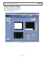
1
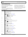
EVAL-AD765x-1SDZ User Guide
UG-417
One Technology Way • P.O. Box 9106 • Norwood, MA 02062-9106, U.S.A. • Tel: 781.329.4700 • Fax: 781.461.3113 • www.analog.com
Evaluating the AD7656-1/AD7657-1/AD7658-1, 250 kSPS, 6-Channel,
Simultaneous Sampling, Bipolar 16-/14-/12-Bit ADCs
FEATURES
GENERAL DESCRIPTION
Full featured evaluation board for the AD7656-1/AD7657-1/
AD7658-1
PC control in conjunction with the system demonstration
platform (EVAL-SDP-CB1Z)
PC software for control and data analysis (time and
frequency domain)
Standalone capability
The EVAL-AD7656-1SDZ/EVAL-AD7657-1SDZ/EVAL-AD76581SDZ are full featured evaluation boards that can be used to easily
evaluate all features of the AD7656-1/AD7657-1/AD7658-1. The
AD7656-1/AD7657-1/AD7658-1 are 16-/14-/12-bit, 6-channel,
250 kSPS simultaneous sampling ADCs, respectively. Each part
contains six 16-, 14-, or 12-bit, low power SAR ADCs and can
operate from a single 4.75 V to 5.25 V power supply or dual
±12 V power supplies. The parts feature throughput rates of up
to 250 kSPS.
EVALUATION KIT CONTENTS
EVAL-AD7656-1SDZ, EVAL-AD7657-1SDZ, or
EVAL-AD7658-1SDZ evaluation board
Evaluation software CD for the AD7656-1/AD7657-1/
AD7658-1
9 V mains power supply adapter
ADDITIONAL EQUIPMENT NEEDED
EVAL-SDP-CB1Z system demonstration platform, includes a
USB cable
Precision analog signal source
SMB cables
PC running Windows XP SP2, Windows Vista, or Windows 7
with USB 2.0 port
ONLINE RESOURCES
Documents
AD7656-1/AD7657-1/AD7658-1 data sheet
EVAL-AD7656-1SDZ/EVAL-AD7657-1SDZ/
EVAL-AD7658-1SDZ user guide
Required Software
EVAL-AD7656-1SDZ/EVAL-AD7657-1SDZ/
EVAL-AD7658-1SDZ evaluation software
The evaluation boards can be controlled via the system demonstration platform (SDP). The EVAL-SDP-CB1Z board allows
the evaluation boards to be controlled via the USB port of a PC
using the AD7656-1/AD7657-1/AD7658-1 evaluation software.
The EVAL-AD7656-1SDZ/EVAL-AD7657-1SDZ/EVALAD7658-1SDZ generates all required power supplies on board and
supplies power to the EVAL-SDP-CB1Z controller board.
On-board components include the following:
AD8597: ultralow distortion, ultralow noise op amp (single)
AD8031: 2.7 V, 800 µA, 80 MHz rail-to-rail I/O single amplifier
ADP1613: step-up PWM dc-to-dc switching converter
ADP3303-5: high accuracy anyCAP® 200 mA low dropout
linear regulator
ADP2301: 1.2 A, 20 V, 1.4 MHz nonsynchronous step-down
switching regulator
ADM1185: quad voltage monitor and sequencer
ADP190: logic controlled, high-side power switch
ADG3308: low voltage, 1.15 V to 5.5 V, 8-channel bidirectional
logic level translator
ADR431: ultralow noise XFET® voltage reference with current
sink and source capability
AD780: 2.5 V/3.0 V ultrahigh precision band gap voltage reference
A functional block diagram is shown in Figure 1, and various link
options are described in the Link Configuration Options section.
For full details on the AD7656-1/AD7657-1/AD7658-1, see the
AD7656-1/AD7657-1/AD7658-1 data sheet, which should be
consulted in conjunction with this user guide when using these
evaluation boards.
PLEASE SEE THE LAST PAGE FOR AN IMPORTANT
WARNING AND LEGAL TERMS AND CONDITIONS.
Rev. 0 | Page 1 of 24
UG-417
EVAL-AD765x-1SDZ User Guide
TABLE OF CONTENTS
Features .............................................................................................. 1
Analog Inputs.............................................................................. 14
Evaluation Kit Contents ................................................................... 1
Reference Options ...................................................................... 14
Additional Equipment Needed ....................................................... 1
Sockets/Connectors ................................................................... 14
Online Resources .............................................................................. 1
Modes of Operation ....................................................................... 15
General Description ......................................................................... 1
SDP Controlled Mode ............................................................... 15
Revision History ............................................................................... 2
Standalone Mode ........................................................................ 15
Functional Block Diagram .............................................................. 3
Getting Started .................................................................................. 4
How to Use the Software for Evaluating the AD7656-1/
AD7657-1/AD7658-1 .................................................................... 16
Quick Start Steps .......................................................................... 4
Setting Up the System for Data Capture ................................. 16
Software Installation Procedures ................................................ 5
Overview of the Main Window ................................................ 18
Evaluation Board Setup Procedures........................................... 8
Generating a Waveform Analysis Report................................ 20
Evaluation Board Hardware ............................................................ 9
Generating a Histogram of the ADC Code Distribution ..... 21
AD7656-1/AD7657-1/AD7658-1 Device Description ............ 9
Generating a Fast Fourier Transform of AC Characteristics ...... 22
Power Supplies .............................................................................. 9
Generating a Summary of the Waveform, Histogram, and
Fast Fourier Transform .............................................................. 23
Link Configuration Options ......................................................... 10
Setup Conditions ........................................................................ 10
Related Links ................................................................................... 24
Evaluation Board Circuitry ........................................................... 14
REVISION HISTORY
6/13—Revision 0: Initial Version
Rev. 0 | Page 2 of 24
EVAL-AD765x-1SDZ User Guide
UG-417
FUNCTIONAL BLOCK DIAGRAM
AVCC
AGND
DGND
ON-BOARD
POWER SUPPLIES
AM1185
POWER
SEQUENCER
DVCC
ADP1613
VSS
ADP2301
OP AMP
SUPPLIES
+
VIN
–
7V TO 9V DC
INPUT JACK
SDP +5V
5V
ADP3303
ADP190
3.3VIO
(×2) +5V
+3.3V
±15V
GND
VIN GND
VDD
BF527
DSP
VDRIVE
GND
CS
RD
WR
CONVST A TO CONVST C
V1 VSS VDD DVCC AVCC
AD8597
V2
V2
AD8597
V3
VDRIVE
BUSY
V3
AD7656-1
ADG3308
LEVEL
SHIFTERS
PARALLEL
INTERFACE
DB0 TO DB15
V4
RESET
AD8597
V5
V4
AD8597
REFIN/ REFCAPA TO
V6 REFOUT
REFCAPC
W/B
RANGE
SER/PAR SEL
H/S SEL
HARDWARE
SELECT
V5
AD8597
AD780/
ADR431
V6
AD8597
REF
EVAL-AD7656-1SDZ
Figure 1.
Rev. 0 | Page 3 of 24
EVAL-SDP-CB1Z
CONTROLLER
BOARD
10726-001
V1
UG-417
EVAL-AD765x-1SDZ User Guide
GETTING STARTED
evaluation board kit to ensure that the boards are
connected firmly together.
QUICK START STEPS
To begin using the evaluation board, do the following:
2.
With the EVAL-SDP-CB1Z board disconnected from the
USB port of the PC, install the AD7656-1/AD7657-1/
AD7658-1 evaluation board software from the CD
included in the evaluation board kit. The PC must be
restarted after the software installation is complete. (For
complete software installation instructions, see the
Software Installation Procedures section.)
Connect the EVAL-SDP-CB1Z board to the EVALAD7656-1SDZ/EVAL-AD7657-1SDZ/EVAL-AD76581SDZ board as shown in Figure 2. Screw the two boards
together using the nylon screw-nut set included in the
3.
Connect the 9 V power supply adapter included in the
evaluation board kit to Connector J702 on the EVALAD7656-1SDZ/EVAL-AD7657-1SDZ/EVAL-AD76581SDZ board.
4.
Connect the EVAL-SDP-CB1Z board to the PC using the
supplied USB cable. (If you are using Windows® XP, you may
need to search for the EVAL-SDP-CB1Z drivers. Choose to
automatically search for the drivers for the EVAL-SDP-CB1Z
board if prompted by the operating system.)
5.
Launch the EVAL-AD7656-1SDZ/EVAL-AD7657-1SDZ/
EVAL-AD7658-1SDZ software from the Analog Devices
subfolder in the Programs menu.
9V PSU
EVAL-SDP-CB1Z
USB TO PC
Figure 2. Hardware Configuration—Setting up the EVAL-AD7656-1SDZ/EVAL-AD7657-1SDZ/EVAL-AD7658-1SDZ
(EVAL-AD7656-1SDZ/EVAL-AD7657-1SDZ/EVAL-AD7658-1SDZ on Left and EVAL-SDP-CB1Z on Right)
Rev. 0 | Page 4 of 24
10726-002
1.
EVAL-AD765x-1SDZ User Guide
UG-417
SOFTWARE INSTALLATION PROCEDURES
4.
Select the location to install the software, and then click Next.
The EVAL-AD7656-1SDZ/EVAL-AD7657-1SDZ/EVALAD7658-1SDZ evaluation kit includes a CD containing
software to be installed on your PC before you begin using the
evaluation board.
There are two parts to the installation:
•
•
AD7656-1/AD7657-1/AD7658-1 evaluation board software
installation
EVAL-SDP-CB1Z system demonstration platform board
drivers installation
Warning
10726-004
The evaluation board software and drivers must be installed
before connecting the evaluation board and EVAL-SDP-CB1Z
board to the USB port of the PC to ensure that the evaluation
system is correctly recognized when it is connected to the PC.
Installing the AD7656-1/AD7657-1/AD7658-1 Evaluation
Board Software
Figure 4. AD7656-1/AD7657-1/AD7658-1 Evaluation Board Software
Installation: Selecting the Location for Software Installation
5.
To install the AD7656-1/AD7657-1/AD7658-1 evaluation board
software,
3.
10726-005
2.
With the EVAL-SDP-CB1Z board disconnected from the
USB port of the PC, insert the installation CD into the CDROM drive.
Double-click the setup.exe file to begin the evaluation
board software installation. The software is installed to the
following default location: C:\Program Files\Analog
Devices\AD7656-1_57-1_58-1.
A dialog box appears asking for permission to allow the
program to make changes to your computer. Click Yes.
Figure 5. AD7656-1/AD7657-1/AD7658-1 Evaluation Board Software
Installation: Accepting the License Agreement
10726-003
1.
A license agreement appears. Read the agreement, and then
select I accept the License Agreement and click Next.
Figure 3. AD7656-1/AD7657-1/AD7658-1 Evaluation Board Software
Installation: Granting Permission for Program to Make Changes
Rev. 0 | Page 5 of 24
UG-417
6.
EVAL-AD765x-1SDZ User Guide
Installing the EVAL-SDP-CB1Z System Demonstration
Platform Board Drivers
A summary of the installation is displayed. Click Next to
continue.
After the installation of the evaluation board software is complete,
a welcome window is displayed for the installation of the EVALSDP-CB1Z system demonstration platform board drivers.
With the EVAL-SDP-CB1Z board still disconnected from
the USB port of the PC, make sure that all other applications
are closed, and then click Next.
10726-006
1.
Figure 6. AD7656-1/AD7657-1/AD7658-1 Evaluation Board Software
Installation: Reviewing a Summary of the Installation
10726-008
A dialog box informs you when the installation is
complete. Click Next.
Figure 8. EVAL-SDP-CB1Z Drivers Setup:
Beginning the Drivers Installation
2.
Select the location to install the drivers, and then click Next.
10726-007
Figure 7. AD7656-1/AD7657-1/AD7658-1 Evaluation Board Software
Installation: Indicating When the Installation Is Complete
10726-009
7.
Figure 9. EVAL-SDP-CB1Z Drivers Setup:
Selecting the Location for Drivers Installation
Rev. 0 | Page 6 of 24
EVAL-AD765x-1SDZ User Guide
Click Install to confirm that you would like to install the
drivers.
5.
Before using the evaluation board, you must restart your
computer. A dialog box opens, giving you the following
options: Restart, Shut Down, Restart Later. Click the
appropriate button.
Figure 10. EVAL-SDP-CB1Z Drivers Setup:
Granting Permission to Install Drivers
Figure 12. EVAL-SDP-CB1Z Drivers Setup:
Restarting the Computer
To complete the drivers installation, click Finish, which
closes the installation wizard.
10726-011
4.
10726-012
10726-010
3.
UG-417
Figure 11. EVAL-SDP-CB1Z Drivers Setup:
Completing the Drivers Setup Wizard
Rev. 0 | Page 7 of 24
UG-417
EVAL-AD765x-1SDZ User Guide
EVALUATION BOARD SETUP PROCEDURES
Configuring the Evaluation and SDP Boards
The AD7656-1/AD7657-1/AD7658-1 evaluation board connects
to the EVAL-SDP-CB1Z system demonstration board. The
EVAL-SDP-CB1Z board is the controller board, which is the
communication link between the PC and the main evaluation
board. Figure 2 shows a photograph of the connections made
between the AD7656-1/AD7657-1/AD7658-1 daughter board
and the EVAL-SDP-CB1Z board.
1.
2.
After following the instructions in the Software Installation
Procedures section, set up the evaluation and SDP boards as
detailed in this section.
Warning
3.
The evaluation software and drivers must be installed before connecting the evaluation board and EVAL-SDP-CB1Z board to
the USB port of the PC to ensure that the evaluation system is
correctly recognized when it is connected to the PC.
Rev. 0 | Page 8 of 24
Connect the EVAL-AD7656-1SDZ/EVAL-AD7657-1SDZ/
EVAL-AD7658-1SDZ board to Connector A or Connector B
of the EVAL-SDP-CB1Z board (see Figure 2).
a. Screw the two boards together using the nylon screwnut set included in the evaluation board kit to ensure
that the boards are connected firmly together.
Connect the 9 V power supply adapter included in the evaluation kit to Connector J702 of the EVAL-AD7656-1SDZ/
EVAL-AD7657-1SDZ/EVAL-AD7658-1SDZ board. (See
Table 1 for more information about the connections and
options for the required power supplies.)
Connect the EVAL-SDP-CB1Z board to the PC using the
supplied USB cable.
EVAL-AD765x-1SDZ User Guide
UG-417
EVALUATION BOARD HARDWARE
POWER SUPPLIES
AD7656-1/AD7657-1/AD7658-1 DEVICE
DESCRIPTION
The AD7656-1/AD7657-1/AD7658-1 are reduced decoupling
pin- and software-compatible versions of the AD7656/AD7657/
AD7658. Each AD7656-1/AD7657-1/AD7658-1 device contains
six 16-/14-/12-bit, fast, low power successive approximation ADCs
in a package designed on the iCMOS® process (industrial CMOS).
iCMOS is a process combining high voltage silicon with submicron
CMOS and complementary bipolar technologies. It enables the
development of a wide range of high performance analog ICs
capable of 33 V operation in a footprint that no previous generation of high voltage parts could achieve.
The AD7656-1/AD7657-1/AD7658-1 feature throughput rates
of up to 250 kSPS. The parts contain low noise, wide bandwidth
track-and-hold amplifiers that can handle input frequencies of
up to 4.5 MHz.
For more information about these devices, refer to the AD7656-1/
AD7657-1/AD7658-1data sheet, which should be used in conjunction with this user guide.
The EVAL-AD7656-1SDZ/EVAL-AD7657-1SDZ/EVALAD7658-1SDZ can be used in two modes: SDP controlled mode
and standalone mode (see the Modes of Operation section for
more information).
When the EVAL-AD7656-1SDZ/EVAL-AD7657-1SDZ/
EVAL-AD7658-1SDZ board is used in conjunction with the
EVAL-SDP-CB1Z board (SDP controlled mode), connect the
9 V dc supply to Connector J702 on the EVAL-AD7656-1SDZ/
EVAL-AD7657-1SDZ/EVAL-AD7658-1SDZ board. The VDD, VSS,
AVCC, and DVCC supplies are generated on board. When the
EVAL-AD7656-1SDZ/EVAL-AD7657-1SDZ/EVAL-AD7658-1SDZ
board is used in standalone mode, the VDD, VSS, AVCC, and DVCC
supplies must be sourced from external sources (see Table 1).
In SDP controlled mode and standalone mode, each supply is
decoupled on the EVAL-AD7656-1SDZ/EVAL-AD7657-1SDZ/
EVAL-AD7658-1SDZ using 10 µF and 0.1 µF capacitors. A
single ground plane is used on this board to minimize the effect
of high frequency noise interference.
Table 1. External Power Supplies Required
Power Supply
VIN 1
Connector
J702
Voltage Range
7 V to 9 V
VDD
VSS
AVCC
DVCC
J100
J100
J703
J701
+12 V to +16.5 V
−12 V to −16.5 V
4.75 V to 5.25 V
4.75 V to 5.25 V
1
Purpose
Supplies all on-board power supplies, generating all required voltages to run the
evaluation board
Supplies the positive rail of the amplifier
Supplies the negative rail of the amplifier
Supplies the AVCC analog supply on the ADC
Supplies the DVCC digital supply on the ADC
When VIN is supplied, all other power supplies are available on board. If the VIN supply is not used, all other power supplies must be sourced from an external source.
Rev. 0 | Page 9 of 24
UG-417
EVAL-AD765x-1SDZ User Guide
LINK CONFIGURATION OPTIONS
There are multiple jumper (LKx) and solder link (SLx) options
that must be set correctly to select the appropriate operating setup
before you begin using the evaluation board. The functions of
these options are outlined in Table 2.
SETUP CONDITIONS
Care should be taken before applying power and signals to the
evaluation board to ensure that all link positions are as required
by the operating mode. There are two modes in which to operate
the evaluation board. The evaluation board can be operated in
SDP controlled mode to be used with the SDP board, or the
evaluation board can be used in standalone mode.
Table 3 shows the default positions in which the links are set when
the evaluation board is packaged. When the board is shipped, it
is assumed that you are going to operate the evaluation board
with the SDP board (SDP controlled mode).
Table 2. Link Option Functions
Link No.
LK1
LK2
LK3
Function
H/S SEL selection.
Position A: the software input is selected.
Position B: the hardware input is selected.
VREF buffer signal selection.
Position A: the VREF signal is unbuffered.
Position B: the VREF signal is buffered by the AD8031 op amp (U10).
WR/REFEN/DIS signal selection.
Position A: the WR/REFEN/DIS pin is connected to EVAL-SDP-CB1Z.
Position B: the WR/REFEN/DIS pin is connected to the J7-2 external socket.
Position C: the WR/REFEN/DIS pin is connected to GND.
Position D: the WR/REFEN/DIS pin is connected to VDRIVE.
LK4
LK5
LK6
LK7
LK8
LK9
V1 input jumper.
Inserted: the V1 input is shorted to GND.
V2 input jumper.
Inserted: the V2 input is shorted to GND.
RANGE signal selection.
Position A: the RANGE pin is connected to VDRIVE.
Position B: the RANGE pin is connected to GND. The input range is set to ±4 × VREF.
STBY signal selection.
Position A: the STBY pin is connected to VDRIVE. Normal operation is selected.
Position B: the STBY pin is connected to GND.
RESET signal selection.
Position A: the RESET pin is connected to VDRIVE.
Position B: the RESET pin is connected to GND.
Position C: the RESET pin is connected to EVAL-SDP-CB1Z.
W/B signal selection.
Position A: the W/B pin is connected to VDRIVE.
Position B: the W/B pin is connected to GND. Word mode is selected.
LK11
BUSY signal selection.
Position A: the BUSY pin is connected to EVAL-SDP-CB1Z.
Position B: the BUSY pin is connected to the J7-12 external socket.
CONVST A signal selection.
Position A: the CONVST A pin is connected to the J7-8 external socket.
Position B: the CONVST A pin is connected to EVAL-SDP-CB1Z.
Position C: the CONVST A pin is connected to GND.
LK12
CS source signal selection.
LK10
LK13
LK14
Position A: the CS pin is connected to EVAL-SDP-CB1Z.
Position B: the CS pin is connected to the J7-1 external socket.
REFIN/REFOUT source signal selection.
Position A: the REFIN/REFOUT signal is sourced from AD780 (U5).
Position B: the REFIN/REFOUT signal is sourced from ADR431 (U3).
V3 input jumper.
Inserted: the V3 input is shorted to GND.
Rev. 0 | Page 10 of 24
EVAL-AD765x-1SDZ User Guide
Link No.
LK15
LK16
LK17
LK18
LK19
LK20
LK21
LK22
LK23
LK24
LK25
LK26
LK27
LK28
LK29
UG-417
Function
V4 input jumper.
Inserted: the V4 input is shorted to GND.
VDRIVE source signal selection.
Position A: the VDRIVE signal is sourced from the on-board 3.3 V supply. (Requires the EVAL-SDP-CB1Z board to be connected.)
Position B: the VDRIVE pin is connected to the J7-14 external socket.
V5 input jumper.
Inserted: the V5 input is shorted to GND.
V6 input jumper.
Inserted: the V6 input is shorted to GND.
REFIN/REFOUT input selection.
Inserted: the VREF signal is connected to the REFIN/REFOUT pin.
SER/PAR SEL selection.
Position A: the SER/PAR SEL pin is connected to VDRIVE.
Position B: the SER/PAR SEL pin is connected to GND. Parallel mode is selected.
AD780 (U5) voltage output selection.
Inserted: the AD780 voltage output is 3 V.
Removed: the AD780 voltage output is 2.5 V.
CONVST A/CONVST B link selection.
Inserted: Connects CONVST A to CONVST B.
RD source signal selection.
Position A: the RD pin is connected to EVAL-SDP-CB1Z.
Position B: the RD pin is connected to the J7-3 external socket.
REFCAPA source signal selection.
Inserted: an external reference is connected to REFCAPA.
Removed: an external reference is disconnected from REFCAPA.
DB10/DOUT C destination selection.
Position A: data is sent to EVAL-SDP-CB1Z.
Position B: data is sent to the J7-4 external socket.
DB7/HBEN/DCEN selection.
Position A: data is sent to EVAL-SDP-CB1Z.
Position B: the DB7/HBEN/DCEN pin is connected to VDRIVE.
Position C: the DB7/HBEN/DCEN pin is connected to GND.
DB9/DOUT B destination selection.
Position A: data is sent to EVAL-SDP-CB1Z.
Position B: not used.
Position C: data is sent to the J7-5 external socket.
DB8/DOUT A destination selection.
Position A: data is sent to EVAL-SDP-CB1Z.
Position B: not used.
Position C: data is sent to the J7-6 external socket.
DB14/REFBUFEN/DIS selection.
Position A: data is sent to EVAL-SDP-CB1Z.
Position B: the DB14/REFBUFEN/DIS pin is connected to VDRIVE.
Position C: the DB14/REFBUFEN/DIS pin is connected to GND.
LK30
LK31
LK32
DB6/SCLK selection.
Position A: the DB6/SCLK pin is connected to EVAL-SDP-CB1Z.
Position B: not used.
Position C: the DB6/SCLK pin is connected to the J7-11 external socket.
DB2/SEL C selection.
Position A: data is sent to EVAL-SDP-CB1Z.
Position B: the DB2/SEL C pin is connected to VDRIVE.
Position C: the DB2/SEL C pin is connected to GND.
DB1/SEL B selection.
Position A: data is sent to EVAL-SDP-CB1Z.
Position B: the DB1/SEL B pin is connected to VDRIVE.
Position C: the DB1/SEL B pin is connected to GND.
Rev. 0 | Page 11 of 24
UG-417
Link No.
LK33
LK34
EVAL-AD765x-1SDZ User Guide
Function
DB0/SEL A selection.
Position A: data is sent to EVAL-SDP-CB1Z.
Position B: the DB0/SEL A pin is connected to VDRIVE.
Position C: the DB0/SEL A pin is connected to GND.
CONVST B selection.
Position A: the CONVST B pin is connected to the J7-9 external socket.
Position B: the CONVST B pin is connected to EVAL-SDP-CB1Z.
LK35
LK36
LK101
LK102
LK103 to LK106
LK701
LK702
SL1
SL2
SL3 to SL14
SL15
SL16
SL17
SL18
SL19
SL20
Position C: the CONVST B pin is connected to GND.
CONVST C selection.
Position A: the CONVST C pin is connected to the J7-10 external socket.
Position B: the CONVST C pin is connected to EVAL-SDP-CB1Z.
Position C: the CONVST C pin is connected to GND.
CONVST A/CONVST C link selection.
Inserted: Connects CONVST A to CONVST C.
VSS signal source selection (op amp negative supply).
Position A: the VSS signal is sourced from the on-board supply generation circuitry (−12 V).
Position B: the VSS signal is sourced from the J100 external socket.
VDD signal source selection (op amp positive supply).
Position A: the VDD signal is sourced from the on-board supply generation circuitry (+12 V).
Position B: the VDD signal is sourced from the J100 external socket.
Sets the VDD and VSS levels when using the on-board supplies as follows (where POP = place both 0 Ω resistors, and NOPOP = neither
0 Ω resistor is placed).
Link
±12 V
±15 V
LK103
POP
NOPOP
LK104
NOPOP
POP
LK105
NOPOP
POP
LK106
POP
NOPOP
AVCC signal source selection.
Position A: the AVCC signal is sourced from the on-board supply generation circuitry.
Position B: the AVCC signal is sourced from the J703 external socket.
DVCC signal source selection.
Position A: the DVCC signal is sourced from the on-board supply generation circuitry.
Position B: the DVCC signal is sourced from the J701 external socket.
REFCAPA/REFCAPB link selection.
Inserted: Connects REFCAPA to REFCAPB when soldered.
REFCAPB/REFCAPC link selection.
Inserted: Connects REFCAPB to REFCAPC when soldered.
Not used. Leave unsoldered.
V1 buffer selection.
Position A: the V1 input signal is buffered through U4.
Position B: the V1 input signal is taken directly from J1.
V2 buffer selection.
Position A: the V2 input signal is buffered through U7.
Position B: the V2 input signal is taken directly from J2.
V3 buffer selection.
Position A: the V3 input signal is buffered through U8.
Position B: the V3 input signal is taken directly from J7.
V4 buffer selection.
Position A: the V4 input signal is buffered through U9.
Position B: the V4 input signal is taken directly from J4.
V5 buffer selection.
Position A: the V5 input signal is buffered through U11.
Position B: the V5 input signal is taken directly from J5.
V6 buffer selection.
Position A: the V6 input signal is buffered through U12.
Position B: the V6 input signal is taken directly from J6.
Rev. 0 | Page 12 of 24
EVAL-AD765x-1SDZ User Guide
UG-417
Table 3. Default Link Positions for Packaged EVAL-AD7656-1SDZ/EVAL-AD7657-1SDZ/EVAL-AD7658-1SDZ
Link No.
LK1
LK2
LK3
Position
A
A
A
Function
Software input is selected.
VREF is not buffered.
The WR/REFEN/DIS pin is connected to EVAL-SDP-CB1Z.
LK4
LK5
LK6
LK7
LK8
LK9
Inserted
Inserted
B
A
C
B
LK10
LK11
LK12
LK13
LK14
LK15
LK16
LK17
LK18
LK19
LK20
LK21
LK22
A
B
A
A
Inserted
Inserted
A
Inserted
Inserted
Removed
B
Removed
Removed
LK23
LK24
LK25
LK26
LK27
LK28
LK29
A
Removed
A
A
A
A
A
The V1 input is grounded.
The V2 input is grounded.
The RANGE pin is connected to GND. The input range is set to ±4 × VREF (can be overridden by control registers in software).
The STBY pin is connected to VDRIVE. Normal operation is selected.
The RESET pin is connected to EVAL-SDP-CB1Z.
The W/B pin is connected to GND. Word mode is selected.
The BUSY pin is connected to EVAL-SDP-CB1Z.
The CONVST A pin is connected to EVAL-SDP-CB1Z.
The CS pin is connected to EVAL-SDP-CB1Z.
The REFIN/REFOUT signal is sourced from AD780.
The V3 input is grounded.
The V4 input is grounded.
The VDRIVE signal is sourced from the on-board 3.3 V supply. (Requires the EVAL-SDP-CB1Z board to be connected.)
The V5 input is grounded.
The V6 input is grounded.
An external VREF is disconnected.
The SER/PAR SEL pin is connected to GND. Parallel mode is selected.
The AD780 voltage output is 2.5 V.
The CONVST A and CONVST B pins are not linked.
The RD pin is connected to EVAL-SDP-CB1Z.
An external VREF is disconnected.
The DB10/DOUT C pin is connected to EVAL-SDP-CB1Z.
The DB7/HBEN/DCEN pin is connected to EVAL-SDP-CB1Z.
The DB9/DOUT B pin is connected to EVAL-SDP-CB1Z.
The DB8/DOUT A pin is connected to EVAL-SDP-CB1Z.
The DB14/REFBUFEN/DIS pin is connected to EVAL-SDP-CB1Z.
LK30
LK31
LK32
LK33
LK34
LK35
LK36
A
A
A
A
B
B
Removed
LK101
LK102
LK103
LK104
A
A
NOPOP 1
POP1
LK105
POP1
LK106
LK701
LK702
SL1
SL2
SL3 to SL14
SL15
SL16
SL17
SL18
SL19
SL20
1
The DB6/SCLK pin is connected to EVAL-SDP-CB1Z.
The DB2/SEL C pin is connected to EVAL-SDP-CB1Z.
The DB1/SEL B pin is connected to EVAL-SDP-CB1Z.
The DB0/SEL A pin is connected to EVAL-SDP-CB1Z.
The CONVST B pin is connected to EVAL-SDP-CB1Z.
The CONVST C pin is connected to EVAL-SDP-CB1Z.
The CONVST A and CONVST C pins are not linked.
The on-board op amp power is used.
The on-board op amp power is used.
The op amp supply rails are set to ±15 V.
The op amp supply rails are set to ±15 V.
The op amp supply rails are set to ±15 V.
1
NOPOP
A
A
Removed
Removed
Removed
A
A
A
A
A
A
The op amp supply rails are set to ±15 V.
The on-board AVCC is used.
The on-board DVCC is used.
The REFCAPA and REFCAPB pins are not linked.
The REFCAPB and REFCAPC pins are not linked.
Not used.
The V1 input is buffered.
The V2 input is buffered.
The V3 input is buffered.
The V4 input is buffered.
The V5 input is buffered.
The V6 input is buffered.
POP = place both 0 Ω resistors; NOPOP = neither 0 Ω resistor is placed.
Rev. 0 | Page 13 of 24
UG-417
EVAL-AD765x-1SDZ User Guide
EVALUATION BOARD CIRCUITRY
ANALOG INPUTS
SOCKETS/CONNECTORS
The V1 to V6 inputs allow a signal to be connected to the board
via SMB connectors.
Table 4. Socket/Connector Functions
The analog inputs on the EVAL-AD7656-1SDZ/EVAL-AD76571SDZ/EVAL-AD7658-1SDZ are filtered and buffered by the
AD8597 ultralow distortion, ultralow noise (single) op amps.
Additional filtering is provided by an R-C filter directly before
the AD7656-1/AD7657-1/AD7658-1 inputs. Alternatively, the
op amps can be bypassed, and the inputs can be fed directly to
the AD7656-1/AD7657-1/AD7658-1 via the R-C filter.
REFERENCE OPTIONS
•
VIN1
VIN2
VIN3
J1
The following two on-board reference supplies are available:
•
Socket
VIN0
ADR431: ultralow noise XFET voltage reference with
current sink and source capability
AD780: 2.5 V/3.0 V ultrahigh precision band gap voltage
reference
J2
J3
J5
J8
J9
Alternatively, the AD7656-1/AD7657-1/AD7658-1 can supply an
internal reference voltage.
J100
J701
J702
J703
Rev. 0 | Page 14 of 24
Function
Analog Input VIN0. Buffered to the VIN0 pin on the
AD7656-1/AD7657-1/AD7658-1.
Analog Input VIN1. Buffered to the VIN1 pin on the
AD7656-1/AD7657-1/AD7658-1.
Analog Input VIN2. Buffered to the VIN2 pin on the
AD7656-1/AD7657-1/AD7658-1.
Analog Input VIN3. Buffered to the VIN3 pin on the
AD7656-1/AD7657-1/AD7658-1.
VIN. Apply a bipolar signal to this pin. This signal is
biased up on J3.
Socket for EVAL-SDP-CB1Z evaluation controller board.
VIN BIASED. Unipolar version of signal applied to J1.
VREF. External reference voltage.
VDRIVE. External screw connection for VDRIVE.
Analog Input VIN4 to Analog Input VIN15. Buffered to
VIN4 to VIN15 pins of the AD7656-1/AD7657-1/AD7658-1.
Odd Pins
Even Pins
Pin 1—VIN4
Pin 2—AGND
Pin 3—VIN5
Pin 4—AGND
Pin 5—VIN6
Pin 6—AGND
Pin 7—VIN7
Pin 8—AGND
Pin 9—VIN8
Pin 10—AGND
Pin 11—VIN9
Pin 12—AGND
Pin 13—VIN10
Pin 14—AGND
Pin 15—VIN11
Pin 16—AGND
Pin 17—VIN12
Pin 18—AGND
Pin 19—VIN13
Pin 20—AGND
Pin 21—VIN14
Pin 22—AGND
Pin 23—VIN15
Pin 24—AGND
Op amp power supply screw terminal connectors.
Supply rails for op amps.
DVCC screw terminal connector.
The 7 V to 9 V dc transformer power connector.
AVCC screw terminal connector.
EVAL-AD765x-1SDZ User Guide
UG-417
MODES OF OPERATION
SDP CONTROLLED MODE
The AD7656-1/AD7657-1/AD7658-1 uses a high speed parallel
interface that allows sampling rates of up to 250 kSPS. For more
information about the operation of the parallel interface, refer
to the AD7656-1/AD7657-1/AD7658-1 data sheet.
The AD7656-1/AD7657-1/AD7658-1 uses the parallel interface
to transfer data to the EVAL-SDP-CB1Z.
The EVAL-AD7656-1SDZ/EVAL-AD7657-1SDZ/EVALAD7658-1SDZ communicates with the EVAL-SDP-CB1Z board
using level shifters. The EVAL-SDP-CB1Z operates at a 3.3 V
logic level, which allows logic voltages that exceed 3.3 V to be
used without damaging the SDP interface.
STANDALONE MODE
The EVAL-AD7656-1SDZ/EVAL-AD7657-1SDZ/EVALAD7658-1SDZ can also be used without the EVAL-SDP-CB1Z
controller board. In this case, the EVAL-AD7656-1SDZ/EVALAD7657-1SDZ/EVAL-AD7658-1SDZ is connected to the serial
interface using the J7 socket. For more information about the
operation of the serial interface, refer to the AD7656-1/AD7657-1/
AD7658-1 data sheet.
Rev. 0 | Page 15 of 24
UG-417
EVAL-AD765x-1SDZ User Guide
HOW TO USE THE SOFTWARE FOR EVALUATING THE AD7656-1/AD7657-1/AD7658-1
Launching the Software
After completing the steps in the Software Installation Procedures
and Evaluation Board Setup Procedures sections, set up the system
for data capture as follows:
2.
Allow the Found New Hardware Wizard to run after the
EVAL-SDP-CB1Z board is plugged into your PC. (If you
are using Windows XP, you may need to search for the
EVAL-SDP-CB1Z drivers. Choose to automatically search
for the drivers for the EVAL-SDP-CB1Z board if prompted
by the operating system.)
Check that the board is connected to the PC correctly
using the Device Manager of the PC.
a. Access the Device Manager as follows:
i. Right-click My Computer and then click Manage.
ii. A dialog box appears asking for permission to
allow the program to make changes to your
computer. Click Yes.
iii. The Computer Management box appears. From
the list of System Tools, click Device Manager
(see Figure 13).
b. Under ADI Development Tools, Analog Devices
System Development Platform (32MB) should
appear, indicating that the EVAL-SDP-CB1Z driver
software is installed and that the board is connected
to the PC correctly.
1.
2.
From the Start menu, select Programs > Analog Devices
> AD7656-1_57-1_58-1. The main window of the software
then displays.
If the EVAL-AD7656-1SDZ/EVAL-AD7657-1SDZ/EVALAD7658-1SDZ evaluation system is not connected to the
USB port via the EVAL-SDP-CB1Z when the software is
launched, a connectivity error displays (see Figure 14).
Connect the evaluation system to the USB port of the PC,
wait a few seconds, click Rescan, and follow the on-screen
instructions.
Figure 14. Connectivity Error Alert
When the software starts running, it searches for hardware
connected to the PC. A dialog box indicates when the evaluation
board attached to the PC is detected, and then the main window
appears (see Figure 15).
10726-013
1.
After completing the steps in the Setting Up the System for Data
Capture section, launch the AD7656-1/AD7657-1/AD7658-1
software as follows:
10726-014
SETTING UP THE SYSTEM FOR DATA CAPTURE
Figure 13. Device Manager:
Checking that the Board Is Connected to the PC Correctly
Rev. 0 | Page 16 of 24
EVAL-AD765x-1SDZ User Guide
UG-417
1
9
2
8
3
11
10
7
4
5
12
6
NOTES
1. FOR DETAILS ABOUT THE AREAS HIGHLIGHTED IN RED, SEE THE OVERVIEW OF THE MAIN WINDOW SECTION.
Figure 15. Evaluation Software Main Window
Rev. 0 | Page 17 of 24
10726-015
CONTROL CONTROL CONTROL
CURSOR ZOOMING PANNING
UG-417
EVAL-AD765x-1SDZ User Guide
OVERVIEW OF THE MAIN WINDOW
Part Information Box (Section 2)
The main window of the software is shown in Figure 15 and has
the features described in this section.
The Part Information box (labeled 2 in Figure 15) allows
selecting the generic to be evaluated; choose AD7656-1,
AD7657-1, or AD7658-1.
File Menu (Section 1)
Device Input Range Box (Section 3)
The File menu (labeled 1 in Figure 15) offers the choice to
•
•
•
Resolution Box (Section 4)
The Resolution box (labeled 4 in Figure 15) displays the
resolution of the selected part in bits.
Sampling Rate Box (Section 5)
The default sampling frequency in the Sampling Rate box (labeled 5
in Figure 15) matches the maximum sample rate of the ADC being
evaluated. Although you can adjust the sampling frequency, there
are limitations in terms of the sample frequencies that can be
entered. If an unusable sample frequency is input, the software
automatically adjusts the sample frequency accordingly. Units
can be entered as, for example, 10k for 10,000 Hz. The software
automatically adjusts the sample frequency according to the ability
of the ADC being evaluated. For example, if you enter a value
that is beyond the ability of the device, the software indicates
this and reverts to the maximum sample frequency.
Exit Button (Section 6)
Clicking Exit (labeled 6 in Figure 15) closes the software.
Alternatively, you can select Exit from the File menu.
Tabs Area (Section 7)
10726-016
•
The Device Input Range box (labeled 3 in Figure 15), in conjunction with hardware settings, is used to select the voltage range.
Load data: load previously captured data or example files in
.tsv (tab separated values) format for analysis (see Figure 16).
(The default location for example files is C:\Program
Files\Analog Devices\AD7656-1_57-1_58-1\examples.)
Save Data as .tsv: save captured data in .tsv format for
future analysis (see Figure 17).
Print Front Panel Picture: print the main window to the
default printer.
Save Picture: save the current screen capture.
Exit: close the application.
Figure 16. Load File Dialog Box:
Loading Previously Captured Data or Example Files in .tsv Format
There are four tabs available in the tabs area (labeled 7 in Figure 15)
of the main window: Waveform, Histogram, FFT, and Summary.
These tabs display the data in different formats. Navigation tools
are provided within each tab to allow you to control the cursor,
zooming, and panning (see Figure 15) within the graphs displayed.
Each tab is described in more detail in the Generating a Waveform
Analysis Report; Generating a Histogram of the ADC Code
Distribution; Generating a Fast Fourier Transform of AC
Characteristics; and Generating a Summary of the Waveform,
Histogram, and Fast Fourier Transform sections.
# Samples Box (Section 8)
The # Samples box (labeled 8 in Figure 15) allows you to select
the number of samples to analyze. When Sample or Continuous
is clicked, the software requests this number of samples to be taken.
This is the total number of samples taken on all channels.
Sample Button (Section 9)
10726-017
•
Figure 17. Save File Dialog Box:
Saving Data as .tsv
Clicking Sample (labeled 9 in Figure 15) performs a single capture,
acquiring a set number of samples at the selected sampling rate.
Continuous Button (Section 10)
Clicking Continuous (labeled 10 in Figure 15) performs a
continuous capture from the ADC. Clicking Continuous a
second time stops sampling.
Rev. 0 | Page 18 of 24
EVAL-AD765x-1SDZ User Guide
UG-417
Busy LED (Section 11)
Channel Display Buttons (Section 12)
The Busy LED (labeled 11 in Figure 15) indicates when a read
from the EVAL-SDP-CB1Z board is in progress.
Clicking the buttons in this area (labeled 12 in Figure 15) allows
you to display multiple channel reads. (Note that for FFT analysis,
you can select only one channel to be displayed.)
Rev. 0 | Page 19 of 24
UG-417
EVAL-AD765x-1SDZ User Guide
GENERATING A WAVEFORM ANALYSIS REPORT
Figure 18 illustrates the waveform capture tab for a 10 kHz sine
wave input signal.
The Waveform Analysis area (labeled 1 in Figure 18) reports
the amplitudes recorded from the captured signal and the
frequency of the signal tone.
10726-018
1
Figure 18. Waveform Tab
Rev. 0 | Page 20 of 24
EVAL-AD765x-1SDZ User Guide
UG-417
GENERATING A HISTOGRAM OF THE ADC CODE
DISTRIBUTION
The Histogram tab can be used to perform ac testing or, more
commonly, dc testing. This tab shows the ADC code distribution of
the input and computes the mean and standard deviation, which
are displayed as Mean and Transition Noise, respectively, in the
Histogram Analysis area (labeled 1 in Figure 19).
Figure 19 shows the histogram with ac input for a 10 kHz sine
wave applied to the ADC input and the resulting calculations.
AC Input
To perform a histogram test of ac input,
1.
2.
3.
Apply a signal source to the selected analog input on the board.
Click the Histogram tab from the main window.
Click Sample.
DC Input
A histogram test of dc input can be performed with or without
an external source because the evaluation board has a buffered
VREF/2 source at the ADC input.
To perform a histogram test of dc input,
1.
2.
3.
If an external source is being used, apply a signal source to the
selected analog input. It may be required to filter the signal
to ensure that the dc source is noise-compatible with the ADC.
Click the Histogram tab from the main window.
Click Sample.
Raw data is then captured and passed to the PC for statistical
computations, and various measured values are displayed in the
Histogram Analysis area.
Raw data is then captured and passed to the PC for statistical
computations, and various measured values are displayed in the
Histogram Analysis area.
10726-019
1
Figure 19. Histogram Tab
Rev. 0 | Page 21 of 24
UG-417
EVAL-AD765x-1SDZ User Guide
GENERATING A FAST FOURIER TRANSFORM OF
AC CHARACTERISTICS
2.
3.
Figure 20 shows the FFT tab. This feature tests the traditional
ac characteristics of the converter and displays a fast Fourier
transform (FFT) of the results.
As in the histogram test, raw data is then captured and passed
to the PC, which performs the FFT and displays the resulting
SNR, THD, and SINAD.
To perform an ac FFT test,
The Spectrum Analysis box displays the results of the captured data.
Apply a sinusoidal signal with low distortion (better than
115 dB) to the evaluation board at the selected analog input.
To attain the requisite low distortion, which is necessary to
allow true evaluation of the part, one option is to
a. Filter the input signal from the ac source. Choose an
appropriate band-pass filter based on the sinusoidal
signal applied.
b. If a low frequency band-pass filter is used when the fullscale input range is more than a few volts peak-to-peak,
use the on-board amplifiers to amplify the signal, thus
preventing the filter from distorting the input signal.
1
•
•
•
2
Figure 20. FFT Tab
Rev. 0 | Page 22 of 24
The area labeled 1 in Figure 20 shows the input signal
information.
The area labeled 2 in Figure 20 displays the fundamental
frequency and amplitude in addition to the second to fifth
harmonics.
The area labeled 3 in Figure 20 displays the performance
data, including the SNR, THD, and SINAD.
3
10726-020
1.
Click the FFT tab from the main window.
Click Sample.
EVAL-AD765x-1SDZ User Guide
UG-417
GENERATING A SUMMARY OF THE WAVEFORM,
HISTOGRAM, AND FAST FOURIER TRANSFORM
10726-021
Figure 21 shows the Summary tab. The Summary tab captures
all the display information and provides it in one panel with a
synopsis of the information, including key performance
parameters such as SNR and THD.
Figure 21. Summary Tab
Rev. 0 | Page 23 of 24
UG-417
EVAL-AD765x-1SDZ User Guide
RELATED LINKS
Resource
AD7656-1
AD7657-1
AD7658-1
AD8597
AD8031
ADP1613
ADP3303-5
ADP2301
ADM1185
ADP190
ADG3308
ADR431
AD780
EngineerZone
Circuits from the Lab
Description
Product Page: 250 kSPS, 6-Channel, Simultaneous Sampling, Bipolar 16-Bit ADC
Product Page: 250 kSPS, 6-Channel, Simultaneous Sampling, Bipolar 14-Bit ADC
Product Page: 250 kSPS, 6-Channel, Simultaneous Sampling, Bipolar 12-Bit ADC
Product Page: Ultralow Distortion, Ultralow Noise Op Amp (Single)
Product Page: 2.7 V, 800 µA, 80 MHz Rail-to-Rail I/O Single Amplifier
Product Page: 650 kHz/1.3 MHz Step-Up PWM DC-to-DC Switching Converter with 2.0 A Current Limit
Product Page: High Accuracy anyCAP 200 mA Low Dropout Linear Regulator
Product Page: 1.2 A, 20 V, 1.4 MHz Nonsynchronous Step-Down Switching Regulator
Product Page: Quad Voltage Monitor and Sequencer
Product Page: Logic Controlled, High-Side Power Switch
Product Page: Low Voltage, 1.15 V to 5.5 V, 8-Channel Bidirectional Logic Level Translator
Product Page: Ultralow Noise XFET 2.5 V Voltage Reference with Current Sink and Source Capability
Product Page: 2.5 V/3.0 V Ultrahigh Precision Band Gap Voltage Reference
Online Community: Analog Devices Online Technical Support Community
Reference Circuits: Circuit Designs that Have Been Built and Tested to Ensure Function and Performance and that Address
Common Analog, RF/IF, and Mixed-Signal Design Challenges by Applying Analog Devices’ Vast Applications Expertise
ESD Caution
ESD (electrostatic discharge) sensitive device. Charged devices and circuit boards can discharge without detection. Although this product features patented or proprietary protection
circuitry, damage may occur on devices subjected to high energy ESD. Therefore, proper ESD precautions should be taken to avoid performance degradation or loss of functionality.
Legal Terms and Conditions
By using the evaluation board discussed herein (together with any tools, components documentation or support materials, the “Evaluation Board”), you are agreeing to be bound by the terms and conditions
set forth below (“Agreement”) unless you have purchased the Evaluation Board, in which case the Analog Devices Standard Terms and Conditions of Sale shall govern. Do not use the Evaluation Board until you
have read and agreed to the Agreement. Your use of the Evaluation Board shall signify your acceptance of the Agreement. This Agreement is made by and between you (“Customer”) and Analog Devices, Inc.
(“ADI”), with its principal place of business at One Technology Way, Norwood, MA 02062, USA. Subject to the terms and conditions of the Agreement, ADI hereby grants to Customer a free, limited, personal,
temporary, non-exclusive, non-sublicensable, non-transferable license to use the Evaluation Board FOR EVALUATION PURPOSES ONLY. Customer understands and agrees that the Evaluation Board is provided
for the sole and exclusive purpose referenced above, and agrees not to use the Evaluation Board for any other purpose. Furthermore, the license granted is expressly made subject to the following additional
limitations: Customer shall not (i) rent, lease, display, sell, transfer, assign, sublicense, or distribute the Evaluation Board; and (ii) permit any Third Party to access the Evaluation Board. As used herein, the term
“Third Party” includes any entity other than ADI, Customer, their employees, affiliates and in-house consultants. The Evaluation Board is NOT sold to Customer; all rights not expressly granted herein, including
ownership of the Evaluation Board, are reserved by ADI. CONFIDENTIALITY. This Agreement and the Evaluation Board shall all be considered the confidential and proprietary information of ADI. Customer may
not disclose or transfer any portion of the Evaluation Board to any other party for any reason. Upon discontinuation of use of the Evaluation Board or termination of this Agreement, Customer agrees to
promptly return the Evaluation Board to ADI. ADDITIONAL RESTRICTIONS. Customer may not disassemble, decompile or reverse engineer chips on the Evaluation Board. Customer shall inform ADI of any
occurred damages or any modifications or alterations it makes to the Evaluation Board, including but not limited to soldering or any other activity that affects the material content of the Evaluation Board.
Modifications to the Evaluation Board must comply with applicable law, including but not limited to the RoHS Directive. TERMINATION. ADI may terminate this Agreement at any time upon giving written notice
to Customer. Customer agrees to return to ADI the Evaluation Board at that time. LIMITATION OF LIABILITY. THE EVALUATION BOARD PROVIDED HEREUNDER IS PROVIDED “AS IS” AND ADI MAKES NO
WARRANTIES OR REPRESENTATIONS OF ANY KIND WITH RESPECT TO IT. ADI SPECIFICALLY DISCLAIMS ANY REPRESENTATIONS, ENDORSEMENTS, GUARANTEES, OR WARRANTIES, EXPRESS OR IMPLIED, RELATED
TO THE EVALUATION BOARD INCLUDING, BUT NOT LIMITED TO, THE IMPLIED WARRANTY OF MERCHANTABILITY, TITLE, FITNESS FOR A PARTICULAR PURPOSE OR NONINFRINGEMENT OF INTELLECTUAL
PROPERTY RIGHTS. IN NO EVENT WILL ADI AND ITS LICENSORS BE LIABLE FOR ANY INCIDENTAL, SPECIAL, INDIRECT, OR CONSEQUENTIAL DAMAGES RESULTING FROM CUSTOMER’S POSSESSION OR USE OF
THE EVALUATION BOARD, INCLUDING BUT NOT LIMITED TO LOST PROFITS, DELAY COSTS, LABOR COSTS OR LOSS OF GOODWILL. ADI’S TOTAL LIABILITY FROM ANY AND ALL CAUSES SHALL BE LIMITED TO THE
AMOUNT OF ONE HUNDRED US DOLLARS ($100.00). EXPORT. Customer agrees that it will not directly or indirectly export the Evaluation Board to another country, and that it will comply with all applicable
United States federal laws and regulations relating to exports. GOVERNING LAW. This Agreement shall be governed by and construed in accordance with the substantive laws of the Commonwealth of
Massachusetts (excluding conflict of law rules). Any legal action regarding this Agreement will be heard in the state or federal courts having jurisdiction in Suffolk County, Massachusetts, and Customer hereby
submits to the personal jurisdiction and venue of such courts. The United Nations Convention on Contracts for the International Sale of Goods shall not apply to this Agreement and is expressly disclaimed.
©2013 Analog Devices, Inc. All rights reserved. Trademarks and
registered trademarks are the property of their respective owners.
UG10726-0-6/13(0)
Rev. 0 | Page 24 of 24