1
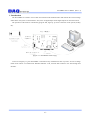
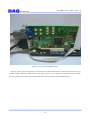
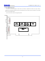
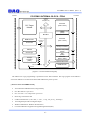
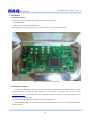
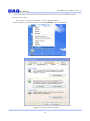
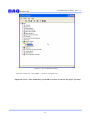
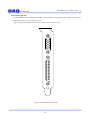
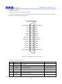
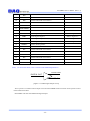
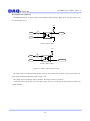
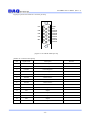
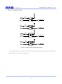
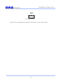
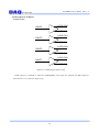
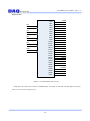
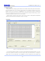
PCI-FRM01 User’s Manual (Rev 1.1) PCI-FRM01 User’s Manual Windows, Windows2000, Windows NT and Windows XP are trademarks of Microsoft. We acknowledge that the trademarks or service names of all other organizations mentioned in this document as their own property. Information is believed to be accurate and reliable. However, no responsibility is assumed for its use, nor for any infringements of patents or other rights of third parties which may result from its use. The information in this document is subject to change without notice and no part of this document may be copied or reproduced without the prior written consent. -1- PCI-FRM01 User’s Manual (Rev 1.1) -- Contents -1. Introduction 2. PCI-FRM01 Functions 3. Installation 3.1 Package contents 3.2 Installation Sequence 4. PCI-FRM01 Description 4.1 PCB Layout 4.2 Description of the functional blocks 4.3 Connector Pin-out 4.4 Description of LVDS I/O 5. Sample Program 5.1 FrmTest 6. Test 6.1 Image frame Test 6.2 UART Tx/Rx Test 6.3 DIO Input/Output Test Appendix A.1 General Specification A.2 Physical Dimension Reference -2- PCI-FRM01 User’s Manual (Rev 1.1) 1. Introduction The PCI-FRM01 is a board to receive data from Camera-Link standard camera and transmit the received image frame data to the system via PCI interface. And, it has 16 digital Inputs and 8 digital outputs for external controls. The operation of the board is controlled by program API, figure [1-1] shows connection of the system (usually PC). [Figure 1-1. PCI-FRM01 board Usage] As shown in Figure [1-1], the PCI-FRM01 is inserted into any available PCI slots in your PC. It receives Image Frame from camera via Camera-Link Standard Interface. And, received data transmit to the API through PCI interface. -3- PCI-FRM01 User’s Manual (Rev 1.1) [Figure 1-2. Picture of PCI-FRM01 board] Figure [1-2] shows physical connection of the board to the Camera-Link Camera. At the left side, there are 15 pin D-SUB connector and 26 pin MDR connector. The upper connector is for connection to external I/O device, and the bottom connector is for connection to Camera-link camera for frame data or UART communication. -4- PCI-FRM01 User’s Manual (Rev 1.1) 2. PCI-FRM01 Functions As shown in the following figure, main control of the board is performed in FPGA Core Logic. Primary functions are receiving the image frame data, transmitting/receiving UART data and controlling 16 bit digital inputs, and 8 bit digital outputs. You can control these functions using API provided. LVDS Interface UART Function PCI Core Logic (FPGA) -5- FPGA Program Logic Digital I/O PCI-FRM01 User’s Manual (Rev 1.1) PCI BUS PCI-FRM01 INTERNAL BLOCK - FPGA Local BUS Local Bus Address Data(Mem,I/O) Reserved (0x00 ? 0x5F) PCI Target / Master UART (0x60) BUS Mux Reserved (0x70 ? 0xAF) MEM Decoder To each IO Module IO Decoder Interrupt controller Camera Link(LVDS) (0xC0) DPRAM CLOCK syn. DIO (0xD0) Reserved (0xE0 ? 0xFF) Interrupt Controller (0xb0) Ext. Address, Data, Control MEM Decoder INT sources in Chip From Ext. [Figure 2-1. Functional Block Diagram] The FPGA Core Logic programming is performed via the JTAG interface. The logic program of the FPGA is saved in an EPLD. It is located on the board and loaded at the power-up time. [ Features of the PCI-FRM01 board] 32-bit PCI-Bus 33MHz Interface, Plug and Play PCI Bus Master Operation PCI 5V and 3.3V compatible operation. Receiving 14-bit Frame data UART communication (8 bit data, 1 start, 1 stop, No parity, 9600bps) 16-bit Digital Input and 8-bit Digital Output Windows 2000 SP4 or Windows XP SP1 above Convenient Windows Application Programming Interface(DLL) -6- PCI-FRM01 User’s Manual (Rev 1.1) 3. Installation 3.1 Package contents In addition to the user’s Manual, the package includes the following items. - PCI-FRM01 board - CDROM (drivers/manuals/API/Samples etc.) After unpacking, inspect the board carton to make sure there are no damages on the board. [Figure 3-1. PCI-FRM01 package contents] 3.2 Installation Sequence To install your PCI-FRM01 board in your PC, follow the steps described in the document “How to install PCI DAQ Board” provided by DAQ System. If the document is missing, you can get it from www.daqsystem.com. The PCI-FRM01 board is completely Plug & Play. There are no switches or jumpers to set. Therefore you can install it easily. - Your OS requirement : Windows 2000 SP4 or Windows XP SP1 above The PCI-FRM01 connects to PCI slot. After that you can show the below picture of “New Hardware Search Wizard” window. -7- PCI-FRM01 User’s Manual (Rev 1.1) Please check the system information after installation to make sure the success of installation, Do the following steps to check. My Computer -> Properties -> Hardware -> Device Manager Window Device manager shows the device name for example PCI-FRM01 at the “Other devices”. [Figure 3-2. Select “My computer”->”Properties”] [Figure 3-3. System Properties Window] -8- PCI-FRM01 User’s Manual (Rev 1.1) [Figure 3-4. Device Manager Window] The name of the device, “PCI-FRM01”, is shown in the Figure [3-4]. Important Notice : After installation, you should re-boot the system for the proper operation. -9- PCI-FRM01 User’s Manual (Rev 1.1) 4. Functions Description In this chapter, the primary functions of the PCI-FRM01 board are described briefly. For more information, refer to the device specification. 4.1 PCB Layout [Figure 4-1. PCI-FRM01 PCB Layout] The board has three LEDs to indicate the operation status. - LED1 turns on when the board receives the image frame data via Camera Link. - LED2 turns on when the board transmits the received data to your PC via PCI interface. - LED3 turns on when power is applied to the board and the initialization ends up. -10- PCI-FRM01 User’s Manual (Rev 1.1) 4.2 Description of the functional blocks (1) FPGA All of the board functions are controlled by the Logic program of the FPGA. (2) LVDS Receive Image frame through LVDS interface. UART signal Receive/Transmit through LVDS interface. Digital Output (3) Regulator This block is for supplying the power(3.3V) to the board. (4) Level Shifter It is protected a circuit that the voltage higher than 3.3V CMOS Logic is exchanged to normal 3.3V Logic Level. (5) EPLD It makes correct timing interface for the FPGA. -11- PCI-FRM01 User’s Manual (Rev 1.1) 4.3 Connector Pin-out The PCI-FRM01 board is equipped with MDR 26 Pin connector J1 for Camera Link connection and D-SUB 15 Pin connector P1 for external I/O connection. Figure [4-2] shows the bracket of the board where P1 and J1 connector exist. 15 5 10 14 4 9 13 3 8 12 2 7 11 1 6 26 13 25 12 24 11 23 10 22 9 21 8 20 7 19 6 18 5 17 4 16 3 15 2 14 1 [Figure 4-2. PCI-FRM01 Front View] -12- PCI-FRM01 User’s Manual (Rev 1.1) [J1(MDR26) connector] Figure4-3 shows the board’s J1 connector pin-map. All of the pin functions are based on the Camera link standard, so please refer to the Camera link standard document for more description and information. Frame Grabber Inner shield 26 13 Inner shield X0- 25 12 X0+ X1- 24 11 X1+ X2- 23 10 X2+ Xclk- 22 9 Xclk+ X3- 21 8 X3+ SerTC+ 20 7 SerTC- SerTFG- 19 6 SerTFG+ CH0+ 18 5 CH0- CH1+ 17 4 CH1- CH2+ 16 3 CH2- CH3+ 15 2 CH3- Inner shield 14 1 Inner shield [Figure 4-3. PCI-FRM01 J1 Connector Pin-out] [Table 1. J1 Connector Description] pin Signal Name Description Remark 1 Inner Shield 2 CH3- LVDS Digital output 3 - Refer to Figure 4-3 3 CH2- LVDS Digital output 2 - Refer to Figure 4-3 4 CH1- LVDS Digital output 1 - Refer to Figure 4-3 5 CH0- LVDS Digital output 0 - Refer to Figure 4-3 6 SerTFG+ Serial to Frame grabber + 7 SerTC- Cable shield Serial to Camera-13- PCI-FRM01 User’s Manual (Rev 1.1) 8 X3+ Camera link LVDS receive data3 + 9 Xclk+ Camera link LVDS receive clock + 10 X2+ Camera link LVDS receive data2 + 11 X1+ Camera link LVDS receive data1 + 12 X0+ Camera link LVDS receive data0 + 13 Inner Shield 14 Inner Shield 15 CH3+ LVDS Digital output 3+ Refer to Figure 4-3 16 CH2+ LVDS Digital output 2+ Refer to Figure 4-3 17 CH1+ LVDS Digital output 1+ Refer to Figure 4-3 18 CH0+ LVDS Digital output 0+ Refer to Figure 4-3 19 SerTFG- Serial to Frame grabber- 20 SerTC+ Serial to Camera+ 21 X3- Camera link LVDS receive data3- 22 Xclk- Camera link LVDS receive clock- 23 X2- Camera link LVDS receive data2- 24 X1- Camera link LVDS receive data1- 25 X0- Camera link LVDS receive data0- 26 Inner Shield (Note) For more information, refer to Camera Link Standard Specification. LVDS CHx+ DIGITAL OUT LVDS CHx[Figure 4-4. LVDS Digital Output circuit] Above picture is a Camera Control output circuit from PCI-FRM01 board to Camera for the specific control of the Camera-link Cable. PCI-FRM01 board has four differential digital outputs. -14- PCI-FRM01 User’s Manual (Rev 1.1) [Description of P1 connector] PCI-FRM01 Board has six photo-coupler isolated digital outputs and four digital inputs. The equivalent circuit is as shown figure [4-5]. VCC R COM To FPGA IN < Photo coupler input> VCC R OUTP OUTN From FPGA <Photo coupler output> [Figure 4-5. Photo-coupler In/Out Circuit] The input resistance is 680 ohms thus the flow current is about 5mA when 5V input or about 15mA when 12V power applied. Maximum operation input voltage is 12V. The output current is limited by output resistance, the output resistance is 10 ohms. Continuous output current has to be used under 10mA. The user can change the Input/Output resistance for special operation. -15- PCI-FRM01 User’s Manual (Rev 1.1) Figure [4-6] shows the board’s P1 connector pin-map. IN1 15 5 10 IN2 14 4 9 IN3 13 3 8 IN4 12 2 7 IN5 11 1 6 COM IN0 OUTN3 OUTP3 OUTN2 OUTP2 OUTN1 OUTP1 OUTN0 OUTP0 [Figure 4-6. P1 DSUB 15PIN pin-out] [Table2. P1 Connector Description] Pin Signal Name Description 1 OUTN0 OUT0 Negative 2 OUTN1 OUT1 Negative 3 OUTN2 OUT2 Negative 4 OUTN3 OUT3 Negative 5 COM Input common 6 OUTP0 OUT0 Positive 7 OUTP1 OUT1 Positive 8 OUTP2 OUT2 Positive 9 OUTP3 OUT3 Positive 10 IN0 Input0 11 IN5 Input5 12 IN4 Input4 13 IN3 Input3 14 IN2 Input2 15 IN1 Input1 -16- Remark PCI-FRM01 User’s Manual (Rev 1.1) [Photo-coupler Digital Input] VCC 680 COM DIN0 IN0 VCC 680 DIN1 IN1 VCC 680 DIN2 IN2 VCC 680 DIN3 IN3 VCC 680 DIN4 IN4 VCC 680 DIN5 IN5 [Figure 4-7. Photo-coupler isolated Input circuit] Photo-coupler input are connected to connector P1(DSUB 15Pin), each input are matched with DIO input bit position from 5 to 0 as shown in Figure [4-7]. -17- PCI-FRM01 User’s Manual (Rev 1.1) [Photo-coupler Digital Output] VCC 10 OUTP0 DOUT0 OUTN0 VCC 10 OUTP1 DOUT1 OUTN1 VCC 10 OUTP2 DOUT2 OUTN2 VCC 10 OUTP3 DOUT3 OUTN3 [Figure 4-8. Photo-coupler isolated Output Circuit] Photo-coupler output are connected to connector P1(DSUB 15PIN), each output are matched with DIO output bit position from 3 to 0 as shown in Figure [4-8]. -18- PCI-FRM01 User’s Manual (Rev 1.1) [Other Connectors] J5 2 1 J5 connector (Top View) The PCI-FRM01 board power is supplied through the PCI connector for the normal operation. However, the power will be supplied through the J6 connector in case of the board self-test or check the power. +5V is connected to pin number 1 and ground is connected to pin number 2. J3 2 4 6 1 3 5 J3 connector (Top View) J3 can be use for the board self-test or the production line, usually do not use at the normal operation. JP2 2 4 6 1 3 5 JP2 connector (Top View) JP2 can be use for the FPGA program up-grade, usually do not use at the normal operation. JP1 TMS 6 5 TDI TDO 4 3 TCK GND 2 1 VCC(+3.3V) JP1 connector (Top View) JP1 can be use for the FPGA functional test at the production line, usually do not use at the normal operation. -19- PCI-FRM01 User’s Manual (Rev 1.1) JP3 1 2 JP3 Jumper (Top View) Make JP3 short when upgrading FPGA program, usually do not use at the normal operation. -20- PCI-FRM01 User’s Manual (Rev 1.1) 4.4 Description of LVDS I/O [Output circuit] LVDS CH0+ DOUT4 LVDS CH0LVDS CH1+ DOUT5 LVDS CH1LVDS CH2+ DOUT6 LVDS CH2LVDS CH3+ DOUT7 LVDS CH3- [Figure 4-9. LVDS Digital Output Circuit] LVDS output are connected to connector J1(MDR26PIN), each output are matched with DIO output bit position from 7 to 4 as shown in Figure [4-9]. -21- PCI-FRM01 User’s Manual (Rev 1.1) [Input circuit] RX0 RX1 RX2 RX3 RX4 RX5 RX6 RX7 RX8 RX9 RX10 RX11 RX12 RX13 RX14 RX15 RX16 RX17 RX18 RX19 RX20 RX21 RX22 RX23 RX24 RX25 RX26 RX27 X0+ X0X1+ X1X2+ X2X3+ X3Xclk+ Xclk- IMG0 IMG1 IMG2 IMG3 IMG4 IMG7 IMG5 IMG8 IMG9 IMG10 DIN6 DIN7 IMG11 IMG12 IMG13 DIN8 DIN9 DIN10 DIN11 DIN12 DIN13 DIN14 DIN15 HSYNC VSYNC LDV IMG6 [Figure 4-10. LVDS Digital Input Circuit] LVDS input are connected to connector J1(MDR26PIN), each input are matched with DIO input bit position from 15 to 6 as shown in Figure [4-10]. -22- PCI-FRM01 User’s Manual (Rev 1.1) 5. Sample Program DAQ system provides a sample program to make the user be familiar with the board operation and to make the program development easier. You can find the sample program in the CDROM accompanying with the PCIFRM01 board. One of the execution file is “FrmTest.exe”. It stores the frame data to memory or hard-disk and displays it to hexadecimal values which can utilize necessary frame data to developers. Before using it, you have to install the PCI-FRM01 board and its drivers in your computer. Sample program is provided in source form in order to show the usage of API(Application Programming Interface) of the board and may be modified for customer’s own usage. 5.1 FrmTest [Figure 5-1. When Sample program “FrmTest.exe” is executed] To run the sample application program, you need to use API (Application Programming Interface). It is a form of client DLL (Dynamic Link Library). You need the Import Library files and header files for compiling the sample source. You can find them in the CDROM. To run the execution file, the API DLL file -23- PCI-FRM01 User’s Manual (Rev 1.1) (PCI_FRM01.DLL) must be located in the same directory with the execution file or Windows system folder. Another method is to add the directory of API DLL file to PATH environmental variable. 5.1.1 Functions related to image Frame (1) ‘DXD810/DXD1417’ Combo-box Use this box to set up the operation mode of the PCI-FRM01. (2) ‘LVDS Init’ button Press this button to initialize the function of receiving image frame data. It is performed only once after power is applied to the board. (3) ‘Start’ button Press this button to begin to save image data. (4) ‘FRAME Read’ button Press this button to read the image frame data of the PCI-FRM01 board to your PC. If image frame data is not saved on the board, you must wait until the end of data collection. (5) ‘LVDS Close’ button Press this button to finish usage of the board and terminate the program. (6) ‘Save to’ button Press this button to save the image frame data of PC to a file. 5.1.2 Functions related to UART (1) ‘Send Serial Data’ button Press this button to send the data in the editor box to UART. You can directly write the data in the editor box beside the button. (2) ‘Get Serial Data’ button Press this button to get the data on the general UART. (3) ‘Clear Serial Data’ button Press this button to clear the contents of the editor box. -24- PCI-FRM01 User’s Manual (Rev 1.1) (4) ‘Start Timer’ button Press this button to start the timer. The sample program will read the UART data periodically. The reading interval is around 0.1s. (5) ‘Stop Timer’ button Press this button to stop the timer. (6) ‘UART Init’ button Press this button to initialize UART. It must be performed only once after power is applied to the board. (7) ‘UART Close’ button Press this button to finish usage of the board and terminate the program. 5.1.3 Functions related to DIO (1) ‘DIO Read’ button Press this button to read the data on General Purpose I/O port. The reading data are recorded the editor box beside the button. (2) ‘DIO Write’ button Press this button to write the data on General Purpose I/O port. You can directly write the data in the editor box beside the button. -25- PCI-FRM01 User’s Manual (Rev 1.1) 6. Test 6.1 Receiving the image frame data In this chapter, the functional test will be explained to discriminate board mal-functions and for the user being familiar with the operation of the board. It is performed using the sample program “FrmTest.exe” on PC equipped with the PCI-FRM01 board. [Figure 6-1. Equipment Connection for Testing] Figure [6-1] shows connection of the equipments. Although the PCI-FRM01 is shown outside the PC in this figure, but actually it is located in a PCI slot inside the PC. The image frame data is generated in the Image Frame Simulator made by DAQ System. If you have real camera or a frame source, you can use it. At this connected state, turn the all power on and execute test program (“FrmTest.exe”) on the PC. Follow the steps to test the function of receiving image frame data. Step 1. : Press the ‘LVDS init” button to initialize the LVDS circuit and then press the “Start” button to save Image Frame data from Image Frame Simulator on the PCI-FRM01 board. Step 2 : Press the “Frame Read” button. Then data are displayed on the editor box. Compare the contents of the editor box with the data of the Image Frame Simulator. The comparison can be performed using the “Save to” button. It saves the contents of the editor box to a file. -26- PCI-FRM01 User’s Manual (Rev 1.1) 6.2 UART Tx/Rx Test At the above stage, make the image frame simulator to send UART data to PCI-FRM01 board periodically. Step 1 : Press the “UART init” button to initialize the UART and then press the “Start Timer” to get the UART data from the Image Frame Simulator. Then the gotten data are displayed on the editor box below the button. Compare the contents of the editor box with the data of the Image Frame Simulator. Step 2: Write the data to the editor box beside the “Send Serial Data” button and press the “Send Serial Data” button to send it to the Image Frame Simulator via the UART. Compare the data on the editor box with that of the Image Frame Simulator. 6.3 DIO Input/Output test Continue the test from the previous stage. Step 1 : After to make all the output port “1’’ using “DIO Write” function of the test program, check the output state using the oscilloscope. To check photo-coupler output, you have to prepare some external circuit. Step 2: Using “DIO read” function, read out each input state. To make some activation of the photo-coupler input , you need to prepare some external circuit. -27- PCI-FRM01 User’s Manual (Rev 1.1) Appendix A.1 General Specification Specification General Interface Functions PCI Local Bus Specification Revision 2.0 PCI 32bit 33Mhz interface PCI Target and Master operation Base Configuration Camera Link Interface +5V Single Power operation , Max 300mA Power consumption PCI +5V and 3.3V compatible operation 16 Digital Input (Dsub15 : Photo-coupler Input 6bit) 8 Digital Output (Dsub15 : Photo-coupler Output 4bit) 14bit Image Frame Acquisition Transmit Image Frame Data to PC One serial UART, 9600bps Tx/Rx Software Supported OS Windows 2000 SP4 above/ Windows XP SP1 above API Interface with Application through client DLL Sample Software Test Sample software for evaluation -28- PCI-FRM01 User’s Manual (Rev 1.1) A.2 Physical Dimension -29- PCI-FRM01 User’s Manual (Rev 1.1) References 1. Specification of Camera Link Interface Standard for Digital Cameras and Frame Grabbers -- Camera Link committee 2. PCI Local Bus Specification Revision2.1 -- PCI Special Interest Group 3. How to install PCI DAQ Board -- DAQ system 4. AN201 How to build application using API -- DAQ system 5. AN241 PCI-FRM01 Register Level Application Guide -- DAQ system 6. AN242 PCI-FRM01 API Programming -- DAQ system -30-