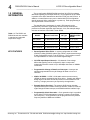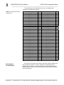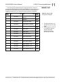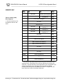
1
Series PMC-DX504/DX2004 Reconfigurable 32 LVDS I/O USER’S MANUAL ACROMAG INCORPORATED 30765 South Wixom Road P.O. BOX 437 Wixom, MI 48393-7037 U.S.A. Copyright 2004, Acromag, Inc., Printed in the USA. Data and specifications are subject to change without notice. Tel: (248) 624-1541 Fax: (248) 624-9234 8500-733-A04D000 2 DX504/DX2004 User’s Manual LVDS I/O Reconfigurable Board __________________________________________________________________ TABLE OF CONTENTS IMPORTANT SAFETY CONSIDERATIONS You must consider the possible negative effects of power, wiring, component, sensor, or software failure in the design of any type of control or monitoring system. This is very important where property loss or human life is involved. It is important that you perform satisfactory overall system design and it is agreed between you and Acromag, that this is your responsibility. 1.0 General Information The information of this manual may change without notice. Acromag makes no warranty of any kind with regard to this material, including, but not limited to, the implied warranties of merchantability and fitness for a particular purpose. Further, Acromag assumes no responsibility for any errors that may appear in this manual and makes no commitment to update, or keep current, the information contained in this manual. No part of this manual may be copied or reproduced in any form without the prior written consent of Acromag, Inc. KEY FEATURES…………...… … … … .… … …… … .. PCI INTERFACE FEATURES……...… … … … …… .. SIGNAL INTERFACE PRODUCTS..… … … …… … .. Board DLL Control Software...………………......... Board VxWORKS Software….………....…...……… Board QNX Software…......………….………........... 4 5 5 6 6 6 2.0 PREPARATION FOR USE UNPACKING AND INSPECTION...…………………... CARD CAGE CONSIDERATIONS.........…………….. BOARD CONFIGURATION..........................………... Default Hardware Configuration.……………… Front Panel I/O...………………………………….. Non-Isolation Considerations........................... 7 7 7 7 8 9 3.0 PROGRAMMING INFORMATION PCI CONFIGURATION ADDRESS SPACE.....……... Configuration registers....…………………..….. MEMORY MAP..............................................………... Flash Configuration..……................................. PCI bus to Xilinx Configuration..….................. Configuration Status Register.......................... Configuration Control Register........................ Configuration Data...........………………............ Flash Status1 Register...................................... Flash Status2 Register...................................... Flash Read……………....................................... Flash Reset……………....................................... Flash Start Write…………….……………........... Flash Erase Sector…………….…………........... Flash Erase Chip……………….…………........... Flash Data Register............……........................ Flash Address Register.................................... Reset Register............…………........................ Interrupt Status/Clear Digital I/O…….………… Data... Input/Output Registers…………………. Direction Control Register………………........... Interrupt Enable Registers..……………………. Interrupt Type Configuration Registers.......... Interrupt Polarity Registers..……..……………. 10 11 12 14 14 14 15 15 16 16 16 17 17 17 17 18 18 19 19 20 21 21 22 22 __________________________________________________________________________ Acromag, Inc. Tel:248-624-1541 Fax:248-624-9234 Email:[email protected] http://www.acromag.com DX504/DX2004 User’s Manual LVDS I/O Reconfigurable Board ___________________________________________________________________ DMA REGISTERS ........................................………... DMA Control Register.............……………......... DMA Transfer Size Registers.............……….... STATIC RAM MEMORY ...............................………... PCI9056 REGISTERS …..............................………... PCI9056 USERo CLOCK CONTROL …................…. 23 23 23 23 23 24 3 TABLE OF CONTENTS 4.0 THEORY OF OPERATION PCI INTERFACE LOGIC...…………………………….. NOT USED PCI9056 FUNCTIONS...…………...…….. LVDS INPUT/OUTPUT LOGIC…………………...…… SYNCHRONOUS SRAM…………………………..…… SERIAL EEPROM……..….………………………..…… CLOCK CONTROL……………………………………... 25 25 26 26 27 27 5.0 SERVICE AND REPAIR SERVICE AND REPAIR ASSISTANCE...…………... PRELIMINARY SERVICE PROCEDURE...………….. WHERE TO GET HELP………………………………… 28 28 28 6.0 SPECIFICATIONS PHYSICAL.................................................................. ENVIRONMENTAL....…….…………………………….. LVDS INPUT/OUTPUT............…………….......……... PCI LOCAL BUS INTERFACE...……………………… 29 29 31 31 APPENDIX CABLE: MODEL 5028-432......................................... 32 DRAWINGS 4501-996 BLOCK DIAGRAM..........………….…….... 4501-919 CABLE 5028-432 (SHIELDED).................. 33 34 Trademarks are the property of their respective owners. RELATED PUBLICATIONS The following manuals and part specifications provide the necessary information for in depth understanding of the DX board. Virtex II Data Book PCI 9056 Data Book IDT71V65603 Specification CY2305 Specification http://www.xilinx.com http://www.plxtech.com http://www.idt.com http://www.cypress.com __________________________________________________________________________ Acromag, Inc. Tel:248-624-1541 Fax:248-624-9234 Email:[email protected] http://www.acromag.com 4 DX504/DX2004 User’s Manual LVDS I/O Reconfigurable Board __________________________________________________________________ 1.0 GENERAL INFORMATION The re-configurable DX504/DX2004 board has 32 LVDS (low-voltage differential signaling) input/output channels. Re-configuration of the FPGA is possible via a direct download into the Xilinx FPGA over the PCI bus. In addition, on board flash memory can be loaded with FPGA configuration data for automatic Xilinx configuration on power-up. Flash programming is also implemented over the PCI bus. The data direction, input/output, for each LVDS channel can be independently controlled. Eight change-of-state interrupt channels are provided on the least significant eight channels. Also, the example design includes an interface to the 256K x 36-bit SRAM. Table 1.1: The DX502 and DX2002 boards are available in standard and extended temperature ranges KEY FEATURES MODEL Board Form Factor I/O Type OPERATING TEMPERATURE RANGE PMC DX504 PCI Mezzanine Card 32 LVDS 0°C to +70°C PMC DX2004 PCI Mezzanine Card 32 LVDS 0°C to +70°C PMC DX504E PCI Mezzanine Card 32 LVDS -40°C to +85°C PMC DX2004E PCI Mezzanine Card 32 LVDS -40°C to +85°C • Reconfigurable Xilinx FPGA – In system configuration of a 500K (DX504) or 2Meg (DX2004) system gate FPGA is implemented through a flash configuration device or via the PCI bus. This provides a means for implementation of custom user defined digital designs. • 32 LVDS Input/Output Channels – 32 channels of low-voltage differential signaling can be configured for input or output with independent direction control at up to 200 Mbps data rates or 100MHz Clock rates. • Programmable Change of State/Level Interrupts – Interrupts are software programmable for any bit Change-Of-State or level on 8 channels. • 256K x 36 SRAM – A 256K x 36-bit static random access memory (SRAM) is directly accessed by the Xilinx device. Custom user defined design logic for the Xilinx FPGA will permit use of the SRAM as FIFO memory, or single port memory as required by the application. • Example Design Provided – The example VHDL design includes implementation of the PCI9056 Local bus interface, control of LVDS I/O, eight Change-Of-State interrupts, and SRAM read/write interface logic. • Programmable Clock Generation – Clock generation logic is provided by the Xilinx FPGA for applications requiring a custom user specified clock frequency. Clock generation can be programmed to any desired frequency between 10MHz and 100MHz. __________________________________________________________________________ Acromag, Inc. Tel:248-624-1541 Fax:248-624-9234 Email:[email protected] http://www.acromag.com DX504/DX2004 User’s Manual LVDS I/O Reconfigurable Board ___________________________________________________________________ • Power Up and System Reset is Failsafe – For safety, the LVDS channels are configured for input upon power-up. • PCI Bus Master – The PCI9056 PCI interface chip becomes the bus master to perform DMA transfers. • DMA Operation – The PCI9056 supports two independent DMA channels capable of transferring data from the PCI to Local bus and Local to PCI bus. The example design implements DMA block and demand modes of operation. • Field Connections – All digital I/O, and power connections are made through a single 68-pin SCSI front panel I/O connector. • 32, 16, 8-bit I/O - Register Read/Write is performed through data transfer cycles in the PCI memory space. All registers can be accessed via 32, 16, or 8-bit data transfers. • Compatibility – Complies with PCI Local Bus Specification Revision 2.2. Provides one multifunction interrupt. Board is 5V or 3.3V signaling compliant. The voltage provided on PCI connector VIO pins determines the operating voltage of the PCI bus. • Supply Voltage Requirement – The board requires that 3.3 volts external power be provided on the 3.3 volt signal lines of the PCI bus connector. The board I/O is accessed via a 68 pin SCSI front panel connector. A cable is available to interface with this board. Cable: Model 5028-432: A 2-meter, round 68 conductor shielded cable with a male SCSI-3 connector at both ends and 34 twisted pairs. The cable is used for connecting the board to a SCSI-3 destination. For optimum performance, use the shortest possible length of shielded cable. 5 PCI INTERFACE FEATURES SIGNAL INTERFACE PRODUCTS See the Appendix for further information on these products. __________________________________________________________________________ Acromag, Inc. Tel:248-624-1541 Fax:248-624-9234 Email:[email protected] http://www.acromag.com 6 DX504/DX2004 User’s Manual LVDS I/O Reconfigurable Board __________________________________________________________________ ENGINEERING DESIGN KIT Acromag provides an engineering design kit for the DX boards (sold separately), a “must buy” for first time DX module purchasers. The design kit (model PMC-DX-EDK) provides the user with the basic information required to develop a custom FPGA program for download to the Xilinx FPGA. The design kit includes a CD containing: schematics, parts list, part location drawing, example VHDL source, and other utility files. The DX modules are intended for users fluent in the use of Xilinx FPGA design tools. BOARD DLL CONTROL SOFTWARE Acromag provides a software product (sold separately) to facilitate the development of Windows (98/Me/2000/XP) applications accessing Acromag PMC I/O board products, PCI I/O Cards, and CompactPCI I/O Cards. This software (Model PCISW-API-WIN) consists of low-level drivers and Windows 32 Dynamic Link Libraries (DLLs) that are compatible with a number of programming environments including Visual C++, Visual Basic, Borland C++ Builder and others. The DLL functions provide a high-level interface to boards eliminating the need to perform low-level reads/writes of registers, and the writing of interrupt handlers. BOARD VxWORKS SOFTWARE Acromag provides a software product (sold separately) consisting of board VxWorks software. This software (Model PMCSW-API-VXW) is composed of VxWorks (real time operating system) libraries for all Acromag PMC I/O board products, PCI I/O Cards, and CompactPCI I/O Cards. The software is implemented as a library of “C” functions which link with existing user code to make possible simple control of all Acromag PCI boards. BOARD QNX SOFTWARE Acromag provides a software product (sold separately) consisting of board QNX software. This software (Model PMCSW-API-QNX) is composed of QNX (real time operating system) libraries for all Acromag PMC I/O board products, PCI I/O cards, and CompactPCI I/O cards. The software supports X86 PCI bus only and is implemented as library of “C” functions which link with existing user code to make possible simple control of all Acromag PCI boards. __________________________________________________________________________ Acromag, Inc. Tel:248-624-1541 Fax:248-624-9234 Email:[email protected] http://www.acromag.com DX504/DX2004 User’s Manual LVDS I/O Reconfigurable Board ___________________________________________________________________ Upon receipt of this product, inspect the shipping carton for evidence of mishandling during transit. If the shipping carton is badly damaged or water stained, request that the carrier's agent be present when the carton is opened. If the carrier's agent is absent when the carton is opened and the contents of the carton are damaged, keep the carton and packing material for the agent's inspection. 7 2.0 PREPARATION FOR USE UNPACKING AND INSPECTION For repairs to a product damaged in shipment, refer to the Acromag Service Policy to obtain return instructions. It is suggested that salvageable shipping cartons and packing material be saved for future use in the event the product must be shipped. This board is physically protected with packing material and electrically protected with an anti-static bag during shipment. However, it is recommended that the board be visually inspected for evidence of mishandling prior to applying power. Refer to the specifications for loading and power requirements. Be sure that the system power supplies are able to accommodate the power requirements of the system boards, plus the installed Acromag board, within the voltage tolerances specified. WARNING: This board utilizes static sensitive components and should only be handled at a static-safe workstation. CARD CAGE CONSIDERATIONS Adequate air circulation must be provided to prevent a temperature rise above the maximum operating temperature and to prolong the life of the electronics. If the installation is in an industrial environment and the board is exposed to environmental air, careful consideration should be given to airfiltering. IMPORTANT: Adequate air circulation must be provided to prevent a temperature rise above the maximum operating temperature. Remove power from the system before installing board, cables, termination panels, and field wiring. BOARD CONFIGURATION The board may be configured differently, depending on the application. When the board is shipped from the factory, it is configured as follows: • The default configuration of the programmable software control register bits at power-up are described in section 3. • The control registers must be programmed to the desired configuration before starting data input or output operation. Default Hardware Configuration The front panel connector provides the field I/O interface connections. It is a SCSI-3 68-pin female connector (AMP 787082-7 or equivalent) employing latch blocks and 30 micron gold in the mating area (per MIL-G45204, Type II, Grade C). Connects to SCSI-3 destination from the front panel via round shielded cable (Model 5028-432). Front Panel Field I/O Connector __________________________________________________________________________ Acromag, Inc. Tel:248-624-1541 Fax:248-624-9234 Email:[email protected] http://www.acromag.com 8 DX504/DX2004 User’s Manual LVDS I/O Reconfigurable Board __________________________________________________________________ The data direction of LVDS channels 0 to 31 are independently controlled via the Direction Register. Table 2.1: Board Field I/O Pin Connections Non-Isolation Considerations Pin Description LVDS Ch0+ LVDS Ch1+ LVDS Ch2+ LVDS Ch3+ LVDS Ch4+ LVDS Ch5+ LVDS Ch6+ LVDS Ch7+ LVDS Ch8+ LVDS Ch9+ LVDS Ch10+ COMMON LVDS Ch11+ LVDS Ch12+ LVDS Ch13+ LVDS Ch14+ LVDS Ch15+ LVDS Ch16+ LVDS Ch17+ LVDS Ch18+ LVDS Ch19+ LVDS Ch20+ COMMON LVDS Ch21+ LVDS Ch22+ LVDS Ch23+ LVDS Ch24+ LVDS Ch25+ LVDS Ch26+ LVDS Ch27+ LVDS Ch28+ LVDS Ch29+ LVDS Ch30+ LVDS Ch31+ Pin 1 2 3 4 5 6 7 8 9 10 11 12 13 14 15 16 17 18 19 20 21 22 23 24 25 26 27 28 29 30 31 32 33 34 Pin Description LVDS Ch0LVDS Ch1LVDS Ch2LVDS Ch3LVDS Ch4LVDS Ch5LVDS Ch6LVDS Ch7LVDS Ch8LVDS Ch9LVDS Ch10COMMON LVDS Ch11LVDS Ch12LVDS Ch13LVDS Ch14LVDS Ch15LVDS Ch16LVDS Ch17LVDS Ch18LVDS Ch19LVDS Ch20COMMON LVDS Ch21LVDS Ch22LVDS Ch23LVDS Ch24LVDS Ch25LVDS Ch26LVDS Ch27LVDS Ch28LVDS Ch29LVDS Ch30LVDS Ch31- Pin 35 36 37 38 39 40 41 42 43 44 45 46 47 48 49 50 51 52 53 54 55 56 57 58 59 60 61 62 63 64 65 66 67 68 The board is non-isolated, since there is electrical continuity between the logic and field I/O grounds. As such, the field I/O connections are not isolated from the system. Care should be taken in designing installations without isolation to avoid noise pickup and ground loops caused by multiple ground connections. __________________________________________________________________________ Acromag, Inc. Tel:248-624-1541 Fax:248-624-9234 Email:[email protected] http://www.acromag.com DX504/DX2004 User’s Manual LVDS I/O Reconfigurable Board ___________________________________________________________________ This Section provides the specific information necessary to program and operate the board. This board is a PCI Specification version 2.2 compliant PCI bus master/target board. 9 3.0 PROGRAMMING INFORMATION The PCI bus is defined to address three distinct address spaces: I/O, memory, and configuration space. This board can be accessed via the PCI bus I/O, memory, and configuration spaces. The card’s configuration registers are initialized by system software at power-up to configure the card. The board is a Plug-and-Play PCI card. As a Plug-and-Play card the board’s base address and system interrupt request line are not selected via jumpers but are assigned by system software upon power-up via the configuration registers. A PCI bus configuration access is used to read/write the PCI card’s configuration registers. When the computer is first powered-up, the computer’s system configuration software scans the PCI bus to determine what PCI devices are present. The software also determines the configuration requirements of the PCI card. PCI Configuration Address Space The system software accesses the configuration registers to determine how many blocks of memory space the module requires. It then programs the board’s configuration registers with the unique memory base address. The configuration registers are also used to indicate that the board requires an interrupt request line. The system software then programs the configuration registers with the interrupt request line assigned to the board. Since this board is relocatable and not fixed in address space, its device driver must use the mapping information stored in the board’s Configuration Space registers to determine where the board is mapped in memory space and which interrupt line will be used. __________________________________________________________________________ Acromag, Inc. Tel:248-624-1541 Fax:248-624-9234 Email:[email protected] http://www.acromag.com 10 DX504/DX2004 User’s Manual LVDS I/O Reconfigurable Board __________________________________________________________________ CONFIGURATION REGISTERS The PCI specification requires software driven initialization and configuration via the Configuration Address space. This board provides 512 bytes of configuration registers for this purpose. It contains the configuration registers, shown in Table 3.1, to facilitate Plug-and-Play compatibility. The Configuration Registers are accessed via the Configuration Address and Data Ports. The most important Configuration Registers are the Base Address Registers and the Interrupt Line Register which must be read to determine the base address assigned to the board and the interrupt request line that goes active on a board interrupt request. Reg. Num. 0 Table 3.1 Configuration Registers 1 2 3 4 5 6 7 : 10 11 12 13,14 15 D31 D24 D23 D16 Device ID = 0504(DX504) 2004 (DX2004) D15 D8 D7 D0 Vendor ID= 16D5 Status Command Class Code=118000 Rev ID=00 BIST Header Latency Cache 32-bit Memory Base Address for Memory Accesses to Local, Runtime, DMA, and Messaging Queue Registers (PCIBAR0) PCI Base Address for I/O Accesses to Local, Runtime, DMA, and Messaging Queue Registers (PCIBAR1) 32-bit Memory Base Address for Memory Accesses to Local Address Space 0, 2M Space, FPGA Space (PCIBAR2) Not Used Subsystem ID= 0504 (DX504) Subsystem Vendor ID=16D5 2004 (DX2004) Max_Lat Not Used Reserved Min_Gnt Inter. Pin Inter. Line This board is allocated memory space address (PCIBAR0) to access the PCI9056 runtime, DMA, and messaging queue registers. The PCI9056 decodes 512 bytes for these memory space registers. These registers can also be accessed by an I/O cycle, with the PCI bus address matching the I/O Base Address (PCIBAR1). In addition, this board is allocated a 2M byte block of memory (PCIBAR2) that is addressable in the PCI bus memory space to control the board’s multiple functions included in the virtex II FPGA. __________________________________________________________________________ Acromag, Inc. Tel:248-624-1541 Fax:248-624-9234 Email:[email protected] http://www.acromag.com DX504/DX2004 User’s Manual LVDS I/O Reconfigurable Board ___________________________________________________________________ The memory space address map for the board is shown in Table 3.2. Note that the base address for the board (PCIBAR2) in memory space must be added to the addresses shown to properly access the board registers. Register accesses as 32, 16, and 8-bit in memory space are permitted. Base Addr+ 0003 D31 D08 D07 D00 Configuration Status Register Configuration Control Register Base Addr+ Not Used 1 0803 Not Used 1 1003 Not Used 1 Configuration Data 1000 2003 Not Used 1 Flash Status 1 Register 2000 2803 Not Used 1 Flash Status 2 Register 2800 3803 Not Used 1 Flash Read 3800 4003 Not Used 1 Flash Reset 4000 4803 Not Used 1 Flash Start Write 4800 5003 Not Used 1 Flash Erase Sector 5000 5803 Not Used 1 Flash Erase Chip 5800 6003 Not Used 1 Flash Data Register 6000 6803 Not Used 1 Flash Address 7->0 6800 7003 Not Used 1 Flash Address 15->8 7000 7803 Not Used 1 Flash Address 20->16 7800 11 MEMORY MAP Table 3.2: Memory Map Configuration Registers 0000 0800 1. The board will return 0 for all addresses that are "Not Used". 2. Address space 0->7FFF is not contiguous because the least significant address lines are not decoded by the CPLD __________________________________________________________________________ Acromag, Inc. Tel:248-624-1541 Fax:248-624-9234 Email:[email protected] http://www.acromag.com 12 DX504/DX2004 User’s Manual LVDS I/O Reconfigurable Board __________________________________________________________________ MEMORY MAP Base Addr+ 8003 8007 Table 3.2: Memory Map Xilinx Registers 1. The board will return 0 for all addresses that are "Not Used". D31 D16 D15 D00 Base Addr+ Not Used 1 Software Reset Register 8000 Not Used 1 Interrupt Status/Clear 7-0 Digital I/O 8004 800B 31-0 LVDS I/O Register 800F Not Used 8013 8017 801B 801F 1 Direction Register Channels 31-0 1 Interrupt Enable Not Used Channels 7-0 1 Interrupt Type Not Used Channels 7-0 1 Interrupt Polarity Not Used Channels 7-0 8008 800C 8010 8014 8018 801C 8023 Not Used 1 8027 Not Used 1 802B DMA Control Register 8028 802F DMA Transfer Size Channel 0 802C 8033 DMA Transfer Size Channel 1 8030 8037 Not Used 1 8020 8024 8034 ↓ FFFFF 100003 Not Used 1 Static RAM Memory FFFFC 100000 ↓ 1FFFFF Static RAM Memory 1FFFFC This memory map reflects byte accesses using the “Little Endian” byte ordering format. Little Endian uses even-byte addresses to store the loworder byte. The Intel x86 family of microprocessors uses “Little Endian” byte ordering. Big Endian is the convention used in the Motorola 68000 microprocessor family and is the VMEbus convention. In Big Endian, the lower-order byte is stored at odd-byte addresses. __________________________________________________________________________ Acromag, Inc. Tel:248-624-1541 Fax:248-624-9234 Email:[email protected] http://www.acromag.com DX504/DX2004 User’s Manual LVDS I/O Reconfigurable Board ___________________________________________________________________ The DX board uses a flash configuration device to store programming information for the Xilinx FPGA. The flash configuration device and FPGA are hardwired together so that during power-up the contents of the configuration device are downloaded to the FPGA. The flash configuration data can be reprogrammed using the PCI bus interface. The following is the general procedure for reprogramming the flash memory and reconfiguration of the Xilinx FPGA: 13 Flash Configuration 1) Disable auto-configuration by setting bit-0 (Stop Configuration) of the Configuration Control register to logic high. 2) Clear the Xilinx of its previous configuration by setting the Configuration Control register bit-2 to logic high. Software must also keep bit-0 set to a logic high. 3) Read INIT as logic high (Bit-1 of Configuration Status register) before programming is initiated. This can take up to 3.7m seconds for the Xilinx XC2V500 FPGA and 5.82m seconds for the Xilinx XC2V2000 FPGA. 4) Verify Flash Chip is not busy by reading bit-7 as logic 0 of the Flash Status 2 register at base address plus 2800H before starting a new Flash operation. 5) Erase the current flash contents by setting bit-0 of the Flash Erase Chip register to logic high. The Flash Erase Chip operation will take 14 seconds to complete. 6) Verify Flash Chip is not busy by reading bit-7 as logic 0 of the Flash Status 2 register at base address plus 2800H before going to the next step. 7) Download the Configuration file to the flash configuration chip via the PCI bus. i) Write the byte to be sent to the Flash Data register at base address plus 6000H. ii) Write the address of the Flash Chip to receive the new data byte to the Flash Address registers at base address plus 6800H, 7000H, and 7800H. Issue of a Flash Start Write will automatically increment this address after the issued Flash Write has completed. Thus, the address will not need to be set prior to issue of the next Flash Start Write. The first byte of the configuration file should be written to address 0 of the Flash Chip. The Flash Start Write operation will take 9µ seconds to complete. iii) Issue a Flash Start Write command to the Flash Chip by writing logic 1 to bit-0 of base address plus 4800H. iv) Verify the Flash Chip is not busy by reading bit-7 as logic 0 of the Flash Status 2 register at base address plus 2800H before going back to step i to write the next byte. 8) Enable auto-configuration by setting bit-0 (Stop Configuration) of the Configuration Control register to logic low. 9) Verify configuration complete by reading DONE (bit-0 of Configuration Status Register) as logic high. The auto-configuration process of moving Flash data to the Xilinx FPGA will take 0.16 seconds for the Xilinx XC2V500 and 0.45 seconds for the Xilinx XC2V2000 FPGA. 10) Thereafter, at power-up the configuration file will automatically be loaded into the FPGA. __________________________________________________________________________ Acromag, Inc. Tel:248-624-1541 Fax:248-624-9234 Email:[email protected] http://www.acromag.com 14 DX504/DX2004 User’s Manual LVDS I/O Reconfigurable Board __________________________________________________________________ Direct PCI bus to Xilinx Configuration Configuration of the Xilinx FPGA can be implemented directly from the PCI bus. The following is the general procedure for re-configuration of the Xilinx FPGA via the PCI bus: 1) Disable auto-configuration by setting bit-0 (Stop Configuration) of the Configuration Control register to logic high. 2) Clear the Xilinx of its previous configuration by setting the Configuration Control register bit-2 to logic high. 3) Read INIT as logic high (Bit-1 of Configuration Status register) before programming is initiated. This can take up to 3.7m seconds for the Xilinx XC2V500 FPGA and 5.82m seconds for the Xilinx XC2V2000 FPGA. 4) Download the Configuration file directly to the Xilinx FPGA by writing to the Configuration Data register. The entire configuration file must be written to the Xilinx FPGA one byte at a time to the Configuration Data register at base address plus 1000H. 5) Verify configuration complete by reading DONE (bit-0 of Configuration Status Register) as logic high. DONE is expected to be logic high immediately after the last byte of the configuration file is written to the Xilinx FPGA. 6) At power-up the configuration file will need to be reloaded into the FPGA. Configuration Status Register (Read Only) – (PCIBAR2 + 0000H) This read only register reflects the status of configuration complete and Xilinx configuration clear. This Configuration Status register is read at base address plus 0H. Configuration Status Register Bit(s) 0 1 FUNCTION DONE: 0 Xilinx FPGA is not configured 1 Xilinx FPGA configuration is complete INIT: INIT is held low until the Xilinx is clear of its current 0 configuration 1 2 to 7 INIT transitions high when the clearing of the Xilinx current configuration is complete Not Used (bits are read as logic “0”) __________________________________________________________________________ Acromag, Inc. Tel:248-624-1541 Fax:248-624-9234 Email:[email protected] http://www.acromag.com DX504/DX2004 User’s Manual LVDS I/O Reconfigurable Board ___________________________________________________________________ Configuration Control Register (Read/Write Only) – (PCIBAR2 + 0800H) 15 CONFIGURATION CONTROL REGISTERS This read/write register is used to stop Xilinx configuration, clear Xilinx configuration memory, and set Local Bus Hold control. This Configuration Control register is accessed at base address plus 0800H. Bit(s) 0 1 2 3 to 6 7 FUNCTION Stop Xilinx Configuration: 0 Enable Xilinx FPGA configuration 1 Stop Xilinx FPGA configuration Not Used (bit is read as logic “0”) Clear Current Xilinx Configuration: 0 Logic low has no effect. 1 Logic high resets the Xilinx configuration logic. Reconfiguration can begin after INIT transitions high. Configuration Control Register Not Used (bits are read as logic “0”) Local Bus Hold Control 0 CPLD controls generation of Local Hold Acknowledge. The CPLD logic will always grant control of the local bus to the PCI9056 device. 1 Xilinx FPGA controls generation of the Local Hold Acknowledge signal. Configuration Data (Write Only) – (PCIBAR2 + 1000H) This write only register is used to write Xilinx configuration data directly to the Xilinx FPGA from the PCI bus. This Configuration Data register is accessed at base address plus 1000H. The entire configuration file must be written to the Xilinx FPGA one byte at a time. Configuration complete is verified by reading DONE (bit-0 of Configuration Status Register) as logic high. A write to this Configuration Data register while auto-configuration from Flash is active will cause the Xilinx configuration to fail. Auto-configuration is stopped by writing logic 1 to bit-0 of the Configuration Control register at base address plus 800H. The Xilinx FPGA should also be cleared of its current configuration prior to loading of a new configuration file. The FPGA is cleared of its current configuration by writing logic 1 to bit-2 at address plus 800H. __________________________________________________________________________ Acromag, Inc. Tel:248-624-1541 Fax:248-624-9234 Email:[email protected] http://www.acromag.com 16 DX504/DX2004 User’s Manual LVDS I/O Reconfigurable Board __________________________________________________________________ FLASH CONTROL REGISTERS Flash Status 1 Register Flash Status 1 (Read Only) – (PCIBAR2 + 2000H) This read only register is used to read the DQ5 and DQ3 status of the flash chip. A Flash Status 1 register is at base address plus 2000H. Bit(s) 0 to 4 5 FUNCTION Not Used (bits are read as logic “1 or 0”) DQ5: 0 Chip enabled for reading array data. The system must issue the Flash Reset command to re-enable the device for reading array data if DQ5 goes high. DQ5 can go high during a Flash Start Write, Flash Erase Chip, or Flash Erase Sector operation. Not Used (bits are read as logic “1 or 0”) 1 6 and 7 Flash Status 2 (Read Only) – (PCIBAR2 + 2800H) This read only register is used to read the ready or busy status of the flash chip. A Flash Status 2 register is at base address plus 2800H. The system must first verify that that Flash Chip is not busy before executing a new Flash command. The Flash Chip is busy if bit-7 of this register is set to logic 1. The Flash will always be Busy while bit-0 of the Configuration Control register is set to logic “0”. Flash Status 2 Register Bit(s) 0 to 6 7 FUNCTION Not Used (bits are read as logic “0”) Busy / Ready~ Set bit-0 of the Configuration Control register to logic “1” before monitoring this busy bit. 0 1 Flash Chip is Ready Flash Chip is Busy Flash Read (Read Only) – (PCIBAR2 + 3800H) A Flash Read command is executed by reading this register at base address plus 3800H. Prior to issue of a Flash Read the Flash Address registers must be set with the desired address to be read. See the Flash Address registers at base address plus 6800H, 7000H, and 7800H. The system must issue the Flash Reset command to re-enable the device for reading array data if DQ5 goes high. DQ5 can go high during a Flash Start Write, Flash Erase Chip, or Flash Erase Sector operation. DQ5 can be monitored via the Flash Status 1 register at base address plus 2000H. Flash Reset (Write Only) – (PCIBAR2 + 4000H) This write only register is used to initiate a reset of the flash chip. A Flash Reset command is executed by writing logic 1 to bit-0 of this register at base address plus 4000H. Writing the flash reset command resets the chip to reading data mode. Once an erase or programming operation begins, the chip ignores reset commands until the operation is complete. __________________________________________________________________________ Acromag, Inc. Tel:248-624-1541 Fax:248-624-9234 Email:[email protected] http://www.acromag.com DX504/DX2004 User’s Manual LVDS I/O Reconfigurable Board ___________________________________________________________________ Flash Start Write (Write Only) – (PCIBAR2 + 4800H) 17 FLASH CONTROL REGISTERS This write only register is used to initiate the write of a byte to the flash chip. A Flash Start Write command is executed by writing logic 1 to bit-0 of this register at base address plus 4800H. Prior to issue of a Flash Start Write the Flash Data and Address registers must be set with the desired data and address to be written. See the Flash Data and Address registers at base address plus 6000H, 6800H, 7000H, and 7800H. Flash Erase Sector (Write Only) – (PCIBAR2 + 5000H) A Flash Erase Sector command is executed by writing logic 1 to bit-0 of this register at base address plus 5000H. Verify that the Flash Chip is not busy from a previous operation before beginning a new operation. This is accomplished by reading bit-0 as logic 1 of the Flash Status 2 register. There are 32 flash sectors, which are addressed via the most significant five flash address lines. The most significant five flash address lines are set via the Flash Address 23-16 register at base address plus 7800H. Issue of a Flash Erase Sector command will erase the contents of the flash chip only in the sector specified. A flash bit cannot be programmed from logic 0 back to logic 1. Only an erase chip operation can convert logic 0 back to logic 1. Prior to reprogramming of the flash chip a Flash Erase Chip or Flash Erase Sector command must be performed. The Flash Erase Chip operation will take 14 seconds to complete. The system can determine the status of the erase operation by reading the Flash Ready/Busy status. Bit-0 of the Flash Status 2 register, at base address plus 2800H, will read as logic 0 when chip erase is completed. Any other flash commands written to the flash chip during execution of the flash erase sector operation are ignored. Note that a hardware reset during the erase sector operation will immediately terminate the operation. Flash Erase Chip (Write Only) – (PCIBAR2 + 5800H) This write only register is used to erase the entire contents of the flash chip. A flash bit cannot be programmed from logic 0 back to logic 1. Only an erase chip operation can convert logic 0 back to logic 1. Prior to reprogramming of the flash chip a Flash Erase Chip command must be performed. A Flash Erase Chip command is executed by writing logic 1 to bit-0 of this register at base address plus 5800H. Verify that the Flash Chip is not busy from a previous operation before beginning a new operation. This is implemented by reading bit-0 as logic 1 of the Flash Status 2 register. The Flash Erase Chip operation will take 14 seconds to complete. The system can determine the status of the erase operation by reading the Flash Ready/Busy status. Bit-0 of the Flash Status 2 register, at base address plus 2800H, will read as logic 0 when chip erase is completed. __________________________________________________________________________ Acromag, Inc. Tel:248-624-1541 Fax:248-624-9234 Email:[email protected] http://www.acromag.com 18 DX504/DX2004 User’s Manual LVDS I/O Reconfigurable Board __________________________________________________________________ FLASH REGISTERS Any other flash commands written to the flash chip during execution of the flash erase chip operation will be ignored. Note that a hardware reset during the chip erase operation will immediately terminate the operation. Flash Data Register (Write Only) – (PCIBAR2 + 6000H) This write only register holds the data byte which is sent to the flash chip upon issue of a Flash Start Write command. Bits 3 to 0 of this register can be read. Flash Address 7->0 (Write Only) – (PCIBAR2 + 6800H) This write only register holds the least significant byte of the address to which the flash chip is written upon issue of a Flash Start Write command. Flash Address 15->8 (Write Only) – (PCIBAR2 + 7000H) This write only register sets bits 15 to 8 of the address to which the flash chip is written upon issue of a Flash Start Write command. Flash Address 20->16 (Write Only) – (PCIBAR2 + 7800H) This write only register sets bits 20 to 16 of the address to which the flash chip is written upon issue of a Flash Start Write command. The most significant 3 bits of this register are not used. __________________________________________________________________________ Acromag, Inc. Tel:248-624-1541 Fax:248-624-9234 Email:[email protected] http://www.acromag.com DX504/DX2004 User’s Manual LVDS I/O Reconfigurable Board ___________________________________________________________________ Reset Register (Write Only) – (PCIBAR2 + 8000H) 19 RESET REGISTER This write only register is used to issue a software reset. Bit-15 when set to logic “1” will issue a software Xilinx FPGA. This register can be read or written with either 8-bit, 16-bit, or 32-bit data transfers. Interrupt Status/Clear (Read/Write) – (PCIBAR2 + 8004H) FPGA INTERRUPT REGISTERS This read/write register is used to determine the pending status of I/O interrupts and release pending I/O interrupts. The I interrupt status/clear registers reflect the status of each of the I/O channels. Read of this bit reflects the interrupt pending status. Read of a “1” indicates that an interrupt is pending for the corresponding channel. Write of a logic “1” to this bit to release the corresponding channel’s pending interrupt. Writing “0” to a bit location has no effect, a pending interrupt will remain pending. Channel 0 interrupt status is identified via data bit-0 while I/O channel 7 status is identified via data bit-7 at base address plus 8004H. BIT 0 1 2 3 4 5 6 7 8-31 FUNCTION Channel 0 Interrupt Pending/Clear Channel 1 Interrupt Pending/Clear Channel 2 Interrupt Pending/Clear Channel 3 Interrupt Pending/Clear Channel 4 Interrupt Pending/Clear Channel 5 Interrupt Pending/Clear Channel 6 Interrupt Pending/Clear Channel 7 Interrupt Pending/Clear 1 Not Used Table 3.3: Board Interrupt Status/Clear 1. All bits labeled “Not Used” will return logic “0” when read. Interrupts must be enabled via the PCI9056 control registers and the Interrupt Enable register at base address + offset 8014H, in order to generate interrupts. The PCI9056 Interrupt Control/Status register at PCIBAR0 base address + offset 68H must have bits 8 and 11 set to a logic high in order for interrupts to occur. DMA interrupts must be enabled and controlled through the PCI9056 registers. The PCI9056 Interrupt Control/Status register at PCIBAR0 base address + offset 68H must have bits 18 and 19 set to a logic high in order for DMA interrupts to occur on DMA channels 0 and 1, respectively. DMA INTERRUPT REGISTERS DMA transfers are configured and controlled via PCI9056 DMA registers. The PCI9056 DMA registers are at PCIBAR0 base address + offset 80H to B8H. These registers control the transfer direction, size, source address, and destination address for DMA channels 0 and 1. __________________________________________________________________________ Acromag, Inc. Tel:248-624-1541 Fax:248-624-9234 Email:[email protected] http://www.acromag.com 20 DX504/DX2004 User’s Manual LVDS I/O Reconfigurable Board __________________________________________________________________ DIGITAL INPUT/OUTPUT REGISTERS LVDS Input/Output Registers (Read/Write) – (PCIBAR2 + 8008H) Thirty two LVDS channels numbered 0 through 31 may be individually accessed via this register. Channels 0 to 31 are accessed at the carrier base address +8008H via data bits 0 to 31. Each channel is controlled by its corresponding data bit, as shown below. Channel input signal levels are determined by reading this register. Likewise, channel output signal levels are set by writing to this register. Note that the data direction, input or output, must first be set via the Direction register at base address plus 8010H. Ch 7 D7 LVDS I/O Channel and Corresponding Register Bits Ch 6 Ch 5 Ch 4 Ch 3 Ch 2 Ch 1 D6 D5 D4 D3 D2 D1 Ch 0 D0 Ch 15 D15 Ch 14 D14 Ch 13 D13 Ch 12 D12 Ch 11 D11 Ch 10 D10 Ch 9 D9 Ch 8 D8 Ch 23 D23 Ch 22 D22 Ch 21 D21 Ch 20 D20 Ch 19 D19 Ch 18 D18 Ch 17 D17 Ch 16 D16 Ch 31 D31 Ch 30 D30 Ch 29 D29 Ch 28 D28 Ch 27 D27 Ch 26 D26 Ch 25 D25 Ch 24 D24 Channel read/write operations use 8-bit, 16-bit, or 32-bit data transfers with the lower ordered bits corresponding to the lower-numbered channels for the register of interest. All input/output channels are configured as inputs following a power-on or software reset. Direction Control Register (Read/Write) – (PCIBAR2 + 8010H) The data direction (input or output) of the 32 LVDS channels is selected via this register. Channels 0 to 31 are accessed at the carrier base address +8010H via data bits 0 to 31. The direction of each channel is controlled by its corresponding data bit. Data bit-0 controls channel 0 up to data bit-31 controlling channel 31. Independent channel direction control is provided for each LVDS channel. Setting a bit low configures the corresponding channel data direction for input. Setting the control bit high configures the corresponding channel data direction for output. The default power-up state of these registers is logic low. Thus, all channels are configured for data input following system reset or power-up. Reading or writing to this register is possible via 32-bit, 16-bit or 8-bit data transfers. __________________________________________________________________________ Acromag, Inc. Tel:248-624-1541 Fax:248-624-9234 Email:[email protected] http://www.acromag.com DX504/DX2004 User’s Manual LVDS I/O Reconfigurable Board ___________________________________________________________________ Interrupt Enable Register (Read/Write) – (PCIBAR2 + 8014H) 21 INTERRUPT REGISTERS The Interrupt Enable Register provides a mask bit for each channel from 0 to 7. A “0” bit will prevent the corresponding input channel from generating an external interrupt. A “1” bit will allow the corresponding channel to generate an interrupt. The Interrupt Enable register at the PCIBAR2 base address + offset 8014H is used to control channels 0 through 7 via data bits 0 to 7. All channel interrupts are disabled (set to “0”) following a power-on or software reset. Reading or writing to this register is possible via 32-bit, 16bit or 8-bit data transfers. In addition to this register interrupts must be enabled via the PCI9056 control registers, in order to generate interrupts. The PCI9056 Interrupt Control/Status register at PCIBAR0 base address + offset 68H must have bits 8 and 11 set to a logic high in order for interrupts to occur. Interrupt Type (COS or H/L) Configuration Register (Read/Write) - (PCIBAR2 + 8018) The Interrupt Type Configuration Register determines the type of input channel transition that will generate an interrupt for each of the eight possible interrupting channels. A “0” bit selects interrupt on level. An interrupt will be generated when the input channel level specified by the Interrupt Polarity Register occurs (i.e. Low or High level transition interrupt). A “1” bit means the interrupt will occur when a Change-Of-State (COS) occurs at the corresponding input channel (i.e. any state transition, low to high or high to low). The Interrupt Type Configuration register at PCIBAR2 base address + offset 8018H is used to control channels 0 through 7. For example, channel 0 is controlled via data bit-0. All bits are set to “0” following a reset which means that, if enabled, the inputs will cause interrupts for the levels specified by the input channel Interrupt Polarity Register. Channel read or write operations use 8-bit, 16-bit, or 32-bit data transfers. Note that no interrupts will occur unless they are enabled by the Interrupt Enable Register. __________________________________________________________________________ Acromag, Inc. Tel:248-624-1541 Fax:248-624-9234 Email:[email protected] http://www.acromag.com 22 DX504/DX2004 User’s Manual LVDS I/O Reconfigurable Board __________________________________________________________________ INTERRUPT REGISTERS Interrupt Polarity Register (Read/Write) – (PCIBAR2 + 801C) The Interrupt Polarity Register determines the level that will cause a channel interrupt to occur for each of the channels enabled for level interrupts. A “0” bit specifies that an interrupt will occur when the corresponding input channel is low (i.e. a “0” in the input channel data register). A “1” bit means that an interrupt will occur when the input channel is high (i.e. a “1” in the input channel data register). Note that no interrupts will occur unless they are enabled by the Interrupt Enable Register. Further, the Interrupt Polarity Register will have no effect if the Change-of-State (COS) interrupt type is configured by the Interrupt Type Configuration Register. The Interrupt Polarity register at the PCIBAR2 base address + offset 801CH is used to control channels 0 through 7. All bits are set to “0” following a reset which means that the inputs will cause interrupts when they are logic low (provided they are enabled for interrupt on level). DMA REGISTERS DMA Control Register (Read/Write) - (PCIBAR2 + 8028H) The DMA Control Register is used to request a DMA Demand mode transfer. The transfer must include the Static RAM Memory as either the source or the destination. Bit-0 is used to request a DMA channel 0 transfer while bit-1 is used to request a channel 1 DMA transfer. The bit must to set to logic high to request a transfer. Once set, the bit will remain set until the DMA transfer has completed. The size of the DMA transfer must be set in the DMA Transfer Size register corresponding to the channel handling the transfer. See the description of the DMA Transfer Size registers in the following paragraphs. In addition, the DMA transfer size, direction, source and destination must be set in the PCI9056 DMA control registers. The PCI9056 DMA registers are at PCIBAR0 base address + offset 80H to B8H. See the PCI9056 user’s manual and Acromag’s software source code which provides an example for further details. The DMA Control and DMA Transfer Size registers are only used to initiate DMA Demand Mode transfers. These registers are used to illustrate DMA Demand Mode data transfers. Writing to this register is possible via 32-bit, 16-bit or 8-bit data transfers. __________________________________________________________________________ Acromag, Inc. Tel:248-624-1541 Fax:248-624-9234 Email:[email protected] http://www.acromag.com DX504/DX2004 User’s Manual LVDS I/O Reconfigurable Board ___________________________________________________________________ DMA Transfer Size Registers (Read/Write) (PCIBAR2 + 802CH and 8030H) 23 DMA REGISTERS The DMA Transfer Size Register is used to set the size of the DMA Demand mode data transfer that moves data to or from the on board Static RAM memory. The on board static RAM has 256K memory locations. As such, the maximum value that can be written to this register is 3FFFFH 18 . which corresponds to 2 . A value of 3FFFFH would specify the move of 256K long words. The DMA Transfer Size Register at base address + 802CH is used to set the DMA channel 0 data transfer size. The register at base address + 8030H is used to set the DMA channel 1 data transfer size. Writing to this register is possible via 32-bit, 16-bit or 8-bit data transfers. Static RAM Memory (Read/Write) – (PCIBAR2 + 100000H to 1FFFFFH) STATIC RAM MEMORY The Static RAM memory space is used to provide read or write access to on board SRAM memory. The Static RAM device has a 256K x 36-bit memory configuration. Reading or writing to this memory space is possible via 32-bit, 16-bit or 8-bit data transfers. PCI9056 Registers (Read/Write) – (PCIBAR0) PCI9056 REGISTERS The PCI9056 is configured for (PLX PCI9056 chip) C Mode Local bus operation. The PCI9056 User’s Manual references to C Mode configuration only apply to the DX boards. The DX boards use the, C Mode, generic 32bit non-multiplexed address and data bus interface for communication between the PCI9056 and the Xilinx FPGA. __________________________________________________________________________ Acromag, Inc. Tel:248-624-1541 Fax:248-624-9234 Email:[email protected] http://www.acromag.com 24 DX504/DX2004 User’s Manual LVDS I/O Reconfigurable Board __________________________________________________________________ PCI9056 USERo CLOCK CONTROL Note the PCI9056 USERo signal is a general purpose output controlled from the PCI9056 Configuration registers. The “o” at the end of this signal name indicates that this is an output signal. A DX on board clock is used to clock the PCI9056 Local bus, SRAM interface, CPLD operation, and FPGA operation. The DX Board clock can be one of two sources. The Board clock can be either 33MHz or the frequency provided by the Xilinx FPGA on the PLL_CLK signal. Clock signal selection is controlled via the PCI9056 USERo signal. The default power-up condition of the DX board enables the on board 33MHz crystal as the active clock. However, after the FPGA is configured to drive the PLL_CLK signal with a user defined frequency, the PLL_CLK signal can be selected as the board clock. The USERo control signal, output from the PCI9056, is used to select between the 33MHz clock and the user defined clock (PLL_CLK). The user defined clock must be defined in the FPGA and output from the FPGA on signal PLL_CLK. The Digital Clock Manager of the FPGA offers a wide range of clock management features including clock multiplication and division for generation of a user defined clock (PLL_CLK). A 33MHz crystal generated clock signal (FPGA_CLK_PLL) is input to the FPGA for use in generation of the user defined clock signal PLL_CLK. The PLL_CLK can be a minimum of 10MHz and a maximum of 100MHz. Since the PLL_CLK signal is generated and driven by the FPGA, it will only be available after the FPGA is configured. See the example VHDL file included in the engineering design kit and the Xilinx documentation on the Digital Clock Manager for more information. The USERo signal is controlled via a PCI9056 device register over the PCI bus. The PCI9056 User I/O Control register at PCIBAR0 base address + offset 6CH must have bit-19 set to a logic high to select USERo to be an output from the PCI9056. In addition, User I/O Control register at PCIBAR0 base address + offset 6CH must control bit-16 to select the DX board clock frequency. Bit-16 set to logic high causes the Board clock to be 33MHz. Bit-16 set to logic low will select the PLL_CLK as the Board clock frequency. PCI Address PCIBAR0 + 6CH Bit-16 USERo Logic “0” Logic “1” PCI9056 Runtime Register User I/O Control Board clock becomes PLL_CLK Board clock 33MHz (Default) Note that the Xilinx FPGA can not be reconfigured with the PLL_CLK signal selected. The first step in FPGA reconfiguration is to clear the FPGA device and this will disable the PLL_CLK signal. Without a board clock the DX board will lock up and require a system power down to reactivate. The USERo clock control signal must be set to logic high prior to FPGA reconfiguration. __________________________________________________________________________ Acromag, Inc. Tel:248-624-1541 Fax:248-624-9234 Email:[email protected] http://www.acromag.com DX504/DX2004 User’s Manual LVDS I/O Reconfigurable Board ___________________________________________________________________ 25 This section contains information regarding the hardware of the board. A description of the basic functionality of the circuitry used on the board is also provided. Refer to the Block Diagram shown in Drawing 4501-996 as you review this material. 4.0 THEORY OF OPERATION A PLX Technology PCI9056 IC installed on the board provides a 66MHz 32-bit interface to the carrier/CPU board per PCI Local Bus Specification 2.2. The interface to the carrier/CPU board allows complete control of all board functions. PCI INTERFACE LOGIC The PCI9056 is compliant with both 5V, and 3.3V signaling. The PCI bus VIO signals are tied directly to the PCI9056 chip which monitors the voltage present on VIO to automatically implement the matching signaling voltage. Note that the DX board requires that system 3.3 volts be present on the PCI bus 3.3V pins. There are some older systems that do not provide 3.3 Volts on the PCI bus 3.3 volt pins. The DX boards will not work in these systems. This is a master/target board, with the PCI bus interface logic contained within the PCI9056. This logic includes support for PCI commands, including: configuration read/write, and memory read/write. In addition, the PCI interface performs parity error detection, uses a single 2Meg base address register (PCIBAR2), and implements target abort, retry, and disconnect. The logic also implements interrupt requests via interrupt line INTA#. The PCI9056 becomes the PCI bus master to perform DMA transfers on channels 0 and 1. The DMA control registers of the PCI9056 chip can be configured for DMA block mode and demand mode. The example device driver can be used to exercise DMA block and demand modes of operation. For other DMA modes of operation see the PLX Technology PCI9056 user manual. The DMA demand mode requires Xilinx FPGA hardware to drive two PCI9056 signals active to request the DMA transfer of data. The signal DREQ0# is driven active to request a DMA channel 0 transfer. The signal DREQ1# is driven active to request a DMA channel 1 transfer. To identify the pins corresponding to these signals, see the Constraints.UCF file provided in the engineering design kit. This DX board does not utilize the PCI9056 PCI power management functions. The power management request signal PME# is not used and is tied high with an external pullup resistor. The internal PCI Arbiter is not used. External pull-up resistors are tied to the REQ[6:1]# input and GNT[6:1]# output signals of the PCI9056 chip. Many features of the PCI9056 are not used in the example design but are available if enabled. It is beyond the scope of this document to duplicate the PCI9056 User’s Manual. Please refer to the PCI9056 User’s Manual (See Related Publications) for more detailed information. NOT USED PCI9056 FUNCTIONS The PCI9056 is hardwired for “C” bus mode. This is a generic 32-bit non-multiplexed address and data bus interface. __________________________________________________________________________ Acromag, Inc. Tel:248-624-1541 Fax:248-624-9234 Email:[email protected] http://www.acromag.com 26 DX504/DX2004 User’s Manual LVDS I/O Reconfigurable Board __________________________________________________________________ THEORY OF OPERATION CONTINUED The example design implements the PCI9056 as the local bus master. The local bus is the bus interface between the PCI9056 and the Xilinx FPGA. As the local bus master, the PCI9056 responds to BREQi assertion to relinquish local bus ownership. The example design has BREQi tied low. The Xilinx FPGA does not request the local bus. However, the FPGA may drive BREQi high if the FPGA must take control of the local bus. The example design implements single cycle mode. In single cycle mode the PCI9056 issues one ADS# per data cycle. The starting address for a single cycle data transfer can be any address. Burst read and write cycles can be implemented but must be enabled in the PCI9056 and supported in the logic of the FPGA. The PCI9056 Local Address Space 0/Expansion ROM Bus Region Descriptor register at PCIBAR0 base address + offset 18H must have bit-24 set to a logic high to enable bursting. LVDS INPUT/OUTPUT LOGIC Thirty two LVDS (low-voltage differential signaling) I/O are provided through the Field I/O Connector (refer to Table 2.1). Field I/O points are NON-ISOLATED. This means that the field return and logic common have a direct electrical connection to each other. As such, care must be taken to avoid ground loops. Ignoring this effect may cause operation errors, and with extreme abuse, possible circuit damage. Channels (0-7) of this model can be configured to generate interrupts for Change-Of-State (COS) and input level (polarity) match conditions on all channels. The interrupt is released via a write to the corresponding bit of the Interrupt Status/Clear register. LVDS channels (0-31) to the FPGA are buffered using Multipoint-LVDS line driver and receivers. Field inputs to these receivers include a 100 ohm termination resistor. Signals received are converted from the required TIA/EIA-899 LVDS voltages to the TTL levels required by the FPGA. Likewise, TTL signals are converted to the TIA/EIA-899 LVDS voltages for data output transmission. The direction control of the LVDS channels is independently controlled. __________________________________________________________________________ Acromag, Inc. Tel:248-624-1541 Fax:248-624-9234 Email:[email protected] http://www.acromag.com DX504/DX2004 User’s Manual LVDS I/O Reconfigurable Board ___________________________________________________________________ A 256K x 36-bit synchronous SRAM is provided on the DX board. The address, data, and control signals are directly connected to the FPGA. To identify the pins corresponding to these signals, see the Constraints.UCF file provided in the engineering design kit. 27 SYNCHRONOUS SRAM Address and control signals are applied to the SRAM during one clock cycle, and two clock cycles later the associated read or write data cycle occurs. Please refer to the IDT71V65603 Data Sheet (See Related Publications) for more detailed information. A 128 x 16-bit Serial EEPROM is wired to the PCI9056 to provide powerup configuration information required by the PCI9056 device. The stored data in the EEPROM contains PCI device and vendor ID information. In addition, the PCI interrupt line, PCI base address size and user options such as burst enabled are specified in this memory device. The contents of the serial EEPROM can be changed using the PCI 9056 VPD function. Acromag software also provides the functions needed to implement read and write operation to the serial EEPROM. SERIAL EEPROM The DX board clock is routed to the PCI9056 Local bus pin, SRAM, CPLD, and FPGA using a low skew clock driver (Cypress CY2305). The input to the CY2305 can be one of two sources. The on board 33MHz crystal oscillator is input to the CY2305 upon power-up (as the default condition). After the FPGA is configured, an FPGA generated clock signal (PLL_CLK) can be selected as the board clock. The PLL_CLK signal is selected as the board clock by setting the USERo PCI9056 output signal to logic low. See the “PCI9056 USERo CLOCK CONTROL “section of chapter 3 for additional details. CLOCK CONTROL __________________________________________________________________________ Acromag, Inc. Tel:248-624-1541 Fax:248-624-9234 Email:[email protected] http://www.acromag.com 28 DX504/DX2004 User’s Manual LVDS I/O Reconfigurable Board __________________________________________________________________ 5.0 SERVICE AND REPAIR Surface-Mounted Technology (SMT) boards are generally difficult to repair. It is highly recommended that a non-functioning board be returned to Acromag for repair. The board can be easily damaged unless special SMT repair and service tools are used. Further, Acromag has automated test equipment that thoroughly checks the performance of each board. When a board is first produced and when any repair is made, it is tested, placed in a burn-in room at elevated temperature, and retested before shipment. SERVICE AND REPAIR ASSISTANCE Please refer to Acromag's Service Policy Bulletin or contact Acromag for complete details on how to obtain parts and repair. PRELIMINARY SERVICE PROCEDURE CAUTION: POWER MUST BE TURNED OFF BEFORE REMOVING OR INSERTING BOARDS Before beginning repair, be sure that all of the procedures in Section 2, Preparation For Use, have been followed. Also, refer to the documentation of your carrier/CPU board to verify that it is correctly configured. Replacement of the board with one that is known to work correctly is a good technique to isolate a faulty board. WHERE TO GET HELP If you continue to have problems, your next step should be to visit the Acromag worldwide web site at http://www.acromag.com. Our web site contains the most up-to-date product and software information. www.acromag.com Choose “Bus Board Products” then go to the “Support” tab in the Acromag banner to access: • Application Notes • Frequently Asked Questions (FAQ’s) • Knowledge Base • Tutorials • Software Updates/Drivers An email question can also be submitted from within the Knowledge Base or directly from the “Contact Us” tab. Acromag’s application engineers can also be contacted directly for technical assistance via telephone or FAX through the numbers listed at the bottom of this page. When needed, complete repair services are also available. __________________________________________________________________________ Acromag, Inc. Tel:248-624-1541 Fax:248-624-9234 Email:[email protected] http://www.acromag.com DX504/DX2004 User’s Manual LVDS I/O Reconfigurable Board ___________________________________________________________________ Single PMC Board Height Stacking Height Depth Width Board Thickness 13.5 mm (0.531 in) 10.0 mm (0.394 in) 149.0 mm (5.866 in) 74.0 mm (2.913 in) 1.59 mm (0.062 in) 29 6.0 SPECIFICATIONS PHYSICAL • PMC PCI Local Bus Interface: Two 64-pin female receptacle header (AMP 120527-1 or equivalent). • Field I/O: 68-pin, SCSI-3, female receptacle header (AMP 787082-7 or equivalent). Power Requirements 5V (±5%) 3.3V (±5%) PMC Modules Typical 34mA Max. Typical 100mA 700mA Max. 1.0A +/-12V (±5%) On Board 1.5V Power to Virtex II FPGA 1.5V (±5%) Connectors Table 6.1: Power Requirements for Example Design 5V Maximum rise time of 100m seconds Not used Current Rating 5A Maximum Operating Temperature: 0 to +70°C. –40°C to +85°C (E Version) Relative Humidity: 5-95% Non-Condensing. Storage Temperature: -55°C to 125°C. Non-Isolated: Logic and field commons have a direct electrical connection. ENVIRONMENTAL Radiated Field Immunity (RFI): Complies with EN61000-4-3 (3V/m, 80 to 1000MHz AM & 900MHz. keyed) and European Norm EN50082-1 with no register upsets. Conducted R F Immunity (CRFI): Complies with EN61000-4-6 (3V/rms, 150KHz to 80MHz) and European Norm EN50082-1 with no register upsets. Electromagnetic Interference Immunity (EMI): No register upsets occur under the influence of EMI from switching solenoids, commutator motors, and drill motors. Surge Immunity: Not required for signal I/O per European Norm EN50082-1. __________________________________________________________________________ Acromag, Inc. Tel:248-624-1541 Fax:248-624-9234 Email:[email protected] http://www.acromag.com 30 DX504/DX2004 User’s Manual LVDS I/O Reconfigurable Board __________________________________________________________________ SPECIFICATIONS Electric Fast Transient (EFT) Immunity: Complies with EN61000-4-4 Level 2 (0.5KV at field I/O terminals) and European Norm EN50082-1. Electrostatic Discharge (ESD) Immunity: Complies with EN61000-4-2 Level 3 (8KV enclosure port air discharge) Level 2 (4KV enclosure port contact discharge) Level 1 (2KV I/O terminals contact discharge) and European Norm EN50082-1. Radiated Emissions: Meets or exceeds European Norm EN50081-1 for class B equipment. Shielded cable with I/O connections in shielded enclosure are required to meet compliance. Reliability Prediction Mean Time Between Failure: TBD hours @ 25°C, Using MIL-HDBK-217F, Notice 2. FPGA (DX504) Xilinx XC2V500-4FG456 • 500K System Gates • 32 Multiplier Blocks • 32 18Kbit SelectRAM Blocks • 8 Digital Clock Managers FPGA (DX2004) Xilinx XC2V2000-4FG676 • 2Meg System Gates • 56 Multiplier Blocks • 56 18Kbit SelectRAM Blocks • 8 Digital Clock Managers Synchronous SRAM 256K x 36-bit Integrated Devices Technology IDT71V65603 • 133 Megahertz Speed Channel Configuration: 32 Bi-directional LVDS signals are independently direction controlled LVDS I/O Electrical Characteristics for Channels 0 to 31 • • 480m V Min., 650mV Max.: LVDS Driver Output Voltage with 50Ω load: 1.2 V Max.: Common Mode Output Voltage. • • -50 mV Min to +50mV Max: LVDS Input Threshold Voltage 25mV Typical: Input Hysteresis • Meets or Exceeds the LVDS Starndard TIA/EIA-644. Also meets or exceeds the M-LVDS Starndard TIA/EIA-899 for Multipoint Data Interchange __________________________________________________________________________ Acromag, Inc. Tel:248-624-1541 Fax:248-624-9234 Email:[email protected] http://www.acromag.com DX504/DX2004 User’s Manual LVDS I/O Reconfigurable Board ___________________________________________________________________ 31 • • • • Driver Propagation Delay Time = 2.4ns Maximum Driver Output Signal Transition Time = 1.6ns Maximum Receiver Propagation Delay Time = 6ns Maximum Receiver Output Signal Transition Time = 2.3ns Maximum LVDS Propagation Delay • • Maximum Data Rate 200 Mbps Maximum Clock Rate 100MHz Maximum Data Rate Termination Resistors: Non-removable 100Ω termination resistor is in place for each of the 32 LVDS channels. Termination Resistors Board Crystal Oscillator: 33MHz Frequency Stability: ± 0.01% PMC Compatibility: Conforms to PCI Bus Specification, Revision 2.2 and PMC Specification, P1386.1 PCI Local Bus Interface PCI Master/Target: Implemented by PLX Technology PCI9056 Chip 2M Memory Space Required: One Base Address Register for this 2M space. PCI commands Supported: Configuration Read/Write memory Read/Write: 32,16, and 8-bit data transfer types supported. Signaling: 5V or 3.3V Compliant INTA#: Interrupt A is used to request an interrupt. Source of interrupt can be from the Digital I/O, or PCI9056 Functions. __________________________________________________________________________ Acromag, Inc. Tel:248-624-1541 Fax:248-624-9234 Email:[email protected] http://www.acromag.com 32 DX504/DX2004 User’s Manual LVDS I/O Reconfigurable Board __________________________________________________________________ APPENDIX CABLE: MODEL 5028432 (SCSI-3 to Round, Shielded) Type: Round shielded cable, 68-wires (SCSI-3 male connector at both ends). The cable length is 2 meters (6.56 feet). This shielded cable is recommended for all I/O applications (both digital I/O and precision analog I/O). Application: Used to connect Model 5025-288 termination panel to the board. Length: Standard length is 2 meters (6.56 feet). Consult factory for other lengths. It is recommended that this length be kept to a minimum to reduce noise and power loss. Cable: 68 conductors, 28 AWG on 0.050 inch centers (permits mass termination for IDC connectors), foil/braided shield inside a PVC jacket. Connectors: SCSI-3, 68-pin male connector with backshell. Keying: The SCSI-3 connector has a “D Shell”. Schematic and Physical Attributes: See Drawing 4501-919. Electrical Specifications: 30 VAC per UL and CSA (SCSI-3 connector spec.’s). 1 Amp maximum at 50% energized (SCSI-3 connector spec.’s). Operating Temperature: -30°C to +80°C. Storage Temperature: -40°C to +85°C. Shipping Weight: 1.0 pound (0.5Kg), packed. __________________________________________________________________________ Acromag, Inc. Tel:248-624-1541 Fax:248-624-9234 Email:[email protected] http://www.acromag.com VIR TEX II D CM GENERATED C LOC K 33MHZ CR YSTAL 32 LVD S IN PU T/OU TPU T C HANN ELS P2 CLOCK MULTIPLEXER 0 1 10K +3.3V I/O IN TERFACE CH AN NEL 0 CH AN NEL 0 DIR ECTION CON TROL CH AN NEL 31 PC I9056 LOC AL BU S C LOC K CPLD C LOC K SR AM C LOCK SERIAL EEPROM PC I9056 CONFIGUR ATION USER o (PC I9056 U SER CONTROL SIGNAL) FPGA C LOC K LOW SKEW CLOC K DR IVERS 100 Ohms 100 Ohms C HANN EL 31 DIR ECTION CON TROL SERIAL EEPROM IN TERR UPT LOGIC DMA C H 0 AND 1 CONTROL LOGIC MASTER / SLAVE PC I BU S INTERFACE C HIP PC I9056 LOC AL BU S PC I9056 LOCAL BUS IN TER FAC E LOGIC VIRTEX II DIGITAL C LOCK MAN AGER D IGITAL IN PU T OU TPUT INTERR UPT LOGIC SR AM IN TER FAC E LOGIC VIRTEX II FPGA 32-BIT 66 MH z PC I BU S IN TERFACE C PLD CONFIGUR ATION CONTROL LOGIC FLASH CONFIGUR ATION MEMORY 2M X 8-BIT SYNC HR ON OU S SR AM 256K X 36 DX504/DX2004 User’s Manual LVDS I/O Reconfigurable Board ___________________________________________________________________ 33 __________________________________________________________________________ Acromag, Inc. Tel:248-624-1541 Fax:248-624-9234 Email:[email protected] http://www.acromag.com 68 67 66 65 64 63 62 61 60 59 58 57 56 55 54 53 52 51 50 49 48 47 46 45 44 43 42 41 40 39 38 37 36 35 34 33 32 31 30 29 28 27 26 25 24 23 22 21 20 19 18 17 16 15 14 13 12 11 10 9 8 7 6 5 4 3 2 1 68 67 66 65 64 63 62 61 60 59 58 57 56 55 54 53 52 51 50 49 48 47 46 45 44 43 42 41 40 39 38 37 36 35 34 33 32 31 30 29 28 27 26 25 24 23 22 21 20 19 18 17 16 15 14 13 12 11 10 9 8 7 6 5 4 3 2 1 SCHEMATIC P1 P2 PIN 1 PIN 34 P2 FRONT VIEW PIN 35 PIN 68 TOP VIEW PIN 1 PIN 34 P1 P1 PIN 35 PIN 68 4501-919C MODEL 5028-432 SCSI-3 68 PIN CABLE ASSEMBLY, SHIELDED P2 2 METERS (78.72 INCHES, +4.0 / -0.0 INCHES) 34 DX504/DX2004 User’s Manual LVDS I/O Reconfigurable Board __________________________________________________________________ __________________________________________________________________________ Acromag, Inc. Tel:248-624-1541 Fax:248-624-9234 Email:[email protected] http://www.acromag.com DX504/DX2004 User’s Manual LVDS I/O Reconfigurable Board ___________________________________________________________________ 35 Notes: __________________________________________________________________________ Acromag, Inc. Tel:248-624-1541 Fax:248-624-9234 Email:[email protected] http://www.acromag.com 36 DX504/DX2004 User’s Manual LVDS I/O Reconfigurable Board __________________________________________________________________ Notes: __________________________________________________________________________ Acromag, Inc. Tel:248-624-1541 Fax:248-624-9234 Email:[email protected] http://www.acromag.com