1
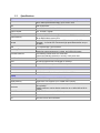
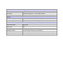
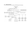
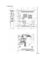
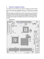
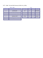
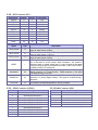
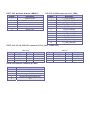
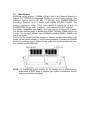
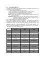
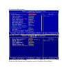
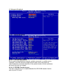
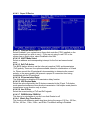
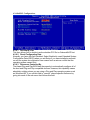
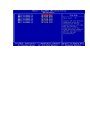
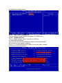
Acrosser Technology Co., Ltd.
AR-B1894
Intel Pentium M
Mini ITX Main Board
User’s Manual
V 1.2
Copyright© May., 2007. All rights reserved
All other brand names are registered trademarks of their respective owners.
Copyright
All rights reserved. The information contained in this guide has been validated
and reviewed for accuracy. No patent liability is assumed with respect to the use
of the information contained herein. While every precaution has been taken in the
preparation of this guide, the Manufacturer assumes no responsibility for errors
or omissions.
No part of this publication may be reproduced, stored in a retrieval system, or
transmitted in any form or by any means, electronic, mechanical, photocopying,
recording, or otherwise, without the prior written permission of Manufacturer.
Trademark
Intel®, Pentium® and Celeron® are registered trademarks of Intel® Corporation.
Microsoft® and Windows® are registered trademarks of Microsoft Corporation.
All products and company names are trademarks or registered trademarks of
their respective holders.
These specifications are subject to change without notice.
Technical Support
We hope you to get the maximum performance from your products and be willing
to help if running into technical difficulties. For the most frequently asked
questions, it’s easily found answers from the product documentation and usually
a lot more detailed, so please take reference to this manual first. If the answer
still can not be found, gather all the information or questions applying to the
problem, and with the product on hand, contact your distributor, sales
representative, or customer service center for technical support. Most problems
reported are minor and able to be easily solved over the phone. In addition, free
technical support is available and always ready to give advices on application
requirements or specific information on the installation and operation of any of
our products.
Please have the following information ready before you call:
1. Product name and serial number
2. Description of your peripheral attachments
3. Description of your software (operating system, version, application software,
etc.)
4. A complete description of the problem
5. The exact wording of any error messages
How to Use This Manual
This manual is written for the system integrator, PC technician and
knowledgeable PC end user. It describes how to configure your AR-B1894 to
meet various operating requirements. The user’s manual is divided into four
chapters, with each chapter addressing a basic concept and operation of the
server board.
Chapter 1: Introduction - presents what you have inside the box and gives you
an overview of the product specifications and basic system architecture for the
AR-B1894 server board.
Chapter 2: Hardware Configuration Setting - shows the definitions and
locations of Jumpers and Connectors so that you can easily configure your
system.
Chapter 3: System Installation - describes how to properly mount the CPU,
main memory, and M-System Flash disk for a safe installation. It will also
introduce and show you the driver installation procedure for the Graphics
Controller and Ethernet Controller.
Chapter 4: BIOS Setup Information - specifies the meaning of each setup
parameter, how to get advanced BIOS performance and update to a new BIOS.
Note:
(1) Memory type support dual-channel interleaved mode assuming DDR2
533 MHz, all DIMMs in a system must be of the same type, the speed in
all channels is the speed of the slowest DIMM in the system.
Table of Content
1.
INTRODUCTION..................................................................................................... 6
1.1
1.2
1.3
1.4
1.5
2.
DESCRIPTION................................................................................................................................ 6
PACKING CHECK LIST................................................................................................................... 7
SPECIFICATIONS ........................................................................................................................... 8
SYSTEM ARCHITECTURE ............................................................................................................ 10
DIMENSIONS ...............................................................................................................................11
HARDWARE CONFIGURATION SETTING .................................................... 12
2.1
BOARD LAYOUT ......................................................................................................................... 12
2.2
JUMPERS & CONNECTORS .......................................................................................................... 13
2.3
JUMPERS/CONNECTORS SETTING ............................................................................................... 15
2.3.1 RTC CMOS Clear Select (JP1)............................................................................................. 15
2.3.2 CPU Frequency Select (JP4) ................................................................................................ 15
2.3.3 Internal Audio for Chassis (AUDIO1).................................................................................. 15
2.3.4 Audio Connector (AUDIO2)................................................................................................. 15
2.3.5 CD-In from CD-ROM (CD1) ................................................................................................ 15
2.3.6 Chassis/CPU/System Connectors (CHS_FAN1, CPU_FAN1, SYS_FAN1) ........................... 15
2.3.7 COM1 / VGA & COM2 Connector (COM2, VGA_COM1) .................................................. 16
2.3.8 DVI Connector (DVI............................................................................................................. 17
2.3.9 GPIO Connector (GPIO1).................................................................................................... 17
2.3.10
IrDA Connector (IR1) ...................................................................................................... 17
2.3.11
PS/2 Keyboard & Mouse (KBMS1).................................................................................. 18
2.3.12
LAN LED Connector (LAN_LED1) ................................................................................. 18
2.3.13
LAN 1/2/3 & USB 1/2 Connectors (LAN2_LAN3, USB1LAN1) ...................................... 18
2.3.14
LCD Inverter Connector (LVDS1) ................................................................................... 18
2.3.15
LVDS Connector (LVDS2) ............................................................................................... 19
2.3.16
Front Side Indicators (PANEL1) ...................................................................................... 20
2.3.17
24-pin ATX Power Connector (PWR1) ............................................................................ 20
2.3.18
Serial ATA 1/2 Connectors (SATA1, SATA2) .................................................................... 20
2.3.19
Internal Speaker Connector (SPK1) ................................................................................ 20
2.3.20
Internal USB 3/4/5/6 Connectors (USB2, USB3)............................................................. 20
3.
SYSTEM INSTALLATION ................................................................................... 21
3.1
SOCKET 478 PROCESSORS .......................................................................................................... 21
3.1.1 Installing Intel® Pentium® M / Celeron® M CPU ................................................................. 21
3.2
INSTALLING COOLING FAN ......................................................................................................... 21
3.3
MAIN MEMORY .......................................................................................................................... 22
3.4
INSTALLING THE MINI-ITX ........................................................................................................ 23
3.4.1 Intel 915GM Integrated Graphics Controller....................................................................... 23
3.4.2 Triple Marvell Gigabit Ethernet Controller.......................................................................... 24
3.4.3 Drivers Support .................................................................................................................... 24
4.
BIOS SETUP ........................................................................................................... 25
4.1
ENTERING SETUP ....................................................................................................................... 25
4.2
MAIN MENU ............................................................................................................................... 25
4.2.1
Standard CMOS Features ..................................................................................................... 26
4.2.2
Advanced BIOS Features...................................................................................................... 27
4.2.3
Advanced Chipset Features .................................................................................................. 31
4.2.4
Integrated Peripheral ........................................................................................................... 34
4.2.5
Power Management Setup .................................................................................................... 38
4.2.6
PnP/PCI Configurations....................................................................................................... 40
4.2.7
PC Health Status................................................................................................................... 43
4.2.8
4.2.9
4.2.10
4.2.11
4.2.12
Frequency/Voltage Control ................................................................................................... 44
Load Fail-Safe Default ......................................................................................................... 44
Load Optimized Defaults ................................................................................................. 45
Supervisor/User Password Setting................................................................................... 45
Exit Selection ................................................................................................................... 47
1.
Introduction
1.1
Description
The AR-B1894 all-in-one Mini ITX is designed to fit a high performance Pentium
M based processor and compatible for high-end computer system application
with PCI bus architecture. It is made to meet today’s demanding pace, and keep
complete compatibility with hardware and software designed for the IBM PC/AT.
The on-board devices support one PCI slot, integrated graphics, and on-board
three Marvell Gigabit Ethernet controllers. It’s beneficial to build up a high
performance and high data availability system for VARs, or system integrators.
AR-B1894 support the following processors:
Intel ® uFC-PGA 478 Pentium M® / Celeron M processor FSB 400/533 MH
with 0.90 and 0.13 micron technology.
This Mini ITX can run with Intel Socket 479 Pentium/Celeron M processors and
support DIMM up to 2 GB dual-channel DDR2 533 memory. The enhanced onboard one PCI-IDE interface can support 1 drive up to PIO mode 4 timing and
Ultra ATA 33/66/100 synchronous mode feature, one CF socket interface, and 2
Serial ATA high-speed data transfers at up to 150 MB/s connectors. The onboard Super I/O chipset supports two serial ports, one SIR (Serial Infrared) port,
two high performance 16C550-compatible UARTs provide 16-byte send/receive
FIFOs, and two RS-232 serial port interfaces. Besides, H/W monitor function,
Intel High Definition Audio as 5.1 surround sound, six Hi-Speed USB 2.0 ports
offering up to 40X greater bandwidth over USB 1.1. Also provide dual display
function by VGA and DVI, by VGA, and LVDS interface.
The Mini-ITX standard makes the AR-B1894 work with the one slot PCI and one
6-pin Mini-DIN connector for PS/2 mouse and keyboard. The on-board Flash
ROM is used to make the BIOS update easier. The high precision Real Time
Clock/calendar is built to support Y2K for accurate scheduling and storing
configuration information. One 20-pin standard connector is designed to support
ATX power function. A feature of CPU overheat protection will give user more
security and stability. All of these features make AR-B1894 series excellent in
stand-alone applications.
Note: 1) The AR-B1894 only support Intel Pentium/Celeron M processor
(Dothan 400/533 FSB) for 0.13 and 0.90 micron.
2) The AR-B1894 only support DDR2 533 memory module.
1.2
Packing Check List
The AR-B1894 package includes the following basic items accompany with this
manual.
One AR-B1894 Mini ITX
One Quick Installation Guide for AR-B1894
One 40-pin IDE cable
One Serial ATA cable
One Serial port cable for COM2
One I/O Shield bracket
One Supporting CD-ROM contains User’s Manual and internal VGA
display driver and Marvell Gigabit Ethernet network controller driver and
on board devices drivers
If any of these items is damaged or missed, please contact your vendor and save
all packing materials for future replacement and maintenance.
1.3
Specifications
System
FSB
Supports Intel μFC-PGA 478 Pentium® M / Celeron® M Processor with
65nm / 90nm process technology, up to 2.26G / 2.0G
FSB 533/400 MHz
BIOS
Award BIOS with 4 Mb Flash ROM
System Chipset
Intel® 915GM + ICH6M
I/O Chip
Winbond W83627THG-AW supports two serial ports
2 x 240-pin DIMM sockets support dual channel DDR2 from 128 MB to 2
GB at 400/533 MHz memory bus
1 x Ultra DMA100/66/33 support two IDE devices by 40-Pin IDE
connector ; 2 x Serial ATA connectors high-speed data transfer at up to
150 MB/s
1 x CompactFlash Type I/II Socket
CPU
System Memory
Storage
SSD
Watchdog Timer
Real Time Clock
Reset: 1 sec.~255 min. and 1 sec. or 1 min./step
Monitoring system temperature, voltage, and cooling fan status.
Auto throttling control when CPU overheats.
System automatically restored on recovery of AC power loss.
Built-in ICH6M with Y2K compliant
GPIO
On-board programmable 8-bit Digital I/O interface
Expansion
1 x 32-bit PCI slot compliant with PCI v2.3 specification
H/W Status Monitor
MIO
Internal
1 x RS-232, 4 x USB 2.0
External
1 x RS-232, 1 x K/B, 1 x Mouse, 3 x LAN & 2 x USB 2.0
Display
Chipset
Intel® 915GM Integrated Intel® GMA 900 graphics
Display Memory
VGA/LCD Interface
Intel® DVMT 3.0 supports up to 128 MB video memory
CRT mode: support maximum resolution up to 2048 x 1536 at fresh rate
75Hz (QXGA)
Multiple maximum overlay display resolution up to 1600x1200 at 85 Hz
(UXGA)
DSUB-15 VGA connector for DAC output
LVDS
Dual Channel 18-bit LVDS
DVI
Chrontel CH7307 DVI transmitter
Resolution
Audio
Chipset
Intel® ICH6M
AC97 Codec
Realtek ALC655 AC97 5.1 CH 3D audio interface
Audio Interface
Mic in, Line in, CD Audio in, Line out, Rear out and Center/Subwoofer out
Ethernet
Chipset
Three Marvell® YukonTM-EC 88E8053 PCI ExpressTM Ethernet controllers
Ethernet Interface
IEEE 802.3 10/100/1000BASE-T Gigabit Ethernet compliant
Mechanical & Environmental
Power Type
3.3 V @ 3.4 A, +5 V @ 359 mA, +12 V @ 1,92 A , -12 V @ 294 mA, 5 Vsb
@ 263 mA
ATX
Operating Temperature
0~60°C (32~140°F)
Operating Humidity
0%~90% relative humidity, non-condensing
Size (L x W)
6.69" x 6.69" (170 mm x 170 mm)
Weight
0.94 lbs (0.43 Kg)
Power Requirement
1.4
System Architecture
All of details operating relations are shown in AR-B1894 system block diagram.
1.5 Dimensions
Unit: mm
2.
Hardware Configuration Setting
This chapter gives the definitions and shows the positions of jumpers, headers
and connectors. All of the configuration jumpers on AR-B1894 are in the proper
position. The default settings shipped from factory are marked with an asterisk
( ).
In general, jumpers on the Mini ITX are used to select options for certain features.
Some of the jumpers are designed to be user-configurable, allowing for system
enhancement. The others are for testing purpose only and should not be altered.
To select any option, cover the jumper cap over (SHORT) or remove (NC) it from
the jumper pins according to the following instructions. Here, NC stands for “Not
Connect”.
2.1
Board Layout
2.2
Jumpers & Connectors
JUMPERS
FUNCTION
REMARK
JP1
RTC CMOS clear select
2 x 1 header
JP4
CPU frequency select
2 x 1 header
CONNECTORS FUNCTION
REMARK
AUDIO1
Internal audio for chassis
2 x 5 header
AUDIO2
Audio connector
Audio jack x 3
CD1
CD-In from CD-ROM
1 x 4 header
CF1
CompactFlash card connector
CHS_FAN1
Chassis fan connector
CPU_FAN1
CPU fan connector
COM2
Serial port 2 connector
2 x 5 header
DIMM1, DIMM2 240-pin DDR2 SDRAM 1 & 2 socket
DVI1
DVI connector
HIROSE
GPIO1
GPIO connector
2 x 5 header
IDE1
Primary IDE connector
2 x 20 header
IR1
IrDA connector
2 x 3 header
KBMS1
PS/2 keyboard & mouse connector
LAN_LED1
LAN LED connector
LAN2_LAN3
LAN 2 & LAN 3 connectors
LVDS1
LCD inverter connector
LVDS2
LVDS connector
HIROSE
PANEL1
Front side indicators:
2 x 5 header
2 x 6 header
IDE1 active LED (1-3)
System power on LED (2-4)
System reset LED (5-7)
System power on switch LED (6-8)
PCI1
PCI slot
PWR1
24-pin ATX power connector
SATA1, SATA2
Serial ATA 1 & 2 connector
SPK1
Internal speaker connector
SYS_FAN1
System fan connector
USB1LAN1
USB 1, 2 & LAN 1 connectors
USB2, USB3
Internal USB 3, 4 & 5, 6 connectors
VGA_COM1
D-sub 15-pin VGA & D-sub 9-pin serial
port 1 connectors
1 x 4 header
2 x 5 header
2.3
Jumpers/Connectors Setting
2.3.1 RTC CMOS Clear Select (JP1)
OPEN
Normal Operation
SHORT
Clear CMOS
contents
2.3.3 Internal Audio for Chassis (AUDIO1)
PIN No.
1
2
3
4
5
6
7
8
9
10
Description
F_MIC1
Ground
F_MIC2
+5V
LOUTR
F_R
NC
NC
LOUTL
F_L
2.3.5 CD-In from CD-ROM (CD1)
PIN No.
1
2
3
4
Description
CD-L
CD-Ground
CD-Ground
CD-R
2.3.2 CPU Frequency Select (JP4)
OPEN
400 MHz
SHORT
533 MHz
2.3.4 Audio Connector (AUDIO2)
PIN No.
Description
1 (Blue)
Line-in
2 (Green)
Speaker out
3 (Red)
MIC-in
2.3.6 Chassis/CPU/System Connectors
(CHS_FAN1, CPU_FAN1, SYS_FAN1)
PIN No.
1
2
3
4
Description
GND
+12V
SENSE
Control (CPU_FAN1 only)
2.3.7 COM1 / VGA & COM2 Connector (COM2, VGA_COM1)
PIN No.
1
2
3
4
5
6
7
8
9
10
COM1 / COM2
Description
Data Carrier Detect
Received Data
Transmit Data
Data Terminal Ready
Ground
Data Set Ready
Request To Send
Clear To Send
Ring Indicator
Not used
Description
Green Signal
NC
Ground
Ground
Ground
DCC_DATA
VSYNC
VGA
PIN No. PIN No.
2
1
4
3
6
5
8
7
10
9
12
11
14
13
15
Description
Red Signal
Blue Signal
Ground
Ground
+5V
NC
HSYNC
DCC_CLK
2.3.8 DVI Connector (DVI
Description
TDC0#
TDC0
NC
NC
TDC1#
TDC1
NC
NC
TDC2#
TDC2
PIN No.
2
4
6
8
10
12
14
16
18
20
Signal
Type
TDC0,TDC0#
O
TDC1,TDC1#
O
TDC2,TDC2#
O
HPDET
I
TMDSDATA
I/O
TMDSDCLK
I/O
TLC,TLC#
O
PIN No.
1
3
5
7
9
11
13
15
17
19
Description
+5V
GND
NC
NC
HPDET
MDVIDATA
MDVICLK
Ground
TLC#
TLC
Description
DVI Data Channel 0 Output: These pins provide the DVI differential
output for data channel 0 (Blue).
DVI Data Channel 1 Output: These pins provide the DVI differential
output for data channel 1 (Green).
DVI Data Channel 2 Output: These pins provide the DVI differential
output for data channel 2 (Red).
Hot Plug Detect (internal pull-down): This input determines whether the
DVI is connected to a DVI monitor. When terminated , the monitor is
required to apply a voltage greater than 2.4 volts. Changes on the status
of this pin will be relayed to the graphics controller via the P-OUT/TLDET*
or GPIO(1)/TLDET* pin pulling low.
DVI I2C Data: This signal is used as the I2C DOC clock for a digital
display connector (i.e. TV-Out Encoder , TMDS transmitter ). This signal
is tri-stated during a hard reset.
DVI DOC Clock: This signal is used as the DOC clock for a digital display
connector (i.e. primary digital monitor). This signal is tri-stated during a
hard reset.
DVI Clock Output: These pins provide the differential clock outputs to the
DVI interface corresponding a data on TDC(0:2) outputs.
2.3.9 GPIO Connector (GPIO1)
PIN No.
1
2
3
4
5
6
7
8
9
10
Description
+3.3V
General Purpose I/O bit 3
General Purpose I/O bit 5
General Purpose I/O bit 0
General Purpose I/O bit 7
General Purpose I/O bit 2
General Purpose I/O bit 4
General Purpose I/O bit 1
General Purpose I/O bit 6
Ground
2.3.10 IrDA Connector (IR1)
PIN No.
1
2
3
4
5
6
Description
NC
NC
+5V
Infrared transmitter output
Ground
Infrared receiver input
2.3.11 PS/2 Keyboard & Mouse (KBMS1)
PIN No.
1
2
3
4
5
6
Description
Keyboard Data
Mouse Data
Ground
+5V
Keyboard Clock
Mouse Clock
2.3.12 LAN LED Connector (LAN_LED1)
PIN No.
1
2
3
4
5
6
7
8
9
10
11
12
Description
L1_LED_LINKACT
L1_LED_LINK100
L1_LED_LINKACT_V
L1_LED_LINK1000
L2_LED_LINKACT
L2_LED_LINK100
L2_LED_LINKACT_V
L2_LED_LINK1000
L3_LED_LINKACT
L3_LED_LINK100
L3_LED_LINKACT_V
L3_LED_LINK1000
2.3.13 LAN 1/2/3 & USB 1/2 Connectors (LAN2_LAN3, USB1LAN1)
PIN No.
1
2
3
4
LAN 1/2/3
Description
PIN No.
TX+
5
TX6
RX+
7
NC
8
Description
NC
RXNC
NC
2.3.14 LCD Inverter Connector (LVDS1)
PIN No.
1
2
3
4
5
Description
+12V
Ground
Backlight On/Off control
Backlight brightness adjustment
+5V
PIN No.
1
2
3
4
USB 1/2
Description
PIN No.
+5 V (fused)
5
USBP06
USBP0+
7
Ground
8
Description
+5 V (fused)
USBP1USBP1+
Ground
2.3.15 LVDS Connector (LVDS2)
Description
+5V
+5V
Ground
LCTLB_CLK_L
LCTLB_DATA_L
Ground
Ground
A_CLKA_CLK+
Ground
A_DATA0A_DATA0+
Ground
A_DATA1A_DATAP+
Ground
A_DATA2A_DATA2+
Ground
+12V
Signal
PIN No.
2
4
6
8
10
12
14
16
18
20
22
24
26
28
30
32
34
36
38
40
PIN No.
1
3
5
7
9
11
13
15
17
19
21
23
25
27
29
31
33
35
37
39
Type
Description
+3.3V
+3.3V
Ground
LDDC_CLKL
LDDC_DATA_L
Ground
Ground
B_CLKB_CLK+
Ground
B_DATA0B_DATA0+
Ground
B_DATA1B_DATA1+
Ground
B_DATA2B_DATA2+
Ground
+12V
Description
2
LCTLB_CLK_L
I/O
I C Based control signal (Clock) for External SSC clock chip control
LCTLB_DATAL
I/O
I2C Based control signal (Data) for External SSC clock chip control
LDDC_CLKL
I/O
EDID support for flat panel display
LDDC_DATAL
I/O
EDID support for flat panel display
2.3.16 Front Side Indicators (PANEL1)
PIN No.
1
3
PIN No.
5
7
PIN No.
6
8
2.3.17 24-pin ATX Power Connector (PWR1)
Description
+3.3V
-12V
Ground
PS_ON
Ground
Ground
Ground
-5V
+5V
+5V
+5V
Ground
IDE1 Active LED
Signal Description
+5V (Pull-up for HDD LED)
HDD active# (LED cathode terminal)
System Reset LED
Signal Description
Reset
Ground
System Power On Switch LED
Signal Description
Power button control signal
Ground
2.3.18 Serial ATA 1/2 Connectors (SATA1,
SATA2)
PIN No.
13
14
15
16
17
18
19
20
21
22
23
24
PIN No.
1
2
3
4
5
6
7
8
9
10
11
12
Description
+3.3V
+3.3V
Ground
+5V
Ground
+5V
Ground
PW_OK
5VSB
+12V
+12V
+3.3V
2.3.19 Internal Speaker Connector (SPK1)
PIN No.
1
2
3
4
These SATA connectors support Serial ATA 150. Each
SATA connector can only support one serial ATA device.
Note: With most storage devices, there is a power cable
that you need attach to a power source (power
supply).
Description
Ground
Ground
NC
+5V
2.3.20 Internal USB 3/4/5/6 Connectors (USB2, USB3)
PIN No.
1
Description
5VSB
2
5VSB
3
4
5
6
7
8
9
10
DATA_3- / DATA_5DATA_3- / DATA_5+
DATA_4+ / DATA_6DATA_4+ / DATA_6+
Ground
Ground
NC
NC
Note :
1) This mainboard provides 2 USB headers on the board
allowing for 4 additional USB ports. To make use of
these headers, you must attach a USB bracket/cable
with USB ports (some models will come packaged
with a USB 4-port bracket-cable). The optionally
packaged bracket will have two connectors that you
can connect to the headers (USB1, USB2). The other
end (bracket containing the USB ports) is attached to
the computer casing.
2) If you are using a USB 2.0 device with Windows
2000/XP, you will need to install the USB 2.0 driver
from the Microsoft® website. If you are using Service
pack 1 (or later) for Windows® XP, and using Service
pack4 (or later) for Windows® 2000, you will not have
to install the driver.
3.
System Installation
This chapter provides you with instructions on how to setup your system. The
additional information shows you how to install CPU/ FAN and memory.
3.1
Socket 478 Processors
3.1.1 Installing Intel® Pentium® M / Celeron® M CPU
The processor socket comes with a screw to secure the processor, please
unlock the screw first.
Position the CPU above the socket and the gold triangular mark on the CPU
must align with pin 1 of the CPU socket. Then Insert the CPU gently seated
in place.
Turn the screw to the lock position.
Unlock
Pin 1 of the
socket
Lock
Gold
triangular
mark
Note: Do not force the CPU into the socket. It may bend the pins and
damage the CPU.
3.2
Installing Cooling Fan
Warning: For a safety landing, avoid leaving prongs on hard surface.
Instructions:Smear thermal grease on the top of the CPU. Lower the CPU
fan onto the CPU/CPU socket and secure it using the
attachments or screws provided on the fan. Finally, attach the
fan power cable to the CPUFAN adapter. For more details on
this, go to http://www.intel.com
3.3
Main Memory
AR-B1894 series provide 2 DIMMs (240-pin Dual In-line Memory Module) to
support 1.5V DDRAM (Synchronized DRAM) as on-board main memory. The
maximum memory size is 256 MB ~ 2 GB with using 256MB/512MB/1GB
technology. Supports up to 2 double sided DIMMs at DDR2 533MHz. The
memory architecture adopts 128-bit data interface to support for x8 and x16
DDRAM(DDR2) device width. In addition, it only supports Non-ECC memory.
For system compatibility and stability, don’t use memory module without brand.
You can also use the single or double-side DIMM .The three DIMMs can be out
of order. You can install different size of DDRAM module on DIMM1, DIMM2 or all
to boot up system.
Without out the contact and lock integrity of memory module with socket, it will
impact on the system reliability. Follow normal procedure to install your DDRAM
module into memory socket. Before locking, make sure that the module has been
fully inserted into the DIMM slot.
NOTE: For maintaining system stability, do not change any of DDR2 memory
parameters in BIOS setup to upgrade your system performance without
acquiring technical information.
3.4
Installing the Mini-ITX
To install your AR-B1894 into standard chassis or proprietary environment, you
need to perform the following steps:
1. Check all jumpers setting on proper position
2. Install and configure CPU and memory module on right position
3. Place AR-B1894 into the dedicated position in your system
4. Attach cables to existing peripheral devices and secure it
NOTE: Please refer section 3.4 to install display and Ethernet drivers and
setup your system.
WARNING: Please ensure that your SBC properly inserted and fixed by
mechanism. Otherwise, the system might be unstable or do not
work from bad contact of golden finger.
3.4.1 Intel 915GM Integrated Graphics Controller
The on-board graphics controller integrated in 915GM(GMCH) chipset that
integrates high performance memory technology , the on-board operates at a
frequency of 2.5Gb/s on each lane while employing 8b/10b encoding, and
supports a maximum theoretical bandwidth of 4Gb/s each direction, the
82915GM GMCH multiplexes the PCI Express interface with DVI & CRT support.
The chipset supports the following modes.
Resolution
Bits Per Pixel (frequency in Hz)
640x480
256 Color
60,70,72,75,85,100,120
16-bit
60,70,72,75,85,100,120
32-bit
60,70,72,75,85,100,120
800x600
60,70,72,75,85,100,120
60,70,72,75,85,100,120
60,70,72,75,85,100,120
1024x768
60,70,72,75,85,100,120
60,70,72,75,85,100,120
60,70,72,75,85,100,120
1152x864
60,75,85,100
60,75,85,100
60,75,85,100
1280x600
60
60
60
1280x720
60,75,85,100
60,75,85,100
60,75,85,100
1280x768
60,75,85
60,75,85
60,75,85
1280x960
60,75,85
60,75,85
60,75,85
1280x1024
60,75,85,100,120
60,75,85,100,120
60,75,85,100,120
1400x1050
60,75,85
60,75,85
60,75,85
1600x900
60,75,85,100,120
60,75,85,100,120
60,75,85,100,120
1600x1200
60,75,85,100,120
60,75,85,100,120
60,75,85,100,120
1856x1392
60,75
60,75
60,75
1920x1080
60,75,85,100
60,75,85,100
60,75,85,100
1920x1200
60,75,85
60,75,85
60,75,85
1280x1024
60,75
60,75
60,75
1920x1440
60,75,85
60,75,85
60,75,85
2048x1536
60,75
60,75
60,75
3.4.2 Triple Marvell Gigabit Ethernet Controller
Triple Marvell Gigabit Ethernet 10/100/1000BASE-TX controller by PCI Express.
The AR-B1894 series provide three LED indicators on RJ-45 connectors to show
LAN interface status. These messages will give you a guide for troubleshooting.
LAN1:
Yellow LED indicates transmit and receive activity.
Blinking: indicates transmit/receive activity
On: indicates no activity but link is valid
Off: link is invalid
Green LED indicates Link speed
On: link speed at 1000Mbps
On: link speed at 100Mbps
Off: link speed at 10Mbps
LAN2, 3:
Red LED indicates transmit and receive activity.
Blinking: indicates transmit/receive activity
On: indicates no activity but link is valid
Off: link is invalid
Green LED indicates Link speed
On: link speed at 100Mbps
Off: link speed at 10Mbps
Orange LED indicates Link speed
On: link speed at 1000Mbps
Off: link speed at 10Mbps
3.4.3 Drivers Support
AR-B1894 provide on CD-Title to support on-board VGA and Ethernet device
drivers in various operating systems. Before installing the device drivers, please
see the reference files in each sub-directory. You cannot install drivers from CDTitle directly.
Intel 915GM Chipset Integrated Graphics supports Win2000, XP, Win2003 and
64bit Windows environment.
Intel 915GM & ICH6(M) Chipset Driver supports Win2000, XP, Win2003 and
64bit Windows environment.
Three Marvell Gigabit Ethernet Controllers support Win2000, XP, Win2003,
and 64 bit Windows environment.
4.
BIOS Setup
4.1
Entering Setup
Phoenix-Award BIOS has a built-in setup program that allows users to modify the
basic system configuration. This information is stored in CMOS RAM whose
power is supplied by a battery so that it can retain the setup information even
when the power is turned off. Press Delete when you Power on or Reboot the
computer system. (i.e. After the logo appears at the center of the screen, please
press Delete to enter the BIOS setup program). In the BIOS, make sure that
everything is working fine before you try to optimize it for maximum performance.
4.2
Main Menu
When you enter the PHOENIX-AWARD™ CMOS Setup Utility, the Main will
appear on the screen. The Main allows you to select several configuration
options. Use the left/right arrow keys to highlight a particular configuration screen
from the top menu bar or use the down arrow key to access and configure the
information below.
4.2.1Standard CMOS Features
4.2.1.1
Date (mm/date/year) and Time (hh/mm/ss)
Allow you to change the date and time of the system clock. No matter how good
the quality of the motherboard, remember that losing (or gaining) several
seconds per month is not a surprising thing.
4.2.1.2
IDE Channel 0 Master/Slave
You can press Enter to see the submenus they contain.
4.2.1.3
Video
Allows you to select the type of displaying standard you are using. Available
options are EGA/VGA, CGA 40, CGA 80 and MONO.
4.2.1.4
Halt On
Select the situation in which you want the BIOS to stop the POST process and
notify you. Available options are All Errors, No Errors, All, but keyboard, All,
but diskette, and All, but disk/key.
4.2.1.5
Base Memory
Displays the amount of conventional memory detected during boot up.
4.2.1.6
Extended Memory
Displays the amount of extended memory detected during boot up.
4.2.1.7
Total Memory
Displays the total memory available in the system.
4.2.2Advanced BIOS Features
4.2.2.1 CPU Feature
4.2.2.1.1 Delay Prior to Thermal
Select the delay thermal time. Configuration options: [4min][8min][16min][32min]
4.2.2.1.2 Thermal Management
This BIOS feature controls the activation of the Thermal Monitor’s automatic
mode. It allows you to determine when the Pentium M4’s Thermal Monitor should
be activated in automatic mode after the system boots. In general, the Thermal
Monitor should not be activated immediately on booting since the processor will
be under a heavy load during the booting process, which results in the sharp rise
in die temperature from its cold state, which leads to the unstable system.
Therefore, to ensure optimal booting performance, the activation of the Thermal
Monitor must be delayed for a set period of time. But how do you possibly know
the optimal delay time? It is recommended that you set this to its lowest value
that exceeds the time it takes to fully boot up your computer.
This item will monitor the CPU thermal to prevent the CPU damage from high
temperature.
4.2.2.1.3 TM2 BUS Ratio
Select the Represents the frequency (bus ratio of the throttled performance state
that will be initiated when the on-die sensor goes from not hot to hot
4.2.2.1.4 TM2 BUS VID
Select Represents the voltage of the throttled performance state that will be
initiated when the on die sensor goes from not hot to hot.
4.2.2.1.5 Limit CPUID MaxVal
When the limit CPUID MaxVal is set to 3, the item should be set to “Disabled” for
Windows XP. Options: Enabled、Disabled (default).
4.2.2.1.6 C1E Function
Select CPU C1E Function Select
4.2.2.1.7 Execute Disable Bit
Select when disable, forces the XD feature flag to always return 0.
4.2.2.1.8 Virtualization Technology
Select when enable, a VMM can utilize the additional hardware capabilities
provided by Vander pool Technology.
4.2.2.2 Hard Disk Boot Priority
Select removable device priority, such as Pri.Master, Pri,Slave, USBHDD0,
USBHDD1, USBHDD2, and Bootable Add-in Cards.
4.2.2.3 Virus Warning
Allows to choose the VIRUS warning feature for IDE Hard Disk boot sector
protection. If this function is enabled and someone attempts to write data into this
area, BIOS will show a warning message on screen and alarm beep.
4.2.2.4 CPU L1 & L2 Cache
Cache memory is much faster than conventional DRAM system memory. These
fields allow you to enable or disable the CPUs Level 1 built-in cache and Level 2
external cache. Both settings are left as Enabled to significantly enhance the
performance of your computer.
4.2.2.5 Hyper-Threading Technology
When you install a CPU featuring Hyper-Threading Technology, this item will
allow you to enable or disable the Hyper-Threading technology. Options:
Disabled、Enabled (default).
4.2.2.6 Quick Power On Self Test
Enable this function to reduce the amount of time required to run the POST
(Power On Self Test). BIOS will save time by skipping certain tests during POST.
It is recommended that you disable this setting. Finding a problem during boot up
is better than loosing data during your work.
4.2.2.7 First/Second/Third Boot Device
Allow you to select the First, Second and Third Boot Device. If your computer is
newly constructed, the next thing you want to do is load the Operating System
from scratch, directly off its CD. Before that, you need to set the First Boot Device
to the CDROM. This instructs the BIOS to boot from the CD drive before trying to
boot from the hard drive, which is still blank.
4.2.2.8 Boot Up NumLock Status
This function defines the keyboard's numberpad as number keys or arrow keys. If
it is set at On the number keys will be activated, if it is set at Off the arrow keys
will be activated.
4.2.2.9 Typematic Rate Setting
When enabled, you can set the following two-typematic control items. When
disabled, the keyboard controller determines keystrokes arbitrarily in your system.
4.2.2.10 Typematic Rate (Chars/Sec)
The typematic rate sets the rate at which characters on the screen repeat when a
key is pressed and held down.
4.2.2.11 Typematic Delay (Msec)
The typematic delay sets how long after you press a key that a character begins
repeating.
4.2.2.12 APIC Mode
By enabling this option, “MPS version control for OS” can be configured.
Disabled is recommended.
4.2.2.13 MPS Version Control for OS
The 1.1 version is the older version that supports 8 more IRQs in the Windows
NT environment. Choose the new 1.4 version for Windows 2000 and Windows
XP. Options: 1.4 (default)、1.1
4.2.2.14 OS Select For DRAM > 64MB
IBM’s relic. If your system's DRAM is larger than 64MB and you are running OS/2,
select OS/2 as the item value. Otherwise, set the item value to Non-OS/2 for all
other operating systems.
4.2.3Advanced Chipset Features
4.2.3.1 DRAM Timing Selectable
This item determines DRAM clock/timing using SPD or manual configuration.
Make sure your memory module has SPD (Serial Presence Data), if you want to
select the “By SPD” option. Options: Manual、By SPD (default)
4.2.3.2 CAS Latency Time
CAS is short for column address strobe, which is a kind of signals. When the
CPU needs data from SDRAM, CAS signals will be sent via the CAS line to
specify the column where the data is needed. This controls the time delay (in
clock cycles - CLKs) that passes before the SDRAM starts to carry out a read
command after receiving it. This also determines the number of CLKs for the
completion of the first part of a burst transfer. In other words, the lower the
latency, the faster the transaction.
Note that some SDRAM modules may not be able to handle the lower latency
and will become unstable and lose data. Therefore, set the DRAM CAS Latency
Time to 2 for optimal performance if possible but increase it to 2.5 if your system
becomes unstable.
Interestingly, increasing the CAS latency time does have an advantage in that it
will enable the SDRAM to run at a higher clockspeed, thereby giving you an edge
in overclocking your system. So, if you hit a snag while overclocking, try
increasing the CAS latency time.
4.2.3.3 DRAM RAS# to CAS# Delay
This item allows you to select a delay time between the CAS and RAS strobe
signals. It only applies when DRAM is written to, read from, or refreshed. This
field is adjustable only when “DRAM Timing Selectable” is set to “manual”. This
field is locked when “DRAM Timing Selectable” is set to “By SPD” and is
automatically determined by the system. Options: 5、4、3、2.
4.2.3.4 DRAM RAS# Precharge
This item allows you to select the DRAM RAS# precharge time. The ROW
address strobe must precharge again before DRAM is refreshed. An inadequate
configuration may result in incomplete data. This field is adjustable only when
“DRAM Timing Selectable” is set to “manual”. This field is locked when “DRAM
Timing Selectable” is set to “By SPD” and is automatically determined by the
system. Options: 5、4、3、2.
4.2.3.5 Precharge Delay
This item allows you to select DRAM Active to Precharge Delay. This field is
locked when “DRAM Timing Selectable” is set to “By SPD” and is automatically
determined by the system. Options: 15、14、13、12、11、10、9、8、7、6、
5、4.
4.2.3.6 System BIOS Cacheable
Enabling this function allows caching of the system BIOS ROM at F0000hFFFFFh, which results in better system performance. However, if any program
writes to this memory area, a system error may result. It is advisable to leave it in
default setting. Caching the system BIOS results in better performance than
shadowing the system BIOS.
4.2.3.7 Video BIOS Cacheable
Select “Enabled” to allow caching of the video BIOS which may improve
performance. If any other program writes to this memory area, a system error
may result. Options: Enabled, Disabled (default)
4.2.3.8 Memory Hole at 15M-16M
Enabling this function will reserve the memory address space between 15MB
and 16MB for ISA expansion cards. However, it will also result in not allowing the
system to have access to memory above 16MB. Please note that some
expansion cards require this setting to be enabled. The default setting is
Disabled. If Auto Configuration is enabled, you must set the DRAM timing
function to 60ns or 70ns, depending on the type of DRAM you install.
4.2.3.9 PCI Express Root Port Function
This item allows to Enable/Disable PCI Express port and select the PCI Express
Compliancy mode from v1.0a to v1.0.
4.2.3.10 On-Chip Frame Buffer Size
This item allows you to setting the VGA memory form share system. Options:
1M(minimum)、8M(Maximum default)
4.2.3.11 DVMT Mode
DVMT/FIXED Memory Size
4.2.3.12 Boot Display
This item allows you to setting CRT monitor only or CRT with EFP(DVI) together
display.
4.2.3.13 Panel Scaling
This item is for the backlight scaling techniques dynamically dimming the
backlight to conserve its power consumption as increasing the panel
transmittance to maintain the same luminance. Most displays use either spatial or
temporal method to synthesize colors.
4.2.3.14 Panel Number
This item allows to select panel resolution that will be displayed depending on the
LCD panel (LFP).
4.2.4Integrated Peripheral
4.2.4.1 Onchip IDE Device
4.2.4.3.1 IDE HDD Block Mode
Block mode is also called block transfer, multiple commands, or multiple sector
read/write. If the IDE hard drive supports block mode (most new drives do),
select Enabled for automatic detection of the optimal number of block read/writes
per sector the drive can support.
4.2.4.3.2 IDE DMA Transfer Access
This item could allows you to enabled/disabled the IDE UDMA transfer function
and only use PIO mode
4.2.4.3.3 On-Chip Primary/Secondary PCI IDE
The chipset contains a PCI IDE interface with support for two IDE channels.
Select Enabled to activate the primary IDE interface. Select Disabled to
deactivate this interface.
4.2.4.3.4 IDE Primary/Secondary Master/Slave PIO
The IDE PIO (Programmed Input/Output) fields let you set a PIO mode (0-4) for
each of the four IDE devices that the onboard IDE interface supports. Modes 0
through 4 provide successively increased performance. In Auto mode, the
system automatically determines the best mode for each device.
4.2.4.3.5 IDE Primary/Secondary Master/Slave UDMA
Ultra DMA implementation is possible only if your IDE hard drive supports it and
the operating environment includes a DMA driver (Windows 95 OSR2 or a thirdparty IDE bus master driver). If the hard drive and the system software both
support Ultra DMA, select Auto to enable BIOS support.
4.2.4.3.6 On-Chip Serial ATA
The chipset contains a SATA IDE interface with support for two IDE channels.
Select Enabled to activate the primary IDE interface (Channel0). Select Disabled
to deactivate this interface.
4.2.4.3.7 PATA IDE Mode
This function allows to select PATA IDE mode.
4.2.4.2 Onboard Device
4.2.4.3.1
USB Controller
This item allows you to set the USB Controller.
4.2.4.3.2
USB 2.0 Controller
This item allows you to set the USB 2.0 Controller.
4.2.4.3.3
USB Keyboard Support
This item allows you to set the system’s USB keyboard to Enabled/Disabled.
4.2.4.3.4
USB Mouse Support
This item allows you to set the system’s USB Mouse to Enabled/Disabled.
4.2.4.3.5
Azalia/AC97 Audio Select
This option is used to Set whether onboard Azalia/AC97 audio is enabled
4.2.4.3 Super IO Device
4.2.4.3.1 Onboard Serial Port 1/2
Select Enabled if your system has a floppy disk controller (FDC) installed on the
system board and you wish to use it. If you are not going to use FDC or the
system has no floppy drive, select Disabled in this field.
4.2.4.3.2 UART Mode Select
Select an address and corresponding interrupt for the first and second serial
ports.
4.2.4.3.3 RxD,TxD Active
This BIOS feature allows to set the infra-red reception (RxD) and transmission
(TxD) polarity. There are four options available, based on combinations of Hi and
Lo. Please consult the IR peripheral's documentation to determine the correct
polarity, or the wrong polarity will prevent a proper IR connection from being
established with the IR peripheral.
4.2.4.3.4 IR transmission Delay
The field enables or disables IR transmission delay function.
4.2.4.3.5 UR2 Duplex Mode
Select the value required by the IR device connected to the IR port. Full-duplex
mode permits simultaneous two-direction transmission. Half-duplex mode permits
transmission in one direction only at a time.
4.2.4.3.6 Use IR Pins
Select the correct setting of TxD and RxD signals.
4.2.4.3.7 PWRON After PWR-Fail
This item is to set whether to run Ac Loss Auto Restart or off
4.2.4.4 Watch Dog Timer Select
This function will determine watch dog timer during the range of 10 Sec., 20 Sec.,
30 Sec., 40 Sec., 1 Min., 2 Min., and 4 Min. The default setting is Disabled.
4.2.5Power Management Setup
4.2.5.1 ACPI Function
This function enables PCs to implement Power Management functions through
Operating System and also provides the opportunity to integrated the interface
for controlling power management and Plug-n-Play features on system devices.
4.2.5.2 ACPI Suspend Type
This item allows to set the ACPI suspend(sleep) mode instead of simply turning
off a computer. In S1 the computer consumes less power because HDDs and
some other devices are powered off, but CPU is still running and it requires its
fan to rotate. In S3 mode it's only RAM (system memory) that remains powered.
4.2.5.3 Run VGABIOS if S3 Resume
This item is to select whether to run VGABIOS if resumed from S3 state but for
older VGA drivers only. Please select Auto (Default) if in doubt.
4.2.5.4 Power Management
There are three selections for power management and HDD power down. The
Min. Power Saving sets the HDD Power Down at 15 Min., Max. Power Saving at
1 Min., and User defined from 1 Min. to 15 Min. and disabled but from 1 Min. to 1
hour while disabled.
4.2.5.5 Video Off Method
Determines the manner in which the monitor is blanked. V/H SYNC + Blank turns
off vertical and horizontal synchronization ports and writes blanks to the video
buffer; DPMS Support is for the monitor supports the Display Power
Management Signaling(DPMS) standard of the Video Electronics Standards
Association(VESA); Blank Screen set the system only writes blanks to the video
buffer.
4.2.5.6 Video Off In Suspend
This item allows to set if the monitor is blanked in Suspend mode. The default
setting is Yes.
4.2.5.7 Suspend Type
This item will set the system status to shut down the PC with choices of Stop
Grant and PwrOn Suspend.
4.2.5.8 MODEM Use IRQ
This determines the IRQ in which the MODEM can use.
4.2.5.9 Sort-Off by PWR-BTTN
Pressing the power button for more than 4 seconds/Instant-Off forces the system
to enter the Soft-Off state when the system has “hung”.(Only could working on
ATX Power supply).
4.2.5.10 Wake-Up by PCI Card
This will enable the system to wake up through PCI Card peripheral or not.
4.2.5.11 Power On by Ring
The function allows the system boot up if there’s an incoming call from the
modem.
4.2.5.12 USB KB Wake-Up From S3
This option is used to enabled/disabled USB keyboard wake up with suspend to
RAM.
4.2.5.13 Primary/Secondary IDE 0/1
This function is for setting IDE 0/1 on primary/secondary mode.
4.2.5.14 FDD,COM,LPT Port
System can be awaked by Floppy Drive, COM or LPT port.
4.2.5.15 PCI PIRQ[A-D]#
This function will cause the system waking up completely from the power
management mode.
4.2.6PnP/PCI Configurations
4.2.6.1 Init Display First
This item allows you to decide to active whether PCI Slot or Onboard/AGP first.
4.2.6.2 Reset Configuration Data
Normally, you leave this field Disabled. Select Enabled to reset Extended System
Configuration Data (ESCD) when you exit Setup if you have installed a new addon and the system reconfiguration has caused such a serious conflict that the
operating system cannot boot.
4.2.6.3 Resources Controlled By
The Award Plug and Play BIOS has the capacity to automatically configure all of
the boot and Plug and Play compatible devices. However, this capability means
absolutely nothing unless you are using a Plug and Play operating system such
as Windows®95. If you set this field to “manual” choose specific resources by
going into each of the sub menu that follows this field.
4.2.6.3.1 IRQ Resources
This item allows you to determine the IRQ assigned to the ISA bus and is not
available to
any PCI slot. Legacy ISA for devices compliant with the original PC AT bus
specification,
PCI/ISA PnP for devices compliant with the Plug and Play standard whether
designed for
PCI or ISA bus architecture.
4.2.6.3.2 DMA Resources
This item allows you to determine the DMA assigned to the ISA bus and is not
available to
any PCI slot. Legacy ISA for devices compliant with the original PC AT bus
specification,
PCI/ISA PnP for devices compliant with the Plug and Play standard whether
designed for
PCI or ISA bus architecture.
4.2.6.4 PCI/VGA Palette Snoop
This function determines if the graphics card should allow VGA palette snooping
by a fixed function display card. It is only useful if a fixed-function display card
using that requires a VGA-compatible graphics card to be present. Otherwise,
leave the setting as default Disabled.
4.2.6.5 Maximum Payload
This item allows to set the maximum TLP payload size (unit in byte) for the PCI
Express devices.
4.2.7PC Health Status
4.2.7.1 Shutdown Temperature
This item allows to shutdown the system while the temperature is overheated.
4.2.7.2 CPU Warning Temperature
This function sets the CPU temperature value when the system will warn you
about possible overheating issue.
4.2.7.3 Smart CPU FAN Temperature
The Smart CPU Fan option in the BIOS slows down the fan when the CPU is
below a given temperature.
4.2.8Frequency/Voltage Control
4.2.8.1 Auto Detect PCI/DIMM Clk
This item allows to enable/disable auto detect PCI/DIMM clock.
4.2.8.2 Spread Spectrum
This is to adjust extreme value of the pulse for EMI test.
4.2.9Load Fail-Safe Default
Use this menu to load the BIOS default values for the minimal/stable
performance for your system to operate.
Press <Y> to load the BIOS default values for the most stable, minimalperformance system operations.
4.2.10 Load Optimized Defaults
Use this menu to load the BIOS default values that are factory settings for
optimal performance system operations. While Award has designed the custom
BIOS to maximize performance, the factory has the right to change these
defaults to meet their needs.
Press <Y> to load the default values setting for optimal performance system
operations.
4.2.11 Supervisor/User Password Setting
You can set either supervisor or user password, or both of them.
Supervisor Password: able to enter/change the options of setup menus
User Password: able to enter but no right to change the options of setup menus.
Type the password, up to eight characters in length, and press <Enter>. The
password typed now will clear any previously entered password from CMOS
memory. You will be asked to confirm the password. Type the password again
and press <Enter>. You may also press <Esc> to abort the selection and not
enter a password. To disable a password, just press <Enter> when you are
prompted to enter the password. A message will confirm the password will be
disabled. Once the password is disabled, the system will boot and you can enter
Setup freely.
PASSWORD DISABLED.
When a password has been enabled, you will be prompted to enter it every time
you try to enter Setup. This prevents an unauthorized person from changing any
part of your system configuration. Additionally, when a password is enabled, you
can also require the BIOS to request a password every time your system is
rebooted. This would prevent unauthorized use of your computer. You determine
when the password is required within the BIOS Features Setup Menu and its
Security option (see Section 3). If the Security option is set to “System”, the
password will be required both at boot and at entry to Setup. If set to “Setup”,
prompting only occurs when trying to enter Setup
4.2.12 Exit Selection
Save CMOS value changes to CMOS and exit setup. Enter <Y> to store the
selection made in the menus in CMOS, a special section in memory that stays on
after turning the system off. The BIOS configures the system according to the
Setup selection stored in CMOS when boot the computer next time. The system
is restarted after saving the values.
Abandon all CMOS value changes and exit setup, and the system is restarted
after exiting