1
Village Telco - MP01 Hardware Description
Page 1 of 18
1 Contents
Table of Contents
1 Contents............................................................................................................................................1
2 Scope................................................................................................................................................2
3 External I/O......................................................................................................................................2
3.1 'PWR' - Power Jack...................................................................................................................2
3.2 'TEL' - FXS RJ25......................................................................................................................2
3.3 'WAN' - Ethernet RJ45..............................................................................................................3
3.4 Antenna.....................................................................................................................................3
3.5 'RESET' Push-button................................................................................................................3
3.6 Indication LEDs........................................................................................................................4
3.7 Metal Case................................................................................................................................4
4 Functional overview.........................................................................................................................4
4.1 WAP / Router............................................................................................................................4
4.2 Telephone Interface...................................................................................................................5
4.3 Power Supply............................................................................................................................6
5 Hardware – Firmware - Software Interfaces....................................................................................6
5.1 WAP / Router............................................................................................................................7
5.2 Telephone Interface.................................................................................................................10
5.3 Power Supply..........................................................................................................................12
6 Maintenance Connectors................................................................................................................12
6.1 List of maintenance connectors..............................................................................................12
6.2 Maintenance connector pinouts..............................................................................................13
6.3 Test points...............................................................................................................................14
7 Suggested start-up & self-test sequences.......................................................................................15
7.1 First Use..................................................................................................................................16
7.2 Re-loading from scratch..........................................................................................................16
7.3 Self-test software....................................................................................................................17
8 History of this document................................................................................................................18
Village Telco - MP01 Hardware Description
Page 2 of 18
2 Scope
This describes the hardware of the MP01 V1.1 (prototype) and MP01 V1.2 (beta units) designed by
the Village Telco (http://villagetelco.org) and manufactured by Atcom (www.Atcom.cn). These are
affectionately known to developers as 'Mesh Potatoes' (to know why, see
www.villagetelco.org/2008/06/the-origin-of-the-mesh-potato ).
The information here is based on published hardware information and a few details from one of the
designers. It is targeted at product developers intending to use the MP01 hardware or create
derivative products from it. It may also be useful to anyone producing user documentation or for
advanced users.
From the outside of the box (see photo left), it is not easy to be
certain that the box you are looking at is an MP01.
After removing the lid and
(with care to avoid
damaging the circuits with
your static charge)
removing the small
daughter board, the lettering
“MP01-V1.2” is visible (see
photo right). Daughter
boards have been known to
come loose in transit, so there is more than one reason to have a
quick look inside!
The MP01 V1.1 and V1.2 differ only in layout and share the same schematic. Later versions may
differ in other ways.
3 External I/O
Customer accessible connections and indicators, available without opening the case:
3.1 'PWR' - Power Jack
External dc supply input. Use the power pack supplied with the MP01.
As an alternative, a separate 4.5V to 42 Vdc source may be connected via a DC power plug with a
5.5 mm dia shaft with 2.1 mm dia centre hole (? to be confirmed) and 9 mm length. The centre pin
is positive and the outer is the common ground of the MP01.
Note that excessive supply voltage can damage the MP01 in some circumstances.
3.2 'TEL' - FXS RJ25
A plain old telephone (POT) may be connected to this modular jack using an RJ25, RJ14 or RJ11
plug. Only 2-wire telephone connections are supported (using the centre terminals). The circuit is
rated TNV-2 (at the time of writing TNV-3 testing has not been performed).
A current limited dc supply in the range 4.5 to 42 Vdc may be fed to additional wires on this
connection as an alternative to feeding power through the power jack. Since this will back-feed to
the power jack and WAN connector, connection of only one power source at a time is
recommended.
Village Telco - MP01 Hardware Description
Page 3 of 18
WARNING: During ringing, the circuits of this connector exceed voltages considered safe for the
general public to touch. They should be treated as any telecommunication circuit.
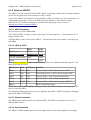
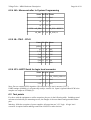
Function
RJ-11 pin RJ-14 pin RJ-25 pin
+12 Vdc input
1
+12 Vdc input
1
2
Phone ('ring' / -)
1
2
3
Phone ('tip' / +)
2
3
4
4
5
0 Vdc input (MP01 Gnd)
0 Vdc input (MP01 Gnd)
6
3.3 'WAN' - Ethernet RJ45
This jack supports standard 10BASE-T or 100BASE-TX ethernet (10 Mb/s or 100 Mb/s).
Crossover of the RX and TX pair is supported by the chipset (automatic or forced crossover). The
pinout diagram applies with crossover disabled.
A current limited dc supply may be fed to additional wires on this connection as an alternative to
feeding power through the power jack. Since this will back-feed to the power jack and TEL
connector, connection of only one power source at a time is recommended. Ensure the cable is not
a crossover type as this will reverse the supply polarity.
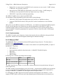
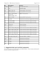
Function
RJ-45 pin
RX+
1
RX-
2
TX+
3
+12 Vdc input
4
+12 Vdc input
5
TX-
6
0 Vdc input (MP01 Gnd) 7
0 Vdc input (MP01 Gnd) 8
3.4 Antenna
The 802.11b/g WLAN operates at 2.300 - 2.500 GHz.
It is recommended that the supplied antenna be fitted to the N-type socket.
An additional antenna with a separate transceiver is mounted on the printed circuit board – although
this is shielded by the metal case.
3.5 'RESET' Push-button
Momentary push-button on the front panel. Flush mounted to prevent accidental operation.
Village Telco - MP01 Hardware Description
Page 4 of 18
3.6 Indication LEDs
Visible through the top cover:
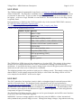
Label:
PWR
ACT
LINK
SYS
WIFI
TEL
Colour:
green
?
?
?
green
(2 colour)
green / none
(? some colours not identified)
3.7 Metal Case
The metal case of the MP01 V1.2 is connected to the common 'ground' of the circuitry and the
power source. To avoid getting a shock from the case, connecting it to ground is recommended
4 Functional overview
The MP01 consists of the following subsections:
•
WAP / Router
•
Telephone interface
•
Power Supply
Collectively the MP01 subsections can perform a variety of networking and telephony functions.
The function of each of these sections is further explained below. Software functionality is in
italics.
4.1 WAP / Router
The heart of the MP is the Wireless Access Point / Router sub-system. This supports 802.11b/g Wifi
communications, a 10/100 Mb/s ethernet interface and a UART. The 32 bit MIPS R4Kc processor
allows flexibility of operation and can support Linux.
Most MP01 functionality can be programmed into the WAP / Router's processor including mesh
networking, call routing, speech transcoding and echo cancellation.
4.1.1 Memory
Serial flash memory is used for non-volatile storage of the boot program, configuration data and the
application program.
SDRAM is used for execution.
Program updates in the field using no additional hardware are possible with appropriately written
software.
4.1.2 Atheros AR2317
The Atheros AR2317 Includes the following functions:
•
2.4 GHz wireless interface with diversity
◦ Transport of regular packets of speech samples
◦ Mesh networking
Village Telco - MP01 Hardware Description
•
Page 5 of 18
Ethernet 10 / 100 Mb/s MAC
◦ networking
◦ maintenance
•
MIPS processor
◦ telephony call routing
◦ telephony speech transcoding
◦ telephony echo cancellation
◦ LEDs and General Purpose i/o
▪ LED4 = 'SYS', LED5 = 'WIFI'
▪ Reading the “RESET” push-button state and acting on it.
▪ Control of the telephony interface and reading its state
◦ uart
▪ Transport of regular speech samples
▪ debugging console support
4.1.3 Ethernet PHY
The ethernet PHY circuit connects the RJ-45 ethernet jack to the ethernet MAC within the AR2317.
It is also responsible for such functions as Auto-MDIX (auto negotiation to cross over the Rx and
Tx pairs) and auto-negotiation or forcing of 10BASE-T, 100BASE-TX, half-duplex and full duplex
modes.
There are two LEDs controlled by the ethernet PHY. They are labelled 'ACT' (LED2) and 'LINK'
(LED3).
There is provision for the MP01 to use a phantom power feed from the RJ-45 jack.
4.2 Telephone Interface
The MP01 provides an FXS telephone interface (to understand FXS, see
http://en.wikipedia.org/wiki/Foreign_exchange_station ) that provides 'battery' power, dial tone and
ring voltage via the TEL jack to a plain old telephone (POT). This is fully controlled and monitored
by the processor in the WAP / Router which also handles all speech samples to and from the speech
codec.
The telephone interface has its own free-running oscillator which is the basis of a local PCM bus
that determines the codec sample rate. To accommodate the lack of synchronisation between the
MP codec and other telephony equipment, samples must be inserted or discarded within the MP.
With a good software implementation, this will have little effect on speech. If a 56 kb/s modem
were to be used, however, it would suffer impairment.
4.2.1 Microcontroller
The microcontroller is normally programmed to listen to the AR2317 SOC's UART output using
settings of 115200,8,n,1, (= baud rate, data bits, parity, stop bits) buffer the bursts of bytes in a
FIFO, then place them in one channel of the PCM bus for transmission to the SLIC. These bytes
Village Telco - MP01 Hardware Description
Page 6 of 18
represent voice samples to be heard by the user of the telephone. A bytes is either inserted or
deleted periodically to account for any slight difference between the PCM bus rate and the rate at
which the AR2317 receives samples from the network.
Reprogramming the microcontroller is only possible via an internal debug connector (J41) and
programming adaptor.
4.2.2 CPLD
The following describes functionality with normal programming:
The CPLD operates the control interface of the SLIC. It maps the control interface pins of the SLIC
to some general purpose i/o pins of the AR2317 SOC to do this.
The CPLD generates the frame synchronisation pulse for the PCM bus used by the SLIC to send
and receive codec samples. It also creates an enable for the microprocessor to identify the PCM
time slot it must use. These are generated from the free-running 2.048 MHz oscillator clock
received via jumper J1 (which is normally only removed to program the microcontroller.)
The CPLD receives PCM samples from the SLIC. It converts these to UART serial to be read with
parameters 115200,8,n,1 (actually sent as 113778,8,n,5.2) and passes them to the UART input of
the AR2317 SOC. These bytes represent samples of the speech waveform spoken by the user of the
telephone.
The CPLD receives serial data from any console that may be connected to internal debug connector
JP1. It passes these to the AR2317 SOC's UART (instead of the PCM samples) from boot time until
normal operation is underway. Distinction is made between the two situations using the GPIO
outputs of the AR2317.
There is one multi-coloured LED controlled by the CPLD. It is labelled 'TEL' (LED6).
4.2.3 SLIC
The Si3215 is a programmable CMOS SLIC / codec. With the help of some external discrete
components, it performs all BORSCHT functions (battery, overvoltage, ringing, supervision, codec,
hybrid, and test ) including stepping up the supply voltage as required.
Traditional telephone circuits were supplied by a -48 V battery with a series resistor. The SLIC
performs this battery feed function using far less power by dynamically controlling its supply
voltage and impedance. There are many configurable parameters to optimise performance.
The SLIC detects the phone going off hook. The SLIC's codec performs A-law or µ-law conversion
of speech samples at a rate of 8000 samples/sec, reading and writing these to the 2.048 Mb/s PCM
bus. The codec sample rate is exactly the PCM bus frame rate of 8 kHz.
4.3 Power Supply
Power inputs from the PWR, TEL and WAN connectors are combined and pass via auto-resetting
current limiting to over-voltage and reverse voltage protection. This then feeds the SLIC (for the
telephone interface) and a switching regulator that produces 3.3 Vdc (for all other circuitry). The
PWR LED shows steady green when the 3.3 Vdc supply is active.
5 Hardware – Firmware - Software Interfaces
This section gives an overview of what can be programmed and where to find the information
needed to program each item.
Village Telco - MP01 Hardware Description
Page 7 of 18
The schematic may help understanding. See
http://wiki.villagetelco.org/index.php?
title=FAQ#If_this_is_a_open_hardware_project.2C_where_are_the_schematics_and_board_layouts
.3F.
Comments in italics assume the CPLD and microprocessor run with their standard programming.
5.1 WAP / Router
The Atheros AR5007AP-G Reference Design is used, centred on the Atheros AR2317 chip, as
detailed in this section.
An overview is available from www.atheros.com/pt/AR5007AP-G.htm .
5.1.1 Memory
The MP01 has both SDRAM and flash memory for use by the AR2317.
5.1.1.1 SDRAM
16 MBytes of SDRAM memory is fitted, organised as 4 banks of 2,097,152 words x 16 bits/word in
a single chip. Details, such as memory refresh requirements, are available on the data sheet for the
Hynix HY57V281620H(F)C(T)T(P)-H/7 from www.huandong.com.cn . This memory is nonretentive – all data is lost at power failure.
5.1.1.2 Flash Memory
The MP01 provides serial flash memory connected to the SPI port of the AR2317. This is normally
programmed with a boot program and the application firmware. One of the following parts is fitted,
usually the 8 MByte option.
Size
Configuration
Part
Website
8 MByte 4 KByte sectors W25X64 www.winbond.com.tw
4 MByte 4 KByte sectors W25X32 www.winbond.com.tw
AR2317 pin Flash pin
SPI_CK
CLK
SPI_MISO
Q / SDO
SPI_MOSI
D / SDI
SPI_CS_L S / CS (active low)
Note: The flash connects directly as above. The optional gating shown in the schematic is not
fitted.
The only way to program the flash memory (called 'flashing') is via AR2317 software, such as a
boot loader program. Programmers should remember that power failure could interrupt
programming at any time and consider the recovery process.
An initial boot loader program may be loaded via the EJTAG programming adaptor (see section 7.2
Re-loading from scratch)
Village Telco - MP01 Hardware Description
Page 8 of 18
5.1.2 Atheros AR2317
The AR2317-AC1A is the heart of the WAP / Router, containing virtually all the systems required
on the one chip (hence the term 'system on a chip' or SOC).
Some of the AR2317 information is only available to Atheros customers for a fee and subject to a
confidentiality agreement. Some is available under the number of the reference design
(AR5007AP-G). Further information is available from third party sources such as:
embeddedcookbook.com/parts/AR2317 .
5.1.2.1 MIPS Processor
The processor is a 32 bit MIPS R4Kc.
The COLD_RESET_L input provides a reset input for a time (approx 5 – 10 ms) after the 3.3 V
supply voltage rises.
A 40.000 MHz crystal is fitted to the AR2317. The internal clock can be made to run faster (e.g.
200 MHz).
5.1.2.2 LEDs & GPIO
LED4
LED5
AR2317 port
GPIO2
GPIO7
Schematic v1.1 label
“WIRELESS” “SYS”
v1.2 case external label “SYS”
“WIFI”
Colour
?
green
Note: (? to be confirmed ?) Labels on these LEDs on the v1.1 schematic should be ignored. The
label on the case is correct.
AR2317 port Label
CPLD port Function
GPIO0
SCLK
IO21
Controls IO39 = SLIC control interface SCLK
GPIO1
SDO
IO20
Controlled by IO41 = SLIC control interface SDO
GPIO3
SDI
IO19
Controls IO40 = SLIC control interface SDI
GPIO4
nCS
IO18
Controls IO37 = SLIC control interface nCS
GPIO5
RESET IO16
Controls IO34 = SLIC control interface nRESET
GPIO6
RESET push-button input
NOTE: The button labelled RESET is simply read by the AR2317 software. You must cycle the
power to reset the MP01.
The standard CPLD program also selects a signal for the AR2317 UART according to the output
state of the AR2317 GPIO pins.
5.1.2.3 Ethernet Interface
The AR2317 has a MII interface to the ethernet PHY. The PHY is described in section 5.1.3
Ethernet PHY below.
5.1.2.4 Serial Interface
The AR2317 UART transmit goes to the following (all at the same time regardless of settings).
Village Telco - MP01 Hardware Description
Page 9 of 18
•
Header JP1 for connection (via an RS232 level convertor) to a test console. UART settings
of 9600,8,n,1 are generally expected.
•
microprocessor UART RXD (as PCM audio for the SLIC's codec). UART settings of
115200,8,n,1 are expected with a block of 8 bytes sent every 1.000 ms.
•
CPLD IO23. Ignored by standard programming.
The AR2317 UART receive comes from CPLD IO22.
The standard CPLD programming selects from either of the following:
•
CPLD IO2, fed by header JP1 (input from a test console) or a pulldown resistor.
•
Converted CPLD IO36 which is fed by the SLIC/codec's transmission to the PCM bus
(DRX).
After power-on, the AR2317 requests (via GPIO pins – see software for details) the CPLD program
to select serial data from JP1 so that any test console data passes to the AR2317 UART. A
continuous break is then received if no console is connected. To receive speech from the SLIC's
codec, the AR2317 should be programmed to request the CPLD to select the codec's PCM output
instead of JP1.
5.1.2.5 Radio Interface
The AR2317 includes radio frequency circuitry that requires factory calibration using specialised
equipment. Hackers are cautioned against disturbing the calibration settings.
5.1.3 Ethernet PHY
The DP83848I 'Phyter' performs the ethernet PHY (physical layer) function. The data sheet is
available from www.national.com.
Hardware strapping options are read on release of the ethernet reset (the ETH_RESET_L output of
the AR2317). These set:
• PHY address = 1
• Autonegotiation enabled, advertised mode = 100BASE-TX half/full duplex.
• MII mode
• LED mode 1
• MDIX enable
Following reset, software can change these settings.
LED2
PHY pin
LED3
LED_ACT/COL LED_LINK
v1.2 case external label “ACT”
“LINK”
Colour
?
?
The PHY should be set to mode 1 for the leds to indicate ethernet activity and ethernet link good
status respectively.
The PHY includes several intelligent power-down states. It performs Auto-MDIX (auto negotiation
to cross over the Rx and Tx pairs) unless software overrides this setting and auto-negotiation or
forcing of 10BASE-T, 100BASE-TX, half-duplex and full duplex modes.
For debugging, the PHY supports an internal loopback (returning data to the AR2317). It also
supports a 'BIST' (built in self-test) mode that transmits pseudo random data on the ethernet port
Village Telco - MP01 Hardware Description
Page 10 of 18
and checks it on return (via a loopback plug).
5.2 Telephone Interface
The MP01's FXS telephone interface connects to the Atheros AR2317 SOC via its serial port and
some GPIO pins. The GPIO pins are primarily used for the control and signalling functions whilst
the serial port is used either for a debug console or to carry the PCM voice samples.
The telephone interface circuitry uses a microprocessor, a CPLD and a SLIC. Central to these is a
PCM bus. The PCM bus has a fixed 2.048 MHz clock which can be disabled by removing jumper
J1 (to allow the in-system programmer to access the microcontroller SPI port). One time slot (8
bits) is used in each 8 kHz frame to transfer PCM samples from the microcontroller to the SLIC and
from the SLIC to the CPLD.
The following subsections detail the various parts of the FXS telephone interface.
5.2.1 Microcontroller
The ATMEGA8L is a single chip microcontroller with 8 KBytes of flash memory, 512 bytes of
EEPROM memory and 1 KByte of SRAM. The data sheet is available from www.atmel.com. The
MP01 attaches a 7.3728 MHz crystal oscillator. Power-on reset functionality is included. In-built
brownout detection and/or a watchdog timer are programming options that can assist in recovery
from supply glitches.
The microcontroller uart input receives the AR2317 uart output. The microcontroller uart output is
not connected (except to a test point).
The microcontroller SPI port is connected to the PCM bus, receiving the clock and transmitting to
the SLIC. A signal from the CPLD identifies the time slot.
Other microcontroller pins are unused or connected only to test points for possible future use. They
should either be programmed with pullups or driven to minimise dissipation.
Reprogramming the microcontroller is possible via an internal ISP (In Service Programming)
connector (J41). This only works when jumper J1 is removed, allowing the ISP programmer to
clock the PCM bus and hence the microprocessor SPI port. The 'serial downloading' features of the
microcontroller are used. See http://wiki.villagetelco.org/index.php?
title=Mesh_Potato_Firmware_How_To#Atmega_Compile_and_Flash.
Warning: For 'serial downloading' to continue functioning, the CKSEL fuses must select only valid
clock modes (external 3 to 8 MHz crystal or an internal oscillator mode) and pin PC6 must remain
as nRESET (RSTDISBL fuse not programmed).
For advanced readers:
The microcontroller does include bootloader support features. The flash memory can be
divided into bootloader and application sections with the bootloader section optionally
protected. Code placed in the bootloader section could conceivably read from any port and
program the application section accordingly.
The microcontroller could therefore, at least in theory, be reprogrammed from the AR2317.
In practice, however, writing a microcontroller bootloader to support this would be quite a
challenge due to the direction from microcontroller to the AR2317 having limited
communication support. The only such communication path is via the microcontroller SPI
port, the PCM bus, the SLIC in loopback mode – including digital – analogue – digital
conversions, the CPLD and the AR2317 uart.
Village Telco - MP01 Hardware Description
Page 11 of 18
5.2.2 CPLD
The CPLD (Complex Programmable Logic Device, see http://en.wikipedia.org/wiki/CPLD) is a
Xilinx XC9572XL. The data sheet is available from www.xilinx.com. The XC9572XL has 34 user
i/o pins and 72 macrocells. To give an idea of capabilities, each macrocell can be thought of as a 1
bit register – with lots of logic available to control that bit. The slowest device in the range (10ns)
is typically fitted.
Reprogramming (or 'flashing') the CPLD is possible only via the internal CPLD JTAG connector,
J8. See http://wiki.villagetelco.org/index.php?
title=Mesh_Potato_Firmware_How_To#Xilinx_CPLD_Compile_and_Flash
CPLD IO can be summarised as follows:
Number of pins Function
5
AR2317 GPIO
2
AR2317 uart
1
Serial data from debug console
2
LED6 “TEL” (LED1A = IO32, LED1B = IO31)
3
PCM bus clock & frame synchronisations
1
PCM bus data
5
SLIC control interface, reset
2
Test points (TP10, TP11)
4
CPLD programming (JTAG)
13
Spare i/o
6
Supply / ground
The CPLD drives LED6, shown in the schematic as a 2-colour LED. The polarity of the voltage
between the two outputs determines the colour. Intermediate colouring is possible through
modulation. It is possible the factory may be fitting single colour LEDs (green) which effectively
makes the second colour none or black (to be confirmed).
The telephone interface also provides a serial port for a debug console. This simply consists of the
shared AR2317 serial transmit output and the ability to select either the debug console or PCM
voice samples for the AR2317 serial receive input.
5.2.3 SLIC
The SLIC (subscriber line interface circuit) is built on a daughter-board connected between J400
and J40 of the main board. The daughter board is described as an FXS card as detailed in
http://www.atcom.cn/AX110S.html. It is also described by the typical application circuits shown in
the data sheet of the Si3215-FM which is available from www.silabs.com. The BJT/Inductor DCDC convertor circuit shown in the data sheet as figure 10 and the application circuit using discrete
components in figure 12 both apply.
The Si3125 has a PCM bus interface, which we use for speech samples, and an SPI control interface
for access to the control and status registers.
WARNING: Incorrect settings applied to this chip may cause the MP01 to violate international
safety standards and present a danger to users. Settings that change voltages, ring cadences and ring
Village Telco - MP01 Hardware Description
Page 12 of 18
trip detection can all affect safety. Some settings could damage the MP01.
5.3 Power Supply
The power supply is not controlled by any software. Software can, however, affect supply loading
as various functions are turned on and off. Be aware that creating contention (that is when two ICs
both attempt to drive the same node to different voltages) can overload the supply, overheat the ICs
and damage the ICs.
Software can not read the supply voltage. It may, however, be possible to gain some insight into the
magnitude of the input voltage using the fact that it drives the SLIC's DC-DC convertor directly
(not via the 3.3 V regulator used by all other logic). The SLIC measures various voltages (but is a
suitable test possible while a phone remains plugged in?)
6 Maintenance Connectors
Debug / commissioning ports, pinouts and pin functions:
6.1 List of maintenance connectors
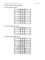
Ref Description
Comment
J1
Jumper 2x1
Connects 2.048 MHz to uP_SCK (the PCM bus clock)
J11
EJTAG Header (2x7) For JTAG programming of the AR2317
J40
Socket 3x2
FXS daughter board
J400 Socket 10x2
FXS daughter board
J41
Conn 5x2
For microcontroller ISP (in-system programming)
J8
CPLD_JTAG
For JTAG programming of the CPLD
JP1 'RS-232' Header (3x2) For an external logic level convertor (0 to 3.3V <-> RS232) for use
by a RS232 device
Village Telco - MP01 Hardware Description
Page 13 of 18
6.2 Maintenance connector pinouts
6.2.1 J11: EJTAG - AR2317
Name Pin Pin Name
TRST_L 1
2 Gnd
TDI 3
4 Gnd
TDO 5
6 Gnd
TMS 7
8 Gnd
TCLK 9
10 Gnd
/COLD_RST 11
12 nc
nc 13 14 3.3V
6.2.2 J40: FXS daughter board
Name Pin Pin Name
Ring 5
6 nc
nc 3
4 nc
Tip 1
2 nc
6.2.3 J400: FXS daughter board
Name Pin Pin Name
Gnd 20 19 VUNREG
Gnd 18 17 nc
nc 16 15 3.3V filt J400
nc 14 13 nc
BBSDO 12
11 nc
BBSDI 10
9 nc
BBSCLK 8
BBnCS
7 FSYNC
6
5 DRX
nc 4
3 DTX
nRST 2
1 PCLK
Village Telco - MP01 Hardware Description
Page 14 of 18
6.2.4 J41: Microcontroller In-System Programming
Name Pin Pin Name
3.3V 1
2 Gnd
nc 3
4 nc
nc 5
6 nc
DTX = uP_PB4 7
uP_PB3 9
8 uP_PC6 = RESET
10 uP_SCK, J1
6.2.5 J8: JTAG - CPLD
Name Pin Pin Name
pullup 1
nc 3
2 nc
4 Gnd
3.3V 5
6 TMS
Gnd 7
8 TCK
Gnd 9
10 nc
Gnd 11
12 TDI
Gnd 13 14 TDO
6.2.6 JP1: UART Serial for logic level convertor
Name Pin Pin Name
SOUT 1
2 SIN_CPLD, pulldown
nc 3
4 Gnd
3.3V 5
6 Gnd
Note: Do not connect RS232 signals to JP1 without a logic level convertor (3.3 V).
UART settings of 9600,8,n,1 are generally used for console i/o. Input is ignored when PCM voice
samples are output at 115200,8,n,1.
6.3 Test points
For those with the equipment to utilise testpoints, they are in the following table. Suitable ground
references include the pcb mounting screws, the flanges of the reset button and grounded header
pins.
Warning: With the exception of power supplies, all testpoints use 3.3 V logic. A logic level
convertor is required when making connection to RS232 or other devices.
Village Telco - MP01 Hardware Description
Ref
Node name(s)
Page 15 of 18
Function
VUNREG VUNREG
DC supply input, fused
TP2
3.3V
Regulated supply
TP3
AR2317_DAC_IN
Unused (AR2317 radio section)
TP4
AR2317_DAC_IP
Unused (AR2317 radio section)
TP5
SOUT / TXD, uP_RXD,
CPLD_IO23,
AR2317_UART_SOUT
AR2317 Uart serial out
TP6
AR2317_ATBP
Unused (AR2317 radio section)
TP7
uP_TXD
Unused microcontroller pin (supports uart serial out)
TP8
uP_PCINT0/PB0
Unused microcontroller pin (supports interrupt)
TP9
uP_PCINT1/PB1
Unused microcontroller pin (supports interrupt)
TP10
CPLD_IO13
Unused CPLD pin
TP11
CPLD_IO3
Unused CPLD pin
TP12
GPIO0 / SCLK, CPLD_IO21 Control connection between AR2317 and CPLD
TP13
GPIO1 / SDO, CPLD_IO20
Control connection between AR2317 and CPLD
TP14
GPIO3 / SDI, CPLD_IO19
Control connection between AR2317 and CPLD
TP15
GPIO4 / nCS, CPLD_IO18
Control connection between AR2317 and CPLD
TP16
GPIO5 / RESET, CPLD_IO16 Control connection between AR2317 and CPLD
TP17
SIN / RXD, CPLD_IO22
Uart serial: CPLD → AR2317
TP18
uP_PD3
Unused microcontroller pin
TP19
uP_PD5
Unused microcontroller pin
TP20
uP_PD6
Unused microcontroller pin
TP21
uP_PD7
Unused microcontroller pin
7 Suggested start-up & self-test sequences
This introduces general techniques applying to the MP01 platform. Other documents detail specific
firmware builds and loading instructions.
Village Telco - MP01 Hardware Description
Page 16 of 18
7.1 First Use
After applying power to the MP01, the PWR led will show a steady green. This only indicates that
the regulator is supplying power. All other leds are under software control.
Software is fully installed in the factory for normal use. For usage see
http://wiki.villagetelco.org/index.php?
title=Mesh_Potato_HOWTOs#Getting_Started_with_your_Mesh_Potato.
For special applications or upgrades, the main processor application firmware (the Linux image)
may need to be upgraded or replaced. With appropriate software it should be possible to do this
without opening the MP01. See
http://wiki.villagetelco.org/index.php?
title=Mesh_Potato_HOWTOs#Preliminary_Mesh_Potato_firmware_disaster_recovery_HOWTO.
7.2 Re-loading from scratch
This summarises the steps needed to program the flash memories of a newly assembled (or perhaps
a extremely corrupted) MP01, making no assumptions about existing code.
•
Apply power to the MP01 with the cover off and ensure that the PWR led shows steady
green. Ensure that no integrated circuits get abnormally hot during each programming step
(avoid touching any circuitry however).
It is possible for corrupted software to cause contention on lines between the AR2317 and
the CPLD or between the CPLD and the microprocessor. This causes excessive power
consumption and could possibly result in repeated and partial resets. In the unlikely event
of this happening, it may be necessary to reprogram the offending device first or to hold it in
reset via its programming connector.
•
Always power down when attaching or removing maintenance connectors.
•
The ATMEGA microprocessor may be programmed first via an ISP adaptor. See
http://wiki.villagetelco.org/index.php?
title=Mesh_Potato_Firmware_How_To#Atmega_Compile_and_Flash.
Remember to re-insert jumper J1 after programming (to provide a clock to the PCM bus).
•
The Xilinx CPLD is programmed using a JTAG programming adaptor. See
http://wiki.villagetelco.org/index.php?
title=Mesh_Potato_Firmware_How_To#Xilinx_CPLD_Compile_and_Flash.
Note that the Xilinx and Atheros parts use different JTAG adaptors.
•
The first boot loader program and configuration data are programmed into the serial flash
memory via a JTAG adaptor connected to the Atheros AR2317 SoC. The configuration data
includes a unique MAC address for the ethernet port and radio calibration data unique to
each AR2317. See
http://wiki.villagetelco.org/index.php?
title=Mesh_Potato_Firmware_How_To#Flashing_the_Boot_Loader_using_JTAG.
This is a slow process. The smaller the program the faster it loads.
Radio calibration data is normally obtained using specialised equipment in the factory.
•
The boot loader program will now be accessible from a console:
◦ If the boot loader supports ethernet, this is the preferred method of access.
◦ To use a serial console, an RS232 terminal should be connected via a logic level
convertor to header JP1. The terminal always receives serial data. The boot program
receives terminal input via the CPLD.
Village Telco - MP01 Hardware Description
Page 17 of 18
Once launched, the main program needs the serial port for the telephony interface and
will have the CPLD redirect input.
•
It is possible that the boot loader could be used to install an upgraded boot loader.
•
Using the boot loader, the application firmware (Linux image) may be loaded in the serial
flash memory (avoiding the segments used by the boot loader and configuration software).
See http://wiki.villagetelco.org/index.php?
title=Mesh_Potato_Firmware_How_To#Flashing_Linux_Images_from_Redboot.
•
Full operation should now be possible.
•
Under control of the application, upgrades to the serial flash memory may be permitted
(which holds the boot loader, configuration data and the application firmware).
It is impossible for the application to change the microcontroller firmware or CPLD
firmware.
7.3 Self-test software
Building self-test software into a product is a great time-saver both during development and product
support. Self-tests usually run briefly following power-up and provide visual indication to the user,
often with debug information made available in case a console is connected. The MP01 hardware
provides the following opportunities for self-testing:
•
Flash memory data could be checked for corruption using checksums.
•
SDRAM memory could be checked for bit failures and improper refreshing.
•
LEDs 4 & 5 are immediately controlled by software.
•
LED6 is controlled via the CPLD. It can provide 2 colours (and blends of these if
modulation is used).
•
The ethernet PHY may be programmed into loopback mode (with auto-negotiation turned
off). Test data transmitted is then received and does not get sent to the network. Presumably
loopback mode gives full control of LEDs 2 & 3.
•
The SLIC has a 'digital loopback' mode. Speech (or tone) samples sent to the SLIC are
converted to linear, gain adjusted, filtered and converted back to PCM before being sent
back. This tests control of the SLIC via the CPLD as well as speech sample processing by
the CPLD and microcontroller. It also confirms that the 20 pin end of the daughter board is
connected (although the other end may have worked free) and that jumper J1 is in place.
This is readily checked by sending DTMF tone samples to the SLIC and using DTMF tone
detection software (which is probably required by the application anyway) on the returned
samples.
•
The SLIC's DC-DC convertor can be checked by ensuring that a suitable combination of
line voltage and line current is reported in the SLIC's registers.
If there is no telephone off-hook, line current should be minimal with voltage determined by
the SLIC settings. Off-hook telephones result in reduced line voltage and increased line
current. Convertor faults reduce the voltage and current below expected values – as do low
supply voltages.
•
(A self-test of the radio interface may also be possible.)
•
A full load test can verify that the supply can provide sufficient power for normal operation
without the processor resetting and without the SLIC's DC-DC convertor being blocked by
undervoltage lockout. The test should be long enough to use capacitively stored energy (10
Village Telco - MP01 Hardware Description
Page 18 of 18
ms uses all such energy within the MP01 but at least 100 ms is suggested to account for
capacitance that may be in the external supply).
8 History of this document
Date
Changes
11 Apr 2010
Initial version for comment
1 Jun 2010
Added FXS board details, corrected serial settings, modified introduction.