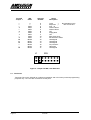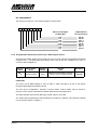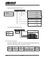
1
PC215E
PROGRAMMABLE
DIGITAL
INPUT/OUTPUT
AND COUNTER/TIMER
BOARD
This Instruction Manual is supplied with the PC215E to provide the user with sufficient information to utilise the
purchased product in a proper and efficient manner. The information contained has been reviewed and is believed to be
accurate and reliable, however Amplicon Liveline Limited accepts no responsibility for any problems caused by errors
or omissions. Specifications and instructions are subject to change without notice.
PC215E Instruction Manual Part Nº 85 956 294 Issue A3
© Amplicon Liveline Limited
Prepared by Jonathan East
Approved for issue by A.S. Gorbold, Operations Director
PC215E
DECLARATION OF CONFORMITY
AMPLICON LIVELINE LIMITED
CENTENARY INDUSTRIAL ESTATE
HOLLINGDEAN ROAD
BRIGHTON BN2 4AW UK
We declare that the product(s) described in this Instruction Manual
perform in conformity with the following standards or standardisation
documents:
Electro Magnetic Compatibility (EMC):
EMC Directive 89/336/EEC
LVD Directive 73/23/EEC
CE Directive
93/68/EEC
Jim Hicks, I.Eng, FIEIE
Managing Director
Amplicon Liveline Limited
PC215E
PROGRAMMABLE DIGITAL I/O AND COUNTER/TIMER BOARD
TABLE OF CONTENTS
1.
INTRODUCTION .......................................................................................................1
1.1
1.2
1.2.1
1.2.2
1.3
1.4
1.5
1.5.1
1.6
1.7
1.8
1.8.1
1.8.2
The Amplicon 200 Series
The 200 Series Digital I/O Counter/Timer Family
Typical Applications
Product List
Product Configurator
Features of the PC215E
PC215E General Description
The Software
What the PC215E Package Contains
The Amplicon Warranty Covering the PC215E
Contacting Amplicon Liveline Limited for Support or Service
Technical Support
Repairs
2.
GETTING STARTED.................................................................................................8
2.1
2.2
2.3
2.4
2.5
2.6
2.6.1
2.6.2
2.6.3
2.7
General Information
Installing the Board
System Requirements
Backing up the Software Diskettes
Software Installation
Configuration Switch and Jumper Settings
Base Address Selection
PC I/O Map
Selection of Interrupt Request (IRQ) Level
Test Points
3.
MAKING THE CONNECTIONS ..............................................................................12
3.1
3.2
3.2.1
3.3
3.4
3.5
3.6
The Input/Output Connector
Cable Connections
Features Summary of the Expansion Panels
Use of Shielded Cables
Digital Input/Output Conditions
Counter/Timer Input/Output Conditions
PC Back-plane Bus Connections
4.
USING THE PC215E...............................................................................................16
4.1
4.2
4.2.1
4.2.2
4.2.3
4.2.4
4.2.5
4.2.6
4.2.7
4.2.8
4.2.9
Multiple PC215E Boards in a Single Application
User Applications
Differential Counter
Monostable Multivibrator
Astable Multivibrator
Stopwatch
Event Recorder
Frequency/Period Measurement
Frequency Generation
Frequency Multiplication
Digitally Controlled Oscillator
PC215E
1
1
1
2
2
4
4
4
6
6
7
7
7
8
8
8
8
9
9
9
10
10
11
12
13
13
14
14
14
14
16
16
17
17
17
18
18
19
19
19
19
4.2.10
4.2.11
4.2.12
Voltage Controlled Oscillator
Switch Matrix
8-Bit Bi-Directional Bus
5.
STRUCTURE AND ASSIGNMENTS OF THE REGISTERS ..................................23
5.1
5.2
5.2.1
5.2.2
5.2.3
5.3
5.3.1
5.3.2
5.3.3
5.3.4
5.3.5
5.3.6
5.3.7
5.3.8
5.3.9
5.3.10
5.3.11
5.3.12
5.3.13
5.3.14
5.3.15
5.3.16
5.3.17
5.3.18
5.3.19
5.3.20
5.3.21
5.3.22
Register Assignments
Register Groups
Cluster X, Y and Z Groups
Counter Connection Register Group
Interrupts Group
The Register Details
Programmable Peripheral Interface PPI-X Data Register Port A
Programmable Peripheral Interface PPI-X Data Register Port B
Programmable Peripheral Interface PPI-X Data Register Port C
Programmable Peripheral Interface PPI-X Command Register
Programmable Peripheral Interface PPI-Y Data Register Port A
Programmable Peripheral Interface PPI-Y Data Register Port B
Programmable Peripheral Interface PPI-Y Data Register Port C
Programmable Peripheral Interface PPI-Y Command Register
Z1 Counter 0 Data Register
Z1 Counter 1 Data Register
Z1 Counter 2 Data Register
Counter/Timer Z1 Control Register
Z1 Counter/Timer Status Register
Z2 Counter 0 Data Register
Z2 Counter 1 Data Register
Z2 Counter 2 Data Register
Counter/Timer Z2 Control Register
Z2 Counter/Timer Status Register
Group Z Clock Connection Register
Group Z Gate Connection Register
Interrupt Source Selection Register
Interrupt Status Register
6.
PROGRAMMING THE PC215E..............................................................................54
6.1
6.2
6.3
6.4
6.4.1
6.4.2
6.5
6.5.1
6.6
6.6.1
6.6.2
6.6.3
6.6.4
6.6.5
6.6.6
6.6.7
6.6.8
6.6.9
6.6.10
6.6.11
Copyright
Files installed from the Distribution Diskette
Windows DLL and Examples
DOS 'C' Library and Examples
Borland C++ User Information
Microsoft C/C++ User Information
Using the Dynamic Link Library
Visual Basic
Windows and DOS Library Functions
Initialisation Functions
Interrupt Control Functions
Data Buffer Functions
Timer/Counter Functions
Differential Counter Functions
Frequency Generation Functions
Millisecond Stopwatch Functions
Frequency Input and Output Functions
Digitally- and Voltage-Controlled Oscillator Functions
Digital Input/Output Functions
Switch Scanner Matrix Functions
PC215E
20
21
22
23
23
23
23
23
24
25
26
27
28
30
31
32
33
35
37
38
39
41
42
43
44
45
47
49
50
51
52
54
54
55
55
56
56
56
56
58
58
60
62
69
78
82
84
89
95
99
104
6.6.12
6.7
6.8
6.8.1
6.8.2
6.9
6.10
Bi-Directional Data Bus Functions
PC215E Library Error Codes
PC215E Interface Guide For LABTECH NOTEBOOK
Channel Assignments:
Configuring the Board
Guide to User Programming
Signal Centre
PC215E
106
107
108
109
109
110
110
1. INTRODUCTION
1.1 The Amplicon 200 Series
The Amplicon 200 Series of Personal Computer based data acquisition products provides very
high performance, affordable hardware with comprehensive software support. The 200 Series is
designed for users requiring fast or complex data input/output to the host PC and comprises a
range of boards and software to handle most analog and digital signal types.
When a large scale system is required, multiple boards can be added from the 200 Series
without conflict. The capacity of the PC mounted hardware can be extended by external
expansion panels to provide a comprehensive system with low cost per channel and maintained
high performance.
1.2 The 200 Series Digital I/O Counter/Timer Family
The family of 200 Series digital input/output products may be configured in a variety of ways to
provide flexible, expansible systems.
Five digital input/output boards with timer/counter facilities are offered. These five boards are
complemented by four external panels for signal conditioning and user connection through
individual terminals. Support and demonstration software for all variants is offered.
A full, itemised list of hardware products is shown below, and a configurator diagram showing
how these products interact is also given. To complete the family, a common software package
supports all digital I/O boards and the expansion panels.
1.2.1
Typical Applications
• TTL compatible digital input/output
• Relay output with isolated contacts, high level ground referenced source drivers (any
combination)
• Isolated high or low level digital input, ground referenced high or low level digital input (any
combination)
• Interrogation of contact closure matrix - up to 1296 points per PC272E
• Elapsed time, period, frequency measurement
• Differential, ratiometric count
• Monostable and astable generation
• Frequency division, frequency multiplication, digitally controlled oscillator
• Voltage controlled oscillator (in conjunction with PC226E, PC30AT, PC26AT or PC27E)
Page 1
PC215E
1.2.2
Product List
Product Number
PC212E
PC214E
PC215E
PC218E
PC272E
Product Type
Brief Description
Counter/timer, Digital I/O board
Counter/timer, Digital I/O board
Counter/timer, Digital I/O board
Counter/timer board
Digital I/O board
12 counters, clock/gate source, 24 line digital I/O
3 counters, 48 line digital I/O
6 counters, clock/gate source, 48 line digital I/O
18 counters, clock/gate source
72 line digital I/O
Termination/distribution panel
Output panel
Input panel
Input/output panel
78 Terminals, 3 x 37 way distribution connectors
24 relay or high level logic source drivers
24 isolated or non-isolated, high or low level inputs
16 inputs, 8 outputs
90 966 349
90 956 109
91 945 753
78 way Screened Cable 1m
37 way Screened Cable 1m
37 way Screened Connector Kit
I/O board to EX233 Termination/distribution panel
PC36AT or EX233 to I/O panel
PC36AT
908 919 50
919 459 53
24 Line Digital I/O Board
37 way screw terminal assy
78 way Screened Connector Kit
EX233
EX213
EX230
EX221
1.3 Product Configurator
Figure 1 - Product Configurator Block Diagram - shows how the six digital I/O boards (including
the PC36AT) may be connected, using the supplied cables, to form a variety of systems. The
simplest usable system configuration comprises one board from the PC212E, PC214E,
PC215E, PC218E or PC272E range, a 78 way cable and an EX233. This system provides user
terminals to all I/O functions of the board. More complex, configurable systems include isolated
or common ground input and output at low or high level.
All five boards employ the concept of I/O Groups, where a group can be six 16 bit counter timers
with interconnects, or 24 lines of digital input/output. These groups are integrated as necessary
to provide the specified functionality.
A software configurable clock and gate source group provides five precise frequencies for
counter/timer input, and also allows for counter/timer inter-connection.
The user I/O connector map recognises this grouping and allows any combination of expansion
panels to be directly added to any of the boards, with each panel mapped onto a counter/timer
group or digital I/O group.
PC215E
Page 2
PC212E
78 way
Connector
Kit
12 Counters
24 Lines Digital I/O
OR
EX
213
24
O/P
OR
PC214E
EX233
78 way termination
and/or 3x37 way
distribution
3 Counters
48 Lines Digital I/O
OR
PC215E
AND
/OR
78-78 way
Cable
6 Counters
48 Lines Digital I/O
24
I/P
AND
/OR
OR
EX
230
PC218E
18 Counters
37-37 way
Cable
OR
PC272E
EX
221
72 Lines Digital I/O
OR
AND
/OR
PC36AT
OR
OR
37 way
Connector
Kit
Existing 37 way
termination assy
Figure 1 - Product Configurator Block Diagram
Page 3
16
I/P
8
O/P
37-37 way
Cable
Existing
24 Lines Digital I/O
AND
/OR
PC215E
1.4 Features of the PC215E
• Six 16-bit, 10 MHz counter/timers, each with six programmable counter modes
• Crystal clock/divider with 5 rates, independently software-selectable for each counter/timer
clock input
• Independent software-selectable clock and gate inputs for each counter/timer
• 48 programmable digital I/O lines, with three operating modes
• Six software-selectable interrupt sources - two timer output and four digital I/O
1.5 PC215E General Description
The PC215E is a half-size ISA bus plug-in board which provides 48 programmable digital
input/output lines, and six independent programmable 16 bit counter/timers. The board can be
installed in IBM© or fully compatible PC/AT computers.
The flexible addressing system provided on the board allows the base address to be set within
the range 000 to FF016. The board interrupt level can be software selected to IRQ3, IRQ5,
IRQ7, IRQ9, IRQ10, IRQ11, IRQ12 or IRQ15, and any number of five possible interrupt sources
can be software selected.
A 10 MHz on-board crystal oscillator provides an accurate, stable clock source for the
counter/timers, independent of the system clock frequency. A divider circuit provides five
selectable frequencies (10 MHz, 1 MHz, 100 kHz, 10 kHz and 1 kHz) derived from the oscillator,
and each of the counter/timer clock inputs can be automatically connected to any of these clock
sources, or to its own individual external clock source, or to the output of another counter/timer.
Each of the counter/timer gate inputs can be enabled and disabled in software, or automatically
connected to its own external gate source, or the output of another counter/timer.
A block diagram of the PC215E is given in Figure 2.
1.5.1 The Software
The PC215E is supplied with a 3½” diskette containing the software, which supports all
five of the boards in the 200 Series Digital I/O Counter/Timer Family. This software is
described fully in section 6 of this manual.
1.5.1.1
Windows Installation Program
The software is installed onto the user's hard disk by a Windows installation program.
See section 2 of this manual for information on getting started.
1.5.1.2
Windows DLL
A Windows Dynamic Link Library (DLL) containing over 50 functions provides an
Applications Program Interface (API) to the PC215E, and the other boards in the family.
The library functions allow the boards to be easily applied to many different applications,
and also provide an easy way of accessing the board's features. The 16-bit DLL can be
called by any language which uses Windows calling conventions, and example programs
written in Microsoft Visual Basic are also provided.
PC215E
Page 4
A7
A6
A5
A4
A3
A2
A1
A0
C7
C6
C5
C4
C3
C2
C1
C0
B7
B6
B5
B4
B3
B2
B1
B0
A7
A6
A5
A4
A3
A2
A1
A0
C7
C6
C5
C4
C3
C2
C1
C0
B7
B6
B5
B4
B3
B2
B1
B0
Port A
82C55
PPI - X
Board Crystal Clock Generator
(5 source frequencies)
Port C
Port B
Port A
82C55
PPI - Y
Port C
Port B
Z1 I/P
CLK0
GAT0
OUT0
CLK1
GAT1
OUT1
CLK2
GAT2
OUT2
/OUT0
CLK0
GAT0
OUT0
CLK1
GAT1
OUT1
CLK2
GAT2
OUT2
/OUT0
CTR 0
Counter
Connection
Registers
Z1 and Z2
CTR 1
CTR 2
CTR 0
CTR 1
CTR 2
82C54
Ctr/Tmr
Z1
82C54
Ctr/Tmr
Z2
Z2 I/P
Interrupts Enable and
Status Registers
8 bit
Data
I/O
Bus
Address Offset
Decoder
Event
Interrupt
W/R
5 bit Address
Offset
PC INTERFACE
IRQ
Controls
ISA Bus
Figure 2 - PC215E Block Diagram
Page 5
PC215E
Data
Address
1.5.1.3
DOS Library
A DOS library for Microsoft and Borland C/C++ is supplied, which has exactly the
same functionality as the Windows DLL. Four example 'C' programs are also
provided, and these can be recompiled with either Microsoft C/C++ or Borland
C++.
1.5.1.4
LABTECH NOTEBOOK Drivers
A LABTECH NOTEBOOKpro driver is provided with template files for each of the boards
in the family.
1.6 What the PC215E Package Contains
!
CAUTION
Some of the components on the board are susceptible to electrostatic discharge, and
proper handling precautions should be observed. As a minimum, an earthed wrist strap
must be worn when handling the PC215E outside its protective bag. Full static handling
procedures are defined in British Standards Publication BSEN100015/BSEN1000151:1992.
When removed from the bag, inspect the board for any obvious signs of damage and
notify Amplicon if such damage is apparent. Do not plug a damaged board into the host
computer. Keep the protective bag for possible future use in transporting the board.
The package as delivered from Amplicon Liveline Ltd. contains:Item 1
PC215E board is supplied in a protective bag. When removing the board,
observe the precautions outlined in paragraph 1.6
Item 2
200 Series Digital I/O Counter/Timer Software Diskette (Part Nº 90 956 209),
supplied on 3 1/2" diskette(s).
Item 3
This PC215E Instruction Manual (Part Nº 85 956 294)
Any additional accessories (termination boards, cables, optional software etc.) may be packed
separately.
1.7 The Amplicon Warranty Covering the PC215E
This product is covered by the warranty as detailed in the Terms and Conditions stated in the
current domestic or international Amplicon Liveline catalogue.
PC215E
Page 6
1.8 Contacting Amplicon Liveline Limited for Support or Service
The PC215E board is produced by Amplicon Liveline Limited and maintenance is available
throughout the supported life of the product.
1.8.1 Technical Support
Should this product appear defective, please check the information in this manual and any 'Help'
or 'READ.ME' files appropriate to the program in use to ensure that the product is being
correctly applied.
If a problem persists, please request Technical Support on one of the following numbers:
Telephone: UK
International
01273 608 331
+44 1273 608 331
Fax:
01273 570 215
+44 1273 570 215
UK
International
Internet
[email protected]
www.amplicon.co.uk
1.8.2 Repairs
If the PC215E requires repair then please return the goods enclosing a repair order detailing the
nature of the fault. If the PC215E is still under warranty, there will be no repair charge unless
any damage as a consequence of improper use.
For traceability when processing returned goods, a Returned Materials Authorisation (RMA)
procedure is in operation. Before returning the goods, please request an individual RMA number
by contacting Amplicon Customer Services by telephone or fax on the above numbers. Give the
reason for the return and, if the goods are still under warranty, the original invoice number and
date. Repair turnaround time is normally five working days but the Service Engineers will always
try to co-operate if there is a particular problem of time pressure.
Please mark the RMA number on the outside of the packaging to ensure that the package is
accepted by the Goods Inwards Department.
Address repairs to:
Page 7
Customer Services Department
AMPLICON LIVELINE LIMITED
Centenary Industrial Estate
Hollingdean Road
BRIGHTON UK BN2 4AW
PC215E
2. GETTING STARTED
2.1
General Information
The PC215E software diskette contains six ready-to-run executable programs, three for DOS
and three for Windows. These programs allow the user to perform I/O operations on the
PC215E immediately after installing the board and software onto a PC.
2.2
Installing the Board
ENSURE THAT THE POWER TO THE COMPUTER IS SWITCHED OFF
BEFORE INSTALLING OR REMOVING ANY EXPANSION BOARD. OBSERVE
HANDLING PRECAUTIONS NOTED IN SECTION 1.6.
REPAIR OF DAMAGE CAUSED BY MIS-HANDLING IS NOT COVERED UNDER
THE AMPLICON WARRANTY.
DO NOT MAKE ANY MODIFICATIONS OTHER THAN SWITCH CHANGES TO A
BOARD THAT IS ON EVALUATION
Please refer to the manufacturer's hardware manual supplied with the PC for instructions on
how to remove the cover and install devices into an ISA bus slot. The PC215E may be installed
in any available position in the machine provided that there is no restriction specified for that
location by the computer manufacturer. If available, the end slot furthest from any other I/O card
should be chosen to minimise the risk of the switched signals inducing interference in the PC
circuits.
2.3 System Requirements
When installing one or more PC215E boards, ensure that the host computer has sufficient
capacity. Take into account other boards or adapters that may be installed in the computer
when assessing physical space, address space in the I/O map, interrupt levels and the power
requirements. A minimum host computer configuration is:
•
•
•
•
•
IBM© or fully compatible PC/AT with 286 or higher processor, 31/2" high density floppy disk
drive, hard disk drive and monitor.
One free, ISA bus to accommodate a 1/2 length I/O card slot.
Sufficient power available. +5 VDC at 30 mA is required for each PC215E (unloaded).
DOS 6.0 or higher to run the DOS demonstration programs.
Microsoft Windows 3.1 or higher to use the DLL and run the Windows demonstration
programs.
2.4 Backing up the Software Diskettes
It is important that a backup copy of the software diskette(s) is made and the original stored in a
cool, dry, safe place. The diskette(s) can be copied onto a blank diskette and/or the software
copied onto the hard disk. A supplied Windows setup program installs the software on the hard
disk. Refer to the DOS or Windows manual for information on disk copying. Always use the
working copy.
PC215E
Page 8
2.5 Software Installation
To install the PC215E software onto your hard disk, insert disk 1 into drive A: and select
‘File|Run...’ from the Windows Program Manager, or, if you are using Windows 95, select
‘Run...’ from the Start menu. In the dialogue box that follows, type
A:\SETUP <RETURN>
The PC215E software installation program will now run. Follow the instructions on the screen to
complete the installation. See section 6 ‘Programming The PC215E’ for information on running
the software.
2.6 Configuration Switch and Jumper Settings
Before installing this board in the host computer, the configuration needs to be set to the user's
requirements. Setting is by means of an on-board in-line switch and a pluggable jumper whose
functions are described below.
2.6.1
Base Address Selection
The base address of the PC215E can be selected in the range 000 to FF016. If more than one
PC215E is installed in a single PC, each board must have a different base address and these
will be separated by at least 32 bytes. It is normally convenient to have the base addresses at
contiguous even locations. The factory default base address is 30016.
Conflict of I/O addresses with other devices in the host PC or fitted adaptors is a common cause
of operational problems and care should be taken to ensure that the PC215E base address is
chosen where no port assignment is in contention.
The board’s base address is set by switch SW1. This switch bank comprises a row of eight
single-pole, single-throw switches with each 'up' or 'ON' position selecting a logic 1, and each
'down' or 'OFF' position selecting a logic 0. The most significant hex digit of the base address is
coded by the four most left switches, and the middle hex digit is coded by the four most right
switches of SW1. The least significant hex digit is always 0.
Figure 3 below shows the factory default setting of 30016
Most significant digit 0011
Middle digit 000
Least significant Default
Page 9
=
=
=
PC215E
316
016
016
SW1
'1'
ON
ON
'0' OFF
'1'
OFF '0'
1 2 3 4 5 6 7 8
800 400 200 100 80
Most Significant
Digit
40
20
Middle
Digit
10
!
Least
Significant
Default
Figure 3 - DIL Switch Selection for Base Address
2.6.2 PC I/O Map
The standard PC/AT I/O map assignments are listed below.
I/O addresses 00016 to 0FF16 are reserved for the PC system board use and I/O
addresses 10016 to 3FF16 are available on the I/O channel. The installation of the
PC215E at a base address that uses unlisted ports may result in conflicting assignments
with third party adapters.
Hex Range
Usage
Hex Range
Usage
1F0-1FF
200-20F
210-21F
238-23B
23C-23F
270-27F
2B0-2DF
2E0-2E7
2E8-2EF
2F8-2FF
300-31F
Hard Disc (AT)
Game/Control
Reserved
Bus Mouse
Alt. Bus Mouse
Parallel Printer
EGA
GPIB (AT)
Serial Port COM4
Serial Port COM2
Prototype Card
360-36F
378-37F
380-38F
3A0-3AF
3B0-3BB
3BC-3BF
3C0-3CF
3D0-3DF
3E8-3EF
3F0-3F7
3F8-3FF
Network
Parallel Printer
SDLC
SDLC
MDA
Parallel Printer
EGA
CGA
Serial Port COM3
Floppy Disc
Serial Port COM1
2.6.3 Selection of Interrupt Request (IRQ) Level
Selection of the required Interrupt Request Level is by means of a jumper in a single position on
header J1. Eight levels are available, but only one of these may be selected, and a level should
be chosen that does not conflict with any other assignments within the host computer.
The factory default setting is IRQ level 5.
The following table shows the available levels on the PC215E and normal usage of all hardware
interrupts. The one of eight position jumper is illustrated in Figure 4.
PC215E
Page 10
PC215E
Jumper 1
IRQ
Name
Interrupt
Number
—
—
—
3
—
5
—
7
—
9
10
11
12
—
—
15
0
1
IRQ2
IRQ3
IRQ4
IRQ5
IRQ6
IRQ7
IRQ8
IRQ9
IRQ10
IRQ11
IRQ12
IRQ13
IRQ14
IRQ15
8
9
A
B
C
D
E
F
70
71
72
73
74
75
76
77
Timer
)
Not available on the
Keyboard )
Bus Connectors
Int 8 - 15
COM or SDLC
COM or SDLC
LPT
Floppy Disk
LPT
Real Time Clock
Re-directed to IRQ2
Unassigned
Unassigned
Unassigned
Co-processor
Hard Disk
Unassigned
IRQ
J1
3
Usage
Description
5
7
9
10 11 12 15
Figure 4 - Jumper for IRQ Level Selection
2.7 Test Points
Test point TP1 on the PC215E is not fitted as standard, and is for factory test and programming
purposes only. Do not make connections to this point.
Page 11
PC215E
3. MAKING THE CONNECTIONS
3.1 The Input/Output Connector
These input/output connections are made through the connector protruding from the PC adaptor
slot corresponding to the chosen board position. For completeness of connection information,
the standard PC back-plane bus connections are also shown in paragraph 3.6.
1
40
21
2
60
41
22
3
61
42
23
4
62
43
24
5
63
44
25
6
64
45
26
7
65
46
27
8
66
47
28
9
67
48
29
10
68
49
30
11
69
50
31
12
70
51
32
13
71
52
33
14
72
53
34
15
73
54
35
16
74
55
36
17
75
56
37
18
76
57
38
19
77
58
39
20
78
59
+5 VDC O/P
PPI X Port A6
PPI X Port A4
PPI X Port A2
PPI X Port A0
PPI X Port C6
PPI X Port C4
PPI X Port C3
PPI X Port C1
PPI X Port B7
PPI X Port B5
PPI X Port B3
PPI X Port B1
GND
PPI Y Port A6
PPI Y Port A4
PPI Y Port A2
PPI Y Port A0
PPI Y Port C6
PPI Y Port C4
PPI Y Port C3
PPI Y Port C1
PPI Y Port B7
PPI Y Port B5
PPI Y Port B3
PPI Y Port B1
GND
CtrZ1 CLK0 I/O
CtrZ1 OUT0 O/P
GND
CtrZ1 GAT1 I/P
CtlZ1 CLK2 I/O
CtrZ1 OUT2 O/P
Ext Clock I/P Z2
CtrZ2 GAT0 I/P
CtrZ2 /OUT0 O/P
CtrZ2 GAT1 I/P
CtrZ2 CLK2 I/O
CtrZ2 OUT2 O/P
PPI X Port A7
PPI X Port A5
PPI X Port A3
PPI X Port A1
PPI X Port C7
PPI X Port C5
GND
PPI X Port C2
PPI X Port C0
PPI X Port B6
PPI X Port B4
PPI X Port B2
PPI X Port B0
PPI Y Port A7
PPI Y Port A5
PPI Y Port A3
PPI Y Port A1
PPI Y Port C7
PPI Y Port C5
GND
PPI Y Port C2
PPI Y Port C0
PPI Y Port B6
PPI Y Port B4
PPI Y Port B2
PPI Y Port B0
Ext Clock I/P Z1
CtrZ1GAT0 I/P
CtrZ1 /OUT0 O/P
CtrZ1 CLK1 I/O
CtrZ1 OUT1 O/P
CtrZ1 GAT2 I/P
GND
CtrZ2 CLK0 I/O
CtrZ2 OUT0 O/P
CtrZ2 CLK1 I/O
CtrZ2 OUT1 O/P
CtrZ2 GAT2 I/P
GND
Figure 5 - PC215E Input/Output Connector Pin Designations
All connections of external devices to the PC215E digital I/O and counter/timer channels are
made via a 78-way 'D' connector, SK1. The pin designations for SK1 are shown in Figure 5.
PC215E
Page 12
Please note that the counter/timer clock and gate input sources are selected in software. if you
select one of the five internal frequencies or the Z1EXTCLK input as the clock source to a
counter/timer, you must ensure that no external signal is connected to the counter/timer's CLK
I/O pin on SK1. In this case, the internal signal selected will be available as an output signal on
the CLK I/O pin..
Similarly, if you select one of the internal gate signals as the source to a counter/timer's gate
input, you must ensure that no external signal is connected to the counter/timer's GAT I/P pin on
SK1.
3.2 Cable Connections
A screened 78 way cable with metal shielded 'D' connectors (Part Nº 90 966 349) is available to
provide cable connections to the PC215E. Alternatively, a mating 78 way 'D' pin connector kit is
available (Part Nº 91 945 953) should the user wish to construct custom cables.
A range of external expansion panels is also available to offer a variety of digital I/O operations
to the range of PC212E, PC214E, PC215E, PC218E and PC272E digital I/O and counter/timer
boards. These expansion panels are also compatible with the existing PC36AT Programmable
Digital I/O board (Part Nº 90 893 163).
3.2.1 Features Summary of the Expansion Panels
As with the digital I/O boards, the expansion panels are of modular design employing common
circuit groups and constructional techniques.
Expansion Panels Common Features
•
•
•
•
•
•
•
•
•
200 Series compatible
DIN rail mounting
Cage clamp terminals
Common circuit groups
78 way shielded connector for user I/O
37 way shielded interconnect cables
Connection groups compatible with I/O boards
Multiple ground I/O connections
User manual
Expansion Panels Individual Features
• EX233 - Termination and Distribution Panel (TTL level termination and/or distribution)
• EX213 - 24 Line Digital Output Panel (24 Isolated relay outputs; 24 high level source
drivers)
• EX230 - 24 Line Digital Input Panel (24 isolated high or low level inputs; 24 common high
or low level inputs)
• EX221 - 16 Line Input, Eight Line Output Panel (16 isolated or common hi/lo level inputs;
eight relay and driver outputs)
Page 13
PC215E
3.3 Use of Shielded Cables
In order to maintain compliance with the EMC directive, 89/336/EEC, it is mandatory that the
final system integrator uses good quality screened cables for external connections. It is up to
the final system integrator to ensure that compliance with the Directive is maintained. Amplicon
Liveline offers a series of good quality screened cables for this purpose. Please contact our
sales staff.
3.4 Digital Input/Output Conditions
Specifications of the digital input/output lines on PPI X and PPI Y Ports A, B and C are:Inputs 'Low' input voltage
'High' input voltage
–0.5 V to +0.8 V
+2.2 V to +5.3 V
When an input line is left open circuit, the state is indeterminate. Ensure that signals to any
inputs are within the above limits, and that any unused input lines are grounded or masked out
in software. The output currents shown below must not be exceeded.
Outputs 'Low' output voltage
'High' output voltage
+0.4v max at +2.5 mA
+3.5v min at –400µA
3.5 Counter/Timer Input/Output Conditions
Specifications of the counter/timer input/output lines of Z1 and Z2 Counter 0, Counter 1 and
Counter 2 are:Clock and Gate Inputs 'Low' input voltage
'High' input voltage
0 V to 0.5 V
+2.1 V to +10 V
See sections 5.3.19 and 5.3.20 for more details on the clock and gate input selection. The
output currents shown below must not be exceeded.
Outputs -
'Low' output voltage
'High' output voltage
+0.3 V max at +5.0 mA
+3.8 V min at –5.0 mA
3.6 PC Back-plane Bus Connections
Connections between the host PC/AT and the PC215E are through a 62 way and a 36 way
edge connector on the PC/AT ISA bus. The user will not normally require access to this I/O
connector information, but for troubleshooting and diagnostic purposes, Figure 6 lists these
standard back-plane connections. The PC215E does not use all of the signals. *Note: Pin B4
is IRQ9 which is re-directed as IRQ2. (Via the computer's second Programmable Interrupt
Controller)
PC215E
Page 14
62 Pin Connector
S
O
L
D
E
R
S
I
D
E
Ground
+ Reset
+5 Volts
+IRQ2/9*
-5 Volts
+DRQ2
-12 Volts
-0WS
+12 Volts
Ground
-SMEMW
-SMEMR
-IOW
-IOR
-DACK3
+DRQ3
-DACK1
+DRQ1
-DACK0
CLK
+IRQ7
+IRQ6
+IRQ5
+IRQ4
+IRQ3
-DACK2
+T/C
+BALE
+5 Volts
OSC
Ground
<
<
<
B1
B2
B3
B4
B5
B6
B7
B8
B9
B10
B11
B12
B13
B14
B15
B16
B17
B18
B19
B20
B21
B22
B23
B24
B25
B26
B27
B28
B29
B30
B31
>
<
>
<
<
<
<
<
<
<
<
<
<
<
<
<
<
<
<
<
<
<
<
<
<
<
<
<
>
>
>
>
>
>
>
>
>
>
>
>
>
>
>
A1
A2
A3
A4
A5
A6
A7
A8
A9
A10
A11
A12
A13
A14
A15
A16
A17
A18
A19
A20
A21
A22
A23
A24
A25
A26
A27
A28
A29
A30
A31
<
<
<
<
<
<
<
<
<
<
<
<
<
<
<
<
<
<
<
<
<
<
<
<
<
<
<
<
<
<
<
>
>
>
>
>
>
>
>
>
>
>
>
>
>
>
>
>
>
>
>
>
>
>
>
>
>
>
>
(bracket end of board)
-I/O CHCK
SD7
SD6
SD5
SD4
SD3
SD2
SD1
SD0
I/O CHRDY
AEN
SA19
SA18
SA17
SA16
SA15
SA14
SA13
SA12
SA11
SA10
SA9
SA8
SA7
SA6
SA5
SA4
SA3
SA2
SA1
SA0
C
O
M
P
O
N
E
N
T
S
I
D
E
36 Pin Connector
–MEMCS16
–I/OCS16
+IRQ10
+IRQ11
+IRQ12
+IRQ15
+IRQ14
–DAC0
+DRQ0
–DACK5
+DRQ5
–DACK6
+DRQ6
–DACK7
+DRQ7
+5 VoltS
–MASTER
Ground
>
>
>
>
>
>
>
<
>
<
>
<
>
<
>
<
>
<
D1
D2
D3
D4
D5
D6
D7
D8
D9
D10
D11
D12
D13
D14
D15
D16
D17
D18
C1
C2
C2
C4
C5
C6
C7
C8
C9
C10
C11
C12
C13
C14
C15
C16
C17
C18
<
<
<
<
<
<
<
<
<
<
<
<
<
<
<
>
>
>
>
>
>
>
>
>
>
>
>
>
>
>
>
>
>
SBHE
LA23
LA22
LA21
LA20
LA19
LA18
LA17
–MEMR
–MEMW
SD08
SD09
SD10
SD11
SD12
SD13
SD14
SD15
Figure 6 - PC Backplane - ISA Bus Connections
Page 15
PC215E
4. USING THE PC215E
This chapter describes the various operations associated with implementing the user’s application.
Programming and usage operations are discussed and include references to the various register
operations and software library functions required for each application. Details of the registers and
software are given in chapters 5 and 6 respectively.
Reference should also be made to chapter 2 ‘Getting Started’ and chapter 3 ‘Making the Connections’
before implementing any of the described operations.
4.1 Multiple PC215E Boards in a Single Application
More than one PC215E board may be installed in a single host PC. Furthermore, up to eight of
any combination of boards in the PC214E, PC215E, PC212E, PC218E and PC272E range may
be installed in a single host PC.
To install more than one board in the host PC, the following points should be checked:
1. Sufficient space is available to mount the required number of boards.
2. Sufficient power is available for all the plug in boards and adapters. Each PC215E
requires +5V at up to 30 mA (unloaded).
3. The base address of each board is set by switch SW1 to a different value, preferably at
contiguous even addresses, and with no conflict with other installed devices. Suitable
base addresses for four boards could be 30016, 32016, 34016 and 36016.
4. The interrupt level (IRQ) of each board is set by jumper J1 to a different value, and with
no conflict with other installed devices.
4.2 User Applications
The PC215E board features two uncommitted 82C55 CMOS Programmable Peripheral
Interface devices, PPIX and PPIY, and two uncommitted 82C54 CMOS Counter/Timer devices,
Z1 and Z2, all of which can each be configured in a variety of operating modes. The operational
mode for each device is established by writing to its control register.
The Windows DLL and the DOS 'C' library contain functions that implement a number of typical
applications for these devices. These functions can be used with any board in the PC214E,
PC215E, PC212E, PC218E and PC272E range. The following paragraphs describe the twelve
applications.
PC215E
Page 16
4.2.1 Differential Counter
Two timer/counters can be used to form a Differential Counter pair from which the ratio of, or the
difference between, the two count values is derived. See section 6.6.5 "Differential Counter
Functions".
The function TCsetDiffCounters allows you to specify the two timer/counters to be used as a
differential pair. The function registers the timer/counter pair as being 'in use' and unavailable
for any other application. Provision is also made by TCsetDiffCounters to specify the clock and
gate connections for both timer/counters.
The functions TCgetDiffCount and TCgetRatio can be called at any time after
TCsetDiffCounters, and these two functions latch and read the current count values of the
timer/counters, using the read-back command, and return the difference and ratio of the two
count values respectively. Function TCfreeDiffCounters can be called when finished with the
differential counter, and releases the timer/counter pair so they become available for use by
another application.
4.2.2 Monostable Multivibrator
Mode 1 of the 82C54 timer/counter provides a digital one-shot output. This can be used to
implement a monostable multivibrator pulse. In this mode, the output of the timer goes low at
the falling edge of the first clock succeeding the gate trigger, and is kept low until the counter
value becomes 0. Once the output is set high, it remains high until the clock pulse succeeding
the next gate trigger.
Function TCsetMonoshot allows you to specify a timer/counter and a monostable pulse duration
(in seconds). See section 6.6.6.1 "Send Monostable Pulse - TCsetMonoShot". The function
calculates the counter/timer clock source and initial count value required to generate the
specified pulse length, and programs the timer/counter accordingly.
It is the responsibility of the user to provide the external gate signal to trigger the monostable
output.
4.2.3 Astable Multivibrator
An extension of the monostable multivibrator is to have two such timer/counters each generating
an output pulse of specified duration, but each being triggered by the end of the other
timer/counter's pulse. By adjusting the two pulse duration times, an astable multivibrator
waveform with a given frequency and mark-to-space ratio can be attained.
This application is implemented in function TCsetAstable - see section 6.6.6.2. The msratio
argument to the function specifies the mark-to-space ratio, and this is defined as follows:
mark-to-space ratio = mark time / overall period
The function registers the timer/counters as being 'in use' and unavailable for any other
application. Function TCfreeAstable can be called when finished with the astable multivibrator,
and releases the timer/counters so they become available for use by another application.
The output of each timer/counter must be connected externally via the user connector, SK1, to
the gate input of the other timer/counter.
The TCsetAstable function calculates the input clock frequencies and counter divide ratios
(CDRs) for the two timers and makes the selections automatically.
Page 17
PC215E
MARK
SPACE
tM
tS
1 / freq
msratio = tM / (tM + tS)
where
msratio = mark to space ratio
tM = mark time (seconds).
tS = space time (seconds).
freq = output frequency (Hz)
Note: the 82C54 timer/counters outputs are switched to the low level by the next clock after the
gate trigger, possibly causing the mark-to-space ratio to become distorted by one or two clock
pulses. This will become more apparent at higher frequencies.
4.2.4 Stopwatch
In mode 2, the output of the 82C54 timer/counter starts high; goes low for one clock pulse when
the count value decrements to 1, and then is set to high again. The initial count value is then
automatically re-loaded; counting continues and the sequence repeats. The output can be used
as a clock signal for another timer/counter, and any number of timer/counters can be cascaded
in this way.
Section 6.6.7 "Millisecond Stopwatch Functions" contains function TCsetStopwatch which sets
up two timer/counters in this way with a clock input frequency of 1 kHz. Function
TCstartStopwatch sets the counters counting, and function TCgetElapsedTime latches and
reads the two count values to calculate the elapsed time, in milliseconds, since the counters
were first set off by TCstartStopwatch. This stopwatch can count milliseconds for nearly 50
days. Function TCfreeStopwatch releases the timer/counters so they can become available for
use by another application when the stopwatch is no longer required.
4.2.5 Event Recorder
An extension of the stopwatch described above is to record the elapsed times when an external
event occurs. This is possible by connecting an event's status output to an 82C55 digital input
channel on SK1, and causing this digital input to generate an interrupt to the computer's CPU.
The interrupt service routine would then read the elapsed time from the stopwatch
timer/counters and store the time into memory.
The function described in section 6.6.7.4 "Prepare an Event Time Recorder TCsetEventRecorder" allows you to specify a digital input chip (PPIX or PPIY) from which Port
C bit 0 will be used as the event input, and interrupt source. Once the board's interrupt has
been enabled (see function enableInterrupts - section 6.6.2.1) and a stopwatch timer has been
started, a positive going signal on the PPI Port C bit 0 pin on SK1 will cause the elapsed time to
be recorded into memory.
PC215E
Page 18
4.2.6 Frequency/Period Measurement
Another use for the pulse generation capabilities of the 82C54 is for one counter/timer to provide
a precise GATE signal during which a second timer/counter counts an external event. In mode
0, a high level on the gate input validates counting, and a low level invalidates it (i.e. counting
stops). Also a low-to-high transition on the gate input causes the initial count value to be relatched into the counting element.
Section 6.6.8 contains two functions TCgetExtFreq and TCgetExtPeriod both of which program
a timer/counter to provide a one-shot gate pulse of precise duration 6.5535 ms to a second
timer/counter. The second timer/counter has an external signal as its clock input. When the
gate pulse is over, the second timer/counter's counting stops, and its value is then read. A
simple calculation can then be made to determine the number of external clock cycles received
during the 6.5535 ms, and from this the external frequency and period can be estimated.
The timer/counter you specify in calls to TCgetExtFreq and TCgetExtPeriod is the second
timer/counter described above: The input frequency range supported by TCgetExtFreq is 153
Hz to 10 MHz, and the input period range supported by TCgetPeriod is 6.54 ms to 100 ns.
4.2.7 Frequency Generation
In mode 3 the output of the timer/counter is a periodic square wave, whose frequency is the
input clock frequency divided by the programmed counter divide ratio (CDR). The function
TCgenerateFreq described in section 6.6.8.3 calculates the CDR required to generate a specific
frequency on a given timer/counter. The function automatically selects an appropriate input
clock frequency.
The function TCgenerateAccFreq described in section 6.6.8.4 uses two cascaded
timer/counters, both in mode 3. The flexibility of having two CDRs adds another degree of
freedom into the calculation of the CDR values, and a more accurate output frequency can be
attained.
4.2.8 Frequency Multiplication
An extension of the frequency measurement and frequency generation capabilities described in
sections 4.2.6 and 4.2.7 above is to combine the two into a process that measures an external
frequency on one timer/counter; multiplies the frequency value by a given factor and generates
this new frequency on a second timer/counter. Function TCmultiplyFreq described in section
6.6.8.5 performs this operation.
4.2.9 Digitally Controlled Oscillator
The combination of the 82C55 PPI and 82C54 counter/timer devices on the PC215E board
make it possible to implement a digitally controlled oscillator, whereby the value of a binary
number read into a PPI input channel is used to calculate the frequency of a square wave
generated on a timer/counter output. To turn this process into a continuous background task, a
second timer/counter can be deployed to generate an 'update' signal by generating a periodic
interrupt. The interrupt service routine then performs the DCO operation in the background.
Function TCsetDCO (section 6.6.9.1) sets up such an arrangement - allowing you to specify the
digital input channel, the output timer/counter and the second timer/counter used to generate
the 'update' interrupts. The function also allows for a flexible update rate and output frequency
range. The digital input channel width (i.e. the number of bits in the digital input word) can be
Page 19
PC215E
selected to either 1, 4, 8, 12, 16 or 24 bits by calling function DIOsetChanWidth (see section
6.6.10.3 for more details). The PPI Port(s) used by the digital input channel must be
programmed as input by calling function DIOsetMode for each port (see section 6.6.10.2
"Configure a Digital I/O Port for Input or Output - DIOsetMode").
The enableInterrupts and disableInterrupts functions must then be called to enable and disable
the 'update' interrupts, and, when finished, function TCfreeDCO frees up the resources used so
they can be used again by another program.
4.2.10 Voltage Controlled Oscillator
In combination with one of Amplicon's data acquisition boards, providing an analog (voltage)
input channel, a Voltage Controlled Oscillator can be implemented. The operation would be
identical to the DCO described above, except that, rather than reading a digital input channel,
an analog input channel voltage can be measured to provide the frequency control.
Function TCsetVCO (section 6.6.9.2) implements such an arrangement using the PC215E
combined with one of the following data acquisition boards also available from Amplicon:
•
•
•
•
PC226E
PC30AT
PC26AT
PC27E
(order code 909 561 63)
(order code 908 931 53)
(order code 908 931 73)
(order code 909 561 13)
The data acquisition board must be configured with the following jumper selections to give a
+10V unipolar analog input range:
1. PC226E
not applicable - analog input range is software-programmable.
2. PC30AT
J8 = UNI
J7 = 1
J3 = C
J10 = /D11
3. PC26AT
J7 = UNI
J1 = 1
J2 - C
J8 = /D11
4. PC27E
J1 = UP
(+4V unipolar)
Care must also be taken to ensure that the base address and interrupt levels of the PC215E
and data acquisition card do not clash.
PC215E
Page 20
4.2.11 Switch Matrix
The high number of digital I/O channels available on the PC215E board lends itself to a switch
matrix scanner implementation. The status of a matrix of switches can be obtained by sending
test patterns into the matrix, and then reading status patterns back from the matrix.
Section 6.6.11 describes functions which allows either PPIX, or both PPIX and PPIY to be used
as such a device. Using only PPIX up to 144 switches can be scanned, and using both PPIX
and PPIY up to 576 switches can be scanned. Group A ports of the 82C55 device(s) - Port A
and Port C-upper - are set for output to send test patterns to the matrix, and group B ports - Port
B and Port C-lower - are set for input to read the switch status information. The user must
ensure that the switch matrix is wired as detailed below.
SPST
SPST
SPST
SPST
1N4448
PPI X A0
1N4448
PPI X A1
etc., up to PPI X A7,
then C4 to C7, then
onto PPI Y, and PPI Z.
10kΩ
10kΩ
GND
PPI X B0
GND
PPI X B1
etc., up to PPI X B7,
then C0 to C3, then
onto PPI Y, and PPI Z.
Figure 7 - Switch Matrix Configuration
Function DIOsetSwitchMatrix allows you to setup the matrix, specifying the matrix order. For
the PC215E, this can be 12 X 12 or 24 X 24 switches. The function also registers the PPIs used
as being 'in use' and unavailable for use by other programs. Function DIOgetSwitchStatus
returns the status of a given switch in the matrix, and function DIOfreeSwitchMatrix frees the
PPIs so they can be used by other programs when the switch matrix is no longer required.
Page 21
PC215E
4.2.12 8-Bit Bi-Directional Bus
In mode 2 it is possible for an 82C55 PPI device to transfer data in two directions through a
single 8-bit port. In this mode, Port C handles the necessary control signals, Port A becomes
the 8-bit bi-directional port, and Port B is free to be programmed (with Group B) for basic input
or basic output operation. Please refer to the manufacturer's 82C55 data sheet included in the
appendices of this manual for a full description of the bi-directional bus operation mode of the
82C55 device.
Section 6.6.12 describes function DIOsetBiDirectionalBus which programs a given PPI chip for
this mode of operation. The PPI's Port C bit 3 interrupt source is used to generate PC215E
interrupts, which will occur when either
a) the device's Output Buffer is empty and ready for another data byte to write to
the Port A bus, or
b) the device's Input Buffer contains a data byte received from the Port A bus.
Two data buffers are required by the function: one which contains output data to be sent to Port
A (byte by byte) whenever a 'write' interrupt occurs, and another empty buffer into which incoming data will be stored (byte by byte) whenever a 'read' interrupt occurs. Please note that
functions enableInterrupts and disableInterrupts must be called to enable and disable these
interrupts.
Care must also be taken when connecting the Port C control signals to other devices on the bidirectional bus.
PC215E
Page 22
5. STRUCTURE AND ASSIGNMENTS OF THE REGISTERS
The set of demonstration programs and routines provided with the PC215E allows the user access to
all the operational functions of the board. However, in some circumstances, the user may wish to
program the application at the lowest level using input/output instructions. This section provides the
necessary information on the accessible registers.
5.1 Register Assignments
The PC215E registers occupy 32 consecutive address locations in the I/O space. A table
summarising the register assignments is shown in Figure 8. Please note that the actual
register address is the base address configured on the board plus the register offset given
in the table. See section 2.6.1 for information on setting the base address.
5.2
Register Groups
All five boards in the PC214E, PC215E, PC212E, PC218E and PC272E series have the same
register map, which is split up into five groups
5.2.1 Cluster X, Y and Z Groups
Each of the Cluster X, Y and Z groups is populated with either an 82C55 Programmable
Peripheral Interface (PPI) device to provide digital input/output, or two 82C54 Counter/Timer
devices, and each of the boards in the range deploy various combinations of these devices.
The PC215E board has only two PPI groups (X and Y) and one Counter/Timer group (Z).
5.2.2 Counter Connection Register Group
The Counter Connection Register group provides software-programmable clock and gate
connections for the six Counter/Timers.
5.2.3 Interrupts Group
The Interrupt group provides software-programmable interrupt source selection and interrupt
source status information.
The consistency of register definitions across the range does mean that some boards, like the
PC215E, have unused address spaces. It is advised that such addresses are treated as
reserved, and not used for other purposes. A summary of PC215E register definitions is given
in Figure 8 - PC215E Register Assignments.
Page 23
PC215E
ADDRESS
Description
Write/Read
Bits
Group
BA + 00
BA + 01
BA + 02
BA + 03
BA + 04
BA + 05
BA + 06
BA + 07
BA + 08
BA + 09
BA + 0A
BA + 0B
BA + 0C
BA + 0D
BA + 0E
BA + 0F
BA + 10
BA + 11
BA + 12
BA + 13
BA + 14
BA + 15
BA + 16
BA + 17
BA + 18
BA + 19
BA + 1A
BA + 1B
BA + 1C
BA + 1D
BA + 1E
BA + 1F
PPI X Port A
PPI X Port B
PPI X Port C
PPI X Control
Write/Read
Write/Read
Write/Read
Write/Read
8
8
8
8
PPI Y Port A
PPI Y Port B
PPI Y Port C
PPI Y Control
Write/Read
Write/Read
Write/Read
Write/Read
8
8
8
8
Ctr Z1 - 0
Ctr Z1 - 1
Ctr Z1 - 2
Ctr Z1 - Control
Ctr Z2 - 0
Ctr Z2 - 1
Ctr Z2 - 2
Ctr Z2 - Control
Write/Read
Write/Read
Write/Read
Write/Read
Write/Read
Write/Read
Write/Read
Write/Read
8
8
8
8
8
8
8
8
Cluster
Z
Clk con Z1/2
8
Counter
Connections
Registers
Gat con Z1/2
Int’s enable/stat
Spare
8
6
Cluster
X
Cluster
Y
Interrupts
Figure 8 - PC215E Register Assignments
5.3
The Register Details
The following paragraphs describe the operations of each of the accessible registers. Additional
information on register usage can be found in section 4 “USING THE PC215E”.
PC215E
Page 24
5.3.1 Programmable Peripheral Interface PPI-X Data Register Port A
This eight bit register writes to and reads from port A of the 82C55 Programmable Peripheral
Interface PPI-X. All input/output lines PA0 to PA7 of this device are available to the user on
connector SK1 as digital I/O.
Register
Offset
Write and/or
Read
Register
Width
Register
Title
Mnemonic
0016
Write and Read
8 bits
82C55 Programmable Peripheral
Interface X Port A Data Register
PPI-X A
FUNCTION
The PPI-X Port A Data Register is used to write or read 8 bit data to port A of the 82C55
Programmable Peripheral Interface device PPI-X.
The PPI can be configured to operate in several modes. Further details may be found by
reference to the device manufacturer's 82C55 data sheets in the appendices.
The eight data bits of port A are data input, data output or bi-directional data I/O according to the
PPI mode:
Mode 0
Mode 1
Mode 2
Input or Output
Input or Output
Bi-Directional Input/output
The modes and programming of PPI operations are outlined in chapters 4 and 6 with the Digital
I/O connections shown in chapter 3.
BIT ASSIGNMENTS
The bit layout of the PPI-X port A data register is shown below.
7
Page 25
6
5
4
3
2
1
0
PC215E
PPI-X Port A Digital
I/O Data Bits
Digital I/O SK1
Pin Connections
PA0
PA1
PA2
PA3
PA4
PA5
PA6
PA7
SK1 3
SK1 61
SK1 22
SK1 41
SK1 2
SK1 60
SK1 21
SK1 40
5.3.2 Programmable Peripheral Interface PPI-X Data Register Port B
This eight bit register writes to and reads from port B of the 82C55 Programmable Peripheral
Interface PPI-X. All input/output lines PB0 to PB7 of this device are available to the user on
connector SK1 as digital I/O.
Register
Offset
Write and/or
Read
Register
Width
Register
Title
Mnemonic
0116
Write and Read
8 bits
82C55 Programmable Peripheral
Interface X Port B Data Register
PPI-X B
FUNCTION
The PPI-X Port B Data Register is used to write or read 8 bit data to a port of the 82C55
Programmable Peripheral Interface device.
The PPI can be configured to operate in several modes. Further details may be found by
reference to the device manufacturer's 82C55 data sheets in the appendices.
The eight data bits of port B are data input or data output in all modes
The modes and programming of PPI operations are outlined in chapters 4 and 6 with the Digital
I/O connections shown in chapter 3.
BIT ASSIGNMENTS
The bit layout of the PPI-X port B data register is shown below.
7
6
5
4
3
2
1
0
PC215E
PPI-X Port B Digital
I/O Data Bits
Digital I/O SK1
Pin Connections
PB0
PB1
PB2
PB3
PB4
PB5
PB6
PB7
SK1 46
SK1 7
SK1 65
SK1 26
SK1 45
SK1 6
SK1 64
SK1 25
Page 26
5.3.3 Programmable Peripheral Interface PPI-X Data Register Port C
This eight bit register writes to and reads from port C of the 82C55 Programmable Peripheral
Interface PPI-X. All input/output lines PC0 to PC7 of this device are available to the user on
connector SK1 as digital I/O.
Register
Offset
Write and/or
Read
Register
Width
Register
Title
Mnemonic
0216
Write and Read
8 bits
82C55 Programmable Peripheral
Interface X Port C Data Register
PPI-X C
FUNCTION
The PPI-X Port C Data Register is used to write or read 8 bit data to a port of the 82C55
Programmable Peripheral Interface device
The PPI can be configured to operate in several modes. Further details may be found by
reference to the device manufacturer's 82C55 data sheets in the appendices.
The eight data bits of port C are split into two groups, the upper port C bits 4 to 7 and the lower
port C bits 0 to 3. These bits can be data input, data output or control/handshake lines according
to the PPI mode:
Mode
Port C Upper
Port C Lower
Mode 0
Mode 1
Mode 2
Input or Output
Control/Data
5 bit Control (PC3 to PC7)
Input or Output
Control/Data
3 bit Control/Data (PC0 to PC2)
With bit 7 'Command Select' set to '0', any of the eight bits of port C can be set or reset using a
single output instruction. When port C is being used as status/control for port A or port B, these
bits can be set or reset using the Bit Set/Reset operation just as if they were data output ports.
The modes and programming of PPI operations are outlined in chapters 4 and 6 with the Digital
I/O connections shown in chapter 3.
BIT ASSIGNMENTS
The bit layout of the PPI-X Port C data register is shown below.
7
6
5
4
3
2
1
0
PPI-X Port C Lower
Byte Data Bits
PPI-X Port C Upper
Byte Data Bits
SK1 Pin
Connections
PC4
PC5
PC6
PC7
SK1 44
SK1 5
SK1 63
SK1 24
SK1 4
SK1 62
SK1 23
SK1 42
PC0
PC1
PC2
PC3
Page 27
PC215E
5.3.4 Programmable Peripheral Interface PPI-X Command Register
This is the command register for the PPI and can be used to set the operational mode of the
three digital I/O ports or to manipulate the bits of port C.
Register
Offset
Write and/or
Read
Register
Width
0316
Write
8 bits
Register
Title
Mnemonic
82C55 Programmable Peripheral
Interface PPI-X Command
Register
PPI-X CMD
FUNCTION
Provides a command word to define the operation of the PPI-X ports A, B and C. Any port
programmed as output is initialised to all zeroes when a command word is written. A separate
feature allows any bit of port C to be set or reset using a single instruction.
The programming procedure for the 82C55 is flexible, but the command word must be written
before data bytes are loaded. As the command register and each port have separate addresses
(offsets 0 to 3) and each command word specifies the mode of each port, no other special
instruction sequence is required.
The Three Modes
The register function depends on the setting of bit 7 'Command Select' and the three mode
selections assume that bit 7 is set to '1'. which allows mode configuration.
Mode 0 provides basic input and output operations through each of the ports A, B and C. Output
data bits are latched and input data follows the signals applied to the I/O lines. No handshaking
is needed.
•
•
•
•
16 different configurations in mode 0
Two 8 bit ports and two 4 bit ports
Inputs are not latched
Outputs are latched
Mode 1 provides strobed input and output operations with data transferred through port A or B
and handshaking through port C.
• Two I/O groups
(Group A - also known as Group 0 or Group I)
(Group B - also known as Group 1 or Group II)
• Both groups contain an 8 bit port and a 4 bit control/data port
• Both 8 bit data ports can be latched input or latched output
PC215E
Page 28
Mode 2 provides strobed bi-directional operation using port A as the bi-directional data bus. Port
C3 to C7 bits are used for interrupts and handshaking bus flow control similar to mode 1.
NOTE: Port B and port C0 to C2 bits may be defined as mode 0 or 1, input or output in
conjunction with port A in mode 2.
• An 8 bit latched bi-directional bus port and 5 bit control port
• Both input and outputs are latched
• An additional 8 bit input or output port with a 3 bit control port
Single Bit Set/Reset Feature
With bit 7 'Command Select' set to '0', any of the eight bits of port C can be set or reset using a
single output instruction. This feature reduces the software overhead in control based
applications.
When port C is being used as status/control for port A or port B, these bits can be set or reset
using the Bit Set/Reset operation just as if they were data output ports.
BIT ASSIGNMENTS
Bit layouts of the PPI-X command word register is shown below.
Further information on programming the 82C55 PPI is given in chapters 4 and 6. A full
description of the operating modes and all other features of the 82C55 are available in the
82C55 device manufacturer's data sheet in the appendices.
Command Word for Mode Definition Format
7
6
5
4
3
2
1
0
GROUP B
Port C (Lower)
COMMAND
SELECT
e
Set Flag 1 = Active
0 = Output
1 = Input
Port B
0 = Output
1 = Input
Mode Selection
0 = Mode 0
1 = Mode 1
GROUP A
Port C (Upper)
0 = Output
1 = Input
Port A
0 = Output
1 = Input
Mode Selection 00 = Mode 0
01 = Mode 1
1X = Mode 2
Page 29
PC215E
Command Word for Bit Set/Reset Format
7
6
5
4
3
2
1
0
Bit Set/Reset
0 = Reset
1 = Set
X X X
Don't Care
COMMAND
SELECT
Port C Bit Select
Bit Set/Reset Flag
0 = Active
0
0
0
0
1
1
0
0
2
0
1
0
3
1
1
0
4
0
0
1
5
1
0
1
6
0
1
1
7
1 B0
1 B1
1 B2
5.3.5 Programmable Peripheral Interface PPI-Y Data Register Port A
This eight bit register writes to and reads from port A of the 82C55 Programmable Peripheral
Interface PPI-Y. All input/output lines PA0 to PA7 of this device are available to the user on
connector SK1 as digital I/O.
Register
Offset
Write and/or
Read
Register
Width
Register
Title
Mnemonic
0816
Write and Read
8 bits
82C55 Programmable Peripheral
Interface Y Port A Data Register
PPI-Y A
FUNCTION
The PPI-X Port A Data Register is used to write or read 8 bit data to port A of the 82C55
Programmable Peripheral Interface device PPI-Y.
The PPI can be configured to operate in several modes. Further details may be found by
reference to the device manufacturer's 82C55 data sheets in the appendices.
The eight data bits of port A are data input, data output or bi-directional data I/O according to the
PPI mode:
Mode 0
Mode 1
Mode 2
Input or Output
Input or Output
Bi-Directional Input/output
The modes and programming of PPI operations are outlined in chapters 4 and 6 with the Digital
I/O connections shown in chapter 3.
PC215E
Page 30
BIT ASSIGNMENTS
The bit layout of the PPI-Y port A data register is shown below.
7
6
5
4
3
2
1
0
PPI-Y Port A Digital
I/O Data Bits
Digital I/O SK1
Pin Connections
PA0
PA1
PA2
PA3
PA4
PA5
PA6
PA7
SK1 29
SK1 48
SK1 9
SK1 67
SK1 28
SK1 47
SK1 8
SK1 66
5.3.6 Programmable Peripheral Interface PPI-Y Data Register Port B
This eight bit register writes to and reads from port B of the 82C55 Programmable Peripheral
Interface PPI-Y. All input/output lines PB0 to PB7 of this device are available to the user on
connector SK1 as digital I/O.
Register
Offset
Write and/or
Read
Register
Width
Register
Title
Mnemonic
0916
Write and Read
8 bits
82C55 Programmable Peripheral
Interface Y Port B Data Register
PPI-Y B
FUNCTION
The PPI-Y Port B Data Register is used to write or read 8 bit data to a port of the 82C55
Programmable Peripheral Interface device.
The PPI can be configured to operate in several modes. Further details may be found by
reference to the device manufacturer's 82C55 data sheets in the appendices.
The eight data bits of port B are data input or data output in all modes
The modes and programming of PPI operations are outlined in chapters 4 and 6 with the Digital
I/O connections shown in chapter 3.
Page 31
PC215E
BIT ASSIGNMENTS
The bit layout of the PPI-Y port B data register is shown below.
7
6
5
4
3
2
1
0
PPI-Y Port B Digital
I/O Data Bits
Digital I/O SK1
Pin Connections
PB0
PB1
PB2
PB3
PB4
PB5
PB6
PB7
SK1 72
SK1 33
SK1 52
SK1 13
SK1 71
SK1 32
SK1 51
SK1 12
5.3.7 Programmable Peripheral Interface PPI-Y Data Register Port C
This eight bit register writes to and reads from port C of the 82C55 Programmable Peripheral
Interface PPI-Y. All input/output lines PC0 to PC7 of this device are available to the user on
connector SK1 as digital I/O.
Register
Offset
Write and/or
Read
Register
Width
Register
Title
Mnemonic
0A16
Write and Read
8 bits
82C55 Programmable Peripheral
Interface Y Port C Data Register
PPI-Y C
FUNCTION
The PPI-Y Port C Data Register is used to write or read 8 bit data to a port of the 82C55
Programmable Peripheral Interface device
The PPI can be configured to operate in several modes. Further details may be found by
reference to the device manufacturer's 82C55 data sheets in the appendices.
The eight data bits of port C are split into two groups, the upper port C bits 4 to 7 and the lower
port C bits 0 to 3. These bits can be data input, data output or control/handshake lines according
to the PPI mode:
Mode
Port C Upper
Port C Lower
Mode 0
Mode 1
Mode 2
Input or Output
Control/Data
5 bit Control (PC3 to PC7)
Input or Output
Control/Data
3 bit Control/Data (PC0 to PC2)
With bit 7 'Command Select' set to '0', any of the eight bits of port C can be set or reset using a
single output instruction. When port C is being used as status/control for port A or port B, these
bits can be set or reset using the Bit Set/Reset operation just as if they were data output ports.
PC215E
Page 32
The modes and programming of PPI operations are outlined in chapters 4 and 6 with the Digital
I/O connections shown in chapter 3.
BIT ASSIGNMENTS
The bit layout of the PPI-Y port C data register is shown below.
7
6
5
4
3
2
1
0
PPI-Y Port C Lower
Byte Data Bits
PPI-Y Port C Upper
Byte Data Bits
SK1 Pin
Connections
PC4
PC5
PC6
PC7
SK1 70
SK1 31
SK1 50
SK1 11
SK1 30
SK1 49
SK1 10
SK1 68
PC0
PC1
PC2
PC3
5.3.8 Programmable Peripheral Interface PPI-Y Command Register
This is the command register for the PPI and can be used to set the operational mode of the
three digital I/O ports or to manipulate the bits of port C.
Register
Offset
Write and/or
Read
Register
Width
Register
Title
Mnemonic
0B16
Write
8 bits
82C55 Programmable Peripheral
Interface PPI-Y Command
Register
PPI-Y CMD
FUNCTION
Provides a command word to define the operation of the PPI-Y ports A, B and C. Any port
programmed as output is initialised to all zeroes when a command word is written. A separate
feature allows any bit of port C to be set or reset using a single instruction.
The programming procedure for the 82C55 is flexible, but the command word must be written
before data bytes are loaded. As the command register and each port have separate addresses
(offsets 0 to 3) and each command word specifies the mode of each port, no other special
instruction sequence is required.
The Three Modes
The register function depends on the setting of bit 7 'Command Select' and the three mode
selections assume that bit 7 is set to '1'. which allows mode configuration.
Page 33
PC215E
Mode 0 provides basic input and output operations through each of the ports A, B and C. Output
data bits are latched and input data follows the signals applied to the I/O lines. No handshaking
is needed.
•
•
•
•
16 different configurations in mode 0
Two 8 bit ports and two 4 bit ports
Inputs are not latched
Outputs are latched
Mode 1 provides strobed input and output operations with data transferred through port A or B
and handshaking through port C.
•
•
•
•
Two I/O groups
(Group A - also known as Group 0 or Group I)
(Group B - also known as Group 1 or Group II)
Both groups contain an 8 bit port and a 4 bit control/data port
Both 8 bit data ports can be latched input or latched output
Mode 2 provides strobed bi-directional operation using port A as the bi-directional data bus. Port
C3 to C7 bits are used for interrupts and handshaking bus flow control similar to mode 1.
NOTE: Port B and port C0 to C2 bits may be defined as mode 0 or 1, input or output in
conjunction with port A in mode 2.
• An 8 bit latched bi-directional bus port and 5 bit control port
• Both input and outputs are latched
• An additional 8 bit input or output port with a 3 bit control port
Single Bit Set/Reset Feature
With bit 7 'Command Select' set to '0', any of the eight bits of port C can be set or reset using a
single output instruction. This feature reduces the software overhead in control based
applications.
When port C is being used as status/control for port A or port B, these bits can be set or reset
using the Bit Set/Reset operation just as if they were data output ports.
BIT ASSIGNMENTS
Bit layouts of the PPI-Y command word register is shown below.
Further information on programming the 82C55 PPI is given in chapters 4 and 6. A full
description of the operating modes and all other features of the 82C55 are available in the
82C55 device manufacturer's data sheet in the appendices.
PC215E
Page 34
Command Word for Mode Definition Format
7
6
5
4
3
2
1
0
GROUP B
Port C (Lower)
COMMAND
SELECT
e
Set Flag 1 = Active
0 = Output
1 = Input
Port B
0 = Output
1 = Input
Mode Selection
0 = Mode 0
1 = Mode 1
GROUP A
Port C (Upper)
0 = Output
1 = Input
Port A
0 = Output
1 = Input
Mode Selection 00 = Mode 0
01 = Mode 1
1X = Mode 2
Command Word for Bit Set/Reset Format
7
6
5
4
3
2
1
0
Bit Set/Reset
0 = Reset
1 = Set
X X X
Don't Care
COMMAND
SELECT
Port C Bit Select
Bit Set/Reset Flag
0 = Active
0
0
0
0
1
1
0
0
2
0
1
0
3
1
1
0
4
0
0
1
5
1
0
1
6
0
1
1
7
1 B0
1 B1
1 B2
5.3.9 Z1 Counter 0 Data Register
The 82C54 Programmable Timer Counter Z1 provides three 16 bit counter/timers which can be
independently programmed to operate in any one of six modes with BCD or Binary count
functions. The register definition for Z1 Counter 0 Data is as follows.
Page 35
Register
Offset
Write and/or
Read
Register
Width
Register
Title
Mnemonic
1016
Write and Read
8 bits
82C54 Counter/Timer Z1
Counter 0 Data Register
Z1 CT0
PC215E
FUNCTION
The Z1 Counter 0 Data Register is used to write and read 8 bit data to the 82C54 Z1
counter/timer 0. The counter is normally configured for 16 bit operation and to ensure validity of
the data it is important to always write/read two bytes to the register, least significant byte first.
Please note that the 16-bit count values written to this register are not latched into the counting
element until the next clock pulse (assuming the gate input is high). Subsequent read
operations from this register will therefore not reflect the new count value until this clock pulse
has latched the data.
The counter can be configured to operate in several modes. Further details may be found by
reference to the device manufacturer's 82C54 data sheets in the appendices.
The input to counter 0 can be any of the five internal master clock frequencies (10 MHz, 1 MHz,
100 kHz, 10 kHz or 1 kHz), an external clock, the Z1 External Clock signal or the output of Z2
counter 2. This clock source selection is made by writing to the Group Z Clock Connection
Register described in Section 5.3.19.
The output of counter 0 is available on the user socket, SK1 pin 15, and also as a possible clock
source for counter 1. The inverted output of Z1 counter 0 is also available on SK1 pin 54.
The gate input to counter 0 can be selected as VCC (permanently enabled), GND (permanently
disabled), the inverted output of Z2 Counter 1, or an external gate signal on SK1 pin 73. This
gate selection is made by writing to the Group Z Gate Connection Register described in Section
5.3.20.
Further information on programming the 82C54 Programmable Counter/Timer is given in
chapters 4 and 6.
BIT ASSIGNMENTS
The bit layout of the Z1 counter 0 data register is shown below.
7
6
5
4
3
2
1
0
Z1 16 BIT COUNTER 0 DATA BIT
PC215E
First Byte
(Least Significant)
Second Byte
(Most Significant)
0
1
2
3
4
5
6
7
8
9
10
11
12
13
14
15
Page 36
5.3.10 Z1 Counter 1 Data Register
The 82C54 Programmable Timer Counter Z1 provides three 16 bit counter/timers which can be
independently programmed to operate in any one of six modes with BCD or Binary count
functions. The register definition for Z1 Counter 1 Data is as follows.
Register
Offset
Write and/or
Read
Register
Width
Register
Title
Mnemonic
1116
Write and Read
8 bits
82C54 Z1 Counter/Timer
Counter 1 Data Register
Z1 CT1
FUNCTION
The Z1 Counter 1 Data Register is used to write and read 8 bit data to the 82C54 Z1
counter/timer 1. The counter is normally configured for 16 bit operation and to ensure validity of
the data it is important to always write/read two bytes to the register, least significant byte first.
Please note that the 16-bit count values written to this register are not latched into the counting
element until the next clock pulse (assuming the gate input is high). Subsequent read
operations from this register will therefore not reflect the new count value until this clock pulse
has latched the data.
The counter can be configured to operate in several modes. Further details may be found by
reference to the device manufacturer's 82C54 data sheets in the appendices.
The input to counter 1 can be any of the five internal master clock frequencies (10MHz, 1 MHz,
100 kHz, 10 kHz or 1 kHz), an external clock, the Z1 External Clock signal or the output of Z1
counter 0. This clock source selection is made by writing to the Group Z Clock Connection
Register described in Section 5.3.19.
The output of counter 1 is available on the user socket, SK1 pin 55, and also as a possible clock
source for counter 2.
The gate input to counter 1 can be selected as VCC (permanently enabled), GND (permanently
disabled), the inverted output of Z2 Counter 2, or an external gate signal on SK1 pin 16. This
gate selection is made by writing to the Group Z Gate Connection Register described in Section
5.3.20.
Further information on programming the 82C54 Programmable Counter/Timer is given in
chapters 4 and 6.
Page 37
PC215E
BIT ASSIGNMENTS
The bit layout of the Z1 counter 1 data register is shown below.
7
6
5
4
3
2
1
0
Z1 16 BIT COUNTER 1 DATA BIT
First Byte
(Least Significant)
Second Byte
(Most Significant)
0
1
2
3
4
5
6
7
8
9
10
11
12
13
14
15
5.3.11 Z1 Counter 2 Data Register
The 82C54 Programmable Timer Counter Z1 provides three 16 bit counter/timers which can be
independently programmed to operate in any one of six modes with BCD or Binary count
functions. The register definition for Z1 Counter 2 Data is as follows.
Register
Offset
Write and/or
Read
Register
Width
Register
Title
Mnemonic
1216
Write and Read
8 bits
82C54 Z1 Counter/Timer
Counter 2 Data Register
Z1 CT2
FUNCTION
The Z1 Counter 2 Data Register is used to write and read 8 bit data to the 82C54 Z1
counter/timer 2. The counter is normally configured for 16 bit operation and to ensure validity of
the data. It is important to always write/read two bytes to the register, least significant byte first.
Please note that the 16-bit count values written to this register are not latched into the counting
element until the next clock pulse (assuming the gate input is high). Subsequent read
operations from this register will therefore not reflect the new count value until this clock pulse
has latched the data.
The input to counter 2 can be any of the five internal master clock frequencies (10 MHz, 1 MHz,
100 kHz, 10 kHz or 1 kHz), an external clock, the Z1 External Clock signal or the output of Z1
counter 1. This clock source selection is made by writing to the Group Z Clock Connection
Register described in Section 5.3.19.
The output of counter 2 is available on the user socket, SK1 pin 17, and also as a possible clock
source for Z2 counter 0.
The gate input to counter 2 can be selected as VCC (permanently enabled), GND (permanently
disabled), the inverted output of Z1 Counter 0, or an external gate signal on SK1 pin 75. This
gate selection is made by writing to the Group Z Gate Connection Register described in Section
5.3.20.
PC215E
Page 38
Further information on programming the 82C54 Programmable Counter/Timer is given in
chapters 4 and 6.
BIT ASSIGNMENTS
The bit layout of the Z1 counter 2 data register is shown below.
7
6
5
4
3
2
1
0
Z1 16 BIT COUNTER 2 DATA BIT
First Byte
(Least Significant)
Second Byte
(Most Significant)
0
1
2
3
4
5
6
7
8
9
10
11
12
13
14
15
5.3.12 Counter/Timer Z1 Control Register
The Z1 control register provides the means to configure the three sixteen bit counter/timers of
the 82C54 Z1. An outline of its operation is given here, but reference should be made to the
82C54 device manufacturers’ data sheets in the appendices before programming of the counter
is attempted.
The Counter Timer Control register is a WRITE register. The READ register at the same
location BA + 1316 returns the status of the 82C54 Z1 Counter/Timer when used with the ReadBack command.
Register
Offset
Write and/or
Read
Register
Width
Register
Title
Mnemonic
1316
Write
8 bits
82C54 Z1 Counter/Timer
Control Register
Z1 CTC
FUNCTION
Provides a control word to define the operation of the Z1 counters 0, 1 and 2.
The programming procedure for the 82C54 is flexible, but the following two conventions must be
followed:
• For each counter, the control word must be written before the initial count is loaded.
• The initial count must follow the count format specified in the control word. This format is
normally least significant byte followed by most significant byte (control word bits 5, 4 = 1 1)
but can be L.S. byte only or M.S. byte only.
Page 39
PC215E
As the control register and each counter have separate addresses (offsets 0, 1, 2 and 3) and
each control word specifies the counter it applies to (bits 6 and 7) no special instruction
sequence is required.
When a control word is written to a counter, all control logic is reset and OUT goes to a known
initial state depending on the mode selected. The six counter modes are:
Mode 0
Mode 1
Mode 2
Mode 3
Mode 4
Mode 5
Interrupt on Terminal Count
Hardware Re-triggerable One-shot
Rate Generator
Square Wave
Software Triggered Mode
Hardware Triggered Strobe (Re-triggerable)
BIT ASSIGNMENTS
Bit layout of the Z1 counter control word register is shown below. Two other commands that
can be written to the Control Register are the Counter Latch Command and the Read-Back
Command. The formats for these two commands are also shown below.
Further information on programming the 82C54 Programmable Counter/Timer is given in
chapters 4 and 6. A full description of the six operating modes and all other features of the
82C54 are available in the 82C54 device manufacturer's data sheet in the appendices.
7
6
5
4
3
2
RWM1 RWM0
0
0
1
1
0
1
0
1
1
0
BCD
Binary or BCD
0
1
Binary Count (16 Bits)
BCD Count (4 Digits)
Read/Write Mode
CM2
CM1
CM0
Count Mode
Count Latch Command
Low Byte Only
High Byte Only
Low Byte then High Byte
0
0
X
X
1
1
0
0
1
1
0
0
0
1
0
1
0
1
Mode 0
Mode 1
Mode 2
Mode 3
Mode 4
Mode 5
SC1
SC0
Select Counter or MLC
0
0
1
1
0
1
0
1
Counter 0
Counter 1
Counter 2
Multiple Latch Command
PC215E
Page 40
5.3.13 Z1 Counter/Timer Status Register
This status register provides the means to interrogate the three sixteen bit counter/timers of the
82C54 Z1. An outline of its operation is given here, but reference should be made to the 82C54
device manufacturers’ data sheets in the appendix before programming of the counter is
attempted.
The Z1 counter Status Register is a READ register. The WRITE register at the same location
BA + 1316 controls the operation of the 82C54 Counter/Timer Z1 and issues a Read-Back
command before the status is interrogated.
Register
Offset
Write and/or
Read
Register
Width
Register
Title
Mnemonic
1316
Read
8 bits
82C54 Z1 Counter/Timer
Status Register
Z1 CTS
FUNCTION
When the Read-Back Command requests the status of the counters, the status register provides
the count value, programmed mode, the current state of the OUT pin and Null Count Flag of the
selected counter(s).
Counter Latch Command
7
6
5
4
3
2
1
Read-back Command
0
7
Bits 3 to 0
= Don’t care
Bits 5 and 4
= 0
Designates Counter Latch Command
Bits 7 and 6
00
=
Counter 0
01
=
Counter 1
10
=
Counter 2
11
=
Read-back Command
6
5
Bit layout of the counter/timer status word register is shown below.
OUT Pin Status
Null Count
Page 41
3
2
1
0
Bit 0 = 0
Bit 1 = Select Counter 0
Bit 2 = Select Counter 1
Bit 3 = Select Counter 2
Bit 4 = /Latch Status of Selected Counter(s)
Bit 5 = /Latch Count of Selected Counter(s)
Bits 6 and 7 = 1
Designates Read-back Command
BIT ASSIGNMENTS
7
4
6
5
4
3
2
1
0
Counter Programmed
Mode
PC215E
Bits 5…0
Counter's programmed Mode exactly as written in the last Mode Control Word
Bit 6
State of the addressed counter element
0
1
Bit 7
Count available for reading
Null Count
State of the addressed counter OUT pin
0
1
OUT pin is '0'
OUT pin is '1'
5.3.14 Z2 Counter 0 Data Register
The 82C54 Programmable Timer Counter Z2 provides three 16 bit counter/timers which can be
independently programmed to operate in any one of six modes with BCD or Binary count
functions. The register definition for Z2 Counter 0 Data is as follows.
Register
Offset
Write and/or
Read
Register
Width
Register
Title
Mnemonic
1416
Write and Read
8 bits
82C54 Counter/Timer Z2
Counter 0 Data Register
Z2 CT0
FUNCTION
The Z2 Counter 0 Data Register is used to write and read 8 bit data to the 82C54 Z2
counter/timer 0. The counter is normally configured for 16 bit operation and to ensure validity of
the data it is important to always write/read two bytes to the register, least significant byte first.
Please note that the 16-bit count values written to this register are not latched into the counting
element until the next clock pulse (assuming the gate input is high). Subsequent read
operations from this register will therefore not reflect the new count value until this clock pulse
has latched the data.
The counter can be configured to operate in several modes. Further details may be found by
reference to the device manufacturer's 82C54 data sheets in the appendices.
The input to counter 0 can be any of the five internal master clock frequencies (10 MHz, 1 MHz,
100 kHz, 10 kHz or 1 kHz), an external clock, the Z2 External Clock signal or the output of Z1
counter 2. This clock source selection is made by writing to the Group Z Clock Connection
Register described in Section 5.3.19.
The output of counter 0 is available on the user socket, SK1 pin 57, and also as a possible clock
source for Z2 counter 1. The inverted output of Z2 counter 0 is also available on SK1 pin 38.
The gate input to counter 0 can be selected as VCC (permanently enabled), GND (permanently
disabled), the inverted output of Z1 Counter 1, or an external gate signal on SK1 pin 18. This
gate selection is made by writing to the Group Z Gate Connection Register described in Section
5.3.20.
PC215E
Page 42
Further information on programming the 82C54 Programmable Counter/Timer is given in
chapters 4 and 6.
BIT ASSIGNMENTS
The bit layout of the Z2 counter 0 data register is shown below.
7
6
5
4
3
2
1
0
Z2 16 BIT COUNTER 0 DATA BIT
First Byte
(Least Significant)
Second Byte
(Most Significant)
0
1
2
3
4
5
6
7
8
9
10
11
12
13
14
15
5.3.15 Z2 Counter 1 Data Register
The 82C54 Programmable Timer Counter Z2 provides three 16 bit counter/timers which can be
independently programmed to operate in any one of six modes with BCD or Binary count
functions. The register definition for Z2 Counter 1 Data is as follows.
Register
Offset
Write and/or
Read
Register
Width
Register
Title
Mnemonic
1516
Write and Read
8 bits
82C54 Z2 Counter/Timer
Counter 1 Data Register
Z2 CT1
FUNCTION
The Z2 Counter 1 Data Register is used to write and read 8 bit data to the 82C54 Z2
counter/timer 1. The counter is normally configured for 16 bit operation and to ensure validity of
the data it is important to always write/read two bytes to the register, least significant byte first.
Please note that the 16-bit count values written to this register are not latched into the counting
element until the next clock pulse (assuming the gate input is high). Subsequent read
operations from this register will therefore not reflect the new count value until this clock pulse
has latched the data.
The counter can be configured to operate in several modes. Further details may be found by
reference to the device manufacturer's 82C54 data sheets in the appendices.
The input to counter 1 can be any of the five internal master clock frequencies (10 MHz, 1 MHz,
100 kHz, 10 kHz or 1 kHz), an external clock, the Z2 External Clock signal or the output of Z2
counter 0. This clock source selection is made by writing to the Group Z Clock Connection
Register described in Section 5.3.19.
Page 43
PC215E
The output of counter 1 is available on the user socket, SK1 pin 58, and also as a possible clock
source for counter 2.
The gate input to counter 1 can be selected as VCC (permanently enabled), GND (permanently
disabled), the inverted output of Z1 Counter 2, or an external gate signal on SK1 pin 19. This
gate selection is made by writing to the Group Z Gate Connection Register described in Section
5.3.20.
Further information on programming the 82C54 Programmable Counter/Timer is given in
chapters 4 and 6.
BIT ASSIGNMENTS
The bit layout of the Z2 counter 1 data register is shown below.
7
6
5
4
3
2
1
0
Z2 16 BIT COUNTER 1 DATA BIT
First Byte
(Least Significant)
Second Byte
(Most Significant)
0
1
2
3
4
5
6
7
8
9
10
11
12
13
14
15
5.3.16 Z2 Counter 2 Data Register
The 82C54 Programmable Timer Counter Z2 provides three 16 bit counter/timers which can be
independently programmed to operate in any one of six modes with BCD or Binary count
functions. The register definition for Z2 Counter 2 Data is as follows.
Register
Offset
Write and/or
Read
Register
Width
Register
Title
Mnemonic
1616
Write and Read
8 bits
82C54 Z2 Counter/Timer
Counter 2 Data Register
Z2 CT2
PC215E
Page 44
FUNCTION
The Z2 Counter 2 Data Register is used to write and read 8 bit data to the 82C54 Z2
counter/timer 2. The counter is normally configured for 16 bit operation and to ensure validity of
the data. It is important to always write/read two bytes to the register, least significant byte first.
Please note that the 16-bit count values written to this register are not latched into the counting
element until the next clock pulse (assuming the gate input is high). Subsequent read
operations from this register will therefore not reflect the new count value until this clock pulse
has latched the data.
The input to counter 2 can be any of the five internal master clock frequencies (10MHz, 1 MHz,
100 KHz, 10 kHz or 1 kHz), an external clock, the Z2 External Clock signal or the output of Z2
counter 1. This clock source selection is made by writing to the Group Z Clock Connection
Register described in Section 5.3.19.
The output of counter 2 is available on the user socket, SK1 pin 20, and also as a possible clock
source for Z1 counter 0.
The gate input to counter 2 can be selected as VCC (permanently enabled), GND (permanently
disabled), the inverted output of Z2 Counter 0, or an external gate signal on SK1 pin 78. This
gate selection is made by writing to the Group Z Gate Connection Register described in Section
5.3.20.
Further information on programming the 82C54 Programmable Counter/Timer is given in
chapters 4 and 6.
BIT ASSIGNMENTS
The bit layout of the Z2 counter 2 data register is shown below.
7
6
5
4
3
2
1
0
Z2 16 BIT COUNTER 2 DATA BIT
First Byte
(Least Significant)
Second Byte
(Most Significant)
0
1
2
3
4
5
6
7
8
9
10
11
12
13
14
15
5.3.17 Counter/Timer Z2 Control Register
The Z2 control register provides the means to configure the three sixteen bit counter/timers of
the 82C54 Z2. An outline of its operation is given here, but reference should be made to the
82C54 device manufacturers’ data sheets in the appendices before programming of the counter
is attempted.
The Counter Timer Control register is a WRITE register. The READ register at the same
location BA + 1316 returns the status of the 82C54 Z2 Counter/Timer when used with the ReadBack command.
Page 45
PC215E
Register
Offset
Write and/or
Read
Register
Width
Register
Title
Mnemonic
1716
Write
8 bits
82C54 Z2 Counter/Timer
Control Register
Z2 CTC
FUNCTION
Provides a control word to define the operation of the Z2 counters 0, 1 and 2.
The programming procedure for the 82C54 is flexible, but the following two conventions must be
followed:
• For each counter, the control word must be written before the initial count is loaded.
• The initial count must follow the count format specified in the control word. This format is
normally least significant byte followed by most significant byte (control word bits 5, 4 = 1 1)
but can be L.S. byte only or M.S. byte only.
As the control register and each counter have separate addresses (offsets 0, 1, 2 and 3) and
each control word specifies the counter it applies to (bits 6 and 7) no special instruction
sequence is required.
When a control word is written to a counter, all control logic is reset and OUT goes to a known
initial state depending on the mode selected.
The six counter modes are:
Mode 0
Mode 1
Mode 2
Mode 3
Mode 4
Mode 5
Interrupt on Terminal Count
Hardware Re-triggerable One-shot
Rate Generator
Square Wave
Software Triggered Mode
Hardware Triggered Strobe (Re-triggerable)
BIT ASSIGNMENTS
Bit layout of the Z2 counter control word register is shown below.
Two other commands that can be written to the Control Register are the Counter Latch
Command and the Read-Back Command. The formats for these two commands are also shown
below.
Further information on programming the 82C54 Programmable Counter/Timer is given in
chapters 4 and 6. A full description of the six operating modes and all other features of the
82C54 are available in the 82C54 device manufacturer's data sheet in the appendices.
PC215E
Page 46
7
6
5
4
3
2
1
RWM1 RWM0
0
0
1
1
0
1
0
1
0
BCD
Binary or BCD
0
1
Binary Count (16 Bits)
BCD Count (4 Digits)
Read/Write Mode
CM2
CM1
CM0
Count Mode
Count Latch Command
Low Byte Only
High Byte Only
Low Byte then High Byte
0
0
X
X
1
1
0
0
1
1
0
0
0
1
0
1
0
1
Mode 0
Mode 1
Mode 2
Mode 3
Mode 4
Mode 5
SC1
SC0
Select Counter or MLC
0
0
1
1
0
1
0
1
Counter 0
Counter 1
Counter 2
Multiple Latch Command
5.3.18 Z2 Counter/Timer Status Register
This status register provides the means to interrogate the three sixteen bit counter/timers of the
82C54 Z2. An outline of its operation is given here, but reference should be made to the 82C54
device manufacturers’ data sheets in the appendix before programming of the counter is
attempted.
The Z2 counter Status Register is a READ register. The WRITE register at the same location
BA + 1316 controls the operation of the 82C54 Counter/Timer Z2 and issues a Read-Back
command before the status is interrogated.
Register
Offset
Write and/or
Read
Register
Width
Register
Title
Mnemonic
1716
Read
8 bits
82C54 Z2 Counter/Timer
Status Register
Z2 CTS
FUNCTION
When the Read-Back Command requests the status of the counters, the status register provides
the count value, programmed mode, the current state of the OUT pin and Null Count Flag of the
selected counter(s).
Page 47
PC215E
Counter Latch Command
7
6
5
4
3
2
1
Read-back Command
0
7
Bits 3 to 0
= Don’t care
Bits 5 and 4
= 0
Designates Counter Latch Command
Bits 7 and 6
00
=
Counter 0
01
=
Counter 1
10
=
Counter 2
11
=
Read-back Command
6
5
4
3
2
1
0
Bit 0 = 0
Bit 1 = Select Counter 0
Bit 2 = Select Counter 1
Bit 3 = Select Counter 2
Bit 4 = /Latch Status of Selected Counter(s)
Bit 5 = /Latch Count of Selected Counter(s)
Bits 6 and 7 = 1
Designates Read-back Command
BIT ASSIGNMENTS
Bit layout of the counter/timer status word register is shown below.
7
OUT Pin Status
Null Count
6
5
4
3
2
1
0
Counter Programmed
Mode
Bits 5…0
Counter's programmed Mode exactly as written in the last Mode Control Word
Bit 6
State of the addressed counter element
0
1
Bit 7
Count available for reading
Null Count
State of the addressed counter OUT pin
0
1
OUT pin is '0'
OUT pin is '1'
PC215E
Page 48
5.3.19 Group Z Clock Connection Register
This is the register that can be used to select the counter/timer clock sources for the six
counter/timers on the PC215E board.
Register
Offset
Write and/or
Read
Register
Width
Register
Title
Mnemonic
1A16
Write
8 bits
Group Z Counter/timer Clock
Selection Register
ZCLK_SCE
FUNCTION
Individually selects one of the eight possible Counter/Timer clock sources for each of the six
counter/timers on the PC215E board. The selected source will then appear on the clock input of
the specified counter/timer.
The Eight Clock Sources
The eight possible clock sources are as follows:
1.
2.
3.
4.
5.
6.
7.
8.
The counter/timer's CLK input from the SK1 connector
The internal 10 MHz clock
The internal 1 MHz clock
The internal 100 kHz clock
The internal 10 kHz clock
The internal 1 kHz clock
The output of the preceding counter/timer
The dedicated external clock input for Z1/Z2
BIT ASSIGNMENTS
7
6
5
4
bit 7
bit 6
X
X
Page 49
3
2
1
0
bit 4
bit 3
Counter/Timer
0
0
1
1
0
1
0
1
Counter 0
Counter 1
Counter 2
Reserved
Reserved
PC215E
bit 2
bit 1
0
0
0
0
1
1
1
1
0
0
1
1
0
0
1
1
bit 0 Clock Source
0
1
0
1
0
1
0
1
CLK n
10 MHz
1 MHz
100 kHz
10 kHz
1 kHz
OUT n-1
Ext Clock
bit 5
Counter/Timer Device
0
1
Z1
Z2
5.3.20 Group Z Gate Connection Register
This is the register that can be used to select the counter/timer gate input sources for the six
counter/timers on the PC215E board.
Register
Offset
Write and/or
Read
Register
Width
Register
Title
Mnemonic
1D16
Write
8 bits
Group Z Counter/timer Gate
Selection Register
ZGAT_SCE
FUNCTION
Individually selects one of the four possible Counter/Timer gate input signal sources for each of
the six counter/timers on the PC215E board. The selected source will then appear on the gate
input of the specified counter/timer.
The Four Gate Sources
The four possible gate sources are as follows:
1.
2.
3.
4.
VCC (internal +5V d.c.) i.e. gate permanently enabled
GND (internal 0V d.c.) i.e. gate permanently disabled
The counter/timer's GAT input from the SK1 connector
OUT n-2 the inverted output of counter/timer n-2
BIT ASSIGNMENTS
7
6
5
4
bit 7
bit 6
X
X
3
2
1
0
bit 4
bit 3
Counter/Timer
0
0
1
1
0
1
0
1
Counter 0
Counter 1
Counter 2
Reserved
bit 2
bit 1
0
0
0
0
1
1
1
1
0
0
1
1
0
0
1
1
bit 0 Gate Selection
0
1
0
1
0
1
0
1
VCC
GND
GAT n
/OUT n-2
Reserved
Reserved
Reserved
Reserved
bit 5
Counter/Timer Device
0
1
Z1
Z2
Reserved
PC215E
Page 50
5.3.21 Interrupt Source Selection Register
This is the register that can be used to select one or more interrupt source for the PC215E
board.
Register
Offset
Write and/or
Read
Register
Width
1E16
Write
8 bits
Register
Title
Mnemonic
Interrupt Source Selection Register
INT_SCE
FUNCTION
Selects one or more of the six PC215E interrupt sources. The selected source(s) will then have
the ability to drive the board’s interrupt request level, as selected on jumper J1. See Section
2.6.3 for details on selecting the PC215E interrupt request level. If more than one source is
selected, the interrupt routine must interrogate the board to determine which source generated
the interrupt. The Interrupt Status register provides this information - see section 5.3.22.
Note: The selected interrupt source signals are latched into the Interrupt Status register - i.e.
once a selected interrupt source signal goes high, it remains high until the corresponding bit in
the Interrupt Source Selection register is cleared (set to 0). Therefore, after servicing the
asserted interrupt sources, the interrupt routine must write a zero to this register to clear all
latched interrupt source signals, then re-write the mask word to re-select the required interrupt
source(s).
The Six Interrupt Sources
The six sources are as follows:
1.
2.
3.
4.
5.
6.
PPI X Port C bit 0 digital input/output
PPI X Port C bit 3 digital input/output
PPI Y Port C bit 0 digital input/output
PPI Y Port C bit 3 digital input/output
Z1 Counter 1 output
Z2 Counter 1 output
For the PPI interrupt sources, Port C of the relevant PPI device can be either an input port or as
an output port, and this is programmed by sending a control word to the PPI’s Command
Register.
Page 51
PC215E
BIT ASSIGNMENTS
Bit layouts of the Interrupt Source register is shown below.
7
6
5
4
3
2
1
0
PPI X Port C bit 0
PPI X Port C bit 3
reserved
PPI Y Port C bit 0
PPI Y Port C bit 3
Z1 OUT1
Z2 OUT1
5.3.22 Interrupt Status Register
This is the register that can be used to determine the status of the PC215E board’s interrupt
source(s).
Register
Offset
Write and/or
Read
Register
Width
1E16
Read
8 bits
Register
Title
Mnemonic
Interrupt Status Register
INT_STAT
FUNCTION
Gives the digital status of the selected interrupt sources. In order to read its status, a source
must have previously been selected as an interrupt source - see section 5.3.19.
A high level in the bit position of a given source indicates that the source has been set high, and
this bit will remain high until the corresponding bit in the Interrupt Source Selection register is
cleared.
A low level in the bit position of a given source indicates that either
1. it has not been selected as an interrupt source, or
2. it has been selected as an interrupt source and is set low.
PC215E
Page 52
The Six Interrupt Sources
The six sources are as follows:
1.
2.
3.
4.
5.
6.
PPI X Port C bit 0 digital input/output
PPI X Port C bit 3 digital input/output
PPI Y Port C bit 0 digital input/output
PPI Y Port C bit 3 digital input/output
Z1 Counter 1 output
Z2 Counter 1 output
BIT ASSIGNMENTS
Bit layouts of the Interrupt Source register is shown below.
7
6
5
4
3
2
1
0
PPI X Port C bit 0
PPI X Port C bit 3
reserved
PPI Y Port C bit 0
PPI Y Port C bit 3
Z1 OUT1
Z2 OUT1
Page 53
PC215E
6. PROGRAMMING THE PC215E
The distribution diskette supplied with the PC215E contains a Windows setup program, which installs
the software onto the user's hard disk drive, and creates a new Windows program group containing
shortcuts to the executable programs and help files. This software includes:
Executable programs for immediate use
Three Windows and three DOS programs ready to run from an icon or the DOS prompt,
providing examples of programming the PC215E, using the Windows/DOS library functions.
Dynamic Link Library (DLL) for programming Windows 3.11 applications
A library of over 40 functions providing easy access to all the features of the PC215E board, and
also providing implementations of common applications for the PC215E board. The functions in
the DLL can be accessed by any programming language which supports Windows and uses the
defined Windows calling conventions. The DLL supports all of the boards in the PC214E,
PC215E, PC212E, PC218E and PC272E series of digital I/O boards.
'C' Library for programming DOS applications
A DOS library providing identical functionality to the Windows DLL is included, which supports
the Microsoft C/C++ and Borland C++ compilers. Again, this library supports all of the boards in
the PC214E, PC215E, PC212E, PC218E and PC272E series.
Interface software for other languages
Generic LABTECH NOTEBOOK drivers for the Digital I/O and Timer Counter devices provided
on the PC214E, PC215E, PC212E, PC218E and PC272E boards are also provided.
6.1
Copyright
Software supplied on the PC215E diskette is Amplicon copyright. Permission is granted for the
purchaser of the PC215E to incorporate any part of the Amplicon copyright software into
related application programs, and to use, resell or otherwise distribute such application
programs for operation with PC215E hardware purchased from Amplicon Liveline Limited.
6.2 Files installed from the Distribution Diskette
The files installed from the 3.5 inch high density diskette are listed in the ReadMe file,
README.TXT. Please refer to this file for the latest information.
Any last minute information will be described in the README.TXT file which should
be examined before proceeding.
PC215E
Page 54
6.3 Windows DLL and Examples
The PC215E DLL is a 16-bit Windows programmer's interface to the PC215E board. Provided
that the compiler/interpreter supports Windows, i.e. uses the Windows calling conventions, all
the functions can be called by software written in any language.
For C/C++ language applications, the software includes a ready prepared header file,
DIO_TC.H which covers all function definitions and declared constants. Similarly for Visual
Basic there is a module DIO_TC.BAS for inclusion in a project make file for DLL declarations
and constant definitions. For other languages the user will need to compile a suitable header in
which the DLL functions and constants are declared, and these files can be used as an
example.
The software includes Visual Basic examples as both runtime and source code. The runtime
examples can be used to exercise and become familiar with the hardware. The source code
serves two purposes. Firstly it can be used as a source of reference to see how the DLL
functions are used. Also it provides a starting point for anyone who wishes to write software
with similar functionality.
6.4 DOS 'C' Library and Examples
The 'C' library is a DOS programmer's interface to the PC215E board. The software includes
'C' examples as both runtime and source code. The source code can be compiled using the
Microsoft C/C++ or Borland C++ compilers - conditional compilation based on a #define at the
top of the program file allows the source code to be compatible with both languages.
To define the 'C' compiler in use, a single line in file DIO_TC.H must be changed for Microsoft or
Borland C/C++ users. The line that is not required must be removed (or made inoperative by
commenting out)
The following example extracted from the 'C' source shows the program set up for Borland C++
#define __BORLAND_C__
//#define __MICROSOFT_C__
// Borland C++ users use this
// Microsoft C/C++ users use this
Section 6.6 describes the library functions available. Please note that in C/C++, the function
syntax lines given should always end with a semi-colon. Where arguments to functions are
described as pointers, the address of a user-declared variable is required. This is easily done
by using the '&' reference operator. For example, function TCgetCount requires a pointer to a
variable declared as long, into which the count value result will be placed. A typical 'C' code
example for displaying the Z1 Counter 0 count value would be
long count;
// declare count as long
TCgetCount( h, Z1, 0, &count );
printf( "count = %ld", count );
// pass count by reference
// count now contains new value
where h is a handle to a registered board. N.B. The large memory model should be used
when compiling the library and example programs.
Page 55
PC215E
6.4.1 Borland C++ User Information
1) Ensure that the library DIO_TC.C and the header file DIO_TC.H are in a directory where the
compiler can locate them. Failure to find these files may cause ‘unresolved external’
compilation errors.
2) At the beginning of the application program, add the following line:
#include "DIO_TC.H"
3) Add the file DIO_TC.C to the project list in the environment and use the MAKE command to
compile and link.
6.4.2 Microsoft C/C++ User Information
1) Ensure that the library DIO_TC.LIB and the header file DIO_TC.H are in a directory where
the compiler can locate them. Failure to find these files may cause ‘unresolved external’
compilation errors.
2) At the beginning of the application program, add the following line:
#include "DIO_TC.H"
3) Compile the Microsoft C/C++ DIO_TC library with the following command-lines:
cl -Ml -c DIO_TC.C
lib DIO_TC.LIB +DIO_TC.OBJ
4) Compile the application program using the large model and linking with the DIO_TC library
by typing the following command line:
cl -Ml myprog.c -link DIO_TC.LIB
6.5 Using the Dynamic Link Library
6.5.1
Visual Basic
To open one of the Visual Basic example projects provided with the DLL, from within Microsoft
Visual Basic select 'File|Open Project...' and select one of the .MAK project files provided in the
WINDOWS\VB subdirectory of the PC215E software directory. The project window will now
appear on the desktop. Double-click on any file in the project to view the source code, or select
Run to run the program.
To create your own PC215E Visual Basic program from scratch, perform the following steps:
• From within Microsoft Visual Basic, select 'File|New Project'. A new project window
will appear, into which the standard Visual Basic Control (VBX) files are automatically
loaded. Also an empty Form1 design window will appear.
• Select 'File|Add file...' and select the following files from the WINDOWS\VB
subdirectory of the PC215E software directory:
DIO_TC.BAS
REGISTER.FRM
CONSTANT.TXT
- PC215E DLL declarations and global constants
- Board registration form
- Visual Basic global constants
PC215E
Page 56
• Double-click on the empty Form1 design window to bring up the code window for the
Form_Load() subroutine. At runtime, this routine will get called when the program first
starts up.
• Type the following lines into the Form_Load() subroutine:
hBoard = ERRSUPPORT
Load REGISTER
REGISTER.Show modal
Unload REGISTER
These lines of code will cause the Board Registration dialog box to pop up so that the
PC215E board can be registered with the DLL.
• Put away the code window, and select the Form1 design window
• Select 'Window|Menu Design...' to bring up the dialog box from which you design the
form's menubar. Type 'Exit' as the caption and 'mnuExit' as the name for the first
menu bar item, then click on OK to put the dialog box away.
• The menubar will now appear in the Form1 design window. Click on the 'Exit' item to
bring up the code window for the mnuExit_Click() subroutine. At runtime, this routine
will get called whenever the 'Exit' menu is selected.
• Type the following lines into the mnuExit_Click() subroutine:
Dim e As Integer
e = freeBoard( hBoard )
if e <> OK then
Call ReportError( e )
End If
End
These lines of code un-registers the board from the DLL as the program closes.
These eight steps will create the shell of a VB application that can now be run. The program at
this stage does nothing more than register a PC215E board (or any other board in the PC214E,
PC215E, PC212E, PC218E and PC272E series) with the DLL on start-up, and free that board
on exit.
Section 6.6 describes the library functions available. Where arguments to functions are
described as pointers, the address of a user-declared variable is required. This is taken care of
automatically by Visual Basic because all arguments to the DLL functions are passed by
reference, unless the 'ByVal' prefix is used on an argument in the function declaration in the
DLL's Visual Basic include file, DIO_TC.BAS. For example, function TCgetCount requires a
pointer to a variable declared as long, into which the count value result will be placed. A typical
VB code example for displaying the Z1 Counter 0 count value would be
Dim count As Long
' declare count as long
i = TCgetCount( h, Z1, 0, count )
Text1.Text = Str$( count )
' count now contains new value
Page 57
PC215E
6.6 Windows and DOS Library Functions
Details are given of each of the functions provided in the supplied Windows Dynamic Link
Library (DLL) and DOS 'C' Library.
6.6.1 Initialisation Functions
6.6.1.1 Register a Board with the Library - registerBoard
Registers a board with the library. This function returns a Board Handle (positive integer)
which must be used in all subsequent calls to library functions for this board. No more than
eight boards can be registered at any one time.
i = registerBoard (model, ba, irq)
where
model
Integer: Board’s model number. The following
pre-defined constants may be used for the
boards supported:PC214E = 214
PC215E = 215
PC272E = 272
PC212E = 212
PC218E = 218
ba
Integer: Board’s base address. Factory default
is 300 hex. See section 2.6.1 for details on
selecting the board's base address.
irq
Integer: Board’s Interrupt level. Factory default
is 5. See section 2.6.3 for details on selecting
the board's interrupt level.
Returns Integer:
Board handle to be used in all subsequent function calls for that
board.
or
ERRSUPPORT
ERRBASE
ERRIRQ
Prior Calls
none
See Also
freeBoard
PC215E
Page 58
6.6.1.2
Get the Name of a Board - getBoardModel
Returns the model name of a registered board.
i = getBoardModel (h)
where
h
Integer: Board's handle as issued by the
registerBoard function.
Returns Integer:
Board’s model number. Possible values are:214: Amplicon PC214E
215: Amplicon PC215E
272: Amplicon PC272E
212: Amplicon PC212E
218: Amplicon PC218E
or
ERRHANDLE
Prior Calls
registerBoard
See Also
6.6.1.3 Un-register a Board with the DLL - freeBoard
Frees a previously registered board from the library's register. This board can be re-registered
by another program.
i = freeBoard (h)
where
h
Integer:
Board handle as issued by the
registerBoard function.
Returns Integer:
OK
or
ERRHANDLE
Prior Calls
registerBoard
See Also
Page 59
PC215E
6.6.2 Interrupt Control Functions
6.6.2.1 Enable a Board's Interrupt Source(s) - setIntMask
Enables or disables one or more of a board’s interrupt sources, by writing a mask byte to the
board's Interrupt Mask register. For the PC215E, PC212E, PC218E and PC272E boards, any
number of the interrupt sources can be enabled (a single interrupt is generated, but the
interrupt service routine interrogates each source in turn and, if asserted, services that
interrupt).
i = setIntMask (h, mask)
where
h
Integer:
Board handle as issued by the
registerBoard function.
mask
Integer: Mask byte. The bit designations for
the board’s Interrupt Mask Register will vary
from board to board. Refer to section 5.3.21 for
a description of the interrupt sources, and their
functionality.
Returns Integer:
OK
or
ERRHANDLE
ERRSUPPORT
Prior Calls
registerBoard
See Also
enableInterrupts
disableInterrupts
6.6.2.2 Read a Board's Interrupt Source Status - getIntStat
Returns a board’s interrupt source status byte, by reading from the board's Interrupt Status
register. The status of each bit is returned, irrespective of whether it has been enabled using
the setIntMask function. See section 5.3.21 for a description of the interrupt sources.
i = getIntStat (h)
where
h
Integer:
Board handle as issued by the
registerBoard function.
Returns Integer:
Interrupt status byte.
interrupt sources.
or
ERRHANDLE
ERRSUPPORT
Prior Calls
registerBoard
See section 2.6.4 for a description of the
See Also
PC215E
Page 60
6.6.2.3 Enable a Board's Interrupts- enableInterrupts
Enables the interrupt level registered for a board, by unmasking the corresponding bit in the
Interrupt Mask register (IMR) of the 82C59 Programmable Interrupt Controller (PIC) on the host
computer. The interrupt sources un-masked by a previous call to the setIntMask function are
now enabled. See section 2.6.4 for details of the interrupt sources.
i = enableInterrupts (h)
where
h
Integer:
Board handle as issued by the
registerBoard function.
Returns Integer:
OK
or
ERRHANDLE
Prior Calls
registerBoard
See Also
disableInterrupts
setIntMask
TCsetEventRecorder
DIOsetBiDirectionalBus
TCsetDCO
TCsetVCO
6.6.2.4 Disable a Board's Interrupts - disableInterrupts
Disables the interrupt level registered for a board, by masking the corresponding bit in the IMR
of the PIC on the host computer.
i = disableInterrupts (h)
where
h
Integer:
Board handle as issued by the
registerBoard function
Returns Integer:
OK
or
ERRHANDLE
Prior Calls
registerBoard
enableInterrupts
setIntMask
See Also
Page 61
PC215E
6.6.3 Data Buffer Functions
6.6.3.1 Allocate an Integer Data Buffer - allocateIntegerBuf
Creates a data buffer, by allocating a block of memory of integer data. The function
returns a Buffer Handle (positive integer). Up to four integer data buffers can be created.
The Buffer Handle must be used in any subsequent function calls to identify that
particular data buffer.
Two integer data buffers are required by the function
DIOsetBiDirectionalBus
b = allocateIntegerBuf (nItems)
where
nItems
Long: Number of data items to be allocated. If
there is insufficient memory available for the
size of the buffer, an error is returned.
Returns Integer:
Buffer Handle (positive integer). This handle must be used in all
subsequent function calls to identify the buffer.
or
ERRSUPPORT
ERRMEMORY
Prior Calls
registerBoard
See Also
freeIntegerBuf
6.6.3.2 Allocate a Long Integer Data Buffer - allocateLongBuf
Creates a data buffer, by allocating a block of memory of long integer data. The function
returns a Buffer Handle (positive integer). Up to four long data buffers can be created.
The Buffer Handle must be used in any subsequent function calls to identify that
particular data buffer.
A long integer data buffer is required by the function
TCsetEventRecorder
b = allocateLongBuf (nItems)
where
nItems
Long: Number of data items to be allocated. If
there is insufficient memory available for the
size of the buffer, an error is returned.
Returns Integer:
Buffer Handle (positive integer). This handle must be used in all
subsequent function calls to identify the buffer.
or
ERRSUPPORT
ERRMEMORY
Prior Calls
registerBoard
See Also
freeLongBuf
PC215E
Page 62
6.6.3.3 Free up an Integer Data Buffer - freeIntegerBuf
Frees a block of memory previously allocated for the given data buffer by the
allocateIntegerBuf function.
i = freeIntegerBuf (b)
where
b
Integer:
buffer handle as issued by the
allocateIntegerBuf function.
Returns Integer:
OK
or
ERRBUFFER
Prior Calls
registerBoard
allocateIntegerBuf
See Also
6.6.3.4 Free up a Long Integer Data Buffer - freeLongBuf
Frees a block of memory previously allocated for the given data buffer by the allocateLongBuf
function.
i = freeLongBuf (b)
where
b
Integer:
buffer handle as issued by the
allocateLongBuf function.
Returns Integer:
OK
or
ERRBUFFER
Prior Calls
registerBoard
allocateLongBuf
See Also
Page 63
PC215E
6.6.3.5 Read Data from an Integer Buffer - readIntegerBuf
Reads a data item from an integer buffer, which is returned via a user-supplied pointer. The
pointer must reference an integer variable.
i = readIntegerBuf (b, item, p)
where
b
Integer:
buffer handle, as issued by the
allocateIntegerBuf function
item
Long: index of the data item in the buffer.
p
Pointer: points to an integer variable to be
used for the result
Returns Integer:
OK
or
ERRBUFFER
ERRRANGE
Prior Calls
registerBoard
allocateIntegerBuf
See Also
6.6.3.6 Read Data from Long Buffer - readLongBuf
Reads a data item from long integer buffer, which is returned via a user-supplied pointer. The
pointer must reference a long integer variable.
i = readLongBuf (b, item, p)
where
b
Integer:
buffer handle, as issued by the
allocateLongBuf function
item
Long: index of the data item in the buffer.
p
Pointer: points to a long integer variable to be
used for the result
Returns Integer:
OK
or
ERRBUFFER
ERRRANGE
Prior Calls
registerBoard
allocateLongBuf
See Also
PC215E
Page 64
6.6.3.7 Write Data to an Integer Buffer - writeIntegerBuf
Writes a single integer data item to an integer data buffer.
i = writeIntegerBuf (b, item, data)
where
b
Integer: buffer handle
item
Long: index of item in buffer
data
Integer: data value
Returns Integer:
OK
or
ERRBUFFER
ERRRANGE
ERRDATA
Prior Calls
registerBoard
allocateIntegerBuf
See Also
6.6.3.8 Write Data to a Long Integer Buffer - writeLongBuf
Writes a single long integer data item to a long data buffer.
i = writeLongBuf (b, item, data)
where
b
Integer: buffer handle
item
Long: index of item in buffer
data
Long: data value
Returns Integer:
OK
or
ERRBUFFER
ERRRANGE
ERRDATA
Prior Calls
registerBoard
allocateLongBuf
See Also
Page 65
PC215E
6.6.3.9 Copy a block of Data to an Integer Buffer - copyToIntegerBuf
Copies a block of integer data to an integer buffer.
i = copyToIntegerBuf (b, start, nItems, p)
where
b
Integer:
buffer handle as issued by the
allocateBuf function.
start
Long: index of the starting item in the buffer.
nItems
Long: number of items to copy.
p
Pointer: pointer to the beginning of the memory
block to copy.
Returns Integer:
OK
or
ERRBUFFER
ERRRANGE
ERRDATA
Prior Calls
allocateIntegerBuf
See Also
freeIntegerBuf
6.6.3.10 Copy a block of Data to a Long Integer Buffer - copyToLongBuf
Copies a block of long integer data to a long integer buffer.
i = copyToLongBuf (b, start, nItems, p)
where
b
Integer:
buffer handle as issued by the
allocateBuf function.
start
Long: index of the starting item in the buffer.
nItems
Long: number of items to copy.
p
Pointer: pointer to the beginning of the memory
block to copy.
Returns Integer:
OK
or
ERRBUFFER
ERRRANGE
ERRDATA
Prior Calls
allocateLongrBuf
See Also
freeLongBuf
PC215E
Page 66
6.6.3.11 Copy a Block of Integer Data from an Integer Buffer - copyFromIntegerBuf
Copies a segment of an integer data buffer to a block of memory.
i = copyFromIntegerBuf (b, start, nIems, p)
where
b
Integer:
buffer handle as issued by the
allocateBuf function.
start
Long: index of the starting item in the buffer.
nItems
Long: number of items to copy.
p
Pointer: pointer to the beginning of the integer
memory block to which data is to be copied.
Returns Integer:
OK
or
ERRBUFFER
ERRRANGE
ERRDATA
Prior Calls
allocateIntegerBuf
See Also
freeIntegerBuf
6.6.3.12 Copy a Block of Long Integer Data from a Long Buffer - copyFromLongBuf
Copies a segment of a Long Integer data buffer to a block of memory.
i = copyFromLongBuf (b, start, nIems, p)
where
b
Integer:
buffer handle as issued by the
allocatBuf function.
start
Long: index of the starting item in the buffer.
nItems
Long: number of items to copy.
p
Pointer: pointer to the beginning of the long
integer memory block to which data is to be
copied.
Returns Integer:
OK
or
ERRBUFFER
ERRRANGE
ERRDATA
Prior Calls
allocateLongBuf
See Also
freeLongBuf
Page 67
PC215E
6.6.3.13 Query Number of Interrupt Operations to date on a Buffer - getIntItem
This function can be called for any data buffer currently being used for Event Recorder or BiDirectional Bus data. In these two cases, data is read from or written to the buffer when the
relevant interrupt occurs. This function returns the index within the specified buffer of the data
item to be read or written to on the next relevant interrupt, giving an indication of how much of
the buffer contains valid data.
i = getIntItem(hB, item)
where
hB
Integer:
buffer handle as issued by the
allocateBuf functions.
item
Pointer to Long: pointer to a variable (declared
as a long integer), into which the result (the
index of the buffer item to be used on the next
relevant interrupt) will be stored.
Returns Integer:
OK
or
ERRHANDLE
Prior Calls
registerBoard
allocateIntegerBuf
allocateLongBuf
enableInterrupts
See Also
disableInterrupts
PC215E
Page 68
6.6.4 Timer/Counter Functions
6.6.4.1 Test if Timer/Counter is free - TCisAvailable
Checks if a particular timer/counter channel is currently available on a board. A counter/timer
may not be available for one of two reasons:
1. the counter/timer is not provided by the board specified, or
2. the counter/timer is being used by some other function.
i = TCisAvailable(h, chip, chan)
where
h
Integer. Board handle as previously issued by
the registerBoard function.
chip
Integer. Address offset of the timer/counter
chip. One of the following pre-defined constants
may be used:
X1 = 0
X2 = 4
Y1 = 8
Y2 = 12
Z1 = 16
Z2 = 20
chan
Integer. Timer/counter channel number within
the chip, i.e. 0, 1, or 2.
Returns Integer:
0 = Timer/counter NOT available, 1 = Available
or
ERRHANDLE
ERRCHAN
ERRDATA
Prior Calls
registerBoard
See Also
TCfreeResource
Page 69
PC215E
6.6.4.2 Free-up Timer/Counter - TCfreeResource
Frees a timer/counter channel previously reserved for use by one of the following functions:
TCsetMonoShot
TCgenerateFreq
TCmultiplyFreq
TCdivideFreq
N.B.: TCmultiplyFreq and TCdivideFreq use 2 timer/counters, so TCfreeResource should be
called twice when you’ve finished this these two functions.
i = TCfreeResource(h, chip, chan)
where
h
Integer.
Board handle as issued by the
registerBoard function.
chip
Integer. Address offset of the timer/counter
chip. One of the following pre-defined constants
may be used:
X1 = 0
X2 = 4
Y1 = 8
Y2 = 12
Z1 = 16
Z2 = 20
chan
Integer. Timer/counter channel number within
the chip (0, 1 or 2).
Returns Integer:
OK
or
ERRHANDLE
ERRCHAN
Prior Calls
registerBoard
See Also
PC215E
Page 70
6.6.4.3 Connect Timer/Counter Clock Source - TCsetClock
Configures a timer/counter clock input source.
i = TCsetClock(h, chip, chan, clk)
where
h
Integer.
Board handle as issued by the
registerBoard function.
chip
Integer. Address offset of the timer/counter
chip. One of the following pre-defined constants
may be used:
X1 = 0
X2 = 4
Y1 = 8
Y2 = 12
Z1 = 16
Z2 = 20
chan
Integer. Timer/counter channel number within
the chip (0, 1 or 2).
clk
Integer. Clock source. Use one of the following
pre-defines constants representing the valid
clock sources:
CLK_CLK = 0: external CLK(chan) i/p
CLK_10MHZ = 1: internal 10 MHz
CLK_1MHZ = 2: internal 1 MHz
CLK_100KHZ = 3: internal 100 kHz
CLK_10KHZ = 4: internal 10 kHz
CLK_1KHZ = 5: internal 1 kHz
CLK_OUTN_1 = 6: OUT (chan-1)
CLK_EXT = 7: external EXTCLK (chip) i/p
Returns Integer:
OK
or
ERRHANDLE
ERRCHAN
ERRDATA
Prior Calls
registerBoard
See Also
TCsetGate
Page 71
PC215E
6.6.4.4 Connect Timer/Counter Gate Source - TCsetGate
Configures a timer/counter gate input source.
i = TCsetGate(h, chip, chan, gat)
where
h
Integer.
Board handle as issued by the
registerBoard function.
chip
Integer. Address offset of the timer/counter
chip. One of the following pre-defined constants
may be used:
X1 = 0
X2 = 4
Y1 = 8
Y2 = 12
Z1 = 16
Z2 = 20
chan
Integer. Timer/counter channel number within
the chip (0, 1 or 2).
gat
Integer. Gate source. Use one of the following
pre-defined constants:GAT_VCC = 0: Enabled
GAT_GND = 1: Disabled
GAT_EXT = 2: GAT(chan) - external i/p
GAT_OUTN_2 = 3: /OUT(chan-2)
Returns Integer:
OK
or
ERRSUPPORT
ERRHANDLE
ERRCHAN
ERRDATA
Prior Calls
registerBoard
See Also
TCsetClock
PC215E
Page 72
6.6.4.5 Configure Timer/Counter Mode - TCsetMode
Sets a timer counter to one of its five available modes of operation. Reading and loading of
count values by LSB followed by MSB is selected, as is a 16-bit binary count.
i = TCsetMode (h, chip, chan, mde)
where
h
Integer: Board handle as issued by the
registerBoard function.
chip
Integer. Address offset of the timer/counter
chip. One of the following pre-defined constants
may be used:
X1 = 0
X2 = 4
Y1 = 8
Y2 = 12
Z1 = 16
Z2 = 20
chan
Integer. Timer/counter channel number within
the chip (0, 1 or 2).
mde
Integer. Counter mode (0 to 5).
appendix for the 82C54 data sheet.
Returns Integer:
OK
or
ERRHANDLE
ERRCHAN
ERRDATA
Prior Calls
registerBoard
TCsetClock
TCsetGate
See Also
TCsetCount
Page 73
PC215E
See the
6.6.4.6 Read Timer/Counter Status - TCgetStatus
Returns the mode and status of a timer/counter by performing a read-back operation on the
channel.
i = TCgetStatus (h, chip, chan)
where
h
Integer.
Board handle as issued by the
registerBoard function.
chip
Integer. Address offset of the timer/counter
chip. One of the following pre-defined constants
may be used:
X1 = 0
X2 = 4
Y1 = 8
Y2 = 12
Z1 = 16
Z2 = 20
chan
Integer. Timer/counter channel number within
the chip (0, 1 or 2).
Returns Integer:
Timer counter status byte. See 82C54 data sheet in the appendix
for details.
or
ERRHANDLE
ERRCHAN
Prior Calls
registerBoard
TCsetMode
TCsetCount
See Also
TCgetCount
PC215E
Page 74
6.6.4.7 Set Timer Count Value - TCsetCount
Sends a 16-bit count value to a timer/counter.
i = TCsetCount (h, chip, chan, count)
where
h
Integer.
Board handle as issued by the
registerBoard function.
chip
Integer. Address offset of the timer/counter
chip. One of the following pre-defined constants
may be used:
X1 = 0
X2 = 4
Y1 = 8
Y2 = 12
Z1 = 16
Z2 = 20
chan
Integer. Timer/counter channel number within
the chip (0, 1 or 2).
count
Long Integer. 16-bit Count value.
Returns Integer:
OK
or
ERRHANDLE
ERRCHAN
ERRDATA
Prior Calls
registerBoard
TCsetClock
TCsetGate
TCsetMode
See Also
TCgetCount
Page 75
PC215E
6.6.4.8 Read Timer's current Count Value - TCgetCount
Latches and reads a timer/counter's 16-bit count value, using the read-back command.
i = TCgetCount (h, chip, chan, count)
where
h
Integer.
Board handle as issued by the
registerBoard function.
chip
Integer. Address offset of the timer/counter
chip. One of the following pre-defined constants
may be used:
X1 = 0
X2 = 4
Y1 = 8
Y2 = 12
Z1 = 16
Z2 = 20
chan
Integer. Timer/counter channel number within
the chip (0, 1 or 2).
count
Pointer to Long. Pointer to a variable, declared
as a long integer, into which the count value
result will be placed.
Returns Integer:
OK
or
ERRHANDLE
ERRCHAN
Prior Calls
registerBoard
TCsetClock
TCsetGate
TCsetMode
TCsetCount
See Also
TCgetUpCount
PC215E
Page 76
6.6.4.9 Read Timer's current Up-Count - TCgetUpCount
Latches and reads a timer counter value, in the same way as TCgetCount, but returns the
actual number of clock pulses received, rather than the count value. Note that the 82C54
timers count down to zero from the initial count value, so this function returns ((initial count) (current count)). Only counter modes 2 or 3 should be used with this function.
i = TCgetUpCount (h, chip, chan, count)
where
h
Integer.
Board handle as issued by the
registerBoard function.
chip
Integer. Address offset of the timer/counter
chip. One of the following pre-defined constants
may be used:
X1 = 0
X2 = 4
Y1 = 8
Y2 = 12
Z1 = 16
Z2 = 20
chan
Integer. Timer/counter channel number within
the chip (0, 1 or 2).
count
Pointer to Long. Pointer to a variable declared
as a long integer, into which the up-count value
will be placed.
Returns Integer:
OK
or
ERRHANDLE
ERRCHAN
Prior Calls
registerBoard
TCsetGate
TCsetClock
TCsetMode
TCsetCount
See Also
TCgetCount
Page 77
PC215E
6.6.5 Differential Counter Functions
6.6.5.1 Setup Differential Counter Pair - TCsetDiffCounters
Sets up two counter/timers for a differential count operation. If the gate sources specified are
both GAT_VCC, counting will start immediately. Otherwise the user must provide the gate
signals or set the gates high by a call to TCsetGate. See section 4.2.1 for more details on the
Differential Counter application.
i = TCsetDiffCounters (h, chip1, chan1, clk1, gat1, chip2, chan2,
clk2, gat2)
where
h
Integer.
Board handle as issued by the
registerBoard function.
chip1
Integer. Address offset of timer/counter chip
#1. One of the following pre-defined constants
may be used:
X1 = 0
X2 = 4
Y1 = 8
Y2 = 12
Z1 = 16
Z2 = 20.
chan1
Integer. Timer/counter #1 channel number
within the chip (0, 1 or 2).
clk1
Integer. Timer #1 clock source. Use one of the
following pre-defined constants:CLK_CLK = 0: CLK(chan#1) - external i/p
CLK_10MHZ = 1: 10 MHz
CLK_1MHZ = 2: 1 MHz
CLK_100KHZ = 3: 100 kHz
CLK_10KHZ = 4: 10 kHz
CLK_1KHZ = 5: 1 kHz
CLK_OUTN_1 = 6: OUT(chan#1-1)
CLK_EXT = 7: EXTCLK(chip) - external
i/p
gat1
Integer. Timer #1 gate source. Use one of the
following pre-defined constants:GAT_VCC = 0: Enabled
GAT_GND = 1: Disabled
GAT_EXT = 2: GAT(chan) - external i/p
GAT_OUTN_2 = 3: /OUT(chan-2)
chip2
Integer. Address offset of timer/counter chip
#2. One of the following pre-defined constants
may be used:
X1 = 0
X2 = 4
PC215E
Page 78
Y1 = 8
Y2 = 12
Z1 = 16
Z2 = 20.
chan2
Integer. Timer/counter #2 channel number
within the chip (0, 1 or 2).
clk2
Integer. Timer #2 clock source. Use one of the
following pre-defined constants:CLK_CLK = 0: CLK(chan#1) - external i/p
CLK_10MHZ = 1: 10 MHz
CLK_1MHZ = 2: 1 MHz
CLK_100KHZ = 3: 100 kHz
CLK_10KHZ = 4: 10 kHz
CLK_1KHZ = 5: 1 kHz
CLK_OUTN_1 = 6: OUT(chan#1-1)
CLK_EXT = 7: EXTCLK(chip) - external
i/p
gat2
Integer. Timer #2 gate source. Use one of the
following pre-defined constants:GAT_VCC = 0: Enabled
GAT_GND = 1: Disabled
GAT_EXT = 2: GAT(chan) - external i/p
GAT_OUTN_2 = 3: /OUT(chan-2)
Returns Integer:
Differential counter handle (positive integer). Use this handle as the
hD parameter in calls to TCgetDiffCount, TCgetRatio and
TCfreeDiffCounters when referring to this particular differential
counter pair.
or
ERRHANDLE
ERRCHAN
ERRDATA
Prior Calls
registerBoard
See Also
TCsetGate
TCfreeDiffCounters
Page 79
PC215E
6.6.5.2 Read Differential Count - TCgetDiffCount
Returns the difference between the count values of the two counters specified in the
TCsetDiffCounters function.
i = TCgetDiffCount (h, hD, diff)
where
h
Integer.
Board handle as issued by the
registerBoard function.
hD
Integer. Differential counter handle as issued
by the TCsetDiffCounters function.
diff
Pointer to Long. pointer to a variable, declared
as a long integer, into which the 16-bit count
value representing (Count#2 - Count#1) will be
placed.
Returns Integer:
OK
or
ERRHANDLE
ERRCHAN
Prior Calls
registerBoard
TCsetDiffCounters
See Also
TCgetRatio
TCfreeDiffCounters
6.6.5.3 Read Differential Ratio - TCgetRatio
Returns the ratio of the count values of the two counter/timers specified in function
TCsetDiffCounters.
i = TCgetRatio (h, hD, ratio)
where
h
Integer. Board handle as issued by function
registerBoard.
hD
Integer. Differential counter handle as issued by
the TCsetDiffCounters function.
ratio
Pointer to Float. pointer to a variable declared
as a single floating-point into which the value
representing
the
ratio
of
counts
(Counter#2/Counter#1) will be placed.
Returns Integer:
OK
or
ERRHANDLE
ERRCHAN
Prior Calls
registerBoard
TCsetDiffCounters
See Also
TCsetGate
TCfreeDiffCounters
PC215E
Page 80
6.6.5.4 Free Differential Counter Pair - TCfreeDiffCounters
Frees the counter/timers associated with a differential pair, as setup by function
TCsetDifferentialCounters. Call this function when finished with the differential counter.
i = TCfreeDiffCounters (h, hD)
where
h
Integer. Board handle as issued by function
registerBoard.
hD
Integer. Differential counter handle as issued by
the TCsetDiffCounters function.
Returns Integer:
OK
or
ERRHANDLE
ERRCHAN
Prior Calls
registerBoard
TCsetDiffCounters
See Also
TCgetDiffCount
TCgetRatio
Page 81
PC215E
6.6.6 Frequency Generation Functions
6.6.6.1 Send Monostable Pulse - TCsetMonoShot
Creates a single pulse of specified duration on the output of a timer/counter, using the timer’s
‘Hardware Retriggerable One-Shot’ mode. In this mode, the timer output will go low for the
duration specified on the clock pulse following a gate trigger. Subsequent gate triggers will
retrigger the pulse. See section 4.2.2 for more details on the Monostable application.
i = TCsetMonoShot (h, chip, chan, duration)
where
h
Integer. Board handle as issued by function
registerBoard.
chip
Integer. Address offset of timer/counter chip.
One of the following pre-defined constants may
be used:
X1 = 0
X2 = 4
Y1 = 8
Y2 = 12
Z1 = 16
Z2 = 20.
chan
Integer. Timer/counter channel number within
the chip (0, 1 or 2).
duration
Float. Pulse duration time, in seconds.
Returns Integer:
OK
or
ERRHANDLE
ERRCHAN
ERRDATA
Prior Calls
registerBoard
See Also
TCsetGate
PC215E
Page 82
6.6.6.2 Generate Astable Multivibrator Waveform - TCsetAstable
Generates a clock signal of specified frequency and mark-to-space ratio. This is implemented
on two counters, both in mode 1 (digital one-shot). One counter counts the mark time and the
other counts the space time. The outputs of each counter/timer control the gate of the other,
so that when the mark times-out, the space counter is triggerred and vice versa. N.B. the user
must connect each counter’s gate to the other’s output on the user connector SK1. See section
4.2.3 for more details on the Astable application.
i = TCsetAstable (h, chip, chan, chipS, chanS, freq, msratio)
where
h
Integer. Board handle as issued by function
registered board.
chip
Integer. Address offset of timer/counter chip.
One of the following pre-defined constants may
be used:
X1 = 0
X2 = 4
Y1 = 8
Y2 = 12
Z1 = 16
Z2 = 20.
chan
Integer. Timer/counter channel number within
the chip (0, 1 or 2).
chipS
Integer.
Address offset of secondary
timer/counter chip. One of the following predefined constants may be used:
X1 = 0
X2 = 4
Y1 = 8
Y2 = 12
Z1 = 16
Z2 = 20.
chanS
Integer.
Secondary timer/counter channel
number within the chip (0, 1 or 2).
freq
Float. Desired frequency, in Hertz.
msratio
Float. Desired mark to space ratio, defined as
(mark time/period), i.e. 0 is D.C. 0V, 1 is D.C.
5V, 0.5 is symmetrical square wave, i.e. high for
1 and low for 1.
Returns Integer:
Handle to the astable multi-vibrator (positive integer). Use this
handle to call the TCfreeAstable function when finished, in order to
free up the counter/timers for re-use.
or
ERRHANDLE
ERRDATA
Prior Calls
registerBoard
See Also
TCfreeAstable
Page 83
PC215E
6.6.6.3 Free-up Astable Multi-vibrator Counter/Timers - TCfreeAstable
Frees the two timer counters used for an astable multi-vibrator, as setup by the TCsetAstable
function.
i = TCfreeAstable (h, hA)
where
h
Integer.
Board handle as issued by the
registerBoard function.
hA
Integer. Astable multi-vibrator handle as issued
by function TCsetAstable.
Returns Integer:
OK
or
ERRHANDLE
ERRDATA
Prior Calls
registerBoard
TCsetAstable
See Also
6.6.7 Millisecond Stopwatch Functions
6.6.7.1 Prepare a Millisecond Stopwatch - TCsetStopwatch
Sets up a stopwatch, which uses two timer/counters to count in milliseconds for just under 50
days. See section 4.2.4 for more details on the Stopwatch application.
i = TCsetStopwatch (h, chip, chan)
where
h
chip
Integer. Handle to previously registered board
Integer. Address offset of timer/counter chip.
One of the following pre-defined constants may
be used:
X1 = 0
X2 = 4
Y1 = 8
Y2 = 12
Z1 = 16
Z2 = 20.
chan
Integer. Timer/counter channel number within
the chip (0, 1 or 2). This channel and the next
channel (chan + 1) are used. The second
channel may be on the next timer/counter chip.
Returns Integer:
Positive handle to the stopwatch. Use this in calls to the other
stopwatch functions to refer to this stopwatch.
or
ERRHANDLE
ERRCHAN
Prior Calls
registerBoard
See Also
TCsetEventRecorder
TCstartStopwatch
TcfreeStopwatch
PC215E
Page 84
6.6.7.2 Start a Millisecond Stopwatch - TCstartStopwatch
Starts a stopwatch which has been previously setup by the TCsetStopwatch function.
i = TCstartStopwatch (h, hS)
where
h
Integer.
Board handle as issued by the
registerBoard function.
hS
Integer. Handle to stopwatch as issued by the
TCsetStopwatch function.
Returns Integer:
OK
or
ERRHANDLE
ERRCHAN
Prior Calls
registerBoard
TCsetStopwatch
See Also
TCgetElapsedTime
TCfreeStopwatch
6.6.7.3 Get Stopwatch Elapsed Time - TCgetElapsedTime
Gets the elapsed time, in milliseconds, since a given stopwatch was started.
i = TCgetElapsedTime (h, hS, lPtr)
where
h
Integer.
Board handle as issued by the
registerBoard function.
hS
Integer. Stopwatch handle as issued by the
TCsetStopwatch function.
lPtr
Pointer to Long. Pointer to a variable defined
as a long integer into which the elapsed time
result will be placed.
Returns Integer:
OK
or
ERRHANDLE
ERRCHAN
Prior Calls
registerBoard
TCsetStopwatch
TCstartStopwatch
See Also
TCgetTimeString
TCsetEventRecorder
Page 85
PC215E
6.6.7.4 Prepare an Event Time Recorder - TCsetEventRecorder
Sets up an event recorder which records the times of positive edges on a PPI Port C bit 0
digital input (DI) line. The times recorded are the elapsed time since the given stopwatch was
started).
This is performed by using a stopwatch, previously setup by a call to
TCsetStopwatch, and enabling the DI line to generate an interrupt. An interrupt service routine
(ISR) stores the elapsed time from the stopwatch into a previously allocated data buffer for
each event. See section 4.2.5 for more details on the Event Recorder application.
i = TCsetEventRecorder (h, hS, chip, hB)
where
h
Integer. Board handle as issued by function
registerBoard.
hS
Integer. Stopwatch handle as issued by the
TCsetStopwatch function.
chip
Integer. Address offset of the digital input chip
from which Port C bit 0 will be used as the event
input. Use one of the following pre-defined
constants:PPIX = 0
PPIY = 8
PPIZ = 16
hB
Integer. Buffer handle as issued by the
allocateBuf function. This function must have
been called with the type argument set to 4,
since the time reading is a 4-byte long integer.
Returns Integer:
Positive handle to the event recorder. Use this handle to call the
TCfreeEventRecorder function when finished.
or
ERRHANDLE
ERRCHAN
ERRBUFFER
Prior Calls
registerBoard
TCsetStopwatch
allocateBuf
See Also
TCfreeEventRecorder
enableInterrupts
PC215E
Page 86
6.6.7.5 Free-up Event Recorder Timer and Digital Input Channels - TCfreeEventRecorder
Frees up the event recorder handle. This function is necessary so that the interrupt service
routine can decide whether a PPI Port C0 interrupt is an event recorder, or some other userdefined task.
i = TCfreeEventRecorder (h, hE)
where
h
Integer. Board handle as issued by function
registerBoard.
hE
Integer. Event recorder handle as issue by
function TCsetEventRecorder.
Returns Integer:
OK
or
ERRHANDLE
ERRCHAN
Prior Calls
registerBoard
TCsetStopwatch
allocateLongBuff
TCsetEventRecorder
See Also
disableInterrupts
TCfreeStopwatch
copyFromLongBuf
freeLongBuf
6.6.7.6 Convert Milliseconds into Time String - TCgetTimeStr
Converts a 32-bit word representing an elapsed time in milliseconds to a time string in the
format “DD HH:MM:SS.TTT”. Such 32-bit elapsed times are produced by the stopwatch
functions.
i = TCgetTimeStr (ms, strPtr)
where
ms
Long. Elapsed time in milliseconds.
strPtr
Pointer to string. Pointer to target string for
result.
Returns Integer:
OK
or
ERRDATA
Prior Calls
registerBoard
TCsetStopwatch
TCgetElapsedTime
See Also
Page 87
PC215E
6.6.7.7 Free-up Stopwatch Counter/Timers - TCfreeStopwatch
Frees the timer/counters used by a stopwatch, as previously setup by TCsetStopwatch. Call
this function when the stopwatch is no longer required.
i = TCfreeStopwatch (h, hS)
where
h
Integer.
Board handle as issued by the
registerBoard function.
hS
Integer. Stopwatch handle as issued by function
TCsetStopwatch.
Returns Integer:
OK
or
ERRHANDLE
ERRCHAN
Prior Calls
registerBoard
TCsetStopwatch
See Also
PC215E
Page 88
6.6.8 Frequency Input and Output Functions
6.6.8.1 Measure Period of an External Signal - TCgetExtPeriod
Returns the period of an external signal, measured in microseconds. The external signal must
be connected to the clock input of the timer channel specified in the chan argument. See
section 4.2.6 for more details on the Frequency/Period Measurement application.
i = TCgetExtPeriod (h, chip, chan, fPtr)
where
h
Integer. Board handle as issued by function
registerBoard.
chip
Integer. Address offset of timer/counter chip
#2. One of the following pre-defined constants
may be used:
X1 = 0
X2 = 4
Y1 = 8
Y2 = 12
Z1 = 16
Z2 = 20.
chan
Integer. Timer/counter channel number within
the chip (0, 1 or 2). Another timer/counter
(chan-2) will also be used to provide the gate
signal. This second timer/counter may be on
the previous chip.
fPtr
Pointer to Float. Pointer to a variable declared
as a single floating-point into which the period
will be placed.
Returns Integer:
OK
or
ERRHANDLE
ERRCHAN
ERRRANGE
Prior Calls
registerBoard
See Also
TCgetExtFreq
Page 89
PC215E
6.6.8.2 Measure Frequency of an External Signal - TCgetExtFreq
Returns the frequency of an external signal, in Hertz. The external signal must be connected
to the clock input of the timer specified in the chan argument. See section 4.2.6 for more details
on the Frequency/Period Measurement application.
i = TCgetExtFreq (h, chip, chan, fPtr)
where
h
Integer. Board handle as issued by function
registerBoard.
chip
Integer. Address offset of timer/counter chip.
One of the following pre-defined constants may
be used:
X1 = 0
X2 = 4
Y1 = 8
Y2 = 12
Z1 = 16
Z2 = 20.
chan
Integer. Timer/counter channel number within
the chip (0, 1 or 2). Another timer/counter (chan
- 2) will be used to provide the gate pulse. This
counter/timer may be on the previous chip.
fPtr
Pointer to Float. Pointer to a variable declared
as a single floating-point, into which the
frequency result will be placed.
Returns Integer:
OK
or
ERRHANDLE
ERRCHAN
ERRRANGE
Prior Calls
registerBoard
See Also
TCgetExtPeriod
PC215E
Page 90
6.6.8.3 Generate a Frequency - TCgenerateFreq
Generates a square wave of specified frequency on a single timer/counter. See section 4.2.7
for more details on the Frequency Generation application.
i = TCgenerateFreq (h, chip, chan, freq)
where
h
Integer. Board handle as issued by the function
registerBoard.
chip
Integer. Address offset of timer/counter chip.
One of the following pre-defined constants may
be used:
X1 = 0
X2 = 4
Y1 = 8
Y2 = 12
Z1 = 16
Z2 = 20.
chan
Integer. Timer/counter channel number within
the chip (0, 1 or 2).
freq
Float. Desired frequency in Hertz.
Returns Integer:
OK
or
ERRHANDLE
ERRCHAN
ERRRANGE
Prior Calls
registerBoard
See Also
TCgenerateAccFreq
Page 91
PC215E
6.6.8.4 Generate an Accurate Frequency - TCgenerateAccFreq
Generates a square wave frequency accurate to 0.1% using two cascaded timer/counters.
See section 4.2.7 for more details on the Frequency Generation application.
i = TCgenerateAccFreq (h, chip, chan, freq)
where
h
Integer. Board handle as issued by function
registerBoard.
chip
Integer. Address offset of timer/counter chip
#2. One of the following pre-defined constants
may be used:
X1 = 0
X2 = 4
Y1 = 8
Y2 = 12
Z1 = 16
Z2 = 20.
chan
Integer. Timer/counter channel number within
the chip (0, 1 or 2). Another timer/counter (chan
- 1) will be used by this function.
This
timer/counter may be on the previous chip.
freq
Float. Desired frequency, in Hertz.
Returns Integer:
OK
or
ERRHANDLE
ERRCHAN
ERRRANGE
Prior Calls
registerBoard
See Also
TCgenerateFreq
PC215E
Page 92
6.6.8.5 Multiply an External Frequency - TCmultiplyFreq
Measures an external signal’s frequency, then generates another signal whose frequency is
the external frequency multiplied by a specified number. N.B. this function is not on-going, and
must be called at a regular interval to keep the generated frequency tracking the external
signal. Note that the output signal will be a square wave. See section 4.2.8 for more details on
the Frequency Multiplication application.
i = TCmultiplyFreq (h, ipChip, ipChan, opChip, opChan, factor)
where
h
Integer. Board handle as issued by function
registerBoard.
ipChip
Integer. Address offset of the timer/counter
chip on which the input frequency will be
measured.
ipChan
Integer. Input timer/counter channel on which
to perform the frequency measurement. The
external signal must be connected to the clock
input of this channel. Another timer channel
(chan-2) will also be used to provide the gate
signal. This may be on the previous chip.
opChip
Integer. Address offset of the timer/counter
chip on which to generate the output frequency.
One of the following pre-defined constants may
be used:
X1 = 0
X2 = 4
Y1 = 8
Y2 = 12
Z1 = 16
Z2 = 20.
opChan
Integer. Output timer/counter channel number
within the chip (0, 1 or 2).
factor
Float. Divisor value.
Returns Integer:
OK
or
ERRHANDLE
ERRCHAN
ERRRANGE
Prior Calls
registerBoard
See Also
TCdivideFreq
TCfreeResource
Page 93
PC215E
6.6.8.6 Divide an External Frequency - TCdivideFreq
Measures an external signal’s frequency, then generates another signal whose frequency is
the external frequency divided by a specified number. N.B. this function is not on-going, and
must be called at a regular interval to keep the generated frequency tracking the external
signal. Note the output signal will be a square wave.
i = TCdivideFreq (h, ipChip, ipChan, opChip, opChan, divisor)
where
h
Integer. Board handle as issued by function
registerBoard.
ipChip
Integer. Address offset of the timer/counter
chip on which the input frequency will be
measured.
ipChan
Integer. Input timer/counter channel on which
to perform the frequency measurement. The
external signal must be connected to the clock
input of this channel. Another timer channel
(chan-2) will also be used to provide the gate
signal. This may be on the previous chip.
opChip
Integer. Address offset of the timer/counter
chip on which to generate the output frequency.
One of the following pre-defined constants may
be used:
X1 = 0
X2 = 4
Y1 = 8
Y2 = 12
Z1 = 16
Z2 = 20.
opChan
Integer. Output timer/counter channel number
within the chip (0, 1 or 2).
divisor
Float. Division Factor
Returns Integer:
OK
or
ERRHANDLE
ERRCHAN
ERRDATA
Prior Calls
registerBoard
See Also
TCmultiplyFreq
TCfreeResource
PC215E
Page 94
6.6.9 Digitally- and Voltage-Controlled Oscillator Functions
6.6.9.1 Prepare a Digitally-Controlled Oscillator - TCsetDCO
Implements a digitally controlled oscillator (DCO) which periodically reads a data value from a
digital input channel and generates an external frequency based on the value. The digital input
channel can be 1, 4, 8, 12, 16, or 24-bits wide, as specified by a previous call to function
DIOsetChanWidth. The digital channel must have already been setup as an input with a call to
function DIOsetMode. See section 4.2.9 for more details on the Digitally Controlled Oscillator
application.
i = TCsetDCO (h, diChip, diChan, opChip, opChan, udFreq, udChip, MinF,
MaxF)
where
h
Integer. Board handle as issued by function
registerBoard.
diChip
Integer. Address offset of the digital input chip.
Use one of the following pre-defined constants:PPIX = 0
PPIY = 8
PPIZ = 16
diChan
Integer. Digital input channel.
opChip
Integer. Address offset of the timer/counter
chip to be used for frequency output. One of the
following pre-defined constants may be used:
X1 = 0
X2 = 4
Y1 = 8
Y2 = 12
Z1 = 16
Z2 = 20.
opChan
Integer.
Frequency
output
timer/counter
channel number within the chip (0, 1 or 2)
udFreq
Float. Update frequency in Hertz.
udChip
Integer. Address offset of a timer/counter chip
of which counter 1 will be used to generate the
update interrupts. One of the following predefined constants may be used:
X1 = 0
X2 = 4
Y1 = 8
Y2 = 12
Z1 = 16
Z2 = 20.
MinF
Page 95
Float. Output frequency corresponding to DI
data value 0.
PC215E
MaxF
Float.
Frequency corresponding to the
maximum digital input data value, which itself
depends on the channel width specified in
DIOsetChanWidth
Returns Integer:
Positive handle to DCO. Use this handle to call TCfreeDCO when
finished
or
ERRHANDLE
ERRCHAN
ERRDATA
ERRRANGE
Prior Calls
registerBoard
See Also
TCsetVCO
enableInterrupts
TCfreeDCO
PC215E
Page 96
6.6.9.2 Prepare a Voltage-Controlled Oscillator - TCsetVCO
Implements a voltage controlled oscillator which periodically reads a voltage from an analog
input channel and generates an external frequency based on the value. The analog input
channel can be from an Amplicon PC226E, PC30AT, PC26AT or PC27E data acquisition
board. Please ensure the board is configured for a 10V unipolar input range (or 4V unipolar,
for the PC27E). See section 4.2.10 for more details on the Voltage Controlled Oscillator
application.
i = TCsetVCO (h, AImodel, AIbaseAddr, AIchan, opChip, opChan, udFreq,
udChip, freq0V, freq10V)
where
h
Integer. Board handle as issued by function
registerBoard.
AImodel
Integer. Model name of the analog input card
being used. Use one of the following predefined constants:
PC226E = 226
PC30AT = 30
PC26AT = 26
PC27E = 27
AIbaseAddr
Integer. Analog input card base address.
AIchan
Integer. Analog input card channel number.
opChip
Integer.
Address offset of the Frequency
Output timer/counter chip. One of the following
pre-defined constants may be used:
X1 = 0
X2 = 4
Y1 = 8
Y2 = 12
Z1 = 16
Z2 = 20.
opChan
Integer.
Frequency
output
timer/counter
channel within the chip (0, 1 or 2).
udFreq
Float. Update rate, in Hertz.
udChip
Integer. Address offset of the Update Rate
timer chip. One of the following pre-defined
constants may be used:
X1 = 0
X2 = 4
Y1 = 8
Y2 = 12
Z1 = 16
Z2 = 20.
Counter1 of this chip will be used to generate
Page 97
PC215E
the update ticks.
freq0V
Float.
Output
frequency,
in
Hertz,
corresponding to 0.0 Volts on the analog input
channel.
freq10V
Float.
Output
frequency,
in
Hertz,
corresponding to +10.0 Volts on the analog
input channel (or +4.0 Volts if using a PC27E).
Returns Integer:
Positive handle to VCO. Use this handle to call TCfreeDCO when
finished.
or
ERRHANDLE
ERRCHAN
ERRDATA
ERRRANGE
ERRPC226
Prior Calls
registerBoard
See Also
TCsetDCO
enableInterrupts
TCfreeDCO
6.6.9.3 Free-up a DCO or VCO's Timer/Counters - TCfreeDCO
Frees the timer/counter & DIO resources used by a DCO, or VCO, as previously setup by
TCsetDCO or TCsetVCO. Call this function when you’ve finished using the DCO or VCO.
i = TCfreeDCO (h, hO)
where
h
Integer. Board handle as issued by function
registerBoard.
hO
Integer. DCO or VCO handle, as issued by
TCsetDCO or TCsetVCO, respectively.
Returns Integer:
OK
or
ERRHANDLE
ERRCHAN
Prior Calls
registerBoard
TCsetDCO
TCsetVCO
enableInterrupts
See Also
disableInterrupts
PC215E
Page 98
6.6.10 Digital Input/Output Functions
6.6.10.1 Test if Digital I/O Chip is Free - DIOisAvailable
Checks if a particular Digital I/O (DIO) chip is available on a board. A DIO chip may not be
available for one of two reasons:
1. the DIO chip is not provided by the board specified, or
2. the DIO chip is being used by some other function.
i = DIOisAvailable (h, chip)
where
h
Integer. Board handle as issued by function
registerBoard.
chip
Integer. Address offset of the DIO chip. Use
one of the following pre-defined constants:
PPIX = 0
PPIY = 8
PPIZ = 16.
Returns Integer:
0 = DIO Chip NOT Available, 1 = Available
or
ERRHANDLE
ERRCHAN
Prior Calls
registerBoard
See Also
DIOfreeResource
Page 99
PC215E
6.6.10.2 Configure a Digital I/O Port for Input or Output - DIOsetMode
Sets up a digital I/O port for basic input or output.
i = DIOsetMode (h, chip, port, isInput)
where
h
Integer. Board handle as issued by function
registerBoard.
chip
Integer. Address offset of the DIO chip. Use
one of the following pre-defined constants:PPIX = 0
PPIY = 8
PPIZ = 16
port
Integer. DIO port within the chip. Port C is split
into two 4-bit nibbles, which can be programmed
independently. Use one of the following predefined constants:PORTA = 0
PORTB = 1
PORTC_L = 2
PORTC_U = 3
isInput
Integer. Non-zero if port is to be set as input,
zero if port is to be set as output.
Returns Integer:
OK
or
ERRHANDLE
ERRCHAN
Prior Calls
registerBoard
See Also
DIOsetChanWidth
DIOsetData
DIOgetData
PC215E
Page 100
6.6.10.3 Re-define Channel Width within a Digital I/O Chip - DIOsetChanWidth
Redefines the number of bits per DIO channel to be used in subsequent calls to the
DIOsetData and DIOgetData functions. The default channel width is 8-bits, and this can be
changed to 1, 4, 8, 12, 16, or 24. After calling this function, the chan argument in the
DIOsetData and DIOgetData functions refers to the group of bits of width numBits, starting at
Port A bit 0. Note that the three ports (A, B, C-upper and C-lower) must be setup correctly for
input or output accordingly by calling the DIOsetMode function for each.
i = DIOsetChanWidth (h, chip, numBits)
where
h
Integer. Board handle as issued by function
registerBoard.
chip
Integer. Address offset of the DIO chip. Use
one of the following pre-defined constants:PPIX = 0
PPIY = 8
PPIZ = 16
numBits
Integer. Bit width to be used in subsequent
calls to functions DIOsetData, DIOgetData and
TCsetDCO. Valid widths are 1, 4, 8, 12, 16, or
24.
numBits
1
4
8
12
16
24
Returns Integer:
OK
or
ERRHANDLE
ERRCHAN
ERRDATA
Prior Calls
registerBoard
See Also
DIOsetMode
DIOsetData
DIOgetData
Page 101
PC215E
channels per chip
24
6
3
2
1
1
6.6.10.4 Send Digital Output Data - DIOsetData
Writes a data value to a DIO channel. It is assumed that the channel has already been set as
an output by a call to function DIOsetMode.
i = DIOsetData (h, chip, chan, data)
where
h
Integer. Board handle as issued by function
registerBoard.
chip
Integer. Address offset of the DIO chip. Use
one of the following pre-defined constants:PPIX = 0
PPIY = 8
PPIZ = 16
chan
Integer. DIO channel.
Note the channel
numbering depends on the channel width as set
by DIOsetChanWidth (default is 3 8-bit
channels).
dat
Long. Digital data word.
Returns Integer:
OK
or
ERRHANDLE
ERRCHAN
Prior Calls
registerBoard
DIOsetMode
DIOsetChanWidth
See Also
DIOgetData
PC215E
Page 102
6.6.10.5 Read Digital Input Data - DIOgetData
Reads a data value from a DIO channel. It is assumed that the channel has already been set
as an input by a call to function DIOsetMode.
i = DIOgetData (h, chip, chan, data)
where
h
Integer. Board handle as issued by function
registerBoard.
chip
Integer. Address offset of the DIO chip. Use
one of the following pre-defined constants:PPIX = 0
PPIY = 8
PPIZ = 16
chan
Integer.
DIO channel.
Note the channel
numbering depends on the channel width as set
by function DIOsetChanWidth (default is three 8bit channels).
dat
Pointer to Long. Pointer to a variable, declared
as a long integer, into which the digital data
word will be placed.
Returns Integer:
OK
or
ERRHANDLE
ERRCHAN
Prior Calls
registerBoard
DIOsetMode
DIOsetChanWidth
DIOsetData
See Also
Page 103
PC215E
6.6.11 Switch Scanner Matrix Functions
6.6.11.1 Setup a Switch Scanner Matrix - DIOsetSwitchMatrix
Sets up one, two or three 82C55 DIO chips as a switch matrix scanning device. The order of
the matrix specified can be 12 (for a 12 X 12 matrix scanning 144 switches, using PPIX), 24
(for a 24 X 24 matrix scanning 576 switches, using PPIX and PPIY), or 36 (for a 36 X 36 matrix
scanning 1296 switches, using PPIX, PPIY and PPIZ). Group A (ports A and C-upper) are set
for output, to send test patterns to the matrix, and group B (port B and C-lower) are set for input
to read the switch status information back in. The user must ensure that the switch array is
wired correctly with suitable diodes and resistors, otherwise the board could get damaged.
See section 4.2.11 for details. Only one switch matrix implementation is available per board.
i = DIOsetSwitchMatrix (h, order)
where
h
Integer. Board handle as issued by function
registerBoard.
order
Integer. Order of the matrix (12, 24 or 36)
Returns Integer:
OK
or
ERRHANDLE
ERRCHAN
Prior Calls
registerBoard
See Also
DIOgetSwitchStatus
DIOfreeSwitchMatrix
PC215E
Page 104
6.6.11.2 Query Status of a Switch within the Scan Matrix - DIOgetSwitchStatus
Queries the status of a particular switch in the switch matrix setup by the DIOsetSwitchMatrix
function. The grid reference of the switch is given, and the function performs a test on that
switch and returns 1 for switch on (closed) or 0 for switch off (open).
i = DIOgetSwitchStatus (h, xcoord, ycoord)
where
h
Integer. Board handle as issued by function
registerBoard.
xcoord
Integer. X-co-ordinate of the position of the
switch in the matrix (origin is at port A0/B0 of
PPIX). Valid values should be in the range 0 order (as specified in DIOsetSwitchMatrix).
ycoord
Integer. Y-co-ordinate of the position of the
switch in the matrix (origin is at port A0/B0 of
PPIX). Valid values should be in the range 0 order (as specified in DIOsetSwitchMatrix).
Returns Integer:
Zero, if switch was OFF (open).
(closed).
or
ERRHANDLE
ERRCHAN
Prior Calls
registerBoard
DIOsetSwitchMatrix
See Also
DIOfreeSwitchMatrix
Non-zero if switch was ON
6.6.11.3 Free-up the Digital I/O Chip(s) from a Switch Matrix - DIOfreeSwitchMatrix
Frees the DIO resources used by the switch matrix as setup in function DIOsetSwitchMatrix.
i = DIOfreeSwitchMatrix (h)
where
h
Integer. Board handle as issued by function
registerBoard.
Returns Integer:
OK
or
ERRHANDLE
ERRCHAN
Prior Calls
registerBoard
DIOsetSwitchMatrix
See Also
Page 105
PC215E
6.6.12 Bi-Directional Data Bus Functions
6.6.12.1 Prepare an 8-bit Bi-Directional Data Bus - DIOsetBiDirectionalBus
Programs Group A of a DIO chip for Mode 2 ‘Strobe bi-directional bus I/O operation’. Group B
(Port B and Port C-lower) are not used in the bi-directional bus, and are programmed by this
function for Mode 0 input or output as specified in the isPBip and isPCLip arguments. They
can be accessed in the normal way using the DIOsetData and DIOgetData functions. Up to
three bi-directional buses are available per board (if PPIs are available). See section 4.2.12 for
more details on the Bi-directional Bus application.
i = DIOsetBiDirectionalBus (h, chip, isPBip, isPCLip, bIn, bOut)
where
h
Integer. Board handle as issued by function
registerBoard.
chip
Integer. Address offset of the DIO chip. Use
one of the following pre-defined constants:PPIX = 0
PPIY = 8
PPIZ = 16
isPBip
Integer. Non-zero if Port B is to be set as input,
zero if output.
isPCLip
Integer. Non-zero if Port C-lower are to be set
as input, zero if output.
bIn
Integer. Handle to a buffer previously allocated
as 2-bytes per item by the allocateBuf function.
This buffer will be used to store incoming digital
input data from the bus.
bOut
Integer. Handle to a buffer previously allocated
as 2-bytes per item by the allocateBuf function.
This buffer should contain digital output data to
be send out onto the bus upon request.
Returns Integer:
Positive handle to the bi-directional bus. Use this handle in the call
to DIOfreeBiDirectionalBus when finished, to free the DIO
resources.
or
ERRHANDLE
ERRCHAN
ERRBUFFER
Prior Calls
registerBoard
See Also
enableInterrupts
DIOfreeBiDirectionalBus
PC215E
Page 106
6.6.12.2 Free-up Bi-Directional Data Bus Digital I/O Chip - DIOfreeBiDirectionalBus
Frees up the DIO chip used by the given Bi-Directional bus handle.
i = DIOfreeBiDirectionalBus (h, hI)
where
h
Integer. Board handle as issued by function
registerBoard.
hI
Integer. Bi directional bus handle as issued by
function DIOsetBiDirectionalBus.
Returns Integer:
OK
or
ERRHANDLE
ERRCHAN
Prior Calls
registerBoard
DIOsetBiDirectionalBus
disableInterrupts
See Also
6.7 PC215E Library Error Codes
Mnemonic
OK
ERRSUPPORT
Returned
Value
0
-1
ERRBASE
ERRIRQ
ERRHANDLE
ERRCHAN
ERRDATA
ERRRANGE
ERRMEMORY
ERRBUFFER
ERRPC226
-2
-3
-4
-5
-6
-7
-8
-9
-10
Page 107
Meaning
Operation successful.
Operation not supported by board, or the maximum
boards/buffers are already registered.
Base address is invalid or in use.
Interrupt level is invalid or in use.
Invalid board handle, or board not registered.
Invalid channel number
Invalid data
Out of range
Insufficient Memory
Invalid buffer handle - not allocated
PC226 board not found (for VCO function)
PC215E
6.8 PC215E Interface Guide For LABTECH NOTEBOOK
The LABTECH NOTEBOOK drivers supplied by Amplicon on the PC215E distribution diskette
are specifically designed to interface the PC215E hardware to the LABTECH NOTEBOOK Data
Acquisition and Analysis software package.
The appropriate drivers to support the functionality of the board are provided with all Amplicon
200 Series products.
A list of I/O types supported by the LABTECH NOTEBOOK software, and their compatibility with
some of the Amplicon 200 series I/O boards is given in the following table. Functions provided
by the Amplicon I/O boards which are not listed in the table are not supported by the LABTECH
NOTEBOOK software.
LABTECH Software I/O Types
Module
AD
Normal
AD
Hi-Spd
DA
DI/DO
TEMP
STRN
CNT
FREQ
PLSE
AMPLICON Board Types
PC224/34
No
No
Yes
No
No
No
Yes
Yes
Yes
PC226
Yes
Yes
No
Yes
Yes
No
No
No
No
PC230
Yes
Yes
Yes
Yes
Yes
No
Yes
Yes
Yes
PC237
No
No
No
Yes
No
No
No
No
No
PC263
No
No
No
DO
No
No
No
No
No
PC214E
No
No
No
Yes
No
No
Yes
Yes
Yes
PC215E
No
No
No
Yes
No
No
Yes
Yes
Yes
PC212E
No
No
No
Yes
No
No
Yes
Yes
Yes
PC218E
No
No
No
No
No
No
Yes
Yes
Yes
PC272E
No
No
No
Yes
No
No
No
No
No
Figure 9 - LABTECH NOTEBOOK Driver Functions
where:
AD
DI
TEMP
CNT
PLSE
=
=
=
=
=
Analog Input
Digital Input
Temperature Measurement
Counter Input
Frequency Output.
DA
DO
STRN
FREQ
=
=
=
=
Analog Output
Digital Output
Strain Measurement
Frequency Measurement
The PC215E provides the following I/O types supported by LABTECH NOTEBOOK:
•
•
•
•
Six 8-bit Digital Input/Output channels
Two Frequency Output channels
Two Counter Input channels
Two Frequency Measurement channels
PC215E
Page 108
6.8.1 Channel Assignments:
Digital Input/Output channels:
Channel 0
Channel 1
Channel 2
Channel 3
Channel 4
Channel 5
PPIX Port A
PPIX Port B
PPIX Port C
PPIY Port A
PPIY Port B
PPIY Port C
Frequency Output channel:
Channel 0
Channel 1
Z1 Counter 2
Z2 Counter 2
Counter Input channel:
Channel 0
Channel 1
Z1 Counter 0
Z2 Counter 0
Frequency Measurement channel:
Channel 0
Channel 1
Z1 Counter 0
Z2 Counter 0
6.8.2 Configuring the Board
The following connections are required to set the board up for the supported LABTECH NOTEBOOK
channel types:
Frequency Output channels:
Frequency output available on Counter 2 OUT
Counter Input channels:
Connect the input signal to Counter 0 CLOCK
Frequency Measurement channels:
Connect the input signal to Counter 0 CLOCK
Page 109
PC215E
6.9 Guide to User Programming
When developing an application specific program, it is advised that the supplied dynamic link
library functions are used for Windows applications and extracts are taken from the DOS
examples. However if there are good reasons for writing low level code then a study of the
source code supplied will be of assistance.
For programming at register level, reference should to be made to section 5 describing the
function and assignments of each I/O register in the PC215E.
6.10 Signal Centre
Signal Centre is a Signal Processing Applications Program available from Amplicon, with
support for the PC215E. Operates under Microsoft Windows.
PC215E
Page 110
APPENDICES
APPENDIX A
-
GLOSSARY OF TERMS
The following glossary explains some terms used in this manual and in data acquisition and control applications.
Active Filter: An electronic filter that combines active circuit devices with passive circuit elements such as
resistors and capacitors. Active filters typically have characteristics that closely match ideal filters.
ADC (A/D): Analog to Digital converter. q.v.
Alias Frequency: A false lower frequency component that appears in analog signal reconstructed from original
data acquired at an insufficient sampling rate.
Algorithm: A set of rules, with a finite number of steps, for solving a mathematical problem. An algorithm can be
used as a basis for a computer program.
Analog to Digital Converter (ADC): A device for converting an analog voltage to a parallel digital word where the
digital output code represents the magnitude of the input signal. See ‘Successive Approximation’.
Analog Switch: An electronic, single pole, two way switch capable of handling the full range of analog signal
voltage, and operating under the control of a logic signal.
Array: Data arranged in single or multidimensional rows and columns.
ASCII: American Standard Code for Information Interchange. A code that is commonly used to represent symbols
in computers.
Assembler: A program that converts a list of computer instructions written in a specific assembly language format
that can be executed by a specific processor.
Bandpass Filter: A type of electrical filter that allows a band of signals between two set frequencies to pass,
while attenuating all signal frequencies outside the bandpass range.
Base Address: A unique address set up on an I/O card to allow reference by the host computer. All registers are
located by an offset in relation to the base address.
BASIC: The most common computer language. BASIC is an acronym for Beginners All-purpose Symbolic
Instruction Code. BASIC is not rigorously structured and relies on English-like instructions which account for its
popularity.
Binary Coded Decimal (BCD): A system of binary numbering where each decimal digit 0 through 9 is
represented by a combination of four bits.
BIOS: Basic Input Output System. BIOS resides in ROM on a computer system board and provides device level
control for the major I/O devices on the system.
Bipolar: A signal being measured is said to be bipolar when the voltage on its 'high' terminal can be either of
positive or negative polarity in relation to its 'low' terminal.
Bit: Contraction of binary digit. The smallest unit of information. A bit represents the choice between a one or zero
value (mark or space in communications technology).
Buffer: A storage device used to compensate for a difference in rate of data flow, or time of occurrence of events,
when transferring data from one device to another. Also a device without storage that isolates two circuits.
Bus: Conductors used to interconnect individual circuitry in a computer. The set of conductors as a whole is
called a bus.
Byte: A binary element string operated on as a unit and usually shorter than a computer word. Normally eight bits.
C: A high level programming language, developed around the concept of structured programming and designed
for high operating speeds. Microsoft 'C' and Turbo 'C' are dialects of C.
Channel: One of several signal/data paths that may be selected.
Character: A letter, figure , number, punctuation or other symbol contained in a message or used in a control
function.
Code: A set of unambiguous rules specifying the way in which characters may be represented.
Conversion Time: The time required for a complete conversion of a value from analog to digital form (ADC) or
analog to digital form (DAC). Inverse of Conversion Rate.
Cold Junction: See Thermocouple Reference Junction
Cold Junction Compensation (CJC): A technique to compensate for thermocouple measurement offset when
the reference or cold junction is at a temperature other than 0° C.
Page 111
PC215E
Common Mode Rejection Ratio (CMR): A measure of the equipment's ability to reject common mode
interference. Usually expressed in decibels as the ratio between the common mode voltage and the error in the
reading due to this common mode voltage.
Common Mode Voltage: In a differential measurement system, the common mode voltage usually represents an
interfering signal. The common mode voltage is the average of the voltages on the two input signal lines with
respect to ground level of the measuring system.
Comparator: An electronic circuit used to compare two values and set an indicator that identifies which value is
greater.
Compiler: High level language used to pre-process a program in order to convert it to a form that a processor
can execute directly.
Contact Closure: The closing of a switch, often controlled by an electromagnetic or solid state relay.
Conversion Time: The time required, in an analog/digital input/output system, from the instant that a channel is
interrogated (such as with a read instruction) to the moment that accurate an accurate representation of the data
is available. This could include switching time, settling time, acquisition time , converter processing time etc.
Counter: In software, a memory location used by a program for the purpose of counting certain occurrences. In
hardware, a circuit that can count pulses.
Counter/Timer Device: Converts time-dependent digital signals to a form that can be further processed by the
host PC. Typical functions include pulse counting, frequency and pulse width measurement. This can relate to
time, number of events, speed etc.
Crosstalk: A phenomenon in which a signal in one or more channels interferes with a signal or signals in other
channels.
Current Loop: (a) Data communications method using presence or absence of current to signal logic ones and
zeros.
(b) A method of analog signal transmission where the measured value is represented by a
current. The common current loop signal is in the range 4 to 20 mA, but other standards include
1 to 5 mA or 10 to 50 mA.
DAC (D/A): Digital to Analog Converter. q.v.
Data Acquisition or Data Collection: Gathering information from sources such as sensors and transducers in an
accurate, timely and organised manner.
Debouncing: Either a hardware circuit or software delay to prevent false inputs from a bouncing relay or switch
contact.
Decibel (dB): A logarithmic representation of the ratio between two signal levels.
Digital-Analog Multiplier: Same as Multiplying DAC. q.v.
Digital Signal: A discrete or discontinuous signal; one whose various states are identified with discrete levels or
values.
Digital to Analog Converter: A device for converting a parallel digital word to an analog voltage, where the
magnitude of the output signal represents the value of the digital input.
DIP Switch: A set of switches contained in a dual in line package.
Drift: Small variations in a measured parameter over a period of time.
Drivers: Part of the software that is used to control a specific hardware device.
Expansion Slots: The spaces provided in a computer for expansion boards that enhance the basic operations of
the computer.
FIFO: First In First Out. A buffer memory that outputs data in the same order that they are input.
Form A, Form B, Form C Contacts: Relay contact sets which are normally open, normally closed and
changeover respectively.
Four Quadrant Operation: In a multiplying DAC, four quadrant operation means that both the reference signal
and the number represented by the digital input may both be either positive or negative polarity. The output obeys
the rules of multiplication for algebraic sign.
GAL (Generic Array Logic): Programmable logic device where the architecture and functionality of each output
is defined by the system designer.
Handshaking: Exchange of predetermined codes and signals between two data devices to establish and control
a connection.
Hardware: The visible parts of a computer system such as the circuit boards, chassis, peripherals, cables etc. It
does not include data or computer programs.
Hexadecimal (Hex): A numbering system to the base 16.
Input/Output (I/O): The process of transferring data from or to a computer system including communication
channels, operator interface devices or data acquisition and control channels.
PC215E
Page 112
Interface: A shared boundary defined by common physical interconnection characteristics, signal characteristics
and meanings of interchanged signals.
Interrupt: A computer signal indicating that the CPU should suspend its current task to service a designated
activity.
I/O Address: A method that allows the CPU to distinguish between different boards and I/O functions in a system.
See Base Address.
Latch: A device to store the state of a digital signal until it is changed by another external command signal. The
action of storing this signal.
Least Significant Bit (LSB): In a system in which a numerical magnitude is represented by a series of digits, the
least significant bit (binary digit) is the digit that carries the smallest value or weight.
Linearity: Compliance with a straight line law between the input and output of a device.
Load Voltage Sensing: A technique for maintaining accuracy of an analog signal at the load by monitoring the
voltage and compensating for errors due to cable and source resistance.
Micro Channel Architecture (MCA): A unique architecture defined by IBM™ to provide a standard input/output
bus for Personal System computers.
Monotonic: A DAC is said to be monotonic if the output increases as the digital input increases, with the result
that the output is always a single valued function of the input.
Most Significant Bit (MSB): In a system in which a numerical magnitude is represented by a series of digits, the
most significant bit (binary digit) is the digit that carries the greatest value or weight.
Multiplexer: A multiple way analog switch q.v., where a single path through the switch is selected by the value of
a digital control word.
Multiplying DAC: A Multiplying DAC (or Digital-Analog Multiplier) operates with varying or AC reference signals.
The output of a Multiplying DAC is proportional to the product of the analog ‘reference’ signal and the fractional
equivalent of the digital input number.
Noise: An undesirable electrical interference to a signal.
Normal Mode Signal: Aka Series mode signal. In a differential analog measuring system, the normal mode
signal is the required signal and is the difference between the voltages on the two input signal lines with respect to
ground level of the measuring system.
Offset:
(a) A fixed, known voltage added to a signal.
(b) The location of a register above the base address.
Pascal: A high level programming language originally developed as a tool for teaching the concepts of structured
programming. It has evolved into a powerful general-purpose language popular for writing scientific and business
programs. Borland Turbo Pascal is a dialect of Pascal.
Passive Filter: A filter circuit using only resistors, capacitors and inductors.
PC: Personal Computer (Also printed circuit - see PCB)
PCB: Printed Circuit Board
Port: An interface on a computer capable of communication with another device.
Range: Refers to the maximum allowable full-scale input or output signal for a specified performance.
Real Time: Data acted upon immediately instead of being accumulated and processed at a later time.
Reed Relay: An electro-mechanical relay where the contacts are enclosed in a hermetically sealed glass tube
which is filled with an inert gas.
Repeatability: The ability of a measuring system to give the same output or reading under repeated identical
conditions.
Resolution: A binary converter is said to have a resolution of n-bits when it is able to relate 2n distinct analog
values to the set of n-bit binary words.
Rollover: Symmetry of the positive and negative values in a bipolar conversion system.
RTD (Resistive Temperature Device): An electrical circuit element characterised by a defined coefficient of
resistivity.
Sample/Hold: A circuit which acquires an analog voltage and stores it for a period of time.
Sensor: Device that responds to a physical stimulus (heat, light, sound, pressure, motion etc.) producing a
corresponding electrical output.
Settling Time: The time taken for the signal appearing at the output of a device to settle to a new value caused
by a change of input signal.
Signal to Noise Ratio: Ratio of signal level to noise in a circuit. Normally expressed in decibels.
Simultaneous Sample/Hold: A data acquisition system in which several sample/hold circuits are used to
simultaneously sample a number of analog channels and hold these values for sequential conversion. One
sample/hold circuit per analog channel is required.
Page 113
PC215E
Software: The non-physical parts of a computer system that includes computer programs such as the operating
system, high level languages, applications program etc.
Spike: A transient disturbance of an electrical circuit.
Stability: The ability of an instrument or sensor to maintain a consistent output when a consistent input is applied.
Successive Approximation: An analog to digital conversion method that sequentially compares a series of
binary weighted values with the analog input signal to produce an output digital word in ‘n’ steps where ‘n’ is the
number of bits of the A/D Converter. q.v.
Symbol: The graphical representation of some idea. Letters and numerals are symbols.
Syntax: Syntax is the set of rules used for forming statements in a particular programming language.
Thermocouple: A thermocouple is two dissimilar electrical conductors, known as thermo-elements, so joined as
to produce a thermal emf when the measuring and reference junctions are at different temperatures.
Thermocouple Measuring Junction: The junction of a thermocouple which is subjected to the temperature
being measured.
Thermocouple Reference Junction: The junction of a thermocouple which is at a known temperature. aka Cold
Junction.
Throughput Rate: The maximum repetitive rate at which a data conversion system can operate with a specified
accuracy. It is determined by summing the various times required for each part of the system and then taking the
reciprocal of this time.
Transducer: Device that converts length, position, temperature, pressure, level or other physical variable to an
equivalent voltage or current accurately representing the original measurement.
Trigger: Pulse or signal used to start or stop a particular action. Frequently used to control data acquisition
processes.
Unipolar: A signal being measured is said to be unipolar when the voltage on its 'high' terminal is always the
same polarity (normally positive) in relation to its 'low' terminal.
Word: The standard number of bits that can be manipulated at once. Microprocessors typically have word lengths
of 8, 16 or 32 bits.
Wrap, Wraparound: Connection of a FIFO buffer such that the contents once loaded, are continuously circulated.
PC215E
Page 114
APPENDIX B
PC215E CIRCUIT LAYOUT DRAWING
A PCB layout drawing of the PC215E Board is given below. A full set of circuit drawings is available
upon request.
B.1
PC215E Assembly Detail
A short description of each user setting and indicator is given in the following table.
Component
Reference
SW1
J1
Function
Switch for Base Address Selection
Jumper for IRQ Level Selection
Figure 10 - PC215E Printed Circuit Layout
Page 115
PC215E