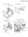
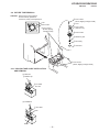
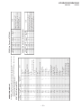
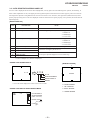
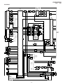
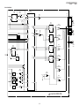
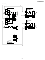
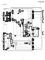
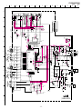
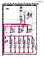
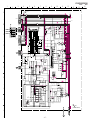
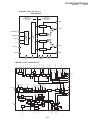
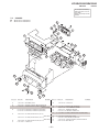
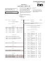
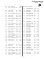
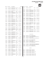
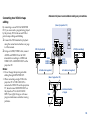
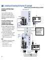
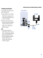
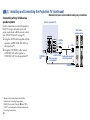
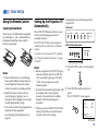
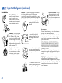
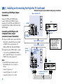
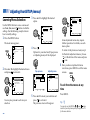
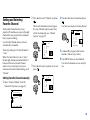
1
SERVICE MANUAL
MODEL
––––––
COMMANDER
––––––––––––
DEST. CHASSIS
NO.
–––––
–––––––––––
KP-XR432K90 RM-Y906K Korean
KP-XR432N90 RM-Y906 Taiwan
DVD/
VTR
MUTING
MODEL
––––––
RA-3A CHASSIS
COMMANDER
––––––––––––
DEST. CHASSIS
NO.
–––––
–––––––––––
SCC-P50D-A
SCC-P50C-A
POWER
SAT/
CABLE
TV
FUNCTION
SYSTEM
OFF
DVD/VTR SAT/CABLE
TV/VTR FREEZE
TV
SWAP
m
PIP
N
M
POSITION AUDIO
X
z
x
SLEEP
ANT
PICTURE
MODE
CC
ACTIVE
TV/VIDEO
MTS/SAP DISPLAY
1
2
4
5
7
8
JUMP
3
6
9
ENTER
0
INDEX
GUIDE
RESET
MENU
VOL
CH
CODE SET
TV
RM-Y906/Y906K
KP-XR432K90/432N90
PROJECTION TV
KP-XR432K90/XR432N90
RM-Y906K
RM-Y906
SPECIFICATIONS
Projection system
3 picture tubes, 3 lenses, horizontal in-line
system
Picture tube
7-inch high-brightness monochrome tubes (6.3 raster size),
with optical coupling and liquid cooling system
Projection lenses
High performance, large diameter hybrid lens F1.05
Television system
American TV standard
Channel coverage
VHF: 2–13/UHF: 14 –69/CATV: 1 – 125
Antenna
75 ohm external terminal for VHF/UHF
Screen size (measured diagonally)
43 inches
Inputs/outputs
VIDEO 1 IN
VIDEO 2 INPUT
S VIDEO IN (4-pin mini DIN):
Y: 1 Vp-p, 75-ohms unbalanced, sync negative
C: 0.286 Vp-p (Burst signal), 75 ohms
VIDEO (phono jack): 1 Vp-p, 75-ohms unbalanced, sync
negative
AUDIO (phono jacks): 500 mVrms (100% modulation),
Impedance: 47 kilohms
VIDEO 3 IN
S VIDEO IN (4-pin mini DIN):
Y: 1 Vp-p, 75-ohms unbalanced, sync negative
C: 0.286 Vp-p (Burst signal), 75 ohms
VIDEO (phono jack): 1 Vp-p, 75-ohms unbalanced, sync
negative
Y: 1 Vp-p, 75 ohms, sync negative
PB : 0.7 Vp-p, 75 ohms
PR : 0.7 Vp-p, 75 ohms
AUDIO (phono jacks): 500 mVrms (100% modulation),
Impedance: 47 kilohms
MONITOR OUT
VIDEO (phono jack): 1 Vp-p, 75-ohms unbalanced, sync
negative
AUDIO (phono jacks): 500 mVrms (100% modulation),
Impedance: 470 ohms
AUDIO (VAR/FIX) OUT (phono jacks): 500 mVrms (100%
modulation), Impedance: 470 ohms
CONTROL S OUT: minijack
Speaker
100 mm (4”) x 2
Speaker output
15W x 2
Power requirement
110 V AC, 60 Hz (KP-XR432N90)
220 V AC, 60 Hz (KP-XR432K90)
Power consumption
In use (Max.): 210W (KP-XR432N90)
200W (KP-XR432K90)
In standby: 1 W
Dimensions (W/H/D)
966 x 1,063 x 508 mm (38 1 /8 x 41 7 /8 x 20 inches)
Mass
61.5 kg (135 lbs 9 oz)
Supplied accessories
Remote control RM-Y906K (1) (KP-XR432K90), RM-Y906
(KP-XR432N90)
Batteries (2) size AA (R6)
Design and specifications are subject to change without
notice.
–2–
KP-XR432K90/XR432N90
RM-Y906K
RM-Y906
TABLE OF CONTENTS
Section
––––––
Title
––––
Page
––––
Section
––––––
SELF DIAGNOSIS FUNCTION ............................................ 3
5-1.
5-2.
1. SELF DIAGNOSIS FUNCTION
5-3.
5-4.
2. DISASSEMBLY
2-1.
2-2.
2-3.
2-4.
2-5.
2-6.
2-7.
2-8.
2-9.
2-10.
Rear Board Removal ................................................... 7
Chassis Assy Removal ................................................ 7
Service Position ........................................................... 7
HA and HB Board Removal ....................................... 7
Mirror Cover Removal ................................................ 8
Beznet Assy Removal .................................................. 8
HC Board Removal ..................................................... 8
A, G and FA Boards Removal ..................................... 8
Picture Tube Removal ................................................. 9
High-Voltage Cable Installation and Removal ............ 9
Screen Voltage Adjustment (Coarse Adjustment) ..... 10
Screen (G2) Adjustment (Fine Adjustment) .............. 10
Deflection York Tilt Adjustment ............................... 10
Focus Lens Adjustment ............................................. 10
Focus VR Adjustment ............................................... 11
2-Pole Magnet Adjustment (Green, Red) .................. 11
4-Pole Magnet Adjustment ........................................ 11
Defocus Adjustment (Blue) ....................................... 11
Electrical Adjustment by Remote Commander ......... 12
Registration Adjustment(PJE) ................................... 17
Auto Registration Error Code List ............................ 20
Page
––––
HV Regulation Circuit Check and Adjustment ......... 23
HV Hold Down Circuit Operation Check and
Adjustment ................................................................ 23
+B Max Voltage Confirmation .................................. 24
+B OVP Confirmation ............................................... 24
6. DIAGRAMS
6-1.
3. SET-UP ADJUSTMENTS
3-1.
3-2.
3-3.
3-4.
3-5.
3-6.
3-7.
3-8.
3-9.
3-10.
3-11.
Title
––––
6-2.
6-3.
6-4.
6-5.
6-6.
6-5.
Block Diagram (1) ..................................................... 25
Block Diagram (2) ..................................................... 26
Block Diagram (3) ..................................................... 27
Block Diagram (4) ..................................................... 28
Block Diagram (5) ..................................................... 29
Block Diagram (6) ..................................................... 30
Block Diagram (7) ..................................................... 31
Block Diagram (8) ..................................................... 32
Circuit Boards Location ............................................ 33
Schematic Diagrams .................................................. 33
Printed Wiring Boards ............................................... 50
Waveforns .................................................................. 56
IC Block Diagram ..................................................... 58
Semiconductors ......................................................... 62
7. EXPLODED VIEWS
7-1.
7-2.
7-3.
Cover ......................................................................... 63
Chassis ....................................................................... 64
Picture Tube .............................................................. 65
4. CIRCUIT ADJUSTMENTS
4-1.
4-2.
4-3.
4-4.
4-5.
4-6.
4-7.
TV Input Sub Contrast Adjustment
(VPNT-SCON) .......................................................... 21
VIDEO Input Sub-HUE and Sub-Color Adjustment
(VPNT-SHUE, SCOL) .............................................. 21
Component Input Sub-HUE and Sub-Color
Adjustment (DAC-UVSH, UVSC) ........................... 21
P&P Sub Contrast Adjustment (SC-SYDR) ............. 21
Sub-HUE, Sub-Color and Main Contrast
Adjustment (MC-MYDR, MSHU, MSCL,
SC-SSHU,SSCL) ...................................................... 22
Bar Display Position Adjustment
(OP-DISP) ................................................................ 22
PIP Position Adjustment (PI-PIPH, PIPV) ................ 22
8. ELECTRICAL PARTS LIST ................................... 66
5. SAFETY RELATED ADJUSTMENTS
(CAUTION)
SHORT CIRCUIT THE ANODE OF THE PICTURE TUBE AND THE
ANODE CAP TO THE METAL CHASSIS, CRT SHIELD, OR CARBON PAINTED ON THE CRT, AFTER REMOVING THE ANODE.
WARNING!!
AN ISOLATION TRANSFORMER SHOULD BE USED DURING
ANY SERVICE TO AVOID POSSIBLE SHOCK HAZARD, BECAUSE OF LIVE CHASSIS.
THE CHASSIS OF THIS RECElVER IS DIRECTLY CONNECTED
TO THE AC POWER LINE.
SAFETY-RELATED COMPONENT WARNING!!
COMPONENTS IDENTIFIED BY SHADING AND MARK ! ON THE
SCHEMATIC DIAGRAMS, EXPLODED VIEWS AND IN THE
PARTS LIST ARE CRITICAL TO SAFE OPERATION. REPLACE
THESECOMPONENTS WITH SONY PARTS WHOSE PART NUMBERS APPEAR AS SHOWN IN THIS MANUAL OR IN SUPPLEMENTS PUBLISHED BY SONY. CIRCUIT ADJUSTMENTS THAT
ARE CRITICAL TO SAFEOPERATION ARE IDENTIFIED IN THIS
MANUAL. FOLLOW THESE PROCEDURES WHENEVER CRITICAL COMPONENTS ARE REPLACED OR IMPROPER OPERATION IS SUSPECTED.
–3–
KP-XR432K90/XR432N90
RM-Y906K
RM-Y906
SECTION 1
SELF DIAGNOSIS FUNCTION
1.
Summary of Self-Diagnosis Function
•
•
This device includes a self-diagnosis function.
In case of abnormalities, the TIMER/STANDBY indicator automatically blinks. It is possible to predict the abnormality location
•
by the number of blinks. The Instruction Manual describes blinking of the TIMER/STANDBY indicator.
If the symptom is not reproduced sometimes in case of a malfunction, there is recording of whether a malfunction was generated
or not. Operate the remote command to confirm the matter on the screen and to predict the location of the abnormality.
2.
Diagnosis Items and Prediction of Malfunction Location
•
When a malfunction occurs the TIMER/STANDBY indicator only blinks for one of the following diagnosis items. In case of two
or more malfunctions, the item which first occurred blinks. If the malfunctions occurred simultaneously, the item with the lower
blink count blinks first.
•
The screen display displays the results regarding all the diagnosis items listed below. The display “ 0 ” means that no malfunctions occurred.
TIMER/STANDBY
Indicater
Number of blinks
Supposed malfunction
Condition
• Power not ON
0
[Standby Power Supply System]
F6001 open.(FB board)
R6565 open.
Q6506 short circuit
[Main Power Supply System]
IC6501 and R6514 are broken.
VD6001 short-circuit (FB board)
Cannot turn on the power.
LED doesn't blink.
+B OCP detection
2 times
Short circuit of power supply system in each circuit.
Goes to the standby mode
Short circuit of +B line
2 : +B OCP 000
+B OVP detection
3 times
R672 open.
Goes to the standby mode
Malfunction of power supply circuit
3 : +B OVP 000
Vertical deflection stop
4 times
IC1509(V out) is broken.
Q1505(V Pulse Buffer) is broken.
Raster goes to one line horizontally, Aand then video
signal is muted.
4 : V Stop
000
Video out abnormality detection
5 times
Video out, Q705, 732, 761 and others in CR, CG
and CB boards circuit.
Q218, 219, 220 (A board)
TIMER/STANDBY LED blinks approx. 30 seconds,
and then blinks for the self diagnosis.
5 : AKB
000
Horizontal deflection stop
6 times
C515, 516 open.
IC206(YC Jungle) is broken.
Raster doesn't appear.
6 : H Stop
000
Audio abnormality detection
8 times
IC406(Audio amp.) is broken.
PS401, 402 open.
The sound is not out.
Goes to the standby mode
8 : Audio
000
Diagnosis item
Self-diagnosis
screen display,
Diagnosis item: Results
* : 000 the range of values for number of operations is 000-255. For 256 or higher there is
no count up and the number remains at 255.
3.
Blinking count display of TIMER/STANDBY indicator
* One blink is not used for self-diagnosis.
< FRONT PANEL >
FLASH FOCUS
TV/VIDEO
–
VOLUME
+
–
CHANNEL +
ON/OFF
•EXAMPLE
TIMER/STAND BY
TIMER/STANDBY indicator
<Diagnosis Items> <Number of Blinks>
• +B overcurrent
2 times
• +B overvoltage
3 times
• Vertical deflection stop
4 times
Lamp ON : 0.3 seconds
Lamp OFF : 0.3 seconds
Lamp OFF :
3.0 seconds
Release of TIMER/STANDBY indicator blinking.
• The TIMER/STANDBY indicator blinking display is released by turning OFF the power switch
on the TV main unit or removing the plug from the power.
–4–
KP-XR432K90/XR432N90
RM-Y906K
4.
Self-diagnosis screen displays
•
In cases of malfunctions where it is not possible to determine the symptom such as when the power goes off occasionally or when
the screen disappears occasionally, there is a screen display on whether the malfunction occurred or not in the past (and whether
the detection circuit operated or not) in order to allow confirmation.
<Screen Display Method>
• Quickly press the remote command button in the following order from the standby state.
DISPLAY b Channel 5 b VOL – b POWER
˘
Be aware that this differs from the method of
entering the service mode (volume + ).
Self-diagnosis screen display
Self Check
2 : +B OCP
3 : +B OVP
4 : V Stop
5 : AKB
6 : H Stop
7 : HV
8 : Audio
101 : WDT
5.
RM-Y906
000
000
000
000
000
000
000
000
÷
2 : +B OCP
000
000 the range of values for number of
operations is 000-255.
For 256 or higher there is no count up
Diagnosis
and the number remains at 255.
Results
Self-Diagnosis Screen Display
•
The results display is not automatically cleared. In case of repairs and after repairs, check the self-diagnosis screen and be sure
•
to return the results display to “ 0 ”.
If the results display is not returned to “ 0 ” it will not be possible to judge a new malfunction after completing repairs.
<Method of Clearing Results Display>
1. Power off (Set to the standby mode)
2. DISPLAY b Channel 5 b VOL + b POWER (Service Mode)
3. Channel 8 b ENTER (Test reset = Factory preset condition)
<Method of Ending Self Diagnosis Screen>
• When ending the self-diagnosis screen completely, turn the power switch OFF on the remote commander or the main unit.
–5–
KP-XR432K90/XR432N90
RM-Y906K
RM-Y906
6. Self-diagnosis function operation
OCP
Low B and +B line detect DET SHORT, and shut-down POWER ON RELAY.
Reset by turning power on/off.
In case of +B is loaded approx. 1.3A or more, microcomputer detects it via IC651.
OVP
In case of +B becomes approx. 150V or more, POWER ON RELAY shuts down and microcomputer detects it via IC651.
Reset by turning power on/off just the same as OCP.
V Stop
In case of microcomputer detects 2 seconds or more interval of V Pulse, Reference Pulse turns off by turning off the picture
signal in YC Jungle IC (IC206).
AKB
After the picture signal turns off, V Pulse is regenerated 2 seconds or more, the picture signal turns on.
IK detection. Makes LED blinking in case of microcomputer doesn’t detect IK returns of IC206 CXA2147Q 30 seconds or more.
H Stop
In case of HV becomes 33kV or more, IC502 detects it and shut-down H Drive Pulse.
Microcomputer receives H Stop data from IC206 and makes LED blinking.
Audio
In case of DC component overlaps the output of Audio Amp., microcomputer detects it and makes LED blinking.
Microcomputer forces to shut down the power.
Self-diagnosis block diagram
D1201
TIMER/STANDBY
Q006
55
5. AKB
6. H STOP
IC002
µProcessor
8
20
21
49
47
50
48
3
4
BUS
22
IC206
CXA2147
YCJ
43
35
34
6. HV STOP
IC502
HV Detector
27
IC004
EEPROM
IC1509
V Drive
Q1505
V Pulse Buffer
5. AKB
C Board
IC406
Audio AMP
Audio
3. OVP
2. OCP
DC Detect
IC651
OVP Buffer
OCP Buffer
OVP DETECT
OCP DETECT
4. V.STOP (V Pulse)
–6–
KP-XR432K90/XR432N90
RM-Y906K
RM-Y906
SECTION 2
DISASSEMBLY
2-1. REAR BOARD REMOVAL
2-3. SERVICE POSITION
1 Disconnect CN203
on A board.
From CG board CN1304.
(The extension cable is not
supplied because of the
A board countermeasure for radiation.)
CN203
G board
2 Rear board
2 Covers
Cut them off with a plier or the like
from chassis assembly in case of
checking printed circuit boards.
After checking, turn over the covers
and secure them with screws.
1 Nine screws
(Screw, tapping haxagon head)
Screws
(+BVTP3x12)
Chassis assembly
2-4. HA AND HB BOARD REMOVAL
2-2. CHASSIS ASSY REMOVAL
8 HB board
7 Three screws
(+BVTP 3x12) 1 Four screws
1 Three screws
(Screw, tapping haxagon head)
4 HA bracket
(Screw, tapping haxagon head)
2
Panel ASSY, Control
3 Four screws
(+BVTP 3x12)
6 HA board
5 Three screws
(+BVTP 3x12)
2 Chassis assy
–7–
KP-XR432K90/XR432N90
RM-Y906K
2-5. MIRROR COVER REMOVAL
RM-Y906
2-7. HC BOARD REMOVAL
1 Sixteen screws
(Screw, tapping haxagon head)
1 Two screws
(+BVTP 4x12)
2 L screen holder
3 HC board
2 Mirror cover
2-8. A, G AND FA BOARDS REMOVAL
2-6. BEZNET ASSY REMOVAL
2 Twelve screws
(Screw, tapping haxagon head)
7 Two screws
0 Screw
(+BVTP 3x12)
(+BVTP 3x12)
!¡ FA board bracket
4 Eight screws
3 Terminal board
!™ FA board
(+BVTP 3x12) 9 A board
3 Beznet assy
8 Claw
2 Seven screws
(+BVTP 3x12)
6 G board
1 Two screws
(Screw, tapping haxagon head)
1 Three screws
(Screw, tapping haxagon head)
Main bracket
–8–
5 Claws
KP-XR432K90/XR432N90
RM-Y906K
RM-Y906
2-9. PICTURE TUBE REMOVAL
CAUTION: Removing the arrow-marked
screws is strictly prohibited.
If removed, it may cause liquid spill.
4 Four screws
(Screw, tapping haxagon head)
Lens
5 Lens
Picture tube
2 Four screws
(Screw, tapping
haxagon head)
9 Four screws
(+BVTP 4x12)
0 Picture tube
8 Diflection yoke
7 Neck assy
6 CR board
3
1 Four screws
(Screw, tapping haxagon head)
2-10. HIGH-VOLTAGE CABLE INSTALLATION
AND REMOVAL
(1) Removal
1 Rubber cap
2 HV cable
turn 90°
(2) Installation
1 HV cable
Hook
Gutter
–9–
KP-XR432K90/XR432N90
RM-Y906K
RM-Y906
SECTION 3
SET-UP ADJUSTMENTS
the mode Cover the both green and red picture lenses with the
lens caps is aligned the same as was done for green.
3-1. SCREEN VOLTAGE ADJUSTMENT
(COARSE ADJUSTMENT)
1. Receive the Monoscope signal.
2. Set 50% BRIGHTNESS and minimum PICTURE.
3. Turn the red VR on the FOCUS block all the way to the left
and then gradually turn it to the right until the point where you
can see the retrace line.
4. Next gradually turn it to the left to the position where the
retrace line disappears.
R
G
Note: Instead of items 3 and 6, you can cut off the unnecessary
color beams by controlling the service mode VPNT 28 RON,
29 GON, and 30 BON.
4-pole magnet
2-pole magnet
Deflection yoke
B
SCREEN
R
G
B
FOCUS
Fig. 3-3
Fig. 3-1
FOCUS block
3-4. FOCUS LENS ADJUSTMENT
3-2. SCREEN (G2) ADJUSTMENT
(FINE ADJUSTMENT)
Fine Mode is recommended to set screen controls to their optimal
condition. It is necessary to build the simple jig, illustrated below,
using 3-watt resistors. Please note, that if the proper voltage is not
obtained with their listed values, resistors, then please increase or
decrease one of the values in the resistor network to obtain the
correct voltage.
1. Select VIDEO1 mode without signals.
2. Connect G2 JIG.
3. SW on JIG.
4. Connect an oscilloscope to the TP701(KR), TP732(KG) and
TP761(KB) of CR board, CG board and CB board.
5. Adjust R, G and B screen voltage to 168-172V with screen
VR on the Focus block.
SW
3.3k
5.6k
200V
5.6k
In this adjustment, use the remote commander in the
service mode.
For details of the usage of the service mode and the remote
commander, please refer the item 3-9. ELECTRICAL
ADJUSTMENT BY REMOTE COMMANDER.
1.
2.
3.
4.
5.
6.
7.
8.
K
G2 JIG
9.
5.6k
GND
10.
11.
175 ± 2V
Anode cap
Loosen the lens screw.
Set to the service mode.
Receive the all-white signal.
Cover the both red and blue picture lenses with the lens caps
to show only the green color.
Set to PJE, and press 6 to display the test signal (crosshatch)“
on the screen.
Turn the green lens to adjust to the optimum focus point with
the test signal.
Tighten the lens screw.
Cover the both green and blue picture lenses with the lens caps
to show only the red color.
Set to PJE, and press 6 to display the test signal (crosshatch)“
on the screen.
Adjust red CRT lens just the same as green.
Cover the both green and red picture lenses with the lens caps
to show only the blue color.
pedestal level
GND
Fig. 3-2
3-3. DEFLECTION YOKE TILT ADJUSTMENT
1. Receive the Monoscope signal.
2. Set in service mode.
3. Cover the both red and blue picture lenses with the lens caps
to show only the green color.
4. Loosen the deflection yoke set screw and align the tilt of the
Deflection Yoke so that the bars at the center of the
monoscope pattern are horizontal.
5. After aligning the deflection yoke, fasten it securely to the
funnel-shaped portion (neck) of the CRT.
6. The tilt of the deflection yoke for red is aligned in the mode
Cover the both green and blue picture lenses with the lens caps
and the tilt of the deflection yoke for blue is aligned with in
Test signal
Fig. 3-4
12. Set to PJE, and press 6 to display the test signal (crosshatch)“
on the screen.
13. Adjust blue CRT lens just the same as green.
14. After adjusting the items 3-5. Focus VR Adjustment, 3-6. 2Pole Magnet Adjustment and 3-7. 4-Pole Magnet Adjustment,
adjust again to the optimum focus point.
*: Every time you press 6, the test signal changes to
“crosshatch+video signal” - “dots+video signal” “crosshach(black)” - “dots(black)” - off.
Note: Instead of items 4, 8 and 11, you can cut off the unnecessary
color beams by controlling the service mode VPNT 28 RON,
29 GON, and 30 BON.
– 10 –
KP-XR432K90/XR432N90
RM-Y906K
3-5. FOCUS VR ADJUSTMENT
Use the center dot
1. Set to the service mode.
2. Receive the all-white signal.
3. Cover the both red and blue picture lenses with the lens caps
to show only the green color.
4. Set to PJE, and press 6 to display the test signal (crosshatch)
on the screen.
5. Turn the green focus VR on the focus block to adjust to the
optimum focus point with the test signal.
6. Cover the both green and blue picture lenses with the lens caps
to show only the red color.
7. Set to PJE, and press 6 to display the test signal (crosshatch)
on the screen.
8. Turn the red focus VR on the focus block to adjust to the
optimum focus point with the test signal.
9. Cover the both green and red picture lenses with the lens caps
to show only the blue color.
10. Set to PJE, and press 6 to display the test signal (crosshatch)
on the screen.
11. Turn the blue focus VR on the focus block to adjust to the
optimum focus point with the test signal.
12. After adjusting the items 3-4. Focus Lens Adjustment, 3-6. 2Pole Magnet Adjustment and 3-7. 4-Pole Magnet Adjustment,
adjust again to the optimum focus point.
Note: Instead of items 3, 6 and 9, you can cut off the unnecessary
color beams by controlling the service mode VPNT 28 RON,
29 GON, and 30 BON.
Fig. 3-7
3-7. 4-POLE MAGNET ADJUSTMENT
1. Receive the Dot signal.
2. Set in service mode.
3. Cover the both red and blue picture lenses with the lens caps
to show only the green color.
4. Turn the green focus VR on the focus block to the left and set
to underfocus to enlarge the spot.
5. Now align the 4-Pole Magnet so that the enlarged spot
becomes a perfect circle for green and red.
6. Perform the same alignment for blue.
Use the center dot
x
/
y
x : y = 1:1.5 (BIue)
x : y = 1:1 (Green, Red)
Scanning line visible.
Fig. 3-8
3-8. DEFOCUS ADJUSTMENT (BLUE)
A
Minimize both A and B.
Lens
Fig. 3-5
RM-Y906
B
Center of crosshatch
Fig. 3-6
3-6. 2-POLE MAGNET ADJUSTMENT
(GREEN,RED)
1. Receive the Dot signal.
2. Set in service mode.
3. Cover the both red and blue picture lenses with the lens caps
to show only the green color.
4. Turn the green focus VR on the focus block to the right and
set to overfocus to enlarge the spot.
5. Now align the 2-Pole Magnet so that the enlarged spot is in
the center of the Just Focus spot.
6. Align the green focus VR and set for just (precise) focus.
7. Perform the same alignment for red.
Note: Please adjust the blue dot to be slightly larger than red and
green dots. This adjustment provides a more pleasing picture
to the customer.
1. Select the video menu and set the mode to “VIVID” mode.
2. Set to the service mode.
3. Change TV mode to the video input mode.
4. Set to PJE, and press 6 to display the test signal (dots) on the
screen.
5. Turn the blue focus VR on the focus block to adjust to the
diameter of the dots as shown in the figure below.
[Focus adjustment point]
Lmm Max
Inch
L
43"
6
Fig. 3-9
– 11 –
KP-XR432K90/XR432N90
RM-Y906K
RM-Y906
3-9. ELECTRICAL ADJUSTMENT BY REMOTE
COMMANDER
7. If you want to recover the latest values press - then [ENTER] to
read the memory.
By using Remote Commander (RM-Y906/Y906K),all circuit
adjustments can be made.
8. Press [MUTING] then [ENTER] to write into memory.
9. Turn power off.
NOTE : Test Equipment Required.
1. Pattern Generator (with component outputs)
Note: Press 8 then [ENTER] on the Remote Commander to initialize
or turn set off and on to exit.
2. Frequency counter
3. Digital multimeter
2. MEMORY WRITE CONFIRMATION METHOD
1. After adjustment, remove the plug from AC outlet, and then
replace the plug in AC outlet again.
4. Audio oscillator
1. METHOD OF SETTING THE SERVICE ADJUSTMENT MODE
2. Turn the power switch ON and set to Service Mode.
3. Call the adjusted items again and confirm they were adjusted.
SERVICE MODE PROCEDURE
1. Standby mode. (Power off)
2. DISPLAY n 5 n VOL (+) n TV POWER
on the Remote Commander.
(Press each button within a second.)
3. ADJUSTING BUTTONS AND INDICATOR
TV POWER ON
SERVICE MODE ADJUSTMENT
MUTING
DVD/
VTR
MUTING
SAT/
CABLE
POWER
TV
Category Adjustment item
DATA
SERVICE VPNT VPOS 031
000000 00
FUNCTION
SYSTEM
OFF
DVD/VTR SAT/CABLE
TV
TV/VTR FREEZE
PIP
SWAP
m
N
M
POSITION AUDIO
X
Category up
z
x
SLEEP
ANT
PICTURE
MODE
CC
ACTIVE
TV/VIDEO
DISPLAY
MTS/SAP DISPLAY
Data up
(SCREEN DISPLAY)
Adjustment item up
3. The SCREEN displays the item being adjusted.
4. Press 1 or 4 on the Remote Commander to select the
adjustment item.
Adjustment item down
1
2
3
4
5
6
7
8
JUMP
Data down
9
ENTER
Category down
0
5. Press 3 or 6 on the Remote Commander to change the data.
6. Press 2 or 5 on the Remote Commander to select the
VOL (+)
category.
Every time you press 2(Category up), Service mode changes
ENTER
INDEX
GUIDE
RESET
MENU
in the order as shown below.
VPNT
SC
VPNV
IC
VPNS
PP
PJE
DAC
3DCM
PI
TONE
ID
DSP
CCD
MC
OP
RM-Y906/Y906K
Note : When the PJE mode is activated, which displays an
internally generated signal, several buttons on the remote
commander will have different functions than listed
above. Therefore, when in the PJE mode, refer to page 17
for button functions.
– 12 –
0
1
2
3
4
5
6
7
8
9
10
11
12
13
14
15
16
17
18
19
20
21
22
23
24
25
26
27
28
29
30
31
32
33
34
35
36
VPOS
VSIZ
VCOM
VLIN
VSCO
HPOS
HSIZ
PAMP
UPIN
LPIN
PPHA
AFC
VBOW
VANG
REF
RDRV
BDRV
RCUT
BCUT
SCON
SHUE
SCOL
CDM2
DPIX
NOTC
CROM
TOT
SHPF
RON
GON
BON
DCOL
CDMD
LBLK
RBLK
PREC
PREY
0-63
0-63
0-3
0-15
0-15
0-15
0-63
0-63
0-15
0-15
0-15
0-3
0-15
0-15
0-3
0-63
0-63
0-15
0-15
0-15
0-15
0-15
0,1
0,1
0,1
0-15
0,1
0-3
0,1
0,1
0,1
0,1
0,1
0-15
0-15
0-3
0-3
ITEM
ADJUSTMENT DATA
NUMBER
ITEM
RANGE
31
31
0
7
7
7
31
31
7
7
5
2
7
7
3
31
31
7
7
7
7
7
0
1
0
7
0
3
1
1
1
1
0
13
13
1
1
STANDARD
DATA
VPNT (Video Processor NTSC)
V POSITION
V SIZE
V COMP
V LINEARITY
V SCURVE CORRECTION
H POSITION
H SIZE
PIN AMP
UPPER CORNER PIN DISTORTION
LOWER CORNER PIN DISTORTION
PIN PHASE
AFC LOOP GAIN
V BOW
V ANGLE
REFERENCE PULSE POSITION
RED DRIVE GAIN
BLUE DRIVE GAIN
RED CUTOFF
BLUE CUTOFF
SUB CONTRAST
SUB HUE
SUB COLOR
COUNT DOWN MODE2
DYNAMIC PICTURE
Y CHROMA TRAP
CHROMA TRAP F0
CHROMA TOT FILTER
SHARPNESS F0
RED ON
GREEN ON
BLUE ON
DYNAMIC COLOR
V COUNT DOWN
LEFT-SIDE BLANK WIDTH
RIGHT-SIDE BLANK WIDTH
PRE OVER LEVEL FOR COMP .V IN
PRE OVER LEVEL FOR Y IN
NOTE
shaded items are fixed. There is no need to change data. Others are different a little
in the sets individually. Basically, there is no need to change data, too.
• Usually, there is no need to adjust except for VPNT and PJE. Use data as a reference in case
of replacing printed circuit boards or devices.
Note: •
4. SERVICE MODE LIST
SBRV
GMMV
YDCV
ABLV
AXIV
0-63
0-3
0,1
0,1
0,1
27
2
1
1
0
STANDARD
DATA
0
1
2
3
4
SBRS
GMMS
YDCS
ABLS
AXIS
0-63
0-3
0,1
0,1
0,1
ITEM
ADJUSTMENT DATA
NUMBER
ITEM
RANGE
27
2
0
1
0
STANDARD
DATA
NOTE
SUB BRIGHTNESS FOR VIVID
GAMMA LEVEL FOR VIVID
Y-DC TRANSFER RATIO FOR VIVID
ABL MODE FOR VIVID
AXIS R-Y,G-Y FOR VIVID
NOTE
SUB BRIGHTNESS FOR STANDARD
GAMMA LEVEL FOR STANDARD
Y-DC TRANSFER RATIO FOR STANDARD
ABL MODE FOR STANDARD
AXIS R-Y,G-Y FOR STANDARD
VPNS (Video Processor NTSC Standard)
0
1
2
3
4
ITEM
ADJUSTMENT DATA
NUMBER
ITEM
RANGE
VPNV (Video Processor NTSC Vivid)
KP-XR432K90/XR432N90
RM-Y906K
– 13 –
RM-Y906
– 14 –
FDIS
OSDH
OSDV
FVST
V1ST
V1CU
COHP
FIHP
TPHP
DFHP
DFHG
DFVG
PWM l
PWM2
HBLD
HBLW
BLKP
COGV
CORV
COBV
COGH
CORH
COBH
SOGV
SORV
SOBV
SOGH
SORH
SOBH
ERR
ADTM
VUP
VMID
VLOW
HPR
CENT
SKEW
SIZE
LIN
KEY
PIN
CENT
SKEW
SIZE
LIN
KEY
PIN
CENT
SKEW
SIZE
LIN
KEY
PIN
0,1
1-255
1-255
0-255
0-255
0-255
0-255
0-255
0-255
0-255
-128-127
-128-127
0-255
0-255
0-255
0-63
0-255
-128-127
-128-127
-128-127
-128-127
-128-127
-128-127
-128-127
-128-127
-128-127
-128-127
-128-127
-128-127
FIXED
0-255
1-255
1-255
1-255
1-510
-512-511
-512-511
-512-511
-512-511
-512-511
-512-511
-512-511
-512-511
-512-511
-512-511
-512-511
-512-511
-512-511
-512-511
-512-511
-512-511
-512-511
-512-511
0
31
25
25
0
62
0
194
62
225
-80
-15
0
32
244
23
27
X(*1)
X(*1)
X(*1)
X(*1)
X(*1)
X(*1)
X(*1)
X(*1)
X(*1)
X(*1)
X(*1)
X(*1)
0
144
1
102
212
1
000 / 000
000 / 000
-70/-190
xxxx / xxxx
xxxx / xxxx
xxxx / 271
000 / 000
080 / -130
-20 / -226
187 / xxxx
xxxx / -115
xxxx / 198
000 / 000
080 / -130
-61 / -206
195 / xxxx
xxxx / 124
xxxx / 250
NOTE
RED H SKEW OFFSET DATA OF AUTO REGI
BLUE H SKEW OFFSET DATA OF AUTO REGI
AUTO REGI ERROR CODE
TIMING TO GET A/D DATA OF AUTO REGI
AUTO REGI PATTERN UPPER V POSITION
AUTO REGI PATTERN MIDDLE V POSITION
AUTO REGI PATTERN LOWER V POSITION
AUTO REGI PATTERN H POSITION
GREEN H/V CENT
GREEN H/V SKEW
GREEN H/V SIZE
GREEN H/V LIN
GREEN H/V KEY
GREEN H/V PIN
BLUE H/V CENT
BLUE H/V SKEW
BLUE H/V SIZE
BLUE H/V LIN
BLUE H/V KEY
BLUE H/V PIN
RED H/V CENT
RED H/V SKEW
RED H/V SIZE
RED H/V LIN
RED H/V KEY
RED H/V PIN
GREEN H SKEW OFFSET DATA OF AUTO REGI
RED V SKEW OFFSET DATA OF AUTO REGI
BLUE V SKEW OFFSET DATA OF AUTO REGI
GREEN V SKEW OFFSET DATA OF AUTO REGI
SELECT REGI DATA DISPLAY OF FINE ADJ
PJED SERVICE MENU H POSITION
PJED SERVICE MENU V POSITION
LINE NUMBER OF FINE ADJUST START
V1 START DATA
V1 COUNT UP DATA
H-PHASE OF ROUGH ADJ
H-PHASE OF FINE ADJ
H-PHASE OF TEST PATTERN
H-PHASE OF DYNAMIC FOCUS
H-2 GAIN OF DYNAMIC FOCUS
V-2 GAIN OF DYNAMIC FOCUS
PWM l
H-PHASE OF AUTO REGI .TEST PATTERN
H-PHASE OF RETURNED BLUE V LINE
PULSE WIDTH OF RETURNED BLUE V LINE
START BLANK PULSE
GREEN V CENT OFFSET DATA OF AUTO REGI
RED V CENT OFFSET DATA OF AUTO REGI
BLUE V CENT OFFSET DATA OF AUTO REGI
GREEN H CENT OFFSET DATA OF AUTO REGI
RED H CENT OFFSET DATA OF AUTO REGI
BLUE H CENT OFFSET DATA OF AUTO REGI
0
1
2
3
4
5
6
7
8
9
10
11
12
13
14
15
16
17
18
19
20
21
22
23
24
25
26
27
28
29
30
31
32
33
34
35
36
37
38
39
40
NRMD
DYCO
DYGA
DCCO
DCGA
SELD
D2GA
VTRH
VTRR
LDSR
VAPG
VAPI
YPFT
YPFG
V1PS
VEGS
CC3N
HDP
CDL
HSSL
VSSL
HPLF
BPLF
FSCF
PLFG
EXAD
MSS
COUT
YAPS
NSDS
CPP
YHCO
YPCO
KILR
BGPS
BGPW
ADCL
PWRF
YHCG
CKG2
CKGE
0-3
0-15
0-15
0-15
0-15
0,1
0-7
0-3
0-3
0-3
0-7
0-31
0-3
0-15
0-3
0-3
0,1
0-7
0-7
0-15
0-15
0,1
0,1
0,1
0,1
0,1
0,1
0-3
0-3
0-3
0-3
0-3
0,1
0-15
0-15
0-15
0-3
0,1
0,1
0,1
0,1
ITEM
ADJUSTMENT DATA
NUMBER
ITEM
RANGE
3DCM (3D Comb Filter)
0
2
10
5
5
1
4
1
1
2
5
11
0
9
2
1
0
4
4
12
8
1
0
1
1
1
0
2
1
0
0
1
0
3
4
10
2
0
0
1
0
STANDARD
DATA
CLOCK GENERATOR TEST BIT
CLOCK GENERATOR TEST BIT
Y HIGH FREQ.SIGNAL CORING 1/2 GAIN
NOISE REDUCER MODE
∆Y CORING LEVEL SETTING
∆Y GAIN SETTING
∆C CORING LEVEL SETTING
∆C GAIN SETTING
SELECT ∆Y SIGNAL FILTER
∆Y/C 2nd GAIN SETTING
VTR HSYNC HYSTERESIS SETTING
VTR HSYNC REFERENCE SETTING
LD SIGNAL REFERENCE
V APERTURE GAIN
V APERTURE INVERT POINT
Y PEAKING FILTER TAP
Y PEAKING FILTER GAIN
VERTICAL 1-LINE SELECTOR
VERTICAL EDGE SELECTOR
C SIGNAL 3-LINE COM FILTER
HD HORIZONTAL PHASE
C DELAY
H SYNC SLICE LEVEL
V SYNC SLICE LEVEL
H PLL FILTER
BURST PLL FILTER
FSC FILTER GAIN
PLL FILTER GAIN
EXTERNAL AD IN
FORCED MOTION SIGNAL
C SIGNAL OUTPUT
Y APERTURE
NON STD SIGNAL DETECT.
CLAMP PULSE & AD RANGE
Y HIGH FREQ.SIGNAL CORING
Y PEAK FILTER CORING OFF
KILLER REFERENCE
BGP START POSITION
BGP WIDTH
AD CLOCK DELAY
PULSE WIDTH REFERENCE
NOTE
RM-Y906K
∗ 1 : Set correctly by the automatic resistration adjustment.
xxxx : Cannot change.
RED
BLU
GRN
0
1
2
3
4
5
6
7
8
9
10
11
12
13
14
15
16
17
18
19
20
21
22
23
24
25
26
27
28
29
30
31
32
33
34
ITEM
ADJUSTMENT DATA STANDARD
NUMBER
ITEM
RANGE
DATA
PJE (Projection TV Engine)
KP-XR432K90/XR432N90
RM-Y906
RBAS
RTRE
BBEH
BBEL
SUFE
0-63
0-63
0-15
0-11
7
– 15 –
TB0H
TB0L
TB1H
TB1L
TB2H
TB2L
TBFH
TBFL
TC0H
TC0L
TC1H
TC1L
SADH
SADL
SB0H
SB0L
0-255
0-255
0-255
0-255
0-255
0-255
0-255
0-255
0-255
0-255
0-255
0-255
0-255
0-255
0-255
0-255
0
1
2
3
4
5
6
7
8
9
10
11
MYDR
MSHU
MSCL
MUPD
MVPD
MDLY
MU2P
MV2P
MY2D
MU2D
MV2D
MPRE
0-31
0-63
0-63
0-15
0-15
0-3
0-15
0-15
0-31
0-31
0-31
0-3
ITEM
ADJUSTMENT DATA
NUMBER
ITEM
RANGE
MC (Main Chroma Decoder)
0
1
2
3
4
5
6
7
8
9
10
11
12
13
14
15
ITEM
ADJUSTMENT DATA
NUMBER
ITEM
RANGE
22
31
31
7
7
0
7
7
19
11
11
3
STANDARD
DATA
48
0
64
0
64
0
165
126
90
130
11
100
64
0
92
0
STANDARD
DATA
39
35
-
STANDARD
DATA
DSP (Digital Signal Processor)
0
1
2
3
4
ITEM
ADJUSTMENT DATA
NUMBER
ITEM
RANGE
TONE (Tone Control)
MAIN Y DRIVE
MAIN SUB HUE
MAIN SUB COLOR
MAIN U PEDESTAL OFFSET
MAIN V PEDESTAL OFFSET
MAIN Y DELAY
MAIN U2 PEDESTAL OFFSET
MAIN V2 PEDESTAL OFFSET
MAIN Y2 DRIVE
MAIN U2 DRIVE
MAIN V2 DRIVE
MAIN PRE-OVER
NOTE
TRUSURROUND EFFECT (L+R) COARSE
TRUSURROUND EFFECT (L+R) FINE
TRUSURROUND EFFECT (L-R) COARSE
TRUSURROUND EFFECT (L-R) FINE
TRUSURROUND EFFECT ( C ) COARSE
TRUSURROUND EFFECT (C) FINE
TRUSURROUND EFFECT ( S ) COARSE
TRUSURROUND EFFECT ( S) FINE
TRUSURROUND EFFECT ( S ) COARSE
TRUSURROUND EFFECT ( S) FINE
TRUSURROUND EFFECT (L,R) COARSE
TRUSURROUND EFFECT (L,R) FINE
SRS SPACE LEVEL COARSE
SRS SPACE LEVEL FINE
SRS CENTER LEVEL COARSE
SRS CENTER LEVEL FINE
NOTE
RESET VALUE OF USER BASS DATA
RESET VALUE OF USER TREBLE DATA
BBE HIGH FREQUENCY
BBE LOW FREQUENCY
SURROUND EFFECT
NOTE
SYDR
SSHU
SSCL
SUPD
SVPD
SDLY
SU2P
SV2P
SY2D
SU2D
SV2D
SPRE
0-31
0-63
0-63
0-15
0-15
0-3
0-15
0-15
0-3
0-15
0-15
0-3
PCDR
PHDR
PAFC
PTAD
PTOT
PSCN
PYDC
PSHP
PMSK
0-15
0-15
0-3
0-15
0,1
0-15
0-7
0,1
0,1
7
7
2
7
0
7
0
1
0
STANDARD
DATA
28
31
31
7
7
0
7
7
20
11
11
3
STANDARD
DATA
0
1
2
3
4
5
6
7
8
9
10
11
12
13
BGHP
BGHN
BGVP
6BIT
MAHP
MAVP
SAHP
SAVP
DECS
DECM
DIS
BSIZ
VPED
UPED
0-15
0-15
0-15
0,1
0-15
0-255
0-15
0-255
0-31
0-31
0-127
0-15
0-15
0-15
ITEM
ADJUSTMENT DATA
NUMBER
ITEM
RANGE
10
7
7
1
7
23
7
23
18
18
66
2
13
13
STANDARD
DATA
PP (Picture In Picture Vseries Only)
0
1
2
3
4
5
6
7
8
ITEM
ADJUSTMENT DATA
NUMBER
ITEM
RANGE
IC (Inset Chroma Decoder)
0
1
2
3
4
5
6
7
8
9
10
11
ITEM
ADJUSTMENT DATA
NUMBER
ITEM
RANGE
SC (Sub Chroma Decoder)
PIP H POSITION
PIP H POSITION FOR NO SIGNAL
PIP V POSITION
6BIT(SMART6/SKIP6) MATRIX
MAIN H ACQUISITION
MAIN V ACQUISITION
SUB H ACOUISITION
SUB V ACQUISITION
SUB DECODER REGISTERS
MAIN DECODER REGISTERS
DISPLAY SETTING
BORDER SIZE
V PEDESTAL OFFSET
U PEDESTAL OFFSET
NOTE
PIP COLOR
PIP HUE
PIP AFC LOOP GAIN
PIP TRAP F0 ADJUSTMENT
PIP CHROMA TOT FILTER
PIP SUB CONTRAST
PIP Y DC TRAN
PIP SHARPNESS F0
PIP MACRO VISION MASK
NOTE
SUB Y DRIVE
SUB SUB HUE
SUB SUB COLOR
SUB U PEDESTAL OFFSET
SUB V PEDESTAL OFFSET
SUB Y DELAY
SUB U2 PEDESTAL OFFSET
SUB V2 PEDESTAL OFFSET
SUB Y2 DRIVE
SUB U2 DRIVE
SUB V2 DRIVE
SUB PRE-OVER
NOTE
KP-XR432K90/XR432N90
RM-Y906K
RM-Y906
UVSH
UVSC
0-63
0-63
31
31
STANDARD
DATA
PIPH
PIPV
PYSD
PYDL
PHDL
PMVD
PIVD
PCON
FRMY
IPER
IPEB
PCPS
PCPF
PPLL
PVNR
– 16 –
AREA
SERS
VCHP
0-3
0-3
0-3
CCHP
CCHN
0-63
0-63
DISP
FWl
FW2
0-63
0-7
0-7
9
2
3
STANDARD
DATA
39
29
STANDARD
DATA
NOTE
OSD H POSITION
FIELD1 WINDOW
FIELD2 WINDOW
NOTE
OSD H POSI FOR INDEX & CC/XDS
NO FUNCTION
AREA ID
SERIES ID
V CHIP ID
NOTE
PIP H POSITION
PIP V POSITION
PIP SELECT DELAY
PIP Y DELAY
H-PULSE DELAY
MAIN V-PULSE DELAY
INSET V-PULSE DELAY
INSET CONTRAST
FRAME Y
PIP PEDESTAIJ R-Y
PIP PEDESTAL B-Y
PIP CLP
PIP CLP CYCLES
PIP PLL TIME CONSTANT
PIP VSP PULSE NOISE REDUCTION
NOTE
YUV SUB HUE
YUV SUB COLOR
NOTE
RM-Y906K
0
1
2
ITEM
ADJUSTMENT DATA
NUMBER
ITEM
RANGE
OP (Option)
0
1
ITEM
ADJUSTMENT DATA
NUMBER
ITEM
RANGE
0
0
0
STANDARD
DATA
-
STANDARD
DATA
CCD (Closed Caption Decoder)
0
1
2
ITEM
ADJUSTMENT DATA
NUMBER
ITEM
RANGE
ID (Identification)
0
1
2
3
4
5
6
7
8
9
10
11
12
13
14
ITEM
ADJUSTMENT DATA
NUMBER
ITEM
RANGE
PI (Picture In Picture S Series only)
0
1
ITEM
ADJUSTMENT DATA
NUMBER
ITEM
RANGE
DAC (D/A Converter)
KP-XR432K90/XR432N90
RM-Y906
KP-XR432K90/XR432N90
RM-Y906K
1. Set to the service mode by pressing quickly keys on the remote
3-10. REGISTRATION ADJUSTMENT (PJE)
• FUNCTION OF BUTTONS OF REMOTE
COMMANDER FOR PJE MODE.
DVD/
VTR
MUTING
TV
FUNCTION
SYSTEM
OFF
DVD/VTR SAT/CABLE
Adjustment item
up
TV/VTR FREEZE
TV
SWAP
m
z
Adjustment item
down
Color select
GRNnBLUnRED
M
ACTIVE
PJE
FDIS
x
ANT
SLEEP
PICTURE
MODE
2. Change TV mode to the video input mode.
3. Change the VPNT mode to the PJE 00 FDIS.
PIP
N
POSITION AUDIO
X
commander in the standby mode in the following order:
[DISPLAY] n 5 n [VOL+] n [TV POWER]
POWER
SAT/
CABLE
CC
TV/VIDEO
MTS/SAP DISPLAY
1
2
3
4
5
6
7
8
JUMP
9
ENTER
0
INDEX
GUIDE
RESET
MENU
INIT*
VOL
CH
Test signal select
crosshach+video signal
dots+video signal
crosshach+black
dots+black
off
00
00
4. Set FDIS data to “01” to display the registration data of each
(
Mode select
Coarse adjustment
Fine adjustment
spot in the fine adjustment.
)
PJE
FDIS
CODE SET
READ*
RM-Y906
ENTER
00
01
TV
data up/down
INIT*:
Press 7, "INIT" green letters appear on the screen.
READ*:
Then press ENTER, all the PJE data are reset.
Press 8, "READ" green letters appear on the screen.
Then press ENTER, all the PJE default data are
5. Press 6 to display the test signal (crosshatch) on the screen.
6. Select GRN CENT(*) with the 1 and 4 keys on the remote
commander and check that the adjustment data is now “000”
both vertically and horizontally.
restored.
Note: Internal patterns are used for geometry and convergence
GRN
CENT
(H)
000
(V)
000
adjustments. However, sizing and centering must be done with
the use of an external generator. The recommended pattern
would be a monoscope, or equivalent pattern, which would
provide the means to adjust both the linearity and sizing of the
*: In the factory preset, “GRN CENT” appears on the screen first.
picture.
In case of other colors “RED” or “BLU”, change color by
every pressing 3 key.
7. Cover the both red and blue picture lenses with the lens caps to
show only the green color.
[SETUP FOR ADJUSTMENT]
•
Current flow in circuit should be stable before attempting
•
adjustment. So wait 5 minutes after turning on the TV power.
At the 4 insides of the screen, locate the middle. Use a tape
SUB DEFLECTION ADJUSTMENT ITEM
Adjustment
O : Yes
– : No
measure to identify the middle.
Adjustment type
: middle
Display
Adjustment item
CENT
G
H/V
O/O
R
H/V
O/O
B
H/V
O/O
CENT
SKEW
SIZE
SKEW
SIZE
O/O
–/–
O/O
O/O
O/O
O/O
LIN
KEY
LIN
KEY
–/–
–/–
O/–
–/O
O/–
–/O
PIN
PIN
–/O
–/O
–/O
– 17 –
KP-XR432K90/XR432N90
RM-Y906K
[GREEN REGISTRATION ADJUSTMENT]
<GREEN CENTER>
1. Select GRN CENT 1and 4 keys on the remote commander.
2. Adjust the center of crosshatch line goes the middle vertically
and horizontally (GRN CENT) with the joystick on the remote
commander.
RM-Y906
<FINE ADJUSTMENT>
1. Press 9 key on the remote commander to shift to the fine
adjustment mode.
The green cursor (in the GRN mode) appears on the center of
the screen.
2. Use the 1and 4 keys or the joystick on the remote commander, move the cursor (see below) everywhere you want to
adjust and adjust with the joystic keys on the remote com-
GRN
CENT
000
mander.
Marker movement by the 1 and 4 keys:
000
: Middle
<GREEN SKEW>
1. Select GRN SKEW with the 1and 4 keys on the remote
Press once the joystick the cursor turns green to white.
Then you can move the cursor up and down left and right every
commander.
2. Adjust the crosshatch line goes straight vertically and horizon-
where you want.
tally with the joystick on the remote commander.
GRN
SKEW
000
000
Press once the joystick the cursor stops and returns green, you
can adjust around the cursor.
<GREEN PINCUSHION>
1. Select GRN PIN with the 1and 4 keys on the remote
commander.
2. Adjust the crosshatch line goes straight horizontally with the
joystick on the remote commander.
GRN
PIN
XXXX
000
3. Press 9 key on the remote commander to shift to the coarse
adjustment mode.
Note : These are required when either severe miss-adjustment or
data loss occurred.
– 18 –
KP-XR432K90/XR432N90
RM-Y906K
RM-Y906
[RED REGISTRATION ADJUSTMENT]
[BLUE REGISTRATION ADJUSTMENT]
<RED CENTER, SKEW>
1. Cover the blue picture lens with the lens cap to show the green
and red colors.
1. Remove the lens cap from the blue picture lens to show full
2. Press 3 key on the remote commander to shift the GRN mode
to the RED mode.
to the BLU mode.
3. Adjust BLU CENT, BLU SKEW, BLU SIZE, BLU LIN, BLU
color.
2. Press 3 key on the remote commander to shift the RED mode
3. Select RED CENT or RED SKEW with the 1 and 4 keys
on the remote commander and adjust while tracking each other
alternately.
4. Adjust the red crosshatch lines go straight vertically and
horizontally and overlaps the green lines with the joystick on
the remote commander.
<RED SIZE, LINEARITY>
1. Select RED SIZE (vertically and horizontally) or RED LIN
(vertically) with the 1 and 4 keys on the remote commander and adjust while tracking each other alternately.
2. Adjust the red crosshatch lines go straight vertically and
horizontally and overlaps the green lines with the joystick on
the remote commander.
KEY and BLU PIN in the same procedure of the red registration adjustment.
[FINAL CHECK]
1. Store the new adjustment (offset) value on the remote control
by pressing [MUTING] and [ENTER].
2. Press the FLASH FOCUS button on the front panel.
(The Offset value is now automatically stored.)
3. Check that no error message appears.
If an error message appears, recheck.
Note: In case of replacing CRTs, adjust the set-up adjustments
(items 3-1 to 3-8) and the registration adjustment (item 3-10).
In case of replacing two or three CRTs at the same time,
replace and adjust one by one.
<RED KEY, PINCUSHION>
1. Select RED KEY or PINCUSHION with the 1 and 4 keys
on the remote commander and adjust while tracking each other
alternately.
2. Adjust the red crosshatch lines go straight horizontally and
overlaps the green lines
with the joystick on the remote commander.
Note : These are required when either severe miss-adjustment or
data loss occurred.
<FINE ADJUSTMENT>
1. Press 9 key on the remote commander to shift to the fine
adjustment mode.
The red cursor (in the RED mode) appears on the center of the
screen.
2. Use the 1 and 4 keys or the joystick on the remote commander, move the cursor everywhere you want to adjust and
adjust with the joystick on the remote commander.
– 19 –
KP-XR432K90/XR432N90
RM-Y906K
RM-Y906
3-11. AUTO REGISTRATION ERROR CODE LIST
If an error code is displayed after the set has been fully adjusted, correctly, please check the following items: position, tilt and sizing. If
either of these adjustments are off, even slightly, the auto-registration pattern will not hit the four sensors properly. This occurs when the
internal generator patterns is being flashed on the screen for the sensors to read. Therefore, auto registration (called auto-focus) cannot
operate properly causing an error code to be displayed. In order for this function to operate properly, correct position, tilt and size must be
adjusted properly.
[ERROR CODE LIST]
ERROR
CODE
DISCRIPTION
00
No Error
10
Sensor Output Level Low
NOTE
* Check wiring, beam position, sensor.
0 : Upper Center
1 : Middle Left
2 : Middle Right
3 : Lower Center
20
Sensor Output Level High
* Check OP-amp circuit.
0 : Upper Center
1 : Middle Left
2 : Middle Right
3 : Lower Center
30
40
Adjustment Loop Counter Overflow
Regi Data Overflow
50
60
Regi Data Overflow
Offset Overflow
70
Offset Overflow
* Check the registring information on the convergence board.
* Check the convergence yoke driver ICs.
* Convergence patterns displayed are out of normal range.
* In case of multiple error, last error is displayed.
• ERROR CODE SCREEN DISPLAY
[SENSOR POSITION]
0
E 11 B
E 11 B
R. G. B
1
SCREEN
SENSOR NUMBER
ERROR CODE 10
ERROR
* Error code will be displayed on center of screen for 3 seconds.
3
0 : UPPER SENSOR
1 : LEFT SENSOR
• ERROR CODE DISPLAY IN REGI SERVICE MODE
2 : RIGHT SENSOR
3 : LOWER SENSOR
PJE
ERR
29
140
ITEM NUMBER-29
SENSOR NUMBER
(ONLY "10"or "20")
ERROR CODE 40
G-0 (Blank)
R.G.B R-1
B-2
– 20 –
2
KP-XR432K90/XR432N90
RM-Y906K
RM-Y906
SECTION 4
CIRCUIT ADJUSTMENTS
4-1. TV INPUT SUB CONTRAST ADJUSTMENT
(VPNT-SCON)
4-3. COMPONENT INPUT SUB-HUE AND SUB-COLOR
ADJUSTMENT (DAC-UVSH, UVSC)
1. Receive the color-bar signal.
2. Mode
: Personal 1 or 2.
PICTURE
: maximum
COLOR
: maximum
BRIGHTNESS
: center
TRINITONE
: medium
SERVICE DATA VPNT SCON : 7
3. Set to service mode.
4. Connect an oscilloscope between pin 7 of CN204 (A board)
and ground.
5. Select “ VPNT-SCON ”, and adjust so that the wave from
level is 1.80 ± 0.05Vp-p.
6. Write the data into memory.
MUTING n ENTER
1. Select VIDEO 4 and supply the color-bar signal.
VIDEO input
2. Mode
: Personal 1 or 2.
PICTURE
: maximum
COLOR
: center
BRIGHTNESS
: center
TRINITONE
: medium
SERVICE DATA DAC UVSH : 31
SERVICE DATA DAC UVSC
: 31
3. Set to service mode.
4. Connect an oscilloscope between pin 5 of CN204 (A board)
connecter and ground.
5. Select “ DAC-UVSH, UVSC ”, and adjust them to have VB1
= VB4 and VB2 = VB3 in the waveform levels.
6. Write the data into memory.
MUTING n ENTER
White
1.80 ± 0.05Vp-p
Black
VB1
VB2
VB3
VB4
Fig. 4-1
Fig. 4-3
4-2. VIDEO INPUT SUB-HUE AND SUB-COLOR
ADJUSTMENT (VPNT-SHUE, SCOL)
1. Select VIDEO1 input and supply the color-bar signal.
2. Mode
: Personal 1 or 2.
PICTURE
: maximum
COLOR
: center
BRIGHTNESS
: center
TRINITONE
: medium
SERVICE DATA VPNT-SHUE : 7
SERVICE DATA VPNT-SCOL : 7
3. Set to service mode.
4. Connect an oscilloscope between pin 5 of CN204 (A board)
connecter and ground.
5. Select “ VPNT-SHUE, SCOL ”, and adjust them to have VB1
= VB4 and VB2 = VB3 in the waveform levels.
6. Increase SCOL by 2 steps.
7. Write the data into memory.
MUTING n ENTER
4-4. P & P SUB CONTRAST ADJUSTMENT
(SC-SYDR)
1. Receive the signal.
TV terminal (sub)
: color-bar signal
VIDEO terminal (main) : no signal
2. Set to service mode and set to P & P mode.
3. Connect an oscilloscope between pin 7 of CN204 (A board)
and ground.
4. Select “ SC-SYDR ”, and adjust so that the wave from level
is 1.65 ± 0.05Vp-p.
5. Write the data into memory.
MUTING n ENTER
White
1.65 ± 0.05Vp-p
Black
Fig. 4-4
VB1
VB2
VB3
VB4
Fig. 4-2
– 21 –
KP-XR432K90/XR432N90
RM-Y906K
4-5. SUB-HUE , SUB-COLOR AND MAIN
CONTRAST ADJUSTMENT (MC-MYDR,
MSHU, MSCL, SC-SSHU, SSCL)
1. Receive the color-bar signal.
2. Mode
: Personal 1 or 2.
PICTURE
: maximum
COLOR
: center
BRIGHTNESS
: center
TRINITONE
: medium
SERVICE DATA MC-MYDR
: 22
SERVICE DATA MC-MSHU
: 31
SERVICE DATA MC-MSCL
: 31
SERVICE DATA SC-SSHU
: 31
SERVICE DATA SC-SSCL
: 31
3. Set to service mode and set to P & P model .
4. Connect an oscilloscope between pin 5 of CN204 (A board)
connecter and ground.
5. Select “ MC-MYDR”, and adjust them to have VB1 = VB5
in the waveform levels.
6. Select “ MC-MSCL, SC-SSCL” and adjust so that the wave
form shows VB1=VB4 and VB5=VB8.
7. Select “ MC-MSHU, SC-SSHU” and adjust so that the wave
form shows VB2=VB3 and VB6=VB7.
8. Write the data into memory.
MUTING n ENTER
VB1
VB2
VB3
VB4
VB5
VB6
VB7
4-7. PIP POSITION ADJUSTMENT
(PI-PIPH, PIPV)
1. Set the PIP mode.
2. Receive the monoscope signal on the main/sub picture.
3. Check the sub picture position.
X1-X2
X1-X2
0.25sq
0.25sq
4. If necessary set to service mode and adjust "PIPH", "PIPV".
5. Write the data into memory.
MUTING n ENTER
Y1
Y2
X1
X2
Fig. 4-7
VB8
Fig. 4-5
4-6. BAR DISPLAY POSITION ADJUSTMENT
(OP-DISP)
1.
2.
3.
4.
Receive the monoscope signal.
Set to service mode.
Push “ PICTURE +” . (Bar is displayed)
Select “ OP-DISP ” , and adjust so that the bar is as shown in
the figure.
5. Write the data into memory.
MUTING n ENTER
X1
RM-Y906
X2
X1 = X2
Fig. 4-6
– 22 –
KP-XR432K90/XR432N90
RM-Y906K
RM-Y906
SECTION 5
SAFETY RELATED ADJUSTMENTS
[ G BOARD]
5-1. HV REGULATION CIRCUIT CHECK AND
ADJUSTMENT
5-2. HV HOLD DOWN CIRCUIT OPERATION
CHECK AND ADJUSTMENT
When replacing the following components marked with
When replacing the following components marked with
on the schematic diagram always check HV regulation, and
if necessary re-adjust.
on the schematic diagram always check hold-down voltage
and if necessary re-adjust.
: C517
: R536, R545
: C517, C521, C522
: C516, C536
IC654, L504
T502, T504 (FBT)
D.Y, A board, G board
D506, D507, D522
IC206, IC502, IC654
L504, R511, R522, R536, R538, R545,
R548, R584
T502, T504 (FBT)
D.Y, A board, G board
OPERATION CHECK
1. Connect a HV static voltmeter to the unconnected plug of
the high-voltage block. (Fig.5-1)
2. Power on the set.
3. Receive the dot signal. (PICTURE and BRIGHTNESS to
minimum)
4. Check that the HV static voltmeter is reading 31.00 +0.95
-1.45 kVdc.
HV Regulation adjustment
1. Connect a HV static voltmeter to the unconnected plug of
the hight-voltage block.
2. Power on the set.
3. Receive the dot signal. (PICTURE and BRIGHTNESS to
minimum)
4. If anode voltage is 31.95kV or higher, replace C517 of 470PF/
2kV with that of 680PF/2kV, and check if the voltage is within
the standard range.
5. If anode voltage is 29.66kV or lower, replace C517 of 470PF/
2kV with that of 100PF/2kV, and check if the voltage is within
the standard range.
Remove the cap off from
the unused terminal and
cpmmect a static voltmeter
there.
OPERATION CHECK
1. Remove CN652 connecter.
2. Short-circuit across TP-PROT and ground.
3. Connect a HV static voltmeter to the unconnected plug of
the high-voltage block.
4. Connect a 220 Ω/200W variable resistor, across pin 2 and
pin 1 of CN652 and connect an external dc power supply
unit (200V, class 2A) to pin 3 of CN652.
5. First turn on the external power supply (+B=135V), then turn
on the power of the set.
6. Receive the dot signal. (PICTURE and BRIGHTNESS to
minimum)
7. Gradually increase the value of the external dc power supply
and check that the hold-down circuit operates at a static voltmeter reading of 33.5±0.95kVdc when the raster disappears.
HV HOLD-DOWN ADJUSTMENT
1. Repeat steps 1 ~ 7 as above.
2. If hold down voltage is 34.45kV or higher, remove R536,
mount a resistor (150kΩ, 1/4W : RN) onto R545 instead, and
check again if the hold-down voltage is within the standard
range.
3. If hold down voltage is 32.55kV or lower, mount a resistor
(220kΩ, 1/4W : RN) onto R536 and check again if the holddown voltage is within the standard range.
NOTE : Please finish the adjustment as soon as possible
Fig. 5-1
– 23 –
KP-XR432K90/XR432N90
RM-Y906K
5-3. +B MAX VOLTAGE CONFIRMATION
The following adjustments should always be performed when
replacing IC654.
1. Supply 130VAC to with variable autotransformer.
2. Input a dot signal.
3. Set the PICTURE control and the BRIGHTNESS controls to
minimum.
4. Confirm the voltage of G BOARD TP135V is less than
137.0Vdc.
5. If step 4 is not satisfied, replace IC654 and repeat above steps.
5-4. +B OVP CONFIRMATION
1.
2.
3.
4.
Connect an external dc power supply to TP OVP.
Supply 120VAC to variable autotransformer.
Set PICTURE and the BRIGHTNESS controls to minimum.
Gradually turn the external dc power supply, and check if
OVP works properly when the voltage of the external dc
power supply is between 139.0 ~ 155.0V.
– 24 –
RM-Y906
SECTION 6
KP-XR432K90/XR432N90
RM-Y906K
DIAGRAMS
6-1. BLOCK DIAGRAM (1)
IC403
D/A CONVERTER
TO A
BOARD
TUNER
BLOCK
28 IN1
5 IN2
ML OUT1
HR OUT1
TO
A
BOARD
TUNER
BLOCK
1
2
15
16
17
18
43
60
61
62
51
52
53
I-2HSYNC
I-HSYNC
SUBTU AFT
MAINTU AFT
O-MONO
O-SAP
I-SAPN
I-STEREN
O-2MUTE
O-MUTE
O-AGC ATT
ANT SW1
ANT SW2
L/R MUTE
Q403, 404
O-SPK MT 58
IO-SDAT 47
O-SCLK 49
TO
A
BOARD
VIDEO
BLOCK
SBLK
MBLK
SWITCH
Q024
SWITCH
Q007
HP
VP-BUFF
TO A
BOARD
PJED
BLOCK
45 O-SBLK
5 MUTE
OUT(R) 2
IN-(R) 10
1
L
2
E
3
R
4
E
SDA
SCL
OFF MUTE
Q402
+11V
IO-B DAT 48
O-B CLK 50
5 B DAT
6 B CLK
I-RESET 9
4 RESET
P-MUTE
ON MUTE
Q401
STBY
+5V
IC404
3
2
X001
16MHz
TO A
BOARD
TUNER
BLOCK
RM IN
7
R OUT
1
L OUT
TO A
BOARD
TUNER
BLOCK
CN003
11 BCLK
10 B DAT
3 SIRCS
I-RMCN 64
46 O-MBLK
5
6
IC404
IC001
RESET
S OUT
O-SIRCS 63
TO A
BOARD
TUNER
BLOCK
FOR
CHECK
TO A
BOARD
TUNER
BLOCK
7 I-HP
8 I-VP
HP
VP-BUFF
B INT
TO A
BOARD
TUNER
BLOCK
O-R
O-G
O-B
O-I
O-OSDYS
O-DISPYM
OUT(L) 4
IN-(L) 8
IC004
EEPROM
I-OSC 12
32
33
34
35
36
37
CN403
7 IN+(L)
11 IN+(R)
PROTECT
Q408-411
I-APROT 22
O-OSC 11
MICRO R
MICRO G
MICRO B
MICRO I
OSD YS
DISP YM
OUT1 21
OUT2 12
17 SCL
18 SDA
IC002
SYSTEM CONTROL
STUH
MTUH
STU AFT
MTU AFT
MONO
SAP
SAP IND
ST IND
STU AUMT
MTU AUMT
AGC ATT
ANT SW1
ANT SW2
IC406
L/R AMP
6 I-BINTN
O-GRAY
KEY
I-POWERN
O-TMRLED
MENU
23
14
44
55
13
GRAY
TO A
BOARD
VIDEO
BLOCK
I-OVP 21
I-OCP 20
O-RELAY 56
YUV MT
8
7
4
CN681
OVP
OCP
RELAY
6
CN002
KEY
G
TO G
BOARD
CN605
57 O-YUVMT
LED BUFF
Q006
7
POWER
8
TIMER LED
CN1203
KEY
S1201-1206
CONTROL
SWITCHES
3
POWER
4
TIMER LED
5
D1201
HB (2/2)
S1207
POWER
(MENU SWITCHES)
STBY +5V
CN1202
TIMER/STANDBY
A (1/6)(AUDIO, SYSTEM CONTROL)
9
MENU
2
SIRCS
MENU
1
6
HA
(CONTROL SWITCHES)
MENU KEY
CN1252
MENU KEY
1
S1251-1255
MENU
SWITCHES
CN1291
SIRCS
2
HC
OUT
D1291
REMOTE SENSOR
(REMOTE SENSOR)
– 25 –
RM-Y906
KP-XR432K90/XR432N90
RM-Y906K
BLOCK DIAGRAM (2)
BUFFER
Q152
DET OUT 2
63 MTV V
MAIN V OUT 41
VIDEO BUFFER
Q1103,1104
BUFFER
Q1701
BUFFER
Q1702,1703
FL1701
H.SEP
Q004
DET OUT
SWITCH
Q151
RF AGC
SDA
SCL
RF AGC
BUFFER
Q153
H.SEP
Q001
ML OUT1
HR OUT1
STUH
10
7
9
C2 5
Y2 3
SSW-2 7
BUFFER
Q1705
FL1703
BUFFER
Q1706,1709
45 Y IN2
Y OUT2 39
BUFFER
Q1102
CN1702
FR C IN
FR Y IN
FRONT SW
CN1253
FR C OUT
FR Y OUT
FRONT SW
10
7
9
3
1
J1251
VIDEO2
IN
Y OUT 15
S VIDEO
U OUT 14
4
2
V2 1
5
FR V IN
FR V OUT
5
VIDEO
L2 2
3
FR L IN
FR L OUT
3
L(MONO)
1
3
SWITCH
Q005
ANT SW1
ANT SW2
1
SWITCH
Q003
ANT SW2
1
FR R IN
FR R OUT
R
1
HB (1/2)
SCL 33
SDA 34
(LINE IN 1)
SCL
SDA
IC1701
5V REG
12 C1
I
O
REG 5V
13
DU IN
V BUFFER
Q1920
3
DV IN
Y BUFFER
Q1914
1
DY IN
V IN 5
U IN 12
Y IN 2
DVD SW 9
DVD SW 10
DVD SW 11
SY OUT1 56
10 Y1
4
2
14 SSW-1
VIDEO
8
V1
L(MONO)
9
L1
R
SC OUT1 58
BUFFER
Q1119,1124
BUFFER
Q1118,1125
11 R1
MUTE BUFFER
Q1122
J1101
19 C3
3
1
YUV MT
P MUTE
Q1110
MUTE BUFFER
Q1117
17 Y3
4
2
S VIDEO
FROM A BOARD
SYSTEM CONTROL
BLOCK
MTU AUMT
21 SSW-3
L(MONO)
16 L3
R
18 R3
R OUT
FROM A BOARD
SYSTEM CONTROL
BLOCK
TO A BOARD
SYSTEM CONTROL
BLOCK
24 Y4
L
R
AUDIO OUT
(VAR/FIX)
Q1109
Q1108
S OUT
J1106
J1104
L OUT
15 V3
VIDEO
Y
25
V OUT 4
R2 4
TO A BOARD
SYSTEM CONTROL
BLOCK
SDA
SCL
S VIDEO
AUDIO
YOUT
AUDIO
STUAFT
STUAUMT
J1102
VIDEO 3
IN
C OUT2 37
INH 6
+11V
AUDIO
43 C IN2
IC1903
YUV SWITCH
59 STV L6
61 STV R6
CN004
ANT SW1
3
BUFFER
Q1707,1708
60 STV V6
DE-EM OUT
1
FL1702
TO A BOARD
SYSTEM CONTROL
BLOCK
52
54
AFT OUT
MUTE
SDA
SCL
BUFFER
Q1704
DET OUT
TU152
SUB TUNER
DET OUT
23
MODE
F MONO
MTU AUMT
ML OUT1
HR OUT1
MODE
F MONO
MUTE
SDA
SCL
COUT
11 CKIN
AFT OUT
ST IND
SAP IND
AFT OUT
ST IND
SAP IND
VIDEO 1
IN
41 ADIN
62 MTV L
64 MTV R
L OUT
R OUT
ANT
SW
IC1702
COMB FILTER
IC1101
A/V SWITCH
TU151
MAIN TUNER
SAVA CONT
Q1121
BUFFER
Q1114
SIRCS MIX
Q1111
BUFFER
Q1106,1107
J1103
CONTROL
S
OUT
RM IN
J1105
VIDEO
PB
28 SSW-4
PR
L OUT 38
AUDIO BUFFER
Q1112,1113
R OUT 40
A (2/6)
AUDIO BUFFER
Q1115,1116
L
R
Q1101
Q1105
(TUNER, VIDEO, AUDIO IN/OUT)
– 26 –
AUDIO
MONIT OR
OUT
TO BLOCK
DIAGRM(3)
RM-Y906
KP-XR432K90/XR432N90
RM-Y906K
BLOCK DIAGRAM (3)
SBLK
IC1905
PIP PROCESSOR
Y BUFFER
Q1916
Y AMP
Q1917
BUFFER
Q1918
32 VIN
X1903
20.48MHz
17
SEL
12
28 YIN
30 UIN
TO BLOCK 1
DIAGRM(2)
M.VSYNC
3
XIN
4
XQ
SDA
21 SDA
SCL
22 SCL
Y OUT
8
U OUT
9
V OUT
7
S.VSYNC
19
S.HSYNC
M.HSYNC
20
18
FROM A BOARD
SYSTEM CONTROL
BLOCK
VP-BUFF
MBLK
BUFFER
Q1915
IC1902
SUB DECODER
BUFFER
Q1905
BUFFER
Q1907
BUFFER
Q1903
12 RU IN
13 RV IN
RY OUT 8
RU OUT 7
RV OUT 6
14 VTIM
INV
Q1910,1911
BUFFER
1909
16 SCP
15 HTIM
XNTSC 26
APC 29
20 V OUT
19 U OUT
18 Y OUT
SUB C BUFFER
Q1906
32
SUB Y BUFFER
Q1904
SYNC BUFFER
Q1913
11 RY IN
BUFFER
Q1908
CIN
38 VSYNC
39 HSYNC
34 CVBS/Y IN
CERA 1
SDA 37
SCL 36
IC1904
D/A CONVERTER
X1902
3.58MHz
X1901
503.5KHz
1
FULL DVD
SDA
SCL
CP IN 10
3
A (3/6) (YUV CONTROLLER)
– 27 –
DVD SW2
MAIN YSM
7
HUE
6
COL
5
SDA
14
SDA
SCL
15
SCL
2
TO BLOCK
DIAGRM(4)
RM-Y906
KP-XR432K90/XR432N90
RM-Y906K
RM-Y906
BLOCK DIAGRAM (4)
Q232
Q229
IC206
YCJ
19 TVIN
23 DVD Y
INV
Q1912
TVOUT 12
PEEKING
Q262,227
BUFFER
Q228
1
3
BUFFER
Q305,306
+9V
64 CIN
IC301
YUV SWITCH
IC1901
YVU CONTROLLER
BUFFER
Q220
BUFFER
Q219
BUFFER
Q218
ROUT 20
7
63 YIN
2
GRAY
GOUT 24
BOUT 26
TO A BOARD
SYSTEM CONTROL
BLOCK
IKIN 27
BUFFER
Q231
BUFFER
Q230
RGB MUTE
Q301
6
YUVSW
YOUT
8
7 EYIN
RYOUT
9
8 ERYIN
BYOUT 10
10 EBYIN
L2FIN 44
AFCFIL 45
1
3
2
PY
P B-Y
P R-Y
CLAMP
LEVEL SHIFT
Q1901,1902
5
55 BGP
SYNC BUFFER
Q221
16 COLOR
MICRO G
FROM A BOARD
SYSTEM CONTROL
BLOCK
MICRO B
G
B
1
6
1K
CN003
G
7
B
4
5
6
8
10
2
CN801
ABL
HV PROT
PIN
HP
HD
V.BLK
FROM A BOARD
SYSTEM CONTROL BLOCK
HDOUT 41
VTIM 31
5
6
CN202
V.DRIVE(-)
V.DRIVE(+)
6
CN203
VM
TO CG
H BOARD
CN731
FOR
CHECK
+11V
Q303 Q302
HP
I
TO G
BOARD
CN1502
14 RIN
15 GIN
16 BIN
VDRIVE-/VPROT 34
VDRIVE+ 35
J
TO G
BOARD
CN501
CERA 46
X203
503.5KHz
XTAL 59
X202
3.58MHz
MICRO I
DSD YS
21 DVD B-Y
Q304
7
5
51 VSIN
52 HSIN
BUFFER
Q002
BUFFER
Q008
BUFFER
Q009
MICRO R
17 HUE
COG BUFFER
Q223
COG UNIT
Q205,224
CN204
R
AFC AMP
Q217
ABLIN/VCCOMP 28
AFCPIN/HOFF 43
E/WDRIVE 37
13 DLYSW
18 YSW
Q013 Q012 Q011
SCL
SDA
DISP YM
3 SCL
4 SDA
IC1601
MAIN V CHIP/CC
22 DVD R-Y
BUFFER
Q1602
7
5
VIDEO
BUFFER
Q010
BUFFER
Q014
BUFFER
Q015
R 18
G
2
B
3
HIN
Q021 Q022 Q023
RST 5
4
SEN
SDA
SCL
IC1603
RESET
Q020 Q019 Q018
BUFFER
Q1601
BOX 17
VM BUFFER
Q222
VM 54
BUFFER
Q016
12 YM
BUFFER
0017
13 YS
IC681
9V REG
+11V
14 15
I
14 15
5
HIN
4
SEN
7
VIDEO
O
+9V
O
PIP 9V
IC682
9V REG
SDA
SCL
SDA
SCL
TO BLOCK
2
DIAGRM(3)
COG AMP
Q225
9
BUFFER
Q1603
FROM A BOARD
PJED
BLOCK
+11V
RE R
RE G
RE B
RE YM
RE YS
I
IC1602
SUB V CHIP
5 YUVSW
57 FSCOUT
– 28 –
A (4/6) (YC JUNGLE)
TO CG
K BOARD
CN1304
KP-XR432K90/XR432N90
RM-Y906K
BLOCK DIAGRAM (5)
IC804
PEAK HOLD
5
7
Q804
6
IC805
PJED-CPU
IC806
BUFF
6
I EXLC 39
7
18 I AREGI D0
17 I AREGI D1
16 I AREGI D2
15 I AREGI D3
57 O AREG RST
5
IC802
IV CONV
3
LEFT
1
5
UPPER
SENSOR
UPPER
3
LOWER
5
RIGHT
7
1
Q803
2
3
1
2
7
I HP
I DREG OVF
I DREG BSY
I DREG ACK
7
26
27
28
I VP
8
8
9
12
RIGHT
SENSOR
3
6
10
LOWER
SENSOR
1
2
13
14
12
14
Q802
13
10
PSCL
SW
Q801
10
SCL
SDA
8
Q805
12
MAIN SCL
MAIN SDA
8
6
9
9
50
48
BINT
DREG SCL
O DREG SDA
I DREG SDA
O IIC SW
49
47
46
58
O DREGI RST
O DREGI MUTE
O NVM STOP
O KUMUPRT
61
62
59
55
PSDA
14
13
44
I VPULSE
RESET
9
3 TO BLOCK
DIAGRM(6)
I OSC
12
O OSC
11
X801
12MHz
36
32
33
34
35
O YS
OR
OG
OB
OI
YM OR
Q806
O YM 37
IC808
(2/6)
4
TO A BOARD
VIDEO
BLOCK
A (5/6) (PJED-CPU)
TO A BOARD
SYSTEM CONTROL
BLOCK
RE-R
RE-G
RE-B
RE-YM
RE-YS
HP
B INT
VP-BUFF
IC808
(5/6, 6/6)
3
10
13
VP
CN802
LEFT
SENSOR
– 29 –
RM-Y906
KP-XR432K90/XR432N90
RM-Y906K
RM-Y906
BLOCK DIAGRAM (6)
IC809
PLL
16MHz
3 VCO OUT
IC803
DIGITAL REGI
IC812
INV(4/4)
15
12
11
FINA 4
+5V
13
6 PFD OUT
12 VCO IN
D+5V
FINB 5
30
CN801
(2/2)
IC812
(3/4)
HBLK IN
9
10
1
TEST5
L
IC808
(1/6, 3/6)
6
1
17
8
11
12
29
18
PWM2
XOFDEF
XBUSY
XACKM
TEST4
VBLK IN
IC817
R DAC
RVOUT
RHOUT
BCLK
14
15
16
13
46
60
28
IC808
(4/6)
IC801
14
13
5
1
SCLS
SDAS
2
HBLK OUT 26
9
8
IC812
(2/4)
INV
4
5
3
7
WCLK
RSI
LSI
CLK
LRCK
ROUT 6
LOUT 11
27
15 LSI
LOUT 11
6
10
9
2
3
16 CLK
13 LRCK
XRESET
XMUTE
XSTOP
XWC
2
IC810
EEPROM
TO BLOCK 3
DIAGRM(5)
WP
VDD
A0
A1
A2
7
IC823
RV-FILTER/BUFF
2
5
4
14
15
16
13
45
59
BVOUT
BHOUT
14
15
16
13
44
58
RSI
LSI
CLK
LRCK
ROUT 6
LOUT 11
IC822
GH-FILTER/BUFF
2
7
3
RSI
LSI
CLK
LRCK
IC819
BV-FILTER/BUFF
ROUT 6
LOUT 11
2
7
3
2
IC814
OSD MIX
IC818
CENT REF
2
21 ROUT
REGI OUT
+5V
4
RE-G
RE-B
G OR
Q809
6
5
Q811
ATT
22 GOUT
2
3
1
IC820
BH-FILTER/BUFF
2
13
11
B OR
Q808
7
3
1
3
R OR
Q807
7
3
12
23 BOUT
DAOUT
38
Q812
ATT
8
9
10
25 YSOUT
DF
YS OR
Q813
HP
RE-YS
RH
RV
GH
GV
BH
BV
M
TO G
BOARD
CN651
3
IC821
GV-FILTER/BUFF
RE-R
10
9
7
5
3
1
7
IC815
B DAC
IC811
RESET
RE-YM
D FOCUS
TO G
BOARD
CN1502
CN202(1)
SCLM
SDAM
4 RST
3
CN402
VP
GVOUT
GHOUT
SCLM 6
SDAM 5
DF
3
IC807
BV DAC
6
IC824
RH-FILTER/BUFF
IC816
G DAC
7
8
1
2
3
REGI MUTE
8
A (6/6) (REGI CORRECTON)
– 30 –
4
VP
N
TO G
BOARD
CN501
KP-XR432K90/XR432N90
RM-Y906K
BLOCK DIAGRAM (7)
TO A
BOARD
CN204
CN732
R
IK R
CN731
R
G
H
B
IK
CR (R DRIVE)
4
1
9
7
5
1
CN701
R
IK R
CN740
AMP
Q731-733
8
4, 5,
9, 11
6
7
10
BUFFER
Q734
K
G1
B/S
H+
H-
5
1
200V
K
CN1304
VM
G2
9
7
6
10
3
R/S
H+
HB/S
200V
9
7
6
G2
1
D
TO G
BOARD
CN503
CN761
B
IK B
VM DRIVE
Q1301, 1302
CN1303
1
VM, OUT
2
VM, RET
B/S
H+
H-
9
7
6
G2
1
CN763
DY(G)
CN1302
VM, OUT
2
VM, RET
1
CN1301
VM, OUT
2
VM, RET
VM
DY(R)
CG (
G DRIVE,
VM DRIVE
)
6 H+
7 H10 G2
CN706
4
1
CN762
VM
FOCUS BLOCK
1
V901
CB (B DRIVE)
CN734
AMP
Q1303-1306
K
CN703
9
7
6
6
R/S
H+
HFOCUS BLOCK
1
DY(B)
TO A
BOARD
CN203
8
4, 5,
G1
9, 11
CN702
FOCUS BLOCK
9
7
6
AMP
Q704-706
V902
H+
HG2
CN737
R/S
H+
HCN733
B
IK B
CN736
CN704
4
1
VM
– 31 –
AMP
Q761-764
8
K
4, 5,
G1
9, 11
6 H+
7 H10 G2
V903
RM-Y906
KP-XR432K90/XR432N90
RM-Y906K
RM-Y906
BLOCK DIAGRAM (8)
G ( H/V OUT
)
POWER SUPPLY
IC1502
SUB DY-DRIVE
CN651
TO A
BOARD
CN402
RH
10
15
RV
9
14
GH
7
6
MUTE
Q1508
M
18
1
CN1503
HR OUT
16
4
HR RET
11
2
VR OUT
13
3
VR RET
9
1
HG OUT
7
4
HG RET
3
IC1506
SUB DY-DRIVE
GV
5
15
BH
3
14
BV
1
6
MUTE
Q1501
J
N
6
V DRIVE (-)
TO A
BOARD
CN202
5
VP
13
14
12
7
6
8
IC1509
V OUT
DY (B)
7
1
5
3
V-SEP
Q1505
4
CN1504
18
2
VG OUT
16
3
VG RET
11
1
HB OUT
13
4
HB RET
3
IC1501(1/2)
V ZOOMING AMP
CN501
V DRIVE (+)
9
2
VB OUT
7
3
VB RET
RELAY
G
OVP
OCP
TO A
BOARD
CN681
IC6502
COMPARATOR
IC6503
REF. VOLTAGE
4
8
7
+135V
7
1
5
8
7
6
IC655
+5V REG
IC651
DVP OCP
CN1505
T602
SRT
STBY
+5V
IN3- 8
IN4- 10
CN1506
RV DEF
2
RV MID
3
RV RET
1
CN1507
GV DEF
2
GV MID
3
GV RET
1
CN1508
BV DEF
H(+)
2
BV MID
H(MID)
3
BV RET
H(-)
V. DEF
V. MID
I
D6530
9
6
3
D671
AUDIO(+)
AUDIO(-)
VCC
VCC-SW
Q6508
SUB
DY
DY
(H)
DY
(G)
SAME AS
ABOVE
IC654
+135V REG
1
D654
(1/2)
D670
DY
(V)
V. RET
T6501
D667
O
REF. 1
CATHODE 3
1
D657
2
11
1
4
+11V
1
8
IN3-
7
D655
F652
12
D654
(2/2)
+15V
CONVERTER
Q6506
+135V
13
F651
1 2 13
-15V
PROTECT
Q6507
D656
IC653
+5V REG
O
+5V
6
D660
I
5
14
IC652
-5V REG
D650
D6001
D659
-5V
O
PH6502
FEEDBACK
I
1
3
5
IC6501
CONVERTER
VS 19
CN6002
AC (L)
AC (W)
F6001
1
3
5
DC IN
DC IN
DC GND
2
1
LINE FILTER
L6002, 6001
CN6501
CN6005
CN6502
CN6006
1
3
7 RT
11V
VD 1
CN1502
REGI MUTE
1
V BLK
2
BUFFER
Q1511
BUFFER
Q1503
20
18
11
9
10
IC1507
(2/2)
5
6
D FOCUS
7
D1504
IC1504
(1/2)
2
3
21
3
5
MV
D533
7
IC502(1/4)
HV PROT
4
HD
2
10
T501
HDT
+135V
3
4
HDRIVE
Q501
1
6
5
4
9
8
H OUT
Q502
11
10
D6510
(LINE FILTER)
RY6501
MV
CN503
3 200V
7 H(+)
9 R/S
10 B/S
6 H(-)
HV
MV
200V
2
10
8
9
1
6
8
FA
D6509
D534
11
6
6 D522
7
+135V
IC502(2/4)
HP
AC(L)OUT
ACIN
B/S
IC1505
1
D532
D531
+12V
D528
PIN
1
3
RY6502
DBL-RECT
Q6504
H(+)
HV
D529
1
7
T504
FBT
+12V
FULL-RECT
Q6502
IC1504
(2/2)
6
5
25
4
I L
VCC-SW
Q6503
D6511
RY-DRIVE
Q652
DY
(B)
SAME AS
ABOVE
14 VC-1
MAIN-SW
Q6503
-12V
TO A
BOARD
CN801
PH6501
MAIN-SW
R/S
1
LATCH
Q654, 655
24
23
22
27
29
3
BUFFER
Q1502
ABL
MCM SW
Q6501
IC1501(2/2)
V ZOOMING AMP
MUTE DRIVE
Q1509
13
T502
PMT
14 PIN AMP
Q503
IC502
(4/4)
5
G2-MUTE
Q507
7
6
5
1
DF AMP
Q505, 1506
CN1501
HV, REG
2
1
G2
DF
1
4
CN506
R-H(+)
R-H(-)
1
4
CN505
G-H(+)
G-H(-)
1
4
CN504
B-H(+)
B-H(-)
D525,
526
1
IC502
(3/4)
– 32 –
O
HV
3
CN507
3
2
IC1507
(1/2)
L504
HLC
3
6
4
OFF.MUTE
Q506
2
3
TO
FOCUS
PACK
TO
HV
BLOCK
TO
FOCUS
PACK
TO CG
BOARD
CN734
KP-XR432K90/XR432N90
RM-Y906K
6-2. CIRCUIT BOARDS LOCATION
HB
Note: The symbol
display is on the component slde.
Terminal name of semiconductors in silk screen
printed circuit ( * )
The components identified by shading and mark
are critical for safety. Replace only with part number
specified.
CR
Device
1
indicate fast operating fuse.
The symbol
Replace only with fuse of same rating as maked.
HC
2
Printed symbol
Transistor
Base
Transistor
3
4
Le symbole
indique une fusible a action rapide.
Doit etre remplacee par une fusible de meme yaleur,
comme maque.
•
: nonflammable resistor.
•
: fusible resistor.
8
: earth-chassis.
in this basic schematic diagram have been
• The components identified by
carefully factory-selected for each set in order to satisfy regulations regarding
X-ray radiation.
Should replacement be required, replace only with the value originally used.
• When replacing components identified by
, make the necessary adjustments
indicated. If results do not meet the specified value, change the component
identified by
and repeat the adjustment until the specified value is achieved.
(Refer to R536,R545 and C517 adjustment on Page 23.)
• When replacing the part in below table, be sure to perform the related adjustment.
Part replaced (
•
•
•
•
•
Readings are taken with a NTSC color-bar signal input.
Readings are taken with a 10MΩ digital multimeter.
Voltages are dc with respect to ground unless otherwise noted.
Voltage variations may be noted due to normal production tolerances.
All voltages are in V.
* : Measurement impossibillity.
• Circled numbers are waveform references.
•
•
•
: internal component.
•
: panel designation and adjustment for repair.
•
• All variable and adjustable resistors have characteristic curve B, unless otherwise
noted.
•
6
7
Note:
• Capacitors without voltage indication are all 50V.
• All resistors are in ohms.
kΩ=1000Ω, MΩ=1000kΩ
• Indication of resistance, which dose not have one for rating electrical power, is
as follows.
Pitch : 5mm
Rating electrical power : 1/ 4 W
)
C517, C521, C522, IC654, L504, T502,
T504, DY, A board, G board
C516, C536, D506, D507, D522, IC206,
IC502, IC654, L504, R511, R522, R536,
R538, R545, R548, R584, T502, T504,
DY, A board, G board
Adjustment (
)
HV Regurator
(C517)
: B+ bus.
: B– bus.
9
0
!¡
Diode
Anode
METAL FILM
SOLID
NONFLAMMABLE CARBON
NONFLAMMABLE FUSIBLE
NONFLAMMABLE WIREWOUND
NONFLAMMABLE METAL OXIDE
NONFLAMMABLE CEMENT
ADJUSTMENT RESISTOR
MICRO INDUCTOR
TANTALUM
STYROL
POLYPROPYLENE
MYLAR
METALIZED POLYESTER
METALIZED POLYPROPYLENE
BIPOLAR
HIGH TEMPERATURE
HIGH RIPPLE
Anode
Diode
(NC)
(NC)
Cathode
Common
Anode
Cathode
Common
Diode
Anode
Anode
Common
Diode
Anode
Anode
Common
Diode
Cathode
Cathode
Common
Diode
Diode
!£
Transistor
(FET)
Cathode
Anode
Anode
Cathode
Drain
Cathode
Cathode
Anode
Anode
Source
Gate
D
D
G
Source
Gate
!¢
Transistor
(FET)
!∞
Transistor
(FET)
Source
Drain
Gate
!§
Transistor
Emitter
Collector
Base
!¶
Transistor
!•
Transistor
Drain
G
S
S
D
D
G
G
S
S
C1
C2
E1
E2
C1
C2
E1
E2
E1
E2
C2 B1 E1
B2
B1
E2 B2 C1
C1 B2 E2
E1 B1 C2
B2
B1
• Divided schematic diagram
!ª
Transistor
@º
Transistor
pieces. Information to where the line is to be connected is printed
@¡
Transistor
@™
Transistor
Ref. No. 1 of A(1/5) and A(2/5) schematic diagrams.
C1 B2 E2
E2 B1 E1
Transistor
–
Discrete semiconductot
Ref. No.
Name of divided schematic diagram
– 33 –
E2
E1(B2)
E2
E2
C1
E1(B2)
C2
C2
C1
C2
B1
C2
(B2)
E2 E1 B1
C2
C2
C2
B1
B1
C1
(Chip semiconductors that are not actually used are included.)
TO A1/5,A2/5_1
B2
C1
C1(B2)
C1(B2)
(B2)
B1 E1 E2
C1
@£
B1
E1 B1 C2
C2
at the end of each.
For example, [ TO A1/5,A2/5_1 ] means the line is connected to
C1 B2 E2
E1 B1 C2
Schematic diagrams of A and G boards are divided into several
HV HOLD-DOWN
(R536, R545)
Anode
Diode
!™
: signal path.(RF)
Reference information
RESISTOR : RN
: RC
: FPRD
: FUSE
: RW
: RS
: RB
:
COIL
: LF-8L
CAPACITOR : TA
: PS
: PP
: PT
: MPS
: MPP
: ALB
: ALT
: ALR
Diode
Common
G
6-3. SCHEMATIC DIAGRAMS
Anode
Cathode
5
CB FA
Emitter
Cathode
Cathode
Note: Les composants identifiés per un tramé et une marque
sont critiques pour la sécurité. Ne les remplacer
que par une piéce portant le numéro spécifié.
A
Diode
Emitter
Collector
Base
HA
CG
Circuit
Terminal name
Collector
Ver.1.6
RM-Y906
KP-XR432K90/XR432N90
RM-Y906K
LEFT
SENSOR
UPPER
SENSOR
LOWER
SENSOR
RIGHT
SENSOR
CN1291
3P
WHT-L
:S-MICRO
TO HA:CN1201
ST BY 5V
HC
SIRCS
E
TO G:CN506
TO G:CN1506
TO G:CN1503
(IN/OUT SELECT)
E
-
MENU KEY
+
TIMER LED
FRONT SW
FR C•OUT
E
E
KEY
POWER
R
FR V•OUT
FR Y•OUT
NC
ANT SW 2
200V
9V
DY
HB
MENU
TO A:CN001
NC
E
NC
E
E
L
E
R
E
FR C IN
FRONT SW
E
FR Y IN
E
FR V I N
E
E
FR L IN
FR R IN
B CLK
E
B
B INT
B DAT
G
NC
NC
PSCL
PSDA
SIRCS
E
POWER
E
KEY
E
SIRCS
ST BY 5V
ST BY 5V
R
E
9V
IKR
(R)
G2
HV
E
E
ST BY 5V
H(-)
4P
BLK-L
:S-MICRO
E
TO FOCUS BLOCK
ANT SW
H(+)
CN701
4P
WHT
:S-MICRO
TO CG:CN732
CN703
CN1203
7P
WHT-L
:S-MICRO
TO A:CN002
NC
ANT SW 1
VM.RET
VM.IN
VM
V.RET
V.MID
V.DEF
DY(V)
V.RET
H.RET
H.IN
V.IN
SUB DY
H-
H(MID)
H+
DY(H)
CRT (R)
E
FR L•OUT
E
+
R/S
CR
MENU KEY
E
TO CG:CN735
CN704
TO FOCUS BLOCK
FR R•OUT
TO HA:CN1202
MENU KEY
CN702
9P
RED
:S-MICRO
L
TO HB:CN1252
CN706
:FASTON
TO CRT-GND-GND
TIMER LED
CN705
:FASTON
CN1253
11P
WHT-L
:S-MICRO
TO U:CN1702
CN1252
2P
WHT-L
:S-MICRO
CN1202
2P
WHT-L
:S-MICRO
-
HA
CN151
:FASTON
TO G:CN653
CN739
CN738
:FASTON :FASTON
E
E
9V
TO SPEAKER
TO HC BOARD CN1291
R/S
NC
CN735
9P
RED
:S-MICRO
TO CRT-GND
CN1301
3P
WHT
:S-MICRO
TO DY(R)
CN1302
3P
WHT
:S-MICRO
TO DY(G)
FOR
CHECK
TO HA BOARD CN1203
VM
NC
135V
R
E
9V
IKR
GND
VM.RET
VM.OUT
VM.OUT
GND
TO G:CN1507
TO G:CN1504
VM.RET
TO G BOARD CN505
CN403
4P
WHT
:S-MICRO
CN1702
11P
WHT-L
:S-MICRO
TO HB:CN1253
CN003
11P
:B TO B-S
CN002
10P
WHT
:S-MICRO
CN732
4P
WHT
:S-MICRO
TO CR:CN701
CN1304
6P
WHT
:S-MICRO
TO A:CN203
TO CR:CN702
H(+)
H(-)
ANT SW 2
NC
E
NC
ANT SW 1
9V
200V
CN001
4P
BLK
:S-MICRO
TO ANT SW
NC
LEFT
E
E
B/S
CN740
CN736
9P
WHT
:S-MICRO
VM.RET
VM.IN
CG
VM
V.RET
DY(V)
V.MID
H.RET
V.DEF
V.RET
SUB DY
UPPER
NC
E
H(+)
H(-)
A
TO S:CN3001
E
TO CB:CN762
CN802
8P
WHT
:S-MICRO
LOWER
NC
RIGHT
NC
E
200V
NC
E
DY
HV
135V
NC
B/S
(G)
E
R/S
CN1303
3P
WHT
:S-MICRO
TO DY(B)
TO FOCUS BLOCK
CN734
10P
WHT
:S-MICRO
CN733
5P
WHT
:S-MICRO
CN731
9P
RED
:S-MICRO
TO A:CN204
CN737
TO G:CN503
TO CB:CN761
9V
NC
VM
H(-)
NC
E
9V
E
B
E
9V
E
E
IKB
R
E
G
E
B
9V
E
IK
G2
E
NC
GND
CN151
:FANSTON
TO FA:CN6003
IK
NC
VM.RET
TO CG:CN1304
E
H(+)
200V
VM.OUT
CN203
6P
WHT
:S-MICRO
B
CN204
9P
RED
:S-MICRO
CN801
10P
:B TO B-P
CN202
10P
:B TO B-P
TO G:CN1502
TO G:CN501
TO CG:CN731
E
CN402
10P
:B TO B-P
TO G:CN651
ANT E
CN681
10P
:B TO B-P
TO G:CN605
)
V.IN
H.IN
H+
H-
DY(H)
CRT (G)
H(MID)
TO FOCUS BLOCK
CN762
9P
WHT
:S-MICRO
TO CG:CN736
H(-)
NC
NC
200V
NC
NC
200V
E
CN503
10P
WHT
:S-MICRO
11V
E
OVP
OVP
STBY 5V
OCP
OCP
E
E
RELAY
NC
E
NC
BV
135V
BH
E
E
BV
GV
E
BH
E
E
E
GV
E
E
GH
RV
RV
11V
E
STB 5V
E
RELAY
135V
AUDIO(-)
AUDIO(+)
PIN
CN501
10P
:B TO B-S
CN651
10P
:B TO B-S
CN605
10P
:B TO B-S
TO A:CN202
TO A:CN402
TO A:CN681
TO CG:CN734
E
DC OUT
DC IN
CN763
TO FOCUS BLOCK
TO FOCUS BLOCK
(B)
NC
NC
CN6501
3P
:VH
TO A:CN6005
CN507
2P
:MINI
G2
G
CN502
2P
:LARGE
R561
R561
R545
:∆R
E
CN6502
3P
:VH
TO A:CN6006
NC
NC
CN6003
:FANSTON
TO A:CN151
CN6006
3P
:VH
TO A:CN6502
-5V
NC
AC OUT
AC IN
FA
DC GND
AC(L)IN
AC(L)OUT
CN652
3P
:MINI
+B IN
CN6005
3P
:VH
TO A:CN6501
DC OUT
DC IN
DC GND )
G2
CN6002
2P
WHT
:VH
+B OUT
G2(R)
G2(G)
G2(B)
CN653
:FASTON
TO FA:CN6007
STDBY 5V
STDBY 5V
HV.REG
DET
E
CN6007
:FASTON
TO G:CN653
GND
F
CN1501
4P
WHT
:S-MICRO
TO HV BLOCK
G2
MV
CN505
4P
:VH
TO DY(G)
CN504
4P
:VH
TO DY(B)
MV
FOCUS
BLOCK
CN1503
4P
RED
:S-MICRO
TO DY(R)
CN506
4P
:VH
TO DY(R)
CN1505
4P
BLK
:S-MICRO
TO DY(B)
CN1504
4P
YEL
:S-MICRO
TO DY(G)
CN1506
3P
WHT
:S-MICRO
TO DY(R)
CN1507
3P
WHT
:S-MICRO
TO DY(G)
CN1508
3P
WHT
:S-MICRO
TO DY(B)
HV
HV
HV.REG
HV(B)
HV(G)
HV(R)
E(HV)
HV BLOCK
– 34 –
BV RET
BV MID
BV DEF
GV RET
GV MID
GV DEF
RV RET
RV MID
RV DEF
HB RET
VB RET
HB OUT
HG RET
VG OUT
VG RET
HG OUT
VR RET
HR RET
VR OUT
HR OUT
R-H(-)
NC
NC
R-H(+)
G-H(-)
NC
FV(B)
NC
FV(G)
G-H(+)
)
B-H(-)
FBT
FV(R
NC
DF
NC
DY
GH
RH
RH
E
E
AUDIO(-)
E
E
AUDIO(+)
V.DRIVE(+)
-5V
-5V
VP
+5V
+5V
V.DRIVE(-)
HD
HD
E
E
E
E
HP
HP
VP
E
PIN
E
HV PROT
CN1502
10P
:B TO B-S
TO A:CN801
NC
DF
HV
ABL
H(+)
NC
VB OUT
VM.IN
VM.RET
CB
NC
H(-)
VM
V.RET
DY(V)
V.MID
V.DEF
H.RET
V.RET
SUB DY
V.IN
H.IN
H-
H+
DY(H)
H(MID) )
TO FOCUS BLOCK
CRT (B)
V.DRIVE(-) )
R/S
H(+)
CN761
5P
WHT
:S-MICRO
TO CG:CN733
CN766
V.DRIVE(+)
B/S
NC
HV PROT
B/S
V.BLK
REGI MUTE
CN764
:FASTON
TO CRT-GND
D FOCUS
B
E
9V
E
IKB
CN765
:FASTON
ABL
REGI MUTE
E
R
D FOCUS
TO G:CN1508
B-H(+)
TO G:CN1505
TO G:CN504
V.BLK
G
ANT E
AC(W)
AC(L)
RM-Y906
KP-XR432K90/XR432N90
RM-Y906K
4
7
R161
27k
:CHIP
C174
100
16V
C172
10
10
9
11
R163
39k
:CHIP
FR R IN
E
V2L
FR L IN
E
L154
10µH
:LAV35
V2V
+ 5V
FR V IN
+ 9V
E
V2Y
FR Y IN
E
+
C164
22
25V
C161
100
C168
0.01
B:CHIP
C165
22
25V
C171
100
16V
C179
0.01
B:CHIP
R154
560
:CHIP
C163
0.47
R135
0
:CHIP
R156
680
:CHIP
R1216
100
:CHIP
D
TO A(1/8), A(3/8)_2
TO A(1/8), A(6/8)_5
R1222 0
:CHIP
V2Y
R1204 100 :CHIP
V1V
D1115
UDZS-10B
PROTECTOR
R1205 4.7k :CHIP
R1206 100 :CHIP
V2SW
V1V
V1L
R1207 1k
:CHIP
R1208 100 :CHIP
R1209 4.7k :CHIP
V1R
V1Y
R1210 100 :CHIP
V1R
R1211 4.7k :CHIP
V1C
R1212 100 :CHIP
V1SW
R1161 1k
R1119
75
:CHIP
C1102
0.1
25V
B:CHIP
D1112
UDZS-10B
PROTECTOR
V3V
R1160 100 :CHIP
V3L
R1159 4.7k :CHIP
V3Y
R1158 100 :CHIP
V3R
R1157 4.7k :CHIP
V3C
R1156 100 :CHIP
:CHIP
V3Y
R1118
75
:CHIP
S VIDEO
C1110
0.47
D1111
UDZS-10B
PROTECTOR
V3SW
IN
ML OUT1
HR OUT1
V GND
TRAP1
STV L6
STV V6
L OUT
V3
C OUT2
L3
DC OUT
R1117
75
:CHIP
C1109
0.47
D1109
UDZS-10B
PROTECTOR
(MONO)
R1116
470k
:CHIP
C1108
22
25V
D1108
UDZS-10B
PROTECTOR
R
R1115
470k
:CHIP
C1112
22
25V
D1107
UDZS-10B
PROTECTOR
L
V3SW
H
R1188
100
:CHIP
SDA
RB
R1113
75
:CHIP
RR
R1112
75
:CHIP
C1107
0.47
R1187
100
:CHIP
C1106
22
25V
C1133
C1131 C1132
0.01
0.01
0.01
B:CHIP
B:CHIP B:CHIP
#
D1129
PROT.
R1147
470
:CHIP
D1128
PROT.
R1169
47k
:CHIP
D1104
UDZS-TE17-10B
R1197
470
:CHIP
R1162
22k
:CHIP
R1193
470
:CHIP
D1124
1SS355
IR MUTE
Q1124
2SB709B
C1140
22
25V
R1184
220
:RN-CP
D1125
1SS355
IR MUTE2
C1126
0.01
B:CHIP
TO A(1/8), A(6/8)_13
L
Q1109
DTC143TKA
MUTE
AUDIO
(MONO)
(VAR/FIX)
R
C1119
10
R1151
220k
:CHIP
R1142
47k
:CHIP
R1144
2.2k
:CHIP
R1140
4.7k
:CHIP
C1125
0.01
B:CHIP
Q1107
2SD601A
D1101
UDZS-5.6B
PROT.
R1141
10k
:CHIP
J1103
CONTROL
R1138
47k
:CHIP
R1135
470
:CHIP
Q1106
2SD601A
R1130
100
:CHIP
S
OUT
R1104
#
:CHIP
R1137
10k
:CHIP
TO A(1/8), A(6/8)_12
R1174
470
:RN-CP
C1121
1
Q1114
2SB709A
BUFF.
C1123
22
25V
Q1111
2SB709A
SIRCS MIX.
R1164
68k
:CHIP
Q1118
2SD601A
R1168
22k
:CHIP
R1106
470
:CHIP
R1126
470k
:CHIP
Q1108
DTC143TKA
MUTE
D1120
1SS355
R1166
100k
:CHIP
RM-IN
Q1125
2SB709A
R1175
470
:RN-CP
D1126
UDZS-10B
PROTECTOR
R1107
470
:CHIP
R1127
470k
:CHIP
STBY 5V
R1165
4.7k
:CHIP
C1138 C1139
0.01
22
25V B:CHIP
D1103
UDZS-TE17-10B
DVDSW
J1104
TO A(1/8), A(4/8)_21
Q1121
DTC144EKA
SAVA CONT
R1163
47k
:CHIP
Q1105
DTC143TKA
MUTE
TO A(1/8), A(4/8)_19
R1182
1k
:CHIP
Q1119
2SD601A
C1105
22
25V
R
D1122
UDZS-TE17-10B
D1121
UDZS-TE17-10B
C1130
0.01
B:CHIP
Q1101
DTC143TKA
MUTE
C1120
10
R1173
1k
:CHIP
R1111
100
:CHIP
D1105
UDZS-TE17-10B
OUT
AUDIO
R1101
470
:CHIP
D1119
UDZS-10B
PROT.
S-OUT
R1114
75
:CHIP
(MONO)
TO A(1/8), A(4/8)_20
Y
I
R1148
470
:CHIP
SCL
DVDSW
J1106
R1102
470
:CHIP
R1108
470k
:CHIP
D1123
1SS355 MUTE OR
SCL
DVD IN
C3
V3R
MONITOR
R1109
470k
:CHIP
C1116
10
C1117
10
R1143
1k
:CHIP
R1172
4.7k
:CHIP
SDA
#
V3L
AUDIO
COMPONENT
Q1122
2SD601A
MUTE BUFF.
V3V
VIDEO
R1139
470
:CHIP
Q1113
2SD601A
AUDIO BUFF.
D1102
UDZS-10B
PROT.
TO A(1/8), A(3/8)_8
AGND
VIDEO3
R3
S2-3
VIDEO 3
R1180
47k
:CHIP
Y OUT2
SSW-1
D1110
UDZS-10B
PROTECTOR
YUV MT
D1106
UDZS-10B
PROT.
R1110
47k
:CHIP
L
R1128
56
:CHIP
R1131
2.2k
:CHIP
R1136
470
:CHIP
R1150
1k
:CHIP
J1105
VIDEO
C1101
470
16V
R OUT
C1
Y3
R1191
100
:CHIP
MAIN V OUT
MONITOR
Q1110
DTC143TKA
MUTE
Q1112
2SB709A
R1167
4.7k
:CHIP
DET OUT
Q1103
2SD601A
VIDEO BUFFER2
Q1116
2SD601A
AUDIO BUFF.
R1171
1k
:CHIP
C1118
22
25V
R1103
75
:CHIP
Q1115
2SB709A
R1170
47k
:CHIP
C1104
25V B:CHIP
VCC
90H
VIDEO1IN
R1
S2-1
V3C
J1101
Y1
0.1
ADR
D1113
UDZS-10B
PROTECTOR
NC
C1113
22
25V
C1122
0.01
B:CHIP
R1129
47
:CHIP
R1132
10k
:CHIP
Q1104
2SD601A
VIDEO BUFFER1
Q1102
2SD601A
C IN2
NC
R1120
470k
:CHIP
L1
AGND
NC
R
MTU AUMT
Q1117
2SD601A
MUTE BUFF.
C1127
0.47
NC
IC1101
CXA2079Q
A.V-SWITCH
SSW-4
F
C1137
0.01
B:CHIP
Y IN2
SSW-2
V1
S2-4
D1114
UDZS-10B
PROTECTOR
C4
AUDIO
C1114
22
25V
NC
R4
R1121
470k
:CHIP
C1124
0.47
MUTE
S2-2
V1L
(MONO)
VIDEO2IN
R2
C2
Y4
L
V2R
V2C
C126
22
25V
SY IN1
L4
C1115
0.47
BIAS
Y2
C1129
0.01
B:CHIP
C1134
0.01
B:CHIP
SC IN1
SUB
TVIN
V4
R1122
75
:CHIP
MAIN
TVIN
L2
SSW-3
VIDEO
IN
V2
SUB V OUT
R1203 4.7k :CHIP
SY OUT1
R1202 100 :CHIP
V2L
SC OUT1
V2V
STV R6
V1SW
D1116
UDZS-10B
PROTECTOR
VIDEO 1
G
MTV L
D1117
UDZS-10B
PROTECTOR
C1128
22
25V
C1135
0.01
B:CHIP
C1136
22
25V
TO A(1/8), A(4/8)_4
D1127
UDZS-10B
PROT.
MTV V
E
C1111
0.47
C128
22
25V
TO A(1/8), A(5/8), A(6/8)_6
D1118
UDZS-10B
PROTECTOR
MTV R
R1123
75
:CHIP
C688
0.01
B:CHIP
TO A(1/8), A(4/8)_3
R1223 100 :CHIP
V1Y
S VIDEO
PIP 9V
11V
C687
22
25V
R1217
100
:CHIP
R1218
100
:CHIP
V1C
C1103
0.1
25V
B:CHIP
IC682
PQ09RD11
9VREG
R162
470
:CHIP
R159
470
:CHIP
R1221 100 :CHIP
R1124
75
:CHIP
C175
22
25V
C177
0.47
R134
#
:CHIP
R1214
100
:CHIP
J1102
TO
HB BOARD
CN1253
TO A(1/8), A(5/8)_9
Q151
DTC144EKA
C180
0.01
B:CHIP
Q153
2SD601A
BUFF.
R1215
100
:CHIP
R1213
100
:CHIP
Q152
2SD601A
BUFF.
E
R160
100
:CHIP
R133
#
:CHIP
CN205
:FASTON
FRONT SW
FR C IN
R158
18k
2W
:RS
TO A(1/8), A(3/8), A(5/8), A(6/8)_7
R132
0
:CHIP
R169
2.0k
:CHIP
D151
UDZ-33B
VCO-REG.
TO A(1/8), A(5/8)_11
C155
22
25V
V2SW
30V
V2C
R170
100
:CHIP
TO A(1/8), A(5/8)_10
C
C153
0.01
B:CHIP
RM-Y906
15
14
13
V2R
135V
CN151
:FASTON
TO
G BOARD
CN653
12
CN1702
11P
WHT
:S-MICRO
C176
0.0022
B:CHIP
STU AUMT
SDA
R164
4.7k
:CHIP
C178
1
C173
0.01
B:CHIP
L155
47µH
:LAV35
SCL
FB152
BLM601
R168 100 :CHIP
R166 100 :CHIP
B:CHIP
C170 0.01
L153
47µH
:LAV35
R167 100 :CHIP
C169
#
C167
470
16V
C166
0.01
B:CHIP
C107
22 25V
MTU AUMT
C162
1
R157
1k
:CHIP
C101
0.01
B:CHIP
MONO
R153
39k
:CHIP
8
TU152
BTF-FA401
SUB TUNER
C159
0.0022
B:CHIP
MTUDET
L152
47µH
:LAV35
6
* BTF-WG411:XR432N90
BTF-WL411:XR432K90
SAP
R152
27k
:CHIP
C156
100
16V
AGCATT MTU AFT
R151 100 :CHIP
R155 100 :CHIP
BLM601
C157
0.01
B:CHIP
SDA
L151
47µH
:LAV35
SCL
C152
0.01
B:CHIP
FB151
C151
470
16V
B
C154 0.01 B:CHIP
TU151
*
MAIN TUNER
SAP IND
A
5
STU AFT
3
2
ST IND
1
TO
A(1/8), A(2/8), A(3/8), A(4/8),
A(5/8), A(6/8), A(7/8), A(8/8)
_1
R1183
470
:RN-CP
(TUNER,AV SWITCH)
J
– 35 –
OUT
KP-XR432K90/XR432N90
RM-Y906K
1
3
2
4
5
6
7
8
10
9
11
12
RM-Y906
15
14
13
A
CN002
10P
WHT
:S-MICRO
D006
UDZS-5.6B
PROT.
C092
#
B:CHIP
E
R078
100
:CHIP
MENU
MENU
C072
0.01
B:CHIP
TIMER LED
TO A(2/8), A(1/8), A(3/8), A(4/8), A(5/8),
A(6/8), A(7/8), A(8/8)_1
POWER
B
KEY
E
KEY
ST BY 5V
C069
#
B:CHIP
E
SIRCS
C076
#
B:CHIP
R019
220
:CHIP
Q006
DTA144EKA
LED BUFF.
C071
# B:CHIP
+5V
STBY 5V
STBY 5V
ST BY 5V
+ 5V
C070
# B:CHIP
TO A(2/8), A(4/8)_22
D004
UDZS-5.6B
PROT.
R001
470
:CHIP
R011 1k :CHIP
R016 220 :CHIP
R009 220 :CHIP
R017 220 :CHIP
MTU AUMT
R008 220 :CHIP
R018 220 :CHIP
RELAY
S-OUT
R006 220 :CHIP
R021 220 :CHIP
ANTSW2
R059
47k
:CHIP
B INT
HP
R050 1k :CHIP
VP BUFFER
R051 1k :CHIP
C091
10p
CH:CHIP
STU AFT
R054 220 :CHIP
MTU AFT
R055 220 :CHIP
MONO
R056 1k :CHIP
SAP
R057 1k :CHIP
ANTSW1
ANTSW2
MHLOCK
O-RELAY
O-TMRLED
O-SPKMT
O-YUVMT
GNG
GND
O-OSC
VDD
B CLK
R025 100 :CHIP
SCL
R026 100 :CHIP
B DAT
R027 100 :CHIP
MENU
I-DOSC
O-DOSC
SUB TU AFT
O-DISPYM
MAIN TU AFT
O-OSDYS
O-MONO
O-I
O-SAP
I-OVP
I-OCP
I-HVPROT
SDA
R129
10k :CHIP
R072
4.7k :CHIP
R068
4.7k :CHIP
R127 100 :CHIP
R128 100 :CHIP
R030 220 :CHIP
R060 1k :CHIP
TO A(2/8), A(3/8)_14
C041
12p
CH:CHIP
C039
0.01
B:CHIP
R031 330 :CHIP
L001 1.0µH :LAV35
R032 220 :CHIP
C044 15p CH:CHIP
TO A(2/8), A(3/8)_16
R033 220 :CHIP
TO A(2/8), A(3/8)_15
MICRO I
R034 220 :CHIP
MICRO B
O-B
MICRO G
O-G
IC004
M24C08-MN6T
EEPROM
G
SAP IND
C040 L004
1000 1.1µH
6.3V
NC
KEY
C084
# B:CHIP
AGCATT
R024 100 :CHIP
I-SAPN
I-OSC
R052 1k :CHIP
R053 1k :CHIP
KEY
R040
2.2k
:CHIP
I-RESET
R061
470
:CHIP
I-POWERN
R023 1k :CHIP
O-R
MENU
O-SBLK
IC002
CXP750010-026Q
MAIN M-COM
I-VP
PB1/HSYNC
R063
4.7k
:CHIP
ANTSW2
O-MBLK
O-NVWP
R058
47k
:CHIP
C085
0.01
B:CHIP
C087
10
A1
WP
A2
BCLK
GND
BDAT
R088
100
:CHIP
A PROT
D009
#
R035 220 :CHIP
R420 100 :CHIP
R045
100k
:CHIP
R037
2.2k
:CHIP
C015
220p
CH:CHIP
C016
0.047
25V
B:CHIP
(SYSTEM CONTROL)
J
– 36 –
R044
1M
:CHIP
D003
1SS355
SLICE1
Q004
2SB709A
H-SEP
R046
10k
:CHIP
R048
4.7k
:CHIP
C042
1
R047
10k
:CHIP
D005
1SS355
SLICE2
BOUT
R419 100 :CHIP
GOUT
R418 100 :CHIP
B
G
NC
R413 100 :CHIP
MICRO R
R131
10k
:CHIP
Q024
DTC144EKA
B DAT
B INT
E
D010
#
SBLK
I
B CLK
NC
R073
0
:CHIP
MTU H
MTUDET
R421 100 :CHIP
R020 220 :CHIP
GRAY
R422 100 :CHIP
B DAT
R084
100
:CHIP
R070 220 :CHIP
R029
4.7k
:CHIP
CN003
11P
:B TO B-S
B CLK
TO A(2/8), A(3/8)_35
C055
# B:CHIP
#
#
#
#
VDD
R071 220 :CHIP
OCP
OVP
H
#
C048
B:CHIP
C049
B:CHIP
C051
B:CHIP
C052
B:CHIP
C053
B:CHIP
A0
PSCL
R412 100 :CHIP
PSDA
R411 100 :CHIP
SIRCS
PSCL
PSDA
TO
BOARD
CN
TO A(2/8), A(7/8)_18
F
Q003
DTA144EKA
ANT SW.
IO-SDAT
I-BINTN
I-V1ON
R171
0
:CHIP
C086
X001
12p
16MHz
CH:CHIP
R062
4.7k
:CHIP
O-CLKN
O-NROFF
ANT SW 2
R043
2.2k
:CHIP
IO-BDAT
I-HP
ANT SW 1
E
O-DAT
I-V3ON
ANTSW1
O-SCLK
I-V4ON
Q005
DTA144EKA
ANT SW.
R117
0
:CHIP
C060
# B:CHIP
R049 1k :CHIP
O-AGCATT
O-BCLK
I-DAT
O-STATUS
9V
I-2HSYNC
I-HSYNC
I-STEREN
R042 220 :CHIP
O-SPKSW
R041 220 :CHIP
MTU H
O-MUTE
STU H
O-2MUTE
D007
UDZS-5.6B
+5V
CN001
4P
BLK
:S-MICRO
R067
# :CHIP
R066
4.7k :CHIP
R065
# :CHIP
R064
4.7k :CHIP
R074
4.7k :CHIP
Q007
DTC144EKA
INT1/PG7
E
+9V
MBLK
C003
0.1
25V
B:CHIP
O-GRAY
IC001
PST9143NL
RESET
+9V
ANTSW1
R130
2.2k
:CHIP
C011
#
R003 1k :CHIP
NC
VCC
RESET
GND
GND
D
YUV MT
R022 220 :CHIP
R007
10k
:CHIP
RM-IN
I-APROT
R122
0
:CHIP
R015
4.7k
:CHIP
STU AUMT
ST IND
I-RMCN
C
R028
4.7k
:CHIP
O-SIRCS
FB001 C005
470
BLM601 6.3V
TO
HA BOARD
CN1203
KP-XR432K90/XR432N90
RM-Y906K
1
3
2
4
5
A
6
CN204
9P
RED
:S-MICRO
TO
BOARD CG
CN731
7
8
R
R362
470
:RN-CP
D303
1SS355
R363
4.7k
:RN-CP
Q302
2SD601A
D304
UDZS-8.2B
Q303
2SD601A
E
IK
D203
#
D212
#
R349
15k
:CHIP
Q304
2SD601A
D211
#
D210
#
Q008
2SD601A
R089
1.8k
:CHIP
R110
560
:CHIP
R329
10k
:CHIP
C310
X202
12p
CH:CHIP 3.58MHz
Q009
2SD601A
Q015
2SD601A
R118 1.5k :CHIP
Q017
2SD601A
C103
33p
CH:CHIP
C102
33p
CH:CHIP
Q016
2SD601A
TO A(3/8), A(2/8)_15
R120
3.3k
:CHIP
G
R121
2.2k
:CHIP
R312 100 :CHIP
SDA
R311 100 :CHIP
YUV SW
R310 220 :CHIP
EY
C302 0.1 25V B:CHIP
EV
C301 0.1 25V B:CHIP
R360
1.2k
:CHIP
R079
2.2k
:CHIP
C300 0.1 25V B:CHIP
R203
1.2k
:CHIP
EBYIN
C006
1
R288
0
:CHIP
RE-B
VDRIVE+
BOUT
STU H
R300
220
:CHIP
NC
C282
0.1
:PT
NC
E
C276
100p
CH:CHIP
R279
2.2M
:CHIP
FB215
0
:CHIP
C287 10
R282
4.7k
:CHIP
Q230
2SB709A
R283
4.7k
:CHIP
R345
1k
:CHIP
Q231
2SB709A
TO
BOARD CG
CN1304
C322
#
B:CHIP
HP
HD
VD+
VD-
R299
220
:CHIP
C277
0.47
R278
10k
:CHIP
Q217
2SD601A
AFC AMP
R298
220
:CHIP
FB216
0
:CHIP
R304
2.7k
:CHIP
C294
0.1 :PT
VM
FB301
0
:CHIP
PIN
R301
D305
UDZS-TE17-10B 220
:CHIP
R275
2.2k
:CHIP
R284
100
:CHIP
R309
3.3k
:CHIP
L211
100µH
:LAV35
R302
1k :CHIP
VDRIVE-/VPROT
C281 0.1 :PT
Q218
2SB709A
B BUFF.
D202
UDZS-10B
PROT.
FB212
0
:CHIP
R286
100
:CHIP
C296
2.2
TO A(3/8), A(1/8), A(5/8), A(6/8)_7
NC
VM
HSIN
BGP
NC
NC
NC
ROUT
R287
100
:CHIP
Q219
R208 2SB709A
0 G BUFF.
:CHIP
R294
1k
:CHIP
(YC JUNGLE)
BIN
C283
0.1 :PT
Q220
2SB709A
R BUFF.
R295
0
:CHIP
R289
1k :CHIP
R285
1k :CHIP
TO A(3/8), A(7/8)_23
I
E/WDRIVE
RSH
R290
1k :CHIP
D001
1SS355
SLICE2
VAGCSH
GIN
R305
6.8k
:CHIP
C297
100p
CH:CHIP
C289 C291
0.1 0.01
100V B:CHIP C290
:PP
470
C288 0.1 :PT 16V
SAWOSC
RIN
NC
R291
1k :CHIP
R013
10k
:CHIP
JVCC
YS
R351
470
:CHIP
R293
1k :CHIP
R292
1k :CHIP
RE-YM
RE-YS
C002
220p
CH:CHIP
R010
10k
:CHIP
R014
4.7k
:CHIP
RE-G
R004
1M
:CHIP
R207
470
:CHIP
C293
0.0033
B:CHIP
HDOUT
YM
R280
10k
:CHIP
R277
47k
:CHIP
R276
100k
:CHIP
R274
10k
:CHIP
V.BLK
CN801
10P
:B TO B-P
REGI MUTE
V.BLK
D FOCUS
C280
R281 C279
100p
100
CH:CHIP :CHIP 0.47
REGI MUTE
V.BLK
D FOCUS
ABL
HV PROT
PIN
PIN
E
GOUT
TO A(3/8), A(1/8)_2
D002
1SS355
SLICE1
RE-R
H
Q001
2SB709A
H.SEP.
NC
SGND
R297 220 :CHIP
C284 0.01 B:CHIP
R005
100k
:CHIP
AFCPIN/HOFF
C299
0.47
C321
0.01
B:CHIP
L2FIN
IC206
CXA2147Q
YCJ
R308
330k
:CHIP
X203
R307
R306
503.5KHz
15k
:RK-CP 470 :RN-CP
AFCFIL
ERYIN
C285 0.01 B:CHIP
C004
0.047
25V
B:CHIP
JGND
CERA
EYIN
C286 0.01 B:CHIP
TO A(3/8), A(2/8)_16
IREF
YUVSW
R296 220 :CHIP
R204
470
:CHIP
SDA
NC
EU
R075
3.3k
:CHIP
VS FIL
R317
2.7k
:CHIP
C311
1
C295
#
B:CHIP
NC
SCL
NC
CCYS
R002
2.2k
:CHIP
YIN
NC
SCL
R314
100 :CHIP
NC
Q023
2SD601A
R323
47
:CHIP
Q221
2SB709A
SYNC.BUFF.
R303
3.3M :CHIP
VSIN
VTIM
R125
47
:CHIP
SVCC
Q020
2SD601A
ABLFIL
C106
10p
CH:CHIP
R107
C100
47
10p
CH:CHIP :CHIP
R313
470k
:CHIP
NC
R113
470k
:CHIP
C303
100
16V
APCFIL
Q022
2SD601A
R322
10k
:CHIP
88H
C308
4.7
Q010
2SD601A
R099
470
:CHIP
NC
F
R106
C099
47
10p
CH:CHIP :CHIP
R104
470k :CHIP
C305
0.0047
B:CHIP
R316
1k
:CHIP
CIN
R124
47
:CHIP
C323
0.1
25V
B:CHIP
E
R315
560
:CHIP
TO A(3/8), A(1/8)_8
C304
0.01
B:CHIP
R100
470
:CHIP
Q019
2SD601A
135V
9V
9V
TV OUT
C306
0.47
R105
C098
47
10p
CH:CHIP :CHIP
R103
470k :CHIP
R115
680
:CHIP
R109
470k
:CHIP
Q222
2SD601A
VM BUFF.
CN203
6P
WHT
:S-MICRO
FB217
0 :CHIP
BLHOLD
Q021
2SD601A
R326 R327 C319
10
10k
10k
:CHIP :CHIP
R321
220
:CHIP
C313
220p
CH:CHIP
C312
0.0033
25V
CH:CHIP
R354
4.7k
:CHIP
R328
1k
:CHIP
TO A(3/8), A(5/8)_24
BGP
Q014
2SD601A
R102
470k :CHIP
R123
47
:CHIP
C105
10p
CH:CHIP
R101
470
:CHIP
Q018
2SD601A
GSH
R116
680
:CHIP
NC
R114
680
:CHIP
R108
470k
:CHIP
R325
10k
:CHIP
2SD601A
COG AMP
R353
470k
:CHIP
C316
0.001
CH:CHIP
R324
1k
R318 :CHIP
15k
:CHIP
C307
0.47
R334
470k
:CHIP
R333
1k
:CHIP
Q225
D208
UDZS-5.6B
R319
1.5k
:RK-CP
C309
470p :CHIP
R119
1.5k :CHIP
C104
10p
CH:CHIP
Q223
Q224
2SD601A
2SD601A
COG BUFF COG UNIT
GND
Q011
2SD601A
SW
R330
10k
:CHIP
R332
10k
:CHIP
D209
1SS355
R331
4.7k
:CHIP
R346
47k
:CHIP
Q205
2SB709A
TO A(3/8), A(1/8), A(2/8), A(4/8), A(5/8),
A(6/8), A(7/8), A(8/8)_1
Q012
2SD601A
SW
R092
470k
:CHIP
R091
47
:CHIP
R077 1.5k :CHIP
CCG
E
OVP
TO
BOARD G
CN605
135V
R111
560
:CHIP
+5V
CCB
E
NC
R096
1.8k
:CHIP
R090
470k
:CHIP
CCR
E
135V
FSCOUT
C082
10p
CH:CHIP
R112
560
:CHIP
ABLIN/VCCOMP
R085
1.5k
:CHIP
MICRO B
STBY 5V
RELAY
IKIN
TO A(3/8), A(5/8)_17
C080
10p
CH:CHIP
C686
0.01
B:CHIP
L681
47µH
:CHK
C683
470
16V
Q002
2SD601A
Q013
2SD601A
SW
E
OCP
NC
R094
470k
:CHIP
R093
47
:CHIP
STBY 5V
OVP
C682
0.01
B:CHIP
C681
22
25V
XTAL
R086
1.5k
:CHIP
11V
C685
0.01
B:CHIP
C684
100
16V
+5V
BSH
MICRO G
R097
1.8k
:CHIP
BOUT
MICRO I
R095
47
:CHIP
GOUT
C
C081
10p
CH:CHIP
CN681
10P
:B TO B-P
D301
1SS355
OCP
RELAY
R087
1.5k
:CHIP
MICRO R
C317
47
16V
11V
TP 9V
+9V
C094
0.1
C093
25V
100
16V B:CHIP
R348
18k
:CHIP
R350
10k
:CHIP
+5V
IC681
PQ09RD11
9VREG
TO A(3/8), A(1/8), A(2/8)_14
D
R347
10k
:CHIP
C318
100
16V
Q301
2SB709A
E
9V
B
13
D302
1SS355
D207
1SS355
FB206
47
:CHIP
B
R352
22k
:CHIP
Q229
2SB709A
G
E
12
+30V
D206
1SS355
C327 C326C325
47
0.1
25V
25V 10
B:CHIP
FB2007
47
:CHIP
E
11
Q232
2SB709A
R361
7.5k
:RN-CP
C320
220
16V
FB209
47
:CHIP
10
9
HP
HD
J
HP
E
TO A(3/8), A(2/8),_35
HD
TO
BOARD G
CN1502
– 37 –
RM-Y906
KP-XR432K90/XR432N90
RM-Y906K
1
3
2
4
5
6
7
8
10
9
11
12
13
-VS(R)
OUT(R)
+VS
OUT(L)
MUTE
-VS(L)
IN+(L)
IN-(L)
GND
IN-(R)
IN+(R)
A
IC406
TDA7265
L/R AMP
D422
#
(AUDIO)
B
D417
#
D413
UDZ-22B
+11V
+5V
C
D418
UDZ-22B
R448
22k
:FPRD
R468
0
:CHIP
D402
1SS355
DISCHARGE
D
C457
220
16V
C462
2.2
D407
1SS355
MUTE OR
D401
#
D403
1SS355
R433
470
:CHIP
R437 R440
750
750
:CHIP :CHIP
R426
10k
:CHIP
D404
1SS355
MUTE OR.
E
R452
27k
:CHIP
D419
#
SPEAKER
E
C474
0.1 C475
0.1
:PT
:PT
R
E
R446
33k
:CHIP
R444
15k
:CHIP
C468
4.7
R451
10k
:CHIP
R-CH
Q403
2SD601A
L/R MUTE
PIP 9V
IC403
BH3868FS
AUDIO PROC.
C427
10
C437
0.033
:PT
C441
0.0033
:PT
J
PS2
SOUT
PS2
BASA2
IN1
BASB2
BASB1
TREA2
TREA1
TREB2
TREB1
BAS2
C443
0.001 :PT
C445
4.7
TRE2
TRE2
OUT2
OUT1
VC2
TC
C449 0.1
25V B:CHIP
C446
0.0033
:PT
C447
0.033 :PT
C448
0.001 :PT
C433
4.7
C440
4.7
VC1
BC
VCC
SDA
SCL
R475
#
:RN-CP
Q409
2SD601A
R460
47k
:CHIP
R441
1k
:CHIP
PS402
N50
D421
1SS355
Q408
2SD601A
R461
100
:CHIP
Q410
2SD601A
R428
10k
:CHIP
C464
100
16V
VD-
CJ401
0
VP
V.DRIVE(-)
V.DRIVE(+)
E
CJ404
0
E
AUDIO(-)
C459
0.1
25V
B:CHIP
CJ403
0
D409
ERC91-02
– 38 –
VD+
E
AUDIO(+)
C461
2200
25V
R464
47k
:CHIP
TO A(4/8), A(1/8), A(2/8), A(3/8),
A(5/8), A(6/8), A(7/8), A(8/8)_1
+5V
VP
C458
0.1
25V
B:CHIP
C460
2200
25V
R431
10k
:CHIP
R438
10k
:CHIP
CJ402
0
-5V
Q411
2SB709A
R449
1k
:CHIP
R462
12k
:CHIP
R463 47k :CHIP
R478
#
:CHIP
PS401
N50
D420
1SS355
CN202
10P
:B TO B-P
TO
G BOARD
CN501
-5V
D416
ERC91-02
C469 R476
#
22
25V :RN-CP
C418
10
C454
0.033
:PT
BAS2
CHIP
C465
22
25V
R467
15k
:CHIP
C453 0.1 25V B:CHIP
BASA1
C442
0.033 :PT
C450
4.7
C451
100
16V
LS2
IN2
TO A(4/8), A(1/8)_3
H
AGCADJ
D+ 5V
A PROT
C439
1
R443
10k
:CHIP
FILTER
LS1
TO A(4/8), A(1/8)_4
GND
R442
470
:CHIP
R429
10k
:CHIP
R466
18k
:CHIP
C456
100
16V
SDA
R465
1M
:CHIP
TO A(4/8), A(1/8)_20
80H
IC404
NJM4558M-T2
AUDIO BUFF.
R432
470
:CHIP
R477
#
:CHIP
SCL
C444
4.7
G
I
C466
22
25V
TO A(4/8), A(1/8)_19
F
L-CH
L
C473
100
25V
C472
#
CN403
4P
WHT
:S-MICRO
R459
4.7
:FPRD
R455
27k
:CHIP
R445
18k
:CHIP
Q404
2SD601A
L/R MUTE
D408
1SS355
TO A(4/8), A(1/8)_21
R447
22k
:FPRD
C470
47
25V
C467
47
25V
R435
10k
:CHIP
R434
100k
:CHIP
D405
1SS355
C477
0.1
:PT
R458
4.7
:FPRD
R436
18k
:CHIP
R423
47k
:CHIP
R414
22k
:CHIP
C438
47
25V
R425
100
:CHIP
Q402
2SB709A
OFF MUTE
Q401
2SB709A
ON MUTE
TO A(4/8), A(2/8)_22
R415
10k
:CHIP
D412
UDZ-22B
C476
0.1
:PT
R430
470
:CHIP
C463
2.2
R474
1k
:CHIP
D423
#
D406
UDZ-22B
RM-Y906
15
14
KP-XR432K90/XR432N90
RM-Y906K
1
3
2
4
5
6
7
8
10
9
A
11
12
+5V
Q1602
2SD601A
C1608
33p
CH:CHIP
B
R1616
1k
:CHIP
TO A(5/8), A(3/8)_17
AS
CCG
CCB
CCR
R
G
BOX
B
SDO
SEN
SCL
R1627
3.3k
:CHIP
HIN
C1601
0.1
25V
B:CHIP
12
C1602
470p
CH:CHIP
0.1
SMS
11
SDA
SDA
C1617
470p
CH:CHIP
R1604
1k
:CHIP
R1609
100 :CHIP
C1604
6800p B:CHIP
VIDEO
VDD
CSYNC
VSS
LPF
0.1
C1607
0.1
25V
B:CHIP
R1607
10k
:RN-CP
R1605
6.8k
:RN-CP
SDA
SMS
VPIN
VIDEO
VDD
R1623
100
:CHIP
VSS
RREF
C1618
0.1
25V
B:CHIP
R1621
10k
:RN-CP
R1615
6.8k
:RN-CP
PIP 9V
C329
22
25V
L212
10µH
:LAV35
R340
470
:CHIP
R344
100
:CHIP
R343
22k
:CHIP
R342
1k
:CHIP
R341
470
:CHIP
C1619
0.1
25V
F:CHIP
IC1603
PST9143NL
RESET
C315
56p
CH:CHIP
TO A(5/8), A(6/8)_25
Q226
2SD601A
PEEKING1
R1617
22k
:CHIP
Q227
2SD601A
PEEKING2
R337
1k
:CHIP
R336
1k
:CHIP
R335
470
:CHIP
C330
22
25V
Q228
2SD601A
BUFF.
R338
15k
:CHIP
C314
22
25V
C1606
4.7
10V
F:CHIP
R320
10k
:CHIP
GND
R339
1k
:CHIP
VCC
NC
C324
0.01
B:CHIP
C1702
0.01
B:CHIP
C332
22
25V
R357
1k
:CHIP
F
R1739
1k
:CHIP
R1708
560
:RN-CP
R1707
1k
:CHIP
C1719
15p
CH:CHIP
IC1702
TC90A53F
C1717
0.01
B:CHIP
Q1701
2SD601A
TO A(5/8), A(1/8)_9
FL1701
R1712
5.6k
:RN-CP
C1706
0.01
B:CHIP
C1707
22
25V
C1714
0.01
B:CHIP
Q1703
2SD601A
VREFL
VSS4
VSS1
VDD4
VDD1
VREF1
VREFH
R1724
470
:CHIP
H
C1716
0.01
B:CHIP
C1712
22
25V
YOUT
ADIN
C1713
4700p
B:CHIP
R1703
10k
:RN-CP
BIAS1
C1715
0.01
B:CHIP
BIAS3
TEST1
VSS3
C1705
0.01
B:CHIP
TO A(5/8), A(3/8)_24
C1711
0.01
B:CHIP
VFIL
CKIN
VSS2
R1742
1k
:CHIP
R1727
560
:RN-CP
FL1702
R1746
100
:CHIP
Q1707
2SD601A
Q1708
2SB709A
C1727
0.01
B:CHIP
CORING
R1717
0
:CHIP
R1710
#
:CHIP
1LINE
R1711
0
:CHIP
VENH1
C1709
0.01
B:CHIP
KIL
TO A(5/8), A(1/8)_10
R1725
2.2k
:CHIP
C1725
0.01
B:CHIP
VDD3
14
VDD2
C1708
22
25V
C1726
22
25V
C1733
0.01
B:CHIP
CH:CHIP
R1738
470
:RN-CP
C1732
15p
CH:CHIP
R1702
820
:CHIP
C1710 180p
C1729
0.01
B:CHIP
R1743
240
:RN-CP
C1720
0.01
B:CHIP
C1718
0.01
B:CHIP
1/2VDD
R1701
10k
:RN-CP
R1736
470
:CHIP
C1735
270p
CH:CHIP
COUT
CLAMP
C1728
22
25V
Q1709
2SB709A
R1730
5.6k
:RN-CP
Q1705
2SB709A
C1721
0.01
B:CHIP
BIAS2
15
R1704
510k
:CHIP
FB1702
BLM601
(V CHIP, COMB FILTER)
C1723
0.01
B:CHIP
FL1703
R1728
560
:RN-CP
R1720
8.2k
:RN-CP
R1747
100
:CHIP
Q1706
2SD601A
R1726
2.2k
:CHIP
R1714
12k
:RN-CP
13
C1730
0.47
C1724
0.01
B:CHIP
C1722
22
25V
16
R1721
91
:RN-CP
R1722
560
:RN-CP
I
NC
R356
3.9k
:CHIP
Q305
DTC144EKA
G
C331
22
25V
Q306
2SD601A
R355
10k
:CHIP
HP
Q1702
2SD601A
IC301
NJM2233BM(TE2)
YUV SW
+5V
C1701
22
25V
C1703
0.01
B:CHIP
SDA
Q1603
2SD601A
PJERST
C1704
100
16V
HIN
SCL
RREF
R886
#
:CHIP
+11V
SCL
R1624
100
:CHIP
C1614
6800p B:CHIP
TO A(5/8), A(1/8), A(2/8), A(3/8), A(4/8), A(6/8), A(7/8), A(8/8) _1
E
SEN
CSYNC
C328
0.01
B:CHIP
IC1701
NJM7805FA
SDO
C1615
25V B:CHIP
C1613
68000p
25V
B:CHIP
D
R1706
12
3W
:RS
NC
XOUT
R1618
220 :CHIP
C1610
0.1
25V
B:CHIP
SCL
R1610
100 :CHIP
INTRO
R1603
1k
:CHIP
LPF
C1605
25V B:CHIP
C1603
68000p
25V
B:CHIP
R1601
4.7k
:CHIP
NC
HSEL
TO A(5/8), A(1/8), A(6/8)_6
CCYS
R1622
220 :CHIP
C
AS
IC1601
Z8622912SSC-00TR
MAIN V CHIP/CC.
TV OUT
R1614
1k
:CHIP
C1620
47
25V
IC1602
Z8613012SSC-00TR
SUB V CHIP
GRAY
TO A(5/8), A(1/8), A(3/8), A(6/8)_7
Q1601
2SD601A
R1619
2.2k
:CHIP
R1713
#
:CHIP
VENH0
FB1701
BLM601
R1716
#
:CHIP
R1729
5.6k
:RN-CP
R1715
0
:CHIP
L1703
47µH
:LAV35
CBPF
J
– 39 –
R1745
390
:RN-CP
Q1704
2SB709A
C1731
15p
CH:CHIP
R1741
470
:CHIP
TO A(5/8), A(1/8)_11
RM-Y906
15
14
13
KP-XR432K90/XR432N90
RM-Y906K
4
5
6
7
8
10
9
11
A
C1938
0.01
B:CHIP
C1943
0.01
B:CHIP
R1944
10k
:CHIP
D1905
1SS355
R1905
4.7k
:CHIP
R1911
4.7k
:CHIP
D1901
1SS355
Q1913
2SD601A
R1941
10k
:CHIP
D1903
1SS355
R1928
100
:CHIP
R1927
100 :CHIP
C1922
0.1
25V
B:CHIP
C1920
0.1
25V
B:CHIP
FB1902
BLM601
VCC
NC
SCL
DVD SW2
SDA
DVD SW
SDA2
Q1903
2SB709A
BUFFER
COL
SDA1
HUE
SDA0
MAIN
YSW
H LOCK
GND
RESET
Q1905
2SB709A
BUFFER
Q1907
2SB709A
BUFFER
DLYSW
GND
DLY
COLOR
R1954
100
:CHIP
R1953
100
:CHIP
G
C1925
0.47
16V
F:CHIP
SDA
X1902
3.58MHz
SGND
R1922
# :CHIP
VDDA2
SW1
IREF
SCL
R1980
220
:CHIP
SDA
R1979
220
:CHIP
S.HSYNC
VBB
S.VSYNC
ADR
M.HSYNC
VSS
M.VSYNC
19
C1958
100p
CH:CHIP
R-Y IN
B-Y IN
SVCC
B-Y OUT
XNTSC
R-Y OUT
APC
X358
X443/358
R1965
100
:CHIP
Q1911
2SD601A
INV
R1925
1k
:CHIP
R1972
2.2k
:CHIP
R1966
470
:CHIP
R1933
100
:CHIP
R1976
560
:RN-CP
C1952
22
25V
R1982
100k
:CHIP
DV IN
U OUT
U IN
DVD SW
GND
DVD SW
GND
DVD SW
Q1916
2SD601A
Y-BUFF.
Q1917
2SD601A
Y AMP
Q1918
2SD601A
BUFFER
R1981
2.2k
:CHIP
R1977
12k
:CHIP
R1970
820
:RN-CP
DU IN
V IN
INH
R1978
22k
:CHIP
C1954
0.01
B:CHIP
R1951
47k
:CHIP
R1964
1k
:CHIP
R1969
470
:RN-CP
C1955
220p
CH:CHIP
C1961
22
25V
R1975
470
:CHIP
R1949
100
:CHIP
R1947
0 :CHIP
R1946
# :CHIP
CP IN
RY IN
ABL FIL IN
VHOLD
RY OUT
RV IN
RU IN
R1921
330k :CHIP
R1910
3.3k
:CHIP
R1923
1k
:CHIP
Q1910
2SB709A
INV
R1967
1k
:CHIP
VTIM
VSYNC
RU OUT
C1914
B:CHIP
0.0047
R1968
1k
:CHIP
C1959
100p
CH:CHIP
C1929
0.01
B:CHIP
C1933
0.1
25V
B:CHIP
SCP
HSYNC
RV OUT
R1915
220 :CHIP
Y OUT
R1950
100
:CHIP
C1934
0.1
25V
B:CHIP
HTIM
SDA
C1915
1 16V F:CHIP
R1934
1k
:CHIP
R1924
1k
:CHIP
SGND2
9EH
JGND
Q1908
2SB709A
BUFFER
:CHIP
R1916
680 :CHIP
IC1902
CXA2019AQ-T4
SUB-DECODER
ADRS
SCL
IREF
R1913
2.2k
:CHIP
Y OUT
CVBS/Y IN
C1921
4.7
R1919
100 :CHIP
R1918
100
U OUT
JVCC
TO A(6/8), A(1/8), A(5/8)_6
SW2
C1967
22
25V
V OUT
CIN
AFC
SDA
C1936
0.01
B:CHIP
I
HVI
U OUT
SELD
R1958
2.2k
:CHIP
VCC
R1948
100
:CHIP
C1935
0.1
25V
B:CHIP
APED
CERA
C1906
16V B:CHIP
SECAMREF
C1905
22
25V
SCL
C1909
0.22
16V
B:CHIP
Y IN
V OUT
C1969
0.01
B:CHIP
R1936
1.5k
:CHIP
C1908
0.01
B:CHIP
R1908
1k
:CHIP
DY IN
C1932
22
25V
C1931
0.01
B:CHIP
C1930
12p
CH:CHIP
R1932
15k
:CHIP
R1907
1k
:CHIP
Y OUT
SEL
C1950
0.01
B:CHIP
IC1903
BU4053BCF-T2
YUV SW
R1955
47k
:CHIP
C1923
470p
B:CHIP
R1942
100
:CHIP
SYS
SCL
SBLK
TO A(6/8), A(1/8)_12
R1957
470
:CHIP
0.22
V OUT
C1939
0.01
B:CHIP
R1943
1.5k
:CHIP
R1974
100k
:CHIP
Q1920
2SD601A
V-BUFFER
R1956
10k
:RN-CP
R1983
3.3k
:RN-CP
Q1904
2SD601A
SUB Y-BUFFER
VSS
VP BUFFER
TO A(6/8), A(5/8)_25
EV
EU
EY
MBLK
BGP
YUV SW
F
Q1906
2SD601A
SUB C-BUFFER
YIN
VSSA2
D1904
1SS355
R1914
1k
:CHIP
Q1914
2SB709A
Y-BUFF
H
R1963
:CHIP
6.8k
R1917
3.3k
:CHIP
Q1909
2SD601A
BUFFER
C1903
0.1
25V
B:CHIP
TO A(6/8), A(1/8)_5
VDDA1
SCL
9V
C1902
0.1
25V
B:CHIP
C1901
0.1
25V
B:CHIP
C1953
0.01
B:CHIP
C1951
0.01
B:CHIP
R1959
1k
:CHIP
C1913 R1920
1
10k
:CHIP
16V
F:CHIP
Q1902
2SB709A
Q1901
2SB709A
UIN
XQ
R1952
1k
:CHIP
TVOUT
YOUT
BYOUT
LEVEL
R1901
1k
:CHIP
XIN
20
RYOUT
YUVSW
GND
CLAMP
PY
PB-Y
PR-Y
E
TO
A(6/8), A(1/8),
A(2/8), A(3/8),
A(4/8), A(5/8),
A(7/8), A(8/8)
_1
Q1915
2SD601A
BUFFER
C1945
0.01
B:CHIP
C1963
1
SDA
HUE
YSW
TV IN
GND
DVD B-Y
DVD R-Y
DVD Y
9V
C1940
22
25V
C1970
0.01
B:CHIP
D1906
1SS355
C1972
0.01
B:CHIP
R1960
680
:RN-CP
C1941
22
25V
17
R1902
1k
:CHIP
VREFH
C1962
0.01
B:CHIP
C1960
0.01
B:CHIP
18
R1961
680
:RN-CP
R1930
0
:CHIP
R1904
4.7k
:CHIP
C1944
0.01
B:CHIP
R1962
680
:RN-CP
IC1901
CXA2039M-T6
PIP 9V
R1903
4.7k
:CHIP
VREFL
R1973
#
:CHIP
X1903
20.48MHz
C1946
33p
CH:CHIP
C1942
22
25V
D1902
1SS355
D
VIN
VDD
FULL
DVD
C1971
0.01
B:CHIP
IC1905
SDA9288XE-B0121
PIP PROCESSOR
VSSA1
13
TO A(6/8), A(1/8)_13
C
C1947
33p
CH:CHIP
40H
R1929
6.2k
:RN-CP
0.1
0.1
C1912
25V B:CHIP
C1916
25V B:CHIP
C1917
25V B:CHIP
C1919
25V B:CHIP
0.1
0.1
C1910
0.01
B:CHIP
R1912
4.7k
:CHIP
C1949
1
C1904
0.01
B:CHIP
IC1904
CXA1315M-T4
B
C1911
22
25V
R1909
4.7k
:CHIP
R1906
4.7k
:CHIP
D6H
R1971
#
:CHIP
C1948
0.01
B:CHIP
+5V
R1937
10k
:CHIP
TO A(6/8), A(1/8), A(3/8), A(5/8)_7
C1937
22
25V
12
C1964
0.1 25V B:CHIP
C1965
0.1 25V B:CHIP
C1966
0.1 25V B:CHIP
3
2
HP
1
C1918
0.47
16V
F:CHIP
C1907
100p
CH:CHIP
R1926
470
:RN-CP
X1901
503.5KHz
R1931
8.2k
:CHIP
C1924
1
C1927
0.01
B:CHIP
R1935
10k
:CHIP
C1928
0.01
B:CHIP
C1926
22
25V
R1938
100
:CHIP
R1939
100
:CHIP
R1940
100
:CHIP
R1945
100
:CHIP
(P IN P,SUB CHROMA DECODER)
J
– 40 –
RM-Y906
KP-XR432K90/XR432N90
RM-Y906K
1
3
2
4
5
6
7
8
10
9
11
SENSOR
C812
0.1
25V
F:CHIP
D-BV
D-GV
D-RV
R848 100 :CHIP
SENSOR
R853 100 :CHIP
SENSOR
C813
47
25V
FB805
BLM21A1025SPD
R855 100 :CHIP
SENSOR
D-BH
D-RH
LEFT
C811
47
25V
R819 100 :CHIP
UPPER
R815 100 :CHIP
LOWER
R817 100 :CHIP
RIGHT
D-GH
TO A(7/8), A(8/8)_30
C810
0.1
25V
F:CHIP
+5V
C821
47
25V
C820
0.1
25V
F:CHIP
IC809
TLC2932IPW-E20
16MHZ PLL
C856
47
25V
SHBIAS
SHVSS
SHVDD
BVOUT
RVOUT
GVOUT
VDAVDD
VOUT
VDAOUT
XVDAOUT
IREF
VCENT
BIASVDD
HDOUT
BIASVSS
HDAVDD
XHDAOUT
TEST6
BHOUT
RHOUT
CN802
8P
WHT
:S-MICRO
GHOUT
UPPER
LEFT
E
E
TEST7
DAVDD
TEST8
DAOUT
TEST9
DAREF
TEST10
TEST14
TEST15
C814
220p
CH:CHIP
PLLVDD
8Ch
TEST16
TEST5
TEST17
VCC-
R821
0
:CHIP
28
0
:CHIP
R879
0
:CHIP
R830
470
:CHIP
TO A(7/8), A(8/8)_27
TO A(7/8), A(8/8)_28
R868 100 :CHIP
ODDEVEN
R867 100 :CHIP
ROUT
R846 100:CHIP
R847 220:CHIP
1k :CHIP
1k :CHIP
R834
R836
R844 100:CHIP
1k :CHIP
1k :CHIP
1k :CHIP
R831
R854
100
:CHIP
R856
220
:CHIP
R829
10k
:CHIP
R832
10k
:CHIP
R941
3.3k
:CHIP
FB808
BLM601
R808
4.7k
:CHIP
R919
3.3k
:CHIP
RE-YS
O IIC SW
R887
BLM21B222SPT
R901 220 :CHIP
R0
R904 220 :CHIP
R899 220 :CHIP
R1
R883 220 :CHIP
R885 100 :CHIP
R882 220 :CHIP
C832
22p
CH:CHIP
D805
UDZS-5.6B
PROT
C835
22p
CH:CHIP
R0
R1
TO
A(7/8), A(1/8), A(2/8), A(3/8),
A(4/8), A(5/8), A(6/8), A(8/8)
_1
– 41 –
R914
1k :CHIP
R922
1k
:CHIP
IC811
PST9143NL
RESET
Q809
2SD601A
G OR
RE-B
RE-G
VCC
R943
470
:CHIP
RST
E
C871
4.7
A0
VDD
A1
WP
A2
SCLM
E
SDAM
Q811
2SD601A
ATT
Q812
2SD601A
ATT
TO A(7/8), A(3/8)_23
R929
1k
:CHIP
E
IC810
ST24E16FM6TR
EEPROM
AEh
J
R928
2.2k
:CHIP
D811
# PROT
C862
0.1 25V B:CHIP
VP-BUFF
TO A(7/8), A(8/8)_33
Q808
2SD601A
B OR
R912
1k
:CHIP
NC
D824
1SS355
PROT
D808
UDZS-5.6B
PROT
R894 220 :CHIP
D807
UDZS-5.6B
PROT
R2
D806
UDZS-5.6B
PROT
B INT
X801
12MHz
AT-49
R923
560
:CHIP
R810
0
:CHIP
R952
1k
:CHIP
ED-B
R909
# :CHIP
R3
R906
100
:CHIP
R880
1k
:CHIP
R809
#
:CHIP
I FF
I JIG
GND
I VP
I HP
RESET
I EXPLL
BINT
I EXODD
SENSOR
I AREGI D0
I WIDE
30
PJERST
R908
100
:CHIP
R916
1k :CHIP
I 5060
O DREGI MUTE
VCC+
R907
100
:CHIP
R915
1k :CHIP
OG
I DSCAN
-5V
C854
0.1
25V
F:CHIP
R950
560
:CHIP
R924
1.5k
:CHIP
6Ah
I HP
VCC-
ED-R
ED-G
ED-B
R902 220 :CHIP
OI
OB
R895 100 :CHIP
O XLC
I EXLC
GND
I VPULSE
O NVM STOP
R951
1.5k
:CHIP
I DREG OVF
O DREGI RST
R812
#
:CHIP
C853
0.1
25V
F:CHIP
RE-R
ED-G
I DREG BSY
I AREGI D1
TO A(7/8), A(8/8)_34
Q807
2SD601A
R OR
ED-R
I DREG ACK
IC805
CXP86324-024Q
PJED-CPU
I AREGI D2
L829
10µH
R839
100 :CHIP
R838
100 :CHIP
R925
560
:CHIP
IC814
TC74HC32AF(EL)
OSD MIX
I DPJE SVA2
O KUMUPRT
O AREG SW
O AREG RST
I AREGI D3
IC806
NJM2058M-TE2
BUFF
9V
+5V
C876
0.1
25V
F:CHIP
R926
1.5k
:CHIP
R917
100
:CHIP
OR
I AREGI D4
R840
100 :CHIP
R913
100
:CHIP
I DPJE SVA0
I AREGI D5
C829
0.47
16V
B:CHIP
C828
0.47
16V
B:CHIP
R910
100
:CHIP
C970
C971
0.1
47
25V
F:CHIP 25V
I DPJE SVA1
I OSC
C827
0.47
16V
B:CHIP
R842
100 :CHIP
31
O OSC
R843
100 :CHIP
R837
#
:CHIP
I DREG SDA
O HSHIFT
O DREG SDA
O VSHIFT
MAIN SCL
0 YS
IC801
TC7W66FU(TE12R)
IIC SW
Q804
DTC144EKA
RESET
Q803
DTC144EKA
RESET
VDD
C822
0.1
25V
F:CHIP
D803
1SS355
PEAK HOLD
Q805
DTC144EKA
RESET
C826
0.47
16V
B:CHIP
R888
100
:CHIP
R900 100 :CHIP
R860
100
:CHIP
RE-YM
O YS
R863 100 :CHIP
PSCL
R920
2.2k
:CHIP
+5V
C823
47
25V
O YM
R866 100 :CHIP
R865 100 :CHIP
SDA
SCL
D802
1SS355
PEAK HOLD
R2
+5V
Q806
2SD601A
YM OR
R881 100 :CHIP
D804
1SS355
PEAK HOLD
R857
100
:CHIP
Q802
DTC144EKA
RESET
R3
R945
2.2k
:CHIP
TO A(7/8), A(8/8)_32
MAIN SDA
R851
470
:CHIP
R905
100
:CHIP
C873
0.1
C875
25V
47
F:CHIP 25V
Q813
2SD601A
YS OR
C864
33p
CH:CHIP
TO A(7/8), A(8/8)_31
VCC+
R849
470
:CHIP
R862
10k
:CHIP
I
TO A(7/8), A(8/8)_26
C872
33p
CH:CHIP
R805
4.7k
:CHIP
R835
#
:CHIP
L816
1.1µH
FB804
BLM21A1025SPD
R869 100 :CHIP
PSDA
Q801
DTC144EKA
INV
-5V
NC
R871 100 :CHIP
GOUT
TEST3
VBLKIN
HBLKIN
SCLS
XBUSY
SDAS
XACKM
XRESET
XMUTE
XOFDEF
DVSS
SCLM
SDAM
DVDD
R825 100 :CHIP
R818 100 :CHIP
R824 100 :CHIP
R833
C807
0.1 25V F:CHIP
R822
0
:CHIP
TO A(7/8), A(2/8)_18
IC804
NJM2058M-TE2
PEAK HOLD
VCC-
G
C867
1
10V
B:CHIP
C806
47 25V
D801
1SS355
PEAK HOLD
F
R816
1k
:CHIP
C817
0.1
25V
F:CHIP
R828
R823
0
:CHIP
R850
470
:CHIP
C816
0.1
25V
F:CHIP
TEST1
C805
0.1
25V
F:CHIP
R814
680k
:CHIP
C808
0.0039
B:CHIP
C809
0.0039
B:CHIP
E
R938
220
:RN-CP
C865
0.1
25V
B:CHIP
VCC+
R813
680k
:CHIP
R820
0
:CHIP
C870
47
25V
TO A(7/8), A(8/8)_29
R875
BOUT
27
TEST25
SENSOR
R939
220
:RN-CP
YMOUT
TEST23
TEST24
C802
0.0039
B:CHIP
C803
0.0039
B:CHIP
TEST22
C842
0.1
25V
B:CHIP
C833
47
25V
R872 100 :CHIP
YSOUT
PWM2
R806
470k
:CHIP
VCO
INHIBIT
PFD
INHIBIT
DGND
A+5V
R892
6.8k
:RN-CP
R873 100 :CHIP
HBLK OUT
TEST21
PWM1
D819
1SS355
PROT
D817
1SS355
PROT
AGND
FIN-B
PFD
OUT
R874 100 :CHIP
BCLK
WCLK
29
XWC
IC802
NJM2058M-TE2
IV CONV
R811
330k
:CHIP
C804
0.1
25V
F:CHIP
TEST18
TEST19
TEST20
D821
1SS355
PROT
D823
1SS355
PROT
D
D816
1SS355
PROT
D818
1SS355
PROT
D820
1SS355
PROT
TEST4
XSTOP
C819
220p
CH:CHIP
D822
1SS355
PROT
FIN-A
C926
0.01
B:CHIP
R932
2.7k
:RN-CP
VCO
IN
C855
220p B:CHIP
C834
0.0022
B:CHIP
C830
0.1
25V
F:CHIP
R864
6.2k
:RN-CP
PDOUT
RBIAS
SELECT
VCO
OUT
1k :CHIP
C824 0.1 25V B:CHIP
PLLVSS
C858
0.1
25V
F:CHIP
C866
0.1
25V
F:CHIP
AVDD
C863
15p CH:CHIP
+5V
VCOIN
IC803
CM0006CF
DIGITAL-REGI
TEST13
R804
BLM21A102SPD
:CHIP
R803
BLM21A102SPD
:CHIP
FB807
BLM601
R877 27k :RN-CP
DREG SCL
C
C815
220p
CH:CHIP
R802
BLM21A102SPD
:CHIP
C831
47
25V
R876 4.7k :CHIP
R1
TEST12
C818
220p
CH:CHIP
R878
R2
TEST11
R801
BLM21A102SPD
:CHIP
C825
0.1
25V
F:CHIP
DAVSS
R884
1k :CHIP
RIGHT
E
E
B
LOWER
R859
22k
:CHIP
DVDD
C869
0.01
B:CHIP
R942
4.7k
:CHIP
RM-Y906
15
14
13
D FOCUS
A
H
12
R935
100
:CHIP
R937
100
:CHIP
R936
100
:CHIP
(PJED, CPU, DIGITAL REGI)
KP-XR432K90/XR432N90
RM-Y906K
1
3
2
4
5
6
7
8
10
9
11
12
13
TO A(8/8), A(7/8)_32
A
TO A(8/8), A(7/8)_33
TO A(8/8), A(7/8)_31
B
C843
47
25V
R852
22k
:CHIP
TO A(8/8), A(7/8)_28
C868
0.1
25V
F:CHIP
C801
0.0012
B:CHIP
IC807
µPD6376GS-E2
BV DAC
C845
0.1
25V
F:CHIP
+5V
SEL
FB806
BLM601
C
R897
1k
:CHIP
IC812
TC74HC08AF(EL)
INV
C848
0.1
25V
F:CHIP
A +5V
R903
100
:CHIP
DGND
LSI
RSI
D-BV
LRCK
AGND
AGND
ROUT
LOUT
AVDD
LREF
AVDD
RREF
C850
47 25V
C852
47
25V
C851
0.1
25V
F:CHIP
C849
47
25V
R893
10k
:CHIP
R911
100
:CHIP
CLK
NC
DVDD
TO A(8/8), A(7/8)_30
TO A(8/8), A(7/8)_26
(REGI DRIVER)
TO A(8/8), A(7/8)_27
IC808
TC74HC04AF(EL)
INV
TO A(8/8), A(7/8)_34
D +5V
TO A(8/8), A(7/8)_29
VP
HP
L809
10µH
:LAV35
C969
0.1
25V
F:CHIP
R898
1k
:CHIP
VP-BUFF
REGI MUTE
D
R896
1M
:CHIP
TO A(8/8), A(1/8), A(2/8), A(3/8),
A(4/8), A(5/8), A(6/8), A(7/8)_1
+5V
L804
10µH
L803
10µH
:LAV35
D810
1SS355
SLICE
R861
10k
:CHIP
SEL
DGND
C880
0.1
25V
F:CHIP
R870
10k
:CHIP
NC
C883
47
25V
+5V
F
CLK
AGND
AGND
ROUT
LOUT
AVDD
LREF
AVDD
RREF
C885
47
25V
TS PCL
R966
10k
:RN-CP
IC818
NJM4558M-T2
CENT REF
AGND
LOUT
LREF
AVDD
RREF
D-RV
RSI
NC
C887
47
25V
DVDD
LRCK
AGND
AGND
ROUT
C886
47
25V
LOUT
AVDD
LREF
AVDD
RREF
C888
47
25V
C893
0.1
25V
F:CHIP
C892
47
25V
D-RH
LSI
C894
47
25V
R965
10k
:RN-CP
R978
15k
:RN-CP
R985
15k
:RN-CP
C899
5p
CH:CHIP
C900
5p
CH:CHIP
L843
10µH
:LAV35
C918
0.001
CH:CHIP
R1003
33k
:RN-CP
C933
0.0047
B:CHIP
R1002
15k
:RN-CP
IC819
µPC4570G
BV FILTER&BUFF
C951
0.0068
B:CHIP
R959
10k
:RN-CP
R979
30k
:RN-CP
R987
30k
:RN-CP
R998
560
:RN-CP
C903
5p
CH:CHIP
R989
30k
:RN-CP
C901
5p
CH:CHIP
C928
0.1
25V
F:CHIP
C919
0.001
CH:CHIP
C934
0.0047
B:CHIP
IC820
µPC4570G
BH FILTER&BUFF
C952
0.0068
B:CHIP
R999
560
:RN-CP
C905
5p
CH:CHIP
C904
5p
CH:CHIP
R991
30k
:RN-CP
C929
0.1
25V
F:CHIP
C920
0.001
CH:CHIP
C935
0.0047
B:CHIP
R1000
560
:RN-CP
C906
5p
CH:CHIP
C907
5p
CH:CHIP
R993
30k
:RN-CP
C930
0.1
25V
F:CHIP
C921
0.001
CH:CHIP
C936
0.0047
B:CHIP
IC822
µPC4570G
GH FILTER&BUFF
R996
560
:RN-CP
C908
5p
CH:CHIP
C910
5p
CH:CHIP
C931
0.1
25V
F:CHIP
C922
0.001
CH:CHIP
L826
1000µH
:FLR50
L833
1800µH
:EL0606
R994
30k
:RN-CP
C909
5p
CH:CHIP
C917
47
25V
C937
0.0047
B:CHIP
IC823
µPC4570G
RV FILTER&BUFF
C954
0.0068
B:CHIP
L832
1800µH
:EL0606
R964
10k
:RN-CP
R983
30k
:RN-CP
C916
47
25V
L825
1000µH
:FLR50
IC821
µPC4570G
GV FILTER&BUFF
R976
10k
:RN-CP
R963
10k
:RN-CP
R982
30k
:RN-CP
C915
47
25V
L824
1000µH
:FLR50
L831
1800µH
:EL0606
R974
10k
:RN-CP
R962
10k
:RN-CP
R981
30k
:RN-CP
C914
47
25V
L823
1000µH
:FLR50
L830
1800µH
:EL0606
R972
10k
:RN-CP
R961
10k
:RN-CP
R980
30k
:RN-CP
C902
5p
CH:CHIP
C913
47
25V
C927
0.1
25V
F:CHIP
C898
220
16V
R970
10k
:RN-CP
R968
10k
:RN-CP
R918
10k
:RN-CP
C912
47
25V
C911
2200p
CH:CHIP
C882
0.1
25V
F:CHIP
R957
100
:CHIP
CLK
SEL
DGND
L802
10µH
:LAV35
-5V
C897
0.1
25V
F:CHIP
AGND
ROUT
AVDD
C891
0.1
25V
F:CHIP
C890
47
25V
R960
10k
:RN-CP
LRCK
R956
100
:CHIP
IC817
µPD6376G
RDAC
R958
100
:CHIP
LSI
DVDD
FB801
BLM601
C878
47
25V
RSI
NC
C884
47
25V
R955
100
:CHIP
CLK
DGND
C881
0.1
25V
F:CHIP
RSI
LRCK
IC816
µPD6376G
GDAC
SEL
LSI
DVDD
FB802
BLM601
R954
100
:CHIP
C889
0.1
25V
F:CHIP
G
C879
47
25V
D-GH
R953
100
:CHIP
D-GV
IC815
µPD6376G
B DAC
D809
1SS355
SLICE
R891
10k
:CHIP
H
FB803
BLM601
C877
47
25V
R858
10k
:CHIP
D-BH
E
D-BV
A +5V
Q814
2SD601A
REGI PROT
C955
0.0068
B:CHIP
R997
560
:RN-CP
C932
0.1
25V
F:CHIP
C923
0.001
CH:CHIP
L827
1000µH
:FLR50
L834
1800µH
:EL0606
C938
0.0047
B:CHIP
IC824
µPC4570G
RH FILTER&BUFF
C956
0.0068
B:CHIP
R1001
560
:RN-CP
L828
1000µH
:FLR50
L835
1800µH
:EL0606
CN402
10P
:B TO B-P
RH
RV
RH
RV
E
GH
R1011
0
:CHIP
C957
0.1
25V
F:CHIP
BH
J
BV
C963
47
25V
C940
#
CH:CHIP
24
R1006
#
C925
#
CH:CHIP
R1012
0
:CHIP
23
R1007
#
C953
0.0068
B:CHIP
C942
#
CH:CHIP
22
R1008
#
R1013
0
:CHIP
C943
#
CH:CHIP
21
R1009
#
R1015
0
:CHIP
R1014
0
:CHIP
C944
#
CH:CHIP
GV
E
BH
BV
C958
0.1
25V
F:CHIP
C959
0.1
25V
F:CHIP
C960
0.1
25V
F:CHIP
C961
0.1
25V
F:CHIP
C962
0.1
25V
F:CHIP
C964
47
25V
C965
47
25V
C966
47
25V
C967
47
25V
C968
47
25V
– 42 –
GH
E
GV
BH
E
RH
R1010
0
:CHIP
L801
10µH
:LAV35
25
R1005
#
RV
C924
#
CH:CHIP
GH
I
26
GV
R1004
#
:RN-CP
BV
TO
G BOARD
CN651
RM-Y906
KP-XR432K90/XR432N90
RM-Y906K
1
3
2
5
6
7
8
G4
G1 G2
4
4
G1 G2
1,2
5
A
6
H
7
G5
G3
V903
PICTURE
TUBE
V902
PICTURE
TUBE
H V .B L O C K
CG
TO FOCUS BLOCK
DY(B)
H+
H(MID)
DY(H)
NL761
R779
100
1/2W
CN765
:FASTON
SG762
B
R761
100
1/2W
:RC
C767
330p
2kV
:B
TP761
CN762
9P
WHT
:S-MICRO
TO CG BOARD CN736
R776
680k
1/2W
1
HB.RET
4P
WHT
:S-MICRO
TO G BOARD
CN1505
+9V
E
BV.MID
3P
WHT
:S-MICRO
TO G BOARD
CN1508
C769
0.0047 C770 L762
470µH
500V 22
250V :LAV35
E
SG732
SG731
R766
8.2k
3W
:RS
L761
68µH
:LAV35
VM
R731
100
1/2W
:RC
D762
1SS133
PROT
R739
8.2k
3W
:RS
CN1303
3P
WHT
:S-MICRO
TO DY(B)
R736
8.2k
3W
:RS
138.4
1.0
+9V
D761
1SS133
PROT
E
DY(G)
R772
33k
H+
2.3
E
H(MID)
B
B
R763
100
Q761
2SC3311A
AMP
R765
100
R770
82
D765
1SS133
SW
1.4
DY(H)
C764
330p
B
1.4
V.IN
SUB DY
R767
10
Q763
R771
5.6k
2SA1309A
BLUE STRETCH
NC
4P
:VH
TO G BOARD
CN505
G-H(-)
VG.IN
HG.RET
E
CN731
9P
RED
:S-MICRO
F
D735
1SS133
SW
8.3
B/S
R743
120k
:RN
200V
NC
E
VM.IN
C734
470p
B
D736
MTZJ-5.1
PROT
R747
56k
CN1304
6P
WHT
:S-MICRO
R1323
0.47
:FPRD
R1307
39
1/2W
:FPRD
R1311
1.5k
:FPRD
+9V
C1312
0.0047
500V
:E
C1302
47
160V
+135V
L1301
47µH
:LAV35
L1302
47µH
:LAV35
Q1304
2SC3311A
BUFF
6.1
C1309
0.047
200V
:PT
R1310
100k
C1315
100
16V
R1319
470
C1313
0.01
B
D1304
1SS133
5.9
R1325
6.8k
Q1303
2SA1309A
BUFF
G
5.4
R1306
10k
C1301
0.001
200V
:PT
R-H(+)
H+
H(MID)
DY(H)
NC
4P
:VH
TO G BOARD
CN506
V.IN
SUB DY
H.RET
HR.IN
VR.IN
HR.RET
4P
WHT
:S-MICRO
TO G BOARD
CN1503
V.MID
RV.DEF
RV.MID
RV.RET
3P
WHT
:S-MICRO
TO G BOARD
CN1506
CN1301
3P
WHT
:S-MICRO
VM.IN
2.1
C1310
1
C1303
100
16V
R1321
120
R1315
33
0.9
R1308
1.5k
C1308
0.047
200V
:PT
R1303
39
:FPRD
TO DY(R)
VM.OUT
VM
VM.RET
R1314
1.5k
R1327
100k
0.4
R1304
6.8
:FPRD
V.RET
Q1305
2SC3311A
AMP
1.1
68.8
Q1301
2SC4793
VM.DRIVE2
V.DEF
DY(V)
R1302
680
3W
:RS
R1301
680
3W
:RS
C1314
0.01
B
5.5
0.5
R-H(-)
VR.RET
V.RET
2
R1328
33k
HH.IN
H
NC
TO A(1/3) BOARD
CN203
NC
E
9V
134.3
68.8
DY(R)
D705
1 SS 1 33
PROT
C 70 6
470 p
B
R 71 1
1 00
8 .3
1.8
1.2
134.9
Q1302
2SA1837
VM.DRIVE1
C 70 3
47
25V
R 7 12
82
135V
R1305
6.8
:FPRD
Q 7 06
2SA 10 91
SW
R704
2 0 0k
:R N
9 .0
+ 9V
R
2.8
C1305
100
16V
GND
C N 70 1
4P
WHT
:S -M IC R O
TO C G B O A R D C N 7 32
R
VM.RET
VM.RET
R 71 9
4 .7 k
Q 7 05
2S C 32 71 F -N
RED AMP
8 .3
R 71 5
1. 5k
Q 70 4
2S C 3 31 1A
AMP
C 7 08
39 0p
B
R 7 14
10
Q734
2SA1309A
BUFF
VM.RET
GND
I
J
– 43 –
1.5
Q1306
2SC3311A
BUFF
R1324
2.2k
C 71 1
0.0 0 47
50 0V
E
15 4.8
2 .0
E
VM.OUT
VM
D 70 8
1 S S 13 3
PROT
15 8.0
9V
3.3
E
R
CN1302
3P
WHT
:S-MICRO
TO DY(G)
C712
22
2 50 V
NC
R738
560
R735
68
L 70 2
47 0µH
:L A V 35
R
C 70 9
47p
D 70 7
1 SS 1 33
PROT
NC
R746
47k
R
L70 1
68 µ H
:L A V3 5
IK R
1.6
Q731
2SC3311A
AMP
R 7 20
1k
1/2 W
R 71 3
8.2 k
3W
:RS D70 6
1 S S 13 3
PR O T
R 7 03
8. 2k
3W
:R S
H(+)
G
E
1
H(-)
R737
10
G
GV.DEF
3P
WHT
:S-MICRO
TO G BOARD
CN1507
K
+2 0 0V
TO CB BOARD CN762
B
B
V.MID
V.RET
GV.RET
T P7 01
CN736
9P
WHT
:S-MICRO
E
GV.MID
R 70 1
10 0
1/ 2 W
:R C
NC
E
9V
V.DEF
DY(V)
C N 7 06
:F A ST O N
E
2.1
R733
100
IK
4P
WHT
:S-MICRO
TO G BOARD
CN1504
NC
NC
1.6
D731
1SS133
PROT
R
R
TO A(1/3) BOARD CN204
HG.IN
VG.RET
V.RET
H.RET
C768
10
NC
HH.IN
1.7
C738
22
250V
153.9
9V
G-H(+)
R768
1.2k
8.4
C736
0.0047
500V
E
Q733
2SA1091
SW
C731 C733
47 470p
25V
B
IKR
Q762
2SC3271F-N
BLUE AMP
IKB
9V
TO CR BOARD CN701
138.4
C761 C763
47 470p
25V
B
20 0V
NC
E
200V
151.3
153.9
Q732
2SC3271F-N
GREEN AMP
R 7 18
68 0 k
1 /2W
NC
D734
1SS133
PROT
GND
TP731
C 7 10
33 0p
2kV
B
H(-)
R741
4.7k
CN732
4P
WHT
:S-MICRO
SW
NC
SG 701
S G 70 2
C 70 1
1 00 0p
2kV
B
C735
47p
D733
1SS133
PROT
Q764
G2 G2
C N 7 05
:F A ST O N
H(+)
L732
470µH
:LAV35
D732
1SS133
PROT
L731
68µH
:LAV35
R775
4.7k
134.5
D764
1SS133
PROT
NC
R/S
TP733
R742
1k
1/2W
H (-)
R 7 02
5 60 k
1 /2 W
C N 70 3
TO F O C U S B L O C K
NC
GND
E
2SA1091
TO CG BOARD CN733
1
200V
+200V
VM.RET
VM.RET
NC
CN735
9P
RED
:S-MICRO
R744
680k
1/2W
TO CR BOARD CN702
C765
47p
CN761
5P
WHT
:S-MICRO
C737
330p
2kV
B
G
TP732
VM.OUT
NC
H (+ )
R
E
C732
1000p
2kV
B
VM.IN
R /S
R7 23
J W( 5)
NC
CN739
:FASTON
NC
NC
200V
D763
1SS133
PROT
NC
H(-)
R773
1k
1/2W
C N 7 02
9P
RED
:S -M IC R O
TO C G B O A R D C N 735
200V
CN738
:FASTON
R 72 2
1 00
1/2 W
R 7 21
1k
1/2 W
NC
R732
560k
1/2W
V.RET
BV.DEF
N L7 01
(R DRIVE)
E
B
BV.RET
C N 7 04
CR
NC
9V
V.MID
NC
T O F O C U S B LO C K
R/S
H(-)
R753
JW(5)
B
B/S
TO G BOARD CN503
H(+)
NL731
R745
1k
1/2W
IKB
V.DEF
DY(V)
CN734
10P
WHT
:S-MICRO
B/S
R734
100
1/2W
CN740
H(+)
K
D
G2
CN733
5P
WHT
:S-MICRO
K
+200V
R764
8.2k
3W
:RS
HB.IN
VB.RET
V.RET
H.RET
SG761
B-H(-)
VB.IN
G2
4P
:VH
TO G BOARD
CN504
(G DRIVE,VM DRIVE)
TO CB:CN761
SUB DY
C762
1000p
2kV
B
NC
V.IN
R762
560k
1/2W
CN764
:FASTON
NC
HH.IN
R783
JW(5)
CN763
TO FOCUS PACK
V901
PICTURE
TUBE
CRT BRACKET
CN737
TO FOCUS BLOCK
B-H(+)
CN766
R777
1k
1/2W
G5
HV.BLOCK
BRACKET
CRT
BRACKET
(B DRIVE)
E
G3
TO FOCUS BLOCK
CB
C
7
K 10
HV.BLOCK
B
6
H
G5
K10
CRT
G4
1,2
5
4
7
14
13
G1 G2
G3
K10
12
G4
6
H
11
1,2
5
4
10
9
E
VM
D 70 9
1SS 1 33
RM-Y906
15
KP-XR432K90/XR432N90
RM-Y906K
JW 60 0 1
JW 60 0 2
JW 60 0 3
JW 6004
R6002
2.2M
1/2W
110~220V
50/60Hz
C600 2
0.22
300V
C60 04
0.4 7
R600 5
0.82
2 0W
VD 6001
470
R 60 03
0.82
20W
CN60 03
:FA STO N
F6001
6.3A
250 V
(1/3)
R6001
8.2M
1W
:R N
C N600 5
5P
:VH
D 6001
D4 SB 60L-F
L60 0 2
LF
L60 01
LF
CN6002
2P
W HT
:V H
C6003
470 p
250 V
:E
C6005
47 0p
250 V
:E
C 6011
22 00 p
250V
VD6 003
EN E471 D-20 A
R6 004
1
10 W
C 6012
220 0p
250V
CN 60 06
3P
:VH
C60 10
2200 p
250V
FA (LINE FILTER)
– 44 –
CN 6007
: F ASTO N
RM-Y906
KP-XR432K90/XR432N90
RM-Y906K
3
5
6
7
8
IC1502
STK392-150
SUB DY-DRIVE
C1510
470
25V
R1508
1k
:RN
R1513
1k
:RN
R1512
1/2W :RN
:RN
10
R1514
3.3k
:RN
C1519
100p
:B
C1521
470
25V
C1533
470
25V
R1529
1k
:RN
R1519
47k
R1535
1k
:RN
R1604
10k
4.8
D1503
MTZJ-4.7B
PS1503
2.0A
L1510
47µH
:LHL08
L1509
47µH
:LHL08
R1524
1k
:RN
R1522
2.2
1/2W
:RN
R1523
2.2
1/2W
:RN
R1525
3.3k
:RN
R1526
220
2.2
2.2
R1509
1/2W :RN
R1510
1/2W
R1506
220
2.2
R1505
220
R1507
3.3k
:RN
2.2
C1504
100p
:B
R1511
1/2W :RN
C1522
470
25V
R1502
2.2
1/2W
:RN
C1523
R1601
47k
R1576
10k
R1501
2.2
1/2W
:RN
C1528
470
25V
R1528
3.3k
:RN
R1527
220
R1518
10k
C1538
470 25V
C1506
100p
:B
PS1504
2.0A
R1532
1/2W :RN
R1504
3.3k
:RN
L1511
47µH
:LHL08
R1603
1.2k
4.7
R1534
1/2W :RN
R1503
1k
:RN
-15.6 -15.6
2.2
C1502
470
25V
R1596
120
3W
:RS
Q1509
2SA1309A
MUTE
Q1508
2SC3311A
MUTE
2.2
-14.5 -14.5
+11V
PS1501
2.0A
CN651
10P
:B TO B-S
15
14
13
IC1506
STK392-150
SUB DY-DRIVE
R1530
1/2W :RN
R1531
1/2W :RN
R1594
120
3W
:RS
C
12
R1595
120
3W
:RS
2.2
R1593
120
3W
:RS
PS1502
2.0A
11
CN1504
4P
YEL
:S-MICRO
CN1503
4P
RED
:S-MICRO
B
10
9
2.2
A
4
C1531
100p
:B
2
C1530
100p
:B
1
RM-Y906
R1536
3.3k
:RN
C1536
100p
:B
L1512
47µH
:LHL08
Q1501
2SC3311A
MUTE
C1540
470
25V
PS1505
2.0A
R1537
220
R1515
220
PS1506
2.0A
R1598
120
3W
:RS
R1597
120
3W
:RS
TO A (1/3) BOARD
CN402
CN1505
4P
BLK
:S-MICRO
TO G(1/4), G(4/4)_10
D
-15V +15V
E
IC1509
LA78045
V OUT
CN1506
3P
WHT
:S-MICRO
R1587
560
TO G(1/4), G(2/4), G(3/4)_2
R1554
15k
:RN
TO G(1/4), G(2/4)_5
R1550
12k
:RN
R1560
180
2W
:RS
R1549
2.2
1/2W
:RN
G
H
C1508
0.0022
:B
D1522
MTZJ-24
R1552
2.2
1/2W
:RN
R1559
10
1W
:RS
C1559
0.22
100V
:PT
L1513
10µH
:LHL08
L1501
47µH
:LHL08
G
(1/4)
(SUB DY-DRIVE, V OUT)
– 45 –
C1525
47p
:CH
C1526
1 :MPS
C1527
0.0047
:B
Q1505
2SC3311A
V-SEP
15.6
-0.5
R1584
22k
R1583
100
R1589
560
0.1
R1582
2.2k
C1560 C1562
1000 0.0047
:B
25V
L1502
47µH
:LHL08
R1585
15k
:RN
R1577
12k
:RN
D1525
GP08D
PUMP UP
D1523
MTZJ-24
R1570
1.5
:FPRD
TH1501
90
CN1507
3P
WHT
:S-MICRO
TO G(1/4), G(2/4), G(3/4)_1
C1552
0.1
100V
:PT
C1551
0.0022
:B
F
R1588
560
TO G(1/4), G(2/4)_3
C1557
220
D1501
C1507
MTZJ-5.6B
1000
25V SYNC SLICE
TO G(1/4), G(3/4)_4
R1590
560
CN1508
3P
WHT
:S-MICRO
C1524
100p
:B
R1591
560
R1592
560
KP-XR432K90/XR432N90
RM-Y906K
1
A
3
2
4
5
6
7
8
10
9
11
12
13
-5V
G
(2/4)
(V ZOOMING, SHADING, DF)
L1515
47µH
:LHL08
D1520
M T Z J - 6. 2 B
C1566
0 . 01
:PT
R1566
6.8k
R1602
100
B
R1567
22k
R1610
100
R1600
100
TO G(2/4), G(1/4), G(3/4)_2
R1611
100
C1520
100
16V
TO G(2/4), G(1/4)_3
TO G(2/4), G(1/4), G(3/4)_1
TO G(2/4), G(1/4)_5
C
IC1501
CXA1726AS
V ZOOMING AMP
C1505
47
25V
TO G(2/4), G(3/4)_6
TO G(2/4), G(4/4)_7
R1541
3 . 3k
R1542
10k
+5V
TO G(2/4), G(4/4)_8
R1517
220k
Q1502
C1545
100
16V
C1546
0.0047
:B
2SA1309A
AMP
D1509
M T Z J - 15 B
PROT
D1515
M T Z J - 1 5B
PROT
C1555
100
25V
C1541
0.0047
:B
R1516
10k
Q1503
2SC3311A
BUFF
E
C1518
0.0047
:B
Q1511
R1613
10k
D1506
M T Z J - 15 B
C1537
0 . 0 04 7
:B
R1557
10k
R572
39k
3W
:RS
2SC3311A
C1534
0.0047
:B
V.BLK SW
TO G(2/4), G(4/4)_12
TO G(2/4), G(4/4)_13
IC1507
N J M4 5 5 8 D
DF AMP
R574
39k
3W
:RS
R578
39k
3W
:RS
R579
39k
3W
:RS
R1599
10k
R1581
160k
:RN
R1609
10k
:RN
C1572
0 . 00 1
:B
R1580
1k
:RN
R1520
120k
R1586
100k
R583
33k
1/2W
C1550
100
25V
C545
4700p
2kV
C1570
0 . 00 1
:PT
R1578
10k
C1563
0 .0 1
:P T
C1517
0.001
:P T
D531
1SS133
12V-RECT
CN507
2P
:MINI
2SC5022-02
Q506
2SA1309A
OFF-MUTE
DF AMP
C563
47
25V
R1562
10k
R600
22k
R515
470k
1 / 2W
R567
47k
C1556
100
25V
SG501
R593
10k
R576
120k
C548
100
25V
D1510
MTZJ-15B
PROT
R1558
10k
SG502
C566
220
25V
Q505
R581
100
D1507
M T Z J - 15 B
PROT
C1548
R1548
1
56k
:MPS
C1547
0.022
:PT
RGP02-20EL
DF.BIAS RECT
R568
100
:FPRD
IC1505
N J M4 5 5 8 D
DF AMP
R1551
8.2k
TO G(2/4), G(4/4)_9
R1556
22k
C1549
0.001
:PT
R1543
10k
R1612
10k
R1544
1.5k
R571
1k
3W
:R S
D525
R G P 0 2 - 20 E L
DF.BIAS RECT
PROT
R1540
1k
F
G
C1516
100
25V
D1505
MTZJ-15B
R1539
8 . 2k
R1568
10k
C1539
100
25V
R1533
100k
R1564
10k
:RN
D526
R1555
100
D1502
JW(5)
-12V
R1561
10k
C1501
0.1
:PT
C1513
10
R1579
1k
:RN
C1512
100
16V
IC1504
N J M4 5 5 8 D
S H A D I N G A MP
R1563
10k
D
D1513
M T Z J - 15 B
PROT
R1615
10k
:RN
C1511
10
C1571
0.001
:B
D1521
MTZJ-6.2B
C1561
2200p :B
D1504
MTZJ-8.2B
R1565
10k
L1514
47µH
: LH L 0 8
+12V
R1521
160k :RN
R1538
10k
C1542
0.0047
:B
R570
100
C550
100
25V
R575
22k
R592
22k
Q1506
2SC3311A
DF-AMP
R580
470
TO G(2/4), G(4/4)_11
H
– 46 –
C552
0 . 03 3
:PT
R589
100
D530
1SS133
MUTE
R599
10k
Q507
2SC5022-02
G2-MUTE
CN508
:F A S T O N
TO T504
FLY BACK
TRANS FORMER
14
RM-Y906
15
KP-XR432K90/XR432N90
RM-Y906K
1
2
3
4
5
6
7
8
10
9
11
12
13
14
TO G(3/4), G(1/4), G(2/4)_1
10P
:B TO B-S
A
TO G(3/4), G(1/4), G(2/4)_2
+11V
+5V -5V
PS653
2.0A
TO G(3/4), G(4/4)_6
TO A (1/3) BOARD
CN681
TO G(3/4), G(1/4)_4
R665
4.7k
D677
1S S133
R673
4.7k
R675
10k
R671
10k
C672
47
25V
Q654
2SA1309A
LATCH
150.8
5
0
160.7
11
17.9
0
0
3.8
2.2
3.8
4.6
293
CN501
10P
:B TO B-S
155
IC6501
MCR5102
CONVERTER
C669
47
25V
R664
4.7k
R659
11k
: RN
C6504
470p
: PT
R6501
3k
: RN
R661
390k
:RN
R657
1k
:RN
R667
4.7k
TO A (1/3) BOARD
CN202
R6564
10
1W
: RS
R6577
10
1W
:RS
D672
11ES2
R6512
330k
:RN
292.5
R6511
13k
:RN
293
0.1
C6513
0.01
:B
C6517
820
250V
R6515
470k
1/2W
CN6502
3P
:VH
D6507
MTZJ-12B
FB652
JW(5)
D6506
Q6502
FULL-R ECT
12
0
Q6504
R6522
22k
2SC3311A
D6510
1SS133
SWITCH
12
R6520
10k
R6523
4.7k
DBL-R ECT
D6512
1SS133
PROTECT
17.1
Q6505
2SC3311A
RY6501
R6540
120k
:RN
R6531
680k
:RN
R6532
680k
:RN
D6515
1SS133
R6535
680k
: RN
R6536
680k
: RN
R6537
470k
R6541
75k
: RN
R6542
120k
:RN
R6543
75k
:R N
D652
D2L20U -F
PH6501
ON3171-R
MAIN-SW
17.1
0
0
0.7
D6513
1SS133
MAIN-SW
R6530 R6534
680k
680k
: RN
:RN
R6539
680k
:RN
R6529 R6533
680k
680k
: RN
:RN
R6538
680k
:RN
D657
D2L20U-F
1.1
17.3
135.5
IC654
DM-58
+B REG
R6525
10k
R6526
47k
D6531
1SS133
R6545
75k
:RN
R6549
56k
:RN
R6546
36k
: RN
C6518
2.2
D6521
ERC04-06SE
Q6508
2SA1309A
VCC-SW
H
R6563
10k
18.1
18.1
18.1
18.1
D6518
1SS133
PROTECT
3.2
R6552
470k
:RN
IC 6 5 0 3
µPC1093J-1
REF. VOLTAGE
I
R6551
100k
:RN
R6559
10k
:RN
5
R6554
100k
:RN
2.4
C6525
100p
B
3.2
R6555
390k
:RN
5
R6556
10k
:RN
5
C6520
100p
B
C6521
100p
B
R6576
68k
18.1
R6575
10k
D6519
1SS133
STOPPER
5
3.3
5
R6550
68k
: RN
C6532
0.022
:F
1.6
D6523
ERA22-08
R6567
22M
1/2W
C6540
470p
:PT
R6580
10k
C6542
470p
:PT
R6573
680
R6553
150k
:RN
D674
1SS133
LIMIT
D675
MTZJ-10B
D6524
MTZJ-15B
PROTECT
D6520
1SS133
PROTECT
D6525
1SS133
R6570
100k
R6569
22
1.6
C6528
10
450V
C6544
0.1
: MPS
R6574
3.3
1/2W
:FPRD
R6557 R6558
100k
100k
:RN
:RN
R6566
1M :RN
T6502
SRT
R6568
2.2k
C6519
10
3.1
C6522
0.001
B
Q6506
2SK2663
CONVERTER
14.5
C6530
100
16V
R6565
4.7
:FPRD
TH6501
THERMISTOR
D6522
ERC04-06SE
C6539
0.01 250V
D6530
D1NL20U - T A
D6532
1SS133
18.1
D6516
1SS133
PROTECT
18.1
D6517
1SS133
STOPPER
C670
0.022
: MPS
0.7
IC6502
µPC339C
COMPARATOR
R6548
10k
1/4W
R654
0.47
2W
:R S
R672
1k
:FPR D
R666
10k
R6547
4.7k
:RN
C662
33
160V
R668
1k
R6544
33k
:RN
-0.3
D653
D2L20U - F
R655
1k
R6524
4.7k
D6514
MTZJ-12B
G
L653
47 µH
18
MAIN-SW
R6528
680k
: RN
R653
#
C657
2200
16V
D6511
1SS133
R6527
680k
: RN
13.2
D656
D2L20U -F
VCC- S W
17.7
-15V
D654
D10SC 6M-4012
FB656
0.45UH
2SA1309A
R6521
10k
0.8
RY6502
R6517
10k
Q6503
R6519
150
1W
:RS
2SA1309A
F652
F651
L656
10µH
:LH L08
L651
8.2 µH
L652
8.2 µH
-15.8
C651
330p
500V
C6529
470
L657
10µH
:LH L08
C658
2200
25V
D655
D4SBS4-F
18
17.3
R6518
22k
D6508
1SS133
PROTECT
D6509
0 . 1 1SS133
DBL-RECT
ERC04-06SE
F
C659
2200
25V
FB654
JW( 5 )
13.1
FB655
0.45UH
R6516
470k
1/2W
+15V
15.8
D6529
D1NL20U -TA
17.9
D6505
ERC04-06SE
C667
47
25V
C665
220
10V
R652
0.47
:FPRD
12.1
R6562
2.2k
Q6501
2SB734-T-4
MCM S W
C6514
0.018
800V
D1NL20U-TA
L654
0.45 µH
R6561
470
3.5
E
C6516
820
250V
C6515
0.018
800V
FB6501
1.1UH
R6514
1/2W :RF
R6560
JW(5)
IC652
MC7905CT
-5V REG
D659
FB651
0.45U H
PH6502
ON3171-R
FEEDBACK
0.47
:FPR D
D650
D2L20U -F
5V RE CT
PS654
2.0A
T6501
R6505
0.22
3W
:RS
C668
47
25V
R656
D670
D3S6M- F
R6579
JW( 5 )
C6510
220p
1kV
R6504
0.22
3W
:RS
C6511
10
L658
10µH
IC653
MC7805CT
5V REG
C666
2200
10V
C656
0.0022
:B
C654
2200
35V
L660
4 . 7µH
: L HL08
D6504
UF4005
STOPPER
R6510
1k
:RN
C6502
10
D660
D2L20U-F
5V REC T
D671
D3S6M- F
L655
0.45 µH
D6502
D1NS4
PROTECT
R6507
2.2M
1/2W
C674
47
25V
C655
2200
35V
D6503
MTZJ-13B
PROTECT
R6509
330k
: RN
R662
10k
:RN
R660
6.8k
:RN
L659
4 . 7µH
:LHL08
D6501
UF4005
C6509
0.1
: MPS
C6507
470p
1kV
:HR
R6506
1.0k :RN
R6508
330k
:RN
CN6501
4P
:VH
R678
4.7k
R6503
2.2M
1/2W
C6508
8200p
:PP
C6506
470p
1kV
: HR
D
Q655
2SC3311A
LATCH
C6503
470p :PT
C6505
4.7
R6502
47
: F PRD
R663
10k
:RN
IC 6 5 1
µPC393C
DVP OCP
C663
100
25V
C6501
10
C
Q652
2SD2144
RY-DRI VE
R677
1k
D663
1SS133
CN1501
4P
WHT
: S - MI CRO
D661
1SS133
B
C6541
0.001
:PT
D667
D1NS6-TR
C676
330
25V
R6571 R6572
470
47k
D6526
MTZJ-18B
PROTECT
C6545
0.001
:PT
IC655
BA05T
5V REG
D6527
D1N20R
C679
47
25V
C6543
22
Q6507
2SD2144S-V
PROTECT
C6523
0.01
B
C6524 C6527
100p
100p
B
B
J
+135V
CN653
:FASTON
– 47 –
CN652
3P
:MINI
G
(3/4)
(POWER SUPPLY)
RM-Y906
15
KP-XR432K90/XR432N90
RM-Y906K
1
3
2
4
5
6
7
8
10
9
11
12
14
13
A
+135V
+12V
-12V
TO G(4/4), G(2/4)_11
L501
4 7µ H
:LHL08
CN506
4P :VH
R508
1.2k
3W
:RS
B
C517
470p
2kV
:B
R507
1.2k
3W
:RS
T501
HDT
R506
1.2k
3W
:RS
C
Q502
2SD2578-RF
L504
HLC
C534
680p
2kV
:B
R556
47k
C533
0.0047
100V
:PT
C538
0.0047
100V
:PT
L503
10mH
:LM
68
R550
68 3W :RS
R509
5.6k
1/2W
:FPRD
C543
0.75
250V
:PP
C542
470p
500V
:B
T502
PMT
R566
680
1W
:RS
D520
RGP10G
PIN-SW
C546
2.2
250V
R569
68
1/2W
:FPRD
R582
1
1/2W
:FPRD
L505
2.2mmH
:LHL08
194.7
R573
91k
1/2W
:RN
NL502
80V
R577
270k
1/2W
:RN
12.2
FB501
JW(5)
NL501
80V
Q503
IRF614-LF
PIN AMP
-12.4
C508
680p
500V
:B
TO G(4/4), G(2/4)_8
E
TO G(4/4), G(2/4)_7
C514
0.1
:PT
R526
47k
R519
10k
:RN
TP501
C526
0.0022
:PT
R544
100
:FPRD
R510
2.2k
R514
2.7k
C510
0.001
:PT
F
C518
0.022
:PT
R531
10k
R513
2.7k
R591
3W :RS
0.47
23.1
D501
MTZJ-5.1B
HP-LIMIT
D522
EL1Z-V1
HV-RECT
C536
22
R529
68k
D507
1SS133
H V .R E F
R511
47k
1W
:RS
H
R538
8.2k
:RN
R528
47k
D506
MTZJ-7.5B
HV.REF
R524
22k
R522 C513
120 100
:RN 16V
CN1502
10P
:B TO B-S
R536
82k
:RN
C516
22
R527
8.2k
R530
8.2k
C565
0.01
:B
R503
4.7k
1/2W
:FPRD
NL505
R504
100 1/2W
R505
100 1/2W
NL503
80V
C525
0.001
:PP
D505
MTZJ-15B
PROT
R598
:FPRD
C567
0.068
200V
:PT
:FPRD
C564
0.01
:B
R546
30k
:RN
R548
15k
:RN
R512
2.7k
I
1.8
TO G(4/4), G(2/4)_13
IC502
µPC339C
PROT
G
130.9
TO G(4/4), G(2/4)_12
R532
12k
R525
8.2k
R595
:FPRD
R584
0.47
FOCUS
PACK
R594
0.47
:FPRD
D528
C553
470
GP08D
16V B-RECT
R543
1M
1/2W
R542
3.9k
R523
470k
139.1
R586
100
PS501
2.0A
194.7
L502
4 7µ H
:LAV35
R596
:FPRD
CN504
4P :VH
D532
C554
470
GP08D
16V R-RECT
TO G(4/4), G(1/4)_10
R517
330k
0.47
R587
1 1W :RS
C551
470
TO G(4/4), G(2/4)_9
0.47
D529
RGP10G
-12-RECT
C555
100
25V
R588
100
C506
820p
500V
:B
CN505
4P :VH
D533
RGP10G
+12-RECT
C556
100
25V
R501
3.3k
C502
680p
500V
:B
D534
RGP10G
200V-RECT
C557
47
100V
R590
220k
1/2W
R597
1/2W :FPRD
0.47
C549
0.033
:PT
C544
330
160V
C540
22
160V
T504
FBT
C547
470
R563
220k
C537
220p
500V
:B
R551
3W :RS
D517
RGP15J-6040G23
DUMPER
Q501
2SC2688
H.DRIVE
R502
1.5k
C531
1.5
250V
:PP
C521
0.039
630V
:PP
R521
JW(7.5)
C501
0.47
D
R537
22k C527
0.001
630V
:PP
R535
220k
H.OUT
C505
0.047
200V
:PT
C535
680p
2kV
:B
D518
ERC06-15S
DUMPER
C522
14000p
1.2kV
G
(4/4)
(H/V DRIVE)
C515 C529
1
0.1
:PT
D513
1SS133
PROT
CN502
2P
:LARGE
R545
– 48 –
NL504
80V
CN503
10P
WHT
:S-MICRO
RM-Y906
KP-XR432K90/XR432N90
RM-Y906K
CN1203
7P
WHT-L
:S-MICRO
TO A(1/3) BOARD
CN002 4-10P
STBY 5V
R1206
220
E
KEY
POWER
TIMER LED
MENU KEY
R1201
15k
S1201
FLASH FOCUS
R1202
4.7k
S1202
TV/VIDEO
S1203
-
HA
R1204
1.5k
R1203
1k
E
R1205
2.2k
S1205
-
S1204
+
D1201
SLR-325VCT31
TIMER/STAND BY
CN1202
2P
WHT-L
:S-MICRO
S1207
POWER
S1206
+
TO HB BOARD CN1252
VOLUME
CHANNEL
MENU KEY
(FUNCTION KEYS)
E
CN1253
11P
WHT-L
:S-MICRO
S VIDEO
R1255
4.7k
E
FR C-OUT
C1254
22 25V
FRONT SW
D1251
MTZJ-10
PROT
R1260
75
R1256
75
VIDEO2
TO A(1/3) BOARD CN1702
C1255
22 25V
J1251
D1256
MTZJ-10
PROT
D1252
MTZJ-10
PROT
1
INPUT
L(MONO)
C1253
22
25V
R1259
75
D1255
MTZJ-10
PROT
FR V-OUT
E
FR L-OUT
2
1
AUD IO
E
R1258
470k
C1252
22
25V
D1254
MTZJ-10
PROT
R1257
470k
C1251
22
25V
D1253
MTZJ-10
PROT
2
3
1
R
FR Y-OUT
E
2
VIDEO
E
R1252
3.9k
R1251
10k
R1253
2.2k
FR R-OUT
CN1252
2P
WHT-L
:S-MICRO
R1254
1.2k
TO HA BOARD CN1202
MENU KEY
E
HB
( VMIEDNEUO C2OI NN PT RUOT ,L K E Y )
S1251
SELECT
S1252
+
S1253
-
S1254
MENU
D1293
MTZJ-5.6
PROT
D1291
GP1U28Y
IR SENCER
STBY 5V
C1291
10
16V
SIRCS
E
R1291
100
D1292
MTZJ-5.6
PROT
CN1291
3P
WHT-L
:S-MICRO
TO A(1/3) BOARD CN002
HC
(REMOTE CONTROL RECEIVER)
– 49 –
S1255
SET UP
RM-Y906
KP-XR432K90/XR432N90
6-4. PRINTED WIRING BOARDS
A BOARD
Terminal name of semiconductors
in silk screen printed circuit (*)
DIODE
*
D001
B-13
3
D002
B-13
3
D003
A-13
3
D004
A-9
3
D006
A-10
3
D301
C-10
3
D302
C-10
3
D303
D-4
3
D304
D-4
3
D402
G-4
3
D403
G-3
3
D404
G-3
3
D405
G-3
3
D406
G-2
3
D407
G-3
3
D408
G-3
3
D409
E-1
-
D412
H-2
3
D413
G-2
3
D416
C-1
-
D418
G-2
3
D420
H-3
3
D421
H-4
3
D801
B-5
3
D802
B-5
3
D804
C-5
3
D809
C-4
3
D810
C-4
3
D816
A-4
3
D817
A-4
3
D818
A-4
3
D819
A-4
3
D820
A-4
3
D821
B-4
3
D822
A-4
3
D823
A-4
3
D1103
I-9
3
D1104
I-7
3
D1105
I-7
3
D1106
I-8
3
D1107
I-9
3
D1109
H-6
3
D1111
I-6
3
D1112
I-6
3
D1113
J-5
3
D1114
I-5
3
D1115
I-5
3
D1116
I-5
3
D1117
I-5
3
D1119
I-7
3
D1120
I-9
3
D1121
I-8
3
D1122
I-9
3
D1123
I-9
3
D1124
J-3
3
D1125
J-3
3
D1127
H-7
3
D1904
J-9
3
D1905
F-10
3
D1906
F-10
3
TRANSISTOR *
RM-Y906K
Q006
A-10
2
Q1701
G-7
2
Q007
D-12
2
Q1703
F-7
2
Q008
A-8
2
Q1704
H-9
2
Q009
A-11
2
Q1705
H-9
2
Q010
A-10
2
Q1708
H-8
2
Q011
B-11
2
Q1709
H-9
2
Q012
B-11
2
Q1901
F-11
2
Q014
B-10
2
Q1902
G-11
2
Q015
A-10
2
Q1903
G-10
2
Q016
B-10
2
Q1905
F-10
2
Q017
B-10
2
Q1907
F-10
2
Q018
A-9
2
Q1908
J-11
2
Q019
A-9
2
Q1909
I-9
2
Q020
A-9
2
Q1910
J-9
2
Q021
B-8
2
Q1911
J-9
2
Q022
A-8
2
Q1915
F-10
2
Q023
B-8
2
Q1916
I-9
2
Q024
D-12
2
Q1917
H-9
2
Q153
E-12
2
Q1918
H-9
2
Q217
C-8
2
Q1920
I-9
2
Q218
B-9
2
Q219
B-9
2
Q220
B-9
2
Q222
D-8
2
Q225
C-7
2
Q226
F-11
2
Q228
F-11
2
Q229
B-10
2
Q230
B-9
2
Q231
B-9
2
Q232
B-10
2
Q301
C-10
2
Q302
C-10
2
Q303
C-10
2
Q304
C-10
2
Q306
E-11
2
Q801
B-5
2
Q802
B-5
2
Q803
B-5
2
Q804
B-5
2
Q805
B-5
2
Q811
B-6
2
Q812
B-7
2
Q813
B-6
2
Q814
C-4
2
Q1102
H-7
2
Q1103
I-8
2
Q1104
I-8
2
Q1107
J-4
2
Q1108
I-8
2
Q1109
I-9
2
Q1110
I-8
2
Q1111
J-3
2
Q1112
I-7
2
Q1113
I-7
2
Q1114
J-3
2
Q1115
I-8
2
Q1116
I-8
2
Q1117
I-8
2
Q1118
I-7
2
Q1119
I-7
2
Q1121
I-3
2
Q1122
I-8
2
Q001
B-13
2
Q1124
I-7
2
Q003
I-13
2
Q1125
I-7
2
Q004
A-13
2
Q1601
A-8
2
2
Q1603
B-7
2
Q005
I-13
A
[TUNER, YCJ, SYSTEM, CONTROL, AUDIO, PJED, REGI-CORRECTION, P IN P, 3D COMB FILTER]
– A Board –
1
2
3
4
5
6
7
8
A
B
IC
IC001
A-12
IC002
B-12
IC004
C-13
IC206
C-9
IC301
E-11
IC403
G-4
IC404
H-3
IC406
H-2
IC681
F-5
IC682
F-5
IC801
D-5
IC802
B-4
IC803
D-4
IC804
B-5
IC805
C-6
IC806
B-5
IC807
C-3
IC808
C-5
IC809
C-5
IC810
D-6
IC811
D-6
IC812
C-4
IC814
B-6
IC815
C-3
IC816
D-3
IC817
E-3
IC818
B-3
IC819
B-2
IC820
C-2
IC821
C-2
IC822
D-2
IC823
D-2
IC824
E-2
IC1101
H-6
IC1601
A-8
IC1602
A-7
IC1603
B-7
IC1701
D-7
IC1702
G-8
IC1901
G-11
IC1902
I-10
IC1903
H-10
IC1904
F-9
IC1905
G-10
RM-Y906
C
D
E
F
G
H
I
J
< Component Side >
*: Refer to Terminal name of
semiconductors in silk screen
printed circuit (see page 33)
– 50 –
9
10
11
12
13
14
KP-XR432K90/XR432N90
RM-Y906K
A
RM-Y906
[TUNER, YCJ, SYSTEM, CONTROL, AUDIO, PJED, REGI-CORRECTION, P IN P, 3D COMB FILTER]
– A Board –
A BOARD
Terminal name of semiconductors
in silk screen printed circuit (*)
DIODE
*
B-13
3
D005
J-13
3
D151
C-13
3
D202
H-8
3
D206
I-10
3
D207
I-10
3
D208
I-7
3
D209
I-7
3
D305
H-9
3
D409
F-1
-
D416
H-2
-
D803
I-5
3
D805
I-7
3
D806
I-7
3
D807
I-7
3
D808
I-7
3
D824
H-8
3
D1101
A-4
3
D1102
B-8
3
D1108
B-7
3
D1110
B-6
3
D1118
B-5
3
D1126
A-7
3
D1901
D-12
3
D1902
D-12
3
D1903
D-11
3
D001
Q221
G-8
1
Q223
I-8
1
Q224
I-7
1
Q227
E-11
1
Q305
F-11
1
Q401
D-4
1
Q402
D-3
1
Q403
D-3
1
Q404
D-3
1
Q408
C-3
1
Q409
C-4
1
Q410
D-3
1
Q411
D-3
1
Q806
I-6
1
Q807
I-7
1
Q808
I-7
1
Q809
I-7
1
Q1101
B-8
1
Q1105
B-8
1
Q1106
B-4
1
Q1602
J-9
1
Q1702
E-8
1
Q1706
C-9
1
Q1707
C-8
1
Q1904
B-10
1
Q1906
A-10
1
Q1913
E-9
1
Q1914
C-10
1
TRANSISTOR *
Q002
J-11
1
Q013
I-11
1
Q151
E-13
1
Q152
F-13
1
Q205
I-7
1
2
3
4
5
6
7
8
A
B
C
D
E
IC
IC681
E-5
IC682
E-6
IC1701
E-7
: Refer to Terminal name of
semiconductors in silk screen
printed circuit (see page 33)
*
1
F
G
H
I
J
< Conductor Side >
– 51 –
9
10
11
12
13
14
KP-XR432K90/XR432N90
RM-Y906K
CG
[G DRIVE, VM DRIVE]
CR
[ R DRIVE ]
CB
[B DRIVE]
– CG Board –
– CB Board –
– CB Board –
– 52 –
RM-Y906
KP-XR432K90/XR432N90
RM-Y906K
FA
[ LINE FILTER ]
– FA Board –
– 53 –
RM-Y906
KP-XR432K90/XR432N90
RM-Y906K
RM-Y906
G BOARD
Terminal name of semiconductors
in silk screen printed circuit (*)
DIODE
D6512
D-1
D6513
B-1
D-11
D6514
D-1
D505
D-12
D6515
D-2
D506
E-10
D6516
B-1
D507
E-10
D6517
A-1
D513
D-11
D6518
A-1
D517
C-8
D6519
B-1
D518
C-7
D6520
B-1
D520
C-9
D6521
F-3
D522
C-3
D6522
F-3
D525
E-7
D6523
G-4
D526
E-8
D6524
G-4
D528
B-3
D6525
G-4
D529
D-5
D6526
F-4
D530
E-11
D6527
F-4
D531
E-11
D6529
F-4
D532
B-4
D6530
F-4
D533
B-3
D6531
C-2
D534
D-5
D6532
C-1
D650
I-9
D652
G-7
D653
G-7
Q501
D654
G-8
Q502
B-8
D655
H-7
Q503
D-10
D656
G-7
Q505
F-10
D657
G-7
Q506
E-11
D659
H-9
Q507
E-11
D660
I-9
Q652
E-5
D661
E-6
Q654
E-5
D663
F-6
Q655
F-5
D667
G-6
Q1501
B-10
D670
I-7
Q1502
F-14
D671
I-7
Q1503
G-14
D672
F-7
Q1505
I-14
D674
G-5
Q1506
F-10
D675
G-6
Q1508
C-13
D677
E-5
Q1509
B-13
D1501
H-14
Q1511
F-14
D1502
G-14
Q6501
E-1
D1503
B-13
Q6502
D-1
D1504
F-14
Q6503
C-1
D1505
F-12
Q6504
D-1
D1506
F-12
Q6505
C-2
D1507
E-12
Q6506
G-3
D1509
F-11
Q6507
F-4
D1510
F-12
Q6508
C-1
D1513
H-10
D1515
H-11
D1520
I-11
IC502
D1521
I-12
IC651
F-6
D1522
H-13
IC652
H-9
D1523
G-13
IC653
I-10
D1525
H-14
IC654
F-6
D6501
H-4
IC655
G-6
D6502
H-4
IC1501
H-11
D6503
H-4
IC1502
C-13
D6504
H-4
IC1504
H-10
D6505
F-2
IC1505
F-12
D6506
G-2
IC1506
B-11
D6507
F-1
IC1507
F-11
D6508
F-1
IC1509
H-13
D6509
D-1
IC6501
H-3
D6510
D-1
IC6502
B-1
D6511
D-1
IC6503
A-2
D501
TRANSISTOR
G
[
] – G Board –
H/V, DY DRIVE,
POWER SUPPLY
1
2
3
4
5
6
A
B
A-8
C
D
E
F
IC
D-11
G
H
I
*: Refer to Terminal name of
semiconductors in silk screen
printed circuit (see page 33)
– 54 –
7
8
9
10
11
12
13
14
15
KP-XR432K90/XR432N90
RM-Y906K
HA
[ FUNCTION KEK ]
HC
[
]
REMOTE CONTROL
RECEIVER
– HA Board –
– HC Board –
– HB Board –
– 55 –
HB
[
VIDEO-2 INPUT, MENU
CONTROL KEYS
]
RM-Y906
KP-XR432K90/XR432N90
RM-Y906K
6-5. WAVEFORMS
• A (1/8) BOARD WAVEFORMS
1
3
2
1.7Vp-p (H)
4
3.5Vp-p (H)
3.2Vp-p (H)
2.2Vp-p (H)
• A (2/8) BOARD WAVEFORMS
8
9
4.1Vp-p (H)
10
16MHz
3.3Vp-p (V)
4.1Vp-p (H)
• A (3/8) BOARD WAVEFORMS
5
6
3.3Vp-p (H)
7
3.4Vp-p (H)
2.8Vp-p (H)
• A (5/8) BOARD WAVEFORMS
11
12
4.8Vp-p (H)
13
1Vp-p (H)
14
1.8Vp-p (H)
15
16
0.7Vp-p (H)
0.5Vp-p (0.275usec)
1.6Vp-p (H)
• A (6/8) BOARD WAVEFORMS
17
19
18
2.1Vp-p (H)
4.5Vp-p (20.48MHz)
20
6.5Vp-p (H)
5Vp-p (V)
• A (7/8) BOARD WAVEFORMS
27
28
4.6Vp-p (H)
29
5Vp-p (V)
30
31
12MHz
4.3Vp-p (V)
4.6Vp-p (H)
430mVp-p (V)
• A (8/8) BOARD WAVEFORMS
21
22
0.9Vp-p (V)
23
1.3Vp-p (V)
24
0.4Vp-p (V)
25
1.5Vp-p (V)
– 56 –
26
1.2Vp-p (V)
1.6Vp-p (V)
RM-Y906
KP-XR432K90/XR432N90
RM-Y906K
• G(1/4) BOARD WAVEFORMS
1
2
12.5Vp-p (H)
18.5Vp-p (H)
5
6
15.2Vp-p (H)
4
3
14.5Vp-p (H)
17.7Vp-p (V)
7
14Vp-p (H)
56.1Vp-p (V)
• G(2/4) BOARD WAVEFORMS
8
9
1.72Vp-p (V)
3.7Vp-p (V)
• G(4/4) BOARD WAVEFORMS
10
11
108Vp-p (H)
12
1.2kVp-p (H)
130Vp-p (H)
• CB BOARD WAVEFORM
1
136Vp-p (H)
• CG BOARD WAVEFORMS
1
103Vp-p (H)
2
133Vp-p (H)
• CR BOARD WAVEFORM
1
101Vp-p (H)
– 57 –
RM-Y906
KP-XR432K90/XR432N90
RM-Y906K
6-6. IC BLOCK DIAGRAMS
A BOARD : IC406 TDA7265
+VS
3
MUTE / ST-BY 5
L + IN 7
4 L OUT
8 L -IN
GND 9
10 R -IN
2 R OUT
R + IN 11
1
6
R-VS L-VS
A BOARD : IC1011 CXA2079Q
TV 63
V1
1
V2
8
V3 15
6dB
53
VOUT1
49 YIN1
56 YOUT1
6dB
V4 22
55 TRAP1
V5 60
6dB
58 COUT1
Y1 3
Y2 10
51 CIN1
6dB
41 VOUT2
Y3 17
45
Y4 24
6dB
C1
5
YIN2
39 YOUT2
6dB
37 COUT2
C2 12
C3 19
43 CIN2
C4 26
57 VGND
BIAS
50 BIAS
42 VCC
35 AGND
6dB
LTV 62
LV1
44
AGND2
52 LOUT1
2
0dB
LV2 9
54 ROUT1
LV3 16
6dB
LV4 23
LV5 59
38 LOUT2
0dB
40 ROUT2
6dB
36 DC OUT
RTV 64
RV1
4
33 SCL
6dB
34 SDA
RV2 11
32 ADR
RV3 18
7
RV4 25
14 S-2
RV5 61
Logic
S-1
21 S-3
28 S-4
NC 29
6
NC 30
13 S2-2
NC 31
20 S2-3
S2-1
NC 46
27 S2-4
NC 47
48
– 58 –
MUTE
RM-Y906
KP-XR432K90/XR432N90
RM-Y906K
A BOARD : IC807, 815, 816, 817
µPD6376GS-E2
DIGUTAL
POWER SUPPLY
SYSTEM
ANALOG
POWER SUPPLY
SYSTEM
13 L.REF
MAIN DAC
11 L.OUT
TIMING
GENERATOR
SHIFT REGISTER
LATCH
LRCK/WDCK 13
LPSEL/RSI 14
SI/LSI 15
SUB DAC
SUB DAC
CLK 16
6 R.OUT
4/8 fs SEL 1
MAIN DAC
9 R.REF
D.GND 2
3
4
NC
D.VDD
5
12
7
A.GND
8
A.VDD
38
40
14
6
8
7
U2 PED
V2 PED
V2 DRIVE
32fH
VCO
I2C BUS
DECORDER
Y2 OUT
15
U2 OUT
16
V TIM
1
V2 OUT
2
V SYNC
H TIM
3
V HOLD
SCP
5
CERA
39
J Vcc
4
AFC
J GND
36
IREF
37
H SYNC
SDA
35
SCL
ADRS
A BOARD : IC1902 CXA2019AQ-T4
Y2 DRIVE
U2 DRIVE
ABL CENT
ABL
H.SYNC
SEP
IREF
PHASE
DET.
1/32
V.SYNC
SEP
H.DRIVE
V COUNT
DOWN
Y2 DRIVE
9
ABLFILIN
11 Y2 IN
2fH
U2 PED
AFC HLOCK
C MODE 50/60
V2 PED
U2 DRIVE
12 U2 IN
13 V2 IN
V2 DRIVE
10 CP IN
CV/YC
SHP f0
SUB CONT
SECAM
DELAY
TRAP ON
CVBS/Y IN 34
CIN 32
VIDEO
SW
SHARPNESS
PRE OVER
Y DRIVE
DC TRAN
U PED
V PED
17
SUB
CONT
TRAP
SGND2
TRAP
DELAY
SHARPNESS
CLAMP
AUTO
PEDESTAL
19 U OUT
U PED
NT/PAL
SUB COLOR
18 Y OUT
Y DRIVE
SUB HUE
ACC
ACC
DET.
V PED
2fH
NT/PAL
HUE
PAL ID
TOT ON
F.F
TOT
ID AXIS
BST AMP
DELAY
COLOR
PHASE
DET.
CHROMA
DET.
DEM
AXIS
HUE
25
29
28
27
26
X 358
X NTSC
DET
SW
CLAMP
33
23 24
22 21
– (B_Y) IN
30
X 443/358
X'TAL PIN
APC
4.43/3.58
SW
SVCC
PHASE
SHIFT
SECAM REF
SECAM
COLOR
CHROMA
VCO
– (B_Y) OUT
LPF
– 59 –
– (R_Y) OUT
KILLER
A PED
S GND 31
– (R_Y) IN
COLOR
KILLER
NT/PAL
EXT COLOR
20 V OUT
RM-Y906
KP-XR432K90/XR432N90
RM-Y906K
B. COM
A. COM
A1
A0
A
B
C
15
14
13
12
11
10
9
1
2
3
4
5
6
7
8
B0
C1
C. COM
C0
INH
VEE
VSS
VDD
16
B1
A BOARD : IC1903 BU4053BCF-T2
A BOARD : IC1904 CXA1315M-T4
13
12
11
2
LEVEL CONVERTION
SDA 14
LATCH
1
9
10
LEVEL CONVERTION
LEVEL
CONVERTION
SCL 15
2
I C DECODER
POWER
ON
RESET
LATCH
LATCH
LATCH
LATCH
LATCH
DAC
DAC
DAC
DAC
DAC
AMP
AMP
AMP
AMP
AMP
3
4
5
6
7
–
Vcc 16
+
Vcc
REG
8
GND
VDDA1
VSSA1
VSS
VDD
VDDA2
VSSA2
A BOARD : IC1905 SDA9288
29
1
16, 27
5
10
6
2
VREFH 28
YIN 28
Clamping
Circuit
UIN 30
VIN 32
Triple
ADC
6
6
Input
Signal
Processing
11 IREF
Output
Signal
Processing
PIP Field
9
9
Memory
8 OUT1
6
Triple
DAC
6
9 OUT2
7 OUT3
6
6
VREFL 2
12 SEL
13 SELD
Input
Clock Generator
Read/Write
Controller
Output
Clock Generator
HSIVSIVSP HSP
27MHz
Numerical
PLL
Sync–Signal–Processing
21
22
26
20
25
19
17
18
14
SDA
SCL
SYS
HPD/SCI
HVI
VPD/VI
VP
HP/SCP
VBB
4
3
XIN
2
I C
XO
ADR 15
SW1 23
SW2 24
– 60 –
RM-Y906
KP-XR432K90/XR432N90
RM-Y906K
G BOARD : IC654 DM-58
3
1
4
R1
IC1
R2
5
G BOARD : IC651 µPC393C
GND
4
IN1
3
IN
2
OUT1
1
5
6
7
8
IN2
IN
OUT2
V–
– 61 –
RM-Y906
KP-XR432K90/XR432N90
RM-Y906K
6-7. SEMICONDUCTORS
BA05T
1
2SA1162-G
2SD601A-Q
DTA144EKA-T146
DTC143TKA-T146
DTC144EKA-T146
MC7905CT
NJM7905FA
CXA2039M-T6
1SS355TE-17
DTZ10B
DTZ33B
MA8039
UDZ-TE17-10B
UDZ-TE-17-22B
UDZ-TE17-33B
UDZS-TE17-10B
UDZS-TE17-5.6B
UDZS-TE17-8.2B
TOP VIEW
C
24pin
BC
2SK2663
B
E
E
DM-58
13
G
2
2SA1175-HFE
2SA1309A
2SC3311A
BH3868FS-E2
SDA9288XE
1
N
MCR5102
D
S
2SC3271F-N
MARKING SIDE VIEW
~
1
N
• pin
• Mt (one side, both side)
MARKING SIDE VIEW
LETTER SIDE
LETTER SIDE
ANODE
CATHODE
1
TOP VIEW
LA78045
32pin
1
19pin
BU4053BCF-T2
CXA1315M
TDA4662T
UPD6376GS-E2
D1NL20U
NJM4558D
UPC393C
UPC4558G2
E
CATHODE
1
7
1
M24C08-MN6T
NJM2533M(TE2)
NJM4558M-T2
ST24E16FM6TR
TC7W66FU(TE12R)
UPCM4570G2
TOP VIEW
16pin
CM0006CF
2SC5022-02
1
TOP VIEW
8pin
PQ09RD11
B
C
1
1
TOP VIEW
MC74HC04AF
MC74HC32AF
NJM2058M-TE2
TC74HC04AF(EL)
TC74HC08AF(EL)
TC74HC32AF(EL)
TC74HC4066A
TLC2932IPW
CXA1726AS
1
TOP VIEW
30pin
CXA2079Q
CXA2147Q
CXP750010-027Q
CXP86324-025Q
PST9143NL
1
E
5pin
C
11ES2
D1N20R
D2L20U
MTZJ-10B
MTZJ-13
MTZJ-15B
MTZJ-2.7A
MTZJ-3.9B
MTZJ-4.7C
MTZJ-5.1B
MTZJ-7.5B
MTZJ-T-77-4.7B
MTZJ-T-77-10B
MTZJ-T-77-12B
MTZJ-T-77-13B
MTZJ-T-77-15B
MTZJ-T-77-18B
MTZJ-T-77-24
MTZJ-T-77-5.1B
MTZJ-T-77-5.6B
MTZJ-T-77-6.2B
MTZJ-T-77-7.5B
MTZJ-T-77-8.2B
32
19
TOP VIEW
CATHODE
ANODE
D4SB60L-F
+
CATHODE
2SD2578-RF
~
~–
~
TOP VIEW
14pin
–
SLR-325VCT31
n
MC7805CT
NJM7805FA
~
ANODE
20
1
D1NS6
EL1Z
GP08DPKG23
RGP02-20EL-6394
RGP10GPKG23
RGP15J-6040G23
B
12
64
ANODE
+
33
52
2SD2144S-UVW
2SD2144S-V
12
34
STK392-150
1
51
E
TOP VIEW
8pin
80pin
C B
E C
B
MARKING SIDE VIEW
B
TC90A49F
CXA2019AQ-T4
C
E
1SS133-T-77
D3S6M-F
ERA22-08
ERC04-06SE
ERC06-15S
CATHODE
ANODE
1
1
TOP VIEW
TOP VIEW
28pin
40pin
ANODE
– 62 –
CATHODE
RM-Y906
KP-XR432K90/XR432N90
RM-Y906K
SECTION 7
EXPLODED VIEWS
NOTE:
• Items with no part number and no
description are not stocked because they
are seldom required for routine service
• The construction parts of an assembled part
are indicated with a collation number in the
remark column.
7-1.
r
4
• Items marked " * " are not stocked since
they are seldom required for routine
service. Some delay should be anticipated
when ordering these items.
The components identified by shading and
mark ! are critial for safety.
Replace only with part number specified.
COVER
: +BVTP 3X12 7-685-648-79
: +BVTP 4X16 7-685-663-79
21
8
25
11
25
21
5
3
9
4
5
6
7
2
7
1
25
21
21
5
5
25
12
13
10
6
20
10
15
14
18
16
Included
in No. 23
23
22
24
19
10
17
10
REF.
NO. –––––––––
PART NO.
––––––––
DESCRIPTION
–––––––––––––
REMARK
–––––––––
1
2
3
4
5
* X-4037-770-2
4-078-189-11
4-070-284-11
4-070-285-12
* 4-105-155-01
BEZEL (43) ASSY
SCREEN (43), CONTRAST
PLATE (L), DIFFUSION
PLATE (43F), DIFFUSION
COVER, SENSOR
6
7
8
9
10
* 4-076-698-11 HOLDER, SCREEN
* 4-076-698-31 HOLDER, SCREEN
* 4-066-129-01 HOLDER, MIRROR
4-076-587-01 MIRROR (43)
4-378-522-31 SCREW, TAPPING, HEXAGON HEAD
11
12
* 4-076-588-01 COVER (43), MIRROR
* 4-078-192-01 BOARD (43), REAR
REF.
NO. –––––––––
PART NO.
––––––––
DESCRIPTION
–––––––––––––
REMARK
–––––––––
13
14
15
4-069-703-01 CAP (L), CONTROL
4-069-704-01 CAP (R), CONTROL
* A-1372-863-A HB BOARD, COMPLETE
16
17
18
19
20
4-069-681-21 BUTTON, MULTI
* A-1372-862-A HA BOARD, COMPLETE
4-078-187-01 LABEL, CONTROL
4-378-522-01 SCREW, TAPPING, HEXAGON HEAD
* A-1372-864-A HC BOARD, COMPLETE
21
22
23
24
25
1-528-864-00
4-069-682-01
* X-4039-436-1
4-076-577-01
* 4-066-132-01
– 63 –
BATTERY, SOLAR
GUIDE, LED
PANEL ASSY, CONTROL
FOOT
HOLDER, SENSOR
RM-Y906
KP-XR432K90/XR432N90
RM-Y906K
The components identified by
shading and mark ! are critical for safety.
Replace only with part number
specified.
7-2.
r
4
CHASSIS
: +BVTP 3X12 7-685-648-79
: +BVTP 4X16 7-685-663-79
60
59
58
61
57
52
55
52
56
62 64
54
52
66
63
65
52
51
67
53
52
REF.
NO. –––––––––
PART NO.
––––––––
51
52
53
54
55
56
57
DESCRIPTION
–––––––––––––
51
REMARK REF.
NO. –––––––––
PART NO.
–––––––––
––––––––
1-529-396-13 SPEAKER (5CM)
4-378-522-31 SCREW, TAPPING, HEXAGON HEAD
0 1-223-925-11 RESISTOR ASSY (HIGH-VOLTAGE)
(FOCUS PACK)
* A-1299-300-A A BOARD, COMPLETE (XR432K90)
* A-1299-301-A A BOARD, COMPLETE (XR432N90)
8-598-475-01 TUNER, FSS BTF-WL46 (TU151)
(XR432K90)
8-598-477-10 TUNER, FSS BTF-WG46 (TU151)
(XR432N90)
8-598-430-00 TUNER, FSS BTF-FA401 (TU152)
* 1-557-056-31 CABLE, P-P
58
DESCRIPTION
–––––––––––––
REMARK
–––––––––
1-556-945-21 CABLE, P-P
59
60
61
62
63
0 1-771-787-11 SWITCH, RF ANTENNA
4-069-675-01 CAP, TERMINAL BOARD
4-069-674-11 TERMINAL BOARD
* A-1316-535-A G BOARD, COMPLETE
0 1-775-468-11 CORD, POWER (WITH CONNECTOR)
64
65
66
67
0 1-453-238-31 FBT ASSY (T504)
* A-1241-433-A FA BOARD, COMPLETE
4-378-522-01 SCREW, TAPPING, HEXAGON HEAD
* 4-076-722-01 BRACKET, FP
– 64 –
RM-Y906
KP-XR432K90/XR432N90
RM-Y906K
The components identified by
shading and mark ! are critical for safety.
Replace only with part number
specified.
7-3.
4
PICTURE TUBE
: +BVTP 4X16 7-685-663-79
101
101
103
106
104
106
107
113
106
116
105
108
114
107
115
109
110
REF.
NO. –––––––––
PART NO.
––––––––
101
103
104
105
4-056-258-11
0 8-733-571-35
0 8-733-570-35
0 8-733-574-15
106
107
108
109
110
0
0
*
*
*
DESCRIPTION
–––––––––––––
LENS (DELTA 78)
CRT 07MXC2(R)(NEW GUN)
CRT 07MXC2(G)(NEW GUN)
CRT 07MAC2(B)(HEATER)
REMARK REF.
NO. –––––––––
PART NO.
–––––––––
––––––––
DESCRIPTION
–––––––––––––
113
114
115
4-373-137-01 CAP (Z), RUBBER
0 8-598-955-30 BLOCK ASSY, HIGH-VOLTAGE
0 1-452-909-31 MAGNET ASSY, 4 POLE
116
4-052-894-01 SCREW (4X20), HEAD TAPPING
1-451-496-11 DEFLECTION YOKE
1-452-790-21 NECK ASSY
A-1332-088-A CR BOARD, COMPLETE
A-1332-089-A CG BOARD, COMPLETE
A-1332-090-A CB BOARD, COMPLETE
– 65 –
REMARK
–––––––––
RM-Y906
KP-XR432K90/XR432N90
RM-Y906K
RM-Y906
FA A
SECTION 8
ELECTRICAL PARTS LIST
The components identified by shading and
mark ! are critial for safety.
Replace only with part number specified.
• The components identified by in
this manual
have been carefully factory-selected for each set
in order to satisfy regulations regarding X-ray
radiation. Should replacement be required,
replace only with the value originally used.
When indicating parts by reference number,
please include the board name.
• Items marked " * " are not stocked since they are
seldom required for routine service. Some delay
should be anticipated when ordering these
items.
• CAPACITORS
PF : µµ F
• There are some cases the reference
number on one board overlaps on the
other board. Therefore, when ordering
parts by the reference number, please
include the board name.
• All variable and adjustable resistors have
characteristic curve B, unless otherwise noted.
RESISTORS
• All resistors are in ohms
• F : nonflammable
REF.
NO. –––––––––
PART NO.
––––––––
DESCRIPTION
–––––––––––––
REMARK REF.
NO. –––––––––
PART NO.
–––––––––
––––––––
VD60010 1-801-073-31 VARISTOR TNR14V471K660
VD6003 1-803-614-11 VARISTOR
1-533-223-11 CLIP,FUSE
<CAPACITOR>
1-104-706-11
1-119-886-51
1-104-708-11
1-119-886-51
1-119-894-51
C6011
C6012
1-119-894-51 CERAMIC
1-119-894-51 CERAMIC
MYLAR
CERAMIC
MYLAR
CERAMIC
CERAMIC
0.22µF
470pF
0.47µF
470pF
0.0022µF
20%
10%
20%
10%
20%
250V
250V
250V
250V
250V
0.0022µF 20%
0.0022µF 20%
250V
250V
<CONNECTOR>
CN6002*
CN6003
CN6005*
CN6006*
CN6007
1-580-843-11
1-695-915-11
1-691-291-11
1-691-960-11
1-695-915-11
REMARK
–––––––––
<VARISTOR>
* A-1241-433-A FA BOARD, COMPLETE
**********************
C6002 0
C6003
C6004
C6005
C6010
DESCRIPTION
–––––––––––––
PIN, CONNECTOR (POWER)
TAB (CONTACT)
PIN, CONNECTOR (PC BOARD) 5P
PIN, CONNECTOR (PC BOARD) 3P
TAB (CONTACT)
*************************************************************
* A-1299-300-A A BOARD, COMPLETE (XR432K90)
*********************
* A-1299-301-A A BOARD, COMPLETE (XR432N90)
*********************
4-382-854-11 SCREW (M3X10), P, SW (+)
<CAPACITOR>
C002
C003
C004
C005
C006
1-163-259-91
1-164-004-11
1-163-809-11
1-126-935-11
1-126-960-11
CERAMIC CHIP
CERAMIC CHIP
CERAMIC CHIP
ELECT
ELECT
220pF
0.1µF
0.047µF
470µF
1µF
5%
10%
10%
20%
20%
50V
25V
25V
6.3V
50V
C015
C016
C039
C040
C041
1-163-259-91
1-163-809-11
1-163-021-91
1-126-916-11
1-163-229-11
CERAMIC CHIP
CERAMIC CHIP
CERAMIC CHIP
ELECT
CERAMIC CHIP
220pF
0.047µF
0.01µF
1000µF
12pF
5%
10%
10%
20%
5%
50V
25V
50V
6.3V
50V
C042
C044
C072
C080
C081
1-126-960-11
1-163-231-11
1-163-021-91
1-163-227-11
1-163-227-11
ELECT
CERAMIC CHIP
CERAMIC CHIP
CERAMIC CHIP
CERAMIC CHIP
1µF
15pF
0.01µF
10pF
10pF
20% 50V
5%
50V
10% 50V
0.50pF50V
0.50pF50V
C082
C085
C086
C087
C091
1-163-227-11
1-163-021-91
1-163-229-11
1-126-964-11
1-163-227-11
CERAMIC CHIP
CERAMIC CHIP
CERAMIC CHIP
ELECT
CERAMIC CHIP
10pF
0.01µF
12pF
10µF
10pF
0.50pF50V
10% 50V
5%
50V
20% 50V
0.50pF50V
C093
C094
C098
C099
C100
1-126-933-11
1-164-004-11
1-163-227-11
1-163-227-11
1-163-227-11
ELECT
CERAMIC CHIP
CERAMIC CHIP
CERAMIC CHIP
CERAMIC CHIP
100µF
0.1µF
10pF
10pF
10pF
20% 16V
10% 25V
0.50pF50V
0.50pF50V
0.50pF50V
C101
C102
C103
C104
1-163-021-91
1-163-239-11
1-163-239-11
1-163-227-11
CERAMIC CHIP
CERAMIC CHIP
CERAMIC CHIP
CERAMIC CHIP
0.01µF
33pF
33pF
10pF
10% 50V
5%
50V
5%
50V
0.50pF50V
<DIODE>
D6001 0 8-719-510-53 DIODE D4SB60L
<FUSE>
F6001 0 1-532-506-51 FUSE 6.3A/250V
<COIL>
L6001 0 1-424-248-11 TRANSFORMER, LINE FILTER
L6002 0 1-424-248-11 TRANSFORMER, LINE FILTER
<RESISTOR>
R6001
R6002 0
R6003 0
R6004 0
R6005 0
1-218-265-11
1-219-512-11
1-240-881-11
1-205-998-11
1-240-881-11
METAL
CARBON
CMT,MELF
CEMENTED
CMT,MELF
8.2M
2.2M
0.82
1
0.82
5%
5%
5%
5%
5%
1W
1/2W
20W
10W
20W
– 66 –
KP-XR432K90/XR432N90
RM-Y906K
RM-Y906
A
REF.
NO. –––––––––
PART NO.
––––––––
DESCRIPTION
–––––––––––––
REMARK
–––––––––
C105
1-163-227-11 CERAMIC CHIP
10pF
0.50pF50V
C106
C107
C126
C128
C151
1-163-227-11
1-128-551-11
1-128-551-11
1-128-551-11
1-126-935-11
CERAMIC CHIP
ELECT
ELECT
ELECT
ELECT
10pF
22µF
22µF
22µF
470µF
0.50pF50V
20% 25V
20% 25V
20% 25V
20% 16V
C152
C153
C154
C155
C156
1-163-021-91
1-163-021-91
1-163-021-91
1-128-551-11
1-126-933-11
CERAMIC CHIP
CERAMIC CHIP
CERAMIC CHIP
ELECT
ELECT
0.01µF
0.01µF
0.01µF
22µF
100µF
10%
10%
10%
20%
20%
50V
50V
50V
25V
16V
C157
C159
C161
C162
C163
1-163-021-91
1-164-161-11
1-126-968-11
1-126-960-11
1-126-959-11
CERAMIC CHIP
CERAMIC CHIP
ELECT
ELECT
ELECT
0.01µF
0.0022µF
100µF
1µF
0.47µF
10%
10%
20%
20%
20%
50V
50V
50V
50V
50V
C164
C165
C166
C167
C168
1-128-551-11
1-128-551-11
1-163-021-91
1-126-935-11
1-163-021-91
ELECT
ELECT
CERAMIC CHIP
ELECT
CERAMIC CHIP
22µF
22µF
0.01µF
470µF
0.01µF
20%
20%
10%
20%
10%
25V
25V
50V
16V
50V
C170
C171
C172
C173
C174
1-163-021-91
1-126-933-11
1-126-964-11
1-163-021-91
1-126-933-11
CERAMIC CHIP
ELECT
ELECT
CERAMIC CHIP
ELECT
0.01µF
100µF
10µF
0.01µF
100µF
10%
20%
20%
10%
20%
50V
16V
50V
50V
16V
C175
C176
C177
C178
C179
1-128-551-11
1-164-161-11
1-126-959-11
1-126-960-11
1-163-021-91
ELECT
CERAMIC CHIP
ELECT
ELECT
CERAMIC CHIP
22µF
0.0022µF
0.47µF
1µF
0.01µF
20%
10%
20%
20%
10%
25V
50V
50V
50V
50V
C180
C276
C277
C279
C280
1-163-021-91
1-163-251-11
1-126-959-11
1-126-959-11
1-163-251-11
CERAMIC CHIP
CERAMIC CHIP
ELECT
ELECT
CERAMIC CHIP
0.01µF
100pF
0.47µF
0.47µF
100pF
10%
5%
20%
20%
5%
50V
50V
50V
50V
50V
C281
C282
C283
C284
C285
1-130-495-00
1-130-495-00
1-130-495-00
1-163-021-91
1-163-021-91
MYLAR
MYLAR
MYLAR
CERAMIC CHIP
CERAMIC CHIP
0.1µF
0.1µF
0.1µF
0.01µF
0.01µF
5%
5%
5%
10%
10%
50V
50V
50V
50V
50V
C286
C287
C288
C289
C290
1-163-021-91
1-126-964-11
1-130-495-00
1-137-581-11
1-126-935-11
CERAMIC CHIP
ELECT
MYLAR
FILM
ELECT
0.01µF
10µF
0.1µF
0.1µF
470µF
10%
20%
5%
5%
20%
50V
50V
50V
100V
16V
C291
C293
C294
C296
C297
1-163-021-91
1-164-182-11
1-130-495-00
1-126-961-11
1-163-251-11
CERAMIC CHIP
CERAMIC CHIP
MYLAR
ELECT
CERAMIC CHIP
0.01µF
0.0033µF
0.1µF
2.2µF
100pF
10%
10%
5%
20%
5%
50V
50V
50V
50V
50V
C299
C300
C301
C302
C303
1-126-959-11
1-164-004-11
1-164-004-11
1-164-004-11
1-126-933-11
ELECT
CERAMIC CHIP
CERAMIC CHIP
CERAMIC CHIP
ELECT
0.47µF
0.1µF
0.1µF
0.1µF
100µF
20%
10%
10%
10%
20%
50V
25V
25V
25V
16V
REF.
NO. –––––––––
PART NO.
––––––––
DESCRIPTION
–––––––––––––
REMARK
–––––––––
C304
C305
C306
C307
C308
1-163-021-91
1-163-017-00
1-126-959-11
1-126-959-11
1-126-963-11
CERAMIC CHIP
CERAMIC CHIP
ELECT
ELECT
ELECT
0.01µF
0.0047µF
0.47µF
0.47µF
4.7µF
10%
10%
20%
20%
20%
50V
50V
50V
50V
50V
C309
C310
C311
C312
C313
1-163-133-00
1-163-229-11
1-126-960-11
1-115-419-11
1-163-259-91
CERAMIC CHIP
CERAMIC CHIP
ELECT
CERAMIC CHIP
CERAMIC CHIP
470pF
12pF
1µF
3300pF
220pF
5%
5%
20%
5%
5%
50V
50V
50V
25V
50V
C314
C316
C317
C318
C319
1-128-551-11
1-163-275-11
1-126-947-11
1-126-933-11
1-126-964-11
ELECT
CERAMIC CHIP
ELECT
ELECT
ELECT
22µF
0.001µF
47µF
100µF
10µF
20%
5%
20%
20%
20%
25V
50V
16V
16V
50V
C320
C321
C323
C324
C325
1-126-934-11
1-163-021-91
1-164-004-11
1-163-021-91
1-126-964-11
ELECT
CERAMIC CHIP
CERAMIC CHIP
CERAMIC CHIP
ELECT
220µF
0.01µF
0.1µF
0.01µF
10µF
20%
10%
10%
10%
20%
16V
50V
25V
50V
50V
C326
C327
C328
C329
C330
1-126-947-11
1-164-004-11
1-163-021-91
1-128-551-11
1-128-551-11
ELECT
CERAMIC CHIP
CERAMIC CHIP
ELECT
ELECT
47µF
0.1µF
0.01µF
22µF
22µF
20%
10%
10%
20%
20%
25V
25V
50V
25V
25V
C331
C332
C418
C427
C433
1-128-551-11
1-128-551-11
1-126-964-11
1-126-964-11
1-126-963-11
ELECT
ELECT
ELECT
ELECT
ELECT
22µF
22µF
10µF
10µF
4.7µF
20%
20%
20%
20%
20%
25V
25V
50V
50V
50V
C437
C438
C439
C440
C441
1-130-489-00
1-126-947-11
1-126-960-11
1-126-963-11
1-130-477-00
MYLAR
ELECT
ELECT
ELECT
MYLAR
0.033µF
47µF
1µF
4.7µF
0.0033µF
5%
20%
20%
20%
5%
50V
25V
50V
50V
50V
C442
C443
C444
C445
C446
1-130-489-00
1-130-471-00
1-126-963-11
1-126-963-11
1-130-477-00
MYLAR
MYLAR
ELECT
ELECT
MYLAR
0.033µF
0.001µF
4.7µF
4.7µF
0.0033µF
5%
5%
20%
20%
5%
50V
50V
50V
50V
50V
C447
C448
C449
C450
C451
1-130-489-00
1-130-471-00
1-164-004-11
1-126-963-11
1-126-933-11
MYLAR
MYLAR
CERAMIC CHIP
ELECT
ELECT
0.033µF
0.001µF
0.1µF
4.7µF
100µF
5%
5%
10%
20%
20%
50V
50V
25V
50V
16V
C453
C454
C456
C457
C458
1-164-004-11
1-130-489-00
1-126-933-11
1-126-934-11
1-164-004-11
CERAMIC CHIP
MYLAR
ELECT
ELECT
CERAMIC CHIP
0.1µF
0.033µF
100µF
220µF
0.1µF
10%
5%
20%
20%
10%
25V
50V
16V
16V
25V
C459
C460
C461
C462
C463
1-164-004-11
1-126-943-11
1-126-943-11
1-126-961-11
1-126-961-11
CERAMIC CHIP
ELECT
ELECT
ELECT
ELECT
0.1µF
2200µF
2200µF
2.2µF
2.2µF
10%
20%
20%
20%
20%
25V
25V
25V
50V
50V
– 67 –
KP-XR432K90/XR432N90
RM-Y906K
RM-Y906
A
REF.
NO. –––––––––
PART NO.
––––––––
DESCRIPTION
–––––––––––––
REMARK REF.
NO. –––––––––
PART NO.
–––––––––
––––––––
C464
C465
C466
C467
C468
1-126-933-11
1-128-551-11
1-128-551-11
1-126-947-11
1-126-963-11
ELECT
ELECT
ELECT
ELECT
ELECT
100µF
22µF
22µF
47µF
4.7µF
20%
20%
20%
20%
20%
16V
25V
25V
25V
50V
C469
C470
C473
C474
C475
1-128-551-11
1-126-947-11
1-104-665-11
1-130-495-00
1-130-495-00
ELECT
ELECT
ELECT
MYLAR
MYLAR
22µF
47µF
100µF
0.1µF
0.1µF
20%
20%
20%
5%
5%
25V
25V
25V
50V
50V
C476
C477
C681
C682
C683
1-130-495-00
1-130-495-00
1-128-551-11
1-163-021-91
1-126-935-11
MYLAR
MYLAR
ELECT
CERAMIC CHIP
ELECT
0.1µF
0.1µF
22µF
0.01µF
470µF
5%
5%
20%
10%
20%
50V
50V
25V
50V
16V
C684
C685
C686
C687
C688
1-126-933-11
1-163-021-91
1-163-021-91
1-128-551-11
1-163-021-91
ELECT
CERAMIC CHIP
CERAMIC CHIP
ELECT
CERAMIC CHIP
100µF
0.01µF
0.01µF
22µF
0.01µF
20%
10%
10%
20%
10%
16V
50V
50V
25V
50V
C801
C802
C803
C804
C805
1-163-143-00
1-163-016-00
1-163-016-00
1-163-038-91
1-163-038-91
CERAMIC CHIP
CERAMIC CHIP
CERAMIC CHIP
CERAMIC CHIP
CERAMIC CHIP
0.0012µF 5%
0.0039µF 10%
0.0039µF 10%
0.1µF
0.1µF
50V
50V
50V
25V
25V
C806
C807
C808
C809
C810
1-126-947-11
1-163-038-91
1-163-016-00
1-163-016-00
1-163-038-91
ELECT
CERAMIC CHIP
CERAMIC CHIP
CERAMIC CHIP
CERAMIC CHIP
47µF
20%
0.1µF
0.0039µF 10%
0.0039µF 10%
0.1µF
25V
25V
50V
50V
25V
C811
C812
C813
C814
C815
1-126-947-11
1-163-038-91
1-126-947-11
1-163-259-91
1-163-259-91
ELECT
CERAMIC CHIP
ELECT
CERAMIC CHIP
CERAMIC CHIP
47µF
0.1µF
47µF
220pF
220pF
25V
25V
25V
50V
50V
C816
C817
C818
C819
C820
1-163-038-91
1-163-038-91
1-163-259-91
1-163-259-91
1-163-038-91
CERAMIC CHIP
CERAMIC CHIP
CERAMIC CHIP
CERAMIC CHIP
CERAMIC CHIP
0.1µF
0.1µF
220pF
220pF
0.1µF
C821
C822
C823
C824
C825
1-126-947-11
1-163-038-91
1-126-947-11
1-164-004-11
1-163-038-91
ELECT
CERAMIC CHIP
ELECT
CERAMIC CHIP
CERAMIC CHIP
47µF
0.1µF
47µF
0.1µF
0.1µF
20%
C826
C827
C828
C829
C830
1-107-823-11
1-107-823-11
1-107-823-11
1-107-823-11
1-163-038-91
CERAMIC CHIP
CERAMIC CHIP
CERAMIC CHIP
CERAMIC CHIP
CERAMIC CHIP
0.47µF
0.47µF
0.47µF
0.47µF
0.1µF
10%
10%
10%
10%
C831
C832
C833
C834
C835
1-126-947-11
1-163-235-11
1-126-947-11
1-164-161-11
1-163-235-11
ELECT
CERAMIC CHIP
ELECT
CERAMIC CHIP
CERAMIC CHIP
47µF
22pF
47µF
0.0022µF
22pF
20%
5%
20%
10%
5%
25V
50V
25V
50V
50V
C842
C843
1-164-004-11 CERAMIC CHIP
1-126-947-11 ELECT
0.1µF
47µF
10%
20%
25V
25V
20%
20%
5%
5%
5%
5%
20%
10%
25V
25V
50V
50V
25V
25V
25V
25V
25V
25V
16V
16V
16V
16V
25V
DESCRIPTION
–––––––––––––
REMARK
–––––––––
C845
C848
C849
1-163-038-91 CERAMIC CHIP
1-163-038-91 CERAMIC CHIP
1-126-947-11 ELECT
0.1µF
0.1µF
47µF
C850
C851
C852
C853
C854
1-126-947-11
1-163-038-91
1-126-947-11
1-163-038-91
1-163-038-91
ELECT
CERAMIC CHIP
ELECT
CERAMIC CHIP
CERAMIC CHIP
47µF
0.1µF
47µF
0.1µF
0.1µF
20%
C855
C856
C858
C862
C863
1-163-001-11
1-126-947-11
1-163-038-91
1-164-004-11
1-163-231-11
CERAMIC CHIP
ELECT
CERAMIC CHIP
CERAMIC CHIP
CERAMIC CHIP
220pF
47µF
0.1µF
0.1µF
15pF
10%
20%
C864
C865
C866
C867
C868
1-163-239-11
1-164-004-11
1-163-038-91
1-109-982-11
1-163-038-91
CERAMIC CHIP
CERAMIC CHIP
CERAMIC CHIP
CERAMIC CHIP
CERAMIC CHIP
33pF
0.1µF
0.1µF
1µF
0.1µF
5%
10%
C869
C870
C871
C872
C873
1-163-021-91
1-126-947-11
1-126-963-11
1-163-239-11
1-163-038-91
CERAMIC CHIP
ELECT
ELECT
CERAMIC CHIP
CERAMIC CHIP
0.01µF
47µF
4.7µF
33pF
0.1µF
10%
20%
20%
5%
50V
25V
50V
50V
25V
C875
C876
C877
C878
C879
1-126-947-11
1-163-038-91
1-126-947-11
1-126-947-11
1-126-947-11
ELECT
CERAMIC CHIP
ELECT
ELECT
ELECT
47µF
0.1µF
47µF
47µF
47µF
20%
20%
20%
20%
25V
25V
25V
25V
25V
C880
C881
C882
C883
C884
1-163-038-91
1-163-038-91
1-163-038-91
1-126-947-11
1-126-947-11
CERAMIC CHIP
CERAMIC CHIP
CERAMIC CHIP
ELECT
ELECT
0.1µF
0.1µF
0.1µF
47µF
47µF
20%
20%
25V
25V
25V
25V
25V
C885
C886
C887
C888
C889
1-126-947-11
1-126-947-11
1-126-947-11
1-126-947-11
1-163-038-91
ELECT
ELECT
ELECT
ELECT
CERAMIC CHIP
47µF
47µF
47µF
47µF
0.1µF
20%
20%
20%
20%
25V
25V
25V
25V
25V
C890
C891
C892
C893
C894
1-126-947-11
1-163-038-91
1-126-947-11
1-163-038-91
1-126-947-11
ELECT
CERAMIC CHIP
ELECT
CERAMIC CHIP
ELECT
47µF
0.1µF
47µF
0.1µF
47µF
20%
25V
25V
25V
25V
25V
C897
C898
C899
C900
C901
1-163-038-91
1-126-934-11
1-163-222-11
1-163-222-11
1-163-222-11
CERAMIC CHIP
ELECT
CERAMIC CHIP
CERAMIC CHIP
CERAMIC CHIP
0.1µF
220µF
5pF
5pF
5pF
25V
20% 16V
0.25pF50V
0.25pF50V
0.25pF50V
C902
C903
C904
C905
C906
1-163-222-11
1-163-222-11
1-163-222-11
1-163-222-11
1-163-222-11
CERAMIC CHIP
CERAMIC CHIP
CERAMIC CHIP
CERAMIC CHIP
CERAMIC CHIP
5pF
5pF
5pF
5pF
5pF
0.25pF50V
0.25pF50V
0.25pF50V
0.25pF50V
0.25pF50V
C907
C908
C909
1-163-222-11 CERAMIC CHIP
1-163-222-11 CERAMIC CHIP
1-163-222-11 CERAMIC CHIP
5pF
5pF
5pF
0.25pF50V
0.25pF50V
0.25pF50V
– 68 –
20%
20%
10%
5%
10%
20%
20%
25V
25V
25V
25V
25V
25V
25V
25V
50V
25V
25V
25V
50V
50V
25V
25V
10V
25V
KP-XR432K90/XR432N90
RM-Y906K
RM-Y906
A
REF.
NO. –––––––––
PART NO.
––––––––
DESCRIPTION
–––––––––––––
REMARK REF.
NO. –––––––––
PART NO.
–––––––––
––––––––
C910
C911
1-163-222-11 CERAMIC CHIP
1-164-690-91 CERAMIC CHIP
5pF
0.25pF50V
0.0022µF 5%
50V
C912
C913
C914
C915
C916
1-126-947-11
1-126-947-11
1-126-947-11
1-126-947-11
1-126-947-11
ELECT
ELECT
ELECT
ELECT
ELECT
47µF
47µF
47µF
47µF
47µF
20%
20%
20%
20%
20%
25V
25V
25V
25V
25V
C917
C918
C919
C920
C921
1-126-947-11
1-163-275-11
1-163-275-11
1-163-275-11
1-163-275-11
ELECT
CERAMIC CHIP
CERAMIC CHIP
CERAMIC CHIP
CERAMIC CHIP
47µF
0.001µF
0.001µF
0.001µF
0.001µF
20%
5%
5%
5%
5%
25V
50V
50V
50V
50V
C922
C923
C926
C927
C928
1-163-275-11
1-163-275-11
1-163-021-91
1-163-038-91
1-163-038-91
CERAMIC CHIP
CERAMIC CHIP
CERAMIC CHIP
CERAMIC CHIP
CERAMIC CHIP
0.001µF
0.001µF
0.01µF
0.1µF
0.1µF
5%
5%
10%
50V
50V
50V
25V
25V
C929
C930
C931
C932
C933
1-163-038-91
1-163-038-91
1-163-038-91
1-163-038-91
1-163-017-00
CERAMIC CHIP
CERAMIC CHIP
CERAMIC CHIP
CERAMIC CHIP
CERAMIC CHIP
0.1µF
0.1µF
0.1µF
0.1µF
0.0047µF 10%
25V
25V
25V
25V
50V
C934
C935
C936
C937
C938
1-163-017-00
1-163-017-00
1-163-017-00
1-163-017-00
1-163-017-00
CERAMIC CHIP
CERAMIC CHIP
CERAMIC CHIP
CERAMIC CHIP
CERAMIC CHIP
0.0047µF
0.0047µF
0.0047µF
0.0047µF
0.0047µF
10%
10%
10%
10%
10%
50V
50V
50V
50V
50V
C951
C952
C953
C954
C955
1-163-019-00
1-163-019-00
1-163-019-00
1-163-019-00
1-163-019-00
CERAMIC CHIP
CERAMIC CHIP
CERAMIC CHIP
CERAMIC CHIP
CERAMIC CHIP
0.0068µF
0.0068µF
0.0068µF
0.0068µF
0.0068µF
10%
10%
10%
10%
10%
50V
50V
50V
50V
50V
C956
C957
C958
C959
C960
1-163-019-00
1-163-038-91
1-163-038-91
1-163-038-91
1-163-038-91
CERAMIC CHIP
CERAMIC CHIP
CERAMIC CHIP
CERAMIC CHIP
CERAMIC CHIP
0.0068µF 10%
0.1µF
0.1µF
0.1µF
0.1µF
50V
25V
25V
25V
25V
C961
C962
C963
C964
C965
1-163-038-91
1-163-038-91
1-126-947-11
1-126-947-11
1-126-947-11
CERAMIC CHIP
CERAMIC CHIP
ELECT
ELECT
ELECT
0.1µF
0.1µF
47µF
47µF
47µF
25V
25V
25V
25V
25V
C966
C967
C968
C969
C970
1-126-947-11
1-126-947-11
1-126-947-11
1-163-038-91
1-163-038-91
ELECT
ELECT
ELECT
CERAMIC CHIP
CERAMIC CHIP
47µF
47µF
47µF
0.1µF
0.1µF
20%
20%
20%
C971
C1101
C1102
C1103
C1104
1-126-947-11
1-126-935-11
1-164-004-11
1-164-004-11
1-164-004-11
ELECT
ELECT
CERAMIC CHIP
CERAMIC CHIP
CERAMIC CHIP
47µF
470µF
0.1µF
0.1µF
0.1µF
20%
20%
10%
10%
10%
25V
16V
25V
25V
25V
C1105
C1106
C1107
C1108
C1109
1-128-551-11
1-128-551-11
1-126-959-11
1-128-551-11
1-126-959-11
ELECT
ELECT
ELECT
ELECT
ELECT
22µF
22µF
0.47µF
22µF
0.47µF
20%
20%
20%
20%
20%
25V
25V
50V
25V
50V
20%
20%
20%
25V
25V
25V
25V
25V
DESCRIPTION
–––––––––––––
REMARK
–––––––––
C1110
C1111
C1112
C1113
C1114
1-126-959-11
1-126-959-11
1-128-551-11
1-128-551-11
1-128-551-11
ELECT
ELECT
ELECT
ELECT
ELECT
0.47µF
0.47µF
22µF
22µF
22µF
20%
20%
20%
20%
20%
50V
50V
25V
25V
25V
C1115
C1116
C1117
C1118
C1119
1-126-959-11
1-126-964-11
1-126-964-11
1-128-551-11
1-126-964-11
ELECT
ELECT
ELECT
ELECT
ELECT
0.47µF
10µF
10µF
22µF
10µF
20%
20%
20%
20%
20%
50V
50V
50V
25V
50V
C1120
C1121
C1122
C1123
C1124
1-126-964-11
1-126-960-11
1-163-021-91
1-128-551-11
1-126-959-11
ELECT
ELECT
CERAMIC CHIP
ELECT
ELECT
10µF
1µF
0.01µF
22µF
0.47µF
20%
20%
10%
20%
20%
50V
50V
50V
25V
50V
C1125
C1126
C1127
C1129
C1130
1-163-021-91
1-163-021-91
1-126-959-11
1-163-021-91
1-163-021-91
CERAMIC CHIP
CERAMIC CHIP
ELECT
CERAMIC CHIP
CERAMIC CHIP
0.01µF
0.01µF
0.47µF
0.01µF
0.01µF
10%
10%
20%
10%
10%
50V
50V
50V
50V
50V
C1131
C1132
C1133
C1134
C1601
1-163-021-91
1-163-021-91
1-163-021-91
1-163-021-91
1-164-004-11
CERAMIC CHIP
CERAMIC CHIP
CERAMIC CHIP
CERAMIC CHIP
CERAMIC CHIP
0.01µF
0.01µF
0.01µF
0.01µF
0.1µF
10%
10%
10%
10%
10%
50V
50V
50V
50V
25V
C1602
C1603
C1604
C1605
C1606
1-163-133-00
1-164-344-11
1-163-019-00
1-164-004-11
1-117-720-11
CERAMIC CHIP
CERAMIC CHIP
CERAMIC CHIP
CERAMIC CHIP
CERAMIC CHIP
470pF
0.068µF
0.0068µF
0.1µF
4.7µF
5%
10%
10%
10%
50V
25V
50V
25V
10V
C1607
C1608
C1610
C1613
C1614
1-164-004-11
1-163-239-11
1-164-004-11
1-164-344-11
1-163-019-00
CERAMIC CHIP
CERAMIC CHIP
CERAMIC CHIP
CERAMIC CHIP
CERAMIC CHIP
0.1µF
33pF
0.1µF
0.068µF
0.0068µF
10%
5%
10%
10%
10%
25V
50V
25V
25V
50V
C1615
C1617
C1618
C1619
C1620
1-164-004-11
1-163-133-00
1-164-004-11
1-163-038-91
1-126-947-11
CERAMIC CHIP
CERAMIC CHIP
CERAMIC CHIP
CERAMIC CHIP
ELECT
0.1µF
470pF
0.1µF
0.1µF
47µF
10%
5%
10%
20%
25V
50V
25V
25V
25V
C1701
C1702
C1703
C1704
C1705
1-128-551-11
1-163-021-91
1-163-021-91
1-126-933-11
1-163-021-91
ELECT
CERAMIC CHIP
CERAMIC CHIP
ELECT
CERAMIC CHIP
22µF
0.01µF
0.01µF
100µF
0.01µF
20%
10%
10%
20%
10%
25V
50V
50V
16V
50V
C1706
C1707
C1708
C1709
C1710
1-163-021-91
1-128-551-11
1-128-551-11
1-163-021-91
1-163-257-11
CERAMIC CHIP
ELECT
ELECT
CERAMIC CHIP
CERAMIC CHIP
0.01µF
22µF
22µF
0.01µF
180pF
10%
20%
20%
10%
5%
50V
25V
25V
50V
50V
C1711
C1712
C1713
C1714
C1715
1-163-021-91
1-128-551-11
1-163-017-00
1-163-021-91
1-163-021-91
CERAMIC CHIP
ELECT
CERAMIC CHIP
CERAMIC CHIP
CERAMIC CHIP
0.01µF
22µF
0.0047µF
0.01µF
0.01µF
10%
20%
10%
10%
10%
50V
25V
50V
50
50V
C1716
C1717
1-163-021-91 CERAMIC CHIP
1-163-021-91 CERAMIC CHIP
0.01µF
0.01µF
10%
10%
50V
50V
– 69 –
KP-XR432K90/XR432N90
RM-Y906K
RM-Y906
A
REF.
NO. –––––––––
PART NO.
––––––––
DESCRIPTION
–––––––––––––
REMARK
–––––––––
C1718
C1719
C1720
1-163-021-91 CERAMIC CHIP
1-163-231-11 CERAMIC CHIP
1-163-021-91 CERAMIC CHIP
0.01µF
15pF
0.01µF
10%
5%
10%
50V
50V
50V
C1721
C1722
C1723
C1724
C1725
1-163-021-91
1-128-551-11
1-163-021-91
1-163-021-91
1-163-021-91
CERAMIC CHIP
ELECT
CERAMIC CHIP
CERAMIC CHIP
CERAMIC CHIP
0.01µF
22µF
0.01µF
0.01µF
0.01µF
10%
20%
10%
10%
10%
50V
25V
50V
50V
50V
C1726
C1727
C1728
C1729
C1730
1-128-551-11
1-163-021-91
1-128-551-11
1-163-021-91
1-126-959-11
ELECT
CERAMIC CHIP
ELECT
CERAMIC CHIP
ELECT
22µF
0.01µF
22µF
0.01µF
0.47µF
20%
10%
20%
10%
20%
25V
50V
25V
50V
50V
C1731
C1732
C1733
C1735
C1901
1-163-231-11
1-163-231-11
1-163-021-91
1-163-127-00
1-164-004-11
CERAMIC CHIP
CERAMIC CHIP
CERAMIC CHIP
CERAMIC CHIP
CERAMIC CHIP
15pF
15pF
0.01µF
270pF
0.1µF
5%
5%
10%
5%
10%
50V
50V
50V
50V
25V
C1902
C1903
C1904
C1905
C1906
1-164-004-11
1-164-004-11
1-163-021-91
1-128-551-11
1-164-489-11
CERAMIC CHIP
CERAMIC CHIP
CERAMIC CHIP
ELECT
CERAMIC CHIP
0.1µF
0.1µF
0.01µF
22µF
0.22µF
10%
10%
10%
20%
10%
25V
25V
50V
25V
16V
C1907
C1908
C1909
C1910
C1911
1-163-251-11
1-163-021-91
1-164-489-11
1-163-021-91
1-128-551-11
CERAMIC CHIP
CERAMIC CHIP
CERAMIC CHIP
CERAMIC CHIP
ELECT
100pF
0.01µF
0.22µF
0.01µF
22µF
5%
10%
10%
10%
20%
50V
50V
16V
50V
25V
C1912
C1913
C1914
C1915
C1916
1-164-004-11
1-164-346-11
1-163-017-00
1-164-346-11
1-164-004-11
CERAMIC CHIP
CERAMIC CHIP
CERAMIC CHIP
CERAMIC CHIP
CERAMIC CHIP
0.1µF
10%
1µF
0.0047µF 10%
1µF
0.1µF
10%
25V
16V
50V
16V
25V
C1917
C1918
C1919
C1920
C1921
1-164-004-11
1-164-005-11
1-164-004-11
1-164-004-11
1-126-963-11
CERAMIC CHIP
CERAMIC CHIP
CERAMIC CHIP
CERAMIC CHIP
ELECT
0.1µF
0.47µF
0.1µF
0.1µF
4.7µF
10%
25V
16V
25V
25V
50V
C1922
C1923
C1924
C1925
C1926
1-164-004-11
1-163-005-11
1-126-960-11
1-164-005-11
1-128-551-11
CERAMIC CHIP
CERAMIC CHIP
ELECT
CERAMIC CHIP
ELECT
0.1µF
470pF
1µF
0.47µF
22µF
10%
10%
20%
20%
25V
50V
50V
16V
25V
C1927
C1928
C1929
C1930
C1931
1-163-021-91
1-163-021-91
1-163-021-91
1-163-229-11
1-163-021-91
CERAMIC CHIP
CERAMIC CHIP
CERAMIC CHIP
CERAMIC CHIP
CERAMIC CHIP
0.01µF
0.01µF
0.01µF
12pF
0.01µF
10%
10%
10%
5%
10%
50V
50V
50V
50V
50V
C1932
C1933
C1934
C1935
C1936
1-128-551-11
1-164-004-11
1-164-004-11
1-164-004-11
1-163-021-91
ELECT
CERAMIC CHIP
CERAMIC CHIP
CERAMIC CHIP
CERAMIC CHIP
22µF
0.1µF
0.1µF
0.1µF
0.01µF
20%
10%
10%
10%
10%
25V
25V
25V
25V
50V
C1937
C1938
C1939
C1940
1-128-551-11
1-163-021-91
1-163-021-91
1-128-551-11
ELECT
CERAMIC CHIP
CERAMIC CHIP
ELECT
22µF
0.01µF
0.01µF
22µF
20%
10%
10%
20%
25V
50V
50V
25V
10%
10%
20%
REF.
NO. –––––––––
PART NO.
––––––––
DESCRIPTION
–––––––––––––
REMARK
–––––––––
C1941
1-128-551-11 ELECT
22µF
20%
25V
C1942
C1943
C1944
C1945
C1946
1-128-551-11
1-163-021-91
1-163-021-91
1-163-021-91
1-163-239-11
ELECT
CERAMIC CHIP
CERAMIC CHIP
CERAMIC CHIP
CERAMIC CHIP
22µF
0.01µF
0.01µF
0.01µF
33pF
20%
10%
10%
10%
5%
25V
50V
50V
50V
50V
C1947
C1948
C1949
C1950
C1951
1-163-239-11
1-163-021-91
1-126-960-11
1-163-021-91
1-163-021-91
CERAMIC CHIP
CERAMIC CHIP
ELECT
CERAMIC CHIP
CERAMIC CHIP
33pF
0.01µF
1µF
0.01µF
0.01µF
5%
10%
20%
10%
10%
50V
50V
50V
50V
50V
C1952
C1953
C1954
C1955
C1958
1-128-551-11
1-163-021-91
1-163-021-91
1-163-259-91
1-163-251-11
ELECT
CERAMIC CHIP
CERAMIC CHIP
CERAMIC CHIP
CERAMIC CHIP
22µF
0.01µF
0.01µF
220pF
100pF
20%
10%
10%
5%
5%
25V
50V
50V
50V
50V
C1959
C1960
C1961
C1962
C1963
1-163-251-11
1-163-021-91
1-128-551-11
1-163-021-91
1-126-960-11
CERAMIC CHIP
CERAMIC CHIP
ELECT
CERAMIC CHIP
ELECT
100pF
0.01µF
22µF
0.01µF
1µF
5%
10%
20%
10%
20%
50V
50V
25V
50V
50V
C1964
C1965
C1966
C1967
C1969
1-164-004-11
1-164-004-11
1-164-004-11
1-128-551-11
1-163-021-91
CERAMIC CHIP
CERAMIC CHIP
CERAMIC CHIP
ELECT
CERAMIC CHIP
0.1µF
0.1µF
0.1µF
22µF
0.01µF
10%
10%
10%
20%
10%
25V
25V
25V
25V
50V
C1970
C1971
C1972
1-163-021-91 CERAMIC CHIP
1-163-021-91 CERAMIC CHIP
1-163-021-91 CERAMIC CHIP
0.01µF
0.01µF
0.01µF
10%
10%
10%
50V
50V
50V
<CONNECTOR>
CN001 * 1-564-507-11 PLUG, CONNECTOR 4P
CN002 * 1-564-513-11 PLUG, CONNECTOR 10P
CN003 1-573-979-21 CONNECTOR, BOARD TO BOARD 11P
CN151 1-695-915-11 TAB (CONTACT)
CN202 * 1-779-892-11 CONNECTOR, BOARD TO BOARD 10P
CN203
CN204
CN205
CN402
CN403
* 1-564-509-11 PLUG, CONNECTOR 6P
* 1-564-512-11 PLUG, CONNECTOR 9P
1-695-915-11 TAB (CONTACT)
* 1-779-892-11 CONNECTOR, BOARD TO BOARD 10P
* 1-564-507-11 PLUG, CONNECTOR 4P
CN681 *
CN801 *
CN802 *
CN1702
1-779-892-11
1-779-892-11
1-564-511-11
1-764-334-11
CONNECTOR, BOARD TO BOARD 10P
CONNECTOR, BOARD TO BOARD 10P
PLUG, CONNECTOR 8P
PLUG, CONNECTOR 11P
<DIODE>
D001
D002
D003
D004
D005
8-719-988-61
8-719-988-61
8-719-988-61
8-719-069-55
8-719-988-61
D006
D007
D009
8-719-069-55 DIODE UDZS-TE17-5.6B
8-719-069-55 DIODE UDZS-TE17-5.6B
8-719-069-55 DIODE UDZS-TE17-5.6B
– 70 –
DIODE
DIODE
DIODE
DIODE
DIODE
1SS355TE-17
1SS355TE-17
1SS355TE-17
UDZS-TE17-5.6B
1SS355TE-17
KP-XR432K90/XR432N90
RM-Y906K
RM-Y906
A
REF.
NO. –––––––––
PART NO.
––––––––
DESCRIPTION
–––––––––––––
D010
D151
8-719-069-55 DIODE UDZS-TE17-5.6B
8-719-977-81 DIODE UDZ-TE-17-33B
D202
D206
D207
D208
D209
8-719-977-28
8-719-988-61
8-719-988-61
8-719-069-55
8-719-988-61
DIODE
DIODE
DIODE
DIODE
DIODE
UDZS-TE17-10B
1SS355TE-17
1SS355TE-17
UDZS-TE17-5.6B
1SS355TE-17
D301
D302
D303
D304
D305
8-719-988-61
8-719-988-61
8-719-988-61
8-719-056-85
8-719-977-28
DIODE
DIODE
DIODE
DIODE
DIODE
1SS355TE-17
1SS355TE-17
1SS355TE-17
UDZS-TE17-8.2B
UDZS-TE17-10B
D402
D403
D404
D405
D406
8-719-988-61
8-719-988-61
8-719-988-61
8-719-988-61
8-719-083-85
DIODE
DIODE
DIODE
DIODE
DIODE
1SS355TE-17
1SS355TE-17
1SS355TE-17
1SS355TE-17
UDZ-TE-17-22B
D407
D408
D409
D412
D413
8-719-988-61
8-719-988-61
8-719-920-67
8-719-083-85
8-719-083-85
DIODE
DIODE
DIODE
DIODE
DIODE
1SS355TE-17
1SS355TE-17
ERC91-02
UDZ-TE-17-22B
UDZ-TE-17-22B
D416
D418
D420
D421
D801
8-719-920-67
8-719-083-85
8-719-988-61
8-719-988-61
8-719-988-61
DIODE
DIODE
DIODE
DIODE
DIODE
ERC91-02
UDZ-TE-17-22B
1SS355TE-17
1SS355TE-17
1SS355TE-17
D802
D803
D804
D805
D806
8-719-988-61
8-719-988-61
8-719-988-61
8-719-069-55
8-719-069-55
DIODE
DIODE
DIODE
DIODE
DIODE
1SS355TE-17
1SS355TE-17
1SS355TE-17
UDZS-TE17-5.6B
UDZS-TE17-5.6B
D807
D808
D809
D810
D816
8-719-069-55
8-719-069-55
8-719-988-61
8-719-988-61
8-719-988-61
DIODE
DIODE
DIODE
DIODE
DIODE
UDZS-TE17-5.6B
UDZS-TE17-5.6B
1SS355TE-17
1SS355TE-17
1SS355TE-17
D817
D818
D819
D820
D821
8-719-988-61
8-719-988-61
8-719-988-61
8-719-988-61
8-719-988-61
DIODE
DIODE
DIODE
DIODE
DIODE
1SS355TE-17
1SS355TE-17
1SS355TE-17
1SS355TE-17
1SS355TE-17
D822
D823
D824
D1101
D1102
8-719-988-61
8-719-988-61
8-719-988-61
8-719-069-55
8-719-977-28
DIODE
DIODE
DIODE
DIODE
DIODE
1SS355TE-17
1SS355TE-17
1SS355TE-17
UDZS-TE17-5.6B
UDZS-TE17-10B
D1103
D1104
D1105
D1106
D1107
8-719-977-28
8-719-977-28
8-719-977-28
8-719-977-28
8-719-977-28
DIODE
DIODE
DIODE
DIODE
DIODE
UDZS-TE17-10B
UDZS-TE17-10B
UDZS-TE17-10B
UDZS-TE17-10B
UDZS-TE17-10B
D1108
D1109
D1110
D1111
D1112
8-719-977-28
8-719-977-28
8-719-977-28
8-719-977-28
8-719-977-28
DIODE
DIODE
DIODE
DIODE
DIODE
UDZS-TE17-10B
UDZS-TE17-10B
UDZS-TE17-10B
UDZS-TE17-10B
UDZS-TE17-10B
REMARK REF.
NO. –––––––––
PART NO.
–––––––––
––––––––
DESCRIPTION
–––––––––––––
REMARK
–––––––––
D1113
D1114
D1115
D1116
D1117
8-719-977-28
8-719-977-28
8-719-977-28
8-719-977-28
8-719-977-28
DIODE
DIODE
DIODE
DIODE
DIODE
UDZS-TE17-10B
UDZS-TE17-10B
UDZS-TE17-10B
UDZS-TE17-10B
UDZS-TE17-10B
D1118
D1119
D1120
D1121
D1122
8-719-977-28
8-719-977-28
8-719-988-61
8-719-977-28
8-719-977-28
DIODE
DIODE
DIODE
DIODE
DIODE
UDZS-TE17-10B
UDZS-TE17-10B
1SS355TE-17
UDZS-TE17-10B
UDZS-TE17-10B
D1123
D1124
D1125
D1126
D1127
8-719-988-61
8-719-988-61
8-719-988-61
8-719-977-28
8-719-977-28
DIODE
DIODE
DIODE
DIODE
DIODE
1SS355TE-17
1SS355TE-17
1SS355TE-17
UDZS-TE17-10B
UDZS-TE17-10B
D1901
D1902
D1903
D1904
D1905
8-719-988-61
8-719-988-61
8-719-988-61
8-719-988-61
8-719-988-61
DIODE
DIODE
DIODE
DIODE
DIODE
1SS355TE-17
1SS355TE-17
1SS355TE-17
1SS355TE-17
1SS355TE-17
D1906
8-719-988-61 DIODE 1SS355TE-17
<FERRITE BEAD>
FB001
FB151
FB152
FB206
FB209
1-414-135-11
1-414-135-11
1-414-135-11
1-216-017-91
1-216-017-91
FERRITE
FERRITE
FERRITE
RES-CHIP
RES-CHIP
0µH
0µH
0µH
47
47
FB212
FB215
FB216
FB217
FB301
1-216-295-91
1-216-295-91
1-216-295-91
1-216-295-91
1-216-295-91
SHORT
SHORT
SHORT
SHORT
SHORT
0
0
0
0
0
FB801
FB802
FB803
FB804
FB805
1-414-135-11
1-414-135-11
1-414-135-11
1-500-245-11
1-500-245-11
FERRITE
FERRITE
FERRITE
FERRITE
FERRITE
0µH
0µH
0µH
0µH
0µH
FB806
FB807
FB808
FB1701
FB1702
1-414-135-11
1-414-135-11
1-414-135-11
1-414-135-11
1-414-135-11
FERRITE
FERRITE
FERRITE
FERRITE
FERRITE
0µH
0µH
0µH
0µH
0µH
FB1902
FB2007
1-414-135-11 FERRITE
1-216-017-91 RES-CHIP
0µH
47
<FILTER>
FL1701
FL1702
FL1703
1-239-847-11 FILTER, LOW PASS
1-239-847-11 FILTER, LOW PASS
1-239-847-11 FILTER, LOW PASS
<IC>
IC001
IC002
– 71 –
8-759-352-91 IC PST9143NL
8-752-916-30 IC CXP750010-027Q
5%
5%
1/10W
1/10W
5%
1/10W
KP-XR432K90/XR432N90
RM-Y906K
RM-Y906
A
REF.
NO. –––––––––
PART NO.
––––––––
DESCRIPTION
–––––––––––––
REMARK
–––––––––
REF.
NO. –––––––––
PART NO.
––––––––
DESCRIPTION
–––––––––––––
REMARK
–––––––––
IC004
IC206
IC301
8-759-675-64 IC M24C08-MN6T(A)
8-752-091-25 IC CXA2147Q
8-759-353-02 IC NJM2533M(TE2)
L151
L152
L153
1-414-187-11 INDUCTOR
1-414-187-11 INDUCTOR
1-414-187-11 INDUCTOR
47µH
47µH
47µH
IC403
IC404
IC406
IC681
IC682
8-759-578-88
8-759-100-96
8-759-190-89
8-759-459-99
8-759-459-99
IC
IC
IC
IC
IC
BH3868FS-E2
NJM4558M-T2
TDA7265
PQ09RD11
PQ09RD11
L154
L155
L211
L212
L681
1-414-183-41
1-414-187-11
1-414-857-11
1-414-856-11
1-406-975-21
INDUCTOR
INDUCTOR
INDUCTOR
INDUCTOR
INDUCTOR
10µH
47µH
100µH
10µH
47µH
IC801
IC802
IC803
IC804
IC805
8-759-488-29
8-759-394-80
8-759-589-66
8-759-394-80
8-752-903-32
IC
IC
IC
IC
IC
TC7W66FU(TE12R)
NJM2058M-TE2
CM0006CF
NJM2058M-TE2
CXP86324-024Q
L801
L802
L803
L804
L809
1-414-183-41
1-414-183-41
1-414-183-41
1-414-183-41
1-414-183-41
INDUCTOR
INDUCTOR
INDUCTOR
INDUCTOR
INDUCTOR
10µH
10µH
10µH
10µH
10µH
IC806
IC807
IC808
IC809
IC810
8-759-394-80
8-759-546-22
8-759-032-11
8-759-669-75
8-759-468-90
IC
IC
IC
IC
IC
NJM2058M-TE2
µPD6376GS-E2
MC74HC04AF(EL)
TLC2932IPW-R
ST24E16FM6TR
L816
L823
L824
L825
L826
1-414-183-41
1-410-494-11
1-410-494-11
1-410-494-11
1-410-494-11
INDUCTOR
INDUCTOR
INDUCTOR
INDUCTOR
INDUCTOR
10µH
1mH
1mH
1mH
1mH
IC811
IC812
IC814
IC815
IC816
8-759-352-91
8-759-235-19
8-759-032-20
8-759-546-22
8-759-546-22
IC
IC
IC
IC
IC
PST9143NL
TC74HC08AF(EL)
MC74HC32AF(EL)
µPD6376GS-E2
µPD6376GS-E2
L827
L828
L829
L830
L831
1-410-494-11
1-410-494-11
1-414-183-41
1-407-495-00
1-407-495-00
INDUCTOR
INDUCTOR
INDUCTOR
INDUCTOR
INDUCTOR
1mH
1mH
10µH
1.8mH
1.8mH
IC817
IC818
IC819
IC820
IC821
8-759-546-22
8-759-100-96
8-759-106-02
8-759-106-02
8-759-106-02
IC
IC
IC
IC
IC
µPD6376GS-E2
NJM4558M-TE2
µPC4570G2-E2
µPC4570G2-E2
µPC4570G2-E2
L832
L833
L834
L835
L843
1-407-495-00
1-407-495-00
1-407-495-00
1-407-495-00
1-414-183-41
INDUCTOR
INDUCTOR
INDUCTOR
INDUCTOR
INDUCTOR
1.8mH
1.8mH
1.8mH
1.8mH
10µH
IC822
IC823
IC824
IC1101
IC1601
8-759-106-02
8-759-106-02
8-759-106-02
8-752-081-32
8-759-638-04
IC
IC
IC
IC
IC
µPC4570G2-E2
µPC4570G2-E2
µPC4570G2-E2
CXA2079Q
Z8622912SSC-00TR
L1703
1-414-187-11 INDUCTOR
IC1602
IC1603
IC1701
IC1702
IC1901
8-759-638-05
8-759-352-91
8-759-701-75
8-759-568-32
8-752-080-75
IC
IC
IC
IC
IC
Z8613012SSC-00TR
PST9143NL
NJM7805FA
TC90A53F(ELP)
CXA2039M-T6
IC1902
IC1903
IC1904
IC1905
8-752-086-80
8-759-932-69
8-752-058-68
8-759-655-57
IC
IC
IC
IC
CXA2019AQ-T4
BU4053BCF-T2
CXA1315M-T4
SDA9288XE-B0121-GEG
<IC LINK>
PS401
PS402
1-774-751-11
1-774-751-11
1-507-667-00
1-774-750-11
1-774-749-11
J1106
1-785-082-11 JACK BLOCK, PIN 3P (Y/PB/PR)
TERMINAL BLOCK, S (VIDEO 3 IN)
TERMINAL BLOCK, S (VIDEO 1 IN)
JACK, MIC (CONTROL S OUT)
JACK BLOCK, PIN (AUDIO (VAR/FIX) OUT)
JACK BLOCK, PIN (MONITOR OUT)
<COIL>
L001
L004
1-414-183-41 INDUCTOR
1-410-397-21 FERRITE
10µH
1.1µH
1-532-984-11 LINK, IC 2A/90V
1-532-984-11 LINK, IC 2A/90V
<TRANSISTOR>
<JACK>
J1101
J1102
J1103
J1104
J1105
47µH
Q001
Q002
Q003
Q004
Q005
8-729-424-02
8-729-422-27
8-729-027-38
8-729-424+02
8-729-027-38
TRANSISTOR
TRANSISTOR
TRANSISTOR
TRANSISTOR
TRANSISTOR
2SB709A-QRS-TX
2SD601A-QR
DTA144EKA-T146
2SB709A-QRS-TX
DTA144EKA-T146
Q006
Q007
Q008
Q009
Q010
8-729-027-38
1-801-806-11
8-729-422-27
8-729-422-27
8-729-422-27
TRANSISTOR
TRANSISTOR
TRANSISTOR
TRANSISTOR
TRANSISTOR
DTA144EKA-T146
DTC144EKA-T146
2SD601A-QRS-TX
2SD601A-QRS-TX
2SD601A-QRS-TX
Q011
Q012
Q013
Q014
Q015
8-729-422-27
8-729-422-27
8-729-422-27
8-729-422-27
8-729-422-27
TRANSISTOR
TRANSISTOR
TRANSISTOR
TRANSISTOR
TRANSISTOR
2SD601A-QRS-TX
2SD601A-QRS-TX
2SD601A-QRS-TX
2SD601A-QRS-TX
2SD601A-QRS-TX
Q016
Q017
Q018
Q019
Q020
8-729-422-27
8-729-422-27
8-729-422-27
8-729-422-27
8-729-422-27
TRANSISTOR
TRANSISTOR
TRANSISTOR
TRANSISTOR
TRANSISTOR
2SD601A-QRS-TX
2SD601A-QRS-TX
2SD601A-QRS-TX
2SD601A-QRS-TX
2SD601A-QRS-TX
– 72 –
KP-XR432K90/XR432N90
RM-Y906K
RM-Y906
A
REF.
NO. –––––––––
PART NO.
––––––––
DESCRIPTION
–––––––––––––
REMARK REF.
NO. –––––––––
PART NO.
–––––––––
––––––––
DESCRIPTION
–––––––––––––
Q021
Q022
Q023
Q024
Q151
8-729-422-27
8-729-422-27
8-729-422-27
1-801-806-11
1-801-806-11
TRANSISTOR
TRANSISTOR
TRANSISTOR
TRANSISTOR
TRANSISTOR
2SD601A-QRS-TX
2SD601A-QRS-TX
2SD601A-QRS-TX
DTC144EKA-T146
DTC144EKA-T146
Q152
Q153
Q205
Q217
Q218
8-729-422-27
8-729-422-27
8-729-216-22
8-729-422-27
8-729-216-22
TRANSISTOR
TRANSISTOR
TRANSISTOR
TRANSISTOR
TRANSISTOR
2SD601A-QRS-TX
2SD601A-QRS-TX
2SB709A-QRS-TX
2SD601A-QRS-TX
2SB709A-QRS-TX
Q219
Q220
Q221
Q222
Q223
8-729-216-22
8-729-216-22
8-729-216-22
8-729-422-27
8-729-422-27
TRANSISTOR
TRANSISTOR
TRANSISTOR
TRANSISTOR
TRANSISTOR
2SB709A-QRS-TX
2SB709A-QRS-TX
2SB709A-QRS-TX
2SD601A-QRS-TX
2SD601A-QRS-TX
Q224
Q225
Q226
Q227
Q228
8-729-422-27
8-729-422-27
8-729-422-27
8-729-422-27
8-729-422-27
TRANSISTOR
TRANSISTOR
TRANSISTOR
TRANSISTOR
TRANSISTOR
2SD601A-QRS-TX
2SD601A-QRS-TX
2SD601A-QRS-TX
2SD601A-QRS-TX
2SD601A-QRS-TX
Q229
Q230
Q231
Q232
Q301
8-729-216-22
8-729-216-22
8-729-216-22
8-729-216-22
8-729-216-22
TRANSISTOR
TRANSISTOR
TRANSISTOR
TRANSISTOR
TRANSISTOR
2SB709A-QRS-TX
2SB709A-QRS-TX
2SB709A-QRS-TX
2SB709A-QRS-TX
2SB709A-QRS-TX
Q302
Q303
Q304
Q305
Q306
8-729-422-27
8-729-422-27
8-729-422-27
1-801-806-11
8-729-422-27
TRANSISTOR
TRANSISTOR
TRANSISTOR
TRANSISTOR
TRANSISTOR
2SD601A-QRS-TX
2SD601A-QRS-TX
2SD601A-QRS-TX
DTC144EKA-T146
2SD601A-QRS-TX
Q401
Q402
Q403
Q404
Q408
8-729-216-22
8-729-216-22
8-729-422-27
8-729-422-27
8-729-422-27
TRANSISTOR
TRANSISTOR
TRANSISTOR
TRANSISTOR
TRANSISTOR
2SB709A-QRS-TX
2SB709A-QRS-TX
2SD601A-QRS-TX
2SD601A-QRS-TX
2SD601A-QRS-TX
Q409
Q410
Q411
Q801
Q802
8-729-422-27
8-729-422-27
8-729-216-22
1-801-806-11
1-801-806-11
TRANSISTOR
TRANSISTOR
TRANSISTOR
TRANSISTOR
TRANSISTOR
2SD601A-QRS-TX
2SD601A-QRS-TX
2SB709A-QRS-TX
DTC144EKA-T146
DTC144EKA-T146
Q803
Q804
Q805
Q806
Q807
1-801-806-11
1-801-806-11
1-801-806-11
8-729-422-27
8-729-422-27
TRANSISTOR
TRANSISTOR
TRANSISTOR
TRANSISTOR
TRANSISTOR
DTC144EKA-T146
DTC144EKA-T146
DTC144EKA-T146
2SD601A-QRS-TX
2SD601A-QRS-TX
Q808
Q809
Q811
Q812
Q813
8-729-422-27
8-729-422-27
8-729-422-27
8-729-422-27
8-729-422-27
TRANSISTOR
TRANSISTOR
TRANSISTOR
TRANSISTOR
TRANSISTOR
2SD601A-QRS-TX
2SD601A-QRS-TX
2SD601A-QRS-TX
2SD601A-QRS-TX
2SD601A-QRS-TX
Q814
Q1101
Q1102
Q1103
Q1104
8-729-422-27
8-729-027-56
8-729-422-27
8-729-422-27
8-729-422-27
TRANSISTOR
TRANSISTOR
TRANSISTOR
TRANSISTOR
TRANSISTOR
2SD601A-QRS-TX
DTC143TKA-T146
2SD601A-QRS-TX
2SD601A-QRS-TX
2SD601A-QRS-TX
R001
R002
R003
R004
R005
1-216-041-00
1-216-057-00
1-216-049-91
1-216-121-91
1-216-097-91
Q1105
Q1106
8-729-027-56 TRANSISTOR DTC143TKA-T146
8-729-422-27 TRANSISTOR 2SD601A-QRS-TX
R006
R007
1-216-033-00 RES-CHIP
1-216-073-00 RES-CHIP
REMARK
–––––––––
Q1107
Q1108
Q1109
8-729-422-27 TRANSISTOR 2SD601A-QRS-TX
8-729-027-56 TRANSISTOR DTC143TKA-T146
8-729-027-56 TRANSISTOR DTC143TKA-T146
Q1110
Q1111
Q1112
Q1113
Q1114
8-729-027-56
8-729-216-22
8-729-216-22
8-729-422-27
8-729-216-22
TRANSISTOR
TRANSISTOR
TRANSISTOR
TRANSISTOR
TRANSISTOR
DTC143TKA-T146
2SB709A-QRS-TX
2SB709A-QRS-TX
2SD601A-QRS-TX
2SB709A-QRS-TX
Q1115
Q1116
Q1117
Q1118
Q1119
8-729-216-22
8-729-422-27
8-729-422-27
8-729-422-27
8-729-422-27
TRANSISTOR
TRANSISTOR
TRANSISTOR
TRANSISTOR
TRANSISTOR
2SB709A-QRS-TX
2SD601A-QRS-TX
2SD601A-QRS-TX
2SD601A-QRS-TX
2SD601A-QRS-TX
Q1121
Q1122
Q1124
Q1125
Q1601
1-801-806-11
8-729-422-27
8-729-216-22
8-729-216-22
8-729-422-27
TRANSISTOR
TRANSISTOR
TRANSISTOR
TRANSISTOR
TRANSISTOR
DTC144EKA-T146
2SD601A-QRS-TX
2SB709A-QRS-TX
2SB709A-QRS-TX
2SD601A-QRS-TX
Q1602
Q1603
Q1701
Q1702
Q1703
8-729-422-27
8-729-422-27
8-729-422-27
8-729-422-27
8-729-422-27
TRANSISTOR
TRANSISTOR
TRANSISTOR
TRANSISTOR
TRANSISTOR
2SD601A-QRS-TX
2SD601A-QRS-TX
2SD601A-QRS-TX
2SD601A-QRS-TX
2SD601A-QRS-TX
Q1704
Q1705
Q1706
Q1707
Q1708
8-729-216-22
8-729-216-22
8-729-422-27
8-729-422-27
8-729-216-22
TRANSISTOR
TRANSISTOR
TRANSISTOR
TRANSISTOR
TRANSISTOR
2SB709A-QRS-TX
2SB709A-QRS-TX
2SD601A-QRS-TX
2SD601A-QRS-TX
2SB709A-QRS-TX
Q1709
Q1901
Q1902
Q1903
Q1904
8-729-216-22
8-729-216-22
8-729-216-22
8-729-216-22
8-729-422-27
TRANSISTOR
TRANSISTOR
TRANSISTOR
TRANSISTOR
TRANSISTOR
2SB709A-QRS-TX
2SB709A-QRS-TX
2SB709A-QRS-TX
2SB709A-QRS-TX
2SD601A-QRS-TX
Q1905
Q1906
Q1907
Q1908
Q1909
8-729-216-22
8-729-422-27
8-729-216-22
8-729-216-22
8-729-422-27
TRANSISTOR
TRANSISTOR
TRANSISTOR
TRANSISTOR
TRANSISTOR
2SB709A-QRS-TX
2SD601A-QRS-TX
2SB709A-QRS-TX
2SB709A-QRS-TX
2SD601A-QRS-TX
Q1910
Q1911
Q1913
Q1914
Q1915
8-729-216-22
8-729-422-27
8-729-422-27
8-729-216-22
8-729-422-27
TRANSISTOR
TRANSISTOR
TRANSISTOR
TRANSISTOR
TRANSISTOR
2SB709A-QRS-TX
2SD601A-QRS-TX
2SD601A-QRS-TX
2SB709A-QRS-TX
2SD601A-QRS-TX
Q1916
Q1917
Q1918
Q1920
8-729-422-27
8-729-422-27
8-729-422-27
8-729-422-27
TRANSISTOR
TRANSISTOR
TRANSISTOR
TRANSISTOR
2SD601A-QRS-TX
2SD601A-QRS-TX
2SD601A-QRS-TX
2SD601A-QRS-TX
<RESISTOR>
– 73 –
RES-CHIP
RES-CHIP
RES-CHIP
RES-CHIP
RES-CHIP
470
2.2K
1K
1M
100K
5%
5%
5%
5%
5%
1/10W
1/10W
1/10W
1/10W
1/10W
220
10K
5%
5%
1/10W
1/10W
KP-XR432K90/XR432N90
RM-Y906K
RM-Y906
A
REF.
NO. –––––––––
PART NO.
––––––––
DESCRIPTION
–––––––––––––
REMARK
–––––––––
R008
R009
R010
1-216-033-00 RES-CHIP
1-216-033-00 RES-CHIP
1-216-073-00 RES-CHIP
220
220
10K
5%
5%
5%
1/10W
1/10W
1/10W
R011
R013
R014
R015
R016
1-216-049-91
1-216-073-00
1-216-065-91
1-216-065-91
1-216-033-00
RES-CHIP
RES-CHIP
RES-CHIP
RES-CHIP
RES-CHIP
1K
10K
4.7K
4.7K
220
5%
5%
5%
5%
5%
1/10W
1/10W
1/10W
1/10W
1/10W
R017
R018
R019
R020
R021
1-216-033-00
1-216-033-00
1-216-033-00
1-216-033-00
1-216-033-00
RES-CHIP
RES-CHIP
RES-CHIP
RES-CHIP
RES-CHIP
220
220
220
220
220
5%
5%
5%
5%
5%
1/10W
1/10W
1/10W
1/10W
1/10W
R022
R023
R024
R025
R026
1-216-033-00
1-216-049-91
1-216-025-91
1-216-025-91
1-216-025-91
RES-CHIP
RES-CHIP
RES-CHIP
RES-CHIP
RES-CHIP
220
1K
100
100
100
5%
5%
5%
5%
5%
1/10W
1/10W
1/10W
1/10W
1/10W
R027
R028
R029
R030
R031
1-216-025-91
1-216-065-91
1-216-065-91
1-216-033-00
1-216-037-00
RES-CHIP
RES-CHIP
RES-CHIP
RES-CHIP
RES-CHIP
100
4.7K
4.7K
220
330
5%
5%
5%
5%
5%
1/10W
1/10W
1/10W
1/10W
1/10W
R032
R033
R034
R035
R037
1-216-033-00
1-216-033-00
1-216-033-00
1-216-033-00
1-216-057-00
RES-CHIP
RES-CHIP
RES-CHIP
RES-CHIP
RES-CHIP
220
220
220
220
2.2K
5%
5%
5%
5%
5%
1/10W
1/10W
1/10W
1/10W
1/10W
R040
R041
R042
R043
R044
1-216-057-00
1-216-033-00
1-216-033-00
1-216-057-00
1-216-121-91
RES-CHIP
RES-CHIP
RES-CHIP
RES-CHIP
RES-CHIP
2.2K
220
220
2.2K
1M
5%
5%
5%
5%
5%
1/10W
1/10W
1/10W
1/10W
1/10W
R045
R046
R047
R048
R049
1-216-097-91
1-216-073-00
1-216-073-00
1-216-065-91
1-216-049-91
RES-CHIP
RES-CHIP
RES-CHIP
RES-CHIP
RES-CHIP
100K
10K
10K
4.7K
1K
5%
5%
5%
5%
5%
1/10W
1/10W
1/10W
1/10W
1/10W
R050
R051
R052
R053
R054
1-216-049-91
1-216-049-91
1-216-049-91
1-216-049-91
1-216-033-00
RES-CHIP
RES-CHIP
RES-CHIP
RES-CHIP
RES-CHIP
1K
1K
1K
1K
220
5%
5%
5%
5%
5%
1/10W
1/10W
1/10W
1/10W
1/10W
R055
R056
R057
R058
R059
1-216-033-00
1-216-049-91
1-216-049-91
1-216-089-91
1-216-089-91
RES-CHIP
RES-CHIP
RES-CHIP
RES-CHIP
RES-CHIP
220
1K
1K
47K
47K
5%
5%
5%
5%
5%
1/10W
1/10W
1/10W
1/10W
1/10W
R060
R061
R062
R063
R064
1-216-049-91
1-216-041-00
1-216-065-91
1-216-065-91
1-216-065-91
RES-CHIP
RES-CHIP
RES-CHIP
RES-CHIP
RES-CHIP
1K
470
4.7K
4.7K
4.7K
5%
5%
5%
5%
5%
1/10W
1/10W
1/10W
1/10W
1/10W
R066
R068
R070
R071
1-216-065-91
1-216-065-91
1-216-033-00
1-216-033-00
RES-CHIP
RES-CHIP
RES-CHIP
RES-CHIP
4.7K
4.7K
220
220
5%
5%
5%
5%
1/10W
1/10W
1/10W
1/10W
REF.
NO. –––––––––
PART NO.
––––––––
DESCRIPTION
–––––––––––––
REMARK
–––––––––
R072
1-216-065-91 RES-CHIP
4.7K
5%
1/10W
R073
R074
R075
R077
R078
1-216-295-91
1-216-065-91
1-216-061-00
1-216-053-00
1-216-025-91
SHORT
RES-CHIP
RES-CHIP
RES-CHIP
RES-CHIP
0
4.7K
3.3K
1.5K
100
5%
5%
5%
5%
1/10W
1/10W
1/10W
1/10W
R079
R084
R085
R086
R087
1-216-057-00
1-216-025-91
1-216-053-00
1-216-053-00
1-216-053-00
RES-CHIP
RES-CHIP
RES-CHIP
RES-CHIP
RES-CHIP
2.2K
100
1.5K
1.5K
1.5K
5%
5%
5%
5%
5%
1/10W
1/10W
1/10W
1/10W
1/10W
R088
R089
R090
R091
R092
1-216-025-91
1-216-055-00
1-216-113-00
1-216-017-91
1-216-113-00
RES-CHIP
RES-CHIP
RES-CHIP
RES-CHIP
RES-CHIP
100
1.8K
470K
47
470K
5%
5%
5%
5%
5%
1/10W
1/10W
1/10W
1/10W
1/10W
R093
R094
R095
R096
R097
1-216-017-91
1-216-113-00
1-216-017-91
1-216-055-00
1-216-055-00
RES-CHIP
RES-CHIP
RES-CHIP
RES-CHIP
RES-CHIP
47
470K
47
1.8K
1.8K
5%
5%
5%
5%
5%
1/10W
1/10W
1/10W
1/10W
1/10W
R099
R100
R101
R102
R103
1-216-041-00
1-216-041-00
1-216-041-00
1-216-113-00
1-216-113-00
RES-CHIP
RES-CHIP
RES-CHIP
RES-CHIP
RES-CHIP
470
470
470
470K
470K
5%
5%
5%
5%
5%
1/10W
1/10W
1/10W
1/10W
1/10W
R104
R105
R106
R107
R108
1-216-113-00
1-216-017-91
1-216-017-91
1-216-017-91
1-216-113-00
RES-CHIP
RES-CHIP
RES-CHIP
RES-CHIP
RES-CHIP
470K
47
47
47
470K
5%
5%
5%
5%
5%
1/10W
1/10W
1/10W
1/10W
1/10W
R109
R110
R111
R112
R113
1-216-113-00
1-216-043-91
1-216-043-91
1-216-043-91
1-216-113-00
RES-CHIP
RES-CHIP
RES-CHIP
RES-CHIP
RES-CHIP
470K
560
560
560
470K
5%
5%
5%
5%
5%
1/10W
1/10W
1/10W
1/10W
1/10W
R114
R115
R116
R117
R118
1-216-045-00
1-216-045-00
1-216-045-00
1-216-295-91
1-216-053-00
RES-CHIP
RES-CHIP
RES-CHIP
SHORT
RES-CHIP
680
680
680
0
1.5K
5%
5%
5%
1/10W
1/10W
1/10W
5%
1/10W
R119
R120
R121
R122
R123
1-216-053-00
1-216-061-00
1-216-057-00
1-216-295-91
1-216-017-91
RES-CHIP
RES-CHIP
RES-CHIP
SHORT
RES-CHIP
1.5K
3.3K
2.2K
0
47
5%
5%
5%
1/10W
1/10W
1/10W
5%
1/10W
R124
R125
R127
R128
R129
1-216-017-91
1-216-017-91
1-216-025-91
1-216-025-91
1-216-073-00
RES-CHIP
RES-CHIP
RES-CHIP
RES-CHIP
RES-CHIP
47
47
100
100
10K
5%
5%
5%
5%
5%
1/10W
1/10W
1/10W
1/10W
1/10W
R130
R131
R132
R135
R151
1-216-057-00
1-216-073-00
1-216-295-91
1-216-295-91
1-216-025-91
RES-CHIP
RES-CHIP
SHORT
SHORT
RES-CHIP
2.2K
10K
0
0
100
5%
5%
1/10W
1/10W
5%
1/10W
– 74 –
KP-XR432K90/XR432N90
RM-Y906K
RM-Y906
A
REF.
NO. –––––––––
PART NO.
––––––––
DESCRIPTION
–––––––––––––
REMARK REF.
NO. –––––––––
PART NO.
–––––––––
––––––––
R152
R153
R154
R155
R156
1-216-083-00
1-216-689-11
1-216-043-91
1-216-025-91
1-216-045-00
RES-CHIP
RES-CHIP
RES-CHIP
RES-CHIP
RES-CHIP
27K
39K
560
100
680
5%
5%
5%
5%
5%
1/10W
1/10W
1/10W
1/10W
1/10W
R157
R158
R159
R160
R161
1-216-049-91
1-216-464-11
1-216-041-00
1-216-025-91
1-216-083-00
RES-CHIP
METAL OXIDE
RES-CHIP
RES-CHIP
RES-CHIP
1K
18K
470
100
27K
5%
5%
5%
5%
5%
1/10W
2W
1/10W
1/10W
1/10W
R162
R163
R164
R166
R167
1-216-041-00
1-216-689-11
1-216-065-91
1-216-025-91
1-216-025-91
RES-CHIP
RES-CHIP
RES-CHIP
RES-CHIP
RES-CHIP
470
39K
4.7K
100
100
5%
5%
5%
5%
5%
1/10W
1/10W
1/10W
1/10W
1/10W
R168
R169
R170
R171
R203
1-216-025-91
1-208-789-11
1-216-025-91
1-216-295-91
1-216-051-00
RES-CHIP
METAL CHIP
RES-CHIP
SHORT
RES-CHIP
100
2K
100
0
1.2K
5%
1/10W
0.5% 1/10W
5%
1/10W
5%
1/10W
R204
R207
R208
R274
R275
1-216-041-00
1-216-041-00
1-216-295-91
1-216-073-00
1-216-057-00
RES-CHIP
RES-CHIP
SHORT
RES-CHIP
RES-CHIP
470
470
0
10K
2.2K
5%
5%
1/10W
1/10W
5%
5%
1/10W
1/10W
R276
R277
R278
R279
R280
1-216-097-91
1-216-089-91
1-216-073-00
1-216-129-00
1-216-073-00
RES-CHIP
RES-CHIP
RES-CHIP
RES-CHIP
RES-CHIP
100K
47K
10K
2.2M
10K
5%
5%
5%
5%
5%
1/10W
1/10W
1/10W
1/10W
1/10W
R281
R282
R283
R284
R285
1-216-025-91
1-216-065-91
1-216-065-91
1-216-025-91
1-216-049-91
RES-CHIP
RES-CHIP
RES-CHIP
RES-CHIP
RES-CHIP
100
4.7K
4.7K
100
1K
5%
5%
5%
5%
5%
1/10W
1/10W
1/10W
1/10W
1/10W
R286
R287
R288
R289
R290
1-216-025-91
1-216-025-91
1-216-295-91
1-216-049-91
1-216-049-91
RES-CHIP
RES-CHIP
SHORT
RES-CHIP
RES-CHIP
100
100
0
1K
1K
5%
5%
1/10W
1/10W
5%
5%
1/10W
1/10W
R291
R292
R293
R294
R295
1-216-049-91
1-216-049-91
1-216-049-91
1-216-049-91
1-216-295-91
RES-CHIP
RES-CHIP
RES-CHIP
RES-CHIP
SHORT
1K
1K
1K
1K
0
5%
5%
5%
5%
1/10W
1/10W
1/10W
1/10W
R296
R297
R298
R299
R300
1-216-033-00
1-216-033-00
1-216-033-00
1-216-033-00
1-216-033-00
RES-CHIP
RES-CHIP
RES-CHIP
RES-CHIP
RES-CHIP
220
220
220
220
220
5%
5%
5%
5%
5%
1/10W
1/10W
1/10W
1/10W
1/10W
R301
R302
R303
R304
R305
1-216-033-00
1-216-049-91
1-216-133-00
1-216-059-00
1-216-066-00
RES-CHIP
RES-CHIP
RES-CHIP
RES-CHIP
RES-CHIP
220
1K
3.3M
2.7K
5.1K
5%
5%
5%
5%
5%
1/10W
1/10W
1/10W
1/10W
1/10W
R306
R307
1-208-774-11 METAL CHIP
1-208-810-11 METAL CHIP
470
15K
0.5% 1/10W
0.5% 1/10W
DESCRIPTION
–––––––––––––
REMARK
–––––––––
R308
R309
R310
1-216-109-00 RES-CHIP
1-216-061-00 RES-CHIP
1-216-033-00 RES-CHIP
330K
3.3K
220
5%
5%
5%
1/10W
1/10W
1/10W
R311
R312
R313
R314
R315
1-216-025-91
1-216-025-91
1-216-113-00
1-216-025-91
1-216-043-91
RES-CHIP
RES-CHIP
RES-CHIP
RES-CHIP
RES-CHIP
100
100
470K
100
560
5%
5%
5%
5%
5%
1/10W
1/10W
1/10W
1/10W
1/10W
R316
R317
R318
R319
R320
1-216-049-91
1-216-059-00
1-216-077-91
1-216-655-11
1-216-073-00
RES-CHIP
RES-CHIP
RES-CHIP
METAL CHIP
RES-CHIP
1K
2.7K
15K
1.5K
10K
5%
5%
5%
0.5%
5%
1/10W
1/10W
1/10W
1/10W
1/10W
R321
R322
R323
R324
R325
1-216-033-00
1-216-073-00
1-216-017-91
1-216-049-91
1-216-073-00
RES-CHIP
RES-CHIP
RES-CHIP
RES-CHIP
RES-CHIP
220
10K
47
1K
10K
5%
5%
5%
5%
5%
1/10W
1/10W
1/10W
1/10W
1/10W
R326
R327
R328
R329
R330
1-216-073-00
1-216-073-00
1-216-049-91
1-216-073-00
1-216-073-00
RES-CHIP
RES-CHIP
RES-CHIP
RES-CHIP
RES-CHIP
10K
10K
1K
10K
10K
5%
5%
5%
5%
5%
1/10W
1/10W
1/10W
1/10W
1/10W
R331
R332
R333
R334
R335
1-216-065-91
1-216-073-00
1-216-049-91
1-216-113-00
1-216-041-00
RES-CHIP
RES-CHIP
RES-CHIP
RES-CHIP
RES-CHIP
4.7K
10K
1K
470K
470
5%
5%
5%
5%
5%
1/10W
1/10W
1/10W
1/10W
1/10W
R336
R337
R338
R339
R340
1-216-049-91
1-216-049-91
1-216-077-91
1-216-049-91
1-216-041-00
RES-CHIP
RES-CHIP
RES-CHIP
RES-CHIP
RES-CHIP
1K
1K
15K
1K
470
5%
5%
5%
5%
5%
1/10W
1/10W
1/10W
1/10W
1/10W
R341
R342
R343
R344
R345
1-216-041-00
1-216-049-91
1-216-081-00
1-216-025-91
1-216-049-91
RES-CHIP
RES-CHIP
RES-CHIP
RES-CHIP
RES-CHIP
470
1K
22K
100
1K
5%
5%
5%
5%
5%
1/10W
1/10W
1/10W
1/10W
1/10W
R346
R347
R348
R349
R350
1-216-089-91
1-216-073-00
1-216-079-00
1-216-077-91
1-216-073-00
RES-CHIP
RES-CHIP
RES-CHIP
RES-CHIP
RES-CHIP
47K
10K
18K
15K
10K
5%
5%
5%
5%
5%
1/10W
1/10W
1/10W
1/10W
1/10W
R351
R352
R353
R354
R355
1-216-041-00
1-216-081-00
1-216-113-00
1-216-065-91
1-216-073-00
RES-CHIP
RES-CHIP
RES-CHIP
RES-CHIP
RES-CHIP
470
22K
470K
4.7K
10K
5%
5%
5%
5%
5%
1/10W
1/10W
1/10W
1/10W
1/10W
R356
R357
R360
R361
R362
1-216-063-91
1-216-049-91
1-216-051-00
1-208-803-11
1-208-774-11
RES-CHIP
RES-CHIP
RES-CHIP
METAL CHIP
METAL CHIP
3.9K
1K
1.2K
7.5K
470
5%
5%
5%
0.5%
0.5%
1/10W
1/10W
1/10W
1/10W
1/10W
R363
R411
R412
R413
1-208-798-11
1-216-025-91
1-216-025-91
1-216-025-91
METAL CHIP
RES-CHIP
RES-CHIP
RES-CHIP
4.7K
100
100
100
0.5%
5%
5%
5%
1/10W
1/10W
1/10W
1/10W
– 75 –
KP-XR432K90/XR432N90
RM-Y906K
RM-Y906
A
REF.
NO. –––––––––
PART NO.
––––––––
DESCRIPTION
–––––––––––––
REMARK
–––––––––
R414
1-216-081-00 RES-CHIP
22K
5%
1/10W
R415
R418
R419
R420
R421
1-216-073-00
1-216-025-91
1-216-025-91
1-216-025-91
1-216-025-91
RES-CHIP
RES-CHIP
RES-CHIP
RES-CHIP
RES-CHIP
10K
100
100
100
100
5%
5%
5%
5%
5%
1/10W
1/10W
1/10W
1/10W
1/10W
R422
R423
R425
R426
R428
1-216-025-91
1-216-089-91
1-216-025-91
1-216-073-00
1-216-073-00
RES-CHIP
RES-CHIP
RES-CHIP
RES-CHIP
RES-CHIP
100
47K
100
10K
10K
5%
5%
5%
5%
5%
1/10W
1/10W
1/10W
1/10W
1/10W
R429
R430
R431
R432
R433
1-216-073-00
1-216-041-00
1-216-073-00
1-216-041-00
1-216-041-00
RES-CHIP
RES-CHIP
RES-CHIP
RES-CHIP
RES-CHIP
10K
470
10K
470
470
5%
5%
5%
5%
5%
1/10W
1/10W
1/10W
1/10W
1/10W
R434
R435
R436
R437
R438
1-216-097-91
1-216-073-00
1-216-079-00
1-216-046-00
1-216-073-00
RES-CHIP
RES-CHIP
RES-CHIP
RES-CHIP
RES-CHIP
100K
10K
18K
750
10K
5%
5%
5%
5%
5%
1/10W
1/10W
1/10W
1/10W
1/10W
R440
R441
R442
R443
R444
1-216-046-00
1-216-049-91
1-216-041-00
1-216-073-00
1-216-077-91
RES-CHIP
RES-CHIP
RES-CHIP
RES-CHIP
RES-CHIP
750
1K
470
10K
15K
5%
5%
5%
5%
5%
1/10W
1/10W
1/10W
1/10W
1/10W
R445
R446
R447
R448
R449
1-216-079-00
1-216-085-00
1-215-451-00
1-215-451-00
1-216-049-91
RES-CHIP
RES-CHIP
METAL
METAL
RES-CHIP
18K
33K
18K
18K
1K
5%
5%
1%
1%
5%
1/10W
1/10W
1/4W
1/4W
1/10W
R451
R452
R455
R458
R459
1-216-073-00
1-216-083-00
1-216-083-00
1-249-389-11
1-249-389-11
RES-CHIP
RES-CHIP
RES-CHIP
CARBON
CARBON
10K
27K
27K
4.7
4.7
5%
5%
5%
5%
5%
1/10W
1/10W
1/10W
1/4W
1/4W
R460
R461
R462
R463
R464
1-216-089-91
1-216-025-11
1-216-075-00
1-216-089-91
1-216-089-91
RES-CHIP
RES-CHIP
RES-CHIP
RES-CHIP
RES-CHIP
47K
100
12K
47K
47K
5%
5%
5%
5%
5%
1/10W
1/10W
1/10W
1/10W
1/10W
R465
R466
R467
R468
R474
1-216-121-91
1-216-079-00
1-216-077-91
1-216-295-91
1-216-049-91
RES-CHIP
RES-CHIP
RES-CHIP
SHORT
RES-CHIP
1M
18K
15K
0
1K
5%
5%
5%
1/10W
1/10W
1/10W
5%
R801
R802
R803
R804
R805
1-500-245-11
1-500-245-11
1-500-245-11
1-500-245-11
1-216-065-91
FERRITE
FERRITE
FERRITE
FERRITE
RES-CHIP
0µH
0µH
0µH
0µH
4.7K
R806
R808
R810
R811
R813
1-216-113-00
1-216-065-91
1-216-295-91
1-216-109-00
1-216-117-00
RES-CHIP
RES-CHIP
SHORT
RES-CHIP
RES-CHIP
470K
4.7K
0
330K
680K
REF.
NO. –––––––––
PART NO.
––––––––
DESCRIPTION
–––––––––––––
REMARK
–––––––––
R814
R815
R816
R817
R818
1-216-117-00
1-216-025-91
1-216-049-91
1-216-025-91
1-216-025-91
RES-CHIP
RES-CHIP
RES-CHIP
RES-CHIP
RES-CHIP
680K
100
1K
100
100
5%
5%
5%
5%
5%
1/10W
1/10W
1/10W
1/10W
1/10W
R819
R820
R821
R822
R823
1-216-025-91
1-216-295-91
1-216-295-91
1-216-295-91
1-216-295-91
RES-CHIP
SHORT
SHORT
SHORT
SHORT
100
0
0
0
0
5%
1/10W
R824
R825
R828
R829
R830
1-216-025-91
1-216-025-91
1-216-049-91
1-216-073-00
1-216-041-00
RES-CHIP
RES-CHIP
RES-CHIP
RES-CHIP
RES-CHIP
100
100
1K
10K
470
5%
5%
5%
5%
5%
1/10W
1/10W
1/10W
1/10W
1/10W
R831
R832
R833
R834
R836
1-216-049-91
1-216-073-00
1-216-049-91
1-216-049-91
1-216-049-91
RES-CHIP
RES-CHIP
RES-CHIP
RES-CHIP
RES-CHIP
1K
10K
1K
1K
1K
5%
5%
5%
5%
5%
1/10W
1/10W
1/10W
1/10W
1/10W
R838
R839
R840
R842
R843
1-216-025-91
1-216-025-91
1-216-025-91
1-216-025-91
1-216-025-91
RES-CHIP
RES-CHIP
RES-CHIP
RES-CHIP
RES-CHIP
100
100
100
100
100
5%
5%
5%
5%
5%
1/10W
1/10W
1/10W
1/10W
1/10W
R844
R846
R847
R848
R849
1-216-025-91
1-216-025-91
1-216-033-00
1-216-025-91
1-216-041-00
RES-CHIP
RES-CHIP
RES-CHIP
RES-CHIP
RES-CHIP
100
100
220
100
470
5%
5%
5%
5%
5%
1/10W
1/10W
1/10W
1/10W
1/10W
R850
R851
R852
R853
R854
1-216-041-00
1-216-041-00
1-208-814-91
1-216-025-91
1-216-025-91
RES-CHIP
RES-CHIP
METAL CHIP
RES-CHIP
RES-CHIP
470
470
22K
100
100
5%
5%
0.5%
5%
5%
1/10W
1/10W
1/10W
1/10W
1/10W
R855
R856
R857
R858
R859
1-216-025-91
1-216-033-00
1-216-025-91
1-216-073-00
1-216-081-00
RES-CHIP
RES-CHIP
RES-CHIP
RES-CHIP
RES-CHIP
100
220
100
10K
22K
5%
5%
5%
5%
5%
1/10W
1/10W
1/10W
1/10W
1/10W
R860
R861
R862
R863
R864
1-216-025-91
1-216-073-00
1-216-073-00
1-216-025-91
1-208-801-11
RES-CHIP
RES-CHIP
RES-CHIP
RES-CHIP
METAL CHIP
100
10K
10K
100
6.2K
5%
5%
5%
5%
0.5%
1/10W
1/10W
1/10W
1/10W
1/10W
1/10W
R865
R866
R867
R868
R869
1-216-025-91
1-216-025-91
1-216-025-91
1-216-025-91
1-216-025-91
RES-CHIP
RES-CHIP
RES-CHIP
RES-CHIP
RES-CHIP
100
100
100
100
100
5%
5%
5%
5%
5%
1/10W
1/10W
1/10W
1/10W
1/10W
5%
1/10W
5%
5%
1/10W
1/10W
R870
R871
R872
R873
R874
1-216-073-00
1-216-025-91
1-216-025-91
1-216-025-91
1-216-025-91
RES-CHIP
RES-CHIP
RES-CHIP
RES-CHIP
RES-CHIP
10K
100
100
100
100
5%
5%
5%
5%
5%
1/10W
1/10W
1/10W
1/10W
1/10W
5%
5%
1/10W
1/10W
R875
R876
1-216-295-91 SHORT
1-216-065-91 RES-CHIP
0
4.7K
5%
1/10W
– 76 –
KP-XR432K90/XR432N90
RM-Y906K
RM-Y906
A
REF.
NO. –––––––––
PART NO.
––––––––
DESCRIPTION
–––––––––––––
REMARK REF.
NO. –––––––––
PART NO.
–––––––––
––––––––
R877
R878
R879
1-208-816-11 METAL CHIP
1-216-049-91 RES-CHIP
1-216-295-91 SHORT
27K
1K
0
0.5% 1/10W
5%
1/10W
R880
R881
R882
R883
R884
1-216-049-91
1-216-025-91
1-216-033-00
1-216-033-00
1-216-049-91
RES-CHIP
RES-CHIP
RES-CHIP
RES-CHIP
RES-CHIP
1K
100
220
220
1K
5%
5%
5%
5%
5%
1/10W
1/10W
1/10W
1/10W
1/10W
R885
R887
R888
R891
R892
1-216-025-91
1-414-551-11
1-216-025-91
1-216-073-00
1-208-802-11
RES-CHIP
FERRITE
RES-CHIP
RES-CHIP
METAL CHIP
100
0µH
100
10K
6.8K
5%
1/10W
5%
1/10W
5%
1/10W
0.5% 1/10W
R893
R894
R895
R896
R897
1-216-073-00
1-216-033-00
1-216-025-91
1-216-121-91
1-216-049-91
RES-CHIP
RES-CHIP
RES-CHIP
RES-CHIP
RES-CHIP
10K
220
100
1M
1K
5%
5%
5%
5%
5%
1/10W
1/10W
1/10W
1/10W
1/10W
R898
R899
R900
R901
R902
1-216-049-91
1-216-033-00
1-216-025-91
1-216-033-00
1-216-033-00
RES-CHIP
RES-CHIP
RES-CHIP
RES-CHIP
RES-CHIP
1K
220
100
220
220
5%
5%
5%
5%
5%
1/10W
1/10W
1/10W
1/10W
1/10W
R903
R904
R905
R906
R907
1-216-025-91
1-216-033-00
1-216-025-91
1-216-025-91
1-216-025-91
RES-CHIP
RES-CHIP
RES-CHIP
RES-CHIP
RES-CHIP
100
220
100
100
100
5%
5%
5%
5%
5%
1/10W
1/10W
1/10W
1/10W
1/10W
R908
R910
R911
R912
R913
1-216-025-91
1-216-025-91
1-216-025-91
1-216-049-91
1-216-025-91
RES-CHIP
RES-CHIP
RES-CHIP
RES-CHIP
RES-CHIP
100
100
100
1K
100
5%
5%
5%
5%
5%
1/10W
1/10W
1/10W
1/10W
1/10W
R914
R915
R916
R917
R918
1-216-049-91
1-216-049-91
1-216-049-91
1-216-025-91
1-208-806-11
RES-CHIP
RES-CHIP
RES-CHIP
RES-CHIP
METAL CHIP
1K
1K
1K
100
10K
5%
5%
5%
5%
0.5%
1/10W
1/10W
1/10W
1/10W
1/10W
R919
R920
R922
R923
R924
1-216-061-00
1-216-057-00
1-216-049-91
1-216-043-91
1-216-053-00
RES-CHIP
RES-CHIP
RES-CHIP
RES-CHIP
RES-CHIP
3.3K
2.2K
1K
560
1.5K
5%
5%
5%
5%
5%
1/10W
1/10W
1/10W
1/10W
1/10W
R925
R926
R928
R929
R932
1-216-043-91
1-216-053-00
1-216-057-00
1-216-049-91
1-208-792-11
RES-CHIP
RES-CHIP
RES-CHIP
RES-CHIP
METAL CHIP
560
1.5K
2.2K
1K
2.7K
5%
5%
5%
5%
0.5%
1/10W
1/10W
1/10W
1/10W
1/10W
R935
R936
R937
R938
R939
1-216-025-91
1-216-025-91
1-216-025-91
1-208-766-11
1-208-766-11
RES-CHIP
RES-CHIP
RES-CHIP
METAL CHIP
METAL CHIP
100
100
100
220
220
5%
5%
5%
0.5%
0.5%
1/10W
1/10W
1/10W
1/10W
1/10W
R941
R942
R943
1-216-061-00 RES-CHIP
1-216-065-91 RES-CHIP
1-216-041-00 RES-CHIP
3.3K
4.7K
470
5%
5%
5%
1/10W
1/10W
1/10W
DESCRIPTION
–––––––––––––
REMARK
–––––––––
R945
R950
1-216-057-00 RES-CHIP
1-216-043-91 RES-CHIP
2.2K
560
5%
5%
1/10W
1/10W
R951
R952
R953
R954
R955
1-216-053-00
1-216-049-91
1-216-025-91
1-216-025-91
1-216-025-91
RES-CHIP
RES-CHIP
RES-CHIP
RES-CHIP
RES-CHIP
1.5K
1K
100
100
100
5%
5%
5%
5%
5%
1/10W
1/10W
1/10W
1/10W
1/10W
R956
R957
R958
R959
R960
1-216-025-91
1-216-025-91
1-216-025-91
1-208-806-11
1-208-806-11
RES-CHIP
RES-CHIP
RES-CHIP
METAL CHIP
METAL CHIP
100
100
100
10K
10K
5%
5%
5%
0.5%
0.5%
1/10W
1/10W
1/10W
1/10W
1/10W
R961
R962
R963
R964
R965
1-208-806-11
1-208-806-11
1-208-806-11
1-208-806-11
1-208-806-11
METAL CHIP
METAL CHIP
METAL CHIP
METAL CHIP
METAL CHIP
10K
10K
10K
10K
10K
0.5%
0.5%
0.5%
0.5%
0.5%
1/10W
1/10W
1/10W
1/10W
1/10W
R966
R968
R970
R972
R974
1-208-806-11
1-208-806-11
1-208-806-11
1-208-806-11
1-208-806-11
METAL CHIP
METAL CHIP
METAL CHIP
METAL CHIP
METAL CHIP
10K
10K
10K
10K
10K
0.5%
0.5%
0.5%
0.5%
0.5%
1/10W
1/10W
1/10W
1/10W
1/10W
R976
R978
R979
R980
R981
1-208-806-11
1-208-810-11
1-208-817-11
1-208-817-11
1-208-817-11
METAL CHIP
METAL CHIP
METAL CHIP
METAL CHIP
METAL CHIP
10K
15K
30K
30K
30K
0.5%
0.5%
0.5%
0.5%
0.5%
1/10W
1/10W
1/10W
1/10W
1/10W
R982
R983
R985
R987
R989
1-208-817-11
1-208-817-11
1-208-810-11
1-208-817-11
1-208-817-11
METAL CHIP
METAL CHIP
METAL CHIP
METAL CHIP
METAL CHIP
30K
30K
15K
30K
30K
0.5%
0.5%
0.5%
0.5%
0.5%
1/10W
1/10W
1/10W
1/10W
1/10W
R991
R993
R994
R996
R997
1-208-817-11
1-208-817-11
1-208-817-11
1-208-776-11
1-208-776-11
METAL CHIP
METAL CHIP
METAL CHIP
METAL CHIP
METAL CHIP
30K
30K
30K
560
560
0.5%
0.5%
0.5%
0.5%
0.5%
1/10W
1/10W
1/10W
1/10W
1/10W
R998
R999
R1000
R1001
R1002
1-208-776-11
1-208-776-11
1-208-776-11
1-208-776-11
1-208-810-11
METAL CHIP
METAL CHIP
METAL CHIP
METAL CHIP
METAL CHIP
560
560
560
560
15K
0.5%
0.5%
0.5%
0.5%
0.5%
1/10W
1/10W
1/10W
1/10W
1/10W
R1003
R1010
R1011
R1012
R1013
1-208-818-11
1-216-295-91
1-216-295-91
1-216-295-91
1-216-295-91
METAL CHIP
SHORT
SHORT
SHORT
SHORT
33K
0
0
0
0
0.5% 1/10W
R1014
R1015
R1101
R1102
R1103
1-216-295-91
1-216-295-91
1-216-041-00
1-216-041-00
1-216-022-00
SHORT
SHORT
RES-CHIP
RES-CHIP
RES-CHIP
0
0
470
470
75
5%
5%
5%
1/10W
1/10W
1/10W
R1106
R1107
R1108
R1109
1-216-041-00
1-216-041-00
1-216-113-00
1-216-113-00
RES-CHIP
RES-CHIP
RES-CHIP
RES-CHIP
470
470
470K
470K
5%
5%
5%
5%
1/10W
1/10W
1/10W
1/10W
– 77 –
KP-XR432K90/XR432N90
RM-Y906K
RM-Y906
A
REF.
NO. –––––––––
PART NO.
––––––––
DESCRIPTION
–––––––––––––
REMARK
–––––––––
R1110
1-216-089-91 RES-CHIP
47K
5%
1/10W
R1111
R1112
R1113
R1114
R1115
1-216-025-91
1-216-022-00
1-216-022-00
1-216-022-00
1-216-113-00
RES-CHIP
RES-CHIP
RES-CHIP
RES-CHIP
RES-CHIP
100
75
75
75
470K
5%
5%
5%
5%
5%
1/10W
1/10W
1/10W
1/10W
1/10W
R1116
R1117
R1118
R1119
R1120
1-216-113-00
1-216-022-00
1-216-022-00
1-216-022-00
1-216-113-00
RES-CHIP
RES-CHIP
RES-CHIP
RES-CHIP
RES-CHIP
470K
75
75
75
470K
5%
5%
5%
5%
5%
1/10W
1/10W
1/10W
1/10W
1/10W
R1121
R1122
R1123
R1124
R1126
1-216-113-00
1-216-022-00
1-216-022-00
1-216-022-00
1-216-113-00
RES-CHIP
RES-CHIP
RES-CHIP
RES-CHIP
RES-CHIP
470K
75
75
75
470K
5%
5%
5%
5%
5%
1/10W
1/10W
1/10W
1/10W
1/10W
R1127
R1128
R1129
R1130
R1131
1-216-113-00
1-216-019-00
1-216-017-91
1-216-025-91
1-216-057-00
RES-CHIP
RES-CHIP
RES-CHIP
RES-CHIP
RES-CHIP
470K
56
47
100
2.2K
5%
5%
5%
5%
5%
1/10W
1/10W
1/10W
1/10W
1/10W
R1132
R1135
R1136
R1137
R1138
1-216-073-00
1-216-041-00
1-216-041-00
1-216-073-00
1-216-089-91
RES-CHIP
RES-CHIP
RES-CHIP
RES-CHIP
RES-CHIP
10K
470
470
10K
47K
5%
5%
5%
5%
5%
1/10W
1/10W
1/10W
1/10W
1/10W
R1139
R1140
R1141
R1142
R1143
1-216-041-00
1-216-065-91
1-216-073-00
1-216-089-91
1-216-049-91
RES-CHIP
RES-CHIP
RES-CHIP
RES-CHIP
RES-CHIP
470
4.7K
10K
47K
1K
5%
5%
5%
5%
5%
1/10W
1/10W
1/10W
1/10W
1/10W
R1144
R1147
R1148
R1150
R1151
1-216-057-00
1-216-041-00
1-216-041-00
1-216-049-91
1-216-105-91
RES-CHIP
RES-CHIP
RES-CHIP
RES-CHIP
RES-CHIP
2.2K
470
470
1K
220K
5%
5%
5%
5%
5%
1/10W
1/10W
1/10W
1/10W
1/10W
R1156
R1157
R1158
R1159
R1160
1-216-025-91
1-216-065-91
1-216-025-91
1-216-065-91
1-216-025-91
RES-CHIP
RES-CHIP
RES-CHIP
RES-CHIP
RES-CHIP
100
4.7K
100
4.7K
100
5%
5%
5%
5%
5%
1/10W
1/10W
1/10W
1/10W
1/10W
R1161
R1162
R1163
R1164
R1165
1-216-049-91
1-216-081-00
1-216-089-91
1-216-093-91
1-216-065-91
RES-CHIP
RES-CHIP
RES-CHIP
RES-CHIP
RES-CHIP
1K
22K
47K
68K
4.7K
5%
5%
5%
5%
5%
1/10W
1/10W
1/10W
1/10W
1/10W
R1166
R1167
R1168
R1169
R1170
1-216-097-91
1-216-065-91
1-216-081-00
1-216-089-91
1-216-089-91
RES-CHIP
RES-CHIP
RES-CHIP
RES-CHIP
RES-CHIP
100K
4.7K
22K
47K
47K
5%
5%
5%
5%
5%
1/10W
1/10W
1/10W
1/10W
1/10W
R1171
R1172
R1173
R1174
R1175
1-216-049-91
1-216-065-91
1-216-049-91
1-208-774-11
1-208-774-11
RES-CHIP
RES-CHIP
RES-CHIP
METAL CHIP
METAL CHIP
1K
4.7K
1K
470
470
5%
5%
5%
0.5%
0.5%
1/10W
1/10W
1/10W
1/10W
1/10W
REF.
NO. –––––––––
PART NO.
––––––––
DESCRIPTION
–––––––––––––
REMARK
–––––––––
R1180
R1182
R1183
R1184
R1187
1-216-089-91
1-216-049-91
1-208-774-11
1-208-766-11
1-216-025-91
RES-CHIP
RES-CHIP
METAL CHIP
METAL CHIP
RES-CHIP
47K
1K
470
220
100
5%
5%
0.5%
0.5%
5%
1/10W
1/10W
1/10W
1/10W
1/10W
R1188
R1191
R1193
R1197
R1202
1-216-025-91
1-216-025-91
1-216-041-00
1-216-041-00
1-216-025-91
RES-CHIP
RES-CHIP
RES-CHIP
RES-CHIP
RES-CHIP
100
100
470
470
100
5%
5%
5%
5%
5%
1/10W
1/10W
1/10W
1/10W
1/10W
R1203
R1204
R1205
R1206
R1207
1-216-065-91
1-216-025-91
1-216-065-91
1-216-025-91
1-216-049-91
RES-CHIP
RES-CHIP
RES-CHIP
RES-CHIP
RES-CHIP
4.7K
100
4.7K
100
1K
5%
5%
5%
5%
5%
1/10W
1/10W
1/10W
1/10W
1/10W
R1208
R1209
R1210
R1211
R1212
1-216-025-91
1-216-065-91
1-216-025-91
1-216-065-91
1-216-025-91
RES-CHIP
RES-CHIP
RES-CHIP
RES-CHIP
RES-CHIP
100
4.7K
100
4.7K
100
5%
5%
5%
5%
5%
1/10W
1/10W
1/10W
1/10W
1/10W
R1213
R1214
R1215
R1216
R1217
1-216-025-91
1-216-025-91
1-216-025-91
1-216-025-91
1-216-025-91
RES-CHIP
RES-CHIP
RES-CHIP
RES-CHIP
RES-CHIP
100
100
100
100
100
5%
5%
5%
5%
5%
1/10W
1/10W
1/10W
1/10W
1/10W
R1218
R1221
R1222
R1223
R1601
1-216-025-91
1-216-025-91
1-216-295-91
1-216-025-91
1-216-065-91
RES-CHIP
RES-CHIP
SHORT
RES-CHIP
RES-CHIP
100
100
0
100
4.7K
5%
5%
1/10W
1/10W
5%
5%
1/10W
1/10W
R1603
R1604
R1605
R1607
R1609
1-216-049-91
1-216-049-91
1-208-802-11
1-208-806-11
1-216-025-91
RES-CHIP
RES-CHIP
METAL CHIP
METAL CHIP
RES-CHIP
1K
1K
6.8K
10K
100
5%
5%
0.5%
0.5%
5%
1/10W
1/10W
1/10W
1/10W
1/10W
R1610
R1614
R1615
R1616
R1617
1-216-025-91
1-216-049-91
1-208-802-11
1-216-049-91
1-216-081-00
RES-CHIP
RES-CHIP
METAL CHIP
RES-CHIP
RES-CHIP
100
1K
6.8K
1K
22K
5%
5%
0.5%
5%
5%
1/10W
1/10W
1/10W
1/10W
1/10W
R1618
R1619
R1621
R1622
R1623
1-216-033-00
1-216-057-00
1-208-806-11
1-216-033-00
1-216-025-91
RES-CHIP
RES-CHIP
METAL CHIP
RES-CHIP
RES-CHIP
220
2.2K
10K
220
100
5%
5%
0.5%
5%
5%
1/10W
1/10W
1/10W
1/10W
1/10W
R1624
R1627
R1701
R1702
R1703
1-216-025-91
1-216-061-00
1-208-806-11
1-216-047-91
1-208-806-11
RES-CHIP
RES-CHIP
METAL CHIP
RES-CHIP
METAL CHIP
100
3.3K
10K
820
10K
5%
5%
0.5%
5%
0.5%
1/10W
1/10W
1/10W
1/10W
1/10W
R1704
R1706
R1707
R1708
R1711
1-216-114-00
1-216-469-11
1-216-049-91
1-208-776-11
1-216-295-91
RES-CHIP
METAL OXIDE
RES-CHIP
METAL CHIP
SHORT
510K
12
1K
560
0
5%
5%
5%
0.5%
1/10W
3W
1/10W
1/10W
R1712
R1714
1-208-800-11 METAL CHIP
1-208-808-11 METAL CHIP
5.6K
12K
0.5% 1/10W
0.5% 1/10W
– 78 –
KP-XR432K90/XR432N90
RM-Y906K
RM-Y906
A
REF.
NO. –––––––––
PART NO.
––––––––
DESCRIPTION
–––––––––––––
REMARK REF.
NO. –––––––––
PART NO.
–––––––––
––––––––
R1715
R1717
R1720
1-216-295-91 SHORT
1-216-295-91 SHORT
1-208-804-11 METAL CHIP
0
0
8.2K
0.5% 1/10W
R1721
R1722
R1724
R1725
R1726
1-208-757-11
1-208-776-11
1-216-041-00
1-216-057-00
1-216-057-00
METAL CHIP
METAL CHIP
RES-CHIP
RES-CHIP
RES-CHIP
91
560
470
2.2K
2.2K
0.5%
0.5%
5%
5%
5%
1/10W
1/10W
1/10W
1/10W
1/10W
R1727
R1728
R1729
R1730
R1736
1-208-776-11
1-208-776-11
1-208-800-11
1-208-800-11
1-216-041-00
METAL CHIP
METAL CHIP
METAL CHIP
METAL CHIP
RES-CHIP
560
560
5.6K
5.6K
470
0.5%
0.5%
0.5%
0.5%
5%
1/10W
1/10W
1/10W
1/10W
1/10W
R1738
R1739
R1741
R1742
R1743
1-208-774-11
1-216-049-91
1-216-041-00
1-216-049-91
1-208-768-11
METAL CHIP
RES-CHIP
RES-CHIP
RES-CHIP
METAL CHIP
470
1K
470
1K
240
0.5%
5%
5%
5%
0.5%
1/10W
1/10W
1/10W
1/10W
1/10W
R1745
R1746
R1747
R1901
R1902
1-208-772-11
1-216-025-91
1-216-025-91
1-216-049-91
1-216-049-91
METAL CHIP
RES-CHIP
RES-CHIP
RES-CHIP
RES-CHIP
390
100
100
1K
1K
0.5%
5%
5%
5%
5%
1/10W
1/10W
1/10W
1/10W
1/10W
R1903
R1904
R1905
R1906
R1907
1-216-065-91
1-216-065-91
1-216-065-91
1-216-065-91
1-216-049-91
RES-CHIP
RES-CHIP
RES-CHIP
RES-CHIP
RES-CHIP
4.7K
4.7K
4.7K
4.7K
1K
5%
5%
5%
5%
5%
1/10W
1/10W
1/10W
1/10W
1/10W
R1908
R1909
R1910
R1911
R1912
1-216-049-91
1-216-065-91
1-216-061-00
1-216-065-91
1-216-065-91
RES-CHIP
RES-CHIP
RES-CHIP
RES-CHIP
RES-CHIP
1K
4.7K
3.3K
4.7K
4.7K
5%
5%
5%
5%
5%
1/10W
1/10W
1/10W
1/10W
1/10W
R1913
R1914
R1915
R1916
R1917
1-216-057-00
1-216-049-91
1-216-033-00
1-216-045-00
1-216-061-00
RES-CHIP
RES-CHIP
RES-CHIP
RES-CHIP
RES-CHIP
2.2K
1K
220
680
3.3K
5%
5%
5%
5%
5%
1/10W
1/10W
1/10W
1/10W
1/10W
R1918
R1919
R1920
R1921
R1923
1-216-025-91
1-216-025-91
1-216-073-00
1-216-109-00
1-216-049-91
RES-CHIP
RES-CHIP
RES-CHIP
RES-CHIP
RES-CHIP
100
100
10K
330K
1K
5%
5%
5%
5%
5%
1/10W
1/10W
1/10W
1/10W
1/10W
R1924
R1925
R1926
R1927
R1928
1-216-049-91
1-216-049-91
1-208-774-11
1-216-025-91
1-216-025-91
RES-CHIP
RES-CHIP
METAL CHIP
RES-CHIP
RES-CHIP
1K
1K
470
100
100
5%
5%
0.5%
5%
5%
1/10W
1/10W
1/10W
1/10W
1/10W
R1929
R1930
R1931
R1932
R1933
1-208-801-11
1-216-295-91
1-216-071-00
1-216-077-91
1-216-025-91
METAL CHIP
SHORT
RES-CHIP
RES-CHIP
RES-CHIP
6.2K
0
8.2K
15K
100
0.5% 1/10W
5%
5%
5%
1/10W
1/10W
1/10W
R1934
R1935
R1936
R1937
1-216-049-91
1-216-073-00
1-216-053-00
1-216-073-00
RES-CHIP
RES-CHIP
RES-CHIP
RES-CHIP
1K
10K
1.5K
10K
5%
5%
5%
5%
1/10W
1/10W
1/10W
1/10W
DESCRIPTION
–––––––––––––
REMARK
–––––––––
R1938
1-216-025-91 RES-CHIP
100
5%
1/10W
R1939
R1940
R1941
R1942
R1943
1-216-025-91
1-216-025-91
1-216-073-00
1-216-025-91
1-216-053-00
RES-CHIP
RES-CHIP
RES-CHIP
RES-CHIP
RES-CHIP
100
100
10K
100
1.5K
5%
5%
5%
5%
5%
1/10W
1/10W
1/10W
1/10W
1/10W
R1944
R1945
R1947
R1948
R1949
1-216-073-00
1-216-025-91
1-216-295-91
1-216-025-91
1-216-025-91
RES-CHIP
RES-CHIP
SHORT
RES-CHIP
RES-CHIP
10K
100
0
100
100
5%
5%
1/10W
1/10W
5%
5%
1/10W
1/10W
R1950
R1951
R1952
R1953
R1954
1-216-025-91
1-216-089-91
1-216-049-91
1-216-025-91
1-216-025-91
RES-CHIP
RES-CHIP
RES-CHIP
RES-CHIP
RES-CHIP
100
47K
1K
100
100
5%
5%
5%
5%
5%
1/10W
1/10W
1/10W
1/10W
1/10W
R1955
R1956
R1957
R1958
R1959
1-216-089-91
1-208-806-11
1-216-041-00
1-216-057-00
1-216-049-91
RES-CHIP
METAL CHIP
RES-CHIP
RES-CHIP
RES-CHIP
47K
10K
470
2.2K
1K
5%
0.5%
5%
5%
5%
1/10W
1/10W
1/10W
1/10W
1/10W
R1960
R1961
R1962
R1963
R1964
1-208-778-11
1-208-778-11
1-208-778-11
1-216-069-00
1-216-049-91
METAL CHIP
METAL CHIP
METAL CHIP
RES-CHIP
RES-CHIP
680
680
680
6.8K
1K
0.5%
0.5%
0.5%
5%
5%
1/10W
1/10W
1/10W
1/10W
1/10W
R1965
R1966
R1967
R1968
R1969
1-216-025-91
1-216-041-00
1-216-049-91
1-216-049-91
1-208-774-11
RES-CHIP
RES-CHIP
RES-CHIP
RES-CHIP
METAL CHIP
100
470
1K
1K
470
5%
5%
5%
5%
0.5%
1/10W
1/10W
1/10W
1/10W
1/10W
R1970
R1972
R1974
R1975
R1976
1-208-780-11
1-216-057-00
1-216-097-91
1-216-041-00
1-208-776-11
METAL CHIP
RES-CHIP
RES-CHIP
RES-CHIP
METAL CHIP
820
2.2K
100K
470
560
0.5%
5%
5%
5%
0.5%
1/10W
1/10W
1/10W
1/10W
1/10W
R1977
R1978
R1979
R1980
R1981
1-216-075-00
1-216-081-00
1-216-033-00
1-216-033-00
1-216-057-00
RES-CHIP
RES-CHIP
RES-CHIP
RES-CHIP
RES-CHIP
12K
22K
220
220
2.2K
5%
5%
5%
5%
5%
1/10W
1/10W
1/10W
1/10W
1/10W
R1982
R1983
1-216-097-91 RES-CHIP
1-208-794-11 METAL CHIP
100K
3.3K
5%
1/10W
0.5% 1/10W
<TUNER>
TU151
TU151
TU152
8-598-475-01 TUNER, FSS BTF-WL411 (XR432K90)
8-598-477-20 TUNER, FSS BTF-WG411 (XR432N90)
8-598-430-00 TUNER, FSS BTF-FA401
<CRYSTAL>
X001
X202
X203
X801
X1901
– 79 –
1-781-589-21
1-567-505-11
1-579-583-11
1-767-925-21
1-579-583-11
VIBRATOR, CRYSTAL 16MHz
OSCILLATOR, CRYSTAL 3.58MHz
VIBRATOR, CERAMIC 503.5kHz
VIBRATOR, CRYSTAL 12MHz
VIBRATOR, CERAMIC 503.5kHz
KP-XR432K90/XR432N90
The components identified by
shading and mark ! are critical for safety.
Replace only with part number
specified.
REF.
NO. –––––––––
PART NO.
––––––––
X1902
X1903
RM-Y906K
• The components identified by
in this manual have
been carefully factory-selected for each set in order to
satisfy regulations regarding X-ray radiation. Should
replacement be required, replace only with the value
originally used.
DESCRIPTION
REMARK REF.
NO. –––––––––
PART NO.
–––––––––––––
–––––––––
––––––––
1-567-505-11 OSCILLATOR, CRYSTAL 3.58MHz
1-760-095-21 VIBRATOR, CRYSTAL 20.48MHz
*************************************************************
* A-1316-535-A G BOARD, COMPLETE
*********************
* 4-077-126-01 SHIELD, TRANSFORMER
4-382-854-11 SCREW(M3X10), P, SW (+)
7-682-952-09 SCREW+PSW 3X16
<CAPACITOR>
C501
C502
C505
C506
C508
1-126-959-11
1-102-002-00
1-106-383-00
1-102-212-00
1-102-002-00
ELECT
CERAMIC
MYLAR
CERAMIC
CERAMIC
0.47µF
680pF
0.047µF
820pF
680pF
20%
10%
10%
10%
10%
50V
500V
200V
500V
500V
C510
C513
C514
C515
C516
1-130-471-00
1-126-933-11
1-130-495-00
1-126-960-11
1-126-965-11
MYLAR
ELECT
MYLAR
ELECT
ELECT
0.001µF
100µF
0.1µF
1µF
22µF
5%
20%
5%
20%
20%
50V
16V
50V
50V
50V
C517 0
CERAMIC
C518
1-130-487-00 MYLAR
C521 0 1-128-660-91 FILM
C522 0 1-117-658-11 FILM
C525
1-136-479-11 FILM
0.022µF
0.039µF
14000pF
0.001µF
5%
3%
3%
5%
2KV
50V
630V
1.2KV
50V
C526
C527
C529
C531
C533
1-130-475-00
1-129-702-00
1-130-495-00
1-117-673-11
1-106-359-00
MYLAR
FILM
MYLAR
FILM
MYLAR
0.0022µF
0.001µF
0.1µF
1.5µF
0.0047µF
5%
5%
5%
5%
5%
50V
630V
50V
250V
100V
C534
C535
C536
C537
C538
1-162-116-00
1-162-116-00
1-126-965-11
1-102-244-00
1-106-359-00
CERAMIC
CERAMIC
ELECT
CERAMIC
MYLAR
680pF
680pF
22µF
220pF
0.0047µF
10%
10%
20%
10%
5%
2KV
2KV
50V
500V
100V
C540
C542
C543
C544
C545
1-107-645-11
1-102-228-00
1-117-813-11
1-110-626-11
1-162-114-00
ELECT
CERAMIC
FILM
ELECT
CERAMIC
22µF
470pF
0.75µF
330µF
0.0047µF
20%
10%
5%
20%
160V
500V
250V
160V
2KV
C546
C547
C548
C549
C550
1-107-649-11
1-126-971-11
1-104-665-11
1-130-489-00
1-104-665-11
ELECT
ELECT
ELECT
MYLAR
ELECT
2.2µF
470µF
100µF
0.033µF
100µF
20%
20%
20%
5%
20%
250V
50V
25V
50V
25V
C551
C552
C553
C554
C555
1-126-971-11
1-130-489-00
1-126-935-11
1-126-935-11
1-104-665-11
ELECT
MYLAR
ELECT
ELECT
ELECT
470µF
0.033µF
470µF
470µF
100µF
20%
5%
20%
20%
20%
50V
50V
16V
16V
25V
C556
C557
C563
1-104-665-11 ELECT
1-128-562-11 ELECT
1-126-947-11 ELECT
100µF
47µF
47µF
20%
20%
20%
25V
100V
25V
RM-Y906
A G
DESCRIPTION
–––––––––––––
REMARK
–––––––––
C564
C565
1-102-129-00 CERAMIC
1-102-129-00 CERAMIC
0.01µF
0.01µF
10%
10%
50V
50V
C566
C567
C619
C625
C626
1-104-666-11
1-106-387-00
1-126-947-11
1-126-947-11
1-126-947-11
ELECT
MYLAR
ELECT
ELECT
ELECT
220µF
0.068µF
47µF
47µF
47µF
20%
5%
20%
20%
20%
25V
200V
16V
16V
16V
C651
C654
C655
C656
C657
1-164-644-11
1-126-953-11
1-126-953-11
1-102-121-00
1-126-768-11
CERAMIC
ELECT
ELECT
CERAMIC
ELECT
330pF
2200µF
2200µF
0.0022µF
2200µF
10%
20%
20%
10%
20%
500V
35V
35V
50V
16V
C658
C659
C662
C663
C665
1-126-943-11
1-126-943-11
1-123-024-21
1-104-665-11
1-126-934-11
ELECT
ELECT
ELECT
ELECT
ELECT
2200µF
2200µF
33µF
100µF
220µF
20%
20%
20%
20%
25V
25V
160V
25V
10V
C666
C667
C668
C669
C670
1-126-927-11
1-126-947-11
1-126-947-11
1-126-947-11
1-137-368-11
ELECT
ELECT
ELECT
ELECT
MYLAR
2200µF
47µF
47µF
47µF
0.0047µF
20%
20%
20%
20%
5%
10V
25V
25V
25V
50V
C672
C674
C676
C679
C1501
1-126-947-11
1-126-947-11
1-126-940-11
1-126-947-11
1-130-495-00
ELECT
ELECT
ELECT
ELECT
MYLAR
47µF
47µF
330µF
47µF
0.1µF
20%
20%
20%
20%
5%
25V
25V
25V
25V
50V
C1502
C1504
C1505
C1506
C1507
1-126-941-11
1-102-106-00
1-126-947-11
1-102-106-00
1-126-942-61
ELECT
CERAMIC
ELECT
CERAMIC
ELECT
470µF
100pF
47µF
100pF
1000µF
20%
10%
20%
10%
20%
25V
50V
25V
50V
25V
C1508
C1510
C1511
C1512
C1513
1-102-121-00
1-126-941-11
1-126-964-11
1-126-933-11
1-126-964-11
CERAMIC
ELECT
ELECT
ELECT
ELECT
0.0022µF
470µF
10µF
100µF
10µF
10%
20%
20%
20%
20%
50V
25V
50V
16V
50V
C1516
C1517
C1518
C1519
C1520
1-104-665-11
1-130-471-00
1-102-125-00
1-102-106-00
1-126-933-11
ELECT
MYLAR
CERAMIC
CERAMIC
ELECT
100µF
0.001µF
0.0047µF
100pF
100µF
20%
5%
10%
10%
20%
25V
50V
50V
50V
16V
C1521
C1522
C1523
C1524
C1525
1-126-941-11
1-126-941-11
1-126-964-11
1-102-106-00
1-102-852-91
ELECT
ELECT
ELECT
CERAMIC
CERAMIC
470µF
470µF
10µF
100pF
47pF
20%
20%
20%
10%
5%
25V
25V
50V
50V
50V
C1526
C1527
C1528
C1530
C1531
1-136-177-00
1-102-125-00
1-126-941-11
1-102-106-00
1-102-106-00
MYLAR
CERAMIC
ELECT
CERAMIC
CERAMIC
1µF
0.0047µF
470µF
100pF
100pF
5%
10%
20%
10%
10%
50V
50V
25V
50V
50V
C1533
C1534
C1536
C1537
C1538
1-126-941-11
1-102-125-00
1-102-106-00
1-102-125-00
1-126-941-11
ELECT
CERAMIC
CERAMIC
CERAMIC
ELECT
470µF
0.0047µF
100pF
0.0047µF
470µF
20%
10%
10%
10%
20%
25V
50V
50V
50V
25V
– 80 –
KP-XR432K90/XR432N90
The components identified by
shading and mark ! are critical for safety.
Replace only with part number
specified.
REF.
NO. –––––––––
PART NO.
––––––––
RM-Y906K
RM-Y906
G
DESCRIPTION
–––––––––––––
REMARK REF.
NO. –––––––––
PART NO.
–––––––––
––––––––
C1539
C1540
C1541
C1542
C1545
1-104-665-11
1-126-941-11
1-102-125-00
1-102-125-00
1-126-933-11
ELECT
ELECT
CERAMIC
CERAMIC
ELECT
100µF
470µF
0.0047µF
0.0047µF
100µF
20%
20%
10%
10%
20%
25V
25V
50V
50V
16V
C1546
C1547
C1548
C1549
C1550
1-102-125-00
1-130-487-00
1-136-177-00
1-130-471-00
1-104-665-11
CERAMIC
MYLAR
MYLAR
MYLAR
ELECT
0.0047µF
0.022µF
1µF
0.001µF
100µF
10%
5%
5%
5%
20%
50V
50V
50V
50V
25V
C1551
C1552
C1555
C1556
C1557
1-102-121-00
1-106-220-00
1-104-665-11
1-104-665-11
1-126-969-11
CERAMIC
MYLAR
ELECT
ELECT
ELECT
0.0022µF
0.1µF
100µF
100µF
220µF
10%
10%
20%
20%
20%
50V
100V
25V
25V
50V
C1559
C1560
C1561
C1562
C1563
1-137-401-11
1-126-942-61
1-102-121-00
1-102-125-00
1-137-150-11
MYLAR
ELECT
CERAMIC
CERAMIC
MYLAR
0.22µF
1000µF
0.0022µF
0.0047µF
0.01µF
10%
20%
10%
10%
5%
100V
25V
50V
50V
50V
C1566
C1570
C1571
C1572
C6501
1-137-150-11
1-130-471-00
1-102-074-00
1-102-074-00
1-126-964-11
MYLAR
MYLAR
CERAMIC
CERAMIC
ELECT
0.01µF
0.001µF
0.001µF
0.001µF
10µF
5%
5%
10%
10%
20%
50V
50V
50V
50V
50V
C6502
C6503
C6504
C6505
C6506
1-126-961-11
1-130-467-00
1-130-467-00
1-126-963-11
1-104-330-91
ELECT
MYLAR
MYLAR
ELECT
CERAMIC
2.2µF
470pF
470pF
4.7µF
470pF
20%
5%
5%
20%
10%
50V
50V
50V
50V
1KV
C6507
C6508
C6509
C6510
C6511
1-104-330-91
1-130-029-00
1-136-165-00
1-107-824-11
1-126-964-11
CERAMIC
FILM
MYLAR
CERAMIC
ELECT
470pF
0.0082µF
0.1µF
220pF
10µF
10%
5%
5%
5%
20%
1KV
50V
50V
1KV
50V
C6513
C6514
C6515
C6516
C6517
1-102-129-00
1-115-389-11
1-115-389-11
1-113-611-11
1-113-611-11
CERAMIC
0.01µF
FILM
0.018µF
FILM
0.018µF
ELECT(BLOCK) 820µF
ELECT(BLOCK) 820µF
10%
3%
3%
20%
20%
50V
800V
800V
250V
250V
C6518
C6519
C6520
C6521
C6522
1-126-961-11
1-126-964-11
1-102-106-00
1-102-106-00
1-102-074-00
ELECT
ELECT
CERAMIC
CERAMIC
CERAMIC
2.2µF
10µF
100pF
100pF
0.001µF
20%
20%
10%
10%
10%
50V
50V
50V
50V
50V
C6523
C6524
C6525
C6527
C6528
1-102-129-00
1-102-106-00
1-102-106-00
1-102-106-00
1-107-679-91
CERAMIC
CERAMIC
CERAMIC
CERAMIC
ELECT
0.01µF
100pF
100pF
100pF
10µF
10%
10%
10%
10%
20%
50V
50V
50V
50V
450V
C6529
C6530
C6532
C6539
C6540
1-126-971-11
1-126-933-11
1-136-165-00
1-137-605-11
1-130-467-00
ELECT
ELECT
MYLAR
MYLAR
MYLAR
470µF
100µF
0.1µF
0.01µF
470pF
20%
20%
5%
10%
5%
50V
16V
50V
250V
50V
C6541
C6542
1-130-471-00 MYLAR
1-130-467-00 MYLAR
0.001µF
470pF
5%
5%
50V
50V
C6543
C6544
C6545
DESCRIPTION
–––––––––––––
1-126-965-11 ELECT
1-136-165-00 MYLAR
1-130-471-00 MYLAR
REMARK
–––––––––
22µF
0.1µF
0.001µF
20%
5%
5%
50V
50V
50V
<CONNECTOR>
CN501
CN502
CN503
CN504
CN505
*
*
*
*
*
1-779-890-11
1-506-371-00
1-564-513-11
1-580-689-11
1-580-689-11
CONNECTOR, BOARD TO BOARD 10P
PIN, CONNECTOR 2P
PLUG, CONNECTOR 10P
PIN, CONNECTOR (PC BOARD) 4P
PIN, CONNECTOR (PC BOARD) 4P
CN506
CN507
CN508
CN605
CN651
* 1-580-689-11 PIN, CONNECTOR (PC BOARD) 4P
* 1-691-134-11 PIN, CONNECTOR (PC BOARD) 2P
1-695-915-11 TAB (CONTACT)
* 1-779-890-11 CONNECTOR, BOARD TO BOARD 10P
* 1-779-890-11 CONNECTOR, BOARD TO BOARD 10P
CN652 *
CN653
CN1501*
CN1502*
CN1503*
1-573-963-11
1-695-915-11
1-564-507-11
1-779-890-11
1-564-507-11
PIN, CONNECTOR (PC BOARD) 3P
TAB (CONTACT)
PLUG, CONNECTOR 4P
CONNECTOR, BOARD TO BOARD 10P
PLUG, CONNECTOR 4P
CN1504*
CN1505*
CN1506*
CN1507*
CN1508*
1-564-507-11
1-564-507-11
1-564-506-11
1-564-506-11
1-564-506-11
PLUG, CONNECTOR 4P
PLUG, CONNECTOR 4P
PLUG, CONNECTOR 3P
PLUG, CONNECTOR 3P
PLUG, CONNECTOR 3P
CN6501* 1-691-291-11 PIN, CONNECTOR (PC BOARD) 5P
CN6502* 1-691-960-11 PIN, CONNECTOR (PC BOARD) 3P
<DIODE>
D501
D505
D506
D507
D513
8-719-109-85
8-719-110-41
8-719-921-63
8-719-991-33
8-719-991-33
DIODE
DIODE
DIODE
DIODE
DIODE
RD5.1ESB2
RD15ESB2
MTZJ-7.5B
1SS133T-77
1SS133T-77
D517
8-719-979-85
D518
8-719-945-80
D520
8-719-302-43
D522 0 8-719-302-43
D525
8-719-031-34
DIODE
DIODE
DIODE
DIODE
DIODE
EGP20G
ERC06-15S
EL1Z
EL1Z
RGP02-20ELG23
D526
D528
D529
D530
D531
8-719-031-34
8-719-908-03
8-719-302-43
8-719-991-33
8-719-991-33
DIODE
DIODE
DIODE
DIODE
DIODE
RGP02-20ELG23
GP08D
EL1Z
1SS133T-77
1SS133T-77
D532
D533
D534
D650
D652
8-719-908-03
8-719-302-43
8-719-302-43
8-719-028-45
8-719-028-45
DIODE
DIODE
DIODE
DIODE
DIODE
GP08D
EL1Z
EL1Z
D2L20U
D2L20U
D653
D654
D655
D656
D657
8-719-028-45
8-719-057-96
8-719-052-91
8-719-028-45
8-719-028-45
DIODE
DIODE
DIODE
DIODE
DIODE
D2L20U
D10SC6M-4012
D4SBS4-F
D2L20U
D2L20U
D659
8-719-063-70 DIODE D1NL20U
– 81 –
KP-XR432K90/XR432N90
The components identified by
shading and mark ! are critical for safety.
Replace only with part number
specified.
RM-Y906K
RM-Y906
G
REF.
NO. –––––––––
PART NO.
––––––––
DESCRIPTION
–––––––––––––
D660
D661
D663
D667
8-719-028-45
8-719-991-33
8-719-991-33
8-719-032-12
DIODE
DIODE
DIODE
DIODE
D2L20U
1SS133T-77
1SS133T-77
D1NS6
D670
D671
D672
D674
D675
8-719-027-22
8-719-027-22
8-719-200-82
8-719-991-33
8-719-110-17
DIODE
DIODE
DIODE
DIODE
DIODE
D3S6M-F
D3S6M-F
11ES2
1SS133T-77
RD10ESB2
D677
D1501
D1503
D1504
D1505
8-719-991-33
8-719-109-89
8-719-921-40
8-719-110-08
8-719-110-41
DIODE
DIODE
DIODE
DIODE
DIODE
1SS133T-77
RD5.6ESB2
MTZJ-4.7C
RD8.2ESB2
RD15ESB2
D1506
D1507
D1509
D1510
D1513
8-719-110-41
8-719-110-41
8-719-110-41
8-719-110-41
8-719-110-41
DIODE
DIODE
DIODE
DIODE
DIODE
RD15ESB2
RD15ESB2
RD15ESB2
RD15ESB2
RD15ESB2
D1515
D1520
D1521
D1522
D1523
8-719-110-41
8-719-109-93
8-719-109-93
8-719-924-16
8-719-924-16
DIODE
DIODE
DIODE
DIODE
DIODE
RD15ESB2
RD6.2ESB2
RD6.2ESB2
MTZJ-T-77-24
MTZJ-T-77-24
D1525
D1526
D1527
D1528
D6501
8-719-908-03
8-719-110-41
8-719-110-41
8-719-110-41
8-719-979-58
DIODE
DIODE
DIODE
DIODE
DIODE
GP08D
RD15ES-B2
RD15ES-B2
RD15ES-B2
EGP10D
D6502
D6503
D6504
D6505
D6506
8-719-510-02
8-719-921-88
8-719-979-64
8-719-052-90
8-719-052-90
DIODE
DIODE
DIODE
DIODE
DIODE
D1NS4
MTZJ-13B
µF4005PKG23
D1NL40-TA2
D1NL40-TA2
D6507
D6508
D6509
D6510
D6511
8-719-110-31
8-719-991-33
8-719-991-33
8-719-991-33
8-719-991-33
DIODE
DIODE
DIODE
DIODE
DIODE
RD12ESB2
1SS133T-77
1SS133T-77
1SS133T-77
1SS133T-77
D6512
D6513
D6514
D6515
D6516
8-719-991-33
8-719-991-33
8-719-110-31
8-719-991-33
8-719-991-33
DIODE
DIODE
DIODE
DIODE
DIODE
1SS133T-77
1SS133T-77
RD12ESB2
1SS133T-77
1SS133T-77
D6517
D6518
D6519
D6520
D6521
8-719-991-33
8-719-991-33
8-719-991-33
8-719-991-33
8-719-068-00
DIODE
DIODE
DIODE
DIODE
DIODE
1SS133T-77
1SS133T-77
1SS133T-77
1SS133T-77
ERC04-06SE
D6522
D6523
D6524
D6525
D6526
8-719-068-00
8-719-948-45
8-719-110-41
8-719-991-33
8-719-110-49
DIODE
DIODE
DIODE
DIODE
DIODE
ERC04-06SE
ERA22-08
RD15ESB2
1SS133T-77
RD18ESB2
D6527
D6529
D6530
8-719-510-48 DIODE D1N20R
8-719-063-70 DIODE D1NL20U
8-719-063-70 DIODE D1NL20U
REMARK
–––––––––
REF.
NO. –––––––––
PART NO.
––––––––
D6531
D6532
DESCRIPTION
–––––––––––––
REMARK
–––––––––
8-719-991-33 DIODE 1SS133T-77
8-719-991-33 DIODE 1SS133T-77
<FUSE>
F651 0 1-576-360-21 FUSE, MULTIPLE
F652 0 1-576-360-21 FUSE, MULTIPLE
<FERRITE BEAD>
FB651
FB655
FB656
FB6501
1-410-396-41
1-410-396-41
1-410-396-41
1-410-397-21
FERRITE
FERRITE
FERRITE
FERRITE
0.45µH
0.45µH
0.45µH
1.1µH
<IC>
IC502
IC651
IC652
IC653
IC654 0
8-759-133-90
8-759-103-93
8-759-701-84
8-759-701-75
8-749-012-13
IC
IC
IC
IC
IC
µPC339C
µPC393C
NJM7905FA
NJM7805FA
DM-58
IC655
IC1501
IC1502
IC1504
IC1505
8-759-450-47
8-752-068-36
8-749-014-37
8-759-634-51
8-759-634-51
IC
IC
IC
IC
IC
BA05T
CXA1726AS
STK392-150
M5218AP
M5218AP
IC1506
IC1507
IC1509
IC6501
IC6502
8-749-014-37
8-759-634-51
8-759-593-33
8-749-013-78
8-759-133-90
IC
IC
IC
IC
IC
STK392-150
M5218AP
LA78045
MCR5102
µPC339C
IC6503
8-759-198-31 IC µPC1093J-1-T
<COIL>
L501
1-412-533-21
L502
1-414-187-11
L503
1-459-104-00
L504 0 1-419-082-11
L505
1-412-552-11
INDUCTOR
47µH
INDUCTOR
47µH
COIL, DUST CORE
COIL, HORIZONTAL LINEARITY
INDUCTOR
2.2mH
L651
L652
L653
L654
L655
1-419-389-21
1-419-389-21
1-406-975-21
1-410-396-41
1-410-396-41
INDUCTOR
INDUCTOR
INDUCTOR
FERRITE
FERRITE
8.2µH
8.2µH
47µH
0.45µH
0.45µH
L656
L657
L658
L659
L660
1-412-525-31
1-412-525-31
1-412-525-31
1-412-521-31
1-412-521-31
INDUCTOR
INDUCTOR
INDUCTOR
INDUCTOR
INDUCTOR
10µH
10µH
10µH
4.7µH
4.7µH
L1501
L1502
L1509
L1510
L1511
1-412-533-21
1-412-533-21
1-412-533-21
1-412-533-21
1-412-533-21
INDUCTOR
INDUCTOR
INDUCTOR
INDUCTOR
INDUCTOR
47µH
47µH
47µH
47µH
47µH
L1512
1-412-533-21 INDUCTOR
47µH
– 82 –
KP-XR432K90/XR432N90
The components identified by
shading and mark ! are critical for safety.
Replace only with part number
specified.
REF.
NO. –––––––––
PART NO.
––––––––
RM-Y906K
• The components identified by
in this manual have
been carefully factory-selected for each set in order to
satisfy regulations regarding X-ray radiation. Should
replacement be required, replace only with the value
originally used.
DESCRIPTION
REMARK REF.
NO. –––––––––
PART NO.
–––––––––––––
–––––––––
––––––––
L1513
1-412-525-31 INDUCTOR
10µH
L1514
L1515
1-412-911-11 FERRITE
1-412-911-11 FERRITE
0µH
0µH
NL501
NL502
NL503
NL504
NL505
1-517-778-21
1-517-778-21
1-517-778-21
1-517-778-21
1-517-778-21
DESCRIPTION
–––––––––––––
REMARK
–––––––––
<RESISTOR>
<NEON LAMP>
1-247-843-11
1-249-419-11
1-260-336-11
1-260-087-11
1-260-087-11
CARBON
CARBON
CARBON
CARBON
CARBON
3.3K
1.5K
4.7K
100
100
5%
5%
5%
5%
5%
1/4W
1/4W
1/2W
1/2W
1/2W
LAMP, NEON
LAMP, NEON
LAMP, NEON
LAMP, NEON
LAMP, NEON
R506
R507
R508
R509
R510
1-216-482-11
1-216-482-11
1-216-482-11
1-260-337-11
1-249-421-11
METAL OXIDE
METAL OXIDE
METAL OXIDE
CARBON
CARBON
1.8K
1.8K
1.8K
5.6K
2.2K
5%
5%
5%
5%
5%
3W F
3W F
3W F
1/2W
1/4W
R511
R512
R513
R514
R515
1-215-879-11
1-249-422-11
1-249-422-11
1-249-422-11
1-260-131-11
METAL OXIDE
CARBON
CARBON
CARBON
CARBON
47K
2.7K
2.7K
2.7K
470K
5%
5%
5%
5%
5%
1W F
1/4W
1/4W
1/4W
1/2W
R517
R519
R520
R522
R523
1-247-891-00
1-215-445-00
1-260-304-51
1-215-399-00
1-247-895-91
CARBON
METAL
CARBON
METAL
CARBON
330K
10K
10K
120
470K
5%
1%
5%
1%
5%
1/4W
1/4W
1/2W
1/4W
1/4W
R524
R525
R526
R527
R528
1-247-863-91
1-249-428-11
1-249-437-11
1-249-428-11
1-249-437-11
CARBON
CARBON
CARBON
CARBON
CARBON
22K
8.2K
47K
8.2K
47K
5%
5%
5%
5%
5%
1/4W
1/4W
1/4W
1/4W
1/4W
R529
R530
R531
R532
R535
1-249-439-11
1-249-428-11
1-249-429-11
1-249-430-11
1-247-887-00
CARBON
CARBON
CARBON
CARBON
CARBON
68K
8.2K
10K
12K
220K
5%
5%
5%
5%
5%
1/4W
1/4W
1/4W
1/4W
1/4W
R536 0
METAL
R537
1-247-863-91 CARBON
R538
1-215-443-00 METAL
R542
1-249-424-11 CARBON
R543
1-260-135-11 CARBON
22K
8.2K
3.9K
1M
5%
1%
5%
5%
1/4W
1/4W
1/4W
1/4W
1/2W
8-749-924-35 PHOTO COUPLER ON3171-R
8-749-924-35 PHOTO COUPLER ON3171-R
<IC LINK>
PS501
1-533-593-11
PS653
1-533-593-11
PS15010 1-533-593-11
PS15020 1-533-593-11
PS15030 1-533-593-11
G
R501
R502
R503
R504
R505
<PHOTO COUPLER>
PH6501
PH6502
RM-Y906
LINK, IC
LINK, IC
LINK, IC 2.0A
LINK, IC 2.0A
LINK, IC 2.0A
PS15040 1-533-593-11 LINK, IC 2.0A
PS15050 1-533-593-11 LINK, IC 2.0A
PS15060 1-533-593-11 LINK, IC 2.0A
<TRANSISTOR>
Q501
Q502
Q503
Q505
Q506
8-729-048-47
8-729-048-46
8-729-931-45
8-729-032-61
8-729-119-76
TRANSISTOR
TRANSISTOR
TRANSISTOR
TRANSISTOR
TRANSISTOR
2SC2688(5)-LK
2SD2578-RF
IRF614
2SC5022-02
2SA1175-HFE
Q507
Q652
Q654
Q655
Q1501
8-729-032-61
8-729-922-39
8-729-119-76
8-729-423-33
8-729-423-33
TRANSISTOR
TRANSISTOR
TRANSISTOR
TRANSISTOR
TRANSISTOR
2SC5022-02
2SD2144S-V
2SA1175-HFE
2SC3311A-QRSTA
2SC3311A-QRSTA
Q1502
Q1503
Q1505
Q1506
Q1508
8-729-119-76
8-729-423-33
8-729-423-33
8-729-423-33
8-729-423-33
TRANSISTOR
TRANSISTOR
TRANSISTOR
TRANSISTOR
TRANSISTOR
2SA1175-HFE
2SC3311A-QRSTA
2SC3311A-QRSTA
2SC3311A-QRSTA
2SC3311A-QRSTA
Q1509
Q1511
Q6501
Q6502
Q6503
8-729-119-76
8-729-423-33
8-729-140-93
8-729-119-76
8-729-119-76
TRANSISTOR
TRANSISTOR
TRANSISTOR
TRANSISTOR
TRANSISTOR
2SA1175-HFE
2SC3311A-QRSTA
2SB733-34
2SA1175-HFE
2SA1175-HFE
Q6504
Q6505
Q6506
Q6507
Q6508
8-729-423-33
8-729-423-33
8-729-046-40
8-729-922-39
8-729-119-76
TRANSISTOR
TRANSISTOR
TRANSISTOR
TRANSISTOR
TRANSISTOR
2SC3311A-QRSTA
2SC3311A-QRSTA
2SK2663
2SD2144S-V
2SA1175-HFE
R544
1-249-405-11 CARBON
R545 0
METAL
R546
1-215-456-00 METAL
R548
1-215-449-00 METAL
R550
1-215-910-00 METAL OXIDE
100
5%
30K
15K
68
1%
1%
5%
1/4W F
1/4W
1/4W
1/4W
3W F
R551
R556
R563
R566
R567
1-215-910-00
1-249-437-11
1-247-887-00
1-215-868-00
1-249-437-11
METAL OXIDE
CARBON
CARBON
METAL OXIDE
CARBON
68
47K
220K
680
47K
5%
5%
5%
5%
5%
3W F
1/4W
1/4W
1W F
1/4W
R568
R569
R570
R571
R572
1-249-405-11
1-260-314-11
1-247-807-31
1-215-917-11
1-216-490-11
CARBON
CARBON
CARBON
METAL OXIDE
METAL OXIDE
100
68
100
1K
39K
5%
5%
5%
5%
5%
1/4W F
1/2W
1/4W
3W F
3W F
R573
R574
R575
R576
R577
1-214-912-00
1-216-490-11
1-247-863-91
1-247-881-00
1-214-923-00
METAL
METAL OXIDE
CARBON
CARBON
METAL
91K
39K
22K
120K
270K
1%
5%
5%
5%
1%
1/2W
3W F
1/4W
1/4W
1/2W
– 83 –
KP-XR432K90/XR432N90
RM-Y906K
RM-Y906
G
REF.
NO. –––––––––
PART NO.
––––––––
DESCRIPTION
–––––––––––––
REMARK
–––––––––
R578
R579
R580
R581
R582
1-216-490-11
1-216-490-11
1-249-413-11
1-247-807-31
1-260-292-11
METAL OXIDE
METAL OXIDE
CARBON
CARBON
CARBON
39K
39K
470
100
1
5%
5%
5%
5%
5%
3W F
3W F
1/4W
1/4W
1/2W
R583
R584
R586
R587
R588
1-260-117-11
1-249-377-11
1-215-863-11
1-216-349-00
1-215-863-11
CARBON
CARBON
METAL OXIDE
METAL OXIDE
METAL OXIDE
33K
0.47
100
1
100
5%
5%
5%
5%
5%
1/2W
1/4W F
1W F
1W F
1W F
R589
R590
R591
R592
R593
1-247-807-31
1-260-127-11
1-216-392-11
1-247-863-91
1-249-429-11
CARBON
CARBON
METAL OXIDE
CARBON
CARBON
100
220K
1.8
22K
10K
5%
5%
5%
5%
5%
1/4W
1/2W
3W F
1/4W
1/4W
R594
R595
R596
R597
R598
1-249-377-11
1-249-377-11
1-249-377-11
1-260-288-11
1-249-377-11
CARBON
CARBON
CARBON
CARBON
CARBON
0.47
0.47
0.47
0.47
0.47
5%
5%
5%
5%
5%
1/4W F
1/4W F
1/4W F
1/2W
1/4W F
R599
R600
R652
R654
R655
1-249-429-11
1-247-863-91
1-249-377-11
1-216-365-00
1-249-417-11
CARBON
CARBON
CARBON
METAL OXIDE
CARBON
10K
22K
0.47
0.47
1K
5%
5%
5%
5%
5%
1/4W
1/4W
1/4W F
2W F
1/4W
R656
R657
R659
R660
R661
1-249-377-11
1-215-421-00
1-215-446-00
1-215-441-00
1-215-483-00
CARBON
METAL
METAL
METAL
METAL
0.47
1K
11K
6.8K
390K
5%
1%
1%
1%
1%
1/4W F
1/4W
1/4W
1/4W
1/4W
R662
R663
R664
R665
R666
1-215-445-00
1-215-445-00
1-249-425-11
1-249-425-11
1-249-429-11
METAL
METAL
CARBON
CARBON
CARBON
10K
10K
4.7K
4.7K
10K
1%
1%
5%
5%
5%
1/4W
1/4W
1/4W
1/4W
1/4W
R667
R668
R671
R672
R673
1-249-425-11
1-249-417-11
1-249-429-11
1-249-417-11
1-249-425-11
CARBON
CARBON
CARBON
CARBON
CARBON
4.7K
1K
10K
1K
4.7K
5%
5%
5%
5%
5%
1/4W
1/4W
1/4W
1/4W F
1/4W
R675
R677
R678
R1501
R1502
1-249-429-11
1-249-417-11
1-249-425-11
1-214-800-11
1-214-800-11
CARBON
CARBON
CARBON
METAL
METAL
10K
1K
4.7K
2.2
2.2
5%
5%
5%
1%
1%
1/4W
1/4W
1/4W
1/2W
1/2W
R1503
R1504
R1505
R1506
R1507
1-215-421-00
1-215-433-00
1-247-815-91
1-247-815-91
1-215-433-00
METAL
METAL
CARBON
CARBON
METAL
1K
3.3K
220
220
3.3K
1%
1%
5%
5%
1%
1/4W
1/4W
1/4W
1/4W
1/4W
R1508
R1509
R1510
R1511
R1512
1-215-421-00
1-214-800-11
1-214-800-11
1-214-800-11
1-214-800-11
METAL
METAL
METAL
METAL
METAL
1K
2.2
2.2
2.2
2.2
1%
1%
1%
1%
1%
1/4W
1/2W
1/2W
1/2W
1/2W
R1513
1-215-421-00 METAL
1K
1%
1/4W
REF.
NO. –––––––––
PART NO.
––––––––
DESCRIPTION
–––––––––––––
REMARK
–––––––––
R1514
R1515
R1516
R1517
1-215-433-00
1-247-815-91
1-249-429-11
1-247-887-00
METAL
CARBON
CARBON
CARBON
3.3K
220
10K
220K
1%
5%
5%
5%
1/4W
1/4W
1/4W
1/4W
R1518
R1519
R1520
R1521
R1522
1-249-429-11
1-249-437-11
1-247-881-00
1-215-474-00
1-214-800-11
CARBON
CARBON
CARBON
METAL
METAL
10K
47K
120K
160K
2.2
5%
5%
5%
1%
1%
1/4W
1/4W
1/4W
1/4W
1/2W
R1523
R1524
R1525
R1526
R1527
1-214-800-11
1-215-421-00
1-215-433-00
1-247-815-91
1-247-815-91
METAL
METAL
METAL
CARBON
CARBON
2.2
1K
3.3K
220
220
1%
1%
1%
5%
5%
1/2W
1/4W
1/4W
1/4W
1/4W
R1528
R1529
R1530
R1531
R1532
1-215-433-00
1-215-421-00
1-214-800-11
1-214-800-11
1-214-800-11
METAL
METAL
METAL
METAL
METAL
3.3K
1K
2.2
2.2
2.2
1%
1%
1%
1%
1%
1/4W
1/4W
1/2W
1/2W
1/2W
R1533
R1534
R1535
R1536
R1537
1-249-441-11
1-214-800-11
1-215-421-00
1-215-433-00
1-247-815-91
CARBON
METAL
METAL
METAL
CARBON
100K
2.2
1K
3.3K
220
5%
1%
1%
1%
5%
1/4W
1/2W
1/4W
1/4W
1/4W
R1538
R1539
R1540
R1541
R1542
1-249-429-11
1-249-428-11
1-249-417-11
1-247-843-11
1-249-429-11
CARBON
CARBON
CARBON
CARBON
CARBON
10K
8.2K
1K
3.3K
10K
5%
5%
5%
5%
5%
1/4W
1/4W
1/4W
1/4W
1/4W
R1543
R1544
R1548
R1549
R1550
1-249-429-11
1-249-419-11
1-249-438-11
1-214-800-11
1-215-447-00
CARBON
CARBON
CARBON
METAL
METAL
10K
1.5K
56K
2.2
12K
5%
5%
5%
1%
1%
1/4W
1/4W
1/4W
1/2W
1/4W
R1551
R1552
R1554
R1555
R1556
1-249-428-11
1-214-800-11
1-215-449-00
1-247-807-31
1-247-863-91
CARBON
METAL
METAL
CARBON
CARBON
8.2K
2.2
15K
100
22K
5%
1%
1%
5%
5%
1/4W
1/2W
1/4W
1/4W
1/4W
R1557
R1558
R1559
R1560
R1561
1-249-429-11
1-249-429-11
1-215-857-11
1-216-452-11
1-249-429-11
CARBON
CARBON
METAL OXIDE
METAL OXIDE
CARBON
10K
10K
10
180
10K
5%
5%
5%
5%
5%
1/4W
1/4W
1W F
2W F
1/4W
R1562
R1563
R1564
R1565
R1566
1-249-429-11
1-249-429-11
1-215-445-00
1-249-429-11
1-249-427-11
CARBON
CARBON
METAL
CARBON
CARBON
10K
10K
10K
10K
6.8K
5%
5%
1%
5%
5%
1/4W
1/4W
1/4W
1/4W
1/4W
R1567
R1568
R1570
R1576
R1577
1-247-863-91
1-249-429-11
1-249-383-11
1-249-429-11
1-215-447-00
CARBON
CARBON
CARBON
CARBON
METAL
22K
10K
1.5
10K
12K
5%
5%
5%
5%
1%
1/4W
1/4W
1/4W F
1/4W
1/4W
R1578
R1579
R1580
1-249-429-11 CARBON
1-215-421-00 METAL
1-215-421-00 METAL
10K
1K
1K
5%
1%
1%
1/4W
1/4W
1/4W
– 84 –
KP-XR432K90/XR432N90
RM-Y906K
RM-Y906
G
REF.
NO. –––––––––
PART NO.
––––––––
DESCRIPTION
–––––––––––––
REMARK REF.
NO. –––––––––
PART NO.
–––––––––
––––––––
R1581
R1582
1-215-474-00 METAL
1-249-421-11 CARBON
160K
2.2K
1%
5%
1/4W
1/4W
R1583
R1584
R1585
R1586
R1587
1-247-807-31
1-247-863-91
1-215-449-00
1-249-441-11
1-249-414-11
CARBON
CARBON
METAL
CARBON
CARBON
100
22K
15K
100K
560
5%
5%
1%
5%
5%
1/4W
1/4W
1/4W
1/4W
1/4W
R1588
R1589
R1590
R1591
R1592
1-249-414-11
1-249-414-11
1-249-414-11
1-249-414-11
1-249-414-11
CARBON
CARBON
CARBON
CARBON
CARBON
560
560
560
560
560
5%
5%
5%
5%
5%
1/4W
1/4W
1/4W
1/4W
1/4W
R1593
R1594
R1595
R1596
R1597
1-216-475-11
1-216-475-11
1-216-475-11
1-216-475-11
1-216-475-11
METAL OXIDE
METAL OXIDE
METAL OXIDE
METAL OXIDE
METAL OXIDE
120
120
120
120
120
5%
5%
5%
5%
5%
3W
3W
3W
3W
3W
R1598
R1599
R1600
R1601
R1602
1-216-475-11
1-249-429-11
1-247-807-31
1-249-437-11
1-247-807-31
METAL OXIDE
CARBON
CARBON
CARBON
CARBON
120
10K
100
47K
100
5%
5%
5%
5%
5%
3W F
1/4W
1/4W
1/4W
1/4W
R1603
R1604
R1609
R1610
R1611
1-249-418-11
1-249-429-11
1-215-445-00
1-247-807-31
1-247-807-31
CARBON
CARBON
METAL
CARBON
CARBON
1.2K
10K
10K
100
100
5%
5%
1%
5%
5%
1/4W
1/4W
1/4W
1/4W
1/4W
R1612
R1613
R1615
R6501
R6502
1-249-429-11
1-249-429-11
1-215-445-00
1-215-432-00
1-249-401-11
CARBON
CARBON
METAL
METAL
CARBON
10K
10K
10K
3K
47
5%
5%
1%
1%
5%
1/4W
1/4W
1/4W
1/4W
1/4W F
R6503
R6504
R6505
R6506
R6507
1-219-512-11
1-216-381-11
1-216-381-11
1-215-421-00
1-219-512-11
CARBON
METAL OXIDE
METAL OXIDE
METAL
CARBON
2.2M
0.22
0.22
1K
2.2M
5%
5%
5%
1%
5%
1/2W
3W F
3W F
1/4W
1/2W
R6508
R6509
R6510
R6511
R6512
1-215-481-00
1-215-481-00
1-215-421-00
1-215-448-00
1-215-481-00
METAL
METAL
METAL
METAL
METAL
330K
330K
1K
13K
330K
1%
1%
1%
1%
1%
1/4W
1/4W
1/4W
1/4W
1/4W
R6514
R6515
R6516
R6517
R6518
1-202-933-61
1-260-131-11
1-260-131-11
1-249-429-11
1-247-863-91
FUSIBLE
CARBON
CARBON
CARBON
CARBON
0.1
470K
470K
10K
22K
10%
5%
5%
5%
5%
1/2W F
1/2W
1/2W
1/4W
1/4W
R6519
R6520
R6521
R6522
R6523
1-215-864-00
1-249-429-11
1-249-429-11
1-247-863-91
1-249-425-11
METAL OXIDE
CARBON
CARBON
CARBON
CARBON
150
10K
10K
22K
4.7K
5%
5%
5%
5%
5%
1W F
1/4W
1/4W
1/4W
1/4W
R6524
R6525
R6526
R6527
R6528
1-249-425-11
1-249-429-11
1-249-437-11
1-215-489-00
1-215-489-00
CARBON
CARBON
CARBON
METAL
METAL
4.7K
10K
47K
680K
680K
5%
5%
5%
1%
1%
1/4W
1/4W
1/4W
1/4W
1/4W
F
F
F
F
F
DESCRIPTION
–––––––––––––
REMARK
–––––––––
R6529
R6530
R6531
R6532
R6533
1-215-489-00
1-215-489-00
1-215-489-00
1-215-489-00
1-215-489-00
METAL
METAL
METAL
METAL
METAL
680K
680K
680K
680K
680K
1%
1%
1%
1%
1%
1/4W
1/4W
1/4W
1/4W
1/4W
R6534
R6535
R6536
R6537
R6538
1-215-489-00
1-215-489-00
1-215-489-00
1-247-895-91
1-215-489-00
METAL
METAL
METAL
CARBON
METAL
680K
680K
680K
470K
680K
1%
1%
1%
5%
1%
1/4W
1/4W
1/4W
1/4W
1/4W
R6539
R6540
R6541
R6542
R6543
1-215-489-00
1-215-471-00
1-215-466-00
1-215-471-00
1-215-466-00
METAL
METAL
METAL
METAL
METAL
680K
120K
75K
120K
75K
1%
1%
1%
1%
1%
1/4W
1/4W
1/4W
1/4W
1/4W
R6544
R6545
R6546
R6547
R6548
1-215-457-00
1-215-466-00
1-215-458-00
1-215-437-00
1-249-429-11
METAL
METAL
METAL
METAL
CARBON
33K
75K
36K
4.7K
10K
1%
1%
1%
1%
5%
1/4W
1/4W
1/4W
1/4W
1/4W
R6549
R6550
R6551
R6552
R6553
1-215-463-00
1-215-465-00
1-215-469-00
1-215-485-00
1-215-473-00
METAL
METAL
METAL
METAL
METAL
56K
68K
100K
470K
150K
1%
1%
1%
1%
1%
1/4W
1/4W
1/4W
1/4W
1/4W
R6554
R6555
R6556
R6557
R6558
1-215-469-00
1-215-483-00
1-215-445-00
1-215-469-00
1-215-469-00
METAL
METAL
METAL
METAL
METAL
100K
390K
10K
100K
100K
1%
1%
1%
1%
1%
1/4W
1/4W
1/4W
1/4W
1/4W
R6559
R6561
R6562
R6563
R6564
1-215-445-00
1-249-413-11
1-249-421-11
1-249-429-11
1-215-857-11
METAL
CARBON
CARBON
CARBON
METAL OXIDE
10K
470
2.2K
10K
10
1%
5%
5%
5%
5%
1/4W
1/4W
1/4W
1/4W
1W F
R6565
R6566
R6567
R6568
R6569
1-249-389-11
1-215-493-00
1-240-205-91
1-249-421-11
1-247-791-91
CARBON
METAL
CARBON
CARBON
CARBON
4.7
1M
22M
2.2K
22
5%
1%
5%
5%
5%
1/4W F
1/4W
1/2W
1/4W
1/4W
R6570
R6571
R6572
R6573
R6574
1-249-441-11
1-249-437-11
1-249-413-11
1-249-415-11
1-260-298-51
CARBON
CARBON
CARBON
CARBON
CARBON
100K
47K
470
680
3.3
5%
5%
5%
5%
5%
1/4W
1/4W
1/4W
1/4W
1/2W
R6575
R6576
R6577
R6580
1-249-429-11
1-249-439-11
1-215-857-11
1-249-429-11
CARBON
CARBON
METAL OXIDE
CARBON
10K
68K
10
10K
5%
5%
5%
5%
1/4W
1/4W
1W
1/4W
<RELAY>
RY6501 1-515-999-11 RELAY, POWER
RY6502 1-515-999-11 RELAY, POWER
– 85 –
KP-XR432K90/XR432N90
The components identified by
shading and mark ! are critical for safety.
Replace only with part number
specified.
REF.
NO. –––––––––
PART NO.
––––––––
RM-Y906K
RM-Y906
G CR CG
DESCRIPTION
–––––––––––––
REMARK
–––––––––
REF.
NO. –––––––––
PART NO.
––––––––
DESCRIPTION
–––––––––––––
REMARK
–––––––––
<SPARK GAP>
<NEON LAMP>
SG501
SG502
1-519-466-11 GAP, SPARK
1-519-466-11 GAP, SPARK
NL701
1-517-778-21 LAMP, NEON
<TRANSFORMER>
T501
T502
T504
T6501
T6502
0
0
0
0
1-433-836-11
1-433-876-11
1-453-238-31
1-433-871-11
1-433-844-11
<TRANSISTOR>
TRANSFORMER, HORIZONTAL DRIVE
TRANSFORMER, FERRITE (PMT)
FBT ASSY
TRANSFORMER, CONVERTER (PIT)
TRANSFORMER, CONVERTER
Q704
Q705
Q706
8-729-423-33 TRANSISTOR 2SC3311A-QRSTA
8-729-326-11 TRANSISTOR 2SC2611
8-729-200-17 TRANSISTOR 2SA1091-O
<RESISTOR>
<THERMISTOR>
TH1501 1-807-925-11 THERMISTOR
TH6501 1-803-586-11 THERMISTOR, NTC
*************************************************************
* A-1332-088-A CR BOARD, COMPLETE
**********************
4-382-854-11 SCREW(M3X10), P, SW (+)
<CAPACITOR>
C701
C703
C706
C708
C709
1-104-570-11
1-126-947-11
1-102-114-00
1-102-113-00
1-101-880-00
CERAMIC
ELECT
CERAMIC
CERAMIC
CERAMIC
C710
C711
C712
1-162-115-00 CERAMIC
1-161-830-00 CERAMIC
1-107-662-11 ELECT
0.001µF
47µF
470pF
390pF
47pF
10%
20%
10%
10%
5%
2KV
25V
50V
50V
50V
330pF
10%
0.0047µF
22µF
20%
2KV
500V
250V
R701
R702
R703
R704
R711
1-219-743-11
1-260-132-11
1-216-486-00
1-215-476-00
1-247-807-31
CARBON
CARBON
METAL OXIDE
METAL
CARBON
100
560K
8.2K
200K
100
5%
5%
5%
1%
5%
1/2W
1/2W
3W
1/4W
1/4W
R712
R713
R714
R715
R718
1-249-404-00
1-216-486-00
1-249-393-11
1-249-419-11
1-260-133-11
CARBON
METAL OXIDE
CARBON
CARBON
CARBON
82
8.2K
10
1.5K
680K
5%
5%
5%
5%
5%
1/4W
3W
1/4W
1/4W
1/2W
R719
R720
R721
R722
R723
1-249-425-11
1-260-099-11
1-260-099-11
1-260-087-11
1-412-911-11
CARBON
CARBON
CARBON
CARBON
FERRITE
4.7K
1K
1K
100
0µH
5%
5%
5%
5%
1/4W
1/2W
1/2W
1/2W
<SPARK GAP>
SG701
SG702
1-519-422-11 GAP, SPARK
1-517-729-31 GAP, SPARK
<TEST PIN>
TP701 * 1-535-881-21 TERMINAL, TP (AUTO INSERTION)
<CONNECTOR>
*************************************************************
CN701 *
CN702 *
CN703
CN7040
CN705
1-564-507-11
1-564-512-11
1-785-879-11
1-251-182-11
1-695-915-11
PLUG, CONNECTOR 4P
PLUG, CONNECTOR 9P
CONNECTOR, ONE TOUCH
SOCKET, CRT
TAB (CONTACT)
CN706
1-695-915-11 TAB (CONTACT)
* A-1332-089-A CG BOARD, COMPLETE
**********************
4-382-854-11 SCREW(M3X10), P, SW (+)
<CAPACITOR>
<DIODE>
D705
D706
D707
D708
D709
8-719-991-33
8-719-991-33
8-719-991-33
8-719-991-33
8-719-991-33
DIODE
DIODE
DIODE
DIODE
DIODE
1SS133T-77
1SS133T-77
1SS133T-77
1SS133T-77
1SS133T-77
<COIL>
L701
L702
1-414-188-41 INDUCTOR
1-412-911-11 FERRITE
68µH
0µH
C731
C732
C733
C734
C735
1-126-947-11
1-104-570-11
1-102-114-00
1-102-114-00
1-101-880-00
ELECT
CERAMIC
CERAMIC
CERAMIC
CERAMIC
47µF
0.001µF
470pF
470pF
47pF
20%
10%
10%
10%
5%
25V
2KV
50V
50V
50V
C736
C737
C738
C1301
C1302
1-161-830-00
1-162-115-00
1-107-662-11
1-104-987-01
1-107-639-11
CERAMIC
CERAMIC
ELECT
MYLAR
ELECT
0.0047µF
330pF
22µF
0.001µF
47µF
10%
20%
10%
20%
500V
2KV
250V
200V
160V
C1303
1-126-933-11 ELECT
100µF
20%
16V
– 86 –
KP-XR432K90/XR432N90
The components identified by
shading and mark ! are critical for safety.
Replace only with part number
specified.
REF.
NO. –––––––––
PART NO.
––––––––
RM-Y906K
RM-Y906
CG
DESCRIPTION
–––––––––––––
REMARK REF.
NO. –––––––––
PART NO.
–––––––––
––––––––
C1305
C1308
C1309
C1310
1-126-933-11
1-106-383-00
1-106-383-00
1-126-960-11
ELECT
MYLAR
MYLAR
ELECT
100µF
0.047µF
0.047µF
1µF
20%
10%
10%
20%
16V
200V
200V
50V
C1312
C1313
C1314
C1315
1-161-830-00
1-102-129-00
1-102-129-00
1-126-933-11
CERAMIC
CERAMIC
CERAMIC
ELECT
0.0047µF
0.01µF
10%
0.01µF
10%
100µF
20%
500V
50V
50V
16V
Q1305
Q1306
DESCRIPTION
–––––––––––––
REMARK
–––––––––
8-729-423-33 TRANSISTOR 2SC3311A-QRSTA
8-729-423-33 TRANSISTOR 2SC3311A-QRSTA
<RESISTOR>
R731
R732
R733
R734
R735
1-219-743-11
1-260-132-11
1-247-807-31
1-260-087-11
1-249-403-11
CARBON
CARBON
CARBON
CARBON
CARBON
100
560K
100
100
68
5%
5%
5%
5%
5%
1/2W
1/2W
1/4W
1/2W
1/4W
R736
R737
R738
R739
R741
1-216-486-00
1-249-393-11
1-249-414-11
1-216-486-00
1-249-425-11
METAL OXIDE
CARBON
CARBON
METAL OXIDE
CARBON
8.2K
10
560
8.2K
4.7K
5%
5%
5%
5%
5%
3W F
1/4W
1/4W
3W F
1/4W
R742
R743
R744
R745
R746
1-260-099-11
1-247-881-00
1-260-133-11
1-260-099-11
1-249-437-11
CARBON
CARBON
CARBON
CARBON
CARBON
1K
120K
680K
1K
47K
5%
1%
5%
5%
5%
1/2W
1/4W
1/2W
1/2W
1/4W
R747
R753
R1301
R1302
R1303
1-249-438-11
1-412-911-11
1-215-916-00
1-215-916-00
1-249-400-11
CARBON
FERRITE
METAL OXIDE
METAL OXIDE
CARBON
56K
0µH
680
680
39
5%
1/4W
5%
5%
5%
3W F
3W F
1/4W F
R1304
R1305
R1306
R1307
R1308
1-249-391-11
1-249-391-11
1-249-429-11
1-260-311-11
1-249-419-11
CARBON
CARBON
CARBON
CARBON
CARBON
6.8
6.8
10K
39
1.5K
5%
5%
5%
5%
5%
1/4W F
1/4W F
1/4W
1/2W
1/4W
R1310
R1311
R1314
R1315
R1319
1-249-441-11
1-249-419-11
1-249-419-11
1-249-399-11
1-249-413-11
CARBON
CARBON
CARBON
CARBON
CARBON
100K
1.5K
1.5K
33
470
5%
5%
5%
5%
5%
1/4W
1/4W F
1/4W
1/4W
1/4W
R1321
R1323
R1324
R1325
R1327
1-249-406-11
1-249-377-11
1-249-425-11
1-249-431-11
1-249-441-11
CARBON
CARBON
CARBON
CARBON
CARBON
120
0.47
4.7K
15K
100K
5%
5%
5%
5%
5%
1/4W
1/4W F
1/4W
1/4W
1/4W
R1328
1-249-435-11 CARBON
33K
5%
1/4W
<CONNECTOR>
CN731
CN732
CN733
CN734
CN735
*
*
*
*
*
1-564-512-11
1-564-507-11
1-564-508-11
1-564-513-11
1-564-512-11
PLUG, CONNECTOR 9P
PLUG, CONNECTOR 4P
PLUG, CONNECTOR 5P
PLUG, CONNECTOR 10P
PLUG, CONNECTOR 9P
CN736 *
CN737
CN738
CN739
CN7400
1-564-512-11
1-785-879-11
1-695-915-11
1-695-915-11
1-251-182-11
PLUG, CONNECTOR 9P
CONNECTOR, ONE TOUCH
TAB (CONTACT)
TAB (CONTACT)
SOCKET, CRT
CN1301*
CN1302*
CN1303*
CN1304*
1-564-506-11
1-564-506-11
1-564-506-11
1-564-509-11
PLUG, CONNECTOR 3P
PLUG, CONNECTOR 3P
PLUG, CONNECTOR 3P
PLUG, CONNECTOR 6P
<DIODE>
D731
D732
D733
D734
D735
8-719-991-33
8-719-991-33
8-719-991-33
8-719-991-33
8-719-991-33
DIODE
DIODE
DIODE
DIODE
DIODE
1SS133T-77
1SS133T-77
1SS133T-77
1SS133T-77
1SS133T-77
D736
D1304
8-719-109-85 DIODE RD5.1ESB1
8-719-991-33 DIODE 1SS133T-77
<COIL>
L731
L732
L1301
L1302
1-414-188-41
1-412-911-11
1-412-911-11
1-412-911-11
INDUCTOR
FERRITE
FERRITE
FERRITE
68µH
0µH
0µH
0µH
<NEON LAMP>
NL731
1-517-778-21 LAMP, NEON
<SPARK GAP>
SG731
SG732
1-519-422-11 GAP, SPARK
1-517-729-31 GAP, SPARK
<TRANSISTOR>
<TEST PIN>
Q731
Q732
Q733
Q734
Q1301
8-729-423-33
8-729-326-11
8-729-200-17
8-729-119-76
8-729-017-06
TRANSISTOR
TRANSISTOR
TRANSISTOR
TRANSISTOR
TRANSISTOR
2SC3311A-QRSTA
2SC2611
2SA1091-O
2SA1175-HFE
2SC4793
Q1302
Q1303
Q1304
8-729-017-05 TRANSISTOR 2SA1837
8-729-119-76 TRANSISTOR 2SA1175-HFE
8-729-423-33 TRANSISTOR 2SC3311A-QRSTA
TP731 * 1-535-881-21 TERMINAL, TP (AUTO INSERTION)
TP732 * 1-535-881-21 TERMINAL, TP (AUTO INSERTION)
TP733 * 1-535-881-21 TERMINAL, TP (AUTO INSERTION)
*************************************************************
– 87 –
KP-XR432K90/XR432N90
The components identified by
shading and mark ! are critical for safety.
Replace only with part number
specified.
REF.
NO. –––––––––
PART NO.
––––––––
RM-Y906K
RM-Y906
CB HC HA
DESCRIPTION
–––––––––––––
REMARK
–––––––––
* A-1332-090-A CB BOARD, COMPLETE
**********************
4-382-854-11 SCREW(M3X10), P, SW (+)
<CAPACITOR>
C761
C762
C763
C764
C765
1-126-947-11
1-104-570-11
1-102-114-00
1-102-112-00
1-101-880-00
ELECT
CERAMIC
CERAMIC
CERAMIC
CERAMIC
47µF
0.001µF
470pF
330pF
47pF
20%
10%
10%
10%
5%
25V
2KV
50V
50V
50V
C767
C768
C769
C770
1-162-115-00
1-126-964-11
1-161-830-00
1-107-662-11
CERAMIC
ELECT
CERAMIC
ELECT
330pF
10%
10µF
20%
0.0047µF
22µF
20%
2KV
50V
500V
250V
REF.
NO. –––––––––
PART NO.
––––––––
DESCRIPTION
–––––––––––––
REMARK
–––––––––
R766
R767
R768
R770
R771
1-216-486-00
1-249-393-11
1-249-418-11
1-249-404-00
1-249-426-11
METAL OXIDE
CARBON
CARBON
CARBON
CARBON
8.2K
10
1.2K
82
5.6K
5%
5%
5%
5%
5%
3W F
1/4W
1/4W
1/4W
1/4W
R772
R773
R775
R776
R777
1-249-435-11
1-260-099-11
1-249-425-11
1-260-133-11
1-260-099-11
CARBON
CARBON
CARBON
CARBON
CARBON
33K
1K
4.7K
680K
1K
5%
5%
5%
5%
5%
1/4W
1/2W
1/4W
1/2W
1/2W
R778
R779
R783
1-259-880-11 CARBON
1-260-087-11 CARBON
1-412-911-11 FERRITE
2.2M
100
0µH
5%
5%
1/4W
1/2W
<SPARK GAP>
SG761
SG762
<CONNECTOR>
CN761 * 1-564-508-11 PLUG, CONNECTOR 5P
CN762 * 1-564-512-11 PLUG, CONNECTOR 9P
CN763 1-785-879-11 CONNECTOR, ONE TOUCH
CN764 1-695-915-11 TAB (CONTACT)
CN765 1-695-915-11 TAB (CONTACT)
1-519-422-11 GAP, SPARK
1-517-729-31 GAP, SPARK
<TEST PIN>
TP761 * 1-535-881-21 TERMINAL, TP (AUTO INSERTION)
*************************************************************
CN7660 1-251-182-11 SOCKET, CRT
* A-1372-864-A HC BOARD, COMPLETE
**********************
<DIODE>
D761
D762
D763
D764
D765
8-719-991-33
8-719-991-33
8-719-991-33
8-719-991-33
8-719-991-33
DIODE
DIODE
DIODE
DIODE
DIODE
1SS133T-77
1SS133T-77
1SS133T-77
1SS133T-77
1SS133T-77
<CAPACITOR>
C1291
1-126-791-11 ELECT
10µF
20%
16V
5%
1/4W
<CONNECTOR>
<COIL>
L761
L762
CN1291* 1-564-518-11 PLUG, CONNECTOR 3P
1-414-188-41 INDUCTOR
1-412-911-11 FERRITE
68µH
0µH
<DIODE>
D1291
D1292
D1293
<NEON LAMP>
NL761
8-719-066-43 DIODE GP1U28Y
8-719-109-89 DIODE RD5.6ESB2
8-719-109-89 DIODE RD5.6ESB2
1-517-778-21 LAMP, NEON
<RESISTOR>
<TRANSISTOR>
R1291
Q761
Q762
Q763
Q764
8-729-423-33
8-729-326-11
8-729-119-76
8-729-200-17
TRANSISTOR
TRANSISTOR
TRANSISTOR
TRANSISTOR
2SC3311A-QRSTA
2SC2611
2SA1175-HFE
2SA1091-O
1-247-807-31 CARBON
100
*************************************************************
* A-1372-862-A HA BOARD, COMPLETE
**********************
<RESISTOR>
<CONNECTOR>
R761
R762
R763
R764
R765
1-219-743-11
1-260-132-11
1-247-807-31
1-216-486-00
1-247-807-31
CARBON
CARBON
CARBON
METAL OXIDE
CARBON
100
560K
100
8.2K
100
5%
5%
5%
5%
5%
1/2W
1/2W
1/4W
3W F
1/4W
CN1202* 1-564-517-11 PLUG, CONNECTOR 2P
CN1203* 1-564-522-11 PLUG, CONNECTOR 7P
– 88 –
KP-XR432K90/XR432N90
The components identified by
shading and mark ! are critical for safety.
Replace only with part number
specified.
REF.
NO. –––––––––
PART NO.
––––––––
RM-Y906K
HA HB
DESCRIPTION
–––––––––––––
REMARK REF.
NO. –––––––––
PART NO.
–––––––––
––––––––
<DIODE>
D1201
8-719-053-43 DIODE SLR-325VCT31
<RESISTOR>
R1201
R1202
R1203
R1204
R1205
1-249-431-11
1-249-425-11
1-249-417-11
1-249-419-11
1-249-421-11
R1206
1-247-815-91 CARBON
CARBON
CARBON
CARBON
CARBON
CARBON
15K
4.7K
1K
1.5K
2.2K
5%
5%
5%
5%
5%
1/4W
1/4W
1/4W
1/4W
1/4W
220
5%
1/4W
S1201
S1202
S1203
S1204
S1205
1-572-198-11
1-572-198-11
1-572-198-11
1-572-198-11
1-572-198-11
S1206
S1207
1-572-198-11 SWITCH, KEYBOARD (CHANNEL + )
1-572-198-11 SWITCH, KEYBOARD (POWER)
1-249-421-11 CARBON
1-249-418-11 CARBON
1-249-425-11 CARBON
2.2K
1.2K
4.7K
5%
5%
5%
1/4W
1/4W
1/4W
R1256
R1257
R1258
R1259
R1260
1-247-804-11
1-247-895-91
1-247-895-91
1-247-804-11
1-247-804-11
75
470K
470K
75
75
5%
5%
5%
5%
5%
1/4W
1/4W
1/4W
1/4W
1/4W
S1251
S1252
S1253
S1254
S1255
SWITCH, KEYBOARD (FLASH FOCUS)
SWITCH, KEYBOARD (TV/VIDEO)
SWITCH, KEYBOARD (VOLUME - )
SWITCH, KEYBOARD (VOLUME + )
SWITCH, KEYBOARD (CHANNEL - )
20%
20%
20%
20%
20%
1-572-198-11
1-572-198-11
1-572-198-11
1-572-198-11
1-572-198-11
0 1-223-925-11 RESISTOR ASSY (HIGH-VOLTAGE)
(FOCUS PACK)
0 1-451-496-11 DEFLECTION YOKE
0 1-452-790-21 NECK ASSY
0 1-452-909-31 MAGNET ASSY, 4 POLE
1-528-864-11 BATTERY, SOLAR
25V
25V
25V
25V
25V
1-529-396-11
1-556-945-21
* 1-557-056-31
0 1-771-787-11
0 1-775-468-11
SPEAKER (10cm)
CABLE, P-P
CABLE, P-P
SWITCH, RF ANTENNA
CORD, POWER (WITH CONNECTOR)
0
0
0
0
BLOCK ASSY, HIGH-VOLTAGE
CRT 07MXC2(G)(NEW GUN)
CRT 07MXC2(R)(NEW GUN)
CRT 07MAC2(B)(HEATER)
CN1252* 1-564-517-11 PLUG, CONNECTOR 2P
CN1253* 1-564-526-11 PLUG, CONNECTOR 11P
ACCESSORIES AND PACKING MATERIALS
****************************************
*
*
*
*
*
<DIODE>
D1251
D1252
D1253
D1254
D1255
8-719-110-17
8-719-110-17
8-719-110-17
8-719-110-17
8-719-110-17
D1256
8-719-110-17 DIODE RD10ESB2
RD10ESB2
RD10ESB2
RD10ESB2
RD10ESB2
RD10ESB2
BAG, PROTECTION
JOINT
SHEET, PROTECTION
TRAY
CUSHION (UPPER) (ASSY)
REMOTE COMMANDER
**********************
1-770-361-11 TERMINAL BLOCK, S
1-418-469-11 REMOTE COMMANDER (RM-Y906)
(XR432N90)
1-418-755-12 REMOTE COMMANDER (RM-Y906K)
(XR432K90)
4-978-977-01 COVER, BATTERY (FOR RM-Y906/Y906K)
<RESISTOR>
R1251
R1252
4-029-168-01
4-030-895-01
4-041-423-11
4-076-536-01
4-076-538-01
* 4-077-602-01 INDIVIDUAL CARTON
* 4-077-603-01 CUSHION (LOWER) (ASSY)
4-085-102-11 MANUAL, INSTRUCTION (XR432N90)
4-085-102-21 MANUAL, INSTRUCTION (XR432K90)
<JACK>
J1251
8-598-955-30
8-733-570-35
8-733-571-35
8-733-574-15
**************************************************************
<CONNECTOR>
DIODE
DIODE
DIODE
DIODE
DIODE
SWITCH, KEYBOARD (SELECT)
SWITCH, KEYBOARD ( + )
SWITCH, KEYBOARD ( - )
SWITCH, KEYBOARD (MENU)
SWITCH, KEYBOARD (SET UP)
MISCELLANEOUS
*****************
<CAPACITOR>
22µF
22µF
22µF
22µF
22µF
CARBON
CARBON
CARBON
CARBON
CARBON
*************************************************************
* A-1372-863-A HB BOARD, COMPLETE
**********************
ELECT
ELECT
ELECT
ELECT
ELECT
REMARK
–––––––––
R1253
R1254
R1255
*************************************************************
1-128-551-11
1-128-551-11
1-128-551-11
1-128-551-11
1-128-551-11
DESCRIPTION
–––––––––––––
<SWITCH>
<SWITCH>
C1251
C1252
C1253
C1254
C1255
RM-Y906
1-249-429-11 CARBON
1-249-424-11 CARBON
10K
3.9K
5%
5%
1/4W
1/4W
– 89 –
KP-XR432K90/XR432N90
RM-Y906K
Sony Corporation
9-965-435-01
HNC. HVC. Projection Display Business. Div
– 90 –
English
2001HA02-1
©2000.8
RM-Y906
4-085-102-E1(1)
Projection TV
Operating Instructions
KP-XR432K90
© 2001 Sony Corporation
WARNING
CAUTION
To prevent fire or shock
hazard, do not expose the TV
to rain or moisture.
To prevent electric shock, do not use this polarized AC
plug with an extension cord, receptacle or other outlet
unless the blades can be fully inserted to prevent blade
exposure.
CAUTION
CAUTION
RISK OF ELECTRIC SHOCK
DO NOT OPEN
ATTENTION
RISQUE DE CHOC ELECTRIQUE,
NE PAS OUVRIR
PRECAUCION
RIESGO DE CHOQUE ELECTRICO
NO ABRIR
When using TV games, computers and similar products
with your projection TV, or viewing a TV station whose
logo always stays on the screen, keep the brightness
and contrast functions at low settings. If a fixed (nonmoving) pattern such as a station logo is left on the
screen for long periods of time, especially at a high
brightness or contrast setting, the image can be
permanently imprinted onto the screen. These types of
imprints are not covered by your warranty.
Note on convergence adjustment
Before you use your projection TV, make sure to adjust
convergence. For details, see page 16.
CAUTION : TO REDUCE THE RISK OF ELECTRIC SHOCK,
DO NOT REMOVE COVER (OR BACK).
NO USER-SERVICEABLE PARTS INSIDE.
REFER SERVICING TO QUALIFIED SERVICE PERSONNEL.
This symbol is intended to alert the user to
the presence of uninsulated “dangerous
voltage” within the product’s enclosure that
may be of sufficient magnitude to constitute
a risk of electric shock to persons.
This symbol is intended to alert the user to
the presence of important operating and
maintenance (servicing) instructions in the
literature accompanying the appliance.
You are cautioned that any changes or
modifications not expressly approved in this manual
could void your authority to operate this
equipment.
Remote Control
In the instructions that follow,
we will refer to the buttons on
your remote control.
Keep this flap unfolded and use
this page for reference.
MUTING
(page 17)
POWER
DVD/
VTR
MUTING
POWER
CABLE
TV
SYSTEM OFF
(page 19)
VCR/DVD/MDP
operation buttons
FUNCTION
SYSTEM
OFF
DVD/VTR CABLE
TV/VTR FREEZE
X
CC (page 18)
0 – 9 buttons
(page 17)
(pages 19, 24)
M
z
x
SLEEP
ANT
PICTURE
MODE
(pages 17, 23)
JUMP (page 18)
PIP
N
POSITION AUDIO
SLEEP (page 19)
PICTURE MODE
SWAP
m
(page 34)
TV
CC
ACTIVE
TV/VIDEO
BILINGUAL DISPLAY
1
2
3
4
5
6
7
8
JUMP
(page 20)
TV/VIDEO
(pages 17, 20)
ANT (page 19)
(pages 19)
ENTER (page 17)
GUIDE
RESET
MENU
VOL
(pages 20, 23, 24)
PIP operation
buttons
BILINGUAL
9
V/v/B/b and
buttons
(page 22)
CH
MENU (page 22)
VOL +/– (page 17)
CODE SET
CODE SET
RM-Y906K
(pages 33, 35)
TV
Getting to know the buttons on the
remote control
(pages 17, 34, 35)
(page 18)
0
RESET
FUNCTION
DISPLAY
ENTER
INDEX
(pages 17, 34, 35)
CH +/– (page 17)
Names of the buttons on the remote control are
presented in different colors to represent the
available functions.
Button color
Transparent .... Press to select the component
you want to control; e.g. VTR
(VCR)/MDP/DVD Player,
CABLE, or projection TV.
Green ............... Buttons relevant to power
operations, like turning the
projection TV, CABLE, or VTR
(VCR)/MDP/DVD Player on
or off
Label color
White ............... TV/VTR (VCR)/MDP/DVD
Player/CABLE operation
buttons
Yellow .............. PIP operation buttons
Green ............... Power operation buttons
Pink .................. DVD Player operation buttons
For a detailed explanation of most buttons, see
“Watching the TV” on page 17.
Welcome! ........................................ 1
Using This Manual .......................... 1
Precautions ...................................... 2
Important Safeguards .................... 3
Installing and Connecting the
Projection TV ....................... 6
Carrying Your Projection TV ..................... 6
Installing the Projection TV ........................ 6
Connector Types .......................................... 7
Making Connections ................................... 7
Connecting directly to a cable or an
antenna ............................................... 7
Cable or antenna .................................... 8
Cable and antenna ................................. 8
Connecting a cable box ......................... 8
Cable box and cable .............................. 8
Connecting a cable TV system/
antenna to a VCR .............................. 9
Connecting a VCR and projection TV
to a cable box ..................................... 9
Connecting a camcorder ..................... 10
Connecting two VCRs for tape
editing ............................................... 11
Connecting a DVD Player .................. 12
Connecting a DVD Player with
component video output
connectors (Lower illustration) ..... 12
Connecting an audio system ............. 13
Connecting a Sony SAVA series
speaker system ................................ 14
Basic Set Up ................................... 15
Using the Timer Menu ........................ 26
ch
Using the Channel Set Up Menu ... 27
Setting and Selecting Favorite Channel .. 29
Using the Set Up Menu ...................... 31
Operating Video Equipment ........ 33
Setting the Manufacturer's Code ............. 33
Using the Remote Control ........................ 15
Operating a Cable Box ................. 35
Setting Up the Projection TV
Automatically ................................... 15
Setting the Manufacturer's Code ............. 35
Adjusting the Convergence Automatically
(FLASH FOCUS) .............................. 16
Troubleshooting ........................... 36
Using Your New Projection TV .... 17
Index .............................................. 39
Watching the TV ........................................ 17
Watching Two Programs at One Time
— PIP ................................................. 20
Adjusting Your SET UP (menus) ... 22
Learning Menu Selection .......................... 22
Using the Video Menu ......................... 23
Using the Audio Menu ........................ 24
Specifications ................................ 38
Open Here For Table of Contents and Remote Control Graphics
Table of Contents
Using This Manual
Welcome!
Thank you for purchasing the Sony
Projection TV.
The features you will enjoy include:
• FLASH FOCUS, allowing you to adjust
convergence automatically.
• Picture-in-Picture (PIP), allowing you to
view another TV channel, video or cable
image as a window picture.
• Favorite Channel, allowing you to
view and choose from eight of your
favorite channels
• Y/PB/PR inputs for DVD Player
connections.
• Three AUDIO/VIDEO/S VIDEO inputs.
We recommend that you carefully review
the contents of the following four sections in
the order provided to ensure that you fully
understand the operation of your new
projection TV.
Instructions in this manual are written for the remote
control. Similar controls may be found on the projection
TV console.
1 Installing and Connecting the Projection
2
3
4
TV
This section guides you through your
initial set up. It shows you how to install
your projection TV, to connect your new
components and to connect to the
antenna and cable.
Basic Set Up
This section teaches you the basic skills
needed to operate your new projection
TV, including Auto Set Up. It shows you
how to operate the remote control’s
special functions.
Using Your New Projection TV
This section shows you how to begin
using your new projection TV. It shows
you how to use your remote control’s
features.
Adjusting Your Set Up (menus)
This section teaches you how to access
on-screen menus and adjust your
projection TV’s settings.
1
Precautions
Installing and Connecting the Projection TV (continued)
Safety
• Operate the projection TV only on 220 V
AC.
• The plug is designed, for safety purposes,
to fit into the wall outlet only one way. If
you are unable to insert the plug fully
into the outlet, contact your dealer.
• If any liquid or solid object should fall
inside the cabinet, unplug the projection
TV immediately and have it checked by
qualified service personnel before
operating it further.
• If you will not be using the projection TV
for several days, disconnect the power by
pulling the plug itself. Never pull on the
cord.
2
Note on cleaning
Installing
Clean the cabinet of the projection TV with a
dry soft cloth. To remove dust from the
screen, wipe it gently with a soft cloth.
Stubborn stains may be removed with a cloth
slightly dampened with solution of mild
soap and warm water. Never use strong
solvents such as thinner or benzine for
cleaning.
• To prevent internal heat buildup, do not
block the ventilation openings.
• Do not install the projection TV in a hot
or humid place, or in a place subject to
excessive dust or mechanical vibration.
• Avoid operating the projection TV at
temperatures below 5° C (41° F).
• If the projection TV is transported
directly from a cold to a warm location,
or if the room temperature changes
suddenly, the picture may be blurred or
show poor color. In this case, please wait
a few hours to let the moisture evaporate
before turning on the projection TV.
• To obtain the best picture, do not expose
the screen to direct illumination or direct
sunlight. It is recommended to use spot
lighting directed down from the ceiling
or to cover the windows that face the
screen with opaque drapery. It is
desirable to install the projection TV in a
room where the floor and walls are not of
a reflective material.
If the picture becomes dark after using the
projection TV for a long period of time, it
may be necessary to clean the inside of the
projection TV. Consult qualified service
personnel.
Important Safeguards
For your protection, please read these
instructions completely, and keep this
manual for future reference.
Carefully observe and comply with all
warnings, cautions and instructions placed
on the set, or described in the operating
instructions or service manual.
WARNING
To guard against injury, the following basic
safety precautions should be observed in the
installation, use, and servicing of the set.
Use
Power Sources — This set should
be operated only from the type of
power source indicated on the
serial/model plate.
If you are not sure of the type of
electrical power supplied to your
home, consult your dealer or local
power company. For those sets
designed to operate from battery
power, refer to the operating
instructions.
Grounding or Polarization — This set is equipped with a
polarized AC power cord plug (a plug having one blade
wider than the other), or with a three-wire grounding type
plug (a plug having a third pin for grounding).
Follow the instructions below:
Overloading — Do not overload
wall outlets, extension cords or
convenience receptacles beyond
their capacity, since this can result
in fire or electric shock.
Always turn the set off when it is
not to be used. When the set is left
unattended and unused for long
periods of time, unplug it from the
wall outlet as a precaution against
the possibility of an internal
malfunction that could create a fire
hazard.
Object and Liquid Entry — Never
push objects of any kind into the
set through the cabinet slots as they
may touch dangerous voltage
points or short out parts that could
result in a fire or electric shock.
Never spill liquid of any kind on
the set.
Attachments — Do not use
attachments not recommended by
the manufacturer, as they may
cause hazards.
Cleaning — Unplug the set from
the wall outlet before cleaning or
polishing it. Do not use liquid
cleaners or aerosol cleaners. Use a
cloth lightly dampened with water
for cleaning the exterior of the set.
If a snapping or popping sound
from a projection TV set is
continuous or frequent while the
projection TV is operating, unplug
the projection TV and consult your
dealer or service technician. It is
normal for some projection TV sets
to make occasional snapping or
popping sounds, particularly when
being turned on or off.
(continued)
3
Important
Safeguards
(continued)
Installing and
Connecting
the Projection TV (continued)
Installation
Water and Moisture — Do not use
power-line operated sets near
water—for example, near a
bathtub, washbowl, kitchen sink,
or laundry tub, in a wet basement
or near a swimming pool, etc.
Power-Cord Protection — Do not
allow anything to rest on or roll
over the power cord, and do not
place the set where the power cord
is subject to wear or abuse.
Ventilation — The slots and openings in the cabinet and
in the back or bottom are provided for necessary
ventilation. To ensure reliable operation of the set, and to
protect it from overheating, these slots and openings must
never be blocked or covered.
— Never cover the slots and
openings with a cloth or other
materials.
Antennas
Accessories — Do not place the set
on an unstable cart, stand, table or
shelf. The set may fall, causing
serious injury to a child or an adult,
and serious damage to the set. Use
only a cart or stand recommended
by the manufacturer for the specific
model of projection TV.
An appliance and cart combination
should be moved with care. Quick
stops, excessive force, and uneven
surfaces may cause the appliance
and cart combination to overturn.
— Never block the slots and
openings by placing the set on a
bed, sofa, rug or other similar
surface.
— Never place the set in a confined
space, such as a bookcase, or builtin cabinet unless proper ventilation
is provided.
— Do not place the set near or over
a radiator or heat register, or where
it is exposed to direct sunlight.
4
Outdoor Antenna Grounding — If an outdoor antenna is
installed, follow the precautions below.
An outdoor antenna system should not be located in the
vicinity of overhead power lines or other electric light or
power circuits, or where it can come in contact with such
power lines or circuits.
WHEN INSTALLING AN OUTDOOR ANTENNA
SYSTEM, EXTREME CARE SHOULD BE TAKEN TO
KEEP FROM CONTACTING SUCH POWER LINES OR
CIRCUITS AS CONTACT WITH THEM IS ALMOST
INVARIABLY FATAL.
Be sure the antenna system is grounded so as to provide
some protection against voltage surges and built-up static
charges.
Lightning — For added protection for this television
receiver during a lightning storm, or when it is left
unattended and unused for long periods of time, unplug it
from the wall outlet and disconnect the antenna. This will
prevent damage to the receiver due to lightning and
power-line surges.
Service
Damage Requiring Service — Unplug the set from the
wall outlet and refer servicing to qualified service
personnel under the following conditions:
— When the power cord or plug is
damaged or frayed.
— If liquid has been spilled into the
set.
— If the set has been exposed to
rain or water.
— If the set has been subject to
excessive shock by being dropped,
or the cabinet has been damaged.
— If the set does not operate
normally when following the
operating instructions. Adjust only
those controls that are specified in
the operating instructions.
Improper adjustment of other
controls may result in damage and
will often require extensive work
by a qualified technician to restore
the set to normal operation.
— When the set exhibits a distinct change in
performance—this indicates a need for service.
Servicing — Do not attempt to
service the set yourself since
opening the cabinet may expose
you to dangerous voltage or other
hazards. Refer all servicing to
qualified service personnel.
Replacement Parts — When replacement parts are
required, be sure the service technician certifies in writing
that he has used replacement parts specified by the
manufacturer that have the same characteristics as the
original parts.
Unauthorized substitutions may result in fire, electric
shock, or other hazards.
Safety Check — Upon completion
of any service or repairs to the set,
ask the service technician to
perform routine safety checks (as
specified by the manufacturer) to
determine that the set is in safe
operating condition, and to so
certify.
When the set reaches the end of its
useful life, improper disposal could
result in a picture tube implosion.
Ask a qualified service technician
to dispose of the set.
5
Installing and Connecting the Projection TV (continued)
Carrying Your Projection TV
Installing the Projection TV
Carrying the projection TV requires three or
more people.
Recommended viewing area
(Horizontal)
mi
n.
1.5
m
60°
60°
(ap
pr
ox
.5
Recommended viewing area
(Vertical)
min
. 1.5
m(
app
rox
.5
ft.
)
20°
20°
6
ft.)
Connector Types
You may find it necessary to use some of the
following connector types during set up.
CONTROL S cable
Sony cable for CONTROL S connection. This
feature is exclusive to Sony products and
allow greater control of all Sony equipment.
Coaxial cable
Standard TV cable and antenna cable
Plug Type
Push into connection.
Mini plug cable
(not supplied)
Push into connection.
About the CONTROL S OUT jack
Screw-on Type
Screw into connection.
S Video cable
High quality video cable for enhanced
picture quality
Align guides and
push into connection.
To control other Sony equipment with the
projection TV’s remote control, connect the
CONTROL S IN jack of the equipment to the
CONTROL S OUT jack on the projection TV
with the CONTROL S cable.
Making Connections
Connecting directly to a cable or
an antenna
The connection you choose will depend on
the cable found in your home. Newer homes
will be equipped with standard coaxial cable
(see A ); older homes will probably have 300 ohm twin lead cable (see B ); still other
homes may contain both (see C ).
Use 75-ohm coaxial cable for improved
picture quality (see A ).
A
• VHF only
or
• VHF/UHF
or
• Cable
(Rear of projection TV)
AUX
Audio/Video cable
TO
CONVERTER
Push into connection.
VIDEO 1
VIDEO 3
VHF/UHF
OUT
MONITOR AUDIO
S VIDEO
CONTROL S
OUT
(VAR/FIX)
VIDEO
Y
L
PB
(MONO)
VIDEO
L
(MONO)
AUDIO
AUDIO
CONTROL S
OUT
PR
R
COMPONENT
(Rear of
projection TV)
VHF/UHF
300-ohm twin
lead cable
(Rear of
projection TV)
VHF/UHF
B
IN
Video - Yellow
Audio (Left) - White
Audio (Right) - Red
Some DVD Players are equipped with the
following three video connectors.
Y - Green
PB (CB, Cb or B–Y) - Blue
PR (CR, Cr or R–Y) - Red
75-ohm
coaxial cable
R
• VHF only
or
• UHF only
or
• VHF/UHF
Antenna connector
(continued)
7
Installing and Connecting the Projection TV (continued)
C
75-ohm coaxial cable
(Rear of
projection TV)
VHF/UHF
• VHF
Coaxial cable
(No connection “TO
CONVERTER” in this case)
and
Antenna cable
U/V mixer
(not supplied)
• UHF
300-ohm twin lead cable
(Rear of projection TV)
AUX
TO CONVERTER
Some pay cable TV systems use scrambled or
encoded signals requiring a cable box* only for
certain channels.
VHF/UHF
*Cable box
Select Cable or ANT mode by pressing ANT
on the remote control.
Cable or antenna
Connecting a cable box
This is the simplest connection. Connection is
made directly from the cable or antenna to
the projection TV.
Some pay cable TV systems use scrambled or
encoded signals that require a cable box* to
view all channels.
Also, set “Cable” to “On” in the Channel Set
Up menu (page 28).
Coaxial cable
(Rear of projection TV)
VHF/UHF
Cable and antenna
You may find it convenient to use the
following set up if your cable provider does
not feature local channels that you are able to
receive using an antenna.
8
Coaxial cable
IN
(Rear of projection TV)
VHF/UHF
OUT
*Cable box
Cable box and cable
(Rear of projection TV)
AUX
Scrambled
channels
TO CONVERTER
75-ohm coaxial cable
(Signal)
(not supplied)
VHF/UHF
CATV cable
(unscrambled channels)
For this set up, you can switch between
scrambled channels (through your cable
box), and normal (CATV) channels by
pressing ANT on your remote control.
Notes:
• You may be able to program your Sony
remote control to operate your cable box.
(see “Operating a Cable Box ” on page 35)
• During PIP or Favorite Channel viewing,
the AUX input can only be viewed in the
main picture.
Disconnect all power sources before making any connections.
Connecting a cable TV system/
antenna to a VCR
(Rear of projection TV)
AUX
1 Attach the coaxial cable from the
TO
CONVERTER
incoming cable connection or antenna to
VHF/UHF IN on the VCR.
Coaxial cable (not supplied)
IN
VIDEO 1
2 Using a coaxial cable, connect VHF/UHF
VHF/UHF
OUT
(VAR/FIX)
VIDEO
L
(MONO)
Y
VIDEO
PB
(MONO)
VHF/UHF
LINE
OUT
R
IN
1
COMPONENT
VIDEO
AV cable
AUDIO-L (not supplied)
AUDIO-R
S video cable
(not supplied)
S VIDEO
Cable/
Antenna
3
(Rear of projection TV)
AUX
1 Connect the single (input) jack of the
3
VCR
S VIDEO
OUT
AUDIO
PR
R
Connecting a VCR and projection
TV to a cable box
2
AUDIO R AUDIO L VIDEO
LINE
IN
L
AUDIO
3 Using AUDIO and S VIDEO* cables,
splitter to the incoming cable connection,
and connect the other two (output) jacks
(using the coaxial cable) to IN on the cable
box and VHF/UHF on the projection TV.
Using a coaxial cable, connect OUT on the
cable box to VHF/UHF IN on the VCR.
Using AUDIO and S VIDEO* cables,
connect AUDIO and S VIDEO OUT on the
VCR to AUDIO and S VIDEO IN on the
projection TV (White-AUDIO Left, RedAUDIO Right**).
2
MONITOR AUDIO
S VIDEO
OUT on the VCR to VHF/UHF on the
projection TV.
connect AUDIO and S VIDEO OUT on the
VCR to AUDIO and S VIDEO IN on the
projection TV (White-AUDIO Left, RedAUDIO Right**).
VIDEO 3
Coaxial cable
IN
VIDEO 1
VIDEO 3
1
Cable/
Antenna
Splitter (not supplied)
TO
CONVERTER
VHF/UHF
OUT
MONITOR AUDIO
S VIDEO
(VAR/FIX)
AUDIO R AUDIO L VIDEO
VIDEO
L
(MONO)
Y
VIDEO
PB
(MONO)
PR
R
VCR
S VIDEO
VHF/UHF
OUT
L
AUDIO
AUDIO
LINE
IN
LINE
OUT
2
IN
R
COMPONENT
S VIDEO
VIDEO
AUDIO-L
AUDIO-R
AV cable
(not supplied)
S video cable
(not supplied)
OUT
IN
Cable box
3
(continued)
9
Installing and Connecting the Projection TV (continued)
Note:
• To view scrambled channels through the
cable box, select the video input which the
cable box is connected to by pressing TV/
VIDEO.
Disconnect all power sources before making any connections.
* If your VCR is not equipped with S VIDEO, use a
VIDEO cable (yellow) instead of the S VIDEO
cable.
** If you are connecting a monaural VCR, connect
only the single audio output to the left (MONO)
input on the projection TV.
Connecting a camcorder
Use this connection to view a picture directly
from your camcorder.
S video cable (not supplied)
1 Using AUDIO and S VIDEO* cables,
connect AUDIO and S VIDEO OUT on the
camcorder to AUDIO and S VIDEO IN
inside the drop-down panel on the front
of the projection TV (White-AUDIO Left,
Red-AUDIO Right**).
2 Press VIDEO 2 to select the video inputs
AV cable
(not supplied)
VIDEO
AUDIO-L
AUDIO-R
S VIDEO
Audio/
video
outputs
S VIDEO
OUT
from a camcorder.
* If your camcorder is not equipped with S
VIDEO, use a VIDEO cable (yellow) instead of
the S VIDEO cable.
** If you are connecting a monaural camcorder,
connect only the single audio output to the left
(MONO) input on the projection TV.
10
S VIDEO
VIDEO
L AUDIO R
(MONO)
VIDEO 2 INPUT
(Front of projection TV)
Camcorder
Disconnect all power sources before making any connections.
Connecting two VCRs for tape
editing
(Rear of projection TV)
By connecting a second VCR to MONITOR
OUT, you can record a program being played
by the primary VCR to the second VCR or
perform tape editing and dubbing.
AUX
TO
CONVERTER
1 Connect the VCR intended for playback
using the connection instructions on page
6 of this manual.
2 Using an AUDIO/VIDEO cable, connect
AUDIO and VIDEO IN on the VCR
intended for recording to AUDIO and
VIDEO OUT of MONITOR OUT on the
projection TV.
Notes:
• Do not change the input signal while
editing through MONITOR OUT.
• When connecting a single VCR to the
projection TV: if VCR LINE OUT is
connected to VIDEO IN on the projection
TV, do not connect MONITOR OUT on
the projection TV to the VCR LINE
INPUT (see right). Doing so will cause
program interference and other viewing
problems.
IN
VIDEO 1
VIDEO 3
VHF/UHF
OUT
MONITOR AUDIO
S VIDEO
(VAR/FIX)
VIDEO
VCR (for playback)
Y
L
PB
(MONO)
OUT
AUDIO R AUDIO L VIDEO
LINE
OUT
VIDEO
L
PR
R
VCR (for recording)
(MONO)
AUDIO
AUDIO
OUT
AUDIO R AUDIO L VIDEO
LINE
IN
R
IN
IN
COMPONENT
VIDEO
AUDIO-L
AUDIO-R
VIDEO
AUDIO-L
AUDIO-R
2
1
AV cable (not supplied)
AV cable (not supplied)
(Rear of projection TV)
VIDEO IN
MONITOR
OUT
Indicates direction
of signal
VCR
IN
LINE
OUT
11
Installing and Connecting the Projection TV (continued)
Disconnect all power sources before making any connections.
Connecting a DVD Player (Upper
illustration)
Using an AUDIO and S VIDEO cables,
connect AUDIO and S VIDEO IN on the
projection TV to AUDIO and S VIDEO OUT
on the DVD Player (White-AUDIO Left, RedAUDIO Right).
(Rear of projection TV)
AUX
TO
CONVERTER
S VIDEO
DVD
IN
VIDEO 1
LINE OUT
VIDEO 3
R–AUDIO 1–L
S VIDEO OUT
S-LINK
VIDEO
DIGITAL OUT
OPTICAL
COAXIAL
VHF/UHF
OUT
MONITOR AUDIO
S VIDEO
(VAR/FIX)
Connecting a DVD Player with
component video output
connectors (Lower illustration)
1 Using an AUDIO cable, connect AUDIO of
LINE OUT on the DVD Player to AUDIO of
VIDEO 3 IN on the projection TV (WhiteAUDIO Left, Red-AUDIO Right).
2 Using three yellow VIDEO cables, connect
Y, PB, and PR of COMPONENT VIDEO
OUT on the DVD Player to Y, PB, and PR of
VIDEO 3 IN on the projection TV.
Note:
• Some DVD Player terminals may be labeled
differently. If so, connect as follows:
Connect Y (green) to Y.
Connect PB (blue) to CB, Cb or B-Y.
Connect PR (red) to CR, Cr or R-Y.
VIDEO
VIDEO
Y
L
Audio/S video
outputs
L
PB
(MONO)
(MONO)
AUDIO
AUDIO
PR
R
AUDIO-R
AUDIO-L
R
COMPONENT
Connect the DVD Player
directly to the projection TV.
Connecting the DVD Player
through other video
equipment will cause
unwanted picture noise.
Audio cable (not supplied)
S video cable (not supplied)
(Rear of
projection
TV)
Audio cable
(not supplied)
AUDIO-L
AUDIO-R
AUX
TO
CONVERTER
IN
VIDEO 1
VIDEO 3
VHF/UHF
OUT
MONITOR AUDIO
S VIDEO
(VAR/FIX)
VIDEO
L
(MONO)
Y
VIDEO
PB
(MONO)
L
DVD
LINE OUT
R–AUDIO 1–L
VIDEO
AUDIO
AUDIO
PR
R
R
COMPONENT
PR
PB
Y
12
Component video cable
(not supplied)
S VIDEO OUT
COMPONENT VIDEO OUT
Y
B-Y
R-Y
S-LINK
DIGITAL OUT
OPTICAL
COAXIAL
Disconnect all power sources before making any connections.
Connecting an audio system
For more dynamic sound, connect an audio
system to the projection TV.
1 Using an AUDIO cable, connect AUDIO
(VAR/FIX) OUT on the projection TV to
one of the unused Line inputs (e.g. Tape2, AUX1, etc.) on the stereo.
2 Set the stereo to the chosen Line input
and use the Audio menu to set the audio
output and switch the projection TV’s
speakers off. (see “Audio Out” and
“Speaker” on page 25)
Note:
• You can adjust VOLUME, “Bass,”
“Treble,” “Balance,” “Effect,” and “Auto
Stereo,” or select bilingual mode with the
supplied remote control. The control
items except VOLUME can be adjusted
only when “Audio Out” is set to
“Variable” in the Audio menu. (see
“Audio Out” on page 25)
(Rear of projection TV)
Stereo amplifier
IN
VIDEO 1
VIDEO 3
OUT
HRD
MONITOR AUDIO
S VIDEO
(VAR/FIX)
VIDEO
Y
L
PB
(MONO)
L
(MONO)
AUDIO-L
(white)
AUDIO
AUDIO
CONTROL S
OUT
VIDEO
PR
R
Line inputs
R
COMPONENT
AUDIO-R
(red)
Audio cable
(not supplied)
13
Installing and Connecting the Projection TV (continued)
Connecting a Sony SAVA series
speaker system
Use this connection to control the speaker’s
Dolby* Pro Logic surround system and
super woofer mode with the remote control.
(see “SAVA SP Control” on page 25)
1 Using the AUDIO cable supplied with the
speaker to AUDIO (VAR/FIX) OUT on
the projection TV.
2 Using the CONTROL S cable, connect
CONTROL S IN on the speaker to
CONTROL S OUT on the projection TV.
Disconnect all power sources before making any connections.
(Rear of projection TV)
SAVA series
speaker system
IN
VIDEO 1
VIDEO 3
OUT
MONITOR AUDIO
S VIDEO
(VAR/FIX)
VIDEO
Y
L
PB
(MONO)
AUDIO-L
(white)
L
(MONO)
PR
R
1 IN L
R
COMPONENT
CONTROL S
OUT
1
AUDIO
AUDIO
CONTROL S
OUT
VIDEO
AUDIO-R (red)
Mini plug cable
(not supplied)
1 IN R
Audio cable supplied
with the speakers
2
CONTROL S IN
* Manufactured under license from Dolby
Laboratories Licensing Corporation.
DOLBY, the double-D symbol a and “PRO
LOGIC” are trademarks of Dolby Laboratories
Licensing Corporation.
14
Basic Set Up
Using the Remote Control
Inserting the batteries
Insert two size AA (R6) batteries (supplied)
by matching the + and – on the batteries to
the diagram inside the remote control’s
battery compartment.
Notes:
• Remove the batteries to avoid damage
from possible battery leakage whenever
you anticipate that the remote control
will not be used for an extended period.
• Handle the remote control with care.
Avoid dropping it, getting it wet, or
placing it in direct sunlight, near a heater
or where the humidity is high.
• Your remote control can be programmed to
operate most video equipment.
(see “Operating Video Equipment” on
page 33)
Setting Up the Projection TV
Automatically
The AUTO SET UP feature will allow you to
set the on-screen language and set all
receivable channels.
The AUTO SET UP feature does not apply for
installations that use a cable box for all channel
selection.
You can also set up the projection TV manually.
(see “Using the Channel Set Up menu” on pages
27 and 28)
Notes:
• Before you perform AUTO SET UP again,
make sure that the input from ANT (not
AUX) is selected by pressing ANT until
“AUX” does not appear next to the
channel number.
• Perform this function during the day, with
the antenna and/or cable properly
connected, to ensure that all available
channels will be broadcasting and
receivable.
• When you perform AUTO SET UP, all the
settings in the Video, and Audio menus
are reset to the factory settings.
Using the buttons on the front panel of the
projection TV:
Front panel:
FLASH FOCUS
TV/VIDEO
–
VOLUME
+
–
CHANNEL +
ON/OFF
TIMER/STAND BY
Inside the drop-down panel:
FLASH FOCUS TV/VIDEO
SET UP MENU
1 Prees ON/OFF to turn on the projection
TV.
ON/OFF
2 Press SET UP inside the drop-down
panel.
The AUTO SET UP screen appears.
English :
Español :
Français :
Auto Set Up :
[CH+]
[CH–]
[VOL+]
[VOL–]
SET UP
First please connect
the antenna.
Press [ SET UP ] to exit.
(continued)
15
Basic Set Up (continued)
3 Press CHANNEL + to select English,
CHANNEL – to select Español or
VOLUME + to select Français.
The screen will change to reflect your
choice.
–
VOLUME
+
–
CHANNEL +
English :
Español :
Français :
Auto Set Up :
[CH+]
[CH–]
[VOL+]
[VOL–]
Primero conecte el
cable/antena.
Oprima [ SET UP ] para
salir.
4 Press VOLUME – to continue.
–
VOLUME
+
Continue to
Auto Program ?
Yes : [CH+]
No : [CH–]
5 Press CHANNEL + to preset channels
automatically.
–
CHANNEL +
Auto Program
“Auto Program” appears and the
projection TV starts scanning and
presetting channels automatically. While
scanning, the received channel will be
displayed on the sub screen. When all the
receivable channels are stored, the lowest
numbered channel is displayed.
• It is recommended to perform FLASH FOCUS about
30 minutes after the projection TV is first turned on.
• You can also perform FLASH FOCUS using the Set
Up menu on page 32.
To perform AUTO SET UP again
Press SET UP inside the drop-down panel on
the projection TV and perform steps 3-5
above.
Press SET UP again to exit.
Adjusting the Convergence
Automatically (FLASH FOCUS)
FLASH FOCUS
Press FLASH FOCUS.
The cross pattern appears and FLASH
FOCUS begins to work. The adjustment is
completed when the cross pattern becomes
white.
The projection tube image appears on the
screen in three layers (red, green and blue). If
they do not converge, the color is poor and
the picture blurs.
Before you use your projection TV, be sure to
adjust the convergence.
The FLASH FOCUS feature allows you to
adjust the convergence automatically.
16
Tips z
Note:
• FLASH FOCUS is canceled if you
perform any other function while FLASH
FOCUS is working.
Using Your New Projection TV
Watching the TV
Many TV features can be accessed directly
through the remote control. The following
chart will explain the function of some
buttons found on your remote control.
Using the White Labeled Buttons for Projection TV Operations
TV (FUNCTION)
Activates the remote control for use with the projection TV.
TV POWER
Turns the projection TV on and off. If a video input indication (e.g., VIDEO 1,
VIDEO 2) appears on the screen, press TV/VIDEO until a channel number
appears.
0 - 9
Use for direct channel selection. Press 0-9 to select a channel (for example,
to select channel 10, press 1 and 0). The channel will change after 2
seconds, or you can press ENTER for immediate selection.
and ENTER
CH +/–
Press to scan through the channels (+ up or – down).
Speed Surf
1 Press and hold CH + or – to change the channel number rapidly.
2 Release to display the desired channel.
VOL +/–
Press to adjust the volume (+ up or – down).
MUTING
Press to mute the sound. “Muting” will appear on the screen and will dim
three seconds later. To restore sound, press again or press VOL +.
TV/VIDEO
Press repeatedly to scroll through available video inputs:
TV, VIDEO 1, VIDEO 2 and VIDEO 3.
If you select “Skip” as a “Video Label” in the Set Up menu, your projection
TV will skip the video input you selected. (see “Video Label” on page 32)
PICTURE MODE
Press PICTURE MODE repeatedly to directly
choose one of five different video modes that
best suits the program you are watching.
Vivid: Select for enhanced picture contrast and
sharpness.
Standard: Select to display a standard
picture for normal viewing environments.
Movie: Select to display a finely detailed
picture for low light environments.
Personal 1, Personal 2: Select to customize
the “Picture Adjustment” of the Video menu
according to your personal preference.
When you select “Movie,” “Personal 1” or
“Personal 2,” you can also perform the “Picture
Adjustment” (such as “Brightness,” “Color,” etc.)
to suit your taste. For details, see “Mode” on
page 23.
(continued)
17
Using Your New Projection TV (continued)
Using the White Labeled Buttons for Projection TV Operations
JUMP
Press to alternate or jump back and forth between two channels. The
projection TV will jump between the current channel and the last channel
selected using the 0-9 buttons.
FREEZE
(yellow labeled
button)
This is useful when you need to copy down information that appears on the
TV’s screen.
Press to freeze the desired picture. The frozen picture is displayed in the
window picture while viewing the normal picture of the current channel in the
main picture.
6
Normal motion
picture
Frozen picture
Reciipe
flour - - - - 2
s u g a r - - - 1/2
s a l t - - - - - 1/2
butter - - - 1
To change the location of the window picture, press V, v, B or b.
Press FREEZE again to display the normal picture.
DISPLAY
Press to display the channel number, current time, channel caption (if set),
and bilingual mode. Bilingual mode indication disappears and the other
indications dim three seconds later.
To turn the display off, press DISPLAY again.
CC
Press repeatedly to scroll through available displays:
XDS (Extended Data Service)
Displays a network name, program name, program type, program length,
program description, call letters and time of the show if the broadcaster
offers this service.
Caption Vision
Displayed on the screen if the broadcaster offers this service. (see “Caption
Vision” on page 31)
No display
“Off” appears and the display is canceled.
18
REFER TO THE
ILLUSTRATION OF THE
REMOTE CONTROL ON THE
INSIDE FRONT COVER OF
THIS MANUAL AS YOU
REVIEW THIS CHART
Using the White Labeled Buttons for Projection TV Operations
SLEEP
Press repeatedly until the projection TV displays the approximate time in
minutes (30, 60, or 90) that you want the projection TV to remain on before
shutting off automatically.
Cancel by pressing until “Sleep Off” appears.
ANT
(AUX input)
Press to change between the VHF/UHF input and the AUX input. (for
detailed connection information, see “Cable and antenna” or “Cable box and
cable” on page 8)
BILINGUAL
Press repeatedly to select a sound options when a bilingual program is
received:
Each time you press this button, the sound option will change
(Main n Main+Sub n Sub).
REFER TO THE
ILLUSTRATION OF THE
REMOTE CONTROL ON THE
INSIDE FRONT COVER OF
THIS MANUAL AS YOU
REVIEW THIS CHART
Main: Select to listen to the main sound from both left and right speakers.
Main+Sub: Select to listen to the main sound from the left speaker, and
sub sound from the right speaker.
Sub: Select to listen to the sub sound from both left and right speakers.
If there is noise in the stereo program, set “Auto Stereo” of the Audio menu
to “Off”. (see “Auto Stereo” on page 24)
Press to select an audio option:
Simulated, Surround, BBE and Effect Off. (see “Effect” on page 24)
TV/VTR
Press when you are finished using a VCR and you want to switch to the TV
input. The VCR power will remain on.
SYSTEM OFF
Press to turn off the projection TV and all other Sony equipment.
19
Using Your New Projection TV (continued)
Watching Two Programs at One Time — PIP
The Picture-in-Picture (PIP) feature allows
you to view two channels simultaneously,
one in the full size “main” picture and one in
a smaller “window” picture.
Using the Yellow Labeled Buttons for PIP Operations
PIP
You can move the window picture to any
location on the screen.
The symbol “b” or “B”
indicates which picture's
TV channel or input
source can be changed.
Main
picture
The symbol “≥”
indicates which
picture's sound is being
received.
6
To close the window picture, press PIP repeatedly until it disappears.
POSITION
or
TV channel or inputsource mode for the
main picture* (yellowgreen-colored)
10
TV channel or inputsource mode for the
window picture*
(white-colored)
Window
picture
ACTIVE
TV/VIDEO
* It will dim in about 3 seconds.
Tip
z
If you press RESET in PIP mode, the window picture
will move to the bottom right (factory-preset location).
20
Press to display a window picture.
Each time you press this button, the picture size will change
(1/9 n1/16 nno display).
(white labeled
button)
Press repeatedly to change the location of the window picture
(counterclockwise) around the main picture.
You can also change the location by pressing the V, v, B or b button.
The window picture moves in the direction of the arrow indicated on the
pressed button.
Press to select either the main or window picture in order to change the
TV channel or video source using the white labeled buttons below. The
symbol “b” (or “B”) will appear to indicate which picture’s channel or input
mode can be changed.
Press repeatedly to scroll through the available video inputs for the
picture on which the symbol “b” (or “B”) is displayed. (see “TV/VIDEO” on
page 17)
Using the Yellow Labeled Buttons for PIP Operations
CH
or
0 - 9
and ENTER
JUMP
or
Press to select the TV channel on which the symbol “b” is
displayed. (for details, see “Watching the TV” on page 17)
Speed Surf
1 Press and hold CH + or – to change the channel number rapidly.
2 Release to display the desired channel.
(white labeled button)
ANT
Press to change between the VHF/UHF input and the AUX input for the picture on
which the symbol “b” (or “B”) is displayed.
(white labeled
button)
AUDIO
FREEZE
SWAP
REFER TO THE
ILLUSTRATION OF THE
REMOTE CONTROL ON THE
INSIDE FRONT COVER OF
THIS MANUAL AS YOU
REVIEW THIS CHART
Note:
• If one of the pictures received through
PIP is snowy, the entire screen may
become unstable. In this case, erase the
snowy channel. (see “Channel Skip/
Add” on page 28)
Press to alternate sound between the main picture and the window picture. The
symbol “ ” will appear for a few seconds to indicate which picture’s sound is being
received.
This is useful when you need to copy down information of the main picture.
Press to freeze the desired scene in the main picture. The frozen picture is displayed
in the window picture while viewing the normal picture in the main picture. The
window picture size is automatically changed to 1/9 if it was 1/16.
Press again to resume normal PIP viewing.
Press to switch the audio and video of the main picture and the window picture.
Each time you press SWAP, the picture and sound of the two will be exchanged.
21
Adjusting Your SET UP (menus) (continued)
Learning Menu Selection
3 Press V or v to highlight the desired
Set Up
Caption Vision: CC1
Language:
English
Video Label
Flash Focus:
No
option.
Use the MENU button to access a menu and
buttons to alter the
use the V, v, B, b and
settings. Use the following example to learn
how to modify settings.
Set Up
Caption Vision: CC1
Language:
English
Video Label
Flash Focus:
No
ch
Move
1 Press the MENU button.
Move
The main menu appears.
Video
Mode:
Vivid
Picture Adjustment
Trinitone:
High
MENU
ch
Move
Select
Exit
Select
Exit
MENU
ch
4 Press
Select
Exit
Some adjustment menus may require
further operations. For details, see each
menu option.
MENU
.
Options for your selection (Pop-up menu
or Adjusting menu) will be displayed.
MENU
To return to the previous screen (except
for the slider adjustment menus), choose
“ ” at the bottom of the menu and press
or B.
6 Once you have completed all menu
2 Press V or v to highlight the desired menu
Pop-up menu
to activate it.
and press
Set Up
Caption Vision: CC1
Language: English
Video Label
Flash Focus:
No
corrections, press MENU to exit the menu
screens.
Adjusting menu
Set Up
Caption Vision: CC1
Language:
English
Video Label Español
F l a s h F o c u sF: r a n ç aNi so
Video Label
VIDEO1:
VIDEO2:
VIDEO3:
MENU
VIDEO1
VIDEO2
VIDEO3
ch
ch
Move
Move
Select
Exit
Select
Exit
MENU
Move
Select
Exit
MENU
MENU
5 Press V or v to make your selection and
You may also press b to activate your
selection.
22
to activate it.
press
The previous screen will reappear.
To exit from the menus at any
time
Press MENU.
Tip z
You can also use the MENU,
/
and
buttons
inside the front drop-down panel of the projection TV
for the menu selection.
Using the Video Menu
Video
Mode:
Vivid
Picture Adjustment
Trinitone:
High
Mode
Customized
picture viewing
ch
Move
Select
Exit
MENU
For detailed information on using the remote
control to modify menu settings, refer to
“Learning Menu Selection” on page 22.
To select the Video
Display
/
Highlight
menu:
/
Picture
Adjustment
Picture adjustment
Select
MENU
First select “Movie,” “Personal 1” or “Personal 2” from “Mode,” then highlight the
desired option using the V or v button and press
to display the adjusting
slider of the selected option.
Personal 1
Picture: Adjust slider right (up) to increase picture
Picture
contrast; left (down) to decrease it.
Brightness
Brightness: Adjust slider right (up) to brighten the
Color
Hue
picture; left (down) to darken it.
Sharpness
Color: Adjust slider right (up) to increase color
intensity; left (down) to decrease it.
Move
Select
Exit MENU
Hue: Adjust slider right (up) to increase the green
tones; left (down) to increase the red tones.
Sharpness: Adjust slider right (up) to sharpen the
picture; left (down) to soften it.
ch
To restore the factory settings
Press RESET on the remote control while the
Video menu is selected. To restore each
“Mode” to the factory setting, press RESET
after selecting the mode to be reset.
You can choose one of five different video modes that best suits the program you
are watching. You can also perform the “Picture Adjustment” (such as
“Brightness,” “Color,” etc.) for “Movie,” “Personal 1” or “Personal 2” to suit your
taste.
Vivid: Select for enhanced picture contrast and sharpness.
Standard: Select to display a standard picture for normal viewing
environments.
Movie: Select to display a finely detailed picture for low light environments.
Personal 1, Personal 2: Select to customize the “Picture Adjustment” of the
Video menu according to your personal preference.
Press PICTURE MODE on the remote control for direct selection of a “Mode”
setting.
Trinitone
White intensity
adjustment
High: Select to give the white colors a blueish tint.
Medium: Select to give the white colors a neutral tint.
NTSC Standard: Select to give the white colors a reddish tint.
23
Adjusting Your SET UP (menus) (continued)
Using the Audio Menu
ch
Audio
Treble
Bass
Balance
Auto Stereo:
On
On
Auto Volume:
Effect:
Surround
Speaker:
On
Audio Out: Variable
SAVA SP Control
Move
Select
Exit
Treble
Sound adjustment
} Sliders
Bass
Sound adjustment
Balance
Sound adjustment
For detailed information on using the remote
control to modify menu settings, refer to
“Learning Menu Selection” on page 22.
Enjoy stereo programs
automatically
To select the Audio
Adjust the sound
level.
/
Highlight
menu:
/
Auto Volume
Select
MENU
To restore the factory settings
Press RESET on the remote control while the
Audio menu is selected.
* The BBE is manufactured by Sony Corporation
under license from BBE Sound, Inc. It is covered
by U.S. Patent No. 4,638,258 and No. 4,482,866.
The word “BBE” and the BBE symbol are the
trademarks of BBE Sound, Inc.
24
Adjust slider right (up) to increase low pitched sounds.
Adjust slider left (down) to decrease low pitched sounds.
Adjust slider right (up) to emphasize right speaker volume.
Adjust slider left (down) to emphasize left speaker volume.
MENU
Auto Stereo
Display
Adjust slider right (up) to increase high pitched sounds.
Adjust slider left (down) to decrease high pitched sounds.
Effect
Customizes
surround sound
effects based on the
program’s audio
type.
On: Select for stereo reception when viewing a program broadcast in stereo.
Off: Select for mono reception. (use to reduce noise during stereo broadcasts)
On: Sound output coming from TV speakers have the volume level equalized for all
channel audio inputs when broadcasts have different sound transmission levels.
Off: Sound output coming from the TV speakers varies according to the received
channel.
“Effect” can only be set when “Speaker” is set to “On” or “Off.”
Simulated: Adds a surround-like effect to mono programs.
Surround: Simulates sound with the atmosphere of a movie theater or a concert
hall for stereo programs.
BBE*: Centers the sound intensity to the front, creating an effect as if you were
seated in front of an orchestra.
Off: Normal stereo or mono reception.
Quick Effect access: Press
on the remote control to cycle through the
“Effect” options as follows: Simulated n Surround n BBE n Effect Off.
Speaker
Custom selection
of audio output
source
Audio Out
Easy control of
volume adjustment
SAVA SP Control
Controls Sony
SAVA speaker’s
mode.
On: Select to listen to the sound from the projection TV speakers alone.
Off: Select to turn off the projection TV speakers and listen to the
projection TV’s sound only through an external audio system’s speakers.
SAVA SP: Select to turn off the projection TV speakers and listen to the projection
TV’s sound only through the Sony SAVA series speaker system. You can
adjust volume, muting, “Surround Mode,” and “Super Woofer Mode” with the
projection TV’s remote control. (see “SAVA SP Control” below)
“Audio Out” can only be set when “Speaker” is set to “Off.”
Fixed: Sound output is held at a fixed level through the audio system.
Use the AV receiver’s remote control to adjust the volume.
Variable: Sound output varies according to the TV settings.
Useful when you want to use your remote control to control the output of a
separate audio system.
“SAVA SP Control” can only be set when Sony SAVA speaker system is
connected to the AUDIO (VAR/FIX) OUT connectors and “Speaker” is set to
“SAVA SP.” (see “Speaker” above)
You can also adjust the SAVA speaker’s volume using VOL +/– of the projection
TV’s remote control.
Surround Mode: Select to activate the SAVA Speaker’s surround mode.
Super Woofer Mode: Select to activate the SAVA Speaker’s super woofer mode.
25
Adjusting Your SET UP (menus) (continued)
Using the Timer Menu
Daylight Savings
Automatically
adjusts the time.
Timer
Daylight Savings: Yes
Current Time
On / Off Timer
Current Time
ch
- - Move
Necessary for the
Timer.
- - : - - AM
Select
Exit
MENU
After setting the clock you can use the timer
to turn the projection TV on and off.
For detailed information on using the remote
control to modify menu settings, refer to
“Learning Menu Selection” on page 22.
To select the Timer
Display
/
Highlight
menu:
/
Select
MENU
Tip
z
Set daylight saving time before setting the clock. Any
loss of power will cause these settings to be erased.
26
On/Off Timer
Wake up or
scheduled viewing.
Spring: Select Yes to compensate for Daylight Saving Time.
The current time automatically moves ahead one hour.
Fall: Select No at the end of Daylight Saving Time.
The current time moves back one hour.
1 Press
, then press V or v until the current day
(Sun-Sat) is displayed, and press
.
2 Press V or v until the current hour (1-12) and
AM/PM is displayed, and press
.
3 Press V or v until the current minute (00-59) is
displayed, and press
.
The clock has now started. Press MENU to exit.
Current Time
–––
Move
– – : – – AM
Select
Exit
MENU
On/Off Timer
1 Press V or v until the desired day or range of days
(Every Sun-Sat, Every Mon-Fri, Sunday, Monday, ...
––––––
– – : – – AM – h ch – – –
Saturday, Every Sunday, ... Every Saturday) is
displayed, and press
.
Sun 12:00AM
2 Press V or v until the time (hours and minutes) that
Move
Select
Exit MENU
you want the projection TV to remain on is displayed,
and then press
.
.
3 Press V or v to set the time duration (maximum of 6 hours) and press
4 Press V or v to select the desired channel and press
.
The timer is now set. The TIMER/STAND BY indicator on your projection TV
will be lit.
Press MENU to exit. To cancel your timer setting, press RESET while in the On/
Off Timer window. Performing Auto Program will erase all Timer settings.
ch
Using the Channel Set Up
Menu
ch
Channel Set Up
Channel Caption
Favorite Channel :Auto
Channel Skip/Add
Auto Program
Cable:
On
Move
Select
Exit
To select the Channel Set Up
menu:
/
Highlight
ch
Easy recognition
of the channel
you are watching
MENU
For detailed information on using the remote
control to modify menu settings, refer to
“Learning Menu Selection” on page 22.
Display
Channel
Caption
/
Select
ch
Favorite
Channel
User’s favorite
channels
You can add a caption for up to 32 channels of VHF/
UHF input.
With the Channel Caption window open:
and then press V or v to select the desired
1 Press
channel. You can view the channel that is selected
with the Channel Caption menu in the sub screen.
2 Press
.
3 Press V or v to display the first letter or number of the
caption and press
to select it.
Repeat until up to five digits are selected.
4 Press
.
To erase a caption, press RESET.
Channel Caption
Channel:
Caption:
Move
Select
– ––
– – –––
Exit
MENU
The Favorite Channel feature enables easy access to the eight channels that you
preset (or the last channel that you were watching).
(for details on how to set up this feature, see “Setting and Selecting Favorite
Channel” on page 29)
(continued)
MENU
27
Adjusting Your SET UP (menus) (continued)
Channel
Skip/Add
Skips unnecessary
channels.
Auto Program
Automatic
channel presetting
Cable
Cable system
setting
28
After AUTO SET UP, you can erase unnecessary
Channel Skip/Add
1: Skip
channels from the channel preset memory.
2: Skip
3:
Add
4:
Add
With the Channel Skip/Add window open:
5:
Add
6:
Add
1 Press V or v to select the desired channel. You can
7:
Add
8:
Add
view the channel that is selected with the Channel
Add
9:
Select a channel
Move
Select
Exit MENU
Skip/Add menu in the sub screen. You can also use
CH +/– or 0–9 and ENTER buttons.
2 Press
.
.
3 Press V or v to select Skip, and press
The selected channel will be erased.
If you want to re-enter the skipped channel, follow the steps above and select
Add.
ch
Select Yes to signal the projection TV to automatically program all receivable
channels. When all the receivable channels are stored, the lowest numbered
channel is displayed.
Select No to cancel Auto Program.
Select On if your projection TV is connected to a cable system.
Select Off if your projection TV is connected to an antenna.
Setting and Selecting
Favorite Channel
The Favorite Channel feature of your
projection TV enables easy access to the eight
channels that you preset (or the last channel
that you were watching).
Your Favorite Channel options can be set
automatically or manually.
The factory setting for “Favorite Channel” is
“Auto.”
When “Favorite Channel” is set to “Auto,”
the last eight channels selected with the 0–9
buttons will be set as Favorite Channel
options. If you want to input your own
selections as Favorite Channel settings, set to
“Manual.”
Setting Favorite Channel manually
1 Select “Favorite Channel” from the
Channel Set Up menu. (see page 27)
ch
Channel Set Up
Channel Caption
Favorite Channe: Auto
C h a n n e l S k i p / A d dM a n u a l
Auto Program
Cable:
On
Move
Select
Exit
2 Press V or v to select “Manual” and press
.
.
The Favorite Channel menu will appear.
If you set Channel Caption names (e.g.
KBS1, MBC), they will also be displayed.
(see “Channel Caption” on page 27)
ch
Favorite Channel
1.
1
2.
2
3.
9 KBS1
4.
11 MBC
5.
30
6.
40
7.
50
8. 100
Select a position
3 Press V or v to select a position (1–8), and
press
4 Press V or v to select a channel and press
.
ch
You have now selected a favorite channel.
ch
Favorite Channel
1.
1
2.
8
3.
9 KBS1
4.
11 MBC
5.
30
6.
40
7.
50
8. 100
Select a channel
5 Use V and v to program other favorite
channels. (Follow steps 3 and 4.)
6 Press MENU when you have finished.
Your favorite channels are now ready for
use.
Favorite Channel
1.
1
2.
2
3.
9 KBS1
4.
11 MBC
5.
30
6.
40
7.
50
8. 100
Select a channel
MENU
29
Adjusting Your SET UP (menus) (continued)
Changing Favorite Channel choices
You have the option of returning to the
Favorite Channel screen to adjust any of your
favorite channel choices.
Simply proceed as described in “Setting
Favorite Channel manually” (skip step 2 if
“Manual” is already selected).
When you reach step 3, select the position
you want to change and press
. Press V or
v to select a new channel.
ch
Favorite Channel
1.
6
2.
2
3.
9 KBS1
4.
11 MBC
5.
30
6.
40
7.
50
8. 100
Select a channel
Press MENU when you are done.
Using Favorite Channel
You can use the Favorite Channel feature to
directly select the channel you want to watch.
1 Press
to select the channel.
The selected channel will be displayed for
normal viewing.
once.
The favorite channel menu and a window
picture will be superimposed over the
current channel. The window picture
displays the channel selected from the
menu.
1
2
9 KBS1
11 MBC
30
40
50
100
Exit
2 Press V or v to select the channel that you
wish to view from the menu.
The picture of the selected channel will be
displayed in the window picture.
1
2
9 KBS1
11 MBC
30
40
50
100
Exit
30
3 Press
To cancel the favorite channel menu before
selecting a channel, press V or v to select
“Exit” at the bottom of the menu and press
.
Using the Set Up Menu
Caption Vision
Television closed
caption display
Set Up
Caption Vision: CC1
Language:
English
Video Label
Flash Focus:
No
ch
ch
Move
Select
Exit
MENU
For detailed information on using the remote
control to modify menu settings, refer to
“Learning Menu Selection” on page 22.
To select the Set Up
Display
MENU
/
Highlight
menu:
/
Set Up
Some programs are broadcast with Caption Vision.
Caption Vision:
CC1
CC2
Language:
To display “Caption Vision,” select CC 1, CC 2,
Video Label
CC3
C CN4o
Flash Focus:
CC 3, CC 4, TEXT1, TEXT2, TEXT3 or TEXT4 from
Text1
Text2
the menu. Then press the CC button until “Caption
Text3
Text4
Vision” is displayed.
Move
Select
Exit MENU
CC 1, CC 2, CC 3 or CC 4 displays a printed
version of the dialogue or sound effects of a
program. (The mode should be set to CC 1 for most
programs.) TEXT1, TEXT2, TEXT3, or TEXT4
displays network/station information presented using
either half or the whole screen.
Notes:
• Poor reception of TV programs can cause errors in Caption Vision and XDS.
Captions may appear with a white box or other errors instead of the intended
text.
• XDS, Caption Vision, and the status display cannot be used at the same time.
Select
Language
Preferred language
Select from available languages (English, Español or Français) to display all
menus in your language of choice.
(continued)
31
Adjusting Your SET UP (menus) (continued)
Video Label
Easy recognition of
connected
equipment
(e.g. DVD, VHS,
etc.)
This feature allows you to label each input mode so
that you can easily identify the connected equipment
(e.g. you can label VIDEO 1 IN as VHS).
Move
With the Video Label window open:
1 Press V or v to select the input mode you want to
label and press
.
2 Press V or v to select the label and press
Video Label
VIDEO1:
VIDEO2:
VIDEO3:
.
Select
VIDEO1
VIDEO2
VIDEO3
Exit
MENU
Video Label
VIDEO1:
Video1
VHS
VIDEO2:
8mm
VIDEO3:
Beta
LD
DVD
AV RECEIVER
Skip
Move
Select
Exit MENU
Video Label Options:
VIDEO 1: VIDEO 1, VHS, 8mm, Beta, LD, DVD, AV RECEIVER, Skip
VIDEO 2/3: VIDEO 2/VIDEO 3, VHS, 8mm, Beta, LD, DVD, Skip
If you select “Skip,” your projection TV will skip this connection when you scan
through video sources using the TV/VIDEO button.
Flash Focus
Automatic
convergence
adjustment
32
Select Yes and press
to start Flash Focus adjustment. When the
adjustment is completed, the cross pattern on the screen becomes white. (for
details, see page 16)
Select No to cancel Flash Focus.
Operating Video Equipment
Setting the Manufacturer's
Code
You can use the supplied remote control to
operate Sony or non-Sony video equipment
that has an infrared sensor.
Press CODE SET, DVD/VTR (FUNCTION),
and the 0-9 buttons to enter the
manufacturer’s code number (see the
following chart), then press ENTER.
For example, to operate a Sony 8mm VCR:
CODE SET
FUNCTION
DVD/VTR
ENTER
3
0
2
If the remote control doesn’t work
• See the tips on page 35.
VCR manufacturer code numbers
Manufacturer
Code
Sony (VHS VCR)
301
Sony (8mm VCR)
302
Sony (Beta, ED Beta, VCRs)
303
Aiwa
338
Admiral (M. Ward)
327
Audio Dynamic
314, 337
Bell & Howell (M. Ward)
330
Broksonic
319, 317
Canon
309, 308
Citizen
332
Craig
302, 332
Curtis Mathis
304, 338, 309
Daewoo
341, 312, 309
DBX
314, 336, 337
Dimensia
304
Emerson
319, 320, 316, 317, 318, 341
Fisher
330, 335
Funai
338
General Electric
329, 304, 309
Go Video
340, 339, 322
Goldstar
332
Hitachi
306, 304, 305, 338
Instant Replay
309, 308
JC Penney
309, 305, 304, 330, 314, 336, 337
JVC
314, 336, 337
Kenwood
314, 336, 332, 337
LXI (Sears)
332, 305, 330, 335, 338
Magnavox
308, 309, 310
Marantz
314, 336, 337
Marta
332
Memorex
309, 335
Minolta
Mitsubishi/MGA
Multitech
NEC
Olympic
Optimus
Panasonic
Pentax
Philco
Philips
Pioneer
Quasar
RCA/PROSCAN
305, 304
323, 324, 325, 326
325, 338, 321
314, 336, 337
309, 308
327
308, 309, 306, 307
305, 304
308, 309
308, 309, 310
308
308, 309, 306
304, 305, 308, 309, 311,
329, 312, 313, 310
Realistic
309, 330, 328, 335, 324, 338
Sansui
314
Samsung
322, 313, 321
Sanyo
330, 335
Scott
312, 313, 321, 335, 323, 324, 325, 326
Sharp
327, 328
Signature 2000 (M. Ward)
338, 327
Sylvania
308, 309, 338, 310
Symphonic
338
SV2000
338
Tashiro
332
Tatung
314, 336, 337
Teac
314, 336, 338, 337
Technics
309, 308
Teknica
338
Toshiba
312, 311
Wards
327, 328, 335, 331, 332
Yamaha
330, 314, 336, 337
Zenith
331
33
Operating Video Equipment (continued)
MDP manufacturer code numbers
Manufacturer
Sony
Panasonic
Mistubishi
Code
701
704, 710
702
DVD Player manufacturer code
numbers
Manufacturer
Sony
Panasonic
Pioneer
RCA
Toshiba
Tips
Code
751
753
752
755
754
z
• In some rare cases, you may not be able to operate
your non-Sony video equipment with the supplied
remote control. In this case, please use the
equipment's own remote control.
• When you remove the batteries, the code number may
revert to the factory setting.
To operate video equipment
1
2
34
Press DVD/VTR (FUNCTION).
Use the VCR/DVD/MDP operation
buttons indicated in the following tables.
Operating a VCR using the remote control
To turn On/Off
To select a channel
To change channels
To record
To play
To stop
To fast forward
To rewind the tape
To pause
To search the
picture forward or
backward
To change input
mode
Press DVD/VTR (POWER).
[Green Button]
Press the 0 – 9 buttons.
Press CH +/–.
Press ( while pressing r.
Press (.
Press p.
Press ).
Press 0.
Press P. Press again to
resume normal playback.
Press ) or 0 during
playback. Release to
resume normal playback.
Press TV/VTR.
Operating an MDP using the remote
control
To turn On/Off
To play
To stop
To pause
Press DVD/VTR (POWER).
[Green Button]
Press (.
Press p.
Press P. Press again to
resume normal playback.
To search the picture Press ) or 0 during
forward or backward playback. Release to resume
normal playback.
To search a chapter Press CH +/–.
forward or backward
Operating a DVD Player using the remote
control
To turn On/Off
To play
To stop
To pause
To step through
different tracks of
an audio disc
To step through
different chapters
of a video disc
To select tracks
directly
To display the
menu (Set up)
Press DVD/VTR (POWER).
[Green Button]
Press (.
Press p.
Press P. Press again to
resume normal playback.
Press ) to step forward or
0 to step backward.
Press CH + to step forward
or CH – to step backward.
Press 0-9 buttons.
Press MENU.
Operating a Cable Box
Setting the Manufacturer's
Code
To operate the cable box
Tips z
1
You can program the supplied remote control
to operate a cable box.
Press CODE SET, CABLE (FUNCTION), and
the 0-9 buttons to enter the manufacturer’s
code number (see the following chart), then
press ENTER.
For example, to operate a Pioneer cable box:
2
3
• If more than one code number is listed, try entering
them one by one until you come to the correct code
for your equipment.
CODE SET
FUNCTION
CABLE
ENTER
2
1
4
Press CABLE (POWER) [Green Button] to
turn on/off the cable box.
Press CABLE (FUNCTION).
For other operations, refer to the
operating instructions that come with the
equipment.
If the remote control doesn’t work
• Try repeating the set up procedures using
the other codes listed for your equipment.
To operate the projection TV
Press TV (FUNCTION). Then use the
projection TV control buttons to control the
projection TV.
Manufacturer code numbers
(cable box)
Manufacturer
Hamlin/Regal
Jerrold/G.I
Oak
Panasonic
Pioneer
Scientific Atlanta
Tocom
Zenith
• If you enter a new code number, the code number
you previously entered at that setting is erased.
• In some rare cases, you may not be able to operate
your equipment with the supplied remote control. In
this case, use the equipment’s own remote control
unit.
• Whenever you remove the batteries — to replace
them, for example — if too much time is taken, the
code numbers may revert to the factory setting and
must be reset.
Code
222, 223, 224, 225, 226
201, 202, 203, 204, 205,
222, 206, 207, 208, 218
227, 228, 229
219, 220, 221
214, 215
209, 210, 211
216, 217
212, 213
35
Troubleshooting
If, after reading the following instructions, you have additional questions related to the use of your Sony projection TV, please contact your nearest Sony
dealer.
The picture turns off and the
• The projection TV is equipped with a self-diagnosis function. If there is a problem with your projection TV, the TIMER/STAND BY indicator on the front
TIMER/STAND BY indicator on the
panel will flash repeatedly. Counting the number of flashes helps you inform qualified Sony personnel of the projection TV’s condition.
front panel flashes (self-diagnosis • Press ON/OFF on the projection TV to turn it off, then inform qualified Sony personnel of the number of flashes.
function)
No picture (screen not lit), no
sound
•
•
•
•
•
Make sure the power cord is plugged in.
Operate with the buttons on both the projection TV and the remote control.
Check to see if the TV/VIDEO setting is correct: when watching TV, set to TV, and when watching video tapes, set to VIDEO 1, 2, or 3.
Try another channel. It could be station trouble.
Perform AUTO SET UP again using the SET UP button to return to the factory preset condition. (see “To perform AUTO SET UP again” on page 16)
Remote control does not
operate
•
•
•
•
•
Batteries could be weak. Replace the batteries.
Press TV (FUNCTION) when operating your projection TV.
Make sure the projection TV’s power cord is connected securely to the wall outlet.
Locate the projection TV at least 3-4 feet away from fluorescent lights.
Check the polarity of the batteries.
Dark, poor or no picture
(screen lit), good sound
•
•
•
•
•
Adjust “Picture” in the Video menu. (see “Picture Adjustment” on page 23)
Adjust “Brightness” in the Video menu. (see “Picture Adjustment” on page 23)
Check antenna/cable connections.
Perform AUTO SET UP again using the SET UP button to return to the factory preset condition. (see “To perform AUTO SET UP again” on page 16)
Adjust the convergence again using the FLASH FOCUS button. (see “Adjusting the Convergence Automatically (FLASH FOCUS)” on page 16)
Good picture, no sound
•
•
•
•
Press MUTING so that “Muting” disappears from the screen. (see “MUTING” on page 17)
Press BILINGUAL on the remote control to change the bilingual modes. (see “BILINGUAL” on page 19)
Make sure “Speaker” is set to “On” in the Audio menu. (see “Speaker” on page 25)
Perform AUTO SET UP again using the SET UP button to return to the factory preset condition. (see “To perform AUTO SET UP again” on page 16)
Cannot receive upper channels
(UHF) when using an antenna
• Make sure “Cable” is “Off” in the Channel Set Up menu. (see “Cable” on page 28)
• Use “Auto Program” to add receivable channels that are not presently in the TV’s memory. (see “Auto Program” on page 28)
36
No color
• Adjust “Color” in the Video menu. (see “Picture Adjustment” on page 23)
• Black and white programs cannot be seen in color.
• Perform AUTO SET UP again using the SET UP button to return to the factory preset condition. (see “To perform AUTO SET UP again” on page 16)
Only snow and noise appear on
the screen
•
•
•
•
Dotted lines or stripes
• Adjust the antenna.
• Keep the projection TV away from noise sources such as cars, neon signs or hair-dryers.
TV is fixed to one channel
• Use “Auto Program” to add receivable channels that are not presently in TV’s memory. (see “Auto Program” on page 28)
Double images or ghosts
• Use a highly directional outdoor antenna or a cable (when the problem is caused by reflections from nearby mountains or tall buildings).
Cannot operate the menu
• If the item you want to choose appears in gray, you cannot select it.
• Press the projection TV’s power button off and on again.
Cannot receive any channels
when using cable TV
• Make sure “Cable” is “On” in the Channel Set Up menu. (see “Cable” on page 28)
• Use “Auto Program” to add receivable channels that are not presently in the TV’s memory. (see “Auto Program” on page 28)
Check the “Cable” setting in the Channel Set Up menu. (see “Cable” on page 28)
Check the antenna/cable connections.
Make sure the channel is broadcasting programs.
Press ANT to change the input mode. (see “ANT” on page 19)
Cannot gain enough volume when • Increase the volume at the cable box. Then press TV (FUNCTION) and adjust the projection TV’s volume.
using a cable box
Favorite Channel does not display • Verify that “Favorite Channel” is set to “Manual” in the Channel Set Up menu. (see “Setting Favorite Channel manually” on page 29)
your choices
Some video sources do not
appear when you press TV/VIDEO
• Ensure that “Video Label” is not set to “Skip.” (see “Video Label” on page 32)
Recording through MONITOR OUT • MONITOR OUT will not record both images in PIP. Only the main picture will be recorded.
does not function properly when
• If you are recording the main picture and you switch to the sound of the sub picture using the AUDIO button, the main picture will be recorded with sound
recording in PIP mode
from the other program.
Cannot play shooting games
• Some shooting games which involve pointing a light beam at the TV screen with an electronic gun or rifle cannot be used with this projection TV. For
details, see the instruction manual supplied with the video game software.
37
4-085-102-F1(1)
Projection TV
Operating Instructions
KP-XR432N90
© 2001 Sony Corporation
WARNING
To prevent fire or shock
hazard, do not expose the TV
to rain or moisture.
CAUTION
CAUTION
When using TV games, computers and similar products
with your projection TV, or viewing a TV station whose
logo always stays on the screen, keep the brightness
and contrast functions at low settings. If a fixed (nonmoving) pattern such as a station logo is left on the
screen for long periods of time, especially at a high
brightness or contrast setting, the image can be
permanently imprinted onto the screen. These types of
imprints are not covered by your warranty.
RISK OF ELECTRIC SHOCK
DO NOT OPEN
Note on convergence adjustment
ATTENTION
Before you use your projection TV, make sure to adjust
convergence. For details, see page 16.
RISQUE DE CHOC ELECTRIQUE,
NE PAS OUVRIR
PRECAUCION
RIESGO DE CHOQUE ELECTRICO
NO ABRIR
CAUTION : TO REDUCE THE RISK OF ELECTRIC SHOCK,
DO NOT REMOVE COVER (OR BACK).
NO USER-SERVICEABLE PARTS INSIDE.
REFER SERVICING TO QUALIFIED SERVICE PERSONNEL.
This symbol is intended to alert the user to
the presence of uninsulated “dangerous
voltage” within the product’s enclosure that
may be of sufficient magnitude to constitute
a risk of electric shock to persons.
This symbol is intended to alert the user to
the presence of important operating and
maintenance (servicing) instructions in the
literature accompanying the appliance.
CAUTION
To prevent electric shock, do not use this polarized AC
plug with an extension cord, receptacle or other
outlet unless the blades can be fully inserted to
prevent blade exposure.
As an ENERGY STAR Partner,
Sony Corporation has
determined that this product
meets the ENERGY STAR
guidelines for energy efficiency.
Remote Control
In the instructions that follow,
we will refer to the buttons on
your remote control.
Keep this flap unfolded and use
this page for reference.
MUTING
POWER*
(page 17)
(pages 17, 34, 35)
DVD/
VTR
MUTING
SAT/
CABLE
POWER
TV
SYSTEM OFF
(page 19)
VCR/DVD/MDP
operation buttons
FUNCTION
SYSTEM
OFF
DVD/VTR SAT/CABLE
TV/VTR FREEZE
X
CC (page 19)
0 – 9 buttons
(page 17)
(pages 19, 24)/
z
x
SLEEP
ANT
PICTURE
MODE
(pages 17, 23)
JUMP (page 18)
PIP
N
CC
ACTIVE
TV/VIDEO
MTS/SAP DISPLAY
1
2
3
4
5
6
7
8
JUMP
PIP operation
buttons
(page 20)
TV/VIDEO
(pages 18, 20)
ANT (page 19)
(page 18)
MTS/SAP
9
ENTER
(pages 19, 24)
ENTER (page 17)
INDEX
GUIDE
INDEX*
RESET
MENU
GUIDE*
V/v/B/b and
buttons
(page 22)
VOL
(pages 20, 23, 24)
* The blue-labeled SAT/
VOL +/–
CABLE (POWER), SAT/
(page 17)
CABLE (FUNCTION),
INDEX and GUIDE
CODE SET
buttons cannot operate a
(pages 33, 35)
satellite receiver (SAT) in
Taiwan (the Republic of
China) even if it is
connected to the projection
TV.
(pages 17, 34, 35)
DISPLAY
0
RESET
CH
MENU
(page 22)
CH +/–
CODE SET
RM-Y906
TV
Getting to know the buttons on the
remote control
Names of the buttons on the remote control are
presented in different colors to represent the
available functions.
M
POSITION AUDIO
SLEEP (page 19)
PICTURE MODE
SWAP
m
(page 34)
TV
FUNCTION*
(page 17)
Button color
Transparent .... Press to select the component
you want to control; e.g. VTR
(VCR)/MDP/DVD Player,
CABLE, or projection TV.
Green ............... Buttons relevant to power
operations, like turning the
projection TV, CABLE, or VTR
(VCR)/MDP/DVD Player on
or off
Label color
White ............... TV/VTR (VCR)/MDP/DVD
Player/CABLE operation
buttons
Yellow .............. PIP operation buttons
Blue .................. SAT operation buttons*
Green ............... Power operation buttons
Pink .................. DVD Player operation buttons
For a detailed explanation of most buttons, see
“Watching the TV” on page 17.
Welcome! ........................................ 1
Using This Manual .......................... 1
Precautions ...................................... 2
Important Safeguards .................... 3
Installing and Connecting the
Projection TV ....................... 6
Connecting a camcorder ..................... 10
Connecting two VCRs for tape
editing ............................................... 11
Connecting a DVD Playe .................... 12
Connecting a DVD Player with
component video output
connectors ........................................ 12
Connecting an audio system ............. 13
Connecting a Sony SAVA series
speaker system ................................ 14
Carrying Your Projection TV ...................... 6
Installing the Projection TV ........................ 6
Basic Set Up ................................... 15
Connector Types .......................................... 7
Using the Remote Control ........................ 15
Making Connections ................................... 7
Setting Up the Projection TV
Automatically ................................... 15
Connecting directly to a cable or an
antenna ............................................... 7
Cable or antenna .................................... 8
Cable and antenna ................................. 8
Connecting a cable box ......................... 8
Cable box and cable .............................. 8
Connecting a cable TV system/
antenna to a VCR .............................. 9
Connecting a VCR and projection TV
to a cable box ..................................... 9
Adjusting the Convergence Automatically
(FLASH FOCUS) .............................. 16
Using Your New Projection TV .... 17
Adjusting Your SET UP (menus) ... 22
Learning Menu Selection .......................... 22
Using the Video Menu ......................... 23
Using the Audio Menu ........................ 24
Using the Timer Menu ........................ 26
ch
Using the Channel Set Up Menu ...... 27
Setting and Selecting Favorite Channel .. 29
Using the Set Up Menu ...................... 31
Operating Video Equipment ........ 33
Setting the Manufacturer's Code ............. 33
Operating a Cable Box ................. 35
Setting the Manufacturer's Code ............. 35
Troubleshooting ........................... 36
Watching the TV ........................................ 17
Specifications ................................ 38
Watching Two Programs at One Time
— PIP ................................................. 20
Index .............................................. 39
Open Here For Table of Contents and Remote Control Graphics
Table of Contents
Using This Manual
Welcome!
Thank you for purchasing the Sony
Projection TV.
The features you will enjoy include:
• FLASH FOCUS, allowing you to adjust
convergence automatically.
• Picture-in-Picture (PIP), allowing you to
view another TV channel, video or cable
image as a window picture.
• Favorite Channel, allowing you to
view and choose from eight of your
favorite channels
• Y/PB/PR inputs for DVD Player
connections.
• Three AUDIO/VIDEO/S VIDEO inputs.
We recommend that you carefully review
the contents of the following four sections in
the order provided to ensure that you fully
understand the operation of your new
projection TV.
1 Installing and Connecting the Projection
2
3
Owner’s Record
The model and serial numbers are located at the rear of
the projection TV, below the Sony logo, on the sticker,
and also on the TV box (white label). Record these
numbers in the spaces provided below. Refer to them
whenever you call upon your Sony dealer regarding this
product.
Model No.
Serial No.
4
TV
This section guides you through your
initial set up. It shows you how to install
your projection TV, to connect your new
components and to connect to the
antenna and cable.
Basic Set Up
This section teaches you the basic skills
needed to operate your new projection
TV, including Auto Set Up. It shows you
how to operate the remote control’s
special functions.
Using Your New Projection TV
This section shows you how to begin
using your new projection TV. It shows
you how to use your remote control’s
features.
Adjusting Your Set Up (menus)
This section teaches you how to access
on-screen menus and adjust your
projection TV’s settings.
Instructions in this manual are written for the remote
control. Similar controls may be found on the projection
TV console.
1
Precautions
Installing and Connecting the Projection TV (continued)
Safety
Note on cleaning
Installing
• Operate the projection TV only on 110 V
AC.
• The plug is designed, for safety purposes,
to fit into the wall outlet only one way. If
you are unable to insert the plug fully
into the outlet, contact your dealer.
• If any liquid or solid object should fall
inside the cabinet, unplug the projection
TV immediately and have it checked by
qualified service personnel before
operating it further.
• If you will not be using the projection TV
for several days, disconnect the power by
pulling the plug itself. Never pull on the
cord.
Clean the cabinet of the projection TV with a
dry soft cloth. To remove dust from the
screen, wipe it gently with a soft cloth.
Stubborn stains may be removed with a cloth
slightly dampened with solution of mild
soap and warm water. Never use strong
solvents such as thinner or benzine for
cleaning.
• To prevent internal heat buildup, do not
block the ventilation openings.
• Do not install the projection TV in a hot
or humid place, or in a place subject to
excessive dust or mechanical vibration.
• Avoid operating the projection TV at
temperatures below 5° C (41° F).
• If the projection TV is transported
directly from a cold to a warm location,
or if the room temperature changes
suddenly, the picture may be blurred or
show poor color. In this case, please wait
a few hours to let the moisture evaporate
before turning on the projection TV.
• To obtain the best picture, do not expose
the screen to direct illumination or direct
sunlight. It is recommended to use spot
lighting directed down from the ceiling
or to cover the windows that face the
screen with opaque drapery. It is
desirable to install the projection TV in a
room where the floor and walls are not of
a reflective material.
2
If the picture becomes dark after using the
projection TV for a long period of time, it
may be necessary to clean the inside of the
projection TV. Consult qualified service
personnel.
Important Safeguards
For your protection, please read these
instructions completely, and keep this
manual for future reference.
Carefully observe and comply with all
warnings, cautions and instructions placed
on the set, or described in the operating
instructions or service manual.
WARNING
To guard against injury, the following basic
safety precautions should be observed in the
installation, use, and servicing of the set.
Use
Power Sources — This set should
be operated only from the type of
power source indicated on the
serial/model plate.
If you are not sure of the type of
electrical power supplied to your
home, consult your dealer or local
power company. For those sets
designed to operate from battery
power, refer to the operating
instructions.
Grounding or Polarization — This set is equipped with a
polarized AC power cord plug (a plug having one blade
wider than the other), or with a three-wire grounding type
plug (a plug having a third pin for grounding).
Follow the instructions below:
Overloading — Do not overload
wall outlets, extension cords or
convenience receptacles beyond
their capacity, since this can result
in fire or electric shock.
Always turn the set off when it is
not to be used. When the set is left
unattended and unused for long
periods of time, unplug it from the
wall outlet as a precaution against
the possibility of an internal
malfunction that could create a fire
hazard.
Object and Liquid Entry — Never
push objects of any kind into the
set through the cabinet slots as they
may touch dangerous voltage
points or short out parts that could
result in a fire or electric shock.
Never spill liquid of any kind on
the set.
Attachments — Do not use
attachments not recommended by
the manufacturer, as they may
cause hazards.
Cleaning — Unplug the set from
the wall outlet before cleaning or
polishing it. Do not use liquid
cleaners or aerosol cleaners. Use a
cloth lightly dampened with water
for cleaning the exterior of the set.
If a snapping or popping sound
from a projection TV set is
continuous or frequent while the
projection TV is operating, unplug
the projection TV and consult your
dealer or service technician. It is
normal for some projection TV sets
to make occasional snapping or
popping sounds, particularly when
being turned on or off.
(continued)
3
Important
Installing and
Safeguards
Connecting
(continued)
the Projection TV (continued)
Installation
Water and Moisture — Do not use
power-line operated sets near
water—for example, near a
bathtub, washbowl, kitchen sink,
or laundry tub, in a wet basement
or near a swimming pool, etc.
Power-Cord Protection — Do not
allow anything to rest on or roll
over the power cord, and do not
place the set where the power cord
is subject to wear or abuse.
Ventilation — The slots and openings in the cabinet and
in the back or bottom are provided for necessary
ventilation. To ensure reliable operation of the set, and to
protect it from overheating, these slots and openings must
never be blocked or covered.
— Never cover the slots and
openings with a cloth or other
materials.
Antennas
Accessories — Do not place the set
on an unstable cart, stand, table or
shelf. The set may fall, causing
serious injury to a child or an adult,
and serious damage to the set. Use
only a cart or stand recommended
by the manufacturer for the specific
model of projection TV.
An appliance and cart combination
should be moved with care. Quick
stops, excessive force, and uneven
surfaces may cause the appliance
and cart combination to overturn.
— Never block the slots and
openings by placing the set on a
bed, sofa, rug or other similar
surface.
— Never place the set in a confined
space, such as a bookcase, or builtin cabinet unless proper ventilation
is provided.
— Do not place the set near or over
a radiator or heat register, or where
it is exposed to direct sunlight.
4
Outdoor Antenna Grounding — If an outdoor antenna is
installed, follow the precautions below.
An outdoor antenna system should not be located in the
vicinity of overhead power lines or other electric light or
power circuits, or where it can come in contact with such
power lines or circuits.
WHEN INSTALLING AN OUTDOOR ANTENNA
SYSTEM, EXTREME CARE SHOULD BE TAKEN TO
KEEP FROM CONTACTING SUCH POWER LINES OR
CIRCUITS AS CONTACT WITH THEM IS ALMOST
INVARIABLY FATAL.
Be sure the antenna system is grounded so as to provide
some protection against voltage surges and built-up static
charges.
Lightning — For added protection for this television
receiver during a lightning storm, or when it is left
unattended and unused for long periods of time, unplug it
from the wall outlet and disconnect the antenna. This will
prevent damage to the receiver due to lightning and
power-line surges.
Service
Damage Requiring Service — Unplug the set from the
wall outlet and refer servicing to qualified service
personnel under the following conditions:
— When the power cord or plug is
damaged or frayed.
— If liquid has been spilled into the
set.
— If the set has been exposed to
rain or water.
— If the set has been subject to
excessive shock by being dropped,
or the cabinet has been damaged.
— If the set does not operate
normally when following the
operating instructions. Adjust only
those controls that are specified in
the operating instructions.
Improper adjustment of other
controls may result in damage and
will often require extensive work
by a qualified technician to restore
the set to normal operation.
— When the set exhibits a distinct change in
performance—this indicates a need for service.
Servicing — Do not attempt to
service the set yourself since
opening the cabinet may expose
you to dangerous voltage or other
hazards. Refer all servicing to
qualified service personnel.
Replacement Parts — When replacement parts are
required, be sure the service technician certifies in writing
that he has used replacement parts specified by the
manufacturer that have the same characteristics as the
original parts.
Unauthorized substitutions may result in fire, electric
shock, or other hazards.
Safety Check — Upon completion
of any service or repairs to the set,
ask the service technician to
perform routine safety checks (as
specified by the manufacturer) to
determine that the set is in safe
operating condition, and to so
certify.
When the set reaches the end of its
useful life, improper disposal could
result in a picture tube implosion.
Ask a qualified service technician
to dispose of the set.
5
Installing and Connecting the Projection TV (continued)
Carrying Your Projection TV
Installing the Projection TV
Carrying the projection TV requires three or
more people.
Recommended viewing area
(Horizontal)
mi
n.
1.5
m
60°
60°
(ap
pr
ox
.5
Recommended viewing area
(Vertical)
min
. 1.5
m(
app
rox
. 5ft
.)
ft.
)
20°
20°
6
Connector Types
You may find it necessary to use some of the
following connector types during set up.
CONTROL S cable
Sony cable for CONTROL S connection. This
feature is exclusive to Sony products and
allow greater control of all Sony equipment.
Coaxial cable
Standard TV cable and antenna cable
Plug Type
Push into connection.
Mini plug cable
(not supplied)
Push into connection.
About the CONTROL S OUT jack
Screw-on Type
Screw into connection.
S Video cable
High quality video cable for enhanced
picture quality
Align guides and
push into connection.
To control other Sony equipment with the
projection TV’s remote control, connect the
CONTROL S IN jack of the equipment to the
CONTROL S OUT jack on the projection TV
with the CONTROL S cable.
Making Connections
Connecting directly to a cable or
an antenna
The connection you choose will depend on
the cable found in your home. Newer homes
will be equipped with standard coaxial cable
(see A ); older homes will probably have 300 ohm twin lead cable (see B ); still other
homes may contain both (see C ).
Use 75-ohm coaxial cable for improved
picture quality (see A ).
A
• VHF only
or
• VHF/UHF
or
• Cable
(Rear of projection TV)
Audio/Video cable
AUX
TO
CONVERTER
Push into connection.
Video - Yellow
Audio (Left) - White
Audio (Right) - Red
Some DVD Players are equipped with the
following three video connectors.
Y - Green
PB (CB, Cb or B–Y) - Blue
PR (CR, Cr or R–Y) - Red
VIDEO 3
VHF/UHF
OUT
MONITOR AUDIO
S VIDEO
CONTROL S
OUT
(VAR/FIX)
VIDEO
Y
L
PB
(MONO)
VIDEO
L
(MONO)
AUDIO
AUDIO
CONTROL S
OUT
(Rear of
projection TV)
VHF/UHF
300-ohm twin
lead cable
(Rear of
projection TV)
VHF/UHF
B
IN
VIDEO 1
75-ohm
coaxial cable
PR
R
COMPONENT
R
• VHF only
or
• UHF only
or
• VHF/UHF
Antenna connector
(continued)
7
Installing and Connecting the Projection TV (continued)
C
75-ohm coaxial cable
(Rear of
projection TV)
VHF/UHF
• VHF
Coaxial cable
(No connection “TO
CONVERTER” in this case)
and
Antenna cable
U/V mixer
(not supplied)
• UHF
300-ohm twin lead cable
(Rear of projection TV)
AUX
TO CONVERTER
Some pay cable TV systems use scrambled or
encoded signals requiring a cable box* only for
certain channels.
VHF/UHF
*Cable box
Select Cable or ANT mode by pressing ANT
on the remote control.
Cable or antenna
Connecting a cable box
This is the simplest connection. Connection is
made directly from the cable or antenna to
the projection TV.
Some pay cable TV systems use scrambled or
encoded signals that require a cable box* to
view all channels.
Also, set “Cable” to “On” in the Channel Set
Up menu (page 28).
Coaxial cable
(Rear of projection TV)
VHF/UHF
Cable and antenna
You may find it convenient to use the
following set up if your cable provider does
not feature local channels that you are able to
receive using an antenna.
8
Coaxial cable
IN
(Rear of projection TV)
VHF/UHF
OUT
*Cable box
Cable box and cable
(Rear of projection TV)
AUX
Scrambled
channels
TO CONVERTER
75-ohm coaxial cable
(Signal)
(not supplied)
VHF/UHF
CATV cable
(unscrambled channels)
For this set up, you can switch between
scrambled channels (through your cable
box), and normal (CATV) channels by
pressing ANT on your remote control.
Notes:
• You may be able to program your Sony
remote control to operate your cable box.
(see “Operating a Cable Box” on page 35)
• During PIP or Favorite Channel viewing,
the AUX input can only be viewed in the
main picture.
Disconnect all power sources before making any connections.
Connecting a cable TV system/
antenna to a VCR
(Rear of projection TV)
AUX
1 Attach the coaxial cable from the
TO
CONVERTER
incoming cable connection or antenna to
VHF/UHF IN on the VCR.
Coaxial cable (not supplied)
IN
VIDEO 1
2 Using a coaxial cable, connect VHF/UHF
VHF/UHF
OUT
(VAR/FIX)
VIDEO
L
(MONO)
Y
VIDEO
PB
(MONO)
VHF/UHF
LINE
OUT
R
IN
1
COMPONENT
VIDEO
AV cable
AUDIO-L (not supplied)
AUDIO-R
S video cable
(not supplied)
S VIDEO
(Rear of projection TV)
Coaxial cable
(not supplied)
1
Cable/
Antenna
Splitter (not supplied)
TO
CONVERTER
IN
VIDEO 1
VIDEO 3
Cable/
Antenna
3
AUX
1 Connect the single (input) jack of the
3
VCR
S VIDEO
OUT
AUDIO
PR
R
Connecting a VCR and projection
TV to a cable box
2
AUDIO R AUDIO L VIDEO
LINE
IN
L
AUDIO
3 Using AUDIO and S VIDEO* cables,
splitter to the incoming cable connection,
and connect the other two (output) jacks
(using the coaxial cable) to IN on the cable
box and VHF/UHF on the projection TV.
Using a coaxial cable, connect OUT on the
cable box to VHF/UHF IN on the VCR.
Using AUDIO and S VIDEO* cables,
connect AUDIO and S VIDEO OUT on the
VCR to AUDIO and S VIDEO IN on the
projection TV (White-AUDIO Left, RedAUDIO Right**).
2
MONITOR AUDIO
S VIDEO
OUT on the VCR to VHF/UHF on the
projection TV.
connect AUDIO and S VIDEO OUT on the
VCR to AUDIO and S VIDEO IN on the
projection TV (White-AUDIO Left, RedAUDIO Right**).
VIDEO 3
VHF/UHF
OUT
MONITOR AUDIO
S VIDEO
(VAR/FIX)
AUDIO R AUDIO L VIDEO
VIDEO
L
(MONO)
Y
VIDEO
PB
(MONO)
PR
R
VCR
S VIDEO
VHF/UHF
OUT
L
AUDIO
AUDIO
LINE
IN
LINE
OUT
2
IN
R
COMPONENT
S VIDEO
VIDEO
AUDIO-L
AUDIO-R
AV cable
(not supplied)
S video cable
(not supplied)
OUT
IN
Cable box
3
(continued)
9
Installing and Connecting the Projection TV (continued)
Note:
• To view scrambled channels through the
cable box, select the video input which the
cable box is connected to by pressing TV/
VIDEO.
Disconnect all power sources before making any connections.
* If your VCR is not equipped with S VIDEO, use a
VIDEO cable (yellow) instead of the S VIDEO
cable.
** If you are connecting a monaural VCR, connect
only the single audio output to the left (MONO)
input on the projection TV.
Connecting a camcorder
Use this connection to view a picture directly
from your camcorder.
1 Using AUDIO and S VIDEO* cables,
connect AUDIO and S VIDEO OUT on the
camcorder to AUDIO and S VIDEO IN
inside the drop-down panel on the front
of the projection TV (White-AUDIO Left,
Red-AUDIO Right**).
2 Press VIDEO 2 to select the video inputs
from a camcorder.
* If your camcorder is not equipped with S
VIDEO, use a VIDEO cable (yellow) instead of
the S VIDEO cable.
** If you are connecting a monaural camcorder,
connect only the single audio output to the left
(MONO) input on the projection TV.
10
S video cable (not supplied)
AV cable
(not supplied)
VIDEO
AUDIO-L
AUDIO-R
S VIDEO
S VIDEO
VIDEO
Audio/
video
outputs
S VIDEO
OUT
L AUDIO R
(MONO)
VIDEO 2 INPUT
(Front of projection TV)
Camcorder
Disconnect all power sources before making any connections.
Connecting two VCRs for tape
editing
(Rear of projection TV)
By connecting a second VCR to MONITOR
OUT, you can record a program being played
by the primary VCR to the second VCR or
perform tape editing and dubbing.
AUX
TO
CONVERTER
1 Connect the VCR intended for playback
using the connection instructions on page
6 of this manual.
2 Using an AUDIO/VIDEO cable, connect
AUDIO and VIDEO IN on the VCR
intended for recording to AUDIO and
VIDEO OUT of MONITOR OUT on the
projection TV.
Notes:
• Do not change the input signal while
editing through MONITOR OUT.
• When connecting a single VCR to the
projection TV: if VCR LINE OUT is
connected to VIDEO IN on the projection
TV, do not connect MONITOR OUT on
the projection TV to the VCR LINE
INPUT (see right). Doing so will cause
program interference and other viewing
problems.
IN
VIDEO 1
VIDEO 3
VHF/UHF
OUT
MONITOR AUDIO
S VIDEO
(VAR/FIX)
VIDEO
VCR (for playback)
Y
L
PB
(MONO)
OUT
AUDIO R AUDIO L VIDEO
LINE
OUT
VIDEO
L
PR
R
VCR (for recording)
(MONO)
AUDIO
AUDIO
OUT
AUDIO R AUDIO L VIDEO
LINE
IN
R
IN
IN
COMPONENT
VIDEO
AUDIO-L
AUDIO-R
1
VIDEO
AUDIO-L
AUDIO-R
2
AV cable (not supplied)
AV cable (not supplied)
(Rear of projection TV)
VIDEO IN
MONITOR
OUT
Indicates direction
of signal
VCR
IN
LINE
OUT
11
Installing and Connecting the Projection TV (continued)
Disconnect all power sources before making any connections.
Connecting a DVD Player (Upper
illustration)
(Rear of projection TV)
AUX
Using an AUDIO and S VIDEO cables,
connect AUDIO and S VIDEO IN on the
projection TV to AUDIO and S VIDEO OUT
on the DVD Player (White-AUDIO Left, RedAUDIO Right).
TO
CONVERTER
S VIDEO
VIDEO 1
LINE OUT
VIDEO 3
R–AUDIO 1–L
12
DIGITAL OUT
OPTICAL
COAXIAL
(VAR/FIX)
VIDEO
Y
L
Audio/S video
outputs
L
PB
(MONO)
(MONO)
AUDIO
AUDIO
PR
R
AUDIO-R
AUDIO-L
R
COMPONENT
Connect the DVD Player
directly to the projection TV.
Connecting the DVD Player
through other video
equipment will cause
unwanted picture noise.
Audio cable (not supplied)
LINE OUT on the DVD Player to AUDIO
of VIDEO 3 IN on the projection TV
(White-AUDIO Left, Red-AUDIO Right).
Y, PB, and PR of COMPONENT VIDEO
OUT on the DVD Player to Y, PB, and PR of
VIDEO 3 IN on the projection TV.
Note:
• Some DVD Player terminals may be
labeled differently. If so, connect as
follows:
Connect Y (green) to Y.
Connect PB (blue) to CB, Cb or B-Y.
Connect PR (red) to CR, Cr or R-Y.
S-LINK
VIDEO
VHF/UHF
OUT
1 Using an AUDIO cable, connect AUDIO of
2 Using three yellow VIDEO cables, connect
S VIDEO OUT
MONITOR AUDIO
S VIDEO
VIDEO
Connecting a DVD Player with
component video output
connectors (Lower illustration)
DVD
IN
S video cable (not supplied)
(Rear of
projection
TV)
Audio cable
(not supplied)
AUDIO-L
AUDIO-R
AUX
TO
CONVERTER
IN
VIDEO 1
VIDEO 3
VHF/UHF
OUT
MONITOR AUDIO
S VIDEO
(VAR/FIX)
VIDEO
L
(MONO)
Y
VIDEO
PB
(MONO)
L
DVD
LINE OUT
R–AUDIO 1–L
S VIDEO OUT
VIDEO
AUDIO
AUDIO
PR
R
R
COMPONENT
PR
PB
Y
Component video cable
(not supplied)
COMPONENT VIDEO OUT
Y
B-Y
R-Y
S-LINK
DIGITAL OUT
OPTICAL
COAXIAL
Disconnect all power sources before making any connections.
Connecting an audio system
For more dynamic sound, connect an audio
system to the projection TV.
(Rear of projection TV)
1 Using an AUDIO cable, connect AUDIO
(VAR/FIX) OUT on the projection TV to
one of the unused Line inputs (e.g. Tape2, AUX1, etc.) on the stereo.
2 Set the stereo to the chosen Line input
and use the Audio menu to set the audio
output and switch the projection TV’s
speakers off. (see “Audio Out” and
“Speaker” on page 25)
Note:
• You can adjust VOLUME, “Bass,”
“Treble,” “Balance,” “MTS/SAP” and
“Effect” with the supplied remote control.
The control items except VOLUME can be
adjusted only when “Audio Out” is set to
“Variable” in the Audio menu. (see
“Audio Out” on page 25)
Stereo amplifier
IN
VIDEO 1
VIDEO 3
OUT
HRD
MONITOR AUDIO
S VIDEO
(VAR/FIX)
VIDEO
Y
L
PB
(MONO)
L
(MONO)
AUDIO-L
(white)
AUDIO
AUDIO
CONTROL S
OUT
VIDEO
PR
R
Line inputs
R
COMPONENT
AUDIO-R
(red)
Audio cable
(not supplied)
13
Installing and Connecting the Projection TV (continued)
Connecting a Sony SAVA series
speaker system
Use this connection to control the speaker’s
Dolby* Pro Logic surround system and
super woofer mode with the remote control.
(see “SAVA SP Control” on page 25)
1 Using the AUDIO cable supplied with the
speaker to AUDIO (VAR/FIX) OUT on
the projection TV.
2 Using the CONTROL S cable, connect
CONTROL S IN on the speaker to
CONTROL S OUT on the projection TV.
Disconnect all power sources before making any connections.
(Rear of projection TV)
SAVA series
speaker system
IN
VIDEO 1
VIDEO 3
OUT
MONITOR AUDIO
S VIDEO
(VAR/FIX)
VIDEO
Y
L
PB
(MONO)
AUDIO-L
(white)
L
(MONO)
PR
R
1 IN L
R
COMPONENT
CONTROL S
OUT
1
AUDIO
AUDIO
CONTROL S
OUT
VIDEO
AUDIO-R (red)
Mini plug cable
(not supplied)
1 IN R
Audio cable supplied
with the speakers
2
CONTROL S IN
* Manufactured under license from Dolby
Laboratories Licensing Corporation.
Additionally licensed under Canadian patent
number 1,037,877. “Dolby,” the double-D
symbol a and “Pro Logic” are trademarks of
Dolby Laboratories Licensing Corporation.
14
Basic Set Up
Using the Remote Control
Inserting the batteries
Insert two size AA (R6) batteries (supplied)
by matching the + and – on the batteries to
the diagram inside the remote control’s
battery compartment.
Notes:
• Remove the batteries to avoid damage
from possible battery leakage whenever
you anticipate that the remote control
will not be used for an extended period.
• Handle the remote control with care.
Avoid dropping it, getting it wet, or
placing it in direct sunlight, near a heater
or where the humidity is high.
• Your remote control can be programmed to
operate most video equipment.
(see “Operating Video Equipment” on
page 33)
Setting Up the Projection TV
Automatically
The AUTO SET UP feature will allow you to
set the on-screen language and set all
receivable channels.
The AUTO SET UP feature does not apply for
installations that use a cable box for all channel
selection.
You can also set up the projection TV manually.
(see “Using the Channel Set Up menu” on pages
27 and 28)
Notes:
• Before you perform AUTO SET UP again,
make sure that the input from ANT (not
AUX) is selected by pressing ANT until
“AUX” does not appear next to the
channel number.
• Perform this function during the day, with
the antenna and/or cable properly
connected, to ensure that all available
channels will be broadcasting and
receivable.
• When you perform AUTO SET UP, all the
settings in the Video, and Audio menus
are reset to the factory settings.
Using the buttons on the front panel and
inside the drop-down panel on the projection
TV:
Front panel:
FLASH FOCUS
TV/VIDEO
–
VOLUME
+
–
CHANNEL +
ON/OFF
TIMER/STAND BY
Inside the drop-down panel:
FLASH FOCUS TV/VIDEO
SET UP MENU
1 Press ON/OFF to turn on the projection
TV.
ON/OFF
2 Press SET UP inside the drop-down panel.
The AUTO SET UP screen appears.
SET UP
English :
Español :
Français :
Auto Set Up :
[CH+]
[CH–]
[VOL+]
[VOL–]
First please connect
cable/antenna.
Press [ SET UP ] to exit.
(continued)
15
Basic Set Up (continued)
3 Press CHANNEL + to select English,
CHANNEL – to select Español or
VOLUME + to select Français.
The screen will change to reflect your choice.
–
VOLUME
+
–
CHANNEL +
English :
Español :
Français :
Auto Set Up :
[CH+]
[CH–]
[VOL+]
[VOL–]
Primero conecte el
cable/antena.
Oprima [ SET UP ] para
salir.
4 Press VOLUME – to continue.
–
VOLUME
+
Continue to
Auto Program ?
Yes : [CH+]
No : [CH–]
5 Press CHANNEL + to preset channels
automatically.
–
CHANNEL +
“Auto Program” appears and the
projection TV starts scanning and
presetting channels automatically. While
scanning, the received channel will be
displayed on the sub screen. When all the
receivable channels are stored, the lowest
numbered channel is displayed.
FLASH FOCUS
To perform AUTO SET UP again
Press SET UP inside the drop-down panel on
the projection TV and perform steps 3-5 on
pages 15 and 16.
Press SET UP again to exit.
Press FLASH FOCUS.
Adjusting the Convergence
Automatically (FLASH FOCUS)
The projection tube image appears on the
screen in three layers (red, green and blue). If
they do not converge, the color is poor and
the picture blurs.
Before you use your projection TV, be sure to
adjust the convergence.
Auto Program
The FLASH FOCUS feature allows you to
adjust the convergence automatically.
Tips
16
The cross pattern appears and FLASH
FOCUS begins to work. The adjustment is
completed when the cross pattern becomes
white.
z
• It is recommended to perform FLASH FOCUS about
30 minutes after the projection TV is first turned on.
• You can also perform FLASH FOCUS using the Set
Up menu on page 32.
Note:
• FLASH FOCUS is canceled if you
perform any other function while FLASH
FOCUS is working.
Using Your New Projection TV
Watching the TV
Many TV features can be accessed directly
through the remote control. The following
chart will explain the function of some
buttons found on your remote control.
Using the White Labeled Buttons for Projection TV Operations
TV (FUNCTION)
Activates the remote control for use with the projection TV.
TV POWER
Turns the projection TV on and off. If a video input indication (e.g., VIDEO 1,
VIDEO 2) appears on the screen, press TV/VIDEO until a channel number
appears.
0 - 9
Use for direct channel selection. Press 0-9 to select a channel (for example,
to select channel 10, press 1 and 0). The channel will change after 2
seconds, or you can press ENTER for immediate selection.
and ENTER
CH +/–
Press to scan through the channels (+ up or – down).
Speed Surf
1 Press and hold CH + or – to change the channel number rapidly.
2 Release to display the desired channel.
VOL +/–
Press to adjust the volume (+ up or – down).
MUTING
Press to mute the sound. “Muting” will appear on the screen and will dim
three seconds later. To restore sound, press again or press VOL +.
PICTURE MODE
Press PICTURE MODE repeatedly to directly
choose one of five different video modes that
best suits the program you are watching.
Vivid: Select for enhanced picture contrast and
sharpness.
Standard: Select to display a standard
picture for normal viewing environments.
Movie: Select to display a finely detailed
picture for low light environments.
Personal 1, Personal 2: Select to customize
the “Picture Adjustment” of the Video menu
according to your personal preference.
When you select “Movie,” “Personal 1” or
“Personal 2,” you can also perform the “Picture
Adjustment” (such as “Brightness,” “Color,” etc.)
to suit your taste. For details, see “Mode” on
page 23.
(continued)
17
Using Your New Projection TV (continued)
Using the White Labeled Buttons for Projection TV Operations
TV/VIDEO
Press repeatedly to scroll through available video inputs:
TV, VIDEO 1, VIDEO 2 and VIDEO 3.
If you select “Skip” as a “Video Label” in the Set Up menu, your projection
TV will skip the video input you selected. (see “Video Label” on page 32)
JUMP
Press to alternate or jump back and forth between two channels. The
projection TV will jump between the current channel and the last channel
selected using the 0-9 buttons.
FREEZE
(yellow labeled
button)
This is useful when you need to copy down information that appears on the
TV’s screen.
Press to freeze the desired picture. The frozen picture is displayed in the
window picture while viewing the normal picture of the current channel in the
main picture.
6
Normal motion
picture
Frozen picture
Reciipe
flour - - - - 2
s u g a r - - - 1/2
s a l t - - - - - 1/2
butter - - - 1
To change the location of the window picture, press V, v, B or b.
Press FREEZE again to display the normal picture.
DISPLAY
18
Press to display the channel number, current time, channel caption (if set),
and MTS/SAP mode (if SAP is selected). The SAP indication disappears and
the other indications dim three seconds later.
To turn the display off, press DISPLAY again.
REFER TO THE
ILLUSTRATION OF THE
REMOTE CONTROL ON THE
INSIDE FRONT COVER OF
THIS MANUAL AS YOU
REVIEW THIS CHART
Using the White Labeled Buttons for Projection TV Operations
CC
Press repeatedly to scroll through available displays:
XDS (Extended Data Service)
Displays a network name, program name, program type, program length,
program description, call letters and time of the show if the broadcaster
offers this service.
Caption Vision
Displayed on the screen if the broadcaster offers this service. (see
“Caption Vision” on page 31)
No display
“Off” appears and the display is canceled.
SLEEP
Press repeatedly until the projection TV displays the approximate time in
minutes (30, 60, or 90) that you want the projection TV to remain on before
shutting off automatically.
Cancel by pressing until “Sleep Off” appears.
ANT
(AUX input)
Press to change between the VHF/UHF input and the AUX input. (for
detailed connection information, see “Cable and antenna” or “Cable box and
cable” on page 8)
MTS/SAP
Press to scroll through the Multi-channel TV Sound (MTS) options:
Stereo, SAP, Mono and Auto SAP. (see “MTS/SAP” on page 24)
REFER TO THE
ILLUSTRATION OF THE
REMOTE CONTROL ON THE
INSIDE FRONT COVER OF
THIS MANUAL AS YOU
REVIEW THIS CHART
Press to select an audio option:
Simulated, Surround, BBE and Effect Off. (see “Effect” on page 24)
TV/VTR
Press when you are finished using a VCR and you want to switch to the TV
input. The VCR power will remain on.
SYSTEM OFF
Press to turn off the projection TV and all other Sony equipment.
19
Using Your New Projection TV (continued)
Watching Two Programs at One Time — PIP
The Picture-in-Picture (PIP) feature allows
you to view two channels simultaneously,
one in the full size “main” picture and one in
a smaller “window” picture.
Using the Yellow Labeled Buttons for PIP Operations
PIP
You can move the window picture to any
location on the screen.
The symbol “b” or “B”
indicates which picture's
TV channel or input
source can be changed.
Main
picture
The symbol “≥”
indicates which
picture's sound is being
received.
6
To close the window picture, press PIP repeatedly until it disappears.
POSITION
or
TV channel or inputsource mode for the
main picture* (yellowgreen-colored)
10
TV channel or inputsource mode for the
window picture*
(white-colored)
Window
picture
ACTIVE
TV/VIDEO
* It will dim in about 3 seconds.
Tip
z
If you press RESET in PIP mode, the window picture
will move to the bottom right (factory-preset location).
20
Press to display a window picture.
Each time you press this button, the picture size will change
(1/9 n1/16 nno display).
(white labeled
button)
Press repeatedly to change the location of the window picture
(counterclockwise) around the main picture.
You can also change the location by pressing the V, v, B or b button.
The window picture moves in the direction of the arrow indicated on the
pressed button.
Press to select either the main or window picture in order to change the
TV channel or video source using the white labeled buttons below. The
symbol “b” (or “B”) will appear to indicate which picture’s channel or input
mode can be changed.
Press repeatedly to scroll through the available video inputs for the
picture on which the symbol “b” (or “B”) is displayed. (see “TV/VIDEO” on
page 18)
Using the Yellow Labeled Buttons for PIP Operations
CH
or
0 - 9
and ENTER
JUMP
or
Press to select the TV channel on which the symbol “b” is
displayed. (for details, see “Watching the TV” on page 17)
Speed Surf
1 Press and hold CH + or – to change the channel number rapidly.
2 Release to display the desired channel.
(white labeled button)
ANT
Press to change between the VHF/UHF input and the AUX input for the picture on
which the symbol “b” (or “B”) is displayed.
(white labeled
button)
AUDIO
FREEZE
SWAP
REFER TO THE
ILLUSTRATION OF THE
REMOTE CONTROL ON THE
INSIDE FRONT COVER OF
THIS MANUAL AS YOU
REVIEW THIS CHART
Note:
• If one of the pictures received through
PIP is snowy, the entire screen may
become unstable. In this case, erase the
snowy channel. (see “Channel Skip/
Add” on page 28)
Press to alternate sound between the main picture and the window picture. The
symbol “ ” will appear for a few seconds to indicate which picture’s sound is being
received.
This is useful when you need to copy down information of the main picture.
Press to freeze the desired scene in the main picture. The frozen picture is displayed
in the window picture while viewing the normal picture in the main picture. The
window picture size is automatically changed to 1/9 if it was 1/16.
Press again to resume normal PIP viewing.
Press to switch the audio and video of the main picture and the window picture.
Each time you press SWAP, the picture and sound of the two will be exchanged.
21
Adjusting Your SET UP (menus) (continued)
Learning Menu Selection
3 Press V or v to highlight the desired
Set Up
Caption Vision: CC1
Language:
English
Video Label
Flash Focus:
No
option.
Use the MENU button to access a menu and
buttons to alter the
use the V, v, B, b and
settings. Use the following example to learn
how to modify settings.
Set Up
Caption Vision: CC1
Language:
English
Video Label
Flash Focus:
No
ch
Move
1 Press the MENU button.
Move
The main menu appears.
Video
Mode:
Vivid
Picture Adjustment
Trinitone:
High
MENU
ch
Move
Select
Exit
Select
Exit
MENU
ch
4 Press
Select
Exit
Some adjustment menus may require
further operations. For details, see each
menu option.
MENU
.
Options for your selection (Pop-up menu
or Adjusting menu) will be displayed.
MENU
To return to the previous screen (except
for the slider adjustment menus), choose
“ ” at the bottom of the menu and press
or B.
6 Once you have completed all menu
2 Press V or v to highlight the desired menu
Pop-up menu
to activate it.
and press
Set Up
Caption Vision: CC1
Language: English
Video Label
Flash Focus:
No
corrections, press MENU to exit the menu
screens.
Adjusting menu
Set Up
Caption Vision: CC1
Language:
English
Video Label Español
F l a s h F o c u sF: r a n ç aNi so
Video Label
VIDEO1:
VIDEO2:
VIDEO3:
MENU
VIDEO1
VIDEO2
VIDEO3
ch
ch
Move
Move
Select
Exit
Select
Exit
MENU
Move
Select
Exit
MENU
MENU
5 Press V or v to make your selection and
You may also press b to activate your
selection.
22
to activate it.
press
The previous screen will reappear.
To exit from the menus at any
time
Press MENU.
Tip z
You can also use the MENU,
/
and
buttons
inside the front drop-down panel of the projection TV
for the menu selection.
Using the Video Menu
Video
Mode:
Vivid
Picture Adjustment
Trinitone:
High
Mode
Customized
picture viewing
ch
Move
Select
Exit
MENU
For detailed information on using the remote
control to modify menu settings, refer to
“Learning Menu Selection” on page 22.
To select the Video
Display
/
Highlight
menu:
/
Picture
Adjustment
Picture adjustment
Select
MENU
First select “Movie,” “Personal 1” or “Personal 2” from “Mode,” then highlight the
desired option using the V or v button and press
to display the adjusting
slider of the selected option.
Personal 1
Picture: Adjust slider right (up) to increase picture
Picture
contrast; left (down) to decrease it.
Brightness
Brightness: Adjust slider right (up) to brighten the
Color
Hue
picture; left (down) to darken it.
Sharpness
Color: Adjust slider right (up) to increase color
intensity; left (down) to decrease it.
Move
Select
Exit MENU
Hue: Adjust slider right (up) to increase the green
tones; left (down) to increase the red tones.
Sharpness: Adjust slider right (up) to sharpen the
picture; left (down) to soften it.
ch
To restore the factory settings
Press RESET on the remote control while the
Video menu is selected. To restore each
“Mode” to the factory setting, press RESET
after selecting the mode to be reset.
You can choose one of five different video modes that best suits the program you
are watching. You can also perform the “Picture Adjustment” (such as
“Brightness,” “Color,” etc.) for “Movie,” “Personal 1” or “Personal 2” to suit your
taste.
Vivid: Select for enhanced picture contrast and sharpness.
Standard: Select to display a standard picture for normal viewing
environments.
Movie: Select to display a finely detailed picture for low light environments.
Personal 1, Personal 2: Select to customize the “Picture Adjustment” of the
Video menu according to your personal preference.
Press PICTURE MODE on the remote control for direct selection of a “Mode”
setting.
Trinitone
White intensity
adjustment
High: Select to give the white colors a blueish tint.
Medium: Select to give the white colors a neutral tint.
NTSC Standard: Select to give the white colors a reddish tint.
23
Adjusting Your SET UP (menus) (continued)
Using the Audio Menu
Treble
Sound adjustment
ch
Audio
Treble
Bass
Balance
MTS/SAP:
Stereo
On
Auto Volume:
Effect:
Surround
Speaker:
On
Audio Out: Variable
SAVA SP Control
Move
Select
Exit
} Sliders
Display
/
Highlight
Sound adjustment
Balance
Sound adjustment
MENU
MTS/SAP
For detailed information on using the remote
control to modify menu settings, refer to
“Learning Menu Selection” on page 22.
To select the Audio
Bass
Enjoy stereo,
bilingual and mono
programs.
menu:
/
Select
Adjust slider right (up) to increase high pitched sounds.
Adjust slider left (down) to decrease high pitched sounds.
Adjust slider right (up) to increase low pitched sounds.
Adjust slider left (down) to decrease low pitched sounds.
Adjust slider right (up) to emphasize right speaker volume.
Adjust slider left (down) to emphasize left speaker volume.
When the sound is intermittent due to poor reception conditions, select “Stereo”
or “SAP.”
Stereo: Select for stereo reception when viewing a program broadcast in stereo.
SAP: Select to listen to a bilingual broadcast. (non-SAP programs will be muted
when this feature is selected)
Mono: Select for mono reception. (use to reduce noise during stereo broadcasts)
Auto SAP: Select to listen to SAP when a SAP program is broadcast and return
to stereo reception automatically for non-SAP programs.
MTS/SAP
Quick MTS access: Press
on the remote control to cycle through the
“MTS/SAP” options as follows: Stereo n SAP n Mono n Auto SAP.
MENU
Auto Volume
Adjust the sound
level.
To restore the factory settings
Press RESET on the remote control while the
Audio menu is selected.
* The BBE is manufactured by Sony Corporation
under license from BBE Sound, Inc. It is covered
by U.S. Patent No. 4,638,258 and No. 4,482,866.
The word “BBE” and the BBE symbol are the
trademarks of BBE Sound, Inc.
24
Effect
Customizes
surround sound
effects based on the
program’s audio
type.
On: Sound output coming from TV speakers have the volume level equalized for all
channel audio inputs when broadcasts have different sound transmission levels.
Off: Sound output coming from the TV speakers varies according to the received
channel.
“Effect” can only be set when “Speaker” is set to “On” or “Off.”
Simulated: Adds a surround-like effect to mono programs.
Surround: Simulates sound with the atmosphere of a movie theater or a concert
hall for stereo programs.
BBE*: Centers the sound intensity to the front, creating an effect as if you were
seated in front of an orchestra.
Off: Normal stereo or mono reception.
Quick Effect access: Press
on the remote control to cycle through the
“Effect” options as follows: Simulated n Surround n BBE n Effect Off.
Speaker
Custom selection
of audio output
source
Audio Out
Easy control of
volume adjustment
SAVA SP Control
Controls Sony
SAVA speaker’s
mode.
On: Select to listen to the sound from the projection TV speakers alone.
Off: Select to turn off the projection TV speakers and listen to the
projection TV’s sound only through an external audio system’s speakers.
SAVA SP: Select to turn off the projection TV speakers and listen to the projection
TV’s sound only through the Sony SAVA series speaker system. You can
adjust volume, muting, “Surround Mode,” and “Super Woofer Mode” with the
projection TV’s remote control. (see “SAVA SP Control” below)
“Audio Out” can only be set when “Speaker” is set to “Off.”
Fixed: Sound output is held at a fixed level through the audio system.
Use the AV receiver’s remote control to adjust the volume.
Variable: Sound output varies according to the TV settings.
Useful when you want to use your remote control to control the output of a
separate audio system.
“SAVA SP Control” can only be set when Sony SAVA speaker system is
connected to the AUDIO (VAR/FIX) OUT connectors and “Speaker” is set to
“SAVA SP.” (see “Speaker” above)
You can also adjust the SAVA speaker’s volume using VOL +/– of the projection
TV’s remote control.
Surround Mode: Select to activate the SAVA Speaker’s surround mode.
Super Woofer Mode: Select to activate the SAVA Speaker’s super woofer mode.
25
Adjusting Your SET UP (menus) (continued)
Using the Timer Menu
Daylight Savings
Automatically
adjusts the time.
Timer
Daylight Savings: Yes
Current Time
On / Off Timer
Current Time
ch
- - Move
Necessary for the
Timer.
- - : - - AM
Select
Exit
MENU
After setting the clock you can use the timer
to turn the projection TV on and off.
For detailed information on using the remote
control to modify menu settings, refer to
“Learning Menu Selection” on page 22.
To select the Timer
Display
/
Highlight
menu:
/
Select
MENU
Tip
z
Set daylight saving time before setting the clock. Any
loss of power will cause these settings to be erased.
26
On/Off Timer
Wake up or
scheduled viewing.
Spring: Select Yes to compensate for Daylight Saving Time.
The current time automatically moves ahead one hour.
Fall: Select No at the end of Daylight Saving Time.
The current time moves back one hour.
1 Press
, then press V or v until the current day
(Sun-Sat) is displayed, and press
.
2 Press V or v until the current hour (1-12) and
AM/PM is displayed, and press
.
3 Press V or v until the current minute (00-59) is
displayed, and press
.
The clock has now started. Press MENU to exit.
Current Time
–––
Move
– – : – – AM
Select
Exit
MENU
On/Off Timer
1 Press V or v until the desired day or range of days
(Every Sun-Sat, Every Mon-Fri, Sunday, Monday, ...
––––––
– – : – – AM – h ch – – –
Saturday, Every Sunday, ... Every Saturday) is
displayed, and press
.
Sun 12:00AM
2 Press V or v until the time (hours and minutes) that
Move
Select
Exit MENU
you want the projection TV to remain on is displayed,
and then press
.
.
3 Press V or v to set the time duration (maximum of 6 hours) and press
4 Press V or v to select the desired channel and press
.
The timer is now set. The TIMER/STAND BY indicator on your projection TV
will be lit.
Press MENU to exit. To cancel your timer setting, press RESET while in the On/
Off Timer window. Performing Auto Program will erase all Timer settings.
ch
Using the Channel Set Up
Menu
ch
Channel Set Up
Channel Caption
Favorite Channel :Auto
Channel Skip/Add
Auto Program
Cable:
On
Move
Select
Exit
To select the Channel Set Up
menu:
/
Highlight
ch
Easy recognition
of the channel
you are watching
MENU
For detailed information on using the remote
control to modify menu settings, refer to
“Learning Menu Selection” on page 22.
Display
Channel
Caption
/
Select
ch
Favorite
Channel
User’s favorite
channels
You can add a caption for up to 32 channels of VHF/
UHF input.
With the Channel Caption window open:
and then press V or v to select the desired
1 Press
channel. You can view the channel that is selected
with the Channel Caption menu in the sub screen.
2 Press
.
3 Press V or v to display the first letter or number of the
caption and press
to select it.
Repeat until up to five digits are selected.
4 Press
.
To erase a caption, press RESET.
Channel Caption
Channel:
Caption:
Move
Select
– ––
– – –––
Exit
MENU
The Favorite Channel feature enables easy access to the eight channels that you
preset (or the last channel that you were watching).
(for details on how to set up this feature, see “Setting and Selecting Favorite
Channel” on page 29)
(continued)
MENU
27
Adjusting Your SET UP (menus) (continued)
Channel
Skip/Add
Skips unnecessary
channels.
Auto Program
Automatic
channel presetting
Cable
Cable system
setting
28
After AUTO SET UP, you can erase unnecessary
Channel Skip/Add
1: Skip
channels from the channel preset memory.
2: Skip
3:
Add
4:
Add
With the Channel Skip/Add window open:
5:
Add
6:
Add
1 Press V or v to select the desired channel. You can
7:
Add
8:
Add
view the channel that is selected with the Channel
Add
9:
Select a channel
Move
Select
Exit MENU
Skip/Add menu in the sub screen. You can also use
CH +/– or 0–9 and ENTER buttons.
2 Press
.
.
3 Press V or v to select Skip, and press
The selected channel will be erased.
If you want to re-enter the skipped channel, follow the steps above and select
Add.
ch
Select Yes to signal the projection TV to automatically program all receivable
channels. When all the receivable channels are stored, the lowest numbered
channel is displayed.
Select No to cancel Auto Program.
Select On if your projection TV is connected to a cable system.
Select Off if your projection TV is connected to an antenna.
Setting and Selecting
Favorite Channel
The Favorite Channel feature of your
projection TV enables easy access to the eight
channels that you preset (or the last channel
that you were watching).
Your Favorite Channel options can be set
automatically or manually.
The factory setting for “Favorite Channel” is
“Auto.”
When “Favorite Channel” is set to “Auto,”
the last eight channels selected with the 0–9
buttons will be set as Favorite Channel
options. If you want to input your own
selections as Favorite Channel settings, set to
“Manual.”
Setting Favorite Channel manually
1 Select “Favorite Channel” from the
Channel Set Up menu. (see page 27)
ch
Channel Set Up
Channel Caption
Favorite Channe: Auto
C h a n n e l S k i p / A d dM a n u a l
Auto Program
Cable:
On
Move
Select
Exit
2 Press V or v to select “Manual” and press
.
.
The Favorite Channel menu will appear.
If you set Channel Caption names, they
will also be displayed. (see “Channel
Caption” on page 27)
ch
Favorite Channel
1 CNN
1.
2.
2
3.
10 SPTN
4.
20
5.
30
6.
40
7.
50
8. 100
Select a position
3 Press V or v to select a position (1–8), and
press
4 Press V or v to select a channel and press
.
ch
You have now selected a favorite channel.
ch
Favorite Channel
1.
1 CNN
2.
8
3.
10 SPTN
4.
20
5.
30
6.
40
7.
50
8. 100
Select a channel
5 Use V and v to program other favorite
channels. (Follow steps 3 and 4.)
6 Press MENU when you have finished.
Your favorite channels are now ready for
use.
Favorite Channel
1 CNN
1.
2.
2
3.
10 SPTN
4.
20
5.
30
6.
40
7.
50
8. 100
Select a channel
MENU
29
Adjusting Your SET UP (menus) (continued)
Changing Favorite Channel choices
You have the option of returning to the
Favorite Channel screen to adjust any of your
favorite channel choices.
Simply proceed as described in “Setting
Favorite Channel manually” (skip step 2 if
“Manual” is already selected).
When you reach step 3, select the position
you want to change and press
. Press V or
v to select a new channel.
ch
Favorite Channel
1.
6
2.
2
3.
10 SPTN
4.
20
5.
30
6.
40
7.
50
8. 100
Select a channel
Press MENU when you are done.
Using Favorite Channel
You can use the Favorite Channel feature to
directly select the channel you want to watch.
1 Press
to select the channel.
The selected channel will be displayed for
normal viewing.
once.
The favorite channel menu and a window
picture will be superimposed over the
current channel. The window picture
displays the channel selected from the
menu.
1 CNN
2
10 SPTN
20
30
40
50
100
Exit
2 Press V or v to select the channel that you
wish to view from the menu.
The picture of the selected channel will be
displayed in the window picture.
1 CNN
2
10 SPTN
20
30
40
50
100
Exit
30
3 Press
To cancel the favorite channel menu before
selecting a channel, press V or v to select
“Exit” at the bottom of the menu and press
.
Using the Set Up Menu
Caption Vision
Television closed
caption display
Set Up
Caption Vision: CC1
Language:
English
Video Label
Flash Focus:
No
ch
ch
Move
Select
Exit
MENU
For detailed information on using the remote
control to modify menu settings, refer to
“Learning Menu Selection” on page 22.
To select the Set Up
Display
MENU
/
Highlight
menu:
/
Set Up
Some programs are broadcast with Caption Vision.
Caption Vision:
CC1
CC2
Language:
To display “Caption Vision,” select CC 1, CC 2,
Video Label
CC3
C CN4o
Flash Focus:
CC 3, CC 4, TEXT1, TEXT2, TEXT3 or TEXT4 from
Text1
Text2
the menu. Then press the CC button until “Caption
Text3
Text4
Vision” is displayed.
Move
Select
Exit MENU
CC 1, CC 2, CC 3 or CC 4 displays a printed
version of the dialogue or sound effects of a
program. (The mode should be set to CC 1 for most
programs.) TEXT1, TEXT2, TEXT3, or TEXT4
displays network/station information presented using
either half or the whole screen.
Notes:
• Poor reception of TV programs can cause errors in Caption Vision and XDS.
Captions may appear with a white box or other errors instead of the intended
text.
• XDS, Caption Vision, and the status display cannot be used at the same time.
Select
Language
Preferred
language
Select from available languages (English, Español or Français) to display all
menus in your language of choice.
(continued)
31
Adjusting Your SET UP (menus) (continued)
Video Label
Easy recognition of
connected
equipment
(e.g. DVD, VHS,
etc.)
This feature allows you to label each input mode so
that you can easily identify the connected equipment
(e.g. you can label VIDEO 1 IN as VHS).
Move
With the Video Label window open:
1 Press V or v to select the input mode you want to
label and press
.
2 Press V or v to select the label and press
Video Label
VIDEO1:
VIDEO2:
VIDEO3:
.
Select
VIDEO1
VIDEO2
VIDEO3
Exit
MENU
Video Label
VIDEO1:
Video1
VHS
VIDEO2:
8mm
VIDEO3:
Beta
LD
DVD
AV RECEIVER
Skip
Move
Select
Exit MENU
Video Label Options:
VIDEO 1: VIDEO 1, VHS, 8mm, Beta, LD, DVD, AV RECEIVER, Skip
VIDEO 2/3: VIDEO 2/VIDEO 3, VHS, 8mm, Beta, LD, DVD, Skip
If you select “Skip,” your projection TV will skip this connection when you scan
through video sources using the TV/VIDEO button.
Flash Focus
Automatic
convergence
adjustment
32
Select Yes and press
to start Flash Focus adjustment. When the
adjustment is completed, the cross pattern on the screen becomes white. (for
details, see page 16)
Select No to cancel Flash Focus.
Operating Video Equipment
Setting the Manufacturer's
Code
You can use the supplied remote control to
operate Sony or non-Sony video equipment
that has an infrared sensor.
Press CODE SET, DVD/VTR (FUNCTION),
and the 0-9 buttons to enter the
manufacturer’s code number (see the
following chart), then press ENTER.
For example, to operate a Sony 8mm VCR:
CODE SET
FUNCTION
DVD/VTR
ENTER
3
0
2
If the remote control doesn’t work
• See the tips on page 35.
VCR manufacturer code numbers
Manufacturer
Code
Sony (VHS VCR)
301
Sony (8mm VCR)
302
Sony (Beta, ED Beta, VCRs)
303
Aiwa
338
Admiral (M. Ward)
327
Audio Dynamic
314, 337
Bell & Howell (M. Ward)
330
Broksonic
319, 317
Canon
309, 308
Citizen
332
Craig
302, 332
Curtis Mathis
304, 338, 309
Daewoo
341, 312, 309
DBX
314, 336, 337
Dimensia
304
Emerson
319, 320, 316, 317, 318, 341
Fisher
330, 335
Funai
338
General Electric
329, 304, 309
Go Video
340, 339, 322
Goldstar
332
Hitachi
306, 304, 305, 338
Instant Replay
309, 308
JC Penney
309, 305, 304, 330, 314, 336, 337
JVC
314, 336, 337
Kenwood
314, 336, 332, 337
LXI (Sears)
332, 305, 330, 335, 338
Magnavox
308, 309, 310
Marantz
314, 336, 337
Marta
332
Memorex
309, 335
Minolta
Mitsubishi/MGA
Multitech
NEC
Olympic
Optimus
Panasonic
Pentax
Philco
Philips
Pioneer
Quasar
RCA/PROSCAN
305, 304
323, 324, 325, 326
325, 338, 321
314, 336, 337
309, 308
327
308, 309, 306, 307
305, 304
308, 309
308, 309, 310
308
308, 309, 306
304, 305, 308, 309, 311,
329, 312, 313, 310
Realistic
309, 330, 328, 335, 324, 338
Sansui
314
Samsung
322, 313, 321
Sanyo
330, 335
Scott
312, 313, 321, 335, 323, 324, 325, 326
Sharp
327, 328
Signature 2000 (M. Ward)
338, 327
Sylvania
308, 309, 338, 310
Symphonic
338
SV2000
338
Tashiro
332
Tatung
314, 336, 337
Teac
314, 336, 338, 337
Technics
309, 308
Teknica
338
Toshiba
312, 311
Wards
327, 328, 335, 331, 332
Yamaha
330, 314, 336, 337
Zenith
331
33
Operating Video Equipment (continued)
MDP manufacturer code numbers
Manufacturer
Sony
Panasonic
Mistubishi
Code
701
704, 710
702
DVD Player manufacturer code
numbers
Manufacturer
Sony
Panasonic
Pioneer
RCA
Toshiba
Tips
Code
751
753
752
755
754
z
• In some rare cases, you may not be able to operate
your non-Sony video equipment with the supplied
remote control. In this case, please use the
equipment's own remote control.
• When you remove the batteries, the code number may
revert to the factory setting.
To operate video equipment
1
2
34
Press DVD/VTR (FUNCTION).
Use the VCR/DVD/MDP operation
buttons indicated in the following tables.
Operating a VCR using the remote control
To turn On/Off
To select a channel
To change channels
To record
To play
To stop
To fast forward
To rewind the tape
To pause
To search the
picture forward or
backward
To change input
mode
Press DVD/VTR (POWER).
[Green Button]
Press the 0 – 9 buttons.
Press CH +/–.
Press ( while pressing r.
Press (.
Press p.
Press ).
Press 0.
Press P. Press again to
resume normal playback.
Press ) or 0 during
playback. Release to
resume normal playback.
Press TV/VTR.
Operating an MDP using the remote
control
To turn On/Off
To play
To stop
To pause
Press DVD/VTR (POWER).
[Green Button]
Press (.
Press p.
Press P. Press again to
resume normal playback.
To search the picture Press ) or 0 during
forward or backward playback. Release to resume
normal playback.
To search a chapter Press CH +/–.
forward or backward
Operating a DVD Player using the remote
control
To turn On/Off
To play
To stop
To pause
To step through
different tracks of
an audio disc
To step through
different chapters
of a video disc
To select tracks
directly
To display the
menu (Set up)
Press DVD/VTR (POWER).
[Green Button]
Press (.
Press p.
Press P. Press again to
resume normal playback.
Press ) to step forward or
0 to step backward.
Press CH + to step forward
or CH – to step backward.
Press 0-9 buttons.
Press MENU.
Operating a Cable Box
Setting the Manufacturer's
Code
You can program the supplied remote control
to operate a cable box.
Press CODE SET, SAT/CABLE
(FUNCTION)*, and the 0-9 buttons to enter
the manufacturer’s code number (see the
following chart), then press ENTER.
For example, to operate a Pioneer cable box:
CODE SET
FUNCTION
SAT/CABLE
ENTER
2
1
4
Manufacturer code numbers
(cable box)
Manufacturer
Hamlin/Regal
Jerrold/G.I
Oak
Panasonic
Pioneer
Scientific Atlanta
Tocom
Zenith
Code
222, 223, 224, 225, 226
201, 202, 203, 204, 205,
222, 206, 207, 208, 218
227, 228, 229
219, 220, 221
214, 215
209, 210, 211
216, 217
212, 213
To operate the cable box
Tips z
1
• If more than one code number is listed, try entering
them one by one until you come to the correct code
for your equipment.
2
3
*
Press SAT/CABLE (POWER)* [Green
Button] to turn on/off the cable box.
Press SAT/CABLE (FUNCTION)*.
For other operations, refer to the
operating instructions that come with the
equipment.
The SAT/CABLE (POWER) and SAT/CABLE
(FUNCTION) buttons cannot operate a satellite
receiver (SAT) in Taiwan (the Republic of
China) even if it is connected to the projection
TV.
• If you enter a new code number, the code number
you previously entered at that setting is erased.
• In some rare cases, you may not be able to operate
your equipment with the supplied remote control. In
this case, use the equipment’s own remote control
unit.
• Whenever you remove the batteries — to replace
them, for example — if too much time is taken, the
code numbers may revert to the factory setting and
must be reset.
If the remote control doesn’t work
• Try repeating the set up procedures using
the other codes listed for your equipment.
To operate the projection TV
Press TV (FUNCTION). Then use the
projection TV control buttons to control the
projection TV.
35
Troubleshooting
If, after reading the following instructions, you have additional questions related to the use of your Sony projection TV, please contact your nearest Sony
dealer.
The picture turns off and the
• The projection TV is equipped with a self-diagnosis function. If there is a problem with your projection TV, the TIMER/STAND BY indicator on the front
TIMER/STAND BY indicator on the
panel will flash repeatedly. Counting the number of flashes helps you inform qualified Sony personnel of the projection TV’s condition.
front panel flashes (self-diagnosis • Press ON/OFF on the projection TV to turn it off, then inform qualified Sony personnel of the number of flashes.
function)
No picture (screen not lit), no
sound
•
•
•
•
•
Make sure the power cord is plugged in.
Operate with the buttons on both the projection TV and the remote control.
Check to see if the TV/VIDEO setting is correct: when watching TV, set to TV, and when watching video tapes, set to VIDEO 1, 2, or 3.
Try another channel. It could be station trouble.
Perform AUTO SET UP again using the SET UP button to return to the factory preset condition. (see “To perform AUTO SET UP again” on page 16)
Remote control does not
operate
•
•
•
•
•
Batteries could be weak. Replace the batteries.
Press TV (FUNCTION) when operating your projection TV.
Make sure the projection TV’s power cord is connected securely to the wall outlet.
Locate the projection TV at least 3-4 feet away from fluorescent lights.
Check the polarity of the batteries.
Dark, poor or no picture
(screen lit), good sound
•
•
•
•
•
Adjust “Picture” in the Video menu. (see “Picture Adjustment” on page 23)
Adjust “Brightness” in the Video menu. (see “Picture Adjustment” on page 23)
Check antenna/cable connections.
Perform AUTO SET UP again using the SET UP button to return to the factory preset condition. (see “To perform AUTO SET UP again” on page 16)
Adjust the convergence again using the FLASH FOCUS button. (see “Adjusting the Convergence Automatically (FLASH FOCUS)” on page 16)
Good picture, no sound
•
•
•
•
Press MUTING so that “Muting” disappears from the screen. (see “MUTING” on page 117)
Check the MTS/SAP setting in the Audio menu. (see “MTS/SAP” on page 24)
Make sure “Speaker” is set to “On” in the Audio menu. (see “Speaker” on page 25)
Perform AUTO SET UP again using the SET UP button to return to the factory preset condition. (see “To perform AUTO SET UP again” on page 16)
36
Cannot receive upper channels
(UHF) when using an antenna
• Make sure “Cable” is “Off” in the Channel Set Up menu. (see “Cable” on page 28)
• Use “Auto Program” to add receivable channels that are not presently in the TV’s memory. (see “Auto Program” on page 28)
No color
• Adjust “Color” in the Video menu. (see “Picture Adjustment” on page 23)
• Black and white programs cannot be seen in color.
• Perform AUTO SET UP again using the SET UP button to return to the factory preset condition. (see “To perform AUTO SET UP again” on page 16)
Only snow and noise appear on
the screen
•
•
•
•
Dotted lines or stripes
• Adjust the antenna.
• Keep the projection TV away from noise sources such as cars, neon signs or hair-dryers.
TV is fixed to one channel
• Use “Auto Program” to add receivable channels that are not presently in TV’s memory. (see “Auto Program” on page 28)
Double images or ghosts
• Use a highly directional outdoor antenna or a cable (when the problem is caused by reflections from nearby mountains or tall buildings).
Cannot operate the menu
• If the item you want to choose appears in gray, you cannot select it.
• Press the projection TV’s power button off and on again.
Cannot receive any channels
when using cable TV
• Make sure “Cable” is “On” in the Channel Set Up menu. (see “Cable” on page 28)
• Use “Auto Program” to add receivable channels that are not presently in the TV’s memory. (see “Auto Program” on page 28)
Check the “Cable” setting in the Channel Set Up menu. (see “Cable” on page 28)
Check the antenna/cable connections.
Make sure the channel is broadcasting programs.
Press ANT to change the input mode. (see “ANT” on page 19)
Cannot gain enough volume when • Increase the volume at the cable box. Then press TV (FUNCTION) and adjust the projection TV’s volume.
using a cable box
Favorite Channel does not display • Verify that “Favorite Channel” is set to “Manual” in the Channel Set Up menu. (see “Setting Favorite Channel manually” on page 29)
your choices
Some video sources do not
appear when you press TV/VIDEO
• Ensure that “Video Label” is not set to “Skip.” (see “Video Label” on page 32)
Recording through MONITOR OUT • MONITOR OUT will not record both images in PIP. Only the main picture will be recorded.
does not function properly when
• If you are recording the main picture and you switch to the sound of the sub picture using the AUDIO button, the main picture will be recorded with sound
recording in PIP mode
from the other program.
Cannot play shooting games
• Some shooting games which involve pointing a light beam at the TV screen with an electronic gun or rifle cannot be used with this projection TV. For
details, see the instruction manual supplied with the video game software.
37