1
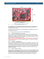
LPC3250 Developer’s Kit - User’s Guide Copyright 2011 © Embedded Artists AB LPC3250 Developer’s Kit User’s Guide Get Up-and-Running Quickly and Start Developing Your Applications On Day 1! EA2-USG-0903 Rev D LPC3250 Developer’s Kit - User’s Guide Page 2 Embedded Artists AB Davidshallsgatan 16 SE-211 45 Malmö Sweden [email protected] http://www.EmbeddedArtists.com Copyright 2011 © Embedded Artists AB. All rights reserved. No part of this publication may be reproduced, transmitted, transcribed, stored in a retrieval system, or translated into any language or computer language, in any form or by any means, electronic, mechanical, magnetic, optical, chemical, manual or otherwise, without the prior written permission of Embedded Artists AB. Disclaimer Embedded Artists AB makes no representation or warranties with respect to the contents hereof and specifically disclaim any implied warranties or merchantability or fitness for any particular purpose. Information in this publication is subject to change without notice and does not represent a commitment on the part of Embedded Artists AB. Feedback We appreciate any feedback you may have for improvements on this document. Please send your comments to [email protected]. Trademarks All brand and product names mentioned herein are trademarks, services marks, registered trademarks, or registered service marks of their respective owners and should be treated as such. Copyright 2011 © Embedded Artists AB LPC3250 Developer’s Kit - User’s Guide Page 3 Table of Contents 1 Document Revision History 5 2 Introduction 6 2.1 Features 6 2.2 ESD and Handling Precaution 7 2.3 LPC3250 Core Voltage Precaution 8 2.4 CE Assessment 8 2.5 Other Products from Embedded Artists 8 2.5.1 Design and Production Services 8 2.5.2 OEM / Education / QuickStart Boards and Kits 8 3 LPC3250 OEM Board Design 9 3.1 9 LPC3250 OEM Board Schematics 3.1.1 Schematic Page 2: Misc 3.1.2 Schematic Page 3: Powering 10 3.1.3 Schematic Page 4: External Memories 10 3.1.4 Schematic Page 5: Digital and Analog IO 11 3.1.5 Schematic Page 6: Ethernet Interface 11 3.1.6 Schematic Page 7: USB Interface 11 3.1.7 Schematic Page 8: Expansion Connector 12 3.2 Usage of CPU Pins 3.3 LPC3250 OEM Board Mechanical Dimensions and Connector 15 3.4 12 Things to note about the LPC3250 OEM Board 16 3.4.1 LPC3250 Adjustable Core Voltage 16 3.4.2 NAND FLASH Bad Block 16 3.4.3 Brand of Memory Chips 16 3.4.4 LPC3250 Peripherals 17 4 QVGA Base Board Design 18 4.1 QVGA Base Board Schematics 18 4.2 Signal Mapping to QVGA Base Board 18 4.3 Jumpers 25 4.3.1 Default Jumper Positions 26 4.3.2 Illegal Jumper Combinations 26 4.4 4.4.1 Connectors Mictor-38 ETM Connector 27 27 4.5 Important Components 28 4.6 USB Interface 29 4.6.1 USB Interface Note 5 Getting Started 29 31 5.1 Initial Setup and Powering 31 5.2 FTDI USB Driver 31 5.2.1 Copyright 2011 © Embedded Artists AB 9 USB Driver Behavior 34 LPC3250 Developer’s Kit - User’s Guide Page 4 5.3 Building Sample Applications 34 5.3.1 Compile Using CodeSourcery 35 5.3.2 Compile Using Keil’s uVision 36 5.4 Booting 5.4.1 Kickstart Loader 36 5.4.2 Stage 1 Loader 36 5.4.3 Service Boot 42 6 Further Information Copyright 2011 © Embedded Artists AB 36 45 LPC3250 Developer’s Kit - User’s Guide Page 5 1 Document Revision History Revision Date Description A 2009-10-05 First official revision of document B 2010-10-18 Added section (4.6) about USB device interface. Updated rework instruction in section (4.6) for USB device interface and R100. Corrected section 5.4.3 about service boot jumpers. Updated to rev 1.3 of OEM board schematic. C 2011-10-26 Updated section 5.4.2 about how to store an application in NAND flash and execute from external memory. D 2011-12-19 Added note about CE marking. Copyright 2011 © Embedded Artists AB LPC3250 Developer’s Kit - User’s Guide Page 6 2 Introduction Thank you for buying Embedded Artists’ LPC3250 Developer’s Kit based on NXP’s ARM926EJ-S LPC3250 microcontroller. This document is a User’s Guide that describes the LPC3250 OEM Board and the QVGA Base Board hardware design. It is the User’s Manual for both the LPC3250 Developer’s Kit as well as for just the LPC3250 OEM Board. 2.1 Features Embedded Artists’ LPC3250 Developer’s Kit with NXP’s ARM926EJ-S LPC3250 microcontroller lets you get up-and-running quickly. The small sized OEM board offers many unique features that ease your learning curve and speed up your program development. The board has also been designed for OEM applications with volume discount available. The features of the LPC3250 OEM Board are: NXP's ARM926EJ-S LPC3250 microcontroller in BGA package, with 256 KByte internal RAM External data memory: 64 MB DDR SDRAM (16-bit databus width) External FLASH memories: 128 MB (1Gbit) NAND FLASH and 4 MB (32Mbit) SPI-NOR FLASH 13.0000 MHz crystal for cpu 256 Kbit I2C E2PROM for storing non-volatile parameters Buffered 16-bit data bus for external expansion 200 pos expansion connector (SODIMM-200 format, 0.6mm pitch) Almost all LPC3250 pins available (except dedicated pins for on-board memories and internal powering) 3.15-3.3V powering Onboard reset generation 5 LEDs Compact SODIMM size: 66 x 48 mm Eight layer PCB design for compact design and best noise immunity There is an accompanying QVGA Base Board that can be used for initial prototyping work. This base board was originally developed for the LPC2478 processor and the associated LPC2478 OEM Board in SODIMM format. Some interfaces, for example the CAN bus and ETM, do not exist on the LPC3250 and can hence not be used. The features of the QVGA Base Board are: 3.2 inch QVGA TFT color LCD with touch screen (4-wire version) Copyright 2011 © Embedded Artists AB 18-bit RGB interface to display Connectors 200 pos, 0.6mm pitch SODIMM connector for the LPC3250 OEM Board Expansion connector with all LCD controller signals, for custom displays Expansion connector with all SODIMM interface signals Ethernet connector (RJ45) CAN interface & connector (cannot be used with the LPC3250 OEM Board) MMC/SD interface & connector LPC3250 Developer’s Kit - User’s Guide JTAG connector Pads for ETM connector (cannot be used with the LPC3250 OEM Board) Interfaces USB OTG interface & connector USB host interface & connector Full modem RS232 on UART #1 (cannot be used on 32-bit databus cpu boards, but RxD2/TxD2 can alternatively be connected to the RS232 interface) Dual CAN interface & connector (cannot be used with the LPC3250 OEM Board) IrDA transceiver interface Power Page 7 Power supply, either via USB or external 9-15V DC Other 5-key joystick 3-axis accelerometer 5 push-button keys (four via I2C and one on ‘gpi01/service_n’ (P2.10)) 9 LEDs (8 via I2C and one on ‘gpi01/service_n’ (P2.10)) Analog input USB-to-serial bridge on UART #5 (FT232R) and ISP functionality Reset push-button and LED 250x150 mm in size 2.2 ESD and Handling Precaution Please note that the LPC3250 OEM Board and QVGA Base Board come without any case/box and all components are exposed for finger touches – and therefore extra attention must be paid to ESD (Electro-Static Discharge) precaution. Make it a habit always to first touch the metal surface of one of the USB or SC/MMC connectors for a few seconds with both hands before touching any other parts of the boards. That way, you will have the same electrical potential as the board and therefore minimize the risk for ESD damages. Never touch directly on the LPC3250 OEM Board and in general as little as possible on the QVGA Base Board. The push-buttons on the QVGA Base Board have grounded shields to minimize the effect of ESD. Note that Embedded Artists does not replace boards that have been damaged by ESD. Do not exercise excessive pressure on the LCD glass area. That will damage the display. Also, do not apply pressure on the two flex cables connecting the LCD. These are relatively sensitive and can be damaged if too much pressure is applied to them. Note that Embedded Artists does not replace boards where the LCD has been improperly handled. Copyright 2011 © Embedded Artists AB LPC3250 Developer’s Kit - User’s Guide Page 8 2.3 LPC3250 Core Voltage Precaution The core voltage for the LPC3250 can be dynamically changed, via I2C commands sent to the LTC3447 voltage converter. The voltage can be set to up to 2V. Note that this is above the limits of the core voltage. Read the LPC3250 datasheet for details (the absolute maximum core voltage allowed is 1.39V). Note that Embedded Artists do not replace LPC3250 OEM boards where the core voltage (VDD(CORE)) has been raised above 1.39 Volt. It is the user’s responsibility not to exceed the voltage specification found in the datasheet. 2.4 CE Assessment The LPC3250 Developers Kit (consisting of the LPC3250 OEM Board and QVGA Base Board) is CE marked. See separate CE Declaration of Conformity document. The LPC3250 Developers Kit is a class A product. In a domestic environment this product may cause radio interference in which case the user may be required to take adequate measures. EMC emission test has been performed on the LPC3250 Developers Kit. Standard interfaces like Ethernet, USB, serial have been in use. General expansion connectors where internal signals are made available (for example processor pins) have been left unconnected. Connecting other devices to the product via the general expansion connectors may alter EMC emission. It is the user’s responsibility to make sure EMC emission limits are not exceeded when connecting other devices to the general expansion connectors of the LPC3250 Developers Kit. Due to the nature of the LPC3250 Developers Kit – an evaluation board not for integration into an endproduct – fast transient immunity tests and conducted radio-frequency immunity tests have not been executed. Externally connected cables are assumed to be less than 3 meters. The general expansion connectors where internal signals are made available do not have any other ESD protection than from the chip themselves. Observe ESD precaution. Note that the LPC3250 OEM board is classified as a component and is hence not CE marked separately. It can perform different functions in different integrations and it does not have a direct function. It is therefore not in the scope of the CE Directive. An end product, where an OEM Board is integration into, is however very likely to need CE marking. 2.5 Other Products from Embedded Artists Embedded Artists have a broad range of LPC1xxx/LPC2xxx/LPC3xxx/LPC4xxx based boards that are very low cost and developed for prototyping / development as well as for OEM applications. Modifications for OEM applications can be done easily, even for modest production volumes. Contact Embedded Artists for further information about design and production services. 2.5.1 Design and Production Services Embedded Artists provide design services for custom designs, either completely new or modification to existing boards. Specific peripherals and I/O can be added easily to different designs, for example, communication interfaces, specific analog or digital I/O, and power supplies. Embedded Artists has a broad, and long, experience in designing industrial electronics in general and with NXP’s LPC1xxx/LPC2xxx/LPC3xxx microcontroller family in specific. Our competence also includes wireless and wired communication for embedded systems. For example IEEE802.11b/g (WLAN), Bluetooth™, ZigBee™, ISM RF, Ethernet, CAN, RS485, and Fieldbuses. 2.5.2 OEM / Education / QuickStart Boards and Kits Visit Embedded Artists’ home page, www.EmbeddedArtists.com, for information about other OEM / Education / QuickStart boards / kits or contact your local distributor. Copyright 2011 © Embedded Artists AB LPC3250 Developer’s Kit - User’s Guide Page 9 3 LPC3250 OEM Board Design Please read the LPC3250 OEM Board datasheet and associated schematic for information about the board. Some additional information about the LPC3250 OEM Board is presented below. 3.1 LPC3250 OEM Board Schematics 3.1.1 Schematic Page 2: Misc 3.1.1.1 Crystals The microprocessor crystal frequency is 13.0000 MHz, which is the recommended frequency from NXP. An internal PLL can create many other frequencies from this, like 208 MHz and 266 MHz. The LPC3250 has an internal real-time clock (RTC) block that can be used to provide real-time and alarm function. A 32.768 kHz crystal gives the base frequency for the RTC. The RTC block can be powered via a separate supply (for example from a battery or high-capacity capacitor). The 32.768 kHz can also be used as main oscillator via a PLL: 32.768 kHz x 397 = 13.009 MHz. Note that the clocking structure is different from the LPC2xxx family. It is a more complex structure but also much more versatile and flexible. There is no shortcut but to read the LPC3250 User’s Manual in detail to understand the options and settings. 3.1.1.2 Booting The LPC3250 starts executing from an on-chip ROM, containing the bootloader. Note that the LPC3250 does not contain any on-chip FLASH memory. Program code must be loaded from an external source into the on-chip SRAM. The default boot is from an external memory (see LPC3250 User’s Manual for details). Program code is typically stored in NAND or SPI-NOR flash. By pulling pin GPI_01/SERVICE_N low, UART boot mode is activated. This is a method for downloading code from the PC, for example for programming the bootloader for the first time. Note that pin GPI_01/SERVICE_N can be pulled low by pressing the “P2.10” key on the QVGA Base Board. 3.1.1.3 JTAG interface The JTAG interface is a standard ARM-compatible JTAG interface. 3.1.1.4 SPI NOR FLASH There is a 32Mbit (4 MByte) NOR flash connected to the SPI bus. Embedded Artists can choose to mount, either S25FL032P from Spansion, AT45DB321 from Atmel, or other, on the board depending on component availability at the time of production. Mounted chips will be supported by the LPC3250 bootloader. However, commands used to program the memory differ. Chip id should always be read out to determine exact type mounted. 3.1.1.5 Reset Generation The reset generation is handled by a standard voltage supervisor chip, CAT811R from Catalyst Semiconductor. The reset signal will be held active (i.e., low) until the supply voltages, +3.3V, is within margins (above 2.63V). The reset duration is typically 200 mS (consult the CAT811R datasheet for exact details). The output reset signal is push/pull output that is converted to an open-collector / opendrain output via the 74LVC1G125 buffer. An external reset source can pull the reset signal low (with an open-collector/open-drain output). The RESET_N input on the LPC3250 has a 1.2V voltage range (voltage domain: VDD_RTC). A 74LVC1G125 buffer makes sure this voltage range is not exceeded by the external signal RESET_IN (which has 3.3V range). Copyright 2011 © Embedded Artists AB LPC3250 Developer’s Kit - User’s Guide Page 10 3.1.1.6 I2C E2PROM There is a 256 kbit E2PROM accessible via the I2C interface (I2C1). The LPC3250 has two on-chip I2C communication channels (I2C1 and I2C2). More peripheral units are easily connected to the two-wire I2C bus, just as long as the addresses do not collide. The address of the 256kbit E2PROM is 0xA0, which is also indicated in the schematic. There are 2.2 kohm pull-up resistors (pull-ups are always needed on I2C busses) on the board on both I2C channels. 3.1.2 Schematic Page 3: Powering 3.1.2.1 1.2V and 1.8V Fixed Voltages The LPC3250 requires three fixed voltages; 1.2V for the core, 1.8V for the memory interface and 3.153.3V for the rest of the i/o interfaces. The 1.2V and 1.8V voltages are generated by two LM3671MF step-down switching regulators from National Semiconductor. These regulators are capable of generating 600mA, which by far exceed the needed current by the LPC3250 and other components on the LPC3250 OEM Board. The 3.15-3.3V voltage is the input voltage to the LPC3250 OEM Board, see below. The Real-time clock also needs a 1.2V power, which is generated by a LDO (MIC5232). 3.1.2.2 1.2V Adjustable Core Voltage The core 1.2V voltage is adjustable and is generated by the step down switching regulator LTC3447 from Linear Technologies. This regulator is capable of generating 600mA, which also by far exceed the needed current by the LPC3250. The adjustment is done via an I2C channel, I2C1 in the LPC3250 case. The core voltage can be adjusted as a power save feature. By lowering the voltage (down to 0.9V), the total power consumption can be lowered but the clock frequency of the core must then also be lowered. This is a trade-off that is important for hand held/portable equipment. Note that it is the user’s responsibility not to program the LTC3447 to generate too high core voltage, which is possible. The LTC3447 can generate voltages up to 2V, which by far exceed the limits for the LPC3250. See the LPC3250 datasheet for exact details about voltage ranges, but it is in the region of 1.1-1.39V. Also see the LTC3447 datasheet for details about how to adjust the voltage (it is a write-only register). The I2C address for the LTC3447 is indicated in the schematic. Note that a core voltage of 1.35V should be programmed when working with the external DDR SDRAM. 3.1.2.3 Input Voltage The input voltage to the LPC3250 OEM Board is given by the requirements of the LPC3250. The recommended input voltage range is 3.15V to 3.3V. The input supply must be stable but there are no special needs for bulk capacitors close to the power pins on the expansion connectors. The needed capacitors are placed close to the switched step down switching regulators on the LPC3250 OEM Board. Note that the LPC3250 OEM Board is sensitive to input noise on the input voltage. The peak-to-peak noise should be below 10mV. A linear regulator to feed the input voltage is strongly recommended. 3.1.3 Schematic Page 4: External Memories Page 4 of the schematic contains the external memory interface and the external memories. The memory interface uses a 16-bit databus and operates at 1.8V level, which minimizes power consumption. Copyright 2011 © Embedded Artists AB LPC3250 Developer’s Kit - User’s Guide Page 11 3.1.3.1 DDR SDRAM A 512 MBit (64 MByte) Mobile DDR SDRAM is used (MT46H32M16LF from Micron). The chip is powered by 1.8V and is organized as 32Mbit x16, i.e. it has 16-bit databus width. The chip is connected to EMC_DYCS0_N (memory bank #0 for dynamic RAM) at address range 0x8000 0000 – 0x9FFF FFFF. Note that memory bank #1 for dynamic RAM is not available (i.e., signal EMC_DYCS1_N is not used). 3.1.3.2 NAND Flash A 1 Gbit (128 MByte) NAND flash is used (K9F1G08U0A-P from Samsung). The chip is powered by 3.3V and has 8-bit databus width. The NAND flash builds on a single-level cell (SLC) technology and has a page size of 2112 bytes (2,048 + 64 bytes). Note that the chip is not directly accessible via the memory bus. Instead, all accesses must be done via the on-chip NAND flash controller of the LPC3250. 3.1.3.3 Buffers to External Interface The LPC3250 memory interface is available on the expansion connector. The data bus width is 16-bits on the external interface. The relevant signals are buffered. The following four static memory regions are available for external access: External static bank #0 (0xE000 0000 – 0xE0FF FFFF) 16-bit databus width and 16MByte in size. External static bank #1 (0xE100 0000 – 0xE1FF FFFF) 16-bit databus width and 16MByte in size. External static bank #2 (0xE200 0000 – 0xE2FF FFFF) 16-bit databus width and 16MByte in size. External static bank #3 (0xE300 0000 – 0xE3FF FFFF) 16-bit databus width and 16MByte in size. By default (R44 = 0 ohm, R43 not mounted), signal N_ABUF_EN is pulled low and the two buffers for address and control signals (U13 and U14) are enabled and act as output (from the LPC3250 OEM Board). The buffered version of the LPC3250 signal OE controls the direction of the data bus buffer (U15). During read operations the buffer acts as an input and during write operations it acts as an output. The data bus buffer is controlled by the signals BLS0 and BLS1, each controlling lower and upper bytes of the 16-bit databus. These signals are active when accessing the external static memory regions. The buffers are dual voltage buffers and act as level translators between the internal 1.8V signal levels and the external levels. Connect the external bus voltage to VDD_EXT. See the datasheet of 74AVCA164245 for exact details about voltage range. Normally 3.3V powering is used on the external side. 3.1.4 Schematic Page 5: Digital and Analog IO Page 5 of the schematic contains all digital and analog signals plus three LEDs controlled by signals P2.10 - P2.12. 3.1.5 Schematic Page 6: Ethernet Interface An external PHY (DP83848 from National Semiconductor) implements a 100/10Mbps Ethernet interface. The external PHY is connected to the Ethernet MAC on the LPC3250 via the RMII interface. 3.1.6 Schematic Page 7: USB Interface There is a USB 2.0 (OTG, Host, Device) interface on the LPC3250. An external PHY (ISP1301) is needed for the cpu. Copyright 2011 © Embedded Artists AB LPC3250 Developer’s Kit - User’s Guide 3.1.7 Page 12 Schematic Page 8: Expansion Connector The LPC3250 OEM Board integrates the core part of a typical LPC3250 board design with a reasonable large amount of external memories. All relevant signals of LPC3250 are available on the 200 pos, 0.6mm pitch expansion connector (SODIMM-200 format). See the next section for a detailed list of available pins. 3.2 Usage of CPU Pins Almost all pins of the LPC3250 are directly available on the expansion connectors. Only in a few cases pins are used for dedicated functionality like (dynamic) memory control signals, chip select signals and power supply. Such pins are not available on the expansion connector. The table below lists all pins and their possible restrictions. Pin Available on expansion connector ADIN0 (TS_XM) ADIN1 (TS_YM) ADIN2 (TS_AUX_IN) TS_XOUT TS_YOUT Yes I2C1_SCL I2C1_SDA I2C2_SCL I2C2_SDA Yes, but I2C-E2PROM (U5 – 24LC256) and core voltage generator (U7, LTC3447) connected to I2C1 pins. SPI1_CLK / SCK0 SPI1_DATIO / MOSI0 / MCFB2 SPI1_DATIN / MISO0 / GPI_25 / MCFB1 GPIO_05 / SSEL0 / MCFB0 Yes, but note that SPI NOR flash is connected to these signals. HIGHCORE / LCDVD[17] ONSW Yes I2S1TX_CLK / MAT3.0 I2S1TX_SDA / MAT3.1 I2S1TX_WS / CAP3.0 MS_BS / MAT2.1 MS_DIO0 / MAT0.0 MS_DIO1 / MAT0.1 MS_DIO2 / MAT0.2 MS_DIO3 / MAT0.3 MS_SCLK / MAT2.0 P0.0 / I2S1RX_CLK P0.1 / I2S1RX_WS P0.2 / I2S0RX_SDA / LCDVD[4] P0.3 / I2S0RX_CLK / LCDVD[5] P0.4 / I2S0RX_WS / LCDVD[6] P0.5 / I2S0TX_SDA / LCDVD[7] P0.6 / I2S0TX_CLK / LCDVD[12] P0.7 / I2S0TX_WS / LCDVD[13] PWM_OUT1 / LCDVD[16] PWM_OUT2 / LCDVD[19] SPI2_CLK / SCK1 / LCDVD[23] SPI2_DATIN / MISO1 / LCDVD[21] / GPI_27 Yes Copyright 2011 © Embedded Artists AB Note that these signals have 2.2K pull-up resistors. Note that HIGHCORE signal can control adjustable core voltage of R28 mounted (normally not mounted). Note: Pull-up on GPI_01/SERVICE_N GPO_01 and GPO_14 controls LED1/LED2 GPI_03 has pull-down resistor GPI_05 has pull-down resistor GPI_28 has pull-up resistor U7_HCTS/CAP0.1/LCDCLKIN/ GPI_22 has pull-up resistor GPO_19 controls NAND write protect signal LPC3250 Developer’s Kit - User’s Guide Page 13 SPI2_DATIO / MOSI1 / LCDVD[20] SYSCLKEN / LCDVD[15] TST_CLK2 U1_RX / CAP1.0 / GPI_15 U1_TX U2_HCTS / U3_CTS / GPI_16 U2_RX / U3_DSR / GPI_17 U2_TX / U3_DTR U3_RX / GPI_18 U3_TX U5_RX / GPI_20 U5_TX U6_IRRX / GPI_21 U6_IRTX U7_HCTS / CAP0.1 / LCDCLKIN / GPI_22 U7_RX / CAP0.0 / LCDVD[10] / GPI_23 U7_TX / MAT1.1 / LCDVD[11] GPI_00 / I2S1RX_SDA GPI_01 / SERVICE_N GPI_02 / CAP2.0 / ENET_RXD3 GPI_03 GPI_04 / SPI1_BUSY GPI_05 / U3_DC GPI_06 / HSTIM_CAP / ENET_RXD2 GPI_07 / CAP4.0 / MCABORT GPI_08 / KEY_COL6 / SPI2_BUSY / ENET_RX_DV GPI_09 / KEY_COL7 / ENET_COL GPI_19 / U4_RX GPI_28 / U3_RI GPIO_00 GPIO_01 GPIO_04 / SSEL1 / LCDVD[22] GPO_00 / TST_CLK1 GPO_01 GPO_02 / MAT1.0 / LCDVD[0] GPO_03 / LCDVD[1] GPO_04 GPO_05 GPO_06 / LCDVD[18] GPO_07 / LCDVD[2] GPO_08 / LCDVD[8] GPO_09 / LCDVD[9] GPO_10 / MC2B / LCDPWR GPO_11 GPO_12 / MC2A / LCDLE GPO_13 / MC1B / LCDDCLK GPO_14 GPO_15 / MC1A / LCDFP GPO_16 / MC0B / LCDENAB / LCDM GPO_17 GPO_18 / MC0A / LCDLP GPO_19 GPO_20 GPO_21 / U4_TX / LCDVD[3] GPO_22 / U7_HRTS / LCDVD[14] GPO_23 / U2_HRTS / U3_RTS EMC_D19/P2.0 EMC_D20/P2.1 EMC_D21/P2.2 Copyright 2011 © Embedded Artists AB Yes Note that signals can only be P2 signals, not LPC3250 Developer’s Kit - User’s Guide Page 14 EMC_D22/P2.3 EMC_D23/P2.4 EMC_D24/P2.5 EMC_D25/P2.6 EMC_D26/P2.7 EMC_D27/P2.8 EMC_D28/P2.9 EMC_D29/P2.10 EMC_D30/P2.11 EMC_D31/P2.12 EMC databus. USB_ATX_INT_N USB_DAT_VP / U5_RX USB_I2C_SCL USB_I2C_SDA USB_OE_TP_N USB_SE0_ VM / U5_TX No, connected to on-board USB transceiver, ISP1301 KEY_COL1 / ENET_RX_CLK / ENET_REF_CLK KEY_COL2 / ENET_RX_ER KEY_COL3 / ENET_CRS KEY_COL4 / ENET_RXD0 KEY_COL5 / ENET_RXD1 KEY_ROW3 / ENET_TX_EN KEY_ROW4 / ENET_TXD0 KEY_ROW5 / ENET_TXD1 GPIO_02 / KEY_ROW6 / ENET_MDC GPIO_03 / KEY_ROW7 / ENET_MDIO No, connected to on-board Ethernet PHY, DP83848 EMC_A00 – EMC_A23 Yes, but only available via the address bus buffer EMC_D00 – EMC_D15 Yes, but only available via the data bus buffer EMC_BLS0 EMC_BLS1 EMC_CS0_N EMC_CS1_N EMC_CS2_N EMC_CS3_N EMC_OE_N EMC_WR_N Yes, but only available via the buffer FLASH_ALE FLASH_CE_N FLASH_IO00 – FLASH_IO07 FLASH_RD_N FLASH_RDY FLASH_WR_N No, used for on-board NAND flash memory. EMC_CAS_N EMC_CKE0 EMC_CLK EMC_DQM0 EMC_DQM1 EMC_DYCS0_N EMC_RAS_N EMC_D16/EMC_DQS0 EMC_D17/EMC_DQS1 EMC_D18/EMC_CLK_N No, used for on-board DDR SDRAM. Copyright 2011 © Embedded Artists AB P2.10 controls LED3 P2.11 controls LED4 P2.12 controls LED5 LPC3250 Developer’s Kit - User’s Guide Page 15 EMC_BLS2 EMC_BLS3 EMC_CKE1 EMC_CLKIN EMC_DQM2 EMC_DQM3 EMC_DYCS1_N No. These signals are not used and not available. KEY_COL0 / ENET_TX_CLK KEY_ROW0 / ENET_TX_ER KEY_ROW1 / ENET_TXD2 KEY_ROW2 / ENET_TXD3 No. These signals are not used and not available. Note that three (of four) signals can become available if 0 ohm resistors are mounted: KEYROW0, mount R93 KEYROW1, mount R94 KEYCOL0, mount R91 JTAG signals Yes RESET_N RESOUT_N Yes Note pull-up resistor on RESET_IN and internal open-drain driving of RESET_IN RTCX_IN RTCX_OUT SYSX_IN SYSX_OUT No, directly connected to on-board crystals All VDD and VSS pins No, not directly accessible, but ground is available and 3.15-3.3V input voltage PLL397_LOOP No, internal on-board connection to signal. The QVGA Base Board illustrates how to typically connect external interfaces (like USB, external memory devices, etc) to the LPC3250 OEM Board. Study this schematic (also found in this document) for details. 3.3 LPC3250 OEM Board Mechanical Dimensions and Connector Figure 1 below contains a drawing of the board that includes mechanical measures. See SODIMM-200 standard for exact measures. 1.8V keying is used (SODIMM-200 boards are either 1.8V or 2.5V keyed). Copyright 2011 © Embedded Artists AB LPC3250 Developer’s Kit - User’s Guide Page 16 66 mm 48 mm 1.8V keying of SODIMM board Figure 1 – LPC3152 OEM Board Mechanical Dimensions The SODIMM-200 format is a standard and there are many connectors that are suitable from many different manufactures. The many sources also keep the connector cost very low. Note that the connector should be 1.8V keyed. One suitable connector is 0-1473005-4 from Tyco/AMP. Basically any SODIMM, DDR2, 200pos, 1.8V, right-angled connector will do. 3.4 Things to note about the LPC3250 OEM Board 3.4.1 LPC3250 Adjustable Core Voltage The core voltage for the LPC3250 is adjustable via I2C commands sent to the LTC3447 voltage converter. The core voltage should always be increased to 1.35 volt in order for external mobile DDR SDRAM to function properly. Initialization code that increase the adjustable core voltage to 1.35V can be downloaded from Embedded Artists support pages. Note that it is the user’s responsibility not to program the LTC3447 to generate too high core voltage, which is possible. The LTC3447 can generate voltages up to 2V, which by far exceed the limits for the LPC3250. 3.4.2 NAND FLASH Bad Block The NAND Flash is the K9F1G08U0A from Samsung and has 1 GBit capacity. The chip may include invalid blocks when shipped from factory. A maximum of 20 invalid blocks may exist initially, i.e., 10041024 valid blocks. Additional invalid blocks may develop while being used. Invalid blocks are defined as blocks that contain one or more bad bits. Do not erase or program factory-marked bad blocks. More information about appropriate management of invalid blocks can be found in technical notes and datasheet from Samsung. 3.4.3 Brand of Memory Chips Note that there is no guarantee for a certain brand or version of memory chips; SPI-NOR flash, parallel NAND flash and mobile DDR SDRAM. The lifetime of memory chips is limited and availability can also be limited from time to time. Embedded Artists make every effort to mount the original design chip on the board. In case that is impossible a compatible chip will instead be mounted without any prior notice. There can be small programming differences between mounted brands. The application Copyright 2010 © Embedded Artists AB LPC3250 Developer’s Kit - User’s Guide Page 17 program shall always read the chip id of flash devices to make certain which chip is actually mounted on the board. The support page contains datasheets to the different memory devices and information about mounted devices on different board versions. 3.4.4 LPC3250 Peripherals The key scan interface peripheral cannot be used with the LPC3250 OEM Board because the Ethernet interface is active. Copyright 2010 © Embedded Artists AB LPC3250 Developer’s Kit - User’s Guide Page 18 4 QVGA Base Board Design Please read the QVGA Base Board schematic for information about the board. Some additional information about the QVGA Base Board is presented below. 4.1 QVGA Base Board Schematics The QVGA Base Board contains a number of interfaces and connectors to the LPC3250 OEM Board. The design can be viewed as a reference schematic for custom designs around the LPC3250 OEM Board. 4.2 Signal Mapping to QVGA Base Board The QVGA Base Board was originally developed for the LPC2478 processor and the associated LPC2478 OEM Board in SODIMM format. The silk screen on the base board therefore reflects the LPC2478 signal names. The table below lists differences between the LPC3250 and LPC2478 OEM Boards in their SODIMM interface. The table also lists what functionality that is connected to the different signals. SODIMM pin number LPC2478 OEM Board LPC3250 OEM Board QVGA Base Board 1 ETH_TXP ETH_TXP Ethernet i/f 2 ETH_RXP ETH_RXP Ethernet i/f 3 ETH_TXN ETH_TXN Ethernet i/f 4 ETH_RXN ETH_RXN Ethernet i/f 5 ETH_VDD ETH_VDD Ethernet i/f 6 ETH_GND ETH_GND Ethernet i/f 7 ETH_LED1 ETH_LED1 Ethernet i/f 8 ETH_LED2 ETH_LED2 Ethernet i/f 9 VBAT_IN VBAT_IN 0.33F backup cap on vbat signal 10 ALARM ONSW Connected to alarm-LED (active high) 11 RESET_IN RESET_IN Connects to RESET push-button and USB-toserial bridge (for automatic ISP functionality) 12 RESET_OUT RESET_OUT Connects to RESET LED indicator. Used to reset PCA9532 and QVGA display. 13 ETH_PHY_PD ETH_PHY_PD Part of Ethernet i/f, can be connected to SODIMM pin 118 14 JTAG_DBGEN JTAG_DBGEN Connected to ‘JTAG Enable’ jumper 15 JTAG_TCK JTAG_TCK Connected to standard 20 pos (2x10 pin) JTAG connector 16 JTAG_RTCK JTAG_RTCK Connected to standard 20 pos (2x10 pin) JTAG connector 17 JTAG_NTRST JTAG_NTRST Connected to standard 20 pos (2x10 pin) JTAG connector 18 JTAG_TMS JTAG_TMS Connected to standard 20 pos (2x10 pin) Copyright 2010 © Embedded Artists AB Comment ONSW functionality not demonstrated/ supported on QVGA Base Board. LPC3250 Developer’s Kit - User’s Guide Page 19 JTAG connector 19 JTAG_TDI JTAG_TDI Connected to standard 20 pos (2x10 pin) JTAG connector 20 JTAG_TDO JTAG_TDO Connected to standard 20 pos (2x10 pin) JTAG connector 21 V3A VDDA Positive reference for trimming potentiometer 22 VREF NC (can be VCCA) Can be connected VDDA(V3A) 23 VSSA VSSA Negative reference for trimming potentiometer 24 GND GND GND 25 P2.0 GPO_10 LCDPWR signal, power enable for QVGA display. Also connects to ETM pads, if connector mounted. ETM cannot be used 26 P2.1 GPO_12 LCDLE signal. Not used by design. Also connects to ETM pads, if connector mounted. ETM cannot be used 27 P2.2 GPO_13 LCDDCLK signal, dot clock for QVGA display. Also connects to ETM pads, if connector mounted. ETM cannot be used 28 P2.3 GPO_15 LCDFP signal, vsync for QVGA display. Also connects to ETM pads, if connector mounted. ETM cannot be used 29 P2.4 GPO_16 LCDENAB signal, data enable for QVGA display. Also connects to ETM pads, if connector mounted. ETM cannot be used 30 P2.5 GPO_18 LCDLP signal, hsync for QVGA display. Also connects to ETM pads, if connector mounted. ETM cannot be used 31 P2.6 P0.2 LCD databit 4. Also connects to ETM pads, if connector mounted. ETM cannot be used 32 P2.7 P0.3 LCD databit 5. Also connects to ETM pads, if connector mounted. ETM cannot be used 33 P2.8 P0.4 LCD databit 6. Also connects to ETM pads, if connector mounted. ETM cannot be used 34 P2.9 P0.5 LCD databit 7. Also connects to ETM pads, if connector mounted. ETM cannot be used 35 P2.10 GPI_01 Connected to push-button (for enabling bootloader during reset or EINT0 input). Also connects to LED (active low). Enable UART booting by pulling signal low at reset Connects to USB-to-serial bridge (for automatic ISP functionality) 36 P2.11 U7_HCTS 37 VCC VCC 38 GND GND 39 VCC VCC 40 GND GND 41 P0.29-USBA-DP NC (can be KEYROW0) Connects to USB device/OTG interface USB Device/OTG i/f not used 42 P0.31-USBB-DP USB_CONN_DP Connects to USB host interface USB Host interface is connected to the LPC3250 43 P0.30-USBA-DM NC (can be Connects to USB device/OTG interface USB Device/OTG Copyright 2010 © Embedded Artists AB LCDCLKIN, an external clock signal can be feed to this pin. LPC3250 Developer’s Kit - User’s Guide Page 20 KEYROW1) i/f not used 44 USBB-DM USB_CONN_DN Connects to USB host interface 45 P2.12 GPO_06 LCD databit 18 46 P2.13 PWMOUT2 LCD databit 19 47 P0.0 U6_IRTX Can be connected to RD1 for CAN channel #1, can also connect to IrDA transceiver USB Host interface is connected to the LPC3250 CAN interface cannot be used by the LPC3250. IrDA can be used 48 P0.1 U6_IRRX Can be connected to TD1 for CAN channel #1, can also connect to IrDA transceiver CAN interface cannot be used by the LPC3250. IrDA can be used 49 P0.2 U5_TX Can be connected to USB-to-serial bridge (TxD on UART #5. Note that the silk screen text says UART#0) Possible to boot over UART#5 50 P0.3 U5_RX Can be connected to USB-to-serial bridge (RxD on UART #5. Note that the silk screen text says UART#0) Possible to boot over UART#5 51 P0.4 GPO_02 LCD databit 0, can also be connected to RD2 for CAN channel #2 CAN i/f cannot be used 52 P0.5 GPO_03 LCD databit 1, can also be connected to TD2 for CAN channel #2 CAN i/f cannot be used 53 P0.6 GPO_08 LCD databit 8 54 P0.7 GPO_09 LCD databit 9 55 P0.8 PWMOUT1 LCD databit 16 56 P0.9 HICORE LCD databit 17 57 P0.10 U1_TX Can be connected to RS232 interface (TxD) 58 P0.11 U1_RX Can be connected to RS232 interface (RxD) 59 P0.12 USB_VBUS_CTRL Can be connected to enable USB-host power switch 60 P0.13 GPO_17 Can be connected to LED (active low) for USB-host indicator 61 P0.14 GPO_20 Can be connected to USB-device enabledevice signal 62 P0.15 SPI1_CLK QVGA display and Touch screen serial interface (SPI-SCK) 63 P0.16 GPO_04 QVGA display serial interface (SSEL) 64 P0.17 SPI1_DATIN QVGA display and Touch screen serial interface (SPI-MISO) 65 P0.18 SPI1_DATIO QVGA display and Touch screen serial interface (SPI-MOSI) 66 P0.19 GPO_05 QVGA display serial interface (command/data select) 67 P0.20 GPO_11 Touch screen serial interface (SSEL) 68 P0.21 TS_XP No special usage on QVGA Base Board 69 P0.22 TS_YP No special usage on QVGA Base Board Copyright 2010 © Embedded Artists AB LPC3250 Developer’s Kit - User’s Guide Page 21 70 P0.23 AIN0 Can be connected to accelerometer, X-axis 71 P0.24 AIN1 Can be connected to accelerometer, Y-axis 72 P0.25 AIN2 Can be connected to accelerometer, Z-axis, or analog input (trimpot) 73 P0.26 GPO_00 Connects to speaker output on AOUT signal 74 P0.27-SDA0 I2C1_SDA I2C-SDA0, connects to PCA9532 (IO expander) 75 P0.28-SCL0 I2C1_SCL I2C-SCL0, connects to PCA9532 (IO expander) 76 GND GND 77 GND GND 78 P1.2 MCICLK Connects to MCICLK on SD/MMC connector 79 P1.3 MCICMD Connects to MCICMD on SD/MMC connector 80 P1.5 GPO_01 Connects to MCIPWR on SD/MMC connector 81 P1.6 MCIDAT0 Connects to MCIDAT0 on SD/MMC connector 82 P1.7 MCIDAT1 Connects to MCIDAT1 on SD/MMC connector 83 P1.11 MCIDAT2 Connects to MCIDAT2 on SD/MMC connector 84 P1.12 MCIDAT3 Connects to MCIDAT3 on SD/MMC connector 85 P1.13 GPIO_05 No special usage on QVGA Base Board 86 P1.18 GPO_14 Connects to QVGA backlight control. Can also be connected to LED (active low) to be used for USB device/OTG 87 P1.19 GPI_13 No special usage on QVGA Base Board 88 P1.20 U7_RX LCD databit 10 89 P1.21 U7_TX LCD databit 11 90 P1.22 P0.6 LCD databit 12 91 P1.23 P0.7 LCD databit 13 92 P1.24 GPO_22 LCD databit 14 93 P1.25 SYSCLKEN LCD databit 15 94 P1.26 SPI2_DATIO LCD databit 20 95 P1.27 SPI2_DATIN LCD databit 21, can also be connected to ISP1301 (USB OTG transceiver) ISP1301 on base board shall not be used 96 P1.28 GPIO_04 LCD databit 22, can also be connected to ISP1301 (USB OTG transceiver) ISP1301 on base board shall not be used 97 P1.29 SPI2_CLK LCD databit 23, can also be connected to ISP1301 (USB OTG transceiver) ISP1301 on base board shall not be used 98 P1.30 USB_CONN_VBUS Can be connected to VBUS signal from USB host power 99 P1.31 GPI_02 Can be connected to over-current error signal from USB host power switch 100 NAND_FLASH_R DY GPO_19 Can be connected to SODIMM pin 119 Copyright 2010 © Embedded Artists AB USB Device/OTG i/f not used Signal not used. Exist internally on OEM board. LPC3250 Developer’s Kit - User’s Guide Page 22 101 GND GND 102 GND GND 103 NC I2S1TX_CLK 104 NC I2S1TX_SDA 105 NC I2S1TX_WS 106 NC P0.0 107 NC P0.1 108 NC GPI_00 109 NC I2C2_SDA 110 NC I2C2_SCL 111 NC GPI_04 112 NC GPI_06 113 NC USB_CONN_ID 114 NC POWER_ON 115 NC TST_CLK2 116 P2.14 P2.7 Can connect as enable signal for IrDA transceiver (active low) 117 P2.15 GPIO_00 Can connect to interrupt signal from touch screen controller 118 P2.19 GPIO_01 Can be connected to Ethernet PHY PD signal, SODIMM pin 13 119 P2.21 GPI_07 Can be connected to NAND FLASH busy output, SODIMM pin 100 120 P2.22 P2.0 Connects to joystick switch 121 P2.23 P2.1 Connects to joystick switch 122 P2.25 P2.2 Connects to joystick switch 123 P2.26 P2.3 Connects to joystick switch 124 P2.27 P2.4 Connects to joystick switch 125 P2.30 P2.5 Can control sensitivity of accelerometer 126 P2.31 P2.6 Can control sensitivity of accelerometer 127 P4.48 GPO_07 LCD databit 2 128 P4.29 GPO_21 LCD databit 3 129 GND GND 130 GND GND 131 BA15 BA15 No special usage on QVGA Base Board 132 BDQM1 BCS3 No special usage on QVGA Base Board 133 BA14 BA14 No special usage on QVGA Base Board 134 BDQM0 BCS2 No special usage on QVGA Base Board 135 BA13 BA13 No special usage on QVGA Base Board 136 BCAS BCS1 No special usage on QVGA Base Board 137 BA12 BA12 No special usage on QVGA Base Board 138 BRAS BCS0 No special usage on QVGA Base Board Copyright 2010 © Embedded Artists AB LPC3250 Developer’s Kit - User’s Guide Page 23 139 BA11 BA11 No special usage on QVGA Base Board 140 BBLS1 BBLS1 No special usage on QVGA Base Board 141 BA10 BA10 No special usage on QVGA Base Board 142 BBLS0 BBLS0 No special usage on QVGA Base Board 143 BA9 BA9 No special usage on QVGA Base Board 144 BWE BWE No special usage on QVGA Base Board 145 BA8 BA8 No special usage on QVGA Base Board 146 BOE BOE No special usage on QVGA Base Board 147 BA7 BA7 No special usage on QVGA Base Board 148 BA23 BA23 No special usage on QVGA Base Board 149 BA6 BA6 No special usage on QVGA Base Board 150 BA22 BA22 No special usage on QVGA Base Board 151 BA5 BA5 No special usage on QVGA Base Board 152 BA21 BA21 No special usage on QVGA Base Board 153 BA4 BA4 No special usage on QVGA Base Board 154 BA20 BA20 No special usage on QVGA Base Board 155 BA3 BA3 No special usage on QVGA Base Board 156 BA19 BA19 No special usage on QVGA Base Board 157 BA2 BA2 No special usage on QVGA Base Board 158 BA18 BA18 No special usage on QVGA Base Board 159 BA1 BA1 No special usage on QVGA Base Board 160 BA17 BA17 No special usage on QVGA Base Board 161 BA0 BA0 No special usage on QVGA Base Board 162 BA16 BA16 No special usage on QVGA Base Board 163 DBUS_EN NC (can connect to KEYCOL0) 164 ABUF_EN ABUF_EN 165 VCC VDD_EXT 166 GND GND 167 BD15 BD15 Occupied by 16-bit databus. No special usage on QVGA Base Board 168 BD31/P3.31 GPI_08 No special usage on QVGA Base Board 169 BD14 BD14 Occupied by 16-bit databus. No special usage on QVGA Base Board 170 BD30/P3.30 GPO_23 No special usage on QVGA Base Board. 171 BD13 BD13 Occupied by 16-bit databus. No special usage on QVGA Base Board 172 BD29/P3.29 GPI_09 No special usage on QVGA Base Board 173 BD12 BD12 Occupied by 16-bit databus. No special usage on QVGA Base Board 174 BD28/P3.28 GPI_19 No special usage on QVGA Base Board 175 BD11 BD11 Occupied by 16-bit databus. No special usage on QVGA Base Board Copyright 2010 © Embedded Artists AB LPC3250 Developer’s Kit - User’s Guide Page 24 176 BD27/P3.27 P2.8 No special usage on QVGA Base Board 177 BD10 BD10 Occupied by 16-bit databus. No special usage on QVGA Base Board 178 BD26/P3.26 P2.9 No special usage on QVGA Base Board 179 BD9 BD9 Occupied by 16-bit databus. No special usage on QVGA Base Board 180 BD25/P3.25 P2.10 No special usage on QVGA Base Board 181 BD8 BD8 Occupied by 16-bit databus. No special usage on QVGA Base Board 182 BD24/P3.24 P2.11 No special usage on QVGA Base Board 183 BD7 BD7 Occupied by 16-bit databus. No special usage on QVGA Base Board 184 BD23/P3.23 P2.12 No special usage on QVGA Base Board 185 BD6 BD6 Occupied by 16-bit databus. No special usage on QVGA Base Board 186 BD22/P3.22 GPI_28 No special usage on QVGA Base Board. 187 BD5 BD5 Occupied by 16-bit databus. No special usage on QVGA Base Board 188 BD21/P3.21 U2_TX No special usage on QVGA Base Board. 189 BD4 BD4 Occupied by 16-bit databus. No special usage on QVGA Base Board 190 BD20/P3.20 U2_RX No special usage on QVGA Base Board. 191 BD3 BD3 Occupied by 16-bit databus. No special usage on QVGA Base Board 192 BD19/P3.19 GPI_05 No special usage on QVGA Base Board. 193 BD2 BD2 Occupied by 16-bit databus. No special usage on QVGA Base Board 194 BD18/P3.18 U2_CTS No special usage on QVGA Base Board. 195 BD1 BD1 Occupied by 16-bit databus. No special usage on QVGA Base Board 196 BD17/P3.17 U3_RX Can be connected to RS232 interface 197 BD0 BD0 Occupied by 16-bit databus. No special usage on QVGA Base Board 198 BD16/P3.16 U3_TX Can be connected to RS232 interface 199 VCC VDD_EXT 200 GND GND Copyright 2010 © Embedded Artists AB LPC3250 Developer’s Kit - User’s Guide Page 25 4.3 Jumpers The QVGA Base Board has a number of jumpers in order to be able to connect/disconnect and fully utilize all functionality of the LPC3250 and the boards. Figure 2 illustrates all jumpers and explains to what part of the design they belong. USB device connect J37 Top pos: always enable Lower pos: enable via P0.14 USB OTG/device J25 Connect or disconnect ISP1301 signals NOT USED NOT USED USB host J27 Connect or disconnect signals UART#0 and ISP Functionality J14, in order from top to bottom: TxD0 RxD0 P2.10 RESET Analog Input J11 Connect V3A to VREF and trim.pot. to analog AD0.2 Accelerometer J12 Connect xyz to AD0.0-AD0.2 Enable/Disable JTAG, J6 IrDA Shutdown J22 CAN/IrDA J18/J19 Connect either CAN or IrDA to P0.0P0.1 Enable ETM J10 NOT USED CAN/IrDA J16 Connect P0.4P0.5 to CAN NOT USED Int/ext display J34/J35 Select internal or external display (for SPI bus and interrupt) RS232 UART J20/J23/J24 Connect RS232 interface to UART #1 or RxD/TxD on UART #3. No of disp. colors J30/J31/J32 All to left: 16-bit color interface to display All to right: 24-bit color interface Figure 2 – QVGA Base Board Jumpers Copyright 2011 © Embedded Artists AB NAND Busy and Ethernet PHY J7 Top: Connect Nand busy signal to P2.2 Bottom: Connect Ethernet PHY PD–signal to P2.19 NOT USED LCD Enable J33 Enable power switch to display Backlight Shutdown J29 Inserted: Shutdown backlight Open: Enable backlight control LPC3250 Developer’s Kit - User’s Guide 4.3.1 Page 26 Default Jumper Positions The figure below illustrates the default jumper positions as mounted when the board is delivered from Embedded Artists. Note that the “Enable JTAG” jumper shall NOT be inserted. The enable state is different for the LPC3250 than on the LPC2478 (which the QVGA Base Board was originally designed for). Figure 3 – QVGA Base Board Default Jumper Positions 4.3.2 Illegal Jumper Combinations Note that some jumpers are mutual exclusive and should not be inserted simultaneously. Copyright 2011 © Embedded Artists AB USB-OTG and LCD interface; the four jumpers in J25 should not be inserted when using the LCD interface since signals (P1.27-P1.29) are also connected to the ISP1301. LPC3250 Developer’s Kit - User’s Guide Page 27 4.4 Connectors The figure below illustrates the position of all external connectors on the QVGA Base Board. USB Host, J28 Connects to the USB interface of the LPC3250 USB OTG/Device J26 NOT USED Ethernet J4 SD/MMC J9 Input power J13 USB-to-serial J15 CAN J17 NOT USED JTAG J5 ETM J8 not mounted NOT USED Expansion connector J1+J2 Expansion connector J3 SODIMM connector X1 RS232 J21 Display Expansion J36 Figure 4 – QVGA Base Board External Connectors 4.4.1 Mictor-38 ETM Connector The ETM connector is not mounted on the board. It’s designated J6. The connector can be soldered to the board if needed but it cannot be used with the LPC3250. It is only for the LPC24xx processor family. Copyright 2011 © Embedded Artists AB LPC3250 Developer’s Kit - User’s Guide Page 28 4.5 Important Components The figure below illustrates the position on the QVGA Base Board for some important components in the design. Accelerometer SD/MMC LEDs (power, inserted, write protected) USB-to-serial activity LEDs Trimpot for analog input IrDA transceiver Trimpot for speaker output volume Speaker Reset push-button and Reset LED SW2 – SW5 marked KEY1-4 LED6-13 marked LED1-8 on pcb Figure 5 – QVGA Base Board Important Components Copyright 2011 © Embedded Artists AB P2.10 pushbutton (SW6) Voltage measurement pads and Power LED (LED15) Joystick( SW7) LPC3250 Developer’s Kit - User’s Guide Page 29 4.6 USB Interface The OTG USB interface of the LPC3250 is connected to the USB Host interface on the QVGA Base Board. Note that the LPC3250 USB interface can only be accessed via the USB Host interface connector, J28, on the QVGA Base Board. Connector J26 (USB OTG/Device) on the QVGA Base Board is not connected at all. When the LPC3250 USB interface is used as a USB Host interface the QVGA Base Board connector (J28) is the correct one. When the LPC3250 USB interface is used as a USB Device interface then an adapter is needed for J28. Two alternatives exist: Use a USB-A (male) to USB-mini-B (female) adapter Use a USB-A (male) to USB-A (male) cable when connecting to for example a PC. 4.6.1 USB Interface Note When working in USB Device mode, there have been a few reports about incorrect operation on some (not all) boards. The problem has been traced back to R100, which is 10K on QVGA Base Board rev 1.0 and rev 1.1. By lowering R100 to 1Kohm, USB Device operation works on these boards. This has been done on QVGA Base Board rev 1.2 so no further actions are needed on this revision of the base board. See the picture below for an illustration how to change R100. Either replace it (but it is not so easy to solder R100 (0603 sized) since it is between the USB Host and Ethernet connectors) or just add a 1K resistor on the backside (as illustrated in Figure 7). USB OTG/Device J26 NOT USED Figure 6 – QVGA Base Board USB Connectors Copyright 2011 © Embedded Artists AB USB Host, J28 Connects to the USB interface of the LPC3250 R100, 10K Might need change to 1K. Note, only on QVGA Base Board rev 1.0 and rev 1.1. On rev 1.2 this is already changed. LPC3250 Developer’s Kit - User’s Guide Page 30 Change R100 value by connecting a 1K resistor between the VBUS pin of the USB Host connector (J28) and the pin list, as illustrated. Figure 7 – QVGA Base Board USB Device Fix of R100 Copyright 2011 © Embedded Artists AB LPC3250 Developer’s Kit - User’s Guide Page 31 5 Getting Started This chapter contains information about how to get acquainted with the LPC3250 Developer’s Kit. Please read this section first before you start using the board - it will be worthwhile! 5.1 Initial Setup and Powering The board can be powered from a PC via the included USB cable (mini-B to A cable). A separate power supply is however needed in stand-alone situations or when running USB Host application (when powering heavy load external USB devices). The power supply should be 9-15V DC, 2 Amp. A 2.1mm standard power plug is used to interface the board. Any polarity is accepted. It is possible to have both the USB cable and external powering connected to the board at the same time. Your PC Optional Powering Power Supply USB cable Figure 8 – Powering of QVGA Base Board The QVGA Base Board contains a USB-to-Serial bridge chip (FT232R from FTDI) that connects the UART channel #5 on the LPC3250 to a virtual COM port on the PC (via USB). It is this serial channel that is the console interface to the system. Special USB drivers must be installed on the PC in order for the virtual COM port to be created. See Section 5.2 for a description of how to install the FTDI USB driver. 5.2 FTDI USB Driver A USB driver must be installed on your PC computer in order to get the USB-to-UART chip (FT232R) to work. Make sure to download the latest version of the driver, which can be found at the following URL: http://www.ftdichip.com/Drivers/VCP.htm (search for a FT232R driver for your operating system). When the QVGA Base Board is connected to the PC (via a USB cable) the PC will ask for a driver. Unpack/unzip the downloaded driver file and browse to the position of the driver files. After successful driver installation, a COM port will be created. Before any communication with the Board can take place the UART settings must be set correctly. The following description is valid for Windows™ XP, but other operating systems have similar dialog windows. See the USB driver documentation for details, if needed. Copyright 2011 © Embedded Artists AB LPC3250 Developer’s Kit - User’s Guide Page 32 To change the UART settings, first open the System Properties dialog, as illustrated in the figure below. Device Manager Figure 9 – System Settings Dialog Then select the Device Manager and open the Ports list, as illustrated in Figure 10. Ports Figure 10 – Device Manager Dialog Copyright 2011 © Embedded Artists AB LPC3250 Developer’s Kit - User’s Guide Page 33 The new COM port (USB Serial Port) will be listed under the Ports list. Right-click on the new USB Serial Port and select Properties, as illustrated in Figure 11 below. USB Serial Port Properties Figure 11 – Device Manager Port Dialog Select 115200 bits per second, 8 data bits, none parity, 1 stop bit, and none flow control, as illustrated in Figure 12 below. Then select Advanced settings. Please note that different application programs can use different baud rate settings for the serial channel. Other baud rates can also be used, depending on your specific application. Also note that it is normally not needed to set the used baud rate at all. The driver and FT232R chip will automatically handle different baud rates. The setting is only shown here for completeness. UART settings Advanced settings Figure 12 – USB Serial Port Properties Dialog Copyright 2011 © Embedded Artists AB LPC3250 Developer’s Kit - User’s Guide Page 34 Select the desired COM port number under the Advanced settings dialog. NXP’s FLASH Utility program (for ISP program download) needs, for example, a COM port number between 1 and 5. Often the COM port number is selected but the USB Serial Port is higher than that and needs to be changed manually. It is common that all COM ports with low numbers are listed as occupied, but try to change to a low number anyway. Very often it is no problem at all to do so. COM Port Number Setting Figure 13 – Advanced USB Serial Port Properties Dialog Finally it is time to test if you have successfully installed and configured the USB Serial Port. Start a terminal program. Connect to the correct COM port, with 115200 bits per second, 8N1, no flow control. 5.2.1 USB Driver Behavior Sometimes the USB COM port does not enumerate properly when the board is connected to the PC. This is a known “feature” of the USB driver. If you experience this problem, just unplug the board shortly and then plug it in again. A new COM port that can be accessed properly should be created the second time. This problem may occur after every time you start (i.e., power cycle) your PC. 5.3 Building Sample Applications A bundle with sample applications is available at Embedded Artists’ support site. These applications illustrate the use of different peripherals on both the LPC3250 OEM Board and the QVGA Base Board. The sample applications have been developed using the Common Driver Library (CDL) framework developed by NXP. The CDL framework contains start-up code, initialization of clocks and drivers for the peripherals on the microcontroller. The file structure, see figure below, is organized in a way where chip specific code is separated from board specific code and the structure also supports using different build environment such as CodeSourcery’s GNU tools or Keil’s uVision. Copyright 2011 © Embedded Artists AB LPC3250 Developer’s Kit - User’s Guide Page 35 Figure 14 – Common Driver Library Structure 5.3.1 Compile Using CodeSourcery This section describes how you compile an application using the CodeSourcery GNU tools. Please note that there is no guarantee that all applications provided by Embedded Artists will be able to compile using CodeSourcery GNU since the main tool is Keil’s uVision. 1. Download the CodeSourcey Tools from www.codesourcery.com. The tool is called Sourcery G++ and there is a Lite Edition available for free after a registration. Select the version for ARM processors and with the EABI target OS. 2. Download the sample applications from Embedded Artists support site and unzip the file. 3. Start a command prompt (Start button run cmd) 4. Change to the software directory in the recently unzipped file. 5. Run setenv ea3250 gnu. 6. Change directory to the sample application you would like to compile, for example, software/csps/lpc32xx/bsps/ea3250/examples/timer 7. Run make to compile the sample application. Copyright 2011 © Embedded Artists AB LPC3250 Developer’s Kit - User’s Guide Page 36 8. A .bin file as well as a .srec file will be generated that can be used for booting. 5.3.2 Compile Using Keil’s uVision This section describes how you can compile an application using Keil’s uVision. 1. You must have Keil’s uVision installed on your computer. An evaluation version can be downloaded from www.keil.com. 2. Download the sample applications from Embedded Artists support site and unzip the file. 3. The sample applications contain Keil project files. Double click on the file with extension Uv2 and the Keil uVision tool will be started. 4. Press the F7 key or go to the Project menu and select Build Target. 5. If you have a USB-JTAG adapter connected between the LPC3250 OEM Board and your computer you can directly download the application to internal RAM of the LPC3250. You do this by pressing CTRL+F5 keys or by going to the Debug menu and selecting the Start/Stop Debug Session alternative. 6. If you don’t have a USB-JTAG adapter you can program the board with the generated bin file. 5.4 Booting The processor will start its code execution from an internal ROM, containing the boot code. This boot loader can load code from one of four external sources to internal RAM (IRAM) at address 0x0. - UART5 - SSP0 (in SPI mode) - EMC Static CS0 memory - NAND FLASH The boot loader loads code as a single contiguous block at a maximum size of 56 kByte. Programs larger than this size must be loaded in more steps, for example, by a secondary boot loader. The LPC3250 User’s Manual from NXP (chapter 35) contains all details about booting. The rest of this section gives an overview of what is supported by the LPC3250 OEM Board and QVGA Base Board, and how to quickly get started with the download process. 5.4.1 Kickstart Loader By default the Embedded Artists LPC3250 OEM Board is programmed with the kickstart loader in block 0 of the NAND flash. The responsibility of this loader is to load an application stored in block 1 and onwards of the NAND flash. The kickstart loader will load the application into internal RAM (IRAM) at address 0x0. The kickstart loader is available in the bundle with sample applications provided by Embedded Artists (examples/kickstart). The application nand_prog (examples/nand_prog) is used to program the NAND flash with the kickstart loader as well as a second application, for example, the stage 1 loader. 5.4.2 Stage 1 Loader By default the Embedded Artists LPC3250 OEM Board is programmed with the stage 1 loader (s1l) in block 1 of the NAND flash. This application will be loaded by the kickstart loader when the LPC3250 OEM Board powers up, see figure below. Copyright 2011 © Embedded Artists AB LPC3250 Developer’s Kit - User’s Guide Page 37 Figure 15 – S1L loader up and running The S1L loader will initialize the board, such as clocks and external memory and then start a console where you can give input commands to the loader. S1L offers the following booting options. - MMC/SD card - UART5 - NAND Flash Load application from MMC/SD card First make sure you have stored the srec file on the FAT formatted MMC/SD card. Please note that the S1L loader doesn’t support long file names. 1. Load srec file to memory ea3250> load blk timer~1.sre srec 2. Start the application using the exec command ea3250> exec If the application has been built and linked to execute from external memory you could also use the binary file when loading the application. This is, for example, the case for the u-boot bootloader. 1. Load the binary file with type set to raw. ea3250> load blk u-boot.bin raw 0x83fc0000 2. Start the application using the exec command and the load address. ea3250> exec 0x83fc0000 Instead of directly executing the binary file you could store it in NAND flash by issuing the nsave command after it has been loaded to the external memory. Load application from UART Loading from UART is similar to loading from MMC/SD card with the difference that source is set to term. Copyright 2011 © Embedded Artists AB LPC3250 Developer’s Kit - User’s Guide Page 38 1. Start the download process. ea3250> load term srec 2. Start to transfer the srec file using your terminal application 3. When the application has been transferred, the prompt will return and you can execute the application ea3250> exec More commands are available in the S1L loader and you can use the help command to find out more about how to use them. Store Application in NAND Flash and Execute From External Memory Note: These instructions are only valid for the sample applications based on the CDL2 package. By default the sample applications found in the zip file on Embedded Artists support site have been setup to run from internal memory which is especially suitable when testing and developing an application. The application is downloaded directly to the internal memory through, for example, a JTAG adapter. When an application should be stored persistently on the LPC3250 OEM Board the NAND flash is a suitable place to store it since the LPC3250 microcontroller doesn’t have any on-chip flash. It can also be suitable to run the application from external memory especially if it is too large to fit into internal memory. These instructions show how to build the applications (using Keil uVision) so that they can be run from external memory and also how to store that application in NAND flash. 1. Open the project in Keil uVision 2. Make sure board initialization isn’t executed when the application is built for external memory. The S1L boot loader will take care of initialization and it shouldn’t be executed twice. Go to Project Options Asm. Remove the USE_BOARD_INIT define. Copyright 2011 © Embedded Artists AB LPC3250 Developer’s Kit - User’s Guide Page 39 Figure 16 – Asm settings in Keil uVision 3. Change linker script so that the application runs from external memory instead of internal memory. Go to Project Options Linker. Click Edit button to the right on the Scatter File. The scatter file will now be opened. Please note that this file is common for all sample applications. If only one application should be changed copy this file to the local project instead of changing the common file. Change the LR_RAM1 row. The first argument is the execute address which could be changed to 0x80000000 if the application should be run from the beginning of the external memory. The second argument is the size of the LR_RAM1 region. In the example below this is set to 16 MB (0x01000000). Copyright 2011 © Embedded Artists AB LPC3250 Developer’s Kit - User’s Guide Figure 17 – Linker settings in Keil uVision Copyright 2011 © Embedded Artists AB Page 40 LPC3250 Developer’s Kit - User’s Guide Page 41 Figure 18 – Scatter file for the sample applications 4. Create a binary file to be stored in NAND flash. This can be done by using the fromelf.exe utility. Go to Project Options User. Add the command below to the “Run User Programs After Build/Rebuild” fromelf.exe --output "$P\app.bin" --bin "$P/output/%L" Copyright 2011 © Embedded Artists AB LPC3250 Developer’s Kit - User’s Guide Page 42 5. Put the binary file (app.bin) on a memory card. 6. Boot into the S1L boot loader and load the application from the memory card, save it to NAND flash and set S1L to automatically load the application at boot. ea3250> ea3250> ea3250> ea3250> 5.4.3 load blk app.bin raw 0x80000000 nsave aboot flash raw 0x80000000 prompt ea3250> 2 Service Boot The LPC3250 bootloader starts by reading the SERVICE_N (GPI_01) input when deciding from which source to boot. If SERVICE_N is low a service boot is performed, which means that it will load code from UART5. On the QVGA Base Board, GPI_01 is connected to the P2.10 button. Holding down the P2.10 button while resetting the board will force it into service boot. There are four jumpers on the QVGA Base Board related to the USB serial channel, connected to UART #5 on the LPC3250. See Figure 19 for details about where the jumpers are located. Make sure the 'Service Boot' jumpers are open. Copyright 2011 © Embedded Artists AB LPC3250 Developer’s Kit - User’s Guide Page 43 USB-to-serial connector Service Boot jumpers: Open: enable Service Boot Shorted: disable Service Boot RX/TX jumpers: Both jumpers should always be inserted Figure 19 – Jumper Settings for USB/Serial Connection If they are not, it is possible that a terminal program resets the board and/or enable service boot mode by accident. In the software bundle with sample applications there is also a Windows application which can be used to transfer a file to the board while it is in service boot mode. The application is available in the software/cspc/lpc2xx/tools/LPC3250 loader directory. 1. Start the LPC3250 loader application, see Figure 20. 2. Click the ”Browse” button in the Executables - Primary Boot section and select the binary file you would like to transfer to the board. 3. Select COM port and then click the “Enable Terminal Mode” button. 4. Click the “Load bin’s / start primary” button. 5. Hold down the P2.10 button on the QVGA Base Board and then press the Reset button on the QVGA Base Board. When you release the reset button the download will begin. Copyright 2011 © Embedded Artists AB LPC3250 Developer’s Kit - User’s Guide Figure 20 – LPC3250 loader application Copyright 2011 © Embedded Artists AB Page 44 LPC3250 Developer’s Kit - User’s Guide Page 45 6 Further Information The LPC3250 microcontroller is a complex circuit and there are a number of other documents with more information. The following documents are recommended as a complement to this document. [1] NXP LPC3250 Datasheet http://ics.nxp.com/products/lpc3000/datasheet/lpc3220.lpc3230.lpc3240.lpc3250.pdf [2] NXP LPC3250 User’s Manual http://ics.nxp.com/support/documents/microcontrollers/pdf/ user.manual.lpc3220.lpc3230.lpc3240.lpc3250.pdf [3] NXP LPC3250 Errata http://ics.nxp.com/support/documents/microcontrollers/pdf/errata.lpc3250.pdf [4] ARM926EJ-S Technical Reference Manual. Document identity: DDI0198E http://infocenter.arm.com/help/topic/com.arm.doc.ddi0198e/ DDI0198E_arm926ejs_r0p5_trm.pdf [5] ARM Architecture Reference Manual. Document identity: DDI0100E Book, Second Edition, edited by David Seal, Addison-Wesley: ISBN 0-201-73719-1 Also available in PDF form on the ARM Technical Publications CD [6] ARM System Developer’s Guide – Designing and Optimizing System Software, by A.N. Sloss, D Symes, C. Wright. Elsevier: ISBN 1-55860-874-5 [7] Embedded System Design on a Shoestring, by Lewin Edwards. Newnes: ISBN 0750676094. [8] GNU Manuals http://www.gnu.org/manual/ [9] An Introduction to the GNU Compiler and Linker, by Bill Gatliff http://www.billgatliff.com [10] LPC3000 Yahoo Group. A discussion forum dedicated entirely to the NXP LPC3xxx series of microcontrollers. http://tech.groups.yahoo.com/group/lpc3000/ [11] LPC2000 Yahoo Group. A discussion forum dedicated entirely to the NXP LPC2xxx series of microcontrollers. http://tech.groups.yahoo.com/group/lpc2000/ Note that there can be newer versions of the documents than the ones linked to here. Always check for the latest information / version. Copyright 2011 © Embedded Artists AB