1
Mini3250 User Manual
Rev 1.0
Release: 2012-09-05
Mini3250 User Manual
Revision History
Rev
Date
Description
1.0
2012-09-05
Initial version
Contact information
For additional information, please visit: http://www. timll.com
Mini3250
User Guide
Timll Technic Inc.,
Rev. 1.0 —5 September 2012
2 of 41
Mini3250 User Manual
Table of Contents
CHAPTER 1 MINI3250 INTRODUCTION ................................................................................................................ 5
1.1 Processor Introduction ....................................................................................................................... 5
1.2 Features ............................................................................................................................................... 5
CHAPTER 2 HARDWARE ON MINI3250 ................................................................................................................ 6
2.1 Mini3250 system block diagram ....................................................................................................... 6
2.2 Layout ................................................................................................................................................... 6
2.3 Pin Allocation ....................................................................................................................................... 7
2.4 Signal Mapping.................................................................................................................................... 9
2.5 Interface description ......................................................................................................................... 13
2.5.1 LCD interface ............................................................................................................................. 13
2.5.2 MicroSD card interface ............................................................................................................. 15
2.5.3 USB interface ............................................................................................................................. 15
2.5.4 JTAG interface (Optional) ......................................................................................................... 15
2.6 Introduction of Circuit Module ......................................................................................................... 16
2.6.1 Mini3250 memory mapping ...................................................................................................... 16
2.6.2 SDRAM ....................................................................................................................................... 16
2.6.3 NANDFLASH.............................................................................................................................. 17
2.6.4 NORFLASH ................................................................................................................................ 18
2.6.5 LED .............................................................................................................................................. 18
CHAPTER 3 MINI3250 SOFTWARE SYSTEM FOR LINUX .................................................................................... 20
3.1 Bootloader .......................................................................................................................................... 20
3.2 Linux Kernel ....................................................................................................................................... 20
3.2.1 Generate Kernel Image ............................................................................................................ 20
3.2.2 Custom Linux kernel for Mini3250 .......................................................................................... 23
CHAPTER 4 UPDATE IMAGE TO MINI3250......................................................................................................... 26
4.1 Burn Stage 1 Loader......................................................................................................................... 26
4.1.1 Hardware requement ................................................................................................................ 26
4.1.2 Enviroment setting ..................................................................................................................... 26
4.1.3 Download the Stage 1 Loader to Mini3250 ........................................................................... 27
4.2 Update Uboot..................................................................................................................................... 28
4.2.1 Update Uboot through UART5 ................................................................................................ 28
4.2.2 Update Uboot through MicroSD card ..................................................................................... 29
4.3 Update Linux Kenel .......................................................................................................................... 30
4.3.1 Update Kernel througt Network (TFTP server) ..................................................................... 30
4.3.2 Update Kernel througt MicroSD Card ..................................................................................... 31
4.4 Update JFFS2 filesystem................................................................................................................. 32
4.4.1 Update the JFFS2 filesystem through Network .................................................................... 32
4.4.2 Update filesystem through MicroSD Card ............................................................................. 33
4.5 Customize Your Own loadme.bin ................................................................................................... 34
5.1 Hardware Connection....................................................................................................................... 36
Mini3250
User Guide
Timll Technic Inc .
Rev. 1.0 —5 September 2012
3 of 41
Mini3250 User Manual
5.2 Hyper Terminal Configuratin ............................................................................................................ 36
5.2 Linux Software Usage ...................................................................................................................... 36
5.2.1 Command rz Receiving File from PC ..................................................................................... 36
5.2.2 Command tftp Receiving File From TFTP Server ................................................................ 37
5.2.3 Using USB Disk ......................................................................................................................... 37
5.2.4 Using MicroSD Card.................................................................................................................. 37
5.2.5 Terminate Program ................................................................................................................... 37
5.2.6 Set System Time ....................................................................................................................... 38
5.2.7 Button Test (Devkit3250) .......................................................................................................... 38
5.2.8 Uart Test (Devkit3250) .............................................................................................................. 39
5.2.9 EEPROM Test (Devkit3250) .................................................................................................... 40
5.2.10 Led & Beep Test (Devkit3250) .............................................................................................. 40
Mini3250
User Guide
Timll Technic Inc .
Rev. 1.0 —5 September 2012
4 of 41
Mini3250 User Manual
Chapter 1 Mini3250 Introduction
Mini3250 is designed as a compact, stable, and reliable ARM-based module board. It is ready to be
the core of your new product. The Mini3250 measuring only 75mm by 55mm, however it has
integrated one LCD connector, one MicroSD card socket and one USB 2.0 OTG port on board, which
helps to speed up your development sharply.
1.1 Processor Introduction
The Mini3250 is based on NXP’s 32-bit ARM926EJ core microcontroller LPC3000 series, which is the
only ARM9 microcontroller that provides a vector floating-point co-processor. The LPC3000 series is
able to run in ultra-low-power mode even down to 0.9V, as well as the lowest power consumption.
The LPC3000 series owns abundant peripheral resource, one of the most distinguishing features is to
provide 7 UART controllers which is rare in ARM microprocessors, moreover, it integrated a USB 2.0
OTG controller, Ethernet controller and so on. With such outstanding performance, the Mini3250 is
perfect to be employed in Industrial field, Medical Equipment, Intelligent Instrument, Consumer
Electronics, Communication Product, and etc.
1.2 Features
Microprocessor:
NXP LPC3250, operates at 208MHz up to 266MHz
A 32 KB instruction cache and a 32 KB data cache on chip
Up to 256 KB of internal SRAM
Memory
SDRAM: 64MB
NANDFLASH: 128MB
NORFLASH: 4MB, up to 32MB supported
Connector
Extended via double 2.0mm pitch 3 lines 27-pin respectively connectors
One JTAG port on the rear of the board (Optional)
One 40-pin LCD connector
MicroSD Card Socket
One USB OTG 2.0 connector, mini-B type, with ESD protection
Indicator
One power indicator
One programmable LED
Other facility
Watchdog timer, supported with the microprocessor
RTC
Mini3250
User Guide
Timll Technic Inc .
Rev. 1.0 —5 September 2012
5 of 41
Mini3250 User Manual
Chapter 2 hardware on Mini3250
This chapter describes the hardware circuit facility of the Mini3250 , and a detailed description of the
interface signals.
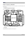
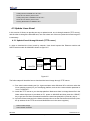
2.1 Mini3250 system block diagram
The block diagram of the Mini3250 is shown in Figure 2.1.
OTG
HEADER
TFT_LCD
CONNECTOR
TF_CARD
5V
RGB666
OTG_PHY
LED
5V
USB
VDD_RTC
3.3V
81
PIN
H
E
A
D
E
R
LDO
UART*7
VDD_CORE
DC-DC
DATA[15:0]
RMII/MII
LPC3250
ADDR[23:0]
JTAG
GPO/GPI/GPIO
WE/OE/CS
ADC
IIS /SDIO/SPI /IICBUS
RESETOUT
GPO
SUPERVISOR
SDRAM
VBAT
JTAG
HEADER
NANDFLASH
81
PIN
H
E
A
D
E
R
NORFLASH
Figure 2.1 Block Diagram of Mini3250
2.2 Layout
The Mechanical Structure of Mini3250 is shown as figure 2.2.
Mini3250
User Guide
Timll Technic Inc .
Rev. 1.0 —5 September 2012
6 of 41
Mini3250 User Manual
Figure 2.2 Mechanical Structure of Mini3250
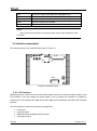
2.3 Pin Allocation
The pin definition of the Mini3250 Expansion Interface is shown in Figure 2.3
Figure 2.3 Pin definition of the Mini3250 Expansion Interface
Mini3250
User Guide
Timll Technic Inc .
Rev. 1.0 —5 September 2012
7 of 41
Mini3250 User Manual
Pin Allocation of the Mini3250 Expansion Interface connector is shown in Table 2-1:
Table 2-1-a Pin Allocation of Mini3250 1 of 2
No
A
B
C
1
GND
USB_D+
USB_D-
2
GPIO_05/SSEL0/MCFB0
SPI1_DATIO/MOSI0/MCFB2
SPI1_DATIN/MISO0/GPI_25
/MCFB1
3
SPI1_CLK/SCK0
GPO_11
GND
4
I2C1_SDA
I2C1_SCL
I2C2_SDA
5
I2C2_SCL
MS_DIO3/MAT0.3
MS_DIO2/MAT0.2
6
MS_SCLK
MS_DIO1/MAT0.1
MS_DIO0/MAT0.0
7
MS_BS
GPIO_01
I2S1TX_WS/CAP3.0
8
I2S1TX_SDA
I2S1TX_CLK/MAT3.0
GPI_00/I2S1RX_SDA
9
I2S1RX_WS
P0.0/I2S1RX_CLK
GPO_20
10
GND
GPO_14
GPO_05
11
GPO_04
GPO_00/TST_CLK1
VCC5
12
EMC_CS1_N
USB_ID
EMC_OE_N
13
EMC_WR_N
EMC_CS2_N
ADDR16
14
ADDR23
ADDR22
ADDR21
15
ADDR20
ADDR19
ADDR18
16
ADDR17
GND
ADDR15
17
ADDR14
ADDR13
ADDR12
18
ADDR11
ADDR10
ADDR9
19
ADDR8
ADDR7
ADDR6
20
ADDR5
ADDR4
ADDR3
21
ADDR2
ADDR1
ADDR0
22
DATA15
DATA14
DATA13
23
DATA12
DATA11
DATA10
24
DATA9
DATA8
DATA7
25
DATA6
DATA5
DATA4
26
DATA3
DATA2
DATA1
27
GND
DATA0
VDD33
Mini3250
User Guide
Timll Technic Inc .
Rev. 1.0 —5 September 2012
8 of 41
Mini3250 User Manual
Table 2-1-b Pin Allocation Pin Allocation of Mini3250 2 of 2
No
D
E
F
1
ADIN0/TS_XM
GND
GND
2
ADIN1/TS_YM
RESOUT_N
GND
3
GPO_02/MAT1.0/LCDVD[0]
GPO_03/LCDVD[1]
GPO_07/LCDVD[2]
4
GPO_10/MC2B/LCDPWR
GPO_06/LCDVD[18]
GPO_09/LCDVD[9]
5
PWM_OUT2/LCDVD[19]
SPI2_DATIO/MOSI1
/LCDVD[20]
SPI2_DATIN/MISO1
/LCDVD[21]/GPI_27
6
GPIO_04/SSEL1/LCDVD[22]
SPI2_CLK/SCK1/LCDVD[23]
GPO_08/LCDVD[8]
7
GPO_22/U7_HRTS
/LCDVD[14]
U7_RX/CAP0.0/LCDVD[10]
/GPI_23
U7_TX/MAT1.1/LCDVD[11]
8
U7_HCTS/CAP0.1
/LCDCLKIN/GPI_22
GPO_21/U4_TX/LCDVD[3]
GPI_01/SERVICE_N
9
GPI_04/SPI1_BUSY
GPI_07/CAP4.0/MCABOR
GPIO_00
10
GND
KEY_COL4/ENET_RXD0
KEY_COL5/ENET_RXD1
11
KEY_COL3/ENET_CRS
KEY_COL2/ENET_RX_ER
KEY_COL1/ENET_RX_CLK
/ENET_REF_CLK
12
KEY_ROW4/ENET_TXD0
KEY_ROW5/ENET_TXD1
KEY_ROW3/ENET_TX_EN
13
KEY_COL0/ENET_TX_CLK
GPI_02/CAP2.0
/ENET_RXD3
GPI_06/HSTIM_CAP
/ENET_RXD2
14
GPI_08/KEY_COL6
/SPI2_BUSY/ENET_RX_DV
GPI_09/KEY_COL7
/ENET_COL
KEY_ROW2/ENET_TXD3
15
KEY_ROW1/ENET_TXD2
KEY_ROW0/ENET_TX_ER
GPIO_02/KEY_ROW6
/ENET_MDC
16
GPIO_03/KEY_ROW7
/ENET_MDIO
DBGEN
MR_RESET
17
RESET_N
TMS
RTCK
18
TDO
TDI
TCK
19
NTRST
U6_IRTX
U6_IRRX/GPI_21
20
U5_TX
U5_RX/GPI_20
GPO_12/MC2A/LCDLE
21
GPI_19/U4_RX
GPI_28/U3_RI
GPI_05/U3_DCD
22
U3_TX
U3_RX/GPI_18
U2_TX/U3_DTR
23
GPO_23/U2_HRTS/U3_RTS
U2_RX/U3_DSR/GPI_17
U2_HCTS/U3_CTS/GPI_16
24
U1_TX
U1_RX/CAP1.0/GPI_15
GND
25
ADIN2/TS_AUX_IN
ONSW
GPO_17
26
EMC_BLS1
EMC_BLS0
EMC_CS3_N
27
VDD33
VSBAT
GND
2.4 Signal Mapping
The signal mapping of Mini3250 is show as table 2-2.
Mini3250
User Guide
Timll Technic Inc .
Rev. 1.0 —5 September 2012
9 of 41
Mini3250 User Manual
Table 2-2 signal mapping
Signal
Function
system signal
ONSW
Connect to ONSW of LPC3250
TST_CLK1
Connect to GPO_00/TST_CLK1 of LPC3250
MR_RESET
Connect to nMR of MP811 with 100KOHM pull-up
NRESET
Connect to RESET_N of LPC3250 and NRESET of MP811 with
100KOHM pull-up
RESOUT
Connect to RESOUT_N of LPC3250
Memory bus signal
ADDR[0:23]
Connect to EMC_A[0:23] of LPC3250
DATA[0:15]
Connect to EMC_D[0:15]of LPC3250
NBLS[0:1]
Connect to EMC_BLS[0:1] of LPC3250
EMC_CS[1:3]_N
Connect to EMC_CS[1:3]_N of LPC3250
NWE
Connect to EMC_WR_N of LPC3250
NOE
Connect to EMC_OE_N of LPC3250
UART signal
U1_TX
Connect to U1_TX of LPC3250
U1_RX
Connect to U1_RX/CAP1.0/GPI_15 of LPC3250
U2_TX
Connect to U2_TX/U3_DTR of LPC3250
U2_RX
Connect to U2_RX/U3_DSR/GPI_17 of LPC3250
U2_HRTS
Connect to GPO_23/U2_HRTS/U3_RTS
U3_TX
Connect to U3_TX of LPC3250
U3_RX
Connect to U3_RX/GPI_18 of LPC3250
U3_CTS
Connect to U2_HCTS/U3_CTS/GPI_16 of LPC3250
U3_DCD
Connect to GPI_05/U3_DCD
U3_RI
Connect to GPI_28/U3_RI
U4_RX
Connect to GPI_19/U4_RX of LPC3250
U4_TX
Connect to GPO_21/U4_TX/LCDVD[3] of LPC3250
U5_RX
Connect to U5_RX/GPI_20 of LPC3250
U5_TX
Connect to U5_TX of LPC3250
U6_IRTX
Connect to U6_IRTX of LPC3250
U6_IRRX
Connect to U6_IRRX/GPI_21 of LPC3250
U7_RX
Connect to U7_RX/CAP0.0/LCDVD[10]/GPI_23of LPC3250
U7_HRTS
Connect to GPO_22/U7_HRTS/LCDVD[14]
U7_HCTS
Connect to U7_HCTS/CAP0.1/LCDCLKIN/GPI_22
U7_TX
Connect to U7_TX/MAT1.1/LCDVD[11] of LPC3250
I2C signal
I2C1_SCL
Connect to I2C1_SCL of LPC3250
I2C1_SDA
Connect to I2C1_SDA of LPC3250
I2C2_SCL
Connect to I2C2_SCL of LPC3250
I2C2_SDA
Connect to I2C2_SDA of LPC3250
I2S signal
Mini3250
User Guide
Timll Technic Inc .
Rev. 1.0 —5 September 2012
10 of 41
Mini3250 User Manual
I2S1TX_CLK
Connect to I2S1TX_CLK/MAT3.0 of LPC3250
I2S1TX_SDA
Connect to I2S1TX_SDA of LPC3250
I2S1TX_WS
Connect to I2S1TX_WS/CAP3.0 of LPC3250
I2S1RX_CLK
Connect to P0.0/I2S1RX_CLK of LPC3250
I2S1RX_SDA
Connect to GPI_00/I2S1RX_SDA of LPC3250
I2S1RX_WS
Connect to I2S1RX_WS of LPC3250
SPI signal
SPI2_CLK
Connect to SPI2_CLK/SCK1/LCDVD[23] of LPC3250
SPI1_CLK
Connect to SPI1_CLK/SCK0 of LPC3250
MISO1
Connect
LPC3250
MISO0
Connect to SPI1_DATIN/MISO0/GPI_25/MCFB1of LPC3250
MOSI1
Connect to SPI2_DATIO/MOSI1/LCDVD[20] of LPC3250
MOSI0
Connect to SPI1_DATIO/MOSI0/MCFB2 of LPC3250
SSEL0
Connect to GPIO_05/SSEL0/MCFB0 of LPC3250
SPI1_BUSY
Connect to GPI_04/SPI1_BUSY of LPC3250
SPI2_BUSY
Connect to GPI_08/KEY_COL6/SPI2_BUSY/ENET_RX_DV of
LPC3250
SSEL1
Connect to GPIO_04/SSEL1/LCDVD[22] of LPC3250
to
SPI2_DATIN/MISO1/LCDVD[21]/GPI_27
of
ADC signal
ADIN0
Connect to ADIN0/TS_XM of LPC3250
ADIN1
Connect to ADIN1/TS_YM of LPC3250
ADIN2
Connect to ADIN2 /TS_AUX_IN of LPC3250
GPIO signal
GPO_02
Connect to GPO_02/MAT1.0/LCDVD[0] of LPC3250
GPO_03
Connect to GPO_03/LCDVD[1] of LPC3250
GPO_04
Connect to GPO_04of LPC3250
GPO_05
Connect to GPO_05of LPC3250
GPO_06
Connect to GPO_06/LCDVD[18] of LPC3250
GPO_07
Connect to GPO_07/LCDVD[2]of LPC3250
GPO_08
Connect to GPO_08/LCDVD[8] of LPC3250
GPO_09
Connect to GPO_09/LCDVD[9] of LPC3250
GPO_10
Connect to GPO_10/MC2B/LCDPWR of LPC3250
GPO_11
Connect to GPO_11 of LPC3250
GPO_12
Connect to GPO_12/MC2A/LCDLE of LPC3250
GPO_14
Connect to GPO_14 of LPC3250
GPO_17
Connect to GPO_17 of LPC3250
GPO_20
Connect to GPO_20 of LPC3250
GPI_01
Connect to GPI_01/SERVICE_N of LPC3250
GPI_02
Connect to GPI_02/CAP2.0/ENET_RXD3 of LPC3250
GPI_07
Connect to GPI_07/CAP4.0/MCABORT of LPC3250
GPIO_00
Connect to GPIO_00 of LPC3250
Ethernet signal
Mini3250
User Guide
Timll Technic Inc .
Rev. 1.0 —5 September 2012
11 of 41
Mini3250 User Manual
ENET_RXD1
Connect to KEY_COL5/ENET_RXD1 of LPC3250
ENET_RX_CLK
Connect to KEY_COL1/ENET_RX_CLK /ENET_REF_CLK of
LPC3250
ENET_TX_EN
Connect to KEY_ROW3/ENET_TX_EN of LPC3250
ENET_RXD2
Connect to GPI_06/HSTIM_CAP/ENET_RXD2 of LPC3250
ENET_TXD3
Connect to KEY_ROW2/ENET_TXD3 of LPC3250
ENET_MDC
Connect to GPIO_02/KEY_ROW6/ENET_MDC of LPC3250
ENET_RXD0
Connect to KEY_COL4/ENET_RXD0 of LPC3250
ENET_RX_ER
Connect to KEY_COL2/ENET_RX_ER of LPC3250
ENET_TXD1
Connect to KEY_ROW5/ENET_TXD1 of LPC3250
ENET_TX_ER
Connect to KEY_ROW0/ENET_TX_ER of LPC3250
ENET_CRS
Connect to KEY_COL3/ENET_CRS of LPC3250
ENET_TXD0
Connect to KEY_ROW4/ENET_TXD0 of LPC3250
ENET_TX_CLK
Connect to KEY_COL0/ENET_TX_CLK of LPC3250
ENET_TXD2
Connect to KEY_ROW1/ENET_TXD2 of LPC3250
ENET_MDIO
Connect to GPIO_03/KEY_ROW7/ENET_MDIO of LPC3250
ENET_COL
Connect to GPI_09/KEY_COL7/ENET_COL of LPC3250
USB signal
USB_D+
Connect to USB_D+ of ISP1301 with ESD protection
USB_D-
Connect to USB_D- of ISP1301 with ESD protection
USB_ID
Connect to ID of ISP1301
SD signal
MS_DIO0
Connect to MS_DIO0/MAT0.0 of LPC3250 with 10kOHM
pull-up
MS_DIO1
Connect to MS_DIO1/MAT0.1 of LPC3250 with 10kOHM
pull-up
MS_DIO2
Connect to MS_DIO2/MAT0.2 of LPC3250 with 10kOHM
pull-up
MS_DIO3
Connect to MS_DIO3/MAT0.3 of LPC3250 with 10kOHM
pull-up
MS_SCLK
Connect to MS_SCLK of LPC3250 with 10kOHM pull-up
MS_BS
Connect to MS_BS of LPC3250 with 10kOHM pull-up
GPIO_01
Connect to GPIO_01 of LPC3250 and MicroSD slot detect pin
Power signal
VDD33
Mini3250 main power supply and power supply for LCD
VCC5
USB HOST and power supply for LCD
VSBAT
LPC3250 RTC back-up power supply
GND
GND of Mini3250
PWM signal
PWM_OUT2
Connect to PWM_OUT2/LCDVD[19] of LPC3250
JTAG signal
NTRST
Connect to NTRST of LPC3250 with 0OHM to NRESET
DBGEN
Connect to DBGEN of LPC3250
Mini3250
User Guide
Timll Technic Inc .
Rev. 1.0 —5 September 2012
12 of 41
Mini3250 User Manual
TMS
Connect to TMS of LPC3250 with 10kOHM pull-up
TCK
Connect to TCK of LPC3250 with 10kOHM pull-up
TDO
Connect to TDO of LPC3250 with 10kOHM pull-up
RTCK
Connect to RTCK of LPC3250
TDI
Connect to TDI of LPC3250 with 10kOHM pull-up
NOTE:
More electrical specification of the pins please refers to the Datasheet of the
LPC3250.
2.5 Interface description
The interfaces layout of the Mini3250 is shown in Figure 2.4
USB
LCD
TF
40
1
JTAG
(Buttom)
Figure 2.4 Interface Layout
2.5.1 LCD interface
Mini3250 provides a FPC connector for the LCD interface. There is an default 5V power supply on the
LCD interface, user can change the power supply to 3V by change the resistance to support a
different LCD. And it support the16bpp (5:5:5) and 16bpp (5:6:5) modes the LPC3250 LCD controller
provides.
The LCD Interface consists of the following components:
LCD Power
LCD panel data
PWM controlled backlight and LCD enable
Touch panel signal
Mini3250
User Guide
Timll Technic Inc .
Rev. 1.0 —5 September 2012
13 of 41
Mini3250 User Manual
Table 2-3 shows a detailed mapping of the LPC3250 LCD port signals.
Table 2-3 LCD Signal Assignment
No
Signal Name
TYPE
Function
1
VDD33/VCC5
POWER
Power supply, Selected by R36 (5V)
and R37 (3V)
2
VDD33/VCC5
POWER
Same as pin1
3
GND
POWER
Ground
4
GND
POWER
Ground
5
GND
POWER
Power supply(GND)
6
LCDVD19
O
LCD panel data
7
LCDVD20
O
LCD panel data.
8
LCDVD21
O
LCD panel data.
9
LCDVD22
O
LCD panel data.
10
LCDVD23
O
LCD panel data.
11
GND
POWER
Ground
12
NC
-
No connect
13
NC
-
No connect
14
LCDVD10
O
LCD panel data.
15
LCDVD11
O
LCD panel data.
16
LCDVD12
O
LCD panel data.
17
LCDVD13
O
LCD panel data.
18
LCDVD14
O
LCD panel data.
19
LCDVD15
O
LCD panel data.
20
GND
POWER
Ground
21
NC
-
No connect
22
NC
-
No connect
23
GND
POWER
Ground
24
LCDVD3
O
LCD panel data.
25
LCDVD4
O
LCD panel data.
26
LCDVD5
O
LCD panel data.
27
LCDVD6
O
LCD panel data.
28
LCDVD7
O
LCD panel data.
29
GND
POWER
Ground
30
LCDPWR
O
LCD panel power enable
31
NC
-
No connect
32
PWM_OUT1
O
Back Light control
33
LCDEN
O
TFT data enable output
34
VSYNC
O
Vertical synchronization pulse
35
HSYNC
O
Horizontal synchronization pulse
36
LCDCLK
O
LCD panel clock
37
TSXM
I/O
Touch screen X minus
Mini3250
User Guide
Timll Technic Inc .
Rev. 1.0 —5 September 2012
14 of 41
Mini3250 User Manual
38
TSXP
I/O
Touch screen X plus
39
TSYM
I/O
Touch screen Y minus
40
TSYP
I/O
Touch screen Y plus
2.5.2 MicroSD card interface
Mini3250 owns a standard MicroSD card socket with plug detection design. MicroSD card interface
connects with the SD/MMC card interface of CPU directly. The detection signal uses the GPIO_01 of
CPU.
Table 2-4 MicroSD card socket Pin Description
Pin name
Type
Description
MS_SCLK
Output
MicroSD card clock output with 10kOHM pull-up
MS_BS
Input
MicroSD card command input with 10kOHM pull-up
MS_DIO[3:0]
Output
MicroSD card data lines with 10kOHM pull-up
GPIO_01
Input
Detection signal with 200kOHM pull-up
The function description of the Mini3250 MicroSD card socket is shown as figure 2.5.
MS_SCLK
CLK
MS_BS
CMD
MS_DIO[3:0]
DAT[3:0]
GPIO_01
CD
MicroSD card socket
LPC3250
Figure 2.5 Function description
2.5.3 USB interface
The Mini3250 provides a USB OTG interface with a Mini-AB OTG connector. The signals of the
connector connect to LPC3250 through the OTG ATX from NXP (ISP 1301). The USB DATA pins are
ESD protected. The USB_VBUS signal is connected to a current-limited power-distribution switch
(TPS2045) output pin.
2.5.4 JTAG interface (Optional)
JTAG Connector of Mini3250 provides a JTAG connection interface to the LPC3250. Table 2-5
provides a detailed list of the signals at the JTAG connector. You should cross reference this with your
JTAG probe to ensure compatibility.
Table 2-5 JTAG Signal Assignment
Pin No.
Signal Name
Type
Function
1
TMS
input
Test mode select input with 10k pull-up.
2
TDO
output
Test data output with 10k pull-up.
3
TDI
input
Test data input with 10k pull-up.
Mini3250
User Guide
Timll Technic Inc .
Rev. 1.0 —5 September 2012
15 of 41
Mini3250 User Manual
4
TCK
input
Test clock input with 10k pull-up.
5
NTRST
input
Test Reset.
6
NRESET
output
System reset.
7
GND
Power
Ground.
8
VDD33
Power
Power
2.6 Introduction of Circuit Module
2.6.1 Mini3250 memory mapping
The memory mapping of the Mini3250 is shown as table 2-6.
Table 2-6 Mini3250 memory mapping
Start address
End address
Device
CS
note
0x0000 0000
0x7FFF FFFF
IROM or IRAM
CPU Internal Memories
-
0x8000 0000
0x9FFF FFFF
SDRAM
EMC_DYSC0
32bit width
0xA000 0000
0xBFFF FFFF
-
EMC_DYSC1
-
0xC000 0000
0xDFFF FFFF
RESERVED
RESERVED
RESERVED
0xE000 0000
0XE0FF FFFF
NORFLASH
EMC_CS0
8bit width
0XE100 0000
0XE1FF FFFF
-
EMC_CS1
-
0XE200 0000
0XE2FF FFFF
-
EMC_CS2
-
0XE300 0000
0XE3FF FFFF
-
EMC_CS3
-
0XE400 0000
0xFFFF FFFF
RESERVED
RESERVER
-
2.6.2 SDRAM
The Mini3250 SDRAM configured for 32-bit access using two 16-bit wide RAM chips at U3 and U4.
The LPC3250 is capable of addressing a single RAM bank located at memory address 0x8000 0000
and extending to 0x9FFF FFFF via the /DYCS0 signal. But the permissible SDRAM memory access
ranges of Mini3250 supplies for on-board memory are 64Mbytes, from Lower Memory Address
0x80000000 to Upper Memory Address 0x83FF FFFF.
The second SDRAM memory bank located on /DYSC1 is not used on the Mini3250. Accesses to this
region of memory should not be performed.
The function description of the Mini3250 SDRAM is shown as figure 2.6, more information please
refer to the schematic of the Mini3250.
Mini3250
User Guide
Timll Technic Inc .
Rev. 1.0 —5 September 2012
16 of 41
Mini3250 User Manual
ADDR[0:12]
A[0:12]
ADDR[13:14]
BA[0:1]
NCS0
/CS
NSRAS
/RAS
NSCAS
/CAS
NWE
/WE
EMC_CLK
CLK
EMC_CKE0
CLE
DQM0
LDQM
DQM1
UDQM
DATA[0:15]
DATA[0:15]
SDRAM
A[0:12]
BA[0:1]
/CS
/RAS
/CAS]
/WE
CLK
CLE
DQM2
LDQM
DQM3
UDQM
DATA[16:31]
DATA[0:15]
LPC3250
SDRAM
Figure 2.6 SDRAM Function
2.6.3 NANDFLASH
The NAND memory is comprised of a single 128MB chip located at U5 and is interfaced via the
LPC3250 NAND memory bus.
The function description of the Mini3250 NANDFLASH is shown as figure 2.7, more information
please refer to the schematic of the Mini3250.
Mini3250
User Guide
Timll Technic Inc .
Rev. 1.0 —5 September 2012
17 of 41
Mini3250 User Manual
FLASH_IO[0:7]
I/O[0:7]
FLASH_RDY
R/B
FLASH_CE_N
/CE
FLASH_WR_N
/NFWE
FLASH_RD_N
/RE
FLASH_CLE
CLE
FLASH_ALE
ALE
LPC3250
NANDFLASH
Figure 2.7 NANDFLASH function
2.6.4 NORFLASH
The NORFLASH memory is comprised of a single 2MB to 16MB chip located at U13. The function
description for the NORFLASH circuit module is shown as figure 2.8.
ADDR[0:23]
A[0:23]
DATA[0:16]
DQ[0:15]
NWE
WE#
RESETOUT
RESET#
EMC_OE
OE#
EMC_CS0
CE#
BYTE#
LPC3250
NORFLASH
Figure 2.8 NORFLASH function
2.6.5 LED
There are two LEDs in the Mini3250, D1 is used for the power indication and D2 is provided for
development purposes. The LED’s status is show as table 2-7
Table 2-7 LED’s status
STATUS
ON
D1
Mini3250 Power ON
Mini3250 Power OFF
D2
GPO_01 in low level
GPO_01 in high level
Mini3250
User Guide
OFF
Timll Technic Inc .
Rev. 1.0 —5 September 2012
18 of 41
Mini3250 User Manual
The location of the User LED and the function description is shown as Figure 2.9.
Figure 2.9 Location of the User LED
Mini3250
User Guide
Timll Technic Inc .
Rev. 1.0 —5 September 2012
19 of 41
Mini3250 User Manual
Chapter 3 Mini3250 software system for Linux
General NANDFLASH Partition
Start Addr
End Addr
Size
Name
0x0000 0000
0x000C 0000
0x000C 0000
S1L
0x000C 0000
0x0018 0000
0x000C 0000
U-Boot
0x0018 0000
0x001C 0000
0x0004 0000
U-Boot Parameter
0x001C 0000
0x005C 0000
0x0040 0000
Kernel
0x005C 0000
0x0800 0000
0x07A4 0000
Filesystem
3.1 Bootloader
Bootloader for Mini3250 Linux system includes two parts, one is Stage 1 Loader, and the other is
Uboot.
The Stage 1 Loader (S1L) is a robust third level boot loader written by NXP Semiconductor to simplify
and enhance the LPC3250 booting procedure. The S1L is feature rich with the ability to configure
clocking, virtual memory mapping, data and instruction caches, the ability to access NAND flash, and
the ability to boot applications/images from the NAND flash, SD Card, or serial port to name a few of
the features the S1L provides.
Mini3250 adapt Uboot as the Bootloader for Linux. Uboot is a general free open source boot program
that supports many kinds of processors; it is similar to BIOS on PC but much more powerful. Uboot
supports features like booting from Ethernet and loading various kernels to NANDFLASH. Uboot is
free open source code software based on GPL.
3.2 Linux Kernel
If user need add or delete some character is respectively to or from kernel, or increase certained
hardware support to kernel. To modify the drive compiled into kernel, user need recompile the kernel.
The following steps will describe how to generate the kener image for the MINI3250 with the Linux
develop kit in the supplied CD.
3.2.1 Generate Kernel Image
The supplied CD provide the Linux develp kit for the Mini3250, user can use it to coustomilize the
system and generate the kernel image.
1> Uncompress Linux kernel package
The name of kernel source pack is “linux-2.6.27.8_mini3250.tar.bz2”. Execute the following command
to unzip bz2 pack.
Mini3250
User Guide
Timll Technic Inc .
Rev. 1.0 —5 September 2012
20 of 41
Mini3250 User Manual
tar zxvf linux-2.6.27.8_mini3250.tar.bz2 –C /home/mini3250/
Caution: file name may vary with the version upgrade, please check it a
gainst the file name appearing in supplied CD.
2> Load default configurations
In order that user could fast configure kernel, root folder of kernel source code provides four default
configuration files:
mini3250_480x272_mouse_config
//for 4.3 inch LCD, use mouse in QT
mini3250_480x272_touch_config
//for 4.3 inch LCD, use touch screen in QT
mini3250_800x480_mouse_config
//for 7.0 inch LCD, use mouse in QT
mini3250_800x480_touch_config
//for 7.0 inch LCD, use mouse in QT
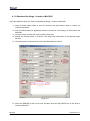
Enter kernel source code folder generated, exute “make menuconfig” command to configure the
properties.
Cd /home/mini3250/linux-2.6.27.8
make menuconfig
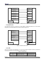
After that, you will get into the Linux kernel configuration. Shown as figure 3.1.
Figure 3.1
Enter “Load an Alternate Configuration File” configurations: shown as figure 3.2.
Mini3250
User Guide
Timll Technic Inc .
Rev. 1.0 —5 September 2012
21 of 41
Mini3250 User Manual
Figure 3.2
Enter configuration file names such as Mini3250_800480_mouse.cfg and press “Enter”, shown as
figure 3.3.
Figure 3.3
while in main menu, select <Exit> to exit and save the settings.
3> Compile image
After loading configuration file, save settings and exit, then exute “make uImage” command to
Mini3250
User Guide
Timll Technic Inc .
Rev. 1.0 —5 September 2012
22 of 41
Mini3250 User Manual
generate uImage kernel.
Caution:
Compiling kernel requires compiler ver. Arm-linux-gcc-4.3.2 version. Pleas
e install the Cross compile tools to your PC before you compile the kernel.
Make uImage
Figure 3.4
Image file is generated at “arch/arm/boot” under kernel source code pack folder, the kernel image
uImage that Uboot uses is generated.
3.2.2 Custom Linux kernel for Mini3250
Above steps configure and compile kernel using default files, in effect, Linux kernel has quite a
number of configuration options. The following sections will describe some options in form of figures,
in order to help you learn kernel configurations as soon as possible, so as to customize your own
kernel.
Run “make menuconfig”, enter kernel configuration main menu:
Table 3-1
function
PATH
Option
LED
System
Type->LPC32XX
Implementtations
[] Enable a 1Hz LED heartbeat tick rate on
the Phytec LPC3250
MII/RMII
System Type->LPC32XX
components
chip
[] Check to enable MII support or leave
disabled for RMII support
UART
System
chip
[] Enable UART5
Type->LPC32XX
Mini3250
User Guide
Timll Technic Inc .
Rev. 1.0 —5 September 2012
23 of 41
Mini3250 User Manual
components-> Standard UARTS
[] Enable UART3
[] Enable UART4
[] Enable UART6
HSUART
System Type->LPC32XX chip
components-> High speed UARTS
[] Enable high speed UART1
[] Enable high speed UART2
[] Enable high speed UART7
I2C
System Type->LPC32XX
components->I2C interfaces
[] Enable I2C0
[] Enable I2C1
[]Enable the USB OTG I2C peripheral
SPI/SSP
System Type->LPC32XX chip
components->SSP/SPI interface
[] Enable SSP0 for SPI0 mode
MicroSD
card
Device Drivers->SD/MMC support
<*>SD/MMC block device driver
[] use bounce buffer for simple hosts
LCD
Graphics support
<*> Support for frame buffer devices
<*> LCD framebuffer support
LCD Size
System Type
-
Implementations -
LOGO
Graphics support-> bootup logo
[*]
[*]
[*]
[*]
USB
mouse
Device Drivers->
support
<*>USB supoort
<*> Support for Host-side USB
<*> OHCI HCD support
chip
LPC32XX
input
device
LCD module revisions
(X) Select 4.3 inch LCD 480X272 Timll
standard 224-color linux logo
standard black and white linux logo
standard 16-color linux logo
Disable cursor when logo display
<*> Event interface
<*> USB Human Interface Devices (full HID)
support
[*] HID input layer support
TOUCH
Device Drivers->
support
input
device
<*> Touchscreen interface
<*> Event interface
[*] touchscreens
<*> LPC32XX touchscreen controller
USB Disk
Device Drivers-> USB support
[*] legacy /proc/scsi support
<*> SCSI disk support
<*> USB Mass Storage support
Buttons
Device Drivers --->
Input device support --->
Keyboards --->
<*>
Devkit3250 Buttons support
LED/BEEP
Device Drivers --->
Input device support --->
Keyboards --->
<*>
Devkit3250 GPIO device support
Mini3250
User Guide
Timll Technic Inc .
Rev. 1.0 —5 September 2012
24 of 41
Mini3250 User Manual
Note
Because UART4 and UART7 conflict with LCD driver, please disable item below
when enable UART4 or UART7.
Device Drivers
--->
Graphics support
--->
<*> Support for frame buffer devices
<>
--->
ARM PrimeCell PL110 support
Note: When using mini3250_xxx_mouse_config, please disable items below,
because all input events will affect mouse event. So just only keep mouse input event.
Device Drivers
--->
Input device support
<>
--->
Touchscreen interface
[]
Touchscreens
[*]
Keyboards
<>
--->
--->
Devkit3250 Buttons support
Mini3250
User Guide
Timll Technic Inc .
Rev. 1.0 —5 September 2012
25 of 41
Mini3250 User Manual
Chapter 4 Update image to Mini3250
This chapter mainly descripte how to update the Bootloader, kernel and the filesystem image to
Mini3250.
4.1 Burn Stage 1 Loader
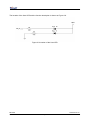
4.1.1 Hardware requement
In order to download the Stage 1 Loader to Mini3250, user need to extend the UART5 and starup
mode of Mini3250.
VDD33
UART5
RS232
PC
SERVICE_N
MR_RESET
Mini3250
GND
GND
Figure 4.1
The pin need to expand are show as table 4-1.
Table 4-1
Pin
function
VDD33
Power supply
GND
Ground
U5_RX
UART receive
U5_TX
UART send
SERVER_N
Start up mode select
MR_RESET
System reset
4.1.2 Enviroment setting
Burnning the Stage 1 Loader to the Mini3250, the English Version Windows XP operating system is
needed, if your PC was installed the other vesion Windows XP system, please follow the steps to set
PC language enviroment.
1> Open the “area and language option” form the control pannal.
2> Select “advance” option, and then change the language to “English(USA)”.
3> At last press the “OK” button and reset the PC.
Mini3250
User Guide
Timll Technic Inc .
Rev. 1.0 —5 September 2012
26 of 41
Mini3250 User Manual
4.1.3 Download the Stage 1 Loader to Mini3250
The follow steps will show you how to download the Stage 1 Loader to Mini3250.
1> Copy LPC3250 loader folder to your PC directory, the path doesn’t allow to contain any
Chinese characters.
2> Run LPC3250 loader.exe application.select the restore.bin [ CD:\Image ] to download to the
Mini3250.
3> Click the button to select the communication serial port.
4> Enable the terminal mode, if sucessul, it will output the imformation in the terminal output
window.
5> Click the button to transmit the bin file to the Mini3250.see frame 5.
1
2
5
4
3
Figure 4.3
6> Driver the SERVER_N pin to low level and then driver the MR_RESET pin to low level to
reset the Mini3250.
Mini3250
User Guide
Timll Technic Inc .
Rev. 1.0 —5 September 2012
27 of 41
Mini3250 User Manual
VDD33
UART5
RS232
PC
SERVICE_N
Mini3250
MR_RESET
GND
GND
After the reset, the system will start up from the UART5 and begin to download the application to
Mini3250 from the PC, then you can release SERVER_N to high level. Figure 4.4 show the
download progress.
Figure 4.4
7> After download finish. The teminal outopt window will output the writing information.
Writing kickstart ICR page 0
Writing kickstart data...
Writing stage 1 application size info...
Writing stage 1 application...
Marking bootloader blocks as reserved...
Kickstart and stage 1 update complete
NOTE: Make sure the path of LPC3250_Loader.exe doesn’t contain any Chi
nese character, other wise, it won’t run normally.
4.2 Update Uboot
There two way to update the Uboot to the Mini3250, one is throught UART5 serial port. And the other
is through SD card. Both of the two ways need to burn the Stage 1 Loader to Mini3250 first.
4.2.1 Update Uboot through UART5
Update the Uboot to the Mini3250, the hardware connection show as figure 4.1. and then follow the
steps to download the Uboot to Mini3250 and burn it to NANDFLASH.
1> Run Tera Term Pro.exe in the host PC.
Mini3250
User Guide
Timll Technic Inc .
Rev. 1.0 —5 September 2012
28 of 41
Mini3250 User Manual
2> Click the “serial port …” from the ”set up“submenu to configure the serial port communication
paramter to “com1 115200 8n1n ”. and than click OK button.
3> In order to get into the Stage 1 Loader command line, please set GPI_02 or GPI_08 or
GPI_09 to low level, and then reset Mini3250, then terminal will show prompt “TIMLL3250>”.
4> Input the the follow command to download the u-boot.bin to Mini3250 SDRAM.
TIMLL3250>load term raw 0x83fc0000 0x83fc0000
//download the Uboot from PC thought UART5
5> After that the Tera Term Pro will prompt “Starting terminal download, send break to stop”.
Please click the “send file ” from the “file” submenu of the tera term to send the “u-boot.bin” to
the Mini3250.
NOTE: when sending the u-boot.bin to the Mini3250, the binary protocol mus
t be selected to transport the image, you can select the binary option in the
send file dialog.
6> After the transmit complete. Please send an break to the Mini3250 by click the “send break ”
from the “control ” submenu of the tera term.
7> After download successes please Input the follow comand to write the Uboot to
NANDFLASH from SDRAM.
TIMLL3250>erase 6 6 1
//erase the nandflash except the stagel lodaer area
TIMLL3250>write 0x83fc0000 384 320 0
//write the Uboot to Mini3250 NANDFLASH
NOTE: Try “help <command>” for command usage, for example: help erase.
4.2.2 Update Uboot through MicroSD card
Updating the kernel image through MicroSD card, the hardware requirement is show as figure 4.1.
The UART5 is optional as the UART5 just use for printing the imformation during update process. The
follow steps will show you how to update the Uboot through MicroSD card.
1> Copy the u-boot.bin to the root directory of the MicroSD card.
2> Insert the MicroSD card to the MicroSD card slot and then reset Mini3250.
3> After Mini3250 detects the MicroSD card and the u-boot.bin in the MicroSD card, it will
update the u-boot.bin to the NANDFLASH automatically.
Loading bootloader to SDRAM from SD card ....
success
Starting block erase
U-Boot update complete
Mini3250
User Guide
Timll Technic Inc .
Rev. 1.0 —5 September 2012
29 of 41
Mini3250 User Manual
Loading kernel to SDRAM from SD card ....
File in SD root directory doesn't exist
Loading Filesystem to SDRAM from SD card ....
File in SD root directory doesn't exist
Running Bootloader from NANDFLASH
4.3 Update Linux Kenel
In this version of Uboot, we provide two way to update kernel, one is throught netwrok (TFTP server),
and the other is through the MicroSD card, user can select one of them to update the kernel image if it
is necessary.
4.3.1 Update Kernel througt Network (TFTP server)
In order to download the Linux kernel by network, User should expand the Ethernet module and
UART5 serial moudle for Mini3250. shown as figure 4.5.
VDD33
UART5
MII/RMII
Mini3250
RS232
PHY
PC
TFTP
GND
Figure 4.5
The follow steps will describe how to download the kernel image through TFTP server.
1> Run serial communicating tool (i.e: hyper teminater under Windows XP or minicom under the
Linux opeating system) on you developing platform, and set the communication paramter to
“com1 115200 8n1”.
2> Install the TFTP server to your develop platform. Make sure there is uImage kernel file in the
folder where tftp server is provided on PC. power on Mini3250 and then press the “SPACE”
key to get into the Uboot command line atfter the terminate prompt the “press any key to ….”
3> Input the follow command in the Uboot command line to set the kernel start enviroment.(note;
the ip address of the TFTP server and Mini3250 must in the same segment)
setenv bootfile uImage
setenv fileaddr 80100000
Mini3250
User Guide
Timll Technic Inc .
Rev. 1.0 —5 September 2012
30 of 41
Mini3250 User Manual
setenv serverip 192.192.192.163
setenv ipaddr 192.192.192.205
setenv gatewayip 192.192.192.101
setenv bootcmd 'nboot 80100000 0 1c0000;bootm'
4> Input the follow command in the Uboot command line to download the kernel to the SDRAM
tftp 80100000 192.192.192.163:uImage
5> After the downlod complete,please input the follow command to burn it to the NANDFLASH.
nand erase 1c0000 400000
nand unlock 1c0000 400000
nand write 80100000 1c0000 400000
nand lock 1c0000 400000
4.3.2 Update Kernel througt MicroSD Card
Updating the kernel image through MicroSD card, the hardware requirement is show as figure 4.1.
the UART5 is optional as the UART5 just use for printing the imformation during update process. The
follow steps will show you how to update the Uboot through MicroSD card .
1> Copy the uImage to the root directory of the MicroSD card.
2> Copy the loadme_kernel.bin to the root directory of the MicroSD card and then rename it to
loadme.bin.
3> Set SERVER_N pin to high level.
4> Insert the MicroSD card to the MicroSD card slot and then power up Mini3250.
5> After the Mini3250 detects the MicroSD card and the uImage in the MicroSD card, it will
update the uImage to the NANDFLASH automatically.
6> Remove MicroSD card and reset.
Loading bootloader to SDRAM from SD card ....
File in SD root directory doesn't exist
Loading kernel to SDRAM from SD card ....
success
Loading Filesystem to SDRAM from SD card ....
File in SD root directory doesn't exist
Running Bootloader from Block device
U-Boot 1.3.3 (Jun 13 2010 - 15:10:33)
DRAM:
64 MB
NAND:
128 MiB
In:
serial
Out:
serial
Mini3250
User Guide
Timll Technic Inc .
Rev. 1.0 —5 September 2012
31 of 41
Mini3250 User Manual
Err:
serial
Hit any key to stop autoboot:
0
NAND erase: device 0 offset 0x1c0000, size 0x400000
Erasing at 0x5a0000 -- 100% complete.
OK
NAND write: device 0 offset 0x1c0000, size 0x400000
4194304 bytes written: OK
Loading from NAND 128MiB 3,3V 8-bit, offset 0x1c0000
Image Name:
Image Type:
Data Size:
Linux-2.6.27.8
ARM Linux Kernel Image (uncompressed)
1697112 Bytes =
1.6 MB
Load Address: 80008000
Entry Point:
80008000
4.4 Update JFFS2 filesystem
When the file system in flash is damaged, file system of flash is to be updated for some reason, user
can update it by downloading the filesystem through TFTP server or mounting root file system of PC
using NFS. The hardware requemet are show as figure 4.1.
Generate JFFS2 image for 2k page size NANDFLASH
mkfs.jffs2 -r rootfs_dir -o rootfs_image.jffs2 -e 0x20000 -s 0x800 --pad=0x1e80000 -n –v
Parameter:
--pad
write.jffs2
Define the size of filesystem image. It should be block aligned and match with nand
If the file system you want to download is bigger than 60MB, please refer to
the “4.4.2 Update firesystem through the NFS server” to update the file syst
em.
4.4.1 Update the JFFS2 filesystem through Network
There two way to update the file system to FLASH through network, one is through TFTP server, and
the other is through NFS.
<1> through TFTP server
The operation of downloading the JFFS2 filesystem image to Mini3250 through TFTP server is almost
the same as downloading the Linux kernel to Mini3250, after the hardware connection and
environment setting, please follow the steps to update the JFFS2 system through the TFTP server:
Mini3250
User Guide
Timll Technic Inc .
Rev. 1.0 —5 September 2012
32 of 41
Mini3250 User Manual
1>
Input the follow command in the Uboot command line to download the kernel to the SDRAM
tftp 0x81000000 192.192.192.163:rootfs_image.jffs2
2>
After the downlod complete,please input the follow command to burn the filesystem to the
NANDFLASH.
nand erase 5c0000 3a80000
nand write.jffs2 81000000 5c0000 1e80000
<2> through NFS server.
Update the filesystem throught the NFS require installing the NFS to the host PC.
Run following command when U-Boot startup to set U-Boot environment parameter:
setenv bootargs 'console=ttyS0,115200n81 root=/dev/nfs rw nfsroot=<nfs server
ip>:/home/nfs/nfs2440-III ip=<local ip>:<nfs server ip>:<gateway ip>:255.255.255.0::eth0:off'
After booting, system will mount nfs and enter console terminal.
After Mini3250 start up and mount the NFS, please enter the follow command to update the special
filesystem to the NANDFLASH. The default pack of Mini3250-nfs includes several kinds of GUI graph
interfaces.
flash_eraseall /dev/mtd3
//erase the filesystem partition
mount -t jffs2 /dev/mtdbloclk3 /mnt
tar xzvf mini3250-qtopia-xxxxx.tar.gz -C /mnt
//xxxxx stand for the touch or mouse. It correspond to the different GUI graph interfaces.
4.4.2 Update filesystem through MicroSD Card
Updating the filesystem image through MicroSD card, the hardware requeiament is show as figure
4.1. the UART5 is optional as the UART5 just use for printing the imformation during update process.
The follow steps will show you how to update the Uboot through MicroSD card.
1>
2>
3>
4>
5>
6>
Copy rootfs_image.jffs2 to the root directory of MicroSD card.
Copy loadme_fs.bin to the root directory of MicroSD card.
Rename rootfs_image.jffs2 to fs, and loadme_fs.bin to loadme.bin.
Set SERVER_N pin at high level.
Insert the MicroSD card to the MicroSD card slot and then power up Mini3250.
After the Mini3250 detects the MicroSD card and the fs in the MicroSD card, it will download
the filesystem to the sdram automatically.
7> Then system will run loadme.bin. It copies fs from sdram to NANDFLASH.
8> Remove MicroSD card and reset after nand write complete.
Loading bootloader to SDRAM from SD card ....
File in SD root directory doesn't exist
Mini3250
User Guide
Timll Technic Inc .
Rev. 1.0 —5 September 2012
33 of 41
Mini3250 User Manual
Loading kernel to SDRAM from SD card ....
File in SD root directory doesn't exist
Loading Filesystem to SDRAM from SD card ....
success
Running Bootloader from Block device
U-Boot 1.3.3 (Jun 13 2010 - 15:37:30)
DRAM:
64 MB
NAND:
128 MiB
In:
serial
Out:
serial
Err:
serial
Hit any key to stop autoboot: 0
NAND erase: device 0 offset 0x5c0000, size 0x7a40000
Erasing at 0x7fe0000 -- 100% complete.
OK
NAND write: device 0 offset 0x5c0000, size 0x1e80000
Writing data at 0x243f800 -- 100% complete.
31981568 bytes written: OK
Loading from NAND 128MiB 3,3V 8-bit, offset 0x1c0000
Image Name:
Image Type:
Data Size:
Linux-2.6.27.8
ARM Linux Kernel Image (uncompressed)
1697112 Bytes =
1.6 MB
Load Address: 80008000
Entry Point:
80008000
4.5 Customize Your Own loadme.bin
“loadme.bin” is used mainly used to update image to NANDFLASH from MicroSD card.
Now, we will tell you how to build your own loadme.bin to update your own image.
Extract u-boot-1.3.3_loadme.tar.bz2 in CD “source\u-boot-1.3.3_loadme.tar.bz2”.
tar -jvxf u-boot-1.3.3_loadme.tar.bz2 –C /home
cd /home/u-boot-1.3.3_loadme
Open configration file
vi include/configs/phy3250.h
The only parameter you need to modify is:
Mini3250
User Guide
Timll Technic Inc .
Rev. 1.0 —5 September 2012
34 of 41
Mini3250 User Manual
#define CONFIG_BOOTCOMMAND
"nand erase 5c0000;nand write.jffs2 81000000 5c0000
1e80000;nboot 80100000 0 1c0000;bootm"
That is the command system will run when u-boot startup.
Before u-boot startup, the system automatically copy below files(if exist) to the specific address in
SDRAM. Meanwhile, after complete copy u-boot.bin, system burns it into NANDFLASH immediately,
so loadme.bin doesn’t need to burn u-boot.bin, it’s task is to burn uImage or fs.
Filename(MicroSD)
Copy to Addr(SDRAM)
u-boot.bin
0x83FC 0000
uImage
0x8010 0000
fs
0x8100 0000
Then we can split the CONFIG_BOOTCOMMAND string into 3 command string.
#define CONFIG_BOOTCOMMAND
"nand erase 5c0000;nand write.jffs2 81000000 5c0000
1e80000;nboot 80100000 0 1c0000;bootm"
① nand erase 5c0000
# erase area from 0x5c0000 to the end of NANDFLASH
② nand write.jffs2 81000000 5c0000 1e80000
③ nboot 80100000 0 1c0000;bootm
# write the image fs to NANDFLASH
# read uImage in NANDFLASH and boot
Please take attention to the command nand write.jffs2, The format is:
nand write.jffs2 81000000 5c0000 <filesize>
But how do we know the filesize? It’s defined by command mkfs.jffs2 when you create jffs2
filesystem:
./mkfs.jffs2 -r /home/nfs/nfs3250-III -o timll3250.jffs2 -e 0x20000 --pad=0x1e80000 -s 0x800 -n
The parameter “--pad” is the filesize of your jffs2 filesystem image.
Fill your own CONFIG_BOOTCOMMAND string, save the file. Then type command below.
make phy3250_config
make
mv u-boot.bin loadme.bin
Mini3250
User Guide
Timll Technic Inc .
Rev. 1.0 —5 September 2012
35 of 41
Mini3250 User Manual
Chapter 5 Linux Application Development Guide
5.1 Hardware Connection
Connect UART5 port of Mini3250 and serial port of PC with serial cable provided with product.
5.2 Hyper Terminal Configuratin
Open hyper terminal program on PC, and set parameter as below:
115200 Bits-per-second
8 Data Bits
No Parity
1 Stop Bit
No Flow Control
Figure 5.1.1 Hyper Terminal Parameter Configuration
Power up the device and boot information will show in hyper terminal.
5.2 Linux Software Usage
5.2.1 Command rz Receiving File from PC
Type Linux command “rz” in shell mode.
[root@bit /]# rz
Mini3250
User Guide
Timll Technic Inc .
Rev. 1.0 —5 September 2012
36 of 41
Mini3250 User Manual
Click right-button of mouse, choose “send file”, then pop-up a diagram, choose the file you want to
send. Click button “Send”, certain seconds later, the file will exist in your current directory.
5.2.2 Command tftp Receiving File From TFTP Server
Type Linux command “tftp” in shell mode:
[root@bit /]# tftp -r <filename> -g <tftp server ip>
Eg: tftp -r myfile -g 192.192.192.105
5.2.3 Using USB Disk
Connect USB disk and Mini3250 with the usb cable provided with product. Then terminal wil show:
scsi 1:0:0:0: Direct-Access
ChipsBnk SD/MMCReader
4081 PQ: 0 ANSI: 2
sd 1:0:0:0: [sda] 1990656 512-byte hardware sectors (1019 MB)
sd 1:0:0:0: [sda] Write Protect is off
sd 1:0:0:0: [sda] Assuming drive cache: write through
sd 1:0:0:0: [sda] 1990656 512-byte hardware sectors (1019 MB)
sd 1:0:0:0: [sda] Write Protect is off
sd 1:0:0:0: [sda] Assuming drive cache: write through
sda: sda1
sd 1:0:0:0: [sda] Attached SCSI removable disk
Type command as below to mount the device.
[root@bit /]# mount –t vfat /dev/sda1 /mnt
Then the content in your USB disk will exist in directory /mnt.
5.2.4 Using MicroSD Card
Insert MicroSD card in Mini3250 slot, then terminal will show:
[root@bit /]# mmc0: host does not support reading read-only switch. assuming write-enable.
mmc0: new SD card at address 0007
mmcblk0: mmc0:0007 SD2GB 1931264KiB
mmcblk0: p1
Type command as below.
[root@bit /]# mount –t vfat /dev/mmcblk0p1 /mnt
Then the content in your MicroSD will exist in directory /mnt.
5.2.5 Terminate Program
Terminate current running program with Ctrl+C. Else, terminate background program with command
“kill”, for example as below.
[root@bit /]# ps
PID Uid
1 root
VmSize Stat Command
540 S
init
2 root
SW< [kthreadd]
3 root
SW< [ksoftirqd/0]
Mini3250
User Guide
Timll Technic Inc .
Rev. 1.0 —5 September 2012
37 of 41
Mini3250 User Manual
4 root
SW< [events/0]
258 root
SW< [spi_lpc32xx.0]
316 root
SW< [rpciod/0]
329 root
476 S < /sbin/udevd --daemon
353 bin
272 S
/sbin/portmap
369 root
168 S
/usr/sbin/telnetd -l /bin/login
371 root
740 S
-sh
372 root
376 S
/usr/sbin/boa
376 root
656 R
ps
[root@bit /]# kill 353
Then run command “ps”, and the portmap program disappears.
5.2.6 Set System Time
Refer to command “date” help information.
[root@bit /]# date --help
BusyBox v1.00 (2005.04.24-17:33+0000) multi-call binary
Usage: date [OPTION]... [MMDDhhmm[[CC]YY][.ss]] [+FORMAT]
Displays the current time in the given FORMAT, or sets the system date.
Options:
-R
Outputs RFC-822 compliant date string
-d STRING
Displays time described by STRING, not `now'
-I[TIMESPEC]
Outputs an ISO-8601 compliant date/time string.
TIMESPEC=`date' (or missing) for date only,
`hours', `minutes', or `seconds' for date and,
time to the indicated precision.
-s
Sets time described by STRING
-r FILE
Displays the last modification time of FILE
-u
Prints or sets Coordinated Universal Time
For example, set time to 2010-6-12 13:12, you should run command below.
[root@bit /]# date -s 061213122010
Sat Jun 12 13:12:00 UTC 2010
If you want to store the time you set into rtc module, please run below command.
[root@bit /]# hwclock –w
5.2.7 Button Test (Devkit3250)
[root@bit /]# cd app/
[root@bit /app]# ./button
Then press KEY1(GPI_01) KEY2(GPI_02) KEY3(GPI_08) KEY4(GPI_09)
type = 1
, code = 65
type = 1
, code = 66
Mini3250
User Guide
Timll Technic Inc .
Rev. 1.0 —5 September 2012
38 of 41
Mini3250 User Manual
type = 1
, code = 67
type = 1
, code = 68
65/66/67/68 is the key code we set in driver. User can redefine the key code by editing file below.
drivers/input/keyboard/buttons/buttons_devkit3250.c
buttons_info_tab[] =
{
{
IRQ_GPI_01, 0, INP_STATE_GPI_01, 0, 'A', "Key1"
},
{
IRQ_GPI_02, 0, INP_STATE_GPI_02, 0, 'B', "Key2"
},
{
IRQ_GPI_08, 0, INP_STATE_GPI_08, 0, 'C', "Key3"
},
{
IRQ_GPI_09, 0, INP_STATE_GPI_09, 0, 'D', "Key4"
},
};
5.2.8 Uart Test (Devkit3250)
Device node of uarts register in Linux system:
/dev/ttyS0
->
Uart5
/dev/ttyS1
->
Uart3
/dev/ttyS2
->
Uart4
/dev/ttyS3
->
Uart6 (IrDA)
/dev/ttyTX0 ->
Uart1
/dev/ttyTX1 ->
Uart2
/dev/ttyTX2 ->
Uart7
/dev/ ttySCMA0
-> Uart8 (Devkit3250 SPI extend)
/dev/ ttySCMA1
-> Uart9 (Devkit3250 SPI extend)
Run command below
[root@bit /app]# ./com
-d /dev/ttyS1
SEND: 1234567890
SEND: 1234567890
Connet the RX and TX pin of Uart3 with jumper, rerun the command.
[root@bit /app]# ./com
-d /dev/ttyS1
SEND: 1234567890
RECV: 1234567890
Notes:
Mini3250
User Guide
Timll Technic Inc .
Rev. 1.0 —5 September 2012
39 of 41
Mini3250 User Manual
Pin
Discription
2
RX
3
TX
5.2.9 EEPROM Test (Devkit3250)
[root@bit /app]# ./eeprom
eeprom write [0x000010]: hello Embest!
eeprom read [0x000010]: hello Embest!
dump buff_rd:
00000: 68 65
6c
6c 6f 20
0x008: 62
73
74 21
65
00
45
00
6d
00
5.2.10 Led & Beep Test (Devkit3250)
[root@bit /app]# ./led
gpio opened
Input key command
'a' -> beep on
'b' -> beep off
'c' -> led on
'd' -> led off
#?a
key = 97(user)
b
key = 98(user)
c
key = 99(user)
d
key = 100(user)
gpio released
^C
[root@bit /app]#
5.2.11 Audio Test (Devkit3250)
[root@bit /app]# madplay music.mp3
Mini3250
User Guide
Timll Technic Inc .
Rev. 1.0 —5 September 2012
40 of 41
Mini3250 User Manual
Notes:
The application source are in directory: CD\source\application
Mini3250
User Guide
Timll Technic Inc .
Rev. 1.0 —5 September 2012
41 of 41