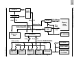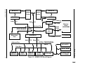
1
MVME197DP and MVME197SP
Single Board Computers
Installation Guide
(MVME197IG/D1)
Notice
While reasonable efforts have been made to assure the accuracy of this document,
Motorola, Inc. assumes no liability resulting from any omissions in this document, or
from the use of the information obtained therein. Motorola reserves the right to revise
this document and to make changes from time to time in the content hereof without
obligation of Motorola to notify any person of such revision or changes.
No part of this material may be reproduced or copied in any tangible medium, or
stored in a retrieval system, or transmitted in any form, or by any means, radio,
electronic, mechanical, photocopying, recording or facsimile, or otherwise, without the
prior written permission of Motorola, Inc.
It is possible that this publication may contain reference to, or information about
Motorola products (machines and programs), programming, or services that are not
announced in your country. Such references or information must not be construed to
mean that Motorola intends to announce such Motorola products, programming, or
services in your country.
Restricted Rights Legend
If the documentation contained herein is supplied, directly or indirectly, to the U.S.
Government, the following notice shall apply unless otherwise agreed to in writing by
Motorola, Inc.
Use, duplication, or disclosure by the Government is subject to restrictions as set forth
in subparagraph (c)(1)(ii) of the Rights in Technical Data and Computer Software
clause at DFARS 252.227-7013.
Motorola, Inc.
Computer Group
2900 South Diablo Way
Tempe, Arizona 85282-9602
Preface
This document provides a general board level hardware description, hardware
preparation and installation instructions, debugger general information, and
instructions on using the debugger for the MVME197DP and MVME197SP versions of
the MVME197 series of Single Board Computers.
This document is intended for anyone who wants to design OEM systems, supply
additional capability to an existing compatible system, or work in a lab environment
for experimental purposes.
A basic knowledge of computers and digital logic is assumed.
To use this document, you may wish to become familiar with the publications listed in
the Related Documentation section found in the following pages. This installation guide
is based on these other documents.
Document Terminology
Throughout this document, a convention has been maintained whereby data and
address parameters are preceded by a character which specifies the numeric format, as
follows:
$
dollar
specifies a hexadecimal number
%
percent
specifies a binary number
&
ampersand
specifies a decimal number
For example, “12” is the decimal number twelve, and “$12” is the decimal number
eighteen. Unless otherwise specified, all address references are in hexadecimal
throughout this document.
An asterisk (*) following the signal name for signals which are level significant denotes
that the signal is true or valid when the signal is low.
An asterisk (*) following the signal name for signals which are edge significant denotes
that the actions initiated by that signal occur on high to low transition.
In this document, assertion and negation are used to specify forcing a signal to a
particular state. In particular, assertion and assert refer to a signal that is active or true;
negation and negate indicate a signal that is inactive or false. These terms are used
independently of the voltage level (high or low) that they represent.
Data and address sizes are defined as follows:
❏
A byte is eight bits, numbered 0 through 7, with bit 0 being the least
significant.
❏
A two-byte is 16 bits, numbered 0 through 15, with bit 0 being the least
significant. For the MVME197series and other RISC modules, this is called
a half-word.
❏
A four-byte is 32 bits, numbered 0 through 31, with bit 0 being the least
significant. For the MVME197 series and other RISC modules, this is called
a word.
❏
An eight-byte is 64 bits, numbered 0 through 63, with bit 0 being the least
significant. For the MVME197 series and other RISC modules, this is called
a double-word.
Throughout this document, it is assumed that the MPU on the MVME197 module
series is always programmed with big-endian byte ordering, as shown below. Any
attempt to use small-endian byte ordering will immediately render the MVME197Bug
debugger unusable.
BIT
63
56 55
ADRO
31
48 47
ADR1
24 23
ADR4
40 39
ADR2
16 15
ADR5
BIT
32
ADR3
08 07
ADR6
00
ADR7
The terms control bit and status bit are used extensively in this document. The term
control bit is used to describe a bit in a register that can be set and cleared under
software control. The term true is used to indicate that a bit is in the state that enables
the function it controls. The term false is used to indicate that the bit is in the state that
disables the function it controls. In all tables, the terms 0 and 1 are used to describe the
actual value that should be written to the bit, or the value that it yields when read. The
term status bit is used to describe a bit in a register that reflects a specific condition. The
status bit can be read by software to determine operational or exception conditions.
Related Documentation
The following publications are applicable to the MVME197 module series and may
provide additional helpful information. If not shipped with this product, they may be
purchased by contacting your Motorola sales office.
Document Title
Motorola
Publication Number
MVME197LE Single Board Computer User’s Manual
MVME197LE
MVME197LE Single Board Computer Support Information
SIMVME197LE
MVME197DP and MVME197SP Single Board Computer
User’s Manual
MVME197
MVME197DP and MVME197SP Single Board Computer
Support Information
SIMVME197
MVME197LE, MVME197DP, and MVME197SP Single
Board Computers Programmer’s Reference Guide
MVME197PG
MVME197BUG 197Bug Debugging Package User’s Manual
MVME197BUG
MVME197BUG 197Bug Diagnostic Firmware User’s Manual MVME197DIAG
MVME712M Transition Module and P2 Adapter Board
User’s Manual
MVME712M
MVME712-12, MVME712-13, MVME712A, MVME712AM, MVME712A
and MVME712B Transition Module and LCP2 Adapter Board
User’s Manual
MC88110 Second Generation RISC Microprocessor User’s
Manual
MC88110UM
MC68040 Microprocessor User’s Manual
MC68040UM
MC88410 Secondary Cache Controller User’s Manual
MC88410UM
N otes
1. The support information manuals (SIMVME197LE and
SIMVME197) contain: the connector interconnect signal
information, parts lists, and the schematics for the
specific board(s) indicated.
2. Although not shown in the above list, each Motorola
Computer Group manual publication number is
suffixed with characters which represent the revision
level of the document, such as “/D2” (the second
revision of a manual); a supplement bears the same
number as the manual but has a suffix such as “/A1” (the
first supplement to the manual).
To further assist your development effort, Motorola has collected user’s manuals for
each of the peripheral controllers used on the MVME197 module series and other
boards from the suppliers. This bundle includes manuals for the following:
68-1X7DS for use with the MVME197 series of Single Board Computers.
NCR 53C710 SCSI Controller Data Manual and Programmer’s Guide
Intel i82596 Ethernet Controller User’s Manual
Cirrus Logic CD2401 Serial Controller User’s Manual
SGS-Thompson MK48T08 NVRAM/TOD Clock Data Sheet
The following non-Motorola publications may also be of interest and may be obtained
from the sources indicated. The VMEbus Specification is contained in ANSI/IEEE
Standard 1014-1987.
ANSI/IEEE Std 1014-1987
Versatile Backplane Bus: VMEbus
The Institute of Electrical and Electronics
Engineers, Incorporated
Publication and Sales Department
345 East 47th Street
New York, New York 10017-2633
Telephone: 1-800-678-4333
ANSI Small Computer System Interface-2
(SCSI-2), Draft Document X3.131-198X,
Revision 10c
Global Engineering Documents
P.O. Box 19539
Irvine, California 92713-9539
Telephone (714) 979-8135
The computer programs stored in the Read Only Memory of this device contain
material copyrighted by Motorola Inc., first published 1991, and may be used only
under license such as the License for Computer Programs (Article 14) contained in
Motorola’s Terms and Conditions of Sale, Rev. 1/79.
Motorola® and the Motorola symbol are registered trademarks of Motorola, Inc.
Delta Series, M88000, SYSTEM V/88, VMEmodule, VMEsystem, and 197bug are
trademarks of Motorola, Inc.
Timekeeper and Zeropower are trademarks of Thompson Components.
All other products mentioned in this document are trademarks or registered
trademarks of their respective holders
© Copyright Motorola 1994
All Rights Reserved
Printed in the United States of America
January 1994
!
WARNING
This equipment generates, uses, and can radiate radio
frequency energy and if not installed and used in
accordance with the documentation for this product, may
cause interference to radio communications. It has been
tested and found to comply with the limits for a Class A
Computing Device pursuant to Subpart J of Part 15 of FCC
rules, which are designed to provide reasonable protection
against such interference when operated in a commercial
environment. Operation of this equipment in a residential
area is likely to cause interference in which case the user, at
the user’s own expense, will be required to take whatever
measures necessary to correct the interference.
SAFETY SUMMARY
SAFETY DEPENDS ON YOU
The following general safety precautions must be observed during all phases of operation, service, and repair
of this equipment. Failure to comply with these precautions or with specific warnings elsewhere in this manual
violates safety standards of design, manufacture, and intended use of the equipment. Motorola Inc. assumes
no liability for the customer’s failure to comply with these requirements. The safety precautions listed below
represent warnings of certain dangers of which we are aware. You, as the user of the product, should follow
these warnings and all other safety precautions necessary for the safe operation of the equipment in your
operating environment.
GROUND THE INSTRUMENT.
To minimize shock hazard, the equipment chassis and enclosure must be connected to an electrical ground. The
equipment is supplied with a three-conductor ac power cable. The power cable must either be plugged into an
approved three-contact electrical outlet or used with a three-contact to two-contact adapter, with the grounding wire
(green) firmly connected to an electrical ground (safety ground) at the power outlet. The power jack and mating plug
of the power cable meet international Electrotechnical Commission (IEC) safety standards.
DO NOT OPERATE IN AN EXPLOSIVE ATMOSPHERE.
Do not operate the equipment in the presence of flammable gases or fumes. Operation of any electrical equipment in
such an environment constitutes a definite safety hazard.
KEEP AWAY FROM LIVE CIRCUITS.
Operating personnel must not remove equipment covers. Only Factory Authorized Service Personnel or other qualified
maintenance personnel may remove equipment covers for internal subassembly or component replacement or any
internal adjustment. Do not replace components with power cable connected. Under certain conditions, dangerous
voltages may exist even with the power cable removed. To avoid injuries, always disconnect power and discharge
circuits before touching them.
DO NOT SERVICE OR ADJUST ALONE.
Do not attempt internal service or adjustment unless another person, capable of rendering first aid and resuscitation,
is present.
USE CAUTION WHEN EXPOSING OR HANDLING THE CRT.
Breakage of the Cathode-Ray Tube (CRT) causes a high-velocity scattering of glass fragments (implosion). To prevent
CRT implosion, avoid rough handling or jarring of the equipment. Handling of the CRT should be done only by qualified
maintenance personnel using approved safety mask and gloves.
DO NOT SUBSTITUTE PARTS OR MODIFY EQUIPMENT.
Because of the danger of introducing additional hazards, do not install substitute parts or perform any unauthorized
modification of the equipment. Contact your local Motorola representative for service and repair to ensure that safety
features are maintained.
DANGEROUS PROCEDURE WARNINGS.
Warnings, such as the example below, precede potentially dangerous procedures throughout this manual. Instructions
contained in the warnings must be followed. You should also employ all other safety precautions which you deem
necessary for the operation of the equipment in your operating environment.
!
WARNING
Dangerous voltages, capable of causing death, are present in
this equipment. Use extreme caution when handling,
testing, and adjusting.
SPD 15163 R-2 (9/93)
Contents
CHAPTER 1
BOARD LEVEL HARDWARE DESCRIPTION
Introduction ................................................................................................................ 1-1
Model Designations ................................................................................................... 1-1
Overview ..................................................................................................................... 1-2
Requirements .............................................................................................................. 1-3
Features........................................................................................................................ 1-3
Block Diagrams........................................................................................................... 1-5
Functional Description .............................................................................................. 1-8
Front Panel Switches and Indicators................................................................ 1-8
Data Bus Structure .............................................................................................. 1-9
MC88110 MPU..................................................................................................... 1-9
MC88410 Cache Controller................................................................................ 1-9
BOOT ROM.......................................................................................................... 1-9
Flash Memory...................................................................................................... 1-9
Onboard DRAM ................................................................................................ 1-10
Battery Backup RAM and Clock..................................................................... 1-10
VMEbus Interface ............................................................................................. 1-10
I/O Interfaces .................................................................................................... 1-11
Serial Port Interface ................................................................................... 1-11
Printer Interface ......................................................................................... 1-11
Ethernet Interface....................................................................................... 1-12
SCSI Interface ............................................................................................. 1-12
SCSI Termination....................................................................................... 1-13
Peripheral Resources ........................................................................................ 1-13
Programmable Tick Timers...................................................................... 1-13
Watchdog Timer ........................................................................................ 1-13
Software-Programmable Hardware Interrupts..................................... 1-13
Processor Bus Timeout.............................................................................. 1-14
Local Peripheral Bus Timeout.................................................................. 1-14
Interrupt Sources............................................................................................... 1-14
Connectors ......................................................................................................... 1-14
Memory Maps .......................................................................................................... 1-15
Processor Bus Memory Map ........................................................................... 1-15
VMEbus Memory Map..................................................................................... 1-18
VMEbus Accesses to the Local Peripheral Bus...................................... 1-18
VMEbus Short I/O Memory Map ........................................................... 1-18
ix
CHAPTER 2
HARDWARE PREPARATION AND INSTALLATION
Introduction .................................................................................................................2-1
Unpacking Instructions..............................................................................................2-1
Hardware Preparation ...............................................................................................2-1
Configuration Switches ......................................................................................2-3
Configuration Switch S1: General Information .......................................2-3
Configuration Switch S1: General Purpose Functions
(S1-1 to S1-8) ......................................................................................2-4
Configuration Switch S1: System Controller Enable
Function (S1-9) ..................................................................................2-4
Configuration Switch S6: Serial Port 4 Clock Select
(S6-1, S6-2)..........................................................................................2-5
Installation Instructions .............................................................................................2-5
MVME197 Module Installation .........................................................................2-6
System Considerations .......................................................................................2-7
CHAPTER 3
DEBUGGER GENERAL INFORMATION
Overview of M88000 Firmware ................................................................................3-1
Description of 197Bug ................................................................................................3-1
Comparison With M68000-Based Firmware...........................................................3-2
197Bug Implementation.............................................................................................3-2
FLASH-Based Debugger ....................................................................................3-2
BOOT ROM ..........................................................................................................3-3
Setup System Parameters SETUP ..............................................................3-5
Execute User Program EXEC [ADDR] ......................................................3-6
Installation and Start-Up ...........................................................................................3-6
Autoboot ......................................................................................................................3-8
ROMboot......................................................................................................................3-9
Network Boot ..............................................................................................................3-9
Restarting the System...............................................................................................3-10
Reset ....................................................................................................................3-10
Double-Button Reset .........................................................................................3-11
Abort....................................................................................................................3-12
Break ....................................................................................................................3-12
SYSFAIL* Assertion/Negation........................................................................3-12
MPU Clock Speed Calculation ........................................................................3-13
Memory Requirements ............................................................................................3-13
Terminal Input/Output Control......................................................................3-13
Disk I/O Support......................................................................................................3-14
x
Blocks Versus Sectors........................................................................................ 3-15
Device Probe Function ..................................................................................... 3-15
Disk I/O via 197Bug Commands ................................................................... 3-15
IOI (Input/Output Inquiry) ..................................................................... 3-16
IOP (Physical Input/Output to Disk) ..................................................... 3-16
IOT (Input/Output Teach)....................................................................... 3-16
IOC (Input/Output Control) ................................................................... 3-16
BO (Bootstrap Operating System) ........................................................... 3-16
BH (Bootstrap and Halt) ........................................................................... 3-16
Disk I/O via 197Bug System Calls .......................................................... 3-16
Default 197Bug Controller and Device Parameters ..................................... 3-17
Disk I/O Error Codes ....................................................................................... 3-18
Network I/O Support ...................................................................................... 3-18
Physical Layer Manager Ethernet Driver............................................... 3-18
UDP/IP Protocol Modules ....................................................................... 3-19
RARP/ARP Protocol Modules ................................................................ 3-19
BOOTP Protocol Module.......................................................................... 3-19
TFTP Protocol Module .............................................................................. 3-19
Network Boot Control Module................................................................ 3-19
Network I/O Error Codes ........................................................................ 3-20
Multiprocessor Support .......................................................................................... 3-20
Multiprocessor Control Register (MPCR) Method ...................................... 3-20
GCSR Method.................................................................................................... 3-22
Diagnostic Facilities ................................................................................................. 3-22
CHAPTER 4
USING THE 197Bug DEBUGGER
Entering Debugger Command Lines ...................................................................... 4-1
Syntactic Variables .............................................................................................. 4-2
Expression as a Parameter.......................................................................... 4-2
Address as a Parameter .............................................................................. 4-4
Address Formats.......................................................................................... 4-4
Offset Registers ............................................................................................ 4-4
Port Numbers ...................................................................................................... 4-5
Entering and Debugging Programs......................................................................... 4-5
Calling System Utilities From User Programs ....................................................... 4-6
Preserving The Debugger Operating Environment .............................................. 4-6
197Bug Vector Table and Workspace................................................................ 4-6
Hardware Functions ........................................................................................... 4-6
Exception Vectors Used by 197Bug .................................................................. 4-6
CPU/MPU Registers .......................................................................................... 4-7
xi
Floating Point Support...............................................................................................4-7
Single Precision Real ...........................................................................................4-8
Double Precision Real .........................................................................................4-8
Scientific Notation ...............................................................................................4-8
197Bug Debugger Command Set .............................................................................4-9
APPENDIX A
CONFIGURE AND ENVIRONMENT COMMANDS
Configure Board Information Block........................................................................A-1
Set Environment to Bug/Operating System..........................................................A-2
APPENDIX B
DISK/TAPE CONTROLLER DATA
Disk/Tape Controller Modules Supported............................................................ B-1
Disk/Tape Controller Default Configurations ...................................................... B-2
IOT Command Parameters for Supported Floppy Types.................................... B-5
APPENDIX C
NETWORK CONTROLLER DATA
Network Controller Modules Supported...............................................................C-1
xii
List of Figures
Figure 1-1. MVME197SP Block Diagram ................................................................ 1-6
Figure 1-2. MVME197DP Block Diagram ............................................................... 1-7
Figure 2-1. MVME197DP/SP Switches, Connectors, and LED Indicators
Location Diagram........................................................................... 2-2
xiii
xiv
List of Tables
Table 1-1. MVME197DP/SP Model Designations................................................. 1-1
Table 1-2. MVME197DP/SP Specifications ............................................................ 1-5
Table 1-3. Processor Bus Memory Map ................................................................. 1-16
Table 1-4. Local Devices Memory Map ................................................................. 1-17
Table 4-1. Debugger Commands.............................................................................. 4-9
Table A-1. ENV Command Parameters ................................................................. A-3
xv
xvi
BOARD LEVEL
HARDWARE DESCRIPTION
1
Introduction
This chapter describes the board level hardware features of the MVME197DP
and MVME197SP versions of the MVME197 series of Single Board Computers,
hereafter referred to as the MVME197, unless separately specified (refer to the
next section for model designations).
The chapter is organized with a board level overview and features listed in this
introduction, followed by a more detailed hardware functional description.
Front panel switches and indicators are included in the detailed hardware
functional description. This chapter closes with some general memory maps.
All programmable registers used in the MVME197 module series reside in
ASIC (Application-Specific Integrated Circuit) devices that are covered in the
MVME197LE, MVME197DP, and MVME197SP Single Board Computers
Programmer’s Reference Guide.
Model Designations
The MVME197DP/SP module series of the Single Board Computers are
available in the following models.
Table 1-1. MVME197DP/SP Model Designations
Model
Number
Motorola
Part Number
Model Description
MVME197SP series
MVME197-101
01-W3815B02
Single Processor MC88110, 256KB Cache, 128MB
Onboard ECC DRAM, 50 MHz
MVME197DP series
MVME197-201
01-W3815B01
Dual Processor MC88110, 256KB Cache per Processor,
128MB Onboard ECC DRAM, 50 MHz
MVME197-202
01-W3815B03
Dual Processor MC88110, 256KB Cache per Processor,
256MB Onboard ECC DRAM, 50 MHz
MVME197IG/D1
1-1
1
Board Level Hardware Description
Overview
Each MVME197 module is a double-high VMEmodule based on the MC88110
RISC (Reduced Instruction Set Computer) microprocessor.
The MVME197DP/SP module series have 128/256MB of onboard DRAM with
programmable ECC (Error Checking and Correction), 256KB of external cache
memory for each MC88110/MC88410 microprocessor/cache controller
combination (note that the MVME197SP version has only one MC88110/
MC88410 device combination), 1MB of flash memory, 8KB of static RAM (with
battery backup), a time of day clock (with battery backup), an Ethernet
transceiver interface, four serial ports with EIA-232-D interface, six tick timers,
a watchdog timer, 128/256KB of BOOT ROM, a SCSI bus interface with DMA
(Direct Memory Access), a Centronics printer port, an A16/A24/A32/D8/
D16/D32 VMEbus master/slave interface, and a VMEbus system controller.
Input/Output (I/O) signals are routed through the MVME197’s backplane
connector P2. A P2 Adapter Board or LCP2 Adapter board routes the signals
and grounds from connector P2 to an MVME712 series transition module. The
MVME197 supports the MVME712M, MVME712A, MVME712AM, and
MVME712B transition boards (referred to here as the MVME712X, unless
separately specified). The MVME197 also supports the MVME712-12 and
MVME712-13 (referred to as the MVME712-XX, unless separately specified).
These transition boards provide configuration headers, serial port drivers, and
industry standard connectors for the I/O devices.
The MVME197 modules have eight ASIC devices (described in the following
order: BusSwitch, DCAM, ECDM, PCC2, and VME2).
N ote
For the MVME197 series, the term Local Bus, as used in
other MVME1xx Single Board Computer series, is referred
to as the Local Peripheral Bus.
The BusSwitch ASIC provides an interface between the processor bus
(MC88110/410 bus) and the local peripheral bus (MC68040 compatible bus).
Refer to the board specific MVME197 block diagram (Figure 1-1 and 1-2). It
provides bus arbitration for the MC88410 bus and serves as a seven level
interrupt handler. It has programmable map decoders for both busses, as well
as write post buffers on each, two tick timers, and four 32-bit general purpose
registers.
The DCAM (DRAM Controller and Address Multiplexer) ASIC provides the
address multiplexers and RAS/CAS/WRITE control for the DRAM as well as
data control for the ECDM.
1-2
Installation Guide
Requirements
The ECDM (Error Correction and Data Multiplexer) ASIC multiplexes
between four data paths on the DRAM array. Since the device handles 16 bits,
four such devices are required on the MVME197 to accommodate the 64-bit
data bus of the MC88110 RISC microprocessor. Single-bit error correction and
double-bit detection is performed in the ECDM.
The PCCchip2 (Peripheral Channel Controller) ASIC provides two tick timers
and the interface to the LAN chip, the SCSI chip, the serial port chip, the
printer port, and the BBRAM (Battery Backup RAM).
The VMEchip2 ASIC provides a VMEbus interface. The VMEchip2 includes
two tick timers, a watchdog timer, programmable map decoders for the master
and slave interfaces, and a VMEbus to/from the local peripheral bus DMA
controller, a VMEbus to/from the local peripheral bus non-DMA
programmed access interface, a VMEbus interrupter, a VMEbus system
controller, a VMEbus interrupt handler, and a VMEbus requester.
The local peripheral bus to VMEbus transfers can be D8, D16, or D32.
VMEchip2 DMA transfers to the VMEbus, however, can be 64 bits wide as
Block Transfer (BLT).
Requirements
All MVME197 boards are designed to conform to the requirements of the
following documents:
❏
VMEbus Specification (IEEE 1014-87)
❏
EIA-232-D Serial Interface Specification, EIA
❏
SCSI Specification, ANSI
Features
These are some of the major features of the MVME197DP/SP single board
computers:
❏
Single MC88110 RISC Microprocessor with an MC88410 Cache Controller
(MVME197SP module series)
❏
Dual MC88110 RISC Microprocessors, each with one MC88410 Cache
Controller (MVME197DP module series)
❏
256 kilobytes of external cache per processor, controlled by the MC88410
(MVME197DP and MVME197SP module series)
❏
128 or 256 megabytes of 64-bit Dynamic Random Access Memory (DRAM)
with Error Checking and Correction (ECC)
MVME197IG/D1
1-3
1
1
Board Level Hardware Description
❏
1 megabyte of Flash memory
❏
Six status LEDs (FAIL, RUN, SCON, LAN, SCSI, and VME)
❏
8 kilobytes of Static Random Access Memory (SRAM) and Time of Day
(TOD) clock with Battery Backup RAM (BBRAM)
❏
Two push-button switches (ABORT and RESET)
❏
128 or 256 kilobytes of BOOT ROM
❏
Six 32-bit tick timers for periodic interrupts
❏
Watchdog timer
❏
Eight software interrupts
❏
I/O
–
–
–
–
❏
SCSI Bus interface with Direct Memory Access (DMA)
Four serial ports with EIA-232-D buffers
Centronics printer port
Ethernet transceiver interface
VMEbus interface
–
–
–
VMEbus system controller functions
VMEbus interface to local peripheral bus (A24/A32, D8/D16/D32
BLT (D8/D16/D32/D64))(BLT = Block Transfer)
Local peripheral bus to VMEbus interface (A24/A32, D8/D16/D32
BLT (D16/D32/D64))
–
VMEbus interrupter
–
VMEbus interrupt handler
–
Global CSR for inter-processor communications
–
DMA for fast local memory - VMEbus transfers (A16/A24/A32,
D16/D32 BLT (D16/D32/D64))
Specifications
The specifications for the MVME197DP/SP are listed in the following table.
1-4
Installation Guide
Block Diagrams
Table 1-2. MVME197DP/SP Specifications
Characteristics
Specifications
Power requirements
+5 Vdc (+/- 2.5%), 4.8 A (typical), 5.8 A (maximum)
+12 Vdc (+/- 2.5%), 100 mA (maximum)
-12 Vdc (+/- 2.5%), 100 mA (maximum)
Operating temperature
0˚ to 55˚ C at point of entry of forced air
(approximately 490 LFM)
Storage temperature
-40˚ to 85˚ C
Relative humidity
5% to 90% (non-condensing)
Physical dimensions:
PC board
Height
Width
Thickness
Double-high VMEboard
PC board with connectors
and front panel
Height
Width
Thickness
Board connectors:
P1 connector
9.187 inches (233.35 mm)
6.299 inches (160.00 mm)
0.063 inch (1.60 mm)
10.309 inches (261.85 mm)
7.4 inches (188.00 mm)
0.80 inch (20.32 mm)
A 96-pin connector which provides the interface to the
VMEbus signals.
P2 connector
A 96-pin connector which provides the interface to the
extended VMEbus signals and other I/O signals.
J1 connector
A 249-pin connector which provides the interface to the
MC88110 address, data, and control signals to and from the
mezzanine memory expansion.
J4 connector
Connector pins not used, all ten pin sockets are soldered
over.
Block Diagrams
General block diagrams for the MVME197DP/SP are provided as follows.
Figure 1-1 illustrates the block diagram for the MVME197SP and Figure 1-2
illustrates the block diagram for the MVME197DP.
MVME197IG/D1
1-5
1
1
256KB
Cache
MC88410
Addr
32
Data
DCAM
64
MUX Address
RAS, CAS
Address Bus
PROCESSOR
BUS
Data Bus
Mezzanine
Port
BusSwitch
Addr
32
Data
ECDM
(X4)
I2C Bus
256
I2C EEPROM
32
LOCAL PERIPHERAL
BUS
Address Bus
Data
Bus
Memory
Array
128 MB
NVRAM/RTC
Data Bus
BOOT ROM
Installation Guide
VMEbus
(VMEchip2)
LAN
82596CA
SCSI -II
NCR53710
Flash
Memory
PCCchip2
Figure 1-1. MVME197SP Block Diagram
4 Serial Ports
CL-CD2401
Board Level Hardware Description
1-6
MC88110
MVME197IG/D1
MC88110
MC88110
256KB
Cache
256KB
Cache
MC88410
Addr
MC88410
32
Data
DCAM
64
MUX Address
RAS, CAS
Address Bus
PROCESSOR
BUS
Data Bus
Mezzanine
Port
BusSwitch
Addr
32
Data
ECDM
(X4)
I 2C Bus
256
I 2C EEPROM
32
LOCAL PERIPHERAL
BUS
Address Bus
Data
Bus
Memory
Array
128/256 MB
NVRAM/RTC
Data Bus
VMEbus
(VMEchip2)
LAN
82596CA
SCSI -II
NCR53710
Flash
Memory
PCCchip2
1-7
Figure 1-2. MVME197DP Block Diagram
4 Serial Ports
CL-CD2401
Block Diagrams
BOOT ROM
1