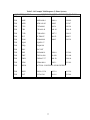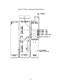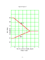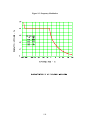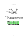
1
Revision D July 1996 Copyright © 1993-1996 by California Instruments. All rights reserved. P/N 5000-960 INSTRUCTION MANUAL FCS-18-P Invertron® SAFETY SUMMARY This power source contains high voltage and current circuits which are potentially lethal. Because of its size and weight, mechanical stability must be ensured. The following safety guidelines must be followed when operating or servicing this equipment. These guidelines are not a substitute for vigilance and common sense. California Instruments assumes no liability for the customer's failure to comply with these requirements. BEFORE APPLYING POWER 1. Verify the correct voltage that applied to the unit (for example 240V). 2. The chassis and cabinet of this power source must be grounded to minimize shock hazard. A chassis ground is provided at the input terminal block. This is located at the back of the cabinet on the lower right hand side. The chassis ground must be connected to an electrical ground through an insulated wire of sufficient gauge. FUSES Use only fuses of the specified current, voltage, and protection speed (slow blow, normal blow, fast blow) rating. Do not short out the fuse holder or use a repaired fuse. DO NOT OPERATE IN A VOLATILE ATMOSPHERE Do not operate the power source in the presence of flammable gases or fumes. DO NOT TOUCH ENERGIZED CIRCUITS Disconnect the power cable before servicing this equipment. Even with the power cable disconnected, high voltage can still exist on some circuits. Discharge these voltages before servicing. Only qualified service personnel may remove covers, replace components or make adjustments. DO NOT SERVICE ALONE Do not remove covers, replace components, or make adjustments unless another person, who can administer first aid, is present. DO NOT EXCEED INPUT RATINGS Do not exceed the rated input voltage or frequency. Additional hazards may be introduced because of component failure or improper operation. DO NOT MODIFY INSTRUMENT OR SUBSTITUTE PARTS Do not modify this instrument or substitute parts. Additional hazards may be introduced because of component failure or improper operation. MOVING THE POWER SOURCE When moving the power source, observe the following: Use two people to prevent injury. SURFACE STABILITY 1. Operate the power source only on a level surface. 2. Verify that the floor will support the weight of the power source. i TABLE OF CONTENTS 1. INTRODUCTION AND SPECIFICATIONS .......................................................................................................1 1.1. INTRODUCTION ..................................................................................................................................................1 1.2. GENERAL DESCRIPTION ...................................................................................................................................1 2. INSTALLATION AND ACCEPTANCE .............................................................................................................12 2.1. UNPACKING.......................................................................................................................................................12 2.2. POWER REQUIREMENTS.................................................................................................................................12 2.3. MECHANICAL INSTALLATION ......................................................................................................................12 2.4. INPUT WIRING (TB1)........................................................................................................................................12 2.5. OUTPUT CONNECTIONS .................................................................................................................................14 2.5.1. OUTPUT WIRING .........................................................................................................................................14 2.6. OUTPUT VOLTAGE RANGES ..........................................................................................................................16 2.7. FUNCTION TEST................................................................................................................................................16 3. OPERATION .........................................................................................................................................................23 3.1. GENERAL............................................................................................................................................................23 3.2. FRONT PANEL CONTROLS..............................................................................................................................23 3.3. FRONT PANEL INDICATORS...........................................................................................................................23 3.4. REAR PANEL CONNECTIONS .........................................................................................................................25 3.4.1. POWER INPUT .............................................................................................................................................25 3.4.2. POWER OUTPUT .........................................................................................................................................25 3.4.3. EXTERNAL SENSE........................................................................................................................................25 3.4.4. IEEE-488 CONNECTOR ...............................................................................................................................26 3.4.5. SYSTEM INTERFACE ...................................................................................................................................26 3.5. FRONT PANEL OPERATION ............................................................................................................................32 3.5.1. KEYPAD ........................................................................................................................................................32 3.5.2. DISPLAY SCREENS ......................................................................................................................................34 3.5.3. OUTPUT PROGRAMMING ..........................................................................................................................39 3.5.3.1. VOLTAGE RANGE (RNG=4)..................................................................................................................................39 3.5.3.2. VOLTAGE AMPLITUDE (AMP=5) ........................................................................................................................40 3.5.3.3. FREQUENCY (FRQ=6) ...........................................................................................................................................40 3.5.3.4. PHASE ANGLE (PHZ=7).........................................................................................................................................41 3.5.3.5. CURRENT LIMIT (CRL=8) .....................................................................................................................................42 3.5.3.6. RAMP OR STEP FUNCTIONS (RMP=9) ...............................................................................................................42 3.5.3.7. EXTERNAL SYNCHRONIZATION (SNC=1)........................................................................................................45 3.5.3.8. REGISTERS AND REGISTER LINKING ...............................................................................................................45 3.5.3.9. SIMULTANEOUS RAMPS......................................................................................................................................47 3.5.3.10. DROP PERIODS (DRP=2) .....................................................................................................................................48 3.5.3.11. DEFAULT VALUES ..............................................................................................................................................48 3.5.3.12. 1 OR 3 PHASE MODE (MOD=30) ........................................................................................................................51 3.5.3.13. PROGRAM THE START-UP POINT ....................................................................................................................52 3.5.4. ERROR MESSAGES ......................................................................................................................................53 3.6. OUTPUT MEASUREMENT ...............................................................................................................................55 3.6.1. VOLTAGE (VLT=21).....................................................................................................................................55 3.6.2. OUTPUT FREQUENCY (FQM=26) .............................................................................................................55 3.6.3. OUTPUT PHASE ANGLE (PZM=27) ...........................................................................................................55 3.6.4. OUTPUT CURRENT (CUR=22) ...................................................................................................................55 3.6.5. POWER (PWR=23)........................................................................................................................................55 3.6.6. OUTPUT POWER FACTOR (PWF=24) .......................................................................................................56 3.6.7. OUTPUT APPARENT POWER (APW=25)...................................................................................................56 3.6.8. ELAPSED TIME (ELT =11) ..........................................................................................................................56 3.7. COMPUTER BUS OPERATION ........................................................................................................................56 3.7.1. UNIT ADDRESS ............................................................................................................................................56 ii 3.7.2. MESSAGE FORMAT .....................................................................................................................................57 3.7.3. NUMERIC DATA FIELD...............................................................................................................................60 3.7.4. PROGRAM HEADERS ..................................................................................................................................60 3.7.5. OUTPUT PROGRAMMING ..........................................................................................................................65 3.7.5.1. OUTPUT VOLTAGE AMPLITUDE (AMP)............................................................................................................65 3.7.5.2. FREQUENCY (FRQ)................................................................................................................................................65 3.7.5.3. PHASE ANGLE (PHZ).............................................................................................................................................65 3.7.5.4. CURRENT LIMIT (CRL) .........................................................................................................................................66 3.7.5.5. RAMP OR STEP OPERATIONS .............................................................................................................................66 3.7.5.6. EXTERNAL SYNCHRONIZATION (SNC) ............................................................................................................67 3.7.5.7. DROP CYCLE (DRP)...............................................................................................................................................68 3.7.5.8. CALIBRATION (CAL).............................................................................................................................................68 3.7.5.9. TO PROGRAM A REGISTER (REG) ......................................................................................................................69 3.7.5.10. TO RECALL A REGISTER (REC) ........................................................................................................................69 3.7.5.11. VOLTAGE RANGE (RNG)....................................................................................................................................70 3.7.5.12. TO TRIGGER AN OPERATION (TRG) ................................................................................................................70 3.7.5.13. TO PROGRAM THE DEFAULT FREQUENCY (FLM A) ...................................................................................70 3.7.5.14. TO PROGRAM THE DEFAULT OUTPUT VOLTAGE (INI A)...........................................................................71 3.7.5.15. DEFAULT CURRENT LIMIT (INI C)...................................................................................................................71 3.7.5.16. 1 OR 3 PHASE MODE (MOD) ..............................................................................................................................71 3.7.5.17. TO TALK (TLK) MEASURED AND PROGRAMMED DATA............................................................................72 3.7.5.18. TO TALK THE MEASURED OUTPUT VOLTAGE (TLK VLT) .........................................................................72 3.7.5.19. TO TALK THE MEASURED OUTPUT CURRENT (TLK CUR).........................................................................72 3.7.5.20. TO TALK THE MEASURED OUTPUT POWER (TLK PWR).............................................................................73 3.7.5.21. TO TALK THE MEASURED OUTPUT POWER FACTOR (TLK PWF).............................................................73 3.7.5.22. TO TALK THE MEASURED OUTPUT APPARENT POWER (TLK APW) .......................................................73 3.7.5.23. TO TALK THE MEASURED OUTPUT FREQUENCY (TLK FQM)...................................................................73 3.7.5.24. TO TALK THE MEASURED OUTPUT PHASE ANGLE (TLK PZM) ................................................................74 3.7.5.25. MESSAGE SEPARATORS ....................................................................................................................................78 3.7.5.26. SERVICE REQUEST .............................................................................................................................................78 3.7.5.27. SERIAL POLL STATUS BYTE .............................................................................................................................78 3.7.5.28. END OF STRING ...................................................................................................................................................79 3.7.5.29. ERROR MESSAGES ..............................................................................................................................................79 3.7.5.30. TO OPEN (OPN) AND CLOSE (CLS) THE OUTPUT RELAY (Optional) ..........................................................79 3.7.6. GROUP EXECUTE TRIGGER ......................................................................................................................79 4. CALIBRATION PROCEDURE...........................................................................................................................83 4.1. GENERAL............................................................................................................................................................83 4.2. TEST EQUIPMENT.............................................................................................................................................85 4.3. PERIODIC CALIBRATION ................................................................................................................................89 4.3.1. VOLTAGE CALIBRATION ............................................................................................................................89 4.3.2. VOLTAGE MEASUREMENT CALIBRATION...............................................................................................89 4.3.3. CURRENT MEASUREMENT CALIBRATION ..............................................................................................92 4.3.4. POWER MEASUREMENT CALIBRATION...................................................................................................93 4.3.5. REMOTE MEASUREMENT CALIBRATION ................................................................................................94 4.3.6. REMOTE OUTPUT VOLTAGE CALIBRATION ...........................................................................................94 4.4. NONPERIODIC CALIBRATION........................................................................................................................97 4.4.1. OUTPUT FREQUENCY CALIBRATION ......................................................................................................97 4.4.2. GAIN ADJUSTMENT ....................................................................................................................................97 4.4.3. OUTPUT PHASE ANGLE CALIBRATION ...................................................................................................98 5. THEORY OF OPERATION.................................................................................................................................99 5.1. GENERAL............................................................................................................................................................99 5.2. OVERALL DESCRIPTION .................................................................................................................................99 5.3. OSCILLATOR ASSEMBLY................................................................................................................................99 5.4. CPU/GPIB BOARD ...........................................................................................................................................102 5.5. PHASE A/REF BOARD.....................................................................................................................................102 iii 5.6. PHASE B/C BOARD .........................................................................................................................................103 5.7. DISPLAY BOARD.............................................................................................................................................103 5.8. CURRENT LIMIT BOARD...............................................................................................................................103 5.9. MOTHER BOARD.............................................................................................................................................104 5.10. POWER AMPLIFIERS ....................................................................................................................................104 5.11. INPUT/OUTPUT BOARD...............................................................................................................................104 5.12. AUXILIARY POWER SUPPLY......................................................................................................................105 5.13. AMPLIFIER BOARDS ....................................................................................................................................105 5.14. CONTROL BOARD.........................................................................................................................................105 5.15. CURRENT TRANSFORMER BOARD...........................................................................................................106 6. MAINTENANCE AND TROUBLESHOOTING .............................................................................................109 6.1. GENERAL..........................................................................................................................................................109 6.2. POOR VOLTAGE ACCURACY .......................................................................................................................109 6.3. POOR OUTPUT VOLTAGE REGULATION...................................................................................................110 6.4. MODULE FAILURE LAMP ON .......................................................................................................................110 6.5. OVERTEMPERATURE LAMP ON..................................................................................................................111 6.6. OUTPUT FAULT LAMP ON ............................................................................................................................111 6.7. CAN'T PROGRAM AC POWER SYSTEM ON GPIB .....................................................................................112 6.8. DISTORTED OUTPUT .....................................................................................................................................112 6.9. NO OUTPUT......................................................................................................................................................112 6.10. OSCILLATOR ASSEMBLY REMOVAL/REPLACEMENT .........................................................................114 6.11. POWER AMPLIFIER ASSEMBLY REMOVAL/REPLACEMENT ..............................................................114 7. REPLACEABLE PARTS....................................................................................................................................119 7.1. GENERAL..........................................................................................................................................................119 7.2. ORDERING INFORMATION ...........................................................................................................................119 8. MIL-STD-704D ....................................................................................................................................................121 8.1. GENERAL..........................................................................................................................................................121 8.2. INITIAL SETUP ................................................................................................................................................121 8.3. TEST PERFORMED..........................................................................................................................................121 8.3.1. STEADY STATE TEST. (REFER TO MIL-704D DOC. TABLE 1) .............................................................121 8.3.2. TRANSIENT .................................................................................................................................................121 8.3.3. ABNORMAL OPERATION ..........................................................................................................................122 8.3.4. EMERGENCY OPERATION (REFER TO MIL-704D DOC. 5.2.5) ............................................................122 8.4. KEYPAD ENTRY (REFER TO PAGE FIGURE 8-1 KEYBOARD FLOW CHART) ........................................122 8.5. GPIB OPERATION (REFER TO SYNTAX DIAGRAM) ..........................................................................................125 8.6. TEST SPECIFICATION ....................................................................................................................................126 8.6.1. STEADY STATE ...........................................................................................................................................126 8.6.2. TRANSIENT .................................................................................................................................................127 8.6.3. ABNORMAL.................................................................................................................................................128 8.6.4. EMERGENCY ..............................................................................................................................................130 8.6.5. MIL704D TEST............................................................................................................................................130 9. RTCA/DO-160C...................................................................................................................................................139 9.1. GENERAL..........................................................................................................................................................139 9.2. INITIAL SETUP ................................................................................................................................................139 9.3. TEST PERFORMED..........................................................................................................................................139 9.3.1. NORMAL STATE .........................................................................................................................................139 9.3.2. EMERGENCY TEST ....................................................................................................................................139 9.3.3. ABNORMAL TEST.......................................................................................................................................140 9.4. KEYPAD ENTRY (REFER TO FIGURE 9-1 FOR KEYBOARD FLOW CHART) .......................................................140 9.5. GPIB OPERATION............................................................................................................................................143 iv 9.6. TEST SPECIFICATION ....................................................................................................................................144 9.6.1. NORMAL STATE .........................................................................................................................................144 9.6.1.1. NORMAL STATE MINIMUM VOLTAGE AND FREQUENCY TEST...............................................................144 9.6.1.2. NORMAL STATE MAXIMUM VOLTAGE AND FREQUENCY TEST .............................................................144 9.6.1.3. NORMAL STATE VOLTAGE UNBALANCE......................................................................................................144 9.6.1.4. NORMAL STATE WAVEFORM DISTORTION ..................................................................................................144 9.6.1.5. NORMAL STATE VOLTAGE MODULATION ...................................................................................................145 9.6.1.6. NORMAL STATE FREQUENCY MODULATION ..............................................................................................145 9.6.1.7. NORMAL STATE POWER INTERRUPT .............................................................................................................145 9.6.1.8. NORMAL STATE VOLTAGE SURGE .................................................................................................................145 9.6.2. EMERGENCY TEST ....................................................................................................................................146 9.6.2.1. EMERGENCY STATE MINIMUM VOLTAGE AND FREQUENCY TEST .......................................................146 9.6.2.2. EMERGENCY STATE MAXIMUM VOLTAGE AND FREQUENCY TEST......................................................146 9.6.2.3. EMERGENCY STATE VOLTAGE UNBALANCE ..............................................................................................146 9.6.3. ABNORMAL STATE ....................................................................................................................................146 9.6.3.1. ABNORMAL STATE MINIMUM VOLTAGE......................................................................................................146 9.6.3.2. ABNORMAL STATE MAXIMUM VOLTAGE ....................................................................................................146 9.6.3.3. ABNORMAL STATE UNDERVOLTAGE ............................................................................................................147 9.6.3.4. ABNORMAL STATE VOLTAGE SURGE............................................................................................................147 TABLE OF TABLES TABLE 1-1: OUTPUT VA PER PHASE ..............................................................................................................................1 TABLE 2-1: INPUT TRANSFORMER, CIRCUIT BREAKER, EMI FILTER CONFIGURATION.................................................13 TABLE 2-2: WIRE SIZE ..................................................................................................................................................16 TABLE 3-1: TERMINAL IDENTIFICATION........................................................................................................................25 TABLE 3-2: CONNECTION IDENTIFICATION ...................................................................................................................25 TABLE 3-3: SYSTEM INTERFACE CONNECTOR (J2) .......................................................................................................26 TABLE 3-4: KEYPAD KEY DESCRIPTION .......................................................................................................................33 TABLE 3-5: OUTPUT PARAMETER SCREEN ...................................................................................................................35 TABLE 3-6: MEASUREMENT SCREENS ..........................................................................................................................36 TABLE 3-7: CALIBRATION SCREEN ...............................................................................................................................37 TABLE 3-8: CONFIGURATION SCREENS .........................................................................................................................38 TABLE 3-9: FRONT PANEL DISPLAY ERROR MESSAGES ................................................................................................53 TABLE 3-10: COMMONLY USED GPIB ABBREVIATIONS...............................................................................................58 TABLE 3-11: UNIT ADDRESS GROUP ............................................................................................................................59 TABLE 3-12: PROGRAM HEADERS ................................................................................................................................63 TABLE 3-13: TLK ARGUMENTS ...................................................................................................................................75 TABLE 3-14: EXAMPLE TALK RESPONSE (3-PHASE SYSTEM) .......................................................................................77 TABLE 3-15: STATUS BYTE VALUES .............................................................................................................................80 TABLE 4-1: FULL RESISTIVE LOAD TABLE ....................................................................................................................88 TABLE 6-1: TROUBLESHOOTING PROCEDURES ...........................................................................................................109 TABLE OF FIGURES FIGURE 1-1: FCS-18 MODEL .........................................................................................................................................2 FIGURE 2-1: FCS-18P REAR PANEL CONNECTIONS ......................................................................................................15 FIGURE 2-2: FCS-54-3/3 CABINET 3 PHASE SYSTEM ...................................................................................................18 FIGURE 2-3: FCS-54-1/3 CABINET 1 PHASE SYSTEM....................................................................................................19 FIGURE 2-4: FCS-36-1/2 CABINET 1 PHASE SYSTEM ...................................................................................................20 FIGURE 2-5: FCS-36-3/2 CABINET 3 PHASE SYSTEM ...................................................................................................21 FIGURE 2-6: POWER SYSTEM FCS-18...........................................................................................................................22 FIGURE 3-1: FRONT PANEL CONTROLS AND INDICATORS .............................................................................................24 FIGURE 3-2: FCS-18P REAR PANEL CONNECTIONS ......................................................................................................28 v FIGURE 3-3: FUNCTION SYNC CONNECTIONS................................................................................................................31 FIGURE 3-4: KEYPAD ....................................................................................................................................................32 FIGURE 3-5: REMOTE COMMAND SEQUENCES ..............................................................................................................61 FIGURE 4-1: GAIN ADJUSTMENT POTENTIOMETER LOCATION ......................................................................................86 FIGURE 4-2: FRONT PANEL/ KEYBOARD DISPLAY REMOVAL .......................................................................................87 FIGURE 4-3: EQUIPMENT HOOKUP FOR PERIODIC CALIBRATION ...................................................................................91 FIGURE 4-4: FLOW DIAGRAM........................................................................................................................................95 FIGURE 5-1: AC POWER SYSTEM BLOCK DIAGRAM ...................................................................................................100 FIGURE 5-2: PROGRAMMABLE OSCILLATOR MODULE ................................................................................................101 FIGURE 5-3: THEORY OF OPERATION EXPLODED LAYOUT..........................................................................................107 FIGURE 6-1: CABINET FRONT VIEW, DOOR REMOVED ...............................................................................................116 FIGURE 6-2: FUSE LOCATIONS, RIGHT SIDE PANEL REMOVED ...................................................................................117 FIGURE 8-1: FLOW DIAGRAM......................................................................................................................................131 FIGURE 8-2: SYNTAX FLOW ........................................................................................................................................132 FIGURE 8-3: FIGURE 1,2,3,4,5.....................................................................................................................................133 FIGURE 8-4: FIGURE 6,7..............................................................................................................................................134 FIGURE 8-5: FIGURE 8,9..............................................................................................................................................135 FIGURE 8-6: FIGURE 10,11..........................................................................................................................................136 FIGURE 8-7: FIGURE 12,13..........................................................................................................................................137 FIGURE 8-8: FIGURE 14,15..........................................................................................................................................138 FIGURE 9-1: KEYBOARD FLOW DIAGRAM...................................................................................................................148 FIGURE 9-2: FREQUENCY VOLTAGE............................................................................................................................149 FIGURE 9-3: FREQUENCY MODULATION .....................................................................................................................150 FIGURE 9-4: TABLE 1..................................................................................................................................................151 vi 1. INTRODUCTION AND SPECIFICATIONS 1.1. INTRODUCTION This instruction manual contains information on the installation, operation, calibration, and maintenance of all power systems that use the FCS-18-P. 1.2. GENERAL DESCRIPTION The FCS-18-P is a high efficiency power source that provides a low distortion output. The output can be configured in either a single or three-phase configuration. A number of FCS-18’s can be configured to supply full output power up to 54KVA. Table 1-1 shows the output VA per phase for each of the available power system models. Table 1-1: Output VA Per Phase MODEL NUMBER FCS-18’s FCS-18-1P FCS-18-3P FCS-36-1P FCS-36-3P FCS-54-1P FCS-54-3P 1 1 2 2 3 3 OUTPUT VA PER PHASE 35°C 18KVA 6KVA 36KVA 12KVA 54KVA 18KVA NUMBER PHASES 1 3 1 3 1 3 Full power is available at the maximum output voltage on any of five voltage ranges. The standard voltage range is 135V. Four optional voltage ranges are available: 156V, 270V, 312V or 400V using autotransformers. The FCS-18 is illustrated in Figure 1-1. 1 Page Intentionally Left Blank 2 Figure 1 Model FCS-18(11 X 14 SINGLE SIDED) 3 Page Intentionally Left Blank 4 SPECIFICATIONS (All specifications apply for one FCS18 chassis with a 135 volt output voltage range, constant line voltage, under no-load and with External Sense Lines connected unless specified otherwise.) ELECTRICAL Input (208 VRMS, 60 Hz, unless otherwise specified) Line Voltage 208,240,380,415,480 (±10%) Line Current 65 Amps, full load, nominal Line Frequency 47 to 63 Hz Efficiency 85% Line Inrush Current 250 Apk, max Output * * * * * * (50% to full scale of output voltage, constant line and load, 23°C ±5°C, 30 minute warmup unless otherwise specified) Total Power 6 to 54kVA (1ø),18 to 54kVA (3ø) at 35°C Power/Phase 6kVA/module Power Factor 0 to 1 Current/Phase 44.4A (see table at end of specifications for other voltage ranges) Repetitive Peak Current/Phase 125A/Module Voltage Range 0 to 135V Total Harmonic Distortion (to 80 kHz) Linear Load (50-60 Hz) 1% (see curve) Output Noise (20kHz to 1MHz) 425mV rms (135V Range) Line Regulation (±10% change) ±0.1% Load Regulation (0 to 100%) ±0.1% Frequency Range 45 to 1200 Hz( 45 to 1000 Hz for HV4 range) (Derate linearly to 30% output voltage at 17 Hz) DC Offset ±50mV Isolation Voltage RMS (input - output) 500V rms Protection Output Overcurrent 105% continuous, shutdown after 100ms above 105%, no automatic reset Shutdown, no automatic reset Shutdown occurs when output voltage exceeds programmed value Output Short Circuit Output Overvoltage 5 * Denotes guaranteed specifications. All other specifications are supplementary. Protection Input Under Voltage/Phase Loss Sense Line Fault Temperature Incorrect Signal Frequency Measurements (23°°C ±5°°C) Range * Voltage 0 to 312V 0 to 200V (HV4 Option 200 to 400V * Current 133 1333 * Power 18kW 180kW * Frequency 45 to 99.99 100 to 499.9 500 to 999.9 1000 to 1200 * Phase Angle 0 to 360 Yes Open, short, reversal Shutdown, no automatic reset Shutdown, no automatic reset Resolution 0.1 volt 0.1 volt 0.1 volt 0.1 Amp 1 Amp 0.01KW 0.1 KW 0.01 0.1 0.1 1 0.1 Accuracy ±10 digits of resolution ±20 digit ±35 digits ±10 digits of resolution ±10 digits of resolution ±10 digits of resolution ±10 digits of resolution ±0.02 Hz ±0.2 Hz ±0.5 Hz ±10 Hz ±2° NOTE: For frequencies below 45 Hz, add 2% of measured value to measurement. Control Front Panel Controls Keypad Bus Subsets Data Transfer Rate Language Function: * Voltage HV4 Option NOTE: * Circuit Breaker 20 button (2 row by 10) IEEE-488.1 SH1, AH1, T6, L3, SR1, RL2, DC1, DT1, PPO, CO 200K Bytes/Sec. APE Range Resolution 0-135V -156V 5-200 200-400 0.1 volts 0.1 volts 0.1 volts 0.1 volts Accuracy Initialization 0.2% of range 0.2% of range ±1.5% of range ±3.0% volts 5 5 5 5 ±0.005% ±0.005% 60 Hz 60 Hz Add 2% of programmed value below 45 Hz. Frequency 17-99.99 100-999.9 0.1% 0.1. 6 1000-1200 1 ±0.005% 60 Hz (Limited to 1000 for HV4) * Phase Angle 0 - 360° 0.5° ±3° B=240 C=120 * Current Limit 0 to Full0.5A to +5 to +15% Maximum Scale 200 Current 5.0A above 200 +5 to +15% Voltage Stability (24 Hrs) 0.25% FS, 15 minute warm-up Features • 1ø, 3ø operation - user configurable for single cabinet, factory/field configurable by manufacturer for multi-cabinet systems. • Remote Sense - allows correction for load wiring losses (up to 2% at full load). • Parallel Capability - operate 6 KVA amplifiers in parallel to increase output power capability. • External Sync Input - causes output signal to track this input in frequency and phase. A 5 volt, 45 to 1200 Hz, 5 milliamp, TTL type signal. Loss of this input forces the output to the fault mode. • • • • • Indicators - Power On Module Failure Overtemp Output Fault Status Reporting • Field Power Upgrades (by manufacturer) - cabinets may be added up to three total in a system; two or three cabinet systems may be converted 1ø to 3ø or 3ø to 1ø. • Ramp/Sweep of Voltage, Frequency, Phase and Current Limit up to 2 functions simultaneously. • Storage Registers - store up to 16 setups. • Calibration - perform either via front panel keypad or IEEE488 bus. 7 • Panel Meter - analog voltmeter with output phase selector switch. • Function Sync - A 400 µs logic low output when any output is programmed. • Display - 32 character LCD • Output Line Drop Compensation - 2% at full load Options -704; MIL-STD-704D test routines -160; RTCA/DO-160 test routines -HV1; 0-156 volt L-N output -HV2; 0-270 volt L-N output -HV3; 0-312 volt L-N output -HV4; 0-400 volt L-N output -MODE; Allows system to be programmed to either 1- or 3-phase operation -PRC; Programmable Voltage Range Change and Output Relay 8 Systems POWER CURRENT PER PHASE (IN AMPS) (At full output voltage) MODEL TOTAL VOLTAGE RANGE PER PHASE 135 156 270 312 400 (HV1) (HV2) (HV3) (HV4) FCS-18-3 18KW 6KW 44.4 38.4 22.2 19.2 15.0 FCS-18-1 18KW 18KW 133.2 115.2 66.6 57.6 45.0 FCS-36/2-3 36KW 12KW 88.8 76.9 44.4 38.4 30.0 FCS-36/2-1 36KW 36KW 266.4 230.7 133.2 115.2 90.0 FCS-54/3-3 54KW 18KW 133.2 115.4 66.6 57.6 45.0 FCS-54/3-1 54KW 54KW 399.6 346.2 199.8 173.1 135.0 MECHANICAL Dimensions Weight Air Intake/Exhaust Modularity Connectors -Input -Output -Sense -Interface Cabinet 30"w x 36"d plus 4" for J-box x 45"h (18kVA) 750 lbs (without output transformers) 900 lbs with output transformers Front/Back Output, Controller, Power Supply, Interface Marathon 142 2570 Marathon 142 2570 Beau 72904 3M 3565-100 3M 3564-1001 (mating connector) Casters and forklift ENVIRONMENTAL, QUALITY, REGULATORY Operating Temperature 0 to 50°C (derated 300 VA per °C linearly from 35°C to 50°C) Storage Temperature -40 to +85°C Operating Altitude 7500 ft. Humidity 95% RH, non-condensing E.M.I. CISPR11 Acoustic Noise 65dBA 3 ft., no load 9 OUTPUT CURRENT VS OUTPUT VOLTAGE 10 CAUTION VOLTAGES UP TO 480 VAC ARE PRESENT IN CERTAIN SECTIONS OF THIS POWER SOURCE. THIS EQUIPMENT GENERATES POTENTIALLY LETHAL VOLTAGES. DEATH ON CONTACT MAY RESULT IF PERSONNEL FAIL TO OBSERVE SAFETY PRECAUTIONS. DO NOT TOUCH ELECTRONIC CIRCUITS WHEN POWER IS APPLIED. 11 2. INSTALLATION AND ACCEPTANCE 2.1. UNPACKING Inspect the unit for any possible shipping damage immediately upon receipt. If damage is evident, notify the carrier. DO NOT return an instrument to the factory without prior approval. Do not destroy the packing container until the unit has been inspected for damage in shipment. 2.2. POWER REQUIREMENTS The AC Power System has been designed to operate from a three-phase AC line voltage. The input line voltage is supplied to an isolating transformer which has taps to accept 208, 240, 380, 415 and 480 volts. The power system is normally shipped wired for one of these voltages. Changing to a different supply voltage may require changing the EMI filter and/or the circuit breaker. See Table 2-1 below. The numbers below the circuit breaker and the EMI filter are California Instruments part numbers and may be ordered directly from California Instruments. The wiring to the system must be capable of carrying the rated current of the circuit breakers. 2.3. MECHANICAL INSTALLATION The FCS-18-P Power System is a complete self-contained free standing unit. The cooling of the unit is accomplished by fans drawing air in at the front of the unit and expelling it at the rear. Both the front and rear of the unit must be kept free of obstructions and a 6" clearance to the wall or structure must be maintained at the rear of the unit. 2.4. INPUT WIRING (TB1) The input terminal block is located at the rear of the unit. The AC Power System must be operated from a three-wire, three-phase service with a fourth wire for ground. Ground or earth wire is connected to the chassis of the AC Power System. The mains source must have a current rating greater than or equal to the AC power system circuit breaker and the input wire must be sized to satisfy the applicable electrical codes. 12 Table 2-1: Input Transformer, Circuit Breaker, EMI Filter Configuration NOMINAL INPUT VOLTAGE TRANSFORMER CONNECTIONS CIRCUIT BREAKER EMI FILTER 208 (187 - 229) jumper 1, 5, 19, 23 jumper 3, 7, 9, 13 jumper 11, 15, 17, 21 100 amp 270162 250558 240 (216 - 264) jumper 1, 5, 20, 24 jumper 4, 8, 9, 13 jumper 12, 16, 17, 21 100 amp 270162 250558 380 (342 - 418) jumper 1, 22 jumper 2, 5 jumper 6, 9 jumper 10, 13 jumper 14, 17 jumper 18, 21 50 amp 270175 250567 415 (374 - 456) jumper 1, 23 jumper 3, 5 jumper 7, 9 jumper 11, 13 jumper 15, 17 jumper 19, 21 50 amp 270175 250567 480 (432 - 528) jumper 1, 24 jumper 4, 5 jumper 8, 9 jumper 12, 13 jumper 16, 17 jumper 20, 21 50 amp 270175 250567 NOTE: FOR 220V & 230V NOMINAL INPUTS USE THE 240V NOMINAL INPUT TAP. 13 2.5. OUTPUT CONNECTIONS 2.5.1. OUTPUT WIRING The output terminal block, TB3, is located at the rear of the power system. The external sense inputs allow the power system output voltages to be monitored directly at the load and must be connected. The external sense wires are connected at TB2 on the rear panel. Refer to Figure 2-1 for all connections. The output power cables must be large enough to prevent a total voltage drop exceeding 1% of rated output voltage between the FCS-18-P Power Source and the load. Table 2-2 shows the AWG size of cables that may be used. Cable lengths not to exceed 25 feet. For lengths greater than 25 feet, calculate the voltage drop from the following formula: 2 X DISTANCE X CABLE RES PER FT. X CURRENT = VOLTAGE DROP 14 Figure 2-1: FCS-18P Rear Panel Connections 15 Table 2-2: Wire Size LOAD CURRENT 45A 90A 135A 199A WIRE GAGE 8 AWG 4 AWG 2 AWG 0 AWG For multiple cabinet systems, refer to Figure 2-2 thru Figure 2-5 for connection details. 2.6. OUTPUT VOLTAGE RANGES The 0-135 Volt output is standard. The following outputs are available with an optional transformer: 0-156V, 0-270V, 0-312V, 0-400V 2.7. FUNCTION TEST Refer to Figure 2-6 for the test setup. Perform the following test sequence for 135 VAC output unit.* 1) Apply the AC line power and turn on the front panel circuit breaker. No loads should be connected to the output terminal block. 2) Verify that the POWER ON lamp is lit. 3) With the front panel keypad program the output to 135 volts with the following key sequences: Depress the MON key 1 time to select the Amplitude screen (AMP) ( or press 5 ENT). 135 PRG ENT Program the voltage to 135 volts: 4) Verify that the front panel voltmeter indicates approximately 135 volts for all three phases or for phase A for a 1-phase system. 5) Observe each of the outputs with the oscilloscope or distortion analyzer. The outputs should be clean sine waves having less than 2.0% distortion. *For 156V, 270V, 0-312V or 0-400V units replace 135V in the text with the relevant voltage. 16 6) Apply full loads to each phase. Verify that the voltage of each phase remains within 0.135 volts of the no-load voltage. The waveforms shall still appear clean on the oscilloscope and have less than 2% distortion. (Full load is 3.0A per 6KVA phase at 135 volts output.) 7) Program the Current Limit to 25.0 amps: 8 ENT 25 PRG ENT 8) The display should show the error message 'CRL FAULT'. The output will default to a programmed value of 0.0 volts. If the FCS 18 has the PRC Option installed, perform the following steps: 9) With the front panel keypad, program the HI output voltage range with the following key sequences: 4 ENT To select the Range screen (RNG) To program the HI range (ex., 270 volt range): 270 PRG ENT 10) Program the output to maximum voltage with the following key sequences: Depress the MON key 1 time to select the Amplitude screen (AMP). To program the voltage to maximum. (Maximum Range value) PRG ENT Verify that the front panel voltmeter indicates approximately the programmed value for all three phases or for phase A for a 1-phase system. 17 Figure 2-2: FCS-54-3/3 Cabinet 3 Phase System 18 Figure 2-3: FCS-54-1/3 Cabinet 1 Phase System 19 Figure 2-4: FCS-36-1/2 Cabinet 1 Phase System 20 Figure 2-5: FCS-36-3/2 Cabinet 3 Phase System 21 Figure 2-6: Power System FCS-18 22 3. OPERATION 3.1. GENERAL The AC Power System may be programmed from the front panel or through the IEEE-488 remote interface. The rear panel of the AC Power System holds the power input and output terminals, external sense connector, system interface connector, IEEE-488 interface connector and the chassis ground stud. 3.2. FRONT PANEL CONTROLS All front panel controls are shown in Figure 3-1. The front panel has two subpanels. A voltmeter selector switch is located on the left subpanel. The three position switch causes the AC voltmeter to indicate the output of one of the three output phases. A circuit breaker is located on the left side of the front panel. The circuit breaker is used to switch power to the unit. The right subpanel has a keypad and a viewing angle adjustment. The 20-key keypad allows the power source to be manually programmed at the front panel. The knob labeled VIEW ANGLE may be turned to adjust the contrast of the front panel display. 3.3. FRONT PANEL INDICATORS The left subpanel has the following indicators: POWER ON, MODULE FAILURE, OVERTEMP, OUTPUT FAULT, and an analog voltmeter. The POWER ON lamp illuminates when power is applied and the circuit breaker is on. The MODULE FAULT indicator illuminates when one of the power modules in the system has malfunctioned. The OVERTEMP lamp illuminates when the power module operating temperature exceeds its maximum safe temperature. The OUTPUT FAULT indicator illuminates when the output voltage of the power source does not match with the programmed value. An analog voltmeter, that indicates from 0 to 300 volts, shows the actual voltage of the phase A, B, and C outputs. The phase is determined by a three position toggle switch below the meter. 23 Figure 3-1: Front Panel Controls and Indicators 24 The right subpanel has a liquid crystal display and a REMOTE lamp. The liquid crystal display shows the numeric value of all programmed output parameters. It also shows all error messages and measured values. The REMOTE lamp illuminates when the AC power system has been addressed through the IEEE-488 interface (GPIB). 3.4. REAR PANEL CONNECTIONS (Refer to Figure 3-2 for all rear panel connections.) 3.4.1. POWER INPUT TB1 is the terminal block for the 3-phase input voltage. Terminals 1, 2 and 3 connect to each leg of the 3-phase input. Terminal 4 is the chassis connection which should be connected to the input mains ground. 3.4.2. POWER OUTPUT TB3 is the power output terminal block. Refer to Table 3-1 for identification of the TB3 terminals. Refer to Figure 2-2 for the output of all multiple power source power systems. Table 3-1: Terminal Identification TB3 1 2 3 4 DESCRIPTION Phase A Output HI Phase B Output HI Phase C Output HI Output Neutral 3.4.3. EXTERNAL SENSE TB2 is the external sense input connector. The external sense input of the master power source must be connected to the respective AC Power System output. If the inputs are not connected, an OUTPUT FAULT error message will be generated. Table 3-2 identifies the pins of connector TB2. Table 3-2: Connection Identification TB2 1 2 3 4 DESCRIPTION Phase A Sense HI Phase B Sense HI Phase C Sense HI Neutral Sense CONNECTION Phase A Output HI Phase B Output HI Phase C Output HI Neutral Output 25 3.4.4. IEEE-488 CONNECTOR J1 is the IEEE-488 (GPIB) connector for the AC system master only. 3.4.5. SYSTEM INTERFACE J2 is the System Interface connector. Table 3-3 identifies the pins of the System Interface connector. Table 3-3: System Interface Connector (J2) J2 1 2 3 4 5 6 7 8 9 10 11 12 13 14 15 16 17 18 19 20 21 22 23 24 25 26 27 28 29 30 31 32 Description Analog common MRB, Phase B amplifier input signal Analog common CSB, Phase B current sum CT COM, Current transformer common OSC B, Oscillator Phase B output Analog common CL B, Phase B DC current limit RPV, Not used ¯¯¯¯¯¯¯¯¯¯¯ OVR TEMP 1, Overtemperature indication CNF 2 FLT C, Phase C current limit fault FLT A, Phase A current limit fault FSTB LO, Function sync output LO EXT SYNC LO, External sync input LO Solid State B, control solid state option switch for Phase B. PARALLEL ¯¯¯¯3 FLT DFI2, Module failure contact closure SHARE A, Amplifier A current share SHARE B, Amplifier B current share SHARE C, Amplifier C current share MRC, Phase C amplifier input signal MRA, Phase A amplifier input signal CSC, Phase C current sum CSA, Phase A current sum OSC C, Oscillator Phase C output OSC A, Oscillator Phase A output CL C, Phase C DC current limit 26 J2 33 34 35 36 37 38 39 40 41 42 43 44 45 46 47 48 49 50 Description CL A, Phase A DC current limit D COM, Digital common 270 4 FLT B, Phase B current limit fault FSTB HI, Function sync output HI EX SYNC HI, External sync input HI Solid State C, control the solid state option switch for Phase C. Solid State A, control the solid state option switch for Phase C. AOVL 5 /REMOTE ON DFI1, Module failure contact closure SEN COM A, Sense return for Phase A SEN COM B, Sense return for Phase B SEN COM C, Sense return for Phase C 27 Figure 3-2: FCS-18P Rear Panel Connections 28 J2-1 ANALOG COMMON: This is the common for all analog signals on the connector. J2-2 MRB: This is the input signal to the phase B amplifier from the internal oscillator drive signal. Make no connection to this pin except for troubleshooting. J2-3 ANALOG COMMON: See J2-1. J2-4 CSB: Current sum for the phase B output. Make no connections to the pin. J2-5 CT COMMON: J2-6 OSC B: This is the output from the internal phase B oscillator. Use this pin as an input if an oscillator is not installed. A 5.0 VRMS signal will generate a full-scale output voltage. J2-7 ANALOG COMMON: See J2-1. J2-8 CL B: A DC level from the oscillator used to set the current limit for phase B. Make no connection to the pin. J2-9 RPV: No connection. J2-10 ¯¯¯¯¯¯¯¯¯¯¯ OVR TEMP 6: A logic low output to indicate an overtemperature condition. Make no connection to the pin. J2-12 FLT C: Make no connections. J2-13 FLT A: Make no connections. J2-14 FSTB LO: Function Sync Low signal. This is the emitter lead of an optically isolated NPN transistor. The internal power controller turns this transistor on to indicate a change of programmed values. J2-15 EXT SYNC LO: External Sync Low signal. This is the ground return for the TTL external sync input. It connects to the cathode of an LED at the input of an optocoupler. Refer to J2-32. J2-16 Solid State B: Control the solid state option output switch for Phase B. J2-17 PARALLEL: No connection. J2-18 ¯¯¯¯ FLT 7: No connection. J2-19 DFI2: 29 J2-23 SHARE A: Make no connection J2-24 SHARE B: Make no connection J2-25 SHARE C: Make no connection J2-26 MRC: This is the input signal to the phase C amplifier from the internal oscillator drive signal. Do not make any connection to this pin except for troubleshooting. J2-27 MRA: This is the input signal to the phase A amplifier from the internal oscillator drive signal. Do not make any connection to this pin except for troubleshooting. J2-28 CSC: Current sum for the phase C output. Make no connection to this pin. J2-29 CSA: Current sum for the phase A output. Make no connection to this pin. J2-30 OSC C: This is the output from the internal phase C oscillator. Use this pin as an input if an oscillator is not installed. 5.0 VRMS on this pin will generate a full-scale output voltage. J2-31 OSC A: This is the output from the internal phase A oscillator. Use this pin as an input if an oscillator is not installed. 5.0 VRMS on this pin will generate a full-scale output voltage. J2-32 CL C: A DC level from the oscillator used to set the current limit for phase C. Make no connection to the pin. J2-33 CL A: A DC level from the oscillator used to set the current limit for phase A. Make no connection to the pin. J2-34 D COM: Digital common. J2-37 FLT B: Make no connection. J2-38 FSTB HI: Function Sync High signal. This is the collector lead of an optically isolated NPN transistor. The internal power controller turns this transistor on to indicate a change of programmed values. This output will sink more than 2 milliamps to a TTL low logic output level (<.4 volts). The output is an open collector optocoupler output. A pull-up resistor, customer supplied, to a + VDC must be connected to J2, pin 38. J2, pin 14, is the common output. Refer to Figure 3-3. 30 J2-39 EX SYNC HI: External Sync High signal. This is an input that can be used to synchronize the outputs of the AC Power System. This input requires a logic high level of at least +4.5 VDC at 5 MA. The input should have a duty cycle 50 ±30%. J2-15 is the common input. The External Sync input is optically isolated. It must also be enabled from the SNC screen. J2-40 Solid State C: Control the solid state option switch for Phase C. J2-41 Solid State A: Control the solid state option switch for Phase A. J2-43 REMOTE SHUTDOWN: This is a logic input that can be used to remove the programmed output voltage. A logic low on this pin will cause the output voltages to be programmed to 0.0 volts and the output relays to open. A logic high will cause the programmed output voltage to be restored at the output terminals. A contact closure between this pin and j2-34 (D COM) will simulate a logic low state. J2-44 DFI1, Discrete Module failure DFI1 and DFI2 will have a contact closure between them when there is a failure in one of the modules or when there is no power. J2-48 SEN COM A: Make no connection J2-49 SEN COM B: Make no connection J2-50 SEN COM C: Make no connection Figure 3-3: Function Sync Connections 31 3.5. FRONT PANEL OPERATION 3.5.1. KEYPAD The front panel keypad is enabled whenever the REMOTE light is not lit. The AC Power System may be manually programmed by using the keypad and observing the front panel LCD display. Figure 3-4 shows the front panel keypad. Table 3-4 lists each key and a brief description. While viewing any Output Parameter screen (Ref.Table 3-5), the screens may be viewed in increasing order by depressing the MON key and in decreasing order by depressing the PRG key. While viewing the Measurement Screens, the MON and PRG keys work in a similar fashion. For example, if the AMP parameter screen is displayed, the FRQ screen may be displayed by pressing the MON key one time. The display will be switched back to the AMP screen by pressing the PRG key. Figure 3-4: Keypad 32 Table 3-4: Keypad Key Description KEY SNW/0 SQW/1 INT/2 EXT/3 4 through 9 MNU/. A B C ↑/REG ↓/REC CLR/SRQ MON PRG ENT DESCRIPTION Inputs the value "0" for all output parameters or to select screen "0" when followed by the ENT key. Also used to select sine wave waveform. Inputs the value "1" for all output parameters or to select screen "1" when followed by the ENT key. Also used to select the square wave waveform. Inputs the value "2" for all output parameters or to select screen "2" when followed by the ENT key. Also used to select the Internal Synchronize or Internal Clock modes of operation. Inputs the value "3" for all output parameters or to select screen "3" when followed by the ENT key. Also used to select the External Synchronize or External Clock modes of operation. Inputs the indicated numeric value for all output parameters or to select the corresponding screen when followed by the ENT key. Selects the Menu screens that show all display screens and the corresponding numeric value. The decimal point function of this key is enabled after any numeric key is depressed. Used to direct any parameter change to phase A. Also used to update any quantity in the display identified as A=. Used to direct any parameter change to phase B. Also used to update any quantity in the display identified as B=. Used to direct any parameter change to phase C. Also used to update any quantity in the display identified as C=. Used to increment the value in any output parameter screen or calibration screen. Also used to load the program register into any register identified by the preceding numeric value. Used to decrement the value in any output parameter screen or calibration screen. Also used to recall the program register identified by the preceding numeric value. Used to clear the numerical inputs for the display screen. Used to display programmed output parameter values. Used repeatedly, it will cause the display screens of increasing numeric numbers to be displayed. Used to program setup values in the Program Register. Used repeatedly, it will cause the display screens of decreasing numeric numbers to be displayed. Used to transfer the contents of the program register to the actual output parameters. 33 3.5.2. DISPLAY SCREENS A display of data on the front panel LCD display is called a screen. There are five types of screens: menu, output parameter, measurement, calibration and configuration screens. Menu screens display the screen abbreviation with its equivalent number. The numeric value for each item in a menu screen is the code that may be used to select the screen. Table 3-5 through 3-8 show the numeric values for all screens. Without the aid of the tables the MNU key may be used. The menu screens will display only the programmable features that are enabled and their associated screen number. Table 3-5 shows all of the available Output Parameter screens. While viewing any of the screens, the associated output parameter may be changed from the keyboard. Table 3-6 shows all of the Measurement screens. When accessing some Measurement screens up to three seconds may be required to display the screen. Table 3-7 shows all of the screens for calibrating the output and measurement functions. A special code is required to access these screens. Refer to Section 4, Calibration. Table 3-8 shows all of the Configuration screens. The only value that is user programmable is the IEEE-488 (GPIB) Listen Address. 34 Table 3-5: Output Parameter Screen NO. SCREEN EXT. ARGUMENT NAME The following are for changing the output: 1 SNC INT, EXT 2 DRP 4 RNG 5 AMP 6 FRQ 7 PHZ 8 9 A, B, C 1-5 Range limit A, B, C 0-RNG limit Sets the output frequency. A, B, C, 0-±999.9 Sets the output phase angle. CRL A, B, C Sets the output current limit. RMP A DLY 0 to MAX current 0.001-9999 RMP B NOTE: Selects phase A to be synchronized to an external input. Set the number of Drop Cycles. PHZ A value will define the start point of the drop cycle. Sets the output voltage limit value below the maximum limit. Selects output voltage range (PRC Option). Sets the output voltage amplitude. 45-1200 STP 30 ACTION TAKEN MOD Sets the Delay between ramp steps in seconds. Four decade resolution from 0.001 to 9999 seconds. Sets the step size of ramp parameter. VAL Sets the final value of the parameter ramped. STP Same as RMPA VAL Same as RMPA PHS1 or PHS3 Selects output to be 1 phase or 3 phase. RMPA and RMPB screens are not accessible until AMP, FRQ, CRL or PHZ are programmed (PRG) but not yet entered (ENT). 35 Table 3-6: Measurement Screens NO. SCREEN EXT. ARGUMENT NAME The following are for measured values. 11 ELT H, M, S Hrs,Min,Sec 21 VLT A, B, C 0-400.0 22 CUR A, B, C 23 PWR A, B, C 24 PWF A, B, C 0.0-200.0 or 0000-2000 0.00-27.00KW or 0.0-270.0KW 0-1.000 25 APW A, B, C 26 FQM 27 PZM A, B, C ACTION TAKEN Reports the total accumulated run time up to 9,999 hours. Measures the TRMS output voltage. Measures the TRMS output current in Amps. Range depends on maximum current per phase. Measures the True output or power. Range depends on output VA per phase. Measures the power factor of the load. 0.00-27.00KVA Measures the apparent output power. or Range depends on output VA per phase. 0.0-270.0KVA 40-1200 Measures the output frequency in hertz. 0-359.9 Measures the phase angle of the output voltage relative to phase A and phase A relative to an external input. 36 Table 3-7: Calibration Screen NO. EXT. ARGUMENT 12 SCREEN NAME CAL AMP A, B, C 0 - 255 13 CAL VLT A, B, C 14 CAL CUR A, B, C 15 CAL PWR A, B, C Actual output voltage Actual output current (amps) Actual output power 20 POF A, B, C 0-±359.9 37 ACTION TAKEN Calibrates the programmed output voltage. Calibrates the measured voltage to be the same as argument. Calibrates the measured current to be same as argument. Calibrates the measured power to be same as argument. The argument is in KW Calibrates the programmed output phase angle. Table 3-8: Configuration Screens NO. 16 17 18 19 29 SCREEN NAME CFG ALM FLM CLM INI EXT ARGUMENT ACTION TAKEN A(LSN) 0-30 B(CFG) *92 C(PHZ) *120 A(RNG) 0 B(LLM) *135 C(HLM) *135 A(FRQ) 60 Sets the IEEE-488 (GPIB) Listen Address. Defines the features enabled for Power Source compatibility. Defines the phase C initial value for power system configuration. Code that defines the default voltage range. Defines the upper limit of the lower voltage range. Defines the upper limit of the higher voltage range. Defines the default frequency. B(LLM) *45 Defines the low frequency limit. C(HLM) *1200 Defines the high frequency limit. A(RNG) Max Current B(PRS) *2 C(CRS) *1 A(AMP) 0-5 C(CRL) 0-Max current Defines the maximum current limit value. Defines the decimal point location for measured power. Defines the decimal point location for measured current. Defines default voltage. Defines default current limit. *NOT USER PROGRAMMABLE. THE VALUES SHOWN ARE FOR A STANDARD 3-PHASE SYSTEM 38 3.5.3. OUTPUT PROGRAMMING 3.5.3.1. VOLTAGE RANGE (RNG=4) The RNG screen is used to select an upper voltage limit less than that specified by the ALM screen, HLM value. For an AC power system with a maximum voltage range of 270, set a program amplitude limit of 250 volts, by performing the key sequence below: 4 ENT 250 PRG ENT If the Programmable Range Change (PRC) Option is installed, the RNG screen has two purposes. One purpose is to select a range defined by the range pair selected in the Amplitude Limit (ALM) screen and the other purpose is to select an upper voltage limit less than that specified by the ALM screen, LLM or HLM values. If the range pair 135/270 has been selected in the ALM screen with LLM=135 and HLM=270, the 135 range of the power source will be programmed by the RNG screen for any value of 135 or less. The value programmed will then be the maximum value allowed to be programmed in the Amplitude (AMP) screen. To select the 270 range and set a program amplitude3 limit of 250 volts, perform the key sequence below: 4 ENT 250 PRG ENT 39 3.5.3.2.VOLTAGE AMPLITUDE (AMP=5) NOTE: The external sense lines must be connected to TB2 on the rear panel of the AC Power System. If they are not properly connected an OUTPUT FAULT message will result when the amplitude is programmed. Refer to Figure 2-6. The output voltage Amplitude may be programmed independently or simultaneously for each phase. Select the Amplitude (AMP) screen by entering keystrokes: 5 ENT The display now shows the AMP parameter screen: AMP MON B = 5.0 NOTE: A = 5.0 C = 5.0 The B and C values are optional and they are only displayed with either a two or three-phase configuration. Program all outputs to 115.5 volts with the keystrokes: 115.5 PRG ENT Program phase A to 130.0, phase B to 110.0 and phase C to 90.0 volts simultaneously. 130 A PRG 110 B PRG 90 C PRG ENT Slowly increase the output amplitude of phase B only: B PRG ↑ (Hold until desired value is obtained.) The output frequency can be programmed between 17 and 45 Hz. For operation between these frequencies, the output voltage Amplitude (AMP) is limited to values less than that described by the following formula: AMP = Voltage Range * (FRQ)/45 3.5.3.3.FREQUENCY (FRQ=6) Select the Frequency (FRQ) screen by entering the keystrokes: 6 ENT 40 Program the output to 60.23 hertz: 60.23 PRG ENT To incrementally increase the output frequency to a desired value: ↑ (Hold until desired frequency is reached.) The output frequency may be programmed down to 17 Hz if the programmed voltage amplitude (AMP)is less than the full scale voltage range. The low frequency limit can be determined from the following formula: FRQ = 45 * (AMP)/Voltage Range 3.5.3.4.PHASE ANGLE (PHZ=7) Select the Phase (PHZ) screen by entering: 7 ENT Program phase C to .5 degree relative the phase A: 0.5 C PRG ENT To enable the External Sync input and to program phase A to 90.0 degrees relative to the External Sync input, perform the following sequence: 1. Select the SNC screen: 1 ENT 2. Program EXT: EXT PRG At this point the phase screen must be accessed by repeatedly depressing either the MON or PRG keys. After the Phase (PHZ) screen is displayed, enter the following key sequence to simultaneously enable the External Sync and program phase A to 90 degrees: 9 0 A PRG ENT The up (↑ and down (↓) keys may be used to increment or decrement any or all output phases. 41 NOTE The PHZ A value is maintained in nonvolatile memory. The last programmed value is retained at power-up. 3.5.3.5.CURRENT LIMIT (CRL=8) The Current Limit can be programmed independently or simultaneously for each phase of the AC Power system. 1. Select the Current Limit screen by entering: 8 ENT 2. Program all phases to 5 amps: 5 PRG ENT 3.5.3.6.RAMP OR STEP FUNCTIONS (RMP=9) The Ramp (RMP) function allows any programmable parameter (AMP, FRQ, PHZ, THD, CAL or CRL) to be Stepped (STP) with a Delay (DLY) for each step to a final value (VAL). There are three types of programs that may be specified by the RMP screen; a ramp and two types of step programs. The step function will program the output parameter value specified by a previous screen for the time specified for the DLY value in seconds. The parameter will then return to a final value specified by the VAL value. The ramp function will step the output parameter value specified by a previous screen with the STP value, the DLY time per step and the final VAL setup in the RMP screen. The ramp will increment if the VAL value is larger than the parameter value. It will decrement if it is less than the parameter value. NOTE The DLY, STP or VAL parameters must be specified (A,B, or C key depressed) before the number value for the parameter is entered.. When ramping frequency, an error message will result with an attempt to step the frequency with greater resolution than that possible by the initial or final values. The step program may also be used to generate a dropout to zero volts on phase A at any point on the waveform. This type of program is selected by setting the AMP value to zero before setting the DLY and VAL parameters. The point on the waveform at which the dropout occurs is specified by setting the A value in the (PHZ) screen. 42 The following key sequence will program 130V for 2.5 seconds and then return to a final value of 115V. 1. Select the AMP screen and enable 130 volts to be programmed: 5 ENT 130 PRG (*) 2. Select the RMP screen, program a DLY of 2.5, a final VAL of 115 volts and run the program: 9 ENT A 2.5 PRG C 115 PRG ENT The next example will illustrate a ramp program. The following sequence will ramp the frequency from 60 hertz to 400 hertz in .1 hertz steps with a delay (DLY) for each step of .003 seconds. The total time for this ramp will be = [(VAL- FRQ)/STP]DLY or 10.2 seconds. 1. Select the FRQ screen and set the starting frequency at 60 Hz: 6 ENT 60 PRG 2. Select the RMP screen, set a DLY of .003, set the STP of .1, set the final VAL of 400 and run the program: 9 ENT A 0.003 PRG B 0.1 PRG C 400 PRG ENT The following program will illustrate a dropout to zero volts. The program will drop the output to zero volt at 90 degrees for .002 seconds and return to 115 volts. This example will cause the clock to stop for 0.002 seconds. Example, the output waveform will start at the same point that it stopped. 1. Select the AMP screen and program output to 115 volts: 5 ENT 115 PRG ENT 2. Select the PHZ screen and program A to 90: 7 ENT 90 A PRG 3. Select the AMP screen and program the dropout voltage to zero volt: 5 ENT 0 PRG 4. Select the RMP screen. Set a delay of .002 seconds and a return value of 115 volts: 9 ENT A 0.002 PRG C 115 PRG 43 (*)If the ENT key is depressed at this point, the AMP would be programmed to and remain at 130 volts. 5. Execute the program by depressing the ENT key. Two output parameters may be ramped simultaneously. The parameter programmed just prior to entering the RMP A screen will be the independent parameter and will be identified in that screen. The parameter loaded prior to the independent parameter will be the dependent parameter. The following example will ramp frequency from 360 to 440 Hz at a rate of .2 Hz per .2 second, while each .2 Hz step causes the amplitude to go from 10 volts to 210 volts in .5 volt steps. 1. Select the AMP screen (dependent parameter) and program the start to 10 volts: 5 ENT 10 PRG 2. Select the FRQ screen (independent parameter) and program the start frequency of 360 Hz: 6 ENT 360 PRG 3. Select the RMPA screen and program the independent ramp parameters of STP = .2, and DLY = .2 and VAL = 440: 9 ENT A 0.2 PRG B 0.2 PRG C 440 PRG 4. Select the RMPB screen and program the dependent (AMP) ramp parameters of STP = .5: 10 ENT B 0.5 PRG 5. Start the program by pressing the ENT key. The final value of the dependent parameter, AMP, will be determined by the number of steps of the independent parameter and the STP value, .5V specified in RMP B. FINAL VALUE = INITIAL VALUE + (RMP B STP) (NO. STEPS) NO. STEPS = (DEP. PAR.) (FINAL VALUE - INITIAL VALUE)/STEP SIZE In this example: NO. STEPS = (440 - 360)/.2 = 400 44 FINAL AMP VALUE = 10 + .5 X 400 = 210 Volts If the final value exceeds the RNG value, an error message will be generated. NOTE Any ramp may be terminated at any time by depressing the ENT key. 3.5.3.7.EXTERNAL SYNCHRONIZATION (SNC=1) The SNC screen displays whether the external or internal SNC mode of operation has been selected. While viewing this screen to select the external SNC mode depress the EXT key followed by the PRG and ENT key: Example: EXT PRG ENT While operating in the EXT SNC mode, the FRQ screen will display the frequency of the External Sync signal. The signal must be between 45 Hz and 1200 Hz. NOTE When viewing the SNC screen the MON or PRG keys must be used to sequence to another screen. The MNU key can also be used to return to the menu then followed by any screen selection. To return to the internal SNC mode of operation, depress the INT key or any even numeric key followed by the PRG and ENT key while viewing the SNC screen. Example: INT PRG ENT If the External Sync signal is not between 45 Hz and 1200 Hz, the message will be 'EXT SYNC ERROR'. In the EXT SNC mode the A value on the PHZ screen represents the angle of the A output leading the External Sync input. If the zero degree point of the power source does not match the zero degree point of the External Sync input, the POF screen may be used for calibration. Select the POF screen and enter a value for calibration. 3.5.3.8.REGISTERS AND REGISTER LINKING The AC Power System has 16 registers that can be used to store setups. All of the data stored in the registers will be retained during power-down. Register operation may be chained to another register by adding the REC and register number to any setup sequence. The REC and REG keys are used for register operations. Any of the previous examples may be stored in a register by adding the extra step of entering the register number followed by depressing the PRG key. This extra step must be entered before the last ENT keystroke. 45 The following program will program 135 volts and 60 hertz on all outputs for 10 seconds before reducing the output to 115 volts and store the test in register 0. 1. Select the FRQ screen and program 60 hertz: 6 ENT 60 PRG 2. Select the AMP screen and program 135 volts: 5 ENT 135 PRG 3. Select the RMP screen and program DLY = 10 and VAL = 115 9 ENT A 10 PRG C 115 PRG 4. Store the program in register 0: 0 REG To recall and perform the register operation, simply enter the register number followed by depressing the REC and ENT keys. Any number of registers may be linked together by using the REC key prior to loading the register operation. The following program will ramp the voltage from 115 volts and 60 hertz to 135 volts with .1 volts per 10 millisecond steps, remain at 135 volts for 10 seconds, return to 115 volts at the same rate but at 62 Hz. Store the program in Registers 1 and 2. 1. Select the FRQ screen and program 60 Hz: 6 ENT 60 PRG 2. Select the AMP screen and program 115 volts: 5 ENT 115 PRG 3. Select the RMP screen and program DLY = 0.01, STP = 0.1 and VAL = 135: 9 ENT A 0.01 PRG B 0.1 PRG C 135 PRG 4. Link this program to Register 2: 2 REC 46 5. Store this program in Register 1: 1 REG ENT The second portion of the program will be stored in Register 2. 6. Select the FRQ screen and program 62 Hz: 6 ENT 62 PRG 7. Select the AMP screen and program 135 volts: 5 ENT 135 PRG 8. Select the RMP screen and program DLY = 0.01, STP = 0.1 and VAL = 115: 9. Store this program in Register 2: 2 REG ENT To initiate the program: 1 REC ENT 3.5.3.9.SIMULTANEOUS RAMPS Two outputs may be simultaneously ramped or stepped by enabling two parameter screens. The screen first selected will be the dependent parameter. The last parameter screen selected before entering the ramp (RMP) screen is the independent parameter. The independent parameter is used to specify the number of steps in a ramp. Since the dependent parameter has as many steps as the independent parameter, the step (STP) size must be calculated so the dependent parameter will not exceed its maximum value. The following example will specify frequency as the independent parameter and voltage amplitude as the dependent parameter. Refer to paragraph 3.5.8 for more information. The following example will ramp frequency from 360 to 440 Hz at a rate of .2 Hz per .2 second, while each .2 Hz step causes the amplitude to go from 10 volts to 210 volts in .5 volt steps. 1. Select the AMP screen and specify the starting voltage of 10 volts: 5 ENT 10 PRG 2. Select the FRQ screen and specify the starting frequency of 360 Hz. 6 ENT 360 PRG 47 3. Select the RMP A screen and specify the ramp parameters of the independent parameter, FRQ, of DLY = .2 seconds, STP = .2 Hz and VAL = 440 Hz: 9 ENT A 0.2 PRG B 0.2 PRG C 440 PRG 4. Select the RMP B screen and specify the ramp parameter of the dependent parameter, AMP, of STP = .5 volts: 10 ENT B 0.5 PRG 5. At this point the program may be executed by depressing the ENT key or stored in a register. 3.5.3.10.DROP PERIODS (DRP=2) Select the phase (PHZ) screen by entering the keystrokes: 7 ENT The display will show the PHZ parameter screen PHZ MON A = 0.0 B = 240.0 C = 120.0 To drop the Phase A output waveform starting at 90 degrees, enter the keystrokes 90 A PRG. Select the Drop screen (DRP=2) by entering the keystroke 2 ENT. The display will show the DRP parameter screen. DRP MON A = 0 B = 0 C = 0 To drop the output waveform for phase A for 3 periods enter, the keystrokes: 3 A PRG ENT Verify that phase A drops at the 90 degree point of the sine wave for 3 periods of the programmed output frequency. 3.5.3.11.DEFAULT VALUES The default values are the values for Frequency, Voltage, Voltage Range and Current Limit that appear at power-up and after the GPIB Device Clear command. 48 To set any of the default values, perform the following steps: 1. Depress the MNU key several times until the first menu screen is displayed as illustrated below: SNC = 01 RNG = 04 2. Enter the key sequence: 9 5 9 ENT 3. Depress the MNU key several times until the configuration menu screen is displayed as illustrated below: CFG = 16 FLM = 18 ALM = 17 CLM = 19 To program the default frequency enter the key sequence: 1 8 ENT A Next enter the default frequency followed by depressing the PRG and ENT key. To program the default voltage range, perform step 1 through 3. Next enter the key sequence: 17 ENT A At this point if 0 is entered the default voltage range is the Low Range. If an 8 is entered the default voltage range will be the High Range. To make High Range the default, continue the key sequence with: 8 PRG ENT To program the default voltage, perform steps 1 through 3. Next enter the key sequence: 2 9 ENT A At this point the default voltage from 0 to 5 may be entered. If a value of less than 5 volts is entered, the output may fault when a voltage is programmed to a value that is less than 50% of full scale. To make 5 volts the default voltage, continue the key sequence with: 5 PRG ENT 49 To program the default Current Limit, perform steps 1 through 3. Next enter the key sequence: 2 9 ENT C At this point any value may be entered up to the maximum current available per phase. To make 5 Amps the default value, continue the key sequence with: 5 PRG ENT 50 page intentionally left blank 51 3.5.3.12.1 OR 3 PHASE MODE (MOD=30) The MODE selection is an optional feature. With this option the AC Power System may be programmed to either be a 1-phase or a 3-phase power system. CAUTION: Do not program the Phase Mode without first configuring the output wiring. Refer to Section 2. If the MODE Option is installed, relays will automatically change the output wiring between 1-phase and 3phase configurations. The MOD screen displays the output configuration of the power system, 1-phase (PHS1) or 3-phase (PHS3). To program the power system to the 3-phase output mode, enter the following key sequence: 1. Press the MNU key until the following screen appears: SNC = 01 2. RNG = 04 Perform the following screen appears: 9 5 9 ENT 3. 4. Press the MNU key until the following screen appears: CFG = 16 FLM =18 ALM = 17 CLM = 19 Select the MOD screen: 3 0 ENT Program the 3-phase mode: 3 PRG ENT The last mode programmed for the power source will be the default mode at power-up. 3.5.3.13. PROGRAM THE START-UP POINT The power system can be programmed to change the AC waveform at a specified phase angle. The PHZ A value in the Phase screen will define the point in the sine wave where the voltage change will occur. The following example will change the voltage to 115 volts at the 90 degree point of the waveform. 7 ENT 9 0 PRG 5 ENT 115 PRG 9 ENT C 115 PRG ENT 52 3.5.4. ERROR MESSAGES Table 3-9 shows all of the possible error messages displayed on the front panel display. The cause of the error messsage is also shown. Table 3-9: Front Panel Display Error Messages ERROR MESSAGE CRL FAULT CAUSE Indicate output current exceeds program current. OUTPUT (1) FAULT Incorrect sense line connection. Overload on indicated output. MODULE FAILURE Amplifier overtemperature or failure CPU MEMORY FAULT CPU failed self-test DMA OVERFLOW Remote message greater than 256 bytes. EXT SYNC ERROR No external sync input at System Interface connector. Signal is not between 45 and 550 Hz. Remote message sent while AC Power System is in local. BUS LOCAL ERROR SYNTAX ERROR Incorrect syntax received from IEEE-488 ,,Remote Interface AMP RANGE ERROR Attempt to program AMP value greater than RNG value. FRQ RANGE ERROR Attempt to program FRQ less than 45 (2) or greater than 550. PHZ RANGE ERROR Attempt to program PHZ greater than ±999.9 CRL RANGE ERROR Attempt to program CRL greater than the maximum current allowed for the voltage range. Attempt to program RNG greater than the maximum voltage range. Attempt to program STP, DLY or VAL greater than the maximum. Consult factory. RNG RANGE ERROR RMPA RANGE ERROR DIV ERROR OVERFLOW ERROR Consult factory. _________________________________________________________________ (1) May be any combination of A, B or C. (2) May be down to 17 Hz with reduced output voltage. 53 page intentionally left blank 54 3.6. OUTPUT MEASUREMENT Seven measurement screens display the output voltage, current, power, apparent power, power factor phase and frequency. The phase A, B and C output values are shown simultaneously for 3-phase systems. While viewing any measurement screen, except ELT, any other measurement screen may be displayed by repeatedly depressing either the MON or PRG key. The screen may also be displayed by entering its equivalent screen number followed by depressing the ENT key. Refer to Table 3-6 for all measurement screen numbers. 3.6.1. VOLTAGE (VLT=21) The voltage screen displays the actual TRMS output voltage with 0.1 volt resolution. This voltage is the voltage at the External Sense connector of the AC Power System. To access the voltage screen, depress the keys: 21 ENT 3.6.2. OUTPUT FREQUENCY (FQM=26) This screen is accessed by its screen number, 26. It displays the output frequency with a resolution of 0.01 Hz, 0.1 Hz or 1 Hz up to 99.99, 99.99 or 1200 Hz, respectively. 3.6.3. OUTPUT PHASE ANGLE (PZM=27) This screen is accessed by its screen number, 27. It displays phase A relative to an external synchronizing input and phase B and C relative to phase A. The resolution is 0.1 degree. 3.6.4. OUTPUT CURRENT (CUR=22) The current screen displays the actual TRMS load current in amps. 3.6.5. POWER (PWR=23) The power screen displays the actual true power, in kilowatts, delivered to the load. 55 3.6.6. OUTPUT POWER FACTOR (PWF=24) This screen displays the power factor from 0 to 1.000 with 0.001 resolution. The PWF screen will read unity for loads less than 10 digits of apparent power on the Apparent Power (APW) screen. When this screen is displayed after another screen, it takes approximately two seconds to update the screen. 3.6.7. OUTPUT APPARENT POWER (APW=25) This screen is accessed by its screen number, 25. It displays KVA. 3.6.8. ELAPSED TIME (ELT =11) This screen displays the total run time accumulated on the AC Power System up to 99,999 hours. H = Hours 3.7. M = Minutes S = Seconds COMPUTER BUS OPERATION Remote programming through the IEEE-488 Interface (GPIB) consists of sending the unit address and the proper ASCII alphanumeric characters to identify the parameter and the numerical value or other argument. The description of the abbreviations for GPIB messages used in this section are listed in Table 3-10. These abbreviations must not be confused with the device dependent abbreviations used to describe the AC Power System operating parameters (ex. FRQ=Frequency, etc.). 3.7.1. UNIT ADDRESS This is the A value (LSN) set in the CFG screen. The Unit Address 0 through 30 corresponds to the HEX value 20 through 3E. Refer to Table 3-11 for the equivalent HEX, Binary, ASCII and Decimal equivalents. The Unit Address is set at the factory to 1 but may be changed by selecting the CFG Configuration screen and setting a new value. To select the CFG screen repeatedly depress the MNU key until menu screen #1 is displayed as illustrated below: SNC = 01 RNG = 04 Enter the key sequence: 959 ENT 56 Repeatedly depress the MNU key until the menu screen #5 is displayed as illustrated below: CFG = 16 FLM = 18 ALM = 17 CLM = 19 Enter the key sequence: 16 ENT The CFG screen will now be displayed. Depress the A key to display the present Unit Address. It may be changed to any value from 0 to 30 and will be stored in non-volatile memory. The new unit address will not be updated until power is shut off and reapplied to the power system. The following key sequence will change the unit address to 16: 16 PRG ENT 3.7.2. MESSAGE FORMAT The message sent to the AC Power System must have the following format for each parameter: HHHDXXX---------------E±NND where H = Three letter mnemonic for each message header. D = Optional header extension (A, B or C) to specify output (ref. Table 3-5 through 3-8) X = Alpha, numeric or # for message header argument. E = Optional ASCII E for exponent identification ± = Exponent sign N = Exponent value 0 to ±63 D = Message string delimiter, (CR) (LF) or (LF) More than one message header with its corresponding argument may be sent in one setup string with a common delimiter. 57 Table 3-10: Commonly Used GPIB Abbreviations ABBREVIATION ATN CR DCL END EOI EOS GET GTL IFC LF LLO REN SDC DEFINITION Attention. A logic line on the GPIB asserted only by the controller to indicate the data on the bus represents a bus message. An ASCII carriage return. Device Clear. A universal bus message to initialize all instruments to their power-on states. End. A message conveyed when a talker uses the EOI line with the last data byte of a data string. End or Identify. A logic line on the GPIB asserted by a talker to indicate the last byte of a data string. End of String. A delimiter message that consists of a data byte(s) to indicate the end of a data string Group Execute Trigger. A GPIB message to trigger an addressed instrument. Go To Local. A GPIB message to put an addressed instrument in the local control mode. Interface Clear. A logic line on the GPIB asserted by the controller to clear all interfaces (ex., default to unlisten and untalk). An ASCII line feed. Local Lockout. A GPIB message, when asserted, will inhibit the instrument from going to local if the CLR/LOC key is pressed. Remote Enable. A logic line on the GPIB asserted by the controller. REN enables an instrument to go to local when addressed. Selected Device Clear. A GPIB message to initialize an addressed instrument to it Power-on state. 58 Table 3-11: Unit Address Group LISTEN ADDRESS 0 1 2 3 4 5 6 7 8 9 10 11 12 13 14 15 16 17 18 19 20 21 22 23 24 25 26 27 28 29 30 UNL HEX 20 21 22 23 24 25 26 27 28 29 2A 2B 2C 2D 2E 2F 30 31 32 33 34 35 36 37 38 39 3A 3B 3C 3D 3E 3F BINARY A5 001 001 001 001 001 001 001 001 001 001 001 001 001 001 001 001 001 001 001 001 001 001 001 001 001 001 001 001 001 001 001 001 0 0 0 0 0 0 0 0 0 0 0 0 0 0 0 0 1 1 1 1 1 1 1 1 1 1 1 1 1 1 1 1 A4 A3 A2 A1 DECIMAL ASCII 0 0 0 0 0 0 0 0 1 1 1 1 1 1 1 1 0 0 0 0 0 0 0 0 1 1 1 1 1 1 1 1 0 0 0 0 1 1 1 1 0 0 0 0 1 1 1 1 0 0 0 0 1 1 1 1 0 0 0 0 1 1 1 1 0 0 1 1 0 0 1 1 0 0 1 1 0 0 1 1 0 0 1 1 0 0 1 1 0 0 1 1 0 0 1 1 0 1 0 1 0 1 0 1 0 1 0 1 0 1 0 1 0 1 0 1 0 1 0 1 0 1 0 1 0 1 0 1 32 33 34 35 36 37 38 39 40 41 42 43 44 45 46 47 48 49 50 51 52 53 54 55 56 57 58 59 60 61 62 63 SP ! “ # $ % & ‘ ( ) * + ‘ . / 0 1 2 3 4 5 6 7 8 9 : ; < = > ? 59 3.7.3. NUMERIC DATA FIELD Parameter values may be sent as an unsigned value with a decimal point or a decimal point with an exponent. The phase value may be sent as a signed value. The Decimal Point for numeric data values may be either sent or inferred. The two following ASCII strings will represent 115 volts. AMP115 AMP115.0 There may be any number of digits following the decimal point, not to exceed the 256 byte DAM buffer, but only the Least Significant Digit (LSD) of resolution will be recognized. The LSD for amplitude is tenths of volts. The LSD for frequency is either 0.01, 0.1 or 1 Hz for up to 99.99, 99.99 Hz or 120.0 Hz respectively. Any parameter's numeric value may be of a mixed form with a decimal point and exponent. The exponent may be a numeric, with or without leading zeros, up to a value of ±63. The following ASCII strings will represent 15 volts: AMP1.15E2 AMP1.15E+2 AMP1.15E+02 AMP1150E-1 A positive exponent value is represented by either an ASCII "+" or an unsigned value. 3.7.4. PROGRAM HEADERS A Program Header is a mnemonic of a series of three ASCII characters used to select a function or identify the data it precedes. The header is an abbreviation of the program function it identifies. The header may be followed by a header extension to separately program each output (phase A, B or C) to different values. If an extension is not added to the header all outputs will be programmed to the header's argument. See Table 3-12 for the definition of the Program Headers and their related arguments. Any header that is sent without an argument will cause the front display to show the corresponding screen. Refer Figure 3-5 the for a summary of all possible command sequences. 60 Figure 3-5: Remote Command Sequences IEEE-488 PROGRAM SYNTAX TO PROGRAM OUTPUT PARAMETERS: −> AMP FRQ CRL RNG PHZ DRP − − A B C − (n) −> OPN −> SNC − INT −> −>REC−(n) −>REG-(n) −>* CLS CLK EXT -------------------------->------------>------------------------------>------------------------>---------------->---------> TO RAMP OR STEP ONE OUTPUT PARAMETERS: −> −> AMP FRQ CRL PHZ AMP FRQ CRL PHZ − − − A B C − A B C − (n) − −>STP − (n) − −>DLY − (n) − −>VAL − (n) − − −> * −>DLY − (n) − −>VAL − (n) − − − − − − − − − − −> * − (n) − −>STP − (n) − −>DLY − (n) − −>VAL − (n) − − −> * −>DLY − (n) − −>VAL − (n) − − − − − − − − − − −> * TO RAMP OR STEP TWO OUTPUT PARAMETERS: −> AMP FRQ CRL PHZ − − A B C − (n) −> AMP − FRQ CRL − PHZ − − (n) −>STP − (n) −>DLY − (n) − >VAL − (n) −>STP − (n) −> * A B − − − − − −>DLY − (n) − >VAL − (n) − −>VAL − (n) − − − > * C TO REQUEST TALKING OF CALIBRATION COEFFICIENTS: − − >TLK− − >CAL − − − AMP VLT PWR CUR − − A B C − − − −>* TO PROGRAM THE OUTPUT MODE: −−> MOD PHS >− − 1 − − − − >* 3 61 Figure 3-4: Remote Command Sequences (continued) IEEE-488 PROGRAM SYNTAX TO SPECIFY THE SERVICE REQUEST INTERRUPT: − −>SRQ − (n) − − − > * TO CALIBRATE OUTPUT: −> −−− AMP − − − (n) − −>DLY − (n) −STP − (n) − >VAL − (n) − − − − −> * A B C − − − − − − − − − − − − − − − − − − − − − − − − −> * TO CALIBRATE MEASUREMENT: − −>CAL −> VLT CUR PWR − − − (n) − − − −> * A B C TO REQUEST TALKING A PROGRAMMED PARAMETER OR MEASURED VALUE: − −>TLK −> AMP − FRQ CRL RNG PHZ SNC CLK MNU ELT VLT CUR PWR APW PWF ALM FLM CFG POF MOD − − − − − − − −> * A B C TO RECALL A REGISTER: − −>REC − (n) − − −> * * Represents either an IEEE-488 END or EOS message. The EOS message may be either an ASCII Carriage Return (CR), Line Feed (LF) or just LF. n Represents a numeric value. 62 Table 3-12: Program Headers HEADER AMP EXTENSION A, B, C CAL CAL VLT A, B, C A, B, C ARGUMENT # or numeric from 0.0 to RNG value 0 - 255 Actual voltage CAL CUR CAL PWR CRL A, B, C A, B, C A, B, C Actual current Actual power 0 to maximum DLY 0.000 to 9999 FRQ 45.00 to 1200 PHZ PRG REC A, B, C REG RNG 0 through 15 A, B, C SNC DRP 0 to 999.0 0 through 15 0 through 15 A, B, C 0.0 to maximum range value INT,EXT 1 through 5 SRQ 0, 1 or 2 STP From parameter minimum to maximum value Any header TLK 63 DEFINITION Amplitude in volts. Calibrated the output voltage. Calibrated measured voltage at external sense point. Calibrate measured current. Calibrate measured power. Current limit in amps current per phase Delay in seconds used as a seconds ramp parameter. Frequency in hertz. Phase angle in degrees. Load register with preceding data. Recall register or specify link register if it is preceded by program argument followed by PRG and register number. Register load. Amplitude and limit volts. Synchronize. Number of Drop cycles. Service Request disable, enable or at completion of program and measurements Define step size in ramp. Set up to talk argument value or measured value when addressed to talk. HEADER TRG EXTENSION OPN DEFINITION Execute (Trigger) set-up parameters on GPIB "GET" message. Final ramp or step value in volts, hertz, amps, degrees,sine wave or square wave. Open output relays. CLS Close output relays. VAL VLT ARGUMENT From parameter minimum to maxi mum value A, B, C Used with TLK to request measurement of the output voltage. Used with TLK to request total accumulated run time. Used with TLK to request measurement of the outputload current. Program the output phase configuration Used with TLK to request measurement of the True out put power. Used with TLK to request measurement of the Apparent output power. Used with TLK to request measurement of the output power factor. Used with TLK to request measurement of the output phase angle. Used with TLK to request measurement of the output frequency. ELT CUR A, B, C MOD PHS PWR A, B, C APW A, B, C PWF A, B, C PZM A, B, C 1 or 3 FQM NOTE: If Extension does not follow the header, the argument will be applied to all phases . 64 3.7.5. OUTPUT PROGRAMMING 3.7.5.1.OUTPUT VOLTAGE AMPLITUDE (AMP) The AMP header with the optional A, B or C extension is used to identify the amplitude command. The argument is a numeric data field from 0.0 to the limit set by the RNG value. An attempt to program a value higher than this value will generate an error and a SRQ on the GPIB. The following ASCII strings will program the voltage given in the left column: A,B,C 0.0 volts AMP0 or AMPA0AMPB0AMPC0 A,B,C 10.5 volts AMP10.5 or AMP1.05E1 or AMP105E-1 A,B,C 100 volts AMP100 or AMP100.0 AMP1E2 A,B = 110.5, C = 115 AMPA110.5AMPB110.5AMPC115 or AMP110.5AMPC115 or 3.7.5.2.FREQUENCY (FRQ) The FRQ header is used to identify the following numeric data as frequency. The following string will program the frequency to 60.56 Hz. FRQ 60.56 3.7.5.3.PHASE ANGLE (PHZ) The PHZ header with the optional A, B or C extension is used to identify the following numeric data as phase. The PHZ header sent with no extension will program the B and C outputs to the same value relative to the phase A output. The phase of the A output will lead the EXT SNC signal by the value programmed. The following example will program the phase A output to 90 degrees relative to an external sync signal when operating in the EXT SNC mode: PHZA 90 65 The following example will program phase B to 240.5 degrees and phase C to 119.3 degrees leading phase A. PHZB 240.5 PHZ C 119.3 The PHZA value can be used to control the point of the phase A waveform where the change will occur. The following string will drop the phase A waveform at 90 degrees for one (1) period of programmed frequency: PHZA 90 DRPA 1 The following example will program the phase A output voltage to 135 volts for 0.017 seconds starting at the 90 degree point of the waveform. The voltage will return to 115 volts after the transient. PHZA 90 AMPA 135 DLY .017 VAL 115 3.7.5.4.CURRENT LIMIT (CRL) The CRL header with the optional A, B or C extension is used to identify the Current Limit Command. The argument is a numeric data field from 0.0 to the maximum rated current of the power system. The following string will program a current limit of 10.5 amps for all three phases: CRL 10.5 3.7.5.5.RAMP OR STEP OPERATIONS The DLY header is used with a parameter that has a numeric argument (ex. AMP, FRQ, PHZ, CRL, CAL) in a single step program. The numeric argument is in seconds with four decade resolution from 0.001 to 9999 seconds. The STP header with VAL may be used with DLY to completely specify a ramp program. The following string will first step the voltage to 125 volts for 2.55 seconds and return to 115 volts. AMP 125 DLY 2.55 VAL 115 The following string will ramp the voltage from 10 volts to 115 volts with 1.5 volt/.5 sec. steps: AMP 10 DLY .5 STP 1.5 VAL 115 66 When an AMP header with an argument of 0 is used, the waveform will stop and drop to zero volts at the point specified by the PHZ A value. The following ASCII string will stop the waveform at 0 degrees for .01 seconds and return to 115 volts: PHZ A 0 AMP 0 DLY .01 VAL 115 The STP header is used to identify the following argument numeric value as the increment or decrement value for a FRQ, CRL, AMP, PHZ, THD, or CAL ramp. The following example will ramp all outputs from 130 volts in 1.5 volt/.5 sec. steps to 10 volts. AMP130 DLY.5 STP1.5 VAL10 The header VAL is used to identify the following numeric argument as the final Value of a ramp or step. If the VAL argument is larger than the initial value for the parameter to be ramped, the ramp will increment with step size defined by STP and DLY. With the VAL argument less than the initial value, the ramp will decrement from the initial parameter. A ramp or step operation can be started at anytime by the GPIB message Group Execute Trigger (GET). The operation will wait for the Group Execute Trigger when the TRG header is added to the string. The following example will decrement the output amplitude of phase A only from 120 in .1 volt/.2 sec steps to 100 volts after a Device Trigger. AMP A 120 DLY.2 STP.1 VAL100 TRG The following example will simultaneously ramp the Frequency from 50 to 500 Hz at a rate of 1 Hz per second and the Amplitude from 5 to 230 volts in increments of .5 volts per step: RNG270 AMP5 FRQ50 STP1 DLY1 VAL500 STP.5 A GPIB Service Request will be generated at the end of a ramp if SRQ2 is included in the setup string. A ramp or step operation can be stopped at anytime by the GPIB Group Execute Trigger. 3.7.5.6.EXTERNAL SYNCHRONIZATION (SNC) The SNC header is used with the EXT argument to synchronize the phase A output to an external sync input. The phase A output will be phase referenced to the sync input with the displacement equal to the PHZ A value. 67 The following ASCII string will program the phase A output to 0 degree relative to the external sync input and select the external sync mode. PHZA0 SNC EXT Sending the ASCII string SNC INT will disable the sync input. 3.7.5.7.DROP CYCLE (DRP) The DRP header is used to identify the Drop Command. The argument is a numeric data field from 1 to 5. The following string will drop the output voltage for phase B for five complete cycles and start at 0 degree of the wave form PHZ 0 DRP B 5 3.7.5.8. CALIBRATION (CAL) The CAL header when used alone or followed by the header AMP, in addition to an A, B or C extension, is used to callibrate the programmed output voltage. The argument is a relative starting coefficient from 0 to 255 or the ASCII # symbol. The CAL ramp is terminated with the GPIB message Group Execute Trigger (GET). The CAL header can be used with a Delay (DLY) command to allow the external calibrtion AC DVM time to settle. Refer to Section 4 for addititonal information. A CAL coefficient can be programmed without a ramp by using only the argument with the CAL header. To program the CAL A coefficient to 55, use the following string: CALA55 To calibrate pahse A at 135 volts, start the CAL routing witha GPIB GET meassage with the CAL coefficient starting at 20 and with each step lasting 2 sconds, use the following string: AMP135.0 CALA20 DLY2 STP1 VAL255 TRG In this example the output will program to 135.0 and start to change the output by stepping the CAL value after a “GET: message. The ramp will terminate after a second “GET” message. The following example will calibrate the phase A output by starting the ramp with the existing CAL coefficient and reducing the output with the steps lasting one second: 68 AMP135.0 CALA# DLYSTP1 VAL0 Again the ramp must be terminated with the bus “GET” meassage when the external AC calibration DVM indicates the correct voltage. The CAL header is used with the headers VLT, CUR and PWR to calibrate the respective measurement function. An A, B or C extension follows the headers to designate a specific measurement channel. If the extension is omitted, the calibation coefficeints for all measurement channels will be the same and will depend on only value for phase A. The arguments is a numeric value that represents the expected measured value. It should be equal to an external precision TRMS voltmeter, ammeter or power meter. The following ASCII string will cause the current measurement for phase A to measure the vallue indicated by a TRMS ammeter standard, 10.12 amps: CAL CUR A 10.12 3.7.5.9.TO PROGRAM A REGISTER (REG) The REG header is used to load the register specified by the following numeric data with the preceding data. The numeric value is from 0 to 15. The PRG header is identical to the REG header and is included to standardize other AC power controllers. The following example will load a ramp program that will step the voltage from 10 to 115 volts with 1 volt/.5 sec steps at 400 Hz into register 0. FRQ400 AMP10 DLY.5 STP1 VAL115 REG0 3.7.5.10.TO RECALL A REGISTER (REC) The REC header is used to recall previously loaded data from a register identified by the following register number (0 to 15). The following example recalls and outputs the parameters stored in register 0 by an example in paragraph 3.7.5.10. REC0 The following example recalls the parameters in register 0 and outputs the parameters after the IEEE-488 "GET" message. REC0 TRG 69 The following is an example of register linking. The voltage and frequency is maintained at 115 volts and 60 Hz for 5 seconds and then the program contained in register 0 is recalled and executed. The program is stored in register 1. FRQ60 AMP115 DLY5 VAL115 REC0 REG1 The program is initiated by the following ASCII string: REC1 3.7.5.11.VOLTAGE RANGE (RNG) The RNG header is used to set an amplitude limit. The numeric value following the RNG header will define the upper limit for the AMP value. When the PRC Option is installed the RNG header is used to select a voltage range. The RNG value will select the higher voltage range if the value is greater than 135. The RNG header must precede the AMP header if they are included in the same setup string. The following example will set the maximum allowable voltage to program to 210 volts provided that the maximum amplitude is 270 volts. RNG210 3.7.5.12.TO TRIGGER AN OPERATION (TRG) The TRG header has no argument. When the TRG mnemonic is included in a setup string, it will delay execution of the string until the GPIB Device Trigger message is sent by the bus controller. The TRG header may also be used to trigger register operations by including the TRG header with the string used to recall a register. The following example will delay execution of the program in register 1 until an IEEE-488 Device Trigger is received: REC1 TRG The Trigger mode may also be enabled in the local mode by programming setup parameters without depressing the ENT key. The setup values will then be programmed in the remote mode when the Device Trigger is received. 3.7.5.13.TO PROGRAM THE DEFAULT FREQUENCY (FLM A) The default frequency is the output frequency after power-up or after an IEEE-488 Device Clear. 70 The following example will program the default frequency to 400 Hz. FLM A 400 3.7.5.14.TO PROGRAM THE DEFAULT OUTPUT VOLTAGE (INI A) The default voltage is the output voltage after power-up, IEEE-488 Device Clear or an Amplitude fault. The following example will program the default voltage to 5 volts. INI A 5 NOTE: If the default voltage is programmed to a value less than 5 volts, the settling time will increase. In addition, there may be an amplitude fault when the voltage is programmed from the default voltage to a value less than 50% of full scale. 3.7.5.15.DEFAULT CURRENT LIMIT (INI C) The default current limit is the value after power-up or IEEE-488 Device Clear. The following example will program the default current limit to 10 amps. INI C 10 3.7.5.16. 1 OR 3 PHASE MODE (MOD) The MOD header with the required PHS extension is used to identify the mode command. The argument is either a 1 or a 3 to specify the 1-phase or 3-phase mode respectively. A mode change by the AC Power System will cause the output voltage to go to the default value. CAUTION: Do not program the Phase Mode without first configuring the output wiring. Refer to Section 2. If the MODE Option is installed, relays will automatically change the output wiring between 1-phase and 3-phase configurations. The following string will set the AC Power System to the 3-phase mode: MOD PHS 3 71 3.7.5.17.TO TALK (TLK) MEASURED AND PROGRAMMED DATA The TLK header will setup the AC Power System to talk data. The TLK header will setup the AC Power System to report a programmed output parameter if the program header is the argument for the TLK header. To setup the AC Power System to report a measured value, attach a measurement header as the TLK argument. The measurement headers are VLT, CUR, PWR, APW and PWF with an A, B or C extension and FQM with no extension. The following string will setup the AC Power System to measure the phase A power output when it is talk addressed: TLK PWR A All arguments for the TLK header are shown in Table 3-13. Table 3-14 shows an example response for all TLK arguments with no A, B or C extension. For 1-phase systems, all responses will only include the phase A value. For 3-phase systems, if the TLK argument includes the A, B or C extension, the response message will be only for the indicated phase. A GPIB Service Request (SRQ) will be generated at the completion of a measurement if the SRQ2 header is included with the TLK string. The following string will cause the Service Request to be generated when the power system is ready to report the power factor measurement. TLK PWF SRQ2 3.7.5.18.TO TALK THE MEASURED OUTPUT VOLTAGE (TLK VLT) VLT may be used as an argument to the header TLK with an A, B or C extension. When used as an argument, it will set up the AC Power System to measure the output voltage with 0.1 volt resolution. When VLT is used as a header in a string with no argument, it will cause the front panel to display the measured output voltage. 3.7.5.19.TO TALK THE MEASURED OUTPUT CURRENT (TLK CUR) CUR may be used as an argument to the header TLK with an A, B or C extension. When used as an argument, it will set up the AC Power System to measure the output current in amps. When CUR is used as a header in a string with no argument, it will cause the front panel to display the output current. 72 3.7.5.20.TO TALK THE MEASURED OUTPUT POWER (TLK PWR) PWR may be used as an argument to the header TLK with an A, B or C extension. When used as an argument, it will set up the AC Power System to measure the output power in kilowatts. When PWR is used as a header in a string with no argument, it will cause the front panel to display the output power. 3.7.5.21.TO TALK THE MEASURED OUTPUT POWER FACTOR (TLK PWF) PWF may be used as an argument to the header TLK with an A, B or C extension. When used as an argument, it will set up the AC Power System to measure the output power factor from 0 to 1.000. When PWF is used as a header in a string with no argument, it will cause the front panel to display the output power factor. 3.7.5.22.TO TALK THE MEASURED OUTPUT APPARENT POWER (TLK APW) APW may be used as an argument to the header TLK with an A, B or C extension. When used as an argument, it will set up the AC Power System to measure the Apparent Power output in KVA. When APW is used as a header in a string with no argument, it will cause the front panel to display the measured output Apparent Power. 3.7.5.23.TO TALK THE MEASURED OUTPUT FREQUENCY (TLK FQM) FQM may be used as an argument to the header TLK. There are no extensions for this argument. When FQM is used as an argument, it will set up the AC Power System to measure the output frequency in hertz. When FQM is used as a header, it will cause the front panel to display the measured output frequency. 73 3.7.5.24.TO TALK THE MEASURED OUTPUT PHASE ANGLE (TLK PZM) PZM may be used as an argument with an extension A, B or C for the header TLK. When used as an argument, PZM will set up the AC Power System to measure the phase angle of phase B and C relative to phase A. The measurement is made at the External Sense terminals. Phase A is the reference phase and will always be reported as 000.0 degrees unless the AC Power System is operating in the external sync mode. When PZM is used as a header, it will cause the front panel to display the phase measurement screen. 74 Table 3-13: TLK Arguments ARGUMENT EXT DATA REPORTED ALM A B C 0 *135.0 *135.0 AMP DEFINITION Default voltage range code. Voltage Range limit High Voltage Range. 0 to 270.0 Programmed voltage Amplitude value in volts. APW A,B,C 0 to maximum apparent power in KVA CFG A B C 0 to 30 *92 *120 CLM A See MAXIMUM CURRENT TABLE 2 1 B C Output KVA IEEE-488 Listen Address Configuration Code Phase C initial Value. 0 for 1ø Defines the maximum current per phase Defines the power decimal point Defines the current decimal point CRL A,B,C 0 to MAX CURRENT see table Programmed output current limit. CUR A,B,C 0 to MAX CURRENT Output current in amps ELT A B C 0000 to 9999 00 to 59 00 to 59 FLM A B C 60 45 1200 FQM None 45.00 to 1200 Measured output frequency FRQ None 45.00 to 1200 Programmed frequency INI A C 0000 to 005.0 0 to CRL Default voltage Default current limit SNC None INT or EXT Programmed external sync mode PHZ A, B, C 0.0 to 359.9 Programmed output phase angle Total accumulated hours (H) Accumulated minutes (M) Accumulated seconds (S) Default frequency Low frequency limit High frequency limit 75 ARGUMENT EXT DATA REPORTED PWR A, B, C 0 to MAX POWER PZM A, B, C 0 to 359.9 REG 0 to 15 Contents of Reg RNG None 0 to 270.0 SRQ None 0, 1 or 2 Programmed SRQ status VLT A, B, C 0.0 to 400.0 Measured output voltage (*) DEFINITION Output KW Measured phase B and C output phase angle relative to A. A is always 0.0 Talk contents of register Programmed range and limit Standard values shown. Values will be different for other ranges, output power and options. NOTE: If the A, B or C Extension is not sent with the argument, all phases will be reported. MAXIMUM CURRENT (PER PHASE) VOLTAGE RANGE MODEL 135 156 270 312 400 FCS-18/1-3 44.4 38.4 22.2 19.22 15.0 FCS-18/1-1 133.2 115.2 66.6 57.6 45.0 FCS-36/2-3 88.86 76.92 44.40 38.4 30.0 FCS-36/2-1 266.4 230.7 133.2 115.2 90.0 FCS-54/3-3 133.2 115.4 66.6 57.6 45.0 FCS-54/3-1 399.6 346.2 199.8 173.1 135.0 76 Table 3-14: Example Talk Response (3-Phase System) ASCII STRING SENT TLK ALM RESPONSE AFTER ADDRESSED TO TALK ALMA0000 B135.0 C135.0 TLK AMP AMPA000.0 B000.0 C000.0 TLK APW APWA10.03 B0985 C1507 TLK CFG CFGA0001 B0156 C0120 TLK CRL CRLA44.44 B44.44 C44.44 TLK CUR CURA030.1 B027.5 C041.5 TLK ELT ELTH0147 M0051 S0033 TLK FLM FLMA0060 B0045 C0550 TLK FQM FQM59.97 TLK FRQ FRQ60.00 TLK SNC SNC INT TLK PHZ PHZA000.0 B240.0 C120.0 TLK PWF PWFA1.000 B1.000 C1.000 TLK PWR PWRA07.37 B06.20 C08.06 TLK PZM PZMA000.0 B242.1 C118.9 TLK REG0 ACTUAL CONTENTS OF REGISTER 0 TLK RNG RNGA 135.0 B135.0 C135.0 TLK VLT VLTA120.1 B119.8 C120.0 77 3.7.5.25.MESSAGE SEPARATORS A complete message consists of a header and an argument. Since more than one message can be sent in a setup string, message separators included in the string between the message will make it more readable to the human operator. Three message separators are recognized: the comma (,), semicolon (;) and a space. Since these separators are ignored, they may be dispersed throughout a setup string. The following are two examples of ASCII strings with separators: PHZA90;FRQ60;AMP115 CRL,90;FRQ50;AMP,120 3.7.5.26.SERVICE REQUEST After power-up the GPIB Service Request (SRQ) will be generated after any error (example. syntax, output fault, etc.). This SRQ output can be inhibited by the SRQ header followed by the single digit "0". The SRQ can be reenabled by the SRQ header followed by 1. Sending SRQ2 causes an SRQ to be generated after the execution of a setup string or when data is available after request of measurements. The setup string can be of any type: ramp, calibration, etc. The following example disables GPIB SRQ. SRQ0 The following example will cause the SRQ to be generated when the APW measurement data is available: TLK APW SRQ 2 3.7.5.27.SERIAL POLL STATUS BYTE Once the bus controller has detected the SRQ, it must determine the instrument needing service by the Serial Poll. During the polling routine the instrument needing service will return a Status Byte (STB) greater than decimal 63. The Status Byte values for various faults are given in Table 3-15. 78 3.7.5.28.END OF STRING The End of String (EOS) delimiter recognized by the AC Power System is the ASCII Line Feed (LF). Carriage Return (CR) followed by Line Feed may also be used for EOS. The End or Identify (EOI) IEEE-488 message END will also be recognized. The END message is sent by setting the IEEE-488 End or Identify line true with the last data byte. 3.7.5.29.ERROR MESSAGES Table 3-15 shows all of the possible error messages that can be generated by the AC Power System. These messages will also be displayed on the front panel of the AC Power System. 3.7.5.30.TO OPEN (OPN) AND CLOSE (CLS) THE OUTPUT RELAY (Optional) The OPN and CLS headers open and close the output relays in the power source. There is no argument associated with these headers. When the OPN and CLS headers are received the output voltage will be programmed to zero volts for 50 milliseconds before the output relays open or close. 3.7.6. GROUP EXECUTE TRIGGER The trigger mode is enabled when the mnemonic TRG is added to a setup string. The trigger command may be inserted anywhere in the string. When the mnemonic is detected, it will delay execution of the new setup values until the GPIB Device Trigger is sent by the bus controller. A GPIB Device Trigger will also terminate a programmed ramp or other program. The following setup string will recall the values from register 9 and delay execution until the GET message is received. (Note: GET is the abbreviation for the GPIB Group Execute Trigger message and does not represent a series of ASCII characters. (See Table 3-10). REC9TRG 79 Table 3-15: Status Byte Values SRQ 1 0 REPORTED MESSAGE CAUSE STATUS BYTE 64 65 66 67 68 69 70 0 1 2 3 4 5 6 OUTPUT A FAULT OUTPUT B FAULT OUTPUT AB FAULT OUTPUT C FAULT OUTPUT AC FAULT OUTPUT BC FAULT OUTPUT ABC FAULT 72 8 MODULE FAILURE 90 26 RNG RANGE ERROR RNG value greater than highest range 91 92 27 28 AMP RANGE ERROR FRQ RANGE ERROR AMP value greater than RNG value FRQ value is less than 45 or greater than 550.0 93 94 29 30 PHZ RANGE ERROR CRL RANGE ERROR PHZ value greater than ±999.0 CRL value greater than maximum value 95 96 97 31 32 33 RMPA RANGE ERROR SYNTAX ERROR BUS LOCAL ERROR 98 34 EXT SYNC ERROR 99 35 100 36 Overload or sense line fault Overload or sense line fault Overload or sense line fault Overload or sense line fault Overload or sense line fault Overload or sense line fault Overload or sense line fault Amplifier failure DLY, STP or VAL values wrong Wrong string SYNTAX Remote message sent while in local mode No external sync input or signal not between 45 and 550 Hz CPU failed self-test Remote message greater than 256 bytes CPU MEMORY FAULT DMA OVERFLOW ERROR 63 The response after SRQ2 is included in a setup string and the execution of the string or measurement is completed. 40 STA OK No problems 80 CAUTION VOLTAGES UP TO 480 VAC ARE PRESENT IN CERTAIN SECTIONS OF THIS POWER SOURCE. THIS EQUIPMENT GENERATES POTENTIALLY LETHAL VOLTAGES. DEATH ON CONTACT MAY RESULT IF PERSONNEL FAIL TO OBSERVE SAFETY PRECAUTIONS. DO NOT TOUCH ELECTRONIC CIRCUITS WHEN POWER IS APPLIED. 81 page intentionally left blank 82 4. CALIBRATION PROCEDURE 4.1. GENERAL The calibration is divided into two categories; a periodic and a nonperiodic calibration. The periodic calibration should be performed at a 1 year interval. The nonperiodic calibration should only be performed if the periodic calibration cannot be performed or if an adjustable subassembly is replaced. The following is a listing of paragraphs that may be performed to fix an indicated problem. Any AC Power System with a 1-phase output or that has more than one chassis will have paralleled amplifiers. PARAGRAPH 4.3.1 TITLE OUTPUT VOLTAGE CALIBRATION This is a periodic calibration of the output voltage. 4.3.2 VOLTAGE MEASUREMENT CALIBRATION This is a periodic calibration of the voltage measurement function. 4.3.3 CURRENT MEASUREMENT CALIBRATION This is a periodic calibration of the current measurement function. 4.3.4 POWER MEASUREMENT CALIBRATION This is a periodic calibration of the power measurement function. 4.3.5 REMOTE MEASUREMENT CALIBRATION 4.4.1 OUTPUT FREQUENCY CALIBRATION This is a nonperiodic calibration of the output frequency. 4.4.2 AMPLIFIER GAIN ADJUSTMENT These are nonperiodic adjustments of the output amplifier gain. The adjustments may have to be performed if there is an OUTPUT FAULT error message. 4.4.3 OUTPHASE ANGLE CALIBRATION This is a nonperiodic calibration. The calibration is required if there is an error in the phase B or C output phase angle relative to phase A. 83 page intentionally left blank 84 4.2. TEST EQUIPMENT The following equipment or their equivalents are required to completely test the AC Power System. TEST EQUIPMENT FOR PERIODIC CALIBRATION 1. Digital Voltmeter: Fluke Model 8840A (modified per CIC005) or equivalent. 2. 100 Amp Current Transformer: 3. Resistive Loads: Full resistive load value from Table 4-1 4. Extender Board: California Instruments part number 5000-709-1 Pearson Model 3468 ADDITIONAL TEST EQUIPMENT 1. Frequency Counter: Philips PM 6671 2. Phase Angle Meter: Krohn-Hite 6500A 85 Figure 4-1: Gain Adjustment Potentiometer Location 86 Figure 4-2: Front Panel/ Keyboard Display Removal Trim Capacitor C43 on phase A (Printed Circuit Board.) 87 Table 4-1: Full Resistive Load Table CONFIGURATION STD, 135V -HV1, 156V -HV2, 270V -HV3, 312V -HV4, 400V SINGLE CABINET SINGLE-PHASE 1.01Ω 18KW 1.35Ω 18KW 4.05Ω 18KW 5.41Ω 18KW 8.89Ω 18KW SINGLE CABINET THREE-PHASE 3.04Ω 6KW 4.06Ω 6KW 12.2Ω 6KW 16.2Ω 6KW 26.7Ω 6KW TWO CABINET SINGLE-PHASE 0.506Ω 36KW 0.676Ω 36KW 2.03Ω 36KW 2.70Ω 36KW 4.44Ω 36KW TWO CABINET THREE-PHASE 1.52Ω 12KW 2.03Ω 12KW 6.08Ω 12KW 8.11Ω 12KW 13.3Ω 12KW THREE CABINET SINGLE-PHASE 0.338Ω 54KW 0.451Ω 54KW 1.35Ω 54KW 1.80Ω 54KW 2.96Ω 54KW THREE CABINET THREE-PHASE 1.01Ω 18KW 1.35Ω 18KW 4.05Ω 18KW 5.41Ω 18KW 8.89Ω 18KW 88 4.3. PERIODIC CALIBRATION The following periodic calibration adjustments should be performed on a 1 year interval. 4.3.1. VOLTAGE CALIBRATION Apply power to the AC Power System and allow at least fifteen minutes for temperature stabilization. Program the output to 60 Hz , 135 volts and perform the following steps: 1) Connect the AC voltmeter to the phase to be calibrated. 2) Depress the MNU key several times until the first menu screen is displayed as illustrated below. SNC = 01 RNG = 04 3) Enter the key sequence: 959 ENT 4) Depress the MNU key several times until the configuration menu screen is displayed as illustrated below: CFG = 16 FLM = 18 ALM = 17 CLM = 19 5) Select the CAL screen with the key sequence: 12 ENT 6) Depress the A, B or C key for the output phase to be calibrated. Verfiy that the other phases are in the MON mode. The a, B, or C keys will switch the respective phase between the MON and PRG mode. If the output voltage is greater than the programmed output, depress and hold the ↓ key until the correct output volrage has been reached. The ↑ key is used if the output is less than the programmed value. 7) Repeat step 6 for other outputs to be calibrated.. 4.3.2. VOLTAGE MEASUREMENT CALIBRATION For calibration of voltage measurement first perform the output voltage calibration and then perform the followings steps: 1. Remove the load from the AC Power System and program 60 Hz and the 135.0 volts. 89 2. Depress the MNU key several times until the Menu screen is displayed as illustrated below: SNC = 01 RNG= 04 3. Enter the key sequence: 959 ENT. 4. Depress the MNU key several times until the configuration menu screen is displayed. CFG = 16 FLM = 18 ALM = 17 CLM = 19 5. Enter the key sequence 13 ENT to access the CAL VLT screen. 6. Example: If the maximum output voltage is 135 volts and if all phases of the voltage measurement are to be calibrated to 135.0, enter the key sequence: 135 PRG ENT After about 5 seconds, the volt measurement function will be calibrated for all three phases. If only one phase is to be calibrated to 135.0 volts (ex., phase A) enter the key sequence: 135 A PRG ENT 90 Figure 4-3: Equipment Hookup for Periodic Calibration 91 4.3.3. CURRENT MEASUREMENT CALIBRATION For calibration of current measurement perform the following steps: 1. Program 60 Hz, 135.0 volts and the maximum Current Limit value. 2. If any calibration screen is already displayed, the Current Calibration screen (CAL CUR) may be displayed by repeatedly depressing either the MON or PRG keys and then skip to step 6. If a calibration screen is not displayed, press the MNU key several times until the screen shown below is displayed: SNC = 01 RNG = 04 3. Enter the key sequence: 959 ENT 4. Depress the MNU key several times until the configuration menu screen is displayed, as shown below: CFG = 16 FLM = 18 ALM = 17 CLM = 19 5. Enter the key sequence: 14 ENT to access the CAL CUR screen. 6. Determine the full load resistive value from Table 4-1. Apply the load to the phase A output only. Measure the phase A output current with the AC Digital Voltmeter and Current Transformer. 7. On the keypad enter the key sequence: (Measured phase A current. Example 11.05) A PRG ENT After about 5 seconds the current measurement function for phase A will be calibrated. 8. Repeat step 6 for phase B. 9. Repeat step 7 except enter the key sequence: (Measured phase B current) B PRG ENT 10. Repeat step 6 for phase C. 11. Repeat step 7 except enter the key sequence: 92 (Measured phase C current) C PRG ENT 4.3.4. POWER MEASUREMENT CALIBRATION For calibration of power measurement perform the following steps: 1. Program 60 Hz and 135.0 volts and the maximum Current Limit value. 2. If any calibration screen is already displayed, the Power Calibration screen (CAL PWR) may be displayed by depressing either the MON or PRG keys and then skip to step 6. If a calibration screen is not displayed, depress the MNU key several times until the screen shown below is displayed: SNC = 01 3. Enter the key sequence: 959 ENT 4. Depress the MNU key several times until the configuration menu screen is displayed as shown below: CFG = 16 FLM = 18 ALM = 17 CLM = 19 5. Enter the key sequence 15 ENT to access the CAL PWR screen. 6. Apply the load resistance value from Table 4-1 to the phase A output only. Measure the phase A output current with the AC Digital Voltmeter and Current Transformer. Measure the phase A voltage from the phase A sense to neutral sense. Multiply the voltage and current values to determine the power value in kilowatts. (Note: The load must be resistive for the correct power value.) 7. On the keypad enter the key sequence: (Measured phase A power) A PRG ENT 8. Repeat step 6 for phase B. 9. Repeat step 7 except enter the key sequence: (Measured phase B power) B PRG ENT 10. Repeat step 6 for phase C. 11. Repeat step 7 except enter the key sequence: 93 (Measured phase C power) C PRG ENT 4.3.5. REMOTE MEASUREMENT CALIBRATION The measurement function of the AC Power System may be remotely calibrated. The equipment hookup is the same as before except an IEEE-488 Controller must be used to program the AC Power System. The values for the VLT, CUR and PWR strings must be derived from the external AC Digital Voltmeters and Current Transformer. To calibrate the measured voltage, first program the AC Power System to 135.0 volts and 60 Hz. Send the following calibration string: CAL VLT (1) (Desired voltage value for phase (1)) To calibrate the measured current send the following string: CAL CUR (1) (Desired current value for phase (1)) To calibrate the measured power value send the following string: CAL PWR (1) (Desired power value for phase (1)) NOTE: (1) May be blank or include an A, B or C extension. 4.3.6. REMOTE OUTPUT VOLTAGE CALIBRATION The ASCII # symbol can be used with a remote calibration to greatly reduce the calibration time. The ASCII # is used in place of a calibration coefficiennt to begin the CAL ramp to start at the existing CAL coefficient and ramp up or down for a VAL argument of 255 or 0 respectively. The following string will cause the CAL coefficient to ramp down with a delay of .2 seconds per step: CAL # DLY.2 VAL0 Figure 4-4 is a flow diagram of the Remote Calibration program. 94 Figure 4-4: Flow Diagram 95 96 4.4. NONPERIODIC CALIBRATION A nonperiodic calibration will only be required if a related assembly is repaired or if the performance is out of specification. 4.4.1. OUTPUT FREQUENCY CALIBRATION Connect the Frequency Counter to the phase A output. Program the output to 135.0 volts and 400.0 Hz. Engage the low-pass filter on the Frequency Counter to obtain the output frequency. If the Frequency Counter does not indicate 400.000 ±0.004 Hz, adjust C43 for the correct frequency. Refer to Figure 4-2. 4.4.2. GAIN ADJUSTMENT CAUTION: The Gain Balance Adjustment should be made if an amplifier, curret limit or an oscillator/controller assembly has been repaired. Remove all loads from the output. Disconnect the remote sense input to TB2. Remove the module behind the left front panel subpanel and reinstall the module with the extender board (California Instruments 5000-709-1). 1. Coonnect the AC DVM to the phase A output. 2. Program the output to 75% of full scale voltage and 60 Hz. Press and hold the ENT key to keeep the output from defaulting. 3. Adjust R90 on the left subpanel module (Refer to Figure 4-1) for an output of 86% of full scale voltage, ±0.1% of full scale. 4. Repeat steps 1 thruouh 3 for a three-phase power system. For step 3, adjust R91 for phase B and R92 for phase C. 5. Turn off the circuit breaker and reinstall the left front panel module without the extender board. 6. Re-connect the remote sense lines. 97 4.4.3. OUTPUT PHASE ANGLE CALIBRATION The phase calibration values for phases B and C are entered on the Phase Offset (POF) screen. To calibrate the output phase angle, connect either a Phase Meter or an oscilloscope between the phase to be calibrated and the phase A output. Program the phase B or C value to be calibrated from the Phase screen (PHZ). If an oscilloscope is used the calibration is best performed with a programmed angle of 0 degrees. To calibrate the output phase angle, program 120.0 volts and 60 Hz. To access the POF screen perform the following key sequences: 1. Access the Phase screen (PHZ). 2. Depress the MNU key several times until the following screen is displayed: SNC = 01 WFV = 03 CLK = 02 RNG = 04 3. Enter the key sequence: 959 ENT 4. Depress the MNU key several times until the Configuration menu screen is displayed: CFG = 16 FLM = 18 5. ALM = 17 CLM = 19 To display the POF screen enter the key sequence: 20 ENT If an oscilloscope is used and the respective phase is programmed to 0 degrees and 200 Hz, a 3 degree error is represented by 41 microseconds of the 0 volt point of the two signals. The POF values may be either a positive or negative value. A negative value is entered by depressing the period key (.) two times after the numerical value is entered before the PRG key is depressed. 98 5. THEORY OF OPERATION 5.1. GENERAL An explanation of the circuits within the AC Power System is given in this section. Refer to Figure 5-1 for a block diagram of the AC Power System. 5.2. OVERALL DESCRIPTION Input power from the rear panel is routed through an EMI filter, the circuit breaker, and to the input transformer, T1. The input transformer provides three isolated six phase supplies each of which are rectified to supply 300 VDC for the power amplifiers. A low power three phase secondary provides isolated AC power to drive the oscillator and current limit boards and the two fans on the lower front panel of the cabinet. The oscillator assembly, A2, generates the oscillator waveforms and power source control and measurement signals. The oscillator assembly plugs into the mother board, A6, through the cabinet front panel. The current limit assembly, A1, provides the programmable current limit function. The assembly also generates the DC supplies for itself and the oscillator assembly using the isolated AC power from T1. The mother board, A6, makes the interconnections between the oscillator, current limit board, power amplifiers, output sense, GPIB, and system interface. The power amplifiers, A3, A4, A5, provide high power AC outputs using DC power from the 300 volt bus, and signal reference from the oscillator assembly. One line of each of the outputs is routed through current transformers on A7, the current transformer assembly; this is the means of measuring output current. Voltage sense is also received from the sense terminal block and directed to the mother board. The assemblies are described in more detail in the following paragraphs. 5.3. OSCILLATOR ASSEMBLY The oscillator assembly, A2, consists of four printed circuit assemblies. These assemblies are interconnected with a small mother board, A2A2. A block diagram of the oscillator assembly is shown in Figure 5-2. 99 Figure 5-1: AC Power System Block Diagram 100 Figure 5-2: Programmable Oscillator Module 101 5.4. CPU/GPIB BOARD The CPU/GPIB board, A2A3, provides the control and measurement functions of the module. A microprocessor circuit accepts commands from the GPIB and the front panel keyboard. It sends digital programming information to set the output parameters of the power source. Data from measurement circuits is accepted and reported to the display and GPIB. Measurement calibration coefficients are stored in a memory backed up by a battery. The battery has a 10 year life expectancy. Measurement circuits on the CPU/GPIB board monitor voltage, current, power, frequency, and phase angle. Voltage from the rear panel sense terminal block is scaled, converted to a DC voltage by a true-rms-converter, and sent to the microprocessor by the analog-to-digital converter. Current sensed by the current transformers is scaled, converted to a DC voltage by a true-rmsconverter, and sent to the microprocessor by the analog-to-digital converter. The scaled voltage and current waveforms are applied to the inputs of a multiplier. The multiplier output is filtered to a DC level and digitized by the analog-to-digital converter. Frequency is computed from the measured time intervals between zero crossings of the Phase A waveform. Phase is computed from the differences of measured zero crossings between the Phase A signal and the Phase B or Phase C signal. A digital-to-analog converter on the CPU/GPIB board sets the DC voltages that are used for the programmable current limit function. 5.5. PHASE A/REF BOARD The Phase A/Ref board, A2A5, serves several purposes. A programmable clock sets the output frequency of the power source. Digital-to-analog converters program references to set the output amplitude of Phases A, B, and C. A sine wave generator creates a 1024 step waveform which is filtered to provide the Phase A oscillator signal. An external sense amplifier controls the Phase A output amplitude. 102 5.6. PHASE B/C BOARD The Phase B/C board, A2A4, uses the DC voltage references and programmable clock from the Phase A/Ref board to generate the Phase B and C oscillator waveforms. External sense circuits control the Phase B and C output amplitudes. 5.7. DISPLAY BOARD The Display Board, A2A1, is connected to the oscillator mother board by a short ribbon cable. The Display Board holds the 20 button keyboard and a 32 character liquid crystal display. A knob on the board allows adjustment of the display viewing angle. 5.8. CURRENT LIMIT BOARD The current limit board receives the oscillator signals identified as OSC A, OSC B, and OSC C from the oscillator assembly. Analog switches on this board direct the oscillator signals to the respective amplifier module. The analog switches switch the OSC A signal to the three amplifier inputs during 1-phase operation. For 3-phase operation, OSC A, B, and C are switched to the amplifier A, B, and C inputs respectively. Gain adjustments are located on this board to set the system gain of the three output phases. The current limit circuits are also located on this board. These circuits receive DC signals from the oscillator assembly, CLA, CLB, and CLC, that are proportional to the rms current limit value. The DC signals are compared to the output current signals TA, TB, and TC which are the outputs of the current transformer assembly, A7. If an output current exceeds the programmed value, an attenuator will limit the output voltage to a value that will cause the AC Power System to operate at a constant output current. If the output voltage drops 10% below programmed voltage during constant current operation, the oscillator will sense this as a fault, set the output to the default value, display an AMP FAULT error message, and report the error to the GPIB interface. The current limit board has analog switches and summing amplifiers that are used for current measurements. The outputs from the summing amplifiers, CTA, CTB, and CTC, are routed to the oscillator assembly for measurement. In the 1-phase mode, the current from all three output current transformers are summed together for measurement. This signal is identified as CTA. Small line frequency transformers step down the auxiliary three phase secondary of the main input transformer. The outputs of these transformers are rectified and filtered to create an 8 VDC unregulated supply, and a ±18 VDC unregulated supply. The 8 VDC supply powers the logic circuits of the current limit board and the oscillator assembly. The ±18 VDC supply powers the analog circuits of the same assemblies. As part of this power supply circuitry, the three phase input voltage, the 8 VDC, and the ±18 VDC are monitored; the power source outputs are disabled if a problem is detected with any of these voltages. 103 5.9. MOTHER BOARD The mother board, A6, has no active circuits. This board connects signals between the oscillator assembly, current limit assembly, the three power amplifiers, current transformer assembly, GPIB and system interface connectors, and the isolated three phase AC power. 5.10. POWER AMPLIFIERS The AC power system has three power amplifiers, A3, A4, and A5. In the three phase mode, one amplifier is used for each of the three outputs. In the single phase mode, the three outputs are paralleled by the user at the output terminal block, TB3. Each amplifier obtains its input signal from the current limit board. A signal of 5 vrms drives the output to full scale. The amplifier generates 0-135 VAC at 44 amps at any frequency from 45 Hz to 120z. To achieve high efficiency operation, the power amplifiers operate in class D mode (pulse width modulation at 75 kHz). A power amplifier consists of 5 printed circuit assemblies, plugged together, mounted to a heat sink in a steel case. LED's on each board indicate operational status of each board. See exploded layout, Figure 5-3. 5.11. INPUT/OUTPUT BOARD The +300 volt supply is connected to J9-3 and J9-4 of the input/output board. The DC supply is filtered by large electrolytic capacitors that also provide storage and approximately 10 ms holdup time. There are outputs of the conditioned 300 VDC to both the front and rear amplifiers and a third output via a 2 amp fuse to the auxiliary switching power supply. A green LED on this board is lit if DC above 50 volts (approximate) is present. This assembly also includes part of the AC output filtering. The AC output is available on J9-1 and J9-2. 104 5.12. AUXILIARY POWER SUPPLY The auxiliary power supply uses the 300 VDC bus to generate all of the low voltage DC supplies needed for amplifier operation. This switching supply delivers the following voltages: 1) ±15 VDC to the control board 2) +16 VDC to the lower gate drives on the front and rear amplifier boards 3) +16 VDC to the top rear amplifier 4) +16 VDC to the top front amplifier 5) +24 VDC to the DC fan. All five DC supplies are isolated from one another. LED's on the power supply are lit when each output is in regulation. If an overload condition causes an output voltage to drop more than 10%, the corresponding LED will extinguish. 5.13. AMPLIFIER BOARDS The power amplifier is a full bridge inverter made of two half bridges joined together. One half bridge is the rear amplifier board, the other is the front amplifier board. Power MOSFET's are used as the switching device in each quadrant of the bridge. Status of the gate drive to the MOSFET's is indicated by LED's on the front and rear boards. Green indicates that the power FET should be on and yellow off. When the unit is switching normally, both green and yellow LED's should appear lit. 5.14. CONTROL BOARD The main function of the control board is to generate the gate drive signals for the front and rear amplifier boards. Other functions include overcurrent and overtemperature protection, and power supply fault detection. The SIG HI oscillator signal from the current limit board is low pass filtered and sent to the reference input of the control board error amplifier. Differentially sensed output voltage closes the loop to the error amp. The output of the error amp drives a 75 kHz pulse width modulator. Modulator output is sent to two gate drive circuits which drive optical isolators to the full bridge switching devices. 105 Power amplifier switch current is sensed by current transformers and used on the control board to provide peak and average current limiting. Thermal switches mounted to the amplifier heat sink and one of the snubber resistors are used to sense overtemperature conditions. If either of the switches is activated, the amplifier output is disabled until the overheated component cools down. A power supply comparator on the control board disables the amplifier output if the supply is below a safe level. 5.15. CURRENT TRANSFORMER BOARD The current transformer board, A7, holds three current transformers, one per power amplifier, to sense the output current of each amplifier. The current transformers are terminated with variable resistors used for current sense calibration. Also on the current transformer board are monitor connections to the output terminal block, TB3. These monitor signals are sent to the front panel voltmeter on the current limit assembly. 106 Figure 5-3: Theory of Operation Exploded Layout 107 CAUTION VOLTAGES UP TO 480 VAC ARE PRESENT IN CERTAIN SECTIONS OF THIS POWER SOURCE. THIS EQUIPMENT GENERATES POTENTIALLY LETHAL VOLTAGES. DEATH ON CONTACT MAY RESULT IF PERSONNEL FAIL TO OBSERVE SAFETY PRECAUTIONS. DO NOT TOUCH ELECTRONIC CIRCUITS WHEN POWER IS APPLIED. 108 6. MAINTENANCE AND TROUBLESHOOTING 6.1. GENERAL This section describes the suggested maintenance and troubleshooting procedures. Table 6-1 lists the paragraph titles and page numbers for the Troubleshooting section. If the AC Power System does not appear to function normally, use this section to isolate the problem. If the problem cannot be found using these steps, consult the factory. Table 6-1: Troubleshooting Procedures PARAGRAPH 6-2 6-3 6-4 6-5 6-6 6-7 6-8 6-9 6.2. PROBLEM Poor Voltage Accuracy Poor Output Voltage Regulation Module Failure Lamp On Overtemperature Lamp On Output Fault Lamp On Can’t Program AC Power System on GPIB Distorted Output No output PAGE 109 110 110 111 111 112 112 112 POOR VOLTAGE ACCURACY If the power source exhibits poor programmed voltage accuracy, the following item may be at fault: 1. The calibration is incorrect. SOLUTION: Calibrate the output. Refer to Paragraph 4.3.1. 109 6.3. POOR OUTPUT VOLTAGE REGULATION If the AC Power System exhibits poor voltage regulation the following item may be at fault: 1. The External Sense lines are not connected at the same point monitored by the external voltmeter used for load regulation check. SOLUTION: Connect AC voltmeter to External Sense lines. If the AC Power System exhibits poor voltage regulation in the single phase mode driving more than approximately 15% of rated load, the following items may be at fault: 1. Check module failure lights on the power modules to see if a module has failed. SOLUTION: Disconnect both the power and logic connections in the failed amplifier per paragraph 6.11. The unit will run at 67% power in a single cabinet system. 2. The fuses on one amplifier may have opened. SOLUTION: Check fuses and connections to all amplifiers. 6.4. MODULE FAILURE LAMP ON The MODULE FAILURE lamp turns on if any of the power amplifier modules cannot maintain a regulated output proportional to the oscillator reference input. If the MODULE FAILURE lamp turns on, the following items may be at fault: 1. The output is overloaded. SOLUTION: Remove the overload. Observe the output capability of the power source. 2. The three phase input voltage is too low or one of the input phases is not functioning. SOLUTION: Verify that the voltage to the power source is within the specified input range and that all three phases are active. 3. An overtemperature condition exists. SOLUTION: If an overtemperature condition has caused the MODULE FAILURE lamp to turn on, the OVERTEMP lamp will also be lit. Refer to paragraph 6.5. 4. An amplifier has failed or its 300 volt bus fuse has blown. 110 SOLUTION: Observe amplifiers from the front of the power source cabinet. Note the condition of the green LED on the upper left side of each amplifier front panel. The green LED is normally on. A module fault in a specific amplifier is indicated when its LED is not on. Replace the fuse or amplifier whose LED is not lit. Refer to paragraph 6.11. 6.5. OVERTEMPERATURE LAMP ON If the power source OVERTEMP lamp is on, the following may be at fault: 1. Ambient temperature is too high. SOLUTION: Operate power source between 0 and 35° C. 2. Fan or ventilation holes are blocked. SOLUTION: Remove obstructions. 3. Fan not working. SOLUTION: Replace fan. Consult factory. 6.6. OUTPUT FAULT LAMP ON The OUTPUT FAULT lamp is lit when the power source output voltage cannot be maintained at the set level. The following items may be at fault: 1. The output is overloaded. SOLUTION: Remove the overload. 2. Programmable current limit is set too low for the load being driven. SOLUTION: Compute and reset the correct programmable current limit level. 3. The external sense lines are not connected or are not connected correctly. SOLUTION: Correctly connect the sense lines. Refer to paragraph 2.5. 4. Incorrect power source configuration. Check the ELT screen. It should show more than 24 hours of operation. If it shows less than 24 hours consult the factory. 111 6.7. CAN'T PROGRAM AC POWER SYSTEM ON GPIB If the power source does not respond to IEEE-488 GPIB programming, the following items may be at fault: 1. The power source unit address is wrong. SOLUTION: Update address. See paragraph 3.7.1. 2. GPIB cable is loose at power source rear panel. SOLUTION: Check connection, tighten jack screws. 3. The oscillator has failed. SOLUTION: Replace the oscillator. See Paragraph 6.10. 6.8. DISTORTED OUTPUT The AC Power System output may have a distorted sine wave from the following causes: 1. The power source output is overloaded. SOLUTION: Remove the overload or program the current limit to a higher value. Observe power source capabilities. See Section 1. 2. The crest factor of the load current exceeds 2.5. With this condition the distortion will be much higher at frequencies above 100 Hz. SOLUTION: Reduce the load or program the current limit to a higher value. 6.9. NO OUTPUT If the AC Power System has no output at the rear panel terminal block, TB3, the following items may be at fault: 1. If the External Sense lines are not connected correctly, there will be no output. The error message AMP FAULT will also be generated. SOLUTION: Correctly connect the sense lines. Refer to Paragraph 2.5. 112 2. When the output is overloaded an error message will be generated. SOLUTION: Remove the overload. Observe the output power capabilities. Refer to Section 1. 3. There is no input to the power amplifiers from the oscillator. Check the oscillator signals at the system interface connector: J2-31 J2-6 J2-30 J2-7 Oscillator Phase A Oscillator Phase B Oscillator Phase C Oscillator common/return Program maximum output voltage. The three signals should be 5.0 ±0.10 VAC. SOLUTION: If there is no signal at the Systems Interface connector replace the oscillator. Refer to paragraph 6.10. SOLUTION: If the signal at the System Interface connector is greater than 5.0 VAC, it may be necessary to replace the respective amplifier. Refer to paragraph 6.11. 4. One of the internal fuses has failed. SOLUTION: Replace the fuse. Remove the input power and allow capacitors to discharge 10 minutes. Refer to paragraph 6.11. 113 6.10. OSCILLATOR ASSEMBLY REMOVAL/REPLACEMENT If a fault is found that requires the replacement of the oscillator assembly, perform the following steps. Refer to Figure 6-1. 6.11. 1. Turn off the front panel circuit breaker. 2. Unscrew the two captive screws holding the oscillator panel to the cabinet panel. 3. Unplug the oscillator module from the front panel. 4. To replace the assembly follow the above steps in reverse order. POWER AMPLIFIER ASSEMBLY REMOVAL/REPLACEMENT If a fault is found that indicates the failure of a power amplifier assembly, perform the following steps to remove and replace the amplifier. Refer to Figures 6-1 and 6-2. 1. CAUTION Turn off the front panel circuit breaker. Allow 10 minutes for the input capacitors to bleed to a safe voltage before attempting to remove an amplifier or check an associated fuse. 2. Disconnect power to the cabinet. 3. Open the cabinet front door and remove the two #8 screws that hold the top edge of the failed amplifier front panel to the cabinet. 4. Remove the screen panel from the rear of the cabinet. 114 5. Unplug the heavy gauge 4-wire connector from the failed amplifier. 6. Unplug the 16-pin ribbon cable from the failed amplifier. 7. Remove the #8 screw that holds the back flange of the failed amplifier to the amplifier module rack. 8. Withdraw the amplifier from the front of the cabinet. 9. To replace the amplifier, follow the above steps in reverse order. 10. Check the input and output fuses associated with the failed amplifier. They may have blown open and must be replaced. Refer to Figure 6-2. 115 Figure 6-1: Cabinet Front View, Door Removed 116 Figure 6-2: Fuse Locations, Right Side Panel Removed 117 page intentionally left blank 118 7. REPLACEABLE PARTS 7.1. GENERAL This section contains ordering information and a list of replaceable parts. The list includes the parts description and California Instruments part numbers. 7.2. ORDERING INFORMATION In order to ensure prompt, accurate service, please provide the following information, when applicable for each replacement part ordered. a. Model number and serial number of the instrument. b. c. California Instruments part number for the subassembly where the component is located. (PARENT ITEM NO.) Component reference designator. (SEQ NO.) d. Component description. e. Component manufacturers' FSCM number. (VENDOR) f. California Instruments' part number (COMPONENT ITEM NO.) All replaceable part orders should be addressed to: California Instruments Attention: Customer Service 9689 Towne Center Drive San Diego, California 92121 119 TOP ASSEMBLY REPLACEABLE PARTS FOR FCS-18-3P TOP ASSEMBLY NO: 5000-400-1/-2 SEQ NO. A1 A2 A3 A4 A5 A6 A7 A8 B1 B2 CR1 CR2 CR3 CR4 CR5 CR6 F1 F2 F3 F4 F5 F6 F7 F8 F9 COMPONENT ITEM NO. 5000-401-1 5000-404-3 5000-403-1 5000-403-1 5000-403-1 5000-715-1 5000-704-1 5000-405-1 241172 241172 310344 310344 310344 310344 310344 310344 270168 270170 270170 270168 270170 270170 270168 270170 270170 DESCRIPTION MODULE ASSY, CURR LIMIT MODULE ASSY, OSC, 3P AMPLIFIER ASSY AMPLIFIER ASSY AMPLIFIER ASSY PC ASSY,MOTHER BOARD PC ASSY, CURRENT XFMR HEATSINK ASSY, RECTIFIER FAN, 6", 115 VAC,50/60 HZ FAN, 6", 115 VAC,50/60 HZ BRDG,RECT,FW,75A,800V BRDG,RECT,FW,75A,800V BRDG,RECT,FW,75A,800V BRDG,RECT,FW,75A,800V BRDG,RECT,FW,75A,800V BRDG,RECT,FW,75A,800V FUSE,30A,600V FUSE,50A,300V FUSE,50A,300V FUSE,30A,600V FUSE,50A,300V FUSE,50A,300V FUSE,30A,600V FUSE,50A,300V FUSE,50A,300V 120 VENDOR QTY. 16067 16067 16067 16067 16067 16067 16067 16067 99743 99743 OOBV OOBV OOBV OOBV OOBV OOBV 71400 71400 71400 71400 71400 71400 71400 71400 71400 1.0 1.0 1.0 1.0 1.0 1.0 1.0 1.0 1.0 1.0 1.0 1.0 1.0 1.0 1.0 1.0 1.0 1.0 1.0 1.0 1.0 1.0 1.0 1.0 1.0 8. MIL-STD-704D 8.1. GENERAL The MIL-704D option is capable of performing all sections of MIL-STD-704D. It will perform all tests in the order listed below or part of the test. There is a 5 second delay between tests to allow the operator to evaluate the result of the test. 8.2. INITIAL SETUP Nominal parameters for the AC Power Source shall be as follows: 8.3. OUTPUT VOLTAGE: 115 L-N OUTPUT FREQUENCY: 400 OUTPUT PHASE ANGLE: B 240 C 120 TEST PERFORMED 8.3.1. STEADY STATE TEST. (REFER TO MIL-704D DOC. TABLE 1) 1. 2. 3. 4. 5. Voltage per Figure 1, page133. Voltage unbalance per Figure 2, page 133. Voltage phase difference per Figure 3, page 133. Waveform distortion factor per Figure 4, page 133. Frequency per Figure 5, page 133. 8.3.2. TRANSIENT 1. Voltage Transient (Refer to MIL-704D Doc. Figure 5.) High voltage Transient per Figure 6, page 134. Low voltage Transient per Figure 7, page 134. 2. Frequency Transient (Refer to MIL-704D Doc. Figure 6, page 131) High frequency Transient per Figure 8, page 135. Low frequency Transient per Figure 9, page 135. 121 8.3.3. ABNORMAL OPERATION 1. Abnormal voltage (Refer to MIL-704D Doc. Figure 7, page 134). Overvoltage per Figure 10, page 136. Undervoltage per Figure 11, page 136. 2. Abnormal frequency (Refer to MIL-704D Doc. Figure 8, page 135) Overfrequency per Figure 12, page 137. Underfrequency per Figure 13, page 137. 8.3.4. EMERGENCY OPERATION (REFER TO MIL-704D DOC. 5.2.5) 1. Voltage per Figure 14, page 138. 2. Frequency per Figure 15, page 138. 8.4. KEYPAD ENTRY (REFER TO PAGE Figure 8-1 KEYBOARD FLOW CHART) To perform a test from the key board, the following key sequence is required: 704 ENT The following screen will appear: MIL704D:SelA,B,C ENT=all CLR=EXIT Pressing the A, B, C or any combination selects the phase in test. Press ENT without the phase select for simultaneous three-phase test. The following screen appears for a short time. TEST A,B,C CLR to Reselect The next screen is: Apply Nom Output Press ENT When ENT is selected the following screen appears: 122 Press MNU to Select Test The MNU screen has two lines of selection shown at a time. There are 3 different types of operations that can be selected from a MENU acreen. If the word MENU appears for the item selected, another MENU screen will be displayed. If the word TEST appears for the item selected, the test will start. The display will return to the previous screen if the word RETURN appears for the item selected. The Main Menu will appear as follows: 1=Steady St Menu 2=Transient Menu 3=Abnormal Menu 4=Emergency Menu 5=MIL704D Test 6=Return If key 1 is selected "Steady State: from the Main Menu, the following Menu will appear: 1=Voltage Test 2=Unbalance Test 3=Phase dif Test 4=Wave dist Test 5=Frequency Test 6=Steady St Test 7=Return If key 2 is selected "Transient" from the Main Menu, the following Menu will appear: 1=Volt Trns Menu 2=Freq Trns Menu 3=Transient Test 4=Return If key 1 is selected from the Transient Menu the following Menu will appear: 1=High Volt Test 2=Low Volt Test 3=Volt Trns Test 4=Return 123 If key 2 is selected from the Transient Menu the following Menu will appear: 1=High Freq Test 2=Low Freq Test 3=Freq Trns Test 4=Return If key 3 is selected "Abnormal" from the Main Menu, the following Menu will appear: 1=Abnl Volt Menu 2=Abnl Freq Menu 3=Abnormal Test 4=Return to Main Menu If key 1 is selected from the "Abnormal" Menu, the following Menu will appear: 1=Overvolt Test 2=Undervolt Test 3=Abnl Volt Test 4=Return If key 2 is selected from the "Abnormal" menu, the following Menu will appear: 1=Overfreq Test 2=Underfreq Test 3=Abnl Freq Test 4=Return If key 4 is selected "Emergency" from the Main Menu, the following Menu will appear: 1=Emrg Volt Test 2=Emrg Freq Test 3=Emergency Test 4=Return 124 8.5. GPIB OPERATION (Refer to syntax diagram) The following command will be used to execute the appropriate part of all of the test. MIL704D[A][B][C] Test all MIL704D Sections MIL704D[A][B][C] :STEady state MIL704D[A][B][C] :STEady state :VOLTage MIL704D[A][B][C] :STEady state :VOLTage :UNBalance MIL704D[A][B][C] :STEady state :PHASe :DIFFerence MIL704D[A][B][C] :STEady state :WAVeform :DISTortion MIL704D :STEady state :FREQuency MIL704D[A][B][C] :TRANsient MIL704D[A][B][C] :TRANsient :VOLTage MIL704D[A][B][C] :TRANsient :VOLTage :HIGH MIL704D[A][B][C] :TRANsient :VOLTage :LOW MIL704D :TRANsient :FREQuency MIL704D :TRANsient :FREQuency:HIGH MIL704D :TRANsient :FREQuency:LOW MIL704D[A][B][C] :ABNormal MIL704D[A][B][C] :ABNormal :VOLTage MIL704D[A][B][C] :ABNormal :VOLTage :OVER MIL704D[A][B][C] :ABNormal :VOLTage :UNDer MIL704D :ABNormal :FREQuency MIL704D :ABNormal :FREQuency :OVER MIL704D :ABNormal :FREQuency :UNDer MIL704D[A][B][C] :EMERgency MIL704D[A][B][C] :EMERgency :VOLTage MIL704D :EMERgency :FREQuency All lower case letters are option. [A],[B],[C] represent phase A, B, C. They are optional if they are omitted; the test will be applied to all three phases. 125 8.6. TEST SPECIFICATION 8.6.1. STEADY STATE 1. Steady state voltage test (Figure 1, page 133). MIL704D[A][B][C] :STEady state :VOLTage This test will change the output voltage simultaneously from 115 volts to 108 volts for 5 seconds to 118 volts for 5 seconds. The unselected phases will remain at 115 volts. 2. Steady state voltage unbalance test (Figure 2, page 133). MIL704D[A][B][C] :STEady state :VOLTage :UNBalance This test will change the output for phase A from 115 volts to 112 volts for 5 seconds and to 118 volts for 5 seconds. The test will repeat itself for phase B and phase C if they are selected. 3. Steady state voltage phase difference test (Figure 3, page 133). MIL704D[A][B][C] :STEady state :PHASe :DIFFerence This test will change phase B program phase angle, if it is selected, from 240 degrees to 236 degrees for 5 seconds and to 244 degrees for another 5 seconds. The test will be repeated for phase C, if it is selected. 4. Steady state waveform distortion (Figure 4, page 133). MIL704D[A][B][C] :STEady state :WAVeform :DISTortion This test will generate a 5% distortion on the selected phase for 5 seconds. 5. Steady state frequency test (Figure 5, page 133). MIL704D :STEady state :FREQuency This test will change the programmed frequency from 400 Hz to 393 Hz for 5 seconds then to 407 Hz for 5 seconds. 126 6. Steady state test MIL704D[A][B][C] :STEady state This test will perform all the above five tests in the same order above. A 5 second pause between tests is asserted. 8.6.2. TRANSIENT 1. Transient high voltage test (Figure 6, page 134). MIL704D[A][B][C] :TRANsient :VOLTage :HIGH This test requires a power source with a voltage range of 180 volts or higher. A range change will take place if the power source is not set for the high range. The output voltage will drop temporarily to allow for range change and after 5 seconds the test will begin. The output will go to 180 volts for 10 msec and will drop gradually to 115 volts in 81.25 msec. After 5 seconds, a range change will take place to the original setup. This is a simultaneous test to all selected phases. 2. Transient low voltage test (Figure 7, page 134). MIL704D[A][B][C] :TRANsient :VOLTage :LOW The output voltage will drop to 80 volts for 10 msec. It will gradually rise to 115 volts in 81.25 msec. This test is a simultaneous test to all selected phases. 3. Transient voltage test MIL704D[A][B][C] :TRANsient :VOLTage This test will combine High voltage transient and Low voltage transient. There will be a pause of 5 seconds between tests. If the voltage range is below 180 volts, the High voltage transient test will not take place. 127 4. Transient high frequency test (Figure 8, page 135). MIL704D :TRANsient :FREQuency:HIGH This test will step up the frequency from 400 Hz to 425 Hz. The frequency will step down to 400 Hz in the following sequence: 425 Hz for 1 second 420 Hz for 4 seconds 410 Hz for 5 seconds 407 Hz for 4 seconds 5. Transient low frequency test (Figure 9, page 135). MIL704D :TRANsient :FREQuency:LOW This test will step down the frequency from 400 Hz to 375 Hz. The frequency will step up to 400 Hz in the following sequence: 375 Hz for 1 second 380 Hz for 4 seconds 390 Hz for 5 seconds 393 Hz for 4 seconds 6. Transient frequency test MIL704D :TRANsient :FREQuency This test will combine the high frequency transient and the low frequency transient. There is a pause of 5 seconds between tests. 8.6.3. ABNORMAL 1. Abnormal overvoltage test (Figure 10, page 136). MIL704D[A][B][C] :ABNormal :VOLTage :OVER This test requires a 180 volt range. A range change will take place if the power source is not set for the high range. The output voltage will drop temporarily to allow for the range change and after 5 seconds the test will begin. 128 The output will go to 180 volts for 50 msec and will drop gradually to 125 volts in 450 msec. The output voltage will remain at 125 volts for 9.5 seconds before it drops to 115 volts. After 5 seconds, a range change will take place to the original setup. This is a simultaneous test to all selected phases. 2. Abnormal undervoltage test (Figure 11, page 136). MIL704D[A][B][C] :ABNormal :VOLTage :UNDer The output voltage will drop to 0 volts for 7 seconds. It step up to 100 volts for 3 seconds before it will go to 115 volts. This is a simultaneous test for all selected phases. 3. Abnormal voltage test MIL704D[A][B][C] :ABNormal :VOLTage This test will combine Abnormal overvoltage and Abnormal undervoltage. There will be a pause of 5 seconds between tests. If the voltage range is below 180 volts the Abnormal overvoltage test will not take place. 4. Abnormal overfrequency test (Figure 12, page 137) MIL704D :ABNormal :FREQuency :OVER This test will step up the frequency from 400 Hz to 480 Hz. The frequency will step down to 400 Hz in the following sequence: 480 Hz for 5 seconds 425 Hz for 5 seconds 5. Abnormal underfrequency test (Figure 13, page 137) MIL704D :ABNormal :FREQuency :UNDer This test will step down the frequency from 400 Hz to 0 Hz. The frequency will step up to 400 Hz in the following sequence: 0 Hz for 5 seconds 375 Hz for 5 seconds 129 6. Abnormal frequency test MIL704D :ABNormal :FREQuency This test will combine the Abnormal overfrequency and the Abnormal underfrequency . There is a pause for 5 seconds between tests. 8.6.4. EMERGENCY 1. Emergency voltage test (Figure 14, page 138). MIL704D[A][B][C] :EMERgency :VOLTage This test will step down the voltage to 104 volts for 5 seconds. Also it will step up the voltage to 122 volts for another 5 seconds. 2. Emergency frequency test (Figure 15, page 138). MIL704D :EMERgency :FREQuency This test will step down the frequency to 360 Hz for 5 seconds then will step up the frequency to 440 Hz for 5 seconds. 3. Emergency test MIL704D[A][B][C] :EMERgency This test will combine the voltage emergency test and the frequency emergency test. A pause of 5 seconds between tests is asserted. 8.6.5. MIL704D TEST MIL704D[A][B][C] This test will combine all the tests listed above in one test in the sequence listed. A 5 second time delay separate the parts of the test. Tests will be performed on the selected phases only. 130 Figure 8-1: Flow Diagram 131 Figure 8-2: Syntax Flow 132 Figure 8-3: Figure 1,2,3,4,5 133 Figure 8-4: Figure 6,7 134 Figure 8-5: Figure 8,9 135 Figure 8-6: Figure 10,11 136 Figure 8-7: Figure 12,13 137 Figure 8-8: Figure 14,15 138 9. RTCA/DO-160C 9.1. GENERAL The RTCA/DO-160C option is capable of performing all sections of RTCA/DO-160C for the AC Source signal. 9.2. INITIAL SETUP Nominal parameters for the AC Power source shall be as follows: Output Voltage Output Frequency Output Phase Angle 9.3. 115V L-N 400 Hz B 240 C 120 TEST PERFORMED 9.3.1. NORMAL STATE 1. 2. 3. 4. 5. 6. 7. Normal State Voltage and Frequency test Voltage Unbalance test Waveform Distortion test Voltage Modulation test Frequency Modulation test Momentary Power Interrupt (Undervoltage) test Voltage Surge (Overvoltage) test 9.3.2. EMERGENCY TEST 1. 2. Emergency Voltage and Frequency test Voltage Unbalance test 139 9.3.3. ABNORMAL TEST 1. 2. 3. 9.4. Abnormal Voltage and Frequency test Momentary Undervoltage test Voltage Surge test KEYPAD ENTRY (Refer to Figure 9-1 for Keyboard Flow Chart) To perform a test from the keyboard, the following key sequence is required: 160 ENT The following screen will appear: DO160C: Sel A, B, C ENT = all CLR = EXIT Pressing the A, B, C or any combination selects the phase in test. Press ENT without the phase select for simultaneous three phase test. The following screen appears for a short time: Test A, B, C CLR to Reselect The next screen is: Apply Nom output Press ENT When ENT is selected the following screen appears; Press MNU to Select Test The MNU screen has two lines of selection shown at a time. 140 There are three different types of operations that can be selected from the MENU screen. If the word MENU appears for the items selected, another MENU screen will be displayed. If the word Test appears for the item selected, the test will start. The display will return to the previous screen if the word RETURN appears for the item selected. The Main Menu will appears as follows: 1 = Normal Menu 2 = Emergency Menu 3 = Abnormal Menu 4 = Return If Key 1 is selected "Normal Menu" from the Main Menu, the following Menu will appear: 1 = Volt/Freq Menu 2 = Unbalance Test 3 = Volt Mod Test 4 = Power Int Test 5 = Volt Surge Test 6 = Wave Dist Test 7 = Freq Mod Test 8 = Return If Key 2 is selected "Emergency Menu" from the Main Menu, the following Menu will appear: 1 = Emg V/F Menu 2 = Emg Unbal Test 3 = Return If Key 3 is selected "Abnormal Menu" from the Main Menu, the following Menu will appear: 1 = Ab Volt Menu 2 = Ab Vunder Test 3 = Ab Vsurge Test 4 = Return If Key 1 is selected "Volt/Freq Menu" from the Normal Menu, the following Menu will appear: 1 = Under Volt Test 2 = Over Volt Test 3 = Return 141 If Key 1 is selected "Volt/Freq Menu" from the Emergency Menu, the following Menu will appear: 1 = Emg Vunder Test 2 = Emg Vover Test 3 = Return If Key 1 is selected "Volt Menu" from the Abnormal Menu, the following Menu will appear: 1 = Ab Vunder Test 2 = Ab Vover Test 3 = Return 142 If Key 3 or Key 7 is selected from the "Normal Menu", another screen will appear as follows: Enter Modulation Rate in Hz and ENT. The numeric value must be within the limits for the test performed. See Figure 9-2 and Figure 9-3. If Key 4 is selected from the "Normal Menu", the following screen will appear as follows: Enter Test Number 1 to 15 and ENT (see Figure 9-4) 9.5. GPIB OPERATION The following command will be used to execute the appropriate section of DO-160C. Remote Command Items contained within square brackets [] are optional. DO160[A][B][C] :NORMal state :VOLT_FREQ :MINinum DO160[A][B][C] :NORMal state :VOLT_FREQ :MAXimum DO160[A][B][C] :NORMal state :VOLTage :UNBalance D0160[A][B][C] :NORMal state :WAVe form :DISTortion DO160[A][B][C] :NORMal state :VOLTage :MODulation <numeric> DO160[A][B][C] :NORMal state :FREQency :MODulation <numeric> DO160[A][B][C] :NORMal state :VOLTage :UNDer<numeric> DO160[A][B][C] :NORMAL state :VOLTage :OVER DO160[A][B][C] :EMERgency :VOLT_FREQ :MINimum DO160[A][B][C] :EMERgency :VOLT_FREQ :MAXimum DO160[A][B][C] :EMERgency :VOLTage :UNBalance DO160[A][B][C] :ABNormal stage :VOLTage :MINimum DO160[A][B][C] :ABNormal state :VOLTage :MAXimum DO160[A][B][C] :ABNormal stage :VOLTage :UNDer DO160[A][B][C] :ABNormal state :VOLTage :OVER 143 9.6. TEST SPECIFICATION 9.6.1. NORMAL STATE 9.6.1.1.NORMAL STATE MINIMUM VOLTAGE AND FREQUENCY TEST DO160[A][B][C] :NORMal state :VOLT_FREQ :MINimum This test will change the output voltage for single phase from 115V to 104V and for three-phase from 115V to 105.5V and the frequency from 400 Hz to 380 Hz. The test will last for 30 minutes. The CLR Key in local operation will terminate the test at any time. Group execute trigger will terminate the test remotely. The unselected phases will remain at 115 volts. 9.6.1.2.NORMAL STATE MAXIMUM VOLTAGE AND FREQUENCY TEST DO160[A][B][C] :NORMal state :VOLT_FREQ :MAXimum This test will change the output voltage for single phase from 115V to 122 volts and from 115V to 120.5 volts for three-phase and the frequency from 400 Hz to 420 Hz. The test will last for 30 minutes. The CLR Key in local operation will terminate the test at any time. Group execute trigger will terminate the test remotely. The unselected phase will remain at 115 volts. 9.6.1.3.NORMAL STATE VOLTAGE UNBALANCE DO160[A][B][C] :NORMal state :VOLTage :UNBalance This test will change the output voltage for each phase from 115 volts to 112 volts and to 118 volts. The test for all three phases will last 30 minutes. The test can be terminated at any time. 9.6.1.4.NORMAL STATE WAVEFORM DISTORTION D0160[A][B][C] :NORMal state :WAVe form :DISTortion This test will generate a 5% distortion on the selected phase. The test will last for 30 minutes. This test can be terminated at any time. 144 9.6.1.5.NORMAL STATE VOLTAGE MODULATION DO160[A][B][C] :NORMal state :VOLTage :MODulation <numeric> This test requires a numeric value equal to the modulation rate in Hz. See Figure 9-2. The amplitude modulation is calculated based on the modulation rate. This test will last for 2 minutes. 9.6.1.6.NORMAL STATE FREQUENCY MODULATION DO160[A][B][C] :NORMal state :FREQency :MODulation <numeric> This test requires a numeric value equal to the modulation rate in Hz. See Figure 9-3. The frequency modulation is calculated based on the modulation rate. This test will last for two minutes. 9.6.1.7.NORMAL STATE POWER INTERRUPT DO160[A][B][C] :NORMal state :VOLTage :UNDer<numeric> This test requires a numeric value equal to the test number. There are 15 tests. See Table 1. 9.6.1.8.NORMAL STATE VOLTAGE SURGE DO160[A][B][C] :NORMAL state :VOLTage :OVER This test requires a power source with 160 volt output. If the power source has a dual voltage range, the test will select the high voltage range to complete the test. The output voltage will remain at 115 volts for 5 minutes before it rises to 160 volts for 30 msec then stay for 5 seconds at 115 volts then drops to 60 volts for 30 msec before returning to 115 volts for 5 seconds. The above specification with repeat itself three times. 145 9.6.2. EMERGENCY TEST This test could be performed in addition to the Normal State test for equipment designed to operate under emergency electrical system. 9.6.2.1.EMERGENCY STATE MINIMUM VOLTAGE AND FREQUENCY TEST DO160[A][B][C] :EMERgency :VOLT_FREQ :MINimum This test is similar to the test at 6.1.1 except the output frequency changes from 400 Hz to 360 Hz. 9.6.2.2.EMERGENCY STATE MAXIMUM VOLTAGE AND FREQUENCY TEST DO160[A][B][C] :EMERgency :VOLT_FREQ :MAXimum This test is similar to the test at 5.1.2 except the output frequency changes from 400 Hz to 440 Hz. 9.6.2.3.EMERGENCY STATE VOLTAGE UNBALANCE DO160[A][B][C] :EMERgency :VOLTage :UNBalance This test is similar to the test at 6.1.3 except the output voltage changes from 115 volts to 111 volts and from 115 volts to 119 volts. 9.6.3. ABNORMAL STATE 9.6.3.1.ABNORMAL STATE MINIMUM VOLTAGE DO160[A][B][C] :ABNormal stage :VOLTage :MINimum This test will drop the output to 97 volts for 5 minutes 9.6.3.2.ABNORMAL STATE MAXIMUM VOLTAGE DO160[A][B][C] :ABNormal state :VOLTage :MAXimum 146 This test will raise the output voltage from 115 volts to 135 volts for 5 minutes. 9.6.3.3.ABNORMAL STATE UNDERVOLTAGE DO160[A][B][C] :ABNormal stage :VOLTage :UNDer This test will drop the output voltage from 115 volts to 60 volts for 7 seconds. 9.6.3.4.ABNORMAL STATE VOLTAGE SURGE DO160[A][B][C] :ABNormal state :VOLTage :OVER This test requires an output voltage range of 180 volts. If the power source is a dual voltage range, this test will select the upper voltage range if the lower voltage ranges is less than 180 volts. The output voltage will rise to 180 volts for 100 msec and will drop to 148 volts for 1 sec before it returns to 115 volts. 147 Figure 9-1: Keyboard Flow Diagram 148 Figure 9-2: Frequency Voltage 149 Figure 9-3: Frequency Modulation 150 Figure 9-4: Table 1 151 ONE YEAR WARRANTY CALIFORNIA INSTRUMENTS CORPORATION warrants each instrument manufactured by them to be free from defects in material and workmanship for a period of one year from the date of shipment to the original purchaser. Excepted from this warranty are fuses, and batteries which carry the warranty of their original manufacturer where applicable. CALIFORNIA INSTRUMENTS will service, replace, or adjust any defective part or parts, free of charge, when the instrument is returned freight prepaid, and when examination reveals that the fault has not occurred because of misuse, abnormal conditions of operation, user modification, or attempted user repair. Equipment repaired beyond the effective date of warranty or when abnormal usage has occurred will be charged at applicable rates. CALIFORNIA INSTRUMENTS will submit an estimate for such charges before commencing repair, if so requested. PROCEDURE FOR SERVICE If a fault develops, notify CALIFORNIA INSTRUMENTS or its local representative, giving full details of the difficulty, including the model number and serial number. On receipt of this information, service information or a Return Material Authorization (RMA) number will be given. Add RMA number to shipping label. .Pack instrument carefully to prevent transportation damage, affix label to shipping container, and ship freight prepaid to the factory. CALIFORNIA INSTRUMENTS shall not be responsible for repair of damage due to improper handling or packing. Instruments returned without RMA No. or freight collect will be refused. Instruments repaired under Warranty will be returned by prepaid surface freight. Instruments repaired outside the Warranty period will be returned freight collect, F.O.B. CALIFORNIA INSTRUMENTS, San Diego, CA. If requested, an estimate of repair charges will be made before work begins on repairs not covered by the Warranty. DAMAGE IN TRANSIT The instrument should be tested when it is received. If it fails to operate properly, or is damaged in any way, a claim should be filed immediately with the carrier. A full report of the damage should be obtained by the claim agent, and a copy of this report should be forwarded to us. CALIFORNIA INSTRUMENTS will prepare an estimate of repair cost and repair the instrument when authorized by the claim agent. Please include model number and serial number when referring to the instrument. 152