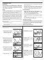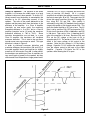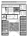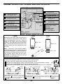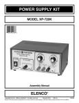
1
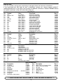
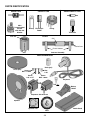
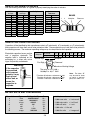
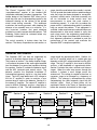
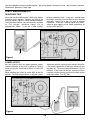
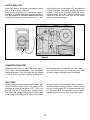
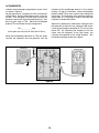
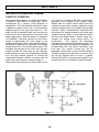
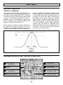
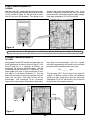
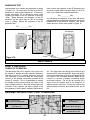
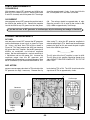
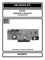
AM RADIO KIT
MODEL
SUPERHET AM-550TK
7 TRANSISTORS
Assembly and Instruction Manual
ELENCO
Copyright © 2010, 1999 by ELENCO® All rights reserved.
®
Revised 2010
REV-G
752550T
No part of this book shall be reproduced by any means; electronic, photocopying, or otherwise without written permission from the publisher.
PARTS LIST
If you are a student, and any parts are missing or damaged, please see instructor or bookstore.
If you purchased this AM radio kit from a distributor, catalog, etc., please contact ELENCO®
(address/phone/e-mail is at the back of this manual) for additional assistance, if needed. DO NOT contact
your place of purchase as they will not be able to help you.
RESISTORS
Qty.
r
r
r
r
r
r
r
r
r
r
r
r
r
r
r
r
1
3
1
1
2
1
2
1
1
1
1
1
1
1
1
1
Symbol
Value
Color Code
Part #
R19
R8, R15, R17
R10
R18
R6, R16
R12
R3, R11
R9
R2
R5
R7
R14
R1
R13
R4
Pot/SW1
1Ω 1/4W 5%
100Ω 1/4W 5%
470Ω 1/4W 5%
820Ω 1/4W 5%
1kΩ 1/4W 5%
2.2kΩ 1/4W 5%
3.3kΩ 1/4W 5%
10kΩ 1/4W 5%
12kΩ 1/4W 5%
27kΩ 1/4W 5%
39kΩ 1/4W 5%
47kΩ 1/4W 5%
56kΩ 1/4W 5%
82kΩ 1/4W 5%
1MΩ 1/4W 5%
50kΩ / SW
brown-black-gold-gold
brown-black-brown-gold
yellow-violet-brown-gold
gray-red-brown-gold
brown-black-red-gold
red-red-red-gold
orange-orange-red-gold
brown-black-orange-gold
brown-red-orange-gold
red-violet-orange-gold
orange-white-orange-gold
yellow-violet-orange-gold
green-blue-orange-gold
gray-red-orange-gold
brown-black-green-gold
Pot/SW with Nut and Washer
111000
131000
134700
138200
141000
142200
143300
151000
151200
152700
153900
154700
155600
158200
171000
192522
CAPACITORS
Qty.
r
r
r
r
r
r
r
r
1
1
2
5
2
1
1
2
Symbol
Value
Description
Part #
C1
C15
C3, C10
C2, C5, C7, C8, C9
C4, C11
C12
C6
C13, C14
Variable
.001μF
.01μF
.02μF or .022μF
10μF
47μF
100μF
470μF
Tuning
Discap (102)
Discap (103)
Discap (203) or (223)
Electrolytic (Lytic)
Electrolytic (Lytic)
Electrolytic (Lytic)
Electrolytic (Lytic)
211677
231036
241031
242010
271045
274744
281044
284744
Symbol
Description
Part #
D1, D2
Q1, Q2, Q3, Q4
Q5
Q6
Q7
1N4148 Diode
2N3904 Transistor NPN
2N3906 Transistor PNP
MPS8050 or 6560 Transistor NPN
MPS8550 or 6562 Transistor PNP
314148
323904
323906
328050
328550
Symbol
Value
L2
T1
T2
T3
L1
Oscillator
(red dot)
IF
(yellow dot)
IF
(white dot)
Detector
(black dot)
AM Antenna with holders
SEMICONDUCTORS
Qty.
r
r
r
r
r
2
4
1
1
1
COILS
Qty.
r
r
r
r
r
1
1
1
1
1
Description
Part #
430057
430260
430262
430264
484004
MISCELLANEOUS
Qty.
r
r
r
r
r
r
r
r
r
1
1
1
1
1
1
1
1
1
Description
PC Board
Battery Holder
Speaker
Knob (dial)
Knob (pot)
Earphone Jack with Nut
Radio Stand
Earphone
Screw M2.5 x 8mm (gang)
Part #
Qty.
r
r
r
r
r
r
r
r
517040
590096
590102
622040
622050
622130 or 622131
626100
629250
641107
3
2
3
8
1
1
1
1
Description
Part #
Screw 2-56 x 1/4” (battery holder)
Screw 2.5 x 3.8mm (gang)
Nut 2-56
Test Point Pin
Label, Dial Knob
Speaker Pad
Wire 4”
Solder Lead-free
641230
641310
644201
665008
720422
780128
814920
9LF99
**** SAVE THE BOX THAT THIS KIT CAME IN. IT WILL BE USED ON PAGE 25. ****
-1-
PARTS IDENTIFICATION
RESISTORS
CAPACITORS
SEMICONDUCTORS
Diode
Resistor
50kΩ
Potentiometer/
Switch
with Nut and
Washer
Discap
Electrolytic
Radial
Tuning
Transistor
COILS
Color Dot
Coil
Ferrite Core
Plastic Holders
Antenna Assembly
Coil
MISCELLANEOUS
Knob (pot)
Knob (dial)
Screw
M2.5 . 3.8mm
Nut
2-56
Screw
2-56 x 1/4”
Screw
M2.5 x 8mm
Earphone
OR
Test Pin
Battery
Holder
Earphone Jack with Nut
Speaker
Speaker Pad
Label
-2-
Radio Stand
IDENTIFYING RESISTOR VALUES
Use the following information as a guide in properly identifying the value of resistors.
BAND 1
1st Digit
Color
Black
Brown
Red
Orange
Yellow
Green
Blue
Violet
Gray
White
BAND 2
2nd Digit
Digit
0
1
2
3
4
5
6
7
8
9
Color
Black
Brown
Red
Orange
Yellow
Green
Blue
Violet
Gray
White
Multiplier
Digit
0
1
2
3
4
5
6
7
8
9
Color
Black
Brown
Red
Orange
Yellow
Green
Blue
Silver
Gold
Resistance
Tolerance
Multiplier
1
10
100
1,000
10,000
100,000
1,000,000
0.01
0.1
Color
Silver
Gold
Brown
Red
Orange
Green
Blue
Violet
Tolerance
±10%
±5%
±1%
±2%
±3%
±0.5%
±0.25%
±0.1%
BANDS
2
1
Multiplier
Tolerance
IDENTIFYING CAPACITOR VALUES
Capacitors will be identified by their capacitance value in pF (picofarads), nF (nanofarads), or μF (microfarads).
Most capacitors will have their actual value printed on them. Some capacitors may have their value printed in
the following manner. The maximum operating voltage may also be printed on the capacitor.
Electrolytic capacitors have a positive
and a negative electrode. The
negative lead is indicated on the
packaging by a stripe with minus
signs and possibly arrowheads.
Multiplier
For the No.
0
1
2
3
Multiply By
1
10
100
1k
Second Digit
First Digit
Warning:
If the capacitor
is connected
with incorrect
polarity, it may
heat up and
either leak, or
cause the
capacitor to
explode.
4
5
8
10k 100k .01
Means
Pico
nano
micro
milli
unit
kilo
mega
0.1
Multiplier
103K
100V
Tolerance*
Maximum Working Voltage
The value is 10 x 1,000 =
10,000pF or .01μF 100V
Polarity
Marking
* The letter M indicates a tolerance of +20%
The letter K indicates a tolerance of +10%
The letter J indicates a tolerance of +5%
Note: The letter “R”
may be used at times
to signify a decimal
point; as in 3R3 = 3.3
METRIC UNITS AND CONVERSIONS
Abbreviation
p
n
μ
m
–
k
M
9
Multiply Unit By
.000000000001
.000000001
.000001
.001
1
1,000
1,000,000
Or
10-12
10-9
10-6
10-3
100
103
106
-3-
1. 1,000 pico units
= 1 nano unit
2. 1,000 nano units
= 1 micro unit
3. 1,000 micro units = 1 milli unit
4. 1,000 milli units
= 1 unit
5. 1,000 units = 1 kilo unit
6. 1,000 kilo units
= 1 mega unit
INTRODUCTION
The Elenco® Superhet 550T AM Radio is a
“superheterodyne” receiver of the standard AM
(amplitude modulated) broadcast frequencies. The
unique design of the Superhet 550T allows you to
place the parts over its corresponding symbol in the
schematic drawing on the surface of the printed
circuit board during assembly. This technique
maximizes the learning process while keeping the
chances of an assembly error at a minimum. It is
very important, however, that good soldering
practices are used to prevent bad connections. The
Soldering Guide should be reviewed before any
assembly is attempted.
stage, should be read before the assembly is started.
This will provide the student with an understanding of
what that stage has been designed to accomplish,
and how it actually works. After each assembly, you
will be instructed to make certain tests and
measurements to prove that each section is
functioning properly. If a test fails to produce the
proper results, a troubleshooting guide is provided to
help you correct the problem. If test equipment is
available, further measurements and calculations are
demonstrated to allow each student to verify that
each stage meets the engineering specifications.
After all of the stages have been built and tested, a
final alignment procedure is provided to peak the
performance of the receiver and maximize the
Superhet 550T’s reception capabilities.
The actual assembly is broken down into five
sections. The theory of operation for each section, or
GENERAL DISCUSSION
stage should be approximately 6kHz. Section 4 is
the first IF amplifier which has a variable gain that
depends on the AGC voltage received from the AGC
stage. The first IF amplifier is also tuned to 455kHz
and has a 3dB bandwidth of approximately 6kHz.
Section 5 includes the mixer, oscillator and antenna
stages. When the radio wave passes through the
antenna, it induces a small voltage across the
antenna coil. This voltage is coupled to the mixer, or
converter, stage to be changed to a frequency of
455kHz. This change is accomplished by mixing
(heterodyning) the radio frequency signal with the
oscillator signal. Each of these blocks will be
explained in detail in the Theory of Operation given
before the assembly instructions for that stage.
The Superhet 550T can best be understood by
analysis of the block diagram shown in Figure 1.
The purpose of section 1, the Audio Amplifier Stage,
is to increase the power of the audio signal received
from the detector to a power level capable of driving
the speaker. Section 2 includes the detector circuit
and the AGC (automatic gain control) circuit. The
detector converts the amplitude modulated IF
(intermediate frequency) signal to a low level audio
signal. The AGC stage feeds back a DC voltage to
the first IF amplifier in order to maintain a near
constant level of audio at the detector. Section 3 is
the second IF amplifier. The second IF amplifier is
tuned to 455kHz (Kilohertz) and has a fixed gain at
this frequency of 100. The 3dB bandwidth of this
Antenna
Section 5
Section 4
Section 3
Section 2
Section 1
Speaker
MIXER
FIRST
IF AMPLIFIER
SECOND
IF AMPLIFIER
LOCAL
OSCILLATOR
DETECTOR
AGC
Figure 1
-4-
AUDIO
AMPLIFIER
CONSTRUCTION
Introduction
• Turn off iron when not in use or reduce temperature setting when
using a soldering station.
The most important factor in assembling your Elenco® Superhet 550T
AM Transistor Radio Kit is good soldering techniques. Using the proper
soldering iron is of prime importance. A small pencil type soldering iron
of 25 - 40 watts is recommended. The tip of the iron must be kept
clean at all times and well tinned.
• Tips should be cleaned frequently to remove oxidation before it becomes
impossible to remove. Use Dry Tip Cleaner (Elenco® #SH-1025) or Tip
Cleaner (Elenco® #TTC1). If you use a sponge to clean your tip, then use
distilled water (tap water has impurities that accelerate corrosion).
Solder
Safety Procedures
For many years leaded solder was the most common type of solder
used by the electronics industry, but it is now being replaced by leadfree solder for health reasons. This kit contains lead-free solder, which
contains 99.3% tin, 0.7% copper, and has a rosin-flux core.
• Always wear safety glasses or safety goggles to
protect your eyes when working with tools or
soldering iron, and during all phases of testing.
• Be sure there is adequate ventilation when soldering.
Lead-free solder is different from lead solder: It has a higher melting
point than lead solder, so you need higher temperature for the solder to
flow properly. Recommended tip temperature is approximately 700OF;
higher temperatures improve solder flow but accelerate tip decay. An
increase in soldering time may be required to achieve good results.
Soldering iron tips wear out faster since lead-free solders are more
corrosive and the higher soldering temperatures accelerate corrosion,
so proper tip care is important. The solder joint finish will look slightly
duller with lead-free solders.
'
• Locate soldering iron in an area where you do not have to go around
it or reach over it. Keep it in a safe area away from the reach of
children.
• Do not hold solder in your mouth. Solder is a toxic substance.
Wash hands thoroughly after handling solder.
Assemble Components
In all of the following assembly steps, the components must be installed
on the top side of the PC board unless otherwise indicated. The top
legend shows where each component goes. The leads pass through the
corresponding holes in the board and are soldered on the foil side.
Use only rosin core solder.
Use these procedures to increase the life of your soldering iron tip when
using lead-free solder:
• Keep the iron tinned at all times.
• Use the correct tip size for best heat transfer. The conical tip is the
most commonly used.
DO NOT USE ACID CORE SOLDER!
What Good Soldering Looks Like
Types of Poor Soldering Connections
A good solder connection should be bright, shiny, smooth, and uniformly
flowed over all surfaces.
Soldering Iron
1. Solder all components from the
copper foil side only. Push the
soldering iron tip against both the
lead and the circuit board foil.
Rosin
Component Lead
1. Insufficient heat - the solder will
not flow onto the lead as shown.
Foil
Soldering iron positioned
incorrectly.
Circuit Board
2. Apply a small amount of solder to
the iron tip. This allows the heat to
leave the iron and onto the foil.
Immediately apply solder to the
opposite side of the connection,
away from the iron. Allow the
heated component and the circuit
foil to melt the solder.
3. Allow the solder to flow around
the connection. Then, remove
the solder and the iron and let the
connection cool. The solder
should have flowed smoothly and
not lump around the wire lead.
Soldering Iron
2. Insufficient solder - let the
solder flow over the connection
until it is covered.
Use just enough solder to cover
the connection.
Solder
Foil
Solder
Gap
Component Lead
Solder
3. Excessive solder - could make
connections that you did not
intend to between adjacent foil
areas or terminals.
Soldering Iron
Solder
Foil
4. Solder bridges - occur when
solder runs between circuit paths
and creates a short circuit. This is
usually caused by using too much
solder.
To correct this, simply drag your
soldering iron across the solder
bridge as shown.
4. Here is what a good solder
connection looks like.
-5-
Soldering Iron
Foil
Drag
SEMICONDUCTOR PARTS FAMILIARIZATION
This section will familiarize you with the proper method used to test the transistors and the diode.
TRANSISTOR TEST
Refer to the parts list and find a NPN transistor. Refer
the Figure C (page 8) for locating the Emitter, Base and
Collector. Using an Ohmmeter, connect the transistor
as shown in Test A. Your meter should be reading a low
resistance. Switch the lead from the Emitter to the
Collector. Your meter should again be reading a low
resistance.
Refer to parts list and find a PNP transistor, refer to
Figure D (page 8) for locating the Emitter, Base and
Collector. Using an Ohmmeter, connect the transistor
as shown in Test C. Your meter should be reading a low
resistance. Switch the lead from the Emitter to the
Collector. Your meter should again be reading a low
resistance.
Using an Ohmmeter, connect the transistor as shown in
Test B. Your meter should be reading a high resistance.
Switch the lead from the Emitter to the Collector. Your
meter should again be reading a high resistance.
Typical results read approximately 1MΩ to infinity.
Using an Ohmmeter, connect the transistor as shown in
Test D. Your meter should be reading a high resistance.
Switch the lead from the Emitter to the Collector. Your
meter should again be reading a high resistance.
Low Resistance
High Resistance
COM
Low Resistance
Ω
NPN
COM
Ω
NPN
Ω
PNP
Ω
COM
EBC
COM
EBC
EBC
TEST A
High Resistance
Ω
Ω
Ω
TEST B
TEST C
Ω
PNP
EBC
TEST D
DIODE TEST
Refer to the parts list and find a diode. Refer to Figure E
(page 8) for locating the Cathode and Anode. The end
with the band is the cathode. Using an Ohmmeter,
connect the diode as shown in Test E. Your meter
should be reading a low resistance. Using an
Ohmmeter, connect the diode as shown in Test F. Your
meter should be reading a high resistance. Typical
results read approximately 1MΩ to infinity for silicon
diodes (1N4148).
High Resistance
Low Resistance
Ω
Ω
COM
COM
Ω
Ω
Diode
Diode
TEST E
TEST F
-6-
SECTION 1
AUDIO AMPLIFIER
Theory of Operation - The purpose of the Audio
Amplifier is to increase the audio power to a level
sufficient to drive an 8 ohm speaker. To do this, DC
(direct current) from the battery is converted by the
amplifier to an AC (alternating current) in the
speaker. The ratio of the power delivered to the
speaker and the power taken from the battery is the
efficiency of the amplifier. In a Class A amplifier
(transistor on over entire cycle) the maximum
theoretical efficiency is .5 or 50%, but in a Class B
amplifier (transistor on for 1/2 cycle) the maximum
theoretical efficiency is .785 or 78.5%. Since
transistor characteristics are not ideal, in a pure
Class B amplifier, the transistors will introduce
crossover distortion. This is due to the non-linear
transfer curve near zero current or cutoff. This type
distortion is shown in Figure 2.
In order to eliminate crossover distortion and
maximize efficiency, the transistors (Q6 and Q7) of
the audio amplifier circuit are biased on for slightly
more than 1/2 of the cycle, Class AB. In other words,
the transistors are working as Class A amplifiers for
very small levels of power to the speaker, but they
slide toward Class B operation at larger power levels.
Transistor Q4 is a Class A amplifier that drives the
base of transistor Q5 directly. Q5 is a current
amplifier that multiplies the collector current of Q4 by
the beta (current gain, B) of Q5. The current from Q5
drives the output transistors Q6 and Q7 through the
bias string R17, D2 and R18. Bias stability is
achieved by using 100% DC feedback from the output
stage to the emitter of Q4 through resistor R16. This
gives the Audio Amplifier a DC gain of one. The AC
gain is set by resistors R16, R15 and capacitor C12.
In this circuit, the value of R16 is 1000 ohms and R15
is 100 ohms. Their ratio is 10 to 1, therefore the AC
gain of the amplifier is 10 times. Resistors R13 and
R14 set the DC voltage at the base of Q4 to
approximately 5.2V. The emitter of Q4 is set at 4.5V,
which is the same voltage at this output to the
speaker. Note that this voltage is 1/2 the battery
voltage. Capacitor C11 AC couples the audio signal
from the volume control to the input of the Audio
Amplifier. Capacitor C13 blocks the DC to the
speaker, while allowing the AC to pass.
Figure 2
-7-
ASSEMBLY INSTRUCTIONS - AUDIO AMPLIFIER
We will begin by installing resistor R14. Identify the resistor by its color code and install as shown on page 3. Be careful to
properly mount and solder all components. Diodes, transistors and electrolytic capacitors are polarized, be sure to follow the
instructions carefully so that they are not mounted backwards. Check the box when you have completed each installation.
Electrolytics have a polarity
marking indicating the (–) lead.
The PC board is marked to
show the lead position.
Warning: If the capacitor is connected with incorrect
polarity, or if it is subjected to voltage exceeding its working
voltage, it may heat up and either leak or cause the
capacitor to explode.
NPN Transistor
Flat
Side
Capacitor C14
Polarity
Mark
(–)
(+)
EBC
B
For safety, solder capacitor
C14 on the copper side as
shown. Bend the leads 90O
and insert into holes.
Check that the polarity is
correct, then solder in
place. Trim the excess
leads on legend side.
Figure B
+
–
C
E
Figure C
PNP Transistor
Flat
Side
Figure Ba
EBC
C
E
Test Point Pin
Band
Diode
Be sure that the
band is in the
correct direction.
Foil Side
of PC Board
Mount so E lead is
in the arrow hole
and flat side is in
the same direction
as shown on the
top legend. Leave
1/4” between the
part and PC board.
B
Mount so E lead is
in the arrow hole
and flat side is in
the same direction
as shown on the
top legend. Leave
1/4” between the
part and PC board.
Figure D
Anode
Cathode
Q5 - 2N3906 Transistor PNP
(see Figure D)
Figure E
Figure A
TP7 - Test Point Pin
(see Figure A)
Q6 - MPS6560 (8050)
Transistor NPN
(see Figure C)
R14 - 47kΩ Resistor
(yellow-violet-orange-gold)
TP8 - Test Point Pin
(see Figure A)
Q4 - 2N3904 Transistor NPN
(see Figure C)
C13 - 470μF Lytic
(see Figure B)
TP6 - Test Point Pin
(see Figure A)
R17 - 100Ω Resistor
(brown-black-brown-gold)
C11 - 10μF Lytic
(see Figure B)
R16 - 1kΩ Resistor
(brown-black-red-gold)
C14 - 470μF Lytic
(see Figure Ba)
R19 - 1Ω Resistor
(brown-black-gold-gold)
R13 - 82kΩ Resistor
(gray-red-orange-gold)
D2 - 1N4148 Diode
(see Figure E)
Pot / SW1 with
Nut and Washer
Knob (pot)
Q7 - MPS6562 (8550)
Transistor PNP
(see Figure D)
Top Side
Solder 5 lugs
to PC board
R18 - 820Ω Resistor
(gray-red-brown-gold)
C12 - 47μF Lytic
(see Figure B)
R15 - 100Ω Resistor
(brown-black-brown-gold)
-8-
ASSEMBLY INSTRUCTIONS
Figure F
Your kit may contain a different type of earphone
jack. Before installing the jack, determine which
one you have.
Foil Side
J1 - Earphone Jack
with Nut
(see Figure F)
Jack
Nut
2
3
Speaker
Speaker Pad
4” Wire
(see Figures G & H)
1
1 - GND
2 - Tip
3 - N.C. Tip
Part #
622130
GND Pad
Foil Side
Battery Holder
3 Screws 2-56 x 1/4”
3 Nuts 2-56
Solder and cut off
excess leads.
Jack
2
Nut
1 - GND
2 - Tip
3 - N.C. Tip
Part #
622131
3 1
GND Pad
Mount the jack with the nut from the foil side of the
PC board (terminal #1 on the GND pad of the PC
board). Be sure to line up the tab with the pad on
the copper side of the PC board. Solder terminal
#1 to the pad of the PC board.
Figure G
Step 1
Step 2
Pad
Step 1: If the speaker pad has
center and outside pieces, then
remove them. Peel the backing off of
one side of the speaker pad and stick
the pad onto the speaker.
Step 3
Backing
PC Board
(solder side)
Backing
Speaker
Step 2: Remove the other backing
from the speaker pad.
Step 3: Stick the speaker onto the
solder side of the PC board.
Figure H
Cut two 1 1/2” wires and one 1” wire and strip 1/4” of insulation off of
both ends. Solder the wires in the locations shown.
From Terminal 3
1” Wire
1 ½”
Wires
Part # 622130
1” Wire
Part # 622131
-9-
1 ½”
Wires
You have completed wiring the Audio Amplifier. We shall proceed in testing this circuit. You will need a Volt-OhmMilliammeter, preferably a digital type.
STATIC MEASUREMENTS
RESISTANCE TEST
reverse multimeter leads. If you get a reading lower
than 20kΩ, check the circuit for shorts or parts inserted
incorrectly. Check C14 to see if it’s leaky or inserted
backwards. If you get a reading higher than 150kΩ,
check for open copper or bad solder connections on
resistors R13 and R14.
Adjust the Volt-Ohm-Milliammeter (VOM) to the highest
resistance scale available. Connect the VOM to the
circuit as shown in Figure 3. Do not connect the battery.
The VOM should indicate a low resistance first and then
as C14 charges, resistance should rise to
approximately 100kΩ. If you get a lower reading,
Ω
Amps
COM
V/Ω
GND
R15
Figure 3
POWER UP TEST
Set your VOM to read the highest possible current.
Connect the meter to the circuit as shown in Figure 4.
Make sure that the On/Off switch (SW1) is in the OFF
position.
While watching your VOM, flip switch SW1 to the ON
position. The VOM should indicate a very low current.
Adjust your meter for a more accurate reading if necessary.
If the current is greater than 25 milliamps, immediately turn
the power off. The current should be between 5 and 15
milliamps. If you circuit fails this test, check that all parts
have been installed correctly and check for shorts or poor
solder connections. Turn OFF SW1.
DC Amps
+
Amps COM
Figure 4
-10-
V/Ω
OUTPUT BIAS TEST
Adjust your VOM to read 9 volts and connect it to test
point 8 (TP8) as shown in Figure 5.
Make sure that the battery, or a 9 volt power supply (if
available), is properly connected and turn the power
ON. The voltage at TP8 should be between 4 to 5 volts.
If you get this reading, go on to the next test. If your
circuit fails this test, turn the power OFF and check that
all of the transistors are correctly inserted in the correct
locations. The E on the transistor indicates the emitter
lead and should always be in the hole with the arrow.
Check that resistors R13 and R14 are the correct
values and not interchanged.
V
Amps COM
V/Ω
Battery
GND
R15
Figure 5
TRANSISTOR BIAS TEST
Move the positive lead of your VOM to test point 7
(TP7). Make sure that the power is ON. The voltage
should be between .5 and .8V higher than the voltage
at TP8. All silicon transistors biased for conduction will
have approximately .7V from the base to the emitter. If
your circuit fails this test, turn off the power and check
that Q6 is properly inserted into the circuit board.
INPUT BIAS
Move the positive lead of the VOM to test point 6 (TP6).
Make sure that the power is ON. The voltage at TP6
should be very close to the voltage at TP7. This is true
because very little DC current flows through resistor
R16 making the voltage at the emitter of Q4 very close
to the voltage at the emitter of Q5. If your circuit passes
this test, leave the VOM connected and go to test 1 in
the Dynamic Measurements Section. If your circuit fails
this test, turn the power OFF and check transistors Q4,
Q7 and resistor R16. All static tests must pass before
proceeding to the Dynamic Tests or the next section.
-11-
DYNAMIC MEASUREMENTS
DC GAIN
Adjust your VOM to read 9 volts DC. Connect the
positive lead of the VOM to TP6 and the negative lead
to any ground. Turn the power ON and record the
voltage at TP6 here:
Once again, parallel resistor R13 with resistor R4 as
shown in Figure 6. The voltage at TP8 should also drop
to a lower voltage. Record the new reading at TP8
here:
V1=________ volts.
V4=__________ volts.
Place resistor R4 across resistor R13 as shown in
Figure 6.
The voltage at TP6 should drop to a lower value.
Record that lower voltage here:
Remove R4 from the circuit but leave your VOM
connected to TP8 for the next test. Turn the power OFF.
Since the DC GAIN equals the DC change at the output
divided by the DC change at the input, the DC gain of
this amplifier is (V1-V2)/(V3-V4). Your calculated
answer should be very close to 1.
V2=__________ volts.
Remove R4 from the circuit and move the positive lead
of the VOM to TP8. Record the voltage at TP8 here:
V3=__________ volts.
V
Amps COM
1MΩ
V/Ω
Battery
GND
R15
Figure 6
If you do not have a generator, skip the following test and go directly to Section 2.
-12-
AC GAIN
Connect the VOM and generator to TP6 as shown in
Figure 7.
Turn the power ON. Normally the AC gain is measured
at a frequency of 1 kilohertz (kHz). Your VOM, however,
may not be able to accurately read AC voltages at this
frequency. It is recommended, therefore, that this test
be performed at 400Hz. Set the generator at 400Hz and
minimum voltage output. Set your VOM to read an AC
voltage of 1 volt at the output of your Audio Amplifier.
Slowly increase the output of the generator until the
VOM reads 1 volt AC. Leave the audio at this setting
Generator
V
and move the positive lead of your VOM to TP6. Record
the AC voltage input to the amplifier here:
Vin=___________ volts.
You may have to change scales on your VOM for the
most accurate reading. Turn the power OFF. The AC
voltage gain of your Audio Amplifier is equal to the AC
output voltage divided by the AC input voltage, or 1/Vin.
Your calculated AC Gain should be approximately 10.
10μF
Output Adjust
GND
R15
Amps COM
V/Ω
Battery
GND
R15
Figure 7
If an oscilloscope is not available, skip the following test and go directly to Section 2.
-13-
AC BANDWIDTH
Connect the oscilloscope and generator to your circuit
as shown in Figure 8.
Set the generator for a frequency of 1kHz and minimum
voltage output. Set the oscilloscope to read .5 volts per
division. Turn the power ON and slowly increase the
generator output until the oscilloscope displays 2 volts
peak to peak (Vpp) at TP8. Move the oscilloscope
probe to TP6 and record the input voltage here:
waveform on the oscilloscope drops to .7 of its original
reading, 1.4 Vpp or 2.8 divisions. Use the oscilloscope
probe to check TP6 to make sure the input voltage did
not change. The frequency of the generator when the
output drops to .7 of its original value is called the high
frequency 3 decibel (dB) corner.
Repeat this procedure by lowering the frequency from
the generator to obtain the low frequency 3dB corner.
Leave the oscilloscope connected to TP8 and turn the
power OFF. By subtracting the frequency of the low
corner from the frequency of the high corner, you
calculate the bandwidth of the Audio Amplifier. Your
bandwidth should be greater than 100kHz.
Vin=___________ Vpp
(at this point you may want to verify the AC Gain).
Move the oscilloscope probe back to TP8 and slowly
increase the frequency from the generator until the
Generator
10μF
Oscilloscope
Probe
Output Adjust
GND
R15
GND
R15
Figure 8
-14-
DISTORTION
Connect the generator and oscilloscope as shown in
Figure 8. Set the generator at a frequency of 1kHz, turn
the power ON and adjust the generator output until the
peaks of the sinewave at TP8 are clipped as shown in
Figure 9A.
Clipped
Crossover
Distortion
A
B
Figure 9
Measure the maximum voltage peak to peak when
clipping first occurs and record that value here:
The waveform on your oscilloscope should resemble
Figure 9B. The “flat spots” near the center of each
sinewave demonstrate what is called crossover
distortion. This distortion should disappear when you
remove the shorting lead. Turn the power OFF
Vclp = _______ Vpp.
Using a wire short out resistor R17 and diode D2 as
shown in Figure 10.
MAXIMUM POWER OUTPUT
The maximum power output before distortion due to
“clipping” can be calculated using the voltage Vclp
obtained in step 4 as follows:
Wire Lead
or Clip Lead
Vpeak (Vp) = Vclp/2
Vroot mean squared (Vrms) = Vp x .7
Max power out = (Vrms)2/8 ohms = (Vclp x .35)2/8
Maximum power output should be greater than 200
milliwatts.
Figure 10
EFFICIENCY
By measuring the DC power taken from the battery at
the maximum power output level, the efficiency to the
Audio Amplifier can be calculated. Power from the
battery is equal to the current taken from the battery
times the voltage of the battery during maximum power
output. It is best to use a power supply to prevent
battery voltage from changing during this
measurement. Efficiency can then be calculated as
follows: Eff = Max audio power/Battery Power.
-15-
SECTION 2
AM DETECTOR AND AGC STAGES
THEORY OF OPERATION
is to maintain a constant audio level at the detector,
regardless of the strength of the incoming signal.
Without AGC, the volume control would have to be
adjusted for each station and even moderately strong
stations would clip in the final IF amplifier causing audio
distortion. AGC is accomplished by adjusting the DC
bias of the first IF amplifier to lower its gain as the signal
strength increases. Figure 11 shows that the audio at
the top of the volume control is actually “riding” on a
negative DC voltage when strong signals are
encountered.
This negative DC component
corresponds to the strength of the incoming signal. The
larger the signal, the more negative the component. At
test point three (TP3), the audio is removed by a low
pass filter, R11 and C4, leaving only the DC
component. Resistor R5 is used to shift the voltage at
TP3 high enough to bias the base of transistor Q2 to
the full gain position when no signal is present.
Resistors R5 and R11 also forward bias diode D1 just
enough to minimize “On Condition” threshold voltage.
The purpose of the detector is to change the amplitude
modulated IF signal back to an audio signal. This is
accomplished by a process called detection or
demodulation. First, the amplitude modulated IF signal
is applied to a diode in such a way as to leave only the
negative portion of that signal (see Figure 11). The
diode acts like an electronic check valve that only lets
current pass in the same direction as the arrow (in the
diode symbol) points. When the diode is in conduction
(On Condition), it will force capacitors C9 and C10 to
charge to approximately the same voltage as the
negative peak of the IF signal. After conduction stops in
the diode (Off Condition), the capacitors will discharge
through resistors R11, R12 and the volume control. The
discharge time constant for this circuit must be small
enough to follow the audio signal or high frequency
audio distortion will occur. The discharge time constant
must be large enough, however, to remove the
intermediate frequency (455kHz) and leave only the
audio at the volume control as shown in Figure 11.
The purpose of the automatic gain control (AGC) circuit
Figure 11
-16-
ASSEMBLY INSTRUCTIONS - DETECTOR
C6 - 100μF Lytic
(see Figure B)
R8 - 100Ω Resistor
(brown-black-brown-gold)
R5 - 27kΩ Resistor
(red-violet-orange-gold)
T3 - IF Coil (black)
T1 - IF Coil (yellow)
TP3 - Test Point Pin
(see Figure A)
C4 - 10μF Lytic
(see Figure B)
TP5 - Test Point Pin
(see Figure A)
R11 - 3.3kΩ Resistor
(orange-orange-red-gold)
D1 - 1N4148 Diode
(see Figure E)
C9 - .02μF or .022μF Discap
(marked 203 or 223)
C15 - .001μF Discap
(marked 102)
R12 - 2.2kΩ Resistor
(red-red-red-gold)
C10 - .01μF Discap
(marked 103)
STATIC MEASUREMENTS
AGC ZERO SIGNAL BIAS
With the power turned OFF, connect the VOM to test
point three (TP3) as shown in Figure 12.
Check that the VOM is adjusted to read 9 volts DC and
turn the power ON. The voltmeter should read
approximately 1.5 volts DC. If your reading varies more
than .5 volts from this value, turn the power OFF and
check the polarity of D1, and resistors R11 and R5.
Also check that transformer T1 is properly installed.
V
Amps COM
Figure 12
V/Ω
GND
R15
T3 TEST
With the power turned OFF, connect the positive lead of
the VOM to TP5 and the negative lead to any ground.
Make sure that the VOM is set to read 9 volts DC and
turn the power ON. The voltage on the VOM should be
the same as your battery voltage or power supply
voltage. If not, turn OFF the power and check that T3
is properly installed.
If you do not have an RF generator, go to Section 3.
-17-
DYNAMIC MEASUREMENTS
DETECTOR AND ACG TEST
Turn the power OFF and connect the VOM and RF
generator as shown in Figure 13. Set the VOM to
accurately read 2 volts DC and set the output of the RF
generator for 455kHz, no modulaton, and minimum
amplitude. Turn the power ON and slowly increase the
amplitude of the 455kHz signal from the RF generator
until the voltage at TP3 just starts to drop. This point is
called the AGC threshold with no IF gain. Make a note
of the amplitude setting on the RF generator here:
____________.
Turn the power OFF.
Generator
.02μF
V
Amps COM
Figure 13
GND
R15
V/Ω
GND
R15
If your RF generator does not have amplitude modulation or you do not have an oscilloscope, go to Section 3.
SYSTEM CHECK
Connect equipment as shown in Figure 14.
Set the RF generator at 455kHz, 1kHz at 80%
modulation and minimum output. Turn the power ON
and put the volume control at full clockwise position.
Slowly adjust the amplitude of the RF generator output
until you hear the 1kHz on the speaker. If this test fails,
turn the power OFF and check C11, R12, volume
control, D1 and TP3.
Oscilloscope
Generator
.02μF
GND
R15
GND
R15
Figure 14
DETECTOR BANDWIDTH TEST
Connect equipment as shown in Figure 14. Set the RF
generator at 455kHz with 80% modulation at a
modulation frequency of 1kHz. Set the oscilloscope to
read .1 volts per division. Turn the power ON and put
the volume control at minimum.
Increase the
amplitude of the RF generator until the signal on the
oscilloscope is 4 divisions peak to peak. Check the
signal to make sure it is free of all distortion. Leave the
frequency of the RF output at 455kHz, but increase the
modulation frequency until the output drops to 0.28
Vpp. Record the modulation frequency on the RF
generator here:
_________.
This frequency should be greater than 5kHz. Turn the
power OFF.
-18-
SECTION 3
SECOND IF AMPLIFIER
THEORY OF OPERATION
The purpose of the SECOND IF AMPLIFIER is to
increase the amplitude of the intermediate frequency (IF)
and at the same time provide SELECTIVITY. Selectivity
is the ability to “pick out” one radio station while rejecting
all others. The second IF transformer (T3) acts as a
bandpass filter with a 3dB bandwidth of approximately
6kHz. The amplitude versus frequency response of the
second IF amplifier is shown in Figure 15.
The gain at 455kHz in the second IF amplifier is fixed
by the AC impedance of the primary side of transformer
T3, and the DC current in Q3. The current in Q3 is set
by resistors R7, R9 and R10. Both C7 and C8 bypass
the 455kHz signal to ground, making Q3 a common
emitter amplifier. The signal is coupled from the first IF
amplifier to the second IF amplifier through transformer
T2. The IF transformers not only supply coupling and
selectivity, they also provide an impedance match
between the collector of one stage and the base of the
next stage. This match allows maximum power to
transfer from one stage to the next.
Both IF amplifiers are tuned to a frequency of 455kHz and
only need to be aligned once when the radio is
assembled. These amplifiers provide the majority of the
gain and selectivity needed to separate the radio stations.
.707
452kHz
458kHz
455kHz
Figure 15
ASSEMBLY INSTRUCTIONS - SECOND IF AMPLIFIER
TP4 - Test Point Pin
(see Figure A)
R7 - 39kΩ Resistor
(orange-white-orange-gold)
T2 - IF Coil
(White)
R9 - 10kΩ Resistor
(brown-black-orange-gold)
Q3 - 2N3904 Transistor NPN
(see Figure C)
C7 - .02μF or .022μF Discap
(marked 203 or 223)
R10 - 470Ω Resistor
(yellow-violet-brown-gold)
C8 - .02μF or .022μF Discap
(marked 203 or 223)
-19-
STATIC MEASUREMENTS
Q3 BIAS
With the power OFF, connect the negative lead of your
VOM to any ground and the positive lead to the emitter
of Q3 as shown in Figure 16. Set the VOM to read 9
volts DC and turn ON the power. The voltage at the
emitter of Q3 should be approximately 1 volt. If your
reading is different by more than 0.5 volts, turn off the
power and check your battery of power supply voltage.
Also check components R7, R9, R10 and Q3.
V
Amps COM
V/Ω
GND
R10
Figure 16
If you do not have an RF generator or oscilloscope, skip the following test and go to Section 4.
DYNAMIC MEASUREMENTS
AC GAIN
With the power turned OFF, connect the oscilloscope and
the RF generator to the circuit as shown in Figure 17. Set
the RF generator at a frequency of 455kHz, no
modulation and minimum amplitude output. Set the
oscilloscope vertical sensitivity at 1 volt/division. The
scope probe must have an input capacitance of less
than 50pF or it will detune transformer T3. Turn the
power ON and slowly increase the amplitude of the RF
signal until you have 4 volts peak to peak on the
oscilloscope. Tune transformer T3 for a maximum
output while readjusting the RF generator amplitude to
keep 4Vpp at the oscilloscope. After T3 is aligned,
move the scope probe tip to the base of Q3 and record
the peak to peak amplitude of the signal here:
Vb=__________Vpp.
Turn the power OFF. The AC gain of the second IF
amplifier at 455kHz is equal to 4/Vb, and should be
greater than 100. If your gain is less than 100, check
components C7, C8, R7, R9 and R10. Also, make sure
that transistor Q3 is properly installed.
Generator
Oscilloscope
.02μF
Probe
Output
Adjust
GND
R10
GND
R10
Figure 17
-20-
BANDWIDTH TEST
With the power OFF, connect your equipment as shown
in Figure 17A. Turn the power ON and adjust the RF
generator for .4Vpp at the cathode of D1. If necessary,
realign transformer T3 for maximum output while
adjusting the output of the RF generator to maintain
.4Vpp. Slowly decrease the frequency of the RF
generator until the signal drops to .707 of its peaked
value or .28Vpp. Record the frequency of the RF
generator here:
Now increase the frequency of the RF generator past
the peak to a point where the signal drops to .707 of its
peak value. Record that frequency point here:
FH=___________kHz.
By subtracting the frequency of the lower 3dB corner
from the frequency of the higher 3dB corner you get the
BANDWIDTH of the second IF amplifier. Your results
should be similar to the values shown in Figure 15.
FL=___________kHz.
Oscilloscope
Generator
.02μF
Output
Adjust
GND
R10
Probe
Figure 17A
GND
R10
SECTION 4
FIRST IF AMPLIFIER
THEORY OF OPERATION
The operation of the first IF amplifier is the same as for
the second IF amplifier with one important difference.
The gain of the first IF amplifier decreases after the
AGC threshold is passed to keep the audio output
constant at the detector and prevent overload of the
second IF amplifier. This is accomplished by making
the voltage on the base of transistor Q2, lower as the
signal strength increases. Since the voltage from base
to emitter is fairly constant, the drop in voltage at the
base produces a similar drop in voltage at the emitter of
Q2. This drop lowers the voltage across R6 and thus
reduces the DC current through R6. Since all of the DC
current from the emitter of Q2 must go through R6, the
DC current in Q2 is therefore lowered. When the DC
current in a transistor is lowered, its effective emitter
resistance increases. The AC gain of transistor Q2 is
equal to the AC collector load of Q2 divided by its
effective emitter resistance. Raising the value of the
effective emitter resistance thus lowers the AC gain of
Q2.
ASSEMBLY INSTRUCTIONS - FIRST IF AMPLIFIER
R4 - 1MΩ Resistor
(brown-black-green-gold)
Q2 - 2N3904 Transistor NPN
(see Figure C)
TP2 - Test Point Pin
(see Figure A)
R6 - 1kΩ Resistor
(brown-black-red-gold)
C5 - .02μF or .022μF Discap
(marked 203 or 223)
-21-
STATIC MEASUREMENTS
Q2 BASE BIAS
With the power turned OFF, reconnect your VOM to test
point 3 (TP3) as shown in Figure 12. Set the VOM to read
2 volts DC accurately and turn the power ON. The voltage
should be approximately 1.5 volts. If your circuit fails this
test, turn the power OFF and check Q2 and R6.
Q2 CURRENT
With the power turned OFF, connect the positive lead of
the VOM to the emitter of Q2. Connect the negative
lead of the VOM to any DC ground and turn the power
ON. The voltage should be approximately .8 volts.
Since the current in Q2 is equal to the current in R6,
I(Q2)=.8/R6 or approximately .8 milliamps.
If you do not have an RF generator or oscilloscope, skip the following test and go to Section 5.
DYNAMIC MEASUREMENTS
AC GAIN
With the power turned OFF, connect the RF generator
and the oscilloscope to your circuit as shown in Figure
18. Using a clip lead, short TP5 to R8 as shown in
Figure 18. This short prevents the AGC from lowering
the gain of the first IF ampifier. Set the RF generator to
455kHz, no modulation, and minimum amplitude
output. Set the oscilloscope for a vertical sensitivity of
1 volt/division and turn the power ON. Increase the
amplitude output from the RF generator until
approximately 4Vpp registers on the oscilloscope. Tune
the IF transformer (T2) to maximize the 455kHz at TP4.
After tuning T2, adjust the RF generator amplitude in
order to keep 4Vpp at TP4. Now move the oscilloscope
probe to the base of Q2 and record the peak to peak
level of the 455kHz signal here:
Vb=____________Vpp.
The AC gain of the first IF amplifier is equal to 4/Vb.
The AC gain of this amplifier should be greater than
100. DO NOT TURN THE POWER OFF. GO TO THE
NEXT TEST.
AGC ACTION
Move the oscilloscope probe back to TP4 and adjust the
RF generator for 4Vpp if necessary. Remove the clip
lead shorting TP5 to R8. The AGC should reduce the
signal level at TP4 to approximately .8 volts.
Clip Lead
Oscilloscope
Generator
.02μF
Output
Adjust
GND
R6
GND
R6
Figure 18
-22-
SECTION 5
MIXER AND OSCILLATOR
THEORY OF OPERATION
frequencies except those near 455kHz. T1 also
couples the 455kHz signal to the base of Q2 to be
processed by the IF amplifiers.
In a superheterodyne type receiver the radio wave at the
antenna is amplified and then mixed with the local
oscillator to produce the intermediate frequency (IF).
Transistor Q1 not only amplifies the RF signal but also
simultaneously oscillates at a frequency 455kHz above
the desired radio station frequency. Positive feedback
from the collector to the emitter of Q1 is provided by coil
L2 and capacitor C3. During the heterodyne process,
the following four frequencies are present at the collector
of Q1.
1. The
2. The
3. The
4. The
The antenna and the oscillator coils are the only two
resonant circuits that change when the radio is tuned
for different stations. Since a radio station may exist
455kHz above the oscillator frequency, it is important
that the antenna rejects this station and selects only the
station 455kHz below the oscillator frequency. The
frequency of the undesired station 455kHz above the
oscillator is called the image frequency. If the selectivity
of the antenna (Q factor) is high, the image will be
reduced sufficiently.
local oscillator frequency, LO.
RF carrier or radio station frequency.
sum of these two frequencies, LO + RF.
difference of these two frequencies, LO - RF.
The oscillator circuit must also change when the radio
is tuned in order to remain 455kHz above the tuning of
the desired radio station. The degree of accuracy in
keeping the oscillator frequency exactly 455kHz above
the tuning of the antenna is called tracking accuracy.
The “difference frequency” is used as the intermediate
frequency in AM radios. The collector of Q1 also
contains an IF transformer (T1) tuned only to the
difference frequency. This transformer rejects all
-23-
ASSEMBLY INSTRUCTIONS - ANTENNA, MIXER AND OSCILLATOR
R1 - 56kΩ Resistor
(green-blue-orange-gold)
L1 - Antenna with Holders
(see Figures I & J)
L2 - Oscillator Coil (red)
C2 - .02μF or .022μF Discap
(marked 203 or 223)
Q1 - 2N3904 Transistor NPN
(see Figure C)
TP1 - Test Point Pin
(see Figure A)
C3 - .01μF Capacitor
(marked 103)
R2 - 12kΩ Resistor
(brown-red-orange-gold)
C1 - Tuning Gang Capacitor
2 Screws M2.5 x 3.8mm
Knob (dial)
Screw M2.5 x 8mm
Label (dial knob)
(see Figure K)
R3 - 3.3kΩ Resistor
(orange-orange-red-gold)
4 Wire
3 Wire
Figure I
Determine if you have a three wire or four wire
coil. Resistance measurements will be used to
check the configuration of the coil. Slide one
holder off the ferrite core of the antenna
assembly. Then slide the coil off the the ferrite
core. Measure the resistance of the coil. Your
readings should match the approximate values
as shown.
White
Black
Red
}
}
White
R=9 - 11Ω
R=1 - 1.5Ω
Black
Red
Note: If the end of a wire from the antenna
should break off, strip the insulation off the end
with a hot soldering iron. Lay the wire down on
a hard surface and stroke the wire with your iron.
The insulation should come off very easily.
CAUTION: The soldering iron will burn the hard
surface that you are working on.
}
}
R=9 - 11Ω
R=1 - 1.5Ω
Green
IMPORTANT: Before installing the antenna coil, determine if you have a 3 wire coil or a 4 wire coil. Assemble it to the
PC board as shown below. Mount the antenna assembly to the PC board.
Put the tab of the first holder into the right hole and twist the tab 90O.
Slide the ferrite core through the antenna coil and the holder. Cut the second holder as shown.
Put the tab of the second holder into the left hole and twist the tab 90O.
Slide the ferrite core through the holder. Make sure that the ferrite core sticks out 1/2” on each side.
1/2”
C (white)
B (black)
1/2”
C (white)
Black
A (red)
Red
Tabs
3 Wire Type Antenna: Solder the 3 colored wires to
the PC board:
Wire A (red) to the hole marked
“RED”, Wire B (black) to the hole marked “BLK” and
Wire C (white) to the hole marked “WHT”.
B Twisted Together
1/2”
B Twisted Together
OR
C (white)
Black
Red
Tabs
A (green)
A (green)
4 Wire Type Antenna: Solder the 4 colored wires to the PC board: Wire A (green) to the
hole marked “RED”, Wire B (red and black twisted together) to the hole marked “BLK” and
Wire C (white) to the hole marked “WHT”.
Figure J
-24-
Your kit may contain a 3 lead or a 4 lead
capacitor. Bend the leads as shown. Fasten C1
into place on the top side of the PC board with
two M2.5 x 3.8mm screws.
Knob Post
Fasten the knob to the
shaft of the capacitor
with one M2.5 x 8mm
screw.
M2.5 x 8mm
Screw
C1
Turn the dial fully clockwise.
Remove the protective
backing from the label and
align the 1600 with the
arrow on the PC board.
Screw Holes
3 Leads
Solder leads
to pads
4 Leads
Figure K
Punch out one antenna shim from the front flap
of the box.
PC Board Stand
Insert the PC board into the stand as shown.
Insert the cardboard antenna shim between the
ferrite core and the antenna coil. This will
temporarily hold the coil in place.
Cut Holder
Coil
Figure L
-25-
Knob
STATIC MEASUREMENTS
Q1 BIAS
With the power turned OFF, connect the VOM to your
circuit as shown in Figure 19. Connect a clip lead from
test point two (TP2) to the collector of Q1. This short
prevents Q1 from oscillating. Set the VOM to read 2 volts
DC accurately and turn the power ON. The DC voltage
at TP1 should be 1.6 volts. If the voltage in your circuit
differs by more than 0.5 volts, leave the power ON and
check the battery voltage. If the battery voltage is
greater than 8.5 volts, turn the power OFF and check
components R1, R2, R3 and Q1.
V
Amps COM V/Ω
Clip Lead
GND
R2
Figure 19
If you do not have an oscilloscope, go to the Final Alignments With No Test Equipment Section.
DYNAMIC MEASUREMENTS
OSCILLATOR CIRCUIT
With the power turned OFF, connect the oscilloscope to
the circuit as shown in Figure 20. Set the oscilloscope
for a vertical sensitivity of 1 volt/division and turn the
power ON.
The oscilloscope should display a low
voltage sine wave. The frequency of the sine wave
should change when capacitor C1 is turned. If your
circuit fails this test, turn the power OFF and check
components Q1, C1, C2, C3, L1 and L2.
Oscilloscope
GND
R2
Figure 20
If you don’t have an oscilloscope and an RF generator,
go to the Final Alignments with No Test Equipment Section.
-26-
FINAL ALIGNMENTS
IF BANDWIDTH
With the power turned OFF, connect the RF generator
and the oscilloscope to your circuit as shown in Figure 21.
Short TP2 to the collector of Q1 with a clip lead to “kill”
the local oscillator. Set the RF generator at a frequency
of 455kHz, modulation of 400Hz 80%, minimum
amplitude output. Set the oscilloscope to read 0.1Vpp
and turn the power ON. Increase the amplitude of the
RF signal until the oscilloscope registers 0.5Vpp. Align
transformers T3, T2 and T1 for the maximum AC
reading on the oscilloscope. Decrease the amplitude of
the signal from the RF generator to restore 0.5Vpp on
the oscilloscope. Repeat the last two steps until no
change in the peak at the oscilloscope is noticed.
After IF alignment, lower the frequency from the RF
generator until the reading on the VOM drops to 0.707
of its peaked value. Record the frequency of this lower
3dB corner here:
Fl=____________kHz.
Increase the RF generator frequency past the peak to
the upper 3dB corner and record that frequency here:
Fh=____________kHz.
The bandwidth of the IF amplifiers is BW=Fh - Fl. IF
bandwidth should be between 1 to 2kHz. This
bandwidth will widen as the AGC is approached.
Oscilloscope
Generator
.02μF
Output
Adjust
Probe
GND
R2
Clip Lead
GND
R6
Figure 21
SETTING OSCILLATOR RANGE
With the power turned OFF, connect the equipment to
the circuit as shown in Figure 21. DO NOT connect the
clip lead from TP2 to Q1. Set the RF generator at
540kHz, 400Hz 80% modulation, and a low level of
output. Turn the tuning capacitor fully counterclockwise. Turn the power ON and a 400Hz tone should
be heard coming from the speaker. Tune the oscillator
coil (L2) for a peak on the oscilloscope. Adjust the RF
Oscillator Trimmer
Antenna Trimmer
Figure 22
generator output during this process to maintain a peak
at 0.5Vpp or less. After peaking L2, set the RF
generator frequency to 1600kHz and turn the tuning
capacitor (C1) fully clockwise. A 400Hz tone should be
heard coming from the speaker. Tune the oscillator
trimmer capacitor on the back of C1 for a peak on the
oscilloscope (see Figure 22).
Antenna Trimmer
3 Leads
4 Leads
-27-
After peaking the oscillator trimmer capacitor, return the
RF generator to 540kHz, and capacitor C1 to the fully
counter-clockwise position and readjust L2. Repeat the
last few steps until both settings of the oscillator are
correct. This process sets the oscillator range at
995kHz to 2055kHz. If a frequency counter is available,
you may verify this alignment by measuring the
frequency at the emitter of Q1 for both ends of the
tuning capacitor (C1). Be careful not to mistune the
oscillator during this measurement. A coupling
capacitor of 82 picofarads or less to the frequency
counter is recommended.
ANTENNA ALIGNMENT
With the power turned OFF, connect test equipment to
your circuit as shown in Figure 23. Set the RF generator
at 600kHz, 400Hz 80% modulation, moderate signal
strength. Set the oscilloscope to read .5Vpp and turn the
power ON. Turn C1 fully counter-clockwise, then slowly
turn C1 clockwise until a 400Hz tone can be heard
coming from the speaker. Slowly slide the antenna coil
back and forth on the ferrite rod to obtain a peak on the
oscilloscope. For maximum signal, your location of the
antenna coil may have to be on the end of the ferrite rod
(as shown in Figure 24). Change the frequency of the RF
generator to 1400kHz and adjust C1 until a 400Hz tone
can be heard coming from the speaker. Carefully peak
the reading on the oscilloscope by adjusting the
frequency of the RF generator. Now tune the antenna coil
to this frequency by adjusting the antenna trimmer on the
back of C1 (see Figure 22). This process should be
repeated until both settings of the antenna track the
oscillator tuning. Once the antenna is properly aligned,
carefully apply candle wax or glue to the antenna coil and
ferrite rod (as shown in Figure 24).
Close to
Antenna
Wire Loop
Oscilloscope
Generator
Output
Adjust
Probe
GND
R6
Figure 23
Coil
Wax
Figure 24
-28-
Holder
AM ALIGNMENT WITH NO TEST EQUIPMENT
It is best to use an earphone for this alignment
procedure. Rotate the tuning knob fully counterclockwise and place the label on the knob with the
white arrow pointing at the 540kHz marking.
their broadcast frequency is announced. If no stations
are present at the low side of the AM band, adjust L2
until a station is heard. Once a station is found and its
broadcast frequency is known, rotate the dial until the
white pointer is aligned with that station’s frequency
marking on the dial. Adjust L2 until the station is heard.
Tune the radio until a station around 1400kHz is heard.
It may be necessary to listen to the station until their
broadcast frequency is announced. If no stations are
present at the high end of the AM band, adjust the
oscillator trimmer on the back of the gang. Once a
station is found and its broadcast frequency is known,
rotate the dial until the white pointer is aligned with that
station’s frequency marking on the dial. Adjust the
oscillator trimmer located on the back of the gang until
a station is heard. Repeat these steps until the
oscillator alignment is optimized. This procedure set
the oscillator range at 995kHz to 2055kHz.
With an alignment tool or screwdriver, turn coils L2, T1,
T2 and T3 fully counter-clockwise until they stop. DO
NOT FORCE THE COILS ANY FURTHER. Turn each
coil in about 1 1/4 to 1 1/2 turns. Set the antenna coil
about 1/8” from the end of its ferrite rod. Refer to
Figure J on page 24.
Turn the power ON and adjust the volume to a
comfortable level. Tune the dial until a weak station is
heard. If no stations are present, carefully slide the
antenna back and forth on its ferrite rod and retune the
dial if necessary. With an alignment tool or screwdriver,
adjust T1 until the station is at its loudest. Reduce the
volume control if necessary. Adjust T2 until the station
is at its loudest and reduce the volume control if
necessary. Adjust T3 until the station is at its loudest
and reduce the volume if necessary. Retune the radio
for another weak station and repeat this procedure until
there is no more improvement noticed on the weakest
possible station. This procedure peaked the IF
amplifiers to their maximum gain.
Tune the radio for a station around 600kHz. Carefully
slide the antenna back and forth until the station is at its
loudest. Tune the radio for a station around 1400kHz.
Adjust the antenna trimmer located on the back of the
gang until the station is at its loudest. Repeat these
steps until the antenna alignment is optimized. This
procedure set the antenna to “track” the oscillator.
Once the antenna is properly aligned, carefully apply
candle wax or glue the antenna coil to the ferrite rod to
prevent it from moving (as shown in Figure 24).
Tune the radio until a known station around 600kHz is
found. It may be necessary to listen to the station until
DC Voltages
The voltage readings below should be used in troubleshooting the AM radio.
Q1 B 1.5V
E 1.0V
C 8.9V
Q5 B 8.3V
E 9.0V
C 5.8V
Q2 B 1.4V
E 0.7V
C 8.9V
Q6 B 5.8V
E 5.2V
C 9.0V
Q3 B 1.7V
E 1.0V
C 9.0V
Q7 B 4.6V
E 5.2V
C 0.0V
Test Conditions
1. Volume control set to minimum.
2. Connect a jumper wire between capacitor C2 (side
that goes to red lead of coil L1) to negative battery.
3. Battery voltage - 9.0V
4. All voltages are referenced to circuit common.
5. Voltage reading can vary +10%.
Q4 B 5.7V
E 5.2V
C 8.3V
-29-
SCHEMATIC DIAGRAM
-30-
ELENCO®
150 Carpenter Avenue
Wheeling, IL 60090
(847) 541-3800
Website: www.elenco.com
e-mail: [email protected]