1
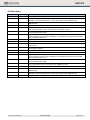
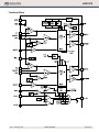
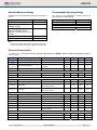
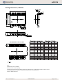
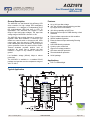
AOZ1978 Dual Channel High Voltage LED Driver IC General Description Features The AOZ1978 is a dual-channel high-efficiency LED driver controller for high voltage LED backlighting applications. It is designed to independently drive two high-brightness LED light bars in LED TV applications. The AOZ1978 can support a wide range of input and output voltages. The input bias voltage range of AOZ1978 is from 8V to 18V. The AOZ1978 has multiple features to protect the regulator under fault conditions. A control pin can disable an external switch to disconnect the LEDs current path from the output in PWM dimming or under catastrophic failure conditions. Cycle-by-cycle current protection limits the peak inductor current. Thermal shutdown provides another level of protection. An output flag to indicate the fault condition if output of any channel is shorted to ground. Low feedback voltage (500mV) helps to reduce power loss. The AOZ1978 is available in a standard SO-20 package and operates over the temperature range of -40C to +85C. 8V to 18V input bias voltage 180⁰ Out of phase channel switching provides input ripple current cancellation 18V driving capability at GATE pins Disconnect control pin for PWM dimming or fault conditions Flag to indicate output short or fault condition 500mV feedback regulation External reference input and Analog Dimming capability 8 bit PWM dimming resolution Cycle-by-cycle current limit Output over-voltage protection LED short and open protection Thermal shutdown protection SO-20 package Applications LCD TV LED backlight Typical Application Rev. 1.0 January 2012 www.aosmd.com Page 1 of 1 AOZ1978 Ordering Information Part Number Temperature Range Package Environmental AOZ1978AI -40°C to +85°C SOIC-20 Green AOS Green Products use reduced levels of Halogens, and are also RoHS compliant. Please visit www.aosmd.com/web/quality/rohs_compliant.jsp for additional information. Pin Configuration VIN 1 20 FLAG DPWM1 2 19 DPWM2 GATE1 3 18 GATE2 GND 4 17 GND COMP1 5 16 COMP2 OVP1 6 15 OVP2 DBRT1 7 14 DBRT2 CS1 8 13 CS2 FB1 9 12 FB2 ISET 10 11 SCP SOIC-20 (Top View) Rev. 1.0 January 2012 www.aosmd.com Page 2 of 2 AOZ1978 Pin Description Part Number Pin Name 1 2 VIN DPWM1 3 GATE1 4 5 GND COMP1 6 OVP1 7 DBRT1 8 9 10 CS1 FB1 ISET 11 SCP 12 13 14 FB2 CS2 DBRT2 15 OVP2 16 COMP2 17 18 GND GATE2 19 DPWM2 20 FLAG Rev. 1.0 January 2012 Pin Function Input Supply Pin. Fault and Dimming PWM Control Output for Channel 1. DPWM1 = High for LED connect. DPWM1 = Low for LED disconnect. Connect to the gate of external NMOS switch. External Boost NMOS Gate Controller Pin for Channel 1. Connect to the gate of external NMOS switch. IC Ground Pin. Compensation Pin for Channel 1. COMP1 is the output of the internal error amplifier. For loop compensation connect a RC network from COMP1 to ground. Output Voltage Protection Input Pin for Channel 1 output. Use a voltage divider from VOUT1 to sense Boost output voltage. Digital Brightness Control Input for Channel 1. PWM dimming controls the LED brightness by turning the LED on and off using a PWM signal. The brightness is proportional to the PWM duty cycle applied at this pin. NMOS Switch Current Sense Pin for Channel 1. Feedback Input Pin for Channel 1. Connect to sense resistor at LED string. LED Current Set Input Pin reference for both channels. 0.5V internal or external reference can be used. Short Circuit Protection Pin: monitors and Flags input voltage drop and over current sensing during Fault conditions. Feedback Input Pin for Channel 2. Connect to sense resistor at LED string. NMOS Switch Current Sense Pin for Channel 2. Digital Brightness Control Input for Channel 2. PWM dimming controls the LED brightness by turning the LED on and off using a PWM signal. The brightness is proportional to the PWM duty cycle applied at this pin. Output Voltage Protection Input Pin for Channel 2 output. Use a voltage divider from VOUT2 to sense Boost output voltage. Compensation Pin for Channel 2. COMP2 is the output of the internal error amplifier. For loop compensation connect a RC network from COMP2 to ground. IC Ground Pin. External Boost NMOS Gate Controller Pin for Channel 2. Connect to the gate of external NMOS switch. Fault and Dimming PWM control output for Channel 2. DPWM2 = High for LED connect. DPWM2 = Low for LED disconnect. Connect to the gate of external NMOS switch. NMOS Open Drain Fault Flag Output Pin. FLAG = 1 if SCP or OVP is detected. www.aosmd.com Page 3 of 3 AOZ1978 Pin Functions Pin1: VIN This is the input supply for the controller IC; it is also the voltage drive for the Gates and DPWM drivers. If the input power of the boost converter is less than 18V, VIN can be connected directly to the boost supply voltage. If the boost supply voltage is higher than 18V, a separate supply rail between 8V and 18V is required for the VIN pin. It is recommended that an RC filter should be added between VIN and Boost supply if they are connected directly. PIN 2: DPWM1 This is the driver output for the gate of the LED current control NMOS switch for channel 1. DPWM1 = LOW if Pin 7 DBRT1 signal is low or fault condition is triggered. The DPWM1 = HIGH if DBRT1 is high under normal operating conditions. The high voltage at DPWM1 equals to Pin1 VIN voltage. It is recommended to add 1Ω resistor between this pin and NMOS gate. The resistor value can be optimized depending on the LED current and selection of NMOS. DPWM1 can be driven simultaneously with DPWM2 or independently from DPWM2. Pin 3: GATE1 This is the driver output for the gate of boost NMOS switch for channel 1. The GATE = HIGH voltage is equal to VIN voltage. It is recommended to add a 1Ω resistor between this pin and the NMOS gate. The resistor value can be optimized depending on the selection of NMOS switch. To reduce system noise and input ripple current, GATE1 is 180⁰ out of phased from GATE2. Pins 4, 17: GND These are the common ground for the IC controller. It is recommended that all the low current paths are connected to these pins as close as possible to the IC controller. It is not recommended to connect any output or input filter capacitors and any current sense resistors to these pins directly. The IC controller ground should be an island around the IC connected to the PWR GND at a single point in the layout. Pin 5: COMP1 This is for feedback loop compensation for Channel 1. It is the output of the error amplifier that controls PWM logic for the boost controller. An RC network should be connected to GND to generate the compensation for boost 1 feedback loop. Rev. 1.0 January 2012 Pin 6: OVP1 This is the input for LED Over-Voltage Protection. OVP1 monitors Channel 1 LED output voltage through a resistor divider. When the voltage at this pin is higher than 1V, Channel 1 will immediately stop switching for 40ms and Pin 20 (FLAG) is instantly asserted HIGH, indicating a Fault condition, CH1 controller will reset and restart again after 40ms. If fault condition persists it will repeat until fault condition is removed. Pin 7: DBRT1 This is the input for digital brightness control for CH1. A PWM logic signal is applied to this pin to vary the brightness of the LED. The brightness of the LED is proportional to the duty cycle of the PWM logic signal. The input signal will control the output driver at DPWM1 pin. This input pin cannot be left floating. Pin 8: CS1 This is the input for peak current sense for CH1. This pin serves the functions of current feedback, peak current limit detection and fault current detection. The pin current limit is internally set to 0.4V for peak current limit and 0.48V for fault current detection, under fault current detection, CH2 controller will assert FLAG, shutdown and reset every 40ms. Pin 9: FB1 This is the feedback input for boost controller for CH1. This pin should connect to a resistor that senses the LED current. The FB1 voltage will be regulated to Pin 10 (ISET) voltage. If the voltage at FB1 pin exceeds 1V due to a fault condition CH1 controller will reset and start again after 40ms, if fault condition persists it will repeat until fault condition is removed. Pin 10: ISET This is 0.5V output of the internal reference voltage of the error Amp for both CH1 and CH2. This pin is bidirectional; if desired it can be driven externally to track an external reference or also can be used as a linear dimming input from 0V to 0.8V, a 10nF or higher value capacitor to GND must be connected to this pin. Pin 11: SCP Short Circuit Protection pin, the rising threshold at this Pin is 1.14V and falling threshold is 0.96V, if the pin voltage falls below 0.96V, FLAG will be asserted HIGH and both channels will shut down and reset every 40ms, if no current sense resistor this pin can be used as a typical UVLO pin. www.aosmd.com Page 4 of 4 AOZ1978 Pin 12: FB2 This is the feedback input for boost controller for CH2. This pin should connect to a resistor that senses the LED current. The FB2 voltage will be regulated to Pin 10 (ISET) voltage. If the voltage at FB2 pin exceeds 1V due to a fault condition CH2 will shut down for 40ms and will try again every 40ms until the fault condition is removed. Note that this is the only fault condition that will not assert a FLAG. Pin 13: CS2 This is the input for peak current sense for CH2. This pin serves the functions of current feedback, peak current limit detection and fault current detection. The pin current limit is internally set to 0.4V for peak current limit and 0.48V for fault current detection, under fault current detection, CH2 controller will assert FLAG, shutdown and reset every 40ms. Pin 14: DBRT2 This is the input for digital brightness control for CH2. A PWM logic signal is applied to this pin to vary the brightness of the LED. The brightness of the LED is proportional to the duty cycle of the PWM logic signal. The input signal will control the output driver at DPWM2 pin. This input pin cannot be left floating. Pin 15: OVP2 This is the input for LED Over-Voltage Protection. OVP2 monitors Channel 2 LED output voltage through a resistor divider. When the voltage at this pin is higher than 1V, Channel 2 will immediately stop switching for 40ms and Pin 20 (FLAG) is instantly asserted HIGH, indicating a Fault condition, CH2 controller will reset and restart again after 40ms. If fault condition persists it will repeat until fault condition is removed. Pin 16: COMP2 This is for feedback loop compensation for Channel 2. It is the output of the transconductance error amplifier that controls PWM logic for the boost controller. An RC network should be connected from COMP2 to Rev. 1.0 January 2012 GND to generate the compensation for boost 2 feedback loop. Pin 18: GATE2 This is the driver output for the gate of boost NMOS switch for Channel 2. The GATE = HIGH voltage is equal to VIN voltage. It is recommended to add a 1Ω resistor between this pin and the NMOS gate. The resistor value can be optimized depending on the selection of NMOS switch. To reduce system noise and input ripple current, GATE2 is 180⁰ out phase from GATE1. PIN 19: DPWM2 This is the driver outputs for the gate of the LED current control NMOS switch for channel 2. DPWM2 = LOW if Pin 14 DBRT2 signal is low or fault condition is triggered. The DPWM2 = HIGH if DBRT2 is high under normal operating conditions. The high gate voltage at DPWM2 equals Pin1 VIN voltage. It is recommended to add 1Ω resistor between this pin and NMOS gate. The resistor value can be optimized depending on the LED current and selection of NMOS. DPWM2 can be driven simultaneously with DPWM1 or independently from DPWM1. PIN 20: FLAG This is an open drain output that is asserted HIGH any time a fault condition is detected on either or both CH1 or CH2. Whenever FLAG is asserted high the controller shuts down and resets every 40ms until fault condition is removed. FLAG is also asserted at start-up, if Pin1 VIN voltage is present before boost input voltage is applied, FLAG will clear when input boost voltage becomes present and SCP Pin 11 reaches 1.14V. To avoid a FLAG at power-up, follow proper power up sequence, Pin 1 VIN voltage should be applied after boost input voltage PVIN has reached operating level. The Only Fault condition when FLAG will not be asserted but controller will still shutdown and reset every 40ms is when either or both FB1 or FB2 exceed 1V due to system noise or Shorted LED string. www.aosmd.com Page 5 of 5 AOZ1978 Functional Block Rev. 1.0 January 2012 www.aosmd.com Page 6 of 6 AOZ1978 Absolute Maximum Ratings Recommended Operating Ratings Exceeding the Absolute Maximum Ratings may damage the device. This device is not guaranteed to operate beyond the Recommended Operating Ratings. Parameter VIN to GND GATE1, DPWM1, GATE2, DPWM2 to GND COMP1, OVP1, DBRT1, CS1, FB1, ISET COMP2, OVP2, DBRT2, CS2, FB2, SCP, FLAG to GND Storage Temperature (TS) ESD Rating(1) Parameter Supply Voltage (VVIN) Ambient Temperature (TA) Package Thermal Resistance SOIC-20 (JA) Rating -0.3V to +20V -0.3V to +20V -0.3V to +6V Rating 8V to 18V -40°C to +85°C 105°C/W -65°C to +150°C 2kV Note: 1. Devices are inherently ESD sensitive, handling precautions are required. Human body model rating: 1.5kΩ in series with 100pF. Electrical Characteristics TA = 25°C, VIN = 12V unless otherwise specified. Specifications in BOLD indicate an ambient temperature range of -40°C to +85°C. Symbol VVIN IVIN_ON VUVLO_RISE VUVLO_FALL VVIN_HYS Parameter Conditions VIN Supply Voltage VIN Quiescent Current VIN UVLO Threshold Min. Typ. 8 VIN rising VIN falling 6.2 VIN UVLO Hysteresis 7 6.5 500 Max Units 18 2 7.3 V mA V mV Oscillator FSW TON Switching Frequency Minimum ON Time (PWM) 170 200 150 230 200 kHz ns GATE1 and GATE2 Driver IGATE_SOURCE IGATE_SINK Source Current Sink Current TGATE_RISE Rise Time TGATE_FALL Fall Time GATE1 or GATE2 = 0V GATE1 or GATE2 = 12V CGATE = 1nF 10% to 90% of VIN CGATE = 1nF 90% to 10% of VIN 350 600 mA mA 50 85 ns 25 45 ns 5 5 5 5 5 5 µA µA µA µA µA µA 2000 Hz 512 mV µA mA Inputs IISET ICS ISCP IDBRT IOVP IFB ISET Input Current CS Input Current SCP Current DBRT Input Current OVP Input Current FB Input Current FDBRT DBRT Dimming Frequency ISET = 0.6V CS1 or CS2 = 0.3V SCP = 1.2V DBRT1 or DBRT2 = 5V OVP1 or OVP2 = 1.2V FB1 or FB2 = 0.5V DBRT1 or DBRT2 duty cycle from 1% to 99% 100 Outputs ISETVOUT ISETSRC IFLAG_SINK ISET Output Voltage ISET Output Source Current FLAG Output Sink Current Rev. 1.0 January 2012 0.5V ISET = GND FLAG = 0.5V www.aosmd.com 488 500 10 1 Page 7 of 7 AOZ1978 Electrical Characteristics (continued) Symbol Protection VCS VSCP VSCP_HYS OVP_THRSHLD FLAG_TO TTHERMAL_SD TTHERMAL_HYS Parameter Conditions Min. Typ. Max Units CS Threshold Voltage SCP Threshold Voltage SCP Hysteresis OVP Threshold Voltage FLAG Time OUT Thermal Shutdown Threshold Thermal Shutdown Hysteresis CS1 or CS2 360 0.864 440 1.056 OVP1 or OVP2 0.9 400 0.96 200 1 40 145 35 mV V mV V ms °C °C PWM Source current PWM Sink current DPWM1 or DPWM2 = 0V DPWM1 or DPWM2 = 12V 60 80 DBRT Logic High DBRT Logic Low DBRT1 or DBRT2 DBRT1 or DBRT2 2 1.1 PWM Drive IPWM_SOURCE IPWM_SINK mA mA Logic Input VDBRT_HI VDBRT_LO Rev. 1.0 January 2012 www.aosmd.com 0.8 V V Page 8 of 8 AOZ1978 DBRT1 or Typical Performance Characteristics Switching Waveforms and Input Current: PVIN = 100V, VLED = 200V, ILED = 125mA/CH Rev. 1.0 January 2012 www.aosmd.com Page 9 of 9 AOZ1978 Typical Performance Characteristics (continued) Rev. 1.0 January 2012 www.aosmd.com Page 10 of 10 AOZ1978 Detailed Description The AOZ1978 is a dual channel boost DC/DC controller designed to power a series of LEDs by regulating the current into an LED string. The LED current information is provided to the system through the sense resistor RFB at the bottom of each LED string, between FB and GND pins. Protection Features Over-Current Protection at Boost Switch The current limit is a function of RCS resistor value at CS pin and the internal set threshold of 0.4V limit. When CS voltage reaches set voltage, current limit protection triggers and the boost switch will turn off immediately until the next clock cycle. To make sure that current limit protection does not affect the normal operation, the current limit should be set at least 30% higher than the inductor peak current. When CS voltage is higher than 0.48V, fault detection is activated and FLAG is asserted. Over-Voltage Protection at Output Over-voltage protection is monitoring the LED output voltage through a resistor divider (Rovh and Rovl in Typical Application Circuit) from VOUT to OVP and GND pins. When the voltage at this pin is higher than 1V, the controller will stop switching immediately and FLAG is asserted for 40ms. Rev. 1.0 January 2012 LED Short Protection When FB voltage exceeds 1V, the system will consider some or all LEDs shorted instantaneously. Under this condition, the controller will shut down and reset every 40ms, this is the only Fault condition that FLAG will not be asserted. LED Open Protection When all LEDs are open, the system will respond by boosting the output voltage. Once the output voltage reaches the OVP threshold, OVP protection will trigger and the controller will latch off until VIN is recycled. Feedback short AOZ1978 also protects against shorted feedback sense resistor or LED cathode shorted to GND. When SCP pin voltage drops below 0.96V due to excess return current sensed by resistor RRTN the controller asserts FLAG and shuts down .It will reset every 40ms until fault condition is removed. Thermal Protection An internal temperature sensor monitors the junction temperature. It shuts down the internal control circuit and all drivers if the junction temperature exceeds 145ºC. www.aosmd.com Page 11 of 11 AOZ1978 Application Information Inductor Selection Inductor choice will be affected by many parameters, like duty cycle based on input/output setting, switching frequency, full scale LED current level, and mode of operations. Boost controller can operate under discontinuous mode, continuous mode, or critical conduction mode. For high voltage boost LED driver applications, it is recommended to use critical conduction mode for best stability and good efficiency. ILPEAK Inductor Current in Critical Conduction Mode The inductor value is determined by: For the application with VIN=100V, VOUT=200V, LED current=125mA. Input _ Current IIN VOUT IOUT 200V 0.125A 0.29A VIN(MIN) 85V ILPEAK di 2 IIN 0.58A ON _ time dt L dt VIN(MIN) di VOUT VIN 200V 100V 0 .5 VOUT 200V D 0 .5 2.5 s FSW 200 kHz COUT IOUT D VRIPPLE FSW When selecting output capacitors, it is more important to check the effective ESR of the capacitor than the actual capacitance value. For example, a 10μF capacitor with 0.02Ω ESR will handle higher ripple current and produce less output ripple than a 33μF capacitor with 0.04Ω ESR. It is recommended to use low ESR MLCC ceramic capacitors. For high voltage cost effective application, multiple Electrolytic capacitors in parallel will reduce the total effective ESR. Input Capacitors The input capacitors for boost converters do not require low ESR due to the fact that the input current is continuous and does not contain large triangular peak current as compared to the output capacitors. AOZ1978 utilizes 180⁰ out of phase switching which provides input ripple current cancellation and significantly reduces input capacitance requirements compared to in-phase switching. In critical Conduction mode inductor Peak current: Duty _ Cycle D Output Capacitors The amount and type of capacitor used is mainly determined by the design output ripple (VRIPPLE) requirement: 2.5s 85V 370H 0.58 After the inductor value is calculated, we need to consider the DCR resistance and the saturation current ISAT of the inductor. Inductor DCR is inversely proportional to the ISAT. It is recommended to select an inductor for which the ISAT value should be at least 50% higher than the ILPEAK value. To minimize EMI effect, it is always preferable to use shielded type inductors. Electrolytic capacitors should work well with the appropriate voltage and ripple current rating, it is not recommended to use Tantalum capacitors because Boost converters do exhibit high surge currents during startup which can cause tantalum capacitors to fail. Current Sense Resistors There are three current sense resistors in this application, an LED Feedback current sense resistor RFB, a Boost switch Current Sense resistor RCS and an optional system Ground return over current protection RRTN. RFB LED current sense resistor is set by: RFB VISET 0.5V 4 LED _ CURRENT 0.125 A RCS boost switch Current Sense resistor is set by: Diode Selection It is recommended to use fast recovery diode for D1. For most applications, Schottky diodes with correct current and voltage rating are suitable. The diode current rating should be at least higher than the full scale LED current. The diode voltage rating should be higher than the OVP level of VOUT voltage. Rev. 1.0 January 2012 RCS www.aosmd.com 0.3V 0.3V 0.4 ILPEAK 1.3 0.58 A 1.3 Page 12 of 12 AOZ1978 For typical application, we recommend to set the voltage at CS to approximately 0.3V when inductor current reaches the peak. To accommodate load, line and inductor tolerances variation, 30% margin is included in the above calculation. RRTN Ground return current sense resistor, this resistor is optional and if desired can be used to add an extra layer of protection against output shorts or any other fault condition that causes excessive return current. When not used, simply connect a 1V divider from PVIN to SCP pin. In this configuration SCP pin will function as a typical under-voltage lock out (UVLO) pin with a rising threshold of 1V and a falling threshold of 0.8V. If short circuit protection is desired then: R RTN I IN AVG 0.2V I IN AVG ILED1 VLED1 ILED2 VLED2 PVIN When RRTN is used then the divider from PVIN to SCP pin will have to be calculated as a 1.34V divider to compensate for the 0.2V drop generated by RRTN, and also this divider will now be referenced to RTN Ground. A small cap is required from SCP pin to IC Ground to integrate the sensed voltage and avoid premature protection (see typical application circuit). Boost Feedback Loop Compensation The AOZ1978 employs peak current mode control for easy use and fast transient response. Peak current mode control eliminates the double pole effect of the output L&C filter. It greatly simplifies the compensation loop design. With peak current mode control, the boost power stage can be simplified to be a one-pole, one left plane zero and one right half plane (RHP) system in frequency domain. The pole is dominant pole and can be calculated by: fP 1 The zero is a ESR zero due to output capacitor and its ESR can be calculated by: 1 2 CO ESRCO Rev. 1.0 January 2012 CO is the output filter capacitor, RL is load resistor value, and ESRCO is the equivalent series resistance of output capacitor. The RHP zero has the effect of a zero in the gain causing an imposed +20dB/decade on the roll off, but has the effect of a pole in the phase, subtracting 90 in the phase. The RHP zero can be calculated by: 2 fZ 2 VIN 2 L IO VO The RHP zero obviously can cause instability issue if the bandwidth is higher. It is recommended to design the bandwidth to lower than the one half frequency of RHP zero. The compensation design is actually to shape the converter close loop transfer function to get desired gain and phase. Several different types of compensation networks can be used for AOZ1978. For most cases, a series capacitor and resistor network connected to the COMP pin sets the polezero and is adequate for a stable high-bandwidth control loop. In the AOZ1978, FB pin and COMP pin inverting input and the output of transconductance error amplifier. A series of compensation network connected to COMP one pole and one zero. The pole is: fP 2 are the internal R and C provides GEA 2 CC GVEA where, GEA is the error amplifier transconductance, which is 200·10-6 A/V, GVEA is the error amplifier voltage gain, which is 1000 V/V, and CC is compensation capacitor. The zero given by the external compensation network, capacitor CC and resistor RC, is located at: 1 2 CO RL fZ 1 where, fZ 2 1 2 CC RC Choose the suitable CC and RC by trading-off stability and bandwidth. www.aosmd.com Page 13 of 13 AOZ1978 PCB Layout Consideration Correct layout practices are essential for a working design that will meet expectations. It is recommended to use two-layer board for the design. However, a single layer board would be sufficient if basic layout rules are followed. In any SMPS layout, external components should be grouped into Power or IC control. From typical application circuit, there are two GND symbols. The striped one is for Power GND and the solid one is for Signal/Control GND. Both symbols are connected to a single point connection on the layout. All Power connections should be as short and wide as possible in order to reduce undesired parasitic inductance. The output capacitors should be physically placed in the current path between the SMPS and the load. Input capacitors should be placed as close as possible to the input side of the inductor. To prevent interference and system noise, it is critical that the switch node connection for boost switch, inductor, and output diode must be as short and close as possible. A GND copper layer covers the top layer to help shield the noise. For two-layer board, it is essential that the GND plane under this switching node be filled and uninterrupted. Single Point Connection: Connecting IC GND to Bottom Layer PWR GND Rev. 1.0 January 2012 www.aosmd.com Page 14 of 14 AOZ1978 Package Dimensions, SOIC-20L RECOMMENDED LAND PATTERN Symbols Min. Nom. Max. Symbols Min. Nom. Max. A 2.35 2.52 2.65 A 0.093 0.099 0.104 A1 0.10 0.20 0.30 A1 0.004 0.008 0.012 A2 2.05 2.35 2.55 A2 0.081 0.093 0.100 b 0.35 — 0.49 b 0.014 — 0.019 c 0.23 — 0.32 c 0.009 — 0.013 D 12.60 12.70 12.80 D 0.496 0.500 0.504 E 7.40 10.00 7.50 10.20 7.60 10.60 E E1 0.291 0.394 0.295 0.402 0.299 0.417 E1 e 1.27 BSC 0.80 1.27 e L1 1.35 REF L1 L2 0.25 BSC L2 L 0.50 0° — 8° L 0.020 0.050 BSC 0.031 0.050 0.053 REF 0.010 BSC 0° — 8° Notes: 1. All dimensions are in millimeters. 2. Dimensions are inclusive of plating. 3. Package body sizes exclude mold flash and gate burrs. Mold flash at the non-lead sides should be less than 6 mil each. 4. Controlling dimension is millimeter, converted inch dimensions are not necessarily exact. 5. Refer to JEDEC MS-013 AC. Rev. 1.0 January 2012 www.aosmd.com Page 15 of 15 AOZ1978 Plastic Tube and Plug, SOIC-20L Cannot read text ANTISTATIC Test Ht. 2.54 max Printing 7.874 R 0.254 Max (Typ) CNRT CNRT CNRT 2.413–2.718 CNRT 4.699 CNRT CNRT CNRT CNRT CNRT 4.902 CNRT 4.902 3.683 CNRT All Sides 14.732 CNRT Vendor Coder 0701–0005XXX Option Rev. NOTES: 1. All dimensions are in millimeters. 2. Tube material, clear rigid PVC. 3. Print color, white. 4. Character thickness, 0.254 millimeters. 5. “ANTISTATIC” print to be placed at center of tube’s length and width. 6. Produce with dry extrusion process. Rev. 1.0 January 2012 www.aosmd.com Page 16 of 16 AOZ1978 Part Marking AOZ1978AI (SOIC-20) Z1978AI FX YW LT Part Number Code Assembly Lot Code Fab & Assembly Location Year & Week Code This datasheet contains preliminary data; supplementary data may be published at a later date. Alpha and Omega Semiconductor reserves the right to make changes at any time without notice. LIFE SUPPORT POLICY ALPHA & OMEGA SEMICONDUCTOR PRODUCTS ARE NOT AUTHORIZED FOR USE AS CRITICAL COMPONENTS IN LIFE SUPPORT DEVICES OR SYSTEMS. As used herein: 1. Life support devices or systems are devices or systems which, (a) are intended for surgical implant into the body or (b) support or sustain life, and (c) whose failure to perform when properly used in accordance with instructions for use provided in the labeling, can be reasonably expected to result in a significant injury of the user. Rev. 1.0 January 2012 2. A critical component in any component of a life support, device, or system whose failure to perform can be reasonably expected to cause the failure of the life support device or system, or to affect its safety or effectiveness. www.aosmd.com Page 17 of 17