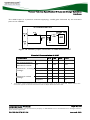
1
Product Technical Specification &
Customer Design Guidelines
Q64 Wireless CPU®
Reference: WA_DEV_Q64_PTS_001
Revision: 003
Date: January 9, 2009
Q64 Wireless CPU®
Product Technical Specification &
Customer Design Guidelines
Reference: WA_DEV_Q64_PTS_001
Revision: 003
Date: January 9, 2009
Powered by the Wavecom Open AT® Software Suite
© Confidential
Page: 1 / 116
This document is the sole and exclusive property of WAVECOM. Not to be distributed or divulged without
prior written agreement.
WA_DEV_Q64_PTS_001-003
January 9, 2009
Product Technical Specification & Customer Design Guidelines
Document History
Revision
Date
List of revisions
001
February 6, 2008
Creation
002
July 11, 2008
Updates
003
January 9, 2009
Updates to sections §3.3.1, §3.15.1, §5.1, §7.13
and some minor changes
© Confidential
Page: 2 / 116
This document is the sole and exclusive property of WAVECOM. Not to be distributed or divulged without
prior written agreement.
WA_DEV_Q64_PTS_001-003
January 9, 2009
Product Technical Specification & Customer Design Guidelines
Overview
This document defines and specifies the Q64 Wireless CPU®, available in a
GSM/GPRS Class 10 quad-band version.
Q64 Wireless CPU® is a variant of Wavecom Wireless Microprocessor® WMP100,
which is pin to pin and functionally compatible with Wavecom Wireless CPU®
GR64001.
© Confidential
Page: 3 / 116
This document is the sole and exclusive property of WAVECOM. Not to be distributed or divulged without
prior written agreement.
WA_DEV_Q64_PTS_001-003
January 9, 2009
Product Technical Specification & Customer Design Guidelines
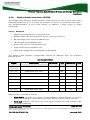
Table of Contents
Document History ................................................................................2
Overview ..............................................................................................3
Table of Contents ................................................................................4
Table of Figures ...................................................................................8
Trademarks ........................................................................................10
Copyright ...........................................................................................10
No Warranty/No Liability ....................................................................10
1
References ................................................................................11
1.1
Reference Documents........................................................................... 11
1.1.1
Wavecom Reference Documentation............................................. 11
1.1.2
General Reference Documentation ................................................ 11
1.2
List of Abbreviations ............................................................................. 12
2
General Description ...................................................................15
2.1
General Information .............................................................................. 15
2.1.1
Overall Dimensions ....................................................................... 15
2.1.2
Environment and Mechanics......................................................... 15
2.1.3
GSM/GPRS Features ..................................................................... 15
2.1.4
Interfaces ...................................................................................... 16
2.1.5
Operating System ......................................................................... 16
2.1.6
Connection Interfaces ................................................................... 16
2.2
Functional Description .......................................................................... 17
2.2.1
RF Functionalities ......................................................................... 18
2.3
Operating System ................................................................................. 18
2.4
Software Description ............................................................................ 18
3
Interfaces ..................................................................................20
3.1
General Interfaces................................................................................. 20
3.2
Power Supply ....................................................................................... 21
3.2.1
Power Supply Description............................................................. 21
© Confidential
Page: 4 / 116
This document is the sole and exclusive property of WAVECOM. Not to be distributed or divulged without
prior written agreement.
WA_DEV_Q64_PTS_001-003
January 9, 2009
Product Technical Specification & Customer Design Guidelines
3.2.2
3.2.3
Electrical Characteristics ............................................................... 22
Power Supply Pin-out ................................................................... 22
3.3
Power Consumption ............................................................................. 23
3.3.1
Power Consumption without Open AT® Processing ...................... 24
3.3.2
Power Consumption with a Dhrystone Open AT® Application ....... 25
3.3.3
Consumption Waveform Samples ................................................. 27
3.3.4
Recommendations for Less Consumption ..................................... 29
3.4
Electrical Information for Digital I/O....................................................... 30
3.5
I2C Bus................................................................................................. 32
3.5.1
Features........................................................................................ 32
3.5.2
Pin Description.............................................................................. 33
3.6
Main Serial Link (UART1) ...................................................................... 34
3.6.1
Features........................................................................................ 34
3.6.2
Pin Description.............................................................................. 34
3.6.3
Application.................................................................................... 36
3.7
Auxiliary Serial Link (UART2) ................................................................ 39
3.7.1
Features........................................................................................ 39
3.7.2
Pin Description.............................................................................. 39
3.7.3
Application.................................................................................... 40
3.8
SIM
3.8.1
3.8.2
3.8.3
Interface ........................................................................................ 41
Features........................................................................................ 41
Pin Description.............................................................................. 43
Application.................................................................................... 43
3.9
General Purpose Input/Output .............................................................. 45
3.9.1
Features........................................................................................ 45
3.9.2
Pin Description.............................................................................. 45
3.10 Analog to Digital Converter................................................................... 47
3.10.1 Features........................................................................................ 47
3.10.2 Pin Description.............................................................................. 49
3.10.3 Application.................................................................................... 49
3.11 Analogue Audio Interface...................................................................... 50
3.11.1 Microphone Features .................................................................... 50
3.11.2 Speaker Features .......................................................................... 53
3.11.3 Pin Description.............................................................................. 55
3.11.4 Application.................................................................................... 56
3.11.5 Design Recommendation .............................................................. 63
3.12 PWM / Buzzer Output........................................................................... 67
3.12.1 Features........................................................................................ 67
3.12.2 Pin Description.............................................................................. 67
3.12.3 Application.................................................................................... 68
3.13 Battery Charging Interface .................................................................... 70
3.13.1 Implementation............................................................................. 70
3.13.2 Ni-Cd / Ni-Mh Charging Algorithm ................................................ 71
3.13.3 Li-Ion Charging Algorithm ............................................................. 72
3.13.4 Controlled Pre-charging Hardware ................................................ 73
3.13.5 Temperature Monitoring ............................................................... 73
3.14
ON / OFF Signal .................................................................................... 74
© Confidential
Page: 5 / 116
This document is the sole and exclusive property of WAVECOM. Not to be distributed or divulged without
prior written agreement.
WA_DEV_Q64_PTS_001-003
January 9, 2009
Product Technical Specification & Customer Design Guidelines
3.14.1
3.14.2
3.14.3
Features........................................................................................ 74
Pin Description.............................................................................. 74
Application.................................................................................... 75
3.15 SERVICE Signal..................................................................................... 79
3.15.1 Features........................................................................................ 79
3.15.2 Pin Description.............................................................................. 79
3.15.3 Application.................................................................................... 80
3.16 VREF Output......................................................................................... 80
3.16.1 Features........................................................................................ 80
3.16.2 Pin Description.............................................................................. 80
3.16.3 Application.................................................................................... 80
3.17 VRTC (Backup Battery) ......................................................................... 81
3.17.1 Features........................................................................................ 81
3.17.2 Pin Description.............................................................................. 82
3.17.3 Application.................................................................................... 82
3.18 LED
3.18.1
3.18.2
3.18.3
Signal ............................................................................................ 84
Features........................................................................................ 84
Pin Description.............................................................................. 85
Application.................................................................................... 85
3.19 Digital Audio Interface (PCM)................................................................ 86
3.19.1 Features........................................................................................ 86
3.19.2 Pin Description.............................................................................. 88
3.20 USB
3.20.1
3.20.2
3.20.3
2.0 Interface.................................................................................. 89
Features........................................................................................ 89
Pin Description.............................................................................. 89
Application.................................................................................... 90
3.21 RF Interface .......................................................................................... 91
3.21.1 RF Connection .............................................................................. 91
3.21.2 RF Performances........................................................................... 91
3.21.3 Antenna Specifications ................................................................. 92
4
Consumption Measurement Procedure......................................93
4.1
Hardware Configuration ....................................................................... 93
4.1.1
Equipment .................................................................................... 93
4.1.2
Wireless CPU® Development Kit .................................................... 95
4.1.3
SIM cards used............................................................................. 95
4.2
Software Configurations ....................................................................... 95
4.2.1
Wireless CPU® Configuration......................................................... 95
4.2.2
Equipment Configuration .............................................................. 97
4.3
Template .............................................................................................. 98
5
Technical Specifications............................................................99
5.1
General Purpose Connector Pin-out Description.................................... 99
5.2
Environmental Specifications .............................................................. 101
5.3
Reflow Soldering ................................................................................ 103
© Confidential
Page: 6 / 116
This document is the sole and exclusive property of WAVECOM. Not to be distributed or divulged without
prior written agreement.
WA_DEV_Q64_PTS_001-003
January 9, 2009
Product Technical Specification & Customer Design Guidelines
Mechanical Specifications .................................................................. 103
5.4
5.4.1
Physical Characteristics .............................................................. 103
5.4.2
Mechanical Drawings ................................................................. 103
6
Connector Peripheral Devices References ...............................105
6.1
General Purpose Connector ................................................................ 105
6.2
SIM Card Reader ................................................................................ 105
6.3
Microphone ........................................................................................ 105
6.4
Speaker .............................................................................................. 105
6.5
Antenna Adaptor ................................................................................ 106
6.6
Antenna Cable .................................................................................... 106
6.7
GSM Antenna..................................................................................... 106
7
Noises and Design ...................................................................107
7.1
Hardware and RF................................................................................ 107
7.1.1
EMC Recommendations.............................................................. 107
7.1.2
Power Supply ............................................................................. 107
7.1.3
Layout Requirement .................................................................... 108
7.1.4
Antenna ...................................................................................... 108
7.2
Mechanical Integration ....................................................................... 108
7.3
Operating System Upgrade................................................................. 109
8
Appendix .................................................................................110
8.1
Standards and Recommendations ...................................................... 110
8.2
Safety Recommendations (For Information Only) ................................ 114
8.2.1
RF Safety .................................................................................... 114
8.2.2
General Safety............................................................................. 115
© Confidential
Page: 7 / 116
This document is the sole and exclusive property of WAVECOM. Not to be distributed or divulged without
prior written agreement.
WA_DEV_Q64_PTS_001-003
January 9, 2009
Product Technical Specification & Customer Design Guidelines
Table of Figures
Figure 1 : Functional architecture ...................................................................17
Figure 2: Power supply during burst emission................................................21
Figure 3: I²C Timing diagrams, Master ...........................................................32
Figure 4: I²C bus configuration inside the Wireless CPU® ................................33
Figure 5: Example of RS-232 level shifter implementation for UART1 .............36
Figure 6: Example of V24/CMOS serial link implementation for UART1...........37
Figure 7: Example of full modem V24/CMOS serial link implementation for
UART1 ..........................................................................................37
Figure 8: Example of RS-232 level shifter implementation for UART2 .............40
Figure 9: Example of SIM Socket implementation ...........................................43
Figure 10: ADC sharing arrangement .............................................................48
Figure 11: ADIN3 and ADIN4 sharing arrangement ........................................48
Figure 12: Auxiliary input connection to Q64 Wireless CPU® ..........................52
Figure 13: Example of MIC1 input differential connection with LC filter ..........56
Figure 14: Example of MIC1 input differential connection without LC filter .....57
Figure 15: Example of MIC1 input single-ended connection with LC filter ......58
Figure 16: Example of MIC1 input single-ended connection without LC filter .58
Figure 17: Example of AUXI input single-ended connection with LC filter .......59
Figure 18: Example of AUXI input single-ended connection without LC filter ..60
Figure 19: Example of Speaker differential connection ....................................61
Figure 20: Example of Earpiece/Speaker single-ended connection...................61
Figure 21: Example of AUXO connection ........................................................62
Figure 22: Microphone ...................................................................................63
Figure 23: Audio track design .........................................................................66
Figure 24: Example of buzzer implementation ................................................68
Figure 25: Example of LED driven by the BUZZER output ...............................69
Figure 26: Charging block diagram .................................................................70
Figure 27: Ni-Cd / Ni-Mh charging waveform .................................................71
Figure 28: Li-Ion full-charging waveform ........................................................72
Figure 29: ON/OFF circuitry inside Q64...........................................................75
Figure 30: Example of ON/OFF pin connection................................................75
Figure 31 : Power-ON sequence (no PIN code activated) ................................76
Figure 32: Power-OFF sequence without GR plug-in in Q64...........................78
Figure 33: Power-OFF sequence with GR plug-in in Q64................................78
© Confidential
Page: 8 / 116
This document is the sole and exclusive property of WAVECOM. Not to be distributed or divulged without
prior written agreement.
WA_DEV_Q64_PTS_001-003
January 9, 2009
Product Technical Specification & Customer Design Guidelines
Figure 34: Example of SERVICE pin implementation .......................................80
Figure 35 : Real Time Clock power supply ......................................................81
Figure 36: RTC supplied by a gold capacitor ...................................................82
Figure 37: RTC supplied by a non rechargeable battery ..................................83
Figure 38: RTC supplied by a rechargeable battery cell ...................................83
Figure 39 : LED state during RESET and Initialization time .............................85
Figure 40: Example of GSM activity status implementation ............................85
Figure 41 : PCM Frame waveform ..................................................................87
Figure 42 : PCM Sampling waveform .............................................................88
Figure 43: Example of USB implementation ....................................................90
Figure 44: Typical hardware configuration......................................................94
Figure 45 : Environmental classes ................................................................102
Figure 46 : Mechanical drawing ...................................................................104
Figure 47: Standing screw holes requirement...............................................108
© Confidential
Page: 9 / 116
This document is the sole and exclusive property of WAVECOM. Not to be distributed or divulged without
prior written agreement.
WA_DEV_Q64_PTS_001-003
January 9, 2009
Product Technical Specification & Customer Design Guidelines
Trademarks
,
, ®, inSIM®, “YOU MAKE IT, WE MAKE IT WIRELESS”®,
WAVECOM , Wireless Microprocessor®, Wireless CPU®, Open AT® and certain other
trademarks and logos appearing on this document, are filed or registered trademarks
of Wavecom S.A. in France and/or in other countries. All other company and/or
product names mentioned may be filed or registered trademarks of their respective
owners.
®
Copyright
This manual is copyrighted by WAVECOM with all rights reserved. No part of this
manual may be reproduced, modified or disclosed to third parties in any form without
the prior written permission of WAVECOM.
No Warranty/No Liability
This document is provided “as is”. Wavecom makes no warranties of any kind, either
expressed or implied, including any implied warranties of merchantability, fitness for
a particular purpose, or noninfringement. The recipient of the documentation shall
endorse all risks arising from its use. In no event shall Wavecom be liable for any
incidental, direct, indirect, consequential, or punitive damages arising from the use or
inadequacy of the documentation, even if Wavecom has been advised of the
possibility of such damages and to the extent permitted by law.
© Confidential
Page: 10 / 116
This document is the sole and exclusive property of WAVECOM. Not to be distributed or divulged without
prior written agreement.
WA_DEV_Q64_PTS_001-003
January 9, 2009
Product Technical Specification & Customer Design Guidelines
References
1 References
1.1 Reference Documents
For more details, several documents are referenced in this specification.
The
Wavecom documents references herein are provided in the Wavecom documentation
package; the general reference documents which are not Wavecom owned are not
provided in the documentation package.
1.1.1
Wavecom Reference Documentation
[1]
Wireless Microprocessor® WMP100 Technical Specification
(Ref: WM_DEV_WUP_PTS_004)
[2]
Wireless CPU® Q64 Hardware Differences between Q64 and GR64
(Ref: WA_DEV_Q64_PTS_002)
[3]
Integrator’s Manual – GR64 GSM/GPRS Wireless CPU®
(Ref: WI_DEV_GR64_UGD_001)
[4]
AT Command Interface Guide for Open AT® Firmware v6.5
(Ref: WM_DEV_OAT_UGD_035)
[5]
Q64 software user guide
(Ref: WA_DEV_ Q64_UGD_003)
[6]
AT Command Manual for GR64 and GS64 Wireless CPU®
(Ref: WI_DEV_ Gx64_UGD_001)
1.1.2
General Reference Documentation
[7]
“I²C Bus Specification”, Version 2.0, Philips Semiconductor 1998
[8]
ISO 7816-3 Standard
© Confidential
Page: 11 / 116
This document is the sole and exclusive property of WAVECOM. Not to be distributed or divulged without
prior written agreement.
WA_DEV_Q64_PTS_001-003
January 9, 2009
Product Technical Specification & Customer Design Guidelines
References
1.2 List of Abbreviations
Abbreviation Definition
AC
Alternative Current
ADC
Analog to Digital Converter
A/D
Analog to Digital conversion
AF
Audio-Frequency
AT
ATtention (prefix for modem commands)
AUX
AUXiliary
CAN
Controller Area Network
CB
Cell Broadcast
CEP
Circular Error Probable
CLK
CLocK
CMOS
Complementary Metal Oxide Semiconductor
CS
Coding Scheme
CTS
Clear To Send
DAC
Digital to Analogue Converter
dB
Decibel
DC
Direct Current
DCD
Data Carrier Detect
DCE
Data Communication Equipment
DCS
Digital Cellular System
DR
Dynamic Range
DSR
Data Set Ready
DTE
Data Terminal Equipment
DTR
Data Terminal Ready
EFR
Enhanced Full Rate
E-GSM
Extended GSM
EMC
ElectroMagnetic Compatibility
EMI
ElectroMagnetic Interference
EMS
Enhanced Message Service
EN
ENable
ESD
ElectroStatic Discharges
FIFO
First In First Out
© Confidential
Page: 12 / 116
This document is the sole and exclusive property of WAVECOM. Not to be distributed or divulged without
prior written agreement.
WA_DEV_Q64_PTS_001-003
January 9, 2009
Product Technical Specification & Customer Design Guidelines
References
Abbreviation Definition
FR
Full Rate
FTA
Full Type Approval
GND
GrouND
GPI
General Purpose Input
GPC
General Purpose Connector
GPIO
General Purpose Input Output
GPO
General Purpose Output
GPRS
General Packet Radio Service
GPS
Global Positioning System
GSM
Global System for Mobile communications
HR
Half Rate
I/O
Input / Output
LED
Light Emitting Diode
LNA
Low Noise Amplifier
MAX
MAXimum
MIC
MICrophone
MIN
MINimum
MMS
Multimedia Message Service
MO
Mobile Originated
MT
Mobile Terminated
na
Not Applicable
NF
Noise Factor
NMEA
National Marine Electronics Association
NOM
NOMinal
NTC
Négative Temperature Coefficient
PA
Power Amplifier
Pa
Pascal (for speaker sound pressure measurements)
PBCCH
Packet Broadcast Control CHannel
PC
Personal Computer
PCB
Printed Circuit Board
PDA
Personal Digital Assistant
PFM
Power Frequency Modulation
PSM
Phase Shift Modulation
PWM
Pulse Width Modulation
© Confidential
Page: 13 / 116
This document is the sole and exclusive property of WAVECOM. Not to be distributed or divulged without
prior written agreement.
WA_DEV_Q64_PTS_001-003
January 9, 2009
Product Technical Specification & Customer Design Guidelines
References
Abbreviation Definition
RAM
Random Access Memory
RF
Radio Frequency
RFI
Radio Frequency Interference
RHCP
Right Hand Circular Polarization
RI
Ring Indicator
RST
ReSeT
RTC
Real Time Clock
RTCM
Radio Technical Commission for Maritime services
RTS
Request To Send
RX
Receive
SCL
Serial CLock
SDA
Serial DAta
SIM
Subscriber Identification Module
SMS
Short Message Service
SPI
Serial Peripheral Interface
SPL
Sound Pressure Level
SPK
SPeaKer
PSRAM
Pseudo Static RAM
TBC
To Be Confirmed
TDMA
Time Division Multiple Access
TP
Test Point
TVS
Transient Voltage Suppressor
TX
Transmit
TYP
TYPical
UART
Universal Asynchronous Receiver-Transmitter
USB
Universal Serial Bus
USSD
Unstructured Supplementary Services Data
VSWR
Voltage Standing Wave Ratio
© Confidential
Page: 14 / 116
This document is the sole and exclusive property of WAVECOM. Not to be distributed or divulged without
prior written agreement.
WA_DEV_Q64_PTS_001-003
January 9, 2009
Product Technical Specification & Customer Design Guidelines
General Description
2 General Description
2.1 General Information
The Q64 Wireless CPU® is a self-contained E-GSM/GPRS 900/1800 and 850/1900
quad-band Wireless CPU®, including the characteristics listed in the subsection
below:
2.1.1
•
•
•
•
2.1.2
Overall Dimensions
Length: 50 mm
Width: 33 mm
Thickness: 6.9 mm
Weight: 11.6 g
Environment and Mechanics
•
Green policy: Restriction of Hazardous Substances in Electrical and Electronic
Equipment (RoHS) compliant
•
Complete shielding
The Q64 Wireless CPU® is compliant with RoHS Directive 2002/95/EC, which sets
limits for the use of certain restricted hazardous substances. This directive states
that “from 1st July 2006, new electrical and electronic equipment sold on the market
does not contain lead, mercury, cadmium, hexavalent chromium, polybrominated
biphenyls (PBB), and polybrominated diphenyl ethers (PBDE)”.
2.1.3
•
•
•
GSM/GPRS Features
2-Watt EGSM 900/GSM 850 radio section running under 3.6 volts
1-Watt GSM1800/1900 radio section running under 3.6 volts
Hardware GPRS class 10 capable
© Confidential
Page: 15 / 116
This document is the sole and exclusive property of WAVECOM. Not to be distributed or divulged without
prior written agreement.
WA_DEV_Q64_PTS_001-003
January 9, 2009
Product Technical Specification & Customer Design Guidelines
General Description
2.1.4
•
•
•
•
•
•
•
•
•
•
•
2.1.5
•
•
•
2.1.6
Interfaces
Digital section running under 2.8 volts
3V/1V8 SIM interface
Power supply
Serial links (UART)
Analogue audio
ADC
PCM digital audio
USB 2.0 slave
I2C Serial buses
PWM (BUZZER)
GPIOs
Operating System
Real Time Clock (RTC) with calendar
Echo Cancellation + noise reduction (quadri codec)
Full GSM or GSM/GPRS Operating System stack
Connection Interfaces
The Q64 Wireless CPU® has two external connections:
•
•
One for RF circuit:
o MMCX connector
One for baseband signals:
o 60-pin I/O connector
© Confidential
Page: 16 / 116
This document is the sole and exclusive property of WAVECOM. Not to be distributed or divulged without
prior written agreement.
WA_DEV_Q64_PTS_001-003
January 9, 2009
Product Technical Specification & Customer Design Guidelines
General Description
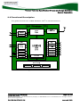
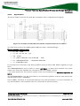
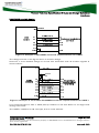
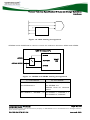
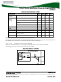
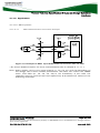
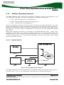
2.2 Functional Description
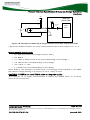
The global architecture of Q64 Wireless CPU® is described below:
Figure 1 : Functional architecture
© Confidential
Page: 17 / 116
This document is the sole and exclusive property of WAVECOM. Not to be distributed or divulged without
prior written agreement.
WA_DEV_Q64_PTS_001-003
January 9, 2009
Product Technical Specification & Customer Design Guidelines
General Description
2.2.1
RF Functionalities
The Radio Frequency (RF) range complies with the Phase II EGSM 900/DCS 1800 and
GSM 850/PCS 1900 recommendation. The frequencies are listed in the table below:
Transmit band (Tx)
Receive band (Rx)
GSM 850
824 to 849 MHz
869 to 894 MHz
E-GSM 900
880 to 915 MHz
925 to 960 MHz
DCS 1800
1710 to 1785 MHz
1805 to 1880 MHz
PCS 1900
1850 to 1910 MHz
1930 to 1990 MHz
The Q64 Wireless CPU® is designed to be used with Wavecom WMP100 Wireless
Microprocessor®. The Radio Frequency (RF) part is based on a specific quad-band
chip with a:
•
•
•
•
•
•
Digital low-IF receiver
Quad-band LNA (Low Noise Amplifier)
Offset PLL (Phase Locked Loop) transmitter
Frequency synthesizer
Digitally controlled crystal oscillator (DCXO)
Tx/Rx FEM ( Front-End Module) for quad-band GSM/GPRS
2.3 Operating System
The Q64 Wireless CPU® is designed to integrate various types of specific process
applications such as telemetry, multimedia, automotive known as vertical
applications.
The Operating System provides a set of AT commands to control the Wireless CPU®.
With this standard Operating System, some interfaces of the Wireless CPU® are not
available, since they are dependent on the peripheral devices connected to the
Wireless CPU®.
The Operating System is Open AT® compliant.
2.4 Software Description
The software package of Q64, Open AT® Software Suite v1.0 / v2.0, includes:
•
An Open AT® Firmware v6.5 which drives the Q64 and offer an AT command
interface over a serial port or USB.
•
An Open AT® Operating System (OS) v5.0 which runs various types of
applications (telemetry, multimedia, automotive…)
•
An Open AT® Integrated Development Environment (IDE) which builds and
debugs applications over the Open AT® Operating System
© Confidential
Page: 18 / 116
This document is the sole and exclusive property of WAVECOM. Not to be distributed or divulged without
prior written agreement.
WA_DEV_Q64_PTS_001-003
January 9, 2009
Product Technical Specification & Customer Design Guidelines
General Description
•
Several other Open AT® plug-in softwares are able to run over the Open AT®
Operating System.
•
A “GR plug-in” software that provides software compatibility with GR64
Wireless CPU®, in terms of AT commands and system operation. It is
specifically designed for GR64 Wireless CPU® compatibility.
© Confidential
Page: 19 / 116
This document is the sole and exclusive property of WAVECOM. Not to be distributed or divulged without
prior written agreement.
WA_DEV_Q64_PTS_001-003
January 9, 2009
Product Technical Specification & Customer Design Guidelines
Interfaces
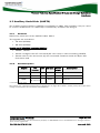
3 Interfaces
3.1 General Interfaces
Every hardware interface of the Q64 can be accessed with the Q64 development kit,
or GR64 Tina or UMA Board.
The available interfaces are described in the table below:
Chapter
Name
Driven by AT commands Driven by Open AT®
3.6
Main Serial Link
X
X
3.7
Auxiliary Serial Link
X
X
3.8
SIM Interface
X
X
3.9
General Purpose IO
X
X
3.5
Serial Interface (I2C Bus)
3.10
Analog to Digital Converter
X
X
3.12
PWM / Buzzer Output
X
X
3.13
Battery charging interface
X
X
3.17
VRTC (Backup Battery)
X
X
3.18
LED signal
X
X
3.19
Digital Audio Interface (PCM)
X
X
3.20
USB 2.0 Interface
X
X
© Confidential
X
Page: 20 / 116
This document is the sole and exclusive property of WAVECOM. Not to be distributed or divulged without
prior written agreement.
WA_DEV_Q64_PTS_001-003
January 9, 2009
Product Technical Specification & Customer Design Guidelines
Interfaces
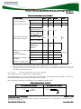
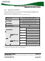
3.2 Power Supply
3.2.1
Power Supply Description
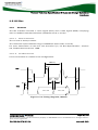
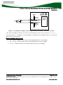
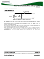
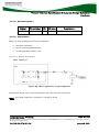
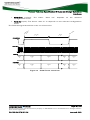
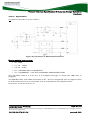
The power supply is one of the key issues in the design of a GSM terminal.
Due to the burst emission mode used in GSM/GPRS, the power supply should deliver
high current peaks in a short time. During the peaks, the ripple (Uripp) on the supply
voltage must not exceed a certain limit (see Table 1 Power supply voltage “Power
Supply Voltage”).
•
In communication mode, a GSM/GPRS class 2 terminal emits 577μs radio
bursts every 4.615ms (see Figure 2 below).
VCC
Uripp
Uripp
t = 577 μs
T = 4,615 ms
Figure 2: Power supply during burst emission
•
In communication mode, a GPRS class 10 terminal emits 1154 μs radio bursts
every 4.615 ms.
The VCC power supply input is only available for Q64 Wireless CPU®.
VCC:
•
Directly supplies the RF components with 3.6 V. It is essential to keep a
minimum voltage ripple at this connection in order to avoid any phase error.
The RF Power Amplifier current (1.5 A peak in GSM /GPRS mode) flows with a
ratio of:
o
1/8 of the time (around 577 μs every 4.615 ms for GSM /GPRS cl. 2) and
o
2/8 of the time (around 1154 μs every 4.615 ms for GSM /GPRS
cl. 10).
The rising time is around 10μs.
•
Is internally used to provide, via several regulators, the supply required for the
baseband signals.
© Confidential
Page: 21 / 116
This document is the sole and exclusive property of WAVECOM. Not to be distributed or divulged without
prior written agreement.
WA_DEV_Q64_PTS_001-003
January 9, 2009
Product Technical Specification & Customer Design Guidelines
Interfaces
3.2.2
Electrical Characteristics
Input power supply voltage
VCC1,2
VMIN
VNOM
VMAX
IMAX
Ripple max (Uripp)
3.2
3.6
4.8
1.8 A
10mV
Table 1 Power supply voltage
(1): This value must be guaranteed during the burst (with 1.5A Peak in GSM or GPRS mode)
(2): Maximum operating Voltage Stationary Wave Ratio (VSWR) 2:1
When powering the WMP100 with a battery, the total impedance (battery +
protections + PCB) should be <150 mΩ.
3.2.3
Power Supply Pin-out
Power supply pin-out
Signal
Pin number
VCC
1,3,5,7,9
GND
2,4,6,8,10,12
© Confidential
Page: 22 / 116
This document is the sole and exclusive property of WAVECOM. Not to be distributed or divulged without
prior written agreement.
WA_DEV_Q64_PTS_001-003
January 9, 2009
Product Technical Specification & Customer Design Guidelines
Interfaces
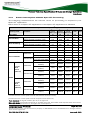
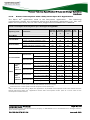
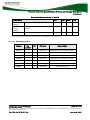
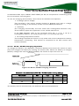
3.3 Power Consumption
Power consumption depends on the configuration. Therefore, the following
consumption values are given for each mode, RF band and type of software used
(with or without an Open AT® application).
Note: The following information is provided assuming a 50 Ω RF output.
The following consumption values were obtained by performing measurements on
Q64 samples at a temperature of 25° C.
Three VCC values are used to measure the consumption, VCCMIN (3.2V), VCCMAX (4.8V)
and VCCTYP (3.6V).
The average current is given for the three VCC values and the peak current given is
the maximum current peak measured with the three VCC voltages.
For more detailed descriptions of the operating modes, (refer to the document [4] AT
Command Interface Guide for Open AT® Firmware v6.5).
For more information about the consumption measurement procedure, refer to
section 4.
© Confidential
Page: 23 / 116
This document is the sole and exclusive property of WAVECOM. Not to be distributed or divulged without
prior written agreement.
WA_DEV_Q64_PTS_001-003
January 9, 2009
Product Technical Specification & Customer Design Guidelines
Interfaces
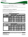
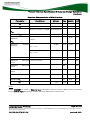
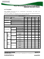
3.3.1
Power Consumption without Open AT® Processing
The following measurements are relevant when no processing is required by the
Open AT® application:
Either there is no Open AT® application or the Open AT® application is disabled
Power consumption without Open AT® application
IMIN
INOM
IMAX
average
average
average
VBATT=4,8V VBATT=3,6V VBATT=3,2V
IMAX
peak
unit
27
19
17
N/A
µA
Paging 9 (Rx burst occurrence ~2s)
16.4
17.6
18.5
160 RX
mA
Paging 2 (Rx burst occurrence ~0,5s)
17.8
19.2
20.1
160 RX
mA
Paging 9 (Rx burst occurrence ~2s)
2.7
2.6
2.6
160 RX
mA
Paging 2 (Rx burst occurrence ~0,5s)
5.3
5.4
5.6
160 RX
mA
Fast Standby Mode
32.1
38.1
42.4
80
mA
Slow Standby Mode
2.1
1.9
1.8
80
mA
PCL5 (TX power 33dBm)
206/206
215/214
221/219
1500
PCL19 (TX power 5dBm)
83/84
91/91
95/95
270
TX
mA
PCL0 (TX power 30dBm)
147/154
156/164
160/169
900
TX
mA
PCL15 (TX power 0dBm)
80/80
87/88
91/92
250
TX
mA
Gam.3 (TX power
33dBm)
197/197
206/205
211/210
1500
Gam.17 (TX power
5dBm)
79/80
86/87
90/91
270
TX
mA
Gam.3 (TX power
30dBm)
141/147
149/157
153/162
900
TX
mA
Gam.18 (TX power
0dBm)
76/76
83/83
87/87
250
TX
mA
Gam.3 (TX power
33dBm)
354/353
365/362
372/370
1500
Gam.17 (TX power
5dBm)
121/114
116/122
125/126
270
TX
mA
Gam.3 (TX power
30dBm)
238/250
248/264
253/271
900
TX
mA
Gam.18 (TX power
0dBm)
106/107
114/115
118/119
250
TX
mA
Operating mode
Parameters
Alarm Mode
Fast Idle Mode
Slow Idle Mode1
850/900 MHz
Connected Mode
1800/1900 MHz
Transfer
Mode
class 8
(4Rx/1Tx)
850/900 MHz
1800/1900 MHz
GPRS
Transfer
Mode
class 10
(3Rx/2Tx)
850/900 MHz
1800/1900 MHz
TX
means that the current peak is the RF transmission burst (Tx burst)
RX
means that the current peak is the RF reception burst (Rx burst)
1
TX
TX
TX
mA
mA
mA
Fast Idle Mode the signal of DTR1 (pin 37) is at high level.
2
Slow Idle Mode consumption depends on the SIM card used. Some SIM cards respond faster than others;
The longer the response time is, the higher the consumption is.
© Confidential
Page: 24 / 116
This document is the sole and exclusive property of WAVECOM. Not to be distributed or divulged without
prior written agreement.
WA_DEV_Q64_PTS_001-003
January 9, 2009
Product Technical Specification & Customer Design Guidelines
Interfaces
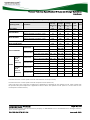
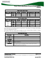
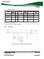
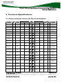
3.3.2
Power Consumption with a Dhrystone Open AT® Application
The Open AT® application used is the Dhrystone application.
The following
consumption results are measured during the Dhrystone application run. The two
tables are respectively for the CPU clock programmed at 26MHz and 104MHz.
Power consumption with Dhrystone Open AT® application@26MHz
Operating mode
IMIN
INOM
IMAX
average
average
average
VBATT=4,8 VBATT=3,6 VBATT=3,2
V
V
V
Parameters
Alarm Mode
IMAX
peak
unit
N/A
N/A
N/A
N/A
Paging 9 (Rx burst occurrence ~2s)
33
40
42
180 RX
mA
Paging 2 (Rx burst occurrence ~0,5s)
34
39
43
180 RX
mA
Paging 9 (Rx burst occurrence ~2s)
N/A
N/A
N/A
N/A
Paging 2 (Rx burst occurrence ~0,5s)
N/A
N/A
N/A
N/A
Fast Standby Mode
33
39
43
60
Slow Standby Mode
N/A
N/A
N/A
N/A
214 / 218
219 / 224
92 / 92
Fast Idle Mode
Slow Idle Mode1
850/900 MHz
Connected Mode
1800/1900 MHz
Transfer
Mode
class 8
850/900 MHz
(4Rx/1Tx)
1800/1900 MHz
Transfer
Mode
class 10
850/900 MHz
(3Rx/2Tx)
1800/1900 MHz
GPRS
PCL5 (TX power 33dBm) 202 / 208
TX
mA
96 / 96
270 TX
mA
157 / 164
161 / 170
260 TX
mA
88 / 89
92 / 93
230 TX
mA
195 / 208
215 / 214
87 / 88
91 / 92
150 / 157
154 / 163
84 / 84
Gam.3 (TX power 33dBm) 350 / 358
PCL19 (TX power 5dBm)
84 / 84
PCL0 (TX power 30dBm) 148 / 161
PCL15 (TX power 0dBm)
80 / 81
Gam.3 (TX power 33dBm) 195 / 181
Gam.17 (TX power 5dBm)
80 / 80
1440
mA
1420
TX
mA
240 TX
mA
930
TX
mA
87 / 88
210 TX
mA
361 / 369
368 / 378
1460 TX
mA
Gam.17 (TX power 5dBm) 116 / 115
119 / 123
126 / 127
270 TX
mA
Gam.3 (TX power 30dBm) 239 / 251
249 / 264
254 / 271
960 TX
mA
Gam.18 (TX power 0dBm) 106 / 109
115 / 116
119 / 120
260 TX
mA
Gam.3 (TX power 30dBm) 141 / 148
Gam.18 (TX power 0dBm)
76 / 77
TX
means that the current peak is the RF transmission burst (Tx burst)
RX
means that the current peak is the RF reception burst (Rx burst)
*N/A: It does not mean that no Open AT® application is possible in this specific mode. That means that the
specific Dhrystone Open AT® application cannot allow this specific mode. (This is a worst case for the
consumption measurement)
© Confidential
Page: 25 / 116
This document is the sole and exclusive property of WAVECOM. Not to be distributed or divulged without
prior written agreement.
WA_DEV_Q64_PTS_001-003
January 9, 2009
Product Technical Specification & Customer Design Guidelines
Interfaces
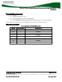
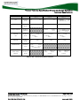
Power consumption with Dhrystone Open AT® application@104MHz
Operating mode
IMIN
INOM
IMAX
average
average
average
VBATT=4,8 VBATT=3,6 VBATT=3,2
V
V
V
Parameters
Alarm Mode
IMAX
peak
unit
N/A
N/A
N/A
N/A
Paging 9 (Rx burst occurrence ~2s)
73
89
96
240 RX
mA
Paging 2 (Rx burst occurrence ~0,5s)
72
88
96
240 RX
mA
Paging 9 (Rx burst occurrence ~2s)
N/A
N/A
N/A
N/A
Paging 2 (Rx burst occurrence ~0,5s)
N/A
N/A
N/A
N/A
Fast Standby Mode
63
80
86
110
Slow Standby Mode
N/A
N/A
N/A
N/A
PCL5 (TX power 33dBm) 233 / 236
252 / 256
262 / 267
PCL19 (TX power 5dBm) 112 / 113
130 / 130
139 / 140
320 TX
mA
PCL0 (TX power 30dBm) 176 / 183
195 / 202
205 / 209
990
TX
mA
PCL15 (TX power 0dBm) 109 / 109
126 / 127
135 / 136
280 TX
mA
Gam.3 (TX power 33dBm) 223 / 227
241 / 245
251 / 253
1540 TX
mA
Gam.17 (TX power 5dBm) 108 / 108
124 / 125
133 / 134
290 TX
mA
Gam.3 (TX power 30dBm) 169 / 175
187 / 194
196 / 204
260 TX
mA
Gam.18 (TX power 0dBm) 104 / 105
121 / 122
130 / 130
980 TX
mA
Gam.3 (TX power 33dBm) 378 / 385
398 / 408
410 / 419
1560 TX
mA
Gam.17 (TX power 5dBm) 141 / 143
159 / 160
168 / 169
320 TX
mA
Gam.3 (TX power 30dBm) 267 / 279
286 / 301
297 / 313
1000 TX
mA
Gam.18 (TX power 0dBm) 135 / 136
152 / 153
161 / 162
280 TX
mA
Fast Idle Mode
Slow Idle Mode1
850/900 MHz
Connected Mode
1800/1900 MHz
Transfer
Mode
class 8
850/900 MHz
(4Rx/1Tx)
1800/1900 MHz
Transfer
Mode
class 10
850/900 MHz
(3Rx/2Tx)
1800/1900 MHz
GPRS
TX
means that the current peak is the RF transmission burst (Tx burst)
RX
means that the current peak is the RF reception burst (Rx burst)
1550
mA
TX
mA
*N/A: That does not mean that no Open AT® application is possible in this specific mode. That means that
the specific Dhrystone Open AT® application cannot allow this specific mode. (This is a worst case for the
consumption measurement)
© Confidential
Page: 26 / 116
This document is the sole and exclusive property of WAVECOM. Not to be distributed or divulged without
prior written agreement.
WA_DEV_Q64_PTS_001-003
January 9, 2009
Product Technical Specification & Customer Design Guidelines
Interfaces
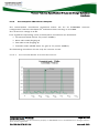
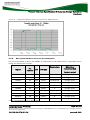
3.3.3
Consumption Waveform Samples
The consumption waveforms presented below are for an EGSM900 network
configuration without the Open AT® Software Suite running on the Q64.
The usual VCC voltage is 3.6V.
Four significant operating mode consumption waveforms are described:
¾
Connected Mode (PCL5: Tx power 33dBm)
¾
Slow Idle mode (Paging 9)
¾
Fast idle mode (Paging 9)
¾
Transfer mode (GPRS class 10, gam.3: Tx power 33dBm )
The following waveform shows only the current curves.
3.3.3.1
Connected Mode Current Waveform
© Confidential
Page: 27 / 116
This document is the sole and exclusive property of WAVECOM. Not to be distributed or divulged without
prior written agreement.
WA_DEV_Q64_PTS_001-003
January 9, 2009
Product Technical Specification & Customer Design Guidelines
Interfaces
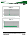
3.3.3.2
Slow Idle Mode Current Waveform
3.3.3.3
Fast Idle Mode Current Waveform
© Confidential
Page: 28 / 116
This document is the sole and exclusive property of WAVECOM. Not to be distributed or divulged without
prior written agreement.
WA_DEV_Q64_PTS_001-003
January 9, 2009
Product Technical Specification & Customer Design Guidelines
Interfaces
3.3.3.4
3.3.4
Transfer Mode Class 10 Current Waveform
Recommendations for Less Consumption
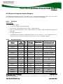
It is recommended to drive the GPIOs as indicated in the table below, especially when
using the quiescent current.
Reset state
Signal
Pin
number
I/O
I/O type
SW driver
recommended
(output state)
GPIO1
21
I/O
2V8-1
Z
0 logic level
GPIO2
22
I/O
2V8-1
Undefined
0 logic level
GPIO3
23
I/O
2V8-1
Undefined
0 logic level
GPIO4
24
I/O
2V8-1
Z
0 logic level
GPIO5
13
I/O
2V8-1
Z
0 logic level
GPIO6
33
I/O
2V8-1
Z
0 logic level
GPIO13
29
I/O
Pull-up
Pull-up*
0 logic level
GPIO14
30
I/O
Pull-up
Pull-up*
0 logic level
GPIO15
20
I/O
2V8-1
Z
0 logic level
GPIO16
35
I/O
2V8-1
Z
0 logic level
*GPIO13 and GPIO14 pull up are about 10K Ω.
© Confidential
Page: 29 / 116
This document is the sole and exclusive property of WAVECOM. Not to be distributed or divulged without
prior written agreement.
WA_DEV_Q64_PTS_001-003
January 9, 2009
Product Technical Specification & Customer Design Guidelines
Interfaces
See chapter 3.4, “Electrical Information for Digital I/O” on page 30 for 2V8-1, 2V8-2, pull-up and open drain
voltage characteristics and for Reset state definition.
If the LED is not necessary, it is possible to disable it.
For further details, refer to document [4] AT Command Interface Guide for Open
AT® Firmware v6.5.
3.4 Electrical Information for Digital I/O
There are three types of digital I/O on the Q64: 2.8 volt CMOS type 1 (2V8-1), 2.8 volt
CMOS type 2 (2V8-2) and Open drain.
The I/O concerned is all interfaces like GPIOs, PCM, etc.
The three types are described below:
Electrical characteristics of digital I/O
2.8 Volts type 1 (2V8-1 )
Parameter
I/O type
Minim.
Typ
Maxim.
Internal 2.8V power supply VCC_2V8
2.74V
2.8V
2.86V
Input / Output pin
VIL
CMOS
-0.5V*
0.84V
VIH
CMOS
1.96V
3.2V*
VOL
CMOS
VOH
CMOS
0.4V
2.4V
Condition
IOL = - 4 mA
IOH = 4 mA
IOH
4mA
IOL
- 4mA
*Absolute maximum ratings
2.8 Volts type 2 (2V8-2 )
Parameter
Input / Output pin
I/O type
Minim.
Typ
Maxim.
VIL
CMOS
-0.3V*
0.15V
VIH
CMOS
1.6V
3.1V*
VOL
CMOS
VOH
CMOS
0.4V
1.87V
Condition
IOL = - 4 mA
IOH = 4 mA
IOH
4mA
IOL
- 4mA
*Absolute maximum ratings
© Confidential
Page: 30 / 116
This document is the sole and exclusive property of WAVECOM. Not to be distributed or divulged without
prior written agreement.
WA_DEV_Q64_PTS_001-003
January 9, 2009
Product Technical Specification & Customer Design Guidelines
Interfaces
Open drain outputs type
Signal name Parameter
BUZZER
I/O type
Minimum
Typ
Maximum
VOL
Open Drain
0.4V
IOL
Open Drain
100mA
Condition
Pull-up outputs type
Signal name Parameter
SDA /
GPIO13
and
SCL /
GPIO14
I/O type
Minimum
Typ
Maximum
VIH
Pull-up
2V
VIL
Pull-up
0.8V
VOL
Pull-up
0.4V
IOL
Pull-up
3mA
Condition
SDA and SCL are internally pulled up with each 1 kΩ resistor to voltage 2.8V (VREF)
inside the Q64 Wireless CPU®.
The reset states for each I/O are given in the corresponding interface chapter
descriptions. The state definitions are defined below:
Reset state definition
Parameter
Definition
0
Set to GND
1
Set to supply 2V8
Pull down
Pull up
Internal pull down with ~60K resistor.
Internal pull up with ~60K resistor to supply 2V8.
Z
High impedance
Undefined
Be careful, undefined should not be used in your application
if a special state is needed at reset. Those pins can be
toggling signals during reset.
© Confidential
Page: 31 / 116
This document is the sole and exclusive property of WAVECOM. Not to be distributed or divulged without
prior written agreement.
WA_DEV_Q64_PTS_001-003
January 9, 2009
Product Technical Specification & Customer Design Guidelines
Interfaces
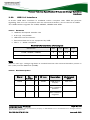
3.5 I2C Bus
3.5.1
Features
The I2C interface includes a clock signal (SCL) and a data signal (SDA) complying
with a 100Kbit/s-standard interface (standard mode: s-mode).
3.5.1.1
Characteristics
The I²C bus is always master.
The maximum speed transfer range is 400Kbit/s (Fast mode: f-mode).
For more information on the bus, see document [7] “I²C Bus Specification”, Version
2.0, Philips Semiconductor 1998.
3.5.1.2
I²C Waveforms
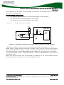
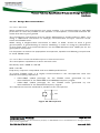
I²C bus waveform in master mode configuration:
SCL-freq
T-high
SCL
T-start
T-data-
T-data-
hold
setup
T-stop
T-free
SDA
Data valid
Data valid
Figure 3: I²C Timing diagrams, Master
© Confidential
Page: 32 / 116
This document is the sole and exclusive property of WAVECOM. Not to be distributed or divulged without
prior written agreement.
WA_DEV_Q64_PTS_001-003
January 9, 2009
Product Technical Specification & Customer Design Guidelines
Interfaces
AC characteristics
Signal
Description
SCL-freq
I²C clock frequency
100
T-start
Hold time START condition
0.6
μs
T-stop
Setup time STOP condition
0.6
μs
T-free
Bus free time, STOP to START
1.3
μs
T-high
High period for clock
0.6
μs
T-data-hold
Data hold time
0
T-data-setup
Data setup time
100
3.5.2
Minimum Typ Maximum Unit
400
0.9
KHz
μs
ns
Pin Description
Signal
Pin
number
I/O
I/O type
Reset state
Description Multiplexed
with
SDA
29
I/O
Pull-up
Pull-up*
Serial Data
GPIO13
SCL
30
O
Pull-up
Pull-up*
Serial
Clock
GPIO14
*SDA and SCL pull-up are about 10K Ω
See chapter 3.4, “Electrical Information for Digital I/O” on page 30 for 2V8-1, 2V8-2, pull-up and open drain
voltage characteristics and for Reset state definition.
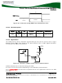
The two lines are internally pulled up with each 1 KΩ resistor to voltage 2.8V (VREF)
inside the Q64 Wireless CPU®.
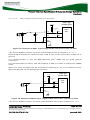
2.8V
1K
Q64
1K
SCL
Customer
application
SDA
Figure 4: I²C bus configuration inside the Wireless CPU®
The I²C bus is compliant with the Standard mode (baud rate 100Kbit/s) and the Fast
mode (baud rate 400Kbit/s).
© Confidential
Page: 33 / 116
This document is the sole and exclusive property of WAVECOM. Not to be distributed or divulged without
prior written agreement.
WA_DEV_Q64_PTS_001-003
January 9, 2009
Product Technical Specification & Customer Design Guidelines
Interfaces
3.6 Main Serial Link (UART1)
A flexible 8-wire serial interface is available, compliant with V24 protocol signaling,
but not with V28 (electrical interface) due to a 2.8 volts interface.
3.6.1
Features
The maximum baud rate of the UART1 is 921 Kbit/s.
The signals are as follows:
•
TX data (DTM1)
•
RX data (DFM1)
•
Request To Send (RTS1)
•
Clear To Send (CTS1)
•
Data Terminal Ready (DTR1)
•
Data Set Ready (DSR1)
•
Data Carrier Detect (DCD1)
•
Ring Indicator (RI).
3.6.2
Pin Description
Signal
Pin
number
I/O
I/O
type
Reset
state
Description
Multiplexed
with
DTM1*
41
I
2V8-1
Z
Transmit serial
data
GPIO18
DFM1*
42
O
2V8-1
1
Receive serial
data
GPIO17
RTS1*
39
I
2V8-1
Z
Request To
Send
CTS1*
40
O
2V8-1
Z
Clear To Send
DSR1*
32
O
2V8-1
Z
Data Set Ready
DTR1*
37
I
2V8-1
Z
Data Terminal
Ready
DCD1*
38
O
2V8-1
Undefined Data Carrier
Detect
RI*
36
O
2V8-1
Undefined Ring Indicator
GND
2, 4, 6, 8,
10, 12
GND
GPIO9
GPIO12
GPIO7
GPIO10
GPIO11
GPIO8
Ground
See chapter 3.4, “Electrical Information for Digital I/O” on page 30 for 2V8-1, 2V8-2, pull-up and open drain
voltage characteristics and for Reset state definition.
*According to PC view
© Confidential
Page: 34 / 116
This document is the sole and exclusive property of WAVECOM. Not to be distributed or divulged without
prior written agreement.
WA_DEV_Q64_PTS_001-003
January 9, 2009
Product Technical Specification & Customer Design Guidelines
Interfaces
With the Open AT® Software Suite 1.0 / V2.0 when the UART1 service is run the
multiplexed signals are unavailable for other purposes. Likewise, if one or more
GPIOs (of this table) are allocated the UART1 service is unavailable.
The rising time and falling time of the reception signals (mainly DTM1) must be
shorter than 300 ns.
Recommendation:
The Q64 is designed to operate with all serial interface signals. It is mandatory to use
RTS1 and CTS1 for hardware flow control in order to avoid data corruption during
transmission.
5-wire serial interface hardware design:
•
Signal: DTM1*, DFM1*, RTS1*, CTS1*
•
The signal DTR1* must be managed following the V24 protocol signalling if we
want to use the slow idle mode
•
Please refer to the document [4] AT Command Interface Guide for Open AT®
Firmware v6.5 for more information.
4-wire serial interface hardware design:
•
DTM1*, DFM1*, RTS1*, CTS1*
•
The signal DTR1* must be configured at the low level.
•
Please refer to the document [4] AT Command Interface Guide for Open AT®
Firmware v6.5 for more information.
2-wire serial interface hardware design:
•
It is possible for connected external chip but not recommended (and forbidden
for AT command or modem use)
•
The flow control mechanism must be managed by the customer.
•
DTM1*, DFM1*
•
The signal DTR1* must be configured at the low level.
•
The signals RTS1*, CTS1* are not used, please configure the AT command
(AT+IFC=0,0 see document [4] AT Command Interface Guide for Open AT®
Firmware v6.5).
•
The signal RTS1* must be configured at the low level.
•
Please refer to the document [4] AT Command Interface Guide for Open AT®
Firmware v6.5 for more information.
© Confidential
Page: 35 / 116
This document is the sole and exclusive property of WAVECOM. Not to be distributed or divulged without
prior written agreement.
WA_DEV_Q64_PTS_001-003
January 9, 2009
Product Technical Specification & Customer Design Guidelines
Interfaces
3.6.3
Application
The level shifter must be set at 2.8V compliant with a V28 electrical signal.
Figure 5: Example of RS-232 level shifter implementation for UART1
U1 chip also protects the Q64 against ESD at 15KV. (Air Discharge).
Recommended components:
R1, R2 : 15KΩ
C1, C2, C3, C4, C5 : 1uF
C6 : 100nF
C7 : 6.8uF TANTAL 10V CP32136
U1 : ADM3307EACP
J1 : SUB-D9 female
AVX
ANALOG DEVICES
R1 and R2 are necessary only during Reset state to lift RI and DCD1 signals to high
level.
The ADM3307EACP chip is able to reach 921Kb/s*. If other level shifters are used,
make sure that their speeds are compliant with the UART1 speed.
*: For this baud rate, the power supply must be provided by an external regulator at
3.0 V.
The ADM3307EACP can be powered by an external regulator at 2.8 V (the baud rate
will be limited up to 720kbps).
If the UART1 interface is connected directly to a host processor, it is not necessary to
use level shifters. The interface can be connected as shown below:
© Confidential
Page: 36 / 116
This document is the sole and exclusive property of WAVECOM. Not to be distributed or divulged without
prior written agreement.
WA_DEV_Q64_PTS_001-003
January 9, 2009
Product Technical Specification & Customer Design Guidelines
Interfaces
V24/CMOS possible design:
Figure 6: Example of V24/CMOS serial link implementation for UART1
The design shown in the figure above is a basic design.
However, a more flexible design to access this serial link with all modem signals is
shown below:
Figure 7: Example of full modem V24/CMOS serial link implementation for UART1
It is recommended to add a 15KΩ pull-up resistor on RI and DCD1 to set high level
during reset state.
The UART1 interface is 2.8 volt type, but is 3 volt tolerant.
© Confidential
Page: 37 / 116
This document is the sole and exclusive property of WAVECOM. Not to be distributed or divulged without
prior written agreement.
WA_DEV_Q64_PTS_001-003
January 9, 2009
Product Technical Specification & Customer Design Guidelines
Interfaces
The Q64 UART1 is designed to operate with all serial interface signals. It is
mandatory to use RTS1 and CTS1 for hardware flow control in order to avoid data
corruption during transmission.
Warning: If you want to activate Power down mode (Wavecom 32K mode) in your
®
Open AT application, you need to connect the DTR1 to a GPIO. Please refer to the
document [4] AT Command Interface Guide for Open AT® Firmware v6.5 (see the
“Appendixes”) for more information on Wavecom 32K mode activation using the
®
Open AT Software Suite.
© Confidential
Page: 38 / 116
This document is the sole and exclusive property of WAVECOM. Not to be distributed or divulged without
prior written agreement.
WA_DEV_Q64_PTS_001-003
January 9, 2009
Product Technical Specification & Customer Design Guidelines
Interfaces
3.7 Auxiliary Serial Link (UART2)
An auxiliary serial interface (UART2) is available on Q64. This interface may be used
to connect a Bluetooth or a GPS chip controlled by an Open AT® Plug-in.
3.7.1
Features
Maximum baud rate of the UART2 is 921 Kbit/s.
The signals are as follows:
•
TX data (DTM3)
•
RX data (DFM3)
2-wire serial interface hardware design:
•
DTM3*, DFM3*
•
Please configure the AT command (AT+IFC=0,0) to start accessing UART2.
•
Please refer to the document [4] AT Command Interface Guide for Open AT®
Firmware v6.5.
3.7.2
Pin Description
Signal
Pin
I/O
I/O type
Reset
state
Description
DTM3*
43
I
2V8-2
Z
Transmit serial data
DFM3*
44
O
2V8-2
Z
Receive serial data
GND*
2, 4, 6,
8, 10, 12
number
GND
Ground
* According to PC view
See chapter 3.4, “Electrical Information for Digital I/O” on page 30 for 2V8-1, 2V8-2, pull-up and open drain
voltage characteristics and for Reset state definition.
© Confidential
Page: 39 / 116
This document is the sole and exclusive property of WAVECOM. Not to be distributed or divulged without
prior written agreement.
WA_DEV_Q64_PTS_001-003
January 9, 2009
Product Technical Specification & Customer Design Guidelines
Interfaces
3.7.3
Application
The voltage level shifter must be set at 2.8V and compliant with a V28 electrical
signal.
Figure 8: Example of RS-232 level shifter implementation for UART2
Recommended components:
Capacitors
C1 : 220nF
C2, C3, C4 : 1μF
Inductor
L1 : 10μH
RS-232 Transceiver
U1 : LINEAR TECHNOLOGY LTC2802IDE
J1 : SUB-D9 female
The LTC2802 can be powered by an external regulator at 2.8 V.
The UART2 interface can be connected directly to others components if the voltage
interface is 2.8 V.
© Confidential
Page: 40 / 116
This document is the sole and exclusive property of WAVECOM. Not to be distributed or divulged without
prior written agreement.
WA_DEV_Q64_PTS_001-003
January 9, 2009
Product Technical Specification & Customer Design Guidelines
Interfaces
3.8 SIM Interface
The Subscriber Identification Module can be directly connected to the Q64 through
this dedicated interface.
3.8.1
Features
The SIM interface controls the 1.8V and 3V SIM cards.
It is recommended to add Transient Voltage Suppressor diodes (TVS) on the signal
connected to the SIM socket in order to prevent any Electrostatic Discharge.
TVS diodes with low capacitance (less than 10 pF) must be connected on SIMCLK
and SIMDAT signals to avoid any disturbance during the rising and falling edges.
These types of diodes are mandatory for the Full Type Approval. They shall be placed
close to the SIM socket.
The following references can be used: DALC208SC6 from ST Microelectronics.
5 signals exist:
•
•
•
•
•
SIMVCC: SIM power supply.
SIMRST: reset.
SIMCLK: clock.
SIMDAT: I/O port.
SIMDET: SIM card detect.
The SIM interface controls a 3V / 1V8 SIM. This interface is fully compliant with GSM
11.11 recommendations concerning SIM functions.
© Confidential
Page: 41 / 116
This document is the sole and exclusive property of WAVECOM. Not to be distributed or divulged without
prior written agreement.
WA_DEV_Q64_PTS_001-003
January 9, 2009
Product Technical Specification & Customer Design Guidelines
Interfaces
Electrical Characteristics of SIM interface
Parameter
Conditions
Minim.
SIMDAT VIH
IIH = ± 20μA
SIMDAT VIL
IIL = 1mA
SIMRST, SIMCLK
Source current = 20μA
0.9xSIMVCC
SIMDAT VOH
Source current = 20μA
0.8xSIMVCC
SIMRST,
SIMCLK
Sink current =
Typ
Maxim. Unit
0.7xSIMVCC
V
0.4
V
V
VOH
SIMDAT,
0.4
V
-200μA
VOL
SIMVCC
Voltage
Output
SIMVCC = 2.9V
2.84
2.9
2.96
V
1.74
1.8
1.86
V
10
mA
IVCC= 1mA
SIMVCC = 1.8V
IVCC= 1mA
SIMVCC current
VCC = 3.6V
SIMCLK
Time
Rise/Fall
Loaded with 30pF
20
ns
SIMRST,
Time
Rise/Fall
Loaded with 30pF
20
ns
SIMDAT
Time
Rise/Fall
Loaded with 30pF
0.7
SIMCLK Frequency
Loaded with 30pF
SIMDET VIL
0
SIMDET VIH
1.5
1.8
1
μs
3.25
MH
z
0.5
V
V
Note:
When SIMDET is used, a high to low transition means that the SIM card is inserted
and a low to high transition means that the SIM card is removed.
© Confidential
Page: 42 / 116
This document is the sole and exclusive property of WAVECOM. Not to be distributed or divulged without
prior written agreement.
WA_DEV_Q64_PTS_001-003
January 9, 2009
Product Technical Specification & Customer Design Guidelines
Interfaces
3.8.2
Pin Description
Signal
Pin
number
I/O
I/O type
Reset
state
Description
Multiplexed
with
SIMCLK
19
O
2V9 / 1V8
0
SIM Clock
Not mux
SIMRST
17
O
2V9 / 1V8
0
SIM Reset
Not mux
SIMDAT
18
I/O
2V9 / 1V8
Pull up*
SIM Data
Not mux
SIMVCC
15
O
2V9 / 1V8
-
SIM Power
Supply
Not mux
SIMDET
16
I
1V8
Pull-up#
SIM Card
Detect
Not mux
*SIMDAT pull-up is about 10K Ω
#SIMDET pull-up is about 100 K Ω.
See chapter 3.4, “Electrical Information for Digital I/O” on page 30 for 2V8-1, 2V8-2, pull-up and open drain
voltage characteristics and for Reset state definition.
3.8.3
Application
Figure 9: Example of SIM Socket implementation
© Confidential
Page: 43 / 116
This document is the sole and exclusive property of WAVECOM. Not to be distributed or divulged without
prior written agreement.
WA_DEV_Q64_PTS_001-003
January 9, 2009
Product Technical Specification & Customer Design Guidelines
Interfaces
Recommended components:
•
C1 : 100nF
•
D1 : ESDA6V1SC6 from ST
•
D2 : DALC208SC6 from SGS-THOMSON
•
J1 : ITT CANNON CCM03 series (See chapter 9.2 for more information)
The capacitor (C1) placed on the SIMVCC line must not exceed 330 nF.
SIM socket connection:
Pin description of the SIM socket
Signal
Pin number
Description
VCC
1
SIMVCC
RST
2
SIMRST
CLK
3
SIMCLK
CC4
4
SIMDET
GND
5
GROUND
VPP
6
Not connected
I/O
7
SIMDAT
CC8
8
GND
© Confidential
Page: 44 / 116
This document is the sole and exclusive property of WAVECOM. Not to be distributed or divulged without
prior written agreement.
WA_DEV_Q64_PTS_001-003
January 9, 2009
Product Technical Specification & Customer Design Guidelines
Interfaces
3.9 General Purpose Input/Output
The Wireless Microprocessor® provides up to 18 General Purpose I/O. They are used
to control any external device such as a LCD, a Keyboard backlight.
3.9.1
Features
Reset State:
0 : Set to GND
1: Set to supply 2V8 depending.
Pull down: Internal pull down with ~60K resistor.
Pull up: Internal pull up with ~60K resistor to supply 1V8 or 2V8 depending on
I/O type.
Z: High impedance.
Undefined: Be careful, undefined must not be used in your application if a
special state at reset is needed. Those pins can be toggling signals.
3.9.2
Pin Description
Signal
Pin
number
I/O
I/O type
GPIO1
21
I/O
2V8-1
Z
NOT MUX
GPIO2
22
I/O
2V8-1
Undefined
NOT MUX
GPIO3
23
I/O
2V8-1
Undefined
NOT MUX
GPIO4
24
I/O
2V8-1
Z
NOT MUX
GPIO5
13
I/O
2V8-1
Z
ADIN4 / GPIO5
GPIO6
33
I/O
2V8-1
Z
LED
GPIO7
32
I/O
2V8-1
Z
DSR1
GPIO8
36
I/O
2V8-1
Pull up
RI
GPIO9
39
I/O
2V8-1
Z
RTS1
GPIO10
37
I/O
2V8-1
Z
DTR1
GPIO11
38
I/O
2V8-1
Undefined
DCD1
GPIO12
40
I/O
2V8-1
Z
CTS1
GPIO13
29
I/O
Pull-up
Pull up*
SDA
GPIO14
30
I/O
Pull-up
Pull up*
SCL
GPIO15
20
I/O
2V8-1
Z
NOT MUX
© Confidential
Reset state
Multiplexed with
Page: 45 / 116
This document is the sole and exclusive property of WAVECOM. Not to be distributed or divulged without
prior written agreement.
WA_DEV_Q64_PTS_001-003
January 9, 2009
Product Technical Specification & Customer Design Guidelines
Interfaces
Signal
Pin
number
I/O
I/O type
Reset state
GPIO16
35
I/O
2V8-1
Z
NOT MUX
GPIO17
42
I/O
2V8-1
1
DFM1
GPIO18
41
I/O
2V8-1
Z
DTM1
Multiplexed with
*GPIO13 and GPIO14 pull-up are 1K Ω.
See chapter 3.4, “Electrical Information for Digital I/O” on page 30 for 2V8-1, 2V8-2, pull-up and open drain
voltage characteristics and for Reset state definition.
© Confidential
Page: 46 / 116
This document is the sole and exclusive property of WAVECOM. Not to be distributed or divulged without
prior written agreement.
WA_DEV_Q64_PTS_001-003
January 9, 2009
Product Technical Specification & Customer Design Guidelines
Interfaces
3.10
Analog to Digital Converter
Three Analog to Digital Converters inputs are provided by the Q64. Those converters
are 10 bits resolution, ranging from 0 to 2V.
3.10.1 Features
ADIN1/BAT-TEMP input can be used, typically, to monitor external temperature,
useful for safety power off in case of application over heating (for Li-Ion battery). This
input can also be used for customer application.
ADIN2, ADIN3 and ADIN4 input can be used for customer application
Electrical Characteristics of ADC
Parameter
Min
Resolution
Sampling rate
Input signal range
Vref (DC Reference level)
Typ
Unit
10
bits
216
S/s
0
1.15
Max
1.20
2
V
1.25
V
Integral Accuracy
15
mV
Differential Accuracy
2.5
mV
ADIN1
1M
Ω
ADIN2
1M
Ω
ADIN3
1M
Ω
ADIN4
1M
Ω
Input
impedance
to Vref.
Remark
Multiplexed
Note that ADIN3 and ADIN 4 are multiplexed. Only one of them is available at a time.
Depending if GR Plug-in is used, the AT commands to control ADC are different.
In Q64 with GR 64 plug-in, all ADIN inputs can be directly accessed through GR AT
command, “AT*EADCREAD”.
If without GR Plug-in, “AT+ADC” is used for accessing the ADIN1 and ADIN2 directly.
For ADIN3 and ADIN4, they need to be selected which to be accessed by another AT
command, “AT+WIOM”, before accessing their ADC return values. The ADC sharing
arrangement and the selection process are shown in Figure 10 and Figure 11 below:
© Confidential
Page: 47 / 116
This document is the sole and exclusive property of WAVECOM. Not to be distributed or divulged without
prior written agreement.
WA_DEV_Q64_PTS_001-003
January 9, 2009
Product Technical Specification & Customer Design Guidelines
Interfaces
Figure 10: ADC sharing arrangement
GPIO29 inside WMP100 is used to control the selection between ADIN and ADIN4.
Q64 Wireless CPU®
GPIO29
ADIN3
0
AUX-ADC1
WMP
100
1
ADIN4/ GPIO5
GPIO23
Figure 11: ADIN3 and ADIN4 sharing arrangement
To read ADIN3
To read ADIN4
Set GPIO29 as output
Set GPIO29 as output
Set GPIO29 as 0
Set GPIO29 as 1
GPIO23 must be released
before
AT+WIOM=1,”GPIO29”,1,0 AT+WIOM=1,”GPIO29”,1,1
AT+WIOM=0,”GPIO23”
© Confidential
Page: 48 / 116
This document is the sole and exclusive property of WAVECOM. Not to be distributed or divulged without
prior written agreement.
WA_DEV_Q64_PTS_001-003
January 9, 2009
Product Technical Specification & Customer Design Guidelines
Interfaces
Please refer to the following documents for the details of controlling the ADC access:
•
[9]
•
[4] AT Command Interface Guide for Open AT® Firmware v6.5
[5] Q64 software user guide
[6] AT Command Manual for GR64 and GS64 Wireless CPU®
3.10.2 Pin Description
Signal
Pin number
I/O
I/O type
Description
ADIN1*
26
I
Analog
A/D converter
ADIN2
27
I
Analog
A/D converter
ADIN3
28
I
Analog
A/D converter
ADIN4 / GPIO5
13
I or
I/O
Analog or
2V8-1
A/D converter or
GPIO5
*This input can be used for battery charging temperature sensor, see chapter “3.13 Battery Charging
interface “.
3.10.3 Application
The ADIN1/BAT-TEMP input is used for battery monitoring during charging of battery.
All information is provided in the “Battery Charging” (see chapter 3.13).
© Confidential
Page: 49 / 116
This document is the sole and exclusive property of WAVECOM. Not to be distributed or divulged without
prior written agreement.
WA_DEV_Q64_PTS_001-003
January 9, 2009
Product Technical Specification & Customer Design Guidelines
Interfaces
3.11
Analogue Audio Interface
Two different microphone inputs and two different speaker outputs are supported.
Audio 1 (MIC and EAR) is designed for handset type application and auxiliary audio is
designed for car-kit type application.
The Q64 also includes an echo cancellation feature which allows hands-free function.
In some cases, ESD protection must be added on the audio interface lines.
3.11.1 Microphone Features
Audio 1 can be configured in differential or single ended, while auxiliary audio can
only be configured in single ended.
In audio 1, the connection can be either differential or single-ended but using a
differential connection in order to reject common mode noise and TDMA noise is
strongly recommended. Either in audio 1 or auxiliary audio, when using a singleended connection, make sure to have a very good ground plane, a very good filtering
as well as shielding in order to avoid any disturbance on the audio path. It is
recommended to use the Q64 Wireless CPU® AREF pin for the good plane connection.
The gain of MIC inputs is internally adjusted and can be tuned using an AT
command.
3.11.1.1 Electrical Characteristics
3.11.1.1.1
MIC1 Microphone Inputs
By default, the MIC1 inputs are differential ones, but they can be configured in single
ended mode. They already include the convenient biasing for an electret microphone.
The electret microphone can be directly connected on those inputs, thus allowing
easy connection to a handset.
AC coupling is already embedded in the Wireless CPU®.
Equivalent circuits of MIC1
DC equivalent circuit
MIC1P
R
MIC1N
R
MIC1+
GND
© Confidential
AC equivalent circuit
MIC1P
MIC1N
Z1
Z1
GND
Page: 50 / 116
This document is the sole and exclusive property of WAVECOM. Not to be distributed or divulged without
prior written agreement.
WA_DEV_Q64_PTS_001-003
January 9, 2009
Product Technical Specification & Customer Design Guidelines
Interfaces
Electrical characteristics of MIC1
Parameters
Internal biasing
DC Characteristics
MIC1+
R2
Z1 MIC1N
(MIC1P=Open)
200 Hz<F<4 kHz
Typ
Max
Unit
2
2.1
2.2
V
0.5
1.5
mA
1650
1900
2150
Ω
1.1
1.3
1.6
0.9
1.1
1.4
1.3
1.6
2
Output current
Z1 MIC1P
(MIC1N=Open)
AC Characteristics
Min
Z1 MIC1P
(MIC1N=GND)
Z1 MIC1N
(MIC1P=GND)
Impedance
between
MIC1P and
MIC1N
Maximum working
voltage
AT+VGT*=2
13.8
AT+VGT*=1
77.5
( MIC1P-MIC1N)
AT+VGT*=0
346
Maximum rating
voltage
Positive
(MIC1P or MIC1N)
Negative
KΩ
mVrms
+7.35**
V
-0.9
•
*The input voltage depends on the input microphone gain set by AT command. Please refer to the
document [4] AT Command Interface Guide for Open AT® Firmware v6.5
•
**Because MIC1P is internally biased, it is necessary to use a coupling capacitor to connect an
audio signal provided by an active generator. Only a passive microphone can be directly connected
to the MIC1P and MIC1N inputs.
3.11.1.1.2
Auxiliary Microphone Inputs (AUXI)
The AUXI input is configured in single-ended.
The AUXI input does not include an internal bias. The AUXI input needs to have an
external biasing if an electret microphone is used.
AC coupling is already embedded in the Q64 Wireless CPU®.
Equivalent circuits of AUXI
DC equivalent circuit
AUXI
DC
Blocked
AC equivalent circuit
AUXI
Z2
GND
© Confidential
Page: 51 / 116
This document is the sole and exclusive property of WAVECOM. Not to be distributed or divulged without
prior written agreement.
WA_DEV_Q64_PTS_001-003
January 9, 2009
Product Technical Specification & Customer Design Guidelines
Interfaces
The AUXI input is a passive network applying –14dB gain followed by the transmit
part of the CODEC.
Figure 12: Auxiliary input connection to Q64 Wireless CPU®
Electrical Characteristics of AUXI
Parameters
Min
DC Characteristics
AC Characteristics
200 Hz<F<4 kHz
Maximum working
voltage
Maximum rating
voltage
Max
0
Unit
V
Z2
60
KΩ
AT+VGT*=2
40
mVrms
AT+VGT*=1
190
AT+VGT*=0
850
Positive
Negative
•
Typ
+12
-2
V
V
*The input voltage depends on the input microphone gain set by AT command. Please refer to the
document [4] AT Command Interface Guide for Open AT® Firmware v6.5.
© Confidential
Page: 52 / 116
This document is the sole and exclusive property of WAVECOM. Not to be distributed or divulged without
prior written agreement.
WA_DEV_Q64_PTS_001-003
January 9, 2009
Product Technical Specification & Customer Design Guidelines
Interfaces
3.11.2 Speaker Features
The connection is single-ended on AUXO and is differential on EAR. Using a
differential connection to reject common mode noise and TDMA noise is strongly
recommended. Moreover in single-ended mode, ½ of the power is lost. When using a
single-ended connection, make sure to have a very good ground plane, a very good
filtering as well as shielding in order to avoid any disturbance on the audio path. It is
recommended to use the Q64 Wireless CPU® AREF pin for good plane connection.
Parameter
Typ
Unit
Connection
Z (EARP, EARN)
4
Ω
single-ended mode
Z (EARP, EARN)
8
Ω
Differential mode
16 or 32
Ω
single-ended mode
Z (AUXO)
3.11.2.1 Speakers Outputs Power
Both speakers maximum power output are not similar, due to the different
configuration between the AUXO which is only single-ended and the EAR which can
be differential, so EAR provides more power.
The maximal specifications given below are available with the maximum power
output configuration values set by an AT command. The default values are
recommended.
3.11.2.1.1
Speaker Outputs
The EAR interface allows differential and single-ended earpiece connection.
Equivalent circuits of SPK1
Q64
+
SPK
© Confidential
1Ω
EARN
1Ω
EARP
Page: 53 / 116
This document is the sole and exclusive property of WAVECOM. Not to be distributed or divulged without
prior written agreement.
WA_DEV_Q64_PTS_001-003
January 9, 2009
Product Technical Specification & Customer Design Guidelines
Interfaces
Electrical characteristics of EAR
Parameters
Min
Typ
Max
Unit
Biasing
voltage
EARP and EARN
1.30
Output
swing
voltage
RL=8Ω: AT+VGR=6*; single ended -
-
2
Vpp
RL=8Ω: AT+VGR=6*; differential
-
-
4
Vpp
single -
-
2.5
Vpp
RL=32Ω:
ended
AT+VGR=6*;
V
RL=32Ω: AT+VGR=6*; differential
-
-
5
Vpp
RL
Load resistance
6
8
-
Ω
IOUT
Output current; peak value; RL=8Ω -
-
180
mA
POUT
RL=8Ω; AT+VGR=6*;
-
250
mW
RPD
Output pull-down
power-down
40
52
KΩ
VPD
Output DC voltage at power-down -
-
100
mV
resistance
at 28
*The output voltage depends on the output speaker gain set by AT command. Please refer to the document
[4] AT Command Interface Guide for Open AT® Firmware v6.5.
If a singled-ended solution is used with the earpiece output, only one of the EAR must
be chosen. The result is a maximal output power divided by 2.
3.11.2.1.2
Auxiliary Audio Output (AUXO)
With the AUXO interface, only single-ended speaker connection is allowed.
A filtering circuitry is already built inside the Q64.
Equivalent circuits of AUXO
© Confidential
Page: 54 / 116
This document is the sole and exclusive property of WAVECOM. Not to be distributed or divulged without
prior written agreement.
WA_DEV_Q64_PTS_001-003
January 9, 2009
Product Technical Specification & Customer Design Guidelines
Interfaces
Electrical characteristics of AUXO
Parameters
Biasing
voltage
Through coupling capacitor
Output
swing
voltage
RL=2kΩ;
ended
RL
Load resistance
AT+VGR=6;
Min
Typ
Max
Unit
-
-
-
V
1.9
TBC
Vpp
-
-
KΩ
single- -
2
*The output voltage depends on the output speaker gain set by AT command. Please refer to the
document [4] AT Command Interface Guide for Open AT® Firmware v6.5.
3.11.3 Pin Description
Signal
Pin
number
I/O
I/O type
Description
MIC1P
53
I
Analog
Microphone 1 positive input
MIC1N
54
I
Analog
Microphone 1 negative input
AUXI
57
I
Analog
Auxiliary audio input
EARP
55
O
Analog
Earpiece 1 positive output
EARN
56
O
Analog
Earpiece 1 negative output
AUXO
59
O
Analog
Auxiliary audio output
AREF
60
I
Ground
Analog Ground
© Confidential
Page: 55 / 116
This document is the sole and exclusive property of WAVECOM. Not to be distributed or divulged without
prior written agreement.
WA_DEV_Q64_PTS_001-003
January 9, 2009
Product Technical Specification & Customer Design Guidelines
Interfaces
3.11.4 Application
3.11.4.1 Microphone
3.11.4.1.1
MIC1 Differential Connection Example
Figure 13: Example of MIC1 input differential connection with LC filter
*:Z1 is from 200Hz to 4kHz. For more characteristics refer to chapter 3.11.1.1.1.
Note: Audio quality can be very good without L1, L2, C2, C3, and C4 depending on
the design. But if there is EMI perturbation, this filter can reduce the TDMA
noise. This filter (L1, L2, C2, C3, C4) is not mandatory. If not used, the
capacitor must be removed and coil replaced by 0 Ω resistors as shown in the
following schematic.
© Confidential
Page: 56 / 116
This document is the sole and exclusive property of WAVECOM. Not to be distributed or divulged without
prior written agreement.
WA_DEV_Q64_PTS_001-003
January 9, 2009
Product Technical Specification & Customer Design Guidelines
Interfaces
Figure 14: Example of MIC1 input differential connection without LC filter
*:Z1 is from 200Hz to 4kHz. For more characteristics refer to the chapter 3.11.1.1.1.
The capacitor C1 is highly recommended to eliminate the TDMA noise. C1 must be
close to the microphone.
Recommended components:
•
C1 : 12pF to 33pF (needs to be tuned depending on the design)
•
C2, C3, C4 : 47pF (need to be tuned depending on the design)
•
L1, L2 : 100nH (need to be tuned depending on the design)
© Confidential
Page: 57 / 116
This document is the sole and exclusive property of WAVECOM. Not to be distributed or divulged without
prior written agreement.
WA_DEV_Q64_PTS_001-003
January 9, 2009
Product Technical Specification & Customer Design Guidelines
Interfaces
3.11.4.1.2
MIC1 Single-ended Connection Example
WMP100
(Inside Q64)
2.1V typ
Z1*= 1100O
typ
L1
C1
53
MIC1P
100nF
54
MIC1N
100nF
Audio
ADC
C2
60
AREF
Figure 15: Example of MIC1 input single-ended connection with LC filter
*:Z1 is from 200Hz to 4kHz. For more characteristics refer to chapter 3.11.1.1.1.
Internal input impedance value becomes 1100 Ω, due to the connection of MIC1N to
ground.
It is recommended to use the Q64 Wireless CPU® AREF pin for good ground
connection.
It is recommended to add L1 and C2 footprint to add a LC filter to reduce the TDMA
noise.
When not used, the filter can be removed by replacing L1 by a 0 Ω resistor and by
disconnecting C2, as the following schematic.
WMP100
(Inside Q64)
2.1V typ
Z1*= 1100O
typ
53
MIC1P
100nF
54
MIC1N
100nF
Audio
ADC
C1
60
AREF
Figure 16: Example of MIC1 input single-ended connection without LC filter
*:Z1 is from 200Hz to 4kHz. For more characteristics refer to the chapter 3.11.1.1.1.
© Confidential
Page: 58 / 116
This document is the sole and exclusive property of WAVECOM. Not to be distributed or divulged without
prior written agreement.
WA_DEV_Q64_PTS_001-003
January 9, 2009
Product Technical Specification & Customer Design Guidelines
Interfaces
The capacitor C1 is highly recommended to eliminate the TDMA noise. C1 must be
close to the microphone.
Recommended components:
C1: 12pF to 33pF (needs to be tuned depending on the design )
C2: Need to be tuned depending on the design.
L1: Need to be tuned depending on the design.
3.11.4.1.3
AUXI connection example
VREF
WMP100
(Inside Q64)
R1
Z2*=120k Ohm
typ
R2
L1
C5
MIC
C1
59
AUXI
60
AREF
100nF
Audio
ADC
C2
Figure 17: Example of AUXI input single-ended connection with LC filter
*:Z2 is from 200Hz to 4kHz. For more characteristics refer to chapter 3.11.1.1.2.
While using a single-ended connection in AUXI, ensure to have a good ground plane,
a good filtering and shielding, in order to avoid any disturbance on the audio path. It
is recommended to use the Q64 Wireless CPU® AREF pin for good plane connection.
It is recommended to add L1 and C2 footprint to add a LC EMI filter to try to eliminate
the TDMA noise.
When not used, the filter can be removed by replacing L1 by a 0 Ω resistor and by
disconnecting C2, as shown in the following schematic.
© Confidential
Page: 59 / 116
This document is the sole and exclusive property of WAVECOM. Not to be distributed or divulged without
prior written agreement.
WA_DEV_Q64_PTS_001-003
January 9, 2009
Product Technical Specification & Customer Design Guidelines
Interfaces
VREF
WMP100
(Inside Q64)
R1
Z2*=120k Ohm
typ
R2
C5
MIC
59
AUXI
60
AREF
100nF
Audio
ADC
C1
Figure 18: Example of AUXI input single-ended connection without LC filter
*:Z2 is from 200Hz to 4kHz. For more characteristics refer to the chapter 3.11.1.1.2.
Recommended components:
R1: 4K7 Ω ( for the bias voltage equal to 2.8V )
R2: 820 Ω
C1: 12pF to 33pF (needs to be tuned depending on the design )
C2: Need to be tuned depending on the design.
C5 : 2.2uF +/- 10%
L1: Need to be tuned depending on the design.
Since AUXI is very sensitive to audio noise, it is strongly recommended to use VREF
(pin 34) for voltage biasing or to ensure to use a “clean” source.
CAUTION: If VREF is not used TDMA noise can degrade quality.
The capacitor C1 is highly recommended to reduce the TDMA noise. C1 must be
close to the microphone.
© Confidential
Page: 60 / 116
This document is the sole and exclusive property of WAVECOM. Not to be distributed or divulged without
prior written agreement.
WA_DEV_Q64_PTS_001-003
January 9, 2009
Product Technical Specification & Customer Design Guidelines
Interfaces
3.11.4.2 Speaker
3.11.4.2.1
EAR Differential Connection
EARP
EARN
Figure 19: Example of Speaker differential connection
Impedance of the speaker amplifier output in differential mode is:
R ≤ 2Ω +/-10 %.
The connection between the Q64 pins and the speaker/earpiece must be designed to
keep the serial impedance lower than 3 Ω in the differential mode.
3.11.4.2.2
EAR Single-ended Connection
Typical implementation:
Figure 20: Example of Earpiece/Speaker single-ended connection
4.7 μF < C1 < 47 μF (depending on speaker characteristics and output power).
A decoupling capacitor C3 is highly recommended to eliminate the TDMA noise. C3
must be close to the speaker.
Using a single-ended connection includes losing of the output power (- 6 dB)
compared to a differential connection.
The connection between the Q64 pins and the speaker must be designed to keep the
serial impedance lower than 1.5 Ω in the single-ended mode.
While using a single-ended connection in EAR, ensure to have a good ground plane, a
good filtering and shielding, in order to avoid any disturbance on the audio path. It is
recommended to use the Q64 Wireless CPU® AREF pin for the good plane connection.
If EARP channel is used, EARN can be left open.
If EARN channel is used, EARP can be left open.
© Confidential
Page: 61 / 116
This document is the sole and exclusive property of WAVECOM. Not to be distributed or divulged without
prior written agreement.
WA_DEV_Q64_PTS_001-003
January 9, 2009
Product Technical Specification & Customer Design Guidelines
Interfaces
3.11.4.2.3
AUXO Connection
Typical implementation:
Figure 21: Example of AUXO connection
An capacitor C1 (4.7 μF < C1 < 47 μF) can be added (optional)(depending on speaker
characteristics and output power).
A decoupling capacitor C3 is highly recommended to reduce the TDMA noise. C3
must be close to the speaker.
The connection between the Q64 pin and the speaker must be designed to keep the
serial impedance lower than 1.5 Ω in single-ended mode.
While using a single-ended connection in AUXO, ensure to have a good ground plane,
a good filtering and shielding, in order to avoid any disturbance on the audio path. It
is recommended to use the Q64 Wireless CPU® AREF pin for the good plane
connection.
© Confidential
Page: 62 / 116
This document is the sole and exclusive property of WAVECOM. Not to be distributed or divulged without
prior written agreement.
WA_DEV_Q64_PTS_001-003
January 9, 2009
Product Technical Specification & Customer Design Guidelines
Interfaces
3.11.5 Design Recommendation
3.11.5.1 General
When speakers and microphones are used outside, it is recommended to add ESD
protection as close as possible to the speaker or microphone, connected between the
audio lines and a good ground.
The microphone connections may be either differential or single-ended in MIC1, but
using a differential connection is strongly recommended to reject common mode
noise and TDMA noise.
While using a single-ended connection in MIC1 or AUXI, ensure to have a good
ground plane, a good filtering as well as shielding, in order to avoid any disturbance
on the audio path. It is recommended to use the Q64 Wireless CPU® AREF pin for the
good plane connection.
It is important to select the appropriate microphone, speaker and filtering components
to avoid TDMA noise
3.11.5.2 Recommended Microphone Characteristics
The microphone impedance must be around 2 KΩ.
Sensitivity from -40dB to –50 dB.
SNR > 50 dB.
Frequency response compatible with the GSM specifications.
To reduce TDMA noise, it is highly recommended to use microphones with two
internal decoupling capacitors:
•
CM1=56pF (0402 package) for the TDMA noise generated
demodulation of the GSM 850 and GSM900 frequency signal.
by
the
•
CM2=15pF (0402 package) for the TDMA
demodulation of the DCS/PCS frequency signal.
by
the
noise
generated
The capacitors must be soldered in parallel to the microphone.
CM
Figure 22: Microphone
© Confidential
Page: 63 / 116
This document is the sole and exclusive property of WAVECOM. Not to be distributed or divulged without
prior written agreement.
WA_DEV_Q64_PTS_001-003
January 9, 2009
Product Technical Specification & Customer Design Guidelines
Interfaces
3.11.5.3 Recommended Speaker Characteristics
Speakers: Electro-magnetic /10mW
Impedance: 8Ω for hands-free (EAR)
Impedance: 32Ω for heads kit (AUXO)
Sensitivity: 110dB SPL min
Receiver frequency response compatible with the GSM specifications.
3.11.5.4 Recommended Filtering Components
When designing a GSM application, it is important to select the right audio filtering
components.
The strongest noise, called TDMA, is mainly due to the GSM850/GSM900/DCS1800
demodulation and PCS1900 signal: A burst being produced every 4.615ms; the
frequency of the TDMA signal is equal to 216.7Hz plus harmonics.
The TDMA noise can be suppressed by filtering the RF signal by using the right
decoupling components.
The types of filtering components are:
•
RF decoupling inductors
•
RF decoupling capacitors
A good “Chip S-Parameter” simulator is proposed by Murata, please visit the website
to find more information:
http://www.murata.com/designlib/mcsil.html
When using different Murata components, the value, the package and the current
rating can have different decoupling effects.
© Confidential
Page: 64 / 116
This document is the sole and exclusive property of WAVECOM. Not to be distributed or divulged without
prior written agreement.
WA_DEV_Q64_PTS_001-003
January 9, 2009
Product Technical Specification & Customer Design Guidelines
Interfaces
The table below shows some examples with different Murata components:
Package
0402
Filtered band
GSM900
GSM 850/900
DCS/PCS
Value
100nH
56pF
15pF
Types
Inductor
Capacitor
Capacitor
Position
Serial
Shunt
Shunt
Manufacturer
Murata
Murata
Murata
Rated
150mA
50V
50V
Reference
LQG15HSR10J02
or
LQG15HNR10J02
GRM1555C1H560JZ01
GRM1555C1H150JZ01
or
GRM1555C1H150JB01
Package
0603
Filtered band
GSM900
GSM 850/900
DCS/PCS
Value
100nH
47pF
10pF
Types
Inductor
Capacitor
Capacitor
Position
Serial
Shunt
Shunt
Manufacturer
Murata
Murata
Murata
Rated
300mA
50V
50V
Reference
LQG18HNR10J00
GRM1885C1H470JA01
or
GRM1885C1H470JB01
GRM1885C1H150JA01
or
GQM1885C1H150JB01
© Confidential
Page: 65 / 116
This document is the sole and exclusive property of WAVECOM. Not to be distributed or divulged without
prior written agreement.
WA_DEV_Q64_PTS_001-003
January 9, 2009
Product Technical Specification & Customer Design Guidelines
Interfaces
3.11.5.5 Audio Track and PCB Layout Recommendation
To avoid TDMA noise, it is recommended to surround the audio tracks by ground:
1mm
0.2mm min
Differential Audio line
Ground
0.15mm max
Ground
1mm
Q64
Differential
Audio line
always in
parallel
Ground
Plane
Application
board
Figure 23: Audio track design
Remark:
Avoid digital tracks crossing under and over the audio tracks.
© Confidential
Page: 66 / 116
This document is the sole and exclusive property of WAVECOM. Not to be distributed or divulged without
prior written agreement.
WA_DEV_Q64_PTS_001-003
January 9, 2009
Product Technical Specification & Customer Design Guidelines
Interfaces
3.12
PWM / Buzzer Output
This output is controlled by a PWM controller and provides a buzzer service.
3.12.1 Features
The BUZZER is an open drain one. A buzzer can be directly connected between this
output and VCC. The maximum current is 100 mA (PEAK).
Electrical characteristics
Parameter
Condition
VOL
IPEAK
Minimum
Maximum
Unit
Iol = 100mA
0.4
V
VCC = VCCmax
100
mA
Frequency
3
10000*
Hz
Duty cycle
0*
100*
%
*Notes
Mind the maximum frequency and the minimum/maximum duty cycle; they are
limited due to the RC configuration.
When the limits are approached, the amplitude modulation is less fine.
3.12.2 Pin Description
Signal
Pin
number
I/O
I/O type
Reset state
Description
BUZZER
31
O
Open
drain
Z
Buzzer output
See chapter 3.4, “Electrical Information for Digital I/O” on page 30 for 2V8-1, 2V8-2, pull-up and open drain
voltage characteristics and for Reset state definition.
© Confidential
Page: 67 / 116
This document is the sole and exclusive property of WAVECOM. Not to be distributed or divulged without
prior written agreement.
WA_DEV_Q64_PTS_001-003
January 9, 2009
Product Technical Specification & Customer Design Guidelines
Interfaces
3.12.3 Application
The maximum peak current is 100 mA and the maximum average current is 40 mA.
A diode against transient peak voltage must be added as described below.
VCC
R1
D1
Q64
C1
BUZZER
Figure 24: Example of buzzer implementation
Where:
R1 must be chosen in order to limit the current at IPEAK max and must be adjusted in
function of the frequency and the duty cycle used.
C1 = 0 to 100 nF (depending on the buzzer type)
D1 = BAS16 (for example)
A low filter is recommended at low frequencies.
Calculation of the Low Filter:
Req is the total resistor in line.
C is the capacitive charge on BUZZER signal and the ground
The cut-off frequency (Fc) must be higher than FBUZZER
Due to the conception of the signal, the frequency modulation of the BUZZER signal is
64 * FBUZZER
FC must be at least 64 * FBUZZER.
FC = 1 / (2.π.Req.C)
© Confidential
Page: 68 / 116
This document is the sole and exclusive property of WAVECOM. Not to be distributed or divulged without
prior written agreement.
WA_DEV_Q64_PTS_001-003
January 9, 2009
Product Technical Specification & Customer Design Guidelines
Interfaces
Recommended characteristics for the buzzer:
Electro-magnetic
Impedance: 7 to 30 Ω
Sensitivity: 90 dB SPL min @ 10 cm
Current: 60 to 90 mA
The BUZZER output can also be used to drive a LED as shown in the Figure below:
« BUZZER »
BUZZER
R1
470 Ω
1
2
VCC
D1
Figure 25: Example of LED driven by the BUZZER output
R1 value can be set according to the LED (D1) characteristics.
© Confidential
Page: 69 / 116
This document is the sole and exclusive property of WAVECOM. Not to be distributed or divulged without
prior written agreement.
WA_DEV_Q64_PTS_001-003
January 9, 2009
Product Technical Specification & Customer Design Guidelines
Interfaces
3.13
Battery Charging Interface
The Q64 Wireless CPU® supports one battery charging circuit, two algorithms and
one hardware charging mode (pre-charging) for 3 battery technologies:
•
Ni-Cd
•
Ni-Mh (Nickel-Metal Hydride) with algorithm 0
•
Li-Ion
(Nickel-Cadmium) with algorithm 0
(Lithium-Ion) with algorithm 1
The two algorithms control a switch, which connects the CHG_IN signal to the VCC
signal. The algorithms control the frequency and the connected time of the switching.
During the charging procedure, battery charging level is controlled and when the LiIon algorithm is used, battery temperature is monitored via the ADIN1/BAT-TEMP
ADC input.
One more charging procedure is provided by the Q64 Wireless CPU®, called “Precharging” mode, but it is a special charging mode as it is only activated when the
Wireless CPU® is OFF. Control is thus only performed by the hardware. The purpose
of this charging mode is to avoid battery damage; it prevents the battery from being
below the minimum level.
3.13.1 Implementation
Q64 Wireless CPU®
CHARGER
DC output
CHG_IN
VCC
VREF
BATTERY
NTC
TEMPERATURE
SENSOR
INTERFACE
ALGORITHM
CONTROL
ADIN1 / BAT-TEMP
Figure 26: Charging block diagram
The Q64 charging circuit is composed of a transistor switch (between CHG_IN pin 11
and VCC pins 1, 3, 5, 7, 9). Charging is controlled by 2 software algorithms.
© Confidential
Page: 70 / 116
This document is the sole and exclusive property of WAVECOM. Not to be distributed or divulged without
prior written agreement.
WA_DEV_Q64_PTS_001-003
January 9, 2009
Product Technical Specification & Customer Design Guidelines
Interfaces
A dedicated ADC input, ADIN1/ BAT-TEMP pin 26, for temperature monitoring (only
for Li-Ion battery technologies).
To use the charging functionality, three items of hardware are required:
¾
A charger power supply
This provides a DC power supply limited to 800mA and with a voltage
range according to the battery chosen and the Q64 specification.
¾
A battery
The charging functionality must be used with rechargeable batteries only.
Three battery types are supported: Li-Ion, Ni-Mh and Ni-Cd.
If the Q64 Wireless CPU is not powered (VCC pin 1, 3, 5, 7, 9) by a
rechargeable battery, the CHG_IN input (pin 11) must be left open.
¾
An analog temperature sensor
The analog temperature sensor is only used with Li-Ion batteries for battery
temperature monitoring. This sensor is composed of an NTC sensor and
several resistors.
3.13.2 Ni-Cd / Ni-Mh Charging Algorithm
To charge the battery, the algorithm measures battery level when the switch is open
(T2) and charges the battery by closing the switch (T3). When the battery is charged
(battery voltage has reached BattLevelMax) the switch is open for time T3.
BattLevelMax
Battery Level
T2
T1
T3
closed
Switch State
opened
Figure 27: Ni-Cd / Ni-Mh charging waveform
Electrical characteristics of Ni-Cd / Ni-Mh battery timing charge
Parameter
Min
Typ
Max
Unit
T1
1
s
T2
0.1
s
T3
5
s
Note: T1,T2,T3 and BattLevelMax may be configured by AT command.
The battery level is monitored by the software (but not temperature).
© Confidential
Page: 71 / 116
This document is the sole and exclusive property of WAVECOM. Not to be distributed or divulged without
prior written agreement.
WA_DEV_Q64_PTS_001-003
January 9, 2009
Product Technical Specification & Customer Design Guidelines
Interfaces
3.13.3 Li-Ion Charging Algorithm
The Li-Ion algorithm provides battery temperature monitoring, which is highly
recommended to prevent battery damage during the charging phase.
The Li-Ion charger algorithm can be divided in three phases:
1. Constant charge
2. Beginning of pulse charge
3. End of pulse charge
The three phases can be seen on the following waveform for full charging:
Figure 28: Li-Ion full-charging waveform
Electrical characteristics of Li-Ion battery timing charge
Parameter
Min
Typ
Max
Unit
Step 1 switching
Closed
Always
s
Step 2 switching
Opened
0.1
s
Closed
1
s
Step 3 switching
Opened
Closed
© Confidential
0.1
3
1
s
s
Page: 72 / 116
This document is the sole and exclusive property of WAVECOM. Not to be distributed or divulged without
prior written agreement.
WA_DEV_Q64_PTS_001-003
January 9, 2009
Product Technical Specification & Customer Design Guidelines
Interfaces
3.13.4
Controlled Pre-charging Hardware
There is another charging mode, Pre-charging mode, which is hardware-controlled
and not software-controlled. This mode is only activated when the Wireless CPU® is
OFF and when VCC is in the voltage range of 2.8V < VBATT < 3.2V. The power
supply charger must be connected to CHG_IN (pin 11). In Pre-charging mode, the
battery is charged with a direct current of 50mA.
This mode is not a real charging mode as it is not possible to obtain a full charge with
it, but it is useful to save battery life by preventing the battery from being below the
low limit voltage value.
3.13.5 Temperature Monitoring
Temperature monitoring is only available for the Li-Ion battery with algorithm 1. The
ADIN1/BAT-TEMP (pin 26) ADC input must be used to sample the temperature
analog signal provided by an NTC temperature sensor. The minimum and maximum
temperature range may be set by AT command.
Pin description of battery charging interface
Signal
Pin number
I/O
I/O type
Description
CHG_IN
11
I
Analog
Current source input
ADIN1/
BAT-TEMP
26
I
Analog
A/D converter
Electrical characteristics of battery charging interface
Parameter
Minimum
Charging operating temperature
0
ADIN1 / BAT-TEMP
(pin 26 )
Typ
Maximum
Unit
50
°C
Resolution
10
bits
Sampling rate
216
S/s
Input Impedance ( R )
1M
Ω
CHG_IN (pin 11)
Input signal range
0
Voltage (for I=Imax)
4.6*
2
V
V
Voltage (for I=0)
6*
V
Current Imax
800
mA
* To be configured as specified by the battery manufacturer
© Confidential
Page: 73 / 116
This document is the sole and exclusive property of WAVECOM. Not to be distributed or divulged without
prior written agreement.
WA_DEV_Q64_PTS_001-003
January 9, 2009
Product Technical Specification & Customer Design Guidelines
Interfaces
3.14
ON / OFF Signal
This input is used to switch ON or OFF the Wireless CPU®.
A low level signal must be provided on the pin ON/OFF to switch ON the Wireless
CPU®. The voltage of this signal must be maintained at low level during a minimum of
1500ms. This signal can be left at high level until switched off.
To power OFF the Wireless CPU®, the steps depends on whether the Q64 has GR
plug-in embedded.
•
If the Wireless CPU® has GR plug-in, the pin ON/OFF must also be maintained
at low level during a minimum of 500ms and then set it back to high level. The
Wireless CPU® can be switched off through the GR plug-in and the Operating
System.
•
If there is no GR plug-in in the Wireless CPU®, the ON/OFF pin must be
maintained at high level. The Wireless CPU® can be switched off through the
Operating System.
•
Please refer to section 3.14.3.2 for further information of Power-OFF sequence.
Warning:
All external signals must be inactive when the CPU® is OFF to avoid any damage
when starting and allow Wireless CPU® to start and stop correctly.
3.14.1 Features
Electrical characteristics of the signal
Signal
Parameter
ON/OFF
VIL
Minimum
VIH
1.5
Maximum
Unit
0.5
V
VCC
V
3.14.2 Pin Description
Signal
Pin number
I/O
Impedance
Description
ON/OFF
14
I
10 kΩ*
Q64 Power-ON
*Remark: The ON/OFF pin is connected to a PNP transistor before going into the Q64
baseband network and WMP100, shown in Figure 29.
© Confidential
Page: 74 / 116
This document is the sole and exclusive property of WAVECOM. Not to be distributed or divulged without
prior written agreement.
WA_DEV_Q64_PTS_001-003
January 9, 2009
Product Technical Specification & Customer Design Guidelines
Interfaces
Figure 29: ON/OFF circuitry inside Q64
3.14.3 Application
Figure 30: Example of ON/OFF pin connection
3.14.3.1 Power-ON
Whatever the Q64 has embedded GR plug-in or not, once the Wireless CPU® is
powered, the application must set the ON/OFF signal to low to start the Wireless
CPU® power-ON sequence. The ON/OFF signal must be held low during a minimum
delay of Ton/off-hold (Minimum hold delay on the ON/OFF signal) to power-ON. After this
delay, an internal mechanism maintains the Q64 in power-ON condition.
During the power-ON sequence, an internal reset is automatically performed by the
Wireless CPU® for 40ms (typically). During this phase, any external reset should be
avoided.
© Confidential
Page: 75 / 116
This document is the sole and exclusive property of WAVECOM. Not to be distributed or divulged without
prior written agreement.
WA_DEV_Q64_PTS_001-003
January 9, 2009
Product Technical Specification & Customer Design Guidelines
Interfaces
Figure 31 : Power-ON sequence (no PIN code activated)
The duration of the firmware power-up sequence depends on:
•
the need to perform a recovery sequence if the power has been lost during a
flash memory modification.
Other factors have a minor influence
•
the number of parameters stored in EEPROM by the AT commands received so
far
•
the deterioration of hardware components, especially the flash memory
•
the temperature conditions
The recommended way to de-assert the ON/OFF signal is to use either an AT
command or WIND indicators: the application has to detect the end of the power-up
initialization and de-assert ON/OFF afterwards.
•
Send an “AT” command and wait for the “OK” answer: once the initialization is
complete the AT interface answers « OK » to “AT” message 1 .
•
Wait for the “+WIND: 3” message: after initialization, the Wireless CPU®, if
configured to do so, will return an unsolicited “+WIND: 3” message. The
generation of this message is enabled or disabled via an AT command.
Note:
• Please refer to the document [4] AT Command Interface Guide for Open AT®
Firmware v6.5 for more information on these commands.
1
If the application manages hardware flow control, the AT command can be sent during the initialisation
phase.
© Confidential
Page: 76 / 116
This document is the sole and exclusive property of WAVECOM. Not to be distributed or divulged without
prior written agreement.
WA_DEV_Q64_PTS_001-003
January 9, 2009
Product Technical Specification & Customer Design Guidelines
Interfaces
Proceeding thus by software detection will always prevent the application from deasserting the ON/OFF signal too early.
If WIND indicators are disabled or AT commands unavailable or not used, it is still
possible to de-assert ON/OFF after a delay long enough (Ton/off-hold) to ensure that the
firmware has already completed its power-up initialization.
The table below gives the minimum values of Ton/off-hold:
Ton/off-hold minimum values
Open AT® Firmware
6.65 & above
Ton/off-hold
Safe evaluations of the firmware
power-up time
8s
The above figure refers to the worst cases: power-loss recovery operations, slow
flash memory operations in high temperature conditions, and so on. But they are safe
because they are long enough to ensure that ON/OFF is not de-asserted too early.
Additional notes:
1.
Typical power-up initialization time figures for best cases conditions (no
power-loss recovery, fast and new flash memory…) approximate 3.5 seconds
in every firmware version. But setting ON/OFF after this delay does not
guarantee that the application will actually start-up if for example the power
plug has been pulled off during a flash memory operation, like a phone book
entry update or an AT&W command…
2.
The ON/OFF signal can be left at a low level until switch OFF. But this is not
recommended as it will prevent the AT+CPOF command from performing a
clean power-off. (see also Note in section 3.14.3.2 Power-OFF for an
alternate usage)
3.
When using a battery as power source, it is not recommended to let this
signal low:
If the battery voltage is too low and the ON/OFF signal is at high level, an
internal mechanism switches OFF the Wireless CPU®. This automatic process
prevents the battery from being discharged and optimize its life span.
4.
During the power-ON sequence, an internal reset is automatically performed
by the Wireless CPU® for 40 ms (typically). Any external reset should be
avoided during this phase.
5.
Connecting a charger on the Wireless CPU® has exactly the same effect than
setting the ON/OFF signal; the Wireless CPU® will not Power-OFF after the
AT+CPOF command, unless the charger is disconnected.
3.14.3.2 Power-OFF
In Q64 Wireless CPU® without GR plug-in embedded, to power-OFF the Wireless
CPU® correctly, the application must set the ON/OFF signal to high level and then
send the AT+CPOF command to de-register from the network and switch OFF the
Wireless CPU®.
© Confidential
Page: 77 / 116
This document is the sole and exclusive property of WAVECOM. Not to be distributed or divulged without
prior written agreement.
WA_DEV_Q64_PTS_001-003
January 9, 2009
Product Technical Specification & Customer Design Guidelines
Interfaces
Once the "OK" response is issued by the Wireless CPU®, the power supply can be
switched off.
If GR plug-in is used, a level transition from high level to low level can be acted as a
command to de-register from the network and enable the power-OFF sequence. And
then the application must set the ON/OFF signal to high level in order to power-OFF
the Q64 Wireless CPU® correctly.
Figure 32: Power-OFF sequence without GR plug-in in Q64
POWER SUPPLY
ON/OFF
AT+CPOF
AT COMMAND
OK response
Network dependent
STATE OF THE
Wireless CPU ®
Wireless CPU ®
READY
Wireless CPU ®
OFF
IBB+RF<22ŸÐ
Figure 33: Power-OFF sequence with GR plug-in in Q64
Note:
•
If the ON/OFF pin is maintained to ON (Low Level), then the Wireless CPU®
cannot be switched OFF.
© Confidential
Page: 78 / 116
This document is the sole and exclusive property of WAVECOM. Not to be distributed or divulged without
prior written agreement.
WA_DEV_Q64_PTS_001-003
January 9, 2009
Product Technical Specification & Customer Design Guidelines
Interfaces
3.15
SERVICE Signal
A specific control pin SERVICE is available to download the Q64 only if the standard
XMODEM download, controlled by AT command, is not possible.
Specific PC software, provided by Wavecom, is needed to perform this download,
especially when downloading for the first time the Flash memory.
3.15.1 Features
The SERVICE pin must be connected to the VCC for this specific download.
Electrical characteristics of the signal
Parameter
I/O type
VIL
CMOS
BOOT
Minimum
Maximum
Unit
0.5
V
Operating mode
Comment
0
Normal use
No download
0
Download XMODEM
AT command for Download
AT+WDWL
1
Download specific
Need WAVECOM PC software
This SERVICE pin must be at low level for normal use or XMODEM download. The
ON/OFF pin must be in low level during downloading.
However, in order to make development and maintenance phases easier, it is highly
recommended to add a test point, a jumper or a switch to VCC power supply.
Electrical characteristics of the signal
Singal
Parameter
Minimum
SERVICE
Input voltage
1.5
Typ
Maximum
Unit
VCC
V
3.15.2 Pin Description
Signal
Pin number
I/O
I/O type
Description
SERVICE
58
I
-
Download mode selection
© Confidential
Page: 79 / 116
This document is the sole and exclusive property of WAVECOM. Not to be distributed or divulged without
prior written agreement.
WA_DEV_Q64_PTS_001-003
January 9, 2009
Product Technical Specification & Customer Design Guidelines
Interfaces
3.15.3 Application
1.5V min
VCC max
Switch
1
2
SERVICE
3
Figure 34: Example of SERVICE pin implementation
3.16
VREF Output
VREF output can be used only for pull-up resistor and can be used as a reference
supply.
This voltage supply is available when the Q64 is on.
3.16.1 Features
Electrical characteristics of the signals
Parameter
Output voltage
VREF
Minimum
Typ
Maximum
Unit
2.74
2.8
2.86
V
15
mA
Output current
3.16.2 Pin Description
Signal
Pin number
I/O
I/O type
Description
VREF
34
O
Supply
Digital supply
3.16.3 Application
Those digital power supplies are mainly used to:
o
pull-up signals such as I/O
o
supply the digital transistors driving LEDs
Act as a voltage reference for ADC interface ADIN
© Confidential
Page: 80 / 116
This document is the sole and exclusive property of WAVECOM. Not to be distributed or divulged without
prior written agreement.
WA_DEV_Q64_PTS_001-003
January 9, 2009
Product Technical Specification & Customer Design Guidelines
Interfaces
3.17
VRTC (Backup Battery)
The Q64 Wireless CPU® provides an input / output to connect a Real Time Clock
power supply.
3.17.1 Features
This pin is used as a back-up power supply for the internal Real Time Clock. The RTC
is supported by the Wireless CPU® when VCC is available, but a back-up power
supply is needed to save date and hour when the VCC is switched off.
Q64
from VCC
to RTC
VRTC
2.5V
regulator
1.8V
regulator
Figure 35 : Real Time Clock power supply
If the RTC is not used, the pin can be left open.
If the VCC is available, the back-up battery can be charged by the internal 2.5V power
supply regulator.
Electrical characteristics of the signal
Parameter
Minimum
Input voltage
1.85
Typ
Maximum
Unit
2.5
V
Input current
consumption*
3.3
μA
Output voltage
2.45
V
Output current
2
mA
*Provided by a RTC back-up battery when Q64 is off and VCC = 0V.
© Confidential
Page: 81 / 116
This document is the sole and exclusive property of WAVECOM. Not to be distributed or divulged without
prior written agreement.
WA_DEV_Q64_PTS_001-003
January 9, 2009
Product Technical Specification & Customer Design Guidelines
Interfaces
3.17.2 Pin Description
Signal
Pin number
I/O
I/O type
Description
VRTC
25
I/O
Supply
RTC Back-up supply
3.17.3 Application
Back-up Power Supply can be provided by:
•
A super capacitor
•
A non rechargeable battery
•
A rechargeable battery cell.
3.17.3.1 Super Capacitor
Figure 36: RTC supplied by a gold capacitor
Estimated range with 0.47 Farad Gold Cap: 25 minutes minimum.
Note: The Gold Capacitor maximum voltage is 2.5V.
© Confidential
Page: 82 / 116
This document is the sole and exclusive property of WAVECOM. Not to be distributed or divulged without
prior written agreement.
WA_DEV_Q64_PTS_001-003
January 9, 2009
Product Technical Specification & Customer Design Guidelines
Interfaces
3.17.3.2 Non Rechargeable battery
Figure 37: RTC supplied by a non rechargeable battery
The diode D1 is mandatory to avoid damaging the non rechargeable battery.
Estimated range with 85 mAh battery: 800 h minimum.
3.17.3.3 Rechargeable Battery Cell
Figure 38: RTC supplied by a rechargeable battery cell
Estimated range with 2 mAh rechargeable battery: ~15 hours.
Warning:
Before assembling the battery cell, ensure that cell voltage is lower than 2.5V to avoid
any damage to the Wireless Microprocessor®.
© Confidential
Page: 83 / 116
This document is the sole and exclusive property of WAVECOM. Not to be distributed or divulged without
prior written agreement.
WA_DEV_Q64_PTS_001-003
January 9, 2009
Product Technical Specification & Customer Design Guidelines
Interfaces
3.18
LED Signal
3.18.1 Features
LED is an open collector output from a PNP transistor. The user must implement
some form of transistor circuit to drive the LED.
When the Q64 is ON, this output is used to indicate the network status.
LED status
Q64
state
VCC status
Q64 ON
VCC > 3.2V
LED status
Q64 status
Permanent
Q64 switched ON, not
registered on the network
Slow flash
Q64
switched
ON,
registered on the network
LED ON for 200 ms,
OFF for 2 s
Quick flash
Q64
switched
ON,
registered on the network,
communication in progress
LED ON for 200 ms,
OFF for 600 ms
Very quick flash
Q64 switched on, software
downloaded
is
either
LED ON for 100ms, OFF
corrupted
or
nonfor 200ms
compatible
("BAD
SOFTWARE")
Electrical characteristics of the signal
Parameter
Condition
Minimum
Typ
Maximum
Unit
VOH
2.8
V
IOUT
7
mA
The LED state is high during the RESET time and undefined during the software
initialization time. During software initialization time, during 2 seconds max after
RESET cancellation, the LED signal is toggling and it does not provide the Q64 status.
After 2 seconds, the LED provides the true status of the Wireless CPU®.
© Confidential
Page: 84 / 116
This document is the sole and exclusive property of WAVECOM. Not to be distributed or divulged without
prior written agreement.
WA_DEV_Q64_PTS_001-003
January 9, 2009
Product Technical Specification & Customer Design Guidelines
Interfaces
2s
RESET Timing
1
led OFF
LED
Wireless CPU® Status
Undefined
Figure 39 : LED state during RESET and Initialization time
3.18.2 Pin Description
Signal
Pin
number
I/O
I/O type
Reset state
Description
LED
33
O
OpenCollector
1*
LED driving
* This signal is undefined 2 seconds after the reset (initialization time).
3.18.3 Application
The GSM activity status indication signals LED (pin 33) can be used to drive a Light
Emitter Diode (LED). This signal is an open-collector from a PNP digital transistor
according to the Q64 activity status.
Figure 40: Example of GSM activity status implementation
A NPN transistor Q1 is used for driving the LED.
R1 value can be harmonized depending on the LED (D1) characteristics.
R2 is MANDATORY and should be implemented on the application side for the LED
flashing.
© Confidential
Page: 85 / 116
This document is the sole and exclusive property of WAVECOM. Not to be distributed or divulged without
prior written agreement.
WA_DEV_Q64_PTS_001-003
January 9, 2009
Product Technical Specification & Customer Design Guidelines
Interfaces
3.19
Digital Audio Interface (PCM)
The Digital audio interface (PCM) interface mode allows the connectivity with audio
standard peripherals. It can be used, for example, to connect an external audio codec.
The programmability of this mode allows to address a large range of audio
peripherals.
3.19.1 Features
•
IOM-2 compatible device on physical level
•
Master mode only with 6 slots by frame, user only on slot 0
•
Bit rate single clock mode at 768KHz only
•
16 bits data word MSB first only
•
Linear Law only (no compression law)
•
Long Frame Synchronization only
•
Push pull configuration on PCM-OUT and PCM-IN
The digital audio interface configuration cannot be different from the specified
features above.
AC characteristics
Signal
Description
Minimum
Typ
Maximum
Tsync_low +
Tsync_high
PCM-SYNC period
125
μs
Tsync_low
PCM-SYNC low time
93
μs
Tsync_high
PCM-SYNC high time
32
μs
TSYNC-CLK
PCM-SYNC to PCM-CLK time
-154
ns
TCLK-cycle
PCM-CLK period
1302
ns
TIN-setup
PCM-IN setup time
50
ns
TIN-hold
PCM-IN hold time
50
ns
TOUT-delay
PCM-OUT delay time
20
Unit
ns
PCM interface consists of 4 wires:
•
PCM-SYNC (output): The frame synchronization signal delivers an 8 kHz
frequency pulse that synchronizes the frame data in and the frame data out.
•
PCM-CLK (output): The frame bit clock signal controls the data transfer with
the audio peripheral.
© Confidential
Page: 86 / 116
This document is the sole and exclusive property of WAVECOM. Not to be distributed or divulged without
prior written agreement.
WA_DEV_Q64_PTS_001-003
January 9, 2009
Product Technical Specification & Customer Design Guidelines
Interfaces
•
PCM-OUT (output):
configuration mode.
•
PCM-IN (input): The frame “data in” is depends on the selected configuration
mode.
The
frame
“data
out”
depends
on
the
selected
The PCM-IN signal should be in Hz out of user slot.
of
ing
g in e
Be fram
T
sync_hig
h
T
do
En
sync_lo
w
e
am
f fr
PCM-SYNC
PCM-CLK
PCM-IN
SLOT
5
SLOT
0
SLOT
1
SLOT
5
SLOT
0
SLOT
0
SLOT
1
SLOT
5
SLOT
0
PCM-OUT
SLOT
5
Figure 41 : PCM Frame waveform
© Confidential
Page: 87 / 116
This document is the sole and exclusive property of WAVECOM. Not to be distributed or divulged without
prior written agreement.
WA_DEV_Q64_PTS_001-003
January 9, 2009
Product Technical Specification & Customer Design Guidelines
Interfaces
PCM-SYNC
TCLK-cycle
TSYNC-CLK
PCM-CLK
TIN-setup
TIN-hold
PCM-IN
SLOT 5 bit 0
SLOT 0 bit 15
SLOT 0 bit 14
SLOT 0 bit 13
SLOT 0 bit 14
SLOT 0 bit 13
TOUTdelay
PCM-OUT
SLOT 5 bit 0
SLOT 0 bit 15
Figure 42 : PCM Sampling waveform
3.19.2 Pin Description
Signal
Pin
number
I/O
I/O type
Reset state
Description
PCM-SYNC
51
O
2V8
Undefined
Frame synchronization 8Khz
PCM-CLK
52
O
2V8
Undefined
Data clock
PCM-OUT
48
O
2V8
Undefined
Data output
PCM-IN
47
I
2V8
Undefined
Data input
See chapter 3.4, “Electrical Information for Digital I/O” on page 30 for 2V8-1, 2V8-2, pull-up and open drain
voltage characteristics and for Reset state definition.
.
© Confidential
Page: 88 / 116
This document is the sole and exclusive property of WAVECOM. Not to be distributed or divulged without
prior written agreement.
WA_DEV_Q64_PTS_001-003
January 9, 2009
Product Technical Specification & Customer Design Guidelines
Interfaces
3.20
USB 2.0 Interface
A 4-wire USB slave interface is available which complies with USB 2.0 protocol
signaling. But it is not compliant with the electrical interface, due to the 5V of VUSB.
The USB interface signals are VUSB, USBDP, USBDN and GND.
3.20.1 Features
¾
12Mbit/s full speed transfer rate
¾
3.3V typ. compatible
¾
USB Soft connect feature
¾
Download feature is not supported by USB
¾
CDC 1.1 – ACM compliant
Electrical characteristics of the signals
Parameter
Min
Typ
Max
Unit
VUSB, USBDP, USBDN
3
3.3
3.6
V
VUSB Input current consumption
8
mA
Note:
A 5V to 3.3V typ. voltage regulator is needed between the external interface power in
line (+5V) and the Q64 line (VUSB).
3.20.2 Pin Description
Signal
Pin
number
I/O
I/O type
Description
Multiplexed
with
VUSB
49
I
VUSB
USB Power
Supply
Not mux
USBDP
45
I/O
VUSB
Differential
data interface
positive
Not mux
USBDN
46
I/O
VUSB
Differential
data interface
negative
Not mux
© Confidential
Page: 89 / 116
This document is the sole and exclusive property of WAVECOM. Not to be distributed or divulged without
prior written agreement.
WA_DEV_Q64_PTS_001-003
January 9, 2009
Product Technical Specification & Customer Design Guidelines
Interfaces
3.20.3 Application
A typical schematic is shown below:
Figure 43: Example of USB implementation
Recommended components:
R1: 1MΩ
C1, C3 : 100nF
C2, C4 : 2.2μF
D1 : STF2002-22 from SEMTECH
U1 : LP2985AIM
3.3V from NATIONAL SEMICONDUCTOR
The regulator used is a 3.3V one. It is supplied through J1 when the USB wire is
plugged.
The EMI/RFI filter with ESD protection is D1. The D1 integrated pull up resistor used
to detect full speed is not connected as it is embedded in the Wireless CPU®.
R1 and C1 must be close to J1.
© Confidential
Page: 90 / 116
This document is the sole and exclusive property of WAVECOM. Not to be distributed or divulged without
prior written agreement.
WA_DEV_Q64_PTS_001-003
January 9, 2009
Product Technical Specification & Customer Design Guidelines
Interfaces
3.21
RF Interface
The Wireless CPU®s antenna connector allows transmission of radio frequency (RF)
signals from the Wireless CPU® to an external customer supplied antenna. The
connector is a micro-miniature coaxial MMCX through hole-mounted socket. A
number of suitable MMCX type, mating plugs are available from the following
manufacturers:
•
Amphenol
•
Suhner
•
IMS Connector Systems
The nominal impedance of the antenna interface is 50 Ω.
3.21.1 RF Connection
Notes:
•
The Q64 does not tolerate an antenna switch for a car kit. But this function can
be implemented externally and can be driven by using a GPIO.
•
The antenna cable and connector should be selected in order to minimize
losses in frequency bands used for GSM 850/900MHz and 1800/1900MHz.
3.21.2 RF Performances
RF performances are compliant with the ETSI recommendation GSM 05.05.
The main parameters for Receiver are:
•
•
•
•
•
•
•
•
GSM850 Reference Sensitivity = -108 dBm Static & TUHigh
E-GSM900 Reference Sensitivity = -108 dBm Static & TUHigh
DCS1800 Reference Sensitivity = -107 dBm Static & TUHigh
PCS1900 Reference Sensitivity = -107 dBm Static & TUHigh
Selectivity @ 200 kHz : > +9 dBc
Selectivity @ 400 kHz : > +41 dBc
Linear dynamic range: 63 dB
Co-channel rejection: >= 9 dBc
And for Transmitter:
•
•
•
•
Maximum output power (EGSM & GSM850): 33 dBm +/- 2 dB at ambient
temperature
Maximum output power (GSM1800 & PCS1900): 30 dBm +/- 2 dB at ambient
temperature
Minimum output power (EGSM & GSM850): 5 dBm +/- 5 dB at ambient
temperature
Minimum output power (GSM1800 & PCS1900): 0 dBm +/- 5 dB at ambient
temperature
© Confidential
Page: 91 / 116
This document is the sole and exclusive property of WAVECOM. Not to be distributed or divulged without
prior written agreement.
WA_DEV_Q64_PTS_001-003
January 9, 2009
Product Technical Specification & Customer Design Guidelines
Interfaces
3.21.3 Antenna Specifications
The antenna must fulfill the following requirements:
• The optimum operating frequency depends on the application. A dual-band or a
quad-band antenna will work in these frequency bands and have the following
characteristics:
Q64
Characteristic
E-GSM 900
DCS 1800
GSM 850
PCS 1900
TX Frequency
880 to 915
MHz
1710 to
1785 MHz
824 to 849
MHz
1850 to 1910
MHz
RX Frequency
925 to 960
MHz
1805 to
1880 MHz
869 to 894
MHz
1930 to 1990
MHz
Impedance
VSWR
50 Ω
Rx max
1.5 :1
Tx max
1.5 :1
Typical
radiated gain
0dBi in one direction at least
Warning:
Wavecom strongly recommends working with an antenna manufacturer either to
develop an antenna adapted to the application or to adapt an existing solution to the
application.
Both mechanical and electrical antenna adaptations are key issues in the design of
the GSM terminal.
© Confidential
Page: 92 / 116
This document is the sole and exclusive property of WAVECOM. Not to be distributed or divulged without
prior written agreement.
WA_DEV_Q64_PTS_001-003
January 9, 2009
Product Technical Specification & Customer Design Guidelines
Consumption Measurement Procedure
4 Consumption Measurement Procedure
This chapter describes the procedure for consumption measurement which is used to
obtain the Wireless CPU® consumption specification.
Q64/OASS1.0 consumption specification values are measured for all operating modes
available on this product. See the appendix of document [4] AT Command Interface
Guide for Open AT® Firmware v6.5.
Consumption results are highly dependent on the hardware configuration used during
measurement, this chapter describes the hardware configuration settings that should
be used to obtain optimum consumption measurements.
4.1 Hardware Configuration
The hardware configuration includes the measurement equipment and the Wireless
CPU® with its motherboard.
4.1.1
Equipment
Four devices are used to perform consumption measurement:
¾
A communication tester
¾
A current measuring power supply
¾
A standalone power supply
¾
A computer, to control the Wireless CPU® and save measurement data.
© Confidential
Page: 93 / 116
This document is the sole and exclusive property of WAVECOM. Not to be distributed or divulged without
prior written agreement.
WA_DEV_Q64_PTS_001-003
January 9, 2009
Product Technical Specification & Customer Design Guidelines
Consumption Measurement Procedure
PC
231 mA
AX502
4V
66321B
3.6V
VBATT supply
VBAT supply
GND
GND
CMU200
UART1
link
USB
SUPPLY
UART1
UART2
SIM
DevelopmentKit Q64
RF
Q64
WCPU
Figure 44: Typical hardware configuration
The communication tester is a CMU 200 from Rhode & Schwartz. This tester offers
all required GSM/GPRS network configurations and allows a wide range of network
configurations to be set.
The AX502 standalone power supply is used to supply all motherboard components
except the Wireless CPU®. The goal is to separate motherboard consumption from
Wireless CPU® consumption, which is measured by the other power supply, the
66321B “current measuring power supply”.
The “current measuring power supply” is also connected and controlled by the
computer (GPIB control not shown in the previous figure).
A SIM must be inserted in the Q64 Wireless CPU® Development Kit during all
consumption measurements.
Equipment reference list:
Device
Manufacturer
Reference
Communication
Tester
Rhode &
Schwartz
CMU 200
Current
measuring
power supply
Agilent
66321B
Used for VBATT (for WMP
alone)
Stand alone
power supply
Metrix
AX502
Used for VBAT (for boards
peripherals)
© Confidential
Quad Band
GSM/DCS/GPRS
Page: 94 / 116
This document is the sole and exclusive property of WAVECOM. Not to be distributed or divulged without
prior written agreement.
WA_DEV_Q64_PTS_001-003
January 9, 2009
Product Technical Specification & Customer Design Guidelines
Consumption Measurement Procedure
4.1.2
Wireless CPU® Development Kit
The Wireless CPU® board used is the Q64 Wireless CPU® Development board. This
board can be used to perform consumption measurement with several settings.
The Wireless CPU® is only powered by VBATT on the development board. The
Development Kit board is powered by the standalone power supply at VBAT. It is for
this reason that the link between VBATT and VBAT (J103) must be opened (by
removing the solder at the top of board in the SUPPLY area).
¾
VBATT powered by the current measuring power supply (66321B).
¾
VBAT powered by the standalone power supply (AX502).
The R100, R101 resistor, and D101, D103 diode (around the BAT-TEMP connector)
must be removed.
The UART2 link is not used, therefore J501, J503 must be opened (by removing the
solder).
The “LED” should not used, so R103 and R104 resistors must be removed.
The USB link is not used, therefore J801, J802 and J803 must be opened (by
removing the solder).
Around “CONFIG” area, the switch SERVICE must be to OFF position.
The purpose of the settings is to eliminate all bias current from VBATT and to supply
the entire board (except the Wireless CPU) via VBAT only.
The standalone power supply may be set to 4 volts.
4.1.3
SIM cards used
Consumption measurement may be performed with 3-Volt or 1.8-Volt SIM cards.
However, all specified consumption values are for a 3-Volt SIM card.
Caution: The SIM card is supplied by the Wireless CPU®, consumption measurement
results may vary depending on the SIM card.
4.2 Software Configurations
Software configuration for the equipment and Wireless CPU® settings.
4.2.1
Wireless CPU® Configuration
The Wireless CPU® software configuration is simply performed by selecting the
operating mode to be used to perform the measurement.
A description of the operating modes and the procedure used to change operating
mode are given in the appendix of document [4] AT Command Interface Guide for
Open AT® Firmware v6.5.
© Confidential
Page: 95 / 116
This document is the sole and exclusive property of WAVECOM. Not to be distributed or divulged without
prior written agreement.
WA_DEV_Q64_PTS_001-003
January 9, 2009
Product Technical Specification & Customer Design Guidelines
Consumption Measurement Procedure
An overview of the Q64 operating modes is given below:
¾
Alarm Mode
¾
Fast Idle Mode
¾
Slow Idle Mode
¾
Fast Standby Mode
¾
Slow Standby Mode
¾
Connected Mode
¾
Transfer Mode class 8 (4Rx/1Tx) (in GPRS mode)
¾
Transfer Mode class 10 (3Rx/2Tx) (in GPRS mode)
NOTE: To enter fast standby mode or slow standby mode, the ON/OFF pin must be
kept at low level.
© Confidential
Page: 96 / 116
This document is the sole and exclusive property of WAVECOM. Not to be distributed or divulged without
prior written agreement.
WA_DEV_Q64_PTS_001-003
January 9, 2009
Product Technical Specification & Customer Design Guidelines
Consumption Measurement Procedure
4.2.2
Equipment Configuration
The communication tester is set according to the Wireless CPU® operating mode.
Paging during idle modes, Tx burst power, RF band and GSM/DCS/GPRS may be
selected on the communication tester.
Network analyzer configuration according to operating mode:
Operating mode
Communication tester configuration
Alarm Mode
N/A
Paging 9 (Rx burst occurrence ~2s)
Fast Idle Mode
Paging 2 (Rx burst occurrence ~0,5s)
Paging 9 (Rx burst occurrence ~2s)
Slow Idle Mode
Paging 2 (Rx burst occurrence ~0,5s)
Fast Standby Mode
N/A
Slow Standby Mode
N/A
850/900 MHz
Connected Mode
1800/1900 MHz
850/900 MHz
Transfer Mode
class 8
(4Rx/1Tx)
1800/1900 MHz
GPRS
850/900 MHz
Transfer Mode
(3Rx/2Tx)
class 10
1800/1900 MHz
1800/1900 MHz
PCL5 (TX power 33dBm)
PCL19 (TX power 5dBm)
PCL0 (TX power 30dBm)
PCL15 (TX power 0dBm)
Gam.3 (TX power 33dBm)
Gam.17 (TX power 5dBm)
Gam.3 (TX power 30dBm)
Gam.18 (TX power 0dBm)
Gam.3 (TX power 33dBm)
Gam.17 (TX power 5dBm)
Gam.3 (TX power 30dBm)
Gam.18 (TX power 0dBm)
Gam.5 (TX power 26dBm)
Gam.18 (TX power 0dBm)
The standalone power supply may be set from 3.2V to 4.5V.
The power supply (VCC) used for measurement may be set from 3.2V to 4.8V
according to the Wireless CPU® VCC specifications.
© Confidential
Page: 97 / 116
This document is the sole and exclusive property of WAVECOM. Not to be distributed or divulged without
prior written agreement.
WA_DEV_Q64_PTS_001-003
January 9, 2009
Product Technical Specification & Customer Design Guidelines
Consumption Measurement Procedure
4.3 Template
This template may be used
configurations are available.
for
consumption
measurement,
all
modes
and
Three VCC voltages are measured, 3.2V, 3.6V and 4.8V and the minimum/maximum
RF transmission power configurations are set and measured.
Power consumption
Operating mode
IMIN
average
VCC=4,8V
Parameters
Alarm Mode
Fast Idle Mode
Slow Idle Mode
INOM
average
VCC=3,6V
IMAX
average
VCC=3,2V
IMAX
peak
unit
µA
Paging 9 (Rx burst occurrence ~2s)
mA
Paging 2 (Rx burst occurrence ~0,5s)
mA
Paging 9 (Rx burst occurrence ~2s)
mA
Paging 2 (Rx burst occurrence ~0,5s)
mA
Fast Standby Mode
mA
Slow Standby Mode
mA
850/900 MHz
Connected Mode
1800/1900 MHz
850/900 MHz
Transfer
Mode
class 8
(4Rx/1Tx)
1800/1900 MHz
GPRS
850/900 MHz
Transfer
Mode
class 10
(3Rx/2Tx)
1800/1900 MHz
© Confidential
PCL5 (TX power 33dBm)
mA
PCL19 (TX power 5dBm)
mA
PCL0 (TX power 30dBm)
mA
PCL15 (TX power 0dBm)
mA
Gam.3 (TX power
33dBm)
mA
Gam.17 (TX power
5dBm)
mA
Gam.3 (TX power
30dBm)
mA
Gam.18 (TX power
0dBm)
mA
Gam.3 (TX power
33dBm)
mA
Gam.17 (TX power
5dBm)
mA
Gam.3 (TX power
30dBm)
mA
Gam.18 (TX power
0dBm)
mA
Gam.18 (TX power
0dBm)
mA
Page: 98 / 116
This document is the sole and exclusive property of WAVECOM. Not to be distributed or divulged without
prior written agreement.
WA_DEV_Q64_PTS_001-003
January 9, 2009
Product Technical Specification & Customer Design Guidelines
Technical Specifications
5 Technical Specifications
5.1 General Purpose Connector Pin-out Description
Signal Name
Pin
Number
Signal Name
Description
I/O*
Voltage
Power Supply
I
VCC
VCC
1
2
GND
GND
Ground
Power Supply
I
VCC
VCC
3
4
GND
GND
Ground
Power Supply
I
VCC
VCC
5
6
GND
GND
Ground
Power Supply
I
VCC
VCC
7
8
GND
GND
Ground
Power Supply
I
VCC
VCC
9
10
GND
GND
Ground
Charger input
I
CHG_IN
CHG_IN
11
12
GND
GND
Ground
Analog to
Digital
converter 4
I
Analog
ADIN4 /
GPIO5
13
14
ON/OFF
VCC
I
ON / OFF
Control
SIM Power
Supply
O
1V8 or 3V
SIMVCC
15
16
SIMDET
1V8
I
SIM Detection
SIM reset
Output
O
1V8 or 3V
SIMRST
17
18
SIMDAT
1V8 or
3V
I/O
SIM Data
SIM Clock
O
1V8 or 3V
SIMCLK
19
20
GPIO15
2V8-1
I/O
General
Purpose Input
Output
General
Purpose Input
Output
I/O
2V8-1
GPIO1
21
22
GPIO2
2V8-1
I/O
General
Purpose Input
Output
General
Purpose Input
Output
I/O
2V8-1
GPIO3
23
24
GPIO4
2V8-1
I/O
General
Purpose Input
Output
Power Supply
I/O
VRTC
VRTC
25
26
ADIN1 /
BATTEMP
Analog
I
Analog to
Digital
converter 1
Analog to
Digital
converter 2
I
Analog
ADIN2
27
28
ADIN3
Analog
I
Analog to
Digital
converter 3
I²C serial data
I/O
Pull-up
SDA
29
30
SCL
Pull-up
I/O
I²C serial clock
Buzzer Output
O
Open
drain
BUZZER
31
32
DSR1 /
GPIO7
2V8-1
O
Main RS232
Data Set
Ready
Flash Led
Output or
GPIO
O or
IO
Open
Collector
or 2V8-1
LED /
GPIO6
33
34
VREF
2V8-1
O
2.8V Supply
Output
General
Purpose Input
Output
I/O
2V8-1
GPIO16
35
36
RI / GPIO8
GPIO8
2V8-1
O
Main RS232
Ring Indicator
Main RS232
Data Terminal
Ready
I
2V8-1
DTR1 /
GPIO10
37
38
DCD1 /
GPIO11
GPIO11
2V8-1
O
Main RS232
Data Carrier
Detect
Mux
GPIO5
GPIO6
GPIO10
© Confidential
Nominal
Nominal
Mux
GPIO7
Voltage
I/O*
Description
Page: 99 / 116
This document is the sole and exclusive property of WAVECOM. Not to be distributed or divulged without
prior written agreement.
WA_DEV_Q64_PTS_001-003
January 9, 2009
Product Technical Specification & Customer Design Guidelines
Technical Specifications
Signal Name
Signal Name
Pin
Number
Nominal
Mux
RTS1 /
GPIO9
39
40
CTS1 /
GPIO12
DTM1 /
GPIO18
41
42
DFM1 /
GPIO17
2V8-2
DTM3
43
44
I/O
VUSB
USBDP
45
PCM Data
Input
I
2V8-2
PCM-IN
USB Power
supply input
I
VUSB
PCM Frame
Synchro
O
Microphone
Input Positive
Description
I/O*
Voltage
Voltage
I/O*
Description
Main RS232
Request To
Send
I
GPIO12
2V8-1
O
Main RS232
Clear To Send
Main RS232
Transmit
GPIO17
2V8-1
O
Main RS232
Receive
DFM3
2V8-2
O
Auxiliary
RS232 Receive
46
USBDN
VUSB
I/O
USB Data
47
48
PCM-OUT
2V8-2
O
PCM Data
Output
VUSB
49
50
Reserved
2V8-2
PCMSYNC
51
52
PCM-CLK
2V8-2
O
PCM Clock
I
Analog
MIC1P
53
54
MIC1N
Analog
I
Microphone
Input Negative
Earpiece 1
Output
Positive
O
Analog
EARP
55
56
EARN
Analog
O
Earpiece 1
Output
Negative
Auxiliary Audio
Output
O
Analog
AUXO
57
58
SERVICE
VCC
I
Not Used
Auxiliary Audio
Input
I
Analog
AUXI
59
60
AREF
GND
Mux
Nominal
2V8-1
GPIO9
I
2V8-1
GPIO18
Auxiliary
RS232
Transmit
I
USB Data
Analog
Ground
The I/O direction information is concerning only the nominal signal. When the signal is configured in
*
GPIO, it is always either an Input or an Output.
© Confidential
Page: 100 / 116
This document is the sole and exclusive property of WAVECOM. Not to be distributed or divulged without
prior written agreement.
WA_DEV_Q64_PTS_001-003
January 9, 2009
Product Technical Specification & Customer Design Guidelines
Technical Specifications
5.2 Environmental Specifications
Wavecom specifies following temperature range of Q64 product.
The Q64 is compliant with following operating class:
Conditions
Operating / Class A
Operating / Class B
Storage
Temperature range
-20 °C to +55°C
-30 °C to +75°C
-40 °C to +85°C
Function Status Classification:
Class A:
The Q64 will have full function during and after an external influence. The GSM
performance will meet the minimum ETSI requirements.
Class B:
Any function can be out of specified tolerances. All functions will be automatically
going back to normal tolerances after that the external influences are removed.
Performance is allowed to exceed the minimum ETSI requirements, but it must be
possible to connect a call and send an SMS.
© Confidential
Page: 101 / 116
This document is the sole and exclusive property of WAVECOM. Not to be distributed or divulged without
prior written agreement.
WA_DEV_Q64_PTS_001-003
January 9, 2009
Product Technical Specification & Customer Design Guidelines
Technical Specifications
Q64
ENVIRONNEMENTAL CLASSES
TYPE OF TEST
STANDARDS
STORAGE
Class 1.2
TRANSPORTATION
Class 2.3
Cold
IEC 68-2.1
Ab test
-25° C
72 h
-40° C
72 h
-20° C (GSM900)
-10° C (GSM1800/1900)
16 h
16h
Dry heat
IEC 68-2.2
Bb test
+70° C
72 h
+70° C
72 h
+55° C
16 h
Change of temperature
IEC 68-2.14
Na/Nb test
Damp heat
cyclic
IEC 68-2.30
Db test
+30° C
2 cycles
90% - 100% RH
variant 1
+40° C
2 cycles
90% - 100% RH
variant 1
+40° C
2 cycles
90% - 100% RH
variant 1
Damp heat
IEC 68-2.56
Cb test
+30° C
+40° C
+40° C
Sinusoidal vibration
IEC 68-2.6
Fc test
5 - 62 Hz :
5 mm / s
62 - 200Hz :
2 m / s2
3 x 5 sweep cycles
Random vibration
wide band
IEC 68-3.36
Fdb test
-40° / +30° C
4 days
5 cycles
t1 = 3 h
4 days
5 - 20 Hz :
0.96 m2 / s3
20 - 500Hz :
- 3 dB / oct
3 x 10 min
OPERATING (PORT USE)
Class 7.3
-20° / +30° C (GSM900) 3 cycles
-10° / +30° C (GSM1800/1900):
3 cycles
t1 = 3 h
4 days
10 -12 Hz :
0.96 m2 / s3
12 - 150Hz :
- 3 dB / oct
3 x 30 min
Figure 45 : Environmental classes
© Confidential
Page: 102 / 116
This document is the sole and exclusive property of WAVECOM. Not to be distributed or divulged without
prior written agreement.
WA_DEV_Q64_PTS_001-003
January 9, 2009
Product Technical Specification & Customer Design Guidelines
Technical Specifications
5.3 Reflow Soldering
The Wireless CPU® Q64 does not support any reflow soldering.
5.4 Mechanical Specifications
5.4.1
Physical Characteristics
The Q64 has a complete self-contained shield.
•
Overall dimensions
: 50 x 33 x 6.8 mm
•
Weight
: 11.6 g
5.4.2
Mechanical Drawings
The next page provides mechanical specifications of the Q64.
© Confidential
Page: 103 / 116
This document is the sole and exclusive property of WAVECOM. Not to be distributed or divulged without
prior written agreement.
WA_DEV_Q64_PTS_001-003
January 9, 2009
Product Technical Specification & Customer Design Guidelines
Technical Specifications
Figure 46 : Mechanical drawing
© Confidential
Page: 104 / 116
This document is the sole and exclusive property of WAVECOM. Not to be distributed or divulged without
prior written agreement.
WA_DEV_Q64_PTS_001-003
January 9, 2009
Product Technical Specification & Customer Design Guidelines
Connector Peripheral Devices References
6 Connector Peripheral Devices References
6.1 General Purpose Connector
The GPC is a 60-pin connector with standard 0.05 in (1.27 mm) pitch device.
The matting connector has the following reference:
M50-3113042 from HARWIN (see http://www.harwin.com)
The stacking height is 4.5 mm.
6.2 SIM Card Reader
•
ITT CANNON CCM03 series (see http://www.ittcannon.com )
•
AMPHENOL C707 series (see http://www.amphenol.com )
•
JAE (see http://www.jae.com )
Drawer type:
•
MOLEX 99228-0002 (connector)
http://www.molex.com )
/
MOLEX
91236-0002
(holder)
(see
6.3 Microphone
Possible suppliers:
•
HOSIDEN
•
PANASONIC
•
PEIKER
6.4 Speaker
Possible suppliers:
•
SANYO
•
HOSIDEN
•
PRIMO
•
PHILIPS
© Confidential
Page: 105 / 116
This document is the sole and exclusive property of WAVECOM. Not to be distributed or divulged without
prior written agreement.
WA_DEV_Q64_PTS_001-003
January 9, 2009
Product Technical Specification & Customer Design Guidelines
Connector Peripheral Devices References
6.5 Antenna Adaptor
The following antenna MMCX to SMA adaptors can be used for a SMA antenna
connection in application side.
•
RADIALL
R191398020
(http://www.radiall.com)
•
Amphenol 242141 SMA Jack/MMCX Plug (http://www.amphenol.com)
MMCX
MALE
STRAIGHT
ADAPTER
6.6 Antenna Cable
The following 50Ω MMCX to SMA cable reference has been qualified for being
plugged on Q64:
•
OnlineCables.com
FXC1F061C-4
(http://www.onlinecables.com)
SMA
Female
Bulkhead
6.7 GSM Antenna
GSM antennas and support
manufacturers such as:
for
antenna
adaptation
•
ALLGON (http://www.allgon.com )
•
IRSCHMANN (http://www.hirschmann.com/ )
© Confidential
can
be
obtained
from
Page: 106 / 116
This document is the sole and exclusive property of WAVECOM. Not to be distributed or divulged without
prior written agreement.
WA_DEV_Q64_PTS_001-003
January 9, 2009
Product Technical Specification & Customer Design Guidelines
Noises and Design
7 Noises and Design
7.1 Hardware and RF
7.1.1
EMC Recommendations
The EMC tests have to be performed as soon as possible on the application to detect
any possible problem.
When designing, special attention should be paid to:
•
Possible spurious emission radiated by the application to the RF receiver in the
receiver band
•
ESD protection is mandatory on all signals which have external accessibility
(typically human accessibility).
o
Typically, ESD protection is mandatory for the:
SIM (if accessible from outside)
•
EMC protection on audio input/output (filters against 900MHz emissions)
•
Biasing of the microphone inputs
•
Length of the SIM interface lines (preferably <10cm)
•
Ground plane: WAVECOM recommends having a common ground plane for
analog / digital / RF grounds and connecting to AREF (pin 60) for the audio
grounding.
•
Metallic case or plastic casing with conductive paint are recommended
Note:
The Wireless CPU® does not include any protection against overvoltage.
7.1.2
Power Supply
The power supply is one of the key issues in the design of a GSM terminal.
A weak power supply design could affect in particular:
•
EMC performances.
•
the emissions spectrum
•
the phase error and frequency error
Warning:
Careful attention should be paid to:
•
Quality of the power supply: low ripple, PFM or PSM systems should be avoided
(PWM converter preferred).
© Confidential
Page: 107 / 116
This document is the sole and exclusive property of WAVECOM. Not to be distributed or divulged without
prior written agreement.
WA_DEV_Q64_PTS_001-003
January 9, 2009
Product Technical Specification & Customer Design Guidelines
Noises and Design
•
Capacity to deliver high current peaks in a short time (pulsed radio emission).
7.1.3
Layout Requirement
Four sets of screws, nuts, washer and standoffs are recommended to hold the
Wireless CPU® tightly on the application board.
•
Nut, 2-56 Hex
•
Screw, 2-56, 1/2" Length
•
Stand-offs, 2-56, .156" O.D., 1/4" Length
•
Washer, 2-56 Lock Inside Tooth
Figure 47: Standing screw holes requirement
7.1.4
Antenna
Warning:
Wavecom strongly recommends to work with an antenna manufacturer either to
develop an antenna adapted to the application or to adapt an existing solution to the
application.
Both mechanical and electrical antenna adaptation are key issues in the design of the
GSM terminal.
7.2 Mechanical Integration
Attention should be paid to:
•
Antenna cable integration (bending, length, position, etc.)
© Confidential
Page: 108 / 116
This document is the sole and exclusive property of WAVECOM. Not to be distributed or divulged without
prior written agreement.
WA_DEV_Q64_PTS_001-003
January 9, 2009
Product Technical Specification & Customer Design Guidelines
Noises and Design
7.3 Operating System Upgrade
The Q64 Wireless CPU® Operating System is stored in flash memory and can be easily
upgraded.
IMPORTANT:
In order to follow regular changes in the GPRS standard and to offer a state-of-the-art
Operating System, Wavecom recommends that the application designed around a
Wireless CPU® (or Wireless CPU® based product) allow easy Operating System
upgrades on the Wireless CPU® via the standard X-modem protocol. Therefore, the
application shall either allow a direct access to the Wireless CPU® serial link through
an external connector or implement any mechanism allowing the Wireless CPU®
Operating System to be downloaded via X-modem.
The Operating System file can be downloaded onto the modem using the X-modem
protocol. The AT+WDWL command allows the download process to be launched (see
the description in the AT Command User Guide, [4] AT Command Interface Guide for
Open AT® Firmware v6.5).
The serial signals required to proceed with X-modem downloading are:
•
DTM1, DFM1, RTS1, CTS1 and GND.
The Operating System file can also be downloaded onto the modem using the DOTA
(download over the air) feature. This feature is available with the Open AT® interface.
For more details, please, refer to the Open AT® documentation, [4] AT Command
Interface Guide for Open AT® Firmware v6.5.
© Confidential
Page: 109 / 116
This document is the sole and exclusive property of WAVECOM. Not to be distributed or divulged without
prior written agreement.
WA_DEV_Q64_PTS_001-003
January 9, 2009
Product Technical Specification & Customer Design Guidelines
Appendix
8 Appendix
8.1 Standards and Recommendations
GSM ETSI, 3GPP, GCF and NAPRD03 recommendations for Phase II.
Specification Reference
Title
3GPP TS 45.005
v5.5.0 Technical Specification Group GSM/EDGE. Radio
(2002-08) Release 5
Access Network; Radio transmission and reception
GSM 02.07 V8.0.0 (1999- Digital cellular telecommunications system (Phase 2+);
07)
Mobile Stations (MS) features (GSM 02.07 version
8.0.0 Release 1999)
GSM 02.60 V8.1.0 (1999- Digital cellular telecommunications system (Phase 2+);
07)
General
Packet
Radio
Service
(GPRS);
Service
description, Stage 1 (GSM 02.60 version 8.1.0 Release
1999)
GSM 03.60 V7.9.0 (2002- Technical Specification Group Services and System
09)
Aspects;
Digital cellular telecommunications system (Phase 2+);
General
Packet
Radio
Service
(GPRS);
Service
description; Stage 2 (Release 1998)
3GPP TS
(2002-04)
43.064
V5.0.0 Technical Specification Group GERAN; Digital cellular
telecommunications system (Phase 2+); General Packet
Radio Service (GPRS); Overall description of the GPRS
radio interface; Stage 2 (Release 5)
3GPP TS
(2002-08)
03.22
V8.7.0 Technical Specification Group GSM/EDGE. Radio
Access Network; Functions related to Mobile Station
(MS) in idle mode and group receive mode; (Release
1999)
3GPP TS
(2001-12)
03.40
V7.5.0 Technical Specification Group Terminals;
Technical realization of the Short Message Service
(SMS)
(Release 1998)
3GPP TS
(2000-09)
03.41
V7.4.0 Technical Specification Group Terminals; Technical
realization of Cell Broadcast Service (CBS) (Release
1998)
ETSI EN 300 903 V8.1.1 Digital cellular telecommunications system (Phase 2+);
(2000-11)
Transmission planning aspects of the speech service in
the GSM
Public Land Mobile Network (PLMN) system (GSM
03.50 version 8.1.1 Release 1999)
© Confidential
Page: 110 / 116
This document is the sole and exclusive property of WAVECOM. Not to be distributed or divulged without
prior written agreement.
WA_DEV_Q64_PTS_001-003
January 9, 2009
Product Technical Specification & Customer Design Guidelines
Appendix
Specification Reference
3GPP TS
(2002-05)
3GPP TS
(2002-09)
04.06
04.08
Title
V8.2.1 Technical Specification Group GSM/EDGE Radio Access
Network; Mobile Station - Base Station System (MS BSS) interface; Data Link (DL) layer specification
(Release 1999)
V7.18.0 Technical Specification Group Core Network;
Digital cellular telecommunications system (Phase 2+);
Mobile radio interface layer 3 specification (Release
1998)
3GPP TS
(2001-12)
04.10
3GPP TS
(2000-09)
04.11
V7.1.0 Technical Specification Group Core Networks;
Mobile radio interface layer 3 Supplementary services
specification; General aspects (Release 1998)
V7.1.0 Technical Specification Group Core Network; Digital
cellular
telecommunications
system
(Phase 2+);
Point-to-Point (PP) Short Message Service (SMS)
support on mobile radio interface
(Release 1998)
3GPP TS 45.005
(2002-08)
v5.5.0 Technical Specification Group GSM/EDGE. Radio
Access Network; Radio transmission and reception
(Release 5)
3GPP TS
(2002-08)
45.008
V5.8.0 Technical Specification Group GSM/EDGE
3GPP TS
(2002-08)
45.010
3GPP TS
(2002-06)
46.010
Radio Access Network; Radio subsystem link control
(Release 5)
V5.1.0 Technical Specification Group GSM/EDGE
Radio
Access
Network;
synchronization (Release 5)
Radio
subsystem
V5.0.0 Technical Specification Group Services and System
Aspects;
Full rate speech; Transcoding (Release 5)
3GPP TS
(2002-06)
46.011
V5.0.0 Technical Specification Group Services and System
Aspects;
Full rate speech; Substitution and muting of lost
frames for
full rate speech channels (Release 5)
3GPP TS
(2002-06)
46.012
V5.0.0 Technical Specification Group Services and System
Aspects;
Full rate speech; Comfort noise aspect for full rate
speech traffic channels (Release 5)
© Confidential
Page: 111 / 116
This document is the sole and exclusive property of WAVECOM. Not to be distributed or divulged without
prior written agreement.
WA_DEV_Q64_PTS_001-003
January 9, 2009
Product Technical Specification & Customer Design Guidelines
Appendix
Specification Reference
3GPP TS
(2002-06)
46.031
Title
V5.0.0 Technical Specification Group Services and System
Aspects;
Full rate speech; Discontinuous Transmission (DTX) for
full rate speech traffic channels (Release 5)
3GPP TS
(2002-06)
46.032
V5.0.0 Technical Specification Group Services and System
Aspects;
Full rate speech; Voice Activity Detector (VAD) for full
rate speech traffic channels (Release 5)
TS 100 913V8.0.0 (1999- Digital cellular telecommunications system (Phase 2+);
08)
General on Terminal Adaptation Functions (TAF) for
Mobile Stations (MS) (GSM 07.01 version 8.0.0
Release 1999)
GSM 09.07 V8.0.0 (1999- Digital cellular telecommunications system (Phase 2+);
08)
General requirements on interworking between the
Public Land Mobile Network (PLMN) and the
Integrated Services Digital Network (ISDN) or Public
Switched Telephone Network (PSTN) (GSM 09.07
version 8.0.0 Release 1999)
3GPP TS 51.010-1 v5.0.0 Technical Specification Group GSM/EDGE; Radio
Access Network ;Digital cellular telecommunications
(2002-09)
system (Phase 2+); Mobile Station (MS) conformance
specification; Part 1: Conformance specification
(Release 5)
3GPP TS 51.011 V5.0.0 Technical Specification Group Terminals; Specification
of the Subscriber Identity Module - Mobile Equipment
(2001-12)
(SIM - ME) interface (Release 5)
ETS 300 641 (1998-03)
Digital cellular telecommunications system (Phase 2);
Specification of the 3 Volt Subscriber Identity Module Mobile Equipment (SIM-ME) interface (GSM 11.12
version 4.3.1)
GCF-CC V3.7.1 (2002-08)
Global Certification Forum – Certification criteria
NAPRD03 V2.6.0 (2002-06) North America Permanent Reference Document for
PTCRB tests
© Confidential
Page: 112 / 116
This document is the sole and exclusive property of WAVECOM. Not to be distributed or divulged without
prior written agreement.
WA_DEV_Q64_PTS_001-003
January 9, 2009
Product Technical Specification & Customer Design Guidelines
Appendix
The Wireless CPU® Q64 connected to a development kit board application is certified
to be in accordance with the following Rules and Regulations of the Federal
Communications Commission (FCC).
Power listed on the Gant is conducted for Part 22 and conducted for Part 24.
This device contains EGSM/GPRS Class 10 functions in the 900 and 1800MHz Band,
which are not operational in U.S. Territories.
This device can be used only for mobile and fixed applications. The antenna(s) used
for this transmitter must be installed at a distance of minimum 20 cm and must not
be co-located or operated with any other antenna or transmitter.
Users and installers must be provided with antenna installation instructions and
transmitter operating conditions for satisfying RF exposure compliance.
Antennas used for this OEM module must not exceed 0.9 dBi gain for GSM 850 MHz
and 7.1 dBi for GSM 1900 MHz for fixed operating configurations. For mobile
operations the gain must not exceed 0.9 dBi for GSM 850 MHz and 3.1 dBi for GSM
1900 MHz. This device is approved as a module to be installed in other devices.
Installed in portable devices, the RF exposure condition requires a separate
mandatory equipment authorization for the final device.
The license module will have a FCC ID label on the module itself. The FCC ID label
should be clearly seen through a window or must be visible when an access panel,
door or cover is easily removed.
If not, a second label must be placed on the outside of the device that contains the
following text: FCC ID: O9EWMP100
This device complies with Part 15 of the FCC Rules. Operation is subjected to the
following conditions:
•
This device may not cause harmful interference.
•
This device must accept any interference received, including interference that
may cause undesired operation.
IMPORTANT: Manufacturers of mobile or fixed devices incorporating Q64 Wireless
CPU® are advised to:
• clarify any regulatory question,
• have their completed product tested,
• have product approved for FCC compliance, and
• include instructions according to above mentioned RF exposure statements in
end product user manual.
Please note that changes or modifications not expressly approved by the party
responsible for compliance could void the user’s authority to operate the equipment.
© Confidential
Page: 113 / 116
This document is the sole and exclusive property of WAVECOM. Not to be distributed or divulged without
prior written agreement.
WA_DEV_Q64_PTS_001-003
January 9, 2009
Product Technical Specification & Customer Design Guidelines
Appendix
8.2 Safety Recommendations (For Information Only)
IMPORTANT
FOR THE EFFICIENT AND SAFE OPERATION OF YOUR GSM APPLICATION
BASED ON WMP100
PLEASE READ THIS INFORMATION CAREFULLY
8.2.1
8.2.1.1
RF Safety
General
Your GSM terminal is based on the GSM standard for cellular technology. The GSM
standard is spread all over the world. It covers Europe, Asia and some American and
African regions. This is the most used telecommunication standard.
Your GSM terminal is actually a low power radio transmitter and receiver. It sends out
and receives radio frequency energy. When you use your GSM application, the
cellular system which handles your calls, controls the radio frequency and the power
level of your cellular modem.
8.2.1.2
Exposure to RF Energy
There has been some public concern about possible health effects of using GSM
terminals. Although research on health effects from RF energy has focused on the
current RF technology for many years, scientists have conducted research regarding
newer radio technologies, such as GSM. After existing research had been reviewed,
and after compliance to all applicable safety standards had been tested, it has been
concluded that the product was fitted for use.
If you are concerned about exposure to RF energy there are things you can do to
minimize exposure. Obviously, limiting the duration of your calls will reduce your
exposure to RF energy. In addition, you can reduce RF exposure by operating your
cellular terminal efficiently by following the guidelines described below.
8.2.1.3
Efficient Terminal Operation
To operate your GSM terminal at the lowest power level, and still have satisfactory
call quality:
If your terminal has an extendible antenna, extend it fully. Some models allow you to
place a call with the antenna retracted. However your GSM terminal operates more
efficiently with the antenna fully extended.
Do not hold the antenna when the terminal is « IN USE ». Holding the antenna
affects call quality and may cause the modem to operate at a higher power level than
needed.
© Confidential
Page: 114 / 116
This document is the sole and exclusive property of WAVECOM. Not to be distributed or divulged without
prior written agreement.
WA_DEV_Q64_PTS_001-003
January 9, 2009
Product Technical Specification & Customer Design Guidelines
Appendix
8.2.1.4
Antenna Care and Replacement
Do not use the GSM terminal with a damaged antenna. If skin contact occurs with a
damaged antenna, a minor burn may result. Replace a damaged antenna
immediately. Consult your manual to see if you may change the antenna yourself. If
so, use only a manufacturer-approved antenna. Otherwise, have your antenna
repaired by a qualified technician.
Use only the supplied or approved antenna. Unauthorized antennas, modifications or
attachments could damage the terminal and may contravene local RF emission
regulations or invalidate type approval.
8.2.2
General Safety
8.2.2.1
Driving
Check the laws and the regulations regarding the use of cellular devices in the area
where you have to drive as you always have to comply with them. When using your
GSM terminal while driving, please:
•
give full attention to driving,
•
pull off the road and park before making or answering a call if driving
conditions require to do so.
8.2.2.2
Electronic Devices
Most electronic equipment, for example in hospitals and motor vehicles is shielded
from RF energy. However RF energy may affect some improperly shielded electronic
equipment.
8.2.2.3
Vehicle Electronic Equipment
Check your vehicle manufacturer representative to determine if any on-board
electronic equipment is adequately shielded from RF energy.
8.2.2.4
Medical Electronic Equipment
Contact the manufacturer of any personal medical device (such as pacemakers,
hearing aids) to determine if they are adequately shielded from external RF energy.
Turn your terminal OFF in health care facilities when any regulation posted in the area
instruct you to do so. Hospitals or health care facilities may be using RF monitoring
equipment.
© Confidential
Page: 115 / 116
This document is the sole and exclusive property of WAVECOM. Not to be distributed or divulged without
prior written agreement.
WA_DEV_Q64_PTS_001-003
January 9, 2009
Product Technical Specification & Customer Design Guidelines
Appendix
8.2.2.5
Aircraft
Turn your terminal OFF before boarding any aircraft.
•
Use it on the ground only with crew permission.
•
Do not use it in the air.
To prevent possible interference with aircraft systems, Federal Aviation
Administration (FAA) regulations require you to have permission from a crew member
to use your terminal while the aircraft is on the ground. To prevent interference with
cellular systems, local RF regulations prohibit using your modem while airborne.
8.2.2.6
Children
Do not allow children to play with your GSM terminal. It is not a toy. Children could
hurt themselves or others (by poking themselves or others in the eye with the
antenna, for example). Children could damage the modem, or make calls that increase
your modem bills.
8.2.2.7
Blasting Areas
To avoid interfering with blasting operations, turn your unit OFF when in a « blasting
area » or in areas posted: « turn off two-way radio ». Construction crews often use
remote control RF devices to set off explosives.
8.2.2.8
Potentially Explosive Atmospheres
Turn your terminal OFF while in any area with a potentially explosive atmosphere. It
is rare, but your application or its accessories could generate sparks. Sparks in such
areas could cause a burst or fire resulting in bodily injuries or even death.
Areas with a potentially explosive atmosphere are often, but not always, clearly
marked. They include fuelling areas such as petrol stations; below decks on boats;
fuel or chemical transfer or storage facilities; and areas where the air contains
chemicals or particles, such as grain, dust, or metal powders.
Do not carry or store flammable gas, liquid, or explosives, in the compartment of your
vehicle which contains your terminal or accessories.
Before using your terminal in a vehicle powered by liquefied petroleum gas (such as
propane or butane) ensure that the vehicle complies with the relevant fire and safety
regulations of the country in which the vehicle is to be used.
© Confidential
Page: 116 / 116
This document is the sole and exclusive property of WAVECOM. Not to be distributed or divulged without
prior written agreement.
WA_DEV_Q64_PTS_001-003
January 9, 2009
WAVECOM S.A. : 3 esplanade du Foncet - 92442 Issy-les-Moulineaux - France - Tel: +33 1 46 29 08 00 - Fax: +33 1 46 29 08 08
Wavecom, Inc: 430 Davis Drive, Suite 300 Research Triangle Park, North Carolina, USA - Tel: +1 919 237 4000 - Fax: +1 919 237 4140
WAVECOM Asia-Pacific: Unit 201-207, 2nd Floor, Bio-Informatics Centre No. 2 Science Park West Avenue, Hong Kong Science Park,
Shatin, New Territories, Hong Kong (PRC) - Tel: +852-2824 0254 - Fax: +852-2824 0255
[Online contact details, GPS and maps]