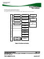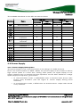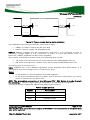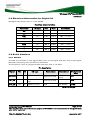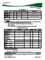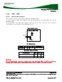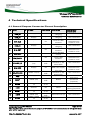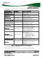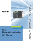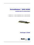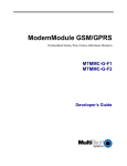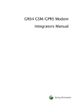
1
WM_
Wireless CPU Q24 Series
Product Technical Specification
®
Revision: 004
Date: January 2007
Wireless CPU® Q24 Series
Product Technical Specification
Reference: WM_PRJ_Q24NG_PTS_001
Revision: 004
Date: January 16, 2007
Powered by the Open AT® Software Suite
confidential ©
Page: 1 / 83
This document is the sole and exclusive property of WAVECOM. Not to be distributed or divulged without
prior written agreement.
WM_PRJ_Q24NG_PTS_001-004
January 16, 2007
Wireless CPU® Q24 Series
Document History
Revision
Date
List of revisions
001
May 2006
Creation (Preliminary version)
002
September 2006
First update
003
November 2006
Update
004
January 16, 2007
Modification of the ON/ ~OFF paragraph
Modification of the Battery charging paragraph
Modification of electrical characteristics BAT-TEMP
Integration of ATEX conformance information
confidential ©
Page: 2 / 83
This document is the sole and exclusive property of WAVECOM. Not to be distributed or divulged without
prior written agreement.
WM_PRJ_Q24NG_PTS_001-004
January 16, 2007
Wireless CPU® Q24 Series
Cautions
This platform contains a modular transmitter. This device is used for wireless
applications. Note that all electronics parts and elements are ESD sensitive.
Information provided herein by WAVECOM is accurate and reliable. However, no
responsibility is assumed for its use and any of such WAVECOM information is herein
provided "as is" without any warranty of any kind, whether express or implied.
Trademarks
®, WAVECOM®, Wireless CPU®, Open AT® and certain other trademarks and logos
appearing on this document, are filed or registered trademarks of Wavecom S.A. in
France or in other countries. All other company and/or product names mentioned may
be filed or registered trademarks of their respective owners.
Copyright
This manual is copyrighted by WAVECOM with all rights reserved. No part of this
manual may be reproduced in any form without the prior written permission of
WAVECOM. No patent liability is assumed with respect to the use of their respective
owners.
confidential ©
Page: 3 / 83
This document is the sole and exclusive property of WAVECOM. Not to be distributed or divulged without
prior written agreement.
WM_PRJ_Q24NG_PTS_001-004
January 16, 2007
Wireless CPU® Q24 Series
Web Site Support
General information about Wavecom and its www.wavecom.com
range of products:
Specific support is available for the Q24 www.wavecom.com/Q24Classic
Classic, Plus, Extended and Auto Wireless
www.wavecom.com/Q24Plus
CPU®:
www.wavecom.com/Q24Extended
www.wavecom.com/Q24Auto
Carrier/Operator approvals:
®
www.wavecom.com/approvals
Open AT Introduction:
www.wavecom.com/OpenAT
Developer support for software and hardware:
www.wavecom.com/forum
confidential ©
Page: 4 / 83
This document is the sole and exclusive property of WAVECOM. Not to be distributed or divulged without
prior written agreement.
WM_PRJ_Q24NG_PTS_001-004
January 16, 2007
Wireless CPU® Q24 Series
Overview
This Product Specification document defines and specifies the Wireless CPU® Q24
Series is available in four different GSM/GPRS Class 10 quad-band versions:
• Q24 Classic: EGSM 900/1800/850/1900 MHz version with 32 Mb of Flash
memory and 16 Mb of PSRAM (32/16), T° range [-20°C / +55°C].
• Q24 Plus: EGSM/GPRS 900/1800/850/1900 MHz version with 32 Mb of Flash
memory and 16 Mb of PSRAM (32/16), T° range [-20°C / +55°C].
• Q24 Extended: EGSM/GPRS 900/1800/850/1900 MHz version with 32 Mb of
Flash memory and 4 Mb of SRAM (32/4), extended T° range.
• Q24 Automotive: EGSM/GPRS 900/1800/850/1900 MHz version with 32 Mb of
Flash memory and 4 Mb of PSRAM (32/4), extended T° range.
This version is dedicated to automotive applications.
This document covers the Wireless CPU® alone and do not include the programmable
capabilities provided in Open AT® Software Suites.
For detailed software programming guides, refer to the documents shown in the
"Reference Documents" section.
Open AT® Software Suites allow developers to natively execute ANSI C software
programs directly on the Wireless CPU®.
confidential ©
Page: 5 / 83
This document is the sole and exclusive property of WAVECOM. Not to be distributed or divulged without
prior written agreement.
WM_PRJ_Q24NG_PTS_001-004
January 16, 2007
Wireless CPU® Q24 Series
Contents
1
References.......................................................................................................10
1.1
Reference Documents ..................................................................................... 10
1.1.1
Open AT® Software Documentation ........................................................ 10
1.1.2
AT Software Documentation................................................................... 10
1.1.3
Hardware Documents ............................................................................. 10
1.1.4
Wavecom Reference Documents............................................................. 10
1.1.5
General Reference Documents ................................................................ 10
1.2
List of Abbreviations ....................................................................................... 11
2
General Description .........................................................................................14
2.1
General Information ........................................................................................ 14
2.1.1
Overall Dimensions ................................................................................. 14
2.1.2
Open AT® Software Suite ........................................................................ 14
2.1.3
GSM/GPRS Features ............................................................................... 15
2.1.4
Interfaces ................................................................................................ 15
2.1.5
External RF Connection Interfaces........................................................... 16
2.1.6
SIM Card Holder ..................................................................................... 16
2.1.7
Green Policy............................................................................................ 16
2.2
Functional Architecture................................................................................... 17
2.2.1
RF Functionalities ................................................................................... 18
2.2.2
Baseband Functionalities ........................................................................ 18
3
Interfaces ........................................................................................................19
3.1
General Purpose Connector (GPC)................................................................... 19
3.2
Power Supply ................................................................................................. 20
3.2.1
Power Supply Description....................................................................... 20
3.2.2
Power Supply Recommendation ............................................................. 22
3.2.3
Power Consumption ............................................................................... 24
3.3
Electrical Information for Digital I/O................................................................. 28
3.4
Serial Interface ................................................................................................ 28
3.4.1
SPI Bus ................................................................................................... 28
3.4.2
SPI Auxiliary Bus .................................................................................... 29
3.4.3
Two-wire Bus Interface (I2C) ................................................................... 29
3.5
Keyboard Interface .......................................................................................... 30
3.6
Main Serial Link (UART1) ................................................................................ 31
3.7
Auxiliary Serial Link (UART2) .......................................................................... 33
3.8
SIM Interface .................................................................................................. 33
confidential ©
Page: 6 / 83
This document is the sole and exclusive property of WAVECOM. Not to be distributed or divulged without
prior written agreement.
WM_PRJ_Q24NG_PTS_001-004
January 16, 2007
Wireless CPU® Q24 Series
3.8.1
General Description................................................................................. 33
3.8.2
SIM Card Holder ..................................................................................... 35
3.9
General Purpose Input/Output ........................................................................ 37
3.10 Activity Status Indication ................................................................................ 38
3.11 Analog to Digital Converter (ADC) ................................................................... 39
3.12 Audio Interface ............................................................................................... 40
3.12.1 Microphone Inputs.................................................................................. 40
3.12.2 Speaker Outputs ..................................................................................... 43
3.13 Buzzer Output ................................................................................................ 45
3.13.1 Hardware Description ............................................................................. 45
3.14 Battery Charging Interface .............................................................................. 46
3.14.1 Hardware Description ............................................................................. 46
3.14.2 Temperature Monitoring ......................................................................... 47
3.14.3 Ni-Cd / Ni-Mh Charging Algorithm .......................................................... 48
3.14.4 Li-Ion Charging Algorithm ....................................................................... 50
3.15 ON / ~OFF ...................................................................................................... 53
3.15.1 General Description................................................................................. 53
3.15.2 Operating Sequences .............................................................................. 54
3.16 BOOT (optional) .............................................................................................. 57
3.17 Reset Signal (~RST) ........................................................................................ 57
3.17.1 General Description................................................................................. 57
3.17.2 Reset Sequence ...................................................................................... 59
3.18 External Interrupt (~INTR)............................................................................... 59
3.19 VCC Output .................................................................................................... 61
3.20 Real Time Clock Supply (VCC_RTC) ................................................................. 61
3.21 RF Interface .................................................................................................... 62
3.21.1 RF Connections....................................................................................... 62
3.21.2 RF Performance ...................................................................................... 63
3.21.3 Antenna Specifications ........................................................................... 64
4
4.1
4.2
5
Technical Specifications...................................................................................65
General Purpose Connector Pin-out Description.............................................. 65
I/O Circuit Diagram ......................................................................................... 69
Environmental Specifications ...........................................................................70
5.1
Environmental Qualifications .......................................................................... 71
5.2
Reflow Soldering ............................................................................................ 73
5.3
Conformance with ATEX 94/9/CE Directive ..................................................... 73
5.4
Mechanical Specifications............................................................................... 73
5.4.1
Physical Characteristics .......................................................................... 73
5.4.2
Mechanical Drawings ............................................................................. 73
6
6.1
Connector and Peripheral Device References....................................................75
General Purpose Connector Data Sheet .......................................................... 75
confidential ©
Page: 7 / 83
This document is the sole and exclusive property of WAVECOM. Not to be distributed or divulged without
prior written agreement.
WM_PRJ_Q24NG_PTS_001-004
January 16, 2007
Wireless CPU® Q24 Series
6.2
6.3
6.4
6.5
6.6
6.7
7
SIM Card Reader............................................................................................. 75
Microphone .................................................................................................... 75
Speaker........................................................................................................... 75
Antenna Cable ................................................................................................ 76
RF board-to-board Connector ......................................................................... 76
GSM Antenna ................................................................................................. 76
Appendix.........................................................................................................77
7.1
Standards and Recommendations .................................................................. 77
7.2
Safety Recommendations (for Information only).............................................. 81
7.2.1
RF safety................................................................................................. 81
7.2.2
General safety ......................................................................................... 82
confidential ©
Page: 8 / 83
This document is the sole and exclusive property of WAVECOM. Not to be distributed or divulged without
prior written agreement.
WM_PRJ_Q24NG_PTS_001-004
January 16, 2007
Wireless CPU® Q24 Series
Table of Figures
Figure 1: Functional architecture .............................................................................. 17
Figure 2: Power supply during burst emission.......................................................... 21
Figure 3: Maximum voltage ripple (Uripp) versus Frequencies in GSM & DCS.......... 23
Figure 4: UART1 Serial Link signals .......................................................................... 31
Figure 5: UART2 Serial Link signals .......................................................................... 33
Figure 6: SIM Card holder constraints ...................................................................... 35
Figure 7: Buzzer connection ..................................................................................... 45
Figure 8: Ni-Cd / Ni-Mh charging waveform ............................................................. 49
Figure 9: Li-Ion full-charging waveform .................................................................... 52
Figure 10: Power-ON sequence diagram .................................................................. 54
Figure 11: Power-OFF sequence diagram ................................................................. 56
Figure 12: RST pin connection.................................................................................. 59
Figure 13: Reset sequence diagram .......................................................................... 59
Figure 14: Wireless CPU® pin position (bottom view)................................................ 68
Figure 15: I/O Circuit Diagram .................................................................................. 69
Figure 16: Q24 Classic, Q24 Plus and Q24 Extended Environmental classes............ 71
Figure 17: Q24 Automotive environmental classes ................................................... 72
Figure 18: Mechanical drawing. ............................................................................... 73
confidential ©
Page: 9 / 83
This document is the sole and exclusive property of WAVECOM. Not to be distributed or divulged without
prior written agreement.
WM_PRJ_Q24NG_PTS_001-004
January 16, 2007
Wireless CPU® Q24 Series
References
1 References
1.1 Reference Documents
For more details, several reference documents may be consulted. The Wavecom
reference documents are provided in the Wavecom documents package contrary to
the general reference documents, which are not Wavecom owned.
Note: All below documents are related to V3.12 Open AT® Software and 6.57 Open AT®
Firmware. Wavecom recommends that the developer should check the web site for
the latest documentation
1.1.1 Open AT® Software Documentation
[1]
Getting Started with Open AT® (Ref. WM_ASW_OAT_CTI_001)
[2]
Open AT® Basic Development Guide (Ref. WM_ASW_OAT_UGD_002)
[3]
ADL User Guide for Open ATA® V3.12 (Ref. WM_ASW_OAT_UGD_006)
1.1.2 AT Software Documentation
[4]
AT Commands Interface Guide for OS 6.57 (Ref. WM_ASW_OAT_UGD_0044)
[5]
AT Commands Interface Guide (Bluetooth) (Ref. WM_ASW_BLU_UGD_001)
1.1.3 Hardware Documents
[6]
Wireless CPU® Q24 Series Customer Design Guidelines
(Ref. WM_PRJ_Q24NG_PTS_002)
[7]
Wireless CPU® Q24 Series Process Customer Guidelines
(Ref. WM_PRJ_Q24NG_PTS_003)
1.1.4 Wavecom Reference Documents
[8]
Automotive Environmental Control Plan for Wireless CPU® Q24 Series
(Ref. WM_PRJ_Q24NG_DCP_001)
[9]
Environmental Control Plan for Wireless CPU® Q24 Series
(Ref. WM_PRJ_Q24NG_DCP_002)
1.1.5 General Reference Documents
[10] "I²C Bus Specification", Version 2.0, Philips Semiconductor 1998
[11] ISO 7816-3 Standard
.
©Confidential
Page: 10 / 83
This document is the sole and exclusive property of WAVECOM. Not to be distributed or divulged without
prior written agreement.
WM_PRJ_Q24NG_PTS_001-004
January 16, 2007
Wireless CPU® Q24 Series
References
1.2 List of Abbreviations
Abbreviation Description
3GPP
Third Generation Partnership Project
ADC
Analog to Digital Converter
A/D
Analog to Digital conversion
AT
ATtention (prefix for modem commands)
AUX
AUXiliary
CBS
Cell Broadcast Service
CLK
CLocK
CMOS
Complementary Metal Oxide Semiconductor
CODEC
COder DECoder
CPU
Central Processing Unit
CTS
Clear To Send
dB
Decibel
DC
Direct Current
DCD
Data Carrier Detect
DCS
Digital Cellular System
DCXO
Digitally Controlled Crystal Oscillator
DR
Dynamic Range
DSR
Data Set Ready
DTR
Data Terminal Ready
EDGE
Enhanced Data rates for GSM Evolution
EGSM
Extended GSM
EN
Enable
ESD
ElectroStatic Discharges
ETSI
European Telecommunications Standards Institute
FEM
Front End Module
FR
Full Rate
GND
GrouND
GPI
General Purpose Input
GPC
General Purpose Connector
GPIO
General Purpose Input Output
GPO
General Purpose Output
GPRS
General Packet Radio Service
GSM
Global System for Mobile communications
©Confidential
Page: 11 / 83
This document is the sole and exclusive property of WAVECOM. Not to be distributed or divulged without
prior written agreement.
WM_PRJ_Q24NG_PTS_001-004
January 16, 2007
Wireless CPU® Q24 Series
References
Abbreviation Description
IF
Intermediate Frequency
INTR
INTeRrupt
I/O
Input / Output
LCD
Liquid Crystal Display
LED
Light Emitting Diode
LNA
Low Noise Amplifier
LSB
Less Significant Bit
MAX
MAXimum
MIC
MICrophone
MIN
MINimum
MMS
Multimedia Message Service
MS
Mobile Station
NOM
NOMinal
NTC
Negative Temperature Coefficient
PA
Power Amplifier
PBB
PolyBrominated Biphenyl
PBDE
PolyBrominated Diphenyl Ethers
PCB
Printed Circuit Board
PCL
Power Control Level
PCS
Personal Communications Services
PLL
Phase Lock Loop
RAM
Random Access Memory
RF
Radio Frequency
RI
Ring Indicator
RoHS
Restriction of Hazardous Substances
RST
ReSeT
RTC
Real Time Clock
RTS
Request To Send
RX
Receive
SCL
Serial CLock
SDA
Serial DAta
SIM
Subscriber Identification Module
SMS
Short Message Service
SPI
Serial Peripheral Interface
SPK
SPeaKer
©Confidential
Page: 12 / 83
This document is the sole and exclusive property of WAVECOM. Not to be distributed or divulged without
prior written agreement.
WM_PRJ_Q24NG_PTS_001-004
January 16, 2007
Wireless CPU® Q24 Series
References
Abbreviation Description
SRAM
Static RAM
TDMA
Time Division Multiple Access
TU
Typical Urban fading profile
TUHigh
Typical Urban, High speed fading profile
TDMA
Time Division Multiple Access
TX
Transmit
TYP
TYPical
UART
Universal Asynchronous Receiver-Transmitter
VLSI
Very Large Scale Integration
VSWR
Voltage Standing Wave Ratio
©Confidential
Page: 13 / 83
This document is the sole and exclusive property of WAVECOM. Not to be distributed or divulged without
prior written agreement.
WM_PRJ_Q24NG_PTS_001-004
January 16, 2007
Wireless CPU® Q24 Series
General Description
2 General Description
2.1 General Information
The Q24 Series are self-contained EGSM/GPRS 900/1800 and 850/1900 quad-band
Wireless CPU®s with the following characteristics:
Note:
The Q24 classic is limited to GSM only (GPRS not supported).
2.1.1 Overall Dimensions
Completely shielded:
•
Length: 58.4 mm
•
Width: 32.2 mm
•
Thickness: 3.9 mm:
- Excluding Shielding legs
- 6, 2 mm for Q24 Automotive, which offers either a MMS or UFL connector
on the top side
•
Weight:<11 g (12g for Q24 Automotive)
2.1.2 Open AT® Software Suite
Every Wavecom Wireless CPU® comes with the "Open AT® Software, which has the
following five elements:
Î Open AT® IDEs
Î Open AT® Applications
Î Open AT® Plug-Ins
Î Open AT® Operating Systems
Î Open AT® Firmwares
The Open AT® Software Suite enables a customer to develop within the Open AT® IDE
an ANSI C based Open AT® Application, which is natively executed under the Open
AT® OS which may utilise one or more Open AT® Plug-Ins and connect to wireless
networks, peripheral devices & companion controllers via the Open AT® Firmware.
Among other things (please refer to Open AT® Programming Guides), the Open AT®
firmware offers:
•
Real Time Clock (RTC) with calendar
•
Echo Cancellation and noise reduction (quadri codec)
•
Full GSM or GSM/GPRS Operating System stacks
©Confidential
Page: 14 / 83
This document is the sole and exclusive property of WAVECOM. Not to be distributed or divulged without
prior written agreement.
WM_PRJ_Q24NG_PTS_001-004
January 16, 2007
Wireless CPU® Q24 Series
General Description
The Wireless CPU® Q24 Series are designed to integrate various types of specific
process applications such as vertical applications (telemetry, multimedia,
automotive).
The Open AT® firmware offers a set of AT commands to control the Wireless CPU®.
With this standard Operating System, some interfaces of the Wireless CPU® are not
available since they are dependent on the peripheral devices connected to the
Wireless CPU®.
This symbol is used to indicate that the interfaces are not available with AT
commands.
AT
The Operating System is Open AT® compliant.
The Open AT® OS offers a set of Open AT® AT API’s to control the Wireless CPU®. The
limitation mentioned above is not valid in this case.
2.1.3 GSM/GPRS Features
•
2-Watt EGSM 900/GSM 850 radio section running under 3.6 volts
•
1-Watt GSM1800/1900 radio section running under 3.6 volts
•
Hardware GSM/GPRS class 10 capable (except the Wireless CPU® Q24
Classic)
2.1.4 Interfaces
•
Complete interfacing is through a 60-pin connector:
o
o
o
o
o
o
o
o
o
o
o
o
o
•
SPI and 2-wire bus interface
Keyboard interface
Two serial link interfaces (UART1 and UART2)
3V/1.8V SIM interface
GPIOs
Activity status indication interface
Analog to digital converter
Analog audio
Buzzer interface
Battery charging interface
External interrupt
Power supply interface
Back-up battery interface
Optional SIM holder (offered on Wireless Q24 Classic and Wireless CPU® Q24
Plus)
©Confidential
Page: 15 / 83
This document is the sole and exclusive property of WAVECOM. Not to be distributed or divulged without
prior written agreement.
WM_PRJ_Q24NG_PTS_001-004
January 16, 2007
Wireless CPU® Q24 Series
General Description
2.1.5 External RF Connection Interfaces
The Wireless CPU® Q24 Series are available with different external RF connection
configurations:
Product reference
UFL
UFL or MMS
Antenna pad
IMP
Position
Bottom side
Top side
Top side
Bottom side
Q24 Classic
X
X
X
Q24 Plus
X
X
X
Q24 Extended
X
X
X
X
X
Q24 Automotive
X
2.1.6 SIM Card Holder
The Wireless CPU® Q24 Series are available with a SIM Card holder at the TOP:
SIM interface location
Product reference
60-pin connector
Optional SIM holder
Q24 Classic
X
X
Q24 Plus
X
X
Q24 Extended
X
Q24 Automotive
X
Caution:
•
•
The Wireless CPU® Q24 Series does not allow two SIM Cards to be
connected at the same time
If a Wireless CPU® Q24 Classic or Q24 Plus is used with a SIM Card holder at
the top, it is mandatory to avoid a SIM interface connection through the
60-pin General Purpose Connector (GPC)
2.1.7 Green Policy
The Wireless CPU® Q24 Series are compliant with RoHS (Restriction of Hazardous
Substances in Electrical and Electronic Equipment). Directive 2002/95/EC which sets
limits for the use of certain restricted hazardous substances.
This directive states that "from 1st July 2006, new electrical and electronic equipment
put on the market does not contain lead, mercury, cadmium, hexavalent chromium,
polybrominated biphenyls (PBB), and polybrominated diphenyl ethers (PBDE)".
©Confidential
Page: 16 / 83
This document is the sole and exclusive property of WAVECOM. Not to be distributed or divulged without
prior written agreement.
WM_PRJ_Q24NG_PTS_001-004
January 16, 2007
Wireless CPU® Q24 Series
General Description
2.2 Functional Architecture
The global architecture of the Wireless CPU® Q24 Series is shown below:
Power supply
RF interface
G
E
N
E
R
A
L
Battery
management
A/D converter
P
U
R
P
O
S
E
Audio interface
Transceiver
PA front-end
module
SIM supply
SIM controller
Vocoder
RF
CONNECTIONS
Keyboard
controller
UART1 – UART2
Controller
SPI – I2C
Controller
C
O
N
N
E
C
T
O
R
RTC
CPU
FLASH
Memory
management
RAM
Figure 1: Functional architecture
©Confidential
Page: 17 / 83
This document is the sole and exclusive property of WAVECOM. Not to be distributed or divulged without
prior written agreement.
WM_PRJ_Q24NG_PTS_001-004
January 16, 2007
Wireless CPU® Q24 Series
General Description
2.2.1 RF Functionalities
The Radio Frequency (RF) range complies with the Phase II EGSM 900/DCS 1800 and
GSM 850/PCS 1900 recommendations. The frequencies are given below:
GSM band
Transmit band (Tx)
GSM 850
EGSM 900
DCS 1800
PCS 1900
824
880
1710
1850
to
to
to
to
849 MHz
915 MHz
1785 MHz
1910 MHz
Receive band (Rx)
869
925
1805
1930
to
to
to
to
894 MHz
960 MHz
1880 MHz
1990 MHz
The Radio Frequency (RF) part is based on a specific quad-band chip. It includes a:
•
Digital low-IF receiver,
•
Quad-band LNAs (Low Noise Amplifier),
•
Offset PLL (Phase Locked Loop) transmitter,
•
Frequency synthesizer,
•
Digitally controlled crystal oscillator (DCXO),
•
Tx/Rx FEM (Front-End module) for quad-band GSM/GPRS.
2.2.2 Baseband Functionalities
The Wireless CPU® Q24 Series digital parts are based on the PHILIPS-VLSI chip (ONE
C GSM / GPRS Kernel).
This chipset uses a 0.25 μm CMOS mixed technology, which allows massive
integration as well as low current consumption.
©Confidential
Page: 18 / 83
This document is the sole and exclusive property of WAVECOM. Not to be distributed or divulged without
prior written agreement.
WM_PRJ_Q24NG_PTS_001-004
January 16, 2007
Wireless CPU® Q24 Series
Interfaces
3 Interfaces
Note:
Some of the Wireless CPU® Q24 Series interface signals are multiplexed in order to
limit the total number of pins. But this architecture imposes some restrictions.
Example:
If the SPI bus and 2-wire bus are multiplexed and if the SPI bus is used, then the 2wire bus is not available.
Caution:
To power-ON the Wireless CPU® Q24 Series correctly and to avoid any damage, all
external signals must be inactive when the Wireless CPU® Q24 Series is OFF.
3.1 General Purpose Connector (GPC)
A 60-pin connector, with 0.5 mm pitch, is provided to interface the Wireless CPU®
Q24 Series with a customer application board containing either an LCD module, or a
keyboard, a SIM connector, a battery connection, etc.
The GPC is made by the KYOCERA / AVX group with the following reference:
•
14 5087 060 930 861.
The matting connector has the following reference:
•
24 5087 060 X00 861.
For further details, refer to section 6.1 General Purpose Connector Data Sheet.
©Confidential
Page: 19 / 83
This document is the sole and exclusive property of WAVECOM. Not to be distributed or divulged without
prior written agreement.
WM_PRJ_Q24NG_PTS_001-004
January 16, 2007
Wireless CPU® Q24 Series
Interfaces
The available interfaces on the GPC are shown below:
OS 6.57
Section
Name
3.4
3.5
3.6
3.7
3.8
3.9
Serial interface
Keyboard Interface
Main Serial Link
Auxiliary Serial Link
SIM interface
General Purpose IO
Activity status
indication
Analog to digital
converter
Audio Interface
Battery charging
interface
ON/~OFF
Boot
Reset
External interrupt
VCC output
Real Time Clock
RF interface
3.10
3.11
0
3.14
3.15
3.16
3.17
3.18
3.19
3.20
3.21
Supported
Open AT®
Not
supported
Supported
X
X
X
X
X
X
X
X
X
X
X
X
X
X
X
X
X
X
X
X
X
X
Not
supported
X
X
X
X
X
X
X
X
X
X
X
X
3.2 Power Supply
3.2.1 Power Supply Description
The power supply is one of the key factors in the design of a GSM terminal.
Due to the burst emission in GSM / GPRS, the power supply must be able to deliver
high current peaks in a short time. During these peaks, the ripple (Uripp) on the
supply voltage must not exceed the limits specified; see the table "Maximum voltage
ripple (Uripp) vs Frequency" given below.
•
In communication mode, a GSM/GPRS class 2 terminal emits 577μs radio
bursts every 4.615ms. (see the Figure 2: Power supply during burst
emission).
•
In communication mode, a GPRS class 10 terminal emits 1154μs radio bursts
every 4.615ms.
©Confidential
Page: 20 / 83
This document is the sole and exclusive property of WAVECOM. Not to be distributed or divulged without
prior written agreement.
WM_PRJ_Q24NG_PTS_001-004
January 16, 2007
Wireless CPU® Q24 Series
Interfaces
VBATTT
Uripp
Uripp
t = 577 μs
T = 4,615 ms
Figure 2: Power supply during burst emission
Two different inputs are provided for the power supply:
•
VBATT is used to supply the RF part and
•
VDD is used to supply the baseband part.
VBATT: Directly supplies the RF components with 3.6 V. It is essential to keep a
minimum voltage ripple at this connection in order to avoid any phase error. In
particular, VBATT supplies the RF Power Amplifier.
The current waveform is bursted with the following duty cycles:
•
1/8 of the time (around 577 μs every 4.615 ms for GSM/GPRS class 2),
•
2/8 of the time (around 1154 μs every 4.615 ms for GSM/GPRS class 10).
The rising time is around 10 μs.
VDD: Supplies the +2.8 V ballast regulators of the Wireless CPU® Q24 Series. It is
essential to keep the voltage over 3.1 volts at any time.
Notes:
•
It is possible to connect VBATT and VDD together.
•
In the event of separate power supply, they must be in same state: e.g. either
active or inactive at the same time.
GND: The grounding connection of the Wireless CPU® Q24 Series is made through
the shielding Ö The four "legs" must be soldered to a complete ground plane.
The power supply voltage for VBATT and VDD is given below:
Power supply pin-out
Signal
Pin number
VBATT
55,57,58,59,60
VDD
11
GND
Shielding legs
©Confidential
Page: 21 / 83
This document is the sole and exclusive property of WAVECOM. Not to be distributed or divulged without
prior written agreement.
WM_PRJ_Q24NG_PTS_001-004
January 16, 2007
Wireless CPU® Q24 Series
Interfaces
Electrical characteristics
Signal
MIN
NOM
MAX
VBATT
3.2 V
3.6 V
4.5 V *
VDD
3.1 V
4.5 V
*Max operating Voltage Standing Wave Ratio (VSWR) 2:1.
3.2.2 Power Supply Recommendation
The VBATT voltage limits must be considered at any time.
The worst condition is during the burst period transmission, when current
consumption is at its highest. During this period, the VBATT voltage is minimum:
•
The output voltage of the power supply drops.
•
Voltage drop is present between the power supply output and the Wireless
CPU® supply pins (VBATT).
To ensure a good design, make sure that during a transmit burst period, the total
drop in voltage should not set the Wireless CPU® supply voltage (VBATT) below
VBATTMIN= 3.2V.
Notes:
•
During a transmit burst, Wireless CPU® nominal current is 1.4A only.
•
To design the Wireless CPU® power supply with a margin, a target of 2A is
recommended.
Caution:
•
If VBATT<3.2V, the Wireless CPU® automatically powers OFF.
•
When a Wireless CPU® is supplied with a battery, the total impedance
(battery + contacts + protections + PCB) should be < 150mΩ to limit voltage
drop-out within emission burst.
•
As the radio power amplifier is directly connected to the VBATT, the Wireless
CPU® Q24 Series are sensitive to any voltage variation. When a DC/DC
converter is used, Wavecom recommends to set the converter frequency in
such a way that the resulting voltage does not exceed these values, which
are given in the following table. "Maximum voltage ripple (Uripp) vs
Frequency".
©Confidential
Page: 22 / 83
This document is the sole and exclusive property of WAVECOM. Not to be distributed or divulged without
prior written agreement.
WM_PRJ_Q24NG_PTS_001-004
January 16, 2007
Wireless CPU® Q24 Series
Interfaces
Uripp Max
(mVpp)
Freq.
(kHz)
Uripp Max
(mVpp)
<100
200
300
400
500
600
700
50
15.5
6.8
3.9
4
2
8.2
800
900
1000
1100
1200
1300
1400
4
15.2
9.5
32
22
29
30
Uripp (mVpp)
Freq.
(kHz)
50
45
40
35
30
25
20
15
10
5
0
200
400
600
800
1000
1200
Freq. (kHz)
Uripp Max
(mVpp)
1500
1600
1700
1800
>1900
34
33
37
40
40
1400
1600
1800
Input Frequency (kHz)
for f<100kHz Uripp Max = 50mVpp
for f> 1800kHz Uripp Max = 40 mVpp
Figure 3: Maximum voltage ripple (Uripp) versus Frequencies in GSM & DCS
Refer to Wireless CPU® Q24 Series Customer Design Guidelines [6], for further
information on power supply design.
©Confidential
Page: 23 / 83
This document is the sole and exclusive property of WAVECOM. Not to be distributed or divulged without
prior written agreement.
WM_PRJ_Q24NG_PTS_001-004
January 16, 2007
Wireless CPU® Q24 Series
Interfaces
3.2.3 Power Consumption
The Wireless CPU® Q24 Series support different power consumption modes:
Working modes
Comments
OFF mode
ALARM mode
The Wireless CPU is in OFF mode.
The Wireless CPU® is in OFF mode with RTC block running,
when an ALARM occurs, the Wireless CPU® wakes-up
automatically.
The Wireless CPU® is synchronized with an RF GSM/GPRS
network.
The internal 26 MHz of the Wireless CPU® is constantly active.
The Wireless CPU® is synchronized with an RF GSM/GPRS tester.
The internal 26 MHz of the Wireless CPU® is not constantly
active.
The SIM and Radio interface are deactivated via AT command or
Open AT® API:
-The embedded application is running
-The serial port remains active (AT commands are available).
The internal 26 MHz of the Wireless CPU® is constantly active.
This mode is similar to the FAST Standby mode.
All the features are disabled (no GSM, no GPRS, no SIM and no
Serial port).
The internal 26 MHz of the Wireless CPU® is not constantly
active.
A GSM/GPRS communication is established with a RF
GSM/GPRS network.
®
FAST idle mode
SLOW idle mode
FAST Standby
mode
SLOW Standby
mode
Communication
mode
The power consumption depends on the configuration used. It is for this reason that
the following power consumption values are given for each modes, RF bands and
software used (AT or Open AT®).
All the following information is given, by assuming a 50 Ω RF output.
Three VBATT values are used to measure the consumption, VBATTMIN (3.2V),
VBATTMAX (4.5V) and VBATTTYP (3.6V).
The average current is given for three VBATT values and peak current given is the
maximum current peak measured with three VBATT voltages.
For more information on power consumption measurement, hardware configuration,
SIM used, and software Dhrystone application, see the AT Command Interface Guide
or OS 6.57 [4] and Wireless CPU® Q24 Series Customer Design Guidelines [6].
When Wireless CPU® is in Alarm mode, no voltage must be applied to any pin of the
60-pin connector, except on the BAT-RTC (pin 56) for RTC operation or ON/~OFF (pin
6) to power-ON the Wireless CPU®.
©Confidential
Page: 24 / 83
This document is the sole and exclusive property of WAVECOM. Not to be distributed or divulged without
prior written agreement.
WM_PRJ_Q24NG_PTS_001-004
January 16, 2007
Wireless CPU® Q24 Series
Interfaces
3.2.3.1
Power Consumption without Open AT® Processing
The following measurement results are relevant only when:
•
There is no Open AT® application,
•
The Open AT® application is disabled,
•
No processing is required by the Open AT® application.
INOM
IMAX
IMAX
Unit
average average peak
Operating mode
Parameters
OFF Mode
VBATT= 3.6V
16.5
18
μA
Alarm Mode
VBATT= 3.6V
18.5
20
μA
Paging 9
10.5
11
150Rx mA
Paging 2
13
13.5
150Rx mA
Paging 9
2.8
3
150Rx mA
Paging 2
5.5
5.8
150Rx mA
Fast Standby
VBATT = 3.6V
9.5
11
-
mA
Slow Standby
VBATT = 3.6V
1.5
2
-
mA
Fast Idle Mode
Slow Idle Mode
Connected Mode
Transfer Mode
Class 8 (4Rx/1Tx)
GPRS
Transfer Mode
Class 10 (3Rx/2Tx)
GSM850
EGSM900
PCL5
217
225
1400Tx mA
PCL19
90
95
250Tx mA
DCS1800
PCL0
165
175
800Tx mA
PCS1900
PCL15
90
100
250Tx mA
GSM850
Gamma 3
209
220
1400Tx mA
EGSM900
Gamma 17
87
90
250Tx mA
DCS1800
Gamma 3
150
170
800Tx mA
PCS1900
Gamma 18
84
95
250Tx mA
GSM850
Gamma 3
380
410
1400Tx mA
EGSM900
Gamma 17
130
160
270Tx mA
DCS1800
Gamma 3
258
290
800Tx mA
PCS1900
Gamma 18
123
150
240Tx mA
TX
means that the peak current is measured during a TX transmission burst
RX
means that the peak current is measured during a RX reception burst
1
Slow Idle mode power consumption depends on the SIM Card used.
Some SIM Cards respond faster than others, the longer the response time, the higher
the consumption. The measurements were performed on a large number of 3V SIM
Cards and the results in brackets shown in the above table are the minimum and
maximum currents measured from among all the SIM Cards used.
©Confidential
Page: 25 / 83
This document is the sole and exclusive property of WAVECOM. Not to be distributed or divulged without
prior written agreement.
WM_PRJ_Q24NG_PTS_001-004
January 16, 2007
Wireless CPU® Q24 Series
Interfaces
3.2.3.2
Power Consumption with Open AT® Software
The power consumption with Open AT® software used is the Dhrystone application
and the following consumption results were measured while performing on the
Dhrystone application.
INOM
IMAX
IMAX
Unit
average average peak
Operating mode
Parameters
OFF Mode
VBATT = 3.6V
16.5
18
μA
Alarm Mode
VBATT = 3.6V
18.5
20
μA
Paging 9
10.5
11
150Rx mA
Paging 2
13
13.5
150Rx mA
Paging 9
N/A
N/A
N/A
mA
Paging 2
N/A
N/A
N/A
mA
Fast Standby
VBATT = 3.6V
9.5
11
Slow Standby
VBATT = 3.6V
N/A
N/A
Fast Idle Mode
Slow Idle Mode
Connected Mode
Transfer Mode
Class 8 (4Rx/1Tx)
GPRS
Transfer Mode
Class 10 (3Rx/2Tx)
3.2.3.3
150Rx mA
N/A
mA
GSM850
PCL5
232
240
1400Tx mA
EGSM900
PCL19
101
110
250Tx mA
DCS1800
PCL0
175
185
800Tx mA
PCS1900
PCL15
100
110
250Tx mA
GSM850
Gamma 3
209
220
1400Tx mA
EGSM900
Gamma 17
87
90
250Tx mA
DCS1800
Gamma 3
150
170
800Tx mA
PCS1900
Gamma 18
84
95
250Tx mA
GSM850
Gamma 3
380
410
1400Tx mA
EGSM900
Gamma 17
130
160
270Tx mA
DCS1800
Gamma 3
258
290
800Tx mA
PCS1900
Gamma 18
123
150
240Tx mA
Consumption Waveform
The consumption waveforms are given for an EGSM900 network configuration with
AT software running on a Wireless CPU®.
The VBATT voltage value is 3.6V typical.
Four significant operating mode consumption waveforms are described as:
•
Connected mode with one TX and one RX burst at PCL5 (33dBm)
•
GPRS class 10 transfer mode with two TX bursts and three RX burst at
Gamma 3 (33dBm)
•
Slow Idle mode with a paging 9 (every 2 seconds)
•
Fast Idle mode with a paging 9 (every 2 seconds)
©Confidential
Page: 26 / 83
This document is the sole and exclusive property of WAVECOM. Not to be distributed or divulged without
prior written agreement.
WM_PRJ_Q24NG_PTS_001-004
January 16, 2007
Wireless CPU® Q24 Series
Interfaces
The following waveform shows only the current form versus time:
Current Waveform
Connected mode with One TX burst at PCL5 and one RX
burst
Slow idle mode paging 9
GPRS Class 10 Transfer mode with two TX bursts at
PCL5 and three RX burst
Fast idle mode paging 9
©Confidential
Page: 27 / 83
This document is the sole and exclusive property of WAVECOM. Not to be distributed or divulged without
prior written agreement.
WM_PRJ_Q24NG_PTS_001-004
January 16, 2007
Wireless CPU® Q24 Series
Interfaces
3.3 Electrical Information for Digital I/O
All digital I/O comply with a 3 volt CMOS.
Electrical characteristics
Parameter
I/O type
min
Max
Conditions
VIL
CMOS
-0.5 V
0.8 V
VIH
CMOS
2.1 V
3.0 V
VOL
1X
-0.2V
0.2 V
IOL = -1 mA
-
2X
-0.2V
0.2 V
IOL = -2 mA
-
3X
-0.2V
0.2 V
IOL = -3 mA
VOH
1X
2.55 V
2.95V
IOH = 1 mA
-
2X
2.55 V
2.95V
IOH = 2 mA
-
3X
2.55 V
2.95V
IOH = 3 mA
3.4 Serial Interface
3.4.1 SPI Bus
The SPI bus includes a CLK signal (SPI_CLK), an I/O signal (SPI_IO), and an EN signal
(SPI_EN) complying with the SPI bus standard.
The frequency clock is programmable from 812 kHz to 13 MHz.
Pin description
Signal
Pin
I/O
SPI_CLK
10
O
SPI_IO
8
SPI_EN
28
I/O type
CMOS 1X (C5)
Reset state
Pull-up to 2V8
I/O CMOS / CMOS 1X
Pull-up to 2V8
(C2)
O
CMOS 1X (C3)
2V8
Description
Multiplexed
with
SPI Serial
Clock
SCL
SPI Data
SDA
SPI Enable
GPO3
(C2), (C3) and (C5): To obtain more details on I/O type, refer to section 4.2 "I/O Circuit diagram"
©Confidential
Page: 28 / 83
This document is the sole and exclusive property of WAVECOM. Not to be distributed or divulged without
prior written agreement.
WM_PRJ_Q24NG_PTS_001-004
January 16, 2007
Wireless CPU® Q24 Series
Interfaces
3.4.2 SPI Auxiliary Bus
A second SPI Chip Enable (called SPI_AUX) must be used to add a second SPI
peripheral to the Wireless CPU® Q24 Series.
Pin description
Signal
Pin I/O
SPI_CLK 10
SPI_IO
8
O
I/O type
Reset state
Description
CMOS 1X (C5)
Pull-up to
2V8
SPI Serial
Clock
SCL
Pull-up to
2V8
SPI Data
SDA
2V8
SPI Aux.
Enable
GPO0
I/O CMOS / CMOS 1X (C2)
SPI_AUX 26
O
CMOS 1X (C3)
Multiplexed
with
(C2), (C3) and (C5): To obtain more details on I/O type, refer to section 4.2 "I/O Circuit diagram"
3.4.3 Two-wire Bus Interface (I2C)
The two-wire bus interface includes a CLK signal (SCL) and a DATA signal (SDA)
complying with a standard two-wire bus interface.
The frequency clock is programmable either to a 96 kHz or a 400 kHz.
Pin description
Signal
Pin
I/O
SCL
10
O
SDA
8
I/O type
CMOS 1X (C5)
I/O CMOS / CMOS1X
(C2)
Reset state
Pull-up to 2V8
Pull-up to 2V8
Description
Serial Clock
Serial Data
(C2) and (C5): To obtain more details on I/O type, refer to section 4.2 "I/O Circuit diagram"
©Confidential
Page: 29 / 83
This document is the sole and exclusive property of WAVECOM. Not to be distributed or divulged without
prior written agreement.
WM_PRJ_Q24NG_PTS_001-004
January 16, 2007
Wireless CPU® Q24 Series
Interfaces
3.5 Keyboard Interface
Equivalent circuit
COLUMN 4
ROW 4
Key Release
Detector
ROW 0
Key Press
2V8
Select
D Q
Key
COLUMN [0]
2V8
GND
Row0
ROW [0]
Detector
COLUMN 0
Col0
Q D
ROWCK
GND
Select
CLOCK
An AT command or Open AT® API allows the input key code to be obtained (see the
AT+CMER command description). This code must then be processed by the
application.
For a total of 25 keys (5 rows x 5 columns), the keyboard interface provides 10
connections:
•
5 rows (ROW0 to ROW4) and
•
5 columns (COL0 to COL4)
The scanning is digital, and the debouncing is performed in the Wireless CPU®. No
discrete components such as R, C (Resistor, Capacitor) are needed.
©Confidential
Page: 30 / 83
This document is the sole and exclusive property of WAVECOM. Not to be distributed or divulged without
prior written agreement.
WM_PRJ_Q24NG_PTS_001-004
January 16, 2007
Wireless CPU® Q24 Series
Interfaces
Pin description
Signal
Pin
number
I/O
I/O type
Reset state
Description
ROW0
13
I/O
CMOS / CMOS 1X
Pull-down to 0V
Row scan
ROW1
15
I/O
CMOS / CMOS 1X
Pull-down to 0V
Row scan
ROW2
17
I/O
CMOS / CMOS 1X
Pull-down to 0V
Row scan
ROW3
19
I/O
CMOS / CMOS 1X
Pull-down to 0V
Row scan
ROW4
21
I/O
CMOS / CMOS 1X
Pull-down to 0V
Row scan
COL0
23
I/O
CMOS / CMOS 1X
Pull-up to 2V8
Column scan
COL1
25
I/O
CMOS / CMOS 1X
Pull-up to 2V8
Column scan
COL2
27
I/O
CMOS / CMOS 1X
Pull-up to 2V8
Column scan
COL3
29
I/O
CMOS / CMOS 1X
Pull-up to 2V8
Column scan
COL4
31
I/O
CMOS / CMOS 1X
Pull-up to 2V8
Column scan
3.6 Main Serial Link (UART1)
A flexible 6-wire serial interface is available, complying with V24 protocol signaling,
but not with V28 (electrical interface) due to a 2.8 volt interface.
The signals are:
•
TX data (CT103/TX)
•
RX data (CT104/RX)
•
Request To Send (CT105/RTS)
•
Clear To Send (CT106/CTS)
•
Data Terminal Ready (CT108-2/DTR)
•
Data Set Ready (CT107/DSR)
The two additional signals are:
•
Data Carrier Detect (CT109/DCD).
•
Ring Indicator (CT125/RI).
Figure 4: UART1 Serial Link signals
©Confidential
Page: 31 / 83
This document is the sole and exclusive property of WAVECOM. Not to be distributed or divulged without
prior written agreement.
WM_PRJ_Q24NG_PTS_001-004
January 16, 2007
Wireless CPU® Q24 Series
Interfaces
Pin description
Signal
Pin
I/O
I/O type
CT103/TXD1
39
I
CMOS
High
impedance
CT104/RXD1
32
O
CMOS
1X (C3)
2V8
CT105/RTS1
30
I
CMOS
High
impedance
Transmit
serial data
Receive serial
data
Request To
Send
CT106/CTS1
37
O
2V8
Clear To Send
CT107/DSR1
36
O
CT1082/DTR1
34
I
CT109/DCD1
51
O
CT125/RI1
54
O
CT102/GND
Shielding
legs
CMOS
1X (C1)
CMOS
1X (C3)
CMOS
CMOS
2X (C1)
CMOS
2X (C1)
Reset state
2V8
High
impedance
High
impedance
High
impedance
Description
Data Set
Ready
Data Terminal
Ready
Data Carrier
Detect
Ring Indicator
Multiplexed
with
GPIO3
GPIO2
Ground
(C1) and (C3): To obtain more details on I/O type, refer to section 4.2 "I/O Circuit diagram"
Caution:
•
The rise and fall time of the reception signals (mainly CT103) must be less
than 200 ns
•
The Wireless CPU® Q24 Series are designed to operate using all the serial
interface signals. In particular, it is necessary to use RTS and CTS signals for
hardware flow control in order to avoid data corruption during transmission
©Confidential
Page: 32 / 83
This document is the sole and exclusive property of WAVECOM. Not to be distributed or divulged without
prior written agreement.
WM_PRJ_Q24NG_PTS_001-004
January 16, 2007
Wireless CPU® Q24 Series
Interfaces
3.7 Auxiliary Serial Link (UART2)
For specific applications, an auxiliary serial interface (UART2) is available on the
Wireless CPU® Q24 Series.
E.g. Bluetooth connectivity: See AT commands interface guide (Bluetooth) [5].
Figure 5: UART2 Serial Link signals
Pin description
Signal
CT103
TXD2
CT104
RXD2
CT106
CTS2
CT105
RTS2
Pin I/O
/
/
/
/
18
I
20
O
24
O
35
I
I/O type
CMOS (C4)
CMOS 1X
(C3)
CMOS 2X
(C1)
CMOS
Reset state
Description
Pull down to
0V
Transmit serial
data
Receive serial
data
2V8
High
impedance
High
impedance
Multiplexed
with
GPI
GPO2
Clear To Send
GPIO0
Request To Send
GPIO5
(C1), (C3) and (C4): To obtain more details on I/O type, refer to section 4.2 "I/O Circuit diagram"
3.8 SIM Interface
3.8.1 General Description
The following five signals are available:
•
SIM_VCC: SIM power supply.
•
SIM_RST: Reset.
•
SIM_CLK: Clock.
•
SIM_DATA: I/O port.
•
SIM_PRES: SIM Card detection.
The SIM interface controls a 3V / 1V8 SIM (and a 5V SIM through an external SIM
driver). This interface is fully compliant with the GSM 11.12 recommendations
concerning SIM functions.
©Confidential
Page: 33 / 83
This document is the sole and exclusive property of WAVECOM. Not to be distributed or divulged without
prior written agreement.
WM_PRJ_Q24NG_PTS_001-004
January 16, 2007
Wireless CPU® Q24 Series
Interfaces
Pin description
Signal
Pin
I/O
I/O type
Reset state
Description
SIM_CLK
3
O
2V9/1V8
0V
SIM Clock
SIM_RST
5
O
2V9/1V8
0V
SIM Reset
SIM_DATA
7
I/O
2V9/1V8
0V
SIM Data
SIM_VCC
9
O
2V9/1V8
0V
SIM Power Supply
SIM_PRES
50
I
2V8
High
impedance
SIM Card Detect
Caution:
Disturbances (digital noise, ESD) in the SIM signals may interrupt the Wireless CPU®
functionality, a good layout of these signals are recommended:
•
Ground separation between SIM signals and others signals
•
ESD protections
(Refer to Wireless CPU® Q24 Series Customer Design Guidelines [6])
Electrical characteristics
Parameters
SIM_DATA VIH
SIM_DATA VIL
SIM_RST,
SIM_CLK VOH
Conditions
Min
IIH = ± 20 μA
IIL = 1 mA
0.7xSIMVCC
Type
Max
Unit
0.3xSIMVCC
V
V
Source current = 20
μA
0.9xSIMVCC
V
SIM_DATA
Source current = 20
μA
0.8xSIMVCC
V
SIM_RST,
SIM_DATA,
SIM_CLK VOL
Sink current = -200
μA
SIM_VCC Output
Voltage
SIMVCC = 2.9V
SIMVCC = 1.8V
2.84
1.77
SIM_CLK Rise/Fall
Loaded with 30 pF
Time
SIM_RST, Rise/Fall
Loaded with 30 pF
Time
SIM_DATA, Rise/Fall
Loaded with 30 pF
Time
SIM_CLK Frequency
Note for SIM_PRES connection:
2.90
1.8
0.4
V
2.96
1.86
V
V
20
ns
20
ns
0.7
μs
3.25
MHz
• When not used, SIM_PRES must be tied to 2V8
• When used, a low to high transition means that the SIM Card is inserted and a
high to low transition means that the SIM Card is removed.
©Confidential
Page: 34 / 83
This document is the sole and exclusive property of WAVECOM. Not to be distributed or divulged without
prior written agreement.
WM_PRJ_Q24NG_PTS_001-004
January 16, 2007
Wireless CPU® Q24 Series
Interfaces
3.8.2 SIM Card Holder
An optional SIM Card holder may be placed on top of Wireless CPU®. This SIM Card
holder does not use the SIM_PRES signal.
Caution:
Customers are advised to verify that the SIM Card environmental specification used is
compliant with the Wireless CPU® Q24NG environmental specifications [3] (see the
Wireless CPU® Q24NG Product Technical Specification WM_PRJ_Q24NG_PTS_001).
Any application must be qualified by the customer with the SIM Card in storage,
transportation and operation.
Some ESD protections were placed to protect SIM form ESD stress; ESD protection
position is described in Figure 6 and should be taken into account during a
mechanical design.
Figure 6: SIM Card holder constraints
(see next page)
©Confidential
Page: 35 / 83
This document is the sole and exclusive property of WAVECOM. Not to be distributed or divulged without
prior written agreement.
WM_PRJ_Q24NG_PTS_001-004
January 16, 2007
Wireless CPU® Q24 Series
Interfaces
3.9 General Purpose Input/Output
The Wireless CPU® Q24 Series provide:
• 3 General Purpose I/O,
• 4 General Purpose Output,
• 1 General Purpose Input.
They are used to control any external devices such as an LCD or a Keyboard
backlight.
Pin description
Signal Pin I/O
I/O type
CMOS / CMOS
(C1)
CMOS / CMOS
GPIO1 52 I/O
(C1)
CMOS / CMOS
GPIO4 53 I/O
(C1)
CMOS / CMOS
GPIO5 35 I/O
(C1)
GPIO0 24 I/O
2X
2X
2X
2X
Reset state
Description
High
impedance
High
impedance
High
impedance
High
impedance
General Purpose
I/O
General Purpose
O
General Purpose
I/O
General Purpose
I/O
General Purpose
O
General Purpose
O
General Purpose
O
General Purpose
O
General Purpose
I
GPO0
26
O
CMOS 3X (C3)
2V8
GPO1
22
O
CMOS 3X (C3)
0V
GPO2
20
O
CMOS 3X (C3)
2V8
GPO3
28
O
CMOS 3X (C3)
2V8
GPI
18
I
CMOS (C4)
Pull down to
0V
Multiplexed
with
CT106/CTS2
FLASH LED
CT105/RTS2
SPI_AUX
CT104/RXD2
SPI_EN
CT103/TXD2
(C1), (C3) and (C4): To obtain more details on I/O type, refer to section 4.2 "I/O Circuit diagram"
A
AT
T
The following GPIOs are not available (reserved) with a Wireless CPU®
running with an AT commands firmware:
©Confidential
Page: 37 / 83
This document is the sole and exclusive property of WAVECOM. Not to be distributed or divulged without
prior written agreement.
WM_PRJ_Q24NG_PTS_001-004
January 16, 2007
Wireless CPU® Q24 Series
Interfaces
Pin description
Signal Pin I/O
I/O type
Reset state
Description
Multiplexed
with
GPIO2 54
I/O
CMOS / 2X
(C1)
High
impedance
General Purpose
I/O
CT125/RI1
GPIO3 51
I/O
CMOS / 2X
(C1)
High
impedance
General Purpose
I/O
CT109/DCD1
(C1): To obtain more details on I/O type, refer to section 4.2 "I/O Circuit diagram"
3.10
Activity Status Indication
The activity status indication signal may be used to drive a FLASH LED through an
open collector transistor.
Q24 Series LED status
LED
status
Comments
OFF
Wireless CPU® in download mode or Wireless CPU® is in OFF mode.
ON
Permanent
Wireless CPU® switched ON, not registered
on the network.
Slow
flash
LED ON for 200 ms, OFF for Wireless CPU® switched ON, registered on
2s
the network.
Quick
flash
Wireless CPU® switched ON, registered on
LED ON for 200 ms, OFF for
the network and communication is in
600 ms
progress.
Pin description
Signal
Pin I/O
FLASH LED 52
O
I/O type
Reset state
Description Multiplexed with
CMOS 2X (C1) High impedance LED driving
GPIO1
(C1): To obtain more details on I/O type, refer to section 4.2 "I/O Circuit diagram"
©Confidential
Page: 38 / 83
This document is the sole and exclusive property of WAVECOM. Not to be distributed or divulged without
prior written agreement.
WM_PRJ_Q24NG_PTS_001-004
January 16, 2007
Wireless CPU® Q24 Series
Interfaces
3.11
Analog to Digital Converter (ADC)
Equivalent circuit
Q24 Series
AUXV0
An Analog to Digital Converter is provided by the Wireless CPU® Q24 Series. This
converter is a10-bit resolution, ranging from 0 to 2.8 V.
Pin description
Signal
Pin number
I/O
I/O type
Description
AUXV0
33
I
Analog
A/D converter
Electrical characteristics
Parameter
Min
Max
Unit
Resolution
10
Bits
Hardware sampling rate
17
Ksps/s
Input signal range
0
2V8
V
ADC reference accuracy
0.75
2
%
Integral accuracy
+/- 1
LSB
Differential accuracy
+/- 1
LSB
Input impedance ( R )
10
MΩ
Input impedance ( C )
©Confidential
100
nF
Page: 39 / 83
This document is the sole and exclusive property of WAVECOM. Not to be distributed or divulged without
prior written agreement.
WM_PRJ_Q24NG_PTS_001-004
January 16, 2007
Wireless CPU® Q24 Series
Interfaces
3.12
Audio Interface
Two different microphone inputs and two different speaker outputs are supported.
The Wireless CPU® Q24 Series also include an echo cancellation feature, which allows
hands-free operation.
Caution:
When speakers and microphones are exposed to the external environment, it is
recommended to add ESD protection on the audio interface lines.
3.12.1
Microphone Inputs
The MIC2 inputs already include the biasing for an electret microphone, thus allowing
easy connection to a handset.
The MIC1 inputs do not include an internal bias. MIC1/SPK1 may be used for a
hands-free system or a handset, including biasing circuit for the microphone.
The microphone connections may be either differential or single-ended, but using a
differential connection in order to reject common mode noise and TDMA noise is
strongly recommended.
Caution:
While using a single-ended connection, ensure to have a good ground plane, a good
filtering as well as shielding, in order to avoid any disturbance on the audio path.
3.12.1.1 Common Microphone Input Characteristics
Both microphone
characteristics:
inputs
are
designed
with
the
following
audio
transmit
Internal audio filter characteristics
Frequency
Gain
0-150 Hz
< -22 dB
150-180 Hz
< -11 dB
180-200 Hz
< -3 dB
200-3700 Hz
0 dB
>4000 Hz
< -60 dB
The gain in the MIC inputs are internally adjusted and may be tuned from -6.5 dB to
51.3 dB by using AT commands (refer to AT commands documentation [4]).
©Confidential
Page: 40 / 83
This document is the sole and exclusive property of WAVECOM. Not to be distributed or divulged without
prior written agreement.
WM_PRJ_Q24NG_PTS_001-004
January 16, 2007
Wireless CPU® Q24 Series
Interfaces
Microphone gain versus Max input voltage
Using Controller 1
Transmit Gain
(dB)
Using Controller 2
Max Vin (mVrms) Transmit Gain (dB)
Max Vin (mVrms)
+30
43.80
-6.5
3031
+33
31.01
-6
2861
+36
21.95
0
1434
+39
15.54
+9.5
480
+42
11
+10
454
+45
7.79
+30.3
43.80
+48
5.51
+30.8
41.36
+51
3.9
+50.8
4.14
-
-
+51.3
3.90
*
For more details, refer to the AT commands documentation [4]
3.12.1.2 MIC1 Microphone Inputs
The MIC1 inputs are differential and do not include internal bias. To use these inputs
with an electret microphone, bias must be generated outside the Wireless CPU® Q24
Series in accordance with the characteristic of this electret microphone. These inputs
are the standard inputs used either for an external headset or a hands-free kit.
The impedance of microphone 1 must be around 2 kΩ. AC coupling is already
embedded in the Wireless CPU®.
Equivalent circuits
DC equivalent circuit
©Confidential
AC equivalent circuit
Page: 41 / 83
This document is the sole and exclusive property of WAVECOM. Not to be distributed or divulged without
prior written agreement.
WM_PRJ_Q24NG_PTS_001-004
January 16, 2007
Wireless CPU® Q24 Series
Interfaces
Pin description
Signal
Pin
I/O
I/O type
MIC1P
42
I
Analog
MIC1N
44
I
Analog
Description
Microphone 1 positive
input
Microphone 1 negative
input
Electrical characteristics
MIC1 Electrical characteristics
Parameters
DC characteristics
AC characteristics
100 Hz<F<5 kHz
Min
Typ
Max
Unit
-
-
-
-
V
Z1
80
120
160
KΩ
3.12.1.3 MIC2 Microphone Inputs
The MIC2 inputs are differential inputs. They already include convenient biasing for
an electret microphone (0.5 mA and 2 volts). This electret microphone may be directly
connected to these inputs.
The impedance of microphone 2 must be around 2 kΩ. These inputs are the standard
inputs for a handset design, while MIC1 inputs may be connected either to an
external headset or a hands-free kit.
AC coupling is already embedded in the Wireless CPU®.
Equivalent circuit
DC equivalent circuit
AC equivalent circuit
Pin description
Signal
Pin
I/O
I/O type
MIC2P
46
I
Analog
MIC2N
48
I
Analog
©Confidential
Description
Microphone 2 positive
input
Microphone 2 negative
input
Page: 42 / 83
This document is the sole and exclusive property of WAVECOM. Not to be distributed or divulged without
prior written agreement.
WM_PRJ_Q24NG_PTS_001-004
January 16, 2007
Wireless CPU® Q24 Series
Interfaces
Electrical characteristics
MIC2 Electrical characteristics
Parameters
Internal biasing
DC
characteristics
AC
characteristics
100 Hz<F<5
kHz
3.12.2
MIC2MIC2+
Output
current
R2
Z2
Min
Typ
Max
Unit
0.225
2.025
0.35
2.15
0.475
2.275
V
V
0.5
1
mA
900
1150
1400
Ω
1.2
1.5
1.8
KΩ
Speaker Outputs
Two speaker outputs are available: SPK1 and SPK2.
Both speaker outputs may be represented as follows:
Equivalent circuit
Q24 Series
3.12.2.1 Common Speaker Output Characteristics
The connection may be differential or single-ended, but using a differential connection
to reject common mode noise and TDMA noise is strongly recommended. Moreover,
in single-ended mode, the power is reduced by two, compare to the differential mode
Caution:
When using a single-ended connection, ensure to have a good ground plane, a good
filtering as well as a good shielding in order to avoid any disturbance on the audio
path.
Speaker outputs SPK1 and SPK2 are push-pull amplifiers and may be loaded down to
150Ω and up to 1 nF
The impedance of the speaker amplifier outputs in differential mode is:
R ≤ 1 Ω +/-10 %.
When speaker output is not used, the speaker interface is in three states and a 20K
+/-30% impedance is kept between SPK1N and SPK1P as well as SPK2N and SPK2P.
These outputs are differential and the output power may be adjusted by step of 2 dB.
The output may be directly connected to a speaker.
The gain in the speaker outputs are internally adjusted and may be tuned by using AT
commands (refer to the AT commands documentation [4]).
©Confidential
Page: 43 / 83
This document is the sole and exclusive property of WAVECOM. Not to be distributed or divulged without
prior written agreement.
WM_PRJ_Q24NG_PTS_001-004
January 16, 2007
Wireless CPU® Q24 Series
Interfaces
Speaker gain versus Max output voltage
Receive Gain
(dB)*
Max output level
(Vrms)
Max.speaker load
(Ω)
+2
1.74
150
0
1.38
50
-2
1.099
32
-4
0.873
32
-6
0.693
32
-8
0.551
32
-10
0.437
32
-12
0.347
32
-14
0.276
32
-16
0.219
32
-18
0.174
32
-20
0.138
32
-22
0.110
32
-24
0.087
32
-26
0.069
32
*Analog gain: may not be significant
3.12.2.2 Speaker 1 Output
Pin description
Signal
Pin
I/O
I/O type
Description
SPK1P
41
O
Analog
Speaker 1 positive output
SPK1N
43
O
Analog
Speaker 1 negative output
3.12.2.3 Speaker 2 Output
Pin description
Signal
Pin
I/O
I/O type
Description
SPK2P
45
O
Analog
Speaker 2 positive output
SPK2N
47
O
Analog
Speaker 2 negative output
©Confidential
Page: 44 / 83
This document is the sole and exclusive property of WAVECOM. Not to be distributed or divulged without
prior written agreement.
WM_PRJ_Q24NG_PTS_001-004
January 16, 2007
Wireless CPU® Q24 Series
Interfaces
3.13
Buzzer Output
3.13.1
Hardware Description
The buzzer interface is accessible through an open drain embedded on the Wireless
CPU® Q24 Series.
A buzzer may be directly connected between this output and VBATT.
Equivalent circuit
Q24 Series
Pin description
Signal
Pin
I/O
I/O type
Description
BUZZER
49
O
Analog
Buzzer output
Operating conditions
Parameter
Condition
VOL
IPEAK
Min
Max
Unit
Iol = 100mA
0.4
V
VBATT = VBATT Max
100
mA
Caution:
A diode against transient peak voltage must be connected as described below.
Figure 7: Buzzer connection
For the implementation of the buzzer interface, refer to the Customer Design
Guidelines [6].
©Confidential
Page: 45 / 83
This document is the sole and exclusive property of WAVECOM. Not to be distributed or divulged without
prior written agreement.
WM_PRJ_Q24NG_PTS_001-004
January 16, 2007
Wireless CPU® Q24 Series
Interfaces
3.14
Battery Charging Interface
3.14.1
Hardware Description
Caution:
The battery charging interface does not allow the Wireless CPU® to be supplied and is
only used to charge a battery connected to VBATT.
Battery charging is performed through a switching transistor connecting the VBATT
signal to the Charger (CHG_IN signal).
The switching transistor is controlled by the operating system with two kinds of
algorithms.
Equivalent circuit
Q24 Series
CHG_IN
5K6
T
Charger
detection
VBATT
Charger controller
BAT_TEMP
The Wireless CPU® Q24 Series supports three types of battery technologies:
•
Ni-Cd (Nickel-Cadmium), which is charged with the algorithm 0
•
Ni-Mh (Nickel-Métal Hydrure), which is charged with the algorithm 0
•
Li-Ion (Lithium-Ion), which is charged with the algorithm 1
The algorithm controls the frequency and the connected time of switching transistor
(T).
To select the algorithm:
•
•
•
AT+WBCM=4,0Æ Ni-Cd/Ni-Mh (by default)
AT+WBCM=4,1ÆLi-Ion
AT+WBCM=4,2ÆTo know which algorithm is used
During the charging procedure, battery charging level is controlled.
©Confidential
Page: 46 / 83
This document is the sole and exclusive property of WAVECOM. Not to be distributed or divulged without
prior written agreement.
WM_PRJ_Q24NG_PTS_001-004
January 16, 2007
Wireless CPU® Q24 Series
Interfaces
When the operating system is not activated (VBATT< 3V2), the battery charging
procedure remains possible by hardware control as long as the charger is plugged:
•
VBATT<2V8: the battery is charged through a trickle current
•
2V8<VBATT<3V2:
max=60mA)
pre-charging
current
(min=40mA,
typ=50mA,
The purpose of the trickle and pre-charging current is to:
•
Allow the battery charging, even if VBATT is too low to power-ON the
Wireless CPU®.
•
Avoid battery damage, by preventing the battery from being discharged
below the minimum battery level.
Pin description
Signal
Pin number
I/O
I/O type
Description
CHG_IN
1, 2, 4
I
Analog
Current source
input
BAT_TEMP
38
I
Analog
A/D converter
Electrical characteristics
Parameter
BAT_TEMP
Min
Typ
Max
Unit
Resolution
10
bits
Sampling rate
17
Ksps/s
Input Impedance
(R)
1M
Input Impedance
(C)
Input signal
range
CHG_IN
0
<BattLevelMax
+0.5*
-
kΩ
100
nF
2V8
V
6
V
* The min CHG_IN voltage depends on the battery characteristics. (see the following chapter).
3.14.2
Temperature Monitoring
Temperature monitoring is available only for the Li-Ion battery with algorithm 1. The
BAT-TEMP ADC input must be used to sample the temperature analog signal
provided by an NTC temperature sensor. The minimum and maximum temperature
range may be set by an AT command (see the section 3.14.4 Li-Ion charging
algorithm).
©Confidential
Page: 47 / 83
This document is the sole and exclusive property of WAVECOM. Not to be distributed or divulged without
prior written agreement.
WM_PRJ_Q24NG_PTS_001-004
January 16, 2007
Wireless CPU® Q24 Series
Interfaces
3.14.3
Ni-Cd / Ni-Mh Charging Algorithm
During the charging process of a Ni-Cd and Ni-Mh battery, it is required to tune
software parameters in the Wireless CPU® operating system:
AT+WBCM=<Mode>, <ChargeInd>, <BattLevelMax>, <BattLevelMin>,
<TPulseInCharge>, <TPulseOutCharge>, <BattIntRes>, <BattChangeLevel > (See the
AT command Interface Guide [4]).
Caution:
The parameters need to be tuned according to the battery specifications.
The main parameters to be tuned are:
Parameters related to time:
•
TPulseInCharge: Monitoring time of the VBATT voltage during a charging
process (T2)
• TPulseOutCharge: Monitoring time of the VBATT voltage when charging
process is not activated(T3)
Parameters related to voltage:
•
•
BattLevelMin: Minimum VBATT voltage allowed by the battery (>3.2V)
BattLevelMax: Maximum VBATT voltage allowed by the battery (<4.5V)
Ni-Cd / Ni-Mh battery and tunable parameter
Parameter
Default value
T1
Min
Max
Unit
1000 (Not tunable)
ms
T2
100
100
10000
ms
T3
5000
100
10000
ms
BattLevelMin
3400
3400
3800
mV
BattLevelMax
4200
4000
5000
mV
©Confidential
Page: 48 / 83
This document is the sole and exclusive property of WAVECOM. Not to be distributed or divulged without
prior written agreement.
WM_PRJ_Q24NG_PTS_001-004
January 16, 2007
Wireless CPU® Q24 Series
Interfaces
Ni-Cd / Ni-Mh charging process
Charger connected: CHG_IN =VBATT+0.5V
VBATT
Operating
system
VBATT<2V8
Not activated
Trickle charge
Open
2V8<VBATT<3V2
Not activated
Pre-charging
50mA typ cross the
switching transistor
Activated
Charging process is
automatically started
Open (T2)/Close (T1)
periodically
Activated
Charging process
running
Open (T2)/Close (T1)
Charging process not
activated
VBATT is monitored
periodically (T3)
Deactivated
Trickle charge
Open
Activated
Charging process is
ended
Open
3V2<VBATT
VBATT<BattLevelMin
BattLevelMin<VBATT
VBATT<BattLevelMax
>=BattLevelMax
Charging status
Switching transistor
(T)
periodically
The graph below summarizes the charging process (charge and discharge).
Note:
A charger is connected to the CHG_IN pin of the Wireless CPU®.
Switching transistor:
Closed
T2
T1
T1
T2
T1
T3
T2
T3
Time
Open
VBATT=BattLevelMax:
Charging process
ended
VBAT
T
BattLevelMax
VBATT=BattLevelMin:
Charging process
automatically started
BattLevelMin
Time
Figure 8: Ni-Cd / Ni-Mh charging waveform
©Confidential
Page: 49 / 83
This document is the sole and exclusive property of WAVECOM. Not to be distributed or divulged without
prior written agreement.
WM_PRJ_Q24NG_PTS_001-004
January 16, 2007
Wireless CPU® Q24 Series
Interfaces
3.14.4
Li-Ion Charging Algorithm
During the charging process of a Li-Ion battery, it is required to tune parameters
embedded in the Wireless CPU® operating system:
AT+WBCM=<Mode>,<ChargeInd>,<TdeltaTemp>,<BattLevelMax>,
<BattLevelMin>, <MaxVoltPulse>,
<MaxBatteryTemp>,<MinBatteryTemp>,<Charging_Current>, <DedicatedVoltStart>,
<Battery_Pulse_Charging_Timeout>, <Battery_Fast_Charging_Timeout>,
<TPulseOutCharge>, <BattIntRes>, <BattChangeLevel> (See the AT command
Interface Guide [4]).
Caution:
The parameters need to be tuned according to the battery specifications.
The main parameters to be tuned are:
Parameters related to time:
•
•
•
BatteryFastChargingTimeout: Maximum duration of the fast charging period.
(T1)
BatteryPulseChargingTimeout: Maximum duration of the charging pulse
period.(T2)
TPulseOutCharge: Monitoring time of the VBATT voltage when charging
process is not activated(T3)
Parameters related to voltage:
•
•
•
BattLevelMin: Minimum VBATT voltage allowed by the battery (>3.2V)
BattLevelMax: Maximum VBATT voltage allowed by the battery (<4.5V)
DedicatedVoltStart: Pulse charging is started above this threshold voltage
Parameter related to charging current:
•
ChargingCurrent: Charging current delivered by the charger
Parameters related to safety:
These parameters are important; as they ensure that the battery will not be damaged.
•
•
•
•
MaxVoltPulse: Maximum VBATT over-voltage supported by the PCM of the
battery (Protection Circuit Module)
TdeltaTemp: Delta time interval to measure the variation of the battery
temperature
Min_Battery_Temp_Volt: Lowest value for battery temperature sensor voltage
in mV (highest temperature with a NTC
Max_Battery_Temp_Volt: Highest value for battery temperature sensor
voltage in mV (lowest temperature with a NTC)
©Confidential
Page: 50 / 83
This document is the sole and exclusive property of WAVECOM. Not to be distributed or divulged without
prior written agreement.
WM_PRJ_Q24NG_PTS_001-004
January 16, 2007
Wireless CPU® Q24 Series
Interfaces
Li-Ion battery and tunable parameters
Parameters
Default value
Min
Max
Unit
T1
90
70
90
min
T2
90
60
90
min
T3
5000
100
10000
ms
BattLevelMin
3400
3400
3800
mV
BattLevelMax
4200
4000
5000
mV
DedicatedVoltStart
4000
4000
4199
mV
ChargingCurrent
500
500
800
mA
MaxVoltPulse
4608
4200
4608
mV
TdeltaTemp
3
1
5
mm
Max_Battery_Temp_Volt
2171 (≈3˚C)
1816 (≈14˚C)
2256 (≈ 0˚C)
mV
Max_Battery_Temp_Volt
908 (≈42˚)
831 (≈45˚C)
1233 (≈31˚C)
mV
Li-Ion charging process
Charger connected: CHG_IN =VBATT+0.5V
VBATT
Operating
system
Charging status
Switching transistor
(T)
VBATT<2V8
Not
activated
Trickle charge
Open
2V8<VBATT<3V2
Not
activated
Pre-charging
50mA typ cross the
switching transistor
3V2<VBATT<BattLevelMin
Activated
Fast charging process is
automatically started
Close
BattLevelMin<VBATT
Activated
Fast charging process
running
Close (<T1)
Charging process not
activated
VBATT is monitored
periodically (T3)
Deactivated
Trickle charge
Open
Activated
If after “n” periods
(1<n<100) of charge
(nx0.1s), the VBATT
voltage is measured
higher than
“BattLevelMax”, the
battery charge is stopped.
Open: Timing
increases regularly
from 0.1s to 10s
VBATT< BattLevelMax
>=BattLevelMax
©Confidential
Close: 1s
Open and close being
periodical
Page: 51 / 83
This document is the sole and exclusive property of WAVECOM. Not to be distributed or divulged without
prior written agreement.
WM_PRJ_Q24NG_PTS_001-004
January 16, 2007
Wireless CPU® Q24 Series
Interfaces
The graph below summarizes the charging process (charge and discharge).
Note:
A charger is connected to the CHG_IN pin of Wireless CPU®.
Figure 9: Li-Ion full-charging waveform
©Confidential
Page: 52 / 83
This document is the sole and exclusive property of WAVECOM. Not to be distributed or divulged without
prior written agreement.
WM_PRJ_Q24NG_PTS_001-004
January 16, 2007
Wireless CPU® Q24 Series
Interfaces
3.15
ON / ~OFF
3.15.1
General Description
This input is used to power ON or OFF the Wireless CPU®.
To power-ON, a high level signal must be provided on the ON/~OFF pin of the
Wireless CPU®.
To power-OFF, the ON/~OFF signal must be set to low and the AT command
“AT+CPOF” must be sent to the Wireless CPU®.
.
Equivalent circuit
Q24 Series
VDD
100K
ON/∼OFF
47K
47K
GND
Pin description
Signal
ON/∼OFF
Pin I/O I/O type
6
I
CMOS
Description
Power ON/OFF
Electrical characteristics
Parameters
Min Max Unit
VIL
0
0.6
V
VIH
2.4
5
V
Warning:
All external signals must be inactive when the Wireless CPU® is OFF to avoid any
damage when starting and allow the Wireless CPU® to start and stop correctly.
©Confidential
Page: 53 / 83
This document is the sole and exclusive property of WAVECOM. Not to be distributed or divulged without
prior written agreement.
WM_PRJ_Q24NG_PTS_001-004
January 16, 2007
Wireless CPU® Q24 Series
Interfaces
3.15.2
Operating Sequences
3.15.2.1 Power-ON
Once the Wireless CPU® is supplied, the ON/~OFF signal must be asserted high
during a delay of Ton-hold (Hold delay on the ON/~OFF signal) to power-ON.
After this delay, once the firmware has completed its power-up sequence, an internal
logic maintains the Wireless CPU® in power-ON condition.
You must not de-assert this ON/~OFF signal before this internal logic is internally
asserted by the firmware; the Wireless CPU® would not start-up otherwise.
VDD
Tonhold
ON/~OFF
Internal RESET
42ms Typ
Status: OFF mode Reset mode
AT command:
ON mode
Ready
“AT” is send, “OK” is received
SIM, memory and
network dependent
Figure 10: Power-ON sequence diagram
The duration of the firmware power-up sequence depends on several factors:
•
firmware version used by the Wireless CPU®
•
need to perform a recovery sequence if the power has been lost during a flash
memory modification
Other factors have a minor influence
•
number of parameters stored in EEPROM by the AT commands received so far
•
ageing of the hardware components, especially the flash memory
•
temperature conditions
©Confidential
Page: 54 / 83
This document is the sole and exclusive property of WAVECOM. Not to be distributed or divulged without
prior written agreement.
WM_PRJ_Q24NG_PTS_001-004
January 16, 2007
Wireless CPU® Q24 Series
Interfaces
The recommended way to de-assert the ON/~OFF signal is to use either an AT
command or WIND indicators: the application must detect the end of the power-up
initialization and de-assert ON/~OFF afterwards.
•
Send an “AT” command and wait for the “OK” answer: once the initialization is
complete the AT interface answers « OK » to “AT” message 1.
•
Wait for the “+WIND: 3” message: after initialization, the Wireless CPU®, if
configured to do so, will return an unsolicited “+WIND: 3” message. The
generation of this message is enabled or disabled via an AT command.
Note:
See also “AT Commands Interface Guide” [4] for more information on these
commands.
Proceeding thus – by software detection - will always prevent the application from
de-asserting the ON/~OFF signal too early.
If WIND indicators are disabled or AT commands unavailable or not used, it is still
possible to de-assert ON/~OFF after a delay long enough (Ton-hold) to ensure that the
firmware has already completed its power-up initialization.
The table below gives the minimum values of Ton-hold for all firmware versions:
Ton-hold minimum values
Open AT® Firmware
6.57 & above
Ton-hold
Safe evaluations of the firmware
power-up time
8s
The above figures take the worst cases into account: power-loss recovery operations,
slow flash memory operations in high temperature conditions). But they are safe
because they are large enough to ensure that ON/~OFF is not de-asserted too early.
Remarks:
1
1.
Typical power-up initialization time figures for best cases conditions (no
power-loss recovery, fast and new flash memory…) approximate 3.5 seconds
in every firmware version. But releasing ON/~OFF after this delay does not
guarantee that the application will actually start-up if for example the power
plug has been pulled off during a flash memory operation, like a phone book
entry update or an AT&W command.
2.
The ON/~OFF signal can be left at a high level until switch OFF. But this is
not recommended as it will prevent the AT+CPOF command from performing
a clean power-off. (see also Note in section 3.15.2.2 Power-OFF for an
alternate usage)
If the application manages hardware flow control, the AT command can be sent during the initialisation
phase.
©Confidential
Page: 55 / 83
This document is the sole and exclusive property of WAVECOM. Not to be distributed or divulged without
prior written agreement.
WM_PRJ_Q24NG_PTS_001-004
January 16, 2007
Wireless CPU® Q24 Series
Interfaces
3.
When using a battery as power source, it is not recommended to let this
signal high:
If the battery voltage is too low and the ON/~OFF signal at low level, an
internal mechanism switches OFF the Wireless CPU®. This automatic process
prevents the battery to be over discharged and optimize its life span.
4.
During the power-ON sequence, an internal reset is automatically performed
by the Wireless CPU® for 42 ms (typical). Any external reset should be
avoided during this phase.
5.
Connecting a charger on the Wireless CPU® as exactly the same effect than
setting the ON/~OFF signal. In particular the Wireless CPU® will not POWEROFF after the AT+CPOF command, unless the Charger is disconnected.
3.15.2.2 Power-OFF
To properly power-OFF the Wireless CPU®, the application must reset the ON/~OFF
signal to low and then send the AT+CPOF command to de-register from the network
and switch off the Wireless CPU®.
Once the « OK » response is issued, the Wireless CPU® is set to OFF mode. The
external power supply can be switched off.
“OK” answer
AT+CPOF
VDD
Network dependent
ON/~OFF
Status:
Ready
OFF mode
Figure 11: Power-OFF sequence diagram
Caution:
It is not allowed to power-OFF the Wireless CPU® by disconnecting the supply pins
VBATT and VDD.
Notes:
•
If the ON/~OFF pin is maintained to ON (High Level), then the Wireless CPU®
can’t be switched OFF
•
Instead of sending AT+CPOF, use the Wireless CPU® external interrupt pin (see
the External interrupt)
•
If the AT command AT+CFUN=1 is sent to the application, the Wireless CPU®
re-starts whatever the level (high or low) of the ON/~OFF signal
©Confidential
Page: 56 / 83
This document is the sole and exclusive property of WAVECOM. Not to be distributed or divulged without
prior written agreement.
WM_PRJ_Q24NG_PTS_001-004
January 16, 2007
Wireless CPU® Q24 Series
Interfaces
3.16
BOOT (optional)
This input may be used to download software to the Flash memory of the Wireless
CPU®.
For applications based on AT commands, this is a backup download procedure (refer
to document [6] Customer Design Guidelines).
The internal BOOT procedure starts when this pin is low during Wireless CPU® reset.
Caution:
•
This BOOT pin must be left open for normal use or X-modem download.
•
The nominal firmware download procedure uses the X-modem.
In Internal BOOT mode, low level must be set through a 1KΩ resistor.
•
BOOT = logical state 0, for download mode and
•
BOOT = logical state 1, for normal mode.
Pin description
Signal
Pin
I/O
I/O type
Reset state
Description
BOOT
12
I
CMOS (C5)
Pull-up to 2V8
Flash Downloading
(C5): To obtain more details on I/O type, refer to the section 4.2 "I/O Circuit diagram"
3.17
Reset Signal (~RST)
3.17.1
General Description
The reset signal is used to force a reset procedure by providing low level, for at least
500 μs.
The Wireless CPU® remains in reset mode as long as the ~RST signal is held low.
The reset process is activated either by the external ~RST signal or automatically by
an internal signal (coming from a reset generator).
•
∼RST = logical state 0, for Wireless CPU® Reset and
•
∼RST = logical state 1, for normal mode.
Note:
A software reset is always preferred to a hardware reset.
The automatic reset is activated during a power-ON sequence.
During a power-ON sequence, the ~RST pin of the Wireless CPU® is set to the logical
state 0.
Caution:
•
During a power-ON sequence of the Wireless CPU®, avoid to apply any voltage
in the ~RST pin
©Confidential
Page: 57 / 83
This document is the sole and exclusive property of WAVECOM. Not to be distributed or divulged without
prior written agreement.
WM_PRJ_Q24NG_PTS_001-004
January 16, 2007
Wireless CPU® Q24 Series
Interfaces
o
Otherwise:
-
Wireless CPU® reset procedure may not perform correctly
-
Wireless CPU® may be damaged
•
If an external hardware reset happens with the ON/~OFF signal set to low, the
Wireless CPU® powers OFF
•
If an external hardware reset happens with ON/~OFF signal set to high, the
Wireless CPU® re-starts
Equivalent circuit
Q24 Series
Power ON
Reset
GND
4K7
2V8
~RST
4K7
10nF
GND
VT+
System
VT-
Reset
10nF
GND
Pin description
Signal
Pin number
I/O
I/O type
Description
∼RST
14
I/O
Schmitt
Reset
Electrical characteristics
Parameters
Min
Max
VT-
0.9
1
VT+
1.7
1.8
Reset
state
0
0.4
IOL = -50 μA
Normal
mode
2.74
2.86
IOH = 50 μA
Hysteresis
thresholds
∼RST
Condition
This signal may also be used to provide a reset to an external device. It then behaves
as an output. If no external reset is necessary, then this input may be left open.
©Confidential
Page: 58 / 83
This document is the sole and exclusive property of WAVECOM. Not to be distributed or divulged without
prior written agreement.
WM_PRJ_Q24NG_PTS_001-004
January 16, 2007
Wireless CPU® Q24 Series
Interfaces
If used (as an emergency reset), it must be driven either by an open collector or an
~RST
open drain output:
External reset
GND
Figure 12: RST pin connection
For the implementation of the reset interface, refer to Customer Design Guidelines [6].
3.17.2
Reset Sequence
To activate the "emergency "reset sequence, the ~RST signal must be set to low for
500 μs minimum.
As soon as the reset is completed, the AT interface answers "OK" to the application.
In this case, the application must send AT↵. If the application manages hardware
flow control, the AT command may be sent during the initialization phase.
Another solution is to use the AT+WIND command to obtain an unsolicited status
from the Wireless CPU®.
For further details, refer to the AT commands documentation [4].
External reset
Min 500µs
Typ: 2ms
Status: Ready
Reset mode
ON mode
Ready
SIM and network dependent
Figure 13: Reset sequence diagram
3.18
External Interrupt (~INTR)
The Wireless CPU® Q24 Series provide an external interrupt input ~INTR. This input is
highly sensitive.
An interrupt is activated on a falling edge.
If this signal is not used, it may be left open.
If used, this input must be driven either by an open collector or an open drain output.
©Confidential
Page: 59 / 83
This document is the sole and exclusive property of WAVECOM. Not to be distributed or divulged without
prior written agreement.
WM_PRJ_Q24NG_PTS_001-004
January 16, 2007
Wireless CPU® Q24 Series
Interfaces
Pin description
Signal Pin number I/O
~INTR
16
I
I/O type
Reset state
Description
CMOS (C5) Pull-up to 2V8 External Interrupt
(C5): To obtain more details on I/O type, refer to the section 4.2 "I/O Circuit diagram"
Electrical characteristics
Parameter
Min
Max
Unit
VIL
-0.5
0.7
V
VIH
2.2
3.0
V
The external interrupt may be used to switch OFF the Wireless CPU®. To enable this
feature, AT+WFM=1, 83 must be entered:
The ON/OFF signal exists earlier in open or in low level, if an interrupt is received on
the external interrupt pin, the Wireless CPU® changes automatically to OFF mode,
similar to an AT+CPOF command.
Notes:
•
By default, this feature is not activated
•
Use AT+WFM=1,84 to return to default mode
©Confidential
Page: 60 / 83
This document is the sole and exclusive property of WAVECOM. Not to be distributed or divulged without
prior written agreement.
WM_PRJ_Q24NG_PTS_001-004
January 16, 2007
Wireless CPU® Q24 Series
Interfaces
3.19
VCC Output
This output may be used to power some external functions. This power supply is
available when the Wireless CPU® is ON.
Pin description
Signal
Pin number
I/O
I/O type
Description
VCC
40
O
Supply
Digital supply
Operating conditions
Parameter
Condition
Output voltage
I=0
I = 100 mA
Min
Unit
2.86
V
2.74
Output Current
3.20
Max
V
100
mA
Real Time Clock Supply (VCC_RTC)
The VCC_RTC input is used to provide a back-up power supply for the internal Real
Time Clock (RTC).
The RTC is supported by the Wireless CPU® when power-ON, but a back-up power
supply is necessary to save date and time information, when the Wireless CPU® is
switched off.
If the RTC is not used, this pin may be left open.
Equivalent circuit
Q24 Series
VDD>2.6V
RTC regulator
BAT-RTC
RTC
block
If VDD<2.6V, the RTC regulator is disabled, a back-up battery is then necessary to
save date and time information.
©Confidential
Page: 61 / 83
This document is the sole and exclusive property of WAVECOM. Not to be distributed or divulged without
prior written agreement.
WM_PRJ_Q24NG_PTS_001-004
January 16, 2007
Wireless CPU® Q24 Series
Interfaces
Pin description
Signal
Pin number
I/O
I/O type
Description
VCC_RTC
56
I/O
Supply
RTC Back-up supply
Operating conditions
Parameter
Condition
Input voltage
Min
Typ
Max
Unit
2.75
V
3
10
μA
2
VCC_RTC=2.5 V
Input current
VDD=3.6V
Output voltage
VDD=3.6V, Iout=0.5mA
2.65
2.7
2.75
V
Output current
VDD=3.6, Vout=2.25V
0.4
1
2
mA
3.21
RF Interface
The impedance is 50Ω nominal and the DC impedance is 0Ω.
3.21.1
RF Connections
The RF interface supports 4 types of connections:
• U.FL Connector (on both sides)
A wide variety of cables fitted with U.FL connectors are proposed by different
suppliers.
• MMS Connector
The MMS connector stands on three pliable legs. The design guarantees the
receptacle stability after placement. The MMS snap on mating system ensures a
correct positive connection on each time.
A wide variety of cables fitted with MMS connectors are proposed by different
suppliers.
• Soldered solution
A soldered solution is preferably based on an RG178 coaxial cable.
• IMP connector
This connector is dedicated to different board applications and must be soldered
to the customer board. The supplier is Radiall with the following reference:
R107 064 900 or R107 064 920.
Notes:
• The Wireless CPU® Q24 Series does not support an antenna switch for a car kit,
but this function may be implemented externally and it may be driven using a
GPIO.
• The antenna cable and connector should be selected in order to minimize losses
in the frequency bands used for GSM 850/900MHz and 1800/1900MHz.
©Confidential
Page: 62 / 83
This document is the sole and exclusive property of WAVECOM. Not to be distributed or divulged without
prior written agreement.
WM_PRJ_Q24NG_PTS_001-004
January 16, 2007
Wireless CPU® Q24 Series
Interfaces
• 0.5dB may be considered as a maximum value for loss between the Wireless
CPU® and an external connector.
• In order to maintain the RoHS status of the Wireless CPU®, Wavecom
recommends that lead-free solder-wire and flux be used for Wireless CPU®
assembly on the motherboard and RF cable, assembly on the Wireless CPU®.
Example:
•
Solder-Wire: Kester 245 Cored 58 (Sn96.5Ag3Cu0.5)
•
Flux: Kester 952-D6
3.21.2
RF Performance
RF performance is compliant with the ETSI recommendation ETSI TS 151 010-1.
The main parameters for a GSM receiver are:
• GSM850 Reference Sensitivity = -104 dBm Static & TUHigh
• EGSM900 Reference Sensitivity = -104 dBm Static & TUHigh
• DCS1800 Reference Sensitivity = -102 dBm Static & TUHigh
• PCS1900 Reference Sensitivity = -102 dBm Static & TUHigh
• Selectivity @ 200 kHz: > +9 dBc
• Selectivity @ 400 kHz: > +41 dBc
• Linear dynamic range: 63 dB
• Co-channel rejection: >= 9 dBc
And for Transmitters:
• Maximum output power (EGSM & GSM850): 33 dBm +/- 2 dB at ambient
temperature
• Maximum output power (GSM1800 & PCS1900): 30 dBm +/- 2 dB at ambient
temperature
• Minimum output power (EGSM & GSM850): 5 dBm +/- 5 dB at ambient
temperature
• Minimum output power (GSM1800 & PCS1900): 0 dBm +/- 5 dB at ambient
temperature
©Confidential
Page: 63 / 83
This document is the sole and exclusive property of WAVECOM. Not to be distributed or divulged without
prior written agreement.
WM_PRJ_Q24NG_PTS_001-004
January 16, 2007
Wireless CPU® Q24 Series
Interfaces
3.21.3
Antenna Specifications
The antenna must fulfill the following requirements, as specified in the table below:
• The optimum operating frequency depends on the application. A dual-band or a
quad-band antenna must operate in these frequency bands and have the
following characteristics:
Characteristic
Q24
EGSM 900
DCS 1800
GSM 850
PCS 1900
TX Frequency
880 to
915 MHz
1710 to
1785 MHz
824 to 849 MHz
1850 to
1910 MHz
RX Frequency
925 to
960 MHz
1805 to
1880 MHz
869 to 894 MHz
1930 to
1990 MHz
Impedance
VSWR
50Ω
Rx max
1.5 :1
Tx max
1.5 :1
Typical
radiated gain
©Confidential
0dBi in one direction at least
Page: 64 / 83
This document is the sole and exclusive property of WAVECOM. Not to be distributed or divulged without
prior written agreement.
WM_PRJ_Q24NG_PTS_001-004
January 16, 2007
Wireless CPU® Q24 Series
Technical Specifications
4 Technical Specifications
4.1 General Purpose Connector Pin-out Description
Pin Name
I/O I/O type
Reset state
Description
Supply for battery
charging
Supply for battery
charging
Dealing with
unused pins
1
CHG_IN
I
Supply
-
2
CHG_IN
I
Supply
-
3
SIM_CLK
O
-
0V
Clock for SIM
interface
Not connected if
Q24 SIM Card
holder is used
4
CHG_IN
I
Supply
-
Supply for battery
charging
Not connected
5
SIM_RST
O
-
0V
Reset for SIM
interface
Not connected if
Q24 SIM Card
holder is used
6
ON/~OFF
I
CMOS
-
Power ON/OFF
control
Must be used
7
SIM_DATA
I/O
-
0V
I/O for SIM
interface
Not connected if
Q24 SIM Card
holder is used
8
SDA/SPI_IO
I/O
CMOS/CMOS 1X
(C2)
Pull-up to
2V8
Two-wire
interface or SPI
Serial Data
Not connected
9
SIM_VCC
O
Supply
0V
SIM Card supply
Not connected if
Q24 SIM Card
holder is used
10
SCL/SPI_CLK
O
CMOS 1X (C5)
Pull-up to
2V8
Two-wire
interface or SPI
Serial clock
Not connected
11
VDD
I
Supply
-
Low power supply
Must be used
12
BOOT
I
CMOS (C5)
Pull-up to
2V8
BOOT
Test point
(Download
purposes)
13
ROW0
I/O
CMOS/ CMOS
1X
Pull-down
to 0V
Keyboard Row
Not connected
14
~RST
I/O
Schmitt
0V
Reset
Test point
(Debug purposes)
15
ROW1
I/O
CMOS/ CMOS
1X
Keyboard Row
Not connected
16
~INTR
I
CMOS (C5)
External interrupt
Not connected
17
ROW2
I/O
CMOS/ CMOS
1X
Pull-down
to 0V
Pull-up to
2V8
Pull-down
to 0V
Keyboard Row
Not connected
©Confidential
Not connected
Not connected
Page: 65 / 83
This document is the sole and exclusive property of WAVECOM. Not to be distributed or divulged without
prior written agreement.
WM_PRJ_Q24NG_PTS_001-004
January 16, 2007
Wireless CPU® Q24 Series
Technical Specifications
Pin Name
I/O I/O type
Reset state
Description
Dealing with
unused pins
CMOS (C4)
Pull-down
to 0V
General Purpose
Input or
Transmit serial
data (UART2)
Not connected
I/O
CMOS/ CMOS
1X
Pull-down
to 0V
Keyboard Row
Not connected
20
GPO2 or
CT104/RXD2
O
CMOS 3X (C1) or
CMOS 1X (C1)
2V8
General Purpose
Output or
Receive serial
data (UART2)
Not connected
21
ROW4
I/O
CMOS/ CMOS
1X
Pull-down
to 0V
Keyboard Row
Not connected
22
GPO1
O
CMOS 3X (C3)
0V
General Purpose
Output
Not connected
23
COL0
I/O
CMOS/ CMOS
1X
Pull-up to
2V8
Keyboard Column
Not connected
24
GPIO0 or
CT106/CTS2
High
impedance
General Purpose
I/O or
Clear To Send
(UART2)
Not connected
25
COL1
I/O
Pull-up to
2V8
Keyboard Column
Not connected
26
GPO0 or
SPI_AUX
O
O
2V8
General Purpose
Output or
SPI_AUX
Not connected
27
COL2
I/O
Pull-up to
2V8
Keyboard Column
Not connected
28
GPO3 or
SPI_EN or
O
O
CMOS 3X (C3) or
CMOS 1X (C3)
2V8
SPI enable or
General Purpose
Output
Not connected
29
COL3
I/O
CMOS/ CMOS
1X
Pull-up to
2V8
Keyboard Column
Not connected
18
GPI or
CT103/TXD2
I
19
ROW3
I/O CMOS/CMOS 2X
(C1) or CMOS 2X
O
(C1)
CMOS/ CMOS
1X
CMOS 3X (C3)
or
CMOS 1X (C3)
CMOS/ CMOS
1X
30
CT105/RTS1
I
COS
High
impedance
Request To Send
(UART1)
100kΩ pull-up to
2V8 with test
point (download
and debug
purposes)
31
COL4
I/O
CMOS/ CMOS
1X
Pull-up to
2V8
Keyboard Column
Not connected
32
CT104/RXD1
O
CMOS 1X (C3)
2V8
Receive serial data
(UART1)
Test point
(Download
purposes)
33
AUXV0
I
Analog
High
impedance
Auxiliary ADC
input 0
Tied to GND
Data Terminal
Ready (UART1)
100kΩ pull-up to
2V8 with test
point (download
and debug
purposes)
34
CT1082/DTR1
I
CMOS
©Confidential
High
impedance
Page: 66 / 83
This document is the sole and exclusive property of WAVECOM. Not to be distributed or divulged without
prior written agreement.
WM_PRJ_Q24NG_PTS_001-004
January 16, 2007
Wireless CPU® Q24 Series
Technical Specifications
Pin Name
35
36
37
38
GPIO5 or
CT105/RTS2
CT107/DSR1
CT106/CTS1
BAT_TEMP
I/O I/O type
Reset state
Description
I/O CMOS/CMOS 2X
(C1) or CMOS
I
High
impedance
General Purpose
I/O or
Clear To Send
(UART2)
Not connected
Dealing with
unused pins
O
CMOS 1X (C3)
2V8
Data Set Ready
(UART1)
Not connected
O
CMOS 1X (C1)
High
impedance
Clear To Send
(UART1)
Test point
(Download
purposes)
Analog
High
impedance
ADC input for
battery
temperature
measurement
Tied to GND
Transmit serial
data (UART1)
100kΩ pull-up to
2V8 with test
point (download
and debug
purposes)
I
39
CT103/TXD1
I
CMOS
High
impedance
40
VCC
O
Supply
2V8
41
SPK1P
O
Analog
-
42
MIC1P
I
Analog
-
43
SPK1N
O
Analog
-
44
MIC1N
I
Analog
-
45
SPK2P
O
Analog
-
46
MIC2P
I
Analog
-
47
SPK2N
O
Analog
-
48
MIC2N
I
Analog
-
49
BUZZER
O
Analog
-
Buzzer output
Not connected
50
SIM_PRES
I
CMOS
High
impedance
SIM Card Detect
Tied to 2V8
51
GPIO3 or
CT109/DCD1
I/O
O
CMOS/CMOS 2X
(C1) or
CMOS2X (C1)
High
impedance
52
GPIO1
FLASH LED
53
GPIO4
CMOS/CMOS 2X
(C1) or
CMOS2X (C1)
CMOS/CMOS 2X
I/O
(C1)
I/O
O
©Confidential
High
impedance
High
impedance
2.8 V digital
supply output
Speaker 1
positive output
Microphone 1
positive input
Speaker 1
negative output
Microphone 1
negative input
Speaker 2
positive output
Microphone 2
positive input
Speaker 2
negative output
Microphone 2
negative input
General Purpose
I/O or
Data Carrier
Detect (UART1)
General Purpose
I/O or
Flash LED
General Purpose
I/O
Not connected
Not connected
Not connected
Not connected
Not connected
Not connected
Not connected
Not connected
Not connected
Not connected
Not connected
Not connected
Page: 67 / 83
This document is the sole and exclusive property of WAVECOM. Not to be distributed or divulged without
prior written agreement.
WM_PRJ_Q24NG_PTS_001-004
January 16, 2007
Wireless CPU® Q24 Series
Technical Specifications
Pin Name
I/O I/O type
Reset state
Description
I/O CMOS/CMOS 2X
(C1) or CMOS 2X
O
(C1)
High
impedance
General Purpose
I/O or
Ring Indicator
(UART1)
Not connected
Dealing with
unused pins
54
GPIO2 or
CT125 / RI1
55
+VBATT
I
Supply
-
Battery Input
Must be used
56
VCC_RTC
I/O
Supply
2V8
RTC back-up
supply
Not connected
57
+VBATT
I
Supply
-
Battery Input
Must be used
58
+VBATT
I
Supply
-
Battery Input
Must be used
59
+VBATT
I
Supply
-
Battery Input
Must be used
60
+VBATT
I
Supply
-
Battery Input
Must be used
59
1
60
2
Figure 14: Wireless CPU® pin position (bottom view)
©Confidential
Page: 68 / 83
This document is the sole and exclusive property of WAVECOM. Not to be distributed or divulged without
prior written agreement.
WM_PRJ_Q24NG_PTS_001-004
January 16, 2007
Wireless CPU® Q24 Series
Technical Specifications
4.2 I/O Circuit Diagram
The following drawings show the internal interface of the Wireless CPU® Q24 Series.
The type indication per interface can be found in the previous chapters.
Type
Circuit
Type
Circuit
2V8
2V8
IN
(C4)
DIR
100K
IN
(C1)
OUT
GND
GND
2V8
100K
100K
2V8
IN
(C2)
DIR
IN
(C5)
OUT
GND
GND
2V8
(C3)
OUT
GND
Figure 15: I/O Circuit Diagram
©Confidential
Page: 69 / 83
This document is the sole and exclusive property of WAVECOM. Not to be distributed or divulged without
prior written agreement.
WM_PRJ_Q24NG_PTS_001-004
January 16, 2007
Wireless CPU® Q24 Series
Environmental Specifications
5 Environmental Specifications
The Wireless CPU® Q24 Classic and Q24 Plus are compliant with the following
operating classes:
Condition
Operating / Class A
Storage
Temperature range
-20°C to +55°C for GSM 850 / 900
-10°C to +55°C for GSM 1800/1900
-40°C to +85°C
The Wireless CPU® Q24 Automotive and Q24 Extended are compliant with the
following operating classes:
Conditions
Operating / Class A
Temperature range
-20°C to +55°Cfor GSM 850 / 900
-10°C to +55°C for GSM 1800/1900
Operating / Class B
-30°C to +75°C
Operating / Class C
-40°C to + 85°C
Storage
-40°C to + 85°C
Classification and Wireless CPU® Q24 Series:
•
Class A:
The Wireless CPU® remains fully functional, meeting GSM performance criteria in
accordance with ETSI requirements, across the specified temperature range.
•
Class B:
The Wireless CPU® remains fully functional, across the specified temperature range.
Some GSM parameters may occasionally deviate from the ETSI specified
requirements and this deviation may not affect the ability of the Wireless CPU® to
connect to the cellular network and fully functional, as it does within the Class A
range.
•
Class C:
The functional requirements will not be fulfilled during external influence, but will
return to fully functional automatically, after the external influence has been removed.
©Confidential
Page: 70 / 83
This document is the sole and exclusive property of WAVECOM. Not to be distributed or divulged without
prior written agreement.
WM_PRJ_Q24NG_PTS_001-004
January 16, 2007
Wireless CPU® Q24 Series
Environmental Specifications
5.1 Environmental Qualifications
For the Wireless CPU® Q24 Classic, Q24 Plus, and Q24
environmental qualifications are defined in the table below:
Extended,
applied
ENVIRONMENTAL CLASSES
TYPE OF TEST
STANDARDS
STORAGE
Class 1.2
TRANSPORTATION
Class 2.3
Cold
IEC 68-2.1
Ab test
-25° C
72 h
-40° C
72 h
-20° C (GSM900)
-10° C (GSM1800/1900)
16 h
16h
Dry heat
IEC 68-2.2
Bb test
+70° C
72 h
+70° C
72 h
+55° C
16 h
Change of temperature
IEC 68-2.14
Na/Nb test
Damp heat
cyclic
IEC 68-2.30
Db test
+30° C
2 cycles
90% - 100% RH
variant 1
+40° C
2 cycles
90% - 100% RH
variant 1
+40° C
2 cycles
90% - 100% RH
variant 1
Damp heat
IEC 68-2.56
Cb test
+30° C
+40° C
+40° C
Sinusoidal vibration
IEC 68-2.6
Fc test
5 - 62 Hz :
5 mm / s
62 - 200Hz :
2 m / s2
3 x 5 sweep cycles
Random vibration
wide band
IEC 68-3.36
Fdb test
-40° / +30° C
4 days
5 cycles
t1 = 3 h
4 days
5 - 20 Hz :
0.96 m2 / s3
20 - 500Hz :
- 3 dB / oct
3 x 10 min
OPERATING (PORT USE)
Class 7.3
-20° / +30° C (GSM900) 3 cycles
-10° / +30° C (GSM1800/1900):
3 cycles
t1 = 3 h
4 days
10 -12 Hz :
0.96 m2 / s3
12 - 150Hz :
- 3 dB / oct
3 x 30 min
Figure 16: Q24 Classic, Q24 Plus and Q24 Extended Environmental classes
For more details, refer to the document "Environmental Control Plan" for Wireless
CPU® Q24 Series [9].
Electro-Static Discharge (ESD):
According to the EN 61000-4-2 standard, the maximum ESD level supported by the
Wireless CPU® series on contact discharges is ±1 kV on the 60-pin connector, ±2 kV
on the antenna connector, and ±4 kV on the SIM Card holder.
©Confidential
Page: 71 / 83
This document is the sole and exclusive property of WAVECOM. Not to be distributed or divulged without
prior written agreement.
WM_PRJ_Q24NG_PTS_001-004
January 16, 2007
Wireless CPU® Q24 Series
Environmental Specifications
For the Wireless CPU® Q24 Automotive, environmental qualification applied is defined
in table below:
Test Designation
Standards
Definition / Severities
Temperature: +85°C
Duration: 504 h
Storage temperature: -40±2°C
Resistance to cold test IEC 60068-2-30 Db
Storage time: 72 h
Temperature: +70 ±2°C
Cooking Test
Duration: 100 days
Storage temperature: +40±2°C
Damp heat test
IEC 60068-2-3
Storage humidity: 95±3%
Storage time: 21 days
Upper temperature: +55±2°C
Damp heat cycle test
IEC 60068-2-30 Db
Number of cycles: 10
Low temperature: -40°±2°C
Temperature change
IEC 60068-2-14 Nb High temperature: +85±2°C
Total duration: 11 days
Low temperature: -40°±2°C
Thermal Shock
IEC 60068-2-14
High temperature: +85±2°C
Total duration: 200 hours
[10 Hz to 16 Hz]: ±5 mm (peak)
[16 Hz to 62 Hz]: 5 g (peak)
Resistance
[62 Hz to 200Hz]: 3g (peak)
IEC 60068-2-6 Fc
to sinusoidal vibration
[200 Hz to 1000 Hz] 1g (peak)
Test duration: 20 cycles
Sweep directions: X / Y / Z
Frequency range: 10 Hz - 2000 Hz
Spectrum level:
0.1 g2/Hz at 10 Hz
Resistance
0.01 g2/Hz at 250 Hz
IEC 60068-2-64
to random vibration
0.0005 g2/Hz at 1000 Hz
0.0005 g2/Hz at 2000 Hz
Duration: 16 h
Vibration axis: X / Y / Z
Peak acceleration: 30g / 100g / 200g
Resistance
IEC 68-2-27
to mechanical shock
Direction: ±X, ±Y, ±Z
1 kV contact discharge on 60-pin
connector
2 kV contact discharge on RF
ESD Test
IEC 1000-4-2
connector
4kV contact discharge on SIM
interface
Resistance to Heat
IEC 60068-2-2
Figure 17: Q24 Automotive environmental classes
For more details, refer to the document:
"Automotive Environmental Control Plan" for Wireless CPU® Q24 Series [8].
©Confidential
Page: 72 / 83
This document is the sole and exclusive property of WAVECOM. Not to be distributed or divulged without
prior written agreement.
WM_PRJ_Q24NG_PTS_001-004
January 16, 2007
Wireless CPU® Q24 Series
Environmental Specifications
5.2 Reflow Soldering
The Wireless CPU® Q24 Series do not support any reflow soldering.
5.3 Conformance with ATEX 94/9/CE Directive
To evaluate the conformity of the final product with ATEX 94/9/CE directive the
following datas must be taken into account:
•
•
Sum of all capacitors
Sum of all inductances
: 93μF
: 11μH
5.4 Mechanical Specifications
5.4.1 Physical Characteristics
The Wireless CPU® Q24NG sub-series have a complete self-contained shield.
•
Dimensions
:
58.4 x 32.2 x 3.9 mm external dimensions
(excluding shielding pins)
•
Weight
:
<11 g (12g for Q24 Automotive)
5.4.2 Mechanical Drawings
The following page gives the mechanical specifications of the Wireless CPU® Q24
Series.
Figure 18: Mechanical drawing.
(see following page)
©Confidential
Page: 73 / 83
This document is the sole and exclusive property of WAVECOM. Not to be distributed or divulged without
prior written agreement.
WM_PRJ_Q24NG_PTS_001-004
January 16, 2007
Wireless CPU® Q24 Series
Connector and Peripheral Device References
6 Connector and Peripheral Device References
6.1 General Purpose Connector Data Sheet
The GPC is a 60-pin connector with 0.5mm pitch from the KYOCERA / AVX group,
with the following reference:
•
14 5087 060 930 861 or 19 5087 060 930 861.
The matting connector has the following reference:
•
24 5087 060 X00 861.
The stacking height is 3.0 mm.
More information is available from http://www.avxcorp.com.
1
6.2 SIM Card Reader
These SIM Card holder references may be used in customer application with Wireless
CPU® Q24 version, not already equipped with a SIM Card holder.
• ITT CANNON CCM03 series (see http://www.ittcannon.com)
• AMPHENOL C707 series (see http://www.amphenol.com )
• JAE (see http://www.jae.com )
Drawer type:
• MOLEX 99228-0002 (connector)
http://www.molex.com)
/
MOLEX
91236-0002
(holder)
(see
6.3 Microphone
Potential suppliers:
• HOSIDEN
• PANASONIC
• PEIKER
6.4 Speaker
Potential suppliers:
• SANYO
• HOSIDEN
• PRIMO
• PHILIPS
©Confidential
Page: 75 / 83
This document is the sole and exclusive property of WAVECOM. Not to be distributed or divulged without
prior written agreement.
WM_PRJ_Q24NG_PTS_001-004
January 16, 2007
Wireless CPU® Q24 Series
Connector and Peripheral Device References
6.5 Antenna Cable
The following cable reference has been certified for mounting on the Wireless CPU®
Q24 Series:
• RG178
6.6 RF board-to-board Connector
The supplier for the IMP connector is Radiall (http://www.radiall.com) with the
following references:
• R107 064 900.
• R107 064 920.
The supplier for the MMS connector is Radiall (http://www.radiall.com)
6.7 GSM Antenna
GSM antenna and support for antenna adaptation may be obtained from the
manufacturers such as:
• ALLGON (http://www.allgon.com)
• HIRSCHMANN (http://www.hirschmann.com)
©Confidential
Page: 76 / 83
This document is the sole and exclusive property of WAVECOM. Not to be distributed or divulged without
prior written agreement.
WM_PRJ_Q24NG_PTS_001-004
January 16, 2007
Wireless CPU® Q24 Series
Appendix
7 Appendix
7.1 Standards and Recommendations
GSM ETSI, 3GPP, GCF, and NAPRD.03 recommendations for Phase II.
Specification Reference
3GPP TS 45.005 v5.5.0
(2002-08) Release 5
GSM 02.07 V8.0.0
(1999-07)
GSM 02.60 V8.1.0
(1999-07)
GSM 03.60 V7.9.0
(2002-09)
3GPP TS 43.064 V5.0.0
(2002-04)
3GPP TS 03.22 V8.7.0
(2002-08)
3GPP TS 03.40 V7.5.0
(2001-12)
3GPP TS 03.41 V7.4.0
(2000-09)
ETSI EN 300 903 V8.1.1
(2000-11)
3GPP TS 04.06 V8.2.1
(2002-05)
©Confidential
Title
Technical Specification Group GSM/EDGE. Radio
Access Network; Radio transmission and reception
Digital cellular telecommunications system (Phase 2+);
Mobile Stations (MS) features (GSM 02.07 version
8.0.0 Release 1999)
Digital cellular telecommunications system (Phase 2+);
General Packet Radio Service (GPRS); Service
description, Stage 1 (GSM 02.60 version 8.1.0 Release
1999)
Technical Specification Group Services and System
Aspects;
Digital cellular telecommunications system (Phase 2+);
General Packet Radio Service (GPRS); Service
description; Stage 2 (Release 1998)
Technical Specification Group GERAN; Digital cellular
telecommunications system (Phase 2+); General
Packet Radio Service (GPRS); Overall description of the
GPRS radio interface; Stage 2 (Release 5)
Technical Specification Group GSM/EDGE. Radio
Access Network; Functions related to Mobile Station
(MS) in idle mode and group receive mode; (Release
1999)
Technical Specification Group Terminals;
Technical realization of the Short Message Service
(SMS)
(Release 1998)
Technical Specification Group Terminals; Technical
realization of Cell Broadcast Service (CBS) (Release
1998)
Digital cellular telecommunications system (Phase 2+);
Transmission planning aspects of the speech service in
the GSM
Public Land Mobile Network (PLMN) system (GSM
03.50 version 8.1.1 Release 1999)
Technical Specification Group GSM/EDGE Radio
Access Network; Mobile Station - Base Station System
(MS - BSS) interface; Data Link (DL) layer specification
(Release 1999)
Page: 77 / 83
This document is the sole and exclusive property of WAVECOM. Not to be distributed or divulged without
prior written agreement.
WM_PRJ_Q24NG_PTS_001-004
January 16, 2007
Wireless CPU® Q24 Series
Appendix
Specification Reference
3GPP TS 04.08 V7.18.0
(2002-09)
3GPP TS 04.10 V7.1.0
(2001-12)
3GPP TS 04.11 V7.1.0
(2000-09)
3GPP TS 45.005 v5.5.0
(2002-08)
3GPP TS 45.008 V5.8.0
(2002-08)
3GPP TS 45.010 V5.1.0
(2002-08)
3GPP TS 46.010 V5.0.0
(2002-06)
3GPP TS 46.011 V5.0.0
(2002-06)
3GPP TS 46.012 V5.0.0
(2002-06)
3GPP TS 46.031 V5.0.0
(2002-06)
3GPP TS 46.032 V5.0.0
(2002-06)
TS 100 913V8.0.0
(1999-08)
©Confidential
Title
Technical Specification Group Core Network;
Digital cellular telecommunications system (Phase 2+);
Mobile radio interface layer 3 specification (Release
1998)
Technical Specification Group Core Networks;
Mobile radio interface layer 3 Supplementary services
specification; General aspects (Release 1998)
Technical Specification Group Core Network; Digital
cellular telecommunications system (Phase 2+);
Point-to-Point (PP) Short Message Service (SMS)
support on mobile radio interface
(Release 1998)
Technical Specification Group GSM/EDGE. Radio
Access Network; Radio transmission and reception
(Release 5)
Technical Specification Group GSM/EDGE
Radio Access Network; Radio subsystem link control
(Release 5)
Technical Specification Group GSM/EDGE
Radio Access Network; Radio subsystem
synchronization (Release 5)
Technical Specification Group Services and System
Aspects;
Full rate speech; Transcoding (Release 5)
Technical Specification Group Services and System
Aspects;
Full rate speech; Substitution and muting of lost
frames for full rate speech channels (Release 5)
Technical Specification Group Services and System
Aspects;
Full rate speech; Comfort noise aspect for full rate
speech traffic channels (Release 5)
Technical Specification Group Services and System
Aspects;
Full rate speech; Discontinuous Transmission (DTX) for
full rate speech traffic channels (Release 5)
Technical Specification Group Services and System
Aspects;
Full rate speech; Voice Activity Detector (VAD) for full
rate speech traffic channels (Release 5)
Digital cellular telecommunications system (Phase 2+);
General on Terminal Adaptation Functions (TAF) for
Mobile Stations (MS) (GSM 07.01 version 8.0.0
Release 1999)
Page: 78 / 83
This document is the sole and exclusive property of WAVECOM. Not to be distributed or divulged without
prior written agreement.
WM_PRJ_Q24NG_PTS_001-004
January 16, 2007
Wireless CPU® Q24 Series
Appendix
Specification Reference
GSM 09.07 V8.0.0
(1999-08)
3GPP TS 51.010-1 v7.3.1
(2006-10)
3GPP TS 51.011 V5.0.0
(2001-12)
ETS 300 641
(1998-03)
GCF-CC V3.23.1
(2006-07)
NAPRD03 v3.8.1
(2006-08)
Title
Digital cellular telecommunications system (Phase 2+);
General requirements on inter-working between the
Public Land Mobile Network (PLMN) and the
Integrated Services Digital Network (ISDN) or Public
Switched Telephone Network (PSTN) (GSM 09.07
version 8.0.0 Release 1999)
Technical Specification Group GSM/EDGE ; Radio
Access Network ;Digital cellular telecommunications
system (Phase 2+);Mobile Station (MS) conformance
specification; Part 1: Conformance specification
(Release 7)
Technical Specification Group Terminals; Specification
of the Subscriber Identity Module - Mobile Equipment
(SIM - ME) interface (Release 5)
Digital cellular telecommunications system (Phase 2);
Specification of the 3 Volt Subscriber Identity Module Mobile Equipment (SIM-ME) interface
(GSM 11.12 version 4.3.1)
Global Certification Forum – Certification criteria
North America Permanent
Reference Document for PTCRB tests
The Wireless CPU® Quik Q24 series connected to a development kit board application
is certified to be in accordance with the following Rules and Regulations of the
Federal Communications Commission (FCC).
Power listed on the Gant is conducted for Part 22 and conducted for Part 24.
This device contains EGSM/GPRS Class 10 functions in the 900 and 1800MHz Band,
which are not operational in U.S. Territories.
This device can be used only for mobile and fixed applications. The antenna(s) used
for this transmitter must be installed at a distance of minimum 20 cm from all
persons and must not be co-located or operated with any other antenna or
transmitter.
Users and installers must be provided with antenna installation instructions and
transmitter operating conditions for satisfying RF exposure compliance.
Antennas used for this OEM module must not exceed 1.4 dBi gain for GSM 850 MHz
and 7 dBi for GSM 1900 MHz for fixed operating configurations. For mobile
operations the gain must not exceed 1.4 dBi for GSM 850 MHz and 3dBi for GSM
1900 MHz. This device is approved as a module to be installed in other devices.
Installed in portable devices, the RF exposure condition requires a separate
mandatory equipment authorization for the final device.
©Confidential
Page: 79 / 83
This document is the sole and exclusive property of WAVECOM. Not to be distributed or divulged without
prior written agreement.
WM_PRJ_Q24NG_PTS_001-004
January 16, 2007
Wireless CPU® Q24 Series
Appendix
The license module will have a FCC ID label on the module itself. The FCC ID label
must be visible through a window or it must be visible when an access panel, door or
cover is easily removed.
If not, a second label must be placed on the outside of the device that contains one of
the following texts:
FCC ID: O9EQ24CL001
FCC ID: O9EQ24CL003
FCC ID: O9EQ24PL001
FCC ID: O9EQ24PL003
FCC ID: O9EQ24PL005
FCC ID: O9EQ24PL006
FCC ID: O9EQ24AU001
FCC ID: O9EQ24AU002
FCC ID: O9EQ24EX001
This device complies with Part 15 of the FCC Rules. Operation is subject to the
following two conditions:
•
This device may not cause harmful interference.
•
This device must accept any interference received, including interference that
may cause undesired operation.
©Confidential
Page: 80 / 83
This document is the sole and exclusive property of WAVECOM. Not to be distributed or divulged without
prior written agreement.
WM_PRJ_Q24NG_PTS_001-004
January 16, 2007
Wireless CPU® Q24 Series
Appendix
7.2 Safety Recommendations (for Information only)
IMPORTANT
FOR THE EFFICIENT AND SAFE OPERATION OF
YOUR GSM APPLICATION BASED ON Wireless CPU® Q24 Series
PLEASE READ THIS INFORMATION CAREFULLY
7.2.1 RF safety
7.2.1.1
General
Your GSM terminal is based on the GSM standard for cellular technology. The GSM
standard is spread all over the world. It covers Europe, Asia and some parts of
America and Africa. This is the most used telecommunication standard.
Your GSM terminal is actually a low power radio transmitter and receiver. It sends
out as well as receives radio frequency energy. When you use your GSM application,
the cellular system which handles your calls controls both the radio frequency and
the power level of your cellular modem.
7.2.1.2
Exposure to RF Energy
There has been some public concern on possible health effects of using GSM
terminals. Although research on health effects from RF energy has focused on the
current RF technology for many years, scientists have begun research regarding
newer radio technologies, such as GSM. After existing research had been reviewed,
and after compliance to all applicable safety standards had been tested, it has been
concluded that the product was safe to use.
If you are concerned about exposure to RF energy, there are things you can do to
minimize the exposure. Obviously, limiting the duration of your calls will reduce your
exposure to RF energy. In addition, you can reduce RF exposure by operating your
cellular terminal efficiently by following the guidelines given in the sections below.
7.2.1.3
Efficient Terminal Operation
For your GSM terminal to operate at the lowest power level, consistent with
satisfactory call quality:
• If your terminal has an extendable antenna, extend it fully. Some models allow
you to place a call with the antenna retracted. However your GSM terminal
operates more efficiently with the antenna when it is fully extended.
• Do not hold the antenna when the terminal is « IN USE ». Holding the antenna
affects call quality and may cause the modem to operate at a higher power level
than needed.
©Confidential
Page: 81 / 83
This document is the sole and exclusive property of WAVECOM. Not to be distributed or divulged without
prior written agreement.
WM_PRJ_Q24NG_PTS_001-004
January 16, 2007
Wireless CPU® Q24 Series
Appendix
7.2.1.4
Antenna Care and Replacement
• Do not use the GSM terminal with a damaged antenna. If a damaged antenna
comes into contact with the skin, a minor burn may result. Replace the damaged
antenna immediately. You may repair antenna to yourself by following the
instruction manual provided to you. If so, use only a manufacturer-approved
antenna. Otherwise, have your antenna repaired by a qualified technician.
• Buy or replace the antenna only from the approved suppliers list. Using of
unauthorized antennas, modifications or attachments could damage the terminal
and may violate local RF emission regulations or invalidate type approval.
7.2.2 General safety
7.2.2.1
Driving
Check with the laws and regulations regarding the use of cellular devices in the area
where you have to drive, as you always have to comply with them. When using your
GSM terminal while driving, please:
• give full attention to driving,
• pull-off the road and park before making or answering a call, if driving conditions
so require.
7.2.2.2
Electronic Devices
Most electronic equipments, for example in hospitals and motor vehicles are shielded
from RF energy. However, RF energy may affect some improperly shielded electronic
equipment.
7.2.2.3
Vehicle Electronic Equipment
Check with your vehicle manufacturer/representative to determine if any on-board
electronic equipment is adequately shielded from RF energy.
7.2.2.4
Medical Electronic Equipment
Consult the manufacturer of any personal medical devices (such as pacemakers,
hearing aids, etc) to determine if they are adequately shielded from external RF
energy.
Turn your terminal OFF in health care facilities when any regulations posted in the
area instruct you to do so. Hospitals or health care facilities may be using RF
monitoring equipment.
7.2.2.5
Aircraft
Turn your terminal OFF before boarding any aircraft.
• Use it on the ground only with crew permission.
• Do not use it in the air.
To prevent possible interference with aircraft systems, Federal Aviation
Administration (FAA) regulations require you should have prior permission from crew
©Confidential
Page: 82 / 83
This document is the sole and exclusive property of WAVECOM. Not to be distributed or divulged without
prior written agreement.
WM_PRJ_Q24NG_PTS_001-004
January 16, 2007
Wireless CPU® Q24 Series
Appendix
members, to use your terminal while the aircraft is on the ground. In order to prevent
interference with cellular systems, local RF regulations prohibit using your modem
while airborne.
7.2.2.6
Children
Do not allow children to play with your GSM terminal. It is not a toy. Children could
hurt themselves or others (by poking themselves or others in the eye with the
antenna, for example). Children could damage the modem, or make calls that increase
your modem bills.
7.2.2.7
Blasting Areas
To avoid interfering with blasting operations, turn your unit OFF when you are in a
« blasting area » or in areas posted: « turn off two-way radio ». Construction crew
often uses remote control RF devices to set off explosives.
7.2.2.8
Potentially Explosive Atmospheres
Turn your terminal OFF in any area with a potentially explosive atmosphere. Though
it is rare, but your modem or its accessories could generate sparks. Sparks in such
areas could cause an explosion or fire resulting in bodily injuries or even death.
Areas with a potentially explosive atmosphere are often, but not always, clearly
marked. They include fuelling areas such as petrol stations; below decks on boats;
fuel or chemical transfer or storage facilities; and areas where the air contains
chemicals or particles, such as grain, dust, or metal powders.
Do not transport or store flammable gas, liquid, or explosives, in the compartment of
your vehicle, which contains your terminal or accessories.
Before using your terminal in a vehicle powered by liquefied petroleum gas (such as
propane or butane), ensure that the vehicle complies with the relevant fire and safety
regulations of the country in which the vehicle is used.
©Confidential
Page: 83 / 83
This document is the sole and exclusive property of WAVECOM. Not to be distributed or divulged without
prior written agreement.
WM_PRJ_Q24NG_PTS_001-004
January 16, 2007
WAVECOM S.A. - 3 esplanade du Foncet - 92442 Issy-les-Moulineaux Cedex - France - Tel: +33(0)1 46 29 08 00 - Fax: +33(0)1 46 29 08 08
Wavecom, Inc. - 4810 Eastgate Mall - Second Floor - San Diego, CA 92121 - USA - Tel: +1 858 362 0101 - Fax: +1 858 558 5485
WAVECOM Asia Pacific Ltd. - Unit 201-207, 2nd Floor, Bio-Informatics Centre – No.2 Science Park West Avenue - Hong Kong Science Park, Shatin
- New Territories, Hong Kong