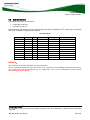
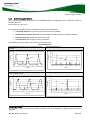
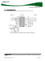
1
Plug & Play Wireless CPU® Integra M2106+ Product Specification Reference: WA_DEV_M2106+_PTS_003 Revision: 001 Date: April, 2007 Supports Open AT® embedded ANSI C applications ©Confidential Page: 1 / 77 This document is the sole and exclusive property of Wavecom. Not to be distributed or divulged without prior written agreement. WA_DEV_M2106+_PTS_003-001 April, 2007 Integra M2106+ Document Information Revision Date 001 April 2007 History of the evolution Creation ©Confidential Page: 2 / 77 This document is the sole and exclusive property of Wavecom. Not to be distributed or divulged without prior written agreement. WA_DEV_M2106+_PTS_003-001 April, 2007 Integra M2106+ Caution Information furnished herein by Wavecom is accurate and reliable. However, no responsibility is assumed for its use. Please read carefully the safety precautions for an application based on the Integra M2106+ Wireless CPU®. Trademarks WAVECOM®, Open AT®, Wireless CPU® are trademarks or registered trademarks of WAVECOM SA. All other company and/or product names mentioned may be trademarks or registered trademarks of their respective owners. Copyright This manual is copyrighted by WAVECOM with all rights reserved. No part of this manual may be reproduced in any form without the prior written permission of WAVECOM. No patent liability is assumed with respect to the use of the information contained herein. ©Confidential Page: 3 / 77 This document is the sole and exclusive property of Wavecom. Not to be distributed or divulged without prior written agreement. WA_DEV_M2106+_PTS_003-001 April, 2007 Integra M2106+ Web Site Support General information about Wavecom and its range of www.wavecom.com products: Carrier/Operator approvals: ® www.wavecom.com/approvals Open AT Introduction: www.wavecom.com/OpenAT Developer support for software and hardware: www.wavecom.com/forum ©Confidential Page: 4 / 77 This document is the sole and exclusive property of Wavecom. Not to be distributed or divulged without prior written agreement. WA_DEV_M2106+_PTS_003-001 April, 2007 Integra M2106+ Overview This document defines and specifies the Integra M2106+ Plug & Play Wireless CPU®. It also contains guidelines for application design and recommendations to use the Integra development kit. This Plug and Play Wireless CPU® is an E-GSM/GSM - GPRS Class 10 900/1800 product, based on the Q24 Wireless CPU® which supports Open AT® by default. Open AT® is the world’s most comprehensive cellular development environment, which allows embedded standard ANSI C applications to be natively executed directly on the Wireless CPU®. This Product Specification document covers the Wireless CPU® alone and does not include the programmable capabilities provided via the use of Open AT® Software Suites. For detailed software programming guides, refer to the documents shown in the “Reference Documents” section. ©Confidential Page: 5 / 77 This document is the sole and exclusive property of Wavecom. Not to be distributed or divulged without prior written agreement. WA_DEV_M2106+_PTS_003-001 April, 2007 Integra M2106+ Contents 1 1.1 2 References ........................................................................................................................................... 10 Reference Documents........................................................................................................................... 10 1.1.1 Open AT® Software Documentation............................................................................................ 10 1.1.2 AT Software Documentation ....................................................................................................... 10 1.1.3 Other Documents ........................................................................................................................ 10 General Description ............................................................................................................................ 13 2.1 2.2 2.3 2.4 2.5 Presentation .......................................................................................................................................... 13 Key Features ......................................................................................................................................... 14 Difference between M2106B and M2106+ Wireless CPU® .................................................................. 14 GSM/GPRS Services ............................................................................................................................ 15 Functional Description........................................................................................................................... 16 2.5.1 Block Diagram............................................................................................................................. 16 2.5.2 RF Functionalities ....................................................................................................................... 17 2.5.3 Firmware ..................................................................................................................................... 17 2.6 CE Conformity ....................................................................................................................................... 17 2.7 RoHS Compliance ................................................................................................................................. 17 3 Interfaces.............................................................................................................................................. 18 3.1 General Purpose Connector.................................................................................................................. 18 3.1.1 Pin Allocation .............................................................................................................................. 19 3.1.2 Signal Description ....................................................................................................................... 20 3.2 Power Supply ........................................................................................................................................ 22 3.3 ON/~OFF Control .................................................................................................................................. 24 3.3.1 General Description .................................................................................................................... 24 3.3.2 Operating Sequences ................................................................................................................. 25 3.4 Alternative Download Control (BOOT pin) ............................................................................................ 28 3.5 Reset Signal (~RST) ............................................................................................................................. 29 3.5.1 General Presentation .................................................................................................................. 29 3.5.2 Reset Sequence.......................................................................................................................... 30 3.6 Serial Link.............................................................................................................................................. 31 3.6.1 Interface Description ................................................................................................................... 31 3.6.2 Application Note with Level Shifter ............................................................................................. 32 3.7 SPI Bus.................................................................................................................................................. 32 3.8 Keyboard Interface ................................................................................................................................ 33 3.9 Audio Interface ...................................................................................................................................... 34 3.9.1 Microphone Inputs....................................................................................................................... 34 3.9.2 Speaker Outputs ......................................................................................................................... 36 3.10 General Purpose Input/Output .............................................................................................................. 38 3.11 Analog to Digital Converter (ADC) ........................................................................................................ 39 ©Confidential Page: 6 / 77 This document is the sole and exclusive property of Wavecom. Not to be distributed or divulged without prior written agreement. WA_DEV_M2106+_PTS_003-001 April, 2007 Integra M2106+ 3.12 Activity Status Indication (Flashing LED) .............................................................................................. 39 3.13 RF Interface........................................................................................................................................... 41 3.13.1 RF Interface Characteristics........................................................................................................ 41 3.13.2 RF Performance.......................................................................................................................... 41 3.13.3 Antenna Specifications................................................................................................................ 42 3.14 SIM Card Interface ................................................................................................................................ 43 3.14.1 Internal SIM Card Interface ......................................................................................................... 44 3.14.2 External SIM Card Interface........................................................................................................ 45 4 Technical Specifications..................................................................................................................... 47 4.1 4.2 Environmental Constraints .................................................................................................................... 47 Mechanical Specifications ..................................................................................................................... 47 4.2.1 Mechanical Overview .................................................................................................................. 47 4.2.2 Mechanical Characteristics ......................................................................................................... 48 4.2.3 Mechanical Drawings .................................................................................................................. 48 4.3 Electrical Specifications......................................................................................................................... 50 4.3.1 Power Mode ................................................................................................................................ 50 4.3.2 Power Consumption without Open AT® Processing ................................................................... 51 4.3.3 Power Consumption with Open AT® Processing ........................................................................ 52 4.3.4 Current Consumption Waveform ................................................................................................ 53 5 Applicable Normative Documents ..................................................................................................... 54 5.1 5.2 Normative Specifications....................................................................................................................... 54 Environmental Specifications ................................................................................................................ 55 6 Using the Integra Wireless CPU® ....................................................................................................... 58 6.1 Firmware Upgrade................................................................................................................................. 58 6.1.1 Nominal Upgrade Procedure....................................................................................................... 58 6.1.2 Alternative Procedure.................................................................................................................. 58 6.2 Guidelines for Application Design ......................................................................................................... 58 6.2.1 Hardware Recommendations...................................................................................................... 58 6.2.2 Antenna ....................................................................................................................................... 59 6.2.3 Minimum Hardware Interface to Get Started .............................................................................. 59 6.3 3 V/5 V SIM Management ..................................................................................................................... 60 6.4 Installation of the Integra M2106+ Wireless CPU® on an Application Board ........................................ 61 6.5 Integra Development Kit Board Presentation........................................................................................ 63 6.5.1 Getting Started ............................................................................................................................ 64 6.5.2 Setting up Terminal Emulator...................................................................................................... 64 6.5.3 Example of AT Commands ......................................................................................................... 65 7 Troubleshooting .................................................................................................................................. 68 7.1 7.2 7.3 Not Connecting Through the Serial Link ............................................................................................... 68 Receiving 'no carrier' Messages .......................................................................................................... 69 Receiving error Messages..................................................................................................................... 71 ©Confidential Page: 7 / 77 This document is the sole and exclusive property of Wavecom. Not to be distributed or divulged without prior written agreement. WA_DEV_M2106+_PTS_003-001 April, 2007 Integra M2106+ 8 Annexes................................................................................................................................................ 73 8.1 Supplier Information .............................................................................................................................. 73 8.1.1 General Purpose Connector ....................................................................................................... 73 8.1.2 Antenna connector ...................................................................................................................... 74 8.1.3 SIM Card Holder ......................................................................................................................... 74 8.2 Safety Recommendations (for information only) ................................................................................... 75 8.2.1 RF Safety .................................................................................................................................... 75 8.2.2 General safety............................................................................................................................. 76 8.2.3 Safety Standards......................................................................................................................... 77 ©Confidential Page: 8 / 77 This document is the sole and exclusive property of Wavecom. Not to be distributed or divulged without prior written agreement. WA_DEV_M2106+_PTS_003-001 April, 2007 Integra M2106+ List of Figures Figure 1: M2106+ view .................................................................................................................................... 13 Figure 2: Integra M2106+ Wireless CPU® connectors .................................................................................... 13 Figure 3: Functional architecture ..................................................................................................................... 16 Figure 4: 50-pin connector............................................................................................................................... 18 Figure 5: Pin allocation .................................................................................................................................... 19 Figure 6: Power-ON sequence diagram (no PIN code activated) ................................................................... 25 Figure 7: Power-OFF sequence diagram ........................................................................................................ 27 Figure 8: BOOT application schematic............................................................................................................ 28 Figure 9: Reset application schematic............................................................................................................. 29 Figure 10: Reset sequence diagram ............................................................................................................... 30 Figure 11: Level shifter application diagram for serial link* ............................................................................. 32 Figure 12: MIC2 input connection.................................................................................................................... 35 Figure 13: MIC1 differential connection........................................................................................................... 36 Figure 14: Speaker differential connection ...................................................................................................... 37 Figure 15: Speaker single-ended connection.................................................................................................. 37 Figure 16: SIM card holder extraction ............................................................................................................. 44 Figure 17: Schematic for external SIM card holder ......................................................................................... 46 Figure 18: Mechanical overview 1/3 ................................................................................................................ 47 Figure 19: Mechanical overview 2/3 ................................................................................................................ 47 Figure 20: Mechanical overview 3/3 ................................................................................................................ 48 Figure 21: Schematic for a SIM level shifter to manage 5 V SIM cards.......................................................... 60 Figure 22: Recommended footprint ................................................................................................................. 62 Figure 23: Integra development kit board description ..................................................................................... 63 Figure 24: High and low profile CLP connectors ............................................................................................. 73 Figure 25: Flexible flat cable (Part number: FFSD-20-S-10-01-N).................................................................. 73 Figure 26: Flex cable connector (Part number: FLE 125 01LDVA)................................................................. 73 Figure 27: MMCX connector example (right angle)......................................................................................... 74 ©Confidential Page: 9 / 77 This document is the sole and exclusive property of Wavecom. Not to be distributed or divulged without prior written agreement. WA_DEV_M2106+_PTS_003-001 April, 2007 Integra M2106+ Erreur ! Style non défini. 1 References 1.1 Reference Documents Note: All below documents are related to V3.12 Open AT® Software and 6.57a Open AT® Firmware. Wavecom recommends that the developer should check the web site for the latest documentation 1.1.1 Open AT® Software Documentation [1] Getting started with Open AT® (Ref. WM_ASW_OAT_CTI_00001) [2] Open AT® Tutorial (Ref. WM_ASW_OAT_UGD_00001) [3] Tools Manual (Ref. WM_ASW_OAT_UGD_00003) [4] Open AT® Basic Development Guide (Ref. WM_ASW_OAT_UGD_00002) [5] Open AT® ADL guide (Ref. WM_ASW_OAT_UGD_00006) [6] Open AT® V3.12 Customer Release Note (Ref. WM_DEV_OAT_DVD_165) 1.1.2 [7] AT Software Documentation AT commands Interface Guide for X57 Release (Ref. WM_ASW_OAT_UGD_00044) [8] 1.1.3 Open AT® 6.57a FW Release Note (Ref. WM_DEV_OAT_DVD_237) Other Documents [9] Environmental conditions and environmental tests for telecommunication equipment - ETS 300 019 [10] Wavecom Acceptance and Verification Plan (Ref. WAVE Plan, Release 1.4) [11] Power Consumption Modes Application note (Ref. WM_ASW_OAT_APN_012) . ©Confidential Page: 10 / 77 This document is the sole and exclusive property of Wavecom. Not to be distributed or divulged without prior written agreement. WA_DEV_M2106+_PTS_003-001 April, 2007 Integra M2106+ Erreur ! Style non défini. 1.2 List of Abbreviations Abbreviation AC Description Alternating Current ADC Analog to Digital Converter A/D Analog to Digital conversion AT ATtention (prefix for modem commands) AUX AUXiliary CBS Cell Broadcast Service CLK CLocK CMOS Complementary Metal Oxide Semiconductor CTS Clear To Send dB Decibel DC Direct Current DCD Data Carrier Detect DCS Digital Cellular System DSR Data Set Ready DTR Data Terminal Ready E-GSM Extended GSM EN ENable ESD ElectroStatic Discharges ETSI European Telecommunications Standards Institute GND GrouND GPIO General Purpose Input Output GPO General Purpose Output GPRS General Packet Radio Service GSM Global System for Mobile communications Hi Z High impedance (Z) I/O Input / Output KSPS Kilo Samples Per Second LED Light Emitting Diode LSB Less Significant Bit MAX MAXimum MIC MICrophone MIN MINimum MO Mobile Originated MS Mobile Station ©Confidential Page: 11 / 77 This document is the sole and exclusive property of Wavecom. Not to be distributed or divulged without prior written agreement. WA_DEV_M2106+_PTS_003-001 April, 2007 Integra M2106+ Erreur ! Style non défini. MT Mobile Terminated PC Personal Computer PCB Printed Circuit Board PCS Personal Communications Service RAM Random Access Memory RF Radio Frequency RI Ring Indicator RST ReSeT RTS Request To Send RX Receive SAR Specific Absorption Rate SIM Subscriber Identification Module SMS Short Message Service SPI Serial Peripheral Interface SPK SPeaKer SRAM Static RAM TAC Type Approval Code TDMA Time Division Multiple Access TU Typical Urban fading profile TUHigh Typical Urban, High speed fading profile TVS Transient Voltage Suppressor TX Transmit TYP TYPical UART Universal Asynchronous Receiver-Transmitter USSD Unstructured Supplementary Service Data VSWR Voltage Stationary Wave Ratio WAP Wireless Application Protocol ©Confidential Page: 12 / 77 This document is the sole and exclusive property of Wavecom. Not to be distributed or divulged without prior written agreement. WA_DEV_M2106+_PTS_003-001 April, 2007 Integra M2106+ Erreur ! Style non défini. 2 General Description 2.1 Presentation The Integra M2106+ Wireless CPU® is a self-contained E-GSM/GSM-GPRS 900/1800 dual-band Wireless CPU® and is GPRS class 10 capable. Figure 1: M2106+ view It includes a Quik Q24 Wireless CPU® and its interfaces are available through: • A 50-pin connector for Baseband analog and digital interfaces (General Purpose Connector) • A RF connector, MMCX type • A SIM card holder SIM c a rd h o ld er RF c o n n ec t o r 5 0 - p in c o n n ec t o r Figure 2: Integra M2106+ Wireless CPU® connectors The mating connectors for the General Purpose connector and RF connector are standard and easy-to-find. ©Confidential Page: 13 / 77 This document is the sole and exclusive property of Wavecom. Not to be distributed or divulged without prior written agreement. WA_DEV_M2106+_PTS_003-001 April, 2007 Integra M2106+ Erreur ! Style non défini. 2.2 Key Features Integra M2106+ Wireless CPU® features: • Open AT® programmable: o o o o Native execution of embedded standard ANSI C applications, Custom AT command creation, Custom application library creation, Standalone operation. • Overall dimensions: 46 x 64 x 12 mm, • Complete shielding, • 2-Watt E-GSM 900 radio section, • 1-Watt GSM1800 radio section, • Full GSM or GSM / GPRS software stack, • GPRS class 10, • 32 Mbits of Flash memory and 16 Mbits of SRAM, • Internal 3V/1.8V SIM interface, • Real Time Clock (RTC) with calendar, • Echo cancellation + noise reduction, • Complete interfacing through a 50-pin General Purpose Connector: o o o o o o 2.3 Power supply, Serial link, Audio interface, SIM card interface, Keyboard interface, GPIO. Difference between M2106B and M2106+ Wireless CPU® The Integra M2106+ Wireless CPU® is designed for replacing Integra M2106B Wireless CPU®. There are some feature differences between these two. M2106B Wireless CPU® M2106+ Wireless CPU® SIM Interface SRAM size RF functionalities 3V only 4 Mbits Dual band capability (E-GSM900 / 1800) Signal description -- 3V / 1V8 16 Mbits Quad band capability* (GSM850/ E-GSM900 / DCS1800 / PCS1900) I/O type and Reset state See section 3.1.2 details (*) See section 2.5.2 for further details ©Confidential Page: 14 / 77 This document is the sole and exclusive property of Wavecom. Not to be distributed or divulged without prior written agreement. WA_DEV_M2106+_PTS_003-001 April, 2007 Integra M2106+ Erreur ! Style non défini. 2.4 GSM/GPRS Services The basic services provided by the Integra M2106+ Wireless CPU® are listed in the table below: Standard Interface Audio SMS Data Fax GPRS SIM • • • • • • • • • • • • • • • • • • • • • • • • • • • 900 MHz, E-GSM compliant; Class 4 (2 W). 1800 MHz ; Class 1 (1 W) GSM phase 2 GPRS Class 10 Serial interface V.24/CMOS AT command set based on V.25ter and GSM 07.05 & 07.07. Auto-bauding function between 2400 bits/s and 19200 bits/s No auto-framing available Half rate / Full rate / Enhanced Full rate operation Accessories (options): Handset, Car Kit Mobile Originated (MO) and Mobile Terminated (MT) Mode Text & PDU point to point Cell broad cast In accordance with GSM 07.05 Asynchronous 2400, 4800, 9600, 14400 bits/s Transparent and Non Transparent mode In Non Transparent Mode: 300, 1200, 1200/75 bauds Mode 3.1 kHz (PSTN) and V110 (ISDN) 2400/4800/7200/9600 bits/s, GSM teleservice 62 in Transparent Mode Class 1 & Class 2 Group 3 compatible Class 10 Coding schemes: CS1 to CS4 Compliant with SMG31bis Plug-In SIM 3V/1.8V Full compatible with GSM 11.11 SIM Toolkit Release 97 ©Confidential Page: 15 / 77 This document is the sole and exclusive property of Wavecom. Not to be distributed or divulged without prior written agreement. WA_DEV_M2106+_PTS_003-001 April, 2007 Integra M2106+ Erreur ! Style non défini. 2.5 Functional Description 2.5.1 Block Diagram In teg ra M 2 1 0 6 + W ire less CPU ® Ser ia l In t erf a c e A n t en n a c o n n ec t o r SPI In t erfa c e Key p a d In t erfac e BOOT Q 2 4 W ir eles s CPU ® RESET M ic r o p h o n e Sp ea k er M ic r o p h o n e A u d io In t er fa c e Sp ea k er G PIO & A D C O p era t in g St at u s In d ica t io n VB a t Po w er Su p p ly SIM VCC SIM c a r d So c ket SIM c a rd H o ld er 5 0 - p in co n n ect o r Figure 3: Functional architecture ©Confidential Page: 16 / 77 This document is the sole and exclusive property of Wavecom. Not to be distributed or divulged without prior written agreement. WA_DEV_M2106+_PTS_003-001 April, 2007 Integra M2106+ Erreur ! Style non défini. 2.5.2 RF Functionalities The Radio Frequency (RF) functionalities comply with the Phase II E-GSM 900 / DCS 1800 recommendations. The frequencies are: EGSM 900 DCS 1800 Transmit band (TX) Receive band (RX) 880 to 915 MHz 1710 to 1785 MHz 925 to 960 MHz 1805 to 915 MHz The Integra M2106+ Wireless CPU® also gives a quad band capability (GSM850, EGSM900, DCS 1800 and PCS 1900) and it is qualified by Wavecom. Warning: The Integra M2106+ Wireless CPU® is not certified for American market for operation band of GSM850 and PCS1900. Customers wishing to sell the Integra M2106+ Wireless CPU® in American region shall be wholly responsible for any certifications and carrier approval required. 2.5.3 Firmware The Integra M2106+ Wireless CPU® is designed to integrate into various types of applications. For applications using an external processor to control the Wireless CPU®, the firmware offers a software interface based on AT commands. A development kit for the Integra M2106+ Wireless CPU® is also available to test customer software applications. 2.6 CE Conformity The Integra M2106+ Wireless CPU® bears the CE marking. This symbol guarantees the compliance of the design and implementation of the Integra M2106+ Wireless CPU® with the R&TTE directive. 2.7 RoHS Compliance The Integra M2106+ Wireless CPU® is now compliant with RoHS (Restriction of Hazardous Substances in Electrical and Electronic Equipment) Directive 2002/95/EC which sets limits for the use of certain restricted hazardous substances. This directive states that “from 1st July 2006, new electrical and electronic equipment put on the market does not contain lead, mercury, cadmium, hexavalent chromium, polybrominated biphenyls (PBB), and polybrominated diphenyl ethers (PBDE)”. ©Confidential Page: 17 / 77 This document is the sole and exclusive property of Wavecom. Not to be distributed or divulged without prior written agreement. WA_DEV_M2106+_PTS_003-001 April, 2007 Integra M2106+ Erreur ! Style non défini. 3 Interfaces This chapter describes the hardware interfaces of the Integra M2106+ Wireless CPU®. 3.1 General Purpose Connector A 50-pin standard connector provides the baseband analog and digital interfaces. 50 2 49 1 Figure 4: 50-pin connector ©Confidential Page: 18 / 77 This document is the sole and exclusive property of Wavecom. Not to be distributed or divulged without prior written agreement. WA_DEV_M2106+_PTS_003-001 April, 2007 Integra M2106+ Erreur ! Style non défini. 3.1.1 Pin Allocation GND 1 2 GND + 5 V 3 4 + 5 V CT 1 0 9 /D CD 5 6 GND G PIO 4 7 8 SPK2 N CT 1 2 5 /RI 9 10 SPK2 P FLA SH IN G LED 11 12 SPK1 P CT 1 0 6 /CT S 13 14 SPK1 N O N /~ O FF 15 16 M IC2 P A U XV 0 17 18 M IC2 N ~ RST 19 20 M IC1 P GND 21 22 M IC1 N B OOT 23 24 GND CT 1 0 3 /T X 25 26 G PIO 0 CT 1 0 7 /D SR 27 28 CT 1 0 4 /RX CT 1 0 8 -2 /D T R 29 30 CT 1 0 5 /RT S CO L3 31 32 CO L4 CO L1 33 34 CO L2 RO W 4 35 36 CO L0 RO W 2 37 38 RO W 3 RO W 0 39 40 RO W 1 NC 41 42 SPI EN , GPO 3 SPI IO 43 44 SPI CLK SIM CLK 45 46 SIM RST SIM V CC 47 48 SIM PRES1 SIM D A T A 49 50 G PO 0 Figure 5: Pin allocation ©Confidential Page: 19 / 77 This document is the sole and exclusive property of Wavecom. Not to be distributed or divulged without prior written agreement. WA_DEV_M2106+_PTS_003-001 April, 2007 Integra M2106+ Erreur ! Style non défini. 3.1.2 Signal Description The following table presents the main characteristics of the 50-pin connector. Pin # Name 1 2 3 4 GND GND +5V +5V 5 CT109/DCD 6 7 Reset State I/O I/O type Description Comment Ground Ground High current High current High current High current I I ----- Supply Supply O High Z 2X GND GPIO4 I/O -High Z CMOS/2X 8 SPK2N O High Z Analog 9 CT125/RI O High Z 2X 10 SPK2P O High Z Analog 11 Flashing LED I/O High Z CMOS/2X 12 SPK1P O High Z Analog 13 CT106/CTS O High Z 1X 14 SPK1N O High Z Analog 15 ON/~OFF I Pull down -- Power control signal 16 MIC2P I High Z Analog Microphone 2 positive input 17 AUXV0 I HZ Analog Auxiliary ADC input 18 MIC2N I High Z Analog Microphone 2 negative input Serial Link Data Carrier Detect Ground General Purpose I/O Speaker2 negative output Serial Link Ring Indicator Speaker 2 positive output Operating mode indication LED Speaker 1 positive output Serial Link Clear To Send Speaker 1 negative output 19 ~RST I/O -- SCHMITT Reset active low 20 MIC1P I High Z Analog Microphone 1 positive input 21 GND 22 MIC1N -I ©Confidential High Z Ground Analog High current Driven by Wireless CPU® ON = VCC Can be tied to GND if not used To be driven by an Open Collector. Internal pull-up 4.7 kΩ. High Current Microphone 1 negative input Page: 20 / 77 This document is the sole and exclusive property of Wavecom. Not to be distributed or divulged without prior written agreement. WA_DEV_M2106+_PTS_003-001 April, 2007 Integra M2106+ Erreur ! Style non défini. Pin # Name Reset State I/O I Pull up I/O type Description Comment CMOS Alternative download mode selection To be driven by Open Collector Internal pull-up 100 kΩ Ground High current Pull up to +5V with 100kΩ when not used 23 BOOT 24 GND 25 CT103/TX I Pull down CMOS Serial Link - Transmit 26 GPIO0 I/O High Z CMOS/2X General Purpose I/O 27 CT107/DSR O Output high 1X Serial Link Data Set Ready 28 CT104/RX O Output high 1X Serial Link – Receive 29 CT108-2/DTR I Pull down CMOS 30 CT105/RTS I Pull down CMOS Serial Link Request To Send 31 COL3 I/O Pull up CMOS/1X Keyboard column 32 COL4 I/O Pull up CMOS/1X Keyboard column 33 COL1 I/O Pull up CMOS/1X Keyboard column 34 COL2 I/O Pull up CMOS/1X Keyboard column 35 ROW4 I/O Pull down CMOS/1X Keyboard row 36 COL0 I/O Pull up CMOS/1X Keyboard column 37 ROW2 I/O Pull down CMOS/1X Keyboard row 38 ROW3 I/O Pull down CMOS/1X Keyboard row 39 ROW0 I/O Pull down CMOS/1X Keyboard row 40 ROW1 I/O Pull down CMOS/1X Keyboard row 41 NC 42 SPI_EN or GPO3 O Output high 1X or 3X SPI enable or General purpose output 43 SPI_IO I/O Pull up CMOS/1X SPI Data 44 SPI_CLK O Pull up 1X SPI Clock -- -- ©Confidential Serial Link Pull up to +5V with Data Terminal Ready 100 kΩ when not used Pull up to +5V with 100 kΩ when not used Not connected Multiplexed Page: 21 / 77 This document is the sole and exclusive property of Wavecom. Not to be distributed or divulged without prior written agreement. WA_DEV_M2106+_PTS_003-001 April, 2007 Integra M2106+ Erreur ! Style non défini. Pin # Name I/O Reset State I/O type 45 SIM_CLK O Output low -- 46 SIM_RST O Output low -- 47 SIM_VCC O -- Supply Description Clock for SIM Interface Reset for SIM interface SIM card supply Comment 3V /1.8V mode 3V /1.8V mode 3V /1.8V mode 6 mA max Connected to SIM connector pin 8. * 48 SIM_PRES I High Z CMOS SIM card detect 49 SIM_DATA I/O -- 50 GPO0* O Output low Output high I/O for SIM interface General purpose output 3X Pin 4 of SIM connector must be pulled down to GND with 1 kΩ 3V /1.8V mode Multiplexed GPO0 is a general purpose output for selection of external 3 V or 5 V SIM. Table 1: Integra M2106+ operating conditions Parameter I/O type Min Max Condition Vinput low Vinput high Voutput low CMOS CMOS 1X 2X 3X 1X 2X 3X CMOS -0.5 V 2.1 V 0V 0V 0V 2.6 V 2.6 V 2.6 V 0.8 V 3.0 V 0.2 V 0.2 V 0.2 V 2.86 V 2.86 V 2.86 V 40µA IOL = -1 mA IOL = -2 mA IOL = -3 mA IOH = 1 mA IOH = 2 mA IOH = 3 mA Vf max = 0.33V Voutput high I clamp 3.2 Power Supply The main power supply is provided through four pins of the General Purpose Connector: • Pins 3 and 4 for the + 5 V • Pins 1 and 2 for the ground (GND) Pins 6, 21, and 24 are also the ground connection for the correct ground plane required for correct RF functionality. A 5 V ± 5% - 1.5 A power unit is required to supply the Wireless CPU® in order to avoid serious RF malfunctions. However, the Wireless CPU® does not need a constant 1.5 A current at 5 V on this power supply. ©Confidential Page: 22 / 77 This document is the sole and exclusive property of Wavecom. Not to be distributed or divulged without prior written agreement. WA_DEV_M2106+_PTS_003-001 April, 2007 Integra M2106+ Erreur ! Style non défini. Pin description Pin number Name Reset state Description Comment 1 2 3 4 6 21 24 GND GND +5V +5V GND GND GND -------- Ground Ground Supply Supply Ground Ground Ground High Current High Current High Current High Current High Current High Current High Current ©Confidential Page: 23 / 77 This document is the sole and exclusive property of Wavecom. Not to be distributed or divulged without prior written agreement. WA_DEV_M2106+_PTS_003-001 April, 2007 Integra M2106+ Erreur ! Style non défini. 3.3 3.3.1 ON/~OFF Control General Description This input is used to switch ON or OFF the Integra Wireless CPU®. A high level signal must be provided on the ON/~OFF pin to switch ON the Wireless CPU®. To switch OFF, the ON/~OFF signal must be reset and an AT+CPOF command must be sent to the Wireless CPU®. Pin description Signal Pin number I/O Reset State I/O type Description ON/∼OFF 15 I Pull down -- Power Control Signal Electrical characteristics Parameter Min Input Impedance ( R ) 47 Max Unit kΩ Input Impedance ( C ) 50 pF Operating conditions Parameter I/O type Min Max Unit VIL -- 0 0.6 V VIH -- 3.4 5.6 V Warning: All external signals must be inactive when the Wireless CPU® is OFF to avoid any damage when starting and allow Integra Wireless CPU® to start and stop correctly. ©Confidential Page: 24 / 77 This document is the sole and exclusive property of Wavecom. Not to be distributed or divulged without prior written agreement. WA_DEV_M2106+_PTS_003-001 April, 2007 Integra M2106+ Erreur ! Style non défini. 3.3.2 3.3.2.1 Operating Sequences Power-ON Once the Wireless CPU® is supplied the ON/~OFF signal must be asserted high during a delay of Ton-hold (Hold delay on the ON/~OFF signal) to power-ON. After this delay, once the firmware has completed its power-up sequence, an internal logic maintains the Wireless CPU® in power ON condition. You must not de-assert this ON/~OFF signal before this internal logic is internally asserted by the firmware; the Wireless CPU® would not start-up otherwise PO W ER SUPPLY ON /~OFF T on -h old IN T ERN A L RST T rs t (4 2 m s t y p ) A T an sw ers « O K » STA T E OF TH E W ireles s CPU ® W ireles s CPU O FF ® RESET m od e W ireles s CPU ® ON W ireles s CPU ® REA D Y (n o lo c . u p d at e) SIM an d N et w ork d ep en d en t Figure 6: Power-ON sequence diagram (no PIN code activated) The duration of the firmware power-up sequence depends on several factors: • firmware version used by the Wireless CPU®, • need to perform a recovery sequence if the power has been lost during a flash memory modification. Other factors have a minor influence • number of parameters stored in EEPROM by the AT commands received so far • ageing of the hardware components, especially the flash memory • temperature conditions The recommended way to de-assert the ON/~OFF signal is to use either an AT command or WIND indicators: the application must detect the end of the power-up initialization and de-assert ON/~OFF afterwards. • Send an “AT” command and wait for the “OK” answer: once the initialization is complete the AT 1 interface answers « OK » to “AT” message . • Wait for the “+WIND: 3” message: after initialization, the Wireless CPU®, if configured to do so, will return an unsolicited “+WIND: 3” message. The generation of this message is enabled or disabled via 1 If the application manages hardware flow control, an AT command can be sent during the initialisation phase. ©Confidential Page: 25 / 77 This document is the sole and exclusive property of Wavecom. Not to be distributed or divulged without prior written agreement. WA_DEV_M2106+_PTS_003-001 April, 2007 Integra M2106+ Erreur ! Style non défini. an AT command. Note: See also “AT Commands Interface Guide” [7] for more information on these commands. Proceeding thus – by software detection - will always prevent the application from de-asserting the ON/~OFF signal too early. If WIND indicators are disabled or AT commands unavailable or not used, it is still possible to de-assert ON/~OFF after a delay long enough (Ton-hold) to ensure that the firmware has already completed its power-up initialization. The table below gives the minimum values of Ton-hold for all firmware versions: Ton-hold minimum values Open AT® Firmware 6.57 & above Ton-hold Safe evaluations of the firmware power-up time 8s The above figures take the worst cases into account: power-loss recovery operations, slow flash memory operations in high temperature conditions, and so on. But they are safe because they are large enough to ensure that ON/~OFF is not de-asserted too early. Additional notes: 1. Typical power-up initialization time figures for best cases conditions (no power-loss recovery, fast and new flash memory…) approximate 3.5 seconds in every firmware version. But releasing ON/~OFF after this delay does not guarantee that the application will actually start-up if for example the power plug has been pulled off during a flash memory operation, like a phone book entry update or an AT&W command. 2. The ON/~OFF signal can be left at a high level until switch OFF. But this is not recommended as it will prevent the AT+CPOF command from performing a clean power-off. (see also Note in section 3.3.2.2 Power-OFF for an alternate usage). 3. When using a battery as power source, it is not recommended to let this signal high: If the battery voltage is too low and the ON/~OFF signal at low level, an internal mechanism switches OFF the Wireless CPU®. This automatic process prevents the battery to be over discharged and optimize its life span. 4. During the power-ON sequence, an internal reset is automatically performed by the Wireless CPU® for 42 ms (typical). Any external reset should be avoided during this phase. 3.3.2.2 Power-OFF To properly power-OFF the Integra Wireless CPU®, the application must reset the ON/~OFF signal to low and then send the AT+CPOF command to de-register from the network and switch off the Wireless CPU®. Once the « OK » response is issued by the Wireless CPU®, the external power supply can be switched off. ©Confidential Page: 26 / 77 This document is the sole and exclusive property of Wavecom. Not to be distributed or divulged without prior written agreement. WA_DEV_M2106+_PTS_003-001 April, 2007 Integra M2106+ Erreur ! Style non défini. PO W ER S U PPLY O N / ~O FF A T + CPO F A T CO M M A N D O K r es p o n s e N et w o rk d ep en d en t STA TE OF T H E W ir eles s CPU ® W ir eles s CPU ® REA D Y W ir eles s CPU ® O FF Figure 7: Power-OFF sequence diagram Note: • If the ON/~OFF pin is maintained to ON (High Level) then the Wireless CPU® can’t be switched OFF and after using AT+CPOF command through the firmware, the Wireless CPU® enters in a Open AT® Max power consumption Mode (please refer to the “Power Consumption Modes” Application Note [11]). ©Confidential Page: 27 / 77 This document is the sole and exclusive property of Wavecom. Not to be distributed or divulged without prior written agreement. WA_DEV_M2106+_PTS_003-001 April, 2007 Integra M2106+ Erreur ! Style non défini. 3.4 Alternative Download Control (BOOT pin) If the standard X-modem download procedure does not work correctly, an alternative download procedure can be selected with the BOOT pin. This alternative procedure requires a specific downloading software tool. See section 6.1, "Firmware Upgrade" for details. Pin description Signal Pin # I/O Reset State I/O type Description BOOT 23 I Pull up CMOS Alternative download mode selection The alternative download procedure starts when this input is low during the Wireless CPU® power-ON. In normal mode, this pin must be left open. If used, this input must be driven either by an open collector or an open drain. See the example application diagram below. 1K Switch BOOT BOOT pin OR Switch BOOT 1K BOOT pin Figure 8: BOOT application schematic • If BOOT pin = 1, the Wireless CPU® is in normal mode • If BOOT pin = 0, the Wireless CPU® is in alternative download mode ©Confidential Page: 28 / 77 This document is the sole and exclusive property of Wavecom. Not to be distributed or divulged without prior written agreement. WA_DEV_M2106+_PTS_003-001 April, 2007 Integra M2106+ Erreur ! Style non défini. 3.5 Reset Signal (~RST) 3.5.1 General Presentation This signal is used to force a reset procedure by providing a low level for at least 500 µs. This signal must be considered as an emergency reset only. A reset procedure is automatically driven by an internal hardware component during the power-up sequence. Pin description Signal Pin # I/O Reset state I/O type Description ~RST 19 I/O -- SCHMITT Reset This signal can also be used as an output to provide a reset to an external device. If no external reset is necessary, this input can be left open. If it is used (emergency reset), it must be driven either by an open collector or an open drain output: RESET pin Switch RESET OR RESET pin Switch RESET Figure 9: Reset application schematic • ~RST pin 19 = 0, to activate Reset, • ~RST pin 19 = 1, to deactivate Reset. Reset signal electrical characteristics Parameter Min Input Impedance (R) Input Impedance (C) 4.7 Max Unit 10 kΩ nF Reset signal operating conditions * Parameter Min Max *VT*VT+ VOL VOH 1.1 V 1.7 V 1.2 V 1.9 V 0.4 V 2.0 V Condition IOL = -50 µA IOH = 50 µA VT-, VT+: Hysteresis thresholds • Additional comments on Reset procedure: ©Confidential Page: 29 / 77 This document is the sole and exclusive property of Wavecom. Not to be distributed or divulged without prior written agreement. WA_DEV_M2106+_PTS_003-001 April, 2007 Integra M2106+ Erreur ! Style non défini. The Reset process is activated either by the external ~RST signal or by an internal signal (coming from a reset generator). This automatic reset mode is activated at Power-up. The Wireless CPU® remains in Reset mode as long as the Reset signal is held low. • This signal should be used only for “emergency” resets: A software reset is always preferred to a hardware reset. 3.5.2 Reset Sequence To activate the « emergency » reset sequence, the ~RST signal must be set to low for 500 μs minimum. As soon as the reset is completed, the AT interface answers « OK » to the application. For this, the application must send AT↵ to get the “OK” response. If the application manages hardware flow control, the AT commands can be sent during the initialization phase. Another solution is to use the AT+WIND command to obtain an unsolicited status from the Wireless CPU®. For further details, refer to the AT commands Interface Guide documentation [7]. EXT ERN A L RES ET M in :5 0 0 μs Typ : 2 m s A T an s w er s “ O K” W ir eles s CPU ® W ir eles s CPU ® REA D Y ON RES ET m o d e STA TE OF T H E W ir eles s CPU ® I B B + RF = 2 0 to 40 m A W ir eles s CPU ® REA D Y I B B + RF < 1 2 0 m A w it h o u t loc u p d at e S IM an d n et w o rk d ep en d en t Figure 10: Reset sequence diagram ©Confidential Page: 30 / 77 This document is the sole and exclusive property of Wavecom. Not to be distributed or divulged without prior written agreement. WA_DEV_M2106+_PTS_003-001 April, 2007 Integra M2106+ Erreur ! Style non défini. 3.6 Serial Link 3.6.1 Interface Description A serial link interface is available on the Integra M2106+ Wireless CPU®. It is compliant with V24 signaling protocol with a 2.8 V electrical interface except TX, RTS, and DTR inputs, which can be either 5 V or 3 V. This means the serial link not compliant with the V28 standard and a level shifter is required to connect to a PC. The available signals are: • Tx data (CT103/TX), • Rx data (CT104/RX), • Request To Send (CT105/RTS), • Clear To Send (CT106/CTS), • Data Terminal Ready (CT108-2/DTR), • Data Set Ready (CT107/DSR). Two additional signals are necessary to have the complete RS232 signal set: • Data Carrier Detect (CT109/DCD), • Ring Indicator (CT125/RI). Pin description * Signal Pin # I/O Reset State I/O type Description CT103 / TX CT104 / RX CT105 / RTS CT106 / CTS CT107 / DSR CT108-2 / DTR CT109 / DCD CT125 / RI CT102 / GND 25 28 30 13 27 29 5 9 21,24…* I O I O O I O O Pull down Output high Pull down Output high Output high Pull down High Z High Z -- CMOS 1X CMOS 1X 1X CMOS 2X 2X Transmit serial data Receive serial data Request To Send Clear To Send Data Set Ready Data Terminal Ready Data Carrier Detect Ring Indicator Ground Any of the available GND pins can be used. ©Confidential Page: 31 / 77 This document is the sole and exclusive property of Wavecom. Not to be distributed or divulged without prior written agreement. WA_DEV_M2106+_PTS_003-001 April, 2007 Integra M2106+ Erreur ! Style non défini. 3.6.2 Application Note with Level Shifter A level shifter (MAX3238, for example) can be used for an application requiring V28 levels. Lev el Sh if t er W ireles s CP U ® T er m in al DTE D CE VCC VCC V CC ERRO R ON VCC VCC M A X3 2 3 8 Figure 11: Level shifter application diagram for serial link* * This application note is valid for VCC ≥ 3.0 Volt (see MAX3238 specifications). Auto shutdown mode is not used in this example. 3.7 SPI Bus The SPI bus includes a clock signal (SPI_CLK), an I/O signal (SPI_IO), and an enable signal (SPI_EN) complying with the SPI bus standard. Pin description * Signal Pin # I/O Reset State I/O type Description SPI_CLK SPI_IO SPI_EN* 44 43 42 O I/O O Pull up Pull up Output high 1X CMOS / 1X 1X SPI Serial Clock SPI Data SPI Enable Multiplexed with GPO3. ©Confidential Page: 32 / 77 This document is the sole and exclusive property of Wavecom. Not to be distributed or divulged without prior written agreement. WA_DEV_M2106+_PTS_003-001 April, 2007 Integra M2106+ Erreur ! Style non défini. 3.8 Keyboard Interface This interface provides 10 connections: • 5 rows (R0 to R4) and • 5 columns (C0 to C4). Digital scanning and debouncing are performed within the M2106+ Wireless CPU®. No discrete components such as R, C (Resistor, Capacitor) are required. Pin description Signal Pin # I/O Reset State I/O type Description ROW0 ROW1 ROW2 ROW3 ROW4 COL0 COL1 COL2 COL3 COL4 39 40 37 38 35 36 33 34 31 32 I/O I/O I/O I/O I/O I/O I/O I/O I/O I/O Pull down Pull down Pull down Pull down Pull down Pull up Pull up Pull up Pull up Pull up CMOS / 1X CMOS / 1X CMOS / 1X CMOS / 1X CMOS / 1X CMOS / 1X CMOS / 1X CMOS / 1X CMOS / 1X CMOS / 1X Row scan Row scan Row scan Row scan Row scan Column scan Column scan Column scan Column scan Column scan WARNING: This interface is not fully available with AT commands. An AT command allows the input key code to be obtained (see AT+CMER command description). This code must then be processed by the application. See the AT commands Interface Guide documentation [7] for details. ©Confidential Page: 33 / 77 This document is the sole and exclusive property of Wavecom. Not to be distributed or divulged without prior written agreement. WA_DEV_M2106+_PTS_003-001 April, 2007 Integra M2106+ Erreur ! Style non défini. 3.9 Audio Interface Two different microphone inputs (MIC1 and MIC2 inputs) and two different speaker outputs (SPK1 and SPK2 outputs) are supported. The connection can be either differential or single-ended but the use of a differential connection in order to reject common mode noise and TDMA noise is strongly recommended. When a single-ended connection is used, ensure to have a good ground plane, good filtering as well as shielding, in order to avoid any disturbance on the audio path. The Integra Wireless CPU® also includes an echo cancellation feature, which allows hands-free function. In some cases, ESD protection must be added on the audio interface lines. 3.9.1 Microphone Inputs The MIC2 inputs already include the biasing for an electret microphone allowing easy connection to a handset. The MIC1 inputs do not include an internal bias. MIC1 is appropriate for a hands-free system, headset or car kit. However, MIC1 can also be used for a handset with external biasing. 3.9.1.1 Common Microphone Input Characteristics Both microphone inputs are designed with the following audio transmit characteristics: Internal audio filter characteristics Frequency Gain 0-150 Hz 150-180 Hz 180-200 Hz 200-3700 Hz > 4000 Hz < -22 dB < -11 dB < -3 dB 0 dB < -60 dB The gains in the MIC inputs are internally adjusted and can be tuned from -6.5dB to 51.3dB by using AT commands. Two different gain ranges (controller1 and controller2) are available and can be selected with AT command software (refer to the AT commands Interface Guide documentation [7] for details). The two microphone inputs are composed of a 1st order high pass filter with a cut-off frequency of 330Hz. ©Confidential Page: 34 / 77 This document is the sole and exclusive property of Wavecom. Not to be distributed or divulged without prior written agreement. WA_DEV_M2106+_PTS_003-001 April, 2007 Integra M2106+ Erreur ! Style non défini. Table 2: Microphone gain vs Max input voltage* Using Controller 1 Using Controller 2 Transmit Gain (dB) Max Vin (mVrms) Transmit Gain (dB) Max Vin (mVrms) + 30 + 33 + 36 + 39 + 42 + 45 + 48 + 51 * 3.9.1.2 43.80 31.01 21.95 15.54 11.00 7.79 5.51 3.90 - -6.5 -6 0 +9.5 +10 +30.3 +30.8 +50.8 +51.3 3031 2861 1434 480 454 43.80 41.36 41.14 3.90 For further details, refer to the AT commands documentation [7] Main Microphone Inputs (MIC2) The MIC2 inputs are differential ones. They already include the convenient biasing for an electret microphone (1 mA and 2 volts). This electret microphone may be directly connected to these inputs. The impedance of the microphone on MIC2 must be around 2 kΩ. These MIC2 characteristics are the standard for a handset design. The input impedance is around 1.4kΩ +/- 20% between 400Hz and 4000Hz. AC coupling is already embedded in the Wireless CPU®. M IC2 P CM M IC2 N Figure 12: MIC2 input connection CM = 22 pF to 100 pF; 33 pF recommended CM must be as close to the microphone as possible. Microphone manufacturers provide this capacitor directly soldered on the microphone. Pin description Signal Pin # I/O Reset state I/O type Description MIC2P MIC2N 16 18 I I High Z High Z Analog Analog Microphone 2 positive input Microphone 2 negative input 3.9.1.3 Auxiliary Microphone Inputs (MIC1 Inputs) ©Confidential Page: 35 / 77 This document is the sole and exclusive property of Wavecom. Not to be distributed or divulged without prior written agreement. WA_DEV_M2106+_PTS_003-001 April, 2007 Integra M2106+ Erreur ! Style non défini. The MIC1 inputs are differential and do not include internal bias. These inputs are the standard for an external headset or a hands-free kit. To use these inputs with an electret microphone, bias has to be generated outside the Wireless CPU® according to the characteristics of this electret microphone. These inputs are provided either for an external headset or a hands-free kit. The input impedance is around 10kΩ +/- 30% between 400Hz and 4000Hz. AC coupling is already embedded in the Wireless CPU®. Pin description Signal Pin # I/O Reset state I/O type Description MIC1P MIC1N 20 22 I I High Z High Z Analog Analog Microphone 1 positive input Microphone 1 negative input Differential connection Vcc R1 R2 M IC1 P CM C2 M IC1 N R3 R4 Figure 13: MIC1 differential connection Vcc = 2.8 V from the analog power supply. R1 = R4 = from 100 to 330 Ω. R2 = R3 =1 kΩ to 3.3 kΩ according to the microphone characteristics. CM = 22 pF to 100 pF. C2 = 47 µF R1 and R4 are used as a voltage supply filter with C2. CM must be as close to the microphone as possible. Microphone manufacturers provide this capacitor directly soldered on the microphone. 3.9.2 Speaker Outputs ©Confidential Page: 36 / 77 This document is the sole and exclusive property of Wavecom. Not to be distributed or divulged without prior written agreement. WA_DEV_M2106+_PTS_003-001 April, 2007 Integra M2106+ Erreur ! Style non défini. 3.9.2.1 Common Speaker Output Characteristics The connection can be differential or single-ended but the use of a differential connection to reject common mode noise and TDMA noise is strongly recommended. Moreover in single-ended mode, ½ of the power is lost. When using a single-ended connection, ensure to have a good ground plane, good filtering as well as shielding, in order to avoid any disturbance on the audio path. Both SPK1 and SPK2 speaker outputs are push-pull amplifiers and can be loaded down to 32 Ω and up to 1 nF. The impedance of the speaker amplifier output in differential mode is: R ≤ 1 Ω±10 %. These outputs are differential and the output power can be adjusted in steps of 2 dB (see details in Table 3: Speaker gain vs Max output voltage). The output can be directly connected to a speaker. SPKx P SPKx N Figure 14: Speaker differential connection In case of a single-ended connection, only half of the output power is available when compared to a differential connection. C1 SPKx P + C3 Sp ea ker Zh p C2 R1 33 to 100p F + SPKx N Figure 15: Speaker single-ended connection C1 = from 100 nF to 47 µF as per the speaker characteristics. C2=C1 R1 = Speaker impedance Nevertheless, in a 32 Ω speaker case, it is possible to use a cheaper and smaller solution: R1=82 Ω and C2=4.7 µF ceramic. The gain in the speaker outputs are internally adjusted and can be tuned by using an AT command (refer to the AT commands documentation [7] for details). ©Confidential Page: 37 / 77 This document is the sole and exclusive property of Wavecom. Not to be distributed or divulged without prior written agreement. WA_DEV_M2106+_PTS_003-001 April, 2007 Integra M2106+ Erreur ! Style non défini. Table 3: Speaker gain vs Max output voltage * 3.9.2.2 Receive Gain (dB)* Max output level (Vrms) Min Speaker load (Ω) +2 0 -2 -4 -6 -8 -10 -12 -14 -16 -18 -20 -22 -24 -26 1.74 1.38 1.099 0.873 0.693 0.551 0.437 0.347 0.276 0.219 0.174 0.138 0.110 0.087 0.069 150 50 32 32 32 32 32 32 32 32 32 32 32 32 32 Analog gain: may not be significant Speaker 2 Output Pin description 3.9.2.3 Signal Pin # I/O Reset state I/O type Description SPK2P SPK2N 10 8 O O High Z High Z Analog Analog Speaker 2 positive output Speaker 2 negative output Speaker 1 Output Pin description Signal Pin # I/O Reset state I/O type Description SPK1P SPK1N 12 14 O O High Z High Z Analog Analog Speaker 1 positive output Speaker 1 negative output 3.10 General Purpose Input/Output Integra M2106+ Wireless CPU® provides 2 General Purpose I/Os (GPIOs). These are useful to control any external device. Pin description Signal Pin # I/O ©Confidential Reset state I/O type Description Page: 38 / 77 This document is the sole and exclusive property of Wavecom. Not to be distributed or divulged without prior written agreement. WA_DEV_M2106+_PTS_003-001 April, 2007 Integra M2106+ Erreur ! Style non défini. GPIO0 GPIO4 26 7 I/O I/O High Z High Z CMOS/ 2X CMOS/ 2X General Purpose I/O General Purpose I/O All digital I/Os comply with 3 volts CMOS. Both GPIO0 and GPIO4 are low level at reset. You can access (write or read) the GPIO value via AT+WIOW and AT+WIOR commands. See the AT commands Interface Guide documentation [7] for more details. 3.11 Analog to Digital Converter (ADC) An Analog to Digital Converter is provided by the Integra M2106+ Wireless CPU®. This converter is 10-bit resolution, ranging from 0 to 2.8 V. You can see the measurements via the AT+ADC command. See the AT commands Interface Guide documentation [7] for more details and sampling rate. Pin description Signal Pin # I/O Reset state I/O type Description AUXV0 17 I HZ Analog Auxiliary ADC input A/D converter electrical characteristics Parameter Min Resolution Input signal range ADC reference accuracy Integral accuracy Differential accuracy Input impedance (R) Input impedance (C) 0 0.75 +/- 1 +/- 1 10 Max Unit 10 bits V % LSB LSB MΩ nF 2.8 2 100 3.12 Activity Status Indication (Flashing LED) The activity status indication signal can be used to drive a Flashing LED through an open-collector transistor according to Wireless CPU® activity status. Pin description Signal Pin # I/O Reset state I/O type Description Flashing LED 11 I/O High Z CMOS/2X Activity status indication Operating status Integra M2106+ Wireless CPU® status LED status ©Confidential Page: 39 / 77 This document is the sole and exclusive property of Wavecom. Not to be distributed or divulged without prior written agreement. WA_DEV_M2106+_PTS_003-001 April, 2007 Integra M2106+ Erreur ! Style non défini. OFF Wireless CPU® in download mode or Wireless CPU® switched OFF. Permanent ON Slow flash LED ON for 200 ms OFF for 2 s Quick flash LED ON for200 ms OFF for 600 ms ©Confidential Wireless CPU® switched ON, not registered on the network Wireless CPU® switched ON Registered on the network Idle mode Wireless CPU® switched ON Registered on the network Communication in progress Page: 40 / 77 This document is the sole and exclusive property of Wavecom. Not to be distributed or divulged without prior written agreement. WA_DEV_M2106+_PTS_003-001 April, 2007 Integra M2106+ Erreur ! Style non défini. 3.13 RF Interface 3.13.1 RF Interface Characteristics The nominal impedance value is 50 Ω. The DC impedance is 0 Ω, connected to GND. The RF connector is a MMCX (Miniature Micro Connector) type. (See section "Supplier Information", 8.1.2) MMCX connector characteristics and benefits: • Standard type • Small physical size type • Easy-to-find product An antenna can be directly connected through the mating connector or using a small adaptor if necessary (MMCX-SMA for example) (see section "Supplier Information", 8.1.2). The MMCX connector incorporates a 'snap-on' latching action in order to make connection easier with excellent RF performance. This type of connector is suitable for the standard ranges of flexible and semirigid cables. 3.13.2 RF Performance RF performance is compliant with the GSM 05.05 recommendation. The main Receiver parameters are: • E-GSM900 Reference Sensitivity = -104 dBm Static & TUHigh • DCS1800 Reference Sensitivity = -102 dBm Static & TUHigh • Selectivity @ 200 kHz: > +9 dBc • Selectivity @ 400 kHz: > +41 dBc • Linear dynamic range: 63 dB • Co-channel rejection: >= 9 dBc The main Transmitter parameters are: • Maximum output power (E-GSM 900): 33 dBm ± 2 dB at ambient temperature • Maximum output power (DCS 1800): 30 dBm ± 2 dB at ambient temperature • Minimum output power (E-GSM 900): 5 dBm ±- 5 dB at ambient temperature • Minimum output power (DCS 1800): 0 dBm ±- 5 dB at ambient temperature ©Confidential Page: 41 / 77 This document is the sole and exclusive property of Wavecom. Not to be distributed or divulged without prior written agreement. WA_DEV_M2106+_PTS_003-001 April, 2007 Integra M2106+ Erreur ! Style non défini. 3.13.3 Antenna Specifications The antenna connected to the Integra M2106+ Wireless CPU® antenna via the MMCX connector should have the following characteristics: Table 4: Antenna requirements EGSM 900 DCS 1800 Frequency RX 925 to 960 MHz 1805 to 1880 MHz Frequency TX 880 to 915 MHz 1710 to 1785 MHz RF power stand 2 W at 2/8 duty cycle 1 W at 2/8 duty cycle Impedance VSWR 50 Ω Rx max 1.5 : 1 Tx max 1.5 : 1 Typical radiated gain ©Confidential 0 dBi in one direction at least Page: 42 / 77 This document is the sole and exclusive property of Wavecom. Not to be distributed or divulged without prior written agreement. WA_DEV_M2106+_PTS_003-001 April, 2007 Integra M2106+ Erreur ! Style non défini. 3.14 SIM Card Interface Integra M2106+ has an embedded SIM reader. This embedded SIM interface is for 3 V / 1V8 micro-SIM cards. If the application requires ISO SIM cards interface or 5 V SIM cards, the SIM interface signals are available on the General Purpose Connector. The Integra M2106+ Wireless CPU® SIM interface consists of 5 signals: • SIMVCC: SIM power supply • SIMRST: Reset • SIMCLK: Clock • SIMDATA: I/O port • SIMPRES1: SIM card presence detection The SIM interface controls a 3V / 1V8 SIM (and a 5V SIM through an external SIM driver). This interface is fully compliant with the GSM 11.11 recommendations concerning SIM functionality. To be fully compliant with GSM 11.11 recommendations concerning SIM functions, please add shielding for each SIM signals on the PCB Electrical characteristics Parameters SIM_DATA VIH SIM_DATA VIL SIM_RST, SIM_CLK VOH SIM_DATA SIM_RST, SIM_DATA, SIM_CLK VOL SIM_VCC* Output Voltage SIM_CLK Rise/Fall Time SIM_RST, Rise/Fall Time SIM_DATA, Rise/Fall Time SIM_CLK Frequency * Conditions IIH = ± 20 µA IIL = 1 mA Min 0.7xSIMVCC Typ Source current = 20 µA 0.9xSIMVCC V Source current = 20 µA 0.8xSIMVCC V 0.3xSIMVCC Sink current = -200 µA SIMVCC = 2.9V SIMVCC = 1.8V Max 2.84 1.77 2.90 1.8 Unit V V 0.4 V 2.96 1.86 V V Loaded with 30 pF 20 ns Loaded with 30 pF 20 ns Loaded with 30 pF 0.7 µs 3.25 MHz Given for a 3 V interface. An external level shifter is needed to handle 5 V SIMs. Transient Voltage Suppressor diodes are internally added on the signals connected to the SIM socket in order to prevent any damage by electrostatic discharge. TVS diodes with low capacitance (less than 10 pF) are used on SIMCLK and SIMDATA to avoid any disturbance of the rising and falling edges. ©Confidential Page: 43 / 77 This document is the sole and exclusive property of Wavecom. Not to be distributed or divulged without prior written agreement. WA_DEV_M2106+_PTS_003-001 April, 2007 Integra M2106+ Erreur ! Style non défini. 3.14.1 Internal SIM Card Interface This interface supports 3V / 1V8 Micro-SIM cards. The SIM card (micro-SIM) is inserted in the extractible holder. In order to extract or insert the micro SIM card, press with a sharp element (a pen for example) the SIM card holder ejector. Caution: If this procedure is not respected, the SIM card holder could be destroyed. SIM c a rd h o ld er SIM c a rd h o ld er ejec t o r Figure 16: SIM card holder extraction WARNING: Adding a capacitor between SIM_VCC and the ground may cause the Wireless CPU® to malfunction. ©Confidential Page: 44 / 77 This document is the sole and exclusive property of Wavecom. Not to be distributed or divulged without prior written agreement. WA_DEV_M2106+_PTS_003-001 April, 2007 Integra M2106+ Erreur ! Style non défini. 3.14.2 External SIM Card Interface The external SIM interface is available through the General Purpose Connector in order to use a stand-alone SIM card holder. This interface is 3V / 1V8, but 5 V SIMs can be driven by using an external level shifter. See the application schematics in section 6.3. Each SIM line must not exceed a length of 10 cm on the application PCB. Although an internal ESD protection inside the Integra M2106+, there is a certain distance between the internal ESD protection circuitry and the external SIM card holder. This distance gives the electrostatic effect to other digital signals around. Wavecom recommends adding Transient Voltage Suppressor diodes (ESD diode) on the external SIM signals, which are placed near to the external SIM socket. TVS diodes with low capacitance (less than 10 pF) are used on SIMCLK and SIMDATA to avoid any disturbance of the rising and falling edges. Pin description Signal Pin # I/O Reset state I/O type Description SIM_CLK 45 O Output low 2V9/1V8 SIM Clock SIM_RST 46 O Output low 2V9/1V8 SIM Reset SIM_DATA 49 I/O Output low 2V9/1V8 SIM Data SIM_VCC 47 O -- SIM Power Supply SIM_PRES 48 I High Z GPO0 50 O Output high 2V9/1V8 Supply 2V8 CMOS 2V8 3X ©Confidential SIM Card Detect SIM 3 V or 5 V Page: 45 / 77 This document is the sole and exclusive property of Wavecom. Not to be distributed or divulged without prior written agreement. WA_DEV_M2106+_PTS_003-001 April, 2007 Integra M2106+ Erreur ! Style non défini. SIM socket pin description Signal Pin number Description VCC RST CLK CC4 GND VPP I/O CC8 1 2 3 4 5 6 7 8 SIMVCC SIMRST SIMCLK Resistor connected to GROUND GROUND Not connected SIMDATA SIMPRES1 SIMVCC 1 SIMRST 2 RST 3 CLK SIMCLK GND VCC CC4 1K GND VPP SIMDATA 7 SIMPRES1 8 I/O CC8 Figure 17: Schematic for external SIM card holder When the external SIM card is used, the internal SIM card must be removed. When no SIM card detection is required on the application, SIMPRES1 must be tied to VCC. When SIM card detection is required on the application: • A low-to-high transition means that the SIM card is inserted • A high-to-low transition means that the SIM card is removed ©Confidential Page: 46 / 77 This document is the sole and exclusive property of Wavecom. Not to be distributed or divulged without prior written agreement. WA_DEV_M2106+_PTS_003-001 April, 2007 Integra M2106+ Erreur ! Style non défini. 4 Technical Specifications 4.1 4.2 4.2.1 Environmental Constraints Conditions Temperature range Operating / Full GSM specification compliant Storage -20°C to + 55°C -30°C to +85°C Mechanical Specifications Mechanical Overview Integra is encased as shown in the figure below. Figure 18: Mechanical overview 1/3 Figure 19: Mechanical overview 2/3 ©Confidential Page: 47 / 77 This document is the sole and exclusive property of Wavecom. Not to be distributed or divulged without prior written agreement. WA_DEV_M2106+_PTS_003-001 April, 2007 Integra M2106+ Erreur ! Style non défini. Figure 20: Mechanical overview 3/3 4.2.2 Mechanical Characteristics Overall dimensions 46 x 64 x 12 mm Weight 81 g Volume 36.21 cm3 Casing Complete shielding - stainless steel Mounting 4 screw holes For the M2106+ assembly on an application board, see the section 6.4. 4.2.3 Mechanical Drawings The following page shows the Integra M2106+ Wireless CPU® mechanical drawings. ©Confidential Page: 48 / 77 This document is the sole and exclusive property of Wavecom. Not to be distributed or divulged without prior written agreement. WA_DEV_M2106+_PTS_003-001 April, 2007 Integra M2106+ Erreur ! Style non défini. PAGE RESERVEE Insérer ici dans le PDF le fichier : wmoi3_assembly_A.pdf ©Confidential Page: 49 / 77 This document is the sole and exclusive property of Wavecom. Not to be distributed or divulged without prior written agreement. WA_DEV_M2106+_PTS_003-001 April, 2007 Integra M2106+ Erreur ! Style non défini. 4.3 4.3.1 Electrical Specifications Power Mode The Integra M2106+ Wireless CPU® supports different power consumption modes: Working modes Comments ® OFF mode FAST idle mode SLOW idle mode FAST Standby mode SLOW Standby mode Communication mode The Wireless CPU is in OFF mode. The Wireless CPU® is synchronized with an RF GSM/GPRS network. The internal 26 MHz of the Wireless CPU® is constantly active. The Wireless CPU® is synchronized with an RF GSM/GPRS tester. The internal 26 MHz of the Wireless CPU® is not constantly active. The SIM and Radio interface are deactivated via AT command or Open AT API: -The embedded application is running -The serial port remains active (AT commands are available). The internal 26 MHz of the Wireless CPU® is constantly active. This mode is similar to the FAST Standby mode. All the features are disabled (no GSM, no GPRS, no SIM and no Serial port). The internal 26 MHz of the Wireless CPU® is not constantly active. A GSM/GPRS communication is established with a RF GSM/GPRS network. The power consumption depends on the configuration used. It is for this reason that the following power consumption values are given for each modes, RF bands and software used (AT or Open AT®). All the following information is given, by assuming a 50 Ω RF output. 5.0 VDC power supply value is used to measure the consumption. For more information on power consumption measurement, hardware configuration, SIM used, and software Dhrystone application, see the AT command Interface Guide documentation [7]. ©Confidential Page: 50 / 77 This document is the sole and exclusive property of Wavecom. Not to be distributed or divulged without prior written agreement. WA_DEV_M2106+_PTS_003-001 April, 2007 Integra M2106+ Erreur ! Style non défini. 4.3.2 Power Consumption without Open AT® Processing The following measurement results are relevant only when: • There is no Open AT® application, • The Open AT® application is disabled, • No processing is required by the Open AT® application. Power supply: 5 V DC ± 5%, 1.5 A INOM average IMAX peak Unit 16 NA µA Paging 9 18.2 150RX mA Paging 2 20.4 150RX mA Paging 9 10.3 150RX mA Paging 2 13.3 150RX mA Fast Standby 17 - mA Slow Standby 9.4 - mA 226 1100TX mA 102 240TX PCL0 158 620TX mA PCL15 99 220TX mA Gamma 3 212 1100TX mA Gamma 17 92 210TX mA Gamma 3 145 590TX mA Gamma 18 88 190TX mA Gamma 3 377 1300TX mA Gamma 17 134 240TX mA Gamma 3 242 690TX mA Gamma 18 127 220TX mA Operating mode Parameters OFF Mode Fast Idle Mode Slow Idle Mode Connected Mode EGSM900 PCL5 PCL19 DCS1800 EGSM900 Transfer Mode Class 8 (4Rx/1Tx) DCS1800 GPRS EGSM900 Transfer Mode Class 10 (3Rx/2Tx) DCS1800 TX means that the peak current is measured during a TX transmission burst RX means that the peak current is measured during a RX reception burst ©Confidential mA Page: 51 / 77 This document is the sole and exclusive property of Wavecom. Not to be distributed or divulged without prior written agreement. WA_DEV_M2106+_PTS_003-001 April, 2007 Integra M2106+ Erreur ! Style non défini. 4.3.3 Power Consumption with Open AT® Processing The power consumption with Open AT® software used is the Dhrystone application and the following consumption results were measured while performing on the Dhrystone application. Power supply: 5 V DC /1.5 A INOM average IMAX peak TBC TBC Paging 9 TBC TBC Paging 2 TBC TBC Paging 9 TBC TBC Paging 2 TBC TBC Fast Standby TBC TBC Slow Standby TBC TBC Operating mode Parameters OFF Mode Fast Idle Mode Slow Idle Mode Connected Mode Transfer Mode Class 8 (4Rx/1Tx) GPRS Transfer Mode Class 10 (3Rx/2Tx) ©Confidential GSM850 PCL5 TBC TBC EGSM900 PCL19 TBC TBC DCS1800 PCL0 TBC TBC PCS1900 PCL15 TBC TBC GSM850 Gamma 3 TBC TBC EGSM900 Gamma 17 TBC TBC DCS1800 Gamma 3 TBC TBC PCS1900 Gamma 18 TBC TBC GSM850 Gamma 3 TBC TBC EGSM900 Gamma 17 TBC TBC DCS1800 Gamma 3 TBC TBC PCS1900 Gamma 18 TBC TBC Unit Page: 52 / 77 This document is the sole and exclusive property of Wavecom. Not to be distributed or divulged without prior written agreement. WA_DEV_M2106+_PTS_003-001 April, 2007 Integra M2106+ Erreur ! Style non défini. 4.3.4 Current Consumption Waveform The consumption waveforms are given for an EGSM900 network configuration with AT software running on the Wireless CPU®. Power supply: 5 V DC /1.5 A Four significant operating mode consumption waveforms are described as: • Connected mode with one TX and one RX burst at PCL5 (33dBm) • GPRS class 10 transfer mode with two TX bursts and three RX burst at Gamma 3 (33dBm) • Slow Idle mode with a paging 9 (every 2 seconds) • Fast Idle mode with a paging 9 (every 2 seconds) The following waveform shows only the current form versus time: Current Waveform Connected mode with One TX burst at PCL5 and one RX burst Slow idle mode paging 9 160 1.2 140 1 Current (mA) Current (A) 120 0.8 TX burst 0.6 0.4 RX bursts 100 80 RX burst 60 40 0.2 20 0 0 0 2 4 6 8 10 0 12 1 2 Time (ms) 1.4 160 1.2 140 1 120 TX Burst 0.6 RX bursts 0.4 4 5 6 Fast idle mode paging 9 Current (mA) Current (A) GPRS Class 10 Transfer mode with two TX bursts at PCL5 and three RX burst 0.8 3 Time (s) 100 RX burst 80 60 40 0.2 20 0 0 2 4 6 Time (ms) ©Confidential 8 10 12 0 0 1 2 3 4 5 6 Time (s) Page: 53 / 77 This document is the sole and exclusive property of Wavecom. Not to be distributed or divulged without prior written agreement. WA_DEV_M2106+_PTS_003-001 April, 2007 Integra M2106+ Erreur ! Style non défini. 5 Applicable Normative Documents 5.1 Normative Specifications Integra M2106+ Wireless CPU® is compliant with the applicable GSM ETSI, 3GPP and GCF recommendations for GSM/GPRS phase2. ©Confidential Page: 54 / 77 This document is the sole and exclusive property of Wavecom. Not to be distributed or divulged without prior written agreement. WA_DEV_M2106+_PTS_003-001 April, 2007 Integra M2106+ Erreur ! Style non défini. 5.2 Environmental Specifications Environmental Tests Environmental Classes (IEC TR 60721-4) (IEC 60721-3) Operation Storage Transportation (IEC 60721-3-1) Class IE13 (IEC 60721-3-2) Class IE23 Stationary (IEC 60721-3-3) Class IE35 Non-Stationary (IEC 60721-3-7) Class IE73 Tests Standards Cold IEC 60068-2-1: Ab/Ad -25°C, 16 h -40°C, 16 h -5°C, 16 h -5°C, 16 h Dry heat IEC 60068-2-2: Bb/Bd +70°C, 16 h +70°C, 16 h +55°C, 16 h +55°C, 16 h Change of temperature IEC 60068-2-14: Na/Nb -33°C to ambient 2 cycles, t1=3 h -1 1 °C.min -40°C to ambient 5 cycles, t1=3 h t2<3 min -5°C to ambient 2 cycles, t1=3 h -1 0,5 °C.min -5°C to ambient 5 cycles, t1=3 h t2<3 min Damp heat IEC 60068-2-56: Cb +30°C, 93% RH 96 h +40°C, 93% RH 96 h minimum +30°C, 93% RH 96 h +30°C, 93% RH 96 h Damp heat, cyclic 60068-2-30: Db Variant 1 or 2 +40°C, 90% to 100% RH One cycle Variant 2 +55°C 90% to 100% RH Two cycles Variant 2 +30°C, 90% to 100% RH Two cycles Variant 2 +40°C 90% to 100% RH Two cycles Variant 1 IEC 60068-2-6: Fc 1-200 Hz -2 2 m.s 0,75 mm 3 axes 10 sweep cycles 1-500 Hz -2 10 m.s 3,5 mm 3 axes 10 sweep cycles 1-150 Hz -2 2 m.s 0,75 mm 3 axes 5 sweep cycles 1-500 Hz -2 10 m.s 3,5 mm 3 axes 10 sweep cycles - - Vibration (sinusoidal) 10-100 Hz/ 2 -3 1,0 m .s Vibration (random) IEC 60068-2-64: Fh - 100-200 Hz / -1 -3 dB.octave 200-2000 Hz / 2 -3 0,5 m .s 3 axes 30 min -2 Shock (half-sine) IEC 60068-2-2: Ea -2 50 m.s 6 ms 3 shocks 6 directions 150 m.s 11 ms 3 shocks 6 directions - - - - -2 Bump IEC 60068-2-29: Eb - 250 m.s 6 ms 50 bumps vertical direction Free fall ISO 4180-2 - Two falls in each specified attitude - 2 falls in each specified attitude 0,025 m (<1kg) Drop and topple IEC 60068-2-3: Ec - One drop on relevant corner One topple about each bottom edge - One drop on each relevant corner One topple on each of 4 bottom edges ©Confidential Page: 55 / 77 This document is the sole and exclusive property of Wavecom. Not to be distributed or divulged without prior written agreement. WA_DEV_M2106+_PTS_003-001 April, 2007 Integra M2106+ Erreur ! Style non défini. Notes: Short description of Class IE13 (For more information see standard IEC 60721-3-1.) "Locations without controlled temperature and humidity, where heating may be used to raise low temperatures, locations in buildings providing minimal protection against daily variations of external climate, prone to receiving rainfall from carrying wind" Short description of Class IE23 (For more information see standard IEC 60721-3-2.) "Transportation in unventilated compartments and in conditions without protection against bad weather, in all sorts of trucks and trailers in areas of well developed road network, in trains equipped with buffers specially designed to reduce shocks and by boat" Short description of Class IE35 (For more information see standard IEC 60721-3-3.) "Locations with no control on heat or humidity where heating may be used to raise low temperatures, to places inside a building to avoid extremely high temperatures, to places such as hallways, building staircases, cellars, certain workshops, equipment stations without surveillance" Short description of Class IE73 (For more information see standard IEC 60721-3-7.) "Transfer to places where neither temperature nor humidity are controlled, but where heat may be used to raise low temperatures, to places exposed to water droplets, products can be subjected to ice formation; these conditions are found in hallways and building staircases, garages, certain workshops, factory building and places for industrial processes and hardware stations without surveillance" WARNING: The specification in the above table applies to the Integra M2106+ Wireless CPU® product only. Customers are advised to verify that the environmental specification of the SIM Card used is compliant with the M2106+ environmental specifications. Any application must be qualified by the customer with the SIM Card in storage, transportation and operation. Notes: • The use of standard SIM cards may drastically reduce the environmental conditions in which the Product can be used. These cards are particularly sensible to humidity and temperature changes. These conditions can produce oxidation of the SIM card metallic layers and cause, in the long term, electrical discontinuities. This is particularly true in left alone applications, where no frequent extraction/insertion of the SIM card is performed. • In case of mobility when the application is moved through different environments with temperature variations, some condensation may appear. These events have a negative impact on the SIM and can favor oxidation. If no solution other than the use of standard SIM card, with exposition to the environmental conditions described above, is possible, special attention must be paid in the integration of the final application in order to minimize the impact of these conditions. The solutions that can be proposed are: • Lubrication of the SIM card to protect the SIM Contact from oxidation. • Putting the Wireless CPU® in a waterproof enclosure with desiccant bags. Lubrication of the SIM card had been tested by Wavecom (using Tutela Fluid 43EM from MOLYDUVAL) and gives very good results. If waterproof enclosure with a desiccant solution is used, check with your desiccant retailer the quantity that must be used according to enclosure dimensions. Ensure humidity has been removed before sealing the enclosure. Any solution selected must be qualified by the customer on the final application. Note: To minimize oxidation problem on the SIM card, its manipulation must be done with the greatest precautions. In particular, the metallic contacts of the card must never bee touched with bare fingers or any ©Confidential Page: 56 / 77 This document is the sole and exclusive property of Wavecom. Not to be distributed or divulged without prior written agreement. WA_DEV_M2106+_PTS_003-001 April, 2007 Integra M2106+ Erreur ! Style non défini. matter which can contain polluted materials liable to produce oxidation (such as, e.g. substances including chlorine). In case a cleaning of the Card is necessary a dry cloth must be used (never use any chemical substance). ©Confidential Page: 57 / 77 This document is the sole and exclusive property of Wavecom. Not to be distributed or divulged without prior written agreement. WA_DEV_M2106+_PTS_003-001 April, 2007 Integra M2106+ Using the Integra Wireless CPU® 6 Using the Integra Wireless CPU® 6.1 Firmware Upgrade The Integra firmware is stored in flash memory and can easily be upgraded. The upgrade procedure is based on the X-modem protocol, but an emergency mode (backup procedure) based on a Wavecom specific downloader is also available. 6.1.1 Nominal Upgrade Procedure The firmware file can be downloaded to the Wireless CPU® using the X-modem protocol. To enter this mode, the AT+WDWL command (see description in the AT command Interface Guide documentation [7]) must be sent to the Wireless CPU®. The serial signals required to proceed with X-modem downloading are: Rx, Tx, RTS, CTS and GND. 6.1.2 Alternative Procedure If nominal upgrade mode cannot be used (due to critical corruption on the flash memory), an alternative procedure is available. This procedure requires Wavecom specific software to download the firmware file to the Wireless CPU®. This tool must be run on a PC connected to the Wireless CPU® serial bus. As this procedure is highly specific and required Wavecom tools, the process must be executed by your distributor. The signals required to proceed with downloading are: Rx, Tx, RTS, CTS and GND. Prior to running the Wavecom downloader, set the Wireless CPU® to download mode: the BOOT signal must be set to low while powering ON (or resetting) the Wireless CPU®. The application must support serial speed changes of up to 115,200 bps and hardware flow control (RTS/CTS connected). 6.2 6.2.1 Guidelines for Application Design Hardware Recommendations When designing the application board, specific attention must be paid to the following points: • Having a common ground plane for analog, digital and RF grounds • Length of the SIM interface lines: 10 cm maximum • Bias of the Microphone inputs properly adjusted when using audio connectors (microphone + speaker) 1 • EMC protection on audio input/output (filters against 900 MHz) • ESD protection on the serial link • Avoid placing application processor or local oscillator circuits near the Wireless CPU® or the antenna cable, in order to avoid any spurious emissions from the application • Avoid placing the audio interface near the application antenna to reduce the risks of TDMA noise on the audio ©Confidential Page: 58 / 77 This document is the sole and exclusive property of Wavecom. Not to be distributed or divulged without prior written agreement. WA_DEV_M2106+_PTS_003-001 April, 2007 Integra M2106+ Using the Integra Wireless CPU® 6.2.2 Antenna The choice of the antenna sub-system (type, performance, cable length and thermal resistance, etc.) and its integration in the application is a major issue. These elements could affect the performance of the GSM features such as sensitivity and transmitted power. It is recommended to shield the application. For applications including an antenna, poor shielding could dramatically affect the sensitivity of the terminal. Therefore, the antenna should be isolated to the maximum extent possible from the digital circuitry (application digital circuits and Integra Wireless CPU® interface). If not, the power transmitted through the antenna could affect the application. Product used within 20 cm from the head or body is required to undergo SAR testing. Because of the industrial application of the Integra M2106+, the Wireless CPU® has not been qualified for SAR. Customer should make sure that the antenna placed is having a minimum distance of 20cm from human body. 6.2.3 Minimum Hardware Interface to Get Started As a minimum, it is necessary to connect the following signals to operate the Integra M2106+ Wireless CPU® correctly within an application: Minimum signals required to operate the Integra Wireless CPU®: * Pin # Signal Description 1 2 3 4 6 13 15 21 24 25 28 30 GND GND +5 V +5 V GND CT106/CTS ON/OFF GND GND CT103/TX CT104/RX CT105/RTS GROUND GROUND Power supply Power supply GROUND Clear To Send Power On/OFF* GROUND GROUND Transmit Receive Request To Send Connected to + 5 V for example See section 3.6 for implementation of the serial link level shifter ©Confidential Page: 59 / 77 This document is the sole and exclusive property of Wavecom. Not to be distributed or divulged without prior written agreement. WA_DEV_M2106+_PTS_003-001 April, 2007 Integra M2106+ Using the Integra Wireless CPU® 6.3 3 V/5 V SIM Management The figure below shows the schematic for a SIM level shifter to manage 5 V SIM cards. Figure 21: Schematic for a SIM level shifter to manage 5 V SIM cards ©Confidential Page: 60 / 77 This document is the sole and exclusive property of Wavecom. Not to be distributed or divulged without prior written agreement. WA_DEV_M2106+_PTS_003-001 April, 2007 Integra M2106+ Using the Integra Wireless CPU® 6.4 Installation of the Integra M2106+ Wireless CPU® on an Application Board The Integra M2106+ Wireless CPU® can be mounted on the application PCB in two ways: • The bottom side of the Wireless CPU® is assembled on the application PCB. The 50-pin connector of the Wireless CPU® is directly connected to the mating connector assembled on the application PCB • The top side of the Wireless CPU® is assembled on the application PCB. The 50-pin connector is connected to the application board via a flex cable connector Note: The bottom side of the Wireless CPU® on the application is the recommended mounting option, because of better Wireless CPU® immunity to noise generated on the application board. For installation of the Integra M2106+ Wireless CPU® on an application board, Wavecom recommends: • Use the recommended footprint described in Figure 22, if the bottom side of the Wireless CPU® is on the application and reverse it, if the top side is on the PCB • Connect the metallic pads around the fixing holes (1, 2, 3 & 4) of the Wireless CPU® to the application board ground Notes: • If the connection of the 4 holes is not possible, at least 2 holes on opposite corners (e.g. 1 & 3 or 2 & 4) must be connected to the ground board • For a better ground connection, it is recommended to use a ground plane on the application board • If the Integra M2106 Wireless CPU® is assembled bottom side on the application PCB, Wavecom strongly recommends using fastening systems, which allows enough clearance to connect the Wireless CPU® • Do not use fastening systems, which do not allow a minimum clearance (such as threaded holes directly on the PCB for example). This may result of being impossible to connect the Wireless CPU® • If the Wireless CPU® is mounted bottom side on the application PCB, use a low-profile connector as the mating connector to the Wireless CPU® 50-pin connector (See section 8.1.1 “General Purpose Connector” for connector recommended reference) • For Wireless CPU® fastening on the application use: o o o o Stainless steel material Screw: Chc M2x16 (Qty=4) Washer: flat or curved spring M2 (Qty=4) Hex Nut: HM2 (Qty=4) ©Confidential Page: 61 / 77 This document is the sole and exclusive property of Wavecom. Not to be distributed or divulged without prior written agreement. WA_DEV_M2106+_PTS_003-001 April, 2007 Integra M2106+ Using the Integra Wireless CPU® • Do not put any components under the Wireless CPU®. • For the overall dimensions of the Wireless CPU®, see section 4.2.3 (Mechanical drawings). Top view 2.4 2 18.83 43.75 57.65 1 19.8 4 3 39.65 General tolerance : ±0.1mm Figure 22: Recommended footprint (Integra M2106 Wireless CPU® bottom side on application board) ©Confidential Page: 62 / 77 This document is the sole and exclusive property of Wavecom. Not to be distributed or divulged without prior written agreement. WA_DEV_M2106+_PTS_003-001 April, 2007 Integra M2106+ Using the Integra Wireless CPU® 6.5 Integra Development Kit Board Presentation The quickest way of getting started with the Integra Wireless CPU® is by using the Wavecom development kit board, also called as development kit board. RS 232 serial link Test connecter Power Supply 5V DC/1A5 Download Status LED Audio RJ 9 Handset and handsfree Flex connector ON/OFF Reset Keypad Integra Plug and Play SIM Card Holder Antenna Connector Figure 23: Integra development kit board description The development kit board is manufactured by Wavecom. It can be ordered either directly from Wavecom or from your distributor. ©Confidential Page: 63 / 77 This document is the sole and exclusive property of Wavecom. Not to be distributed or divulged without prior written agreement. WA_DEV_M2106+_PTS_003-001 April, 2007 Integra M2106+ Using the Integra Wireless CPU® 6.5.1 Getting Started To use the Integra M2106+ Wireless CPU® with a Development kit board: 1. Mount the Integra Wireless CPU® on the Development kit board. 2. Insert one SIM card in the holder internal or external) and verify the SIM card fits in the holder correctly. 3. Connect the antenna to the Integra M2106+ RF connector. 4. Plug the handset into the RJ9 connector (HANDSET1). 5. Connect the RS232 cable to the Development kit board and Terminal (PC COM1 port, for example). 6. Ensure that: • download Switch is not in the BOOT position, • ON/OFF switch is ON. 7. Connect the power supply (DC 5 V) to the Development kit board. 8. After a short time, the status indication LED should come on. The Wireless CPU® is now ready to operate. The next section explains how to configure the PC for data exchange. 6.5.2 Setting up Terminal Emulator An example based on the WindowsTM HyperTerminal application (terminal emulator program) is given below. Setup: 1. START>PROGRAMS>ACCESSORIES>COMMUNICATION>HYPERTERMINAL, then run HYPERTRM. 2. Enter the name of your choice, and click an icon, then click “OK” 3. Select “Connect” using: direct to COM1 (or any other free serial port). 4. Set the following properties: • 115,200 bps • 8 bits data • no parity • 1 stop bit • hardware flow control and Click “OK” Once HyperTerminal is open and configured, it can be used to send AT commands to the Integra M2106+ Wireless CPU®. ©Confidential Page: 64 / 77 This document is the sole and exclusive property of Wavecom. Not to be distributed or divulged without prior written agreement. WA_DEV_M2106+_PTS_003-001 April, 2007 Integra M2106+ Using the Integra Wireless CPU® 6.5.3 Example of AT Commands This section gives examples to get started with AT commands. Refer to the AT commands Interface Guide documentation [7] for details. 6.5.3.1 Example of AT commands for Quick Starting the Wireless CPU® The table below lists the main AT commands required to start the Wireless CPU®. Description AT commands Wireless CPU®’s response OK Enter PIN Code AT+CPIN=1234 +CME ERROR: 16 +CME ERROR: 3 CREG= <mode>,1 Wireless CPU® synchronization checking AT+CREG? CREG= <mode>,2 CREG= <mode>,0 Receiving an incoming call ATA Initiate a call ATD<phone number>; (Don’t forget the «;» at the end for « voice » call) ATD112; (Don’t forget the «;» at the end for « voice » call) Initiate an emergency call Communication loss Hang up Store the parameters in EEPROM PIN Code accepted. Incorrect PIN Code (with +CMEE= 1 mode). PIN already entered (with +CMEE= 1 mode). Wireless CPU® synchronized on the network. Synchronization lost, resynchronization attempt. Wireless CPU® not synchronized on the network, no synchronization attempt. OK Answer the call. OK Communication established. PIN code not entered (with +CMEE= 1 mode). AOC credit exceeded or the communication is already established. +CME ERROR: 11 +CME ERROR: 3 OK ATH NO CARRIER OK AT&W OK ©Confidential Comment Communication established. The configuration settings are stored in EEPROM. Page: 65 / 77 This document is the sole and exclusive property of Wavecom. Not to be distributed or divulged without prior written agreement. WA_DEV_M2106+_PTS_003-001 April, 2007 Integra M2106+ Using the Integra Wireless CPU® Example of set of AT commands, which can be used for quickly getting started with the Integra Wireless CPU®: • AT+CGMI: Wireless CPU® response is “WAVECOM MODEM” when serial link is OK. • AT+CPIN=<Pin Code>: enter a PIN code (if activated). • AT+CSQ: to check received signal strength. • AT+CREG?: to check the registration of the Wireless CPU® on the network. • ATD<phone number>; - to initiate a call. • ATH: to hang up (end of call). For further information on these AT commands and their associated parameters, refer to the AT commands Interface Guide documentation [7]. 6.5.3.2 Checking Received Signal Strength The Integra Wireless CPU® establishes a call only if the received signal is sufficiently strong. To check received signal strength: • Enter the command AT+CSQ by using communication software such as the HyperTerminal program. The value appears for the received signal strength. • Check the result by comparing it with the values listed in the table below. Received signal strength values * Received signal strength value (AT+CSQ response) (RSSI) Interpretation of received signal strength 0 - 10 11 - 31 Greater than 99 Insufficient* Sufficient* Insufficient* Based on general observations. ©Confidential Page: 66 / 77 This document is the sole and exclusive property of Wavecom. Not to be distributed or divulged without prior written agreement. WA_DEV_M2106+_PTS_003-001 April, 2007 Integra M2106+ Using the Integra Wireless CPU® 6.5.3.3 Checking Wireless CPU® Network Registration To check Wireless CPU® network registration: 5. Make sure a valid SIM card is previously inserted in the Wireless CPU® SIM card holder. 6. Enter the AT+CREG? command by using communication software such as the HyperTerminal program, The value appears as a response. 7. Check the result by comparing it with the values listed in the table below. Network registration values * Value* Network registration 0,1 0,5 Yes Yes (registered roaming) Refer to the AT commands Interface Guide documentation [7] for further information about the other returned values and their meaning. If the Wireless CPU® is not registered, perform the following procedure: • Check the connection between the Wireless CPU® and the antenna. • Check signal strength to determine the strength of the received signal (refer to section 6.5.3.2). ©Confidential Page: 67 / 77 This document is the sole and exclusive property of Wavecom. Not to be distributed or divulged without prior written agreement. WA_DEV_M2106+_PTS_003-001 April, 2007 Integra M2106+ Erreur ! Style non défini. 7 Troubleshooting This section describes: • Problems that may be encountered when using the Integra Wireless CPU® • Possible causes • Possible solutions To review other troubleshooting information, refer to the 'FAQs' (Frequently Asked Questions) page either at www.wavecom.com or use the following link: http://www.wavecom.com/modules/movie/scenes/support/ 7.1 Not Connecting Through the Serial Link If the Wireless CPU® does not answer through the serial link on attempted transmission of data, refer to the table below for possible causes and solutions: Table 5: Solutions for no connection through the serial link If the Wireless CPU® returns: Then ask: Corrective Action: Is the Wireless CPU® correctly powered? Is the serial cable correctly connected to the Wireless CPU® and PC sockets? Provide a power supply to the Wireless CPU®. Nothing Is the communication program correctly configured? Is there another program interfering with the communication program? ©Confidential Connect the cable. Ensure the following Wireless CPU® settings: • Data bits = 8 • Parity = none • Stop bits = 1 • Baud = 9600 bps Close the application in conflict on the communication port (e.g. mouse or printer driver) Page: 68 / 77 This document is the sole and exclusive property of Wavecom. Not to be distributed or divulged without prior written agreement. WA_DEV_M2106+_PTS_003-001 April, 2007 Integra M2106+ Erreur ! Style non défini. 7.2 Receiving 'no carrier' Messages If the Wireless CPU® returns a 'no carrier' message on an attempted transmission of data or voice signals, refer to the next table for possible causes and solutions. Table 6: Solutions for no carrier message If the Wireless CPU® returns Then ask Is the received signal strong enough? No carrier No carrier (when trying to issue a voice communication) Is the antenna in accordance with requirements and correctly connected? Is the semicolon (;) entered immediately after the phone number in the ATD command? No carrier (when trying to issue a data or fax communication) Is the SIM card configured for data/fax calls? Is the selected bearer type supported by the called party and by the network? Corrective Action Refer to section 6.5.3.2 to check the strength of the received signal. Refer to Table 4 for antenna requirements and antenna connection check. Make a new attempt with the semicolon at the end of the AT command: e.g. ATD 1234; Contact your network provider for activation of Data Fax services. Check bearer type with the called party and the network provider. Try bearer selection by AT command: AT+CBST=0,0,3 If the Integra Wireless CPU® returns a 'no carrier' message, and there is no solution in Table 6, investigate the extended error code by using the AT+CEER command. Refer to the following table for interpretation of the extended error code. ©Confidential Page: 69 / 77 This document is the sole and exclusive property of Wavecom. Not to be distributed or divulged without prior written agreement. WA_DEV_M2106+_PTS_003-001 April, 2007 Integra M2106+ Erreur ! Style non défini. Table 7: Interpretation of extended error codes for “no carrier” Error Code Diagnostic 1 16 17 18 19 21 22 31 Unallocated phone number Normal call clearing User busy No user responding User alerting, no answer Call rejected Number changed Normal, unspecified Requested facility not subscribed ACM equal or greater than ACMmax Call barring on outgoing calls Call barring on incoming calls 50 68 252 253 3, 6, 8, 29, 34, 38, 41,42, 43, 44, 47, 49, 57, 58, 63, 65, 69, 70, 79, 254 Network causes Hint Not applicable Check your subscription (data subscription available?). The credit of your pre-paid SIM card is expired. Not applicable Call the network provider. See the AT commands Interface Guide documentation [7] for further details. ©Confidential Page: 70 / 77 This document is the sole and exclusive property of Wavecom. Not to be distributed or divulged without prior written agreement. WA_DEV_M2106+_PTS_003-001 April, 2007 Integra M2106+ Erreur ! Style non défini. 7.3 Receiving error Messages If the Wireless CPU® returns an 'error' message on an attempted transmission of data or voice signals, refer to the table below for possible causes and solutions: Table 8: Solutions for error messages If the Wireless CPU® returns Then ask Corrective Action Is the Wireless CPU® registered on the network? Refer to section 6.5.3.3 to check that the Wireless CPU® is registered on the network. Is the Wireless CPU® receiving an incoming call or is it already in communication? End any communication using the ATH command. Ensure that the selected bearer type is supported by the called party and Is the selected bearer type the network. supported by the called party and Ensure that the semicolon (;) is typed the network? immediately after the phone number in the AT command. e.g. ATD######; Is the received signal strong Refer to section 6.5.3.2 to check the enough? strength of the received signal. Error Is the antenna compliant with requirements and correctly connected? ©Confidential Refer to Table 4 for antenna requirements and antenna connection check. Page: 71 / 77 This document is the sole and exclusive property of Wavecom. Not to be distributed or divulged without prior written agreement. WA_DEV_M2106+_PTS_003-001 April, 2007 Integra M2106+ Erreur ! Style non défini. ® If the Integra Wireless CPU returns an 'error' message and there is no solution in Table 8, investigate the extended error code by using the AT+CMEE command. Refer to the table below for interpretation of the extended error code. Table 9: Interpretation of extended error codes Error Code Diagnostic Hint 0 3 4 Phone failure Operation not allowed Operation not supported Call technical support. 10 SIM not inserted No action Do one of the following: • Insert the SIM card in the SIM card holder of the Wireless CPU® • Check that the SIM card is clean and correctly inserted in the holder 11 SIM PIN required 12 SIM PUK required 13 SIM failure 16 17 Incorrect password SIM PIN2 required 18 SIM PUK2 required 26 30 Dialing string too long No network service ©Confidential Enter PIN code Enter PUK code Note: Call your network provider if you do not know this code. Check the validity of your SIM card. If the SIM is damaged, call your network provider. Check the code you entered. Enter PIN2 code. Enter PUK2 code. Note: Call your network provider if you do not know this code. Check the phone number (max. 20 digits). No action Page: 72 / 77 This document is the sole and exclusive property of Wavecom. Not to be distributed or divulged without prior written agreement. WA_DEV_M2106+_PTS_003-001 April, 2007 Integra M2106+ Erreur ! Style non défini. 8 Annexes 8.1 8.1.1 Supplier Information General Purpose Connector The mating connector for the Integra M2106+ Wireless CPU® General Purpose Connector is made by SAMTEC France (http://www.samtec.com/). Many SAMTEC products are available via SAMTEC dealers throughout the world. Figure 24: High and low profile CLP connectors For better fastening of the M2106+ on the application, Wavecom recommends the use of a low-profile connector. Figure 25: Flexible flat cable (Part number: FFSD-20-S-10-01-N) Figure 26: Flex cable connector (Part number: FLE 125 01LDVA) ©Confidential Page: 73 / 77 This document is the sole and exclusive property of Wavecom. Not to be distributed or divulged without prior written agreement. WA_DEV_M2106+_PTS_003-001 April, 2007 Integra M2106+ Erreur ! Style non défini. 8.1.2 Antenna connector The Integra M2106+ Wireless CPU® antenna connector is an MMCX connector (Miniature Micro Connector). A mating MMCX connector for a cable or a mattng MMCX/SMA adaptor can be used for antenna connection. Figure 27: MMCX connector example (right angle) An antenna with mating connector can be ordered, for example, from: IMS Connectors Systems GMBH Obere Hauptstrasse 30 D-79843 Löffingen Germany Tel: +49 76 54 90 10 Fax: +49 76 54 90 11 99 http://www.imscs.com/ A MMCX/SMA adaptor can be ordered, for example, from: Amphenol Socapex http://www.amphenol.com/ Part Number: 908-31100 8.1.3 SIM Card Holder The SIM card connector used in the Integra M2106+ Wireless CPU® is a MOLEX connector. It is possible to order only the SIM card holder if it is lost. • Connector part number: 99228-0002 • Holder part number: 91236-0002 For more information on this connector: http://www.molex.com/ ©Confidential Page: 74 / 77 This document is the sole and exclusive property of Wavecom. Not to be distributed or divulged without prior written agreement. WA_DEV_M2106+_PTS_003-001 April, 2007 Integra M2106+ Erreur ! Style non défini. 8.2 Safety Recommendations (for information only) IMPORTANT FOR THE EFFICIENT AND SAFE OPERATION OF YOUR INTEGRA WIRELESS CPU®, PLEASE READ THIS INFORMATION CAREFULLY 8.2.1 8.2.1.1 RF Safety General Your GSM terminal based on Integra Wireless CPU® is based on the GSM standard for cellular technology. The GSM standard is spread all over the world. It covers Europe, Asia and some parts of America and Africa. This is the most used telecommunication standard. Your GSM terminal is actually a low power radio transmitter and receiver. It sends out as well as receives radio frequency energy. When a GSM application is used, the cellular system which handles your calls controls both the radio frequency and the power level of your cellular Wireless CPU®. 8.2.1.2 Exposure to RF Energy There has been some public concern about possible health effects of using GSM terminals. Although research on health effects from RF energy has focused on the current RF technology for many years, scientists have begun research regarding newer radio technologies, such as GSM. After existing research had been reviewed, and after compliance to all applicable safety standards had been tested, it has been concluded that the product was fitted for use. If you are concerned about exposure to RF energy there are things you can do to minimize exposure. Obviously, limiting the duration of your calls will reduce your exposure to RF energy. In addition, you can reduce RF exposure by operating your cellular terminal efficiently by following the below guidelines. 8.2.1.3 Efficient Terminal Operation For your GSM terminal to operate at the lowest power level, consistent with satisfactory call quality: • If your terminal has an extendable antenna, extend it fully. Some models allow you to place a call with the antenna retracted. However, your GSM terminal operates more efficiently with the antenna when it is fully extended. • Do not hold the antenna when the terminal is « IN USE ». Holding the antenna affects call quality and may cause the Wireless CPU® to operate at a higher power level than needed. ©Confidential Page: 75 / 77 This document is the sole and exclusive property of Wavecom. Not to be distributed or divulged without prior written agreement. WA_DEV_M2106+_PTS_003-001 April, 2007 Integra M2106+ Erreur ! Style non défini. 8.2.1.4 Antenna Care and Replacement Do not use the GSM terminal with a damaged antenna. If a damaged antenna comes into contact with the skin, a minor burn may result. You may repair antenna to yourself by following the instruction manual provided to you. If so, use only a manufacturer-approved antenna. Otherwise, have your antenna repaired by a qualified technician. Buy or replace the antenna only from the approved suppliers list. Using of unauthorized antennas, modifications or attachments could damage the terminal and may contravene local RF emission regulations or invalidate type approval. 8.2.2 8.2.2.1 General safety Driving Check with the laws and the regulations regarding the use of cellular devices in the area where you have to drive as you always have to comply with them. When using your GSM terminal while driving, please: • give full attention to driving, • pull-off the road and park before making or answering a call if driving conditions so require. 8.2.2.2 Electronic Devices Most electronic equipment, for example in hospitals and motor vehicles, is shielded from RF energy. However, RF energy may affect some improperly shielded electronic equipment. 8.2.2.3 Vehicle Electronic Equipment Check with your vehicle manufacturer/representative to determine if any on-board electronic equipment is adequately shielded from RF energy. 8.2.2.4 Medical Electronic Equipment Consult the manufacturer of any personal medical devices (such as pacemakers, hearing aids, etc) to determine if they are adequately shielded from external RF energy. Turn your terminal OFF in health care facilities when any regulations posted in the area instruct you to do so. Hospitals or health care facilities may be using RF monitoring equipment. ©Confidential Page: 76 / 77 This document is the sole and exclusive property of Wavecom. Not to be distributed or divulged without prior written agreement. WA_DEV_M2106+_PTS_003-001 April, 2007 Integra M2106+ Erreur ! Style non défini. 8.2.2.5 Aircraft Turn your terminal OFF before boarding any aircraft. • Use it on the ground only with crew permission. • Do not use it in the air. To prevent possible interference with aircraft systems, Federal Aviation Administration (FAA) regulations require you should have prior permission from a crew member to use your terminal while the aircraft is on the ground. In order to prevent interference with cellular systems, local RF regulations prohibit using your Wireless CPU® while airborne. 8.2.2.6 Children Do not allow children to play with your GSM terminal. It is not a toy. Children could hurt themselves or others (by poking themselves or others in the eye with the antenna, for example). Children could damage the Wireless CPU®, or make calls that increase your Wireless CPU® bills. 8.2.2.7 Blasting Areas To avoid interfering with blasting operations, turn your unit OFF when you are in a « blasting area » or in areas posted: « turn off two-way radio ». Construction crew often uses remote control RF devices to set off explosives. 8.2.2.8 Potentially Explosive Atmospheres Turn your terminal OFF in any area with a potentially explosive atmosphere. It is rare, but your Wireless CPU® or its accessories could generate sparks. Sparks in such areas could cause an explosion or fire resulting in bodily injuries or even death. Areas with a potentially explosive atmosphere are often, but not always, clearly marked. They include fuelling areas such as petrol stations; below decks on boats; fuel or chemical transfer or storage facilities; and areas where the air contains chemicals or particles, such as grain, dust, or metal powders. Do not transport or store flammable gas, liquid, or explosives, in the compartment of your vehicle which contains your terminal or accessories. Before using your terminal in a vehicle powered by liquefied petroleum gas (such as propane or butane) ensure that the vehicle complies with the relevant fire and safety regulations of the country in which the vehicle is used. 8.2.3 Safety Standards This Wireless CPU® complies with all applicable RF Safety Standards. This cellular Wireless CPU® meets the standards and recommendations for the protection of public exposure to RF electromagnetic energy established by governmental bodies and other qualified organizations. ©Confidential Page: 77 / 77 This document is the sole and exclusive property of Wavecom. Not to be distributed or divulged without prior written agreement. WA_DEV_M2106+_PTS_003-001 April, 2007