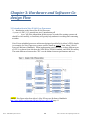
1
Embedded
Systems
Design Flow
using
Altera’s
FPGA
Development
Board (DE2115 T-Pad)
SPRING 2012
Ankita Goel
Hamid Mahmoodi
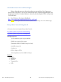
Table of Contents
Chapter 1: Introduction to the DE2-115 Development and Education Board ............................................... 3
1.1 Overview of DE2-115 .......................................................................................................................... 3
1.2 Block Diagram of the DE2-115 Board.................................................................................................. 5
1.3 Getting Started.................................................................................................................................... 7
1.4 Control Panel Demonstration ........................................................................................................... 15
Chapter 2: Hardware Design Flow Using Verilog in Quartus II ................................................................... 16
2.1 Introduction to Quartus II System Development Software .............................................................. 16
2.2 Design Flow (Hardware Only) ........................................................................................................... 18
2.3 Binary Adder Example ....................................................................................................................... 19
Step by Step Binary Adder Tutorial ......................................................................................................... 20
2.4 Introduction to System Builder ......................................................................................................... 32
Chapter 3: Hardware and Software Co-design Flow ................................................................................... 40
3.1 Introduction to Nios II Soft-Core Processor ...................................................................................... 40
3.2 Co-design Flow .................................................................................................................................. 42
3.3 Overview of System Integration Software SOPC Builder and Q Sys ................................................. 43
3.4 Introduction to Nios II SBT for Eclipse .............................................................................................. 44
Binary Adder Tutorial Using Nios II ......................................................................................................... 44
Chapter 4 : Video Generation for Text Display on T-Pad ............................................................................ 51
Introduction ................................................................................................................................................ 51
Hardware ................................................................................................................................................ 51
Software .................................................................................................................................................. 52
Step by Step ALU on T-Pad Tutorial ............................................................................................................ 53
Hardware Setup ...................................................................................................................................... 53
Step 1 : System Setup by using System Builder ...................................................................................... 53
Step 2: Quartus II – Hardware Setup ...................................................................................................... 54
Step 3: SOPC Builder Hardware Setup .................................................................................................... 58
Software Setup........................................................................................................................................ 63
Basic Software Algorithm ........................................................................................................................ 64
Downloading the design to the board: ................................................................................................... 66
SFSU - Embedded Systems Tutorial
1
Nano- Electronics & Computing Research Lab
Link to the Video Demonstration:........................................................................................................... 67
Chapter 5 – Integrating Touch Interface of T-Pad ...................................................................................... 68
Introduction ................................................................................................................................................ 68
Step by Step ALU on T-Pad with Touch Interface Tutorial .......................................................................... 70
Software Setup........................................................................................................................................ 80
SOFTWARE Algorithm ............................................................................................................................. 81
Downloading the design to the board .................................................................................................... 83
Link of Video Demonstration .................................................................................................................. 85
Chapter 6: Video Generation for Text and Image Display on T-Pad ........................................................... 86
Introduction ............................................................................................................................................ 86
Step by Step ALU with image in background Tutorial ............................................................................ 89
Hardware Setup .................................................................................................................................. 89
Software Setup.................................................................................................................................. 102
Downloading the design to the Board .................................................................................................. 104
SFSU - Embedded Systems Tutorial
2
Nano- Electronics & Computing Research Lab
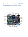
Chapter 1: Introduction to the DE2-115
Development and Education Board
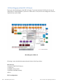
1.1 Overview of DE2-115
This device (FPGA Board) is specifically designed for to create, implement, and test digital designs using
programmable logic. Figure below shows the I/O ports in DE2-115. It shows the layout of the board and
indicates the location and connections of various components.
The following hardware is provided on the DE2-115 board:
SFSU - Embedded Systems Tutorial
3
Nano- Electronics & Computing Research Lab
Altera Cyclone® IV 4CE115 FPGA device
Altera Serial Configuration device – EPCS64
USB Blaster (on board) for programming; both JTAG and Active Serial (AS) programming modes are
supported
2MB SRAM
Two 64MB SDRAM
8MB Flash memory
SD Card socket
4 Push buttons
18 Slide switches
18 Red user LEDs
9 Green user LEDs
50MHz oscillator for clock sources
24-bit CD-quality audio CODEC with line-in, line-out, and microphone-in jacks
VGA DAC (8-bit high-speed triple DACs) with VGA-out connector
TV Decoder (NTSC/PAL/SECAM) and TV-in connector
2 Gigabit Ethernet PHY with RJ45 connectors
USB Host/Slave Controller with USB type A and type B connectors
RS-232 transceiver and 9-pin connector
PS/2 mouse/keyboard connector
IR Receiver
2 SMA connectors for external clock input/output
One 40-pin Expansion Header with diode protection
One High Speed Mezzanine Card (HSMC) connector
16x2 LCD module
SFSU - Embedded Systems Tutorial
4
Nano- Electronics & Computing Research Lab
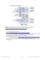
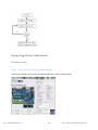
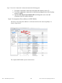
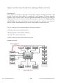
1.2 Block Diagram of the DE2-115 Board
Figure gives the block diagram of the DE2-115 board. To provide maximum flexibility for the user, all
connections are made through the Cyclone IV E FPGA device. Thus, the user can configure the FPGA to
implement any system design.
Block Diagram of DE2-115
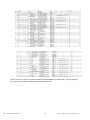
Following is more detailed information about the blocks of the Figure below:
FPGA device:
•Cyclone IV EP4CE115F29 device
•114,480 LEs
•432 M9K memory blocks
•3,888 Kbits embedded memory
•4PLLs
FPGA configuration:
SFSU - Embedded Systems Tutorial
5
Nano- Electronics & Computing Research Lab
•JTAG and AS mode configuration
•EPCS64 serial configuration device
•On-board USB Blaster circuitry
Memory devices:
•128MB (32Mx32bit) SDRAM
•2MB (1Mx16) SRAM
•8MB (4Mx16) Flash with 8-bit mode
•32Kb EEPROM
SD Card socket:
•Provides SPI and 4-bit SD mode for SD Card access
Connectors:
•Two Ethernet 10/100/1000 Mbps ports
•High Speed Mezzanine Card (HSMC)
•Configurable I/O standards (voltage levels:3.3/2.5/1.8/1.5V)
•USB type A and B
Provide host and device controllers compliant with USB 2.0
Support data transfer at full-speed and low-speed
PC driver available
•40-pin expansion port
Configurable I/O standards (voltage levels: 3.3/2.5/1.8/1.5V)
•VGA-out connector
VGA DAC (high speed triple DACs)
•DB9 serial connector for RS-232 port with flow control
•PS/2 mouse/keyboard
Clock:
•Three 50MHz oscillator clock inputs
•SMA connectors (external clock input/output)
Audio:
•24-bit encoder/decoder (CODEC)
•Line-in, line-out, and microphone-in jacks
Display:
•16x2 LCD module
Switches and indicators:
•18 slide switches and 4 push-buttons switches
SFSU - Embedded Systems Tutorial
6
Nano- Electronics & Computing Research Lab
•18 red and 9 green LEDs
•Eight 7-segment displays
Other features:
•Infrared remote-control receiver module
•TV decoder (NTSC/PAL/SECAM) and TV-in connector
Power:
•Desktop DC input
•Switching and step-down regulators LM3150MH
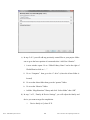
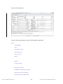
1.3 Getting Started
After getting the overview of the kit, next step is to download the necessary software development tools
and drivers for the DE2-115 that will connect to your host computer via USB.
Required Downloads:
The majority of resources listed below are found on the DE2-115 and T-Pad System CDs. These CDs can
be downloaded from Terasic’s website free of charge. Students should first download these files onto
their personal computers. Each student will need to become a Terasic member. This is done on first
download attempt.
Resources on the System CD are not available for single file download directly from Terasic website.
Specific files, unavailable for download, is available from System cd.
To download Quartus II and Nios II:
https://www.altera.com/download/dnl-index.jsp
To download system CDs:
1. DE2-115 resource site:
http://www.terasic.com.tw/cgi-bin/page/archive.pl?
%E2%80%A8Language=English&CategoryNo=139&No=502&PartNo=4
2. TPad resource site:
http://www.terasic.com.tw/cgi-bin/page/archive.pl?
%E2%80%A8Language=English&CategoryNo=139&No=550&PartNo=4
Downloading Quartus II and Nios II
SFSU - Embedded Systems Tutorial
7
Nano- Electronics & Computing Research Lab
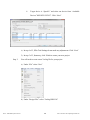
Step 1) Go to the link below:
https://www.altera.com/download/dnl-index.jsp
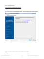
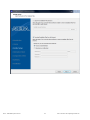
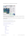
Step 2) Click on the icon “Download Windows Version” and run The Altera Software Installer will open
Step 3) Click Next then Agree to the Terms and Conditions, then click Next
SFSU - Embedded Systems Tutorial
8
Nano- Electronics & Computing Research Lab
SFSU - Embedded Systems Tutorial
9
Nano- Electronics & Computing Research Lab
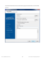
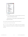
Step 4) Select the Destination where the Altera folder is going to be located and the name of the folder
Click next
SFSU - Embedded Systems Tutorial
10
Nano- Electronics & Computing Research Lab
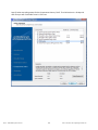
Step 5) Select everything except for the Components that say “Paid”. The Paid version is a 30-day trial
after that you will not be able to use it. Click next
SFSU - Embedded Systems Tutorial
11
Nano- Electronics & Computing Research Lab
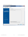
Step 6) Click next for the DSP Builder setup
SFSU - Embedded Systems Tutorial
12
Nano- Electronics & Computing Research Lab
Step 7) A summary of what will be installed to the computer will appear
SFSU - Embedded Systems Tutorial
13
Nano- Electronics & Computing Research Lab
Step 8) After the installation is complete click finish.
Using these steps, Quartus and Nios software can be downloaded and ready to be used on the board.
SFSU - Embedded Systems Tutorial
14
Nano- Electronics & Computing Research Lab
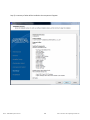
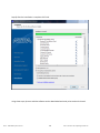
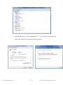
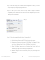
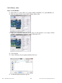
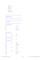
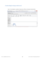
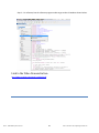
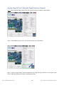
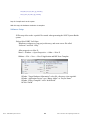
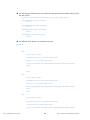
1.4 Control Panel Demonstration
To get familiarized with the board, Control Panel can be used which automatically uses Quartus II to run
a demonstration on the DE2-115. A video link demonstrating the same is given below:
http://www.youtube.com/watch?v=EtDDd07yUnw
Step 1: Connect the DE2-115 to your host computer through the USB port. Turn on
pressing the big red push-button. Make sure that SW-19 is set to Run.
the power by
Step 2: open <system cd>\DE2_115\DE2_115_tools within this file you will find control_panel.exe. With
the DE2-115 connected to your host computer, execute this Control Panel file by double-clicking its icon.
Note: If your Operating System is running on 64 bit, click on win7_64bits and then click in the DE2_115
Control Panel
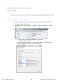
Step 3: It may take a few minutes for the
program load. Control Panel provides a GUI
for you to play with all the peripherals on the
DE2-115.
Once the Control Panel is open, follow the
pattern shown in the picture below and type
your name into the LCD Display:
A link describing the DE2-115 board is given below: http://www.youtube.com/watch?v=720t8fNcJKM
SFSU - Embedded Systems Tutorial
15
Nano- Electronics & Computing Research Lab
Chapter 2: Hardware Design Flow Using
Verilog in Quartus II
2.1 Introduction to Quartus II System Development Software
This chapter is an introduction to the Quartus II software that will be used for analysis and
synthesis of the DE2-115 Development and Education Board. Throughout this chapter hardware
description languages like Verilog will be used for coding. The Altera Quartus II design software
provides a complete, multiplatform design environment for system-on-a-programmable-chip
(SOPC) designs. Also an example will be implemented in a tutorial using the hardware
description language (Verilog) and the DE2-115. Below are some suggested readings before
going into the next section.
Quartus II Development Software Reading Resources:
(In suggested chronological reading/watching order)
1)
Introduction to Quartus II Software
Version 11.0 (Latest):
http://www.altera.com/literature/manual/quartus2_introduction.pdf
•
NOTE: The link to the newer version of the later version (11.0) provides a very
brief overview, whereas the older version (listed below) gives more in depth information.
Version 10.0:
http://www.altera.com/literature/manual/archives/intro_to_quartus2.pdf
•
focus: Emphasis is placed on the following sections, although a greater
knowledge base is achieved by reviewing the entire document:
SFSU - Embedded Systems Tutorial
16
Nano- Electronics & Computing Research Lab
a) Design Flow- Introduction (Page No. 11), Graphical User Interface Design
Flow (Page No. 12)
b) Design Entry (Page No. 29) Introduction, Creating a Project(Page No. 30),
Creating a Design(Page No. 31), later this document can be used for a specific
method of design entry (like Verilog, Block Diagram, VHDL, etc.)
c) Programming & Configuration (Page No. 93) Introduction, Creating and
Using Programming Files
2)
Using Verilog for Quartus II Design:
<system cd>\DE2_115_tutorials\tut_quartus_intro_verilog.pdf
•
focus: This tutorial guides through the simulation process so that the project can
be implemented without needing access to the DE2-115.(familiar with quartus and Verilog)
(PG No 1-21)
3)
Quartus II Handbook: http://www.altera.com/literature/hb/qts/quartusii_handbook.pdf
•
NOTE: This resource is in depth and is only necessary to briefly overview the
material in order to know where information can be found on an as needed basis.
SFSU - Embedded Systems Tutorial
17
Nano- Electronics & Computing Research Lab
2.2 Design Flow (Hardware Only)
SFSU - Embedded Systems Tutorial
18
Nano- Electronics & Computing Research Lab
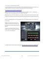
2.3 Binary Adder Example
Now that you are getting familiar with Quartus II and the DE2-11 a tutorial discussing
the basic steps for using Quartus II is discussed below.
In this example, the components from the DE2-115
Board that will be used are:
7 Segment Hex Display,
Switches,
8 Red LEDs, and the
LCD Display
As shown in the picture above the switches and LED’s are synchronized and represent a
4 bit binary number. The values of these binary numbers are displayed on the 7 segment display
and LCD. Moreover the addition of these two binary numbers is also displayed on the seven
segment display and LCD.
*To learn more in detail about the 7 Segment Hex Display also there is a short video about 7 segment display () and
LCD refer to the last 5 pages of this example
SFSU - Embedded Systems Tutorial
19
Nano- Electronics & Computing Research Lab
0The Binary Adder tutorial teaches how to
Connect the conputer with the DE2-115.
Create a new project using Quartus II.
Create a Verilog file.
Put I/O pin locations in the assignment editor.
Synthesize your design.
Use system builder.
1. The youtube video for the complete procedure can be accessed from the link given below:
http://www.youtube.com/watch?v=PB9wk5Wl_Ec
2. The example can also be implemented by using the written instructions given below:
Step by Step Binary Adder Tutorial
Step 1:
Install the USB driver for the FPGA development board. This step will only be
done for the first time the FPGA board is used.
a) On the FPGA board, connect the power plug to an outlet. Connect the USB cable
from your computer to the FPGA board in port J9 (closest to the power outlet).
b) Open the start Menu and Search Windows for “Device Manager”-> Scroll down
to “Other Devices”-> A new window called “USB Blaster Properties” will open.
SFSU - Embedded Systems Tutorial
20
Nano- Electronics & Computing Research Lab
c) Under the tab “Driver” select “Update Driver” -> A new window will pop up and
you’ll select “Browse my computer for driver software
SFSU - Embedded Systems Tutorial
21
Nano- Electronics & Computing Research Lab
d) In the field “Search for Drivers in this location” browse your computer to create
the following path: C: - > Altera -> 11.0 -> Quartus -> Drivers -> USB Blaster
then select “Browse”
e) You may need to click “allow” to complete the process.
Step 2:
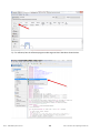
Open the Quartus II software
a) Select “Create New Project Wizard”
b) In the first step (1 of 5) you will need to create a directory for your project and
name your new project.
SFSU - Embedded Systems Tutorial
22
Nano- Electronics & Computing Research Lab
c) In step 2 of 5, you will add any previously created files to your project. Make
sure to go to the lower portion of screen and select “Add User Libraries”.
i. A new window opens. Go to “Global Library Name” and to the right of
Global libraries click on “…”
ii. Go to “Computer” then go to the “C drive” (where the Altera folder is
located)
iii. Go to on the Altera folder then go to the “quartus” folder
iv. Go to on the “libraries” folder
v. Add the “MegaFunctions” library and click “Select folder” then “OK”
d) In step 3 of 5, “Family & Device Settings” you will adjust the family and
device you want to target for compilation.
i.
SFSU - Embedded Systems Tutorial
Device family is Cyclone IV E.
23
Nano- Electronics & Computing Research Lab
ii.
Target device is “Specific” and select our device from “Available
Devices”EP4CE115F29C7. Click “Next”
e) In step 4 of 5, EDA Tool Settings do not make any adjustments. Click “Next”
f) In step 5 of 5, Summary, click “Finish to create your new project.
Step 3:
You will need to create a new Verilog file for your project.
a) Under “File” select “New”
b) Under “Design Files” select “Verilog HDL File”
SFSU - Embedded Systems Tutorial
24
Nano- Electronics & Computing Research Lab
c) Click “OK”
d) A new Verilog file will open. An asterisk will appear near the file name
whenever unsaved changes have been made.
~ This tutorial focuses on Verilog (a hardware description language), In order to
program the Altera DE2-115
Step 4: Copy the Verilog Code from the file Binary_Adder.txt file into Quartus II
Note: Binary_Adder.txt is located in the Codes folder
Step 5: You will use the DE2-115 manual to determine ports and PIN assignments.
Assignments->assignment editor (Ctrl+Shift+A) set all components to their appropriate locations
and voltage
SFSU - Embedded Systems Tutorial
25
Nano- Electronics & Computing Research Lab
SFSU - Embedded Systems Tutorial
26
Nano- Electronics & Computing Research Lab
SFSU - Embedded Systems Tutorial
27
Nano- Electronics & Computing Research Lab
SFSU - Embedded Systems Tutorial
28
Nano- Electronics & Computing Research Lab
Step 6:
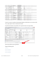
For any project it is required to create pin assignment from the DE2-115 manual.
a) Under “Assignments” select “Assignment Editor”
b) Add each port under “Assignment Name” –each port will need two
assignments:
i.
PIN location
ii.
I/O requirement.
Note: This process is very lengthy and in the future can be bypassed using “System
Builder”( PG No. 15).
SFSU - Embedded Systems Tutorial
29
Nano- Electronics & Computing Research Lab
Step 7: When the Verilog code is finished, and all assignments are done, you will be
ready to compile your design and program the device.
Step 8: At the top of the screen, select the “Play” button to begin the automatic
compilation process. Watch in the lower left screen as the compilation process occurs.
This may take several minutes.
(Step 7)
Step 9: When it has compiled, double click on “Program Device”.
a) Push the large red button on the FPGA board to turn on the power.
b) Programmer will open, and at the top left “USB Blaster” will appear. If it does
not, click on “Hardware Setup”. Select “USB Blaster” and click ok.
c) When “USB Blaster” appears next to “Hardware Setup” select “Start” and
watch the upper right corner as the design is implemented.
d) When the “Progress” bar has reach 100% you may test your design on the
FPGA board.
SFSU - Embedded Systems Tutorial
30
Nano- Electronics & Computing Research Lab
SFSU - Embedded Systems Tutorial
31
Nano- Electronics & Computing Research Lab
2.4 Introduction to System Builder
Alternate way to do pin assignments with the help of System Builder
System builder is a GUI that creates pin assignment by selecting the components that will be
needed for a project. System builder saves time by creating the pin assignments for you and
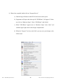
letting you choose what components you need. For Example:1) Open DE2_115_tools->DE2_115_system_builder to find DE2_115_SystemBuilder.exe
2) Name the project under Project Name: in this Tutorial we name or project Binary_Adder
3) Check all Components that you will be using: in this Tutorial we are using CLOCK,
LEDx27, Buttonx4, 7-Segementx8, Switchx18, and of course the LCD.
SFSU - Embedded Systems Tutorial
32
Nano- Electronics & Computing Research Lab
4) Click Generate
5) Create a directory for your project and then click save
6) To open this project open the .qpf file
7) Delete the verilog code that System Builder created then copy the code from
Binary_Adder_System_Builder(is located in the codes folder)
8) At the top of the screen, select the “Play” button to begin the automatic compilation
process. Watch in the lower left screen as the compilation process occurs. This may take
several minutes.
(Step 7)
SFSU - Embedded Systems Tutorial
33
Nano- Electronics & Computing Research Lab
9) When it has compiled, double click on “Program Device”.
a) Push the large red button on the FPGA board to turn on the power.
b) Programmer will open, and at the top left “USB Blaster” will appear. If it does
not, click on “Hardware Setup”. Select “USB Blaster” and click ok.
c) When “USB Blaster” appears next to “Hardware Setup” select “Start” and
watch the upper right corner as the design is implemented.
d) When the “Progress” bar has reach 100% you may test your design on the
FPGA board.
SFSU - Embedded Systems Tutorial
34
Nano- Electronics & Computing Research Lab
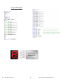
7 Segment Hex Display
SFSU - Embedded Systems Tutorial
35
Nano- Electronics & Computing Research Lab
In this project we used four 7-segment displays to show the values of switches being
turned on in binary. In a 7- segment display a high logic level will turn off the led and a low
logic level to a segment will turn the led on. To represent an LED with a seven-bit value we use
the values zero through six. To display a zero to a segment we set the hex value to be equal to
7b’1000000. This is because a zero will have all led on but the center led (number 6 on the figure
above). The code also uses a function to simplify the task of representing a bit value to a hex
value. Since the function DISPLAYNUMBERS only has one output it seemed like a function
instead of a task. In the function we have only one input value that represents a 4 bit switch
value, this value is passed through a series of if else statements to determine the hex value. At the
end of this program we assign all appropriate values to the represented LEDs.
There is a quick example of getting the LED’s, Switches, Keys, and 7 segment Hex
Display to function properly in the link below that goes more in detail about the 7 segment
display.
http://www.youtube.com/watch?v=SNCZGqWEtJg
SFSU - Embedded Systems Tutorial
36
Nano- Electronics & Computing Research Lab
16 x 2 LCD
SFSU - Embedded Systems Tutorial
37
Nano- Electronics & Computing Research Lab
To display characters to an LCD there is a series of steps that need to be done before to
initializing the LCD module. Since Verilog doesn’t read code sequentially we created a case
statement that will allow the initialization to be done in order. This is done by changing the state
of the case to the next step in every case statement. The steps performed are RESET1, RESET2,
RESET3, FUNCTION SET, DISPLAY OFF, DISPLAY CLEAR, RETURN HOME, CHANGE
SFSU - Embedded Systems Tutorial
38
Nano- Electronics & Computing Research Lab
LINE, DROP LCD, HOLD, DISPLAY ON, and MODE SET AND PRINT STRING.
These
reset needs to be done three time to because we need to initialize enable to high and register
select and read/write to low signals. These steps are also done to communicate with the LCD to
determine if it will be an 8 or 4 bit data bus, this is done by setting the data bus equal to the hex
value eight(8’h38). Before we can write to the screen we need to clear the LCD display, this is
done by changing the data bus equal to 8’h01 (Start of heading). Finally when we need to display
the screen we set enable and read/write to high and reset to low, this is done because this allows
us to write data to the LCD. In the print string case statement we added an else if (index ==line1)
because without this the LCD wouldn’t know when the next line begin or the first line starts.
SFSU - Embedded Systems Tutorial
39
Nano- Electronics & Computing Research Lab
Chapter 3: Hardware and Software Codesign Flow
3.1 Introduction to Nios II Soft-Core Processor
1) Introduction to the Altera Nios II Soft Processor:
<system cd>\DE2_115_tutorials\tut_nios2_introduction.pdf
•
focus: All of the information in this resource is needed for creating systems and
should be read carefully, as familiarity will greatly help students in avoiding time consuming
mistakes.
Nios II is an embedded processor architecture designed specifically for Altera’s FPGA boards.
An example of a Nios II processor system could be found on page 11 from Altera’s Nios II
Processor Reference Handbook. When implementing your board there is three different types
of CPU’s to choose from which are the NIOS II/fast, NIOS II/standard, and NIOS II/economy.
The main differences between the CPU’s are the balance between performance and cost.
NOTE: This figure taken from Altera’s Nios II Processor Reference Handbook:
http://www.altera.com/literature/hb/nios2/n2cpu_nii5v1.pdf page 11
SFSU - Embedded Systems Tutorial
40
Nano- Electronics & Computing Research Lab
NOTE: This figure taken from Altera’s Nios II Processor Reference Handbook:
http://www.altera.com/literature/hb/nios2/n2cpu_nii5v1.pdf page 18
2) Nios II Hardware Development:
http://www.altera.com/literature/tt/tt_nios2_hardware_tutorial.pdf
•
focus: This resource is an excellent overview of the basic requirements to creating
a system using QSys in Quartus II, instantiating the design in the project files,
implementation, and then creating the necessary software.
3) Nios II Processor Reference: http://www.altera.com/literature/hb/nios2/n2cpu_nii5v1.pdf
•
NOTE: This resource has a lot of detailed information which is not necessary to
complete most projects, but it is good to be familiar with document in the case of
troubleshooting.
SFSU - Embedded Systems Tutorial
41
Nano- Electronics & Computing Research Lab
3.2 Co-design Flow
Figure 1–2 shows the Nios II system development flow between hardware and software. This flow
consists of three types of development: hardware design steps, software design steps, and system design
steps.
NOTE: This figure taken from Altera’s Nios II Hardware Development Tutorial:
http://www.altera.com/literature/tt/tt_nios2_hardware_tutorial.pdf
SFSU - Embedded Systems Tutorial
42
Nano- Electronics & Computing Research Lab
3.3 Overview of System Integration Software SOPC Builder and Q Sys
NOTE: This diagram was taken from Altera’s Nios II Software Developer’s Handbook,
http://www.altera.com/literature/hb/nios2/n2sw_nii5v2.pdf
System Integration Software
This software allows the designer to marry hardware and software. In order to use the Nios II
soft-core processor, a system must be designed using either SOPC builder or QSys (both are
accessed from Quartus II-> Menu -> Tools). QSys is a newer version of SOPC builder and it is
encouraged that students begin with QSys. This development tool primarily generates
the .sopcinfo file which is used in Nios II SBT for Eclipse to create the software project to run on
top of the FPGA design, utilizing the Nios II soft-core processor.
After creating a system to suit the students’ project needs, “Generation” (synonymous to
“Compilation”) automatically creates the necessary hardware files for low-level abstraction. A
main niosII module is created in this process, which is instantiated from the top-level hardware
file. This process is described as System Integration
Although much of the reading presented here applies to SOPC Builder, the information applies
also to QSys and an effort should be made to use QSys in place of SOPC Builder.
1)
Introduction to the Altera SOPC Builder:
<system cd>\DE2_115_tutorials\tut_sopc_introduction_verilog.pdf
2) QSys System Design: http://www.altera.com/literature/tt/tt_qsys_intro.pdf
•
QSys main reference page: http://www.altera.com/products/software/quartusii/subscription-edition/qsys/qts-qsys.html?GSA_pos=10&WT.oss_r=1&WT.oss=qSys
3) SOPC Builder User Guide: http://www.altera.com/literature/ug/ug_sopc_builder.pdf
SFSU - Embedded Systems Tutorial
43
Nano- Electronics & Computing Research Lab
3.4 Introduction to Nios II SBT for Eclipse
Eclipse allows the user to use the software that was executed by a Nios II processorbased system in an FPGA. The user can configure the FPGA on the development board with
the pre-generated Nios II standard hardware system by downloading the FPGA configuration
file to the board.
1) Nios II Software Developer’s Handbook:
http://www.altera.com/literature/hb/nios2/n2sw_nii5v2.pdf
NOTE: Link is placed here for reference, but is not necessary for review in this stage.
Binary Adder Tutorial Using Nios II
A link to the video describing the Binary Adder Tutorial:
http://www.youtube.com/watch?v=bKA3mNYTl2g
http://www.youtube.com/watch?v=bM4uHq9hlmQ
The major steps were:
1) Create hardware system in system builder
2) Build new system in QSys system
3) Instantiate the Nios II module in top level entity
4) Add IP variation file
5) Adjust .sdc
6) Place design on FPGA
7) Develop Software in Nios II SBT for Eclipse.
Hardware:
Clock
Red LEDs
Switches
7 segment Hex
LCD
SFSU - Embedded Systems Tutorial
44
Nano- Electronics & Computing Research Lab
NIOS II Binary Adder
Step 1: System Builder
1) Open DE2_115_tools->DE2_115_system_builder to find DE2_115_SystemBuilder.exe
2) Name the project under Project Name: Binary_Adder_Nios
3) Check all Components that you will be using: in this Tutorial we are using CLOCK,
LEDx27, 7-Segementx8, Switchx18, and of course the LCD.
4) Click Generate
5) Create a directory for your project and then click save
6) To open this project open the .qpf file
SFSU - Embedded Systems Tutorial
45
Nano- Electronics & Computing Research Lab
Step 2: Building Qsys System
1) Open Qsys under tools tab
2) Start by adding a Nios II Processor Core: Under “Component Library”-> Processors ->
Nios II Processor -> Add
a. Select “Nios II/s”
b. Set “Hardware multiplication type” = “None”
c. Disable “Hardware divide”
d. “Finish”
e. Rename Nios to “cpu”
3) On-Chip Memory: Under “Component Library”-> Memories and Memory Controllers ->
On-Chip -> On-Chip Memory (RAM or ROM)-> Click “Add”
a. Block Type list = “Auto”
b. Total Memory size = “204800” to specify 2KB of memory
c. Do not change any other default settings.
d. “Finish”
e. Under the “System Contents” tab, right-click the on-chip memory and rename as
“onchip_mem”
4) JTAG UART: Component Library -> Interface Protocols -> Serial -> JTAG UART ->
Add
a. Do not change any default settings
b. Rename to “jtag_uart”
5) Interval Timer: Component Library -> Peripherals -> Microcontroller Peripherals ->
Interval Timer-> Add
a. Under “Hardware Options” set “Presets” to “Full-Featured”
b. Do not change any other default settings
c. Rename to “sys_clk_timer”
6) System ID Peripheral: Component Library-> Peripherals -> Debug and Performance ->
System ID Peripheral-> Add
a. Do not change any default settings
b. Rename as “sysid”
7) PIO’s: Component Library-> Peripherals -> Microcontroller Peripherals -> PIO -> Add
a. Under “Basic Settings” enter the value of “4” for the box labeled “Width”
b. Do not change any other default settings
c. Finish
d. Rename as “pio_led”
e. For this example us two “pio_led”
f. Repeat these steps for two “pio_sw” with 4 bits of width and change to input.
g. Repeat these steps for pio_hex0 through 7 with widths of 7 bits.
8) LCD: Component Library-> Peripherals -> Display-> Character LCD -> Add
a. Finish
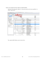
9) Go to the “Connections” column and connect the following ports: (Figure Below)
a. For all the components connect the clock input and outputs to clock_50
b. For all the components connect the Avalon memory mapped slave to the On-chip
memory AMMS.
c. Open the Nios II processor named CPU and change the reset vector and
exception vectors to onchip_memory2
SFSU - Embedded Systems Tutorial
46
Nano- Electronics & Computing Research Lab
10) Go to the “Export” column and connect the following ports:
a. Click on “click to export” on the external connection row to activate connection
for all of the led’s, switches and 7 segment display.
b. Click on “click to export” on the external row for the LCD
11) Under Generation click generate
a. Save as “Nios”
b. Once generation is complete coping code from HDL example
Step 2: Quartus HDL Connections
1) Add IP Variation File: Menu bar: Assignments -> Settings
a. Under “Category” -> “Files” -> (…) Browse -> Choose script files for type to
find(*.tcl, *.sdc, *.qip)
SFSU - Embedded Systems Tutorial
47
Nano- Electronics & Computing Research Lab
b. Locate and choose the file nios2/synthesis/nios.qip
c. Add to project, click okay and close
2) Copy code under structural coding in Quartus (Code located in the Codes folder under
Binary_Adder_Quartus)
a. Notice LCD_BLON is set to 1'b1;
b. Notice LCD_ON is set to 1'b1;
c. Notice all connections in parenthesis
3) Compile and Run
a. Compile and Run
SFSU - Embedded Systems Tutorial
48
Nano- Electronics & Computing Research Lab
Step 3: Develop the Software for Nios II SBT for Eclipse
1) This step relies on the .sopcinfo file created when generating the Qsys system
2) Open Nios II SBT for Eclipse
a) Indicate workspace as your project directory, and create a new file called
“Software” and click “Okay”
b) Set perspective to Nios II: Menu -> Window -> Open Perspective -> Other ->
Nios II
c) Menu -> File -> New -> Nios II Application and BSP from Template
i) Under “Target Hardware Information” select file
<directory>\nios.sopcinfo
ii) Under “Application Project” type “Binary Adder” as “Project Name”
iii) Under “Project Template” select “helloWorld”
iv) Click “Finish”
3) Include C++ code (Code located in the Codes folder under Binary_Adder_Nios2)
SFSU - Embedded Systems Tutorial
49
Nano- Electronics & Computing Research Lab
4) Build project
5) Run as Hardware
SFSU - Embedded Systems Tutorial
50
Nano- Electronics & Computing Research Lab
Chapter 4 : Video Generation for Text
Display on T-Pad
Introduction
In this chapter, the ALU will be displayed on T-Pad. Switches perform different operation of the ALU.
With switches, different numbers can be displayed and also their ALU operations can be performed.
Hardware
Character Buffer
DMA
The T-Pad features an 8-inch Amorphous-TFT-LCD panel. The LCD Screen module offers resolution of
(800x600) to provide users the best display quality for developing applications. The LCD panel supports
18-bit parallel RGB data interface.
The hardware is implemented using Altera IP cores on SOPC builder. A phase locked loop (Alt PLL) has
been used to generate the required clocking for the whole system. In this system a 100Mhz clock for the
Nios-II/f have been used, another 100Mhz with -65 phase shift is used to clock the SDRAM in addition to
the required 40Mhz clock for the VGA controller. The figure above shows the block diagram of the
hardware that is implemented in the SOPC builder.
SFSU - Embedded Systems Tutorial
51
Nano- Electronics & Computing Research Lab
Video Pipeline
A Scatter Gather DMA is used to connect to the VGA Controller as shown in the figure below. A
summary of how video is fed to the VGA Controller is given in the paragraph below.
The Scatter Gather DMA is used for high speed data transfer between two components. It is used to
transfer and merge noncontiguous memory to continuous address space and vice versa. It works in three
modes.
1. Memory to Memory
2. Memory to Data Stream
3. Data Stream to Memory
In this chapter, the SGDMA is used to transfer data from SDRAM to the VGA Stream. So that is option 2
from the above. A timing adapter is used to adjust the timing between the two different streams of data.
In short, it is used to connect two components that require different number of cycles to receive or send
data. A FIFO is a First In First Out queue. It is a dual clock FIFO that is used to match the system clock to
the VGA clock to normalize the flow of pixels to the VGA sink.
A RGB converter is required to convert the RGB format from BGR0 to BGR.
The VGA Controller requires 18 bit parallel RGB interface. To make the format coming from memory
(24bit RGB) compatible with the VGA sink that is connected to the tPad, we insert RGB Converter. All
these components contribute to generate a video pipeline which enables us to display a video on the tPad.
Software
The LCD screen is initialized and a blank screen can be seen. Switches are toggled to change the number
values and their operation, the result is displayed on the LCD Screen and updated every time switch is
toggled.
SFSU - Embedded Systems Tutorial
52
Nano- Electronics & Computing Research Lab
Step by Step ALU on T-Pad Tutorial
Hardware Setup
Step 1 : System Setup by using System Builder
Open System Builder, select Clock, LED, VGA and switches as shown in figure below.
SFSU - Embedded Systems Tutorial
53
Nano- Electronics & Computing Research Lab
Select HSMC Source as LTC – 8” LCD/Touch Camera as shown below.
Select a project name, for this example we are using “tpad_alu_display” as our project name Click on
Generate and open the folder containing these files.
Open the folder where the project files are saved and open tpad_alu_display.qpf file. This file will be
opened in quartus II.
Step 2: Quartus II – Hardware Setup
In Quartus II, the Verilog code will look like this (in blue):
//=======================================================
// This code is generated by Terasic System Builder
//=======================================================
module tpad_alu_display(
//////////// CLOCK //////////
CLOCK_50,
CLOCK2_50,
CLOCK3_50,
//////////// LED //////////
LEDG,
LEDR,
//////////// SW //////////
SFSU - Embedded Systems Tutorial
54
Nano- Electronics & Computing Research Lab
SW,
//////////// VGA //////////
VGA_B,
VGA_BLANK_N,
VGA_CLK,
VGA_G,
VGA_HS,
VGA_R,
VGA_SYNC_N,
VGA_VS,
//////////// I2C for HSMC //////////
I2C_SCLK,
I2C_SDAT,
//////////// HSMC, HSMC connect to LTC - 8" LCD/Touch/Camera //////////
CAMERA_D,
CAMERA_FVAL,
CAMERA_LVAL,
CAMERA_PIXCLK,
CAMERA_RESET_N,
CAMERA_SCLK,
CAMERA_SDATA,
CAMERA_STROBE,
CAMERA_TRIGGER,
CAMERA_XCLKIN,
LCD_B,
LCD_DEN,
LCD_DIM,
LCD_G,
LCD_NCLK,
LCD_R,
TOUCH_BUSY,
SFSU - Embedded Systems Tutorial
55
Nano- Electronics & Computing Research Lab
TOUCH_CS_N,
TOUCH_DCLK,
TOUCH_DIN,
TOUCH_DOUT,
TOUCH_PENIRQ_N
);
//=======================================================
// PARAMETER declarations
//=======================================================
//=======================================================
// PORT declarations
//=======================================================
//////////// CLOCK //////////
input
CLOCK_50;
input
CLOCK2_50;
input
CLOCK3_50;
//////////// LED //////////
output
[8:0]
LEDG;
output
[17:0]
LEDR;
//////////// SW //////////
input
[17:0]
SW;
//////////// VGA //////////
output
[7:0]
VGA_B;
output
VGA_BLANK_N;
output
VGA_CLK;
output
[7:0]
output
output
VGA_G;
VGA_HS;
[7:0]
VGA_R;
output
VGA_SYNC_N;
output
VGA_VS;
SFSU - Embedded Systems Tutorial
56
Nano- Electronics & Computing Research Lab
//////////// I2C for HSMC //////////
output
I2C_SCLK;
inout
I2C_SDAT;
//////////// HSMC, HSMC connect to LTC - 8" LCD/Touch/Camera //////////
input
[11:0]
CAMERA_D;
input
CAMERA_FVAL;
input
CAMERA_LVAL;
input
CAMERA_PIXCLK;
output
CAMERA_RESET_N;
output
CAMERA_SCLK;
inout
CAMERA_SDATA;
input
CAMERA_STROBE;
output
CAMERA_TRIGGER;
output
CAMERA_XCLKIN;
output
[5:0]
LCD_B;
output
LCD_DEN;
output
LCD_DIM;
output
[5:0]
output
output
LCD_G;
LCD_NCLK;
[5:0]
LCD_R;
input
TOUCH_BUSY;
output
TOUCH_CS_N;
output
TOUCH_DCLK;
output
TOUCH_DIN;
input
TOUCH_DOUT;
input
TOUCH_PENIRQ_N;
//=======================================================
// REG/WIRE declarations
//=======================================================
//=======================================================
// Structural coding
SFSU - Embedded Systems Tutorial
57
Nano- Electronics & Computing Research Lab
//=======================================================
Endmodule
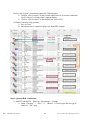
Step 3: SOPC Builder Hardware Setup
Open SOPC Builder Window and add:
CPU
On – Chip memory
Character Buffer with DMA
Pixel Buffer
Pixel Buffer with DMA
Pixel RGB Resampler
Pixel Scaler
Video Clipper
Alpha Blender
Dual Clock FIFO
VGA Controller
JTAG UART
SYSID
Touch Panel SPI
Touch Panel penirq
Touch Panel Busy
Altpll_0
Step 3a: Go to the “Connections” column and connect the following ports:
c. For all the components connect the clock input and outputs to clock_50
d. For all the components connect the Avalon memory mapped slave to the On-chip
memory AMMS.
e. Open the Nios II processor named CPU and change the reset vector and
exception vectors to onchip_memory2
SFSU - Embedded Systems Tutorial
58
Nano- Electronics & Computing Research Lab
Step 3b: For assignment of base addresses in SOPC Builder:
Click on “Auto assign base addresses” on the main menu bar and “Auto assign IRQ’s” as
shown in figure below:
The complete SOPC Builder system is shown below:
SFSU - Embedded Systems Tutorial
59
Nano- Electronics & Computing Research Lab
Note: If you wish to open the complete already designed hardware in SOPC builder, you may open the
file “Video_system.sopcinfo” which is attached to this tutorial.
SFSU - Embedded Systems Tutorial
60
Nano- Electronics & Computing Research Lab
Step 3c: Click on Generate.
Step 3(d): After you generate the system. Following code is generated:
system (
// 1) global signals:
.clk_0(),
.clocks_VGA_CLK_40_out(),
.clocks_VGA_CLK_out(),
.clocks_sys_clk_out(),
.reset_n(),
// the_SW
.in_port_to_the_SW(),
// the_video_vga_controller
.VGA_BLANK_from_the_video_vga_controller(),
.VGA_B_from_the_video_vga_controller(),
.VGA_CLK_from_the_video_vga_controller(),
.VGA_DATA_EN_from_the_video_vga_controller(),
.VGA_G_from_the_video_vga_controller(),
.VGA_HS_from_the_video_vga_controller(),
.VGA_R_from_the_video_vga_controller(),
SFSU - Embedded Systems Tutorial
61
Nano- Electronics & Computing Research Lab
.VGA_SYNC_from_the_video_vga_controller(),
.VGA_VS_from_the_video_vga_controller()
)
Step 3(e): This code should be copied and pasted in the main Verilog (shown previously) under
REG/WIRE declarations section. The modifications are shown in green:
system (
// 1) global signals:
.clk_0(CLOCK_50),
.clocks_VGA_CLK_40_out(),
.clocks_VGA_CLK_out(),
.clocks_sys_clk_out(),
.reset_n(SW[17]),
// the_SW
.in_port_to_the_SW(),
// the_video_vga_controller
.VGA_BLANK_from_the_video_vga_controller(),
.VGA_B_from_the_video_vga_controller(B),
.VGA_CLK_from_the_video_vga_controller(LCD_NCLK),
.VGA_DATA_EN_from_the_video_vga_controller(LCD_DEN),
.VGA_G_from_the_video_vga_controller(G),
.VGA_HS_from_the_video_vga_controller(),
.VGA_R_from_the_video_vga_controller(R),
.VGA_SYNC_from_the_video_vga_controller(),
.VGA_VS_from_the_video_vga_controller()
)
Step 3(f): Compile and run the system.
SFSU - Embedded Systems Tutorial
62
Nano- Electronics & Computing Research Lab
With this step, the hardware simulation is complete.
Software Setup
This step relies on the .sopcinfo file created when generating the SOPC Builder system
Step 1: Open Nios II SBT for Eclipse
a) Indicate workspace as your project directory, and create a new file called
“Software” and click “Okay”
b) Set perspective to Nios II: Menu -> Window -> Open Perspective -> Other ->
Nios II
c) Menu -> File -> New -> Nios II Application and BSP from Template
i) Under “Target Hardware Information” select file
<directory>\nios.sopcinfo
ii) Under “Application Project” type “Binary Adder” as “Project Name”
iii) Under “Project Template” select “helloWorld”
iv) Click “Finish”
SFSU - Embedded Systems Tutorial
63
Nano- Electronics & Computing Research Lab
Basic Software Algorithm
Initialize the screen
screen_x = 319; screen_y = 239;
char text[16];
color = 0x0000;
// black color
VGA_box (0, 0, screen_x, screen_y, color); // fill the screen with background
Values of switches are pointed by allocating their base address
volatile int * switch1_ptr = (int *) 0x00101810;
volatile int * switch2_ptr = (int *) 0x00101820;
volatile int * switch3_ptr = (int *) 0x00101830;
volatile int * switch4_ptr = (int *) 0x00101850;
According to the switch position, the operation of ALU is decided.
00 : Addition
01: Subtraction
10: Logical OR
11 : Logical And
if (sel1&sel2)
{
sprintf( text_top_VGA, "My ALU");
sprintf (text,"%d + %d = %d ",number1,number2,number1 + number2);
}
else if (!sel1&sel2)
{
sprintf( text_top_VGA, "My ALU");
sprintf (text,"%d - %d = %d ",number1,number2,number1 - number2);
}
else if (sel1&!sel2)
{
sprintf( text_top_VGA, "My ALU");
SFSU - Embedded Systems Tutorial
64
Nano- Electronics & Computing Research Lab
sprintf (text,"%d & %d = %d ",number1,number2,number1 & number2);
}
else
{
sprintf( text_top_VGA, "My ALU");
sprintf (text,"%d | %d = %d ",number1,number2,number1 | number2);
}
Characters are written on the screen through “VGA_text” function.
void VGA_text(int x, int y, char * text_ptr)
{
int offset;
volatile char * character_buffer = (char *) 0x00101000; // VGA character buffer
offset = (y << 7) + x;
while ( *(text_ptr) )
{
*(character_buffer + offset) = *(text_ptr);
// write to the character buffer
++text_ptr;
++offset;
}
}
You can obtain the software code by opening the main.c file which is attached with this
tutorial.
SFSU - Embedded Systems Tutorial
65
Nano- Electronics & Computing Research Lab
Downloading the design to the board:
Step 1 –For Hardware, compile the respective .sof file on the board as shown below:
SFSU - Embedded Systems Tutorial
66
Nano- Electronics & Computing Research Lab
Step 2 – For software, Run the software program under target as Nios II Hardware shown below:
Link to the Video Demonstration:
http://www.youtube.com/watch?v=gSJPt2jvn9E
SFSU - Embedded Systems Tutorial
67
Nano- Electronics & Computing Research Lab
Chapter 5 – Integrating Touch Interface of
T-Pad
Introduction
In this chapter, the ALU will be displayed on T-Pad. Different operation of the ALU is performed by
touch interface. With switches, different numbers can be displayed and their ALU operations are
performed by touching the buttons on the screen.
Hardware
Character
Buffer DMA
The T-Pad features an 8-inch Amorphous-TFT-LCD panel. The LCD Screen module offers resolution of
(800x600) to provide users the best display quality for developing applications. The LCD panel supports
18-bit parallel RGB data interface.
In this chapter, touch features on the LCD Display are used. Hardware implementation to exploit the
touch features on the TPad:
a) A touch_panel_spi
b) A touch_panel_busy
c)A touch_panel_penirq_n
SFSU - Embedded Systems Tutorial
68
Nano- Electronics & Computing Research Lab
Serial Peripheral Interface (SPI) and a Parallel I/0 (PIO) peripheral implement the touch screen
interface. The SPI peripheral communicates with the Analog Devices AD7843, touch screen digitizer chip
to signal pen_move events. A single PIO captures pen interrupt events, transitions on the pen_down line
from the AD7843 chip to indicate pen_down and pen_up events. The Nios II processor in the system runs
the software that drives the SPI and PIO peripherals. The main commands, which we use in the project to
implement the touch interface, are touch_panel_spi which implements the SPI interface are
touch_panel_spi which implements pen interrupt interface.
The T-Pad has SPI for recognizing touch on a resistive screen. The touch is communicated with the
processor using Serial Peripheral Interface. We need to designate two parallel input ports, one with
interrupt for pen down, for recognizing that the screen is touched. The PIO with interrupt is known as
pen_irq. The PIO without the interrupt is used to indicate if the touch interface is busy or not. If busy, the
touch will not sense any interrupt i.e., touch on the screen.
Software
The LCD screen is initialized and ALU Options will be displayed. Switches are toggled to change the
number values and for a specific ALU operation, screen is touched. The result is displayed on the LCD
Screen and updated every time switch is toggled and/or screen is touched.
SFSU - Embedded Systems Tutorial
69
Nano- Electronics & Computing Research Lab
Step by Step ALU on T-Pad with Touch Interface Tutorial
Step 1 : Open System Builder, select Clock, LED, VGA ans switches as shown in figure below.
Step 2 : Select HSMC Source as LTC – 8” LCD/Touch Camera as shown below.
Step 3 : Select a project name, for this example we are using “tpad_alu_display” as our project name
Click on Generate and open the folder containing these files.
SFSU - Embedded Systems Tutorial
70
Nano- Electronics & Computing Research Lab
Step 4 : Open the folder where the project files are saved and open “tpad_alu_display.qpf” file. This file
will be opened in quartus II.
Step 5: In Quartus II, the Verilog code will look like this (in blue):
//=======================================================
// This code is generated by Terasic System Builder
//=======================================================
module tpad_alu_display(
//////////// CLOCK //////////
CLOCK_50,
CLOCK2_50,
CLOCK3_50,
//////////// LED //////////
LEDG,
LEDR,
//////////// SW //////////
SW,
//////////// VGA //////////
VGA_B,
VGA_BLANK_N,
VGA_CLK,
VGA_G,
VGA_HS,
VGA_R,
VGA_SYNC_N,
VGA_VS,
SFSU - Embedded Systems Tutorial
71
Nano- Electronics & Computing Research Lab
//////////// I2C for HSMC //////////
I2C_SCLK,
I2C_SDAT,
//////////// HSMC, HSMC connect to LTC - 8" LCD/Touch/Camera //////////
CAMERA_D,
CAMERA_FVAL,
CAMERA_LVAL,
CAMERA_PIXCLK,
CAMERA_RESET_N,
CAMERA_SCLK,
CAMERA_SDATA,
CAMERA_STROBE,
CAMERA_TRIGGER,
CAMERA_XCLKIN,
LCD_B,
LCD_DEN,
LCD_DIM,
LCD_G,
LCD_NCLK,
LCD_R,
TOUCH_BUSY,
TOUCH_CS_N,
TOUCH_DCLK,
TOUCH_DIN,
TOUCH_DOUT,
TOUCH_PENIRQ_N
);
//=======================================================
SFSU - Embedded Systems Tutorial
72
Nano- Electronics & Computing Research Lab
// PARAMETER declarations
//=======================================================
//=======================================================
// PORT declarations
//=======================================================
//////////// CLOCK //////////
input
CLOCK_50;
input
CLOCK2_50;
input
CLOCK3_50;
//////////// LED //////////
output
[8:0]
LEDG;
output
[17:0]
LEDR;
//////////// SW //////////
input
[17:0]
SW;
//////////// VGA //////////
output
[7:0]
VGA_B;
output
VGA_BLANK_N;
output
VGA_CLK;
output
[7:0]
output
output
VGA_G;
VGA_HS;
[7:0]
VGA_R;
output
VGA_SYNC_N;
output
VGA_VS;
//////////// I2C for HSMC //////////
SFSU - Embedded Systems Tutorial
73
Nano- Electronics & Computing Research Lab
output
I2C_SCLK;
inout
I2C_SDAT;
//////////// HSMC, HSMC connect to LTC - 8" LCD/Touch/Camera //////////
input
[11:0]
CAMERA_D;
input
CAMERA_FVAL;
input
CAMERA_LVAL;
input
CAMERA_PIXCLK;
output
CAMERA_RESET_N;
output
CAMERA_SCLK;
inout
CAMERA_SDATA;
input
CAMERA_STROBE;
output
CAMERA_TRIGGER;
output
CAMERA_XCLKIN;
output
[5:0]
LCD_B;
output
LCD_DEN;
output
LCD_DIM;
output
[5:0]
output
output
LCD_G;
LCD_NCLK;
[5:0]
LCD_R;
input
TOUCH_BUSY;
output
TOUCH_CS_N;
output
TOUCH_DCLK;
output
TOUCH_DIN;
input
TOUCH_DOUT;
input
TOUCH_PENIRQ_N;
//=======================================================
// REG/WIRE declarations
//=======================================================
SFSU - Embedded Systems Tutorial
74
Nano- Electronics & Computing Research Lab
//=======================================================
// Structural coding
//=======================================================
Endmodule
Step 6: Open SOPC Builder Window and add:
CPU
On – Chip memory
Character Buffer with DMA
Pixel Buffer
Pixel Buffer with DMA
Pixel RGB Resampler
Pixel Scaler
Video Clipper
Alpha Blender
Dual Clock FIFO
VGA Controller
JTAG UART
SYSID
Touch Panel SPI
Touch Panel penirq
Touch Panel Busy
Altpll_0
SFSU - Embedded Systems Tutorial
75
Nano- Electronics & Computing Research Lab
Step 7: Go to the “Connections” column and connect the following ports:
f. For all the components connect the clock input and outputs to clock_50
g. For all the components connect the Avalon memory mapped slave to the On-chip
memory AMMS.
h. Open the Nios II processor named CPU and change the reset vector and
exception vectors to onchip_memory2
Step 8: For assignment of base addresses in SOPC Builder:
Click on “Auto assign base addresses” on the main menu bar and “Auto assign IRQ’s” as
shown in figure below:
The complete SOPC Builder system is shown below:
SFSU - Embedded Systems Tutorial
76
Nano- Electronics & Computing Research Lab
Note: If you wish to open the complete already designed hardware in SOPC builder, you may open the
file “Video_system.sopcinfo” which is attached to this tutorial.
SFSU - Embedded Systems Tutorial
77
Nano- Electronics & Computing Research Lab
Step 9 : Click on Generate.
Step 10 : After you generate the system. Following code is generated:
system (
// 1) global signals:
.clk_0(),
.clocks_VGA_CLK_40_out(),
.clocks_VGA_CLK_out(),
.clocks_sys_clk_out(),
.reset_n(),
// the_SW
.in_port_to_the_SW(),
// the_video_vga_controller
.VGA_BLANK_from_the_video_vga_controller(),
.VGA_B_from_the_video_vga_controller(),
.VGA_CLK_from_the_video_vga_controller(),
SFSU - Embedded Systems Tutorial
78
Nano- Electronics & Computing Research Lab
.VGA_DATA_EN_from_the_video_vga_controller(),
.VGA_G_from_the_video_vga_controller(),
.VGA_HS_from_the_video_vga_controller(),
.VGA_R_from_the_video_vga_controller(),
.VGA_SYNC_from_the_video_vga_controller(),
.VGA_VS_from_the_video_vga_controller()
)
Step 11: This code should be copied and pasted in the main Verilog (shown previously) under REG/WIRE
declarations section. The modifications are shown in green:
system (
// 1) global signals:
.clk_0(CLOCK_50),
.clocks_VGA_CLK_40_out(),
.clocks_VGA_CLK_out(),
.clocks_sys_clk_out(),
.reset_n(SW[17]),
// the_SW
.in_port_to_the_SW(),
// the_video_vga_controller
.VGA_BLANK_from_the_video_vga_controller(),
.VGA_B_from_the_video_vga_controller(B),
.VGA_CLK_from_the_video_vga_controller(LCD_NCLK),
.VGA_DATA_EN_from_the_video_vga_controller(LCD_DEN),
.VGA_G_from_the_video_vga_controller(G),
.VGA_HS_from_the_video_vga_controller(),
.VGA_R_from_the_video_vga_controller(R),
SFSU - Embedded Systems Tutorial
79
Nano- Electronics & Computing Research Lab
.VGA_SYNC_from_the_video_vga_controller(),
.VGA_VS_from_the_video_vga_controller()
)
Step 12: Compile and run the system.
With this step, the hardware simulation is complete.
Software Setup
This step relies on the .sopcinfo file created when generating the SOPC System Buider
system.
Open Nios II SBT for Eclipse
Indicate workspace as your project directory, and create a new file called
“Software” and click “Okay”
Set perspective to Nios II:
Menu -> Window -> Open Perspective -> Other -> Nios II
Menu -> File -> New -> Nios II Application and BSP from Template
Under “Target Hardware Information” select file <directory>\nios.sopcinfo
Under “Application Project” type “Binary Adder” as “Project Name”
Under “Project Template” select “helloWorld”
Click “Finish”
SFSU - Embedded Systems Tutorial
80
Nano- Electronics & Computing Research Lab
SOFTWARE Algorithm
Values of switches are pointed by allocating their base address
volatile int * switch1_ptr = (int *) 0x0b081040;
volatile int * switch2_ptr = (int *) 0x0b081060;
For displaying different options on the LCD Display :
sprintf(szText," + ");
vid_print_string_alpha(rcPlus.left+5, rcPlus.top, COLOR_WHITE, COLOR_BLACK, tahomabold_32, display,
szText);
vid_draw_round_corner_box ( rcPlus.left, rcPlus.top, rcPlus.right, rcPlus.bottom, 10, COLOR_WHITE,
DO_NOT_FILL, display);
sprintf(szText," - ");
vid_print_string_alpha(rcMinus.left+10, rcMinus.top, COLOR_WHITE, COLOR_BLACK, tahomabold_32,
display, szText);
vid_draw_round_corner_box ( rcMinus.left, rcMinus.top, rcMinus.right, rcMinus.bottom, 10, COLOR_WHITE,
DO_NOT_FILL, display);
sprintf(szText," & ");
vid_print_string_alpha(rcAnd.left+5, rcAnd.top, COLOR_WHITE, COLOR_BLACK, tahomabold_32, display,
szText);
vid_draw_round_corner_box ( rcAnd.left, rcAnd.top, rcAnd.right, rcAnd.bottom, 10, COLOR_WHITE,
DO_NOT_FILL, display);
sprintf(szText," | ");
vid_print_string_alpha(rcOr.left+10, rcOr.top, COLOR_WHITE, COLOR_BLACK, tahomabold_32, display,
szText);
vid_draw_round_corner_box ( rcOr.left, rcOr.top, rcOr.right, rcOr.bottom, 10, COLOR_WHITE, DO_NOT_FILL,
display);
SFSU - Embedded Systems Tutorial
81
Nano- Electronics & Computing Research Lab
For touch display, different cases are referred for each option selected, which is discussed in
the next section.
alt_touchscreen_get_pen(screen, (&pen_data.pen_down), (&pen_data.x), (&pen_data.y));
if (PtInRect(&rcPlus, pen_data.x, pen_data.y)){
select = 0;
}
if (PtInRect(&rcMinus, pen_data.x, pen_data.y)){
select = 1;
}
if (PtInRect(&rcAnd, pen_data.x, pen_data.y)){
select = 2;
}
if (PtInRect(&rcOr, pen_data.x, pen_data.y)){
select = 3;
}
For different ALU options, case statements are used.
switch (select)
{
case 0:
result = number1 + number2;
sprintf (szText,"%d (+) %d = %d ",number1,number2,result);
printf ("%d + %d = %d ",number1,number2,result);
vid_print_string_alpha(400, 300, COLOR_WHITE, COLOR_BLACK, tahomabold_20, display,
szText);
break;
case 1:
result = number1 - number2;
sprintf (szText,"%d (-) %d = %d ",number1,number2,result);
printf ("%d - %d = %d ",number1,number2,result);
vid_print_string_alpha(400, 300, COLOR_WHITE, COLOR_BLACK, tahomabold_20, display,
szText);
break;
case 2:
result = number1 & number2;
sprintf (szText,"%d (&) %d = %d ",number1,number2,result);
printf ("%d & %d = %d ",number1,number2,result);
vid_print_string_alpha(400, 300, COLOR_WHITE, COLOR_BLACK, tahomabold_20, display,
SFSU - Embedded Systems Tutorial
82
Nano- Electronics & Computing Research Lab
szText);
break;
case 3:
result = number1 | number2;
sprintf (szText,"%d (|) %d = %d ",number1,number2,result);
printf ("%d | %d = %d ",number1,number2,result);
vid_print_string_alpha(400, 300, COLOR_WHITE, COLOR_BLACK, tahomabold_20, display,
szText);
break;
}
THE LCD Display screen is updated.
alt_video_display_register_written_buffer( display );
while(alt_video_display_buffer_is_available(display) != 0);
You can obtain the software code by opening the main.c file which is attached with this
tutorial.
Downloading the design to the board
a) –For Hardware, compile the respective .sof file on the board as shown below:
SFSU - Embedded Systems Tutorial
83
Nano- Electronics & Computing Research Lab
b) – For software, Run the software program under target as Nios II Hardware shown below:
SFSU - Embedded Systems Tutorial
84
Nano- Electronics & Computing Research Lab
Link of Video Demonstration
http://www.youtube.com/watch?v=nvzwhp5aRSE
SFSU - Embedded Systems Tutorial
85
Nano- Electronics & Computing Research Lab
Chapter 6: Video Generation for Text and Image Display on T-Pad
Introduction
In this chapter, the ALU will be displayed on T-Pad with an image in the background. Terasic T-Pad
provides a touch screen, which enables us to incorporate a video component. The strong multimedia
capabilities of the T-Pad are used to develop an application that would ease the process of viewing an
image from a SD Card. SD Card is used to access the images/pictures because every Digital single-lens
reflex (DSLR) camera used in the modern day stores clicked images on it. Moreover, these images are
generally in JPEG format and hence the user can store a large quantity of images on the card.
The ALU with image at the background supports following functionalities
1. Mounting a SD Card and reading files from it.
2. Displaying pictures on the touch screen display.
3. A simple ALU on the top of the image.
4. Intuitive touch to perform various functions of the ALU.
Hardware Description:
SFSU - Embedded Systems Tutorial
86
Nano- Electronics & Computing Research Lab
The hardware can be broken down in the following subsystems.
1. Memory Subsystem
2. Video Pipeline Subsystem
3. Touch Panel Subsystem
Memory Subsystem
The FPGA provides multiple options for memory storage. It provides on chip memory, off chip SRAM
FLASH and SDRAM and a SD Card SPI interface. In this chapter, SDRAM is used as a source for the
Scatter Gather DMA for VGA controller. SRAM is not used for this particular design. On-chip memory
of the Cyclone 4 FPGA is used to store local data for the application program run on Nios II processor.
The stack for the application is built in the on chip memory itself for faster access. Flash memory is
included in the system for program code storage. Flash programmer in Nios II IDE is used to program the
code into the flash. When this is done, the FPGA will boot up with the Nios II processor for image
display and the application will load automatically.
The SD Card controller needs to be included to provide appropriate control and data signals
for SPI interface, which connects the SD Card socket to the processor. Image from the SD Card will be
read out using simple memory pointers. The SDRAM is used as a frame buffer to store images for the
VGA controller to read. The SD Card cannot feed images to the VGA controller and hence SDRAM is
required as a buffer to connect to the VGA controller.
Software Design
For software implementation the VGA module, touch screen and SD Card are initialized first. Then a
home screen appears on the T-Pad which allows the user to touch and initialize the SD Card to read the
images. After the image is displayed by the pixel buffer on the T-Pad, the character buffer displays the
ALU options. After the user selects/touch one of the options of ALU, the character buffer is refreshed
and the result is displayed. After the result is displayed, the software waits for the touch input to any other
option and respective results are shown.
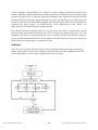
For initializing the touch screen and the VGA, Hardware Abstraction Layer is used provided by Altera.
The SD card controller is initialized using SPI. Once these components are initialized, the home screen
appears on the T-Pad’s screen. After the user selects a particular mode, images are read one by one from
the SD Card. Then using JPEG library, we decode the image data into hex format. This hex data is passed
to the buffer and pushed into video pipeline. Image corresponding to this data is then displayed. The
latency with which the image is displayed depends on the size of the hex data and therefore ultimately on
the image size. The flow chart for the software is shown below:
SFSU - Embedded Systems Tutorial
87
Nano- Electronics & Computing Research Lab
SFSU - Embedded Systems Tutorial
88
Nano- Electronics & Computing Research Lab
Step by Step ALU with image in background Tutorial
Hardware Setup
Step 1 : Open System Builder, select Clock, SDRAM, SRAM, FLASH, SD CARD, VGA and LTC – 8”
LCD/Touch/Camera as shown in figure below.
Step 2 : Select a project name, for this example we are using “picture_alu” as our project name. Click on
Generate and open the folder containing these files.
Step 3: Open the folder where the project files are saved and open picture_alu.qpf file. This file is
generated when we generate in the above step. Open the respective folder for this file. This file will be
opened in Quartus II.
Step 4: In Quartus II, the Verilog code will look like this (in blue):
//=======================================================
SFSU - Embedded Systems Tutorial
89
Nano- Electronics & Computing Research Lab
// This code is generated by Terasic System Builder
//=======================================================
module picture_alu(
//////////// CLOCK //////////
CLOCK_50,
CLOCK2_50,
CLOCK3_50,
//////////// LCD //////////
LCD_BLON,
LCD_DATA,
LCD_EN,
LCD_ON,
LCD_RS,
LCD_RW,
//////////// SDCARD //////////
SD_CLK,
SD_CMD,
SD_DAT,
SD_WP_N,
//////////// VGA //////////
VGA_B,
VGA_BLANK_N,
VGA_CLK,
VGA_G,
VGA_HS,
VGA_R,
VGA_SYNC_N,
SFSU - Embedded Systems Tutorial
90
Nano- Electronics & Computing Research Lab
VGA_VS,
//////////// I2C for HSMC //////////
I2C_SCLK,
I2C_SDAT,
//////////// SDRAM //////////
DRAM_ADDR,
DRAM_BA,
DRAM_CAS_N,
DRAM_CKE,
DRAM_CLK,
DRAM_CS_N,
DRAM_DQ,
DRAM_DQM,
DRAM_RAS_N,
DRAM_WE_N,
//////////// SRAM //////////
SRAM_ADDR,
SRAM_CE_N,
SRAM_DQ,
SRAM_LB_N,
SRAM_OE_N,
SRAM_UB_N,
SRAM_WE_N,
//////////// Flash //////////
FL_ADDR,
FL_CE_N,
FL_DQ,
FL_OE_N,
SFSU - Embedded Systems Tutorial
91
Nano- Electronics & Computing Research Lab
FL_RST_N,
FL_RY,
FL_WE_N,
FL_WP_N,
//////////// HSMC, HSMC connect to LTC - 8" LCD/Touch/Camera //////////
CAMERA_D,
CAMERA_FVAL,
CAMERA_LVAL,
CAMERA_PIXCLK,
CAMERA_RESET_N,
CAMERA_SCLK,
CAMERA_SDATA,
CAMERA_STROBE,
CAMERA_TRIGGER,
CAMERA_XCLKIN,
LCD_B,
LCD_DEN,
LCD_DIM,
LCD_G,
LCD_NCLK,
LCD_R,
TOUCH_BUSY,
TOUCH_CS_N,
TOUCH_DCLK,
TOUCH_DIN,
TOUCH_DOUT,
TOUCH_PENIRQ_N
);
//=======================================================
// PARAMETER declarations
SFSU - Embedded Systems Tutorial
92
Nano- Electronics & Computing Research Lab
//=======================================================
//=======================================================
// PORT declarations
//=======================================================
//////////// CLOCK //////////
input
CLOCK_50;
input
CLOCK2_50;
input
CLOCK3_50;
//////////// LCD //////////
output
inout
LCD_BLON;
[7:0]
LCD_DATA;
output
LCD_EN;
output
LCD_ON;
output
LCD_RS;
output
LCD_RW;
//////////// SDCARD //////////
output
SD_CLK;
inout
SD_CMD;
inout
[3:0]
input
SD_DAT;
SD_WP_N;
//////////// VGA //////////
output
[7:0]
VGA_B;
output
VGA_BLANK_N;
output
VGA_CLK;
output
output
SFSU - Embedded Systems Tutorial
[7:0]
VGA_G;
VGA_HS;
93
Nano- Electronics & Computing Research Lab
output
[7:0]
VGA_R;
output
VGA_SYNC_N;
output
VGA_VS;
//////////// I2C for HSMC //////////
output
I2C_SCLK;
inout
I2C_SDAT;
//////////// SDRAM //////////
output
[12:0]
DRAM_ADDR;
output
[1:0]
DRAM_BA;
output
DRAM_CAS_N;
output
DRAM_CKE;
output
DRAM_CLK;
output
DRAM_CS_N;
inout
[31:0]
DRAM_DQ;
output
[3:0]
DRAM_DQM;
output
DRAM_RAS_N;
output
DRAM_WE_N;
//////////// SRAM //////////
output
[19:0]
output
inout
SRAM_ADDR;
SRAM_CE_N;
[15:0]
SRAM_DQ;
output
SRAM_LB_N;
output
SRAM_OE_N;
output
SRAM_UB_N;
output
SRAM_WE_N;
//////////// Flash //////////
output
output
SFSU - Embedded Systems Tutorial
[22:0]
FL_ADDR;
FL_CE_N;
94
Nano- Electronics & Computing Research Lab
inout
[7:0]
FL_DQ;
output
FL_OE_N;
output
FL_RST_N;
input
FL_RY;
output
FL_WE_N;
output
FL_WP_N;
//////////// HSMC, HSMC connect to LTC - 8" LCD/Touch/Camera //////////
input
[11:0]
CAMERA_D;
input
CAMERA_FVAL;
input
CAMERA_LVAL;
input
CAMERA_PIXCLK;
output
CAMERA_RESET_N;
output
CAMERA_SCLK;
inout
CAMERA_SDATA;
input
CAMERA_STROBE;
output
CAMERA_TRIGGER;
output
CAMERA_XCLKIN;
output
[5:0]
LCD_B;
output
LCD_DEN;
output
LCD_DIM;
output
[5:0]
output
output
LCD_G;
LCD_NCLK;
[5:0]
LCD_R;
input
TOUCH_BUSY;
output
TOUCH_CS_N;
output
TOUCH_DCLK;
output
TOUCH_DIN;
input
TOUCH_DOUT;
input
TOUCH_PENIRQ_N;
SFSU - Embedded Systems Tutorial
95
Nano- Electronics & Computing Research Lab
//=======================================================
// REG/WIRE declarations
//=======================================================
//=======================================================
// Structural coding
//=======================================================
endmodule
This step initiates all the ports selected on system builder.
Step 5: Open SOPC Builder Window and add the following components from library (detailed procedure
is explained in chapter no.3):
alt_pll
CPU
System id
SD RAM
Tri State Bridge Flash
Flash
SRAM
On chip Memory
SGDMA Controller
Timing Adapter
On Chip FIFO Memory
Timing Adapter
SFSU - Embedded Systems Tutorial
96
Nano- Electronics & Computing Research Lab
Pixel Converter
VGA Sink
Peripheral Bridge
Sd Card Controller
Interval Timer
Touch Panel
Touch Panel SPI
Touch Panel penirq
Touch Panel Busy
Step 6: Go to the “Connections” column and connect the following ports:
i. Pll_slave(system clock) is connected to cpu, jtag_uart, sysid, sdram, tri_state
bridge flas, cfi_flash, sram, on chip memory, SGDMA Controller, Fifo and
peripheral bridge
j. CPU’s jtag_debug_module to SDRAM, Tristate Bridge, SRAM.
k. SDRAM to SGDMA Controller’s “m_read”.
l. Descriptor Memory to SGDMA Controller’s “Descriptor Read”
m. Descriptor Memory to SGDMA Controller’s “Descriptor Write”
n. SGDMA Controller’s out to Timing Adapter’s “in”.
o. Timing Adapter’s “out” to FIFO’s “in”.
p. FIFO’s “out” to Pixel Converter’s “in”.
q. Pixel Converter’s “out” to VGA_Sink.
r. SD Card Controller to System Clock Timer, Touch Panel SPI, Touch_Panel_irq_n
and Touch_Panel_busy.
s. Open the Nios II processor named CPU and change the reset vector and
exception vectors to onchip_memory2
Step 7: For assignment of base addresses in SOPC Builder:
Click on “Auto assign base addresses” on the main menu bar and “Auto assign IRQ’s” as
shown in figure below:
SFSU - Embedded Systems Tutorial
97
Nano- Electronics & Computing Research Lab
The complete SOPC Builder system is shown below:
SFSU - Embedded Systems Tutorial
98
Nano- Electronics & Computing Research Lab
If you wish to open the complete already designed hardware in SOPC builder, you may open the file
“nios_simple.sopcinfo” which is attached to this tutorial.
To generate the hardware in sopc builder, click on generate shown in the figure below:
After the sopc builder system is generated:
We get the following code:
wire reset_n;
wire [7:0] wire_HC_B;
wire [7:0] wire_HC_G;
wire [7:0] wire_HC_R;
SFSU - Embedded Systems Tutorial
99
Nano- Electronics & Computing Research Lab
assign reset_n = 1'b1;
assign HC_DIM = 1'b1;
nios_simple nios_simple_ins(
// 1) global signals:
.clk_ext(CLOCK_50),
.reset_n(reset_n),
//.altpll_25(),
// .altpll_io(),
.clk_sdram(DRAM_CLK),
//.clk_sdram(DRAM_CLK),
//.clk_pixel(HC_NCLK),
////VGA SINK
.vga_b_from_the_vga_source
(wire_HC_B),
.vga_clk_from_the_vga_source
(HC_NCLK),
.vga_de_from_the_vga_source
(HC_DEN),
.vga_g_from_the_vga_source
(wire_HC_G),
.vga_hs_from_the_vga_source
(),
.vga_r_from_the_vga_source
(wire_HC_R),
.vga_vs_from_the_vga_source
(),
// the_sdram
.zs_addr_from_the_sdram(DRAM_ADDR),
.zs_ba_from_the_sdram(DRAM_BA),
.zs_cas_n_from_the_sdram(DRAM_CAS_N),
.zs_cke_from_the_sdram(DRAM_CKE),
.zs_cs_n_from_the_sdram(DRAM_CS_N),
.zs_dq_to_and_from_the_sdram(DRAM_DQ),
.zs_dqm_from_the_sdram(DRAM_DQM),
.zs_ras_n_from_the_sdram(DRAM_RAS_N),
.zs_we_n_from_the_sdram(DRAM_WE_N),
// the_sd_card_controller
.spi_clk_from_the_sd_card_controller
SFSU - Embedded Systems Tutorial
(SD_CLK),
100
Nano- Electronics & Computing Research Lab
.spi_cs_n_from_the_sd_card_controller
(SD_DAT[3]),
.spi_data_in_to_the_sd_card_controller (SD_DAT[0]),
.spi_data_out_from_the_sd_card_controller (SD_CMD),
////cfi flash
.tri_state_bridge_flash_address
(FL_ADDR),
.tri_state_bridge_flash_data
(FL_DQ),
.write_n_to_the_cfi_flash
(FL_WE_N),
.read_n_to_the_cfi_flash
(FL_OE_N),
.select_n_to_the_cfi_flash
(FL_CE_N),
////touch panel interface
.MISO_to_the_touch_panel_spi
(HC_ADC_DOUT),
.MOSI_from_the_touch_panel_spi
(HC_ADC_DIN),
.SCLK_from_the_touch_panel_spi
(HC_ADC_DCLK),
.SS_n_from_the_touch_panel_spi
.in_port_to_the_touch_panel_pen_irq_n
.in_port_to_the_touch_panel_busy
(HC_ADC_CS_N),
(HC_ADC_PENIRQ_N),
(HC_ADC_BUSY),
////SRAM
.SRAM_ADDR_from_the_sram
.SRAM_CE_n_from_the_sram
.SRAM_DQ_to_and_from_the_sram
(SRAM_ADDR),
(SRAM_CE_N),
(SRAM_DQ),
.SRAM_LB_n_from_the_sram
(SRAM_LB_N),
.SRAM_OE_n_from_the_sram
(SRAM_OE_N),
.SRAM_UB_n_from_the_sram
(SRAM_UB_N),
.SRAM_WE_n_from_the_sram
(SRAM_WE_N)
);
////
assign HC_B = wire_HC_B[7:2];
assign HC_G = wire_HC_G[7:2];
assign HC_R = wire_HC_R[7:2];
// Flash Config
assign
FL_RST_N = reset_n;
assign
FL_WP_N = 1'b1;
SFSU - Embedded Systems Tutorial
101
Nano- Electronics & Computing Research Lab
//
FLASH_RY,
///////////////////////////////////////////
// LCD config
assign LCD_BLON = 0; // not supported
assign LCD_ON = 1'b1; // alwasy on
This code should be copied and pasted in the main Verilog (shown previously) under REG/WIRE
declarations section.
With this step our hardware configuration is done.
After this step, open Nios II IDE Eclipse and write software to configure software of the demonstration.
Software Setup
Basic Algorithm:
1) Display is initialized.
display_global = alt_video_display_init( "/dev/sgdma_pixel", // Name of video controller
WIDTH,
// Width of display
HEIGHT,
// Height of display
32,
// Color depth (32 or 16)
SDRAM_BASE+SDRAM_SPAN/2,
// Where we want our frame buffers
DESCRIPTOR_MEM_BASE,
// Where we want our descriptors
NUM_FRAME );
if( display_global )
2) Touch Panel is initialized.
hTouch = Touch_Init(TOUCH_PANEL_SPI_BASE, TOUCH_PANEL_PEN_IRQ_N_BASE,
TOUCH_PANEL_PEN_IRQ_N_IRQ);
3) Welcome screen is displayed . The following commands are used to display characters on
the screen.
sprintf(szText,"\nCalculator ");
vid_print_string_alpha(400, 2, COLOR_WHITE, COLOR_BLACK, tahomabold_20, display_global, szText);
sprintf(szText,"\nTouch Anywhere to Begin");
vid_print_string_alpha(220, 200, COLOR_WHITE, COLOR_BLACK, tahomabold_20, display_global, szText);
SFSU - Embedded Systems Tutorial
102
Nano- Electronics & Computing Research Lab
//vid_draw_round_corner_box ( 300, 400, 500, 500,10, 0x5555, 0x0000, display_global);
4) After the touch is selected , pixel buffer and character buffer gets updated.
alt_video_display_clear_screen(display_global, 0x0);
result = write_buffer(display_global,name_list[pic_index],frame_write_index);
alt_video_display_register_written_buffer(display_global);
////direct the display buffer to buffer_being_written
while(alt_video_display_buffer_is_available(display_global)!=0); ////update display_global- >buffer_being_displayed
printf("\nLook at the the screen");
x=0;
y=0;
sprintf(text_disp,"ADDITION");
vid_print_string_alpha(50, 200, COLOR_WHITE, COLOR_BLACK, tahomabold_20,
display_global, text_disp);
sprintf(text_disp,"SUBTRACTION");
vid_print_string_alpha(200, 200, COLOR_WHITE, COLOR_BLACK, tahomabold_20, display_global, text_disp);
sprintf(text_disp,"LOGICAL AND");
vid_print_string_alpha(400, 200, COLOR_WHITE, COLOR_BLACK, tahomabold_20, display_global, text_disp);
sprintf(text_disp,"LOGICAL OR");
vid_print_string_alpha(600, 200, COLOR_WHITE, COLOR_BLACK, tahomabold_20,
display_global, text_disp);
Touch_EmptyFifo(hTouch);
Touch_EmptyFifo(hTouch) is used to empty the touch input
5) The screen waits for the touch input in trigger area which will perform ALU functions.
For example:
if (touch == 0 && (x >= 50 && x<=150 )) //Trigger area
{
printf("I am in addition loop\n x=%d y = %d", x, y);// display statement on console for debugging
SFSU - Embedded Systems Tutorial
103
Nano- Electronics & Computing Research Lab
touch = 1;
x=0;
y=0;
result = write_buffer(display_global,name_list[pic_index],frame_write_index);
sprintf(text_calc,"10 + 5 = 15");
vid_print_string_alpha(350, 410, COLOR_WHITE, COLOR_BLACK, tahomabold_20, display_global, text_calc);
sprintf(text_disp,"ADDITION");
vid_print_string_alpha(50, 200, COLOR_WHITE, COLOR_BLACK, tahomabold_20, display_global, text_disp);
sprintf(text_disp,"SUBTRACTION");
vid_print_string_alpha(200, 200, COLOR_WHITE, COLOR_BLACK, tahomabold_20, display_global, text_disp);
sprintf(text_disp,"LOGICAL AND");
vid_print_string_alpha(400, 200, COLOR_WHITE, COLOR_BLACK, tahomabold_20, display_global, text_disp);
sprintf(text_disp,"LOGICAL OR");
vid_print_string_alpha(600, 200, COLOR_WHITE, COLOR_BLACK, tahomabold_20, display_global, text_disp);
usleep(100000);
Touch_EmptyFifo(hTouch);
goto here; // label to take it back to the main loop
6) The screen performs respective functions according to which trigger area is touched.
Alternatively you can obtain the software code by opening the main.c file which is attached with this
tutorial.
Downloading the design to the Board
a) –For Hardware, compile the .sof file on the board as shown below:
SFSU - Embedded Systems Tutorial
104
Nano- Electronics & Computing Research Lab
b) – For software, Run the software program under target as Nios II Hardware shown below:
SFSU - Embedded Systems Tutorial
105
Nano- Electronics & Computing Research Lab
Video Demonstration of this tutorial is available on YouTube by clicking here:
http://www.youtube.com/watch?v=_epPtQ-lTuQ
SFSU - Embedded Systems Tutorial
106
Nano- Electronics & Computing Research Lab