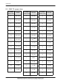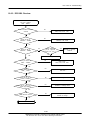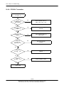
1
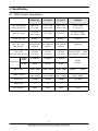
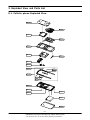
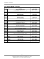
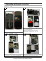
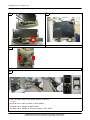
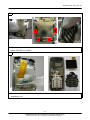
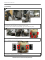
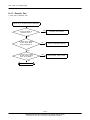
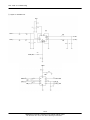
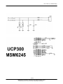
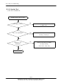
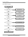
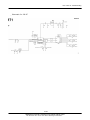
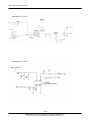
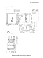
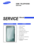
GSM TELEPHONE
SGH-L170
GSM TELEPHONE
CONTENTS
1.
Safety Precautions
2.
Specification
3.
Product Function
4.
Array course control
5.
Exploded View and Parts list
6.
MAIN Electrical Parts List
7.
Disassembly and Assembly
Instructions
8.
Block Diagrams
9.
PCB Diagrams
10. Chart of Troubleshooting
11. Reference data
GSPN (Global Service Partner Network)
Country
Web Site
North America
service.samsungportal.com
Latin America
latin.samsungportal.com
CIS
cis.samsungportal.com
Europe
europe.samsungportal.com
China
china.samsungportal.com
Asia
asia.samsungportal.com
Mideast & Africa
mea.samsungportal.com
This Service Manual is a property of Samsung Electronics Co.,Ltd.
Any unauthorized use of Manual can be punished under applicable
International and/or domestic law.
ⓒ Samsung Electronics Co.,Ltd.
2008. 02. Rev.1.0
1. Safety Precautions
1-1. Repair Precaution
● Repair in Shield Box, during detailed tuning.
Take specially care of tuning or test,
because specipicty of cellular phone is sensitive for surrounding interference(RF noise).
● Be careful to use a kind of magnetic object or tool,
because performance of parts is damaged by the influence of manetic force.
● Surely use a standard screwdriver when you disassemble this product,
otherwise screw will be worn away.
● Use a thicken twisted wire when you measure level.
A thicken twisted wire has low resistance, therefore error of measurement is few.
● Repair after separate Test Pack and Set because for short danger (for example an
overcurrent and furious flames of parts etc) when you repair board in condition of
connecting Test Pack and tuning on.
● Take specially care of soldering, because Land of PCB is small and weak in heat.
● Surely tune on/off while using AC power plug, because a repair of battery charger is
dangerous when tuning ON/OFF PBA and Connector after disassembing charger.
● Don't use as you pleases after change other material than replacement registered on SEC
System.
Otherwise engineer in charge isn't charged with problem that you don't keep this rules.
1-1
SAMSUNG Proprietary-Contents may change without notice
This Document can not be used without Samsung's authorization
Safety Precautions
1-2. ESD(Electrostatically Sensitive Devices) Precaution
Several semiconductor may be damaged easilly by static electricity. Such parts are called by
ESD(Electrostatically Sensitive Devices), for example IC,BGA chip etc. Read Precaution below.
You can prevent from ESD damage by static electricity.
● Remove static electricity remained your body before you touch semiconductor or parts with
semiconductor. There are ways that you touch an earthed place or wear static electricity
prevention string on wrist.
● Use earthed soldering steel when you connect or disconnect ESD.
● Use soldering removing tool to break static electricity. , otherwise ESD will be damaged by
static electricity.
● Don't unpack until you set up ESD on product. Because most of ESD are packed by box
and aluminum plate to have conductive power,they are prevented from static electricity.
● You must maintain electric contact between ESD and place due to be set up until ESD is
connected completely to the proper place or a circuit board.
1-2
SAMSUNG Proprietary-Contents may change without notice
This Document can not be used without Samsung's authorization
2. Specification
2-1. GSM General Specification
EG SM 900
DCS1 800
PCS1 900
WCDMA
Fr eq. Band [MHz]
Up link/ Do wnl ink
880~9 15
925~9 60
1710~1 785
1805~1 880
1850~1 910
1930~1 990
1 920~19 80
2 110~21 70
ARFCN ran ge
0~1 24 &
975~1 023
512~8 85
512~8 10
UL:9 612~98 88
DL:10 562~10 838
Tx/Rx spacin g
45MHz
95MHz
80MHz
190MHz
Mod . Bit r ate/
Bi t Peri od
270.8 33kbps
3.69 2us
270.8 33kbps
3.69 2us
270.8 33kbps
3.69 2us
3. 84Mcps
Tim e Slot
Per iod/ Fra me Per iod
576. 9us
4 .615ms
576. 9us
4 .615ms
576. 9us
4 .615ms
F rame l ength : 10ms
Slot lengt h : 0. 667ms
GSM/
G PR S
0.3G MSK
0.3G M SK
0.3G MSK
EDG E
8PSK
8PSK
8PSK
QPSK
HQPSK
Modu lation
MS Power
Po wer Class
33dBm~ 5dBm 30dBm~ 0dBm 30dBm~ 0dBm
4
(max +33dBm)
1
(max +30dBm)
2 4dBm ~ - 50dBm
1
(max +30dBm)
Sen sitivity
- 102dBm
- 100dBm
- 100dBm
TDMA M ux
8
8
8
Cell Radius
35Km
2Km
2Km
2-1
SAMSUNG Proprietary-Contents may change without notice
This Document can not be used without Samsung's authorization
3
(max +24dBm)
- 106.7 dBm
2Km
Specification
2-2. GSM TX power class
TX Power
control level
GSM900
TX Power
control level
DCS1800
TX Power
control level
PCS1900
5
33±2 dBm
0
30±2 dBm
0
30±2 dBm
6
31±2 dBm
1
28±3 dBm
1
28±3 dBm
7
29±2 dBm
2
26±3 dBm
2
26±3 dBm
8
27±2 dBm
3
24±3 dBm
3
24±3 dBm
9
25±2 dBm
4
22±3 dBm
4
22±3 dBm
10
23±2 dBm
5
20±3 dBm
5
20±3 dBm
11
21±2 dBm
6
18±3 dBm
6
18±3 dBm
12
19±2 dBm
7
16±3 dBm
7
16±3 dBm
13
17±2 dBm
8
14±3 dBm
8
14±3 dBm
14
15±2 dBm
9
12±4 dBm
9
12±4 dBm
15
13±2 dBm
10
10±4 dBm
10
10±4 dBm
16
11±3 dBm
11
8±4dBm
11
8±4dBm
17
9±3dBm
12
6±4 dBm
12
6±4 dBm
18
7±3 dBm
13
4±4 dBm
13
4±4 dBm
19
5±3 dBm
14
2±5 dBm
14
2±5 dBm
15
0±5 dBm
15
0±5 dBm
2-2
SAMSUNG Proprietary-Contents may change without notice
This Document can not be used without Samsung's authorization
3. Product Function
Main Function
[ H/W ]
- Size
: 102.3 x 45.8 x 10.7 mm
- Weight
: 83 g
- Band
: GSM 900 / 1800 / 1900
UMTS 2100
- Battery
: 880mAh / Inner (653039H)
- BB
: Qualcomm MSM6245
- RF
: Qualcomm RTR6275
- LCD
:
- Memory
: 1G (NAND) +512Mb (SDRAM)
1.6" 220*176 262K TFT (SDI)
* external : microSD ( T-Flash )
- Camera
:
2.0M CMOS (LSI)
VGA QCIF (서울전자통신)
- TOUCH KEY
: SYNAPTICS
- BT/FM
: Braodcom BCM2048
* FM Radio with RDS
* Bluetooth 2.0
[ S/W ]
- Video Telephony / Streaming
- USB 2.0
- MP3 / 72 Poly Melody
- WAP2.0, MPEG4
- MIDP 2.0 / cldc 1.1
- Mobile Blog
- Rss Reader
- FM Radio with RDS
- Music Search
- Bluetooth 2.0
- Auto Time Setting,
- GPRS/EDGE
- MMS / EMS
3-1
SAMSUNG Proprietary-Contents may change without notice
This Document can not be used without Samsung's authorization
4. Array course control
4-1. Software Adjustments
Test Jig
(GH80-03308A)
Test Cable
(GH39-00886A or GH39-00889A)
Serial Cable
Power Supply Cable
RF Test Cable
DATA CABLE
(GH39-00922A or GH39-00922B)
(GH39-00397A)
4-1
SAMSUNG Proprietary-Contents may change without notice
This Document can not be used without Samsung's authorization
Array course control
4-2. Software Downloading
4-2-1. Downloading Binary Files
• Four binary files for downloading L170
• SGH-L170 Mobile Phone
• Data Cable
• Binary file,
4-2-2. Pre-requsite for Downloading
• Downloader Program
• SGH-L170 Mobile Phone
• Data Cable
• Binary file,
4-2-3. S/W Downloader Program
1. Boot the L170 by pressing ‘Power ON key’ + 'Number 9 Key' at the same time.
→ If you do properly, you can see the "DOWNLOAD" mode screen on the LCD.
2. Load the binary download program by executing the “Downloader V5.30.exe”.
→ If you connect the data cable to L170, you can see "COM" port detection sign.
4-2
SAMSUNG Proprietary-Contents may change without notice
This Document can not be used without Samsung's authorization
Array course control
3. Select chipset "MSM6245".
Next, check the "boot change" and check the "full download"
4. Select the binary files. (Boot, Modem, Rsrc1, Rsrc2, Factory FS)
4-3
SAMSUNG Proprietary-Contents may change without notice
This Document can not be used without Samsung's authorization
Array course control
5. Now press the button ‘Port Search’.
→ Model name is displayed additionally in COM port screen.
6. Now click the button ‘DownLoad’.
→ Download progressing bar is starting.
7. When downloading is complete, UE reboot automatically.
→ If there is difference in FactoryFs.bin, UE will format file system automatically.
4-4
SAMSUNG Proprietary-Contents may change without notice
This Document can not be used without Samsung's authorization
5. Exploded View and Parts List
5-1. Cellular phone Exploded View
QMW01
QKP01
QLC01
QME03
QFR01
QMP01
QMO01
QSP01
QCA01
QCR69
QVO01
QCK01
QVO08
QIF01
QCK02
QRE01
QRF01
QCR70
QCR70
QBA01
QBA00
5-1
SAMSUNG Proprietary-Contents may change without notice
This Document can not be used without Samsung's authorization
Exploded View and Parts List
5-2. Cellular phone Parts list
Design LOC
Discription
SEC CODE
QBA00
ASSY COVER-BATTERY
GH98-07254A
QBA01
INNER BATTERY PACK-880MAH , BL
GH43-02666A
QCA01
CAMERA MODULE-SGHL170 2M
GH59-05043A
QCR69
SCREW-MACHINE
6001-002065
QCR70
SCREW-TAPPING
6002-001402
QCR70
SCREW-TAPPING
6002-001402
QFR01
ASSY CASE-FRONT
GH98-06461A
QKP01
ASSY KEYPAD-(FMG/MSS)
GH98-07459A
QLC01
LCD-MODULE SGHL170
GH07-01209A
QME03
KEY FPCB-SGHL170 TOUCH 34 KEY
GH59-05081A
QMO01
MOTOR DC-SCH-S269
GH31-00319A
QMP01
PBA MAIN-SGHL170S
GH92-04414A
QMW01
ASSY COVER-MAIN WINDOW
GH98-06465A
QRE01
ASSY CASE-REAR
GH98-06463A
QRF01
TAPE-RF SHEET
GH74-35355A
QSP01
ASSY ETC-SGHL170 SPK INT ASS'Y
GH59-05124A
QVO08
ASSY DECO-SIDE BELT
GH98-06464A
QIF01
PMO COVER-IF
GH72-44663A
QVO01
PMO KEY-VOL
GH72-44664A
QCK01
PMO KEY-CAM
GH72-44665A
QCK02
PMO KEY-SWITCH
GH72-44666A
5-2
SAMSUNG Proprietary-Contents may change without notice
This Document can not be used without Samsung's authorization
6. MAIN Electrical Parts List
SEC CODE
Design LOC
Discription
STATUS
0403-001547
ZD603
DIODE-ZENER
SA
0403-001547
ZD604
DIODE-ZENER
SA
0404-001153
D400
DIODE-SCHOTTKY
SA
0404-001153
D401
DIODE-SCHOTTKY
SA
0404-001153
D601
DIODE-SCHOTTKY
SA
0406-001208
ZD601
DIODE-TVS
SA
0406-001208
ZD602
DIODE-TVS
SA
0406-001223
V706
DIODE-TVS
SA
0406-001223
ZD300
DIODE-TVS
SA
0406-001223
ZD500
DIODE-TVS
SA
0406-001223
ZD501
DIODE-TVS
SA
0406-001223
ZD502
DIODE-TVS
SA
0406-001223
ZD503
DIODE-TVS
SA
0406-001231
ZD605
DIODE-TVS
SA
0406-001231
ZD606
DIODE-TVS
SA
0406-001254
ZD600
DIODE-TVS
SA
0406-001254
ZD701
DIODE-TVS
SA
0406-001254
ZD702
DIODE-TVS
SA
0406-001254
ZD703
DIODE-TVS
SA
0406-001254
ZD704
DIODE-TVS
SA
0407-001002
D402
DIODE-ARRAY
SA
0407-001002
D600
DIODE-ARRAY
SA
0504-000168
Q400
TR-DIGITAL
SA
0504-000168
Q401
TR-DIGITAL
SA
0504-001151
Q200
TR-DIGITAL
SA
1001-001336
U504
IC-ANALOG SWITCH
SA
1001-001336
U601
IC-ANALOG SWITCH
SA
1001-001405
U501
IC-ANALOG MULTIPLEX
SA
1006-001322
U401
IC-LINE TRANSCEIVER
SA
1108-000144
UME300
IC-MCP
SA
1201-002304
U503
IC-AUDIO AMP
SA
1201-002305
PAM200
IC-POWER AMP
SA
1201-002570
PAM100
IC-POWER AMP
SA
1203-002624
U500
IC-POSI.FIXED REG.
SA
1203-003340
U403
IC-POSI.FIXED REG.
SA
1203-003432
Q605
IC-POSI.FIXED REG.
SA
6-1
SAMSUNG Proprietary-Contents may change without notice
This Document can not be used without Samsung's authorization
Main Electrical Parts List
SEC CODE
Design LOC
Discription
STATUS
1203-003523
Q601
IC-POSI.FIXED REG.
SA
1203-003523
Q603
IC-POSI.FIXED REG.
SA
1203-003708
U600
IC-DC/DC CONVERTER
SA
1203-003737
Q602
IC-POSI.FIXED REG.
SA
1203-003754
Q600
IC-POSI.FIXED REG.
SA
1203-003791
Q604
IC-POSI.FIXED REG.
SA
1203-004518
U402
IC-BATTERY
SA
1203-004926
U400
IC-POWER SUPERVISOR
SA
1205-003206
UCP300
IC-MODEM
SA
1205-003216
U101
IC-TRANSCEIVER
SA
1205-003285
U200
IC-TRANSCEIVER
SA
1404-001224
TH300
THERMISTOR-NTC
SA
1405-001110
V400
VARISTOR
SA
1405-001133
V700
VARISTOR
SA
1405-001133
V702
VARISTOR
SA
1405-001133
V704
VARISTOR
SA
1405-001201
V708
VARISTOR
SA
1405-001201
V709
VARISTOR
SA
1405-001201
V711
VARISTOR
SA
1405-001201
V712
VARISTOR
SA
1405-001201
V713
VARISTOR
SA
1405-001201
V714
VARISTOR
SA
1405-001201
V715
VARISTOR
SA
1405-001201
V716
VARISTOR
SA
1405-001201
V717
VARISTOR
SA
2007-000138
R518
R-CHIP
SA
2007-000141
R505
R-CHIP
SA
2007-000148
R104
R-CHIP
SA
2007-000148
R301
R-CHIP
SA
2007-000152
R303
R-CHIP
SA
2007-000171
R110
R-CHIP
SA
2007-000171
R111
R-CHIP
SA
2007-000171
R320
R-CHIP
SA
2007-000171
R404
R-CHIP
SA
2007-000171
R406
R-CHIP
SA
2007-000171
R408
R-CHIP
SA
6-2
SAMSUNG Proprietary-Contents may change without notice
This Document can not be used without Samsung's authorization
Main Electrical Parts List
SEC CODE
Design LOC
Discription
STATUS
2007-000171
R409
R-CHIP
SA
2007-000171
R410
R-CHIP
SA
2007-000171
R411
R-CHIP
SA
2007-000171
R412
R-CHIP
SA
2007-000171
R508
R-CHIP
SA
2007-000171
R515
R-CHIP
SA
2007-000171
R709
R-CHIP
SA
2007-001119
R500
R-CHIP
SA
2007-007308
R516
R-CHIP
SA
2007-007308
R517
R-CHIP
SA
2007-007317
R105
R-CHIP
SA
2007-007468
R414
R-CHIP
SA
2007-007489
R109
R-CHIP
SA
2007-007528
R501
R-CHIP
SA
2007-007741
R302
R-CHIP
SA
2007-007741
R310
R-CHIP
SA
2007-007741
R319
R-CHIP
SA
2007-007741
R321
R-CHIP
SA
2007-007766
R116
R-CHIP
SA
2007-008044
R203
R-CHIP
SA
2007-008045
R115
R-CHIP
SA
2007-008045
R204
R-CHIP
SA
2007-008045
R213
R-CHIP
SA
2007-008045
R511
R-CHIP
SA
2007-008045
R618
R-CHIP
SA
2007-008045
R706
R-CHIP
SA
2007-008046
R102
R-CHIP
SA
2007-008046
R103
R-CHIP
SA
2007-008046
R107
R-CHIP
SA
2007-008046
R108
R-CHIP
SA
2007-008049
R305
R-CHIP
SA
2007-008053
R432
R-CHIP
SA
2007-008055
R300
R-CHIP
SA
2007-008055
R317
R-CHIP
SA
2007-008055
R322
R-CHIP
SA
2007-008055
R325
R-CHIP
SA
6-3
SAMSUNG Proprietary-Contents may change without notice
This Document can not be used without Samsung's authorization
Main Electrical Parts List
SEC CODE
Design LOC
Discription
STATUS
2007-008055
R403
R-CHIP
SA
2007-008055
R419
R-CHIP
SA
2007-008055
R420
R-CHIP
SA
2007-008055
R421
R-CHIP
SA
2007-008055
R422
R-CHIP
SA
2007-008055
R438
R-CHIP
SA
2007-008055
R441
R-CHIP
SA
2007-008055
R609
R-CHIP
SA
2007-008055
R619
R-CHIP
SA
2007-008419
R440
R-CHIP
SA
2007-008419
R602
R-CHIP
SA
2007-008419
R603
R-CHIP
SA
2007-008419
R605
R-CHIP
SA
2007-008419
R606
R-CHIP
SA
2007-008477
R401
R-CHIP
SNA
2007-008478
R503
R-CHIP
SA
2007-008478
R506
R-CHIP
SA
2007-008483
R402
R-CHIP
SA
2007-008483
R429
R-CHIP
SA
2007-008483
R601
R-CHIP
SA
2007-008483
R612
R-CHIP
SA
2007-008483
R615
R-CHIP
SA
2007-008483
R622
R-CHIP
SA
2007-008486
R415
R-CHIP
SA
2007-008486
R417
R-CHIP
SA
2007-008486
R620
R-CHIP
SA
2007-008516
R405
R-CHIP
SA
2007-008516
R423
R-CHIP
SA
2007-008516
R424
R-CHIP
SA
2007-008516
R425
R-CHIP
SA
2007-008516
R426
R-CHIP
SA
2007-008516
R427
R-CHIP
SA
2007-008516
R439
R-CHIP
SA
2007-008516
R710
R-CHIP
SA
2007-008516
R711
R-CHIP
SA
2007-008531
R211
R-CHIP
SA
6-4
SAMSUNG Proprietary-Contents may change without notice
This Document can not be used without Samsung's authorization
Main Electrical Parts List
SEC CODE
Design LOC
Discription
STATUS
2007-008542
R112
R-CHIP
SA
2007-008542
R113
R-CHIP
SA
2007-008542
R200
R-CHIP
SA
2007-008542
R207
R-CHIP
SA
2007-008542
R210
R-CHIP
SA
2007-008542
R306
R-CHIP
SA
2007-008542
R504
R-CHIP
SA
2007-008542
R509
R-CHIP
SA
2007-008542
R514
R-CHIP
SA
2007-008542
R613
R-CHIP
SA
2007-008542
R617
R-CHIP
SA
2007-008542
R701
R-CHIP
SA
2007-008542
R703
R-CHIP
SA
2007-008542
R707
R-CHIP
SA
2007-008542
R708
R-CHIP
SA
2007-008544
R212
R-CHIP
SA
2007-008544
R502
R-CHIP
SA
2007-008544
R507
R-CHIP
SA
2007-008548
R604
R-CHIP
SA
2007-008588
R704
R-CHIP
SA
2007-008588
R705
R-CHIP
SA
2007-008647
R208
R-CHIP
SA
2007-008648
R437
R-CHIP
SA
2007-008648
R600
R-CHIP
SA
2007-008648
R610
R-CHIP
SA
2007-008648
R611
R-CHIP
SA
2007-008648
R621
R-CHIP
SA
2007-008774
R206
R-CHIP
SA
2007-008774
R209
R-CHIP
SA
2007-008786
R323
R-CHIP
SA
2007-008806
R101
R-CHIP
SA
2007-008806
R106
R-CHIP
SA
2007-008806
R114
R-CHIP
SA
2007-008806
R202
R-CHIP
SA
2007-008806
R308
R-CHIP
SA
2007-008806
R326
R-CHIP
SA
6-5
SAMSUNG Proprietary-Contents may change without notice
This Document can not be used without Samsung's authorization
Main Electrical Parts List
SEC CODE
Design LOC
Discription
STATUS
2007-008806
R413
R-CHIP
SA
2007-008809
R407
R-CHIP
SNA
2007-008964
R430
R-CHIP
SA
2007-009111
R608
R-CHIP
SA
2007-009111
R623
R-CHIP
SA
2007-009111
R624
R-CHIP
SA
2007-009112
R521
R-CHIP
SNA
2007-009154
R519
R-CHIP
SNA
2007-009154
R520
R-CHIP
SNA
2007-009168
R522
R-CHIP
SA
2007-009168
R607
R-CHIP
SA
2007-009169
R434
R-CHIP
SA
2007-009171
R311
R-CHIP
SA
2007-009171
R312
R-CHIP
SA
2007-009171
R313
R-CHIP
SA
2007-009171
R314
R-CHIP
SA
2007-009171
R315
R-CHIP
SA
2007-009171
R416
R-CHIP
SA
2007-009171
R418
R-CHIP
SA
2007-009208
R510
R-CHIP
SA
2007-009208
R513
R-CHIP
SA
2007-009408
R436
R-CHIP
SA
2007-009410
R433
R-CHIP
SA
2007-009801
R205
R-CHIP
SA
2203-000138
C419
C-CER,CHIP
SA
2203-000254
C205
C-CER,CHIP
SA
2203-000254
C322
C-CER,CHIP
SA
2203-000254
C519
C-CER,CHIP
SA
2203-000254
C520
C-CER,CHIP
SA
2203-000278
C117
C-CER,CHIP
SA
2203-000330
C100
C-CER,CHIP
SA
2203-000330
C201
C-CER,CHIP
SA
2203-000438
C121
C-CER,CHIP
SA
2203-000438
C122
C-CER,CHIP
SA
2203-000438
C126
C-CER,CHIP
SA
2203-000438
C315
C-CER,CHIP
SA
6-6
SAMSUNG Proprietary-Contents may change without notice
This Document can not be used without Samsung's authorization
Main Electrical Parts List
SEC CODE
Design LOC
Discription
STATUS
2203-000438
C316
C-CER,CHIP
SA
2203-000438
C326
C-CER,CHIP
SA
2203-000438
C329
C-CER,CHIP
SA
2203-000438
C522
C-CER,CHIP
SA
2203-000438
C527
C-CER,CHIP
SA
2203-000466
C133
C-CER,CHIP
SA
2203-000696
C113
C-CER,CHIP
SA
2203-000812
C112
C-CER,CHIP
SA
2203-000812
C127
C-CER,CHIP
SA
2203-000812
C200
C-CER,CHIP
SA
2203-000812
C504
C-CER,CHIP
SA
2203-000812
C505
C-CER,CHIP
SA
2203-000812
C523
C-CER,CHIP
SA
2203-000812
C524
C-CER,CHIP
SA
2203-000836
C245
C-CER,CHIP
SA
2203-000854
C111
C-CER,CHIP
SA
2203-000995
C105
C-CER,CHIP
SA
2203-000995
C119
C-CER,CHIP
SA
2203-000995
C120
C-CER,CHIP
SA
2203-000995
C454
C-CER,CHIP
SA
2203-002668
C208
C-CER,CHIP
SA
2203-002677
C204
C-CER,CHIP
SA
2203-002709
C116
C-CER,CHIP
SA
2203-002709
C130
C-CER,CHIP
SA
2203-002709
C700
C-CER,CHIP
SA
2203-002709
C701
C-CER,CHIP
SA
2203-005390
C101
C-CER,CHIP
SA
2203-005450
C207
C-CER,CHIP
SA
2203-005482
C500
C-CER,CHIP
SA
2203-005482
C518
C-CER,CHIP
SA
2203-005482
C601
C-CER,CHIP
SA
2203-005682
C109
C-CER,CHIP
SA
2203-005682
C110
C-CER,CHIP
SA
2203-005682
C231
C-CER,CHIP
SA
2203-005682
C440
C-CER,CHIP
SA
2203-005682
C441
C-CER,CHIP
SA
6-7
SAMSUNG Proprietary-Contents may change without notice
This Document can not be used without Samsung's authorization
Main Electrical Parts List
SEC CODE
Design LOC
Discription
STATUS
2203-005682
C442
C-CER,CHIP
SA
2203-005682
C443
C-CER,CHIP
SA
2203-005682
C444
C-CER,CHIP
SA
2203-005682
C445
C-CER,CHIP
SA
2203-005682
C446
C-CER,CHIP
SA
2203-005682
C447
C-CER,CHIP
SA
2203-005682
C450
C-CER,CHIP
SA
2203-005682
C451
C-CER,CHIP
SA
2203-005682
C512
C-CER,CHIP
SA
2203-005682
C513
C-CER,CHIP
SA
2203-005682
C702
C-CER,CHIP
SA
2203-005682
C706
C-CER,CHIP
SA
2203-005683
C220
C-CER,CHIP
SA
2203-005683
C221
C-CER,CHIP
SA
2203-005683
C355
C-CER,CHIP
SA
2203-005683
C514
C-CER,CHIP
SA
2203-005683
C515
C-CER,CHIP
SA
2203-005683
C708
C-CER,CHIP
SA
2203-005683
C709
C-CER,CHIP
SA
2203-005683
C710
C-CER,CHIP
SA
2203-005683
C711
C-CER,CHIP
SA
2203-005683
C712
C-CER,CHIP
SA
2203-005683
C713
C-CER,CHIP
SA
2203-005683
C714
C-CER,CHIP
SA
2203-005725
C211
C-CER,CHIP
SA
2203-005725
C212
C-CER,CHIP
SA
2203-005725
C225
C-CER,CHIP
SA
2203-005725
C226
C-CER,CHIP
SA
2203-005725
C232
C-CER,CHIP
SA
2203-005725
C235
C-CER,CHIP
SA
2203-005725
C237
C-CER,CHIP
SA
2203-005725
C238
C-CER,CHIP
SA
2203-005725
C241
C-CER,CHIP
SA
2203-005725
C242
C-CER,CHIP
SA
2203-005725
C255
C-CER,CHIP
SA
2203-005727
C218
C-CER,CHIP
SA
6-8
SAMSUNG Proprietary-Contents may change without notice
This Document can not be used without Samsung's authorization
Main Electrical Parts List
SEC CODE
Design LOC
Discription
STATUS
2203-005731
C411
C-CER,CHIP
SA
2203-005731
C412
C-CER,CHIP
SA
2203-005736
C106
C-CER,CHIP
SA
2203-005736
C108
C-CER,CHIP
SA
2203-005736
C210
C-CER,CHIP
SA
2203-005736
C227
C-CER,CHIP
SA
2203-005736
C243
C-CER,CHIP
SA
2203-005736
C252
C-CER,CHIP
SA
2203-005736
C256
C-CER,CHIP
SA
2203-005736
C408
C-CER,CHIP
SA
2203-005736
C409
C-CER,CHIP
SA
2203-005736
C521
C-CER,CHIP
SA
2203-005742
C219
C-CER,CHIP
SA
2203-005777
C253
C-CER,CHIP
SA
2203-005806
C248
C-CER,CHIP
SNA
2203-005806
C251
C-CER,CHIP
SNA
2203-005806
C430
C-CER,CHIP
SNA
2203-005806
C437
C-CER,CHIP
SNA
2203-005808
C254
C-CER,CHIP
SA
2203-006048
C104
C-CER,CHIP
SA
2203-006048
C308
C-CER,CHIP
SA
2203-006048
C431
C-CER,CHIP
SA
2203-006120
C213
C-CER,CHIP
SA
2203-006120
C214
C-CER,CHIP
SA
2203-006120
C216
C-CER,CHIP
SA
2203-006120
C217
C-CER,CHIP
SA
2203-006194
C128
C-CER,CHIP
SA
2203-006194
C224
C-CER,CHIP
SA
2203-006194
C306
C-CER,CHIP
SA
2203-006194
C318
C-CER,CHIP
SA
2203-006194
C320
C-CER,CHIP
SA
2203-006194
C327
C-CER,CHIP
SA
2203-006194
C330
C-CER,CHIP
SA
2203-006194
C332
C-CER,CHIP
SA
2203-006194
C334
C-CER,CHIP
SA
2203-006194
C336
C-CER,CHIP
SA
6-9
SAMSUNG Proprietary-Contents may change without notice
This Document can not be used without Samsung's authorization
Main Electrical Parts List
SEC CODE
Design LOC
Discription
STATUS
2203-006194
C338
C-CER,CHIP
SA
2203-006194
C339
C-CER,CHIP
SA
2203-006194
C343
C-CER,CHIP
SA
2203-006194
C345
C-CER,CHIP
SA
2203-006194
C347
C-CER,CHIP
SA
2203-006194
C452
C-CER,CHIP
SA
2203-006261
C102
C-CER,CHIP
SA
2203-006305
C107
C-CER,CHIP
SA
2203-006305
C131
C-CER,CHIP
SA
2203-006305
C422
C-CER,CHIP
SA
2203-006305
C426
C-CER,CHIP
SA
2203-006305
C428
C-CER,CHIP
SA
2203-006305
C429
C-CER,CHIP
SA
2203-006307
C606
C-CER,CHIP
SA
2203-006324
C206
C-CER,CHIP
SA
2203-006399
C115
C-CER,CHIP
SA
2203-006399
C129
C-CER,CHIP
SA
2203-006399
C132
C-CER,CHIP
SA
2203-006399
C324
C-CER,CHIP
SA
2203-006399
C325
C-CER,CHIP
SA
2203-006423
C125
C-CER,CHIP
SA
2203-006423
C209
C-CER,CHIP
SA
2203-006423
C222
C-CER,CHIP
SA
2203-006423
C233
C-CER,CHIP
SA
2203-006423
C234
C-CER,CHIP
SA
2203-006423
C236
C-CER,CHIP
SA
2203-006423
C239
C-CER,CHIP
SA
2203-006423
C244
C-CER,CHIP
SA
2203-006423
C246
C-CER,CHIP
SA
2203-006423
C247
C-CER,CHIP
SA
2203-006423
C249
C-CER,CHIP
SA
2203-006423
C250
C-CER,CHIP
SA
2203-006423
C304
C-CER,CHIP
SA
2203-006423
C305
C-CER,CHIP
SA
2203-006423
C307
C-CER,CHIP
SA
2203-006423
C309
C-CER,CHIP
SA
6-10
SAMSUNG Proprietary-Contents may change without notice
This Document can not be used without Samsung's authorization
Main Electrical Parts List
SEC CODE
Design LOC
Discription
STATUS
2203-006423
C310
C-CER,CHIP
SA
2203-006423
C311
C-CER,CHIP
SA
2203-006423
C312
C-CER,CHIP
SA
2203-006423
C313
C-CER,CHIP
SA
2203-006423
C314
C-CER,CHIP
SA
2203-006423
C317
C-CER,CHIP
SA
2203-006423
C319
C-CER,CHIP
SA
2203-006423
C321
C-CER,CHIP
SA
2203-006423
C323
C-CER,CHIP
SA
2203-006423
C328
C-CER,CHIP
SA
2203-006423
C331
C-CER,CHIP
SA
2203-006423
C333
C-CER,CHIP
SA
2203-006423
C335
C-CER,CHIP
SA
2203-006423
C337
C-CER,CHIP
SA
2203-006423
C340
C-CER,CHIP
SA
2203-006423
C341
C-CER,CHIP
SA
2203-006423
C342
C-CER,CHIP
SA
2203-006423
C344
C-CER,CHIP
SA
2203-006423
C346
C-CER,CHIP
SA
2203-006423
C348
C-CER,CHIP
SA
2203-006423
C349
C-CER,CHIP
SA
2203-006423
C350
C-CER,CHIP
SA
2203-006423
C351
C-CER,CHIP
SA
2203-006423
C352
C-CER,CHIP
SA
2203-006423
C354
C-CER,CHIP
SA
2203-006423
C404
C-CER,CHIP
SA
2203-006423
C407
C-CER,CHIP
SA
2203-006423
C410
C-CER,CHIP
SA
2203-006423
C449
C-CER,CHIP
SA
2203-006423
C716
C-CER,CHIP
SA
2203-006423
C717
C-CER,CHIP
SA
2203-006423
C719
C-CER,CHIP
SA
2203-006423
C721
C-CER,CHIP
SA
2203-006439
C229
C-CER,CHIP
SNA
2203-006439
C230
C-CER,CHIP
SNA
2203-006462
C301
C-CER,CHIP
SA
6-11
SAMSUNG Proprietary-Contents may change without notice
This Document can not be used without Samsung's authorization
Main Electrical Parts List
SEC CODE
Design LOC
Discription
STATUS
2203-006556
C356
C-CER,CHIP
SA
2203-006556
C508
C-CER,CHIP
SA
2203-006556
C509
C-CER,CHIP
SA
2203-006562
C123
C-CER,CHIP
SA
2203-006562
C124
C-CER,CHIP
SA
2203-006562
C438
C-CER,CHIP
SA
2203-006562
C448
C-CER,CHIP
SA
2203-006562
C455
C-CER,CHIP
SA
2203-006562
C502
C-CER,CHIP
SA
2203-006562
C506
C-CER,CHIP
SA
2203-006562
C602
C-CER,CHIP
SA
2203-006562
C603
C-CER,CHIP
SA
2203-006562
C604
C-CER,CHIP
SA
2203-006562
C605
C-CER,CHIP
SA
2203-006562
C607
C-CER,CHIP
SA
2203-006562
C609
C-CER,CHIP
SA
2203-006562
C612
C-CER,CHIP
SA
2203-006562
C614
C-CER,CHIP
SA
2203-006562
C615
C-CER,CHIP
SA
2203-006562
C616
C-CER,CHIP
SA
2203-006562
C618
C-CER,CHIP
SA
2203-006562
C620
C-CER,CHIP
SA
2203-006562
C715
C-CER,CHIP
SA
2203-006562
C718
C-CER,CHIP
SA
2203-006562
C720
C-CER,CHIP
SA
2203-006562
C723
C-CER,CHIP
SA
2203-006648
C302
C-CER,CHIP
SA
2203-006648
C303
C-CER,CHIP
SA
2203-006648
C501
C-CER,CHIP
SA
2203-006648
C503
C-CER,CHIP
SA
2203-006668
C300
C-CER,CHIP
SA
2203-006681
C406
C-CER,CHIP
SA
2203-006712
C421
C-CER,CHIP
SA
2203-006824
C413
C-CER,CHIP
SA
2203-006824
C418
C-CER,CHIP
SA
2203-006824
C420
C-CER,CHIP
SA
6-12
SAMSUNG Proprietary-Contents may change without notice
This Document can not be used without Samsung's authorization
Main Electrical Parts List
SEC CODE
Design LOC
Discription
STATUS
2203-006824
C423
C-CER,CHIP
SA
2203-006824
C427
C-CER,CHIP
SA
2203-006824
C435
C-CER,CHIP
SA
2203-006824
C436
C-CER,CHIP
SA
2203-006824
C600
C-CER,CHIP
SA
2203-006825
C223
C-CER,CHIP
SA
2203-006825
C228
C-CER,CHIP
SA
2203-006825
C402
C-CER,CHIP
SA
2203-006825
C403
C-CER,CHIP
SA
2203-006838
C215
C-CER,CHIP
SA
2203-006838
C405
C-CER,CHIP
SA
2203-006838
C414
C-CER,CHIP
SA
2203-006838
C415
C-CER,CHIP
SA
2203-006838
C416
C-CER,CHIP
SA
2203-006838
C424
C-CER,CHIP
SA
2203-006838
C453
C-CER,CHIP
SA
2203-006838
C610
C-CER,CHIP
SA
2203-006838
C611
C-CER,CHIP
SA
2203-006838
C613
C-CER,CHIP
SA
2203-006838
C617
C-CER,CHIP
SA
2203-006838
C619
C-CER,CHIP
SA
2203-006838
C722
C-CER,CHIP
SA
2203-006839
C118
C-CER,CHIP
SA
2203-006839
C432
C-CER,CHIP
SA
2203-006839
C433
C-CER,CHIP
SA
2203-006839
C434
C-CER,CHIP
SA
2203-006839
C724
C-CER,CHIP
SA
2203-006841
C400
C-CER,CHIP
SA
2203-006841
C401
C-CER,CHIP
SA
2203-006841
C417
C-CER,CHIP
SA
2203-006841
C439
C-CER,CHIP
SA
2203-006841
C516
C-CER,CHIP
SA
2203-006841
C517
C-CER,CHIP
SA
2203-006872
C425
C-CER,CHIP
SA
2203-006872
C507
C-CER,CHIP
SA
2203-006994
C240
C-CER,CHIP
SA
6-13
SAMSUNG Proprietary-Contents may change without notice
This Document can not be used without Samsung's authorization
Main Electrical Parts List
SEC CODE
Design LOC
Discription
STATUS
2404-001377
TA500
C-TA,CHIP
SA
2404-001381
TA200
C-TA,CHIP
SA
2404-001411
TA400
C-TA,CHIP
SA
2404-001415
TA600
C-TA,CHIP
SA
2404-001415
TA601
C-TA,CHIP
SA
2404-001424
TA501
C-TA,CHIP
SA
2404-001474
TA100
C-TA,CHIP
SA
2703-001737
L200
INDUCTOR-SMD
SA
2703-002155
L102
INDUCTOR-SMD
SA
2703-002199
L101
INDUCTOR-SMD
SA
2703-002208
L100
INDUCTOR-SMD
SA
2703-002309
L504
INDUCTOR-SMD
SA
2703-002309
L506
INDUCTOR-SMD
SA
2703-002313
L116
INDUCTOR-SMD
SA
2703-002313
L500
INDUCTOR-SMD
SA
2703-002313
L502
INDUCTOR-SMD
SA
2703-002782
L400
INDUCTOR-SMD
SA
2703-002782
L401
INDUCTOR-SMD
SA
2703-002782
L402
INDUCTOR-SMD
SA
2703-002793
L205
INDUCTOR-SMD
SA
2703-002795
L112
INDUCTOR-SMD
SNA
2703-002795
L114
INDUCTOR-SMD
SNA
2703-002901
L108
INDUCTOR-SMD
SNA
2703-002907
L103
INDUCTOR-SMD
SNA
2703-002907
L106
INDUCTOR-SMD
SNA
2703-002907
L107
INDUCTOR-SMD
SNA
2703-002907
L110
INDUCTOR-SMD
SNA
2703-002917
L202
INDUCTOR-SMD
SA
2703-002917
L203
INDUCTOR-SMD
SA
2703-002917
L204
INDUCTOR-SMD
SA
2703-002917
L206
INDUCTOR-SMD
SA
2703-002953
L104
INDUCTOR-SMD
SA
2703-002955
L105
INDUCTOR-SMD
SA
2703-002955
L109
INDUCTOR-SMD
SA
2703-002961
L501
INDUCTOR-SMD
SA
2703-002961
L503
INDUCTOR-SMD
SA
6-14
SAMSUNG Proprietary-Contents may change without notice
This Document can not be used without Samsung's authorization
Main Electrical Parts List
SEC CODE
Design LOC
Discription
STATUS
2703-002961
L508
INDUCTOR-SMD
SA
2703-002961
L509
INDUCTOR-SMD
SA
2703-003004
L111
INDUCTOR-SMD
SA
2703-003004
L113
INDUCTOR-SMD
SA
2703-003196
L600
INDUCTOR-SMD
SA
2703-003249
L115
INDUCTOR-SMD
SA
2801-004373
OSC400
CRYSTAL-SMD
SA
2809-001280
TCXO100
OSCILLATOR-VCTCXO
SA
2901-001351
F704
FILTER-EMI/ESD
SA
2901-001351
F705
FILTER-EMI/ESD
SA
2901-001408
F700
FILTER-EMI SMD
SA
2901-001408
F701
FILTER-EMI SMD
SA
2901-001408
F702
FILTER-EMI SMD
SA
2901-001408
F703
FILTER-EMI SMD
SA
2904-001658
F200
FILTER-SAW
SA
2904-001702
F202
FILTER-SAW
SA
2904-001703
F101
FILTER-SAW
SA
2904-001812
F100
FILTER-SAW
SA
2909-001279
F102
FILTER-LC
SA
2910-000031
DUP200
DUPLEXER-SAW
SA
3301-001208
L505
BEAD-SMD
SA
3301-001208
L507
BEAD-SMD
SA
3301-001534
L403
BEAD-SMD
SA
3301-001659
L117
BEAD-SMD
SA
3301-001729
L601
BEAD-SMD
SA
3404-001303
SWT_KEY
SWITCH-TACT
SA
3404-001303
VOL_DOWN
SWITCH-TACT
SA
3404-001303
VOL_UP
SWITCH-TACT
SA
3404-001303
VT_KEY
SWITCH-TACT
SA
3705-001358
RFS100
CONNECTOR-COAXIAL
SA
3708-001890
HEA700
CONNECTOR-FPC/FFC/PIC
SA
3709-001453
CN400
CONNECTOR-CARD EDGE
SA
3710-002523
IFC600
SOCKET-INTERFACE
SA
3711-006256
BTC400
HEADER-BATTERY
SA
3711-006630
HEA701
HEADER-BOARD TO BOARD
SA
3711-006630
HEA702
HEADER-BOARD TO BOARD
SA
6-15
SAMSUNG Proprietary-Contents may change without notice
This Document can not be used without Samsung's authorization
Main Electrical Parts List
SEC CODE
Design LOC
Discription
STATUS
4302-001180
BAT400
BATTERY-LI(2ND)
SA
4709-001399
F201
COUPLER-DIRECTION
SA
GH70-02640A
CLIP300
ICT SHIELD-CAN CLIP
SA
GH70-02640A
CLIP302
ICT SHIELD-CAN CLIP
SA
GH70-02640A
CLIP303
ICT SHIELD-CAN CLIP
SA
GH70-02640A
CLIP304
ICT SHIELD-CAN CLIP
SA
GH70-02640A
CLIP306
ICT SHIELD-CAN CLIP
SA
GH70-02640A
CLIP307
ICT SHIELD-CAN CLIP
SA
GH70-02640A
CLIP308
ICT SHIELD-CAN CLIP
SA
GH70-02640A
CLIP309
ICT SHIELD-CAN CLIP
SA
GH70-02640A
CLIP310
ICT SHIELD-CAN CLIP
SA
GH70-02640A
CLIP311
ICT SHIELD-CAN CLIP
SA
GH70-02640A
CLIP312
ICT SHIELD-CAN CLIP
SA
GH70-02640A
CLIP313
ICT SHIELD-CAN CLIP
SA
GH70-02640A
CLIP315
ICT SHIELD-CAN CLIP
SA
GH70-02640A
CLIP316
ICT SHIELD-CAN CLIP
SA
GH70-02640A
CLIP317
ICT SHIELD-CAN CLIP
SA
GH70-02640A
CLIP318
ICT SHIELD-CAN CLIP
SA
GH70-02640A
CLIP319
ICT SHIELD-CAN CLIP
SA
GH70-02640A
CLIP320
ICT SHIELD-CAN CLIP
SA
Please consult the GSPN website (Samsung Portal) for the most recent version of the product's
part list.
6-16
SAMSUNG Proprietary-Contents may change without notice
This Document can not be used without Samsung's authorization
7. Disassembly and Assembly Instructions
7-1. Disassembly
2
1
1) Disassemble REAR case with being careful of
the LOCKER position.
2) Open the REAR case from the FRONT.
1) Remove the BATTERY COVER.
3) Disassemble LCD/KEY FPCB from two
connectors of PBA.
2) Remove the SCREWs. (6 points)
3
4
Side belt
1) Disassemble the PBA Assy from FRONT.
(Be careful of crack antenna soldering pad)
1) Disassemble the CAMERA from PBA assy.
2) Disassemble the Side belt from FRONT.
7-1
SAMSUNG Proprietary-Contents may change without notice
This Document can not be used without Samsung's authorization
Exploded View and Parts List
5
6
1) Remove The Black film from FRONT.
1) Disassemble the MOTOR from the FRONT.
7
1) Remove rubbers in 2 flange position.
8
1) Open the Main window from bottom position to the top.
※ Caution
- Be careful not to make a scratch on Main window.
- Be careful not to damage on Main window.
- Be careful not to damage on Touch key sensor in KEY FPCB.
7-2
SAMSUNG Proprietary-Contents may change without notice
This Document can not be used without Samsung's authorization
Exploded View and Parts List
9
1) Pick out 4 flanges from FRONT.
2) Detach KEYPAD from FRONT.
10
1) Disassemble LCD from FRONT by using LCD
disassembly hole.
7-3
SAMSUNG Proprietary-Contents may change without notice
This Document can not be used without Samsung's authorization
Exploded View and Parts List
7-2. Assembly
1
1) Assemble LCD with FRONT from bottom side.
2) Assemble KEY PBA with FRONT by inserting MIC portion at first.
3) Arrange MIC part into FRONT by pushing slightly. (Do not push with strong force)
2
1) Assemble KEYPAD with FRONT by inserting flanges of bottom side at first.
2) Set up flanges(4 points) into FRONT back side.
1) Insert rubbers. (2 points)
(Protection for separation KEYPAD from FRONT)
7-4
SAMSUNG Proprietary-Contents may change without notice
This Document can not be used without Samsung's authorization
Exploded View and Parts List
3
4
(+)
1) Solder MOTOR wire.
1) Attach MAIN WINDOW into FRONT from TOP
(Red line(+) must be located at bottom side.)
side to BOTTOM side.
5
Check up flange joint status
Push a MOTOR wire lightly
1) Check up flange joint status.
2) Insert MOTOR on FRONT.
3) Arrange MOTOR wire by pushing a wire lightly.
7-5
SAMSUNG Proprietary-Contents may change without notice
This Document can not be used without Samsung's authorization
Exploded View and Parts List
6
1) Attach black tape on FRONT.
2) Assemble SIDE BELT with FRONT.
7
Silk Line
Hook
1) Assemble LCD FPCB with PBA Assy. (Arrange silk line between LCD FPCB and PBA)
2) Set up Hook in bottom side and Assemble PBA Assy with FRONT.
3) Assemble KEY FPCB with PBA Assy.
4) Assemble CAMERA with PBA Assy.
8
1) Assemble REAR case with FRONT Assy from bottom side to top side.
2) Assemble screws. (6points)
7-6
SAMSUNG Proprietary-Contents may change without notice
This Document can not be used without Samsung's authorization
8. Block Diagrams
8-1. RF Solution Block Diagram
8-1
SAMSUNG Proprietary-Contents may change without notice
This Document can not be used without Samsung's authorization
Block Diagrams
8-2. Base Band Solution Block Diagram
8-2
SAMSUNG Proprietary-Contents may change without notice
This Document can not be used without Samsung's authorization
Block Diagrams
8-3. Power Block Diagram
8-3
SAMSUNG Proprietary-Contents may change without notice
This Document can not be used without Samsung's authorization
9. PCB Diagrams
VOL_UP
VOL_DOWN
ZD703
C614
CLIP320
9-1
SAMSUNG Proprietary-Contents may change without notice
This Document can not be used without Samsung's authorization
VT_KEY
V706
R322
R323
ZD300
C605
C609
Q603
BAT40
0
BT_RESE
T
F701 F703
TP_MODE30
0
F700 F702
C408 R407
C315
C324
C607
C604
R609
R607
C608
R302
C304
C305
C312
C354
C348
C350
C351
C352
R311
R312
R315
R314
C338
C340
C355
C454
V400
L403
R408
CLIP313
ZD704
C334
C335
C300
C349
R313
C339
C341
C344
C345
R413
C342
C343
R318
R316
U600
C302
C303
C508
C503
C501
C509
BTC40
0
C325
UCP300
C317
R404C318
CLI P312
C332
C323
R304
TA400
C319
C320
C347
C346
C331
C330
C326C329
CAS
WP
R325
R308
R707
C333
R319
C337
C336
V704 ZD702
C610
L601
C613
V702
Q601
R612
R317
UME300
R320C353
C321
U601
U500
R321
Q400
C619
C308
R521 R522
CLI P319
R301C316 C322
R409
R618
R504
R417
C452
R439 R441
R440 R401
R421
R434
ZD603
C603
R615 R600
R611 R601
R428 R429 C437
U401
Q401
Q602Q600
C601
C602
C615
C616
R420
TA600
D600 C600
C127
R113
C125
R112
R620
R619
EAR_SWITC
H
C307
C306
C310
C311
C309
RAS
C328
C327
C517R515C518C527R518
C525
L505
R516 U503
L
507
C519
C128 C520R517C526C522
R114
R606
R511
U501
ZD602 R514
C515
C513
ZD604
R602
ZD606R624
R438
R431
C438
R442
R622
R621
C528
F102
C117
R508
I FC600
C516
D601
C606 U402
U403
C453
R436
R433
TA601
C455
WE
CLIP316
L508 R510
L509 R513
R512
C512
R509
C514
R603
R604
R605
R623
SDRAM_C
S
TCXO100
C126
CLIP307
R617
C618
R610
C617Q604 C612
RE
CE
R115
C301
R305
R500
ZD601
ZD605
CLI P317
R519
R520
C504L500
L502
R505
R403
0
R608 ZD60
C620
U504
C439
R435 R419 R432
C507
C506
D402
L600
CLIP318
ZD503 ZD502
C120L116
C121C119
C118
CLIP311
TA500
L117
C116
C132
C129 C131
R410C115
L115
U101
V700
CLIP309
C521
C500
R501
R116
C122
R109
R110
R111
C130
C124
C123
ZD701
SWT_KEY
CLIP310
Q605
C113
C133
C114
C611
PCB Diagrams
U502
ANT10
1
R200
U300
TP_PON_RESET_
N
R300
C406
C407
R412
R411
ZD401
C433
R326
R414C356
C425
9-2
SAMSUNG Proprietary-Contents may change without notice
This Document can not be used without Samsung's authorization
V713
R711
R710
C502
R708
C723
R709
C505
L501L503
R503R506
V709
ZD500
HEA702 V708
R502
ZD501C511
R507
C413TA501
TP_VPD
C409
C722
V711
C410 V712
C436C423
R418
R416
C422 C432 V717 V716 V715
CLI P302
C428
C415
C427
U400
OSC400
TP_PS_HOL
D
C426
ZD700
R406
C448 C702
C414 C704
C703
R702
C411
R303
C416
C430
C434
C435
D401 C412
D400 V714
R201
C314
R310
C429
L402
R613
R415
R405
R402
C403 C419C418
CLI P315
C449 R701
R437 R700
HEA70
0
R616 C444
C443 R425
C441 R423
C442 R424
C446 R426
C447 R427
C450
C701
R422 C445
C400
C431
C417
C401
L400
C402
L401
C706
C209
C313 TH300
C206
CLIP306
C404
C420
CLI P304
R202
C253
CN400
C405
C102
RFS100
Q200
C201
CLIP308
C440 R703
C451 C705
G301
F201 TA200
R205 R203R204
C421
C424
R430
C700
L102
C103
C208
DUP200
C207
L201
ZD400
CLI P303
C210
C211
C212
PAM200C205
C204L200
C252
C200
C100
CLIP305
C203
C202
C243
C244
C101
L100
F200
F202
L206
L101
R107
R108
C106 C107 C108
L203L202
L205
L204 211
R
C242
R212
C251
C247
R210
C246
C245
R213 C254
PAM100
C110
C109
F100
L105 L109 L111
C234
C235
C248 C250
C249
L103
L110
L107
L114
L112
C241 C230C229
C231
C255
C256
R209
R103
C236 C232
C237 C233
R206
ANT10
0
BT_ANT101
C111F101R106
TA100C105
C104R105
C223C112
R104
L106
C221
L113
U200
C238
C239
C240
BT_ANT10
0
R101
C227 C222
R102 C224 C226 L104 L108
C215
C220
C219
C225
C217
C214
C216
C213
C218
R306
R208
C228R207
F705
R706
HEA701
F704
C711
C710
C709
C717
C716
R705
R704
CLI P300
C715C719 C721 C720 C718
C714
C713
C708
C712
L504C523
L506C524
C724
C510
G300
10. Flow Chart of Troubleshooting
10-1.Baseband
10-1-1. Power ON
① Flow chart of Power ON
'Power On' does not work
Check the current consumption
Yes
Current
consumption
>= 100mA
No
Download again
Yes
Check the Vbat Voltage
Voltage >=3.3V
No
Charge the Battery
Yes
The pin 3 of D402
is high?
No
Check D402
Yes
Check the PMIC
output voltage.
(C418, C420, C413,
C423, C416)
No
check the PMIC
Yes
check the TCXO100
19.2Mhz?
No
Check the clock generation circuit
(related to TCXO100)
Yes
Check the initial operation
END
10-1
SAMSUNG Proprietary-Contents may change without notice
This Document can not be used without Samsung's authorization
Flow Chart of Troubleshooting
② Schematic for Power ON
③ Layout for Power ON
10-2
SAMSUNG Proprietary-Contents may change without notice
This Document can not be used without Samsung's authorization
Flow Chart of Troubleshooting
10-1-2. System Initial
① Flow chart of System Initial
Initial Failure
NO
The pin #9 of U400
" Low --> High" ?
Check the U400
YES
Check the Sleep X-
NO
tal signal's
Check the OSC400
at C412
YES
Check the clock
NO
signal's
at R114
Check the clock generation
circuit (related to U400 and
TCXO100)
YES
NO
LCD Display OK ?
Check the LCD part
YES
NO
Sound operation OK
Check the Audio part
?
YES
END
10-3
SAMSUNG Proprietary-Contents may change without notice
This Document can not be used without Samsung's authorization
Flow Chart of Troubleshooting
② Schematic for System Initial
③ Layout for System Initial
10-4
SAMSUNG Proprietary-Contents may change without notice
This Document can not be used without Samsung's authorization
Flow Chart of Troubleshooting
10-1-3. SIM Part
① Flow chart of SIM Part
"Please insert SIM card"
Check the CN400's
NO
Connection to SIM
Resolder or change CN400
card
YES
Check the voltage
NO
at CN400 pin #11 ≒ 3.
Check the U400
0
YES
There is any signal
NO
pin#13,#15,#16 of
Check the U400 & UCP300
CN400
YES
Check the SIM Card
END
** Check SIM's signal
when you see SIM checking display
10-5
SAMSUNG Proprietary-Contents may change without notice
This Document can not be used without Samsung's authorization
Flow Chart of Troubleshooting
② Schematic for SIM Part
③ Layout for SIM Part
10-6
SAMSUNG Proprietary-Contents may change without notice
This Document can not be used without Samsung's authorization
Flow Chart of Troubleshooting
10-1-4. Charging Part
① Flow chart of Charging part
Abnormal charging operation
Check IFC600's pin
#19,20
is around 5V when
charging
YES
Check U402's Pin #3
NO
is "LOW" when
Check the U402
charging
YES
NO
Check U402's Pin #4
is "LOW" when
Check the U402
charging
YES
END
10-7
SAMSUNG Proprietary-Contents may change without notice
This Document can not be used without Samsung's authorization
Flow Chart of Troubleshooting
② Schematic for Charging part
③ Layout for Charging part
10-8
SAMSUNG Proprietary-Contents may change without notice
This Document can not be used without Samsung's authorization
Flow Chart of Troubleshooting
10-1-5. Microphone Part
① Flow chart of Microphone Part
Micro-phone does not work
Is the assembled
NO
status of
Reassemble MAIN KEY FPCB
Microphone O.K?
YES
Check the DC bias voltage on Mic path.
YES
The voltage of R503
NO
is
Check the path around MIC
Bias circuit
about 1.8V ?
YES
NO
The microphone is OK
Check UCP300
YES
END
10-9
SAMSUNG Proprietary-Contents may change without notice
This Document can not be used without Samsung's authorization
Flow Chart of Troubleshooting
② Schematic for Microphone Part
10-10
SAMSUNG Proprietary-Contents may change without notice
This Document can not be used without Samsung's authorization
Flow Chart of Troubleshooting
③Layout for Microphone Part
10-11
SAMSUNG Proprietary-Contents may change without notice
This Document can not be used without Samsung's authorization
Flow Chart of Troubleshooting
10-1-6. Speaker Part
① Flow chart of Speaker Part
There is no sound from the Speaker
Yes
Is the terminal of
Speaker O.K ?
No
Replace the Speaker
Yes
Is there any signals
at the pin#AC17
and pin#AC18 of
No
Check C519,C520
R516,R517
Yes
Is there any signals
at the pin#A3 and
pin#C3 of U503?
No
Check U503, C522, C527
Yes
Is there any signals
at the pin# 6 and
pin# 9 of U504 ?
No
Check U504, L504, L506
END
10-12
SAMSUNG Proprietary-Contents may change without notice
This Document can not be used without Samsung's authorization
Flow Chart of Troubleshooting
10-1-7. Receiver Part
① Flow chart of Receiver Part
There is no sound from the Receiver
Yes
Is the terminal of
Receiver O.K ?
No
Replace the Receiver
Yes
Is there any signals
at the pin# AF18
and pin#AE18 of
No
Check UCP300,R519,R520
Yes
Is there any signals
at the pin# 6 and
pin# 9 of U504 ?
No
Check U504, L504, L506
Yes
END
10-13
SAMSUNG Proprietary-Contents may change without notice
This Document can not be used without Samsung's authorization
Flow Chart of Troubleshooting
② Schematic for Receiver & Speak Part
10-14
SAMSUNG Proprietary-Contents may change without notice
This Document can not be used without Samsung's authorization
Flow Chart of Troubleshooting
③ Layout for Headset Part
10-15
SAMSUNG Proprietary-Contents may change without notice
This Document can not be used without Samsung's authorization
Flow Chart of Troubleshooting
10-16
SAMSUNG Proprietary-Contents may change without notice
This Document can not be used without Samsung's authorization
Flow Chart of Troubleshooting
10-1-8. Headset Part
① Flow chart of Headset Part
Headset function does not work
Check R602 is LOW ?
NO
Check the headset device,
or R602 crack
YES
Mic is not operational?
NO
Check the mic path from earjack
to MIC2_P & MIC2_N
YES
Earphone is not
NO
operational?
Check the ear path from earjack
to EAR_R & EAR_L
R510, R513, L508, L509
YES
END
10-17
SAMSUNG Proprietary-Contents may change without notice
This Document can not be used without Samsung's authorization
Flow Chart of Troubleshooting
② Schematic for Headset Part
10-18
SAMSUNG Proprietary-Contents may change without notice
This Document can not be used without Samsung's authorization
Flow Chart of Troubleshooting
③ Layout for Headset Part
10-19
SAMSUNG Proprietary-Contents may change without notice
This Document can not be used without Samsung's authorization
Flow Chart of Troubleshooting
10-1-9. Camera Part (Mega and QCIF)
① Flow chart of Camera Part (Mega and QCIF)
Camera function does not work
Check camera
NO
FPCB and connector
Reconnect the camera
or Replace the New Camera
YES
C716, C720 = 2.8V
NO
C717 = 1.8V
Check Q601, Q604, Q605
C719 = 1.5V
YES
NO
Check input signals at
Check the F704, F705
F704 , F705
YES
Check the
C709 = 33.6MHz
NO
Check the UCP300
YES
NO
Is Camera Working?
Check the UCP300
YES
END
10-20
SAMSUNG Proprietary-Contents may change without notice
This Document can not be used without Samsung's authorization
Flow Chart of Troubleshooting
② Schematic for Camera Part (Mega and QCIF)
10-21
SAMSUNG Proprietary-Contents may change without notice
This Document can not be used without Samsung's authorization
Flow Chart of Troubleshooting
③ Layout for Camera Part (Mega and QCIF)
10-22
SAMSUNG Proprietary-Contents may change without notice
This Document can not be used without Samsung's authorization
Flow Chart of Troubleshooting
10-23
SAMSUNG Proprietary-Contents may change without notice
This Document can not be used without Samsung's authorization
Flow Chart of Troubleshooting
10-2.RF
10-2-1. EGSM900 Receiver
Continuous RX ON
RF Input : 62CH
AMP : -50dBm
YES
Normal Condition Catch the
channel
NO
Check soldered status of
ANT, C102, C101, L101
YES
NO
Check pin #8 of
PAM100 ≥ -55dBm
Resolder or Change
RFS100, L102, C100
YES
Check pin #4 of
PAM100 ≥ -60dBm
NO
Check PAM100
pin #1 : High &&
pin #27, 28 : Low ?
YES
Resolder or Change
PAM100
NO
YES
Resolder or change UCP300
Check pin #32,33 of
U200 ≥ -65dBm
NO
Check soldered status of
C108, F100
L111, L112, L113, L114
YES
Check VDDA pins of
U200 ≒ 2.65V
NO
Resolder or change PMIC pin #27, #28
and L400
YES
Check the pin #7 of
U200 = 19.2MHz
NO
Resolder or Change TCXO100
YES
Check the pin #10,11,12,13 of
U200 Vp-p=160mV
NO
Resolder or Change U200
YES
GSM Receiver is O.K?
NO
GSM RX path component
resolder or change
YES
END
10-24
SAMSUNG Proprietary-Contents may change without notice
This Document can not be used without Samsung's authorization
Flow Chart of Troubleshooting
10-2-2. EGSM900 Transmitter
Tx On
Tx Level : 5
Nomal
Condition Catch
The Channel
No
Check soldered status of
ANT, C102, C101, L101
Yes
RFS100 Pin #3
≥ 30dBm ?
Yes
Check and change
RFS100
Yes
Check soldered status of
L102, C100
No
PAM100 pin #8
≥ 30dBm ?
No
PAM100
pin #27, 28 :
high && pin #1,
No
Check and change
UCP300
Yes
PAM100
pin #25 : 1.2V
?
Yes
Check and change
PAM100
No
PAM100
pin #26 ≥ 3.7V
?
No
Check PAM100, VBATT
Yes
Check U200
10-25
SAMSUNG Proprietary-Contents may change without notice
This Document can not be used without Samsung's authorization
Flow Chart of Troubleshooting
10-2-3. DCS1800 Receiver
Continuous RX ON
RF Input : 698CH
AMP : -50dBm
YES
Normal Condition Catch the
channel
NO
Check soldered status of
ANT, C102, C101, L101
YES
NO
Check pin #8 of
PAM100 ≥ -55dBm
Resolder or Change
RFS100, L102, C100
YES
Check pin #4 of
PAM100 ≥ -60dBm
NO
Check PAM100
pin #1 : High &&
pin #27, 28 : Low ?
YES
Resolder or Change
PAM100
NO
YES
Resolder or change UCP300
Check pin #32,33 of
U200 ≥ -65dBm
NO
Check soldered status of
C106, F100
L103, L104, L105, L106
YES
Check VDDA pins of
U200 ≒ 2.65V
NO
Resolder or change PMIC pin #27, #28
and L400
YES
Check the pin #7 of
U200 = 19.2MHz
NO
Resolder or Change TCXO100
YES
Check the pin #10,11,12,13 of
U200 Vp-p=160mV
NO
Resolder or Change U200
YES
GSM Receiver is O.K?
NO
GSM RX path component
resolder or change
YES
END
10-26
SAMSUNG Proprietary-Contents may change without notice
This Document can not be used without Samsung's authorization
Flow Chart of Troubleshooting
10-2-4. DCS1800 Transmitter
Tx On
Tx Level : 0
Nomal
Condition Catch
The Channel
No
Check soldered status of
ANT, C102, C101, L101
Yes
RFS100 Pin #3
≥ 28dBm ?
Yes
Check and change
RFS100
Yes
Check soldered status of
L102, C100
No
PAM100 pin #8
≥ 28dBm ?
No
PAM100
pin #27, 28 :
high && pin #1,
No
Check and change
UCP300
Yes
PAM100
pin #25 : 1.2V
?
Yes
Check and change
PAM100
No
PAM100
pin #26 ≥ 3.7V
?
No
Check PAM100, VBATT
Yes
Check U200
10-27
SAMSUNG Proprietary-Contents may change without notice
This Document can not be used without Samsung's authorization
Flow Chart of Troubleshooting
10-2-5. PCS1900 Receiver
Continuous RX ON
RF Input : 698CH
AMP : -50dBm
YES
Normal Condition Catch the
channel
NO
Check soldered status of
ANT, C102, C101, L101
YES
NO
Check pin #8 of
PAM100 ≥ -55dBm
Resolder or Change
RFS100, L102, C100
YES
Check pin #4 of
PAM100 ≥ -60dBm
NO
Check PAM100
pin #1 : High &&
pin #27, 28 : Low ?
YES
Resolder or Change
PAM100
NO
YES
Resolder or change UCP300
Check pin #32,33 of
U200 ≥ -65dBm
NO
Check soldered status of
C107, F100
L107, L108, L109, L110
YES
Check VDDA pins of
U200 ≒ 2.65V
NO
Resolder or change PMIC pin #27, #28
and L400
YES
Check the pin #7 of
U200 = 19.2MHz
NO
Resolder or Change TCXO100
YES
Check the pin #10,11,12,13 of
U200 Vp-p=160mV
NO
Resolder or Change U200
YES
GSM Receiver is O.K?
NO
GSM RX path component
resolder or change
YES
END
10-28
SAMSUNG Proprietary-Contents may change without notice
This Document can not be used without Samsung's authorization
Flow Chart of Troubleshooting
10-2-6. PCS1900 Transmitter
Tx On
Tx Level : 0
Nomal
Condition Catch
The Channel
No
Check soldered status of
ANT, C102, C101, L101
Yes
RFS100 Pin #3
≥ 28dBm ?
Yes
Check and change
RFS100
Yes
Check soldered status of
L102, C100
No
PAM100 pin #8
≥ 28dBm ?
No
PAM100
pin #27, 28 :
high && pin #1,
No
Check and change
UCP300
Yes
PAM100
pin #25 : 1.2V
?
Yes
Check and change
PAM100
No
PAM100
pin #26 ≥ 3.7V
?
No
Check PAM100, VBATT
Yes
Check U200
10-29
SAMSUNG Proprietary-Contents may change without notice
This Document can not be used without Samsung's authorization
Flow Chart of Troubleshooting
10-2-7. UMTS2100 Receiver
RX ON
RF Input : 10700CH
Cell Power : -40dBm
YES
Normal Condition Catch the
channel
NO
Check soldered status of
ANT, C102, C101, L101
NO
Resolder or Change
YES
Check pin #8 of
PAM100 ≥ -45dBm
RFS100, L102, C100
YES
Check pin #10 of
PAM100 ≥ -50dBm
NO
Check PAM100
pin #28 : Low
pin #1, 27 : High ?
YES
Resolder or Change
PAM100
NO
YES
Check pin #3 of
DUP200 ≥ -50dBm
Resolder or change UCP300
NO
Check soldered status of
DUP200
YES
Check pin #26 of
U200 ≥ -50dBm
NO
Resolder or change
L206, C252, C253
YES
Check the pin #7 of
U201 = 19.2MHz
NO
Resolder or Change TCXO100
YES
Check the pin #10,11,12,13
of
U201 Vp-p=160mV
NO
Resolder or Change U200
YES
NO
UMTS Receiver is O.K?
UMTS RX path component
resolder or change
YES
END
10-30
SAMSUNG Proprietary-Contents may change without notice
This Document can not be used without Samsung's authorization
Flow Chart of Troubleshooting
10-2-8. UMTS2100 Transmitter
Tx On
RF Input : 9750CH
Tx Power : 24dBm
Nomal Condition
Catch The Channel
No
Check soldered status of
ANT, C102, C101, L101
Yes
RFS100 Pin #3 ≥
20dBm ?
Yes
Check and change
RFS100
Yes
Check soldered status of
No
PAM100 pin #8 ≥
20dBm ?
L102, C100
No
PAM100
pin #1,27 : Low
pin # 28 : High
No
Check and change
UCP300
Yes
PAM100
pin #26 ≥ 3.7V ?
Yes
Check PAM100, VBATT
No
DUP200
pin #2 ≥ 20dBm ?
Yes
Check PAM100, L200, C204
No
CPL200
pin #1 ≥ 20dBm ?
Yes
Check F201
No
Check PAM200
10-31
SAMSUNG Proprietary-Contents may change without notice
This Document can not be used without Samsung's authorization
Flow Chart of Troubleshooting
- Schematic for 2G RF
10-32
SAMSUNG Proprietary-Contents may change without notice
This Document can not be used without Samsung's authorization
Flow Chart of Troubleshooting
- Schematic for 3G RF
- Schematic for TCXO
10-33
SAMSUNG Proprietary-Contents may change without notice
This Document can not be used without Samsung's authorization
Flow Chart of Troubleshooting
- Layout for 2G/3G RF
- Layout for 2G/3G RF
10-34
SAMSUNG Proprietary-Contents may change without notice
This Document can not be used without Samsung's authorization
Flow Chart of Troubleshooting
10-2-9. BLUETOOTH
① Flow chart of Bluetooth
Bluetooth Activation
Check if there is
YES
Replace ANT102
soldering problem on
BT antenna pad.
NO
Is there any signal
pin #C1, #D1
NO
Check the path
from ANT102 to U102
at U101?
YES
L117 is High?
NO
replace L115 or check U400
YES
C129 &&
NO
C130 = 2.6V ?
Check U400
YES
END
10-35
SAMSUNG Proprietary-Contents may change without notice
This Document can not be used without Samsung's authorization
Flow Chart of Troubleshooting
10-2-10. FM radio
① Flow chart of FM Radio
Run FM radio application
Check the
earphone if it's
NO
proper FM
Change earphone
including FM Radio antenna.
earphone
YES
Is there any signal
NO
pin#G1 at U101?
Check the path
from earphone antenna to U101
YES
Is there any signal
NO
at C123 , C124
Replace U101
YES
END
10-36
SAMSUNG Proprietary-Contents may change without notice
This Document can not be used without Samsung's authorization
Flow Chart of Troubleshooting
② Schematic for Bluetooth / FM Radio
10-37
SAMSUNG Proprietary-Contents may change without notice
This Document can not be used without Samsung's authorization
Flow Chart of Troubleshooting
③ Layout for Bluetooth / FM Radio
10-38
SAMSUNG Proprietary-Contents may change without notice
This Document can not be used without Samsung's authorization
11. Reference data
11-1. Reference Abbreviate
AAC: Advanced Audio Coding.
AVC : Advanced Video Coding.
BER : Bit Error Rate
BPSK: Binary Phase Shift Keying
CA : Conditional Access
CDM : Code Division Multiplexing
C/I : Carrier to Interference
DMB : Digital Multimedia Broadcasting
EN : European Standard
ES : Elementary Stream
ETSI: European Telecommunications Standards Institute
MPEG: Moving Picture Experts Group
PN : Pseudo-random Noise
PS : Pilot Symbol
QPSK: Quadrature Phase Shift Keying
RS : Reed-Solomon
SI : Service Information
TDM : Time Division Multiplexing
TS : Transport Stream
11-1
SAMSUNG Proprietary-Contents may change without notice
This Document can not be used without Samsung's authorization