1
Application Report
SPNA106 – September 2011
Initialization of Hercules™ ARM® Cortex™-R4F
Microcontrollers
Sunil Oak ........................................................................................................................................
ABSTRACT
This application report provides a brief overview and initialization procedure of the TMS570LS31x series
and the RM4x series of microcontrollers in the Hercules family. "Hercules MCU" will be used henceforth in
this document to refer to any part in these series of microcontrollers.
The document also shows code fragments from source files that are generated using the nowGen tool. All
code constructs used in this document are defined in header files also generated by the same utility.
1
2
3
Contents
Block Diagram ............................................................................................................... 3
Standard Initialization Sequence for Hercules Microcontrollers ...................................................... 4
References ................................................................................................................. 32
List of Figures
1
Device Block Diagram ...................................................................................................... 3
2
Color Legend for Block Diagram .......................................................................................... 3
3
FMPLL Block Diagram
5
4
PLL Control Register 1 (PLLCTL1) Address = 0xFFFFFF70
6
5
6
7
8
9
10
11
12
13
14
15
16
17
18
19
20
21
22
23
24
.....................................................................................................
.........................................................
PLL Control Register 2 (PLLCTL2) Address = 0xFFFFFF74 .........................................................
Clock Source Disable Register (CSDIS) Address = 0xFFFFFF30 ...................................................
Clock Source Disable Set Register (CSDISSET) Address = 0xFFFFFF34 .........................................
Clock Source Disable Clear Register (CSDISCLR) Address = 0xFFFFFF38.......................................
Flash Read Control Register (FRDCNTL) Address = 0xFFF87000 ................................................
Flash State Machine Write Enable Control Register (FSM_WR_ENA) Address = 0xFFF87288 ...............
Flash EEPROM Configuration Register (EEPROM_CONFIG) Address = 0xFFF872B8 ........................
Flash Bank Fall-Back Control Register (FBFALLBACK) Address = 0xFFF87040 ................................
Flash Bank Access Control Register (FBAC) Address = 0xFFF8703C ............................................
Flash Pump Access Control Register 1 (FPAC1) Address = 0xFFF87048 ........................................
Flash Pump Access Control Register 2 (FPAC2) Address = 0xFFF8704C .......................................
GCLK, HCLK , VCLKx Source Register (GHVSRC) Address = 0xFFFFFF48 ....................................
Asynchronous Clock Source Register (VCLKASRC) Address = 0xFFFFFF4C ...................................
Asynchronous Clock Configuration Register 1 (VCLKACON1) Address = 0xFFFFE140 ........................
RTI Clock Source Register (RCLKSRC) Address = 0xFFFFFF50 ..................................................
Peripheral Clock Control Register (CLKCNTL) Address = 0xFFFFFFD0 ..........................................
Clock Control Register 2 (CLK2CNTL) Address = 0xFFFFE13C ...................................................
Memory Hardware Initialization Global Control Register (MINITGCR) Address = 0xFFFFFF5C ...............
Memory Self-Test / Initialization Control Register (MSIENA) Address = 0xFFFFFF60 ..........................
Memory Self-Test / Initialization Status Register (MSTCGSTAT) Address = 0xFFFFFF68 .....................
7
8
9
9
14
15
15
16
17
18
18
19
20
20
21
21
22
24
25
25
Hercules is a trademark of Texas Instruments.
Cortex is a trademark of ARM Limited.
ARM is a registered trademark of ARM Limited.
All other trademarks are the property of their respective owners.
SPNA106 – September 2011
Submit Documentation Feedback
Initialization of Hercules™ ARM® Cortex™-R4F Microcontrollers
Copyright © 2011, Texas Instruments Incorporated
1
www.ti.com
25
VIM Interrupt Address Memory Map .................................................................................... 27
26
FIQ/IRQ Control Register 0 (FIRQPR0) Address = 0xFFFFFE10 .................................................. 30
27
FIQ/IRQ Control Register 1 (FIRQPR1) Address = 0xFFFFFE14 .................................................. 30
28
Interrupt Enable Set Register 0 (REQENASET0) Address = 0xFFFFFE30 ....................................... 30
29
Interrupt Enable Set Register 1 (REQENASET1) Address = 0xFFFFFE34 ....................................... 31
30
Interrupt Enable Clear Register 0 (REQENACLR0) Address = 0xFFFFFE40 ..................................... 31
31
Interrupt Enable Clear Register 1 (REQENACLR1), Address = 0xFFFFFE44 .................................... 31
List of Tables
1
PLL Control Register (PLLCTL1) Field Descriptions ................................................................... 6
2
PLL Control Register 2 (PLLCTL2) Field Descriptions ................................................................. 7
3
Clock Sources on Hercules Microcontrollers ............................................................................ 8
4
Flash Read Control Register (FRDCNTL) Field Descriptions ....................................................... 14
5
Flash State Machine Write Enable Control Register (FSM_WR_ENA) Field Descriptions ...................... 15
6
Flash EEPROM Configuration Register (EEPROM_CONFIG) Field Descriptions................................ 15
7
Flash Bank Access Control Register (FBAC) Field Descriptions
8
9
10
11
12
13
14
2
...................................................
Flash Pump Access Control Register 1 (FPAC1) Field Descriptions ...............................................
Flash Pump Access Control Register 2 (FPAC2) Field Descriptions ...............................................
Clock Domains on Hercules Microcontrollers ..........................................................................
GCLK, HCLK , VCLKx Source Register (GHVSRC) Field Descriptions ...........................................
Asynchronous Clock Source Register (VCLKASRC) Field Descriptions ...........................................
Memory Hardware Initialization Global Control Register (MINITGCR) Field Descriptions .......................
Memory Self-Test / Initialization Control Register (MSIENA) Field Descriptions..................................
Initialization of Hercules™ ARM® Cortex™-R4F Microcontrollers
Copyright © 2011, Texas Instruments Incorporated
17
18
18
19
19
20
24
25
SPNA106 – September 2011
Submit Documentation Feedback
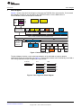
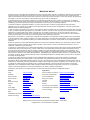
Block Diagram
www.ti.com
1
Block Diagram
Section 1 shows a high-level block diagram of the superset TMS570LS31x microcontroller. For the actual
block diagram relevant for any derivative of the TMS570LS series or for the RM4x series of
microcontrollers, see the device-specific data sheet.
3M
Flash
with
ECC
64K
ETM-R4
(CPU Trace)
256K
RAM
with
ECC
64K
64K
64K
Dual Cortex-R4F
CPUs in Lockstep
DMA
DMM
POM
Switched Centrol Resource
RTP
(RAM Trace)
FTU
HTU1
HTU2
EMAC
Switched Centrol Resource
Switched Centrol Resource
Main Cross Bar: Arbitration and :Prioritization Control
64 KB Flash
for EEPROM
Emulation
with ECC
CRC
Peripheral Central Resource Bridge
Switched Central Resource
EMAC
EMIF
Slave
MibADC1
MibADC2
N2HET1
I2C
N2HET2
DCAN1
SCI
LIN
FlexRay
DCAN2
MibSPIx
GIO
DCAN3
SPI2
SPI4
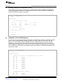
Figure 1. Device Block Diagram
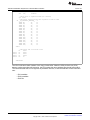
The block diagram includes a color-coded representation of the individual core-power domains
implemented on the microcontroller (see Figure 2). These power domains can be individually turned ON or
OFF during initialization as per the application requirements.
Core/RAM
Core
always on
#1
RAM
#2
#3
#4
#5
#1
#2
#3
Figure 2. Color Legend for Block Diagram
SPNA106 – September 2011
Submit Documentation Feedback
Initialization of Hercules™ ARM® Cortex™-R4F Microcontrollers
Copyright © 2011, Texas Instruments Incorporated
3
Standard Initialization Sequence for Hercules Microcontrollers
2
www.ti.com
Standard Initialization Sequence for Hercules Microcontrollers
A basic sequence for initialization and configuration of the key features on a Hercules MCU is summarized
below and detailed in the following sections. Some parts of the initialization sequence are not mandatory.
Applications that are non-safety-critical can choose to not use the ECC feature for Flash and RAM
accesses, for example. Each application must also have its specific exception handling scheme: reset
handler, abort handler, etc. The code generated using nowGen includes template handling routines for
each exception. These routines need to be modified as required by the application.
1. Initialize stack pointer for the supervisor (default) operating mode, Section 2.1
2. Configure PLL control registers, Section 2.2
3. Enable the PLLs, Section 2.3
4. Trim the LPO, Section 2.4
5. Enable the floating-point Unit (FPU) inside the Cortex-R4F CPU, Section 2.5
6. Initialize the CPU registers and FPU registers, Section 2.6
7. Handle the cause of reset to determine whether to continue with the start-up sequence, Section 2.7
8. Set up Flash module for required wait states and pipelined mode, Section 2.8
9. Set up Flash bank and pump power modes, Section 2.9
10. Wait for main PLL output to become valid
11. Map device clock domains to desired clock sources, Section 2.10
12. Run the built-in self-test for the CPU (LBIST), Section 2.11
13. Release peripherals from reset and enable clocks to all peripherals, Section 2.12
14. Start self-tests on all device memories using programmable built-in self-test (PBIST), Section 2.13
15. Enable the floating-point Unit (FPU) inside the Cortex-R4F CPU, Section 2.5
16. Enable the response mechanism to ECC errors inside flash and TCRAM interface modules,
Section 2.14
17. Enable CPU Event Signaling and ECC checking on ATCM and BTCM accesses, Section 2.15
18. Run eFuse controller start-up checks including self-test on the eFuse controller SECDED logic,
Section 2.17
19. Run the self-test on the Flash module embedded SECDED logic, Section 2.18
20. Check whether the eFuse controller self-test has completed; wait here if it has not completed
21. Check if all RAMs have passed the memory self-test (PBIST); wait here if PBIST has not yet
completed
22. Perform auto-initialization for all on-chip SRAMs, Section 2.19
23. Initialize stack pointers for all operating modes, Section 2.20
24. Configure IRQ / FIQ interrupt priorities for all interrupt channels, Section 2.21.2
25. Check if the auto-initialization process for all RAMs is completed; wait here if it has not completed
26. Program Vectored Interrupt Manager memory to map all interrupt service routine addresses,
Section 2.21
27. Enable CPU’s dedicated vectored interrupt controller (VIC) port, Section 2.22
28. Enable the desired interrupts, Section 2.21.3
29. Initialize copy table, global variables, and constructors, Section 2.24
30. Call the main application, Section 2.25
4
Initialization of Hercules™ ARM® Cortex™-R4F Microcontrollers
Copyright © 2011, Texas Instruments Incorporated
SPNA106 – September 2011
Submit Documentation Feedback
Standard Initialization Sequence for Hercules Microcontrollers
www.ti.com
2.1
Initialize Stack Pointers for the CPU Supervisor (SVC) Operating Mode
Define the base addresses for the stacks used for the different operating modes. The addresses listed
below are only examples and can be defined by the application as required.
user:
svc:
.word 0x08001000
.word 0x08002000
Supervisor mode is a protected mode for the operating system and is entered upon taking a Supervisor
Call (SVC). This is also the default mode of the CPU after a CPU reset. It is important to initialize the
stack pointer for this mode before making any function call.
cps
ldr
2.2
#0x13
sp,
; switch to Supervisor mode if you are not already in this mode
svc
Configure PLLs
The Hercules microcontrollers contain a frequency-modulated phase-locked loop (FMPLL) macro that
allows the input oscillator frequency to be multiplied to a higher frequency than can be conveniently
achieved with an external resonator or crystal. Additionally, the FMPLL allows the flexibility to generate
many different frequency options from a fixed crystal or resonator.
The FMPLL allows the application to superimpose a “modulation frequency” signal on the selected base
frequency signal output from the FMPLL. This reduces the electromagnetic energy of the output signal by
spreading it across a controlled frequency range around the base frequency. This mode is disabled by
default, and the application can enable it in applications sensitive to noise emissions.
The Hercules microcontrollers also contain a second non-modulating PLL macro. This PLL#2 can be
independently configured to generate a second high-frequency clock source for specific uses, e.g.,
FlexRay communication clock source of 80 MHz.
2.2.1
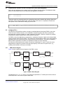
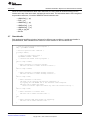
FMPLL Block Diagram
Figure 3 shows a high-level block diagram of the FMPLL macro.
OSCIN
/NR
/1 to /64
INTCLK
PLL
VCOCLK
/OD
/1 to /8
post_ODCLK
/R
/1 to /32
PLLCLK
fPLLCLK = (fOSCIN / NR) * NF / (OD * R)
/NF
/1 to /256
OSCIN
/NR2
/1 to /64
INTCLK2
PLL#2
/NF2
/1 to /256
VCOCLK2
/OD2
/1 to /8
post_ODCLK2
/R2
/1 to /32
PLL2CLK
fPLL2CLK = (fOSCIN / NR2) * NF2 / (OD2 * R2)
Figure 3. FMPLL Block Diagram
The parameters fOSCIN, fpost_ODCLK and fHCLK are data sheet specifications. To identify the min/max limits on
these frequencies, see the device-specific data sheet.
SPNA106 – September 2011
Submit Documentation Feedback
Initialization of Hercules™ ARM® Cortex™-R4F Microcontrollers
Copyright © 2011, Texas Instruments Incorporated
5
Standard Initialization Sequence for Hercules Microcontrollers
www.ti.com
NOTE: The FMPLL takes (127 + 1024*NR) oscillator cycles to acquire lock to the target frequency,
hence it is recommended to configure the FMPLL(s) and enable them as soon as possible in
the device initialization.
2.2.2
FMPLL Slip Detector
The FMPLL macro has a slip detector circuit that compares the OSCIN to the VCOCLK and flags any
single-cycle slips. The application can choose the response to a PLL slip indication from among three
choices: do nothing, cause a system reset, or bypass the FMPLL such that the OSCIN frequency itself is
supplied as the output from the FMPLL macro. There is also a slip filter circuit that can be enabled by the
application, which allows the application to require the PLL to detect a slip condition for two or more
consecutive cycles before the slip is actually indicated to the system.
2.2.3
FMPLL Modulation
The FMPLL allows the application to enable modulation (insertion of controlled jitter). The modulation
characteristics are configured by the PLLCTL2 control register. The modulation option is only available for
the main FMPLL.
2.2.4
FMPLL Configuration
The FMPLL1 has two control registers located within the System module on the Hercules microcontrollers:
PLLCTL1 and PLLCTL2. PLL control register 1 (PLLCTL1) is shown in Figure 4 and described in Table 1.
Figure 4. PLL Control Register 1 (PLLCTL1) Address = 0xFFFFFF70
31
30
29
ROS
MASK_
SLIP[1:0]
R/WP-0
R/WP-01
28
24
23
22
21
16
PLLDIV[4:0]
ROF
RSVD
REFCLKDIV[5:0]
R/WP-01111
R/WP-0
R-0
R/WP-000010
15
0
PLLMUL[15:0]
R/WP-0x5F00
LEGEND: R = Read in all modes; WP = Write in priviledged mode only; -n = value after reset
Table 1. PLL Control Register (PLLCTL1) Field Descriptions
Bit
Field
31
ROS
Value
Description
Reset-on slip selects whether a PLL slip condition causes a system reset or not.
ROS = 1 causes a system reset when a PLL slip is flagged and the slip detection is not masked.
30-29
MASK_SLIP
Mark slip allows the application to ignore a slip indicated by the PLL.
MASK_SLIP = 10 ignores a PLL slip condition flagged by the FMPLL macro.
Writing any other value to MASK_SLIP causes the FMPLL to be bypassed so that the OSCIN is
used as the output from the FMPLL macro.
NOTE: If the ROS bit is also ‘1’ when the FMPLL is bypassed, then a system reset occurs and the
FMPLL output is not bypassed.
28-24
PLLDIV
Defines the R-divider.
R = PLLDIV + 1
fPLLCLK = fpost-ODCLK / R
23
ROF
22
Reserved
21-16
REFCLKDIV
Reset-on-oscillator-fail controls the response to an oscillator failure detected by the clock monitor
and is not relevant to the PLL configuration discussion.
0
Reserved
Defines the NR-divider
NR = REFCLKDIV + 1
fINTCLK = fCLKIN / NR
6
Initialization of Hercules™ ARM® Cortex™-R4F Microcontrollers
Copyright © 2011, Texas Instruments Incorporated
SPNA106 – September 2011
Submit Documentation Feedback
Standard Initialization Sequence for Hercules Microcontrollers
www.ti.com
Table 1. PLL Control Register (PLLCTL1) Field Descriptions (continued)
Bit
Field
15-0
Value
Description
PLLMUL
Defines the NF multiplier
NF = (PLLMUL / 256) + 1
fVCOCLK = fINTCLK * NF
The PLL control register 2 (PLLCTL2) is shown in Figure 5 and described in Table 2.
Figure 5. PLL Control Register 2 (PLLCTL2) Address = 0xFFFFFF74
31
30
22
21
20
16
FM
ENA
SPREADINGRATE[8:0]
RSVD
MULMOD[8:4]
R/WP-0
R/WP-0x1FF
RW-0
R/WP-0x000
15
12
11
9
8
0
MULMOD[3:0]
ODPLL
SPR_AMOUNT[8:0]
R/WP-0x000
R/WP-111b
R/WP-0x000
LEGEND: R = Read; W = Write; P = Priviledge mode only; -n = value after reset
Table 2. PLL Control Register 2 (PLLCTL2) Field Descriptions
Bit
Field
31
FM ENA
Setting the FM ENA bit enables the modulation frequency to be superimposed on the output
of the FMPLL macro.
SPREADINGRATE
Defines the modulation frequency used
30-22
Value
Description
NS = SPREADINGRATE + 1
Modulation frequency, fmod = fs = fINTCLK / (2 * NS)
21
Reserved
20-12
0
BWADJ
Reserved
Defines the FMPLL modulation bandwidth adjustment
NB = BWADJ + 1
fBW = fnom_BW / NB
NOTE: NB must be set to 7 when modulation is not used. This is also the default value.
11-9
ODPLL
Defines the OD-divider
OD = ODPLL + 1
fpost-ODCLK = fVCOCLK / OD
8-0
SPR_AMOUNT
Defines the frequency modulation depth divider.
NV = SPR_AMOUNT + 1
2.2.4.1
Example FMPLL Configuration
systemREG1->PLLCTL1 =
|
|
|
|
0x00000000U
0x20000000U
(0U << 24U)
(5U << 16U)
(119U << 8U);
//
//
//
//
No reset on slip, bypass on slip
R = 1
NR = 6
NF = 120
systemREG1->PLLCTL2 =
|
|
|
|
0x00000000U
(255U << 22U)
(7U << 12U)
(1U << 9U)
61U;
//
//
//
//
//
Modulation disabled
NS = 256
NB = 8
OD = 2
NV = 62
This example configuration results in a FMPLL output clock frequency of:
fPLLCLK = (fOSCIN / 6) * 120 / 2 / 1 = fOSCIN * 10
SPNA106 – September 2011
Submit Documentation Feedback
Initialization of Hercules™ ARM® Cortex™-R4F Microcontrollers
Copyright © 2011, Texas Instruments Incorporated
7
Standard Initialization Sequence for Hercules Microcontrollers
2.3
www.ti.com
Enable Clock Sources
2.3.1
Available Clock Sources on Hercules Microcontrollers
The Hercules microcontrollers support seven different clock sources, as listed in Table 3.
Table 3. Clock Sources on Hercules Microcontrollers
Clock
Source
Number
Clock Source Name
Description
OSCIN
This is the primary oscillator, typically driven by an external resonator or crystal. This
is the only available input to the FMPLL and the FMPLL2 macros. The OSCIN
frequency must be between 5 MHz and 20 MHz.
1
FMPLL#1 output
This is the output of the FMPLL, which is generated using the OSCIN as the input
clock. The FMPLL output clock frequency must not exceed the maximum device
frequency specified in the specific part's datasheet. The FMPLL features a modulation
mode where a modulation frequency is superimposed on the FMPLL output signal.
2
Not implemented
No clock signal is connected to source # 2. This clock source must not be enabled or
chosen for any clock domain.
3
EXTCLKIN1
External clock input # 1. This clock source must only be enabled if there is an actual
external clock source connected to the identified device terminal for EXTCLKIN1. For
more information, see the specific part's datasheet.
4
LF LPO
This is the low-frequency output of the internal reference oscillator. The LF LPO is
typically an 80 KHz signal, and is generally used for low-power mode use cases.
5
HF LPO
This is the high-frequency output of the internal reference oscillator. The HF LPO is
typically a 10 MHz signal, and is used as a reference clock for monitoring the main
oscillator.
6
FMPLL#2 output
This is the output of the secondary FMPLL, which is generated using the OSCIN as
the input clock. The FMPLL output clock frequency must not exceed the maximum
device frequency specified in the specific part's datasheet.
7
EXTCLKIN2
External clock input # 2. This clock source must only be enabled if there is an actual
external clock source connected to the identified device terminal for EXTCLKIN2. For
more information, see the specific part's datasheet.
0
2.3.2
Control Registers for Enabling and Disabling Clock Sources
Figure 6 shows the default states of the clock sources supported on the Hercules microcontrollers:
• Clock sources 0, 4 and 5 are enabled, while clock sources 1, 3, 6 and 7 are disabled upon any system
reset.
• Clock source 2 is not implemented and must not be enabled in the application.
The clock source disable register (CSDIS) is shown in Figure 6.
Figure 6. Clock Source Disable Register (CSDIS) Address = 0xFFFFFF30
31
16
Reserved
R-0
15
8
7
6
5
4
3
2
1
0
Reserved
CLK
SR7
OFF
CLK
SR6
OFF
CLK
SR5
OFF
CLK
SR4
OFF
CLK
SR3
OFF
CLK
SR2
OFF
CLK
SR1
OFF
CLK
SR0
OFF
R-0
R/WP-1
R/WP-1
R/WP-D
R/WP-0
R/WP-1
R/WP-1
R/WP-1
R/WP-0
LEGEND: R = Read in all modes; WP = Write in priviledged mode only; -n = value after reset; D = Device-specific reset value
•
•
8
Each bit of the CSDIS controls the clock source of the same number: bit 0 controls clock source 0, bit
1 controls clock source 1, and so on.
Setting any bit commands, the corresponding clock source to be disabled.
– The clock source can only be disabled once there is no clock domain or secondary clock source
(FMPLL, FMPLL#2) using the clock source to be disabled.
Initialization of Hercules™ ARM® Cortex™-R4F Microcontrollers
Copyright © 2011, Texas Instruments Incorporated
SPNA106 – September 2011
Submit Documentation Feedback
Standard Initialization Sequence for Hercules Microcontrollers
www.ti.com
The clock source disable register (CSDISSET) is shown in Figure 7.
Figure 7. Clock Source Disable Set Register (CSDISSET) Address = 0xFFFFFF34
31
16
Reserved
R-0
15
8
7
6
5
4
3
2
1
0
Reserved
SET
CLK
SR7
OFF
SET
CLK
SR6
OFF
SET
CLK
SR5
OFF
SET
CLK
SR4
OFF
SET
CLK
SR3
OFF
SET
CLK
SR2
OFF
SET
CLK
SR1
OFF
SET
CLK
SR0
OFF
R-0
R/WP-1
R/WP-1
R/WP-0
R/WP-0
R/WP-1
R/WP-1
R/WP-1
R/WP-0
LEGEND: R = Read in all modes; WP = Write in priviledged mode only; -n = value after reset; D = Device-specific reset value
The clock source disable clear register (CSDISCLR) is shown in Figure 8.
Figure 8. Clock Source Disable Clear Register (CSDISCLR) Address = 0xFFFFFF38
31
16
Reserved
R-0
15
8
7
6
5
4
3
2
1
0
Reserved
CLR
CLK
SR7
OFF
CLR
CLK
SR6
OFF
CLR
CLK
SR5
OFF
CLR
CLK
SR4
OFF
CLR
CLK
SR3
OFF
CLR
CLK
SR2
OFF
CLR
CLK
SR1
OFF
CLR
CLK
SR0
OFF
R-0
R/WP-1
R/WP-1
R/WP-D
R/WP-0
R/WP-1
R/WP-1
R/WP-1
R/WP-0
LEGEND: R = Read in all modes; WP = Write in priviledged mode only; -n = value after reset; D = Device-specific reset value
•
•
•
2.3.3
The system module also contains two additional registers that can be used to enable or disable clock
sources. These registers are provided so that the application can avoid using read-modify-write
operations for enabling or disabling clock sources.
Setting any bit in the CSDISSET register commands the corresponding clock source to be disabled.
Setting any bit in the CSDISCLR register enables the corresponding clock source.
Example Clock Source Configuration
systemREG1->CSDISCLR =
|
|
|
|
|
0x00000000U
0x00000001U
0x00000002U
0x00000010U
0x00000020U
0x00000040U;
//
//
//
//
//
Enable
Enable
Enable
Enable
Enable
clock
clock
clock
clock
clock
source
source
source
source
source
0
1
4
5
6
The above configuration enables clock sources 0, 1, 4, 5, and 6.
Of the clock sources that are enabled, number 0, 4 and 5 are enabled by default and will have become
valid by the time the processor is released from reset upon a power-up. These are the main oscillator and
the two outputs from the internal reference oscillator.
Clock source 1 and 6 are the two PLL outputs. The FMPLL as well as the FMPLL#2 have a defined
start-up time, and their outputs are not available for use until this time. The application must wait for the
valid status flags for these clock sources to be set before using the PLL outputs for any clock domain.
while (!((systemREG1->CSVSTAT & 2)
& (systemREG1-> CSVSTAT & 0x40)));
SPNA106 – September 2011
Submit Documentation Feedback
// Wait for FMPLL to become valid
// Wait for FMPLL#2 to become valid
Initialization of Hercules™ ARM® Cortex™-R4F Microcontrollers
Copyright © 2011, Texas Instruments Incorporated
9
Standard Initialization Sequence for Hercules Microcontrollers
2.4
www.ti.com
Configure Oscillator Monitor
The HF LPO clock source is used as a reference clock for monitoring the main oscillator. A failure is
detected if the oscillator frequency falls outside the range: {fHFLPO / 4, fHFLPO*4}.
The HF LPO frequency varies significantly over process corners as well as with changes in the core
supply (VCC) and temperature. The Hercules microcontrollers allow the application to trim the HF LPO
such that the application can choose the operating frequency point of the HF LPO. This in turn determines
the valid range of oscillator frequency.
During device test, a trim value is written into the one-time programmable section of the Flash memory
(OTP), address 0xF008_01B4. Bits 31:16 of this OTP word contain a 16-bit value that may be
programmed into Low Power Oscillator Monitor Control Register (LPOMONCTL) in order to initialize the
trim for HF LPO.
Alternatively the application can use the dual-clock compare (DCC) module to determine the trim setting
for the HF LPO. The DCC module allows for comparison of two clock frequencies. Once the HF LPO is
determined to be in-range with the initial HFTRIM setting from the OTP, the crystal oscillator may be used
as a reference against which the HF LPO and LF LPO may be further adjusted. For more details, see the
specific part's technical reference manual.
10
Initialization of Hercules™ ARM® Cortex™-R4F Microcontrollers
Copyright © 2011, Texas Instruments Incorporated
SPNA106 – September 2011
Submit Documentation Feedback
Standard Initialization Sequence for Hercules Microcontrollers
www.ti.com
2.5
Enabling Floating-Point Coprocessor (FPU)
The floating-point coprocessor is disabled upon a CPU reset and must be enabled if the application
requires floating-point calculations. If a floating-point instruction is executed with the FPU disabled, an
undefined instruction exception is generated.
.def
_coreEnableVfp_
.asmfunc
_coreEnableVfp_
; First enable access to the FPU
mrc
orr
mcr
p15,
r0,
p15,
#0x00,
r0,
#0x00,
r0,
c1, c0, #0x02
#0xF00000
r0,
c1, c0, #0x02
; Now enable the FPU
mov
fmxr
r0,
fpexc,
bx
lr
#0x40000000
r0
.endasmfunc
2.6
Initialization of Cortex-R4F Registers
The Hercules series of microcontrollers include dual Cortex-R4F CPUs running in a lock-step operation
mode. A Core Compare Module (CCM-R4) compares the output signals from each R4F CPU. Any
difference in the two CPUs’ outputs is flagged as a fault of a high-severity level. The CPU internal
registers are not guaranteed to power up in the same state for both the CPUs. The CPU pushes the
internal registers on to the stack on a function call, which could lead to the detection of a core compare
error. Therefore, the CPU internal core registers need to be initialized to a predefined state before any
function call is made.
.def
_coreInitRegisters_
.asmfunc
_coreInitRegisters_
; After reset, the CPU is in the Supervisor mode (M = 0b10011)
mov
r0,
lr
mov
r1,
#0x0000
mov
r2,
#0x0000
mov
r3,
#0x0000
mov
r4,
#0x0000
mov
r5,
#0x0000
mov
r6,
#0x0000
mov
r7,
#0x0000
mov
r8,
#0x0000
mov
r9,
#0x0000
mov
r10,
#0x0000
mov
r11,
#0x0000
mov
r12,
#0x0000
; Switch to FIQ mode (M = 0b10001)
cps
#0x11
mov
r8,
#0x0000
mov
r9,
#0x0000
mov
r10,
#0x0000
SPNA106 – September 2011
Submit Documentation Feedback
Initialization of Hercules™ ARM® Cortex™-R4F Microcontrollers
Copyright © 2011, Texas Instruments Incorporated
11
Standard Initialization Sequence for Hercules Microcontrollers
mov
mov
r11,
r12,
www.ti.com
#0x0000
#0x0000
; Switch back to Supervisor Mode (M = 0b10011)
cps #0x13
; Initialize Floating Point Unit registers if FPU is used
.if __TI_VFPV3D16_SUPPORT__ = 1
fmdrr d0,
r1,
r1
fmdrr d1,
r1,
r1
fmdrr d2,
r1,
r1
fmdrr d3,
r1,
r1
fmdrr d4,
r1,
r1
fmdrr d5,
r1,
r1
fmdrr d6,
r1,
r1
fmdrr d7,
r1,
r1
fmdrr d8,
r1,
r1
fmdrr d9,
r1,
r1
fmdrr d10,
r1,
r1
fmdrr d11,
r1,
r1
fmdrr d12,
r1,
r1
fmdrr d13,
r1,
r1
fmdrr d14,
r1,
r1
fmdrr d15,
r1,
r1
.endif
next1
next2
next3
next4
; Initialize CPU call-return stack
bl
next1
bl
next2
bl
next3
bl
next4
bx
r0
.endasmfunc
The CPU’s call-return stack consists of a 4-entry circular buffer. When the CPU pre-fetch unit (PFU)
detects a taken procedure call instruction, the PFU pushes the return address onto the call-return stack.
The instructions that the PFU recognizes as procedure calls are, in both the ARM and Thumb instruction
sets:
→ BL immediate
→ BLX immediate
→ BLX Rm
12
Initialization of Hercules™ ARM® Cortex™-R4F Microcontrollers
Copyright © 2011, Texas Instruments Incorporated
SPNA106 – September 2011
Submit Documentation Feedback
Standard Initialization Sequence for Hercules Microcontrollers
www.ti.com
When the return stack detects a taken return instruction, the PFU issues an instruction fetch from the
location at the top of the return stack, and pops the return stack. The instructions that the PFU recognizes
as procedure returns are, in both the ARM and Thumb instruction sets:
→
→
→
→
→
→
→
2.7
LDMIA Rn{!}, {..,pc}
POP {..,pc}
LDMIB Rn{!}, {..,pc}
LDMDA Rn{!}, {..,pc}
LDMDB Rn{!}, {..,pc}
LDR pc, [sp], #4
BX Rm
Reset Handler
Each application has different levels of tolerance for different reset conditions. A typical reset handler is
presented below, which identifies all the causes of a reset condition on the Hercules MCUs.
/* read the system exception status register */
temp = systemREG1->SYSESR;
/* check for power-on reset condition */
if (temp & 0x8000)
{
/* clear all reset status flags */
systemREG1->SYSESR = 0xFFFF;
/* continue with normal start-up sequence */
}
else if (temp & 0x4000)
{
/* Reset caused due to oscillator failure.
Add user code here to handle oscillator failure */
}
else if (temp & 0x2000)
{
/* Reset caused due to windowed watchdog violation.
Add user code here to handle watchdog violation */
}
else if (temp & 0x20)
{
/* Reset caused due to CPU reset.
CPU reset can be caused by CPU self-test completion, or
by toggling the "CPU RESET" bit of the CPU Reset Control Register.
Add user code to handle CPU reset:
check for selftest completion without any error and continue start-up. */
}
else if (temp & 0x10)
{
/* Reset caused due to software reset.
Add user code to handle software reset. */
}
else
{
/* Reset caused by nRST being driven low externally.
Add user code to handle external reset. */
}
SPNA106 – September 2011
Submit Documentation Feedback
Initialization of Hercules™ ARM® Cortex™-R4F Microcontrollers
Copyright © 2011, Texas Instruments Incorporated
13
Standard Initialization Sequence for Hercules Microcontrollers
2.8
www.ti.com
Configure Flash Access
The Flash memory on the Hercules series microcontrollers is a non-volatile electrically erasable and
programmable memory.
The Hercules microcontrollers contain a digital module that manages all accesses to the Flash memory. A
Flash access can be completed without any wait states required for bus master clock speeds up to 45
MHz. If the bus clock is faster than 45 MHz, then any Flash access requires the appropriate number of
wait states depending on the bus clock speed. The Hercules series microcontrollers support clock speeds
up to 180 MHz. For the actual maximum allowed speed and the number of corresponding address and
data wait states, see the specific part's datasheet.
Suppose that the application requires the microcontroller to run at the maximum supported speed of 180
MHz. This requires 1 address wait state and 3 data wait states for any access to the Flash memory.
These wait states need to be configured in the Flash module registers.
The Flash module also features a pipelined mode of operation. When this mode is enabled, the module
reads 128 bits from the Flash memory and holds them in buffers that the CPU can read from without any
wait state. The CPU can read 32 or 64 bits of instructions or data from the pipeline buffers.
The register inside the Flash module that controls the wait states and the pipeline mode is shown in
Figure 9.
The Flash read control register (FRDCNTL) is shown in Figure 9 and described in Table 4.
Figure 9. Flash Read Control Register (FRDCNTL) Address = 0xFFF87000
31
16
Reserved
R-0
15
12
11
8
7
5
4
Reserved
RWAIT
Reserved
ASW
STEN
R-0
R/WP-0001
R-0
R/WP-0
3
2
1
0
Reserved
EN
PIPE
R-0
R/WP-0
LEGEND: R = Read; WP = Write in priviledge mode; -n = value after reset
Table 4. Flash Read Control Register (FRDCNTL) Field Descriptions
Bit
Field
31-12
Reserved
11-8
RWAIT
7-5
Reserved
4
ASWTEN
3-1
Reserved
0
ENPIPE
Value
0
Description
Reserved
Configures the number of data read wait states
0
Reserved
Enables the generation of 1 address wait state. When the address wait state is enabled, the
address bus is latched one cycle before it is decoded for a pipeline hit or miss.
0
Reserved
Used to enable or disable the pipeline mode of the Flash module.
The sequence to configure the wait states and to enable the pipeline mode is as follows.
flashWREG->FRDCNTL = 0x00000000U
| (3U << 8U)
| (1U << 4U)
| 1U;
// 3 data wait states
// 1 address wait state enabled
// Enable pipeline mode
The Hercules MCUs also have a separate flash bank for data storage. This bank can be used to emulate
an EEPROM. Accesses to this flash bank are configured via a separate register in the flash module.
14
Initialization of Hercules™ ARM® Cortex™-R4F Microcontrollers
Copyright © 2011, Texas Instruments Incorporated
SPNA106 – September 2011
Submit Documentation Feedback
Standard Initialization Sequence for Hercules Microcontrollers
www.ti.com
Figure 10. Flash State Machine Write Enable Control Register (FSM_WR_ENA) Address =
0xFFF87288
31
16
Reserved
R-0
15
12
11
8
7
5
4
3
2
1
0
WR
ENA
Reserved
R-0
R/WP010
LEGEND: R = Read; WP = Write in priviledge mode; -n = value after reset
Table 5. Flash State Machine Write Enable Control Register (FSM_WR_ENA) Field Descriptions
Bit
Field
Value
31-3
Reserved
2-0
WR ENA
0
Description
Reserved
This field enables application to write to the control registers for the Flash module state machine.
101
other
value
Privileged mode write access to all other FSM control registers is enabled.
No write access is allowed to any FSM control register.
Once the access to the FSM control registers is enabled, the read access to the flash bank 7 can be
configured.
Figure 11. Flash EEPROM Configuration Register (EEPROM_CONFIG) Address = 0xFFF872B8
31
20
19
16
Reserved
EWAIT
R-0
R/WP-0001
15
9
8
7
5
4
3
Reserved
AUTO
SUSP
EN
AUTO
START
GRACE
R-0
R/WP-0
R/WP-0x02
2
1
0
LEGEND: R = Read; WP = Write in priviledge mode; -n = value after reset
Table 6. Flash EEPROM Configuration Register (EEPROM_CONFIG) Field Descriptions
Bit
Field
31-20
Reserved
19-16
EWAIT
15-9
Reserved
8
7-0
Value
0
Description
Reserved
Configures the number of data read wait states for the flash bank 7
0
Reserved
AUTO SUSP EN
Auto Suspend Enable. This bit, when set, affects the behavior of the Flash module state machine
when the CPU or another bus master accesses the flash bank 7 with an active and suspendable
FSM operation. When this happens, the FSM will automatically be issued a suspend command and
exit from the FSM operation. The bus master access then proceeds. After the access is completed,
the Flash module will wait for a time determined by the AUTOSTART GRACE field before issuing
the FSM resume command.
AUTOSTART
GRACE
Auto-suspend Start-up Grace Period. The contents of this field determine the duration for which the
Flash module will wait after the last access to flash bank 7 before ussing the FSM resume
command. The flash module will wait 16 HCLK periods for each count in the AUTOSTART GRACE
field. Each access to flash bank 7 resets the down counter to AUTOSTART GRACE * 16.
SPNA106 – September 2011
Submit Documentation Feedback
Initialization of Hercules™ ARM® Cortex™-R4F Microcontrollers
Copyright © 2011, Texas Instruments Incorporated
15
Standard Initialization Sequence for Hercules Microcontrollers
2.9
www.ti.com
Configure Flash Bank and Pump Power Modes
The Flash banks and pump used on the Hercules series microcontrollers support three different operating
modes to optimize power consumption.
• Active mode
– Flash bank sense amplifiers and sense reference are enabled
– All circuits of Flash charge pump are enabled
• Standby mode (only for Flash banks)
– Flash bank sense reference is enabled but sense amplifiers are disabled
• Sleep Mode
– Flash bank sense amplifiers and sense reference are disabled
– All circuits of Flash charge pump are disabled
The Flash banks and charge pump are in the active state by default and after any system reset. The Flash
module allows the application to configure “fall back” power states for the Flash banks and charge pump.
The Flash banks and pump automatically switch the power mode to the selected fall back state when
there is no access to the Flash banks detected within a user-configurable time.
The Flash module also contains special timers to automatically sequence the Flash banks and pump
between the active and the selected fall-back states. A read access to any Flash bank which is in a
non-active power state will “wake up” both the selected bank and the charge pump to active power state.
Programming and erase operations are only allowed on banks in active state.
The Flash module register that controls the Flash banks’ power states is shown in Figure 12.
Figure 12. Flash Bank Fall-Back Control Register (FBFALLBACK) Address = 0xFFF87040
31
16
Reserved
R-0
15
8
7
6
5
4
3
2
1
0
Reserved
BANKPWR3
[1:0]
BANKPWR2
[1:0]
BANKPWR1
[1:0]
BANKPWR3
[1:0]
R/WP-0xF
R/WP-11
R/WP-11
R/WP-11
R/WP-11
LEGEND: R = Read in all modes; WP = Write in priviledged mode only; -n = value after reset
16
Initialization of Hercules™ ARM® Cortex™-R4F Microcontrollers
Copyright © 2011, Texas Instruments Incorporated
SPNA106 – September 2011
Submit Documentation Feedback
Standard Initialization Sequence for Hercules Microcontrollers
www.ti.com
Each of the BANKPWRx fields configures the fall-back mode for a single Flash bank. The Hercules
microcontrollers support up to 4 Flash banks.
Configuration of fall-back mode for the Flash banks:
enum flashWPowerModes
{
SYS_SLEEP
= 0U, /** flash bank power mode sleep
*/
SYS_STANDBY = 1U, /** flash bank power mode standby */
SYS_ACTIVE = 3U /** flash bank power mode active */
};
flashWREG->FBFALLBACK =
|
|
|
|
0x00000000
(SYS_SLEEP << 6U)
(SYS_SLEEP << 4U)
(SYS_SLEEP << 2U)
SYS_SLEEP;
//
//
//
//
Bank3
Bank2
Bank1
Bank0
falls
falls
falls
falls
back
back
back
back
to
to
to
to
SLEEP
SLEEP
SLEEP
SLEEP
The above code fragment configures the fall-back mode for each available Flash bank to be the sleep
mode. The application can choose to configure these modes differently as required. The power savings
can be disabled completely by selecting the active state to also be the fall-back power state, which is the
default.
There are a few other registers that control the timing sequence for entry to a fall-back mode and wake up
to active mode. The Flash bank access control register is shown in Figure 13 and described in Table 7.
Figure 13. Flash Bank Access Control Register (FBAC) Address = 0xFFF8703C
31
24
23
16
Reserved
OTPPROTDIS[7:0]
R-0
R/WP-00000000
15
8
7
0
BAGP[7:0]
VREADST[7:0]
R/WP-0
R/WP-00001111
LEGEND: R = Read in all modes; WP = Write in priviledged mode only; -n = value after reset
Table 7. Flash Bank Access Control Register (FBAC) Field Descriptions
Bit
Field
Value
0
Description
31-24
Reserved
Reserved
23-16
OTPPROTDIS
Not relevant to power modes
15-8
BAGP
Configures the Flash banks’ Active Grace Period (AGP). This is the starting count value for a
down-counter. An access to a Flash bank before this counter counts down to 0 causes a reload of
this counter to the configured AGP value. In effect, the AGP delays the Flash banks’ entry into the
selected fall-back mode by 0 to 255 * 16 HCLK cycles. This value must be greater than 1 when the
fall-back mode is not “ACTIVE”.
7-0
VREADST
Controls the delay, in terms of HCLK cycles, between the time when the charge pump generates
the required read voltage (VREAD) and the time when the Flash bank starts its own power up
sequence. This time must be at least 100 ns.
NOTE: The Flash banks have hard-coded timings for transitioning from sleep to standby to active
power states. These timings are not configurable by the application.
flashWREG->FMAC = 0x00000003;
flashWREG->FBAC |= 0x0000FF00;
// Select flash bank3
// Select 255 * 16 HCLK cycles as the bank3 AGP
flashWREG->FMAC = 0x00000002;
flashWREG->FBAC |= 0x0000FF00;
// Select flash bank2
// Select 255 * 16 HCLK cycles as the bank2 AGP
flashWREG->FMAC = 0x00000001;
flashWREG->FBAC |= 0x0000FF00;
// Select flash bank1
// Select 255 * 16 HCLK cycles as the bank1 AGP
SPNA106 – September 2011
Submit Documentation Feedback
Initialization of Hercules™ ARM® Cortex™-R4F Microcontrollers
Copyright © 2011, Texas Instruments Incorporated
17
Standard Initialization Sequence for Hercules Microcontrollers
flashWREG->FMAC = 0x00000000;
flashWREG->FBAC |= 0x0000FF00;
www.ti.com
// Select flash bank0
// Select 255 * 16 HCLK cycles as the bank0 AGP
The Flash pump access control register 1 (FPAC1) is shown in Figure 14 and described in Table 8.
Figure 14. Flash Pump Access Control Register 1 (FPAC1) Address = 0xFFF87048
31
27
26
16
Reserved
PSLEEP[10:0]
R-0
R/WP-0x64
15
1
0
Reserved
PUMP
PWR
R-0
RWP-1
LEGEND: R = Read in all modes; WP = Write in priviledged mode only; -n = value after reset
Table 8. Flash Pump Access Control Register 1 (FPAC1) Field Descriptions
Bit
Field
Value
31-27
Reserved
26-16
PSLEEP
15-1
Reserved
0
0
Description
Reserved
Configures the time that the Flash pump takes for transitioning from the sleep state to the standby
state. This is specified in terms of 2 * HCLK cycles. Please check the specific part's datasheet to
identify the minimum time required for the Flash pump to switch from the sleep state to the standby
state.
0
PUMPPWR
Reserved
Defines whether the Flash pump falls back into sleep mode, or remains active.
flashWREG->FPAC1 = 0x00640000;
// PSLEEP = 100 * 2 HCLK cycles,
// Pump fall-back state = SLEEP
The Flash pump access control register 2 is shown in Figure 15 and described in Table 9.
Figure 15. Flash Pump Access Control Register 2 (FPAC2) Address = 0xFFF8704C
31
16
Reserved
R-0
15
0
PAGP[15:0]
R/WP-0
LEGEND: R = Read in all modes; WP = Write in priviledged mode only; -n = value after reset
Table 9. Flash Pump Access Control Register 2 (FPAC2) Field Descriptions
Bit
Field
31-16
Reserved
15-0
PAGP
18
Value
0
Description
Reserved
Defines the active grace period for the Flash charge pump. This defines the starting count for a
down counter. An access to the Flash memory reloads this counter with the selected PAGP value.
After the last access to Flash memory, the down counter delays the Flash pump’s entry to the
selected fall-back mode by 0 to 65536 * 16 HCLK cycles.
Initialization of Hercules™ ARM® Cortex™-R4F Microcontrollers
Copyright © 2011, Texas Instruments Incorporated
SPNA106 – September 2011
Submit Documentation Feedback
Standard Initialization Sequence for Hercules Microcontrollers
www.ti.com
flashWREG->FPAC2 = 0x000000FF;
// PSLEEP = 255 * 16 HCLK cycles
2.10 Clock Domains
There are multiple clock domains on the Hercules microcontrollers to ease the configuration and
controllability of the different modules using these clock domains (see Table 10).
Table 10. Clock Domains on Hercules Microcontrollers
2.10.1
Domain Name
Clock Name
Comments
CPU clock domain
GCLK
GCLK controls all the CPU sub-systems, including the floating point
unit (FPU), and the memory protection unit (MPU)
System bus clock domain
HCLK
HCLK shares the same clock source as GCLK, and is always the
same frequency as HCLK.
System peripheral clock domain
VCLK_sys
VCLK_sys is used for the system modules such as VIM, ESM, SYS,
etc. VCLK_sys is divided down from HCLK by a programmable
divider from 1 to 16.
Peripheral clock domains
VCLK, VCLK2, VCLK3
VCLK is the primary peripheral clock, and is synchronous with
VCLK_sys. VCLK2 is a secondary peripheral clock and is reserved
for use by the enhanced timer module (NHET) and the associated
transfer unit (HTU). VCLK2 is also divided down from HCLK by a
programmable divider from 1 to 16. fHCLK must be an integer multiple
of fVCLK2, fVCLK2 must be an integer multiple of fVCLK. VCLK3 is also
divided down from HCLK by a programmable divider from 1 to 16,
and is used for the Ethernet and EMIF modules on the TMS570LS3x
microcontrollers.
Asynchronous clock domains
These clock domains are reserved for use by special communication
modules that have strict jitter constraints. The protocols for these
VCLKA1, VCLKA2, and communication modules (e.g., CAN, FlexRay, Ethernet) do not allow
VCLKA4
modulated clocks to be used for the baud rate generation. The
asynchronous clocks allow the clock sources for the baud clocks to
be decoupled from the GCLK, HCLK and VCLKx clock domains.
Real-time Interrupt clock domains
RTI1CLK
This clock is used for generating the periodic interrupts by the RTI
module.
Mapping Clock Domains to Clock Sources
The system module on the Hercules microcontrollers contains registers that allow the clock domains to be
mapped to any of the available clock sources.
The GCLK, HCLK , VCLKx source register (GHVSRC) is shown in Figure 16 and described in Table 11.
Figure 16. GCLK, HCLK , VCLKx Source Register (GHVSRC) Address = 0xFFFFFF48
31
28
27
24
23
20
19
16
Reserved
GHVWAKE[3:0]
Reserved
HVLPM[3:0]
R-0
R/WP-0000
R-0
R/WP-0000
15
4
3
0
Reserved
GHVSRC[3:0]
R-0
R/WP-0000
LEGEND: R = Read in all modes; WP = Write in priviledged mode only; -n = value after reset
Table 11. GCLK, HCLK , VCLKx Source Register (GHVSRC) Field Descriptions
Bit
Field
31-28
Reserved
27-24
GHVWAKE
Value
SPNA106 – September 2011
Submit Documentation Feedback
0
Description
Reserved
Defines the clock source that will be used for the GCLK, HCLK and VCLKx domains when the
microcontroller wakes up from a low power mode. For more details on the low-power modes
supported, see the specific part's technical reference manual.
Initialization of Hercules™ ARM® Cortex™-R4F Microcontrollers
Copyright © 2011, Texas Instruments Incorporated
19
Standard Initialization Sequence for Hercules Microcontrollers
www.ti.com
Table 11. GCLK, HCLK , VCLKx Source Register (GHVSRC) Field Descriptions (continued)
Bit
Field
Value
23-20
Reserved
19-16
HVLPM
15-1
Reserved
0
GHVSRC
Description
0
Reserved
Defines the clock source used for the HCLK and VCLKx domains when the CPU clock domain
GCLK is disabled.
0
Reserved
Defines the clock source to be currently used for the GCLK, HCLK and VCLKx domains. As shown
by the reset value of the GHVSRC field, the clock source # 0, that is, the main oscillator, is used as
the default clock source for the GCLK, HCLK and VCLKx domains.
The asynchronous clock source register (VCLKASRC) is shown in Figure 17 and described in Table 12.
Figure 17. Asynchronous Clock Source Register (VCLKASRC) Address = 0xFFFFFF4C
31
16
Reserved
R-0
15
12
11
8
7
4
3
0
Reserved
VCLKA1[3:0]
Reserved
VCLKA2[3:0]
R-0
R/WP-1001
R-0
R/WP-1001
LEGEND: R = Read in all modes; WP = Write in priviledged mode only; -n = value after reset
Table 12. Asynchronous Clock Source Register (VCLKASRC) Field Descriptions
Bit
Field
Value
31-12
Reserved
11-8
VCLKA1
7-4
Reserved
3-0
VCLKA2
Description
0
Reserved
Used for generating the DCAN bit timings, and the VCLKA1S field defines the clock source used for
the VCLKA1 domain.
0
Reserved
Used for generating the FlexRay timings, and the VCLKA2S field defines the clock source used for
the VCLKA2 domain.
The asynchronous clock configuration register 1 (VCLKACON1) is shown in Figure 18.
Figure 18. Asynchronous Clock Configuration Register 1 (VCLKACON1) Address = 0xFFFFE140
31
27
26
24
23
21
Reserved
VCLKA4[2:0]
Reserved
R-0
R/WP-001
R-0
15
11
10
8
7
VCLKA3[2:0]
Reserved
R-0
R/WP-001
R-0
19
18
17
16
VCLKA4S[3:0]
R/WP-1001
5
Reserved
20
VCLK4_
DIV_
CDDIS
4
VCLK3_
DIV_
CDDIS
3
0
VCLKA3S[3:0]
R/WP-1001
LEGEND: R = Read in all modes; WP = Write in priviledged mode; -n = value after reset
•
•
20
VCLKA4 is used for the Ethernet controller.
– VCLKA4S field is used to select the clock source for the VCLKA4 domain.
– VCLKA4R field is used to select the divider value to generate the VCLKA4/R frequency.
– VCLKA4_DIV_CDDIS field allows the application to disable the VCLKA4/R signal separately while
the VCLKA4 domain is enabled
VCLKA3 is not used on the TMS570LS3x microcontrollers.
Initialization of Hercules™ ARM® Cortex™-R4F Microcontrollers
Copyright © 2011, Texas Instruments Incorporated
SPNA106 – September 2011
Submit Documentation Feedback
Standard Initialization Sequence for Hercules Microcontrollers
www.ti.com
The asynchronous clock source register (VCLKASRC) is shown in Figure 19.
Figure 19. RTI Clock Source Register (RCLKSRC) Address = 0xFFFFFF50
31
16
Reserved
R-0
15
12
11
8
7
4
3
0
Reserved
RTIDIV[1:0]
Reserved
RTI1SRC[3:0]
R-0
R/WP-01
R-0
R/WP-1001
LEGEND: R = Read in all modes; WP = Write in priviledged mode; -n = value after reset
•
•
2.10.2
RTI1SRC field defines the clock source used for the RTI1CLK domain. This domain is mapped to
VCLK by default.
If the clock source for RTI1CLK is selected to be something other than VCLK, then the RTI1CLK
frequency must be at least 1/3rd of the VCLK frequency. This can be achieved by using the RTI2DIV
field, which defines the divider values used to divide down the clock source selected for RTI1CLK.
Example Clock Domain Mapping
systemREG1->GHVSRC
=
|
|
systemREG1->VCLKASRC =
|
systemREG1->RCLKSRC =
|
2.10.3
(0U <<
(0U <<
(1U);
(6U <<
(0U);
(1U <<
(0U);
24U)
16U)
//
//
//
//
//
//
//
8U)
8U)
Use
Use
Use
Use
Use
Set
Use
main oscillator as wake up source for GHV CLK
main oscillator for HV CLK when GCLK is off
FMPLL as current source for GHV CLK
second PLL output for FlexRay bit timing
main oscillator for DCANx bit timings
the RTI1CLK divider to divide-by-2
FMPLL as source for RTI1CLK
Configuring VCLK and VCLK2 Frequencies
The VCLK and VCLK2 clock signals are divided down from the HCLK clock signal. These are independent
dividers that can be configured via the system module Clock Control Register (CLKCNTL).
The peripheral clock control register (CLKCNTL) is shown in Figure 20.
Figure 20. Peripheral Clock Control Register (CLKCNTL) Address = 0xFFFFFFD0
31
28
27
24
23
20
19
16
Reserved
VCLK2R
Reserved
VCLKR
R-0
R/WP-0001
R-0
R/WP-0001
15
9
8
7
0
Reserved
PENA
Reserved
R-0
R/WP-0
R-0
LEGEND: R = Read in all modes; WP = Write in priviledged mode; -n = value after reset
•
•
VCLK2R defines the divide ratio between HCLK and VCLK2.
VCLKR defines the divide ratio between HCLK and VCLK.
– VCLK2 and VCLK can be from HCLK/1 to HCLK/16
NOTE:
•
•
VCLK2 frequency must also be an integer multiple of VCLK frequency.
There must be some delay between configuring the divide ratios for VCLK2 and VCLK.
SPNA106 – September 2011
Submit Documentation Feedback
Initialization of Hercules™ ARM® Cortex™-R4F Microcontrollers
Copyright © 2011, Texas Instruments Incorporated
21
Standard Initialization Sequence for Hercules Microcontrollers
systemREG1->CLKCNTL |= 0x00000000U
temp = systemREG1->CLKCNTL;
systemREG1->CLKCNTL |= 0x00010000U;
| (0U);
2.10.4
;
www.ti.com
// VCLK2 = HCLK/1
// dummy read to cause delay
// VCLK = HCLK/2
// Use FMPLL as source for RTI1CLK
Configuring VCLK3 Frequency
The VCLK3 clock signal is divided down from the HCLK clock signal. This divider is in the clock control
register 2 (CLK2CNTL), which is shown in Figure 21.
Figure 21. Clock Control Register 2 (CLK2CNTL) Address = 0xFFFFE13C
31
16
Reserved
R-0
15
12
11
8
7
4
3
0
Reserved
VCLK4R[3:0]
Reserved
VCLK3R[3:0]
R-0
R/WP-0001
R-0
R/WP-0001
LEGEND: R = Read in all modes; WP = Write in priviledged mode; -n = value after reset
2.11 Run CPU Self-Test (LBIST)
For information on the configuration and execution of the CPU self-test, see the specific part's technical
reference manual. The CPU will be reset once the self-test is completed. The reset handler routine can
resume the device initialization from the next step in the sequence.
2.12 Release Reset and Clocks to Peripherals
The peripherals are kept under reset, and need to be explicitly brought out of reset by the application. This
can be done by setting the Peripheral Enable (PENA) bit of the clock control register.
systemREG1->CLKCNTL |= 0x00000100U;
// Release peripheral reset
The clocks to the peripheral modules are also disabled upon any system reset and need to be explicitly
enabled by the application. This can be done by setting the bits corresponding to the peripheral select
quadrant occupied by the peripheral module in the PCR module registers for clearing the power down
states of peripheral modules (PSPWRDWNCLRx). For information on the peripheral select quadrants for
each peripheral, see the specific part's datasheet.
In the following example, the clocks to all implemented peripherals are being enabled.
pcrREG->PSPWRDWNCLR0
pcrREG->PSPWRDWNCLR0
pcrREG->PSPWRDWNCLR0
pcrREG->PSPWRDWNCLR0
=
=
=
=
0xFFFFFFFFU;
0xFFFFFFFFU;
0xFFFFFFFFU;
0xFFFFFFFFU;
2.13 Memories’ Self-Test
For information on executing the self-test on the on-chip memories using the programmable BIST (PBIST)
engine, see the specific part's technical reference manual.
22
Initialization of Hercules™ ARM® Cortex™-R4F Microcontrollers
Copyright © 2011, Texas Instruments Incorporated
SPNA106 – September 2011
Submit Documentation Feedback
Standard Initialization Sequence for Hercules Microcontrollers
www.ti.com
2.14 Enable Response to ECC Errors in Flash Module and TCRAM Module
The flash module has a Flash Error Detection and Correction Control Register 1 (FEDACCTRL1) at
address 0xFFF87008. This register controls the ECC functionality implemented inside the flash module,
including support for the SECDED logic inside the Cortex-R4F CPU. The bits 3–0 of this register make up
the EDACEN field. EDACEN is configured to 0x5 by default. The application must configure EDACEN to
0xA in order to enable the flash module's support for the CPU's SECDED logic.
unsigned int temp;
temp = flashWREG->FEDACCTRL1;
temp = temp & 0xFFFFFFF0;
temp = temp | 0xA;
flashWREG->FEDACCTRL1 = temp;
The TCRAM interface module also includes support for the CPU's SECDED logic. This functionality is
enabled by default. For information on disabling / enabling this functionality, please refer to the TCRAM
Module chapter of the part's technical reference manual.
2.15 Enable the Cortex-R4F CPU’s Event Signaling Mechanism
The Cortex-R4F CPU has a dedicated event bus that is used to indicate that an event had occurred. This
event signaling is disabled upon reset and must be enabled. The Flash module and the RAM module
interfaces capture the ECC error events signaled by the CPU. This allows the application to further debug
the exact address, which caused the ECC error.
The CPU event signaling can be enabled by clearing the “X” bit of the performance monitoring unit’s
“Performance monitor control register, c9”. This can be done as shown below.
MRC
ORR
MCR
MRC
p15,#0,r1,c9,c12,#0
r1, r1, #0x00000010
p15,#0,r1,c9,c12,#0
p15,#0,r1,c9,c12,#0
;Enabling Event monitor states
;Set 4th bit (‘X’) of PMNC register
2.16 Enable the Cortex-R4F CPU’s ECC Checking for ATCM and BTCM Interfaces
The CPU has internal ECC logic that protects all CPU accesses to the ATCM (Flash) and BTCM (RAM)
interfaces. This logic is not used by default and must be enabled by setting the B1TCMPCEN,
B0TCMPCEN and ATCMPCEN bits of the System control coprocessor’s Auxiliary control register, c1. This
can be done as shown below.
MRC p15, #0, r1, c1, c0, #1
ORR r1, r1, #0x0e000000
DMB
MCR p15, #0, r1, c1, c0, #1
;Enable ECC checking for ATCM and BTCMs
2.17 Run Self-Test on the eFuse Controller SECDED Logic
Electrically programmable fuses (eFuses) are used to configure the part after de-assertion of power-on
reset (nPORRST). The eFuse values are read and loaded into internal registers as part of the
power-on-reset sequence. This is called the eFuse autoload. The eFuse values are protected with
single-bit error-correction, double-bit error-detection (SECDED) codes. These fuses are programmed
during the initial factory test of the device. The eFuse controller is designed so that the state of the eFuses
cannot be changed once the device is packaged.
For safety critical systems, it is important for the application to check the status of the eFuse controller
after a device reset. For more details on eFuse controller errors and the application sequence to check for
these errors, see the eFuse Controller chapter of the specific part's technical reference manual.
SPNA106 – September 2011
Submit Documentation Feedback
Initialization of Hercules™ ARM® Cortex™-R4F Microcontrollers
Copyright © 2011, Texas Instruments Incorporated
23
Standard Initialization Sequence for Hercules Microcontrollers
www.ti.com
2.18 Run Self-Test on the Flash Module SECDED Logic
The Flash module reads the “reset configuration vector” from address 0xF0080140 in the TI OTP region of
Flash bank 0. This is a 64-bit value which is used to configure the device power domains, etc. The Flash
module has built-in SECDED logic to correct any single-bit error in this vector or detect and flag and
double-bit error in this vector. If a double-bit error is detected during this read from the OTP, an ESM
(Error Signaling Module) group3 error condition is flagged and the nERROR signal is asserted low. If a
single-bit error is detected during the read from the OTP, this error is corrected by the SECDED logic – no
flag is set and no error signal is sent to the ESM.
The following sequence can be used to verify that the reset configuration vector was read in correctly by
the Flash module:
• The error checking logic in the Flash module is disabled by default and must be enabled. This can be
done by writing 0xA to the EDACEN[3 – 0] field of the FEDACCTRL1 control register at address
0xFFF87008.
• Read the 64-bit reset configuration vector from address 0xF0080140.
• Check for any single-bit or double-bit error flags.
There is also a procedure for running an elaborate self-test on the SECDED logic inside the Flash module.
This procedure is described in the Flash Module chapter of the specific part's technical reference manual.
2.19 On-Chip SRAM Auto-Initialization
The system module on the Hercules microcontroller allows all on-chip SRAMs to be initialized in hardware.
This is especially essential since all the on-chip memories support some form of error detection. The CPU
data RAM supports ECC while the peripheral memories support parity error detection. The
auto-initialization mechanism also initializes the ECC or parity memories, as required. The following
registers are used in this process.
The memory hardware initialization global control register (MINITGCR) is shown in Figure 22 and
described in Table 13.
Figure 22. Memory Hardware Initialization Global Control Register (MINITGCR) Address =
0xFFFFFF5C
31
16
Reserved
R-0
15
4
3
0
Reserved
MINITGENA[3:0]
R-0
R/WP-0101
LEGEND: R = Read in all modes; WP = Write in priviledged mode; -n = value after reset
Table 13. Memory Hardware Initialization Global Control Register (MINITGCR) Field Descriptions
Bit
Field
31-4
Reserved
3-0
MINITGENA
Value
0
Description
Reserved
Must be configured to 1010b to enable the hardware memory initialization mechanism
The memory self-test / initialization control register (MSIENA) is shown in Figure 23 and described in
Table 14.
24
Initialization of Hercules™ ARM® Cortex™-R4F Microcontrollers
Copyright © 2011, Texas Instruments Incorporated
SPNA106 – September 2011
Submit Documentation Feedback
Standard Initialization Sequence for Hercules Microcontrollers
www.ti.com
Figure 23. Memory Self-Test / Initialization Control Register (MSIENA) Address = 0xFFFFFF60
31
16
MSIENA[31:16]
R/WP-0
15
0
MSIENA[15:0]
R/WP-0
LEGEND: R = Read in all modes; WP = Write in priviledged mode; -n = value after reset
Table 14. Memory Self-Test / Initialization Control Register (MSIENA) Field Descriptions
Bit
Field
31-0
Value
MSIENA
Description
Each bit of MSIENA refers to a single SRAM module on the microcontroller. For the on-chip SRAM
mapping to the initialization channel number, see the specific part's datasheet.
The memory self-test / initialization status register (MSTCGSTAT) is shown in Figure 24.
Figure 24. Memory Self-Test / Initialization Status Register (MSTCGSTAT) Address = 0xFFFFFF68
31
16
Reserved
R-0
15
9
8
7
1
0
Reserved
MINI
DONE
Reserved
MST
DONE
R-0
R/WP-0
R-0
R/WP-0
LEGEND: R = Read in all modes; WP = Write in priviledged mode; -n = value after reset
•
MINI DONE gets set when all memories selected via the MSIENA field have been initialized to zeros.
The application can poll this bit.
systemREG1->MSIENA
= 0xE57F;
init
systemREG1->MINITGCR = 0xA;
// Select all SRAMs capable of auto// Enable memory init
2.20 Initialize Stack Pointers for All CPU Operating Modes
Define the base addresses for the stacks used for the different operating modes. The addresses listed
below are only examples and can be defined by the application as required.
user:
svc:
sys:
fiq:
irq:
abort:
undef
.word
.word
.word
.word
.word
.word
.word
0x08001000
0x08002000
0x08003000
0x08004000
0x08005000
0x08006000
0x08007000
SPNA106 – September 2011
Submit Documentation Feedback
Initialization of Hercules™ ARM® Cortex™-R4F Microcontrollers
Copyright © 2011, Texas Instruments Incorporated
25
Standard Initialization Sequence for Hercules Microcontrollers
www.ti.com
The Cortex-R4F CPU can operate in one of several modes:
• User mode (USR) is the usual mode for the execution of ARM or Thumb programs. It is used for
executing most application programs. Many control registers on the Hercules microcontroller are not
writable in user mode.
cps
ldr
•
irq
#23
sp,
abort
#27
sp,
undef
System mode (SYS) is a privileged mode for the operating system.
cps
ldr
•
#18
sp,
Undefined mode (UND) is entered when an undefined instruction exception occurs.
cps
ldr
•
fiq
Abort mode (ABT) is entered after a data or instruction abort.
cps
ldr
•
#17
sp,
Interrupt mode (IRQ) is entered on taking a normal interrupt.
cps
ldr
•
user
Fast interrupt mode (FIQ) is entered upon taking a fast interrupt.
cps
ldr
•
#16
sp,
#31
sp,
sys
Supervisor mode (SVC) is a protected mode for the operating system and is entered upon taking a
Supervisor Call (SVC). This is also the default mode of the CPU after a CPU reset.
cps
ldr
#19
sp,
svc
The application can initialize the stack pointers in the above sequence. This will leave the CPU in the
Supervisor (SVC) mode once the stack pointers are initialized.
2.21 Vectored Interrupt Manager Configuration
The Vectored Interrupt Manager (VIM) module on the Hercules microcontrollers supports flexible mapping
of interrupt request channels and the interrupt generating sources. The default mapping between the
channel number and the interrupting module is defined in the device datasheet. The interrupt channel
number also defines the inherent priority between the channels, with the lower numbered channel having
the higher priority. That is, the priority decreases in the following order: channel 0 → channel 1 → channel
2 → … channel 95.
For this application report, assume that the application prefers to keep the default priority order between
the channels. For details on the control registers for changing the mapping between interrupt channels
and sources, see the specific part's technical reference manual.
26
Initialization of Hercules™ ARM® Cortex™-R4F Microcontrollers
Copyright © 2011, Texas Instruments Incorporated
SPNA106 – September 2011
Submit Documentation Feedback
Standard Initialization Sequence for Hercules Microcontrollers
www.ti.com
The VIM module contains a memory that holds the starting addresses of the interrupt service routines for
each interrupt enabled in the application. This memory starts at base address 0xFFF82000 on the
Hercules microcontrollers. It is organized in 97 words of 32 bits. The VIM address memory map is shown
below.
Interrupt vector table address space
0xFFF82000
Phantom Vector
0xFFF82004
Channel 0 Vector
0xFFF82008
Channel 1 Vector
0xFFF82178
Channel 93 Vector
0xFFF8217C
Channel 94 Vector
Figure 25. VIM Interrupt Address Memory Map
SPNA106 – September 2011
Submit Documentation Feedback
Initialization of Hercules™ ARM® Cortex™-R4F Microcontrollers
Copyright © 2011, Texas Instruments Incorporated
27
Standard Initialization Sequence for Hercules Microcontrollers
2.21.1
www.ti.com
Example VIM RAM Configuration
typedef void (*t_isrFuncPTR)();
#define VIM_CHANNELS 96U
typedef volatile struct vimRam
{
t_isrFuncPTR ISR[VIM_CHANNELS];
} vimRAM_t;
#define vimRAM ((vimRAM_t *)0xFFF82000U)
static const t_isrFuncPTR s_vim_init[] =
{
phantomInterrupt,
esmHighLevelInterrupt,
phantomInterrupt,
rtiCompare0Interrupt,
rtiCompare1Interrupt,
rtiCompare2Interrupt,
rtiCompare3Interrupt,
rtiOverflow0Interrupt,
rtiOverflow1Interrupt,
rtiTimebaseInterrupt,
gioHighLevelInterrupt,
het1HighLevelInterrupt,
htu1HighLevelInterrupt,
spi1HighLevelInterrupt,
sci1HighLevelInterrupt,
adc1Group0Interrupt,
adc1Group1Interrupt,
can1HighLevelInterrupt,
spi2HighLevelInterrupt,
erayHighLevelInterrupt,
/* phantomInterrupt for RM4x */
crcInterrupt,
esmLowLevelInterrupt,
swInterrupt,
pmuInterrupt,
gioLowLevelInterrupt,
het1LowLevelInterrupt,
htu1LowLevelInterrupt,
spi1LowLevelInterrupt,
sci1LowLevelInterrupt,
adc1Group2Interrupt,
can1LowLevelInterrupt,
spi2LowLevelInterrupt,
adc1MagInterrupt,
erayLowLevelInterrupt,
/* phantomInterrupt for RM4x */
dmaFTCAInterrupt,
dmaLFSAInterrupt,
can2HighLevelInterrupt,
dmmHighLevelInterrupt,
spi3HighLevelInterrupt,
spi3LowLevelInterrupt,
dmaHBCAInterrupt,
dmaBTCAInterrupt,
emifInterrupt,
can2LowLevelInterrupt,
dmmLowLevelInterrupt,
can1IF3Interrupt,
can3HighLevelInterrupt,
can2IF3Interrupt,
fpuInterrupt,
ftuXferStatusInterrupt,
spi4HighLevelInterrupt,
adc2Group0Interrupt,
adc2Group1Interrupt,
28
Initialization of Hercules™ ARM® Cortex™-R4F Microcontrollers
Copyright © 2011, Texas Instruments Incorporated
SPNA106 – September 2011
Submit Documentation Feedback
Standard Initialization Sequence for Hercules Microcontrollers
www.ti.com
erayT0CInterrupt,
spi5HighLevelInterrupt,
spi4LowLevelInterrupt,
can3LowLevelInterrupt,
spi5LowLevelInterrupt,
adc2Group2Interrupt,
ftuErrorInterrupt,
adc2MagInterrupt,
can3IF3Interrupt,
fmcFSMDONEInterrupt,
erayT1CInterrupt,
het2HighLevelInterrupt,
sci2HighLevelInterrupt,
htu2HighLevelInterrupt,
i2cInterrupt,
ohciInterrupt,
w2fcIRQISOONInterrupt,
w2fcIRQGENIONInterrupt,
w2fcIRQNONISOONInterrupt,
w2fcNOTDSWAKEREQONInterrupt,
w2fcUSBRESETOInterrupt,
het2LowLevelInterrupt,
sci2LowLevelInterrupt,
htu2LowLevelInterrupt,
emacC0MISCPULSEInterrupt,
emacC0TXPULSEInterrupt,
emacC0THRESHPULSEInterrupt,
emacC0RXPULSEInterrupt,
hwag1HighLevelInterrupt,
hwag2HighLevelInterrupt,
dcc1DONEInterrupt,
dcc2DONEInterrupt,
phantomInterrupt,
pbistDONEInterrupt,
phantomInterrupt,
phantomInterrupt,
hwag1LowLevelInterrupt,
hwag2LowLevelInterrupt,
phantomInterrupt,
phantomInterrupt,
phantomInterrupt,
phantomInterrupt,
phantomInterrupt,
phantomInterrupt
/* phantomInterrupt for RM4x */
/* phantomInterrupt for RM4x */
/*
/*
/*
/*
/*
/*
phantomInterrupt
phantomInterrupt
phantomInterrupt
phantomInterrupt
phantomInterrupt
phantomInterrupt
for
for
for
for
for
for
TMS570
TMS570
TMS570
TMS570
TMS570
TMS570
*/
*/
*/
*/
*/
*/
};
for (i = 0; i < 96U; i++)
{
vimRAM->ISR[i] = s_vim_init[i];
}
SPNA106 – September 2011
Submit Documentation Feedback
Initialization of Hercules™ ARM® Cortex™-R4F Microcontrollers
Copyright © 2011, Texas Instruments Incorporated
29
Standard Initialization Sequence for Hercules Microcontrollers
2.21.2
www.ti.com
Configure Interrupts to be Fast Interrupts or Normal Interrupts
Two registers in the VIM module allow each of the interrupts to be assigned to either the fast interrupt
(FIQ) queue, or the normal interrupt queue (IRQ).
The FIQ/IRQ control register 0 (FIRQPR0) is shown in Figure 26.
Figure 26. FIQ/IRQ Control Register 0 (FIRQPR0) Address = 0xFFFFFE10
31
16
FIRQPR[31:16]
R/WP:0
15
2
FIRQPR[15:0]
1
0
Reserved
R/WP:0
LEGEND: R = Read in all modes; WP = Write in priviledged mode; -n = value after reset
The FIQ/IRQ control register 1 (FIRQPR1) is shown in Figure 27.
Figure 27. FIQ/IRQ Control Register 1 (FIRQPR1) Address = 0xFFFFFE14
31
16
FIRQPR[63:48]
R/WP-0
15
0
FIRQPR[47:32]
R/WP-0
LEGEND: R = Read in all modes; WP = Write in priviledged mode; -n = value after reset
There are similar registers FIRQPR2 at 0xFFFFFE18 and FIRQPR3 at 0xFFFFFE1C for interrupt
channels up to 128. Setting any bit in these registers makes the corresponding interrupt request an FIQ
interrupt. As shown, the interrupt requests 0 and 1 are always FIQ. All others are IRQ interrupts by
default.
NOTE: An interrupt request mapped to FIQ cannot use the CPU’s VIC port.
2.21.3
Enabling Interrupts
Control registers in the VIM module allow each interrupt request to be enabled or disabled. There are
registers to enable all 128 channels. The registers to enable the first 64 interrupt channels are shown in
Figure 28 and Figure 29.
The interrupt enable set register 0 (REQENASET0) is shown in Figure 28.
Figure 28. Interrupt Enable Set Register 0 (REQENASET0) Address = 0xFFFFFE30
31
16
REQENASET[31:16]
R/WP:0
15
2
REQENASET[15:0]
1
0
Reserved
R/WP:0
LEGEND: R = Read in all modes; WP = Write in priviledged mode; -n = value after reset
30
Initialization of Hercules™ ARM® Cortex™-R4F Microcontrollers
Copyright © 2011, Texas Instruments Incorporated
SPNA106 – September 2011
Submit Documentation Feedback
Standard Initialization Sequence for Hercules Microcontrollers
www.ti.com
The interrupt enable set register 1 (REQENASET1) is shown in Figure 29.
Figure 29. Interrupt Enable Set Register 1 (REQENASET1) Address = 0xFFFFFE34
31
16
REQENASET[63:48]
R/WP-0
15
0
REQENASET[47:32]
R/WP-0
LEGEND: R = Read in all modes; WP = Write in priviledged mode; -n = value after reset
Setting any bit in these registers enables the corresponding interrupt request to trigger either an IRQ or an
FIR exception to the Cortex-R4F CPU.
The interrupt requests 0 and 1 are always enabled and cannot be disabled.
Similarly, there are registers to disable all 128 interrupts, except for interrupt requests 0 and 1. The
registers for disabling interrupt requests 0 to 63 are shown as follows.
The interrupt enable clear register 0 (REQENACLR0) is shown in Figure 30.
Figure 30. Interrupt Enable Clear Register 0 (REQENACLR0) Address = 0xFFFFFE40
31
16
REQENACLR[31:16]
R/WP:0
15
2
REQENACLR[15:0]
1
0
Reserved
R/WP:0
LEGEND: R = Read in all modes; WP = Write in priviledged mode; -n = value after reset
The interrupt enable clear register 1 (REQENACLR1) is shown in Figure 31.
Figure 31. Interrupt Enable Clear Register 1 (REQENACLR1), Address = 0xFFFFFE44
31
16
REQENACLR[63:48]
R/WP-0
15
0
REQENACLR[47:32]
R/WP-0
LEGEND: R = Read in all modes; WP = Write in priviledged mode; -n = value after reset
Setting any bit in the interrupt enable clear registers disables the corresponding interrupt. When an
interrupt is disabled, it does not prevent the interrupt flag to get set when the interrupt condition is
generated but no IRQ or FIR exception is generated for the Cortex-R4F CPU.
2.22 Enable the Cortex-R4F CPU’s Vectored Interrupt Controller (VIC) Port
The CPU has a dedicated port that enables the Vectored Interrupt Manager (VIM) module to supply the
address of an interrupt service routine along with the interrupt (IRQ) signal. This provides faster entry into
the interrupt service routine versus the CPU having to decode the pending interrupts and identify the
highest priority interrupt to be serviced first.
SPNA106 – September 2011
Submit Documentation Feedback
Initialization of Hercules™ ARM® Cortex™-R4F Microcontrollers
Copyright © 2011, Texas Instruments Incorporated
31
References
www.ti.com
The VIC port is disabled upon any CPU reset and must be enabled by the application. The VIC is enabled
by setting the VE bit in the CPU’s System Control Register, as shown below.
mrc
orr
mcr
p15, #0, r0, c1, c0,
r0, r0, #0x01000000
p15, #0, r0, c1, c0,
#0
#0
2.23 Enable Normal Interrupts in the Cortex-R4F CPU
The normal interrupt (IRQ) is disabled inside the Cortex-R4F CPU by default and after a CPU reset. The
normal interrupt can be enabled by clearing the "I" bit of the Current Program Status Register (CPSR)
inside the Cortex-R4F CPU. This can simply be done by executing the below instruction in a privileged
CPU mode. This can be any CPU mode other than the "user" mode.
cpsie i,f
2.24 Additional Initializations Required by Compiler
If the source program is written using C or C++, the TI compiler requires the creation of the C/C++
run-time environment. This includes:
• Initialization of copy table, if required
• Initialization of global and static variables defines in C/C++
• Initialization of global constructors
• Make a function call to branch to the main application
These requirements could be different for each compiler. The compiler reference manual must be referred
to identify the specific requirements for the compiler being used.
2.25 Call the Main Application
This is a normal function call when using C/C++. It could be a branch or branch-link to the name of the
routine that executes the application.
For example:
main();
exit();
3
References
•
•
•
•
•
•
•
•
32
TMS570LSxxx7 16/32-Bit Risc Flash Microcontroller Data Sheet (SPNS162)
TMS570LSxxx5 16/32-Bit Risc Flash Microcontroller Data Sheet (SPNS164)
TMS570LSxxx4 16/32-Bit Risc Flash Microcontroller Data Sheet (SPNS165)
RM48Lx50 16/32-Bit Risc Flash Microcontroller Data Sheet (SPNS174)
RM48Lx40 16/32-Bit Risc Flash Microcontroller Data Sheet (SPNS175)
RM48Lx30 16/32-Bit Risc Flash Microcontroller Data Sheet (SPNS176)
TMS570LS31/21 16/32-Bit RISC Flash Microcontroller Technical Reference Manual (SPNU499)
RM48 16/32-Bit RISC Flash Microcontroller Technical Reference Manual (SPNU503)
Initialization of Hercules™ ARM® Cortex™-R4F Microcontrollers
Copyright © 2011, Texas Instruments Incorporated
SPNA106 – September 2011
Submit Documentation Feedback
IMPORTANT NOTICE
Texas Instruments Incorporated and its subsidiaries (TI) reserve the right to make corrections, modifications, enhancements, improvements,
and other changes to its products and services at any time and to discontinue any product or service without notice. Customers should
obtain the latest relevant information before placing orders and should verify that such information is current and complete. All products are
sold subject to TI’s terms and conditions of sale supplied at the time of order acknowledgment.
TI warrants performance of its hardware products to the specifications applicable at the time of sale in accordance with TI’s standard
warranty. Testing and other quality control techniques are used to the extent TI deems necessary to support this warranty. Except where
mandated by government requirements, testing of all parameters of each product is not necessarily performed.
TI assumes no liability for applications assistance or customer product design. Customers are responsible for their products and
applications using TI components. To minimize the risks associated with customer products and applications, customers should provide
adequate design and operating safeguards.
TI does not warrant or represent that any license, either express or implied, is granted under any TI patent right, copyright, mask work right,
or other TI intellectual property right relating to any combination, machine, or process in which TI products or services are used. Information
published by TI regarding third-party products or services does not constitute a license from TI to use such products or services or a
warranty or endorsement thereof. Use of such information may require a license from a third party under the patents or other intellectual
property of the third party, or a license from TI under the patents or other intellectual property of TI.
Reproduction of TI information in TI data books or data sheets is permissible only if reproduction is without alteration and is accompanied
by all associated warranties, conditions, limitations, and notices. Reproduction of this information with alteration is an unfair and deceptive
business practice. TI is not responsible or liable for such altered documentation. Information of third parties may be subject to additional
restrictions.
Resale of TI products or services with statements different from or beyond the parameters stated by TI for that product or service voids all
express and any implied warranties for the associated TI product or service and is an unfair and deceptive business practice. TI is not
responsible or liable for any such statements.
TI products are not authorized for use in safety-critical applications (such as life support) where a failure of the TI product would reasonably
be expected to cause severe personal injury or death, unless officers of the parties have executed an agreement specifically governing
such use. Buyers represent that they have all necessary expertise in the safety and regulatory ramifications of their applications, and
acknowledge and agree that they are solely responsible for all legal, regulatory and safety-related requirements concerning their products
and any use of TI products in such safety-critical applications, notwithstanding any applications-related information or support that may be
provided by TI. Further, Buyers must fully indemnify TI and its representatives against any damages arising out of the use of TI products in
such safety-critical applications.
TI products are neither designed nor intended for use in military/aerospace applications or environments unless the TI products are
specifically designated by TI as military-grade or "enhanced plastic." Only products designated by TI as military-grade meet military
specifications. Buyers acknowledge and agree that any such use of TI products which TI has not designated as military-grade is solely at
the Buyer's risk, and that they are solely responsible for compliance with all legal and regulatory requirements in connection with such use.
TI products are neither designed nor intended for use in automotive applications or environments unless the specific TI products are
designated by TI as compliant with ISO/TS 16949 requirements. Buyers acknowledge and agree that, if they use any non-designated
products in automotive applications, TI will not be responsible for any failure to meet such requirements.
Following are URLs where you can obtain information on other Texas Instruments products and application solutions:
Products
Applications
Audio
www.ti.com/audio
Communications and Telecom www.ti.com/communications
Amplifiers
amplifier.ti.com
Computers and Peripherals
www.ti.com/computers
Data Converters
dataconverter.ti.com
Consumer Electronics
www.ti.com/consumer-apps
DLP® Products
www.dlp.com
Energy and Lighting
www.ti.com/energy
DSP
dsp.ti.com
Industrial
www.ti.com/industrial
Clocks and Timers
www.ti.com/clocks
Medical
www.ti.com/medical
Interface
interface.ti.com
Security
www.ti.com/security
Logic
logic.ti.com
Space, Avionics and Defense
www.ti.com/space-avionics-defense
Power Mgmt
power.ti.com
Transportation and Automotive www.ti.com/automotive
Microcontrollers
microcontroller.ti.com
Video and Imaging
RFID
www.ti-rfid.com
OMAP Mobile Processors
www.ti.com/omap
Wireless Connctivity
www.ti.com/wirelessconnectivity
TI E2E Community Home Page
www.ti.com/video
e2e.ti.com
Mailing Address: Texas Instruments, Post Office Box 655303, Dallas, Texas 75265
Copyright © 2011, Texas Instruments Incorporated