1
32” LCD TV
chassis FL10.3
SERVICE MANUAL
Contents
TYPE A
LC320EM1
EMERSON
(Serial No.: DS1A, DS2A, DS3A, DS4A, DS5A)
LC320SL1
SYLVANIA
(Serial No.: DS1A, DS2A)
LC320SS1
SYLVANIA
(Serial No.: DS1A, DS3A)
32MF330B/F7
MAGNAVOX
(Serial No.: DS1A, DS3A)
32MF360B/F7
MAGNAVOX
(Serial No.: DS1A)
TYPE B
LC320EM1
EMERSON
(Serial No.: DS6A, DS7A, TH1A)
LC320SL1
SYLVANIA
(Serial No.: DS3A, DS4A, TH1A)
LC320EM1F
EMERSON
(Serial No.: DS1A, DS2A)
LC320EM1
EMERSON
(Serial No.: TH2A)
LC320SL1
SYLVANIA
(Serial No.: TH2A, TH4A)
LC320EM1F
EMERSON
(Serial No.: TH1A, TH2A)
LC320EM1F
EMERSON
(Serial No.: DS3A, DS4A)
LC320SL1
SYLVANIA
(Serial No.: DS8A)
TYPE C
TYPE D
This service manual contains information of different types of models.
Make sure to refer to the section describing your model.
© 2010 Funai Electric Co., Ltd.
All rights reserved. No part of this manual may be reproduced, copied, transmitted, disseminated, transcribed,
downloaded or stored in any storage medium, in any form or for any purpose without the express prior written
consent of Funai. Furthermore, any unauthorized commercial distribution of this manual or any revision hereto
is strictly prohibited.
Information in this document is subject to change without notice. Funai reserves the right to change the content
herein without the obligation to notify any person or organization of such changes.
with the
design is a registered trademark of Funai Electric Co., Ltd and may not be used in any way
without the express written consent of Funai. All other trademarks used herein remain the exclusive property of
their respective owners. Nothing contained in this manual should be construed as granting, by implication or
otherwise, any license or right to use any of the trademarks displayed herein. Misuse of any trademarks or any
other content in this manual is strictly prohibited. Funai shall aggressively enforce its intellectual property rights
to the fullest extent of the law.
101201
IMPORTANT SAFETY NOTICE
Proper service and repair is important to the safe, reliable operation of all
Funai Equipment. The service procedures recommended by Funai and
described in this service manual are effective methods of performing
service operations. Some of these service special tools should be used
when and as recommended.
It is important to note that this service manual contains various CAUTIONS
and NOTICES which should be carefully read in order to minimize the risk
of personal injury to service personnel. The possibility exists that improper
service methods may damage the equipment. It also is important to
understand that these CAUTIONS and NOTICES ARE NOT EXHAUSTIVE.
Funai could not possibly know, evaluate and advice the service trade of all
conceivable ways in which service might be done or of the possible
hazardous consequences of each way. Consequently, Funai has not
undertaken any such broad evaluation. Accordingly, a servicer who uses a
service procedure or tool which is not recommended by Funai must first
use all precautions thoroughly so that neither his safety nor the safe
operation of the equipment will be jeopardized by the service method
selected.
The LCD panel is manufactured to provide many years of useful life.
Occasionally a few non active pixels may appear as a tiny spec of color.
This is not to be considered a defect in the LCD screen.
TABLE OF CONTENTS
Specifications . . . . . . . . . . . . . . . . . . . . . . . . . . . . . . . . . . . . . . . . . . . . . . . . . . . . . . . . . . . . . . . . . . . . . . . . . . . 1-1
Important Safety Precautions . . . . . . . . . . . . . . . . . . . . . . . . . . . . . . . . . . . . . . . . . . . . . . . . . . . . . . . . . . . . . . . 2-1
Standard Notes for Servicing . . . . . . . . . . . . . . . . . . . . . . . . . . . . . . . . . . . . . . . . . . . . . . . . . . . . . . . . . . . . . . . 3-1
Cabinet Disassembly Instructions [TYPE A, TYPE B] . . . . . . . . . . . . . . . . . . . . . . . . . . . . . . . . . . . . . . . . . . . . 4-1
[TYPE C, TYPE D] . . . . . . . . . . . . . . . . . . . . . . . . . . . . . . . . . . . . . . . . . . . . 4-6
Electrical Adjustment Instructions . . . . . . . . . . . . . . . . . . . . . . . . . . . . . . . . . . . . . . . . . . . . . . . . . . . . . . . . . . . . 5-1
How to Initialize the LCD TV . . . . . . . . . . . . . . . . . . . . . . . . . . . . . . . . . . . . . . . . . . . . . . . . . . . . . . . . . . . . . . . . 6-1
Firmware Renewal Mode . . . . . . . . . . . . . . . . . . . . . . . . . . . . . . . . . . . . . . . . . . . . . . . . . . . . . . . . . . . . . . . . . . 7-1
Troubleshooting. . . . . . . . . . . . . . . . . . . . . . . . . . . . . . . . . . . . . . . . . . . . . . . . . . . . . . . . . . . . . . . . . . . . . . . . . . 8-1
Block Diagrams [TYPE A] . . . . . . . . . . . . . . . . . . . . . . . . . . . . . . . . . . . . . . . . . . . . . . . . . . . . . . . . . . . . . . . . . . 9-1
[TYPE B] . . . . . . . . . . . . . . . . . . . . . . . . . . . . . . . . . . . . . . . . . . . . . . . . . . . . . . . . . . . . . . . . . . 9-8
[TYPE C, TYPE D] . . . . . . . . . . . . . . . . . . . . . . . . . . . . . . . . . . . . . . . . . . . . . . . . . . . . . . . . . 9-14
Schematic Diagrams / CBA and Test Points . . . . . . . . . . . . . . . . . . . . . . . . . . . . . . . . . . . . . . . . . . . . . . . . . . . 10-1
Waveforms . . . . . . . . . . . . . . . . . . . . . . . . . . . . . . . . . . . . . . . . . . . . . . . . . . . . . . . . . . . . . . . . . . . . . . . . . . . . 11-1
Wiring Diagram [TYPE A] . . . . . . . . . . . . . . . . . . . . . . . . . . . . . . . . . . . . . . . . . . . . . . . . . . . . . . . . . . . . . . . . . 12-1
[TYPE B] . . . . . . . . . . . . . . . . . . . . . . . . . . . . . . . . . . . . . . . . . . . . . . . . . . . . . . . . . . . . . . . . . 12-2
[TYPE C, TYPE D] . . . . . . . . . . . . . . . . . . . . . . . . . . . . . . . . . . . . . . . . . . . . . . . . . . . . . . . . . 12-3
Exploded Views. . . . . . . . . . . . . . . . . . . . . . . . . . . . . . . . . . . . . . . . . . . . . . . . . . . . . . . . . . . . . . . . . . . . . . . . . 13-1
Parts List . . . . . . . . . . . . . . . . . . . . . . . . . . . . . . . . . . . . . . . . . . . . . . . . . . . . . . . . . . . . . . . . . . . . . . . . . . . . . . 14-1
Revision History . . . . . . . . . . . . . . . . . . . . . . . . . . . . . . . . . . . . . . . . . . . . . . . . . . . . . . . . . . . . . . . . . . . . . . . . 15-1
SPECIFICATIONS
< TUNER / NTSC >
ANT. Input ---------------------- 75 Ω Unbal., F type
Description
Condition
Unit
Nominal
Limit
---
MHz
±2.3
±2.1
TV.ch.4
CA.ch.31
CA.ch.87
dBµ
dBµ
dBµ
18
18
18
20
20
23
Condition
Unit
Nominal
Limit
---
kHz
---
±100
ch.4
ch.10
ch.41
dBm
dBm
dBm
-------
-76/0
-76/0
-76/+4
Description
Condition
Unit
Nominal
Limit
1. Native Pixel Resolution
Horizontal
Vertical
pixels
pixels
1366
768
-----
1. AFT Pull-In Range
2. Synchronizing Sens.
< TUNER / ATSC >
Description
1. Received Freq. Range (-28dBm)
2. ATSC Dynamic Range (min / max)
< LCD PANEL >
2. Brightness (w / filter)
cd/m2
---
[LC320EM1,
LC320SL1,
32MF330B/F7,
LC320SS1,
32MF360B/F7]
310
---
[LC320EM1F]
300
3. Viewing Angle
Horizontal
Vertical
°
°
[LC320EM1,
LC320SL1,
32MF330B/F7,
LC320SS1,
32MF360B/F7]
-85 to 85
-85 to 85
-----
[LC320EM1F]
-88 to 88
-88 to 88
< VIDEO >
Description
1. Over Scan
2. Color Temperature
3. Resolution (composite video)
Condition
Unit
Nominal
Limit
Horizontal
Vertical
%
%
5
5
5±5
5±5
--x
y
°K
12000
0.272
0.278
--±3%
±3%
Horizontal
Vertical
line
line
400
350
-----
1-1
FL10.3SP
< AUDIO >
All items are measured across 8 Ω load at speaker output terminal with L.P.F.
Description
1. Audio Output 10% Distortion
(ATSC 0 dBfs)
2. Audio Distortion (NTSC)
3. Audio Freq. Response (NTSC)
Condition
Unit
Nominal
Limit
[LC320EM1,
LC320SL1,
LC320EM1F]
5.0/5.0
[LC320EM1,
LC320SL1,
LC320EM1F]
4.5/4.5
[32MF330B/F7,
LC320SS1,
32MF360B/F7]
10.0/10.0
[32MF330B/F7,
LC320SS1,
32MF360B/F7]
9.0/9.0
Lch/Rch
W
500mW: Lch/Rch
%
0.5/0.5
2.0/2.0
-6dB: Lch
-6dB: Rch
Hz
Hz
70 to 10 k
70 to 10 k
-----
1-2
FL10.3SP
IMPORTANT SAFETY PRECAUTIONS
Prior to shipment from the factory, our products are strictly inspected for recognized product safety and electrical
codes of the countries in which they are to be sold. However, in order to maintain such compliance, it is equally
important to implement the following precautions when a set is being serviced.
Safety Precautions for LCD TV
Circuit
d. Leakage Current Hot Check - With the
instrument completely reassembled, plug the
AC line cord directly into a 120 V AC outlet. (Do
not use an isolation transformer during this
test.) Use a leakage current tester or a
metering system that complies with American
National Standards Institute (ANSI) C101.1
Leakage Current for Appliances and
Underwriters Laboratories (UL) 1410, (50.7).
With the instrument AC switch first in the on
position and then in the off position, measure
from a known earth ground (metal water pipe,
conduit, etc.) to all exposed metal parts of the
instrument (antennas, handle brackets, metal
cabinet, screw heads, metallic overlays, control
shafts, etc.), especially any exposed metal
parts that offer an electrical return path to the
chassis. Any current measured must not
exceed 0.5 milli-ampere. Reverse the
instrument power cord plug in the outlet and
repeat the test.
1. Before returning an instrument to the
customer, always make a safety check of the
entire instrument, including, but not limited to, the
following items:
a. Be sure that no built-in protective devices are
defective and have been defeated during
servicing. (1) Protective shields are provided
on this chassis to protect both the technician
and the customer. Correctly replace all missing
protective shields, including any removed for
servicing convenience. (2) When reinstalling
the chassis and/or other assembly in the
cabinet, be sure to put back in place all
protective devices, including but not limited to,
nonmetallic control knobs, insulating
fishpapers, adjustment and compartment
covers/shields, and isolation resistor/capacitor
networks. Do not operate this instrument or
permit it to be operated without all
protective devices correctly installed and
functioning. Servicers who defeat safety
features or fail to perform safety checks
may be liable for any resulting damage.
READING SHOULD
NOT BE ABOVE 0.5 mA
DEVICE
BEING
TESTED
b. Be sure that there are no cabinet openings
through which an adult or child might be able to
insert their fingers and contact a hazardous
voltage. Such openings include, but are not
limited to, (1) spacing between the Liquid
Crystal Panel and the cabinet mask, (2)
excessively wide cabinet ventilation slots, and
(3) an improperly fitted and/or incorrectly
secured cabinet back cover.
LEAKAGE
CURRENT
TESTER
_
+
TEST ALL EXPOSED
METAL SURFACES
ALSO TEST WITH
PLUG REVERSED
USING AC
ADAPTER PLUG
AS REQUIRED
c. Antenna Cold Check - With the instrument AC
plug removed from any AC source, connect an
electrical jumper across the two AC plug
prongs. Place the instrument AC switch in the
on position. Connect one lead of an ohmmeter
to the AC plug prongs tied together and touch
the other ohmmeter lead in turn to each tuner
antenna input exposed terminal screw and, if
applicable, to the coaxial connector. If the
measured resistance is less than 1.0 megohm
or greater than 5.2 megohm, an abnormality
exists that must be corrected before the
instrument is returned to the customer. Repeat
this test with the instrument AC switch in the off
position.
EARTH
GROUND
ANY MEASUREMENTS NOT WITHIN THE
LIMITS SPECIFIED HEREIN INDICATE A
POTENTIAL SHOCK HAZARD THAT MUST
BE ELIMINATED BEFORE RETURNING THE
INSTRUMENT TO THE CUSTOMER OR
BEFORE CONNECTING THE ANTENNA OR
ACCESSORIES.
2. Read and comply with all caution and safetyrelated notes on or inside the receiver cabinet, on
the receiver chassis, or on the Liquid Crystal
Panel.
2-1
LTVN_ISP
7. Product Safety Notice - Some electrical and
mechanical parts have special safety-related
characteristics which are often not evident from
visual inspection, nor can the protection they give
necessarily be obtained by replacing them with
components rated for higher voltage, wattage, etc.
Parts that have special safety characteristics are
identified by a # on schematics and in parts lists.
Use of a substitute replacement that does not
have the same safety characteristics as the
recommended replacement part might create
shock, fire, and/or other hazards. The product's
safety is under review continuously and new
instructions are issued whenever appropriate.
Prior to shipment from the factory, our products
are strictly inspected to confirm they comply with
the recognized product safety and electrical codes
of the countries in which they are to be sold.
However, in order to maintain such compliance, it
is equally important to implement the following
precautions when a set is being serviced.
3. Design Alteration Warning - Do not alter or add
to the mechanical or electrical design of this TV
receiver. Design alterations and additions,
including, but not limited to circuit modifications
and the addition of items such as auxiliary audio
and/or video output connections, might alter the
safety characteristics of this receiver and create a
hazard to the user. Any design alterations or
additions will void the manufacturer's warranty and
may make you, the servicer, responsible for
personal injury or property damage resulting
therefrom.
4. Hot Chassis Warning a. Some TV receiver chassis are electrically
connected directly to one conductor of the AC
power cord and maybe safety-serviced without
an isolation transformer only if the AC power
plug is inserted so that the chassis is
connected to the ground side of the AC power
source. To confirm that the AC power plug is
inserted correctly, with an AC voltmeter,
measure between the chassis and a known
earth ground. If a voltage reading in excess of
1.0 V is obtained, remove and reinsert the AC
power plug in the opposite polarity and again
measure the voltage potential between the
chassis and a known earth ground.
b. Some TV receiver chassis normally have 85V
AC(RMS) between chassis and earth ground
regardless of the AC plug polarity. This chassis
can be safety-serviced only with an isolation
transformer inserted in the power line between
the receiver and the AC power source, for both
personnel and test equipment protection.
c. Some TV receiver chassis have a secondary
ground system in addition to the main chassis
ground. This secondary ground system is not
isolated from the AC power line. The two
ground systems are electrically separated by
insulation material that must not be defeated or
altered.
5. Observe original lead dress. Take extra care to
assure correct lead dress in the following areas: a.
near sharp edges, b. near thermally hot parts-be
sure that leads and components do not touch
thermally hot parts, c. the AC supply, d. high
voltage, and, e. antenna wiring. Always inspect in
all areas for pinched, out of place, or frayed wiring.
Check AC power cord for damage.
6. Components, parts, and/or wiring that appear to
have overheated or are otherwise damaged
should be replaced with components, parts, or
wiring that meet original specifications.
Additionally, determine the cause of overheating
and/or damage and, if necessary, take corrective
action to remove any potential safety hazard.
2-2
LTVN_ISP
Precautions during Servicing
A. Parts identified by the # symbol are critical for
safety.
Replace only with part number specified.
B. In addition to safety, other parts and assemblies
are specified for conformance with regulations
applying to spurious radiation. These must also be
replaced only with specified replacements.
Examples: RF converters, RF cables, noise
blocking capacitors, and noise blocking filters, etc.
C. Use specified internal wiring. Note especially:
1) Wires covered with PVC tubing
2) Double insulated wires
3) High voltage leads
D. Use specified insulating materials for hazardous
live parts. Note especially:
1) Insulation Tape
2) PVC tubing
3) Spacers
4) Insulators for transistors.
E. When replacing AC primary side components
(transformers, power cord, etc.), wrap ends of
wires securely about the terminals before
soldering.
F. Observe that the wires do not contact heat
producing parts (heat sinks, oxide metal film
resistors, fusible resistors, etc.)
G. Check that replaced wires do not contact sharp
edged or pointed parts.
H. When a power cord has been replaced, check that
5~6 kg of force in any direction will not loosen it.
I.
Also check areas surrounding repaired locations.
J. Use care that foreign objects (screws, solder
droplets, etc.) do not remain inside the set.
K. When connecting or disconnecting the internal
connectors, first, disconnect the AC plug from the
AC supply outlet.
L. When installing parts or assembling the cabinet
parts, be sure to use the proper screws and
tighten certainly.
2-3
LTVN_ISP
Safety Check after Servicing
Examine the area surrounding the repaired location for damage or deterioration. Observe that screws, parts and
wires have been returned to original positions. Afterwards, perform the following tests and confirm the specified
values in order to verify compliance with safety standards.
1. Clearance Distance
When replacing primary circuit components, confirm
specified clearance distance (d) and (d') between
soldered terminals, and between terminals and
surrounding metallic parts. (See Fig. 1)
Chassis or Secondary Conductor
Primary Circuit
Table 1: Ratings for selected area
AC Line Voltage
Region
Clearance
Distance (d), (d’)
110 to 130 V
U.S.A. or
Canada
≥ 3.2 mm
(0.126 inches)
d'
d
Note: This table is unofficial and for reference only. Be
sure to confirm the precise values.
Fig. 1
2. Leakage Current Test
Confirm the specified (or lower) leakage current
between B (earth ground, power cord plug prongs) and
externally exposed accessible parts (RF terminals,
antenna terminals, video and audio input and output
terminals, microphone jacks, earphone jacks, etc.) is
lower than or equal to the specified value in the table
below.
Exposed Accessible Part
Z
AC Voltmeter
(High Impedance)
Measuring Method: (Power ON)
Insert load Z between B (earth ground, power cord plug
prongs) and exposed accessible parts. Use an AC
voltmeter to measure across both terminals of load Z.
See Fig. 2 and following table.
B
Earth Ground
Power Cord Plug Prongs
Fig. 2
Table 2: Leakage current ratings for selected areas
AC Line Voltage
Region
Load Z
Leakage Current (i)
Earth Ground (B) to:
110 to 130 V
U.S.A. or
Canada
0.15 µF CAP. & 1.5 kΩ
RES. Connected in parallel
i ≤ 0.5 mA rms
Exposed accessible
parts
Note: This table is unofficial and for reference only. Be sure to confirm the precise values.
2-4
LTVN_ISP
STANDARD NOTES FOR SERVICING
Circuit Board Indications
How to Remove / Install Flat Pack-IC
1. The output pin of the 3 pin Regulator ICs is
indicated as shown.
1. Removal
With Hot-Air Flat Pack-IC Desoldering Machine:
Top View
Out
1. Prepare the hot-air flat pack-IC desoldering
machine, then apply hot air to the Flat Pack-IC
(about 5 to 6 seconds). (Fig. S-1-1)
Bottom View
In
Input
2. For other ICs, pin 1 and every fifth pin are
indicated as shown.
5
Pin 1
10
3. The 1st pin of every male connector is indicated as
shown.
Fig. S-1-1
2. Remove the flat pack-IC with tweezers while
applying the hot air.
Pin 1
3. Bottom of the flat pack-IC is fixed with glue to the
CBA; when removing entire flat pack-IC, first apply
soldering iron to center of the flat pack-IC and heat
up. Then remove (glue will be melted). (Fig. S-1-6)
Pb (Lead) Free Solder
4. Release the flat pack-IC from the CBA using
tweezers. (Fig. S-1-6)
Pb free mark will be found on PCBs which use Pb
free solder. (Refer to figure.) For PCBs with Pb free
mark, be sure to use Pb free solder. For PCBs
without Pb free mark, use standard solder.
CAUTION:
1. The Flat Pack-IC shape may differ by models. Use
an appropriate hot-air flat pack-IC desoldering
machine, whose shape matches that of the Flat
Pack-IC.
2. Do not supply hot air to the chip parts around the
flat pack-IC for over 6 seconds because damage
to the chip parts may occur. Put masking tape
around the flat pack-IC to protect other parts from
damage. (Fig. S-1-2)
Pb free mark
3-1
TVN_SN
With Soldering Iron:
3. The flat pack-IC on the CBA is affixed with glue, so
be careful not to break or damage the foil of each
pin or the solder lands under the IC when
removing it.
CBA
1. Using desoldering braid, remove the solder from
all pins of the flat pack-IC. When you use solder
flux which is applied to all pins of the flat pack-IC,
you can remove it easily. (Fig. S-1-3)
Hot-air
Flat Pack-IC
Desoldering
Machine
Flat Pack-IC
Desoldering Braid
Soldering Iron
Masking
Tape
Tweezers
Flat Pack-IC
Fig. S-1-3
2. Lift each lead of the flat pack-IC upward one by
one, using a sharp pin or wire to which solder will
not adhere (iron wire). When heating the pins, use
a fine tip soldering iron or a hot air desoldering
machine. (Fig. S-1-4)
Fig. S-1-2
Sharp
Pin
Fine Tip
Soldering Iron
Fig. S-1-4
3. Bottom of the flat pack-IC is fixed with glue to the
CBA; when removing entire flat pack-IC, first apply
soldering iron to center of the flat pack-IC and heat
up. Then remove (glue will be melted). (Fig. S-1-6)
4. Release the flat pack-IC from the CBA using
tweezers. (Fig. S-1-6)
3-2
TVN_SN
With Iron Wire:
2. Installation
1. Using desoldering braid, remove the solder from
all pins of the flat pack-IC. When you use solder
flux which is applied to all pins of the flat pack-IC,
you can remove it easily. (Fig. S-1-3)
1. Using desoldering braid, remove the solder from
the foil of each pin of the flat pack-IC on the CBA
so you can install a replacement flat pack-IC more
easily.
2. Affix the wire to a workbench or solid mounting
point, as shown in Fig. S-1-5.
2. The “ I ” mark on the flat pack-IC indicates pin 1.
(See Fig. S-1-7.) Be sure this mark matches the
pin 1 on the PCB when positioning for installation.
Then presolder the four corners of the flat pack-IC.
(See Fig. S-1-8.)
3. While heating the pins using a fine tip soldering
iron or hot air blower, pull up the wire as the solder
melts so as to lift the IC leads from the CBA
contact pads as shown in Fig. S-1-5.
3. Solder all pins of the flat pack-IC. Be sure that
none of the pins have solder bridges.
4. Bottom of the flat pack-IC is fixed with glue to the
CBA; when removing entire flat pack-IC, first apply
soldering iron to center of the flat pack-IC and heat
up. Then remove (glue will be melted). (Fig. S-1-6)
Example :
5. Release the flat pack-IC from the CBA using
tweezers. (Fig. S-1-6)
Note: When using a soldering iron, care must be
taken to ensure that the flat pack-IC is not
being held by glue. When the flat pack-IC is
removed from the CBA, handle it gently
because it may be damaged if force is applied.
Pin 1 of the Flat Pack-IC
is indicated by a " " mark.
Hot Air Blower
or
Fig. S-1-7
Presolder
Iron Wire
Soldering Iron
To Solid
Mounting Point
Fig. S-1-5
Flat Pack-IC
CBA
CBA
Fig. S-1-8
Fine Tip
Soldering Iron
Flat Pack-IC
Tweezers
Fig. S-1-6
3-3
TVN_SN
Instructions for Handling Semiconductors
Electrostatic breakdown of the semi-conductors may
occur due to a potential difference caused by
electrostatic charge during unpacking or repair work.
1. Ground for Human Body
Be sure to wear a grounding band (1 MΩ) that is
properly grounded to remove any static electricity that
may be charged on the body.
2. Ground for Workbench
Be sure to place a conductive sheet or copper plate
with proper grounding (1 MΩ) on the workbench or
other surface, where the semi-conductors are to be
placed. Because the static electricity charge on
clothing will not escape through the body grounding
band, be careful to avoid contacting semi-conductors
with your clothing.
<Incorrect>
CBA
<Correct>
Grounding Band
1MΩ
CBA
1MΩ
Conductive Sheet or
Copper Plate
3-4
TVN_SN
CABINET DISASSEMBLY INSTRUCTIONS
[TYPE A, TYPE B]
1. Disassembly Flowchart
Removal
This flowchart indicates the disassembly steps for the
cabinet parts, and the CBA in order to gain access to
item(s) to be serviced. When reassembling, follow the
steps in reverse order. Bend, route and dress the
cables as they were.
Step/
Loc.
No.
[1] Stand
Assembly
[10] Junction
CBA
[2] Rear Cabinet
[8] Speaker
Holder (L,R)
[3] Inverter CBA
[9] Speaker
[4] Jack CBA
[11] IR Sensor
CBA
[5] Power Supply
CBA
[12] Function
CBA
[6] Jack Holder
Part
[13] LCD Module
Assembly
[14] Front
Cabinet
Remove/*Unhook/
Unlock/Release/
Unplug/Unclamp/
Desolder
Note
[7]
4(S-9), 2(S-10),
Digital Main D2 4(S-11), *CN3902*1,
CBA Unit
D4 *CN3005*2, Shield
Box,
---
[8]
Speaker
Holder
(L,R)
D3 *Hook
---
[9]
Speaker
D3 4(S-12)
---
[10]
Junction
CBA
D3
Desolder
D4
---
[11]
IR Sensor
CBA
D3 2(S-13), 2(S-14),
D4 *CL103B
---
[12]
Function
CBA
D3
--------------D4
---
D3 (S-15)
---
D3 ---------------
---
↓
(3)
↓
(5)
LCD
[13] Module
Assembly
[7] Digital Main
CBA Unit
Fig.
No.
[14]
Front
Cabinet
↓
(1)
↓
(2)
↓
(4)
*1: TYPE A
*2: TYPE B
2. Disassembly Method
Note:
Removal
Step/
Loc.
No.
Part
Fig.
No.
Remove/*Unhook/
Unlock/Release/
Unplug/Unclamp/
Desolder
(1) Order of steps in procedure. When reassembling,
follow the steps in reverse order. These numbers
are also used as the Identification (location) No. of
parts in figures.
Note
(2) Parts to be removed or installed.
[1]
Stand
Assembly
D1 4(S-1)
---
[2]
Rear
Cabinet
D1 13(S-2), 2(S-3), 3(S-4)
---
[3]
Inverter
CBA
6(S-5), *CN1001,
D2 *CN1003, *CN1050,
D4 *CN1100, *CN1150,
*CN1200, *CN1900
---
[4]
Jack CBA
D2
2(S-6), *CL701B
D4
---
[5]
7(S-7), *CN101,
Power
D2
*CN301, *CN302,
Supply CBA D4
*CN801, *CN802
---
[6]
Jack Holder D2 2(S-8)
---
(3) Fig. No. showing procedure of part location
(4) Identification of parts to be removed, unhooked,
unlocked, released, unplugged, unclamped, or
desoldered.
P = Spring, L = Locking Tab, S = Screw,
H = Hex Screw, CN = Connector
* = Unhook, Unlock, Release, Unplug, or Desolder
e.g. 2(S-2) = two Screws (S-2),
2(L-2) = two Locking Tabs (L-2)
(5) Refer to the following "Reference Notes in the
Table."
4-1
FL10.3A/B_DC
(S-2)
(S-4)
[2] Rear Cabinet
(S-4)
(S-2)
(S-3)
(S-4)
(S-2)
(S-2)
[1] Stand Assembly
(S-1)
4-2
Fig. D1
FL10.3A/B_DC
[3] Inverter CBA
(S-5)
(S-7)
(S-5)
[4] Jack CBA
(S-11)
(S-6)
(S-7)
Shield Box
(S-7)
[5] Power Supply CBA
(S-9)
[7] Digital Main
CBA Unit
(S-10)
(S-9)
(S-8)
[6] Jack Holder
Fig. D2
4-3
FL10.3A/B_DC
[14] Front Cabinet
[13] LCD Module
Assembly
(S-12)
Hook
[9] Speaker
(S-15)
[10] Junction
CBA
[8] Speaker Holder (R)
[12] Function CBA
(S-14)
Hook
(S-12)
[9] Speaker
[11] IR Sensor CBA
(S-13)
[8] Speaker Holder (L)
Fig. D3
4-4
FL10.3A/B_DC
TV Cable Wiring Diagram
Inverter CBA
Jack
CBA
CN1050
Power Supply CBA
CL701B
CN1100
CN201
CN1001
CN1150
CL701A
CN602
CN302
CN301
CN101
AC CORD
CN1900
CN1200
CN1003
CN801
CN802
To LCD Module
Assembly
To Speaker
Digital Main
CBA Unit
*1 CN3702
*2 CN3006
Junction
CBA
*1 CN3701
*2 CN3002
*1
CN101 CL102A
*2
CN3902
CN3005
IR Sensor CBA
Function CBA
CL103B
CL103C
CL101B
To LCD Module
Assembly
*1: TYPE A
*2: TYPE B
Fig. D4
4-5
FL10.3A/B_DC
[TYPE C, TYPE D]
1. Disassembly Flowchart
Removal
Step/
Loc.
No.
This flowchart indicates the disassembly steps for the
cabinet parts, and the CBA in order to gain access to
item(s) to be serviced. When reassembling, follow the
steps in reverse order. Bend, route and dress the
cables as they were.
[1] Stand
Assembly
[2] Rear Cabinet
[9] Speaker
[4] Jack CBA
[10] IR Sensor
CBA
[5] Power Supply
CBA
[11] Function
CBA
[7] Digital Main
CBA Unit
[12] LCD Module
Assembly
Remove/*Unhook/
Unlock/Release/
Unplug/Unclamp/
Desolder
Note
Jack Holder D2 2(S-8)
---
[7]
4(S-9), 2(S-10),
Digital Main D2
4(S-11), *CN3005,
CBA Unit
D4
Shield Box,
---
[8]
Speaker
Holder
(L,R)
D3 *Hook
---
[9]
Speaker
D3 4(S-12)
---
[10]
IR Sensor
CBA
D3 2(S-13), 2(S-14),
D4 *CL103B
---
[11]
Function
CBA
D3
--------------D4
---
D3 (S-15)
---
D3 ---------------
---
↓
(3)
↓
(5)
LCD
[12 Module
Assembly
[6] Jack Holder
Fig.
No.
[6]
[8] Speaker
Holder (L,R)
[3] Inverter CBA
Part
[13]
Front
Cabinet
↓
(1)
↓
(2)
↓
(4)
[13] Front
Cabinet
Note:
(1) Order of steps in procedure. When reassembling,
follow the steps in reverse order. These numbers
are also used as the Identification (location) No. of
parts in figures.
(2) Parts to be removed or installed.
(3) Fig. No. showing procedure of part location
(4) Identification of parts to be removed, unhooked,
unlocked, released, unplugged, unclamped, or
desoldered.
P = Spring, L = Locking Tab, S = Screw,
H = Hex Screw, CN = Connector
* = Unhook, Unlock, Release, Unplug, or Desolder
e.g. 2(S-2) = two Screws (S-2),
2(L-2) = two Locking Tabs (L-2)
(5) Refer to the following "Reference Notes in the
Table."
2. Disassembly Method
Removal
Step/
Loc.
No.
Part
Fig.
No.
Remove/*Unhook/
Unlock/Release/
Unplug/Unclamp/
Desolder
Note
[1]
Stand
Assembly
D1 4(S-1)
---
[2]
Rear
Cabinet
D1 13(S-2), 2(S-3), 3(S-4)
---
[3]
Inverter
CBA
6(S-5), *CN1001,
D2 *CN1003, *CN1050,
D4 *CN1100, *CN1150,
*CN1200, *CN1900
---
[4]
Jack CBA
D2
2(S-6), *CL701B
D4
---
[5]
Power
Supply
CBA
7(S-7), *CN101,
D2
*CN301, *CN302,
D4
*CN801, *CN802
---
4-6
FL10.3C/D_DC
(S-2)
(S-4)
[2] Rear Cabinet
(S-4)
(S-2)
(S-3)
(S-4)
(S-2)
(S-2)
[1] Stand Assembly
(S-1)
4-7
Fig. D1
FL10.3C/D_DC
[3] Inverter CBA
(S-5)
(S-7)
(S-5)
[4] Jack CBA
(S-11)
(S-6)
(S-7)
Shield Box
(S-7)
[5] Power Supply CBA
(S-9)
[7] Digital Main
CBA Unit
(S-10)
(S-9)
(S-8)
[6] Jack Holder
Fig. D2
4-8
FL10.3C/D_DC
[13] Front Cabinet
[12] LCD Module
Assembly
(S-12)
Hook
[9] Speaker
(S-15)
[8] Speaker Holder (R)
[11] Function CBA
(S-14)
Hook
(S-12)
[9] Speaker
[10] IR Sensor CBA
(S-13)
[8] Speaker Holder (L)
Fig. D3
4-9
FL10.3C/D_DC
TV Cable Wiring Diagram
Inverter CBA
Jack
CBA
CN1050
Power Supply CBA
CL701B
CN1100
CN201
CN1001
CN1150
CL701A
CN602
CN302
CN301
CN101
AC CORD
CN1900
CN1200
CN1003
CN801
CN802
To LCD Module
Assembly
To Speaker
Digital Main
CBA Unit
CN3006
CN3002
CN3005
IR Sensor CBA
Function CBA
CL103B
CL103C
CL101B
To LCD Module
Assembly
Fig. D4
4-10
FL10.3C/D_DC
ELECTRICAL ADJUSTMENT INSTRUCTIONS
How to set up the service mode:
General Note: “CBA” is abbreviation for
“Circuit Board Assembly.”
Service mode:
Note: Electrical adjustments are required after
replacing circuit components and certain
mechanical parts. It is important to perform
these adjustments only after all repairs and
replacements have been completed.
Also, do not attempt these adjustments unless
the proper equipment is available.
1. Turn the power on.
2. Press [MENU] button to display Setup menu.
3. Select “Features”.
4. Select “Current Software Info”.
5. Press [0], [4], [2], [5], [7], [4] and [Info] buttons on
the remote control unit in this order. The following
screen appears.
Test Equipment Required
1. NTSC Pattern Generator (Color Bar W/White
Window, Red Color, Dot Pattern, Gray Scale,
Monoscope, Multi-Burst)
"*" differs depending on the models.
Code : *******-***-*-*****-****
Pic code : **-*******-*****-**
2. Remote control unit
MIPS : Push 0key
3. Color Analyzer
Press "POWER" key to exit.
Tuner : ****-*****-****
Safety : safety_Non
5-1
FL10.3EA
1. Purity Check Mode
2. VCOM Adjustment
This mode cycles through full-screen displays of red,
green, blue, and white to check for non-active pixels.
Test Point
Adj. Point
1. Enter the Service mode.
Screen
2. Each time pressing [7] button on the remote
control unit, the display changes as follows.
[CHANNEL UP/DOWN ]
buttons
M. EQ.
Spec.
Color analyzer
See below
Purity Check Mode
Figure
White mode
To avoid interference from ambinent
light, this adjustment should be
performed in a dark room.
[7] button
Perpendicularity
[7] button
Black mode
L = 3 cm
Color Analyzer
[7] button
Red mode
All models except LC320EM1 (Serial No.:
DS2A):
1. Operate the unit for more than 60 minutes.
2. Set the color analyzer and bring the optical
receptor to the center on the LCD-Panel surface
after zero point calibration as shown above.
Note: The optical receptor must be set
perpendicularly to the LCD Panel surface.
[7] button
Green mode
3. Enter the Service mode.
4. Press [3] button on the remote control unit.
5. Press [CHANNEL UP/DOWN] buttons on the
remote control unit so that the color analyzer value
becomes minimum.
[7] button
Blue mode
6. To cancel or to exit from the VCOM Adjustment,
press [PREV CH] button.
LC320EM1 (Serial No.: DS2A):
1. Set the color analyzer and bring the optical
receptor to the center on the LCD-Panel surface
after zero point calibration as shown above.
Note: The optical receptor must be set
perpendicularly to the LCD Panel surface.
[7] button
White 20% mode
2. Enter the Service mode.
3. Press [2] button on the remote control unit.
Note:
When entering this mode, the default setting is White mode.
4. Press [CHANNEL UP/DOWN] buttons on the
remote control unit so that the color analyzer value
becomes minimum within 2minutes from
Power-On.
3. To cancel or to exit from the Purity Check Mode,
press [PREV CH] button.
5. To cancel or to exit from the VCOM Adjustment,
press [PREV CH] button.
5-2
FL10.3EA-2
The White Balance Adjustment should be
performed when replacing the LCD Panel
or Digital Main CBA.
Purpose: To mix red, green and blue beams correctly
for pure white.
5. [CUTOFF]
Press [1] button to select “COR” for Red Cutoff
adjustment. Press [3] button to select “COB” for
Blue Cutoff adjustment.
[DRIVE]
Press [4] button to select “DR” for Red Drive
adjustment. Press [6] button to select “DB” for Blue
Drive adjustment.
Symptom of Misadjustment: White becomes bluish
or reddish.
6. In each color mode, press [CHANNEL UP/DOWN]
buttons to adjust the values of color.
Test Point Adj. Point
7. Adjust Cutoff and Drive so that the color
temperature becomes 12000°K (x= 0.272 / y=
0.278 ±0.005).
3. White Balance Adjustment
Screen
[VOLUME
DOWN]
button
Mode
Input
[VIDEO1]
C/D
White Raster
(APL 70%)
or
(APL 40%)
M. EQ.
Spec.
Pattern Generator,
Color analyzer
x= 0.272 ± 0.005
y= 0.278 ± 0.005
8. To cancel or to exit from the White Balance
Adjustment, press [PREV CH] button.
Figure
To avoid interference from ambinent
light, this adjustment should be
performed in a dark room.
Perpendicularity
L = 3 cm
INPUT: WHITE 70%, 40% Color Analyzer
1. Operate the unit for more than 60 minutes.
2. Input the White Raster(70%=70IRE, 40%=40IRE).
INPUT SIGNAL
0IRE
0IRE
Low
Light
Hight
Light
100IRE
100IRE
40%=40IRE
70%=70IRE
3. Set the color analyzer to the CHROMA mode and
bring the optical receptor to the center on the
LCD-Panel surface after zero point calibration as
shown above.
Note: The optical receptor must be set
perpendicularly to the LCD Panel surface.
4. Enter the Service mode. Press [VOLUME DOWN]
button on the remote control unit and select “C/D”
mode.
5-3
FL10.3EA-2
HOW TO INITIALIZE THE LCD TV
The purpose of initialization is to place the set in a new out of box condition. The customer will be prompted to
select a language and program channels after the set has been initialized.
To put the program back at the factory-default, initialize the LCD TV using the following procedure.
1. Turn the power on.
2. Enter the service mode.
- To cancel the service mode, press [POWER]
button on the remote control unit.
3. Press [INFO] button on the remote control unit to
initialize the LCD television.
4. "INITIALIZED" will appear in the upper right of the
screen. "INITIALIZED" color will change to green
from red when initializing is completed.
6-1
PL10.3INT
FIRMWARE RENEWAL MODE
Equipment Required
The appearance shown in *1 is described as follows.
Appearance
a. USB storage device
b. Remote Control Unit
State
Downloading...
Downloading the firmware from
the USB storage device.
Firmware Update Procedure
Writing...
Writing the downloaded firmware
in flash memory.
Note: There are two states (the User Upgrade and
the Factory Upgrade) in firmware update.
Checking...
Checking the new firmware.
User Upgrade
Upgrade the firmware only.
The setting values are not
initialized.
Factory upgrade
Upgrade the firmware and
initialize the setting values.
5. When the firmware update is completed, the
following will appear on the screen.
Software Upgrade
The identification of User Upgrade and Factory
Upgrade are done by the filename.
1. Turn the power off and unplug the AC Cord.
The software upgrade is completed.
Remove USB storage device, turn TV off then on again.
2. Insert the USB storage device to the USB port as
shown below.
Rear Cabinet
Remove the USB storage device from the USB
port.
Turn the power off and turn the power on again.
Note:
When the Factory Upgrade is used, after
restarting TV, shift to initial screen menu in service
mode. "INITIALIZED" will appear on the upper
right of the screen. "INITIALIZED" color will
change to green from red when initializing is
completed.
USB storage
device
3. Plug the AC cord in the wall outlet and turn the
power on.
4. The update will start and the following will appear
on the screen.
"*" differs depending on the models.
Software Upgrade
Software upgrade in progress. Please wait.
Do not remove the USB storage device or
turn the TV off while upgrade is in progress.
Current Version: *******-***-*-***-****
New Version: *******-***-*-***-****
*1
Downloading...
0%
Note: If the above screen isn’t displayed, repeat from
step 1.
7-1
FL10.3FW
TROUBLESHOOTING
[ Power Supply Section ]
FLOW CHART NO.1
The power cannot be turned on.
No
Is the fuse (F601) normal?
See FLOW CHART No.2 <The fuse blows out.>
Yes
Is normal state restored when once unplugged
power cord is plugged again several seconds?
No
Yes
Is the AL+33V line voltage normal?
No
Check if there is any leak or short-circuiting on the
primary circuit component, and service it if defective.
(C605, D601, D602, D603, D604, Q601, Q602,
T601)
Yes
Check each rectifying circuit of the secondary
circuit and service it if defective.
FLOW CHART NO.2
The fuse blows out.
Check the presence that the primary component
is leaking or shorted and service it if defective.
Check the presence that the rectifying diode or circuit
is shorted in each rectifying circuit of secondary side,
and service it if defective.
After servicing, replace the fuse.
FLOW CHART NO.3
When the output voltage fluctuates.
Does the photocoupler circuit on the
secondary side operate normally?
No
Check IC601, D652, Q631 and their periphery
circuit, and service it if defective.
Yes
Check IC601, D609, D611 and their periphery,
circuit and service it if defective.
FLOW CHART NO.4
When buzz sound can be heard in the vicinity of power circuit.
Check if there is any short-circuit on the rectifying diode and the circuit in each rectifying circuit of the secondary side,
and service it if defective. (IC631, Q207, Q209, Q210, Q211, Q501, Q635, Q636, Q637, Q640, Q641, Q642, Q643,
D631, D632, D633, D638, D641, D642, D646, D647)
FLOW CHART NO.5
AL+33V is not output.
Is approximately +34V voltage supplied to the
cathode of D638?
No
Check C638, D638, D639 and their periphery
circuit, and service it if defective.
Yes
Check D657, R661 and their periphery circuit, and
service it if defective.
8-1
FL10.3TR
FLOW CHART NO.6
LCD+24.5V is not output.
Is approximately +30V voltage supplied to the collector
of Q210?
No
See FLOW CHART No.5 <AL+33V is not output.>
Yes
Check Q207, Q208, D205, P-ON-H1 line and their
periphery circuit, and service it if defective.
FLOW CHART NO.7
LCD+16V is not output.
Is approximately +19.5V voltage supplied to the
collector of Q209?
No
Check C631, D631, D635 and their periphery circuit,
and service it if defective.
Yes
Is approximately +16V voltage supplied to the
base of Q209?
No
Check Q207, Q208, D203, D204, D211 and their
periphery circuit, and service it if defective.
Yes
Replace Q209.
FLOW CHART NO.8
INV+16V is not output.
Is approximately +19.5V voltage supplied to the
collector of Q501?
No
Check C631, D631, D635 and their periphery circuit,
and service it if defective.
Yes
Is approximately +16V voltage supplied to the
base of Q501?
No
Check Q207, Q208, D203, D204, D211 and their
periphery circuit, and service it if defective.
Yes
Replace Q501.
FLOW CHART NO.9
P-ON+7V is not output.
Is approximately +7V voltage supplied to the
collector of D646?
No
Check C644, D646 and their periphery circuit,
and service it if defective.
Yes
Check if there is any leak or short-circuit on
the loaded circuit, and service it if defective.
8-2
FL10.3TR
FLOW CHART NO.10
P-ON+5V is not output. (LCD+16V is outputted normally.)
Is approximately +6.8V voltage supplied to the
collector of Q641 and the collector of Q643?
No
See FLOW CHART No.9 <P-ON+7V is not output.>
Yes
Is approximately +6V voltage supplied to the
base of Q641 and the base of Q643?
No
Check D645 and their periphery circuit, and service
it if defective.
Yes
Replace Q641 or Q643.
FLOW CHART NO.11
TUNER+5V is not output. (LCD+16V is outputted normally.)
Is approximately +6.7V voltage supplied to the
collector of Q640?
No
See FLOW CHART No.9 <P-ON+7V is not output.>
Yes
Is approximately +6V voltage supplied to the
base of Q640?
No
Check D645 and their periphery circuit, and service
it if defective.
Yes
Replace Q640.
FLOW CHART NO.12
AL+13V(M+13V) is not output.
Is approximately +13V voltage supplied to the
cathode of D641 and D642?
No
Check C639, D641, D642 and their periphery circuit,
and service it if defective.
Yes
Check if there is any leak or short-circuit on
the loaded circuit, and service it if defective.
FLOW CHART NO.13
P-ON+3V is not output.
Is approximately +3V voltage supplied to the
cathode of D647?
No
Check C645, D647 and their periphery circuit, and
service it if defective.
Yes
Check if there is any leak or short-circuit on
the loaded circuit, and service it if defective.
8-3
FL10.3TR
FLOW CHART NO.14
P-ON+3.3V is not output.
Is approximately +5V voltage supplied to the
cathode of D633?
No
Check C633, D633 and their periphery circuit, and
service it if defective.
Yes
Is the "H" signal (approximately +3.5V) inputted to the
base of Q637?
No
Check Q638, Q639, D666, P-ON-H2 line and their
periphery circuit, and service it if defective.
Yes
Replace Q637.
FLOW CHART NO.15
P-ON+9V is not output. (LCD+16V is outputted normally.)
Is approximately +13V voltage supplied to the
collector of Q642?
No
See FLOW CHART No.12 <AL+13V(M+13V) is not
output.>
Yes
Is approximately +10V voltage supplied to the
base of Q642?
No
Check D670 and their periphery circuit, and service
it if defective.
Yes
Replace Q642.
FLOW CHART NO.16
AL+3.3V is not output.
Is approximately +34V voltage supplied to the
collector of Q635?
No
See FLOW CHART No.5 <AL+33V is not output.>
Yes
Is approximately +5V voltage supplied to Pin(3) of
IC631?
No
Check Q635, D659 and their periphery circuit, and
service it if defective.
Yes
Replace IC631.
FLOW CHART NO.17
LCD-6.8V is not output.
Is approximately -9V voltage supplied to the
Anode of D632?
No
Check C632, D632 and their periphery
circuit, and service it if defective.
Yes
Is approximately -8V voltage supplied to the
base of Q211?
No
Check Q207, Q208, D208, P-ON-H1 line and their
periphery circuit, and service it if defective.
Yes
Replace Q211.
8-4
FL10.3TR
[ Video Signal Section ]
FLOW CHART NO.1
The key operation is not functioning.
Are the contact point and installation state of the key
switches (SW101A, SW103A~SW107A) normal?
No
Re-install the switches (SW101A, SW103A~SW107A)
correctly or replace the poor switch.
Yes
When pressing each switches (SW101A, SW103A~
SW107A) do the voltage of Pin(29) of CN302 increase?
No
Check the switches (SW101A, SW103A~SW107A)
and their periphery circuit, and service it if defective.
Yes
Replace Digital Main CBA Unit.
FLOW CHART NO.2
No operation is possible from the remote control unit.
Operation is possible from the unit.
Is 3.3V voltage supplied to Pin(2) terminal of the
remote control receiver (RS102)?
No
Check AL+3.3V line and service it if defective.
Yes
No
Is the "L" pulse sent out Pin(1) terminal of remote
control receiver (RS102) when the infrared remote
control is activated?
Replace the remote control receiver(RS102)
or the remote control unit.
Yes
Is the "L" pulse supplied to Pin(25) of CN301?
No
Yes
Check the line between Pin(1) terminal of remote
control receiver(RS102) and Pin(25) of CN301,
and service it if defective.
Replace Digital Main CBA Unit.
FLOW CHART NO.3
Picture does not appear normally.(Video input)
Are the video signal inputted to Pin(4) of CN302?
No
Yes
Is the "H" level signal inputted to the Pin(5) of CN302?
No
Yes
Check the line between Pin(4) of CN302 and
JK752, and service it if defective.
Check JK751, R763 and their periphery circuit, and
service it if defective.
Replace Digital Main CBA Unit or LCD Module
Assembly.
8-5
FL10.3TR
FLOW CHART NO.4
Picture does not appear normally.(Tuner input)
Are the DIF signal inputted to the Pin(26,28) of CN302?
No
Yes
Check the line between Pin(26, 28) of CN302 and
Pin(10, 11) of TU301, and service it if defective.
Replace Digital Main CBA Unit or LCD Module
Assembly.
FLOW CHART NO.5
Picture does not appear normally.(S-Video input)
Are the video signal outputted to the Pin(6, 8) of
CN302?
No
Check the line between Pin(6, 8) of CN302 and
JK751, and service it if defective.
Pin(6): S-VIDEO-C
Pin(8): S-VIDEO-Y
Yes
Is the "L" level signal inputted to the Pin(5) of CN302?
No
Yes
Is the "L" level signal inputted to the Pin(19) of CN701A?
No
Check CL701 and their
periphery circuit, and
service it if defective.
Replace Digital Main CBA Unit or LCD Module
Assembly.
Replace JK751
FLOW CHART NO.6
Picture does not appear normally.(Y/Pb/Pr input)
Are the video signal inputted to the Pin(15, 17, 19) of
CN302?
No
Pin(15): VIDEO-Y
Pin(17): VIDEO-Pb
Pin(19): VIDEO-Pr
Check the line between Pin(15, 17, 19) of CN302
and input terminals(JK731, JK732, JK733), and
service it if defective.
Yes
Replace Digital Main CBA Unit or LCD Module
Assembly.
8-6
FL10.3TR
[ Audio Signal Section ]
FLOW CHART NO.1
Audio is not outputted normally.(Audio input)
Are the audio(L/R) signals inputted to Pin(2, 15)
of IC771?
No
Check the line between Pin(2, 15) of IC771 and input
terminal(JK753, JK754), and service it if defective.
Yes
Are the audio(L/R) signals inputted to each pin of
CN301?
Pin(6) :
Pin(8) :
Pin(2) :
Pin(4) :
No
Replace Digital Main CBA Unit.
AMP(L)-OUT
AMP(R)-OUT
AUDIO(L)-OUT
AUDIO(R)-OUT
Yes
Are the audio(L/R) signals inputted to the Pin(1, 44)
of IC801?
No
Check the line between Pin(6, 8) of CN301 and
Pin(1, 44) of IC801, and service it if defective.
Are the audio(L/R) signals inputted to the Pin(3, 5)
of IC871?
No
Check the line between Pin(2, 4) of CN301 and
Pin(3, 5) of IC871, and service it if defective.
Yes
Are the audio(L/R) signals outputted to the Pin(1, 2)
of CN801 and CN802?
CN801: SP(L)
CN802: SP(R)
No
Yes
Are the audio(L/R) signals outputted to the audio
output terminal?
JK871: AUDIO(L)-OUT
JK872: AUDIO(R)-OUT
No
8-7
Check IC801 and their periphery circuit, and
service it if defective.
Check SP801,SP802 and their periphery circuit,
and service it if defective.
Check the line between Pin(1, 7) of IC871 and audio
output terminal(JK871, JK872), and service it if
defective.
FL10.3TR
FLOW CHART NO.2
Audio is not outputted normally.(Component Audio input)
Are the audio(L/R) signals inputted to the Pin(4, 11)
of IC771?
No
Check the line between Pin(4, 11) of IC771 and input
terminal(JK741, JK742), and service it if defective.
Yes
Are the audio(L/R) signals inputted to each pin of
CN301?
Pin(6) :
Pin(8) :
Pin(2) :
Pin(4) :
No
Replace Digital Main CBA Unit.
AMP(L)-OUT
AMP(R)-OUT
AUDIO(L)-OUT
AUDIO(R)-OUT
Yes
Are the audio(L/R) signals inputted to the Pin(1, 44)
of IC801?
No
Check the line between Pin(6, 8) of CN301 and
Pin(1, 44) of IC801, and service it if defective.
Are the audio(L/R) signals inputted to the Pin(3, 5)
of IC871?
No
Check the line between Pin(2, 4) of CN301 and
Pin(3, 5) of IC871, and service it if defective.
Yes
Are the audio(L/R) signals outputted to the Pin(1, 2)
of CN801 and CN802?
CN801: SP(L)
CN802: SP(R)
No
Yes
Are the audio(L/R) signals outputted to the audio
output terminal?
JK871: AUDIO(L)-OUT
JK872: AUDIO(R)-OUT
No
8-8
Check IC801 and their periphery circuit, and
service it if defective.
Check SP801,SP802 and their periphery circuit,
and service it if defective.
Check the line between Pin(1, 7) of IC871 and audio
output terminal(JK871, JK872), and service it if
defective.
FL10.3TR
FLOW CHART NO.3
Audio is not outputted normally.(HDMI Audio input)
Are the audio(L/R) signals inputted to Pin(5, 14)
of IC771?
No
Check the line between Pin(5, 14) of IC771 and input
terminal(JK721, JK722), and service it if defective.
Yes
Are the audio(L/R) signals inputted to each pin of
CN301?
Pin(6) :
Pin(8) :
Pin(2) :
Pin(4) :
No
Replace Digital Main CBA Unit.
AMP(L)-OUT
AMP(R)-OUT
AUDIO(L)-OUT
AUDIO(R)-OUT
Yes
Are the audio(L/R) signals inputted to the Pin(1, 44)
of IC801?
No
Check the line between Pin(6, 8) of CN301 and
Pin(1, 44) of IC801, and service it if defective.
Are the audio(L/R) signals inputted to the Pin(3, 5)
of IC871?
No
Check the line between Pin(2, 4) of CN301 and
Pin(3, 5) of IC871, and service it if defective.
Yes
Are the audio(L/R) signals outputted to the Pin(1, 2)
of CN801 and CN802?
CN801: SP(L)
CN802: SP(R)
No
Yes
Are the audio(L/R) signals outputted to the audio
output terminal?
JK871: AUDIO(L)-OUT
JK872: AUDIO(R)-OUT
No
8-9
Check IC801 and their periphery circuit, and
service it if defective.
Check SP801,SP802 and their periphery circuit,
and service it if defective.
Check the line between Pin(1, 7) of IC871 and audio
output terminal(JK871, JK872), and service it if
defective.
FL10.3TR
FLOW CHART NO.4
Audio is not outputted normally.(Tuner input)
Are the DIF signals outputted to the Pin(26, 28)
of CN302?
No
Check TU301 and their periphery circuit, and
service it if defective.
Yes
Are the audio(L/R) signals inputted to each pin of
CN301?
Pin(6) :
Pin(8) :
Pin(2) :
Pin(4) :
No
Replace Digital Main CBA Unit.
AMP(L)-OUT
AMP(R)-OUT
AUDIO(L)-OUT
AUDIO(R)-OUT
Yes
Are the audio(L/R) signals inputted to the Pin(1, 44)
of IC801?
No
Check the line between Pin(6, 8) of CN301 and
Pin(1, 44) of IC801, and service it if defective.
Are the audio(L/R) signals inputted to the Pin(3, 5)
of IC871?
No
Check the line between Pin(2, 4) of CN301 and
Pin(3, 5) of IC871, and service it if defective.
Yes
Are the audio(L/R) signals outputted to the Pin(1, 2)
of CN801 and CN802?
CN801: SP(L)
CN802: SP(R)
No
Yes
Are the audio(L/R) signals outputted to the audio
output terminal?
JK871: AUDIO(L)-OUT
JK872: AUDIO(R)-OUT
No
8-10
Check IC801 and their periphery circuit, and
service it if defective.
Check SP801,SP802 and their periphery circuit,
and service it if defective.
Check the line between Pin(1, 7) of IC871 and audio
output terminal(JK871, JK872), and service it if
defective.
FL10.3TR
9-1
SCK
SI
SO
CS
WP
N2 CLKIN-32K
N1 CLKOUT-32K
X3102
32.768kHz
OSC
DIGITAL MAIN CBA UNIT
U1 CLKIN-25M
V1 CLKOUT-25M
X3101
25MHz
OSC
SCK
SIN
SOUT
CS
WP
K22
L19
L20
K21
F21
L2
L3
M2
M4
E19
C22
SCL1 K3
SDA1 K4
PROTECT1
PROTECT2
PROTECT3
VCOM-PWM
BACKLIGHT-SW
BACKLIGHT-ADJ
G19 INPUT0
G20 INPUT1
P5 AUDIO-MUTE
6
5
2
1
3
INPUT0
INPUT1
AUDIO-MUTE
IC3101 (MEMORY)
TO AUDIO
BLOCK
DIAGRAM
22 SCL
21 SDA
CN3702
CN302
22
21
CN301
11
11 PROTECT1
15
15 PROTECT2
5
5 PROTECT3
29
29 VCOM-PWM
26 BACKLIGHT-SW 26
28 BACKLIGHT-ADJ 28
CN3701
CN301
25
27
1
9
13
REMOTE
LED1
P-ON-H2
P-ON-H1
LED-R
CN3701
25
27
1
9
13
REMOTE
LED1
P-ON-H2
P-ON-H1
LED-R
T1
R2
U3
P2
P3
CN302
29
CN3702
29 KEY-IN1
KEY-IN1 L1
IC3301
(MAIN MICRO CONTROLLER)
Q171
P-ON-H2
P-ON-H1
PROTECT1
PROTECT2
* TU301
9 SCL
8 SDA
* TU301
4 SCL
5 SDA
(TUNER UNIT)
(TUNER UNIT)
CN101
2
5
4
6
DRIVE
IC201,Q203,
Q204,Q205
PROTECT3
BACKLIGHT-SW
BACKLIGHT-ADJ
VCOM
POWER SUPPLY CBA
6
5
4
14
CN201
TO
POWER SUPPLY
BLOCK DIAGRAM
D104
POWER
AL+3.3V
D105
STANDBY
IR SENSOR CBA
CL103C
3
CL101B
2
5
4
6
REMOTE
SENSOR
RS102
TO
INVERTER
BLOCK
DIAGRAM
(CN1001)
REMOTE
P-ON-H1
LED1
KEY-IN1
CL103B
3 KEY-IN1
CL102A
2
5
4
6
FUNCTION CBA
KEY SWITCH
REMOTE
P-ON-H1
LED1
KEY-IN1
Either TU301 is used for Power Supply CBA.
Q172
CN101
2
5
4
6
JUNCTION
CBA
[TYPE A]
1. System Control Block Diagram
BLOCK DIAGRAMS
FL10.3ABLS
JK751
S-VIDEO
-IN
C
Y
9-2
CL701B
5
3
1
2
VIDEO-IN
S-VIDEO-C-IN
S-VIDEO-Y-IN
S-VIDEO-SW
CL701A
5
3
1
2
DIF-OUT1 12
DIF-OUT2 13
IF-AGC 14
(TUNER UNIT)
* TU301
DIF-OUT1 11
DIF-OUT2 10
IF-AGC 9
(TUNER UNIT)
* TU301
Either TU301 is used for Power Supply CBA.
JK731
COMPONENT
-Y-IN
JK732
COMPONENT
-Pb-IN
JK733
COMPONENT
-Pr-IN
JACK CBA
JK752
VIDEO-IN
POWER SUPPLY CBA
WF4
WF2
WF5
WF3
WF6
WF1
VIDEO-IN
S-VIDEO-C-IN
S-VIDEO-Y-IN
S-VIDEO-SW
COM-VIDEO-Y-IN
COM-VIDEO-Pb-IN
COM-VIDEO-Pr-IN
CN302
26 DIF-OUT1
28 DIF-OUT2
24 IF-AGC
CN302
4
6
8
5
15
17
19
CN3702
26
28
24
CN3702
4
6
8
5
15
17
19
DIGITAL MAIN CBA UNIT
DIF-OUT1
DIF-OUT2
IF-AGC
VIDEO-IN
S-VIDEO-C-IN
S-VIDEO-Y-IN
S-VIDEO-SW
COM-VIDEO-Y-IN
COM-VIDEO-Pb-IN
COM-VIDEO-Pr-IN
AUDIO SIGNAL
TO DIGITAL
SIGNAL PROCESS
BLOCK DIAGRAM
VIDEO SIGNAL
2. Video Block Diagram
FL10.3ABLV
JACK CBA
9-3
SP802
SPEAKER
R-CH
SP801
SPEAKER
L-CH
JK841
DIGITAL
AUDIO-OUT
(COAXIAL)
CN801
SP(L)+ 2
SP(L)- 1
CN802
SP(R)+ 2
SP(R)- 1
CL801
CL802
BUFFER
Q841
MUTE
Q873,Q874
DRIVE
DRIVE2
35,36
31,32
PWM2
5
3
44
1
Q771
13
3
Q801
Q772
POWER SUPPLY CBA
20
MUTE CONTROL
DRIVE1
9,10
13,14
PWM1
IC871
(OP AMP)
9 10
CONTROL
LOGIC
IC801 (AUDIO AMP)
7
15
11
12
14
2
4
1
5
IC771
(AUDIO SELECTOR)
JK872
AUDIO(R)-OUT
Q872
MUTE
CL701A
7
9
1
Q871
CL701B
7 AUDIO(L)-IN
9 AUDIO(R)-IN
JK871
AUDIO(L)-OUT
JK721
HDMIAUDIO(L)-IN
JK722
HDMIAUDIO(R)-IN
JK741
COMPONENTAUDIO(L)-IN
JK742
COMPONENTAUDIO(R)-IN
JK753
AUDIO(L)
-IN
JK754
AUDIO(R)
-IN
WF7
AUDIO(L)-OUT
AUDIO(R)-OUT
AMP(L)-OUT
AMP(R)-OUT
CN302
2 SPDIF
20 AUDIO-MUTE
CN301
2
4
6
8
CN302
10 INPUT1
12 INPUT0
CN302
13 AUDIO(L)
11 AUDIO(R)
CN3702
2
20
CN3701
2
4
6
8
CN3702
10
12
CN3702
13
11
32MF330B/F7, 32MF360B/F7, LC320SS1
(L-CH)
15
D/A
(R-CH) CONVERTER
14
IC3801
(D/A CONVERTER)
(L-CH)
15
D/A
(R-CH) CONVERTER
14
IC3802
(D/A CONVERTER)
LC320EM1, LC320SL1
8
7
6
5
8
7
6
5
DSP
2
40
4
39
3
DIGITAL MAIN CBA UNIT
35
36
33
37
34
IC3803
(AUDIO DSP)
LRCLK
BCLK
ADATA1
ACLK
ADATA0
SPDIF
AUDIO(L)-OUT
AUDIO(R)-OUT
AMP(L)-OUT
AMP(R)-OUT
INPUT1
INPUT0
AUDIO-MUTE
AUDIO(L)
AUDIO(R)
AUDIO SIGNAL
TO DIGITAL
SIGNAL
PROCESS
BLOCK
DIAGRAM
TO SYSTEM
CONTROL
BLOCK
DIAGRAM
TO DIGITAL
SIGNAL
PROCESS
BLOCK
DIAGRAM
3. Audio Block Diagram
FL10.3ABLA
9-4
TMDS-D0(+)
TMDS-D0(-)
TMDS-D1(+)
TMDS-D1(-)
TMDS-D2(+)
TMDS-D2(-)
TMDS-CLOCK(+)
TMDS-CLOCK(-)
SDA
SCL
7
9
4
6
HDMI-IN2 1
3
10
12
16
15
TMDS-D0(+)
TMDS-D0(-)
TMDS-D1(+)
TMDS-D1(-)
TMDS-D2(+)
TMDS-D2(-)
TMDS-CLOCK(+)
TMDS-CLOCK(-)
SDA
SCL
JK3704
7
9
4
6
HDMI-IN3 1
3
10
12
16
15
57
56
60
59
63
62
54
53
51
52
8
7
11
10
14
13
5
4
1
2
42
41
45
44
48
47
39
38
36
37
HDMI
SW
26
27
23
24
20
21
17
18
A3
A2
B5
A5
C8
B6
A6
J20
J19
J21
J22
H20
A/D
CONVERTER
P21
P22
N21
N22
M21
M22
L21
L22
VIDEO
DECODER
HDMI
I/F
AUDIO
DECODER
AUDIO I/F
DEMODULATOR
/MPEG DECODER
SW
IC3301 (DIGITAL SIGNAL PROCESS)
R1 IF-AGC
G22 S-VIDEO-SW
H2
H1
F3
E2
F2
G3
E3
H3
K2
IC3702 (HDMI SW)
AUDIO(L)
AUDIO(R)
AUDIO(L)-OUT
AUDIO(R)-OUT
SPDIF
AMP(L)-OUT
AMP(R)-OUT
BCLK
LRCLK
ACLK
ADATA1
ADATA0
IF-AGC
S-VIDEO-SW
DIF-OUT1
DIF-OUT2
TMDS-D0(+)
TMDS-D0(-)
TMDS-D1(+)
TMDS-D1(-)
TMDS-D2(+)
TMDS-D2(-)
TMDS-CLOCK(+)
TMDS-CLOCK(-)
SDA
SCL
JK3702
7
9
4
6
1
HDMI-IN1
3
10
12
16
15
JK3701
TO AUDIO
BLOCK DIAGRAM
TO VIDEO
BLOCK DIAGRAM
TO VIDEO
BLOCK DIAGRAM
VIDEO-IN
S-VIDEO-C-IN
S-VIDEO-Y-IN
COM-VIDEO-Y-IN
COM-VIDEO-Pb-IN
COM-VIDEO-Pr-IN
DIGITAL MAIN CBA UNIT
DIGITAL
SIGNAL
PROCESS
B9
A9
B10
A10
B11
A11
B12
A12
B8
A8
Y20,AA1-AA4,AA20-AA22,
AB1-AB3,AB21,AB22
AA7,AA8-10,AA12,AA13,
AA15,AA16,AB7-10,AB12,
AB13,AB15,AB16
LVDS TX
8
7
10
9
12
11
16
15
14
13
IC3201
(DDR2 SDRAM)
DATA
INPUT
LATCH
B1,B9,C2,C8,
D1,D3,D7,D9,
F1,F9,G2,G8, DATA(0-15)
H1,H3,H7,H9
M2,M3,M7,M8,
N2,N3,N7,N8, ADDESS(0-12)
P2,P3,P7,P8,R2
LVDS
RX
LINE BUFFER
FRC
GAMMA
CORRECTOR
DATA
PROCESSING
IC3901 (TINING CONTROLLER)
LC320EM1 (Serial No.:DS2A)
B9
A9
B10
A10
B11
A11
B12
A12
B13
A13
C12
C13
B8
A8
B22
D20
C20
A21
A20
Type A models except LC320EM1 (Serial No.:DS2A)
LVDS
OUTPUT
VIDEO SIGNAL
48
47
46
45
44
43
38
37
36
35
34
33
42
41
63
64
30
31
32
CN3902
23
22
21
20
19
18
13
12
11
10
9
8
16
15
6
5
4
3
1
CN3902
23
22
21
20
19
18
13
12
11
10
9
8
16
15
6
5
4
3
1
AUDIO SIGNAL
LLV0(+)
LLV0(-)
LLV1(+)
LLV1(-)
LLV2(+)
LLV2(-)
LLV3(+)
LLV3(-)
LLV4(+)
LLV4(-)
LLV5(+)
LLV5(-)
LLVCLK(+)
LLVCLK(-)
TP
POL
CPV
OE1
STV
LLV0(+)
LLV0(-)
LLV1(+)
LLV1(-)
LLV2(+)
LLV2(-)
LLV3(+)
LLV3(-)
LLV4(+)
LLV4(-)
LLV5(+)
LLV5(-)
LLVCLK(+)
LLVCLK(-)
TP
POL
CPV
OE1
STV
LCD MODULE
ASSEMBLY
4. Digital Signal Process Block Diagram
FL10.3ABLD
TO SYSTEM
CONTROL
BLOCK
DIAGRAM
(CN201)
TO POWER
SUPPLY
BLOCK
DIAGRAM
(CN602)
10
11
12
2
Q1931
9-5
CN1001
PROTECT3
BACKLIGHT-SW
BACKLIGHT-ADJ
VCOM
COLD
HOT
Q1932
Q1930
SWITCHING
CN1900
2 ACL
1 HOT-GND
HOT CIRCUIT. BE CAREFUL.
11
3
15
8
2
3
Q1971
1
4
IC1931
2
3
Q1970
1
4
IC1930
14
7
5
4
10
2
T1950
Q1621
Q1004,
Q1005
SW
Q1800,Q1815
SW+16V
INV+16V
Q1972
NOTE:
The voltage for parts in hot circuit is measured using
hot GND as a common terminal.
Q1600
2
1
15
16
3
4 DCT
12 VCC
6
5
1
3
2
3
7
1
OVER VOLTAGE
PROTECTOR
OVER VOLTAGE
PROTECTOR
Q1061
OVER VOLTAGE
PROTECTOR
Q1111
OVER VOLTAGE
PROTECTOR
6
5
8
Q1060
OVER VOLTAGE
PROTECTOR
Q1110
9
10
Q1161
OVER VOLTAGE
PROTECTOR
Q1211
14
Q1160
OVER VOLTAGE
PROTECTOR
Q1210
8
7
6
5
8
7
6
5
8
7
6
5
2
4
T1200
1
3
2
4
T1150
1
3
2
4
T1100
1
3
8
7
OVER VOLTAGE
PROTECTOR
CURRENT
CONTROL
SWITCH
Q1550
CURRENT
CONTROL
SWITCH
Q1500
T1050
2
4
13
12
Q1003
DRIVE
Q1551,
Q1552,
Q1553
DRIVE
Q1501,
Q1502,
Q1503
Q1801,Q1802,
Q1803,Q1804
SW+16V
Q1001
8
11
IC1700
(COMPARATOR)
5 6
OSC
PWM
CONTROL
LOGIC
IC1000
(PWM CONTROL)
INVERTER CBA
CN1003
10
CN1200
1
2
CN1150
1
2
CN1100
1
2
CN1050
1
2
LCD MODULE
ASSEMBLY
VCOM
BACK
LIGHT
BACK
LIGHT
BACK
LIGHT
BACK
LIGHT
5. Inverter Block Diagram
FL10.3BLINV
TO
INVERTER
BLOCK
DIAGRAM
(CN1900)
AC601
AC CORD
LINE
FILTER
LINE
FILTER
9-6
BRIDGE
RECTIFIER
D601- D604
POWER SUPPLY CBA
Q602
SWITCHING
CONTROL
L602
L601
Q601
SWITCHING
CN602
2 ACL
1 HOT-GND
4A/125V
F601
4A/125V
HOT CIRCUIT. BE CAREFUL.
FEED
BACK
Q631
19
15
16
13
18
17
12
14
11
COLD
2
3
HOT
1
4
IC601
9
8
7
5
4
3
T601
CAUTION !
Fixed voltage (or Auto voltage selectable) power supply circuit is used in this unit.
If Main Fuse (F601) is blown , check to see that all components in the power supply
circuit are not defective before you connect the AC plug to the AC power supply.
Otherwise it may cause some components in the power supply circuit to fail.
4A/125V
Q635
+5V REG.
Q634
Q209,D204
SW+16V
Q501
SW+16V
Q207,Q208
SWITCHING
Q210
SW+24.5V
3
IC631
+3.3V
REG.
2
Q640
SW+5V
Q638,Q639
SWITCHING
Q641,643
SW+5V
Q637,D666
SW+3.3V
Q642
SW+9V
Q401
Q201, Q202, Q212
SW
Q211
SW-6.8V
CN301
10
16
21,22
19,20
14
CN201
13
8,9
2
10
12
CAUTION ! : For continued protection against risk of fire,
replace only with same type 4 A, 125V fuse.
ATTENTION : Utiliser un fusible de rechange de même type de 4A, 125V.
P-ON+3V
P-ON+7V
AL+3.3V
P-ON+3.3V
P-ON+5V
LCD-6.8V
LCD+16V
INV+16V
VGH
P-ON+3.3V
CN3701
10
16
21,22
19,20
14
CN1001
3
7,8
14
6
4
LCD-6.8V
LCD+16V
INV+16V
VGH
P-ON+3.3V
P-ON-H1
P-ON-H2
PROTECT1
PROTECT2
TO SYSTEM
CONTROL
BLOCK
DIAGRAM
P-ON+9V
AL+33V
P-ON+5V
AL+13V
TUNER+5V
AL+3.3V
P-ON+3V
P-ON+7V
AL+3.3V
P-ON+3.3V
P-ON+5V
DIGITAL MAIN CBA UNIT
INVERTER CBA
NOTE:
The voltage for parts in hot circuit is measured using
hot GND as a common terminal.
6. Power Supply Block Diagram
FL10.3ABLP
9-7
SCK
SI
SO
CS
WP
DIGITAL MAIN CBA UNIT
T22 XIN25
T21 XOUT25
X3001
25MHz
OSC
SCK
SIN
SOUT
CS
WP
V19
Y21
AA22
Y20
AA21
H21
G22
H22
AB21
W20
W17
AL+3.3V
SCL K3
SDA K2
PROTECT1
PROTECT2
PROTECT3
VCOM-PWM
BACKLIGHT-SW
BACKLIGHT-ADJ
K1 INPUT0
L4 INPUT1
L19 AUDIO-MUTE
6
5
2
1
3
INPUT0
INPUT1
AUDIO-MUTE
IC3006 (MEMORY)
TO AUDIO
BLOCK
DIAGRAM
Q3006
22 SCL
21 SDA
CN3006
CN302
22
21
CN301
11
11 PROTECT1
15
15 PROTECT2
5
5 PROTECT3
29
29 VCOM-PWM
26 BACKLIGHT-SW 26
28 BACKLIGHT-ADJ 28
CN3002
Q3005
CN301
25
27
1
9
13
REMOTE
LED1
P-ON-H2
P-ON-H1
LED-R
REMOTE
LED1
P-ON-H2
P-ON-H1
LED-R
CN3002
25
27
1
9
13
KEY-IN1 G21
K21
K19
K20
Y22
J21
CN302
29
CN3006
29 KEY-IN1
IC3005
(MAIN MICRO CONTROLLER)
P-ON-H2
P-ON-H1
PROTECT1
PROTECT2
9 SCL
8 SDA
* TU301
4 SCL
5 SDA
* TU301
(TUNER UNIT)
(TUNER UNIT)
CN101
2
5
4
6
DRIVE
IC201,Q203,
Q204,Q205
PROTECT3
BACKLIGHT-SW
BACKLIGHT-ADJ
VCOM
POWER SUPPLY CBA
6
5
4
14
CN201
TO
POWER SUPPLY
BLOCK DIAGRAM
D104
POWER
AL+3.3V
D105
STANDBY
IR SENSOR CBA
CL103C
3
CL101B
2
5
4
6
REMOTE
SENSOR
RS102
TO
INVERTER
BLOCK
DIAGRAM
(CN1001)
REMOTE
P-ON-H1
LED1
KEY-IN1
CL103B
3 KEY-IN1
CL102A
2
5
4
6
FUNCTION CBA
KEY SWITCH
REMOTE
P-ON-H1
LED1
KEY-IN1
Either TU301 is used for Power Supply CBA.
Q171
Q172
CN101
2
5
4
6
JUNCTION
CBA
[TYPE B]
1. System Control Block Diagram
FL10.3BBLS
JK751
S-VIDEO
-IN
C
Y
9-8
CL701B
5
3
1
2
VIDEO-IN
S-VIDEO-C-IN
S-VIDEO-Y-IN
S-VIDEO-SW
CL701A
5
3
1
2
DIF-OUT1 12
DIF-OUT2 13
IF-AGC 14
(TUNER UNIT)
* TU301
DIF-OUT1 11
DIF-OUT2 10
IF-AGC 9
(TUNER UNIT)
* TU301
Either TU301 is used for Power Supply CBA.
JK731
COMPONENT
-Y-IN
JK732
COMPONENT
-Pb-IN
JK733
COMPONENT
-Pr-IN
JACK CBA
JK752
VIDEO-IN
POWER SUPPLY CBA
WF4
WF2
WF5
WF3
WF6
WF1
VIDEO-IN
S-VIDEO-C-IN
S-VIDEO-Y-IN
S-VIDEO-SW
COM-VIDEO-Y-IN
COM-VIDEO-Pb-IN
COM-VIDEO-Pr-IN
CN302
26 DIF-OUT1
28 DIF-OUT2
24 IF-AGC
CN302
4
6
8
5
15
17
19
CN3006
26
28
24
CN3006
4
6
8
5
15
17
19
DIGITAL MAIN CBA UNIT
DIF-OUT1
DIF-OUT2
IF-AGC
VIDEO-IN
S-VIDEO-C-IN
S-VIDEO-Y-IN
S-VIDEO-SW
COM-VIDEO-Y-IN
COM-VIDEO-Pb-IN
COM-VIDEO-Pr-IN
AUDIO SIGNAL
TO DIGITAL
SIGNAL PROCESS
BLOCK DIAGRAM
VIDEO SIGNAL
2. Video Block Diagram
FL10.3BBLV
JACK CBA
9-9
SP802
SPEAKER
R-CH
SP801
SPEAKER
L-CH
JK841
DIGITAL
AUDIO-OUT
(COAXIAL)
CN801
SP(L)+ 2
SP(L)- 1
CN802
SP(R)+ 2
SP(R)- 1
CL801
CL802
BUFFER
Q841
MUTE
Q873,Q874
DRIVE
DRIVE2
35,36
31,32
PWM2
5
3
44
1
Q771
13
3
Q801
Q772
POWER SUPPLY CBA
20
MUTE CONTROL
DRIVE1
9,10
13,14
PWM1
IC871
(OP AMP)
9 10
CONTROL
LOGIC
IC801 (AUDIO AMP)
7
15
11
12
14
2
4
1
5
IC771
(AUDIO SELECTOR)
JK872
AUDIO(R)-OUT
Q872
MUTE
CL701A
7
9
1
Q871
CL701B
7 AUDIO(L)-IN
9 AUDIO(R)-IN
JK871
AUDIO(L)-OUT
JK721
HDMIAUDIO(L)-IN
JK722
HDMIAUDIO(R)-IN
JK741
COMPONENTAUDIO(L)-IN
JK742
COMPONENTAUDIO(R)-IN
JK753
AUDIO(L)
-IN
JK754
AUDIO(R)
-IN
WF7
AUDIO(L)-OUT
AUDIO(R)-OUT
AMP(L)-OUT
AMP(R)-OUT
CN302
2 SPDIF
20 AUDIO-MUTE
CN301
2
4
6
8
CN302
10 INPUT1
12 INPUT0
CN302
13 AUDIO(L)
11 AUDIO(R)
CN3006
2
20
CN3002
2
4
6
8
CN3006
10
12
CN3006
13
11
6
2
7
1
IC3015
(OP AMP)
(L-CH)
D/A
15
(R-CH) CONVERTER
14
IC3010
(D/A CONVERTER)
SPDIF
LRCLK
BCLK
ADATA
ACLK
AMP(R)-OUT
AMP(L)-OUT
DIGITAL MAIN CBA UNIT
8
7
6
5
INPUT1
INPUT0
AUDIO-MUTE
AUDIO(L)
AUDIO(R)
AUDIO SIGNAL
TO DIGITAL
SIGNAL
PROCESS
BLOCK
DIAGRAM
TO SYSTEM
CONTROL
BLOCK
DIAGRAM
TO DIGITAL
SIGNAL
PROCESS
BLOCK
DIAGRAM
3. Audio Block Diagram
FL10.3BBLA
9-10
TMDS-D0(+)
TMDS-D0(-)
TMDS-D1(+)
TMDS-D1(-)
TMDS-D2(+)
TMDS-D2(-)
TMDS-CLOCK(+)
TMDS-CLOCK(-)
SDA
Q3016
SCL
BUFFER
7
9
4
6
HDMI-IN3 1
3
10
12
16
15
TMDS-D0(+)
TMDS-D0(-)
TMDS-D1(+)
TMDS-D1(-)
TMDS-D2(+)
TMDS-D2(-)
TMDS-CLOCK(+)
TMDS-CLOCK(-)
SDA
Q3017
SCL
BUFFER
JK3002
7
9
4
6
HDMI-IN2 1
3
10
12
16
15
Q3019
BUFFER
Q3018
BUFFER
Q3020
BUFFER
AUDIO(L)
AUDIO(R)
SPDIF
AMP(L)-OUT
AMP(R)-OUT
BCLK
LRCLK
ACLK
ADATA
IF-AGC
S-VIDEO-SW
DIF-OUT1
DIF-OUT2
TMDS-D0(+)
TMDS-D0(-)
TMDS-D1(+)
TMDS-D1(-)
TMDS-D2(+)
TMDS-D2(-)
TMDS-CLOCK(+)
TMDS-CLOCK(-)
SDA
Q3015
SCL
BUFFER
JK3004
7
9
4
6
1
HDMI-IN1
3
10
12
16
15
JK3003
TO AUDIO
BLOCK DIAGRAM
TO VIDEO
BLOCK DIAGRAM
TO VIDEO
BLOCK DIAGRAM
VIDEO-IN
S-VIDEO-C-IN
S-VIDEO-Y-IN
COM-VIDEO-Y-IN
COM-VIDEO-Pb-IN
COM-VIDEO-Pr-IN
DIGITAL MAIN CBA UNIT
A21
A22
D19
D20
C19
C20
B21
B22
C16
A16
A19
B19
A18
B18
A17
B17
A20
B20
C17
D17
E19
E20
D21
D22
C21
C22
F19
F20
D16
D15
C4
B5
L2
G1
G2
L1
M1
L3
L2
A/D
CONVERTER
HDMI
SW
VIDEO
DECODER
HDMI
I/F
AUDIO
DECODER
AUDIO I/F
DEMODULATOR
/MPEG DECODER
SW
J1 IF-AGC
AB22 S-VIDEO-SW
F2
F1
A12
B7
A8
A11
B12
D8
C14
IC3005 (DIGITAL SIGNAL PROCESS)
DIGITAL
SIGNAL
PROCESS
TP
POL
CPV
OE
STV
W5,W7,AA4-AA8,
AB3-AB8
N4,P2,P4,R1-R4,T2,
T4,U4,V1,V4,W1-W3
LVDS TX
AA17
AB17
AA16
AB16
AA15
AB15
AA13
AB13
AA12
AB12
AA11
AB11
AA14
AB14
AB19
Y19
AA18
AB20
AA19
B1,B9,C2,C8,
D1,D3,D7,D9,
F1,F9,G2,G8, SD-DQ(0-15)
H1,H3,H7,H9
M2,M3,M7,M8,
N2,N3,N7,N8, SD-A(0-12)
P2,P3,P7,P8,R2
IC3002
(DDR2 SDRAM)
VIDEO SIGNAL
CN3005
23
22
21
20
19
18
13
12
11
10
9
8
16
15
6
5
4
3
1
AUDIO SIGNAL
LLV0(+)
LLV0(-)
LLV1(+)
LLV1(-)
LLV2(+)
LLV2(-)
LLV3(+)
LLV3(-)
LLV4(+)
LLV4(-)
LLV5(+)
LLV5(-)
LLVCLK(+)
LLVCLK(-)
TP
POL
CPV
OE1
STV
LCD MODULE
ASSEMBLY
4. Digital Signal Process Block Diagram
FL10.3BBLD
TO SYSTEM
CONTROL
BLOCK
DIAGRAM
(CN201)
TO POWER
SUPPLY
BLOCK
DIAGRAM
(CN602)
10
11
12
2
Q1931
9-11
CN1001
PROTECT3
BACKLIGHT-SW
BACKLIGHT-ADJ
VCOM
COLD
HOT
Q1932
Q1930
SWITCHING
CN1900
2 ACL
1 HOT-GND
HOT CIRCUIT. BE CAREFUL.
11
3
15
8
2
3
Q1971
1
4
IC1931
2
3
Q1970
1
4
IC1930
14
7
5
4
10
2
T1950
Q1621
Q1004,
Q1005
SW
Q1800,Q1815
SW+16V
INV+16V
Q1972
NOTE:
The voltage for parts in hot circuit is measured using
hot GND as a common terminal.
Q1600
2
1
15
16
3
4 DCT
12 VCC
6
5
1
3
2
3
7
1
OVER VOLTAGE
PROTECTOR
OVER VOLTAGE
PROTECTOR
Q1061
OVER VOLTAGE
PROTECTOR
Q1111
OVER VOLTAGE
PROTECTOR
6
5
8
Q1060
OVER VOLTAGE
PROTECTOR
Q1110
9
10
Q1161
OVER VOLTAGE
PROTECTOR
Q1211
14
Q1160
OVER VOLTAGE
PROTECTOR
Q1210
8
7
6
5
8
7
6
5
8
7
6
5
2
4
T1200
1
3
2
4
T1150
1
3
2
4
T1100
1
3
8
7
OVER VOLTAGE
PROTECTOR
CURRENT
CONTROL
SWITCH
Q1550
CURRENT
CONTROL
SWITCH
Q1500
T1050
2
4
13
12
Q1003
DRIVE
Q1551,
Q1552,
Q1553
DRIVE
Q1501,
Q1502,
Q1503
Q1801,Q1802,
Q1803,Q1804
SW+16V
Q1001
8
11
IC1700
(COMPARATOR)
5 6
OSC
PWM
CONTROL
LOGIC
IC1000
(PWM CONTROL)
INVERTER CBA
CN1003
10
CN1200
1
2
CN1150
1
2
CN1100
1
2
CN1050
1
2
LCD MODULE
ASSEMBLY
VCOM
BACK
LIGHT
BACK
LIGHT
BACK
LIGHT
BACK
LIGHT
5. Inverter Block Diagram
FL10.3BLINV
TO
INVERTER
BLOCK
DIAGRAM
(CN1900)
AC601
AC CORD
LINE
FILTER
LINE
FILTER
9-12
BRIDGE
RECTIFIER
D601- D604
POWER SUPPLY CBA
Q602
SWITCHING
CONTROL
L602
L601
Q601
SWITCHING
CN602
2 ACL
1 HOT-GND
4A/125V
F601
4A/125V
HOT CIRCUIT. BE CAREFUL.
FEED
BACK
Q631
19
15
16
13
18
17
12
14
11
COLD
2
3
HOT
1
4
IC601
9
8
7
5
4
3
T601
CAUTION !
Fixed voltage (or Auto voltage selectable) power supply circuit is used in this unit.
If Main Fuse (F601) is blown , check to see that all components in the power supply
circuit are not defective before you connect the AC plug to the AC power supply.
Otherwise it may cause some components in the power supply circuit to fail.
4A/125V
Q635
+5V REG.
Q634
Q209,D204
SW+16V
Q501
SW+16V
Q207,Q208
SWITCHING
Q210
SW+24.5V
3
IC631
+3.3V
REG.
2
Q640
SW+5V
Q638,Q639
SWITCHING
Q641,643
SW+5V
Q637,D666
SW+3.3V
Q642
SW+9V
Q401
Q201, Q202, Q212
SW
Q211
SW-6.8V
CN301
10
16
21,22
19,20
14
CN201
13
8,9
2
10
12
CAUTION ! : For continued protection against risk of fire,
replace only with same type 4 A, 125V fuse.
ATTENTION : Utiliser un fusible de rechange de même type de 4A, 125V.
P-ON+3V
P-ON+7V
AL+3.3V
P-ON+3.3V
P-ON+5V
LCD-6.8V
LCD+16V
INV+16V
VGH
P-ON+3.3V
CN3002
10
16
21,22
19,20
14
CN1001
3
7,8
14
6
4
LCD-6.8V
LCD+16V
INV+16V
VGH
P-ON+3.3V
P-ON-H1
P-ON-H2
PROTECT1
PROTECT2
TO SYSTEM
CONTROL
BLOCK
DIAGRAM
P-ON+9V
AL+33V
P-ON+5V
AL+13V
TUNER+5V
AL+3.3V
P-ON+3V
P-ON+7V
AL+3.3V
P-ON+3.3V
P-ON+5V
DIGITAL MAIN CBA UNIT
INVERTER CBA
NOTE:
The voltage for parts in hot circuit is measured using
hot GND as a common terminal.
6. Power Supply Block Diagram
FL10.3BBLP
9-13
SCK
SIN
SOUT
CS
WP
T22 XIN25
T21 XOUT25
V19
Y21
AA22
Y20
AA21
H21
G22
H22
AB21
W20
W17
AL+3.3V
SCL K3
SDA K2
PROTECT1
PROTECT2
PROTECT3
VCOM-PWM
BACKLIGHT-SW
BACKLIGHT-ADJ
K1 INPUT0
L4 INPUT1
L19 AUDIO-MUTE
DIGITAL MAIN CBA UNIT
X3001
25MHz
OSC
SCK
SI
SO
CS
WP
6
5
2
1
3
INPUT0
INPUT1
AUDIO-MUTE
IC3006 (MEMORY)
TO AUDIO
BLOCK
DIAGRAM
Q3006
22 SCL
21 SDA
CN3006
CN302
22
21
CN301
11
11 PROTECT1
15
PROTECT2
15
5
5 PROTECT3
29
29 VCOM-PWM
26 BACKLIGHT-SW 26
28 BACKLIGHT-ADJ 28
CN3002
Q3005
CN301
25
27
1
9
13
REMOTE
LED1
P-ON-H2
P-ON-H1
LED-R
REMOTE
LED1
P-ON-H2
P-ON-H1
LED-R
CN3002
25
27
1
9
13
KEY-IN1 G21
K21
K19
K20
Y22
J21
CN302
29
CN3006
29 KEY-IN1
IC3005
(MAIN MICRO CONTROLLER)
Q172
P-ON-H2
P-ON-H1
PROTECT1
PROTECT2
DRIVE
IC201,Q203,
Q204,Q205
9 SCL
8 SDA
* TU301
4 SCL
5 SDA
* TU301
(TUNER UNIT)
(TUNER UNIT)
REMOTE
SENSOR
CL103C
3 KEY-IN1
D104
POWER
AL+3.3V
D105
STANDBY
TO
INVERTER
BLOCK
DIAGRAM
(CN1001)
IR SENSOR CBA
CL101B
2
5
4
6
PROTECT3
BACKLIGHT-SW
BACKLIGHT-ADJ
VCOM
REMOTE
P-ON-H1
LED1
KEY-IN1
POWER SUPPLY CBA
6
5
4
14
CN201
TO
POWER SUPPLY
BLOCK DIAGRAM
Either TU301 is used for Power Supply CBA.
Q171
CN101
2
5
4
6
RS102
FUNCTION CBA
CL103B
KEY SWITCH
3
[TYPE C, TYPE D]
1. System Control Block Diagram
FL10.3CBLS
JK751
S-VIDEO
-IN
C
Y
9-14
CL701B
5
3
1
2
VIDEO-IN
S-VIDEO-C-IN
S-VIDEO-Y-IN
S-VIDEO-SW
CL701A
5
3
1
2
DIF-OUT1 12
DIF-OUT2 13
IF-AGC 14
(TUNER UNIT)
* TU301
DIF-OUT1 11
DIF-OUT2 10
IF-AGC 9
(TUNER UNIT)
* TU301
Either TU301 is used for Power Supply CBA.
JK731
COMPONENT
-Y-IN
JK732
COMPONENT
-Pb-IN
JK733
COMPONENT
-Pr-IN
JACK CBA
JK752
VIDEO-IN
POWER SUPPLY CBA
WF4
WF2
WF5
WF3
WF6
WF1
VIDEO-IN
S-VIDEO-C-IN
S-VIDEO-Y-IN
S-VIDEO-SW
COM-VIDEO-Y-IN
COM-VIDEO-Pb-IN
COM-VIDEO-Pr-IN
CN302
26 DIF-OUT1
28 DIF-OUT2
24 IF-AGC
CN302
4
6
8
5
15
17
19
CN3006
26
28
24
CN3006
4
6
8
5
15
17
19
DIGITAL MAIN CBA UNIT
DIF-OUT1
DIF-OUT2
IF-AGC
VIDEO-IN
S-VIDEO-C-IN
S-VIDEO-Y-IN
S-VIDEO-SW
COM-VIDEO-Y-IN
COM-VIDEO-Pb-IN
COM-VIDEO-Pr-IN
AUDIO SIGNAL
TO DIGITAL
SIGNAL PROCESS
BLOCK DIAGRAM
VIDEO SIGNAL
2. Video Block Diagram
FL10.3BBLV
JACK CBA
9-15
SP802
SPEAKER
R-CH
SP801
SPEAKER
L-CH
JK841
DIGITAL
AUDIO-OUT
(COAXIAL)
CN801
SP(L)+ 2
SP(L)- 1
CN802
SP(R)+ 2
SP(R)- 1
CL801
CL802
BUFFER
Q841
MUTE
Q873,Q874
DRIVE
DRIVE2
35,36
31,32
PWM2
5
3
44
1
Q771
13
3
Q801
Q772
POWER SUPPLY CBA
20
MUTE CONTROL
DRIVE1
9,10
13,14
PWM1
IC871
(OP AMP)
9 10
CONTROL
LOGIC
IC801 (AUDIO AMP)
7
15
11
12
14
2
4
1
5
IC771
(AUDIO SELECTOR)
JK872
AUDIO(R)-OUT
Q872
MUTE
CL701A
7
9
1
Q871
CL701B
7 AUDIO(L)-IN
9 AUDIO(R)-IN
JK871
AUDIO(L)-OUT
JK721
HDMIAUDIO(L)-IN
JK722
HDMIAUDIO(R)-IN
JK741
COMPONENTAUDIO(L)-IN
JK742
COMPONENTAUDIO(R)-IN
JK753
AUDIO(L)
-IN
JK754
AUDIO(R)
-IN
WF7
AUDIO(L)-OUT
AUDIO(R)-OUT
AMP(L)-OUT
AMP(R)-OUT
CN302
2 SPDIF
20 AUDIO-MUTE
CN301
2
4
6
8
CN302
10 INPUT1
12 INPUT0
CN302
13 AUDIO(L)
11 AUDIO(R)
CN3006
2
20
CN3002
2
4
6
8
CN3006
10
12
CN3006
13
11
6
2
7
1
IC3015
(OP AMP)
(L-CH)
D/A
15
(R-CH) CONVERTER
14
IC3010
(D/A CONVERTER)
SPDIF
LRCLK
BCLK
ADATA
ACLK
AMP(R)-OUT
AMP(L)-OUT
DIGITAL MAIN CBA UNIT
8
7
6
5
INPUT1
INPUT0
AUDIO-MUTE
AUDIO(L)
AUDIO(R)
AUDIO SIGNAL
TO DIGITAL
SIGNAL
PROCESS
BLOCK
DIAGRAM
TO SYSTEM
CONTROL
BLOCK
DIAGRAM
TO DIGITAL
SIGNAL
PROCESS
BLOCK
DIAGRAM
3. Audio Block Diagram
FL10.3BBLA
9-16
TMDS-D0(+)
TMDS-D0(-)
TMDS-D1(+)
TMDS-D1(-)
TMDS-D2(+)
TMDS-D2(-)
TMDS-CLOCK(+)
TMDS-CLOCK(-)
SDA
Q3016
SCL
BUFFER
7
9
4
6
HDMI-IN3 1
3
10
12
16
15
TMDS-D0(+)
TMDS-D0(-)
TMDS-D1(+)
TMDS-D1(-)
TMDS-D2(+)
TMDS-D2(-)
TMDS-CLOCK(+)
TMDS-CLOCK(-)
SDA
Q3017
SCL
BUFFER
JK3002
7
9
4
6
HDMI-IN2 1
3
10
12
16
15
Q3019
BUFFER
Q3018
BUFFER
Q3020
BUFFER
AUDIO(L)
AUDIO(R)
SPDIF
AMP(L)-OUT
AMP(R)-OUT
BCLK
LRCLK
ACLK
ADATA
IF-AGC
S-VIDEO-SW
DIF-OUT1
DIF-OUT2
TMDS-D0(+)
TMDS-D0(-)
TMDS-D1(+)
TMDS-D1(-)
TMDS-D2(+)
TMDS-D2(-)
TMDS-CLOCK(+)
TMDS-CLOCK(-)
SDA
Q3015
SCL
BUFFER
JK3004
7
9
4
6
1
HDMI-IN1
3
10
12
16
15
JK3003
TO AUDIO
BLOCK DIAGRAM
TO VIDEO
BLOCK DIAGRAM
TO VIDEO
BLOCK DIAGRAM
VIDEO-IN
S-VIDEO-C-IN
S-VIDEO-Y-IN
COM-VIDEO-Y-IN
COM-VIDEO-Pb-IN
COM-VIDEO-Pr-IN
DIGITAL MAIN CBA UNIT
A21
A22
D19
D20
C19
C20
B21
B22
C16
A16
A19
B19
A18
B18
A17
B17
A20
B20
C17
D17
E19
E20
D21
D22
C21
C22
F19
F20
D16
D15
C4
B5
L2
G1
G2
L1
M1
L3
L2
A/D
CONVERTER
HDMI
SW
VIDEO
DECODER
HDMI
I/F
AUDIO
DECODER
AUDIO I/F
DEMODULATOR
/MPEG DECODER
SW
J1 IF-AGC
AB22 S-VIDEO-SW
F2
F1
A12
B7
A8
A11
B12
D8
C14
IC3005 (DIGITAL SIGNAL PROCESS)
DIGITAL
SIGNAL
PROCESS
TP
POL
CPV
OE
STV
W5,W7,AA4-AA8,
AB3-AB8
N4,P2,P4,R1-R4,T2,
T4,U4,V1,V4,W1-W3
LVDS TX
AA17
AB17
AA16
AB16
AA15
AB15
AA13
AB13
AA12
AB12
AA11
AB11
AA14
AB14
AB19
Y19
AA18
AB20
AA19
B1,B9,C2,C8,
D1,D3,D7,D9,
F1,F9,G2,G8, SD-DQ(0-15)
H1,H3,H7,H9
M2,M3,M7,M8,
N2,N3,N7,N8, SD-A(0-12)
P2,P3,P7,P8,R2
IC3002
(DDR2 SDRAM)
VIDEO SIGNAL
CN3005
23
22
21
20
19
18
13
12
11
10
9
8
16
15
6
5
4
3
1
AUDIO SIGNAL
LLV0(+)
LLV0(-)
LLV1(+)
LLV1(-)
LLV2(+)
LLV2(-)
LLV3(+)
LLV3(-)
LLV4(+)
LLV4(-)
LLV5(+)
LLV5(-)
LLVCLK(+)
LLVCLK(-)
TP
POL
CPV
OE1
STV
LCD MODULE
ASSEMBLY
4. Digital Signal Process Block Diagram
FL10.3BBLD
TO SYSTEM
CONTROL
BLOCK
DIAGRAM
(CN201)
TO POWER
SUPPLY
BLOCK
DIAGRAM
(CN602)
10
11
12
2
Q1931
9-17
CN1001
PROTECT3
BACKLIGHT-SW
BACKLIGHT-ADJ
VCOM
COLD
HOT
Q1932
Q1930
SWITCHING
CN1900
2 ACL
1 HOT-GND
HOT CIRCUIT. BE CAREFUL.
11
3
15
8
2
3
Q1971
1
4
IC1931
2
3
Q1970
1
4
IC1930
14
7
5
4
10
2
T1950
Q1621
Q1004,
Q1005
SW
Q1800,Q1815
SW+16V
INV+16V
Q1972
NOTE:
The voltage for parts in hot circuit is measured using
hot GND as a common terminal.
Q1600
2
1
15
16
3
4 DCT
12 VCC
6
5
1
3
2
3
7
1
OVER VOLTAGE
PROTECTOR
OVER VOLTAGE
PROTECTOR
Q1061
OVER VOLTAGE
PROTECTOR
Q1111
OVER VOLTAGE
PROTECTOR
6
5
8
Q1060
OVER VOLTAGE
PROTECTOR
Q1110
9
10
Q1161
OVER VOLTAGE
PROTECTOR
Q1211
14
Q1160
OVER VOLTAGE
PROTECTOR
Q1210
8
7
6
5
8
7
6
5
8
7
6
5
2
4
T1200
1
3
2
4
T1150
1
3
2
4
T1100
1
3
8
7
OVER VOLTAGE
PROTECTOR
CURRENT
CONTROL
SWITCH
Q1550
CURRENT
CONTROL
SWITCH
Q1500
T1050
2
4
13
12
Q1003
DRIVE
Q1551,
Q1552,
Q1553
DRIVE
Q1501,
Q1502,
Q1503
Q1801,Q1802,
Q1803,Q1804
SW+16V
Q1001
8
11
IC1700
(COMPARATOR)
5 6
OSC
PWM
CONTROL
LOGIC
IC1000
(PWM CONTROL)
INVERTER CBA
CN1003
10
CN1200
1
2
CN1150
1
2
CN1100
1
2
CN1050
1
2
LCD MODULE
ASSEMBLY
VCOM
BACK
LIGHT
BACK
LIGHT
BACK
LIGHT
BACK
LIGHT
5. Inverter Block Diagram
FL10.3BLINV
TO
INVERTER
BLOCK
DIAGRAM
(CN1900)
AC601
AC CORD
LINE
FILTER
LINE
FILTER
9-18
BRIDGE
RECTIFIER
D601- D604
POWER SUPPLY CBA
Q602
SWITCHING
CONTROL
L602
L601
Q601
SWITCHING
CN602
2 ACL
1 HOT-GND
4A/125V
F601
4A/125V
HOT CIRCUIT. BE CAREFUL.
FEED
BACK
Q631
19
15
16
13
18
17
12
14
11
COLD
2
3
HOT
1
4
IC601
9
8
7
5
4
3
T601
CAUTION !
Fixed voltage (or Auto voltage selectable) power supply circuit is used in this unit.
If Main Fuse (F601) is blown , check to see that all components in the power supply
circuit are not defective before you connect the AC plug to the AC power supply.
Otherwise it may cause some components in the power supply circuit to fail.
4A/125V
Q635
+5V REG.
Q634
Q209,D204
SW+16V
Q501
SW+16V
Q207,Q208
SWITCHING
Q210
SW+24.5V
3
IC631
+3.3V
REG.
2
Q640
SW+5V
Q638,Q639
SWITCHING
Q641,643
SW+5V
Q637,D666
SW+3.3V
Q642
SW+9V
Q401
Q201, Q202, Q212
SW
Q211
SW-6.8V
CN301
10
16
21,22
19,20
14
CN201
13
8,9
2
10
12
CAUTION ! : For continued protection against risk of fire,
replace only with same type 4 A, 125V fuse.
ATTENTION : Utiliser un fusible de rechange de même type de 4A, 125V.
P-ON+3V
P-ON+7V
AL+3.3V
P-ON+3.3V
P-ON+5V
LCD-6.8V
LCD+16V
INV+16V
VGH
P-ON+3.3V
CN3002
10
16
21,22
19,20
14
CN1001
3
7,8
14
6
4
LCD-6.8V
LCD+16V
INV+16V
VGH
P-ON+3.3V
P-ON-H1
P-ON-H2
PROTECT1
PROTECT2
TO SYSTEM
CONTROL
BLOCK
DIAGRAM
P-ON+9V
AL+33V
P-ON+5V
AL+13V
TUNER+5V
AL+3.3V
P-ON+3V
P-ON+7V
AL+3.3V
P-ON+3.3V
P-ON+5V
DIGITAL MAIN CBA UNIT
INVERTER CBA
NOTE:
The voltage for parts in hot circuit is measured using
hot GND as a common terminal.
6. Power Supply Block Diagram
FL10.3BBLP
SCHEMATIC DIAGRAMS / CBA AND TEST POINTS
Standard Notes
WARNING
Many electrical and mechanical parts in this chassis
have special characteristics. These characteristics
often pass unnoticed and the protection afforded by
them cannot necessarily be obtained by using
replacement components rated for higher voltage,
wattage, etc. Replacement parts that have these
special safety characteristics are identified in this
manual and its supplements; electrical components
having such features are identified by the mark “#” in
the schematic diagram and the parts list. Before
replacing any of these components, read the parts list
in this manual carefully. The use of substitute
replacement parts that do not have the same safety
characteristics as specified in the parts list may create
shock, fire, or other hazards.
Notes:
1. Do not use the part number shown on these
drawings for ordering. The correct part number is
shown in the parts list, and may be slightly
different or amended since these drawings were
prepared.
2. All resistance values are indicated in ohms
(K = 103, M = 106).
3. Resistor wattages are 1/4W or 1/6W unless
otherwise specified.
4. All capacitance values are indicated in µF
(P = 10-6 µF).
5. All voltages are DC voltages unless otherwise
specified.
6. This schematic diagrams are masterized version
that should cover the entire FL10.3 chassis models.
Thus some parts in detail illustrated on this
schematic diagrams may vary depend on the
model within the FL10.3 chassis.
Please refer to the parts lists for each models.
7. The Circuit Board layout illustrated on this service
manual is the latest version for this chassis at the
moment of making this service manual.
Depend on the mass production date of each
model, the actual layout of each Board may differ
slightly from this version.
10-1
FL10.3SC
LIST OF CAUTION, NOTES, AND SYMBOLS USED IN THE SCHEMATIC DIAGRAMS ON
THE FOLLOWING PAGES:
1. CAUTION:
CAUTION: FOR CONTINUED PROTECTION AGAINST RISK OF FIRE, REPLACE ONLY WITH SAME
TYPE_A,_V FUSE.
ATTENTION: UTILISER UN FUSIBLE DE RECHANGE DE MÊME TYPE DE_A,_V.
2. CAUTION:
Fixed Voltage (or Auto voltage selectable) power supply circuit is used in this unit.
If Main Fuse (F601) is blown, first check to see that all components in the power supply circuit are not
defective before you connect the AC plug to the AC power supply. Otherwise it may cause some components
in the power supply circuit to fail.
3. Note:
1. Do not use the part number shown on the drawings for ordering. The correct part number is shown in the
parts list, and may be slightly different or amended since the drawings were prepared.
2. To maintain original function and reliability of repaired units, use only original replacement parts which are
listed with their part numbers in the parts list section of the service manual.
4. Voltage indications on the schematics are as shown below:
Plug the TV power cord into a standard AC outlet.:
2
1
(Unit: Volt)
3
5.0
Voltage
5.0
Power on mode
Indicates that the voltage
is not consistent here.
5. How to read converged lines
1-D3
Distinction Area
Line Number
(1 to 3 digits)
3
AREA D3
2
Examples:
1. "1-D3" means that line number "1" goes to the line number
"1" of the area "D3".
1
2. "1-B1" means that line number "1" goes to the line number
"1" of the area "B1".
1-B1
AREA B1
1-D3
A
B
C
D
6. Test Point Information
: Indicates a test point with a jumper wire across a hole in the PCB.
: Used to indicate a test point with a component lead on foil side.
: Used to indicate a test point with no test pin.
: Used to indicate a test point with a test pin.
10-2
FL10.3SC
Power Supply 1 Schematic Diagram
CAUTION !
Fixed voltage (or Auto voltage selectable) power supply circuit is used in this unit.
If Main Fuse (F601) is blown , check to see that all components in the power supply
circuit are not defective before you connect the AC plug to the AC power supply.
Otherwise it may cause some components in the power supply circuit to fail.
4A/125V
CAUTION ! : For continued protection against risk of fire,
replace only with same type 4 A, 125V fuse.
ATTENTION : Utiliser un fusible de rechange de même type de 4A, 125V.
10-3
NOTE:
The voltage for parts in hot circuit is measured using
hot GND as a common terminal.
FL10.3SCM1
Power Supply 2 Schematic Diagram
10-4
FL10.3SCM2
Power Supply 3 & Jack Schematic Diagram
10-5
FL10.3SCM3
Power Supply 4 Schematic Diagram
10-6
FL10.3SCM4
Inverter Schematic Diagram
NOTE:
The voltage for parts in hot circuit is measured using
hot GND as a common terminal.
10-7
FL10.3SCINV
Function Schematic Diagram
10-8
FL10.3SCF
IR Sensor & Junction Schematic Diagram
10-9
FL10.3SCIR
Digital Main 1 Schematic Diagram [TYPE A]
1 NOTE:
The order of pins shown in this diagram is different from that of actual IC3301.
IC3301 is divided into five and shown as IC3301 (1/6) ~ IC3301 (6/6) in this Digital Main Schematic Diagram Section.
10-10
FL10.3SCD1
Digital Main 2 Schematic Diagram [TYPE A]
1 NOTE:
The order of pins shown in this diagram is different from that of actual IC3301.
IC3301 is divided into five and shown as IC3301 (1/6) ~ IC3301 (6/6) in this Digital Main Schematic Diagram Section.
10-11
FL10.3SCD2
Digital Main 3 Schematic Diagram [TYPE A]
1 NOTE:
The order of pins shown in this diagram is different from that of actual IC3301.
IC3301 is divided into five and shown as IC3301 (1/6) ~ IC3301 (6/6) in this Digital Main Schematic Diagram Section.
10-12
FL10.3SCD3
Digital Main 4 Schematic Diagram [TYPE A]
1 NOTE:
The order of pins shown in this diagram is different from that of actual IC3301.
IC3301 is divided into five and shown as IC3301 (1/6) ~ IC3301 (6/6) in this Digital Main Schematic Diagram Section.
10-13
FL10.3SCD4
Digital Main 5 Schematic Diagram [TYPE A]
1 NOTE:
The order of pins shown in this diagram is different from that of actual IC3301.
IC3301 is divided into five and shown as IC3301 (1/6) ~ IC3301 (6/6) in this Digital Main Schematic Diagram Section.
10-14
FL10.3SCD5
Digital Main 6 Schematic Diagram [TYPE A]
1 NOTE:
The order of pins shown in this diagram is different from that of actual IC3301.
IC3301 is divided into five and shown as IC3301 (1/6) ~ IC3301 (6/6) in this Digital Main Schematic Diagram Section.
10-15
FL10.3SCD6
Digital Main 1 Schematic Diagram [TYPE B, TYPE C, TYPE D]
1 NOTE:
The order of pins shown in this diagram is different from that of actual IC3005.
IC3005 is divided into five and shown as IC3005 (1/6) ~ IC3005 (6/6) in this Digital Main Schematic Diagram Section.
10-16
FL10.3_2SCD1
Digital Main 2 Schematic Diagram [TYPE B, TYPE C, TYPE D]
1 NOTE:
The order of pins shown in this diagram is different from that of actual IC3005.
IC3005 is divided into five and shown as IC3005 (1/6) ~ IC3005 (6/6) in this Digital Main Schematic Diagram Section.
10-17
FL10.3_2SCD2
Digital Main 3 Schematic Diagram [TYPE B, TYPE C, TYPE D]
1 NOTE:
The order of pins shown in this diagram is different from that of actual IC3005.
IC3005 is divided into five and shown as IC3005 (1/6) ~ IC3005 (6/6) in this Digital Main Schematic Diagram Section.
10-18
FL10.3_2SCD3
Digital Main 4 Schematic Diagram [TYPE B, TYPE C, TYPE D]
1 NOTE:
The order of pins shown in this diagram is different from that of actual IC3005.
IC3005 is divided into five and shown as IC3005 (1/6) ~ IC3005 (6/6) in this Digital Main Schematic Diagram Section.
10-19
FL10.3_2SCD4
Digital Main 5 Schematic Diagram [TYPE B, TYPE C, TYPE D]
1 NOTE:
The order of pins shown in this diagram is different from that of actual IC3005.
IC3005 is divided into five and shown as IC3005 (1/6) ~ IC3005 (6/6) in this Digital Main Schematic Diagram Section.
10-20
FL10.3_2SCD5
Digital Main 6 Schematic Diagram [TYPE B, TYPE C, TYPE D]
1 NOTE:
The order of pins shown in this diagram is different from that of actual IC3005.
IC3005 is divided into five and shown as IC3005 (1/6) ~ IC3005 (6/6) in this Digital Main Schematic Diagram Section.
10-21
FL10.3_2SCD6
Power Supply CBA & Jack CBA Top View [TYPE A, TYPE B, TYPE D]
CAUTION !
Fixed voltage (or Auto voltage selectable) power supply circuit is used in this unit.
If Main Fuse (F601) is blown , check to see that all components in the power supply
circuit are not defective before you connect the AC plug to the AC power supply.
Otherwise it may cause some components in the power supply circuit to fail.
Because a hot chassis ground is present in the power supply
circuit, an isolation transformer must be used when repairing.
Also, in order to have the ability to increase the input slowly,
when troubleshooting this type of power supply circuit,
a variable isolation transformer is required.
J241
GND
J242
J240
R821
J163
LCD -6V
J299
BL-SW
14
CN201
15
J309
2
1
J286
GND
J288
C692
C612
R615
C609
C611
D609
Q601
R672
D662
D646
C644
D641
Q871
JK733
Q873
6.7V
D421
J232
J233
COMP-Pr
J229
A-OUT-MUTE
Q874
Q204
P-ON 3.3V
LCD 16V
C220
C675
Q602
D643
ALL6V
J231
J236
PROTECT1
J341
P-ON-H2
C650
COMP-Pb
R611
C613
R618
D633
C642
LOW-VOL PROTECT
J238
P-ON 3.3V
D411
/
BLUE
LCD 16V
J235
R210
J297
J284
GND
R616
J262
FG
D638
D647
D644
D661
P-ON 3.3V
J234
J230
VT 31V
J226
D634
BC601
D657
D908
C645
D655
R671
J237
COMP-Y
J332
V-R
V-L
J224
GND
J225
GND
J222
S-Y
D606
D5.5V
9
R763
GND
R670
JK732
1
J228
J245
D612
T601
3.5Vfor1.8V
J227
GND
J223
GND
D902
D640
D909
D903
R606
J338
CL701A
J239
GND
J243
DVD-LED
J244
KEY-IN2
J331
J335
L951
Q206
J306
J301
VGH
Q203
J312
J291
GND
R653
J274
J273
D652
C637
D635
D209
D607
C634
R931
D674
R212
GND
Q202
C646
Q631
R650
J281 36V
R639
C638
J276
36V
R247
R242
D608
C633
R661
J246
D610
C610
R610
D412
/
GREEN
C219
C210
Q205
R203
C204
R249
GND
Q212
R638 D651
D419
D650
Q209
C222
C632
IC601
D632
J253
3.5Vfor1.8V
GND
J307
PROTECT3
J303
BL-ADJ
R245
J314
D205
D206
R238
R239
C223
R237
GND
J296
C643
GND
J305
Q644
D416
LCD 16V
R637
D649
D648
J293
J290
D211
D406
D204
J324
D631
R613
A-MUTE
KEY-IN2
D639
D611
J254
J251
C631
D653
R614
C647
J249
P-ON 5V
R646
LCD -6V
J256
DVD-LED
JS101
R645
J263
D5.5V
J259
JS201
Q634
Q211
36V
C224
R243
J264
R204
D675
D403
C501
J267
GND
J320
D202
R236
C225
GND
J337
Q210
R235
36V
Q207
R229
Q501
J302
J300
R228
J336
RESET
J298
LCD 24V
J292
LCD -6V
D404
JS202
OE2
R224
D420
R240
R223
J315
D207
D401
R405
Q401
J265
D664
LCD 16V
GND
J255
C648
D413
J252
Q905
R930
D901
D408
J250
R914
J257
MOTOR 10V
ALL3.3V
IC631
J261
D904
JK731
R227
J329
J278
LOW-VOL PROTECT
GND
J269
PROTECT1
25
ALL6V
A
Q201
R244
R912
26
J325
C916
J339
C910
J280
GND
R913
C951
J334
J221
ALL6V
BA94F0F0102 6
R501
J272
R917
J
E234498
JS102
R697
4
A01F0MPW
D667
IC901
R915
Q208
D210
J327
C911
R636
J326
J275
D5.5V
J268
J248
DVD-LED
J247
KEY-IN2
D405
2
J270
P-ON 5V
J271
R909
D203
D637
R696
GND
Q902
R409
D402
D673
R695
Q901
CN901
TOOL NO.
J260
DVD-SDATA
J258
REMOTE-OUT
J316
J308
J304
PROTECT2
D660
ALL3.3V
J287
C912
1
J285
DVD 3.3V
10
D907
D208
RESET
J313
LCD 16V
R666
Q636
C918
1 2 3 4 5 6 7 8 9
R660
R665
Q635
R667
GND
GND
J289
R925
R407
J310
Q633
L901
Q903
J318
GND
R684
R919
R920
JK754
Q904
C917
D5.5V
J294
J311
D407
A3
RESET
Q402
R924
R929
C7A3
J319
D659
R923
D905
R926
3
NOTE:
The voltage for parts in hot circuit is measured using
hot GND as a common terminal.
J295
GND
13
R663
R664
R662
D658
1
R922
JK752
JK751
R698
/
RED
R927 C919
/
WHITE
JK753
D906
R921
/
YELLOW
12
R928
9
CL701B
J317
GND
CN902
2
1
B
4A/125V
Power Supply CBA
Jack CBA
BA94F0F0102 6
CAUTION ! : For continued protection against risk of fire,
replace only with same type 4 A, 125V fuse.
ATTENTION : Utiliser un fusible de rechange de même type de 4A, 125V.
D642
R605
JS631
5.5Vfor3.3V
J208
R674
CN602
D645
L602
GND
GND
R6
07
SA601
C602
BC803
HOT
J116
GND
03
D
10-22
/WHITE
C693
J107
AMP 13V
J106
GND
E
J322
GND
CN801
TM602
GND
C827
AC601
J328
D801
L804
L8
D802
J104
BC805
D803
J105
D807
CN802
TM601
C694
C832
C816
BC804
FH601
GND
GND
R819
J112
R6
01
J128
GND
J114
J111
GND
L601
J136
AMP-MUTE
F601
GND
J123
D804
COLD
BC802
J144
J143
ERROR
J323
J142
A-MUTE
D418
C814
FH602
D601
C601
J330
C603
J140
J125
J110
DVD-LED
/RED
J164
C655
C823
4A/125V
GND
R685
R683
R682
C605
AMP 13V
J149
ALL3.3V
R175
GND
/BLACK
RISK OF FIREREPLACE FUSE AS MARKED
D602
D603
C676
J172
D666
Q641
Q640
C604
BC801
L802
C819
VCCA
ALL3.3V
J102
D620
J150
GND
C653
J161
D415
C654
Q801
J145
GND
GND
J127
J109
KEY-IN2
J103
GND
Q171
JS138
R699
J176
GND
D806
D417
J101
C
Q639
R673
R677
R691
Q643
C652
R694
R687
P-ON 3.3V
R402
J137
PROTECT2
ALL3.3V
J130
J340
J139
PROTECT3
J135
3.5Vfor1.8V
VCOM-PWM
KEY-IN1
P-ON-H1
J122
J117
J118
BL-SW
OE2
J119
J121
J120
BL-ADJ
GND
GND
J131
D414
Q172
CN101
B
R693
Q642
C657
C656
BC841
Q841
SPDIF
J115
J108
P-ON 3.3V
J113
GND
6.7V
J132
J126
3.5Vfor1.8V
D676
8
D409
Q802
J147
J151
J129
GND
J134
PROTECT1
J133
P-ON-H2
29
J146
2
P-ON 5V
J124
J141
GND
R700
28 CN301
GND
R692
L871
D671
D670
/
WHITE
JK711
L301
J343
TUNER 5V
L801
/
RED
J197
AMP 13V
R602
GND
GND
J153
ALL3.3V
C844
TU301
29
R678
P-ON 5V
J159
/
ORANGE
C691
C639
AMP 13V
D604
J160
J155
TUNER
A S
A
J207
6.7V
J198
R686
J171
AOUT-R
J157
JK722
1
R603
R688
JK841
D621
Q637
GND
Q638
Q872
J169
HDMI-R
J170
HDMI-L
J168
P-ON 9V
R604
R617
P-ON 3.3V
J174
D303
1
J206
JK741
GND
GND
D665
J196
AOUT-L
J186
J166
TUNER 5V
J156
GND
28
J152
RESET
J148
1
KEY-IN1
/
RED
TUNER 5V
JS302
R878
J195
SW 9V
D302
J158
JS301
J191
D410
JK721
C303
J154
J342
C306
JS303
D301
GND
CN302
GND
J194
J188
JK742
/
RED
JS304
J162
J165
VT 31V
J167
SPDIF
C640
J202
PROTECT1
R689
J180
PC-R
BC301
2
2
J212
6.7V
C880
J184
R781
1
J192
PC-L
J333
J219 MOTOR 10V
AMP 13V
LCD 16V
J204
J189
A-OUT-R
JK872
R780
J187
SW 9V
Q772
J173
GND
Q771
R771
GND
28 J181
J178
INPUT1
J175
INPUT0
29
J179
SEL-R
GND
GND
J177 J199
CN303
J185
J182
J215
J211
OPAMP 9V
J183
J210
C771
J218
GND
OPAMP 9V
R788
R791
/
WHITE
JK871
J200
GND
HDMI-L
GND
J203
J216
COMP-L
J213
A-OUT-L
/
WHITE
J205
J209
SEL-L
V-R
J214
V-L
2
J217
A-MUTE
J190
R790
1
/
RED
CN601
F
G
/
BLACK
BA94F0F01026
Power Supply CBA & Jack CBA Bottom View [TYPE A, TYPE B, TYPE D]
C902
R902
R903
C903
R752
C755
C757
R761
C761
C758
R762
C762
R754
C754
C756
R698
R662
C752
R756
R758
C751
R757
C753
R760
R753
R759
R755
JK754
C919 R927
R921
JK751
R751
JK752
C914
C917
Q904
R907
C906
L901
Q633
R406
J308
R407
C905
R908
R920
Q903
J318
GND
C907
C904
R905
R919
Q401
D420
R665
C402
Q635
R684
R906
R904
R901
C901
D658
R664
R663
R660
R409
J316
R405
R240
R225
Q207
R226
R212
R211
D405
R910
R911
J326
R636
D648
D649
R231
D204
D406
D211
J290
Q209
J293
R649
R658
D650
R648
Q631
R652
C646
J291
GND
J301
VGH
J297
R659
R918
R912
C911
J327
GND
R411
R668
R247
C638
R639
C222
R234
R233
R232
J276
36V
J324
C501
C221
R412
R637
R650
36V J281
D652
J273
J274
R653
C675
2
1
J286
GND
J288
C692
GND
J284
C203
Q204
P-ON 3.3V
R210
C217
LCD 16V
C220
Q206
J306
2 CN901
J285
DVD 3.3V
1
C915
C912
C913
D402
D404
Q501
J300
J302
J298
LCD 24V
J292
LCD -6V
J336
RESET
R228
R229
J295
Q644
D416
LCD 16V
J305
GND
J296
R647
C643
D419
Q203
D651 R638
R644
GND
C212
R208
C208
J312
R222
C209
R205
Q202
R207
R206
C207
GND
Q212
D206
D205
R238
R239
C223
R237
36V
GND
J314
C214
C213
C210
C201
J299
C909
C908
R669
D664
26
R916
25
C957
C952
R957
R951
R954
C955
J339
C910
R914
R959
D901
R244
D609
C953
R953
C959
J250
R930
Q905
C647
J249
P-ON 5V
J252
GND J255
LCD 16V
J261
PROTECT1
R403
R681
R410
R241
R613
D611
R242
D635
R616
FG J262
D638
D209
R243
Q211
C632
C637
D210
J265
ALL3.3V
IC631
J325
4
C613
R611
Q602
C609
R615
C612
T601
R958
J331
C954
C958
C960
R960
J338
J334
C956
R956
R952
R955
D908
J239
GND
J243
DVD-LED
J244
KEY-IN2
R734
C731
R731
D657
R401
BC601
J241
GND
J230
VT 31V
R893
R888
J234
1
R735
C732
LCD 16V
C650
C736
P-ON 3.3V
R887
R732
C734
C735
CL701A
R651
C611
J226
J225
J224
GND
V-R
Q873
V-L
J332
J232
R672
R736
JK733
R877
R606
R614
1
2
R779
R778
R790
R791
R788
R789
C773
C776
R745
R777
C775
J195
R792
R881
C879
J206
J207
R674
CN303
R774
Q772
J196
C744
R884
C878
GND
J181 28
C883
D665
Q638
R775
J179
29
Q771
R771
1
R772
J192
PC-L
R773
J180
PC-R
R691
J171
D671
C657
Q642
R302
R303
C309
J165
VT 31V
D301
CN302
GND
D302
R845
R711
C721
C723
R310
JS304
L301
R723
R721
JK711
R848
C656
R846
J161
C653
J154
RESET
J148
KEY-IN1
1
2
P-ON 5V
J124
J126
3.5Vfor1.8V
J129
GND
J146
29
C681
C311
J134
PROTECT1
J133
P-ON-H2
C302
C301
R301
C307
L302
C310
R308
L303
C308
C305
J151
28
J152
GND
R305
R307
J343
SPDIF
R724
GND
J132
J131
J141
GND
J113
GND
R700
C683
J115
J117
J118
J340
R172
ALL3.3V
R175
C834 C836
R811
BC803
CN301
R699
JS138
R173
C693
28
29
J102
ALL3.3V
J103
GND
R174
Q171
J112
J111
GND
J109
KEY-IN2
R815
C837
R816
C815
C816
D807
J107
AMP 13V
J106
GND
C845
D804
D801
J105
J104
C828
C846
C821
C824
C820
C829
C825
C826
C822
C833
R812
C817
J116
GND
C818
VCCA
R171
J108
P-ON 3.3V
C682
6.7V
J120
J119
GND
OE2
J121
BL-SW
BL-ADJ
R807
GND
FH601
F601
J323
C684
J122
R801
C801
R814
R813
R819
J130
P-ON-H1
KEY-IN1
VCOM-PWM
J135
3.5Vfor1.8V
J139
PROTECT3
ALL3.3V
J137
R803
J125
PROTECT2
J110
DVD-LED
C835
D418
C805
C804
C807
C808
J142
A-MUTE
C803
R804
R802
C802
C809
J143
C806
R805
R806
BC802
C811
C810
J144
P-ON 3.3V
R402
J145
GND
R722
C842
R844
R842
R726
R841
Q841
C843
R809
C813
L601
C601
07
R6
FH602
SA60
1
COLD
R817
BC801
R808
R690
BC841
R847
C841
C722
R654
R818
Q801
C847
R408
J330
GND
R820
C654
D415
D645
R642
R643
R641
C655
J164
R687
D670
R795
C703
C704
C702
R716
R714
R712
R694
R693
Q643
C652
R685
R683
R682
Q641
Q640
GND
C651
R680
J172
2
R715
C701
R713
J169
HDMI-R
J170
HDMI-L
R781
C742
R746
C676
D603
R692
R872
C874
C876
R892
R880
C885
L871
R876
R874
C872
R785
R782
R673
R677
D602
R675
R676
Q639
R679
D666
R882
R886
Q872
R744 R742
R780
GND
J199 J177
C772
J187
SW 9V
R787
R784
R878
JK741
R741
JK871
J200
C871
HDMI-L
SW 9V
R776
J205
V-R
J214
V-L
R794
R793
C743
R743
GND
JS631
C641
5.5Vfor3.3V
J208
GND
IC871
OPAMP 9V
J183
J210
R873
C873
R871
C741
R875
C875
R891
R883
R879
C884
OPAMP 9V
R885
C882
C877
R605
CN602
01
R6
4A/125V
CN101
C830
C838
03
L8
D802
C839
GND
J328
BA94F0F01026
10-23
1
8
GND
A
B
C
D
D676
WF6
PIN 19 OF
CN302
BC805
D803
L804
GND
J317
GND
R404
D401
D207
R224
R223
R248
C216
R213
R215
R214
R202
J337
J315
R249
Q210
GND
JS202
OE2
R235
C225
R236
R245
C206
R201
J320
D202
R203
C204
R219
Q205
R218
C219
R217
R216
C218
J163
GND
J307
PROTECT3
J303
BL-ADJ
R209
C202 C215
14
CN201
15
J309
BL-SW
44
IC801
23
J101
BC804
Q172
C832
C819
CN802
J322
GND
CN801
C827
CN601
C694
J128
GND
TU301
AC601
R810
HOT
TUNER
S A
1
J127
GND
22
J136
AMP-MUTE
D414
R929
LCD -6V
J140
GND
JK722
WF4
PIN 15 OF
CN302
ERROR
D417
C814
L801
R304
R309
R306
J342
R311
JS301
JK841
J158
J156
WF5
PIN 17 OF
CN302
GND
GND J123
J114
C602
D806
D303
C724
JS302
TUNER 5V
R843
J157
C304
J147
L802
AMP 13V
J149
J159
J167
SPDIF
WF7
PIN 13 OF
CN302
D601
J160
C844
GND J155
J153
ALL3.3V
D409
Q802
GND
C603
JS303
D604
BC301
WF2
PIN 8 OF
CN302
R725
R786
P-ON 5V
TUNER 5V
C823
L602
J162
GND
C306
C605
J333
JK742
C303
JK721
GND
J168
P-ON 9V
R688
J176
GND
J150
R689
J203
J221
WF3
PIN 6 OF
CN302
D620
J184
AOUT-R
16
9
J178
INPUT1
J175
INPUT0
D410
J174
6.7V
J185
SEL-R
J182
GND
R783
JK872
J189
A-OUT-R
8
5
J186
GND
J173
GND
R602
J166
TUNER 5V
C604
R678
J197
AMP 13V
C880
J194
J217
A-MUTE
J190
WF1
PIN 4 OF
CN302
J191
P-ON 3.3V
R603
J209
GND
1
8
8
IC951
GND
C771
R617
GND
Q637
AMP 13V
C639
J202
D621
AOUT-L
1
4
J204
PROTECT1
IC771
J211
LCD 16V
C640
R604
5
3
R733
SEL-L
J216
COMP-L
J213
A-OUT-L
J212
6.7V
J218
GND
MOTOR 10V
J219
J215
AMP 13V
GND J228
D641
C951
GND
D903
D909
D640
J188
R686
J198
C691
E
F
G
D412
Q902
R917
J222
S-Y
J223
Q871
J227
GND
D902
GND
D642
R763
C733
D421
C644
J235
J231
6.7V
J233
COMP-Pr
J229
A-OUT-MUTE
Q874
D662
J237
COMP-Y
D411
P-ON 3.3V
R821
J240
ALL6V
D643
J246
L951
J335
JK732
J238
COMP-Pb
J236
PROTECT1
J341
P-ON-H2
D646
R671
D644
D674
J242
LOW-VOL PROTECT
C642
D633
9
D661
Q601
D655
R913
J248
DVD-LED
J247
KEY-IN2
3.5Vfor1.8V
R931
D647
R618
R670
C645
D634
J245
D5.5V
D606
J268
R915
R610
Q901
1
D612
J251
KEY-IN2
3.5Vfor1.8V
D608
R923
1
CL701B
9
R909
J253
JK731
R661
C633
D408
D413
J254
A-MUTE
D632
4A/125V
J260
DVD-SDATA
J258
REMOTE-OUT
J257
MOTOR 10V
JS101
DVD-LED
D904
J264
36V
J259
D5.5V
J263
C648
J267
GND
C224
J280
IC901
J272
C918
D907
J287
ALL3.3V
D637
4
C634
D607
IC601
R666
R924
J271
R697
JS102
ALL6V
J329
ALL6V
J275
D5.5V
D667
GND
J278
LOW-VOL PROTECT
GND
J269
D639
LCD -6V
J256
C610
R645
C916
D631
D610
D653
C631
J270
P-ON 5V
R501
R646
R696
Q634
Q636
R227
R695
D403
R925
D673
R926
D675
Q402
D5.5V
J294
GND
J289
D660
J304
PROTECT2
GND J310
R667
Q208
J311
RESET
D407
J313
LCD 16V
R221
R204
8
5 JS201
JK753
IC201
D906
1
13
R922
D203
1
4
J319
D905
R220
D659
RESET
R928
Q201
D208
2
CN902
12
CAUTION ! : For continued protection against risk of fire,
replace only with same type 4 A, 125V fuse.
ATTENTION : Utiliser un fusible de rechange de même type de 4A, 125V.
NOTE:
The voltage for parts in hot circuit is measured using
hot GND as a common terminal.
CAUTION !
Fixed voltage (or Auto voltage selectable) power supply circuit is used in this unit.
If Main Fuse (F601) is blown , check to see that all components in the power supply
circuit are not defective before you connect the AC plug to the AC power supply.
Otherwise it may cause some components in the power supply circuit to fail.
Because a hot chassis ground is present in the power supply
circuit, an isolation transformer must be used when repairing.
Also, in order to have the ability to increase the input slowly,
when troubleshooting this type of power supply circuit,
a variable isolation transformer is required.
Power Supply CBA
Jack CBA
Power Supply CBA & Jack CBA Top View [TYPE C]
CAUTION !
Fixed voltage (or Auto voltage selectable) power supply circuit is used in this unit.
If Main Fuse (F601) is blown , check to see that all components in the power supply
circuit are not defective before you connect the AC plug to the AC power supply.
Otherwise it may cause some components in the power supply circuit to fail.
3.5Vfor1.8V
J242
J240
R821
J163
LCD -6V
BL-SW
J299
1
J286
GND
2
C612
R615
R614
R672
D646
C644
D641
D902
GND
J223
GND
J307
PROTECT3
J303
BL-ADJ
J288
C692
C611
Q601
D662
GND
J227
Q871
JK733
Q873
6.7V
D421
J232
J233
COMP-Pr
J229
A-OUT-MUTE
Q874
C609
R613
D643
ALL6V
J231
J236
PROTECT1
J341
P-ON-H2
C650
COMP-Pb
Q204
P-ON 3.3V
LCD 16V
C220
C675
Q602
R618
D633
C642
LOW-VOL PROTECT
J238
P-ON 3.3V
D411
/
BLUE
LCD 16V
J235
R611
C613
R616
J262
FG
D638
BC601
D657
D908
D644
R671
D674
D661
P-ON 3.3V
J234
J230
VT 31V
J226
D634
D647
J237
COMP-Y
J332
V-R
V-L
J224
GND
J225
GND
J222
S-Y
C645
9
R763
GND
D606
D5.5V
D655
JK732
1
J228
J245
R931
D612
T601
J246
D607
C634
D903
D640
D909
R606
CL701A
J241
GND
J335
L951
J338
J334
J239
GND
J243
DVD-LED
J244
KEY-IN2
J331
T
R210
J297
GND
J284
R653
J274
D652
R650
R637
J281 36V
C637
D635
D209
D608
C633
R661
R670
D610
C610
R610
D412
/
GREEN
Q206
J306
J301
VGH
J291
GND
C646
Q631
Q203
J312
14
CN201
15
J309
Q202
R638 D651
D650
R639
C638
J276
36V
R247
C632
IC601
D632
J253
R212
GND
J314
GND
Q212
D206
C223
D419
Q209
J324
D631
LCD -6V
J256
3.5Vfor1.8V
C219
C210
Q205
R203
C204
D205
Q210
R249
C225
R245
R238
J337GND
R237
GND
J296
C643
GND
J305
Q644
D416
LCD 16V
J293
J290
D211
D204
D649
D648
C222
D639
D611
A-MUTE
KEY-IN2
D653
D609
C647
J249
P-ON 5V
J254
J251
C631
J263
DVD-LED
JS101
D413
R646
Q211
36V
D5.5V
J259
R645
C501
J264
C224
J320
D202
R236
R239
R235
36V
Q207
R229
Q501
J302
J300
R228
J336
RESET
JS202
OE2
J315
R224
R223
D420
R240
R405
GND
JS201
Q634
R242
J261
J267
R243
J265
D664
ALL3.3V
IC631
C648
D403
J329
J278
LOW-VOL PROTECT
GND
J269
PROTECT1
LCD 16V
GND
J255
Q905
R930
J250
D901
D408
J252
J257
MOTOR 10V
JK731
R227
R204
R244
R912
26
J325
D904
C951
D207
D401
ALL6V
A
Q201
D675
D210
J327
J280
GND
C916
R914
J298
LCD 24V
J292
LCD -6V
6
R63
J326
C911
ALL6V
BA01FPF0102 6
R501
J272
R913
25
JS102
IC901
R917
C910
D667
R697
J339
D406
2
CN901
J275
D5.5V
R915
E234498
D405
Q901
4
R909
Q401
R695
J268
A01F0MPW
R409
D402
D673
Q208
D637
R696
J271
J248
DVD-LED
J247
KEY-IN2
J316
J308
D660
J270
P-ON 5V
GND
Q902
J313
LCD 16V
J304
PROTECT2
R666
ALL3.3V
J287
C912
J285
DVD 3.3V
1
TOOL NO.
A B C D E F G H I J
D907
D203
RESET
D404
GND
Q636
C918
J260
DVD-SDATA
J258
REMOTE-OUT
R660
R665
Q635
R667
GND
J289
R925
D407
R407
J310
J311
Q633
L901
Q903
C917
D5.5V
J294
D208
RESET
Q402
R924
R929
A3
C7A3
J319
D659
J318
GND
R684
R919
Q904
R920
JK754
D905
R926
J221
NOTE:
The voltage for parts in hot circuit is measured using
hot GND as a common terminal.
J295
GND
13
R663
R662
R664
D658
1
R923
R922
JK752
JK751
R698
/
RED
R927 C919
/
WHITE
JK753
D906
R921
/
YELLOW
B
12
R928
9
CL701B
J317
GND
CN902
2
1
3
4A/125V
Power Supply CBA
Jack CBA
BA01FPF0102 6
CAUTION ! : For continued protection against risk of fire,
replace only with same type 4 A, 125V fuse.
ATTENTION : Utiliser un fusible de rechange de même type de 4A, 125V.
J273
Because a hot chassis ground is present in the power supply
circuit, an isolation transformer must be used when repairing.
Also, in order to have the ability to increase the input slowly,
when troubleshooting this type of power supply circuit,
a variable isolation transformer is required.
D642
R605
JS631
5.5Vfor3.3V
J208
R674
C605
D645
L602
GND
D601
FH602
1
R6
07
SA60
J323
C602
BC803
HOT
C
D
10-24
/WHITE
C693
J107
AMP 13V
J106
GND
E
CN801
TM602
GND
C827
J322
GND
AC601
J328
D801
D802
3
L804
L8
0
BC805
D803
J105
J104
BC804
CN802
TM601
C694
C832
C816
D807
J116
GND
VCCA
J112
GND
FH601
GND
GND
R819
J125
J128
GND
J114
J111
GND
L601
J136
AMP-MUTE
F601
GND
R6
01
ERROR
J123
D804
COLD
BC802
J144
J140
J142
A-MUTE
D418
C814
C601
J330
C603
AMP 13V
J149
C819
J127
J109
KEY-IN2
/RED
C655
J164
C653
C823
D806
ALL3.3V
R175
Q171
GND
/BLACK
RISK OF FIREREPLACE FUSE AS MARKED
D602
C604
GND
CN602
GND
R683
R682
D620
J150
4A/125V
J172
D666
Q641
Q640
C652
L802
J143
J145
GND
GND
D417
J110
DVD-LED
P-ON 3.3V
R402
J137
PROTECT2
ALL3.3V
J130
J340
J139
J176
GND
BC801
Q841
JS138
J103
GND
D603
R677
D409
Q802
BC841
D414
J101
ALL3.3V
J102
Q639
R673
R691
J161
Q801
GND
J153
ALL3.3V
C654
C656
GND
J147
PROTECT3
J135
3.5Vfor1.8V
P-ON-H1
KEY-IN1
J117
J118
BL-ADJ
VCOM-PWM
J122
J121
OE2
J119
J120
BL-SW
GND
J132
GND
J131
6.7V
J115
J108
P-ON 3.3V
GND
J113
R699
B
R693
R694
D670
R687
TUNER 5V
J157
Q172
CN101
R602
D415
C657
Q642
P-ON 5V
J159
J151
J126
3.5Vfor1.8V
D676
8
Q643
R692
L871
D671
JK711
SPDIF
J343
J129
GND
J134
PROTECT1
J133
P-ON-H2
29
J146
2
P-ON 5V
J124
J141
GND
R700
28 CN301
/
RED
J197
AMP 13V
D604
J160
L801
TU301
29
GND
6.7V
J171
J174
C691
C639
AMP 13V
R678
R685
D665
AOUT-R
C844
TUNER
A S
A
R603
J198
R686
Q637
GND
J155
/
ORANGE
D621
P-ON 3.3V
Q638
Q872
J169
HDMI-R
J170
HDMI-L
L301
JK841
R604
R617
C676
GND
R688
JK722
1
J207
GND
AOUT-L
J186
D303
1
J206
OPAMP 9V
J183
J210
JK741
J194
J191
J166
TUNER 5V
J156
GND
28
J152
RESET
J148
1
KEY-IN1
/
RED
TUNER 5V
JS302
C880
D410
J168
P-ON 9V
/
WHITE
D302
J158
JS301
C640
J202
PROTECT1
J188
JK721
C303
J154
J342
C306
JS303
D301
GND
CN302
GND
J204
JK742
/
RED
JS304
J162
J165
VT 31V
J167
SPDIF
J212
6.7V
R689
R781
BC301
2
2
R878
J195
SW 9V
J196
R780
J187
SW 9V
1
J192
PC-L
J333
J219 MOTOR 10V
AMP 13V
LCD 16V
J211
J189
A-OUT-R
JK872
J215
J184
J180
PC-R
J173
GND
Q771
R771
GND
J178
INPUT1
J175
INPUT0
29
28 J181
Q772
GND
J182
J179
SEL-R
GND
J177 J199
CN303
J185
J218
GND
OPAMP 9V
R788
R791
/
WHITE
C771
JK871
J200
GND
HDMI-L
GND
J203
J216
COMP-L
J213
A-OUT-L
/
WHITE
J205
J209
SEL-L
V-R
J214
V-L
2
J217
A-MUTE
J190
R790
1
/
RED
CN601
F
G
/
BLACK
BA01FPF01026
Power Supply CBA & Jack CBA Bottom View [TYPE C]
Power Supply CBA
C902
R902
R903
C903
R752
C755
C757
R761
C761
C758
R762
C762
R754
C754
C756
R698
R662
C752
R756
R758
C751
R757
C753
R760
R753
R759
R755
JK754
C919 R927
R921
JK751
R751
JK752
C914
C917
Q904
R907
C906
L901
Q633
R406
J308
R407
C905
R908
R920
Q903
J318
GND
C907
C904
R905
R919
Q635
R684
R906
R904
R901
C901
D658
R665
C402
D420
R225
Q207
R226
D405
R910
R911
J326
R636
D648
D649
R231
D204
D406
D211
J290
Q209
J293
R649
R658
D650
R648
Q631
R652
C646
J297
J291
GND
J301
VGH
R659
R918
R912
C911
J327
R411
R668
R247
C638
R639
C222
R234
R233
R232
J276
36V
J324
C501
C221
R412
R637
R650
36V J281
D652
J273
J274
R653
C675
J288
C692
GND
J284
C203
Q204
P-ON 3.3V
R210
C217
LCD 16V
C220
Q206
J306
2 CN901
J285
DVD 3.3V
1
C915
C912
C913
D402
D404
J298
LCD 24V
J292
LCD -6V
J302
J300
Q501
J296
J295
Q644
D416
LCD 16V
GND
GND
R647
C643
C208
J312
D651 R638
R644
D419
J305
R229
R228
J336
RESET
36V
R237
R239
C223
R238
D205
D206
GND
Q212
C207
R206
R205
Q202
R207
C209
R222
Q203
R211
R208
C909
C908
R669
26
R916
25
C957
C952
R957
R951
R954
C955
J339
C910
R914
R959
D901
R244
D609
C953
R953
C959
J250
Q905
R930
C647
J249
P-ON 5V
J252
GND J255
LCD 16V
J261
PROTECT1
R403
R681
R410
R241
R613
D611
R242
D635
R616
FG J262
D638
D209
R243
Q211
C632
C637
D210
J265
ALL3.3V
D664
IC631
J325
4
C613
C609
R611
Q602
R615
C612
T601
R958
J331
C954
C958
C960
R960
J338
C956
R956
R952
R955
D908
J239
GND
J243
DVD-LED
J244
KEY-IN2
R734
C731
R731
D657
R401
BC601
J241
GND
J230
VT 31V
R893
R888
J234
R735
C732
LCD 16V
C650
C736
P-ON 3.3V
R887
R732
C734
C735
1
R651
C611
J225
J224
GND
V-L
J226
Q873
V-R
J332
J232
R672
R736
R877
JK733
R606
R614
1
2
R779
R778
R790
R791
R789
C776
R745
R743
R777
C775
J206
J207
CN303
R774
Q772
J196
C744
C878
R884
GND
J181 28
C883
D665
Q638
R775
J179
29
Q771
R771
R773
1
R772
J192
PC-L
J180
PC-R
R691
J171
D671
C657
Q642
R302
R303
C309
J165
VT 31V
D301
CN302
GND
D302
R848
R845
R711
C721
C723
R310
JS304
L301
R723
R721
JK711
C656
R846
J161
C653
J154
C305
C308
J145
GND
1
2
P-ON 5V
J124
J126
3.5Vfor1.8V
J129
GND
J141
GND
J113
GND
R700
C683
J115
J117
J118
J340
R172
ALL3.3V
R175
C834 C836
R811
BC803
CN301
R699
JS138
R173
C693
28
29
J102
ALL3.3V
J103
GND
R174
Q171
J112
J111
GND
J109
KEY-IN2
R815
C837
R816
C815
C816
D807
C818
J107
AMP 13V
J106
GND
C845
D804
D801
J105
J104
C828
C846
C821
C824
C820
C829
C825
C826
C822
C833
R812
C817
J116
GND
VCCA
R171
J108
P-ON 3.3V
C682
J119
6.7V
J120
J131
J121
GND
OE2
J132
BL-SW
GND
BL-ADJ
J122
R807
GND
FH601
F601
J323
C684
VCOM-PWM
KEY-IN1
R801
C801
R814
R813
R819
J130
P-ON-H1
J135
3.5Vfor1.8V
J139
PROTECT3
ALL3.3V
J137
R803
01
J125
PROTECT2
J110
DVD-LED
C835
D418
J142
A-MUTE
C803
R804
R802
C802
C809
J143
C805
C804
C807
C808
C806
R805
R806
BC802
C811
C810
J144
P-ON 3.3V
R402
J134
PROTECT1
J133
P-ON-H2
C302
C301
R301
C307
L302
C310
R308
L303
C311
C681
J146
29
KEY-IN1
RESET
J148
R809
C813
R808
BC801
L601
C601
SA60
1
COLD
R817
R722
J151
28
J152
GND
R305
R307
J343
SPDIF
R726
C842
R844
R842
C843
Q841
R841
R724
R818
R690
BC841
R847
C841
C722
R654
Q801
C847
R408
GND
J330
R820
C654
D415
D645
R642
R643
R641
C655
J164
R687
D670
R795
C703
C704
C702
R716
R714
R712
R694
R693
Q643
C652
R685
R683
R682
Q641
Q640
GND
C651
R680
J172
2
R715
C701
R713
J169
HDMI-R
J170
HDMI-L
R781
C742
R746
C676
D603
R692
R872
C874
C876
R892
R880
C885
L871
R876
R874
C872
R785
R782
R673
R677
D602
R675
R676
Q639
R679
D666
R882
R886
Q872
R744 R742
R780
GND
J199 J177
C772
J187
SW 9V
R787
R784
R878
JK741
R741
JK871
J200
C871
HDMI-L
J195
R792
R871
C879
R881
IC871
OPAMP 9V
J183
J210
R873
C873
GND
GND
R674
J208
C641
5.5Vfor3.3V
JS631
SW 9V
R776
J205
V-R
J214
V-L
R794
R793
R788
C773
C743
C741
R875
C875
R891
R883
R879
C884
OPAMP 9V
C882
R885
C877
R605
CN602
07
R6
FH602
R6
4A/125V
C830
C838
D802
C839
GND
J328
BA01FPF01026
10-25
1
8
GND
A
B
C
D
R664
R663
R660
R409
J316
Q401
R405
R240
R223
R224
J314
GND
R212
C212
2
1
J286
GND
CN101
BC805
D803
D676
J101
BC804
R304
R309
R306
J342
R311
WF6
PIN 19 OF
CN302
L8
03
L804
GND
J317
GND
R404
D401
D207
J315
J337
R202
C216
R213
R215
R214
R248
Q210
GND
JS202
OE2
R235
R236
C225
R245
R201
C206
R249
J320
D202
R203
C204
R219
Q205
R218
C219
R217
C218
R216
C214
C213
C210
R209
14
CN201
15
C201
J299
44
IC801
23
Q172
C832
CN802
J322
GND
CN801
C827
CN601
C694
R810
HOT
C819
TU301
AC601
E
F
G
J163
GND
J307
PROTECT3
J303
BL-ADJ
C202 C215
J309
BL-SW
C602
J128
GND
D303
WF5
PIN 17 OF
CN302
GND J123
J114
GND
TUNER
S A
1
J127
GND
22
J136
AMP-MUTE
D414
R926
LCD -6V
J140
GND
C304
J162
GND
WF4
PIN 15 OF
CN302
ERROR
D417
C814
L801
L802
AMP 13V
J149
C844
J158
J156
JS301
JS302
JK841
C303
WF7
PIN 13 OF
CN302
D601
J147
D806
JK722
D409
Q802
J159
TUNER 5V
R843
J157
GND
C603
JS303
J160
C724
GND J155
J153
ALL3.3V
WF2
PIN 8 OF
CN302
R786
P-ON 5V
TUNER 5V
C823
L602
R725
D604
BC301
J168
P-ON 9V
R688
C306
C605
J333
JK742
J167
SPDIF
J150
J176
GND
D620
JK721
GND
WF3
PIN 6 OF
CN302
J173
GND
R602
R689
16
J178
INPUT1
J175
INPUT0
D410
J185
SEL-R
J182
GND
R783
8
5
J186
GND
Q637
J174
6.7V
J184
AOUT-R
JK872
GND
R678
J197
AMP 13V
J204
PROTECT1
J191
J203
1
IC771
J217
A-MUTE
J190
J221
GND
WF1
PIN 4 OF
CN302
C880
J194
9
J188
AOUT-L
P-ON 3.3V
R603
J209
GND
R617
8
GND
C771
D621
J189
A-OUT-R
AMP 13V
C639
R686
J198
C691
1
8
J211
4
J202
LCD 16V
C640
R604
CL701B
3
R733
SEL-L
J216
COMP-L
J213
A-OUT-L
J212
6.7V
C733
D421
5
J222
S-Y
J223
Q871
J227
GND
D642
R763
C644
GND
D902
D903
D909
D640
J218
GND
MOTOR 10V
J219
J215
AMP 13V
GND J228
D641
J235
J231
6.7V
J233
COMP-Pr
J229
A-OUT-MUTE
Q874
D646
CL701A
D411
P-ON 3.3V
R821
J240
ALL6V
JK732
IC951
J334
L951
J335
J238
COMP-Pb
J236
PROTECT1
J341
P-ON-H2
D662
J245
J237
COMP-Y
D643
J166
TUNER 5V
C604
D655
J248
DVD-LED
J247
KEY-IN2
D412
1
4
JK731
R661
9
D661
Q601
R671
D644
D674
J242
LOW-VOL PROTECT
C642
D633
R670
C645
D634
J251
R931
D647
R618
D5.5V
D606
J246
3.5Vfor1.8V
C634
D607
D612
Q902
R909
D408
J254
J253
C951
C633
R913
D904
R915
R610
Q901
J260
DVD-SDATA
J258
REMOTE-OUT
JS101
DVD-LED
J268
GND
GND
IC901
J272
C918
D907
J287
ALL3.3V
D637
R924
R917
J259
D5.5V
J263
R666
R929
D5.5V
J294
GND J310
R667
J271
JS102
J280
C916
J264
D413
A-MUTE
KEY-IN2
3.5Vfor1.8V
D608
D667
J257
MOTOR 10V
D632
D673
R697
ALL6V
J275
D5.5V
ALL6V
J329
C648
J267
C224
36V
IC601
R696
Q634
J278
LOW-VOL PROTECT
GND
J269
D639
LCD -6V
J256
C610
R645
GND
D631
D610
D653
C631
J270
P-ON 5V
R501
R646
Q636
R227
R695
D403
Q402
R925
GND
J289
D660
J304
PROTECT2
D675
J311
RESET
D407
J313
LCD 16V
Q208
R221
R204
8
5 JS201
JK753
IC201
D906
1
13
R922
D203
1
4
J319
D905
R220
R923
D659
RESET
D208
2
CN902
12
4A/125V
1
9
R928
Q201
CAUTION ! : For continued protection against risk of fire,
replace only with same type 4 A, 125V fuse.
ATTENTION : Utiliser un fusible de rechange de même type de 4A, 125V.
NOTE:
The voltage for parts in hot circuit is measured using
hot GND as a common terminal.
CAUTION !
Fixed voltage (or Auto voltage selectable) power supply circuit is used in this unit.
If Main Fuse (F601) is blown , check to see that all components in the power supply
circuit are not defective before you connect the AC plug to the AC power supply.
Otherwise it may cause some components in the power supply circuit to fail.
Because a hot chassis ground is present in the power supply
circuit, an isolation transformer must be used when repairing.
Also, in order to have the ability to increase the input slowly,
when troubleshooting this type of power supply circuit,
a variable isolation transformer is required.
Jack CBA
Inverter CBA, Function CBA, IR Sensor CBA & Junction CBA Top View [TYPE A, TYPE B, TYPE D]
NOTE:
The voltage for parts in hot circuit is measured using
hot GND as a common terminal.
Because a hot chassis ground is present in the power supply
circuit, an isolation transformer must be used when repairing.
Also, in order to have the ability to increase the input slowly,
when troubleshooting this type of power supply circuit,
a variable isolation transformer is required.
Junction CBA [TYPE A, TYPE B]
C1065
BA01F4F0103 2
D
CN1150
C1111
C1061
C1115
TOOL NO.
1 2 3 4 5
CL102B
A3
6 7 8 9 10
J103
CL103A
C101
C7A3
C
CN101
CL101B
D106
J102
BA01F4F0103 2
R101
D105
STD BY
SW101A
CN1100
CN1050
CL103C
D104
C113
A3
D101
STB BY
GND
R124
R123
CL103B
J101
SW151
SW152
R154
EJECT
R108
DVD
C7A3
RS101
R127
SW153
C151
POWER
D151
SW101B
R153
/
/
RED ORANGE
R128
SW103A
CH
UP
SW104A
MENU
VOL
DOWN
R152
R111
CH
DOWN
SW106A
VOL
UP
SW107A
R112
R114
SW105A
STOP
R113
B
POWER
C108
R115
BA01F4F0103 2
RS102
D107
MENU
R109
/
GREEN
POWER
PATTERN
C7A3/A3
SW103B
CH
DOWN
CH
UP
PLAY
VOL
DOWN
SW154 SW104B
R151
SW105B
R155
D
SW155
AGING
SW106B
R156
SW107B
VOL
UP
Not Used
IR Sensor CBA
CL102A
Not Used
Function CBA
CN1200
C1165
C1161
C1211
C1215
C
C1216
C1212
C1166
C1162
C1116
C1112
C1062
C1066
A01F0MIV
J
E234498
C1205
J1123
J1122
BC1500
BC1501
J1102
J1101
J1097
GND
D1960
R19
47
46
48
C1940
GND
J1081
GND
GND
J1083
J1080
R19
J1084
J1082
J1091
J1090
C1051
J1079
C1050
J1077
R1050
J1076
R19
J1096
J1095
J1100
J1109
J1108
D1500
J1107
J1106
J1105
D1550
J1099
J1098
J1087
J1086
GND
J1089
D1218
2
D1051
D10
50
0
10 CN1003
R1944
J1067
Q1930
J1068
31
J1059
R1937
J1054
J1052
D1930
J1026
2
CN1900
19
J1071
J1008
5
CN1005
11
J1075
1
IC
10
GND
J1061
J1022
J1063
R1940
Q1931
R1930
C1910
C1931
R1939
D1933
R1932
R1942
Q1932
R1933
R1941
R1934
1
IC
J1131
Q1971
0
93
GND
D1970
C1982
C1934
J1121
C1970
D1972
Q1970
4
J1045
FG
D1934
D1935
C1933
D1931
R1935
C1932
R1936
D1932
3
5
90
C1
R1987
C1983
CN1001
15
J1002
R1967
D1973
Q1972
D1002
R1805
R1804
J1004
R1969
R1968
R1045
R1983
GND
BC1301
J1021
GND
J1019
BL-SW
J1016
J1018
PANEL+13V
R1035
R1019
R1036
R1040
14
GND
1
J1001
R1984
C1992
J1043
J1132
GND
J1028
GND
J1029
GND
J1041
J1027
BL-SW
2
J1007
BL-ADJ.
D1971
R1970
R1971
R1931 FG
Q1161
Q1803
R1803
D1630
R1943
11
R1945
BC1930
93
R1989
EER35
T1950
D1040
D1220
R1991
D1940
BC1550
BC1551
1
D1224
D1223
D1222
J1066
D1168
Q1804
D1801
Q1801
J1012
PROTECT3
J1005
Q1815
D1701
D1703
D1702
D1700
Q1005
C1801
C1800
2
D1961
HOT
Q1500
D1166
J1009
A3
R1990
R1044
Q1004
Q1802
Q1800
J1015
Q1600
J1013
GND
J1032
D1171
R1171
D1802
D1172
R1810
J1033
J1014
Q1503
C7A3
6
D1990
J1136
D1173
J1025
GND
J1134
R1503
R1502
R1812
D1163
D1161
J1038
C1053
BC1931
GND
VREF
J1017
J1006
J1011
J1030
J1034
R1504
Q1553
J1020
D1164
J1037
90
A
C1990
D1174
D1160
R1018
VREF
J1049
J1042
R1554
Q1501
VREF
Q1621
1
C1500
J1058
D1169
J1040
J1023
J1035
GND
Q1502
J1051
J1003
J1044
C1
C1167
J1053
D1162
J1036
GND
J1010
D1167
J1055
R1811
D1004
D1001
R1165
D1165
BA01F4F0103 2
COLD
D1994
J1135
D1122
J1056
D1005
VREF
J1047
GND
T1200
C1
J1046
R1121
C1000
C1056
R1988
D1120
Q1160
GND
J1039
Q1551
J1064
D1121
J1048
R1051
Q1550
D1170
J1062
J1060
C1012
R1552
J1065 GND
C1117
GND
T1150
C1550
C1217
C1163
R1553
D1221
D1124
D1118
D1119
D1116
Q1111
D1114
D1214
J1072
J1057
J1050
R1032
R1021
Q1001
R1221
D1110
J1073
D1111
D1113
D1123
J1070
C1009
Q1552
C1204
D1216
Q1211
D1000
D1006
A
J1112
R1550
C1213
D1219
R1006
R1043
J1031
J1088
R1041
J1074
J1069
J1085
D1112
D1070
Q1061
Q1110
D1003
D1217
D1210
J1078
C1067
C1113
Q1003
D1212
D1211
R1215
D1215
D1213
GND
R1501
Q1210
D1117
B
J1127
J1125
J1104
C1052
J1093
R1551
GND
J1094
D1068
D1069
D1072
R1071
R1115
D1067
J1120
D1074
D1073
D1065
R1065
D1066
D1071
C1063
J1103
J1110
T1100
GND
Q1060
T1050
D1064
J1111
R1005
D1060
D1115
J1128
J1129
D1063
D1062
D1061
J1124
C1054
GND
J1126
C1055
J1113
6
Inverter CBA
10-26
BA01F4F01032
VOL
DOWN
VOL
UP
MENU
CH
DOWN
CH
UP
EJECT
STOP
PLAY
POWER
C1062
C1112
C1116
C1162
C1054
J1124
J1125
J1126
J1127
BC1501
BC1500
J1123
J1122
C1205
D1062
D1063
J1105
J1106
J1107
J1108
R1060
GND
R1063
R1065
D1065
D1073
R1062
D1074
D1067
D1068
J1093
C1068
D1064
R1061
R1114
R1115
R1064
C1064
D1071
D1211
D1212
D1217
J1088
D1218
D1115
R1113
Q1110
C1114
Q1061
D1070
D1112
R1110
R1214
C1214
48
46
R19
R19
C1940
J1081
J1080
R1050
J1077
J1076
J1085
J1089
R1072
R1071
C1072
R1070
R1069
R1066
R1551
R1215
D1215
R1213
D1213
R1211
R1210
GND
GND
D1069
D1072
R1067
R1501
J1086
J1087
C1050
J1090
J1091
GND
GND
GND
J1083
C1051
J1079
GND
J1084
J1082
R1500
R1212
GND
J1094
J1120
R1068
Q1060
J1098
J1099
D1550
D1500
J1096
J1095
J1097
J1109
J1100
J1101
R1550
C1052
J1104
J1103
J1111
J1110
D1060
J1102
6
R155
R151
D107
J102
C1166
C1212
90
R156
AGING
D151
POWER
C151
C108
C114
R128
R127
C115
R126
C102
R102
C103
47
R19
R1031
C1011
R1030
D1123
R1112
D1113
J1073
D1111
D1110
R1008
D1114
R1111
R1007
C1004 R1009
D1116 Q1111
C1117
R1116
Q1001
R1081
R1028
R1080
J1050
R1032
R1021
C1008
R1012
J1072
C1040
R1042
C1118
R1120
R1117
D1120
R1011
R1010
R1025
C1005
J1057
R1015
R1119
R1118
D1118
D1119
D1124
R1221
R1219
C1218
R1220
R1167
R1222
R1216
D1220
J1066
C1222
GND J1065
D1221
R1218
R1217
D1222
D1219
D1223
D1224
BC1550
BC1551
50
D10
D1051
D1040
11
0
D1122
R1166
R1169
D1166
R1168
D1170
C1
93
R1172
C1172
C1168
R1170
R1945
T1950
10
EER35
D1940
R1991
R1989
2 CN1003
R1023 R1027
R1026
D1004
D1001
R1020
R1014
R1022
C1164
R1164
D1167
D1168
Q1161
C1006
C1010
R1017
R1016
C1007
R1122
J1047
VREF
R1002
C1003
IC1000
R1018
R1163
R1162
D1160
C1122
D1171
R1171
C1002
J1049
VREF
R1506
C1001
C1703
J1034
C1502
Q1503
Q1552
C1501
Q1551
Q1501
Q1553
J1011
GND
R1988
Q1502
R1503
R1502
R1556
J1134
C1552
C1600
C1620
R1621
R1620
J1136
R1631
R1630
D1002
R1804
J1004
R1805
Q1815
D1701
D1703
D1702
D1700
R1700
J1032
R1555
R1600
R1601
C1601
Q1600
C1702
R1701
J1014
IC1700
R1033
R1800
R1029
R1019
R1035
R1036
J1018
PANEL+13V
BL-SW
J1016
J1019
GND
J1021
BC1301
C1802
R1811
J1015
D1172
R1810
Q1802
Q1800
R1809
R1808
J1006
J1030
R1001 R1504
R1505
D1161
D1173
R1160
D1802
R1812
J1135
Q1801
R1807
D1801
J1027
BL-SW
R1045
R1040
R1983
R1976
Q1972
C1983
R1986
C1982
Q1971
J1008
R1982
C1981
R1981
J1075
J1071
31
J1131
19
IC
GND
R1974
D1970
D1972
R1967
R1977
R1968
30
Q1970
R1979
R1980
C1970
5
90
C1
19
IC
FG R1931
C1934
J1121
Q1931
R1930
R1940
R1941
R1942
Q1932
D1930
R1937
R1554
C1551
GND
J1042 R1003
C1013
D1163
Q1804
Q1803
C1014
R1034
R1934
R1975
R1984
R1972
J1043
R1973
C1992
J1041
J1054
J1052
D1935
D1932
J1028
GND
J1029
GND
J1132
GND
R1802
R1806
D1174
R1936
C1932
D1931
R1935
C1933
R1939
D1933
C1931
J1031
J1059
GND
1
D1003
J1069
A
J1022
C1800
J1010
BA01F4F01032
10-27
Q1621
14
8
R1803
2
D1630
3
4
1
J1001
CN1001
15
J1002
R1552
J1009
R1801
GND
J1005
2
J1007
BL-ADJ.
14
R1987
CL103B
R123
C110
GND
C104
R101
CL103A
R124
C111
C112
R125
CL103C
CL101B
R103
C105
CL102B
1
D1973
16
9
R1553
GND
J1033
C1801
8
R1004
Q1004
D1971
J1061
5
6
FG
J1013
2
R1969
J1017
J1035
GND
1
J1025
J1023
Q1005
7
J1063
J1036
J1037
J1038
R1971
R1970
J1045
J1026
C1000
J1044
J1040
J1048
R1161
J1003
J1039
D1164
VREF
D1162
R1013
J1020
1
VREF
D1165
D1006
GND
J1113
C1055
B
J1070
C1012
C1163
J1051
R1024
D1005
J1055
D1169
GND
J1053
C1167
D1934
R1933
R1932
R1165
J1062
J1060
D1121
C1009
R1121
J1056
J1058
C1990
J1046
GND
J1064
R1043
C1217
Q1160
J1068
R115
R106
J103
CN101
D1960
R1944
D1994
Q1930
Q1550
R1044
J1067
D1990
C1910
BC1930
C1067
Q1003
Q1500
D1117
Q1211
D1000
C1056
R1006
C1213
D1216
J1078
D1061
J1129
C1063
D1066
J1074
BC1931
D1210
D1214
C1550
R1943
R1005
SW107A
SW106A
R114
SW105A
SW104A
C1113
C1500
R1990
R1041
HOT
Q1210
R1051
D1961
GND
1
CN1005
COLD
C1053
T1100
T1150
J1128
T1050
T1200
J1012
PROTECT3
10
CN1900
11
C1204
GND
C1065
C1111
GND
J1112
CN1050
CN1100
CN1150
CN1200
C1061
C1115
C1161
C1165
C1211
C1215
R113
R153
SW103A
SW153
R154
SW152
SW151
J101
SW101A
PATTERN
MENU
R109
R152
SW101B
D104
SW154
SW104B
R112
R111
R108
C113
STD BY
SW105B
D
POWER
DVD
STB BY
D105
D106
SW107B
SW106B
SW155
VOL
UP
VOL
DOWN
CH
UP
CH
DOWN
RS102
SW103B
RS101
D101
NOTE:
The voltage for parts in hot circuit is measured using
hot GND as a common terminal.
Because a hot chassis ground is present in the power supply
circuit, an isolation transformer must be used when repairing.
Also, in order to have the ability to increase the input slowly,
when troubleshooting this type of power supply circuit,
a variable isolation transformer is required.
Junction CBA [TYPE A, TYPE B]
Function CBA
Not Used
IR Sensor CBA
Not Used
C101
CL102A
C1216
C1
Inverter CBA, Function CBA, IR Sensor CBA & Junction CBA Bottom View [TYPE A, TYPE B, TYPE D]
H.V. CAUTION
C1066
C
Inverter CBA
Inverter CBA, Function CBA & IR Sensor CBA Top View [TYPE C]
Because a hot chassis ground is present in the power supply
circuit, an isolation transformer must be used when repairing.
Also, in order to have the ability to increase the input slowly,
when troubleshooting this type of power supply circuit,
a variable isolation transformer is required.
BA01F4F0103 2
C1065
A3
BA01F4F0103 2
D
CN1150
C1115
CN101
6 7 8 9 10
J103
CL103A
C101
C7A3
C
C1111
C1061
CL102A
CL101B
D106
TOOL NO.
1 2 3 4 5
SW101A
R101
D105
STD BY
CN1100
CN1050
CL103C
GND
D104
C113
A3
D101
STB BY
CL102B
PLAY
R124
R123
CL103B
J101
C7A3
RS101
J102
SW152
R154
EJECT
R108
SW151
DVD
R127
SW153
C151
POWER
D151
R153
/
/
RED ORANGE
R128
SW103A
CH
UP
SW104A
MENU
VOL
DOWN
R111
CH
DOWN
SW106A
VOL
UP
SW107A
R112
R114
SW105A
RS102
SW101B
STOP
R113
B
R152
POWER
C108
R109
Not Used
IR Sensor CBA
/
GREEN
D107
MENU
R115
BA01F4F0103 2
C7A3/A3
SW103B
CH
DOWN
CH
UP
POWER
PATTERN
SW154 SW104B
R151
SW105B
R155
SW155
VOL
DOWN
AGING
SW106B
R156
SW107B
D
Not Used
Not Used
Function CBA
VOL
UP
NOTE:
The voltage for parts in hot circuit is measured using
hot GND as a common terminal.
CN1200
C1165
C1161
C1211
C1215
C
C1216
C1212
C1166
C1162
C1116
C1112
C1062
C1066
A01F0MIV
J
E234498
C1205
J1123
J1122
BC1500
BC1501
J1102
J1101
J1097
GND
R19
1
D10
50
2
10 CN1003
11
R1945
0
R1944
J1067
J1068
31
J1059
2
J1071
J1008
5
CN1005
11
J1075
1
IC
10
GND
J1063
J1061
J1022
R1939
D1933
C1931
R1937
J1054
J1052
D1930
J1026
R1940
Q1931
R1930
R1942
Q1932
R1932
C1910
CN1900
19
J1131
R1933
R1941
R1934
GND
D1970
19
IC
R1931 FG
C1970
D1972
C1934
J1121
30
Q1970
4
J1045
FG
D1934
D1935
C1933
D1931
R1935
C1932
R1936
D1932
3
R1967
R1968
R1987
Q1971
CN1001
15
J1002
5
90
C1
C1982
1
J1001
D1973
Q1972
D1002
R1804
J1004
R1805
GND
R1969
C1983
14
R1970
R1971
R1983
GND
BC1301
GND
J1021
J1019
D1971
BL-SW
J1016
R1045
R1040
J1018
PANEL+13V
R1036
R1035
2
J1007
BL-ADJ.
R1984
C1992
J1043
J1132
GND
R1019
R1803
D1630
R1989
EER35
T1950
D1040
R1991
D1940
BC1551
BC1550
D1051
93
Q1930
J1028
GND
J1029
GND
J1041
J1027
BL-SW
D1801
Q1803
Q1804
D1960
47
46
GND
J1081
GND
J1083
GND
R19
48
J1084
J1082
C1051
J1079
J1091
C1050
J1090
J1080
R19
J1096
J1095
D1500
J1100
J1109
J1107
J1108
J1106
J1105
D1550
J1099
J1098
J1087
J1086
J1077
R1050
J1089
J1085
J1088
D1218
D1217
D1224
D1223
D1219
D1222
J1066
D1168
Q1161
Q1801
J1012
PROTECT3
J1005
C1800
2
Q1005
C1801
Q1815
J1009
D1701
D1703
D1702
D1700
BC1930
D1990
Q1004
Q1802
Q1800
J1015
Q1600
J1013
GND
J1032
R1812
D1172
R1810
J1033
J1014
Q1503
J1134
R1503
R1502
D1171
J1025
Q1621
1
R1171
J1038
GND
R1044
R1943
C1990
J1136
D1173
J1037
D1961
HOT
Q1500
GND
VREF
J1017
J1006
J1011
J1030
J1034
R1504
Q1553
R1554
D1161
J1049
J1042
VREF
J1023
J1035
GND
J1020
D1164
A3
R1990
J1058
D1169
J1040
D1802
J1044
D1163
C1000
C1053
C7A3
D1994
D1174
D1160
R1018
J1003
J1036
GND
Q1501
VREF
D1162
A
6
C1167
J1053
J1051
J1048
J1039
Q1502
D1167
J1055
D1165
R1811
D1004
D1001
R1165
VREF
J1047
J1056
D1005
J1010
J1046
R1121
90
C1
J1135
D1122
Q1160
C1012
Q1551
GND
BC1931
D1166
D1121
GND
C1
C1550
D1170
J1062
J1060
C1500
R1988
D1120
J1072
J1057
J1050
R1032
R1021
Q1001
GND
C1056
Q1550
J1064
C1163
R1552
J1065 GND
C1117
D1214
C1217
C1009
R1553
D1221
D1124
D1118
D1119
D1116
J1069
BA01F4F0103 2
COLD
D1216
Q1211
Q1111
D1114
J1070
D1006
Q1552
C1204
T1200
C1940
C1213
R1221
D1110
J1073
D1111
J1074
T1150
R1051
D1220
R1006
R1043
J1031
D1212
D1211
R1041
D1000
D1123
D1113
D1003
J1076
D1112
D1070
Q1061
Q1110
Q1003
GND
GND
D1213
R1215
D1215
D1210
J1078
C1067
D1117
A
J1112
R1550
R1501
Q1210
C1113
B
J1127
J1125
J1104
C1052
J1093
R1551
GND
J1094
D1068
D1069
D1072
R1071
R1115
D1067
J1120
D1074
D1073
D1065
R1065
D1066
D1071
C1063
J1103
J1110
T1100
GND
Q1060
T1050
D1064
J1111
R1005
D1060
D1115
J1128
J1129
D1063
D1062
D1061
J1124
C1054
GND
J1126
C1055
J1113
6
Inverter CBA
10-28
BA01FPF01032
VOL
DOWN
VOL
UP
MENU
CH
DOWN
CH
UP
EJECT
STOP
PLAY
POWER
J102
C1062
C1112
C1116
C1162
C1166
C1212
C1054
J1124
J1125
J1126
J1127
BC1500
BC1501
J1123
J1122
C1205
D1062
D1063
J1105
J1106
J1107
J1108
R1060
GND
R1063
R1065
D1065
D1073
R1062
D1074
D1067
D1068
J1093
C1068
D1064
R1115
R1114
D1115
R1113
Q1110
C1114
Q1061
D1070
D1112
R1110
R1214
C1214
R1031
C1011
R1030
D1123
R1112
D1113
J1073
D1111
D1110
R1008
D1114
R1111
R1007
C1004 R1009
D1116 Q1111
C1117
R1116
Q1001
R1081
R1028
R1080
J1050
R1032
R1021
C1008
R1012
J1072
C1040
R1042
R1120
C1118
R1117
D1120
R1011
R1010
R1025
C1005
J1057
R1015
R1119
R1118
D1118
D1119
D1124
R1221
R1219
C1218
R1220
R1167
R1222
R1216
D1220
J1066
C1222
GND J1065
D1221
R1218
R1217
BC1551
D1040
11
0
D1122
R1166
R1169
D1166
R1168
D1170
C1
93
R1172
C1172
C1168
R1170
R1945
T1950
10
EER35
D1940
R1991
R1989
2 CN1003
D1051
D10
50
BC1550
D1222
D1223
D1219
D1224
1
D1003
J1069
R1061
R1064
C1064
D1071
D1211
D1212
D1217
J1088
D1218
48
47
46
R19
R19
R19
C1940
J1081
J1080
R1050
J1077
J1076
J1085
J1089
R1072
R1071
R1070
R1069
C1072
R1066
R1551
R1215
D1215
R1213
D1213
R1211
R1210
GND
GND
D1069
D1072
R1067
R1501
J1086
J1087
C1050
J1090
J1091
GND
GND
GND
J1083
C1051
J1079
GND
J1084
J1082
R1500
R1212
GND
J1094
J1120
R1068
Q1060
J1098
J1099
D1550
D1500
J1096
J1095
J1097
J1109
J1100
J1101
R1550
C1052
J1104
J1103
J1111
J1110
D1060
J1102
6
R155
R151
D107
C108
C114
R128
R127
C115
R126
C102
C103
90
R156
AGING
D151
POWER
C151
CL103B
R123
C110
GND
C104
R113
R102
R101
CL103A
R124
C111
C112
R125
CL103C
CL101B
R103
C105
CL102B
D1960
R1023 R1027
R1026
D1004
D1001
R1020
R1014
R1022
C1164
R1164
D1167
D1168
Q1161
C1007
R1017
R1016
C1010
C1006
C1012
R1122
J1047
VREF
C1003
R1002
IC1000
R1018
R1163
R1162
D1160
C1122
R1171
C1002
J1049
VREF
R1506
C1001
J1034
C1502
Q1552
C1501
Q1551
Q1501
Q1553
J1011
J1018
PANEL+13V
BL-SW
J1016
J1019
GND
BC1301
GND
J1021
R1976
R1968
R1988
R1977
R1967
IC
GND
R1974
D1970
D1972
Q1502
R1503
R1502
R1556
J1134
C1552
C1600
R1621
R1620
C1620
J1136
R1631
R1630
R1804
J1004
R1805
D1002
Q1972
C1983
R1986
C1982
Q1971
J1131
J1008
R1982
C1981
R1981
J1075
J1071
31
19
Q1815
D1701
D1703
D1702
D1700
R1700
J1032
R1555
R1600
J1006
R1601
C1601
Q1600
C1702
J1014
IC1700
R1035
R1036
R1019
R1033
R1800
R1029
R1980
R1979
Q1970
C1802
R1811
J1015
D1172
R1810
Q1802
Q1800
R1809
R1808
R1701
Q1503
J1030
R1001 R1504
R1505
D1161
C1703
D1173
R1160
D1802
J1135
R1812
R1807
D1801
J1027
BL-SW
R1045
R1040
R1983
90
5
C1970
C1
30
19
IC
C1934
J1121
FG R1931
Q1931
R1930
R1940
R1941
R1942
Q1932
D1930
R1937
R1554
C1551
GND
J1042 R1003
C1013
D1163
Q1804
D1171
Q1803
Q1801
C1014
R1034
R1934
R1975
R1984
R1972
J1043
R1973
C1992
J1041
J1054
J1052
D1935
D1932
J1028
GND
J1029
GND
J1132
GND
R1802
R1806
D1174
R1936
C1932
D1931
R1935
C1933
R1939
D1933
C1931
J1031
J1059
GND
J1022
C1800
J1010
BA01FPF01032
10-29
Q1621
14
8
1
2
D1630
3
4
5
6
1
J1001
CN1001
15
J1002
R1552
J1009
R1801
GND
J1005
2
R1803
GND
1
D1973
J1007
BL-ADJ.
14
R1987
J1013
16
D1061
J1129
A
C1801
8
J1113
C1055
B
J1070
R1004
J1017
Q1004
D1971
J1061
C1067
R1553
GND
J1033
J1035
GND
1
J1025
J1023
Q1005
R1969
FG
C1000
J1044
J1040
J1036
J1037
J1038
R1971
R1970
J1045
J1026
J1003
9
R1933
J1048
R1161
D1162
D1006
GND
1
VREF
J1039
VREF
7
J1063
D1934
R1013
J1020
C1163
J1051
D1165
J1053
C1167
R1024
D1005
J1055
D1169
GND
D1164
R1932
R1165
J1062
J1060
C1009
R1121
J1056
J1058
C1990
J1046
GND
J1064
R1043
C1217
D1121
Q1930
D1117
Q1211
J1078
Q1003
Q1500
R1041
D1000
C1056
R1006
C1213
Q1160
D1994
J1068
Q1550
R1044
J1067
D1990
C1910
BC1930
R1944
C1061
C1115
C1063
D1066
J1074
BC1931
D1210
D1214
C1550
R1943
R1005
C1113
C1500
R1990
Q1210
R1051
D1961
D1216
HOT
R106
J103
CN101
COLD
C1053
T1050
T1100
T1150
T1200
J1128
GND
J1012
PROTECT3
2
10
CN1900
CN1005
11
C1204
C1065
C1111
GND
J1112
CN1050
CN1100
CN1150
CN1200
SW107A
SW106A
R114
SW105A
SW104A
SW103A
SW153
R154
SW152
R112
R111
R153
R108
C113
STD BY
SW151
J101
R115
D106
SW101A
PATTERN
MENU
R109
R152
SW101B
D104
SW105B
D
POWER
DVD
STB BY
D105
SW107B
SW106B
SW155
VOL
UP
VOL
DOWN
CH
UP
CH
DOWN
RS102
SW154
SW104B
SW103B
RS101
D101
NOTE:
The voltage for parts in hot circuit is measured using
hot GND as a common terminal.
Because a hot chassis ground is present in the power supply
circuit, an isolation transformer must be used when repairing.
Also, in order to have the ability to increase the input slowly,
when troubleshooting this type of power supply circuit,
a variable isolation transformer is required.
Not Used
C1161
C1165
C1211
C1215
Function CBA
IR Sensor CBA
Not Used
C101
CL102A
C1216
C1
Inverter CBA, Function CBA & IR Sensor CBA Bottom View [TYPE C]
H.V. CAUTION
C1066
C
Inverter CBA
WAVEFORMS
WF1 ~ WF7 = Waveforms to be observed at
Waveform check points.
(Shown in Schematic Diagram.)
Input: NTSC Color Bar Signal (with 1kHz Audio Signal)
WF1
Pin 4 of CN302
CVBS
WF2
0.2V
WF6
20µs
0.2V
20µs
AUDIO
0.2V
20µs
Pin 19 of CN302
VIDEO-Pr
WF7
0.2V
Pin 17 of CN302
VIDEO-Pb
Pin 6 of CN302
S-VIDEO-C
WF4
20µs
Pin 8 of CN302
S-VIDEO-Y
WF3
WF5
0.2V
20µs
Pin 13 of CN302
0.1V
0.5ms
Pin 15 of CN302
VIDEO-Y
0.2V
20µs
11-1
LC7NWF
12-1
AC601
AC CORD
WITH PC INPUT
PC-AUDIO
-IN
AUDIO(R)
-OUT
AUDIO(L)
-OUT
DIGITAL
AUDIO-OUT
(COAXIAL)
HDMIAUDIO(R)-IN
HDMIAUDIO(L)-IN
COMPONENTAUDIO(R)-IN
CN3702
1
2
3
4
5
6
7
8
9
10
11
12
13
14
15
16
17
18
19
20
21
22
23
24
25
26
27
28
29
CL3702
GND
SPDIF
GND
VIDEO-IN
S-VIDEO-SW
S-VIDEO-C-IN
GND
S-VIDEO-Y-IN
GND
INPUT1
AUDIO(R)
INPUT0
AUDIO(L)
GND
COM-VIDEO-Y-IN
GND
COM-VIDEO-Pb-IN
GND
COM-VIDEO-Pr-IN
AUDIO-MUTE
SDA
SCL
RESET
IF-AGC
GND
DIF-OUT1
GND
DIF-OUT2
KEY-IN1
CN302
1
2
3
4
5
6
7
8
9
10
11
12
13
14
15
16
17
18
19
20
21
22
23
24
25
26
27
28
29
CN802
SP(R)SP(R)+
CN801
SP(L)SP(L)+
TUNER UNIT
1
CL802
2
1
CL801
2
SP802
SPEAKER
R-CH
SP801
SPEAKER
L-CH
POWER SUPPLY CBA
CN101
1
2
3
4
5
6
7
8
GND
REMOTE
AL+3.3V
LED1
P-ON-H1
KEY-IN1
KEY-IN2
DVD-LED
CL701
S-VIDEO-Y-IN
S-VIDEO-SW
S-VIDEO-C-IN
GND
VIDEO-IN
GND
AUDIO(L)-IN
GND
AUDIO(R)-IN
CL201
GND
INV+16V
GND
BACKLIGHT-ADJ
BACKLIGHT-SW
PROTECT3
GND
LCD+16V
LCD+16V
VGH
GND
P-ON+3.3V
LCD-6.8V
VCOM
GND
CN201
1
2
3
4
5
6
7
8
9
10
11
12
13
14
15
CL701A
1
2
3
4
5
6
7
8
9
CL602
HOT-GND
ACL
CN602
1
2
DIGITAL MAIN CBA UNIT
CL102A
1
2
3
4
5
6
7
8
CBA
JUNCTION CBA
CN101
1
2
3
4
5
6
7
8
CL701B
1
2
3
4
JACK
5
6
7
8
9
CL1003
GND
LCD+16V
LCD+16V
VGH
GND
P-ON+3.3V
P-ON+3.3V
LCD-6.8V
GND
VCOM
GND
CL101
GND
REMOTE
AL+3.3V
LED1
P-ON-H1
KEY-IN1
KEY-IN2
DVD-LED
S-VIDEO
-IN
AUDIO(R)
-IN
AUDIO(L)
-IN
VIDEO-IN
1
2
3
4
5
6
7
8
CL103C
1
2
3
4
IR SENSOR CBA
CL101B
LCD MODULE
ASSEMBLY
BACK
LIGHT
CN1200
1
2
CN1003
1
2
3
4
5
6
7
8
9
10
11
BACK
LIGHT
BACK
LIGHT
BACK
LIGHT
CN1150
1
2
CN1100
1
2
CN1050
1
2
INVERTER CBA
CN1001
15
14
13
12
11
10
9
8
7
6
5
4
3
2
1
CN1900
1
2
CL103
AL+3.3V
GND
KEY-IN1
KEY-IN2
CL3902
STV
XAO
OE1
CPV
POL
TP
GND
LLV5(-)
LLV5(+)
LLV4(-)
LLV4(+)
LLV3(-)
LLV3(+)
GND
LLVCLK(-)
LLVCLK(+)
GND
LLV2(-)
LLN2(+)
LLV1(-)
LLV1(+)
LLV0(-)
LLV0(+)
GND
HDMICONNECTOR-3
HDMICONNECTOR-2
HDMICONNECTOR-1
FUNCTION CBA
CL103B
1
2
3
4
CN3902
1
2
3
4
5
6
7
8
9
10
11
12
13
14
15
16
17
18
19
20
21
22
23
24
[TYPE A]
COMPONENTAUDIO(L)-IN
COMPONENT
-Pr-IN
COMPONENT
-Pb-IN
COMPONENT
-Y-IN
CL3701
CN3701
1
P-ON-H2
AUDIO(L)-OUT 2
3
GND
AUDIO(R)-OUT 4
PROTECT3
5
AMP(L)-OUT
6
7
GND
AMP(R)-OUT
8
P-ON-H1
9
10
P-ON+3V
11
PROTECT1
GND
12
LED-R
13
P-ON+5V
14
PROTECT2
15
P-ON+7V
16
GND
17
18
GND
19
P-ON+3.3V
20
P-ON+3.3V
21
AL+3.3V
22
AL+3.3V
23
GND
24
OE2
25
REMOTE
BACKLIGHT-SW 26
27
LED1
BACKLIGHT-ADJ 28
VCOM-PWM 29
CN301
1
2
3
4
5
6
7
8
9
10
11
12
13
14
15
16
17
18
19
20
21
22
23
24
25
26
27
28
29
WIRING DIAGRAM
FL10.3AWI
12-2
AC601
AC CORD
WITH PC INPUT
PC-AUDIO
-IN
AUDIO(R)
-OUT
AUDIO(L)
-OUT
DIGITAL
AUDIO-OUT
(COAXIAL)
HDMIAUDIO(R)-IN
HDMIAUDIO(L)-IN
COMPONENTAUDIO(R)-IN
COMPONENTAUDIO(L)-IN
COMPONENT
-Pr-IN
COMPONENT
-Pb-IN
COMPONENT
-Y-IN
CL3702
GND
SPDIF
GND
VIDEO-IN
S-VIDEO-SW
S-VIDEO-C-IN
GND
S-VIDEO-Y-IN
GND
INPUT1
AUDIO(R)
INPUT0
AUDIO(L)
GND
COM-VIDEO-Y-IN
GND
COM-VIDEO-Pb-IN
GND
COM-VIDEO-Pr-IN
AUDIO-MUTE
SDA
SCL
RESET
IF-AGC
GND
DIF-OUT1
GND
DIF-OUT2
KEY-IN1
CN302
1
2
3
4
5
6
7
8
9
10
11
12
13
14
15
16
17
18
19
20
21
22
23
24
25
26
27
28
29
CN3006
1
2
3
4
5
6
7
8
9
10
11
12
13
14
15
16
17
18
19
20
21
22
23
24
25
26
27
28
29
CL3701
CN3002
1
P-ON-H2
AUDIO(L)-OUT 2
3
GND
AUDIO(R)-OUT 4
PROTECT3
5
AMP(L)-OUT
6
7
GND
AMP(R)-OUT
8
P-ON-H1
9
10
P-ON+3V
11
PROTECT1
GND
12
LED-R
13
P-ON+5V
14
PROTECT2
15
P-ON+7V
16
GND
17
18
GND
19
P-ON+3.3V
20
P-ON+3.3V
21
AL+3.3V
22
AL+3.3V
23
GND
24
OE2
25
REMOTE
BACKLIGHT-SW 26
27
LED1
BACKLIGHT-ADJ 28
VCOM-PWM 29
CN301
1
2
3
4
5
6
7
8
9
10
11
12
13
14
15
16
17
18
19
20
21
22
23
24
25
26
27
28
29
CN802
SP(R)SP(R)+
CN801
SP(L)SP(L)+
TUNER UNIT
1
CL802
2
1
CL801
2
SP802
SPEAKER
R-CH
SP801
SPEAKER
L-CH
POWER SUPPLY CBA
CN101
1
2
3
4
5
6
7
8
GND
REMOTE
AL+3.3V
LED1
P-ON-H1
KEY-IN1
KEY-IN2
DVD-LED
CL701
S-VIDEO-Y-IN
S-VIDEO-SW
S-VIDEO-C-IN
GND
VIDEO-IN
GND
AUDIO(L)-IN
GND
AUDIO(R)-IN
CL201
GND
INV+16V
GND
BACKLIGHT-ADJ
BACKLIGHT-SW
PROTECT3
GND
LCD+16V
LCD+16V
VGH
GND
P-ON+3.3V
LCD-6.8V
VCOM
GND
CN201
1
2
3
4
5
6
7
8
9
10
11
12
13
14
15
CL701A
1
2
3
4
5
6
7
8
9
CL602
HOT-GND
ACL
CN602
1
2
DIGITAL MAIN CBA UNIT
CL102A
1
2
3
4
5
6
7
8
CBA
JUNCTION CBA
CN101
1
2
3
4
5
6
7
8
CL701B
1
2
3
4
JACK
5
6
7
8
9
CL1003
GND
LCD+16V
LCD+16V
VGH
GND
P-ON+3.3V
P-ON+3.3V
LCD-6.8V
GND
VCOM
GND
CL101
GND
REMOTE
AL+3.3V
LED1
P-ON-H1
KEY-IN1
KEY-IN2
DVD-LED
S-VIDEO
-IN
AUDIO(R)
-IN
AUDIO(L)
-IN
VIDEO-IN
1
2
3
4
5
6
7
8
CL103C
1
2
3
4
IR SENSOR CBA
CL101B
LCD MODULE
ASSEMBLY
BACK
LIGHT
CN1200
1
2
CN1003
1
2
3
4
5
6
7
8
9
10
11
BACK
LIGHT
BACK
LIGHT
BACK
LIGHT
CN1150
1
2
CN1100
1
2
CN1050
1
2
INVERTER CBA
CN1001
15
14
13
12
11
10
9
8
7
6
5
4
3
2
1
CN1900
1
2
CL103
AL+3.3V
GND
KEY-IN1
KEY-IN2
CL3902
STV
XAO
OE1
CPV
POL
TP
GND
LLV5(-)
LLV5(+)
LLV4(-)
LLV4(+)
LLV3(-)
LLV3(+)
GND
LLVCLK(-)
LLVCLK(+)
GND
LLV2(-)
LLN2(+)
LLV1(-)
LLV1(+)
LLV0(-)
LLV0(+)
GND
HDMICONNECTOR-3
HDMICONNECTOR-2
HDMICONNECTOR-1
FUNCTION CBA
CL103B
1
2
3
4
CN3005
1
2
3
4
5
6
7
8
9
10
11
12
13
14
15
16
17
18
19
20
21
22
23
24
[TYPE B]
FL10.3BWI
12-3
AC601
AC CORD
WITH PC INPUT
PC-AUDIO
-IN
AUDIO(R)
-OUT
AUDIO(L)
-OUT
DIGITAL
AUDIO-OUT
(COAXIAL)
HDMIAUDIO(R)-IN
HDMIAUDIO(L)-IN
COMPONENTAUDIO(R)-IN
COMPONENTAUDIO(L)-IN
COMPONENT
-Pr-IN
COMPONENT
-Pb-IN
COMPONENT
-Y-IN
CL3702
GND
SPDIF
GND
VIDEO-IN
S-VIDEO-SW
S-VIDEO-C-IN
GND
S-VIDEO-Y-IN
GND
INPUT1
AUDIO(R)
INPUT0
AUDIO(L)
GND
COM-VIDEO-Y-IN
GND
COM-VIDEO-Pb-IN
GND
COM-VIDEO-Pr-IN
AUDIO-MUTE
SDA
SCL
RESET
IF-AGC
GND
DIF-OUT1
GND
DIF-OUT2
KEY-IN1
CN302
1
2
3
4
5
6
7
8
9
10
11
12
13
14
15
16
17
18
19
20
21
22
23
24
25
26
27
28
29
CN3006
1
2
3
4
5
6
7
8
9
10
11
12
13
14
15
16
17
18
19
20
21
22
23
24
25
26
27
28
29
CL3701
CN3002
1
P-ON-H2
AUDIO(L)-OUT 2
3
GND
AUDIO(R)-OUT 4
PROTECT3
5
AMP(L)-OUT
6
7
GND
AMP(R)-OUT
8
P-ON-H1
9
10
P-ON+3V
11
PROTECT1
GND
12
LED-R
13
P-ON+5V
14
PROTECT2
15
P-ON+7V
16
GND
17
18
GND
19
P-ON+3.3V
20
P-ON+3.3V
21
AL+3.3V
22
AL+3.3V
23
GND
24
OE2
25
REMOTE
BACKLIGHT-SW 26
27
LED1
BACKLIGHT-ADJ 28
VCOM-PWM 29
CN301
1
2
3
4
5
6
7
8
9
10
11
12
13
14
15
16
17
18
19
20
21
22
23
24
25
26
27
28
29
CN802
SP(R)SP(R)+
CN801
SP(L)SP(L)+
TUNER UNIT
1
CL802
2
1
CL801
2
SP802
SPEAKER
R-CH
SP801
SPEAKER
L-CH
POWER SUPPLY CBA
CN101
1
2
3
4
5
6
7
8
CL101
GND
REMOTE
AL+3.3V
LED1
P-ON-H1
KEY-IN1
KEY-IN2
DVD-LED
CL701
S-VIDEO-Y-IN
S-VIDEO-SW
S-VIDEO-C-IN
GND
VIDEO-IN
GND
AUDIO(L)-IN
GND
AUDIO(R)-IN
CL201
GND
INV+16V
GND
BACKLIGHT-ADJ
BACKLIGHT-SW
PROTECT3
GND
LCD+16V
LCD+16V
VGH
GND
P-ON+3.3V
LCD-6.8V
VCOM
GND
CN201
1
2
3
4
5
6
7
8
9
10
11
12
13
14
15
CL701A
1
2
3
4
5
6
7
8
9
CL602
HOT-GND
ACL
CN602
1
2
DIGITAL MAIN CBA UNIT
1
2
3
4
5
6
7
8
CL103C
1
2
3
4
CBA
IR SENSOR CBA
CL101B
CL701B
1
2
3
4
JACK
5
6
7
8
9
CL1003
GND
LCD+16V
LCD+16V
VGH
GND
P-ON+3.3V
P-ON+3.3V
LCD-6.8V
GND
VCOM
GND
CL103
AL+3.3V
GND
KEY-IN1
KEY-IN2
S-VIDEO
-IN
AUDIO(R)
-IN
AUDIO(L)
-IN
VIDEO-IN
FUNCTION CBA
CL103B
1
2
3
4
LCD MODULE
ASSEMBLY
BACK
LIGHT
CN1200
1
2
CN1003
1
2
3
4
5
6
7
8
9
10
11
BACK
LIGHT
BACK
LIGHT
BACK
LIGHT
CN1150
1
2
CN1100
1
2
CN1050
1
2
INVERTER CBA
CN1001
15
14
13
12
11
10
9
8
7
6
5
4
3
2
1
CN1900
1
2
CL3902
STV
XAO
OE1
CPV
POL
TP
GND
LLV5(-)
LLV5(+)
LLV4(-)
LLV4(+)
LLV3(-)
LLV3(+)
GND
LLVCLK(-)
LLVCLK(+)
GND
LLV2(-)
LLN2(+)
LLV1(-)
LLV1(+)
LLV0(-)
LLV0(+)
GND
CN3005
1
2
3
4
5
6
7
8
9
10
11
12
13
14
15
16
17
18
19
20
21
22
23
24
HDMICONNECTOR-3
HDMICONNECTOR-2
HDMICONNECTOR-1
[TYPE C, TYPE D]
FL10.3CWI
EXPLODED VIEWS
Cabinet
*2: 32MF330B/F7, LC320SS1, 32MF360B/F7
A12
*2
*1: LC320EM1, LC320SL1, LC320EM1F
B15
A15
B15
A1
L2
*1
B5
B15
L2
L2
B4
CL201
A8
SP801
B15
A2
L2
L1
S5
L8
B9
*3
A5
L2
Inverter CBA
CL801
A6
B13
L2
L1
Function CBA
Junction CBA
L16
A10
L3
L2
CL101
CL802
L2
B13
L3
CL103
L2
SP802
L16
L8
IR Sensor CBA
L1
L7
B14
CL1003
L8
B8
L1
L1
L16
L1
*3: TYPE A, TYPE B
A11
CL701
L1
S5
Jack CBA
LCD1
CL3902
L3
B11
L8
Stand Assembly
L8
L8
L8
Power Supply CBA
AC601
CL3702
CL3701
B1
See Electrical Parts List
for parts with this mark.
L9
Digital Main CBA Unit
B44
L8
L6
B27
L6
A13
13-1
L8
FL10.3CEX
Packing
Some Ref. Numbers are
not in sequence.
X2
X8
X6
Stand
Assembly
S2
X10
Packing Tape
S5
S9
S6
Tape
X1
S2
S3
Packing Tape
S4
L9
X3
Tape
S3
X4
S1
Packing Tape
FR
ON
FR
ON
T
T
S1
S5
13-2
FL10.3PEX
PARTS LIST [LC320EM1 (Serial No. : DS1A)]
Mechanical Parts
PRODUCT SAFETY NOTE: Products marked with a
# have special characteristics important to safety.
Before replacing any of these components, read
carefully the product safety notice in this service
manual. Don't degrade the safety of the product
through improper servicing.
Ref. No.
Description
Part No.
X2#
OWNERS MANUAL A01F4UH
1EMN25720
X3
REMOTE CONTROL NH001UD
NH001UD
X4
DRY BATTERY R03/2S
XB0M451T0006
X6
QUICK START GUIDE A01F4UH
1EMN25724
X8
CHILD SAFETY SHEET A94F1UH
1EMN24522
X10
REGISTRATION CARD (EMERSON) A91F4UH 1EMN24701
NOTE: Parts that are not assigned part numbers
(---------) are not available.
Ref. No.
Description
STAND ASSEMBLY A91F1UH
Part No.
1ESA19883
A1
FRONT CABINET A91FNUH
1EM024585
A2
CONTROL PLATE A91F3UH
1EM325778
A5
DECORATION PLATE A01F4UH
1EM124476
A6
REAR CABINET A01F0UH
1EM025226
A8
AC CORD HOLDER A94F0UH
1EM325557
A10#
RATING LABEL A01F4UH
----------
A11
JACK LABEL A01F4UH
1EM430762
A13
JACK HOLDER A94F0UH
1EM123173
A15
LOGO LABEL A8A71UH
----------
B1
SHIELD BOX A01F2UH
1EM224323
B4
STAND HOLDER 32W A94F0UH
1EM222763
B5
WALL MOUNT BRACKET A84N0UH
1EM323797
B8
SPEAKER HOLDER (L) A94F0UH
1EM123233
B9
SPEAKER HOLDER (R) A94F0UH
1EM123234
B15
CLOTH(10X180XT0.5) L0336JG
0EM408827
B27
GASKET A8AF0UH
1EM425861
B44
THERMOSTAR TMS-L-2(12*12HC)
XK10000X4003
CL201
WIRE ASSEMBLY 15PIN FFC 15PIN 140MM
WX1A94F0-104
CL801
WIRE ASSEMBLY 2PIN 2PIN 310MM RED
BLACK
WX1A94F0-202
CL802
WIRE ASSEMBLY 2PIN 2PIN 100MM RED
BLACK
WX1A94F0-203
CL1003
WIRE ASSEMBLY 11PIN FFC 11PIN 129MM
WX1A91F6-101
CL3701
WIRE ASSEMBLY 29PIN FFC 29PIN 50MM
WX1A94F0-101
CL3702
WIRE ASSEMBLY 29PIN FFC 29PIN 70MM
WX1A94F0-111
CL3902
WIRE ASSEMBLY 24PIN FFC 24PIN 117.5MM
WX1A91F6-102
L1
SCREW P-TIGHT M4X14 BIND HEAD+BLK
GBHP4140
L2
SCREW P-TIGHT 3X10 BIND HEAD+
GBHP3100
L6
SCREW S-TIGHT M3X8 BIND HEAD+
GBHS3080
L7
DOUBLE SEMS SCREW M4X10 + BLK
FPH34100
L8
ASSEMBLED SCREW ( D9 M3X6 ) A71F0UH
1EM424392B
L9
STAND SCREW KIT A91F0UH
1ESA19881
LCD1
LCD MODULE CMO 6BIT A GRADE
UJ32MXA
SP801
SPEAKER MAGNETIC S0412F06A
DSD0809XQ006
SP802
SPEAKER MAGNETIC S0412F06A
DSD0809XQ006
PACKING
S1
CARTON A01F4UH
1EM430758
S2
STYROFOAM TOP A91F0UH
1EM023566
S3
STYROFOAM BOTTOM A91F0UH
1EM023567
S4
SET BAG (900X850) A8AFFUH
1EM324904A
S5
SERIAL NO. LABEL A01P0UH
----------
S6
STAND BAG A94F0UH
1EM428757
S9
STAND HOLD PAD A94F1UH
1EM023746
ACCESSORIES
X1
BAG POLYETHYLENE 235X365XT0.03
20100205
0EM408420A
14-1
A01F4CA
Electrical Parts
PRODUCT SAFETY NOTE: Products marked with a
# have special characteristics important to safety.
Before replacing any of these components, read
carefully the product safety notice in this service
manual. Don't degrade the safety of the product
through improper servicing.
Ref. No.
C602#
NOTES:
1. Parts that are not assigned part numbers (---------)
are not available.
2. Tolerance of Capacitors and Resistors are noted
with the following symbols.
C.....±0.25%
D.....±0.5%
F.....±1%
G.....±2%
J......±5%
K.....±10%
M.....±20%
N.....±30%
Z.....+80/-20%
DIGITAL MAIN CBA UNIT
Ref. No.
Description
DIGITAL MAIN CBA UNIT
Part No.
A01F4MMA-003
MPW CBA
Ref. No.
Description
Part No.
MPW CBA
Consists of the following:
A01F4MPWS001
POWER SUPPLY CBA(MPW-1)
JACK CBA(MPW-2)
-------------------
POWER SUPPLY CBA(MPW-1)
Ref. No.
Description
POWER SUPPLY CBA(MPW-1)
Consists of the following:
Part No.
----------
Description
CAP METALIZED FILM 0.47µF/300V K 3.5MM
Part No.
CT2F474DC004
C605
CAP ELECTROLYTIC 470µF/200V M
CA2D471DYG07
C609
POLYESTER FILM CAP. (PB FREE) 0.047µF/
100V J
CA2A473DT018
C611
CERAMIC CAP. 470pF/2KV
CA3D471PAN04
C612
POLYESTER FILM CAP. (PB FREE) 0.068µF/
100V J
CA2A683DT018
C613
POLYESTER FILM CAP. (PB FREE) 0.0015µF/
100V J
CA2A152DT018
C631
ELECTROLYTIC CAP. 1000µF/25V M
CE1EMZNDL102
C632
ELECTROLYTIC CAP. 220µF/25V M
CE1EMASDL221
C633
CAP ALUMINUM ELECTOLYTIC 2200µF/6.3V
M
CE0KMZNDL222
C637
CERAMIC CAP. 2200pF/1KV
CCD3AKA0R222
C638
ELECTROLYTIC CAP. 220µF/50V M
CE1JMASDL221
C639
ELECTROLYTIC CAP. 1000µF/35V M
CE1GMZADL102
C642
ELECTROLYTIC CAP. 0.47µF/50V M
CE1JMASDLR47
C644
ELECTROLYTIC CAP 3300µF/16V M
CE1CMZNDL332
C645
CAP ALUMINUM ELECTOLYTIC 2200µF/6.3V
M
CE0KMZNDL222
C646
POLYESTER FILM CAP. (PB FREE) 0.0022µF/
100V J
CA2A222DT018
C647
ELECTROLYTIC CAP. 1µF/50V M
CE1JMASDL1R0
C648
ELECTROLYTIC CAP. 100µF/10V M
CE1AMASDL101
C652
ELECTROLYTIC CAP. 1000µF/6.3V M
CE0KMASDL102
C653
ELECTROLYTIC CAP. 220µF/10V M
CE1AMASDL221
C654
ELECTROLYTIC CAP. 220µF/10V M
CE1AMASDL221
C656
ELECTROLYTIC CAP. 100µF/16V M
CE1CMASDL101
C657
ELECTROLYTIC CAP. 22µF/50V M
CE1JMASDL220
C676
ELECTROLYTIC CAP. 2.2µF/50V M
CE1JMASDL2R2
C681
CHIP CERAMIC CAP.(1608) F Z 0.1µF/25V
CHD1EZ30F104
C682
CHIP CERAMIC CAP.(1608) F Z 0.1µF/25V
CHD1EZ30F104
C683
CHIP CERAMIC CAP.(1608) F Z 0.1µF/25V
CHD1EZ30F104
C684
CHIP CERAMIC CAP.(1608) F Z 0.1µF/25V
CHD1EZ30F104
C691#
SAFTY CAP. 1000pF/250V KX
CA2E102MR101
C693#
SAFTY CAP. 1000pF/250V KX
CA2E102MR101
C723
CHIP CERAMIC CAP.(1608) B K 2.2µF/10V
CHD1AK30B225
C724
CHIP CERAMIC CAP.(1608) B K 2.2µF/10V
CHD1AK30B225
C201
CHIP CERAMIC CAP.(1608) F Z 0.1µF/25V
CHD1EZ30F104
C731
CHIP CERAMIC CAP. CH J 39pF/50V
CHD1JJ3CH390
C202
CHIP CERAMIC CAP.(1608) F Z 0.1µF/25V
CHD1EZ30F104
C732
CHIP CERAMIC CAP. CH J 39pF/50V
CHD1JJ3CH390
CHD1EZ30F104
C733
CHIP CERAMIC CAP. CH J 39pF/50V
CHD1JJ3CH390
CHIP CERAMIC CAP.(1608) B K 2.2µF/10V
CHD1AK30B225
CAPACITORS
C203
CHIP CERAMIC CAP.(1608) F Z 0.1µF/25V
C204
ELECTROLYTIC CAP. 2.2µF/50V M
CE1JMASDL2R2
C743
C207
CHIP CERAMIC CAP.(1608) B K 0.1µF/16V
CHD1CK30B104
C744
CHIP CERAMIC CAP.(1608) B K 2.2µF/10V
CHD1AK30B225
C210
ELECTROLYTIC CAP. 22µF/50V M
CE1JMASDL220
C771
ELECTROLYTIC CAP. 100µF/16V M
CE1CMASDL101
C216
CHIP CERAMIC CAP.(1608) CH J 1000pF/50V
CHD1JJ3CH102
C772
CHIP CERAMIC CAP.(1608) F Z 0.1µF/25V
CHD1EZ30F104
CHIP CERAMIC CAP.(1608) CH J 100pF/50V
CHD1JJ3CH101
C217
CHIP CERAMIC CAP.(1608) B K 0.1µF/16V
CHD1CK30B104
C775
C218
CHIP CERAMIC CAP.(1608) B K 1µF/25V
CHD1EK30B105
C776
CHIP CERAMIC CAP.(1608) CH J 100pF/50V
CHD1JJ3CH101
C219
ELECTROLYTIC CAP. 47µF/25V M
CE1EMASDL470
C801
CHIP CERAMIC CAP. F Z 1µF/10V
CHD1AZ30F105
CHD1JK30B103
C802
CHIP CERAMIC CAP.(1608) B K 0.1µF/25V
CHD1EK30B104
CE1EMASDL471
C803
CHIP CERAMIC CAP.(1608) B K 1µF/25V
CHD1EK30B105
C221
CHIP CERAMIC CAP.(1608) B K 0.01µF/50V
C222
ELECTROLYTIC CAP. 470µF/25V M
C223
ELECTROLYTIC CAP. 22µF/50V M
CE1JMASDL220
C804
CHIP CERAMIC CAP.(1608) B K 0.1µF/25V
CHD1EK30B104
C224
ELECTROLYTIC CAP. 10µF/50V M
CE1JMASDL100
C805
CHIP CERAMIC CAP.(1608) CH J 1000pF/50V
CHD1JJ3CH102
C302
CHIP CERAMIC CAP.(1608) F Z 0.1µF/25V
CHD1EZ30F104
C806
CHIP CERAMIC CAP.(1608) B K 1µF/25V
CHD1EK30B105
CHIP CERAMIC CAP.(1608) B K 0.1µF/25V
CHD1EK30B104
CHIP CERAMIC CAP.(1608) CH J 1000pF/50V
CHD1JJ3CH102
C303
ELECTROLYTIC CAP. 1000µF/6.3V M
CE0KMASDL102
C807
C305
CHIP CERAMIC CAP.(1608) F Z 0.1µF/50V
CHD1JZ30F104
C808
C306
ELECTROLYTIC CAP. 1µF/50V M
CE1JMASDL1R0
C809
CHIP CERAMIC CAP.(1608) B K 0.1µF/25V
CHD1EK30B104
CHIP CERAMIC CAP.(1608) B K 0.1µF/25V
CHD1EK30B104
C309
CHIP CERAMIC CAP.(1608) B K 0.1µF/25V
CHD1EK30B104
C810
C310
CHIP CERAMIC CAP.(1608) CH J 47pF/50V
CHD1JJ3CH470
C811
CHIP CERAMIC CAP.(1608) B K 0.47µF/16V
CHD1CK30B474
C311
CHIP CERAMIC CAP.(1608) CH J 47pF/50V
CHD1JJ3CH470
C815
CHIP CERAMIC CAP. F Z 1µF/10V
CHD1AZ30F105
C501
ELECTROLYTIC CAP. 100µF/25V M
CE1EMASDL101
C816
ELECTROLYTIC CAP. 10µF/50V M
CE1JMASDL100
CT2F474DC004
C817
CHIP CERAMIC CAP.(1608) B K 1µF/25V
CHD1EK30B105
C818
CHIP CERAMIC CAP.(1608) B K 0.1µF/25V
CHD1EK30B104
C601#
CAP METALIZED FILM 0.47µF/300V K 3.5MM
20100205
14-2
A01F4EL
Ref. No.
Description
C819
ELECTROLYTIC CAP. 10µF/50V M
C820
C821
Part No.
Ref. No.
Description
Part No.
CE1JMASDL100
D303
DIODE ZENER 5V6BSB-T26
NDTB5R6BST26
CHIP CERAMIC CAP.(1608) B K 1µF/25V
CHD1EK30B105
D404
SWITCHING DIODE 1SS133(T-77)
QDTZ001SS133
CHIP CERAMIC CAP.(1608) B K 0.1µF/25V
CHD1EK30B104
D405
SWITCHING DIODE 1SS133(T-77)
QDTZ001SS133
C822
CHIP CERAMIC CAP.(1608) CH J 1000pF/50V
CHD1JJ3CH102
D406
DIODE ZENER 15BSB-T26
NDTB015BST26
C823
ELECTROLYTIC CAP. 1000µF/25V M
CE1EMZNDL102
D407
DIODE ZENER 10BSB-T26
NDTB010BST26
C824
CHIP CERAMIC CAP.(1608) B K 1µF/25V
CHD1EK30B105
D409
SWITCHING DIODE 1SS133(T-77)
QDTZ001SS133
C825
CHIP CERAMIC CAP.(1608) B K 0.1µF/25V
CHD1EK30B104
D410
SWITCHING DIODE 1SS133(T-77)
QDTZ001SS133
C826
CHIP CERAMIC CAP.(1608) CH J 1000pF/50V
CHD1JJ3CH102
D411
SWITCHING DIODE 1SS133(T-77)
QDTZ001SS133
C827
ELECTROLYTIC CAP. 10µF/50V M
CE1JMASDL100
D412
SWITCHING DIODE 1SS133(T-77)
QDTZ001SS133
C828
CHIP CERAMIC CAP.(1608) B K 0.1µF/25V
CHD1EK30B104
D413
SWITCHING DIODE 1SS133(T-77)
QDTZ001SS133
C829
CHIP CERAMIC CAP.(1608) B K 0.1µF/25V
CHD1EK30B104
D414
SWITCHING DIODE 1SS133(T-77)
QDTZ001SS133
C830
CHIP CERAMIC CAP.(1608) B K 0.47µF/16V
CHD1CK30B474
D415
SWITCHING DIODE 1SS133(T-77)
QDTZ001SS133
C832
ELECTROLYTIC CAP. 3.3µF/50V M
CE1JMASDL3R3
D416
SWITCHING DIODE 1SS133(T-77)
QDTZ001SS133
C833
CHIP CERAMIC CAP.(1608) B K 0.1µF/25V
CHD1EK30B104
D417
DIODE ZENER 3V9BSB-T26
NDTB3R9BST26
C834
CHIP CERAMIC CAP. F Z 1µF/10V
CHD1AZ30F105
D418
DIODE ZENER 3V9BSB-T26
NDTB3R9BST26
C835
CHIP CERAMIC CAP. B K 560pF/50V
CHD1JK30B561
D419
SWITCHING DIODE 1SS133(T-77)
QDTZ001SS133
C836
CHIP CERAMIC CAP. F Z 1µF/10V
CHD1AZ30F105
D420
SWITCHING DIODE 1SS133(T-77)
QDTZ001SS133
C837
CHIP CERAMIC CAP. B K 560pF/50V
CHD1JK30B561
D421
SWITCHING DIODE 1SS133(T-77)
QDTZ001SS133
C838
CHIP CERAMIC CAP.(1608) CH J 470pF/50V
CHD1JJ3CH471
D601#
DIODE GENERAL PURPOSE 1N5406-BU
NDLZ1N5406BU
C839
CHIP CERAMIC CAP.(1608) CH J 470pF/50V
CHD1JJ3CH471
D602#
DIODE GENERAL PURPOSE 1N5406-BU
NDLZ1N5406BU
C841
CHIP CERAMIC CAP. F Z 1µF/10V
CHD1AZ30F105
D603#
DIODE GENERAL PURPOSE 1N5406-BU
NDLZ1N5406BU
C842
CHIP CERAMIC CAP. F Z 1µF/10V
CHD1AZ30F105
D604#
DIODE GENERAL PURPOSE 1N5406-BU
NDLZ1N5406BU
C843
CHIP CERAMIC CAP.(1608) B K 0.01µF/50V
CHD1JK30B103
D606#
DIODE ZENER 27BSB-T26
NDTB027BST26
C844
ELECTROLYTIC CAP. 10µF/50V M
CE1JMASDL100
D607
DIODE ZENER 4V3BSB-T26
NDTB4R3BST26
C845
CHIP CERAMIC CAP.(1608) CH J 470pF/50V
CHD1JJ3CH471
D609#
SWITCHING DIODE 1SS133(T-77)
QDTZ001SS133
C846
CHIP CERAMIC CAP.(1608) CH J 470pF/50V
CHD1JJ3CH471
D611
SWITCHING DIODE 1SS133(T-77)
QDTZ001SS133
C847
CHIP CERAMIC CAP.(1608) B K 0.1µF/25V
CHD1EK30B104
D612#
DIODE ZENER 39BSB-T26
NDTB039BST26
C871
CHIP CERAMIC CAP.(1608) B K 3300pF/50V
CHD1JK30B332
D631
DIODE FR154
NDLZ000FR154
C872
CHIP CERAMIC CAP.(1608) B K 3300pF/50V
CHD1JK30B332
D632
DIODE FR104-B
NDLZ000FR104
C873
CHIP CERAMIC CAP.(1608) B K 2.2µF/10V
CHD1AK30B225
D633
DIODE FAST RECOVERY FR151-B/P
NDWZ0FR151BP
C874
CHIP CERAMIC CAP.(1608) B K 2.2µF/10V
CHD1AK30B225
D635
DIODE ZENER 24BSB-T26
NDTB024BST26
C875
CHIP CERAMIC CAP.(1608) CH J 100pF/50V
CHD1JJ3CH101
D637
SCHOTTKY BARRIER DIODE SB160
NDWZ000SB160
C876
CHIP CERAMIC CAP.(1608) CH J 100pF/50V
CHD1JJ3CH101
D638
DIODE FR154
NDLZ000FR154
C877
CHIP CERAMIC CAP.(1608) B K 6800pF/50V
CHD1JK30B682
D639
DIODE ZENER 1ZB43BB
NDWZ0001ZB43
C878
CHIP CERAMIC CAP.(1608) B K 6800pF/50V
CHD1JK30B682
D641
SCHOTTKY BARRIER DIODE SB390
NDWZ000SB390
C879
CHIP CERAMIC CAP.(1608) F Z 0.1µF/25V
CHD1EZ30F104
D642
SCHOTTKY BARRIER DIODE SB390
NDWZ000SB390
C880
ELECTROLYTIC CAP. 100µF/16V M
CE1CMASDL101
D643
DIODE FR104-B
NDLZ000FR104
C882
CHIP CERAMIC CAP.(1608) B K 2.2µF/10V
CHD1AK30B225
D644
DIODE ZENER 10BSB-T26
NDTB010BST26
C883
CHIP CERAMIC CAP.(1608) B K 2.2µF/10V
CHD1AK30B225
D645
SHUNT REGULATOR KIA431B-AT/P
NSZBA0TJY038
C884
CHIP CERAMIC CAP.(1608) B K 2.2µF/10V
CHD1AK30B225
D646
DIODE SCHOTTKY SB360BH
NDWZ000SB360
C885
CHIP CERAMIC CAP.(1608) B K 2.2µF/10V
CHD1AK30B225
D647
SCHOTTKY BARRIER DIODE SB240-B/P
NDWZ000SB240
D648
SCHOTTKY BARRIER DIODE SB140
NDWZ000SB140
QDTZ001SS133
CONNECTORS
CN101
242 SERIES CONNECTOR 224202108W1
J322C08TG001
D649
SWITCHING DIODE 1SS133(T-77)
CN201
FFC CONNECTOR 15P IMSA-9615S-15A-PP-A JC96J15ER007
D650
SWITCHING DIODE 1SS133(T-77)
QDTZ001SS133
CN301
FFC CONNECTOR IMSA-9615S-29A-PP-A
JC96J29ER007
D652
DIODE ZENER 5V6BSB-T26
NDTB5R6BST26
CN302
FFC CONNECTOR IMSA-9615S-29A-PP-A
JC96J29ER007
D655
RECTIFIER DIODE 1N4005
NDQZ001N4005
CN602
WIRE ASSEMBLY 2PIN 2PIN 145MM RED
BLACK
WX1A94F0-201
D657
DIODE ZENER 33BSB-T26
NDTB033BST26
D658
DIODE ZENER 3V3BSB-T26
NDTB3R3BST26
PH CONNECTOR TOP 2P B2B-PH-K-S
(LF)(SN)
J3PHC02JG029
D659
DIODE ZENER 6V8BSA-T26
NDTA6R8BST26
D660
SWITCHING DIODE 1SS133(T-77)
QDTZ001SS133
D661
DIODE FR154
NDLZ000FR154
D662
DIODE FR154
NDLZ000FR154
DIODE ZENER 4V7BSB-T26
NDTB4R7BST26
XZ40C0SHG002
CN801
CN802
PH CONNECTOR TOP 2P B2B-PH-K-S
(LF)(SN)
J3PHC02JG029
DIODES
SWITCHING DIODE 1SS133(T-77)
QDTZ001SS133
D664
D203
SWITCHING DIODE 1SS133(T-77)
QDTZ001SS133
D665
WIRE COPPER 6111-06003-0120
D204
IC SHUNT REGULATOR KIA431-AT/P
NSZBA0TJY036
D666
IC SHUNT REGULATOR KIA431-AT/P
NSZBA0TJY036
D205
DIODE ZENER 24BSC-T26
NDTC024BST26
D670
DIODE ZENER 10BSB-T26
NDTB010BST26
D206
SWITCHING DIODE 1SS133(T-77)
QDTZ001SS133
D671
WIRE COPPER 6111-06003-0120
XZ40C0SHG002
D207
SWITCHING DIODE 1SS133(T-77)
QDTZ001SS133
D675
WIRE COPPER 6111-06003-0120
XZ40C0SHG002
D208
SWITCHING DIODE 1SS133(T-77)
QDTZ001SS133
D676
WIRE COPPER 6111-06003-0120
XZ40C0SHG002
D209
DIODE ZENER 39BSB-T26
NDTB039BST26
D801
DIODE ZENER 20BSB-T26
NDTB020BST26
D210
DIODE ZENER 6V2BSB-T26
NDTB6R2BST26
D802
DIODE ZENER 20BSB-T26
NDTB020BST26
D211
SWITCHING DIODE 1SS133(T-77)
QDTZ001SS133
D803
DIODE ZENER 20BSB-T26
NDTB020BST26
D804
DIODE ZENER 20BSB-T26
NDTB020BST26
D202
20100205
14-3
A01F4EL
Ref. No.
Description
Part No.
D806
SWITCHING DIODE 1SS133(T-77)
IC201
IC TL3472CDR
NSZBA0TTY115
Ref. No.
QDTZ001SS133
ICS
Description
Part No.
R204
RES CARBON FILM T 1/4W J 560 Ω
R206
CHIP RES. 1/10W J 1k Ω
RRXAJR5Z0102
R207
CHIP RES. 1/10W J 100k Ω
RRXAJR5Z0104
RCX4561T1001
IC601#
PHOTO COUPLER LTV817MCF
NPECLTV817MF
R208
CHIP RES. 1/10W J 1 Ω
RRXAJR5Z01R0
IC631
IC LD1117V
NSZBA0SSS046
R210
RES CARBON FILM T 1/4W J 10 Ω
RCX4100T1001
IC771
IC SWITCHING TC4052BF(ELNF)
QSZBA0TTS162
R212
RES CARBON FILM T 1/4W J 10 Ω
RCX4100T1001
IC801
IC D-AMP BD5426EFS-E2
QSZBA0TRM137
R213
CHIP RES. 1/10W J 100k Ω
RRXAJR5Z0104
IC871
IC OP AMP NJM4558M(TE1)-#ZZZB
QSZBA0TJR089
R216
CHIP RES. 1/10W J 10k Ω
RRXAJR5Z0103
R217
CHIP RES. 1/10W J 1.5k Ω
RRXAJR5Z0152
CHIP RES. 1/10W J 10k Ω
RRXAJR5Z0103
COILS
L302
CHIP INDUCTOR LK1608R22K-T
LLACKB3TUR22
R218
L303
CHIP INDUCTOR LK1608R22K-T
LLACKB3TUR22
R219
CHIP RES. 1/10W J 15k Ω
RRXAJR5Z0153
L601#
COIL LINE FILTER ST0807ET28-009 10MH
LLEG0Z0Y2029
R220
CHIP RES. 1/10W J 1k Ω
RRXAJR5Z0102
L602#
COIL LINE FILTER ST0807ET28-009 10MH
LLEG0Z0Y2029
R223
RES CARBON FILM T 1/4W J 3.3k Ω
RCX4332T1001
RES CARBON FILM T 1/4W J 27k Ω
RCX4273T1001
L801
RADIAL LEAD INDUCTORS 33µH
LLARKGQTU330
R224
L802
RADIAL LEAD INDUCTORS 33µH
LLARKGQTU330
R225
CHIP RES. 1/10W J 22k Ω
RRXAJR5Z0223
L803
RADIAL LEAD INDUCTORS 33µH
LLARKGQTU330
R226
CHIP RES. 1/10W J 22k Ω
RRXAJR5Z0223
L804
RADIAL LEAD INDUCTORS 33µH
LLARKGQTU330
R227
METAL OXIDE FILM RES. 1W J 2.7 Ω
RN012R7ZU001
XZ40C0SHG002
R228
RES CARBON FILM T 1/4W J 2.7k Ω
RCX4272T1001
R229
RES CARBON FILM T 1/4W J 2.7k Ω
RCX4272T1001
L871
WIRE COPPER 6111-06003-0120
TRANSISTORS
Q171
TRANSISTOR KTC3198-Y-AT/P
NQSYKTC3198P
R231
CHIP RES. 1/10W J 1.5k Ω
RRXAJR5Z0152
Q172
TRANSISTOR KTC3198-Y-AT/P
NQSYKTC3198P
R232
CHIP RES. 1/10W F 11k Ω
RRXAFR5H1102
Q201
TRANSISTOR KTA1267-GR-AT/P
NQS1KTA1267P
R233
CHIP RES. 1/10W F 750 Ω
RRXAFR5H7500
CHIP RES. 1/10W F 2.2k Ω
RRXAFR5H2201
Q202
TRANSISTOR KTC3198-Y-AT/P
NQSYKTC3198P
R234
Q203
TRANSISTOR KTC3198-Y-AT/P
NQSYKTC3198P
R235
RES CARBON FILM T 1/4W J 330 Ω
RCX4331T1001
Q204
TRANSISTOR KTA1267-GR-AT/P
NQS1KTA1267P
R236
RES CARBON FILM T 1/4W J 10 Ω
RCX4100T1001
NQSYKTC3198P
R237
RES CARBON FILM T 1/4W J 8.2k Ω
RCX4822T1001
RES CARBON FILM T 1/4W J 1.5k Ω
RCX4152T1001
Q205
TRANSISTOR KTC3198-Y-AT/P
Q207
TRANSISTOR KTA1267-GR-AT/P
NQS1KTA1267P
R238
Q208
TRANSISTOR KTC3198-Y-AT/P
NQSYKTC3198P
R240
RES CARBON FILM T 1/4W J 47k Ω
RCX4473T1001
Q209
TRANSISTOR 2SD400(E)
QQUE002SD400
R241
CHIP RES. 1/10W J 22k Ω
RRXAJR5Z0223
NQSYKTC3198P
R242
RES CARBON FILM T 1/4W J 12k Ω
RCX4123T1001
RES CARBON FILM T 1/4W J 220 Ω
RCX4221T1001
Q210
TRANSISTOR KTC3198-Y-AT/P
Q211
TRANSISTOR KTC3198-Y-AT/P
NQSYKTC3198P
R243
Q212
TRANSISTOR KTC3198-Y-AT/P
NQSYKTC3198P
R245
RES CARBON FILM T 1/4W J 8.2k Ω
RCX4822T1001
Q401
TRANSISTOR KTC3198-Y-AT/P
NQSYKTC3198P
R247
METAL OXIDE FILM RES. 1W J 2.7 Ω
RN012R7ZU001
NQSYKTC3198P
R248
CHIP RES. 1/10W J 10k Ω
RRXAJR5Z0103
CHIP RES.(1608) 1/10W 0 Ω
RRXAZR5Z0000
Q402
TRANSISTOR KTC3198-Y-AT/P
Q501
TRANSISTOR 2SC2120-Y(TE2 F T)
QQSY2SC2120F
R301
Q601#
FET MOS 2SK3563(Q)
QFWZ2SK3563Q
R302
CHIP RES.(1608) 1/10W 0 Ω
RRXAZR5Z0000
Q602#
TRANSISTOR 2SC2120-O(TE2 F T)
QQS02SC2120F
R303
CHIP RES.(1608) 1/10W 0 Ω
RRXAZR5Z0000
NQSYKTC3198P
R304
CHIP RES. 1/10W J 47 Ω
RRXAJR5Z0470
CHIP RES. 1/10W J 47 Ω
RRXAJR5Z0470
Q631
TRANSISTOR KTC3198-Y-AT/P
Q634
TRANSISTOR KTC3198-Y-AT/P
NQSYKTC3198P
R305
Q635
TRANSISTOR KTC3198-Y-AT/P
NQSYKTC3198P
R311
CHIP RES.(1608) 1/10W 0 Ω
RRXAZR5Z0000
Q636
TRANSISTOR 2SA950-O (TE2 F T)
QQS002SA950F
R401
CHIP RES. 1/10W J 22k Ω
RRXAJR5Z0223
NPN TRANSISTOR POWER 2SC4881F HFE
MAX320
QQWZ2SC4881F
R402
RES CARBON FILM T 1/4W J 22k Ω
RCX4223T1001
R403
CHIP RES. 1/10W J 47k Ω
RRXAJR5Z0473
Q638
TRANSISTOR KTA1267-GR-AT/P
NQS1KTA1267P
R404
CHIP RES. 1/10W J 22k Ω
RRXAJR5Z0223
Q639
TRANSISTOR KTC3198-Y-AT/P
NQSYKTC3198P
R405
RES CARBON FILM T 1/4W J 47k Ω
RCX4473T1001
Q640
TRANSISTOR 2SC2120-Y(TE2 F T)
QQSY2SC2120F
R407
RES CARBON FILM T 1/4W J 22k Ω
RCX4223T1001
Q641
TRANSISTOR 2SC2120-Y(TE2 F T)
QQSY2SC2120F
R408
CHIP RES. 1/10W J 10k Ω
RRXAJR5Z0103
Q642
TRANSISTOR KTC3198-Y-AT/P
NQSYKTC3198P
R410
CHIP RES. 1/10W F 43.0 k Ω
RRXAFR5H4302
Q643
TRANSISTOR 2SC2120-Y(TE2 F T)
QQSY2SC2120F
R411
CHIP RES. 1/10W F 56k Ω
RRXAFR5H5602
Q771
TRANSISTOR KTC3198-Y-AT/P
NQSYKTC3198P
R412
CHIP RES. 1/10W J 10k Ω
RRXAJR5Z0103
Q772
TRANSISTOR KTC3198-Y-AT/P
NQSYKTC3198P
R501
RES CARBON FILM T 1/4W J 10 Ω
RCX4100T1001
Q801
TRANSISTOR KTC3198-Y-AT/P
NQSYKTC3198P
R601#
RES. CARBON FILM J 1/2W J 560k Ω
RCX2564T1003
Q802
TRANSISTOR KTC3198-Y-AT/P
NQSYKTC3198P
R602#
CEMENT RESISTOR 5W J 2.2 Ω H 10MM
RW052R2PAK10
Q841
TRANSISTOR KTC3198-Y-AT/P
NQSYKTC3198P
R604
RES CARBON FILM T 1/4W J 390k Ω
RCX4394T1001
Q871
TRANSISTOR KTC3198-Y-AT/P
NQSYKTC3198P
R605
RES CARBON FILM T 1/4W J 390k Ω
RCX4394T1001
Q872
TRANSISTOR KTC3198-Y-AT/P
NQSYKTC3198P
R606
RES CARBON FILM T 1/4W J 390k Ω
RCX4394T1001
Q873
TRANSISTOR KTC3198-Y-AT/P
NQSYKTC3198P
R610
RES CARBON FILM T 1/4W J 180 Ω
RCX4181T1001
Q874
TRANSISTOR KTA1267-GR-AT/P
NQS1KTA1267P
R611
RES CARBON FILM T 1/4W J 180 Ω
RCX4181T1001
R613
RES CARBON FILM T 1/4W J 1.2k Ω
RCX4122T1001
Q637
RESISTORS
R172
CHIP RES. 1/10W J 22k Ω
RRXAJR5Z0223
R614#
METAL OXIDE FILM RES. 2W J 0.39 Ω
RN02R39ZU001
R175
RES CARBON FILM T 1/4W J 22k Ω
RCX4223T1001
R615
RES CARBON FILM T 1/4W J 3.9k Ω
RCX4392T1001
R201
CHIP RES. 1/10W J 100k Ω
RRXAJR5Z0104
R616
RES CARBON FILM T 1/4W J 180 Ω
RCX4181T1001
R202
CHIP RES. 1/10W J 1k Ω
RRXAJR5Z0102
R617#
CEMENT RESISTOR 5W J 2.2 Ω H 10MM
RW052R2PAK10
20100205
14-4
A01F4EL
Ref. No.
R618
Description
RES CARBON FILM T 1/4W J 390k Ω
Ref. No.
Part No.
Description
Part No.
RCX4394T1001
R743
CHIP RES. 1/10W J 15k Ω
RRXAJR5Z0153
R636
RES. CARBON FILM J 1/2W J 2.7 Ω
RCX22R7T1003
R744
CHIP RES. 1/10W J 15k Ω
RRXAJR5Z0153
R637
RES CARBON FILM T 1/4W J 1.5k Ω
RCX4152T1001
R745
CHIP RES. 1/10W J 39k Ω
RRXAJR5Z0393
R638
RES CARBON FILM T 1/4W J 1.5k Ω
RCX4152T1001
R746
CHIP RES. 1/10W J 39k Ω
RRXAJR5Z0393
R639
RES CARBON FILM T 1/4W J 1.5k Ω
RCX4152T1001
R763
RES CARBON FILM T 1/4W J 10k Ω
RCX4103T1001
R641
RES CHIP.(1608) 1/10W D 1.1k Ω
RRXADR5H1101
R771
WIRE COPPER 6111-06003-0120
XZ40C0SHG002
R642
RES CHIP.(1608) 1/10W D 10k Ω
RRXADR5H1002
R772
CHIP RES. 1/10W J 10k Ω
RRXAJR5Z0103
R643
RES CHIP.(1608) 1/10W D 10k Ω
RRXADR5H1002
R773
CHIP RES. 1/10W J 10k Ω
RRXAJR5Z0103
R644
CHIP RES. 1/10W F 820 Ω
RRXAFR5H8200
R774
CHIP RES. 1/10W J 10k Ω
RRXAJR5Z0103
R645
RES CARBON FILM T 1/4W J 270 Ω
RCX4271T1001
R775
CHIP RES. 1/10W J 10k Ω
RRXAJR5Z0103
R646
RES CARBON FILM T 1/4W J 180 Ω
RCX4181T1001
R776
CHIP RES. 1/10W J 100k Ω
RRXAJR5Z0104
R648
CHIP RES. 1/10W F 1.0k Ω
RRXAFR5H1001
R777
CHIP RES. 1/10W J 100k Ω
RRXAJR5Z0104
R650
RES CARBON FILM T 1/4W J 6.8k Ω
RCX4682T1001
R778
CHIP RES. 1/10W J 100k Ω
RRXAJR5Z0104
R651
CHIP RES. 1/10W J 1 Ω
RRXAJR5Z01R0
R779
CHIP RES. 1/10W J 100k Ω
RRXAJR5Z0104
R652
CHIP RES. 1/10W F 24k Ω
RRXAFR5H2402
R802
CHIP RES. 1/10W F 27k Ω
RRXAFR5H2702
R653
WIRE COPPER 6111-06003-0120
XZ40C0SHG002
R803
CHIP RES. 1/10W F 11k Ω
RRXAFR5H1102
R654
CHIP RES. 1/10W J 1k Ω
RRXAJR5Z0102
R804
CHIP RES. 1/10W F 11k Ω
RRXAFR5H1102
R658
CHIP RES. 1/10W J 10k Ω
RRXAJR5Z0103
R806
CHIP RES. 1/10W J 4.7k Ω
RRXAJR5Z0472
R659
CHIP RES. 1/10W J 100k Ω
RRXAJR5Z0104
R810
CHIP RES.(1608) 1/10W 0 Ω
RRXAZR5Z0000
R660
RES CARBON FILM T 1/4W J 680 Ω
RCX4681T1001
R813
CHIP RES. 1/10W J 10k Ω
RRXAJR5Z0103
R661
RES. CARBON FILM J 1/2W J 390 Ω
RCX2391T1003
R814
CHIP RES. 1/10W J 6.8k Ω
RRXAJR5Z0682
R662
RES CARBON FILM T 1/4W J 10 Ω
RCX4100T1001
R815
CHIP RES. 1/10W J 10k Ω
RRXAJR5Z0103
R663
RES CARBON FILM T 1/4W J 680 Ω
RCX4681T1001
R816
CHIP RES. 1/10W J 6.8k Ω
RRXAJR5Z0682
R664
RES CARBON FILM T 1/4W J 680 Ω
RCX4681T1001
R817
CHIP RES. 1/10W J 100k Ω
RRXAJR5Z0104
R665
WIRE COPPER 6111-06003-0120
XZ40C0SHG002
R818
CHIP RES. 1/10W J 10k Ω
RRXAJR5Z0103
R666
RES CARBON FILM T 1/4W J 1.0 Ω
RCX41R0T1001
R819
RES CARBON FILM T 1/4W J 22k Ω
RCX4223T1001
R667
WIRE COPPER 6111-06003-0120
XZ40C0SHG002
R820
CHIP RES. 1/10W J 22k Ω
RRXAJR5Z0223
R668
CHIP RES. 1/10W F 620 Ω
RRXAFR5H6200
R843
CHIP RES. 1/10W J 110 Ω
RRXAJR5Z0111
R669
CHIP RES. 1/10W F 1.0k Ω
RRXAFR5H1001
R844
CHIP RES. 1/10W J 220 Ω
RRXAJR5Z0221
R670
WIRE COPPER 6111-06003-0120
XZ40C0SHG002
R847
CHIP RES. 1/10W J 4.7k Ω
RRXAJR5Z0472
R671
WIRE COPPER 6111-06003-0120
XZ40C0SHG002
R848
CHIP RES. 1/10W J 4.7k Ω
RRXAJR5Z0472
R672
WIRE COPPER 6111-06003-0120
XZ40C0SHG002
R871
CHIP RES. 1/10W J 560 Ω
RRXAJR5Z0561
R673
RES CARBON FILM T 1/4W J 22k Ω
RCX4223T1001
R872
CHIP RES. 1/10W J 560 Ω
RRXAJR5Z0561
R674
RES CARBON FILM T 1/4W J 1.0k Ω
RCX4102T1001
R873
CHIP RES. 1/10W J 100k Ω
RRXAJR5Z0104
R675
CHIP RES. 1/10W J 10k Ω
RRXAJR5Z0103
R874
CHIP RES. 1/10W J 100k Ω
RRXAJR5Z0104
R676
CHIP RES. 1/10W J 100k Ω
RRXAJR5Z0104
R877
CHIP RES. 1/10W J 1k Ω
RRXAJR5Z0102
R677
RES CARBON FILM T 1/4W J 270 Ω
RCX4271T1001
R878
RES CARBON FILM T 1/4W J 1.0k Ω
RCX4102T1001
R678
RES CARBON FILM T 1/4W J 10 Ω
RCX4100T1001
R879
CHIP RES. 1/10W J 16k Ω
RRXAJR5Z0163
R679
CHIP RES. 1/10W F 3.6k Ω
RRXAFR5H3601
R880
CHIP RES. 1/10W J 16k Ω
RRXAJR5Z0163
R680
CHIP RES. 1/10W F 10k Ω
RRXAFR5H1002
R881
CHIP RES. 1/10W J 100 Ω
RRXAJR5Z0101
R682
RES CARBON FILM T 1/4W J 2.7 Ω
RCX42R7T1001
R882
CHIP RES. 1/10W J 100 Ω
RRXAJR5Z0101
R683
RES CARBON FILM T 1/4W J 2.7 Ω
RCX42R7T1001
R883
CHIP RES. 1/10W J 100k Ω
RRXAJR5Z0104
R685
RES CARBON FILM T 1/4W J 22 Ω
RCX4220T1001
R884
CHIP RES. 1/10W J 100k Ω
RRXAJR5Z0104
R686
RES CARBON FILM T 1/4W J 1.0k Ω
RCX4102T1001
R885
CHIP RES. 1/10W J 100k Ω
RRXAJR5Z0104
R687
RES CARBON FILM T 1/4W J 10 Ω
RCX4100T1001
R886
CHIP RES. 1/10W J 100k Ω
RRXAJR5Z0104
R688
RES CARBON FILM T 1/4W J 10 Ω
RCX4100T1001
R887
CHIP RES. 1/10W J 22k Ω
RRXAJR5Z0223
R689
RES CARBON FILM T 1/4W J 1.2k Ω
RCX4122T1001
R888
CHIP RES. 1/10W J 1k Ω
RRXAJR5Z0102
R691
RES CARBON FILM T 1/4W J 2.7 Ω
RCX42R7T1001
R891
CHIP RES. 1/10W J 20k Ω
RRXAJR5Z0203
R692
RES CARBON FILM T 1/4W J 2.7 Ω
RCX42R7T1001
R892
CHIP RES. 1/10W J 20k Ω
RRXAJR5Z0203
R693
WIRE COPPER 6111-06003-0120
XZ40C0SHG002
R893
CHIP RES. 1/10W J 22k Ω
RRXAJR5Z0223
R694
WIRE COPPER 6111-06003-0120
XZ40C0SHG002
R696
METAL OXIDE FILM RES. 1W J 3.3 Ω
RN013R3ZU001
R697
METAL OXIDE FILM RES. 1W J 3.3 Ω
RN013R3ZU001
R723
CHIP RES. 1/10W J 15k Ω
MISCELLANEOUS
AC601#
AC CORD W/O A GND WIRE UL/CSA 1770 NO WAC0172LW022
BLACK
RRXAJR5Z0153
B11
POW HEAT SINK A7120UH
1EM423993
WIRE COPPER 6111-06003-0120
XZ40C0SHG002
R724
CHIP RES. 1/10W J 15k Ω
RRXAJR5Z0153
BC301
R725
CHIP RES. 1/10W J 39k Ω
RRXAJR5Z0393
BC601
BEADS INDUCTOR FBR07HA121SB-00
LLBF00STU030
R726
CHIP RES. 1/10W J 39k Ω
RRXAJR5Z0393
BC801
BEADS INDUCTOR FBR07HA121SB-00
LLBF00STU030
R731
CHIP RES. 1/10W J 75 Ω
RRXAJR5Z0750
BC802
BEADS INDUCTOR FBR07HA121SB-00
LLBF00STU030
RRXAJR5Z0750
BC803
BEADS INDUCTOR FBR07HA121SB-00
LLBF00STU030
BEADS INDUCTOR FBR07HA121SB-00
LLBF00STU030
LLBF00STU030
R732
CHIP RES. 1/10W J 75 Ω
R733
CHIP RES. 1/10W J 75 Ω
RRXAJR5Z0750
BC804
R734
CHIP RES. 1/10W J 10 Ω
RRXAJR5Z0100
BC805
BEADS INDUCTOR FBR07HA121SB-00
R735
CHIP RES. 1/10W J 10 Ω
RRXAJR5Z0100
BC841
BEADS INDUCTOR FBR07HA121SB-00
LLBF00STU030
RRXAJR5Z0100
CL701
WIRE ASSEMBLY 9P 9PIN/170MM
WX1A94F0-002
R736
CHIP RES. 1/10W J 10 Ω
20100205
14-5
A01F4EL
Ref. No.
Description
Part No.
F601#
FUSE STC4A125V U/CT
PAGE20CW3402
FH601
FUSE HOLDER MSF-015 LF (B110)
XH01Z00LY002
INVERTER ASSEMBLY
Ref. No.
Description
FH602
FUSE HOLDER MSF-015 LF (B110)
XH01Z00LY002
INVERTER ASSEMBLY
Consists of the following:
JK721
JACK RCA PCB S WHITE 01/RCA-101H(WH)
JXRJ010YUQ02
INVERTER CBA
JK722
JACK RCA PCB S RED 01/RCA-101H(RD)
JXRJ010YUQ01
JK731
JACK RCA PCB S GREEN 01/RCA-101H(GN)
JXRJ010YUQ03
JK732
JACK RCA PCB S BLUE 01/RCA-101H(BL)
JXRJ010YUQ04
JK733
JACK RCA PCB S RED 01/RCA-101H(RD)
JXRJ010YUQ01
Part No.
A01F0M1V-001
A01F0M1V-001-IV
--------------------------------------------------------------------- ---------------------------A01F0M1V-001-FNIRJN
FUNCTION CBA
IR SENSOR CBA
JUNCTION CBA
JK741
JACK RCA PCB S WHITE 01/RCA-101H(WH)
JXRJ010YUQ02
JK742
JACK SW RCA PCB S RED RCA-102H(RD)
JYRJ010YUQ03
JK841
JACK RCA PCB S ORANGE 01/RCA-101H(OR) JXRJ010YUQ06
JK871
JACK RCA PCB S WHITE 01/RCA-101H(WH)
JXRJ010YUQ02
JK872
JACK RCA PCB S RED 01/RCA-101H(RD)
JXRJ010YUQ01
JS138
WIRE COPPER 6111-06003-0120
XZ40C0SHG002
JS202
WIRE COPPER 6111-06003-0120
XZ40C0SHG002
C1001
CHIP CERAMIC CAP.(1608) B K 0.1µF/50V
JS301
WIRE COPPER 6111-06003-0120
XZ40C0SHG002
C1002
CHIP CERAMIC CAP.(1608) B K 0.01µF/50V
CHD1JK30B103
JS304
INDUCTOR 22µH-K-5FT
LLARKBSTU220
C1003
CHIP CERAMIC CAP.(1608) B K 0.1µF/50V
CHD1JK30B104
L3
SCREW B-TIGHT D3X8 BIND HEAD+
GBJB3080
C1004
CHIP CERAMIC CAP.(1608) B K 0.1µF/50V
CHD1JK30B104
SA601#
SURGE ABSORBER 470V+-10PER
NVQZ10D471KB
C1005
CHIP CERAMIC CAP.(1608) B K 0.1µF/50V
CHD1JK30B104
INVERTER CBA
Ref. No.
Description
INVERTER CBA
Consists of the following:
Part No.
----------
CAPACITORS
CHD1JK30B104
T601#
TRANS POWER BCK-28-9932
LTT2PC0XB043
C1006
CHIP CERAMIC CAP.(1608) B K 0.1µF/50V
CHD1JK30B104
TM601
EYELET TYPE D-1
0VM406868
C1007
CHIP CERAMIC CAP.(1608) B K 0.1µF/50V
CHD1JK30B104
TM602
EYELET TYPE D-1
0VM406868
C1008
CHIP CERAMIC CAP.(1608) B K 0.1µF/50V
CHD1JK30B104
TU301
TUNER UNIT ATSC UC130AF
UTNATS0SP004
C1009
ELECTROLYTIC CAP. 100µF/25V M
CE1EMASDL101
C1011
CHIP CERAMIC CAP.(1608) B K 0.1µF/50V
CHD1JK30B104
C1012
POLYESTER FILM CAP. (PB FREE) 0.0039µF/
100V J
CA2A392DT018
CHD1JK30B104
JACK CBA(MPW-2)
Ref. No.
Description
JACK CBA(MPW-2)
Consists of the following:
Part No.
----------
CAPACITORS
C754
CHIP RES.(1608) 1/10W 0 Ω
RRXAZR5Z0000
C755
CHIP RES.(1608) 1/10W 0 Ω
RRXAZR5Z0000
C756
CHIP RES.(1608) 1/10W 0 Ω
RRXAZR5Z0000
C757
CHIP CERAMIC CAP.(1608) B K 2.2µF/10V
CHD1AK30B225
C758
CHIP CERAMIC CAP.(1608) B K 2.2µF/10V
CHD1AK30B225
RESISTORS
C1013
CHIP CERAMIC CAP.(1608) B K 0.1µF/50V
C1014
CHIP CERAMIC CAP.(1608) B K 6800pF/50V
CHD1JK30B682
C1040
CHIP CERAMIC CAP.(1608) B K 0.47µF/10V
CHD1AK30B474
C1050
CAP CERAMIC HV 4700pF/500V/B/K
CCA472YNA001
C1051
CAP CERAMIC HV 4700pF/500V/B/K
CCA472YNA001
C1052
ELECTROLYTIC CAP 100µF/100V
CE2AMZNDL101
C1053
ELECTROLYTIC CAP 100µF/100V
CE2AMZNDL101
C1056
ELECTROLYTIC CAP 100µF/100V
CE2AMZNDL101
C1061
CAP CERAMIC HV 15pF/6.3KV/SL/J
CCA1500MR001
C1062
CAP CERAMIC (AX) 1500pF/50V/B/K
CA1J152TU061
CE1JMASDL100
R751
CHIP RES. 1/10W J 75 Ω
RRXAJR5Z0750
ELECTROLYTIC CAP. 10µF/50V M
R752
CHIP RES. 1/10W J 75 Ω
C1063
RRXAJR5Z0750
CHIP RES. 1/10W J 75 Ω
C1064
CHIP CERAMIC CAP.(1608) B K 0.01µF/50V
CHD1JK30B103
R753
RRXAJR5Z0750
CAP CERAMIC HV 15pF/6.3KV/SL/J
CCA1500MR001
R756
CHIP RES.(1608) 1/10W 0 Ω
C1065
RRXAZR5Z0000
CHIP RES.(1608) 1/10W 0 Ω
C1066
CAP CERAMIC (AX) 1500pF/50V/B/K
CA1J152TU061
R757
RRXAZR5Z0000
ELECTROLYTIC CAP. 10µF/50V M
CE1JMASDL100
R758
CHIP RES.(1608) 1/10W 0 Ω
C1067
RRXAZR5Z0000
CHIP RES. 1/10W J 15k Ω
C1068
CHIP CERAMIC CAP.(1608) B K 0.01µF/50V
CHD1JK30B103
R759
RRXAJR5Z0153
CHIP CERAMIC CAP.(1608) B K 0.01µF/50V
CHD1JK30B103
R760
CHIP RES. 1/10W J 15k Ω
C1072
RRXAJR5Z0153
CHIP RES. 1/10W J 39k Ω
C1111
CAP CERAMIC HV 15pF/6.3KV/SL/J
CCA1500MR001
R761
RRXAJR5Z0393
CAP CERAMIC (AX) 1500pF/50V/B/K
CA1J152TU061
R762
CHIP RES. 1/10W J 39k Ω
C1112
RRXAJR5Z0393
C1113
ELECTROLYTIC CAP. 10µF/50V M
CE1JMASDL100
C1114
CHIP CERAMIC CAP.(1608) B K 0.01µF/50V
CHD1JK30B103
JK751
JACK SW DIN PCB L DIN-435C(777D)
JYEL040YUQ03
C1115
CAP CERAMIC HV 15pF/6.3KV/SL/J
CCA1500MR001
JK752
JACK RCA PCB L RCA-101S(1)-03
JXRL010YUQ12
C1116
CAP CERAMIC (AX) 1500pF/50V/B/K
CA1J152TU061
JK753
JACK RCA PCB L RCA-101S(1)-04
JXRL010YUQ13
C1117
ELECTROLYTIC CAP. 10µF/50V M
CE1JMASDL100
JK754
JACK SW RCA PCB L RCA-102F(RD)
JYRL010YUQ05
C1118
CHIP CERAMIC CAP.(1608) B K 0.01µF/50V
CHD1JK30B103
C1122
CHIP CERAMIC CAP.(1608) B K 0.1µF/50V
CHD1JK30B104
C1161
CAP CERAMIC HV 15pF/6.3KV/SL/J
CCA1500MR001
C1162
CAP CERAMIC (AX) 1500pF/50V/B/K
CA1J152TU061
C1163
ELECTROLYTIC CAP. 10µF/50V M
CE1JMASDL100
C1164
CHIP CERAMIC CAP.(1608) B K 0.01µF/50V
CHD1JK30B103
C1165
CAP CERAMIC HV 15pF/6.3KV/SL/J
CCA1500MR001
MISCELLANEOUS
20100205
14-6
C1166
CAP CERAMIC (AX) 1500pF/50V/B/K
CA1J152TU061
C1167
ELECTROLYTIC CAP. 10µF/50V M
CE1JMASDL100
C1168
CHIP CERAMIC CAP.(1608) B K 0.01µF/50V
CHD1JK30B103
C1172
CHIP CERAMIC CAP.(1608) B K 0.1µF/50V
CHD1JK30B104
C1211
CAP CERAMIC HV 15pF/6.3KV/SL/J
CCA1500MR001
C1212
CAP CERAMIC (AX) 1500pF/50V/B/K
CA1J152TU061
A01F4EL
Ref. No.
C1213
Description
ELECTROLYTIC CAP. 10µF/50V M
Part No.
Ref. No.
Description
Part No.
CE1JMASDL100
D1073
SWITCHING DIODE 1SS133(T-77)
QDTZ001SS133
C1214
CHIP CERAMIC CAP.(1608) B K 0.01µF/50V
CHD1JK30B103
D1074
SWITCHING DIODE 1SS133(T-77)
QDTZ001SS133
C1215
CAP CERAMIC HV 15pF/6.3KV/SL/J
CCA1500MR001
D1110
SWITCHING DIODE 1SS133(T-77)
QDTZ001SS133
C1216
CAP CERAMIC (AX) 1500pF/50V/B/K
CA1J152TU061
D1111
SWITCHING DIODE 1SS133(T-77)
QDTZ001SS133
C1217
ELECTROLYTIC CAP. 10µF/50V M
CE1JMASDL100
D1112
SWITCHING DIODE 1SS133(T-77)
QDTZ001SS133
C1218
CHIP CERAMIC CAP.(1608) B K 0.01µF/50V
CHD1JK30B103
D1113
SWITCHING DIODE 1SS133(T-77)
QDTZ001SS133
C1222
CHIP CERAMIC CAP.(1608) B K 0.1µF/50V
CHD1JK30B104
D1114
SWITCHING DIODE 1SS133(T-77)
QDTZ001SS133
C1500
CERAMIC CAP. 470pF/2KV
CA3D471PAN04
D1115
SWITCHING DIODE 1SS133(T-77)
QDTZ001SS133
C1502
CHIP CERAMIC CAP.(1608) B K 0.01µF/50V
CHD1JK30B103
D1116
SWITCHING DIODE 1SS133(T-77)
QDTZ001SS133
C1550
CERAMIC CAP. 470pF/2KV
CA3D471PAN04
D1117
SWITCHING DIODE 1SS133(T-77)
QDTZ001SS133
C1552
CHIP CERAMIC CAP.(1608) B K 0.01µF/50V
CHD1JK30B103
D1118
SWITCHING DIODE 1SS133(T-77)
QDTZ001SS133
C1600
CHIP CERAMIC CAP.(1608) B K 0.1µF/50V
CHD1JK30B104
D1119
SWITCHING DIODE 1SS133(T-77)
QDTZ001SS133
C1620
CHIP CERAMIC CAP.(1608) CH J 1000pF/50V
CHD1JJ3CH102
D1120
SWITCHING DIODE 1SS133(T-77)
QDTZ001SS133
C1702
CHIP CERAMIC CAP.(1608) F Z 0.22µF/50V
CHD1JZ30F224
D1121
SWITCHING DIODE 1SS133(T-77)
QDTZ001SS133
C1703
CHIP CERAMIC CAP.(1608) F Z 0.22µF/50V
CHD1JZ30F224
D1122
SWITCHING DIODE 1SS133(T-77)
QDTZ001SS133
C1800
ELECTROLYTIC CAP. 100µF/25V M
CE1EMASDL101
D1123
SWITCHING DIODE 1SS133(T-77)
QDTZ001SS133
C1801
ELECTROLYTIC CAP. 22µF/35V M
CE1GMASDL220
D1124
SWITCHING DIODE 1SS133(T-77)
QDTZ001SS133
C1802
CHIP CERAMIC CAP.(1608) B K 0.1µF/50V
CHD1JK30B104
D1160
SWITCHING DIODE 1SS133(T-77)
QDTZ001SS133
C1905#
SAFTY CAP. 2200pF/250V KX
CA2E222MR101
D1161
SWITCHING DIODE 1SS133(T-77)
QDTZ001SS133
C1910
CAP ELECTROLYTIC 270µF/200V
CEA271DYG005
D1162
SWITCHING DIODE 1SS133(T-77)
QDTZ001SS133
C1930
CERAMIC CAP. 820pF/2KV
CA3D821PAN04
D1163
SWITCHING DIODE 1SS133(T-77)
QDTZ001SS133
C1931#
POLYESTER FILM CAP. (PB FREE) 0.001µF/
100V J
CA2A102DT018
D1164
SWITCHING DIODE 1SS133(T-77)
QDTZ001SS133
D1165
SWITCHING DIODE 1SS133(T-77)
QDTZ001SS133
C1932
POLYESTER FILM CAP. (PB FREE) 0.027µF/
100V J
CA2A273DT018
D1166
SWITCHING DIODE 1SS133(T-77)
QDTZ001SS133
C1933
POLYESTER FILM CAP. (PB FREE) 0.1µF/100V CA2A104DT018
J
D1167
SWITCHING DIODE 1SS133(T-77)
QDTZ001SS133
D1168
SWITCHING DIODE 1SS133(T-77)
QDTZ001SS133
POLYESTER FILM CAP. (PB FREE) 0.047µF/
100V J
CA2A473DT018
D1169
SWITCHING DIODE 1SS133(T-77)
QDTZ001SS133
C1981
CHIP CERAMIC CAP. F Z 0.01µF/50V
CHD1JZ30F103
D1170
SWITCHING DIODE 1SS133(T-77)
QDTZ001SS133
C1982
ELECTROLYTIC CAP. 0.47µF/50V M
CE1JMASDLR47
D1171
SWITCHING DIODE 1SS133(T-77)
QDTZ001SS133
C1990
CAP CERAMIC HV 820pF/1KV B K
CA3A821TE006
D1172
SWITCHING DIODE 1SS133(T-77)
QDTZ001SS133
C1992#
ELECTROLYTIC CAP 470µF/100V
CE2AMZNDL471
D1173
SWITCHING DIODE 1SS133(T-77)
QDTZ001SS133
D1174
SWITCHING DIODE 1SS133(T-77)
QDTZ001SS133
D1210
SWITCHING DIODE 1SS133(T-77)
QDTZ001SS133
D1211
SWITCHING DIODE 1SS133(T-77)
QDTZ001SS133
D1212
SWITCHING DIODE 1SS133(T-77)
QDTZ001SS133
D1213
SWITCHING DIODE 1SS133(T-77)
QDTZ001SS133
D1214
SWITCHING DIODE 1SS133(T-77)
QDTZ001SS133
D1215
SWITCHING DIODE 1SS133(T-77)
QDTZ001SS133
D1216
SWITCHING DIODE 1SS133(T-77)
QDTZ001SS133
D1217
SWITCHING DIODE 1SS133(T-77)
QDTZ001SS133
D1218
SWITCHING DIODE 1SS133(T-77)
QDTZ001SS133
C1970
CONNECTORS
CN1001
FFC CONNECTOR 15P IMSA-9615S-15A-PP-A JC96J15ER007
CN1003
FFC CONNECTOR IMSA-9615S-11A-PP-A
JC96J11ER007
CN1050# CONNECTOR/JACK 1747386-1
JB17J02AP002
CN1100# CONNECTOR/JACK 1747386-1
JB17J02AP002
CN1150# CONNECTOR/JACK 1747386-1
JB17J02AP002
CN1200# CONNECTOR/JACK 1747386-1
JB17J02AP002
CN1900# CONNECTOR B2P3-VH(LF)(SN)
J3VH020JG001
DIODES
D1000
DIODE ZENER 15BSB-T26
NDTB015BST26
D1219
SWITCHING DIODE 1SS133(T-77)
QDTZ001SS133
D1001
WIRE COPPER 6111-06003-0120
XZ40C0SHG002
D1220
SWITCHING DIODE 1SS133(T-77)
QDTZ001SS133
D1003
SWITCHING DIODE 1SS133(T-77)
QDTZ001SS133
D1221
SWITCHING DIODE 1SS133(T-77)
QDTZ001SS133
D1004
WIRE COPPER 6111-06003-0120
XZ40C0SHG002
D1222
SWITCHING DIODE 1SS133(T-77)
QDTZ001SS133
D1005
WIRE COPPER 6111-06003-0120
XZ40C0SHG002
D1223
SWITCHING DIODE 1SS133(T-77)
QDTZ001SS133
D1006
SWITCHING DIODE 1SS133(T-77)
QDTZ001SS133
D1224
SWITCHING DIODE 1SS133(T-77)
QDTZ001SS133
D1040
DIODE ZENER 36BSB-T26
NDTB036BST26
D1500
DIODE ZENER 20BSB-T26
NDTB020BST26
D1050
DIODE FR104-B
NDLZ000FR104
D1550
DIODE ZENER 20BSB-T26
NDTB020BST26
D1051
DIODE FR104-B
NDLZ000FR104
D1630
SWITCHING DIODE 1SS133(T-77)
QDTZ001SS133
D1060
SWITCHING DIODE 1SS133(T-77)
QDTZ001SS133
D1700
SWITCHING DIODE 1SS133(T-77)
QDTZ001SS133
D1061
SWITCHING DIODE 1SS133(T-77)
QDTZ001SS133
D1701
SWITCHING DIODE 1SS133(T-77)
QDTZ001SS133
D1062
SWITCHING DIODE 1SS133(T-77)
QDTZ001SS133
D1702
SWITCHING DIODE 1SS133(T-77)
QDTZ001SS133
D1063
SWITCHING DIODE 1SS133(T-77)
QDTZ001SS133
D1703
SWITCHING DIODE 1SS133(T-77)
QDTZ001SS133
D1064
SWITCHING DIODE 1SS133(T-77)
QDTZ001SS133
D1801
DIODE ZENER 10BSB-T26
NDTB010BST26
D1065
SWITCHING DIODE 1SS133(T-77)
QDTZ001SS133
D1802
WIRE COPPER 6111-06003-0120
XZ40C0SHG002
D1066
SWITCHING DIODE 1SS133(T-77)
QDTZ001SS133
D1930#
DIODE ZENER 27BSB-T26
NDTB027BST26
D1067
SWITCHING DIODE 1SS133(T-77)
QDTZ001SS133
D1931
DIODE ZENER 5V6BSB-T26
NDTB5R6BST26
D1068
SWITCHING DIODE 1SS133(T-77)
QDTZ001SS133
D1932
SWITCHING DIODE 1SS133(T-77)
QDTZ001SS133
D1069
SWITCHING DIODE 1SS133(T-77)
QDTZ001SS133
D1933
SWITCHING DIODE 1SS133(T-77)
QDTZ001SS133
D1070
SWITCHING DIODE 1SS133(T-77)
QDTZ001SS133
D1934#
DIODE ZENER 39BSB-T26
NDTB039BST26
D1071
SWITCHING DIODE 1SS133(T-77)
QDTZ001SS133
D1970
DIODE ZENER 5V6BSB-T26
NDTB5R6BST26
D1072
SWITCHING DIODE 1SS133(T-77)
QDTZ001SS133
D1971
DIODE ZENER 33BSB-T26
NDTB033BST26
20100205
14-7
A01F4EL
Ref. No.
D1972
Description
SWITCHING DIODE 1SS133(T-77)
Part No.
Ref. No.
QDTZ001SS133
R1018
Description
Part No.
RES CARBON FILM T 1/4W J 2.2k Ω
RCX4222T1001
D1973
SWITCHING DIODE 1SS133(T-77)
QDTZ001SS133
R1019
WIRE COPPER 6111-06003-0120
XZ40C0SHG002
D1990
DIODE FAST RECOVERY 31DF4-FC
QDWZ031DF4FC
R1021
RES CARBON FILM T 1/4W J 10k Ω
RCX4103T1001
D1994
DIODE ZENER 1ZB100BB
NDWZ001ZB100
R1022
CHIP RES. 1/10W F 2.2k Ω
RRXAFR5H2201
R1023
CHIP RES. 1/10W F 3.3k Ω
RRXAFR5H3301
R1024
CHIP RES. 1/10W F 100k Ω
RRXAFR5H1003
ICS
IC1000
IC PULSE-WIDTH-MODULATION CONT
TL494CDR
NSCA0T0TY006
R1026
CHIP RES. 1/10W F 220 Ω
RRXAFR5H2200
IC1700
IC BA10324AF-E2
QSZBA0TRM032
R1028
CHIP RES. 1/10W F 36k Ω
RRXAFR5H3602
IC1930#
PHOTO COUPLER LTV817MCF
NPECLTV817MF
R1030
CHIP RES. 1/10W J 22k Ω
RRXAJR5Z0223
IC1931#
PHOTO COUPLER LTV817MCF
NPECLTV817MF
R1031
CHIP RES. 1/10W J 15k Ω
RRXAJR5Z0153
R1032
RES CARBON FILM T 1/4W J 24k Ω
RCX4243T1001
TRANSISTORS
Q1001
TRANSISTOR KTC3198-Y-AT/P
NQSYKTC3198P
R1033
CHIP RES. 1/10W J 10k Ω
RRXAJR5Z0103
Q1003
TRANSISTOR KTC3198-Y-AT/P
NQSYKTC3198P
R1034
CHIP RES. 1/10W J 10k Ω
RRXAJR5Z0103
Q1004
TRANSISTOR KTA1267-GR-AT/P
NQS1KTA1267P
R1035
RES CARBON FILM T 1/4W J 3.3k Ω
RCX4332T1001
Q1005
TRANSISTOR KTC3198-Y-AT/P
NQSYKTC3198P
R1036
RES CARBON FILM T 1/4W J 10k Ω
RCX4103T1001
Q1060
TRANSISTOR KTC3198-Y-AT/P
NQSYKTC3198P
R1040
METAL OXIDE FILM RES. 2W J 0.39 Ω
RN02R39ZU001
Q1061
TRANSISTOR KTC3198-Y-AT/P
NQSYKTC3198P
R1041
RES CARBON FILM T 1/4W J 33k Ω
RCX4333T1001
Q1110
TRANSISTOR KTC3198-Y-AT/P
NQSYKTC3198P
R1043
RES CARBON FILM T 1/4W J 12k Ω
RCX4123T1001
Q1111
TRANSISTOR KTC3198-Y-AT/P
NQSYKTC3198P
R1044
METAL OXIDE FILM RES. 2W J 0.39 Ω
RN02R39ZU001
Q1160
TRANSISTOR KTC3198-Y-AT/P
NQSYKTC3198P
R1050
METAL OXIDE FILM RES. 1W J 15k Ω
RN01153ZU001
Q1161
TRANSISTOR KTC3198-Y-AT/P
NQSYKTC3198P
R1051
METAL OXIDE FILM RES. 1W J 15k Ω
RN01153ZU001
Q1210
TRANSISTOR KTC3198-Y-AT/P
NQSYKTC3198P
R1060
CHIP RES. 1/10W J 100k Ω
RRXAJR5Z0104
RRXAJR5Z0203
Q1211
TRANSISTOR KTC3198-Y-AT/P
NQSYKTC3198P
R1061
CHIP RES. 1/10W J 20k Ω
Q1500
FET MOS 2SK2417(FT)
QFWZSK2417FT
R1062
CHIP RES. 1/10W J 390 Ω
RRXAJR5Z0391
Q1501
TRANSISTOR 2SC2120-Y(TE2 F T)
QQSY2SC2120F
R1063
CHIP RES. 1/10W F 18k Ω
RRXAFR5H1802
Q1502
TRANSISTOR 2SA950-O (TE2 F T)
QQS002SA950F
R1064
CHIP RES. 1/10W F 8.2k Ω
RRXAFR5H8201
Q1503
TRANSISTOR KTC3198-Y-AT/P
NQSYKTC3198P
R1065
RES CARBON FILM T 1/4W J 27k Ω
RCX4273T1001
Q1550
FET MOS 2SK2417(FT)
QFWZSK2417FT
R1066
CHIP RES. 1/10W J 100k Ω
RRXAJR5Z0104
Q1551
TRANSISTOR 2SC2120-Y(TE2 F T)
QQSY2SC2120F
R1067
CHIP RES. 1/10W J 20k Ω
RRXAJR5Z0203
Q1552
TRANSISTOR 2SA950-O (TE2 F T)
QQS002SA950F
R1068
CHIP RES. 1/10W J 390 Ω
RRXAJR5Z0391
Q1553
TRANSISTOR KTC3198-Y-AT/P
NQSYKTC3198P
R1069
CHIP RES. 1/10W F 18k Ω
RRXAFR5H1802
Q1600
TRANSISTOR KTC3198-Y-AT/P
NQSYKTC3198P
R1070
CHIP RES. 1/10W F 8.2k Ω
RRXAFR5H8201
Q1621
TRANSISTOR KTC3198-Y-AT/P
NQSYKTC3198P
R1071
RES CARBON FILM T 1/4W J 27k Ω
RCX4273T1001
Q1800
TRANSISTOR KTC3198-Y-AT/P
NQSYKTC3198P
R1072
CHIP RES. 1/10W J 1M Ω
RRXAJR5Z0105
Q1801
TRANSISTOR KTA1267-GR-AT/P
NQS1KTA1267P
R1080
CHIP RES. 1/10W F 22k Ω
RRXAFR5H2202
Q1802
TRANSISTOR KTC3198-Y-AT/P
NQSYKTC3198P
R1081
CHIP RES. 1/10W J 5.6k Ω
RRXAJR5Z0562
Q1803
TRANSISTOR KTC3198-Y-AT/P
NQSYKTC3198P
R1110
CHIP RES. 1/10W J 100k Ω
RRXAJR5Z0104
Q1804
TRANSISTOR KTC3198-Y-AT/P
NQSYKTC3198P
R1111
CHIP RES. 1/10W J 20k Ω
RRXAJR5Z0203
Q1815
TRANSISTOR 2SA950-O (TE2 F T)
QQS002SA950F
R1112
CHIP RES. 1/10W J 390 Ω
RRXAJR5Z0391
Q1930#
MOS FET TK7A50D
QEWZTK7A50DQ
R1113
CHIP RES. 1/10W F 18k Ω
RRXAFR5H1802
Q1931#
TRANSISTOR KTC3198-Y-AT/P
NQSYKTC3198P
R1114
CHIP RES. 1/10W F 8.2k Ω
RRXAFR5H8201
Q1932#
TRANSISTOR 2SC2120-Y(TE2 F T)
QQSY2SC2120F
R1115
RES CARBON FILM T 1/4W J 27k Ω
RCX4273T1001
Q1970
NPN TRANSISTOR KTC3200-GR-AT/P
NQSGKTC3200P
R1116
CHIP RES. 1/10W J 100k Ω
RRXAJR5Z0104
Q1971
TRANSISTOR KTC3198-Y-AT/P
NQSYKTC3198P
R1117
CHIP RES. 1/10W J 20k Ω
RRXAJR5Z0203
Q1972
TRANSISTOR KTC3198-Y-AT/P
NQSYKTC3198P
R1118
CHIP RES. 1/10W J 390 Ω
RRXAJR5Z0391
R1119
CHIP RES. 1/10W F 18k Ω
RRXAFR5H1802
RESISTORS
R1001
CHIP RES. 1/10W F 22k Ω
RRXAFR5H2202
R1120
CHIP RES. 1/10W F 8.2k Ω
RRXAFR5H8201
R1002
CHIP RES. 1/10W F 1.0k Ω
RRXAFR5H1001
R1121
RES CARBON FILM T 1/4W J 27k Ω
RCX4273T1001
R1003
CHIP RES. 1/10W J 100k Ω
RRXAJR5Z0104
R1122
CHIP RES. 1/10W J 1M Ω
RRXAJR5Z0105
R1004
CHIP RES.(1608) 1/10W 0 Ω
RRXAZR5Z0000
R1160
CHIP RES. 1/10W J 100k Ω
RRXAJR5Z0104
R1005
RES CARBON FILM T 1/4W J 220k Ω
RCX4224T1001
R1161
CHIP RES. 1/10W J 20k Ω
RRXAJR5Z0203
R1006
RES CARBON FILM T 1/4W J 56k Ω
RCX4563T1001
R1162
CHIP RES. 1/10W J 390 Ω
RRXAJR5Z0391
R1007
CHIP RES. 1/10W J 10k Ω
RRXAJR5Z0103
R1163
CHIP RES. 1/10W F 18k Ω
RRXAFR5H1802
R1008
CHIP RES. 1/10W J 2.2k Ω
RRXAJR5Z0222
R1164
CHIP RES. 1/10W F 8.2k Ω
RRXAFR5H8201
R1009
CHIP RES. 1/10W J 82k Ω
RRXAJR5Z0823
R1165
RES CARBON FILM T 1/4W J 27k Ω
RCX4273T1001
R1010
CHIP RES.(1608) 1/10W 0 Ω
RRXAZR5Z0000
R1166
CHIP RES. 1/10W J 100k Ω
RRXAJR5Z0104
RRXAJR5Z0203
R1011
CHIP RES. 1/10W F 10k Ω
RRXAFR5H1002
R1167
CHIP RES. 1/10W J 20k Ω
R1012
CHIP RES. 1/10W F 12k Ω
RRXAFR5H1202
R1168
CHIP RES. 1/10W J 390 Ω
RRXAJR5Z0391
R1013
CHIP RES.(1608) 1/10W 0 Ω
RRXAZR5Z0000
R1169
CHIP RES. 1/10W F 18k Ω
RRXAFR5H1802
R1014
CHIP RES. 1/10W F 4.7k Ω
RRXAFR5H4701
R1170
CHIP RES. 1/10W F 8.2k Ω
RRXAFR5H8201
R1015
CHIP RES. 1/10W F 7.50 k Ω
RRXAFR5H7501
R1171
RES CARBON FILM T 1/4W J 27k Ω
RCX4273T1001
R1016
CHIP RES. 1/10W J 120k Ω
RRXAJR5Z0124
R1172
CHIP RES. 1/10W J 1M Ω
RRXAJR5Z0105
R1017
CHIP RES. 1/10W J 10k Ω
RRXAJR5Z0103
R1210
CHIP RES. 1/10W J 100k Ω
RRXAJR5Z0104
20100205
14-8
A01F4EL
Ref. No.
Description
R1211
CHIP RES. 1/10W J 20k Ω
R1212
R1213
Ref. No.
Part No.
Description
Part No.
RES CARBON FILM T 1/4W J 3.9k Ω
RCX4392T1001
R1969
RES CARBON FILM T 1/4W J 3.9k Ω
RCX4392T1001
R1970
RES CARBON FILM T 1/4W J 270 Ω
RCX4271T1001
RRXAFR5H8201
R1971
RES CARBON FILM T 1/4W J 3.9k Ω
RCX4392T1001
RES CARBON FILM T 1/4W J 27k Ω
RCX4273T1001
R1972
CHIP RES. 1/10W J 68k Ω
RRXAJR5Z0683
R1216
CHIP RES. 1/10W J 100k Ω
RRXAJR5Z0104
R1973
CHIP RES. 1/10W J 22k Ω
RRXAJR5Z0223
R1217
CHIP RES. 1/10W J 20k Ω
RRXAJR5Z0203
R1975
CHIP RES. 1/10W F 30k Ω
RRXAFR5H3002
R1218
CHIP RES. 1/10W J 390 Ω
RRXAJR5Z0391
R1976
CHIP RES. 1/10W F 30k Ω
RRXAFR5H3002
R1219
CHIP RES. 1/10W F 18k Ω
RRXAFR5H1802
R1977
CHIP RES. 1/10W F 27k Ω
RRXAFR5H2702
R1220
CHIP RES. 1/10W F 8.2k Ω
RRXAFR5H8201
R1979
CHIP RES. 1/10W F 6.8k Ω
RRXAFR5H6801
R1221
RES CARBON FILM T 1/4W J 27k Ω
RCX4273T1001
R1980
CHIP RES. 1/10W F 360 Ω
RRXAFR5H3600
R1222
CHIP RES. 1/10W J 1M Ω
RRXAJR5Z0105
R1981
CHIP RES.(1608) 1/10W 0 Ω
RRXAZR5Z0000
R1500
CHIP RES. 1/10W J 12k Ω
RRXAJR5Z0123
R1982
CHIP RES. 1/10W J 2.7k Ω
RRXAJR5Z0272
R1501
RES CARBON FILM T 1/4W J 10 Ω
RCX4100T1001
R1983
RES CARBON FILM T 1/4W J 33k Ω
RCX4333T1001
R1502
RES CARBON FILM T 1/4W J 150 Ω
RCX4151T1001
R1984
RES CARBON FILM T 1/4W J 15k Ω
RCX4153T1001
R1503
RES CARBON FILM T 1/4W J 2.2k Ω
RCX4222T1001
R1986
CHIP RES. 1/10W J 1k Ω
RRXAJR5Z0102
R1504
RES CARBON FILM T 1/4W J 2.2k Ω
RCX4222T1001
R1987
RES CARBON FILM T 1/4W J 820k Ω
RCX4824T1001
R1505
CHIP RES. 1/10W J 1k Ω
RRXAJR5Z0102
R1988
RES CARBON FILM T 1/4W J 1.0k Ω
RCX4102T1001
R1506
CHIP RES. 1/10W J 1k Ω
RRXAJR5Z0102
R1989
RES CARBON FILM 1/4W J 330k Ω
RCX4334FS002
R1550
RES CARBON FILM T 1/4W J 12k Ω
RCX4123T1001
R1990
RES CARBON FILM 1/4W J 330k Ω
RCX4334FS002
R1551
RES CARBON FILM T 1/4W J 10 Ω
RCX4100T1001
R1991
RES CARBON FILM 1/4W J 330k Ω
RCX4334FS002
R1552
RES CARBON FILM T 1/4W J 150 Ω
RCX4151T1001
RRXAJR5Z0203
R1968
CHIP RES. 1/10W J 390 Ω
RRXAJR5Z0391
CHIP RES. 1/10W F 18k Ω
RRXAFR5H1802
R1214
CHIP RES. 1/10W F 8.2k Ω
R1215
MISCELLANEOUS
R1553
RES CARBON FILM T 1/4W J 2.2k Ω
RCX4222T1001
B13
HEAT SINK PNA A94F0UH
R1554
RES CARBON FILM T 1/4W J 2.2k Ω
RCX4222T1001
B14
HEAT SINK PNB ASSEMBLY A94F0UH
1EM428123
R1555
CHIP RES. 1/10W J 1k Ω
RRXAJR5Z0102
BC1301
WIRE COPPER 6111-06003-0120
XZ40C0SHG002
R1556
CHIP RES. 1/10W J 1k Ω
RRXAJR5Z0102
BC1500
COIL BEADS CORE FBR07VA850TB-00
LLBF00ZTU020
R1600
CHIP RES. 1/10W J 18k Ω
RRXAJR5Z0183
BC1501
COIL BEADS CORE FBR07VA850TB-00
LLBF00ZTU020
R1601
CHIP RES. 1/10W J 10k Ω
RRXAJR5Z0103
BC1550
COIL BEADS CORE FBR07VA850TB-00
LLBF00ZTU020
R1620
CHIP RES. 1/10W J 100k Ω
RRXAJR5Z0104
BC1551
COIL BEADS CORE FBR07VA850TB-00
LLBF00ZTU020
R1621
CHIP RES. 1/10W J 10k Ω
RRXAJR5Z0103
BC1930
BEADS INDUCTOR FBR07HA121SB-00
LLBF00STU030
R1630
CHIP RES. 1/10W J 10k Ω
RRXAJR5Z0103
BC1931
BEADS INDUCTOR FBR07HA121SB-00
LLBF00STU030
R1631
CHIP RES. 1/10W J 3.3k Ω
RRXAJR5Z0332
L3
SCREW B-TIGHT D3X8 BIND HEAD+
GBJB3080
R1700
CHIP RES. 1/10W F 9.1k Ω
RRXAFR5H9101
T1050#
TRANS INVERTER HVT-153
LTZ3PZ0XB009
R1701
CHIP RES. 1/10W F 1.0k Ω
RRXAFR5H1001
T1100#
TRANS INVERTER HVT-153
LTZ3PZ0XB009
R1800
CHIP RES. 1/10W J 10k Ω
RRXAJR5Z0103
T1150#
TRANS INVERTER HVT-153
LTZ3PZ0XB009
R1801
CHIP RES. 1/10W J 22k Ω
RRXAJR5Z0223
T1200#
TRANS INVERTER HVT-153
LTZ3PZ0XB009
R1802
CHIP RES. 1/10W J 22k Ω
RRXAJR5Z0223
T1950#
TRANS POWER BCK-28-9919
LTT2PC0XB051
R1803
RES CARBON FILM T 1/4W J 4.7k Ω
RCX4472T1001
R1804
RES CARBON FILM T 1/4W J 1.2 Ω
RCX41R2T1001
R1805
RES CARBON FILM T 1/4W J 1.0k Ω
RCX4102T1001
R1806
CHIP RES. 1/10W J 22k Ω
RRXAJR5Z0223
R1807
CHIP RES. 1/10W J 1k Ω
RRXAJR5Z0102
R1808
CHIP RES. 1/10W J 5.1k Ω
RRXAJR5Z0512
R1809
CHIP RES. 1/10W J 1.5k Ω
RRXAJR5Z0152
R1810
RES CARBON FILM T 1/4W J 4.7k Ω
RCX4472T1001
R1811
RES CARBON FILM T 1/4W J 100k Ω
RCX4104T1001
R1812
RES CARBON FILM T 1/4W J 12k Ω
RCX4123T1001
1EM428121
FUNCTION CBA
Ref. No.
Description
FUNCTION CBA
Consists of the following:
Part No.
----------
CAPACITOR
C108
CAP CERAMIC (AX) 0.1µF/50V/F/Z
CA1J104TU062
DIODE
D107
CAP CERAMIC (AX) 0.1µF/50V/B/K
CA1J104TU061
RESISTORS
R1930
RES CARBON FILM T 1/4W J 47 Ω
RCX4470T1001
R1931
RES CARBON FILM T 1/4W J 47k Ω
RCX4473T1001
R108
RES CARBON FILM T 1/4W J 220 Ω
RCX4221T1001
R1932
RES CARBON FILM T 1/4W J 82 Ω
RCX4820T1001
R109
RES CARBON FILM T 1/4W G 10k Ω
RCX4103T1002
R1933
RES CARBON FILM T 1/4W J 82 Ω
RCX4820T1001
R111
RES CARBON FILM T 1/4W G 4.7k Ω
RCX4472T1002
RES CARBON FILM T 1/4W G 2.7k Ω
RCX4272T1002
RCX4472T1002
R1934
RES CARBON FILM T 1/4W J 180 Ω
RCX4181T1001
R112
R1935
RES CARBON FILM T 1/4W J 1.5k Ω
RCX4152T1001
R113
RES CARBON FILM T 1/4W G 4.7k Ω
R1936
RES CARBON FILM T 1/4W J 180 Ω
RCX4181T1001
R114
RES CARBON FILM T 1/4W G 8.2k Ω
RCX4822T1002
RN02R33ZU001
R115
RES CARBON FILM T 1/4W G 18k Ω
RCX4183T1002
R1937#
METAL OXIDE FILM RES. 2W J 0.33 Ω
R1939
RES CARBON FILM T 1/4W J 2.2k Ω
RCX4222T1001
R1940
RES CARBON FILM T 1/4W J 220k Ω
RCX4224T1001
SW101A
TACT SWITCH SKHHLMA010
SST0101AL049
R1941
RES CARBON FILM T 1/4W J 220k Ω
RCX4224T1001
SW103A
TACT SWITCH SKHHLMA010
SST0101AL049
R1942
RES CARBON FILM T 1/4W J 120k Ω
RCX4124T1001
SW104A
TACT SWITCH SKHHLMA010
SST0101AL049
TACT SWITCH SKHHLMA010
SST0101AL049
SWITCHES
R1943
RES CARBON FILM 1/4W J 330k Ω
RCX4334FS002
SW105A
R1944
RES CARBON FILM 1/4W J 330k Ω
RCX4334FS002
SW106A
TACT SWITCH SKHHLMA010
SST0101AL049
R1945
RES CARBON FILM 1/4W J 390k Ω
RCX4394FS002
SW107A
TACT SWITCH SKHHLMA010
SST0101AL049
R1967
RES CARBON FILM T 1/4W J 3.9k Ω
RCX4392T1001
20100205
14-9
A01F4EL
IR SENSOR CBA
Ref. No.
Description
IR SENSOR CBA
Consists of the following:
Part No.
----------
CAPACITORS
C113
ELECTROLYTIC CAP. 47µF/16V M H7
CE1CMAVSL470
C115
CHIP CERAMIC CAP. CH J 330pF/50V
CHD1JJ3CH331
D104
LED GREEN 333GT/E(FNA)
NPWZ33GTEFNA
D105
LED L-53HT
NP4Z000L53HT
R123
RES CARBON FILM T 1/4W J 220 Ω
RCX4221T1001
R124
RES CARBON FILM T 1/4W J 220 Ω
RCX4221T1001
R126
CHIP RES. 1/10W J 1k Ω
RRXAJR5Z0102
R127
RES CARBON FILM T 1/4W J 3.3k Ω
RCX4332T1001
R128
RES CARBON FILM T 1/4W J 100 Ω
RCX4101T1001
DIODES
RESISTORS
MISCELLANEOUS
CL101
WIRE ASSEMBLY 8P 8PIN/170MM
WX1A94F0-001
CL103
WIRE ASSEMBLY 4P 4PIN/250MM
WX1A94F0-003
RS102
SENSOR REMOTE RECEIVER KSM-712TH2E USESJRSKK044
JUNCTION CBA
Ref. No.
Description
JUNCTION CBA
Consists of the following:
Part No.
----------
CONNECTOR
CN101
242 SERIES CONNECTOR TUC-P08X-B1 WHT JCTUB08TG002
ST
20100205
14-10
A01F4EL
PARTS LIST [LC320EM1 (Serial No. : DS2A)]
Mechanical Parts
PRODUCT SAFETY NOTE: Products marked with a
# have special characteristics important to safety.
Before replacing any of these components, read
carefully the product safety notice in this service
manual. Don't degrade the safety of the product
through improper servicing.
NOTE: Parts that are not assigned part numbers
(---------) are not available.
Different parts from the original model
LC320EM1 (Serial No. : DS1A)
Ref. No.
A10#
Description
Part No.
RATING LABEL A01FAUH
----------
CL201
WIRE ASSEMBLY 15PIN FFC 15PIN 140MM
WX1A01F4-102
CL1003
WIRE ASSEMBLY 11PIN FFC 11PIN 129MM
WX1A01F4-101
L16
SCREW TAP TIGHT M3X10 BIND HEAD+BLK
NI
GBHS3100
LCD1
LCD MODULE IPS ALPHA 6BIT
UJ32AXA
S5
SERIAL NO. LABEL A01PBUH
----------
X2#
OWNERS MANUAL A01F4UH
1EMN25720A
20100401
14-11
A01FACA
Electrical Parts
PRODUCT SAFETY NOTE: Products marked with a
# have special characteristics important to safety.
Before replacing any of these components, read
carefully the product safety notice in this service
manual. Don't degrade the safety of the product
through improper servicing.
NOTES:
1. Parts that are not assigned part numbers (---------)
are not available.
2. Tolerance of Capacitors and Resistors are noted
with the following symbols.
C.....±0.25%
D.....±0.5%
F.....±1%
G.....±2%
J......±5%
K.....±10%
M.....±20%
N.....±30%
Z.....+80/-20%
Different parts from the original model
LC320EM1 (Serial No. : DS1A)
Ref. No.
Description
Part No.
DIGITAL MAIN CBA UNIT
A01FAMMA-001
MPW CBA
A01FAMPWS001
POWER SUPPLY CBA
----------
D205
DIODE ZENER 33BSA-T26
NDTA033BST26
D210
DIODE ZENER 5V1BSB-T26
NDTB5R1BST26
D406
DIODE ZENER 27BSB-T26
NDTB027BST26
D644
DIODE ZENER 6V2BSB-T26
NDTB6R2BST26
R204
RES CARBON FILM T 1/4W J 1.0k Ω
RCX4102T1001
R228
RES CARBON FILM T 1/4W J 3.3k Ω
RCX4332T1001
R229
RES CARBON FILM T 1/4W J 3.3k Ω
RCX4332T1001
R232
CHIP RES. 1/10W F 9.1k Ω
RRXAFR5H9101
R233
CHIP RES.(1608) 1/10W 0 Ω
RRXAZR5Z0000
R235
RES CARBON FILM T 1/4W J 68 Ω
RCX4680T1001
R236
WIRE COPPER 6111-06003-0120
XZ40C0SHG002
R238
RES CARBON FILM T 1/4W J 150 Ω
RCX4151T1001
R243
RES CARBON FILM T 1/4W J 120 Ω
RCX4121T1001
R412
CHIP RES. 1/10W J 3.3k Ω
RRXAJR5Z0332
R501
RES CARBON FILM T 1/4W J 6.8 Ω
RCX46R8T1001
R686
RES CARBON FILM T 1/4W J 680 Ω
RCX4681T1001
R689
RES CARBON FILM T 1/4W J 560 Ω
RCX4561T1001
T601#
TRANS POWER BCK-28-9900
LTT2PC0XB063
20100401
14-12
A01FAEL
PARTS LIST [LC320EM1 (Serial No. : DS5A)]
Mechanical Parts
PRODUCT SAFETY NOTE: Products marked with a
# have special characteristics important to safety.
Before replacing any of these components, read
carefully the product safety notice in this service
manual. Don't degrade the safety of the product
through improper servicing.
NOTE: Parts that are not assigned part numbers
(---------) are not available.
Different parts from the original model
LC320EM1 (Serial No. : DS1A)
Ref. No.
Description
Part No.
STAND ASSEMBLY A01F1UH
1ESA25566
A10#
RATING LABEL A01FHUH
----------
CL1003
WIRE ASSEMBLY 11PIN FFC 11PIN 110MM
WX1A94F0-105
CL3902
WIRE ASSEMBLY 24PIN FFC 24PIN 80MM
WX1A94F0-106
L16
SCREW TAP TIGHT M3X10 BIND HEAD+BLK
NI
GBHS3100
LCD1
LCD MODULE CMO 6BIT A GRADE
UH32MXH
S5
SERIAL NO. LABEL A01PBUH
----------
X2#
OWNERS MANUAL A01F4UH
1EMN25720A
20100514
14-13
A01FHCA
Electrical Parts
PRODUCT SAFETY NOTE: Products marked with a
# have special characteristics important to safety.
Before replacing any of these components, read
carefully the product safety notice in this service
manual. Don't degrade the safety of the product
through improper servicing.
NOTES:
1. Parts that are not assigned part numbers (---------)
are not available.
2. Tolerance of Capacitors and Resistors are noted
with the following symbols.
C.....±0.25%
D.....±0.5%
F.....±1%
G.....±2%
J......±5%
K.....±10%
M.....±20%
N.....±30%
Z.....+80/-20%
Different parts from the original model
LC320EM1 (Serial No. : DS1A)
Ref. No.
Description
DIGITAL MAIN CBA UNIT
20100514
Part No.
A01FHMMA-001
14-14
A01FHEL
PARTS LIST [LC320EM1 (Serial No. : DS6A)]
Mechanical Parts
PRODUCT SAFETY NOTE: Products marked with a
# have special characteristics important to safety.
Before replacing any of these components, read
carefully the product safety notice in this service
manual. Don't degrade the safety of the product
through improper servicing.
NOTE: Parts that are not assigned part numbers
(---------) are not available.
Different parts from the original model
LC320EM1 (Serial No. : DS1A)
Ref. No.
Description
Part No.
A10#
RATING LABEL A01FJUH
----------
L16
SCREW TAP TIGHT M3X10 BIND HEAD+BLK
NI
GBHS3100
S5
SERIAL NO. LABEL A01PBUH
----------
X2#
OWNERS MANUAL A01F4UH
1EMN25720A
20100413
14-15
A01FJCA
Electrical Parts
PRODUCT SAFETY NOTE: Products marked with a
# have special characteristics important to safety.
Before replacing any of these components, read
carefully the product safety notice in this service
manual. Don't degrade the safety of the product
through improper servicing.
NOTES:
1. Parts that are not assigned part numbers (---------)
are not available.
2. Tolerance of Capacitors and Resistors are noted
with the following symbols.
C.....±0.25%
D.....±0.5%
F.....±1%
G.....±2%
J......±5%
K.....±10%
M.....±20%
N.....±30%
Z.....+80/-20%
Different parts from the original model
LC320EM1 (Serial No. : DS1A)
Ref. No.
Description
DIGITAL MAIN CBA UNIT
20100413
Part No.
A01FJMMA-003
14-16
A01FJEL
PARTS LIST [LC320EM1 (Serial No. : TH1A)]
Mechanical Parts
PRODUCT SAFETY NOTE: Products marked with a
# have special characteristics important to safety.
Before replacing any of these components, read
carefully the product safety notice in this service
manual. Don't degrade the safety of the product
through improper servicing.
NOTE: Parts that are not assigned part numbers
(---------) are not available.
Different parts from the original model
LC320EM1 (Serial No. : DS1A)
Ref. No.
Description
Part No.
STAND ASSEMBLY A01FKUT
1ESA25132
A2
CONTROL PLATE A01FKUT
1EM328759
A5
DECORATION PLATE A01FKUT
1EM125153
A8
AC CORD HOLDER A01FKUT
1EM328758
A10#
RATING LABEL A01FKUT
----------
A11
JACK LABEL A01FKUT
1EM432500
B4
STAND HOLDER 32W A01FKUT
1EM224824
B15
CLOTH(10X180XT0.5) A01FKUT
1EM432497
L9
STAND SCREW KIT A01FKUT
1ESA25131
L16
SCREW TAP TIGHT M3X10 BIND HEAD+BLK
NI
GBHS3100
S1
CARTON A01FKUT
1EM432501
S2
STYROFOAM TOP A01FKUT
1EM026245
S3
STYROFOAM BOTTOM A01FKUT
1EM026246
S4
SET BAG (900X850) A01FKUT
1EM328757
S5
SERIAL NO. LABEL A01PBUH
----------
S6
STAND BAG A01FKUT
1EM432498
S9
STAND HOLD PAD A01FKUT
1EM026247
X2#
OWNERS MANUAL A01FKUT
1EMN26641
X6
QUICK START GUIDE A01FKUT
1EMN26642
X8
CHILD SAFETY SHEET A91N8UT
1EMN25041
X10
REGISTRATION CARD (EMERSON) A01FKUT 1EMN26640
20100525
14-17
A01FKCA
Electrical Parts
PRODUCT SAFETY NOTE: Products marked with a
# have special characteristics important to safety.
Before replacing any of these components, read
carefully the product safety notice in this service
manual. Don't degrade the safety of the product
through improper servicing.
NOTES:
1. Parts that are not assigned part numbers (---------)
are not available.
2. Tolerance of Capacitors and Resistors are noted
with the following symbols.
C.....±0.25%
D.....±0.5%
F.....±1%
G.....±2%
J......±5%
K.....±10%
M.....±20%
N.....±30%
Z.....+80/-20%
Different parts from the original model
LC320EM1 (Serial No. : DS1A)
Ref. No.
Description
Part No.
DIGITAL MAIN CBA UNIT
A01FJMMA-003
INVERTER ASSEMBLY
Consists of the following
A01FKM1V-001
INVERTER CBA
A01FKM1V-001-IV
----------------------------------------------------------------- -------------------------------FUNCTION CBA
A01FKM1V-001-FNIRJN
IR SENSOR CBA
JUNCTION CBA
20100525
14-18
A01FKEL
PARTS LIST [LC320EM1 (Serial No. : TH2A)]
Mechanical Parts
PRODUCT SAFETY NOTE: Products marked with a
# have special characteristics important to safety.
Before replacing any of these components, read
carefully the product safety notice in this service
manual. Don't degrade the safety of the product
through improper servicing.
NOTE: Parts that are not assigned part numbers
(---------) are not available.
Different parts from the original model
LC320EM1 (Serial No. : DS1A)
Ref. No.
Description
Part No.
STAND ASSEMBLY A01FKUT
1ESA25132
A2
CONTROL PLATE A01FKUT
1EM328759
A5
DECORATION PLATE A01FKUT
1EM125153
A8
AC CORD HOLDER A01FKUT
1EM328758
A10#
RATING LABEL A01FKUT
----------
A11
JACK LABEL A01FKUT
1EM432500
A13
JACK HOLDER A01FNUT
1EM125213
B4
STAND HOLDER 32W A01FKUT
1EM224824
B15
CLOTH(10X180XT0.5) A01FKUT
1EM432497
L9
STAND SCREW KIT A01FKUT
1ESA25131
L16
SCREW TAP TIGHT M3X10 BIND HEAD+BLK
NI
GBHS3100
S1
CARTON A01FKUT
1EM432501
S2
STYROFOAM TOP A01FKUT
1EM026245
S3
STYROFOAM BOTTOM A01FKUT
1EM026246
S4
SET BAG (900X850) A01FKUT
1EM328757
S5
SERIAL NO. LABEL A01PBUH
----------
S6
STAND BAG A01FKUT
1EM432498
S9
STAND HOLD PAD A01FKUT
1EM026247
X2#
OWNERS MANUAL A01FKUT
1EMN26641A
X6
QUICK START GUIDE A01FKUT
1EMN26642
X8
CHILD SAFETY SHEET A91N8UT
1EMN25041
X10
REGISTRATION CARD (EMERSON) A01FKUT 1EMN26640
20100720
14-19
A01FPCA
Electrical Parts
PRODUCT SAFETY NOTE: Products marked with a
# have special characteristics important to safety.
Before replacing any of these components, read
carefully the product safety notice in this service
manual. Don't degrade the safety of the product
through improper servicing.
NOTES:
1. Parts that are not assigned part numbers (---------)
are not available.
2. Tolerance of Capacitors and Resistors are noted
with the following symbols.
C.....±0.25%
D.....±0.5%
F.....±1%
G.....±2%
J......±5%
K.....±10%
M.....±20%
N.....±30%
Z.....+80/-20%
Different parts from the original model
LC320EM1 (Serial No. : DS1A)
Ref. No.
Description
Part No.
DIGITAL MAIN CBA UNIT
A01FPMMA-002
MPW CBA
A01FPMPWS001
POWER SUPPLY CBA
----------
CN101
PH CONNECTOR TOP 8P B8B-PH-K-S
(LF)(SN)
J3PHC08JG029
CL701
WIRE ASSEMBLY 9P 9PIN/170MM
WX1A01F0-002
INVERTER ASSEMBLY
Consists of the following
A01FPM1V-001
INVERTER CBA
A01FPM1V-001-IV
----------------------------------------------------------------- -------------------------------FUNCTION CBA
A01FPM1V-001-FNIR
IR SENSOR CBA
INVERTER CBA
----------
B13
HEAT SINK PNA A01FNUT
1EM432597
B14
HEAT SINK PNB ASSEMBLY A01FNUT
1EM432598
IR SENSOR CBA
----------
CL101
WIRE ASSEMBLY 8P 8PIN/170MM
WX1A01F0-001
CL103
WIRE ASSEMBLY 4P 4PIN/250MM
WX1A01F0-003
JUNCTION CBA
(In this model, the JUNCTION CBA is not
used.)
CN101
Not used
20100720
14-20
A01FPEL
PARTS LIST [LC320SL1 (Serial No. : DS1A)]
Mechanical Parts
PRODUCT SAFETY NOTE: Products marked with a
# have special characteristics important to safety.
Before replacing any of these components, read
carefully the product safety notice in this service
manual. Don't degrade the safety of the product
through improper servicing.
NOTE: Parts that are not assigned part numbers
(---------) are not available.
Different parts from the original model
LC320EM1 (Serial No. : DS1A)
Ref. No.
Description
Part No.
A1
FRONT CABINET A91F3UH
1EM023528A
A10#
RATING LABEL A01F3UH
----------
L16
SCREW TAP TIGHT M3X10 BIND HEAD+BLK
NI
GBHS3100
S1
CARTON A01F3UH
1EM430757A
S5
SERIAL NO. LABEL A01PBUH
----------
X2#
OWNERS MANUAL A01F3UH
1EMN25719
X6
QUICK START GUIDE A01F3UH
1EMN25723
X10
REGISTRATION CARD (SYLVANIA) A94F1UH
1EMN24700
20100303
14-21
A01F3CA
Electrical Parts
PRODUCT SAFETY NOTE: Products marked with a
# have special characteristics important to safety.
Before replacing any of these components, read
carefully the product safety notice in this service
manual. Don't degrade the safety of the product
through improper servicing.
NOTE: Parts that are not assigned part numbers
(---------) are not available.
Different parts from the original model
LC320EM1 (Serial No. : DS1A)
Ref. No.
Description
DIGITAL MAIN CBA UNIT
20100303
Part No.
A01F4MMA-003
14-22
A01F3EL
PARTS LIST [LC320SL1 (Serial No.: DS2A)]
Mechanical Parts
PRODUCT SAFETY NOTE: Products marked with a
# have special characteristics important to safety.
Before replacing any of these components, read
carefully the product safety notice in this service
manual. Don't degrade the safety of the product
through improper servicing.
NOTE: Parts that are not assigned part numbers
(---------) are not available.
Different parts from the original model
LC320EM1 (Serial No. : DS1A)
Ref. No.
Description
STAND ASSEMBLY A01F1UH
Part No.
1ESA25566
A1
FRONT CABINET A91F3UH
1EM023528A
A10#
RATING LABEL A01FMUH
----------
CL1003
WIRE ASSEMBLY 11PIN FFC 11PIN 110MM
WX1A94F0-105
CL3902
WIRE ASSEMBLY 24PIN FFC 24PIN 80MM
WX1A94F0-106
L16
SCREW TAP TIGHT M3X10 BIND HEAD+BLK
NI
GBHS3100
LCD1
LCD MODULE CMO 6BIT A GRADE
UH32MXH
S1
CARTON A01F3UH
1EM430757A
S5
SERIAL NO. LABEL A01PBUH
----------
X2#
OWNERS MANUAL A01F3UH
1EMN25719
X6
QUICK START GUIDE A01F3UH
1EMN25723
X10
REGISTRATION CARD (SYLVANIA) A94F1UH
1EMN24700
20100423
14-23
A01FMCA
Electrical Parts
PRODUCT SAFETY NOTE: Products marked with a
# have special characteristics important to safety.
Before replacing any of these components, read
carefully the product safety notice in this service
manual. Don't degrade the safety of the product
through improper servicing.
NOTES:
1. Parts that are not assigned part numbers (---------)
are not available.
2. Tolerance of Capacitors and Resistors are noted
with the following symbols.
C.....±0.25%
D.....±0.5%
F.....±1%
G.....±2%
J......±5%
K.....±10%
M.....±20%
N.....±30%
Z.....+80/-20%
Different parts from the original model
LC320EM1 (Serial No. : DS1A)
Ref. No.
Description
DIGITAL MAIN CBA UNIT
20100423
Part No.
A01FHMMA-001
14-24
A01FMEL
PARTS LIST [LC320SL1 (Serial No. : DS8A)]
Mechanical Parts
PRODUCT SAFETY NOTE: Products marked with a
# have special characteristics important to safety.
Before replacing any of these components, read
carefully the product safety notice in this service
manual. Don't degrade the safety of the product
through improper servicing.
NOTE: Parts that are not assigned part numbers
(---------) are not available.
Different parts from the original model
LC320EM1 (Serial No. : DS1A)
Ref. No.
Description
STAND ASSEMBLY A01F1UH
Part No.
1ESA25566
A1
FRONT CABINET A91F3UH
1EM023528A
A10#
RATING LABEL A01FRUH
----------
B44
THERMAL SHEET TMS-14-20 12X12
XK10000X4011
CL1003
WIRE ASSEMBLY 11PIN FFC 11PIN 110MM
WX1A94F0-105
CL3902
WIRE ASSEMBLY 24PIN FFC 24PIN 80MM
WX1A94F0-106
L16
SCREW TAP TIGHT M3X10 BIND HEAD+BLK
NI
GBHS3100
LCD1
LCD MODULE CMO 6BIT A GRADE
UH32MXH
S1
CARTON A01F3UH
1EM430757A
S5
SERIAL NO. LABEL A01PBUH
----------
X2#
OWNERS MANUAL A01F3UH
1EMN25719
X6
QUICK START GUIDE A01F3UH
1EMN25723
X10
REGISTRATION CARD (SYLVANIA) A94F1UH
1EMN24700
20101119
14-25
A01FR(DS8A)CA
Electrical Parts
PRODUCT SAFETY NOTE: Products marked with a
# have special characteristics important to safety.
Before replacing any of these components, read
carefully the product safety notice in this service
manual. Don't degrade the safety of the product
through improper servicing.
NOTES:
1. Parts that are not assigned part numbers (---------)
are not available.
2. Tolerance of Capacitors and Resistors are noted
with the following symbols.
C.....±0.25%
D.....±0.5%
F.....±1%
G.....±2%
J......±5%
K.....±10%
M.....±20%
N.....±30%
Z.....+80/-20%
Different parts from the original model
LC320EM1 (Serial No. : DS1A)
Ref. No.
CN101
Description
Part No.
DIGITAL MAIN CBA UNIT
A01FRMMA-003
MPW CBA
A01F4MPWS002
POWER SUPPLY CBA
----------
PH CONNECTOR TOP 8P B8B-PH-K-S
(LF)(SN)
J3PHC08JG029
INVERTER ASSEMBLY
Consists of the following
A01F0M1V-003
INVERTER CBA
A01F0M1V-003-IV
----------------------------------------------------------------- ---------------------------A01F0M1V-003-FNIR
FUNCTION CBA
IR SENSOR CBA
CL101
IR SENSOR CBA
----------
WIRE ASSEMBLY 8P 8PIN/170MM
WX1A01F0-001
JUNCTION CBA
(In this model, the JUNCTION CBA is not
used.)
CN101
Not used
20101119
14-26
A01FR(DS8A)EL
PARTS LIST [LC320SL1 (Serial No.: TH1A)]
Mechanical Parts
PRODUCT SAFETY NOTE: Products marked with a
# have special characteristics important to safety.
Before replacing any of these components, read
carefully the product safety notice in this service
manual. Don't degrade the safety of the product
through improper servicing.
NOTE: Parts that are not assigned part numbers
(---------) are not available.
Different parts from the original model
LC320EM1 (Serial No. : DS1A)
Ref. No.
Description
STAND ASSEMBLY A01FKUT
Part No.
1ESA25132
A1
FRONT CABINET A91F3UH
1EM023528A
A2
CONTROL PLATE A01FKUT
1EM328759
A5
DECORATION PLATE A01FKUT
1EM125153
A8
AC CORD HOLDER A01FKUT
1EM328758
A9
STAND RUBBER FOOT A01FKUT
1EM432499
A10#
RATING LABEL A01FLUT
----------
A11
JACK LABEL A01FKUT
1EM432500
B4
STAND HOLDER 32W A01FKUT
1EM224824
B15
CLOTH(10X180XT0.5) A01FKUT
1EM432497
L9
STAND SCREW KIT A01FKUT
1ESA25131
L16
SCREW TAP TIGHT M3X10 BIND HEAD+BLK
NI
GBHS3100
S1
CARTON A01FLUT
1EM432503
S2
STYROFOAM TOP A01FKUT
1EM026245
S3
STYROFOAM BOTTOM A01FKUT
1EM026246
S4
SET BAG (900X850) A01FKUT
1EM328757
S5
SERIAL NO. LABEL A01PBUH
----------
S6
STAND BAG A01FKUT
1EM432498
S9
STAND HOLD PAD A01FKUT
1EM026247
X2#
OWNERS MANUAL A01FLUT
1EMN26644
X6
QUICK START GUIDE A01FLUT
1EMN26645
X8
CHILD SAFETY SHEET A91N8UT
1EMN25041
X10
REGISTRATION CARD (SYLVANIA) A01FLUT
1EMN26643
20100602
14-27
A01FLCA
Electrical Parts
PRODUCT SAFETY NOTE: Products marked with a
# have special characteristics important to safety.
Before replacing any of these components, read
carefully the product safety notice in this service
manual. Don't degrade the safety of the product
through improper servicing.
NOTES:
1. Parts that are not assigned part numbers (---------)
are not available.
2. Tolerance of Capacitors and Resistors are noted
with the following symbols.
C.....±0.25%
D.....±0.5%
F.....±1%
G.....±2%
J......±5%
K.....±10%
M.....±20%
N.....±30%
Z.....+80/-20%
Different parts from the original model
LC320EM1 (Serial No. : DS1A)
Ref. No.
Description
Part No.
DIGITAL MAIN CBA UNIT
A01FJMMA-003
INVERTER ASSEMBLY
Consists of the following:
A01FKM1V-001
INVERTER CBA
A01FKM1V-001-IV
------------------------------------------------------------ ------------------------------------A01FKM1V-001-FNIRJN
FUNCTION CBA
IR SENSOR CBA
JUNCTION CBA
20100602
14-28
A01FLEL
PARTS LIST [LC320SL1 (Serial No. : TH2A)]
Mechanical Parts
PRODUCT SAFETY NOTE: Products marked with a
# have special characteristics important to safety.
Before replacing any of these components, read
carefully the product safety notice in this service
manual. Don't degrade the safety of the product
through improper servicing.
NOTE: Parts that are not assigned part numbers
(---------) are not available.
Different parts from the original model
LC320EM1 (Serial No. : DS1A)
Ref. No.
Description
STAND ASSEMBLY A01FKUT
Part No.
1ESA25132
A1
FRONT CABINET A91F3UH
1EM023528A
A2
CONTROL PLATE A01FKUT
1EM328759
A5
DECORATION PLATE A01FKUT
1EM125153
A8
AC CORD HOLDER A01FKUT
1EM328758
A10#
RATING LABEL A01FLUT
----------
A11
JACK LABEL A01FKUT
1EM432500
A13
JACK HOLDER A01FNUT
1EM125213
B4
STAND HOLDER 32W A01FKUT
1EM224824
B15
CLOTH(10X180XT0.5) A01FKUT
1EM432497
B44
THERMAL SHEET TMS-14-20 12X12
XK10000X4011
L9
STAND SCREW KIT A01FKUT
1ESA25131
L16
SCREW TAP TIGHT M3X10 BIND HEAD+BLK
NI
GBHS3100
S1
CARTON A01FLUT
1EM432503
S2
STYROFOAM TOP A01FKUT
1EM026245
S3
STYROFOAM BOTTOM A01FKUT
1EM026246
S4
SET BAG (900X850) A01FKUT
1EM328757
S5
SERIAL NO. LABEL A01PBUH
----------
S6
STAND BAG A01FKUT
1EM432498
S9
STAND HOLD PAD A01FKUT
1EM026247
X2#
OWNERS MANUAL A01FLUT
1EMN26644
X6
QUICK START GUIDE A01FLUT
1EMN26645
X8
CHILD SAFETY SHEET A91N8UT
1EMN25041
X10
REGISTRATION CARD (SYLVANIA) A01FLUT
1EMN26643
20100729
14-29
A01FNCA
Electrical Parts
PRODUCT SAFETY NOTE: Products marked with a
# have special characteristics important to safety.
Before replacing any of these components, read
carefully the product safety notice in this service
manual. Don't degrade the safety of the product
through improper servicing.
NOTES:
1. Parts that are not assigned part numbers (---------)
are not available.
2. Tolerance of Capacitors and Resistors are noted
with the following symbols.
C.....±0.25%
D.....±0.5%
F.....±1%
G.....±2%
J......±5%
K.....±10%
M.....±20%
N.....±30%
Z.....+80/-20%
Different parts from the original model
LC320EM1 (Serial No. : DS1A)
Ref. No.
Description
Part No.
DIGITAL MAIN CBA UNIT
A01FPMMA-002
MPW CBA
A01FPMPWS001
POWER SUPPLY CBA
----------
CN101
PH CONNECTOR TOP 8P B8B-PH-K-S
(LF)(SN)
J3PHC08JG029
CL701
WIRE ASSEMBLY 9P 9PIN/170MM
WX1A01F0-002
INVERTER ASSEMBLY
Consists of the following
A01FPM1V-001
INVERTER CBA
A01FPM1V-001-IV
----------------------------------------------------------------- -------------------------------FUNCTION CBA
A01FPM1V-001-FNIR
IR SENSOR CBA
INVERTER CBA
----------
B13
HEAT SINK PNA A01FNUT
1EM432597
B14
HEAT SINK PNB ASSEMBLY A01FNUT
1EM432598
IR SENSOR CBA
----------
CL101
WIRE ASSEMBLY 8P 8PIN/170MM
WX1A01F0-001
CL103
WIRE ASSEMBLY 4P 4PIN/250MM
WX1A01F0-003
JUNCTION CBA
(In this model, the JUNCTION CBA is not
used.)
CN101
Not used
20100729
14-30
A01FNEL
PARTS LIST [32MF330B/F7 (Serial No.: DS1A)]
Mechanical Parts
PRODUCT SAFETY NOTE: Products marked with a
# have special characteristics important to safety.
Before replacing any of these components, read
carefully the product safety notice in this service
manual. Don't degrade the safety of the product
through improper servicing.
NOTE: Parts that are not assigned part numbers
(---------) are not available.
Different parts from the original model
LC320EM1 (Serial No. : DS1A)
Ref. No.
Description
STAND ASSEMBLY A91F0UH
Part No.
1ESA19880
A1
FRONT CABINET A91F0UH
1EM023625
A2
CONTROL PLATE A91F0UH
1EM325799
A5
DECORATION PLATE A01F0UH
1EM124474
A7
STAND COVER A94F0UH
1EM023407
A10#
RATING LABEL A01F0UH
----------
A12
POP LABEL A01F0UH
----------
A15
Not used
L16
SCREW TAP TIGHT M3X10 BIND HEAD+BLK
NI
GBHS3100
S1
CARTON A01F0UH
1EM430959
S5
SERIAL NO. LABEL A01PBUH
----------
S9
STAND HOLD PAD A94F0UH
1EM023745
X2#
OWNERS MANUAL A01F0UH
1EMN25839
X3
REMOTE CONTROL NF804UD
NF804UD
X6
QUICK START GUIDE A01F0UH
1EMN25840
X8
CHILD SAFETY SHEET A94F0UH
1EMN24439
X10
REGISTRATION CARD (MAGNAVOX)
A94F0UH
1EMN24699
20100303
14-31
A01F0CA
Electrical Parts
PRODUCT SAFETY NOTE: Products marked with a
# have special characteristics important to safety.
Before replacing any of these components, read
carefully the product safety notice in this service
manual. Don't degrade the safety of the product
through improper servicing.
NOTES:
1. Parts that are not assigned part numbers (---------)
are not available.
2. Tolerance of Capacitors and Resistors are noted
with the following symbols.
C.....±0.25%
D.....±0.5%
F.....±1%
G.....±2%
J......±5%
K.....±10%
M.....±20%
N.....±30%
Z.....+80/-20%
Different parts from the original model
LC320EM1 (Serial No. : DS1A)
Ref. No.
C835
Description
Part No.
DIGITAL MAIN CBA UNIT
A01F0MMA-001
MPW CBA
A01F0MPWS001
POWER SUPPLY CBA
----------
CHIP CERAMIC CAP.(1608) B K 2700pF/50V CHD1JK30B272
C837
CHIP CERAMIC CAP.(1608) B K 2700pF/50V CHD1JK30B272
C875
CHIP CERAMIC CAP.(1608) CH J 270pF/50V CHD1JJ3CH271
C876
CHIP CERAMIC CAP.(1608) CH J 270pF/50V CHD1JJ3CH271
R814
CHIP RES. 1/10W J 3.3k Ω
RRXAJR5Z0332
R816
CHIP RES. 1/10W J 3.3k Ω
RRXAJR5Z0332
R879
CHIP RES. 1/10W J 47k Ω
RRXAJR5Z0473
R880
CHIP RES. 1/10W J 47k Ω
RRXAJR5Z0473
20100303
14-32
A01F0EL
PARTS LIST [LC320SS1 (Serial No.: DS1A)]
Mechanical Parts
PRODUCT SAFETY NOTE: Products marked with a
# have special characteristics important to safety.
Before replacing any of these components, read
carefully the product safety notice in this service
manual. Don't degrade the safety of the product
through improper servicing.
NOTE: Parts that are not assigned part numbers
(---------) are not available.
Different parts from the original model
LC320EM1 (Serial No. : DS1A)
Ref. No.
Description
STAND ASSEMBLY A01F1UH
Part No.
1ESA25566
A1
FRONT CABINET A91F1UH
1EM023705
A2
CONTROL PLATE A91F0UH
1EM325799
A5
DECORATION PLATE A01F1UH
1EM124475
A10#
RATING LABEL A01F1UH
----------
A12
POP LABEL A01F0UH
----------
A15
Not used
L16
SCREW TAP TIGHT M3X10 BIND HEAD+BLK
NI
GBHS3100
S1
CARTON A01F1UH
1EM430961
S5
SERIAL NO. LABEL A01PBUH
----------
X2#
OWNERS MANUAL A01F1UH
1EMN25841
X3
REMOTE CONTROL NH200UD
NH200UD
X6
QUICK START GUIDE A01F1UH
1EMN25842
X10
REGISTRATION CARD (SYLVANIA) A94F1UH
1EMN24700
20100506
14-33
A01F1CA
Electrical Parts
PRODUCT SAFETY NOTE: Products marked with a
# have special characteristics important to safety.
Before replacing any of these components, read
carefully the product safety notice in this service
manual. Don't degrade the safety of the product
through improper servicing.
NOTES:
1. Parts that are not assigned part numbers (---------)
are not available.
2. Tolerance of Capacitors and Resistors are noted
with the following symbols.
C.....±0.25%
D.....±0.5%
F.....±1%
G.....±2%
J......±5%
K.....±10%
M.....±20%
N.....±30%
Z.....+80/-20%
Different parts from the original model
LC320EM1 (Serial No. : DS1A)
Ref. No.
C835
Description
Part No.
DIGITAL MAIN CBA UNIT
A01F1MMA-001
MPW CBA
A01F0MPWS001
POWER SUPPLY CBA
----------
CHIP CERAMIC CAP.(1608) B K 2700pF/50V CHD1JK30B272
C837
CHIP CERAMIC CAP.(1608) B K 2700pF/50V CHD1JK30B272
C875
CHIP CERAMIC CAP.(1608) CH J 270pF/50V CHD1JJ3CH271
C876
CHIP CERAMIC CAP.(1608) CH J 270pF/50V CHD1JJ3CH271
R814
CHIP RES. 1/10W J 3.3k Ω
RRXAJR5Z0332
R816
CHIP RES. 1/10W J 3.3k Ω
RRXAJR5Z0332
R879
CHIP RES. 1/10W J 47k Ω
RRXAJR5Z0473
R880
CHIP RES. 1/10W J 47k Ω
RRXAJR5Z0473
20100506
14-34
A01F1EL
PARTS LIST [LC320EM1F (Serial No. : DS1A)]
Mechanical Parts
PRODUCT SAFETY NOTE: Products marked with a
# have special characteristics important to safety.
Before replacing any of these components, read
carefully the product safety notice in this service
manual. Don't degrade the safety of the product
through improper servicing.
NOTE: Parts that are not assigned part numbers
(---------) are not available.
Different parts from the original model
LC320EM1 (Serial No. : DS1A)
Ref. No.
Description
Part No.
STAND ASSEMBLY A01F1UH
1ESA25566
A5
DECORATION PLATE A01FTUH
1EM125434
A10#
RATING LABEL A01FTUH
----------
L16
SCREW TAP TIGHT M3X10 BIND HEAD+BLK
NI
GBHS3100
LCD1
LCD MODULE CMO 6BIT A GRADE
UJ32MXC
S1
CARTON A01FTUH
1EM433197
S5
SERIAL NO. LABEL A01PBUH
----------
X2#
OWNERS MANUAL A01F4UH
1EMN25720B
20100713
14-35
A01FTCA
Electrical Parts
PRODUCT SAFETY NOTE: Products marked with a
# have special characteristics important to safety.
Before replacing any of these components, read
carefully the product safety notice in this service
manual. Don't degrade the safety of the product
through improper servicing.
NOTES:
1. Parts that are not assigned part numbers (---------)
are not available.
2. Tolerance of Capacitors and Resistors are noted
with the following symbols.
C.....±0.25%
D.....±0.5%
F.....±1%
G.....±2%
J......±5%
K.....±10%
M.....±20%
N.....±30%
Z.....+80/-20%
Different parts from the original model
LC320EM1 (Serial No. : DS1A)
Ref. No.
Description
DIGITAL MAIN CBA UNIT
20100713
Part No.
A01FTMMA-001
14-36
A01FTEL
PARTS LIST [LC320EM1F (Serial No.: DS2A)]
Mechanical Parts
PRODUCT SAFETY NOTE: Products marked with a
# have special characteristics important to safety.
Before replacing any of these components, read
carefully the product safety notice in this service
manual. Don't degrade the safety of the product
through improper servicing.
NOTE: Parts that are not assigned part numbers
(---------) are not available.
Different parts from the original model
LC320EM1 (Serial No. : DS1A)
Ref. No.
Description
Part No.
STAND ASSEMBLY A01F1UH
1ESA25566
A5
DECORATION PLATE A01FTUH
1EM125434
A10#
RATING LABEL A0RF0UH
----------
B44
THERMAL SHEET TMS-14-20 12X12
XK10000X4011
L16
SCREW TAP TIGHT M3X10 BIND HEAD+BLK
NI
GBHS3100
LCD1
LCD MODULE CMO 6BIT A GRADE
UJ32MXF
S1
CARTON A01FTUH
1EM433197A
S5
SERIAL NO. LABEL A01PBUH
----------
X2#
OWNERS MANUAL A01F4UH
1EMN25720B
20100818
14-37
A0RF0CA
Electrical Parts
PRODUCT SAFETY NOTE: Products marked with a
# have special characteristics important to safety.
Before replacing any of these components, read
carefully the product safety notice in this service
manual. Don't degrade the safety of the product
through improper servicing.
NOTES:
1. Parts that are not assigned part numbers (---------)
are not available.
2. Tolerance of Capacitors and Resistors are noted
with the following symbols.
C.....±0.25%
D.....±0.5%
F.....±1%
G.....±2%
J......±5%
K.....±10%
M.....±20%
N.....±30%
Z.....+80/-20%
Different parts from the original model
LC320EM1 (Serial No. : DS1A)
Ref. No.
Description
DIGITAL MAIN CBA UNIT
20100818
Part No.
A0RF0MMA-001
14-38
A0RF0EL
PARTS LIST [LC320EM1F (Serial No.: DS3A)]
Mechanical Parts
PRODUCT SAFETY NOTE: Products marked with a
# have special characteristics important to safety.
Before replacing any of these components, read
carefully the product safety notice in this service
manual. Don't degrade the safety of the product
through improper servicing.
NOTE: Parts that are not assigned part numbers
(---------) are not available.
Different parts from the original model
LC320EM1 (Serial No. : DS1A)
Ref. No.
Description
Part No.
STAND ASSEMBLY A01F1UH
1ESA25566
A5
DECORATION PLATE A01FTUH
1EM125434
A10#
RATING LABEL A0RF0UH
----------
B44
THERMAL SHEET TMS-14-20 12X12
XK10000X4011
L16
SCREW TAP TIGHT M3X10 BIND HEAD+BLK
NI
GBHS3100
LCD1
LCD MODULE CMO 6BIT A GRADE
UJ32MXF
S1
CARTON A01FTUH
1EM433197A
S5
SERIAL NO. LABEL A01PBUH
----------
X2#
OWNERS MANUAL A01F4UH
1EMN25720B
20101116
14-39
A0RF0(DS3A)CA
Electrical Parts
PRODUCT SAFETY NOTE: Products marked with a
# have special characteristics important to safety.
Before replacing any of these components, read
carefully the product safety notice in this service
manual. Don't degrade the safety of the product
through improper servicing.
NOTES:
1. Parts that are not assigned part numbers (---------)
are not available.
2. Tolerance of Capacitors and Resistors are noted
with the following symbols.
C.....±0.25%
D.....±0.5%
F.....±1%
G.....±2%
J......±5%
K.....±10%
M.....±20%
N.....±30%
Z.....+80/-20%
Different parts from the original model
LC320EM1 (Serial No. : DS1A)
Ref. No.
CN101
Description
Part No.
DIGITAL MAIN CBA UNIT
A0RF0MMA-001
MPW CBA
A01F4MPWS002
POWER SUPPLY CBA
----------
PH CONNECTOR TOP 8P B8B-PH-K-S
(LF)(SN)
J3PHC08JG029
INVERTER ASSEMBLY
Consists of the following
A01F0M1V-003
INVERTER CBA
A01F0M1V-003-IV
----------------------------------------------------------------- -------------------------------A01F0M1V-003-FNIR
FUNCTION CBA
IR SENSOR CBA
CL101
IR SENSOR CBA
----------
WIRE ASSEMBLY 8P 8PIN/170MM
WX1A01F0-001
JUNCTION CBA
(In this model, the JUNCTION CBA is not
used.)
CN101
Not used
20101116
14-40
A0RF0(DS3)EL
PARTS LIST [LC320EM1F (Serial No. : DS4A)]
Mechanical Parts
PRODUCT SAFETY NOTE: Products marked with a
# have special characteristics important to safety.
Before replacing any of these components, read
carefully the product safety notice in this service
manual. Don't degrade the safety of the product
through improper servicing.
NOTE: Parts that are not assigned part numbers
(---------) are not available.
Different parts from the original model
LC320EM1 (Serial No. : DS1A)
Ref. No.
Description
Part No.
STAND ASSEMBLY A01F1UH
1ESA25566
A5
DECORATION PLATE A01FTUH
1EM125434
A10#
RATING LABEL A01FTUH
----------
B44
THERMAL SHEET TMS-14-20 12X12
XK10000X4011
L16
SCREW TAP TIGHT M3X10 BIND HEAD+BLK
NI
GBHS3100
LCD1
LCD MODULE CMO 6BIT A GRADE
UJ32MXC
S1
CARTON A01FTUH
1EM433197A
S5
SERIAL NO. LABEL A01PBUH
----------
X2#
OWNERS MANUAL A01F4UH
1EMN25720B
20100906
14-41
A01FT(DS4)CA
Electrical Parts
PRODUCT SAFETY NOTE: Products marked with a
# have special characteristics important to safety.
Before replacing any of these components, read
carefully the product safety notice in this service
manual. Don't degrade the safety of the product
through improper servicing.
NOTES:
1. Parts that are not assigned part numbers (---------)
are not available.
2. Tolerance of Capacitors and Resistors are noted
with the following symbols.
C.....±0.25%
D.....±0.5%
F.....±1%
G.....±2%
J......±5%
K.....±10%
M.....±20%
N.....±30%
Z.....+80/-20%
Different parts from the original model
LC320EM1 (Serial No. : DS1A)
Ref. No.
CN101
Description
Part No.
DIGITAL MAIN CBA UNIT
A01FTMMA-002
MPW CBA
A01F4MPWS002
POWER SUPPLY CBA
----------
PH CONNECTOR TOP 8P B8B-PH-K-S
(LF)(SN)
J3PHC08JG029
INVERTER ASSEMBLY
Consists of the following
A01F0M1V-003
INVERTER CBA
A01F0M1V-003-IV
----------------------------------------------------------------- -------------------------------A01F0M1V-003-FNIR
FUNCTION CBA
IR SENSOR CBA
CL101
IR SENSOR CBA
----------
WIRE ASSEMBLY 8P 8PIN/170MM
WX1A01F0-001
JUNCTION CBA
(In this model, the JUNCTION CBA is not
used.)
CN101
Not used
20100906
14-42
A01FT(DS4)EL
PARTS LIST [LC320EM1F (Serial No. : TH1A)]
Mechanical Parts
PRODUCT SAFETY NOTE: Products marked with a
# have special characteristics important to safety.
Before replacing any of these components, read
carefully the product safety notice in this service
manual. Don't degrade the safety of the product
through improper servicing.
NOTE: Parts that are not assigned part numbers
(---------) are not available.
Different parts from the original model
LC320EM1 (Serial No. : DS1A)
Ref. No.
Description
Part No.
STAND ASSEMBLY A01FKUT
1ESA25132
A2
CONTROL PLATE A01FKUT
1EM328759
A5
DECORATION PLATE A01FVUT
1EM125473
A8
AC CORD HOLDER A01FKUT
1EM328758
A10#
RATING LABEL A01FVUT
----------
A11
JACK LABEL A01FKUT
1EM432500
A13
JACK HOLDER A01FNUT
1EM125213
B4
STAND HOLDER 32W A01FKUT
1EM224824
B15
CLOTH(10X180XT0.5) A01FKUT
1EM432497
L9
STAND SCREW KIT A01FKUT
1ESA25131
L16
SCREW TAP TIGHT M3X10 BIND HEAD+BLK
NI
GBHS3100
S1
CARTON A01FVUT
1EM433438
S2
STYROFOAM TOP A01FKUT
1EM026245
S3
STYROFOAM BOTTOM A01FKUT
1EM026246
S4
SET BAG (900X850) A01FKUT
1EM328757
S5
SERIAL NO. LABEL A01PBUH
----------
S6
STAND BAG A01FKUT
1EM432498
S9
STAND HOLD PAD A01FKUT
1EM026247
X2#
OWNERS MANUAL A01FKUT
1EMN26641A
X6
QUICK START GUIDE A01FKUT
1EMN26642
X8
CHILD SAFETY SHEET A91N8UT
1EMN25041
X10
REGISTRATION CARD (EMERSON) A01FKUT 1EMN26640
X8
CHILD SAFETY SHEET A91N8UT
X10
REGISTRATION CARD (EMERSON) A01FKUT 1EMN26640
20100720
1EMN25041
14-43
A01FVCA
Electrical Parts
PRODUCT SAFETY NOTE: Products marked with a
# have special characteristics important to safety.
Before replacing any of these components, read
carefully the product safety notice in this service
manual. Don't degrade the safety of the product
through improper servicing.
NOTES:
1. Parts that are not assigned part numbers (---------)
are not available.
2. Tolerance of Capacitors and Resistors are noted
with the following symbols.
C.....±0.25%
D.....±0.5%
F.....±1%
G.....±2%
J......±5%
K.....±10%
M.....±20%
N.....±30%
Z.....+80/-20%
Different parts from the original model
LC320EM1 (Serial No. : DS1A)
Ref. No.
Description
Part No.
DIGITAL MAIN CBA UNIT
A01FPMMA-002
MPW CBA
A01FPMPWS001
POWER SUPPLY CBA
----------
CN101
PH CONNECTOR TOP 8P B8B-PH-K-S
(LF)(SN)
J3PHC08JG029
CL701
WIRE ASSEMBLY 9P 9PIN/170MM
WX1A01F0-002
INVERTER ASSEMBLY
Consists of the following
A01FPM1V-001
INVERTER CBA
A01FPM1V-001-IV
----------------------------------------------------------------- -------------------------------FUNCTION CBA
A01FPM1V-001-FNIR
IR SENSOR CBA
INVERTER CBA
----------
B13
HEAT SINK PNA A01FNUT
1EM432597
B14
HEAT SINK PNB ASSEMBLY A01FNUT
1EM432598
IR SENSOR CBA
----------
CL101
WIRE ASSEMBLY 8P 8PIN/170MM
WX1A01F0-001
CL103
WIRE ASSEMBLY 4P 4PIN/250MM
WX1A01F0-003
JUNCTION CBA
(In this model, the JUNCTION CBA is not
used.)
CN101
Not used
20100720
14-44
A01FVEL
REVISION HISTORY
Chassis FL10.3
• 2010-02-16
LC320EM1 (Serial No. : DS1A) added
• 2010-03-12
LC320SL1 (Serial No. : DS1A) added
• 2010-03-12
32MF330B/F7 (Serial No. : DS1A) aadded
• 2010-04-23
LC320EM1 (Serial No. : DS2A) added
• 2010-04-23
LC320EM1 (Serial No. : DS6A) added
• 2010-05-19
LC320EM1 (Serial No. : DS5A) added
• 2010-05-19
LC320SL1 (Serial No. : DS2A) added
• 2010-05-19
LC320SS1 (Serial No. : DS1A) added
• 2010-06-14
LC320EM1 (Serial No. : TH1A) added
• 2010-06-14
Corrected the ELECTRICAL PARTS LIST
Deleted service parts numbers (POWER SUPPLY CBA, JACK CBA)
• 2010-06-24
LC320SL1 (Serial No. : TH1A) added
• 2010-08-05
LC320EM1 (Serial No. : TH2A) added
• 2010-08-05
LC320EM1F (Serial No. : DS1A) added
• 2010-08-05
LC320EM1F (Serial No. : TH1A) added
• 2010-08-11
LC320SL1 (Serial No. : TH2A) added
• 2010-08-25
LC320EM1F (Serial No. : DS3A) added
(2010-11-24 Changed the serial number to DS2A due to the discrepancy between the
Service Manual and Rating Label.)
• 2010-10-13
LC320EM1F (Serial No. : DS2A) added
(2010-11-24 Changed the serial number to DS4A due to the discrepancy between the
Service Manual and Rating Label.)
• 2010-11-26
LC320SL1 (Serial No. : DS8A) added
• 2010-12-01
LC320EM1F (Serial No. : DS3A) added
• TBD
LC320EM1 (Serial No. : DS3A) added
• TBD
32MF360B/F7 added
• TBD
LC320EM1 (Serial No. : DS4A) added
• TBD
LC320SL1 (Serial No. : DS3A) added
• TBD
LC320EM1 (Serial No. : DS7A) added
• TBD
LC320SL1 (Serial No. : DS4A) added
• TBD
LC320SS1 (Serial No. : DS3A) added
• TBD
32MF330B/F7 (Serial No. : DS3A) aadded
• TBD
LC320SL1 (Serial No. : TH4A) added
• TBD
LC320EM1F (Serial No. : TH2A) added
15-1
FL10.3REV
COMPARISON LIST OF MODEL NAME
Chassis FL10.3
LC320EM1
LC320SL1
(DS1A)
A01F4UH
(DS2A)
A01FAUH
(DS3A)
A01FFUH
(DS4A)
A01FGUH
(DS5A)
A01FHUH
(DS6A)
A01FJUH
(DS7A)
A01FSUH
(TH1A)
A01FKUT
(TH2A)
A01FPUT
(DS1A)
A01F3UH
(DS2A)
A01FMUH
(DS3A)
A01FQUH
(DS4A)
A01FRUH
(DS8A)
A01FRUH
(TH1A)
A01FLUT
(TH2A)
A01FNUT
(TH4A)
A01FYUT
32MF330B/F7 (DS1A)
A01F0UH
LC320SS1
(DS3A)
A01FWUH
(DS1A)
A01F1UH
(DS3A)
A01FXUH
32MF360B/F7 (DS1A)
A01F5UH
LC320EM1F
(DS1A)
A01FTUH
(DS2A)
A0RF0UH
(DS3A)
A0RF0UH
(DS4A)
A01FTUH
(TH1A)
A01FVUT
(TH2A)
A0RF1UT
FL10.3COM
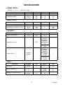
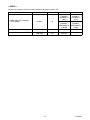
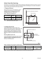
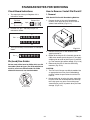
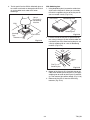
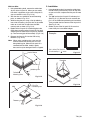
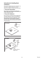
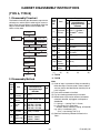
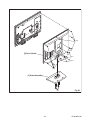
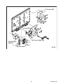

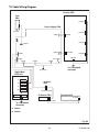


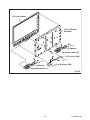
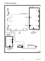
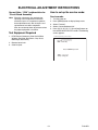
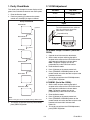
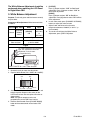
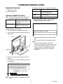
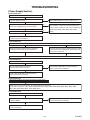
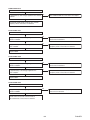
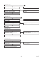
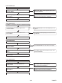
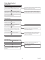


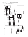
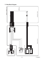

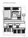
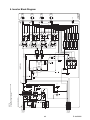


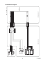
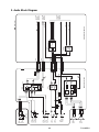
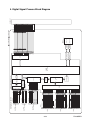

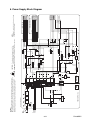
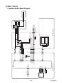
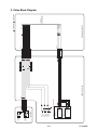
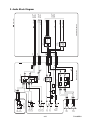
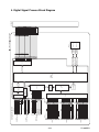
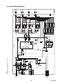
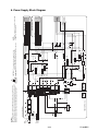
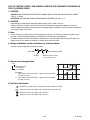

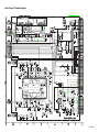
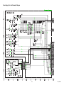
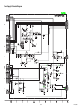
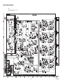
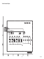
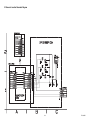
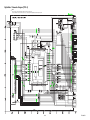
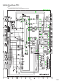
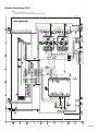
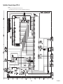
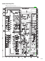
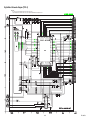
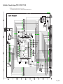
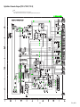
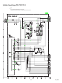
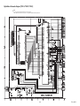
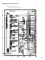
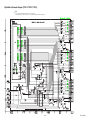
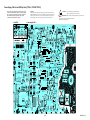

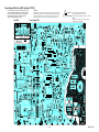

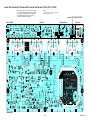

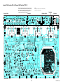
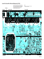

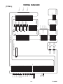
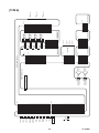
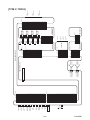

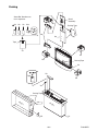
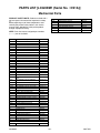
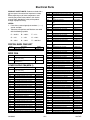
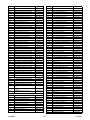


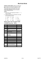


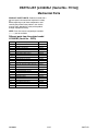
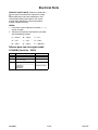


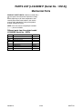


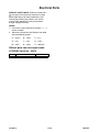
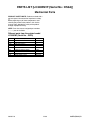


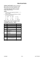
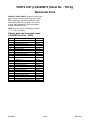

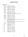

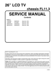
![高圧気中負荷開閉器[EH734u]](http://vs1.manualzilla.com/store/data/006667384_3-7ef974a52a2dc312f6ac65191136d1ff-150x150.png)