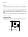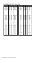
1
Advanced/ZP Baby-AT Board Technical Product Summary Version 2 July, 1995 Order Number 281786-002 ® Advanced/ZP Technical Product Summary Table of Contents Introduction.......................................................................................................................................................................... 3 Board Level Features........................................................................................................................................................... 5 CPU Performance Upgrade Second Level Cache System Memory Expansion Slots Peripheral Component Interconnect (PCI) PCIset National Semiconductor 87306 Super I/O Controller System BIOS Security Features Connectors Power Consumption Appendix A − User-Installable Upgrades.......................................................................................................................... 14 Appendix B − Jumpers and Switches ................................................................................................................................ 15 Appendix C − I/O Map ...................................................................................................................................................... 17 Appendix D − Memory Map.............................................................................................................................................. 18 Appendix E − Interrupts & DMA Channels ..................................................................................................................... 18 Appendix F − Connectors .................................................................................................................................................. 19 Appendix G − BIOS Setup................................................................................................................................................. 23 Appendix H − BIOS Recovery........................................................................................................................................... 33 Appendix I − Error messages and Beep Codes ................................................................................................................. 34 Appendix J − Environmental Standards ........................................................................................................................... 36 Appendix K − Reliability Data .......................................................................................................................................... 36 Intel Corporation disclaims all warranties and liabilities for the use of this document and the information contained herein, and assumes no responsibility for any errors which may appear in this document. Intel makes no commitment to update the information contained herein, and may make changes at any time without notice. There are no express or implied licenses granted hereunder to any intellectual property rights of Intel Corporation or others to design or fabricate Intel integrated circuits or integrated circuits based on the information in this document. Contact your local sales office to obtain the latest specifications before placing your order. *other product and corporate names may be trademarks or registered trademarks of other companies, and are used only for explanation and to the owners’benefit, without intent to infringe. INTEL CORPORATION, 1995 Advanced/ZP Technical Product Summary •Page 2 Introduction The Intel Advanced/ZP baseboard features the Pentium processor in a Baby-AT form factor with integrated I/O. Advanced/ZP baseboards are focused on providing the best possible performance at the lowest possible price for mainstream desktop computers. Advanced/ZP is a flexible baseboard which is available with the 75 MHz, 90 MHz, 100 MHz, or 120 MHz Pentium processor. The processor is complemented by a standard 256 KB asynchronous SRAM second level write-back cache and support for up to 128 MB of Fast Page or EDO DRAM. A Pentium OverDrive socket (Socket 5) provides access to future performance enhancements. The Advanced/ZP baseboard offers outstanding I/O capabilities starting with the full set of I/O, including a floppy drive interface, dual channel PCI local bus IDE interfaces, two serial ports with FIFOs, an EPP/ECP capable parallel port, and an infrared (IrDA) port. Two dedicated PCI local bus slots, and one shared PCI/ISA slot, provide a high bandwidth data path for functions such as graphics that have a high data throughput requirement. The integrated Bus Mastering capable PCI IDE controller provides two high performance IDE interfaces for hard drives and CD-ROMs. Bus mastering enhances the performance in multi-tasking environments such as Windows* 95. The Advanced/ZP baseboard also provides three dedicated ISA connectors and one shared PCI/ISA connector. There is one PCI full length capable slot, and three ISA full length capable slots. In addition to superior hardware capabilities, features like Windows 95-ready Plug and Play and Advanced Power Management (APM) with application restart are provided by software available from Intel for the Advanced/ZP platform. The Advanced/ZP baseboard provides the foundation for cost effective, high performance, highly expandable platforms which deliver the latest in CPU and I/O technology. Although the Advanced/ZP will support CGA emulation by VGA cards, it will not support CGA cards. ADVANCED/ZP FORM FACTOR The Advanced/ZP baseboard is designed to fit into a standard Baby-AT form factor chassis. Figure 1 illustrates the mechanical form factor for the Advanced/ZP. The actual dimensions of the Advanced/ZP baseboard do not strictly adhere to the standard Baby-AT guidelines, and exceptions to the standard are listed in the Baseboard Design Exceptions section. 10.0" 9.60" 0.70" 0.80" 3.80" 4.00" 3.50" PIN 1 Pentium™ Processor 0.0" 0.65" 0.20" 0.20" 5.60" 8.40" 0.0" 8.60" Figure 1. Advanced/ZP Baseboard dimensions. Advanced/ZP Technical Product Summary •Page 3 BASEBOARD DESIGN EXCEPTIONS BASEBOARD DIMENSIONS The Advanced/ZP is 3.0" shorter than the Baby-AT standard. The shorter board length may require some chassis to be modified to add additional mounting holes. MOUNTING HOLE PLACEMENT The mounting holes located in the bottom left and right corners of Figure 1 are pseudo Baby-AT standard and are available in many, but not all, Baby-AT compatible chassis. FRONT PANEL CONNECTORS There is no front panel connector on the baseboard for a Turbo/Deturbo switch. The processor speed can be set either through a parameter in the CMOS Setup Utility, or from the keyboard (<CTL><ALT><+> = Turbo, <CLT><ALT><-> = Deturbo). Changing processor speed from the keyboard may be prohibited by the operating system, or when the processor is in protected mode. Setting the processor to deturbo (or slow) only slows the processor to the approximate equivalent of a 25 MHz clock rate, not the standard 8 MHz clock rate. JUMPERS/SWITCHES There is no Color/Mono jumper/switch on the baseboard to specify Monochrome or Color video mode at boot, the BIOS will automatically detect the type of video card installed. Also, there is no Flash write protect jumper/switch, the BIOS needs to be able to write to FLASH to support the Plug and Play features. Advanced/ZP Technical Product Summary •Page 4 Board Level Features AB C D E F A − Two PCI IDE interfaces B − National 87306 I/O controller C − Primary power connector D − Four SIMM sockets (two banks) E − 82438FX Triton Data Path (TDP) F − Parallel port connector G − Floppy drive connector H − 256KB Secondary cache I − 82437FX Triton System Controller (TSC) J − Socket 5 Pentium processor socket K− CPU voltage regulator L − Front Panel I/O connectors M − Configuration switch block N − 82371FB PCI ISA/IDE Accelerator (PIIX) O − Battery for the Real-time clock P − Four ISA expansion connectors Q − BIOS recovery boot jumper R − Flash EEPROM for system BIOS S − Three PCI expansion connectors T − 3.3 volt power connector for PCI U − Serial port connectors V − AT Keyboard Connector G H V U T I PIN 1 S J R K Q L P O N M (Optional PS/2 style Keyboard and Mouse connectors may be available) Figure 2. Advanced/ZP Board Level Features CPU The Advanced/ZP baseboard is designed to operate with 3.3 volt Pentium processors. A patented on-board voltage regulator circuit provides the required 3.3 volts from the 5 volt tap provided by a standard PC power supply. The baseboard supports the Pentium processors at iCOMP index 610 \ 75 MHz, 735 \ 90 Mhz, 815 \ 100 Mhz, and 1000 \ 120 Mhz. The Pentium processor is backward-compatible with the 8086, 80286, i386 and i486 CPUs. It supports both read and write burst mode bus cycles, and includes separate 8K on-chip code and data caches which employ a write-back policy. Also integrated into the Pentium processor is an advanced numeric coprocessor which significantly increases the speed of floating point operations, while maintaining backward compatibility with i486DX math coprocessor and complying to ANSI/IEEE standard 754-1985. All Advanced/ZP baseboards support the 75 MHz and 90 MHz processors. The matrix below shows which Printed Board Assemblies (PBA number found on the baseboard) also support the 100 MHz or 120 MHz processor. Processor Speed Supported by PBA Numbers: 75 MHz 90 MHz 100 MHz 120 MHz All PBAs All PBAs PBA 638995, PBA 641525, PBA 639379 Suffixes -606, -607, -806, -807, -808 and above Table 1. Processor support PERFORMANCE UPGRADE A 320-pin Type 5 Zero Insertion Force socket provides users with a performance upgrade path to future, higher speed, Pentium processors. An OverDrive processor being developed for use with this socket will provide performance beyond that delivered by the originally installed Pentium processor. SECOND LEVEL CACHE The Pentium processor's internal cache is complemented by 256 KB direct mapped write-back second level cache. The 256 KB cache configuration is implemented with eight 32kx8 asynchronous SRAM devices for the cache data and one 32kx8 SRAM for the cache tag. The cache size is set by three configuration jumpers located on the baseboard. This is preset by the factory to support the onboard 256 KB configuration. Advanced/ZP Technical Product Summary •Page 5 SYSTEM MEMORY The Advanced/ZP baseboard provides four 72-pin SIMM sites for memory expansion. The sockets support 1M x 32 (4 MB), 2M x 32 (8 MB), 4M x 32 (16 MB), and 8M x 32 (32 MB) single-sided or double-sided SIMM modules. Minimum memory size is 8 MB and maximum memory size, using four 8M x 32 SIMM modules, is 128 MB. For external CPU speeds of less than 60 Mhz (used with 75, 90 and 120 Mhz processors) memory timing requires 70 ns fast page devices or, for higher performance, 70 ns EDO DRAM. For external CPU speeds of 66 Mhz (used with 100 Mhz processors) you must use 60 nS EDO DRAM, but 70 nS fast page DRAM may still be used. Parity generation and checking is not supported by the chip set. The four sockets are arranged as Bank 0 and Bank 1, with each bank consisting of two sockets and providing a 64-bit wide data path. Both SIMMs in a bank must be of the same memory size and type, however Banks 0 and 1 may have different types of memory installed. It is even possible to have 70 ns Fast Page DRAM in one bank and 60 ns EDO DRAM in the other, in which case each bank is independently optimized for maximum performance. Bank 0 only, Bank 1 only, or both banks may be populated. There are no jumper settings required for the memory size or type, which is automatically detected by the system BIOS. Tin lead SIMMs are required to be used when adding Fast Page or EDO DRAM. EDO DRAM Extended Data Out (or Hyper Page Mode) DRAM is designed to improve the DRAM read performance. EDO DRAM holds the memory data valid until the next CAS# falling edge, unlike standard fast page mode DRAM which tri-states the memory data when CAS# negates to precharge for the next cycle. With EDO, the CAS# precharge overlaps the data valid time, allowing CAS# to negate earlier while still satisfying the memory data valid window time. EXPANSION SLOTS Up to six expansion slots may be populated on the Advanced/ZP baseboard. There are four ISA bus expansion conectors and three PCI expansion connectors. One slot is shared by connectors that will accommodate either an ISA or a PCI expansion card, but not both at the same time. This accounts for the disparity between the number of slots and connectors. All three PCI expansion slots accept PCI bus mastering cards, and fully comply with the PCI 2.10 specification. Three of the ISA slots and one PCI slot can accommodate full length add-in cards. Interference with the processor heat sink and CPU voltage regulator support circuitry limits the rest of the ISA and PCI slots to being able to support only half-length add-in cards. PCI 3.3 VOLT CAPABILITIES To maintain strict compliance with the PCI specification, the baseboard provides a connector which can be used to route 3.3 volt power to the PCI slots. The connector may be used with a separate 3.3 volt power supply or with a custom designed voltage converter. Note: The on-board 3.3 volt regulator provides power for the CPU, PCIset and L2 cache only, not the PCI slots. Advanced/ZP Technical Product Summary •Page 6 PERIPHERAL COMPONENT INTERCONNECT (PCI) PCISET The Intel Triton 82430FX PCIset consists of the 82437FX Triton System Controller (TSC), two 82438FX Triton Data Path (TDP) devices, and one 82371FB PCI ISA/IDE Accelerator (PIIX) bridge chip. The Triton PCIset provides the following functions: • CPU interface control • Interface between the PCI bus and ISA bus • Integrated L2 write-back cache controller • Integrated fast IDE interface – Pipelined Burst or standard SRAM – Support for up to 4 devices – 256kB or 512kB Direct Mapped – PIO Mode 4 transfers up to 16MB/sec – Integrated Tag Status Bits – Integrated 8 x 32-bit buffer for PCI IDE burst • Integrated DRAM controller transfers – 64-bit path to Memory • Enhanced Fast DMA controller – Support for EDO and Fast Page DRAM • Interrupt controller and steering – 4 MB to 128 MB main memory • Counters/Timers • Fully synchronous PCI bus interface • SMI interrupt logic and timer with Fast On/Off mode – 25/30/33 MHz – PCI to DRAM > 100 Mbytes/sec – PCI to DRAM posting of 12 Dwords – 5 Dword buffers for CPU-PCI write posting – 4 Dword buffers for PCI to Memory bus master cycles – Support for up to 5 PCI masters 82437FX TRITON SYSTEM CONTROLLER (TSC) The 82437FX provides all control signals necessary to drive a second level cache and the DRAM array, including multiplexed address signals. It also controls system access to memory and generates snoop controls to maintain cache coherency. The TSC comes in a 208 pin QFP package. 82438FX TRITON DATA PATH (TDP) There are two 82438FX components which provide data bus buffering and dual port buffering to the memory array. Controlled by the 82437FX, the 82438FX devices add one load each to the PCI bus and perform all the necessary byte and word swapping required. Memory and I/O write buffers are included in these devices. The TDP devices are 100 pin QFP packages. 82371FB PCI ISA/IDE ACCELERATOR (PIIX) The 82371FB provides the interface between the PCI and ISA buses and integrates a dual channel fast IDE interface capable of supporting up to 4 devices, seven 32-bit DMA channels, five 16-bit timer/counters, two eight-channel interrupt controllers, PCI-to-AT interrupt mapping circuitry, NMI logic, ISA refresh address generation, and PCI/ISA bus arbitration circuitry. The PIIX comes in a 208-pin QFP package. TRITON DESIGN CONSIDERATIONS Triton Memory Hole Limitation Due the design of the Triton chipset, only one memory hole can be active at a time. The user can not set the Base Memory size to 512 KB and enable the ISA LFB at the same time. Triton PCI Hold Time Requirement The Triton chipset provides less hold time than the earlier Neptune and Mercury chipsets on the PCI address and data lines, but still is within the PCI specification. (The PCI specification calls out a 0 ns minimum hold time.) Some PCI expansion cards do not meet this requirement, and in fact require more hold time than the Triton chipset provides. Disabling PCI write bursting will sometimes enable these cards to function. Advanced/ZP Technical Product Summary •Page 7 IDE SUPPORT The Advanced/ZP baseboard provides two independent high performance bus-mastering PCI IDE interfaces capable of supporting PIO Mode 3 and Mode 4 devices for up to 16 MB/sec transfers. Support for ATAPI devices is provided in the system BIOS. The system BIOS also supports Logical Block Addressing (LBA) and ECHS on both IDE interfaces. When used in conjunction with a special driver the IDE interface operates as a PCI bus master for optimum performance in a multi-tasking environment. One such driver is provided by Intel for the Windows 95 environment. NATIONAL SEMICONDUCTOR 87306 SUPER I/O CONTROLLER Control for the integrated serial ports, parallel port, floppy drive, RTC and keyboard controller is incorporated into a single component, the National Semiconductor 87306. This component provides: •Two NS16C550-compatible UARTs with send/receive 16 byte FIFO - Support for an IrDA compliant Infra Red interface •Multi-mode bi-directional parallel port - Standard mode; IBM and Centronics compatible - Enhanced Parallel Port (EPP) with BIOS/Driver support - High Speed mode; Enhanced Capabilities Port (ECP) compatible •Industry standard floppy controller with 16 byte data FIFO (2.88 MB floppy support) •Integrated Real Time Clock accurate within +/- 13 minutes/yr •Integrated 8042 compatible keyboard controller Configuration of these interfaces is possible via the CMOS Setup program that can be invoked during boot-up. The serial ports can be enabled as COM1, COM2 or disabled. COM2 can alternately be configured as an IRDA port. The parallel port can be configured as normal, extended , or disabled. The floppy interface can be configured for 720 KB, 1.2 MB, 1.44 MB, or 2.88 MB media. Header pins located near the back of the board allow cabling to use these interfaces. KEYBOARD INTERFACE The AT keyboard connector is located on the back panel side of the baseboard. The 5V lines to this connector is protected with a PolySwitch* circuit which acts much like a self-healing fuse, re-establishing the connection after an over-current condition is removed. While this device eliminates the possibility of having to replace a fuse, care should be taken to turn off the system power before installing or removing a keyboard. The integrated 8042 microcontroller contains the AMI Megakey keyboard controller code which, besides providing traditional keyboard control functions, supports Power-On/Reset (POR) password protection. The POR password can be defined by the user via the Setup program. The keyboard controller also provides for the following "hot key" sequences: •CTRL-ALT-DEL: System software reset. This sequence performs a software reset of the system by jumping to the beginning of the BIOS code and running the POST operation. •CTRL-ALT+ and CTRL-ALT-: Turbo mode selection. CTRL-ALT- sets the system for de-turbo mode, emulating a 25 MHz AT, and CTRL-ALT+ sets the system for turbo mode. Changing the Turbo mode may be prohibited by an operating system, or when the CPU is in Protected mode or virtual 86 mode under DOS. •CTRL-ALT-<defined in setup>: Power down and coffee-break key sequences take advantage of the SMM features of the Pentium processor to greatly reduce the system’s power consumption while maintaining the responsiveness necessary to service external interrupts. REAL TIME CLOCK, CMOS RAM AND BATTERY The integrated Real Time Clock, RTC, is accurate to within 13 minutes/year. The RTC can be set via the BIOS SETUP Program. CMOS memory supports the standard 128-byte battery-backed RAM, fourteen bytes for clock and control registers, and 114 bytes of general purpose non-volatile CMOS RAM. All CMOS RAM is reserved for BIOS use. The CMOS RAM can be set to specific values or cleared to the system default values using the BIOS SETUP program. Also, Advanced/ZP Technical Product Summary •Page 8 the CMOS RAM values can be cleared to the system defaults by using a configuration switch on the baseboard. Appendix B lists switch and jumper configurations. An external coin-cell style battery provides power to the RTC and CMOS memory. The battery has an estimated lifetime of seven years and is socketed for easy replacement. Refer to Appendix A for battery replacement details. IRDA (INFRARED) SUPPORT Serial port 2 can be configured to support an IrDA module via a 5 pin header connector. Once configured for IrDA, the user can transfer files to/from portable devices such as laptops, PDA’s and printers using application software such as LapLink. The IrDA specification provides for data transfers at up to 115kbps from a distance of 1 meter. A 5-pin header is provided to allow connection to a Hewlett Packard HSDSL-1000 compatible Infra-red transmitter/receiver. SYSTEM BIOS The Advanced/ZP baseboard uses an American Megatrends Incorporated (AMI) Pentium Processor ROM BIOS, which is stored in Flash EEPROM and easily upgraded using a floppy disk-based program. In addition to the AMIBIOS, the Flash EEPROM also contains the Setup utility, Power-On Self Tests (POST), update recovery code, and the PCI autoconfiguration utility. This baseboard supports system BIOS shadowing, allowing the BIOS to execute from 32-bit onboard write-protected DRAM. The BIOS displays a sign-on message during POST identifying the type of BIOS and a five-digit revision code. As an example the BIOS for the Advanced/ZE will be 1.00.02.BS0. As BIOS updates occur the revision number will increase to 1.00.03.BS0, and so on. Information on BIOS functions can be found in the IBM PS/2 and Personal Computer BIOS Technical Reference published by IBM, and the ISA and EISA Hi-Flex AMIBIOS Technical Reference published by AMI. Both manuals are available at most technical bookstores. FLASH IMPLEMENTATION The Intel 28F001BXT 1 Mb FLASH component is organized as 128K x 8 (128 KB). The Flash device is divided into five areas, as described in Table 1. System Address FLASH Memory Area F0000H EE000H FFFFFH EFFFFH 64 KB Main BIOS 8 KB Boot Block (Not FLASH erasable) ED000H EDFFFH 4 KB Plug and Play ESCD Storage Area EC000H ECFFFH 4 KB OEM LOGO Area E0000H EBFFFH 48 KB System BIOS Reserved Table 2. Flash Memory Organization The FLASH device resides in system memory in two 64 KB segments starting at E0000H, and can be mapped two different ways, depending on the mode of operation. In Normal Mode, address line A16 is inverted, setting the E000H and F000H segments so that the BIOS is organized as shown in the system address column above. Recovery mode removes the inversion on address line A16, swapping the E000H and F000H segments so that the 8 KB boot block resides at FE000H where the CPU expects the bootstrap loader to exist. This mode is only necessary in the unlikely event that a BIOS upgrade procedure is interrupted, causing the BIOS area to be left in an unusable state. For information on recovering the BIOS in the event of a catastrophic failure, refer to the appendix. BIOS UPGRADES FLASH memory makes distributing BIOS upgrades easy. A new version of the BIOS can be installed from a diskette. BIOS upgrades will be available as downloadable files on the Intel bulletin board. The disk-based Flash upgrade utility, FMUP.EXE, has three options for BIOS upgrades: Advanced/ZP Technical Product Summary •Page 9 •The Flash BIOS can be updated from a file on a disk; •The current BIOS code can be copied from the Flash EEPROM to a disk file as a backup in the event that an upgrade cannot be successfully completed; or •The BIOS in the Flash device can be compared with a disk file to ensure the system has the correct BIOS version. The upgrade utility ensures the upgrade BIOS extension matches the target system to prevent accidentally installing a BIOS for a different type of system. A recovery jumper is provided to allow recovery in the unlikely event of an unsuccessful BIOS upgrade. The jumper forces the ROM decode to access a 8 KB block of write protected recovery code in the Flash device. SETUP UTILITY The ROM-based Setup utility allows the configuration to be modified without opening the system for most basic changes. The Setup utility is accessible only during the Power-On Self Test, POST, by pressing the <F1> key after the POST memory test has begun and before boot begins. A prompt may be enabled that informs the user to press the <F1> key to access Setup. A switch on the baseboard can be set to prevent user access to Setup for security purposes. Setup options are detailed in the BIOS appendix. PCI AUTO-CONFIGURATION The PCI auto-configuration utility operates in conjunction with the system Setup utility to allow the insertion and removal of PCI cards to the system without user intervention. When the system is turned on after adding a PCI add-in card, the BIOS automatically configures interrupts, DMA channels, I/O space, and other parameters. The user does not have to configure jumpers or worry about potential resource conflicts. Because PCI cards use the same interrupt resources as ISA cards, the user must specify the interrupts used by ISA add-in cards in the Setup utility. The PCI AutoConfiguration function complies with version 2.10 of the PCI BIOS specification. ISA PLUG & PLAY The BIOS incorporates ISA Plug and Play capabilities conforming to version 1.0a of the Plug-n-Play specification. This will allow auto-configuration of Plug and Play ISA cards, and resource management for legacy ISA cards, when used in conjunction with the ISA Configuration Utility (ICU). SHADOW MEMORY Memory from C8000-DFFFF is not shadowed. This is a change from previous Intel products using AMI BIOS. This may have a slight adverse affect on the performance of some non-Plug and Play ISA cards. All or part of this area may be used as shared ISA memory if needed. Video BIOS located from C0000-C7FFF is shadowed to boost performance. POWER MANAGEMENT The Advanced/ZP will enable you to have an Energy Star compliant system through its Advanced Power Management resources. The Advanced/ZP BIOS supports power management via System Management Mode (SMM) interrupts to the CPU and Advanced Power Management (APM v1.1). In general, power management capabilities will allow the system to be put into a power managed Stand By state. This can be accomplished by pressing the sleep/resume button on the front of the chassis, entering an user configured hot-key sequence on the keyboard, or by the expiration of a hardware timer which detects system inactivity for a user-configurable length of time. While in the Stand By state, the Advanced/ZP baseboard reduces the system power consumption to Energy Star levels by utilizing the power saving capabilities of the Pentium Processor, spinning down the IDE hard drive, and turning off an Energy Star rated monitor. Add-in cards supplied with APM-aware drivers can also be put into a power managed state for further energy savings. The ability to respond to external interrupts is fully maintained while in Stand By mode allowing the system to service requests such as in-coming FAX’s or network messages while unattended. FLASH LOGO AREA Advanced/ZP supports a 4 KB programmable FLASH user area located at EC000-ECFFF. An OEM may use this area to display a custom logo. The BIOS accesses the user area at several points during the boot up sequence. Advanced/ZP Technical Product Summary •Page 10 SECURITY FEATURES ADMINISTRATIVE PASSWORD The administrative password protects several sensitive Setup options from being viewable to a user unless the password is entered. These sensitive fields are viewable unless the administrative password is set. BIOS PASSWORD A BIOS password feature provides security during the boot process. A password can be entered using the Setup utility, and will be required on boot up before normal operation of the system can commence. To enable, disable, or change the password, refer to the Setup program options in the appendix. If the password is forgotten, it can be cleared by turning off the system and setting the "password clear" jumper to the clear position. SETUP ENABLE SWITCH A baseboard configuration switch controls access to the BIOS Setup utility. By setting switch SW5 to the ON position, the user is prevented from accessing the Setup utility during the Power-On Self Test or at any other time. The message prompting the user to press <F1> to enter setup is also disabled CONNECTORS FRONT PANEL CONNECTIONS The Advanced/ZP baseboard provides header connectors to support functions typically located on the chassis bezel: • • • • • • • • • System Reset Power LED Keyboard Lock Hard Drive activity LED Turbo LED System Speaker Secondary CPU Fan Infra-Red (IrDA) port Sleep/Resume Sleep/Resume Infra-Red +12v Fan Speaker Reset Keylock/ HDD LED Power LED Turbo LED Advanced/ZP Technical Product Summary •Page 11 Figure 3. Front Panel Connectors Sleep/Resume This two pin header, when connected to a momentary switch, can be used to put the system into a power managed state (standby) that will reduce the system’s power consumption. If the system is in Stand By mode and the switch is pressed, the system will instantly “wake up” or Resume full system activity. When used with a power supply with a high efficiency rating, the Advanced/ZE is easily capable of reducing the system power to below EPA Energy Star requirements. The function of the Sleep/Resume button can also be achieved via the keyboard with a hot key sequence programmable in setup. Infra-Red (IrDA) connector Serial port 2 can be configured to support an IrDA module via a 5 pin header connector. Once configured for IrDA, the user can transfer files to/from portable devices such as laptops, PDA’s and printers using application software such as LapLink. The IrDA specification provides for data transfers at up to 115kbps from a distance of 1 meter. Speaker The external speaker provides error beep code information during the Power-On Self Test if the system cannot use the video interface. See the appendix for more information about error beep codes. BACK PANEL CONNECTIONS The back panel provides external access to an AT style keyboard connector integrated on the Advanced/ZP baseboard. Figure 4 shows the general location of the AT style keyboard connector. Keyboard Connector Figure 4. Advanced/ZP AT Style Back panel I/O CONNECTIONS The baseboard contains shroudless stake pin header connections for cabling the serial, parallel, floppy, and IDE interfaces. Figure 5 shows the locations of these connectors and the orientation of pin 1 on each. Primary IDE Parallel Port Floppy Secondary IDE COM 1 COM 2 Denotes Pin 1 Figure 5. I/O Connections POWER CONSUMPTION Table 2 lists the current used by system resources in a configuration which includes 8 MB of DRAM. Table 3 lists the typical power consumed by the same configuration. Note that the 3.3 volts used to drive the CPU and core logic is derived Advanced/ZP Technical Product Summary •Page 12 from an on-board voltage regulator from the +5 volt source. This information is provided only as a guide for calculating approximate total system power usage with additional resources added. CURRENT DC Voltage +5V -5V +12V -12V 75 MHz Typical Current* 3.3 amps 20 milliamps 75 milliamps 10 milliamps 90 MHz Typical Current* 3.45 amps 20 milliamps 75 milliamps 10 milliamps Table 3. Advanced/ZP Current Requirements *(measured with 8 MB DRAM, VGA controller and Floppy Drive while sitting at DOS prompt) WATTS Resource Advanced/ZP baseboard, 8 MB, 256 KB cache, 3½” floppy drive, 540 MB hard drive Typical Power* 32 Watts Standby Power* 21 Watts Table 4. Power used by System Resources *(true power measured from the wall with a 65% efficient power supply) Advanced/ZP Technical Product Summary •Page 13 Appendix A − User-Installable Upgrades SYSTEM MEMORY Table A-1 shows the possible memory combinations. The Advanced/ZP will support both Fast Page DRAM or EDO DRAM SIMMs, but they cannot be mixed within the same memory bank. If Fast Page DRAM and EDO DRAM SIMMs are installed in separate banks, each bank will be optimized for maximum performance. Parity generation and detection is NOT supported. SIMM requirements are Fast Page Mode or EDO DRAM, 60 nS or 70 nS, with tin-lead connectors. SIMM 1,2 (Bank 0) SIMM Type (Size) Empty Empty Empty Empty 1M X 32 (4 MB) 1M X 32 (4 MB) 1M X 32 (4 MB) 1M X 32 (4 MB) 1M X 32 (4 MB) 2M X 32 (8 MB) 2M X 32 (8 MB) 2M X 32 (8 MB) 2M X 32 (8 MB) 2M X 32 (8 MB) 4M X 32 (16 MB) 4M X 32 (16 MB) 4M X 32 (16 MB) 4M X 32 (16 MB) 4M X 32 (16 MB) 8M X 32 (32 MB) 8M X 32 (32 MB) 8M X 32 (32 MB) 8M X 32 (32 MB) 8M X 32 (32 MB) SIMM 3,4 (Bank 1) Total System Memory SIMM Type (Size) 1M X 32 (4 MB) 8 MB 2M X 32 (8 MB) 16 MB 4M X 32 (16 MB) 32 MB 8M X 32 (32 MB) 64 MB Empty 8 MB 1M X 32 (4 MB) 16 MB 2M X 32 (8 MB) 24 MB 4M X 32 (16 MB) 40 MB 8M X 32 (32 MB) 72 MB Empty 16 MB 1M X 32 (4 MB) 24 MB 2M X 32 (8 MB) 32 MB 4M X 32 (16 MB) 48 MB 8M X 32 (32 MB) 80 MB Empty 32 MB 1M X 32 (4 MB) 40 MB 2M X 32 (8 MB) 48 MB 4M X 32 (16 MB) 64 MB 8M X 32 (32 MB) 96 MB Empty 64 MB 1M X 32 (4 MB) 72 MB 2M X 32 (8 MB) 80 MB 4M X 32 (16 MB) 96 MB 8M X 32 (32 MB) 128 MB Table A-1. Possible SIMM Memory Combinations RTC BATTERY The battery can be replaced with either of the following batteries: Sony CR2032 3V Lithium cell Panasonic CR2032 3V Lithium cell Advanced/ZP Technical Product Summary •Page 14 Appendix B − Jumpers and Switches Figure B-1. Jumper locations and settings (default settings shown) EXTERNAL CPU CLOCK SPEED (50/60/66 MHZ) - SWITCHES 7 & 8 This jumper sets the CPU's external operating frequency at 50, 60, and 66 MHz.. Default setting is 50 MHz. Frequency 50 MHz 60 Mhz 66 MHz Switch 7 OFF ON OFF Switch 8 OFF OFF ON Table B-1. External CPU Speed Switches INTERNAL CPU BUS CLOCK SPEED - SWITCH 6 Sets the internal processor speed to either 3/2 or 2 times the external CPU clock speed. Switch 6=OFF for 3/2, Switch 6=ON for 2 times. The 3/2 setting is used for 75 MHz, 90 MHz, and 100 MHz processors. The 2 times setting is used for 120 MHz processors. The default setting is 3/2, (Switch 6 = OFF). SETUP DISABLE - SWITCH 5 Allows access to CMOS Setup Utility to be disabled by setting switch 5 to the ON position. Default is for access to setup to be enabled (switch 5 = OFF). CLEAR CMOS - SWITCH 4 Allows CMOS settings to be reset to default values by moving switch 4 to the ON position and turning the system on. The system should then be turned off and switch 4 should be returned to the OFF position to restore normal operation. This procedure should be done whenever the system BIOS is updated. Default setting is SW4=OFF. PASSWORD CLEAR - SWITCH 3 Allows system password to be cleared by moving switch 3 to the ON position and turning the system on. The system should then be turned off and switch 3 should be returned to the OFF position to restore normal operation. This procedure should only be done if the user password has been forgotten. Default setting is SW3=OFF. Advanced/ZP Technical Product Summary •Page 15 PROCESSOR VOLTAGE REGULATION - SWITCH 2 Sets the output of the on-board voltage regulator. The switch settings are OFF = VR, and ON = VRE. The VR voltage specification requires a voltage range of 3.3-3.465 Volts DC, while the VRE specification requires a voltage range of 3.453.6V. Pentium processors currently available that do not require the VRE voltage specification should use the VR setting. When upgrading your CPU be sure to consult the documentation for the processor voltage requirements before setting this switch, as an incorrect setting may damage the processor. The default position is with the switch set for VR (off). ISA BUS SPEED - SWITCH 1 Sets the ISA bus speed to either 1/4 or 1/3 of the PCI bus speed to best maximize system performance for 75, 90, 100 or 120 MHz processor speeds. When SW1=ON the ISA bus speed will be 1/4 of the PCI bus speed and when SW1=OFF the ISA bus speed will be 1/3 the PCI bus speed. The ISA bus speed is derived from the PCI bus speed which is derived from the external processor clock frequency. The position of SW1 will set the ISA bus speed to either Compatible or Enhanced for 90 MHz, 100 MHz, and 120 MHz processors and will leave the ISA bus speed Compatible for 75 MHz processor speed. For 90 MHz, 100 MHz, and 120 MHz processor speeds, if SW1 is set to Compatible (SW1=ON), the speed will fall within the limits defined by the IBM AT Technical Reference (6-8.33 MHz). If set to Enhanced (SW1=OFF), the speed will be greater than the maximum defined by the IBM AT Technical Reference manual. SW1 can be set to either position when a 75 MHz processor speed is used for maximum ISA bus performance. Modern ISA cards can operate with the enhanced speeds, however some older cards can experience difficulties. The actual value of the Bus Clock when set to Compatible or Enhanced is dependent upon the setting of the external processor frequency. The following table describes the ISA bus speeds for the 75 MHz, 90 MHz, 100 MHz, and 120 MHz processor speeds. Internal Processor Frequency PCI bus Frequency SW1=OFF (1/3) SW1=ON (1/4) 75 MHz 90 MHz 100 MHz 120 MHz 25 MHz 30 MHz 33 MHz 30 MHz 8.33 MHz 10.0 MHz 11.0 MHz 10.0 MHz 8.33 MHz 7.50 MHz 8.33 MHz 7.50 MHz Table B-2. ISA Bus Speed Switch Settings RECOVERY BOOT ENABLE - J1K1 This switch allows the system to boot in the event the system BIOS has been corrupted by moving the jumper from the default position of 1-2 to the 2-3 position. A recovery disk must be in drive A while booting up with this jumper set to 2-3. Once the recovery is complete the jumper should be move back to pins 1-2, and the system rebooted. Advanced/ZP Technical Product Summary •Page 16 Appendix C − I/O Map Address (hex) Size Description Address (hex) Size Description 0000 - 000F 0020 - 0021 16 bytes 2 bytes PIIX - DMA 1 PIIX - Interrupt Controller 1 01F0 - 01F7 0278 - 027B 8 bytes 4 bytes Primary IDE Channel Parallel Port 2 0040 - 0043 4 bytes PIIX - Timer 1 02F8 - 02FF 8 bytes On-Board Serial Port 2 0048 - 004B 4 bytes PIIX - Timer 2 0376 1 byte Sec IDE Chan Cmd Port 0060 1 byte Keyboard Controller Data Byte 0377 1 byte Sec IDE Chan Stat Port 0061 1 byte PIIX - NMI, speaker control 0378 - 037F 8 bytes Parallel Port 1 0064 1 byte Kbd Controller, CMD/STAT 03BC - 03BF 4 bytes Parallel Port x 0070, bit 7 1 bit PIIX - Enable NMI 03E8 - 03EF 8 bytes Serial Port 3 0070, bits 6:0 7 bits PIIX - Real Time Clock, Address 03F0 - 03F5 6 bytes Floppy Channel 1 0071 1 byte PIIX - Real Time Clock, Data 03F6 1 bytes Pri IDE Channel Cmnd Port 0078 1 byte Reserved - Brd. Config. 03F7 (Write) 1 byte Floppy Channel 1 Command 0079 1 byte Reserved - Brd. Config. RD Only 03F7, bit 7 1 bit Floppy Disk Change Channel 1 0080 - 008F 16 bytes PIIX - DMA Page Register 03F7, bits 6:0 7 bits Pri IDE Channel Status Port 00A0 - 00A1 2 bytes PIIX - Interrupt Controller 2 03F8 - 03FF 8 bytes On-Board Serial Port 1 00C0 - 00DE 31 bytes PIIX - DMA 2 LPT + 400h 8 bytes ECP port, LPT + 400h 00F0 1 byte Reset Numeric Error 0CF8-0CFB* 4 bytes PCI Config Addr Reg Enable 0170 - 0177 8 bytes Secondary IDE Channel 0CFC-0CFF* 4 bytes PCI Config Data Reg FF00-FF07 8 bytes IDE Bus Master Reg. Table C-1 and C-2. Advanced/ZP I/O Address Map * Only accessible after PCI configuration space is enabled. I/O Port 78 is reserved for BIOS use. I/O Port 79 is a read only port, the bit definitions are shown below. Bit # Description Bit = 1 Bit = 0 0 1 Internal CPU Clock Freq. (Switch 6) No Connect 3/2x 2x Disable access 2 No Connect 3 External CPU clock (Switch 7) 4 External CPU clock (Switch 8) 5 Setup Disable (Switch 5) Enable access 6 Clear CMOS (Switch 4) Keep values Clear values 7 Password Clear (Switch 3) Keep password Clear password Figure C-3. I/O Port For Board Configuration PCI CONFIGURATION SPACE MAP The Triton chipset uses Configuration Mechanism 1 to access PCI configuration space. The PCI Configuration Address register is a 32-bit register located at CF8h, the PCI Configuration Data register is a 32-bit register located at CFCh. These registers are only accessable by full DWORD accesses. The table below lists the PCI bus and device numbers used by the baseboard. Bus Number (hex) Dev Number (hex) Func. Number (hex) Description 00 00 00 07 00 00 Intel 82437FX (TSC) Intel 82371FB (PIIX) PCI/ISA bridge 00 07 01 Intel 82371FB (PIIX) IDE Bus Master 00 0F PCI Expansion Slot 1 00 0D PCI Expansion Slot 2 00 0E PCI Expansion Slot 3 00 10 PCI Expansion Slot 4 Table C-4. Advanced/ZP PCI Config. Space Map Advanced/ZP Technical Product Summary •Page 17 Appendix D − Memory Map Address Range (Decimal) Address Range (hex) Size Description 1024K-131072K 960K-1023K 100000-8000000 F0000-FFFFF 127M 64K Extended Memory AMI System BIOS 952K-959K EE000-EFFFF 8K FLASH Boot Block (Available as UMB) 948K-951K ED000-EDFFF 4K ESCD (Plug and 'Play configuration area) 944K-947K EC000-ECFFF 4K OEM LOGO (available as UMB) 896K-943K E0000-EBFFF 48K BIOS RESERVED (Currently available as UMB) 800K-895K C8000-DFFFF 96K Available HI DOS memory (open to ISA and PCI bus) 640K-799K A0000-C7FFF 160K Available HI DOS memory (open to ISA and PCI bus) 639K 9FC00-9FFFF 1K Extended BIOS Data (moveable by QEMM, 386MAX) 512K-638K 80000-9FBFF 127K Extended conventional 0K-511K 00000-7FFFF 512K Table D-1. Advanced/ZP Memory Map Conventional The table above details the Advanced/ZE memory map. The ESCD area from ED000-EDFFF is not available for use as an Upper Memory Block (UMB) by memory managers. The area from E0000-EBFFF is currently not used by the BIOS and is available for use as UMB by memory managers. Parts of this area may be used by future versions of the BIOS to add increased functionality. Appendix E − Interrupts & DMA Channels IRQ System Resource NMI 0 Unused Reserved, Interval Timer 1 Reserved, Keyboard buffer full DMA Data Width System Resource 2 Reserved, Cascade interrupt from slave PIC 3 Serial Port 2 0 1 8- or 16-bits 8- or 16-bits Open Open - Normally used for LAN 4 Serial Port 1 2 8- or 16-bits Floppy 5 Parallel Port 2 3 8- or 16-bits Parallel Port 6 Floppy 4 7 Parallel Port 1 5 16-bits Open 8 Real Time Clock 6 16-bits Open 9 User available 10 User available 11 User available 12 User available 13 Reserved, Math coprocessor 14 Primary IDE if enabled, else available to user 15 Secondary IDE if enabled, else available to user Table E-1.Advanced/ZP Interrupts Advanced/ZP Technical Product Summary •Page 18 Reserved - Cascade channel 7 16-bits ISA IDE Table E-2. Advanced/ZP DMA Map Appendix F − Connectors POWER SUPPLY CONNECTORS PRIMARY POWER (J9J1) AUXILIARY (3.3V) PCI POWER (J6G1) Pin Name Function Pin Name Function 1 2 PWRGD +5 V Power Good + 5 volts Vcc 1 2 GND GND Ground Ground 3 +12 V + 12 volts 3 GND Ground 4 -12 V - 12 volts 4 +3.3 V + 3.3 volts 5 GND Ground 5 +3.3V + 3.3 volts 6 GND Ground 6 +3.3 V + 3.3 volts 7 GND Ground 8 GND Ground 9 -5 V -5 volts 10 +5 V + 5 volts Vcc 11 +5 V + 5 volts Vcc 12 +5 V + 5 volts Vcc Tables F-1 and F-2. Power Connectors FRONT PANEL CONNECTORS − (J2A1, J1B1) Turbo LED sleep/resume Pin Signal Name Pin Signal Name 1 2 +5 V Sleep 1 2 PULL_UP_330 LED_TURBO- Table F-3. Sleep/Resume Connector Infra-red Table F-4. Turbo LED Connector Hard Drive LED (Disk) Pin Signal Name Pin Signal Name 1 2 +5 V Key 1 2 PULL_UP_330 Key 3 IR_RX 3 HD ACTIVE 4 Ground 4 PULL_UP_330 5 IR_TX Table F-6. HDD LED Table F-5. IRDA Connector Key lock/Power LED Auxiliary 12V CPU Fan Power Pin Signal Name 1 2 Ground +12 V (fused) 3 Ground Table F-7. CPU Fan Connector Pin Signal Name 1 2 LED_PWR Key 3 Ground 4 KEY LOCK 5 Ground Table F-8. Key Lock/Power LED Connector Speaker Connector Pin Signal Name 1 2 SPKR_DAT Key 3 SPKR_DAT onnect 4 Ground Table F-9. Speaker Connector Reset Connector Pin Signal Name 1 2 Ground RESET Table F-10. Reset connector I/O CONNECTORS AT Keyboard Connector (J8k1) Pin Signal Name 1 2 Clock Data 3 No Connect 4 Ground 5 Vcc (fused) Table F-11. Keyboard Connector Serial Ports (j7k1, j7k2) IDE Connectors (j6h1, j6h2) Signal Name Pin Pin Signal Name Reset IDE Host Data 7 1 3 2 4 Ground Host Data 8 Host Data 6 5 6 Host Data 9 Host Data 5 7 8 Host Data 10 Host Data 4 9 10 Host Data 11 Host Data 3 11 12 Host Data 12 Host Data 2 13 14 Host Data 13 Host Data 1 15 16 Host Data 14 Host Data 0 17 18 Host Data 15 Pin Signal Name Ground 19 20 Key 1 2 DCD DSR DRQ3 21 22 Ground I/O Write- 23 24 Ground 3 Serial In - (SIN) I/O Read- 25 26 Ground 4 RTS IOCHRDY 27 28 BALE 5 Serial Out - (SOUT) DACK3- 29 30 Ground 6 CTS IRQ14 31 32 IOCS16- 7 DTR Addr 1 33 34 Ground 8 RI Addr 0 35 32 Addr 2 9 GND Chip Select 0- 37 38 Chip Select 1- N.C. Activity 39 40 Ground 10 Figure F-9. Serial Connectorr Parallel Port (j9e1) Figure F-10 IDE Connectors FLoppy Connector (j9c1) Signal Name Pin Pin Signal Name Signal Name Pin Pin Signal Name STROBEData Bit 0 1 3 2 4 AUTO FEEDERROR- Ground Ground 1 3 2 4 FDHDIN Reserved Data Bit 1 5 6 INIT- Key 5 6 FDEDIN Data Bit 2 7 8 SLCT IN- Ground 7 8 Index- Data Bit 3 9 10 Ground Ground 9 10 Motor Enable A- Data Bit 4 11 12 Ground Ground 11 12 Drive Select B- Data Bit 5 13 14 Ground Ground 13 14 Drive Select A- Data Bit 6 15 16 Ground Ground 15 16 Motor Enable B- Data Bit 7 17 18 Ground Ground 17 18 DIR- ACJ- 19 20 Ground Ground 19 20 STEP- BUSY 21 22 Ground Ground 21 22 Write Data- PE (Paper End) 23 24 Ground Ground 23 24 Write Gate- 26 N.C. Ground 25 26 Track 00- Ground 27 28 Write Protect- Ground 29 30 Read Data- Ground 31 32 Side 1 Select- Ground 33 34 Diskette SLCT Table F-11 Parallel Ports Table F-12. Floppy Connector Advanced/ZP Technical Product Summary •Page 20 ISA CONNECTORS (J1G1, J2G1, J2G2, J3G1) Signal Name Pin Pin Signal Name GND RSTDRV B1 B2 A1 A2 IOCHKSD7 Vcc B3 A3 SD6 IRQ9 B4 A4 SD5 -5V B5 A5 SD4 DRQ2 B6 A6 SD3 -12V B7 A7 SD2 0WS- B8 A8 SD1 +12V B9 A9 SD0 GND B1 A1 IOCHRDY SMEMW- B1 A1 AEN SMEMR- B1 A1 SA19 IOW- B1 A1 SA18 IOR- B1 A1 SA17 DACK3- B1 A1 SA16 DRQ3 B1 A1 SA15 DACK1- B1 A1 SA14 DRQ1 B1 A1 SA13 REFRESH- B1 A1 SA12 SYSCLK B2 A2 SA11 IRQ7 B2 A2 SA10 IRQ6 B2 A2 SA9 IRQ5 B2 A2 SA8 IRQ4 B2 A2 SA7 IRQ3 B2 A2 SA6 DACK2- B2 A2 SA5 TC B2 A2 SA4 BALE B2 A2 SA3 Vcc B2 A2 SA2 OSC B3 A3 SA1 GND B3 A3 SA0 KE KE MEMCS16- D1 C1 SBHE- IOCS16- D2 C2 LA23 IRQ10 D3 C3 LA22 IRQ11 D4 C4 LA21 IRQ12 D5 C5 LA20 IRQ15 D6 C6 LA19 IRQ14 D7 C7 LA18 DACK0- D8 C8 LA17 DRQ0 D9 C9 MEMR- DACK5- D1 C1 MEMW- DRQ5 D1 C1 SD8 DACK6- D1 C1 SD9 DRQ6 D1 C1 SD10 DACK7- D1 C1 SD11 DRQ7 D1 C1 SD12 Vcc D1 C1 SD13 Master- D1 C1 SD14 GND D1 C1 SD15 Table F-13. ISA Connector Advanced/ZP Technical Product Summary •Page 21 PCI CONNECTORS (J4G1, J5G1, J5G2) Signal Name Pin Pin Signal Name Signal Name Pin Pin Signal Name GND +12V A1 A2 B1 B2 -12V No Connect AD16 3.3V A32 A33 B32 B33 AD17 CBE2- No Connect A3 B3 GND FRAME- A34 B34 GND No Connect A4 B4 No Connect GND A35 B35 IRDY- Vcc A5 B5 Vcc TRDY- A32 B32 3.3V PCIINT3- A6 B6 Vcc GND A37 B37 DEVSEL- PCIINT1- A7 B7 PCIINT2- STOP- A38 B38 GND Vcc A8 B8 PCIINT4- 3.3V A39 B39 PLOCKPERR- Reserved A9 B9 No Connect SDONE A40 B40 Vcc A10 B10 Reserved SBO- A41 B41 3.3V Reserved A11 B11 No Connect GND A42 B42 SERR- GND A12 B12 GND PAR A43 B43 3.3V GND A13 B13 GND AD15 A44 B44 CBE1AD14 Reserved A14 B14 Reserved 3.3V A45 B45 SPCIRST- A15 B15 GND AD13 A46 B46 GND Vcc A16 B16 PCLKE AD11 A47 B47 AD12 AGNT- A17 B17 GND GND A48 B48 AD10 GND A18 B18 REQA- AD9 A49 B49 GND Reserved A19 B19 Vcc KEY A50 B50 KEY AD30 A20 B20 AD31 KEY A51 B51 KEY 3.3V A21 B21 AD29 CBEO- A52 B52 AD8 AD28 A22 B22 GND 3.3V A53 B53 AD7 AD26 A23 B23 AD27 AD6 A54 B54 3.3V AD5 GND A24 B24 AD25 AD4 A55 B55 AD24 A25 B25 3.3V GND A56 B56 AD3 AD22 (IDSEL) A26 B26 CBE3- AD2 A57 B57 GND AD1 3.3V A27 B27 AD23 AD0 A58 B58 AD22 A28 B28 GND Vcc A59 B59 Vcc AD20 A29 B29 AD21 SREQ64- A60 B60 SACK64- GND A30 B30 AD19 Vcc A61 B61 Vcc AD18 A31 B31 3.3V Vcc A62 B62 Vcc Table F-14. PCI Connectors Advanced/ZP Technical Product Summary •Page 22 Appendix G − BIOS Setup OVERVIEW OF THE SETUP MENU SCREENS The Setup program initially displays the Main menu screen. In each screen there are options for modifying the system configuration. Select a menu screen by pressing the left <← > or right <→ > arrow keys. Use the up <↑> or down <↓> keys to select items in a screen. Use <Enter> to select an item for modification. For certain items, pressing <Enter> will bring up a submenu. After you have selected an item, use the arrow keys to modify the setting. Setup Menu Screen Main Advanced Security Exit Setup Submenu Hard Disk Configuration Boot Options Peripheral Configuration Advanced Chipset Configuration Power Management Configuration Plug and Play Configuration Description For setting up and modifying some of the basic options of a PC, such as time, date, diskette drives, hard drives. For modifying the more advanced features of a PC, such as peripheral configuration and advanced chipset configuration. For specifying passwords that can be used to limit access to the system. For saving or discarding changes. Description For configuring your hard drives. For modifying options that affect the system boot up, such as the boot sequence. For modifying options that affect the serial ports, the parallel port, and the disk drive interfaces. For modifying options that affect memory and system busses. For accessing and modifying Advanced Power Management (APM) options. For modifying options that affect the system’s plug and play capabilities. Table G-1. Set Up Screen For BIOS OVERVIEW OF THE SETUP KEYS Setup Key <F1> <Esc> <Enter> <↑> <↓> <← > <→ > <F5> <F6> <F10> Description Pressing the <F1> key brings up a help screen for the currently selected item if available. Pressing the <Esc> key takes you back to the previous screen. Pressing <esc> in the Main, Advanced, Security, or Exit screen allows you to Exit Discarding Changes (see later in this chapter). Pressing the <Enter> key selects the current item or option. Pressing the up <↑> key changes the selection to the previous item or option. Pressing the down <↓> key changes the selection the to the next item or option. Pressing the left <← > or right <→ > keys in the Main, Advanced, Security, or Exit menu screens changes the menu selection. Pressing either key in a submenu does nothing. Pressing the <F5> key allows you to Load Setup Defaults (see later in this chapter). Pressing the <F6> key allows you to Discard Changes (see later in this chapter). Pressing the <F10> key allows you to Exit Saving Changes (see later in this chapter). Table G-2. Overview of Special Purpose Keys For Setup MAIN SCREEN This section describes the Setup options found on the main menu screen. If you select certain options from the main screen (e.g, Hard Disk), the Setup program will switch to a submenu for the selected option. Submenus are described in the sections following the description of the main screen options. System Date When selected, this brings up a dialog box that allows you to specify the current date. System Time When selected, this brings up a dialog box that allows you to specify the current time. Floppy Options Advanced/ZP Technical Product Summary •Page 23 When selected, this brings up the Floppy Options submenu. Hard Disk 0:, 1:, 2:, 3: This reports if a hard disk is connected to the system. When selected, this brings up the Hard Disk Configuration submenu. Language When selected, this brings up a dialog box that allows you to specify the language of the text strings used in the Setup program and the BIOS. The options are any installed languages. If no additional languages have been installed, this item will not appear. Boot Options When selected, this brings up the Boot Options screen. Video Mode This reports the video mode. This is informational only, and there are no options. Mouse This reports if a mouse is installed or not. This is informational only, and there are no options. Base Memory This reports the amount of base memory. This is informational only, and there are no options. Extended Memory This reports the amount of extended memory. This is informational only, and there are no options. FLOPPY OPTIONS SUBMENU Floppy A: Type When selected, this brings up a dialog box that allows you to specify the physical size and capacity of the diskette drive. The options are Disabled, 360 KB, 5.25-inch; 1.2 MB, 5.25-inch; 720 KB, 3.5-inch; 1.44 MB, 3.5-inch; 2.88 MB, 3.5inch. The default is 1.44 MB, 3.5-inch. Floppy B: Type When selected, this brings up a dialog box that allows you to specify the physical size and capacity of the diskette drive. The options are Disabled, 360 KB, 5.25-inch; 1.2 MB, 5.25-inch; 720 KB, 3.5-inch; 1.44 MB, 3.5-inch; 2.88 MB, 3.5inch. The default is Disabled. HARD DISK CONFIGURATION SUBMENU Hard Disk Type When selected, this brings up a dialog box that allows you to manually configure your hard drive or have the system auto configure it. The options are Auto Configured and User Definable. The default is Auto Configured. If you select User Definable then the Number of Cylinders, Number of Heads, and Number of Sectors items can be modified. Advanced/ZP Technical Product Summary •Page 24 Number of Cylinders If Hard Disk Type is set to User Definable, you must type the correct number of cylinders for your hard disk. If Hard Disk Type is set to Auto Configured, this reports the number of cylinders for your hard disk and cannot be modified. Number of Heads If Hard Disk Type is set to User Definable, you must type the correct number of heads for your hard disk. If Hard Disk Type is set to Auto Configured, this reports the number of heads for your hard disk and cannot be modified. Number of Sectors If Hard Disk Type is set to User Definable, you must type the correct number of sectors for your hard disk. If Hard Disk Type is set to Auto Configured, this reports the number of sectors for your hard disk and cannot be modified. Maximum Capacity This reports the maximum capacity of your hard disk. It is calculated from the number of cylinders, heads, and sectors. This is informational only, and there are no options here. Initialization Timeout When selected, this brings up a dialog box that allows you to specify the amount of time the system allows for autoconfiguring an IDE drive before reporting that a drive is not present. The options are Disabled, 5, 10, or 31 seconds. The default setting for drive C: is 5 seconds, and the default for drives D:, E:, and F: is Disabled. To decrease boot-up time, you can set the time-out specification to Disabled for any drive not in the system. Furthermore, many hard drives do not require 5 seconds for auto-configuration. You may try setting the time-out to Disabled for a hard drive in your system. When set to Disabled, the system will try to auto-configure your drive once. If you set the time-out to Disabled and the drive is not detected, reset the time-out to a higher setting. IDE Translation Mode When selected, this brings up a dialog box that allows you to specify the IDE translation mode. The options are Standard CHS (standard cylinder head sector — less than 1024 cylinders), Logical Block Addressing (LBA), Extended CHS (extended cylinder head sector — greater than 1024 cylinders), and Auto Detected (BIOS detects IDE drive support for LBA). The default is Auto-detected. Do not change this from the option selected when the hard drive was formatted. Changing the option may result in corrupted data or drive not properly recognized. Multiple Sector Setting When selected, this brings up a dialog box that allows you to set the IDE programmed I/O cycles so that multiple sectors are transferred in a single block. This only affects drives connected to the ISA/IDE connector. The options are Disabled, 4 Sectors/Block, 8 Sectors/Block, or Auto Detected. The default is Auto Detected. Check the specifications for your hard disk drive to determine which setting will provide the optimum performance for your drive. Fast Programmed I/O Modes When selected, this brings up a dialog box that allows you to set how fast transfers on the PCI IDE interface occur. The options are Disabled or Auto Detected. The default is Auto Detected. If set to Disabled, transfers occur at an unoptimized speed. If set to Auto Detected, transfers occur at the drive’s maximum speed. Advanced/ZP Technical Product Summary •Page 25 BOOT OPTIONS SUBMENU Boot Sequence When selected, this brings up a dialog box that allows you to set the order of drives the system uses to find an operating system to boot from. The following options are available: C: First, Then A: The system checks drive C first, followed by drive A. A: First, Then C: The system checks drive A first, followed by drive C. (The above selection allows you to boot from a diskette when necessary.) C: Only The system checks drive C and no other drives. A: Only The system checks drive A and no other drives. The default is A: First, Then C: System Cache When selected, this brings up a dialog box that allows you to enable or disable both the primary and secondary cache memory. The options are Enabled or Disabled. The default is Enabled. Boot Speed When selected, this brings up a dialog box that allows you to set the system’s boot speed. The options are Deturbo and Turbo. The default is Turbo. If Turbo is selected, boot-up occurs at full speed. If Deturbo is selected, the board operates at a slower speed (similar to a 25 MHz AT). Num Lock When selected, this brings up a dialog box that allows you to set the beginning state of the Num Lock feature on your keyboard. The options are On and Off. The default is Off. Setup Prompt When selected, this brings up a dialog box that allows you to turn on the “Press <F1> Key if you want to run Setup” prompt during the power-up sequence. The options are Enabled and Disabled. The default is Enabled. Hard Disk Pre-Delay When selected, this brings up a dialog box that allows you to set the hard disk drive pre-delay. The options are Disabled, 1, 2, 3, 4, 5, 6, or 7 seconds. The default is 3 seconds. When enabled, this option causes the BIOS to wait the specified time before it first accesses the hard drive. If your system contains a hard drive, and you don’t see the drive type displayed during boot-up, the hard drive may need more time before it is able to communicate with the controller. Setting a pre-delay will provide additional time for the hard drive to initialize. Typematic Rate Programming When selected, this brings up a dialog box that allows you to set the typematic rates. The options are Default and Override. The default is Default. Choosing Override enables Typematic Rate Delay and Typematic Rate. Typematic Rate Delay When selected, this brings up a dialog box that allows you to set how long it takes for the key-repeat function to start when you hold down a key on the keyboard. The options are 250, 500, 750, and 1000 millisecond delays. The default is 250. If Typematic Rate Programming is set to Default, this option will not be visible. Advanced/ZP Technical Product Summary •Page 26 Typematic Rate When selected, this brings up a dialog box that allows you to set the speed at which characters repeat when you hold down a key on the keyboard. The higher the number, the faster the characters repeat. The options are 6, 8, 10, 12, 15, 20, 24, and 30 characters per second. The default is 6. If Typematic Rate Programming is set to Default, this option will not be visible. ADVANCED SCREEN This section describes the Setup options found on the Advanced menu screen. If you select certain options from the Advanced screen (e.g, Peripheral Configuration), the Setup program will switch to a submenu for the selected option. Submenus are described in the sections following the description of the Advanced screen options. Processor Type This reports the CPU type. This is informational only, and there are no options. Processor Speed This reports the clock speed of the CPU. This is informational only, and there are no options. Cache Size This reports the size of the secondary cache. This is informational only, and there are no options. If no secondary cache is installed, this field will not be displayed. Peripheral Configuration When selected, this brings up the Peripheral Configuration submenu. Advanced Chipset Configuration When selected, this brings up the Advanced Chipset Configuration submenu. Power Management Configuration When selected and enabled, this brings up the Advanced Power Management (APM) submenu. Plug and Play Configuration When selected, this brings up the Plug and Play Configuration submenu. PERIPHERAL CONFIGURATION SUBMENU Configuration Mode When selected, this brings up a dialog box that allows you to set the peripheral configuration yourself, or have the system do it. The options are Auto and Manual. The default is Auto. When Auto is selected, the system peripherals are automatically configured during power up. The options below for the PCI/IDE Interfaces, Floppy Interface, Serial Port 1 and Serial Port 2 Addresses, and the Parallel Port Address can not be modified. The settings displayed for those options reflect the current state of the hardware, and not necessarily the state after reboot. If Manual is selected, the options for the PCI IDE Interfaces, Floppy Interface, Serial Port 1 and Serial Port 2 Addresses, and Parallel Port Address can be explicitly configured. Advanced/ZP Technical Product Summary •Page 27 PCI IDE Interface When selected, this brings up a dialog box that allows you to enable the PCI IDE hard disk interface. The options are Enabled and Disabled. The default is Enabled. (If Configuration Mode is set to Auto, this option cannot be modified.) Floppy Interface When selected, this brings up a dialog box that allows you to enable the diskette drive interface. The options are Enabled and Disabled. The default is Enabled. (If Configuration Mode is set to Auto, this option cannot be modified.) Serial Port 1 Address When selected, this brings up a dialog box that allows you to select the address of the serial port. The options are Disabled; COM1, 3F8h; COM2, 2F8h; COM3, 3E8h; and COM4, 2E8h. The default is COM1, 3F8h. If the Configuration Mode is set to Auto, the Setup program assigns the first free COM port (normally COM1, 3F8h) as the serial port 1 address, regardless of what is selected under the Serial Port 1 Address option. (If Configuration Mode is set to Auto, this option cannot be modified.) If either serial port address is set, the address it is set to will not appear in the options of the other serial port. Serial Port 2 Address When selected, this brings up a dialog box that allows you to select the address of the serial port. The options are Disabled; COM1, 3F8h; COM2, 2F8h; COM3, 3E8h; and COM4, 2E8h. The default is COM2, 2F8h. If the Configuration Mode is set to Auto, the Setup program assigns the first free COM port (normally COM2, 2F8h) as the serial port 2 address, regardless of what is selected under the Serial Port 2 Address option. (If Configuration Mode is set to Auto, this option cannot be modified.) If either serial port address is set, the address it is set to will not appear in the options of the other serial port. Serial Port 2 IR Mode When selected, this dedicates Serial Port 2 for infrared applications. Serial Port 2 also can be enabled with software from application programs. This option is only available when the Configuration Mode is set to Manual. Parallel Port Address When selected, this brings up a dialog box that allows you to select the address of the parallel port. The options are Disabled; LPT3, 3bch, IRQ7; LPT1, 378h, IRQ7; LPT1, 378h, IRQ5, and LPT2, 278h, IRQ5. The default is LPT1, 378h. If the Configuration Mode is set to Auto, the setup program assigns LPT1, 378h, IRQ7 as the parallel port address, regardless of what is selected under the Parallel Port Address option. (If Configuration Mode is set to Auto, this option cannot be modified.) Parallel Port Mode When selected, this brings up a dialog box that allows you to select the mode for the parallel port. The options are Compatible, Bi-directional, ECP or EPP. The default is Compatible. Compatible means the parallel port will operate in AT-compatible output mode. Bi-directional means the parallel port will operate in bi-directional PS/2-compatible mode. EPP/ECP means the parallel port will operate in either ECP or EPP compatible mode, which is the most advanced mode at which the chipset will operate. Serial Port 1 IRQ This reports the IRQ number for serial port 1. This is informational only, and there are no options. If the Serial Port 1 Address field is set to Disabled, this field will not be visible. Advanced/ZP Technical Product Summary •Page 28 Serial Port 2 IRQ This reports the IRQ number for serial port 2. This is informational only, and there are no options. If the Serial Port 2 Address field is set to Disabled, this field will not be visible. Parallel Port IRQ This reports the IRQ number for the parallel port. This is informational only, and there are no options. If the Parallel Port Address field is set to Disabled, this field will not be visible. ADVANCED CHIPSET CONFIGURATION SUBMENU Base Memory Size When selected, this brings up a dialog box that allows you to set the size of the base memory. The options are 512 KB and 640 KB. The default is 640 KB. ISA LFB Size When selected, this brings up a dialog box that allows you to set the size of the video linear frame buffer. The options are Disabled or 1 MB. The default is Disabled. If this is not set to Disabled, then the ISA LFB Base Address field will appear. ISA LFB Base Address This reports the base address of the LFB. This is informational only, and there are no options. This field will not appear if the ISA LFB Size is set to Disabled. Video Palette Snoop When selected, this brings up a dialog box that allows you to control the ability of a PCI graphics card to “snoop” write cycles to an ISA graphics card’s color pallet registers. The options are Enabled and Disabled. The default is Disabled. Note: Some video capture or TV tuner add-in boards may require this feature to be enabled. Depending on hardware limitations, this item may not appear. Latency Timer (PCI Clocks) When selected, this brings up a dialog box that allows you to control the time and agent on the PCI bus can hold the bus when another agent has requested the bus. The valid numbers are between 0 and 256. The default is 66. PCI Burst This enables or disables support for PCI/memory burst mode data transfers. The options are Enabled or Disabled. The default is Enabled. PCI burst mode allows higher throughput of data between the PCI bus and memory. Not all cards are capable of utilizing this enhanced data transfer mode. Some cards may act unpredictably with PCI burst mode enabled. If you are having problems with a PCI add in card, PCI Burst mode should be disabled. SIMM Type Detection This reports the type of DRAM installed in each of the two memory banks: Fast Page Mode, Extended Data Out Mode, or None. This is informational only, and there are no options. POWER MANAGEMENT CONFIGURATION Power Management Configuration enables or disables the Advanced Power Management (APM) support in your system’s BIOS. Power Management will only work with APM-capable operating systems to manage power consumption in your system. If Advanced Power Management is set to Disabled, none of the fields in the Advanced Power Management submenu will be visible. Advanced/ZP Technical Product Summary •Page 29 IDE Drive Power Down When selected, this brings up a dialog box that allows you to set any IDE drives to spin down when the system goes into power managed mode. The options are Enabled and Disabled. The default is Enabled. VESA Video Power Down When selected, this brings up a dialog box that allows you to set the command issued to your graphics card when the system goes into power managed mode. The command options are Disabled, Standby, Suspend, and Sleep. The default is Sleep. Inactivity Timer This allows you to set how many minutes the system must be inactive before it enters power managed mode. The range is 0 to 255 minutes. The default is 10 minutes. Hot Key This allows you to enter a hot key that, when pressed while holding down the <Ctrl> and <Alt> keys, will cause the system to enter power managed mode. All alphanumeric keys, punctuation, and spaces are valid. PLUG AND PLAY CONFIGURATION SUBMENU Configuration Mode When selected, this brings up a dialog box that allows you to set how the BIOS gets information about ISA cards that do not have plug and play capabilities. The options are Use Setup Utility and Use ICU (ISA Configuration Utility). The default is Use Setup Utility. If Use ICU is selected, the BIOS will depend on run-time software to ensure that there are no conflicts between ISA boards with plug and play capabilities and those without. None of the rest of the items in this submenu will be visible. If Use Setup Utility is selected, the BIOS will depend on the following items to avoid conflicts. ISA Shared Memory Size When selected, this brings up a dialog box that allows you to set the size of ISA shared memory. The options are Disabled, 16 KB, 32 KB, 48 KB, 64 KB, 80KB, and 96 KB. The default is Disabled. If this is set to Disabled, ISA Shared Memory Base Address, below, will not be visible. ISA Shared Memory Base Address When selected, this brings up a dialog box that allows you to set the base address for the ISA Shared Memory. The options are C8000h, CC000h, D0000h, D4000h, D8000h, and DC000h. The default is C8000h. This setting may affect the ISA Shared Memory Size item. The value entered in the ISA Shared Memory Size item cannot extend into the E0000h address. For example, if a size of 64K was selected, options D4000h, D8000h, and DC000h will not be available. Boot With PnP OS When Enabled is selected, the BIOS will activate only those Plug and Play add-in cards needed to boot the system, then pass control to the operating system to configure any remaining Plug and Play add-in cards. The default is Disabled, but this feature should be set to Enabled for use with Windows 95.. IRQ 3, 4, 5, 7, 9, 10, 11, 12 When selected, this brings up a dialog box that allows you to set the status of the IRQ. The options are Available and Used By ISA Card. The default is Available. The PCI auto-configuration code looks here to see if these interrupts are Advanced/ZP Technical Product Summary •Page 30 available. If an interrupt is available, the PCI auto-configuration code can assign the interrupt to be used by the system. If your system contains an ISA agent that uses one of these interrupts, select Used By ISA Card for that interrupt. Some of these interrupts may not be displayed if they already have been assigned to other peripherals, such as IRQ 3 and IRQ 4, which are normally used by the serial ports, and IRQ 7 for the parallel port, and IRQ12 for the mouse port. Note: One IRQ is required for PCI devices. When selecting IRQs for use by ISA the BIOS will not allow you to select all IRQs as used by ISA. Note: IRQ 14 and IRQ 15 will not show up on the list of available IRQs, even when the on board IDE controllers are disabled. If the on board IDE controllers are not used, these IRQs may be used for ISA cards, even though they do not show up on the menu. These interrupts will not be used by PCI devices other than the IDE controllers, as they must remain available for bootable devices. SECURITY SCREEN This section describes the two access modes that can be set using the options found on the Security screen, and then describes the Security screen options themselves. ADMINISTRATIVE AND USER ACCESS MODES The options on the Security screen menu make it possible to restrict access to the Setup program by allowing you to set passwords for two different access modes: Administrative mode and User mode. In general, Administrative mode has full access to the Setup options, whereas User mode has restricted access to the options. Thus, by setting separate Administrative and User passwords, a system administrator can limit who can change critical Setup values. The actual limitations depend on whether either the Administrative or User passwords or both are set. If you want to limit access to who can boot the system, you must set the User password. This is the password that the system will ask for before booting. If only the Administrative password is set, the system will boot up without asking for a password. If both passwords are set, you can enter either password to boot the system. This table shows the effects of setting the Administrative and User passwords. (The table is for reference only, and is not shown on the Security screen.) In the table, the statement “Can change a limited number of options” means you can change the system date and time, the User password, and the security hot key. Password Set Neither Administrative only User only Both Administrative mode can: User mode can: Change all options* Change all options* Change all options Change a limited number of options N/A Change all options Change all options Change a limited number of options Table G-1. Password Settings * If no password is set, any user can change all Setup options. Pswd Required at Boot None None User Administrative or User SECURITY SCREEN OPTIONS User Password is This reports if there is a User password set. This is informational only, and there are no options. Administrative Password is This reports if there is an Administrative password set. This is informational only, and there are no options. Set User Password When selected, this brings up a dialog box that allows you to set the User password. Advanced/ZP Technical Product Summary •Page 31 Set Administrative Password When selected, this brings up a dialog box that allows you to set the Administrative password. Unattended Start When selected, this brings up a dialog box that allows you to control when the security password is requested. The options are Enabled and Disabled. The default is Disabled. The User password must be enabled before you can enable this option. If Enabled is selected, the system will boot, but the keyboard will be locked until the User password is entered. Security Hot Key (CTRL-ALT-) This allows you to set a hot key that, when pressed, will lock the keyboard until the User password is entered. EXIT SCREEN Exit Saving Changes When selected, this allows you to save the change to CMOS and exit the Setup program. You can also press the <F10> key anywhere in the Setup program to do this. Exit Discarding Changes When selected, this allows you to exit the Setup program without saving any changes. This means that any changes made while in the Setup program will be discarded and NOT SAVED. Pressing the <Esc> key in any of the four main screens will do this. Load Setup Defaults When selected, this allows you to reset all of the setup options to their defaults. You can also press the <F5> key anywhere in the Setup program to do this. This selection loads the default values from the ROM table. Discard Changes When selected, this allows you to discard any changes you made during the current Setup session without exiting the program. You can also press the <F6> key anywhere in the Setup program to do this. This selection loads the CMOS values that were present when the system was turned on. Advanced/ZP Technical Product Summary •Page 32 Appendix H − BIOS Recovery The Advanced/ZE incorporates the AMIBIOS in a Flash memory component. Flash BIOS allows easy upgrades without the need to replace an EPROM. The upgrade utility fits on a floppy diskette and provides the capability to save, verify, and update the system BIOS. The upgrade utility also provides the capability to install alternate languages for BIOS messages and the SETUP utility. The upgrade utility can be run from a hard drive or a network drive, but no memory managers can be installed during upgrades. USING THE UPGRADE UTILITY If the utility is obtained from the bulletin board, UNZIP the archive and copy the files to a bootable MS-DOS 3.3, 4.01, 5.0, or 6.x diskette. Reboot the system with the upgrade diskette in the bootable floppy drive and follow the directions in the easy to use menu-driven program. RECOVERY MODE In the unlikely event that a FLASH upgrade is interrupted catastrophically, it is possible the BIOS may be left in an unusable state. Recovering from this condition requires the following steps (be sure a power supply and speaker have been attached to the board, and a floppy drive is connected as drive A:): 1. Change Flash Recovery jumper to the recovery mode position. 2. Install the bootable upgrade diskette into drive A: 3. Reboot the system. 4. Because of the small amount of code available in the non-erasable boot block area, no video is available to direct the procedure. The procedure can be monitored by listening to the speaker and looking at the floppy drive LED. When the system beeps and the floppy drive LED is lit, the system is copying the recovery code into the FLASH device. As soon as the drive LED goes off, the recovery is complete. 5. Turn the system off. 6. Change the Flash Recovery jumper back to the default position. 7. Leave the upgrade floppy in drive A: and turn the system on. 8. Continue with the original upgrade. Advanced/ZP Technical Product Summary •Page 33 Appendix I − Error messages and Beep Codes Errors can occur during POST (Power On Self Test) which is performed every time the system is powered on. Fatal errors, which prevent the system to continue the boot process, are communicated through a series of audible beeps. Other errors are displayed in the following format: ERROR Message Line 1 ERROR Message Line 2 For most displayed error messages, there is only one message. If a second message appears, it is "RUN SETUP". If this message occurs, press <F1> to run AMIBIOS Setup. BEEP CODES Beeps Error Message Description 1 2 3 4 Refresh Failure Parity Error Base 64 KB Memory Failure Timer Not Operational 5 6 Processor Error 8042 - Gate A20 Failure 7 8 Processor Exception Interrupt Error Display Memory Read/Write Error 9 10 11 ROM Checksum Error CMOS Shutdown Register Rd/Wrt Error Cache Error / External Cache Bad The memory refresh circuitry on the baseboard is faulty. Parity is not supported on this product, will not occur. Memory failure in the first 64 KB. Memory failure in the first 64 KB of memory, or Timer 1 on the baseboard is not functioning. The CPU on the baseboard generated an error. The keyboard controller (8042) may be bad. The BIOS cannot switch to protected mode. The CPU generated an exception interrupt. The system video adapter is either missing or its memory is faulty. This is not a fatal error. ROM checksum value does not match the value encoded in BIOS. The shutdown register for CMOS RAM failed. The external cache is faulty. Table I-1. Beep Codes ERROR MESSAGES Error Message Explanation 8042 Gate - A20 Error Address Line Short! Cache Memory Bad, Do Not Enable Cache! CH-2 Timer Error CMOS Battery State Low Gate A20 on the keyboard controller (8042) is not working. Replace the 8042. Error in the address decoding circuitry on the baseboard. Cache memory is defective. Replace it. Most AT systems include two timers. There is an error in timer 2. CMOS RAM is powered by a battery. The battery power is low. Replace the battery. After CMOS RAM values are saved, a checksum value is generated for error checking. The previous value is different from the current value. Run AMIBIOS Setup. The values stored in CMOS RAM are either corrupt or nonexistent. Run Setup. The video type in CMOS RAM does not match the type detected by the BIOS. Run AMIBIOS Setup. The amount of memory on the baseboard is different than the amount in CMOS RAM. Run AMIBIOS Setup. Run Standard CMOS Setup to set the date and time in CMOS RAM. The boot disk in floppy drive A: is corrupt. It cannot be used to boot the system. Use another boot disk and follow the screen instructions. Some systems require a video switch on the baseboard be set to either color or monochrome. Turn the system off, set the switch, then power on. Error in the DMA controller. Error in the first DMA channel. Error in the second DMA channel. CMOS Checksum Failure CMOS System Options Not Set CMOS Display Type Mismatch CMOS Memory Size Mismatch CMOS Time and Date Not Set Diskette Boot Failure Display Switch Not Proper DMA Error DMA #1 Error DMA #2 Error Table I-2. Error Messages Advanced/ZP Technical Product Summary •Page 34 ERROR MESSAGES (CONT.) FDD Controller Failure HDD Controller Failure INTR #1 Error INTR #2 Error Invalid Boot Diskette Keyboard Is Locked...Unlock It Keyboard Error The BIOS cannot communicate with the floppy disk drive controller. Check all appropriate connections after the system is powered down. The BIOS cannot communicate with the hard disk drive controller. Check all appropriate connections after the system is powered down. Interrupt channel 1 failed POST. Interrupt channel 2 failed POST. The BIOS can read the disk in floppy drive A:, but cannot boot the system. Use another boot disk. The keyboard lock on the system is engaged. The system must be unlocked to continue. There is a timing problem with the keyboard. Set the Keyboard option in Standard CMOS Setup to Not Installed to skip the keyboard POST routines. KB/Interface Error Off Board Parity Error There is an error in the keyboard connector. Parity error in memory installed in an expansion slot. The format is: OFF BOARD PARITY ERROR ADDR (HEX) = (XXXX) XXXX is the hex address where the error occurred. On Board Parity Error Parity Error ???? Parity is not supported on this product, this error will not occur. Parity error in system memory at an unknown address. PLUG AND PLAY ERROR MESSAGES Bad PNP Serial ID Checksum Floppy Disk Controller Resource Conflict NVRAM Checksum Error, NVRAM Cleared NVRAM Cleared by Jumper NVRAM Data Invalid, NVRAM Cleared Parallel Port Resource Conflict PCI Error Log is Full PCI I/O Port Conflict PCI IRQ Conflict Primary Memory Conflict Primary Boot Device Not Found Primary IDE Controller Resource Conflict Primary Input Device not Found Secondary IDE Controller Resource Conflict Serial Port 1 Resource Conflict Serial Port 2 Resource Conflict Static Device Resource Conflict System Board Device Resource Conflict The serial ID checksum of a Plug and Play card was invalid. The floppy disk controller has requested a resource that is already in use. The ESCD data was reinitialized because of an NVRAM checksum error. Try rerunning the ICU. The "Clear CMOS" switch has been moved to the ON position and CMOS RAM has been cleared. Invalid entry in the ESCD area. The parallel port has requested a resource that is already in use. This message is displayed when more than 15 PCI conflict errors are detected. No additional PCI errors can be logged. Two devices requested the same resource, resulting in a conflict. Two devices requested the same resource, resulting in a conflict. Two devices requested the same resource, resulting in a conflict. The designated primary boot device (hard disk drive, diskette drive, etc.) could not be found. The primary IDE controller has requested a resource that is already in use. The designated primary input device (keyboard, mouse, or other, if input is redirected) could not be found. The secondary IDE controller has requested a resource that is already in use. Serial port 1 has requested a resource that is already in use. Serial port 2 has requested a resource that is already in use. A non-Plug and Play ISA card has requested a resource that is already in use. A non Plug and Play system resource has requested a resource that is already in use. Table I-3. Plug and Play Error Messages ISA NMI MESSAGES ISA NMI Message Explanation Memory Parity Error at xxxxx Memory failed. If the memory location can be determined, it is displayed as xxxxx. If not, the message is Memory Parity Error ????. An expansion card failed. If the address can be determined, it is displayed as xxxxx. If not, the message is I/O Card Parity Error ????. I/O Card Parity Error at xxxxx DMA Bus Time-out A device has driven the bus signal for more than 7.8 microseconds. Table I-4. ISA NMI Messages Advanced/ZP Technical Product Summary •Page 35 Appendix J − Environmental Standards Parameter Condition Specification Non-Operating Operating -40oC to +70oC +0oC to +55oC Temperature Humidity Shock Non-Operating Operating Non-Operating 92% Relative Humidity max. @ 36oC 80% Relative Humidity max. @ 36°C 30.0G, 11ms, 1/2 sine Table J-1. Environmental standards Appendix K − Reliability Data The Mean-Time-Between-Failures (MTBF) data is calculated from predicted data @ 55° Advanced/ZP baseboard Advanced/ZP Technical Product Summary •Page 36 105053