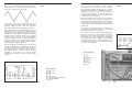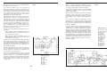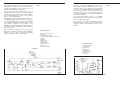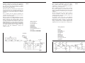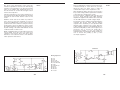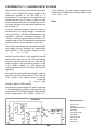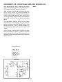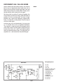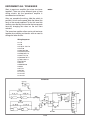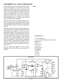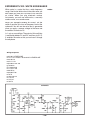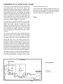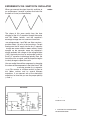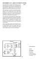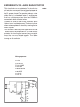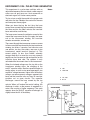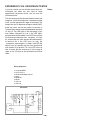
1
ELECTRONIC
PLAYGROUND
TM
and LEARNING CENTER
MODEL EP-130
ELENCO®
150 Carpenter Avenue
Wheeling, IL 60090
(847) 541-3800
Website: www.elenco.com
e-mail: [email protected]
ELENCO
®
Wheeling, IL, USA
Copyright © 2012, 2009 by Elenco® Electronics, Inc. All rights reserved.
REV-A
Revised 2012
No part of this book shall be reproduced by any means; electronic, photocopying, or otherwise without written permission from the publisher.
753039
Important: If you encounter any problems with this kit, DO NOT RETURN TO RETAILER. Call toll-free (800) 533-2441
or e-mail us at: [email protected]. Customer Service • 150 Carpenter Ave. • Wheeling, IL 60090 U.S.A.
WARNING: Always check your wiring before
turning on a circuit. Never leave a circuit
unattended while the batteries are installed.
Never connect additional batteries or any
other power sources to your circuits.
!
WARNING:
CHOKING HAZARD - Small parts.
Not for children under 3 years.
Conforms to all applicable U.S. government
requirements.
• Do not short circuit the battery
terminals.
• Never throw batteries in a fire or
attempt to open its outer casing.
• Non-rechargeable batteries should not
be recharged. Rechargeable batteries
should only be charged under adult
supervision, and should not be
recharged while in the product.
• Use only 1.5V “AA” type, alkaline
batteries (not included).
• Do not mix old and new batteries.
• Insert batteries with correct polarity.
• Remove batteries when they are used
up.
• Do not mix alkaline, standard (carbonzinc),
or
rechargeable
(nickelcadmium) batteries.
• Batteries are harmful if swallowed, so
keep away from small children.
I. PLAYGROUND OF ELECTRONIC CIRCUITS
1. Woodpecker
2. Police Siren
3. Metronome
4. Grandfather Clock
5. Harp
6. Tweeting Bird
7. Meowing Cat
8. Callin’ Fish
9. Strobe Light
10. Sound Effects for Horror Movies
11. Machine Gun Oscillator
12. Motorcycle Mania
13. Vision Test
14. Patrol Car Siren
Page 4
4
5
5
9
10
10
III. LED DISPLAY CIRCUITS
23. LED Display Basics
24. Digital Display Circuit for the Seven-Segment LED
25. LED Display with CdS and Transistor
26. Switching the LED Display Using Transistor Control
IV. WELCOME TO DIGITAL CIRCUITS
27. “Flip-Flop” Transistor Circuit
28. “Toggle Flip-Flop” Transistor
29. “AND” Diode Transistor Logic with LED Display
30. “OR” DTL Circuit with Display
31. “NAND” DTL Circuit with Display
32. “NOR” Transistor Circuit with Display
33. “Exclusive OR” DTL Circuit
11
12
13
14
15
16
17
18
19
20
21
22
23
24
25
II. BASIC ELECTRONICS CIRCUITS
26
A MAJOR CHANGE
15. Dimming the Light
16. Flip Flopping
17. Capacitor Discharge Flash
18. Transistor Action
19. Series and Parallel Capacitors
20. Transistor Switching
21. Series and Parallel Resistors
22. Amplify the Sound
27
28
29
30
31
32
33
34
35
V. MORE FUN WITH DIGITAL CIRCUITS
34. “BUFFER” GATE using TTL
35. “INVERTER” GATE using TTL
36. “AND” GATE using TTL
37. “OR” GATE using TTL
38. “R-S Flip-Flop” using TTL
39. “Triple-Input AND” Gate using TTL
40. “AND” Enable Circuit using TTL
41. “NAND” Enable Circuit using TTL
42. “NOR” Enable Circuit using TTL
43. “NAND” Gate Making a Toggle Flip-Flop
44. “Exclusive OR” GATE using TTL
45. “OR” Enable Circuit using TTL
46. Line Selector using TTL
47. Data Selector using TTL
-2-
Use the following information as a guide in properly identifying the value of resistors.
BAND 1
1st Digit
Batteries:
TABLE OF CONTENTS
Before We Begin
Installing the Batteries
Making Wire Connections
Components
Building Your First Project
Troubleshooting
Helpful Suggestions
IDENTIFYING RESISTOR VALUES
Color
Black
Brown
Red
Orange
Yellow
Green
Blue
Violet
Gray
White
BAND 2
2nd Digit
Digit
0
1
2
3
4
5
6
7
8
9
Color
Black
Brown
Red
Orange
Yellow
Green
Blue
Violet
Gray
White
Multiplier
Digit
0
1
2
3
4
5
6
7
8
9
Color
Black
Brown
Red
Orange
Yellow
Green
Blue
Silver
Gold
Resistance
Tolerance
Multiplier
1
10
100
1,000
10,000
100,000
1,000,000
0.01
0.1
Color
Silver
Gold
Brown
Red
Orange
Green
Blue
Violet
Tolerance
±10%
±5%
±1%
±2%
±3%
±0.5%
±0.25%
±0.1%
BANDS
2
1
Multiplier
Tolerance
36
37
38
39
40
IDENTIFYING CAPACITOR VALUES
Capacitors will be identified by their capacitance value in pF (picofarads), nF (nanofarads), or μF (microfarads).
Most capacitors will have their actual value printed on them. Some capacitors may have their value printed in
the following manner. The maximum operating voltage may also be printed on the capacitor.
41
42
43
44
45
46
47
48
49
50
51
52
53
54
55
56
57
58
59
60
61
62
63
Electrolytic capacitors have a positive
and a negative electrode. The negative
lead is indicated on the packaging by
a stripe with minus signs and possibly
arrowheads.
Multiplier
For the No.
0
1
2
3
Multiply By
1
10
100
1k
Second Digit
First Digit
Warning:
If the capacitor
is connected
with incorrect
polarity, it may
heat up and
either leak, or
cause the
capacitor to
explode.
4
5
8
10k 100k .01
Means
pico
nano
micro
milli
unit
kilo
mega
0.1
Multiplier
103K
100V
Tolerance*
Maximum Working Voltage
The value is 10 x 1,000 =
10,000pF or .01μF 100V
Polarity
Marking
* The letter M indicates a tolerance of +20%
The letter K indicates a tolerance of +10%
The letter J indicates a tolerance of +5%
Note: The letter “R”
may be used at times
to signify a decimal
point; as in 3R3 = 3.3
METRIC UNITS AND CONVERSIONS
Abbreviation
p
n
μ
m
–
k
M
9
Multiply Unit By
.000000000001
.000000001
.000001
.001
1
1,000
1,000,000
Or
10-12
10-9
10-6
10-3
100
103
106
-159-
1. 1,000 pico units
= 1 nano unit
2. 1,000 nano units
= 1 micro unit
3. 1,000 micro units
= 1 milli unit
4. 1,000 milli units
= 1 unit
5. 1,000 units
= 1 kilo unit
6. 1,000 kilo units
= 1 mega unit
Ohm’s Law
The
relationship
between
voltage, current, and resistance.
Ohm, (Ω)
The unit of
resistance.
Oscillator
A circuit that uses feedback to
generate an AC output.
Parallel
When
several
electrical
components are connected
between the same points in the
circuit.
Pico- (p)
A prefix used in the metric
system. It means a millionth of
a millionth (0.000,000,000,001)
of something.
measure
for
Pitch
The musical term for frequency.
Printed Circuit Board
A board used for mounting
electrical components.
Components are connected
using metal traces “printed” on
the board instead of wires.
Receiver
The device which is receiving a
message (usually with radio).
Resistance
The electrical friction between
an electric current and the
material it is flowing through; the
loss of energy from electrons as
they move between atoms of
the material.
Resistor
Components used to control the
flow of electricity in a circuit.
They are made of carbon.
Resistor-TransistorLogic (RTL)
A
type
of
circuit
arrangement used to construct
digital gates.
Reverse-Biased
When there is a voltage in the
direction of high-resistance
across a diode.
Saturation
The state of a transistor when
the circuit resistances, not the
transistor itself, are limiting the
current.
Schematic
A drawing of an electrical circuit
that uses symbols for all the
components.
A material that has more
Semiconductor
resistance than conductors but
less than insulators. It is used to
construct diodes, transistors,
and integrated circuits.
Series
When electrical components
are connected one after the
other.
Short Circuit
When wires from different parts
of a circuit (or different circuits)
connect accidentally.
Silicon
The chemical element most
commonly
used
as
a
semiconductor.
Speaker
A device which converts
electrical energy into sound.
Switch
A device to connect (“closed” or
“on”) or disconnect (“open” or
“off”) wires in an electric circuit.
Transformer
A device which uses two coils to
change the AC voltage and
current (increasing one while
decreasing the other).
Transient
Temporary. Used to describe
DC changes to circuits.
Transistor
An electronic device that uses a
small amount of current to
control a large amount of
current.
Transmitter
The device which is sending a
message (usually with radio).
Tuning Capacitor
A capacitor whose value is
varied by rotating conductive
plates over a dielectric.
Variable Resistor
A resistor with an additional arm
contact that can move along the
resistive material and tap off the
desired resistance.
Voltage
A measure of how strong an
electric charge across a
material is.
Voltage Divider
A resistor configuration
create a lower voltage.
Volts (V)
The unit of measure for voltage.
-158-
to
VI. MEET TRANSISTOR-TRANSISTOR LOGIC
64
48. Blinking LEDs
49. Machiny Sound
50. Astable Multivibrator Using TTL
51. Tone Generator
52. Monster Mouth
53. Dark Shooting
54. A One-Shot TTL
55. Transistor Timer Using TTL
56. LED Buzzin’
57. Another LED Buzzin’
58. Set/Reset Buzzer
59. Another Set/Reset Buzzer
65
66
67
68
69
70
71
72
73
74
75
76
VII. OSCILLATOR APPLICATION CIRCUITS
77
60. Ode to the Pencil Lead Organ
61. Double-Transistor Oscillator
62. Decimal Point Strobe Light
63. “The Early Bird Gets the Worm”
64. Adjustable R-C Oscillator
65. Heat-Sensitive Oscillator
66. Pulse Alarm
67. Pushing & Pulling Oscillator
68. Slow Shut-off Oscillator
69. Electronic Organ Detector
78
79
80
81
82
83
84
85
86
87
VIII. MEET THE OPERATIONAL AMPLIFIER
70. Operational Amplifier Comparator
71. Changing Input Voltage
72. Non-inverting Dual Supply Op Amp
73. Inverting Dual Supply Op Amp
74. Non-inverting Amplifier
75. Dual-Supply Differential Amplifier
76. Miller Integrating Circuit
77. Stable-Current Source
78. Operational Amplifier Blinking LED
79. LED Flasher
80. Double LED Blinker
81. Single Flash Light
82. Introducing the Schmitt Trigger
83. Initials on LED Display
84. Logic Testing Circuit
85. Voice-Controlled LED
86. Buzzin’ with the Op Amp
87. Sweep Oscillator
88. Falling Bomb
89. Alert Siren
90. Crisis Siren
91. Op Amp Metronome
92. Burglar Buzzer
93. LED Initials
94. Wake Up Siren
95. Voice Activated LED
96. Logic Tester
IX. MORE FUN WITH OPERATIONAL AMPLIFIERS
97. Voice Power Meter
98. Reset Circuit
99. RC Delay Timer
100. Listen To Alternating Current
101. Pulse Frequency Multiplier
102. White Noise Maker
103. Light-Controlled Sound
104. DC-DC Converter
105. Super Sound Alarm
106. Op Amp Three-Input “AND” Gate
107. Timer
108. Cooking Timer
X. RADIO AND COMMUNICATION CIRCUITS
109. Operational Amplifier AM Radio
110. AM Code Transmitter
111. AM Radio Station
112. Crystal Set Radio
113. Two-Transistor Radio
114. Morse Code Oscillator With Tone Control
112
113
114
115
116
117
118
119
120
121
122
123
124
125
126
127
128
129
130
131
132
133
134
135
88
XI. TEST AND MEASUREMENT CIRCUITS
89
90
91
92
93
94
95
96
97
98
99
100
101
102
103
104
105
106
107
108
109
110
111
115. Water Level Warning
116. Water Level Alarm
117. Audio Signal Hunter
118. RF Signal Tracer
119. Square Wave Oscillator
120. Sawtooth Oscillator
121. Audio Continuity Tester
122. Audio Rain Detector
123. Audio Metal Detector
124. Water Level Buzzer
125. Pule Tone Generator
126. Resistance Tester
127. Transistor Tester
128. Sine Wave Oscillator
129. Sine Wave Oscillator With Low Distortion
130. Twin-T Oscillator
-3-
136
137
138
139
140
141
142
143
144
145
146
147
148
149
150
151
152
INDEX
153
PARTS LIST
155
DEFINITION OF TERMS
156
IDENTIFYING RESISTOR VALUES
159
IDENTIFYING CAPACITOR VALUES
159
METRIC UNITS AND CONVERSIONS
159
BEFORE YOU START THE FUN!
As you will notice we refer to a Volt / Ohm Meter
(VOM) for making measurements. A VOM or
multimeter is a instrument that measures voltage,
current (amperes or amps), and resistance (ohms-Ω).
You will learn more about these in the upcoming
pages. If you really want to learn about electronic
circuits, it is vital that that you learn how to measure
circuit values - for only then will you really understand
electronic circuitry.
Welcome to the thrilling world of electronics! Now that
you have your Elenco® EP-130 Electronic Playground
Kit, you can learn about electronics while doing 130
fun experiments. In this kit we have included
everything you will need to start off on this electronics
adventure, well except the batteries that is ☺.
As you go through this manual and do the
experiments, you will notice that we have arranged
the experiments, as well as information, into a logical
progression. We will start off with easy circuits and
then work toward the more intricate ones. Take your
time and be sure to have some fun!
You do not have to have or use a VOM to do the
experiments but you will find that it helps to better
grasp how the circuits work. The VOM is a good
investment if you plan to stay interested in electricity
and electronics.
Each electronic component in the kit is connected to
springs, so you can do all the circuit assembly without
having to solder. To build a working project, all you
have to do is connect the wires to the terminals as
shown in each wiring sequence. There is no danger
when doing these projects because you are using low
voltage batteries, not the standard AC voltages.
Our simple instructions will show you how to operate
the circuit for each experiment. A schematic diagram
is also included, to help you learn how the circuit
works. A schematic is simply a blueprint that shows
how different parts are wired together. An image or
symbols for each of the components in your kit are
printed next to each piece.
Electric Field
The region of electric attraction
or repulsion around a constant
voltage. This
is
usually
associated with the dielectric in
a capacitor.
Electricity
A flow of electrons between
atoms due to an electrical
charge across the material.
Electrolytic Capacitor
A type of capacitor that has high
capacitance and is used mostly
in low frequency circuits. It has
polarity markings.
Electron
A sub-atomic particle that has
an electrical charge.
Electronics
The science of electricity and its
applications.
Emitter
The output of an NPN bipolar
junction transistor.
Encode
To put a message into a format
which is easier to transmit.
Farad, (F)
The unit of
capacitance.
Feedback
To adjust the input to something
based on what its output is
doing.
Flip-Flop
INSTALLATION OF BATTERIES
This kit requires six (6) “AA” batteries. To install the
batteries to the back of your kit make sure to install
them in the corresponding compartments. Put the +
end and the – end correctly into the kit, the + end for
the battery is the side that has the metal cap.
+
+
–
–
–
+
+
Forward-Biased
The state of a diode when
current is flowing through it.
Frequency
The rate at which something
repeats.
Generator
A device which uses steam or
water pressure to move a
magnet near a wire, creating an
electric current in the wire.
–
Remember: Never leave a dying battery or dead
+
battery in your kit. Even if they are “leak-proof”, they
still have the potential to leak damaging chemicals.
–
+
–
+
+
Germanium
–
+
+
–
–
A chemical element that is used
as a semiconductor.
Ground
A common term for the 0V or “–
” side of a battery or generator.
Henry (H)
The unit of
Inductance.
–
-4-
A
type
of
transistor
configuration is which the output
changes every time it receives
an input pulse.
Frequency modulation. The
frequency of the radio signal is
varied depending on the
information being sent.
+
+
measure
The ability of a wire to create an
induced voltage when the
current varies, due to magnetic
effects.
Inductor
A component that opposes
changes in electrical current.
Integrated Circuit
A type of circuit
transistors, diodes,
and
capacitors
constructed
semiconductor base.
Kilo- (K)
A prefix used in the metric
system. It means a thousand of
something.
Light Emitting Diode
(LED)
A diode made from gallium
arsenide that has a turn-on
energy so high that light is
generated when current flows
through it.
Magnetic Field
The region of magnetic
attraction or repulsion around a
magnet or an AC current. This is
usually associated with an
inductor or transformer.
Magnetism
A force of attraction between
certain metals. Electric currents
also have magnetic properties.
Meg- (M)
A prefix used in the metric
system. It means a million of
something.
Micro- (μ)
A prefix used in the metric
system. It means a millionth
(0.000,001) of something.
Microphone
A device which converts sound
waves into electrical energy.
Milli- (m)
A prefix used in the metric
system. It means a thousandth
(0.001) of something.
Modulation
Methods used for encoding
radio signals with information.
Morse Code
A code used to send messages
with long or short transmit
bursts.
NAND Gate
A type of digital circuit which
gives a HIGH output if some of
its inputs are LOW.
NPN
Negative-Positive-Negative, a
type of transistor construction.
for
FM
–
–
measure
Inductance
for
-157-
in which
resistors,
are
all
on
a
DEFINITION OF TERMS
WIRING CONNECTIONS
AC
Common
abbreviation
alternating current.
Provided in your kit are spring terminals and pre-cut
wires, make the wires snap together for your use in
the numerous projects. To join a wire to a spring
terminal, just directly bend the spring over to one side
and then install the wire into the opening.
Alternating Current
for
Carbon
A chemical element used to
make resistors.
A current that is constantly
changing.
Clockwise
In the direction in which the
hands of a clock rotate.
AM
Amplitude modulation. The
amplitude of the radio signal is
varied depending on the
information being sent.
Coil
When something is wound in a
spiral. In electronics this
describes inductors, which are
coiled wires.
Amp
Shortened name for ampere.
Collector
The controlled input of an NPN
bipolar junction transistor.
Ampere (A)
The unit of measure for electric
current. Commonly shortened
to amp.
Color Code
A method for marking resistors
using colored bands.
Amplitude
Strength or level of something.
Conductor
A material that has
electrical resistance.
Analogy
A similarity in some ways.
AND Gate
A type of digital circuit which
gives a HIGH output only if all of
its inputs are HIGH.
Antenna
Inductors used for sending or
receiving radio signals.
Astable Multivibrator
A
type
of
transistor
configuration in which only one
transistor is on at a time.
Atom
The smallest particle of a
chemical element, made up of
electrons, protons, etc.
low
Counter-Clockwise
Opposite the direction in which
the hands of a clock rotate.
Current
A measure of how fast electrons
are flowing in a wire or how fast
water is flowing in a pipe.
Darlington
A transistor configuration which
has high current gain and input
resistance.
DC
Common abbreviation for direct
current.
Decode
To recover a message.
Audio
Electrical energy represent-ing
voice or music.
Detector
A device or circuit which finds
something.
Base
The controlling input of an NPN
bipolar junction transistor.
Diaphragm
A flexible wall.
Differential Pair
Battery
A device which uses a chemical
reaction to create an electric
charge across a material.
A
type
of
configuration.
Digital Circuit
A wide range of circuits in which
all inputs and outputs have only
two states, such as high/low.
Bias
The state of the DC voltages
across a diode or transistor.
Bipolar Junction
Transistor (BJT)
A widely
transistor.
used
type
Bistable Switch
A
type
of
transistor
configuration, also known as the
flip-flop.
Capacitance
The ability to store electric
charge.
Capacitor
An electrical component that
can store electrical pressure
(voltage) for periods of time.
An electronic device that allows
current to flow in only one
direction.
Direct Current
A current that is constant and
not changing.
Disc Capacitor
A type of capacitor that has low
capacitance and is used mostly
in high frequency circuits.
-156-
When you have to join to two or three wires into a
single spring terminal, be sure that the first wire does
not come loose when you attach the second and third
wires. The simplest way to do this is to place the
spring onto the opposing side where you have
connected the first wire.
If the exposed metal ends of some of the wires break
off due to great use, you should just simply remove
3/8” if the insulation from the wire of the broken end
and then simply twist the strands together. To remove
the installation you can use either a wire-stripper tool
or a simple penknife. Be extremely careful when doing
this because penknives are remarkably sharp.
transistor
Diode
of
Only insert the exposed or shiny part of the wire into
the spring terminal. The electrical connection will not
be made if the plastic part of the wire is inserted into
the terminal. Removing the wire from the spring
terminals is simply just bending each terminal and
then pulling the wires out of it.
COMPONENTS
This kit has more than 30 distinct components. If this
happens to be your first time with electronics don’t fret
over not knowing the difference between a resistor or
a transistor, because the general purpose of each
component will be described. The following
explanations will help you comprehend what each
component does and you will also gain more
knowledge of each component as you do each
experiment. There is also a parts list in the back of
this manual, that way you can compare the parts in
your kit with those recorded in the back.
Resistors: Why is the water pipe that goes to the
kitchen faucet in your house smaller than the one
from the water company? And why is the pipe smaller
than the main water line that disburses the water to
your entire town? Because you don’t need a lot of
water. The pipe size controls the water flow to what
you really need. Electricity works in the same manner,
except that the wires have a minimal resistance that
they would have to be particularly thin to limit the
electricity flow. They would be solid enough to handle
and break effortlessly. However, the flow of water
through a large pipe could be restricted to by filling a
part of the pipe with rocks (a
-5-
fine screen would keep rocks from falling over), which
would prolong the flow of water but not stop it
completely. Like rocks are for water, resistors work in
a similar way. They regulate how much electric current
flows. The resistance, is expressed in ohms (Ω,
named in honor of George Ohm), kilohms (kΩ, 1,000
ohms) or megohms (MΩ, 1,000,000 ohms) is a
determination of how much resistor resists the flow of
electricity. The water through a pipe can be increased
by an increase in water pressure or the removal of
rocks. In a similar way you can increase the electric
current in a circuit by increasing the voltage or by the
use of a lower value resistor (this will be shown in a
moment). Below the symbol for the resistor is shown.
Capacitors: Capacitors move alternating current
(AC) signals while prohibiting direct current (DC)
signals to pass. They store electricity and can function
as filters to smooth out signals that pulsate.
Capacitors that are small are traditionally used in
high-frequency applications such as radios,
transmitters, or oscillators. Larger capacitors
ordinarily reserve electricity or act as filters. The
capacitance (capacity for storing electricity) of a
capacitor is expressed in a unit known as farad. An
extremely large amount of electricity defines the farad.
Most of the value of capacitors is predetermined in
millionths-of-a-farad or microfarads.
Resistor Color Code: The method for marking the
value of resistance on a part is by using colored
bands on each resistor. The representation of the first
ring is the digit of the value of the resistor. The second
ring is a representation of the second digit of the
resistors value. The third ring means that you to which
power of ten to multiply by, ( or the amount of zeros
to add). The fourth and final ring is a representation
of the construction tolerance. A majority of resistors
have a gold band that represents 5% tolerance.
Simply this means that the resistor value is
guaranteed to be 5% of the valued marked. See the
color chart on page 159.
PARTS LIST
Bar Antenna with Holder
PCB for LM358
Battery Box Plastic (2)
Resistors
100Ω 5% 1/4W (4)
Capacitors
10pF, ceramic disc type
470Ω 5% 1/4W
100pF, ceramic disc type
1kΩ 5% 1/4W
0.001μF, ceramic disc type
2.2kΩ 5% 1/4W
0.01μF, ceramic disc type
4.7kΩ 5% 1/4W
0.02μF, ceramic disc type
10kΩ 5% 1/4W (2)
Electrolytic - Electrolytic are the four largest
capacitors. They are marked with an “–”. There is only
one-way to connect them to the circuit, the + and the
– wires must always go into the correct terminals.
0.05μF, ceramic disc type (2)
22kΩ 5% 1/4W
0.1μF, ceramic disc type
47kΩ 5% 1/4W
3.3μF, 25V electrolytic type
100kΩ 5% 1/4W
Disc - Unlike the electrolytic above, these capacitors
have no polarity and can be connected in either way.
10μF, 16V electrolytic type
220kΩ 5% 1/4W
100μF, 10V electrolytic type
470kΩ 5% 1/4W
Screw 2.4 x 8mm (4)
470μF, 10V electrolytic type
Disc
Electrolytic
Tuning Capacitor: Ever wonder what that knob that
changes the stations on your radio is? It’s a tuning
capacitor. When the knob is rotated, the capacitance
is changed. This alters the frequency of the circuit,
letting through only one frequency and blocking out
the rest.
Variable Resistor (Control): The variable resistor is
simply a control and this is required in many electric
circuits. The variable resistor can be used as a light
dimmer, volume control, and in many other circuits
when you are wanting to change resistance easily
and quickly. A normal resistor is shown, this contains
an additional arm contact that moves along the
resistive material and can tap off the resistance
desired.
CdS Cell
Screw 2.5 x 3mm
CdS Holder Plastic
Screw 2.8 x 8mm (2)
Digital Display PCB Assembly
Slide Switch
LED Digital Display LT-312
Speaker, 8Ω
PCB for Digital Display
Spring (138)
Resistor 360Ω (8)
Transformer
Transistors
Diode Germanium 1N34A (2)
Diode Silicon 1SS53 / 1N4148
2SA733 PNP (2)
Earphone, ceramic type
2SC945 NPN
Frame, Plastic (L)
Variable Capacitor (tuning)
Frame, Plastic (R)
Variable Resistor (control)
Integrated Circuit 74LS00
Washer 10mm (4)
Integrated Circuit BA728
Wires
Key Switch
White, 75mm (20)
Knob, Tuning Capacitor, Plastic
Red, 150mm (30)
Knob, Control, Metal
Blue, 250mm (20)
Light Emitting Diode (3)
Yellow, 350mm (5)
Nut 2mm
Black, 380mm (2)
Paper Bottom Panel
Green, 3M (2)
PCB for 74LS00
-6-
-155-
AND Gate:
29, 36, 39, 40
Data:
47
DTL:
29, 30, 31, 33, 35
Exclusive OR:
33, 44
Flip-flop:
27, 28, 38, 43, 58, 59
Inverting:
70, 72, 73, 74, 85, 95,
109
Line:
46
NAND Gate:
31, 41
NOR Gate:
42
OR Gate:
37, 42, 44, 45
Power Supply:
29, 72, 73, 74, 75
TTL:
34, 35, 36, 37, 38, 39,
40, 41, 42, 43, 44, 45,
46, 47, 48, 50, 51, 54,
55, 60, 78, 90, 112, 123
The “8” LED display is mounted on a board and to
prevent burning out the display with excess current,
permanent resistors have been wired in.
Diodes: Are like one-way streets. They allow the
current to flow in only one direction. There are three
of these in your kit. Your kit contains one silicon diode
(marked Si) as well as two germanium diodes (marked
Ge).
LOGIC AND COMPUTER CIRCUITS
Integrated Circuit: The transistor was invented in
the 1940’s and after that the next big break through
in electronics was in the 1960’s with the invention
integrated circuit or the ICs. The advantage of this that
the equivalent of hundreds or even thousands of
transistors, diodes and even resistors can be placed
into one small package.
Transistors: Three transistors can be found in your
kit. The part that makes each transistor work is a tiny
chip, which is made of either germanium or silicon.
There are a total of three connections points on each
transistor. They are B, which stands for base, C, which
stands for collector, and E, which stands for emitter.
Mainly transistors are used to amplify weak signals.
Transistors can also be used as switches to connect
or disconnect other components as well as oscillators
to permit signals to flow in pulses.
Two types of ICs are used in this kit. They are the
quad two-input NAND and the dual-operational
amplifier, and you will have the chance to learn more
about these in a bit.
Simple ICs will help you to understand enough to
grasp the basic theories of more advanced ICs.
NATURAL SCIENCE PROJECTS
Electrical Energy:
52
Fish:
11
PNP
OSCILLATORS
Blocking:
21
Oscillators:
8, 51
Sine wave:
128, 129, 130
Square wave:
67, 86, 96, 118
NPN
LEDs (Light Emitting Diodes): These are special
diodes because they give off light whenever electricity
passes through them. (The current can only pass
through in one direction—similar to “regular” diodes).
Cadmium Sulfide (CdS) Cell: This is what is known
as a semiconductor, which practically resists
electricity while it conducts. The resistance changes
by the amount of light that is shined upon it.
SWITCHING AND CONTROL CIRCUITS
Relay:
26
Transistor:
27, 28, 61, 67, 95, 101,
113, 127
LED Digital Display: Seven Light Emitting Diodes
are arranged to create an outline that can show most
letters of the English alphabet and all the numbers.
An additional LED is added to represent a decimal
point.
TEST EQUIPMENT
Transistor Checker:
127
Voltmeters:
25, 68
Water Level:
115
Note: Provided is a light shield to use with the CdS
cells, to use just simply place the shield over the cell,
this helps to prevent light from leaving the cell.
TRANSMITTERS
Code:
110, 114
Tone:
2, 5, 14, 19, 51, 60, 64,
65, 66, 94, 110, 111,
114, 128, 125
Voice:
4, 52, 85, 97, 105, 111
-154-
-7-
Antenna: This cylindrical component with a coil of
fine wire wrapped around it is a radio antenna. If
you’re wondering what the dark colored rod is, it’s
actually mostly powdered iron. It’s also known as a
“Ferrite Core”, which is efficient for antennas, and
used in almost all transistor radios.
created by variations of vibrations and then travel
across the room. When you hear a sound it is actually
your ears feeling the pressure from the air vibrations.
To operate a speaker a high current and a low voltage
are needed, so the transformer will also be used with
the speaker. (A transformer can convert a highvoltage/low current to a low-voltage/high current).
INDEX
We’ve added this listing to aid you in finding
experiments and circuits that you might be especially
interested in. Many of the experiments are listed two,
three, or four times - since they can be used in many
ways. You’ll find some listed as entertainment-type
circuits, even through they were not organized that
way in the sequence of projects. However, you may
find some of these same circuits to be good for other
uses too.
Do you want to learn more about a specific type of
circuit? Use this Index to look up all the other uses
and applications of any specific circuit - then turn to
those and read what we’ve told you in each one. You’ll
find by jumping back and forth and around, you often
will pick up a lot more circuit details than just by going
from one project to the next in sequence.
Use this Index and your own creative ability and we
know you will have a lot of extra fun with your Lab Kit.
BASIC ELECTRONIC CIRCUITS AND
COMPONENTS
Transformer: Did you know that if you were to wrap
two wires from different circuits around different ends
of an iron bar, and if you were to add current in the
first circuit, it will magnetically create current in the
second circuit? That’s exactly what a transformer is!
Transformers are used to isolate parts of a circuit, to
keep them from interfering with each other.
Capacitors:
Similar to the speaker, is the earphone. It is movable
and more sensitive than the speaker, otherwise they
are the same. The earphone you will be using is
efficient as well as lightweight and can be used
without taking away too much electrical energy from
the circuit. Sound wise you will be using the earphone
for weak sounds and for louder sounds the speaker
will be used.
6, 11, 12, 16, 17, 19, 21,
27, 50, 51, 64, 69, 119,
130
Diodes:
29, 31, 34, 79, 91, 101,
102, 105, 121
Integrated:
34, 70
Multivibrators:
48, 50, 56, 90, 91
Resistance:
2, 10, 12, 18, 21, 25, 60,
74, 77, 78, 94, 102, 114,
120, 123, 126
Set / reset:
58, 59
Timing:
4
Transformers:
129
Persistence of Vision:
13
Radio:
8, 10, 11, 38, 109, 110,
111, 112, 113, 114, 117,
118, 123, 124
Rain Detector:
120
RF Signal Tracer:
118
Shot in the Dark:
53
Siren:
2, 14, 15, 87, 88, 89, 90,
93
Sound:
1, 2, 3, 4, 5, 6, 8, 10, 11,
12, 14, 15, 19, 22, 49, 52,
54, 55, 56, 57, 58, 59, 63,
64, 66, 72, 87, 88, 89, 90,
93, 102, 103, 105, 108
Strobe:
9
Timer:
54, 55, 78, 99, 107, 108,
119
ENTERTAINMENT CIRCUITS
Batteries: The battery holders that are used in this
kit are constructed to hold six (6) “AA” batteries. These
batteries will be the supplier of all the power used in
your experiments. When you connect the wires to the
batteries make sure that you only connect the
batteries to terminals noted. Terminals 119 and 120
provide 3 volts while terminals 119 and 121 provide
4.5 volts. Be aware that parts can be damaged
(burned out) if you connect too much voltage (you can
get up to 9 volts from the connections to the batteries)
Be sure to make battery connections the right way.
If the iron bar in a transformer were allowed to rotate,
it would become a motor. However, if a magnet within
a coil is rotating then an electrical current is made;
this is called a generator. Those two ideas may not
seem important but they are the foundation of the
present society. Pretty much all of the electricity used
in this world is generated by huge generators, which
are propelled by water pressure or steam. Wires
transport energy to homes and businesses where it
will be used. Motors are used to convert the electricity
back into mechanical form so that it can be used to
drive machinery and appliances.
Caution: Make sure your wiring uses the correct
polarity (the “+” and “-” sides of the component)! Some
parts can be permanently damaged if you reverse
polarity.
Speaker: Did you know that electral energy is
converted into sound through a speaker? By using the
energy from an AC electrical signal it creates
mechanical vibration. Sound waves, which are
-8-
Alarm:
58, 63, 66, 92, 93, 105,
107, 116, 120, 123
Audio Oscillators:
51
Buzzin:
56, 57, 92, 107
Code Transmitter:
110
Electronic Cat:
7
Grandfather Clock:
4
Machine Gun:
11
LED DISPLAY
Metal Detector:
123
LED Display:
Metronome:
3, 91
13, 16, 18, 20, 23, 24, 25,
26, 29, 30, 31, 32, 62, 83,
84, 98, 106, 116
Motorcycle:
12
Logic:
Musical:
3, 5, 102
25, 29, 30, 31, 34, 37, 84,
98
INTEGRATED CIRCUIT PROJECTS
-153-
Amplifier:
22, 70, 71, 72, 73, 74, 75,
76, 77, 78, 79, 80, 81, 82,
85, 86, 91, 92, 94, 95, 96,
97, 100, 104, 106, 122
Amplifier Uses:
22, 72
IC Radio:
109
Key: The key is a simple switch—you press it and
electricity is allowed to flow through the circuit. When
you release it, the circuit is not complete because a
break is caused in the circuit’s path. The key will be
used in most circuits often times in signaling circuits
(you can send Morse code this way as well as other
things).
EXPERIMENT #130 TWIN-T OSCILLATOR
The twin-T type audio oscillator is very popular for
use with electronic organs and electronic test
equipment because it is very stable.
Notes:
The resistors and capacitors in the twin-T network
determine the frequency of oscillation. The letter T is
used because the resistors and capacitors are
arranged in the shape of the letter T in the schematic
diagram. There are two T networks in parallel across
from each other; hence the term twin is used. The
capacitors in series shift the phase of the wave; the
resistors in series supply voltage to the transistor’s
base as well as shifting the phase of the wave.
Switch: You know what a switch is – you use
switches every day. When you slide (or flip) to the
proper position, the circuit will be completed, allowing
current to flow through. In the other position a break
is made, causing the circuit to be “off”. The switch that
we will be using is a double-pole, double-throw switch.
You will learn about that later on.
Carefully adjust the circuit to obtain pure sine wave
output as in the previous two projects. Modify the
control very slowly over its entire range until you hear
a tone in the earphone that is very low and resembles
the lowest note of a large pipe organ. This control
setting should be between 7 and 10 on your dial.
Terminals: Two terminals will be used in some
projects (terminals 13 and 14). They will be used to
make connections to external devices such as an
earphone, antenna or earth ground connection,
special sensor circuits and so forth.
Once the oscillation has started, adjust the control
carefully for the setting that gives the purest sounding
low note near the high end of the dial.
You can experiment with this circuit in many ways. We
suggest you try different values for the 10kΩ and
470Ω resistors, and try using higher and lower battery
voltages. Also, if you have a VOM, try measuring
circuit voltages.
Wires: Wires will be used to make connections to the
terminals.
Your parts and spring terminals are mounted on the
colorful platform. You can see how the wires are
connected to the parts and their terminals if you look
under the platform.
Schematic
YOUR FIRST PROJECT
Wiring Sequence:
o 72-106-116-27-124
o 28-104-102
o 46-103-87
o 47-101-86-81-EARPHONE
o 48-71
o 119-115-82-EARPHONE
o 85-88-105
o 121-122
-152-
between 2 and 30, another between 3 and 104 and
then another wire between 104 and 106. Continue
until all connections are made.
A simple wiring sequence is listed for each project.
Connect the wires with appropriate length between
each grouping of terminals listed. When doing the
experiment use the shortest wire that possibly gets
the job done. New groupings will be separated by a
comma, connect the terminals in each group.
Caution: The last connection in each wiring
sequence is an important power wire; this is
deliberate. It is important that you make this
connection your LAST connection. Damage can occur
if one part of the circuit is completed before another.
Therefore follow the wiring sequence exactly.
As an example, here is the project 1 wiring sequence:
1-29, 2-30, 3-104-106, 4-28-124, 5-41-105, 27-88,
75-87-103-40, 115-42-119, 76-116, 121-22.
Connect a wire between 1 and 29, another wire
-9-
TROUBLESHOOTING
EXPERIMENT #129: SINE WAVE OSCILLATOR WITH LOW DISTORTION
You should have no problem with the projects working
properly if you follow the wiring instructions. However,
if you do encounter a problem you can try and fix it by
using the following troubleshooting steps. These steps
are comparable to those steps that electronic
technicians use to troubleshoot complex electronic
equipment.
1. Are the batteries being used new? If they are not,
this may be your problem because the batteries
could be too weak to power the project.
3. Are you following the schematic diagram and the
explanation of the circuit? As your understanding
and knowledge expands of electronics, you will be
able to troubleshoot by following only a schematic,
and once you add the description of the circuit you
will be able to figure out your own problems.
In this experiment, you build and study a low-distortion
sine wave oscillator. Build this experiment after you
have built and studied the previous experiment
because this one has no transformer; transformers
are likely to cause distortion because of their nonlinear characteristics.
4. If you have VOM, try taking some measurements
of the voltage and current. You might be surprised
just how handy a VOM really is.
As in the previous experiment, you should listen to the
tone of this oscillator and modify the control for the
clearest-sounding single tone (the one with the least
distortion). Again, start with the control near
maximum. The operating frequency is about 300Hz at
the minimum distortion setting of the control.
5. Try building project 24 (Digital Display Circuit for
the Seven-Segment LED). This is a very simple
circuit that lights part of the LED display using only
2 wires.
2. Is the project assembled properly? Check all the
wiring connections to make sure that you have all
the terminals wired correctly. Sometimes having
someone else look at it helps to find the problem.
Contact Elenco® if you still need help.
SUGGESTIONS TO HELP
Keep a Notebook
Collecting Components
As you’re about to find out, you are going to learn
many things about electronics by using this kit. As you
learn, many of the things you discover in the easy
projects will be built upon in later projects. We suggest
using a notebook to help you organize the data you
will be collecting.
You should start to make your own collection of
electronic parts and therefore have your own scrap
box of electronic parts. You can build your own circuits
in or on top of a framework, box or container. You
could use your circuit as a Science Fair project at
school and even make a major research project from
it.
This notebook does not have to be like the one you
use in school. Think of it more as a fun notebook, that
way you can look back on the all the projects you have
done once you finish.
Notes:
We call this circuit an RC phase shift oscillator, and it
is considered a basic sine wave oscillator. The positive
feedback of the signal causes oscillations to occur.
The resistors (R) and capacitors (C) make up the path
for the signal to the transistor base. Every time the
signals pass the RC circuits, a slight time lag occurs.
In other words, the rise and fall of the wave (the
phase) shifts slightly. That’s why we call it phase shift.
After the signal has traveled through the circuit, the
phase shifts 180 degrees. When the collector voltage
rises, this rise is fed back to the collector with the
phase shifted. When the base voltage rises, the
collector voltage falls. This repeating cycle causes the
transistor to oscillate.
The frequency changes when you change the control
setting, because the degrees of phase shift changes.
The tonal quality also changes. Set the control to the
point where you can hear the purest tone; at this point
a clear sine wave is generated.
Wiring Sequence Marking
When you are wiring a project, especially those with
lots of connections, you will find it helpful to mark off
each terminal number as you connect the wires to it.
Use a pencil and make light marks so that you can go
back multiple times and re-read the sequence.
Schematic
Wiring Sequence:
o 124-27-48-82-80-EARPHONE
o 47-105-93-77-EARPHONE
o 81-109-108-28
o 94-110-46
o 78-138
o 79-106-107
o 119-137
o 121-122
-10-
-151-
EXPERIMENT #128: SINE WAVE OSCILLATOR
Notes:
This oscillator circuit produces a sine wave signal. A
sine wave (or sinusoid) is a wave of pure singlefrequency tone. As an example, a 400Hz sine wave
is a wave that oscillates 400 cycles in one second
and contains no other frequency contents. Non-sine
waves (such as square wave or triangular wave
signals) have harmonics - waves with frequencies
that are multiples of the single-frequency
fundamental wave. A non-sine 400Hz wave can
include the 400Hz wave (its fundamental wave)
along with an 800Hz wave (its 2nd harmonic wave)
and a 1200Hz wave (its third harmonic wave). A
square wave signal contains many harmonics.
Experienced technicians can test a circuit by putting
a sine wave into it and listening to its output - and
you can too. If you put in a sine wave, and something
else comes out, the undesired harmonic frequencies
must have been generated somewhere in the circuit.
The key parts of this circuit that produce a 400Hz
sine are:
• A 0.1μF capacitor connected across terminals
3 and 5 of the transformer. This forms a tank
circuit that resonates at about 600Hz.
I. PLAYGROUND OF ELECTRONIC CIRCUITS
• A 470kΩ resistor to turn on the base of the
transistor only a little.
Wiring Sequence:
• An adjustable feedback circuit that includes the
control and the 0.05μF capacitor.
o 1-EARPHONE
o 2-EARPHONE
o 3-28-109
o 4-94-106-124
o 5-41-110
o 26-40-93
o 27-105
o 42-71
o 72-119
o 121-122
• A 100Ω resistor connected to the emitter. This
helps to stabilize the circuit and keep the sound
from being distorted.
Connect the earphone to terminals 1 and 2 of the
transformer. Start with the control on maximum (10
on the dial) and slowly decrease the control setting
while listening to the tone quality of the output. Before
the oscillations stop, you will reach a point where you
hear only one tone. This last clear-sounding tone is
the sine wave. Repeat these control adjustments until
you have no trouble distinguishing between a sine
wave and a distorted wave.
Schematic
-150-
-11-
EXPERIMENT #1: WOODPECKER
EXPERIMENT #127: TRANSISTOR TESTER
Transistors are very important, and you may need to
test them to be sure they are working. You can’t tell if
one is working just by looking at it, but this circuit lets
you test them. This circuit also checks whether a
transistor is a PNP or an NPN.
Notes:
For your first experiment you are going to make a
circuit that that sounds like a woodpecker chirping.
Follow the wiring sequence carefully and observe the
drawings. Don’t forget to make all the proper
connections and have fun!
Notes:
You’ll notice that this project has three long wires - one
for the emitter, one for the collector and one for the
base. The schematic shows the terminals marked for
checking PNP transistors.
The simple circuit shown here does not have a key
or a switch, but you can easily add one. Replace
connection 124-28 with connections 124-137 and
138-28 to connect the key. Or, you can hook the
switch up by replacing 124-28 with connections 124131 and 132-28. Now you can easily turn off and on
the circuit. Go outside and see if you can attract birds
with it.
Want a different sound? Try varied combinations of
capacitance and resistance in place of the 100μF
capacitor and the 1kΩ resistor. To change the 100μF
capacitor to 470µF, disconnect terminal 116 and
transfer to terminal 118. Then, reconnect the wire
from 115 to connect to 117. Your “bird” might sound
like a cricket, or a bear!
Schematic
To use this experiment, connect the long wires to the
base, collector, and emitter of the transistor you want
to test. Turn the control fully counter-clockwise. Then,
press the key and turn the control clockwise. The
transistor is a working PNP transistor if you hear a
sound from the speaker. If you hear no sound at all,
change connections 4-124 and 119-138 to 4-119 and
124-138, and repeat the test. If you get a sound from
the speaker this time, the transistor is a working NPN
type. If you get no sound from the speaker using either
set of connections, the transistor is defective.
You’ll find this a handy circuit for testing unmarked
transistors as you start to accumulate parts for other
electronic circuits.
Also, you can try using the 3V power supply.
Disconnect terminal 119 and connect it to terminal
123. Now your bird might sound like an English
sparrow. Feel free to experiment. Just don’t replace
the 47kΩ resistor with anything below 10kΩ,
because it might damage the transistor.
Wiring Sequence:
o 1-29
o 2-30
o 3-105-COLLECTOR
o 4-124
o 5-94-106-110
o 26-72-137
o 27-71
o 28-EMITTER
o 93-109-BASE
o 119-138
o 121-122
Wiring Sequence:
o 1-29
o 2-30
o 3-104-106
o 4-28-124
o 5-41-105
o 27-88
o 75-87-103-40
o 115-42-119
o 76-116
o 121-122
Schematic
-12-
-149-
EXPERIMENT #126: RESISTANCE TESTER
EXPERIMENT #2: POLICE SIREN
Notes:
If you use a meter you can find the exact value of a
resistance; but when you only want to know
approximate resistance values, you can use this
resistance tester.
Notes:
Here is the first siren you are going to do – don’t be
shocked if this experiment becomes the most famous
circuit in this kit.
This siren sounds like a real siren on a police car!
After the wiring is competed press the key. The tone
you eventually hear gets higher after pressing the
key. When you release the key, the tone gets lower
and then fades out.
This circuit converts resistance to electric current and
compares it with the comparator’s reference current
to tell you the approximate range of resistance. The
comparator has a reference voltage of about 0.82V.
Try some of these modifications:
Build the circuit and set the switch to position A.
Connect the material to be tested between terminals
13 and 14. The LED lights if the resistance is less
than 100kΩ, otherwise it is off. If the LED lights,
connect terminals 93 and 86. If the LED turns off now
the resistance is between 10Ω and 100kΩ. If it stays
on, remove the wire from terminal 86 and connect it
to terminal 84. If the LED turns off now, the
resistance is in the range of 1 to 10kΩ. If the LED still
doesn’t turn off, remove the wire from terminal 84
and connect it to terminal 76. If the LED turns off
now, it means that the resistance is in the range of
100Ω to 1kΩ; if it stays on, the resistance is less than
100Ω.
1. If you change the 10μF capacitor to a 100μF or a
470μF it will give a very long delay for both turn
off and turn on.
2. Change the circuit to remove the delays by
temporarily disconnecting the 10μF capacitor.
Schematic
3. Change out the 0.02μF capacitor to a 0.01μF
capacitor, and then to a 0.05μF capacitor.
Wiring Sequence:
o 13-93-69-WIRE
o 14-79-70-121
o 75-83-94-90-88-31-63-131
o 33-67
o 68-80-87
o 85-89
o 119-124
o 122-132
Wiring Sequence:
o 1-29
o 2-30
o 3-103-109
o 4-119-137
o 5-47-110
o 46-104-90
o 114-48-120
o 85-138
o 86-89-113
Schematic
-148-
-13-
EXPERIMENT #3: METRONOME
EXPERIMENT #125: PULSE TONE GENERATOR
Notes:
Learning to play a musical instrument? Then you
might find this experiment helpful. This is an
electronic version of the metronome, used by musical
students and musical geniuses alike, worldwide.
Notes:
This experiment is a pulse-tone oscillator with an
adjustable frequency that can obtain a wide range of
notes. You can play tunes on it that sound like an
electronic organ, but it takes some practice.
If you press the key, you hear a repeating sound from
the speaker. Turn the control knob to the right and
you’ll hear the sound “get faster” as the time between
sounds shortens.
To play a tune, modify the control to the proper note
and press the key. Readjust the control for the next
note and press the key again.
When you close the key the first time, the base
current flows around the loop formed by the battery,
the 10kΩ resistor, the 50kΩ resistor, the transistor
base and emitter, and the key.
Try swapping out the 4.7kΩ resistor with different
one. Also, you might want to try a different capacitor
in place of the 100μF capacitor too see what effect it
will have. Are you still keeping notes?
The base current causes the collector current to flow
around the loop formed by the 3V supply, the lower
half of the transformer winding, the transistor
collector and emitter, and the key.
If you would like to hear the difference that a stronger
capacitor makes, try connecting the 470μF capacitor
to the batteries. Connect terminal 117 to 119 and
terminal 118 to terminal 120. You might need to
adjust the control to maintain the same pulse rate.
Schematic
The current through the transformer causes a current
to flow around the loop formed by the top transformer
winding, the 0.05μF capacitor, the transistor base
and emitter, the key, the battery and back to the
transformer’s center terminal (terminal 4). This
current quickly (in less than 0.0001 seconds)
charges the 0.05μF to about 4V or so with a polarity
negative on the transformer side and positive on the
transistor base lead side. The speaker is only
activated while the current flows in the transformer.
Wiring Sequence:
When the induced voltage from the top half of the
transformer winding stops, the charging of the
0.05μF capacitor stops, then the capacitor begins to
charge again. As soon as the discharge begins, the
capacitor voltage becomes higher than the battery
voltage. The reverse polarity voltage is applied to the
base and the transistor turns off. Now, all transistor
junctions act as open circuits. The capacitor
discharges around the loop formed by the top
transformer winding, the 10kΩ resistor, and the 50kΩ
resistor. When you reduce the control setting, the
discharge is faster, so the process is repeated at a
faster rate causing a higher frequency. The cycle
repeats when the 0.05μF capacitor discharges to
slightly below the 3V of the battery.
Wiring Sequence:
o 1-29
o 2-30
o 3-104-116
o 4-28-138
o 5-41-103
o 27-80
o 40-115-79
o 42-119
o 120-137
-14-
o 1-29
o 2-30
o 3-108-110
o 4-82-120
o 27-40-107
o 28-81
o 5-41-109
o 42-137
o 119-138
Schematic
-147-
EXPERIMENT #124: WATER LEVEL BUZZER
Notes:
You can use the operational amplifier as a
comparator for detecting changes in voltage. In this
experiment, you are going to use this comparator
function to make a water buzzer that sounds when
the wire ends come into contact with water.
EXPERIMENT #4: GRANDFATHER CLOCK
Does your home lack a grandfather clock? Well not
any longer, with this experiment you will make your
own electronic grandfather clock.
Notes:
This circuit will produce clicks at approximately onesecond intervals. The sound and timing together
might remind you of an old grandfather clock. If you
would like for it to go faster or slower then you can
change out the 100kΩ resistor.
Slide the switch to position B, build the circuit, and
then slide the switch to position A to turn on the
circuit. You should not hear any sound from the
speaker. Now connect the two output terminals with
a wire, and you hear a sound from the speaker.
The steady ticking can put animals (and people) into
a sleepy state of mind. If you have ever traveled on a
train, you remember how sleepy you get from
hearing the clicking sound of the wheels.
Touch the two output terminals with your fingers. If
the speaker makes a sound again, the electricity is
flowing through your body because the wire lead is
in contact with sweat.
Ever scare a clock out of ticking? Shout directly into
the speaker. You can briefly stop the clock! The
speaker acts like a microphone as well. The sound
of your voice vibrates the speaker and disturbs the
electrical balance of the circuit, briefly.
This experiment uses two operational amplifiers. IC
1 works as a comparator. The IC’s negative (–) input
terminal has a reference voltage of about 1.6V. When
a voltage exceeding 1.6V is applied to the positive
(+) input terminal, the output of the comparator
allows IC 2 to work as an astable multivibrator.
Schematic
Wiring Sequence:
o 1-29
o 2-30
o 3-114
o 5-83-80-94-70-110-121
o 13-86-63-131
o 14-93-69
o 65-89-109
o 66-82-84-91
o 64-90-92-113
o 67-81
o 68-79-85
o 119-124
Wiring Sequence:
o 1-29
o 2-30
o 3-104-116
o 4-90-120
o 5-41-103
o 40-72
o 42-119
o 71-89-115
Schematic
-146-
-15-
EXPERIMENT #5: HARP
EXPERIMENT #123: AUDIO METAL DETECTOR
Have you ever wanted to make music just by waving
your hand? Well that is just what you are going to be
doing. How does this magic work? Well, the tones
change based upon the amount of light that gets to
the CdS cell. With a bright light the tone is higher but,
if you cover the CdS with your hand, the sound gets
lower.
Notes:
This experiment demonstrates how a metal detector
works. When the coil gets close to something that is
made of metal, the oscillator changes in frequency.
This type of metal detector has been used to locate
lost treasures, buried pipes, hidden land mines, and
so on. These have been used to save many lives by
locating mines and booby traps set out by the enemy
during wartime.
Since the early days of vacuum-tube circuitry, this
method of creating musical sound has been used.
Leon Theremin was the inventor of this type of
instrument, thus the instrument has been named the
Theremin in his honor.
Notes:
This circuit is a low distortion oscillator that draws
only one milliamp from the 9V supply. Using low
power allows the nearby metal to have maximum
effect on oscillation frequency.
After the wiring has been completed press the key
and then wave your hand over the CdS cell. You will
soon be able to play music with this magical
electronic instrument after just a bit of practice. Use
your CdS cell light shield and use it to experiment for
more light control. Most importantly HAVE FUN!
Schematic
You need a small transistor radio to use as the
detector; tune it to a weak AM broadcast station.
Adjust the tuning capacitor until you hear a lowfrequency beat note; this beat note is the difference
between the signal of a broadcast station and this
oscillator. Do not bring the radio any closer than
necessary. The best position is where the levels of the
two signals are about equal, because this gives
maximum sensitivity.
Try using keys, plastic objects, coins, and so on, as
sample objects. Of course, a real metal detector does
not have a small ferrite coil like this. It usually uses a
Faraday electrostatic shield, which is an air-core coil
shielded with an aluminum electrostatic shield.
Try reversing the wire connections on terminals 9 and
10 if the oscillator does not oscillate no matter what
you do. If this fixes the problem, reverse the wire
connections underneath the board so you can use
the proper terminals for this and other similar
experiments.
Wiring Sequence:
o 1-29
o 2-30
o 3-16-41-109
o 4-120
o 5-106-110
o 15-87
o 40-105-88
o 42-137
o 119-138
Schematic
Wiring Sequence:
o 6-11-85-47
o 8-12-119
o 9-109
o 10-79-86-46
o 48-72
o 71-80-110-124
o 121-122
-16-
-145-
EXPERIMENT #122: AUDIO RAIN DETECTOR
EXPERIMENT #6: TWEETING BIRD
This circuit works as a rain detector. This circuit stays
off and draws no current if the resistance between the
long wires is more than about 250kΩ, whether the
key is open or closed. The speaker produces a tone
when the key is closed and water (or anything else
that has a resistance of less than about 250kΩ) is
connected to both of the test wires.
In this experiment you are going to make a circuit
that that sounds like the mockingbird.
Notes:
Notes:
Follow the wiring sequence and observe the
drawings. Don’t forget to make all the proper
connections and have fun!
To finish the circuit below, slide the switch to the A
position to turn on the power. No sound will come
from the speakers yet. When you press the key you
will hear a sound quite like a bird chirping from the
speaker. When you release the key, you will still be
able to hear the chirping sound but eventually it will
slow down and stop. The first transistor “Q1” is
dropped off from the battery when the key is
released. Transistor “Q2” still produces the bird sound
until the controlling current from transistor “Q1” stops.
Connect the wires to other wires or metallic plates
laid out on an insulated surface. The alarm turns on
when water completes the circuit by spanning the two
wires or plates.
This oscillator is the basic pulse-type that we’ve used
several times in this experiment kit. The 22kΩ resistor
protects the circuit against excess base current, in
case the wires are shorted together. The 100kΩ
resistor keeps any transistor leakage current from
turning on the oscillator.
Schematic
Try using a different value capacitor instead of the
10μF and the 100μF capacitors. These capacitors
control the amount of electricity reaching the
transistors. Listen for the difference. Make sure to
start keeping notes on your experiments.
Wiring Sequence:
o 1-29
o 2-30
o 3-104-110
o 124-4-WIRE
o 5-41-109
o 86-89-103-40
o 42-90-138
o 85-WIRE
o 119-137
o 121-122
Wiring Sequence:
o 1-29
o 2-30
o 3-106-110
o 4-41-131-138
o 5-44-109
o 40-114-91-75
o 42-85
o 43-105-86-77
o 119-45-115-113-92
o 76-137
o 78-116
o 120-132
Schematic
-144-
-17-
EXPERIMENT #7: MEOWING CAT
EXPERIMENT #121: AUDIO CONTINUITY TESTER
Notes:
Are you bothered by mice, do you not have a
mousetrap? You should try this next experiment to
help you instead—see if the sound of this cat can
keep the pests out of your life.
Just follow the drawing below and the wiring
sequence. To start the experiment switch the set to
B. Press down on the key and release it immediately.
You will hear the meow from the cat coming from the
speaker. If you adjust the control knob while the cat’s
meow is fading away, what effect on the circuit
operation does it have? Now set the switch to A and
try it once more. Now it sounds as if the cat is
begging for a dish of milk in a low, long sounding
tone.
This circuit emits a sound if the material you are
checking transmits electricity. This is convenient when
you are looking at wires, terminals, or other things and
cannot look at a signal lamp or LED. Your ears will
detect the results of the test while your eyes are busy.
Notes:
If the component or circuit you are testing conducts
electricity, it will complete the circuit for a pulse-type
oscillator. You can use this to test most of the
components in this kit. For diodes and transistors,
remember that electricity only flows through them in
one direction (unless they are damaged).
Schematic
To produce a variety of sounds try experimenting
with this circuit. Whatever you do just don’t change
the value of the 0.05μF capacitor to more than 10μF
or reduce the value of the 10kΩ resistor— or else the
transistor could get damaged.
In the schematic, you will see that the output from the
transistor goes through the transformer to the 0.02μF
capacitor and then to the base of the transistor. The
TEST terminal is connected to the emitter of the
transistor. The transistor starts to oscillate when
something that allows electricity to flow is connected
to the terminal.
You can safely check almost any component with this
continuity checker because it uses a very low current
of about 15mA or less. You might want to try
measuring the continuity of pencil lines on paper,
water, metallic surfaces, and many other things.
Wiring Sequence:
o 1-29
o 2-30
o 3-41-109
o 4-72-82-132-114
o 5-106-110
o 27-40-105
o 115-113-42-119
o 71-138
o 81-28
o 116-131
o 120-137
Schematic
Wiring Sequence:
o 1-29
o 2-30
o 3-103-109
o 4-87-120
o 5-110-41
o 88-104-40
o 42-116-PROBES
o 115-131-PROBES
o 119-132
-18-
-143-
EXPERIMENT #8: CALLIN’ FISH
EXPERIMENT #120: SAWTOOTH OSCILLATOR
Notes:
When you connect the signal from this oscillator to
an oscilloscope, it creates a pattern that looks like
the teeth of a saw (as shown below).
Did you know that many marine animals
communicate to each other using sound? I bet you
have heard that dolphins and whales use sound for
communication, but what you probably don’t know is
that they are not the only ones. Due to research we
are able to find out that some fish are attracted to
certain sounds. Making this circuit, will allow you do
to some research of your own.
Notes:
Once you make the last connection you are turning
on the power. You should be able to hear pulses of
sound coming from the speaker. The sound changes
by turning the control. This circuit is a type of audio
oscillator circuit, which you will learn more about later
in this book.
The shape of this wave results from the slow
charging of the 0.1μF capacitor through the control
and the 100kΩ resistor, and the capacitor’s
discharge through the PNP and NPN transistors.
If you have a fish tank at home or at school you
should place your kit near the glass to see if the fish
are attracted to the sound. Are they?
The voltage divider - the 470Ω and 100Ω resistors provides about 1.6 volts to the transistors. Current
flowing from the 9V supply into the 0.1μF capacitor
(through the control and the 100kΩ resistor) slowly
charges up the capacitor. When the capacitor’s
charge exceeds the voltage of the voltage divider
(1.6V), the transistors turn on and provide a path for
the 0.1μF capacitor to discharge quickly. Now, the
transistors turn off again, and the capacitor begins
to slowly charge to repeat the cycle.
If you like to fish, you should try this out while fishing.
What you need to do is attach another speaker to
terminals 1 and 2 using long lengths of insulated
wire. Wrap the speaker carefully in a waterproof
plastic bag or place it in a tightly sealed jar. Make
sure that no water is able to reach the speaker. Lower
the speaker into the water, cast your fishing line, and
see if you catch anything.
You can modify the oscillator frequency by changing
the values of the components in the timer circuit - the
control, the 100kΩ resistor and the 0.1μF capacitor.
Try a 47kΩ resistor or a 220kΩ resistor in place of
the 100kΩ resistor, and try several different
capacitors. If you connect one of the electrolytic
capacitors, be sure that you use the proper polarity
(+ and –).
Schematic
Wiring Sequence:
o 1-29
o 2-30
o 3-93-100-110
o 4-120
o 5-41-109
o 27-94
o 28-40-99
o 42-119
Schematic
Wiring Sequence:
o 73-81-27-119
o 28-89
o 71-74-47-40
o 41-46
o 42-43-90-109
o 124-44-48-110-72-EARPHONE
o 45-82-EARPHONE
o 121-122
-142-
-19-
EXPERIMENT #9: STROBE LIGHT
EXPERIMENT #119: SQUARE WAVE OSCILLATOR
In this experiment you will be creating an oscillator
circuit that doesn’t make sound using a speaker or
an earphone. Instead the circuit will produce light
with an LED. This will give you an idea of how larger
strobe lights work. When you press the key, watch
LED 1. At certain intervals the light turns on and off.
With the 50kΩ control you can control the rate of
blinking.
Notes:
Multivibrator oscillators produce square waves, and
you can use square waves as test signals. You should
be familiar with multivibrator circuits from previous
experiments. The name square wave comes from the
pattern produced by the signal on an oscilloscope
(shown below).
Notes:
Try substituting a capacitor with a lower value for the
100μF capacitor to see how an oscillator works.
Make a prediction about what you think will happen?
Were you correct?
Schematic
Build this circuit and you will hear the sound produced
by a square wave signal. You can differ the pitch and
the frequency of the signal by modifying the control.
This varies the current supplied to the PNP transistor
bases.
Wiring Sequence:
o 77-75-48-27-124
o 28-81-83
o 40-107-84
o 41-106-76
o 119-42-45-80-EARPHONE
o 43-105-82
o 78-87-108-44
o 46-88
o 47-79-EARPHONE
o 121-122
Wiring Sequence:
o 3-115
o 4-27-138
o 5-31
o 28-80
o 33-47
o 79-116-112-46
o 111-48-121
o 119-137
Schematic
-20-
-141-
EXPERIMENT #10: SOUND EFFECTS FOR HORROR MOVIES
EXPERIMENT #118: RF SIGNAL TRACER
Notes:
This experiment is a wide band, untuned RF signal
tracer. You can use it to check for antenna signals
and find sources of RF noise and interference. This
circuit is like an untuned crystal set.
The 100pF capacitor in the input blocks DC and the
60Hz power line frequency, so the wires can touch
almost anywhere without fear of electrical shock. Of
course, you should never intentionally probe around
high voltage.
Frequency modulation, or FM, is when the frequency
of an oscillator is controlled by part of the circuit. An
FM radio signal is similar to this but at higher
frequencies.
The sounds that you will hear from this circuit will
remind you of the music you hear in horror movies.
Once you wire the project, use your special light
shield and your hand to change the light amount that
shines onto the CdS cell. This changes the pitch of
the music.
Notes:
The pitch of a sound is determined is by the sound
wave’s frequency, which is the number of cycles of
electromagnetic energy per second. The amount of
light on the CdS cell determines the resistance of the
cell. The more resistance you have the slower the
frequency of the musical sound waves. The oscillator
circuit produces the basic sound wave.
Attach the probes between grounded objects and
other metallic objects that can act as antennas. You
will find that this circuit allows you to receive all kinds
of AM signals as well as noise. For example, if you
have citizens’ band transmitters, you can hear these
signals if the transmitter is close enough to the signal
tracer.
Schematic
Sometimes you might hear noise from fluorescent
lights, auto ignition systems, light dimmers, or
switches opening and closing.
Wiring Sequence:
Wiring Sequence:
o 1-29
o 2-30
o 3-47-106
o 4-74-45-42-119
o 5-103-105
o 15-86
o 16-46-104
o 40-113-80
o 41-112-78
o 44-114-83-76
o 120-48-81-79-75-77
o 73-85-84
o 89-97-126
o 90-92-100-EARPHONE-PROBES
o 125-99-91-EARPHONE
o 98-PROBES
Schematic
-140-
-21-
EXPERIMENT #11: MACHINE GUN OSCILLATOR
EXPERIMENT #117: AUDIO SIGNAL HUNTER
Once you finish wiring, press the key to start the
oscillator. The 50kΩ resistor is the control; you can
swap it out with other resistors to change the sound
from a few pulses per second to a dozen or so per
second. Also, you can change the frequency of this
oscillator circuit by swapping out other capacitors in
place of the 10μF. Remember to observe the correct
polarity!
This circuit is what engineers refer to as a “pulse
oscillator”. It will make machine gun like sounds.
There are many different ways to make oscillators. In
this kit, you will build several of them and later on,
you will be told on how they work. In the meantime,
we will just tell you what an oscillator is.
An oscillator is a circuit that goes from high to low
output on its own, or in other words, it turns itself on
and off. A pulse oscillator is controlled from pulses,
like the pulses made from a capacitor charging and
discharging. The oscillator in this kit turns off and on
slowly. However, some oscillators turn off and on
many thousands of times per second. Slower
oscillators can often be seen controlling blinking
lights, such as turn signals in a car or truck. “Fast”
oscillators are used to produce sound. The fastest
oscillators produce radio frequency signals known as
“RF signals”. The RF signal oscillators turn on and
off millions of times per second!
Notes:
Schematic
This experiment is a simple transistor audio amplifier
used as an audio signal tracer. You can use this
amplifier to troubleshoot transistor audio equipment.
You can connect the wires to different terminals in the
circuit until you find the stage or component that does
not pass the signal along when a circuit is not working
correctly.
Notes:
The 0.1μF input capacitor blocks DC so you can
probe around circuits without worrying about
damaging the circuit.
The amplifier circuit is a common-emitter type. The
transistor’s emitter is connected directly to the input
and the output of the earphone. Its base current is the
self-current type. The current from the transistor
collector provides current to the base (through the
470kΩ resistor). This provides some stabilizing
negative DC feedback.
You can use this amplifier to check any transistor
radio or amplifier you have that needs fixing.
The amount of times an oscillator turns off and on
each second is called the frequency of the oscillator.
Frequency is measured in units called hertz (Hz).
The frequency of this oscillator is about 1 to 12Hz.
The frequency of a radio signal oscillator would be
measured in either MHz (megahertz, meaning a
million hertz) or kHz (kilohertz, meaning a thousand
hertz).
Wiring Sequence:
o 46-110-94
o 47-79-93-EARPHONE
o 124-48-PROBES
o 119-80-EARPHONE
o 109-PROBES
o 121-122
Wiring Sequence:
o 1-29
o 2-30
o 3-110-114
o 4-27-138
o 5-41-109
o 28-82
o 40-113-81
o 42-119
o 121-122
o 124-137
Schematic
-22-
-139-
EXPERIMENT #12: MOTORCYCLE MANIA
EXPERIMENT #116: WATER LEVEL ALARM
provide the quickest results.
This circuit is a radio transmitter/alarm for monitoring
rising water levels such as on rivers, dams, and
spillways, and sends alarm signals to a standard AM
radio. When the water-contact plates or wires are out
of the water, the circuit is not complete and nothing
happens. When the contacts are touching water, the
circuit is activated and transmits a radio signal that
can be received by a nearby AM radio. When the
radio receives the signal, you know that the water
level has reached the height of the contacts.
Place an AM radio receiver nearby and tune it to a
weak station. Next, adjust the oscillation frequency
with the tuning capacitor to a point where you can
hear your water alarm through the radio.
Notes:
The emitter of the NPN transistor in the radio
frequency (RF) oscillator circuit is connected to the
ferrite coil center terminal through the 10μF
capacitor. The capacitor acts as a short circuit at AM
radio frequencies. The radio signal is fed back to the
base through the 100pF capacitor. The 470kΩ
resistor supplies the base current that turns on the
transistor.
Experiment with different values for the 0.1μF and
0.05μF capacitors, but make sure you don’t use
values above 10μF or you may damage the
transistor.
Have you ever tried to steer a bicycle or a motorcycle
with just four fingers? This would be dangerous on a
real motorcycle but on electronic version it is a lot of
fun!
To do this project, connect the components following
the wiring sequence. Next grasp the metal exposed
ends of the two long wires (connected to terminals
110 and 81) in between your index finger and thumb
of your left and right hands. Now vary your
grip/pressure and listen as the sound changes in the
speaker. Due to the grip you use the sound changes.
Notes:
You can create different sounds by controlling the
light that into the CdS cell. If you have a strong light
on the CdS cell you can control the entire operation
by putting more pressure on the wires within your
hands. Make a shadow over the CdS cell with your
hand and see what happens.
By holding the ends of the wires, you are making
yourself an extension of the circuit- thus a human
resistor. When you change your grip the resistance
changes in the projects current. The sound from the
circuit will make a real motorcycle noise and with
practice you can do it real well. By doing this you can
make the motorcycle idle as well as race.
The battery current must flow through the PNP
transistor to get to the oscillator circuit and back.
When the wires are out of the water, the PNP
transistor is turned off, and so is the oscillator circuit.
When the wires are in the water, current flows
through the water to supply base current to the PNP
transistor, turning it on. This allows current to flow
through the PNP transistor’s emitter and collector to
the oscillator circuit with little resistance. The 47kΩ
resistor limits the current; without it excessive current
could burn out the PNP transistor, especially if the
probes were accidentally touched directly together.
When the transistor is on, the oscillator produces an
RF signal. These probes can be formed of almost
any insulated conductor, but large surface areas
Schematic
Wiring Sequence:
Schematic
Wiring Sequence:
o 47-11-6-ANT
o 7-93-113-41
o 8-12-97
o 40-87
o 42-119
o 46-98-94
o 48-73
o 74-114-120-WATER
o 88-WATER
-138-
o 1-29
o 2-30
o 3-16-105-109
o 4-120
o 5-41-106
o 15-82
o 40-110-WIRE
o 42-119
o 81-WIRE
WIRE
-23-
EXPERIMENT #13: VISION TEST
EXPERIMENT #115: WATER LEVEL WARNING
Notes:
This circuit produces short pulses. After you close
the key, the LED display shows 1 for a second and
then turns off, even when you keep pressing the key.
This experiment uses the LED and an audio oscillator
alarm to indicate three different levels of water in a
container. The water is used as a conductor to
complete the circuits and show the water level.
You could create a game with this circuit. Display a
number or a letter on the LED display and then have
the players tell you what number it is. You change
numbers or letters on the display by just changing
the wiring to the display. Connect the terminals to
form the letters or numbers to terminal 71 (in the
place of the 21 and 23 terminals). Connections for
the number 3 would be 17-21-22-23-20-71.
Notes:
When the water is below all three of the wire
connections, only the bottom segment (D) of the LED
is on (indicating a low water level).
When the water is at a level that touches the two long
wires connected to terminals 77 and 124 (but is below
the shorter wire), the base current turns on transistor
Q2 and the middle segment of the LED (G) turns on
(indicating a moderate water level).
You can try different values of capacitors to see their
effects. Don’t use a capacitor with a value higher than
10μF or the excessive current can damage the
transistor.
Schematic
If the water rises to a level high enough to touch all
three wires, the base current is supplied to transistor
Q1, and the top segment of the LED (A) lights. The
audio oscillator is also activated as a warning of a
high water level.
Of course, you can alter this wiring to make the LED
display show other letters of symbols to indicate the
different water levels. Can you think of any other
symbols? (How about L = low, C = center, and H =
high?)
Wiring Sequence:
o 1-29
o 2-30
o 3-103-109
o 4-17-41-87
o 5-47-110
o 20-42-45-119
o 22-44
o 25-48-124-WIRE
o 40-76
o 43-78
o 46-104-88
o 75-WIRE
o 77-WIRE
o 121-122
Wiring Sequence:
o 21-23-71
o 25-124-137
o 40-73
o 41-72
o 82-83-42-119
o 74-81-111
o 84-112-138
o 121-122
Schematic
-24-
-137-
EXPERIMENT #14: PATROL CAR SIREN
With this experiment you may want to be careful not
to confuse your neighbors. This experiment sounds
as like a loud siren just like the real sirens on police
cars and ambulances. The tone is initially high but as
you close the key the tone gets lower. You are able
to control the tone just as the police and ambulance
drivers do.
Notes:
The oscillator circuit being used is the same type
used in many other experiments in this kit. Press the
key and another capacitor is added to the circuit to
slow the action of the oscillator circuit.
Schematic
XI. TEST AND MEASUREMENT CIRCUITS
Wiring Sequence:
o 1-29
o 2-30
o 3-104-106-110
o 4-85-120
o 5-41-109
o 40-137-105-86
o 103-138
o 42-119
-136-
-25-
EXPERIMENT #114: MORSE CODE OSCILLATOR WITH TONE CONTROL
Notes:
Do you want to become an amateur radio ham?
Many radio operators started out using an oscillator
with a tone control like this one. Listening to the same
tone for a long time can be very tiring, so the tone
control in this experiment can be very helpful. Simply
connect the wires for this circuit and your code
practice oscillator is ready for use.
Morse Code is a code system that uses dots and
dashes, invented by Samuel Morse. The most
effective way to learn Morse Code is to find someone
else who is interested in learning the code. Set up a
schedule and practice every day. Create a progress
chart so you can see your improvement. Take turns
sending and receiving, and it won’t be long until the
code becomes almost like a spoken language.
Operating the key becomes automatic. It takes hard
work to get to this point, but you’ll be proud when you
do.
You can also use different tones to make up your own
special code.
II. BASIC ELECTRONICS CIRCUITS
If you want to practice by yourself simply use the
earphone. Disconnect the speaker and connect the
earphone to terminals 27 and 28. Now, the control
acts as a volume control as well as a tone control. If
you want a fixed tone and volume, just replace the
control with a fixed resistance.
When you adjust the control for less resistance, the
0.05μF capacitor charges faster, making the
frequency (and the tone) higher. The opposite
situation occurs when the control is adjusted for more
resistance.
Schematic
Wiring Sequence:
o 1-29
o 2-30
o 3-87-105-109
o 4-124
o 5-41-110
o 85-106-40-27
o 28-88
o 86-42-137
o 119-138
o 121-122
-26-
-135-
A MAJOR CHANGE
EXPERIMENT #113: TWO-TRANSISTOR RADIO
Until now, in addition to the wiring sequences you have
had drawings to help guide you in the wiring connections.
The rest of the projects will have just the schematic
diagram without the circuit drawings.
Notes:
This radio circuit uses two-transistor receiver with
enough gain (amplification) to drive the speaker.
These simple radios require a good antenna and
ground system. Wire the circuit and use terminal 74
as the ground terminal. Connect the antenna to
terminal 95 or 97. Use the one that gives the best
results.
As you will start to notice, the schematics have some lines
that cross each other and that there is a dot at the crossing
point. This means that the two wires which are
represented by the lines, are to be connected at the point
where the dot is located (you will find the terminal number
next to the dot). If there is not a dot where the lines cross,
this means that the wires do not connect (you won’t see a
terminal number if the wires don’t cross).
A schematic diagram is like a road map but it is used for
electronic circuits. It shows you how different parts connect
together and how electricity flows through a circuit.
Electronics engineers and technicians use schematics to
help guide them through circuits.
The radio’s detector circuit uses a diode and 22kΩ
resistor. First, try to use the radio without the 22kΩ
resistor by disconnecting the wire from terminal 85.
The results are ________ (worse / improved) for
weak stations and ________ (worse / improved) for
strong stations.
The basic rules of radio reception are the same as
in the last experiment (“Crystal Set Radio”). The
tuning capacitor selects the radio station frequency.
The diode and 0.02μF capacitor rectify (detect) the
audio signal, changing it from AC to DC. Since these
signal are very week and must be amplified, so you
can hear it through the speaker. Transistor Q1
amplifies the signal first, then the control adjusts the
volume, and finally Q2 amplifies the signal again.
Finally, the speaker produces the amplified sounds.
Wiring Sequence:
o 1-29
o 2-30
o 3-44
o 5-72-131
o 6-12-96
o 7-98-126
o 8-11-74-86-88-104-115-117-42-119
o 71-82-116-26
o 27-113
o 28-43-87
o 40-112-91
o 81-92-114-41
o 45-118-73
o 85-103-111-125
o 121-122
o 124-132
o 95-ANT (or 97-ANT)
Lines Are Connected
You don’t need to build your circuits from the schematic
diagrams by themselves. We have added the number of
terminals to where you will be making the wiring
connections on each schematic, to help you out - a line
between numbers on the schematic means that you
should connect a wire between those terminals in your kit.
Every part in your kit has a schematic symbol all of its
own. At the beginning of this manual you will find a picture
of each part with its schematic symbol as well as a short
description.
Lines Not Connected
The schematic diagrams will look confusing at first but
they are simple once you have some practice using them.
Don’t get discouraged if you get confused at first. You will
be constructing circuits in no time by just looking at the
schematic diagrams.
To be able to read schematic diagrams is important for
anyone getting into the field of electronics. Many
electronics books and magazines display intricate circuits
only in schematic form. A schematic is also shorter and
more accurate way to show a circuit rather than a written
form.
Schematic
-134-
/
-27-
EXPERIMENT #15: LIGHT DIMMER
EXPERIMENT #112: CRYSTAL SET RADIO
Hint: the 10μF capacitor charges when you close the
key.
Ever thought you could use a capacitor to dim a
light? Try this project. After you finish the wiring, set
the switch to A. Then the LED segments will light up
slowly and show an L. Once the LED reaches its
brightest point it will stay on. Move the switch to B
and watch as the L fades away.
Notes:
The crystal radio is one of the oldest and simplest
radio circuits, which most people in electronics have
experimented with. In the days before vacuum tubes
or transistors, people used crystal circuit sets to pick
up radio signals.
Notes:
Since the crystal radio signals are very weak, you’ll
use a ceramic type earphone to pick up the sounds.
These earphones reproduce these sounds well
because it is and requires little current.
Look at the schematic. When the switch is on, the
current flows from the battery to the 100μF capacitor
to charge. Once the capacitor reaches full charge,
electricity flows to the transistor base and turns it on
gradually, which turns the LED on. Eventually the
capacitor will be completely charged and then the
current flows continuingly to the base of the transistor
and the LED stays on.
Necessary for receiving distant stations is a good
antenna and earth ground connection is, but you can
hear local stations using almost anything as an
antenna. A long piece of wire (like the green wire in
your kit) makes an acceptable antenna in most cases.
When “earth ground” is referenced it means just that;
you connect the wire to the ground. You can easy
make an earth ground connection by connecting a
wire to a metal cold water pipe. If you can also drive
a metal stake into the ground and connect the wire to
the stake.
When the switch is turned off and you remove the
battery from the circuit, then the capacitor starts to
discharge through the transistor and the LED. The L
dims until the discharge of the 100μF is finished.
If you want a slower dimmer circuit, all you have to
do is replace the 100μF capacitor with the 470μF
capacitor. Replace connections 25-116-124 with
connections 25-118-124. Be patient because the
LED does eventually come on.
Construct the circuit according to the wiring sequence
to use your crystal diode radio. The circuit has two
antenna connections for either short or long antennas,
but only use one at time. Connect short antennas, 50
feet or less on terminal 95 and longer antennas on
terminal 97. Try out each connection and use the one
that results in the best reception.
Go back to project 2 (the police siren) and see if you
can figure out why the siren goes from high to low as
you press and then release the key.
Schematic
Wiring Sequence:
o 18-19-20-48
o 25-116-124
o 46-115-90
o 119-47-131
o 89-132
o 121-122
-28-
Wiring Sequence:
Tank circuit is the part of the radio circuit that includes
the antenna coil and the tuning capacitor is called.
When a coil and the tuning capacitor are connected
in parallel, the circuit resonates only at one frequency.
So the circuit picks up only the frequency that
generates the tank circuit to resonate. The tuning
capacitor alters its capacitance as you rotate it. When
the capacitance changes the resonating frequency of
the circuit changes. Thus, you can tune in various
stations by rotating the tuning capacitor. Without this
selectivity, you might hear several stations mixed
together (or only a lot of noise).
o 6-12-96
o 7-98-126
o 8-11-90-100-EARPHONE
o 89-99-125-EARPHONE
o 95-ANT or (97-ANT)
Schematic
The tank circuit receives high-frequency RF (radio
frequency) signals. The broadcast station uses sound
signals to control the amplitude (strength) of the RF
signals - that is, the height of the RF wave varies as
the sound varies. The diode and the 0.001μF
capacitor detect the changes in the RF amplitude and
convert it back to audio signals. The conversion of
amplitude modulation signal into audio signal is called
detection or demodulation.
-133-
EXPERIMENT #16: FLIP FLOPPING
EXPERIMENT #111: AM RADIO STATION
How about we take a break? This circuit is for
entertainment. The numbers 1 and 2 will flash on the
display in the circuit. This might remind you of some
neon signs that have eye-catching advertisements
on them.
Notes:
This AM radio station circuit lets you actually transmit
your voice through the air.
When you completed wiring the circuit, tune your AM
radio a weak station or place with no stations. Place
the AM radio close to the circuit since the signal can
only transmitted a few feet. As you talk into the
speaker adjust the tuning capacitor, until you hear
your voice on the radio
Notes:
A “flip-flop” circuit controls the LED display in this
experiment. In later projects you will be learning more
about flip-flop circuits. Try a different value for the
capacitors to see the effects on the operation speed.
Try and rewire the LED display to flash numbers
other than 1 and 2. Try placing higher values in place
of the 22kΩ and 4.7kΩ resistors. Do not use lower
values for any of the resistors or else you could
damage the transistors.
The audio signals produced as you talk into the
speaker are amplified by transistor Q1. These
signals control the amplitude of the RF oscillator
signal. The antenna and tuning capacitor tune the RF
signal to the setting on your AM radio dial and it is
transmitted through the antenna.
The amplitude of the RF signal is controlled by
transistor Q2. The RF signal is amplified by NPN
transistor (part of the RF oscillator) before the AF
(audio frequency) signal modulates it.
Wiring Sequence:
o 17-19-20-22-41-116-82
o 21-42-45-119
o 23-44-118-84
o 79-81-83-85-25-124
o 80-117-40
o 86-115-43
o 121-122
Schematic
Schematic
Wiring Sequence:
o 1-29
o 2-30
o 3-111
o 5-7-90-42-119
o 6-12-47-ANT
o 8-11-99
o 40-112-94
o 41-43-93-78
o 77-44-131
o 45-79
o 89-100-46
o 48-80
o 121-122
o 124-132
-132-
-29-
EXPERIMENT #17: CAPACITOR DISCHARGE FLASH
EXPERIMENT #110: AM CODE TRANSMITTER
In this circuit single pulses of high voltage electric
energy are generated by suddenly discharging a
charged capacitor through a transformer. Automobile
ignition systems use a similar capacitor-discharge
reaction.
This circuit is a simplified but effective code transmitter
similar the kind used by military and amateur radio
operators around the world. As the key is pressed and
released, the transmitter turns on and off in sequence.
when the charge held by the capacitor is released
into the transformer.
Notes:
Notes:
The code send out by the transmitter can be received
using an AM radio. The radio should be tuned to a
weak station. When the transmitter signal mixes with
the station’s signal it produce an audio tone, called a
beat note. The code signal transmitted is the beat note
you hear on the radio. Use the tuning capacitor to
tune this transmitter until you can hear the beat note
in the radio when you press the key.
The operation of this circuit is simple but the
concepts involved are important to helping you
understand more complicated circuits. If you have
access to an oscilloscope, you can scientifically
measure the energy that is discharged through the
transformer.
The 470μF capacitor stores up energy as the
batteries supply millions of electrons to the
capacitors negative electrode. Meanwhile the
batteries draw the same number of electrons from
the capacitors positive electrode so that the positive
electrode is lacking electrons. The current must pass
through the 4.7kΩ resistor, so it requires at least 12
seconds for the capacitor to receive the full 9V
charge from the batteries.
If your communications receiver has a beat frequency
oscillator (BFO), you can receive the carrier wave
(CW) signal of this transmitter on a communications
receiver, without tuning to another station,. The BFO
beats with your transmitter’s CW signal and produces
the tone.
The frequency of this oscillator sends out an RF signal
because is very high (500,000Hz to 1,600,000Hz).
Tuning to a weak AM station first, then sending a
signal slightly off from the station frequency, you can
hear the beat note that you produced.
The amount of charge a capacitor can store depends
on its capacitance value and the voltage applied
across it. This represents the amount of electrons
displaced in the electrode.
The amount of electrons in a capacitor’s electrode is
measured in coulombs. The quantity of one coulomb
is 6,280,000,000,000,000,000 electrons (6.25 x
1018).
This type of transmission and reception of CW signals
is very efficient and most reliable type of transmission
for some emergencies. You might find that you do not
need an antenna or only 1- 3 feet (about 60-90 cm) of
wire.
The charge in either electrode of the capacitor is
determined by multiplying the capacitance (C) by the
voltage across the capacitor (E). (Q = C x E). The
470µF (470 x 10-6F) capacitor at 9V is calculated as
follows:
Schematic
Q = C x E = 470 x 10-6 x 9 = 4.23 x 10⁻³ coulombs
or:
470 x 0.000001 x 9 = 4.23 x 10⁻³ coulombs
(265,564,400,000,000 electrons)
Schematic
Pressing the key causes the above number of
electrons to pass through the transformer winding in
a very short time and induces a high voltage in the
secondary winding. Thus causing the LED to flash.
Wiring Sequence:
Wiring Sequence:
o 1-138
o 2-118-124
o 3-31
o 5-33
o 79-119
o 80-117-137
o 121-122
An oscilloscope is an electronics measurement
instrument used by engineers and technicians. If you
have access to one, connect it (with help from
someone who knows how to use it) to terminal 3 and
terminal 5 of the transformer to indicate the presence
of 90V or more. The indicated voltage is produced
-30-
o 41-6-11-ANT
o 7-89-110-137
o 8-12-100
o 40-90-99
o 42-79
o 80-109-119
o 121-122
o 124-138
-131-
EXPERIMENT #109: OPERATIONAL AMPLIFIER AM RADIO
EXPERIMENT #18: TRANSISTOR ACTION
In emergency situations when there is no power, a
germanium diode radio can be used. Generally they
do not perform well and limited to using and crystal
earphone since they have no power source.
There are three connections made on a transistor;
one of these (the base) controls the current between
the other two connections. The important rule to
remember for transistors is: a transistor is turned on
when a certain voltage is applied to the base. A
positive voltage turns on an NPN type transistor. A
negative voltage turns on a PNP type transistor.
Notes:
In this circuit, we will use an operational amplifier so
you can hear the radio through the speaker. This
simple IC radio uses the dual operational amplifier as
a two-power source, non-inverting amplifier.
Notes:
In this project the LED display shows which transistor
is on by lighting either the top or the bottom half. This
demonstrates how a positive voltage controls an
NPN transistor and the PNP transistor is controlled
by a negative voltage.
Slide the switch to position B and assemble the
experiment. After wiring the circuits put up the
antenna and connect it to the circuit. Set the control
to the 12 o’clock position and slide the switch to
position A to turn on the power. Turn the tuning
capacitor until you hear a station. You can try picking
up weaker stations, by using the earphone in place of
the speaker in connections to terminals 1 and 2.
After the connections are made the NPN transistor
will be turned on because the positive voltage
through the 1kΩ resistor is applied to the base. This
turns on the upper half of the LED display.
Simultaneously the PNP is off because current
cannot flow to its base. (The current flows from the
PNP emitter to the NPN transistor base; however,
this flow from the PNP base is blocked by the diode.)
Wiring Sequence:
The NPN is turned off if you press the key, because
current is diverted away from its base. The PNP is
turned on simultaneously because now current can
flow from its base through the 4.7kΩ resistor. As a
result, the upper LED segments turn off and the
lower segments turn on.
o 18-17-21-48
o 19-20-23-41
o 25-124-138
o 40-80-77
o 75-78-47-42-119
o 76-46-126
o 79-137-125
o 121-122
Schematic
Wiring Sequence:
Schematic
o 1-29
o 2-30
o 3-67-90
o 5-8-11-76-92-26-119-124
o 6-126
o 7-12-ANT
o 27-69
o 28-109
o 63-135
o 68-89-75
o 70-132
o 91-110-125
o 121-131
o 122-134
-130-
-31-
EXPERIMENT #19: SERIES AND PARALLEL CAPACITORS
smallest capacitor in the series connection. The
higher-pitch sound is caused by the lower
capacitance.
Some of the handiest items in your kit are the
capacitors. They store electricity, smooth out pulsing
electricity into a steady flow and let some electric
current flow while blocking other current. This circuit
allows you to compare the effects of capacitors
connected in both series and parallel.
Notes:
Once you have finished wiring this project, set the
switch to B. Next connect terminals 13 and 14. You
will hear a sound coming from the speaker. In this
case, electricity is flowing through the 0.01μF
capacitor (refer to the schematic to help understand
this). Press the key now. What happens?
You will hear a lower-pitched sound coming from the
speaker, because the 0.05μF capacitor has been
added in parallel to the first capacitor. Current now
flows through both capacitors at the same time,
through two channels that are separate. What do you
think happens to the total capacitance when you
connect two capacitors in parallel?
You may have guessed wrong. When connected in
parallel, two capacitors make the total capacitance
increase. The tone is lower because the increased
capacitance causes it to be.
X. RADIO AND COMMUNICATION CIRCUITS
Now release the key and then move the switch from
B to A. While the switch is set to A, do not press the
key. Now what do you hear?
You now hear a high-pitched sound coming from the
speaker. This is due to the 0.05μF and 0.01μF
capacitors are now connected in series – the flow of
the current goes directly from one to the other. The
total of the capacitance in the circuit is less than the
Schematic
Wiring Sequence:
o 1-29
o 2-30
o 3-91-110-132
o 4-121
o 5-41-109
o 13-42
o 14-119
o 40-92-101-137
o 102-106-133
o 105-131-138
o 13-14 (POWER)
-32-
-129-
EXPERIMENT #20: TRANSISTOR SWITCHING
EXPERIMENT #108: COOKING TIMER
Wouldn’t you like to make a kitchen timer that you can
use for cooking meals? This circuit gives out a buzzer
sound for 1 to 2 seconds and automatically stops.
Notes:
Slide the switch to position B, build the circuit, and set
the switch to position A to turn it on. Set the control
to position 2 on the dial, and press the key to start the
timer. After about 40 seconds, the timer sounds for 1
to 2 seconds and stops. Use the graph you made in
project 107 to preset this timer.
Next, change the resistors to 10kΩ and then press
the key. Use terminals 83 and 84 and terminals 81
and 82. With the transistors both fully on the
brightness should not change much. If change does
occur check your batteries.
In this experiment you study the switching action of
transistors in turning an LED on. You will be using
two different transistors - one of the two PNP types
and the NPN type included in your kit. PNP and the
NPN refers to the arrangement of the semiconductor
materials inside the transistors.
Notes:
The NPN transistor at the bottom of the schematic
stays on due to the 47kΩ resistor supplying voltage
to its base. Making the connection through the 22kΩ
resistor causes the PNP transistor at the top of the
schematic to turn on.
Look at the schematic. When the preset time is up,
the comparator (IC 2) sends out an output. After a
time lag of 1 to 2 seconds produced by R and C, the
transistor Q1 turns on to stop the multivibrator. The
silicon diode discharges C and restores the circuit to
the original state when the timer is restarted.
The resistance of the 22kΩ is approximately half of
that of the 47kΩ resistor, so the current supplied to
the base of the PNP transistor is about twice that of
the NPN. Therefore the PNP is turned on “greater”
than the NPN.
Connect the circuit and then press the key: 1 is
displayed. To increase the base current for the NPN
transistor, you have to decrease the value of the
47kΩ resistor connected to the base – terminal 46.
To do this simply disconnect between 87 and 88 and
then replace them with connections to another
resistor. For example, change connection 87-42 to
83-42 and connection 46-88 to 84-46, to change the
47kΩ to a 10kΩ resistor. Every time that you lower
the resistor value more current is then supplied to the
base of the transistor, and the LED display lights a
little brighter when you press the key. If you decrease
the resistance below 1kΩ the transistor may burn
out.
Wiring Sequence:
o 1-29
o 2-30
o 3-114
o 5-83-70-104-116-118-137-48-26-121
o 27-68
o 93-63-28-131
o 46-85
o 91-103-65-47
o 92-88-64-113
o 81-84-87-66
o 67-82-89
o 69-94-117-138-129
o 86-90-115-130
o 119-124
o 122-132
Schematic
Schematic
Wiring Sequence:
o 21-23-41
o 25-47
o 40-85
o 87-42-119
o 46-88
o 124-48-137
o 86-138
o 121-122
-128-
-33-
EXPERIMENT #21: SERIES AND PARALLEL RESISTORS
EXPERIMENT #107: TIMER
together, and then divide the product by the sum of
values. In this case, the total resistance is:
In this project, you will discover what happens when
you connect resistors in series and in parallel. You
will see the LED-1 on the panel flash on and off when
you finish wiring.
470 x 100
(470 + 100)
See what happens to the LED on side A and then on
side B when you slide the switch. There is no change
at all. The schematic shows that two 10kΩ resistors
are connected in series to side A of the switch, and
one 22kΩ resistor is connected to side B. The
resistors connected in series on side A are equal to
the sum of each resistor’s value – so 20kΩ is the total
resistance of the resistors. This is about the same as
22kΩ resistance in side B. So the LED shows no
change when you move the switch.
= 82Ω
Connect now terminals 13-14. As shown in the
schematic, this connects the 22kΩ resistor in parallel
with the two 10kΩ resistors. Is there any change in
the LED? The flashes on and off of the LED are at
shorter intervals because the resistance connected
to the slide switch decreases. Try to calculate the new
resistance value. The new value is about 10.5kΩ.
This circuit is known as a multivibrator. A multivibrator
is an oscillator that uses components that direct
current back to each other. From the schematic you
can see that the 10μF and the 100μF capacitors
discharge through the transistors. This multivaibrator
circuit controls the oscillations to create the flash
through the LED at certain intervals.
You can now see that resistors and capacitors have
opposite effects when they are connected in series
or parallel. Be careful - it is easy to get confused
about which one increases or decreases in strength.
The LED becomes brighter when you press the key.
By looking at the schematic, you will see that resistor
R1 (470kΩ) is connected to the LED in series. The
resistor controls the flow of current to the LED. The
total resistance decreases when you press the key,
R1 and resistor R2 (100Ω) are connected in parallel.
The LED becomes brighter because of the amount of
current flowing to it increases, when the amount of
resistance decreases.
Notes:
Calculating the total resistance for resistors connected
in parallel is not as easy as when resistors are
connected in series. You must multiply the values
Notes:
Here’s a timer you can use for taking timed tests or
simply for knowing when an amount of time has
passed. You can preset this timer for up to
approximately 15 minutes. When the time is up, it
gives out a continuous buzzer sound until you turn
off the power or press the key to reset the circuit.
After you build this experiment, set the control to
position 2 on the dial and slide the switch to position
A to turn on the power. Hold a stopwatch and start it
when you press the key. The timer makes a buzzing
sound in about 30 or more seconds.
Set the control to each division on the dial from 2 to
8, and note how long it takes the timer to produce a
sound. Setting the timer’s calibration - the time that
passes at each setting of the dial - requires a lot of
patience, but it is necessary for making sure your
timer works accurately. After you set the calibration,
you need to make a graph showing each control
position and the time it takes for the buzzer to sound.
Then your tester is ready for use.
Scan the schematic. The control changes the
reference voltage of the comparator (IC 1). The
resistor R and the capacitor C determine the timer
setting. When the voltage applied to the positive (+)
terminal of IC 1 exceeds the reference voltage, the
alarm sounds.
The operational amplifier has high input impedance
(input resistance), so its current loss is very small,
and you can use it to make a timer with a very long
setting. IC 2 works as an astable mulitivibrator that
produces the buzzer sound.
Schematic
Wiring Sequence:
Schematic
o 1-29
o 2-30
o 3-114
o 5-83-70-106-118-137-26-121
o 93-63-28-132
o 92-90-64-113
o 65-105-91
o 66-82-84-89
o 67-81
o 94-69-117-138
o 119-124
o 122-131
Wiring Sequence:
o 31-41-114
o 79-116-44
o 40-115-85-81
o 43-113-87
o 32-71
o 72-138
o 82-84
o 13-83-131
o 14-86-133
o 33-80-88-137-132-121
o 45-42-119
-34-
-127-
EXPERIMENT #106: OP AMP THREE-INPUT “AND” GATE
Notes:
Who says an operational amplifier (op amp) can’t be
used to make a digital circuit? Here, you will use one
to make an AND gate. The LED display is the output
device. If it displays nothing, at least one of the output
signals is logical 0 or low; if it displays H, they are all
logical 1 or high.
EXPERIMENT #22: AMPLIFY THE SOUND
Notes:
A two-transistor amplifier is used in this circuit. In an
amplifier, a small signal is used to produce or control
a large signal. This circuit is similar to an early model
transistor hearing aid amplifier.
Your kit’s speaker can change sound pressure into a
weak voltage. The transformer increases the voltage,
and which is then applied to the NPN transistor
through the 3.3μF capacitor.
When you finish the wiring, turn on the power by
setting the switch to position A. The LED remains
dark. The input terminals are 125, 127, and 129.
These terminals are connected to the negative (–)
terminal, so they do not cause the LED to light.
Terminal 14 is connected to the positive (+) terminal,
so it is the logic 1 terminal. When you connect
terminals 125, 127, and 129 to terminal 14 in various
combinations, you see that the LED lights and shows
H only when terminals 125, 127, and 129 are all
connected to terminal 14 - logic 1.
Now it is time to talk about the transformer. The
transformer has a copper wire wound hundred of
turns. We call this a coil. A transformer has two coils
separated by an iron plate.
A magnetic field is created when electricity flows
through a coil. The reverse is also true - if a coil is
subjected to a change in its magnetic field strength,
electricity flows through it. The magnetic field created
depends on the number of windings in the coil, so
when electricity flows through the first coil (the
primary coil), the voltage at the second coil (the
secondary coil) will be different if the number of
windings is different. Induction is the creation of an
electric charge using a magnetic field. Now go back
to project 17 and think of how a large voltage is
induced at the secondary side when 9V is applied to
the primary side of the transformer.
Wiring Sequence:
o 1-29
o 2-30
o 3-112
o 5-124-48-116-102-78-13-EARPHONE
o 93-109-40
o 41-94-77-14-EARPHONE
o 42-72
o 91-100-101-111-46
o 75-92-99-110-47
o 71-76-115-119
o 121-122
Wiring Sequence:
o 14-85-81-63-19-18-21-22-23-132
o 25-47
o 46-88
o 78-76-83-80-70-48-121
o 67-87
o 68-82-84
o 86-69-126-128-130
o 129-75-WIRE
o 127-77-WIRE
o 125-79-WIRE
o 119-124
o 122-131
Schematic
Schematic
-126-
-35-
EXPERIMENT #105: SUPER SOUND ALARM
This circuit produces light and sound when it detects
your voice or any other sound. The earphone acts as
a microphone. IC 1 amplifies sounds picked up by the
microphone. Diodes Da and Db rectify the amplified
signal - that is, they convert the sound signal from AC
to DC. The signal travels through IC 2, the
comparator, and activates the LED and the speaker.
Notes:
When you complete the circuit, rotate the control fully
counter-clockwise, and set the switch to position A.
Then rotate the control clockwise while speaking into
the microphone, and set the control in a position
where the LED only lights when you speak into the
microphone. Stop speaking and the LED turns off.
Wiring Sequence:
o 75-63-28-131
o 29-76
o 30-47
o 31-64
o 46-86
o 56-77-110
o 58-59-60-79-78
o 85-80-61-109
o 66-83
o 67-90-73
o 68-89-71
o 87-69-113
o 74-111
o 84-91-115-127
o 112-129-128
o 49-50-51-53-54-135
o 114-13-EARPHONE
o 122-132
o 27-65
o 57-26-121-130-48-116-70-92-88-62-33-72-14-EARPHONE
o 119-124-134
Now disconnect the wire between 57 and 62, and
reconnect it between 57 and 32. See what happens
to the speaker and LED when you blow into the
microphone (earphone).
III. LED DISPLAY CIRCUITS
Schematic
-36-
-125-
EXPERIMENT #23: LED DISPLAY BASICS
EXPERIMENT #104 DC-DC CONVERTER
Notes:
Here’s a DC-DC converter circuit; it can make 5VDC
from 3VDC. Assemble the experiment, set the switch
to position A, and see how this circuit works.
The schematic shows how it works. IC 1 is an
oscillator; its output controls transistor Q1. Selfinduction of the transformer coil generates a high
voltage current. Diode D1 rectifies this voltage and
passes on a high DC voltage current. IC 2 is a
comparator that examines the voltage. When the
input voltage to IC 2 is more than 5V, the LED lights.
Do the following experiment to experience how fast
the LED operates.
By using the LED display you will see the effect of
electrical signals. An LED is similar to a normal diode
except when current flows through it, it emits light.
One example of the LED display is a power indicator
on your DVD player or your radio that tells you the
power is on.
1. Do not close the key but hook up the circuit.
2. Decrease the light in the room to a low level so
that you are able to see the LED light emission
easily.
A seven-segment LED display can show the
numbers 0 through 9 for reading information on a
calculator. Seven is the minimum number of
segments (separate lines that can be each lighted)
that are necessary to clearly distinguish all ten digits.
Two conditions that you must always observe for the
proper LED operation are:
How does turning the control affect the circuit? The
control is used as a fixed resistor of 50kΩ, so turning
the control has no effect.
3. Close the key but only for less than a second.
You will notice that the display goes quickly off and
on. Hold the platform steady but glance quickly at the
LED as you quickly tap the key. It will appear that the
display goes on and off. What occurs in the
persistence of the human eye is much longer than
the LED’s time but without the use of special
instruments this gets the point across.
1. Polarity correctness (+ and – LED connections)
2. Proper current flow
Notes:
LEDs can burn out due to reverse polarity if the
voltage is more than about 4 volts, or if the current is
not limited to a safe value. When the polarity is
reversed the LED will not light.
Series resistors (permanently wired to your kit) are
used with the LED display to keep the current flow at
a proper level. Current flows through these resistors
and the LED to terminal 25, providing a
comparatively constant voltage (approx. 1.7 volts) to
the LED. To make the current flow through the LED
display we need voltages above this value. The
series resistors set how much current flows from the
batteries through the LED.
Wiring Sequence:
o 3-134
o 5-47-130
o 26-67-72-81
o 28-69-90-92-94
o 31-64
o 33-76-83-86-93-91-70-106-116-48-120
o 46-71-75
o 89-88-63-131
o 84-87-65
o 85-66-115-129
o 82-68-105
o 119-124-135
o 122-132
Now it is time for you to learn about the commoncathode seven-segment LED digital display. Seven
LED display segments use one contract point –
terminal 25 – as a common negative electrode in a
common- cathode.
Schematic
To allow current to flow through an LED must have
both (+) and (–) connections. The anode is the
positive side and the cathode is the negative side. In
this kit the LED display is a common cathode type.
You connect any anode segment terminals as
required, to the battery’s positive side and connect
the common cathode segment terminal (terminal 25)
to the negative side of the battery.
Schematic
LEDs operate tremendously fast. An LED can turn
off and on hundreds of times per each second; so
fast that you won’t even see it blink. There is no warm
up time or large amount of heat produced unlike an
incandescent lamp.
-124-
Wiring Sequence:
o 17-18-19-20-21-22-23-24-138
o 25-120
o 119-137
-37-
EXPERIMENT #24: DIGITAL DISPLAY CIRCUIT FOR THE SEVEN-SEGMENT LED
Notes:
Wire the circuit as shown to connect the 3V supply
to the LED segments and the decimal point (Dp).
What numbers and letters do you see displayed?
EXPERIMENT #103: LIGHT-CONTROLLED SOUND
Notes:
This circuit changes the intervals between each
sound according to the amount of light falling on the
CdS cell. The sound changes continuously as you
alter the light intensity.
In this experiment you can make some voltage
measurements using a Voltage/Ohm Meter (VOM) if
you have one. Connect the VOM as directed by its
instructions. Skip these measurements if you do not
have a VOM.
Build the circuit, and set the switch to position A to
turn on the power. The speaker makes a sound. To
change the sound, move your hand over the CdS.
You can calculate the approximate value of the
frequency of the signal by using the equation 1/2 x
C1 x R1. However, R1, in this project, is the CdS and
is not constant. By changing C1 you can change the
value of the output frequency. In this experiment,
another operational amplifier is used as a buffer, so
the light-controlled sound part of the circuit is not
affected by the speaker sound.
With this low battery voltage, you can reverse the
polarity of the circuit by reversing the connections to
the battery. (Changes to make are: change 25-120
and 119-WIRE, 25-119 and 120-WIRE.) Record your
results. After you note your results, reconnect the
battery with the correct polarity. Measure the LED
voltages between terminal 25 and each separate
terminal (17 through 24) using a VOM if you have
one. Change the battery connections to 25-124, 121122, and 119-WIRE to temporarily change the 9V
supply. Next, make the same measurements. What
amount is the LED voltage increased by, from using
this three-time increase from the battery? (A normal
increase is 0.25V)
Next, try measuring the voltage in each resistor
attached to one of the LED segments. All of the
resistors are 360Ω. The LED current is in milliamps
(one-thousandths of an ampere) is calculated by
dividing the voltage by 360Ω. The LED segment
currents are approximately ____ milliamperes (mA)
with the 3V supply (3mA typically), and ____ mA with
the 9V supply.
Schematic
Make a chart of the connections required to display
0 through 9 on the display in the space below.
Schematic
Wiring Sequence:
o 1-29
o 2-30
o 3-64-65
o 5-86-110-119-124
o 15-68-109
o 16-66-67-88
o 63-131
o 69-87-85
o 70-134
o 121-135
o 122-132
Wiring Sequence:
o 25-120
o 119-WIRE
or
o 25-120
o 119-(17, 18, 19, 20, 21, 22, or 23)
-38-
-123-
EXPERIMENT #25: LED DISPLAY WITH CdS AND TRANSISTOR
EXPERIMENT #102: WHITE NOISE MAKER
Notes:
White noise is a noise that has a wide frequency
range. One kind of white noise is the static noise you
hear when you tune your FM radio to an area with
no station. When you play electronic musical
instruments, you can use white noise, a normally
useless noise, as a sound source.
Notes:
In this project you will see how to turn on an LED by
using a transistor and a CdS cell.
Think of the CdS cell as a resistor that changes its
resistance based upon the amount of light that falls
upon it. In the dark the resistance is very high,
around 5 megohms (MΩ, 5 million ohms); in bright
sunlight, it can decrease to about 100Ω or less.
When you complete building this circuit, set the
switch to position A to turn on the power. Look at the
schematic. You will use the noise that is generated
when you apply a reverse voltage to the base and
the emitter of transistor Q1.
To test this easily; just set your VOM to the resistance
function and then connect it to the CdS cell. Now hold
you hand over the CdS cell and note its resistance.
Read the resistance again once you have moved
your hand.
IC 1 acts as an oscillator. The output of this oscillator
is rectified by diodes D1 and D2, and flows to Q1. IC
2 amplifies the noise so that you can hear it through
the earphone.
For a switch you can use the NPN transistor. This
transistor turns on when sufficient positive voltage is
applied to its base. Positive voltage leads from the
positive terminal of the battery, then to the CdS cell,
to the control, and then finally to the 10kΩ resistor.
The amount of voltage applied to the transistor’s
base is determined by the total resistance value of
the CdS, the control, and the 10kΩ resistor. The
amount of light striking the cell and the control setting
change the base voltage - making it either high or
low enough to turn on the transistor. Using your
voltmeter on the control, try to change the control
position while casting a shadow over the CdS to
verify the voltage change. When light changes over
the CdS, adjust the control so that the transistor turns
on and off.
Wiring Sequence:
o 64-90-13-EARPHONE
o 121-114-112-46-47-70-96-84-85-14-EARPHONE
o 93-48-101
o 94-111-127
o 82-88-63-132-126
o 76-89-65
o 113-66-81-83
o 77-91-67-110
o 68-95-92
o 69-80-87-86
o 78-79
o 109-128-125
o 119-124
o 122-131
o 102-75
Under bright light the circuit displays a 1. You can
connect the wires to display any number you desire.
1 might be considered to be a binary digit, showing
logic “high” (H or ON), as indication of the presence
of a bright light on the CdS cell. Can you rewire this
circuit to display another character to indicate this
condition?
Schematic
Schematic
Wiring Sequence:
o 15-21-23-119
o 16-28
o 25-47
o 124-26-48
o 27-82
o 46-81
o 121-122
-122-
-39-
EXPERIMENT #26: SWITCHING THE LED DISPLAY USING TRANSISTOR CONTROL
Notes:
This project shows how to control the LED display
through the use of transistors.
EXPERIMENT #101: PULSE FREQUENCY MULTIPLIER
Notes:
This is a pulse frequency multiplier with one
transistor. It doubles the frequency of the input signal,
so it is also called a pulse frequency doubler.
This circuit is similar to the one in Project 18
(Transistor Action). The differences between these
two are the position of the switch as well as the value
of the resistor. In this project we use the base circuit
of the NPN transistor as a switch, in order to control
the cathode of the LED. Project 18 controlled the
LED from the anode (positive side).
The operational amplifier IC acts as a square-wave
oscillator. The output from the oscillator is an AC
signal of about 500Hz.
When you finish the wiring, set the switch to position
A to turn on the power. Connect the earphone to
terminals 93 and 134 and press the key to listen to
the oscillating sound of 500Hz. Note the pitch of the
tone.
The transistors in this circuit act as switches. The
PNP transistor is always on, allowing the current to
flow from the collector to the emitter, because a
sufficient amount of the negative voltage is applied
to its base through one of the 10kΩ resistors. When
you press the key the NPN transistor turns on,
thereby applying sufficient positive voltage to its
base, through the use of another 10kΩ resistor.
When you close the key, then current can flow from
the PNP’s emitter to its collector.
Now, connect the earphone to terminals 13 and 14
and press the key. Listen through the earphone; this
time you hear a sound that is an octave higher than
the previous sound. This means the frequency is
doubled to 1,000Hz.
Here are some important basic principles for you to
remember:
• When negative voltage is applied to its base, a
PNP transistor turns on; the current flows from
the collector to the emitter.
• When positive voltage is applied to its base, a
NPN transistor turns on; the current flows from
the emitter to the collector.
Schematic
How does this work? The operational amplifier is
configured as an oscillator. Transistor Q1 receives a
signal from the operational amplifier through the
transistor’s base; the base voltage changes with the
oscillations. This result is that opposite phase signals
appear at the transistor’s collector and emitter - when
one signal is at a wave maximum, the other is at the
wave minimum. The two outputs from transistor Q1
are applied to diodes Da and Db. The diodes pass
through only the positive portion of the waves, so
these two signals combine together to produce a
doubled frequency.
Wiring Sequence:
o 125-127-91-13-EARPHONE
o 134-110-92-80-83-76-14-EARPHONE
o 32-63-87-131
o 33-47-107
o 35-48-105
o 89-36-70-121
o 88-90-103-46
o 81-86-67-137
o 85-68-109
o 69-82-84
o 75-77
o 78-106-128
o 79-108-126
o 94-104-138
o 119-124-135
o 122-132
Current can now flow through the NPN transistor,
thus current can now travel a complete path - from
the negative batteries side, to the NPN transistor, to
the common cathode terminal of the display, to the
PNP transistor, to the positive side of the batteries –
thus lighting the display.
Turning on the LED with either of the transistors may
not see important to you now. But, to people who
design computer circuits that are complicated, it is
an easy way to control the circuits.
Schematic
Have you noticed that transistors switch on and off
as fast as you press the key? These quick switching
allows operations to be performed quickly by
computers. Transistors are many times faster than
hand operated switches or relays. Later you will see
how to delay this fast switching by using other
components.
Wiring Sequence:
o 21-23-41
o 25-47
o 40-82
o 119-42-137
o 46-84
o 124-48-81
o 83-138
o 121-122
-40-
-121-
EXPERIMENT #100: LISTEN TO ALTERNATING CURRENT
Notes:
The circuit in this experiment allows you to hear
alternating current. You probably know that the
electric power running through your home is an
alternating current. All your appliances that receive
power from electric outlets operate on AC- including
lamps. Lamps actually flicker at the rate of 60 times
per second, but it looks constant because our eyes
see after images. In this experiment you will hear
sound converted from light.
Ready to start? After constructing this circuit, turn on
the power to your kit by setting the switch to A. Place
the CdS cell near an electric lamp. Do you hear a
hissing sound coming from the earphone? This is the
sound of the alternating current. Now place the CdS
cell under a fluorescent lamp, and listen for a similar
sound.
This circuit greatly intensifies the signals of light on
the CdS cell through the operational amplifier. Adjust
the quantity of light on the CdS cell with your hand.
You can probably hear the volume of the hissing
sound reduce and the quality of the sound improve.
See what occurs when you expose the CdS to
sunlight.
IV. WELCOME TO DIGITAL CIRCUITS
Wiring Sequence:
o 15-88-113
o 87-63-131
o 76-93-68
o 70-121
o 69-90
o 75-99-114
o 122-132
o 67-94-81-13-EARPHONE
o 124-119-16-100-89-82-14-EARPHONE
Schematic
-120-
-41-
EXPERIMENT #27: “FLIP-FLOP” TRANSISTOR CIRCUIT
EXPERIMENT #99: RC DELAY TIMER
Transistor Q1 turns on when the charge drops to a
specific point, the negative voltage from the 47kΩ
resistor. Once Q1 turns on, and 100μF quickly starts
charging and transistor Q2 turns off. With the Q2 off,
its collector voltage rises toward the 9V of the battery
supply and thus the LED turns off. The Q1 turns on
fully through the fast charging of the 10μF. This flip
occurs very fast.
What is a flip-flop? It is a kind of circuit that changes
back and forth between two states (on and off) at
specific intervals. It flips into one state and flops into
another and so on.
Two transistors, two capacitors and four resistors are
used by the flip-flop to turn on and off the LED. Each
of the transistors are always in the opposing state of
each other; when transistor Q1 is on, transistor Q2
is off; when Q2 is on then Q1 is off. The change from
on to off or off to on, happens quickly (in
microseconds). Note the effect on the flashing rate
of the LED when adjusting the control.
To see how this circuit works, look at the schematic.
Remember when voltage is applied to the base of a
transistor, it turns on. On the negative side of the
batteries you have the two PNP transistor connected
through resistors. You may think that both transistors
would always be on however, there are two
capacitors connected to the bases that aid the cause
of the flip-flop action.
The circuit will eventually flop back to the original
state to repeat the above action due to the 100μF
discharging through the Q2 transformer.
Look back at the previous projects and try to locate
where you have used this sort of circuit.
Notes:
Notes:
This circuit is a delayed timer that uses an
operational amplifier and the RC time constant. RC
stands for resistor/capacitor. A circuit that delays an
operation is a time constant.
Through resistors RA and RB the negative (–)
terminal of the operational amplifier receives a
voltage of about 4.5V. This is the comparator’s
reference voltage. Connected to capacitor C1 is the
positive (+) terminal of the comparator. This capacitor
receives its charge through the series resistance of
R2 and the control. The charging speed is slower
when the resistance is large, and faster when the
resistance is small. This charging speed set the delay
time for the timer circuit.
Now turn the control fully clockwise to position 10.
Set the switch to position A to turn on the power. LED
1 lights first; LED 2 lights about 5 to 7 seconds later.
This 5 to 7 second time difference is the delay time
that is set by the CR time constant.
Now, turn off the power, set the control fully counterclockwise to position 1, and see what happens when
you turn on the power again. LED 2 lights later than
LED 1 again, but how many seconds later?
In order to explain the circuit, you should assume that
transistor Q1 is off. The 100μF capacitor will be
charging and discharging through its base, so we
can say that Q2 is on. Transistor Q2 is kept on after
the 100μF capacitor has discharged due to the 47kΩ
resistor and the control. Now the 10μF capacitor has
received a charge and is discharging through the
4.7kΩ resistor, the battery and the Q2. (Remember
that current can flow through the collector to the
emitter when transistor Q2 when it is on.) As long as
the charge on the 10μF is high enough the Q1
transistor remains off.
Wiring Sequence:
o 81-31-63-27-131
o 28-87
o 83-33-36-70-116-135-121
o 34-67
o 68-82-84
o 88-69-115-136
o 119-124
o 122-132
Schematic
Wiring Sequence:
Schematic
o 21-23-41-84
o 75-81-87-25-27-124
o 28-79-82
o 40-115-80
o 45-42-119
o 43-88-83
o 44-116-76
o 121-122
-42-
-119-
EXPERIMENT #28: “TOGGLE FLIP-FLOP” TRANSISTOR
EXPERIMENT #98: RESET CIRCUIT
allow the display to light. With the switch in position
A, the battery voltage is increased to 9V, and the
100μF capacitor gradually causes the comparator’s
positive (+) terminal voltage to increase to about 6V.
When this voltage exceeds the reference voltage of
5.4V, the LED display lights 1.
When you set the switch to B, the voltage at the
amplifier’s positive (+) terminal discharges through
the diode, so the voltage is reduced to 4.1V.
Do you know what a reset circuit does? It activates
other circuits and detects any power fluctuations in
order to prevent malfunctions. In this experiment, we
change the supply voltage to the circuit with the
switch. The power to the display portion of the circuit
is on, or logic high, when the switch is set to position
A; it is off when the switch is at position B. When the
circuit has been reset the LED display shows 1.
Let’s start experimenting. First, finish the wiring and
set the switch to position B. Now, with the switch set
to B, the power reset circuit operates under 6V, and
the three LEDs light dimly. The LED display is off,
meaning that the display circuit is not activated.
Although this circuit seems very simple (consisting
of only one operational amplifier), it is very complex
and important for later use.
Now set the switch to position A. You can see the
three LEDs light brightly because the supply voltage
has been modified to 9V. For a moment, the LED
display still shows no change, indicating that the
circuit is being reset. After a short interval, the LED
displays 1 to show that the circuit has finished
resetting and now it is stabilized.
Now it is time to step into the world of digital circuits
and learn some basics. A circuit that acts as a switch
to turn different components off and on is a digital
circuit. In this section you will be dealing with diodetransistor logic (DTL) circuits- these are circuits that
use diodes and transistors to turn the power on and
off.
Once you have completed the wiring, set the switch
to A. The lower part of the LED lights up. Press the
key now. The upper section lights up while the lower
section shuts down. Every time you press the key the
LED sections will change, thus a flip and a flop.
When a transistor is on and the other transistor is off,
it will stay either on or off until you tell it to change.
We can easily say that a flip-flop circuit remembers.
Once you put a circuit into a certain setting, it will stay
that way until you tell it to change. Controlled by a
single toggle signal, flip-flops can remember many
things. This is also why computers can remember so
many things.
It doesn’t usually matter how much voltage is applied
to a digital circuit; what matters is whether the circuit
is off (no voltage present) or on (presence of
voltage). When a circuit is off we describe it as logic
low or use the number 0. When a circuit is turned on
we say logic high or use the number 1.
A switch that turns circuits on and off is a toggle
switch. In this experiment we will use the flip-flop
circuit to work as a toggle switch. In this project,
unlike others that you will be doing later, the circuit
does not change until you tell it to.
Notes:
Notes:
Wiring Sequence:
o 84-108-44-17
o 81-106-41-20
o 25-124-137
o 40-107-83
o 42-110-72
o 45-130
o 43-105-82
o 71-75-111-131-129
o 76-109-112-138
o 119-132
o 121-122
Set the switch to position B to switch the power back
to 6V. You will observe the 1 on the LED disappear,
because now the display circuit is off.
Study the schematic to understand how the circuit
works. The operational amplifier is a comparator. The
3 LEDs are connected together to make a reference
voltage of about 5.4V for the negative (–) terminal.
With the switch in position B, the positive (+) terminal
receives about 4.1V, so the comparator does not
Schematic
Schematic
Wiring Sequence:
o 21-23-67-116
o 85-70-38-25-121
o 31-68-74
o 32-34
o 35-37
o 73-81-63-129-132
o 86-82-69-115-130
o 119-124
o 122-131
o 123-133
-118-
-43-
EXPERIMENT #29: “AND” DIODE TRANSISTOR LOGIC WITH LED DISPLAY
The base of the PNP transistor turns on when both
of the inputs are high and when both diodes supply
negative voltage to the base of the PNP transistor. In
addition, the NPN transistor turns on and then the
current flows to the display to light the LED.
In this circuit you will first learn about the AND circuit.
When all the connections to its terminals are logic
high (receiving voltage), the AND circuit produces a
high output.
Make the connections in this circuit based upon the
wiring sequence below. After that make the
connection to terminals 119 and 124 using terminals
A (126) and B (128) in different combinations to
complete the circuit and to learn how an AND circuit
works.
Symbol AB is used to represent an AND function that
mathematicians use. On the bottom right of this
schematic is the schematic symbol for the AND
circuit.
The PNP transistor stays off when either or both of
the inputs are low (terminals 126 and/or terminal 128
are connected to terminal 119), and when positive
voltage is applied to the PNP transistor base through
the diode(s). The NPN transistor is also off because
the PNP transistor does not complete the circuit, and
no current is supplied to the NPN transistor base.
Also remaining off is the LED due to the fact that the
common cathode terminal is not connected to the
negative power supply.
In this experiment, you will create a voice input power
meter. The brightness of the LED in this circuit
changes according to the level of voice input that
comes from the microphone (the earphone). Since
voice levels change quickly, the brightness of the LED
should also adjust quickly. In order to show the
highest voice input levels, we use a circuit called a
peak-level hold circuit. This allows the LED to hold
certain brightness after it reaches peak strength,
rather than turning off immediately.
Notes:
Build the circuit, and set the switch to position A. You
will use the earphone as a microphone. Speak loudly
or blow strongly into the earphone. You can see the
LED get brighter temporarily and then gradually grow
dimmer.
Notes:
Terminal 124 provides logic high (voltage) while
terminal 119 provides logic low (no voltage) in this
circuit. H is only shown on the LED after you have
connected terminal A and terminal B to terminal 124
(high terminal). If you make the connection of either
terminal A or B or both to terminal 119 (low terminal)
the LED will display nothing. For the combined output
(the LED) to read H (high), both A and B have to be
high.
EXPERIMENT #97: VOICE POWER METER
Wiring Sequence:
o 22-23-21-18-19-72
o 25-47
o 81-40-125-127
o 41-83
o 42-129
o 46-84-85
o 86-82-48-124
o 71-130-119
o 121-122
o 126-(to 119 “HIGH” or 124 “LOW”)
o 128-(to 119 “HIGH” or 124 “LOW”)
Study the schematic. You can see that the signal from
the earphone travels through the PNP transistor and
then becomes the positive (+) input for the first
operational amplifier. The output level of the first
operational amplifier is stored in the 100mF capacitor,
and slowly discharges through the 47kΩ resistor. The
LED gets dim as the voltage on the capacitor
decreases. The voltage that lights the LED is also fed
back to the negative (-) input of the first operational
amplifier, where it is compared to the signal from the
earphone. If the signal from the earphone is larger, it
charges the 100mF capacitor; otherwise there is no
output from it.
Wiring Sequence:
o 112-13-EARPHONE
o 119-124-116-33-88-90-80-72-14-EARPHONE
o 31-65-64-82
o 32-71
o 93-111-40
o 79-94-113-41
o 63-42-131
o 87-66-127-115
o 67-129-128
o 81-68-130
o 89-69-114
o 70-134
o 121-135
o 122-132
You can modify the brightness of the LED by
changing resistor RA (47kΩ) or the capacitor CA
(100μF).
Schematic
Schematic
-44-
-117-
EXPERIMENT #30: “OR” DTL CIRCUIT WITH DISPLAY
Notes:
This next circuit is a logic OR circuit. Are you able to
guess how this circuit may work? Remember that the
AND circuit produces high logic only when inputs A
and B are both high. In the OR circuit logic high is
produced when A or B receives a logic high input.
By connecting either terminal A or B to terminal 119
(logic high terminal) the display will show H. Try
connecting each of the terminals to terminal 119;
then to terminal 124. What occurs? When connected
to H the output is high when either A or B is
connected. A+B is the symbol for this logic function.
We won’t explain the entire operation for you here
because this circuit is similar to project #29.
Compare these two projects (29 and 32); then make
notes of their similarities and their differences. On the
schematics diagram see if you can follow the circuit.
Wiring Sequence:
IX. MORE FUN WITH
OPERATIONAL AMPLIFIERS
o 71-41
o 72-19-18-21-22-23
o 79-25-48-124
o 81-47
o 83-127-125
o 84-80-46
o 85-42-119
o 86-82-40
o 121-122
o 126-(to 119 “HIGH” or 124 “LOW”)
o 128-(to 119 “HIGH” or 124 “LOW”)
Schematic
-116-
-45-
EXPERIMENT #31: “NAND” DTL CIRCUIT WITH DISPLAY
Notes:
You will not be able to find the word NAND in your
dictionary (unless it is a computer or electronic
dictionary). This term means inverted or Non-AND
function. It creates output conditions that are the
opposite of the AND circuits output conditions. When
both inputs A and B are high the NAND output is low.
If either or both of the inputs are low then the output
is high. The symbol for logic looks like the AND
symbol but with a small circle at the output. AB is the
representation of the function.
EXPERIMENT #96: VCO
Notes:
VCO? What’s that? VCO stands for voltage
controlled oscillator, and as the name implies, this
oscillator changes its oscillation frequency according
to the voltage applied to the circuit. The circuit
creates two different output signals that have
triangular and square waves.
When you finish the wiring sequence, slide the switch
to position A to turn on the power. Turn the control
slowly while you listen to the sound from the
earphone. The sound becomes lower when you turn
the control clockwise.
The NPN transistor stays off when either or both
terminals A and B are connected to terminal 124
(logic low terminal), and negative current flows
through the diode(s). The LED remains off. Both
diodes allow positive voltage to flow through them
when both of the inputs are connected to terminal
119 (logic high terminal). The NPN transistor is
turned on by positive voltage, thus the current flows
to light the L on the LED.
Turning the control changes the voltage at terminal
27, which changes the 0.01μF capacitor’s charging
and discharging times, which changes the oscillator
frequency. The output signal from the first operational
amplifier is a triangular wave signal is at terminal 67,
and is applied to terminal 65 of the second amplifier.
The second amplifier acts as a comparator, and
produces a square wave signal at terminal 64.
Wiring Sequence:
o 79-63-26-131
o 27-87-89
o 46-91
o 47-76
o 86-92-109-64
o 65-78
o 66-80-83-85
o 67-102-77
o 68-90-101-75
o 69-88-81
o 84-70-134
o 121-135
o 122-132
o 124-119-28-48-94-82-14-EARPHONE
o 110-93-13-EARPHONE
Wiring Sequence:
o 81-20-19-18-119
o 25-47
o 82-46-128-126
o 48-130
o 121-122
o 124-129
o 125-(to 124 “LOW” or 119 “HIGH”)
o 127-(to 124 “LOW” or 119 “HIGH”)
Schematic
Schematic
-46-
-115-
EXPERIMENT #95: OP AMP POWER AMPLIFIER
EXPERIMENT #32: “NOR” TRANSISTOR CIRCUIT WITH DISPLAY
Now you are going to produce a loud sound by
combining an operational amplifier with two
transistors. After you finish the wiring, set the switch
to position A to turn on the power. You hear a loud
sound from the speaker when you press the key.
It is easy to determine what the NOR (inverted OR)
circuit does now that you have built and learned
about the NAND (inverted AND) circuit. When either
terminal A or B is connected to terminal H (119) the
display shows L. When low inputs are received by
terminals both A and B then the circuit output is high.
In the OR circuit this is the opposite. The schematic
shows the logic symbol for the NOR circuit. A + B is
the writing for the function. The OR is symbolized by
the + and the bar over the symbol signifies that the
circuit is inverted.
Notes:
A capacitor-resistor oscillator is the signal source for
this sound. The operational amplifier acts as an
inverting amplifier, and transistors Q2 and Q3 cause
the speaker to create the sound. This circuit is called
a single ended push-pull circuit (SEPP). You have
learned about push-pull circuits. Single ended
signifies that the circuit has only one output. Most
amplifiers have a second output that is connected to
the negative (–) side of the battery.
Notes:
The current path for the LED is complete when you
connect either A or B (or both) to terminal H, turning
the NPN transistor on. The transistor and the LED go
off when you connect both A and B to L.
Wiring Sequence:
o 1-29
o 2-30
o 3-90-67-47-44
o 5-94-48-119-124
o 73-81-86-87-32-113-45-131
o 33-63-43
o 35-46-70
o 76-92-36-134
o 91-88-104-40
o 75-100-111-41
o 74-114-42
o 68-80-89
o 69-93
o 79-138
o 82-84
o 83-102-103
o 85-99-101
o 112-137
o 121-135
o 122-132
Schematic
Schematic
Wiring Sequence:
o 18-19-20-119
o 25-47
o 46-82-84
o 48-124
o 81-(to 119 “HIGH” or 124 “LOW”)
o 83-(to 119 “HIGH” or 124 “LOW”)
o 121-122
-114-
-47-
EXPERIMENT #33: “EXCLUSIVE OR” DTL CIRCUIT
EXPERIMENT #94: TONE MIXER
Notes:
If you don’t know what an exclusive OR means, don’t
worry. An exclusive OR (abbreviated XOR) circuit
provides a high output only when one or the other of
its inputs are high.
Notes:
Want to create an amplifier that mixes two tones
together? There are many different types of tone
mixing circuits, but the operational amplifier is
considered one of the best.
You can see that an XOR circuit produces a low
output, only if both of the inputs are the same (high
or low). If the inputs are different (either high and low
or low and high) it results in the output being high.
This circuit is handy to let us know if we have two
inputs that are the same or if the inputs are different.
After you complete the wiring, slide the switch to
position A to turn on the power. Note the timbre (the
tone) of the sound produced. To mix this tone with
another, press the key. You can alter the two separate
tones by changing the values for the two 10kΩ
resistors.
Before completing this circuit, be sure you have the
switch set to B. Once you have finished connecting
the wiring, connect terminals 13 and 14 to turn the
power on. Now watch LED 1. Press the key to
produce a high input. Is there any change in the LED
1? To make both inputs low release the switch. To
make the input through the switch high, set the
switch to A. What does LED 1 do?
The tone mixer amplifier allows you to mix two tones
together by modifying resistances with no need to
change the other circuits.
Wiring Sequence:
o 1-29
o 2-30
o 3-49-91-119-124
o 5-67-90
o 50-51-85-106
o 52-53-54-87-86
o 55-88-105-113
o 56-57-75-110
o 58-59-60-76-77
o 78-61-109-111
o 62-70-134
o 63-131
o 68-82-84-89
o 69-92
o 81-112
o 83-138
o 114-137
o 121-135
o 122-132
Press the key while leaving the switch at A to make
both the inputs high. Now you can see that in an
XOR circuit, you need two high inputs to produce a
low output.
If desired, you can build an XNOR circuit (exclusive
NOR). We will not build one here, however, you might
be able to figure how to do it. Hint: It is almost
identical to the NOR circuit followed by additional
wiring in order to reverse the circuit. Make sure that
you keep track of your experiments in your notebook,
particularly if you make an XNOR circuit.
Schematic
Schematic
Wiring Sequence:
o 13-45-132-137
o 14-119
o 44-31-75
o 76-84-82-33-121
o 81-40-138
o 41-130
o 48-42-128
o 43-47
o 46-80
o 79-129-125
o 83-126-127-131
-48-
-113-
EXPERIMENT #93: GET UP SIREN
Do you sleep late? Even if you do, don’t fear!
Because you can make the siren in this circuit alarm
so that wakes you up gradually as the day dawns.
Set the switch to position B, construct the circuit, then
set the switch to position A to turn it on. You should
hear sound from the speaker.
Notes:
When you expose the CdS cell to light, the siren
sounds. The siren sound stops when you cover the
CdS. The alarm siren is made with a multivibrator,
and controls its operation with the CdS.
When you go to bed at night and sleep with your
room dark, turn on this circuit. The next morning, the
alarm siren will wake you up.
V. MORE FUN WITH DIGITAL CIRCUITS
Wiring Sequence:
o 1-29
o 2-30
o 3-116
o 5-83-108-70-121
o 15-63-132
o 16-81
o 67-90-92-115
o 91-68-107
o 69-82-84-89
o 119-124
o 122-131
Schematic
-112-
-49-
EXPERIMENT #34: “BUFFER” GATE USING TTL
EXPERIMENT #92: BURGLAR BUZZER
1 is the input when the switch is set to A, and 0 is the
input when the switch is at B. When the input to the
first NAND is 1, its output is 0. But the 0 output of the
first NAND is the input to the second. The 0 input to
the second makes its output become 1, lighting the
LED.
Have you ever wondered what happens once you
start adding digital circuits together, using the output
of one as the input of another? You’ll find out when
you build this project.
A quad two-input NAND gate IC, is one of the
integrated circuits contained in your kit. Some of
these words will probably be a confusing at first. IC
is short for integrated circuit. Something that contains
many transistors, diodes, and resistors in one small
package is an integrated circuit. This NAND gate
uses TTL, short for Transistor-Transistor-Logic,
because it is mostly constructed using transistors.
Notes:
This burglar alarm makes a buzzing sound when
anyone sneaking into your house trips over a wire
and breaks it off or disconnects it from a terminal. Try
to figure out how to connect a switch to the door of
your house, so that the alarm sounds when a burglar
opens the door, instead of stretching out the wire.
Start by sliding the switch to position B and
assembling the circuit. When you complete the
wiring, connect the terminals 13 and 14 to the long
wire, and slide the switch to position A to turn on the
power. No sound comes from the speaker, at this
time.
Notes:
Quad means four. There are four separate NAND
gate circuits, in this IC each receiving two inputs. Two
input terminals are for Each NAND gate.
Detach the wire from terminal 13,to test the alarm.
The speaker gives out a beep. This beep is the alarm
that tells you a burglar is about the break into your
house.
As you build this project make sure to consult to the
schematic. This circuit takes the output from one
NAND gate, and uses it for both inputs to the second
(both inputs for the two NANDs are always the same
here). What do you think happens if the input to the
first NAND is 1, after learning about NANDs? If the
first input is 0? Attempt to figure it out before building
this project.
As you can observe in the schematic, this burglar
alarm uses the operational amplifier as an astable
multivibrator, as the electronic buzzer in the last
experiment did. You can change its frequency by
using different values for the 10kΩ resistor and the
0.1μF capacitor. Note how the tone of the buzzer
alters when you set the 10kΩ resistor to 47kΩ or
switch the 100kΩ and 220kΩ resistors with each
other.
Set the switch to B before completing the wiring. To
turn the power on, connect terminals 13 and 14.
What happens to LED 1? Set the switch to A. LED 1
lights up.
Wiring Sequence:
Schematic
Wiring Sequence:
o 13-49-131
o 14-119
o 31-55
o 33-56-57-59-60-62-133-121
o 50-51-132
o 52-53-54
o 13-14 (POWER)
-50-
o 1-29
o 2-30
o 3-114
o 5-14-83-70-110-121
o 13-89-68109
o 81-63-132
o 67-90-92-113
o 69-82-84-91
o 119-124
o 122-131
o 13-14 (LONG WIRE)
Schematic
-111-
EXPERIMENT #35: “INVERTER” GATE USING TTL
EXPERIMENT #91: OP AMP METRONOME
Notes:
This is the operational amplifier version of the
electronic metronome from Project 3 (“Electronic
Metronome”). Slide the switch to position B, and
connect the wires carefully - this project is more
intricate than most of the others. When you complete
assembling the circuit, set the control to the 12
o’clock position, and slide the switch to position A to
turn on the power. You’ll hear a pip noise from the
speaker at fixed intervals. Now gradually rotate the
control clockwise, and the beats come faster.
Notes:
A circuit that has an output that is the opposite of its
input is called an inverter. If the output is 0, (low) then
the input is 1 (high). If the output is 1, then the input
is 0.
Before completing this project set the switch to A.
Next, connect terminals 13 and 14. You’ll observe
that both LED 1 and LED 2 are off. Since the input is
1, the output has to be 0. When you set the switch to
B, you will see both LEDs come on, indicating the
input is 0.
Now observe the schematic. IC 1 and IC 2 are used
as astable multivibrators, as in our last experiment.
But you’ll notice that IC 1 uses diodes to generate
short pulses and the control is used to modify the
speed of the pulses. The transistor turns on each
time a pulse is generated, and creates a sound.
You can see from the schematic that we use two of
the four NAND gates in the IC. With the switch at A,
both inputs to the two NANDs are 1. This means the
outputs of both NANDS are 0 (and the LEDs go out).
When the switch is set to B, the LEDs come back on
because we no longer have all inputs at 1.
One extraordinary thing to think about is how big the
RTL and DTL circuits were in earlier projects. Four
of those circuits, Believe it or not, have been shrunk
down to fit inside this tiny IC.
ICs can be very complex. Large-scale integration
(LSI) is the process of putting several circuits inside
just one IC. The microprocessors running computers
and cell phones are very complex ICs.
Schematic
Wiring Sequence:
o 1-29
o 2-30
o 3-114
o 5-47
o 27-127
o 28-77
o 46-80-84
o 79-70-108-116-48-121
o 63-131
o 89-91-113-64
o 65-90-107
o 86-92-66
o 78-76-83-88-67
o 68-115-125-128
o 82-87-69
o 75-126
o 85-81-119-124
o 122-132
Schematic
-110-
Wiring Sequence:
o 13-49-50-131
o 14-119
o 31-52
o 36-33-56-57-59-60-62-133-121
o 34-55
o 51-53-54-132
o 13-14 (POWER)
-51-
EXPERIMENT #36: “AND” GATE USING TTL
EXPERIMENT #90: CRISIS SIREN
Notes:
By using your kit’s NAND gates, are you able to
figure out how to make an AND gate? To find out let’s
experiment!
Notes:
This siren gives off alternating high and low sounds.
Slide the switch to position B and construct the
circuit. After you complete the wiring and slide the
switch to position A, the power turns on and the
speaker creates the sound of a two-pitch siren.
As you build this circuit, leave the switch at B.
connect terminals 13 and 14 to turn the power on
once you have finished. Now press the key. What
happens to LED 1? Now while pressing the key, set
the switch to A. Are there any changes in LED 1?
This siren is made up of two astable multivibrators.
IC 2 provides the normal beep sound. IC 1 produces
the signal that alters the pitch of its sound at regular
intervals.
As you can observe by setting the switch to A and
then pressing the key, makes the inputs 1, causing
the overall output to be 1. Are you able to flow the 1
input through the circuit until you reach a 1 output?
Give it a try, but don’t peek at the answer.
Let’s execute a small experiment now. The siren
gives out an intermittent beep instead of the twopitch sound once you detach the 22kΩ resistor. Can
you decipher why? The IC 1 interrupts the siren
sound produced by IC 2.
Here is how it works – each 1 input goes into the first
NAND gate. Thus causing the output of the NAND to
be 0. This 0 output is used for both inputs to the
second NAND. The LED lights when the 0 inputs to
the second NAND cause its output to be 1. AND gate
is formed from two NAND gates.
Schematic
Wiring Sequence:
o 13-49-131-137
o 14-119
o 31-55
o 72-56-57-59-60-62-33-133-121
o 50-71-138
o 51-132
o 52-53-54
o 13-14 (POWER)
-52-
Wiring Sequence:
Schematic
o 1-29
o 2-30
o 3-116
o 5-83-70-108-112-121
o 85-63-131
o 64-90-92-115
o 65-107-89
o 66-82-84-86-91
o 81-94-88-67
o 93-68-111
o 69-80-87
o 79-119-124
o 122-132
-109-
EXPERIMENT #37: “OR” GATE USING TTL
EXPERIMENT #89: ALERT SIREN
The sirens in Projects 88 and 89 (“Sweep Oscillator”
and “Falling Bomb”, respectively) adjust the pitch
only in one direction. This circuit makes a low sound
that becomes higher, and goes back to its original
low sound. The siren sounds only when you press
the key.
Notes:
Notes:
One of the cool things about the quad two-input
NAND IC is that to make up other logic circuits all we
have to do is combine the four NAND gates. In our
last two projects you have been shown how you are
able to use NANDs to make up some other logic
circuits. In this project you will be shown how to make
up an OR gate from the NAND gates.
Set the switch to position B and build the circuit. Turn
on the siren by sliding the switch to position A. When
you press the key, the siren starts over at the original
low pitch. Do you hear the siren sound change pitch?
Does it do so as you expected? IC 1 is an oscillator
that produces a triangular signal when you press the
key. Then the output is sent to IC 2, which acts as an
astable multivibrator.
Can you trace what happens from each input to the
eventual output from just looking at the schematic?
(Of course you can, just try it.)
Keep the switch set to B, as you work on this project.
Connect terminals 13 and 14 when you’ve finished.
Now press the key. What happens to LED 1? Set the
switch to A and release the key. What happens to
LED 1 now? Press the key again while keeping the
switch at A and press the key again. Are there any
changes in LED 1?
See how the pitch changes when you set C to
0.02μF and then to 0.1μF.
You see that this circuit acts like other OR gates
you’ve experimented with. The output to the LED is
1 if at least one or the other of the inputs is 1. Have
you tried tracing what happens from input to output
yet? The explanation is in the next paragraph.
Say you press the key with the switch set to B. This
enters 1 as both inputs of the NAND, thus causing
the NAND’s output to become 0. This 0 output is one
of the inputs to the NAND gate controlling the LED.
Since a NAND’s output is 0 only if all inputs are 1,
then the 0 input causes the NAND’s output to go to
1, and LED 1 lights!
Schematic
Wiring Sequence:
Schematic
Wiring Sequence:
o 13-49-131-137
o 14-119
o 31-58
o 72-59-60-62-33-133-121
o 50-51-71-138
o 52-56
o 53-54-132
o 55-57
o 13-14 (POWER)
o 1-29
o 2-30
o 3-116
o 5-70-108-137-121
o 80-63-132
o 64-90-92-115
o 65-89-107
o 66-82-91
o 81-67-118
o 78-79-68-117
o 69-119-124
o 77-138
o 122-131
-108-
-53-
EXPERIMENT #88: FALLING BOMB
EXPERIMENT #38: “R-S FLIP-FLOP” USING TTL
Notes:
R-S does not mean Radio Shack® flip-flop. As we
mentioned earlier circuits that flip-flop alternate
between two states. Those who use flip-flop circuits
most often are engineers, and they use flip-flop
circuits to switch between low (0) and high (1)
outputs. We say a circuit is at set status (S) when the
output is high or on. We use the word rest (R) when
a circuit is off.
Notes:
Here’s another siren that alters its pitch. The siren we
built in our last experiment alters pitch from low to
high, but this one alters its pitch from high to low and
finally stops making any sound. When it stops, press
the key and the siren sound will start again.
Set the switch to position B and put together the
circuit. When you finish the wiring, slide the switch to
position A to turn on the power. You hear a highpitched siren sound that becomes progressively
lower, it sounds like a falling bomb. Press the key to
start the sound again.
Once you have completed the wiring, to turn the
power on turn the switch to A. LED 1 or LED 2 will
light up. Touch terminals 13 and 14 in turn with the
long wire connected to terminal 26. What occurs to
LED 1 and LED 2?
Like the siren in our last experiment, this siren uses
IC 1 as a buffer and IC 2 as an astable multivibrator.
The capacitor C and the resistor R change the pitch
of the siren sound. The pitch adjusts slowly when you
increase the values of C and R, and adjusts quickly
when you decrease their values. Try using the 3.3μF
capacitor for C and notice how the pitch changes.
The R-S flip-flop is set when the LED 2 lights. The RS flip flop is in reset when the LED 1 lights. Set or
reset the flip-flop, then remove the long wire from the
circuit and see what it does.
Now you can observe one of the primary
characteristics of the R-S flip flop. Once you have the
circuit either set or reset, the circuit stays in the
specific state until an input signal causes it to
change. This means that R-S flip flop can remember
things. Advanced computers use similar circuits to
remember things.
Wiring Sequence:
o 77-75-49-31-34-131
o 33-53-52
o 36-55-51
o 50-76-13 (SET)
o 54-78-14 (RESET)
o 121-62-60-59-57-56-LONG WIRE
o 119-132
Schematic
Wiring Sequence:
Schematic
o 1-29
o 2-30
o 3-116
o 5-84-94-106-70-121
o 63-113-131-138
o 64-90-92-115
o 65-105-89
o 66-82-83-91
o 68-67-81
o 93-69-114-137
o 119-124
o 122-132
-54-
-107-
EXPERIMENT #39: “TRIPLE-INPUT AND” GATE USING TTL
EXPERIMENT #87: SWEEP OSCILLATOR
Notes:
The electronic buzzer we built in the previous circuit
can only make a continuous beep, but we can make
a similar circuit that produces various siren sounds.
Your going to make a siren that gives out a sound
with a variable pitch. When you move the switch, this
siren wails and then creates a continuous highpitched noise.
The circuit works this way: connected to the one
NAND are both the key and the switch. When each
provides an input of 1, then the NAND has an output
of 0. This 0 creates the input of another NAND,
causing the output to become 1.
We have been using digital circuits that have two
inputs, but that doesn’t mean that we can’t have
more than the two inputs. Here is a TTL AND gate
which has three inputs. Use the schematic to try and
figure out how to have three inputs result in an output
of 1.
This output of 1 then goes on to another NAND gate
(can you find it on the schematic?). There it makes
up one input in addition to the input from terminals
13 and 14 that created the other. Once these inputs
are both 1, then the NAND’s output goes to 0. This
output is used with both of the inputs of the last
NAND, thus causing it to become 1 and for the LED
to light.
We are going to do things a bit differently this time terminals 13 and 14 create P as an input signal.
When you connect the two terminals they create a 1
input, and disconnecting them creates a 0.
Connecting terminals 119 and 137 “turns on” this
project.
Slide the switch to position B and assemble the
circuit. When you complete the wiring, turn the power
on by sliding the switch to position A. You hear the
speaker produce a sudden, roaring siren sound. At
first the sound is low and becomes higher, then
changes to a steady tone in about 3 to 4 seconds.
When you press the key and release it, the capacitor
discharges and starts the siren sound again.
This circuit is called a gate because it is a circuit that
has more than one input and only one output. The
output of the gate is not energized until the inputs
meet the certain requirements. We will be using this
handy component in more digital circuits through
other projects.
You can understand how this works by looking at the
schematic. The pitch changes as the 10μF capacitor
is charged through the 100kΩ resistor. IC 2 is an
astable multivibrator. IC 1 is a buffer between the
capacitor and IC 2.
Doesn’t it seem simple? Well, believe it or not but,
even complex computers operate through the use of
the same principles we are using in these circuits.
Notes:
A gate circuit that is used to keep two portions of a
circuit separated from each other is called a buffer.
Next, look at the schematic and see if you can figure
out the connections needed for the switch, the key,
and terminals 13 and 14 that will result in an output
of 1. Try to figure it out on your own and then read on
to see if you were correct.
o 13-49-131-137-119
o 14-73-57
o 31-61
o 74-71-62-33-121-133
o 50-72-138
o 51-132
o 52-53-54
o 55-56
o 58-59-60
Schematic
Wiring Sequence:
Schematic
o 1-29
o 2-30
o 3-116
o 5-84-70-106-114-137-121
o 89-63-131
o 64-88-92-115
o 65-87-105
o 66-82-83-91
o 68-67-81
o 90-69-113-138
o 119-124
o 122-132
-106-
Wiring Sequence:
-55-
EXPERIMENT #40: “AND” ENABLE CIRCUIT USING TTL
EXPERIMENT #86: BUZZIN’ WITH THE OP AMP
Setting the switch to B blocks the channel from the
LED 1 to the LED 2 However, when you set the
switch to A, you will find that LED lights and turns off
at the same time as LED 1. The two NAND gates
produce an AND gate.
The operational amplifier (op amp) works well as an
oscillator. In this experiment, you will build an electric
buzzer that makes a continuous beep. By rotating the
control you can change the tone of this buzzer.
Notes:
Notes:
When you finish the wiring, set the control to the 12
o’clock position and press the key. From the speaker
you hear a continuous beep. Turn the control as you
press the key; the tone of the buzzer changes.
The electronic buzzer only makes a beep, but it can
be used for many different purposes, as you’ll see
later.
In this circuit the LED 1 is known as the data input.
The output is the LED 2. Frequently these terms are
used with enable circuits. They will show up from time
to time when we talk about digital circuitry.
As you may have suspected by now, we can use
digital circuits to perform enable functions. Are you
able to figure out how? Make sure to keep the notes
of your findings especially if you are able to figure out
how to use an OR gate in an enable circuit.
This circuit is an astable multivibrator working as an
oscillator to produce a square wave signal for the
speaker. Adjusting the control changes the
frequency, so the tone of the sound is different. The
frequency is determined by the resistors and
capacitor connected to the input terminals of the
operational amplifier. Try changing the capacitor to
0.02μF or 0.1μF and see how the tone changes.
Wiring Sequence:
o 13-49-42-45-131
o 14-119
o 71-50-31-44-114
o 86-82-80-72-56-57-59-60-62-33-36-121-133
o 34-55
o 40-113-85
o 41-116-79
o 43-115-81
o 51-132
o 52-53-54
o 13-14 (POWER)
Wiring Sequence:
Schematic
o 1-29
o 2-30
o 3-116
o 5-84-70-106-121
o 63-27-138
o 28-81
o 67-90-92-115
o 91-68-105
o 69-82-83-89
o 119-124
o 122-137
Schematic
-56-
-105-
EXPERIMENT #85: VOICE-CONTROLLED LED
Notes:
A microphone can be used to detect sound. Here you
will make a circuit that lights the LED when the
microphone detects sound, using the speaker as a
microphone.
EXPERIMENT #41: “NAND” ENABLE CIRCUIT USING TTL
two inputs to the NAND equivalent to 1 once the
switch is set to A. The multivibrator sends 0 and then
signals to the other NAND input. When the output for
the mulitivibrator is 1, then the LED 1 lights but only
because both input signals to the NAND are 1, then
the NAND output is 1 and the LED 2 lights. Now try
to figure out what occurs when the switch is set to B
– why does the LED 2 always light. Hint: B switch
supplies an output of 0.
NAND gates are able to act as electronic
guardsmen. If you don’t want a signal to be placed
into input of a circuit, a NAND will make sure that it
doesn’t happen.
In the schematic, one thing that you recognize right
away is the multivibrator. By watching the LED you
can see the multivibrator. You will also realize that the
multivibrator provides one of the inputs to the NAND
gate. With the use of the schematic can you figure
out what occurs when the switch is set to A? B? Are
you able to figure out what occurs when LEDs 1 and
2 do with the switch set to A and then set to B? Make
sure you that you make notes and then compare
them with what you learn.
Slide the switch to position B and construct the
circuit. When you finish the wiring, by sliding the
switch to position A to turn on the power. Now talk
into the “microphone” (the speaker) or tap it lightly;
the LED blinks.
Observe the schematic. IC1 is configured as a noninverting amplifier with a gain of about 100, and it
amplifies the signal from the microphone (the
speaker). IC2 is configured as a comparator,
comparing the output of IC1 to a reference voltage
from the battery. When IC1’s output exceeds the
reference voltage, the comparator output goes low,
and the LED lights.
Now were you able to figure all of that out before you
built the circuit? We sure hope so ☺
Notes:
Set the switch to B, before completing the circuit.
Once you have finished the wiring connect terminals
13 and 14 and then look at LEDs 1 and 2. You will
notice that LED 1 will “blink” in order to indicate the
output of the multivibrator. Look now at the LED 2.
You will find that it is lighting continuously, thus
indicating that something is preventing the LED
signal at 1 from reaching the second LED. Set the
switch to A and then look at LED 1. What is
occurring? Is it the same occurrence that was
happening to both LED 1 and LED 2?
Wiring Sequence:
o 1-29
o 2-30
o 3-110
o 5-76-74-80-70-121
o 85-31-63-132
o 33-64
o 79-65-112
o 73-86-66
o 90-67-111
o 89-68-115
o 69-109
o 75-116
o 119-124
o 122-131
Wiring Sequence:
o 13-49-53-54-42-45-131
o 14-119
o 71-50-31-44-114
o 86-82-80-72-56-57-59-60-62-33-36-121-133
o 34-52
o 40-113-85
o 41-116-79
o 43-115-81
o 51-132
o 13-14 (POWER)
As you can see, LED 1 and LED 2 are taking turns
going on and off. This is because we make one of the
Schematic
Schematic
-104-
-57-
EXPERIMENT #42: “NOR” GATE USING TTL
EXPERIMENT #84: LOGIC TESTING CIRCUIT
Notes:
Try to mark 0 and 1 inputs on the schematic and see
if this circuit comes up at either a 0 or 1 output. Give
it try and don’t peak at the answer.
Notes:
You know that digital circuits produce low or high (L
or H) outputs (0 or 1). Now you’re going to create a
logic tester that shows 1 for high level (H) and 0 for
low level (L) on the LED display.
As you are constructing this circuit, make sure to
have the switch set to B. Once you have completed
the wiring, connect to terminals 13 and 14. Now
press the key. Are there any changes in LED 1? Now
release the key and place the switch to A. Now what
occurs on LED 1? Leave the switch at A and then
press the key. Is anything different occurring?
Slide the switch to position B and construct the
circuit. When you finish the wiring, slide the switch to
position A to turn on the power. The number 0 is on
the display because the test terminal (terminal 13) is
at low level when no input is exerted. Attach the test
terminal-to-terminal 122 to apply +4.5V. The display
alters to 1.
This project acts just like the other NOR gates we
have built. The NANDs mark with an A and B both
have an input of 1. Therefore they both have an
output of 0 when the input is 1. Their outputs are
used as inputs to the NAND labeled C. The output of
NAND C is 1 as long as one or both of inputs are 0.
This output is used for the inputs of the next NAND
causing it to have an output of 0. Therefore the LED
1 does not light.
View the schematic. The operational amplifier works
as a comparator. The 22kΩ and 10kΩ resistors
produce a reference voltage of 3V at its negative (-)
input terminal. When the voltage at its positive (+)
terminal exceeds this reference voltage, the
comparator’s output level goes high, turning off
transistor Q1. Now segments A, D, E, and F on the
display turn off, leaving a 1 on the display.
Wiring Sequence:
A NOR gate only has an output of 1 when both inputs
are 0. This occurs when the switch is set to B and the
key is not pressed.
o 13-49-131-137
o 14-119
o 31-55
o 72-33-62-133-121
o 50-58
o 51-61
o 52-53-54
o 56-57-71-138
o 59-60-132
o 13-14 (POWER)
Schematic
Wiring Sequence:
o 17-18-19-20-44
o 86-79-63-21-23-45-132
o 43-80-82
o 67-81
o 68-83-85
o 119-124
o 122-131
o 69-89-13-CHECK POINT
o 121-25-70-90-84-14-CHECK POINT
Schematic
-58-
-103-
EXPERIMENT #83: INITIALS ON LED DISPLAY
Notes:
The digital LED can’t display all 26 letters of the
alphabet, but it’s possible to exhibit many of them.
Let’s make an LED display that intersperse shows
the initials E and P of our ELECTRONIC
PLAYGROUND. You can show other initials too.
EXPERIMENT #43: “NAND” GATE MAKING A TOGGLE FLIP-FLOP
Notes:
If you are thinking that the NAND gate is a truly
versatile circuit, well then your right! This experiment
is a toggle flip-flop circuit made by using four NAND
gates.
When you have finished building this circuit, connect
terminals 13 and 14 in order to turn the power on.
Slowly press the key several times. You will notice
that each time the key is pressed the LED 1 turns on.
Now it is time to put on your thinking cap and try to
trace what occurs from the key input to LED 1. Two
out of the four NANDs function as a R-S flip-flop. See
if you can figure out what the other NANDs are
doing.
Slide the switch to position B and construct the
circuit. Once you have completed the wiring, slide the
switch to position A to turn on the power, and you’ll
observe the letters E and P lighting alternately on the
LED display.
IC 1 works as an astable multivibrator and exhibits
the letter E. IC 2 is used as an inverter, with an output
that is opposite to that of IC 1; it displays the letter P.
This circuit is known as inverter because it takes the
inputs and reverses them.
Now that you’ve successfully displayed the letters E
and P, why not try showing other letters? It should be
easy if you take a close look at the schematic.
Wiring Sequence:
o 13-75-85-81-49-31-42
o 14-119
o 33-57-61-87
o 40-88
o 41-74-77
o 46-102-86
o 47-53-50-76
o 78-62-48-112-116-137-121
o 51-55-60
o 52-56
o 73-54-115
o 58-59
o 82-101-111-138
o 13-14 (POWER)
Wiring Sequence:
Schematic
o 22-17-18-19-63-131-81
o 20-65-67-90-94
o 21-64
o 83-114-70-25-121
o 66-69-82-84-89
o 93-68-113
o 119-124
o 122-132
Schematic
-102-
-59-
EXPERIMENT #44: “EXCLUSIVE OR” GATE USING TTL
EXPERIMENT #82: INTRODUCING THE SCHMITT TRIGGER
Since we have made up some digital circuits by
combining NAND gates, it makes sense that we
make XOR gates too. This circuit will show you how.
Before you complete this circuit set the switch to B.
Connect the terminals 13 and 14, once you have
finished the wiring. Does anything happen to LED 1
when you press the key? Release the key now and
set the switch to A. What occurs with the LED 1?
Now press the key while leaving the switch at A.
What happens with the LED 1 now?
Now you are going to use the operational amplifier
as a comparator and as a Schmitt trigger circuit. As
long as its input voltage exceeds a certain value, the
operational amplifier will produce a signal. View the
schematic: can you see how it works? The input
level that turns on the output is higher than the level
than turns it off. So once a Schmitt trigger circuit
turns on, it stays on unless the input drops
significantly. We call this type of operation a
“hysteresis loop.”
Notes:
Notes:
Build the circuit, but don’t press the key yet. The
operational amplifier serves as a comparator in this
state. When you alternate the control, LEDs 1 and 2
take turns lighting at some point. Note that this point
doesn’t alter whether you turn the control clockwise
or counterclockwise.
As long as the inputs are different, output is 1. The
output of the XOR gate is 0, as long as both of the
inputs are the same - either 0 or 1.
Its thinking cap time again. Follow each 0 or 1 input
throughout the circuit until they reach the output. It
will help if you mark 0 or 1 on the input and the output
of each NAND gate on the schematic.
Now push the key and you have a Schmitt trigger
circuit, which makes a hysteresis loop. Turn the
control and see how the circuit operation is different
from before.
Wiring Sequence:
As the ratio of resistors RB/RA increases, the width
of hysteresis becomes narrower. Try using different
values for RA and RB, and notice how the width
changes.
o 13-49-131-137
o 14-119
o 31-61
o 72-62-33-133-121
o 71-50-53-138
o 57-51-132
o 54-52-56
o 55-59
o 58-60
o 13-14 (POWER)
Schematic
Schematic
Wiring Sequence:
o 70-36-26-121
o 27-83
o 63-28-130-131
o 34-33-67-90
o 68-134
o 84-69-138
o 89-137
o 119-124-135
o 122-132
o 31-129
-60-
-101-
EXPERIMENT #81: SINGLE FLASH LIGHT
EXPERIMENT #45: “OR” ENABLE CIRCUIT USING TTL
Notes:
You’ve built many circuits using the operational
amplifier, but there are lots of other ways to use this
handy IC. One of them is the single flash
multivibrator. With this multivibrator, you can make
the LED stay on for a preset amount of time when
the key is pressed - a single flash light.
Notes:
Have you figured out how to make an enable circuit
using an OR gate? Well, if the answer is yes, then
this is your chance to compare you design to our OR
enable circuit.
As done in projects 35 and 36, the multivibrator
provides the input to the OR gate in this circuit. You
can observe the output of the OR gate when you
view LED 1—it flashes on and off corresponding to
the output of the multivibrator. Can you tell what
occurs when the multivibrator’s input is applied to the
OR gate by viewing the schematic? Give it a try
before building the project.
Slide the switch to position B and construct the
circuit. Turn the power on by sliding the switch to
position A. The LED lights, but quickly turns off. Now,
press the key and observe what happens. The LED
lights and stays on for 2 to 3 seconds and then turns
off.
By using different values for C You can change the
amount of time the LED is on. Change the value of
C from 10μF to 100μF and see what occurs to the
LED. It stays on longer.
Before completing this circuit, set the switch to A.
Connect terminals 13 and 14 to turn the power on
once you have finished the wiring. What does LED 1
do? What does LED 2 do? Set the switch to B. What
occurs to LED 1 and LED 2 now?
Wiring Sequence:
We can simplify the circuit by stating that setting the
switch to A blocks the flow of the data from LED 1 to
LED 2. We call this inhibit status. An enable status
occurs when the switch is at B; then data can flow
from LED 1 to LED 2.
o 13-49-42-45-131
o 14-119
o 71-50-51-31-44-114
o 86-82-80-72-59-60-62-33-36-121-133
o 34-58
o 40-113-85
o 41-116-79
o 43-115-81
o 52-56
o 53-54-132
o 55-57
o 13-14 (POWER)
Wiring Sequence:
o 31-63-94-131-138
o 33-67-114
o 85-68-110
o 69-82-89-93
o 70-134
o 81-86-130-124-119
o 90-115
o 109-137-129
o 113-116
o 121-135
o 122-132
Schematic
Schematic
-100-
-61-
EXPERIMENT #46: LINE SELECTOR USING TTL
EXPERIMENT #80: DOUBLE LED BLINKER
It isn’t hard to think of some situations where we
might want to send input data to two or more different
outputs. This experiment shows how we can use a
network of NAND gates to help do that.
The LED circuits in experiments 78 and 79
(“Operational Amplifier Blinking LED” and “LED
Flasher”) each use one LED, but the circuit in this
project uses two LEDs that take turns lighting. Slide
the switch to position B and assemble the circuit.
Then, turn the power on by sliding the switch to
position A and wait for a few seconds. The LEDs light
and turn off in rotation.
Notes:
This circuit uses three NAND gates and a
multivibrator. Build the circuit, connecting terminals
13 and 14 last. If the switch is set to A then LEDs 1
and 2 will be blinking; if the switch is set to B then
LEDs 1 and 3 will be blinking.
Notes:
The operational amplifier works as an astable
multivibrator. When the output is low, LED 2 lights;
when it is high, LED 1 lights.
Setting the switch to A or B controls the inputs to the
two NANDs that light LED 2 and LED 3 as shown in
the schematic. When the switch is A then the NAND
is controlling LED 2 gets one steady input of 1. The
other input is supplied by the output of the
multivibrator. As the multivaibrator’s output switches
from 0 to 1, NAND controlling the LED 2 switches it
output from 1 to 0.
You can alter the speed of the blinking by using
different values for R and C. See how the speed of
the pulses alters when you alter the value of R to
220kΩ.
When you have the switch set to B, the opposite
happens. According to the input from the multivibrator
LED 3 can go on and off because the NAND
controlling the LED 3 gets a steady input of 1.
Wiring Sequence:
o 13-49-34-37-42-45-131
o 14-119
o 71-57-54-31-44-114
o 86-82-80-72-59-60-62-33-121-133
o 36-55
o 39-58
o 40-113-85
o 41-116-79
o 43-115-81
o 50-51-53-132
o 52-56
o 13-14 (POWER)
Schematic
Wiring Sequence:
o 31-36-67-90-94
o 33-70-135
o 34-63-132
o 93-68-113
o 81-89-69
o 82-114-124-119
o 121-134
o 122-131
Schematic
-62-
-99-
EXPERIMENT #47: DATA SELECTOR USING TTL
EXPERIMENT #79: LED FLASHER
Begin by sliding the switch to position B and wiring
the circuit. This LED flasher uses two diodes. As you
build this experiment, be sure to connect these
diodes in the correct direction.
Notes:
When you finish assembling the experiment, turn on
the power by sliding the switch to position A, and
press the key. The LED starts blinking immediately.
Even if you don’t press the key, this LED flasher
starts flashing shortly after you turn on the power; if
you press the key, it begins blinking right away.
Computers use a more complex version of these
circuits. As you probably guessed, the switching from
one input channel to another is usually done
electronically.
The last experiment you did let you explore how data
could be sent to two or more different outputs. You
can probably think of situations where we might want
to or need to do the opposite - which is sending data
from two different sources of output. This circuit
shows you how.
Notes:
You see two different input sources when you view
the schematic. The multivibrator circuit provides one
of the input signals to LED 2; can you guess what the
other signal is provided by?
YOU! You provide the input signal by pressing and
relieving the key. The LED 1 is controlled by the
action of the key.
This LED flasher uses an operational amplifier as an
astable multivibrator, but its flashing time is much
shorter because of the two diodes.
Before completing this project set the switch to A.
Once you have connected terminals 13 and 14 to
switch on the power LED 2 blinks. Keep your eye on
both LED 1 and LED 3. Has anything happened yet?
See what happens to LED 1 and LED 3 when you
press the key. At the same time as LED 1, LED 3
goes on and off. Set the switch to B. Now LED 3 turns
on and off according to the blinking of LED 2. To
determine the output of LED 3, you can use either of
the two sources as the input.
Wiring Sequence:
o 13-49-42-45-131-137
o 14-119
o 73-50-31-138
o 86-82-74-72-80-62-33-36-39-121-133
o 71-57-34-44-114
o 37-61
o 40-113-85
o 41-116-79
o 51-53-54-132
o 43-115-81
o 52-59
o 55-56
o 58-60
o 13-14 (POWER)
Put on your thinking cap, and try following the inputs
from the multivibrator, to the key, to the setting of the
switch, to the LED. By each of the terminals of the
NANDs, mark either a 1 or 0 to observe the different
high and low inputs.
Wiring Sequence:
o 81-31-63-131-138
o 33-67-88-90-76
o 68-115-137-128-125
o 69-87-82-84
o 83-70-116-121
o 75-127
o 89-126
o 119-124
o 122-132
Schematic
Schematic
-98-
-63-
EXPERIMENT #78: OPERATIONAL AMPLIFIER BLINKING LED
Now you’re going to make a blinking LED circuit
using an operational amplifier. In this experiment, an
LED continuously lights and turns off slowly.
Notes:
Slide the switch to position B and connect the wires
for this circuit. When you finish connecting the
project, slide the switch to position A to turn on the
power. After a couple seconds, you’ll see the LED
start to blink. Watch carefully and you should be able
to observe that it’s on and off periods are about
equal.
The operational amplifier works as an astable
multivibrator at low frequency. You can alter the
period of oscillation (the LED blinking rate) by using
different values for R and C. See what happens to
the blinking rate when you make the value of R
220kΩ.
One last thing - the operational amplifier has high
input resistance at its inputs - so there is very little
current flowing into its inputs. This means you can
operate it to build accurate blinkers and timers with
longer intervals.
VI. MEET TRANSISTOR-TRANSISTOR LOGIC
Wiring Sequence:
o 81-31-63-131
o 33-67-90-94
o 93-68-113
o 69-82-84-89
o 83-70-114-121
o 119-124
o 122-132
Schematic
-64-
-97-
EXPERIMENT #48: BLINKING LEDS
EXPERIMENT #77: STABLE-CURRENT SOURCE
Notes:
In this experiment, we will make a constant current
circuit, using an operational amplifier and a
transistor. This circuit maintains a constant current
even when the input voltage is changed, because
more energy is used up in the circuit.
Notes:
Connect terminals 13 and 14 to turn on the power
and finish the wiring sequence for this circuit. You’ll
notice that both LED 1 and LED 2 alternate going on
and off. By substituting different values for the 100μF
capacitor you can change the speed of the blinking.
View the schematic. When the current is modified,
the voltage across R1 is also modified. The output of
the operational amplifier changes corresponding to
the feedback signal from R1. This output from the
amplifier controls the base voltage of transistor Q1
allowing it to maintain the continual current.
In place of transistor multivibrators, TTL
multivibrators are becoming widely used today. Think
of some reasons why? Make notes on any reasons
you think TTL multivibrators would work better than
regular transistor multivibrators.
TTL multivibrators use much less space than
transistor multivibrators. TTL ICs also exert less
current than comparative transistor arrangements.
First set the switch to position A, and press the key
while monitoring LED 1. When the key is pressed it
gets dimmer. This occurs because both LED 1 and
LED 2 are in the circuit when the key is closed. The
total current through the circuit is the same, but now
it is split between LED 1 and LED 2, so LED 1 gets
dimmer.
Set the switch to position B with the key off. Do you
notice any changes in LED brightness from position
A to position B? Setting the switch to B modifies the
supply voltage from 9V to 6V. However, the current
remains constant again, so the LED brightness is not
affected.
Wiring Sequence:
o 13-49-31-34
o 14-119
o 33-60-59-58
o 36-61
o 50-51-77-115
o 52-53-54-78-75
o 55-57-56-76-116
o 62-121
o 13-14 (POWER)
Schematic
Schematic
Wiring Sequence:
o 31-132-137
o 32-35-47
o 34-138
o 46-67
o 48-68-75
o 63-131-122
o 69-119-124
o 76-70-121
o 123-133
-96-
-65-
EXPERIMENT #76: MILLER INTEGRATING CIRCUIT
EXPERIMENT #49: MACHINY SOUND
Notes:
Listen to the sound this project makes. Take your
time and check your work because there are a lot of
wiring steps. Once you’ve finished, set the switch to
position A. What are you hearing? From looking at
the schematic, can you explain how the circuit
produces this sound?
Notes:
You know that an LED promptly lights when you turn
it on. You can also light it up gradually. In this project,
you’ll be able to observe the LEDs slowly get brighter
while you hold down the key.
This circuit arrangement is called a Miller integrating
circuit. The output of the circuit increases as its input
rises. The integrating circuit increases the value of
the 100μF capacitor above its actual value. When
you press the key, the LEDs become brighter and the
capacitor charges slowly through resistor R. Setting
the switch to position B discharges the capacitor, and
the LEDs turn off.
This circuit has two multivibrators, one with PNP
transistors, and one built with NAND gates. You have
used both types before, but not together in the same
circuit. The NAND gate multivibrator affects the
operation of the transistor multivibrator, which sends
its output through the NPN transistor to the audio
amplifier. You hear the resulting sound from the
speaker.
By substituting a different value for the 470μF
capacitor, you can change the sound this circuit
makes. See what happens when you try different
values for the 10kΩ resistor and the 0.05μF
capacitor.
Wiring Sequence:
o 1-29
o 2-30
o 3-48
o 5-50-51-53-54-72-80-62-121
o 40-109-85
o 41-106-79
o 42-45-47-131-115-49
o 43-105-81
o 44-110-83-71
o 46-84
o 57-56-77-117
o 58-59-60-75-78
o 61-73-76-118
o 74-82-86-116
o 119-132
Schematic
-66-
Before completing the project, set the switch to
position B, to discharge the capacitor. Set the switch
to position B and hold the key down to watch LEDs
1, 2, and 3 become brighter. In about 5 seconds they
will reach maximum brightness. Now set the switch
to B to discharge the capacitor, then hold down the
key to do the experiment again.
Wiring Sequence:
o 31-63-122-137
o 32-34
o 35-37
o 38-72
o 71-67-116-133
o 68-90-115-132
o 69-124-119
o 70-121
o 89-138
Schematic
-95-
EXPERIMENT #75: DUAL-SUPPLY DIFFERENTIAL AMPLIFIER
This circuit is simplified by using the speaker as a
microphone. To use the earphone as in previous
experiments, you would have to make a far more
complex circuit.
This is the last in the series of microphone amplifiers.
Now you will use the operational amplifier as a
differential amplifier. It is a two-power source type
amplifier, and this time we use the speaker as a
microphone.
Notes:
Slide the switch to position B and construct the
circuit. When you finish the wiring, apply the
earphone to your ear, slide the switch to position A
to turn on the power, and tap the speaker lightly with
your finger.
EXPERIMENT #50: ASTABLE MULTIVIBRATOR USING TTL
Notes:
Multivibrator circuits can be created from NAND
gates. This experiment is an example of an astable
multivibrator – are you able guess what astable
means? Generate a guess, and complete this project
to see if you were right.
To turn the circuit on, connect terminals 13 and 14.
LED 1 begins to flash. Astable means the
multivibrator’s output keeps switching back and forth
between 0 and 1. So far most of the multivibrators
that you have built do the same things.
In this circuit the operational amplifier is configured
to amplify the difference between its positive (+) and
negative (–) inputs, so we call it a differential
amplifier. The speaker is connected to the
transformer, which is then connected to the
amplifier’s inputs, so the speaker signal will be
amplified.
You shouldn’t trouble figuring out how this particular
circuit works. The 100μF capacitor is the key. In
place of the 100μF capacitor, try using other
electrolytic capacitors and see what result they have
on LED 1 (Be sure to apply the correct polarity.)
By now can see why NAND gate ICs are so useful.
Quad two-input NAND ICs, like the one in this set,
are among the most widely used electronic
components in the world, because there are so many
different types of circuits that they can be used in.
In a speaker, an electrical signal flows through a coil
and creates a magnetic field; the magnetic field
changes as the electrical signal changes. The
magnetic field is used to move a small magnet, and
this movement creates variations in air pressure,
which travel to your ears and are interpreted as
sound.
Schematic
This circuit uses the speaker as a microphone. In this
arrangement, your voice creates variations in air
pressure, which move the magnet inside the
speaker. The moving magnet’s magnetic field creates
an electrical signal across both ends of a coil. This
small signal is applied to the primary of the
transformer, which then results in larger signal at the
secondary side of the transformer.
Wiring Sequence:
o 13-49-31
o 14-119
o 33-58
o 50-51-77-115
o 54-53-52-75-78
o 55-56-57-76-116
o 59-60-62-121
o 13-14 (POWER)
Schematic
Wiring Sequence:
o 1-29
o 2-30
o 3-110
o 5-68-93
o 63-131
o 69-81-109
o 70-134
o 121-135
o 122-132
o 124-119-82-13-EARPHONE
o 94-67-14-EARPHONE
-94-
-67-
EXPERIMENT #74: NON-INVERTING AMPLIFIER
EXPERIMENT #51: TONE GENERATOR USING TTL
Notes:
We’ve been constructing tones with audio oscillators
for so long that it might seem as if there’s no other
way to produce tones from electronic circuits.
Multivibrators made from NAND gates do the job just
as well.
Notes:
In Projects 72 and 73 (“Non-inverting Dual Supply
Op Amp,” and “Inverting Dual Supply Op Amp,”
respectively), we used the operational amplifier with
two power sources. In this experiment, we will make
a single-power source, non-inverting microphone
amplifier. Again, the earphone works as a
microphone.
Connect the earphone to terminals 13 and 14 and
set the switch to A to turn on the power once you
finish wiring this circuit. A tone produced from the
multivibrator will be what you hear. Change the value
of the capacitors from 0.1μF to 0.5μF. What effect
does this have on the sound?
Slide the switch to position B and assemble the
circuit. When you competed the wiring, slide the
switch to position A to turn on the power, alternate
the control clockwise, and speak into the
microphone. The experiment works just like Projects
72 and 73, but you’ll notice something different.
Try using different capacitors within this experiment.
Don’t try using any of the electrolytic capacitors,
(terminals 111-118). To vary the tone, try to arrange
the circuit so you can switch different value
capacitors in and out of this circuit.
The contrast comes from the gain of this microphone
amplifier. It is still determined by R1 and R2, but now
it’s much bigger. Can you observe why? Yes, we use
the 100Ω resistor in place of the 1kΩ resistor from
the last two experiments. Try changing R2 to 1kΩ,
and the gain drops to the level of the last
experiments.
In this experiment, two power sources are connected
in series to operate the dual operational amplifier at
9V. But the operational amplifier can work at half this
voltage, at 4.5V. See what occurs when you
disconnect the operational amplifier from battery
terminal 122 and connect it to terminal 119.
Wiring Sequence:
o 1-29
o 2-30
o 3-116
o 27-112
o 71-114
o 81-63-131
o 67-90-115
o 89-68-113
o 84-82-69-111
o 119-124
o 122-132
o 121-26-70-83-72-5-14-EARPHONE
o 28-13-EARPHONE
Schematic
Schematic
Wiring Sequence:
o 49-131
o 50-51-77-109
o 52-53-54-60-59-75-78
o 55-57-56-76-110
o 62-121
o 119-132
o 58-13-EARPHONE
o 61-14-EARPHONE
-68-
-93-
EXPERIMENT #73: INVERTING DUAL SUPPLY OP AMP
Notes:
This is another two-power source microphone
amplifier, but this one is an inverting amplifier. You
will use the earphone as a microphone again.
Slide the switch to position B and construct the
circuit. Once you finish the wiring, slide the switch to
position A to turn the power on, adjust the control
clockwise, and speak into the “microphone” – the
earphone. This project works just like the preceding
one.
EXPERIMENT #52: MONSTER MOUTH
Notes:
Do you know of someone who is a big mouth? (Or,
have you ever been accused of being one?) This
experiment lets you and your friends see who’s got
the most ear-splitting voice.
How does this work? When you yell, you create
sound waves, which are actually variations in air
pressure. These air pressure variations create
pressure on the crystalline structure in the earphone.
In a crystal structure, pressure creates voltage
through a process called piezoelectricity. The voltage
produced by the earphone is applied to a twotransistor circuit, which amplifies it. You can use the
control to adjust the amount of the signal from the
earphone that is amplified. Two NAND gates in
series control the lighting of LED 1.
IC 2 is an inverting amplifier and IC 1 is used as a
buffer between the earphone and IC2, and has a
gain of 1. IC2 is an inverting amplifier, with the input
applied through its negative (–) terminal, not the
positive (+) one as in our last project. IC2’s gain is
about 100, as determined by:
R1/R2 = 100k/1k=100.
Set the switch position A and set the control to
position 5. Watch LED 1 as you yell into the
earphone; it probably lights. To make it more difficult
to light LED 1, try turning the control counterclockwise. (Try adjusting it just a tiny bit each time.)
See how far you can lower the control to reduce the
strength of the amplifier and still light the LED.
If you increase R1 or decrease R2, the gain becomes
larger. See what occurs to the gain when you alter
the value of R2 to 470.
Wiring Sequence:
o 27-79
o 28-110
o 124-131-31-49
o 33-55
o 41-43-100-81
o 42-72
o 44-109-99-83
o 45-88-78
o 46-80
o 47-115-51-50
o 52-53-54
o 77-71-123
o 119-132
o 40-87-13-EARPHONE
o 121-26-48-116-62-60-59-57-56-84-82-14-EARPHONE
Wiring Sequence:
o 1-29
o 2-30
o 3-64-90
o 27-69
o 63-131
o 65-89-76
o 68-67-75
o 70-134
o 121-135
o 122-132
o 124-119-26-66-5-14-EARPHONE
o 28-13-EARPHONE
Schematic
Schematic
-92-
-69-
EXPERIMENT #72: NON-INVERTING DUAL SUPPLY OP AMP
EXPERIMENT #53: DARK SHOOTING
Notes:
Think you have good night vision? This experiment is
a game that lets you find out how well you can see in
the dark. In a completely dark room, it tests your aim!
Notes:
In this experiment, you will make a microphone
amplifier, using the operational amplifier (op amp) as
a non-inverting amplifier with two power sources. The
earphone acts as a microphone.
Once you have completed this project, put it in as
dark of a room as possible. Slide the switch to
position A and modify the control in a counterclockwise direction until LED 1 and LED 3 light. Now
it is time to test your ability.
Begin by sliding the switch to position B and finishing
the wiring for the circuit. When your wiring is ready,
set the switch to position A to turn on the power. Now
rotate the control fully clockwise, and lightly tap your
“microphone” – the earphone. The tapping sound is
heard through the speaker.
The earphone is a better microphone if you remove
the end that you put in your ear, by turning it counterclockwise to unscrew it. To adjust the volume, turn
the control.
For this game your “gun” is a typical flashlight. With
a beam of light you use your flashlight to “shoot” the
kit. If your aim is correct, you’ll hit the CdS cell to light
LED 2 and turn off LED 1 and LED 3. Then turn off
your flashlight and wait until LED 2 goes off before
you try your next shot.
Start off trying to hit the CdS cell from around five
feet or so. You aim will improve as you increase your
distance. Once you get really good, you can try
hitting the CdS cell simply by switching your flashlight
on and off rather than using a continuous stream of
light.
Wiring Sequence:
o 15-34-49-50-51-37-42-131
o 16-28
o 48-121-26-88-74-62-60-59-57-56-33
o 27-81
o 31-41
o 32-54-85
o 35-45
o 73-44
o 39-55-116
o 40-115-87
o 43-86
o 46-82
o 47-53
o 119-132
You may have to modify the control knob very
carefully to have LED 2 come on when light strikes
the CdS cell. For the best results, use a sharply
focused flashlight (not a fluorescent lamp or other
light) and be sure you have the kit in a completely
dark room. Once you’ve found the best setting, keep
it there so you can use it again. Don’t change it until
you want to stop using the “shot in the dark” game.
Have fun and good luck ☺
As you can observe in the schematic, the operational
amplifier uses two power sources: 4.5V for the circuit
and 9V for the IC. The signal from the earphone is
connected to the operational amplifier’s non-inverting
input through the control. The input is amplified, and
the output is applied to the transformer. The gain
through the amplifier is about 100, determined by the
ratio R1/R2 (100kΩ / 1kΩ = 100).
Schematic
Schematic
Wiring Sequence:
o 1-29
o 2-30
o 3-67-90
o 27-69
o 63-131
o 68-89-75
o 70-134
o 121-135
o 122-132
o 124-119-26-76-5-14-EARPHONE
o 28-13-EARPHONE
-70-
-91-
EXPERIMENT #71: CHANGING INPUT VOLTAGE
EXPERIMENT #54: A ONE-SHOT TTL
11.8V. However, the actual output voltage will be
limited by the available battery voltage, which is 1.5V
+ 3.0V + 3.0V = 7.5V.
After you finish the wiring, set the switch to position B.
LEDs 1 and 2 indicate the output voltage of the
operational amplifier IC. An LED lights if it is
connected to 1.5V or higher. In this experiment, we
connect the two LEDs in series, so they only light
when connected with about 3V. When they are off,
the output voltage of the operational amplifier must
be less than 3V.
Notes:
Notes:
What does “one-shot” mean to you?
Turn the switch to A, and see what happens to LED
1 when you press the key once at a time. Try holding
the key down for different periods while watching
LED 1. Does LED 1 stay on the same length of time
or does it change?
Regardless of the length of the input, you see that a
one-shot multivibrator has an output for a certain
length of time. (It “fires one shot.”) This means that it
can be applied in many circuits as a timer. This circuit
is also called a monostable multivibrator.
View the schematic diagram. With the switch at
position B, the 1.5V battery voltage is connected to
two 10kΩ resistors, with the positive terminal of the
operational amplifier connected between the
resistors. These two 10kΩ resistors divide the 1.5V
supply voltage in half. This signifies the positive input
terminal receives an input voltage of only 0.75V.
To total the output voltage of the operational amplifier
you multiply its input voltage by the amplification
factor (R1/R2) + 1. So, the output voltage is 0.75V x
((220kΩ / 100kΩ) + 1) = 2.4V.
Slide the switch position A. This eliminates the 10kΩ
resistors from the circuit, so the amplifier’s positive
input terminal receives the full 1.5V input voltage.
Using the above equation, you can see that the
output voltage of the operational amplifier is now
1.5V x ((220kΩ / 100kΩ) +1) = 4.8V. Because the
voltage supplied to them is more than 3V, the LEDs
light dimly.
Wiring Sequence:
o 81-75-49-53-31-131
o 33-58
o 50-55
o 51-82-83-109
o 52-56-57-115
o 54-77-116
o 59-60-62-78-84-138-121
o 76-110-137
o 119-132
Schematic
Let’s alter the amplification factor. Slide the switch to
position B again and press the key. This adds the
47kΩ resistor to the 100kΩ resistor in parallel,
making total resistance of R2 about 32kΩ. Now the
output voltage is 0.75V x ((220kΩ / 32kΩ) +1) = 5.9V,
enough to light the LEDs brightly.
Now slide the switch to position A again (to connect
1.5V to the amplifier’s positive (+) input terminal), and
press the key. The LEDs light brightly. Calculating the
output voltage gives 1.5V x ((220kΩ / 32kΩ) +1) =
Schematic
Wiring Sequence:
o 31-67-92
o 32-34
o 81-89-88-70-36-121
o 63-122
o 68-90-91-138
o 69-132
o 82-84-133
o 83-131-120
o 87-137
o 119-124
-90-
-71-
EXPERIMENT #55: TRANSISTOR TIMER USING TTL
EXPERIMENT #70: OPERATIONAL AMPLIFIER COMPARATOR
This is another type of one-shot circuit; in this project
you hear the effects of the multivibrator. From the
schematic you can see that this experiment uses a
combination of simple components and digital
electronics. Once you press the key, the 100μF
capacitor is charged and lets the NPN translator in
the left corner of the schematic operate. You can
observe that the collector of this transistor serves as
both inputs for the first NAND gate.
For this section you will need some basic
understanding about the operational amplifier
integrated circuit. First, we can use separate power
sources or we can use one power source for both the
circuit and the IC.
Notes:
Notes:
The operational amplifier (often called “op amp” for
short) can be operated as a non-inverting amplifier,
an inverting amplifier, or a differential amplifier. A
non-inverting amplifier reproduces an input signal as
an output signal without any alteration in polarity. An
inverting amplifier does the reverse: its output has
the reverse polarity of its input. The differential
amplifier has an output that is the contrast between
the strengths of the two input signals.
The digital portion in the middle controls the PNP
transistor on the right side of the schematic. To turn
the power on, set the switch to A. You hear a sound
from the speaker when the output of the first NAND
is 1, and the multivibrator is enabled.
This sound will continue until the 100μF capacitor
discharges, preventing the first transistor from
operating. When the output of the first NAND
becomes 0, the multivibrator shuts off. With the
component values as shown in the schematic, the
sound will last for about 10 seconds. Try substituting
the 22kΩ with the 47kΩ or the 100kΩ resistor and see
what occurs.
Wiring Sequence:
o 1-29
o 2-30
o 3-41
o 5-59-60-62-48-116-121
o 40-82
o 79-49-42-131-138
o 46-86
o 47-50-51-80
o 52-54
o 53-77-111
o 55-57-56-75-78
o 58-76-81-112
o 85-115-137
o 119-132
Part B: press the key and release it. When the sound
stops, remove the wire between springs 52 and 54.
What happens? Can you explain why?
Schematic
Comparing two voltages and telling you which one is
stronger than the other is the job of a comparator. We
call the controlled voltage the reference voltage
because we use it as a reference for measuring other
voltages. The voltage that is compared is the input
voltage.
The reference voltage in this experiment is about
3.7V. It is connected to terminal 68 of one of the op
amp integrated circuit. Input voltage is connected to
terminal 69 of the same IC. The LED will light if this
input voltage is higher than the reference voltage,
and the LED stays off if it is lower. The operational
amplifier acts as an inverting amplifier for the
reference voltage to keep the LED turned off, or as a
non-inverting amplifier to light the LED.
Build the experiment and then set the switch to
position A. This supplies an input of 6V. The LED lights
because the input voltage is higher than the reference
voltage. Now slide the switch to position B. This
supplies an input voltage of 1.5V. The comparator IC
does not turn on the LED, because the input voltage
is now lower than the reference voltage.
Schematic
Wiring Sequence:
o 31-67
o 84-82-33-70-121
o 63-122
o 68-83-78
o 69-81-76
o 75-132
o 77-119-124
o 120-133
o 123-131
-72-
-89-
EXPERIMENT #56: LED BUZZIN’
This is another circuit that uses both transistor and
NAND type multivibrators. As you hear a sound
through the earphone you see LED 1 light up.
Notes:
Build the circuit, connect the earphone to terminals
13 and 14, and set the switch to position A. Each
time the LED lights up you’ll hear a pulse in the
earphone. Do you know why?
Trace the output from the NAND multivibrator to the
transistor multivibrator, assuming the output of the
NAND multivibrator is 0. Do you think the NAND
multivibrator affects the operation of the transistor
multivibrator? If you respond yes, how is it affected?
Try using other electrolytic capacitors in place of the
100μF capacitor in the NAND multivibrator to see
what effects they have on the circuit. Next, try
changing the ceramic capacitors in the transistor
multivibrator to other ceramic ones.
Wiring Sequence:
By connecting the NPN transistor, the output
transformer, and maybe a resistor or two you can use
the speaker instead of the earphone.
o 31-55-56-57-76-116
o 33-59-60-62-72-80-121
o 40-109-85
o 131-45-42-49
o 43-105-81
o 50-51-77-115
o 52-53-54-75-78
o 58-82-86
o 119-132
o 110-44-71-13-EARPHONE
o 106-41-79-14-EARPHONE
VIII. MEET THE OPERATIONAL AMPLIFIER
Schematic
-88-
-73-
EXPERIMENT #57: ANOTHER LED BUZZIN’
EXPERIMENT #69: ELECTRONIC ORGAN OSCILLATOR
Notes:
Carefully compare the schematic for this experiment
with the schematic for the last experiment. While they
are similar in many ways, but there’s a critical
difference. Can you find what it is? Can you tell how
the operation will be different?
Notes:
This circuit has a multivibrator connected to a pulse
type oscillator. Rather than turning the oscillator
completely on and off, the multivibrator provides a
tremolo effect (a wavering tone).
After you build the circuit, use the control to vary the
base current supplied to the NPN transistor. This
changes the charge/discharge rate of the 0.1μF and
0.05μF capacitors, as well the frequency of the pulse
oscillator.
Attach the earphone to Terminals 13 and 14 and set
the switch to position A. You will hear nothing in the
earphone but you should find that LED 1 lights up.
You will hear a sound in the earphone once LED 1
turns off.
The key works to turn the whole circuit on and off.
You can substitute it with the slide switch. By
changing the 10μF and 3.3μF capacitor values, you
can change the tonal range.
Try to decipher why this happens. Examine the
schematic and when you think you have the answer,
read on to check your guess.
When the output of the NAND multivibrator is 0, the
voltage at the junction of springs 42-58-33 is low. This
allows current to flow through LED 1, but the
transistor multivibrator won’t work because there is
no voltage to its left transistor. When the output of the
NAND multivibrator is 1, the voltage at the springs
42-58-33 junction is high. This prevents current from
flowing through LED 1, but the transistor multivibrator
now works because there is voltage to its left
transistor, and this multivibrator controls the
earphone sound.
Wiring Sequence:
o 131-45-31-49
o 116-76-56-57-55
o 40-109-85
o 42-58-33
o 43-105-81
o 50-51-77-115
o 52-53-54-75-78
o 72-59-60-62-80-82-86-121
o 119-132
o 44-110-71-13-EARPHONE
o 41-106-79-14-EARPHONE
Schematic
Try using the switch or the key to add additional
components to the circuit (like an extra capacitor in
parallel with the 10μF or 3.3μF), so you can alter
from one tonal range to another, quickly. These
changes will make a more complete organ from this
experiment. Be sure to make notes on what you do.
Wiring Sequence:
o 1-29
o 2-30
o 3-47-106
o 4-74-45-42-119
o 5-105-109
o 27-46-110
o 28-86
o 40-111-80
o 41-114-78
o 43-113-82
o 44-112-87-76
o 77-75-81-79-48-138
o 73-85-88
o 120-137
Schematic
-74-
-87-
EXPERIMENT #68: SLOW SHUT-OFF OSCILLATOR
EXPERIMENT #58: SET/RESET BUZZER
You have seen how a capacitor’s charge/discharge
cycle can be used to delay certain circuit operations.
Now let’s slow the oscillator action in this project with
a 470μF capacitor.
Does anything look familiar about the schematic for
this project? This circuit uses an R-S flip-flop circuit
made from NAND gates, comparable to the circuit in
experiment 38 (R-S Flip-Flop using TTL).
Notes:
Press and release the key. The circuit oscillates, but
slowly shuts down as the capacitor charges up.
When the capacitor is fully charged, no current can
flow to the oscillator, and it is off. When you press the
key, it instantly discharges the capacitor, and the
oscillator resumes working.
Once you have finished building this project, set the
switch to position A and press the key. A sound
should result from the earphone. Try pressing the key
multiple times. This should not alter the sound in your
earphone. Now move the switch to position B and
push the key one more time. What occurs now?
On its positive (+) and negative (–) electrodes, a
discharged capacitor has an equal number of
electronics. Electrical charge is stored in a capacitor
by drawing electrons from the positive electrode (to
actually make it positive) and adding an equal
number of electrons to the negative electrode (to
make it negative). Charging current or displacement
current is the current that flows to charge the
capacitor. The same amount of current must flow in
the opposite direction when the capacitor is
discharging. This current is known as discharge
current or displacement current.
Circuits like this are used in alarms. Since intruders
usually can’t figure out how to make them stop, they
are extremely useful.
Notes:
Wiring Sequence:
o 13-77-75-49-45
o 14-119
o 40-109-85
o 41-106-79
o 42-55-51
o 43-105-81
o 50-78-131
o 52-53
o 54-76-133
o 132-138
o 44-110-71-EARPHONE
o 121-137-62-60-59-57-56-80-82-86-72-EARPHONE
o 13-14 (POWER)
With the voltmeter function if you have a VOM, use it
to measure the charge on the capacitor. The
displacement current can be measured with the
current function.
This electrical-storage ability makes capacitors
useful in many different ways. However, this storage
ability can be dangerous in very high voltage circuits
due to possible shock if you are not careful with it.
You need to discharge capacitors before touching
them if they use voltages above 50V.
Schematic
Schematic
Wiring Sequence:
o 1-29
o 2-30
o 3-85-105-109
o 4-120
o 5-41-110
o 40-106-86
o 42-118-137
o 117-138-119
-86-
-75-
EXPERIMENT #59: ANOTHER SET/RESET BUZZER
EXPERIMENT #67: PUSHING & PULLING OSCILLATOR
Here’s a variant of the last project. This time we use
an R-S flip-flop made with transistors and a NAND
multivibrator.
In this experiment you will make a push/pull, square
wave oscillator. This oscillator is known a push/pull
because it uses two transistors that are connected
to each other. They take turns maneuvering so that
while one transistor is “pushing,” the other is “pulling.
This type of oscillator is called a square wave
oscillator because the electrical waveform of the
signal has a square shape.
Notes:
You will hear a sound in the earphone when you set
the switch to B and press the key. No matter how
many times you press the key you can still hear the
sound. The sound will stop when you set the switch
to A and press the key.
Notes:
Slide the switch to position A to turn on the power
after wiring the circuit. We will be using square wave
signals in later projects therefore, note the sound
from the speaker.
Compare the operation of this experiment with the
last one. What makes them independent from each
other? Are you able to think of some situations where
one circuit might be better suited than the other? Be
sure to make some notes about what you are
learning.
Wiring Sequence:
o 13-49-42-45-138
o 14-119
o 81-32-41
o 33-59-60-62-36-121
o 44-35-51-84
o 40-133-83
o 82-43-131
o 50-77-109
o 54-53-52-75-78
o 132-137
o 110-76-57-56-55-EARPHONE
o 58-EARPHONE
o 13-14 (POWER)
Schematic
Schematic
Wiring Sequence:
o 1-29
o 2-30
o 3-83-101-41
o 4-131
o 5-81-102-44
o 40-82
o 45-42-119
o 43-84
o 120-132
-76-
-85-
EXPERIMENT #66: PULSE ALARM
Notes:
Now you will let one oscillator control another to
create an alarm. Here we have a multivibrator-type
oscillator controlling a pulse oscillator. The pulse
oscillator produces frequency in the audible range
(the range that our ears can hear, about 20 to 20k
Hertz). The multivibrator circuit on the left side of the
schematic should look familiar. The multivibrator
commands the pulse oscillator by allowing current to
flow to the transistor base.
Build the experiment and press the key to hear the
alarm sound coming from the speaker. You hear the
alarm resonate turning on and off as the pulse
oscillator turns on and off.
This intermittent sounding alarm is more beneficial
than a continuous tone, because it is more
noticeable. You can experiment with this experiment
by varying the values of the 22kΩ, 47kΩ, and 100kΩ
resistors, and the 0.02μF capacitor.
Wiring Sequence:
VII. OSCILLATOR APPLICATION CIRCUITS
o 1-29
o 2-30
o 3-103-109
o 4-42-45-138
o 5-47-110
o 40-113-87
o 41-112-75
o 43-111-85
o 44-114-73-89
o 46-104-90
o 76-86-88-74-48-124
o 119-137
o 121-122
Schematic
-84-
-77-
EXPERIMENT #60: ODE TO THE PENCIL LEAD ORGAN
EXPERIMENT #65: HEAT-SENSITIVE OSCILLATOR
Notes:
This experiment is an oscillator that is controlled in
an abnormal way: with a pencil mark! You have
caught a glimpse in other oscillator projects how
changing the circuit’s resistance can change the
sound that is produced. Resistors, such as the ones
in your kit, are made of a form of carbon, and so are
pencils (we still call them “lead” pencils, even though
they are now made with carbon, not lead). By
causing the current to flow through different amounts
of pencil lead, we can vary the resistance and
consequently, the tone of the sound coming from the
speaker.
Notes:
Did you know that a transistor alters its
characteristics according to the temperature? This
experiment will show you how temperature affects
transistor action.
View the schematic. The NPN transistor acts as a
pulse oscillator. The 22kΩ resistor and the PNP
transistor control the voltage applied to its base. The
transistor’s base current and collector current vary
with the temperature.
Build this experiment and you will hear a sound from
the speaker. Modify the 50kΩ control so that the
sound is low or a series of pulses.
Make a very heavy pencil mark on a sheet of paper
(a sharp #2 pencil works best) once you complete
the wiring. The mark needs to be approximately half
inch wide and 5 inches long.
Hold the PNP transistor between your fingers to
warm it up. As the transistor temperature increases
you will hear the tone become higher.
Set the switch to position A to turn on the power, and
hold one of the probe wires on one end of the mark.
Move the other probe back and forth from one end
of the mark to the other end of the mark. As you
move the probe you’ll hear the pitch rise and fall.
After a little practice you should be able to play a tune
with this organ.
Schematic
Wiring Sequence:
Schematic
o 1-29
o 2-30
o 3-101-103
o 4-26-41-119
o 5-47-104
o 27-81
o 120-28-48
o 40-82
o 42-85
o 46-102-86
Wiring Sequence:
o 1-29
o 2-30
o 3-105-109
o 4-80-131
o 5-47-110
o 92-48-120
o 119-132
o 46-106-91-PROBES
o 79-PROBES
-78-
-83-
EXPERIMENT #61: DOUBLE-TRANSISTOR OSCILLATOR
EXPERIMENT #64: ADJUSTABLE R-C OSCILLATOR
Notes:
Now you will build an oscillator using two transistors
connected directly to each other. As you have
witnessed, there are many ways to make an
oscillator. This way is easier compared to some.
Notes:
The “R-C” in this experiment’s name represents
resistance-capacitance. You have seen how varying
resistance and capacitance can affect the pulsing
action of an oscillator. This experiment lets us see
the effects when we can alter the strengths of both
resistors and capacitors.
After finishing the wiring, press the key. You hear a
beep sound coming from the speaker. Now rotate the
control. How does it change the sound?
The two transistors collaborate with each other and
act as a single transistor. The NPN transistor
amplifies the signal from the 22kΩ resistor and sends
it to the PNP transistor, to obtain a larger output.
View the schematic. You can see the switch lets you
choose between two different capacitors. Connecting
terminals 13 and 14 adds another resistor to the
circuit.
Build the circuit and set the switch to position B.
Press the key, and leave terminals 13 and 14
unconnected. What kind of sound comes from the
speaker? Now set the switch to A and press the key
another time. Is there any difference in the sound?
Now attach terminals 13 and 14 and press the key.
Try both settings of the switch with terminals 13 and
14 attached and see what occurs.
The frequency of the oscillation is determined by the
capacitor. The project starts with the 0.01μF
capacitor in the circuit but you can experiment with
alternate value capacitors. The control alters the
voltage leading to the base of the NPN transistors. It
alters the tonal quality as well as the frequency. You
should be sure to record your results like a
professional scientist, so you can repeat the
experiment later. If you alternate capacitor values, be
sure to observe the polarity (+ and –) of the
electrolytic capacitors.
Which combination gives you the highest tone? The
lowest? What does this show you about how
capacitors and resistors affect each other? Take
meticulous notes about the effects of the different
value capacitors and resistors.
Wiring Sequence:
Schematic
o 1-29
o 2-30
o 3-48-138
o 5-101-44
o 26-45-76
o 27-85
o 28-124-137
o 46-102-86
o 47-43
o 75-119
o 121-122
Wiring Sequence:
Schematic
o 1-29
o 2-30
o 3-47-110
o 4-87-89-138
o 5-101-105-109
o 13-88
o 14-90-46-132
o 48-121
o 102-131
o 106-133
o 119-137
-82-
-79-
EXPERIMENT #62: DECIMAL POINT STROBE LIGHT
Notes:
This circuit is an oscillator with a slow frequency, and
you can see the LED lighting and turning off. The off
time is longer than the on time, so you observe short
pulses of light with long periods between them. The
wiring sequence below will make the decimal point
light, however you can light any part of the LED
display.
EXPERIMENT #63: “THE EARLY BIRD GETS THE WORM”
This is the electronic bird circuit that you built for
Project 6 (The Woodpecker), but now it has a
photoelectric control of the transistor base. This
circuit is activated by light, so you can use it as an
early bird wake up alarm.
Notes:
To make the sound of the bird, press the key. You can
modify the control so that the right amount of light
will set off the bird and wake you up in the morning
– not too early and not too late.
This type of circuit is known as a sawtooth wave
oscillator, because the electrical waveform of the
signal looks like a sawtooth pattern between two
voltage values. The signal alters as the LED lights
and turns off. Shorter pulses are generated when the
output from the emitter of the PNP transistor supplies
the base current to the NPN transistor (as in this
circuit).
From the original electronic bird, we have changed
only a few component values, and rearranged the
circuit schematic. See if you can find the changes and
rearrange the circuit so that it looks like Project 6. Use
the space provided to redraw the schematic.
Try experimenting by altering the value of the 3.3μF
capacitor to 10μF. You can also differ the 1kΩ resistor
and alter the 470kΩ resistor to 220kΩ. The rate of
charge and discharge of the capacitor controls the
frequency of this oscillator. Changing its value or the
values of the resistors that supply current to the
capacitor alters the frequency.
Schematic
Schematic
Wiring Sequence:
o 1-29
o 2-30
o 3-107-109
o 4-27-137
o 5-41-110
o 15-88
o 16-28
o 76-87-106-40
o 119-42-115
o 75-116
o 105-108
o 120-138
Wiring Sequence:
o 47-40-25-89
o 41-46
o 42-76
o 90-112-48-120
o 75-94-111
o 93-119-24
-80-
-81-
EXPERIMENT #63: “THE EARLY BIRD GETS THE WORM”
This is the electronic bird circuit that you built for
Project 6 (The Woodpecker), but now it has a
photoelectric control of the transistor base. This
circuit is activated by light, so you can use it as an
early bird wake up alarm.
Notes:
To make the sound of the bird, press the key. You can
modify the control so that the right amount of light
will set off the bird and wake you up in the morning
– not too early and not too late.
From the original electronic bird, we have changed
only a few component values, and rearranged the
circuit schematic. See if you can find the changes and
rearrange the circuit so that it looks like Project 6. Use
the space provided to redraw the schematic.
Schematic
Wiring Sequence:
1-29
2-30
3-107-109
4-27-137
5-41-110
15-88
16-28
76-87-106-40
119-42-115
75-116
105-108
120-138
-81-
EXPERIMENT #64: ADJUSTABLE R-C OSCILLATOR
Notes:
The “R-C” in this experiment’s name represents
resistance-capacitance. You have seen how varying
resistance and capacitance can affect the pulsing
action of an oscillator. This experiment lets us see
the effects when we can alter the strengths of both
resistors and capacitors.
View the schematic. You can see the switch lets you
choose between two different capacitors. Connecting
terminals 13 and 14 adds another resistor to the
circuit.
Build the circuit and set the switch to position B.
Press the key, and leave terminals 13 and 14
unconnected. What kind of sound comes from the
speaker? Now set the switch to A and press the key
another time. Is there any difference in the sound?
Now attach terminals 13 and 14 and press the key.
Try both settings of the switch with terminals 13 and
14 attached and see what occurs.
Which combination gives you the highest tone? The
lowest? What does this show you about how
capacitors and resistors affect each other? Take
meticulous notes about the effects of the different
value capacitors and resistors.
Wiring Sequence:
Schematic
1-29
2-30
3-47-110
4-87-89-138
5-101-105-109
13-88
14-90-46-132
48-121
102-131
106-133
119-137
-82-
EXPERIMENT #65: HEAT-SENSITIVE OSCILLATOR
Did you know that a transistor alters its
characteristics according to the temperature? This
experiment will show you how temperature affects
transistor action.
Notes:
View the schematic. The NPN transistor acts as a
pulse oscillator. The 22kΩ resistor and the PNP
transistor control the voltage applied to its base. The
transistor’s base current and collector current vary
with the temperature.
Build this experiment and you will hear a sound from
the speaker. Modify the 50kΩ control so that the
sound is low or a series of pulses.
Hold the PNP transistor between your fingers to
warm it up. As the transistor temperature increases
you will hear the tone become higher.
Wiring Sequence:
Schematic
1-29
2-30
3-101-103
4-26-41-119
5-47-104
27-81
120-28-48
40-82
42-85
46-102-86
-83-
EXPERIMENT #66: PULSE ALARM
Now you will let one oscillator control another to
create an alarm. Here we have a multivibrator-type
oscillator controlling a pulse oscillator. The pulse
oscillator produces frequency in the audible range
(the range that our ears can hear, about 20 to 20k
Hertz). The multivibrator circuit on the left side of the
schematic should look familiar. The multivibrator
commands the pulse oscillator by allowing current to
flow to the transistor base.
Notes:
Build the experiment and press the key to hear the
alarm sound coming from the speaker. You hear the
alarm resonate turning on and off as the pulse
oscillator turns on and off.
This intermittent sounding alarm is more beneficial
than a continuous tone, because it is more
noticeable. You can experiment with this experiment
by varying the values of the 22kΩ
k , 47kΩ
k , and 100kΩ
k
resistors, and the 0.02μF capacitor.
Wiring Sequence:
1-29
2-30
3-103-109
4-42-45-138
5-47-110
40-113-87
41-112-75
43-111-85
44-114-73-89
46-104-90
76-86-88-74-48-124
119-137
121-122
Schematic
-84-
EXPERIMENT #67: PUSHING & PULLING OSCILLATOR
In this experiment you will make a push/pull, square
wave oscillator. This oscillator is known a push/pull
because it uses two transistors that are connected
to each other. They take turns maneuvering so that
while one transistor is “pushing,” the other is “pulling.
This type of oscillator is called a square wave
oscillator because the electrical waveform of the
signal has a square shape.
Notes:
Slide the switch to position A to turn on the power
after wiring the circuit. We will be using square wave
signals in later projects therefore, note the sound
from the speaker.
Schematic
Wiring Sequence:
1-29
2-30
3-83-101-41
4-131
5-81-102-44
40-82
45-42-119
43-84
120-132
-85-
EXPERIMENT #68: SLOW SHUT-OFF OSCILLATOR
You have seen how a capacitor’s charge/discharge
cycle can be used to delay certain circuit operations.
Now let’s slow the oscillator action in this project with
a 470μF capacitor.
Notes:
Press and release the key. The circuit oscillates, but
slowly shuts down as the capacitor charges up.
When the capacitor is fully charged, no current can
flow to the oscillator, and it is off. When you press the
key, it instantly discharges the capacitor, and the
oscillator resumes working.
On its positive (+) and negative (–) electrodes, a
discharged capacitor has an equal number of
electronics. Electrical charge is stored in a capacitor
by drawing electrons from the positive electrode (to
actually make it positive) and adding an equal
number of electrons to the negative electrode (to
make it negative). Charging current or displacement
current is the current that flows to charge the
capacitor. The same amount of current must flow in
the opposite direction when the capacitor is
discharging. This current is known as discharge
current or displacement current.
With the voltmeter function if you have a VOM, use it
to measure the charge on the capacitor. The
displacement current can be measured with the
current function.
This electrical-storage ability makes capacitors
useful in many different ways. However, this storage
ability can be dangerous in very high voltage circuits
due to possible shock if you are not careful with it.
You need to discharge capacitors before touching
them if they use voltages above 50V.
Schematic
Wiring Sequence:
1-29
2-30
3-85-105-109
4-120
5-41-110
40-106-86
42-118-137
117-138-119
-86-
EXPERIMENT #69: ELECTRONIC ORGAN OSCILLATOR
Notes:
This circuit has a multivibrator connected to a pulse
type oscillator. Rather than turning the oscillator
completely on and off, the multivibrator provides a
tremolo effect (a wavering tone).
After you build the circuit, use the control to vary the
base current supplied to the NPN transistor. This
changes the charge/discharge rate of the 0.1μF and
0.05μF capacitors, as well the frequency of the pulse
oscillator.
The key works to turn the whole circuit on and off.
You can substitute it with the slide switch. By
changing the 10μF and 3.3μF capacitor values, you
can change the tonal range.
Try using the switch or the key to add additional
components to the circuit (like an extra capacitor in
parallel with the 10μF or 3.3μF), so you can alter
from one tonal range to another, quickly. These
changes will make a more complete organ from this
experiment. Be sure to make notes on what you do.
Wiring Sequence:
1-29
2-30
3-47-106
4-74-45-42-119
5-105-109
27-46-110
28-86
40-111-80
41-114-78
43-113-82
44-112-87-76
77-75-81-79-48-138
73-85-88
120-137
Schematic
-87-
VIII. MEET THE OPERATIONAL AMPLIFIER
-88-
EXPERIMENT #70: OPERATIONAL AMPLIFIER COMPARATOR
For this section you will need some basic
understanding about the operational amplifier
integrated circuit. First, we can use separate power
sources or we can use one power source for both the
circuit and the IC.
Notes:
The operational amplifier (often called “op amp” for
short) can be operated as a non-inverting amplifier,
an inverting amplifier, or a differential amplifier. A
non-inverting amplifier reproduces an input signal as
an output signal without any alteration in polarity. An
inverting amplifier does the reverse: its output has
the reverse polarity of its input. The differential
amplifier has an output that is the contrast between
the strengths of the two input signals.
Comparing two voltages and telling you which one is
stronger than the other is the job of a comparator. We
call the controlled voltage the reference voltage
because we use it as a reference for measuring other
voltages. The voltage that is compared is the input
voltage.
The reference voltage in this experiment is about
3.7V. It is connected to terminal 68 of one of the op
amp integrated circuit. Input voltage is connected to
terminal 69 of the same IC. The LED will light if this
input voltage is higher than the reference voltage,
and the LED stays off if it is lower. The operational
amplifier acts as an inverting amplifier for the
reference voltage to keep the LED turned off, or as a
non-inverting amplifier to light the LED.
Build the experiment and then set the switch to
position A. This supplies an input of 6V. The LED lights
because the input voltage is higher than the reference
voltage. Now slide the switch to position B. This
supplies an input voltage of 1.5V. The comparator IC
does not turn on the LED, because the input voltage
is now lower than the reference voltage.
Schematic
Wiring Sequence:
31-67
84-82-33-70-121
63-122
68-83-78
69-81-76
75-132
77-119-124
120-133
123-131
-89-
EXPERIMENT #71: CHANGING INPUT VOLTAGE
11.8V. However, the actual output voltage will be
limited by the available battery voltage, which is 1.5V
+ 3.0V + 3.0V = 7.5V.
After you finish the wiring, set the switch to position B.
LEDs 1 and 2 indicate the output voltage of the
operational amplifier IC. An LED lights if it is
connected to 1.5V or higher. In this experiment, we
connect the two LEDs in series, so they only light
when connected with about 3V. When they are off,
the output voltage of the operational amplifier must
be less than 3V.
Notes:
View the schematic diagram. With the switch at
position B, the 1.5V battery voltage is connected to
two 10kΩ
k resistors, with the positive terminal of the
operational amplifier connected between the
resistors. These two 10kΩ
k resistors divide the 1.5V
supply voltage in half. This signifies the positive input
terminal receives an input voltage of only 0.75V.
To total the output voltage of the operational amplifier
you multiply its input voltage by the amplification
factor (R1/R2) + 1. So, the output voltage is 0.75V x
((220kΩ
k / 100kΩ
k ) + 1) = 2.4V.
Slide the switch position A. This eliminates the 10kΩ
k
resistors from the circuit, so the amplifier’s positive
input terminal receives the full 1.5V input voltage.
Using the above equation, you can see that the
output voltage of the operational amplifier is now
1.5V x ((220kΩ / 100kΩ) +1) = 4.8V. Because the
voltage supplied to them is more than 3V, the LEDs
light dimly.
Let’s alter the amplification factor. Slide the switch to
position B again and press the key. This adds the
47kΩ resistor to the 100kΩ resistor in parallel,
making total resistance of R2 about 32kΩ
k . Now the
output voltage is 0.75V x ((220kΩ
k / 32kΩ
k ) +1) = 5.9V,
enough to light the LEDs brightly.
Now slide the switch to position A again (to connect
1.5V to the amplifier’s positive (+) input terminal), and
press the key. The LEDs light brightly. Calculating the
output voltage gives 1.5V x ((220kΩ / 32kΩ) +1) =
Schematic
Wiring Sequence:
31-67-92
32-34
81-89-88-70-36-121
63-122
68-90-91-138
69-132
82-84-133
83-131-120
87-137
119-124
-90-
EXPERIMENT #72: NON-INVERTING DUAL SUPPLY OP AMP
In this experiment, you will make a microphone
amplifier, using the operational amplifier (op amp) as
a non-inverting amplifier with two power sources. The
earphone acts as a microphone.
Notes:
Begin by sliding the switch to position B and finishing
the wiring for the circuit. When your wiring is ready,
set the switch to position A to turn on the power. Now
rotate the control fully clockwise, and lightly tap your
“microphone” – the earphone. The tapping sound is
heard through the speaker.
The earphone is a better microphone if you remove
the end that you put in your ear, by turning it counterclockwise to unscrew it. To adjust the volume, turn
the control.
As you can observe in the schematic, the operational
amplifier uses two power sources: 4.5V for the circuit
and 9V for the IC. The signal from the earphone is
connected to the operational amplifier’s non-inverting
input through the control. The input is amplified, and
the output is applied to the transformer. The gain
through the amplifier is about 100, determined by the
ratio R1/R2 (100kΩ
k / 1kΩ
k = 100).
Schematic
Wiring Sequence:
1-29
2-30
3-67-90
27-69
63-131
68-89-75
70-134
121-135
122-132
124-119-26-76-5-14-EARPHONE
28-13-EARPHONE
-91-
EXPERIMENT #73: INVERTING DUAL SUPPLY OP AMP
Notes:
This is another two-power source microphone
amplifier, but this one is an inverting amplifier. You
will use the earphone as a microphone again.
Slide the switch to position B and construct the
circuit. Once you finish the wiring, slide the switch to
position A to turn the power on, adjust the control
clockwise, and speak into the “microphone” – the
earphone. This project works just like the preceding
one.
IC 2 is an inverting amplifier and IC 1 is used as a
buffer between the earphone and IC2, and has a
gain of 1. IC2 is an inverting amplifier, with the input
applied through its negative (–) terminal, not the
positive (+) one as in our last project. IC2’s gain is
about 100, as determined by:
R1/R2 = 100k/1k=100.
If you increase R1 or decrease R2, the gain becomes
larger. See what occurs to the gain when you alter
the value of R2 to 470.
Wiring Sequence:
1-29
2-30
3-64-90
27-69
63-131
65-89-76
68-67-75
70-134
121-135
122-132
124-119-26-66-5-14-EARPHONE
28-13-EARPHONE
Schematic
-92-
EXPERIMENT #74: NON-INVERTING AMPLIFIER
In Projects 72 and 73 (“Non-inverting Dual Supply
Op Amp,” and “Inverting Dual Supply Op Amp,”
respectively), we used the operational amplifier with
two power sources. In this experiment, we will make
a single-power source, non-inverting microphone
amplifier. Again, the earphone works as a
microphone.
Notes:
Slide the switch to position B and assemble the
circuit. When you competed the wiring, slide the
switch to position A to turn on the power, alternate
the control clockwise, and speak into the
microphone. The experiment works just like Projects
72 and 73, but you’ll notice something different.
The contrast comes from the gain of this microphone
amplifier. It is still determined by R1 and R2, but now
it’s much bigger. Can you observe why? Yes, we use
the 100Ω resistor in place of the 1kΩ resistor from
the last two experiments. Try changing R2 to 1kΩ,
and the gain drops to the level of the last
experiments.
In this experiment, two power sources are connected
in series to operate the dual operational amplifier at
9V. But the operational amplifier can work at half this
voltage, at 4.5V. See what occurs when you
disconnect the operational amplifier from battery
terminal 122 and connect it to terminal 119.
Wiring Sequence:
1-29
2-30
3-116
27-112
71-114
81-63-131
67-90-115
89-68-113
84-82-69-111
119-124
122-132
121-26-70-83-72-5-14-EARPHONE
28-13-EARPHONE
Schematic
-93-
EXPERIMENT #75: DUAL-SUPPLY DIFFERENTIAL AMPLIFIER
This circuit is simplified by using the speaker as a
microphone. To use the earphone as in previous
experiments, you would have to make a far more
complex circuit.
This is the last in the series of microphone amplifiers.
Now you will use the operational amplifier as a
differential amplifier. It is a two-power source type
amplifier, and this time we use the speaker as a
microphone.
Notes:
Slide the switch to position B and construct the
circuit. When you finish the wiring, apply the
earphone to your ear, slide the switch to position A
to turn on the power, and tap the speaker lightly with
your finger.
In this circuit the operational amplifier is configured
to amplify the difference between its positive (+) and
negative (–) inputs, so we call it a differential
amplifier. The speaker is connected to the
transformer, which is then connected to the
amplifier’s inputs, so the speaker signal will be
amplified.
In a speaker, an electrical signal flows through a coil
and creates a magnetic field; the magnetic field
changes as the electrical signal changes. The
magnetic field is used to move a small magnet, and
this movement creates variations in air pressure,
which travel to your ears and are interpreted as
sound.
This circuit uses the speaker as a microphone. In this
arrangement, your voice creates variations in air
pressure, which move the magnet inside the
speaker. The moving magnet’s magnetic field creates
an electrical signal across both ends of a coil. This
small signal is applied to the primary of the
transformer, which then results in larger signal at the
secondary side of the transformer.
Schematic
Wiring Sequence:
1-29
2-30
3-110
5-68-93
63-131
69-81-109
70-134
121-135
122-132
124-119-82-13-EARPHONE
94-67-14-EARPHONE
-94-
EXPERIMENT #76: MILLER INTEGRATING CIRCUIT
You know that an LED promptly lights when you turn
it on. You can also light it up gradually. In this project,
you’ll be able to observe the LEDs slowly get brighter
while you hold down the key.
Notes:
This circuit arrangement is called a Miller integrating
circuit. The output of the circuit increases as its input
rises. The integrating circuit increases the value of
the 100μF capacitor above its actual value. When
you press the key, the LEDs become brighter and the
capacitor charges slowly through resistor R. Setting
the switch to position B discharges the capacitor, and
the LEDs turn off.
Before completing the project, set the switch to
position B, to discharge the capacitor. Set the switch
to position B and hold the key down to watch LEDs
1, 2, and 3 become brighter. In about 5 seconds they
will reach maximum brightness. Now set the switch
to B to discharge the capacitor, then hold down the
key to do the experiment again.
Wiring Sequence:
31-63-122-137
32-34
35-37
38-72
71-67-116-133
68-90-115-132
69-124-119
70-121
89-138
Schematic
-95-
EXPERIMENT #77: STABLE-CURRENT SOURCE
Notes:
In this experiment, we will make a constant current
circuit, using an operational amplifier and a
transistor. This circuit maintains a constant current
even when the input voltage is changed, because
more energy is used up in the circuit.
View the schematic. When the current is modified,
the voltage across R1 is also modified. The output of
the operational amplifier changes corresponding to
the feedback signal from R1. This output from the
amplifier controls the base voltage of transistor Q1
allowing it to maintain the continual current.
First set the switch to position A, and press the key
while monitoring LED 1. When the key is pressed it
gets dimmer. This occurs because both LED 1 and
LED 2 are in the circuit when the key is closed. The
total current through the circuit is the same, but now
it is split between LED 1 and LED 2, so LED 1 gets
dimmer.
Set the switch to position B with the key off. Do you
notice any changes in LED brightness from position
A to position B? Setting the switch to B modifies the
supply voltage from 9V to 6V. However, the current
remains constant again, so the LED brightness is not
affected.
Schematic
Wiring Sequence:
31-132-137
32-35-47
34-138
46-67
48-68-75
63-131-122
69-119-124
76-70-121
123-133
-96-
EXPERIMENT #78: OPERATIONAL AMPLIFIER BLINKING LED
Now you’re going to make a blinking LED circuit
using an operational amplifier. In this experiment, an
LED continuously lights and turns off slowly.
Notes:
Slide the switch to position B and connect the wires
for this circuit. When you finish connecting the
project, slide the switch to position A to turn on the
power. After a couple seconds, you’ll see the LED
start to blink. Watch carefully and you should be able
to observe that it’s on and off periods are about
equal.
The operational amplifier works as an astable
multivibrator at low frequency. You can alter the
period of oscillation (the LED blinking rate) by using
different values for R and C. See what happens to
the blinking rate when you make the value of R
220kΩ
k .
One last thing - the operational amplifier has high
input resistance at its inputs - so there is very little
current flowing into its inputs. This means you can
operate it to build accurate blinkers and timers with
longer intervals.
Wiring Sequence:
81-31-63-131
33-67-90-94
93-68-113
69-82-84-89
83-70-114-121
119-124
122-132
Schematic
-97-
EXPERIMENT #79: LED FLASHER
Begin by sliding the switch to position B and wiring
the circuit. This LED flasher uses two diodes. As you
build this experiment, be sure to connect these
diodes in the correct direction.
Notes:
When you finish assembling the experiment, turn on
the power by sliding the switch to position A, and
press the key. The LED starts blinking immediately.
Even if you don’t press the key, this LED flasher
starts flashing shortly after you turn on the power; if
you press the key, it begins blinking right away.
This LED flasher uses an operational amplifier as an
astable multivibrator, but its flashing time is much
shorter because of the two diodes.
Wiring Sequence:
81-31-63-131-138
33-67-88-90-76
68-115-137-128-125
69-87-82-84
83-70-116-121
75-127
89-126
119-124
122-132
Schematic
-98-
EXPERIMENT #80: DOUBLE LED BLINKER
The LED circuits in experiments 78 and 79
(“Operational Amplifier Blinking LED” and “LED
Flasher”) each use one LED, but the circuit in this
project uses two LEDs that take turns lighting. Slide
the switch to position B and assemble the circuit.
Then, turn the power on by sliding the switch to
position A and wait for a few seconds. The LEDs light
and turn off in rotation.
Notes:
The operational amplifier works as an astable
multivibrator. When the output is low, LED 2 lights;
when it is high, LED 1 lights.
You can alter the speed of the blinking by using
different values for R and C. See how the speed of
the pulses alters when you alter the value of R to
220kΩ
k .
Wiring Sequence:
31-36-67-90-94
33-70-135
34-63-132
93-68-113
81-89-69
82-114-124-119
121-134
122-131
Schematic
-99-
EXPERIMENT #81: SINGLE FLASH LIGHT
Notes:
You’ve built many circuits using the operational
amplifier, but there are lots of other ways to use this
handy IC. One of them is the single flash
multivibrator. With this multivibrator, you can make
the LED stay on for a preset amount of time when
the key is pressed - a single flash light.
Slide the switch to position B and construct the
circuit. Turn the power on by sliding the switch to
position A. The LED lights, but quickly turns off. Now,
press the key and observe what happens. The LED
lights and stays on for 2 to 3 seconds and then turns
off.
By using different values for C You can change the
amount of time the LED is on. Change the value of
C from 10μF to 100μF and see what occurs to the
LED. It stays on longer.
Wiring Sequence:
31-63-94-131-138
33-67-114
85-68-110
69-82-89-93
70-134
81-86-130-124-119
90-115
109-137-129
113-116
121-135
122-132
Schematic
-100-
EXPERIMENT #82: INTRODUCING THE SCHMITT TRIGGER
Notes:
Now you are going to use the operational amplifier
as a comparator and as a Schmitt trigger circuit. As
long as its input voltage exceeds a certain value, the
operational amplifier will produce a signal. View the
schematic: can you see how it works? The input
level that turns on the output is higher than the level
than turns it off. So once a Schmitt trigger circuit
turns on, it stays on unless the input drops
significantly. We call this type of operation a
“hysteresis loop.”
Build the circuit, but don’t press the key yet. The
operational amplifier serves as a comparator in this
state. When you alternate the control, LEDs 1 and 2
take turns lighting at some point. Note that this point
doesn’t alter whether you turn the control clockwise
or counterclockwise.
Now push the key and you have a Schmitt trigger
circuit, which makes a hysteresis loop. Turn the
control and see how the circuit operation is different
from before.
As the ratio of resistors RB/RA increases, the width
of hysteresis becomes narrower. Try using different
values for RA and RB, and notice how the width
changes.
Schematic
Wiring Sequence:
70-36-26-121
27-83
63-28-130-131
34-33-67-90
68-134
84-69-138
89-137
119-124-135
122-132
31-129
-101-
EXPERIMENT #83: INITIALS ON LED DISPLAY
Notes:
The digital LED can’t display all 26 letters of the
alphabet, but it’s possible to exhibit many of them.
Let’s make an LED display that intersperse shows
the initials E and P of our ELECTRONIC
PLAYGROUND. You can show other initials too.
Slide the switch to position B and construct the
circuit. Once you have completed the wiring, slide the
switch to position A to turn on the power, and you’ll
observe the letters E and P lighting alternately on the
LED display.
IC 1 works as an astable multivibrator and exhibits
the letter E. IC 2 is used as an inverter, with an output
that is opposite to that of IC 1; it displays the letter P.
Now that you’ve successfully displayed the letters E
and P, why not try showing other letters? It should be
easy if you take a close look at the schematic.
Wiring Sequence:
22-17-18-19-63-131-81
20-65-67-90-94
21-64
83-114-70-25-121
66-69-82-84-89
93-68-113
119-124
122-132
Schematic
-102-
EXPERIMENT #84: LOGIC TESTING CIRCUIT
Notes:
You know that digital circuits produce low or high (L
or H) outputs (0 or 1). Now you’re going to create a
logic tester that shows 1 for high level (H) and 0 for
low level (L) on the LED display.
Slide the switch to position B and construct the
circuit. When you finish the wiring, slide the switch to
position A to turn on the power. The number 0 is on
the display because the test terminal (terminal 13) is
at low level when no input is exerted. Attach the test
terminal-to-terminal 122 to apply +4.5V. The display
alters to 1.
View the schematic. The operational amplifier works
as a comparator. The 22kΩ and 10kΩ resistors
produce a reference voltage of 3V at its negative (-)
input terminal. When the voltage at its positive (+)
terminal exceeds this reference voltage, the
comparator’s output level goes high, turning off
transistor Q1. Now segments A, D, E, and F on the
display turn off, leaving a 1 on the display.
Wiring Sequence:
17-18-19-20-44
86-79-63-21-23-45-132
43-80-82
67-81
68-83-85
119-124
122-131
69-89-13-CHECK POINT
121-25-70-90-84-14-CHECK POINT
Schematic
-103-
EXPERIMENT #85: VOICE-CONTROLLED LED
A microphone can be used to detect sound. Here you
will make a circuit that lights the LED when the
microphone detects sound, using the speaker as a
microphone.
Notes:
Slide the switch to position B and construct the
circuit. When you finish the wiring, by sliding the
switch to position A to turn on the power. Now talk
into the “microphone” (the speaker) or tap it lightly;
the LED blinks.
Observe the schematic. IC1 is configured as a noninverting amplifier with a gain of about 100, and it
amplifies the signal from the microphone (the
speaker). IC2 is configured as a comparator,
comparing the output of IC1 to a reference voltage
from the battery. When IC1’s output exceeds the
reference voltage, the comparator output goes low,
and the LED lights.
Wiring Sequence:
1-29
2-30
3-110
5-76-74-80-70-121
85-31-63-132
33-64
79-65-112
73-86-66
90-67-111
89-68-115
69-109
75-116
119-124
122-131
Schematic
-104-
EXPERIMENT #86: BUZZIN’ WITH THE OP AMP
The operational amplifier (op amp) works well as an
oscillator. In this experiment, you will build an electric
buzzer that makes a continuous beep. By rotating the
control you can change the tone of this buzzer.
Notes:
When you finish the wiring, set the control to the 12
o’clock position and press the key. From the speaker
you hear a continuous beep. Turn the control as you
press the key; the tone of the buzzer changes.
The electronic buzzer only makes a beep, but it can
be used for many different purposes, as you’ll see
later.
This circuit is an astable multivibrator working as an
oscillator to produce a square wave signal for the
speaker. Adjusting the control changes the
frequency, so the tone of the sound is different. The
frequency is determined by the resistors and
capacitor connected to the input terminals of the
operational amplifier. Try changing the capacitor to
0.02μF or 0.1μF and see how the tone changes.
Wiring Sequence:
1-29
2-30
3-116
5-84-70-106-121
63-27-138
28-81
67-90-92-115
91-68-105
69-82-83-89
119-124
122-137
Schematic
-105-
EXPERIMENT #87: SWEEP OSCILLATOR
Notes:
The electronic buzzer we built in the previous circuit
can only make a continuous beep, but we can make
a similar circuit that produces various siren sounds.
Your going to make a siren that gives out a sound
with a variable pitch. When you move the switch, this
siren wails and then creates a continuous highpitched noise.
Slide the switch to position B and assemble the
circuit. When you complete the wiring, turn the power
on by sliding the switch to position A. You hear the
speaker produce a sudden, roaring siren sound. At
first the sound is low and becomes higher, then
changes to a steady tone in about 3 to 4 seconds.
When you press the key and release it, the capacitor
discharges and starts the siren sound again.
You can understand how this works by looking at the
schematic. The pitch changes as the 10μF capacitor
is charged through the 100kΩ resistor. IC 2 is an
astable multivibrator. IC 1 is a buffer between the
capacitor and IC 2.
Wiring Sequence:
Schematic
1-29
2-30
3-116
5-84-70-106-114-137-121
89-63-131
64-88-92-115
65-87-105
66-82-83-91
68-67-81
90-69-113-138
119-124
122-132
-106-
EXPERIMENT #88: FALLING BOMB
Notes:
Here’s another siren that alters its pitch. The siren we
built in our last experiment alters pitch from low to
high, but this one alters its pitch from high to low and
finally stops making any sound. When it stops, press
the key and the siren sound will start again.
Set the switch to position B and put together the
circuit. When you finish the wiring, slide the switch to
position A to turn on the power. You hear a highpitched siren sound that becomes progressively
lower, it sounds like a falling bomb. Press the key to
start the sound again.
Like the siren in our last experiment, this siren uses
IC 1 as a buffer and IC 2 as an astable multivibrator.
The capacitor C and the resistor R change the pitch
of the siren sound. The pitch adjusts slowly when you
increase the values of C and R, and adjusts quickly
when you decrease their values. Try using the 3.3μF
capacitor for C and notice how the pitch changes.
Wiring Sequence:
Schematic
1-29
2-30
3-116
5-84-94-106-70-121
63-113-131-138
64-90-92-115
65-105-89
66-82-83-91
68-67-81
93-69-114-137
119-124
122-132
-107-
EXPERIMENT #89: ALERT SIREN
The sirens in Projects 88 and 89 (“Sweep Oscillator”
and “Falling Bomb”, respectively) adjust the pitch
only in one direction. This circuit makes a low sound
that becomes higher, and goes back to its original
low sound. The siren sounds only when you press
the key.
Notes:
Set the switch to position B and build the circuit. Turn
on the siren by sliding the switch to position A. When
you press the key, the siren starts over at the original
low pitch. Do you hear the siren sound change pitch?
Does it do so as you expected? IC 1 is an oscillator
that produces a triangular signal when you press the
key. Then the output is sent to IC 2, which acts as an
astable multivibrator.
See how the pitch changes when you set C to
0.02μF and then to 0.1μF.
Schematic
Wiring Sequence:
1-29
2-30
3-116
5-70-108-137-121
80-63-132
64-90-92-115
65-89-107
66-82-91
81-67-118
78-79-68-117
69-119-124
77-138
122-131
-108-
EXPERIMENT #90: CRISIS SIREN
Notes:
This siren gives off alternating high and low sounds.
Slide the switch to position B and construct the
circuit. After you complete the wiring and slide the
switch to position A, the power turns on and the
speaker creates the sound of a two-pitch siren.
This siren is made up of two astable multivibrators.
IC 2 provides the normal beep sound. IC 1 produces
the signal that alters the pitch of its sound at regular
intervals.
Let’s execute a small experiment now. The siren
gives out an intermittent beep instead of the twopitch sound once you detach the 22kΩ
k resistor. Can
you decipher why? The IC 1 interrupts the siren
sound produced by IC 2.
Wiring Sequence:
Schematic
1-29
2-30
3-116
5-83-70-108-112-121
85-63-131
64-90-92-115
65-107-89
66-82-84-86-91
81-94-88-67
93-68-111
69-80-87
79-119-124
122-132
-109-
EXPERIMENT #91: OP AMP METRONOME
This is the operational amplifier version of the
electronic metronome from Project 3 (“Electronic
Metronome”). Slide the switch to position B, and
connect the wires carefully - this project is more
intricate than most of the others. When you complete
assembling the circuit, set the control to the 12
o’clock position, and slide the switch to position A to
turn on the power. You’ll hear a pip noise from the
speaker at fixed intervals. Now gradually rotate the
control clockwise, and the beats come faster.
Notes:
Now observe the schematic. IC 1 and IC 2 are used
as astable multivibrators, as in our last experiment.
But you’ll notice that IC 1 uses diodes to generate
short pulses and the control is used to modify the
speed of the pulses. The transistor turns on each
time a pulse is generated, and creates a sound.
Wiring Sequence:
1-29
2-30
3-114
5-47
27-127
28-77
46-80-84
79-70-108-116-48-121
63-131
89-91-113-64
65-90-107
86-92-66
78-76-83-88-67
68-115-125-128
82-87-69
75-126
85-81-119-124
122-132
Schematic
-110-
EXPERIMENT #92: BURGLAR BUZZER
This burglar alarm makes a buzzing sound when
anyone sneaking into your house trips over a wire
and breaks it off or disconnects it from a terminal. Try
to figure out how to connect a switch to the door of
your house, so that the alarm sounds when a burglar
opens the door, instead of stretching out the wire.
Notes:
Start by sliding the switch to position B and
assembling the circuit. When you complete the
wiring, connect the terminals 13 and 14 to the long
wire, and slide the switch to position A to turn on the
power. No sound comes from the speaker, at this
time.
Detach the wire from terminal 13,to test the alarm.
The speaker gives out a beep. This beep is the alarm
that tells you a burglar is about the break into your
house.
As you can observe in the schematic, this burglar
alarm uses the operational amplifier as an astable
multivibrator, as the electronic buzzer in the last
experiment did. You can change its frequency by
using different values for the 10kΩ
k resistor and the
0.1μF capacitor. Note how the tone of the buzzer
alters when you set the 10kΩ resistor to 47kΩ or
switch the 100kΩ and 220kΩ resistors with each
other.
Wiring Sequence:
1-29
2-30
3-114
5-14-83-70-110-121
13-89-68109
81-63-132
67-90-92-113
69-82-84-91
119-124
122-131
13-14 (LONG WIRE)
Schematic
-111-
EXPERIMENT #93: GET UP SIREN
Do you sleep late? Even if you do, don’t fear!
Because you can make the siren in this circuit alarm
so that wakes you up gradually as the day dawns.
Set the switch to position B, construct the circuit, then
set the switch to position A to turn it on. You should
hear sound from the speaker.
Notes:
When you expose the CdS cell to light, the siren
sounds. The siren sound stops when you cover the
CdS. The alarm siren is made with a multivibrator,
and controls its operation with the CdS.
When you go to bed at night and sleep with your
room dark, turn on this circuit. The next morning, the
alarm siren will wake you up.
Wiring Sequence:
1-29
2-30
3-116
5-83-108-70-121
15-63-132
16-81
67-90-92-115
91-68-107
69-82-84-89
119-124
122-131
Schematic
-112-
EXPERIMENT #94: TONE MIXER
Notes:
Want to create an amplifier that mixes two tones
together? There are many different types of tone
mixing circuits, but the operational amplifier is
considered one of the best.
After you complete the wiring, slide the switch to
position A to turn on the power. Note the timbre (the
tone) of the sound produced. To mix this tone with
another, press the key. You can alter the two separate
tones by changing the values for the two 10kΩ
resistors.
The tone mixer amplifier allows you to mix two tones
together by modifying resistances with no need to
change the other circuits.
Wiring Sequence:
1-29
2-30
3-49-91-119-124
5-67-90
50-51-85-106
52-53-54-87-86
55-88-105-113
56-57-75-110
58-59-60-76-77
78-61-109-111
62-70-134
63-131
68-82-84-89
69-92
81-112
83-138
114-137
121-135
122-132
Schematic
-113-
EXPERIMENT #95: OP AMP POWER AMPLIFIER
Now you are going to produce a loud sound by
combining an operational amplifier with two
transistors. After you finish the wiring, set the switch
to position A to turn on the power. You hear a loud
sound from the speaker when you press the key.
Notes:
A capacitor-resistor oscillator is the signal source for
this sound. The operational amplifier acts as an
inverting amplifier, and transistors Q2 and Q3 cause
the speaker to create the sound. This circuit is called
a single ended push-pull circuit (SEPP). You have
learned about push-pull circuits. Single ended
signifies that the circuit has only one output. Most
amplifiers have a second output that is connected to
the negative (–) side of the battery.
Wiring Sequence:
1-29
2-30
3-90-67-47-44
5-94-48-119-124
73-81-86-87-32-113-45-131
33-63-43
35-46-70
76-92-36-134
91-88-104-40
75-100-111-41
74-114-42
68-80-89
69-93
79-138
82-84
83-102-103
85-99-101
112-137
121-135
122-132
Schematic
-114-
EXPERIMENT #96: VCO
VCO? What’s that? VCO stands for voltage
controlled oscillator, and as the name implies, this
oscillator changes its oscillation frequency according
to the voltage applied to the circuit. The circuit
creates two different output signals that have
triangular and square waves.
Notes:
When you finish the wiring sequence, slide the switch
to position A to turn on the power. Turn the control
slowly while you listen to the sound from the
earphone. The sound becomes lower when you turn
the control clockwise.
Turning the control changes the voltage at terminal
27, which changes the 0.01μF capacitor’s charging
and discharging times, which changes the oscillator
frequency. The output signal from the first operational
amplifier is a triangular wave signal is at terminal 67,
and is applied to terminal 65 of the second amplifier.
The second amplifier acts as a comparator, and
produces a square wave signal at terminal 64.
Wiring Sequence:
79-63-26-131
27-87-89
46-91
47-76
86-92-109-64
65-78
66-80-83-85
67-102-77
68-90-101-75
69-88-81
84-70-134
121-135
122-132
124-119-28-48-94-82-14-EARPHONE
110-93-13-EARPHONE
Schematic
-115-
IX. MORE FUN WITH
OPERATIONAL AMPLIFIERS
-116-
EXPERIMENT #97: VOICE POWER METER
In this experiment, you will create a voice input power
meter. The brightness of the LED in this circuit
changes according to the level of voice input that
comes from the microphone (the earphone). Since
voice levels change quickly, the brightness of the LED
should also adjust quickly. In order to show the
highest voice input levels, we use a circuit called a
peak-level hold circuit. This allows the LED to hold
certain brightness after it reaches peak strength,
rather than turning off immediately.
Notes:
Build the circuit, and set the switch to position A. You
will use the earphone as a microphone. Speak loudly
or blow strongly into the earphone. You can see the
LED get brighter temporarily and then gradually grow
dimmer.
Study the schematic. You can see that the signal from
the earphone travels through the PNP transistor and
then becomes the positive (+) input for the first
operational amplifier. The output level of the first
operational amplifier is stored in the 100mF capacitor,
and slowly discharges through the 47kΩ
k resistor. The
LED gets dim as the voltage on the capacitor
decreases. The voltage that lights the LED is also fed
back to the negative (-) input of the first operational
amplifier, where it is compared to the signal from the
earphone. If the signal from the earphone is larger, it
charges the 100mF capacitor; otherwise there is no
output from it.
Wiring Sequence:
112-13-EARPHONE
119-124-116-33-88-90-80-72-14-EARPHONE
31-65-64-82
32-71
93-111-40
79-94-113-41
63-42-131
87-66-127-115
67-129-128
81-68-130
89-69-114
70-134
121-135
122-132
You can modify the brightness of the LED by
changing resistor RA (47kΩ) or the capacitor CA
(100μF).
Schematic
-117-
EXPERIMENT #98: RESET CIRCUIT
allow the display to light. With the switch in position
A, the battery voltage is increased to 9V, and the
100μF capacitor gradually causes the comparator’s
positive (+) terminal voltage to increase to about 6V.
When this voltage exceeds the reference voltage of
5.4V, the LED display lights 1.
When you set the switch to B, the voltage at the
amplifier’s positive (+) terminal discharges through
the diode, so the voltage is reduced to 4.1V.
Do you know what a reset circuit does? It activates
other circuits and detects any power fluctuations in
order to prevent malfunctions. In this experiment, we
change the supply voltage to the circuit with the
switch. The power to the display portion of the circuit
is on, or logic high, when the switch is set to position
A; it is off when the switch is at position B. When the
circuit has been reset the LED display shows 1.
Let’s start experimenting. First, finish the wiring and
set the switch to position B. Now, with the switch set
to B, the power reset circuit operates under 6V, and
the three LEDs light dimly. The LED display is off,
meaning that the display circuit is not activated.
Although this circuit seems very simple (consisting
of only one operational amplifier), it is very complex
and important for later use.
Now set the switch to position A. You can see the
three LEDs light brightly because the supply voltage
has been modified to 9V. For a moment, the LED
display still shows no change, indicating that the
circuit is being reset. After a short interval, the LED
displays 1 to show that the circuit has finished
resetting and now it is stabilized.
Notes:
Set the switch to position B to switch the power back
to 6V. You will observe the 1 on the LED disappear,
because now the display circuit is off.
Study the schematic to understand how the circuit
works. The operational amplifier is a comparator. The
3 LEDs are connected together to make a reference
voltage of about 5.4V for the negative (–) terminal.
With the switch in position B, the positive (+) terminal
receives about 4.1V, so the comparator does not
Schematic
Wiring Sequence:
21-23-67-116
85-70-38-25-121
31-68-74
32-34
35-37
73-81-63-129-132
86-82-69-115-130
119-124
122-131
123-133
-118-
EXPERIMENT #99: RC DELAY TIMER
Notes:
This circuit is a delayed timer that uses an
operational amplifier and the RC time constant. RC
stands for resistor/capacitor. A circuit that delays an
operation is a time constant.
Through resistors RA and RB the negative (–)
terminal of the operational amplifier receives a
voltage of about 4.5V. This is the comparator’s
reference voltage. Connected to capacitor C1 is the
positive (+) terminal of the comparator. This capacitor
receives its charge through the series resistance of
R2 and the control. The charging speed is slower
when the resistance is large, and faster when the
resistance is small. This charging speed set the delay
time for the timer circuit.
Now turn the control fully clockwise to position 10.
Set the switch to position A to turn on the power. LED
1 lights first; LED 2 lights about 5 to 7 seconds later.
This 5 to 7 second time difference is the delay time
that is set by the CR time constant.
Now, turn off the power, set the control fully counterclockwise to position 1, and see what happens when
you turn on the power again. LED 2 lights later than
LED 1 again, but how many seconds later?
Wiring Sequence:
81-31-63-27-131
28-87
83-33-36-70-116-135-121
34-67
68-82-84
88-69-115-136
119-124
122-132
Schematic
-119-
EXPERIMENT #100: LISTEN TO ALTERNATING CURRENT
The circuit in this experiment allows you to hear
alternating current. You probably know that the
electric power running through your home is an
alternating current. All your appliances that receive
power from electric outlets operate on AC- including
lamps. Lamps actually flicker at the rate of 60 times
per second, but it looks constant because our eyes
see after images. In this experiment you will hear
sound converted from light.
Notes:
Ready to start? After constructing this circuit, turn on
the power to your kit by setting the switch to A. Place
the CdS cell near an electric lamp. Do you hear a
hissing sound coming from the earphone? This is the
sound of the alternating current. Now place the CdS
cell under a fluorescent lamp, and listen for a similar
sound.
This circuit greatly intensifies the signals of light on
the CdS cell through the operational amplifier. Adjust
the quantity of light on the CdS cell with your hand.
You can probably hear the volume of the hissing
sound reduce and the quality of the sound improve.
See what occurs when you expose the CdS to
sunlight.
Wiring Sequence:
15-88-113
87-63-131
76-93-68
70-121
69-90
75-99-114
122-132
67-94-81-13-EARPHONE
124-119-16-100-89-82-14-EARPHONE
Schematic
-120-
EXPERIMENT #101: PULSE FREQUENCY MULTIPLIER
Notes:
This is a pulse frequency multiplier with one
transistor. It doubles the frequency of the input signal,
so it is also called a pulse frequency doubler.
The operational amplifier IC acts as a square-wave
oscillator. The output from the oscillator is an AC
signal of about 500Hz.
When you finish the wiring, set the switch to position
A to turn on the power. Connect the earphone to
terminals 93 and 134 and press the key to listen to
the oscillating sound of 500Hz. Note the pitch of the
tone.
Now, connect the earphone to terminals 13 and 14
and press the key. Listen through the earphone; this
time you hear a sound that is an octave higher than
the previous sound. This means the frequency is
doubled to 1,000Hz.
How does this work? The operational amplifier is
configured as an oscillator. Transistor Q1 receives a
signal from the operational amplifier through the
transistor’s base; the base voltage changes with the
oscillations. This result is that opposite phase signals
appear at the transistor’s collector and emitter - when
one signal is at a wave maximum, the other is at the
wave minimum. The two outputs from transistor Q1
are applied to diodes Da and Db. The diodes pass
through only the positive portion of the waves, so
these two signals combine together to produce a
doubled frequency.
Wiring Sequence:
125-127-91-13-EARPHONE
134-110-92-80-83-76-14-EARPHONE
32-63-87-131
33-47-107
35-48-105
89-36-70-121
88-90-103-46
81-86-67-137
85-68-109
69-82-84
75-77
78-106-128
79-108-126
94-104-138
119-124-135
122-132
Schematic
-121-
EXPERIMENT #102: WHITE NOISE MAKER
White noise is a noise that has a wide frequency
range. One kind of white noise is the static noise you
hear when you tune your FM radio to an area with
no station. When you play electronic musical
instruments, you can use white noise, a normally
useless noise, as a sound source.
Notes:
When you complete building this circuit, set the
switch to position A to turn on the power. Look at the
schematic. You will use the noise that is generated
when you apply a reverse voltage to the base and
the emitter of transistor Q1.
IC 1 acts as an oscillator. The output of this oscillator
is rectified by diodes D1 and D2, and flows to Q1. IC
2 amplifies the noise so that you can hear it through
the earphone.
Wiring Sequence:
64-90-13-EARPHONE
121-114-112-46-47-70-96-84-85-14-EARPHONE
93-48-101
94-111-127
82-88-63-132-126
76-89-65
113-66-81-83
77-91-67-110
68-95-92
69-80-87-86
78-79
109-128-125
119-124
122-131
102-75
Schematic
-122-
EXPERIMENT #103: LIGHT-CONTROLLED SOUND
This circuit changes the intervals between each
sound according to the amount of light falling on the
CdS cell. The sound changes continuously as you
alter the light intensity.
Notes:
Build the circuit, and set the switch to position A to
turn on the power. The speaker makes a sound. To
change the sound, move your hand over the CdS.
You can calculate the approximate value of the
frequency of the signal by using the equation 1/2 x
C1 x R1. However, R1, in this project, is the CdS and
is not constant. By changing C1 you can change the
value of the output frequency. In this experiment,
another operational amplifier is used as a buffer, so
the light-controlled sound part of the circuit is not
affected by the speaker sound.
Schematic
Wiring Sequence:
1-29
2-30
3-64-65
5-86-110-119-124
15-68-109
16-66-67-88
63-131
69-87-85
70-134
121-135
122-132
-123-
EXPERIMENT #104 DC-DC CONVERTER
Notes:
Here’s a DC-DC converter circuit; it can make 5VDC
from 3VDC. Assemble the experiment, set the switch
to position A, and see how this circuit works.
The schematic shows how it works. IC 1 is an
oscillator; its output controls transistor Q1. Selfinduction of the transformer coil generates a high
voltage current. Diode D1 rectifies this voltage and
passes on a high DC voltage current. IC 2 is a
comparator that examines the voltage. When the
input voltage to IC 2 is more than 5V, the LED lights.
How does turning the control affect the circuit? The
control is used as a fixed resistor of 50kΩ
k , so turning
the control has no effect.
Wiring Sequence:
3-134
5-47-130
26-67-72-81
28-69-90-92-94
31-64
33-76-83-86-93-91-70-106-116-48-120
46-71-75
89-88-63-131
84-87-65
85-66-115-129
82-68-105
119-124-135
122-132
Schematic
-124-
EXPERIMENT #105: SUPER SOUND ALARM
This circuit produces light and sound when it detects
your voice or any other sound. The earphone acts as
a microphone. IC 1 amplifies sounds picked up by the
microphone. Diodes Da and Db rectify the amplified
signal - that is, they convert the sound signal from AC
to DC. The signal travels through IC 2, the
comparator, and activates the LED and the speaker.
Notes:
When you complete the circuit, rotate the control fully
counter-clockwise, and set the switch to position A.
Then rotate the control clockwise while speaking into
the microphone, and set the control in a position
where the LED only lights when you speak into the
microphone. Stop speaking and the LED turns off.
Wiring Sequence:
75-63-28-131
29-76
30-47
31-64
46-86
56-77-110
58-59-60-79-78
85-80-61-109
66-83
67-90-73
68-89-71
87-69-113
74-111
84-91-115-127
112-129-128
49-50-51-53-54-135
114-13-EARPHONE
122-132
27-65
57-26-121-130-48-116-70-92-88-62-33-72-14-EARPHONE
119-124-134
Now disconnect the wire between 57 and 62, and
reconnect it between 57 and 32. See what happens
to the speaker and LED when you blow into the
microphone (earphone).
Schematic
-125-
EXPERIMENT #106: OP AMP THREE-INPUT “AND” GATE
Who says an operational amplifier (op amp) can’t be
used to make a digital circuit? Here, you will use one
to make an AND gate. The LED display is the output
device. If it displays nothing, at least one of the output
signals is logical 0 or low; if it displays H, they are all
logical 1 or high.
Notes:
When you finish the wiring, turn on the power by
setting the switch to position A. The LED remains
dark. The input terminals are 125, 127, and 129.
These terminals are connected to the negative (–)
terminal, so they do not cause the LED to light.
Terminal 14 is connected to the positive (+) terminal,
so it is the logic 1 terminal. When you connect
terminals 125, 127, and 129 to terminal 14 in various
combinations, you see that the LED lights and shows
H only when terminals 125, 127, and 129 are all
connected to terminal 14 - logic 1.
Wiring Sequence:
14-85-81-63-19-18-21-22-23-132
25-47
46-88
78-76-83-80-70-48-121
67-87
68-82-84
86-69-126-128-130
129-75-WIRE
127-77-WIRE
125-79-WIRE
119-124
122-131
Schematic
-126-
EXPERIMENT #107: TIMER
Notes:
Here’s a timer you can use for taking timed tests or
simply for knowing when an amount of time has
passed. You can preset this timer for up to
approximately 15 minutes. When the time is up, it
gives out a continuous buzzer sound until you turn
off the power or press the key to reset the circuit.
After you build this experiment, set the control to
position 2 on the dial and slide the switch to position
A to turn on the power. Hold a stopwatch and start it
when you press the key. The timer makes a buzzing
sound in about 30 or more seconds.
Set the control to each division on the dial from 2 to
8, and note how long it takes the timer to produce a
sound. Setting the timer’s calibration - the time that
passes at each setting of the dial - requires a lot of
patience, but it is necessary for making sure your
timer works accurately. After you set the calibration,
you need to make a graph showing each control
position and the time it takes for the buzzer to sound.
Then your tester is ready for use.
Scan the schematic. The control changes the
reference voltage of the comparator (IC 1). The
resistor R and the capacitor C determine the timer
setting. When the voltage applied to the positive (+)
terminal of IC 1 exceeds the reference voltage, the
alarm sounds.
The operational amplifier has high input impedance
(input resistance), so its current loss is very small,
and you can use it to make a timer with a very long
setting. IC 2 works as an astable mulitivibrator that
produces the buzzer sound.
Wiring Sequence:
Schematic
1-29
2-30
3-114
5-83-70-106-118-137-26-121
93-63-28-132
92-90-64-113
65-105-91
66-82-84-89
67-81
94-69-117-138
119-124
122-131
-127-
EXPERIMENT #108: COOKING TIMER
Wouldn’t you like to make a kitchen timer that you can
use for cooking meals? This circuit gives out a buzzer
sound for 1 to 2 seconds and automatically stops.
Notes:
Slide the switch to position B, build the circuit, and set
the switch to position A to turn it on. Set the control
to position 2 on the dial, and press the key to start the
timer. After about 40 seconds, the timer sounds for 1
to 2 seconds and stops. Use the graph you made in
project 107 to preset this timer.
Look at the schematic. When the preset time is up,
the comparator (IC 2) sends out an output. After a
time lag of 1 to 2 seconds produced by R and C, the
transistor Q1 turns on to stop the multivibrator. The
silicon diode discharges C and restores the circuit to
the original state when the timer is restarted.
Wiring Sequence:
1-29
2-30
3-114
5-83-70-104-116-118-137-48-26-121
27-68
93-63-28-131
46-85
91-103-65-47
92-88-64-113
81-84-87-66
67-82-89
69-94-117-138-129
86-90-115-130
119-124
122-132
Schematic
-128-
X. RADIO AND COMMUNICATION CIRCUITS
-129-
EXPERIMENT #109: OPERATIONAL AMPLIFIER AM RADIO
In emergency situations when there is no power, a
germanium diode radio can be used. Generally they
do not perform well and limited to using and crystal
earphone since they have no power source.
Notes:
In this circuit, we will use an operational amplifier so
you can hear the radio through the speaker. This
simple IC radio uses the dual operational amplifier as
a two-power source, non-inverting amplifier.
Slide the switch to position B and assemble the
experiment. After wiring the circuits put up the
antenna and connect it to the circuit. Set the control
to the 12 o’clock position and slide the switch to
position A to turn on the power. Turn the tuning
capacitor until you hear a station. You can try picking
up weaker stations, by using the earphone in place of
the speaker in connections to terminals 1 and 2.
Wiring Sequence:
Schematic
1-29
2-30
3-67-90
5-8-11-76-92-26-119-124
6-126
7-12-ANT
27-69
28-109
63-135
68-89-75
70-132
91-110-125
121-131
122-134
-130-
EXPERIMENT #110: AM CODE TRANSMITTER
This circuit is a simplified but effective code transmitter
similar the kind used by military and amateur radio
operators around the world. As the key is pressed and
released, the transmitter turns on and off in sequence.
Notes:
The code send out by the transmitter can be received
using an AM radio. The radio should be tuned to a
weak station. When the transmitter signal mixes with
the station’s signal it produce an audio tone, called a
beat note. The code signal transmitted is the beat note
you hear on the radio. Use the tuning capacitor to
tune this transmitter until you can hear the beat note
in the radio when you press the key.
If your communications receiver has a beat frequency
oscillator (BFO), you can receive the carrier wave
(CW) signal of this transmitter on a communications
receiver, without tuning to another station,. The BFO
beats with your transmitter’s CW signal and produces
the tone.
The frequency of this oscillator sends out an RF signal
because is very high (500,000Hz to 1,600,000Hz).
Tuning to a weak AM station first, then sending a
signal slightly off from the station frequency, you can
hear the beat note that you produced.
This type of transmission and reception of CW signals
is very efficient and most reliable type of transmission
for some emergencies. You might find that you do not
need an antenna or only 1- 3 feet (about 60-90 cm) of
wire.
Schematic
Wiring Sequence:
41-6-11-ANT
7-89-110-137
8-12-100
40-90-99
42-79
80-109-119
121-122
124-138
-131-
EXPERIMENT #111: AM RADIO STATION
Notes:
This AM radio station circuit lets you actually transmit
your voice through the air.
When you completed wiring the circuit, tune your AM
radio a weak station or place with no stations. Place
the AM radio close to the circuit since the signal can
only transmitted a few feet. As you talk into the
speaker adjust the tuning capacitor, until you hear
your voice on the radio
The audio signals produced as you talk into the
speaker are amplified by transistor Q1. These
signals control the amplitude of the RF oscillator
signal. The antenna and tuning capacitor tune the RF
signal to the setting on your AM radio dial and it is
transmitted through the antenna.
The amplitude of the RF signal is controlled by
transistor Q2. The RF signal is amplified by NPN
transistor (part of the RF oscillator) before the AF
(audio frequency) signal modulates it.
Schematic
Wiring Sequence:
1-29
2-30
3-111
5-7-90-42-119
6-12-47-ANT
8-11-99
40-112-94
41-43-93-78
77-44-131
45-79
89-100-46
48-80
121-122
124-132
-132-
EXPERIMENT #112: CRYSTAL SET RADIO
The crystal radio is one of the oldest and simplest
radio circuits, which most people in electronics have
experimented with. In the days before vacuum tubes
or transistors, people used crystal circuit sets to pick
up radio signals.
Notes:
Since the crystal radio signals are very weak, you’ll
use a ceramic type earphone to pick up the sounds.
These earphones reproduce these sounds well
because it is and requires little current.
Necessary for receiving distant stations is a good
antenna and earth ground connection is, but you can
hear local stations using almost anything as an
antenna. A long piece of wire (like the green wire in
your kit) makes an acceptable antenna in most cases.
When “earth ground” is referenced it means just that;
you connect the wire to the ground. You can easy
make an earth ground connection by connecting a
wire to a metal cold water pipe. If you can also drive
a metal stake into the ground and connect the wire to
the stake.
Construct the circuit according to the wiring sequence
to use your crystal diode radio. The circuit has two
antenna connections for either short or long antennas,
but only use one at time. Connect short antennas, 50
feet or less on terminal 95 and longer antennas on
terminal 97. Try out each connection and use the one
that results in the best reception.
Wiring Sequence:
Tank circuit is the part of the radio circuit that includes
the antenna coil and the tuning capacitor is called.
When a coil and the tuning capacitor are connected
in parallel, the circuit resonates only at one frequency.
So the circuit picks up only the frequency that
generates the tank circuit to resonate. The tuning
capacitor alters its capacitance as you rotate it. When
the capacitance changes the resonating frequency of
the circuit changes. Thus, you can tune in various
stations by rotating the tuning capacitor. Without this
selectivity, you might hear several stations mixed
together (or only a lot of noise).
6-12-96
7-98-126
8-11-90-100-EARPHONE
89-99-125-EARPHONE
95-ANT or (97-ANT)
Schematic
The tank circuit receives high-frequency RF (radio
frequency) signals. The broadcast station uses sound
signals to control the amplitude (strength) of the RF
signals - that is, the height of the RF wave varies as
the sound varies. The diode and the 0.001μF
capacitor detect the changes in the RF amplitude and
convert it back to audio signals. The conversion of
amplitude modulation signal into audio signal is called
detection or demodulation.
-133-
EXPERIMENT #113: TWO-TRANSISTOR RADIO
Notes:
This radio circuit uses two-transistor receiver with
enough gain (amplification) to drive the speaker.
These simple radios require a good antenna and
ground system. Wire the circuit and use terminal 74
as the ground terminal. Connect the antenna to
terminal 95 or 97. Use the one that gives the best
results.
The radio’s detector circuit uses a diode and 22kΩ
k
resistor. First, try to use the radio without the 22kΩ
k
resistor by disconnecting the wire from terminal 85.
The results are ________ (worse / improved) for
weak stations and ________ (worse / improved) for
strong stations.
The basic rules of radio reception are the same as
in the last experiment (“Crystal Set Radio”). The
tuning capacitor selects the radio station frequency.
The diode and 0.02μF capacitor rectify (detect) the
audio signal, changing it from AC to DC. Since these
signal are very week and must be amplified, so you
can hear it through the speaker. Transistor Q1
amplifies the signal first, then the control adjusts the
volume, and finally Q2 amplifies the signal again.
Finally, the speaker produces the amplified sounds.
Wiring Sequence:
1-29
2-30
3-44
5-72-131
6-12-96
7-98-126
8-11-74-86-88-104-115-117-42-119
71-82-116-26
27-113
28-43-87
40-112-91
81-92-114-41
45-118-73
85-103-111-125
121-122
124-132
95-ANT (or 97-ANT)
Schematic
-134-
EXPERIMENT #114: MORSE CODE OSCILLATOR WITH TONE CONTROL
Notes:
Do you want to become an amateur radio ham?
Many radio operators started out using an oscillator
with a tone control like this one. Listening to the same
tone for a long time can be very tiring, so the tone
control in this experiment can be very helpful. Simply
connect the wires for this circuit and your code
practice oscillator is ready for use.
Morse Code is a code system that uses dots and
dashes, invented by Samuel Morse. The most
effective way to learn Morse Code is to find someone
else who is interested in learning the code. Set up a
schedule and practice every day. Create a progress
chart so you can see your improvement. Take turns
sending and receiving, and it won’t be long until the
code becomes almost like a spoken language.
Operating the key becomes automatic. It takes hard
work to get to this point, but you’ll be proud when you
do.
You can also use different tones to make up your own
special code.
If you want to practice by yourself simply use the
earphone. Disconnect the speaker and connect the
earphone to terminals 27 and 28. Now, the control
acts as a volume control as well as a tone control. If
you want a fixed tone and volume, just replace the
control with a fixed resistance.
When you adjust the control for less resistance, the
0.05μF capacitor charges faster, making the
frequency (and the tone) higher. The opposite
situation occurs when the control is adjusted for more
resistance.
Schematic
Wiring Sequence:
1-29
2-30
3-87-105-109
4-124
5-41-110
85-106-40-27
28-88
86-42-137
119-138
121-122
-135-
XI. TEST AND MEASUREMENT CIRCUITS
-136-
EXPERIMENT #115: WATER LEVEL WARNING
This experiment uses the LED and an audio oscillator
alarm to indicate three different levels of water in a
container. The water is used as a conductor to
complete the circuits and show the water level.
Notes:
When the water is below all three of the wire
connections, only the bottom segment (D) of the LED
is on (indicating a low water level).
When the water is at a level that touches the two long
wires connected to terminals 77 and 124 (but is below
the shorter wire), the base current turns on transistor
Q2 and the middle segment of the LED (G) turns on
(indicating a moderate water level).
If the water rises to a level high enough to touch all
three wires, the base current is supplied to transistor
Q1, and the top segment of the LED (A) lights. The
audio oscillator is also activated as a warning of a
high water level.
Of course, you can alter this wiring to make the LED
display show other letters of symbols to indicate the
different water levels. Can you think of any other
symbols? (How about L = low, C = center, and H =
high?)
Wiring Sequence:
1-29
2-30
3-103-109
4-17-41-87
5-47-110
20-42-45-119
22-44
25-48-124-WIRE
40-76
43-78
46-104-88
75-WIRE
77-WIRE
121-122
Schematic
-137-
EXPERIMENT #116: WATER LEVEL ALARM
provide the quickest results.
This circuit is a radio transmitter/alarm for monitoring
rising water levels such as on rivers, dams, and
spillways, and sends alarm signals to a standard AM
radio. When the water-contact plates or wires are out
of the water, the circuit is not complete and nothing
happens. When the contacts are touching water, the
circuit is activated and transmits a radio signal that
can be received by a nearby AM radio. When the
radio receives the signal, you know that the water
level has reached the height of the contacts.
Place an AM radio receiver nearby and tune it to a
weak station. Next, adjust the oscillation frequency
with the tuning capacitor to a point where you can
hear your water alarm through the radio.
Notes:
The emitter of the NPN transistor in the radio
frequency (RF) oscillator circuit is connected to the
ferrite coil center terminal through the 10μF
capacitor. The capacitor acts as a short circuit at AM
radio frequencies. The radio signal is fed back to the
base through the 100pF capacitor. The 470kΩ
resistor supplies the base current that turns on the
transistor.
The battery current must flow through the PNP
transistor to get to the oscillator circuit and back.
When the wires are out of the water, the PNP
transistor is turned off, and so is the oscillator circuit.
When the wires are in the water, current flows
through the water to supply base current to the PNP
transistor, turning it on. This allows current to flow
through the PNP transistor’s emitter and collector to
the oscillator circuit with little resistance. The 47kΩ
resistor limits the current; without it excessive current
could burn out the PNP transistor, especially if the
probes were accidentally touched directly together.
When the transistor is on, the oscillator produces an
RF signal. These probes can be formed of almost
any insulated conductor, but large surface areas
Schematic
Wiring Sequence:
47-11-6-ANT
7-93-113-41
8-12-97
40-87
42-119
46-98-94
48-73
74-114-120-WATER
88-WATER
-138-
EXPERIMENT #117: AUDIO SIGNAL HUNTER
This experiment is a simple transistor audio amplifier
used as an audio signal tracer. You can use this
amplifier to troubleshoot transistor audio equipment.
You can connect the wires to different terminals in the
circuit until you find the stage or component that does
not pass the signal along when a circuit is not working
correctly.
Notes:
The 0.1μF input capacitor blocks DC so you can
probe around circuits without worrying about
damaging the circuit.
The amplifier circuit is a common-emitter type. The
transistor’s emitter is connected directly to the input
and the output of the earphone. Its base current is the
self-current type. The current from the transistor
collector provides current to the base (through the
470kΩ resistor). This provides some stabilizing
negative DC feedback.
You can use this amplifier to check any transistor
radio or amplifier you have that needs fixing.
Wiring Sequence:
46-110-94
47-79-93-EARPHONE
124-48-PROBES
119-80-EARPHONE
109-PROBES
121-122
Schematic
-139-
EXPERIMENT #118: RF SIGNAL TRACER
Notes:
This experiment is a wide band, untuned RF signal
tracer. You can use it to check for antenna signals
and find sources of RF noise and interference. This
circuit is like an untuned crystal set.
The 100pF capacitor in the input blocks DC and the
60Hz power line frequency, so the wires can touch
almost anywhere without fear of electrical shock. Of
course, you should never intentionally probe around
high voltage.
Attach the probes between grounded objects and
other metallic objects that can act as antennas. You
will find that this circuit allows you to receive all kinds
of AM signals as well as noise. For example, if you
have citizens’ band transmitters, you can hear these
signals if the transmitter is close enough to the signal
tracer.
Sometimes you might hear noise from fluorescent
lights, auto ignition systems, light dimmers, or
switches opening and closing.
Wiring Sequence:
89-97-126
90-92-100-EARPHONE-PROBES
125-99-91-EARPHONE
98-PROBES
Schematic
-140-
EXPERIMENT #119: SQUARE WAVE OSCILLATOR
Multivibrator oscillators produce square waves, and
you can use square waves as test signals. You should
be familiar with multivibrator circuits from previous
experiments. The name square wave comes from the
pattern produced by the signal on an oscilloscope
(shown below).
Notes:
Build this circuit and you will hear the sound produced
by a square wave signal. You can differ the pitch and
the frequency of the signal by modifying the control.
This varies the current supplied to the PNP transistor
bases.
Wiring Sequence:
77-75-48-27-124
28-81-83
40-107-84
41-106-76
119-42-45-80-EARPHONE
43-105-82
78-87-108-44
46-88
47-79-EARPHONE
121-122
Schematic
-141-
EXPERIMENT #120: SAWTOOTH OSCILLATOR
Notes:
When you connect the signal from this oscillator to
an oscilloscope, it creates a pattern that looks like
the teeth of a saw (as shown below).
The shape of this wave results from the slow
charging of the 0.1μF capacitor through the control
and the 100kΩ resistor, and the capacitor’s
discharge through the PNP and NPN transistors.
The voltage divider - the 470Ω and 100Ω resistors provides about 1.6 volts to the transistors. Current
flowing from the 9V supply into the 0.1μF capacitor
(through the control and the 100kΩ
k resistor) slowly
charges up the capacitor. When the capacitor’s
charge exceeds the voltage of the voltage divider
(1.6V), the transistors turn on and provide a path for
the 0.1μF capacitor to discharge quickly. Now, the
transistors turn off again, and the capacitor begins
to slowly charge to repeat the cycle.
You can modify the oscillator frequency by changing
the values of the components in the timer circuit - the
control, the 100kΩ
k resistor and the 0.1μF capacitor.
Try a 47kΩ resistor or a 220kΩ resistor in place of
the 100kΩ resistor, and try several different
capacitors. If you connect one of the electrolytic
capacitors, be sure that you use the proper polarity
(+ and –).
Schematic
Wiring Sequence:
73-81-27-119
28-89
71-74-47-40
41-46
42-43-90-109
124-44-48-110-72-EARPHONE
45-82-EARPHONE
121-122
-142-
EXPERIMENT #121: AUDIO CONTINUITY TESTER
This circuit emits a sound if the material you are
checking transmits electricity. This is convenient when
you are looking at wires, terminals, or other things and
cannot look at a signal lamp or LED. Your ears will
detect the results of the test while your eyes are busy.
Notes:
If the component or circuit you are testing conducts
electricity, it will complete the circuit for a pulse-type
oscillator. You can use this to test most of the
components in this kit. For diodes and transistors,
remember that electricity only flows through them in
one direction (unless they are damaged).
In the schematic, you will see that the output from the
transistor goes through the transformer to the 0.02μF
capacitor and then to the base of the transistor. The
TEST terminal is connected to the emitter of the
transistor. The transistor starts to oscillate when
something that allows electricity to flow is connected
to the terminal.
You can safely check almost any component with this
continuity checker because it uses a very low current
of about 15mA or less. You might want to try
measuring the continuity of pencil lines on paper,
water, metallic surfaces, and many other things.
Schematic
Wiring Sequence:
1-29
2-30
3-103-109
4-87-120
5-110-41
88-104-40
42-116-PROBES
115-131-PROBES
119-132
-143-
EXPERIMENT #122: AUDIO RAIN DETECTOR
This circuit works as a rain detector. This circuit stays
off and draws no current if the resistance between the
long wires is more than about 250kΩ, whether the
key is open or closed. The speaker produces a tone
when the key is closed and water (or anything else
that has a resistance of less than about 250kΩ) is
connected to both of the test wires.
Notes:
Connect the wires to other wires or metallic plates
laid out on an insulated surface. The alarm turns on
when water completes the circuit by spanning the two
wires or plates.
This oscillator is the basic pulse-type that we’ve used
several times in this experiment kit. The 22kΩ
k resistor
protects the circuit against excess base current, in
case the wires are shorted together. The 100kΩ
resistor keeps any transistor leakage current from
turning on the oscillator.
Wiring Sequence:
1-29
2-30
3-104-110
124-4-WIRE
5-41-109
86-89-103-40
42-90-138
85-WIRE
119-137
121-122
Schematic
-144-
EXPERIMENT #123: AUDIO METAL DETECTOR
This experiment demonstrates how a metal detector
works. When the coil gets close to something that is
made of metal, the oscillator changes in frequency.
This type of metal detector has been used to locate
lost treasures, buried pipes, hidden land mines, and
so on. These have been used to save many lives by
locating mines and booby traps set out by the enemy
during wartime.
Notes:
This circuit is a low distortion oscillator that draws
only one milliamp from the 9V supply. Using low
power allows the nearby metal to have maximum
effect on oscillation frequency.
You need a small transistor radio to use as the
detector; tune it to a weak AM broadcast station.
Adjust the tuning capacitor until you hear a lowfrequency beat note; this beat note is the difference
between the signal of a broadcast station and this
oscillator. Do not bring the radio any closer than
necessary. The best position is where the levels of the
two signals are about equal, because this gives
maximum sensitivity.
Try using keys, plastic objects, coins, and so on, as
sample objects. Of course, a real metal detector does
not have a small ferrite coil like this. It usually uses a
Faraday electrostatic shield, which is an air-core coil
shielded with an aluminum electrostatic shield.
Try reversing the wire connections on terminals 9 and
10 if the oscillator does not oscillate no matter what
you do. If this fixes the problem, reverse the wire
connections underneath the board so you can use
the proper terminals for this and other similar
experiments.
Schematic
Wiring Sequence:
6-11-85-47
8-12-119
9-109
10-79-86-46
48-72
71-80-110-124
121-122
-145-
EXPERIMENT #124: WATER LEVEL BUZZER
Notes:
You can use the operational amplifier as a
comparator for detecting changes in voltage. In this
experiment, you are going to use this comparator
function to make a water buzzer that sounds when
the wire ends come into contact with water.
Slide the switch to position B, build the circuit, and
then slide the switch to position A to turn on the
circuit. You should not hear any sound from the
speaker. Now connect the two output terminals with
a wire, and you hear a sound from the speaker.
Touch the two output terminals with your fingers. If
the speaker makes a sound again, the electricity is
flowing through your body because the wire lead is
in contact with sweat.
This experiment uses two operational amplifiers. IC
1 works as a comparator. The IC’s negative (–) input
terminal has a reference voltage of about 1.6V. When
a voltage exceeding 1.6V is applied to the positive
(+) input terminal, the output of the comparator
allows IC 2 to work as an astable multivibrator.
Wiring Sequence:
1-29
2-30
3-114
5-83-80-94-70-110-121
13-86-63-131
14-93-69
65-89-109
66-82-84-91
64-90-92-113
67-81
68-79-85
119-124
Schematic
-146-
EXPERIMENT #125: PULSE TONE GENERATOR
Notes:
This experiment is a pulse-tone oscillator with an
adjustable frequency that can obtain a wide range of
notes. You can play tunes on it that sound like an
electronic organ, but it takes some practice.
To play a tune, modify the control to the proper note
and press the key. Readjust the control for the next
note and press the key again.
When you close the key the first time, the base
current flows around the loop formed by the battery,
the 10kΩ resistor, the 50kΩ resistor, the transistor
base and emitter, and the key.
The base current causes the collector current to flow
around the loop formed by the 3V supply, the lower
half of the transformer winding, the transistor
collector and emitter, and the key.
The current through the transformer causes a current
to flow around the loop formed by the top transformer
winding, the 0.05μF capacitor, the transistor base
and emitter, the key, the battery and back to the
transformer’s center terminal (terminal 4). This
current quickly (in less than 0.0001 seconds)
charges the 0.05μF to about 4V or so with a polarity
negative on the transformer side and positive on the
transistor base lead side. The speaker is only
activated while the current flows in the transformer.
Wiring Sequence:
When the induced voltage from the top half of the
transformer winding stops, the charging of the
0.05μF capacitor stops, then the capacitor begins to
charge again. As soon as the discharge begins, the
capacitor voltage becomes higher than the battery
voltage. The reverse polarity voltage is applied to the
base and the transistor turns off. Now, all transistor
junctions act as open circuits. The capacitor
discharges around the loop formed by the top
transformer winding, the 10kΩ
k resistor, and the 50kΩ
k
resistor. When you reduce the control setting, the
discharge is faster, so the process is repeated at a
faster rate causing a higher frequency. The cycle
repeats when the 0.05μF capacitor discharges to
slightly below the 3V of the battery.
1-29
2-30
3-108-110
4-82-120
27-40-107
28-81
5-41-109
42-137
119-138
Schematic
-147-
EXPERIMENT #126: RESISTANCE TESTER
Notes:
If you use a meter you can find the exact value of a
resistance; but when you only want to know
approximate resistance values, you can use this
resistance tester.
This circuit converts resistance to electric current and
compares it with the comparator’s reference current
to tell you the approximate range of resistance. The
comparator has a reference voltage of about 0.82V.
Build the circuit and set the switch to position A.
Connect the material to be tested between terminals
13 and 14. The LED lights if the resistance is less
than 100kΩ, otherwise it is off. If the LED lights,
connect terminals 93 and 86. If the LED turns off now
the resistance is between 10Ω and 100kΩ
k . If it stays
on, remove the wire from terminal 86 and connect it
to terminal 84. If the LED turns off now, the
resistance is in the range of 1 to 10kΩ
k . If the LED still
doesn’t turn off, remove the wire from terminal 84
and connect it to terminal 76. If the LED turns off
now, it means that the resistance is in the range of
100Ω to 1kΩ
k ; if it stays on, the resistance is less than
100Ω.
Wiring Sequence:
13-93-69-WIRE
14-79-70-121
75-83-94-90-88-31-63-131
33-67
68-80-87
85-89
119-124
122-132
Schematic
-148-
EXPERIMENT #127: TRANSISTOR TESTER
Transistors are very important, and you may need to
test them to be sure they are working. You can’t tell if
one is working just by looking at it, but this circuit lets
you test them. This circuit also checks whether a
transistor is a PNP or an NPN.
Notes:
You’ll notice that this project has three long wires - one
for the emitter, one for the collector and one for the
base. The schematic shows the terminals marked for
checking PNP transistors.
To use this experiment, connect the long wires to the
base, collector, and emitter of the transistor you want
to test. Turn the control fully counter-clockwise. Then,
press the key and turn the control clockwise. The
transistor is a working PNP transistor if you hear a
sound from the speaker. If you hear no sound at all,
change connections 4-124 and 119-138 to 4-119 and
124-138, and repeat the test. If you get a sound from
the speaker this time, the transistor is a working NPN
type. If you get no sound from the speaker using either
set of connections, the transistor is defective.
You’ll find this a handy circuit for testing unmarked
transistors as you start to accumulate parts for other
electronic circuits.
Wiring Sequence:
1-29
2-30
3-105-COLLECTOR
4-124
5-94-106-110
26-72-137
27-71
28-EMITTER
93-109-BASE
119-138
121-122
Schematic
-149-
EXPERIMENT #128: SINE WAVE OSCILLATOR
Notes:
This oscillator circuit produces a sine wave signal. A
sine wave (or sinusoid) is a wave of pure singlefrequency tone. As an example, a 400Hz sine wave
is a wave that oscillates 400 cycles in one second
and contains no other frequency contents. Non-sine
waves (such as square wave or triangular wave
signals) have harmonics - waves with frequencies
that are multiples of the single-frequency
fundamental wave. A non-sine 400Hz wave can
include the 400Hz wave (its fundamental wave)
along with an 800Hz wave (its 2nd harmonic wave)
and a 1200Hz wave (its third harmonic wave). A
square wave signal contains many harmonics.
Experienced technicians can test a circuit by putting
a sine wave into it and listening to its output - and
you can too. If you put in a sine wave, and something
else comes out, the undesired harmonic frequencies
must have been generated somewhere in the circuit.
The key parts of this circuit that produce a 400Hz
sine are:
• A 0.1μF capacitor connected across terminals
3 and 5 of the transformer. This forms a tank
circuit that resonates at about 600Hz.
• A 470kΩ resistor to turn on the base of the
transistor only a little.
Wiring Sequence:
• An adjustable feedback circuit that includes the
control and the 0.05μF capacitor.
1-EARPHONE
2-EARPHONE
3-28-109
4-94-106-124
5-41-110
26-40-93
27-105
42-71
72-119
121-122
• A 100Ω resistor connected to the emitter. This
helps to stabilize the circuit and keep the sound
from being distorted.
Connect the earphone to terminals 1 and 2 of the
transformer. Start with the control on maximum (10
on the dial) and slowly decrease the control setting
while listening to the tone quality of the output. Before
the oscillations stop, you will reach a point where you
hear only one tone. This last clear-sounding tone is
the sine wave. Repeat these control adjustments until
you have no trouble distinguishing between a sine
wave and a distorted wave.
Schematic
-150-
EXPERIMENT #129: SINE WAVE OSCILLATOR WITH LOW DISTORTION
In this experiment, you build and study a low-distortion
sine wave oscillator. Build this experiment after you
have built and studied the previous experiment
because this one has no transformer; transformers
are likely to cause distortion because of their nonlinear characteristics.
Notes:
As in the previous experiment, you should listen to the
tone of this oscillator and modify the control for the
clearest-sounding single tone (the one with the least
distortion). Again, start with the control near
maximum. The operating frequency is about 300Hz at
the minimum distortion setting of the control.
We call this circuit an RC phase shift oscillator, and it
is considered a basic sine wave oscillator. The positive
feedback of the signal causes oscillations to occur.
The resistors (R) and capacitors (C) make up the path
for the signal to the transistor base. Every time the
signals pass the RC circuits, a slight time lag occurs.
In other words, the rise and fall of the wave (the
phase) shifts slightly. That’s why we call it phase shift.
After the signal has traveled through the circuit, the
phase shifts 180 degrees. When the collector voltage
rises, this rise is fed back to the collector with the
phase shifted. When the base voltage rises, the
collector voltage falls. This repeating cycle causes the
transistor to oscillate.
The frequency changes when you change the control
setting, because the degrees of phase shift changes.
The tonal quality also changes. Set the control to the
point where you can hear the purest tone; at this point
a clear sine wave is generated.
Schematic
Wiring Sequence:
124-27-48-82-80-EARPHONE
47-105-93-77-EARPHONE
81-109-108-28
94-110-46
78-138
79-106-107
119-137
121-122
-151-
EXPERIMENT #130 TWIN-T OSCILLATOR
The twin-T type audio oscillator is very popular for
use with electronic organs and electronic test
equipment because it is very stable.
Notes:
The resistors and capacitors in the twin-T network
determine the frequency of oscillation. The letter T is
used because the resistors and capacitors are
arranged in the shape of the letter T in the schematic
diagram. There are two T networks in parallel across
from each other; hence the term twin is used. The
capacitors in series shift the phase of the wave; the
resistors in series supply voltage to the transistor’s
base as well as shifting the phase of the wave.
Carefully adjust the circuit to obtain pure sine wave
output as in the previous two projects. Modify the
control very slowly over its entire range until you hear
a tone in the earphone that is very low and resembles
the lowest note of a large pipe organ. This control
setting should be between 7 and 10 on your dial.
Once the oscillation has started, adjust the control
carefully for the setting that gives the purest sounding
low note near the high end of the dial.
You can experiment with this circuit in many ways. We
suggest you try different values for the 10kΩ and
470Ω resistors, and try using higher and lower battery
voltages. Also, if you have a VOM, try measuring
circuit voltages.
Schematic
Wiring Sequence:
72-106-116-27-124
28-104-102
46-103-87
47-101-86-81-EARPHONE
48-71
119-115-82-EARPHONE
85-88-105
121-122
-152-
INDEX
We’ve added this listing to aid you in finding
experiments and circuits that you might be especially
interested in. Many of the experiments are listed two,
three, or four times - since they can be used in many
ways. You’ll find some listed as entertainment-type
circuits, even through they were not organized that
way in the sequence of projects. However, you may
find some of these same circuits to be good for other
uses too.
Do you want to learn more about a specific type of
circuit? Use this Index to look up all the other uses
and applications of any specific circuit - then turn to
those and read what we’ve told you in each one. You’ll
find by jumping back and forth and around, you often
will pick up a lot more circuit details than just by going
from one project to the next in sequence.
Use this Index and your own creative ability and we
know you will have a lot of extra fun with your Lab Kit.
BASIC ELECTRONIC CIRCUITS AND
COMPONENTS
Capacitors:
6, 11, 12, 16, 17, 19, 21,
27, 50, 51, 64, 69, 119,
130
Diodes:
29, 31, 34, 79, 91, 101,
102, 105, 121
Integrated:
34, 70
Multivibrators:
48, 50, 56, 90, 91
Resistance:
2, 10, 12, 18, 21, 25, 60,
74, 77, 78, 94, 102, 114,
120, 123, 126
Set / reset:
58, 59
Timing:
4
Transformers:
129
Persistence of Vision:
13
Radio:
8, 10, 11, 38, 109, 110,
111, 112, 113, 114, 117,
118, 123, 124
Rain Detector:
120
RF Signal Tracer:
118
Shot in the Dark:
53
Siren:
2, 14, 15, 87, 88, 89, 90,
93
Sound:
1, 2, 3, 4, 5, 6, 8, 10, 11,
12, 14, 15, 19, 22, 49, 52,
54, 55, 56, 57, 58, 59, 63,
64, 66, 72, 87, 88, 89, 90,
93, 102, 103, 105, 108
Strobe:
9
Timer:
54, 55, 78, 99, 107, 108,
119
ENTERTAINMENT CIRCUITS
Alarm:
58, 63, 66, 92, 93, 105,
107, 116, 120, 123
Audio Oscillators:
51
Buzzin:
56, 57, 92, 107
Code Transmitter:
110
Electronic Cat:
7
Grandfather Clock:
4
Machine Gun:
11
LED DISPLAY
Metal Detector:
123
LED Display:
Metronome:
3, 91
13, 16, 18, 20, 23, 24, 25,
26, 29, 30, 31, 32, 62, 83,
84, 98, 106, 116
Motorcycle:
12
Logic:
Musical:
3, 5, 102
25, 29, 30, 31, 34, 37, 84,
98
INTEGRATED CIRCUIT PROJECTS
-153-
Amplifier:
22, 70, 71, 72, 73, 74, 75,
76, 77, 78, 79, 80, 81, 82,
85, 86, 91, 92, 94, 95, 96,
97, 100, 104, 106, 122
Amplifier Uses:
22, 72
IC Radio:
109
LOGIC AND COMPUTER CIRCUITS
AND Gate:
29, 36, 39, 40
Data:
47
DTL:
29, 30, 31, 33, 35
Exclusive OR:
33, 44
Flip-flop:
27, 28, 38, 43, 58, 59
Inverting:
70, 72, 73, 74, 85, 95,
109
Line:
46
NAND Gate:
31, 41
NOR Gate:
42
OR Gate:
37, 42, 44, 45
Power Supply:
29, 72, 73, 74, 75
TTL:
34, 35, 36, 37, 38, 39,
40, 41, 42, 43, 44, 45,
46, 47, 48, 50, 51, 54,
55, 60, 78, 90, 112, 123
NATURAL SCIENCE PROJECTS
Electrical Energy:
52
Fish:
11
OSCILLATORS
Blocking:
21
Oscillators:
8, 51
Sine wave:
128, 129, 130
Square wave:
67, 86, 96, 118
SWITCHING AND CONTROL CIRCUITS
Relay:
26
Transistor:
27, 28, 61, 67, 95, 101,
113, 127
TEST EQUIPMENT
Transistor Checker:
127
Voltmeters:
25, 68
Water Level:
115
TRANSMITTERS
Code:
110, 114
Tone:
2, 5, 14, 19, 51, 60, 64,
65, 66, 94, 110, 111,
114, 128, 125
Voice:
4, 52, 85, 97, 105, 111
-154-
PARTS LIST
Bar Antenna with Holder
PCB for LM358
Battery Box Plastic (2)
Resistors
100Ω 5% 1/4W (4)
Capacitors
10pF, ceramic disc type
470Ω 5% 1/4W
100pF, ceramic disc type
1kΩ
k 5% 1/4W
0.001μF, ceramic disc type
2.2kΩ
k 5% 1/4W
0.01μF, ceramic disc type
4.7kΩ
k 5% 1/4W
0.02μF, ceramic disc type
10kΩ
k 5% 1/4W (2)
0.05μF, ceramic disc type (2)
22kΩ
k 5% 1/4W
0.1μF, ceramic disc type
47kΩ
k 5% 1/4W
3.3μF, 25V electrolytic type
100kΩ
k 5% 1/4W
10μF, 16V electrolytic type
220kΩ
k 5% 1/4W
100μF, 10V electrolytic type
470kΩ
k 5% 1/4W
Screw 2.4 x 8mm (4)
470μF, 10V electrolytic type
CdS Cell
Screw 2.5 x 3mm
CdS Holder Plastic
Screw 2.8 x 8mm (2)
Digital Display PCB Assembly
Slide Switch
LED Digital Display LT-312
Speaker, 8Ω
PCB for Digital Display
Spring (138)
Resistor 360Ω (8)
Transformer
Transistors
Diode Germanium 1N34A (2)
Diode Silicon 1SS53 / 1N4148
2SA733 PNP (2)
Earphone, ceramic type
2SC945 NPN
Frame, Plastic (L)
Variable Capacitor (tuning)
Frame, Plastic (R)
Variable Resistor (control)
Integrated Circuit 74LS00
Washer 10mm (4)
Integrated Circuit BA728
Wires
Key Switch
White, 75mm (20)
Knob, Tuning Capacitor, Plastic
Red, 150mm (30)
Knob, Control, Metal
Blue, 250mm (20)
Light Emitting Diode (3)
Yellow, 350mm (5)
Nut 2mm
Black, 380mm (2)
Paper Bottom Panel
Green, 3M (2)
PCB for 74LS00
-155-
DEFINITION OF TERMS
AC
Common
abbreviation
alternating current.
Alternating Current
for
Carbon
A chemical element used to
make resistors.
A current that is constantly
changing.
Clockwise
In the direction in which the
hands of a clock rotate.
AM
Amplitude modulation. The
amplitude of the radio signal is
varied depending on the
information being sent.
Coil
When something is wound in a
spiral. In electronics this
describes inductors, which are
coiled wires.
Amp
Shortened name for ampere.
Collector
The controlled input of an NPN
bipolar junction transistor.
Ampere (A)
The unit of measure for electric
current. Commonly shortened
to amp.
Color Code
A method for marking resistors
using colored bands.
Amplitude
Strength or level of something.
Conductor
A material that has
electrical resistance.
Analogy
A similarity in some ways.
Counter-Clockwise
AND Gate
A type of digital circuit which
gives a HIGH output only if all of
its inputs are HIGH.
Opposite the direction in which
the hands of a clock rotate.
Current
A measure of how fast electrons
are flowing in a wire or how fast
water is flowing in a pipe.
Darlington
A transistor configuration which
has high current gain and input
resistance.
DC
Common abbreviation for direct
current.
Decode
To recover a message.
Antenna
Inductors used for sending or
receiving radio signals.
Astable Multivibrator
A
type
of
transistor
configuration in which only one
transistor is on at a time.
Atom
The smallest particle of a
chemical element, made up of
electrons, protons, etc.
low
Audio
Electrical energy represent-ing
voice or music.
Detector
A device or circuit which finds
something.
Base
The controlling input of an NPN
bipolar junction transistor.
Diaphragm
A flexible wall.
Differential Pair
Battery
A device which uses a chemical
reaction to create an electric
charge across a material.
A
type
of
configuration.
Digital Circuit
A wide range of circuits in which
all inputs and outputs have only
two states, such as high/low.
Diode
An electronic device that allows
current to flow in only one
direction.
Direct Current
A current that is constant and
not changing.
Disc Capacitor
A type of capacitor that has low
capacitance and is used mostly
in high frequency circuits.
Bias
The state of the DC voltages
across a diode or transistor.
Bipolar Junction
Transistor (BJT)
A widely
transistor.
used
type
of
Bistable Switch
A
type
of
transistor
configuration, also known as the
flip-flop.
Capacitance
The ability to store electric
charge.
Capacitor
An electrical component that
can store electrical pressure
(voltage) for periods of time.
-156-
transistor
Electric Field
The region of electric attraction
or repulsion around a constant
voltage. This
is
usually
associated with the dielectric in
a capacitor.
Electricity
A flow of electrons between
atoms due to an electrical
charge across the material.
Electrolytic Capacitor
A type of capacitor that has high
capacitance and is used mostly
in low frequency circuits. It has
polarity markings.
Electron
A sub-atomic particle that has
an electrical charge.
Electronics
The science of electricity and its
applications.
Emitter
The output of an NPN bipolar
junction transistor.
Encode
To put a message into a format
which is easier to transmit.
Farad, (F)
The unit of
capacitance.
Feedback
To adjust the input to something
based on what its output is
doing.
Flip-Flop
measure
A
type
of
transistor
configuration is which the output
changes every time it receives
an input pulse.
Frequency modulation. The
frequency of the radio signal is
varied depending on the
information being sent.
Forward-Biased
The state of a diode when
current is flowing through it.
Frequency
The rate at which something
repeats.
Generator
A device which uses steam or
water pressure to move a
magnet near a wire, creating an
electric current in the wire.
A chemical element that is used
as a semiconductor.
Ground
A common term for the 0V or “–
” side of a battery or generator.
Henry (H)
The unit of
Inductance.
measure
The ability of a wire to create an
induced voltage when the
current varies, due to magnetic
effects.
Inductor
A component that opposes
changes in electrical current.
Integrated Circuit
A type of circuit
transistors, diodes,
and
capacitors
constructed
semiconductor base.
Kilo- (K)
A prefix used in the metric
system. It means a thousand of
something.
Light Emitting Diode
(LED)
A diode made from gallium
arsenide that has a turn-on
energy so high that light is
generated when current flows
through it.
Magnetic Field
The region of magnetic
attraction or repulsion around a
magnet or an AC current. This is
usually associated with an
inductor or transformer.
Magnetism
A force of attraction between
certain metals. Electric currents
also have magnetic properties.
Meg- (M)
A prefix used in the metric
system. It means a million of
something.
Micro- (μ
μ)
A prefix used in the metric
system. It means a millionth
(0.000,001) of something.
Microphone
A device which converts sound
waves into electrical energy.
Milli- (m)
A prefix used in the metric
system. It means a thousandth
(0.001) of something.
Modulation
Methods used for encoding
radio signals with information.
Morse Code
A code used to send messages
with long or short transmit
bursts.
NAND Gate
A type of digital circuit which
gives a HIGH output if some of
its inputs are LOW.
NPN
Negative-Positive-Negative, a
type of transistor construction.
for
FM
Germanium
Inductance
for
-157-
in which
resistors,
are
all
on
a
Ohm’s Law
The
relationship
between
voltage, current, and resistance.
Ohm, (Ω
Ω)
The unit of
resistance.
Oscillator
A circuit that uses feedback to
generate an AC output.
Parallel
When
several
electrical
components are connected
between the same points in the
circuit.
Pico- (p)
A prefix used in the metric
system. It means a millionth of
a millionth (0.000,000,000,001)
of something.
measure
for
Pitch
The musical term for frequency.
Printed Circuit Board
A board used for mounting
electrical components.
Components are connected
using metal traces “printed” on
the board instead of wires.
Receiver
The device which is receiving a
message (usually with radio).
Resistance
The electrical friction between
an electric current and the
material it is flowing through; the
loss of energy from electrons as
they move between atoms of
the material.
Resistor
Components used to control the
flow of electricity in a circuit.
They are made of carbon.
Resistor-TransistorLogic (RTL)
A
type
of
circuit
arrangement used to construct
digital gates.
Reverse-Biased
When there is a voltage in the
direction of high-resistance
across a diode.
Saturation
The state of a transistor when
the circuit resistances, not the
transistor itself, are limiting the
current.
Schematic
A drawing of an electrical circuit
that uses symbols for all the
components.
A material that has more
Semiconductor
resistance than conductors but
less than insulators. It is used to
construct diodes, transistors,
and integrated circuits.
Series
When electrical components
are connected one after the
other.
Short Circuit
When wires from different parts
of a circuit (or different circuits)
connect accidentally.
Silicon
The chemical element most
commonly
used
as
a
semiconductor.
Speaker
A device which converts
electrical energy into sound.
Switch
A device to connect (“closed” or
“on”) or disconnect (“open” or
“off”) wires in an electric circuit.
Transformer
A device which uses two coils to
change the AC voltage and
current (increasing one while
decreasing the other).
Transient
Temporary. Used to describe
DC changes to circuits.
Transistor
An electronic device that uses a
small amount of current to
control a large amount of
current.
Transmitter
The device which is sending a
message (usually with radio).
Tuning Capacitor
A capacitor whose value is
varied by rotating conductive
plates over a dielectric.
Variable Resistor
A resistor with an additional arm
contact that can move along the
resistive material and tap off the
desired resistance.
Voltage
A measure of how strong an
electric charge across a
material is.
Voltage Divider
A resistor configuration
create a lower voltage.
Volts (V)
The unit of measure for voltage.
-158-
to
IDENTIFYING RESISTOR VALUES
Use the following information as a guide in properly identifying the value of resistors.
BAND 1
1st Digit
Color
Black
Brown
Red
Orange
Yellow
Green
Blue
Violet
Gray
White
BAND 2
2nd Digit
Digit
0
1
2
3
4
5
6
7
8
9
Color
Black
Brown
Red
Orange
Yellow
Green
Blue
Violet
Gray
White
Multiplier
Digit
0
1
2
3
4
5
6
7
8
9
Color
Black
Brown
Red
Orange
Yellow
Green
Blue
Silver
Gold
Resistance
Tolerance
Multiplier
1
10
100
1,000
10,000
100,000
1,000,000
0.01
0.1
Color
Silver
Gold
Brown
Red
Orange
Green
Blue
Violet
Tolerance
±10%
±5%
±1%
±2%
±3%
±0.5%
±0.25%
±0.1%
BANDS
2
1
Multiplier
Tolerance
IDENTIFYING CAPACITOR VALUES
Capacitors will be identified by their capacitance value in pF (picofarads), nF (nanofarads), or μF (microfarads).
Most capacitors will have their actual value printed on them. Some capacitors may have their value printed in
the following manner. The maximum operating voltage may also be printed on the capacitor.
Electrolytic capacitors have a positive
and a negative electrode. The negative
lead is indicated on the packaging by
a stripe with minus signs and possibly
arrowheads.
Multiplier
For the No.
0
1
2
3
Multiply By
1
10
100
1k
Second Digit
First Digit
Warning:
If the capacitor
is connected
with incorrect
polarity, it may
heat up and
either leak, or
cause the
capacitor to
explode.
4
5
8
10k 100k .01
Means
pico
nano
micro
milli
unit
kilo
mega
0.1
Multiplier
103K
100V
Tolerance*
Maximum Working Voltage
The value is 10 x 1,000 =
10,000pF or .01μF 100V
Polarity
Marking
* The letter M indicates a tolerance of +20%
The letter K indicates a tolerance of +10%
The letter J indicates a tolerance of +5%
Note: The letter “R”
may be used at times
to signify a decimal
point; as in 3R3 = 3.3
METRIC UNITS AND CONVERSIONS
Abbreviation
p
n
μ
m
–
k
M
9
Multiply Unit By
.000000000001
.000000001
.000001
.001
1
1,000
1,000,000
Or
10-12
10-9
10-6
10-3
100
103
106
-159-
1. 1,000 pico units
= 1 nano unit
2. 1,000 nano units
= 1 micro unit
3. 1,000 micro units
= 1 milli unit
4. 1,000 milli units
= 1 unit
5. 1,000 units
= 1 kilo unit
6. 1,000 kilo units
= 1 mega unit
ELENCO®
150 Carpenter Avenue
Wheeling, IL 60090
(847) 541-3800
Website: www.elenco.com
e-mail: [email protected]