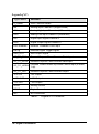
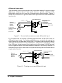
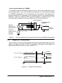
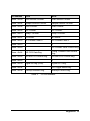
1
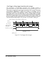
cPCI-9116®/cPCI-9116R® 64 Ch, 16 bit, 250KS/s Analog input Card For 3U CompactPCI User’s Guide Recycled Paper Copyright 2002 ADLINK Technology Inc. All Rights Reserved. Manual Rev. 1.02: JUL 23, 2002 Part No: 50-15002-100 The information in this document is subject to change without prior notice in order to improve reliability, design and function and does not represent a commitment on the part of the manufacturer. In no event will the manufacturer be liable for direct, indirect, special, incidental, or consequential damages arising out of the use or inability to use the product or documentation, even if advised of the possibility of such damages. This document contains proprietary information protected by copyright. All rights are reserved. No part of this manual may be reproduced by any mechanical, electronic, or other means in any form without prior written permission of the manufacturer. Trademarks NuDAQ, NuIPC are registered trademarks of ADLINK Technology Inc. Other products names mentioned herein are used for identification purposes only and may be trademarks and/or registered trademarks of their respective companies. Getting service from ADLINK • Customer Satisfaction is the most important priority for ADLINK Tech Inc. If you need any help or service, please contact us. ADLINK Technology Inc. Web Site http://www.adlinktech.com Sales & Service [email protected] NuDAQ + USBDAQ [email protected] Technical Automation [email protected] Support NuIPC [email protected] TEL +886-2-82265877 NuPRO / EBC Address • [email protected] FAX +886-2-82265717 9F, No. 166, Jian Yi Road, Chungho City, Taipei, 235 Taiwan. Please email or FAX us of your detailed information for a prompt, satisfactory and constant service. Detailed Company Information Company/Organization Contact Person E-mail Address Address Country TEL FAX Web Site Questions Product Model Environment to Use Detail Description Suggestions to ADLINK OS: Computer Brand: M/B: CPU: Chipset: BIOS: Video Card: Network Interface Card: Other: Table of Contents Tables .....................................................................................iii Figures .....................................................................................iv How to Use This Guide .............................................................v Chapter 1 Introduction..............................................................1 1.1 Features ............................................................................. 1 1.2 Applications ........................................................................ 2 1.3 Specifications...................................................................... 3 1.4 Software Support ................................................................ 5 1.4.1 1.4.2 1.4.3 Programming Library....................................................................5 ® PCIS-LVIEW: LabVIEW Driver .................................................6 DAQBenchTM: ActiveX Controls..................................................6 Chapter 2 Installation ................................................................7 2.1 What You Have ................................................................... 7 2.2 Unpacking .......................................................................... 8 2.3 cPCI-9116 and cPCI-9116R Layout ...................................... 9 2.4 PCI Configuration .............................................................. 11 Chapter 3 Signal Connections...............................................12 3.1 Connectors and Pin Assignment ........................................ 12 3.2 Analog Input Signal Connection ......................................... 15 3.2.1 3.2.2 3.3 Types of signal sources .............................................................15 Input Configurations....................................................................15 Digital I/O Connection........................................................ 17 Chapter 4 Registers.................................................................18 4.1 I/O Port Address ............................................................... 18 4.2 Internal Timer/Counter Register ......................................... 20 4.3 General Purpose Timer/Counter Register ........................... 21 4.4 General Purpose Timer/Counter Control Register................ 22 4.5 A/D Data Registers ............................................................ 23 Table of Contents • i 4.6 Channel Gain Queue Register ........................................... 24 4.7 A/D & FIFO Control Register .............................................. 25 4.8 A/D & FIFO Status Register ............................................... 27 4.9 Digital I/O register ............................................................. 28 4.10 A/D Trigger Mode Register ................................................ 29 4.11 Interrupt Control Register................................................... 31 4.12 Interrupt Status Register.................................................... 33 Chapter 5 Operation Theory...................................................34 5.1 A/D Conversion ................................................................. 34 5.1.1 5.1.2 5.1.3 5.1.4 A/D Conversion Procedure........................................................34 Software conversion with polling data transfer acquisition mode (Software Polling).............................................................35 5.1.2.1 Specifying Channels, Gains, and input configurations in the Channel Gain Queue..........36 Programmable scan acquisition mode....................................36 5.1.3.1 Scan Timing and Procedure...................................36 5.1.3.2 Specifying Channels, Gains, and input configurations in the Channel Gain Queue..........38 5.1.3.3 Trigger Modes...........................................................39 A/D Data Transfer Modes..........................................................47 5.2 Digital Input and Output ..................................................... 48 5.3 General Purpose Timer/Counter Operation ......................... 49 Chapter 6 Software Utility & Calibration...............................51 6.1 Running 9116util.exe program ........................................... 51 6.2 Calibration ........................................................................ 52 6.2.1 6.2.2 6.2.3 6.3 What do you need.......................................................................52 VR Assignment............................................................................53 A/D Adjustment............................................................................53 6.2.3.1 PGA offset Calibration.............................................54 6.2.3.2 Bipolar input Calibration ..........................................54 6.2.3.3 Unipolar input Calibration........................................54 Functional Testing ............................................................. 54 Warranty Policy........................................................................56 ii • Table of Contents Tables Table 1. Legend of J1 Connector ......................................... 14 Table 2. I/O Port Address .................................................... 19 Table 3. Timer/Counter Register Address............................. 20 Table 4. General Purpose Timer/Counter Register ................ 21 Table 5. General Purpose Timer/Counter Control Register .... 22 Table 6. GPTC0’s Mode selection........................................ 23 Table 7. A/D Data Registers ................................................ 23 Table 8. Channel Gain Queue Register................................ 24 Table 9. Gain Selection Bits ................................................ 24 Table 10. A/D & FIFO Control Register .................................. 25 Table 11. A/D & FIFO Status Register.................................... 27 Table 12. Digital I/O register (Read) ....................................... 28 Table 13. Digital I/O register (Write) ....................................... 29 Table 14. A/D Trigger Mode Register..................................... 29 Table 15. Trigger Mode Selection Bits.................................... 30 Table 16. Interrupt Control Register ....................................... 31 Table 17. Interrupt Status Register ........................................ 33 Table 18. Functions of VRs ................................................... 53 Tables • iii Figures Figure 1: PCB Layout of the cPCI-9116 ................................... 9 Figure 2: PCB Layout of cPCI-9116R and Rear I/O adaptor .... 10 Figure 3: J1 Pin Assignments ............................................... 13 Figure 4: Single-ended Mode and Floating sources ................ 15 Figure 5: Ground-referenced source and differential input....... 16 Figure 6: Floating source and differential input ....................... 16 Figure 7: Ground-referenced source and User Common Mode connections ........................................................... 17 Figure 8: Digital I/O Connection ............................................ 17 Figure 9: Scan Timing .......................................................... 37 Figure 10: Pre-trigger (trigger occurs after M scans)................. 40 Figure 11: Pre-trigger (trigger with scan is in progress)............. 40 Figure 12: Pre-trigger with M_enable = 0................................. 41 Figure 13: Pre-trigger with M_enable = 1................................. 42 Figure 14: Middle trigger with M_enable = 1 ............................ 43 Figure 15: Middle trigger (trigger with scan is in progress) ........ 44 Figure 16: Post trigger............................................................ 44 Figure 17: Delay trigger.......................................................... 45 Figure 18: Post trigger with re-trigger ...................................... 46 Figure 19: General-purpose Timer/Counter model ................... 49 Figure 20: Mode 0 Operation.................................................. 50 Figure 21: Mode 1 Operation.................................................. 50 Figure 22: CPCI-9116 Utility Main Screen ............................... 52 Figure 23: A/D Adjustment menu Screen................................. 53 Figure 24: cPCI-9116 Function Testing Screen ........................ 55 iv • Figures How to Use This Guide This manual is designed to help you use the 9116 series. The manual describes how to modify various settings on the card to meet your requirements. It is divided into seven chapters: Chapter1, “Introduction”, gives an overview of the product features, applications, and specifications. Chapter 2, “Installation”, describes how to install the 9116 series . The layout of 9116 series is shown. Chapter 3, “Signal Connection”, describes the connectors' pin assignment and how to connect external signal and devices to the 9116 series card. Chapter 4, “Registers”, describes the details of the registers and its structure. This information is important for programmers who want to control the hardware with low-level programming. Chapter 5, “Operation theory”, describes the working theory of the 9116 series card. The A/D, DIO and timer/counter functions are introduced. Also, some programming concepts are specified. Chapter 6, “Software Utility & Calibration”, describes how to run the utility program included in the software CD and how to calibrate the 9116 series card for accurate measurements. How to Use This Guide • v 1 Introduction The 9116 series products are advanced data acquisition cards based on the 32-bit CompactPCI architecture. The 9116 series include: • cPCI-9116 : 16-bit 250KHz DAS card for 3U CompactPCI • cPCI-9116R : 16-bit 250KHz DAS card for 3U CompactPCI with Rear I/O connector The 9116 series DAS cards use state-of-the-art technology making it an ideal for data logging and signal analysis applications in medical, process control, etc. 1.1 Features The 9116 series CompactPCI Advanced Data Acquisition Card provides the following advanced features: • 32-bit PCI-Bus, plug and play • Up to 64 single-ended inputs or 32 differential inputs, mixing of using SE and DI analog signal sources • 16-bit analog input resolution • On-board A/D 1K FIFO memory • 512 words analog input Channel Gain Queue spaces • Sampling rate up to 250KS/s • Bipolar or Unipolar input signals • Programmable gain of x1, x2, x4, x8 • Jumper-less and software configurable Introduction • 1 • Five A/D trigger modes: software trigger, pre-trigger, post-trigger, middle-trigger and delay-trigger • Software Polling, Interrupt and Bus-mastering DMA data transfer available • 8 digital input and 8 digital o utput channels • 100-pin D-type SCSI-II connector for cPCI-9116 • 100-pin D-type SCSI-II connector on a rear I/O transition board for cPCI-9116R • Compact size: standard compact PCI 3U size 1.2 Applications • Automotive Testing • Cable Testing • Transient signal measurement • ATE • Laboratory Automation • Biotech measurement 2 • Introduction 1.3 ♦ Specifications Analog Input (A/D) • Converter: LT1606 (or equivalent) 250KHz • Number of channels: (programmable) P 64 single-ended (SE) P 32 differential input (DI) P Mixing of SE and DI analog signal between channel allowed • A/D Data FIFO Buffer Size: 1024 locations • Channel Gain Queue Length: 512 words configurations • Resolution: 16-bit • Input Range: (Controlled by Channel Gain Queue) • P Bipolar: ± 5V, ±2.5V, ±1.25V, ±0.625V P Unipolar: 0~10V, 0~5V, 0~2.5V, 0~1.25 CMRR (DC to 60 Hz, typical) Input Range CMRR ±5, 0~10V 87dB ±2.5, 0~5V 90dB ±1.25, 0~2.5V 92dB ±0.625, 0~1.25V 93dB • Overvoltage Protection: Continuous ± 35V maximum • Accuracy: 0.01% of FSR • Input Impedance: 100 MΩ | 6pF • Time-base source: • P Internal 24MHz P External clock Input (fmax: 24MHz, fmin: 1MHz) Programmable scan interval and sampling rate (divided from time-base source) Introduction • 3 • • • ♦ ♦ P Software-trigger. P Pre-trigger. P Post-trigger. P Middle-Trigger. P Delay Trigger Data Transfer: P Polling. P EOC interrupt transfer. P FIFO half-full Interrupt transfer. P Bus-mastering DMA. Data Throughput: 250KHz (maximum) Digital I/O (DIO) • Channel: 8 TTL compatible digital inputs and outputs • Input Voltage: • ♦ Trigger Mode: P Low: VIL=0.8 V max. IIL=0.2mA max. P High: VIH=2.0V max. IIH=0.02mA max Output Voltage: P Low: VOL=0.5 V max. IOL=8mA max. P High: VOH=2.7V min; IOH=400µA General Purpose Timer/ Counter • Number of channel: One 16-bit Up/Down Timer/Counter • Clock Input: Internal 24MHz or External CLK input up to 20MHz General Specifications • Connector: 100-pin D-type SCSI-II connector • Operating Temperature: 0° C ~ 60° C • Storage Temperature: -20° C ~ 80° C • Humidity: 5 ~ 95%, non-condensing • Power Consumption: 4 • Introduction P +5V @ 560mA typical P +3.3V@ 100mA typical • ± 15V (pin35, pin85) Output Current (max): 5mA • +5V(pin49, pin99) Output Current (max): 500mA • Dimension: Standard Compact PCI 3U size 1.4 Software Support ADLINK provides versatile software drivers and packages for users’ different approach to building a system. We not only provide programming libraries such as DLL for many Windows systems, but also provide drivers for other software packages such as LabVIEW®. All software options are included in the ADLINK CD. Non-free software drivers are protected with licensing codes. Without the software code, you can install and run the demo version for two hours for trial/demonstration purposes. Please contact ADLINK dealers to purchase the formal license. 1.4.1 Programming Library For customers who are writing their own programs, we provide function libraries for many different operating systems, including: • PCIS-DASK: Include device drivers and DLL for Windows 98, Windows NT and Windows 2000. DLL is binary compatible across Windows 98, Windows NT and Windows 2000. That means all applications developed with PCIS-DASK are compatible across Windows 98, Windows NT and Windows 2000. The developing environment can be VB, VC++, Delphi, BC5, or any Windows programming language that allows calls to a DLL. The user’s guide and function reference manual of PCIS-DASK are in the CD. Please refer the PDF manual files under \\Manual_PDF\Software\PCIS-DASK • PCIS-DASK/X: Includes device drivers and shared library for Linux. The developing environment can be Gnu C/C++ or any programming language that allows linking to a shared library. The user's guide and function reference manual of PCIS-DASK/X are in the CD. (\Manual_PDF\Software\PCIS-DASK-X.) The above software drivers are shipped with the board. Please refer to the “Software Installation Guide” for installation procedures. Introduction • 5 1.4.2 ® PCIS-LVIEW: LabVIEW Driver PCIS-LVIEW contains the VIs, which are used to interface with NI’s LabVIEW® software package. The PCIS-LVIEW supports Windows 95/98/NT/2000. The LabVIEW® drivers is shipped free with the board. You can install and use them without a license. For more information about PCIS-LVIEW, please refer to the user’s guide in the CD. (\\Manual_PDF\Software\PCIS-LVIEW) 1.4.3 TM DAQBench : ActiveX Controls We suggest customers who are familiar with ActiveX controls and VB/VC++ programming use the DAQBenchTM ActiveX Control component library for developing applications. The DAQBenchTM is designed under Windows NT/98. For more information about DAQBench, please refer to the user’s guide in the CD. (\\Manual_PDF\Software\DAQBench\DAQBench Manual.PDF). 6 • Introduction 2 Installation This chapter describes how to install the 9116 series cards. The contents of the package and unpacking information that you should be aware of are described first. The 9116 series cards perform an automatic configuration of the IRQ, port address, and BIOS address. You do not need to set these configurations, as you would do in ISA form factor DAS cards. Automatic configuration allows your system to operate more reliable and safe. 2.1 What You Have In addition to this User's Guide, the package should also include the following items: • cPCI-9116 or cPCI-9116R with rear I/O adaptor Analog input Data Acquisition Card • ADLINK All-in-one Compact Disc • Software Installation Guide If any of these items are missing or damaged, contact the dealer from whom you purchased the product. Save the shipping materials and carton in case you want to ship or store the product in the future. Installation • 7 2.2 Unpacking The card contains electro-static sensitive components that can be easily be damaged by static electricity. Therefore, the card should be handled on a grounded anti-static mat. The operator should be wearing an anti-static wristband, grounded at the same point as the anti-static mat. Inspect the card module carton for obvious damages. Shipping and handling may cause damage to your module. Be sure there are no shipping and handling damages on the modules carton before continuing. After opening the card module carton, extract the system module and place it only on a grounded anti-static surface with component side up. Again, inspect the module for damages. Press down on all the socketed IC's to make sure that they are properly seated. Do this only with the module place on a firm flat surface. Note: DO NOT APPLY POWER TO THE CARD IF IT HAS BEEN DAMAGED. You are now ready to install your cPCI-9116/R. 8 • Installation 2.3 cPCI-9116 and cPCI-9116R Layout Figure 1: PCB Layout of the cPCI-9116 Installation • 9 Figure 2: PCB Layout of cPCI-9116R and Rear I/O adaptor 10 • Installation 2.4 1. PCI Configuration Plug and Play: As a plug and play component, the board requests an interrupt number via a system call. The system BIOS responds with an interrupt assignment based on the board information and on known system parameters. These system parameters are determined by the installed drivers and the hardware load seen by the system. 2. Configuration: The board configuration is done on a board-by-board basis for all PCI form factor boards on your system. Because configuration is controlled by the system and software, so there is no jumpers for base-address, DMA, and interrupt IRQ need to be set by the user. The configuration is subject to change with every boot of the system as new boards are added or boards are removed. So, there is no idea what‘s going on to be installed. 3. Trouble shooting: If your system doesn’t boot or if you experience erratic operation with your PCI board in place, it’s likely caused by an interrupt conflict (perhaps because you incorrectly configured the BIOS setup). In general, the solution, once you determine it is not a simple oversight, is to consult the BIOS documentation that came with your system. Installation • 11 3 Signal Connections This chapter describes the connectors of the 9116 series. The signal connections between the 9116 series cards and external devices are also outlined. 3.1 Connectors and Pin Assignment The cPCI-9116 is equipped with one 100-pin SCSI-type connector (J1). J1 is used for digital input/output, analog input, and timer/counter signals. The pin assignment for the connector is illustrated in the Figure 3.1. With the REAR I/O adaptor specifically designed for the cPCI-9116R, the cPCI-9116R connector pin assignments are identical to that of the cPCI-9116. The red LED positioned on the front panel is used as a power indicator. 12 • Signal Connections J1 100-pin SCSI-type connector AIH0 AIH1 AIH2 AIH3 AIH4 AIH5 AIH6 AIH7 AIH8 AIH9 AIH10 AIH11 AIH12 AIH13 AIH14 AIH15 AIH16 AIH17 AIH18 AIH19 AIH20 AIH21 AIH22 AIH23 AIH24 AIH25 AIH26 AIH27 AIH28 AIH29 AIH30 AIH31 U_CMMD AI0 AI1 AI2 AI3 AI4 AI5 AI6 AI7 AI8 AI9 AI10 AI11 AI12 AI13 AI14 AI15 AI16 AI17 AI18 AI19 AI20 AI21 AI22 AI23 AI24 AI25 AI26 AI27 AI28 AI29 AI30 AI31 AGND +15V out N/C DI0 DI1 DI2 DI3 DI4 DI5 DI6 DI7 ExtTimeBase ExtTrg SSH_OUT GP_TC_OUT +5V Out DGND 1 2 3 4 5 6 7 8 9 10 11 12 13 14 15 16 17 18 19 20 21 22 23 24 25 26 27 28 29 30 31 32 33 34 35 36 37 38 39 40 41 42 43 44 45 46 47 48 49 50 51 52 53 54 55 56 57 58 59 60 61 62 63 64 65 66 67 68 69 70 71 72 73 74 75 76 77 78 79 80 81 82 83 84 85 86 87 88 89 90 91 92 93 94 95 96 97 98 99 100 AGND AI32 AI33 AI34 AI35 AI36 AI37 AI38 AI39 AI40 AI41 AI42 AI43 AI44 AI45 AI46 AI47 AI48 AI49 AI50 AI51 AI52 AI53 AI54 AI55 AI56 AI57 AI58 AI59 AI60 AI61 AI62 AI63 AGND -15V out N/C DO0 DO1 DO2 DO3 DO4 DO5 DO6 DO7 N/C GP_TC_CLK GP_TC_GATE GP_TC_UPDN +5V out DGND AIL0 AIL1 AIL2 AIL3 AIL4 AIL5 AIL6 AIL7 AIL8 AIL9 AIL10 AIL11 AIL12 AIL13 AIL14 AIL15 AIL16 AIL17 AIL18 AIL19 AIL20 AIL21 AIL22 AIL23 AIL24 AIL25 AIL26 AIL27 AIL28 AIL29 AIL30 AIL31 Figure 3: J1 Pin Assignments Signal Connections • 13 Legend of J1: Signal Name Definition U_CMMD User Common Mode AIn Analog Input Channel n (single-ended) AIHn Analog High Input Channel n (differential) AILn Analog Low Input Channel n (differential) DIn Digital Input Signal Channel n DOn Digital Output Signal Channel n ExtTimeBase External Timebase Clock Input ExtTrg External Digital Trigger Signal SSH_OUT SSH Output Signal GP_TC_CLK General Purpose Timer/Counter Clock Input GP_TC_GATE General Purpose Timer/Counter Gate Input GP_TC_UPDN Purpose Timer/Counter Up/Down Control Input (0:down, 1:up) GP_TC_OUT General Purpose Timer/Counter Output +5V OUT +5V Output +15V OUT +15V Output -15V OUT -15V Output AGND Analog Ground DGND Digital Ground N/C No Connection Table 1. 14 • Signal Connections Legend of J1 Connector 3.2 Analog Input Signal Connection The 9116 series provides up to 64 single-ended or 32 differential analog input channels. You can set and fill the Channel Gain Queue to get the desired combination of the input signal types. The analog signals can be converted to digital value by the A/D converter. To avoid ground loops and to obtain accurate measurements from the A/D conversion, it is quite important to understand the signal source type and how to choose the analog input modes: Single-ended, Differential, or User Common Mode. 3.2.1 Types of signal sources Floating Signal Sources A floating signal source means it is not connected in any way to the buildings ground system. A device with an isolated output is a floating signal source, such as optical isolator outputs, transformer outputs, and thermocouples Ground-Referenced Signal Sources A ground-referenced signal means it is connected in some way to the buildings system. That is, the signal source is already connected to a common ground point with respect to the 9116 card, assuming that the computer is plugged into the same power system. Non- isolated outputs of instruments and devices that plug into the buildings power system are ground-referenced signal sources. 3.2.2 Input Configurations Single-ended Mode In single-ended mode, all input signals are connected to ground provided by the 9116 card. It is suitable for connections with floating signal sources. Figure 4 illustrates single-ended connection. Note that when more than two floating sources are connected, these sources will be referenced to the same common ground. J1 AIn Floating Signal Source V1 Input Multipexer Instrumentation Amplifier + - V2 + To A/D - Converter AGND n = 0, ...,63 Figure 4: Single-ended Mode and Floating sources Signal Connections • 15 Differential input mode The differential input mode provides two inputs that respond to signal voltage differences between them. If the signal source is ground- referenced, the differential mode can be used for common-mode noise rejection. Figure 5 shows the connection of ground-referenced signal sources under differential input mode. Input Multipexer x = 0, ..., 31 AIxH Ground Referenced Signal Source Commonmode noise & Ground potential + Instrumentation Amplifier - + To A/D Converter - AIxL Vc m AGND Figure 5: Ground-referenced source and differential input Fig 6 shows how to connect a floating signal source to the 9116 card in differential input mode. For floating signal sources, a resis tor is required on each channel to provide a bias return path. The resistor value should be about 100 times the equivalent source impedance. If the source impedance is less than 100ohms, simply connect the negative side of the signal to AGND as well as the negative input of the Instrumentation Amplifier, without any resistors. In differential input mode, less noise is coupled into the signal connections than in single-ended mode. Input Multipexer x = 0, ..., 31 AIxH Ground Referenced Signal Source + Instrumentation Amplifier AIxL AGND Figure 6: Floating source and differential input 16 • Signal Connections + To A/D Converter - User Common Mode (U_CMMD) To measure ground-referenced signal sources, which are connected to the same ground point, you can connect the signals in a User-Common-Mode (U_CMMD) configuration. Fig 7 illustrates the connections. The signal local ground reference is connected to the negative input of the instrumentation Amplifier, and the common-mode ground potential to signal ground. The instrumentation amplifier will now reject the 9116 series ground. Input Multipexer Instrumentation Amplifier AIn GroundReferenced Signal Source Commonmode noise & Ground potential + V1 Vcm V2 n = 0, ...,63 + To A/D - Converter U_CMMD Figure 7: Ground-referenced source and User Com mon Mode connections 3.3 Digital I/O Connection The 9116 series card provides 8 digital input and 8 digital output channels. The digital I/O signals are fully TTL/DTL compatible. The details of the digital I/O signal specification can be found in section 1 .3. 74LS244 From TTL Signal To TTL Devices Digital Input(DI) 74LS244 Digital Output(DO) Digital GND(DGND) Figure 8: Digital I/O Connection Signal Connections • 17 4 Registers The descriptions of the registers and structure of the PCI-9116 are outlined in this chapter. The information in this chapter will assist programmers, who wish to handle the card with low-level programs. In addition, the low level programming syntax is introduced. This information can help beginners to operate the PCI-9116 in the shortest possible time. 4.1 I/O Port Address The 9116 series card functions as a 32-bit PCI master device to any master on the PCI bus. It supports burst transfer to memory space by using 32-bit data. All data read and write are based on 32-bit transactions. Table 2 shows the I/O address of each register with respect to the base address. The function of each register is also shown. 18 • Registers I/O Address Read Write Base + 0x00 Scan Interval Counter Scan Interval Counter Base + 0x04 Sample Interval Counter Sample Interval Counter Base + 0x08 Scan Counter Scan Counter Base + 0x0C DIV Counter DIV Counter Base + 0x10 Delay1 Counter Delay1 Counter Base + 0x14 M Counter M Counter Base + 0x18 GP Counter/Timer 0 GP Counter/Timer 0 Base + 0x1C X X Base + 0x20 X GP Counter/Timer Control Reg Base + 0x24 A/D FIFO Data Reg Config. Channel Gain Queue Reg.. Base + 0x28 A/D and FIFO Status Reg. A/D and FIFO Control Reg. Base + 0x2C X X Base + 0x30 Digital IN Reg.(Dout) Digital OUT Reg. Base + 0x34 X A/D Trigger Mode Reg. Base + 0x38 Interrupt Reason Reg. Interrupt Control Reg. Table 2. I/O Port Address Registers • 19 4.2 Internal Timer/Counter Register The 9116 series card basically has 6 counters, which are responsible for the scan timing of the analog input data acquisition. The 6 counters occupy 6 I/O address locations in the 9116 card as shown below. Address: BASE + 0 ~ BASE + 14 Attribute: read / write Data Format: Base + 0x00 Scan Interval Counter Register (R/W) 24bit Base + 0x04 Sample Interval Counter Register (R/W) 16bit Base + 0x08 Scan Counter Register (R/W) 24bit Base + 0x0C DIV Counter Register (R/W) 9bit Base + 0x10 Delay1 Counter Register (R/W) 16bit Base + 0x14 M Counter Register (R/W) 16bit Table 3. Timer/Counter Register Address SI_counter: Scan Interval counter SI2_counter: Sample Interval counter SC_counter: total Scan Count counter DIV_counter: specify the number of samples per scan DLY1_counter: Delay Interval counter (only used in delay trigger mode) M_counter: 20 • Registers specify the number of scans before a trigger (only used in pre-trigger and middle-trigger modes) 4.3 General Purpose Timer/Counter Register One 16-bit, general-purpose timer/counter exists in the 9116 series card. Writing to this register loads the initial count value into the general-purpose timer/counter. Reading from this register feedbacks the current count value of the general-purpose timer/counter Address: BASE + 0x18 Attribute: write / read Data Format: Bit Bit Bit Bit 7 6 5 4 3 2 1 0 GP7 GP6 GP5 GP4 GP3 GP2 GP1 GP0 15 14 13 12 11 10 9 8 GP15 GP14 GP13 GP12 GP11 GP10 GP9 GP8 23 22 21 20 19 18 17 16 --- --- --- --- --- --- --- --- 31 30 29 28 27 26 25 24 --- --- --- --- --- --- --- --- Table 4. General Purpose Timer/Counter Register Registers • 21 4.4 General Purpose Timer/Counter Control Register Address: BASE + 0x20 Attribute: write only Data Format: Bit 7 6 5 4 3 Up Counter Up Clk_sr Down Gate_src en c Down src Bit Bit Bit 15 2 1 0 --- MODE1 MODE 0 14 13 12 11 10 9 8 --- --- --- --- --- --- --- 23 22 21 20 19 18 17 16 --- --- --- --- --- --- --- --- 31 30 29 28 27 26 25 24 --- --- --- --- --- --- --- --- Table 5. General Purpose Timer/Counter Control Register Counter en (bit7): GPTC0 count enable 1: enable GPTC0 0: disable GPTC0 UpDown (bit6): GPTC0’s up/down pin software control 1: Up counter 0: Down counter UpDown src(bit5): GPTC0’s up/down pin selection bit 1: External input (Pin 98) 0: Software Control Gate_src (bit4): GPTC0’s gate source 1: External Input (Pin 97) 0: gate controlled by setting the enable (bit7) 22 • Registers Clk_src (bit3): GPTC0’s clock source 1: External Input (Pin 96) 0: Internal Timebase MODE1~MODE0 (bit1 ~ bit0): MODE1 MODE0 Description 0 0 General Counter 0 1 Pulse Generation 1 0 X 1 1 X Table 6. 4.5 GPTC0’s Mode selection GPTC0’s Mode selection A/D Data Registers The digital converted data is 16-bits and is stored into 32-bit registers. Address: BASE +24 Attribute: read Data Format: Bit 7 6 5 4 3 2 1 0 AD7 AD6 AD5 AD4 AD3 AD2 AD1 AD0 15 14 13 12 11 10 9 8 AD15 AD14 AD13 AD12 AD11 AD10 AD9 AD8 23 22 21 20 19 18 17 16 --- --- --- --- --- --- --- --- 31 30 29 28 27 26 25 24 --- --- --- --- --- --- --- --- Bit Bit Bit Table 7. AD15 ~ AD0: A/D Data Registers Analog to digital data. AD15 is the Most Significant Bit (MSB). AD0 is the Least Significant Bit (LSB). Registers • 23 4.6 Channel Gain Queue Register This register is used to fill the Channel Gain Queue. We recommend users use our call function to avoid any possible errors from these settings. Address: BASE + 0x24 Attribute: write Data Format: Bit Bit Bit Bit 7 6 5 4 3 2 1 0 EN3 EN2 EN1 EN0 HL_sel UNIP DIFF U_CMMD 15 14 13 12 11 10 9 8 --- --- CH3 CH2 CH1 CH0 23 22 21 20 19 18 17 16 --- --- --- --- --- --- --- --- 31 30 29 28 27 26 25 24 --- --- --- --- --- --- --- --- Gain1 Gain0 Table 8. Channel Gain Queue Register CH3 ~ CH0 (bit11~ bit8): Internal A/D Channel selection bits EN3 ~ EN0 (bit7~ bit4): Multiplexer Enable selection bits Gain1~Gain0 (bit13~bit12): Gain selection bits Gain1 Gain0 Gain 0 0 1 0 1 2 1 0 4 1 1 8 Table 9. 24 • Registers Gain Selection Bits HL_sel(bit3): >31 channel selection (single ended) 1: when channel number is larger than 31 0: when channel number is smaller than or equal to 31 DIFF(bit1): Analog Input Signals Type 1: Differential 0: Single ended UNIP(bit2): Analog Input Signals Polarity 1: Unipolar 0: Bipolar U_CMMD (bit0): User Defined Common Mode Selection 1: User Defined Common Mode (Pin 1) 0: Local Ground of 9116 series 4.7 A/D & FIFO Control Register Address: BASE + 28 Attribute: Write Data Format: Bit 7 6 Clear Bit Bit Bit 5 4 3 2 1 0 Set Clear Trg_de t Clear SC_T C Clear ADOR Clear ADOS SC_dis Channel Gain Queue don e Clear DFIF O 15 14 13 12 11 10 9 8 --- --- --- --- --- --- --- DMA 23 22 21 20 19 18 17 16 --- --- --- --- --- --- --- --- 31 30 29 28 27 26 25 24 --- --- --- --- --- --- --- --- Table 10. A/D & FIFO Control Register Registers • 25 DMA (Bit8): Write Only, set for DMA transfer SC_dis (Bit7): Write Only, set to disable the SC counter Clear Channel Gain Queue (Bit6): Write Only Clear the Channel Gain Queue 0: no effect on the Channel Gain Queue 1: clear the Channel Gain Queue Set done (Bit5): Write Only 0: indicate the Channel Gain Queue is not ready 1: indicate the Channel Gain Queue is OK Clear DFIFO(Bit4) : Write Only Clear the Data FIFO: 0: no effect on Data FIFO 1: clear the Data FIFO Clear Trg_det(Bit3) : Write 1 to clear Write 1 to clear the trigger status: 0: no effect 1: clear trigger detect status Clear SC_TC(Bit2) : Write 1 to clear Write 1 to clear Scan Counter Terminal Count status 0: no effect 1: clear the SC_TC status Clear ADOR(Bit1) : Write 1 to clear Write 1 to clear the A/D Overrun Status 0: no effect 1: clear the A/D Overrun status Clear ADOS(Bit0) : Write 1 to clear Write 1 to clear the A/D Over Speed Status: 0: no effect 1: clear the A/D Over-Speed status 26 • Registers 4.8 A/D & FIFO Status Register Address: BASE + 28 Attribute: read Data Format: Bit Bit Bit Bit 7 6 5 4 3 2 1 0 ACQ Full HFull Empty Trg_det SC_TC ADOR ADOS 15 14 13 12 11 10 9 8 --- --- --- --- --- --- --- --- 23 22 21 20 19 18 17 16 --- --- --- --- --- --- --- --- 31 30 29 28 27 26 25 24 --- --- --- --- --- --- --- --- Table 11. A/D & FIFO Status Register ACQ (Bit7): Read Only, set when acquisition is in progress. Full (Bit6): Read Only A/D FIFO Full status (Fatal Error!) 0: FIFO Full 1: FIFO not Full HFull(Bit5): Read only A/D FIFO Half Full status 0: FIFO Half Full 1: FIFO not Half Full Empty (Bit4): Read Only A/D FIFO Empty status 0: FIFO Empty 1: FIFO not Empty Trg_det (Bit3): Read/ Write 1 to clear External Digital Trigger Status 1: External Digital Trigger 0: No External Digital Trigger Registers • 27 SC_TC(Bit2) : Read/ Write 1 to clear Scan Counter Terminal Count Status 1: Scan Counter counts to 0 0: Scan Counter not completed ADOR(Bit1) : Read/ Write 1 to clear A/D Overrun Status (Fatal Error !) 1: A/D Overrun 0: A/D not Overrun ADOS(Bit0) : Read/ Write 1 to clear A/D Over Speed Status (Warning !) 1: A/D Over Speed 0: A/D not Over Speed 4.9 Digital I/O register There are 8 digital input and 8 digital output channels provided by the 9116 series cards. The address Base + 30 is used to access digital inputs and control digital outputs. Address: BASE +30 Attribute: read Data Format: Bit Bit Bit Bit 7 6 5 4 3 2 1 0 DI7 DI6 DI5 DI4 DI3 DI2 DI1 DI0 15 14 13 12 11 10 9 8 DO7 DO6 DO5 DO4 DO3 DO2 DO1 DO0 23 22 21 20 19 18 17 16 --- --- --- --- --- --- --- --- 31 30 29 28 27 26 25 24 --- --- --- --- --- --- --- --- Table 12. Digital I/O register (Read) 28 • Registers Address: BASE + 30 Attribute: write Data Format: Bit 7 6 5 4 3 2 1 0 DO7 DO6 DO5 DO4 DO3 DO2 DO1 DO0 15 14 13 12 11 10 9 8 --- --- --- --- --- --- --- --- 23 22 21 20 19 18 17 16 --- --- --- --- --- --- --- --- 31 30 29 28 27 26 25 24 --- --- --- --- --- --- --- --- Bit Bit Bit Table 13. Digital I/O register (Write) 4.10 A/D Trigger Mode Register Address: BASE + 0x34 Attribute: write only Data Format: Bit Bit Bit Bit 7 6 5 4 3 2 1 0 Retrig DLYSRC Time Base TrgP MODE2 MODE1 MODE0 --- 15 14 13 12 11 10 9 8 --- --- --- --- --- 23 22 21 20 19 18 17 16 --- --- --- --- --- --- --- --- 31 30 29 28 27 26 25 24 --- --- --- --- --- --- --- --- softconv ACQ_EN M_enable Table 14. A/D Trigger Mode Register Registers • 29 softconv (bit10): ADC direct conversion control 1: generate 1 convert pulse 0: no effect ACQ_EN (bit9): Acquisition enable bit 1: enable the acquisition timing 0: disable the acquisition timing M_enable (bit8): M counter enable bit 1: ignore trigger signals before M counter reaches 0 0: accept the trigger signal anytime Retrig (bit7): Re-triggerability in an acquisition 1: Re-triggerable 0: trigger only once DLY SRC (bit6): Delay time unit in delay trigger mode 1: delay in sampling rate (SI2) 0: delay in Timebase TimeBase(bit5) : The Timebase Selection of 9116 series 1: External Timebase 0: Internal Timebase (24 MHz) TrgP (bit4): The Trigger polarity selection bit 1: Negative Edge Trigger 0: Positive Edge Trigger MODE2 ~ 0(bit3 ~ bit1): Trigger Mode Selection Bits MODE2 MODE1 MODE0 Description 0 0 0 Software Trigger 0 0 1 Post Trigger 0 1 0 Delay Trigger 0 1 1 Pre Trigger 1 0 0 Middle Trigger Table 15. Trigger Mode Selection Bits 30 • Registers 4.11 Interrupt Control Register Address: BASE + 0x38 Attribute: write Data Format: Bit Bit Bit Bit 7 6 5 4 3 2 1 0 --- --- --- Clr_Timer Clr_STTC 15 14 13 12 11 10 --- --- --- Timer_en STTC_en Hfull_en 23 22 21 20 19 18 17 16 --- --- --- --- --- --- --- --- 31 30 29 28 27 26 25 24 --- --- --- --- --- --- --- --- Clr_Hfull Clr_DTrg Clr_EOC 9 8 DTrg_en EOC_en Table 16. Interrupt Control Register Timer_en (bit12): General Purpose Timer Interrupt Enable Control 1: Enable 0: Disable SCTC_en (bit11): Trigger Complete Interrupt Enable Control 1: Enable 0: Disable Hfull_en (bit10): A/D FIFO Half Full Interrupt Enable Control 1: Enable 0: Disable DTrg_en (bit9): External Digital Trigger Interrupt Enable Control 1: Enable 0: Disable Registers • 31 EOC_en (bit8): End of conversion Interrupt Enable Control 1: Enable 0: Disable Clr_Timer (bit4): write 1 to clear the GPTC Interrupt status 1: clear interrupt from the GPTC 0: no effect Clr_SCTC (bit3): write 1 to clear the SCTC Interrupt 1: clear the interrupt on terminal count of the Scan counter 0: no effect Clr_HFull (bit2): write 1 to clear the data FIFO half full interrupt 1: clear the interrupt on the data FIFO half full status 0: no effect Clr_DTrg (bit1): write 1 to clear the Digital Trigger Interrupt 1: clear the interrupt when trigger happens 0: no effect Clr_EOC (bit0): write 1 to clear the End of Conversion Interrupt 1: clear the interrupt when EOC 0: no effect 32 • Registers 4.12 Interrupt Status Register Address: BASE + 0x38 Attribute: read Data Format: Bit Bit Bit Bit 7 6 5 4 3 2 1 0 --- --- --- Timer STTC Hfull DTrg EOC 15 14 13 12 11 10 9 8 --- --- --- --- --- --- --- --- 23 22 21 20 19 18 17 16 --- --- --- --- --- --- --- --- 31 30 29 28 27 26 25 24 --- --- --- --- --- --- --- --- Table 17. Interrupt Status Register Timer (bit4): GPTC generated Interrupt status 1: Interrupt Occurs 0: Interrupt not Occur SCTC(bit3): Scan Counter reach Terminal Count Interrupt status 1: Interrupt Occurs 0: Interrupt not Occur HFull (bit2): data FIFO Half Full Interrupt 1: Interrupt Occurs 0: Interrupt not Occur DTrg (bit1): Digital Trigger Interrupt status 1: Interrupt Occur 0: Interrupt not Occur EOC (bit0): End of Conversion Interrupt status 1: Interrupt Occurs 0: Interrupt not Occur Registers • 33 5 Operation Theory The operation theory of the functions on the 9116 series is described in this chapter. The functions include the A/D conversion, Digital I/O and General Purpose Counter / Timer. The operation theory can help you better understand how to configure and program the 9116 series card. 5.1 5.1.1 A/D Conversion A/D Conversion Procedure When using an A/D converter, users should beware of the properties of the signal to be measured. Users can decide which channel to use and where to connect the signals to the card. Please refer to 3.2 for signal connections. In addition, users should define and control the A/D signal configurations, including channels, gains, and A/D signal types. The A/D acquisition is initiated by a trigger source; users must decide how to trigger the A/D conversion. The data acquisition will start when a trigger condition is met. After the end of the A/D conversion, the A/D data is buffered in a Data FIFO. The A/D data is then transferred into PC's memory for further processing. There are two acquisition modes: Software Polling and Scan acquisition. They will be described separately in the following section, including the timing, signal source control, trigger mode, and transfer method. 34 • Operation Theory 5.1.2 Software conversion with polling data transfer acquisition mode (Software Polling) This is the easiest way to acquire a single A/D data. The A/D converter starts a conversion when the user writes 1 into bit10 of the A/D trigger mode register (BASE+34). After the software initializes the A/D conversion, the software polls the FIFO Empty status (bit4) in the A/D & FIFO Status register (BASE+28) until it changes to active low logic. If the Data FIFO is empty before an A/D conversion starts, the Empty bit will be high. After the A/D conversion is completed, the A/D data is written to the Data FIFO immediately, thus the Empty becomes low. You can consider the Empty bit as a flag to indicate the converted data ready status. That is, a low Empty bit meaning the data is ready. The A/D data is now ready to be transferred to host memory from the FIFO. This method is suitable for applications that needs to process AD data in real time. Under this mode, the timing of the A/D conversion is fully controlled by the software. However, it is difficult to control a fixed A/D conversion rate unless another timer interrupt service routine is used to generate a fixed conversion rate trigger. ADLINK’s software driver provides an integral function to acquire a single data (That is, it will start an A/D conversion, then poll the Empty flag and read the data back when the data is ready). We also provide individual functions to allow users to start an A/D conversion only. Users must read it back from the A/D data register (BASE+24) by themselves. This method makes it possible to read A/D converted data without polling. The conversion and acquisition time of the ADC does not exceed 4µs. Hence, after software conversion, the software need only wait for a maximum of 4µs to read the A/D Data Register without polling. Operation Theory • 35 5.1.2.1 Specifying Channels, Gains, and input configurations in the Channel Gain Queue In both Software Polling and programmable scan acquisition mode, the channel, gain, and input configuration (single-end, differential, and U_CMMD), where you want to acquire samples from, can be specified in the Channel Gain Queue. You can set the channel number in the Channel Gain Queue in any order. Therefore, you can control the channel order from which data is acquired with different gain and input configuration for each channel. The maximum number of entries you can set is 512 channels. The channel order of acquisition is the same as the order you set in the Channel Gain Queue. When the specified channels are sampled from the beginning to the end in the Channel Gain Queue, the channels in the Channel Gain Queue will be sampled again until the specified number of samples has been acquired. 5.1.3 Programmable scan acquisition mode 5.1.3.1 Scan Timing and Procedure It's recommended that this mode be used, if your application needs a fixed and precise A/D sampling rate. You can accurately program the period between conversions of each individual channel in the scan and the period between conversions of the entire scan. There are 4 counters, which need to be specified: SI_counter(24 bit): Specify the Scan Interval = SI_counter / Timebase SI2_counter(16 bit): Specify the data Sampling Interval = SI2_counter/Timebase SC_counter(24 bit): Specify Scan Count Counter after trigger DIV_counter(9 bit): Specify the number of samples per scan The acquisition timing and the meaning of the 4 counters are illustrated in figure 9. 36 • Operation Theory Timebase clock source In scan acquisition mode, all the A/D conversions start on the output of counters, which use Timebase as the clock source. With the software you can specify the Timebase to be either an internal clock source (on board 24MHz) or an external clock input on pin 45 of J1. The external clock is useful when you want to acquire data at rates not available with the internal A/D sample clock. The external clock source must generate TTL-compatible continuous clocks, and the maximum frequency is 24MHz while the minimum is 1MHz. 3 Scans, 4 Samples per scan (SC_Counter=3, DIV_Counter=4) ( channel sequences are specified in Channel Gain Queue) Ch2 Ch3 Ch1 Ch0 Ch2 Ch3 Ch1 Ch0 Ch2 Ch3 Ch1 Ch0 Scan_start AD_conversion Scan_in_progress (SSH_OUT )(pin47) Acquisition_in_progress Sampling Interval t= SI2_COUNTER/TimeBase Scan Interval T= SI_COUNTER/TimeBase Figure 9: Scan Timing In the scan acquisition mode, the channel, gain, and input configurations (single-end, differential, or U_CMMD) must be specified in the hardware Channel Gain Queue, please refer to 5.1.3.2 for more details. There are 5 trigger modes to start the scan acquisition, please refer to 5.1.3.3 details. The data transfer modes will be discussed in 5.1.3.4. Operation Theory • 37 Note: 1.The maximum A/D sampling rate is 250kHz. Therefore, SI2_counter can’t be smaller than 96 while using the internal Timebase. 2.The SI_counter is a 24-bit counter and the SI2_counter is a 16-bit counter. Therefore, the maximum scan interval while using the internal Timebase = 224/24M s = 0.699s, and the maximum sampling interval between 2 channels while using the internal Timebase = 2 16/24M s = 2.73ms. 3.The scan interval can’t be smaller than the product of the data sampling interval and the DIV_counter value. The relationship can be represented as: SI_counter>=SI2_counter*DIV_counter. Scan with SSH You can send the SSH_OUT signal on pin 47 of J1 to an external S&H circuits to sample and hold all signals if you want to simultaneously sample all channels in a scan, as illustrated in fig 9. Note: The ‘SSH_OUT’ signal is sent to external S&H circuits to hold the analog signal. Users must implement external S&H circuits on their own to carry out the S&H function. There are no on-board S&H circuits. 5.1.3.2 Specifying Channels, Gains, and input configurations in the Channel Gain Queue Like software polling acquisition mode, the channel, gain, and input configurations (single-end, differential, and U_CMMD) must also be specified in the hardware Channel Gain Queue under scan acquisition mode. Please refer to 5.1.2.1 for details. Note that in scan acquisition mode, the number of entries in the Channel Gain Queue is normally equivalent to the value of DIV_counter (that is, the numbers of samples per scan). Example: Set SI2_counter = 240 SI_counter = 960 SC_counter = 3 DIV_counter = 4 Timebase = Internal clock source Channel entries in the Channel Gain Queue: ch1, ch2, ch0, ch2 38 • Operation Theory Then Acquisition sequence of channels: 1, 2, 0, 2, 1, 2, 0, 2, 1, 2, 0, 2. Sampling Interval = 240/24M s = 10 us Scan Interval = 960/24M s = 40 us Equivalent sampling rate of ch0, ch1: 25kHz Equivalent sampling rate of ch2: 50kHz 5.1.3.3 Trigger Modes There are 5 trigger modes (software-trigger, pre-trigger, post-trigger, middle-trigger, and delay-trigger) to start the data acquisition described in 5.3.1.1. All but software trigger are external digital triggers. An external digital trigger event occurs when a rising edge or a falling edge (software programmable) of a digital signal is detected on pin 46 of J1. They are described as follows. Software-Trigger Acquisition This trigger mode does not need any external trigger source. The data acquisition starts right after you execute the specified function calls to begin the operation. The scan timing is the same as fig 9. The total acquired data length = DIV_counter*SC_counter. Pre-Trigger Acquisition Use pre-trigger acquisition in applications where you want to collect data before an external trigger event. The A/D starts when you execute the specified function calls to begin the operation, and it stops when the external trigger event occurs. Users must program the value M in the M_counter (16bit) to specify the amount of stored scans of data before the trigger event. If the external trigger occurs after M scans of data are converted, the program only stores the last M scans of data, as illustrated in fig 10, where M_counter = M =3, DIV_counter =4, SC_counter = 0. The total stored amount of data = DIV_counter *M_counter =12. Operation Theory • 39 (M_counter = M = 3, DIV_counter=4, SC_counter=0) ExtTrg(pin46) Scan_start AD_conversion Scan_in_progress (SSH_OUT)(pin47) Acquisition_in_progress Aquired data Acquired & stored data (M scans) Operation start Figure 10: Pre-trigger (trigger occurs after M scans) Note: If an external trigger event occurs when a scan is in progress, the data acquisition won’t stop until this scan completes, and the stored M scans of data include the last scan. Therefore, the first stored data will always be the first channel entry of a scan (that is, the first channel entry in the Channel Gain Queue if the number of entries in the Channel Gain Queue is equivalent to the value of DIV_counter), no matter when the trigger signal occurs, as illustrated in Fig 11, where M_counter = M =3, DIV_counter = 4, SC_counter = 0. (M_counter = M = 3, DIV_counter =4, SC_counter=0) Trigger occurs ExtTrg(pin46) Scan_start Data acquisition won’t stop until a scan completes AD_conversion Scan_in_progress (SSH_OUT)(pin47) Acquisition_in_progress Aquired data Acquired & stored data (M scans) Operation start Figure 11: Pre-trigger (trigger with scan is in progress) 40 • Operation Theory When an external trigger signal occurs before the first M scans of data are converted, the amount of stored data could be fewer than the originally specified amount of DIV_counter * M_counter, as illustrated in fig 12. This situation can be avoided by setting M_enable. If M_enable is set to 1, the trigger signal will be ignored until the first M scans of data are converted, and it assures user of obtaining M scans of data under pre-trigger mode, as illustrated in fig 13. However, if M_enable is set to 0, the trigger signal will be accepted in any time, as illustrated in fig 12. Note that the total amount of stored data is still always a multiple of DIV_counter (number of samples per scan) because the data acquisition won’t stop until a scan is completed. (M_Counter = M = 3, DIV_Counter=4, SC_Counter=0) ExtTrg(pin46) Scan_start AD_conversion Scan_in_progress (SSH_OUT )(pin47) Acquisition_in_progress Acquired & stored data (2 scans) Operation start Figure 12: Pre-trigger with M_enable = 0 (trigger occurs before M scans) Operation Theory • 41 (M_counter = M = 3, DIV_counter=4, SC_counter=0) The first M scans Trigger signals which occur in the shadow region(the first M scans) will be ignored ExtTrg(pin46) Scan_start AD_conversion Scan_in_progress (SSH_OUT )(pin47) Acquisition_in_progress Aquired data Acquired & stored data (M scans) Operation start Figure 13: Pre-trigger with M_enable = 1 Note: The SC_counter must be set to 0 in pre-trigger acquisition mode. Middle-Trigger Acquisition Use middle-trigger acquisition in applications where you want to collect data before and after an external trigger event. The number of scans stored before the trigger is specified in M_counter, while the number of scans after the trigger is specified in SC_counter. Like pre-trigger mode, the number of stored data can be less than the specified amount of data (DIV_counter *(M_counter+SC_counter)) if an external trigger occurs before M scans of data is converted. The M_enable bit in middle -trigger mode takes the same effect as in pre-trigger mode. If M_enable is set to 1, the tigger signal will be ignored until the first M scans of data are converted, this assures user of obtaining M+N scans of data under middle-trigger mode. However, if M_enable is set to 0, the trigger signal will be accepted at any time. Fig 14 shows the acquisition timing with M_enable=1. 42 • Operation Theory (M_Counter=M=3, DIV_Counter=4, SC_Counter=N=1) The first M scans Trigger signals which occur in the shadow region(the first M scans) will be ignored ExtTrg(pin46) Scan_start AD_conversion Scan_in_progress ( SSH_OUT )(pin47) Acquisition_in_progress Aquired data M scans before trigger Operation start N scans after trigger Acquired & stored data (M+N scans) Figure 14: Middle trigger with M_enable = 1 If an external trigger event occurs when a scan is in progress, the stored N scans of data would include this scan. And the first stored data will always be the first channel entry of a scan, as illustrated in Fig 15. Operation Theory • 43 (M_Counter=M=2, DIV_Counter=4, SC_Counter=N=2) Trigger occurs when a scan is in progress ExtTrg(pin46) Scan_start AD_conversion Scan_in_progress (SSH_OUT)(pin47) Acquisition_in_progress Acquired data M scans before trigger Operation start N scans after trigger Acquired & stored data (M+N scans) Figure 15: Middle trigger (trigger with scan is in progress) Post-Trigger Acquisition Use post-trigger acquisition in applications where you want to collect data after an external trigger event. The number of scans after the trigger is specified in SC_counter, as illustrated in fig 16. The total acquired data length = DIV_counter *SC_counter. (DIV_Counter=4, SC_Counter=3) ExtTrg Scan_start AD_conversion Scan_in_progress (SSH_OUT) Acquisition_in_progress Acquired & stored data (3 scans) Operation start Figure 16: Post trigger 44 • Operation Theory Delay Trigger Acquisition Use delay trigger acquisition in applications where you want to delay the data collection after the occurrence of a specified trigger event. The delay time is controlled by the value, which is pre-loaded in the Delay_counter (16bit). The counter counts down on the rising edge of Delay_counter clock source after the trigger condition is met. The clock source can be software programmed either Timebase clock (24MHz) or A/D sampling clock (Timebase /SI2_counter). When the count reaches 0, the counter stops and 9116 card starts to acquire data. The total acquired data length = DIV_counter * SC_counter. (DIV_Counter=4, SC_Counter=3) ExtTrg Scan_start AD_conversion Scan_in_progress (SSH_OUT) Acquisition_in_progress Delay until Delay_Counter reaches 0 Operation start Acquired & stored data (3 scans) Figure 17: Delay trigger Note: When the Delay_counter clock source is set to Timebase, the maximum delay time = 216/24M s = 2.73ms, and when the source is set to A/D sampling clock, the maximum delay time = 216 * SI2_counter / 24M). Operation Theory • 45 Post-Trigger or Delay-trigger Acquisition with re-trigger Use post-trigger or delay-trigger acquisition with re-trigger function in applications where you want to collect data after several external trigger events. The number of scans after each trigger is specified in SC_counter, and users could program Retrig_no to specify the number of re-triggers. Fig 18 illustrates an example. In this example, 2 scans of data is acquired after the first trigger signal, then the board waits for the re-trigger signal (re-trigger signals which occur before the first 2 scans of data is acquired will be ignored). When the re-trigger signal occurs, the board scans 2 more scans of data. The process repeats until the specified amount of re-trigger signals are detected. The total acquired data length = DIV_counter * SC_counter * Retrig_no. (DIV_Counter=4, SC_Counter=2, retrig_no=3) ExtTrg Scan_start AD_conversion Scan_in_progress (SSH_OUT) Acquisition_in_progress Acquired & stored data (6 scans) Operation start Figure 18: Post trigger with re-trigger 46 • Operation Theory 5.1.4 A/D Data Transfer Modes After the end of the A/D conversion, A/D data are buffered into the Data FIFO memory. The FIFO size on the 9116 series card is 1024 (1K) words. If the sampling rate is 10 KHz, the FIFO can buffer 102.4 ms of analog signal. After the FIFO is full, any data after this time will be lost. The data must be transferred to the host memory after the data is ready and before the FIFO is full. In scan acquisition mode, there are 3 data transfer modes that can be used. They are described below. EOC Interrupt Transfer The 9116 series card provides traditional hardware End-Of-Conversion (EOC) interrupt capability. Under this mode, an interrupt signal is generated when the A/D conversion has ended and the data is ready to be read into the Data FIFO. The hardware interrupt will be asserted and its corresponding ISR (Interrupt Service Routine) will be invoked and executed. The ISR program can read the converted data. This method is suitable for data processing applications under real-time and fixed sampling rate. FIFO Half-Full Interrupt Transfer Sometimes, the application does not need real-time processing, cause the foreground program is busy polling the FIFO data. The FIFO half-full interrupt transfer mode is useful for the situation mentioned above. Under this mode, an interrupt signal is generated when FIFO becomes half-full. It means that there are 512 words of data in the FIFO ready for transfer. The ISR can read the whole block of data when the interrupt occurs. A “block is 512 words long. Note: In the current version, EOC & FIFO half-full interrupt transfer mode doesn’t support pre-trigger and middle-trigger mode data acquisition. Users must use DMA transfer to work with pre-trigger or middle-trigger data acquisition. Operation Theory • 47 DMA Transfer PCI bus-mastering DMA is necessary for high speed DAQ in order to utilize the maximum PCI bandwidth. The bus -mastering controller, which is built-in into the AMCC-5933 PCI controller, controls the PCI bus when it becomes the master on the bus. Bus mastering reduces the size of the on-board memory and reduces the CPU loading because data is directly transferred to the computer’s memory without host CPU intervention. Bus-mastering DMA provides the fastest data transfer rates on PCI-bus. Once the analog input operation starts, control returns to your program. The hardware temporarily stores the acquired data in the onboard Data FIFO and then transfers the data to a user-defined DMA buffer memory in the computer. Note that even when the acquired data length is less than the Data FIFO, the AD data will not held in the Data FIFO but directly transferred to the host memory by bus-mastering DMA. The DMA transfer mode is very complex to program. We recommend using a high-level program library to configure this card. If you want to program the software, which can handle DMA bus master data transfer, please refer to information about the PCI controller at www.amcc.com. Note: In DMA transfer mode, the maximum acquired data length in one acquisition can be up to 64M bytes (32M samples ), which is the limit of the PCI controller. However, the memory that you allocate for data transfer must be continuous. 5.2 Digital Input and Output To program the digital I/O operation is fairly straightforward. The digital input (DI) operation is to read data from its corresponding registers, and the digital output (DO) operation is to write data to its corresponding registers. The digital I/O registers ‘ formats are shown in section 4.9. The DO can be read back when reading the DI port. Note that the DIO data channel can only be read or written to, in the form of 16-bit blocks. It is impossible to access individual bits. 48 • Operation Theory 5.3 General Purpose Timer/Counter Operation An independent 16-bit up/down timer/counter is designed in the FPGA for user applications. Fig 19 shows a simplified model of the timer/counter on the 9116 series card. It has the following features: CPCI-9116 Controller Initial Count load Mode Count control read back Counter CLK(pin96) D0 Q0 D15 Q15 C Gate(pin97) O OUT(pin48) G UP/DOWN(pin98) Figure 19: General-purpose Timer/Counter model (CLK, Gate, UP/DOWN Counter can be software programmed externally or internally) • Count up/Count down controlled by hardware or software (low or 0: counts down, high or 1: counts up) • Programmable counter CLK source selection (Internal 24MHz or External CLK input up to 20MHz) • Programmable Gate selection (Internal or External. For Internal control, you can disable counting only by software. For External gate control, either software or setting Gate = low on pin 97 of J1 disables the counting) • Initial Count can be loaded from software • Current count value can be read with software without affecting circuit operation Operation Theory • 49 • Two programmable timer modes are provided: Mode 0: Interrupt on Terminal Count Mode 0 is typically used for event counting, as illustrated in fig 20. After the initial count is written, OUT is initially low, and will remain low until the Counter counts to zero. OUT then goes high and will remain high until a new count is written into the Counter. Mode 0, Initial count=3, Count down Gate CLK 3 Count value 3 2 1 1 1 0 0 0 OUT Figure 20: Mode 0 Operation Mode 1: Rate Generator This mode operates like a divide-by-N counter, as illustrated in fig 21. After the initial count is written, initially OUT is low. When the counter reaches 1, OUT goes high for one clock pulse. OUT then goes low again. The counter reloads the initial count and the process will be repeated. mode 1, Initial count=3, Count down Gate CLK Count value 3 3 2 2 1 3 2 1 OUT Figure 21: Mode 1 Operation Note: In Mode 1 the initial count value N must be larger than one. 50 • Operation Theory 3 6 Software Utility & Calibration This software CD provides a utility program, 9116util.exe, and is intended for: Calibration and Functional Testing. This utility is a menu-driven design and operates under the DOS environment. The text messages gives operating guidance, with graphics to indicate correct hardware configuration and location. The utility is described in the following sections. Note that the software driver for the cPCI-9116 and cPCI-9116R are the same. 6.1 Running 9116util.exe program After finishing the DOS installation, you can execute the utility by typing the following command. (Assuming the utility is located in C:\ADLINK\9116\DOS_BC\Util directory, the following command should be entered at the DOS prompt. C> cd \ADLINK\9116\DOS_BC\Util C> 9116UTIL The following diagram will be displayed on you screen. The message at the bottom of each window guides you through the selected item. Software Utility & Calibration • 51 ****** cPCI-9116 Utility Rev. 1.0 ****** Copyright © 2001-2002, ADLINK Technology Inc. All rights reserved. <F1> : Calibration. <F2> : Function testing. <Esc>: Quit. >>> Select function key F1 ~ F2, or press <Esc> to quit. <<< Figure 22: CPCI-9116 Utility Main Screen 6.2 Calibration In data acquisition processes, calibration of the measurement devices is very important to maintain its accuracy. Users can calibrate the analog input channels under the operating environment to optimizing the accuracy of the 9116 series card. The following section will guide you though the calibration process for the 9116 series card. Note: For an environment with frequently large fluctuations in temperature and vibration, a 3 months re-calibration interval is recommended. For laboratory conditions, 6 months to 1 year is acceptable. 6.2.1 What do you need Before calibrating your 9116 series card, you should prepare the following equipment’s: • A 5 1/2 digital multimeter (6 1/2 is recommended) • A voltage calibrator or a very stable and noise free DC voltage generator 52 • Software Utility & Calibration 6.2.2 VR Assignment There are 4 variable resistors (VR) on the 9116 series board that allows you to make adjustments to the A/D channels. The function of each VR is specified in Table 18. VR1 VR2 VR3 VR4 A/D unipolar offset adjustment A/D bipolar offset adjustment A/D full scale adjustment PGA offset adjustment Table 18. Functions of VRs 6.2.3 A/D Adjustment When you choose the calibration function from the main menu list, a calibration items menu is displayed on the screen. After you have select one of the calibration items from the calibration items menu, a calibration window displays on the screen. The upper window outlines the procedures that must be carefully followed to calibrate the 9116 series card. The instructions will guide you through the calibration process step by step. The bottom window shows the layout of the 9116 series card and the Variable Resister (VR) that needs to be adjusted will blink. ****** cPCI-9116 Calibration ****** <1> A/D PGA offset adjusting <2> A/D (Bipolar Gain = 1, -5V ~ 5V) adjusting <3> A/D (Unipolar Gain = 1, 0V ~ 10V) adjusting <Esc> Quit Select 1 to 3 or <Esc> to quit calibration. Figure 23: A/D Adjustment menu Screen Software Utility & Calibration • 53 6.2.3.1 PGA offset Calibration 1. Short the A/D channel 0 (pin 2 of J1) to ground (pin51 of J1). 2. Use multi -meter to measure the voltage between TP1 and TP2 on board. 3. Adjust VR4 to obtain the multi-meter value as close as possible to 0V. 6.2.3.2 Bipolar input Calibration 1. Calibrate the PGA offset as described in 6.2.3.1. 2. Connect A/D channel 0 (pin 2 of J1) to ground (pin 51 of J1), and Applied a precise +5V to A/D channel 1 (pin 3 of J1). 3. Trim VR2 to obtain the reading of A/D channel 0 flicks between 0 to 1, and Trim VR3 to obtain reading of A/D channel 1 flicks between 32766~32767. 6.2.3.3 Unipolar input Calibration 1. Calibrate the PGA offset as described in 6.2.3.1. 2. Applied a precise +5 V input signal to A/D channel 1 (pin 3 of J1). 3. Trim VR1 to obtain reading flicking between 0~1. 6.3 Functional Testing This function is used to test the functions of the 9116 series card, it includes Digital I/O testing, A/D polling test, A/D Interrupt Test, A/D with DMA test, A/D with DMA & pre-trigger test, A/D with DMA & mn-trigger test, A/D with DMA & post-trigger test, A/D with DMA & delay-trigger with re-trigger=3 test, and A/D with continuous DMA test (Double buffer mode). When you choose one of the testing functions from the function menu, a diagram is displayed on the screen. The figure below is the function testing menu window. 54 • Software Utility & Calibration ****** cPCI-9116 Function Testing ****** <0> : DI/DO Test <1> : A/D with Polling Test (ch0~31) <2> : A/D with Polling Test (ch32~63) <3> : A/D with Interrupt Test <4> : A/D with DMA Test <5> : A/D with DMA & pre-trigger <6> : A/D with DMA & mn-trigger <7> : A/D with DMA & post-trigger <8>: A/D with DMA & delay-trigger with retrigger=3 <9> : A/D with continuous DMA(Double buffer mode) <Esc>: Quit. Select 0 to 9 or <Esc> to quit function testing Figure 24: cPCI-9116 Function Testing Screen A calibration utility is supported in the software CD that is included in the product package. The calibration procedures and descriptions can be found in the utility. Users only need to run the software calibration utility and follow the procedures. The 9116 series card is shipped calibrated from the factory. Unless the 9116 card is operating in a very hostile environment with high temperature fluctuation and vibration, users do not need to calibrate the 9116 series card when you first receive it. Software Utility & Calibration • 55 Warranty Policy Thank you for choosing ADLINK. To understand your rights and enjoy all the after-sales services we offer, please read the following carefully. 1. Before using ADLINK’s products, please read the user manual and follow the instructions exactly. When sending in damaged products for repair, please attach an RMA application form. 2. All ADLINK products come with a two-year guarantee, free of repair charge. • The warranty period starts from the product’s shipment date from ADLINK’s factory • Peripherals and third-party products not manufactured by ADLINK will be covered by the original manufacturers’ warranty • End users requiring maintenance services should contact their local dealers. Local warranty conditions will depend on the local dealers 3. Our repair service does not cover two-year guarantee while damages are caused by the following: a. Damage caused by not following instructions on user menus. b. Damage caused by carelessness on the users’ part during product transportation. c. Damage caused by fire, earthquakes, floods, lightening, pollution and incorrect usage of voltage transformers. d. Damage caused by unsuitable storage environments with high temperatures, high humidity or volatile chemicals. e. Damage caused by leakage of battery fluid when changing batteries. f. Damages from improper repair by u nauthorized technicians. g. Products with altered and damaged serial numbers are not entitled to our service. h. Other categories not protected under our guarantees 56 • Warranty Policy 4. Customers are responsible for the fees regarding transportation of damaged products to our company or to the sales office. 5. To ensure the speed and quality of product repair, please download an RMA application form from our company website www.adlinktech.com . Damaged products with RMA forms a ttached receive priority. For further questions, please contact our FAE staff. ADLINK: [email protected] Test & Measurement Product Segment: [email protected] Automation Product Segment: [email protected] Computer & Communication Product Segment: [email protected] ; [email protected] Warranty Policy • 57