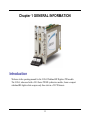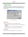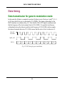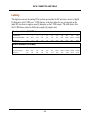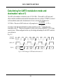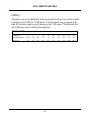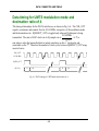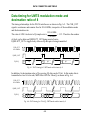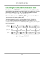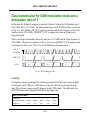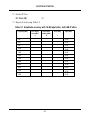
1
Operating Manual 3030A Wideband RF Digitizer PXI Module Contents About this manual Chapter 1 – General information Chapter 2 – Installation Chapter 3 – Operation Chapter 4 – Technical description Chapter 5 – Acceptance test Aeroflex offices Safety information www.aeroflex.com 3030A Wideband RF Digitizer PXI Module Operating Manual This manual applies to instruments with software issues of 2.0 and higher. Aeroflex International Ltd. 2006 No part of this document may be reproduced or transmitted in any form or by any means, electronic or mechanical, including photocopying, or recorded by any information storage or retrieval system, without permission in writing by Aeroflex International Ltd. (hereafter referred to throughout the document as ‘Aeroflex’). Printed in the UK Document part no. 46892/718 Issue 3 24 July 2006 PREFACE About this manual This manual explains how to set up and configure an Aeroflex 3030A wideband RF digitizer PXI module. Where necessary, it refers you to the appropriate installation documents that are supplied with the module. This manual provides information about how to configure the module as a stand-alone device. However, one of the advantages of Aeroflex 3000 Series PXI modules is their ability to form versatile test instruments, when used with other such modules and running 3000 Series application software. Getting Started with afDigitizer (supplied on the CD-ROM that accompanies each module (see Associated documentation)) explains how to set up and configure a 3030 Series RF digitizer with a 3010 Series RF synthesizer module to form a high performance digitizer instrument. Using the soft front panel and/or ActiveX controls supplied, the modules form an instrument that provides the functionality and performance of an integrated, highly-specified RF digitizer, but with the adaptability to satisfy a diverse range of test or measurement requirements. Intended audience Users who need to configure and operate the 3030A wideband RF digitizer to down-convert and digitize RF signals. This manual is intended for first-time users, to provide familiarity with basic operation. Programming is not covered in this document but is documented fully in the help files that accompany the drivers and ActiveX controls on the CD-ROM. ii PREFACE Structure Chapter 1 General information Chapter 2 Installation Chapter 3 Operation Chapter 4 Brief technical description Chapter 5 Acceptance testing Associated documentation The following documentation covers specific aspects of this equipment: PXI Modules CD-ROM Part no. 46886/028 Compilation containing soft front panels, drivers, application software, data sheets, getting started and operating manuals for this and other modules in the 3000 Series. 3000 Series PXI Modules Common Installation Guide Part no. 46882/663 Detailed information on installing modules into a rack, external connections, powering up and installing drivers. 3000 Series PXI Modules Installation Guide for Chassis Part no. 46882/667 Explains how to set up a populated chassis ready for use. Getting Started with afDigitizer Part no. 46892/676 Setting up and using the RF digitizer application for 3010 Series and 3030 Series modules. iii PREFACE Preface The PXI concept VXI and GPIB systems meet the specific needs of instrumentation users but are often too large and expensive for mainstream applications. PC-based instrumentation may cost less but cannot meet the environmental and operational requirements of many systems. PXI (PCI Extensions for Instrumentation) is based on CompactPCI, itself based on the PCI standard. PCI was designed for desktop machines but CompactPCI was designed for industrial applications, and features a rugged Eurocard format with easy insertion and removal. PXI adds to the CompactPCI specification by defining system-level specifications for timing, synchronization, cooling, environmental testing, and software. While PXI extends CompactPCI, it also maintains complete interoperability so that you can use any CompactPCIcompliant product in a PXI system and vice versa. PXI also makes use of Windows software, VXI timing and triggering, and VXIplug&play instrument drivers to provide powerful and affordable systems. ® is a registered trademark of Aeroflex International Inc. in the US PXI™ is a registered trademark of the PXI Systems Alliance Windows™, Windows XP™ and Windows NT™ are trademarks of Microsoft Corporation iv PREFACE Abbreviations/acronyms ACLR Adjacent Channel Leakage Ratio ACP Adjacent Channel Power ACPR Adjacent Channel Power Ratio ADC Analog-to-Digital Converter AM Amplitude Modulation ARB Arbitrary Waveform Generator CW Continuous Wave DAC Digital-to-Analog Converter dB Decibels dBc Decibels relative to the carrier level dBm Decibels relative to 1 mW FFT Fast Fourier Transform FM Frequency Modulation FPGA Field Programmable Gate Array GND Ground IQ In-phase/Quadrature LO Local Oscillator LSTB List Strobe LVDS Low-Voltage Differential Signaling PCI Peripheral Component Interconnect Pk-Pk Peak-to-Peak v PREFACE PXI PCI eXtensions for Instrumentation RF Radio Frequency RMS Root Mean Square SFP Soft Front Panel SMA SubMiniature version A (connector) SMB SubMiniature version B (connector) TDMA Time Division Multiple Access TRIG Trigger TTL Transistor-Transistor Logic UUT Unit Under Test VCO Voltage-Controlled Oscillator VHDCI Very High Density Connector Interface VSWR Voltage Standing-Wave Ratio VXI VMEbus Extension for Instrumentation vi Chapter 1 GENERAL INFORMATION Introduction Welcome to the operating manual for the 3030A Wideband RF Digitizer PXI module. The 3030A, when used with a 3010 Series PXI RF synthesizer module, forms a compact wideband RF digitizer that occupies only three slots in a 3U PXI chassis. 1-1 GENERAL INFORMATION Applications The 3030A down-converts and digitizes RF signals. It converts an analog RF waveform presented at its RF port into a series of amplitude- and phase-corrected digital IF or IQ data pairs at its LVDS port. Software supplied with the module allows for spectrum analysis of the digitized signals. The 3030A can be used in RF test and measurement systems used in development or manufacturing. Applications span all areas of UHF radio communications. Wide frequency coverage The 3030A provides continuous frequency coverage from 330 MHz to 3 GHz. A linear single-stage down-converter converts input signals to an IF centered on 77.76 MHz. Input range and accuracy Input level control is provided by electronic switched attenuation, which helps to maximize the usable dynamic range. Good level accuracy and repeatability make the 3030A ideal for high-volume manufacturing. Wide bandwidth The 3030A produces a 36 MHz wide digitized IF signal. Amplitude and phase correction is applied across 33 MHz. Full-rate digital IF or decimated IQ data can be output via LVDS, useful for real-time emulation. Data can also be captured to internal memory and read over the PCI bus. For narrowband signal analysis, the 3030A provides internal digital down-conversion and decimation. Lowering the sample rate allows longer events to be captured. The 3030A contains digital resampling filters that allow you to set the sample rate, as well as numerous preset values associated with common digital communications standards. Signal routing A configurable routing matrix provides flexibility in how you interconnect signals on the PXI backplane and the LVDS front-panel input. Predefined routing scenarios can be selected, or your own matrix settings stored and recalled. 1-2 GENERAL INFORMATION Triggering and synchronization The 3030A synchronizes to an external 10 MHz signal (generally supplied by a 3010/3011 RF Synthesizer). Triggering is external, from the PXI backplane or directly from the front-panel LVDS connector or SMB TTL input, or internal, from the internal timer or level trigger. List mode In list mode, up to 128 internal hardware settings can be pre-calculated and stored, providing fast switching of frequency whilst maintaining RF output accuracy. List addresses are sourced externally or from an internal counter, possibly driven by the test application controlling the 3030A. In production, list mode enables faster testing and simplified programming. Software The 3030A is supplied with a VXI PNP driver and soft front panel for use as a self-contained module. An instrument-level ActiveX control and soft front panel is also provided, combining the controls of the 3030A together with the 3010/3011 RF Synthesizer. Refer to Getting Started with afDigitizer (part no. 46892/676) supplied on the PXI Modules CD-ROM part no. 46886/028. An FFT spectrum analyzer measurement suite is supplied, and optional signal analysis components are available to measure power, modulation quality and spectra to recognized standards. RF Investigator, also supplied with the module, is an application that provides combined operation of all Aeroflex 3000 Series modules from a single user interface, especially useful for acceptance testing. 1-3 GENERAL INFORMATION Deliverable items • 3030A Wideband RF Digitizer PXI module • PXI Modules CD-ROM (part no. 46886/028), containing soft front panels, drivers, application software, data sheets and operating manuals for this and other modules in the 3000 Series • 3000 Series PXI Modules Common Installation Guide, part no. 46882/663 • 3000 Series PXI Modules Installation Guide for Chassis, part no. 46882/667 • SMA connector cable, part no. 43138/421 (2 off) • SMA connector saver, part no. 46885/224 Cleaning Before commencing any cleaning, switch off the chassis and disconnect it from the supply. You can wipe the front panel of the module using a soft cloth moistened in water, taking care not to wet the connectors. Do not use aerosol or liquid solvent cleaners. Putting into storage If you put the module into storage, ensure that the following conditions are not exceeded: Temperature range: Humidity: −20 to +70°C (−4 to +158°F) 5 to 93%, non-condensing 1-4 Chapter 2 INSTALLATION WARNING Initial visual inspection Refer to the 3000 Series Common Installation Guide 46882/663. Handling precautions Refer to the 3000 Series Common Installation Guide 46882/663. Hardware installation Installing the module into the PXI chassis Refer to the 3000 Series Common Installation Guide 46882/663 and Installation Guide for Chassis 46882/667. 2-1 Chapter 3 OPERATION Front-panel connectors 3030A 1 IF OUT 77.76 MHz, nominally −5 dB relative to RF input, 0 dB input attenuation selected. SMA socket, 50 Ω. 2 10 MHz I/O Two SMA I/O sockets in parallel. Input Ext frequency standard input for sampling clock. 0.4 to 4 V pk-pk into 50 Ω. 1 7 IF OUT IF IN Output Link-through from input. 6 TRIG 10 MHz I/O 2 5 3 LO IN 1.5 to 3 GHz, nominally 0 dBm. SMA socket, 50 Ω. 4 RF IN +16 dBm max. (0 dB input attenuation). SMA socket, 50 Ω. 5 DATA 68-way VHDCI connector for LVDS data I/O, 14-bit IQ digital data output. DATA LO IN 3 RF IN See Appendix A for details. 6 TRIG TTL +ve or −ve edge. SMB socket, 50 Ω. 7 IF IN 77.76 MHz input, −15 to +10 dBm for fullscale digitizer. SMA socket, 50 Ω. 4 I/P PWR 16dBm MAX Maximum safe powers RF input: +16 dBm continuous (0 dB input attenuation) IF input: +10 dBm (0 dB IF attenuation) C5950 Fig. 3-1 3030A front panel 3-1 OPERATION Soft front panel (af3030_sfp) The soft front panel provides a graphical interface for operating the module. It is intended for testing and diagnosing, for demonstration and training, and for basic operation of the module. It represents most of the functions available in the instrument driver. It is not however a comprehensive application suitable for measurements; for this, use the afDigitizer ActiveX control or the afDigitizer DLL. Installation The soft front panel is installed during the driver installation process (refer to the 3000 Series PXI Modules Common Installation Guide, part no. 46882/663). Open the AF3030_sfp.exe file: this is in the C:\VXIPNP|WinNT\af3030\ directory on a Windows NT machine, for example. It is also accessible from the Windows Start menu under Programs\Aeroflex\PXI Module Front Panels\AF3030 Front Panel. The soft front panel, similar to that in Fig. 3-2, is displayed. Detailed help information Soft front panel controls are all available as driver export functions unless noted otherwise, and are documented in the help files (page 3-40). This operating manual provides an overview of the facilities that the module provides and summarizes its operation; however, refer to the help files for detailed descriptions of functions, together with their parameter lists and return values. 3-2 OPERATION IF/IQ data format Menu bar Input source Boot C6122 Input conditioning RF tuning Fig. 3-2 3030A soft front panel 3-3 Acquisition & triggering Soft front panel controls Menu bar File Save Captured Data (as ASCII file)… captures the 16-bit sample data into the specified ASCII file. Save Captured Data (as Binary file)… captures the 16-bit sample data into the specified binary file. Click Exit to close the application. Settings Load and Save allow you to load and save soft front panel configurations from and to your preferred locations. If you did not change the default location when installing the software, it is C:\VXIPNP\WinNT\af3030\settings, and configurations are saved as .ini files. You can edit, copy and paste settings files as required; for example, you may want to save only a new routing setup without changing other parameters. Edit the saved .ini file using a text editor (for example, Notepad) to remove unwanted parameters. Ensure only that you do not delete the General (VendorID, DeviceID) and Version (Major/Minor) parameters. Save the changed file. When the settings file is next loaded, the configuration of the soft front panel changes to match the parameters remaining in the settings file. Directories lets you choose the location for your front-panel configuration settings, including routing matrix. 3-4 MENU BAR ON SOFT FRONT PANEL LVDS allows you to set each LVDS Data, Auxiliary and Marker mode for input, output or tristate (default) operation. • To use Spare 0 as a trigger input, set LVDS Data to Input. Spare 0 is controlled by LVDS Data Mode. • To use an auxiliary bit as a trigger input, set LVDS Auxiliary to Input • To use a marker bit as a trigger input, set LVDS Marker to Input. • IF Data Position places 14-bit IF data in either the upper 14 bits of a 16-bit word (the lower two bits are padded with 0s) or lower 14 bits of a 16-bit word (upper two bits are sign extended), as required by the processing software. Routing Scenarios allows you to select a predefined routing matrix connection. A tick against the scenario’s title shows that it is selected. Selecting or removing a routing scenario affects only the connections specific to that scenario, and does not change any other routing connections. However, changing the routing matrix connections of any scenario invalidates that scenario. 3-5 MENU BAR ON SOFT FRONT PANEL Routing Matrix displays a matrix that provides interconnection between input and output signals on the PXI backplane bus and the DATA connector, as shown diagrammatically in Fig. 3-3. This provides great flexibility in how you can route signals between modules. PXI_STAR PXI_LBL[0]–[12] PXI_TRIG[0]–[7] PXI BACKPLANE BUS TRIG ROUTING MATRIX 3030A PXI MODULE DATA LVDS_MARKER1–4 LVDS_AUX[0]–[4] LVDS_SPARE[0]–[2] Fig. 3-3 Routing matrix in 3030A 3-6 C5960 MENU BAR ON SOFT FRONT PANEL Use the routing matrix (Fig. 3-4) to interconnect signals. Output signals form the body of the matrix. Select appropriate input signals from the drop-down menus under each down-arrow to create the interconnections. Check the boxes to enable the outputs and select the appropriate LVDS mode. Reset connects all input signals to GND and disables the outputs (LVDS outputs go tri-state). This is the default state. When operating the 3030A in default digitizer mode (routing matrix reset), all necessary input, output and trigger signals are available on front-panel DATA, SMA and SMB connectors and there is no need to configure the matrix. If you need to set up particular signal routings, you can define these using the drop-down menus on the matrix and save them using the Load and Save commands in Settings, or use Routing Scenarios to access pre-set alternative routings, or contact Aeroflex if you need assistance in defining particular routing requirements. 3-7 MENU BAR ON SOFT FRONT PANEL Output enable check boxes Input signal selection C5961 Output signals Input signals Fig. 3-4 Routing matrix inputs and outputs 3-8 MENU BAR ON SOFT FRONT PANEL Optimization allows you to choose how the 3030A compensates for the effect of temperature changes and RF frequency response. Auto Temperature Optimization (default) monitors the temperature of the module at regular intervals and adjusts the correction figure for the current temperature. You can turn this off if it might interfere with a time-critical measurement. It is also turned off automatically when List Mode is enabled. Optimize Temperature Correction forces an immediate update, after which the timer starts a new interval. Auto Flatness Mode compensates for the slope of the RF response, and may be needed for measurements taken over a wide bandwidth. It applies compensation to ‘flatten’ the response over the chosen bandwidth. The change in RF level due to RF response may not be significant for narrow-bandwidth measurements, which should be taken into account as auto flatness mode compensation may slow measurement time considerably. Default is ‘off’. 3-9 MENU BAR ON SOFT FRONT PANEL Options Allows you to enable or disable additional instrument options if you have the appropriate password (available from the Aeroflex sales desk). Click Edit… to display the options screen (Fig. 3-5). Fig. 3-5 Options screen Disabled options are shown grayed out. To enable an option, enter the appropriate password. Click Enable. The enabled option is shown highlighted in green. Click OK. 3-10 MENU BAR ON SOFT FRONT PANEL View Allows you to view results in different formats. View FFT (default) displays a single graph showing logarithmic power versus frequency. The default span is 66% of full span. You can modify the top of screen reference power (dBm) and the vertical scaling (dB/div). Select other display settings from FFT Display. View Time Series displays two graphs showing I and Q magnitude (in IQ mode) or IF magnitude (in IF mode) versus sample number. Sample Start and Sample End let you change the start and stop time of samples, allowing you to ‘zoom in’ on data. Select other display settings from Time Series Display. View IQ Polar presents I and Q data as a polar response. Select other display settings from IQ Polar Display. View Numeric Data displays IQ or IF data that can be placed alongside either the FFT or Time Series views. Numeric data representing the values of I and Q capture data is displayed as I first, followed by Q. Use the scroll bar to inspect long sample records. 3-11 MENU BAR ON SOFT FRONT PANEL FFT Display This menu is enabled only when View\View FFT is selected. It allows you to hide/display the graticule and save the dB levels of the trace as a .txt or other file. Graticule Visible hides or displays the graticule. The Span menu selects either Full or Truncated (approx. 66%) span. For example, with Modulation Mode set to UMTS and with a Decimation Ratio of 2, Full span is the full decimated bandwidth of the module — 30.72 MHz — and Truncated limits this to 20 MHz, placing graticule lines at integer frequencies for easier reading. For Generic Modulation Mode, the Full and Truncated limits are 51.84 MHz and 33 MHz respectively, reflecting the maximum available span of the module with a Decimation Ratio of 2. Save FFT Trace saves the current FFT trace as a text file. The FFT trace is recorded as an array of dB values. The length of the array is displayed in the FFT Length field. The text file’s location is defined in File Setup... File Setup… allows you to select the filename and location for the FFT trace. 3-12 MENU BAR ON SOFT FRONT PANEL Time Series Display When View Time Series is selected, the Time Series Display menu is enabled, allowing you view I and Q traces on two separate graphs or overlaid in different colors. Graticule Visible hides or displays the graticule. IQ Separate Graphs displays separate graphs of Time Series (I) and Time Series (Q). Both graphs are displayed with a common horizontal axis scaling (as set by Sample Start and Sample End). IQ Overlaid Graph displays colored I and Q traces on a single graph; I is yellow and Q is green. Full Width Sample View adjusts the number of samples displayed in the graph to the number of samples captured. Y-axis Autoscale: when selected, automatically sets the scaling of signal magnitude to the peak value. When it is deselected, you can set the values manually using the Magnitude Min and Magnitude Max controls above the display. The values of Magnitude Min and Magnitude Max apply to both I and Q when IQ Separate Graphs is selected. IQ Polar Display When View IQ Polar is selected, the IQ Polar Display menu is enabled, allowing you view I and Q traces on a polar plot. Graticule Visible hides or displays the graticule. Autoscale, when selected, scales the I and Q signal magnitudes to the peak value. When it is deselected, you can set the values manually using the IAxis Range (±) and QAxis Range (±) controls above the display. 3-13 MENU BAR ON SOFT FRONT PANEL Capture By default, 3030A captures data to the screen (To Screen Only), but you can also capture results to ASCII or binary files whilst continuing to display on screen (To ASCII File and Screen; To Binary File and Screen). File Setup… opens a browser to define a file extension (default is .txt) and location for storing data. Files are saved as interleaved I/Q pairs (I followed by Q) or single IF data, depending on the setting of the Sample Data Type field. • ASCII IQ file: I and Q values are on new lines, I value followed by Q value. • Binary IQ file (16-bit mode): I and Q values are stored as 16-bit integers, I value followed by Q value. Binary IQ file (32-bit mode): I and Q values are stored as 32-bit integers, I value followed by Q value. Help Instrument Information provides the module’s PXI resource code and serial number, revision numbers for driver, FPGA and PCI, and its last calibration dates. About provides the version and date of the soft front panel. 3-14 Boot Click Boot to initialize the module and view the Boot Resource window. Resources available for initializing are shown in blue. Select the 3030A you want to boot. Check the box to use the boot default configuration. Do not change the configuration unless you are advised otherwise. Click OK. While you select the boot resource, the indicator is amber. Once the module has initialized, the indicator changes to green in a few seconds. If no calibration data is available, the driver returns a caution. If this happens, return the module for calibration. s/n: After the module initializes, this field displays its serial number. Res: After the module initializes, this field displays its VISA resource string. 3-15 Input source Set this to RF or IF depending on which input is used (IF IN or RF IN). Apply IF or RF signals to the appropriate input connector. If the signal is RF, the module downconverts it and provides attenuator configuration and filtering options (see Input conditioning). RF frequency settings/input level or IF input level controls are enabled, depending on which is selected, and unused controls are grayed out. 3-16 RF tuning RF Channel Sets the currently active channel in a range of 0 to 127. Chan List Click this to set up the channels for list mode operation (page 3-34). You can Load and Save the settings file (page 3-4) to make setup easier. RF Freq (Hz) This is the RF input frequency. This defines the center frequency of the FFT trace and selects appropriate correction values. The module is tuned by setting the RF frequency and the LO offset direction (above or below). From these two values, the module calculates the LO frequency that must be applied to the LO input. Set the input frequency using the up/down arrows or by entering the frequency in Hz or scientific (e) notation, in the range 330 MHz to 3.0 GHz. LO Offset (Hz) Displays the local oscillator offset frequency in Hz. Set the Above/Below switch to Above when the LO is higher in frequency than the RF (IF = LO−RF), and to Below when the LO is lower in frequency than the RF (IF = RF−LO). 3-17 RF TUNING ON SOFT FRONT PANEL LO Freq Shows the frequency to which a 3010/11 synthesizer module or other source should be set in order to provide the correct LO frequency for the 3030A. If you are using a 3010/11, simply double-click on the field, copy the value, and paste it into the RF Frequency (Hz) field on the 3010/11’s soft front panel. External Reference Lock to 10MHz causes the ADC clock to lock to the 10 MHz reference connected to the 10 MHz I/O connector. Free Run causes the ADC clock to free run at the center of its range, at a nominal frequency of 103.68 MHz. 3-18 Input conditioning You may find the block schematic diagram (Fig. 4-1) helpful in understanding these features. RF Input Level (dBm) Set this to the peak level of the input RF signal to ensure the best dynamic range and signalto-noise ratio. Grayed out when Input Source is set to IF. Set the RF input level using the up/down arrows or by entering the level, in the range −99.99 to +22.00 dBm (Atten Config = Auto) or −99.99 to +16.00 dBm (Atten Config = Auto IF or Manual). Note: when Atten Config is set to Auto and the RF input attenuation is 8 dB or more, the module can accept an input level of +22 dBm peak. For any setting below 8 dB attenuation, the maximum safe input reduces to +16 dBm peak with 4 dB of IF attenuation. IF Input Level Set this to the peak level of the input signal to ensure the best dynamic range and signal-tonoise ratio. Grayed out when Input Source is set to RF. Set the IF input level using the up/down arrows or by entering the level, in the range −99.00 to +17.00 dBm for full scale on the digitizer. Note: the maximum safe input with 0 dB IF attenuation is +10 dBm. Step size: double-click on the step value under the IF Input Level field to set up the size of RF and IF level step. RF Atten Sets the RF attenuator value, which changes the input level to the mixer. This value can only be adjusted manually if Atten Config is set to Manual or Auto IF. Set the RF attenuator level using the up/down arrows or by entering the level, in the range 0 to +28 dB in 4 dB steps. 3-19 INPUT CONDITIONING ON SOFT FRONT PANEL IF Atten Sets the IF attenuator value, which changes the input level to the ADC. This value can only be adjusted manually if Atten Config is set to Manual. Set the IF attenuator level using the up/down arrows or by entering the level, in the range 0 to +35 dB in 1 dB steps. Input Level Dimensions Establishes the measurement units as dBm, dBµV, dBmV, dBV, V or mW. Atten Config Auto the RF input level set is used to optimize RF and IF attenuator gain settings automatically. Auto IF the IF input level set is used to optimize the IF attenuator settings, but you have manual control of RF attenuation. Manual ignores the RF input level you set, giving complete control over the settings of the RF and IF attenuators. Filter Bypass When enabled, causes the anti-aliasing filter to be bypassed, allowing signals outside its passband to reach the ADC. Level calibration is maintained. Allows you to observe spurii and other signals within the module’s bandwidth that would otherwise be removed by the filter. ADC Overload (LED) Indication is red if the ADC was overloaded during the last acquisition. ADC Overload Level Indicates the input level that could cause ADC overload error. 3-20 INPUT CONDITIONING ON SOFT FRONT PANEL Note: ADC overload level is clamped to the safe input level. Remove DC Offset Removes the DC component from captured IF or IQ data. Removes DC components at the edge of the span at full and/or ½ sample rate. Note: if DC but no signal is present on the input, a sawtooth waveform is displayed on I and Q time series screens. 3-21 Acquisition & triggering Capture Trigger Allows you to select the trigger source from a drop-down list: Software trigger • SW_TRIG This is a non-triggered capture mode. Click on Start to capture samples (defined by Number of Samples) when in Single/Repeat mode, without waiting for any external event. Click Stop to end the capture. 3-22 ACQUISITION AND TRIGGERING ON SOFT FRONT PANEL Hardware triggers Remaining triggers on the drop-down list are hardware triggers. When any of these are selected, triggering is dependent on trigger events, including the correct arming of the trigger. The module ignores triggers that occur during the sample capture. Refer to the help files (page 3-40) for full details. Most of the hardware triggers share a common triggering interface: 3-23 ACQUISITION AND TRIGGERING ON SOFT FRONT PANEL Trigger Type set to Edge or Gate Edge/Gate Polarity set +ve or –ve Trigger Offset Delay all hardware triggers can be delayed in the range 0 to +29 decimated samples. Samples C5977 Trigger offset delay Trigger Max buffer length Pre-Trig Samples (Edge trigger type) sets the number of pre-trigger samples present in the captured data buffer. Increase this value to move the position of the trigger point in the captured data further from the start. Samples C5976 Pre-trigger samples Max buffer length Trigger Post-Trig Samples (Gate trigger type) sets the number of post-trigger samples present in the captured data buffer. Max buffer length Gate Post-trigger samples 3-24 C5983 ACQUISITION AND TRIGGERING ON SOFT FRONT PANEL • PXI_TRIG [0–7] Takes its trigger input from any one of 8 bits of the PXI trigger bus that is common to all modules in the chassis. • PXI_STAR Takes its trigger input from a module that has ST functionality and is fitted in PXI slot 2. • PXI_LBL (Local Bus Left) [0–12] Takes its trigger input from the slot to the left of the 3030A (viewed from the front panel), using the PXI local bus. Choose from any of 13 bits for the trigger; this bus is common only to the 3030A and the module to its left. • LVDS_M [1–4] Takes its trigger from any of four Marker bits on the DATA connector. Ensure that Settings/LVDS/Marker Mode is set to Input. • LVDS_A [0–4] Takes its trigger from any of five Auxiliary input bits on the DATA connector. Ensure that Settings/LVDS/Auxiliary Mode is set to Input. • LVDS_S Takes its trigger from the Spare 0 input bit on the LVDS data bus. Ensure that Settings/LVDS/Data Mode is set to Input. Because the data bus is set to receive when this trigger is used, it is not then possible to output data on the DATA connector. • FRONT_SMB Takes its trigger from the TRIG connector on the module’s front panel. 3-25 ACQUISITION AND TRIGGERING ON SOFT FRONT PANEL • INT_TIMER Takes its trigger from the internal timer. Timer Period Timer Phase sets the period of the internal timer (50% mark/space ratio) adjusts the phase of the internal timer signal in multiples of the resampled sample clock period for the selected modulation mode. This allows you to synchronize the timer trigger with external events. 3-26 ACQUISITION AND TRIGGERING ON SOFT FRONT PANEL • INT_TRIG Takes its trigger from the internal level trigger. This timer trigger can also be routed to other modules using the routing matrix (page 3-6). Similarly, this timer can be synchronized with the external signal connected to the TIMER_SYNC signal in the routing matrix. 3-27 ACQUISITION AND TRIGGERING ON SOFT FRONT PANEL Int Trigger Mode Select the internal level trigger mode: Absolute/Relative Absolute: the digitized signal is filtered using an absolute time constant. An internal level trigger is generated when the level of this filtered signal exceeds the absolute level trigger threshold (specified in dBm). The absolute time constant and level settings may affect the trigger delay. AbsTime Const Absolute Threshold Relative Slow/Fast Time Const Relative Threshold Relative: the digitized signal is filtered using both fast and slow time constants. The amplitude difference between the fast and slow time constant filtered signal is compared with the 'relative threshold level'. For a step level change, the difference signal is a pulse with a duration and level determined by the difference between the fast and slow time constants. When the relative threshold trigger level is entered as positive, the difference signal = (fast signal − slow signal). When relative threshold trigger level is entered as negative, the difference signal = (slow signal − fast signal). Sets the time constant for the absolute level internal trigger. The threshold value (dBm) used in Absolute Int Trigger Mode to compare the digitized filtered signal using the AbsTime Constant. Relative Threshold is the difference in dB between the signal filtered with the specified fast and slow time constants. The threshold value (dBm) used in Relative Int Trigger Mode to compare the difference signal filtered using Relative Slow and Fast Time Constants. 3-28 ACQUISITION AND TRIGGERING ON SOFT FRONT PANEL Trigger mode and control Mode: Selects Single-shot or Repeat data capture. Use with the Start and Stop buttons to initiate and stop data capture. The indicator shows the status of the trigger or capture: green when waiting for a trigger or capturing, gray when idle. 3-29 IF/IQ data format Sample Data Type Select IQ or IF sample data type. • IQ Sample Data: output sample rate is determined by the Modulation Mode and Decimation Ratio • IF Sample Data: output sample rate is fixed to 103.68 MHz Modulation Mode (IQ data format only). Sets the digital modulation mode. Select from Generic, UMTS, GSM, CDMA2000 1X or 2319 Emulation. The sample rate varies, depending upon modulation mode and decimation ratio: • Generic: user-defined. Use this mode to create or emulate any modulation scheme. Enter any sample rate up to 85 MHz or define a fractional rate by setting the numerator and denominator. Click on the button adjoining the Undecimated Sample Rate box to open the popup panel and enter a fractional sample rate: 3-30 IQ/IF DATA FORMAT ON SOFT FRONT PANEL Pre-defined rates: • UMTS data mode: 61.44 MHz/2N (where N = 1 to 10) N • GSM resampled IQ data mode: 13 MHz/(3 * 2 ), where N = 0 to 4 (2 (4-N) times symbol rate of 13 MHz/48) N • CDMA2000 1X resampled IQ data mode: 9.8304/2 , where N = 0 to 3 (2 (3-N) times chip rate of 1.2288 MHz) N • 2319 emulation mode: 65.28/2 , where N = 4 or 5. Decimation Ratio (Generic/GSM/UMTS/CDMA2000 X1/2319E) (IQ data format only) Select a decimation ratio, dependent on the modulation mode: GENERIC 2n where n = 0 to 14 GSM 2n where n = 0 to 4 UMTS 2n where n = 1 to 10 CDMA2000 1X 2n where n = 0 to 3 2319E emulation 2n where n = 4, 5 See Data timing on page A-3. Undecimated Samp Rate (MHz) Displays the internal undecimated sampling rate before division by the decimation ratio. GENERIC max 85.00 MHz UMTS 61.44 MHz = 3.84 MHz (3GPP chip rate) x 16 GSM 4.3333 (rec.) MHz = 270.8333 (rec.) kHz (GSM bit rate) x 16 CDMA2000 1X 9.8304 MHz = 1.2288 MHz (CDMA2000 chip rate) x 8 2319E 65.28 MHz = 3.84 MHz (3GPP chip rate) x 17 IF 103.68 MHz 3-31 IQ/IF DATA FORMAT ON SOFT FRONT PANEL IQ Data Output Format Select 16- or 32-bit, subject to the modulation mode and decimation ratio chosen. Sample rates Modulation GENERIC UMTS Decimation ratio n 2 where n = 0 to 14 CDMA2000 2319E variable IQ data format 16 (when Output Sample Rate > 12.96 MHz ) 16/32 (when Output Sample Rate <= 12.96 MHz) 2 30.72 16 4 15.36 16 8 7.68 16/32 16 3.84 16/32 32 1.92 16/32 64 0.96 16/32 128 0.48 16/32 256 0.24 16/32 512 0.12 16/32 1024 GSM IQ sample rate (Msymbol/s) 0.06 16/32 1 4.33333 16/32 2 2.16666 16/32 4 1.08333 16/32 8 0.541667 16/32 16 0.270833 16/32 1 9.8304 16 2 4.9152 16 4 2.4576 16 8 1.2288 16/32 16 4.08 16/32 32 2.04 16/32 3-32 IQ/IF DATA FORMAT ON SOFT FRONT PANEL Window Function Defines the window used by the FFT. 5-term Aeroflex gives good noise performance and side-lobe suppression at the expense of a wider main lobe, optimal for ACPR measurements. Decimated Samp Rate (MHz) Displays the result of the undecimated sampling rate divided by the decimation ratio. Number of (IF/IQ) Samples The name of the field changes to reflect the sample type selected. Sets the sample size (number of samples to be captured), up to 32 x 106 IQ pairs with 32-bit storage, 64 x 106 IQ pairs with 16-bit storage, or 128 x 106 IF samples. FFT Length Varies with number of IF/IQ samples set. Minimum 16, maximum 2048. 3-33 List mode operation Introduction List mode operation associates a list address with a particular RF setup (channels 0–127). When the module is set to list mode operation, a new address, when strobed in, causes the module to change to the RF setup (channel) associated with that address. List mode operation facilitates fast channel hopping during, for example, testing of transmitter/receiver modules where numerous different RF level and frequency settings are needed. A seven-bit list address selects the channel. A strobe signal, internally or externally generated, then causes the instrument to switch between channels as required. Flexibility is provided to allow channel hopping using a variety of control sources. List addresses for list mode operation can be provided manually, or from an external source via the signal routing matrix (providing access to backplane bus, LVDS and other address sources), or from an internal sequential counter. The strobe signal that changes the list address can be sourced externally via the routing matrix, or internally. 3-34 LIST MODE Channel List Click Chan List on the soft front panel to display individual channel list settings (Fig. 3-6). This is where you define channel setup for list mode operation. Fig. 3-6 Edit channel list settings 3-35 LIST MODE Edit individual channel parameters by selecting the specific channel. Channel parameters are: Freq (Hz) LO Position Atten Config RF Level (dBm) IF Level (dBm) RF Atten (dB) IF Atten (dB) Select the channel to be edited either by changing the channel number on the panel or by clicking on the corresponding channel row in the channel list. Check the Automatically set focus from grid select box to make the associated channel parameter field active when you click on a channel parameter in the grid. If you check the Link channel selection to main panel box, changing the channel number on this panel makes it become the active channel on the soft front panel. 3-36 LIST MODE Click Edit Range to display the Edit Channel Range screen (Fig. 3-7), which lets you apply changes to a set of channels simultaneously, speeding up channel setup. Define start and finish values for address numbers in the Chan range, from: and to: fields. Insert values and click Set for each field. You are asked to confirm each action. When finished, click Close to return to the Channel List screen. Fig. 3-7 Edit all channel settings Click List Mode to display the List Mode Settings screen (page 3-38), which lets you set up addressing and strobing, and the internal counter. 3-37 LIST MODE List Mode Settings Click List Mode on the Channel List screen to display the List Mode Settings screen. From here, you can define the list address source, and how the strobe (internal or external) that actions a new list address is handled. You can also set up the internal sequential counter and the timer that drives it. Fig. 3-8 Edit list mode settings Address Source Defines the source from which the seven-bit-wide list address is obtained. Manual: RF list addresses are register-driven values, manually controlled by setting the RF Channel. External: RF list addresses are sourced from the signal routing matrix (Fig. 3-3). Counter: RF list addresses are sourced from the internal sequential counter. Strobe Polarity Defines whether a positive- or negative-going edge is active for the strobe signal. 3-38 LIST MODE Counter Strobe Source Defines the method used to sequence the internal List Counter register, when Address Source is set to Counter. When sequenced, the resulting change of address (the count value) automatically causes an internal strobe signal to be generated, which actions the new list address. External: an external strobe, sourced from the signal routing matrix (Fig. 3-3), causes the counter to count up or down, providing a new list address. Timer: the counter strobe signal is generated periodically by an internal timer, whose period is set by Timer Dwell. Counter Start Defines the start address of the list counter. If this value is less than the value of Counter Stop, the counter increments; otherwise it decrements. Setting this value also resets the list count to the next start address. Counter Stop Defines the stop address of the list counter. If this value is greater than the value of Counter Start, the counter increments; otherwise it decrements. Setting this value also resets the list count to the next start address. Timer Dwell Defines the period of the list timer, in units of 0.1 µs. The range is 1 µs to 600 s. 3-39 Driver export functions On-line help and functional documentation for driver export functions are available on the CD-ROM supplied with your module. They are installed onto your computer at the same time as the drivers. Driver installation folder Find help and functional documentation in the driver installation folder on your computer. This is typically: C:\vxipnp\winnt\af3030 Help Within the driver installation folder are help files that provide detailed descriptions, parameter lists and return values for all available functions. Help files are provided in three formats: af3030.doc af3030.hlp af3030_C.hlp 3030A function documentation 3030A Visual BASIC function reference 3030A C language function reference Text file Windows Help file format We recommend that you use the C or Visual Basic formats, as these are easier to navigate. 3-40 DRIVER EXPORT FUNCTIONS The file opens at the Contents page: Fig. 3-9 Online help contents — example Hyperlinks from here take you to Introduction Assumptions Error codes Functions listings 3-41 DRIVER EXPORT FUNCTIONS Functions listings Functions are grouped by type. Click on the hyperlink for details of the function. Each function has a description of its purpose, and may have a list of parameters and return values. Fig. 3-10 Function description — example 3-42 RF digitizer using 3010/3011 and 3030A Refer to 3000 Series PXI Modules Installation Guide for Chassis (part no. 46882/667) and Getting Started with afDigitizer (part no. 46882/676), both supplied on the CD-ROM with the module, for detailed information on creating a fully functional RF digitizer using the 3030A and 3010/3011 together. The afDigitizer soft front panel and ActiveX control combine the functions of the individual modules to provide a single interface with the appearance and functionality of an integrated instrument. 3-43 Appendix A DATA connector and timing The DATA connector is a 68-way female VHDCI-type LVDS (low-voltage differential signaling) interface. It can be used to output data and associated control and timing signals. The DATA connector is shown in Fig. A-1. LVDS data conforms to ANSI/TIA/EIA-644. 34 1 68 35 C5504 Fig. A-1 DATA connector (looking onto front panel) The DATA interface provides: • output of IF or IQ data • input/output of triggering, List Mode and Timer signals • clock. The electrical level is LVDS: VOH typically 1.38 V, VOL typically 1.03 V A-1 DATA CONNECTOR AND TIMING Table A-1 DATA pin-out Contact 1 2 3 4 5 6 7 8 9 10 11 12 13 14 15 16 17 18 19 20 21 22 23 24 25 26 27 28 29 30 31 32 33 34 Function AUX0AUX1− AUX2− SPARE1− SPARE2− CLK_IN− GND CLK_OUT− D0− D1− D2− D3− D4− D5− D6− D7− D8− D9− D10− D11− D12− D13− D14− D15− IQSELECT_OUT− IQSELECT_IN− SPARE0− GND MARKER1− MARKER2− MARKER3− MARKER4− AUX3− AUX4− Contact 35 36 37 38 39 40 41 42 43 44 45 46 47 48 49 50 51 52 53 54 55 56 57 58 59 60 61 62 63 64 65 66 67 68 A-2 Function AUX0+ AUX1+ AUX2+ SPARE1+ SPARE2+ CLK_IN+ GND CLK_OUT+ D0+ D1+ D2+ D3+ D4+ D5+ D6+ D7+ D8+ D9+ D10+ D11+ D12+ D13+ D14+ D15+ IQSELECT_OUT+ I/QSELECT_IN+ SPARE0+ GND MARKER1+ MARKER2+ MARKER3+ MARKER4+ AUX3+ AUX4+ DATA CONNECTOR AND TIMING Data format The data output to the DATA interface is real-time. In resample mode, data is output using a 103.68 MHz clock but bursted to achieve the correct average sample rate. Sample DATA Decimated IQ (also resampled IQ): 16-bit IQ, 2 x D[15:0], I followed by Q, D[0]=LSB. 32-bit IQ, 4 x D[15:0] in order I MSW, I LSW, Q MSW, Q LSW, D[0]=LSB. 32-bit data available only for decimate by 8 or more. IF data: there are two configurations: Upper 14 bits: D[15:2], D[2]=LSB (default mode) Lower 14 bits: D[13:0], D[0] = LSB, D[15:14] sign extended from D[13]. IQSELECT_OUT Determines if the data is I (IQSELECT_OUT=1) or Q (IQSELECT_OUT=0). IQSELECT_OUT=0 at all times in IF mode. CLK+ Data changes on the falling edge. CLK− Data changes on the rising edge. A-3 DATA CONNECTOR AND TIMING Data timing Data transmission for generic modulation mode In this mode the IQ data is resampled to produce IQ data at a rate of between 1 and 2N (N = 0 to 14) times the bit rate, up to a maximum of 51.84 MHz. The timing relationships for the DATA interface is as shown in Fig. A-2. Note that the CLK_OUT signal is continuous and that the frequency of the clock remains fixed at 103.68 MHz. It is possible to define any relationship between the data rate and the clock frequency of 103.68 MHz: in this example, the chosen decimated data rate of 51.84 Ms/s means that the ratio of clock to data rate is 2. CLK_OUT 103.68 MHz IQSEL_OUT D[15:0] I1 Q1 I2 Q2 I3 Q3 I4 Fig. A-2 DATA timing for generic modulation A-4 Q4 I5 Q5 DATA CONNECTOR AND TIMING Latency The digitizer converts an analog RF waveform presented at its RF port into a series of digital IQ data pairs at its LVDS port. LVDS latency is the time taken for any given point on the input RF waveform to appear as an IQ data pair on the LVDS output. The table below lists the LVDS latency times for different example IQ sample rates. Generic modulation (51.84 MHz) Decimation ratio 1 2 4 8 16 32 64 128 256 512 1024 Output sample rate (MHz) 51.84 25.92 12.96 6.48 3.24 1.62 0.81 0.405 0.2025 0.10125 0.050625 Total delay (µs) 1.32 1.76 2.55 4.13 7.14 13.16 25.19 49.27 97.42 193.71 386.31 Generic modulation (38.88 MHz) Decimation ratio Output sample rate (MHz) Total delay (µs) 1 2 4 8 16 32 64 128 256 512 1024 38.88 19.44 9.72 4.86 2.43 1.215 0.6075 0.30375 0.151875 0.075938 0.037969 1.41 1.99 3.04 5.15 9.16 17.19 33.24 65.34 129.54 257.93 A-5 514.72 DATA CONNECTOR AND TIMING Data timing for UMTS modulation mode and decimation ratio of 2 The ADC in the module is clocked at a rate of 103.68 Ms/s. The module’s soft front panel allows both the modulation mode and the decimation ratio to be selected. If UMTS is selected as the modulation mode and a decimation rate of two is selected, the IQ data rate is 103.68 MHz = 3.375, a 30.72 Ms/s. The ratio of ADC clock rate to IQ sample rate is 30.72 MHz non-integer value that means that data is output sometimes on the 3rd clock pulse and sometimes on the 4th. Therefore the number of clock cycles between IQSELECT_OUT being asserted varies. When configured in this way, the timing relationships for the DATA interface are as shown in Fig. A-3. CLK_OUT 103.68 MHz IQSEL_OUT D[15:0] I1 Q1 I2 Q2 I3 Fig. A-3 DATA timing for UMTS mode and decimate by 2 A-6 Q3 I4 DATA CONNECTOR AND TIMING Latency The digitizer converts an analog RF waveform presented at its RF port into a series of digital IQ data pairs at its LVDS port. LVDS latency is the time taken for any given point on the input RF waveform to appear as an IQ data pair on the LVDS output. The table below lists the LVDS latency times for different IQ sample rates. UMTS (61.44 MHz) Decimation ratio 2 4 8 16 32 64 128 256 512 Output sample rate (MHz) 30.72 15.36 7.68 3.84 1.92 0.96 0.48 0.24 0.12 0.06 Total delay (µs) 1.50 2.23 3.57 6.24 11.32 21.47 41.79 82.41 163.66 326.16 A-7 1024 DATA CONNECTOR AND TIMING Data timing for UMTS modulation mode and decimation ratio of 4 The timing relationships for the DATA interface are as shown in Fig. A-4. The CLK_OUT signal is continuous and remains fixed at 103.68 MHz, irrespective of the modulation mode and the decimation rate. IQSELECT_OUT is toggled only when an IQ data pair is being 103.68 MHz transmitted. The ratio of ADC clock rate to IQ sample rate is = 6.75, a 15.36 MHz non-integer value that means that data is output sometimes on the 6th clock pulse and sometimes on the 7th. Therefore the number of clock cycles between IQSELECT_OUT being asserted varies. CLK_OUT 103.68 MHz IQSEL_OUT D[15:0] I1 Q1 I2 Q2 Fig. A-4 DATA timing for UMTS mode and decimate by 4 A-8 DATA CONNECTOR AND TIMING Data timing for UMTS modulation mode and decimation ratio of 8 The timing relationships for the DATA interface are as shown in Fig. A-5. The CLK_OUT signal is continuous and remains fixed at 103.68 MHz, irrespective of the modulation mode and the decimation rate. 103.68 MHz The ratio of ADC clock rate to IQ sample rate is = 13.5. Therefore the number 7.68 MHz of clock cycles between IQSELECT_OUT being asserted varies. IQSELECT_OUT is toggled only when an IQ data pair is being transmitted. CLK_OUT 103.68 MHz IQSEL_OUT D[15:0] I1 Q1 I2 Q2 I3 Q3 Fig. A-5 DATA timing for UMTS mode and decimate by 8 In addition, for decimation ratios of 8 or greater, IQ data can be 32-bit. In this mode data is transmitted as two 16-bit words, MSW then LSW for I then Q, as shown in Fig. A-6. CLK_OUT 103.68 MHz IQSEL_OUT D[15:0] I I Q Q MSW LSW MSW LSW I I Q Q MSW LSW MSW LSW I I Q Fig. A-6 DATA timing for 32 bit IQ, UMTS mode and decimate by 8 A-9 Q MSW LSW MSW LSW DATA CONNECTOR AND TIMING Data timing for CDMA2000 1X modulation mode If a modulation mode of CDMA2000 1X and a decimation value of 1 are both selected, IQ data is generated at eight times the CDMA2000 1X chip rate. As the chip rate is 1.2288 MHz, this gives an IQ sample rate of 9.8304 Ms/s. There is no longer an integer relationship between the clock rate of 103.68 MHz and the 9.8304 Ms/s data rate. The number of clock cycles between IQSELECT_OUT being asserted is not fixed but varies. This is true for all CDMA mode decimation ratios. The timing relationship for the DATA interface is shown in Fig. A-7. Note that the CLK_OUT signal is continuous and remains fixed at 103.68 MHz, irrespective of the modulation mode and the decimation rate. IQSELECT_OUT is toggled only when an IQ data pair is being transmitted. CLK_OUT 103.68 MHz IQ_SEL_OUT D[15:0] I1 Q1 I2 Q2 Fig. A-7 DATA timing for CDMA2000 1X . A-10 I3 Q3 DATA CONNECTOR AND TIMING Latency The digitizer converts an analog RF waveform presented at its RF port into a series of digital IQ data pairs at its LVDS port. LVDS latency is the time taken for any given point on the input RF waveform to appear as an IQ data pair on the LVDS output. The table below lists the LVDS latency times, calculated for different IQ sample rates. CDMA2000-1x (9.8304 MHz) Decimation ratio Output sample rate (MHz) Total delay (µs) 1 2 4 8 9.8304 4.9152 2.4576 1.2288 3.02 5.11 9.07 17.01 A-11 DATA CONNECTOR AND TIMING Data transmission for GSM modulation mode and a decimation ratio of 1 In this mode the IQ data is resampled to produce IQ data at 16 times the GSM symbol rate of 270.83 kHz, that is, 4.333 Ms/s. The timing relationships for the DATA interface is as shown in Fig. A-8. Note that the CLK_OUT signal is continuous and that the frequency of the clock remains fixed at 103.68 MHz. IQSELECT_OUT is toggled only when an IQ data pair is being transmitted. There is no integer relationship between the data rate of 4.33 MHz and the clock frequency of 103.68 MHz. Therefore the number of clock cycles between IQSELECT_OUT being asserted is no longer fixed but varies. This is true for all GSM mode decimation ratios. CLK_OUT 103.68 MHz IQSEL_OUT D[15:0] I1 Q1 I2 Q2 I3 Q3 Fig. A-8 DATA timing for GSM Latency The digitizer converts an analog RF waveform presented at its RF port into a series of digital IQ data pairs at its LVDS port. LVDS latency is the time taken for any given point on the input RF waveform to appear as an IQ data pair on the LVDS output. The table below lists the LVDS latency times, calculated for different IQ sample rates. GSM (4.333333 MHz) Decimation ratio Output sample rate (MHz) Total delay (µs) 1 2 4 8 16 4.333333 2.166667 1.083333 0.541667 0.270833 5.65 10.15 19.15 37.15 73.15 A-12 DATA CONNECTOR AND TIMING Data transmission for 2319E emulation mode In this mode, the IQ data is resampled to produce IQ data at 4.08 MHz with a decimation ratio of 16. The timing relationships for the DATA interface are as shown in Fig. A-8. Note that the CLK_OUT signal is continuous and that the frequency of the clock remains fixed at 103.68 MHz. IQSELECT_OUT is toggled only when an IQ data pair is being transmitted. There is no integer relationship between the data rate of 4.08 MHz and the clock frequency of 103.68 MHz. Therefore the number of clock cycles between IQSELECT_OUT being asserted is no longer fixed but varies. This is true for all 2319E modulation mode decimation ratios. CLK_OUT 103.68 MHz IQSEL_OUT D[15:0] I1 Q1 I2 Q2 I3 Q3 Latency The digitizer converts an analog RF waveform presented at its RF port into a series of digital IQ data pairs at its LVDS port. LVDS latency is the time taken for any given point on the input RF waveform to appear as an IQ data pair on the LVDS output. The table below lists the LVDS latency times, calculated for different IQ sample rates. 2319E emulation (65.28 MHz) Decimation ratio 16 32 Output sample rate (MHz) 4.08 2.04 Total delay (µs) 5.93 10.71 A-13 DATA CONNECTOR AND TIMING Data transmission in IF data format In IF data format, the IQ_SELECT signal remains low and IF data is clocked on each ADC clock cycle at a fixed sample rate of 103.68 MHz Latency LVDS latency in IF data format is the time taken for any given point on the input RF waveform to appear as IF data on the LVDS output. IF (103.68 MHz) Total delay (µs) 0.81 A-14 Chapter 4 BRIEF TECHNICAL DESCRIPTION Introduction 3030A is a PXI RF bandpass digitizer, digitizing an instantaneous IF bandwidth of 36 MHz with a 14-bit converter. Digitized RF can be stored in a large internal RAM and read back over PXI. It can also be streamed out of a front panel LVDS output at full speed. Flexible signal and trigger processing is available. 3030A can be operated as a spectrum analyzer, modulation analyzer, demodulator or part of a radio test set, by selecting the appropriate application software. 3030A is a three-board design occupying two slots in the backplane. The first board is a single stage RF downconverter to IF, with an input attenuator and output gain. It must be used with an external local oscillator (LO) from a 3010 Series RF Synthesizer module or other RF source. The IF output is normally linked externally to the second board, which digitizes the input IF signal. It has switchable input gain, an anti-alias filter with bypass and a clock source. It outputs data to the third board, which provides all of the digital services required by the module, including the power supply, PXI interface, LVDS interface, memory and digital signal processing. A block schematic for the instrument is shown in Fig. 4-1. 4-1 BRIEF TECHNICAL DESCRIPTION RF board The input attenuator has three pads, which provide 2 dB of loss in the ‘thru’ condition, and 6, 10 and 18 dB of loss respectively in the ‘attenuate’ condition, giving 28 dB of control in 4 dB steps. The 3010 RF Synthesizer generates a top octave of 1500 MHz to 3 GHz. This is amplified to provide level control, then split to the RF switch and to the dividers. It is divided down for frequencies below 1500 MHz. The signal is switched through up to two dividers in cascade and then amplified to +17 dBm before application to the mixer, which has an input frequency range of 330 MHz to 3 GHz. The mixer is followed by a diplexing filter, which provides a good broadband match and lowpass filters the IF output, and a 10 dB gain amplifier. The loss of the mixer, its excess noise, the loss of the diplexing filter and the noise figure of the amplifier define the noise floor of the downconverter system. IF board The signal is input to an IF amplifier of adjustable gain. The IF amplifier consists of three 10 dB gain stages, with switchable pads. They provide a maximum gain of 30 dB, and a minimum gain of –5 dB. The signal then enters an anti-alias bandpass filter, which passes signals at 75% of the digitizer sampling rate. This can be bypassed if required. The ADC sample rate is generated from a VCXO, which is phase locked to the 10 MHz signal relayed from the downconverter board. The ADC outputs are buffered and sent to the logic board. 4-2 BRIEF TECHNICAL DESCRIPTION Digital board The logic board has several functions: an interface to the PCI bus, digital signal processing of IF data, data capture memory management, control of the LVDS data interface, and serial control of the digitizer and downconverter boards. The PCI interface uses an FPGA, which boots up at power-on from flash memory, and which controls the logic on the board and in the rest of the module via serial links. Another FPGA provides all of the signal processing hardware, and can be reloaded as the data processing is required to change. The data path from the ADC is first corrected for frequency response by an FIR filter. This corrects for the amplitude and group delay non-flatness created by the anti-alias filter. The data is then downconverted to I and Q using a complex mix, and decimated to a lower data rate consistent with the modulation bandwidth. Finally, the data is optionally resampled to another clock rate appropriate to the data rate of the modulation. Alternatively all processing can be bypassed to capture raw IF data. A 64-bit memory module is used to capture data. The SDRAM controller allows continuous sample-rate capture of IQ or IF data being written into SDRAM, or 32-bit PCI burst transfers for reading data from SDRAM to controller memory. Simultaneous writing and reading of memory is not possible. IF or IQ data can also be routed to an external LVDS data interface. This uses bidirectional transceivers for maximum flexibility, with clock in and out, 16-bit data, IQ select for multiplexed data, 4-bit markers, 5-bit auxiliary signals and spare lines. 4-3 BRIEF TECHNICAL DESCRIPTION 0 dB to –28 dB 4 dB STEPS DIPLEXING FILTER LP IF GAIN RF INPUT IF OUTPUT 77.76 MHz 330 MHz to 3 GHz ENABLE FREQUENCY DIVIDER ¸2 ENABLE FREQUENCY DIVIDER ¸2 RF SWITCH LO INPUT RF BOARD 1500 MHz to 3 GHz 10 MHz INPUT FRAC N SYNTH 103.68 MHz VCXO 10 MHz LINK OUT –5 dB to +30 dB 1 dB STEPS S IF INPUT 77.76 MHz ADC IF BOARD ANTI-ALIAS BP TRIG DSP TRIGGERS PCI BUS PCI INTERFACE TRIGGERS ROUTING SDRAM LVDS INTERFACE LVDS IN/OUT DIGITAL BOARD C5962 Fig. 4-1 Block schematic diagram 4-4 Chapter 5 ACCEPTANCE TESTING Introduction The test procedures in this chapter enable you to verify that the 3030A wideband RF digitizer module is meeting its specified performance. Abbreviations Throughout the chapter, the following abbreviations are used: UUT SFP Unit Under Test Soft Front Panel Test procedures Each test procedure shows you how to configure the test equipment and then describes how to perform the test. Tables are provided for recording your results. Measurements should fall within the maximum and minimum limits indicated, provided that you use the recommended test equipment and adhere to the test precautions. The tests recommend the use of conventional ‘rack and stack’ test equipment, apart from the LO for the 3030A UUT, where an Aeroflex 3011 RF synthesizer is specified. Other PXI modules may be used as long as they comply with the minimum specification. 5−1 ACCEPTANCE TESTING Controlling the UUT Control the UUT with the RF Investigator SFP, which is on the supplied CD−ROM (part no. 46886/028) in the following location: Applications\RF Investigator\Soft Front Panel\Vx.x.x\setup.exe Follow the instructions provided in the 3000 Series Common Installation Guide (part no. 46882/663) to ensure that this software is correctly installed. Each test procedure relies on the module being set to its power−up conditions. To avoid switching the PXI chassis off and back on, close and restart the RF Investigator SFP, then boot the module. Note that for clarity, the PXI chassis and controller are not shown in the setup diagrams for the test equipment. 5−2 ACCEPTANCE TESTING Recommended test equipment The test equipment recommended is shown below. You may use alternative equipment provided it complies with the stated minimum specification. The minimum specification is only an indication of the required performance. With all measurements, you should ensure that the performance of the test equipment has adequate stand−off from the specification of the UUT. Description Signal generator Minimum specification 330 MHz to 3 GHz Arbitrary waveform generator Example Test parameters Aeroflex 3413 with Options 5 and 21 RF level accuracy ACLR PXI synthesizer 1.5 GHz to 3 GHz Aeroflex 3011 Local oscillator Power meter and sensor 330 MHz to 3 GHz Aeroflex 6960B and 6912 RF level accuracy Power splitter 3 GHz Agilent 11667B RF level accuracy Microwave scalar analyzer 330 MHz to 3 GHz Aeroflex 6821, 6822 or 6823 RF Input return loss Autotester 330 MHz to 3 GHz Aeroflex 59999/168 RF Input return loss 50 ohm SMA termination 330 MHz to 3 GHz Aeroflex 82532 Residual responses / noise spectral density Oscilloscope 10 MHz Tektronix TDS3032 10 MHz reference output 5−3 ACCEPTANCE TESTING Test precautions To ensure minimum errors and uncertainties when making measurements, it is important to observe the following precautions: • Always use recently calibrated test equipment, with any correction figures taken into account, to establish a known traceable limit of performance uncertainty. This uncertainty must be allowed for in determining the accuracy of measurements. • Ensure any user calibration routines are performed when necessary. On most power meters, it is also necessary to perform an auto-zero routine. • Use the shortest possible connecting leads. • Allow 20 minutes for the UUT to warm up, plus any extra time for other test equipment being used. Checking that the UUT powers up correctly This test ensures that the module powers up in a satisfactory manner and that the internal selftests do not report any errors. This test assumes that the module is fitted in a PXI chassis and that the necessary supplied software is installed on the host controller. • Apply power to the PXI chassis. • Press the supply switch on the PXI chassis. Wait for the operating system to complete its boot-up sequence. • Click on Start\Programs\Aeroflex\RF Investigator. Boot the module via the SFP as follows: • Click on File\Resource\[Dig]. • After a few seconds, the appropriate indicators turn green to show that the boot sequence has completed successfully. • Click OK. 5−4 ACCEPTANCE TESTING Level accuracy test This test measures the RF level accuracy across the frequency range of the instrument at a selection of RF attenuator and IF attenuator settings. The first two sets of values recorded are with the RF attenuation fixed at 16dB with minimum (0 dB), then maximum (35 dB), IF attenuation. The second two sets of values recorded are with the IF attenuation fixed at 12 dB with minimum (4 dB), then maximum (28 dB) RF attenuation. 3011 synthesizer UUT 3030A 3011 IF IN - IF OUT 10 MHz I/O 10 MHz I/O IF OUT IF IN TRIG 10 MHz I/O 10 MHz I/O DATA LO IN Signal generator 50/ 100k SIG GEN SWEEP 7 8 9 IQ MOD ANALOG MOD 4 5 6 RECALL SAVE 1 2 3 0 . EXT Q EXT FM <TAB> 50/ 100k LO IN LO OUT EXT I EXT AM ... LOCAL UTIL GHz s RF ON/OFF V MHz RF OUTPUT 50 kHz Hz x10 rad dB RF IN RF IN I/P PWR 16dBm MAX SOURCE ON/OFF % V ENTER LO OUT MOD ON/OFF ms mV KNOB/ STEP 10 ERROR STATUS REVERSE POWER 50W MAX RF OUTPUT Power meter Splitter Power sensor C5963 Fig. 5-1 Level accuracy test setup 5−5 ACCEPTANCE TESTING 1 2 Connect the test equipment as shown in Fig. 5-1. On the signal generator set: Carrier Frequency 330 MHz RF Level 0 dBm 3 On the UUT set: Centre Frequency (MHz) 330.000000 RF Level (dBm) 10 RF Atten (dB) 16 IF Atten (dB) 0 Trace Mkr click check box Hint: right-click on Centre Frequency (MHz) and set a frequency step of 250 MHz. From the 500 MHz frequency upwards, this will speed up the test. Set a 250 MHz step on the signal generator also. 4 On the UUT: click on Single, then Peak Read the Mkr. level at the top of the display and record the value in Table 5-1 column a. 5 Read the level displayed on the power meter and record the value in Table 5-1 column b. 6 Record the error in Table 5-1 column c. (c = a – b) 7 Repeat (4) to (6) for the remaining frequencies in Table 5-1, setting the UUT and signal generator frequencies as necessary. 8 On the UUT set: IF Atten 35 9 Repeat (4) to (6) using Table 5-2. 10 On the UUT set: RF Atten (dB) 4 IF Atten (dB) 12 11 Repeat (4) to (6) using Table 5-3. 5−6 ACCEPTANCE TESTING 12 On the UUT set: RF Atten (dB) 28 13 Repeat (4) to (6) using Table 5-4. Table 5-1 Amplitude accuracy with 16 dB input atten. and 0 dB IF atten. Frequency (MHz) UUT display level (dBm) Power meter reading (dBm) Error (dBm) a b c Limit (dBm) 330 ±0.45 500 ±0.45 750 ±0.45 1000 ±0.45 1250 ±0.45 1500 ±0.45 1750 ±0.45 2000 ±0.45 2250 ±0.45 2500 ±0.45 2750 ±0.45 3000 ±0.45 5−7 ACCEPTANCE TESTING Table 5-2 Amplitude accuracy with 16 dB input atten. and 35 dB IF atten. Frequency (MHz) UUT display level (dBm) Power meter reading (dBm) Error (dBm) a b c Limit (dBm) 330 ±0.45 500 ±0.45 750 ±0.45 1000 ±0.45 1250 ±0.45 1500 ±0.45 1750 ±0.45 2000 ±0.45 2250 ±0.45 2500 ±0.45 2750 ±0.45 3000 ±0.45 5−8 ACCEPTANCE TESTING Table 5-3 Amplitude accuracy with 4 dB input atten. and 12 dB IF atten. Frequency (MHz) UUT display level (dBm) Power meter reading (dBm) Error (dBm) a b c Limit (dBm) 330 ±0.45 500 ±0.45 750 ±0.45 1000 ±0.45 1250 ±0.45 1500 ±0.45 1750 ±0.45 2000 ±0.45 2250 ±0.45 2500 ±0.45 2750 ±0.45 3000 ±0.45 5−9 ACCEPTANCE TESTING Table 5-4 Amplitude accuracy with 28 dB input atten. and 12 dB IF atten. Frequency (MHz) UUT display level (dBm) Power meter reading (dBm) Error (dBm) a b c Limit (dBm) 330 ±0.45 500 ±0.45 750 ±0.45 1000 ±0.45 1250 ±0.45 1500 ±0.45 1750 ±0.45 2000 ±0.45 2250 ±0.45 2500 ±0.45 2750 ±0.45 3000 ±0.45 5−10 ACCEPTANCE TESTING Linearity and noise Adjacent channel leakage ratio (ACLR) Load the signal generator’s arbitrary waveform generator with the 3GPP, 64-channel, test model 1, downlink example test waveform: ats_3gpp_fdd_fwd_tm1_64ch_sc0_v5pt1.aiq. 3011 synthesizer UUT 3030A 3011 IF IN - IF OUT 10 MHz I/O 10 MHz I/O IF OUT IF IN TRIG 10 MHz I/O 10 MHz I/O DATA LO IN Signal generator 50/ 100k <TAB> ... LOCAL GHz SIG GEN SWEEP 7 8 9 IQ MOD ANALOG MOD 4 5 6 ms mV RECALL SAVE 1 2 3 % V 0 . EXT Q EXT FM 50/ 100k LO IN LO OUT EXT I EXT AM UTIL s RF ON/OFF V MHz Hz rad dB ENTER LO OUT MOD ON/OFF RF OUTPUT 50 kHz RF IN RF IN I/P PWR 16dBm MAX SOURCE ON/OFF x10 KNOB/ STEP 10 ERROR STATUS REVERSE POWER 50W MAX RF OUTPUT C5964 Fig. 5-2 ACLR test setup 1 Connect the test equipment as shown in Fig. 5-2. 5−11 ACCEPTANCE TESTING 2 3 4 5 On the signal generator set: Carrier Frequency 330 MHz RF Level 0 dBm Select and play the waveform: ats_3gpp_fdd_fwd_tm1_64ch_sc0_v5pt1.aiq On the UUT set: Carrier Frequency (MHz) 330.000000 RF Level (dBm) 0 RF Atten 121 IF Atten 151 ACP click check box From the toolbar, click on Config\Spectrum Analyser and check that the following parameters are set: Analysis Width (MHz) 20 Percentage 99.00 Centre Freq (MHz) 0 Channel Spacing (MHz) 5.00 Channel Width (MHz) 3.84 Alpha 0.22 Click OK. On the UUT: Click on Single. Read the upper and lower adjacent channel power values and record them in Table 5-5. Repeat (2) to (4) for the remaining frequencies in Table 5-5, setting the UUT and signal generator frequencies as necessary. 1 It may be necessary to adjust the input attenuation and/or the IF attenuation to achieve best results. Do not allow the A2D indicator to turn red as this indicates a front-end overload. 5−12 ACCEPTANCE TESTING Table 5-5 ACLR results Frequency (MHz) 1st lower (dBc) 1st upper (dBc) Limit (dBc) 330 <−63 400 <−63 800 <−63 1200 <−63 1600 <−63 2000 <−63 2400 <−63 2800 <−63 3000 <−63 5−13 ACCEPTANCE TESTING Residual responses No test equipment is required. 1 On the UUT, connect a 50 ohm termination to the RF IN connector. 2 On the UUT set: Centre Frequency (MHz) 340.000000 Step Size 20 MHz Ref Level (dBm) −70 Span (MHz) 20 NBW (kHz) 10.0 RF Atten 0 IF Atten 0 Averaging 10 Trace Mkr click check box 3 On the UUT: Click on Single, then Peak. 4 Check the displayed trace for any residual responses. Increase Centre Frequency in 20 MHz steps up to 3000 MHz using the Centre Frequency increment icon, and repeat (3) above, waiting briefly for the sweep averaging to complete. Record the level and frequency of the largest residual responses, if any are found, in Table 5-6. 5−14 ACCEPTANCE TESTING Table 5-6 Residual responses results Frequency (MHz) Result (dBm) Limit (dBm) −100 −100 −100 −100 −100 −100 −100 −100 5−15 ACCEPTANCE TESTING Noise spectral density No test equipment is required. 1 On the UUT, connect a 50 ohm termination to the RF IN connector. 2 On the UUT set: Centre Frequency (MHz) 330.000000 Step Size 100 MHz Ref Level (dBm) −70 Span (MHz) 20 NBW (kHz) 10.0 RF Atten 0 IF Atten 0 Averaging 50 Trace Mkr click check box 3 On the UUT: Click on Single, then Peak. It may be necessary to drag the marker off any residual response as this gives a false indication of the noise floor. Subtract 40 dB from the Mkr. level at the top of the display (to normalize to a 1 Hz bandwidth) and record the value in Table 5-7 4 Repeat (3) for each of the frequencies shown in Table 5-7, using the Centre Frequency increment icon where appropriate. 5−16 ACCEPTANCE TESTING Table 5-7 Noise spectral density results Frequency (MHz) Result (dBm) Limit (dBm) 330 −145 400 −145 600 −145 800 −145 999 −145 1000 −140 1200 −140 1400 −140 1600 −140 1800 −140 2000 −140 2100 −140 2200 −140 2300 −140 2400 −140 2500 −140 2600 −140 2700 −140 2800 −140 2900 −140 3000 −140 5−17 ACCEPTANCE TESTING RF input return loss 3011 synthesizer UUT 3030A 3011 IF IN - IF OUT 10 MHz I/O 10 MHz I/O IF OUT IF IN TRIG 10 MHz I/O 10 MHz I/O Microwave scalar analyzer DATA LO IN LO IN LO OUT LO OUT INPUT A RF IN RF IN I/P PWR 16dBm MAX SIGNAL SOURCE OUTPUT Open/short circuit RF INPUT DETECTED OUTPUT TEST PORT (connect directly to RF IN on UUT) Autotester C5965 Fig. 5-3 RF input VSWR test setup 1 2 Connect the test equipment as shown in Fig. 5-3. On the UUT set: RF Level (dBm) 0 RF Atten 8 IF Atten 15 5−18 ACCEPTANCE TESTING 3 On the Microwave Scalar Analyzer (MSA) define the source conditions as follows: [PRESET] [Full] [SOURCE] [Set Start Frequency] 330 [Mu] [Set Stop Frequency] 3 [Gn] 4 Calibrate the MSA for VSWR measurements as follows: [CAL] [Short AND Open Cal] 5 Connect the short-circuit to the test port of the autotester. 6 On the MSA select [Continue] 7 Remove the short-circuit and connect the open-circuit to the test port of the autotester. 8 On the MSA select [Continue] 9 Remove the open-circuit and connect the test port of the autotester directly to the UUT’s RF IN input. 10 On the MSA select: [FORMAT/SCALING] [VSWR] Using the rotary control on the MSA, measure the worst-case return loss and record the frequency and value in Table 5-8. Table 5-8 RF input return loss result Frequency (MHz) Result (dB) Limit (dB) 16 dB 5−19 Precautions These terms have specific meanings in this manual: WARNING information to prevent personal injury. information to prevent damage to the equipment. important general information. Hazard symbols The meaning of hazard symbols appearing on the equipment and in the documentation is as follows: Symbol Description Refer to the operating manual when this symbol is marked on the instrument. Familiarize yourself with the nature of the hazard and the actions that may have to be taken. Dangerous voltage Toxic hazard i General conditions of use This product is designed and tested to comply with the requirements of IEC/EN61010-1 ‘Safety requirements for electrical equipment for measurement, control and laboratory use’, for Class III equipment and is for use in a pollution degree 2 environment. The equipment is designed to operate from an installation category I supply. Equipment should be protected from the ingress of liquids and precipitation such as rain, snow, etc. When moving the equipment from a cold to a hot environment, it is important to allow the temperature of the equipment to stabilize before it is connected to the supply to avoid condensation forming. The equipment must only be operated within the environmental conditions specified in the data sheet, otherwise the protection provided by the equipment may be impaired. This product is not approved for use in hazardous atmospheres or medical applications. If the equipment is to be used in a safety-related application, e.g. avionics or military applications, the suitability of the product must be assessed and approved for use by a competent person. WARNING Electrical hazards (DC supply voltage) This equipment conforms with IEC safety Class III, meaning that for continued safety it must only be connected to supplies and signal sources which conform to ‘Separated Extra-Low Voltage’ (SELV and SELV-E) voltage and insulation requirements. No hazardous voltages are generated internally. See the data sheet for the maximum permitted voltage levels that can be applied. Do not remove instrument covers as this may result in personal injury. There are no userserviceable parts inside. Refer all servicing to qualified personnel. See list of Service Centers at rear of manual. ii WARNING Fire hazard Access to the supply fuses is through the removal of an external cover. Removal of the covers should be referred to qualified personnel. For continued protection against fire, fuses must only be replaced with those of the correct rating and type. WARNING Toxic hazards Some of the components used in this equipment may include resins and other materials which give off toxic fumes if incinerated. Take appropriate precautions, therefore, in the disposal of these items. WARNING Beryllia Beryllia (beryllium oxide) is used in the construction of some of the components in this equipment. This material, when in the form of fine dust or vapor and inhaled into the lungs, can cause a respiratory disease. In its solid form, as used here, it can be handled quite safely although it is prudent to avoid handling conditions which promote dust formation by surface abrasion. Because of this hazard, you are advised to be very careful in removing and disposing of these components. Do not put them in the general industrial or domestic waste or dispatch them by post. They should be separately and securely packed and clearly identified to show the nature of the hazard and then disposed of in a safe manner by an authorized toxic waste contractor. iii WARNING Beryllium copper Some mechanical components within this instrument are manufactured from beryllium copper. This is an alloy with a beryllium content of approximately 5%. It represents no risk in normal use. The material should not be machined, welded or subjected to any process where heat is involved. It must be disposed of as “special waste”. It must NOT be disposed of by incineration. Static sensitive components This equipment contains static sensitive components which may be damaged by handling. Suitability for use This equipment has been designed and manufactured by Aeroflex to generate low-power RF signals for testing radio communications apparatus and to digitize and provide spectrum analysis of RF signals. If the equipment is not used in a manner specified by Aeroflex, the protection provided by the equipment may be impaired. Aeroflex has no control over the use of this equipment and cannot be held responsible for events arising from its use other than for its intended purpose. iv Précautions Les termes suivants ont, dans ce manuel, des significations particulières: WARNING contient des informations pour éviter toute blessure au personnel. contient des informations pour éviter les dommages aux équipements. contient d'importantes informations d'ordre général. Symboles signalant un risque La signification des symboles de danger apparaissant sur l'équipement et dans la documentation est la suivante: Symbole Nature du risque Reportez-vous au manuel d'utilisation quand ce symbole apparaît sur l'instrument. Familiarisez-vous avec la nature du danger et la conduite à tenir. Tension dangereuse Danger produits toxiques v Conditions générales d’utilisation Ce produit a été conçu et testé pour être conforme aux exigences des normes CEI/EN61010-1 “Règles de sécurité pour appareils électriques de mesurage, de régulation et de laboratoire”, pour des équipements Classe III et pour une utilisation dans un environnement de pollution de niveau 2. Cet équipement est conçu pour fonctionner à partir d’une alimentation de catégorie I. Cet équipement doit être protégé de l’introduction de liquides ainsi que des précipitations d’eau, de neige, etc... Lorsqu’on transporte cet équipement d’un environnement chaud vers un environnement froid, il est important de laisser l’équipement se stabiliser en température avant de le connecter à une alimentation afin d’éviter toute formation de condensation. L'appareil doit être utilisé uniquement dans le cadre des conditions d'environnement spécifiées dans la fiche technique, toute autre utilisation peut endommager les systèmes de protection. Ce produit n’est pas garanti pour fonctionner dans des atmosphères dangereuses ou pour un usage médical. Si l'équipement doit être utilisé pour des applications en relation avec la sécurité, par exemple des applications militaires ou aéronautiques, la compatibilité du produit doit être établie et approuvée par une personne compétente. vi WARNING Sécurité électrique (tension d’alimentation continue) Cet équipement est conforme aux normes de sécurité CEI Classe III, c’est-à-dire qu’il ne doit être connecté qu’à des sources d’alimentation ou de signaux qui suivent les recommandations de tension et d’isolement du type ‘Tension extra-faible séparée’ (SELV at SELV-E). Aucune tension dangereuse n’est générée en interne. La fiche technique précise les niveaux de tension maximum acceptables en entrée. Ne démontez pas le capot de l'instrument, car ceci peut provoquer des blessures. Il n'y a pas de pièces remplaçables par l'utilisateur à l'intérieur. Faites effectuer toute réparation par du personnel qualifié. Contacter un des Centres de Maintenance Internationaux dans la liste jointe à la fin du manuel. WARNING Risque lié au feu L'accès aux fusibles d'alimentation se fait après démontage d'un couvercle de protection extérieur. Cette manipulation est à la charge d'un personnel qualifié. Pour un protection continue contre le feu, les fusibles de remplacement doivent de type et de valeur adaptés. WARNING Danger produits toxiques Certains composants utilisés dans cet appareil peuvent contenir des résines et d'autres matières qui dégagent des fumées toxiques lors de leur incinération. Les précautions d'usages doivent donc être prises lorsqu'on se débarrasse de ce type de composant. vii WARNING Le Beryllia Le Béryllia (oxyde de Béryllium) entre dans la composition de certains composants de cet appareil. Cette matière peut, lorsqu’elle est inhalée sous forme de vapeur ou de fine poussière, être la cause de maladies respiratoires. Sous sa forme solide, comme c’est le cas ici, cette matière peut être manipulée sans risque, bien qu’il soit conseillé d’éviter toute manipulation pouvant entraîner la formation de poussière par abrasion de la surface. Il est donc conseillé, pour éviter ce risque, de prendre les précautions requises pour retirer ces composants et s’en débarrasser. Ne les jetez pas avec les déchets industriels ou domestiques ou ne les envoyez pas par la poste. Il faut les emballer séparément et solidement et bien indiquer la nature du risque avant de les céder, avec précautions, à une entreprise spécialisée dans le traitement de déchets toxiques. WARNING Bronze au béryllium Dans cet équipement,certaines pièces mécaniques sont à base de bronze au béryllium. Il s'agit d'un alliage dans lequel le pourcentage de béryllium ne dépasse pas 5%. Il ne présente aucun danger en utilisation normale. Toutefois, cet alliage ne doit pas être travaillé, soudé ou soumis à un processus qui implique l'utilisation d'une source de chaleur. En cas de destruction, il sera entreposé dans un container spécial. IL ne devra pas être détruit par incinération. viii Utilisation Cet équipement a été conçu et fabriqué par Aeroflex pour générer des signaux RF de faible puissance pour le test d'appareils de radio communications et numériser et analyser le spectre de signaux RF. La protection de l'équipement peut être altérée s'il n'est pas utilisé dans les conditions spécifiées par Aeroflex. Aeroflex n'a aucun contrôle sur l'usage de l'instrument, et ne pourra être tenu pour responsable en cas d'événement survenant suite à une utilisation différente de celle prévue. ix Vorsichtsmaßnahmen Diese Hinweise haben eine bestimmte Bedeutung in diesem Handbuch: WARNING dienen zur Vermeidung von Verletzungsrisiken. dienen dem Schutz der Geräte. enthalten wichtige Informationen. Gefahrensymbole Die Bedeutung der Gefahrensymbole auf den Geräten und in der Dokumentation ist wie folgt: Symbol Gefahrenart Beziehen Sie sich auf die Bedienungsanleitung wenn das Messgerät mit diesem Symbol markiert ist. Machen Sie sich mit der Art der Gefahr und den Aktionen die getroffen werden müssen bekannt. Gefährliche Spannung Warnung vor giftigen Substanzen x Allgemeine Hinweise zur Verwendung Dieses Produkt wurde entsprechend den Anforderungen von IEC/EN61010-1 “Sicherheitsanforderungen für elektrische Ausrüstung für Meßaufgaben, Steuerung und Laborbedarf”, Klasse III, zur Verwendung in einer Grad 2 verunreinigten Umgebung, entwickelt und getestet. Dieses Gerät ist für Netzversorgung Klasse I zugelassen. Das Gerät sollte vor dem Eindringen von Flüssigkeiten sowie vor Regen, Schnee etc. geschützt werden. Bei Standortänderung von kalter in wärmere Umgebung sollte das Gerät wegen der Kondensation erst nach Anpassung an die wärmere Umgebung mit dem Netz verbunden werden. Das Gerät darf nur in Umgebungsbedingungen wie im Datenblatt beschrieben, betrieben werden; ansonsten wird der vom Gerät vorgesehene Schutz des Anwenders beeinträchtigt. Dieses Produkt ist nicht für den Einsatz in gefährlicher Umgebung (z.B. Ex-Bereich) und für medizinische Anwendungen geprüft. Sollte das Gerät für den Einsatz in sicherheitsrelevanten Anwendungen wie z.B. im Flugverkehr oder bei militaerischen Anwendungen vorgesehen sein, so ist dieser von einer für diesen Bereich zuständigen Person zu beurteilen und genehmigen. WARNING Elektrische Schläge (Gleichspannungsversorgung) Dieses Gerät entspricht der IEC Sicherheitsklasse III. Aus Sicherheitsgründen darf es nur an Netzgeräte und Signalquellen angeschlossen werden, die in Spannung und Isolation der SELV und SELV-E Richtlinie genügen (“Getrennte Niederspannung”). Im Gerät werden keine gefährlichen Spannungen erzeugt. Im Datenblatt werden die anschließbaren Höchstspannungen definiert. Öffnen Sie niemals das Gehäuse der Geräte das dies zu ernsthaften Verletzungen führen kann. Es gibt keine vom Anwender austauschbare Teile in diesem Gerät. xi WARNING Brandgefahr Der Zugriff auf die Netzsicherungen geschieht durch die Entfernung einer Abdeckung. Die Entfernung der Abdeckungen sollte nur von qualifiziertem Personal ausgeführt werden. Zum Schutz gegen Brandgefahr dürfen die Sicherungen nur gegen solche gleichen Typs und Wertes ausgetauscht werden. WARNING Warnung vor giftigen Substanzen In einigen Bauelementen dieses Geräts können Epoxyharze oder andere Materialien enthalten sein, die im Brandfall giftige Gase erzeugen. Bei der Entsorgung müssen deshalb entsprechende Vorsichtsmaßnahmen getroffen werden. WARNING Beryllium Oxid Beryllium Oxid wird in einigen Bauelementen verwendet. Als Staub inhaliert kann Beryllium zu Schädigungen der Atemwege führen. In fester Form kann es ohne Gefahr gehandhabt werden, wobei Staubabrieb vermieden werden sollte. Wegen dieser Gefahren dürfen diese Bauelemente nur mit der entsprechenden Vorsicht ausgebaut und entsorgt werden. Sie dürfen nicht mit Industrie oder Hausmüll vermengt oder per Post versandt werden. Sie müssen separat verpackt und entsprechend der Gefährdung markiert werden. Die Entsorgung muß über einen autorisierten Fachbetrieb erfolgen. xii WARNING Beryllium Kupfer In diesem Gerät sind einige mechanische Komponenten aus Berylium Kupfer gefertigt. Dies ist eine Verbindung welche aus einem Berylliumanteil von ca. 5 % besteht. Bei normaler Verwendung besteht kein Gesundheitsrisiko. Das Metall darf nicht bearbeitet, geschweißt oder sonstiger Wärmebehandlung ausgesetzt werden. Es muß als Sondermüll entsorgt werden. Es darf nicht durch Verbrennung entsorgt werden. Eignung für Gebrauch Dieses Gerät wurde von Aeroflex entwickelt und hergestellt um HF Signale geringer Leistung zum Test von Kommunikationseinrichtungen zu erzeugen und HF Signale zu digitalisieren und Spektrumanalyse an HF Signalen durchzuführen. Sollte das Gerät nicht auf die von Aeroflex vorgesehene Art und Weise verwendet werden, kann die Schutzfunktion des Gerätes beeinträchtigt werden. Aeroflex hat keinen Einfluß auf die Art der Verwendung und übernimmt keinerlei Verantwortung bei unsachgemässer Handhabung. xiii Precauzioni Questi termini vengono utilizzati in questo manuale con significati specifici: WARNING riportano informazioni atte ad evitare possibili pericoli alla persona. riportano informazioni per evitare possibili pericoli all'apparecchiatura. riportano importanti informazioni di carattere generale. Simboli di pericolo Il significato del simbolo di pericolo riportato sugli strumenti e nella documentazione è il seguente: Simbolo Tipo di pericolo Fare riferimento al manuale operativo quando questo simbolo è riportato sullo strumento. Rendervi conto della natura del pericolo e delle precauzioni che dovrete prendere. Tensione pericolosa Pericolo sostanze tossiche xiv Condizioni generali d’uso Questo prodotto è stato progettato e collaudato per rispondere ai requisiti della direttiva IEC/EN61010-1 ‘Safety requirements for electrical equipment for measurement, control and laboratory use’ per apparati di classe III, per l’uso in un ambiente inquinato di grado 2. L’apparato è stato progettato per essere alimentato da un alimentatore di categoria I. Lo strumento deve essere protetto dal possibile ingresso di liquidi quali, ad es., acqua, pioggia, neve, ecc. Qualora lo strumento venga portato da un ambiente freddo ad uno caldo, è importante lasciare che la temperatura all’interno dello strumento si stabilizzi prima di alimentarlo per evitare formazione di condense. Lo strumento deve essere utilizzato esclusivamente nelle condizioni ambientali descritte nella scheda tecnica, in caso contrario le protezioni previste nello strumento potrebbero risultare non sufficienti. Questo prodotto non è stato approvato per essere usato in ambienti pericolosi o applicazioni medicali. Se lo strumento deve essere usato per applicazioni particolari collegate alla sicurezza (per esempio applicazioni militari o avioniche), occorre che una persona o un istituto competente ne certifichi l'uso. WARNING Pericoli da elettricità (alimentazione a c.c.) Questo strumento rispetta le norme IEC, classe III, e quindi, per una completa sicurezza, deve essere collegato solo ad alimentatori e generatori di segnali che rispettano I requisiti di tensione ed isolamento SELV e SELV-E (Separated Extra-Low Voltage). Nessuna tensione pericolosa è generata al suo interno. Vedi la scheda tecnica per quanto concerne I livelli massimi di tensione applicabili. Non rimuovete mai le coperture perché così potreste provocare danni a voi stessi. Non vi sono all’interno parti di interesse all’utilizzatore. Tutte gli interventi sono di competenza del personale qualificato. Vedi elenco internazionale dei Centri di Assistenza in fondo al manuale. xv WARNING Pericolo d'incendio L'accesso ai fusibili dell'alimentazione avviene attraverso la rimozione di un coperchio esterno. La rimozione dei coperchi dovrebbe essere eseguita solo da personale qualificato. Per una protezione costante contro pericoli d'incendio, utilizzare esclusivamente fusibili del tipo e dalle caratteristiche elettriche prescritte. WARNING Pericolo sostanze tossiche Alcuni dei componenti usati in questo strumento possono contenere resine o altri materiali che, se bruciati, possono emettere fumi tossici. Prendere quindi le opportune precauzioni nell'uso di tali parti. WARNING Berillio Berillio (ossido di berillio) è utilizzato nella costruzione di alcuni componenti di quest’apparato. Questo materiale, se inalato sotto forma di polvere fine o vapore, può causare malattie respiratorie. Allo stato solido, come è usato qui, può essere maneggiato con sufficiente sicurezza anche se è prudente evitare condizioni che provochino la formazione di polveri tramite abrasioni superficiali. A cause di questi pericoli occorre essere molto prudenti nella rimozione e nella locazione di questi componenti. Questi non devono essere gettati tra i rifiuti domestici o industriali né. vanno spediti per posta. Essi devono essere impacchettati separatamente ed in modo sicuro e devono indicare chiaramente la natura del pericolo e quindi affidate a personale autorizzato. xvi WARNING Rame berillio Alcuni componenti meccanici in questo strumento sono realizzati in rame berillio. Si tratta di una lega con contenuto di berillio di circa il 5%, che non presenta alcun rischio in usi normali. Questo materiale non deve essere lavorato, saldato o subire qualsiasi processo che coinvolge alte temperature. Deve essere eliminato come "rifiuto speciale". Non deve essere eliminato tramite "inceneritore". Caratteristiche d’uso Questo strumento è stato progettato e prodotto da Aeroflex generare segnali RF in bassa potenza per provare apparati di radio comunicazione e digitalizzare ed eseguire analisi di spettro su segnali RF. Se lo strumento non è utilizzato nel modo specificato da Aeroflex, le protezioni previste sullo strumento potrebbero risultare inefficaci. Aeroflex non può avere il controllo sull’uso di questo strumento e non può essere ritenuta responsabile per eventi risultanti da un uso diverso dallo scopo prefisso. xvii Precauciones Estos términos tienen significados específicos en este manual: WARNING contienen información referente a prevención de daños personales. contienen información referente a prevención de daños en equipos. contienen información general importante. Símbolos de peligro El significado de los símbolos de peligro en el equipo y en la documentación es el siguiente: Símbolo Naturaleza del peligro Vea el manual de funcionamiento cuando este símbolo aparezca en el instrumento. Familiarícese con la naturaleza del riesgo y con las acciones que deban de tomarse. Voltaje peligroso Aviso de toxicidad xviii Condiciones generales de uso Este producto ha sido diseñado y probado para cumplir los requerimientos de la normativa IEC/EN61010-1 “Requerimientos de la normativa para equipos eléctricos de medida, control y uso en laboratorio”, para equipos clase III, para uso en un ambiente con un grado de contaminación 2. El equipo ha sido diseñado para funcionar sobre una instalación de alimentación de categorías I. Debe protegerse el equipo de la entrada de líquidos y precipitaciones como nieve, lluvia, etc. Cuando se traslada el equipo de entorno frío a un entorno caliente, es importante aguardar la estabilización el equipo para evitar la condensación. Solamente debe utilizarse el equipo bajo las condiciones ambientales especificadas en la Hoja Técnica, en caso contrario la propia protección del equipo puede resultar dañada. Este producto no ha sido aprobado para su utilización en entornos peligrosos o en aplicaciones médicas. Si se va a utilizar el equipo en una aplicación con implicaciones en cuanto a seguridad, como por ejemplo aplicaciones de aviónica o militares, es preciso que un experto competente en materia de seguridad apruebe su uso. xix WARNING Nivel peligroso de electricidad (tensión de alimentación DC) Este equipo cumple con la norma de seguridad IEC clase III, lo que significa que para total seguridad debe ser conectado a alimentaciones y fuentes de señal que cumplan los requerimientos de tensión y aislamiento “Tensión Separada Extra-Baja” (SELV y SELV-E). Ninguna tensión generada internamente implica riesgo para el operario. En la Hoja Técnica podrá encontrar los valores máximos permitidos que pueden aplicarse. No retire las cubiertas del chasis del instrumento, ya que pudiera resultar dañado personalmente. No existen partes que puedan ser reparadas en su interior. Deje todas las tareas relativas a reparación a un servicio técnico cualificado. Vea la lista de Centros de Servicios Internacionales en la parte trasera del manual. WARNING Peligro de incendio El acceso a los fusibles de alimentación se lleva a cabo retirando la tapa exterior del equipo. La retirada de las tapas deberá efectuaría personal cualificado. Para asegurar protección continuada frente a incendios, los fusibles fundidos sólo deberán reemplazarse con aquellos del tipo y valores correctos. xx WARNING Aviso de toxicidad Alguno de los componentes utilizados en este equipo pudieran incluir resinas u otro tipo de materiales que al arder produjeran sustancias tóxicas, Por tanto, tome las debidas precauciones en la manipulación de esas piezas. WARNING Berilio Berilio (óxido de berilio) Este material es utilizado en la fabricación de alguno de los componentes de este equipo. La inhalación de este material, en forma de polvo fino o vapor, entrando en los pulmones, puede ser causa de enfermedades respiratorias. En forma sólida, como se utiliza en este caso, puede manipularse con bastante seguridad, aunque se recomienda no manejarlo en aquellas condiciones que pudieran favorecer la aparición de polvo por abrasión de la superficie. Por todo lo anterior, se recomienda tener el máximo cuidado al reemplazar o deshacerse de estos componentes, no tirándolos en basuras industriales o domésticas y no utilizar el correo para su envío. Deben, ser empaquetados de forma segura y separada, y el paquete debidamente etiquetado e identificado, señalando claramente la naturaleza del riesgo y ponerlo a disposición de un destructor autorizado de productos tóxicos. xxi WARNING Berilio-cobre Algunos componentes mecánicos contenidos en este instrumento incorporan berilio-cobre en su proceso de fabricación. Se trata de una aleación con un contenido aproximado de berilio del 5%, lo que no representa ningún riesgo durante su uso normal. El material no debe ser manipulado, soldado, ni sometido a ningún proceso que implique la aplicación de calor. Para su eliminación debe tratarse como un "residuo especial". El material NO DEBE eliminarse mediante incineración. Idoneidad de uso Este equipo ha sido diseñado y fabricado por Aeroflex para generar señales de VHF y UHF de bajo nivel de potencia para prueba de equipos de radiocomunicaciones y para digitalizar y realizar análisis espectral de señales RF. Si el equipo fuese utilizado de forma diferente a la especificada por Aeroflex, la protección ofrecida por el equipo pudiera quedar reducida. Aeroflex no tiene control sobre el uso de este equipo y no puede, por tanto, exigirsele responsabilidades derivadas de una utilización distinta de aquellas para las que ha sido diseñado. xxii CHINA Beijing Tel: [+86] (10) 6539 1166 Fax: [+86] (10) 6539 1778 KOREA Tel: [+82] (2) 3424 2719 Fax: [+82] (2) 3424 8620 CHINA Shanghai Tel: [+86] (21) 5109 5128 Fax: [+86] (21) 5150 6112 SCANDINAVIA Tel: [+45] 9614 0045 Fax: [+45] 9614 0047 FINLAND Tel: [+358] (9) 2709 5541 Fax: [+358] (9) 804 2441 SPAIN Tel: [+34] (91) 640 11 34 Fax: [+34] (91) 640 06 40 FRANCE Tel: [+33] 1 60 79 96 00 Fax: [+33] 1 60 77 69 22 UK Burnham Tel: [+44] (0) 1628 604455 Fax: [+44] (0) 1628 662017 GERMANY Tel: [+49] 8131 2926-0 Fax: [+49] 8131 2926-130 UK Stevenage Tel: [+44] (0) 1438 742200 Fax: [+44] (0) 1438 727601 Freephone: 0800 282388 HONG KONG Tel: [+852] 2832 7988 Fax: [+852] 2834 5364 INDIA Tel: [+91] 80 5115 4501 Fax: [+91] 80 5115 4502 USA Tel: [+1] (316) 522 4981 Fax: [+1] (316) 522 1360 Toll Free: (800) 835 2352 As we are always seeking to improve our products, the information in this document gives only a general indication of the product capacity, performance and suitability,none of which shall form part of any contract. We reserve the right to make design changes without notice. web www.aeroflex.com Email [email protected] November 2005