1
MD-MT15/15C/15H/15W/161E/18H
SERVICE MANUAL
No. S7946MDMT15//
MD-MT15(S)
MD-MT15C(S)
MD-MT15H(RD)
MD-MT15H(S)
MD-MT15W(S)
MD-MT161E(S)
MD-MT18H(GR)
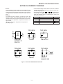
Illustration: MD-MT15/15C
• In the interests of user-safety the set should be restored to its
original condition and only parts identical to those specified be
used.
Illustration: MD-MT15H/15W
Illustration: MD-MT161E/18H (Only printing is different.)
The machine MD-MT15H/MT161E/MT18H is a modification
of MD-MT20H/MT16E the difference is the Top Cabinet. Its
performance and operation are identical with those of MDMT20H/MT16E. For details refer to the service manual (No.
S5933MDMT20H/) for MD-MT20H/MT16E.
The machine MD-MT15/MT15C/MT15W is a modification of
MD-MT20/MT20C/MT20W the difference is the Top Cabinet.
Its performance and operation are identical with those of MDMT20/MT20C/MT20W. For details refer to the service manual
(No.S6943MDMT20//) for MD-MT20/MT20C/MT20W.
MD-MT20/MT20C/MT20W
MD-MT20H/MT16E
Page
REMOVING AND REINSTALLING THE MAIN PARTS
ADJUSTMENT ..............................................................
TROUBLE SHOOTING .................................................
FUNCTION TABLE OF IC ............................................
CIRCUIT DESCRIPTION ..............................................
Page
REMOVING AND REINSTALLING THE MAIN PARTS .. 9
ADJUSTMENT .............................................................. 10
TROUBLE SHOOTING ................................................. 35
FUNCTION TABLE OF IC ............................................ 38
CIRCUIT DESCRIPTION .............................................. 40
11
12
37
40
42
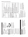
CONTENTS OF MD-MT15/15C/15H/15W/161E/18H
Page
SAFETY PRECAUTION FOR SERVICE MANUAL (MD-MT15W/15H/18H/161E ONLY) ..................................................... 2
SPECIFICATIONS ................................................................................................................................................................. 3
NAMES OF PARTS ............................................................................................................................................................... 4
OPERATION MANUAL .......................................................................................................................................................... 5
QUICK GUIDE (MD-MT15 ONLY) ......................................................................................................................................... 8
DISASSEMBLY .................................................................................................................................................................... 10
NOTES ON SCHEMATIC DIAGRAM .................................................................................................................................. 11
TYPES OF TRANSISTOR AND DIODE .............................................................................................................................. 11
VOLTAGE ............................................................................................................................................................................ 12
BLOCK DIAGRAM ............................................................................................................................................................... 13
SCHEMATIC DIAGRAM ...................................................................................................................................................... 14
WIRING SIDE OF P.W.BOARD ........................................................................................................................................... 17
WAVEFORMS OF MD CIRCUIT ......................................................................................................................................... 22
PARTS GUIDE/EXPLODED VIEW
PACKING OF THE SET (MD-MT15 FOR U.S.A. ONLY)
PACKING METHOD (MD-MT161E ONLY)
SHARP CORPORATION
–1–
This document has been published to be used
for after sales service only.
The contents are subject to change without notice.
MD-MT15/15C/15H/15W/161E/18H
SAFETY PRECAUTION FOR SERVICE MANUAL (MD-MT15W/15H/18H/161E ONLY)
Precaution to be taken when replacing and servicing the Laser Pickup.
The AEL (Accessible Emission Level) of Laser Power Output for this model is specified to be lower than Class I Requirements.
However, the following precautions must be observed during servicing to protect your eyes against exposure to the laser beam.
(1) When the cabinet has been removed, the power is turned on without a compact disc, and the Pickup is on a position
outer than the lead-in position, the Laser will light for several seconds to detect a disc. Do not look into the Pickup Lens.
(2) The Laser Power Output of the Pickup inside the unit and replacement service parts have already been adjusted prior
to shipping.
(3) No adjustment to the Laser Power should be attempted when replacing or servicing the Pickup.
(4) Under no circumstances look directly into the Pickup Lens at any time.
(5) CAUTION - Use of controls or adjustments, or performance of procedures other than those specified herein may result
in hazardous radiation exposure.
Laser Diode Properties
● Material: GaAIAs
● Wavelength: 785 nm
● Pulse time:
Read mode; 0.8 mW Continuous
Write mode; max. 10 mW 0.5S
min. cycle 1.5S
Repetition
LASER KLASSE 1
LUOKAN 1 LASERLAITE
KLASS 1 LASERAPPARAT
For MD-MT15H/18H
For MD-MT15W/15H/18H
CAUTION
● This Portable MiniDisc Recorder is classified as a CLASS 1 LASER product.
● The CLASS 1 LASER PRODUCT label is located on the bottom.
● Use the Portable MiniDisc Recorder only in accordance with the instructions given in
this manual and do not attempt to interfere with the interlock switch or make any
other adjustment as this may result in exposure to hazardous radiation.
For MD-MT15W
VARO !
VARNING!
For MD-MT161E
Avattaessa ja suojalukitus ohitettaessa olet alttiina näkymättömälle lasersäteilylle. Älä katso säteeseen.
Osynlig laserstralning när denna del är öppnad och spärren är urkopplad. Betrakta ej strälen.
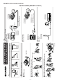
Precaution to be taken when replacing and servicing the laser pickup.
The following precautions must be observed during servicing to protect your eyes against exposure to the laser.
Warning of possible eye damage when repairing:
If the AC adaptor or batteries are connected when the top houising (disc cover) of the unit is removed, and the PLAY key is
pressed, the laser will light up during focus access (2-3 seconds). (Fig. 2-1) During the operation, the laser will leak from the
opening between the magnetic head and the mechanical chassis (Fig. 2-2). In order to protect your eyes, you must not look
at the laser during repair. Before repairing be sure to disconnect the AC adaptor and remove the batteries.
Magnet head
Magnet Head
Laser Beam
Mechanism
Chassis
Top Cabinet
Spindle motor
Optical pick-up
Figure 2-1
Main PWB Optical Pick-Up
Figure 2-2
–2–
MD-MT15/15C/15H/15W/161E/18H
FOR A COMPLETE DESCRIPTION OF THE OPERATION OF THIS UNIT, PLEASE REFER TO
THE OPERATION MANUAL.
SPECIFICATIONS
MD-MT15H
MD-MT15/15C
■ General
Power source:
Power source:
DC 5V:
DC 3.0V:
DC 2.4V:
DC 4.5V:
AC adaptor (AC 120V, 60 Hz)
Commercially available, “AA” size (LR6), alkaline
battery x 2
Optional Rechargeable Nickel-Metal Hydride battery (AD-T20BT) x 1
Optional car adaptor, AD-CA20X
(for cars with a 12-24V DC negative ground electrical system)
Power consumption:
7.5 W (AC adaptor)
Output power:
RMS; 20 mW (10 mW + 10 mW)
(0.2% T.H.D.)
Charging time:
Approx. 4 hours (90 %)
Approx. 6 hours (fully charged)
(When using the AC adaptor included with the unit)
DC 3.0V:
Commercially available, “AA” (LR6) size, alkaline
battery x 2
Optional Rechargeable Nickel-Metal Hydride battery (AD-T20BT) x 1
DC 4.5V: Optional car adaptor, AD-CA20X
(for cars with a 12-24V DC negative earth electrical system)
DC 5V:
Optional AC adaptor (AD-T20APH, AC 220 - 230V,
50/60 Hz)
7 W (Optional AC adaptor)
DC 2.4V:
Power consumption:
Output power:
RMS; 20 mW (10 mW + 10 mW)
(0.2% T.H.D.)
Charging time:
Approx. 4 hours (90 %)
Approx. 6 hours (fully charged)
(When using the AC adaptor)
Battery life:
MD-MT161E
When using two, commercially
available, high capacity, “AA”
size (LR6), alkaline batteries
When using the optional rechargeable battery AD-T20BT
(fully charged)
Continuous recording:
Approx. 7.5 hours
Continuous recording:
Approx. 7.5 hours
DC 2.4V:
Continuous play:
Approx. 15 hours
Continuous play:
Approx. 12 hours
DC 4.5V:
Power source:
● The continuous recording time is for analog inputs when the volume level is set to “VOL
0”.
● The continuous play time shows the value when the volume level is set to “VOL 15”.
● The above values are the standard values when the unit is charged and used at an
ambient temperature of 68°F (20°C).
● The operating time when using an alkaline battery may be different, depending on the
type and manufacturer of the battery, and on the operating temperature.
Input sensitivity:
Recording level
0.25 mV
MIC L
2.5 mV
10 k ohms
LINE
100 mV
20 k ohms
Output level:
Dimensions:
DC 5V:
7 W (Optional AC adaptor)
Output power:
RMS; 20 mW (10 mW + 10 mW)
(0.2% T.H.D.)
Charging time:
Approx. 4 hours (90 %)
Approx. 6 hours (fully charged)
(When using the AC adaptor)
10 k ohms
MD-MT18H
Power source:
DC 5V:
DC 3.0V:
Specified
output
Maximum
output level
Load
impedance
Headphones
—
10 mW + 10 mW
16 ohms
DC 2.4V:
LINE
250 mV
(-12dB)
—
10 k ohms
DC 4.5V:
Width: 3-7/16" (87.9 mm)
Height: 1-3/16" (29.8 mm)
Depth: 3-1/8" (79.7 mm)
Weight:
Input jack:
0.40 lbs. (180g) without battery
Line/optical digital, microphone (powered by the main unit)
Output jack:
Headphones (impedance: 19 ohms)
Type:
Portable MiniDisc recorder
Signal readout:
Non-contact, 3-beam semi-conductor laser pick-up
Audio channels:
Stereo 2 channels/monaural (long-play mode) 1 channel
Frequency response:
20 – 20,000 Hz (± 3 dB)
Rotation speed:
Approx. 400 – 900 rpm
Error correction:
ACIRC (Advanced Cross Interleave Reed-Solomon Code)
Coding:
ATRAC (Adaptive Transform Acoustic Coding), 24-bit computed type
Recording method:
Magnetic modulation overwrite method
Sampling frequency:
44.1 kHz (32 kHz and 48 kHz signals are converted to 44.1 kHz,
and then recorded.)
Wow and flutter:
Unmeasurable (less than ±0.001% W. peak)
7 W (AC adaptor)
Output power:
RMS; 20 mW (10 mW + 10 mW)
(0.2% T.H.D.)
Charging time:
Approx. 4 hours (90 %)
Approx. 6 hours (fully charged)
(When using the AC adaptor included with the unit)
MD-MT15W
Power source: DC 3.0V [Commercially
available, “AA” size (LR6),
alkaline battery x 2]
DC 4.5V [Optional car
adaptor, AD-CA20X (for
cars with a 12-24V DC
negative earth electrical
system)]
Output power: RMS; 20 mW (10 mW + 10
mW) (0.2% T.H.D.)
Battery life:
When using two, commercially available, high
capacity, “AA” size (LR6), alkaline batteries
Continuous recording: Approx. 7.5 hours
Continuous play: Approx. 15 hours
MD-MT15H/18H/161E
Specified
output
Maximum
output level
Load
impedance
Earphones
—
10 mW + 10 mW
32 ohms
LINE
250 mV
(-12dB)
—
10 k ohms
Dimensions:
Width: 87.9 mm (3-7/16")
Height: 29.8 mm (1-3/16")
Depth: 79.7 mm (3-1/8")
Weight:
Input socket:
180g (0.40 lbs.) without battery
Line/optical digital, microphone (powered by the main unit)
Output socket:
Earphones (impedance: 32 ohms)
AC adaptor (AC 220 - 230V, 50/60 Hz)
Commercially available, “AA” (LR6) size alkaline
battery x 2
Optional Rechargeable Nickel-Metal Hydride battery (AD-T20BT) x 1
Optional car adaptor, AD-CA20X
(for cars with a 12-24V DC negative earth electrical system)
Power consumption:
■ MiniDisc Recorder
Output level:
Commercially available, “AA” size (LR6), alkaline
battery x 2
Optional Rechargeable Nickel-Metal Hydride battery (AD-T20BT) x 1
Optional car adaptor, AD-CA20X
(for cars with a 12-24V DC negative earth electrical
system)
Optional AC adaptor (AD-T20APE, AC 230 - 240V,
50/60 Hz)
Power consumption:
Reference input level Input impedance
MIC H
DC 3.0V:
● The continuous recording time is for
analogue inputs when the volume level
is set to “VOL 0”.
● The continuous play time shows the
value when the volume level is set to
“VOL 15”.
● The above values are the standard values when the unit is used at an ambient
temperature of 20°C (68°F).
● The operating time when using alkaline
batteries may be different, depending on
the type and manufacturer of the battery, and on the operating temperature.
Input sensitivity:
Recording Reference input
level
level
MIC H
0.25 mV
MIC L
2.5 mV
LINE
100 mV
Input
impedance
10 k ohms
10 k ohms
20 k ohms
Output level:
Specified
output
Earphones
—
LINE
250 mV
(-12dB)
Maximum
Load
output
impedance
level
10 mW +
10 mW 32 ohms
—
10 k ohms
Dimensions:
Width 87.9 mm (3-7/16")
Height 29.8 mm (1-3/16")
Depth 79.7 mm (3-1/8")
Weight:
180 g (0.40 lbs.) without
battery
Input socket: Line/optical digital, microphone (powered by the
main unit)
Output socket: Earphones (impedance:
32 ohms)
Specifications for this model are subject to change without prior
notice
–3–
MD-MT15/15C/15H/15W/161E/18H
NAMES OF PARTS
Illustration: MD-MT15/15C
1. Monaural Long-Play Mode Indicator
2. Record Indicator
3. Level Meter
4. Fast Play Indicator
5. Repeat Indicator
6. TOC Indicator
7. Battery Indicator
8. Random Indicator
9. Track Number Indicator
10. Character/Time Information Indicator
11. Synchro Recording Indicator
12. Disc Mode Indicator
13. Disc Name Indicator
14. Track Name Indicator
15. Remaining Recording Time Indicator
16. Total Track Number Indicator
1 2 3 4 5 6
7
11
12
13
14
8
9
10
15
17
17. Edit/Auto Mark/Time Mark Button
18. Mode Button
19. Display/Character Select Button
20. Bass/Delete Button
21. Enter/Fast Play/Synchro Button
22. Volume Up/Cursor Button
23. Volume Down/Cursor/Charge Button
24. Record/Track Mark Button
25. Fast Reverse/Recording Level Down/
Name Select Button
26. Stop/Power Off Button
27. Play/Pause Button
28. Fast Forward/Recording Level Up/
Name Select Button
16
18 19 20
21
22
23
24 25 26 27
29. Open Lever
30. Headphones Jack (MD-MT15/15C)
30. Earphones Socket (MD-MT15H/15W/161E/18H)
31. Optical/Line Input Jack
32. Microphone Input Jack
33. Hold Switch
34. 5V DC Input Jack
35. Battery Cover
29
28
30
31
32
33
34
35
–4–
POWER SOURCE
–5–
(MD-MT18H)
AC 120V, 60 Hz
AC 220-230V,
50/60 Hz
● AC adaptors of MD-MT15H/15W/161E
are option parts.
Insert securely,
all the way in.
To the DC IN 5V socket
Insert securely,
all the way in.
To the DC IN 5V jack
(MD-MT15/15C)
Notes:
● When there is thunder or lightning in your
vicinity, unplug the AC adaptor from the
AC outlet.
● When the unit is not in use for extended
periods, remove the AC adaptor from the
AC outlet.
● Never use an AC adaptor other than the
one specified. Otherwise, problems or
serious hazards may be created.
● Do not bend, twist or tie the power cord
or put heavy objects on top of it.
● Be sure to hold the plug when removing
it. If you pull on the cord, it may break, or
the unit may malfunction.
2 Plug the AC adaptor into an AC outlet.
to the DC IN 5V jack on the unit.
1 Connect the cord from the AC adaptor
3
2
1
3 Close the battery cover.
to the polarity marked on the bottom of
the unit.
● Installing the batteries incorrectly may
cause the unit to malfunction.
2 Insert two alkaline batteries according
● Slide the battery cover as far as it will
go to the outside and then lift to open it.
If the battery cover is lifted without being slid all the way out, it may break.
1 Open the battery cover.
● Use two commercially available alkaline
batteries (LR6, “AA” size).
■ AC power (For MD-MT15/15C/18H) ■ Alkaline batteries power
You can power this unit with AC adaptor or commercially available alkaline batteries
(LR6, “AA” size).
You can also power this unit with a rechargeable battery (AD-T20BT) or car adaptor
(AD-CA20X) which are available separately.
● When recording from digital inputs, i t
is not necessary to adjust the recording level.
Manual recording:
(1) Insert a recordable MiniDisc, and
then press the REC button.
(2) Press the
button.
(1) Insert a recordable MiniDisc, and
then press the REC button.
(2) Press the ENTER/SYNC button.
(3) Start the playback on the equipment
connected to this unit.
Before starting a synchro recording,
perform the following steps on the
equipment connected to this unit.
(1) First, put it in the playback mode.
(2) Next, put it in the pause mode.
(3) Finally, position it at the beginning
of the track you want to record.
Synchro recording:
2 Start recording.
1 Connect the external equipment.
This is the method used for recording digital signals from CDs exactly as they are
stored on the original. Compared to recordings made from analog inputs, digital recordings have extremely high-quality
sound.
MD player
Recording
Analog recording is
possible.
Digital cable
Recording
Notes:
● This unit incorporates a sampling rate
converter.
When this unit is connected to digital
equipment such as a DSS tuners or a
DAT tape recorder that use a different
sampling frequency (32 kHz or 48 kHz),
recordings can still be made. (The sampling frequency of this unit is 44.1 kHz.)
● When making a digital recording from a
portable CD player (if the player has a
sound skip prevention function and this
function is turned on) the optical output
will drop out and digital recording will not
be possible. Be sure to turn the sound
skip prevention function off.
Playback
Digital cable
Digitally recorded MiniDisc
CD player, MD
player, etc.
Playback
When you attempt to make a new digital
recording from a track that was digitally recorded on a MiniDisc.
● MiniDiscs are designed so that only first
generation digital copies can be made.
Further digital copies are prevented by
the SCMS (Serial Copy Management
System).
There are cases where digital recording
may be impossible.
In the following cases digital recording is
impossible, even if you are using digital
cables.
RECORDING USING THE OPTICAL DIGITAL CABLE
MD-MT15/15C/15H/15W/161E/18H
OPERATION MANUAL
When the battery
level is very low
–6–
● Shortly after turning on a heater.
● When the unit is placed in a room where
there is excessive steam or moisture.
● When the unit is moved from a cool
place to a warm place.
When the unit has condensation inside,
the disc signals cannot be read, and the
unit may not function properly.
● If this happens, remove the disc.
The condensation should evaporate in
approximately 1 hour. The unit will then
function properly.
If the hold function is active while the power
is turned off, the power cannot be turned
on by mistake and the battery will not be
accidentally drained.
● To cancel the hold mode, move the
HOLD switch away from the safety position (the opposite direction of the arrow).
● When the unit is in the hold mode, pressing the buttons will have no affect.
In the following cases, condensation
may form inside the unit.
■ Moisture condensation
TROUBLESHOOTING
Notes:
● When using the unit with alkaline batteries or a rechargeable battery, the battery indicator will not correctly display
the remaining capacity for approximately
10 seconds after the power has been
turned on.
● When an AC adaptor or a car adaptor is
used, the battery indicator will not be
shown.
● The number of bars shown in the battery indicator may increase or decrease,
depending on the operation being performed. This is normal.
● When the battery is completely discharged, the battery indicator will flash.
Recharge the battery or replace the alkaline batteries with new ones.
● When the battery has run completely out,
“BATT EMPTY” will appear. Then, the
power will be disconnected automatically.
Since the battery level is very low, you
cannot start recording or editing.
When the battery
level is high
< How to read the battery indicator >
To avoid accidental operation of the unit,
use the hold function.
The remaining amount of battery level is
shown by the battery indicator (
) during operation.
Battery indicator
Move the HOLD switch to the safety position (direction indicated by the arrow).
■ To prevent the unit from being
operated by mistake
■ Checking the remaining amount
of battery level
CONVENIENT OPERATION OF THE UNIT
Is the AC adaptor disconnected?
Is the battery exhausted?
Is the unit in the hold mode?
Has condensation formed inside the unit?
Is the unit being influenced by mechanical shock or by
static electricity?
When this product is subjected to strong
external interference (mechanical shock,
excessive static electricity, abnormal supply voltage due to lightning, etc.) or if it is
operated incorrectly, it may malfunction.
If such a problem occurs, do the following:
1. Unplug the AC adaptor from the AC outlet.
2. Remove the battery.
3. Leave the unit completely unpowered for
approximately 30 seconds.
■ If trouble occurs
Recording and editing
are impossible.
If strange sounds, smell or smoke come out
of the unit or an object is dropped into the
unit, remove the AC adaptor from the AC
outlet immediately and contact an authorized SHARP service center.
4. Plug the AC adaptor back into the AC
outlet and retry the operation.
● Is the MiniDisc protected against accidental erasure?
● Is the unit connected properly to the other equipment?
● Is the AC adaptor unplugged or did a power failure occur while recording or editing?
● Is the unit in the hold mode?
● Is an optical signal being output from the external equipment?
Read the operation manual for the external equipment.
● Has the track number or character information been
written on the disc yet?
● Is the unit in the recording or editing mode?
● Is the battery exhausted?
● Is the unit being subjected to excessive vibration?
Some sounds are
skipped.
The MiniDisc cannot be
ejected.
● Is the unit in the hold mode?
● Is the battery exhausted?
● Is the volume set too low?
● Is the headphones plugged in?
● Are you trying to play a MiniDisc with data on it instead
of a MiniDisc containing music?
●
●
●
●
●
CAUSE
When the operation buttons are pressed, the
unit does not respond.
No sound is heard from
the headphones.
The unit does not turn
on.
PROBLEM
Many potential “problems” can be resolved by the owner without calling a service technician.
If something seems to be wrong with this product, check the following before calling your
authorized SHARP dealer or service center.
MD-MT15/15C/15H/15W/161E/18H
When the remaining recording time of a
disc is displayed, short tracks less than
12 seconds long may not be included in
the total.
For MiniDiscs on which repeated recording and editing operations were performed, the COMBINE function may not
work.
A cluster (about 2 seconds) is normally the
minimum unit of recording. So, even if a track
is less than 2 seconds long, it will use about
2 seconds of space on the disc.
Therefore, the time actually available for recording may be less than the remaining time
displayed.
If there are scratches on discs, those sections will be automatically avoided (no recording will be placed in those sections). Therefore, the recording time will be reduced.
For MiniDiscs on which repeated recording and editing were performed, some
sounds may be skipped while cueing and
reviewing.
If there are scratches or dust on a
MiniDisc, the track numbers following that
track will be increased by one.
Two tracks may not be combined
in editing.
The total of the recorded time and
time remaining on a disc may not
add up to the maximum possible
recording time.
When recorded tracks are played
back using the cue and review operations, some sounds may be
skipped.
A track number can be created in
the middle of a track.
If there are scratches on a disc, the unit
will automatically avoid recording in those
areas. The recording time will be reduced.
Even if several short tracks are
erased, the remaining recording
time may not show an increase.
Even if the number of tracks and
the recording time have not
reached the limit, “DISC FULL”
may be displayed.
Even if the maximum recording
time of a MiniDisc has not been
reached, “DISC FULL” or “TOC
FULL” may be displayed.
When the number of tracks used reaches
the limit, regardless of the remaining recording time, further recording will be
impossible.
(Maximum number of tracks: 255)
If a MiniDisc has been recorded or edited repeatedly or if a MiniDisc has
scratches on it, it may not be possible to
record the maximum number of tracks on
it.
MiniDiscs are recorded using a different system than is used for cassette tapes or DAT
recordings. Therefore, the following conditions may be encountered, depending on how
the disc has been recorded or edited. These are due to system limitations, and should be
considered normal.
MINIDISC SYSTEM LIMITATIONS
–7–
? DISC
U TOC ERROR
Tr. Protect
TOC FULL
TOC ERROR
TEMP OVER
SYSTEM ERR
SORRY
READ ERROR
PROTECTED
POWER ?
PB DISC
LOCKED
LOCK ERROR
NO DISC
HOLD
DISC FULL
Din UNLOCK
DEFECT
Can’t WRITE
Can’t REC
Can’t EDIT
Can’t COPY
BLANK DISC
BATT EMPTY
Error messages
● A large portion of the disc has been
damaged.
● There is no space left for recording
character information (track names,
disc names, etc.).
● The track has been protected from
being erased.
● A large portion of the disc has been
damaged.
● There is an error in the recorded signal.
● A disc which contains data other than
music was played.
● There is an error in the signal from
the disc.
● Since a track number is currently
being located or written to, the unit
cannot accept your command.
● You have come to the conclusion
that the unit is out of order.
● The temperature is too high.
● The disc is damaged.
● The MD is write protected.
● The OPEN lever was moved during
recording or editing.
● A disc has not been loaded.
● You tried to record on a playbackonly disc.
● Improper power is being supplied.
● The unit is in the hold mode.
● Poor connection of the digital cable.
● The disc is out of recording space.
● Recording cannot be performed correctly due to vibration or shock in the unit.
● Editing is impossible.
● The disc is scratched.
● Nothing is recorded.
● No copy can be made because of
the SCMS copyright system.
● A track cannot be edited.
Meaning
● The battery is run down.
ERROR MESSAGES
● Edit the track with the device on
which it was recorded.
● Replace it with another recorded
disc.
● Erase all of the signal errors, and
then try recording again.
● A disc which contains non-music
data cannot be played.
● Replace it with another recorded
disc.
● To have it repaired, go to the distributor where you purchased the unit.
● Turn off the power, and wait for a
while.
● Replace it with another recorded
disc.
● Replace it with another recordable
disc.
● Use one of the specified power
sources.
● Move the write protection knob back
to its original position.
● Reload the disc or replace it.
● Replace it with another recorded disc.
● Wait for a while and try the operation again.
● Change the stop position of the track
and then try editing it.
● Re-record or replace it with another
recordable disc.
● Check the number of tracks.
● If the sound you hear is not right, try
recording again.
● Replace the disc with another recordable disc.
● Connect the digital cable securely.
● Replace it with another recordable
disc.
● Return the HOLD switch to its original position.
● Turn off the power and remove the
MiniDisc.
● Load a disc.
● Replace it with a recordable disc.
Remedy
● Charge the rechargeable battery or
replace the alkaline batteries (or use
the AC adaptor for power).
● Replace the disc with a recorded disc.
● Record using the analog cable.
MD-MT15/15C/15H/15W/161E/18H
● AC Adaptor x 1
● Adaptador de CA x 1
–8–
2
1
2
3
■ Rechargeable battery power (Separately available)
■ Alimentación de la batería recargable (Disponible por separado)
1
3
4
• AC 120V, 60Hz
• 120V CA, 60Hz
● Analog Cable x 1
● Cable analógico x 1
■ Alkaline battery power (Commercially available)
■ Alimentación de la pila alcalina (Disponible en las tiendas del ramo)
■AC power
■ Alimentación de CA
2 Power source / Alimentación
● Headphones x 1
● Auriculares x 1
• AC 120V, 60Hz
• 120V CA, 60Hz
5
● Carrying Bag x 1
● Caja para el
transporte x 1
1 Check the supplied accessories / Compruebe los accesorios suministrados
PORTABLE MINIDISC RECORDER
Quick Guide/Guía rápida MD-MT15
Stereo microphone
Micrófono estéreo
■ Microphone
■ Micrófono
Playback side
Lado de reproducción
■ Digital recording
■ Grabación digital
DIGITAL OUT
R
(LEFT)
(IZQUIERDO)
Recording side
Lado de grabación
PLUG IN
POWER
MIC IN
Recording side
Lado de grabación
• Optical digital cable
(AD-M1DC, available separately)
• Cable óptico digital
(AD-M1DC, disponible por separado)
Recording side
Lado de grabación
• Analog cable included with this unit
• Cable analógico suministrado con este
L
AUDIO OUT
(RIGHT)
(DERECHO)
• To the line output jacks
on a stereo
• A los enchufes de
salida de línea de un
equipo estéreo
Playback side
Lado de reproducción
■ Analog recording
■ Grabación analógica
3 Connection / Conexión
OPTICAL/
LINE IN
OPTICAL/
LINE IN
MD-MT15/15C/15H/15W/161E/18H
QUICK GUIDE (MD-MT15 ONLY)
3
Insert a recordable MiniDisc.
Inserte un minidisco grabable.
4
Connect the external equipment.
Conecte el equipo externo.
6
5
Inicie la reproducción en el equipo fuente.
Begin playback on the source equipment.
Pulse el botón ENTER/SYNC.
Press the ENTER/SYNC button.
Mientras se produce el sonido del equipo externo
conectado a este aparato, pulse el botón
o
para ajustar el nivel de grabación.
While playing sound from the external
equipment connected to this unit, press the
or
button to adjust the recording
level.
Pulse el botón REC.
Press the REC button.
–9–
5
4
3
2
1
o
para ajustar el nivel
button to adjust the
Press the ENTER/SYNC button to select the
synchro recording level. (This level can be
changed, even while recording.)
Pulse el botón ENTER/SYNC para seleccionar el
nivel de la grabación sincronizada. (Este nivel podrá
cambiarse incluso durante la grabación.)
Pulse el botón
de grabación.
Press the
or
recording level.
Pulse el botón REC.
Press the REC button.
Insert a recordable MiniDisc.
Inserte un minidisco grabable.
Connect the stereo microphone to the MIC IN jack.
Conecte el micrófono estéreo al enchufe MIC IN del
aparato principal.
Cuando el micrófono capte un sonido, el de una
persona que hable por ejemplo, la grabación
empezará automáticamente.
When a sound, such as a person speaking, is
picked up by the microphone, recording will
begin automatically.
1
3
Turn off the power and move the OPEN lever in the
direction indicated by the arrow.
Desconecte la alimentación y mueva la palanca OPEN en el
sentido indicado por la flecha.
2
To remove the MiniDisc:
Para extraer el minidisco:
Press the ■/:OFF button while in the stop mode.
Pulse el botón ■/:OFF estando en el modo de parada.
To turn off the power:
Para desconectar la alimentación:
Press the ■/:OFF button.
Pulse el botón ■/:OFF.
To stop recording:
Para detener la grabación:
6
■ Recording from the microphone (Mic synchro recording)
■ Grabación de un micrófono (Grabación sincronizada con micrófono)
1
2
2
1
4
3
■ Recording from CDs or MDs (Synchro recording)
■ Grabación de discos compactos o minidiscos (Grabación sincronizada)
4 Recording / Grabación
jack.
Inserte un minidisco.
Insert a MiniDisc.
Inerte la clavija de auriculares en el enchufe .
Empuje completamente hacia adentro la clavija.
Insert the headphones plug into the
Push the plug all the way in.
3
4
• Volume (0 - 30)
• Volumen (0 - 30)
Ajuste el nivel de los graves.
Cada vez que pulse el botón BASS, el tono cambiará de la
forma siguiente:
Ajuste el volumen.
Pulse el botón VOLUME + para aumentar el volumen y el
botón VOLUME – para reducirlo.
BASS OFF ---- El realce de los graves se cancela.
BASS 3 ------- Los sonidos graves se realzan aún más.
BASS 2 ------- Los sonidos graves se realzan más.
BASS 1 ------- Los sonidos graves se realzan ligeramente.
BASS OFF ---- Bass emphasis is canceled.
BASS 3 ------- Bass sounds are emphasized even more.
BASS 2 ------- Bass sounds are emphasized more.
BASS 1 ------- Bass sounds are emphasized slightly.
Adjust the bass level.
Each time the BASS button is pressed, the tone will be
switched as follows:
Press the ■/:OFF button while in the stop mode.
Pulse el botón ■ /:OFF estando en el modo de parada.
To turn off the power:
Para desconectar la alimentación:
Press the ■/:OFF button.
Pulse el botón ■ /:OFF.
To stop playback:
Para detener la reproducción:
Pulse el botón
durante la reproducción.
● Para reanudar la reproducción, pulse de nuevo el botón
.
Press the
button during playback.
● To resume playback, press the
button again.
To interrupt playback:
Para interrumpir la reproducción:
Pulse el botón
.
En los casos siguientes, la función de reproducción
automática no se activará.
● Cuando esté cerrada la lengüeta de protección contra
escritura del minidisco grabable
● Cuando haya sido cancelada la función de reproducción
automática
Adjust the volume.
Press the VOLUME + button to increase the volume and
the VOLUME – button to decrease the volume.
6 Sound control / Control del sonido
● The power will be turned on automatically, and playback
will start from the first track.
(Auto-play function)
● La alimentación se conectará automáticamente, y la
reproducción empezará desde la primera pista.
(Función de reproducción automática)
2
1
1
2
Playback does not start when a MiniDisc is inserted:
La reproducción no empieza cuando se inserta un
minidisco:
Press the
button.
In the following cases, the auto-play function will not work.
● When the recordable MiniDisc write protection tab is
closed.
● When the auto-play function has been canceled.
5 Playing a MiniDisc / Reproducción de un minidisco
MD-MT15/15C/15H/15W/161E/18H
MD-MT15/15C/15H/15W/161E/18H
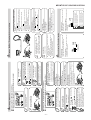
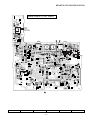
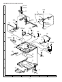
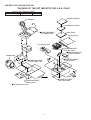
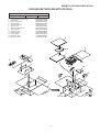
DISASSEMBLY
STEP
REMOVAL
PROCEDURE
FIGURE
1
Bottom Cabinet
1. Screw ..................... (A1) x7
10-1
2
Top Cabinet
1. Open the Top cabinet.
2. Screw ..................... (B1) x4
3. Screw ..................... (B2) x1
10-1
10-2
3
Key Switch/LCD
1. Flexible PWB ......... (C1) x2
4
Mechanism Unit
1. Flexible PWB ......... (D1) x2 10-2
2. Raise the rear part, and .....
10-3
remove in the arrow direction.
5
Main PWB
1. Flat cable ................ (E1) x1
2. Screw ..................... (E2) x2
10-2
6
Audio PWB
1. Screw ...................... (F1) x3
10-4
LCD
(B1)x2
ø1.4x2mm
Cares before disassembling
When assembling the machine after disassembling or
repair, observe the following requirements so as to ensure
safety and performance.
1. Remove the batteries from the machine, and take out the
mini-disc.
2. When assembling after repair, be sure to restore the
initial location of wires.
Since the screws are small, incorrect fixing may result in
malfunction.
3. When repairing, pay utmost attention to static electricity
of IC.
Key Switch
Top Cabinet
(A1)x2
ø1.4x2mm
(A1)x1
ø1.4x2mm
Open
Open Lever
(B1)x2
ø1.4x2mm
(B2)x1
ø1.4x2mm
Bottom
(A1)x2
ø1.4x2mm Cabinet
(A1)x2
ø1.4x2mm
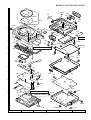
Figu re 10-1
Put the fold on the connector, and
apply with the felt. Sagging may
result in contact with the sheet metal.
Felt
(E2)x2
ø1.7x2.5mm
(D1)x1
Main
PWB
pull
pull
pull
pull
pull
pull pull
Audio
PWB
pull
(C2)x2
LCD
(E1)x1
(D1)x1*
Flexible PWB
for optical pickup
Mechanism
Unit
Key Switch
Caution:
Carefully handle the main PWB and flexible PWB. After removing the
flexible PWB (1*) for the optical pickup from the connector, do not
touch directly the front end of flexible PWB with your hand so as to
prevent damage of optical pickup by static electricity.
(F1)x3
ø1.7x2.5mm
Figure 10-2
Mechanism Unit
Audio PWB
Figure 10-4
Figure 10-3
– 10 –
MD-MT15/15C/15H/15W/161E/18H
NOTES ON SCHEMATIC DIAGRAM
• Resistor:
To differentiate the units of resistors, such symbol as K and
M are used: the symbol K means 1000 ohm and the symbol
M means 1000 kohm and the resistor without any symbol is
ohm-type resistor. Besides, the one with “Fusible” is a fuse
type.
• Capacitor:
To indicate the unit of capacitor, a symbol P is used: this
symbol P means micro-micro-farad and the unit of the
capacitor without such a symbol is microfarad. As to electrolytic capacitor, the expression “capacitance/withstand voltage” is used.
(CH), (TH), (RH), (UJ): Temperature compensation
(ML): Mylar type
B
(G)
(3)
E
(S)
1
• The indicated voltage in each section is the one measured
by Digital Multimeter between such a section and the chassis with no signal given.
• Parts marked with “
”(
) are important for
maintaining the safety of the set. Be sure to replace these
parts with specified ones for maintaining the safety and
performance of the set.
DESCRIPTION
REF. NO
SW401
EJECT
SW402
HOLD
OFF—ON
SW403
DISC LID OPEN
OFF—ON
SW902
DISC PROTECT
OFF—ON
TOP VIEW
TOP VIEW
C
(D)
(2)
TOP
VIEW
2SA17457
2SC4213 B
RN1103
1SS361
SB10015 C
TOP VIEW
TOP VIEW
TOP VIEW
1SS372
1SS360
SBE803
2SA1873 GR
Figure 11 TYPES OF TRANSISTOR AND DIODE
– 11 –
POSITION
OFF—ON
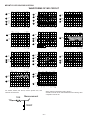
MD-MT15/15C/15H/15W/161E/18H
VOLTAGE
IC101
PIN
NO.
1
2
3
4
5
6
7
8
9
10
11
12
13
14
15
16
17
18
19
20
21
22
23
24
25
26
27
28
29
30
31
32
33
34
35
36
37
38
39
40
41
42
43
44
45
46
47
48
VOLTAGE
0.72V
0.72V
0.72V
0.72V
1.24V
1.24V
0.71V
1.24V
1.24V
1.24V
1.24V
1.24V
2.5V
2.5V
0.18V
2.5V
2.5V
0V
0V
1.48V
2.35V
0V
0V
2.5V
1.24V
1.24V
1.24V
1.24V
1.24V
1V
1.24V
1.24V
1.24V
NC
1.25V
1.25V
0.17V
1.24V
1.24V
1.24V
1.24V
2.5V
0V
0V
1.24V
1.24V
1.24V
0V
PIN
NO.
1
2
3
4
5
6
7
8
9
10
11
12
13
14
15
16
17
18
19
20
21
22
23
24
25
26
27
28
29
30
31
32
33
34
35
36
37
38
39
40
41
42
43
44
45
46
47
48
49
50
IC201
VOLTAGE PIN
NO.
51
0.88V
52
2.5V
53
1.27V
54
0V
1.25V
55
1.25V
56
57
1.25V
1.25V
58
59
1.25V
60
1.3V
61
2.2V
2V
62
63
0V
64
0V
65
0V
66
0V
67
1V
68
0V
0V
69
70
0V
71
0V
72
0V
0V
73
0V
74
0V
75
0.51V
76
77
0.51V
78
0.49V
1.44V
79
1.13V
80
2.56V
81
0.6V
82
83
1V
1V
84
0.8V
85
0.8V
86
0.8V
87
0V
88
2.13V
89
1.4V
90
1.56V
91
1.1V
92
1.75V
93
2.57V
94
1.74V
95
1.61V
96
0V
97
1.93V
98
1V
99
100
0.91V
VOLTAGE
1V
0V
0V
0V
0V
2V
0V
0V
0V
0V
0.14V
2V
0V
0.9V
0.9V
1.66V
1V
2V
0V
1V
1V
2V
0V
0V
0V
0V
0V
2V
0V
2V
1V
2V
0V
0V
1V
2V
2V
0V
2.36V
0.2V
1.65V
0V
0.1V
0.7V
1.35V
1.76V
0.32V
2.27V
2.36V
0.2V
IC202
PIN
NO.
1
2
3
4
5
6
7
8
9
10
11
12
13
14
15
16
17
18
19
20
1.28V
1.63V
2.57V
1.76V
1.44V
1.44V
0.6V
0.6V
0.6V
2.56V
0.6V
1V
1V
1V
1V
1.8V
1.9V
1.7V
1.7V
0V
IC354
PIN
NO.
1
2
3
4
5
IC351
VOLTAGE
VOLTAGE
–
–
0V
0V
0V
PIN
NO.
1
2
3
4
5
6
7
8
9
10
11
12
13
14
VOLTAGE
0V
0V
4.42V
0V
0V
4.42V
0V
0.9V
4.42V
0V
0.9V
4.42V
0V
4.46V
IC353
PIN
NO.
1
2
3
4
5
6
7
8
VOLTAGE
2.74V
–
–
0V
0V
–
–
2.74V
IC901
PIN
NO.
1
2
3
4
5
6
7
8
9
10
11
12
13
14
15
16
17
18
19
20
VOLTAGE
0V
0V
0V
0V
0V
0V
–
2.44V
2V
0V
2.48V
0.67V
0V
2.35V
0V
2.5V
0V
0V
0V
0V
PIN
NO.
1
2
3
4
5
6
7
8
9
10
11
12
13
14
15
16
17
18
19
20
21
22
23
24
25
26
27
28
29
30
31
32
33
34
35
36
37
38
39
40
41
42
43
44
45
46
47
48
49
50
IC401
VOLTAGE PIN
NO. VOLTAGE
51
0V
0V
52
2.32V
2.5V
2.34V
0V
53
54
0V
2.35V
2.32V
NC
55
0V
0.18V
56
2.34V
0V
57
2.34V
0.23V
58
0.3V
0V
59
60
2.35V
2.23V
61
2.35V
2.12V
2.28V
2.04V
62
2.35V
2.25V
63
2.35V
2.35V
64
2.35V
0.18V
65
1.08V
0V
66
1.13V
0V
67
0V
0V
68
2.34V
2.35V
69
2.32V
0.2V
70
2.34V
2.35V
71
2.34V
2.26V
72
2.1V
0.14V
73
2.32V
1.6V
74
2.32V
0V
75
1.93V
0.08V
76
2.34V
1.6V
77
2.34V
1.26V
78
0.82V
1.7V
79
1.46V
0.27V
80
0V
1.33V
81
0V
2.34V
82
2.1V
2.34V
83
2.72V
2.34V
84
2.72V
0V
85
2.35V
1.62V
86
0V
0V
87
2.34V
0V
88
2.32V
0V
89
2.33V
2.35V
90
2.33V
0V
91
2.35V
2.34V
92
1.7V
2.35V
93
1.5V
0V
94
0.12V
0V
95
2.33V
2.35V
96
2.33V
0V
97
2.34V
0V
98
0.18V
0V
99
2.33V
–
100
Preform the measurement on
the IC401 pin 37 in the TEST
mode with GND short-circuited.
(LCD is in "TEST" state.)
IC402
PIN
NO.
1
2
3
4
5
6
7
8
VOLTAGE
2.34V
0V
–
–
0V
0V
0.26V
2.34V
PIN
NO.
1
2
3
4
VOLTAGE
4.64V
4.64V
NC
0V
VOLTAGE
2.5V
2.5V
0V
0V
0V
0V
0V
0V
1V
1V
1V
0V
0V
2.5V
0V
0V
0V
0V
0V
0V
0V
0V
2.5V
2.5V
PIN
NO.
1
2
3
4
PIN
NO.
1
2
3
4
5
6
7
8
9
10
11
12
13
14
15
16
17
18
19
20
21
22
23
24
25
26
27
28
29
30
31
32
33
34
35
36
VOLTAGE
0V
1V
2.35V
0V
4.72V
0V
0V
0V
4.72V
4.72V
0V
0V
0V
4.72V
0V
0V
0V
0V
0V
0V
0V
0V
4.72V
0V
0V
0V
4.72V
4.72V
0V
0V
0V
4.72V
0V
0V
2.5V
9.67V
VOLTAGE
2.34V
2.34V
NC
0V
PIN
NO.
1
2
3
4
5
VOLTAGE
NC
1.16V
0V
1.17V
2.33V
– 12 –
IC701
PIN
NO.
1
2
3
4
5
6
7
8
9
10
11
12
13
14
15
16
17
18
19
20
21
22
23
24
VOLTAGE
0V
0V
0V
0V
0V
0V
0V
0V
0V
0V
0V
0V
0V
0V
0V
0V
–2.48V
0V
0V
2.72V
0.86V
0V
0V
0V
IC702
IC601
IC431
IC851
IC872
IC501
PIN
NO.
1
2
3
4
5
6
7
8
9
10
11
12
13
14
15
16
17
18
19
20
21
22
23
24
IC651
PIN
NO.
1
2
3
4
5
6
7
8
9
10
PIN
NO.
1
2
3
4
5
VOLTAGE
0V
9.66V
2.34V
NC
4.46V
IC703
PIN
NO.
1
2
3
4
5
6
7
8
9
10
11
12
13
14
15
16
17
18
19
20
21
22
23
24
VOLTAGE
0V
0V
0V
0V
0V
0V
0V
0.97V
0V
0V
0V
0V
2.34V
0V
0V
0V
–2.87V
0V
0V
2.74V
0.85V
0V
0V
0V
IC771
PIN
NO.
1
2
3
4
5
VOLTAGE
0V
2.74V
2.74V
NC
2.5V
VOLTAGE
2.74V
NC
0V
0V
0V
0V
–
NC
–
NC
IC801
PIN
NO.
1
2
3
4
5
6
VOLTAGE
NC
4.49V
4.64V
0V
2.34V
0V
0.2V
0V
0V
0.73V
0.73V
IC802
PIN
NO.
1
2
3
4
5
6
VOLTAGE
5V
5V
0.7V
5V
5V
5V
IC805
PIN
NO.
1
2
3
4
5
6
7
8
VOLTAGE
2.15V
1.38V
–
–2.86V
0V
0V
–1.49V
2.73V
IC806
PIN
NO.
1
2
3
4
5
6
VOLTAGE
0V
0V
4.44V
0V
0V
0V
IC808
PIN
NO.
1
2
3
4
5
6
VOLTAGE
2.15V
0.56V
0.56V
0V
0.56V
2.74V
IC807
PIN
NO.
1
2
3
4
5
6
VOLTAGE
2V
1.98V
1.98V
0V
0V
0.94V
IC821
PIN
NO.
1
2
3
4
5
6
7
8
9
10
11
12
IC841
PIN
NO.
1
2
3
4
5
VOLTAGE
VOLTAGE
1.25V
0.94V
1.16V
1.15V
1.13V
0V
0.54V
4.49V
0V
0.41V
1V
1V
IC871
PIN
NO.
1
2
3
4
5
VOLTAGE
4.64V
4.48V
NC
0V
4.63V
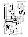
M
M903
HEAD
UP/DOWN
MOTOR
F
T
17
1-2
40
16
PLAYBACK SIGNAL
RECORD SIGNAL
– 13 –
13
24,26
29,31
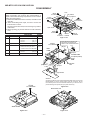
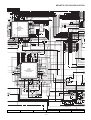
Figure 13 BLOCK DIAGRAM
6,8
5,9,10,14
23,27,28,32
VM
36
VG
IC601
4CH PWM DRIVER
MPC17A39
35
VCC
+2.5V
13,14
24,42
2,15-17,
19-22
SW402
HOLD
M
M901
SPINDLE
MOTOR
8
1-3
3
M
6-9
9,
11,
13,
42
IC901
SPINDLE MOTOR
DRIVER
BA6966FV
1, 3, 4, 5,
6,19,20
M902
SLED
MOTOR
74
4
SW401
EJECT
SW403
DISC LID
OPEN
KEY OPERATION UNIT
LCD UNIT
52,
69,
70,
83,
84
97
98
3
2.5V
REGULATOR
IC820
62FP2502
IC401
SYSTEM
MICROCOMPUTER
IX0298AW
1-12
14-16
4
VDD
+2.0V
1, 20-30, 73, 93-95
2
2
62
2.0V
REGULATOR
IC200
62FP2002
82-84,86,
89-100
73
74
+2.5V
1,2,23,24,14
+2.7V
+2.35V 5
6
7
VCC
VEE
17
17
VEE
VCC
8
2
24 L-CH
22 R-CH
19
18
+B
F871
T0.5A L 63V
Q873
NDS332P
FETIC
3
+7~+10V
20
VCC
IC703
AUDIO AMP.
IR3R54N
IC821
IR3M09N
DC/DC
CONVERTER
3
–2.7V
5
+2.7V
19
6
IC701
AUDIO AMP.
IR3R54N
20
IC841
XC62HS02
2.35V REGULATOR
3
+2.7V
3
2.5V REGULATOR
IC771 62GR2522
5
IC501
AD/DA CONVERTER
AK4519VF
12
15
10
5
L-CH
R-CH
L-CH 2
R-CH 3
L-CH
R-CH
2.8V
UP CONVERTER
IC871
S8324A28
IC872
S80813LN
CHARGING CIRCUIT
IC803 FDT439N
IC805 NJM022V
IC806 NDC631N
IC807 RN4904
IC808 HN1C01FU
IC802 FDC634P
IC801 HN1C01FU
OVER VOLTAGE
REVERSE CONNECTION
PROTECTION CIRCUIT
2
IC702
62GR4522
4.5V
REGULATOR
5
+4.5V
Q721
RIPPLE
FILTER
J801
DC IN JACK
(4~5.5V)
IC402
EEPROM
S29L294A
SW902
DISC
PROTECT
55
57,66
IC201
ENCODE/DECODE/
SERVO ATRAC
LR37811
26-29,
32-37,
39-46
1-9,
11-19
+2.5V
OPTICAL IN
UNIT
J703
HEADPHONES
LINE
NC
92
AVCC
+2.5V
2
3
17-24
52,53
50
+2.7V
+2.5V
IC101
SIGNAL
PROCESSOR
IR3R55
8,11
31
+2.7V
1,13
VS
IC351
HEAD DRIVER
74ACT02T
+2.7V
4
+4.5V
10
IC202
IX2567AF
4MBIT D-RAM
J702
MIC IN
(READY FOR
PLUG/IN
POWER)
PICK
OPIC
LASER
HEAD
VCC
14
IC354
1
CPH5608
HEAD DRIVER
3,4
J701
LINE IN
3
IC353
FTD2005
HEAD DRIVER
1
VS
J701
OPTICAL IN
+2.7V
VCC
IC651
HEAD UP/DOWN
DRIVER
7,9
LB1930M
MD-MT15/15C/15H/15W/161E/18H
Ni - MH Battery
or
Dry Battery
(2 pieces)
1.7~3.4V
MD-MT15/15C/15H/15W/161E/18H
P14 P15 P16
SYD4
SYD5
SYD6
SYD7
SYWR
AUDATA
C124
390P
AUSCLK
RFLAT
+B
PDCNT
INNSW
EFMO
LDCNT1
LDCNT2
LDCNT1
C201
1
SPDRR
SPDRF
SLDRR
SLDRF
TRDRR
TRDRF
FODRR
FODRF
TP207
TP413
DSPSTB
DSPDAT
DSPDAT
SCKO
DSPSTB
P32
_EPCS
DSPSCK
VSS
EEPK
EEPD
PLVON
SYRS
PCNT1
_SYRD
TP412
AUSCLK
AUDATA
ELON
EXTAL
XTAL
XL401
4.19MHz
11 RO2
12 PGND
L608
4.7µH
SLDRR
SLDRF
SPDRF
L603
4.7µH
RO3 29
VD3 28
L602
4.7µH
VD4 27
RO4 26
PGND 25
13 FO2
14 VD2
FO4 24
VD4 23
15 RI1
16 FI1
RI3 22
FI3
21
17 FI2
FI4
20
18 RI2
RI4 19
T-
R407
10K
T+
L604
4.7µH
F-
VCCPWMTP610
TT+
FODRR
L601
4.7µH
FODRF
TRDRF
R431
330K
SW402
HOLD
L600
2.2µH
R461
100K
9 VD1
10 VD2
F+
C600
22/6.3
L610
4.7µH
FO3 31
PGND 30
C605
0.1
7 PGND
8 RO1
F+
F-
GND 33
VD3 32
5 VD1
6 FO1
C431
0.47
C604
1
-
L609
4.7µH
R408
100K
D431
1SS361
C601
1
TP601
LG 34
3 PS
4 OE
C651
1
C602
1
C603
1
SPVM
13
C608
1
C609
1
C610
1
COM
W
U
V
M903
HEAD UP/
DOWN
MOTOR
VG 36
VC 35
C622
0.1
+
M
+B
TP602
1 AGND
2 CLK
IC601
SLSL+
-
X176KO
R601
56K
DCNT1
M902
SLED M
MOTOR
+B
TRDRR
+
MECHANISM FLEXIBLE
PWB ASS'Y
PH901
PHOTE
INTERRUPER
IC601
4CH PWM DRIVER
MPC17A39
H
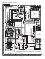
• NOTES ON SCHEMATIC DIAGRAM can be found on page 11.
• The numbers 1 to 18 are waveform numbers shown in page 22.
1
TP400
R600
56
LDCNT2
LDCNT1
CN601
1
HEAD
SW902
DISC PROTECT
M
_REC
PLVGIN 51 52 53 54 55 56 57 58 59 60 61 62 63 64 65 66 67
IC651
HEAD UP/DOWN
DRIVER
LB1930M
+B
16 15 14 13 12 11 10 9 8 7 6 5 4 3 2 1
M901
SPINDLE
MOTOR
G5
6 G
7 O2 I2 4
I1 3
8
2
9 O1
10 VCC 1
14
TP653
TP652
TP651
TP654
TP656
TP655
TP657
TP665
TP664
TP663
TP662
TP661
TP660
TP659
TP658
L921
100mA
TP666
R922
100K
R921
330
VCC
DSPRST
PBAULT
LDON
OPICGA
RFLAT
FLEXIBLE
PWB
16
G
SYD2
SYD1
SYD0
SYWR
SYRD
SYRS
PCNT1
DSPSCK
R422
100K
_STBY
R404
100K
IC353
FTD2005
R403
1K
15
D
IC401
SYSTEM
MICROCOMPUT
IX0298AWZZ
_NMI
SPIN
HDON
TP417
_RESET
TP416
IC353:IC354
HEAD DRIVER
F
EMPH1
DAPON
OPTCNT
VXI
VPD
VDD1
ADPON
X1I
DGND
DIN
X1O
DOUT
VDD3
SYD7
SYD6
SYD5
SYD4
SYD3
RCPCNT
DISCPR
R361
15
INPGCK
MD2
+8
INPGIN
INNSW
C911
0.1
RCAULT
MCPGIN
MD1
VOUT
INNSW
WOUT
TP403
VM
SYD2
26 SYD3
27 SYD4
28 SYD5
29 SYD6
30 SYD7
31 VSS
32 RCLAT
33 _MCPGI
34 _INPGI
35 INPGCK
36 RCPCNT
37 TEST1
38 TEST0
39 JPNP
40 VCC
41
42 _LCDRST
43 PBLAT
44 LDON
45 OPICGA
46 RFLAT
47 RACLK
48 RADAT
49 VSS
50 _ELON
MD0
VCC
1 2 3 4
C361
0.039
D
25 24 23 22 21 20 19 18 17 16 15 14 13 12 11 10 9
C909
0.033
C908
0.22
C905
0.0022
C906
0.0022
C907
0.0022
R901
1
R904
33K
_KHOLD
RIB
TP404
CSL1
BEEP
CSL2
BRK+
SYD1
SYD0
_SYWR
9
8
CST 7
COM 6
WIN 5
VIN 4
UIN 3
RF 2
UOUT 1
R902
1
BRKSTBY
C910
0.033
GND 10
FG
PBOPON
_DCEXT
R906
270K
11
12
13
14
15
16
17
18
19
20
R908
100K
C902
0.01
PBMUTE
G2
S2
S2
C903
3.3
S1
G1
C351
56P(CH)
S1
D2
8 7 6 5
D1
S
G1
D2
G2
D1
R905
100K
VCCHEAD
D351
SBE803
3
4
2
1
5
S
R412
3
10K
4
TP409
SPDRR
HREC
TP351
C353
10/6.3
R909
10K
1
R903
330
IC354
CPH5608
2
R415
1K
3
IC901
2
Q901
RN1113
C354
0.1
1
2
+B
R907
180K
TP901
10
11
12
13
14
C357
0.1
GND 7
6
5
4
3
2
VCC
1
R351
5.6
8
9
5 4 3
R
R413 TP407 1
1K
C
1
R414
TP408
1K
EFMO
R920
100K
IC351
E
LDCNT2
L206
100mA
L202
100mA
TP204
R222
1M
C212
5P(CH)
L205
100mA
C200
1
WDTOVF
IC351
HEAD DRIVER
74ACT02T
12
C171
100/6.3
F-
TF+
RF1
T+
F
E
RF4
RF3
VCC
MP/R
AGND
R205
330K
+B
+B
IC901
SPINDLE MOTOR
DRIVER
BA6966FV
OPTICAL PICKUP UNIT
D
RAA1 28
RAA2 27
RAA3 26
SPDRR
+B
OPIC
RF2
LDVAR
DGND
A
B
COM
CVCC
VCC
DGND
LDON
7 8 9 10 11 12 13 14 15 16 17 18 19 20 21 22
2 3 4 5 6
TP206
C205
0.1
R206
270K
L100
10µH
VCCRF
L171
10µH TP187
FLEXBLE
PWB
1
VDD2 31
TP201
R161
1.2K
2
7 8 9 10 11 12 13 14 15 16 17 18 19 20 21 22
RAA4 32
C207
0.1
TP114
TP115
TP116
TP117
TP118
TP119
TP120
TP108
TP109
TP110
TP111
5 6
RAA5 33
RAA10 30
RAA0 29
BUZOUT
1 2 3 4
TP121
TP122
9
VCCLASER
CN101
TP105
TP106
TP101
TP102
TP103
C
RAA7 35
RAA6 34
1 2 3 4 5 6 7 8 9 10 11 12 13 14 15 16 17 18 19 20 21 22 23 24 25 VCCENDEC
LDON
LDVAR
OPICGA
18
DGND 38
SLDRF
SLDRR
SPDRF
SYD3
TEMP
C165
0.033
FF+
T+
T-
TP202
CK207
R204
1K
RAD2 40
RAOEX 37
RAA8 36
TRDRR
SYD1
RAA9 42
RAD3 41
RACASX 39
TRDRF
SYD0
C123
390P
DGND
100
XRT
SYD2
+B
LRCK
SYRS
C203
0.1
C122
270P
(CH)
R154
1.2K
C130
0.1
SYRD
DINT
CK222
RAWEX 44
FODRR
CK106
TP151
TP145
TP100
3
R101
22K
C121
270P
(CH)
TP203
RARASX 43
IC201
ENCODE/
DECODE/SERVO
ATRAC
LR37811
CK206
CK224
X176KO
C161
1
CK104
+B
CK103
Q101
2SA17457
CK102
CK101
13 14 15 16 17 18 19 20 21 22 23 24
CIN
FODRF
25
R102
22K
X176KO
TP130
TEST2
TP131
X700KO
EFMO 50
PLCK 49
ACRCER 48
TCRS 47
RAD1 45
TEST1
26
CK203
FOK CK204
SENSE CK205
R104
22K
R103
22K
TEST0
TP132
27
EOUT
DVCC
DATA
TP133
28
BOUT
FOUT
CLOCK
LATCH
DTEMP
DGND
AGND
SGAIN
DISC
STBY
BIAS
AVCC
LOGIC
TP212
RAD0 46
C100
10/6.3
EIN
29
CK202
DGND
AOUT
4
CK107
FIN
AIN
CK201
VDD1
TCGO
76 TOTMON
77 TEMON
78 SBCK
79 SBO
80 SBSY
81 SFSY
82 FOK
83 SENSE
84 COUT
85 MCCK
86 DINTX
87 VDD1
88 DGND
89 RSTX
90 SYSD0
91 SYSD1
92 SYSD2
93 SYSD3
94 SYSD4
95 SYSD5
96 SYSD6
97 SYSD7
99 SYRDX
98 SYWRX
99
TP210
WBI
30
HPF
TP209
VBAT
LPF
10
17
BIN
BIAS
XL201
33.868MHz
FEMON 75 74 73 72 71 70 69 68 67 66 65 64 63 62 61 60 59 58 57 56 55 54 53 52 51
CK105
CK108
DFCK
BCLK
31
WBO
TCG
32
22KI
TCGI
12 FIN
B
22KO
11
EIN
ADIP
AGC
33
AIN
ADLPFO
10 BIN
11
C204
0.47
34
REFI
REFO
RFADD
16
AGND
DIFF
1
R106
56K
36
35
TP208
4
EFMAGC
ADIPO
C211
5P(CH)
DADATA
ADDATA
ADAGC
ADIPI
SYRS
EFMMON
AVCC
EFMI
RF4
DIFF
SW
AVCC
ADAG
4
EFM
AGC
EFMI
3
RF3
R
and
EFMO
RF2-1
RF2
AGND
2
L203
100mA
L204
100mA
R207
680
C106
0.22
CK112
RF1
TTR
ROUT
1
C102
1
5
C103 TP144
6
1
C104
7
0.027
R105
8
390K
9
VCCPU
C209
22P(CH)
TP139
C107
0.012
C109
1
48 47 46 45 44 43 42 41 40 39 38 37
GOUT
PLAYBACK SIGNAL
RECORD SIGNAL
+B
C110
C111
0.0033 0.22
IC101
RF SIGNAL
PROCESSOR
IR3R55
EFMAGI
A
C112
0.033
L201
100mA
L209
100mA
MAIN PWB-A1
2
3
4
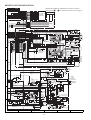
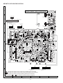
Figure 14 SCHEMATIC DIAGRAM (1/3)
– 14 –
5
6
IC
SE
S8
1O
2V
MD-MT15/15C/15H/15W/161E/18H
P14 P15 P16
DADATA
TP451
TP452
TP453
TP454
TP455
TP456
TP457
TP458
TP459
TP460
TP461
TP462
TP463
ADDATA
TP202
HSTOP
DAPON
TP212
TP205
R455
5.6K
HPLAY
HKEY2
HKEY1
EFMO
LDCNT1
OPTCNT
LDCNT2
XL201
33.868MHz
ADPON
L206
100mA
C212
5P(CH)
L205
100mA
L202
100mA
TP204
R222
1M
CK207
HREC
DIN
DADATA
ADDATA
R451
5.6K
EMPH1
R456
8.2K
11
12
13
14
EDIT
DISP
SKIP
SKIP
REC
P-MO
STOP
VOL
PLAY
BASS
VOL
ENTE
GND
A0
I/O3 18
CAS 17
RAS
A9
DGND 38
RAOEX 37
RAA8 36
A1
A2
TP761
TP763
TP764
TP765
C202
47/6.3
R202
33
RAA1 28
RAA2 27
RAA3 26
SPDRR
SLDRF
SLDRR
SPDRF
TRDRR
TRDRF
FODRR
FODRF
X176KO
TEST2
TEST1
CN701
TP200
VDD2 31
TEST0
A6 13
A5 12
A4 11
VCCDRAM
RAA10 30
RAA0 29
DGND
DSPSCK
DSPSTB
DSPRST
A8 15
A7 14
A3
10 VCC
RAA7 35
RAA6 34
DSPDAT
OE 16
VCCRF
R205
330K
C100
10/6.3
C820
1
IC200
12 2.0V REGULATOR
62FP2002
+B
1
+B
3
VCC2.5
2
EMPH0
RESET
1
C200
1
PBMUTE
+B
3
2
+B
BEEP
RCAULT
+B
AUSCLK
AUDATA
DCNT1
PBAULT
INPGCK
INPGIN
MCPGIN
RKEY
RPLAY
TP413
RDATA
ELON
SYD7
SYD6
SYD5
SYD4
SYD3
CS
2
R415
1K
IC402
EEPROM
S29L294A
R411
100K
IC402
R413 TP407
1K
1
R414
TP408
1K
SYD2
SYD1
SYD0
SYWR
SYRD
SYRS
PCNT1
+B
5
VCC
SK
R412
3
10K
4
TP409
DO PRTCT
7
DI
8
GND
CN702
TP093
33
TP092
32
TP091
31
TP090
30
TP089
29
TP088
28
TP087
27
TP086
26
TP085
25
TP084
24
TP083
23
TP082
22
21
20
TP080
19
TP079
18
TP078
TP077
17
TP076
16
TP075 EMPH0
15
TP074 RESET
14
TP073 PBMUTE
13
TP072 BEEP
12
TP071 RCAULT
11 TP070
TP070B AUSCLK
10
TP069 AUDATA
9
TP068 PBAULT
8
TP067 INPGCK
7
TP066 INPGIN
6
TP065 MCPGIN
5
4
3
2
1
1
TP088B
TP087B
TP086B
1
TP064B RKEY
TP064
RPLAY
+B
TP063RDATA
TP062
TP061
1
TP418
6
NC
33
TP767
TP768
TP769
10
TP770
11
TP771
12
13
14
TP774
15
TP775
16
17
TP777
18
TP779
19
TP780
20
21
TP782
22
TP783
23
24
TP785
25
TP786
26
TP787
27
TP788
28
TP789
29
TP790
30
TP791
31
TP792
32
TP793
33
+B
IC820
2.5V REGULATOR
62FP2502
C201
1
SPDRR
SPDRF
SLDRR
SLDRF
TRDRR
TRDRF
FODRR
FODRF
TP207
TP206
C205
0.1
R206
270K
L100
10µH
X176KO
C207
0.1
TP201
33
1
2
3
4
5
6
7
8
9
1
2
3
4
5
6
7
8
9
C506
1000P
C
6
7
8
9
I/O4 19
WE
1 2 3 4 5 6 7 8 9 10 11 12 13 14 15 16 17 18 19 20 21 22 23 24 25 VCCENDEC
9
11
12
13
14
1
2
3
4
5
TP486
6
TP487
7
TP488
8
TP489
9
CN482
GND 20
I/O2
RAD2 40
RACASX 39
RAA4 32
VDD1
YWR
I/O1
RAA9 42
RAD3 41
RAA5 33
FIN
YD7
1
2
3
4
5
IC202
4MBIT D-RAM
IX2567AF
EMPH1
LDCNT2
LDCNT1
OPTCNT
VXI
VPD
DAPON
VDD1
ADPON
X1I
DGND
DIN
RARASX 43
WBI
YD6
1
2
3
4
5
6
7
8
9
TP481
TP482
TP483
+B
CK222
RAD1 45
VBAT
YD5
TP203
RAD0 46
BIN
YD4
CK224
ACRCER 48
TCRS 47
RAWEX 44
TCG
YD3
EIN
YD2
AIN
R204
1K
AGND
C203
0.1
SYRS
EFMMON
AVCC
EFMI
NT
RT
YD1
X700KO
EFMO 50
PLCK 49
IC201
ENCODE/
DECODE/SERVO
ATRAC
LR37811
CK206
YD0
X1O
100
N
DOUT
YRS
CK202
CK203
OK CK204
NSE CK205
VDD3
DGND
LRCK
DFCK
BCLK
YRD
CK201
1
2
3
4
5
6
7
8
9
CN451
76 TOTMON
77 TEMON
78 SBCK
79 SBO
80 SBSY
81 SFSY
82 FOK
83 SENSE
84 COUT
85 MCCK
86 DINTX
87 VDD1
88 DGND
89 RSTX
90 SYSD0
91 SYSD1
92 SYSD2
93 SYSD3
94 SYSD4
95 SYSD5
96 SYSD6
97 SYSD7
99 SYRDX
98 SYWRX
99
TP210
R458
56K
C481
1
C482
1
FEMON 75 74 73 72 71 70 69 68 67 66 65 64 63 62 61 60 59 58 57 56 55 54 53 52 51
TP209
R457
18K
R453
18K
R452
8.2K
FLAT CABLE
(243)
TP208
11
BCLK
C211
5P(CH)
1
04
47
DFCK
LRCK
L204
100mA
L201
100mA
L209
R207 100mA
680
C209
22P(CH)
L203
100mA
TP411
TP410
+B
+B
HDON
TP414
CIN
SPIN
CHGON
SPIN
VSS 88
AVSS 87
LDVAR 86
TEMP
PLVDCI
R424
22K
R467
18K
R465
100K
L862
100µH
C865
1
RKEY
Q461
2SC4738 GR
R423
22K
TP402
R425
22K
PLVDRY
77
76
R426
22K
EMPH0
OPEN
R460
68K
HKEY1
R462
100K
_RPLAY
_ARQK
EMPH0
_DINT
_ARQD
VSS
_PLAY
_STOP
EXTAL
XL401
4.19MHz
IC802
OVER
CONN
CIRC
HKEY2
PLVDCI 80
PLVBAT 79
Vref
AVCC 78
HSTOP
TP400
HPLAY
INNSW
TP403
TP404
BEEP
TP412
PBMUTE
HREC
AUSCLK
AUDATA
ELON
LDVAR
CHGCNT 85
HKEY2 84
PLVGIN 51 52 53 54 55 56 57 58 59 60 61 62 63 64 65 66 67 68 69 70 71 72 73 74 75
BATON
C401
TP401 0.1
C869
47/6.3
DISCPR
SPWDS
VSS
PDCNT
RMDAT
DSPDAT
_EPCS
DSPSCK
EEPD
EEPK
PLVON
VSS
SYRS
PCNT1
_SYRD
SCKO
DSPSTB
P32
XTAL
VCC
_STBY
_REC
BATINCK
TP415
TEMP 81
_NMI
RFLAT
SENSE
MCMON 90
BAT0FF 89
HKEY1 83
RKEY 82
_RESET
DSPRST
PBAULT
LDON
OPICGA
MD2
R422
100K
WDTOVF
TP417
AUDIO
PWB-A2
FOK
DCNT1M 92
NIHEXT 91
IC401
SYSTEM
MICROCOMPUTER
IX0298AWZZ
INNSW
TP416
PCNT2
XRT
SENSE 93
MD1
RCPCNT
MD0
INPGCK
BUZOUT
INPGIN
R406
100K
TP406
R405
10K
TP405
VDD 98
_XRST 95
_FOK 94
_KHOLD
MCPGIN
CIN
HDON 100
PCNT2 99
_EJSW 97
CKSTP 96
PBOPON
_DCEXT
RCAULT
SYD1
SYD0
_SYWR
25 24 23 22 21 20 19 18 17 16 15 14 13 12 11 10 9 8 7 6 5 4 3 2 1
SYD2
26 SYD3
27 SYD4
28 SYD5
29 SYD6
30 SYD7
31 VSS
32 RCLAT
33 _MCPGI
34 _INPGI
35 INPGCK
36 RCPCNT
37 TEST1
38 TEST0
39 JPNP
40 VCC
41
42 _LCDRST
43 PBLAT
44 LDON
45 OPICGA
46 RFLAT
47 RACLK
48 RADAT
49 VSS
50 _ELON
RCPCNT
DISCPR
PDCNT
DSPDAT
DSPSTB
DSPSCK
ELON
DINT
RPLAY
C863
1
D861
EP10LA03
C851
R851 150P
10K (CH)
IC
2
R
T
1
2
3
R821
100K
C825
4P(CH)
4
C866
1
C832
0.1
R833
47
C831
0.1
IC702
4.5V REGULATOR
62GR4522
7
8
9
10
Figure 15 SCHEMATIC DIAGRAM (2/3)
– 15 –
11
C822 4
56P(CH)
5
R828
220K
12
R827
300K
EAINEAOUT
6 GND
D821
EC30LA02
L822
10µH
D831
1SS372
C877
1
5
IC702
DB
3 EAIN+
C827
22/6.3
R811
180K
C810
0.33
TP811
C834
0.1
VCC2.7
VCCVG
1
2
3
R823
100K
R832
10M
+B
2
R826
10K
IC808 CHARGING CIRCUIT
HN1C01FU
PCNT1
R810
180K
1 VREF IC
R829
33K
C830
1000P
R279
6 100
5
4
C821
220/4
+B
+B
IC808
1
2
3
R277
39K
PLVDCI
PCNT1
BATINCK
BATON
D461
RB731U
3
4
2
5
1
6
VCC4.5
R463
100K
R461
100K
R803
100K
3
PCNT2
2 VDD
PLVDRY
1 OUT VSS 4
R466
560K
R431
330K
SW402
HOLD
L600
2.2µH
IC431
SESET
S80820LN
C600
22/6.3
MTP610
RESET
D431
1SS361
C431
0.47
R464
100K
R408
100K
C454
0.0022
R407
10K
VCC2.7X
MD-MT15/15C/15H/15W/161E/18H
• NOTES ON SCHEMATIC DIAGRAM can be found on page 11.
P14 P15 P16
• The numbers 1 to 18 are waveform numbers shown in page 22.
TP451
TP452
TP453
TP454
TP455
TP456
TP457
TP458
TP459
TP460
TP461
TP462
TP463
EC
A
TOP
R455
5.6K
AY
Y2
Y1
R451
5.6K
R456
8.2K
R457
18K
R458
56K
R453
18K
R452
8.2K
1
2
3
4
5
6
7
8
9
1
2
3
4
5
6
7
8
9
11
12
13
14
11
12
13
14
EDIT
DISPLY
LCD ASS'Y
SKIP DOWN
SKIP UP
REC
KEY SWITCH
FLEXIBLE
PWB ASS'Y
P-MODE
STOP
VOL DOWN
PLAY
LCD
BASS
VOL UP
ENTER
GND
CN451
C481
1
C482
1
TP481
TP482
TP483
DSPDAT
DSPSCK
DSPSTB
DSPRST
R770
15K
R769
15K
4
5
RI
3
2
1
LI
C720
1000P
C735
R765:R766
1000P
MD-MT15H/
15W/161E/18H
18
MD-MT15/15C
C452
8.2
1000P
VCC
KEY
PLAY
J702
R724 L714
6.8K 100mA TP714 MICIN
4
TP713
2
TP712
3
L712
100mA
1
C724
1000P
L713
100mA
L711
100mA
C776
1000P
TP726
L452
TP725
100mA TP729TP722
L453 TP724
100mA
L454
100mA
TP723
L451 TP721B TP721
150mA
TP727
TP728
RDATA
R492
1K
RPLAY
RKEY
R763
68
L719
0.47uH
L456
100mA
C491
0.1
D492
15AZ7.5Y
R765
R766
R764
68
R767
1K
C765
0.22
C766
0.22
R768
1K
C753
1
L752
22uH
L-ch
R-ch
C752
0.082
C751
0.082
R753
120K
C754
1
C755
0.01
L751
22uH
C719
10/10
PBAULT
AUDATA
AUSCLK
RCAULT
RESET
BEEP
C771
47/6.3
L771
100µH
PBMUTE
+B
+B
ELON
AUDIO
PWB-A2
C723
1000P
E
C832
0.1
8
OUT
6 GND
L822
10µH
G
D822
1SS389
4
MICOM2.35V
2
R258
180K
V+
O
+
O
+
VC256
0.1
IC841
2.35V REGULATOR
XC62HS02
VCCPOWER
Q874
RN1113
C841
10/6.3
5
3
2
1
3
R809
2.2K
R806
1K
IC801
HN1C01FU
R807
680
L887
TIP IMPEDER
VCC4
TP803
TP804
BATTERY
TERMINAL
2 D D 5
3 G S 4
IC806
R263 NDC631N
100K
C255
0.1
Q251
2 RN1113
R271
1K
R276
3.3K
1
3
R264
18K
2
IC805,IC806,IC807
CHARGING CIRCUIT
Q255
RN1113
3
1
2
3
6
5
4
IC807
RN4904
1
R831
100K
2
1
R274
75K
1 D S 6
R275
56K
IC822 S
CPH3403
3
R270
100
C254
0.1
G
C826 L821
4.7µH
1
D
1 2 3 4
R267
75K
R265 R269
22K 100
S
1
R254
C258 2.2K
0.0047
8 7 6 5
R268
2.2K
D
VCC13
7
TP809
FET IC
Q873
NDS332P
R878
100K
OSC
PWM
VCC
EAOUT
C828
1
R827
300K
R824
15K
9
C829
0.01
R821
100K
C825
4P(CH)
10
STATE
C831
0.1
IC702
4.5V REGULATOR
62GR4522
1
ROSC
11
C824
560P
IC821
DC/DC
CONVERTER
IR3M09N
R261
270K
R262
24K
!
F871
T0.5A L 63V
L871
47µH
D871
EP10LA03
VCC11
VCC12
C874
15/10
C866
1
H
R833
47
12
C875
0.1
4
D831
1SS372
IC702
C877
1
5
R832
10M
VCC2.7
EAIN-
D821
EC30LA02
C823
390P
OSCOUT
DB
3 EAIN+
C822 4
56P(CH)
5
R828
220K
C821
220/4
TP811
C834
0.1
VCCVG
1
2
3
R823
100K
R811
180K
C810
0.33
VCC4.5
+B
2
R826
10K
IC808 CHARGING CIRCUIT
HN1C01FU
PCNT1
R810
180K
1 VREF IC821OSCIN
R829
33K
R279
6 100
5
4
C830
1000P
1
2
3
R277
39K
IC808
C827
22/6.3
PCNT1
G
PLVDRY
PLVDCI
R257
100K
Q254
RN1113
3
2
SW801
Ni-MH
BATTERY
DETECTION
R251
1
VCC2.7X
R259 Q252
82K 2SC4738GR
R250
1
R852
47K
R273
56K
4
GND
TP808
C852
1
R804
1.0A
R253 R252 R278
75K
150K 2.2K
1
5
SW801
VCC3
C250
0.1
VCC
IC803
FDT439N
CHARGING
CIRCUIT
G
1
2
3
5
4
C876
1 R871
10K
1
2
3
Q253
RN1113
2
3
R853
100
IC805
NJM022V
IC851
2.35V
REGULATOR
TC7S14FU
R255
0.2M
C851
R851 150P
10K (CH)
R256
18K
C863
1
D861
EP10LA03
4
3
J801
DC IN
D803 1SS382
REVERSE
CONNECTION
D812
S SB10015C
C253
0.1
C869
47/6.3
C865
1
L862
100µH
3
D
R260
3.3M
F
2
DC JACK
1
TP801
2
TP802
3
D800
1SS360
6
5
4
1
R802 2
1K
C805
100/6.3
R467
18K
R465
100K
1
IC801
1
2
3
4
IC802
FDC634P
C806
3.3
C800
1
R808
5.6K
R266
100K
Q461
2SC4738 GR
5
6
D801
SB10015C
R460
68K
IC802: IC802
OVER VOLTAGE REVERSE
CONNECTION PROTECTION
CIRCUIT
TP805
GND1
VCC2
L888
TIP IMPEDER
VCC1
R801
2.2K
R816
24K
D802
015Z5.1Y
R800
22K
TP800
C801
0.1
R815
56K
C871
0.47
IC871
S8324A28
2.8V UP CONVERTER
4
Figure 16 SCHEMATIC DIAGRAM (3/3)
– 16 –
1
OUT VSS
4
2
VDD
3
IC872
S80813LN
2.8V UP CONVERTER
5
L
R
GND
R725
100
13 14 15 16 17 18 19 20 21 22 23 24
D494
15AZ7.5Y
Vout
J703
HEADPHONES
DGND
6
R-ch
C722
3.3/10
VCC
GND
C725
3.3/10
C714
1
C703
0.01
C701
10/6.3
R703
120K
C758
3.3/10
C756
0.68
7
L-ch
C721
3.3/10
7
9
8
6
1
2
3
4
5
TP711
VEE
R702
100
C702
10/6.3
C759
0.027
D
8
9
12 11 10
R727 R723
8.2K 6.8K
C731
0.22
R729
2.7K
IC703
AUDIO AMP.
IR3R54N
IC771
2.5V REGULATOR
62 GR2522
R726
RIPPLE 39K
FILTER
R728
1K
MCPGIN
R730
2.7K
AGND
4
C774
1
L702
100mA TP701
TP702
C712
100P L703
TP703
(CH) 100mA
TP704
C711
L704 TP705
100P
100mA
R714 (CH)
Q721
10K
2SC4213 B
C726
3.3/10
LIHP
RIHP
LOUT
ROUT
5
VEE
TP063RDATA
TP062
AGND
C501
0.0022/50
C502
0.0022/50
C504
3.3/10
C503
3.3/10
AINR
VRDA
AINL
VCML
VRAD
VA
VB
AGND
VCOM
AOUTL
AOUTR
DEM0
DEM1
+B
TP061
1
VCMR
PWAD
SCLK
LRCK
MCLK
PWDA
SDTO
RPLAY
R716
100K
INPGIN
TP707
TP709
TP708
R713
10K
+B
R761
4.3K
LIHP
1
1
2
3
TP064B RKEY
TP064
LOUT
ELON
5
4
3
2
1
R715
100K
R762
4.3K
C757
0.68
MCPGIN
INPGCK
IC701
24 AUDIO
AMP.
IR3R54N
R701
100
R754
270K
RIHP
INPGIN
RKEY
RPLAY
2 C713
1
3
Q711
RN1444 A
1
J701
OPTICAL/
LINE IN
4
C715
0.1
1
C500
10/6.3
ROUT
INPGCK
C508
1
R757
27K
PBAULT
2
3
LI
13 14 15 16 17 18 19 20 21 22 23
R756
27K
AUDATA
13 14 15 16 17 18 19 20 21 22 23 24
4
5
RI
3
4
R717
1K
R710
56
C733
0.1
VCC
C760
0.027
AUSCLK
15
6
7
8
C511
1
BEEP
RCAULT
L500
47µH
PBMUTE
9
R711
5.6K
L-ch
R-ch
IC501
AD/DA
CONVERTER
AK4519VF
TP500
RESET
VD
SDTI
CMODE
EMPH0
12 11 10
3
R720 R712
8.2K 5.6K
C734
0.1
R719
8.2K
DGND
IC501
DGND
C
C509
2.2
C510
2.2
R502
470
12 11 10 9 8 7 6 5 4 3 2 1
R500
4.7
C761
2.2
C762
2.2
+B
R501
470
TP088B
TP087B
TP086B
EMPH0
TP767
TP768
TP769
10
TP770
11
TP771
12
13
14
TP774
15
TP775
16
17
TP777
18
TP779
19
TP780
20
21
TP782
22
TP783
23
24
TP785
25
TP786
26
TP787
27
TP788
28
TP789
29
TP790
30
TP791
31
TP792
32
TP793
33
SW403
DISC LID
OPEN 1
2
SW401
EJECT 1
2
CN702
TP093
33
TP092
32
TP091
31
TP090
30
TP089
29
TP088
28
TP087
27
TP086
26
TP085
25
TP084
24
TP083
23
TP082
22
21
20
TP080
19
TP079
18
TP078
TP077
17
TP076
16
TP075 EMPH0
15
TP074 RESET
14
TP073 PBMUTE
13
TP072 BEEP
12
TP071 RCAULT
11 TP070
TP070B AUSCLK
10
TP069 AUDATA
9
TP068 PBAULT
8
TP067 INPGCK
7
TP066 INPGIN
6
TP065 MCPGIN
C773
0.22
TP763
TP764
TP765
33
C506
1000P
C505
1000P
TP761
33
1
2
3
4
5
6
7
8
9
C507
10/6.3
CN701
LCD
DRIVER
6 7 8
FLAT CABLE
(243)
B
1
2
3
4
5
6
7
8
9
1
2
3
4
5
TP486
6
TP487
7
TP488
8
TP489
9
CN482
+B
6
6
5
2
4
3
1
7
8
MD-MT15/15C/15H/15W/161E/18H
MAGNETIC HEAD FLEXIBLE PWB(18)
A
M901
SPINDLE MOTOR
OPTICAL PICKUP
UNIT(13)
MAGNETIC
HEAD(24)
B
SW902
DISC
PROTECT
MECHANISM
FLEXIBLE PWB
C
PH901
PHOTO
INTERRUPTER
D
CN601
TO MAIN PWB
P18 5-H
M902
SLED MOTOR
CN101
TO MAIN PWB
P18 4-H
M903
HEAD
UP/DOWN MOTOR
TO MAIN PWB
P18 2-C
CN451
TO MAIN PWB
P18 3-C
CN482
E
F
G
KEY SWITCH FLEXIBLE PWB Ass'y (213)
LCD Ass'y (214)
H
1
2
3
4
Figure 17 WIRING OF P.W.BOARD (1/5)
– 17 –
5
6
MD-MT15/15C/15H/15W/161E/18H
A
R804
TP803
MAIN PWB-A1 (BOTTOM VIEW)
C255
C254
R269
Terminal, Battery
(235)
CN702
1
C256
TO AUDIO PWB
8
IC805
4
5
33
1
R271
C258
R255
R254
R262
Q255
TP804
FLAT CABLE
(243)
R275
R267
33
1
R266
B
R274
P20 3-A
C253
13
1
Terminal, Battery
(233)
1
9
Q253
Terminal, Battery
(237)
/
R278
To LCD Ass'y
P17 5-E
R259
To Key Switch Flexible Ass'y
P17 2-E
R260
R261
R252
R276
9
TP666
TP660
TP657
TP656
Q254
TP655
8
TP119
TP120
TP121
18
22
TP117
5
10
35
TP139
40
48
C107
16
22
TP101
CK112
C112
1
10
To Optical Pickup Unit
P17 1-D
5
1
45
37
2
16
1
To Mechanism Flexible PWB
P17 6-D
: Through-hole where the top, bottom and +B patterns are connected.
: Through-hole where the top, bottom and hround patterns are connected.
: Through-hole where the top and bottom patterns are connected.
• The numbers 1 to 18 are waveform numbers shown in page 22.
2
3
4
Figure 18 WIRING OF P.W.BOARD (2/5)
– 18 –
5
6
TP118
TP115
15
TP144
30
IC101
CN101
12
TP102 TP108 TP109 TP111
15
TP103
20
20
TP114
13
TP116
CK102
10
17
TP351
R906
R154
TP122
TP151
CK106
TP131
TP130
TP133
CK108
24
36
SW402
HOLD
Q101
C130
CK103 CK101
25
R106 CK105 TP132
TP402
CK107
TP411
TP418
TP207
TP406
TP414
TP659
TP658
TP901
10
7
C903
8
1
1
R273
TP653
TP602
TP654
TP661
TP662
TP601
TP187
TP663
TP651
R908
9
Q251
R265
IC808
TP610
R853
C810
R810
TP652
TP201
5
TP105
8
R909
C902
TP110
7
6
14
R905
C110
5
11
R907
C908
C109
4
10
C106
3
TP664
TP665
R851
R852
TP200
1
TP100
2
G
H
C910
TP106
TP212
1
13
IC351
C161
R406
TP405
TP808
TP415
TP809
TP206
TP145
IC202
TP205
TP793
TP789
TP783
33
15 14 13 12 11
19 18 17 16
TP792
30
20
TP203
TP786
TP777
TP790
25
1
R903
15
IC402
1
R405
L921C357
IC901
TP407
4
C911
5
R411
TP404
TP779
TP774
TP788
TP787
C401
TP791
TP202
TP775
20
95
20
C905
C909
5
100
TP782
15
90
CN601
5
1
R902
C906
5
85
R901
R412 C907
R413
15
70
80
10
R921
1
TP409
IC401
76
L602
R904
R414
20
10
75
C603
C601
C250
16
15
C602
C851
25
65
10
6
R279
L601
R415
XL401
C604
IC851
C828
C852
26
55
60
5
3
TP811
C825
30
4
4
3
IC807
L603
R811
TP416
TP410
35
4
6
1
R922
R827
40
5
TP413
45
1
L604
1
C822
R823
C830
R826
R832
C832
R829
5 6
3
CK104
TP482
C824
C482
TP463
TP486
C831
D831
R821
1
R828
TP785
C829
7
TP403
TP204
1
10
50
51
TP400
D822
TP408
TP761
TP459
TP763
CN701
TP462
TP209
TP802
2
TP210
TP801
R452
R831
IC821
R422
R453
R451
L888
R824
12
R264
R277
C823
TP417
R425
TP208
TP800 R815
R816
C801
TP488
TP487
TP455
TP452
TP805
TP457
R426
3
TP412 TP780 TP771 TP770 TP769 TP768 TP767 TP765
TP401
TP489
R424
1
C800
TP481
TP483
TP454
TP460 TP458
TP461
9
J801
TP764
F
5
R458
10
C481
1
R457
R455
5
L887
E
CN482
R456
13
J801
DC IN
1
TP453
TP451
TP456
CN451
1
D
14 15
11
C111
10
C
R263
R253
MD-MT15/15C/15H/15W/161E/18H
R257
R258
Q252
R270
MAIN PWB-A1 (TOP VIEW)
R256
SW801
SW801
Ni-MH
BATTERY
DETECTION
R250
1
6
2
5
4
3
IC806
R251
D812
G
3
F871
T0.5A L 63V
L821
C876
L822
C874
C821
D861
75
R101 R205
70
10
C171
6
65
15
L201
L203
R222
60
IC201
C205
R351
C354
1
4 5 6
C212
C211
XL201
20
55
R161
35
40
51
50
45
L205
1
R803
C100
R403
R404
IC820
R408
3
C102
C103
2
CK224
C820
CK222
C104
R407
R105
3
2
1
3
4
C201
R423
1
L206
R462
30
C165
C200
25
26
R460
R467
3 21
IC801
L202
R206
2
5
R463
CK207
C121
5
4
3
2
R808
1
D461
R465
R809
76
R807
CK205
CK204
CK203
80
C202
R802
1
85
D803
3
R461
R806
C207
90
4
1 2
C353
CK202
R103
3
D351
1
C124
R102
5 4
4
R871
R466
95
4
D431
CK201
C123
IC353
5
CK206
6
5
C431
100
C122
L171
C351
5
R878
Q874
6
R104
IC354
R361
8
C204
G
5
R920
1
R431
R601
Q461
D800
Q873
2
C209
D
3
4
R207
L608
19
C203
S
R204
10
IC651
C361
1
1
2
3
C871
IC431
1
20
18
2
IC872 4
15
Q901
3
25
C877
4
D802
C827
IC702
R464
10
L862
5
C875
5
C454
IC822
C608
4
4
IC802
C863
IC841
L209
C826
S
C806
2
3
1
2
3
C869
D
30
L610
R833
G
2 1
3
5
IC871
C834
C866
35
L204
5
36
C865
IC601
1
D821
C605
L609
C609
C610
1
D801
C622
C651
C841
L600
R801
R600
L871
C600
R800
S
4
C805
R268
D871
IC803
D
2
IC200
L100
R202
12
7
8
9
10
Figure 19 WIRING OF P.W.BOARD (3/5)
– 19 –
11
12
MD-MT15/15C/15H/15W/161E/18H
TO MAIN PWB
AUDIO PWB-A2 (TOP VIEW)
CN701
P18 2-B
33
1
33
1
FLAT
CABLE
(243)
A
CN702
L751
L752
30
33
20
25
15
10
1
5
R766
R767
R768
C766
C765
B
C752
L453
R763
R764
R765
R761
12
L771
C756
13
C758
C491
R716
C712
R756
R754
C757
D
L703
R714
C759
L704
C760
C773
C774
15
D492
10
C714
IC703
D494
R762
C753
C771
20
C751
R753
5
R492
R770
C
L454
C755
L456
24
1
C754
R769
3
R757
L719
4
5
C719
4
3
2
9
1 C762
C761
C507
C508
R500
L500
C511
5
8
R711
L702
4
1
SW401
EJECT
8 7 6
R703
C703
L714
L712
G
4
C701
R728
2
R727
3
R724
C725
C726
C723
2
C720
C721
C722
R723
3
L713
R729
C509
C510
C702
Q721
C501
R726
C502
C503
R501
R730
C724
C731
12
1
R502
1
R702
2
R719
10
5
C711
15
R725
C500
C504
F
Q711
13
20
IC501
H
J701
OPTICAL/
LINE IN
6
7
24
C506
C505
R720 R712
E
R717
C715
5
R710
IC771
1
SW403
DISC LID
OPEN
: Through-hole where the top, bottom and +B patterns are connected.
: Through-hole where the top, bottom and hround patterns are connected.
: Through-hole where the top and bottom patterns are connected.
• The numbers 1 to 18 are waveform numbers shown in page 22.
1
2
3
4
Figure 20 WIRING OF P.W.BOARD (4/5)
– 20 –
5
6
MD-MT15/15C/15H/15W/161E/18H
C776
AUDIO PWB-A2 (BOTTOM VIEW)
TP066
TP062
TP728
TP077
TP068
TP076
TP064
TP061
TP065
L452
TP069
TP086
TP080
8
TP093
TP727
TP063
7
TP082
TP067
2
TP072
4
TP724
TP729
TP092
TP070
TP089
J703
HEADPHONES
TP722
TP721
TP723
1
TP071
3
TP721B
TP070B
TP725
5
TP064B
TP074
TP726
6
L451
TP085
TP704
TP705
C452
TP703
C713
TP073
TP079
TP075
TP090
R715
TP083
TP088
TP709
TP707
TP084
R713
TP708
TP087
TP702
TP701
13
12
R701
15
IC701
10
TP091
TP088B
TP500
20
5
TP086B
24
L711
TP087B
1
TP711
1
2
TP713
J702
MIC
IN
C734
C733
TP712
TP078
TP714
4
3
C735
7
8
9
10
Figure 21 WIRING OF P.W.BOARD (5/5)
– 21 –
11
12
MD-MT15/15C/15H/15W/161E/18H
WAVEFORMS OF MD CIRCUIT
T
Stopped
CH1=1mV
DC 10:1
1
CH2=500mV
DC 10:1
CH3=5V
DC 10:1
TP208
(FEOUT)
5
SDTi
6
SCLK
3
CK205
(SENSE)
9
4
CK204
(FOK)
LRCK
8
1994 / 12 / 16 01:03:40
2ms/div
(2ms/div)
ENV
T
TP209
(TOTAL)
MCLK
4
4
=Filter=
Smoothiing : OFF
BW : FULL
=Offset=
CH1 :
0.00V
CH2 :
0.000V
CH3 :
0.00V
CH4 :
0.00V
=Record Length=
Main :
10K
Zoom : 10K
T
Stopped
CH1=2V
DC 10:1
CH2=2V
DC 10:1
=Trigger=
Mode : NORMAL
Type : EDGE CH4
Detay :
0.0ns
Hold OFF :
MINIMUM
=Filter=
Smoothiing : OFF
BW : FULL
1994 / 12 / 15 23:31:21
50ms/div
(50ms/div)
ENV
Stopped
CH1=2V
DC 10:1
T
1
SPDRR
1
TP601
(VM)
CH3=500mV
DC 10:1
2
11
3
3
T
CH2=2V
DC 10:1
TP201
(EFM)
TP210
10 (TEOUT)
T
7
T
Stopped
CH1=1V
DC 10:1
1994 / 12 / 16 00:24:17
CH4=2V
50us/div
DC 10:1
(50us/div)
NORM:100MS / s
2
2
13
CH3=2V
DC 10:1
1
TP122
(F+)
12
CH2=2V
DC 10:1
1
1
2
T
Stopped
CH1=2V
DC 10:1
1994 / 12 / 15 22:54:19
CH4=2V
50ms/div
DC 10:1
(50ms/div)
NORM:200kS / s
=Offset=
:
0.00V
:
0.00V
:
0.00V
:
0.00V
CH1
CH2
CH3
CH4
CH2=2V
DC 10:1
=Record Length=
Main :
5K
Zoom : 5K
CH3=2V
DC 10:1
=Trigger=
Mode : AUTO
Type : EDGE CH3
Detay :
0.0ns
Hold OFF :
MINIMUM
=Filter=
Smoothiing : OFF
BW : FULL
1994 / 12 / 18 09:26:46
CH4=2V
1s/div
DC 10:1
(1s/div)
ENV
Stopped
CH1=2V
DC 10:1
=Offset=
CH1 :
0.00V
CH2 :
0.00V
CH3 :
0.000V
CH4 :
0.00V
=Record Length=
Main :
10K
Zoom : 10K
=Trigger=
Mode : NORMAL
Type : EDGE CH2
Detay :
0.0ns
Hold OFF :
MINIMUM
1994 / 12 / 16 01:23:16
500ms/div
(500ms/div)
MORM:200MS/s
TP208
(FEOUT)
1
10
TP210
(TEOUT)
14
TP656
(SL+)
15
TP657
(SL-)
9
T
TP201
(EFM)
T
2
2
3
1
=Tracel=
4
Bandwidth
FULL
20MHz
=Filter=
Smoothiing : OFF
BW : FULL
CH1
CH2
CH3
CH4
=Offset=
:
0.00V
:
0.00V
:
0.00V
:
0.00V
=Record Length=
Main :
10K
Zoom : 10K
T
Stopped
CH1=2V
DC 10:1
CH2=2V
DC 10:1
CH3=500mV
DC 10:1
=Filter=
Smoothiing : OFF
BW : FULL
=Trigger=
Mode : NORMAL
Type : EDGE CH1
Detay :
0.0ns
Hold OFF :
MINIMUM
1994 / 12 / 15 08:57:26
2ms/div
(2ms/div)
ENV
CH1
CH2
CH3
CH4
Stopped
CH1=2V
DC 10:1
P-P
1.280V
Smooth
OFF ON
=Offset=
:
0.00V
:
0.00V
:
0.00V
:
0.00V
CH2=2V
DC 10:1
=Record Length=
Main :
10K
Zoom : 10K
CH3=2V
DC 10:1
=Trigger=
Mode : AUTO
Type : EDGE CH2
Detay :
0.0ns
Hold OFF :
MINIMUM
=Filter=
Smoothiing : OFF
BW : FULL
CH1
CH2
CH3
CH4
Stopped
CH1=2V
DC 10:1
1994 / 12 / 15 09:58:45
CH4=2V
1s/div
DC 10:1
(1s/div)
ENV
=Offset=
:
0.000V
:
0.00V
:
0.00V
:
0.00V
CH2=2V
DC 10:1
=Record Length=
Main :
1K
Zoom : 1K
CH3=2V
DC 10:1
=Trigger=
Mode : AUTO
Type : EDGE CH1
Detay :
0.0ns
Hold OFF :
MINIMUM
1994 / 12 / 15 08:39:46
1s/div
(1s/div)
NORM:1kS/s
T
9
1
TP201
(EFM)
TP208
(FEOUT)
1
TP210
10 (TEOUT)
2
10
TP210
(TEOUT)
11
TP209
(TOTAL)
10
TP210
(TEOUT)
12
SPDRR
T
1
2
T
1
13
=Filter=
Smoothiing : OFF
BW : FULL
CH1
CH2
CH3
CH4
Stopped
CH1=500mV
DC 10:1
=Offset=
:
0.00V
:
0.00V
:
0.000V
:
0.0V
=Record Length=
Main :
10K
Zoom : 10K
CH2=2V
DC 10:1
3
TP601
(VM)
14
TP656
(SL+)
15
TP657
(SL-)
2
3
4
=Trigger=
Mode : NORMAL
Type : EDGE CH1
Detay :
0.0ns
Hold OFF :
MINIMUM
=Filter=
Smoothiing : OFF
BW : FULL
1994 / 12 / 15 09:10:03
20us/div
(20us/div)
ENV
Stopped
CH1=2V
DC 10:1
9
TP201
(EFM)
10
TP210
(TEOUT)
=Offset=
:
0.00V
:
0.00V
:
0.00V
:
0.00V
CH1
CH2
CH3
CH4
=Record Length=
Main :
10K
Zoom : 10K
T
CH2=2V
DC 10:1
CH3=1V
DC 10:1
=Trigger=
Mode : AUTO
Type : EDGE CH1
Detay :
0.0ns
Hold OFF :
MINIMUM
=Filter=
Smoothiing : OFF
BW : FULL
CH1
CH2
CH3
CH4
=Offset=
:
0.00V
:
0.00V
:
0.00V
:
0.0V
=Record Length=
Main :
10K
Zoom : 10K
=Trigger=
Mode : AUTO
Type : EDGE CH1
Detay :
0.0ns
Hold OFF :
MINIMUM
1994 / 12 / 15 21:54:52
CH4=1V
500us/div
DC 10:1
(500us/div)
ENV
1
16
CK105
(HPFO)
T
T
2
1
17
CK108
(WBO)
3
2
18
=Filter=
Smoothiing : OFF
BW : FULL
CH1
CH2
CH3
CH4
=Offset=
:
0.000V
:
0.00V
:
0.000V
:
0.0V
=Record Length=
Main :
4K
Zoom : 4K
=Trigger=
Mode : NORMAL
Type : EDGE CH1
Detay :
0.0ns
Hold OFF :
MINIMUM
TP121
(T-)
4
=Filter=
Smoothiing : OFF
BW : FULL
CH1
CH2
CH3
CH4
For TP208, TP209, and TP210, use the specific LPF, and
observe the waveform.
10K
=Offset=
:
0.00V
:
0.00V
:
0.00V
:
0.00V
=Record Length=
Main :
10K
Zoom : 10K
=Trigger=
Mode : NORMAL
Type : EDGE CH2
Detay :
0.0ns
Hold OFF :
MINIMUM
When watching the EEM monitor (TP201)
Set MSL from 00H to 80H with EEPROM control setting. After
completion restore 00H.
Measurement
TP
1000P
– 22 –
MD-MT15/15C/15H/15W/161E/18H
PARTS GUIDE
MODEL
MD-MT15(S)
MD-MT15C(S)
MD-MT15H(RD)
MD-MT15H(S)
MD-MT15W(S)
MD-MT161E(S)
MD-MT18H(GR)
“HOW TO ORDER REPLACEMENT PARTS”
To have your order filled promptly and correctly, please furnish the
following information.
1. MODEL NUMBER
2. REF. No.
3. PART NO.
4. DESCRIPTION
For U.S.A. only
Contact your nearest SHARP Parts Distributor to order.
For location of SHARP Parts Distributor,
Please call Toll-Free;
1-800-BE-SHARP
MARK: SPARE PARTS-DELIVERY SECTION
Explanation of capacitors/resistors parts codes
Capacitors
Resistors
VCC ....................... Ceramic type
VCK ........................ Ceramic type
VCT ........................ Semiconductor type
VC • • MF ............... Cylindrical type (without lead wire)
VC • • MN ............... Cylindrical type (without lead wire)
VC • • TV ................ Square type (without lead wire)
VC • • TQ ............... Square type (without lead wire)
VC • • CY ............... Square type (without lead wire)
VC • • CZ ............... Square type (without lead wire)
VC • • • • • • • • • J .. The 13th character represents capacity difference.
("J" ±5%, "K" ±10%, "M" ±20%, "N" ±30%,
"C" ±0.25 pF, "D" ±0.5 pF, "Z" +80-20%.)
VRD ....................... Carbon-film type
VRS ........................ Carbon-film type
VRN ....................... Metal-film type
VR • • MF ............... Cylindrical type (without lead wire)
VR • • MN ............... Cylindrical type (without lead wire)
VR • • TV ................ Square type (without lead wire)
VR • • TQ ............... Square type (without lead wire)
VR • • CY ............... Square type (without lead wire)
VR • • CZ ............... Square type (without lead wire)
VR • • • • • • • • • J .. The 13th character represents error.
("J" ±5%, "F" ±1%, "D" ±0.5%.)
If there are no indications for the electrolytic capacitors, error is ±20%.
If there are no indications for other parts, the resistors are ±5%
carbon-film type.
NOTE:
Parts marked with “
” are important for maintaining the safety of the set.
Be sure to replace parts with specified ones for maintaining the safety and performance of the set.
MD-MT15/15C/15H/15W/161E/18H
NO.
PRICE
RANK
PARTS CODE
DESCRIPTION
INTEGRATED CIRCUITS
IC101
IC200
IC201
VHIIR3R55//-1
VHI62FP2002-1
VHILR37811/-1
J
J
J
IC202
IC351
IC353
IC354
IC401
RH-IX2567AFZZ
VHI74ACT02T-1
VHIFTD2005/-1
VHICPH5608/-1
RH-IX0298AWZZ
J
J
J
J
J
IC402
IC431
IC501
IC601
IC651
IC701
IC702
IC703
IC771
IC801
VHIS29L294A-1
VHIS80820LN-1
VHIAK4519VF-1
VHIMPC17A39-1
VHILB1930M/-1
VHIIR3R54N/-1
VHI62GR4522-1
VHIIR3R54N/-1
VHI62GR2522-1
VHIHN1C01FU-1
J
J
J
J
J
J
J
J
J
J
IC802
VHIFDC634P/-1
J
IC803
IC805
IC806
IC807
IC808
IC820
IC821
IC822
IC841
IC851
IC871
IC872
IC901
Q873
VSFDT439N//-1
VHINJM022V/-1
VHINDC631N/-1
VHIRN4904//-1
VHIHN1C01FU-1
VHI62FP2502-1
VHIIR3M09N/-1
VHICPH3403/-1
VHIXC62HS02-1
VHITC7S14FU-1
VHIS8324A28-1
VHIS80813LN-1
VHIBA6966FV-1
VHINDS332P/-1
J
J
J
J
J
J
J
J
J
J
J
J
J
J
AQ RF Signal,Processor,IR3R55
AE 2.0V Regulator,62FP2002
BB Encode/Decode/
Servo Atrac,LR37811
BA 4M bit D-RAM,IX2567AF
AE Head Driver,74ACT02T
AG Head Driver,FTD2005
AH Head Driver,CPH5608
AX System Microcomputer,
IX0298AW
AH EEPROM,S29L294A
AD Reset,S80820LN
AQ AD/DA Converter,AK4519VF
AQ 4ch PWM Driver,MPC17A39
AH Head Up/Down Driver,LB1930M
AQ Audio Amp.,IR3R54N
AG 4.5V Regulator,62GR4522
AQ Audio Amp.,IR3R54N
AG 2.5V Regulator,62GR2522
AD Over Voltage Reverse
Connection Protection
Circuit,HN1C01FU
AG Over Voltage Reverse Connection Protection Circuit,FDC634P
AL Charging Circuit,FDT439N
AG Charging Circuit,NJM022V
AG Charging Circuit,NDC631N
AD Charging Circuit,RN4904
AD Charging Circuit,HN1C01FU
AE 2.5V Regulator,62FP2502
AL DC/DC Converter,IR3M09N
AE 2.7V Regulator,CPH3403
AE 2.35V Regulator,XC62HS02
AE 2.35V Regulator,TC7S14FU
AH 2.8V Up Converter,S8324A28
AE 2.8V Up Converter,S80813LN
AM Spindle Motor Driver,BA6966FV
AD FETIC,NDS332P
TRANSISTORS
Q101
Q251
Q252
Q253~255
Q461
Q711
Q721
Q874
Q901
VS2SA17457/-1
VSRN1113///-1
VS2SC4738GR-1
VSRN1113///-1
VS2SC4738GR-1
VSRN1444A//-1
VS2SC4213B/-1
VSRN1113///-1
VSRN1113///-1
J
J
J
J
J
J
J
J
J
AB
AC
AC
AC
AC
AC
AC
AC
AC
Silicon,PNP,2SA17457
Digital,NPN,RN1113
Silicon,NPN,2SC4738 GR
Digital,NPN,RN1113
Silicon,NPN,2SC4738 GR
Digital,NPN,RN1444 A
Silicon,NPN,2SC4213 B
Digital,NPN,RN1113
Digital,NPN,RN1113
VHDSBE803//-1
VHD1SS361//-1
VHDRB731U//-1
VHE15AZ7R5Y-1
VHE15AZ7R5Y-1
VHD1SS360//-1
VHDSB10015C-1
VHE015Z5R1Y-1
VHD1SS382//-1
VHDSB10015C-1
VHDEC30LA02-1
VHD1SS389//-1
VHD1SS372//-1
VHDEP10LA03-1
VHDEP10LA03-1
J
J
J
J
J
J
J
J
J
J
J
J
J
J
J
AD
AB
AC
AC
AC
AB
AD
AD
AC
AD
AF
AB
AD
AD
AD
Silicon,SBE803
Silicon,1SS361
Silicon,RB731U
Zener,7.5V,15AZ7.5Y
Zener,7.5V,15AZ7.5Y
Silicon,1SS360
Silicon,SB10015C
Zener,5.1V,015Z5.1Y
Silicon,1SS382
Silicon,SB10015C
Silicon,EC30LA02
Silicon,1SS389
Silicon,1SS372
Silicon,EP10LA03
Silicon,EP10LA03
VPBNN100K0000
RCILC0356AFZZ
RCILC0353AFZZ
RCILC0353AFZZ
RCILC0352AFZZ
RCILC0353AFZZ
RCILC0353AFZZ
J
J
J
J
J
J
J
AC
AC
AB
AB
AB
AB
AB
10 µH
10 µH,Choke
Tip Solid Induction,100mA
Tip Solid Induction,100mA
Tip Impeder,150mA
Tip Solid Induction,100mA
Tip Solid Induction,100mA
DIODES
D351
D431
D461
D492
D494
D800
D801
D802
D803
D812
D821
D822
D831
D861
D871
COILS
L100
L171
L201~206
L209
L451
L452~454
L456
NO.
L500
L600
L601~604
L608~610
L702~704
L711~714
L719
L751,752
L771
L821
L822
L862
L871
L887,888
L921
PRICE
RANK
PARTS CODE
RCILC0344AFZZ
RCILC0331AFZZ
RCILC0358AFZZ
RCILC0358AFZZ
RCILC0353AFZZ
RCILC0353AFZZ
VPBNNR47K0000
RCILC0354AFZZ
RCILC0359AFZZ
RCILC0004AWZZ
RCILC0005AWZZ
RCILC0359AFZZ
RCILC0344AFZZ
RCORF0017AWZZ
RCILC0353AFZZ
DESCRIPTION
47 µH,Choke
2.2 µH,Choke
4.7 µH,Choke
4.7 µH,Choke
Tip Solid Induction,100mA
Tip Solid Induction,100mA
0.47 µH
22 µH,Choke
100 µH,Choke
4.7 µH,Choke
10 µH,Choke
100 µH,Choke
47 µH,Choke
Tip Impeder
Tip Solid Induction,100mA
J
J
J
J
J
J
J
J
J
J
J
J
J
J
J
AC
AC
AC
AC
AB
AB
AC
AC
AC
AF
AF
AC
AC
AE
AB
J
J
AH Crystal,33.868 MHz
AD Ceramic,4.19 MHz
AD 10 µF,6.3V,Electrolytic,
Tantalum
AD 1 µF,10V
AA 0.027 µF,16V
AB 0.22 µF,16V
AA 0.012 µF,25V
AD 1 µF,10V
AB 0.22 µF,16V
AA 0.0033 µF,50V
AA 0.033 µF,16V
AA 270 pF (CH),50V
AA 390 pF,50V
AB 0.1 µF,16V
AD 1 µF,10V
AA 0.033 µF,16V
AE 100 µF,6.3V,Electrolytic,
Tantalum
AD 1 µF,10V
AD 47 µF,6.3V,Electrolytic,
Tantalum
AB 0.1 µF,16V
AC 0.47 µF,16V
AB 0.1 µF,16V
AB 0.1 µF,16V
AA 22 pF (CH),50V
AA 5 pF (CH),50V
AB 0.1 µF,16V
AA 0.1 µF,16V
AB 0.1 µF,16V
AA 0.0047 µF,50V
AA 56 pF (CH),50V
AD 10 µF,6.3V,Electrolytic,
Tantalum
AB 0.1 µF,16V
AB 0.1 µF,16V
AB 0.039 µF,50V
AB 0.1 µF,16V
AC 0.47 µF,16V
AA 1000 pF,50V
AA 0.0022 µF,50V
AD 1 µF,16V
AA 0.1 µF,16V
AD 10 µF,6.3V,Electrolytic,
Tantalum
AA 0.0022 µF,50V
AB 3.3 µF,10V,Electrolytic,
Tantalum
AA 1000 pF,50V
AD 10 µF,6.3V,Electrolytic,
Tantalum
AD 1 µF,10V
AC 2.2 µF,16V
AD 1 µF,10V
AB 22 µF,6.3V,Electrolytic
AD 1 µF,10V
AB 0.1 µF,16V
AD 1 µF,16V
AD 1 µF,10V
VIBRATORS
XL201
XL401
RCRSC0028AFZZ
RCRM-0201AFZZ
CAPACITORS
C100
VCSATA0JJ106M
J
C102,103
C104
C106
C107
C109
C110
C111
C112
C121,122
C123,124
C130
C161
C165
C171
VCKYTV1AB105K
VCKYCY1CB273K
VCKYTV1CB224K
VCKYCY1EB123K
VCKYTV1AB105K
VCKYTV1CB224K
VCKYCY1HB332K
VCKYCY1CB333K
VCCCCY1HH271J
VCCSCY1HL391J
VCKYCY1CB104K
VCKYTV1AB105K
VCKYCY1CB333K
VCSATE0JJ107M
J
J
J
J
J
J
J
J
J
J
J
J
J
J
C200,201
C202
VCKYTV1AB105K
VCSATE0JJ476M
J
J
C203
C204
C205
C207
C209
C211,212
C250
C253
C254~256
C258
C351
C353
VCKYCY1CB104K
VCKYTV1CB474K
VCKYCY1CB104K
VCKYCY1CB104K
VCCCCY1HH220J
VCCCCY1HH5R0C
VCKYCY1CB104K
VCKYTV1CB104K
VCKYCY1CB104K
VCKYCY1HB472K
VCCCCY1HH560J
VCSAFA0JJ106M
J
J
J
J
J
J
J
J
J
J
J
J
C354
C357
C361
C401
C431
C452
C454
C481,482
C491
C500
VCKYCY1CB104K
VCKYCY1CB104K
VCKYTV1HB393K
VCKYCY1CB104K
VCKYTV1CB474K
VCKYCY1HB102K
VCKYCY1HB222K
VCKYTQ1CB105K
VCKYTV1CB104K
VCSATA0JJ106M
J
J
J
J
J
J
J
J
J
J
C501,502
C503,504
VCKYCY1HB222K
VCSATA1AJ335M
J
J
C505,506
C507
VCKYCY1HB102K
VCSATA0JJ106M
J
J
C508
C509,510
C511
C600
C601~604
C605
C608
C609,610
VCKYTV1AB105K
VCKYTV1CF225Z
VCKYTV1AB105K
VCEAPS226AF0J
VCKYTV1AB105K
VCKYCY1CB104K
VCKYTQ1CB105K
VCKYTV1AB105K
J
J
J
J
J
J
J
J
–1–
MD-MT15/15C/15H/15W/161E/18H
NO.
C622
C651
C701,702
C703
C711,712
C713,714
C715
C719
C720
C721,722
C723,724
C725,726
C731
C733,734
C735
C751,752
C753,754
C755
C756,757
C758
C759,760
C761,762
C765,766
C771
C773
C774
C776
C800
C801
C805
C806
C810
C820
C821
C822
C823
C824
C825
C826
C827
C828
C829
C830
C831,832
C834
C841
C851
C852
C863
C865,866
C869
C871
C874
C875
C876,877
C902
C903
C905~907
C908
C909,910
C911
PRICE
RANK
PARTS CODE
VCKYCY1CB104K
VCKYTV1CF105Z
VCSATA0JJ106M
VCKYCY1EB103K
VCCCCY1HH101J
VCKYTV1AB105K
VCKYCY1CB104K
VCSATA1AJ106M
VCKYCY1HB102K
VCSATA1AJ335M
VCKYCY1HB102K
VCSATA1AJ335M
VCKYCY1CF224Z
VCKYTV1CB104K
VCKYCY1HB102K
VCKYTV1CB823K
VCKYTV1CF105Z
VCKYCY1EB103K
VCKYTV1AB684K
VCSATA1AJ335M
VCKYCY1CB273K
VCKYTV1CF225Z
VCKYTV1CB224K
VCSATE0JJ476M
VCKYTV1CB224K
VCKYTV1CF105Z
VCKYCY1HB102K
VCKYTV1AB105K
VCKYCY1CB104K
VCEAPS107AF0J
VCKYTQ1AB335K
VCKYTV1CB334K
VCKYTV1AB105K
VCEAPS227AF0G
VCCCCY1HH560J
VCCSCY1HL391J
VCCSCY1HL561J
VCCCCY1HH4R0C
VCKYTQ1CB105K
RC-SZ0001AWZZ
VCKYTV1AB105K
VCKYCY1EB103K
VCKYCY1HB102K
VCKYCY1CB104K
VCKYCY1CB104K
VCSATA0JJ106M
VCCCCY1HH151J
VCKYTV1AB105K
VCKYTQ1CB105K
VCKYTQ1CB105K
VCSATE0JJ476M
VCKYTV1CB474K
RC-SZ1145AFZZ
VCKYTV1CB104K
VCKYTV1AB105K
VCKYCY1EB103K
VCKYTQ1AB335K
VCKYCY1HB222K
VCKYTV1CB224K
VCKYCY1CB333K
VCKYCY1CB104K
DESCRIPTION
NO.
0.1 µF,16V
1 µF,16V
10 µF,6.3V,Electrolytic,Tantalum
0.01 µF,25V
100 pF (CH),50V
1 µF,10V
0.1 µF,16V
10 µF,10V,Electrolytic,Tantalum
1000 pF,50V
3.3 µF,10V,Electrolytic,Tantalum
1000 pF,50V
3.3 µF,10V,Electrolytic,Tantalum
0.22 µF,16V
0.1 µF,16V
1000 pF,50V
0.082 µF,16V
1 µF,16V
0.01 µF,25V
0.68 µF,10V
3.3 µF,10V,Electrolytic,Tantalum
0.027 µF,16V
2.2 µF,16V
0.22 µF,16V
47 µF,6.3V,Electrolytic,Tantalum
0.22 µF,16V
1 µF,16V
1000 pF,50V
1 µF,10V
0.1 µF,16V
100 µF,6.3V,Electrolytic
3.3 µF,10V
0.33 µF,16V
1 µF,10V
220 µF,4V,Electrolytic
56 pF (CH),50V
390 pF,50V
560 pF,50V
4 pF (CH),50V
1 µF,16V
22 µF,6.3V,Electrolytic
1 µF,10V
0.01 µF,25V
1000 pF,50V
0.1 µF,16V
0.1 µF,16V
10 µF,6.3V,Electrolytic,Tantalum
150 pF (CH),50V
1 µF,10V
1 µF,16V
1 µF,16V
47 µF,6.3V,Electrolytic,Tantalum
0.47 µF,16V
15 µF,10V,Electrolytic
0.1 µF,16V
1 µF,10V
0.01 µF,25V
3.3 µF,10V
0.0022 µF,50V
0.22 µF,16V
0.033 µF,16V
0.1 µF,16V
J
J
J
J
J
J
J
J
J
J
J
J
J
J
J
J
J
J
J
J
J
J
J
J
J
J
J
J
J
J
J
J
J
J
J
J
J
J
J
J
J
J
J
J
J
J
J
J
J
J
J
J
J
J
J
J
J
J
J
J
J
AB
AB
AD
AA
AA
AD
AB
AE
AA
AB
AA
AB
AB
AA
AA
AB
AB
AA
AC
AB
AA
AC
AB
AD
AB
AB
AA
AD
AB
AC
AF
AC
AD
AC
AA
AA
AA
AA
AD
AG
AD
AA
AA
AB
AB
AD
AA
AD
AD
AD
AD
AC
AD
AA
AD
AA
AF
AA
AB
AA
AB
VRS-CY1JB000J
J
VRS-TV2AB000J
VRS-CY1JB223J
VRS-CY1JB394J
VRS-CY1JB563J
VRS-CY1JB122J
VRS-CY1JB122J
VRS-TV2AB330J
VRS-CY1JB102J
VRS-CY1JB334F
VRS-CY1JB274F
VRS-CY1JB681J
VRS-CY1JB105J
VRS-TV2AB1R0F
VRS-CY1JB154D
VRS-CY1JB753D
J
J
J
J
J
J
J
J
J
J
J
J
J
J
J
AA 0 ohm,Jumper,0.8×1.55mm,
Green
AA 0 ohm,Jumper,1.25×2mm,Green
AA 22 kohms,1/16W
AA 390 kohms,1/16W
AA 56 kohms,1/16W
AA 1.2 kohms,1/16W
AA 1.2 kohms,1/16W
AA 33 ohms,1/10W
AA 1 kohm,1/16W
AA 330 kohms,1/16W
AA 270 kohms,1/16W
AA 680 ohms,1/16W
AA 1 Mohm,1/16W
AB 1 ohm,1/10W
AA 150 kohms,1/16W
AA 75 kohms,1/16W
RESISTORS
R101~104
R105
R106
R154
R161
R202
R204
R205
R206
R207
R222
R250,251
R252
R253
–2–
PRICE
RANK
PARTS CODE
R254
R255
R256
R257
R258
R259
R260
R261
R262
R263
R264
R265
R266
R267
R268
R269,270
R271
R273
R274
R275
R276
R277
R278
R279
R351
R361
R403
R404
R405
R406
R407
R408
R411
R412
R413~415
R422
R423
R424
R425
R426
R431
R451
R452
R453
R455
R456
R457
R458
R460
R461~465
R466
R467
R492
R500
R501,502
R600
R601
R701,702
R703
R710
R711,712
R713,714
R715,716
R717
R719,720
R723,724
R725
R726
R727
R728
R729,730
R753
R754
R756,757
R761,762
R763,764
R765,766
VRS-CY1JB222J
VRS-CY1JB225J
VRS-CY1JB183J
VRS-CY1JB104J
VRS-CY1JB184J
VRS-CY1JB823J
VRS-CY1JB335J
VRS-CY1JB274F
VRS-CY1JB243F
VRS-CY1JB104J
VRS-CY1JB183D
VRS-CY1JB223D
VRS-CY1JB104D
VRS-CY1JB753D
VRS-CY1JB222J
VRS-CY1JB101J
VRS-CY1JB102J
VRS-CY1JB563J
VRS-CY1JB753D
VRS-CY1JB563D
VRS-CY1JB332D
VRS-CY1JB393J
VRS-CY1JB222J
VRS-CY1JB101J
VRS-TV2AB5R6J
VRS-TQ2BB150J
VRS-CY1JB102J
VRS-CY1JB104J
VRS-CY1JB103J
VRS-CY1JB104J
VRS-CY1JB103J
VRS-CY1JB104J
VRS-CY1JB104J
VRS-CY1JB103J
VRS-CY1JB102J
VRS-CY1JB104J
VRS-CY1JB223F
VRS-CY1JB223J
VRS-CY1JB223J
VRS-CY1JB223F
VRS-CY1JB334J
VRS-CY1JB562J
VRS-CY1JB822J
VRS-CY1JB183J
VRS-CY1JB562J
VRS-CY1JB822J
VRS-CY1JB183J
VRS-CY1JB563J
VRS-CY1JB683J
VRS-CY1JB104J
VRS-CY1JB564J
VRS-CY1JB183J
VRS-CY1JB102J
VRS-CY1JB4R7J
VRS-CY1JB471J
VRS-CY1JB560J
VRS-CY1JB563J
VRS-CY1JB101J
VRS-CY1JB124J
VRS-TV2AB560J
VRS-CY1JB562J
VRS-CY1JB103J
VRS-CY1JB104J
VRS-CY1JB102J
VRS-CY1JB822J
VRS-CY1JB682J
VRS-CY1JB101J
VRS-CY1JB393J
VRS-CY1JB822J
VRS-CY1JB102J
VRS-CY1JB272J
VRS-CY1JB124J
VRS-CY1JB274J
VRS-CY1JB273J
VRS-CY1JB432J
VRS-CY1JB680J
VRS-CY1JB180J
J
J
J
J
J
J
J
J
J
J
J
J
J
J
J
J
J
J
J
J
J
J
J
J
J
J
J
J
J
J
J
J
J
J
J
J
J
J
J
J
J
J
J
J
J
J
J
J
J
J
J
J
J
J
J
J
J
J
J
J
J
J
J
J
J
J
J
J
J
J
J
J
J
J
J
J
J
AA
AA
AA
AA
AA
AA
AA
AA
AA
AA
AA
AA
AA
AA
AA
AA
AA
AA
AA
AA
AA
AA
AA
AA
AA
AA
AA
AA
AA
AA
AA
AA
AA
AA
AA
AA
AA
AA
AA
AA
AA
AA
AA
AA
AA
AA
AA
AA
AA
AA
AA
AA
AA
AA
AA
AA
AA
AA
AA
AA
AA
AA
AA
AA
AA
AA
AA
AA
AA
AA
AA
AA
AA
AA
AA
AA
AA
R765,766
R767,768
R769,770
R800
VRS-CY1JB8R2J
VRS-CY1JB102J
VRS-CY1JB153J
VRS-CY1JB223J
J
J
J
J
AA
AA
AA
AA
DESCRIPTION
2.2 kohms,1/16W
0.2 Mohms,1/16W
18 kohms,1/16W
100 kohm,1/16W
180 kohms,1/16W
82 kohms,1/16W
3.3 Mohms,1/16W
270 kohms,1/16W
24 kohms,1/16W
100 kohm,1/16W
18 kohms,1/16W
22 kohms,1/16W
100 kohm,1/16W
75 kohms,1/16W
2.2 kohms,1/16W
100 ohm,1/16W
1 kohm,1/16W
56 kohms,1/16W
75 kohms,1/16W
56 kohms,1/16W
3.3 kohms,1/16W
39 kohms,1/16W
2.2 kohms,1/16W
100 ohm,1/16W
5.6 ohms,1/10W
15 ohms,1/8W
1 kohm,1/16W
100 kohm,1/16W
10 kohm,1/16W
100 kohm,1/16W
10 kohm,1/16W
100 kohm,1/16W
100 kohm,1/16W
10 kohm,1/16W
1 kohm,1/16W
100 kohm,1/16W
22 kohms,1/16W
22 kohms,1/16W
22 kohms,1/16W
22 kohms,1/16W
330 kohms,1/16W
5.6 kohms,1/16W
8.2 kohms,1/16W
18 kohms,1/16W
5.6 kohms,1/16W
8.2 kohms,1/16W
18 kohms,1/16W
56 kohms,1/16W
68 kohms,1/16W
100 kohm,1/16W
560 kohms,1/16W
18 kohms,1/16W
1 kohm,1/16W
4.7 ohms,1/16W
470 ohms,1/16W
56 ohms,1/16W
56 kohms,1/16W
100 ohm,1/16W
120 kohms,1/16W
56 ohms,1/10W
5.6 kohms,1/16W
10 kohm,1/16W
100 kohm,1/16W
1 kohm,1/16W
8.2 kohms,1/16W
6.8 kohms,1/16W
100 ohm,1/16W
39 kohms,1/16W
8.2 kohms,1/16W
1 kohm,1/16W
2.7 kohms,1/16W
120 kohms,1/16W
270 kohms,1/16W
27 kohms,1/16W
4.3 kohms,1/16W
68 ohms,1/16W
18 ohms,1/16W
[MD-MT15H/15W/161E/18H]
8.2 ohms,1/16W [MD-MT15/15C]
1 kohm,1/16W
15 kohms,1/16W
22 kohms,1/16W
MD-MT15/15C/15H/15W/161E/18H
NO.
PRICE
RANK
PARTS CODE
R801
R802
R803
R804
VRS-CY1JB222F
VRS-CY1JB102J
VRS-CY1JB104J
VHHMSMDC100-1
J
J
J
J
AA
AA
AA
AH
R806
R807
R808
R809
R810,811
R815
R816
R821
R823
R824
R826
R827
R828
R829
R831
R832
R833
R851
R852
R853
R871
R878
R901,902
R903
R904
R905
R906
R907
R908
R909
R920
R921
R922
VRS-TV2AB102J
VRS-CY1JB681F
VRS-CY1JB562J
VRS-CY1JB222J
VRS-CY1JB184F
VRS-CY1JB563F
VRS-CY1JB243F
VRS-CY1JB104J
VRS-CY1JB104J
VRS-CY1JB153J
VRS-CY1JB103J
VRS-CY1JB304F
VRS-CY1JB224F
VRS-CY1JB333J
VRS-CY1JB104J
VRS-CY1JB106J
VRS-CY1JB470J
VRS-CY1JB103J
VRS-CY1JB473J
VRS-CY1JB101J
VRS-CY1JB103J
VRS-CY1JB104J
VRS-CY1JB1R0J
VRS-CY1JB331J
VRS-CY1JB333J
VRS-CY1JB104J
VRS-CY1JB274J
VRS-CY1JB184J
VRS-CY1JB104J
VRS-CY1JB103J
VRS-CY1JB104J
VRS-CY1JB331J
VRS-CY1JB104J
J
J
J
J
J
J
J
J
J
J
J
J
J
J
J
J
J
J
J
J
J
J
J
J
J
J
J
J
J
J
J
J
J
AA
AA
AA
AA
AA
AA
AA
AA
AA
AA
AA
AF
AA
AA
AA
AA
AA
AA
AA
AA
AA
AA
AA
AA
AA
AA
AA
AA
AA
AA
AA
AA
AA
DESCRIPTION
2.2 kohms,1/16W
1 kohm,1/16W
100 kohm,1/16W
Thermistor,Positive/Negative
C,1.0A
1 kohm,1/10W
680 ohms,1/16W
5.6 kohms,1/16W
2.2 kohms,1/16W
180 kohms,1/16W
56 kohms,1/16W
24 kohms,1/16W
100 kohm,1/16W
100 kohm,1/16W
15 kohms,1/16W
10 kohm,1/16W
300 kohms,1/16W
220 kohms,1/16W
33 kohms,1/16W
100 kohm,1/16W
10 Mohm,1/16W
47 ohms,1/16W
10 kohm,1/16W
47 kohms,1/16W
100 ohm,1/16W
10 kohm,1/16W
100 kohm,1/16W
1 ohm,1/16W
330 ohms,1/16W
33 kohms,1/16W
100 kohm,1/16W
270 kohms,1/16W
180 kohms,1/16W
100 kohm,1/16W
10 kohm,1/16W
100 kohm,1/16W
330 ohms,1/16W
100 kohm,1/16W
OTHER CIRCUITRY PARTS
!
CN101
CN451
CN482
CN601
CN701,702
F871
J701
J702
J703
J801
M901
M902
M903
PH901(8-3)
SW401
SW402
SW403
QCNCW801XAFZZ J
QCNCW804NAFZZ J
QCNCW804JAFZZ J
QCNCW716RAFZZ J
QCNCWWQ33AFZZ J
QFS-L501AAFN0
J
VHLGP1FB95R-1
J
QJAKM0014AWZZ J
QJAKM0015AWZZ J
QJAKC0007AWZZ J
RMOTV0524AFZZ J
RMOTV0511AFZZ J
RMOTV0512AFM1 J
VHPGP1S93K/-1
J
QSW-M0172AFZZ J
QSW-S0948AFZZ J
QSW-M0172AFZZ J
SW801
QSW-M0006AWZZ J
SW902(8-2)
QSW-M0170AFZZ
J
NO.
!
13
RCTRH8175AFZZ
J
!
13
14
15
16
17
18
19
20
21
22
23
24
501
502
503
504
505
506
507
508
509
510
511
512
M901
M902
M903
RCTRH8175AF10
MSPRP0922AFFJ
MSPRP0923AFZZ
NSFTM0292AFFW
MLEVF2641AFZZ
QPWBH0338AFZZ
MLEVF2637AFM1
MLEVF2638AFFW
MLEVF2639AFFW
MLEVF2640AFZZ
MSPRD1362AFFJ
RCILH0112AFZZ
LX-BZ0804AFFF
LX-JZ0154AFZZ
LX-BZ0823AFZZ
LX-WZ9290AFZZ
LX-BZ0800AFZZ
XSPSN14P01500
LX-JZ0148AFZZ
XWSSD14-05000
LX-BZ0959AFZZ
LX-WZ9296AFZZ
LX-BZ0974AFZZ
LX-BZ0991AFZZ
RMOTV0524AFZZ
RMOTV0511AFZZ
RMOTV0512AFM1
J
J
J
J
J
J
J
J
J
J
J
J
J
J
J
J
J
J
J
J
J
J
J
J
J
J
J
Socket,22Pin
Socket,13Pin
Socket,9Pin
Socket,16Pin
Socket,33Pin
Fuse,T0.5A L 63V
Jack,Optical/Line IN
Jack,Mic IN
Jack,Headphones
Jack,DC IN
Motor Ass’y [Spindle]
Motor Ass’y [Sled]
Motor Ass’y [Head Up/Down]
Phote Interrupter,GP1S93K
Switch,Push Type [Eject]
Switch,Slide Type [Hold]
Switch,Push Type
[Disc Lid Open]
AD Switch,Push Type
[Ni-MH Battery Detection]
AD Switch,Push Type [Disc Protect]
201
GFTAT3006AWM1 J
201
GFTAT3006AWM2 J
201
201- 1
GFTAT3006AWM3 J
————
————
202
HDECQ0492AWM1 J
202
HDECQ0492AWM2 J
202
HDECQ0498AWM1 J
202
HDECQ0499AWM1 J
202- 1
————
202- 2
203
PSHEZ0039AWZZ
TCAUS0044AWZZ
J
J
204
205
206
207
208
209
210
211
212
PSHEZ0035AWZZ
PSHEZ0040AWZZ
PSHEZ0041AWZZ
JKNBZ0630AWSA
LANGT0058AWFW
MSPRP0026AWFW
MSPRP0027AWFW
MSPRP0028AWFW
TCAUS0043AWZZ
J
J
J
J
J
J
J
J
J
213
214
215
216
217
218
219
220
220
220
220
220
220
220
221
222
223
RUNTK0005AWZZ
RUNTZ0015AWZZ
PSHEZ0046AWZZ
PSHEZ0044AWZZ
PCUSZ0016AWZZ
PSHEZ0045AWZZ
PCUSZ0017AWZZ
GFTAU3005AWSA
GFTAU3013AWSA
GFTAU3014AWSA
GFTAU3015AWSA
GFTAU3016AWSA
GFTAU3017AWSA
GFTAU3018AWSA
JKNBZ0625AWSA
GCOVA1241AWSA
PSHET0014AWZZ
J
J
J
J
J
J
J
J
J
J
J
J
J
J
J
J
J
MECHANICAL PARTS
1
2
3
4
5
6
7
8
8- 1
NGERH0597AFZZ
NSFTD0334AFZZ
LHLDX3141AFM1
MSPRT1625AFFJ
LANGF1610AFZZ
LCHSM0944AFM1
PCUSG0599AFZZ
QPWBH0337AFM1
————
J
J
J
J
J
J
J
J
AC
AD
AP
AD
AC
AT
AB
AN
—
8- 2(SW902)
8- 3(PH901)
9
10
11
12
QSW-M0170AFZZ
VHPGP1S93K/-1
MSPRP0925AFZZ
PCOVP1339AFZZ
MARMM0170AFM1
NGERH0603AFZZ
J
J
J
J
J
J
AD
AF
AD
AK
AE
Wheel,Drive
Screw,Drive
Cartridge Holder Ass’y
Spring,Eject Lever
Bracket,Cancel
Main Chassis Ass’y
Cushion,Mechanism
Mechanism Flexible PWB Ass’y
Mechanism Flexible PWB
(Not Replacement Item)
Switch,Push Type [Disc Protect]
Phote Interrupter,GP1S93K
Spring,Drive Screw
Cover,Mechanism
Magnetic Field Block
Gear,Drive
DESCRIPTION
BM Optical Pickup Unit
[Except for U.S.A.]
BM Optical Pickup Unit [For U.S.A.]
AD Spring,Drive Grip
Spring,Thrust Plate
AC Shaft,Guide
Lever,Eject
AH Magnetic Head Flexible PWB
AH Lift Working Lever Ass’y
AD Lever,Block
AD Lever,Lift Joint
Lever,Lift
AD Spring,Lift Lever
AM Magnetic Head
AA Screw,ø1.4×2.2mm
AA Screw,ø1.4×2.8mm
AA Screw,ø1.4×1.2mm
AA Washer,ø0.8×ø2.4×0.2mm
AA Screw,ø1.4×2.5mm
AA Screw,ø1.7×2.5mm
AA Screw,ø1.7×3mm
AA Washer,ø1.4×0.5mm
AB Screw,ø1.4×1.8mm
AA Washer,ø1.5×ø3.5×0.25mm
AB Screw,ø1.4×5.5mm
AB Screw,ø1.2×1.6mm
AS Motor Ass’y [Spindle]
AT Motor Ass’y [Sled]
AR Motor Ass’y [Head Up/Down]
CABINET PARTS
201- 2
AH
AE
AE
AF
AE
AG
AP
AF
AL
AF
AS
AT
AR
AF
AD
AC
AD
PRICE
RANK
PARTS CODE
–3–
AW Top Cabinet Ass’y [MD-MT15/
15C/15H-S/15W/161E]
AW Top Cabinet Ass’y
[MD-MT15H-RD]
AW Top Cabinet Ass’y [MD-MT18H]
— Top Cabinet
(Not Replacement Item)
— Bracket,Top Cabinet
(Not Replacement Item)
AP Decoration Plate Ass’y
[MD-MT15/15C/15H-S/15W]
AP Decoration Plate Ass’y
[MD-MT15H-RD]
AP Decoration,Plate Ass’y
[MD-MT161E]
AM Decoration,Plate Ass’y
[MD-MT18H]
— Plate,Decoration
(Not Replacement Item)
Sheet,Decoration Plate
AB Label B,Class 3B
[MD-MT15H/15W/18H Only]
AB Sheet A,Operation Button
AB Sheet D,Operation Button
AB Sheet E,Operation Button
AM Button,Operation
AG Bracket,Operation Button
AB Spring A,Cartridge
AC Spring B,Cartridge
AB Spring C,Cartridge
AC Label A,Class 3B
[MD-MT15H/15W/18H Only]
AV Key Switch Flexible PWB Ass’y
BD LCD Ass’y
AB Sheet E,LCD
AB Sheet C,LCD
AB Cushion,Mechanism,Top
AB Sheet D,LCD
AB Cushion,Cartridge
AS Bottom Cabinet [MD-MT15H-S]
AS Bottom,Cabinet [MD-MT161E]
AS Bottom Cabinet [MD-MT15H-RD]
AS Bottom Cabinet [MD-MT18H]
AS Bottom Cabinet [MD-MT15-S]
AS Bottom Cabinet [MD-MT15C-S]
Bottom Cabinet [MD-MT15W]
AD Button,Hold
AC Cover,DC IN Jack
AE Sheet,Bottom Cabinet
MD-MT15/15C/15H/15W/161E/18H
NO.
PRICE
RANK
PARTS CODE
224
225
226
227
228
229
230
231
232
233
234
235
236
237
238
239
240
241
PSHEZ0043AWZZ
LHLDZ3010AWM1
PCUSZ0015AWZZ
PCUSZ0014AWZZ
PCUSG0534AFZZ
PCUSG0641AFSA
PSHET0015AWZZ
PSHET0016AWZZ
PCOVW1009AW00
QTANB9018AWFQ
PCOVW1008AW00
QTANB9017AWFQ
PGIDM0027AW00
QTANB9016AWFQ
LHLDZ1231AW00
MLEVP0094AW00
JKNBZ0624AWSA
GCABA1185AWSA
J
J
J
J
J
J
J
J
J
J
J
J
J
J
J
J
J
J
AB
AW
AB
AB
AC
AB
AB
AC
AC
AD
AC
AD
AC
AD
AC
AC
AF
AF
241
GCABA1185AWSB J
AF
242
GCABB1185AWSA J
AE
242
GCABB1185AWSB J
AE
243
244
245
QCNWN1478AWZZ J
PSHEF0019AWZZ J
GDORB0001AWSA J
AG
AB
AE
245
245
246
247
248
601
602
603
GDORB0001AWSD
GDORB0001AWSE
PCUSZ0012AWZZ
PCUSZ0013AWZZ
PSHEZ0047AWZZ
LX-BZ0045AWF3
LX-BZ0805AFFN
LX-BZ0045AWFN
AF
AF
AB
AC
J
J
J
J
J
J
J
J
AB
DESCRIPTION
NO.
Sheet,Bottom Cabinet Sheet
Main Frame Ass’y
Cushion,Mechanism,Front
Cushion,Mechanism,Right
Rubber,Preventive Vibration
Insulator
Sheet B,Insulator
Sheet C,Insulator
Cover,Battery Terminal,Terminal,Battery,Cover,Battery Terminal,+
Terminal,Battery,+
Guide,Battery
Terminal,Battery,+/Holder,Battery Terminal,+/Lever,Battery Push
Lever,Open
Front Cabinet
[MD-MT15H-RD/18H]
Front Cabinet [MD-MT15-S/
15C-S/15H-S/15W/161E]
Rear Cabinet
[MD-MT15H-RD/18H]
Rear Cabinet [MD-MT15-S/
15C-S/15H-S/15W/161E]
Flat Cable,33Pin
Felt,Mechanism Flexible PWB
Door,Battery [MD-MT15-S/
15C-S/15H-S/15W/161E]
Door,Battery [MD-MT15H-RD]
Door,Battery [MD-MT18H]
Cushion,Vub
Support,Head Cushion
Insulate Fiber B
Screw,ø1.4×2mm
Screw,ø1.7×2.5mm
Screw,ø1.4×2mm
ACCESSORIES/PACKING PARTS
(MD-MT15C/15H/15W/161E/18H)
RADPA3040AWZZ
RADPA7038AWZZ
RPHOH0002AWZZ
SPAKA0219AWZZ
SPAKA0220AWZZ
SPAKC0820AWZZ
SPAKC0822AWZZ
SPAKC0823AWZZ
SPAKC0824AWZZ
SPAKC0827AWZZ
SPAKZ0484AWZZ
SPAKZ0485AWZZ
SPAKZ0490AWZZ
J
J
J
J
J
J
J
J
J
J
J
J
J
AX
BA
AZ
AC
AC
TCAUH0050AWZZ J
AB
AC
AD
AC
TINSE0267AWZZ
J
TINSK0092AWZZ
TINSZ0454AWZZ
TINSZ0455AWZZ
J
J
J
AH
AM
TINSZ0456AWZZ
TLABE0307AWZZ
TLABE0308AWZZ
J
J
J
AM
TLABE0311AWZZ
TLABE0312AWZZ
TLABJ0009AWSA
J
J
J
AB
TLABJ0010AWZZ
J
AB
TLABN0092AWZZ
TLABN0092AWZZ
J
J
AB
AB
TLABN0092AW02
J
AB
PRICE
RANK
PARTS CODE
TLABN0092AW02
J
TLABRF235AWZZ
TLABR1058AWZZ
J
J
TLABZ0600AWSA
J
TLABZ0618AWZZ
J
TLABZ0619AWZZ
J
92LG-CARD1266E J
1
2
QCNWG0382AFZZ J
RPHOH0001AWZZ J
3
SPAKA0222AWZZ
J
4
5
6
7
SPAKC0821AWZZ
TINSE0266AWZZ
TCADS0002AWZZ
SPAKZ0490AWZZ
J
J
J
J
8
9
10
11
12
13
UBAGC0002AWSA
TLABN0088AWZZ
SPAKZ0522AWZZ
SPAKZ0518AWZZ
TLABN0092AWZZ
TLABE0313AWZZ
J
J
J
J
J
J
DESCRIPTION
AB Label,Serial No. [MD-MT15W for
Central & South America/Chile/
Peru/Bolivia]
Label,Bar Code [MD-MT15C]
Label,Bar Code
[MD-MT15W for Central &
South America/Chile/Peru/
Bolivia]
AC Label,Made in Malaysia
[MD-MT15W for Australia/
New Zealand/Central & South
America Only]
AB Label,Made in Malaysia
[MD-MT15W for Australia/
New Zealand/Central & South
America Only]
AB Label,Made in Malaysia
[MD-MT15W for Australia/
New Zealand/Central & South
America Only]
AB Gurantee Card [MD-MT15W for
Australia/New Zealand Only]
AK Connecting Cord,RCA Type
AW Earphones
[Except for MD-MT15C]
AC Packing Add.,Unit
[MD-MT15H/15W/161E]
AG Packing Case [MD-MT161E]
AE Operation Manual [MD-MT161E]
AB Service Card [MD-MT161E Only]
AC Pad,Operation Manual
[MD-MT161E]
AK Carrying Case
AB Label,Serial No.
AC Cushion,Protect
AB Sheet,Protect
AB Label,Serial No. [MD-MT161E]
Label,Bar Code [MD-MT161E]
PACKING PARTS (MD-MT15 for Central America)
AC Adaptor [MD-MT15C]
AC Adaptor [MD-MT18H]
Headphones [MD-MT15C Only]
Packing Add.,Unit [MD-MT18H]
Packing Add.,Unit [MD-MT15C]
Packing Case [MD-MT15H-S]
Packing Case [MD-MT15H-RD]
Packing Case [MD-MT18H]
Packing Case [MD-MT15W]
Packing Case [MD-MT15C]
Pad,AC Adaptor [MD-MT18H]
Pad,AC Adaptor [MD-MT15C]
Pad,Operation Manual
[MD-MT15W for Australia/
New Zealand]
Caution,Headphones
[MD-MT15C Only]
Operation Manual [MD-MT15W
for Australia/New Zealand]
Operation Manual [MD-MT15C]
Operation Manual [MD-MT15H]
Operation Manual
[MD-MT15W Except for
Australia/New Zealand]
Operation Manual [MD-MT18H]
Label,Bar Code [MD-MT15H-S]
Label,Bar Code [MD-MT15W for
Australia/New Zealand]
Label,Bar Code [MD-MT15H-RD]
Label,Bar Code [MD-MT18H]
Label,SHARP Corpration Japan
[MD-MT15W for Chile/Peru/
Bolivia Only]
Label,Japan [MD-MT15W for
Chile/Peru/Bolivia Only]
Label,Serial No. [MD-MT15C]
Label,Serial No.
[MD-MT15W for New Zealand]
Label,Serial No.
[MD-MT15H-S/15H-RD/18H]
–4–
SPAKA0220AWZZ
SPAKC0819AWZZ
SPAKZ0485AWZZ
SPAKZ0518AWZZ
SPAKZ0522AWZZ
TLABN0088AWZZ
TLABN0092AWZZ
J
J
J
J
J
J
J
TLABR1057AWZZ
J
AC Packing Add.,Unit [MD-MT15]
Packing Case [MD-MT15]
AD Pad,AC Adaptor [MD-MT15]
AB Sheet,Protect
AC Cushion,Protect
AB Label,Serial No.
AB Label,Serial No.
[Central America Only]
AB Label,Bar Code [MD-MT15]
ACCESSORIES (MD-MT15)
QCNWG0382AFZZ
RADPA3040AWZZ
RPHOH0002AWZZ
TCAUH0050AWZZ
TINSE0265AWZZ
TINSZ0453AWZZ
UBAGC0002AWSA
J
J
J
J
J
J
J
AK
AX
AZ
AB
AE
AB
AK
Connecting Cord,RCA Type
AC Adaptor [MD-MT15]
Headphones [MD-MT15]
Caution,Headphones [MD-MT15]
Operation Manual [MD-MT15]
Quick Guide [MD-MT15 Only]
Carrying Case
P.W.B. ASSEMBLY (Not Replacement Item)
(MD-MT15/15C/15W/161E Only)
PWB-A1,2
92LPWB3112MDSS J
—
Main,Audio (Combined Ass’y)
OTHER SERVICE PARTS
UDSKM0001AFZZ
88GMMD-110
J
J
88GMMD-212
J
88GMMD-213A
J
AZ Recording Mini Disc
BV High Reflection Disc MMD-110
(TEAC Test MD)
BU Low Reflection Disc MMD-212
(TEAC Test MD)
Low Reflection Disc MMD-213A
(TEAC Test MD)
MD-MT15/15C/15H/15W/161E/18H
501x2
508x2
A
506
11
8
8-3(PH901)
24
B
8-1
505
16
512
14
C
502x3
8-2
(SW902)
18
509
503
2
13
507
9
507
1
M901
511
D
19
15
510
M903
7
21
503x2
504
E
12
6
M902
503
20
10
F
5
3
G
22
17
23
H
4
1
2
3
4
Figure 5 MD MECHANISM EXPLODED VIEW
–5–
5
6
MD-MT15/15C/15H/15W/161E/18H
229x2
238
237
230
A
202-1
245
202
231
202-2
603x2
227
201
B
226
201-1
247
228
239
243
225
236
PWB-A2
603x2
203
201-2
C
234
233
204
235
206
205
207
232
602x3
248
PWB-A1
MD-MT15H/15W/18H Only
214
D
602
602
244
601
215
216x2
242
218
E
213
217
208
209
F
240
241
224
223
601
219
211
219
222
210
603
MD-MT15H/15W/18H Only
212
G
603x2
MD MECHANISM
220
603x2
H
603x2
246
1
2
3
4
Figure 6 CABINET EXPLODED VIEW
–6–
221
5
6
MD-MT15/15C/15H/15W/161E/18H
PACKING OF THE SET (MD-MT15 FOR U.S.A. ONLY)
Setting position of switches and knobs
UNIT
HOLD
OFF
Operation Manual
AC Adaptor
Headphones Caution
SPAKZ0485AWZZ
AC Adaptor Pad
Quick Guide
Carying Case
Connecting Cord
TLABN0088AWZZ
Serial No. Label
SPAKZ0522AWZZ
Protect Cushion
Headphones
SPAKA0220AWZZ
Packing Add., Unit
SPAKZ0518AWZZ
Protect Sheet
1
3
2
TLABR1057AWZZ
Bar Code Label
SPAKC0819AWZZ
Packing Case
Not Replacement Item
–7–
MD-MT15/15C/15H/15W/161E/18H
PACKING METHOD (MD-MT161E ONLY)
Setting position of switches and knobs
UNIT
1.
2.
3.
4.
5.
6.
7.
8.
9.
10.
11.
12.
13.
HOLD
Connecting Cord, RCA Type
Earphones
Packing Add., Unit
Packing Case
Operation Manual
Service Card
Operation Manual Pad
Carrying Case
Serial No. Label
Protect Cushion
Protect Sheet
Serial No. Label
Bar Code Label
OFF
QCNWG0382AFZZ
RPHOH0001AWZZ
SPAKA0222AWZZ
SPAKC0821AWZZ
TiNSE0266AWZZ
TCADS0002AWZZ
SPAKZ0490AWZZ
UBAGC0002AWSA
TLABN0088AWZZ
SPAKZ0522AWZZ
SPAKZ0518AWZZ
TLABN0092AWZZ
TLABE0313AWZZ
5
8
6
7
1
2
3
10
9
11
10
1
3
4
12 13
–8–
2
MD-MT15/15C/15H/15W/161E/18H
COPYRIGHT
©
1999 BY SHARP COPORATION
ALL RIGHTS RESERVED.
No part of this publication may be reproduced,
stored in a retrieval system, or transmitted in
any from or by any means, electronic, mechanical,
photocopying, recording, or otherwise, without
prior written permission of the publisher.
SHARP CORPORATION
Communication Systems Group
Quality & Reliability Control Center
Higashihiroshima, Hiroshima 739-0192, Japan
Printed in Japan
A9907-5599NS•HA•M
SC • SL• SG • SK• EX• LAG