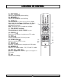
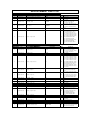
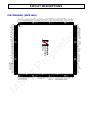
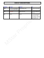
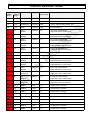
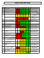
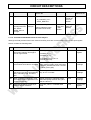
1
COLOR TFT-LCD TV
SERVICE MANUAL
MODEL : LT-32HLFH
CAUTION !!
BEFORE SERVICING THE TFT-LCD TV,
READ THE SAFETY PRECAUTIONS IN THIS MANUAL.
SERVICE MANUAL
CONTENTS
Contents ------------------------------------------------------------------------- 2
Safety precautions ----------------------------------------------------------- 3
Servicing precautions ------------------------------------------------------- 4
Specifications ------------------------------------------------------------------ 5
Location of control ----------------------------------------------------------- 9
Trouble Shooting ------------------------------------------------------------- 12
Deassembly procedure ---------------------------------------------------- 14
Exploded Drawing ----------------------------------------------------------- 19
Wire dressing ------------------------------------------------------------------ 21
Adjustment instruction with Default Factory Data----------------- 22
Inspection instruction ------------------------------------------------------ 24
PCB Layout --------------------------------------------------------------------- 28
Schematic Diagram -----------------------------------------------------------31
Replacement part list -------------------------------------------------------- 32
Block Diagram ----------------------------------------------------------------- 40
Circuit descriptions ---------------------------------------------------------- 41
SERVICE MANUAL
SAFETY PRECAUTIONS
!! Important Safety Notice !!
Many electrical and mechanical parts in this chassis have special safety-related
characteristics.
These parts are identified by in the Schematic Diagram and Replacement Parts List.
It is essential that these special safety parts should be replaced with the same components
as recommended in this manual to prevent Shock, Fire, or other Hazards.
Do not modify the original design without permission of manufacturer.
Leakage Current Hot Check (See below Figure)
Plug the AC cord directly into the AC outlet.
Do not use a line Isolation Transformer during this check.
Connect 1.5K/10watt resistor in parallel with a 0.15uF capacitor between a known good earth
ground (Water Pipe, Conduit, etc.) and the exposed metallic parts.
Measure the AC voltage across the resistor using AC voltmeter with 1000 ohms/volt or more
sensitivity.
Reverse plug of the AC cord into the AC outlet and repeat AC voltage measurements for each
exposed metallic part. Any voltage measured must not exceed 0.75 volt RMS, which is,
corresponds to 0.5mA.
In case any measurement is out of the limits specified, there is possibility of shock hazard and
the set must be checked and repaired before it is returned to the customer.
Leakage Current Hot Check circuit
SERVICE MANUAL
SERVICING PRECAUTIONS
CAUTION!!
Before servicing receivers covered by this service manual, read and follow the SAFETY
PRECAUTIONS on page 2 of this publication.
General Servicing Precautions
1.Always unplug the receiver AC power cord from AC power source before;
ⓐRemoving or reinstalling any component, circuit board module or any other receiver assembly.
ⓑDisconnecting or reconnecting any receiver electrical plug or other electrical connection.
ⓒConnecting a test substitute in parallel with an electrolytic capacitor in the receiver.
CAUTION!! A wrong part substitution or incorrect polarity installation of electrolytic capacitors
may result in an explosion harzard.
2.Do not spray chemicals on or near this receiver or any of its assemblies.
3.Do not defect any plug/socket voltage interlocks with which receivers covered by this service
manual might be equipped.
4.Always connect the test receiver ground lead to the receiver chassis ground before
connecting the test receiver positive lead. Always remove the test receiver ground lead last.
5.Do not connect the test fixture ground strap to power supply heatsink in this receiver
Electrostatically Sensitive(ES) Devices
Some semiconductor(solid state) devices can be damaged easily by static electricity. Such
components commonly are called Electrostatically Sensitive(ES) Device.Examples
Circuit Board Foil Repair
Excessive heat applied to the copper foil of any printed circuit board will weaken the adhesive
that bonds the foil to the circuit board causing the foil th separate from or “lift-off” the board.
The following guidelines and procedures should be flollowed whenever this condition is
encountered.
At IC Connections
To repair a defective copper pattern at IC connections use the following procedure to install a
jumper wire on the copper pattern side of the circuit board.(Use this technique only on IC
connections.)
1.Carefully remove the damaged copper pattern with a sharp knife.
(Remove only as much copper as absolutely necessary.)
2.Carefully scratch away the solder resist and acrylic coating(if used) from the end of the
remaining coopper pattern.
3.Bend a small “U” in one end of a small guage jumper wire and carefully crimp it around the
IC pin.
4.Route the jumper wire along the path of the out-away copper pattern and let it overlap the
previously scraped end of the good copper pattern. Solder the overlapped area and clip off
any excess jumper wire.
SERVICE MANUAL
SPECIFICATIONS
Note: Specifications and others are subject to change without notice for improvement.
1.Scope.
This document is the specification of 32” TFT-LCD Color TV.
2.Power
1) Power requirement
150W
2) AC / DC SMPS.
Input Frequency : 50 / 60㎐
Input Voltage:
AC 100V- 240V 2.5A ~1.5A
Output Voltage: DC 12V, 24V
3) Power cord
Use UL listed and CSA certified detachable power cord type; SVT, 3-conductors, 18AWG
For AC 120V area. Use VDE listed detachable power cord type; HO5VV-F, 3-conductors,
18AWG for AC 220~240V area.
3.Tuning system
FVS 100 Program
4.Sound output
10W+10Wrms Stereo (Max)
5.Antenna input impedance
VHF / UHF at 75ohm
6.OSD Type (On Screen Display)
Windows type (Center)
7.External in/output
HDMI INPUT, PC ANALOG INPUT, PC AUDIO INPUT, HEADPHONE OUTPUT, SVC port
S-VIDEO AUDIO INPUT, S- VIDEO INPUT, COMPONEN INPUT, COAXIAL OUT,
SCART 1(FULL), SCART 2(HALF), TUNER
8. Function
CATV/Hyper band
Auto Program
Manual Program
Auto Sleep
Quick view
ACMS(Auto channel Memory System)
PSM(Picture Status memory)
SSM(Sound Status memory)
PIP : COMPONET, PC-ANALOG, HDMI(Main) – Tuner, SCART 1, SCART 2, S-Video(Sub)
TUNER, SCART1, SCART2, S-Video(Main) – PC ANALOG, HDMI, COMPONET(Sub)
ARC(ASPECT RATIO CONTROL)
SERVICE MANUAL
SPECIFICATIONS
9.Receiving RF TV system
NO
1
2
3
4
5
6
7
8
9
10
11
12
13
14
15
16
17
18
19
20
21
22
23
24
25
26
Model System
PAL-B
PAL-G
PAL-I, I /I
PAL-D
PAL-K
SECAM-B
SECAM-G
SECAM-D
SECAM-K
SECAM-K1
SECAM-I (6.0)
NTSC-3.58 / 4.5
NTSC-3.58 / 5.5
NTSC-3.58 / 6.0
NTSC-3.58 / 6.5
NTSC-3.58 / 4.5(5.0)
NTSC-4.43 / 5.5
NTSC-4.43 / 6.0
NTSC-4.43 / 6.5
PAL 5.5 / 60Hz
PAL 6.0 / 60Hz
PAL 6.5 / 60Hz
SECAM 5.5 / 60Hz
SECAM 6.0 / 60Hz
SECAM 6.5 / 60Hz
SECAM L / L'
TOTAL SYSTEM
SERVICE MANUAL
LT-32HLFH
/
/
○
○
○
○
○
○
○
○
○
○
○
X
X
X
X
X
X
X
X
○
○
○
○
○
○
○
18
/
/
/
/
/
/
/
/
/
/
/
/
/
/
/
/
/
/
/
/
/
/
/
/
/
/
/
/
/
/
/
/
/
/
/
/
/
/
/
/
/
/
/
/
/
/
/
/
/
/
/
/
/
/
SPECIFICATIONS
10. PC Mode Scan Frequency & Timing
1) Scan Freq:
H: 31~56 kHz
/
V: 56~75㎐
2) Preset Timing Chart
Note!! :
ⓐ If the set is cold, there may be a small “flicker” when the set is switched on. This is
Normal, there is nothing wrong with the set.
ⓑ If possible, use the XGA 1024 x 768@60HZ video mode to obtain the best image quality
for your LCD monitor. If used under the other resolutions, some scaled or processed
pictures may appear on the screen.
ⓒ Some dot defects may appear on the screen, like Red, Green or Blue spot. However, this
will have no impact or effect on the monitor performance.
SERVICE MANUAL
SPECIFICATIONS
11. TFT – LCD Panel Character
Description
LTA320W2-L03 is a color active matrix TFT(Thin Film Transistor) liquid crystal display(LCD)
that uses amorphous silicon TFTs as a switching devices. This model is composed of a
TFT LCD panel, a driver circuit and a back-light system. The resolution of a 32.0" contains
1366 X 768 pixels and can display up to 16.7 million colors with wide viewing anale of
85˚or higher in all directions.
Features
- High contrast ratio, high aperture structure
- APVA(Advanced Patterned Vertical Align) mode
- Wide verwing anale(±170°)
- High speed response
- WXGA(1366 X 768 pixels) resolution(16:9)
- Low Power consumption
- Dyrect Type 16 CCFL(Cold Cathode Fluorescent Lamp)
- DE only mode
- LVDS(Low-Voltage Differential Signal) interface.(1pixel/clock)
Applications
- Home-alone Multimedia TFT-LCD TV
- Display terminals for AV applications products
- High Definition TV(HD TV)
● Feature
Size
32.0 inches
Driver element
a-si TFT Active Matrix
Display area
697.6845mm(H) X 392.256mm(V)
Display colors
16.7M(true)
Number of Pixels
Pixel arrangement
Pixel Pitch
1366 X 768 Pixel(16:9)
RGB Vertical Stripe
0.51075mm (H) x 0.51075mm(W)
Display mode
Normally Black
Surface treatment
Haze 44%, Hard-Coating(3H)
SERVICE MANUAL
LOCATION OF CONTROL
All the functions can be controlled with the remote controller. Some functions can
also be adjusted with the buttons on the side panel of the set.
Remote controller
Before you use the remote controller, please install the batteries.
1. POWER
Turns the TV on from standby or off to standby mode.
2. MUTE
Turns the sound on and off.
3. NUMBER buttons
Selects programme numbers.
4. TV/AV
Selects TV, SCART1,SCART2, S-VIDEO,
RADIO(Only when the set is Radio On.),
COMPONENT, PC ANALOG, HDMI mode.
Clears the menu from the screen.
5. MENU
Displays a main menu.
6. LIST
Displays the programme list menu.
7. I/II
Selects the language during dual language broadcast.
Selects the sound output.
8. SLEEP
Sets the sleep timer.
9. PÏP
Returns to the previously viewed programme.
10. PRx/PRy (Programme Up/Down)
Selects next programme or a menu item.
11. OK
Accepts your selection or displays the current mode.
12. VOLÏ/VOLq (Volume Up/Down)
Adjusts the sound level.
13. TV/PC
Selects TV or PC mode directly.
SERVICE MANUAL
LOCATION OF CONTROL
14. PICTURE(
)
Recalls your preferred picture setting
15. SOUND(
)
Recalls your preferred sound setting
16. ARC(
)
You can watch TV in various picture formats; Auto,
16:9, 14:9, 4:3, 16:9 Zoom, 14:9 Zoom, 4:3 Zoom.
Repeatedly press the ARC button to select your
desired picture format.
Note. 16:9 and 4:3 in PC mode are available.
17. TELETEXT buttons
These buttons are used for Teletext.
For further details, see the ‘Teletext’ section.
18. INPUT(
)
Selects the AV source of sub picture in PIP mode.
19. PIP(
)
Displays a PIP(Picture In Picture) screen.
20. POSITION(
)
Selects a position of PIP screen.
21. SWAP(
)
Switches a main picture to sub picture in PIP mode.
22. MODE(
)
Selects a PIP screen mode. – 16:1, 9:1 and 3:1 mode.
23. PIP PRx/PIP PRy
Selects a programme when RF signal is displayed in
PIP mode.
24. Ïq
Adjusts menu settings.
SERVICE MANUAL
LOCATION OF CONTROL
1-3. Controller of Panel
< SIDE VIEW>
1.ON/OFF:
Switches TV set on or off.
1
2.MENU:
Display a menu.
-
2
3.+ PR ( Programme Up/Down):
Selects a programme or a menu item.
-
3
4.+ VOL ( Volume Up/Down):
Adjusts the volume.
Adjusts menu settings.
5.TV/AV:
Selects input signal source.
Clears the menu from the screen.
4
5
6
7
SERVICE MANUAL
6:POWER INDICATOR:
Illuminates red when the TV is inpower standby mode.
Illuminates green when the TV isswitched power on mode.
Illuminates amber when the TV isswitched power saving mode.
7.REMOTE CONTROL SENSOR:
Accepts the IR signal of remote
controller.
TROUBLE SHOOTING
No Raster
Check
P803 (8~12) : 24V?
P804 (6~10) : 24V
Y
Check
P303 (25~27) : 5V?
N
Check
Q804 (3)
Replace LCD Panel.
(If possible, replace
inverter module.)
Y
Replace
IC805
Y
Replace
IC821
N
Check
IC805 (3)
IC805 (4)
: 24V?
Y
: 5V?
: 0V?
N
Replace
Q800
N
Check
IC821 (3)
IC821 (4)
: 5V?
: 0V?
N
Check
Q804 (3) : 24V?
Q804 (1) : 0V?
Replace
IC804
Y
Replace
Q804
Y
N
Replace
SMPS
SERVICE MANUAL
TROUBLE SHOOTING
No Sound &
Picture OK
IC601 (4,7,12,15)
= 24V?
Y
IC601 (25-Mute)
< 0.7V?
(L:Mute/ H:On)
Y
N
N
Y
N
IC101
(123/124 L/R)
Q104/105 (E)
Sound Wave ?
Check
24V Line
ZD601 (C)
< 1V?
N
Replace
ZD601
Replace
IC202
N
Replace IC101
No Operation
LED blinking
No LED
Y
Y
Resistance : 0 ?
IC804 (4) <->
GND
Check
All SCL/SDA
TTL Level ?
Y
Replace
IC804 / D850
N
Replace
Non-Operation
IC.
SERVICE MANUAL
IC202 (10)
= 0V?
Y
IC01 (69~75)
Scaler
Communic
ation Lines)
TTL Level ?
N
Replace IC01
DEASSEMBLY PROCEDURE
1. Disassembly procedure
1).Back cover
Remove 4 screws
Remove 16crews
Removal of Backcover
SERVICE MANUAL
DEASSEMBLY PROCEDURE
2).Metal plate & Rear chassis
Remove 5 screws
Removal of rear metal chassis...
Remove 2 screws
Slide away the metal plate
SERVICE MANUAL
DEASSEMBLY PROCEDURE
3).Metal plate & Rear chassis
Remove Main PCB 10 screws
Removal of Main PCB
Remove 6 connector
SERVICE MANUAL
DEASSEMBLY PROCEDURE
4).LCD Panel chassis
Remove 22 screws, then take LCD-BRKT
Removal of LCD Module take LCD-BRKT
Removal of LCD Module
SERVICE MANUAL
DEASSEMBLY PROCEDURE
5).LCD Module
Remove 8 screws, then take LCD-BRKT
Front mask remains after removing LCD Module
SERVICE MANUAL
MECHANICAL EXPLODED VIEW
NO
1
2
3
4
5
6
7
8
9
PART NO
610-006A
400-021C
DESCRIP TION
DECO FRONT
SPEAKER
FRONT COVER
10W,10Ω
PC+ABS
COLOR FINISH
BLACK
SILVER,BLACK
LENS SENSOR
IR PCB
PC
-
TRANSPARENCE
-
1
1
404-004B
CONTROL PCB
BLOCK KNOB
ABS
SILIVER
1
1
450-001Z
CONTROL PLATE
AL
SILIVER
1
408-002D
AYCOLT40A01A
PANV320W2L01
PANEL
MATERKAL
PMMA
SAMSUNG
-
Q'TY
1
2
1
407-005F
407-001Z
620-005D
BRKT L,R
LCD BRKT
SMPS
EGI
EGI
-
-
2
1
1
13
14
15
AYMALT52A01A
407-007S,T
407-002L
MAIN PCB ASS'Y
JACK SHIELD
REAR SHIELD
SPTH
EGI
-
1
1
1
16
17
407-003F
401-0032
BACK COVER
BOTTOM BRKT
PC+ABS
EGI
DARK GRAY
-
1
1
18
19
20
450-001Y
450-004F,G,H
402-004W
DECO STAND
REAR PLATE
STAND BOTTOM
PMMA
PVC
ABS
BLACK
BLACK
SILVER
1
1
1
21
22
23
402-004C
401-0016
402-004D
STAND FRONT
STAND BRKT
STAND REAR
ABS
EGI
ABS
DARK GRAY
DARK GRAY
1
1
1
24
25
410-001Q
410-001K
26
27
28
410-001L
410-003R
410-002R
29
30
410-001R
410-001N
SCREW MACHINE
BTB 4*12
TTB 3*8
TTB 3*10
PBTB 4*10
PP 4*12
26
23
1
10
11
12
SCREW TAPPING
29
24
SZN
PB 4*8
FTB 3*6
22
21
20
25
31
31
39
8
13
5
4
4
31
13
18
25
3
27
25
2
31
28
18
19
17
1
27
16
32
15
31
14
12
31
25
11
10
9
25
6
7
26
4
5
8
MATERIAL
THIS
TREATMENT
MODEL
LT32H
DATA
2005. 04. 18
ENGR
D. H. KIM
GHK
TITLE
APPD
SCALE
SET Exploded Draw ing
DRAWING NO.
MA05-005
SHEET
-
1/1
WIRE DRESSING
1. Wire Dressing
Note: Using acetate
Using Copper (Conducted tape)
Using Ferrite Cpre
Using Copper Tape
Using Conducted tape
Using Ferrite Cpre
SERVICE MANUAL
ADJUSTMENT INSTRUCTION
WITH DEFAULT FACTORY DATA
1.SVC mode data Adjustment
NOTE!! When the EEPROM has been replaced, the SVC data should be restored as the
function of individual system and specification.
When the EEPROM has been replaced White Blance Checking.
[ Enter and exit SVC mode ]
Note: into the SVC mode, Initialize with default data.
1) Press 5 Seconds MENU buttons on both TV set and Remote Controller at the same
time to get into SVC mode.
2) Press the PR ▲▼ button several times to find SVC Data.
3) Input the corresponding SVC data referring to Table below with the VOL ◀▶, key.
4) Press TV/AV button to exit SVC mode
1-1. Factory outgoing setting & Initialize with default data (into the SVC mode)]
Main menu
(Model)
Language Option
(TV White Balance)
Change value
(L)
EU 14EA
TV White Balance
Sub-menu
Option 1
Audio Options
(DRX)
(NVM Edit)
(Hotel Option)
(Reset TV-set)
Sub menu
Change value
Settings
ALL
Start
PC
Yes
System
BG/I/DK/L
China/Australia
AV1
Text
Top
VPS/PDC
Data Service
ATS Delay Time
Game
DVI
DTV
QURAN
No
RGB
WEST_EU
YES
YES
Text
60
No
Yes
No
No
M
+ 42
BG/I/DK
NICAM
FM Radio
Scart Volume
Surround
Mute if no carrier
High Deviation
DUAL
MONO
STEREO
+ 21
+ 26
+ 10
+ 118
0
Yes
No
No
No
Yes
Option 1
Sub-menu
Audio Options
Sub-menu
(Sub-menu)
(Sub-menu)
(Sub-menu)
(Sub-menu)
Waring: Do not change the “(
SERVICE MANUAL
)” item…
ADJUSTMENT INSTRUCTION WITH DEFAULT FACTORY DATA
2. White Blance Checking
1. Panel : SSLTA320W2-L03-10K
6. Setting : All Start Click
9. Pattern Generator : MSPG-3420
PATTEN : Patten No. : 33
MODE
: 1024*768(13)
SERVICE MANUAL
2. MODEL : L
7. PC White Balance Setting中
10. Equipment : MSPG-925FS
MODE
: 1024*768
3. Language Option
EU 14EA
:
8. White Balance Setting Verify
4. PC Pattern Generator
1024 x 768, 60Hz
(Pattern Generator : MSPG-3420)
5. Setting : All
INSPECTION INSTRUCTION
1. Supplied Accessories
Note: Make Sure the following accessories are provided with Product.
SERVICE MANUAL
INSPECTION INSTRUCTION
*
2. Packing condition
PACKING BOTTOM
SET FRONT
SET FRONT
BOX FRONT
<picture2> SET insert in BOX
BOX FRONT
<picture 1> PACKING insert in BOX
PACKING TOP
L
SET FRONT
ACCESSORY BOX
SET BACK
SET FRONT
<picture3> Accessory Box insert
<picture4> TOP PACKING insert in BOX
12
1 POINT
POINT
SET/BOX FRONT
<Picture 1>Staping
SERVICE MANUAL
1
3
SET/BOX FRONT
<Picture 2>Taping TOP of SET box
with OPP TAPE
NO
1
PART NO
-
DESCRIP TION
LCD COLOR TV
MATERKAL
-
COLOR
-
Q'TY
1
2
321-006A
POLY VINLY
PE
-
1
3
310-021A,B
PACKING BOTTOM (L,R)
EPS
WHITE
2
4
300-012B
SET BOX
PAPER
-
1
5
-
ACCESSORY
-
-
1
6
7
310-022A,B
499-002A
PACKING TOP (L,R)
TAPE OPP
EPS
-
WHITE
-
2
-
3
1
2
4
5
6
7
MATERIAL
THIS
TREATMENT
MODEL
LT32H
DATA
2005. 10. 26
ENGR
D. H. KIM
GHK
TITLE
APPD
SCALE
SET Packing Exploded Drawg
DRAWING NO.
MA05-006
SHEET
-
1/1
PCB LAYOUT
1. CONTROL PCB
2. Tuner PCB
3. SUB PCB
SERVICE MANUAL
REPLACEMENT PART LIST
1. Parts List (Assemble process)
LEVEL
1
1
1
1
1
1
1
1
1
1
1
1
1
1
1
1
1
1
1
1
1
1
1
1
1
1
1
1
1
1
1
1
1
1
1
1
1
1
1
1
PART NO
300-003R
PART NAME
40 ACCESSORY BOX
DESCRIPTION
BOX, ACCESSORY
Q,TY
1
300-012B
310-021A
310-021B
310-022A
310-022B
320-001A
321-006A
404-004J
407-001Z
407-002L
407-005F
407-007S
410-001K
410-001L
410-001N
410-001Q
410-001R
410-002R
490-001M
490-001R
490-011C
490-011L
490-011W
490-011X
490-021C
490-021E
491-001A
492-001A
492-001B
492-001D
499-002A
499-004A
NO BRAND
32"H-MODEL
32"H-MODEL
32"H-MODEL
32"H-MODEL
ACCESSORY PACKING
30 SET PACKING
H, C/KEY,SILVER
32",LCD BRKT,SS
32" SHIELD PCB,SS
32"SS FIX BRKT L/R
VCTI-32"(HD/DVB-T)
TTB 3*8
TTB 3*10
FTB 3*6
BTB 4*12
PB 4*8
PP 4*12
7ITS FK10-2-104-13
7ITS FK 6-4-35-13
71TS-FK 20-2-34-13-S
MSF15-20-30-00K
MK-7-03-325-11
MK-15-15-310-00K
MK-15-20-90-11
MK-15-5-55
W40mm,L20mm, COPPER
CLIP, ZCAT1325-0530
CLIP, ZCHT1730-0730
CLIP, ZCAT2035-0930
W:70mm
W:20mm, L:30m
BOX, CARTON
PACKING, BOTTOM "L"
PACKING, BOTTOM "R"
PACKING, TOP "L"
PACKING, TOP "R"
BAG, VINYL
BAG, PACKING
BLOCK KNOB
SHIELD, FRONT
SHIELD, REAR
SHIELD,SUPPORT(SS)
SHIELD, JACK (SCART)
SCREW
SCREW
SCREW
SCREW
SCREW
SCREW
FORM, SHIELD
FORM, SHIELD
FORM, SHIELD
FORM, SHIELD
FORM, SHIELD
FORM, SHIELD
FORM, SHIELD
FORM, SHIELD
TAPE, CONDUCTIVE
FERRITE CORE
FERRITE CORE
FERRITE CORE
TAPE, OPP
TAPE, ACETATE
1
1
1
1
1
1
1
1
1
1
2
1
6
5
18
49
10
4
2
2
1
1
1
2
1
1
11
2
1
1
4000
400
500-084D
501-001H
501-003O
501-018G
501-113E
502-001O
509-009W
NO BRAND, ENG/TUR
WEEE
COMMON
DIBOSS
DIBOSS
COMMON
DIBOSS
OWNERS MANUAL
LABEL, WARNING
LABEL,SERIAL
STICKER, LOGO
LABEL, ID
LABEL, BOX ID
LABEL, BRAND
SERVICE MANUAL
1
1
1
1
1
1
2
REPLACEMENT PART LIST
2. Parts List (Assemble process)
LEVEL
1
1
1
1
1
1
1
1
1
1
1
1
1
1
1
1
1
1
1
1
PART NO
510-320A
520-001A
610-006A
620-005D
621-001B
626-002C
627-001A
AYBCLT32A01R
AYCALT43A02A
AYCOLT40A01A
AYMALT52A01A
AYSTLT32A01F
CON02P200AOU
CON03P200AOY
CON05P200ABH
CON07P200AD3
CON12P200ACL
CON12P250ACX
CON30P125ACF
PANLTA320W02
PART NAME
NO BRAND,(PR),symbol
1.5V, AAA SIZE
10W,8Ohm(CT156B03K)
32",SMPS,HNE,150W
VDE KKP-4819R (EU)
IVORY,1.8M,15P,SHORT
1.8M, BK
32H, DVBT, SCART
32H, HDMI,PR+,- NO/B
VCTI N/F CONTROL
HD READ_SCART_32(5V)
30", H-MODEL,REV.01
30.1 SPK,2P 700MMH/301 SPK,3P 900MM H/301 LED,5P 200MM H/H
VCTI-232627,7P-10P
32,W2,IVT,12P,300MM
32" SMPS 12P 850MM
32,SS,CORE&GND,150MM
32",SS,LTA320W2-L03
SERVICE MANUAL
DESCRIPTION
REMOCON (WEE),L-GRAY
BATTERY
SPEAKER
AD/DC ADAPTER
POWER CORD
CABLE, PC RGB
CABLE, PC-SOUND
BACK COVER ASSY
Front body,32inch
CONTROL PCB ASSY
MAIN PCB ASSY
STAND ASSY
LEAD ASSY
LEAD ASSY
LEAD ASSY
LEAD ASSY, 1000CTRL
LEAD ASSY
LEAD ASSY
LEAD ASSY(VCTi-32")
PANEL, LCD COLOR
Q,TY
1
2
2
1
1
1
1
1
1
1
1
1
1
1
1
1
1
1
1
1
REPLACEMENT PART LIST
P/N
AYMALT52A01A
HD READ_SCART_32(5V)
Description
GRLT51AM001B
LAVEL
P/N
1
0JASCART001D
GR, SCART MANUAL
VENDOR P/N
JACK, SCART
Description
SCART/AV-6P
Q'ty
Circuit No.
2 J401,J403
GRLT51AA001B
LAVEL
P/N
2
0CESS100CMTR
2
0CESS220CMTR
GR, SCART AUTO
VENDOR P/N
CESSL1C100M0511AD
CESSL1C220M0511AD
Description
10U
22U/16V
Q'ty
Circuit No.
2 C240,C241
2 C207,C208
GRLT51AS001B
LAVEL
P/N
3
0CHSS080DCTS
3
0CHSS101DJTS
3
0CHSS104DZTS
3
0CHSS471DJTS
3
0DHKEKDS226S
3
0LHSS120EJTS
GR, SCART SMD
VENDOR P/N
8P
CL10C101JBNC
CL10F104ZANC
CL10C471JBNC
KDS226
INDUCTOR, CHIP
Description
8P
100P
0.1U
470P
KDS226
12UH/2012
Q'ty
1
3
1
2
1
3
3
0RHSS000DJTS
RC1608J000CS
0
11
3
3
3
3
3
3
3
3
3
3
3
0RHSS102DJTS
0RHSS103DJTS
0RHSS273DJTS
0RHSS393DJTS
0RHSS151DJTS
0RHSS471DJTS
0RHSS513DJTS
0RHSS750DJTS
0RHSS821DJTS
0TRKE1504STS
0TRKE3875STS
RC1608J102CS
RC1608J103CS
RC1608J273CS
RESISTOR, CHIP
Resistor, chip 150 ohm
RC1608J471CS
RC1608J513CS
RC1608J750CS
RC1608J821CS
KTA1504S Y
C3875
1K
10K
27K
39K
150
470
51K
75
820
A1504
C3875
2
1
1
1
1
2
1
3
1
1
1
3
1DZSC5231BTS
MMSZ5231BS
5.1VZ
5
GRLT51AM001A
LAVEL
P/N
1
0CESH471FMBD
1
0ICKE78080AD
1
0ISSY32P00BD
0JAHDD15S0SD
1
1
0JAGE14060BD
1
0JAH19SRJ2BD
1
0JAPK6046GBD
1
0XTKI143180D
1
0XTKI184320D
1
0XTKI202500D
1
1ICIPAP5T5TD
1
1ICSY49F040D
1
0JAUG0624NSD
1
WA1YH10200SD
1
WA1YH12200SD
1
WAFLG04250SD
1
WAFML07200SD
1
WAFYH02200SD
1
WAFYH03200SD
1
WAFYH10200SD
1
111-A84B
1
420-001J
GR, HD-READY COMMON M/I
VENDOR P/N
470UF 35V
IC, KIA7808
DIP 32P
HDD-15S, VERTICAL
RCA-1406(W/R) 2열
HDMI-19SR-J2(DIP)
S-VHS, PJ6046G
14.318MHZ
18.432MHZ
Crystal, 20.25MHZ
AP1501A-50T5,5V,5A
ATMEL AT49F040
COM(3*2), UJB0624N
10P, P2.0mm STRAIGHT
12P, STRAIGHT
Pin wafer, 4-PIN
WAFER, PIN
Pin wafer, 2-PIN
Pin wafer, 3-PIN
10P, P2.0mm STRAIGHT
MAIN PCB
TSC020018,STA515
GRLT51AA001A
LAVEL
P/N
2
0CESS010HMTR
GR,HD-READY COMMON AUTO
VENDOR P/N
1UF 50V
1U
Description
470U
KIA7808AP
AT49F040
D-SUB-15P
AUDIO-LR
JACK, HDMI
JACK, S-VHS
14.318M
18.432M
20.25M
AC1501A-5.0
AT49F040
JACK, AV YPBPR
10P
12P
4P-2.5
7-PIN
2P-SPKL
3P-SPKR
10P
HEAT SINK
Description
2
0CESS100HMTR
10UF 50V
10U
2
0CESS101CMTR
Capacitor, 100UF 16V
100U
2
2
2
0CESS101EMTR
0CESS220CMTR
0CESS221AMTR
100UF 25V
Capacitor, 22UF 16V
220UF 10V
100U/25V
22U/16V
220U/10V
Q'ty
5
1
1
1
1
1
1
1
1
1
1
1
1
1
1
2
1
1
1
1
1
1
Circuit No.
C202
C203,C212,C214
C242
C209,C210
D253
L202,L205,L206
R227,R231,R269,R271,R272
R520,R521,R522,R83,R84
R85
R210,R240
R243
R242
R219
R205
R241
R220
R206,R208,R209
R244
Q201
Q202
ZD201,ZD203,ZD207,ZD208,Z
D209
Circuit No.
C837,C851,C650,C836,C852
IC800
IC109
J202
J407
J201
J406
X01
X601
X100
IC804
IC109
J402
P804
P803
P101,P110
P111
P601
P602
P115
IC603
Q'ty
Circuit No.
1 C618
C173,C174,C216,C219,C853
14 C239,C253,C674,C688,C81
C82,C83,C84,C86
C01,C160,C169,C170,C36
15 C501,C610,C617,C620,C654
C87,C89,C92,C841,C108
1 C839
2 C222,C227
2 C175,C190
REPLACEMENT PART LIST
GRLT51AA001A
LAVEL
P/N
2
0CESS2R2HMTR
2
0CESS3R3HMTR
GR,HD-READY COMMON AUTO
VENDOR P/N
Capacitor, 2.2UF 50V
Capacitor, 3.3UF 50V
2.2U
3.3U
Description
2
0CESS470CMTR
Capacitor, 47UF 16V
47U
2
2
2
2
0CESS471CMTR
0CESS4R7HMTR
0CESS684HMTR
0CQSS104KKTR
470UF 16V
Capacitor, 4.7UF 50V
Capacitor, 0.68UF 50V
0.1UF 100V
470U/16V
4.7U/50V
0.68U/50V
0.1U/MYL
2
0LBSS3580RTR
BEAD CORE, RADIAL
FB-RAD-2P
2
2
2
2
2
3
0LRSU221KKTR
0LRSU220KKTR
0RNSS391FFTA
1DZSSHZT33TA
1ICFC2N700TR
0QCSS474KKTR
INDUCTOR
22U/RAD,5MM RADIAL
390 ohm 1/6W, 1%
33V
IC, 2N7000
0.47UF 100V
220U/RAD,5MM RADIAL
22U/RAD
390/RN
HZT33
2N7000
0.47u
GR, HD-READY COMMON SMD
VENDOR P/N
3PF,1608
8P
Capacitor, chip 10PF,1608
3p
8P
10P
Capacitor, chip 100PF
100P
GRLT51AS001A
LAVEL
P/N
3
0CHSS030DCTS
3
0CHSS080DCTS
3
0CHSS100DJTS
3
0CHSS101DJTS
Description
3
0CHSS102DKTS
Capacitor, chip 1000PF
1000P
3
0CHSS103DKTS
Capacitor, chip 0.01UF
0.01
Q'ty
Circuit No.
5 C178,C179,C187,C615,C619
2 C165,C677
C121,C151,C185,C254,C514
10
C622,C671,C693,C697C844
3 C80,C802,C122
2 C106,C197
1 C823
2 C806,C817
L24,L631,L632,L633,L634
7
L807,L808
1 L198
5 L604,L605,L606,L607,L172
1 R48
1 ZD802
2 Q120,Q121
2 C633,C645
Q'ty
Circuit No.
2 C694,C695
2 C215,C255
2 C702,C703
C188,C189,C211,C213,C218
15 C221,C224,C226,C229,C232
C233,C247,C248,C256,C846
C112,C113,C114,C115,C149
10
C150,C601,C602,C675,C676
4 C192,C193,C502,C51
C02,C03,C04,C05,C06
C09,C10,C104,C105,C107
C109,C11,C12,C120,C124
C128,C133,C136,C137,C138
C142,C147,C148,C152,C158
C159,C161,C162,C163,C166
101
C171,C172,C180,C181,C182
C183,C191,C186,C195,C196
C217,C236,C250,C27,C28
C29,C30,C31,C32,C33
C34,C35,C37,C38,C39
C
3
0CHSS104DZTS
Capacitor, chip 0.1UF
0.1U
3
0CHSS104HZTS
0.1U, 50V, 2012
0.1u
10
3
3
0CHSS105EKTS
0CHSS152DKTS
1U, 25V, 2012
1500PF,1608
1UF
1500p
2
4
GR, HD-READY COMMON SMD
VENDOR P/N
Capacitor, Chip, 22PF
CAPACITOR, CHIP
Capacitor, chip 2200PF,1608
Capacitor, chip 0.22UF
Capacitor, Chip, 33PF
CAPACITOR, CHIP
Capacitor, chip 330PF
Description
22P
220p
2200p
0.22U
33P
330P, 50V, 2012
330P
GRLT51AS001A
LAVEL
P/N
3
0CHSS220DJTS
3
0CHSS221DJTS
3
0CHSS222DKTS
3
0CHSS224DZTS
3
0CHSS330DJTS
0CHSS331HZTS
3
0CHSS331DJTS
Q'ty
2
1
2
2
2
2
2
3
0CHSS334DZTS
Capacitor, chip,0.33UF,1608
0.33U
6
3
0CHSS471DJTS
Capacitor, chip 470PF
470P
15
3
0CHSS472DKTS
4700PF,1608
4700p
3
3
0CHSS473DKTS
Capacitor, chip 0.047UF
0.047U
11
3
0CHSS474DZTS
0.47UF,1608
0.47u
11
3
3
3
3
3
3
0DHKEKDS181S
0DHKEKDS226S
0ICHN28322QS
0ICKE7027FTS
0ICKE7805ATS
0ICSS6X8008S
Diode, chip KDS181
Diode, chip KDS226
HY5DU283222Q, 128Mb
IC, KIA7027
KIA7805AF 5.0V 1A
SS,K6X8008T2B,SDRAM
KDS181
KDS226
HY5DU283222Q
KIA7027
KIA7805AF
K6X8008T2B
2
5
1
1
3
1
C631,C634,C635,C637,C639
C641,C642,C643,C644,C652
C636,C638
C606,C672,C692,C698
Circuit No.
C07,C08
C699
C616,C621
C139,C605
C145,C146
C640,C651
C153,C154
C116,C117,C118,C119,C131
C132
C200,C201,C205,C206,C220
C223,C225,C228,C230,C231
C245,C246,C604,C673,C691
C249,C257,C259
C13,C14,C15,C16,C17
C18,C19,C21,C23,C24
C26
C679,C680,C681,C682,C683
C684,C685,C686,C689,C690
C625
D250,D251
D101,D201,D202,D203,D204
IC03
IC104
IC102,IC203,IC609
IC105
REPLACEMENT PART LIST
GRLT51AS001A
LAVEL
P/N
3
0ICVI4925DTS
GR, HD-READY COMMON SMD
VENDOR P/N
DUAL P-CHANNEL 30V MOSFET
SI4925
Description
3
0LBSS101DJTS
100 OHM, 2012
101/2012
3
0LBSS601FJTS
600 OHM, 3216
601/3216
3
0LHSS120EJTS
12UH, 2012
12UH/2012
3
0LRSL10100BS
INDUCTOR
33UH
3
0RHSS000DJTS
GRLT51AS001A
LAVEL
P/N
Resistor, chip 0 ohm
75
0
GR, HD-READY COMMON SMD
VENDOR P/N
Q'ty
Circuit No.
2 IC805,IC821
L207,L208,L209L701,L702
7
L703,L502
L01,L03,L04,L05,L07
13 L08,L09,L104,L160,L23
L610,L501,L95,L603
L200,L201,L203,L204,L210
L211,L212,L213,L214,L215
16
L216,L217,L218,L220,L221
L222
1 L850
Description
Q'ty
3
0RHSS000EJTS
0 OHM, 2012 J
0/2012
19
3
0RHSS000FJTS
0RHSS100DJTS
0 OHM, 3216 J
Resistor, chip 10 ohm
0/3216
10
2
2
3
0RHSS101DJTS
Resistor, chip 100 ohm
100
55
3
0RHSS102DJTS
Resistor, chip 1K
1K
11
3
0RHSS103DJTS
Resistor, chip 10K
10K
25
3
0RHSS123DJTS
12K OHM, 1608 J
12K
1
3
0RHSS104DJTS
Resistor, chip 100K
100K
6
3
3
3
3
3
0RHSS105DJTS
0RHSS122DJTS
0RHSS151DJTS
0RHSS153DJTS
0RHSS181DJTS
1M OHM, 1608 J
Resistor, chip 1.2K
Resistor, chip 150 ohm
15K OHM, 1608 J
180 OHM, 1608 J
1M
1.2K
150
15K
180
1
2
5
2
1
3
0RHSS220DJTS
Resistor, chip 22 ohm
22
30
3
3
0RHSS223DJTS
0RHSS272DJTS
Resistor, chip 22K
Resistor, chip 2.7K
22K
2.7K
1
1
3
0RHSS273DJTS
Resistor, chip 27K
27K
7
3
3
3
0RHSS330DJTS
0RHSS332DJTS
0RYSS100FJTS
33 OHM, 1608 J
Resistor, chip 3.3K
10 OHM, *8 J
33
3.3K
10
4
5
2
3
0RYSS330FJTS
RESISTOR, ARRAY CHIP
33 OHM, 3216
14
C135,R01,R06,R07,R09
R10,R108,R109,R11,R110
R118,R12,R128,R152,R16
R161,R164,R165,R166,R167
R178,R179,R180,R188,R196
R197,R198,R199,R224,R225
R23,R238,R239,R24,R25
R251,R30,R40,R41,R42
R501,R513,R54,R545,R548
R55,R556,R58,R59,R60
R603,R61,R626,R67,R678
R6
Circuit No.
L15,L16,L17,L18,L19
L20,L21,L22,R159,R223
R160,R173,R174,R221,R222
L219,L505,L506,L507
R852,R853
R168,R93
R08,R105,R106,R107,R130
R131,R132,R133,R135,R137
R138,R139,R140,R141,R142
R143,R147,R148,R149,R150
R151,R162,R163,R17,R194
R195,R288,R289,R291,R292
R293,R294,R295,R296,R297
R298,R36,R561,R91,R719
R562,R563,R564,R601,R602
R604,R605,R606,R672,R673
R676,R703
R117,R254,R39,R56,R660
R712,R713,R717,R94,R96
R276
R190,R232,R233,R234,R235
R236,R237,R255,R256,R27
R278,R290,R611,R612,R674
R677,R704,R705,R706,R707
R72,R825,R847,R860,R861
R871
R620,R621,R659,R802,R804
R821
R02
R805,R809
R113,R114,R115,R53,R280
R618,R623
R95
R04,R05,R120,R129,R154
R155,R192,R193,R211,R212
R213,R252,R253,R32,R33
R34,R44,R45,R50,R51
R52,R528,R529,R65,R66
R701,R702,R80,R81,R82
R156
R204
R260,R274,R675,R803,R816
R818,R92
R70,R71,R73,R74
R03,R134,R247,R526,R527
AR26,AR27
AR01,AR02,AR03,AR13,AR14
AR15,AR16,AR17,AR18,AR19
AR22,AR23,AR24,AR25
REPLACEMENT PART LIST
GRLT51AS001A
LAVEL
P/N
3
0RHSS392DJTS
3
0RHSS393DJTS
3
0RHSS3R0DJTS
3
0RHSS470DJTS
3
0RHSS471DJTS
GR, HD-READY COMMON SMD
VENDOR P/N
Resistor, chip 3.9K
Resistor, chip 39K
3 OHM, 1608 J
Resistor, chip 47 ohm
Resistor, chip 470 ohm
3.9K
39K
3
47
470
Q'ty
2
2
1
2
3
Description
3
0RHSS472DJTS
Resistor, chip 4.7K
4.7K
22
3
0RHSS473DJTS
Resistor, chip 47K
47K
12
3
0RHSS474DJTS
Resistor, chip 470K
470K
2
3
0RHSS512DJTS
RESISTOR, CHIP
5.1K
11
3
0RHSS622DJTS
RESISTOR, CHIP
6.2K
2
3
0RHSS750DJTS
Resistor, chip 75 ohm
75
15
3
0RHSS821DJTS
Resistor, chip 820 ohm
820
1
3
0RYSS220FJTS
22 OHM, *8 J
22
7
3
0TRKE1504STS
Transistor, chip A1504
A1504
3
3
0TRKE3875STS
Transistor, chip
C3875
15
3
1DHSTS1545GS
D2PAK, 45V 15A
STPS1545G
1
GRLT51AS001A
LAVEL
P/N
GR, HD-READY COMMON SMD
VENDOR P/N
Description
Circuit No.
R124,R125
R619,R622
R43
R257,R258
R104,R275,R519
R119,R121,R122,R123,R177
R181,R182,R183,R184,R207
R246,R26,R28,R530,R867
R709,R710,R720,R819,R859
R865,R866
R103,R126,R245,R551,R552
R817,R826,R872,R873,R874
R875,R876
R202,R203
R191,R200,R201,R217,R218
R266,R267,R282,R283,R284
R285
R624,R625
R214,R215,R216,R259,R279
R281,R286,R287,R502,R503
R560,R567,R714,R715,R716
R277
AR07,AR08,AR101,AR102,AR1
1
AR12,AR21
Q203,Q104,Q105
Q01,Q106,Q11,Q12,Q13
Q204,Q205,Q210,Q601,Q602
Q632,Q800,Q802,Q803,Q814
D850
Q'ty
Circuit No.
3
1DZSC5231BTS
5.1V, MMSZ5231BS-7
5.1VZ
30
D700,D701,ZD191,ZD192,ZD20
2
ZD204,ZD205,ZD206,ZD210,Z
D211
ZD212,ZD213,ZD214,ZD215,Z
D216
ZD217,ZD218,ZD219,ZD220,Z
D221
ZD222,ZD223,ZD224,ZD225,Z
D601
ZD702,ZD703,ZD704,ZD705,Z
D706
3
3
3
3
1ICMI49X3RF2
1ICMS5151ABS
1ICPH74F08TS
1ICPH8574ATS
111-A84B
1ICR03V512BS
1ICSE24C16TS
1ICST24C02WS
1ICST3232CDS
1ICST80PF55S
1ICSTLD18TTS
1ICSTLD25TTS
1ICSTLD33TTS
1ICSTTS482TS
WAFYH30125AS
0RHSS620DJTS
0RHSS200DJTS
0RHSS362DJTS
1DHPR0514MOS
0ICKE7808ATS
1ICMIMAP46DS
1ICST51500BS
IC,V/S DECODER
MST5151A
IC, N74F08D
IC, I/O EXPANDER
MAIN PCB
IC, INPUT RGBHV S/W
IC, 24C16
24C02W
ST3232-RS232C
STB80PF55
LD1117S18TR
LD1117S25TR
LD1117S33TR
TS482IST, MINI08
WAFER, PIN
6.2 OHM, 3216
20 OHM, 3216
3.6K OHM, 1608J
514M
KIA7808AF
MAP46XX
STA515
VCT49XX
MST5151A
74F08
PCF8574TS
MAIN PCB
PI3V512
24C16
24C02W
ST3232CD
STB80PF55
LD1117S-18TR
LD1117S-25TR
LD1117S-33TR
TS482-MINISO8
30PLVDS
6.2
20
3.6K
514M
KIA7808AF
MAP46XX
STA515
1
1
1
1
IC101
IC01
IC702
IC202
1
1
2
1
1
2
IC501
IC103
IC201,IC701
IC106
Q804
IC832,IC10
IC09
IC107,IC108,IC606,IC06,IC08
IC602
P303
R613,R615,R631,R632
R614,R616
R97
D261,D262
IC608
IC610
IC603
GR, HD-READY TUNER M/I
VENDOR P/N
TAEM-G083D
HDMI ANALOG TUNER
X6966M
WAFER, PIN
HD-READY TUNER(PAL)
Description
Tuner
PCB, TUNER
SAW FILTER
Pin wafer, 10-Pin
3
3
3
3
3
3
3
3
3
3
3
3
3
3
3
3
3
GRLT51AM001F
LAVEL
P/N
1
0TULGG083DBD
1
111-A90A
1
1SFEPX6966MD
1
WAFYH10200AD
5
1
1
4
2
1
2
1
1
1
Q'ty
Circuit No.
1
1
1
1
SF101
P115
REPLACEMENT PART LIST
GRLT41AM001H
LAVEL
P/N
1TPMU40R9MTD
GRLT41DS001G
LAVEL
P/N
3
0TRKE3875STS
3
0RHSS472DJTS
GRLT51AS001G
LAVEL
3
P/N
MKTGA40M9AAHP00A03
GR, LL' SMD
VENDOR P/N
KTC3875S
Resistor, chip 4.7K
VCTI 15/17 동일I
Description
40.9M
V2327 신규
Description
C3875
4.7K
HD-READY 32 PANEL S/I (5V)
VENDOR P/N
Description
0 OHM, 2012 J
0/2012
GRLT10AM002A
LAVEL
P/N
1
410-001J
1
420-001F
1
498-001A
GR, HEAT SINK M/I
VENDOR P/N
SCREW
HEAT SINK
Silicon Grease
AP1501A-50T5,25*16
Description
GRLT51AM001D
LAVEL
P/N
WAFET08250SD
1
1
0JAKKST215BD
1
111-A92A
1
0JAAR823PDBD
GR, HP+RJ45 M/I
VENDOR P/N
WAFER, PIN
ST-215
HD-READY,HP+RJ45 PCB
JACK, RJ-45
HD-READY,HP+RJ45(PCB, SUB)
Description
8P
Jack, PC-AUDIO,HP
PCB, SUB
RJ-45, 8PIN
GRLT51AM001J
LAVEL
GR, ONLY 32" MANUAL
VENDOR P/N
12P, P2.5mm ANGLE
HD-READY ONLY 32"
Description
12P
GR, ONLY 32" SMD
VENDOR P/N
DUAL P-CHANNEL 30V MOSFET
C3875
HD-READY ONLY 32"
Description
SI4925
C3875
1
0RHSS000EJTS
GR, LL' MANUAL
VENDOR P/N
P/N
WA1YH12250AD
GRLT51AS001J
LAVEL
P/N
3
0ICVI4925DTS
3
0TRKE3875STS
Q'ty
1
Circuit No.
T101
Q'ty
1 Q106
1 R177
Circuit No.
Q'ty
Circuit No.
1
R822
Q'ty
1
1
0.15
Circuit No.
Q'ty
Circuit No.
2 P203,P204
2 J601,J602
1
1 J405
Q'ty
1
Circuit No.
P813
Q'ty
Circuit No.
1 IC806
1 Q820,Q821
BLOCK DIAGRAM
1. Block Diagram
32 Block Diagram
DC-IN
DC-IN
SPEAKER
Power
ITU-6 5 6
DVI Receiver
ADC
PIP
De-Interlacer
Power
IIC
I
M
D
H
D-SUB
YC
S-VIDEO
B
G
R
C
P
HDMI
PC-RGB
)
V
T
D
(
r
P
b
P
Y
HDMI-RGB
YPbPr(DVD)
YPbPr(D-TV)
RGB,FB
AV-IN/OUT
YPbPr(DVD)
YPbPr(D-TV)
SCART1
PAL(EU)
YPbPr(DVD)
YPbPr(D-TV)
AV-IN/OUT
NTSC/MULTI
SERVICE MANUAL
HEADPHONE
u-Com
TEXT/Caption
Video Processor
Sound Processor
IF Processor
T
U
O
/
N
I
V
A
DC-IN
24V
H/P AMP
L/R
IC101 VCTI
B
F
,
B
G
R
IC01
SCALER
L/R
T
U
O
/
N
I
V
A
Power
IIC
L
/
R
)
D
V
D
(
R
P
b
P
Y
(INVERTER)
I
2
C
S
C
Y
26/32
D
T
V
PANEL DRIVE
LVDS
S
V
,
S
H
,
B
G
R
I
T
C
V
POWER
Power
(Inverter/Scaler/
ADC/VCTI)
AMP
SOUND
Processor
SC2 L/R
PC L/R
Power
IIC
F
I
LCD PANEL
AV-IN/OUT
SCART2
IF
TUNER
CIRCUIT DESCRIPTIONS
General Description for 26.0” color TFT LCD TV.
The TFT LCD TV described in the followings is based on a Multi TV system, digital
Control display, 26.0" diagonal. The TFT LCD TV is intended to be a finished product,
Basically a display device mounted inside an enclosure which will provide the safety
Requirements. With the exception of LCD Panel, the display device shall be composed
entirely of solid state components.
These components shall have a history of reliable service in identity applications
and shall be applied in the circuits.
1. SCALER SECTION.
2. VCT 49xxi SECTION.
3. Video A/D Converter
SERVICE MANUAL
CIRCUIT DESCRIPTIONS
1.SCALER SECTION.
Device : MST5151A
Features: LCD TV controller with PC & multimedia display functions
Input supports up to UXGA & 1080P
Supports up to SXGA panels
Integrated two-port triple-ADC/PLL
Integrated DVI/HDCP/HDMI compliant receiver
YUV422 digital video input ports
Dual high-quality scaling engines
Dual 3-D video de-interlacers
Full function PIP/POP
MStarACE picture/color processing engine
Embedded On-screen display controller (OSD) engine
Digital audio I/O & sync processor
Built-in dual-link LVDS transmitter
5 Volt tolerant inputs
Low EMI and power saving features
Supports PWM & GPO controls
208-pin PQFP package
Analog RGB/YPbPr Input Ports
Dual analog ports support up to 165Mhz
Supports PC RGB input up to UXGA@60Hz
Supports HDTV RGB/YPbPr/YCbCr up to 1080P
On-chip high-performance PLLs
Supports Composite Sync and SOG (Sync-on-Green) separator
Automatic color calibration
DVI/HDCP/HDMI Compliant Input Port
Operates up to 165 MHz (up to UXGA @60Hz)
Single link on-chip DVI 1.0 compliant receiver
High-bandwidth Digital Content Protection
(HDCP) 1.1 compliant receiver
High Definition Multimedia Interface (HDMI)
1.0 compliant receiver with I2S and S/PDIF digital audio outputs
Long-cable tolerant robust receiving
Video Input Port
Two 4:2:2 ITU656 8-bit digital video input ports
One 4:2:2 ITU601 16-bit digital video input port
Supports 16-bit YUV 4:2:2 interlaced/ progressive video input up to 1080i/720P
Auto-Configuration/Auto-Detection
Auto input signal format (SOG, Composite,Separated HSYNC, VSYNC, and DE),
and input mode (all PC & TV modes) detection
Auto-tuning function including phasing, positioning, offset, gain, and jitter detection
Sync Detection for H/V Sync
Dual High-Performance Scaling Engines
Fully programmable shrink/zoom capabilities
Nonlinear video scaling supports various modes including Panorama
Video Processing & Conversion
Dual 3-D motion adaptive video de-interlacers with upgraded edge-oriented adaptive
algorithm for smooth low-angle edges
Automatic 3:2 pull-down & 2:2 pull-down detection and recovery
PIP/POP with programmable size and location, supports multi-video applications
Video-over-graphic overlay
MStar 2nd Generation Advanced Color Engine
On-Screen OSD Controller
SERVICE MANUAL
1) Description
The MST5151A is a high performance and fully integrated graphics processing IC solution for multi-function
LCD monitor/TV with resolutions up to SXGA. It is configured with an integrated triple-ADC/PLL, an integrated
DVI/HDCP/HDMI receiver, two video de-interlacers, two high quality scaling engines, an on-screen display
controller, and a built-in output clock generator. By use of external frame buffer, PIP/POP is provided for
multimedia applications. It supports de-interlaced full-screen video, video-on-graphic overlay, split screen,
frame rate conversion, and aspect ratio conversion for various video sources. To further reduce system costs,
the MST5151A also integrates intelligent power management control capability for green-mode requirements
and spread-spectrum support for EMI management.
.
SERVICE MANUAL
CIRCUIT DESCRIPTIONS
157
158
159
160
161
162
163
164
165
166
167
168
169
170
171
172
173
174
175
176
177
178
179
180
181
182
183
184
185
186
187
188
189
190
191
192
193
194
195
196
197
198
199
200
201
202
203
204
205
206
1
156
2
155
3
154
Pin 1
4
153
152
6
151
7
150
8
149
9
148
10
147
11
146
12
145
13
144
14
143
15
142
16
141
17
140
18
139
19
138
20
137
21
136
22
135
23
134
24
133
25
26
27
28
29
30
31
32
33
34
MST5151A
5
XXXXXXXXXXX
XXXXX
132
131
130
129
128
127
126
125
124
123
104
103
102
101
100
99
98
97
96
95
94
93
92
91
90
89
88
87
86
85
84
83
82
81
80
79
78
77
76
75
74
73
72
71
105
70
106
52
69
107
51
68
108
50
67
109
49
66
110
48
65
111
47
64
112
46
63
113
45
62
114
44
61
115
43
60
116
42
59
117
41
58
118
40
57
119
39
56
120
38
55
121
37
54
122
36
53
35
VI_CK
VI_DATA[0]
VI_DATA[1]
VI_DATA[2]
VI_DATA[3]
VI_DATA[4]
VI_DATA[5]
VI_DATA[6]
VI_DATA[7]
VCTRL
VDDC
GND
GND
VDDP
HWRESET
INT
ALE
RDZ
WRZ
DBUS[0]
DBUS[1]
DBUS[2]
DBUS[3]
GPO[3]
GPO[2]
GPO[1]
VDDC
GND
DQS[3]
MDATA[31]
MDATA[30]
MDATA[29]
MDATA[28]
VDDM
GND
MDATA[27]
MDATA[26]
MDATA[25]
MDATA[24]
MDATA[23]
MDATA[22]
MDATA[21]
MDATA[20]
MDATA[19]
MDATA[18]
MDATA[17]
MDATA[16]
DQS[2]
DQM[1]
VDDM
GND
MVREF
GND
DVI_G+
DVI_GAVDD_DVI
DVI_B+
DVI_BGND
DVI_CK+
DVI_CKAVDD_DVI
REXT
AVDD_PLL
GND
DDCD_DA
DDCD_CK
GND
AVDD_ADC
HSYNC1
VYSNC1
BIN1P
BIN1M
SOGIN1
GIN1P
GIN1M
RIN1P
RIN1M
BIN0M
BIN0P
GIN0M
GIN0P
SOGIN0
RIN0M
RIN0P
AVDD_ADC
GND
HSYNC0
VSYNC0
RMID
REFP
REFM
VI_DATA[8]
VI_DATA[9]
VI_DATA[10]
VI_DATA[11]
VI_DATA[12]
VI_DATA[13]
VI_DATA[14]
VI_DATA[15]
AVDD_APLL
GND
GPO[5]
GPO[4]
207
208
DVI_RDVI_R+
GND
GND
AVDD_MPLL
XIN
XOUT
PWM1
PWM0
AIWS
AISCK
AISD
AIMCK
VDDC
GND
SPDIFO
AUMUTE
AUWS
AUSCK
AUSD
AUMCK
LVB0M
LVB0P
VDDC
GND
GND
VDDP
LVB1M
LVB1P
LVB2M
LVB2P
LVBCKM
LVBCKP
LVB3M
LVB3P
VDDC
GND
LVA0M
LVA0P
LVA1M
LVA1P
LVA2M
LVA2P
LVACKM
LVACKP
GND
VDDP
LVA3M
LVA3P
GND
BYPASS
GND
PIN DIAGRAM (MST5151A)
VDDC
GND
VDDM
DQS[0]
MDATA[0]
MDATA[1]
MDATA[2]
MDATA[3]
MDATA[4]
MDATA[5]
MDATA[6]
MDATA[7]
MDATA[8]
MDATA[9]
MDATA[10]
MDATA[11]
GND
VDDM
MDATA[12]
MDATA[13]
MDATA[14]
MDATA[15]
DQS[1]
DQM[0]
GND
VDDC
MADR[11]
MADR[10]
MADR[9]
MADR[8]
GND
VDDM
MADR[7]
MADR[6]
MADR[5]
MADR[4]
MADR[3]
MADR[2]
MADR[1]
MADR[0]
WEZ
CASZ
GND
VDDM
RASZ
BADR[0]
BADR[1]
AVDD_PLL2
GND
MCLK
MCLKZ
MCLKE
CIRCUIT DESCRIPTIONS
PIN DESCRIPTION
MCU Interface
Pin Name
Pin Type
Function
Pin
HWRESET
Schmitt Trigger Input
Hardware Reset, active high
67
w/ 5V-tolerant
DBUS[3:0]
I/O w/ 5V-tolerant
MCU 4-bit DDR Direct bus; 4mA driving strength
75-72
ALE
I w/ 5V-tolerant
MCU Bus ALE, active high
69
RDZ
I w/ 5V-tolerant
MCU Bus RDZ, active high
70
WRZ
I w/ 5V-tolerant
MCU Bus WDZ, active high
71
INT
Output
MCU Bus Interrupt; 4mA driving strength
68
Function
Pin
RMID
Mid-Scale Voltage Bypass
38
REFP
Internal ADC Top De-coupling Pin
39
REFM
Internal ADC Bottom De-coupling Pin
40
Analog Interface
Pin Name
Pin Type
REXT
Analog Input
External Resister 390 ohm to AVDD_DVI
11
HSYNC0
Schmitt Trigger Input
Analog HSYNC Input from Channel 0
36
Analog VSYNC Input from Channel 0
37
w/ 5V-tolerant
VSYNC0
Schmitt Trigger Input
w/ 5V-tolerant
BIN0M
Analog Input
Reference Ground for Analog Blue Input from Channel 0
27
BIN0P
Analog Input
Analog Blue Input from Channel 0
28
GIN0M
Analog Input
Reference Ground for Analog Green Input from Channel 0
29
GIN0P
Analog Input
Analog Green Input from Channel 0
30
SOGIN0
Analog Input
Sync On Green Input from Channel 0
31
RIN0M
Analog Input
Reference Ground for Analog Red Input from Channel 0
32
RIN0P
Analog Input
Analog Red Input from Channel 0
33
HSYNC1
Schmitt Trigger Input
Analog HSYNC Input from Channel 1
18
Analog VSYNC Input from Channel 1
19
w/ 5V-tolerant
VSYNC1
Schmitt Trigger Input
w/ 5V-tolerant
BIN1P
Analog Input
Analog Blue Input from Channel 1
20
BIN1M
Analog Input
Reference Ground for Analog Blue Input from Channel 1
21
SOGIN1
Analog Input
Sync On Green Input from Channel 1
22
GIN1P
Analog Input
Analog Green Input from Channel 1
23
CIRCUIT DESCRIPTIONS
Pin Name
Pin Type
Function
Pin
GIN1M
Analog Input
Reference Ground for Analog Green Input from Channel 1
24
RIN1P
Analog Input
Analog Red Input from Channel 1
25
RIN1M
Analog Input
Reference Ground for Analog Red Input from Channel 1
26
Pin Name
Pin Type
Function
Pin
DVI_R+
Input
DVI Input Channel Red +
207
DVI_R-
Input
DVI Input Channel Red -
208
DVI_G+
Input
DVI Input Channel Green +
2
DVI_G-
Input
DVI Input Channel Green -
3
DVI_B+
Input
DVI Input Channel Blue +
5
DVI_B-
Input
DVI Input Channel Blue -
60
DVI_CK+
Input
DVI Input Clock +
8
DVI_CK-
Input
DVI Input Clock -
9
DVI Interface
Video Interface
Pin Name
Pin Type
Function
Pin
VI_CK
Input w/ 5V-tolerant
Digital Video Input Clock
66
VI_DATA[15:0]
Input w/ 5V-tolerant
Digital Video Input Data[15:0]
48-41, 61-54
Digital Audio Interface
Pin Name
Pin Type
Function
Pin
AUMCK
Output
Audio Master Clock Output
188
AUSD
Output
Audio Serial Data Output; 4mA driving strength
189
AUSCK
Output
Audio Serial Clock Output; 4mA driving strength
190
AUWS
Output
Word Select Output; 4mA driving strength
191
AUMUTE
Output
Audio Output Mute Control
192
SPDIFO
Output
S/PDIF Audio Output; 4mA driving strength
193
AIMCK
Input
Audio Master Clock Input
196
AISD
Input
Audio Serial Data Input
197
AISCK
Input
Audio Serial Clock Input
198
AIWS
Input
Word Select Input
199
CIRCUIT DESCRIPTIONS
LVDS Interface
Pin Name
Pin Type
Function
Pin
LVA0M
Output
A-Link Negative LVDS Differential Data Output
171
LVA0P
Output
A-Link Positive LVDS Differential Data Output
170
LVA1M
Output
A-Link Negative LVDS Differential Data Output
169
LVA1P
Output
A-Link Positive LVDS Differential Data Output
168
LVA2M
Output
A-Link Negative LVDS Differential Data Output
167
LVA2P
Output
A-Link Positive LVDS Differential Data Output
166
LVA3M
Output
A-Link Negative LVDS Differential Data Output
161
LVA3P
Output
A-Link Positive LVDS Differential Data Output
160
LVACKM
Output
A-Link Negative LVDS Differential Data Output
165
LVACKP
Output
A-Link Positive LVDS Differential Data Output
164
LVB0M
Output
B-Link Negative LVDS Differential Data Output
187
LVB0P
Output
B-Link Positive LVDS Differential Data Output
186
LVB1M
Output
B-Link Negative LVDS Differential Data Output
181
LVB1P
Output
B-Link Positive LVDS Differential Data Output
180
LVB2M
Output
B-Link Negative LVDS Differential Data Output
179
LVB2P
Output
B-Link Positive LVDS Differential Data Output
178
LVB3M
Output
B-Link Negative LVDS Differential Data Output
175
LVB3P
Output
B-Link Positive LVDS Differential Data Output
174
LVBCKM
Output
B-Link Negative LVDS Differential Data Output
177
LVBCKP
Output
B-Link Positive LVDS Differential Data Output
176
Pin Name
Pin Type
Function
Pin
PWM0
Output
GPO with PWM Function; 4mA driving strength
200
PWM1
Output
GPO with PWM Function; 4mA driving strength
201
GPO[1]
I/O
GPO / FIELD input; 4mA driving strength
78
GPO[2]
I/O
GPO / Digital VSYNC Input; 4mA driving strength
77
GPO[3]
I/O
GPO / DE Input; 4mA driving strength
76
GPO[4]
I/O
GPO / Secondary Video Clock Input; 4mA driving strength
52
GPO[5]
I/O
GPO / Digital HSYNC Input; 4mA driving strength
51
GPO Interface
CIRCUIT DESCRIPTIONS
DRAM Interface
Pin Name
Pin Type
Function
Pin
MVREF
Input
Reference Voltage for DDR SDRAM Interface
104
MCLKE
Output
DRAM Memory Clock Enable
105
MCLKZ
Output
DRAM Memory clock Complementary /Input
106
(for differential clocks)
MCLK
Output
DRAM Memory Clock
107
RASZ
Output
Row Address Strobe, active low
112
CASZ
Output
Column Address Strobe, active low
115
WEZ
Output
Write Enable, active low
116
DQM[1:0]
Output
Data Mask Byte Enable
101, 133
DQS[3:0]
Output
Data Strobe
81, 100, 134, 153
BADR[1:0]
Output
Memory Bank Address
110, 111
MADR[11:0]
Output
Memory Address
130-127, 124-117
MDATA[31:0]
I/O
Memory Data
82-85, 88-99,
135-138, 141-152
Misc. Interface
Pin Name
Pin Type
Function
Pin
XIN
Crystal Oscillator Input
Crystal Oscillator Input
203
XOUT
Crystal Oscillator Output Crystal Oscillator Output
DDCD_DA
I/O w/ 5V-tolerant
202
HDCP Serial Bus Data / DDC data of DVI port; 4mA driving 14
strength
DDCD_CK
Input w/ 5V-Tolerant
BYPASS
VCTRL
Output
HDCP Serial Bus Clock / DDC Clock of DVI Port
15
For External Bypass Capacitor
158
Regulator Control
62
Power Pins
Pin Name
Pin Type
Function
Pin
AVDD_DVI
3.3V Power
DVI Power
4, 10
AVDD_ADC
3.3V Power
ADC Power
17, 34
AVDD_PLL
3.3V Power
PLL Power
12
AVDD_PLL2
3.3V Power
PLL Power
109
AVDD_APLL
1.8V Power
Audio PLL Power
49
AVDD_MPLL
3.3V Power
PLL Power
204
CIRCUIT DESCRIPTIONS
Pin Name
Pin Type
Function
Pin
VDDM
3.3V Power (SDR SDRAM) /
DRAM Interface Power
86, 102, 113, 125, 139,
2.5V Power (DDR SDRAM)
154
VDDP
3.3V Power
Digital Output Power
66, 162, 182
VDDC
1.8V Power
Digital Core Power
63, 79, 131, 156, 173,
185, 195
GND
Ground
Ground
1, 7, 13, 16, 35, 50, 64,
65, 80, 87, 103, 108,
114, 126, 132, 140, 155,
157, 159, 163, 172, 183,
184, 194, 205, 206
CIRCUIT DESCRIPTIONS
MECHANICAL DIMENSIONS
A
A2
A1
θ1
θ2
c
R1
R2
θ
Gage Plane
0.25mm
Seating Plane
b
L
Symbol
L1
S
E2
E
E1
D
D1
D2
Millimeter
e
Inch
Min. Nom. Max. Min. Nom. Max.
Symbol
Millimeter
Inch
Min. Nom. Max. Min. Nom. Max.
A
-
-
4.10
-
-
0.161
θ
0°
-
7°
0°
-
7°
A1
0.25
-
-
0.010
-
-
θ1
0°
-
-
0°
-
-
A2
3.20 3.32
3.60 0.126 0.131 0.142
θ2
8° Ref
8° Ref
D
31.20
1.228
b
0.17 0.20
0.27 0.007 0.008 0.011
D1
28.00
1.102
c
0.11 0.15
0.23 0.004 0.006 0.009
D2
25.50
1.004
e
E
31.20
1.228
L
E1
28.00
1.102
L1
E2
25.50
1.004
S
R1
0.13
-
R2
0.13
-
-
0.005
-
-
0.30 0.005
-
0.012
0.50 BSC.
0.73 0.88
0.020 BSC.
1.03 0.029 0.035 0.041
1.60 Ref
0.20
-
0.063 Ref
-
0.008
-
-
CIRCUIT DESCRIPTIONS
General Description
Features
Introduction
The VCT 49xxI family offers a rich feature set, covering the whole range of state-of-the-art 50/60-Hz TV
applications.
The VCT 49xxI is an IC family of high-quality singlechip TV processors. Modular design and deep-submicron technology allow the economic integration of features in all classes of single-scan TV sets. The
VCT 49xxI family is based on functional blocks contained and approved in existing products like
DRX 396xA, MSP 34x5G, VSP 94x7B, DDP 3315C,
and SDA 55xx.
– PSSDIP88-1/-2 package
– PMQFP144-2 package
– Submicron CMOS technology
– Low-power standby mode
– Single 20.25-MHz reference crystal
– 8-bit 8051 instruction set compatible CPU
Each member of the family contains the entire IF,
audio, video, display, and deflection processing for 4:3
and 16:9 50/60-Hz mono and stereo TV sets. The integrated microcontroller is supported by a powerful OSD
generator with integrated Teletext & CC acquisition
including on-chip page memory.
– Up to 256 kB on-chip program ROM
– WST, PDC, VPS, and WSS acquisition
– Closed Caption and V-chip acquisition
– Up to 10 pages on-chip teletext memory
– Multi-standard QSS IF processing with single SAW
– FM Radio and RDS with standard TV tuner
Video & Sound IF
DRX 396xA
– TV-sound demodulation:
• all A2 standards
• all NICAM standards
• BTSC/SAP with MNR (DBX optional)
• EIA-J
Audio Processing
MSP 34x5G
Video Processing
VSP 94x7B
Display & Deflection
DDP 3315C
VCT 49xyI
– Baseband sound processing for loudspeaker channel:
• volume
• bass and treble
• loudness
• balance
• spatial effect (e.g. pseudo stereo)
• Micronas AROUND (virtual Dolby optional)
• Micronas BASS
– CVBS, S-VHS, YCrCb and RGB inputs
Control, OSD, Text
SDA 55xx
– 4H adaptive comb filter (PAL/NTSC)
– multi-standard color decoder (PAL/NTSC/SECAM)
– Nonlinear horizontal scaling “panorama vision”
Fig. : Single-chip VCT 49xxI
– Luma and chroma transient improvement (LTI, CTI)
– Non-linear color space enhancement (NCE)
– Dynamic black level expander (BLE)
– Scan velocity modulation output
– Soft start/stop of H-drive
– Vertical angle and bow correction
– Average and peak beam current limiter
– Nonlinear and dynamic EHT compensation
– Black switch off procedure (BSO)
CIRCUIT DESCRIPTIONS
IFIN+
IFIN-
IF
Frontend
IF
Processor
Sound
Demodulator
SPEAKER
AOUT
AIN
SIF
TAGC
Chip Architecture
Audio
Processor
PROT
HOUT
HFLB
CVBS in
YCrCb in
RGB in
Video
Frontend
Comb
Filter
Color
Decoder
Component
Interface
CVBS out
VERT
Panorama
Scaler
Display &
Deflection
Processor
EW
Video
Backend
SVM
RGB out
RGB in
SENSE
RSW
Slicer
Bus
Arbiter
24kB
Char ROM
20kB XRAM
Display
Generator
CPU
8051
256kB
Prog ROM
Memory
Interface
ADB, DB, PSENQ,
PSWEQ, WRQ, RDQ
Fig. : Block diagram of the VCT 49xxI
I2C Master/
Slave
Timer
CRT
PWM
ADC
UART
Watchdog
RTC
I/O-Ports
Pxy
I2C
Reset & Test
Logic
Clock
Generator
RESETQ
TEST
XTAL1
XTAL2
CIRCUIT DESCRIPTIONS
Pin Connections and Short Descriptions
NC = not connected
LV = if not used, leave vacant
OBL = obligatory; connect as described in circuit diagram
IN = Input Pin
OUT = Output Pin
SUPPLY = Supply Pin
Pin No.
PSSDIP
88-pin
Pin Name
Type
Connection
Short Description
(If not used)
PMQFP-2
144-pin
1
128
GND
SUPPLY
OBL
Ground Platform
2
129
VSUP5.0BE
SUPPLY
OBL
Supply Voltage Analog Video Back-end, 5.0 V
3
130
TEST
IN
GND
Test Input, reserved for Test
4
131
VERT+
OUT
LV
Differential Vertical Sawtooth Output
5
132
VERT-
OUT
LV
Differential Vertical Sawtooth Output
6
133
EW
OUT
LV
Vertical Parabola Output
7
134
RSW2
OUT
LV
Range Switch 2 Output
8
135
RSW1
OUT
LV
Range Switch 1 Output
9
136
SENSE
IN
GND
Sense ADC Input
10
137
GNDM
IN
GND
Reference Ground for Sense ADC
11
138
FBIN
IN
GND
Fast Blank Input, Back-end
12
139
RIN
IN
GND
Analog Red Input, Back-end
13
140
GIN
IN
GND
Analog Green Input, Back-end
14
141
BIN
IN
GND
Analog Blue Input, Back-end
15
142
SVMOUT
OUT
VSUP5.0BE
Scan Velocity Modulation Output
16
143
ROUT
OUT
VSUP5.0BE
Analog Red Output
17
144
GOUT
OUT
VSUP5.0BE
Analog Green Output
18
1
BOUT
OUT
VSUP5.0BE
Analog Blue Output
19
2
VRD
OBL
Reference Voltage for RGB DACs
20
3
XREF
OBL
Reference Current for RGB DACs
21
4
VSUP3.3BE
SUPPLY
OBL
Supply Voltage Analog Video Back-end, 3.3 V
22
5
GND
SUPPLY
OBL
Ground Platform
23
6
GND
SUPPLY
OBL
Ground Platform
24
7
VSUP3.3IO
SUPPLY
OBL
Supply Voltage I/O Ports, 3.3 V
25
8
VSUP3.3DAC
SUPPLY
OBL
Supply Voltage Video DACs, 3.3 V
26
9
GNDDAC
SUPPLY
OBL
Ground Video DACs
27
10
SAFETY
IN
GND
Safety Input
CIRCUIT DESCRIPTIONS
Pin No.
PSSDIP
88-pin
Pin Name
Type
Connection
Short Description
(If not used)
PMQFP-2
144-pin
28
11
HFLB
IN
HOUT
Horizontal Flyback Input
29
12
HOUT
OUT
LV
Horizontal Drive Output
30
13
VPROT
IN
GND
Vertical Protection Input
37
PWMV
OUT
LV
PWM Vertical Output
38
DFVBL
OUT
LV
Dynamic Focus Vertical Blanking Output
31
39
SDA
IN/OUT
OBL
I2C Bus Data Input/Output
32
40
SCL
IN/OUT
OBL
I2C Bus Clock Input/Output
33
41
P21
IN/OUT
LV
Port 2, Bit 1 Input/Output
34
42
P20
IN/OUT
LV
Port 2, Bit 0 Input/Output
35
43
P17
IN/OUT
LV
Port 1, Bit 7 Input/Output
36
44
P16
IN/OUT
LV
Port 1, Bit 6 Input/Output
37
45
P15
IN/OUT
LV
Port 1, Bit 5 Input/Output
38
46
P14
IN/OUT
LV
Port 1, Bit 4 Input/Output
39
47
P13
IN/OUT
LV
Port 1, Bit 3 Input/Output
40
48
P12
IN/OUT
LV
Port 1, Bit 2 Input/Output
41
49
P11
IN/OUT
LV
Port 1, Bit 1 Input/Output
42
50
P10
IN/OUT
LV
Port 1, Bit 0 Input/Output
43
53
VSUP3.3FE
SUPPLY
OBL
Supply Voltage Analog Video Front-end, 3.3 V
44
54
GND
SUPPLY
OBL
Ground Platform
45
55
GND
SUPPLY
OBL
Ground Platform
46
56
VSUP1.8FE
SUPPLY
OBL
Supply Voltage Analog Video Front-end, 1.8 V
47
57
VOUT3
OUT
LV
Analog Video 3 Output
48
58
VOUT2
OUT
LV
Analog Video 2 Output
49
59
VOUT1
OUT
LV
Analog Video 1 Output
50
60
VIN1
IN
GND
Analog Video 1 Input
51
61
VIN2
IN
GND
Analog Video 2 Input
52
62
VIN3
IN
GND
Analog Video 3 Input
53
63
VIN4
IN
GND
Analog Video 4 Input
54
64
VIN5
IN
GND
Analog Video 5 Input
55
65
VIN6
IN
GND
Analog Video 6 Input
56
66
VIN7
IN
GND
Analog Video 7 Input
57
67
VIN8
IN
GND
Analog Video 8 Input
58
68
VIN9
IN
GND
Analog Video 9 Input
CIRCUIT DESCRIPTIONS
Pin No.
PSSDIP
88-pin
Pin Name
Type
Connection
Short Description
(If not used)
PMQFP-2
144-pin
59
69
VIN10
IN
GND
Analog Video 10 Input
60
70
VIN11
IN
GND
Analog Video 11 Input
61
98
P23
IN/OUT
LV
Port 2, Bit 3 Input/Output
62
99
P22
IN/OUT
LV
Port 2, Bit 2 Input/Output
63
100
XTAL2
OUT
OBL
Analog Crystal Output
64
101
XTAL1
IN
OBL
Analog Crystal Input
65
102
VSUP1.8DIG
SUPPLY
OBL
Supply Voltage Digital Core, 1.8 V
(main and standby supply)
66
103
GND
SUPPLY
OBL
Ground Platform
67
104
GND
SUPPLY
OBL
Ground Platform
68
105
VSUP3.3DIG
SUPPLY
OBL
Supply Voltage Digital Core, 3.3 V
(main and standby supply)
69
106
VSUP5.0IF
SUPPLY
OBL
Supply Voltage Analog IF Front-end, 5.0 V
70
107
GNDIF
SUPPLY
OBL
Ground Analog IF Front-end
71
108
RESETQ
IN/OUT
OBL
Reset Input/Output
72
109
IFIN+
IN
VREFIF
Differential IF Input
73
110
IFIN-
IN
VREFIF
Differential IF Input
74
111
VREFIF
OBL
Reference Voltage, IF ADC
75
112
TAGC
OUT
LV
Tuner AGC Output
76
113
AIN1R /
SIF
IN/OUT
GND
Analog Audio 1 Input, Right
Analog 2nd Sound IF Output
77
114
AIN1L
IN
GND
Analog Audio 1 Input, Left
78
115
AIN2R
IN
GND
Analog Audio 2 Input, Right
79
116
AIN2L
IN
GND
Analog Audio 2 Input, Left
117
AIN3R
IN
GND
Analog Audio 3 Input, Right
118
AIN3L
IN
GND
Analog Audio 3 Input, Left
119
AOUT2R
OUT
LV
Analog Audio 2 Output, Right
120
AOUT2L
OUT
LV
Analog Audio 2 Output, Left
80
AIN3R /
AOUT2R
IN /
OUT
LV
Analog Audio 3 Input, Right
Analog Audio 2 Output, Right
81
AIN3L /
AOUT2L
IN /
OUT
LV
Analog Audio 3 Input, Left
Analog Audio 2 Output, Left
82
121
AOUT1R
OUT
LV
Analog Audio 1 Output, Right
83
122
AOUT1L
OUT
LV
Analog Audio 1 Output, Left
84
123
SPEAKERR
OUT
LV
Analog Loudspeaker Output, Right
CIRCUIT DESCRIPTIONS
Pin No.
PSSDIP
88-pin
Pin Name
Type
Connection
Short Description
(If not used)
PMQFP-2
144-pin
85
124
SPEAKERL
86
125
VREFAU
87
126
VSUP8.0AU
88
127
OUT
LV
Analog Loudspeaker Output, Left
OBL
Reference Voltage, Audio
SUPPLY
OBL
Supply Voltage Analog Audio, 8.0 V
GND
SUPPLY
OBL
Ground Platform
71
P37 /
656IO7
IN/OUT
LV
Port 3, Bit 7 Input/Output
Digital 656 Bus 7 Input/Output
72
P36 /
656IO6
IN/OUT
LV
Port 3, Bit 6 Input/Output
Digital 656 Bus 6 Input/Output
73
P35 /
656IO5
IN/OUT
LV
Port 3, Bit 5 Input/Output
Digital 656 Bus 5 Input/Output
74
P34 /
656IO4
IN/OUT
LV
Port 3, Bit 4 Input/Output
Digital 656 Bus 4 Input/Output
75
P33 /
656IO3
IN/OUT
LV
Port 3, Bit 3 Input/Output
Digital 656 Bus 3 Input/Output
76
GNDEIO
SUPPLY
OBL
Ground Extended I/O Ports
77
VSUP3.3EIO
SUPPLY
OBL
Supply Voltage Extended I/O Ports, 3.3 V
78
P32 /
656IO2
IN/OUT
LV
Port 3, Bit 2 Input/Output
Digital 656 Bus 2 Input/Output
79
P31 /
656IO1
IN/OUT
LV
Port 3, Bit 1 Input/Output
Digital 656 Bus 1 Input/Output
80
P30 /
656IO0
IN/OUT
LV
Port 3, Bit 0 Input/Output
Digital 656 Bus 0 Input/Output
81
P26 /
656VIO
IN/OUT
LV
Port 2, Bit 6 Input/Output
Digital 656 Vsync Input/Output
82
P25 /
656HIO
IN/OUT
LV
Port 2, Bit 5 Input/Output
Digital 656 Hsync Input/Output
83
P24 /
656CLKIO
IN/OUT
LV
Port 2, Bit 4 Input/Output
Digital 656 Clock Input/Output
31
ADB19
OUT
LV
Address Bus 19 Output
21
ADB18
OUT
LV
Address Bus 18 Output
19
ADB17
OUT
LV
Address Bus 17 Output
22
ADB16
OUT
LV
Address Bus 16 Output
23
ADB15
OUT
LV
Address Bus 15 Output
18
ADB14
OUT
LV
Address Bus 14 Output
17
ADB13
OUT
LV
Address Bus 13 Output
26
ADB12
OUT
LV
Address Bus 12 Output
14
ADB11
OUT
LV
Address Bus 11 Output
CIRCUIT DESCRIPTIONS
Pin No.
PSSDIP
88-pin
Pin Name
Type
Connection
Short Description
(If not used)
PMQFP-2
144-pin
96
ADB10
OUT
LV
Address Bus 10 Output
15
ADB9
OUT
LV
Address Bus 9 Output
16
ADB8
OUT
LV
Address Bus 8 Output
27
ADB7
OUT
LV
Address Bus 7 Output
28
ADB6
OUT
LV
Address Bus 6 Output
29
ADB5
OUT
LV
Address Bus 5 Output
30
ADB4
OUT
LV
Address Bus 4 Output
84
ADB3
OUT
LV
Address Bus 3 Output
85
ADB2
OUT
LV
Address Bus 2 Output
86
ADB1
OUT
LV
Address Bus 1 Output
87
ADB0
OUT
LV
Address Bus 0 Output
88
DB0
IN/OUT
LV
Data Bus 0 Input/Output
89
DB1
IN/OUT
LV
Data Bus 1 Input/Output
90
DB2
IN/OUT
LV
Data Bus 2 Input/Output
91
DB3
IN/OUT
LV
Data Bus 3 Input/Output
92
DB4
IN/OUT
LV
Data Bus 4 Input/Output
93
DB5
IN/OUT
LV
Data Bus 5 Input/Output
94
DB6
IN/OUT
LV
Data Bus 6 Input/Output
95
DB7
IN/OUT
LV
Data Bus 7 Input/Output
32
RDQ
OUT
LV
Data Read Enable Output
33
WRQ
OUT
LV
Data Write Enable Output
34
OCF
OUT
LV
Opcode Fetch Output
35
ALE
OUT
LV
Address Latch Enable Output
36
RSTQ
OUT
LV
Internal CPU Reset Output
97
PSENQ
OUT
LV
Program Store Enable Output
20
PSWEQ
OUT
LV
Program Store Write Enable Output
51
XROMQ
IN
OBL
External ROM Enable Input
52
EXTIFQ
IN
LV
Enable External Interface Input
24
STOPQ
IN
LV
Stop CPU Input
25
ENEQ
IN
LV
Enable Emulation Input
CIRCUIT DESCRIPTIONS
Pin Descriptions
than one capacitor. By choosing different values, the
frequency range of active decoupling can be extended.
Supply Pins
VSUP1.8DIG − Supply Voltage 1.8 V
This pin is main and standby supply for the digital core
logic of controller, video, display and deflection processing.
VSUP1.8FE − Supply Voltage 1.8 V
This pin is main supply for the analog video front-end.
VSUP3.3FE − Supply Voltage 3.3 V
This pin is main supply for the analog video front-end.
VSUP3.3IO − Supply Voltage 3.3 V
This pin is main and standby supply for the digital I/Oports.
VSUP3.3DIG − Supply Voltage 3.3 V
This pin is main supply for the digital core logic of IF
and audio processing and digital video back-end.
VSUP3.3BE − Supply Voltage 3.3 V
This pin is main supply for the analog video back-end.
VSUP5.0BE − Supply Voltage 5.0 V
This pin is main supply for the analog video back-end.
VSUP8.0AU − Supply Voltage 8.0 V
This pin is main supply for the analog audio processing.
GND − Ground Platform
This pin is main ground for all above supplies.
VSUP3.3DAC − Supply Voltage 3.3 V
This pin is main supply for the video DACs.
GNDDAC − Ground for 3.3 V Video DAC Supply
VSUP5.0IF − Supply Voltage 5.0 V
This pin is main supply for the analog IF front-end.
GNDIF − Ground for 5.0 V IF Supply
VSUP3.3EIO − Supply Voltage 3.3 V
This pin is main and standby supply for the extended
digital I/O-ports available in QFP package only. It is
internally connected to VSUP3.3IO.
GNDEIO − Ground for 3.3 V Extended I/O Supply
It is internally connected to GND.
Application Note:
All GND pins must be connected to a low-resistive
ground plane underneath the IC. All supply pins must
be connected separately with short and low-resistive
lines to the power supply. Decoupling capacitors from
VSUPxx to GND have to be placed as closely as possible to these pins. It is recommended to use more
IF Pins
VREFIF − Reference Voltage for Analog IF (Fig. 4–9)
This pin must be connected to GNDIF via a circuitry
according to the application circuit. Low inductance
caps are necessary.
IFIN+, IFIN- − Balanced IF Input (Fig. 4–6)
These pins must be connected to the SAW filter output. The SAW filter has to be placed as close as possible. The layout of the IF input should be symmetrical
with respect to GNDIF.
SIF − 2nd Sound IF Output (Fig. 4–8)
Output level is set via I2C-Bus. An appropriate sound
processor (e.g. MSP) can be connected to this pin.
This pin is also configurable as audio input (see
Fig. 4–10).
TAGC − Tuner AGC Output (Fig. 4–7)
This pin controls the delayed tuner AGC. As it is a
noise-shaped-I-DAC output, it has to be connected
according to the application circuit.
Audio Pins
VREFAU – Reference Voltage for Analog Audio (Fig.
4–14)
This pin serves as the internal ground connection for
the analog audio circuitry. It must be connected to the
GND pin with a 3.3 µF and a 100 nF capacitor in parallel. This pins shows a DC level of typically 3.77 V.
AIN1 L – Audio 1 Inputs (Fig. 4–10)
The analog input signal for audio 1 is fed to this pin.
Analog input connection must be AC coupled.
AIN1 R – Audio 1 Inputs (Fig. 4–10)
The analog input signal for audio 1 is fed to this pin.
Analog input connection must be AC coupled. This pin
is also configurable as sound IF output (see Fig. 4–8).
AIN2 R/L – Audio 2 Inputs (Fig. 4–10)
The analog input signal for audio 2 is fed to this pin.
Analog input connection must be AC coupled.
AIN3 R/L – Audio 3 Inputs (Fig. 4–10)
The analog input signal for audio 3 is fed to this pin.
Analog input connection must be AC coupled.
CIRCUIT DESCRIPTIONS
General Description
AOUT1 R/L – Audio 1 Outputs (Fig. 4–11)
Output of the analog audio 1 signal. Connections to
these pins are intended to be AC coupled.
AOUT2 R/L – Audio 2 Outputs (Fig. 4–11)
Output of the analog audio 2 signal. Connections to
these pins are intended to be AC coupled.
SPEAKER R/L – Loudspeaker Outputs (Fig. 4–13)
Output of the loudspeaker signal. A 1 nF capacitor to
GND must be connected to these pins. Connections to
these pins are intended to be AC-coupled.
Video Pins
VIN 1–11 − Analog Video Input (Fig. 4–15)
These are the analog video inputs. A CVBS, S-VHS,
YCrCb or RGB/FB signal is converted using the luma,
chroma and component AD converters. The input signals must be AC-coupled by 100nF. In case of an analog fast blank signal carrying alpha blending information
the input signal must be DC-coupled.
VOUT 1-3 − Analog Video Output (Fig. 4–16)
The analog video inputs that are selected by the video
source select matrix are output at these pins.
RIN, GIN, BIN − Analog RGB Input (Fig. 4–17)
These pins are used to insert an external analog RGB
signal, e.g. from a SCART connector which can be
switched to the analog RGB outputs with the fast blank
signal. Separate brightness and contrast settings for
the external analog signals are provided.
FBIN − Fast Blank Input (Fig. 4–18)
This pin is used to switch the RGB outputs to the external analog RGB inputs. The active level (low or high)
can be selected by software.
ROUT, GOUT, BOUT − Analog RGB Output (Fig. 4–
19)
These pins are the analog Red/Green/Blue outputs of
the back-end. The outputs are current sinks.
SVMOUT − Scan Velocity Modulation Output (Fig. 4–
19)
This output delivers the analog SVM signal. The D/A
converter is a current sink like the RGB D/A converters. At zero signal the output current is 50% of the
maximum output current.
VRD − DAC Reference Decoupling (Fig. 4–20)
Via this pin the RGB-DAC reference voltage is decoupled by an external capacitor. The DAC output currents depend on this voltage, therefore a pulldown
transistor can be used to shut off all beam currents. A
decoupling capacitor of 4.7 µF in parallel to 100 nF
(low inductance) is required.
XREF − DAC Current Reference (Fig. 4–20)
External reference resistor for DAC output currents,
typical 10 kΩ to adjust the output current of the D/A
converters. (see recommended operating conditions).
This resistor has to be connected to ground as closely
as possible to the pin.
CRT Pins
VPROT − Vertical Protection Input (Fig. 4–22)
The vertical protection circuitry prevents the picture
tube from burn-in in the event of a malfunction of the
vertical deflection stage. If the peak-to-peak value of
the sawtooth signal from the vertical deflection stage is
too small, the RGB output signals are blanked.
SAFETY − Safety Input (Fig. 4–22)
This input has two thresholds. A signal between the
lower and upper threshold means normal function. A
signal below the lower threshold or above the upper
threshold is detected as malfunction and the RGB signals will be blanked.
HOUT − Horizontal Drive Output (Fig. 4–21)
This open source output supplies the drive pulse for
the horizontal output stage. An external pulldown
resistor has to be used. The polarity and gating with
the flyback pulse are selectable by software.
HFLB − Horizontal Flyback Input (Fig. 4–22)
Via this pin the horizontal flyback pulse is supplied to
the VCT 49xxI.
VERT+, VERT− − Vertical Sawtooth Output (Fig. 4–23)
These pins supply the symmetrical drive signal for the
vertical output stage. The drive signal is generated
with 15-bit precision. The analog voltage is generated
by a 4 bit current-DAC with an external resistor of
6.8 kΩ and uses digital noise shaping.
EW − East-West Parabola Output (Fig. 4–24)
This pin supplies the parabola signal for the East-West
correction. The drive signal is generated with 15 bit
precision. The analog voltage is generated by a 4 bit
current-DAC with an external resistor of 6.8 kΩ and
uses digital noise shaping.
PWMV − PWM Vertical Output (Fig. 4–35)
This pin provides an adjustable vertical parabola with 7
bit resolution and appr. 79.4 kHz PWM frequency.
DFVBL − Dynamic Focus Vertical Blanking (Fig. 4–35)
This pin supplies the blank pulse for dynamic focus
during vertival blanking period or a free programmable
horizontal pulse for horizontal dynamic focus generation.
CIRCUIT DESCRIPTIONS
General Description
SENSE − Measurement ADC Input (Fig. 4–27)
This is the input of the analog to digital converter for
the picture and tube measurement. Three measurement ranges are selectable with RSW1 and RSW2.
GNDM − Measurement ADC Reference Input
This is the reference ground for the measurement A/D
converter. Connect this pin to GND.
RSW1 − Range Switch1 for Measuring ADC (Fig. 4–
25)
These pin is an open drain pulldown output. During
cutoff and white drive measurement the switch is off.
During the rest of time it is on. The RSW1 pin can be
used as second measurement ADC input for picture
beam current measurement.
RSW2 − Range Switch2 for Measuring ADC (Fig. 4–
26)
These pin is an open drain pulldown output. During
cutoff measurement the switch is off. During white
drive measurement the switch is on. Also during the
rest of time it is on. It is used to set the range for white
drive current measurement.
Controller Pins
XTAL1 − Crystal Input and XTAL2 Crystal Output (Fig.
4–28)
These pins connect a 20.25 MHz crystal to the internal
oscillator. An external clock can be fed into XTAL1.
RESETQ − Reset Input/Output (Fig. 4–29)
A low level on this pin resets the VCT 49xxI. The internal CPU can pull down this pin to reset external
devices connected to this pin.
TEST − Test Input (Fig. 4–30)
This pin enables factory test modes. For normal operation, it must be connected to ground.
SCL − I2C Bus Clock (Fig. 4–31)
This pin delivers the I2C bus clock line. The signal can
be pulled down by external slave ICs to slow down
data transfer.
SDA − I2C Bus Data (Fig. 4–31)
This pin delivers the I2C bus data line.
P10−P13, P20−P23 − I/O Port (Fig. 4–32)
These pins provide CPU controlled I/O ports.
P14−P17 − I/O Port (Fig. 4–33)
These pins provide CPU controlled I/O ports. Additionally they can be used as analog inputs for the controller ADC.
P24−P26, P30−P37 − I/O Port (Fig. 4–34)
These pins provide CPU controlled I/O ports.
ADB0−ADB19 − Address Bus Output (Fig. 4–35)
These 20 lines provide the CPU address bus output to
access external memory.
DB0−DB7 − Data Bus Input/Output (Fig. 4–36)
These 8 lines provide the bidirectional CPU data bus
to access external memory.
WRQ − Data Write Enable Output (Fig. 4–35)
This pin controls the direction of data exchange
between the CPU and the external data memory
device (SRAM).
RDQ − Data Read Enable Output (Fig. 4–35)
This pin is used to enable the output driver of the
external data memory device (SRAM) for read access.
PSENQ − Program Store Enable Output (Fig. 4–35)
This pin is used to enable the output driver of the
external program memory device (ROM/FLASH) for
read access.
PSWEQ − Program Store Write Enable Output (Fig. 4–
35)
This pin is used to write into the external program flash
memory device.
XROMQ − External ROM Enable Input (Fig. 4–37)
This pin must be pulled low to access the external program memory. XROMQ has an internal pull-up resistor.
EXTIFQ − Enable External Memory Interface Input
(Fig. 4–37)
This pin must be pulled low to enable the external
memory interface. EXTIFQ has an internal pull-up
resistor.
STOPQ − Stop CPU Input (Fig. 4–37)
Applying a low level during the input phase freezes the
realtime relevant internal peripherals such as timers
and interrupt controller. STOPQ has an internal pull-up
resistor.
ENEQ − Enable Emulation Input (Fig. 4–37)
Only if this pin is set to low level, STOPQ and OCF are
operational. ENEQ has an internal pull-up resistor.
ALE − Address Latch Enable Output (Fig. 4–35)
This signal indicates changes on the address bus.
OCF − Opcode Fetch Output (Fig. 4–35)
A high level driven by the CPU during output phase
indicates the beginning of a new instruction.
RSTQ − Internal CPU Reset Input/Output (Fig. 4–38)
This pin is used for emulation purpose only. A low level
on this pin resets the CPU. It also indicates an internal
reset of the CPU.
CIRCUIT DESCRIPTIONS
P34 / 656IO4
P35 / 656IO5
74
73
GNDEIO
P33 / 656IO3
75
76
77
P31 / 656IO1
P32 / 656IO2
VSUP3.3EIO
78
80
79
81
82
ADB3
P24 / 656CLKIO
P25 / 656HIO
P26 / 656VIO
P30 / 656IO0
84
83
86
85
88
87
89
DB3
DB2
DB1
DB0
ADB0
ADB1
ADB2
90
91
DB5
DB4
92
93
94
ADB10
DB7
DB6
96
XTAL1
XTAL2
101
95
VSUP1.8DIG
102
P23
PSENQ
GND
103
97
GND
104
P22
VSUP3.3DIG
105
98
VSUP5.0IF
106
99
GNDIF
107
100
RESETQ
108
General Description
IFIN+
109
72
IFINVREFIF
TAGC
110
71
111
70
112
69
AIN1R / SIF
AIN1L
113
68
114
67
AIN2R
115
66
AIN2L
116
65
AIN3R
AIN3L
AOUT2R
117
64
118
63
VIN6
VIN5
VIN4
119
62
VIN3
AOUT2L
AOUT1R
120
61
121
60
VIN2
VIN1
AOUT1L
SPEAKERR
122
59
123
58
SPEAKERL
VREFAU
124
57
125
56
VOUT1
VOUT2
VOUT3
VSUP1.8FE
VSUP8.0AU
126
55
GND
GND
GND
127
54
GND
VSUP3.3FE
VSUP5.0BE
TEST
VERT+
129
52
130
51
131
50
VERT-
132
49
EXTIFQ
XROMQ
P10
P11
EW
133
48
P12
RSW2
134
47
P13
RSW1
135
46
P14
SENSE
GNDM
136
45
P15
137
44
P16
FBIN
138
43
P17
RIN
139
42
P20
GIN
140
41
P21
BIN
141
40
SCL
SVMOUT
142
39
SDA
ROUT
143
38
DFVBL
GOUT
144
37
PWMV
36
34
OCF
ALE
RSTQ
35
33
32
WRQ
31
30
ADB4
ADB19
RDQ
29
27
25
ENEQ
ADB12
ADB7
ADB6
ADB5
28
24
26
23
13
VPROT
ADB11
ADB9
ADB8
STOPQ
12
HOUT
22
11
21
10
HFLB
20
9
GNDDAC
SAFETY
PSWEQ
ADB18
ADB16
ADB15
8
VSUP3.3DAC
19
7
VSUP3.3IO
18
6
GND
ADB17
5
GND
17
4
VSUP3.3BE
53
ADB13
ADB14
3
XREF
16
2
VRD
15
1
BOUT
Fig. PMQFP144-2 package
14
VCT 49xyI
128
P36 / 656IO6
P37 / 656IO7
VIN11
VIN10
VIN9
VIN8
VIN7
CIRCUIT DESCRIPTIONS
Advance Information Supplement
Subject:
Additional Info for VCT 49xyI
Data Sheet Concerned:
VCT 49xyI
6251-573-1AI, Edition Feb. 18, 2004
Supplement:
Version History
Edition:
Dec. 16, 2004
Changes to the previous revision are indicated by change bars. Please note section 2.1.1.2., which is of importance
for the use of the VCT-I F1 in combination with NICAM-audio modes.
1. VCT 49xyI Version History
1.1. Field Problems
Field test results are available for the VCT 49xyI versions C7 to D5. The versions F1 and F2 are intended to solve all
listed field problems.
Table 1–1: History of field problems
No.
Field Problem
C7
D2
D4
D5
F1
F2
FP01
Streaky Noise
x
x
x
x
Problem solved in F1
FP02
Modulator Imbalance
x
x
x
x
Problem solved in F1
FP03
FM Modulation
x
x
x
x
Problem solved in F1
FP04
Color Clipping
x
x
x
x
FP05
Closed Caption Performance
x
x
x
x
FP06
VSP-AGC performance
x
x
x
x
x
Problem to be solved in F2
FP07
Sync/H-PLL performance
x
x
x
x
x
Problem to be solved in F2
x
Comment
Problem to be solved in F2
Problem to be solved in F1
1.2. Functional Problems
For a more detailed description and workarounds of the functional problems please refer to the list of the particular
VCT 49xyI version in the next sections. The problem numbers are consistent throughout the whole document. The
versions F1 and F2 are intended to solve the remaining problems.
Table 1–2: History of functional problems
No.
Functional Problem
C6
C7
D2
D4
D5
F1
F2
Comment
18
Vertical Synchronisation
x
x
Problem solved in D2
26
Picture Frame Blanked
x
x
Problem solved in D2
34
Reset after Read
x
x
Problem solved in D2
CIRCUIT DESCRIPTIONS
Table 1–2: History of functional problems, continued
No.
Functional Problem
C6
C7
D2
D4
D5
F1
F2
39
Peaking Filter
x
x
Problem solved in D2
40
Bandwidth of Antialias Filter
x
x
Problem solved in D2
41
SVM Overflow
x
x
Problem solved in D2
42
ADC Initialisation
x
x
Problem solved in D2
43
a) Clock Noise
!
!
!
!
!
!
b) IF-Nonlinearity
x
x
x*)
x
x
x
45
DRX Video-DAC Headroom
x
46
HORPOS changes color multiplex
x
x
Problem solved in D2
47
Preframe Generator
x
x
Problem solved in D2
48
DRX AGC Hangup
x
x
Problem solved in D2
50
Fastblank Monitor
x
x
51
!
Comment
! = Applicative methods
solve the problem to a
large extent
*)
slight degradation in
comparison to C6/7, D4/5.
Problem to be solved in F2
Problem solved in C7
x
x
x
Problem solved in F1
East/West Glitch
!
!
!
Problem appeared in D2,
Problem solved in F1
! = workaround available
52
OSD Jitter
x
x
53
MSP Automatic Standard
Detection for EIA-J
x
x
x
Problem solved in D4
54
MSP Standard Toggle in HDEV- x
Mode fails
x
x
Problem solved in D4
55
OSD Offset Compensation
x
x
x
x
Problem solved in F1
56
ESD Induced Reset
!
!
!
Problem appeared in D2,
Problem solved in F1
! = workaround available
57
White Blanking Line in OSD
!
!
!
Problem solved in F1
! = workaround available
58
EHT
!
!
!
Problem appeared in D2,
Problem solved in F1
! = workaround available
60
VCR detection “TVMODE”
x
x
!
!
!
!
!
! = Workaround available
no redesign planned
61
Vertical flywheel mode
(VFLYWHLMD)
!
!
!
!
!
!
!
! = Workaround available
no redesign planned
62
BLE
!
!
!
!
!
x
!
!
Problem appeared in D2,
Problem solved in D5
Problem solved in F1
! = workaround available
CIRCUIT DESCRIPTIONS
Table 1–2: History of functional problems, continued
No.
Functional Problem
C6
C7
D2
D4
D5
F1
F2
Comment
63
ODC-Modes: FHPULLIN/
SHPULLIN
!
!
!
!
!
!
!
! = Workaround available
no redesign planned
64
Safety Pin
x
x
x
x
x
Problem solved in F1
65
13.5MHz Backend Mode
-
-
x
x
x
- = new feature in D2,
Problem solved in F1
66
ITU656 Interference
-
-
x
x
x
- = new feature in D2,
Problem solved in F1
67
Audio EIA-J: Plop from stereo to x
mono
x
x
x
x
68
BSO
x
x
x
x
x
Problem solved in F1
69
H-Out Jitter
!
!
x
x
x
Problem solved in F1
! = workaround available
70
SCE Luma Input
-
-
x
x
x
- = new feature in D2,
Problem solved in F1
71
YUV ECO Mode
x
x
x
x
x
Problem solved in F1
72
Scaler Bondoption
x
x
x
x
x
Problem solved in F1
73
FM radio not working
!
Problem appeared in F1,
Problem to be solved in F2
! = workaround available
74
ITU656 Biterror
x
Problem appeared in F1,
Problem to be solved in F2
x
under investigation
Problem to be solved in F2
CIRCUIT DESCRIPTIONS
7. VCT 49xyI-C7
The VCT 49xyI-C7 is pin-compatible to VCT 49xyI-C6 and VCT 49xyI-C4.
Problem 45 has been solved. Problem 43 is partly solved: Improved internal clock suppression leads to reduced
noise floor and better video snr. Problems 53 and 54 have not been detected before D2.
VCT 49xyI-C7 includes functionality of DRX396xA-H8.
Table 7–1: Functional problems of VCT 49xyI-C7:
No.
Problem
Description
Comment
OK
18
Vertical Synchronisation
Vertical pull-in after channel
change takes too long
hardware redesign D1
D1
26
Picture Frame Blanked
Left side of picture frame is blanked hardware redesign D1
if HORPOSG<180.
D1
34
Reset after Read
All I2C register with "reset by read"
are not functional (NMSTATUS,
LBDSTATUS, FBLACTIVE,
FBFALL, FBRISE, PFBL/G/R/B).
hardware redesign D1
D1
39
Peaking Filter
In case of PKCF=2,3, the dynamic
peaking adaption doesn’t work.
Thus the peaking signal is limited
only.
hardware redesign D1
D1
40
Bandwidth of Antialias
Filter
The bandwidth adjustment of the
antialias filter 1-6 is disturbed. This
causes wrong filter settings after
reset and/or after a modification of
TRIM_FILTER1-6
hardware redesign D1
D1
The SVM output signal is not limited correctly over the full range of
SVLIM.
hardware redesign D1
41
SVM Overflow
workaround:
increase LPFOPOFF
workaround:
<0xb0 0x2f 0x00 0x01>
D1
workaround:
SVLIM = 31
42
ADC Initialisation
Wrong initialisation of RGB ADCs
after power-on causes color mismatch.
hardware redesign D1
D1
workaround:
<0xb0 0x37 0x00 0xe4>
43
Clock Noise
Induced harmonics of the system
clock generate visible interference
on weak IF input signals.
hardware redesign D1
46
HORPOS changes
color multiplex
When picture is shifted to the right
via HORPOS the color multiplex is
inverted.
hardware redesign D1
D1
workaround:
HORPOS+HORWIDTH < 1287
47
Preframe Generator
The preframe generator cannot
produce full screen background
color.
hardware redesign D1
D1
CIRCUIT DESCRIPTIONS
No.
Problem
Description
Comment
OK
48
DRX AGC Hangup
If VAGC_REDUC>0 and positive
signal jumps above top level, AGC
hangup may occur and CVBS output level is reduced.
firmware redesign D1
D2
Automatic standard detection fails,
if EIA-J is selected as preferred
4.5MHz-sound carrier.
firmware redesign D4
53
MSP Automatic Standard Detection
workaround:
KI_CHANGE_TH = 19 after standard change
D4
workaround:
avoid Mod_4_5MHz[1:0]=[1,0]. If
Mod_ASS and Mod_Dis_Std_Chg
= 1, EIA-J is detected anyhow
54
MSP Standard Toggle
in HDEV-Mode fails
Toggling between Standard 3 and 8 firmware redesign D4
while Mod_HDEV_A = 1 leads to
workaround: not available
occasional sound impairments
D4
CIRCUIT DESCRIPTIONS
2. VCT 49xyI-F1
The VCT 49xyI-F1 is targeted to solve field and functional problems of the earlier VCT-I versions. For that purpose
some new registers were implemented. In addition workarounds used for VCT-I versions prior to F1 may not be
compatible.
The VCT 49xyI-F1 is pin-compatible to VCT 49xyI-D5.
Functional problems 50, 56, 57 and 58, 62, 64, 65, 66, 68, 69, 70, 71 have been solved. Problem 55 has been
solved but requires software initialisation. Field problems FP01, FP02 and FP03 have been solved, FP06 and FP07
are still under inverstigation. New features F19 and F20 have been successfully implemented.
Table 2–1: New features of VCT 49xyI-F1:.
No.
Feature
Description
Ok
F19
Vertical Peaking
Additional mode for vertical peaking in 4H-combfilter allows switching
between 2H and 1H peaking filter. See new register VPM in section
2.1.2.
F1
F20
Fastblank Output
The fastblank signal of the TVT display generator is availbale as output
signal for LCD-Scaler applications. It can be programmed to the pin
PWMV, P11 and P21.
F1
Table 2–2: Field problems of VCT 49xyI-F1:
No.
Problem
Description
FP06
VSP-AGC performance Poor performance with some non
standard signals
hardware redesign in F2
FP07
Sync/H-PLL performance
hardware redesign in F2
Poor performance with some VCR
tapes
Comment
Ok
Table 2–3: Functional problems of VCT 49xyI-F1:
No.
Problem
Description
Comment
Ok
73
FM Radio not working
root causes:
firmware redesign F2
F2
a) fast carrier recovery is automatically always ON, but should be
OFF for FM-Radio mode
workaround: s. 2.1.1.4. W3 & W4
b) When switching to FM-Radio
mode the output frequency sometimes will not be set correctly
74
ITU656 Biterror
Bit errors on ITU656 output data
metal fix F1
produce noisy and unstable picture.
no workaround available
CIRCUIT DESCRIPTIONS
2.1. Register Changes on VCT 49xyI-F1
2.1.1. DRX Part
The major improvement of the VCT 49xyI-F1 DRX-performance is based on the speed up of the Tuner-AGC, the
Video AGC and the Carrier Recovery. While the faster Tuner and Video AGC help to improve significantly the
Streaky Noise and Airplane Flutter issues, the extended Carrier Recovery removes all remaining field test matters.
Although the fast modes are activated by default, some new registers are introduced to enable the configuration of
the modified functions if necessary.
Table 2–4: New DRX Registers
Name
Sub
Addr
Dir
Reset
Range
Function
MOD_ACCU_BS[9:0]
h10
h100E[10:1]
RW
0
-512..511
Modulator imbalance value
Write:set manual imbalance value (with MOD_IF=0,
MOD_IR=0, for take-over set MOD_UPDATE=1)
Read:compensated imbalance value
MOD_UPDATE
h10
h100E[0]
W
0
0,1
Update modulator imbalance
1: write Modulator imbalance value into hardware
MOD_TH[3:0]
h10
h100F[11:8]
W
5
0..15
Imbalance control threshold
Selects the edge sensitivity
MOD_MODE
h10
h100F[7]
W
1
0,1
Imbalance Control estimation mode
0: trigger estimation on rising edges
1: trigger estimation on rising and falling edges
MOD_If[3:0]
h10
h100F[6:3]
W
6
0..15
Imbalance control integral part (falling)
The control uses this value for decreasing imbalance
MOD_Ir[2:0]
h10
h100F[2:0]
W
1
0..7
Imbalance control integral part (rising)
The control uses this value for increasing imbalance
NOISE_BS[3:0]
h10
h1013[3:0]
W
15
0..15
Maximum deviation for noise reduction
PHAC_BP
h10
h1015[9]
W
0
0,1
Phase correction bypass
0: active phase correction
1: bypass phase correction
FAST_VAGC_EN
h10
h1023[8]
W
1
0,1
Enable Fast VAGC
0: Fast VAGC disabled
1: Fast VAGC enabled
COMP_DC_MUX[2:0]
h10
h10B3[11:9]
W
7
0..7
Multiplexer for DC estimation during compensation
The reference signal is attenuated with the following filter
H(z) = 0.5*(1+z^-(4+COMP_DC_MUX)) @fs=40.5MHz
COMP_FREQ_BS[8:0]
h10
h10B3[8:0]
W
93
0..511
Increment for reference signal generation
19.7kHz<fref<10.1MHz
COMP_FREQ_BS = (fref*2048/40.5MHz)
h10
h10A5[5:0]
W
21
0..63
Minimum KI setting
TAGC_KI and VAGC_KI will not be set
below this values
Advanced Settings
Firmware
BP_KI_MIN_BS[5:0]
2.1.1.1. Comments to the Tuner and Video-AGCs
The fast mode of the Video AGC is enabled by default and can be switched off by FAST_VAGC_EN = 0. Nevertheless, switching off this new AGC is not recommended.
In earlier versions the VAGC_KI and TAGC_KI values had to be continuously updated to prevent the adaptive KI
control from setting them too low. In the new version a minimum limit register is implemented: BP_KI_MIN_BS
allows to determine the minimum allowed KIs.
For example : BP_KI_MIN_BS = 0x15 means: TAGC_KI must not be lower than 2 and VAGC_KI must not be lower
than 5.
BP_KI_MIN_BS is set to 0x15 by default. Should there be a need for further improving Streaky Noise, 0x16 or 0x17
can be user selected. With the new algorithm VAGC_KI = 6 or 7 are also stable settings and do not produce any
stripes.
CIRCUIT DESCRIPTIONS
All controller software workarounds used at former versions which write the KIs will no longer be needed and should
be removed (see also next section).
2.1.1.2. Comments to the Carrier Recovery in Connection with NICAM Audio Performance
The speed up of the carrier recovery to optimize the performance at non standard RF signals (caused by FM modulation and modulator imbalance) is mainly based on a significant extension of the PLL-bandwith. However as a matter of principle any extension of the PLL bandwith increases the system noise sensitivity.
Since the NICAM audio system is basically highly sensitive to phase noise, the fast carrier recovery may reduce the
NICAM sensitivity, depending on the RF-signal condition. To avoid any reduction of the NICAM sound quality it is
recommended to switch off the carrier recovery speed up in case of NICAM reception setting the register PHAC_BP
to 1 (see also section 2.1.1.4., WP5).
2.1.1.3. Status of VCT 49xyI-F1 and how to deal with currently used workarounds
The following table gives recommendations how to deal with workarounds used at C7/Dx:
No.
Problem
FP1 Streaky Noise
Countries
Workaround
for C7 / Dx
Side-Effect
Status in F1
Recommendation for F1
Korea
T1-Coefficients for M/N
Speed up DRX video AGC:
Could not
solve problem completely
significantly
improved
remove WA
Adaptively
(AFC_LOCK_QUAL):
Reduced
FM
significantly
improved
remove WA
- CR_AMP_TH 16 -> 64
sound S/N
Adaptively (NLPFLD):
Could not
solve problem completely
significantly
improved
remove WA
SW code
overhead
significantly
improved,
previously
forced values now
default
remove WA
- write VAGC_KI=5 every
20ms
- write TAGC_KI=2 every
20ms
FP2 Modulator Imbalance
Korea,
China,
Thailand,
Brazil
Vietnam
FP3 FM Modulation
India,
Pakistan,
Korea
- CLMPST1 28 -> 45
- CLMPD1 11-> 3
- CR_P 3-> 4
Flicker, Airplane
Flutter
Asia,
France,
RC: default AGC
setting too slow
Czech
Speed up DRX video AGC:
- write VAGC_KI=5 every
20ms
- write TAGC_KI=2 every
20ms
adaptive
functionality not
usablex
CIRCUIT DESCRIPTIONS
No.
Problem
Countries
Workaround
for C7 / Dx
Side-Effect
Status in F1
Hsync Distortion
Malaysia
Speed up DRX video AGC:
none
previously
forced values now
default
remove WA
Measured
Video S/N
1-2dB
smaller
unchanged
(0xF still
default)
keep WA
- KI_CHANGE_TH=1
- VAGC_REDUC=1
India,
Color Sensitivity,
bar edge distortion Malaysia
RC: default
NOISE_BS=15
too high
Reduce NOISE_BS to 8
(partly adaptively when
chroma level is small)
Recommendation for F1
2.1.1.4. Recommended Workarounds for VCT 49xyI-F1
Although the field problems have been fixed successfully, there are recommendations for specific input-signals.
Please consider the following table.
No.
Issue
Workaround for F1
Side-Effect
Plan for F2
W1
Imbalance control can cause problems when changing from high to
low RF signal levels
If TAGC_I = 0:
none
under investigation
- set MOD_Ir = 0
- set MOD_If = 0
- write MOD_ACCU_BS = 0
(consider also W2)
W2
MOD_ACCU_BS must be written
several times until value is accepted
Write MOD_ACCU_BS until readback
value matches written value (remember
that MOD_UPDATE has to be 1 for writing MOD_ACCU_BS)
none
firmware
redesign
W3
FM radio not working; root cause:
fast carrier recovery is automatically
ON in FM radio mode, should be
OFF
Set PHAC_PB to 1 in FM radio mode
only, to 0 in TV modes
none
firmware
redesign
W4
When switching to FM-Radio mode
the output frequency sometimes will
not be set correctly
Repeat switching to FM-Radio mode
and subsequently read out AFC_DEV
until the value is 0
none
firmware
redesign
W5
Reduction of NICAM sensitivity at
weak RF signal conditions
Set PHAC_PB to 1 in NICAM audio
mode
none
under investigation
CIRCUIT DESCRIPTIONS
2.1.2. VSP Part
Table 2–5: New VSP Registers
Name
Sub
Dir
Sync
Reset
Range
Function
LPCDEL[2:0]
h07[2:0]
RW
VS_CD
0
-8..7
Window Shift For Fine Error Calculation
100: -4 clock cycles
000: no offset
011: +3 clock cycles
THRSEL[1:0]
h07[13:12]
RW
VS_CD
0
0,1,2,3
H Slicing Level Threshold
00: 50%
01: 31%
10: 37%
11: 25%
CVBSLPBW[1:0]
hB4[5:4]
RW
VS_CD
0
0..3
CVBSLP Bandwidth
00: very small
01: small
10: wide
11: very wide
CVBSFEBW[1:0]
hB4[3:2]
RW
VS_CD
0
0..3
CVBSFE Bandwidth
00: very small
01: small
10: wide
11: very wide
PDTHD[1:0]
hB4[1:0]
RW
VS_CD
0
0,1,2,3
AGC Peak Dark Threshold
00: 140
01: 124
10: 104
11: 70
MINVWIN
hB5[15]
RW
VS_CD
0
0,1
Calculate MINV
0: every line
1: over 4 lines
Note: set to '0' for standard CVBS and '1' for component
input
THRELIM
hB5[14]
RW
VS_CD
0
0,1
Limit Threshold to MINV
0: no limitation
1: limit
CETHD[1:0]
hB5[13:12]
RW
VS_CD
0
0,1,2,3
Coarse Error Threshold
00: +-255
01: +-192
10: +-160
11: +-128
THRELP[1:0]
hB5[11:10]
RW
VS_CD
0
0..3
Lowpass Coeff for Threshold Value
00: very strong
01: strong
10: weak
11: filter off
FECA[1:0]
hB5[4:3]
RW
VS_CD
0
0..3
Fine Error Calculation
00: normal syncs
01: short syncs
10: new algorithm
11: fine error disabled
PWREDLIM[2:0]
hB5[2:0]
RW
VS_CD
0
0..7
Peak White Reduction Limit
000: 63
001: 48
010: 32
011: 24
100: 16
101: 12
110: 8
111: 4
NSREDTHD[1:0]
hB6[1:0]
RW
VS_CD
0
0,1,2,3
Noise Reduction Threshold
00: 256
01: 384
10: 512
11: 640
CD
CIRCUIT DESCRIPTIONS
Table 2–5: New VSP Registers, continued
Name
Sub
Dir
Sync
Reset
Range
Function
h1F[4]
RW
VS_CO
MB
0
0,1
Vertical Peaking Mode
0: 2H PAL, 1H NTSC (old mode)
1: 1H PAL, 2H NTSC (new mode)
h26[1:0]
R
VS_CD
0,1, 2, 3
Macrovision Detection
00: nothing present
01: AGC process present and colorstripe process not
present
10: AGC process present and colorstripe process type 2
present
11: AGC process present and colorstripe process type 3
present
h55[10]
RW
VS_ITU
0
0,1
ITU656 Output Pad Strength
0: normal
1: weak
COMB
VPM
MACROVISION
MVRESULT[1:0]
ITU
ITUOUTSTR
Table 2–6: Extended VSP Registers
Name
Sub
Dir
Sync
Reset
Range
Function
h0B[7:6]
RW
VS_CD
0
0,1,2,3
AGC Method (ADC1)
00: sync amplitude and peak white
01: sync amplitude only
10: sync amplitude, peak white and peak dark
11: fixed to value AGCADJ1
hFC[4:0]
R
1,2,3,4,5,
6
VCTH Revision
h01: VCTH-01-01
h02: VCTH-02-01
h03: VCTH-03-01
h04: VCTJ-01-01
h05: VCTJ-02-01
h06: VCTH-04-01
CD
AGCMD[1:0]
I2C
REV[4:0]
Table 2–7: Wrongly Documented VSP Registers
Name
Sub
Dir
Sync
Reset
Range
Function
h50[1:0]
RW
VS_ITU
0
0,1,2,3
Enable ITU656 Interface
00: input & output disabled
01: output enabled
10: input enabled
11: input & output enabled
ITU
EN_656[1:0]
Table 2–8: Deleted VSP Registers
Sub
Data Bits
h20
LINELENH50[3:0]
15
h21
14
Reset
13
12
11
10
9
LINELENH60[3:0]
8
7
6
5
REM
DEL
2
REM
DEL
1
INCOMB[1:0]
4
3
2
1
0
VCRDET
HD
YCTCOM
B
TVM
ODE
hC300
CIRCUIT DESCRIPTIONS
2.1.3. DPS Part
Table 2–9: New DPS Registers
Name
Sub
Dir
Sync
Reset
Range
Function
hD3[0]
RW
VS_DEFL
0
0,1
FBOUT Enable at PWMV pin
0: PWMV to Port Mux
1: FBOUT to Port Mux
DEFL
FBOUTEN
Table 2–10: Undocumented DPS Registers (already available in Dx versions)
Name
Sub
Dir
Sync
Reset
Range
Function
IICINCR[18:3]
h00[15:0]
RW
load_iicinc
r
32768
0..65535
HDTO Increment High
controls center frequency of LLPLL
clkhll = IICINCR* 648*10**6/1048576
beclk = clkhll / 8
16384: beclk = 1.27 MHz
174763: beclk = 13.5MHz
262144: beclk = 20.25 MHz
349525: beclk = 27MHz
524287: beclk = 40.5 MHz
IICINCR[2:0]
h01[2:0]
RW
load_iicinc
r
0
0..7
HDTO Increment Low
PPLIP[11:0]
h02[11:0]
RW
1296
0..4095
Pixel per Line Input Processing
must be equal to PPLOP !!!
h17[11:0]
RW
upd_pplop
1296
0..4095
Pixel Per Line Output
must be equal to PPLIP !!!
h3E[13]
RW
VS_DP
0
0,1
Enable Entropy Adaption
0: entropy adaption off
1: entropy adaption on
LMIXMODE
h47[14]
RW
VS_DP
1
0,1
Luminance Mixer Mode
0: static mixer
1: amplitude adaptive mixer
LMIXCOF[5:0]
h47[13:8]
RW
VS_DP
0
0..63
Luminance Mixer Coefficient
static mixer coefficient (used if LMIXMODE=0)
0: 100% peaking
...
63: 100% LTI
h60[11]
RW
VS_DP
1
0,1
Test Pattern Size
0: 720 pixel/line
1: 1080 pixel/line
LLPLL
ODC
PPLOP[11:0]
BLE
MINRED
LUMAMIX
PIXMIX
PATTSIZE
2.1.4. XDFP Part
Table 2–11: New XDFP Registers
Name
Sub
Dir
Sync
Reset
Range
Function
hF2
h01C2[11]
RW
0
0,1
Horizontal & Vertical Blanking Disable
hF2
h01DE[11]
RW
1
0, 1
New Calibration Method
for compatibility of different MSPH and VCTH versions
0: use old VCTH with new MSPH
1: any other combination
Measurement
HVBLKDIS
Analog RGB
NEWCALIB
CIRCUIT DESCRIPTIONS
Table 2–12: Undocumented XDFP Registers (already available in Dx versions)
Name
Sub
Dir
Sync
Reset
Range
Function
PER_MIN[10:0]
hF2
h0183[10:0]
RW
1140
0..2047
HSync Period Minimum
PER_MAX[10:0]
hF2
h0184[10:0]
RW
1426
0..2047
HSync Period Maximum
Horizontal Deflection
2.1.5. TVT Part
Table 2–13: Wrongly Documented TVT Registers
Name
Addr
Dir
Reset
Range
Function
RTCRW
h8F[4]
RW
0
0,1
RTC Read/Write
RTCSUB[3:0]
h8F[3:0]
RW
0
0..15
RTC Subaddress
INTSRC0
hE8[5]
RW
0
0,1
Interrupt 0 Source
0: Int0 is source
1: CRT is source
INTSRC1
hE8[4]
RW
0
0,1
Interrupt 1 Source
0: Int1 is source
1: CRT is source
PATCH
hE8[3]
RW
0
0,1
Patch Modul
0: enable
1: disable
RTC
MEMORY