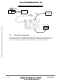
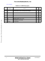
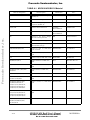
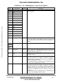
1
Freescale MOTOROLA
Semiconductor, Inc.
Metrowerks
Freescale Semiconductor, Inc...
SW/HW Dept
MSC8101 ADS
User’s Manual
Revision B
(Revision Release 1.2)
Dragilev Lev
SW/HW Dept
Motorola Semiconductor Israel
1 Shenkar Street,
Herzlia 46120, Israel
TEL: 972-9-522-579
email: [email protected]
FAX: 972-9-9562990
25/1/2004
For More Information On This Product,
Go to: www.freescale.com
Freescale Semiconductor, Inc...
Freescale Semiconductor, Inc.
MSC8101ADS RevB User’s Manual
For More Information On This Product,
Go to: www.freescale.com
Freescale Semiconductor, Inc.
CONTENTS
Freescale Semiconductor, Inc...
1•1
1•2
1•3
1•4
1•5
2•1
2•2
2•3
2•3•1
2•3•2
2•3•3
3•1
3•2
3•3
3•4
3•5
3•6
3•7
3•8
3•9
4•1
4•2
4•2•1
4•2•2
4•2•3
4•2•4
4•2•5
4•2•6
4•2•7
4•2•8
4•2•9
4•2•10
4•3
4•3•1
4•3•2
4•3•3
4•3•4
4•3•5
4•3•6
4•3•7
4•3•8
4•3•9
4•3•10
4•4
4•4•1
4•4•2
4•4•3
MOTOROLA
Introduction
Abbreviations’ List
Related Documentation
Specification
ADS Features
INTRODUCTION
UNPACKING INSTRUCTIONS
HARDWARE PREPARATION
Setting The Core Supply Voltage Level
Setting MODCK(1:3) For Initial PLLs’ Multiplication Factor - SW9
Setting HReset Configuration Source
OnCE Connection Scheme
Host I/F Operation
Stand Alone Operation
+5V Power Supply Connection
JTAG/OnCE Connector - P6
HOST I/F Connector - P4
Terminal to MSC8101ADS RS-232 Connection
10/100-Base-T Ethernet Port Connection
Flash Memory SIMM Installation
INTRODUCTION
SWITCHES
Host I/F Setting - SW1
Emulator Enable (EE) - SW2
ABORT Switch - SW3
SOFT RESET (SRESET) Switch - SW4
DATA Bus Width Setting - SW5 & SW6.
HARD RESET (HRESET) - Switch - SW7
Power-On RESET Switch (PRESET) - SW8
Configuration Switch - SW9
Boot Mode Select - SW10
Software Options Switch - SW11
Jumpers
JP1 - DLL Disable.
JP2 - Clock Buffer Set.
JP3 - 50 Ohm Enable.
JP4 - VPP Source Selector
JP5,JP8 - 600 Ohm Termination.
JP6,JP7 - MIC Enable.
JP9 - 5V power supply for CODEC
JS1-5 - Current Consumption Measurement
JG1-6 GND Bridges
Solder Bridges
LEDs
Fast Ethernet Indicator - LD1
Fast Ethernet RX Indicator - LD2
Ethernet TX Indicator - LD3
MSC8101ADS RevB User’s Manual
For More Information On This Product,
Go to: www.freescale.com
11
11
11
12
13
16
16
16
18
18
18
19
19
20
21
21
22
23
24
24
26
26
26
26
27
27
27
28
28
28
29
30
30
30
30
31
31
31
31
31
32
32
32
32
32
32
32
III
Freescale Semiconductor, Inc...
Freescale Semiconductor, Inc.
4•4•4
4•4•5
4•4•6
4•4•7
4•4•8
4•4•9
4•4•10
4•4•11
4•4•12
4•4•13
4•4•14
4•4•15
4•4•16
4•4•17
4•4•18
4•4•19
4•4•20
4•4•21
4•4•22
4•5
4•5•1
5•1
5•1•1
5•1•2
5•1•3
5•1•4
5•1•5
5•2
5•2•1
5•2•2
5•2•3
5•3
5•4
5•5
5•6
5•6•1
5•6•2
5•7
5•7•1
5•8
5•8•1
5•8•2
5•8•3
5•8•4
5•8•5
5•9
5•10
5•11
IV
Ethernet LINK Indicator - LD4
Fast Ethernet CLSN Indicator - LD5
ATM RX Indicator - LD6
ATM TX Indicator - LD7
TEXP Indicator - LD8
Signaling Indicator 1 - LD9
Signaling Indicator 0 - LD10
RS232 Port 2 ON - LD11
RS232 Port 1 ON - LD12
Fast Ethernet Port Initially Enabled - LD13
ATM ON - LD14
T1-1 TDM Port 1 Enable - LD15
T1-234 TDM Ports 2,3,4 Enable - LD16
CODEC Enable - LD17
RUN Indicator - LD18
Host I/F Enable - LD19
1.5V Indicator - LD20
3.3V Indicator - LD21
5V Indicator - LD22
The MSC8101’s Registers’ Programming
System Initialization
Reset & Reset - Configuration
Power- On Reset
Manual Hard Reset
Hard Reset Configuration
Manual Soft Reset
MSC8101 Internal Hard Reset Sources
Local Interrupter
ABORT Interrupt
ATM UNI Interrupt
QFALC Interrupt
Clock Generator
Bus Buffering
Chip - Select Generator
Synchronous DRAM Bank
SDRAM Programming
SDRAM Refresh
Flash Memory SIMM
Flash Programming Voltage
Communication Ports
ATM Port
100/10 Base - T Port
Audio CODEC
T1/E1 Ports
RS232 Ports
Host I/F
DMA off-board tool
Board Control & Status Register - BCSR
MSC8101ADS RevB User’s Manual
For More Information On This Product,
Go to: www.freescale.com
33
33
33
33
33
33
33
33
33
33
34
34
34
34
34
34
34
34
34
34
35
39
39
39
39
41
42
42
42
42
42
42
43
43
44
45
46
46
47
48
50
50
51
52
52
53
54
54
MOTOROLA
Freescale Semiconductor, Inc.
5•11•1
5•11•2
5•11•3
5•11•4
7•1
7•1•1
7•1•2
7•1•3
Freescale Semiconductor, Inc...
A•1
B•1
B•1•1
B•1•2
B•1•3
B•1•4
B•1•5
B•1•6
B•1•7
B•1•8
B•1•9
B•1•10
B•1•11
B•1•12
B•1•13
C•1
C•1•1
C•1•2
C•1•3
MOTOROLA
BCSR0 - Board Control / Status Register 0
BCSR1 - Board Control / Status Register 1
BCSR2 - Board Control / Status Register 2
BCSR3 - Board Status Register 3
Power rails.
5V Bus
3.3V Bus
1.5V Bus
BOM
Interconnect Signals
MSC8101ADS’s P1- System Expansion Connector
MSC8101ADS’s P2 - CPM Expansion Connector
P3 - Altera’s In System Programming (ISP)
P4 - Host Interface Connector
P5, P7, P8, P9, P10, P13, P14 - Logic Analyzer Connectors
P6 - JTAG/OnCE Port Connector
P12 - Ethernet Port Connector
P15,P16 - SMB Connectors
P17,P18 - Double RJ45 T1/E1 Line Connectors
P19,P21,P24 - Stereo Phone Jack Connectors
P20,P22,P23,P25 - RCA Jack Connectors
P26 - 5V Power Supply Connectors
P27A,B - RS232 Ports’ Connectors
Logic Equations
First Include File
Second Include file
Main File
MSC8101ADS RevB User’s Manual
For More Information On This Product,
Go to: www.freescale.com
55
56
58
59
65
66
66
66
68
76
76
82
90
90
92
92
93
93
93
94
94
95
95
99
99
100
101
V
Freescale Semiconductor, Inc...
Freescale Semiconductor, Inc.
VI
MSC8101ADS RevB User’s Manual
For More Information On This Product,
Go to: www.freescale.com
MOTOROLA
Freescale Semiconductor, Inc.
Freescale Semiconductor, Inc...
LIST OF FIGURES
FIGURE 1-1
FIGURE 2-1
FIGURE 3-1
FIGURE 3-2
FIGURE 3-3
FIGURE 3-4
FIGURE 3-5
FIGURE 3-6
FIGURE 3-7
FIGURE 3-8
FIGURE 3-9
FIGURE 4-1
FIGURE 4-2
FIGURE 4-3
FIGURE 4-4
FIGURE 4-5
FIGURE 4-6
FIGURE 4-7
FIGURE 4-8
FIGURE 5-1
FIGURE 5-2
FIGURE 5-3
FIGURE 5-4
FIGURE 5-5
FIGURE 5-6
FIGURE 7-1
MSC8101ADS Block Diagram
MSC8101ADS Top Side Part Location diagram
Host System Debug Scheme A
Host System Debug Scheme B
Stand Alone Configuration
P26: +5V Power Connector
P6 - JTAG/OnCE Port Connector
P4 - Host I/F Connector
P27A - Upper RS-232 Serial Port Connector
P27B - Lower RS-232 Serial Port Connector
Flash Memory SIMM Insertion
Switch SW1 HOST - Description
Switch SW2 - Description
DIP-Switch 64/32 Bit Setting
Switch SW9 MODCK - Description
Switch SW10 BOOT MODE - Description
Switch SW11 S/W Option - Description
JP4 - FLASH Programming Source Selection
JP9 - 5V CODEC Source Selection
Clock Distribution Scheme
SDRAM Connection Scheme
FLASH SIMM Connection Scheme
MSC8101 to CODEC connection.
RS232 Serial Ports’ Connector
Host Interface Diagram
ADS Power Scheme
MOTOROLA
MSC8101ADS RevB User’s Manual
For More Information On This Product,
Go to: www.freescale.com
15
17
19
20
21
21
22
23
24
24
25
26
27
28
29
30
30
31
32
43
45
47
51
52
53
65
VII
Freescale Semiconductor, Inc...
Freescale Semiconductor, Inc.
VIII
MSC8101ADS RevB User’s Manual
For More Information On This Product,
Go to: www.freescale.com
MOTOROLA
Freescale Semiconductor, Inc.
Freescale Semiconductor, Inc...
LIST OF TABLES
TABLE 1-1.
TABLE 4-1.
TABLE 4-2.
TABLE 4-3.
TABLE 4-4.
TABLE 5-1
TABLE 5-2.
TABLE 5-3.
TABLE 5-4.
TABLE 5-5.
TABLE 5-6.
TABLE 5-7.
TABLE 5-8.
TABLE 5-9.
TABLE 5-10.
TABLE 5-11.
TABLE 5-12.
TABLE 5-13.
TABLE 5-14.
TABLE 5-15.
TABLE 5-16.
TABLE 5-17.
TABLE 5-18.
TABLE 6-1.
TABLE 7-1.
TABLE A-1.
TABLE B1-2.
TABLE B1-3.
TABLE B1-4.
TABLE B1-5.
TABLE B1-6.
TABLE B1-7.
TABLE B1-8.
TABLE B1-9.
TABLE B1-10.
TABLE B1-11.
MOTOROLA
MSC8101ADS Specifications
Available Clock Mode Setting
JP1/JP2 Settings
SIU Registers’ Programming
Memory Controller Initialization for 100(50) MHz
Summary Reset Configuration Schemes.
Hard Reset Configuration Word
MSC8101ADS Chip Select Assignments
100 MHz SDRAM Mode Register Programming
Flash Memory Projected Performance Figures
Ports Function Enable
CS4221 Programming
Host I/F Interconnect signals
BCSR0 Description
BCSR1 Description
Peripheral’s Availability Decoding.
BCSR2 Description
Flash Presence Detect (7:5) Encoding
Flash Presence Detect (4:1) Encoding
BCSR3 Description
EXTOOLI(0:3) Assignment
External Tool Revision Encoding
ADS Revision Encoding
MSC8101ADS Memory Map
Off-Board Application Maximum Current Consumption
MSC8101ADS Bill Of Material
P1 - System Expansion - Interconnect Signals
P2 - CPM Expansion - Interconnect Signals
P3 - ISP Connector - Interconnect Signals
P4 - Host Interface Connector - Interconnect Signals
P6 - JTAG/ONCE Connector - Interconnect Signals
P12 - Ethernet Port Interconnect Signals
P17,P18 - T1/E1 Line Connectors Interconnect Signals
P19,P21,P24 - Stereo Phone Connectors Interconnect Signals
P27A Interconnect Signals
P27B Interconnect Signals
MSC8101ADS RevB User’s Manual
For More Information On This Product,
Go to: www.freescale.com
12
29
31
35
36
40
40
44
45
46
49
51
54
55
56
58
58
59
59
60
61
61
61
63
66
68
77
82
90
90
92
93
94
94
95
95
IX
Freescale Semiconductor, Inc...
Freescale Semiconductor, Inc.
T-X
MSC8101ADS RevB User’s Manual
For More Information On This Product,
Go to: www.freescale.com
MOTOROLA
FreescaleGeneral
Semiconductor,
Inc.
Information
1 - General Information
1•1
Introduction
This document describes the engineering specifications of the MSC8101ADS board based on the
MSC8101- first member of the family of programmable DSP based around the SC100 DSP cores.
It integrates a high-performance Star*Core SC140 DSP is four ALU DSP Core, large on-chip
memory (1/2 MByte), Communication Processor Module compatible with PowerQUICCII
(MPC8260) CPM, a very flexible system integration unit (SIU) and a 16-channel DMA engine.
Freescale Semiconductor, Inc...
This board is meant to serve as a platform for s/w and h/w development around the MSC8101 processor. Using its on-board resources and its associated debugger, a developer is able to download
code, run it, set breakpoints, display memory and registers and connect proprietary h/w via the expansion and host interface connectors, to be incorporated into a desired system with the MSC8101
processor.
This board could also be used as a demonstration tool, i.e., application s/w may be burnedA into
its flash memory and ran in exhibitions etc.
1•2
Abbreviations’ List
•
Processor - The MSC8101
•
ADS - The MSC8101ADS, the subject of this document
•
SDRAM Machine - Synchronous Dynamic RAM Machine
•
UPM - User Programmable Machine
•
GPCM - General Purpose Chip-select Machine
•
CPM - Communication Processor Module
•
FCC - Fast communications controller
•
SCC - Serial communications controller
•
SMC - Serial management controller
•
TDMA(B,C,D) - One of four A(B,C,D) time-division multiplexed interfaces
•
HID16 - Host Parallel Interface 16 bit-wide
•
GPL - General Purpose Line (associated with a UPM)
•
EOnCE - Enhanced On-Chip Emulation (debug port)
•
EE - EOnCE Event Signal
•
BCSR - Board Control & Status Register
•
ZIF - Zero Input Force
•
BGA - Ball Grid Array
•
SIMM - Single In-line Memory Module
•
MII - Media Independent Interface
1•3
Related Documentation
[1]
StarCore 140 Architecture Functional Specification
[2]
SC140 DSP Core Reference Manual
[3]
MSC8101 Reference Manual
[4]
MSC8101 Hardware Specification
A. Either on or off-board.
MOTOROLA
MSC8101ADS RevB User’s Manual
For More Information On This Product,
Go to: www.freescale.com
11
FreescaleGeneral
Semiconductor,
Inc.
Information
[5]
PMC-SIERRA 5350 Long Form Data Sheet
[6]
PMC-SIERRA 5350 Errata Notice
[7]
PMC-SIERA 5350 Reference Design
[8]
LXT970A (by Level One) Data Sheet
[9]
LXT970 Demo Board User’s Guide
1•4
Specification
The MSC8101ADS specifications are given in TABLE 1-1. "MSC8101ADS Specifications" below
TABLE 1-1. MSC8101ADS Specifications
Freescale Semiconductor, Inc...
CHARACTERISTICS
SPECIFICATIONS
Power requirements (no other boards attached)
+5V DC @ 2A (Typ.), 3A (Max.)
MSC8101
Internal clock up to 300MHz @ 1.5V
PowerPC(60x) Bus
Running up to 100 MHz Bus Clock Frequency.
PowerPC (60x) bus:
Total address range:
4 Giga Bytes (32 address lines)
256 KBytes External (18 address lines)
Data Bus width:
64 bit without Host Interface(HID16)/32bit with HID16
Flash memory mounted on SIMM
8 MByte, 32 bits wide expandable to 32 MBytes.
Synchronous DRAM 100MHz soldered (non-buffered)
16MBytes, organized as 2x8Megx32 bit. May be reconfiged
to 32bits wide with 8MByte (expansion to 16MByte is
optional)
Operating temperature
0OC - 30OC (room temperature)
Storage temperature
-25OC to 85OC
Relative humidity
5% to 90% (non-condensing)
Dimensions:
Length
Width
PCB Thickness
9.549" (240 mm)
7.480" (190 mm)
0.063" (1.6 mm)
12
MSC8101ADS RevB User’s Manual
For More Information On This Product,
Go to: www.freescale.com
MOTOROLA
FreescaleGeneral
Semiconductor,
Inc.
Information
Freescale Semiconductor, Inc...
1•5
MOTOROLA
ADS Features
o
64-bit MSC8101, running up to @ 100MHz external bus frequency.
o
8 MByte, 80 pin Flash SIMM reside after buffer. Support for up to 32 MByte, controlled by GPCM, 5V Programmable, with Automatic Flash SIMM identification, via
BCSR.
o
16 MByte unbuffered SDRAM on PPC bus, controlled by SDRAM machine, soldered directly on the board. Data bus width 64/32 bits is controlled by Jumper Array. The narrow data bus configuration is supported with 8MByte SDRAM memory
space.
o
256 KBit serial EEPROM on I2C bus.
o
Board Control & Status Register - BCSR, controlling Board’s Operation on PPC
bus. Access via GPCM.
o
Programmable Hard-Reset Configuration via Flash memory or Host Interface.
Also may be forced from BCSR.
o
High density (MICTOR) Logic Analyzer connectors, carrying all MSC8101 signals,
for fast logic analyzer connection.
o
155 Mbps ATM UNI on FCC1 with Optical I/F, connected to the MSC8101 via
UTOPIA, using the PMC-SIERA 5350.
o
10/100-Base-T Port on FCC2 with T.P. I/F, MII controlled, using Level-One
LXT970.
o
Four channels T1/E1 on TDMs using Infeneon Quad FALC PEB22554.
o
24-bit audio-CODEC CS4221 connected to the CPM’s TDMA1 channel with
gained stereo audio Input/Output.
o
Dual RS232 port residing on SCC1 & SMC1.
o
Module disable (i.e., low-power mode) option for all communication transceivers BCSR controlled, enabling use of communication ports, off-board via expansion
connectors.
o
Dedicated MSC8101’s communication ports expansion connectors for convenient
tools’ connection, carrying also necessary bus signals, for transceivers’ M/P I/F
connection. Use is done with 2 X 128 pin DIN 41612 receptacle connectors.
o
Host I/F, providing through expansion connectors or dedicated header.
o
External Tools’ Identification & status read Capability, via BCSR.
o
SMB-connectors for external pulse generator and clock output
o
Configuration setting via DIP switches.
o
Power-On Reset Push, Soft - Hard Reset Push, ABORT Push - Buttons.
o
Ext. Single 5V DC Supply with Reverse / Over Voltage Protection for Power Input
and Power-On sequence.
MSC8101ADS RevB User’s Manual
For More Information On This Product,
Go to: www.freescale.com
13
FreescaleGeneral
Semiconductor,
Inc.
Information
On-board 1.2V - 2.2V adjustable for MSC8101 Internal Logic Operation and
3.3V±10% fixed Voltage Regulators for other circuits. May be bypassed in case of
external power supplying.
o
Software Option Switch provides 8 S/W options via BCSR.
o
LED’s for power supply, module enables, timer expired and SW indications.
Freescale Semiconductor, Inc...
o
14
MSC8101ADS RevB User’s Manual
For More Information On This Product,
Go to: www.freescale.com
MOTOROLA
FreescaleGeneral
Semiconductor,
Inc.
Information
FIGURE 1-1 MSC8101ADS Block Diagram
2
PPC (non-buffered)
1
SDRAM
D[0:59]
2Megx32
Address Mux
for variable
Port Size 64/32
36pin
HOST Buffers
Clock
Host PORT
28
D[32:59]
16.4/25MHz
*
16Mbyte @ 64bit
3.3V
HOST I/F
Reset,Config
Interrupts
DATA Transceivers &
Address Buffers
5V
PPC Bus (buffered)
D[0:31]
Control &
Status Register
Altera
3.3V<->5V
3ns
(3M Socket)
Clock Buffer
1
ClkOut
7
SCC1,SMC1
RS232
PORTS
DLLIN
D-9
JTAG/OnCE
Flash Detect
MC145583
3.3V
To
Command
Converter
Magnetics
QFALC
4xT1/E1
TDMA,B,C,D
FCC1
I2C
PM5350
EEPROM
3.3V<->5V
Buffered Exp. System Bus
CPM
TDMA1
SPI
cnt
CODEC
CS4221
From MIC/LINE STEREO
To STEREO AUDIO AMP
DIN 41612
3.3V
OPTICAL
5V
CPM EXPANSION
LXT970
ATM-155
PORT
FCC2
MIIctrl.
10/100-Base-T
PORT
3.3V
RJ45-8
14pin
Flash SIMM.
8 - 32MByte
32 - Bit
MSC8101
332 pin 0.8mm
19x19 matrix
RJ45
Freescale Semiconductor, Inc...
Ext CLK
* - Additional memory part is optional
MOTOROLA
MSC8101ADS RevB User’s Manual
For More Information On This Product,
Go to: www.freescale.com
15
Freescale
Semiconductor,
Inc.
Hardware
Preparation
2 - Hardware Preparation
2•1
INTRODUCTION
This chapter provides unpacking instructions, hardware preparation, and installation instructions
for the MSC8101ADS.
2•2
UNPACKING INSTRUCTIONS
NOTE
If the shipping carton is damaged upon
receipt, request carrier’s agent to be
present during unpacking and inspection of
equipment.
Freescale Semiconductor, Inc...
Unpack equipment from shipping carton. Refer to packing list and verify that all items are present.
Save packing material for storing and reshipping of equipment.
CAUTION
AVOID
TOUCHING
AREAS
OF
INTEGRATED
CIRCUITRY;
STATIC
DISCHARGE CAN DAMAGE CIRCUITS.
2•3
HARDWARE PREPARATION
To select the desired configuration and ensure proper operation of the MSC8101-ADS board,
changes of the DIP-Switch settings may be required before installation. The location of the
switches, indicators, DIP-Switches, and connectors is illustrated in FIGURE 2-1 "MSC8101-ADS
Top Side Part Location diagram" on page 17. The board has been factory tested and is shipped
with DIP-Switch settings as described in the following paragraphs. Parameters can be changed for
the following conditions:
•
The Processor Internal Logic and PLLs Supply Level (1.6V) via potentiometer RP2.
•
The Processor I/O Supply Voltage (3.3V) via potentiometer RP1 (be careful since this
power supply feeds another logic devices on the ADS and tool boards).
•
The Processor Clocking:
•
•
16
o
MODCK(1:3). Determining Core’s and CPM’s PLLs multiplication factor via the
DIP Switch SW9.
o
MODCKH(4:6) for the Flash Memory Config. Word/Host Config Word (Power-On
Reset Source Dependent) or from the DIP Switch SW9 for FPGA Config. Setting
(Safe Mode).
o
Clock mode update requires power up operation.
Hard Reset Configuration Word source is selected by the DIP Switch SW9/7.
Normal (64-bit wide) or Narrow (32-bit wide) Data bus width for Host I/F mode is
selected by the DIP Switches SW5,6.
MSC8101ADS RevB User’s Manual
For More Information On This Product,
Go to: www.freescale.com
MOTOROLA
FreescaleHardware
Semiconductor,
Inc.
Preparation
Freescale Semiconductor, Inc...
FIGURE 2-1 MSC8101ADS Top Side Part Location diagram
Host SW
MOTOROLA
EE SW
64/32 Select
Boot Mode SW
Config SW
MSC8101ADS RevB User’s Manual
S/W Opt
For More Information On This Product,
Go to: www.freescale.com
17
Freescale
Semiconductor,
Inc.
Hardware
Preparation
2•3•1
Setting The Core Supply Voltage Level
The internal Logic & PLL’s of the MSC8101 is powered separately through a supply bus named
1V5. The voltage level over this power bus may vary between 0.9V - 2.1V. In the lower voltage
level, the Processor will operate at lower frequency range, consuming a smaller amount of power
and vice-versa for the higher voltage level.
1V5 power level is factory set for 1.5V, but may be changed by RP2.
2•3•2
Setting MODCK(1:3) For Initial PLLs’ Multiplication Factor - SW9
During Power On reset sequence the Processor samples the three MODCK(1:3) lines which are
driven by Altera FPGA device in accordance with SW9/1-3 setting. MODCK_HI field (MODCK[4–
6]), taken from the reset configuration word, are read from the Flash memory (default value from
Altera FPGA for non-programmed Flash is read from SW9/4-6) or from Host Interface to establish
with the multiplication factors of the CPM’s and Core’s PLLs. SW9 is shown in FIGURE 4-4 "Switch
SW9 MODCK - Description" on page 29:
Freescale Semiconductor, Inc...
Some Clock Configuration can see in FIGURE 5-1 on page 43:
2•3•3
Setting HReset Configuration Source
The HReset Configuration WordA, read by the Processor while HRESET~ is asserted, may be
taken from three sources:
1)
Flash Memory SIMM.
2)
Altera FPGA (Safe Mode).
3)
Host I/F.
When SW9/7 is OFF, the Hard Reset Configuration Word is taken from Altera FPGA, when it is
ON, the Hard Reset Configuration Word is taken from the Flash SIMM. If SW9/8 (Configuration)
set OFF the Processor will be configured from Host, independent of SW9/7 (Flash Configuration
Enable) position. For correct operation for Host Config. Mode Data bus width will be set to 32-bit
wide.
A. In fact 8 Hard-Reset configuration words are read by a configuration master, however only the first is relevant for a single MSC8101.
18
MSC8101ADS RevB User’s Manual
For More Information On This Product,
Go to: www.freescale.com
MOTOROLA
Freescale
Semiconductor, Inc.
Installation Instructions
3 - Installation Instructions
The MSC8101ADS may be configured according to the required working environment as follows:
•
Host Controlled Operation through OnCE Port
•
Host Interface Operation through HDI16 Port
•
Stand-Alone Mode
3•1
OnCE Connection Scheme
In this configuration the MSC8101ADS is controlled by a host computer via the OnCE Port, which
is a subset of the JTAG port. This configuration allows for extensive debugging using on-host debugger. The host is connected to the ADS by a Command Converter provided by a third party
(Macraigor Systems).
Freescale Semiconductor, Inc...
FIGURE 3-1 Host System Debug Scheme A
Host
Computer
Media I/F
Command
Converter
14 Wire
Flat Cable
5V Power Supply
3•2
Host I/F Operation
In this configuration the MSC8101ADS is using HDI16 I/F that provide 16-bit wide, full-duplex,
double-buffered, parallel port to connect directly to the data bus of a host processor. The HDI16
supports two classes of interfaces:
•
Host processor/Microcontroller (MCU) connection interface
•
DMA controller interface
A Host Device may be connected to the ADS via dedicated 36pin two rows header or via 128pin
DIN - connector P2.
MOTOROLA
MSC8101ADS RevB User’s Manual
For More Information On This Product,
Go to: www.freescale.com
19
Freescale
Semiconductor,
Inc.
Installation
Instructions
FIGURE 3-2 Host System Debug Scheme B
Host
Computer
Media I/F
Command
Converter
14 Wire
Flat Cable
To JTAG/OnCE
36Wire
Flat Cable
Host
Device
Freescale Semiconductor, Inc...
5V Power Supply
3•3
Stand Alone Operation
In this mode, the ADS is not controlled by the host via the OnCE port. It may connect to host via
one of its other ports, e.g., RS232 port, Fast Ethernet port, ATM155 port etc. Operating in this
mode requires an application program to be programmed into the board’s Flash memory.
20
MSC8101ADS RevB User’s Manual
For More Information On This Product,
Go to: www.freescale.com
MOTOROLA
Freescale
Semiconductor, Inc.
Installation Instructions
FIGURE 3-3 Stand Alone Configuration
et
rn
he ork
t
E etw
N
ATM155(Opt
ic)
Host
Computer
Freescale Semiconductor, Inc...
T1/E1
four ch.
RS
5V Power Supply
232
Audio
Stereo
3•4
+5V Power Supply Connection
The MSC8101 requires +5V DC @ 4A max, power supply for operation. Connect the +5V power
supply to connector P26 as shown below:
FIGURE 3-4 P26: +5V Power Connector
+5V
GND
GND
1
2
3
P26 is a 3 terminal block power connector with power plug. The plug is designed to accept 14 to
22 AWG wires. It is recommended to use 14 to 18 AWG wires. To provide solid ground, two GND
terminals are supplied. It is recommended to connect both GND wires to the common of the power
supply, while “Hot” line is connected with a single wire.
NOTE
Since hardware applications may be connected
to the MSC8101ADS via the expansion connectors P1 and P2, the additional power consumption should be taken into consideration when a
power supply is connected to the MSC8101ADS.
3•5
JTAG/OnCE Connector - P6
The MSC8101ADS JTAG/OnCE connector, P6, is a 14 pin, two rows, header connector with key.
The connection between the MSC8101ADS and the Command Converter is by a 14 line flat cable,
MOTOROLA
MSC8101ADS RevB User’s Manual
For More Information On This Product,
Go to: www.freescale.com
21
Freescale
Semiconductor,
Inc.
Installation
Instructions
supplied with the Command Converter obtained from Macraigor Systems. FIGURE 3-5 "P6 JTAG/OnCE Port Connector" below shows the pin configuration of the connector.
FIGURE 3-5 P6 - JTAG/OnCE Port Connector
TDI
TDO
TCK
N.C.
RESET
3.3V
Freescale Semiconductor, Inc...
N.C.
3•6
1
2
3
4
5
6
7
8
9
10 TMS
11
12
13
14
GND
GND
GND
KEY (NO PIN)
N.C.
TRST
HOST I/F Connector - P4
The MSC8101ADS HOST I/F connector, P4, is a 36 pin, two rows, header connector. The
connection between the MSC8101-ADS and the Host Board is by a 36 line flat cable, not shipped
with the ADS. FIGURE 3-6 "P4 - Host I/F Connector" below shows the pin configuration of the
connector.
22
MSC8101ADS RevB User’s Manual
For More Information On This Product,
Go to: www.freescale.com
MOTOROLA
Freescale
Semiconductor, Inc.
Installation Instructions
FIGURE 3-6 P4 - Host I/F Connector
GND
HD0
HD2
HD4
HD6
HD8
HD10
Freescale Semiconductor, Inc...
HD12
HD14
GND
HA0
HA2
HCS1
HRRQACK
HRDRW
HRESET
3.3V
GND
3•7
1
2
3
4
5
6
7
8
9
10
11
12
13
14
15
16
17
18
19
20
21
22
23
24
25
26
27
28
29
30
31
32
33
34
35
36
GND
HD1
HD3
HD5
HD7
HD9
HD11
HD13
HD15
GND
HA1
HA3
HCS2
HREQ
HDS
PORST
N.C.
GND
Terminal to MSC8101ADS RS-232 Connection
A serial (RS232) terminal or any other RS232 equipment, may be connected to both connectors
P27/A-B (Upper and Lower). This connectors are a 9 pin, female, D-type connectors, arranged in
a stacked configuration. P27A connected to SCC1 of the MSC8101 is the lower and P27B,
connected to SMC1 of the MSC8101, is the upper in the stack.
The connectors are arranged in a manner that allows for 1:1 connection with the serial port of an
IBM-ATA or compatibles, i.e. via a flat cable. The pinout which is not identical - P27A supports DTE
to DCE connection unlike it the P27B supports Null Modem connection (DTE to DTE). The
difference is shown in FIGURE 3-7 and FIGURE 3-8.
A. IBM-AT is a trademark of International Business Machines Inc.
MOTOROLA
MSC8101ADS RevB User’s Manual
For More Information On This Product,
Go to: www.freescale.com
23
Freescale
Semiconductor,
Inc.
Installation
Instructions
FIGURE 3-7 P27A - Upper RS-232 Serial Port Connector
CD
TX
1
2
RX
DTR
3
4
5
GND
6
7
8
9
DSR
N.C.
CTS
N.C.
Freescale Semiconductor, Inc...
FIGURE 3-8 P27B - Lower RS-232 Serial Port Connector
N.C.
TX
1
2
RX
N.C.
3
4
5
GND
3•8
6
7
8
9
N.C.
N.C.
N.C.
N.C.
10/100-Base-T Ethernet Port Connection
The 10/100-Base-T port connector - P12, is an 8-pin, 90o, receptacle RJ45 connector. The connection between the 10/100-Base-T port to the network is done by a standard cable, having two
RJ45/8 jacks on its ends.
3•9
Flash Memory SIMM Installation
To install a memory SIMM, it should be taken out of its package, put diagonally in its socket - U8
and then raised to a vertical position until the metal lock clips are locked. See FIGURE 3-9 "Flash
Memory SIMM Insertion" on page 25.
24
MSC8101ADS RevB User’s Manual
For More Information On This Product,
Go to: www.freescale.com
MOTOROLA
Freescale
Semiconductor, Inc.
Installation Instructions
CAUTION
The memory SIMMs have alignment nibble
near their # 1 pin. It is important to align the
memory correctly before it is twisted, otherwise damage might be inflicted to both the
memory SIMM and its socket.
FIGURE 3-9 Flash Memory SIMM Insertion
(1)
Insert
Freescale Semiconductor, Inc...
(2)
Turn
Metal Lock Clip
Flash
SIMM
SIMM Socket
SIMM
MOTOROLA
MSC8101ADS RevB User’s Manual
For More Information On This Product,
Go to: www.freescale.com
25
Freescale
Semiconductor,
Inc.
Operating
Instructions
4 - Operating Instructions
4•1
INTRODUCTION
This chapter provides necessary information to use the MSC8101-ADS in host-controlled and
stand-alone configurations. This includes controls and indicators, memory map details, and
software initialization of the board.
4•2
SWITCHES
The MSC8101ADS has the following switches:
4•2•1
Host I/F Setting - SW1
Freescale Semiconductor, Inc...
This switch is using for manually set a Host Bus parameters. When Host Configuration is enable
the DIP switch SW1/1-3 will be connected to Data Bus through tri-state buffers and sampled by the
Processor. The SW1 factory set is all ON.
FIGURE 4-1 Switch SW1 HOST - Description
SW1
4
8/16BIT
3
DualSingleStrobe
2
StrobePolarity
ON
RESERVED
Set to ‘0’ <=
4•2•2
1
=> Set to ’1’
Emulator Enable (EE) - SW2
This switch controls lines EE0-EE7,EED, connected to appropriate pins of the Processor. When
Reset Configuration executed, EEs lines, involved in one, are driven by FPGA. In fact, they are
EE0, EE1, EE4 and EE5 which sampled at the rising edge of PORESET~. After configuration is
done level of all EE-signals is set by the switch SW2/1-7. Their status may be read out via
BCSR3/0-6. SW2 is factory set to all ON.
26
MSC8101ADS RevB User’s Manual
For More Information On This Product,
Go to: www.freescale.com
MOTOROLA
Freescale
Semiconductor, Inc.
Operating Instructions
FIGURE 4-2 Switch SW2 - Description
SW2
8
EED
7
EE5
6
EE4
5
EE3
4
EE2
3
EE1
2
EE0
ON
Freescale Semiconductor, Inc...
RESERVED
1
Set to ‘0’ <=
4•2•3
=> Set to ’1’
ABORT Switch - SW3
The ABORT switch is normally used to abort program execution, this by issuing a level 0 nonmaskable interrupt to the Processor. If the ADS is in stand alone mode, it is the responsibility of
the user to provide means of handling the interrupt, since there is no resident debugger with the
MSC8101-ADS. The ABORT switch signal is denounced, and can not be disabled by software.
4•2•4
SOFT RESET (SRESET) Switch - SW4
The SOFT reset switch SW4 performs Soft Reset to the Processor internal modules, maintaining
it’s configuration (clocks & chip-selects) and SDRAMs’ contents. The switch signal is debounced,
and it is not possible to disable it by software.
4•2•5
DATA Bus Width Setting - SW5 & SW6.
Two switches SW5 & SW6 are using together for preparing the SDRAM Memory Banks for Host
Interface Mode when HDI16 interface is provided over Data Bus lines D32-D63. They should be
set in “32bit” position when DIP-Switch SW9/8 HOST CFG set ON (PPC bus supports Host I/F)
and vice versa - “64bit” when Host I/F disable.
MOTOROLA
MSC8101ADS RevB User’s Manual
For More Information On This Product,
Go to: www.freescale.com
27
Freescale
Semiconductor,
Inc.
Operating
Instructions
FIGURE 4-3 DIP-Switch 64/32 Bit Setting
SW6
64
BIT
32
SW5
4•2•6
HARD RESET (HRESET) - Switch - SW7
Freescale Semiconductor, Inc...
HARD reset is generated when switch SW7 is pressed. When the Processor executes HARD reset
sequence, all its configuration is lost, including data stored in the SDRAMs and the Processor has
to be re-initialized.
4•2•7
Power-On RESET Switch (PRESET) - SW8
The Power-On reset switch SW8 performs Power-On reset to the MSC8101, as if the power was
re-applied to the ADS. When the Processor is reset that way, all configuration and all data residing
in volatile memories are lost. After PORST~ signal is negated, the Processor re-acquires the
power-on reset configuration data from the Flash (Altera) or Host I/F.
4•2•8
Configuration Switch - SW9
SW9 is a 8-switch DIP-Switch. This switch is connected over Altera device to MODCK(1:6) lines
of the Processor. The combination of the switches composing SW9, sets, during Power-On reset
sequence, the MODCK(1:6) field for the MSC8101. The switch SW9/7 establishes Configuration
Word Source. If SW9/7 is set to ON position Configuration Word will be loaded from the Flash, otherwise from Altera device (default). The Host Configuration will be chosen with SW9/8 set ON,
when SW9/8 is OFF - PPC bus has 64-bit width.
The Switch SW9 is factory set to (1 - OFF, 2 - ON, 3 - OFF, 4 - OFF (X), 5 - ON, 6 - OFF, 7,8 OFF).
28
MSC8101ADS RevB User’s Manual
For More Information On This Product,
Go to: www.freescale.com
MOTOROLA
Freescale
Semiconductor, Inc.
Operating Instructions
FIGURE 4-4 Switch SW9 MODCK - Description
SW9
HOST
CFG
8
FCFG
7
MODCK6
6
5
MODCK4
4
MODCK3
3
MODCK2
2
MODCK1
ON
Freescale Semiconductor, Inc...
MODCK5
1
=> Set to ’1’
Set to ‘0’ <=
TABLE 4-1. Available Clock Mode Setting
MODCK-1
-2
-3
-4
-5
-6
0
0
1
1
1
1
0
0
1
0
0
1
Clock
Mode
Clock In
MHz
CPM
MHz
PPC Bus
MHz
SC140 Core
MHz
57a
55
137.5
55a
275
20
200
100
300
b
9
a. Factory setting.
b. Alternative clock mode for 100MHz bus frequency requires clock oscillator 20MHz
4•2•9
Boot Mode Select - SW10
SW10 is a 4-switch Dip-Switch with three poles in use. This switch selects Boot Mode over Altera
FPGA on the Processor inputs EE0, EE4, EE5 during Power-On reset sequence. Setting SW10/1
(DBG) to ON brings holding EE0 at logic 1 during reset that puts the SC140 core into DEBUG
MODE. In doing so BTM’s switch position will be ignored. See TABLE 5-1 on page 40 for more
explanation. SW10 is factory set to all ON.
MOTOROLA
MSC8101ADS RevB User’s Manual
For More Information On This Product,
Go to: www.freescale.com
29
Freescale
Semiconductor,
Inc.
Operating
Instructions
FIGURE 4-5 Switch SW10 BOOT MODE - Description
RESERVED
4
BTM1
3
BTM0
2
ON
BOOT
SW10
DBG
1
=> Set to ’1’
Freescale Semiconductor, Inc...
Set to ‘0’ <=
4•2•10
Software Options Switch - SW11
SW11 is a 4-switch Dip-Switch with three poles in use. This switch is connected over SWOPT(0:2)
lines which are available at BCSR2 via bus driver U16, S/W options may be manually selected,
according to SW11 state. SW11 is factory set to all ON.
FIGURE 4-6 Switch SW11 S/W Option - Description
SW11
4
SWOPT2
3
SWOPT1
2
SWOPT0
ON
RESERVED
Set to ‘0’ <=
4•3
1
=> Set to ’1’
Jumpers
The MSC8101-ADS has the following jumpers:
4•3•1
JP1 - DLL Disable.
J1 set DLLDIS bit 27 in the HCW loaded from BCSR. When Jumper JP1 is open MSC8101 will be
configured without DLL. If JP3 will closed the DLL is ON. Setting of JP3 is depended on jumper
JP2 (see JP2 description). Default set is JP3-OPEN (DLL disable).
4•3•2
JP2 - Clock Buffer Set.
Jumper J2 allows to change mode of Zero-Delay Buffer JP2. When Jumper JP2 is open ZD buffer
operates in normal mode and require DLL disable setting (JP1 is open). For U44 buffer mode (internal PLL is disable) JP2 should be close. If JP2 is close MSC8101 will be configured without
30
MSC8101ADS RevB User’s Manual
For More Information On This Product,
Go to: www.freescale.com
MOTOROLA
Freescale
Semiconductor, Inc.
Operating Instructions
DLL. See TABLE 4-2. summarized available modes. . Default set is JP3-OPEN (DLL disable).
TABLE 4-2. JP1/JP2 Settings
4•3•3
J1
J2
Clock Driver
U44
MSC8101
Mode
OPEN
OPEN
PLL Mode
DLL disable
CLOSE
CLOSE
Buffer Mode
DLL enable
JP3 - 50 Ohm Enable.
4•3•4
JP4 - VPP Source Selector
JP4 selects the source for VPP - programming voltage for the Flash SIMM. When a jumper is
located between pins 1 - 2 of JP4 (Factory Set), the VPP is connected to the 5V0 plane of the ADS.
For 12V programming set VPP will be drawn from external power supply 12V connected to pins
JP4/2,3.
NOTE
Should be taken into consideration that 12V
external power input for Flash SIMM have
no protection.
FIGURE 4-7 JP4 - FLASH Programming Source Selection
JP4
12V Ext.
JP4
+
5V
Freescale Semiconductor, Inc...
JP3 provides 50 Ohm resistance termination in case when using an external clock source via
coaxial cable connected to the SMB CLOCKIN. In so doing the on-board clock oscillator U18 must
be removed from the socket. Default set is JP3-OPEN (termination disable).
1
Factory Set
4•3•5
1
JP5,JP8 - 600 Ohm Termination.
Set for audio measurements. Factory set - JP5,JP8 are OPEN.
4•3•6
JP6,JP7 - MIC Enable.
Set if using external microphone audio source. Factory set - JP6,JP7 are CLOSE.
4•3•7
JP9 - 5V power supply for CODEC
JP9 selects the source for CODEC Power Rail. When a jumper is located between pins 1 - 2 of
JP9 (Factory Set), the CODEC feeds from the 5V0 plane of the ADS. When a jumper is removed
external low noise power supply 5V @ 200 mA might be connected to JP9 pins 2,3. See figure
below:
MOTOROLA
MSC8101ADS RevB User’s Manual
For More Information On This Product,
Go to: www.freescale.com
31
Freescale
Semiconductor,
Inc.
Operating
Instructions
FIGURE 4-8 JP9 - 5V CODEC Source Selection
JP9
JP9
1
1
5V Internal
+5V GND
External
Factory Set
4•3•8
JS1-5 - Current Consumption Measurement
Freescale Semiconductor, Inc...
JS1-5 reside on I/O-pins, core & PLL main flow. To measure current consumption, the corresponding JS should be removed using a solder tool and a current meter (shunt) should be connected
instead, with as shorted and thicker wires as possible.
Warning
The job of removing JS1-5 and soldering current
meter connections instead is very delicate and
should be done by a skilled technician.
If this process is done by unskilled hand or repeated more than 3 times, permanent damage
might be inflicted to the MSC8101ADS.
4•3•9
JG1-6 GND Bridges
There are 6 GND bridges on the MSC8101-ADS, 4, designated as GND reside on digital ground
and 2, designated as AGND3 and AGND4 resides on analog ground plane. They are meant to
assist general measurements and logic-analyzer connection.
Warning
When connecting to a GND bridge, use only INSULATED GND clips. Otherwise, un-insulated
clips may cause short- circuits, touching "HOT"
points around them. Failure in doing so, might
result in permanent damage to the
MSC8101ADS.
4•3•10
Solder Bridges
All the solder bridges should be shorted while additional SDRAM device has been assembled on
the ADS board (special requirement).
4•4
LEDs
The MSC8101-ADS has the following indicators:
4•4•1
Fast Ethernet Indicator - LD1
When the LXT970 is enabled and is in 100 Mbps operation mode, the yellow LED - LD1 lights.
4•4•2
Fast Ethernet RX Indicator - LD2
The green Ethernet Receive LED indicator blinks whenever the LXT970 is receiving data from one
of the 10/100-Base-T port.
4•4•3
32
Ethernet TX Indicator - LD3
MSC8101ADS RevB User’s Manual
For More Information On This Product,
Go to: www.freescale.com
MOTOROLA
Freescale
Semiconductor, Inc.
Operating Instructions
The green Ethernet Receive LED indicator blinks whenever the LXT970 is transmitting data via the
10/100-Base-T port.
4•4•4
Ethernet LINK Indicator - LD4
The yellow Ethernet Twisted Pair Link Integrity LED indicator - LINK, lights to indicate good link
integrity on the 10/100-Base-T port. LD4 is off when the link integrity fails.
4•4•5
Fast Ethernet CLSN Indicator - LD5
The red Ethernet Collision LED indicator CLSN, lights whenever a collision condition is detected
on the 10/100-Base-T port, i.e., simultaneous receive and transmit. This led functions in this duty
provided that bits 7:6) of LXT970’s register 19, are cleared.
4•4•6
ATM RX Indicator - LD6
Freescale Semiconductor, Inc...
The green ATM Receive LED indicator blinks whenever the PM5350 ATM-UNI is receiving cells
via the ATM port.
4•4•7
ATM TX Indicator - LD7
The green ATM Receive LED indicator blinks whenever the PM5350 ATM-UNI is transmitting cells
via the ATM port.
4•4•8
TEXP Indicator - LD8
The green Timer Expired LED indicates status of Timer 4 output and lights when it’s low.
4•4•9
Signaling Indicator 1 - LD9
This red indication LED has no dedicated function over the ADS. It is meant to provide additional
visibility for program behavior. Its different color from LD9 provides additional information. It is controlled by BCSR0/7. When either of HRESET or Power-On-Reset is asserted the LED lights as
well.
4•4•10
Signaling Indicator 0 - LD10
This green indication LED has no dedicated function over the ADS. It is meant to provide some
visibility for program behavior. It is controlled by BCSR0/6. When either of SRESET or Power-OnReset is asserted the LED lights as well.
4•4•11
RS232 Port 2 ON - LD11
When the yellow RS232 Port 2 ON LED is lit, it designates that the RS232 transceiver connected
to P27B, is active and communication via that medium is allowed. When darkened, it designates,
that the transceiver is in shutdown mode and its associated SMC1 pins may be used off-board via
the expansion connectors.
4•4•12
RS232 Port 1 ON - LD12
When the yellow RS232 Port 1 ON LED is lit, it designates, that the RS232 transceiver connected
to P27A, is active and communication via that medium is allowed. When darkened, it designates
that the transceiver is in shutdown mode and its associated SCC1 pins may be used off-board via
the expansion connectors.
4•4•13
Fast Ethernet Port Initially Enabled - LD13
When the yellow FETH ON LED is lit, it indicates that the fast ethernet port transceiver - the
LXT970, is initially active. When it is dark, it indicates that the LXT970 is initially in power down
mode, enabling the use of its associated FCC2 pins off-board via the expansion connectors. The
state of LD13 is controlled by bit BCSR1/4.
This is a soft-indication, i.e., since the LXT970 may be controlled via the MII port, it is possible that
the state of LD13 does not reflect correctly the status of the LXT970.
MOTOROLA
MSC8101ADS RevB User’s Manual
For More Information On This Product,
Go to: www.freescale.com
33
Freescale
Semiconductor,
Inc.
Operating
Instructions
Note
Application S/W should always seek to match
the state of LD13 to the status of the LXT970, so
that, this indication is made reliable as to the
correct status of the LXT970.
4•4•14
ATM ON - LD14
When the yellow ATM ON LED is lit, it indicates that the ATM-UNI transceiver - the PM5350, is
active and enables communication via that medium. When it is dark, the ATM-UNI transceiver is
disconnected from the MSC8101, enabling the use of its associated FCC1 pins off-board via the
expansion connectors.
ATM ON LED is controlled by BCSR1/2.
Freescale Semiconductor, Inc...
4•4•15
T1-1 TDM Port 1 Enable - LD15
When the yellow T1-1 LED is lit, it indicates that T1/E1 QFALC port 1 is connected to the CPM
TDMA1 port. When darkened, it designates that associated CPM TDMA1 lines may be used for
the CODEC application, in case when CODEC LED is lit. The LD15 reflects the bit BCSR0/3
T1_1EN.
4•4•16
T1-234 TDM Ports 2,3,4 Enable - LD16
When the yellow T1-234 LED is lit, it indicates that T1/E1 QFALC ports 2-4 are available. When
darkened, it designates that associated CPM’s TDMB2,TDMC2,TDMD2 lines may be used for the
other application, e.g. Fast Ethernet. The LD16 reflects the bit BCSR0/4 T1_234EN.
4•4•17
CODEC Enable - LD17
When the yellow CODEC LED is lit, it indicates that CODEC lines are connected to the CPM
TDMA1 port instead of T1/E1 QFALC port 1. When darkened, the CODEC device is isolated from
the bus by tri-state buffers. The LD17 reflects the bit BCSR1/1 CODEC_EN.
4•4•18
RUN Indicator - LD18
When the green RUN LED - LD18 is lit, it indicates that the MSC8101 is performing cycles on the
PPC Bus. When dark, the Processor is either running internally or stuck.
4•4•19
Host I/F Enable - LD19
When the yellow Host I/F ON LED is lit, it indicates that the Processor implementes HDI16 port.
It’s is available on the Host connector P4 and expansion connectors P1, P2. When darkened, PPC
Data Bus becomes 64-bit width with no Host I/F support.
4•4•20
1.5V Indicator - LD20
The green 1.5V LED - LD20, indicates the presence of the +1.5V supply with output voltage no
less than 0.9V.
4•4•21
3.3V Indicator - LD21
The green 3.3V LED - LD21, indicates the presence of the +3.3V supply on the ADS.
4•4•22
5V Indicator - LD22
The green 5V LED - LD22, indicates the presence of the +5V external supply on the ADS.
4•5
The MSC8101’s Registers’ Programming
The MSC8101 provides the following functions on the MSC8101ADS:
1)
34
System functions which include:
MSC8101ADS RevB User’s Manual
For More Information On This Product,
Go to: www.freescale.com
MOTOROLA
Freescale
Semiconductor, Inc.
Operating Instructions
2)
•
PPC Bus SDRAM Controller
•
GPCM (Flash, BCSR, ATM, Ext. Tools)
•
UPM (QFALC, Ext. Tools)
Communication functions which include:
•
ATM SAR
•
Fast Ethernet controller.
•
TDMs for T1/E1 and CODEC support
•
UART for terminal or host computer connection.
The internal registers of the MPC must be programmed after Hard reset as described in the
following paragraphs. The addresses and programming values are in Hexadecimal base.
For better understanding the of the following initialization refer to the
Freescale Semiconductor, Inc...
4•5•1
System Initialization
Hard Reset Config. Word is programmed in Flash according to TABLE 5-2. "Hard Reset Configuration Word" on page 40.
TABLE 4-3. SIU Registers’ Programming
Register
Init Value[hex]
Description
RMR
0001
Check-Stop Reset enabled.
IMMR
14700000
Internal space begins from 0x1470_0000
SYPCR
FFFFFFC3
Software watchdog timer count - FFFF, Bus-monitor timing FF, PPC Bus-monitor Enabled, Local Bus-monitor - Enabled, S/W watch-dog - disabled, S/W watch-dog
(if enabled) causes reset, S/W watch-dog (if enabled) - prescaled.
BCR
0000_0000
Single MSC8101, 0 wait-states on address tenure, 1-level Pipeline depth,
Extended transfer mode disabled for PCC & Local Buses, Odd parity for PPC &
Local Buses (not relevant for this application, External Master delay enabled,
Internal space responds as 64 bit slave for external master (not relevant for this
application).
4•5•1•1
Memory Controller Registers Programming
The memory controller on the MSC8101ADS is initialized to 50/100 MHz operation. I.e., registers’
programming is based on 50/100 MHz timing calculation.
MOTOROLA
MSC8101ADS RevB User’s Manual
For More Information On This Product,
Go to: www.freescale.com
35
Freescale
Semiconductor,
Inc.
Operating
Instructions
Warning
The initialization in TABLE 4-4. "Memory Controller Initialization for 100(50) MHz" below are based
on design and are not verified yet, due to silicon
availability problems.
TABLE 4-4. Memory Controller Initialization for 100(50)a MHz
Reg.
Freescale Semiconductor, Inc...
BR0
Device Type
Bus
FF801801
Base at FF800000, 32 bit port size, no parity,
GPCM
SM73248XG2JHBG0 by
Smart Modular Tech.
FF001801
Base at FF00000, 32 bit port size, no parity,
GPCM
FE001801
Base at FE00000, 32 bit port size, no parity,
GPCM
SM73228XG1JHBG0 by
Smart Modular Tech.
FF800866
(FF800836)
8MByte block size, CS early negate, 12(6) w.s.,
Timing relax
SM73248XG2JHBG0 by
Smart Modular Tech.
FF000866
(FF000836)
16MByte block size, CS early negate, 12(6) w.s.,
Timing relax
SM73288XG4JHBG0 by
Smart Modular Tech.
FE000866
(FE000836)
32MByte block size, CS early negate, 12(6) w.s.,
Timing relax
14501801
Base at 14500000, 32 bit port size, no parity,
GPCM
FFFF8010
(FFFF8020)
32 KByte block size, all types access, 1 w.s.
(32 KByte block size, all types access, 2 w.s.)
20000041
Base at 20000000, 64 bit port size, no parity,
SDRAM machine 1
FF003080
16MByte block size, 4 banks per device, row starts
at A8, 11 row lines, internal bank interleaving
allowed
Non-buffered
PPC with
Host support
20001841
Base at 20000000, 32 bit port size, no parity,
SDRAM machine 1
FF803280
8MByte block size, 4 banks per device, row starts
at A9, 11 row lines, internal bank interleaving
allowed
Non-buffered
PPC with
Host support
20801841
Base at 20800000, 32 bit port size, no parity,
SDRAM machine 1
FF803280
8MByte block size, 4 banks per device, row starts
at A9, 11 row lines, internal bank interleaving
allowed
Buffered
PPC
146088A1
Base at 14608000, 8 bit port size, no parity, UPMB
on PPC bus
FFFF8106
32K Byte block size, burst inhibit, eight idle cycle
are inserted before next access
BR1
Buffered
PPC
Buffered
PPC
BCSR0-3
OR1
BR2
SDRAM 64bit Supported
OR2
MT48LC2M32B2T6-8x2
by Micron
BR2b
SDRAM 32bit Supported
OR2b
MT48LC2M32B2T6-8 by
Micron
BR3c
SDRAM 32bit Supported
OR3c
MT48LC2M32B2T6-8 by
Micron
BR4
QFALC - 4ch. T1/E1
OR4
36
Description
SM73228XG1JHBG0 by
Smart Modular Tech.
SM73288XG4JHBG0 by
Smart Modular Tech.
OR0
Init Value
[hex]
Non-buffered
PPC
MSC8101ADS RevB User’s Manual
For More Information On This Product,
Go to: www.freescale.com
MOTOROLA
Freescale
Semiconductor, Inc.
Operating Instructions
TABLE 4-4. Memory Controller Initialization for 100(50)a MHz
Reg.
BR5
Device Type
PM5350 - ATM UNI
Buffered
PPC
OR5
BR6
User’s peripheral
Freescale Semiconductor, Inc...
OR6
BR7
User’s peripheral
OR7
BR10
DSPRAM
Buffered
PPC
Buffered
PPC
Local PPC
OR10
BR11
DSP Peripherals
Local PPC
OR11
PSDMR
PSRT
Init Value
[hex]
Bus
14600801
Base at 14600000, 8 bit port size, no parity, GPCM
on PPC bus.
FFFF8E36
32K Byte block size, delayed CS assertion, early
CS and WE negation for write cycle, relaxed
timing, 7 w.s. for read, 8 for write, extended hold
time after read.
-
-
-
-
-
-
-
-
020000C1
Base at 200000, 64 bit port size, no parity,UPMC
FFF80000
512K Byte block size
01F00021
Base at 1F00000, 64 bit port size, no parity, GPCM
on local PPC bus.
FFFF0000
64K Byte block size
SDRAM 64bit
Non-buffered
PPC
C26B36A3
(C2692452)
Page interleaving, Refresh enabled, normal
operation, address muxing mode SDAM=2, A(1517) on BNKSEL(0:2), A8 on PSDA10, 8(4) clocks
refresh recovery, 3(2) clocks precharge to activate
delay, 3(2) clocks activate to read/write delay, 4
beat burst length, 2(1) clock last data out to
precharge, 2(1) clock write recovery time, Internal
address muxing, normal timing, 3(2) clocks CAS
latency.
SDRAM 32bit
Non-buffered
PPC with
Host support
C28737A3
(C2432552)
Page interleaving, Refresh enabled, normal
operation, address muxing mode 1, A(13-15) on
BNKSEL(0:2), A9 on PSDA10, 8(4) clocks refresh
recovery, 3(2) clocks precharge to activate delay,
3(2) clocks activate to read/write delay, 8 beat
burst length, 2(1) clock last data out to precharge,
2(1) clock write recovery time, Internal address
muxing, normal timing, 3(2) clocks CAS latency.
22
Generates refresh every 14 µsec, while 15.6 µsec
required. Therefore is refresh redundancy of 6.6
msec throughout full SDRAM refresh cycle which
completes in 64 msec. I.e., Application s/w may
withhold the bus upto app. 6.6 msec in a 57.3
msec period, without jeopardizing the contents of
the PPC bus SDRAM.
2800(1300)
Divide Bus clock by 40D (20D)
SDRAM Supported
All PPC Bus
Config.
MPTPR
Description
SDRAM Supported
MOTOROLA
MSC8101ADS RevB User’s Manual
For More Information On This Product,
Go to: www.freescale.com
37
Freescale
Semiconductor,
Inc.
Operating
Instructions
TABLE 4-4. Memory Controller Initialization for 100(50)a MHz
Reg.
MBMR
Device Type
QFALC - 4ch. T1/E1
Read Access
Init Value
[hex]
Description
10015400
60x bus select, refresh disable, write to UPM
RAM, Read loop execute 5 times, first RAM
address.
10015418
60x bus select, refresh disable, write to UPM
RAM, Write loop execute 5 times, RAM address
begins at 18H.
Exception Access
1001543c
RAM address begins at 0x3c.
Normal Operation
00015400
Execute at 0x0.
Write Access
Freescale Semiconductor, Inc...
Bus
Buffered
PPC
a. Table values in parentheses reflect the lower frequency bus.
b. With Host Enable.
c. If additional SDRAM device U38SP will be assembled on the ADS (special requirement).
38
MSC8101ADS RevB User’s Manual
For More Information On This Product,
Go to: www.freescale.com
MOTOROLA
Freescale
Semiconductor, Inc.
Functional Description
5 - Functional Description
In this chapter the ADS block diagram is described in detail.
5•1
Reset & Reset - Configuration
Freescale Semiconductor, Inc...
There are available reset sources on the MSC8101ADS:
1)
Power-On-Reset and manual
2)
Manual Hard-Reset
3)
Manual Soft-Reset
4)
JTAG/ONCE - Reset
5)
MSC8101 internal Resets. See [4].
5•1•1
Power- On Reset
The power on reset to the MSC8101ADS initializes the processor state after power up. A dedicated
logic, using Seiko S-80808AN, which is a voltage detector of 1.0V +/- 2.0% keeps nominal core
power supplying. Its open-drain output scheme allows off-board RESET sources e.g. pulse generator. PORESET is asserted to the MSC8101ADS for a period of ~300 msec and keeps.This time
period is long enough to cover also the Core and I/O supply stabilization, powered by a different
voltage regulator. Power-On-Reset may be generated manually as well by a dedicated pushbutton.
5•1•1•1
Power - On Reset Configuration
At the end of Power - On reset sequence, MODCK(1:3) are sampled by the MSC8101 and together
with two additional clock configuration bits and set the various clock modes of the MSC8101
system (dsp core, cpm, 60x bus). Selection between the MODCK(1:3) combination options is done
by means of DIP-switches. See TABLE 4-1. "Available Clock Mode Setting" on page 29.
Following Power-on reset sequence is the hard-reset sequence, within which, many other different
options are configured (see TABLE 5-2. "Hard Reset Configuration Word" on page 40). MODCKs
bits are sampled at hard-reset configuration, whenever hard-reset sequence is entered, they are
influential only once - after power-on reset. If a hard reset sequence is entered later on, these bits
although sampled, are don’t care.
5•1•2
Manual Hard Reset
To allow run-time Hard-reset, when the Command Converter is disconnected from the
MSC8101ADS and to support resident debuggers, manual Hard is facilitated. Depressing both
Soft-Reset and ABORT buttons asserts the HRESET pin of the MSC8101, generating a HARD
RESET sequence.
Since the HRESET line may be driven internally by the MSC8101, it must be driven to the
MSC8101 with an open-drain gate. If off-board H/W connected to the MSC8101ADS is to drive
HRESET line, then it should do so with an open-drain gate, this, to avoid contention over this line.
When Hard Reset is generated, the MSC8101 is reset in a destructive manner, i.e., the hard reset
configuration is re-sampled and all registers (except for the PLL’s) are reset, including memory
controller registers - reset of which results in a loss of dynamic memory contents.
To save on board’s real-estate, this button is not a dedicated one, but is shared with the Soft-Reset
button and the ABORT button - when both are depressed, Hard Reset is generated. The Soft
Reset is action achieved by using one dedicated button and provides DSP core reset only as well
as JTAG reset without sampling reset configuration word.
5•1•3
Hard Reset Configuration
When Hard-Reset is applied to the MSC8101ADS (externally as well as internally), it samples the
MOTOROLA
MSC8101ADS RevB User’s Manual
For More Information On This Product,
Go to: www.freescale.com
39
Freescale
Semiconductor,
Inc.
Functional
Description
Hard-Reset configuration word. This configuration may be taken from an internal default, in case
RSTCONF is negated during HRESET asserted or taken from the Flash memory (MS 8 bits of the
data bus) or Altera deviceA in case RSTCONF signal is asserted along with HRESET. Its meant
Hardware Reset Configuration in different of Host Reset Configuration that available while HPEHost Port Enable input of the MSC8101 is sampled high at the rising edge of PORESET the Host
Port is enabled and a Configuration Word is got from Host I/F. The default configuration word can
be taken from the Flash or from the Altera device in case the Flash has been tampered with. The
selection between the Flash and the Altera device as the source of the default configuration word
is determined by a dedicated jumper.
Freescale Semiconductor, Inc...
During hard reset sequence while Host Port Disable (HPE is low) the configuration master reads
the Flash (or Altera device) memory at addresses 0, 8, 0x18, 0x20,... a byte each time, to assemble
the 32 bit configuration word. If the HPE pin and RSTCONF are sampled high the Host Port is
enable by Slave Configuration Reset mode. The Host device which must not be MSC8101 write
two 16-bit words to program 32-bit Reset Conf. Word. See a table below including the several boot
mode.
TABLE 5-1 Summary Reset Configuration Schemes.
Signal/
Config. Mode
RSTCONF
HPE/EE1
EE0/DBG
EE[4-5]/BTM[1-0]
Boot Mode
MASTER
0
0
HOST
1
1
0 - Debug Mode
Enable
1- Debug Mode
Disable
00-From ext. memory
01-From HOST
10-From EEPROM
11- Reserved
For Debug and Boot Mode setting will be used separate DIP switch array. EEs and EED pins are
controlled from another DIP switch and may be read out from status register of the BCSR3.
The following table describes The Hard Reset Config. Word field values:
TABLE 5-2. Hard Reset Configuration Word
Data
Bus
Bits
Prog
Value
[Bin]
EARB
0
’0’
Internal Arbitration Selected.
EXMC
1
’0’
Internal Memory Controller. CS0 active at
system boot.
IRQ7INT
2
’1’
INT_OUT function is active
EBM
3
’0’
Single Quartz001 bus mode is assumed
BPS
4:5
’11’
32 Bit Boot Port Size for both Flash memory
and BCSR
SCDIS
6
’0’
SC140 enabled
ISPS
7
‘0’
Internal space port size for ext. master access
is 64 bit. Don’t care since this feature is not
supported for the current board configuration.
Field
Implication
Offset In
Flash
[Hex]
Value
[Hex]
0
2C
A. In general, from any device residing on CS0.
40
MSC8101ADS RevB User’s Manual
For More Information On This Product,
Go to: www.freescale.com
MOTOROLA
Freescale
Semiconductor, Inc.
Functional Description
TABLE 5-2. Hard Reset Configuration Word
Data
Bus
Bits
Prog
Value
[Bin]
IRPC
8:9
’00’
Interrupt pin configuration. NC/BADDR(29)/
IRQ2,NC/BADDR(30)/IRQ3,NC/BADDR(31)/
IRQ5 are selected as NC (not connect)
DPPC
10:11
‘00’
Data Parity Pin configuration as IRQ[1:7].
12
’0’
NMI interrupt is serviced by the core.
ISB
13:15
’000’
BMS
16
’0’
Non-functional cleared bit.
BBD
17
’0’
Bus busy pins set: ABB/IRQ2 pin is ABB
DBB/IRQ3 pin is DBB
Reserved
18:21
‘0000’
TCPC
22:23
’10’
Transfer code pins are configured following
way after PONRESET:
MODCK1/BNKSEL(0)/TC(0) as BKSEL0
MODCK2/BNKSEL(1)/TC(1) as BKSEL1
MODCK3/BNKSEL(2)/TC(2) as BKSEL2
BC1PC
24:25
’00’
Buffer control 1-pin configuration BCTL1/
DBG_DIS~ functions as BCTL1
Reserved
26
’0’
Reserved. Should be cleared.
DLLDISa
27
’1’
No DLL bypass when value is zero. Controlled
with jumper JP1
28:30
‘111’
High-order bits of the MODCK array i.e.
MODCK[4-6]. Set Clock Mode 57. See [4].
31
’0’
Field
Freescale Semiconductor, Inc...
NMIOUT
MODCK_HI
Reserved
Implication
Offset In
Flash
[Hex]
Value
[Hex]
8
00
10
02
18
1E
IMMR initial value 0x0, i.e., the internal space
resides initially at address 0xF0000000
Must be cleared
Reserved. Should be cleared.
a. Applies only ONCE after power-up reset.
When HCW is applied from Flash (SW9/7 is ON) DLLDIS and MODCK_HI bits have value shown in table. In case of HCW source will be from BCSR (SW9/7 is OFF) those bits set up manually - DLLDIS is
controlled by JP1 and MODCK_HI - by DIP-switch SW9/4-6.
5•1•4
Manual Soft Reset
To allow run-time Soft-reset, when the Command Converter is disconnected from the JTAG/ONCE
connector and to support resident debuggers, a Soft Reset push-button is provided. When the Soft
Reset push-button is depressed, the SRESET line is asserted to the MSC8101, generating a Soft
Reset sequence.
Since the SRESET line may be driven internally by the MSC8101, it must be driven by an opendrain gate, to avoid contention over that line. If off-board H/W connected to the MSC8101ADS is
to drive SRESET line, then, it should do so with an open-drain gate, this, to avoid contention over
this line.
MOTOROLA
MSC8101ADS RevB User’s Manual
For More Information On This Product,
Go to: www.freescale.com
41
Freescale
Semiconductor,
Inc.
Functional
Description
5•1•5
MSC8101 Internal Hard Reset Sources
The MSC8101 has internal sources which generate Hard / Soft Resets. Among these sources are:
1)
Loss of Lock Reset (Hard)
2)
S/W Watch Dog Reset (Hard)
3)
Bus Monitor (Hard)
4)
JTAG/ONCE Reset (Hard)
In general, the MSC8101 asserts a reset line HARD or SOFT for a period 512 clock cycles after
the reset source has been identified. A hard reset sequence is followed by a soft reset sequence
that released three bus clocks later than hard reset is negated.
5•2
Local Interrupter
Freescale Semiconductor, Inc...
There are external interrupts which are applied to the MSC8101ADS via its interrupt controller:
1)
ABORT (NMI)
2)
ATM UNI interrupt
5•2•1
ABORT Interrupt
The ABORT (NMI), is generated by a push-button. When this button is depressed, the IRQ0 input
to the MSC8101 is asserted. The purpose of this type of interrupt, is to support the use of resident
debugger if any is made available to the MSC8101ADS. To support external (off-board) generation
of an NMI, the IRQ0 line, is driven by an open-drain gate. This allows for an external h/w, to also
drive this line. If an external h/w indeed does so, it is compulsory that IRQ0 is driven by an opendrain (or open-collector) gate.
5•2•2
ATM UNI Interrupt
To support ATM UNI (User Network I/F) event report by means of interrupt, the interrupt output of
the UNI (INTB) is connected to IRQ6 line of the MSC8101.
Since INTB of the UNI is an open-drain output, it is possible to connect additional (off-board) interrupt requesters on the same IRQ6, provided that they drive IRQ6 with open-drain gate as well.
5•2•3
QFALC Interrupt
Interrupt of T1/E1 Frame are served by IRQ7. The QFALC has an open-drain output, therefore it
is possible to connect additional (off-board) interrupt requesters on the IRQ7 line, the same way
as IRQ6.
5•3
Clock Generator
The MSC8101 requires a single clock source for the main clock oscillator. Use is done with 25MHz
(16.38MHz) 3.3V clock generator mounted on the 14-pin DIP socket for simpler changing. Also
clock may be provided from external clock generator (reference) via SMB-connector. All MSC8101
PPC bus timings are referenced to the clock output of the DSP. The CLKOUT is connected to a
low inter-skew buffer to split the load between all various clock consumers on the board. One of
the channel intends for the MSC8101 DLL input to eliminate buffer and path propagation delay.
Special care is taken to isolate and terminate the clock route between the on-board devices and
the MSC8101, this to provide a "clean" clock for proper operation. The main clock scheme is
shown in figure below:
42
MSC8101ADS RevB User’s Manual
For More Information On This Product,
Go to: www.freescale.com
MOTOROLA
Freescale
Semiconductor, Inc.
Functional Description
FIGURE 5-1 Clock Distribution Scheme
CY2309
A1
Zero
Delay A2
Buffer
MSC8101
CLOCK OSC.
55MHz/
20MHz
CLKIN
CLKOUT
VCC
DLL_IN
JP2
S2
VCC/
GND
S1
SDRAM1
SDRAM2
B1
BCSR
B2
MICTOR
B3
EXPANSION
A4
Freescale Semiconductor, Inc...
U44
The Zero Delay Buffer CY2309 distributes high speed clock with skew less 250ps when internal
PLL is ON. Select inputs S1,S2 allow to the input clock be directly applied to the output with propogation delay of regular clock buffer about 5ns. See available working modes in TABLE 4-2. "JP1/
JP2 Settings".
5•4
Bus Buffering
In order to achieve best performance, it is necessary to reduce the capacitive load over the PPC
bus as much as possible. Therefore, the slower devices on the bus, i.e., the Flash SIMM, ATM UNI
M/P interface, BCSR and the external tool bus are buffered, while the SDRAM devices are not
buffered from the bus.
Buffers are provided over address and strobe (when necessary) lines while transceivers are
provided for data. Use is done with 74ALVT buffers (by Philips) which are 3.3V operated and 5V
tolerantA and provide bus hold to reduce pull-up/pull-down resistors count (as required by the
MSC8101). This type of buffers reduces noise on board due to reduced transition’s amplitude.
To further reduce noise and reflections, serial damping resistors may be added are placed over
SDRAM address and all MSC8101 strobe lines.
The data transceivers are open only if there is an access to a validB buffered board address or
during Hard - Reset configurationC. That way data conflicts are avoided in case an unbuffered
memory read or off-board memory is read - provided that it is not mapped to an address valid on
board. It is the users’ responsibility to avoid such errors.
5•5
Chip - Select Generator
The memory controller of the MSC8101 is used as a chip-select generator to access on-board (and
off-board) memories, saving board’s area, reducing cost, power consumption and increasing flexibility. To enhance off-board application development, memory modules (including the BCSRx)
may be disabled via BCSRD in favor of an external memory connected via the expansion connectors. That way, a CS line may be used off-board via the expansion connectors, while its associated
local memory is disabled.
When a CS region, assigned to a bufferedE memory, is disabled via BCSR, the local data transA. Required for Flash SIMM and BCSR
B. An address which is covered in a Chip-Select region, that controls a buffered device by BCSR logic.
C. To allow a configuration word stored in the Flash memory or BCSR to become active.
D. After the BCSR is removed from the local memory map, there is no way to access it but to re-apply
power to the MSC8101ADS.
MOTOROLA
MSC8101ADS RevB User’s Manual
For More Information On This Product,
Go to: www.freescale.com
43
Freescale
Semiconductor,
Inc.
Functional
Description
ceivers are disabled during access to that region, avoiding possibleA contention over data lines.
The MSC8101 chip-selects assignment to the various memories / registers on the MSC8101ADS
are shown in TABLE 5-3.
Freescale Semiconductor, Inc...
TABLE 5-3. MSC8101ADS Chip Select Assignments
Chip
Select
Assignment
Bus
Timing
Machine
CS0
Flash SIMM /BCSR Config Word
PPC (Buffered)
GPCM
CS1
BCSR
PPC (Buffered)
GPCM
CS2
SDRAM(soldered on the board)
PPC (Unbuffered)
SDRAM Machine 1
CS3
SDRAM spare (soldered on the
board)
PPC (Unbuffered)
SDRAM Machine 1
CS4
QFALC T1/E1
PPC (Buffered)
UPMB
CS5
ATM UNI Microprocessor I/F
PPC (Buffered)
GPCM
CS6
Communication Tool M/P Interface
CS1
PPC (Buffered)
GPCM/UPMAa
CS7
Communication Tool M/P Interface
CS2
PPC (Buffered)
GPCM/UPMAa
CS10
DPSRAM
Internal Local PPC
UPMC
CS11
DSP Peripherals
Internal Local PPC
GPCM
a. User defined.
5•6
Synchronous DRAM Bank
To enhance MSC8101ADS performance, 16MBytes of SDRAM is provided on the Unbuffered
PPC Bus for storage and fast data exchange. The SDRAM is configured as 2 X 2Meg X 32. Use
is done with two MT48LC2M32B2 chips by Micron or compatibles (Samsung). The part data sheet
may be obtained on the Internet at URL: http://www.micron.com/mti/msp/htm/datasheet.html.
Since it includes only 2 memory chips, the SDRAM is unbuffered from the MSC8101, avoiding the
delay associated with address and data buffers. As the volume of this sdram is far beyond any
possible future requirement, the SDRAM is soldered directly to the board.
In order to provide Host Interface held a half of the Data Bus (32bits of 64bits wide) width the DIP
switch array is present. It allows to shift address field by one bit A28->A29, A27->A28,.A12->A13.
In this case we can use one from two SDRAM chip, therewith the second chip will be disable with
BCSR’s control bit - memory space will be decreased by half. The system bus of the MSC8101 is
very fast and run up to 100MHz, therefore any type of logic for address mux puts large timing
penalty and impossible. The mux is done by jumper’s array. See FIGURE 5-2 "SDRAM Connection
Scheme" on page 45.
The SDRAM’s timing is controlled by the 1’nd SDRAM machine of the MSC8101, which will be
E. When an unbuffered CS region is being accessed, buffers do not open anyway.
A. During read cycles.
44
MSC8101ADS RevB User’s Manual
For More Information On This Product,
Go to: www.freescale.com
MOTOROLA
Freescale
Semiconductor, Inc.
Functional Description
assigned to a CS line according to TABLE 5-3. "MSC8101ADS Chip Select Assignments" on page
44.
FIGURE 5-2 SDRAM Connection Scheme
MT48LC2M32B2 x 2
CS2
RAS
CAS
WE
Address MUX
BNK1
A29
A0
A28
A27
Freescale Semiconductor, Inc...
A(29:19)
A2
A26
A(0:9)
A3
A20
A19
BNK0
A1
PSDA10
3.3
A9
CS
CS
RAS
RAS
CAS
CAS
W
W
BA1
BA1
BA0
BA0
A(9:0)
A(9:0)
A10
A10
CKE
32
SYSCLK1
CLK
DQM(0:3)
64
CKE
SYSCLK2
CLK
DQM(0:3)
DQM(0:3)
DQ(31:0)
DQ(31:0)
D(0:31)
SDRAMEN64/32
DQM(4:7)
D(32:63)
5•6•1
SDRAM Programming
After power-up, SDRAM needs to be initialized by means of programming, to establish its mode of
operation. The SDRAM is programmed by issuing a Mode Register Set command. During that
command data is passed to the Mode Register through the SDRAM’s address lines. This
command is fully supported by the SDRAM machine of the MSC8101.
Mode Register programming values are shown in TABLE 5-4. "100 MHz SDRAM Mode Register
Programming" below:
TABLE 5-4. 100 MHz SDRAM Mode Register Programming
SDRAM
Address Linea
SDRAM Mode Reg
Field
Value
Meaning:
A10
Reserved
‘0’
Should program zero
A9
WB
‘0’
Read & Write Burst Access
A8, A7
Operation Mode
‘00’
Standard Operation
A6 - A4
CAS Latency
3/2b
CAS Latency
A3
A2 - A0 (LSB)
Burst Type
Burst Length
‘0’
’010’/’011’c
Sequential
4/8 Word Burst Length
a. Actually SDRAM’s A0 is connected to MSC8101 A29/A28 address line (32/64 bit width mode)
MOTOROLA
MSC8101ADS RevB User’s Manual
For More Information On This Product,
Go to: www.freescale.com
45
Freescale
Semiconductor,
Inc.
Functional
Description
b. Two clocks latency setting is programmed for 50MHz Bus Clock
c. 8 beat burst is programmed for 32bit Data Bus width (Host Interface is active)
5•6•2
SDRAM Refresh
The SDRAM is refreshed using its auto-refresh mode. I.e., using SDRAM machine 1’s periodic
timer, an auto-refresh command is issued to the SDRAM every 14 µsec, so that all 4096A SDRAM
rows are refreshed within spec’d 57.3 msec, while leaving a 6.6msec interval of refresh redundancy
within that window, as a safety measure, covering for possible delays in bus availability for the
refresh controller.
5•7
Flash Memory SIMM
Freescale Semiconductor, Inc...
The MSC8101 is provided with 8Mbyte of 90 nsec flash memory SIMM, the SM73228XG1JHBGO
by Smart Modular Technology which is composed of four LH28F016SCT-L95 chips by Sharp,
arranged as 2M X 32 in a single bank. Support is given also to 16MBytes and 32 MBytes Simm’s.
The Flash SIMM resides on an 80 pin SIMM socket and is buffered from the 60X bus to reduce
capacitive load over it.
To minimize use of MSC8101s’ chip-select lines, only one chip-select line CS0 is used to select
the Flash as a whole, while distributing chip-select lines among the module’s internal banks is done
by on-board programmable logic (BCSR), according to the Presence-Detect lines of the Flash
SIMM inserted to the MSC8101ADS.
The access time of the Flash memory provided with the MSC8101ADS is 95 nsec, however,
devices with different delay are supported as well. By reading the delay section of the Flash SIMM
Presence-Detect lines see TABLE 5-13. "Flash Presence Detect (7:5) Encoding" on page 59, the
debugger can establish via register OR0 the correct number of wait-states needed to access the
Flash SIMM (considering default system clock frequency).
The control over the Flash is done with the GPCM and a dedicated CS0 region which controls the
whole bank. During hard - reset initializationB, the debugger or any application S/W for that matter,
reads the Flash Presence-Detect lines via BCSR and determines how to program registers BR0 &
OR0, within which the size and the delay of the region are determined. The performance of the
flash memory is shown in TABLE 5-5.:
TABLE 5-5. Flash Memory Projected Performance Figures
Number of System Clock Cycles
@ 100 MHz Bus Clock Freq.
Cycle Type \ Flash Delay [nsec]
95
Read Access
10a
Writeb Access
10a
a. From TS asserted. However, due to internal activity, these figures may be larger.
b. The figures in the table refer to the actual write access. The write operation continues
internally and the device has to be polled for completion.
The Flash connection scheme is shown in FIGURE 5-3:
A. In fact each SDRAM component is composed of 4 internal banks each having 4096 rows, but they are refreshed in parallel.
B. i.e., initialization that follow the hard reset sequence at system boot.
46
MSC8101ADS RevB User’s Manual
For More Information On This Product,
Go to: www.freescale.com
MOTOROLA
Freescale
Semiconductor, Inc.
Functional Description
FCS0
FCS1
FCSb
BA7
FCS2
FCS3
BA8
Flash Type Detect
Freescale Semiconductor, Inc...
FIGURE 5-3 FLASH SIMM Connection Scheme
FLASH SIMM
BD(0:31)
D(31:0)
BA(9:29)
A(22:0)
BA(7:8)
ADR Ext.
BWE0
WE0
BWE1
WE1
BWE2
WE2
BWE3
WE3
BPOE
OE
BCSR
FPD1
FPD2
FPD3
FPD4
FPD5
FPD6
FPD7
CS0
CS1
CS2
CS3
PD1
PD2
PD3
PD4
PD5
PD6
PD7
As can be seen in FIGURE 5-3, the FLASH CS is distributed to four CS signals. The distribution
depends on the size of the FLASH module installed - it is read by the BCSR using the PD(1-7) pins.
5•7•1
Flash Programming Voltage
Support is given to modules that require 5V for programming. The 5V voltage for programming is
taken from the main board voltage supply or 12V from external power supply in protection mode.
MOTOROLA
MSC8101ADS RevB User’s Manual
For More Information On This Product,
Go to: www.freescale.com
47
Freescale
Semiconductor,
Inc.
Functional
Description
5•8
Communication Ports
The MSC8101ADS is include several communication ports, to allow convenient evaluation of CPM
"Highlights". Obviously, it is not possible to provide all types of communication interfaces supported by the CPM, but it is made convenient to connect communication interface devices to the
MSC8101 via the CPM Expansion connectors, residing on the edge of the board.
The communication ports’ interfaces provided on the MSC8101ADS are listed below:
1)
155 Mbps ATM UNI on FCC1 with Optical I/f, connected via UTOPIA I/F.
2)
100/10-Base-T Port on FCC2 with T.P. I/F, MII controlled.
3)
Four T1/E1 ch. on TDMA1,-B2,-C2,-D2 ports.
4)
Audio CODEC on TDMA1A.
5)
Dual RS232 port residing on SCC1 & SMC1.
Freescale Semiconductor, Inc...
Not all peripherals are available at once.
For understanding Communication Ports compatibility see TABLE 5-6. "Ports Function Enable" on
page 49.
48
MSC8101ADS RevB User’s Manual
For More Information On This Product,
Go to: www.freescale.com
MOTOROLA
Freescale
Semiconductor, Inc.
Functional Description
TABLE 5-6. Ports Function Enable
ADS On-Board Peripherals
MSC8101 I/O Ports/Name
QFALC on
CODEC
on
T1/E1
T1/E1
T1/E1
T1/E1
TDMA1
TDMA1 TDMB2 TDMC2 TDMD2
PA6/TDMA1-L1RSYNC
Fast Et ATM8
on
on
FCC2 FCC1
DMA Ext.
Tool
Possible
Collision
-
-
+
+
D
+
+
+
+
D
PA7/TDMA1-L1TSYNC
PA8/TDMA1-L1RXD0
PA9/TDMA1-L1TXD0
D
+
+
+
+
+
+
+
+
+
+
+
+
+
+
PA14/MIIRXD3/ATM8-RXD4
Freescale Semiconductor, Inc...
PA15//MIIRXD2/ATM8-RXD5
PA16/MIIRXD1/ATM8-RXD6
PA17/MIIRXD0/ATM8-RXD7
PA18/MIITXD0/ATM8-TXD7
PA19/MIITXD1/ATM8-TXD6
PA20/MIITXD2/ATM8-TXD5
PA21/MIITXD3/ATM8--TXD4
PA26/MIIRXER/ATM8-RxClav
PA27/MIIRXDV/ATM8-RxSOC
PA28/MIITXEN/ATM8-RxEnb
PA29/MIITXER/ATM8-TxSOC
PA30/MIICRS/ATM8-TxClav
PA31/MIICOL/ATM8-TxEnb
PB18/MIIRXD3
PB19/MIIRXD2
+
PB20/TDMD2-L1RSYNC/MIIRXD1
PB21/TDMD2-L1TSYNC/MIIRXD0
+
+
PB22//TDMD2-L1RXD/MIITXD0
PB23//TDMD2-L1TXD/MIITXD1
+
PB24/TDMC2-L1RSYNC/MIITXD2
PB25/TDMC2-L1TSYNC/MIITXD3
+
+
PB26/TDMC2-L1RXD/MIICRS
PB27/TDMC2-L1TXD/MIICOL
PB28/TDMB2-L1TSYNC/MIIRXER
+
+
+
PB29/TDMB2-L1RSYNC/MIITXEN
PB30/TDMB2-L1RXD/ATM8-MIIRXDV
PB31/TDMB2-L1TXD/MIITXER
+
+
+
+
+
+
+
+
+
+
+
+
+
+
D
D
D
D
D
D
D
D
D
PC22/CLK10/IDMA1-DREQ
+
PC23/TDMD2-L1RXCLK(CLK9)/IDMA1-DACK
PC24/CLK8/IDMA2-DREQ
+
PC25/TDMC2-L1RXCLK(CLK7)/IDMA2-DACK
+
PC26/CLK6
PC27/TDMB2-L1RXCLK(CLK5)
PC28/CLK4
PC29/CLK3
MOTOROLA
+
+
+
MSC8101ADS RevB User’s Manual
For More Information On This Product,
Go to: www.freescale.com
49
Freescale
Semiconductor,
Inc.
Functional
Description
TABLE 5-6. Ports Function Enable
ADS On-Board Peripherals
MSC8101 I/O Ports/Name
QFALC on
CODEC
on
T1/E1
T1/E1
T1/E1
T1/E1
TDMA1
TDMA1 TDMB2 TDMC2 TDMD2
Fast Et ATM8
on
on
FCC2 FCC1
PC30/TDMA1-TXCLK(CLK2)
+
PC31/TDMA1-RXCLK(CLK1)
+
PD30/IDMA2-DRACK/IDMA2-DONE
PD31/IDMA1-DRACK/IDMA1-DONE
5•8•1
DMA Ext.
Tool
Possible
Collision
-
-
+
+
+
+
D
ATM Port
Freescale Semiconductor, Inc...
To support the MSC8101 ATM controller, a 155.52Mbps User Network Interface (UNI) is provided
on board, connected to FCC1 of the MSC8101 via UTOPIA I/F.Use is done with PM5350 S/UNI155-ULTRA by PMC-SIERA. Although these transceivers are capable of supporting 51.84Mbps
rate, support is given only to the higher rate.
The control over the transceiver is done using the microprocessor i/f of the transceiver, controlled
by the MSC8101 memory controller’s GPCM. Since the UNI is 5V powered and the MSC8101 3.3V
powered (5V intolerant), the UNI is buffered (LCX buffers) from the MSC8101 on both the receive
part of UTOPIA I/F and MP control ports.
The ATM transceiver may enabled / disabled at any time by writing ’0’ / ’1’ to the ATMEN~ bit in
BCSR1/2. When ATMEN~ is negated, (’1’) the MPcontrol port is also detached from the MSC8101
and its associated FCC1 may be used off-board via the expansion connectors.
The ATM transceiver reset input is driven by HRESET~ signal of the MSC8101, so that the UNI is
reset whenever a hard-reset sequence occurs. The UNI may also be reset by either asserting
ATM_RST bit in BCSR1/3 or by asserting (’1’) the RESET bit in the Master Reset and Identify /
Load Meters register via the UNI MP I/F.
The UNI transmit and receive clocks is fed with a 19.44 MHz +/- 20 ppm, clock generator, 5 V
powered, while the receive and transmit FIFOs’ clock is provided by the MSC8101, optionally from
the same clock or separate clocks, hard-configured.
The ATM SAR is connected to the physical medium by an optical I/F. Use is done with HP’s HFBR
5205 optical I/F, which operates at 1300 nm with upto 2 Km transmission range.
5•8•2
100/10 Base - T Port
A Fast Ethernet port with T.P. (100-Base-TX) I/F is provided on the MSC8101ADS. This port is
also support 10 Mbps ethernet (10-Base-T) via the same transceiver - the LXT970 by Level One.
The LXT970 is connected to FCC2 of the MSC8101 via MII interface, which is used for both device’s control and data path. The initial configuration of the LXT970 is done be setting desired
values at 8 configuration signals: FDE, CFG(0:1) and MF(0:4). The MF(0:4) pins however, are controlled by 4 - voltage levels, this to allow each pin to configure two functions. On the MSC8101ADS
these pins is driven by factory set 0Ω resistors, connected to a voltage divider, allowing future
option change during production.
The LXT970 reset input is driven by HRESET~ signal of the MSC8101, resetting the transceiver
whenever hard-reset sequence is taken. The LXT970 may also be reset by either asserting the
FETH_RST bit in BCSR1/5 or by asserting bit 0.15 (MSB of LXT970 control register) via MII I/F.
To allow external use of FCC2, its pins is appear at the CPM expansion connectors and the
50
MSC8101ADS RevB User’s Manual
For More Information On This Product,
Go to: www.freescale.com
MOTOROLA
Freescale
Semiconductor, Inc.
Functional Description
ethernet transceiver may be Disabled / Enabled at any time via the MII’s MDIO port.
The LXT970 is able to interrupt the MSC8101, this via IRQ7~ line. This line is shared also with the
CPM expansion connectors. Therefore, any tool that is connect to IRQ7 or IRQ6~ for that matter,
should drive these lines only with an Open Drain buffer.
5•8•3
Audio CODEC
The CS4221 is a highly integrated, high performance, 24-bit, audio CODEC providing stereo ADC
and stereo DAC converters using delta-sigma conversion techniques.The device operates from a
single +5V power supply and provides digital interface 3.3V.
Control for the functions available on the CODEC device over SPI port of the MSC8101.
Freescale Semiconductor, Inc...
External crystal must be equal 11.289MHz for master mode with sample rate frequency Fs equal
to 44.1kHz.
The chip controlled by CODEC_EN bit in BCSR1/1. To enable CODEC device operation the
CODEC_EN bit should be set to zero (default setting).
FIGURE 5-4 MSC8101 to CODEC connection.
To Exp. Connector
MSC8101
6
BCSR1/1
CPM
CODECENb
CS4221
TDMA1
on MCC1
U22
HRESET
CLK1
CLK2
L1TSYNC
L1RSYNC
L1TXD
L1RXD
RST
SCLK
AINL+/-
LRCK
AINR+/-
SDIN
SDOUT
P.D.*
AONL+/AONR+/-
XTI XTO
MIC
Input
Line
Input
To stereo
Amp.
SPI pins
2
* Master Mode select
11.289MHz
5•8•3•1
To SPI port
CPM
CS4221 Programming
After power-up the CODEC device needs to be initialized over SPI port of the CPM. The pulldown
resistor on SDOUT pin causes the part operates in Clock Master Mode. To communicate with the
CS4221 the chip address field must be ‘001000’. The control register contains eight bytes which
are selected by memory address pointer of three LSB. The programming values are shown in
TABLE 5-7. "CS4221 Programming" below:
TABLE 5-7. CS4221 Programming
Byte
Num.
Function
Value
1
ADC Control
‘0’
2
DAC Control
‘0/60’
3,4
5
MOTOROLA
OUT
Data
Attenuator
DSP Mode
Meaning:
Default. Normal mode. High Pass Filter active
Default/Both channels are muted
‘00’
Default. No attention.
‘0F’
44.1 kHz de-emphasis setting, I/O serial data format is
right justified 20 bit
MSC8101ADS RevB User’s Manual
For More Information On This Product,
Go to: www.freescale.com
51
Freescale
Semiconductor,
Inc.
Functional
Description
TABLE 5-7. CS4221 Programming
Byte
Num.
Function
Value
6
Converter Status
7
Master Clock
5•8•4
Meaning:
-
Read only
‘0’
Default. Crystal frequency is equal to 256x Fs
T1/E1 Ports
The QFALC framer supports four T1/E1 and contains analog and digital function blocks, which are
configured and controlled by MSC8101. Due to its multitude of implemented functions, it fits to a
wide range of networking applications and fulfills the according international standards.
Freescale Semiconductor, Inc...
External clock oscillator is mounted on the DIP socket to provide easy changing for both T1 and
E1. The QFALC reset input is driven by FRMRST~ signal of the BCSR0/5. Due the MSC8101 I/O
pins functional limitation, T1/E1 2,3,4 channels are available when Fast Ethernet MII pins will be
set to Hi-Z (FETHIEN bit is asserted) and T1/E1 1-th channel is available, when the CODEC is
disable (T1_234CODEN is negated) and vice versa. See TABLE 5-6. on page 49.
5•8•5
RS232 Ports
To assist user’s applications and to provide convenient communication channels with both a
terminal and a host computer, two identical RS232 ports is provided on the MSC8101ADS, connected to SCC1 and SMC1 ports of the MSC8101. Use is done with MC145583 transceiver which
generates RS232 levels internally using a single 3.3V supply and has shutdown mode, during
which receive buffers are tri-stated. When the RS232EN1 or RS232EN2 bits in BCSR1/6-7 is
asserted (low), the corresponding transceiver is enabled. When negated, the corresponding transceiver is enter standby mode, within which the receiver outputs are tri-stated, enabling use of the
corresponding port’s pins, off-board via the expansion connectors.
In order of saving board space, 9 pins, female D-Type stacked connector is used, configured to be
directly (via a flat cable) connected to a standard IBM-PC like RS232 connector.RS-232 Ports’
Signal Description the list below, the directions ’I’, ’O’, and ’I/O’ are relative to the MSC8101ADS
board. (I.e. ’I’ means input to the MSC8101ADS).
FIGURE 5-5 RS232 Serial Ports’ Connector
DCD
TX
RX
DTR
GND
52
1
2
3
4
5
6
7
8
9
DSR
RTS
CTS
N.C.
•
CD ( O ) - Data Carrier Detect. This line is always is asserted by the MSC8101ADS.
•
TX ( O ) - Transmit Data.
•
RX ( I ) - Receive Data.
•
DTR ( I ) - Data Terminal Ready. This signal is used by the software on the MSC8101ADS
MSC8101ADS RevB User’s Manual
For More Information On This Product,
Go to: www.freescale.com
MOTOROLA
Freescale
Semiconductor, Inc.
Functional Description
to detect if a terminal is connected to the MSC8101ADS board.
•
DSRA ( O ) - Data Set Ready. This line is always asserted by the MSC8101ADS.
•
RTS ( I ) - Request To Send. This line is not connected in the MSC8101ADS.
•
CTS ( O ) - Clear To Send. This line is always asserted by the MSC8101ADS.
5•9
Host I/F
Buffer/transceivers are 5V compliant.
Host Port is also available via two row header 36 pins.
FIGURE 5-6 Host Interface Diagram
16bit
D[0:63]
U45
D[32:47]
from BCSR
E DIR
O.D.
D[56]
HACK/HRRQ
U3
E DIR
O.D.
D[55]
HREQ/HTRQ
from BCSR control bit set once
U4
E
U45
D[48:51]
HA[0:3]
D[52:54]
HCS,HRW,HWR
D[57:60]
DSP, DDS,
8BIT
Host Enable
DIP SW
To P2-CPM & P4-HOST conn
HD[0:15]
PPC bus
Freescale Semiconductor, Inc...
Host processor may be connected through 16bit-wideB bidirectional parallel port multiplexed with
32 LSBC of MSC8101 Data bus. The Host I/F will be driven after hard-reset sequence if HPE pin
is sampled high at the rising edge of PORESET. Since MSC8101 Data bus has 64bit width in 60x
mode to provide Host I/F disconnect additional buffers will be needed. These buffers are enabled
by BCSR control line. Host Dual Data Strobe (DDS), Data Strobe Polarity (DSP), Chip Select
Polarity (CSP) lines and HRRQ/HACK direction are controlled by corresponding bits of the
BCSR0/1-2. See FIGURE 5-6 "Host Interface Diagram" below.
E
O.D.
PORESET
O.D.
To P2 & P4 conn.
HRESET
Presence Detect Pin (PDP)
BCSR controlled
The MSC8101 CPM ports are poorer than the MPC8260 CPM, therefore Host I/F bus may be
driven outside through CPM Expansion Connector in place of unusable lines. Since the CPM ExA. Since there are only 3 RS232 transmitters in the device, DSR is connected to CD.
B. 8-bit mode is also available for HDI8 I/F.
C. Really 28pins are used for Host interface.
MOTOROLA
MSC8101ADS RevB User’s Manual
For More Information On This Product,
Go to: www.freescale.com
53
Freescale
Semiconductor,
Inc.
Functional
Description
pansion Connector is using for off-board tools (ECOM,DMA e.g.) it’s necessary to avoid signal collisions. For this purpose Host I/F buffers should be disabled for external non-dedicated tools. The
placement Host I/F signals is shown in the following table.
TABLE 5-8. Host I/F Interconnect signals
Freescale Semiconductor, Inc...
Con/Pin No.
Signal Name
Shadow Signal
(For
MPC8260ADS)
Description
P2/A24
HWRDS
PD8
Data Strobe (HDS)/Write Strobe (HWR)
P2/A23
HRDRW
PD9
Read Write Select (HRW)/Read Strobe (HRD)
P2/A22
HCS1
PD10
Host Chip Select
P2/A21
HCS2
PD11
Global Host Chip Select
P2/B31-B32
HD(14:15)
PA(1:0)
Host Data bits 14-15
P2/C15-C28
HD(0:13)
PB(17:4)
Host Data bits 0-13
P2/D21
HREQTRQ
PC11
Host Request/Host Transmit Request
P2/D24
HRRQACK
PC8
Host Receive Request/Host Acknowledge
P2/D29-D32
HA(0:3)
P2/A30,C30
PDP
P1/C10
HRESETb
P1/B20
PORSTb
5•10
PC(3:0)
GND
HRESET~
N.C.
Host Address bits 0-3.
Presence Detect Pins - should be pull-upped on the ADS. If
etx. tool has these pins grounded Host buffer will be
disabled combinatorialy. The pins must remain
disconnected for Host I/F tool.
Hard Reset
Output of Host to asserts PORESET on the ADS to start
Host Configuration sequence.
DMA off-board tool
The MSC8101 has multi-channel DMA connected to both PPC and Internal Local Bus. The DMA
supports flyby transfer between peripheral and memory when they have the same port size. For
testing flyby mode will be used off-board tool consists FIFO’s array and control logic placing on the
wire-wrap prototype board. This tool allows to check DRACK (DMA Request Logic) and DONE
logic. The tool will be connected to CPM Expansion Connectors.
5•11
Board Control & Status Register - BCSR
Most of the hardware options on the ADS are controlled or monitored by the BCSR, which is a 32
bit wide read / write register file. BCSR resides over the PPC Bus, accessed via the MSC8101’s
memory controller (see TABLE 5-3. "MSC8101ADS Chip Select Assignments" on page 44) and in
fact includes 8 registers: BCSR0 to BCSR7. Since the minimum block size for a CS region is
32KBytes and only A(27:29) lines are decoded by the BCSR for register selection, BCSR0 BCSR7 are duplicated many times inside that region. See also TABLE 1-1. "MSC8101ADS Specifications" on page 12.
The following functions are controlled / monitored by the BCSR:
54
1)
PPC Data Bus width 64/32 bits.
2)
CODEC Enable/Disable.
3)
QFALC:
MSC8101ADS RevB User’s Manual
For More Information On This Product,
Go to: www.freescale.com
MOTOROLA
Freescale
Semiconductor, Inc.
Functional Description
4)
5)
Freescale Semiconductor, Inc...
6)
•
Buffers Enable/Disable.
•
Device Reset.
Host Interface which includes:
•
Buffers Enable/Disable
•
Host Acknowledge Enable
ATM Port Control which includes:
•
Transceiver Enable / Disable
•
Device Reset.
Fast Ethernet Port Control which includes:
•
Transceiver Initial Enable
•
Device Reset
7)
RS232 port 1 Enable / Disable.
8)
RS232 port 2 Enable / Disable.
9)
Flash Size / Delay Identification.
10) External (off-board) tools Support which include:
•
Tool Identification
•
Tool Revision
•
Tool Status Information
11) S/W Option Identification.
12) ADS Revision code.
Since part of the ADS’s modules are controlled by the BCSR and since they may be disabled in
favor of external hardware, the enable signals for these modules are presented at the CPM expansion connectors, so that off- board hardware may be mutually-exclusive enabled with on-board
modules.
For reason to achieve maximum SW compatibility with Voyager ADS the usable control/status bits
will be populated at the corresponding addresses.
5•11•1
BCSR0 - Board Control / Status Register 0
The BCSR0 serves as a control register on the ADS. Although it resides only over D(0:7) lines of
the PPC data bus, it is accessed as a word at offset 0 from BCSR base address. It may be read
or written at any time. BCSR0 gets its defaults upon Power-On reset. BCSR0 fields are described
in TABLE 5-9. "BCSR0 Description" below:
TABLE 5-9. BCSR0 Description
BIT
MNEMONIC
Function
PON
DEF
ATT.
0
HOSTCSP
Host Chip Select Polarity. Defines the chip-select polarity for Host I/F, for
both chip-select inputs HCS1 and HCS2. When low chip-selects have
negative polarity, otherwise - positive.
0
R,W
1
HOSTRQAC
Host Request or Acknowledge Select. When Host I/F supports DMA
acknowledge, this bit should be set low and high for double host request
mode. This bit allows to change direction of external buffer.
0
R,W
MOTOROLA
MSC8101ADS RevB User’s Manual
For More Information On This Product,
Go to: www.freescale.com
55
Freescale
Semiconductor,
Inc.
Functional
Description
TABLE 5-9. BCSR0 Description
Freescale Semiconductor, Inc...
BIT
MNEMONIC
Function
PON
DEF
ATT.
2
HOSTTRI
Host Request or Acknowledge Enable. When high host request/
acknowledge I/O obtains high impedance and external buffer is HI-Z if low
this signal is enable via external buffer.
1
R,W
3
T1_1ENa
T1/E1 channel 1 Enable. When asserted (low) T1/E1 QFALC framer
channel 1 lines are connected to the CPM TDMA1 ports. If negated (high),
T1/E1 channel 1 is disable and associated TDMA1 lines may be used for
the CODEC application. See TABLE 5-11. "Peripheral’s Availability
Decoding." for more explanation
1
R,W
4
T1_234ENa
T1/E1 Ports channels 2,3,4 Enable. When asserted (low) the QFALC
channels 2,3,4 are available on TDMB2,TDMC2 and TDMD2. When
negated (high), the QFALC channels 2,3,4 are isolated by tri-state buffersb.
The T1/E1 2,3,4 ports are available when MII bus of Fast Ethernet
Transceiver is disabled. See TABLE 5-11. "Peripheral’s Availability
Decoding." for more explanation.
1
R,W
5
FRM_RST
T1/E1 Framer (QFALC) Reset. When asserted (low), the QFALC device is
in reset state. This line is driven also by HRESET~ signal of the MSC8101.
1
R,W
6
SIGNAL_LAMP_0
Signal Lamp 0. When this signal is active (low), a dedicated Green LED
illuminates. When in-active, this LED is darkened. This LED may be used
for S/W signalling to user.
1
R,W
7
SIGNAL_LAMP_1
Signal Lamp 1. When this signal is active (low), a dedicated Red LED
illuminates. When in-active, this LED is darkened. This LED may be used
for S/W signalling to user.
1
R,W
a. See also TABLE 5-11. "Peripheral’s Availability Decoding."
b. In fact only “Receive Data Out” and “Receive Clock” output signals from QFALC will be disabled. “Frame Sync”
should be disabled by QFALC programming or by reset to the framer (FRM_RST bit).
5•11•2
BCSR1 - Board Control / Status Register 1
The BCSR1 serves as a control register on the ADS. It is accessed as a word at offset 4 from
BCSR base address. It may be read or written at any time. BCSR1 gets its defaults upon PowerOn reset. BCSR1 fields are described in TABLE 5-10. "BCSR1 Description" below
TABLE 5-10. BCSR1 Description
BIT
MNEMONIC
Function
PON
DEF
ATT.
0
SBOOT_EN
Serial BOOT Enable. When asserted (low) or if serial boot mode is chosen
I2C lines are tied to EEPROM part U20, if (high) FETH MII data bus are
driven over I2C lines. The mux is done via Bus Switch U19.
0
R,W
1
CODEC_ENa
CODEC Enable. When asserted (low) CODEC chip (CS4221) is connected
to TDMA1 port, if (high) data path from CODEC is isolated.
0
R,W
2
ATM_EN
ATM Port Enable. When asserted (low) the ATM UNI chip (PM5350)
connected to FCC1 is enabled for transmission and reception. When
negated, the ATM transceiver is in factb in standby mode and its associated
buffersc are in tri-state mode, freeing all its i/f signals for off-board use via
the expansion connectors.
1
R,W
56
MSC8101ADS RevB User’s Manual
For More Information On This Product,
Go to: www.freescale.com
MOTOROLA
Freescale
Semiconductor, Inc.
Functional Description
TABLE 5-10. BCSR1 Description
Freescale Semiconductor, Inc...
BIT
MNEMONIC
Function
PON
DEF
ATT.
3
ATM_RST
ATM Port Reset. When asserted (low), the ATM port transceiver is in reset
state. This line is driven also by HRESET~ signal of the MSC8101.
1
R,W
4
FETHIEN
Fast Ethernet Port Initial Enable. When asserted (low) the LXT970’s MII
port, residing on FCC2, is enabled after Power-Up or after FETH_RST is
negated. When negated (high), the LXT970’s MII port is isolated after
Power-Up or after FETH_RST is negated and all I/F signals are tri-stated.
After initial value has been set this signal has no influence over the LXT970
and MII isolation may be controlled via MDIO 0.10 bit. The Fast Ethernet
Port on the FCC2 which lines are muxed with T1/E1 channels 2-4 and may
be available if they are tri-stated. See bit BCSR0/4 description.
1
R,W
5
FETH_RST
Fast Ethernet port Reset. When active (low) the LXT970 is reset. This line
is also driven by HRESET~ signal of the MSC8101. Since MDDIS pin of the
LXT970 is driven low with this application, the negation of this signal causes
all the H/W configuration bits to be sampled for initial values and device
control is moved to the MDIO channel, which is the control path of the MII
port.
1
R,W
6
RS232EN_1
RS232 port 1 Enable. When asserted (low) the RS232 transceiver for port
1 (upper), is enabled. When negated, the RS232 transceiver for port 1, is in
standby mode and SCC1 pins are available for off-board use via the
expansion connectors.
1
R,W
7
RS232EN_2
RS232 port 2 Enable. When asserted (low) the RS232 transceiver for port
2 (lower), is enabled. When negated, the RS232 transceiver for port 2, is in
standby mode and SCC2 pins are available for off-board use via the
expansion connectors.
1
R,W
a. See also TABLE 5-11. "Peripheral’s Availability Decoding."
b. The ATM transceiver itself does not enter standby mode, the fact that it is disconnected from MSC8101 the emulates this state.
c. Required for voltage levels adaptation.
MOTOROLA
MSC8101ADS RevB User’s Manual
For More Information On This Product,
Go to: www.freescale.com
57
Freescale
Semiconductor,
Inc.
Functional
Description
TABLE 5-11. Peripheral’s Availability Decoding.
BCSR Control Bits
Freescale Semiconductor, Inc...
Enable to:
FETHIEN
1.4
T1_1EN
0.3
T1_234EN
0.4
CODEC_EN
1.1
CODECa
x
x
x
0
T1/E1
channels
2-4
1
x
0
x
FETH
0
x
x
x
T1/E1
channel
1
x
0
x
1
a. Power-on default mode is enable for CODEC and disable for the
rest peripherals.
5•11•3
BCSR2 - Board Control / Status Register 2
BCSR2 is a status register which is accessed as word at offset 8 from the BCSR base address.
Its a Read-Only register which may be read at any time. BCSR2’s various fields are described in
TABLE 5-12. "BCSR2 Description" on page 58
TABLE 5-12. BCSR2 Description
BIT
MNEMONIC
Function
DEF
SET
ATT.
0-7
TSTAT(0:7)
Tool Status (0:7). This field is reserved for external tool status report. The
exact meaning of each bit within this field is tool unique and therefore will be
documented separately per each tool. These signals are available at the
System Expansion connector.
-
R
8 - 11
TOOLREV(0:3)
Tool Revision (0:3). This field may contains the revision code of an
external tool connected to the ADS. The various combinations of this field
will be described per each tool user’s manual. These signals are available
at the System Expansion connector.
-
R
12 - 15
EXTTOLI(0:3)
External Tools Identification. These lines, which are available at the CPM
expansion connectors, are intended to serve as tools’ identifier. On-board S/
W may check these lines to detect The presence of various tools (h/w
expansions) at the CPM Expansion connectors. For the external tools’
codes and their associated combinations see TABLE 5-16.
"EXTOOLI(0:3) Assignment" on page 61.
-
R
16 - 17
SWOPT(0:1)a
Software Option (0:1). Two bits shows the state of a dedicated dipswitches providing an option to manually change a program flow.
0
R
18
HOSTCFG
Host Configuration Set. This is high when the MSC8101 is configured for
PPC bus Normal Mode, if low - Host I/F is enable.
1
R
19
B64_32
Data Bus 64/32 bit. This line is connected to address mux switch for
manually setting the PPC bus width. When it is high the PPC bus is 64-bit
width, if low - 32-bit width.
1
R
58
MSC8101ADS RevB User’s Manual
For More Information On This Product,
Go to: www.freescale.com
MOTOROLA
Freescale
Semiconductor, Inc.
Functional Description
TABLE 5-12. BCSR2 Description
BIT
20 - 23
Function
DEF
SET
ATT.
BREVN(0:3)
Board Revision Number (0:3). This field represents the revision code,
hard-assigned to the ADS. See TABLE 5-18. "ADS Revision Encoding"
on page 61, for revisions’ encoding.
0
R
SWOPT2
Software Option 2. This is the LSB of the field. Shows the state of a
dedicated dip-switch providing an option to manually change a program
flow. For the setting of dip-switch see.
0
R
25 - 27
FLASH_PD(7:5)
Flash Presence Detect(7:5). These lines are connected to the Flash SIMM
presence detect lines, which encode the Delay of Flash SIMM mounted on
the Flash SIMM socket. For the encoding of FLASH_PD(4:1) see TABLE
5-13. "Flash Presence Detect (7:5) Encoding" on page 59.
-
R
28 - 31
FLASH_PD(4:1)
Flash Presence Detect(4:1). These lines are connected to the Flash SIMM
presence detect lines which encode the type of Flash SIMM mounted on the
Flash SIMM socket. For the encoding of FLASH_PD(4:1) see TABLE 514. "Flash Presence Detect (4:1) Encoding" on page 59.
-
R
24
Freescale Semiconductor, Inc...
MNEMONIC
a. There is additional bit to this field. See bit 24 in the same table.
TABLE 5-13. Flash Presence Detect (7:5) Encoding
FLASH_PD(7:5)
FLASH DELAY [nsec]
000
Not Supported
001
150
010
100/120
011
80/90
100
70 nsec
101 - 111
Not Supported
TABLE 5-14. Flash Presence Detect (4:1) Encoding
FLASH_PD(4:1)
Flash TYPE / SIZE
0000
SM73288XG4JHBG0 - 32 MByte (4 banks of 4 X 2M X 8) by Smart Modular
Technology.
0001
SM73248XG2JHBG0 - 16 MByte (2 banks of 4 X 2M X 8) by Smart Modular
Technology.
0010
SM73228XG1JHBG0 - 8 MByte (1 bank of 4 X 2M X 8) by Smart Modular
Technology.
0011 - 1111
5•11•4
Not Supported
BCSR3 - Board Status Register 3
BCSR3 is a status register which is accessed as word at offset C from the BCSR base address.
Its a Read-Only register. BCSR3’s various fields are described in TABLE 5-15. "BCSR3 Descrip-
MOTOROLA
MSC8101ADS RevB User’s Manual
For More Information On This Product,
Go to: www.freescale.com
59
Freescale
Semiconductor,
Inc.
Functional
Description
tion" on page 60.
TABLE 5-15. BCSR3 Description
Freescale Semiconductor, Inc...
BIT
MNEMONIC
Function
DEF
SET
ATT.
0
EE0
Emulation Enable 0. Shows the apropriate bit state of the emulation dipswitch providing an option to manually program debugging.
0
R
1
EE1
Emulation Enable 1. Same as EE0.
0
R
2
EE2
Emulation Enable 2. Same as EE0.
0
R
3
EE3
Emulation Enable 3. Same as EE0.
0
R
4
EE4
Emulation Enable 4. Same as EE0.
0
R
5
EE5
Emulation Enable 5. Same as EE0.
0
R
6
EED
Event Detection. Same as EE0.
0
R
7
Reserved
Un-Implemented.
-
-
60
MSC8101ADS RevB User’s Manual
For More Information On This Product,
Go to: www.freescale.com
MOTOROLA
Freescale
Semiconductor, Inc.
Functional Description
TABLE 5-16. EXTOOLI(0:3) Assignment
EXTTOOLI(0:3) [hex]
Freescale Semiconductor, Inc...
0
External Tool
T/ECOM - Communication tool
1-C
Reserved
D
DMA Tool
E
Future Host I/F Tool
F
External Tool is Not Present
TABLE 5-17. External Tool Revision Encoding
TOOLREV(0:3) [hex]
External Tool Revision
0
ENGINEERING
1
PILOT
2
A
3
B
4-F
Reserved
TABLE 5-18. ADS Revision Encoding
Revision Number (0:3)
[Hex]
0
ENG (Engineering)
1
PILOT
2
A
3
B
4-F
MOTOROLA
ADS Revision
Reserved
MSC8101ADS RevB User’s Manual
For More Information On This Product,
Go to: www.freescale.com
61
Freescale
Inc.
PPCSemiconductor,
Bus Memory Map
6 - PPC Bus Memory Map
Freescale Semiconductor, Inc...
All accesses to MSC8101 memory slaves is controlled by the its memory controller. Therefore, the
memory map is reprogrammable to the desire of the user. After Hard Reset is performed by the
debug station, the debugger checks for existance, size, delay and type of the FLASH memory
SIMM mounted on board and initializes the memory controller accordingly. The SDRAM and the
FLASH memory, respond to all types of memory access i.e., problem / supervisory, program / data
62
MSC8101ADS RevB User’s Manual
For More Information On This Product,
Go to: www.freescale.com
MOTOROLA
Freescale
Semiconductor, Inc.
PPC Bus Memory Map
and DMA. This memory map is a recommended memory map and since it is a "soft" map devices’
TABLE 6-1. MSC8101ADS Memory Map
Device Name
ADDESS RANGE
Memory Type
Freescale Semiconductor, Inc...
Host Interface Enable
00000000 - 0007FFFF
Internal SRAMa
00080000 - 00EFFDFF
Empty Space
00EFFE00 - 00EFFEFF
EOnCE Registersa
00EFFF00 - 00EFFFFF
Empty Space
00F00000 - 00F0FFFF
DSP Peripherals (Qbus Bank0)
00F10000 - 00F7FFFF
Empty Space
00F80000 - 00F807FF
Boot ROM (Qbus Bank1)
00F80800 - 01EFFFF
Empty Space
01F00000 - 01F0FFFF
DSP Peripherals (CS11)
01F10000 - 01FFFFFF
Empty Space
02000000- 0207FFFF
Internal SRAM (CS10)
02080000 - 144FFFFF
Empty Space
14500000 - 14507FFF
BCSR(0:3)b:
Port
Size
64
16
64
64
64
64
-
14500000 - 14507FF3
BCSR0
14500004 - 14507FF7
BCSR1
14500008 - 14507FFB
BCSR2
1450000C - 14507FFF
BCSR3
14508000 - 145FFFFF
Empty Space
14600000 - 14607FFFc
ATM UNI Proc. Control
14608000 - 1460FFFFc
T1/E1 Framer
14610000 - 146FFFFF
Empty Space
14700000d - 1483FFFF
MSC8101 PPC Bus Memory and
CPMe
14840000 - 1FFFFFFF
Empty Space
32
PMC5350
8
QFALC
8
32
-
MT48LC2M32B2 x 1
20000000 - 207FFFFF
20000000 - 20FFFFFF
Host Interface Disable
(Default)
SDRAM
32
8 MByte
MT48LC2M32B2 x 1
8 MBytef
MT48LC2M32B2 x 2
64
16 MByte
-
20800000 - FDFFFFFF
21000000 - FDFFFFFF
MOTOROLA
Empty Space
MSC8101ADS RevB User’s Manual
For More Information On This Product,
Go to: www.freescale.com
-
63
Freescale
Inc.
PPCSemiconductor,
Bus Memory Map
TABLE 6-1. MSC8101ADS Memory Map
Device Name
ADDESS RANGE
Memory Type
Host Interface Enable
FE000000 - FFFFFFFF
FF000000 - FFFFFFFF
Freescale Semiconductor, Inc...
FF800000 - FFFFFFFF
Host Interface Disable
(Default)
Port
Size
32M SIMM SM73288 or
Flash SIMM
32
16M SIMM SM73248 or
8M SIMM SM73228
a. Mapped to fixed addresses in the SC140 core. Refer to the MSC8101 spec for complete description of
the SC140’s Core internal memory map [4].
b. The device appears repeatedly in multiples of its port-size (in bytes) X depth. E.g., BCSR0 appears at
memory locations 14700000, 14700010, 14700020..., while BCSR1 appears at 14700004, 14700014,
14700024... and so on.
c. The internal space of the ATM UNI control port is 256 bytes, however, the minimal block size that may
be controlled by a CS region is 32KBytes. The same reason is for another peripherals.
d. Initially at hF0000000 - hF000FFFF, set by hard reset configuration.
e. Refer to the MSC8101 spec for complete description of the MSC8101’s Memory Map.
f. Optionally.
Note: Address (except fixed) may moved about the map, to the convenience of any user.
64
MSC8101ADS RevB User’s Manual
For More Information On This Product,
Go to: www.freescale.com
MOTOROLA
Freescale Semiconductor,
Inc.
Power
7 - Power
7•1
Power rails.
There 3 power buses with the MSC8101:
1)I/O -3.3V nominal
1)Internal Logic - 1.5V nominal.
2)PLL - 1.5V nominal.
and there are 3 power buses on the MSC8101ADS:
1)5V bus
2)3.3V bus
FIGURE 7-1 ADS Power Scheme
P1
ADS Logic & Peripherals
5VExt
JP3
Expansion Con.
CODEC
5V0
3V3
F1
4A
0.9-2.2.V
5V
P26
1V5
JS4
JS5
JS3
JS2
JS1
3V3IO
3.3+-10%V
1V5CR
Freescale Semiconductor, Inc...
3)Vlogic bus
VCCSYN VCCSYN1 QVCC NVCC QHCC
MSC8101
To support off-board application development, two of the power buses are connected to the expansion connectors, so that external logic may be powered directly from the board. The maximum
current allowed to be drawn from the board on each bus is shown in TABLE 7-1. "Off-Board Appli-
MOTOROLA
MSC8101ADS RevB User’s Manual
For More Information On This Product,
Go to: www.freescale.com
65
Freescale Semiconductor,
Inc.
Power
cation Maximum Current Consumption" below:
TABLE 7-1. Off-Board Application Maximum Current Consumption
Power Bus
Max. Current
5V0
2A
3V3
1.5A
To protect on-board devices against supply spikes, decoupling capacitors (typically 0.1µF) are
provided between the devices’ power leads and GND, located as close as possible to the power
leads, while 47 µF bulk capacitors are spread around.
7•1•1
5V Bus
Freescale Semiconductor, Inc...
Some of the ADS peripherals reside on the 5V bus. Since the MSC8101 is not 5V tolerant, buffering is provided between 5V peripherals and the MSC8101, protecting the MSC8101 from the
higher voltage level. The 5V bus is connected to an external power connector via a fuse (4A).
To protect against reverse-voltage or over-voltage being applied to the 5V inputs a set of highcurrent diodes and zener diode is connected between the 5V bus GND. When either over or
reverse voltage is applied to the ADS, the protection logic blows the fuse, while limiting the momentary effects on board.
7•1•2
3.3V Bus
The MSC8101, the SDRAMs, the address and data buffers are powered by the 3.3 bus, which is
produced from the 5V bus using a low-voltage drop, linear voltage regulator LM1085S, the which
is capable of driving upto 4A, facilitating operation of external logic as well.
7•1•3
1.5V Bus
The MSC8101’s internal logic and the PLL are powered with a lower-voltage power source, voltage
of which may be in a range of 0.9V - 2.2V. Obviously, there is the power-speed trade-off, i.e., lower
operation speeds may be obtained with lower voltage supply.
To provide means of evaluating this trade-off, a variable, linear power regulator - MIC29372 with
OpAmp MC33202 in feedback, is provided, so that the voltage level of that bus, may be easily
tuned, to evaluate influence.
66
MSC8101ADS RevB User’s Manual
For More Information On This Product,
Go to: www.freescale.com
MOTOROLA
Freescale Semiconductor, Inc...
Freescale Semiconductor, Inc.
APPENDIX A - MSC8101 Bill of Material
MOTOROLA
MSC8101ADS RevB User’s Manual
For More Information On This Product,
Go to: www.freescale.com
A-67
Freescale Semiconductor, Inc.
A•1
BOM
In this section the MSC8101ADS’s RevB bill of material is listed according to their reference designation
TABLE A-1. MSC8101ADS Bill Of Material
Freescale Semiconductor, Inc...
Reference Designation
Part Description
Manufacturer
Part #
C1,C2,C3,C4,C6,C7,C8,C9,C14,
C15,C20,C21,C23,C24,C26,C27,
C28,C29,C30,C31,C33,C34,C35,
C36,C37,C39,C40,C41,C42,C43,
C44,C45,C48,C49,C50,C51,C53,
C54,C55,C56,C57,C61,C62,C63,
C64,C66,C67,C68,C69,C72,C73,
C74,C75,C76,C77,C78,C81,C82,
C83,C85,C86,C87,C88,C89,C90,
C91,C92,C93,C96,C97,C100,C101,
C102,C103,C104,C106,C108,C109,
C113,C114,C115,C116,C118,C122,
C123,C127,C129,C130,C134,C135,
C136,C137,C138,C140,C142,C148,
C149,C150,C151,C152,C155,C158,
C159,C161,C163,C164,C165,C166,
C167,C170,C171,C172,C173,C174,
C175,C176,C177,C178,C179,C180,
C181,C182,C183,C187,C189,C190,
C192,C193,C194,C195,C198,C199,
C200,C201,C203,C205,C206,C207,
C208
Capacitor 0.1µF, 16V, 10%, SMD
0603, Ceramic
AVX
0603YC104KAT2A
C5,C71,C107,C125,C139,C141
Capacitor 68µF, 20V, 20%, SMD,
Size D, Tantalum
AVX
TAJD686K020R
C10,C11,C184,C196
Capacitor 47µF, 16V, 10%, SMD
Size D, Tantalum
AVX
TAJD476K016
C12,C13
Capacitor 2200pF, 50V, X7R 50V
10% , SMD, Size 1206, Ceramic
AVX
AV12065C222KATJ
C16,C17,C18,C19
Capacitor 47µF, 25V, 10%, Electrolit
JAMICON
TKR470M1ED11
C25,C32,C38,C105,C126,C153,
C160,C197
Capacitor 10µF, 25V, 10%, SMD
Size C, Tantalum
AVX
TAJC106K025R
C46,C47,C52,C58,C59,C60,C65,
C94,C95,C98,C99,C110,C111,C112,
C120,C121,C124,C128,C131,C132,
C133,C143,C144,C145,C146,C147,
C154,C156,C157,C162,C168,C169
Capacitor 10nF, 50V, 10%, X7R,
SMD 0603, Ceramic
AVX
06035C103KAT2A
C70
Capacitor 0.001µF, 2 KV, 10%, SMD
Size 1210, Ceramic
AVX
1210B102K202NT
C79,C80
Capacitor 10pF, 50V, 5%, SMD 1206,
Ceramic
AVX
AV12065A100JATJ
C84,C119
Capacitor 0.1µF, X7R, 500V, 20%,
SMD Size 1812, Ceramic
JOHANSON
DIELECTRIC
501S43W104MV4E
A-68
MSC8101ADS RevB User’s Manual
For More Information On This Product,
Go to: www.freescale.com
MOTOROLA
Freescale Semiconductor, Inc.
TABLE A-1. MSC8101ADS Bill Of Material
Freescale Semiconductor, Inc...
Reference Designation
Part Description
Manufacturer
Part #
C117
Capacitor 10uF, 10V, 10%
SMD Size A,
SPRAGUE
293D106X9010A2T
C185,C186
Capacitor 47pF, 50V, 5% COG SMD
Size 1206, Ceramic
AVX
12065A470JATJ
C188,C191,C204
Capacitor 1µF, 16V, 10%, X7R SMD
Size 1206, Ceramic
AVX
1206YC105KAT1A
C209
Capacitor 100uF, 16V, 10% SMD
Size D ,Tantalum
AVX
TAJD107K016R
C22,C202
Capacitor 15uF, 6.3V, 10%, SMD
Size B, Tantalum
SPRAGUE
592D156X96R3B2T
D1
Schottky Barrier Rectifier SMD 6A
20V
ON
SEMICONDUCTOR
MBRD620CT
D2
Small Signal Diode SMD
ROHM
RLS4148
D3
Zener Transient Diode SMD
ON
SEMICONDUCTOR
1SMC5.0AT3
FR1
Ferrite Bead
MURATA
NFM60R30T222T
F1
Fuse, 4A/250V Miniature 5x20mm,
Fast-blow
Little Fuse
217004
-
PC Fuse Block 5x20mm
Little Fuse
PTF/15
L1,L2,L3,L4,L5,L6,L7
Ferrite Bead SMD, Size 4532
TDK
HF70ACC453215
LD1,LD4,LD11,LD12,LD13,LD14,
LD15,LD16,LD17,LD19
Led Yellow SMD, Size 1206
KINGBRIGHT
KPT-3216YD
LD5,LD9
Led Red SMD, Size 1206
KINGBRIGHT
KPT-3216ID
LD2,LD3,LD6,LD7,LD8,LD10,
LD18,LD20,LD21,LD22
Led Green SMD, Size 1206
KINGBRIGHT
KPT-3216SGD
JG1,JG2,JG3,JG4,JG5,JG6
Gnd Bridge, Gold Plated 5mm
PRECIDIP
PD999-11-11210
JS1,JS2,JS3,JS4,JS5
Gnd Bridge, Gold Plated 5mm
PRECIDIP
PD999-11-11210
JP4,JP9
Jumper Header,
Fabricated Jumper
with
MOLEX
87156-0303
JP1,JP2,JP3,JP5,JP6,JP7,JP8,JP10
Jumper, 2 Pole, Soldered, Gold Plated
MOLEX
87156-4003
P1,P2
Connector
128
DIN41612, 90o
ERNI
ERNI 043326
P3
Connector header, 10 pin, dual inline, SMD
SAMTEC
TSM-10501-SDV
P4
Connector 36 Pin dual in-line SMD
SAMTEC
TSM-11801-SDVAP
AMP
2-767004-2
SAMTEC
TSM-10701-SDVAP
3
MICTORa
Pole
pin,
Female,
P5,P7,P8,P9,P10,P11,P13,P14
Connector
P6
Connector header, 14 pin, dual inline, with middle cut pin for one row,
SMD
MOTOROLA
38 pin, SMD
MSC8101ADS RevB User’s Manual
For More Information On This Product,
Go to: www.freescale.com
A-69
Freescale Semiconductor, Inc.
TABLE A-1. MSC8101ADS Bill Of Material
Freescale Semiconductor, Inc...
Reference Designation
Part Description
Manufacturer
Part #
P12
Connector 8 pin, RJ45 Receptacle,
Shielded, 90o
MOLEX
43202_8110
P15,P16
Connector SMB Straight PCB Jack
SUHNER
82SMB-50-0-1/111
P17,P18
Connector 6 pin, double, RJ45
Receptacle, Shielded, 90o
MOLEX
43223-8128
P19,P21,P24
Connector Stereo Phone Jack
I.COHEN
ELECTRONICS
COHEN-01301
P20,P22,P23,P25
Connector RCA Jack, Straight
I.COHEN
ELECTRONICS
COHEN-34228
P26
Connector 3 pin, Power, Straight,
with false insertion protection
WB
8113S-253303353
Connector 3 pin, Power Plug
WB
8113B-253303353
EDA Inc.
8LE 009 009 D 3 06H
P27
Connector
9pin,
Stacked,Female, D-Type
R5,R6,R88,R89,R90,R124
Resistor 4.7 KΩ, 1% SMD 0603,
0.1W or 0.063W
RODERSTEIN
D11 04K7FCS
R16,R17,R18,R33,R58,R112
Resistor 43.2 Ω, 1%, SMD 0603,
0.1W
RODERSTEIN
D11 43R2FCS
R19
Resistor 3.3 Ω, 5% SMD 1206, 1/4W
DRALORIK
D2503R3JCS
R20,R22,R215,R218
Resistor 10 KΩ, 0.1% SMD 1206,
1/4W
RCD
BLU1206 10K 0.1%
R21,R23,R196
Resistor 47 KΩ, 1% SMD 1206,
1/4W
RODERSTEIN
D25 047KFCS
R24,R25,R212,R213,R214,R217,
R223,R224
Resistor 20 KΩ, 1% SMD 1206,
1/4W
RODERSTEIN
D25 020KFCS
R26,R27,R204,R205,R216,R219
Resistor 150 Ω, 5% SMD 1206, 1/4W
RODERSTEIN
D25 150RJCS
R28,R51,R155,R156,R164,R165,
R176,R177,R182,R183
Resistor 10Ω, 1%, SMD 1206, SMD,
1/4W
AVX
CR32-10ROF-T
R29,R30,R31,R53,R57,R68,
R75,R92,R95,R110,R113,
R130,R131,R137,R140,R142,
R143,R145,R149,R166,R171,
R184,R185,R197,R202,R203
Resistor 10 KΩ, 1%, SMD 0603,
0.1W
RODERSTEIN
D11 010KFCS
R32,R40,R52,R55,R59,R87,
R117,R123,R125,R134,R141,
R146,R158,R168,R169,R170,
R172,R178,R186,R193,R210
Resistor 330 Ω, 5%, SMD 1206,
1/4W
RODERSTEIN
D25 330RJCS
R35,R36,R37,R38,R56,R74,
R80,R81,R82,R84,R85,R86,
R91,R138,R150
Resistor 0 Ω, SMD 0603, 0.1W
RODERSTEIN
D11 000RFCS
A-70
double,
MSC8101ADS RevB User’s Manual
For More Information On This Product,
Go to: www.freescale.com
MOTOROLA
Freescale Semiconductor, Inc.
TABLE A-1. MSC8101ADS Bill Of Material
Freescale Semiconductor, Inc...
Reference Designation
Part Description
Manufacturer
Part #
R34,R39,R48,R54,R63,R66,
R67,R72,R73,R93,R96,R103,
R108,R111,R119,R121,R209
Resistor 1 KΩ, 1%, SMD 0603, 0.1W
DRALORIK
D11 001KFCS
R41,R42,R43,R44,R45,R46,R47
Resistor 1.5KΩ, 1%, SMD 1206,
1/4W
RODERSTEIN
D25 01K5FCS
R49,R129,R135,R167
Resistor 22.1Ω, 1% SMD 0603, 0.1W
RODERSTEIN
D11 22R1FCS
R50,R132,R229
Resistor 2.2KΩ 1% SMD 1206, 1/4W
RODERSTEIN
D25 02K2FCS
R60,R157
Resistor 0 Ω, SMD 1206, 1/4W
RODERSTEIN
D25 000RFCS
R61,R64,R69,R70,R71,R76,
R77,R79,R114,R115,R127,R133
Resistor 51.1 Ω, 1%, SMD 0603,
0.1W
RODERSTEIN
D11 51R1FCS
R62,R83
Resistor 75 Ω 1% SMD 0603, 0.1W
RODERSTEIN
D11 075RFCS
R65
Resistor 22.1 KΩ 1% SMD 1206,
1/4W
DRALORIK
D25-22K1FCS
R78
Resistor 100 Ω, 1% SMD 1206,
1/4W
RODERSTEIN
D25-100RFCS
R94
Resistor 2.2 MΩ, 1% SMD 1206,
1/4W
RODERSTEIN
D2502M2FCS
R97,R102,R105,R116,R126
Resistor 2.7 Ω, 1% SMD 1206, 1/4W
RODERSTEIN
D25 02R7FCS
R98,R101,R106
Resistor 133 Ω, 1% SMD 0603, 0.1W
DRALORIK
D11 133RFCS
R99,R100,R107
Resistor 82.5 Ω, 1% SMD 0603,
0.1W
DRALORIK
D11 82R5FCS
R104,R128
Resistor 1.5 Ω, 1% SMD 1206, 1/4W
RODERSTEIN
D25 01R5FCS
R109
Resistor 43.2Ω, 1% SMD 0603, 0.1W
DRALORIK
D11 43R2FCS
R118,R122
Resistor 270 Ω, 1% SMD 1206, 1/4W
DRALORIK
D25 270RFCS
R120
Resistor 63.4 Ω, 1% SMD 0603,
0.1W
DRALORIK
D11 63R4FCS
R144,R151
Resistor 20 Ω, 1% SMD 0603, 0.1W
DRALORIK
D11 020RFCS
R147,R148,R152,R153,R159,
R160,R161,R162,R173,R174,
R179,R180,R194,R195,R225,R226
Resistor 5.6 Ω, 1% SMD 1206, 1/4W
RODERSTEIN
D2505R6FCS
R154,R163,R175,R181
Resistor 93.1 Ω, 1% SMD1206,1/4W
RODERSTEIN
D25 93R1FCS
R136,R139,R189,R190
Resistor 0 Ω, SMD 0603, 0.1W
RODERSTEIN
D11 000RFCS
R187,R207,R208
Resistor 4.7 KΩ ,5% SMD 1206,
1/4W
RODERSTEIN
D25 04.7KJCS
R188,R206
Resistor 3.9 KΩ, 1% SMD 1206,
1/4W
RODERSTEIN
D25 03K9FCS
R198,R199,R227,R228
Resistor 600 Ω, 0.1% SMD 1206,
1/4W
RCD
BLU1206 600R 0.1%
MOTOROLA
MSC8101ADS RevB User’s Manual
For More Information On This Product,
Go to: www.freescale.com
A-71
Freescale Semiconductor, Inc.
TABLE A-1. MSC8101ADS Bill Of Material
Freescale Semiconductor, Inc...
Reference Designation
Part Description
Manufacturer
Part #
R200
Resistor 8.45 KΩ, 1% SMD 1206,
1/4W
RODERSTEIN
D25-8K45FCS
R201,R220
Resistor 5KΩ, 5% SMD 1206,
1/4W
RCD
BLU1206 5K (4.99K)
0.1%
R97,R102,R105,R116,R126
Resistor 2.7 Ω, 1% SMD 1206, 1/4W
RCD
MC1206 2R74FT
R211
Resistor 750 Ω, 1% SMD 1206, 1/4W
RODERSTEIN
D25 750RFCS
R222
Resistor 47.5 KΩ 1% SMD 0603,
0.1W
DALE
CRCW0603-4752F
R221
Resistor 24 KΩ, 5% SMD 1206,
1/4W
DRALORIK
1002G42402J
RN1,RN2,RN3,RN7,RN9,RN38,
RN42,RN45,RN46,RN47,RN48,
RN49,RN50,RN51,RN52,RN53,
RN54,RN55,RN56,RN57,RN59,
RN60,RN61,RN64
Resistor Network 22 Ω, 5%, 4
resistors, 8 pin.
DALE
CRA06S-08-03-220JR
RN4,RN5,RN6,RN8,RN10,RN12,
RN13,RN14,RN15,RN16,RN17,
RN30,RN34,RN35,RN44
Resistor Network 43 Ω, 5%, 4
resistors, 8 pin.
DALE
CRA06S-08-03 430JRT
RN11,RN18,RN19,RN20,RN21,
RN22,RN23,RN24,RN25,RN26,
RN27,RN28,RN29,RN31,RN32,
RN33,RN36,RN37,RN39,RN40,
RN41,RN43,RN58,RN62,RN63,
RN65
Resistor Network 10 KΩ, 5%, 8
resistors, 10 pin, Common Bus
ROHM
RS8A-1002J
RP1
Trimmer-Potentiometer 1K singleturn
BOURNS
3362P-1-102
RP2
Potentiometer 1K multi-turn
BOURNS
3296Y-1-102
SW1,SW10,SW11
Dip-Switch, 4 X SPST, SMD
GRAYHILL
90HBW04SR
SW2,SW9
Dip-Switch, 8 X SPST, SMD
GRAYHILL
90HBW08SR
SW3,SW4
SPST, Push Button, BROWN, SMD
DIPTRINICS
MANUFACTURING
INC.
DTSMW-69N-B
SW5,SW6
6 Pole Slide Switch, SMD
AUGAT
ASF62GL
SW7,SW8
SPST, Push Button, RED, SMD
DIPTRINICS
MANUFACTURING
INC.
DTSMW-69R-B
U1,U45
Low Voltage, CMOS, 5V Tolerant,
16-bit Transceiver, 48-pin Plastic
TSSOP, Case 1201-01
MOTOROLA
MC74LCX16245DT
A-72
MSC8101ADS RevB User’s Manual
For More Information On This Product,
Go to: www.freescale.com
MOTOROLA
Freescale Semiconductor, Inc.
TABLE A-1. MSC8101ADS Bill Of Material
Freescale Semiconductor, Inc...
Reference Designation
Part Description
Manufacturer
Part #
U2
EPM7256A - 120 I/O, 256
Macrocell, 7 nsec propagation delay,
EEPROM
Based
In
System
Programmable Logic Device, 144-pin
TQFP
ALTERA
EPM7256ATC144
U3,U4,U11,U13,U21,U22,U23,U24,
U48
Quad CMOS buffer with individual
Output Enable. TSSOP pkg.
ON
SEMICONDUCTOR
MC74LCX125DT
U39,U5
Low Voltage, CMOS, 5V Tolerant,
16-bit Buffer with Output Enable, 48pin Plastic TSSOP, Case 1201-01
MOTOROLA
74ALVT16244DT
U6
Fast Ethernet Transceiver. 64-pin
PQFP pkg.
LEVEL ONE
LXT970QC/AQC
U7
10/100 Base-T Filter network
HALO
TG22-3506ND
U8
8 MByte Flash SIMM, 95 nsec delay,
Single bank, composed of four
LH28F016SCT-L95
chips
by
SHARP.
SMART
TECHNOLOGY/
SHARP
SM73228XG1JHBG0
80 pin SIMM Socket
AMP
822032-5
U9
Octal Tri-State Buffer. 20-pin SOIC
pkg.
ON
SEMICONDUCTOR
74ACT541DW
U10,U12,U42,U43
Octal CMOS Buffer. 20-pin TSSOP
pkg. CASE 948E–02
ON
SEMICONDUCTOR
MC74LCX541DT
U14
Saturn User Network I/F (S/UNI) for
155.52 & 51.84 Mbps, 128-pin PQFP
PMC-Sierra Inc.
PM5350-RC
U15
Fiber Optic I/F Module, 1300 nm
wavelength, 2 Km Range
HP
HFBR 5205
U16,U37,U38
Low Voltage, CMOS, 5V Tolerant 16
bit buffer, with OEs. 48-pin Plastic
TSSOP, Case 1201-01
MOTOROLA
MC74LCX16244DT
U17
MCS8101
MOTOROLA
PC8101FC300A
Socket 0.80mm Ball Grid Array
Open-top, 332-pin , 19x19 Matrix
3M
2332-9025-01-1501
Programmable Clock Generator, 55
MHz, 3.3V Supply, 4-pin, (8 pin DIP
form factor)
CARDINAL
COMPONENTS
CPPLC4LBP1.5440TS
Socket 14-pin SMD
PRECIDIP
110-91-314-41-105
U19
Low Voltage Quad 2:1 Mux/Demux
IDT
IDT74CBTLV3257PG
U20
EEPROM 256KBit TSSOP8
SAMSUNG
S524AD0XF1-RCT0
U25
Clock Generator 19.44MHz, 3.3V
Supply, 4-pin 30ppm
M-TRON
M3H16FAD-19.44MHz
U18
MOTOROLA
MSC8101ADS RevB User’s Manual
For More Information On This Product,
Go to: www.freescale.com
A-73
Freescale Semiconductor, Inc.
TABLE A-1. MSC8101ADS Bill Of Material
Reference Designation
Freescale Semiconductor, Inc...
U26
Part Description
Manufacturer
Part #
Clock Generator 1.544MHz, 3.3V
Supply, 4-pin
M-TRON
1.544MHz. M3H16FCD
Socket 8-pin SMD
PRECIDIP
110-93-308-41-105
U27
Quad E1/T1 Framer PEB22554-HTV1.3, 144-pin QFP pkg.
SIEMENS
PEB22554-HT-V1.3
U28
Eight Transformers for Quad E1/T1
Ports, SMD
PULSE ENG.
T1142
U29,U30,U32
Rail-to-Rail Output Audio Amp.,
SMD, SO-8
ANALOG DEVICES
SSM2275
U31
24-Bit Audio Stereo Codec CS4221,
28-pin SSOP
CRYSTAL
CS4221-KS
U33
Low Dropout Positive Adjustable
Regulator 3A, TO-263 pkg.
NATIONAL
LM1085IS-ADJ
U34
Low Dropout Positive Adjustable
Voltage Regulator 750mA, TO-263-5
pkg.
MICREL
MIC29372BU
U35,U36
3.3V Powered, Single Supply, RS232
Transceiver (3 Tx, 5 Rx), 28-pin
SSOP
MOTOROLA
MC145583V
U40,U41
SDRAM 4Mx32
MICRON
MT48LC2M32B2TG-7
U42
Zero-delay Buffer 8 outputs 3.3V
IDT
IDT2309-1HPG
U46,U47
Low Voltage, CMOS, 5V Tolerant 16
bit Transceiver, with Bus-Hold. 48pin Plastic TSSOP.
PHILIPS
74ALVT16245DL
U49
Dual TMOS Power
MOSFET, 4A, 20V SO-8
N-Chanel
ON
SEMICONDUCTOR
MMDF4N01HD
U50
Low Voltage Rail-to-Rail OpAmp,
SO-8 pkg.
ON
SEMICONDUCTOR
MC33202D
U51
High-Precision Voltage Detector.
Range 1.0V ±2%. O.D. output. SC82AB pkg.
SEIKO
S-80810ANNP
Y1
Crystal
resonator,
25
MHz,
Fundamental
Oscillation
mode,
Frequency tolerance ±30 ppm, Drivelevel - 2mW max 10µW - 100 µW
recommended, Shunt capacitance 5pF Max., Load capacitance - 10pF
min, Equivalent Series Resistance 40Ω Max. Insulation Resistance - 500
MΩ min.
EPSON
MA-505
Y2
Crystal resonator, 11.289 MHz,
Fundamental Oscillation mode
M-TRON
ATSM-49 11.2896MHz
a. Matched Impedance Connector.
A-74
MSC8101ADS RevB User’s Manual
For More Information On This Product,
Go to: www.freescale.com
MOTOROLA
Freescale Semiconductor, Inc...
Freescale Semiconductor, Inc.
MOTOROLA
MSC8101ADS RevB User’s Manual
For More Information On This Product,
Go to: www.freescale.com
A-75
Freescale Semiconductor, Inc...
Freescale Semiconductor, Inc.
APPENDIX B - Support Information
MOTOROLA
MSC8101ADS RevB User’s Manual
For More Information On This Product,
Go to: www.freescale.com
B-75
Freescale Semiconductor, Inc.
10
10
In this chapter all information needed for support, maintenance and connectivity to the
MSC8101ADS is provided.
B•1
Interconnect Signals
Freescale Semiconductor, Inc...
The MSC8101ADS interconnects with external devices via the following set of connectors:
1)
P1 - System Expansion
2)
P2 - CPM Expansion
3)
P3 - Altera’s In System Programming (ISP)
4)
P4 - Host I/F
5)
P5, P7, P8, P9, P10, P13, P14 - Logic Analyzer MICTOR Connectors
6)
P6 - JTAG/ONCE
7)
P12 - 100 / 10 - Base-T Ethernet port
8)
P15,P16 - SMB Coax Connectors
9)
P17,P18 - Double RJ45 for T1/E1 port
10) P19,P21,P24 - Stereo Phone Jack
11) P20,P22,P23,P25 - RCA Jack
12) P26 - 5V Power Supply
13) P27A,B - RS232 port 1,2
B•1•1
MSC8101ADS’s P1- System Expansion Connector
P1 is a 128 pin, 900, DIN 41612 connector, which provide a minimal system I/F required to interface various types of communication transceivers, data path of which passes through MSC8101’s.
This connector contains 16 bit (lower PPC bus) address lines, 16 bit (higher PPC bus) Data lines
plus useful GPCM and UPM control lines. The pinout of P1 is shown in TABLE B1-2. "P1 - System
B-76
MSC8101ADS RevB User’s Manual
For More Information On This Product,
Go to: www.freescale.com
MOTOROLA
Freescale Semiconductor, Inc.
Expansion - Interconnect Signals" below:
TABLE B1-2. P1 - System Expansion - Interconnect Signals
Freescale Semiconductor, Inc...
Pin No.
Signal Name
Attribute
Description
O
Expansion Address (16a:31). This is a Latched-Buffered version
of the MSC8101’s PPC Address lines (16:31), provided for
external tool connection. To avoid reflection these lines are series
terminated with 43 Ω resistors.
N.C.
-
Not connected.
A19
EXPDVALb
I/O, T.S.
Expansion 60x bus Data Valid signal.
A20
3V3
P
+3.3V Power Out. These lines are connected to the main 3.3V
plane of the MSC8101ADS, this, to provide 3.3V power where
necessary for external tool connected. The amount of current
allowed to be drawn from this power bus is found in TABLE 7-1.
A1
EXPA16
A2
EXPA17
A3
EXPA18
A4
EXPA19
A5
EXPA20
A6
EXPA21
A7
EXPA22
A8
EXPA23
A9
EXPA24
A10
EXPA25
A11
EXPA26
A12
EXPA27
A13
EXPA28
A14
EXPA29
A15
EXPA30
A16
EXPA31
A17
A18
A21
A22
"Off-Board Application Maximum Current Consumption" on
page 66.
A23
A24
A25
N.C.
MOTOROLA
-
Not Connected.
MSC8101ADS RevB User’s Manual
For More Information On This Product,
Go to: www.freescale.com
B-77
Freescale Semiconductor, Inc.
TABLE B1-2. P1 - System Expansion - Interconnect Signals
Pin No.
A26
Signal Name
5V0
Attribute
P
A27
Description
+5V Supply. Connected to ADS’s 5V plane. Provided as power
supply for external tool. For allowed current draw, see TABLE 7-
1. "Off-Board Application Maximum Current Consumption"
on page 66.
A28
A29
A30
A31
Freescale Semiconductor, Inc...
A32
B1
GND
P
Digital Ground. Connected to main GND plane of the ADS.
B4
TSTAT0
I,P.U.
B5
TSTAT1
Tool Status (0a:7). This lines may be driven by an external tool to
be read via BCSR2 of the ADS. These lines are pulled-up on the
ADS, by 10 KΩ resistor’s network. See also TABLE 7-1. "Off-
B6
TSTAT2
B7
TSTAT3
B8
TSTAT4
B9
TSTAT5
B10
TSTAT6
B11
TSTAT7
B12
TOOLREV0
B13
TOOLREV1
B14
TOOLREV2
B15
TOOLREV3
B16
EXTOLI0
B17
EXTOLI1
B18
EXTOLI2
B19
EXTOLI3
B20
PORSTb
B2
B3
B-78
Board Application Maximum Current Consumption" on
page 66.
I,P.U.
Tool Revision (0a:3). This lines should be driven by an external
tool with the Tool Revision Code, to be read via BCSR2 of the
ADS. These lines are pulled-up on the ADS, by 10 KΩ resistor’s
network. See also TABLE 5-12. "BCSR2 Description" on
page 58.
I,P.U.
External Tool Identification (0a:3). This lines should be driven by
an external tool with the Tool Identification Code, to be read via
BCSR2 of the ADS. These lines are pulled-up on the ADS, by 10
KΩ resistor’s network. See also TABLE 5-12. "BCSR2
Description" on page 58.
I/O,P.U.
Power-On-Reset. This line is connected to open drain output of
voltage detector device. When power-up is executed this line
asserted low during apr. 800 ms. Off-board power-on-reset may
be provided when this pin is driven by external O.D. (without pullup resistor) logic. Failure to do so might result in permanent
damage to the MSC8101 and / or to ADS logic.
MSC8101ADS RevB User’s Manual
For More Information On This Product,
Go to: www.freescale.com
MOTOROLA
Freescale Semiconductor, Inc.
TABLE B1-2. P1 - System Expansion - Interconnect Signals
Pin No.
B21
Signal Name
V3.3
Attribute
P
B22
B23
3.3V Power Out. These lines are connected to the main 3.3V
plane of the MSC8101ADS, this, to provide 3.3V power where
necessary for external tool connected. The amount of current
allowed to be drawn from this power bus is found in TABLE 7-1.
"Off-Board Application Maximum Current Consumption" on
page 66.
B24
B25
N.C.
-
Not Connected
B26
5V0
P
5V Supply. Connected to ADS’s 5V plane. Provided as power
supply for external tool. For allowed current draw, see TABLE 7-
B27
Freescale Semiconductor, Inc...
Description
1. "Off-Board Application Maximum Current Consumption"
on page 66.
B28
B29
B30
B31
B32
C1
GND
P
Digital Ground. Connected to main GND plane of the ADS.
C2
CLKX
O
Buffered System Clock. This is a low skew buffered version of the
MSC8101’s CLKOUT signal, to be used by an external tool.
C3
GND
P
Digital Ground. Connected to main GND plane of the ADS.
C4
BTOLCS1b
O
Buffered Tool Chip Select 1. This is a buffered MSC8101’s CS6~
line, reserved for an external tool.
C5
BTOLCS2b
O
Buffered Tool Chip Select 2. This is a buffered MSC8101’s CS7~
line, reserved for an external tool.
C6
GND
P
Digital Ground. Connected to main GND plane of the ADS.
C7
ATMENb
O
ATM Port Enable. This line enables the ATM port UNI’s output
lines towards the MSC8101. An external tool, using the same pins
as does the ATM port should consult this signal before driving the
same lines. Failure to do so might result in permanent
damage to the PM5350 ATM UNI.
C8
ATMRSTb
O
ATM Port Reset.This signal resets the ATM UNI (PM5350). An
external tool may use this signal to its benefit.
C9
FETHRSTb
O
Ethernet Port Reset (L). This signal resets the LXT970 Ethernet
transceiver. An external tool may use this signal to its benefit.
C10
HRESETb
I/O, O.D.
MSC8101’s Hard Reset. When asserted by an external H/W,
generates Hard-Reset sequence for the MSC8101. During that
sequence, asserted by the MSC8101 for 512 system clocks.
Pulled Up on the ADS using a 1KΩ resistor.
When driven by an external tool, MUST be driven with an Open
Drain gate. Failure to do so might result in permanent
damage to the MSC8101 and / or to ADS logic.
MOTOROLA
MSC8101ADS RevB User’s Manual
For More Information On This Product,
Go to: www.freescale.com
B-79
Freescale Semiconductor, Inc.
TABLE B1-2. P1 - System Expansion - Interconnect Signals
Freescale Semiconductor, Inc...
Pin No.
Signal Name
Attribute
Description
C11
IRQ6b
I,P.U.
Interrupt Request 6 . Connected to MSC8101‘s DP6//IRQ6b/
DACK3 signal. Pulled up on the ADS with a 10 KΩ resistor. This
line is shared with the ATM UNI’s interrupt line and therefore,
when driven by an external tool, MUST be driven with an Open
Drain gate. Failure to do so may result in permanent damage
to the MSC8101 or to ADS logic.
C12
IRQ7b
I.P.U.
Interrupt Request 7 . Connected to MSC8101‘s DP7/IRQ7b/
DACK4 signal. Pulled up on the ADS with a 10 KΩ resistor. This
line is shared with the Fast Ethernet transceiver’s interrupt line
and therefore, when driven by an external tool, MUST be driven
with an Open Drain gate. Failure to do so might result in
permanent damage to the MSC8101 and / or to ADS logic.
C13
GND
P
Digital Ground. Connected to main GND plane of the ADS.
C14
EXPD0
I/O, T.S.
C15
EXPD1
C16
EXPD2
C17
EXPD3
Expansion Data (0a:15). This is a double buffered version of the
PPC bus D(0:15) lines, controlled by on-board logic. These lines
will be driven only if BTOLCS1b or BTOLCS2b are asserted.
Otherwise they are tristated.
The direction of these lines is determined by buffered BCTL0, in
function of R~/W.
C18
EXPD4
C19
EXPD5
C20
EXPD6
C21
EXPD7
C22
EXPD8
C23
EXPD9
C24
EXPD10
C25
EXPD11
C26
EXPD12
C27
EXPD13
C28
EXPD14
C29
EXPD15
C30
IRQ4b
I.P.U.
Interrupt Request 4. Connected to MSC8101‘s DP4/IRQ4b/
DREQ3 signal. Pulled up on the ADS with a 10 KΩ resistor. This
line is shared with the Fast Ethernet transceiver’s interrupt line
and therefore, when driven by an external tool, MUST be driven
with an Open Drain gate. Failure to do so might result in
permanent damage to the MSC8101 and / or to ADS logic.
C31
IRQ5b
I.P.U.
Interrupt Request 5. Connected to MSC8101‘s DP5/IRQ5b/
DREQ5 signal. Pulled up on the ADS with a 10 KΩ resistor. This
line is shared with the Fast Ethernet transceiver’s interrupt line
and therefore, when driven by an external tool, MUST be driven
with an Open Drain gate. Failure to do so might result in
permanent damage to the MSC8101 and / or to ADS logic.
B-80
MSC8101ADS RevB User’s Manual
For More Information On This Product,
Go to: www.freescale.com
MOTOROLA
Freescale Semiconductor, Inc.
TABLE B1-2. P1 - System Expansion - Interconnect Signals
Pin No.
Signal Name
Attribute
Description
C32
N.C.
-
Not Connected
D1
GND
P
Digital Ground. Connected to main GND plane of the ADS.
D4
EXPWE0b
O
D5
EXPWE1b
Expansion Write Enable (0:1) (L). This are buffered GPCM Write
Enable lines (0:1). They are meant to qualify writes to GPCM
controlled 8/16 data bus width memory devices. This to provide
eased access to various communication transceivers.
EXPWE0b controls EXPD(0:7) while EXPWE1b controls
EXPD(8:15). These lines may also function as UPM controlled
Byte Select Lines, which allow control over almost any type of
memory device.
D6
GND
P
Digital Ground. Connected to main GND plane of the ADS.
D7
EXPGL0b
O
D8
EXPGL1b
D9
EXPGL2b
Expansion General Purpose Lines (0:5). These are buffered
GPL(0:5)b lines which assist UPM control over memory device if
necessary. These are output only signals and therefore, do not
support H/W controlled UPM waits (GPL4 as such UPWAIT).
D10
EXPGL3b
D11
EXPGL4b
D12
EXPGL5b
D13
GND
P
Digital Ground. Connected to main GND plane of the ADS.
D14
V3.3
P
3.3V Power Out. These lines are connected to the main 3.3V
plane of the MSC8101ADS, this, to provide 3.3V power where
necessary for external tool connected. The amount of current
allowed to be drawn from this power bus is found in TABLE 7-1.
D2
Freescale Semiconductor, Inc...
D3
"Off-Board Application Maximum Current Consumption" on
page 66.
D15
EXPCTL0
MOTOROLA
O
Expansion Control Line 0. This line is a buffered version of
MSC8101’s BCTL0 (Bus Control Line 0) which serves as R~/W,
provided for expansion board’s use.
MSC8101ADS RevB User’s Manual
For More Information On This Product,
Go to: www.freescale.com
B-81
Freescale Semiconductor, Inc.
TABLE B1-2. P1 - System Expansion - Interconnect Signals
Pin No.
D16
Signal Name
Attribute
GND
P
Description
Digital Ground. Connected to main GND plane of the ADS.
D17
D18
D19
D20
D21
Freescale Semiconductor, Inc...
D22
D23
D24
D25
D26
D27
D28
D29
D30
D31
D32
a. MS Bit.
B•1•2
MSC8101ADS’s P2 - CPM Expansion Connector
P4 is a 128 pin, 900 , DIN 41612 connector, which allows for convenient expansion of the
MPC8101’s serial and host ports. This connector contains all CPM pins plus power supply pins, to
provide for easy tool connection. The pinout of P2 is shown in TABLE B1-3. "P2 - CPM Expansion
- Interconnect Signals" below:
TABLE B1-3. P2 - CPM Expansion - Interconnect Signals
Pin No.
Signal Name
Attribute
Description
A1
SCC1RXD (PD31a)
I/O, T.S.
When RS232 port #1 is enabled, this signal is the receive data
line for SCC1 port. When this port is disabled, this signal is
tristated and may be used to any available alternate function for
PD31.
A2
SCC1RXD (PD30)
I/O, T.S.
When RS232 port #1 is enabled, this signal is the transmit data
line for SCC1 port. When this port is disabled, this signal may be
used to any available alternate function for PD30.
A3
SCC1CTSb (PD29)
I/O, T.S
When RS232 port #1 is enabled, this signal is the carrier detect
line for SCC1 port. When this port is disabled, this signal may be
used to any available alternate function for PD29.
A4-A12
N.C.
-
Not connected
B-82
MSC8101ADS RevB User’s Manual
For More Information On This Product,
Go to: www.freescale.com
MOTOROLA
Freescale Semiconductor, Inc.
TABLE B1-3. P2 - CPM Expansion - Interconnect Signals
Freescale Semiconductor, Inc...
Pin No.
Signal Name
Attribute
Description
A13
SPISELb(PD19)
I/O, T.S.
When SPI port is enabled, this signal is the select input line for
that port. When this port is disabled, this signal may be used to
any available alternate function for PD19. In fact, for the ADS
application using as GPIO output pin.
A14
SPICLK(PD18)
I/O, T.S.
When SPI port is enabled, this signal is SPI clock output line for
that port. When this port is disabled, this signal may be used to
any available alternate function for PD18.
A15
SPIMOSI(PD17)
I/O, T.S.
When SPI port is enabled, this signal is master output line for that
port. When this port is disabled, this signal may be used to any
available alternate function for PD17.
A16-A20
N.C.
-
Not connected
A21
HCS2
I
Chip-select 2 input for HDI16 port. Present as well as at P4
connector.
A22
HCS1
I
Chip-select 1 input for HDI16 port. Present as well as at P4
connector.
A23
HRDRW
I
When the HDI16 is programmed to interface to a single data
strobe host bus, this pin is the read/write input (HRW). When the
HDI16 is programmed to interface to a double data strobe host
bus, this pin is the read data strobe Schmitt trigger input (HRD).
Present as well as at P4 connector.
A24
HWRDS
I
When the HDI16 is programmed to interface to a single data
strobe host bus, this pin is the data strobe Schmitt trigger input
(HDS). When the HDI16 is programmed to interface to a double
data strobe host bus, this pin is the write data strobe Schmitt
trigger input (HWR). Present as well as at P4 connector.
A25
PD7
A26-A28
N.C.
-
Not connected
A29
ATRCKDIS
I
ATM Receive Clock Out Disable. When active (H), the ATMRCLK
output, on pin C29 of this connector, is Tri-stated. When either not
connected or driven low, ATMRCLK on pin C29, is enabled. This
provides compatibility with ENG revision of T/ECOM
communication tools.
A30
HOSTPD
I
Host tool present detect. Disable Host Interface with active low
(GND) for not compatible external tools.
A31-A32
5V
P
5V Supply. Connected to ADS’s 5V VCC plane. Provided as
power supply for external tool. For allowed current draw, see
MSC8101’s Port D7 Parallel I/O line. May be used to any of its
available functions
TABLE 7-1. "Off-Board Application Maximum Current
Consumption" on page 66.
B1
ATMTXENb (PA31)
MOTOROLA
I/O, T.S.
ATM Transmit Enabled (L). When this signal is asserted (Low),
while the ATM port is enabled and ATMTFCLK is rising, an octet
of data, ATMTXD(7:0), is written into the transmit FIFO of the
PM5350. When the ATM port is disabled, this line may be used
for any available function of PA31.
MSC8101ADS RevB User’s Manual
For More Information On This Product,
Go to: www.freescale.com
B-83
Freescale Semiconductor, Inc.
TABLE B1-3. P2 - CPM Expansion - Interconnect Signals
Freescale Semiconductor, Inc...
Pin No.
Signal Name
Attribute
Description
B2
ATMTCAb (PA30)
I/O, T.S.
ATM Transmit Cell Available (H). When this signal is asserted
(High), while the ATM port is enabled, it indicates that the transmit
FIFO of the PM5350 is empty and ready to except a new cell.
When negated, it may show either that the transmit FIFO is Full or
close to Full, depending on PM5350 internal programming.
When the ATM port is disabled, this line may be used for any
available function of PA30.
B3
ATMTSOC (PA29)
I/O, T.S.
ATM Transmit Start Of Cell (H). When this signal is asserted
(High) by the MSC8101, while the ATM port is enabled, it
indicates to the PM5350 the start of a new ATM cell over
ATMTXD(7:0), i.e., the 1’st octet is present there.
When the ATM port is disabled, this line may be used for any
available function of PA29.
B4
ATMRXENb (PA28)
I/O, T.S.
ATM Receive Enable (L). When this signal is asserted (Low),
while the ATM port is enabled and ATMRFCLKb goes high, on
octet of data is available at the PM5350’s ATMRXD(7:0) lines.
When negated while ATMRFCLK goes high data on
ATMRXD(7:0) is invalid, however driven.
When the ATM port is disabled, this line may be used for any
available function for PA28.
B5
ATMRSOC (PA27)
I/O, T.S.
ATM Receive Start Of Cell (H). When this signal is asserted
(High), while the ATM port is enabled, it indicates, that the 1’st
octet of data for the received cell is available at the PM5350’s
ATMRXD(7:0) lines. This line is updated over the rising edge of
ATMRFCLK.
When the ATM port is disabled, this line is tristated and may be
used for any available function for PA27.
B6
ATMRCA (PA26)
I/O, T.S.
ATM Receive Cell Available (H). When this signal is asserted
(High), while the ATM port is enabled and ATMRFCLK goes high,
it indicates that the PM5350’s receive FIFO is either full or that
there are 4 empty bytes left in it - PM5350 internal programming
dependent.
When the ATM port is disabled, this line is tristated and may be
used for any available function of PA26.
B7
ATMTXD0 (PA25)
I/O, T.S.
B8
ATMTXD1 (PA24)
B9
ATMTXD2 (PA23)
B10
ATMTXD3 (PA22)
ATM Transmit Data (7c:0). When the ATM port is enabled, this
bus carries the ATM cell octets, written to the PM5350’s transmit
FIFO. This bus is considered valid only when ATMTXENb is
asserted and are sampled on the rising edge of ATMTFCLK.
When the ATM port is disabled, these lines may be used for any
available respective function.
B11
ATMTXD4 (PA21)
B12
ATMTXD5 (PA20)
B13
ATMTXD6 (PA19)
B14
ATMTXD7 (PA18)
B-84
MSC8101ADS RevB User’s Manual
For More Information On This Product,
Go to: www.freescale.com
MOTOROLA
Freescale Semiconductor, Inc.
TABLE B1-3. P2 - CPM Expansion - Interconnect Signals
Freescale Semiconductor, Inc...
Pin No.
Signal Name
Attribute
Description
I/O, T.S.
ATM Receive Data (7c:0). When the ATM port is enabled, this bus
carries the cell octets, read from the PM5350 receive FIFO. This
lines are updated on the rising edge of ATMRFCLKb.
When the ATM port is disabled, these lines are tristated and may
be used for any available respective function.
B15
ATMRXD7 (PA17)
B16
ATMRXD6 (PA16)
B17
ATMRXD5 (PA15)
B18
ATMRXD4 (PA14)
B19
ATMRXD3 (PA13)
B20
ATMRXD2 (PA12)
B21
ATMRXD1 (PA11)
B22
ATMRXD0 (PA10)
B23
L1TXD(PA9)
I/O, T.S.
TDMA port transmit data. May be used for CODEC or T1/E1
applications. When TDMA port is disabled this line may be used
for any available function of PA9 Port A.
B24
L1RXD(PA8)
I/O, T.S.
TDMA port receive data. May be used for CODEC or T1/E1
applications. When TDMA port is disabled this line may be used
for any available function of PA8 Port A.
B25
L1TSYNC(PA7)
I/O, T.S.
TDMA port transmit frame sync input. In fact this pin used as PA8
Port A.
B26
L1RXSYNC(PA6)
I/O, T.S.
TDMA port frame sync input. May be used for CODEC or T1/E1
applications. When TDMA port is disabled this line may be used
for any available function of PA8 Port A.
B27
PA5
I/O, T.S.
B28
PA4
MSC8101’s Port A (5:2) Parallel I/O lines. May be used to any of
their available functions.
B29
PA3
B30
PA2
B31
HD14
I/O, T.S.
B32
HD15
Host Interface Bidirectional Data Port D14 and D15. Present as
well as at P4 connector.
C1
FETHTXER (PB31)
I/O, T.S.
Fast-Ethernetd Transmit Error (H). When the Ethernet port is
enabled, this signal will be asserted (High) by the MSC8101 when
an error is discovered in the transmit data stream. When the port
is operation at 100 Mbps, the LXT970 responds by sending
invalid code symbols on the line.
When the Ethernet port is disabled, this line may be used for any
available function of PB31.
C2
FETHRXDV (PB30)
I/O, T.S.
Fast-Ethernet Receive Data Valid (H). When this signal is
asserted (High) while the Fast Ethernet port is enabled and
FETHRXCK goes high, it indicates that data is valid on the MII
Receive Data lines - FETHRXD(3:0).
When the Fast Ethernet port is disabled, this line is tristated and
may be used for any available function of PB30.
MOTOROLA
MSC8101ADS RevB User’s Manual
For More Information On This Product,
Go to: www.freescale.com
B-85
Freescale Semiconductor, Inc.
TABLE B1-3. P2 - CPM Expansion - Interconnect Signals
Freescale Semiconductor, Inc...
Pin No.
Signal Name
Attribute
Description
C3
FETHTXEN (PB29)
I/O, T.S.
Fast-Ethernet Transmit Enable (H). The MSC8101 will assert
(High) this line, to indicate data valid on the FETHTXD(3:0) lines.
When the Fast-Ethernet port is disabled, this line may be used for
any available function of PB29.
C4
FETHRXER (PB28)
I/O, T.S.
Fast-Ethernet Receive Error (H). When this signal is asserted
(High) by the LXT970, while the Ethernet port is enabled and
FETHRXCK goes high, it indicates that the port is receiving
invalid data symbols from the network.
When the Ethernet port is disabled, this line is tristated and may
be used for any available function of PB28.
C5
FETHCOL (PB27)
I/O, T.S.
Fast-Ethernet Port Collision Detected (H). When this signal is
asserted (High) by the LXT970, while the ethernet port is enabled,
it indicates a Collision state over the line. When the LXT970 is in
Full-Duplex mode, this line is inactive.
When the Ethernet port is disabled, this line is tristated and may
be used for any available function of the PB27.
C6
FETHCRS (PB26)
I/O, T.S.
Fast-Ethernet Carrier Sense (H). When this signal is asserted
(High), while the Ethernet port is enabled and the LXT970 is in
half-duplex mode, it indicates that either the transmit or receive
media are non-idle. When the LXT970 is in either full-duplex or
repeater operation, it indicates that the receive medium is nonidle.
When the Ethernet port is disabled, this line may be used for any
available function of PB26.
C7
FETHTXD3 (PB25)
I/O, T.S.
C8
FETHTXD2 (PB24)
C9
FETHTXD1 (PB23)
Fast Ethernet Transmit Data (3:0). This is the MII transmit data
bus. The MSC8101 drives these lines according to rising edge of
FETHTXCK.
When the ethernet port is disabled, these lines may be used for
any available respective function.
C10
FETHTXD0 (PB22)
C11
FETHRXD0 (PB21)
I/O, T.S.
C12
FETHRXD1 (PB20)
C13
FETHRXD2 (PB19)
Fast Ethernet Receive Data (3:0). This is the MII receive data
bus. The LXT970 drives these lines according to rising edge of
FETHRXCK.
When the ethernet port is disabled, these lines are tristated and
may be used for any available respective parenthesized function.
C14
FETHRXD3 (PB18)
B-86
MSC8101ADS RevB User’s Manual
For More Information On This Product,
Go to: www.freescale.com
MOTOROLA
Freescale Semiconductor, Inc.
TABLE B1-3. P2 - CPM Expansion - Interconnect Signals
Freescale Semiconductor, Inc...
Pin No.
Signal Name
Attribute
Description
I/O, T.S.
Host Interface Bidirectional Data Port D0-D13. Present as well as
at P4 connector.
C15
HD0
C16
HD1
C17
HD2
C18
HD3
C19
HD4
C20
HD5
C21
HD6
C22
HD7
C23
HD8
C24
HD9
C25
HD10
C26
HD11
C27
HD12
C28
HD13
C29
ATMRCLK
O, T.S.
ATM Receive Clock. A divide by 8 of the ATM line clock recovered
by the ATM receive logic. Enabled only when pin A29 of this
connector is either not connected or driven low. Otherwise, Tristated.
C30
GND
P
Digital Ground. Connected to main GND plane of the ADS.
D1
CLK1(PC31)
I/O, T.S.
Clock 1 input. When TDMA is enabled this pin is an input clock.
When TDMA port is disabled this line may be used for any
available function of PC31 Port C.
D2
PC30
I/O, T.S.
MSC8101’s Port C30 Parallel I/O line. May be used to any of its
available functions.
D3
FETHRXCK (PC29)
I/O, T.S.
Fast-Ethernet Receive Clock. When the Ethernet port is enabled,
this clock (25 MHz for 100 Mbps, 2.5 MHz for 10 Mbps) is
extracted from the received data and driven to the MSC8101 to
qualify incoming receive data.
When the Ethernet port is disabled, this line is tristated and may
be used for any available function of PC29.
D4
FETHTXCK (PC28)
I/O, T.S.
Fast-Ethernet Transmit Clock. When the Ethernet port is enabled,
this clock (25 MHz for 100 Mbps, 2.5 MHz for 10 Mbps) is
normally extracted from the received data and driven to the
MSC8101 to qualify out coming transmit data. In Slave mode (not
used with this application) this clock should be input to the
LXT970.
When the Ethernet port is disabled, this line is tristated and may
be used for any available function of PC28.
C31
C32
MOTOROLA
MSC8101ADS RevB User’s Manual
For More Information On This Product,
Go to: www.freescale.com
B-87
Freescale Semiconductor, Inc.
TABLE B1-3. P2 - CPM Expansion - Interconnect Signals
Freescale Semiconductor, Inc...
Pin No.
Signal Name
Attribute
Description
D5
CLK5 (PC27)
I/O, T.S.
Clock 5 input. When TDMB is enabled this pin is an input clock.
When TDMB port is disabled this line may be used for any
available function of PC27 Port C.
D6
ATMFCLK (PC26)
I/O, T.S.
ATM Transmit FIFO Clock. Upon the rising edge of this clock
(driven by the MSC8101), while the ATM port is enabled, the cell
octets are written to the PM5350’s transmit FIFO. This clock
samples ATMTXD(7:0), ATMTXPTY, ATMTXENb and ATMTSOC.
When the ATM port is disabled, this line may be used for any
available function of PC26.
D7
DACK2b(PC25)
I/O, T.S.
DMA channel 2 data acknowledge. Output from DMA port. Using
for external DMA tool. When the DMA port is disabled, this line
may be used for any available function of PC25.
D8
DREQ2b(PC24)
I/O, T.S.
DMA channel 2 data request acknowledge. This signal is
asserted by the DMA, indicating that the DMA has sampled the
peripheral request. Using for external DMA tool. When the DMA
port is disabled, this line may be used for any available function of
PC24.
D9
DACK1b(PC23)
I/O, T.S.
DMA channel 1 data acknowledge. Output from DMA port. Using
for external DMA tool. When the DMA port is disabled, this line
may be used for any available function of PC23.
D10
DREQ1b(PC22)
I/O, T.S.
DMA channel 1 data request acknowledge. This signal is
asserted by the DMA, indicating that the DMA has sampled the
peripheral request. Using for external DMA tool. When the DMA
port is disabled, this line may be used for any available function of
PC22.
D11
N.C.
-
Not connected.
D17
PC15
I/O, T.S.
MSC8101’s Port C15 Parallel I/O line. May be used to any of its
available functions.
D18
SCC1CDb (PC14)
I/O, T.S.
RS232 Port 1 Carrier Detect (L). Connected via RS232
transceiver to RS232 DTR1b input, allowing detection of a
connected terminal to this port. This line is simply a I/O input line
to the MSC8101.
When RS232 Port 1 is disabled, this line is tristated and may be
used for any available function of PC14.
D19
FETHMDC (PC13)
I/O, T.S.
Fast-Ethernet Port Management Data Clock. This slow clock (S/
W generated) qualifies the management data I/O to read / write
the LXT970’s internal registers.
When the Ethernet port is disabled, this line may be used for any
available function of PC13.
D12
D13
D14
D15
D16
B-88
MSC8101ADS RevB User’s Manual
For More Information On This Product,
Go to: www.freescale.com
MOTOROLA
Freescale Semiconductor, Inc.
TABLE B1-3. P2 - CPM Expansion - Interconnect Signals
Freescale Semiconductor, Inc...
Pin No.
Signal Name
Attribute
Description
D20
FETHMDIO (PC12)
I/O, T.S.
Fast-Ethernet Port Management Data I/O. This signal serves as
bidirectional serial data line, qualified by FETHMDC, to allow read
/ write the LXT970’s internal registers.
When the Ethernet port is disabled, this line may be used for any
available function of PC12.
D21
HREQTRQ
O, T.S.
When the HDI16 is enabled and programmed to interface to a
single host request, this pin is the host request output (HREQ).
This pin can be used for host DMA requests in host DMA mode.
When the HDI16 is programmed to interface to a double host
request, this pin is the transmit host request output (HTRQ).
Tristated when HDI16 is disabled. Present as well as at P4
connector.
D22
N.C.
-
Not connected.
D24
HRRQACK
I/O, T.S.
When the HDI16 is enabled and programmed to interface to a
single host request, this pin is the host acknowledge Schmitt
trigger input in host DMA mode (HACK). The polarity of the host
DMA acknowledge is programmable. When the HDI16 is
programmed to interface to a double host request, this pin is the
receive host request output (HRRQ). The direction of this line
may be programmed by BCSR0/1. See TABLE 5-9. "BCSR0
Description" on page 55.
D25
PC7
I/O, T.S.
D26
PC6
MSC8101’s Port C (7:6) Parallel I/O lines. May be used to any of
their available functions.
D27
SMCTX1(PC5)
I/O, T.S.
When RS232 port #2 is enabled, this signal is the transmit data
line for SMC1 port. When this port is disabled, this signal may be
used to any available alternate function for PC5.
D28
SMCRX1(PC4)
I/O, T.S.
When RS232 port #2 is enabled, this signal is the receive data
line for SMC1 port. When this port is disabled, this signal may be
used to any available alternate function for PC4.
D29
HA0
I
Host Interface Address Line 0. Tristated when Host I/F is
disabled. Present as well as at P4 connector.
D30
HA1
I
Host Interface Address Line 1. Tristated when Host I/F is
disabled. Present as well as at P4 connector.
D31
HA2
I
Host Interface Address Line 2. Tristated when Host I/F is
disabled. Present as well as at P4 connector.
D32
HA3
I
Host Interface Address Line 3. Tristated when Host I/F is
disabled. Present as well as at P4 connector.
D23
a. The functions in parenthesis, are MSC8101’s parallel I/Os.
b. Normally connected to ATMTFCLK on the ADS.
c. MS bit.
d. For that matter, both 100-Base-T and 10-Base-T.
MOTOROLA
MSC8101ADS RevB User’s Manual
For More Information On This Product,
Go to: www.freescale.com
B-89
Freescale Semiconductor, Inc.
B•1•3
P3 - Altera’s In System Programming (ISP)
This is a 10 pin generic 0.100" pitch header connector, providing In System Programming capability for Altera CPLD devices made programmable logic on board. The pinout of P3 is shown in
TABLE B1-4. "P3 - ISP Connector - Interconnect Signals" below:
TABLE B1-4. P3 - ISP Connector - Interconnect Signals
Freescale Semiconductor, Inc...
Pin No.
Signal Name
Attribute
Description
1
TCK
I
ISP Test port Clock. This clock shifts in / out data to / from the
programmable logic JTAG chain.
2
GND
P
Digital GND. Main GND plane.
3
TDO
O
ISP Transmit Data Output. This the prog. logic’s JTAG serial data
output driven by Falling edge of TCK.
4
VCC
P
Connect to 3.3V power supply bus for feeding an external
programmer logic.
5
TMS
I
ISP Test Mode Select. This signal qualified with TCK, changes
the state of the prog. logic JTAG machine.
6
N.C.
-
Not Connected.
7
N.C.
-
Not Connected.
8
N.C.
-
Not Connected.
9
TDI
I
ISP Transmit Data In. This is the prog. logic’s JTAG serial data
input, sampled by the MCS8101 on the rising edge of TCK.
10
GND
P
Digital GND. Main GND plane.
B•1•4
P4 - Host Interface Connector
This is a 36 pin two rows 0.100" pitch header connector. For more user’s convenience each of the
Host Interface signals is present at the CPM The pinout of P4 is shown in TABLE B1-5. "P4 - Host
Interface Connector - Interconnect Signals" below:
TABLE B1-5. P4 - Host Interface Connector - Interconnect Signals
Pin No.
1
Signal Name
GND
Attribute
P
Description
Digital GND. Main GND plane.
2
B-90
MSC8101ADS RevB User’s Manual
For More Information On This Product,
Go to: www.freescale.com
MOTOROLA
Freescale Semiconductor, Inc.
TABLE B1-5. P4 - Host Interface Connector - Interconnect Signals
Freescale Semiconductor, Inc...
Pin No.
Signal Name
3
HD0
4
HD1
5
HD2
6
HD3
7
HD4
8
HD5
9
HD6
10
HD7
11
HD8
12
HD9
13
HD10
14
HD11
15
HD12
16
HD13
17
HD14
18
HD15
19
Attribute
Description
I/O, T.S.
Host Interface Bidirectional Data Port HD(0:15).
GND
P
Digital GND. Main GND plane.
21
HA0
I
Host Interface Address Line HA(0:3).
22
HA1
23
HA2
24
HA3
25
HCS1
I
Host Chip-Select 1. For further explanation see P2/A22 in
20
TABLE B1-3. "P2 - CPM Expansion - Interconnect Signals"
above.
26
HCS2
I
Host Chip-Select 2. For further explanation see P2/A21 in
TABLE B1-3. "P2 - CPM Expansion - Interconnect Signals"
above.
27
HACK
I/O,T.S.
Host Acknowledge or Receive Host Request Output. For further
explanation see P2/D24 in TABLE B1-3. "P2 - CPM
Expansion - Interconnect Signals" above.
28
HREQ
O,T.S.
Host Request or Transmit Host Request Output. For further
explanation see P2/D21 in TABLE B1-3. "P2 - CPM
Expansion - Interconnect Signals" above.
29
HRW
I
Host Read/Write or Host Read Input. For further explanation see
P2/A23 in TABLE B1-3. "P2 - CPM Expansion Interconnect Signals" above.
MOTOROLA
MSC8101ADS RevB User’s Manual
For More Information On This Product,
Go to: www.freescale.com
B-91
Freescale Semiconductor, Inc.
TABLE B1-5. P4 - Host Interface Connector - Interconnect Signals
Pin No.
Signal Name
Attribute
30
HDS
I
31
HRESETb
I/O, P.U
Description
Host Data Strobe or Host Write Data Strobe. For further
explanation see P2/A24 in TABLE B1-3. "P2 - CPM
Expansion - Interconnect Signals" above.
MSC8101’s Hard Reset. For further explanation see P1/C10 in
TABLE B1-2. "P1 - System Expansion - Interconnect
Signals" above.
32
PORSTb
I/O, P.U
Power-On-Reset. For further explanation see P1/B20 in TABLE
Freescale Semiconductor, Inc...
B1-2. "P1 - System Expansion - Interconnect Signals"
above.
33
3V3
P
+3.3V Power Out. These lines are connected to the main 3.3V
plane of the MSC8101ADS.
34
N.C.
-
Not connected.
35
GND
P
Digital GND. Main GND plane.
36
B•1•5
P5, P7, P8, P9, P10, P13, P14 - Logic Analyzer Connectors
These are 38 pin, SMT, high density, matched impedance connector made by AMP. They contain
all MSC8101 signals unbuffered. The pinout of these connectors is shown in MSC8101ADS Schematics.
B•1•6
P6 - JTAG/OnCE Port Connector
P6 is a Motorola standard JTAG/ONCE connector for the DSP. It is a 14 pin 90o two row header
connector with key. The pinout of P6 is shown in TABLE B1-6. "P6 - JTAG/ONCE Connector - Interconnect Signals" below:
TABLE B1-6. P6 - JTAG/ONCE Connector - Interconnect Signals
Pin No.
Signal Name
Attribute
Description
1
TDI
I
Transmit Data In. This is the JTAG serial data input of the ADS,
sampled on the rising edge of TCK.
2
GND
P
Digital GND. Main GND plane.
3
TDO
O
Transmit Data Output. This the MSC8101’s JTAG serial data
output driven by Falling edge of TCK.
4
GND
P
Digital GND. Main GND plane.
5
TCK
I
Test port Clock. This clock shifts in / out data to / from the
MSC8101ADS JTAG logic. Data is driven on the falling edge of
TCK and is sampled both internally and externally on it’s rising
edge.
TCK is pulled up internally by the MSC8101.
6
GND
P
Digital GND. Main GND plane.
7
N.C.
-
Not Connected.
8
KEY
-
No pin in connector. Serve for correct plug insertion. Not
Connected.
B-92
MSC8101ADS RevB User’s Manual
For More Information On This Product,
Go to: www.freescale.com
MOTOROLA
Freescale Semiconductor, Inc.
TABLE B1-6. P6 - JTAG/ONCE Connector - Interconnect Signals
Freescale Semiconductor, Inc...
Pin No.
Signal Name
Attribute
Description
9
RST
I/O,P.U.
In fact, HRESETb. When asserted by an external H/W, generates
Hard-Reset sequence for the MSC8101. During that sequence,
asserted by the MSC8101 for 512 system clocks. Pulled Up on
the ADS using a 1KΩ resistor.
When driven by an external tool, MUST be driven with an Open
Drain gate. Failure to do so might result in permanent
damage to the MSC8101 and / or to ADS logic.
10
TMS
I
Test Mode Select. This signal qualified with TCK in a same
manner as TDI, changes the state of the JTAG machines. This
line is pulled up internally by the MSC8101.
11
VDD
P
Connect to 3.3V power supply bus. May be used for Command
Convertor power.
12
N.C.
-
Not Connected.
TRSTb
I
Test port Reset. When this signal is active (Low), it resets the
JTAG logic of both the MSC8101. This line is pull-down on the
ADS with a 2.2KΩ resistor, to provide constant reset of the JTAG
logic.
13
14
B•1•7
P12 - Ethernet Port Connector
The Ethernet connector on the MSC8101ADS - P12, is a Twisted-Pair (10-Base-T) compatible
connector. It is implemented with a 90o, 8-pin, RJ45 connector, signals of which are described in
TABLE B1-8. "P17,P18 - T1/E1 Line Connectors Interconnect Signals" below
TABLE B1-7. P12 - Ethernet Port Interconnect Signals
Pin
No.
Signal Name
Description
1
TPTX(GRAY)
Twisted-Pair Transmit Data positive output from the MSC8101ADS.
2
TPTX~(BROWN)
Twisted-Pair Transmit Data negative output from the MSC8101ADS.
3
TPRX(YELLOW)
Twisted-Pair Receive Data positive input to the MSC8101ADS.
4
(RED,GREEN)
Bob Smith terminated on the MSC8101ADS.
6
TPRX~(BLACK)
Twisted-Pair Receive Data negative input to the MSC8101ADS.
7
(BLUE,ORANGE)
Bob Smith terminated on the MSC8101ADS.
5
8
B•1•8
P15,P16 - SMB Connectors
These are RF Subminiature Coaxial Connectors.
B•1•9
P17,P18 - Double RJ45 T1/E1 Line Connectors
The T1/E1 connectors Twisted-Pair compatible connector. It is implemented with a 90o, 8-pin,
double RJ45 connector, signals of which are described in TABLE B1-8. "P17,P18 - T1/E1 Line
MOTOROLA
MSC8101ADS RevB User’s Manual
For More Information On This Product,
Go to: www.freescale.com
B-93
Freescale Semiconductor, Inc.
Connectors Interconnect Signals" below
TABLE B1-8. P17,P18 - T1/E1 Line Connectors Interconnect Signals
Freescale Semiconductor, Inc...
Pin
No.
Signal Name
Description
A1
RX1+
Twisted-Pair Receive Data 1-ch. positive input from the MSC8101ADS.
A2
RX1-
Twisted-Pair Transmit Data 1-ch. positive input from the MSC8101ADS.
A3
GND
Digital Ground plane.
A4
TX1+
Twisted-Pair Transmit Data 1-ch. positive output from the MSC8101ADS.
A5
TX1-
Twisted-Pair Transmit Data 1-ch. negative output from the MSC8101ADS.
A6
GND
Digital Ground plane.
A7
N.C.
Not Connected.
B1
RX2+
Twisted-Pair Receive Data 2-ch. positive input from the MSC8101ADS.
B2
RX2-
Twisted-Pair Transmit Data 2-ch. positive input from the MSC8101ADS.
B3
GND
Digital Ground plane.
B4
TX2+
Twisted-Pair Transmit Data 2-ch. positive output from the MSC8101ADS.
B5
TX2-
Twisted-Pair Transmit Data 2-ch. negative output from the MSC8101ADS.
B6
GND
Digital Ground plane.
B7
N.C.
Not Connected.
A8
B8
B•1•10
P19,P21,P24 - Stereo Phone Jack Connectors
These are stereo 5-pin headphone connector with pinout as shown in TABLE B1-8. "P17,P18 - T1/
E1 Line Connectors Interconnect Signals" below
TABLE B1-9. P19,P21,P24 - Stereo Phone Connectors Interconnect Signals
Pin
No.
Signal Name
Description
1
RIGHT
Right channel
2
SPEAKER RIGHT
Not connected
3
COMMON
Analog Ground. Connect to AGND1 plane.
4
LEFT
Left channela
5
SPEAKER LEFT
Not connected
a. Not connected for Microphone Mono P19 connector.
B•1•11
P20,P22,P23,P25 - RCA Jack Connectors
These are RCA Audio Connectors.
B-94
MSC8101ADS RevB User’s Manual
For More Information On This Product,
Go to: www.freescale.com
MOTOROLA
Freescale Semiconductor, Inc.
B•1•12
P26 - 5V Power Supply Connectors
See FIGURE 3-4, "P26: +5V Power Connector" on page 21 .
B•1•13
P27A,B - RS232 Ports’ Connectors
The RS232 ports’ connectors - PA3 and PB3 are 9 pin, 90o, female D-Type Stacked connectors,
signals of which are presented in TABLE B1-10. "P27A Interconnect Signals" and TABLE B1-11.
"P27B Interconnect Signals"
TABLE B1-10. P27A Interconnect Signals
Freescale Semiconductor, Inc...
Pin No.
Signal Name
Description
A1
RSCD
Carrier Detect output from the MSC8101ADS.
A2
TXD
Transmit Data output from the MSC8101ADS.
A3
RXD
Receive Data input to the MSC8101ADS.
A4
DTR
Data Terminal Ready input to the MSC8101ADS.
A5
GND
Ground signal of the MSC8101ADS.
A6
DSR
Data Set Ready output from the MSC8101ADS shorted to pin 1
A7
N.C.
Not connected
A8
CTS
Clear To Send output from the MSC8101ADS.
A9
N.C.
Not connected
TABLE B1-11. P27B Interconnect Signals
Pin No.
Signal Name
Description
B1
N.C.
Not connected
B2
TXD
Transmit Data output from the MSC8101ADS.
B3
RXD
Receive Data input to the MSC8101ADS.
B4
N.C.
Not connected
B5
GND
Ground signal of the MSC8101ADS.
B6-B9
N.C.
Not connected
MOTOROLA
MSC8101ADS RevB User’s Manual
For More Information On This Product,
Go to: www.freescale.com
B-95
Freescale Semiconductor, Inc...
Freescale Semiconductor, Inc.
B-96
MSC8101ADS RevB User’s Manual
For More Information On This Product,
Go to: www.freescale.com
MOTOROLA
Freescale Semiconductor, Inc...
Freescale Semiconductor, Inc.
APPENDIX C - Program Information
MOTOROLA
MSC8101ADS RevB User’s Manual
For More Information On This Product,
Go to: www.freescale.com
C-97
Freescale Semiconductor, Inc.
The MSC8101 has one programmable logic device - Altera CPLD, serving control and stasus
function on the ADS. It implemented an U2 EPM7128ATC144-7. The design is done in AHDL
program format and is listed below:
Freescale Semiconductor, Inc...
20
20
C-98
MSC8101ADS RevB User’s Manual
For More Information On This Product,
Go to: www.freescale.com
MOTOROLA
Freescale Semiconductor, Inc.
C•1
Logic Equations
C•1•1
First Include File
%*********************bcsrA.inc ************************************%
%
TITLE
%
Written by Yehuda Palchan - November , 1999
“MSC8101 ADS
Board Control and Status Register.”;
%
%
%
This file defines the Constant declarations used by the BCSR
%
%*******************************************************************%
-- The reserved lines are granted with ACTIVE/NOT ACTIVE states.
-----------------------------------------------------------------BCSR0
--
Freescale Semiconductor, Inc...
---------------------------------------------------------------CONSTANT HOSTCSP_POSITIVE= 1;
CONSTANT HOSTRQAC_DEF
CONSTANT HOSTCSP_NEGATIVE = 0;
= 0;
CONSTANT HOSTTRI_DEF= 1;
CONSTANT E1EN_ENABLED
= 0;
CONSTANT E1EN_DISABLED = 1;
CONSTANT CODEC_ENABLED = 0;CONSTANT CODEC_DISABLED= 1;
CONSTANT FrmRst_ON
= 0;
CONSTANT FrmRst_OFF = 1;
CONSTANT SIGNAL_LAMP_OFF = 1; -- INDICATOR FOR LAMP OFF
CONSTANT SIGNAL_LAMP_ON
= 0; -- INDICATOR FOR LAMP ON
-----------------------------------------------------------------BCSR1
--
---------------------------------------------------------------CONSTANT RSV1_0_ACTIVE
= 1;
CONSTANT RSV1_0_NACTIVE = 0;
CONSTANT RSV1_1_ACTIVE
= 1;
CONSTANT RSV1_1_NACTIVE = 0;
CONSTANT ATM_ENABLED
= 0;CONSTANT ATM_DISABLED = 1;
CONSTANT ATM_RST_ON= 0;CONSTANT ATM_RST_OFF= 1;
CONSTANT FETHI_ENABLED= 0;CONSTANT FETHI_DISABLED = 1;
CONSTANT FETH_RST_ON= 0;CONSTANT FETH_RST_OFF= 1;
CONSTANT RS232_1_ENABLED= 0;CONSTANT RS232_1_DISABLED= 1;
CONSTANT RS232_2_ENABLED= 0;CONSTANT RS232_2_DISABLED
= 1;
-----------------------------------------------------------------BCSR3
--
---------------------------------------------------------------CONSTANT EE0_ACTIVE
= 0;
CONSTANT EE0_NACTIVE = 1;
CONSTANT EE1_ACTIVE
= 0;
CONSTANT EE1_NACTIVE = 1;
CONSTANT EE2_ACTIVE
= 0;
CONSTANT EE2_NACTIVE = 1;
CONSTANT EE3_ACTIVE
= 0;
CONSTANT EE3_NACTIVE = 1;
CONSTANT EE4_ACTIVE
= 0;
CONSTANT EE4_NACTIVE = 1;
CONSTANT EE5_ACTIVE
= 0;
CONSTANT EE5_NACTIVE = 1;
CONSTANT EED_ACTIVE
= 0;
CONSTANT EED_NACTIVE = 1;
CONSTANT RSV3_7_ACTIVE
MOTOROLA
= 1;
CONSTANT RSV3_7_NACTIVE = 0;
MSC8101ADS RevB User’s Manual
For More Information On This Product,
Go to: www.freescale.com
C-99
Freescale Semiconductor, Inc.
C•1•2
Second Include file
%*********************ResetEnsure.tdf ******************************%
%
TITLE
%
Written by Yehuda Palchan - February , 2000
“MSC8101 ADS
Board Control and Status Register.”;
%
%
%
This file defines the Reset Ensure State Machine
%
%*******************************************************************%
SubDesign Reset_Ensure
(
Clk: INPUT;
Reset: INPUT;
PushBtn : INPUT;
Rst_True: OUTPUT;
)
Freescale Semiconductor, Inc...
Variable
RstEnsureMachine: MACHINE WITH STATES (Start, Rst1, Rst2, Rst3);
Begin
RstEnsureMachine.clk= Clk;-- Initialize
RstEnsureMachine.reset= Reset;
CASE RstEnsureMachine IS
When Start =>-- Poreset State
Rst_True= GND;
if PushBtn == 1 then
RstEnsureMachine= Start;
else
RstEnsureMachine= Rst1;-- PushButton Pressed
end if;
When Rst1=>-- First check of PushButton Succeded
Rst_True= GND;
if PushBtn== 1 then
RstEnsureMachine= Start;
else
RstEnsureMachine= Rst2;
end if;
When Rst2=>-- Second check of PushButton Succeded
Rst_True= GND;
if PushBtn== 1 then
RstEnsureMachine= Start;
else
RstEnsureMachine= Rst3;
end if;
When Rst3=>-- Third check of PushButton Succeded
Rst_True= VCC;
if PushBtn== 1 then
RstEnsureMachine= Start;
else
RstEnsureMachine= Rst3;
end if;
end case;
End;
C-100
MSC8101ADS RevB User’s Manual
For More Information On This Product,
Go to: www.freescale.com
MOTOROLA
Freescale Semiconductor, Inc.
C•1•3
Main File
%*********************bcsr.tdf ***************************************%
TITLE
%
“MSC8101ADS Board Control and Status Register.”;
Written by Dragilev Lev, MSIL
%
%
Rev B Version Release 1.0 31/10/2002
%
%
This file declares the BCSR registers and their functions
%
%
It also controlls the Codec, Flash, RS232, T1/E1 Framer,Host
%
%
Interface and ATM devices.
%
%
Modifid from rev2.1 (MSC8101revA source)
%
Freescale Semiconductor, Inc...
%*********************************************************************%
% Changes description to rev 2.1:
%
%
1. Support programmed Power-On-Reset.
%
%
2. Added bit BCSR1/1 - CODEC_EN to enable CODEC together
%
%
3. Added MODCK1-6 write register BCSR4 using for change PLL mode %
%
by pogramming. Updated PLL (MODCK) setting will be produced
%
during PORESET sequence that initiated by writting B”10” to
%
%
the register BCSR4/0-1.
%
% Rev 1.1:
%
%
%
1. Added PRST ensure function to stable BCSR initialize.
%
%
2. Release PSDVAL from “BCSR write” equation to provide
%
%
bus high frequency
%
INCLUDE “Reset_Ensure”;
INCLUDE “bcsr”;
INCLUDE “lpm_counter”;
INCLUDE “lpm_shiftreg”;
INCLUDE “freqdiv”;
OPTIONS BIT0 = ANY;-- allows [a..b] and [b..a] alignment
%
*****************************************************
********** BCSR0 Power On Default Assignments *******
*****************************************************
%
CONSTANT HOSTCSP_PON_DEFAULT = HOSTCSP_NEGATIVE;
CONSTANT HOSTRQAC_PON_DEFAULT= HOSTRQAC_DEF;
CONSTANT HOSTTRI_PON_DEFAULT= HOSTTRI_DEF;
CONSTANT T1_1EN_PON_DEFAULT
= T1_1EN_DISABLED;
CONSTANT T1_234EN_PON_DEFAULT
CONSTANT FrmRst_PON_DEFAULT
= T1_234EN_DISABLED;
= FrmRst_OFF;
CONSTANT SIG_LMP0_PON_DEFAULT = SIGNAL_LAMP_OFF;
CONSTANT SIG_LMP1_PON_DEFAULT = SIGNAL_LAMP_OFF;
%
*****************************************************
******* BCSR1 Power On Default Assignments **********
*****************************************************
%
CONSTANT SBOOT_EN_PON_DEFAULT
= SBOOT_ENABLE;
CONSTANT CODEC_EN_PON_DEFAULT
= CODEC_ENABLE;
CONSTANT ATM_ENABLE_PON_DEFAULT= ATM_DISABLED;
CONSTANT ATM_RST_PON_DEFAULT= ATM_RST_OFF;
CONSTANT FETHIEN_PON_DEFAULT= FETHI_DISABLED;
CONSTANT FETH_RST_PON_DEFAULT= FETH_RST_OFF;
CONSTANT RS232_1_ENABLE_PON_DEFAULT
= RS232_1_DISABLED;
CONSTANT RS232_2_ENABLE_PON_DEFAULT
= RS232_2_DISABLED;
%
*****************************************************
MOTOROLA
MSC8101ADS RevB User’s Manual
For More Information On This Product,
Go to: www.freescale.com
C-101
Freescale Semiconductor, Inc.
********** BCSR3 Power On Default Assignments *******
*****************************************************
%
CONSTANT EE0_PON_DEFAULT
= EE0_ACTIVE;
CONSTANT EE1_PON_DEFAULT
= EE1_ACTIVE;
CONSTANT EE2_PON_DEFAULT
= EE2_ACTIVE;
CONSTANT EE3_PON_DEFAULT
= EE3_ACTIVE;
CONSTANT EE4_PON_DEFAULT
= EE4_ACTIVE;
CONSTANT EE5_PON_DEFAULT
= EE5_ACTIVE;
CONSTANT EED_PON_DEFAULT
= EED_ACTIVE;
CONSTANT RSV3_7_PON_DEFAULT
= RSV3_7_NACTIVE;
%
*****************************************************
***************
Default
Assignments ***************
Freescale Semiconductor, Inc...
*****************************************************
%
CONSTANT
BCSR_WRITE_ACTIVE= 0;
CONSTANT
REGULAR_PON_RESET_ACTIVE
CONSTANT
DATA_HOLD_VALUE= 3;
CONSTANT
EE0_HOLD_VALUE
CONSTANT
EE45_HOLD_VALUE
= 1000;
CONSTANT
PRST_Ensure_VALUE
= 31;
CONSTANT
SHIFT_LENGTH= 4;-- LENGTH OF HRD/HRW DELAY SHIFTER
CONSTANT
SIZE0
= 7;
-- MSB of the BCSR0
CONSTANT
SIZE1
= 7;
-- MSB of the BCSR1
CONSTANT
SIZE3 = 7; -- MSB of the BCSR3
CONSTANT
SIZE4 = 7; -- MSB of the BCSR4
CONSTANT
SIZE5 = 7; -- MSB of the BCSR5
CONSTANT
SIZE6 = 2; -- MSB of the BCSR6
= 0;
= 4000;
----------------------------------------------------------------- Hard Reset Configuration Word
--
---------------------------------------------------------------CONSTANT EARB_DEFAULT= 0;
CONSTANT EXMC_DEFAULT= 0;
CONSTANT IRQ7INT~_DEFAULT
= 1;
CONSTANT EBM_DEFAULT= 0;
CONSTANT BPS_DEFAULT0
= 1;
CONSTANT BPS_DEFAULT1
= 1;
CONSTANT SCDIS_DEFAULT= 0;
CONSTANT ISPS_DEFAULT= 0;
CONSTANT IRPC_DEFAULT0
= 0;
CONSTANT IRPC_DEFAULT1
= 0;
CONSTANT DPPC_DEFAULT0= 0;
CONSTANT DPPC_DEFAULT1= 0;
CONSTANT NMIOUT_DEFAULT= 0;
CONSTANT ISB_DAFAULT0= 0;
CONSTANT ISB_DAFAULT1= 0;
CONSTANT ISB_DAFAULT2= 0;
CONSTANT BMS_DEFAULT= 0;
CONSTANT RSVHR16
= 0;
CONSTANT BBD_DEFAULT= 0;
CONSTANT RSVHR18
= 0;
CONSTANT RSVHR19
= 0;
CONSTANT RSVHR20
= 0;
CONSTANT RSVHR21
= 0;
C-102
MSC8101ADS RevB User’s Manual
For More Information On This Product,
Go to: www.freescale.com
MOTOROLA
Freescale Semiconductor, Inc.
CONSTANT TCPC_DEFAULT0
= 1;
CONSTANT TCPC_DEFAULT1
= 0;
CONSTANT BC1PC_DEFAULT0
= 0;
CONSTANT BC1PC_DEFAULT1
CONSTANT RSVHR26
= 0;
= 0;
-- CONSTANT DLLDIS_DEFAULT= 0;
CONSTANT RSVHR31
SUBDESIGN
-- Get value from DIP-Switch
= 0;
bcsr
(
clock,
ExtClk,
-- External/Osc clock for EEinit (BCSR3)
CS1~,
-- BCSR SELECT From DSP
W_R~,
A[27..29], A7,A8
-- Flash address
Freescale Semiconductor, Inc...
: INPUT;
EE0, EE1, EE2, EE3, EE4, EE5, EED
-- EE pins
: BIDIR;
DBGEN~,
-- Debug Enable from Dip-SW (Defines Boot EE0)
BTM0,
-- EE4 from Dip-SW (Defines Boot EE4)
BTM1,
-- EE5 from Dip-SW (Defines Boot EE5)
PRST~,
-- Power-on-Reset for Altera only
RstSoft~,
-- connected to SoftReset P.B.
RstHard~,
-- connected to HardReset P.B.
RstNMI~
-- connected to Abort(NMI) pushbutton
: INPUT;
R_PORI~
: BIDIR;
-- Regular Power-On-Reset from voltage detector.
MODCK[1..3],-- MODCK dip-switch bits 1 through 3
MODCK_H[1..3]
-- MODCK dip-switch bits 4 through 6
: INPUT;
MODCK_BNK[0..2],-- SDRAM BANK SELECT
NMI~
: OUTPUT;
HDSP,
-- HOST RD/WR polarity
H8BIT,
-- HOST SPARE
HOSTPD,
HOSTCFG~
-- HOST PRESENCE DETECT
: INPUT;
HDIMDEN~,
RSTCNF~
-- HOSTCFG signal from DIP-SW
: OUTPUT;
SRESET~,
-- RESET CONFIG to 8101
-- Soft Reset (O.D.)
HRESET~
: BIDIR;
HDILED~,
-- HOST LED (O.D.)
-- Hard Reset (O.D.)
BPOE~,
-- FLASH OE
WE0,
-- WE0
PSDVAL~
(Active LOW)
-- HOST SW ENABLE
*** Option ***
-- PSDVAL
*** Option ***
*** Option ***
: BIDIR;
TEA~
F_CFG_EN~,
F_CS0~,
AtmUniCsIn~,
ToolCs1~,
ToolCs2~,
FrmCs_In~,
DLLDIS
: OUTPUT;
-- Transfer Error Acknowledge (O.D.) *** Option ***
-- Flash Config Enable from Ext. Switch
-- Flash CS from DSP
-- ATM Framer CS from DSP
-- Ext Tool CS line 1.
-- Ext Tool CS line 2.
-- T1/E1 Framer CS from DSP.
-- Input from jumper JP1 for DLL bypass when open
: INPUT;
FrmCs_Out~,
ToolDataBufEn~,
-- Framer CS out to Framer.
-- Enable for Tool Buffers.
DataBufEn~,
-- Enable for Data Bus Buffers to/from ALTERA.
BCSR2_CS~,
-- Enable for Status Buffer
MOTOROLA
MSC8101ADS RevB User’s Manual
For More Information On This Product,
Go to: www.freescale.com
C-103
Freescale Semiconductor, Inc.
SBOOTEN_OUT~,
-- Enable Boot to serial EEPROM
F_CS1~,
F_CS2~,
F_CS3~,
F_CS4~,
-- External FLASH memory chip-selects 1,2,3,4
SPARE1
: OUTPUT;
%****************************%
% Host Interface Definition
%
%****************************%
HDI_EN~,
Freescale Semiconductor, Inc...
HRRQ_EN~,
-- Host Enable to Buffer
-- Host Recieve Request Enable
HACK_EN~,
-- Host Acknowledge Enable
HDI_WR
-- Host Data Write
HRD_HRW,
-- Host RD/RW
: OUTPUT;
HCS1,
-- Host CS1
HCS2,
-- Host CS2
HDDS
-- Dual Data Strobe
: INPUT;
%********************************************************************************
*
BCSR0 OUTPUT
*
********************************************************************************%
T1_EN_OUT~
-- T1 Buffers Enable
: OUTPUT;
T1_1LED,
-- LED indicates when T1 port 1 is available
T234_EN_OUT~
-- T1 Channels 2,3,4 enable
: BIDIR;
FrmRst_Out~,-- Framer Reset.
SIG_LAMP0_OUT~,
-- AUX Output 0 for USER Software Green LED Indicator
SIG_LAMP1_OUT~
-- AUX Output 1 for USER Software Red LED Indicator
: OUTPUT;
%********************************************************************************
*
BCSR1 OUTPUT
*
********************************************************************************%
CODECEN_OUT~
-- Enable CODEC
: BIDIR;
ATM_EN_OUT~,-- ATM Enable
ATM_RST_OUT~,-- Reset to ATM (This line is also HRESET~ driven)
FETHIEN_OUT~,-- Fast Ethernet Port Initial Enable
FETH_RST_OUT~,-- Fast Ethernet Port Reset
RS232EN_1_OUT~,-- RS232 Port 1 Enable
RS232EN_2_OUT~-- RS232 Port 2 Enable
: OUTPUT;
%********************************************************************************
*
Flash Presence Detect BITS
*
********************************************************************************%
FLASH_PD_IN[4..1] -- Flash Presence Detect[7..1]
: INPUT;
%********************************************************************************
*
DATA BUS
*
********************************************************************************%
C-104
MSC8101ADS RevB User’s Manual
For More Information On This Product,
Go to: www.freescale.com
MOTOROLA
Freescale Semiconductor, Inc.
D[0..7]
: BIDIR;
-- Bidirectional 8-bit wide Data Bus
DUMMY
: BIDIR;
-- Blank - Schematic’s bug workaround
)
VARIABLE
Bcsr0[0..SIZE0],
Bcsr1[0..SIZE1],
Bcsr4[2..SIZE4],
-- BCSR4 is utilized for MODCK reconfig - Service Register 1
Bcsr5[0..SIZE5],
-- BCSR5 is utilized to program synthesizer - Service Register 2
Bcsr6[0..SIZE6],
-- BCSR6 is utilized to program synthesizer - Service Register 3
WE0Spare,
--
*** Option ***
HOST_EN,
SyncHardReset,
DSyncHardReset,-- Double D-ff to double synchronize the HRESET input.
FlashOE,
-- optional Flash OE (BPOEb)
SyncTEA
-- optional cell for TEA~ line
Freescale Semiconductor, Inc...
: DFF;
Data_Buff[0..SIZE0]
: TRI;
DivEn,
-- Starter for divider to produce PONRESET pulse from clock
-- WDEn,
-- Starter for divider to produce WD
StartStopWD
-- Control WD
: SRFF;
HRESET_FEdge
: lpm_counter WITH (LPM_WIDTH = 2, LPM_DIRECTION = “UP”);
SoftRstMachin,
AbortRstMachin,
HardRstMachin
HRD_SHIFT
DATA_HOLD
: Reset_Ensure;
--State Machines for Push Buttons
: lpm_shiftreg WITH (LPM_WIDTH = SHIFT_LENGTH);
: lpm_counter WITH (LPM_WIDTH = 2, LPM_DIRECTION = “UP”);
% The Reset Ensure Code disables the debouncing of all 3 reset push buttons
in case of 3 msec bouncing time (Equal count is 2^19)%
ResetEnsure
: lpm_counter WITH (LPM_WIDTH = 19, LPM_DIRECTION = “UP”);
PRST_Ensure
: lpm_counter WITH (LPM_WIDTH = 5, LPM_DIRECTION = “UP”);
% Provide Altera safe Power-on-Reset to initiate BCSR4 register %
EE0_HOLD
: lpm_counter WITH (LPM_WIDTH = 12, LPM_DIRECTION = “UP”);
% Hold EE0 in high up to X clocks after HRESET becomes disasserted to enter the chip
into the debug mode%
EE45_HOLD
: lpm_counter WITH (LPM_WIDTH = 10, LPM_DIRECTION = “UP”);
% Hold EE4,EE5 setting up to X clocks after SRESET becomes disasserted for correct boot %
POR_IMPULSE1,
-- First 4 bit Stage
POR_IMPULSE2,
-- Second 4 bit Stage
WD_TIMER1,
-- WD first 4 bit stage
WD_TIMER2,
-- WD second 4 bit stage
WD_TIMER3,
-- WD third 4 bit stage
WD_TIMER4,
-- WD forth 4 bit stage
WD_TIMER5,
-- WD fifth 4 bit stage
WD_TIMER6,
-- WD sixth 4 bit stage
WD_TIMER7,
-- WD seventh 4 bit stage
WD_TIMER8
-- WD eighth 4 bit stage
: freqdiv; -- Dividers to provide PONRESET pulse from Clock Osc
SM73288X,
-- Flash Devices available
SM73248X,
SM73228X,
FLASH_BANK1,
FLASH_BANK2,
FLASH_BANK3,
FLASH_BANK4,
FIRST_CFG_BYTE_READ,
MOTOROLA
MSC8101ADS RevB User’s Manual
For More Information On This Product,
Go to: www.freescale.com
C-105
Freescale Semiconductor, Inc.
SCND_CFG_BYTE_READ,
THIRD_CFG_BYTE_READ,
FOURTH_CFG_BYTE_READ,
F_PD[4..1],
T1_EN_OUT_NODE,
T234_EN_OUT_NODE,
CODECEN_OUT_NODE,
FETHIEN_OUT_NODE,
CONF_ADD[0..1],-- CONFIGURATION ADDRESS
CFG_BYTE0[0..7],
CFG_BYTE1[0..7],
CFG_BYTE2[0..7],
CFG_BYTE3[0..7],
END_OF_FLASH_READ,-- “1” if DSP has ended Flash reading
Freescale Semiconductor, Inc...
END_OF_ATM_READ,-- “1” if DSP has ended ATM reading
DATA_HOLD_END,
-- “1” if Data_Hold counter has reached its limit
EE0_HOLD_END,
-- “1” if EE0_Hold counter has reached its limit
EE45_HOLD_END,
-- “1” if EE45_Hold counter has reached its limit
END_OF_IMPULSE,
-- End of PORESET pulse when divider will achive max value
END_OF_WD_TIMER,
-- End of WD count
EEPROM_ENABLE,
-- Access to EEPROM is available (write/read)
RESETS,
CLEAR_TO_WD_CTRL,
-- Misc Node
WritetoBcsr,
PRST_Ensure_END
-- End of Altera PRST count
: NODE;
%
****************************************
********* BCSRs Bits Description *******
****************************************
%
%********************************************************************************
*
BCSR0
*
********************************************************************************%
HOSTCSP,
HOSTRQAC,
HOSTTRI,
T1_1EN~,
-- BCSR0 Bit 0. Host CS Polarity
-- BCSR0 Bit 1. Host Request or Acknowledge Select
-- BCSR0 Bit 2. Host Request or Acknowledge Enable
-- BCSR0 BIT 3. T1 port 1 enable
T1_234EN~,
-- BCSR0 Bit 4. T1 ports 1,2,3 are enable
FrmRst~,
-- BCSR0 Bit 5. Framer Reset
SIGNAL_LAMP_0~,-- BCSR0 Bit 6. LED0 illuminate command.
SIGNAL_LAMP_1~,-- BCSR0 Bit 7. LED1 illuminate command.
%*******************************************************************************
*
BCSR1
*
********************************************************************************%
SBOOT_EN~,
-- BCSR1 Bit 0. Serial BOOT Enable
CODEC_EN~,
-- BCSR1 Bit 1. CODEC with Ethernet Enable
ATM_EN~,
-- BCSR1 Bit 2. ATM Port enable
ATM_RST~,
-- BCSR1 Bit 3. ATM Port Reset
FETHIEN~,
-- BCSR1 Bit 4. Fast Ethernet Port Initial enable
FETH_RST~,
-- BCSR1 Bit 5. Fast Ethernet Port Reset
RS232EN_1~,
-- BCSR1 Bit 6. RS232 port 1 enable
RS232EN_2~,
-- BCSR1 Bit 7. RS232 port 2 enable
%********************************************************************************
C-106
MSC8101ADS RevB User’s Manual
For More Information On This Product,
Go to: www.freescale.com
MOTOROLA
Freescale Semiconductor, Inc.
* BCSR3
*
********************************************************************************%
EE0_node,
EE1_node,
EE2_node,
EE3_node,
EE4_node,
EE5_node,
EED_node,
RSV3_7,
%********************************************************************************
*
BCSR4
- Write Register
*
Freescale Semiconductor, Inc...
********************************************************************************%
GO,
-- PORESET pulse start when write high
RSV4_1,
-- Should be zero for produce PORESET pulse
MODCK4r,
-- Registered MODCK4
MODCK5r,
-- Registered MODCK5
MODCK6r,
-- Registered MODCK6
MODCK1r,
-- Registered MODCK1
MODCK2r,
-- Registered MODCK2
MODCK3r,
-- Registered MODCK3
----------------------------------------------------------------------------------------------IRQ0,
-- non-maskable interrupt
Bcsr0Write~,
Bcsr1Write~,
Bcsr4Write~,
Bcsr5Write~,
-- 5,6 service registers
Bcsr6Write~,
-- for ext. synthesizer tool programming
MPC_WRITE_BCSR_0,
MPC_WRITE_BCSR_1,
MPC_WRITE_BCSR_4,
MPC_WRITE_BCSR_5,
MPC_WRITE_BCSR_6,
MPC_READ_BCSR_0,
MPC_READ_BCSR_1,
MPC_READ_BCSR_2,
MPC_READ_BCSR_3,
MPC_READ_BCSR_4,
MPC_READ_BCSR_5,
MPC_READ_BCSR_6,
BCSR0_PON_DEF[0..SIZE0],
-- Power ON default value of BCSR1
BCSR1_PON_DEF[0..SIZE1],
BCSR3_PON_DEF[0..SIZE3],
-- Power ON default value of BCSR2
-- Power ON default value of BCSR3
BCSR0_PON_CONST[0..SIZE0],
BCSR1_PON_CONST[0..SIZE1],
BCSR3_PON_CONST[0..SIZE3],
MODCK_TRI[1..3],
BNK_TRI[0..2],
HARD_RESET_ACTIVE~,
REGULAR_POWER_ON_RESET,
FROM_FLASH_CNFG_WORD,
FROM_HOST_CNFG_WORD,
RESETi,
HardReset~,
MOTOROLA
-- Both R_PORI~ or HRESET~
-- Hard Reset internal
MSC8101ADS RevB User’s Manual
For More Information On This Product,
Go to: www.freescale.com
C-107
Freescale Semiconductor, Inc.
SoftReset~,
-- Soft Reset internal
HRD_HRWd
-- Delayed Host RD/WR
: NODE;
BEGIN
DEFAULTS
Data_Buff[].oe = GND; -- Data Bus Output disable
DivEn.clrn
= VCC;
END DEFAULTS;
RESETi = !HARD_RESET_ACTIVE~ or REGULAR_POWER_ON_RESET;
(
HOSTCSP,HOSTRQAC,HOSTTRI, T1_1EN~,T1_234EN~,FrmRst~,SIGNAL_LAMP_0~,SIGNAL_LAMP_1~) =
Bcsr0[0..SIZE0].q;
(
SBOOT_EN~,CODEC_EN~,ATM_EN~,ATM_RST~,FETHIEN~,FETH_RST~,RS232EN_1~,RS232EN_2~) = Bcsr1[0..SIZE1].q;
(
Freescale Semiconductor, Inc...
EE0_node,EE1_node,EE2_node,EE3_node,EE4_node,EE5_node,EED_node,RSV3_7) = (EE[0..5],EED,GND);
(
MODCK4r,MODCK5r,MODCK6r,MODCK1r,MODCK2r,MODCK3r) = Bcsr4[2..SIZE4].q;
%
*****************************************************
*******
Power On Defaults Value Generation *********
*****************************************************
%
-------------------
BCSR0
--
-----------------BCSR0_PON_CONST[0..5]
= (HOSTCSP_PON_DEFAULT,HOSTRQAC_PON_DEFAULT, HOSTTRI_PON_DEFAULT,
T1_1EN_PON_DEFAULT,T1_234EN_PON_DEFAULT,FrmRst_PON_DEFAULT );
BCSR0_PON_CONST[6..SIZE0]
= (SIG_LMP0_PON_DEFAULT, SIG_LMP1_PON_DEFAULT);
-------------------
BCSR1
--
------------------
BCSR1_PON_CONST[0..SIZE1] = (SBOOT_EN_PON_DEFAULT,CODEC_EN_PON_DEFAULT,ATM_ENABLE_PON_DEFAULT,
C-108
MSC8101ADS RevB User’s Manual
For More Information On This Product,
Go to: www.freescale.com
MOTOROLA
Freescale Semiconductor, Inc.
ATM_RST_PON_DEFAULT,FETHIEN_PON_DEFAULT,FETH_RST_PON_DEFAULT,
RS232_1_ENABLE_PON_DEFAULT,RS232_2_ENABLE_PON_DEFAULT);
-------------------
BCSR3
--
-----------------BCSR3_PON_CONST[] = (EE0_PON_DEFAULT,EE1_PON_DEFAULT,EE2_PON_DEFAULT,
EE3_PON_DEFAULT,EE4_PON_DEFAULT,EE5_PON_DEFAULT,
EED_PON_DEFAULT,RSV3_7_PON_DEFAULT);
FOR i IN 0 to SIZE0 GENERATE
IF(BCSR0_PON_CONST[i]) THEN
BCSR0_PON_DEF[i] = VCC;
ELSE
BCSR0_PON_DEF[i] = GND;
END IF;
Freescale Semiconductor, Inc...
END GENERATE;
FOR i IN 0 to SIZE1 GENERATE
IF(BCSR1_PON_CONST[i]) THEN BCSR1_PON_DEF[i] = VCC;
ELSE
BCSR1_PON_DEF[i] = GND;
END IF;
END GENERATE;
FOR i IN 0 to SIZE3 GENERATE
IF(BCSR3_PON_CONST[i]) THEN BCSR3_PON_DEF[i] = VCC;
ELSE
BCSR3_PON_DEF[i] = GND;
END IF;
END GENERATE;
%
*********************************
*******
END Generation *********
*********************************
%
%********************************
*******
Clock Assignments ******
********************************%
Bcsr0[].clk
= GLOBAL(clock);
Bcsr1[].clk
= GLOBAL(clock);
Bcsr4[].clk
= ExtClk;
Bcsr5[].clk
= ExtClk;
Bcsr6[].clk
= ExtClk;
DivEn.clk
= ExtClk;
SyncHardReset.clk
= ExtClk;
DSyncHardReset.clk
= ExtClk;
PRST_Ensure.clock
= ExtClk;
EE0_HOLD.clock
= ExtClk;
EE45_HOLD.clock
POR_IMPULSE1.clk
WD_TIMER1.clk
= ExtClk;
--WDEn.clk
= ExtClk;
SyncTEA.clk
FlashOE.clk
= ExtClk;
= ExtClk;
= GLOBAL(clock);
= GLOBAL(clock);
HOST_EN.clk
= R_PORI~;
DATA_HOLD.clock
= GLOBAL(clock);
ResetEnsure.clock
HRD_SHIFT.clock
MOTOROLA
= GLOBAL(clock);
= GLOBAL(clock);
MSC8101ADS RevB User’s Manual
For More Information On This Product,
Go to: www.freescale.com
C-109
Freescale Semiconductor, Inc.
WE0Spare.clk
= GLOBAL(clock);
SyncTEA.d = VCC;
-- for optional use
TEA~ = OPNDRN(SyncTEA.q);
FlashOE.d= VCC;
BPOE~= OPNDRN(FlashOE);
PSDVAL~ = OPNDRN(VCC);
WE0Spare.d= VCC;
WE0 = OPNDRN(WE0Spare);
%*************************************
EE PINS
*************************************%
EE0_HOLD.aclr = !HRESET~;
EE0_HOLD_END = (EE0_HOLD.q[] == EE0_HOLD_VALUE); -- terminal count
Freescale Semiconductor, Inc...
IF(EE0_HOLD_END & HRESET~) THEN EE0_HOLD.cnt_en = GND; -- Disable count after term value
ELSE
EE0_HOLD.cnt_en = VCC;
END IF;
EE45_HOLD.aclr = !SRESET~;
-- Holding Boot Mode Setting (EE4,EE5) after negation SRESET
EE45_HOLD_END = (EE45_HOLD.q[] == EE45_HOLD_VALUE); -- terminal count
IF(EE45_HOLD_END & SRESET~) THEN EE45_HOLD.cnt_en = GND; -- Disable count after term value
ELSE
EE45_HOLD.cnt_en = VCC;
END IF;
EE0 = TRI((DBGEN~==GND),(!HRESET~ or !EE0_HOLD_END));
-- EE0 delayed to N-clocks
--TRI((DBGEN~==GND),(RESETi or !SRESET~)); !!!!!!
EE1 = TRI(!HOSTCFG~,RESETi); -- Assign HPE (Via EE1 net)
EE2= TRI(GND, GND);
EE3= TRI(GND, GND);
EE4= TRI((BTM0==VCC),(RESETi or !SRESET~ or !EE45_HOLD_END));
EE5= TRI((BTM1==VCC),(RESETi or !SRESET~ or !EE45_HOLD_END));
EED= TRI(GND, GND);
RSTCNF~ = TRI((!HOSTCFG~), RESETi); -- RSTCNF~ IS ENABLED(depends on HOSTCFG)
-- on R_PORI~ rise.
-- ver 2.0
REGULAR_POWER_ON_RESET = (R_PORI~ == REGULAR_PON_RESET_ACTIVE);
SyncHardReset.d = HRESET~; -- Check for Hard Reset
DSyncHardReset.d = SyncHardReset.q;
HARD_RESET_ACTIVE~ = DSyncHardReset.q;
%********************************
*******
HOST Assignments *******
********************************%
HOST_EN.d= !HOSTCFG~ and HOSTPD;
HDILED~ = OPNDRN(!HOST_EN);
HDI_EN~
= !HOST_EN;
HRRQ_EN~= !HOSTRQAC OR HDI_EN~ OR HOSTTRI;
HACK_EN~= HOSTRQAC OR HDI_EN~ OR HOSTTRI;
HDIMDEN~= !HOST_EN OR REGULAR_POWER_ON_RESET;
HRD_SHIFT.enable= VCC;
IF(!DSyncHardReset.q) THEN HRD_SHIFT.aclr = VCC;--CLEAR SH-REG in case of Hard Reset
C-110
MSC8101ADS RevB User’s Manual
For More Information On This Product,
Go to: www.freescale.com
MOTOROLA
Freescale Semiconductor, Inc.
ELSE
HRD_SHIFT.aclr = GND;
END IF;
HRD_SHIFT.shiftin= HRD_HRW;--LOAD SHIFT REGISTER
HRD_HRWd= HRD_SHIFT.shiftout;--READ SHIFT REGISTER
--HDI_WR = (((!HDDS
-- (!((!HDDS
and !HRD_HRW) or
(HDDS and HRD_HRWd)) and HDSP) or
and !HRD_HRW) or (HDDS and HRD_HRWd)) and !HDSP); --ASSIGN HOST-Write NODE
-- HDI_WR = ~(HCS1 * HCS2) * (HDDS ? (HDSP ^ HRD_HRW) : ~HRD_HRW)
IF (HDDS) THEN
-- Double Strobe Mode
IF (!HDSP) THEN
HDI_WR = !(!HRD_HRW & !(HCS1 & HCS2)); -- Negative Strobe
ELSE
HDI_WR = !(HRD_HRW & !(HCS1 & HCS2));
-- Positive Strobe
END IF;
ELSE
-- Single Strobe Mode
HDI_WR = !(HRD_HRW & !(HCS1 & HCS2));
END IF;
Freescale Semiconductor, Inc...
-- HDI_WR = !(!HRD_HRW & !(HCS1 & HCS2));
%**********************************************************************
BCSR’S READS AND WRITES
*
*
**
**
***
***
**********************************************************************%
-- WritetoBcsr = LCELL (!CS1~ & !PSDVAL~ & W_R~);
WritetoBcsr = LCELL (!CS1~ & W_R~);
!Bcsr0Write~ = (WritetoBcsr & !A27 & !A28 & !A29 );
!Bcsr1Write~ = (WritetoBcsr & !A27 & !A28 &
!Bcsr4Write~ = (WritetoBcsr &
----------------
A29 );
A27 & !A28 & !A29 );
Service Misc. Registers
!Bcsr5Write~ = (WritetoBcsr &
A27 & !A28 &
!Bcsr6Write~ = (WritetoBcsr &
A27 &
----------------------------------A29 ); -- Address ending ‘0x14’
A28 & !A29 ); -- Address ending ‘0x18’
MPC_WRITE_BCSR_0 = (Bcsr0Write~ == BCSR_WRITE_ACTIVE);
MPC_WRITE_BCSR_1 = (Bcsr1Write~ == BCSR_WRITE_ACTIVE);
MPC_WRITE_BCSR_4 = (Bcsr4Write~ == BCSR_WRITE_ACTIVE);
MPC_WRITE_BCSR_5 = (Bcsr5Write~ == BCSR_WRITE_ACTIVE);
MPC_WRITE_BCSR_6 = (Bcsr6Write~ == BCSR_WRITE_ACTIVE);
MPC_READ_BCSR_0
= (!CS1~ & !W_R~ & !A27 & !A28 & !A29 ); -- Address ending ‘0x0’
MPC_READ_BCSR_1
= (!CS1~ & !W_R~ & !A27 & !A28 &
MPC_READ_BCSR_2
= (!CS1~ & !W_R~ & !A27 & A28
& !A29 ); -- Address ending ‘0x80’
MPC_READ_BCSR_3
= (!CS1~ & !W_R~ & !A27 & A28
&
MPC_READ_BCSR_4
= (!CS1~ & !W_R~ &
----------------
A29 ); -- Address ending ‘0x40’
A29 ); -- Address ending ‘0x0c’
A27 & !A28 & !A29 ); -- Address ending ‘0x10’
Service Misc. Registers
-----------------------------------
MPC_READ_BCSR_5
= (!CS1~ & !W_R~ &
A27 & !A28 &
MPC_READ_BCSR_6
= (!CS1~ & !W_R~ &
A27 &
A29 ); -- Address ending ‘0x14’
A28 & !A29 ); -- Address ending ‘0x18’
%
*************************
** BCSR0 Write Operation **
*************************
%
IF (RESETi) THEN
Bcsr0[].d = BCSR0_PON_DEF[];
--Load default values in Reset
ELSIF (MPC_WRITE_BCSR_0) THEN
Bcsr0[0..SIZE0].d = D[0..SIZE0];
--Read the Data Bus
ELSE
Bcsr0[].d = Bcsr0[].q;
MOTOROLA
--Remember last values
MSC8101ADS RevB User’s Manual
For More Information On This Product,
Go to: www.freescale.com
C-111
Freescale Semiconductor, Inc.
END IF;
%
*************************
** BCSR1 Write Operation **
*************************
%
IF (RESETi) THEN
Bcsr1[].d = BCSR1_PON_DEF[];
--Load default values when Reset
ELSIF (MPC_WRITE_BCSR_1) THEN
Bcsr1[0..SIZE1].d = D[0..SIZE1];
--Read the Data Bus
ELSE
Bcsr1[].d = Bcsr1[].q;
END IF;
%
*********************************************
Freescale Semiconductor, Inc...
** BCSR4 Service Register 1 Write Operation **
*********************************************
%
PRST_Ensure.aclr = PRST~; PRST_Ensure.cnt_en = !PRST~;
PRST_Ensure_END = (PRST_Ensure.q[] == PRST_Ensure_VALUE); -- terminal count
IF ((PRST_Ensure_END AND !PRST~) OR END_OF_WD_TIMER) THEN
Bcsr4[2..SIZE4].d = (MODCK_H[1..3],MODCK[1..3]);
--Load MODCK default values from DIP-Switch
ELSIF (MPC_WRITE_BCSR_4) THEN
Bcsr4[2..SIZE4].d = D[2..SIZE4];
--Write to the Register
ELSE
Bcsr4[2..SIZE4].d = Bcsr4[2..SIZE4].q;
END IF;
%
*********************************************
** BCSR5 Service Register 2 Write Operation **
*********************************************
%
IF (RESETi) THEN
Bcsr5[].d = 0;
--Load default values when Reset
ELSIF (MPC_WRITE_BCSR_5) THEN
Bcsr5[0..SIZE5].d = D[0..SIZE5];
--Read the Data Bus
ELSE
Bcsr5[].d = Bcsr5[].q;
END IF;
%
*********************************************
** BCSR6 Service Register 3 Write Operation **
*********************************************
%
IF (RESETi) THEN
Bcsr6[].d = 0;
--Load default values when Reset
ELSIF (MPC_WRITE_BCSR_6) THEN
Bcsr6[0..SIZE6].d = D[0..SIZE6];
--Read the Data Bus
ELSE
Bcsr6[].d = Bcsr6[].q;
END IF;
%
************************
** Configuration Word **
** & Buffers Read
**
************************
%
C-112
MSC8101ADS RevB User’s Manual
For More Information On This Product,
Go to: www.freescale.com
MOTOROLA
Freescale Semiconductor, Inc.
-- Assign Configuration Word:
FROM_FLASH_CNFG_WORD = (F_CFG_EN~ == GND);
FROM_HOST_CNFG_WORD
-- Config word was loaded from data bus
= (HOSTCFG~ == GND);
CFG_BYTE0[0..7]= (EARB_DEFAULT,EXMC_DEFAULT,IRQ7INT~_DEFAULT,EBM_DEFAULT,BPS_DEFAULT0,BPS_DEFAULT1,
SCDIS_DEFAULT,ISPS_DEFAULT);
CFG_BYTE1[0..7]=
(IRPC_DEFAULT0,IRPC_DEFAULT1,DPPC_DEFAULT1,DPPC_DEFAULT0,NMIOUT_DEFAULT,ISB_DAFAULT0,
ISB_DAFAULT1,ISB_DAFAULT2);
CFG_BYTE2[0..7]= (RSVHR16,BBD_DEFAULT,RSVHR18,RSVHR19,RSVHR20,RSVHR21,TCPC_DEFAULT0,TCPC_DEFAULT1);
CFG_BYTE3[0..7]= (BC1PC_DEFAULT0,BC1PC_DEFAULT1,RSVHR26,DLLDIS,MODCK4r,MODCK5r,MODCK6r,RSVHR31);
CONF_ADD[]=(A27,A28);
FIRST_CFG_BYTE_READ = (!F_Cs0~ & !HARD_RESET_ACTIVE~ & (CONF_ADD[] == 0) & !FROM_FLASH_CNFG_WORD
& !FROM_HOST_CNFG_WORD & !W_R~);
Freescale Semiconductor, Inc...
SCND_CFG_BYTE_READ
= (!F_Cs0~ & !HARD_RESET_ACTIVE~ & (CONF_ADD[] == 1) & !FROM_FLASH_CNFG_WORD
& !FROM_HOST_CNFG_WORD & !W_R~);
THIRD_CFG_BYTE_READ = (!F_Cs0~ & !HARD_RESET_ACTIVE~ & (CONF_ADD[] == 2) & !FROM_FLASH_CNFG_WORD
& !FROM_HOST_CNFG_WORD & !W_R~);
FOURTH_CFG_BYTE_READ= (!F_Cs0~ & !HARD_RESET_ACTIVE~ & (CONF_ADD[] == 3) & !FROM_FLASH_CNFG_WORD
& !FROM_HOST_CNFG_WORD & !W_R~);
IF (MPC_READ_BCSR_0) THEN
Data_Buff[].oe = VCC;
Data_Buff[0..SIZE0].in = (HOSTCSP,HOSTRQAC,HOSTTRI,T1_1EN~,T1_234EN~, FrmRst~,SIGNAL_LAMP_0~,
SIGNAL_LAMP_1~);
ELSIF (MPC_READ_BCSR_1) THEN
Data_Buff[].oe = VCC;
Data_Buff[0..SIZE1].in = (SBOOT_EN~,CODEC_EN~,ATM_EN~,ATM_RST~,FETHIEN~,
FETH_RST~,RS232EN_1~,RS232EN_2~);
ELSIF (MPC_READ_BCSR_3) THEN
Data_Buff[].oe = VCC;
Data_Buff[0..SIZE3].in
MOTOROLA
MSC8101ADS RevB User’s Manual
For More Information On This Product,
Go to: www.freescale.com
=
C-113
Freescale Semiconductor, Inc.
(EE0_node,EE1_node,EE2_node,EE3_node,EE4_node,EE5_node,EED_node
,RSV3_7);
ELSIF (MPC_READ_BCSR_4) THEN
Data_Buff[].oe = VCC;
Data_Buff[0..SIZE4].in = ((!F_CFG_EN~),DLLDIS,Bcsr4[2..SIZE4].q);
ELSIF (MPC_READ_BCSR_5) THEN
Data_Buff[].oe = VCC;
Data_Buff[0..SIZE5].in = Bcsr5[0..SIZE5].q;
ELSIF (MPC_READ_BCSR_6) THEN
Data_Buff[].oe = VCC;
Data_Buff[0..SIZE6].in = Bcsr6[0..SIZE6].q;
-- Assign Default Configuration Word onto Data Bus:
ELSIF (FIRST_CFG_BYTE_READ) THEN
Data_Buff[].oe = VCC;
Freescale Semiconductor, Inc...
Data_Buff[0..7] = CFG_BYTE0[0..7];
ELSIF (SCND_CFG_BYTE_READ)
THEN
Data_Buff[].oe = VCC;
Data_Buff[0..7] = CFG_BYTE1[0..7];
ELSIF (THIRD_CFG_BYTE_READ) THEN
Data_Buff[].oe = VCC;
Data_Buff[0..7] = CFG_BYTE2[0..7];
ELSIF (FOURTH_CFG_BYTE_READ) THEN
Data_Buff[].oe = VCC;
Data_Buff[0..7] = CFG_BYTE3[0..7];
ELSE Data_Buff[].oe = GND;
-- Do not assign Data Bus
END IF;
D[0..SIZE0]=Data_Buff[0..SIZE0];
BCSR2_CS~ = !MPC_READ_BCSR_2;
-- Move Data to Bus
-- DSP reads external BCSR2 status
%
******************************************************************************
* Reset Logic:
* Debounce the Abort(NMI), Soft-Reset and HardReset buttons & assign outputs
******************************************************************************
%
SoftRstMachin.Clk= ResetEnsure.q[18];
SoftRstMachin.Reset= REGULAR_POWER_ON_RESET;
SoftRstMachin.PushBtn= RstSoft~;
SoftReset~ = !SoftRstMachin.Rst_True;
HardRstMachin.Clk= ResetEnsure.q[18];
HardRstMachin.Reset= REGULAR_POWER_ON_RESET;
HardRstMachin.PushBtn= RstHard~;
HardReset~ = !HardRstMachin.Rst_True;
AbortRstMachin.Clk= ResetEnsure.q[18];
AbortRstMachin.Reset= REGULAR_POWER_ON_RESET;
AbortRstMachin.PushBtn= RstNMI~;
IRQ0 = AbortRstMachin.Rst_True;
HRESET~ = OPNDRN(HardReset~); -- Assign Hard Reset output
SRESET~ = OPNDRN(SoftReset~);-- Assign Soft Reset output
NMI~ = OPNDRN(!IRQ0);
-- drive low to IRQ0 input of DSP
%
******************************************************************************
C-114
MSC8101ADS RevB User’s Manual
For More Information On This Product,
Go to: www.freescale.com
MOTOROLA
Freescale Semiconductor, Inc.
* Buffers Enable & ATM Chip Select
******************************************************************************
%
DATA_HOLD_END = (DATA_HOLD.q[] == DATA_HOLD_VALUE); -- terminal count
IF(DATA_HOLD_END & DSyncHardReset) THEN DATA_HOLD.cnt_en = GND; -- Disable count after term value
ELSE
DATA_HOLD.cnt_en = VCC;
END IF;
END_OF_FLASH_READ = !PSDVal~ & !F_CS0~ & !W_R~ & DSyncHardReset; -- end of flash read cycle.
-- not during hard reset config
END_OF_ATM_READ = !PSDVAL~ & !AtmUniCsIn~ & !W_R~ ;
DataBufEn~ = !((!F_CS0~
#
-- covers also hard reset config
!CS1~
#
Freescale Semiconductor, Inc...
!AtmUniCsIn~ #
!ToolCs1~
#
!ToolCs2~
#
!FrmCs_OUT~
-- end of atm uni m/p i/f read cycle
-- provides data-hold for write
)
& (DATA_HOLD.q[] == 0))
;-- if no hold yet then Enable Data-Buffer
IF ( (((END_OF_FLASH_READ # END_OF_ATM_READ ) & (DATA_HOLD.q[] == 0)) #
(DATA_HOLD.q[] != 0)) & !DATA_HOLD_END & DSyncHardReset.Q) THEN
DATA_HOLD.aclr
= GND;-- Enable Count
ELSE
DATA_HOLD.aclr = VCC;
END IF;
ToolDataBufEn~ = !((!ToolCs1~ # !ToolCs2~) & (DATA_HOLD.q[] == 0)) ;
%
******************************************************************************
* AUX indication (Use BCSR0)
******************************************************************************
%
IF (!SRESET~ or REGULAR_POWER_ON_RESET or SIGNAL_LAMP_0~ == SIGNAL_LAMP_ON)
THEN
ELSE
SIG_LAMP0_OUT~ = GND;
SIG_LAMP0_OUT~ = VCC;
END IF;
IF (!HARD_RESET_ACTIVE~ or REGULAR_POWER_ON_RESET or SIGNAL_LAMP_1~ == SIGNAL_LAMP_ON)
THEN
SIG_LAMP1_OUT~ = GND;
ELSE
SIG_LAMP1_OUT~ = VCC;
END IF;
%
******************************************************************************
* Eguations for FETH, CODEC, T1 (ch.1-4) enables
******************************************************************************
%
IF (!CODEC_EN~ # (!FETHIEN~ & !T1_234EN~ & T1_1EN~)) THEN
-- Case for CODEC-FETH demo -CODECEN_OUT_NODE = GND; -- CODEC is enable
ELSE
CODECEN_OUT_NODE = VCC; -- CODEC is disable
END IF;
IF (!T1_234EN~ & FETHIEN~) THEN
ELSE
T234_EN_OUT_NODE
= GND; -- T1 ch 2-4 are enable
T234_EN_OUT_NODE
= VCC; -- T1 ch 2-4 are disable
END IF;
IF (!FETHIEN~) THEN FETHIEN_OUT_NODE = GND; -- FETH is enable
ELSE
FETHIEN_OUT_NODE = VCC; -- FETH is disable
END IF;
IF (!T1_1EN~ & CODEC_EN~) THEN
ELSE
MOTOROLA
T1_EN_OUT_NODE
= GND; -- T1 ch.1 is enable
T1_EN_OUT_NODE
= VCC; -- T1 ch.1 is disable
MSC8101ADS RevB User’s Manual
For More Information On This Product,
Go to: www.freescale.com
C-115
Freescale Semiconductor, Inc.
END IF;
T1_EN_OUT~
= T1_EN_OUT_NODE;
T1_1LED
= OPNDRN(T1_EN_OUT_NODE);
T234_EN_OUT~ = OPNDRN(T234_EN_OUT_NODE);
FETHIEN_OUT~ = FETHIEN_OUT_NODE;
CODECEN_OUT~ = OPNDRN(CODECEN_OUT_NODE);
DUMMY = OPNDRN(VCC); --
Test Workaround
%
******************************************************************************
* ATM ENABLE AND RESET LOGIC (Use BCSR1)
******************************************************************************
%
IF (ATM_EN~ == ATM_ENABLED) THEN ATM_EN_OUT~ = GND;
ELSE
ATM_EN_OUT~ = VCC;
Freescale Semiconductor, Inc...
END IF;
IF (ATM_RST~ == ATM_RST_ON) # (!HARD_RESET_ACTIVE~) THENATM_RST_OUT~ = GND;
ELSE
ATM_RST_OUT~ = VCC;
END IF;
%
******************************************************************************
* FAST ETHERNET PORT
RESET LOGIC (Use BCSR1)
******************************************************************************
%
IF (FETH_RST~ == FETH_RST_ON) # (!HARD_RESET_ACTIVE~) THEN FETH_RST_OUT~ = GND;
ELSE
FETH_RST_OUT~ = VCC;
END IF;
%
******************************************************************************
* RS232 Transceivers Enable (Use BCSR1)
******************************************************************************
%
IF (RS232En_1~ == RS232_1_ENABLED) THEN RS232EN_1_OUT~ = GND; -- RS232-1 - active
ELSE
RS232EN_1_OUT~ = VCC; -- standby
END IF;
IF (RS232En_2~ == RS232_2_ENABLED) THEN RS232EN_2_OUT~ = GND; -- RS232-2 - active
ELSE
RS232EN_2_OUT~ = VCC; -- standby
END IF;
%
******************************************************************************
* T1/E1 Framer CS
******************************************************************************
%
IF (FrmCs_In~ == GND) THEN FrmCs_OUT~ = GND;
ELSE
FrmCs_OUT~ = VCC;
END IF;
IF ((FrmRst~ == GND) #
!HARD_RESET_ACTIVE~)THEN FrmRst_OUT~ = GND;
ELSE
FrmRst_OUT~ = VCC;
END IF;
%
******************************************************************************
* Flash memory handler & Configuration Word
******************************************************************************
%
F_PD[4..1]= FLASH_PD_IN[4..1]; -- load “Flash Presence Detect” lines
SM73288X = (F_PD[] == 0);-- 32MByte (4 X 8 MByte banks)
SM73248X = (F_PD[] == 1);-- 16MByte (2 X 8 MByte banks)
C-116
MSC8101ADS RevB User’s Manual
For More Information On This Product,
Go to: www.freescale.com
MOTOROLA
Freescale Semiconductor, Inc.
SM73228X = (F_PD[] == 2);-- 8MByte
(1 X 8 MByte bank )
-- Declare 4 Flash Banks:
FLASH_BANK1 = ( SM73228X # (SM73248X & !A8) # ( SM73288X & !A7 & !A8)) ;
FLASH_BANK2 = ((SM73248X & A8) # (SM73288X & !A7 & A8)) ;
FLASH_BANK3 = (A7 & !A8 & SM73288X) ;
FLASH_BANK4 = (A7 &
A8 & SM73288X) ;
-- Assign the appropriate Flash Chip Select:
F_Cs1~ = !((!F_Cs0~ & FLASH_BANK1 & FROM_FLASH_CNFG_WORD) #
(!F_Cs0~ & FLASH_BANK1 & !FROM_FLASH_CNFG_WORD & !FROM_HOST_CNFG_WORD & HARD_RESET_ACTIVE~));
F_Cs2~ = !((!F_Cs0~ & FLASH_BANK2 & FROM_FLASH_CNFG_WORD) #
(!F_Cs0~ & FLASH_BANK2 & !FROM_FLASH_CNFG_WORD & !FROM_HOST_CNFG_WORD & HARD_RESET_ACTIVE~));
F_Cs3~ = !((!F_Cs0~ & FLASH_BANK3 & FROM_FLASH_CNFG_WORD) #
(!F_Cs0~ & FLASH_BANK3 & !FROM_FLASH_CNFG_WORD & !FROM_HOST_CNFG_WORD & HARD_RESET_ACTIVE~));
F_Cs4~ = !((!F_Cs0~ & FLASH_BANK4 & FROM_FLASH_CNFG_WORD) #
Freescale Semiconductor, Inc...
(!F_Cs0~ & FLASH_BANK4 & !FROM_FLASH_CNFG_WORD & !FROM_HOST_CNFG_WORD & HARD_RESET_ACTIVE~));
%
******************************************************************************
* MODCK[1-3] DRIVEN
******************************************************************************
%
MODCK_TRI[1..3]= (MODCK1r,MODCK2r,MODCK3r);
BNK_TRI[2]= TRI(MODCK_TRI[1], !HARD_RESET_ACTIVE~);
BNK_TRI[1]= TRI(MODCK_TRI[2], !HARD_RESET_ACTIVE~);
BNK_TRI[0]= TRI(MODCK_TRI[3], !HARD_RESET_ACTIVE~);
MODCK_BNK[0..2]= BNK_TRI[0..2];
%
******************************************************************************
* BOOT FROM SERIAL EEPROM
******************************************************************************
%
EEPROM_ENABLE = !SBOOT_EN~ # (BTM0 AND !BTM1);
IF (FETHIEN~ AND EEPROM_ENABLE) THEN SBOOTEN_OUT~ = GND;
ELSE
-- boot from serial EEPROM
SBOOTEN_OUT~ = VCC;
END IF;
%
******************************************************************************
* DRIVE PORESET IMPULSE (RECONFIG USING BCSR4)
******************************************************************************
%
DivEn.s = GND; DivEn.r = GND;
DivEn.prn = !(MPC_WRITE_BCSR_4 & (D[0..1] == B”10”)) & !END_OF_WD_TIMER;
-- Preset to FF when write b’10 bit to BCSR4
DivEn.clrn = !END_OF_IMPULSE & PRST~;
END_OF_IMPULSE = POR_IMPULSE1.dv2 & POR_IMPULSE1.dv4 & POR_IMPULSE1.dv8 & POR_IMPULSE1.dv16 &
POR_IMPULSE2.dv2 & POR_IMPULSE2.dv4 & POR_IMPULSE2.dv8 & POR_IMPULSE2.dv16;
POR_IMPULSE1.g = VCC;
POR_IMPULSE2.g = VCC;
POR_IMPULSE2.clk = POR_IMPULSE1.dv16;
POR_IMPULSE1.clr = !DivEn.q; -- Start first cascade divider if zero
POR_IMPULSE2.clr = !DivEn.q; -- Start second cascade divider if zero
R_PORI~ = OPNDRN(!DivEn.q);
-- Drive PORESET with updated MODCK values
%
******************************************************************************
* WATCHDOG FOR AUTO RECONFIGURATION
******************************************************************************
% ---
WD Start/Stop by writing B”01xxxxxx” into BCSR4
when count value will be achived PORESET is forced
MOTOROLA
MSC8101ADS RevB User’s Manual
For More Information On This Product,
Go to: www.freescale.com
C-117
Freescale Semiconductor, Inc.
--
with default MODCK setting from DIP-Switch
--
PONRESET pulse resets while WD.
--
Implemented as ripple counter with 30 stages
-- WDEn.s = GND; WDEn.r = GND;
-- WDEn.prn = !(MPC_WRITE_BCSR_4 & (D[0..1] == B”10”));
-- Preset to FF when write b’10 bit to BCSR4
-- WDEn.clrn = !END_OF_WD_TIMER & !MPC_READ_BCSR_4 & PRST~;
CLEAR_TO_WD_CTRL = LCELL (PRST~);
StartStopWD.clrn = CLEAR_TO_WD_CTRL;
StartStopWD.clk = !(MPC_WRITE_BCSR_4 & (D[0..1] == B”01”));
StartStopWD.s = VCC; StartStopWD.r = VCC; ---- Provide toggling
END_OF_WD_TIMER = WD_TIMER1.dv2 & WD_TIMER1.dv4 & WD_TIMER1.dv8 & WD_TIMER1.dv16 &
WD_TIMER2.dv2 & WD_TIMER2.dv4 & WD_TIMER2.dv8 & WD_TIMER2.dv16 &
WD_TIMER3.dv2 & WD_TIMER3.dv4 & WD_TIMER3.dv8 & WD_TIMER3.dv16 &
Freescale Semiconductor, Inc...
WD_TIMER4.dv2 & WD_TIMER4.dv4 & WD_TIMER4.dv8 & WD_TIMER4.dv16 &
WD_TIMER5.dv2 & WD_TIMER5.dv4 & WD_TIMER5.dv8 & WD_TIMER5.dv16 &
WD_TIMER6.dv2 & WD_TIMER6.dv4 & WD_TIMER6.dv8 & WD_TIMER6.dv16 &
WD_TIMER7.dv2 & WD_TIMER7.dv4 & WD_TIMER7.dv8 & WD_TIMER7.dv16 &
WD_TIMER8.dv2 & WD_TIMER8.dv4;
WD_TIMER1.g = StartStopWD.q; WD_TIMER2.g = StartStopWD.q; WD_TIMER3.g = StartStopWD.q; WD_TIMER4.g =
StartStopWD.q;
WD_TIMER5.g = StartStopWD.q; WD_TIMER6.g = StartStopWD.q; WD_TIMER7.g = StartStopWD.q; WD_TIMER8.g =
StartStopWD.q;
WD_TIMER2.clk = WD_TIMER1.dv16; -- Cascade
WD_TIMER3.clk = WD_TIMER2.dv16; -- Cascade
WD_TIMER4.clk = WD_TIMER3.dv16; -- Cascade
WD_TIMER5.clk = WD_TIMER4.dv16; -- Cascade
WD_TIMER6.clk = WD_TIMER5.dv16; -- Cascade
WD_TIMER7.clk = WD_TIMER6.dv16; -- Cascade
WD_TIMER8.clk = WD_TIMER7.dv16; -- Cascade
HRESET_FEdge.clock = Extclk;
HRESET_FEdge.aclr = HRESET~ OR !R_PORI~;
IF(HRESET_FEdge.q[] == 3) THEN HRESET_FEdge.cnt_en = GND; -- Disable count after term value
ELSE
HRESET_FEdge.cnt_en = VCC;
END IF;
RESETS = (HRESET_FEdge.q[] == 1) OR (HRESET_FEdge.q[] == 2) OR
!(R_PORI~ & PRST~);
WD_TIMER1.clr = RESETS; -- Reset first cascade divider
WD_TIMER2.clr = RESETS; -- Reset second cascade divider
WD_TIMER3.clr = RESETS; -- Reset third cascade divider
WD_TIMER4.clr = RESETS; -- Reset forth cascade divider
WD_TIMER5.clr = RESETS; -- Reset third cascade divider
WD_TIMER6.clr = RESETS; -- Reset forth cascade divider
WD_TIMER7.clr = RESETS; -- Reset forth cascade divider
WD_TIMER8.clr = RESETS; -- Reset forth cascade divider
SPARE1 = (HRESET_FEdge.q[] == 1) OR (HRESET_FEdge.q[] == 2);
%
******************************************************************************
%
END;-- End of BCSR module
C-118
MSC8101ADS RevB User’s Manual
For More Information On This Product,
Go to: www.freescale.com
MOTOROLA