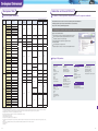
1
Renesas Microcomputer
32-bit Microcontrollers
V850
See your creations come to life
through the unsurpassed
performance of V850 microcontrollers.
www.renesas.com
2011.09
Roadmap/Features
V850 Product Lineup • • • • • • • • 4
Renesas Electronics 78K and V850
Microcontroller Roadmap • • • • • • • • 5
Application Examples • • • • • •
5 Keys of V850 • • • • • • • • • • • •
Low-End Lineup • • • • • • • • • • • • • • 8
High-End Lineup • • • • • • • • • • • • 10
ASSP Lineup (Inverter Control, etc.) • • • 12
ASSP Lineup (Dashboard Control, Body Control) • • 14
ASSP Lineup (CAN) • • • • • • • • • • • 16
ASSP Lineup (Car Audio/Vehicle Navigation Control) • 18
Memory Lineup • • • • • • • • • • • • • 20
Package Lineup • • • • • • • • • • • • • 22
CPU Roadmap • • • • • • • • • • • • • • 24
CPU Comparison • • • • • • • • • • • • 24
PFESiP Roadmap • • • • • • • • • • • 25
V850 Architecture • • • • • • • • • • • • 26
V850E1, V850ES Architecture • • • 30
V850E2, V850E2M Architecture • • 31
•
•
5
6
Product Lineup
The V850 high-performance microcontrollers answer many different application
system needs. They realize extremely low power consumption and low noise while
offering high performance and a wide array of functions.
The broad V850 product lineup provides the best solution for your next-generation
system.
Broad
product
lineup
High
performance
Performance from 20 to over
500 MIPS using a
single instruction set
CPU
Variety of Peripheral Features
Low-end/high-end/
ASSP lineups
Memory Access • • • • • • • • • • • • • 32
Analog Circuits • • • • • • • • • • • • • 32
Timer/Counter • • • • • • • • • • • • • 34
Serial Interface • • • • • • • • • • • • • 35
Other • • • • • • • • • • • • • • • • • • • • • • 36
All Flash 32-bit USB MCU
(V850ES/Jx3-H, V850ES/Jx3-U) • • • • • 38
All Flash 32-bit Ethernet Controller MCU
(V850ES/Jx3-E) • • • • • • • • • • • • • • • • • 39
All Flash MCUs (V850E2/MN4) with
32-bit high-performance CPU cores • • 40
V850 Benchmark •
41
Low Power Consumption • • • • • 41
Solutions for V850 • • • • • • • • • 42
Rotating • • • • • • • • • • • • • • • • • • 42
Speaking • • • • • • • • • • • • • • • • • • 42
Showing • • • • • • • • • • • • • • • • • • • 43
Connecting • • • • • • • • • • • • • • • 43
Features • • • • • • • • • • • • • • • • • • • • 44
Rewrite Modes • • • • • • • • • • • • • 44
Flash Specification List • • • • • • • 45
Performance
• • • • • • • • • •
Solution
Flash
Additional
functions
PFESiP® lineup
Rich solution
lineup
Smooth transition to
PFESiP
Development
environment
Rich development
environment
Product Specification List
Low-End Lineup (5 V Operation) • • 46
Low-End Lineup (3 V Operation) • • 47
High-End Lineup • • • • • • • • • • • • 56
ASSP Lineup (Inverter Control, etc.) • • 58
Development Environment
Development Environment
Lineup • • • • • • • • • • • • • • • • • • • • • 85
Integrated Development
Environment • • • • • • • • • • • • • • • • 86
Software Products • • • • • • • • • • • 87
Emulator • • • • • • • • • • • • • • • • • • • 88
Information Availability
V850 Website • • • • • • • • • • • • • • • 96
2
ASSP Lineup (Dashboard Control, Body Control) • • 63
ASSP Lineup (CAN) • • • • • • • • • 73
ASSP Lineup (Car Audio/Vehicle Navigation Control) • 80
Flash Memory Programmers • • 90
Mass production support
environment for your needs. • • • 93
Development Tools • • • • • • • • • • 94
Information on Renesas Partners • • 95
04
08
24
32
41
42
44
46
84
96
3
Roadmap/Features
V850 Product Lineup
V850E2 CPU
200 MHz @ 432 MIPS
V850E1 CPU
High performance: On-chip MEMC/DMAC
ASSP
ASSP lineup
lineup
• Frequency: 33 to 200 MHz
Inverter control
• Parallel pipeline processing
(V850E2, V850E2M)
DVC control
• Memory size: ROM: ROMless to 2048 KB
RAM: 4 to 200 KB
Car infotainment control
• Package: 100 to 304 pins (QFP & FBGA)
Network support
Dashboard control
150 MHz @ 323 MIPS
• Frequency: 13 to 160 MHz
• Memory size: ROM: ROMless to
2048 KB
RAM: 4 to 192 KB
• Package: 64 to 256 pins
(QFP & FBGA)
V850ES CPU
50 MHz @ 103 MIPS
Low-end
Low-end lineup
lineup
High cost-performance
• Frequency: 16 to 50 MHz
V850 CPU
• Memory size: ROM: ROMless to 1024 KB
RAM: 4 to 124 KB
• Package: 40 to 144 pins (QFN & QFP &
FBGA)
20 MHz @ 23 MIPS
Standard lineup
4
Performance
200 MHz @ 512 MIPS
High-end
High-end lineup
lineup
High-end lineup
ASSP lineup
32-bit RISC
Low-end lineup
78K0R
Upward compatible instruction sets
V850E2M CPU
Renesas Electronics 78K and V850 Microcontroller Roadmap
An expanding lineup of continuously evolving V850
microcontrollers
78K0S
8/16-bit CISC
17K
D6X
78K0
trol
con
m
te
ing
ess
Sys
roc
p
a
Dat
4 to 16-bit applications
32-bit applications
Price
Price
Application Examples
The V850 microcontrollers are suitable for many application
fields and raise the commercial value of your system.
Automotive
Engines, car infotainment, dashboards,
power steering, ABS
Audio
Portable audio, component stereo systems,
home theater
Portable devices
PDAs, IC recorders
Cameras
DVC, DSC, SLR cameras
Computer peripherals
LBP, PPC, MFP, inkjet printers, scanners,
fax machines
Home appliances
Air conditioners, refrigerators, washing machines,
microwave ovens
Industrial equipment
Industrial motors, control equipment,
vending machines, power meters
Video and
recording equipment
Blu-ray players, Blu-ray recorders,
industrial cameras
Other
Electronic instruments, electric bidets, toys,
learning devices, remote controllers, etc.
Field-specific lineup
5
Roadmap/Features
High performance
5 reasons why you should choose a V850 microcontroller
Performance of 20 to over 500 MIPS using a single instruction set
High performance
PFESiP® Roadmap
System LSI
Smooth transition to PFESiPs
System
≥ 200 MHz
Data processing
Processors
to 8-bit or 16-bit microcontrollers, V850 microcontrollers
• Compared
offer a MIPS performance that is at least 10 times higher for the
•
Product lineup
Compatible with up to
middle-range class
Not compatible
Other
manufacturers' 16-bit
microcontrollers
33 MHz
V850ES
V850
Compatible with up to high-end class
models with MIPS performance of
10 times higher
Compatible at the
object level
System control
High-end lineup
V850E/Mxx
V850E2/Xxx
High performance
V850E2 CPU
On-chip dedicated
hardware
V850E1 CPU
V850ES CPU
General-purpose microcontrollers for the
• Low-end lineup: 16to 32-bit market designed for high
ASSP lineup
Industrial
Low-end lineup (3 V)
Communication
cost-performance
Home
appliances
High cost-performance
Low-end lineup (5 V)
DMAC
Field-specific product lineup, that includes
on-chip dedicated hardware
IP cores
MPU, DSP, DRAM,
SRAM, AV, communication,
BUS, high-speed I/O
750
500
300
100
50
V850E2M
Next-generation
process
V850E2/xxx
PFESiP EP-3*
V850E2
90 nm
process
0.13 µm
process
V850E2/ME3
V850E1
0.15 µm
process
PFESiP EP-1*
PFESiP EP-2*
V850E/ME2
0.25 µm
process
V850
Consumer
electronics
V850ES/Hxx
Logic DRAM
1000
150
V850ES/Jxx
V850ES/Sxx
for high performance and
• High-end lineup:Designed
include an on-chip memory controller and
• ASSP lineup:
Office
equipment
V850E/xxx
V850ES/xxx
V850/xxx
Low noise,
low power consumption
V850 CPU
Automotive
IP
next-generation CPU
Product lineup
Low-end/High-end/ASSP lineups
Analog
Memory Flash
<1> Leading-edge process technology
<2> High-performance CPU cores
<3> Rich lineup of IP cores
<4> Top-down design environment
<5> Flexible application design
20 MHz
V850ES
V850
Chip design environment
Synthesis/verification
Software development environment
Hardware/software coordinated design
CPU DSP
microcontrollers are also being actively used as ASIC CPU
• V850
cores, helping you transition smoothly to PFESiP development.
following elements essential for PFESiPs are provided
• The
when you need them:
V850E1
Performance (MIPS)
•
same frequency, and 2 to 3 times higher at the actual application
level (based on Renesas Electronics evaluation).
V850 microcontrollers can operate at frequencies 1/2 to
1/3 those of 8-bit or 16-bit microcontrollers, lowering
the system power consumption.
The V850 CPU, V850ES CPU, V850E1 CPU, V850E2 CPU, and
V850E2M CPU are compatible at the object level.
Micro-fabrication technology
Multi-layer wiring technology
Mixed-process technology
High-pin-count packages
150 MHz
Other
manufacturers' 32-bit
microcontrollers
Design environment
Processes
V850E2M
V850E2
Not compatible
PC I/F
5 Keys of V850
Under planning
V850E/MA3
Under development
0.35 µm
process
In mass production
Generation
* PFESiP EP-1, PFESiP EP-2, and PFESiP EP-3 are custom microcontrollers that integrate a V850 microcontroller and logic LSI.
Additional functions
Additional functions
Rich solution lineup
Gaming machines
Portable devices
H.264
Toys
•
JPEG
Speech
recognition*
IrDA*
Networks
JavaTM *
* Middleware from a partner company is used.
6
CubeSuite automatically generates source code (a device
driver program) to control the microcontroller peripherals
(such as the timers, UART, and A/D converter).
Speech
synthesis*
Middleware
Browsers*
Code generated easily
Top screen
Human interfaces
File systems
AV equipment
Development environment
Car
infotainment
ADPCM
Image processing
by using middleware
By using V850 and middleware, you no longer need a
lot of peripheral ICs which reduces your development
time and system costs
Rich development environment lineup
Electronic
dictionaries
DSC
microcontrollers add value to your system
• V850
because you can add functions to an existing system
Development environment
TCP/IP
Home
appliances
Telephones
Electronics has released the CubeSuite+ integrated development platform, an easy-to-use
• Renesas
and convenient development environment. CubeSuite+ can be used to compile and debug programs,
manage pin layouts, generate code for microcontroller peripherals, and execute high-speed building.
CubeSuite+ in combination with an on-chip debugging emulator with a flash programming
• Use
function (such as the E1) to create an environment for fast system development.
7
Product Lineup
Low-End Lineup
V850ES/JC3-H, JE3-H, JG3-H, JH3-H, JG3-U, JH3-U
V850ES/HE3 V850ES/HF3 V850ES/HG3 V850ES/HJ3
32 MHz, 64-pin
32 MHz, 80-pin
32 MHz, 144-pin
32 MHz, 100-pin
5 V opration
All Flash lineup
All Flash products
ROMless product with large-capacity RAM
98 MIPS @ 48 MHz, 2.85 to 3.6 V operation
(A/D converter, USB controller: 3.0 to 3.6 V)
34 MHz, 3.0 to 3.6 V operation
ROM/RAM: 16 KB/8 KB to 512 KB/56 KB*
V850ES/JE3-E V850ES/JF3-E V850ES/JG3-E V850ES/JH3-E V850ES/JJ3-E
50 MHz, 64-pin
50 MHz, 80-pin
50 MHz, 100/121-pin
USB controller: USB 2.0 function (full-speed) × 1 ch,
USB 2.0 host (full-speed) × 1 ch (JG3-U, JH3-U only)
50 MHz, 144-pin
50 MHz, 128-pin
40-pin WQFN (JC3-H), 48-pin LQFP/WQFN (JC3-H), 64-pin
LQFP/WQFN (JE3-H), 64-pin FBGA (µPD70F3824), 100-pin LQFP
(JG3-H, JG3-U), 128-pin LQFP (JH3-H, JH3-U)
V850ES/JG3-U V850ES/JH3-U
48 MHz, 100-pin
48 MHz, 128-pin
* Includes 8 KB of data-only RAM.
V850ES/JG3-H V850ES/JH3-H
V850ES/JC3-H V850ES/JE3-H
48 MHz, 40/48-pin
3 V opration
All Flash lineup
48 MHz, 64-pin
48 MHz, 100-pin
48 MHz, 128-pin
V850ES/JJ3
V850ES/JG3
32 MHz, 144-pin
32 MHz, 100-pin
V850ES/ST2
V850ES/JG3, JJ3
ROM/RAM: ROMless/48 KB
120-pin TQFP/144-pin LQFP
V850ES/SG2-H, SJ2-H
66 MIPS @ 32 MHz, 3.0 to 3.6 V operation
ROM/RAM: 512 KB/40 KB, 640 KB/48 KB
On-chip multi-channel serial interface, clock monitor, CRC, DMAC,
and on-chip debugger
All Flash products
5 V withstand voltage ports incorporated, and 5 V output is possible
by setting N-ch open-drain output
69 MIPS @ 32 MHz, 2.85 to 3.6 V operation (A/D converter: 3.0 to 3.6 V)
100-pin LQFP (SG2-H), 144-pin LQFP (SJ2-H)
ROM/RAM: 384 KB/32 KB, 512 KB/40 KB, 768 KB/60 KB, 1024 KB/60 KB
V850ES/JC3-L V850ES/JE3-L V850ES/JF3-L V850ES/JG3-L
20 MHz, 40/48-pin
20 MHz, 64-pin
20 MHz, 80-pin
On-chip multi-channel serial interface, LVI, clock monitor, DMAC,
and on-chip debugger
20 MHz, 100/121-pin
V850ES/ST2
34 MHz, 120/144-pin
V850ES/SG2-H
V850ES/SJ2-H
V850ES/SG2
V850ES/SJ2
32 MHz, 100-pin
Under
development
20 MHz, 100-pin
Some models in
mass production
20 MHz, 100-pin
In mass
production
ROMless
Internal RAM: 48 KB
All Flash products
Sxx lineup
V850ES/SG1
40/48-pin
64-pin
80-pin
100-pin
100-pin LQFP (JG3), 144-pin LQFP (JJ3)
V850ES/JC3-L, JE3-L, JF3-L, JG3-L
32 MHz, 144-pin
20 MHz, 144-pin
5 V withstand voltage ports incorporated, and 5 V output is possible
by setting N-ch open-drain output
43 MIPS @ 20 MHz, 2.0 to 3.6 V operation (JG3-L*),
2.2 to 3.6 V operation (JC3-L, JE3-L, JF3-L)
ROM/RAM: 16 KB/8 KB, 1024 KB/80 KB
128-pin
144-pin and higher
Remark See Product Specification List (pp. 46 to 55) for details about the product specifications.
V850ES/HE3, HF3, HG3, HJ3
8
43 MIPS @ 20 MHz, 2.85 to 3.6 V operation (A/D converter: 3.0 to 3.6 V)
ROM/RAM: 256 KB/24 KB, 384 KB/32 KB, 512 KB/40 KB, 640 KB/48 KB
On-chip multi-channel serial interface, LVI, clock monitor, CRC,
DMAC, and on-chip debugger
5 V withstand voltage ports incorporated, and 5 V output is possible
by setting N-ch open-drain output
100-pin LQFP (SG2), 100-pin QFP (SG2 (ROM: 256 KB/384 KB
versions only)), 144-pin LQFP (SJ2)
V850ES/SG1
Low power operation 36 mW (3.0 V, 20 MHz)
Part of V850ES/SG2 lineup
Function and pin compatibility with V850ES/Jx3 and can use
V850ES/Jx3 development environment
43 MIPS @ 20 MHz, 2.85 to 3.6 V operation (A/D converter: 3.0 to 3.6 V)
5 V withstand voltage ports incorporated, and 5 V output is possible
by setting N-ch open-drain output
40-pin WQFN (JC3-L), 48-pin LQFP/WQFN (JC3-L), 64-pin LQFP/FBGA/WQFN
(JE3-L), 80-pin LQFP (JF3-L), 100-pin LQFP/121-pin FBGA (JG3-L)
Features
V850ES/SG2, SJ2
* 2.2 V to 3.6 V operation for µPD70F3737 and µPD70F3738
ROM/RAM: 256 KB/12 KB
On-chip clock monitor
5 V withstand voltage ports incorporated, and 5 V output is possible
by setting N-ch open-drain output
100-pin LQFP/100-pin QFP
V850ES/JE3-E, JF3-E, JG3-E, JH3-E, JJ3-E
All Flash products
All Flash products
69 MIPS @ 32 MHz, 66 MIPS @ 32 MHz (µPD70F3757 only),
3.7 to 5.5 V operation (A/D converter: 4.0 to 5.5 V)
103 MIPS @ 50 MHz, 2.85 to 3.6 V operation
(A/D converter, USB controller: 3.0 to 3.6 V)
ROM/RAM: 128 KB/8 KB to 512 KB/32 KB
ROM/RAM: 64 KB/32 KB* to 512 KB/124 KB**
On-chip multi-channel A/D converter, POC, LVI, DMAC,
on-chip debugger, 3-phase inverter control, and SSCG*
USB controller: USB 2.0 function (full-speed) × 1 ch,
Ethernet controller × 1 ch
64-pin LQFP (HE3), 80-pin LQFP (HF3), 100-pin LQFP (HG3),
144-pin LQFP (HJ3)
64-pin WQFN (JE3-E), 80-pin LQFP (JF3-E), 100-pin LQFP/121-pin
FBGA (JG3-E), 128-pin LQFP (JH3-E), 144-pin LQFP (JJ3-E)
* Spread spectrum frequency synthesizer clock generator
* Includes 16 KB of data-only RAM.
** Includes 64 KB of data-only RAM.
9
Product Lineup
High-End Lineup
Application examples
V850E2/MN4
200 MHz, 304-pin
Dual-core CPU
FPU
Large-capacity flash ROM
MFP (Multifunction printer)
CCD
V850E2/ML4
200 MHz, 216-pin
Single-core CPU
FPU
Large-capacity flash ROM
A/D
Multi Function Printer
V850E/ME2
Instruction
RAM
128 KB
V850E2/ME3
RPU
Data RAM
16 KB
PORT
JPEG
MH/MR/MMR
ROM, Flash
Superscalar,
on-chip instruction
/data cache, internal
large-capacity RAM
Motor
DMA
SDRAM
For storing image data
Document
Engine
controller
INTC
Memory
SRAM
200 MHz, 176-pin
ASIC
V850E/ME2
Image processing
Shooting
correction/
binarization
S/H
CPU
Browser
function
Communication
ASIC
system
Interface
control circuit
Modem
NCU
RTC
Image
processing
SIO
Printer
engine
Control panel
USB
PC
LAN
IEEE1394
Telephone network
Printing paper
Thermal printer
SRAM/
SDRAM
V850E/MA3
CPU
Address/data/control
Internal RAM
(32 KB)
ASIC
64-pin
In mass
production
80-pin
100-pin
144-pin
176-pin and higher
Port
Data clock
Data latch
UART
Stepping
motor
USB interface
controller
Distributed control
RS-232C
driver/receiver
Driver
Sensor
IEEE1284 interface
controller
TMP
Applied STB
SIO
TxD/RxD
TMQ
4-phase PWM
V850E/MA3
Thermistor
80 MHz, 144/161-pin
Supporting high-speed
internal ROM operation
and inverter control
ADC
IEEE1284 I/F
DMARQ/DMAAK/TC
DMAC
Thermal Printer
V850E/MA3
CG-ROM
MEMC
USB I/F
Internal ROM
(512 KB)
serial interface
V850E/ME2
150 MHz *, 176-pin
On-chip
instruction cache,
internal large-capacity
RAM
Thermal head
* Products that can operate at 66, 100, 133, and 150 MHz are available.
Remark See Product Specification List (pp. 56 and 57) for details about the product specifications.
Features
V850E2/MN4
V850E/ME2, V850E2/ME3
Ultra-high-speed dual-core CPU
Real-time control with internal large-capacity RAM
512 MIPS @ 200 MHz, internal 1.1 V to 1.3 V/
external 3.0 V to 3.6 V operation
323 MIPS @ 150 MHz (ME2), 432 MIPS @ 200 MHz (ME3),
internal 1.5 V/external 3.3 V operation
ROM/RAM: 2 MB/128 KB, 1 MB/128 KB, 1 MB/64 KB
ROM/RAM: ROMless/128 KB + 16 KB (ME2),
ROMless/168 KB + 32 KB (ME3)
USB (Host, Function), Ethernet controller, DMAC, and CAN
304-pin FBGA
On-chip SSCG*, USB (function), SDRAM interface, DMAC, 8 KB
instruction cache, 8 KB data cache (ME3 only), and on-chip debugger
176-pin LQFP (ME2), 176-pin QFP (ME3)
V850E2/ML4
Ultra-high-speed single-core CPU
* Spread spectrum frequency synthesizer clock generator
V850E/MA3
512 MIPS @ 200 MHz, internal 1.1 V to 1.3 V/
external 3.0 V to 3.6 V operation
Over 100 MIPS single-chip microcontroller
ROM/RAM: 768 KB/128 KB,* 1 MB/128 KB*
158 MIPS @ 80 MHz, internal 2.5 V/external 3.3 V operation
USB (Host, Function), Ethernet controller, DMAC, and CAN
ROM/RAM: 256 KB/8 KB, 256 KB/16 KB, 256 KB/32 KB,
512 KB/16 KB, 512 KB/32 KB
216-pin LQFP
* Includes 64 KB of expanded internal RAM.
On-chip SDRAM interface, motor control, DMAC,
D/A converter, and on-chip debugger
144-pin LQFP/161-pin FBGA
10
11
Product Lineup
ASSP Lineup (Inverter Control, etc.)
V850E/IA1, IA2
V850E/IG4-H
100 MHz,100-pin
V850E/IG4
100 MHz,100-pin
V850E/IH4-H
100 MHz,128-pin
V850E/IH4
100 MHz,128-pin
V850E/MA3
80 MHz,144/161-pin
V850E/IF3
64 MHz,80-pin
V850E/IA3
64 MHz,80-pin
V850E/IG3
64 MHz,100-pin
V850ES/HE3
32 MHz,64-pin
V850ES/HF3
32 MHz,80-pin
V850ES/HG3
32 MHz,100-pin
For inverter control
103 MIPS @ 50 MHz, internal 3.0 to 3.6 V/external 4.5 to 5.5 V
operation (IA1), 82 MIPS @ 40 MHz, 4.5 to 5.5 V operation
(when using on-chip regulator) (IA2)
63 MIPS @ 32 MHz, 3.5 to 5.5 V operation (A/D converter: 4.5 to 5.5 V)
ROM/RAM: 64 KB/4 KB, 128 KB/6 KB
ROM/RAM: 128 KB/6 KB (IA2), 256 KB/10 KB (IA1)
On-chip 3-phase inverter control PWM timer, two A/D converters,
POC, LVI, and clock monitor
On-chip 3-phase inverter control PWM timers (2 ch), 2-phase encoder
timers (2 ch) (IA2: 1 ch), two A/D converters, and DMAC
On-chip debugger (can be used with MINICUBE2)
64-pin LQFP
V850E/IG3
64 MHz,161-pin
V850ES/IE2
V850ES/HE3, HF3, HG3, HJ3
Inverter control lineup
V850E/IA4
V850E/IA2
For inverter control
100-pin LQFP/100-pin QFP (IA2), 144-pin LQFP (IA1)
64 MHz,100-pin
40 MHz,100-pin
V850ES/IK1
All Flash products, for inverter control
All Flash products
39 MIPS @ 20 MHz, 3.5 to 5.5 V operation (A/D converter: 4.5 to 5.5 V)
69 MIPS @ 32 MHz, 66 MIPS @ 32 MHz (µPD70F3757 only),
3.7 to 5.5 V operation (A/D converter: 4.0 to 5.5 V)
V850E/IA1
50 MHz,144-pin
ROM/RAM: 128 KB/8 KB to 512 KB/32 KB
V850ES/HJ3
On-chip 3-phase inverter control PWM timer, multi-channel A/D
converter, POC, LVI, DMAC, on-chip debugger, inverter control, and
SSCG*
32 MHz,144-pin
ROM/RAM: 64 KB/6 KB, 128 KB/6 KB
On-chip 3-phase inverter control PWM timer, two A/D converters,
POC, LVI, and clock monitor
On-chip debugger (can be used with MINICUBE2)
64-pin LQFP
64-pin LQFP (HE3), 80-pin LQFP (HF3), 100-pin LQFP (HG3),
144-pin LQFP (HJ3)
V850ES/IK1
32 MHz,64-pin
* Spread spectrum frequency synthesizer clock generator
V850ES/IE2
20 MHz,64-pin
In mass
production
64-pin
80-pin
100-pin
144-pin
176-pin and higher
Remark See Product Specification List (pp. 58 to 62) for details about the product specifications.
Application examples
■ 180˚ control for two motors
BLDC
Features
IPM
PFC
AC
180˚ control
TOT31
V850E/IF3, IG3
180˚ Control for Two Motors
6ch
TOB1T1-T3
TOB1B1-B3
TOB1OFF
All Flash products, for inverter control
197 MIPS @ 100 MHz, 1.5 V, 5.0 V, or 3.3 V operation
(IG4-H and IH4-H only)
ROM/RAM: 256 KB/24 KB, 384 KB/24 KB, 480 KB/24 KB
On-chip USB controller (USB 2.0 peripheral (full-speed)) × 1 ch (IG4-H
and IH4-H only), PWM timer for 3-phase inverter control × 2 ch (1 ch in
the IG4-H), 2-phase encoder timer × 2 ch, six operational amplifiers,
12 comparators, two 12-bit A/D converters, one 10-bit A/D converter,
DMAC, on-chip debugger (can be used with MINICUBE® and
MINICUBE2), POC, LVI, and clock monitor
All Flash products, for inverter control
131 MIPS @ 64 MHz, 3.5 to 5.5 V operation (A/D converter: 4.0 to 5.5 V)
ROM/RAM: 128 KB/8 KB, 256 KB/12 KB
On-chip 3-phase inverter control PWM timers (2 ch), 2-phase encoder
timers (2 ch) (IF3: 1 ch), four operational amplifiers, eight comparators,
two 12-bit A/D converters, one 10-bit A/D converter, DMAC, on-chip
debugger (IF3: can be used with MINICUBE2, IG3: can be used with
MINICUBE® and MINICUBE2), POC, LVI, clock monitor, and 5 V single
power supply
V850E/IG4,IH4
ON/OFF
ON/OFF
ON/OFF
ON/OFF
3 shunts
Sensor
Sub microcontroller
EEPROMTM
3ch
BLDC
180˚ control
TOT2 OFF
TOB0T1-T3
TOB0B1-B3
6ch
TOB0OFF
Op-amp
H level
L level
IPM
TOT2 1
TOT3OFF
V850E/IG4, IH4, IG4-H, IH4-H
PFC
AC
V850E/IG4 (100-pin)
V850E/IH4 (128-pin)
H level
Comparator
3ch
3ch
L level
3ch
12-bit A/D 12-bit A/D
3 shunts
8ch
10-bit A/D
CSI
3ch
2ch
UART
2ch
I2C
RESET-IC
SIO
etc.
6ch
Output of internal
information
PG-FP5
MINICUBE
MINICUBE2
80-pin LQFP (IF3), 100-pin LQFP (IG3), 161-pin FBGA (µPD70F3454)
100-pin LQFP (IG4, IG4-H), 128-pin LQFP (IH4, IH4-H)
V850E/IA3, IA4
V850E/MA3
12
For inverter control
For inverter control
126 MIPS @ 64 MHz, internal 2.5 V/external 5 V operation
158 MIPS @ 80 MHz, internal 2.5 V/external 3.3 V operation
ROM/RAM: 128 KB/6 KB, 256 KB/12 KB
ROM/RAM: 256 KB/8 KB, 256 KB/16 KB, 256 KB/32 KB,
512 KB/16 KB, 512 KB/32 KB
On-chip SDRAM interface, 3-phase inverter control PWM timer,
2-phase encoder timer, DMAC, D/A converter, and on-chip debugger
On-chip 3-phase inverter control PWM timers (2 ch) (IA3: 1 ch),
2-phase encoder timers (2 ch) (IA3: 1 ch), six operational amplifiers
(5 in the IA3), six comparators (5 in the IA3), three A/D converters,
DMAC, on-chip debugger (can be used with MINICUBE2),
and clock monitor
144-pin LQFP/161-pin FBGA
80-pin QFP (IA3), 100-pin LQFP/100-pin QFP (IA4)
13
Product Lineup
ASSP Lineup (Dashboard Control, Body Control)
V850E2/FE4-M, FF4-M
V850E/DG3
16 MHz, 100-pin
V850E/DJ3
V850E/DL3
64 MHz/32 MHz, 144-pin
64 MHz, 208-pin
Dashboard control
All Flash products, for automotive electronics
(body control applications)
All Flash products, for automotive electronics
(body control applications)
205 MIPS @ 80 MHz, 3.0 to 5.5 V operation
98 MIPS @ 48 MHz, 69 MIPS @ 32 MHz,
3.3 to 5.5 V operation (A/D converter: 4.0 to 5.5 V)
ROM/RAM: 256 KB/32 KB to 512 KB/48 KB
On-chip CAN (1 ch) and LIN-compatible UART (3 ch max.)
V850E2/FL4-H
On-chip multi-channel A/D converter, motor control, POC, LVI, clock
monitor, DMAC, on-chip debugger, and random number generator
160 MHz, 208/256-pin
V850E2/FE4-M V850E2/FF4-M
80 MHz, 64-pin
80 MHz, 80-pin
V850E2/FG4 V850E2/FJ4
48 MHz, 64-pin
V850E2/FK4
80 MHz, 144-pin
80 MHz, 176-pin
V850E2/FF4-L V850E2/FG4-L V850E2/FJ4-L
V850E2/FK4-L
48 MHz, 80-pin
64 MHz/48 MHz, 100-pin 64 MHz/48 MHz, 144-pin
V850E2/FK4-G
V850E2/FL4
80 MHz, 208/256-pin
All Flash products, for automotive electronics
(body control applications)
3.0 to 5.5 V operation
64 MHz, 176-pin
ROM/RAM: 1024 KB/128 KB
Body control
V850ES/FE3
32 MHz, 64-pin
V850ES/FF3
32 MHz, 80-pin
V850ES/FG3 V850ES/FJ3 V850ES/FK3
48 MHz/32 MHz, 100-pin 48 MHz/32 MHz, 144-pin
48 MHz, 176-pin
V850ES/FE3-L V850ES/FF3-L V850ES/FG3-L
20 MHz, 64-pin
20 MHz, 80-pin
20 MHz, 100-pin
V850ES/FE2
V850ES/FF2
V850ES/FG2
ROM/RAM: 128 KB/8 KB to 1024 KB/60 KB
On-chip CAN (5 ch max.) and LIN-compatible UART (8 ch max.)
On-chip multi-channel A/D converter, motor control, POC, LVI,
clock monitor, DMAC, on-chip debugger, and SSCG*
64-pin LQFP (FE3), 80-pin LQFP (FF3), 100-pin LQFP (FG3),
144-pin LQFP (FJ3), 176-pin LQFP (FK3)
80 MHz, 176-pin
80 MHz, 100-pin
V850E2/FE4-L
64-pin LQFP (FE4-M), 80-pin LQFP (FF4-M)
V850E2/FK4-G
V850ES/FE3, FF3, FG3, FJ3, FK3
On-chip CAN (6 ch) and LIN-compatible UART (5 ch)
On-chip multi-channel A/D converter, POC, LVI, clock monitor,
DMAC, on-chip debugger, and random number generator
* Spread spectrum frequency synthesizer clock generator
V850ES/FE3-L, FF3-L, FG3-L
All Flash products, for automotive electronics
(body control applications)
43 MIPS @ 20 MHz, 3.3 to 5.5 V operation (A/D converter: 4.0 to 5.5 V)
ROM/RAM: 64 KB/6 KB to 256 KB/16 KB
FlexRay controller: 2 ch × 1 unit
On-chip CAN (1 ch) and LIN-compatible UART (3 ch max.)
176-pin LQFP
On-chip multi-channel A/D converter, POC, LVI, clock monitor,
and on-chip debugger
64-pin LQFP (FE3-L), 80-pin LQFP (FF3-L), 100-pin LQFP (FG3-L)
20 MHz, 64-pin
20 MHz, 80-pin
20 MHz, 100-pin
V850ES/FJ2
V850E2/FG4, FJ4, FK4, FL4
20 MHz, 144-pin
All Flash products, for automotive electronics
(body control applications)
V850E/IA1
Under
development
50 MHz, 144-pin
In mass
production
64-pin
80-pin
100-pin
144-pin
176-pin and higher
Remark See Product Specification List (pp. 63 to 72) for details about the product specifications.
Features
V850E/DG3, DJ3, DL3
All Flash products, for automotive electronics
(body control applications)
126 MIPS @ 64 MHz (DJ3, DL3), 69 MIPS @ 32 MHz (DJ3),
34 MIPS @16 MHz (DG3),
3.2 to 5.5 V operation (A/D converter: 3.5 to 5.5 V)
324 MIPS @ 160 MHz, 3.0 to 5.5 V operation
On-chip CAN (6 ch) and LIN-compatible UART (12 ch max.)
On-chip multi-channel A/D converter, motor control, POC, LVI, clock
monitor, DMAC, and on-chip debugger
On-chip meter driver, voltage comparator (DJ3, DL3 only), sound
generator, POC, clock monitor, DMAC (DJ3, DL3 only), and SSCG*
Random number generator
* Spread spectrum frequency synthesizer clock generator
14
ROM/RAM: 2 MB/144 KB
On-chip CAN (2 ch max.) and LIN-compatible UART (2 ch)
100-pin LQFP (DG3), 144-pin LQFP (DJ3), 208-pin LQFP (DL3)
162 MIPS @ 80 MHz, 3.0 to 5.5 V operation
For automotive electronics (body control applications)
ROM/RAM: 512 KB/32 KB to 2 MB/144 KB
43 MIPS @ 20 MHz, 3.5 to 5.5 V operation (A/D converter: 4.0 to 5.5 V)
On-chip CAN (5 ch max.) and LIN-compatible UART (12 ch max.)
ROM/RAM: 64 KB/4 KB to 512 KB/20 KB
On-chip multi-channel A/D converter, motor control, POC, LVI, clock
monitor, DMAC, on-chip debugger, and random number generator
On-chip CAN (4 ch max.) and LIN-compatible UART (4 ch max.)
FlexRay controller: 2 ch × 1 unit (µPD70F4000 to µPD70F4012 only)
On-chip multi-channel A/D converter, POC, LVI, DMAC,
and on-chip debugger
100-pin LQFP (FG4), 144-pin LQFP (FJ4), 176-pin LQFP (FK4),
208-pin QFP (FL4), 256-pin BGA (FL4)
64-pin LQFP (FE2), 80-pin TQFP (FF2), 100-pin LQFP (FG2),
144-pin LQFP (FJ2)
V850E2/FL4-H
All Flash products, for automotive electronics
(dashboard control applications)
ROM/RAM: 128 KB/6 KB to 2048 KB/84 KB
V850ES/FE2, FF2, FG2, FJ2
FlexRay controller: 2 ch × 1 unit
208-pin QFP, 256-pin BGA
V850E2/FE4-L, FF4-L, FG4-L, FJ4-L, FK4-L
V850E/IA1
All Flash products, for automotive electronics
(body control applications)
For automotive electronics (body control applications)
109 MIPS @ 64 MHz, 82 MIPS @ 48 MHz, 3.0 to 5.5 V operation
103 MIPS @ 50 MHz, internal 3.0 to 3.6 V/
external 4.5 to 5.5 V operation
ROM/RAM: 256 KB/24 KB to 1.5 MB/96 KB
On-chip CAN (2 ch max.) and LIN-compatible UART (5 ch max.)
On-chip multi-channel A/D converter, POC, LVI, clock monitor,
and on-chip debugger
64-pin LQFP (FE4-L), 80-pin LQFP (FF4-L), 100-pin LQFP (FG4-L),
144-pin LQFP (FJ4-L), 176-pin LQFP (FK4-L)
ROM/RAM: 256 KB/10 KB
On-chip CAN (1 ch)
On-chip 3-phase inverter control PWM timer, 2-phase encoder timer,
two A/D converters, and DMAC
144-pin LQFP
15
Product Lineup
ASSP Lineup (CAN)
V850E2/SG4-H,SJ4-H,SK4-H
V850E2/MN4
200 MHz, 304-pin
V850E2/ML4
200 MHz, 216-pin
V850E2/SG4-H V850E2/SJ4-H V850E2/SK4-H
160 MHz, 100-pin
160 MHz, 144-pin
160 MHz, 176-pin
V850E2M dual-core CPU
FPU
Large-capacity flash ROM
V850E2M highperformance CPU
FPU
Large-capacity flash ROM
V850E2M highperformance CPU
Large-capacity flash ROM
V850ES/JE3-E V850ES/JF3-E V850ES/JG3-E V850ES/JH3-E V850ES/JJ3-E
All Flash products, for car infotainment systems
All Flash products, for car infotainment systems
325 MIPS @ 160 MHz, internal 1.1 to 1.3 V/
external 3.0 to 3.6 V operation
69 MIPS @ 32 MHz, 2.85 to 3.6 V operation (A/D converter: 3.0 to 3.6 V)
ROM/RAM: 1 MB/96 KB to 2 MB/192 KB
On-chip CAN (2 ch max.), IEBus (1 ch), LVI, DMAC, on-chip debugger,
and Ethernet controller (V850E2/SK4-H only)
100-pin LQFP (SG4-H), 144-pin LQFP (SJ4-H), 176-pin LQFP (SK4-H)
48 MHz, 48-pin
48 MHz, 100-pin
V850ES/SG2, SJ2, SG2-H, SJ2-H
103 MIPS @ 50 MHz, 2.85 to 3.6 V operation (A/D converter, USB
controller: 3.0 to 3.6 V)
For car infotainment systems
48 MHz, 128-pin
Ethernet controller × 1 ch
V850E/SJ3-H V850E/SK3-H
64-pin LQFP/WQFN (JE3-E), 64-pin FBGA (µPD70F3824),
80-pin LQFP (JF3-E), 100-pin LQFP/121-pin FBGA (JG3-E),
128-pin LQFP (JH3-E), 144-pin LQFP (JJ3-E)
48 MHz, 144-pin
48 MHz, 176-pin
3 V operation lineup
V850ES/SG3
32 MHz, 100-pin
V850ES/SJ3
32 MHz, 144-pin
V850ES/SG2
V850ES/SJ2
20 MHz, 100-pin
All flash products, for general-purpose applications
20 MHz, 144-pin
20 MHz, 100-pin
In mass
production
48-pin
64-pin
80-pin
100-pin
144-pin
176-pin and higher
Remark See Product Specification List (pp. 73 to 79) for details about the product specifications.
On-chip CAN (2 ch max.), LIN-compatible UART (4 ch max.),
multi-channel serial interface, LVI (SG2, SJ2 only), clock monitor,
CRC, DMAC, and on-chip debugger
5 V withstand-voltage ports incorporated, and 5 V output is possible
by setting N-ch open-drain output
V850E2/ML4
All flash products, for general-purpose applications
All flash products, for general-purpose applications
512 MIPS @ 200 MHz, internal 1.1 to 1.3 V/
external 3.0 to 3.6 V operation
512 MIPS @ 200 MHz, internal 1.1 V to 1.3 V/
external 3.0 V to 3.6 V operation
ROM/RAM: 2 MB/128 MB, 1 MB/128 KB, 1 MB/64 KB
ROM/RAM: 768 KB/128 KB*, 1 MB/128 KB*
On-chip CAN (2 ch)
On-chip CAN (1 ch)
USB (Host, Function), Ethernet controller, and DMAC
USB (Host, Function), Ethernet controller, and DMAC
Ultra-high-speed dual-core CPU
216-pin LQFP
304-pin FBGA
* Includes 64 KB of expanded internal RAM.
V850ES/SG1
98 MIPS @ 48 MHz, 2.85 to 3.6 V operation
(A/D converter, USB controller: 3.0 to 3.6 V)
For car infotainment systems
ROM/RAM: 256 KB/24 KB to 256 KB/40 KB*
43 MIPS @ 20 MHz, 2.85 to 3.6 V operation (A/D converter: 3.0 to 3.6 V)
On-chip CAN (1 ch) and LIN-compatible UART (4 ch or 5 ch max.)
ROM/RAM: 128 KB/8 KB
USB controller: USB 2.0 function (full-speed) × 1 ch
On-chip CAN (1 ch), clock monitor, and DMAC
48-pin LQFP/WQFN (JC3-H), 64-pin LQFP/FBGA/WQFN (JE3-H),
100-pin LQFP (JG3-H), 128-pin LQFP (JH3-H)
5 V withstand-voltage ports incorporated, and 5 V output is possible
by setting N-ch open-drain output
* Includes 8 KB of data-only RAM.
100-pin LQFP
Features
V850E2/MN4
ROM/RAM: 256 KB/24 KB (SG2, SJ2 only),
384 KB/32 KB (SG2, SJ2 only), 512 KB/40 KB,
640 KB/48 KB
V850ES/JC3-H, JE3-H, JG3-H, JH3-H
V850ES/SG1
Under
development
43 MIPS @ 20 MHz, 2.85 to 3.6 V operation
(A/D converter: 3.0 to 3.6 V) (SG2, SJ2)
66 MIPS @ 32 MHz, 3.0 to 3.6 V operation (SG2-H, SJ2-H)
100-pin LQFP (SG2, SG2-H), 144-pin LQFP (SJ2, SJ2-H)
V850ES/SG2-H V850ES/SJ2-H
Under
planning
* Includes 16 KB of data-only RAM.
** Includes 64 KB of data-only RAM.
32 MHz, 144-pin
32 MHz, 100-pin
5 V withstand-voltage ports incorporated, and 5 V output is possible
by setting N-ch open-drain output
All Flash products, for general-purpose applications
USB controller: USB 2.0 function (full-speed) × 1 ch
V850ES/JG3-H V850ES/JH3-H
48 MHz, 64-pin
On-chip CAN (2 ch max.), LIN-compatible UART (4 ch max.), IEBus
(1 ch), multi-channel serial interface, LVI, clock monitor, CRC, DMAC,
and on-chip debugger
V850ES/JE3-E, JF3-E, JG3-E, JH3-E, JJ3-E
CAN × 1 ch, UART supporting LIN x max 3 ch (JE3-E) to 8 ch (JJ3-E)
V850ES/JC3-H V850ES/JE3-H
ROM/RAM: 256 KB/24 KB to 1024 KB/60 KB
100-pin LQFP (SG3), 144-pin LQFP (SJ3)
ROM/RAM: 256 KB/64 KB* to 512 KB/124 KB**
50 MHz, 64-pin 50 MHz, 80-pin 50 MHz, 100/121-pin 50 MHz, 128-pin 50 MHz, 144-pin
V850ES/SG3, SJ3
V850E/SJ3-H, SK3-H
All flash products, for car infotainment systems
95 MIPS @ 48 MHz, 2.85 to 3.6 V operation (A/D converter: 3.0 to 3.6 V)
ROM/RAM: 512 KB/60 KB (SJ3-H only), 768 KB/76 KB* (SJ3-H only),
1024 KB/76 KB*, 1280 KB/92 KB**, 1536 KB/92 KB**
On-chip CAN (2 ch max.), UART (8 ch max. (including two UART
channels with FIFO buffers)), IEBus (1 ch), multi-channel serial
interface, LVI, clock monitor, CRC, DMAC, real-time counter,
SSCG***, and on-chip debugger
5 V withstand-voltage ports incorporated, and 5 V output is possible
by setting N-ch open-drain output
144-pin LQFP (SJ3-H), 176-pin LQFP (SK3-H)
* Includes 16 KB of expanded internal RAM.
** Includes 32 KB of expanded internal RAM.
*** Spread spectrum frequency synthesizer clock generator
16
17
Product Lineup
ASSP Lineup (Car Audio/Vehicle Navigation Control)
V850ES/SG1
V850ES/SG2, SJ2
Under
planning
V850E2/SG4-H
V850E2/SJ4-H
V850E2/SK4-H
160 MHz, 100-pin
160 MHz, 144-pin
160 MHz, 176-pin
V850E/SJ3-H
V850E/SK3-H
48 MHz, 144-pin
48 MHz, 176-pin
V850ES/SG3
V850ES/SJ3
32 MHz, 100-pin
32 MHz, 144-pin
V850ES/SG2-H
V850ES/SJ2-H
32 MHz, 100-pin
32 MHz, 144-pin
V850ES/SG2
V850ES/SJ2
20 MHz, 100-pin
20 MHz, 144-pin
For car infotainment systems
43 MIPS @ 20 MHz, 2.85 to 3.6 V operation (A/D converter: 3.0 to 3.6 V)
43 MIPS @ 20 MHz, 2.85 to 3.6 V operation (A/D converter: 3.0 to 3.6 V)
ROM/RAM: 256 KB/24 KB, 384 KB/32 KB, 512 KB/40 KB,
640 KB/48 KB
ROM/RAM: 256 KB/12 KB
On-chip IEBus (1 ch) and clock monitor
On-chip LIN-compatible UART (4 ch max.), IEBus (1 ch),
multi-channel serial interface, LVI, clock monitor, CRC, DMAC,
and on-chip debugger
5 V withstand-voltage ports incorporated, and 5 V output is possible
by setting N-ch open-drain output
100-pin LQFP, 100-pin QFP
5 V withstand-voltage ports incorporated, and 5 V output is possible
by setting N-ch open-drain output
3 V operation lineup
100-pin LQFP (SG2), 100-pin QFP (SG2 (ROM: 256 KB/384 KB
versions only)), 144-pin LQFP (SJ2)
Application examples
V850ES/SG1
Under
development
For car infotainment systems
■ Car audio
20 MHz, 100-pin
Antenna
In mass
production
64-pin
80-pin
100-pin
144-pin
Tuner unit
176-pin and higher
PLL
Microcontroller
(CD control)
CD unit
Remark See Product Specification List (pp. 80 to 83) for details about the product specifications.
V850ES/Sx3,
V850E/Sx3-H
Car Audio
Features
V850E2/SG4-H, SJ4-H, SK4-H
V850ES/SG3
V850ES/SG3, SJ3
All Flash products, for car infotainment systems
All Flash products, for car infotainment systems
325 MIPS @ 160 MHz, internal 1.1 to 1.3 V/external 3.0 to 3.6 V
69 MIPS @ 32 MHz, 2.85 to 3.6 V operation
(A/D converter: 3.0 to 3.6 V)
ROM/RAM: 1 MB/96 KB to 2 MB/192 KB
On-chip LIN-compatible UART (5 ch max.), IEBus (1 ch), LVI, DMAC,
on-chip debugger, and Ethernet controller (V850E2/SK4-H only)
100-pin LQFP (SG4-H), 144-pin LQFP (SJ4-H), 176-pin LQFP (SK4-H)
Driver
Speaker
MPX
RF
DAC
servo
ASSP for CD
µPD63763
DSP
MP3, WMA playback
MD unit
CD (MD)
changer unit
Power
amplifier
Audio DSP
(or electrical volume)
Power block
Microcontroller
(CD control)
V850ES/Sx3,
V850E/Sx3-H
CAN, IEBus
driver
Battery
(always on)
ACC
Regulator
Power detection IC
Microcontroller
(display/key control)
78K0R, V850ES/Sx3,
V850E/Sx3-H
KEY
Inter-automobile communication (CAN, IEBus...)
(on when engine is on)
Display unit
Driver
4-/8-gradation
LCD
Control system signal
Audio system signal
ROM/RAM: 256 KB/24 KB to 1024 KB/60 KB
On-chip LIN-compatible UART (4 ch max.), IEBus (1 ch),
multi-channel serial interface, LVI, clock monitor, CRC, DMAC,
and on-chip debugger
5 V withstand-voltage ports incorporated, and 5 V output is possible
by setting N-ch open-drain output
V850E/SJ3-H, SK3-H
100-pin LQFP (SG3), 144-pin LQFP (SJ3)
All flash products, for car infotainment systems
95 MIPS @ 48 MHz, 2.85 to 3.6 V operation (A/D converter: 3.0 to 3.6 V)
ROM/RAM: 512 KB/60 KB (SJ3-H only), 768 KB/76 KB* (SJ3-H only),
1024 KB/76 KB*, 1280 KB/92 KB**, 1536 KB/92 KB**
On-chip UART (8 ch max. (including two UART channels with FIFO)),
IEBus (1 ch), multi-channel serial interface, LVI, clock monitor, CRC,
DMAC, real-time counter, SSCG***, and on-chip debugger
5 V withstand-voltage ports incorporated, and 5 V output is possible
by setting N-ch open-drain output
144-pin LQFP (SJ3-H), 176-pin LQFP (SK3-H)
* Includes 16 KB of expanded internal RAM.
** Includes 32 KB of expanded internal RAM.
*** Spread spectrum frequency synthesizer clock generator
18
V850ES/SG2-H, SJ2-H
For car infotainment systems
66 MIPS @ 32 MHz, 3.0 to 3.6 V operation
ROM/RAM: 512 KB/40 KB, 640 KB/48 KB
On-chip LIN-compatible UART (4 ch max.), IEBus (1 ch),
multi-channel serial interface, clock monitor, CRC, DMAC,
and on-chip debugger
5 V withstand-voltage ports incorporated, and 5 V output is possible
by setting N-ch open-drain output
100-pin LQFP (SG2-H), 144-pin LQFP (SJ2-H)
19
Product Lineup
Memory Lineup
Flash memory version
Mask ROM version
Mask ROM/flash memory version
DJ3-64*1
2048 K
MN4
FK4
SK4-H
FL4
FL4-H
1536 K
SJ3-H*5
SK3-H*5
FJ4-L
FK4-L
1280 K
SJ3-H*5
SK3-H*5
DJ3-64*1
FJ3-48*1
1024 K
FJ3-48*1
768 K
SJ3
SG3
JG3
DL3
MN4
FG4-L
JJ3
FK3
FJ4-L
FK4-L
FG4-L
FK4-L
SJ3
JJ3
FG4
FJ4-L
FK3
SG3
JG3
FJ4
SJ3-H*6
SK3-H*6
SJ3-H*6
FG4
FJ4
FJ4
FL4
FL4-H
SG4-H
SJ4-H
SK4-H
MN4
ML4*7
SG4-H
SJ4-H
FK4
JG3-L
FK4-G
JG3-L
ML4*7
FK4
640 K
MA3
FJ2
DJ3-32*1
MA3
FE4-L
FF4-L
DJ3-64*1
512 K
FJ3-48*1
FG3-48*1
HJ3
JJ3
JG3
JG3-L
SJ2
SJ3
SG3
SJ2
FE4-M
FG4-L
FJ4-L
FK3
IG4
IG4-H
IH4
IH4-H
FG2
FJ3-48*1
DJ3-32*1
FG3-48*1
IG4
IH4
IG4-H
IH4-H
480 K
384 K
FE4-L
JJ3
FF4-L
FG4-L
JG3
FJ4-L
JG3-L
SJ3
SG2
SG3
SJ2-H
SG2-H
SG2
FF4-M
JG3-L
SJ2-H
SG2-H
SJ3
SG3
SJ2
SG2
FG4
FJ4
FE4-M
FF4-M
JG3-H*2
JH3-H*2
JG3-U*2
JH3-U*2
JG3-H*2
JH3-H*2
JG3-U*2
JH3-U*2
SJ3-H
JH3-E*3
JJ3-E*3
JH3-E*4
JJ3-E*4
JH3-E*3
JH3-E*4
FJ2
376 K
IA1
MA3
256 K
FJ2
SG1
MA3
JC3-L
SG3
JE3-H
MA3
JG3-H*2
JG3-E*2
FG2
IG3
FJ3-32*1
JE3-L
SG2
JC3-H
FE4-M
JH3-H*2
JF3-E*2
FF4-M
JG3-L
JE3-E*2
FF2
IF3
FG3-32*1
JG3-L
FE4-L
IG4
DJ3-32*1
IA4
FF3
JF3-L
FF4-L
IH4
DG3
IA3
FG3-L
192 K
FE3
HJ3
FG4-L
IG4-H
FG3-L
HG3
FJ4-L
IH4-H
FF3-L
FE3-L
HF3
JH3-E*3
FE3-L
FF3-L
128 K
FE2
SA2
JC3-L
FF2
FG3-32*1
IG3
FG2
FF3
IF3
DG3
FE3
FE3-L
IK1
HE3
FF3-L
IA4
JG3-L
FG3-L
IA3
JF3-L
SG1
IA2
JE3-L
FF2
JG3-E*3
JE3-H
JF3-E*3
JC3-H
JE3-E*3
IE2
FE3-L
96 K
64 K
FF3-L
IK1
IE2
JE3-L
JE3-H
FE2
FE3-L
JC3-L
JC3-H
JE3-E*3
JE3-L
JE3-H
JC3-L
JC3-H
16 K
JE3-H
JE3-L
JC3-H
JC3-L
ME2
ROM
less
ME3
Instruction RAM: 128 KB
4K
6K
RAM size (bytes)
20
JF3-E*3
FF3-L
32 K
ROM size
(bytes)
JG3-E*3
8K
10 K
12 K
16 K
ST2
Instruction RAM: 168 KB
20 K
24 K
28 K
32 K
40 K
48 K
56 K
60 K
64 K
76 K
80 to 84 K
92 to 96 K
112 K
124 to 128 K
144 K
192 K
*1. -32: 32 MHz product, -48: 48 MHz product, -64: 64 MHz product *2. Includes 8 KB of data-only RAM. *3. Includes 16 KB of data-only RAM. *4. Includes 64 KB of data-only RAM.
*5. Includes 32 KB of expanded internal RAM. *6. Includes 16 KB of expanded internal RAM. *7. Includes 64 KB of expanded internal RAM.
21
Product Lineup
Package Lineup
64
No. of pins
Type
Size
Pitch
Thickness
Mounted products
64 pins
FBGA (F1)
5 × 5 mm
0.5 mm
0.91 mm
JE3-L
64
No. of pins
Type
Size
Pitch
Thickness
Mounted products
64 pins
FBGA (F1)
6 × 6 mm
0.65 mm
1.11 mm
JE3-H
No. of pins
Type
Size
Pitch
Thickness
Mounted products
22
121 pins
FBGA (F1)
8 × 8 mm
0.65 mm
0.91 mm
JG3-L, JG3-E
40
48
64
No. of pins
Type
Size
Pitch
Thickness
Mounted products
40 pins
WQFN (K8)
6 × 6 mm
0.5 mm
0.75 mm
JC3-H, JC3-L
No. of pins
Type
Size
Pitch
Thickness
Mounted products
48 pins
WQFN (K8)
7 × 7 mm
0.5 mm
0.75 mm
JC3-H, JC3-L
No. of pins
Type
Size
Pitch
Thickness
Mounted products
64 pins
WQFN (K8)
9 × 9 mm
0.5 mm
0.75 mm
JE3-H, JE3-E, JE3-L
48
No. of pins
Type
Size
Pitch
Thickness
Mounted products
48 pins
LQFP (GA)
7 × 7 mm
0.5 mm
1.4 mm
JC3-H, JC3-L
No. of pins
Type
Size
Pitch
Thickness
Mounted products
64 pins
LQFP (GA)
7 × 7 mm
0.4 mm
1.4 mm
FE3-L
No. of pins
Type
Size
Pitch
Thickness
Mounted products
64 pins
LQFP (GB)
10 × 10 mm
0.5 mm
1.4 mm
HE3, JE3-E, JE3-H,
JE3-L, FE4-M, FE4-L,
FE2, FE3, FE3-L
No. of pins
Type
Size
Pitch
Thickness
Mounted products
161 pins
FBGA (F1)
10 × 10 mm
0.65 mm
1.13 mm
IG3
No. of pins
Type
Size
Pitch
Thickness
Mounted products
64 pins
LQFP (GC)
14 × 14 mm
0.8 mm
1.4 mm
IK1, IE2
No. of pins
Type
Size
Pitch
Thickness
Mounted products
161 pins
FBGA (F1)
13 × 13 mm
0.8 mm
1.13 mm
MA3
No. of pins
Type
Size
Pitch
Thickness
Mounted products
80 pins
TQFP (GK)
12 × 12 mm
0.5 mm
1.0 mm
FF2
256
No. of pins
Type
Size
Pitch
Thickness
Mounted products
256 pins
BGA (F1)
21 × 21 mm
1.0 mm
1.33 mm
FL4, FL4-H
304
No. of pins
Type
Size
Pitch
Thickness
Mounted products
304 pins
FBGA (F1)
19 × 19 mm
0.8 mm
1.11 mm
MN4
No. of pins
Type
Size
Pitch
Thickness
Mounted products
80 pins
LQFP (GK)
12 × 12 mm
0.5 mm
1.4 mm
FF3, HF3, JF3-L, JF3-E,
FF4-L, FF4-M, FF3-L
No. of pins
Type
Size
Pitch
Thickness
Mounted products
128 pins
LQFP (GF)
14 × 20 mm
0.5 mm
1.4 mm
JH3-E, JH3-H, JH3-U,
IH4, IH4-H
No. of pins
Type
Size
Pitch
Thickness
Mounted products
144 pins
LQFP (GJ)
20 × 20 mm
0.5 mm
1.4 mm
No. of pins
Type
Size
Pitch
Thickness
Mounted products
176 pins
LQFP (GM)
24 × 24 mm
0.5 mm
1.4 mm
ME2, FK3, FK4-L, FK4,
FK4-G, SK3-H, SK4-H
100 pins
LQFP (GF)
14 × 20 mm
0.65 mm
1.4 mm
IG3, IG4, JG3-L
No. of pins
Type
Size
Pitch
Thickness
Mounted products
176 pins
QFP (GM)
24 × 24 mm
0.5 mm
2.7 mm
ME3
No. of pins
Type
Size
Pitch
Thickness
Mounted products
100 pins
QFP (GF)
14 × 20 mm
0.65 mm
2.7 mm
SG1, SG2, IA2, IA4
No. of pins
Type
Size
Pitch
Thickness
Mounted products
208 pins
QFP (GD)
28 × 28 mm
0.5 mm
3.2 mm
DL3, FL4, FL4-H
No. of pins
Type
Size
Pitch
Thickness
Mounted products
120 pins
TQFP (GC)
14 × 14 mm
0.4 mm
1.0 mm
ST2
No. of pins
Type
Size
Pitch
Thickness
Mounted products
216 pins
LQFP (GM)
24 × 24 mm
0.4 mm
1.4 mm
ML4
No. of pins
Type
Size
Pitch
Thickness
Mounted products
80 pins
QFP (GC)
14 × 14 mm
0.65 mm
1.4 mm
IA3
No. of pins
Type
Size
Pitch
Thickness
Mounted products
80 pins
LQFP (GC)
14 × 14 mm
0.65 mm
1.4 mm
IF3, JF3-L
No. of pins
Type
Size
Pitch
Thickness
Mounted products
100 pins
LQFP (GC)
14 × 14 mm
0.5 mm
1.4 mm
No. of pins
Type
Size
Pitch
Thickness
Mounted products
JG3, JG3-L, JG3-E, JG3-H,
JG3-U, HG3, SG2, SG2-H,
SG3, SG4-H, FG2, FG3,
FG3-L, FG4-L, FG4, IA2, IA4,
IG3, IG4, IG4-H, DG3, SG1
216
JJ3, JJ3-E, HJ3, SJ2, SJ2-H,
SJ3, SJ3-H, SJ4-H, ST2,
FJ2, FJ3, FJ4-L, FJ4, MA3,
IA1, DJ3
23
CPU Roadmap
PFESiP Roadmap
Performance of
20 to over 500 MIPS
using a single instruction set
V850 N
V850E2M CPU
512 MIPS @ 200 MHz
V850E2 CPU
432 MIPS @ 200 MHz
323 MIPS @ 150 MHz
215 MIPS @ 100 MHz
EP-3 overview
EP Series applications
The EP-3, built around the V850E2M core, is the second in
the EP (Embedded Processor) series of general-function chips
incorporating a microcontroller. The EP-3 combines in a single
package a Renesas 32-bit microcontroller and ASIC chips
such as gate arrays or cell-based ICs. This platform makes it
easy to create customized microcontroller products.
The EP-3 delivers better CPU performance than the EP-1
and operates at a high speed of 266 MHz. It supports highspeed USB functions and adds new communication interface
functions such as Ethernet and CAN. The optimal bus,
memory, and DMAC configuration helps to eliminate internal
bus bottlenecks.
V850E2M
dual CPU
• Can use existing software resources
• Maintain a real-time performance
• Lower power consumption
V850E1 CPU
ext
V850E2 CPU
PFESiP (Platform for Embedded System in a Package) is a new ASIC solution providing Gate Array quickly, cost-effectively, and safely
with expanded functionality, by developing Gate Array and general-purpose function chips into SiPs, which are pre-verified and lined
up as masters.
Factory automation and industrial equipment
Servers, inverters, PLC equipment, measuring devices,
machine tools, vending machines, security cameras, etc.
Office equipment and consumer products
Thermal/dot matrix printers, video/photo printers,
card reader/writers, barcode readers, etc.
103 MIPS @ 50 MHz
EP-3 Features
98 MIPS @ 48 MHz
69 MIPS @ 32 MHz
38 MIPS @ 33 MHz
43 MIPS @ 20 MHz
23 MIPS @ 20 MHz
V850 CPU
V850ES CPU
CPU Comparison
CPU
Characteristics
Maximum operating frequency
Instructions
Maximum program memory space
Maximum data memory space
Higher performance
High code efficiency
Multiplier
Interrupt responsiveness
24
V850
V850ES
V850E1
V850E2
V850E2M
20/33 MHz
20/32/48/50 MHz
66 ⇒ 100 ⇒ 150 MHz
200 MHz
200 MHz
47
80
80
89
98
16 MB
16 MB
64 MB
512 MB (internal 128 MB)
4 GB
16 MB
16 MB
256 MB
4 GB
4 GB
5-stage pipeline
Harvard
architecture
2-byte instructions
CISC instructions
16 × 16 bits ⇒ 32 bit
operation
11 to 18 clocks
Addition of C language compatible instructions
(Switch instruction, Callt instruction,
data conversion instruction,
Prepare/Dispose instruction)
Simultaneous execution
of 2 instructions
V850E2M CPU SS
Optimized instruction execution
Enhanced ability to execute 2 instructions simultaneously
Can be used with a single-precision or double-precision high-speed
FPU
16 × 16 bits ⇒ 32-bit operation
16 × 16 bits ⇒ 32-bit operation
32 × 32 bits ⇒ 64-bit operation
32 × 32 bits ⇒ 64-bit operation
(32-bit multiply instruction support)
4 to 10 clocks
V850E2M
Bus Bridge
CPU
wMEM 128KB
FPU
32-bit relative branch instruction
3-operand instruction
Sum-of-products instruction Expanded displacement of LD
and ST instructions
Bit search instruction
−
New
300
EP-3
EP-1
200
V850E2 core
200 MHz operation
USB2.0 FS Host/Function
V850E2M core
266 MHz operation
USB2.0 HS Host/Function
Ether MAC
EP-2
(In study and planning phase)
V850E2M core
150 MHz operation
USB2.0 HS Host/Function
Low Power
100
EP-3 block diagram
• 7-stage pipeline
Improved pipeline
• Non-blocking load/store instructions
- Parallel instruction execution (instruction execution in internal ROM)
• Addition of branching/load pipe
• Shift to 3-operand manipulations in 1 slot
PFESiP [EP Series] Roadmap (V850 Core)
V850E2M CPU core, max. 266 MHz operation
Programmable logic (requires masking)
Logic capacity: 160,000 to 1 million gates (EA-9HD/CB-12)
Multi-layer system bus
Memory bus: Entirely discrete external bus and SiP internal bus
Internal instruction RAM: Max. 512 KB
Work RAM: 64 KB × 2
Internal DMA controller with descriptor function
Internal serial flash memory controller
USB 2.0 HS ports: Host 1 ch, Function 1 ch
Ethernet: Internal 10/100 EtherMAC
Power supply voltage: Internal 1.0 V, I/O 3.3 V (1.5 V with
CB-12 user logic)
Low-heat-resistance PBGA package
550-pin (25 × 30 mm), 1 mm ball pitch
544-pin (27 × 27 mm), 1 mm ball pitch
Frequency (MHz)
142 MIPS @ 66 MHz
MPU
INTC
User logic
10/100
Ether
MAC
16KB m$
iMEM 512KB
Central DMAC
dMEM 32KB
USB
2.0 HS
Function
Bridge
Multi Layer Bus Sub-System
R/W Buffer
Debug
USB
2.0 HS
Host
Serial
Flash
MEMC
System
Bus
DMAC
MEMC #1 MEMC #2
for
for SiP
External
Internal
Custom microcontroller for EP-3
PFESiP/V850EP3
EA-9HD: 160,000/240,000 gates
CB-12: Up to 1 million gates
PORT
Interval Timer x12ch
Multi Function Timer x8ch
Encoder Timer x2ch
Watchdog Timer
UART with FIFO x4ch
CSI with FIFO x8ch
CAN Controller x2ch
ADC 10bit x8ch
DAC 8bit x2ch (option)
Gate Array, CBIC
User Logic
EP-3
This block diagram illustrates the maximum
specifications of the EP-3.
The functions that can actually be used by the
microcontroller differ depending on the package.
External bus
Serial Flash Max. bus width: 32 bits
ROM
Max. 100 MHz
External Bus
Flash
ROM
SDRAM
SRAM
SiP internal connection bus
I/O
Bus width: 32 bits
Max. 100 MHz
25
V850 Architecture
The V850 microcontrollers are single-chip RISC microcontrollers that use an architecture optimized for embedding, and have the
following features:
5-stage pipeline processing
Harvard architecture
32 general-purpose registers
Simple addressing
2-byte basic instruction set
Support of CISC-like instructions
Multi-status flags
DSP
32 general-purpose registers
The V850 microcontrollers have 32 general-purpose registers. Along with a hardware environment that is ideal for program
execution, the development environment, including compilers, exploits these 32 registers to achieve program generation with
superior code efficiency and execution performance.
Comparison of Performance/Object Efficiency According to Number of Registers
32-bit barrel shifter
5-stage pipeline processing
The V850 microcontrollers use a 5-stage pipeline structure (5 stages from instruction fetch to writeback) that supports simultaneous
processing of 5 instructions, thus enabling the execution of almost all instructions in just one clock cycle.
Internal system clock
3000
9
2000
6
1000
3
0
IF
Instruction 1
Instruction 2
ID
EX
MEM
WB
IF
ID
EX
MEM
WB
IF
ID
EX
MEM
WB
IF
ID
EX
MEM
WB
IF
ID
EX
MEM
IF
ID
EX
MEM
WB
Instruction 1
completion
Instruction 2
completion
Instruction 3
completion
Instruction 4
completion
Instruction 5
completion
Instruction 6
completion
Instruction 3
Instruction 4
Instruction 5
16
18
20
22
Used C program: Servo control module
Instruction 6
IF:
Instruction fetch
ID:
Instruction decode
EX: Instruction execution
MEM: Memory access to target address
WB: Write execution result to register
Register bank
interrupt
Program
execution
0
32
Number of registers
Save the program counter, etc., to a backup
register.
Execute the interrupt restore instruction.
Program
execution
Actual interrupt
servicing time
Program
execution
Interrupt servicing
instruction execution
Restore the program counter value, etc.,
from the backup register.
Save general-purpose registers to the stack.
Restore general-purpose registers from the
stack.
Program
execution
Actual interrupt
servicing time
User interrupt servicing routine execution time
Total interrupt servicing time
In the case of an architecture other than Harvard architecture, the MEM stage of
instruction 1 and the IF stage of instruction 4, and the MEM stage of instruction 2 and
the IF stage of instruction 5 conflict, causing bus waits. This in turn causes the pipeline
operation to become disordered and lowers the instruction execution speed.
Instruction bus
Pipeline Operation of Non-Harvard Architecture
Internal
ROM
Instruction 1
External
memory
Instruction 2
Instruction 3
Data bus
On-chip
peripheral
I/O
Instruction 4
IF
ID
IF
EX
MEM
WB
ID
---
EX
MEM
WB
IF
---
ID
---
EX
MEM
WB
IF
---
ID
EX
MEM
WB
IF
ID
EX
MEM
Instruction 5
---: Idles inserted due to bus wait
26
30
Execution time
Interrupt servicing
instruction execution
An instruction is executed in each clock cycle
BCU
Internal
RAM
28
The number of registers can be selected from 22, 26, or 32 as a compiler option to efficiently execute application programs. Unused
registers can be used as a software register bank for which backup and restore processing is not required during interrupt servicing
or task switching, which increases the processing speed.
WB
The V850 microcontrollers use Harvard architecture, which is designed so that the instruction bus and data bus can operate
independently from each other, thereby preventing pipeline operation problems and ensuring efficient instruction execution.
Operand
data access
26
Byte count
Harvard architecture
Instruction
fetch
24
Software register bank
Normal
interrupt
CPU
For example, looking at the program execution time and
code size changes when the number of registers used by
the compiler is changed using the servo control module,
we can see that the larger the number of registers, the
better the program execution speed and the smaller
the code size. However, from about 26 registers, the
improvement in terms of execution speed and code size
becomes smaller, and in the neighborhood of 32 registers,
there are no more changes. This is why the V850
microcontrollers have been provided with 32 registers as
a strict minimum requirement.
Execution time (s)
12
Byte count (bytes)
4000
WB
General-purpose register configuration
31
r0
r1
r2
r3
r4
r5
r6
r7
r8
r9
r10
r11
r12
r13
r14
r15
r16
r17
r18
r19
r20
r21
r22
r23
r24
r25
r26
r27
r28
r29
r30
r31
31
PC
System register configuration
0
Zero Register
Reserved for Address Generation
Name
Stack Pointer (SP)
Global Pointer (GP)
Text Pointer (TP)
Operation
r0
Zero register
Always holds "0"
r1
Assembler
reservation
Used as working register for
address generation
r2
r3
Stack pointer
Used for stack frame
generation during function call
Global pointer
Used when accessing global
variables in the data area
r5
Text pointer
Used as register
for specifying
the beginning of the text area
(program code allocation)
r30
No.
Address/data variable register
(If real-time OS being used does not use r2)
r4
r6-r29
Element Pointer (EP)
Link Pointer (LP)
Application
Address/data variable register
Element pointer
0
Program Counter
Used as base pointer
for address
generation during memory
access
Used during function
call by compiler
r31
Link pointer
PC
Program counter Holds instruction addresses
during program execution
Supported by
other than
V850 CPU
products
System
Register Name
Operand
Specification
LDSR
Application
STSR
0
EIPC
1
EIPSW
2
FEPC
3
FEPSW
4
ECR
5
PSW
Program status word
16
CTPC
17
CTPSW
Register for saving status
during CALLT execution
18
DBPC
19
DBPSW
20
CTBP
6-15, 21-31
Register for saving status
during interrupt
Register for saving status
during NMI
×
Register for saving status
during exception/debug trap
CALLT base pointer
Reserved
×: Access prohibited
: Access enabled
Interrupt source register
×
×
LDSR: Instruction to load general-purpose register
contents to system register
STSR: Instruction to store system register contents to
general-purpose register
27
Simple addressing
CISC-like instructions for embedding (bit manipulation instructions)
The increased amount of address calculations in the CPU in the case of complex addressing causes disturbances in the pipeline. As
a result, address calculation becomes a bottleneck for pipeline processing making it difficult to raise the frequency and increase the
performance. The V850 microcontrollers avoid this problem by supporting only simple addressing.
• Improvement of operability of memory mapped
I/O devices for control applications
• Manipulation of any 1 bit of byte data in the
memory space
• Provision of test (tst1)/set (set1)/clear (clr1)/
invert (not1) instructions
• Effective for reducing object size and execution
time since flags can be manipulated in 1-bit
units using 1 instruction
Pipeline Processing Time and CPU Operating Frequency
In case of excessive addressing
In case of simple addressing
Pipeline processing sequence
Instruction fetch
All processing is standardized and efficient
Address calculation
The V850 microcontrollers support bit manipulation instructions ideal for manipulating the flags in I/O registers, which play a large
role in embedding control.
Execution
Operating
frequency held back
by slow processing
Example: Setting bit 6 of ASIM00 register to 1
Item
Bit Manipulation
Instruction
Coding example
Object size
4 bytes
12 bytes
24 bytes
Execution time
4 clock cycles
4 clock cycles
8 clock cycles
•
Instruction addresses
• Relative addressing (PC dependent)
Add 9 signed bits or 22 signed bits of data of the instruction code to the program counter.
0
26 25
31
0
disp22
Addressing that accesses the general-purpose register specified by the generalpurpose specification field or a system register as an operand.
0
0
PC
Memory subject to
manipulation
• Register addressing (register indirect)
Transfer the contents of the general-purpose register specified by the instruction (reg1) to
the program counter (PC).
31
26 25
0
reg1
31
26 25
0
-4, sp
Save r20
r20, 0[sp]
ASIM00[r0], r20
0x0040, r20, r20
r20, ASIM00[r0]
0[sp], r20
Restore r20
4, sp
ZERO: Zero processing
PLUS: Positive processing
MINUS: Negative processing
0
PC
Memory subject to
manipulation
cmp
jz
jgt
jmp
V850
ax, 0
ZERO
PLUS
MINUS
cmp
bz
bgt
br
Other Manufacturers’ RISC Microcontroller
0, r10
ZERO
PLUS
MINUS
cmp/eq
bt
cmp/pl
bt
bra
nop
#0, r10
ZERO
r10
PLUS
MINUS
;For delay branching
Addressing of 5-bit data or 16-bit data for manipulation in the instruction code.
• Based addressing
26 25
CISC Microcontroller
• Register addressing
PC
22 21
Signed extension
add
st.w
ld.b
ori
st.b
ld.w
add
Example: Program that branches to positive/negative/zero according to register contents
• Easy coding using an assembler
• Improved object efficiency and execution speed
Operand addresses
• Immediate addressing
31
ASIM00[r0], r20
0x0040, r20, r20
r20, ASIM00[r0]
In the V850 microcontrollers, calculation results are reflected in registers as status flags. As a result, the delay branching that can
occur in the RISC microcontrollers of other manufacturers does not occur and programs can be coded with the same feel as CISC
microcontrollers.
Processing time
Addressing modes
0
ld.b
ori
st.b
Multi-status flags
Processing time
31
When Not Used
6, ASIM00[r0]
Memory access
Writeback
•
When Used
set1
Addressing that
accesses memory, with
the sum of the contents
of the general-purpose
register (reg1) and
16-bit displacement
(disp16) used as the
operand address.
• Bit addressing
Addressing that
accesses 1 bit of 1 byte
of the memory space,
with the sum of the
contents of the generalpurpose register (reg1)
and 16-bit displacement
(disp16) that has been
sign extended to word
length used as the
operand address.
31
0
reg1
31
16 15
0
disp16
Signed extension
DSP function
The V850 microcontrollers provide a DSP function for executing high-speed multiplication and product-sum operations
indispensable for digital signal processing such as image and speech processing.
Memory subject to
manipulation
31
0
reg1
16 15
31
Signed extension
0
disp16
Memory subject to
manipulation
• Direct data handling via general-purpose registers
• Realization of digital signal processing through generalpurpose CPU
• High-speed 16-bit (V850, V850ES CPU) and 32-bit (V850E1
CPU) multiply/sum-of-products operations
(Multiply: 1 to 2 clocks, sum-of-products: 3 clocks)
• Effective for filter operations and matrix operations for
feedback calculations in speed, position, and other servo
control.
V850
CPU + DSP
General-purpose register
CPU
DSP
CPU
SAT
flag
MUL
INT
MUL
ALU
ALU
Memory
32-bit barrel shifter
2-byte basic instruction set
The V850 microcontrollers employ a 2-byte instruction code to perform basic processing to enable compact program development
equivalent to 16-bit CISC microcontrollers.
Object Code Size Comparison
(Dhrystone 1.1/Large model)
• Improved object efficiency through ROMization programming
Application of 2-byte instructions to all basic processing, consisting of load, store,
arithmetic/logic operations, and branching.
• To realize ease of use, restrictions on 16-bit fixed-length instructions are
partially removed through the incorporation of 32-bit instructions.
• Bit manipulation instructions, etc., are available.
16-bitV (CISC)
78K4 (CISC)
V850 (RISC)
1.00
1.03
1.02
1.48
VRTM/MIPSTM32 (RISC)
The V850 microcontrollers can realize bit manipulations frequently used during signed data and image data processing using 1
instruction per clock cycle.
• Shifting of any number of bits (0 to 31) executable in 1 instruction per clock
cycle
Improved execution speed and object efficiency
Effective for extracting arbitrary bit lengths of image data and signed data
(extracting code during MH/MR/MMR encoding, etc.)
Example: 27-bit logical right shift
Other manufacturers'
V850
RISC microcontroller
Processing sequence
SHR16
Rn
SHR8
Rn
SHR2
Rn
SHR
Rn
4
4
28
SHR 27, Rn
Number of instructions
1
Number of execution clock cycles 1
29
V850E1, V850ES Architecture
V850E2, V850E2M Architecture
The V850E1 and V850ES CPUs achieve high performance and higher code efficiency through the implementation of the following
improvements to the V850 CPU.
Non-blocking load/store
Addition of branch/load pipes
• Improved bus use efficiency
• Shorter interrupt insensitivity period
• 2-clock branching
• Parallel execution of instructions
Shift to 3-operand manipulations in 1 slot
Addition of high-level language-compatible instructions
• Improved absolute performance
• Example: Synchronous processing
of mov + add
• Improved code efficiency
• 10 to 15% improvement in object
efficiency when C compiler used
V850E2, V850E2M CPU main added functions
V850E2M high-performance CPU core: 512 MIPS @ 200 MHz
High-speed division instructions (V850E2M)
Improved internal architecture for performance 1.6 times that the
of the E1 and 1.2 that of the E2
- Variable-step division instructions added for high-speed
calculation.
Single-precision and double-precision floating-point
instructions (V850E2M)
600
- Compliant with IEEE 754-1985
512MIPS*2
500
• Non-blocking load/store
• Pipeline configuration
V850E2, V850E2M CPU features
32-bit relative branch instruction
432MIPS*1
- Support of program space expansion
- Long-distance branching performance, elimination of code
efficiency losses
400
Master Pipeline
(V850 CPU compatible)
ID
EX
br/sld
Pipeline
ID
Address
calculation stage
EX (ALU, multiplier, barrel shifter execution):
MEM (Memory access):
WB (Writeback):
DF (Data fetch):
WB
Load
instruction
Async WB Pipeline
ADD
instruction
MEM
Next
instruction
DF
IF
IF (Instruction fetch):
ID (Instruction decode):
323MIPS*1
Conventional (V850 CPU) Pipeline is stopped until MEM stage complete
WB
Load, store buffer
(1 stage each)
IF
V850E1 CPU
Fetches instructions and increments the fetch pointer.
Decodes instructions, creates immediate data,
and reads registers.
Executes decoded instructions.
Accesses memory of corresponding addresses.
Writes execution results to registers.
Transfers execution data to WB stage.
EX
MEM (external memory)
T1
T2
T3
WB
IF
ID
EX
(MEM)
WB
IF
ID
EX
MEM
IF
ADD
instruction
MEM (external memory)
T1
T2
ID
EX
IF
ID
EX
DF
WB
IF
ID
EX
MEM
Next
instruction
- Higher speed processing of operations such as multiplex add/
subtract (64-bit operation, saturate operation) and bit shift.
Sum-of-products instruction
WB
V850E1
150MHz
Effective pipeline processing that uses the Async WB Pipeline when
appropriate, according to the instruction.
Load
instruction
3-operand instructions (addition of target operations)
300
ID
V850E2
200MHz
V850E2M
200MHz
- Higher speed 32-bit sum-of-products operation
(32 × 32 + 64 → 64 bits)
*1 Dhrystone1.1
*2 Dhrystone2.1
Bit search instruction
WB
WB
Backward instruction compatibility with V850E1, V850ES
and V850E2 CPUs at object level
7-stage pipeline
- Bit row change point search for run length measurement,
contributing to increased speed of conversion from integers to
floating-point values, etc.
- Execution cycle optimization (V850E2M)
Eliminates flag hazards and speeds up conditional branching.
V850E2, V850E2M CPU pipeline configuration
Improved interrupt functions
2 instructions can be executed by simultaneously using 2 instruction execution units
MEM
WB
Branch instruction
(16-bit length)
1-clock-cycle reduction
IF
ID
MEM
WB
IF
ID
ADD instruction
Branch instruction
Branch destination
instruction
(MEM)
WB
ID
EX
MEM
WB
IF
ID
V850E1 CPU
V850E1 CPU
EX
MEM
EX
MEM
2-clock-cycle reduction
IF
ID
EX
DF
WB
ID
MEM
WB
IF
ID
Support of expanding application software sizes
WB
Next instruction
EX
MEM
WB
* The next branch instruction code is also fetched due to the internal 32-bit bus.
•
Shift to 3-operand manipulations in 1 slot
Conventional
(V850 CPU)
mov
add
r20(src1),
r22(src2),
r21(dst)
r21(dst)
• Sequence from mov to arithmetic
instruction is detected in the ID
stage, and if dst is the same, the
next manipulation is performed.
src1: Replace with src2 of mov
src2: src2 of arithmetic instruction
dst: As is
• mov + add instructions executable in
1 clock cycle
V850E1 CPU
add r22(src2), r20(src1), r21(dst)
•
- Address space (program/data) expansion
- Strengthened cache memory support
ALU
unit
Instruction memory, instruction cache
MUL
unit
ALU
unit
MEM
unit
Data memory, data cache
V850E2, V850E2M CPU pipeline operation
Execution of up to 2 instructions/clock possible (dependent on instruction sequence)
Addition of high-level language compatible instructions
The V850E1 and V850ES CPUs have enhanced the
instruction set of the V850 CPU as follows.
switch (2 bytes)
• C language switch statement processing
converted into instruction
callt (2 bytes)/ctret (4 bytes)
• Table-reference branching
• Reducing size of call code that frequently
appears
Data conversion instructions (2 bytes)
• char, short type cast executed using
1 instruction
• sxh, sxb, zxb, and zxh instructions
prepare/dispose (4 bytes)
• Function start/end processing
executed using 1 instruction
unsigned Load
• Reduction of unsigned manipulation
code
30
- System register protection
- Memory protection
- Peripheral device protection
- Timing monitoring
The above four functions detect or inhibit illegal use of system
resources and improper monopolization of CPU execution time.
Instruction execution
pipeline right (R-pipe)
Processor protection functions (V850E2M)
EX
Next instruction
Branch destination determined in ID stage
Branch
instruction
ID
Write back unit
EX
IF
BSFT
unit
Instruction
decode unit R
ADD instruction
(16-bit length)
WB
ID
16 levels
Register file
IF
256
8 levels
Instruction
decode unit L
Branch destination
instruction
MEM
117
8 levels
Instruction execution
pipeline left (L-pipe)
EX
117
Priority
Dispatch unit
ID
Channels
Conventional (V850 CPU)
Branch destination determined in EX stage
IF
instruction execution (when executed by internal ROM)
V850E2M
Instruction buffer
Branch
instruction
• Parallel
V850E2
Instruction fetch unit (B-pipe)
Conventional (V850 CPU)
V850E1
Instruction fetch pipeline (F-pipe)
•
Addition of branch/load pipes
• Pipeline operation with branch instruction
mov imm32, reg (6 bytes/2 clock
cycles)
• Reduction of address setting code
mul/mulu (4 bytes)
• Reduction of array address calculation
• Improvement of sum-of-products
performance
Other
• Bit manipulation (register indirect bit
specification)
• cmov (conditional move), divide (div/
divu/divhu)
• sasf, endian conversion
Time flow
<1>
<2>
IF
DP
<3>
<4>
<5>
<6>
AT
DF
<7>
<8>
<9>
<10>
<11>
<12>
Internal system clock
Processing simultaneously
performed by CPU
Instruction 1 ......
Instruction 2 ......
ID
EX
ID
EX
Instruction 3 .................
Instruction 4 .................
IF
ID
EX
ID
EX
AT
DF
WB
DP
Instruction 5 ............................
Instruction 6 ............................
WB
WB
IF
ID
EX
ID
EX
IF
ID
EX
ID
EX
IF
WB
AT
DF
WB
WB
ID
EX
ID
EX
AT
DF
WB
DP
Instruction 11 ............................................................
IF: Instruction fetch
Instruction 12 ............................................................
DP: Dispatch
ID: Instruction decode
EX: Instruction execution
AT: Address transfer
DF: Data fetch
WB: Writing execution result to register
DF
WB
DP
Instruction 9 .................................................
Instruction 10 .................................................
AT
DP
Instruction 7 ......................................
Instruction 8 ......................................
WB
IF
WB
ID
EX
ID
EX
AT
DF
WB
DP
WB
Instruction 2 Instruction 4 Instruction 1 Instruction 3 Instruction 5 Instruction 7 Instruction 9 Instruction 11
completion completion Instruction 6 Instruction 8 Instruction 10 Instruction 12 completion completion
completion completion completion completion
Instructions executed in each clock cycle
31
Memory Access
SDRAM controller
DMA controller (provided in V850E, V850ES products)
10-bit A/D converter (multi-stage buffer type)
Operational amplifier, comparator
Products: V850E/MA3, ME2, V850E2/ME3
SDRAM connectable without external circuit
CAS latency: 2, 3 supported
CBR (automatic) refresh: Self refresh supported
Products:V850E/MA3, IA1, IA2, IA3, IA4, IF3, IG3, Ix4, Ix4-H,
ME2, DJ3, DL3, Sx3-H,
V850ES/Sx2, Sx2-H, Sx3, FG2, FJ2, Fx3, Jx3,
Jx3-E, Jx3-L, Jx3-H, Jx3-U, Hx3
V850E2/MN4, ML4, ME3, Fx4-L, Fx4, Fx4-M,
Fx4-G, Fx4-H, Sx4-H
Transfer targets: Memory-peripheral I/O, memory-memory
Transfer mode: Single, single step (some products only),
block transfer (some products only)
Transfer units : 8/16 bits (8/16/32 bits for V850E/DL3, Ix4, Ix4-H)
: 8/16/32 bits (V850E2/Fx4-L, Fx4-G)
: 8/16/32/128 bits (V850E2/MN4, Fx4, Fx4-M, Fx4-H, Sx4-H)
Transfer type: 1-cycle transfer (some products only), 2-cycle transfer
Number of transfers: 65536 max.
Products: V850E/MA3, ME2, IA1, IA2
V850ES/Jx3, Hx3, etc.
Conversion startable by software or hardware
Select/scan mode switching possible
Products: V850E/IF3, IG3, Ix4, Ix4-H
Input voltage settable in range of 2.5 times to 10 times
Overcurrent detectable at positive and negative sides
Timer output pin settable to high impedance after
detection of overcurrent
D0-D15
DQ0-DQ15
SDCLK
CLK
SDCKE
CKE
CSn
CS
SDRAS
RAS
SDCAS
CAS
ANI0
Tap selector
A12, A13
Selector
A0-A11
A1-A12
A21, A22*
ANIn
Successive approximation
register
AVREF
ANI05
ANI06
ANI07
ANI15
ANI16 *1
ANI17 *1
Operational amplifier
Through mode
12-bit A/D
+
−
Amplification mode
−
+
+
−
AVSS
CREFnL *2
Low
Full
Hi-Z
Programmable
noise filter
Edge
detection
INT
Programmable
noise filter
Edge
detection
INT
Comparator
CREFnF *2
LDQM
LDQM
UDQM
UDQM
* 1. These pins are not included in the V850E/IF3.
WE
* 2.In the V850E/Ix4 and Ix4-H, the comparator reference voltage is generated by
the on-chip D/A converter.
WE
V850E/MA1
CPU
64 MB SDRAM
(1 Mword × 16 bits × 4 banks)
External I/O
External RAM
8-/16-bit
bus
Internal RAM
Conversion result register 0
On-chip peripheral I/O
Conversion result register 1
Conversion result register 2
Conversion result register 3
Conversion result register 4
Data control
Conversion result register 5
Address control
Conversion result register 6
Conversion result register 7
Count control
External ROM
INTAD
Conversion control circuit
DMA
Bus interface
* The address signal used differs depending on the SDRAM product.
ADTRG
Hi-Z
Channel control
D/A converter
Analog Circuits
12-bit multifunction A/D converter
10-bit multifunction A/D converter
Products: V850E/IF3, IG3, Ix4, Ix4-H
Simultaneous 12-bit A/D converter sampling of 2 circuits
On-chip operational amplifier (×2.5 to ×10) for input level
amplification
On-chip overvoltage detection comparator
Products: V850E/IA3, IA4
V850ES/IK1, IE2
Simultaneous 10-bit A/D converter sampling of 2 circuits
On-chip operational amplifier (×2.5/×5) for input level
amplification (IA3, IA4 only)
On-chip overvoltage detection comparator (IA3, IA4 only)
Products: V850E/MA3, Sx3-H
V850ES/Sx2, Sx2-H, Sx3, Jx3, Jx3-H, Jx3-L
(except for the 40-pin version), Jx3-U
R-2R ladder method
8-bit resolution
Operation mode: Normal mode/real-time output mode
Conversion value
setting register 0
AVDD
Low
comparator
NF
NF
ANI01/ANI06
Analog block*2
ANI02/ANI07
Analog block*2
CREF0L*1
CREF0F*1
ADTRG0/INTADT0
Selector
Analog block*2
SW
A/D conversion
circuit 0
Sample &
hold circuit
Input circuit
AVDD0
AVREFP0
12-bit conversion
register (SAR)
AVSS0
INTAD0
SW
Timer
trigger
SW
ANIn0
AMP
ANIn1
AMP
ANIn2
Selector
Full
comparator
Hi-zC,
INT
Array
Operational
amplifier*2
SW
Controller
ANI00/ANI05
SW
Sample & hold
circuit
AVSS
AMP
Conversion result
register (AD0CRn)
ANIn3
Low
comparator
NF
Successive
approximation
register (SAR)
NF
ANI11/ANI16
Analog block*2
ANI12/ANI17
Analog block*2
CREF1L*1
CREF1F*1
ADTRG1/INTADT1
Selector
Analog block*2
SW
Sample &
hold circuit
CMP
CMPREF
AVSS
R-2R ladder or
R string
ANO0
Conversion value
setting register 1
CMP
AVREFP1
12-bit conversion
register (SAR)
AVSS1
INTAD1
SW
SW
Timer
trigger
Conversion result
register (AD1CRn)
* 1.In the V850E/Ix4 and Ix4-H, the comparator reference voltage is generated by
the on-chip D/A converter.
* 2. The V850E/IF3 and IG3 have four on-chip analog blocks.
32
AVDD1
INTCMPn
ADTRGn
TTRGn0
TTRGn1
Edge detection/noise
elimination circuit
Selector
Full
comparator
A/D conversion
circuit 1
Array
SW
Controller
ANI10/ANI15
Operational
amplifier*2
AVREF1
Array
CMP
SW
Hi-zC,
INT
Voltage
comparator
Control circuit
INTADn
R-2R ladder or
R string
ANO1
A/Dn conversion
result register m
(ADAnCRm/ADAnCRmH)
33
Timer/Counter
Serial Interface
Timer configuration during inverter control
Up/down counter
LINBus
CAN
Products: V850E/IA3, IA4, IF3, IG3, Ix4, Ix4-H, MA3
V850ES/IK1, IE2, Fx3, Hx3
0% and 100% output and 6-phase PWM output with
deadtime possible
Switchable anytime/batch overwrite for compare register
A/D converter conversion start trigger generator
Products: V850E/IA1, IA2, IA3, IA4, Ix3, Ix4, Ix4-H, MA3, ME2
V850E2/ME3, V850ES/Jx3-E, Jx3-H, Jx3-U
16-bit 2-phase encoder input possible
Compare registers: 2
C apture/compare registers: 2
Products: V850ES/Sx2, Sx2-H, Sx3, Jx3, Jx3-E, Jx3-H,
Jx3-L, Jx3-U, Hx3,
V850ES/Fx2, Fx3, Fx3-L,
V850E/Dx3
Low-cost 1-wire network bus
Sync break field (SBF) send/receive possible using
hardware
(Send: 13 bits ≤ SBF ≤ 20 bits; Receive: SBF ≥ 11 bits)
Also generally usable as UART
Products: V850E/IA1, Dx3, Sx3-H
V850ES/Sx2, Sx2-H, Sx3, Fx2, Fx3, Fx3-L, Jx3-E,
Jx3-H
V850E2/Fx4-L, Fx4, Fx4-M, Fx4-H, Fx4-G, MN4,
ML4, Sx4-H
CAN protocol ver. 2.0 Part B (send/receive of standard
and extended frames)
Max. transfer rate: 1 Mbps
32 message buffer
TMQ/TAB
Capture/compare
register
TMQOP
INTOVF
16-bit counter
Interrupt signal
Output period generation
16-bit capture/compare
TM output
control
Interrupt signal
16-bit capture/compare
U
Timer Output
16-bit capture/compare
Timer Output
16-bit capture/compare
Timer Output
Capture/compare
register
6-phase
PWM
output
controller
Interrupt signal
V
A/D operation
trigger control
Selector
TCUD
CTXD
16-bit up/down counter timer
Reception
circuit
CLR
circuit
Edge
detection
circuit
W
Sync start supported
CAN module
Timer output selectable as source clock→Any baud rate selectable
LIN reception pin
V
W
A/D capture timing generation
SBF automatic detection
INTCC1
control
TMP/TAA
Port configuration for LIN reception
TCLR
U
Interrupt signal
Output duty generation
INTCC0
Output
control
Clear
External interrupt pin
Selector
Output
control
A/D trigger
TO
Compare
register
Timer
Edge detection
interrupt
Flag
Selector
INTCM0
MAC
(Message
Access
Controller)
Control
circuit
Interrupt
request
Wakeup detection
Internally connectable by software,
so external connection not required
Timer input pin
TIUD
CRXD
CAN protocol
transfer block
CAN RAM
(message buffer)
Capture input
Baud rate error detection using capture timer
Compare
register
Flag
INTCM1
LIN transmission circuit
SBF automatic transmission
Transmission
circuit
Real-time counter
Products: V850E/Sx3-H
V850ES/SA2, SA3, Jx3-E, Jx3-H, Jx3-U
On-chip week, day, hour, minute, second counters
Counting up to 4095 periods
Support of interval interrupt generation at fixed intervals
selectable from: 0.015625 s, 0.03125 s, 0.0625 s, 0.125 s,
0.25 s, 0.5 s, 1 s, 1 mn, 1 hr, 1 day
Selector
0.015625 s/0.03125 s/0.0625 s/0.125 s/0.25 s/0.5 s
6
fXT
Prescaler fBRG
3
Selector
Count clock
= 32.768 kHz
Subcount
register
(15 bits)
1s
1 mn
Second
count
register
(6 bits)
1 hr
Minute
count
register
(6 bits)
Hour
count
register
(5 bits)
INTRTC
1 day
Day count
register
(3 bits)
Week
count
register
(12 bits)
LIN
transmission pin
Selector
Able to invert output
Timer
Flag
Timer output selectable as source clock
→Any baud rate selectable
IEBus controller
Products: V850ES/SG1, Sx2, Sx2-H, Sx3, V850E/Sx3-H,
V850E2/Sx4-H
Communication mode 1 supported
Max. transfer bytes: 32 bytes/frame
Max. transfer speed: Approx. 26 kbps
INTROV
Count enable/
disable circuit
Register block
Second count
specification
register
Minute count
specification
register
Hour count
specification
register
Internal bus
Day count
specification
register
Week count
specification
register
IETX
IERX
Transmission
block
Reception
block
Bit
controller
Field
controller
Control block
34
Interrupt
request
35
Other
USB
SSCG (Spread spectrum frequency synthesizer clock generator)
Low-voltage detector (LVI)
Clock monitor
Products: V850E/IG4-H, IH4-H, ME2
V850E2/ME3, MN4, ML4
Compliant with Universal Serial Bus Specification
Support of 12 Mbps (full speed) transfer
Many endpoint configurations
Products: V850E/ME2, Dx3, Sx3-H, V850ES/Hx3, Fx3
V850E2/ME3
EMI peak noise reduction through input frequency
modulation
Large reduction in noise countermeasure time and cost
possible
Frequency modulation rate and modulation period
changeable by register setting
Products: V850E/IF3, IG3, Ix4, Ix4-H, Sx3-H
V850ES/Sx2, Sx3, Fx2, Fx3, Fx3-L, Jx3, Jx3-E,
Jx3-H, Jx3-L, Jx3-U, Hx3, IK1, IE2
V850E2/Fx4-L, Fx4, Fx4-M, Fx4-H, Fx4-G, Sx4-H
Detection voltage level changeable by using software
Can be used in place of reset IC, lowering system costs
Detection voltage not changeable after mode transition
(security protection)
Products: V850E/IA3, IA4, IF3, IG3, Ix4, Ix4-H, Dx3, Sx3-H
V850ES/SG1, Sx2, Sx2-H, Sx3, Fx2, Fx3, Fx3-L,
Jx3, Jx3-E, Jx3-H, Jx3-L, Jx3-U, Hx3, IK1, IE2
V850E2/Fx4-L, Fx4, Fx4-M, Fx4-H, Fx4-G, Sx4-H
Monitors abnormal stops of main clock by using internal oscillator
During abnormal stop, entire system can be set to reset status
Prevention of damage due to system deadlock or program loop
UDM
USBSP2B
Resistor
Modulation period
I/O buffer
SIE
With frequency modulation rate of -3%➔Modulation period: 13 to 27 kHz
Without frequency modulation
UDP
USBSP4B
Improvement of
10 dB or more
INTUSB0B
INTUSB1B
RSUM_OUT
INTUSB2B
+
---
Reset signal
Interrupt signal
Internal oscillation
clock
enable
Reference
voltage
Flag
Flag
INTRSUM
f USB (48 MHz)
USB function 0 buffer
control register (UF0BC)
Remark n = 0 to 3
Internal reset signal
VDD
Selector
TCn
Detection level selection
DMAAKn
reset
Main clock
Resistor
USB
VDD
Resistor
Control transfer: Endpoint0R (64 bytes)/Endpoint0W (64 bytes)
Bulk transfer 1: Endpoint1 (64 bytes × 2)/Endpoint2 (64 bytes × 2)
Bulk transfer 2: Endpoint3 (64 bytes × 2)/Endpoint4 (64 bytes × 2)
Interrupt transfer1/2: Endpoint7 (8 bytes)/Endpoint8 (8 bytes)
Selector
UFDRQn
Endpoints
Frequency
modulation rate
USB function 0 DMA
channel select
register (UF0CS)
Main clock oscillation monitoring
Reset upon abnormal stop
Run/stop settable by software
ROM correction
Explanation of ROM correction operation
Products: V850E/MA3, IA3, IA4, Dx3, Sx3-H
V850ES/SG1, Sx2, Sx2-H, Sx3, IK1
Instructions of address to be modified inserted to replace
DBTRAP instruction (JMP r0 instruction in case of V850
CPU), branching to 0060H (0000H in case of V850 CPU)
Program modification following switch to mask ROM
possible
Modified addresses: 4 points, 8 points*
RESET
Normal flow
Yes
External ROM,
EEPROM, etc.
Correction
address enable
setting information
Initialization
Jump to
modification program
Modification
program download
Correction address = XXXX
ROM correction
enable flag = 1
DBTRAP instruction*
generation block
Correction point
Modification
program execution
Correction address
setting
ROM correction enable
Return to
internal ROM
* JMP r0 instruction for the V850 CPU
36
*1.Tracing is possible by using the RTE-2000-TP made by Midas Lab
Co., Ltd.
*2.Tracing is possible by using the RTE-2000-TP made by Midas Lab
Co., Ltd., or PARTNER-ET II, PARTNER-J made by Kyoto Micro
Computer Co., Ltd.
On-chip debug emulator
Next processing...
Instruction data bus
Products: V850E2/MN4, ML4, ME3*1 , Fx4-L, Fx4, Fx4-M,
Fx4-H, Fx4-G, Sx4-H
V850E/ME2*2 , MA3, IA4, IG3, Ix4, Ix4-H, DJ3,
DL3, Sx3-H
V850ES/Sx2, Sx2-H, Sx3, Fx2, Fx3, Fx3-L, Jx3,
Jx3-E, Jx3-H, Jx3-L, Jx3-U, Hx3
Realization of on-chip debugging of microcontroller with
DCU (debug control unit)
Compact and low-cost on-chip emulator
Downloading
Integrated debugger (ID850QB) supported
Replace DBTRAP
instruction*
Main routine
Instruction
replacement part
Output trigger
control circuit
Internal RAM
Read modification
program to RAM
Internal ROM
Comparator
ROM correction flow
ROM correction
request flag clear
Download
modification
program
ROM correction
address register
No
ROM correction
request flag = 0?
* V850E/DJ3, Sx3-H
Instruction address bus
Internal ROM
On-chip debugger
* JMP r0 instruction in case of V850 CPU
MINICUBE
Target system
• Break
• Execute
Host machine
• Pin mask
• Download
• Execution time measurement
• Non-use of user resources
0
V85 sh
Fla
37
All Flash 32-bit USB MCU (V850ES/Jx3-H, V850ES/Jx3-U)
All Flash 32-bit Ethernet Controller MCU (V850ES/Jx3-E)
Overview
Control your networks and systems using only the internal memory
High-performance CPU: 98 MIPS @ 48 MHz
USB 2.0 compliant
Built-in USB 2.0 function (full-speed) and USB 2.0 host (fullspeed)* controller
128-pin LQFP
Multiplexed/separate bus: address = 24 bits,
data = 8/16 bits, CS: 3 ch
100-pin LQFP
Multiplexed bus: address = 16 bits,
data = 8/16 bits, CS: 3 ch
40-pin WQFN (6 × 6 mm, 0.5 mm pitch)
48-pin LQFP (7 × 7 mm, 0.5 mm pitch)
48-pin WQFN (7 × 7 mm, 0.5 mm pitch)
64-pin LQFP (10 × 10 mm, 0.5 mm pitch)
64-pin FBGA (6 × 6 mm, 0.65 mm pitch)
64-pin WQFN (9 × 9 mm, 0.5 mm pitch)
100-pin LQFP (14 × 14 mm, 0.5 mm pitch)
128-pin LQFP (14 × 20 mm, 0.5 mm pitch)
16-bit multifunction timer TAA × 6 ch*1
16-bit multifunction timer TAB × 2 ch*2
Motor control option (TMQOP) × 1 ch*3
16-bit encode timer (TMT) × 1 ch
16-bit interval timer (TMM) × 4 ch
* V850ES/JG3-U and V850ES/JH3-U only
Extensive peripheral features
Backward-compatible with V850ES/Jx3.
Additional motor control capability and real-time counter
available.
Memory controller (SRAM)
Package
Timer/counter
DMA controller
4 ch, transfer unit: 8/16 bits
Serial interface
V850ES core
Watchdog timer
Flash memory 512 KB/RAM 48 KB + 8 KB*10
USB controller
Flash memory 384 KB/RAM 40 KB + 8 KB*10
USB 2.0 function (full-speed) × 1 ch
USB 2.0 host function (full-speed)*7 × 1 ch
Other features
Other features
10 bits × 12 ch*8
Low voltage detector
CRC circuit
Key interrupt
Clock monitor
Real-time output
(Not included in the JE3-E and JF3-E.)
D/A converter
8 bits × 2 ch*9
On-chip debugger
Flash memory 64 KB/RAM 24 KB
Subclock oscillator
(32.768 kHz)
Flash memory 32 KB/RAM 16 KB
5 V tolerant I/O
On-chip oscillator
(220 kHz)
Flash memory 16 KB/RAM 8 KB
* 1.
* 2.
* 3.
* 4.
* 5.
Four channels in the V850ES/JC3-H and V850ES/JE3-H.
One channel in the V850ES/JC3-H and V850ES/JE3-H.
Not included in the V850ES/JC3-H.
Not included in the V850ES/JC3-H and V850ES/JE3-H.
µPD70F3819 (V850ES/JC3-H), 70F3825 (V850ES/JE3-H),
70F3770 (V850ES/JG3-H), and 70F3771 (V850ES/JH3-H) only
* 6. Not included in the 40-pin WQFN package.
USB function driver
Sample code supplied by Renesas Electronics free of charge.
Driver software provided by a partner company*.
USB host driver
Driver software provided by a partner company*.
1 ch
1 ch
USB host (OHCI)
USB clock
None
Internal
External 6 MHz clock × Internal clock multiplied by 8 = 48 MHz
External
External clock input (fUSB) = 48 MHz
USB host transfer mode
USB host features
Control, Bulk, Interrupt,
Isochronous
PPON (USB power supply output) pin
OCI (overcurrent detection input) pin
* Partner companies:Tepco Uquest, Ltd., Grape Systems Inc.,
Ubiquitous Corporation
None
USB host driver configuration
USB function driver configuration
User application
User application
None
File system
USB function endpoint
configuration
Control × 2 (64 bytes), Bulk × 4 (64 bytes × 2),
Interrupt × 1 (8 bytes)
External USB DMA capability *
DMA request (UDMARQn), DMA acknowledge (UDMAAKn) (n = 0, 1)
* Assuming connection of µPD720150.
Class driver
MSC
Class driver
(option)
USB host driver
(OHCI, device, bus, etc.)
OS dependent
USB 2.0 (full speed)
OS dependent
USB standard
USB function
Class driver
MSC
or
CDC
or
Other
: Supplied by partner company
USB function driver
: Supplied by partner company
and Renesas Electronics
Starter kit
Two types: one for USB host and one for USB function
Provides development environment enabling system-level USB evaluation
For USB Host
TK-850/JG3H
Device mounted in
µPD70F3769 (V850ES/JH3-U)
µPD70F3760 (V850ES/JG3-H)
Main device features
512 KB flash memory, 48 KB + 8 KB RAM,
USB 2.0 function, USB 2.0 host
256 KB flash memory, 32 KB + 8 KB RAM,
USB 2.0 function
Main features included
MAC
- Enables IEEE802.3-compliant 10/100 Mbps
full-duplex and half-duplex communication as
well as flow control.
- Uses MII as the physical layer device (PHY) interface
- Includes an on-chip VLAN detector
FIFO size: Transmission = 2 KB
Reception = 2 KB
Dedicated Ethernet controller DMAC
On-chip reception checksum calculator
compliant with RFC1071
Flash memory 256 KB/RAM 60 KB + 16 KB*10
Flash memory 128 KB/RAM 32 KB + 16 KB*10
A/D converter
JE3-E, JF3-E: 10 bits × 8 ch
JG3-E, JH3-E: 10 bits × 10 ch
JJ3-E: 10 bits × 12 ch
Subclock oscillator
(32.768 kHz)
Internal oscillator
(220 kHz)
Flash memory 64 KB/RAM 16KB + 16 KB*10
Four channels in other than the V850ES/JH3-E and V850ES/JJ3-E.
One channel in other than the V850ES/JH3-E and V850ES/JJ3-E.
Not included in the V850ES/JE3-E.
V850ES/JH3-E and V850ES/JJ3-E only
One channel is assigned to two different pins.
One channel in the V850ES/JE3-E.
* 7. The same channel is assigned to two different pins.
* 8. V850ES/JJ3-E only
* 9. µPD70F3829 (V850ES/JE3-E), 70F3833 (V850ES/JF3-E),
70F3837 (V850ES/JG3-E), 70F3783 (V850ES/JH3-E), and
70F3786 (V850ES/JJ3-E) only
*10. Data-only RAM
FIFO
controller
Dedicated
Ethernet
controller
DMAC
MAC
TPO+
Transmission
FIFO (2 KB)
Reception
FIFO (2 KB)
MII I/O
buffer
PHY
TPOTPI+
TPI-
Reception
checksum
unit
Enhanced development environment and network software
Evaluation kit that can be used for evaluation and development at the system level
Network software in the form of a TCP/IP protocol stack
Renesas Electronics provides a free TCP/IP protocol stack -- the Compact TCP/IP Library*.
TCP/IP protocol stacks are also available from our partner companies.
Evaluation kit
TCP/IP protocol stacks provided by partner companies
Partner
For USB Function
TK-850/JH3U-SP
Part number
USB controller
USB 2.0 peripheral (full-speed) × 1 ch
Flash memory 384 KB/RAM 60 KB + 16 KB*10
* Also includes web server and mail client software.
Starter kit for USB host
USB Type
Class driver
(option)
Flash memory 512 KB/RAM 60 KB + 16 KB*10
Flash memory 384 KB/RAM 60 KB + 64 KB*10
Hardware
Hardware
Item
Flash memory 512 KB/RAM 60 KB + 64 KB*10
Except JJ3-E: UART (LIN)/CSI × 1 ch
JJ3-E: UART (LIN)/CSI × 3 ch
UART (LIN)/CSI (FIFO) × 1 ch*4
UART (FIFO)/CSI × 2 ch*4, 5
UART (LIN)/CSI/I2C × 2 ch*6
UART (LIN)/CSI (FIFO)*7/I2C x 1 ch*4
CSI (FIFO)*7 × 1 ch*4
JE3-E: CSI × 1 ch
JF3-E, JG3-E: CSI × 2 ch
I2C × 1 ch*8
UART (LIN)/I2C/CAN*9 × 1 ch
On-chip Ethernet controller lets you build a low-cost system
Internal bus
Many USB-compliant features supported
Products are USB certified
V850ES/Jx3-H
5 V tolerant I/O
* 1.
* 2.
* 3.
* 4.
* 5.
* 6.
USB driver
DMA controller
4 ch, transfer unit: 8/16 bits
Flash memory 256 KB/RAM 48 KB + 16 KB*10
On-chip debugger
* 7. V850ES/JG3-U and V850ES/JH3-U only
* 8. Five channels in the 40-pin version of the V850ES/JC3-H,
six channels in the 48-pin version of the V850ES/JC3-H, and
ten channels in the V850ES/JE3-H.
* 9. Not included in the 40-pin WQFN package.
One channel in the 48-pin and 64-pin package.
*10. Data-only RAM
Overview of USB specifications
V850ES/Jx3-U
Internal memory
Ethernet controller
A/D converter
Flash memory 128 KB/RAM 24 KB
Generic Name
50 MHz (max.)
2.85 to 3.6 V (single power supply)
Flash memory 256 KB/RAM 32 KB + 8 KB*10
Flash memory 256 KB/RAM 24 KB
JH3-E: Multiplexed/separate address bus: 22 bits
Data bus: 8/16 bits
CS: 3 ch
JJ3-E: Multiplexed/separate address bus: 24 bits
Data bus: 8/16 bits
CS: 2 ch
Serial interfaces
V850ES core
Real-time counter
10/100 Mbps Ethernet MAC × 1 ch
Memory controller (SRAM)
Package
JE3-E: 64-pin LQFP (10 × 10 mm, 0.5 mm pitch)
64-pin WQFN (9 × 9 mm, 0.5 mm pitch)
JF3-E: 80-pin LQFP (12 × 12 mm, 0.5 mm pitch)
JG3-E: 100-pin LQFP (14 × 14 mm, 0.5 mm pitch)
113-pin FBGA (8 × 8 mm, 0.65 mm pitch)
JH3-E: 128-pin LQFP (14 × 20 mm, 0.5 mm pitch)
JJ3-E: 144-pin LQFP ( 20 × 20 mm, 0.5 mm pitch)
Watchdog timer
Internal memory
Low-voltage detector (LVI)
CRC circuit
Key interrupt
Clock monitor
Real-time output
Features
Timers/counters
16-bit multifunction timer TAA × 6 ch*1
16-bit multifunction timer TAB × 2 ch*2
Motor control option (TABOP) × 1 ch*3
16-bit encode timer (TMT) × 1 ch
16-bit interval timer (TMM) × 4 ch
CSI × 2 ch*2
UART/CSI × 2 ch
UART/I2C × 1 ch*4
UART/CSI/I2C × 1 ch
UART/I2C/CAN*5 × 1 ch*6
48 MHz (max.)
2.85 V to 3.6 V (single power supply)
Real-time counter
High-performance CPU of 103 MIPS @ 50 MHz
Internal flash memory of up to 512 KB and RAM of up to 124 KB
On-chip Ethernet controller
On-chip 10/100 Mbps MAC eliminates the need to attach an
external Ethernet controller
Block diagram
TK-850/JH3U-SP
TESSERA Technology Inc.
Starter kit for USB function
LCD with touch panel function, Ethernet,
Debug I/F, 7-seg LED, DIP switch
IrDA, audio I/O, external memory (SRAM),
RS-232C, expansion connectors, debug I/F
TCP/IP protocol stack
NEC Communication Systems
Qlism
Nissin Systems Co., Ltd.
USNetPlus
Zuken Elmic, Inc.
KASAGO
Data Technology Inc.
Cente
Ubiquitous Corporation
Ubiquitous TCP/IP
TK-850/JH3E+NET
(V850ES/JH3-E mounted)
Made by TESSERA Technology Inc.
TK-850/JG3H
TESSERA Technology Inc.
38
39
All Flash MCUs (V850E2/MN4) with 32-bit high-performance CPU cores
Overview of functions
V850 Benchmark
Block diagram
The V850 microcontrollers realize high speed, high performance, and high code efficiency.
Minimum instruction execution time
V850E2M high-performance CPU core: 512 MIPS @ 200 MHz
Products with dual CPU cores achieve world-top-class
performance of 1,024 MIPS when operating at 200 MHz.
Large-capacity flash memory supporting high-speed access:
Max. 2 MB
Many on-chip peripheral functions
Ethernet controller, USB Function/USB Host, and CAN
I/O Port
[In : 7, In/Out : 181]
V850E2M Core
(Single/Dual)
INTC × 2
* One INTC for each core
UART (FIFO) [4ch]
DTS [Max.128ch]
CSI (FIFO) [4ch]
On-chip memory
16bit Timer Array
[16ch × 4unit]
Flash memory: 1MB
RAM: 64KB
H bus common memory: 64KB
*2
16bit Encoder Timer
[2ch]
Watchdog Timer [2ch]*1
CAN [2ch]*4
USB FS Host [1ch]
304 pin FBGA (19mm × 19mm)
*1. One channel in the µPD70F3510
*2. µPD70F3510, 3512
*3. µPD70F3514, 3515
*4. Not included in the µPD70F3510
Ethernet Controller
[1ch]*4
PMEMC (SRAM/SDRAM)
× 8/16/32-bit
Package
Debug I/F
USB FS Function [1ch]
Flash memory: 1MB/2MB
<Dual-core>
RAM: 64KB x 2
*3 H bus common memory: 64KB
* Each core uses one channel.
A/D Converter [12ch]
(5 V: 10 bit/3 V: 10 bit)
V850ES-20 MHz
■
32-bit RISC
0.05
Arithmetic processing performance comparison
4.1
V850ES-20 MHz
16-bit CISC
0.125
78K4
1.7
A 16-bit 20 MHz
1.0
A 16-bit 16 MHz
8-bit CISC
0.20
78K0/Kx1
3.6
B 32-bit 50 MHz
0
■
0.24
78K0
2
1
3
0.97
V850ES-20 MHz
0.40
78K0S
1.00
1.37
A 16-bit 16 MHz
1.18
B 32-bit 50 MHz
0
: 12 MHz (0.168 µs) supported for some products
: 10 MHz (0.2 µs) supported for some products
Remark: Numbers of channels indicate the total number implemented on the product.
The actual number of usable channels differs depending on multi-use pin settings.
5 (Relative comparison)
4
Code size comparison
A 16-bit 20 MHz
0.2
0.4
0.6
0.8
1.0
1.2
1.4
1.6 (Relative comparison)
* Renesas Electronics measurement results using sample program
Low Power Consumption
Interface
INTC1
RAM1
V850E2M
CPU1
<4>
• PMEMC
(SRAM/SDRAM)
For high-speed access
Flash
memnory
<5>
<5>
INTC2
RAM2
V850E2M
CPU2
<3>
Interface
Flash interface
<2>
<On-chip peripheral A>
• CSI
∑I2C
• UART ∑CAN
• A/D, etc.
Interface
Flash cache 1
<4>
<On-chip peripheral B>
• EX-RAM
• USB
• Ethernet, etc.
Thanks to a thorough energy-saving design, the V850ES/Jx3-L attains a current/performance ratio of 0.28 mA/MIPS. As a result,
compared with the 32- bit and 16-bit microcontrollers made by other manufacturers and having equivalent performances, the power
consumption is reduced by over 65%.
Lower system power consumption and higher system performance are simultaneously achieved through the V850's extremely high
power performance.
Power performance
V850ES/Jx3-L
0.28
Reduction of 65%
<1>
V850ES/Jx3
Flash cache 2
0.58
Reduction of 27.5%
DMA
CPU1 CPU2 DMA
bus bus bus
<1> <2> <3> Data flow
<4> <5> Instruction flow
32-bit microcontrollers
of competitors
0.80
16-bit microcontrollers
of competitors
0.82
32-bit microcontrollers
of competitors
Rich development envirenment Introducing Prism*, a dynamic analysis tool for multi-core microcontrollers (V850E2/MN4)
Prism is an analysis and verification environment that provides
software optimized for implementing multi-core architecture.
Prism provides virtual task division, core assignment, and
data-dependent display features that allow software engineers
to easily develop and realize the full potential of multi-core
processors without the need to change the source code.
0.4 µs
SMEMC (SRAM/SDRAM)
× 16/32-bit
Dual-Core CPUs block diagram
The V850E2/MN4 includes three high-speed internal buses to
maximize the dual-core performance.
These buses allow various types of processing to be
performed in parallel.
By maximizing the performance of each unit in this way, the
overall performance can be dramatically improved.
Example of processing that can be performed in parallel:
<1>Data is transferred at high speed from an external
memory to an Ethernet peripheral by using DMA.
<2>CPU1 executes CAN communication protocol processing
while processing other data at the same time.
<3>CPU2 processes the data from internal RAM2 while
its high-performance CPU core executes high-speed
calculations.
<4>, <5> CPU1 and CPU2 execute no-wait instruction fetches
from the microcontroller's large-capacity flash memory
using the flash cache in each core.
0.2 µs
I 2C [6ch]
<Single-core>
32bit Timer Array
[4ch × 1unit]
Cycle time
CSI [6ch]
1.2 V (int.) / 3.3 V (ext.)
512MIPS@200MHz / Core
DMAC [16ch]
V850 arithmetic processing performance and code size
UART [6ch]
2.5
16-bit microcontrollers
of competitors
3.0
mA/MIPS
Operating current/performance
Clock gear feature
Standby mode
* Made by CriticalBlue, Inc
CPU Peripheral
Operating
current
Watch Oscillator
timer Main Sub
Normal
operation mode
Reduction to 1/5th
through clock gear (1/8)
Approx. 1/2
HALT mode
Reduction to 1/10th
through clock gear (1/32)
Approx. 1/10
IDLE mode
Sub normal
operation mode
Reduction to 1/400
by switching from main
clock to subclock
fxx
Operating
frequency (20 MHz)
40
fxx/8
(2.5 MHz)
fxx/32
(625 kHz)
fXT
(32.768 kHz)
Sub IDLE mode
or
Approx. 1/400
or
Approx. 1/4000
STOP mode
(sub operation)
Approx. 1/4000
STOP mode
(sub stop)
Approx. 1/15000
Operating current
Operating
Stopped
41
Solutions for V850
Showing
Renesas Electronics supports your product development by supplying various solutions, such as ASSPs intended for particular
systems, middleware* for complicated processing, and peripheral devices* for special functions. These solutions can substantially
shorten your development period and reduce your costs.
* Through close cooperation with our partner companies, Renesas Electronics offers many solutions consisting of not only our own products but also of products from partner companies.
Efficiently
TM
MascotCapsule, which enjoys a well-deserved reputation as a 3D drawing engine for cellular phones, can be used with an embedded
microcontroller to realize 3D graphics.
• High-end V850 and advanced MascotCapsule produce low-cost but expression-rich 3D graphics.
• All leading plug-in 3D creation tools are supported, so that high-quality 3D contents can be developed easily.
Precision control
interface
• User
Input via keyboard
Speaking clearly
Notification by display
Notification by sound
Showing clearly
High-end "showing" solution
• 3D graphics solution using high-end V850+MascotCapsule
control
• System
Real-time control
rotating motors
"Showing" solutions are available, depending on the performance of the CPU.
A solution of 3D graphics using a high-performance V850E2/ME3 is also proposed.
• Networks
Communication within a system
System configuration example
CGROM
(texture, background data)
Communication between sets
Communication with an external source
Connecting easily
Software configuration
ROM
(program)
Application
LCD display
2D drawing
(background)
Graphics LSI
V850*1
AG301
Rotating
SDRAM
(program and data)
Controlling a motor can be easily started by using a V850 ASSP for inverter control applications.
A brushless DC (BLDC) motor is also supplied, making this evaluation kit ideal for those who wish to rotate a motor.
Evaluation kit supporting "rotating" (low-voltage version motor starter kit*)
• Features
• Parameter display by GUI
• System power supply: 15 V
4
• Speed display: 7-SEG LED
• User interface: Push-button switch 4
Variable resistor
1
1
• PC interface: RS-232C
Isolation by photocoupler
• Safety:
Overcurrent detection signal
• Control signal: U-/V-/W-phase voltage
U-/V-/W-phase current
BEMF signal by comparator
MascotCapsule for AG3 (V850)
(3D coordinate calculation and drawing command creation)
Driver
Graphics LSI
(AG301)*2
* 1. The µPD760110, which is pin-compatible with the V850E2/ME3, is available and is provided with a license for MascotCapsule, which is to be used with the AG3 (V850).
For details, consult a Renesas Electronics sales representative or distributor.
* 2. AG301 is a graphics LSI made by Axel Company.
Connecting
• Target devices
V850ES/IE2, V850ES/IK1, V850E/IG3
• Sample programs (to be released)
Sample programs for 120-degree excitation mode BLDC motors
(Hall sensor/sensor-less) and 180-degree excitation mode BLDC
motors (Hall sensor) will be made available.
Renesas Electronics provides “connecting” solutions using a wide range of network media such as Ethernet and CAN.
Ethernet solution
The V850ES/JH3-E and V850ES/JJ3-E feature an on-chip Ethernet MAC, deliver a high performance of 103 MIPS at a clock speed
of 50 MHz, and provide the large-capacity RAM required for network control applications.
These microcontrollers enable single-chip control of networks and systems, allowing you to build low-cost networks in a range of
fields such as remote monitoring and production line control.
"Connecting" is achieved by a simple configuration that does not
require external memory.
MII interface
Network application
(such as WEB server and mail)
Low-voltage version motor starter kit*
By Renesas Electronics
Network library
(TCP/IP)
* For details and purchasing, consult a Renesas Electronics sales representative or distributor.
Ethernet driver
Internal
Flash
Internal
RAM
Ethernet
MAC
Ethernet
PHY
Evaluation kit for the Ethernet solution
TK-850/JH3E+NET
(V850ES/JH3-E mounted)
Made by TESSERA Technology Inc.
Speaking
System control and sound function to compress and decompress sounds via software can be achieved by using a single chip.
ADPCM library
(about 3 KB)
Internal
Flash
+
Sound data
(selectable from
Internal
RAM
The bath
is ready.
D/A
converter
(or PWM)
Set temperature
˚c
Water quantity
Application
example
RUN
Current temperature
˚c
Volu
me
2 KBps, 3 KBps,
Renesas Electronics provides an extensive CAN microcontroller lineup together with a CAN protocol stack for industrial applications,
including protocols such as CANopen and DeviceNet (supplied by NSD Co., Ltd., as DNGS for V850), helping you develop networks
for industrial equipment more efficiently.
Temperature
setting
Amplifier
Speaker
Sound evaluation kit
supporting "speaking"
CAN solution
Heating
Calling
Example of CANopen communication used in a production line system
Water heater
Controller
CEB-V850ES/FJ3
(V850ES/FJ3 mounted)
Made by Cosmo Co., Ltd.
and 4 KBps)
Size of library
ROM
RAM
3 KB
32 bytes
Processing performance (at 20 MHz)*
Compression Decompression
15 µs max.
12 µs max.
* Processing is necessary every 125 µs in the case of 8 kHz sampling sound.
42
Evaluation kit for CAN solution
NMT master
Sensor
Actuator
Motor
Sensor
NMT slave
TK-850/JH3U-SP
(with V850ES/JH3-U)
Made by TESSERA Technology Inc.
Remark NMT: Network management
43
Features
Flash Specification List
To reduce your development time and improve maintenance after shipping, Renesas Electronics offers V850 microcontrollers with
on-chip flash memory from 16 KB to 2048 KB. Our flash memory microcontrollers offer the following features:
Flash capacity
16 to 2048 KB
Overwrite unit
Entire memory at one time, or block units
Rewrite method
Serial communication using dedicated flash memory
programmer (on-board, off-board)
Self-flash programming
Rewrite voltage
Single-power-supply flash: Operating voltage
Dual-power-supply flash: Operating voltage 7.8 V
Rewrite count: 100/1,000/20,000 times
Rewrite Mode
CPU
So that you can use the same microcontroller from development to mass production and maintenance, our V850 microcontrollers
provide a programmer rewrite mode that uses serial communication to enable on-board programming, as well as a self-programming
mode that enables the flash memory to be rewritten by using a user-created program:
On-board programming mode
This programming mode is used to rewrite the flash memory mounted on the target system using a dedicated flash memory programmer.
Off-board programming mode
This programming mode is used to rewrite the flash memory using a dedicated flash memory programmer and dedicated program adapter
(FA Series*1).
Self-programming mode
This programming mode is used to rewrite the flash memory by executing a user-created program written beforehand to the flash memory
by using on-board/off-board programming*2.
*1. The FA Series is a product of Naito Densei Machida Mfg. Co., Ltd.
2.Since instruction fetch and data access cannot be performed from the internal flash memory area during self-programming, a program for rewriting the
internal RAM or external memory must be transferred in advance.
V850ES
Programming using programmer (on-board/off-board)
CSI communication method
RESET
SO
Dedicated flash
SI
memory programmer
SCK
(PG-FP5, etc.)
V850E/MA3
80 MHz
V850E/IG4, IH4
100 MHz
V850E/IG4-H, IH4-H
100 MHz
V850E/IF3, IG3
64 MHz
V850E/IA3, IA4
64 MHz
V850E/IA2
40 MHz
V850E/IA1
50 MHz
FLMD0
FLMD1
VDD
GND
RESET
SIB0, SIB3
SOB0, SOB3
SCKB0, SCKB3
RESET
SO
Dedicated flash
SI
memory programmer
SCK
(PG-FP5, etc.)
HS
FLMD0
FLMD1
VDD
VSS Example: V850ES/JG3
RESET
SIB0, SIB3
SOB0, SOB3
SCKB0, SCKB3
PCM0
UART communication method
FLMD0
FLMD1
VDD
GND
RESET
TxD
Dedicated flash
RxD
memory programmer
(PG-FP5, etc.)
FLMD0
FLMD1
VDD
VSS Example: V850ES/JG3
RESET
RXDA0
TXDA0
2.3 V to 2.7 V (internal),
3.0 V to 3.6 V (external)
1.35 V to 1.65 V (internal),
4.0 V to 5.5 V (external)
1.35 V to 1.65 V (internal),
4.0 V to 5.5 V (external)
3.5 V to 5.5 V
2.3 V to 2.7 V (internal),
4.5 V to 5.5 V (external)
4.5 V to 5.5 V
(using regulator)
3.0 V to 3.6 V (internal),
4.5 V to 5.5 V (external)
On-Board/Off-Board
Programming
SelfProgramming
Rewrite
Count
(Times)
VPP
CSI
UART
CSI+HS
–
√
√
√
√
100
–
√
√
√
√
100
–
√
√
√
√
100
–
√
√
√
√
100
–
√
√
√
√
100
7.8 V
√
√
√
–
100
7.8 V
√
√
√
–
100
V850E/DG3
16 MHz
4.0 V to 5.5 V
–
√
√
√
√
100
V850E/DJ3
64 MHz/32 MHz
4.0 V to 5.5 V
–
√
√
√
√
100
V850E/DL3
64 MHz
4.0 V to 5.5 V
–
√
√
√
√
100
V850E/SJ3-H, SK3-H
48 MHz
2.85 V to 3.6 V
–
√
√
√
√
1000
V850ES/HE3, HF3, HG3, HJ3
32 MHz
3.8 V to 5.5 V
–
√
√
√
√
1000
V850ES/IE2
20 MHz
3.5 V to 5.5 V
–
√
√
√
√
100
V850E/JE3-E, JF3-E, JG3-E, JH3-E, JJ3-E
50 MHz
2.85 V to 3.6 V
–
√
√
√
√
1000
V850ES/JC3-H, JE3-H, JG3-H, JH3-H, JG3-U, JH3-U
48 MHz
2.85 V to 3.6 V
–
√
√
√
√
1000
V850ES/JG3, JJ3
32 MHz
2.85 V to 3.6 V
–
√
√
√
√
1000
V850ES/JC3-L, JE3-L, JF3-L, JG3-L
20 MHz
2.7 V to 3.6 V
–
√
√
√
√
1000
V850ES/IK1
32 MHz
3.5 V to 5.5 V
–
√
√
√
√
100
48 MHz/32 MHz
3.3 V to 5.5 V
–
√
√
√
√
1000
V850ES/FE3-L, FF3-L, FG3-L
20 MHz
3.3 V to 5.5 V
–
√
√
√
√
1000
V850ES/FE2, FF2, FG2, FJ2
20 MHz
3.5 V to 5.5 V
–
√
√
√
√
100
V850ES/SG3, SJ3
32 MHz
3.0 V to 3.6 V
–
√
√
√
√
1000
V850ES/SG2-H, SJ2-H
32 MHz
3.0 V to 3.6 V
–
√
√
√
√
100
V850ES/SG2, SJ2
20 MHz
3.0 V to 3.6 V
–
√
√
√
√
100
–
√
√
√
√
100
–
√
√
√
√
100
–
√
√
√
√
20000
V850ES/FE3, FF3, FG3, FJ3, FK3
Handshake-compatible CSI communication method
FLMD0
FLMD1
VDD
Example: V850ES/JG3
VSS
Rewrite Voltage
VDD
V850E
Rewrite Modes
FLMD0
FLMD1
VDD
GND
Product
Max. Operating
Frequency
1.1 V to 1.3 V (internal),
V850E2/MN4
200 MHz
3.0 V to 3.6 V (external)
3.0 V to 3.6 V or
4.5 V to 5.5 V (analog)
Self-programming mode (single-power-supply method)
The flash memory can be erased and rewritten using a selfprogramming library in a program placed in an area outside
the flash memory.
Normal operation mode
Self-programming mode
Flash memory
3FFFFH
Flash memory
3FFFFH
Library initialization
processing
Block 7 (60 KB)
Self-programming flow
V850E2
V850E2/ML4
200 MHz
V850E2/SG4-H, SJ4-H, SK4-H
160 MHz
Flash memory operation
• Access to flash area prohibited
• STOP instruction execution
prohibited
• Clock stop prohibited
Erase processing
Write processing
Flash information setting processing
3.0 V to 3.6 V (external)
1.1 V to 1.3 V (internal),
3.0 V to 3.6 V (external)
80 MHz
3.0 V to 5.5 V
–
√
√
√
√
100
64 MHz/32 MHz
3.0 V to 5.5 V
–
√
√
√
√
1000
V850E2/FL4-H
160 MHz
3.0 V to 5.5 V
–
√
√
√
√
100
V850E2/FK4-G
80 MHz
3.0 V to 5.5 V
–
√
√
√
√
100
V850E2/FE4-M, FF4-M
80 MHz
3.0 V to 5.5 V
–
√
√
√
√
100
V850E2/FG4, FJ4, FK4, FL4
Flash environment initialization processing
1.1 V to 1.3 V (internal),
V850E2/FE4-L, FF4-L, FG4-L, FJ4-L, FK4-L
Block 6 (60 KB)
Internal verify processing
256 KB
00000H
Library end
processing
Self-programming
library
(erase/write
routine execution)
Block 5 (60 KB)
All blocks completed?
Block 4 (60 KB)
00000H
Block 3 (4 KB)
Block 2 (4 KB)
Block 1 (4 KB)
Block 0 (4 KB)
Caution The number of blocks and block capacity differ depending on the product.
(Example: V850ES/SA2)
44
YES
NO
Boot area replacement processing
Flash environment end processing
Processing end
45
Low-End Lineup (1/10)
Low-End Lineup (2/10)
5 V Operation
3 V Operation
Generic Name
V850ES/HE3
V850ES/HF3
µPD70F3747
µPD70F3750
V850ES
V850ES
Part No.
CPU name
CPU performance (Dhrystone)
69 MIPS (@ 32 MHz)
128 KB (flash)
256 KB (flash)
Internal RAM
8 KB
16 KB
Bus type
-
-
Address bus
-
-
Data bus
-
-
Chip select signal
-
-
Interrupt sources
43 (including one NMI)
32 KB*
48 KB*
256 KB (flash)
1
64 KB*
Address bus
-
-
Data bus
-
-
Chip select signal
-
-
Internal
-
62 (Including one NMI)
66 (Including one NMI)
11 (11)* (Including one NMI)
External
20 (20)* (Including one NMI)
9 (9)* (including one NMI)
9 (9)* (including one NMI)
16-bit timer/event counter (TAA) × 5 ch
16-bit timer/event counter (TAB) × 1 ch
16-bit timer/event counter (TAB) × 1 ch
16-bit timer/event counter (TMT) × 1 ch
16-bit interval timer (TMM) × 4 ch
16-bit timer/event counter (TAA) × 4 ch
Timer/counter
Watchdog timer
Watchdog timer
1 ch
1 ch
Serial interface
Serial interface
CSI × 2 ch
CSI × 2 ch
UART (LIN compatible) × 2 ch
UART (LIN compatible) × 2 ch
I2C × 1 ch
I2C × 1 ch
A/D converter
10 bits × 10 ch
10 bits × 12 ch
D/A converter
-
-
DMA controller
4 ch
4 ch
51
67
Input
-
-
Debug control unit
UART (LIN compatible)/CSI × 1 ch
UART (LIN compatible)/CSI × 1 ch
UART (LIN compatible)/CSI × 1 ch
UART (LIN compatible)/CSI/I2C × 1 ch
UART (LIN compatible)/CSI/I2C × 1 ch
UART (LIN compatible)/CSI/I2C × 2 ch
UART (LIN compatible)/CSI/I2C × 2 ch
CSI × 1 ch
CSI × 1 ch
CSI × 2 ch
CSI × 2 ch
UART (LIN compatible)/I2C × 1 ch
UART (LIN compatible)/I2C/CAN × 1 ch
UART (LIN compatible)/I2C × 1 ch
UART (LIN compatible)/I2C/CAN × 1 ch
10 bits × 8 ch
D/A converter
-
-
4 ch
4 ch
I/O
29
41
Input
-
-
Provided (RUN/break)
Provided (RUN/break)
USB 2.0 function (full-speed) × 1 ch
USB 2.0 function (full-speed) × 1 ch
Debug control unit
Provided (RUN/break)
Provided (RUN/break)
3-phase inverter control, watch timer: 1 ch, POC/LVI/clock monitor, RAM retention flag, SSCG
When using main clock: 4 to 32 MHz
When using main clock: 4 to 32 MHz
1 ch
UART (LIN compatible)/CSI × 1 ch
A/D converter
Ports
3-phase inverter control, watch timer:1 ch, POC/LVI/clock monitor, RAM retention flag, SSCG
16-bit timer/event counter (TAA) × 4 ch
1 ch
DMA controller
I/O
USB controller
1 ch
1 ch
Real-time counter (RTC), LVI/clock monitor, CRC, RAM retention flag
Motor control, real-time counter (RTC), LVI/clock monitor, CRC, RAM retention flag
When using main clock: 24 to 50 MHz
When using main clock: 24 to 50 MHz
Ethernet controller
Other peripheral functions
10 bits × 8 ch
Operating frequency
When using subclock: 32.768 kHz
When using subclock: 32.768 kHz
When using high-speed internal oscillation clock: 8 MHz
When using high-speed internal oscillation clock: 8 MHz
When using subclock: 32.768 kHz
When using subclock: 32.768 kHz
When using low-speed internal oscillation clock: 240 kHz
When using low-speed internal oscillation clock: 240 kHz
When using internal oscillation clock: 220 kHz
When using internal oscillation clock: 220 kHz
3.7 V to 5.5 V (A/D converter: 4.0 V to 5.5 V)
3.7 V to 5.5 V (A/D converter: 4.0 V to 5.5 V)
2.85 V to 3.6 V (A/D converter, USB controller: 3.0 V to 3.6 V)
2.85 V to 3.6 V (A/D converter, USB controller: 3.0 V to 3.6 V)
64-pin LQFP (10 × 10 mm)
80-pin LQFP (12 × 12 mm)
64-pin LQFP (10 × 10 mm), 64-pin WQFN (9 × 9 mm)
80-pin LQFP (12 × 12 mm)
-40°C to +85°C
-40°C to +85°C
-40°C to +85°C
-40°C to +85°C
Package
Operating ambient temperature
V850ES/HG3
µPD70F3752
Operating ambient temperature
*1. Includes 16 KB of data-only RAM.
*2. The figure in parentheses indicates the number of external interrupts that can be used to release STOP mode.
V850ES/HJ3
V850ES/JG3-E (Under development)
Generic Name
µPD70F3755
µPD70F3757
V850ES
Power supply voltage
Package
* The figure in parentheses indicates the number of external interrupts that can be used to release STOP mode.
V850ES
µPD70F3834
Part No.
µPD70F3835
69 MIPS (@ 32 MHz)
69 MIPS (@ 32 MHz)
66 MIPS (@ 32 MHz)
256 KB (flash)
256 KB (flash)
512 KB (flash)
Internal ROM
64 KB (flash)
128 KB (flash)
Internal RAM
16 KB
16 KB
32 KB
Internal RAM
32 KB*1
48 KB*1
External bus
Bus type
-
interface
Address bus
-
16-bit
Data bus
-
8/16-bit
Chip select signal
-
4
Interrupt sources
Multiplexed
51 (including one NMI)
58 (including one NMI)
64 (including one NMI)
External
12 (12)*1 (including one NMI)
16 (16)*1 (including one NMI)
16-bit timer/event counter (TAA) × 5 ch
16-bit timer/event counter (TAA) × 5 ch
16-bit timer/event counter (TAB) × 2 ch
16-bit timer/event counter (TAB) × 3 ch
(3-phase inverter control PWM timer compatible)
(3-phase inverter control PWM timer compatible)
16-bit interval timer (TMM) × 1 ch
16-bit interval timer (TMM) × 1 ch
Watchdog timer
1 ch
1 ch
Serial interface
Ports
I2C × 1 ch
I2C × 1 ch
UART (LIN compatible)/CSI × 2 ch*2
4 ch
4 ch
I/O
84
128
Input
-
-
Provided (RUN/break)
Provided (RUN/break)
Debug control unit
Other peripheral functions
Operating frequency
Power supply voltage
Package
Operating ambient temperature
3-phase inverter control, watch timer: 1 ch, POC/LVI/clock monitor, RAM retention flag, SSCG
3-phase inverter control, watch timer: 1 ch, POC/LVI/clock monitor, RAM retention flag, SSCG
When using main clock: 4 to 32 MHz
When using main clock: 4 to 32 MHz
When using subclock: 32.768 kHz
When using subclock: 32.768 kHz
When using high-speed internal oscillation clock: 8 MHz
When using high-speed internal oscillation clock: 8 MHz
When using low-speed internal oscillation clock: 240 kHz
When using low-speed internal oscillation clock: 240 kHz
3.7 V to 5.5 V (A/D converter: 4.0 V to 5.5 V)
3.7 V to 5.5 V (A/D converter: 4.0 V to 5.5 V)
100-pin LQFP (14 × 14 mm)
144-pin LQFP (20 × 20 mm)
-40°C to +85°C
-40°C to +85°C
*1. The figure in parentheses indicates the number of external interrupts that can be used to release STOP mode.
*2. Two channels identical to independent UART are available. The V850ES/HJ3 has a total of 6 UART channels.
46
66 (Including one NMI)
Internal
70 (Including one NMI)
22 (22)*2 (Including one NMI)
16-bit timer/event counter (TAA) × 4 ch
1 ch
UART (LIN compatible)/CSI × 1 ch
UART (LIN compatible)/CSI × 1 ch
Serial interface
UART (LIN compatible)/I2C × 1 ch
DMA controller
-
Chip select signal
16-bit interval timer (TMM) × 4 ch
CSI × 1 ch
-
-
Data bus
Watchdog timer
UART (LIN compatible) × 4 ch
-
Address bus
16-bit timer/event counter (TAB) × 1 ch
CSI × 3 ch
D/A converter
interface
16-bit timer/event counter (TMT) × 1 ch
UART (LIN compatible) × 3 ch
10 bits × 24 ch
-
Timer/counter
CSI × 2 ch
10 bits × 16 ch
64 KB*1
Bus type
External
UART (LIN compatible) × 3 ch
A/D converter
256 KB (flash)
External bus
Interrupt sources
µPD70F3837
103 MIPS (@ 50 MHz)
CPU performance (Dhrystone)
Memory controller
SRAM, etc.
Internal
Timer/counter
µPD70F3836
V850ES
CPU name
Internal ROM
Memory controller
67 (Including one NMI)
2
16-bit interval timer (TMM) × 1 ch
CPU performance (Dhrystone)
66 (Including one NMI)
2
16-bit interval timer (TMM) × 1 ch
CPU name
64 KB*1
interface
16-bit interval timer (TMM) × 4 ch
Part No.
256 KB (flash)
-
Interrupt sources
µPD70F3833
48 KB*1
-
16-bit timer/event counter (TAB) × 1 ch
Generic Name
32 KB*
128 KB (flash)
1
Bus type
(3-phase inverter control PWM timer compatible)
Power supply voltage
64 KB (flash)
1
External bus
16-bit timer/event counter (TAB) × 1 ch
Operating frequency
µPD70F3832
103 MIPS (@ 50 MHz)
128 KB (flash)
1
(3-phase inverter control PWM timer compatible)
Other peripheral functions
µPD70F3831
V850ES
16-bit timer/event counter (TMT) × 1 ch
Ports
µPD70F3830
16-bit timer/event counter (TAA) × 5 ch
External
Timer/counter
64 KB (flash)
Memory controller
-
43 (including one NMI)
µPD70F3829
103 MIPS (@ 50 MHz)
CPU performance (Dhrystone)
Internal RAM
-
V850ES/JF3-E (Under development)
µPD70F3828
V850ES
Internal ROM
Memory controller
Internal
µPD70F3827
CPU name
69 MIPS (@ 32 MHz)
interface
µPD70F3826
Part No.
Internal ROM
External bus
V850ES/JE3-E (Under development)
Generic Name
2
UART (LIN compatible)/CSI/I2C × 2 ch
UART (LIN compatible)/CSI/I C × 2 ch
CSI × 2 ch
CSI × 2 ch
UART (LIN compatible)/I2C × 1 ch
A/D converter
-
D/A converter
4 ch
DMA controller
Ports
UART (LIN compatible)/I2C/CAN × 1 ch
10 bits × 10 ch
64
I/O
-
Input
Provided (RUN/break)
Debug control unit
USB 2.0 function (full-speed) × 1 ch
USB controller
1 ch
Ethernet controller
Other peripheral functions
Motor control, real-time counter (RTC), real-time output, LVI/clock monitor, CRC, RAM retention flag
Operating frequency
When using main clock: 24 to 50 MHz
When using subclock: 32.768 kHz
When using internal oscillation clock: 220 kHz
Power supply voltage
Package
Operating ambient temperature
2.85 V to 3.6 V (A/D converter, USB controller: 3.0 V to 3.6 V)
100-pin LQFP (14 × 14 mm), 121-pin FBGA (8 × 8 mm)*3
-40°C to +85°C
*1. Includes 16 KB of data-only RAM.
*2. The figure in parentheses indicates the number of external interrupts that can be used to release STOP mode.
*3. µPD70F3837 only
47
Low-End Lineup (3/10)
Low-End Lineup (4/10)
3 V Operation
3 V Operation
V850ES/JH3-E
Generic Name
µPD70F3778
Part No.
µPD70F3779
µPD70F3780
µPD70F3783
256 KB (flash)
Internal ROM
384 KB (flash)
512 KB (flash)
Bus type
interface
Address bus
384 KB (flash)
124 KB (including 64 KB of data-only RAM)
22 bits
8/16 bits
78 (Including one NMI)
Internal
82 (Including one NMI)
1
22 (22)* (Including one NMI)
External
32 KB (flash)
Internal RAM
8 KB
16 KB
64 KB (flash)
128 KB (flash)
16 KB (flash)
32 KB (flash)
64 KB (flash)
128 KB (flash)
8 KB
16 KB
-
Data bus
-
Chip select signal
-
µPD70F3818
256 KB (flash)
24 KB
54 (Including one NMI)
58 (Including one NMI)
UART (LIN compatible)/CSI × 2 ch
UART (LIN compatible)/CSI × 2 ch
UART (LIN compatible)/CSI/I2C × 1 ch
UART (LIN compatible)/CSI/I2C × 1 ch
CSI × 1 ch
CSI × 1 ch
UART
(LIN compatible)/CSI × 2 ch
UART
(LIN compatible)/CSI/I2C × 1 ch
CSI × 1 ch
UART
(LIN compatible)/I2C/CAN × 1 ch
52 (Including one NMI)
Internal
10 (10)* (Including one NMI)
16-bit timer/event counter (TAA) × 4 ch
16-bit timer/event counter (TAB) × 1 ch
16-bit timer/event counter (TMT) × 1 ch
UART (LIN compatible)/CSI × 1 ch
UART (LIN compatible)/CSI × 1 ch
UART (LIN compatible)/CSI (with FIFO) × 1 ch
UART (LIN compatible)/CSI (with FIFO) × 1 ch
2
UART (with FIFO)/CSI × 2 ch*
2
2
UART (LIN compatible)/CSI/I C × 2 ch
UART (LIN compatible)/CSI/I C × 2 ch
UART (LIN compatible)/CSI (with FIFO)*3/I2C × 1 ch
UART (LIN compatible)/CSI (with FIFO)*3/I2C × 1 ch
CSI (with FIFO)*3 × 1 ch
CSI (with FIFO)*3 × 1 ch
UART (LIN compatible)/I2C × 1 ch
UART (LIN compatible)/I2C/CAN × 1 ch
16-bit interval timer (TMM) × 4 ch
1 ch
Watchdog timer
Serial interface
UART (LIN compatible)/I2C × 1 ch
10 bits × 10 ch
A/D converter
−
D/A converter
4 ch
A/D converter
10 bits × 5 ch
I/O
84
D/A converter
-
Input
−
DMA controller
DMA controller
Provided (RUN/break)
Debug control unit
Ports
USB 2.0 function (full-speed) × 1 ch
USB controller
25
I/O
32
Provided (RUN/break)
USB 2.0 function (full-speed) × 1 ch
USB controller
When using main clock: 24 to 50 MHz
Operating frequency
8 bits × 1 ch
4 ch
Debug control unit
Motor control, real-time counter (RTC), real-time output, LVI/clock monitor, CRC, RAM retention flag
Other peripheral functions
10 bits × 6 ch
Input
1 ch
Ethernet controller
Real-time counter (RTC), real-time output, LVI/clock monitor, CRC, RAM retention flag
Other peripheral functions
When using subclock: 32.768 kHz
When using main clock: 24 to 48 MHz
Operating frequency
When using internal oscillation clock: 220 kHz
When using subclock: 32.768 kHz
2.85 V to 3.6 V (A/D converter, USB controller: 3.0 V to 3.6 V)
Power supply voltage
When using internal oscillation clock: 220 kHz
128-pin LQFP (14 × 20 mm)
Package
2.85 V to 3.6 V (A/D converter, USB controller: 3.0 V to 3.6 V)
Power supply voltage
-40°C to +85°C
Operating ambient temperature
*1. The figure in parentheses indicates the number of external interrupts that can be used to release STOP mode.
µPD70F3819
-
Memory controller
Timer/counter
2
Ports
µPD70F3817
Address bus
1 ch
UART (with FIFO)/CSI × 2 ch*
µPD70F3816
Bus type
16-bit interval timer (TMM) × 4 ch
Serial interface
256 KB (flash)
24 KB
External
16-bit timer/event counter (TAB) × 2 ch
µPD70F3815
interface
Interrupt sources
16-bit timer/event counter (TMT) × 1 ch
Watchdog timer
µPD70F3814
External bus
16-bit timer/event counter (TAA) × 6 ch
Timer/counter
µPD70F3813
98 MIPS (@ 48 MHz)
16 KB (flash)
SRAM, etc.
Memory controller
µPD70F3812
V850ES
Internal ROM
3
Chip select signal
µPD70F3811
CPU performance (Dhrystone)
512 KB (flash)
Multiplexed/separate
Data bus
µPD70F3810
CPU name
76 KB (including 16 KB of data-only RAM)
Internal RAM
External bus
µPD70F3809
Part No.
103 MIPS (@ 50 MHz)
CPU performance (Dhrystone)
Interrupt sources
µPD70F3782
V850ES
CPU name
V850ES/JC3-H
Generic Name
µPD70F3781
*2. One channel is assigned to two different pins.
*3. The same channel is assigned to two different pins.
40-pin WQFN (6 × 6 mm)
Package
48-pin LQFP (7 × 7 mm), 48-pin WQFN (7 × 7 mm)
-40°C to +85°C
Operating ambient temperature
* The figure in parentheses indicates the number of external interrupts that can be used to release STOP mode.
V850ES/JJ3-E
Generic Name
µPD70F3784
Part No.
µPD70F3785
103 MIPS (@ 50 MHz)
CPU performance (Dhrystone)
76 KB (including 16 KB of data-only RAM)
Internal RAM
External bus
Bus type
interface
Address bus
124 KB (including 64 KB of data-only RAM)
2
SRAM, etc.
Internal
84 (Including one NMI)
88 (Including one NMI)
16-bit timer/event counter (TAA) × 6 ch
Timer/counter
32 KB (flash)
Internal RAM
8 KB
16 KB
1 ch
Bus type
-
Address bus
-
Data bus
-
Chip select signal
-
UART (LIN compatible)/CSI (with FIFO) × 1 ch
UART (LIN compatible)/CSI (with FIFO) × 1 ch
UART (with FIFO)/CSI × 2 ch*2
-
UART (LIN compatible)/CSI/I2C × 2 ch
2
3
UART (LIN compatible)/CSI (with FIFO)* /I C × 1 ch
2
UART (LIN compatible)/CSI (with FIFO)* /I C × 1 ch
3
3
CSI (with FIFO)* × 1 ch
CSI (with FIFO)* × 1 ch
I2C × 1 ch
I2C × 1 ch
UART (LIN compatible)/I2C × 1 ch
58 (Including one NMI)
11 (11)*1 (Including one NMI)
16-bit timer/event counter (TAA) × 4 ch
16-bit timer/event counter (TAB) × 1 ch
16-bit timer/event counter (TMT) × 1 ch
16-bit interval timer (TMM) × 4 ch
UART (with FIFO)/CSI × 2 ch*2
UART (LIN compatible)/CSI/I2C × 2 ch
1 ch
Watchdog timer
Serial interface
UART (LIN compatible)/I2C/CAN × 1 ch
UART (LIN compatible)/CSI × 2 ch
UART (LIN compatible)/CSI × 2 ch
UART (LIN compatible)/CSI/I2C × 1 ch
UART (LIN compatible)/CSI/I2C × 1 ch
CSI × 1 ch
CSI × 1 ch
UART (LIN compatible)/I2C × 1 ch
UART (LIN compatible)/I2C/CAN × 1 ch
A/D converter
10 bits × 12 ch
A/D converter
10 bits × 10 ch
D/A converter
−
D/A converter
8 bits × 1 ch
DMA controller
Ports
I/O
DMA controller
100
Ports
Other peripheral functions
Motor control, real-time counter (RTC), real-time output, LVI/clock monitor, CRC, RAM retention flag
Operating frequency
Package
Operating ambient temperature
*1. The figure in parentheses indicates the number of external interrupts that can be used to release STOP mode.
48
USB 2.0 function (full-speed) × 1 ch
Motor control, real-time counter (RTC), real-time output, LVI/clock monitor, CRC, RAM retention flag
Operating frequency
When using main clock: 24 to 48 MHz
When using main clock: 24 to 50 MHz
When using subclock: 32.768 kHz
When using subclock: 32.768 kHz
When using internal oscillation clock: 220 kHz
When using internal oscillation clock: 220 kHz
Power supply voltage
Provided (RUN/break)
USB controller
1 ch
Ethernet controller
45
Debug control unit
USB 2.0 function (full-speed) × 1 ch
USB controller
4 ch
I/O
Input
Provided (RUN/break)
Debug control unit
Other peripheral functions
4 ch
−
Input
Power supply voltage
2.85 V to 3.6 V (A/D converter, USB controller: 3.0 V to 3.6 V)
Package
144-pin LQFP (20 × 20 mm)
Operating ambient temperature
-40°C to +85°C
*2. One channel is assigned to two different pins.
*3. The same channel is assigned to two different pins.
256 KB (flash)
52 (Including one NMI)
Internal
Timer/counter
UART (LIN compatible)/CSI × 3 ch
µPD70F3825
24 KB
External
UART (LIN compatible)/CSI × 3 ch
3
128 KB (flash)
interface
16-bit interval timer (TMM) × 4 ch
Serial interface
64 KB (flash)
External bus
Interrupt sources
µPD70F3824
98 MIPS (@ 48 MHz)
16 KB (flash)
Memory controller
16-bit timer/event counter (TAB) × 2 ch
16-bit timer/event counter (TMT) × 1 ch
Watchdog timer
µPD70F3823
V850ES
Internal ROM
27 (27)*1 (Including one NMI)
External
µPD70F3822
CPU performance (Dhrystone)
8/16 bits
Memory controller
µPD70F3821
CPU name
24 bits
Data bus
µPD70F3820
Part No.
Multiplexed/separate
Chip select signal
V850ES/JE3-H
Generic Name
512 KB (flash)
Internal ROM
Interrupt sources
µPD70F3786
V850ES
CPU name
2.85 V to 3.6 V (A/D converter, USB controller: 3.0 V to 3.6 V)
64-pin LQFP (10 × 10 mm), 64-pin FBGA (6 × 6 mm)*2, 64-pin WQFN (9 × 9 mm)
-40°C to +85°C
*1. The figure in parentheses indicates the number of external interrupts that can be used to release STOP mode.
*2. µPD70F3824 only
49
Low-End Lineup (5/10)
Low-End Lineup (6/10)
3 V Operation
3 V Operation
V850ES/JG3-H
Generic Name
µPD70F3760
Part No.
µPD70F3761
CPU name
µPD70F3770
µPD70F3764
µPD70F3768
V850ES
98 MIPS (@ 48 MHz)
98 MIPS (@ 48 MHz)
Internal ROM
256 KB (flash)
384 KB (flash)
512 KB (flash)
256 KB (flash)
Internal ROM
384 KB (flash)
512 KB (flash)
384 KB (flash)
Internal RAM
40 KB*1
48 KB*1
56 KB*1
40 KB*1
Internal RAM
48 KB*1
56 KB*1
48 KB*1
External bus
Bus type
interface
Address bus
Multiplexed
interface
16 bits
8/16 bits
Data bus
73 (including one NMI)
Timer/counter
72 (including one NMI)
72 (including one NMI)
External
15 (15)*2 (including one NMI)
20 (20)*2 (including one NMI)
16-bit timer/event counter (TAA) × 6 ch
16-bit timer/event counter (TAB) × 2 ch
16-bit timer/event counter (TMT) × 1 ch
16-bit interval timer (TMM) × 4 ch
16-bit interval timer (TMM) × 4 ch
16-bit interval timer (TMM) × 4 ch
CSI × 2 ch
CSI × 2 ch
Watchdog timer
1 ch
1 ch
Serial interface
CSI × 2 ch
CSI × 2 ch
UART (LIN compatible)/I2C × 1 ch
UART (LIN compatible)/I2C × 2 ch
UART (LIN compatible)/I2C × 2 ch
UART (LIN compatible)/CSI/I2C × 1 ch
UART (LIN compatible)/CSI/I2C × 1 ch
UART (LIN compatible)/CSI/I2C × 1 ch
A/D converter
10 bits × 12 ch
10 bits × 12 ch
D/A converter
8 bits × 2 ch
8 bits × 2 ch
4 ch
4 ch
I/O
75
96
Input
-
-
Provided (RUN/break)
Provided (RUN/break)
USB 2.0 function (full-speed) × 1 ch
USB 2.0 function (full-speed) × 1 ch
UART (LIN compatible)/I2C/CAN × 1 ch
D/A converter
8 bits × 2 ch
DMA controller
DMA controller
4 ch
I/O
77
Input
-
Debug control unit
Ports
Debug control unit
Provided (RUN/break)
USB controller
USB controller
USB 2.0 function (full-speed) × 1 ch
Motor control, real-time counter (RTC), real-time output, LVI/clock monitor, CRC, RAM retention flag
Other peripheral functions
When using main clock: 24 to 48 MHz
Operating frequency
USB 2.0 host (full-speed) × 1 ch
USB 2.0 host (full-speed) × 1 ch
Motor control, real-time counter (RTC), real-time output, LVI/clock monitor, CRC, RAM retention flag
Motor control, real-time counter (RTC), real-time output, LVI/clock monitor, CRC, RAM retention flag
When using main clock: 24 to 48 MHz
When using main clock: 24 to 48 MHz
Operating frequency
When using subclock: 32.768 kHz
When using internal oscillation clock: 220 kHz
Power supply voltage
2.85 V to 3.6 V (A/D converter, USB controller: 3.0 V to 3.6 V)
Package
Power supply voltage
100-pin LQFP (14 × 14 mm)
Operating ambient temperature
-40°C to +85°C
When using subclock: 32.768 kHz
When using internal oscillation clock: 220 kHz
When using internal oscillation clock: 220 kHz
2.85 V to 3.6 V (A/D converter, USB controller: 3.0 V to 3.6 V)
2.85 V to 3.6 V (A/D converter, USB controller: 3.0 V to 3.6 V)
100-pin LQFP (14 × 14 mm)
128-pin LQFP (14 × 20 mm)
-40°C to +85°C
-40°C to +85°C
Operating ambient temperature
*1. Includes 8 KB of data-only RAM.
*2. The figure in parentheses indicates the number of external interrupts that can be used to release STOP mode.
V850ES/JH3-H
Generic Name
µPD70F3765
Part No.
µPD70F3766
CPU name
µPD70F3767
µPD70F3771
512 KB (flash)
256 KB (flash)
V850ES
CPU performance (Dhrystone)
Internal ROM
40 KB*
384 KB (flash)
1
48 KB*
1
56 KB*
1
40 KB*
1
Multiplexed/separate
Bus type
Data bus
Chip select signal
Memory controller
32 KB (flash)
64 KB (flash)
128 KB (flash)
interface
Address bus
-
8 KB
-
Chip select signal
-
43 (Including one NMI)
Watchdog timer
UART (LIN compatible)/I2C × 2 ch
UART (LIN compatible)/I2C × 1 ch
UART (LIN compatible)/CSI/I2C × 1 ch
UART (LIN compatible)/CSI/I2C × 1 ch
Serial interface
Other peripheral functions
1 ch
Operating frequency
Power supply voltage
Package
Operating ambient temperature
*1. Includes 8 KB of data-only RAM.
*2 The figure in parentheses indicates the number of external interrupts that can be used to release STOP mode.
UART (LIN compatible)/CSI × 1 ch
CSI/I2C × 1 ch
UART (LIN compatible)/I2C × 2 ch
A/D converter
10 bits × 5 ch
10 bits × 6 ch
D/A converter
-
-
Ports
When using main clock: 24 to 48 MHz
CSI × 2 ch
UART (LIN compatible) × 1 ch
CSI/I C × 1 ch
DMA controller
USB 2.0 function (full-speed) × 1 ch
CSI × 1 ch
UART (LIN compatible)/I2C × 1 ch
96
Motor control, real-time counter (RTC), real-time output, LVI/clock monitor, CRC, RAM retention flag
47 (Including one NMI)
2
Provided (RUN/break)
USB controller
8 bits × 1 ch
4 ch
I/O
27
34
-
Input
Debug control unit
Provided (RUN/break)
Other peripheral functions
Watch timer: 1 ch, real-time output, LVI/clock monitor, CRC
When using main clock: 2.5 to 20 MHz
Operating frequency
When using subclock: 32.768 kHz
When using subclock: 32.768 kHz
When using internal oscillation clock: 220 kHz
When using internal oscillation clock: 220 kHz
2.85 V to 3.6 V (A/D converter, USB controller: 3.0 V to 3.6 V)
128-pin LQFP (14 × 20 mm)
-40°C to +85°C
16 KB
16-bit timer/event counter (TMP) × 6 ch
UART (LIN compatible)/I2C/CAN × 1 ch
Input
256 KB (flash)
16-bit interval timer (TMM) × 1 ch
CSI × 2 ch
4 ch
128 KB (flash)
16-bit timer/event counter (TMQ) × 1 ch
UART (LIN compatible)/CSI × 2 ch
8 bits × 2 ch
64 KB (flash)
µPD70F3839
6 (6)* (Including one NMI)
Timer/counter
CSI × 2 ch
D/A converter
µPD70F3804
Internal
External
UART (LIN compatible)/CSI × 2 ch
10 bits × 12 ch
µPD70F3803
8 KB
Data bus
1 ch
A/D converter
32 KB (flash)
16 KB
Memory controller
16-bit interval timer (TMM) × 4 ch
Debug control unit
16 KB (flash)
-
16-bit timer/event counter (TMT) × 1 ch
I/O
256 KB (flash)
Bus type
Interrupt sources
µPD70F3802
43 MIPS (@ 20 MHz)
16 KB (flash)
External bus
16-bit timer/event counter (TAB) × 2 ch
DMA controller
µPD70F3801
3
16-bit timer/event counter (TAA) × 6 ch
Serial interface
µPD70F3838
V850ES
CPU performance (Dhrystone)
73 (including one NMI)
Watchdog timer
µPD70F3800
CPU name
20 (20)*2 (including one NMI)
Timer/counter
µPD70F3799
Internal RAM
SRAM, etc.
External
µPD70F3798
8/16 bits
69 (including one NMI)
Internal
µPD70F3797
Part No.
Internal ROM
24 bits
Address bus
V850ES/JC3-L
Generic Name
98 MIPS (@ 48 MHz)
256 KB (flash)
Internal RAM
50
When using subclock: 32.768 kHz
Package
*1. Includes 8 KB of data-only RAM.
*2. The figure in parentheses indicates the number of external interrupts that can be used to release STOP mode.
Ports
UART (LIN compatible)/CSI × 2 ch
UART (LIN compatible)/CSI × 2 ch
UART (LIN compatible)/CSI × 2 ch
UART (LIN compatible)/I2C × 2 ch
UART (LIN compatible)/CSI/I2C × 1 ch
10 bits × 12 ch
Interrupt sources
16-bit timer/event counter (TAA) × 6 ch
16-bit timer/event counter (TAB) × 2 ch
A/D converter
interface
3
SRAM, etc.
16-bit timer/event counter (TMT) × 1 ch
UART (LIN compatible)/CSI × 2 ch
External bus
3
SRAM, etc.
16-bit timer/event counter (TAB) × 2 ch
1 ch
Other peripheral functions
24 bits
8/16 bits
Internal
Timer/counter
16-bit timer/event counter (TAA) × 6 ch
Serial interface
16 bits
16-bit timer/event counter (TMT) × 1 ch
Watchdog timer
Ports
Interrupt sources
17 (17)*2 (including one NMI)
56 KB*1
Multiplexed/separate
8/16 bits
Chip select signal
69 (including one NMI)
Internal
External
Address bus
Memory controller
SRAM, etc.
512 KB (flash)
Multiplexed
Bus type
Data bus
3
Chip select signal
Memory controller
Interrupt sources
External bus
µPD70F3769
V850ES
CPU performance (Dhrystone)
98 MIPS (@ 48 MHz)
V850ES/JH3-U
µPD70F3763
Part No.
CPU name
V850ES
CPU performance (Dhrystone)
V850ES/JG3-U
Generic Name
µPD70F3762
Power supply voltage
Package
2.2 V to 3.6 V (A/D converter: 2.7 V to 3.6 V)
40-pin WQFN (6 × 6 mm)
Operating ambient temperature
48-pin LQFP (7 × 7 mm), 48-pin WQFN (7 × 7 mm)
-40°C to +85°C
* The figure in parentheses indicates the number of external interrupts that can be used to release STOP mode.
51
Low-End Lineup (7/10)
Low-End Lineup (8/10)
3 V Operation
3 V Operation
V850ES/JE3-L
Generic Name
µPD70F3805
Part No.
µPD70F3806
V850ES/JF3-L
µPD70F3807
CPU name
µPD70F3808
µPD70F3840
µPD70F3735
V850ES
CPU performance (Dhrystone)
Internal ROM
32 KB (flash)
Internal RAM
128 KB (flash)
µPD70F3743
µPD70F3744
V850ES
69 MIPS (@ 32 MHz)
384 KB (flash)
512 KB (flash)
768 KB (flash)
1024 KB (flash)
384 KB (flash)
512 KB (flash)
16 KB
8 KB
16 KB
Internal RAM
32 KB
40 KB
60 KB
60 KB
32 KB
40 KB
-
Multiplexed
Address bus
-
18 bits
Data bus
-
8/16 bits
Chip select signal
-
-
-
SRAM, etc.
Memory controller
Interrupt sources
External bus
Bus type
interface
Address bus
Data bus
Chip select signal
Internal
49 (Including one NMI)
40 (including one NMI)
External
9 (9)* (Including one NMI)
9 (9)* (including one NMI)
Multiplexed/separate
60 KB
Multiplexed/separate
22 bits
24 bits
8/16 bits
8/16 bits
-
4
SRAM, etc.
SRAM, etc.
48 (including one NMI)
61 (including one NMI)
External
9 (9)* (including one NMI)
10 (10)* (including one NMI)
16-bit timer/event counter (TMP) × 6 ch
16-bit timer/event counter (TMP) × 4 ch
16-bit timer/event counter (TMQ) × 1 ch
16-bit timer/event counter (TMQ) × 1 ch
16-bit timer/event counter (TMP) × 6 ch
16-bit timer/event counter (TMP) × 9 ch
16-bit interval timer (TMM) × 1 ch
16-bit interval timer (TMM) × 1 ch
16-bit timer/event counter (TMQ) × 1 ch
16-bit timer/event counter (TMQ) × 1 ch
16-bit interval timer (TMM) × 1 ch
16-bit interval timer (TMM) × 1 ch
Watchdog timer
1 ch
1 ch
Watchdog timer
1 ch
1 ch
Serial interface
CSI × 3 ch
CSI × 2 ch
Serial interface
CSI × 3 ch
CSI × 4 ch
UART (LIN compatible)/CSI × 1 ch
UART (LIN compatible)/CSI × 1 ch
UART (LIN compatible) × 2 ch
UART (LIN compatible)/CSI × 1 ch
CSI/I2C × 1 ch
CSI/I2C × 1 ch
CSI/I2C × 1 ch
CSI/I2C × 1 ch
UART (LIN compatible)/I2C × 2 ch
UART (LIN compatible)/I2C × 1 ch
UART (LIN compatible)/I2C × 2 ch
UART (LIN compatible)/I2C × 2 ch
A/D converter
10 bits × 10 ch
10 bits × 8 ch
D/A converter
8 bits × 1 ch
8 bits × 1 ch
4 ch
4 ch
I/O
50
66
Input
-
-
Provided (RUN/break)
Provided (RUN/break)
Watch timer: 1 ch, real-time output, LVI/clock monitor, CRC
Watch timer: 1 ch, real-time output, LVI/clock monitor, CRC
When using main clock: 2.5 to 20 MHz
When using main clock: 2.5 to 20 MHz
When using subclock: 32.768 kHz
When using subclock: 32.768 kHz
When using internal oscillation clock: 220 kHz
When using internal oscillation clock: 220 kHz
When using subclock: 32.768 kHz
When using subclock: 32.768 kHz
2.2 V to 3.6 V (A/D converter: 2.7 V to 3.6 V)
2.2 V to 3.6 V (A/D converter: 2.7 V to 3.6 V)
When using internal oscillation clock: 220 kHz
When using internal oscillation clock: 220 kHz
64-pin LQFP (10 × 10 mm), 64-pin FBGA (5 × 5 mm)
80-pin LQFP (12 × 12 mm), 80-pin LQFP (14 × 14 mm)
2.85 V to 3.6 V (A/D converter: 3.0 V to 3.6 V)
2.85 V to 3.6 V (A/D converter: 3.0 V to 3.6 V)
-40°C to +85°C
-40°C to +85°C
100-pin LQFP (14 × 14 mm)
144-pin LQFP (20 × 20 mm)
-40°C to +85°C
-40°C to +85°C
DMA controller
Ports
Debug control unit
Other peripheral functions
Operating frequency
Power supply voltage
Package
Operating ambient temperature
1024 KB (flash)
768 KB (flash)
Internal
Timer/counter
µPD70F3746
69 MIPS (@ 32 MHz)
Internal ROM
Bus type
µPD70F3745
V850ES
256 KB (flash)
interface
Timer/counter
µPD70F3742
128 KB (flash)
External bus
Interrupt sources
V850ES/JJ3
µPD70F3741
256 KB (flash)
8 KB
Memory controller
µPD70F3740
CPU performance (Dhrystone)
43 MIPS (@ 20 MHz)
64 KB (flash)
µPD70F3739
Part No.
CPU name
V850ES
43 MIPS (@ 20 MHz)
16 KB (flash)
V850ES/JG3
Generic Name
µPD70F3736
UART (LIN compatible) × 1 ch
A/D converter
10 bits × 12 ch
10 bits × 16 ch
D/A converter
8 bits × 2 ch
8 bits × 2 ch
4 ch
4 ch
I/O
84
128
Input
-
-
Provided (RUN/break)
Provided (RUN/break)
Watch timer: 1 ch, real-time output, LVI/clock monitor, CRC, RAM retention flag
Watch timer: 1 ch, real-time output, LVI/clock monitor, CRC
When using main clock: 2.5 to 32 MHz
When using main clock: 2.5 to 32 MHz
DMA controller
Ports
Debug control unit
Other peripheral functions
Operating frequency
Power supply voltage
Package
Operating ambient temperature
* The figure in parentheses indicates the number of external interrupts that can be used to release STOP mode.
* The figure in parentheses indicates the number of external interrupts that can be used to release STOP mode.
V850ES/JG3-L
Generic Name
µPD70F3737
Part No.
µPD70F3738
µPD70F3792
µPD70F3793
µPD70F3794
µPD70F3795
CPU name
CPU performance (Dhrystone)
Internal ROM
µPD70F3841
µPD70F3842
µPD70F3843
µPD70F3844
256 KB (flash)
8 KB
External bus
Bus type
interface
Address bus
384 KB (flash)
16 KB
512 KB (flash)
32 KB
256 KB (flash)
384 KB (flash)
512 KB (flash)
768 KB (flash)
1 MB (flash)
80 KB*
1 MB (flash)
1
CPU name
Internal ROM
22 bits
-
48 (Including one NMI)
Bus type
interface
Address bus
Data bus
Chip select signal
9 (9)*2 (Including one NMI)
Memory controller
16-bit timer/event counter (TMP) × 6 ch
Timer/counter
Interrupt sources
16-bit timer/event counter (TMQ) × 1 ch
Serial interface
Internal
Timer/counter
1 ch
Separate (multiplexed selectable only for CS1)
22 bits
8/16 bits
4
SRAM, etc.
External
16-bit interval timer (TMM) × 1 ch
Watchdog timer
48 KB
External bus
55 (Including one NMI)
ROMless
Internal RAM
SRAM, etc
External
V850ES
CPU performance (Dhrystone)
8/16 bits
Chip select signal
Internal
768 KB (flash)
Multiplexed/separate
Memory controller
µPD703220
Part No.
40 KB
Data bus
V850ES/ST2
Generic Name
43 MIPS (@ 20 MHz)
128 KB (flash)
Internal RAM
Interrupt sources
µPD70F3796
V850ES
28 (including one NMI)
9 (including one NMI)
16-bit interval timer (TMM) × 1 ch
16-bit timer/event counter (TMP) × 6 ch
CSI × 3 ch
CSI × 3 ch
UART (LIN compatible)/CSI × 1 ch
UART (LIN compatible) × 4 ch
CSI/I2C × 1 ch
UART (LIN compatible)/CSI × 1 ch
UART (LIN compatible)/I2C × 2 ch
CSI/I2C × 1 ch
Watchdog timer
1 ch
Serial interface
CSI × 1 ch
CSI/UART × 1 ch
UART (LIN compatible)/I2C × 2 ch
UART × 1 ch
A/D converter
10 bits × 12 ch
A/D converter
10 bits × 8 ch
D/A converter
8 bits × 2 ch
D/A converter
8 bits × 2 ch
DMA controller
Ports
4 ch
I/O
84
83
80
83
80
Provided (RUN/break)
USB controller
-
USB function (full-speed) × 1 ch
-
Real-time counter (RTC), watch timer: 1 ch, real-time output,
LVI/clock monitor, CRC
LVI/clock monitor, CRC
USB function (full-speed) × 1 ch
When using subclock: 32.768 kHz
2.2 V to 3.6 V
2.0 V to 3.6 V
2.0 V to 3.6 V
2.0 V to 3.6 V
2.0 V to 3.6 V
(A/D converter: 2.7 V to 3.6 V)
(A/D converter: 2.7 V to 3.6 V,
(A/D converter: 2.7 V to 3.6 V)
(A/D converter: 2.7 V to 3.6 V,
100-pin LQFP (14 × 14 mm)
100-pin LQFP (14 × 14 mm)
121-pin FBGA (8 × 8 mm)
8
Other peripheral functions
Package
(A/D converter: 2.7 V to 3.6 V)
100-pin LQFP (14 × 20 mm)
Input
Power supply voltage
When using internal oscillation clock: 220 kHz
Package
57
Operating frequency
When using main clock: 2.5 to 20 MHz
USB controller: 3.0 V to 3.6 V)
I/O
Debug control unit
Watch timer: 1 ch, real-time output,
Operating frequency
Power supply voltage
Ports
-
Input
Debug control unit
Other peripheral functions
DMA controller
USB controller: 3.0 V to 3.6 V)
Real-time output
20 to 34 MHz
3.0 V to 3.6 V
120-pin TQFP (14 × 14 mm)
144-pin LQFP (20 × 20 mm)
Operating ambient temperature
-40°C to +85°C
121-pin FBGA (8 × 8 mm)
Operating ambient temperature
-40°C to +85°C
*1. 24 bytes is expanded internal RAM.
*2. The figure in parentheses indicates the number of external interrupts that can be used to release STOP mode.
52
53
Low-End Lineup (9/10)
Low-End Lineup (10/10)
3 V Operation
3 V Operation
V850ES/SG2-H
Generic Name
Part No.
µPD703263HY
µPD70F3263HY
µPD703260Y
µPD703261Y
µPD70F3261Y
µPD703262Y
µPD703263Y
µPD70F3263Y
Part No.
On-chip IEBus
µPD703272HY
µPD703273HY
µPD70F3273HY
µPD703270Y
µPD703271Y
µPD70F3271Y
µPD703272Y
µPD703273Y
µPD70F3273Y
CPU name
On-chip CAN
µPD703282HY
µPD703283HY
µPD70F3283HY
µPD703280Y
µPD703281Y
µPD70F3281Y
µPD703282Y
µPD703283Y
µPD70F3283Y
CPU performance (Dhrystone)
640 KB (mask)
640 KB (flash)
CPU performance (Dhrystone)
Internal ROM
512 KB (mask)
Internal RAM
40 KB
External bus
Bus type
interface
Address bus
V850ES
V850ES
66 MIPS (@ 32 MHz)
43 MIPS (@ 20 MHz)
640 KB (mask)
256 KB (mask)
384 KB (mask)
24 KB
512 KB (mask)
32 KB
40 KB
48 KB
interface
Address bus
8/16 bits
8/16 bits
-
-
Memory controller
SRAM, etc.
SRAM, etc.
Interrupt sources
47*1/51*2 (including one NMI for each)
48*1/52*2 (Including one NMI for each)
External
Data bus
Chip select signal
3
9 (9)* (including one NMI)
9 (9)* (including one NMI)
16-bit interval timer (TMM) × 1 ch
16-bit timer/event counter (TMP) × 6 ch
16-bit timer/event counter (TMQ) × 1 ch
16-bit interval timer (TMM) × 1 ch
16-bit timer/event counter (TMP) × 6 ch
16-bit timer/event counter (TMQ) × 1 ch
Watchdog timer
1 ch
1 ch
Serial interface
CSI × 3 ch
UART (LIN compatible)/CSI × 1 ch
CSI/I2C × 1 ch
UART (LIN compatible)/I2C × 2 ch
CSI × 3 ch
UART (LIN compatible)/CSI × 1 ch
CSI/I2C × 1 ch
UART (LIN compatible)/I2C × 2 ch
A/D converter
10 bits × 12 ch
10 bits × 12 ch
D/A converter
8 bits × 2 ch
8 bits × 2 ch
4 ch
4 ch
I/O
84
84
DMA controller
Input
-
-
Ports
Timer/counter
DMA controller
Debug control unit
-
Other peripheral functions
Watch timer: 1 ch
IEBus controller: 1 ch*4
CAN controller: 1 ch*5
ROM correction: 4 points
Real-time output
Clock monitor, CRC
Operating frequency
-
Provided (RUN/break)
Internal
32 (including one NMI)
External
9 (9)* (including one NMI)
16-bit interval timer (TMM) × 1 ch
Watchdog timer
1 ch
Serial interface
CSI × 2 ch
UART × 2 ch
I2C × 1 ch
-
A/D converter
10 bits × 12 ch
D/A converter
-
Provided (RUN/break)
Watch timer: 1 ch
IEBus controller: 1 ch*6
CAN controller: 1 ch*7
ROM correction: 4 points
Real-time output
LVI/clock monitor, CRC
I/O
84
Input
-
Debug control unit
Other peripheral functions
Operating frequency
Power supply voltage
Package
100-pin LQFP (14 × 14 mm)
V850ES/SJ2-H
Generic Name
Part No.
µPD703266HY
µPD70F3266HY
µPD703264Y
µPD70F3264Y
µPD703265Y
µPD703266Y
On-chip IEBus
µPD703275HY
µPD703276HY
µPD70F3276HY
µPD703274Y
µPD70F3274Y
µPD703275Y
µPD703276Y
µPD70F3276Y
On-chip
1 ch
µPD703285HY
µPD703286HY
µPD70F3286HY
µPD703284Y
µPD70F3284Y
µPD703285Y
µPD703286Y
µPD70F3286Y
CAN
2 ch
µPD703287HY
µPD703288HY
µPD70F3288HY
−
−
µPD703287Y
µPD703288Y
µPD70F3288Y
V850ES
CPU performance (Dhrystone)
Internal RAM
40 KB
External bus
Bus type
interface
Address bus
43 MIPS (@ 20 MHz)
640 KB (mask)
640 KB (flash)
384 KB (mask)
48 KB
384 KB (flash)
512 KB (mask)
32 KB
Chip select signal
24 bits
8/16 bits
8/16 bits
4
SRAM, etc.
1
2
SRAM, etc.
1
3
2
3
Internal
60* /64* /68* (including one NMI for each)
External
10 (10)*4 (including one NMI)
10 (10)*4 (including one NMI)
16-bit interval timer (TMM) × 1 ch
16-bit timer/event counter (TMP) × 9 ch
16-bit timer/event counter (TMQ) × 1 ch
16-bit interval timer (TMM) × 1 ch
16-bit timer/event counter (TMP) × 9 ch
16-bit timer/event counter (TMQ) × 1 ch
Timer/counter
61* /65* /69* (including one NMI for each)
Watchdog timer
1 ch
1 ch
Serial interface
CSI × 4 ch
UART (LIN compatible)/CSI × 1 ch
CSI/I2C × 1 ch
UART (LIN compatible)/I2C × 2 ch
UART (LIN compatible) × 1 ch
CSI × 4 ch
UART (LIN compatible)/CSI × 1 ch
CSI/I2C × 1 ch
UART (LIN compatible)/I2C × 2 ch
UART (LIN compatible) × 1 ch
A/D converter
10 bits × 16 ch
10 bits × 16 ch
D/A converter
8 bits × 2 ch
8 bits × 2 ch
4 ch
4 ch
128
128
DMA controller
Ports
I/O
-
Input
Debug control unit
Other peripheral functions
Operating frequency
Power supply voltage
Package
Operating ambient temperature
-
Provided (RUN/break)
-
-
Provided (RUN/break)
Watch timer: 1 ch
IEBus controller: 1 ch*5
CAN controller: 1 ch*6
CAN controller: 2 ch*7
ROM correction: 4 points
Real-time output
Clock monitor, CRC
Watch timer: 1 ch
IEBus controller: 1 ch*8
CAN controller: 1 ch* 9
CAN controller: 2 ch*10
ROM correction: 4 points
Real-time output
LVI/clock monitor, CRC
When using main clock: 2.5 to 32 MHz
When using subclock: 32.768 kHz
When using internal oscillation clock: 200 kHz
When using main clock: 2.5 to 20 MHz
When using subclock: 32.768 kHz
When using internal oscillation clock: 200 kHz
3.0 V to 3.6 V (@ 32 MHz)
2.85 V to 3.6 V (A/D converter: 3.0 V to 3.6 V) (@ 20 MHz)
144-pin LQFP (20 × 20mm)
144-pin LQFP (20 × 20 mm)
-40°C to +85°C
*1. Products without IEBus and CAN only
*2. Products with IEBus or CAN only
*3. Products with 2 ch CAN only
*4. The figure in parentheses indicates the number of external interrupts that can be used to release STOP mode.
54
640 KB (flash)
48 KB
Multiplexed/separate
24 bits
4
Memory controller
640 KB (mask)
40 KB
Multiplexed/separate
Data bus
µPD70F3266Y
V850ES
66 MIPS (@ 32 MHz)
512 KB (mask)
-40°C to +85°C
* The figure in parentheses indicates the number of external interrupts that can be used to release STOP mode.
V850ES/SJ2
µPD703265HY
Internal ROM
Interrupt sources
*7. µPD703280Y/3281Y/F3281Y/3282Y/3283Y/F3283Y only
*8. µPD703260Y/3261Y/F3261Y/3270Y/3271Y/F3271Y only
Without IEBus, CAN
CPU name
100-pin LQFP (14 × 14 mm)
100-pin QFP (14 × 20 mm)
Operating ambient temperature
-40°C to +85°C
*4. µPD703272HY/3273HY/F3273HY only
*5. µPD703282HY/3283HY/F3283HY only
*6. µPD703270Y/3271Y/F3271Y/3272Y/3273Y/F3273Y only
2.85 V to 3.6 V
(A/D converter: 3.0 V to 3.6 V)
100-pin QFP (14 × 20 mm)*8
*1. Products without IEBus and CAN only
*2. Products with IEBus or CAN only
*3. The figure in parentheses indicates the number of external interrupts that can be used to release STOP mode.
When using main clock: 2.5 to 20 MHz
When using subclock: 32.768 kHz
2.85 V to 3.6 V (A/D converter: 3.0 V to 3.6 V) (@ 20 MHz)
-40°C to +85°C
Watch timer: 1 ch, ROM correction: 4 points, clock monitor
When using internal oscillation clock: 200 kHz
3.0 V to 3.6 V (@ 32 MHz)
Operating ambient temperature
-
CSI/I2C × 1 ch
Provided (RUN/break)
100-pin LQFP (14 × 14mm)
22 bits
8/16 bits
16-bit timer/event counter (TMP) × 5 ch
When using main clock: 2.5 to 20 MHz
When using subclock: 32.768 kHz
When using internal oscillation clock: 200 kHz
Package
Multiplexed/separate
SRAM, etc.
Timer/counter
When using main clock: 2.5 to 32 MHz
When using subclock: 32.768 kHz
When using internal oscillation clock: 200 kHz
Power supply voltage
12 KB
Bus type
22 bits
43 MIPS (@ 20 MHz)
256 KB (mask)
External bus
Multiplexed/separate
3
V850ES
Internal RAM
22 bits
Memory controller
µPD703249Y
Internal ROM
384 KB (flash)
Multiplexed/separate
Data bus
Internal
640 KB (flash)
48 KB
Chip select signal
Ports
V850ES/SG1
Generic Name
µPD703262HY
CPU name
Interrupt sources
V850ES/SG2
Without IEBus, CAN
Provided (RUN/break)
-40°C to +85°C
*5. µPD703275HY/3276HY/F3276HY only
*6. µPD703285HY/3286HY/F3286HY only
*7. µPD703287HY/3288HY/F3288HY only
*8. µPD703274Y/F3274Y/3275Y/3276Y/F3276Y only
*9. µPD703284Y/F3284Y/3285Y/3286Y/F3286Y only
*10. µPD703287Y/3288Y/F3288Y only
55
High-End Lineup (1/2)
High-End Lineup (2/2)
V850E2/MN4 (Under development)
Generic Name
µPD70F3510
Part No.
CPU name
µPD70F3512
CPU performance (Dhrystone)
2 MB (flash)
64 KB × 2
64 KB
External bus
Bus type
interface
Address bus
Separate (2 channels)
26 bits, 26 bits
180
Bus type
interface
Address bus
196
Interrupt sources
29 (including one NMI)
Watchdog timer
8
8
SDRAM, SRAM, etc.
SDRAM, SRAM, etc.
59
40 (including one NMI)
16-bit interval timer (TMD) × 4 ch
16-bit timer/event counter (TMC) × 6 ch
16-bit encoder counter/timer (TMENC) × 1 ch
D/A converter
8 bits × 2 ch
-
4 ch
4 ch
I/O
101
77
Input
11
1
Provided (RUN/break)
Provided (RUN/break/trace)
3-phase inverter control, ROM correction: 4 points
USB (function) × 1 ch, SSCG, 16-bit PWM output × 2 ch
Other peripheral functions
USB 2.0 host (full-speed) × 1 ch
1 ch
Hardware bus common memory: 64 KB, hardware bus side cache: 16 KB, dedicated DMA for secondary memory controller, inverter timer support, boundary scan
5 to 80 MHz
100 to 200 MHz
Power supply voltage
2.3 V to 2.7 V (internal)/3.0 V to 3.6 V (external)
1.40 V to 1.65 V (internal)/3.0 V to 3.6 V (external)
144-pin LQFP (20 × 20 mm)
176-pin QFP (24 × 24 mm)
161-pin FBGA (13 × 13 mm)
Operating ambient temperature
304-pin FBGA (19 × 19 mm)
-40°C to +100°C*
10 bits × 8 ch
Operating frequency
Package
144 to 200 MHz
UART × 1 ch
10 bits × 8 ch
Debug control unit
USB 2.0 function (full-speed) × 1 ch
1.1 V to 1.3 V (internal)/3.0 V to 3.6 V (external)/analog: 3.0 V to 3.6 V or 4.5 V to 5.5 V*4
CSI (with FIFO)/UART × 1 ch
A/D converter
Ports
7
Power supply voltage
CSI (with FIFO) × 1 ch
CSI/UART × 3 ch
DMA controller
Operating frequency
-
1 ch
UART/I2C × 1 ch
Provided (RUN/break)
Operating ambient temperature
8/16/32 bits
41 (including one NMI)
Serial interface
181
Package
26 bits
8/16 bits
26 (26)* (including one NMI)
Watchdog timer
-
Other peripheral functions
Separate
26 bits
16-bit interval timer (TMD) × 4 ch
16 ch
Ethernet controller
instruction: 168 KB, data: 32 KB
16-bit encoder counter/timer (TMENC) × 2 ch
12 bits × 12 ch (5 V analog), 10 bits × 12 ch (3.3 V analog)
USB controller
ROMless (instruction cache: 8 KB, data cache: 8 KB)
8 KB
16-bit timer/event counter (TMP) × 3 ch
UART/CSI/I2C × 4 ch*2
Debug control unit
256 KB (mask)
16-bit timer/event counter (TMQ) × 1 ch (3-phase inverter control PWM timer compatible)
UART/CSI/I2C × 6 ch*1
I/O
512 KB (flash)
32 KB
External
2 ch
Input
432 MIPS (@ 200 MHz)
Internal
UART/CSI/I2C/CAN × 2 ch*3
Ports
V850E2
158 MIPS (@ 80 MHz)
Multiplexed/separate
Timer/counter
UART/CSI × 4 ch
DMA controller
µPD703500
16-bit encoder timer: 2 ch
1 ch
D/A converter
µPD703136BY
16-bit timer: 16 ch × 4 units
UART/CSI × 4 ch
A/D converter
µPD70F3134BY
V850E1
16 KB
Chip select signal
32-bit timer: 4 ch × 1 unit
Serial interface
External bus
V850E2/ME3
µPD703134BY
512 KB (mask)
32 KB
Memory controller
190
Timer/counter
16 KB
Data bus
SDRAM, SRAM, etc.
External
µPD703133BY
256 KB (mask)
Internal RAM
4, 5
Chip select signal
Memory controller
Internal
Internal ROM
8/16/32 bits, 16/32 bits
Data bus
µPD703132BY
CPU performance (Dhrystone)
1 MB (flash)
Internal RAM
µPD703131BY
Part No.
CPU name
512 MIPS (@ 200 MHz)
Internal ROM
Interrupt sources
µPD70F3515
V850E2M × 2
V850E2M
V850E/MA3
Generic Name
µPD70F3514
-40°C to +85°C
-40°C to +80°C
* The figure in parentheses indicates the number of external interrupts that can be used to release STOP mode.
5
*1. Of which, 4 UART/SCII channels have FIFO function.
*2. Of which, 3 UART/SCII channels have FIFO function.
*3. Of which, 1 UART/SCII channel have FIFO function.
*4. 10-bit precision when using 3.3 V analog power supply, 12-bit precision when using 5 V analog power supply
*5. Package surface temperature
µPD70F3510
Part No.
CPU name
Internal ROM
1 MB (flash)
64 KB + expanded RAM: 64 KB
External bus
Bus type
interface
Address bus
Data bus
Chip select signal
Memory controller
Separate
26 bits
SDRAM, SRAM, etc.
Internal
150
External
29 (including one NMI)
Timer/counter
16-bit timer array: 16 ch × 2 unit
µPD703111B-10
CPU name
142 MIPS (@ 66 MHz)
215 MIPS (@ 100 MHz)
Bus type
interface
Address bus
1 ch
UART × 4 ch (of which, 2 have FIFO function)
26 bits
8/16/32 bits
Data bus
8
Chip select signal
Memory controller
SDRAM, SRAM, etc.
Internal
59
External
40 (32)* (including one NMI)
Timer/counter
16-bit timer/event counter (TMC) × 6 ch
16-bit interval timer (TMD) × 4 ch
16-bit encoder counter/timer (TMENC) × 2 ch
Watchdog timer
-
Serial interface
CSI (with FIFO) × 1 ch
CSI (with FIFO)/UART × 1 ch
CSI × 4 ch (of which, 2 have FIFO function)
I2C × 2 ch
A/D converter
10 bits or 12 bits × 12 ch (5 V input for 12-bit)
D/A converter
-
DMA controller
Ports
8 ch (4 ch for internal transfers only)
I/O
Input
Debug control unit
USB controller
119
1
Provided (RUN/break/trace)
USB 2.0 function (full-speed) × 1 ch
UART × 1 ch
A/D converter
10 bits × 8 ch
D/A converter
-
DMA controller
Ports
4 ch
77
I/O
1
Input
Debug control unit
Provided (RUN/break/trace)
Other peripheral functions
USB (function) × 1 ch, SSCG
16-bit PWM output × 2 ch
USB 2.0 host (full-speed) × 1 ch
Ethernet controller
Other peripheral functions
1 ch
CAN, FPU
Operating frequency
200 MHz
Power supply voltage
1.2 V and 3.3 V (+5 V (12-bits A/D)
Package
Operating ambient temperature
216-pin QFP (24 × 24 mm)
325 MIPS (@ 150 MHz)
Separate
16-bit encoder timer: 2 ch
Serial interface
286 MIPS (@ 133 MHz)
instruction: 128 KB, data: 16 KB
External bus
32-bit timer array: 4 ch × 1 units
Watchdog timer
µPD703111B-15
ROMless (instruction cache: 8 KB)
Internal RAM
Interrupt sources
µPD703111B-13
V850E1
Internal ROM
8/16/32 bits
4
µPD703111B-06
Part No.
CPU performance (Dhrystone)
512 MIPS (@ 200 MHz)
768 KB (flash)
Internal RAM
Interrupt sources
µPD70F3514
V850E2M
CPU performance (Dhrystone)
V850E/ME2
Generic Name
V850E2/ML4 (Under development)
Generic Name
Operating frequency
Power supply voltage
10 to 150 MHz
1.35 V to 1.65 V (internal)/3.0 V to 3.6 V (external)
Package
Operating ambient temperature
1.40 V to 1.65 V (internal)/3.0 V to 3.6 V (external)
176-pin LQFP (24 × 24 mm)
-40°C to +85°C
-40°C to +70°C
* The figure in parentheses indicates the number of external interrupts that can be used to release STOP mode.
-40°C to +100°C*
* Package surface temperature
56
57
ASSP Lineup (Inverter Control, etc.) (1/5)
ASSP Lineup (Inverter Control, etc.) (2/5)
V850E/IG4
Generic Name
µPD70F3913
Part No.
CPU name
µPD70F3914
V850E/IH4
µPD70F3915
µPD70F3916
V850E1
CPU performance (Dhrystone)
Internal ROM
Internal RAM
384 KB (flash)
256 KB (flash)
384 KB (flash)
µPD70F3454
µPD70F3451
V850E1
131 MIPS (@ 64 MHz)
131 MIPS (@ 64 MHz)
Internal ROM
128 KB (flash)
256 KB (flash)
128 KB (flash)
8 KB
12 KB
8 KB
24 KB
24 KB
Internal RAM
µPD70F3452
V850E1
CPU performance (Dhrystone)
480 KB (flash)
V850E/IF3
µPD70F3453
Part No.
CPU name
197 MIPS (@ 100 MHz)
480 KB (flash)
V850E/IG3
Generic Name
µPD70F3918
V850E1
197 MIPS (@ 100 MHz)
256 KB (flash)
µPD70F3917
256 KB (flash)
12 KB
External bus
Bus type
−
−
External bus
Bus type
-
Multiplexed/separate *1
-
interface
Address bus
−
−
interface
Address bus
-
Multiplexed: 16 bits, separate: 8 bits*1
-
Data bus
−
−
Data bus
-
8/16 bits*1
-
Chip select signal
−
−
Chip select signal
-
2*1
-
−
−
Memory controller
-
SRAM, etc.*1
82 (Including one NMI)
82 (Including one NMI)
Interrupt sources
Memory controller
Interrupt sources
Internal
74 (including one NMI)
21 (18)*2
15 (12)*2
16-bit timer/event counter (TAB) × 2 ch
16-bit timer/event counter (TAB) × 2 ch
(3-phase inverter control PWM timer compatible)
(3-phase inverter control PWM timer compatible)
(3-phase inverter control PWM timer compatible)
16-bit timer/event counter (TAA) × 1 ch
16-bit timer/event counter (TAA) × 3 ch
16-bit timer/event counter (TAA) × 3 ch
16-bit timer/event counter (TMT) × 4 ch (encoder count function: 2 ch)
16-bit timer/event counter (TMT) × 2 ch (encoder count function: 2 ch)
16-bit timer/event counter (TMT) × 2 ch (encoder count function: 1 ch)
22 (22)*
22 (22)*
16-bit timer/event counter (TAB) × 2 ch
16-bit timer/event counter (TAB) × 2 ch
(3-phase inverter control PWM timer compatible)
16-bit timer/event counter (TAA) × 1 ch
16-bit timer/event counter (TMT) × 4 ch (encoder count function: 2 ch)
External
Timer/counter
-
75 (including one NMI)
Internal
External
Timer/counter
16-bit timer/counter (TAA) × 2 ch
16-bit timer/counter (TAA) × 2 ch
16-bit timer/counter (TAA) × 2 ch
16-bit timer/counter (TAA) × 2 ch
16-bit interval timer (TMM) × 4 ch
16-bit interval timer (TMM) × 4 ch
16-bit interval timer (TMM) × 4 ch
16-bit interval timer (TMM) × 4 ch
Watchdog timer
1 ch
1 ch
Watchdog timer
1 ch
1 ch
Serial interface
CSI/UART (With FIFO) × 1 ch
CSI/UART (With FIFO) × 1 ch
Serial interface
CSI/UART (with FIFO) × 1 ch
CSI/UART (with FIFO) × 1 ch
CSI/UART × 2 ch
CSI/UART × 2 ch
CSI/UART × 2 ch
CSI/UART × 2 ch
UART/I2C × 1 ch
UART/I2C × 1 ch
UART/I2C × 1 ch
UART/I2C × 1 ch
12 bits × 4 ch (A/D converter 0), 12 bits × 3 ch (A/D converter 1) (conversion time: 2 µs)
12 bits × 4 ch, 2 units (conversion time: 2 µs)
12 bits × 5 ch, 2 units (conversion time: 2 µs)
12 bits × 5 ch, 2 units (conversion time: 2 µs)
10 bits × 12 ch
10 bits × 12 ch
10 bits × 8 ch
10 bits × 4 ch
−
−
7 ch
7 ch
I/O
55
68
Input
12
12
Provided (RUN/break)
Provided (RUN/break/trace)
−
−
3-phase inverter control, 6 operational amplifiers, comparators: 12 circuits,
3-phase inverter control, 6 operational amplifiers, comparators: 12 circuits,
software pull-up, POC/LVI/clock monitor
software pull-up, POC/LVI/clock monitor
Operating frequency
4 to 64 MHz
4 to 64 MHz
Operating frequency
10 to 100 MHz
10 to 100 MHz
Power supply voltage
3.5 V to 5.5 V
3.5 V to 5.5 V
Power supply voltage
1.5 V/5.0 V
1.5 V/5.0 V
(A/D converter: 4.0 V to 5.5 V)
(A/D converter: 4.0 V to 5.5 V)
100-pin LQFP (14 × 14 mm)
80-pin LQFP (14 × 14 mm)
A/D converter
D/A converter
DMA controller
Ports
Debug control unit
USB controller
Other peripheral functions
Package
100-pin LQFP (14 × 14 mm)
A/D converter
D/A converter
-
-
4 ch
4 ch
I/O
56
44
Input
8
4
DMA controller
Ports
Debug control unit
Other peripheral functions
Provided (RUN/break)
-
3-phase inverter control, 4 operational amplifiers, comparators: 8 circuits,
3-phase inverter control, 4 operational amplifiers, comparator: 8 circuits,
software pull-up, POC/LVI/clock monitor
software pull-up, POC/LVI/clock monitor
Package
128-pin LQFP (14 × 20 mm)
100-pin LQFP (14 × 20 mm)
100-pin LQFP (14 × 20 mm)
Operating ambient temperature
161-pin FBGA (10 × 10 mm)*3
-40°C to +85°C
-40°C to +85°C
Operating ambient temperature
* The figure in parentheses indicates the number of external interrupts that can be used to release STOP mode.
V850E/IG4-H
Generic Name
µPD70F3919
Part No.
CPU name
CPU performance (Dhrystone)
Internal ROM
256 KB (flash)
Internal RAM
External bus
Bus type
interface
Address bus
Data bus
Chip select signal
Memory controller
Interrupt sources
*1. µPD70F3454GC-8EA-A only
Internal
External
Timer/counter
µPD70F3920
-40°C to +85°C
µPD70F3922
µPD70F3923
V850E1
197 MIPS (@ 100 MHz)
197 MIPS (@ 100 MHz)
480 KB (flash)
256 KB (flash)
384 KB (flash)
µPD70F3924
V850E/MA3
Generic Name
µPD703131BY
Part No.
480 KB (flash)
CPU performance (Dhrystone)
Internal ROM
Multiplexed
Multiplexed/separate
Internal RAM
16 bits
Multiplexed: 16 bits, separate: 8 bits
External bus
Bus type
8/16 bits
8/16 bits
interface
Address bus
2
2
SRAM, etc.
84 (Including one NMI)
84 (Including one NMI)
Memory controller
22 (22)*
22 (22)*
Interrupt sources
16-bit timer/event counter (TAB) × 2 ch
16-bit timer/event counter (TAB) × 2 ch
(3-phase inverter control PWM timer compatible)
16-bit timer/event counter (TAA) × 1 ch
16-bit timer/event counter (TAA) × 1 ch
16-bit timer/event counter (TMT) × 4 ch (encoder count function: 2 ch)
16-bit timer/event counter (TMT) × 4 ch (encoder count function: 2 ch)
16-bit timer/counter (TAA) × 2 ch
16-bit interval timer (TMM) × 4 ch
µPD703134BY
16 KB
512 KB (mask)
32 KB
16 KB
32 KB
SDRAM, SRAM, etc.
Internal
41 (including one NMI)
External
26 (26)* (including one NMI)
Timer/counter
16-bit interval timer (TMD) × 4 ch
16-bit timer/event counter (TMP) × 3 ch
16-bit timer/event counter (TMQ) × 1 ch (3-phase inverter control PWM timer compatible)
16-bit encoder counter/timer (TMENC) × 1 ch
Watchdog timer
1 ch
Serial interface
CSI/UART × 3 ch
1 ch
Serial interface
CSI/UART × 2 ch
CSI/UART × 2 ch
UART/I2C × 1 ch
UART/I2C × 1 ch
A/D converter
10 bits × 8 ch
12 bits × 4 ch (A/D converter 0), 12 bits × 3 ch (A/D converter 1) (conversion time: 2 µs)
12 bits × 4 ch, 2 units (conversion time: 2 µs)
D/A converter
8 bits × 2 ch
10 bits × 12 ch
10 bits × 12 ch
−
−
7 ch
7 ch
51
68
Debug control unit
Other peripheral functions
UART/I2C × 1 ch
DMA controller
Ports
4 ch
I/O
Input
101
11
Provided (RUN/break)
12
12
Provided (RUN/break)
Provided (RUN/break/trace)
Operating frequency
5 to 80 MHz
USB 2.0 function (full-speed) × 1 ch
USB 2.0 function (full-speed) × 1 ch
Power supply voltage
2.3 V to 2.7 V (internal)/3.0 V to 3.6 V (external)
3-phase inverter control, 6 operational amplifiers, comparators: 12 circuits,
3-phase inverter control, 6 operational amplifiers, comparators: 12 circuits,
software pull-up, POC/LVI/clock monitor
software pull-up, POC/LVI/clock monitor
Operating frequency
10 to 100 MHz
10 to 100 MHz
Power supply voltage
1.5 V (internal)/5.0 V (pin, A/D)/3.3 V (USB)
1.5 V (internal)/5.0 V (A/D)/3.3 V (pin, USB)
100-pin LQFP (14 × 14 mm)
128-pin LQFP (14 × 20 mm)
-40°C to +85°C
-40°C to +85°C
Input
Debug control unit
USB controller
Other peripheral functions
Package
Operating ambient temperature
8 KB
8
Chip select signal
CSI/UART (With FIFO) × 1 ch
I/O
256 KB (mask)
26 bits
1 ch
Ports
512 KB (flash)
8/16 bits
CSI/UART (With FIFO) × 1 ch
DMA controller
µPD703136BY
Multiplexed/separate
Watchdog timer
D/A converter
µPD70F3134BY
158 MIPS (@ 80 MHz)
256 KB (mask)
Data bus
SRAM, etc. (5 V interface)
16-bit timer/counter (TAA) × 2 ch
µPD703133BY
V850E1
24 KB
16-bit interval timer (TMM) × 4 ch
µPD703132BY
CPU name
24 KB
(3-phase inverter control PWM timer compatible)
A/D converter
*3. µPD70F3454F1-DA9-A only
V850E/IH4-H
µPD70F3921
V850E1
384 KB (flash)
-40°C to +85°C
*2. The figure in parentheses indicates the number of external interrupts that can be used to release STOP mode.
Package
3-phase inverter control, ROM correction: 4 points
144-pin LQFP (20 × 20 mm)
161-pin FBGA (13 × 13 mm)
Operating ambient temperature
-40°C to +85°C
* The figure in parentheses indicates the number of external interrupts that can be used to release STOP mode.
* The figure in parentheses indicates the number of external interrupts that can be used to release STOP mode.
58
59
ASSP Lineup (Inverter Control, etc.) (3/5)
ASSP Lineup (Inverter Control, etc.) (4/5)
V850E/IA4
Generic Name
µPD703185
Part No.
CPU name
CPU performance (Dhrystone)
Internal ROM
128 KB (mask)
Internal RAM
6 KB
V850E/IA3
µPD703186
µPD70F3186
Generic Name
µPD703183
µPD70F3184
V850E1
126 MIPS (@ 64 MHz)
126 MIPS (@ 64 MHz)
256 KB (flash)
12 KB
V850ES/HF3
µPD70F3747
µPD70F3750
CPU name
V850E1
256 KB (mask)
V850ES/HE3
Part No.
CPU performance (Dhrystone)
V850ES
V850ES
69 MIPS (@ 32 MHz)
69 MIPS (@ 32 MHz)
128 KB (mask)
256 KB (flash)
Internal ROM
128 KB (flash)
256 KB (flash)
6 KB
12 KB
Internal RAM
8 KB
16 KB
External bus
Bus type
-
-
External bus
Bus type
-
-
interface
Address bus
-
-
interface
Address bus
-
-
Data bus
-
-
Data bus
-
-
Chip select signal
-
-
Chip select signal
-
-
Memory controller
Interrupt sources
Internal
-
-
Memory controller
53 (including one NMI)
49 (including one NMI)
Interrupt sources
7 (6)*
16-bit timer/event counter (TMQ) × 1 ch (3-phase inverter control PWM timer compatible)
16-bit encoder counter/timer (TMENC) × 2 ch
16-bit encoder counter/timer (TMENC) × 1 ch
16-bit timer/event counter (TAB) × 1 ch
16-bit timer/event counter (TAB) × 1 ch
16-bit timer/event counter (TMP) × 2 ch
16-bit timer/event counter (TMP) × 2 ch
(3-phase inverter control PWM timer compatible)
(3-phase inverter control PWM timer compatible)
16-bit timer/counter (TMP) × 2 ch
16-bit timer/event counter (TMQ) × 1 ch
16-bit interval timer (TMM) × 1 ch
16-bit interval timer (TMM) × 1 ch
16-bit timer/counter (TMP) × 2 ch
Watchdog timer
1 ch
1 ch
Serial interface
CSI × 1 ch
CSI × 1 ch
UART × 1 ch
UART × 1 ch
A/D converter
CSI/UART × 1 ch
CSI/UART × 1 ch
10 bits × 4 ch, 10 bits × 2 ch (conversion time: 2 µs)
8/10 bits × 8 ch
8/10 bits × 6 ch
DMA controller
I/O
-
-
4 ch
4 ch
56
44
8
Input
Debug control unit
1 ch
1 ch
Serial interface
CSI × 2 ch
CSI × 2 ch
UART (LIN compatible) × 2 ch
UART (LIN compatible) × 2 ch
I2C × 1 ch
I2C × 1 ch
10 bits × 10 ch
10 bits × 12 ch
D/A converter
-
-
4 ch
4 ch
I/O
51
67
Input
-
-
Provided (RUN/break)
Provided (RUN/break)
3-phase inverter control, watch timer: 1 ch, POC/LVI/clock monitor, RAM retention flag, SSCG
3-phase inverter control, watch timer: 1 ch, POC/LVI/clock monitor, RAM retention flag, SSCG
When using main clock: 4 to 32 MHz
When using main clock: 4 to 32 MHz
DMA controller
Debug control unit
Other peripheral functions
Operating frequency
-
Provided (RUN/break)
9 (9)* (including one NMI)
16-bit timer/event counter (TAA) × 5 ch
Watchdog timer
Ports
6
-
Timer/counter
A/D converter
10 bits × 4 ch, 2 units (conversion time: 2 µs)
D/A converter
9 (9)* (including one NMI)
16-bit timer/event counter (TAA) × 5 ch
External
16-bit interval timer (TMM) × 1 ch
Other peripheral functions
43 (including one NMI)
8 (7)*
16-bit interval timer (TMM) × 1 ch
Ports
43 (including one NMI)
16-bit timer/event counter (TMQ) × 2 ch (3-phase inverter control PWM timer compatible)
External
Timer/counter
Internal
When using subclock: 32.768 kHz
When using subclock: 32.768 kHz
3-phase inverter control, ROM correction: 4 points, operational amplifiers: 6 circuits,
3-phase inverter control, ROM correction: 4 points, operational amplifiers: 5 circuits,
When using high-speed internal oscillation clock: 8 MHz
When using high-speed internal oscillation clock: 8 MHz
comparators: 6 circuits, software pull-up
comparators: 5 circuits, software pull-up
When using low-speed internal oscillation clock: 240 kHz
When using low-speed internal oscillation clock: 240 kHz
3.7 V to 5.5 V (A/D converter: 4.0 V to 5.5 V)
3.7 V to 5.5 V (A/D converter: 4.0 V to 5.5 V)
64-pin LQFP (10 × 10 mm)
80-pin LQFP (12 × 12 mm)
-40°C to +85°C
-40°C to +85°C
Power supply voltage
Operating frequency
4 to 64 MHz
4 to 64 MHz
Power supply voltage
2.3 V to 2.7 V (internal)/4.0 V to 5.5 V (external)
2.3 V to 2.7 V (internal)/4.0 V to 5.5 V (external)
(A/D converter: 4.5 V to 5.5 V)
(A/D converter: 4.5 V to 5.5 V)
100-pin LQFP (14 × 14 mm)
80-pin QFP (14 × 14 mm)
Package
Package
Operating ambient temperature
* The figure in parentheses indicates the number of external interrupts that can be used to release STOP mode.
100-pin QFP (14 × 20 mm)
Operating ambient temperature
-40°C to +85°C
-40°C to +85°C
* The figure in parentheses indicates the number of external interrupts that can be used to release STOP mode.
V850ES/HG3
Generic Name
µPD70F3752
Part No.
V850E/IA1
Generic Name
µPD703116
Part No.
CPU name
CPU performance (Dhrystone)
Internal ROM
External bus
Bus type
interface
Address bus
Data bus
Chip select signal
Memory controller
Interrupt sources
V850E/IA2
µPD70F3116
µPD703114
V850E1
103 MIPS (@ 50 MHz)
82 MIPS (@ 40 MHz)
256 KB (flash)
128 KB (mask)
128 KB (flash)
Address bus
-
16 bits
Data bus
-
8/16 bits
Chip select signal
-
4
-
SRAM, etc.
Interrupt sources
16-bit 3-phase inverter control PWM timer × 2 ch
16-bit encoder counter/timer × 1 ch
16-bit timer/counter × 2 ch
16-bit timer/counter × 2 ch
16-bit timer/event counter × 1 ch
16-bit interval timer × 1 ch
-
-
51 (including one NMI)
External
12 (12)*1 (including one NMI)
16 (16)*1 (including one NMI)
16-bit timer/event counter (TAA) × 5 ch
16-bit timer/event counter (TAA) × 5 ch
Timer/counter
58 (including one NMI)
64 (including one NMI)
16-bit timer/event counter (TAB) × 2 ch
16-bit timer/event counter (TAB) × 3 ch
(3-phase inverter control PWM timer compatible)
(3-phase inverter control PWM timer compatible)
16-bit interval timer (TMM) × 1 ch
16-bit interval timer (TMM) × 1 ch
Serial interface
CSI × 2 ch
CSI × 3 ch
16-bit timer/event counter × 1 ch
UART (LIN compatible) × 3 ch
UART (LIN compatible) × 3 ch
UART (LIN compatible) × 4 ch
16-bit interval timer × 1 ch
I2C × 1 ch
I2C × 1 ch
UART (LIN compatible)/CSI × 2 ch*2
CSI × 2 ch
CSI × 1 ch
CSI/UART × 1 ch
10 bits × 8 ch, 2 units
D/A converter
-
-
10 bits × 6 ch (A/D converter 0)
10 bits × 8 ch (A/D converter 1)
4 ch
4 ch
I/O
75
47
Input
8
6
-
-
CAN controller × 1 ch
-
Operating frequency
4 to 50 MHz
4 to 40 MHz
Power supply voltage
3.0 V to 3.6 V (internal)
4.5 V to 5.5 V (when internal regulator used)
4.5 V to 5.5 V (external)
100-pin QFP (14 × 20 mm)
100-pin LQFP (14 × 14 mm)
-40°C to +85°C (110°C version available)
Internal
1 ch
UART × 3 ch
144-pin LQFP (20 × 20 mm)
Multiplexed
Watchdog timer
A/D converter
Operating ambient temperature
interface
-
16-bit encoder counter/timer × 2 ch
Package
-
8/16 bits
16-bit 3-phase inverter control PWM timer × 2 ch
Other peripheral functions
Bus type
8
16 (12)* (including one NMI)
32 KB
External bus
8/16 bits
20 (14)* (including one NMI)
Debug control unit
16 KB
Memory controller
UART × 1 ch
Ports
16 KB
22 bits
External
DMA controller
512 KB (flash)
Internal RAM
Multiplexed
42
Serial interface
66 MIPS (@ 32 MHz)
256 KB (flash)
24 bits
SRAM, etc.
Watchdog timer
69 MIPS (@ 32 MHz)
256 KB (flash)
Multiplexed
45
Timer/counter
69 MIPS (@ 32 MHz)
6 KB
SRAM, etc.
V850ES
Internal ROM
10 KB
Internal
µPD70F3757
V850ES
CPU performance (Dhrystone)
µPD70F3114
V850E1
256 KB (mask)
Internal RAM
CPU name
V850ES/HJ3
µPD70F3755
-40°C to +85°C
1 ch
CSI × 1 ch
UART (LIN compatible)/I2C × 1 ch
A/D converter
10 bits × 16 ch
D/A converter
-
-
4 ch
4 ch
I/O
84
128
Input
-
-
Provided (RUN/break)
Provided (RUN/break)
DMA controller
Ports
10 bits × 24 ch
Debug control unit
Other peripheral functions
Operating frequency
3-phase inverter control, watch timer: 1 ch,
3-phase inverter control, watch timer: 1 ch,
POC/LVI/clock monitor, RAM retention flag, SSCG
POC/LVI/clock monitor, RAM retention flag, SSCG
When using main clock: 4 to 32 MHz
When using main clock: 4 to 32 MHz
When using subclock: 32.768 kHz
Power supply voltage
Package
Operating ambient temperature
When using subclock: 32.768 kHz
When using high-speed internal oscillation clock: 8 MHz
When using high-speed internal oscillation clock: 8 MHz
When using low-speed internal oscillation clock: 240 kHz
When using low-speed internal oscillation clock: 240 kHz
3.7 V to 5.5 V (A/D converter: 4.0 V to 5.5 V)
3.7 V to 5.5 V (A/D converter: 4.0 V to 5.5 V)
100-pin LQFP (14 × 14 mm)
144-pin LQFP (20 × 20 mm)
-40°C to +85°C
-40°C to +85°C
*1. The figure in parentheses indicates the number of external interrupts that can be used to release STOP mode.
*2. Two channels identical to independent UART are available. The V850ES/HJ3 has a total of 6 UART channels.
* The figure in parentheses indicates the number of external interrupts that can be used to release STOP mode.
60
61
ASSP Lineup (Inverter Control, etc.) (5/5)
ASSP Lineup (Dashboard Control, Body Control) (1/10)
V850ES/IK1
Generic Name
V850ES/IE2
µPD703327
Part No.
µPD703329
µPD70F3713
µPD70F3329
CPU name
CPU performance (Dhrystone)
Internal ROM
V850ES
V850ES
39 MIPS (@ 20 MHz)
128 KB (mask)
64 KB (flash)
µPD70F3417
128 KB (flash)
µPD70F3421
µPD70F3422
V850E1
CPU performance (Dhrystone)
128 KB (flash)
V850E/DJ3
µPD70F3416
Part No.
CPU name
63 MIPS (@ 32 MHz)
64 KB (mask)
V850E/DG3
Generic Name
µPD70F3714
34 MIPS (@ 16 MHz)
69 MIPS (@ 32 MHz)
Internal ROM
128 KB (flash)
256 KB (flash)
256 KB (flash)
384 KB (flash)
512 KB (flash)
Internal RAM
6 KB
12 KB
12 KB
16 KB
20 KB
External bus
Bus type
-
-
interface
Address bus
-
-
External bus
Bus type
-
-
Data bus
-
-
interface
Address bus
-
-
Chip select signal
-
-
Data bus
-
-
Memory controller
Chip select signal
-
-
Interrupt sources
Internal RAM
4 KB
Memory controller
Interrupt sources
6 KB
6 KB
6 KB
-
-
Internal
36 (including one NMI)
36 (including one NMI)
External
7 (6)*
7 (6)*
16-bit timer/event counter (TMQ) × 1 ch (3-phase inverter control PWM timer compatible)
16-bit timer/event counter (TMQ) × 1 ch (3-phase inverter control PWM timer compatible)
Timer/counter
Watchdog timer
Serial interface
16-bit timer/event counter (TMP) × 2 ch
16-bit timer/event counter (TMP) × 2 ch
16-bit timer/event counter (TMQ) × 1 ch
16-bit timer/event counter (TMQ) × 1 ch
16-bit timer/counter (TMP) × 2 ch
16-bit timer/counter (TMP) × 2 ch
16-bit interval timer (TMM) × 1 ch
16-bit interval timer (TMM) × 1 ch
1 ch
1 ch
CSI × 1 ch
CSI × 1 ch
UART × 2 ch
UART × 2 ch
A/D converter
10 bits × 4 ch, 2 units (conversion time: 2 µs)
10 bits × 4 ch, 2 units (conversion time: 3.1 µs)
D/A converter
-
-
DMA controller
Ports
-
-
I/O
39
39
Input
-
-
-
-
3-phase inverter control, ROM correction: 4 points, software pull-up, POC/LVI/clock monitor
3-phase inverter control, software pull-up, POC/LVI/clock monitor
Debug control unit
Other peripheral functions
Operating frequency
2.5 to 32 MHz
2.5 to 20 MHz
Power supply voltage
3.5 V to 5.5 V (A/D converter: 4.5 V to 5.5 V)
3.5 V to 5.5 V (A/D converter: 4.5 V to 5.5 V)
64-pin LQFP (14 × 14 mm)
64-pin LQFP (14 × 14 mm)
-40°C to +85°C
-40°C to +85°C
Package
Operating ambient temperature
* The figure in parentheses indicates the number of external interrupts that can be used to release STOP mode.
µPD70F3423
V850E1
Internal
-
48 (including one NMI)
75 (including one NMI)
5 (5)* (including one NMI)
8 (8)* (including one NMI)
16-bit timer/event counter (TMP) × 1 ch
16-bit timer/event counter (TMP) × 4 ch
16-bit timer/event counter (TMG) × 2 ch
16-bit timer/event counter (TMG) × 3 ch
16-bit interval timer (TMZ) × 4 ch
16-bit interval timer (TMZ) × 6 ch
External
Timer/counter
-
Watchdog timer
1 ch
1 ch
Serial interface
CSI × 1 ch
CSI × 2 ch
I2C × 1 ch
I2C × 2 ch
UART (LIN compatible) × 2 ch
UART (LIN compatible) × 2 ch
A/D converter
10 bits × 8 ch
10 bits × 12 ch
D/A converter
-
-
DMA controller
-
4 ch
I/O
72
98
Input
8
16
-
Provided (RUN/break)
Ports
Debug control unit
Watch timer: 1 ch
Watch timer: 1 ch
Meter driver: 4 ch
Meter driver: 6 ch
ROM correction: 6 points, POC/clock monitor, SSCG
ROM correction: 8 points, POC/clock monitor, SSCG
Other peripheral functions
Sound generator
Voltage comparator
LCD controller/driver
Sound generator
CAN controller: 1 ch
LCD controller/driver
When using main clock: 4 to 16 MHz
When using main clock: 4 to 32 MHz
CAN controller: 2 ch
Operating frequency
Power supply voltage
Package
When using subclock: 32.768 kHz
When using subclock: 32.768 kHz
When using internal oscillation clock: 240 kHz
When using internal oscillation clock: 240 kHz
3.2 V to 5.5 V (A/D converter: 3.5 V to 5.5 V)
3.2 V to 5.5 V (A/D converter: 3.5 V to 5.5 V)
100-pin LQFP (14 × 14 mm)
144-pin LQFP (20 × 20 mm)
-40°C to +85°C
-40°C to +85°C
Operating ambient temperature
* The figure in parentheses indicates the number of external interrupts that can be used to release STOP mode.
V850E/DJ3
Generic Name
µPD70F3424
Part No.
µPD70F3425
CPU name
CPU performance (Dhrystone)
V850E/DL3
µPD70F3426
µPD70F3427
V850E1
V850E1
126 MIPS (@ 64 MHz)
126 MIPS (@ 64 MHz)
Internal ROM
512 KB (flash)
1024 KB (flash)
2048 KB (flash)
Internal RAM
24 KB
32 KB
84 KB
1024 KB (flash)
60 KB
External bus
Bus type
-
interface
Address bus
-
24 bits
Data bus
-
8/16/32 bits
Chip select signal
-
4
-
SRAM, etc.
Memory controller
Interrupt sources
Separate
Internal
82 (including one NMI)
82 (including one NMI)
External
9 (9)* (including one NMI)
9 (9)* (including one NMI)
Timer/counter
16-bit timer/event counter (TMP) × 4 ch
16-bit timer/event counter (TMP) × 4 ch
16-bit timer/event counter (TMG) × 3 ch
16-bit timer/event counter (TMG) × 3 ch
16-bit interval timer (TMZ) × 10 ch
16-bit interval timer (TMZ) × 10 ch
Watchdog timer
1 ch
1 ch
Serial interface
CSI × 3 ch
I2C × 2 ch
UART (LIN compatible) × 2 ch
CSI × 3 ch
I2C × 2 ch
UART (LIN compatible) × 2 ch
A/D converter
10 bits × 16 ch
10 bits × 16 ch
D/A converter
-
-
4 ch
4 ch
I/O
98
101
Input
16
16
Provided (RUN/break)
Provided (RUN/break)
DMA controller
Ports
Debug control unit
Watch timer: 1 ch
Watch timer: 1 ch
Meter driver: 6 ch
Meter driver: 6 ch
ROM correction: 8 points, POC/clock monitor, SSCG
ROM correction: 8 points, POC/clock monitor
Voltage comparator
SSCG, Voltage comparator
Other peripheral functions
Operating frequency
Power supply voltage
Sound generator
Sound generator
LCD bus interface
LCD bus interface
CAN controller: 2 ch
CAN controller: 2 ch
When using main clock: 4 to 64 MHz
When using main clock: 4 to 64 MHz
When using subclock: 32.768 kHz
When using subclock: 32.768 kHz
When using internal oscillation clock: 240 kHz
When using internal oscillation clock: 240 kHz
3.2 V to 5.5 V (A/D converter: 3.5 V to 5.5 V)
3.2 V to 5.5 V (A/D converter: 3.5 V to 5.5 V)
144-pin LQFP (20 × 20 mm)
208-pin LQFP (28 × 28 mm)
-40°C to +85°C
-40°C to +85°C
Package
Operating ambient temperature
* The figure in parentheses indicates the number of external interrupts that can be used to release STOP mode.
62
63
ASSP Lineup (Dashboard Control, Body Control) (2/10)
V850E2/FE4-L (Under development)
Generic Name
µPD70F3570
Part No.
µPD70F3571
CPU name
V850E2/FF4-L (Under development)
µPD70F3572
µPD70F3573
µPD70F3574
V850E2S
CPU performance (Dhrystone)
ASSP Lineup (Dashboard Control, Body Control) (3/10)
µPD70F3581
Part No.
µPD70F3582
µPD70F3583
CPU name
V850E2S
82 MIPS (@ 48 MHz)
V850E2/FJ4-L (Under development)
Generic Name
µPD70F3575
CPU performance (Dhrystone)
82 MIPS (@ 48 MHz)
µPD70F3584
µPD70F3585
µPD70F3586
V850E2S
82 MIPS (@ 48 MHz)
109 MIPS (@ 64 MHz)
Internal ROM
256 KB (flash)
384 KB (flash)
512 KB (flash)
256 KB (flash)
384 KB (flash)
512 KB (flash)
Internal ROM
256 KB (flash)
384 KB (flash)
512 KB (flash)
768 KB (flash)
1 MB (flash)
1.5 MB (flash)
Internal RAM
24 KB
28 KB
32 KB
24 KB
28 KB
32 KB
Internal RAM
24 KB
28 KB
32 KB
48 KB
64 KB
96 KB
Data flash
32 KB
32 KB
Data flash
32 KB
External bus
Bus type
−
−
External bus
Bus type
−
interface
Address bus
−
−
interface
Address bus
−
Data bus
−
−
Data bus
−
Chip select signal
−
−
Chip select signal
−
−
−
Memory controller
External
9
9
Interrupt sources
External
16
Memory controller
Interrupt sources
Timer/counter
32-bit timer: 4 ch × 1 unit
32-bit timer: 4 ch × 1 unit
16-bit timer: 16 ch × 1 unit
16-bit timer: 16 ch × 1 unit
Timer/counter
32-bit timer: 4 ch × 1 unit
16-bit timer: 16 ch × 2 units
Watchdog timer
2 ch
2 ch
Watchdog timer
Serial interface
UART (LIN compatible) × 2 ch
UART (LIN compatible) × 2 ch
Serial interface
CSI × 2 ch
CSI × 2 ch
2
−
2 ch
UART (LIN compatible) × 3 ch
UART (LIN compatible) × 5 ch
CSI × 3 ch
CSI × 3 ch
I C × 1 ch
I C × 1 ch
I C × 1 ch
I2C × 1 ch
CAN controller × 1 ch
CAN controller × 1 ch
CAN controller × 2 ch
CAN controller × 2 ch
A/D converter
10 bits × 12 ch
10 bits × 14 ch
A/D converter
D/A converter
−
−
D/A converter
8 ch
8 ch
I/O
43
57
Input
−
−
Provided (RUN/break/trace)
Provided (RUN/break/trace)
POC, LVI, clock monitor, key return: 8 ch
POC, LVI, clock monitor, key return: 8 ch
When using main clock: 48 MHz (max.)
When using main clock: 48 MHz (max.)
When using high-speed internal oscillation clock: 8 MHz
When using high-speed internal oscillation clock: 8 MHz
When using low-speed internal oscillation clock: 240 kHz
When using low-speed internal oscillation clock: 240 kHz
3.0 V to 5.5 V
3.0 V to 5.5 V
DMA controller
Ports
Debug control unit
Other peripheral functions
Operating frequency
Power supply voltage
Package
Operating ambient temperature
2
2
Ports
Operating frequency
When using main clock: 64 MHz (max.)
When using high-speed internal oscillation clock: 8 MHz
When using high-speed internal oscillation clock: 8 MHz
When using low-speed internal oscillation clock: 240 kHz
144-pin LQFP (20 × 20 mm)
Operating ambient temperature
-40°C to +85°C, -40°C to +110°C, -40°C to +125°C
V850E2/FK4-L (Under development)
Generic Name
µPD70F3579
µPD70F3580
µPD70F3587
Part No.
CPU name
82 MIPS (@ 48 MHz)
µPD70F3588
µPD70F3589
V850E2S
CPU performance (Dhrystone)
109 MIPS (@ 64 MHz)
When using low-speed internal oscillation clock: 240 kHz
3.0 V to 5.5 V
Package
V850E2S
CPU performance (Dhrystone)
POC, LVI, clock monitor, key return: 8 ch
When using main clock: 48 MHz (max.)
Power supply voltage
V850E2/FG4-L (Under development)
CPU name
−
Provided (RUN/break/trace)
Other peripheral functions
80-pin LQFP (12 × 12 mm)
µPD70F3578
118
I/O
Debug control unit
-40°C to +85°C, -40°C to +110°C, -40°C to +125°C
µPD70F3577
8 ch
Input
64-pin LQFP (10 × 10 mm)
µPD70F3576
Part No.
−
DMA controller
-40°C to +85°C, -40°C to +110°C, -40°C to +125°C
Generic Name
10 bits × 24 ch
109 MIPS (@ 64 MHz)
Internal ROM
256 KB (flash)
384 KB (flash)
512 KB (flash)
768 KB (flash)
1 MB (flash)
Internal ROM
768 KB (flash)
1 MB (flash)
1.5 MB (flash)
Internal RAM
24 KB
28 KB
32 KB
48 KB
64 KB
Internal RAM
48 KB
64 KB
96 KB
Data flash
Data flash
32 KB
32 KB
External bus
Bus type
−
External bus
Bus type
−
interface
Address bus
−
interface
Address bus
−
Data bus
−
Data bus
−
Chip select signal
−
Chip select signal
−
External
17
Memory controller
Interrupt sources
External
Timer/counter
−
Memory controller
13 ch
Interrupt sources
−
Timer/counter
32-bit timer: 4 ch × 1 unit
32-bit timer: 4 ch × 1 unit
16-bit timer: 16 ch × 1 unit
16-bit timer: 16 ch × 2 units
Watchdog timer
2 ch
Watchdog timer
2 ch
Serial interface
UART (LIN compatible) × 3 ch
Serial interface
UART (LIN compatible) × 5 ch
CSI × 3 ch
CSI × 4 ch
I2C × 1 ch
I2C × 1 ch
CAN controller × 2 ch
CAN controller × 2 ch
A/D converter
10 bits × 20 ch
A/D converter
D/A converter
−
D/A converter
DMA controller
Ports
75
Debug control unit
Package
Operating ambient temperature
64
I/O
Debug control unit
Other peripheral functions
POC, LVI, clock monitor, key return: 8 ch
When using main clock: 48 MHz (max.)
When using main clock: 64 MHz (max.)
When using high-speed internal oscillation clock: 8 MHz
When using high-speed internal oscillation clock: 8 MHz
When using low-speed internal oscillation clock: 240 kHz
Power supply voltage
8 ch
Input
Provided (RUN/break/trace)
Other peripheral functions
Operating frequency
Ports
−
Input
−
DMA controller
8 ch
I/O
10 bits × 24 ch
Operating frequency
100-pin LQFP (14 × 14 mm)
-40°C to +85°C, -40°C to +110°C, -40°C to +125°C
−
Provided (RUN/break/trace)
POC, LVI, clock monitor, key return: 8 ch
When using main clock: 64 MHz (max.)
When using high-speed internal oscillation clock: 8 MHz
When using low-speed internal oscillation clock: 240 kHz
When using low-speed internal oscillation clock: 240 kHz
3.0 V to 5.5 V
143
Power supply voltage
Package
Operating ambient temperature
3.0 V to 5.5 V
176-pin LQFP (24 × 24 mm)
-40°C to +85°C, -40°C to +110°C, -40°C to +125°C
65
ASSP Lineup (Dashboard Control, Body Control) (4/10)
ASSP Lineup (Dashboard Control, Body Control) (5/10)
V850E2/FG4 (Under development)
Generic Name
µPD70F3548
Part No.
µPD70F4000
µPD70F3549
CPU name
µPD70F3550
µPD70F4002
µPD70F3555
Part No.
µPD70F4007
µPD70F3556
µPD70F4008
CPU name
V850E2M
CPU performance (Dhrystone)
V850E2/FK4 (Under development)
Generic Name
µPD70F4001
CPU performance (Dhrystone)
162 MIPS (@ 80 MHz)
µPD70F3557
µPD70F4009
512 KB (flash)
768 KB (flash)
1 MB (flash)
Internal ROM
768 KB (flash)
1 MB (flash)
1.5 MB (flash)
Internal RAM
48 KB
64 KB
80 KB
Internal RAM
64 KB
80 KB
112 KB
Data flash
32 KB
Bus type
−
External bus
Bus type
−
Address bus
−
interface
Address bus
−
Data bus
−
Data bus
−
Chip select signal
−
Chip select signal
−
Interrupt sources
104
Internal
108
Memory controller
104
108
104
108
Interrupt sources
13
External
Timer/counter
−
Internal
181
185
181
185
181
Timer/counter
2 ch
Watchdog timer
2 ch
Serial interface
UART (LIN compatible) × 5 ch
Serial interface
UART (LIN compatible) × 8 ch
CSI × 2 ch
CSI × 2 ch
CSI (With FIFO) × 1 ch
CSI (With FIFO) × 3 ch
I2C × 1 ch
I2C × 1 ch
CAN controller × 2 ch
CAN controller × 4 ch
FlexRay controller × 2 ch × 1 unit*
Ports
FlexRay controller × 2 ch × 1 unit*
12 bits × 20 ch
A/D converter
−
D/A converter
−
DMA controller
8
DMA controller
8 ch
I/O
72
Input
−
Debug control unit
Ports
134
I/O
−
Debug control unit
Provided (RUN/break/trace)
Other peripheral functions
POC, LVI, clock monitor, comparator, random number generator, data CRC, key return: 8 ch
When using main clock: 80 MHz (max.)
Operating frequency
12 bits × 24 ch × 1 unit, 12 bits × 16 ch × 1 unit
Input
Provided (RUN/break/trace)
Other peripheral functions
POC, LVI, clock monitor, comparator × 2, random number generator, data CRC, key return: 8 ch
Operating frequency
When using main clock: 80 MHz (max.)
When using high-speed internal oscillation clock: 8 MHz
When using subclock: 32.768 kHz
When using low-speed internal oscillation clock: 240 kHz
When using high-speed internal oscillation clock: 8 MHz
3.0 V to 5.5 V
When using low-speed internal oscillation clock: 240 kHz
Power supply voltage
Package
Power supply voltage
100-pin LQFP (14 × 14 mm)
Operating ambient temperature
185
16-bit timer: 16 ch × 7 units
Watchdog timer
D/A converter
181
32-bit timer: 4 ch × 2 units
16-bit timer: 16 ch × 2 units
A/D converter
185
17
External
32-bit timer: 4 ch × 2 units
144 KB
64 KB
interface
−
2 MB (flash)
32 KB
External bus
Memory controller
µPD70F4010
162 MIPS (@ 80 MHz)
Internal ROM
Data flash
µPD70F3558
V850E2M
3.0 V to 5.5 V
Package
-40°C to +85°C, -40°C to +110°C, -40°C to +125°C
176-pin HLQFP (24 × 24 mm)
Operating ambient temperature
* µPD70F4000/4001/4002 only
-40°C to +85°C, -40°C to +110°C, -40°C to +125°C
* µPD70F4007/4008/4009/4010 only
V850E2/FJ4 (Under development)
Generic Name
µPD70F3551
Part No.
µPD70F4003
µPD70F3552
µPD70F4004
CPU name
µPD70F3553
µPD70F4005
µPD70F3554
µPD70F4006
CPU performance (Dhrystone)
V850E2/FL4 (Under development)
Generic Name
µPD70F3559
Part No.
V850E2M
µPD70F4011
CPU name
162 MIPS (@ 80 MHz)
CPU performance (Dhrystone)
512 KB (flash)
768 KB (flash)
1 MB (flash)
1.5 MB (flash)
48 KB
64 KB
80 KB
112 KB
Internal ROM
1.5 MB (flash)
64 KB
Internal RAM
112 KB
32 KB
2 MB (flash)
144 KB
External bus
Bus type
−
Data flash
interface
Address bus
−
External bus
Bus type
−
Data bus
−
interface
Address bus
−
Chip select signal
−
Data bus
−
−
Chip select signal
−
Memory controller
Interrupt sources
Internal
External
Timer/counter
166
170
166
170
166
170
16
166
170
−
Internal
External
32-bit timer: 4 ch × 2 units
16-bit timer: 16 ch × 6 units
64 KB
Memory controller
Interrupt sources
Timer/counter
196
200
196
32-bit timer: 4 ch × 2 units
16-bit timer: 16 ch × 8 units
2 ch
Serial interface
UART (LIN compatible) × 6 ch
Watchdog timer
2 ch
CSI × 2 ch
Serial interface
UART (LIN compatible) × 12 ch
CSI (With FIFO) × 2 ch
CSI × 2 ch
I2C × 1 ch
CSI (With FIFO) × 3 ch
CAN controller × 3 ch
I2C × 1 ch
FlexRay controller × 2 ch × 1 unit*
CAN controller × 5 ch
FlexRay controller × 2 ch × 1 unit*
A/D converter
12 bits × 24 ch
D/A converter
−
A/D converter
DMA controller
8
D/A converter
−
DMA controller
8
I/O
Input
Debug control unit
Other peripheral functions
Operating frequency
109
−
Ports
Provided (RUN/break/trace)
POC, LVI, clock monitor, comparator × 2, random number generator, data CRC, key return: 8 ch
When using main clock: 80 MHz (max.)
When using subclock: 32.768 kHz
12 bits × 24 ch × 2 units
I/O
Input
Debug control unit
Other peripheral functions
Operating frequency
When using high-speed internal oscillation clock: 8 MHz
Power supply voltage
Package
Operating ambient temperature
* µPD70F4003/4004/4005/4006 only
164
−
Provided (RUN/break/trace)
POC, LVI, clock monitor, comparator × 2, random number generator, data CRC, key return: 8 ch
When using main clock: 80 MHz (max.)
When using subclock: 32.768 kHz
When using low-speed internal oscillation clock: 240 kHz
When using high-speed internal oscillation clock: 8 MHz
3.0 V to 5.5 V
When using low-speed internal oscillation clock: 240 kHz
144-pin HLQFP (20 × 20 mm)
-40°C to +85°C, -40°C to +110°C, -40°C to +125°C
200
17
Watchdog timer
Ports
µPD70F4012
162 MIPS (@ 80 MHz)
Internal ROM
Internal RAM
Data flash
µPD70F3560
V850E2M
Power supply voltage
Package
Operating ambient temperature
3.0 V to 5.5 V
208-pin QFP (28 × 28 mm), 256-pin PBGA (21 × 21 mm)
-40°C to +85°C, -40°C to +110°C, -40°C to +125°C
* µPD70F4011/4012 only
66
67
ASSP Lineup (Dashboard Control, Body Control) (6/10)
V850E2/FE4-M (Under development)
Generic Name
µPD70F3540
Part No.
CPU name
µPD70F3541
V850E2/FF4-M (Under development)
µPD70F3542
µPD70F3543
V850E2M
CPU performance (Dhrystone)
ASSP Lineup (Dashboard Control, Body Control) (7/10)
µPD70F3544
µPD70F3370A
Part No.
CPU name
V850E2M
205 MIPS (@ 80 MHz)
V850ES/FE3
Generic Name
µPD70F3545
µPD70F3372
V850ES/FG3
µPD70F3373
V850ES
CPU performance (Dhrystone)
205 MIPS (@ 80 MHz)
V850ES/FF3
µPD70F3371
µPD70F3374
µPD70F3375
V850ES
69 MIPS (@ 32 MHz)
µPD70F3376A
µPD70F3377A
V850ES
69 MIPS (@ 32 MHz)
69 MIPS (@ 32 MHz)
98 MIPS (@ 48 MHz)
Internal ROM
256 KB (flash)
384 KB (flash)
512 KB (flash)
256 KB (flash)
384 KB (flash)
512 KB (flash)
Internal ROM
128 KB (flash)
256 KB (flash)
128 KB (flash)
256 KB (flash)
128 KB (flash)
256 KB (flash)
384 KB (flash)
512 KB (flash)
Internal RAM
32 KB
40 KB
48 KB
32 KB
40 KB
48 KB
Internal RAM
8 KB
16 KB
8 KB
16 KB
8 KB
16 KB
24 KB
32 KB
Data flash
32 KB
32 KB
EEPROM emulation
32 KB
32 KB
32 KB
External bus
Bus type
−
−
External bus
Bus type
-
-
-
interface
Address bus
−
−
interface
Address bus
-
-
-
Data bus
−
−
Data bus
-
-
-
Chip select signal
−
−
Chip select signal
-
-
-
−
−
Memory controller
-
-
Internal
84
84
Interrupt sources
Internal
48 (including one NMI)
48 (including one NMI)
60 (including one NMI)
65 (including one NMI)
External
11
12
External
9 (9)* (including one NMI)
9 (9)* (including one NMI)
12 (12)* (including one NMI)
13 (13)* (including one NMI)
16-bit timer/event counter (TAB) × 1 ch
16-bit timer/event counter (TAA) × 5 ch
16-bit interval timer (TMM) × 1 ch
16-bit timer/event counter (TAB) × 1 ch
16-bit timer/event counter (TAA) × 5 ch
16-bit interval timer (TMM) × 1 ch
Memory controller
Interrupt sources
Timer/counter
32-bit timer: 4 ch × 1 unit
32-bit timer: 4 ch × 1 unit
16-bit timer: 16 ch × 2 units
16-bit timer: 16 ch × 2 units
Watchdog timer
2 ch
2 ch
Serial interface
UART (LIN compatible) × 3 ch
UART (LIN compatible) × 3 ch
CSI × 2 ch
CSI × 2 ch
I2C × 1 ch
I2C × 1 ch
CAN controller × 1 ch
CAN controller × 1 ch
A/D converter
12 bits × 12 ch
12 bits × 12 ch
D/A converter
−
−
DMA controller
Ports
8 ch
8 ch
I/O
33
49
Input
−
−
Debug control unit
Other peripheral functions
Operating frequency
Power supply voltage
Package
Operating ambient temperature
Timer/counter
1 ch
1 ch
Serial interface
CSI × 2 ch
CSI × 2 ch
CSI × 2 ch
CSI × 2 ch
UART (LIN compatible) × 2 ch
UART (LIN compatible) × 2 ch
UART (LIN compatible) × 3 ch
UART (LIN compatible) × 5 ch
I2C × 1 ch
I2C × 1 ch
I2C × 1 ch
10 bits × 10 ch
10 bits × 12 ch
A/D converter
D/A converter
Ports
CPU name
CPU performance (Dhrystone)
-
-
-
4 ch
4 ch
I/O
51
67
84
Input
-
-
-
Provided (RUN/break)
Provided (RUN/break)
Provided (RUN/break)
Debug control unit
Provided (RUN/break/trace)
Provided (RUN/break/trace)
POC, LVI, clock monitor, comparator × 1, random number generator, data CRC, key return: 8 ch
CAN controller: 1 ch
CAN controller: 1 ch
CAN controller: 2 ch
When using main clock: 80 MHz (max.)
When using main clock: 80 MHz (max.)
Key input interrupt: 8 ch
Key input interrupt: 8 ch
Key input interrupt: 8 ch
Clock monitor/POC/LVI/PCL output, SSCG
Clock monitor/POC/LVI/PCL output, SSCG
When using main clock: 4 to 32 MHz
When using main clock: 4 to 32 MHz
When using high-speed internal oscillation clock: 8 MHz
When using high-speed internal oscillation clock: 8 MHz
When using low-speed internal oscillation clock: 240 kHz
When using low-speed internal oscillation clock: 240 kHz
3.0 V to 5.5 V
3.0 V to 5.5 V
64-pin LQFP (10 × 10 mm)
80-pin LQFP (12 × 12 mm)
-40°C to +85°C, -40°C to +110°C, -40°C to +125°C
-40°C to +85°C, -40°C to +110°C, -40°C to +125°C
V850E2/FK4-G (Under development)
V850E2/FL4-H (Under development)
µPD70F3592
µPD70F3564
V850E2M
V850E2M
T.B.D.
324 MIPS (@ 160 MHz)
1 MB (flash)
2 MB (flash)
Internal RAM
128 KB
144 KB
Data flash
32 KB
64 KB
Other peripheral functions
Operating frequency
Power supply voltage
60 KB
T.B.D.
239
17
17
Memory controller
32-bit timer: 4 ch × 2 units
32-bit timer: 4 ch × 2 units
Interrupt sources
16-bit timer: 16 ch × 2 units
16-bit timer: 16 ch × 9 units
Data bus
Internal
Timer/counter
161
−
−
Input
Debug control unit
Other peripheral functions
Operating frequency
Power supply voltage
Package
Operating ambient temperature
Provided (RUN/break/trace)
Provided (RUN/break/trace)
POC, LVI, clock monitor, comparator × 2,
POC, LVI, clock monitor, comparator × 2,
random number generator, data CRC
random number generator, data CRC, key return: 8 ch
When using main clock: 80 MHz (max.)
When using main clock: 160 MHz (max.)
When using subclock: 32.768 kHz
When using subclock: 32.768 kHz
When using high-speed internal oscillation clock: 8 MHz
When using high-speed internal oscillation clock: 8 MHz
When using low-speed internal oscillation clock: 240 kHz
When using low-speed internal oscillation clock: 240 kHz
3.0 V to 5.5 V
3.0 V to 5.5 V
176-pin HLQFP (24 × 24 mm)
208-pin QFP (28 × 28 mm), 256-pin BGA (21 × 21 mm)
-40°C to +110°
-40°C to +85°C, -40°C to +110°C
Multiplexed
Multiplexed
16 bits
16 bits
8/16 bits
8/16 bits
4
4
SRAM, etc.
SRAM, etc.
16-bit timer/event counter (TAB) × 3 ch
16-bit timer/event counter (TAA) × 5 ch
16-bit interval timer (TMM) × 1 ch
16-bit timer/event counter (TAB) × 3 ch
16-bit timer/event counter (TAA) × 8 ch
16-bit interval timer (TMM) × 1 ch
1 ch
CSI × 3 ch
CSI × 4 ch
CSI × 4 ch
UART (LIN compatible) × 3 ch
UART (LIN compatible) × 6 ch
UART (LIN compatible) × 6 ch
UART (LIN compatible) × 8 ch
I2C × 1 ch
I2C × 1 ch
I2C × 1 ch
10 bits × 24 ch
I/O
Input
Debug control unit
Other peripheral functions
Operating frequency
Power supply voltage
Package
Operating ambient temperature
101 (including one NMI)
17 (17)*1 (including one NMI)
CSI × 3 ch
DMA controller
Ports
83 (including one NMI)
16 (16)*1 (including one NMI)
1 ch
Serial interface
D/A converter
16 ch
32 KB
81 (including one NMI)
Watchdog timer
A/D converter
136
71 (including one NMI)
External
FlexRay controller × 2 ch × 1 unit
8 ch
I/O
32 KB
Chip select signal
CAN controller × 6 ch
Ports
98 MIPS (@ 48 MHz)
1024 KB (flash)
External
DMA controller
98 MIPS (@ 48 MHz)
48 KB
Internal
−
µPD70F3385
V850ES
768 KB (flash)
−
12 bits × 24 ch × 2 units
69 MIPS (@ 32 MHz)
µPD70F3384
32 KB
−
−
µPD70F3383
48 KB
Address bus
12 bits × 24 ch + 12 ch
µPD70F3382
40 KB
Bus type
A/D converter
V850ES/FK3
µPD70F3381
32 KB
interface
D/A converter
µPD70F3380
24 KB
External bus
Ethernet controller × 1 ch
µPD70F3379
16 KB
−
FlexRay controller × 2 ch × 1 unit
100-pin LQFP (14 × 14 mm)
-40°C to +85°C, -40°C to +110°C, -40°C to +125°C
Internal RAM
−
I2C × 1 ch
80-pin LQFP (12 × 12 mm)
-40°C to +85°C, -40°C to +110°C, -40°C to +125°C
512 KB (flash)
−
CSI × 3 ch
64-pin LQFP (10 × 10 mm)
-40°C to +85°C, -40°C to +110°C, -40°C to +125°C
1024 KB (flash)
−
CSI (With FIFO) × 3 ch
When using low-speed internal oscillation clock: 240 kHz
3.3 V to 5.5 V (A/D converter: 4.0 V to 5.5 V)
768 KB (flash)
Data bus
I2C × 1 ch
When using low-speed internal oscillation clock: 240 kHz
3.3 V to 5.5 V (A/D converter: 4.0 V to 5.5 V)
V850ES
Chip select signal
CSI × 2 ch
When using low-speed internal oscillation clock: 240 kHz
3.3 V to 5.5 V (A/D converter: 4.0 V to 5.5 V)
512 KB (flash)
EEPROM emulation
CAN controller × 6 ch
When using low-speed internal oscillation clock: 240 kHz
384 KB (flash)
−
2 ch
When using subclock: 32.768 kHz
When using high-speed internal oscillation clock: 8 MHz
256 KB (flash)
−
UART (LIN compatible) × 12 ch
When using subclock: 32.768 kHz
When using high-speed internal oscillation clock: 8 MHz
V850ES/FJ3
CPU performance (Dhrystone)
−
2 ch
When using main clock: 4 to 48 MHz
When using subclock: 32.768 kHz
When using high-speed internal oscillation clock: 8 MHz
Internal ROM
−
UART (LIN compatible) × 5 ch
Clock monitor/POC/LVI/PCL output, SSCG
When using main clock: 4 to 32 MHz
When using subclock: 32.768 kHz
CPU name
Address bus
Serial interface
Watch timer: 1 ch
When using high-speed internal oscillation clock: 8 MHz
µPD70F3378
Part No.
Bus type
Watchdog timer
Watch timer: 1 ch
Generic Name
interface
Timer/counter
Watch timer: 1 ch
* The figure in parentheses indicates the number of external interrupts that can be used to release STOP mode.
External bus
Interrupt sources
I2C × 1 ch
10 bits × 16 ch
POC, LVI, clock monitor, comparator × 1, random number generator, data CRC, key return: 8 ch
Internal ROM
Memory controller
1 ch
4 ch
DMA controller
Operating ambient temperature
Part No.
16-bit timer/event counter (TAB) × 2 ch
16-bit timer/event counter (TAA) × 5 ch
16-bit interval timer (TMM) × 1 ch
Watchdog timer
Package
Generic Name
-
-
-
4 ch
4 ch
128
152
-
-
Provided (RUN/break)
Provided (RUN/break)
Watch timer: 1 ch
When using main clock: 4 to 32 MHz
When using subclock: 32.768 kHz
When using high-speed internal
oscillation clock: 8 MHz
When using low-speed internal
oscillation clock: 240 kHz
I2C × 1 ch
10 bits × 24 ch, 10 bits × 16 ch
Watch timer: 1 ch
CAN controller: 3 ch*2
CAN controller: 5 ch
CAN controller: 4 ch*3
Key input interrupt: 8 ch
Key input interrupt: 8 ch, clock monitor/POC/LVI/PCL output, SSCG
Clock monitor/POC/LVI/PCL output, SSCG
When using main clock: 4 to 48 MHz
When using main clock: 4 to 48 MHz
When using subclock: 32.768 kHz
When using subclock: 32.768 kHz
When using high-speed internal oscillation clock: 8 MHz
When using high-speed internal oscillation clock: 8 MHz
When using low-speed internal oscillation clock: 240 kHz
When using low-speed internal oscillation clock: 240 kHz
3.3 V to 5.5 V (A/D converter: 4.0 V to 5.5 V)
3.3 V to 5.5 V (A/D converter: 4.0 V to 5.5 V)
144-pin LQFP (20 × 20 mm)
176-pin LQFP (24 × 24 mm)
-40°C to +85°C, -40°C to +110°C, -40°C to +125°C
-40°C to +85°C, -40°C to +110°C, -40°C to +125°C
*1. The figure in parentheses indicates the number of external interrupts that can be used to release STOP mode.
*2. µPD70F3378 only
*3. µPD70F3379/F3380/F3381/F3382 only
68
69
ASSP Lineup (Dashboard Control, Body Control) (8/10)
ASSP Lineup (Dashboard Control, Body Control) (9/10)
V850ES/FE3-L
Generic Name
µPD70F3610
Part No.
µPD70F3611
µPD70F3612
CPU name
µPD70F3614
µPD703230B
Part No.
µPD70F3231B
µPD703232B
µPD70F3232B
µPD703233B
V850ES
CPU performance (Dhrystone)
43 MIPS (@ 20 MHz)
V850ES/FF2
µPD703231B
CPU name
V850ES
CPU performance (Dhrystone)
V850ES/FE2
Generic Name
µPD70F3613
43 MIPS (@ 20 MHz)
Internal ROM
64 KB (flash)
96 KB (flash)
128 KB (flash)
192 KB (flash)
256 KB (flash)
Internal ROM
64 KB (mask)
Internal RAM
6 KB
6 KB
8 KB
12 KB
16 KB
Internal RAM
4 KB
43 MIPS (@ 20 MHz)
128 KB (mask)
128 KB (flash)
128 KB (mask)
6 KB
128 KB (flash)
256 KB (mask)
6 KB
Bus type
-
External bus
Bus type
-
-
interface
Address bus
-
interface
Address bus
-
-
Data bus
-
Data bus
-
-
Chip select signal
-
Chip select signal
-
-
Interrupt sources
Internal
-
Memory controller
39 (including one NMI)
Interrupt sources
9 (9)*1 (including one NMI)
External
Timer/counter
Internal
16-bit interval timer (TMM) × 1 ch
Watchdog timer
1 ch
CSI × 2 ch
Serial interface
UART (LIN compatible) × 2 ch
-
-
36 (including one NMI)
36 (including one NMI)
9 (9)* (including one NMI)
9 (9)* (including one NMI)
16-bit timer/event counter (TMP) × 4 ch
16-bit timer/event counter (TMP) × 4 ch
16-bit timer/event counter (TMQ) × 1 ch
16-bit timer/event counter (TMQ) × 1 ch
16-bit interval timer (TMM) × 1 ch
16-bit interval timer (TMM) × 1 ch
External
Timer/counter
16-bit timer/event counter (TAA) × 5 ch
Watchdog timer
1 ch
1 ch
Serial interface
CSI × 2 ch
CSI × 2 ch
UART (LIN compatible) × 2 ch
UART (LIN compatible) × 2 ch
A/D converter
10 bits × 10 ch
A/D converter
10 bits × 10 ch
10 bits × 12 ch
D/A converter
-
D/A converter
-
-
DMA controller
-
DMA controller
-
-
51
Ports
51
67
I2C × 1 ch
Ports
I/O
-
Input
Debug control unit
CAN controller: 1 ch
Provided (RUN/break)
Watch timer: 1 ch, POC/LVI, RAM retention flag, CAN controller: 1 ch
Watch timer: 1 ch, POC/LVI, RAM retention flag, CAN controller: 1 ch
When using main clock: 4 to 20 MHz
When using main clock: 4 to 20 MHz
Power supply voltage
3.5 V to 5.5 V
3.5 V to 5.5 V
When using main clock: 4 to 20 MHz
Package
64-pin LQFP (10 × 10 mm)
80-pin TQFP (12 × 12 mm)
-40°C to +85°C, -40°C to +110°C, -40°C to +125°C
-40°C to +85°C, -40°C to +110°C, -40°C to +125°C
When using subclock: 32.768 kHz
Operating ambient temperature
* The figure in parentheses indicates the number of external interrupts that can be used to release STOP mode.
When using low-speed internal oscillation clock: 240 kHz
3.3 V to 5.5 V (A/D converter: 4.0 V to 5.5 V)
Package
64-pin LQFP (10 × 10 mm)
64-pin LQFP (10 × 10 mm)
64-pin LQFP (7 × 7 mm)*2
64-pin LQFP (7 × 7 mm)
Operating ambient temperature
V850ES/FG2
Generic Name
-40°C to +85°C, -40°C to +110°C, -40°C to +125°C
µPD703234B
Part No.
*1. The figure in parentheses indicates the number of external interrupts that can be used to release STOP mode.
*2. µPD70F3614 only
µPD70F3234B
µPD70F3615
Part No.
µPD70F3616
CPU name
CPU performance (Dhrystone)
Internal ROM
Internal RAM
µPD70F3617
µPD70F3618
µPD70F3619
µPD70F3620
µPD70F3621
V850ES
V850ES
43 MIPS (@ 20 MHz)
43 MIPS (@ 20 MHz)
Internal ROM
µPD70F3622
64 KB (flash)
96 KB (flash)
128 KB (flash)
192 KB (flash)
256 KB (flash)
128 KB (flash)
192 KB (flash)
256 KB (flash)
6 KB
6 KB
8 KB
12 KB
16 KB
8 KB
12 KB
16 KB
External bus
Bus type
-
-
interface
Address bus
-
-
Data bus
-
-
Chip select signal
-
-
Memory controller
-
-
Internal
39 (including one NMI)
42 (including one NMI)
External
9 (9)* (including one NMI)
12 (12)* (including one NMI)
16-bit timer/event counter (TAA) × 5 ch
16-bit timer/event counter (TAA) × 5 ch
16-bit interval timer (TMM) × 1 ch
16-bit interval timer (TMM) × 1 ch
1 ch
1 ch
Timer/counter
Watchdog timer
Serial interface
CSI × 2 ch
CSI × 2 ch
UART (LIN compatible) × 2 ch
UART (LIN compatible) × 3 ch
Internal RAM
Chip select signal
-
4
-
SRAM, etc.
Interrupt sources
Internal
51 (including one NMI)
External
12 (12)* (including one NMI)
Timer/counter
58 (including one NMI)
68 (including one NMI)
16 (16)* (including one NMI)
16-bit timer/event counter (TMP) × 4 ch
16-bit timer/event counter (TMP) × 4 ch
16-bit timer/event counter (TMQ) × 2 ch
16-bit timer/event counter (TMQ) × 3 ch
16-bit interval timer (TMM) × 1 ch
16-bit interval timer (TMM) × 1 ch
1 ch
Serial interface
CSI × 2 ch
CSI × 3 ch
CSI × 3 ch
UART (LIN compatible) × 3 ch
UART (LIN compatible) × 3 ch
UART (LIN compatible) × 4 ch
1 ch
A/D converter
10 bits × 16 ch
D/A converter
-
-
4 ch
4 ch
I/O
84
128
Input
-
DMA controller
Other peripheral functions
Ports
-
Input
-
-
Operating frequency
Provided (RUN/break)
Provided (RUN/break)
Power supply voltage
Watch timer: 1 ch
Watch timer: 1 ch
Operating ambient temperature
Multiplexed
Watchdog timer
84
Package
512 KB (flash)
20 KB
16 bits
-
Power supply voltage
376 KB (flash)
8/16 bits
67
When using main clock: 4 to 20 MHz
12 KB
-
I/O
Operating frequency
16 KB
Data bus
Debug control unit
CAN controller: 1 ch
256 KB (flash)
-
-
Key input interrupt: 8 ch
12 KB
384 KB (flash)
-
-
Clock monitor/POC/LVI/PCL output
256 KB (flash)
Address bus
D/A converter
CAN controller: 1 ch
43 MIPS (@ 20 MHz)
256 KB (mask)
Memory controller
µPD70F3239B
V850ES
Bus type
I2C × 1 ch
Key input interrupt: 8 ch
µPD70F3238B
interface
10 bits × 16 ch
Clock monitor/POC/LVI/PCL output
µPD70F3237B
External bus
I2C × 1 ch
Other peripheral functions
128 KB (flash)
6 KB
10 bits × 12 ch
Debug control unit
µPD70F3236B
43 MIPS (@ 20 MHz)
128 KB (mask)
A/D converter
DMA controller
µPD70F3235B
V850ES
CPU performance (Dhrystone)
V850ES/FG3-L
V850ES/FJ2
µPD703235B
CPU name
V850ES/FF3-L
Generic Name
Ports
-
Provided (RUN/break)
Operating frequency
When using high-speed internal oscillation clock: 8 MHz
Interrupt sources
-
Provided (RUN/break)
Clock monitor/POC/LVI/PCL output
Key input interrupt: 8 ch
Power supply voltage
-
-
Other peripheral functions
Watch timer: 1 ch
Operating frequency
-
Input
Debug control unit
Provided (RUN/break)
Other peripheral functions
I/O
256 KB (flash)
12 KB
External bus
Memory controller
µPD70F3233B
V850ES
-
-
Provided (RUN/break)
10 bits × 24 ch
Provided (RUN/break)
Watch timer: 1 ch, POC/LVI, RAM retention flag, CAN controller: 2 ch
Provided (RUN/break)
Watch timer: 1 ch, POC/LVI, RAM retention flag
CAN controller: 2 ch
Package
Operating ambient temperature
When using main clock: 4 to 20 MHz
CAN controller: 4 ch
When using main clock: 4 to 20 MHz
3.5 V to 5.5 V
3.5 V to 5.5 V
100-pin LQFP (14 × 14 mm)
144-pin LQFP (20 × 20 mm)
-40°C to +85°C, -40°C to +110°C, -40°C to +125°C
-40°C to +85°C, -40°C to +110°C, -40°C to +125°C
* The figure in parentheses indicates the number of external interrupts that can be used to release STOP mode.
When using main clock: 4 to 20 MHz
When using subclock: 32.768 kHz
When using subclock: 32.768 kHz
When using high-speed internal oscillation clock: 8 MHz
When using high-speed internal oscillation clock: 8 MHz
When using low-speed internal oscillation clock: 240 kHz
When using low-speed internal oscillation clock: 240 kHz
3.3 V to 5.5 V (A/D converter: 4.0 V to 5.5 V)
3.3 V to 5.5 V (A/D converter: 4.0 V to 5.5 V)
80-pin LQFP (12 × 12 mm)
100-pin LQFP (14 × 14 mm)
-40°C to +85°C, -40°C to +110°C, -40°C to +125°C
-40°C to +85°C, -40°C to +110°C, -40°C to +125°C
* The figure in parentheses indicates the number of external interrupts that can be used to release STOP mode.
70
71
ASSP Lineup (Dashboard Control, Body Control) (10/10)
V850E/IA1
Generic Name
µPD703116
Part No.
CPU name
Internal ROM
Internal RAM
External bus
Bus type
interface
Address bus
Data bus
Chip select signal
Memory controller
Interrupt sources
Multiplexed
External bus
Bus type
interface
Address bus
Internal
45
Interrupt sources
External
20 (14)* (including one NMI)
190
196
29 (including one NMI)
Timer/counter
32-bit timer: 4 ch × 1 unit
16-bit timer: 16 ch × 4 units
16-bit encoder timer: 2 ch
Watchdog timer
Serial interface
CSI × 2 ch
UART × 3 ch
A/D converter
A/D converter
10 bits × 8 ch, 2 units
D/A converter
D/A converter
4 ch
1 ch
2 ch
Serial interface
-
UART/CSI × 4 ch
2
UART/CSI/I C × 4 ch*
1
UART/CSI/I2C/CAN × 2 ch*2
12 bits × 12 ch (5 V analog), 10 bits × 12 ch (3.3 V analog)
-
DMA controller
Ports
I/O
75
Input
8
Debug control unit
-
USB controller
Other peripheral functions
Internal
16-bit timer/counter × 2 ch
16-bit interval timer × 1 ch
Debug control unit
4, 5
SDRAM, SRAM, etc.
External
Watchdog timer
Ports
26 bits, 26 bits
8/16/32 bits, 16/32 bits
16-bit encoder counter/timer × 2 ch
16-bit timer/event counter × 1 ch
DMA controller
Separate (2 channels)
Chip select signal
Memory controller
2 MB (flash)
64 KB × 2
64 KB
Data bus
8
16-bit 3-phase inverter control PWM timer × 2 ch
512 MIPS (@ 200 MHz)
1 MB (flash)
Internal RAM
8/16 bits
µPD70F3515
V850E2M × 2
Internal ROM
10 KB
24 bits
µPD70F3514
V850E2M
CPU performance (Dhrystone)
256 KB (flash)
SRAM, etc.
Timer/counter
µPD70F3512
Part No.
CPU name
103 MIPS (@ 50 MHz)
256 KB (mask)
V850E2/MN4 (Under development)
Generic Name
µPD70F3116
V850E1
CPU performance (Dhrystone)
ASSP Lineup (CAN) (1/7)
16 ch
181
I/O
7
Input
Provided (RUN/break)
USB 2.0 function (full-speed) × 1 ch
USB 2.0 host (full-speed) × 1 ch
CAN controller × 1 ch
Ethernet controller
Operating frequency
4 to 50 MHz
Power supply voltage
3.0 V to 3.6 V (internal)
Other peripheral functions
4.5 V to 5.5 V (external)
Operating frequency
144 to 200 MHz
144-pin LQFP (20 × 20 mm)
Power supply voltage
1.1 V to 1.3 V (internal)/3.0 V to 3.6 V (external)/analog: 3.0 V to 3.6 V or 4.5 V to 5.5 V*3
Package
Operating ambient temperature
* The figure in parentheses indicates the number of external interrupts that can be used to release STOP mode.
-40°C to +85°C (110°C version also available)
1 ch
Hardware bus common memory: 64 KB, hardware bus side cache: 16 KB, dedicated DMA for secondary memory controller, inverter timer support, boundary scan
Package
304-pin FBGA (19 × 19 mm)
4
Operating ambient temperature
-40°C to +100°C*
*1. Of which, 3 UART/SCII channels have FIFO function.
*2. Of which, 1 UART/SCII channel have FIFO function.
*3. 10-bit precision when using 3.3 V analog power supply, 12-bit precision when using 5 V analog power supply
*4. Package surface temperature
V850E2/ML4 (Under development)
Generic Name
µPD70F3510
Part No.
CPU name
CPU performance (Dhrystone)
Internal ROM
512 MIPS (@ 200 MHz)
768 KB (flash)
Internal RAM
1 MB (flash)
64 KB + expanded RAM: 64 KB
External bus
Bus type
interface
Address bus
Data bus
Chip select signal
Memory controller
Interrupt sources
µPD70F3514
V850E2M
Separate
26 bits
8/16/32 bits
4
SDRAM, SRAM, etc.
Internal
150
External
29 (including one NMI)
Timer/counter
16-bit timer array: 16 ch × 2 unit
32-bit timer array: 4 ch × 1 units
16-bit encoder timer: 2 ch
Watchdog timer
1 ch
Serial interface
UART × 4 ch (of which, 2 have FIFO function)
CSI × 4 ch (of which, 2 have FIFO function)
I2C × 2 ch
A/D converter
10 bits or 12 bits × 12 ch (5 V input for 12-bit)
D/A converter
-
DMA controller
Ports
8 ch (4 ch for internal transfers only)
I/O
Input
Debug control unit
USB controller
119
1
Provided (RUN/break/trace)
USB 2.0 function (full-speed) × 1 ch
USB 2.0 host (full-speed) × 1 ch
Ethernet controller
Other peripheral functions
1 ch
CAN, FPU
Operating frequency
200 MHz
Power supply voltage
1.2 V and 3.3 V (+5 V (12-bits A/D)
Package
Operating ambient temperature
216-pin QFP (24 × 24 mm)
-40°C to +100°C*
* Package surface temperature
72
73
ASSP Lineup (CAN) (2/7)
ASSP Lineup (CAN) (3/7)
Generic Name
V850E2/SG4-H (Under planning)
V850E2/SJ4-H (Under planning)
Part No.
µPD70F4013
µPD70F4015
CPU name
CPU performance (Dhrystone)
Internal ROM
interface
Bus type
Address bus
Data bus
Chip select signal
Memory controller
Interrupt sources
V850E2/SK4-H (Under development)
µPD70F4017
µPD70F4018
V850E2M
400 MIPS (@ 160 MHz)
400 MIPS (@ 160 MHz)
400 MIPS (@ 160 MHz)
1.5 MB (flash)
128 KB
1 MB (flash)
1.5 MB (flash)
96 KB
128 KB
1.5 MB (flash)
Part No.
CPU performance (Dhrystone)
2 MB (flash)
128 KB
192 KB
32 KB
32 KB
32 KB
Multiplexed SRAM I/F
SDRAM I/F, multiplexed/separate SRAM I/F
SDRAM I/F, multiplexed/separate SRAM I/F
512 KB (flash)
Multiplexed/separate
Multiplexed/separate
External bus
Bus type
interface
Address bus
Data bus
24 bits
Memory controller
Interrupt sources
Chip select signal
4
SDRAM, SRAM, etc.
10
16
16
External
144
161
208
103 MIPS (@ 50 MHz)
124 KB (including 64 KB of data-only RAM)
8/16/32 bits
3
V850ES
103 MIPS (@ 50 MHz)
512 KB (flash)
24 bits
SDRAM, SRAM, etc.
µPD70F3786
V850ES
124 KB (including 64 KB of data-only RAM)
8/16 bits
−
V850ES/JJ3-E
µPD70F3783
Internal RAM
20 bits
SRAM, etc.
V850ES/JH3-E
Internal ROM
8/16 bits
Internal
Timer/counter
Generic Name
CPU name
V850E2M
96 KB
Data flash
µPD70F4016
V850E2M
1 MB (flash)
Internal RAM
External bus
µPD70F4014
22 bits
24 bits
8/16 bits
8/16 bits
3
2
SRAM, etc.
SRAM, etc.
Internal
82 (Including one NMI)
88 (Including one NMI)
External
22 (22)*1 (Including one NMI)
27 (27)*1 (Including one NMI)
16-bit timer/event counter (TAA) × 6 ch
Timer/counter
16-bit timer/event counter (TAA) × 6 ch
16-bit timer/event counter (TAB) × 2 ch
16-bit timer/event counter (TAB) × 2 ch
16-bit timer/event counter (TMT) × 1 ch
16-bit timer/event counter (TMT) × 1 ch
16-bit interval timer (TMM) × 4 ch
16-bit interval timer (TMM) × 4 ch
32-bit timer: 4 ch × 1 unit
32-bit timer: 4 ch × 1 unit
32-bit timer: 4 ch × 1 unit
16-bit timer: 16 ch × 1 unit
16-bit timer: 16 ch × 1 unit
16-bit timer: 16 ch × 2 units
Watchdog timer
2 ch
2 ch
2 ch
Serial interface
UART/CSI × 4 ch
UART/CSI × 5 ch
UART/CSI × 5 ch
CSI × 2 ch
CSI × 2 ch
CSI × 2 ch
UART (with FIFO)/CSI × 2 ch*2
CSI (With FIFO) × 2 ch
CSI (With FIFO) × 3 ch
CSI (With FIFO) × 3 ch
UART (LIN compatible)/CSI/I C × 2 ch
UART (LIN compatible)/CSI/I2C × 2 ch
Watchdog timer
1 ch
1 ch
Serial interface
UART (LIN compatible)/CSI × 1 ch
UART (LIN compatible)/CSI × 3 ch
UART (LIN compatible)/CSI (with FIFO) × 1 ch
UART (LIN compatible)/CSI (with FIFO) × 1 ch
2
UART (with FIFO)/CSI × 2 ch*2
I2C × 4 ch
I2C × 4 ch
I2C × 4 ch
UART (LIN compatible)/CSI (with FIFO)*3/I2C × 1 ch
UART (LIN compatible)/CSI (with FIFO)*3/I2C × 1 ch
CAN controller × 1 ch
CAN controller × 2 ch
CAN controller × 2 ch
CSI (with FIFO)*3 × 1 ch
CSI (with FIFO)*3 × 1 ch
IEBus × 1 ch
IEBus × 1 ch
IEBus × 1 ch
UART (LIN compatible)/I C/CAN × 1 ch
MediaLB × 1 ch
MediaLB × 1 ch
MediaLB × 1 ch
A/D converter
10 bits × 8 ch × 1 unit
10 bits × 16 ch × 1 unit
10 bits × 16 ch × 1 unit
D/A converter
−
−
−
16 ch
16 ch
16 ch
I/O
58
100
127
Input
−
−
−
Debug control unit
Provided (RUN/break)
Provided (RUN/break)
Provided (RUN/break)
Ethernet controller
−
−
1 ch
Power-on clear (option), LVI, clock monitor, data CRC,
Power-on clear (option), LVI, clock monitor, data CRC,
Power-on clear (option), LVI, clock monitor, data CRC,
Hardware bus common memory: 32 KB, SSCG
Hardware bus common memory: 32 KB, SSCG
Hardware bus common memory: 32 KB, SSCG
When using main clock: 160 MHz (max.)
When using main clock: 160 MHz (max.)
When using main clock: 160 MHz (max.)
When using subclock: 32.768 kHz
When using subclock: 32.768 kHz
When using subclock: 32.768 kHz
DMA controller
Ports
Other peripheral functions
Operating frequency
Power supply voltage
Package
Operating ambient temperature
2
I2C × 1 ch
UART (LIN compatible)/I2C/CAN × 1 ch
A/D converter
10 bits × 10 ch
D/A converter
−
−
4 ch
4 ch
I/O
84
100
Input
−
−
Provided (RUN/break)
Provided (RUN/break)
USB 2.0 function (full-speed) × 1 ch
USB 2.0 function (full-speed) × 1 ch
DMA controller
Ports
Debug control unit
USB controller
Ethernet controller
Other peripheral functions
When using high-speed internal oscillation clock: 8 MHz
When using high-speed internal oscillation clock: 8 MHz
When using high-speed internal oscillation clock: 8 MHz
Power supply voltage
When using low-speed internal oscillation clock: 240 kHz
When using low-speed internal oscillation clock: 240 kHz
When using low-speed internal oscillation clock: 240 kHz
Package
1.1 V to 1.3 V (internal)/3.0 V to 3.6 V (external)
1.1 V to 1.3 V (internal)/3.0 V to 3.6 V (external)
1.1 V to 1.3 V (internal)/3.0 V to 3.6 V (external)
100-pin LQFP (14 × 14 mm)
144-pin LQFP (20 × 20 mm)
176-pin LQFP (24 × 24 mm)
-40°C to +85°C, -40°C to +105°C
-40°C to +85°C, -40°C to +105°C
-40°C to +85°C, -40°C to +105°C
1 ch
1 ch
Motor control, real-time counter (RTC), real-time output, LVI/clock monitor, CRC, RAM retention flag
Motor control, real-time counter (RTC), real-time output, LVI/clock monitor, CRC, RAM retention flag
When using main clock: 24 to 50 MHz
Operating frequency
Operating ambient temperature
10 bits × 12 ch
When using main clock: 24 to 50 MHz
When using subclock: 32.768 kHz
When using subclock: 32.768 kHz
When using internal oscillation clock: 220 kHz
When using internal oscillation clock: 220 kHz
2.85 V to 3.6 V (A/D converter, USB controller: 3.0 V to 3.6 V)
2.85 V to 3.6 V (A/D converter, USB controller: 3.0 V to 3.6 V)
128-pin LQFP (14 × 20 mm)
144-pin LQFP (20 × 20 mm)
-40°C to +85°C
-40°C to +85°C
*1. The figure in parentheses indicates the number of external interrupts that can be used to release STOP mode.
*2. One channel is assigned to two different pins.
*3. The same channel is assigned to two different pins.
Numbers of channels indicate the total number implemented on the product. The actual number of usable channels differs depending on multi-use pin settings.
Generic Name
Generic Name
Part No.
CPU name
V850ES/JE3-E (Under development)
V850ES/JF3-E (Under development)
V850ES/JG3-E (Under development)
µPD70F3829
µPD70F3833
µPD70F3837
V850ES
V850ES
V850ES
103 MIPS (@ 50 MHz)
Part No.
CPU name
CPU performance (Dhrystone)
V850ES/JC3-H
V850ES/JE3-H
µPD70F3819
µPD70F3825
V850ES
V850ES
98 MIPS (@ 48 MHz)
98 MIPS (@ 48 MHz)
103 MIPS (@ 50 MHz)
103 MIPS (@ 50 MHz)
Internal ROM
256 KB (flash)
256 KB (flash)
256 KB (flash)
Internal ROM
256 KB (flash)
256 KB (flash)
Internal RAM
64 KB (Including 16 KB of data-only RAM)
64 KB (Including 16 KB of data-only RAM)
64 KB (Including 16 KB of data-only RAM)
Internal RAM
24 KB
24 KB
CPU performance (Dhrystone)
External bus
Bus type
−
−
−
External bus
Bus type
-
-
interface
Address bus
−
−
−
interface
Address bus
-
-
Data bus
−
−
−
Data bus
-
-
Chip select signal
−
−
−
Chip select signal
-
-
Memory controller
Interrupt sources
Internal
External
Timer/counter
−
−
−
Memory controller
66 (Including one NMI)
67 (Including one NMI)
70 (Including one NMI)
Interrupt sources
11 (11)* (Including one NMI)
20 (20)* (Including one NMI)
22 (22)* (Including one NMI)
16-bit timer/event counter (TAA) × 4 ch
16-bit timer/event counter (TAA) × 4 ch
16-bit timer/event counter (TAA) × 4 ch
16-bit timer/event counter (TAB) × 1 ch
16-bit timer/event counter (TAB) × 1 ch
16-bit timer/event counter (TAB) × 1 ch
16-bit timer/event counter (TMT) × 1 ch
16-bit timer/event counter (TMT) × 1 ch
16-bit timer/event counter (TMT) × 1 ch
16-bit interval timer (TMM) × 4 ch
16-bit interval timer (TMM) × 4 ch
16-bit interval timer (TMM) × 4 ch
Watchdog timer
1 ch
1 ch
1 ch
Serial interface
UART (LIN compatible)/CSI × 1 ch
2
UART (LIN compatible)/CSI/I C × 1 ch
UART (LIN compatible)/CSI × 1 ch
2
UART (LIN compatible)/CSI/I C × 2 ch
UART (LIN compatible)/CSI × 1 ch
2
UART (LIN compatible)/CSI/I C × 2 ch
External
Timer/counter
UART (LIN compatible)/CSI/I 2C × 1 ch
10 bits × 8 ch
10 bits × 8 ch
10 bits × 10 ch
D/A converter
−
−
−
4 ch
4 ch
4 ch
I/O
29
41
64
DMA controller
Input
−
−
−
Ports
Provided (RUN/break)
Provided (RUN/break)
Provided (RUN/break)
USB 2.0 function (full-speed) × 1 ch
USB 2.0 function (full-speed) × 1 ch
USB 2.0 function (full-speed) × 1 ch
Operating frequency
Power supply voltage
Package
Operating ambient temperature
1 ch
1 ch
1 ch
Motor control, real-time counter (RTC), LVI/clock monitor,
Motor control, real-time counter (RTC), real-time output,
CRC, RAM retention flag
LVI/clock monitor, CRC, RAM retention flag
When using main clock: 24 to 50 MHz
When using main clock: 24 to 50 MHz
When using main clock: 24 to 50 MHz
When using subclock: 32.768 kHz
When using subclock: 32.768 kHz
When using subclock: 32.768 kHz
When using internal oscillation clock: 220 kHz
When using internal oscillation clock: 220 kHz
When using internal oscillation clock: 220 kHz
2.85 V to 3.6 V (A/D converter, USB controller: 3.0 V to 3.6 V)
2.85 V to 3.6 V (A/D converter, USB controller: 3.0 V to 3.6 V)
2.85 V to 3.6 V (A/D converter, USB controller: 3.0 V to 3.6 V)
64-pin LQFP (10 × 10 mm), 64-pin WQFN (9 × 9 mm)
80-pin LQFP (12 × 12 mm)
100-pin LQFP (14 × 14 mm), 121-pin FBGA (8 × 8 mm)
-40°C to +85°C
-40°C to +85°C
-40°C to +85°C
* The figure in parentheses indicates the number of external interrupts that can be used to release STOP mode.
74
16-bit interval timer (TMM) × 4 ch
UART (LIN compatible)/CSI/I2C × 1 ch
A/D converter
Real-time counter (RTC), LVI/clock monitor, CRC, RAM retention flag
16-bit timer/event counter (TAB) × 1 ch
16-bit timer/event counter (TMT) × 1 ch
16-bit interval timer (TMM) × 4 ch
1 ch
CSI × 2 ch
Other peripheral functions
16-bit timer/event counter (TAB) × 1 ch
16-bit timer/event counter (TMT) × 1 ch
UART (LIN compatible)/CSI × 2 ch
UART (LIN compatible)/I2C/CAN × 1 ch
Ethernet controller
11 (11)* (Including one NMI)
16-bit timer/event counter (TAA) × 4 ch
UART (LIN compatible)/CSI × 2 ch
CSI × 2 ch
USB controller
10 (10)* (Including one NMI)
16-bit timer/event counter (TAA) × 4 ch
Serial interface
UART (LIN compatible)/I2C/CAN × 1 ch
Debug control unit
58 (Including one NMI)
1 ch
CSI × 1 ch
Ports
58 (Including one NMI)
Watchdog timer
UART (LIN compatible)/I2C/CAN × 1 ch
DMA controller
Internal
CSI × 1 ch
CSI × 1 ch
UART (LIN compatible)/I 2C/CAN × 1 ch
UART (LIN compatible)/I 2C/CAN × 1 ch
A/D converter
10 bits × 6 ch
10 bits × 10 ch
D/A converter
8 bits × 1 ch
8 bits × 1 ch
4 ch
4 ch
I/O
32
45
Input
-
-
Provided (RUN/break)
Provided (RUN/break)
Debug control unit
USB controller
Other peripheral functions
Operating frequency
Power supply voltage
Package
Operating ambient temperature
USB 2.0 function (full-speed) × 1 ch
USB 2.0 function (full-speed) × 1 ch
Real-time counter (RTC), real-time output, LVI/clock monitor, CRC, RAM retention flag
Motor control, real-time counter (RTC), real-time output, LVI/clock monitor, CRC, RAM retention flag
When using main clock: 24 to 48 MHz
When using main clock: 24 to 48 MHz
When using subclock: 32.768 kHz
When using subclock: 32.768 kHz
When using internal oscillation clock: 220 kHz
When using internal oscillation clock: 220 kHz
2.85 V to 3.6 V (A/D converter, USB controller: 3.0 V to 3.6 V)
2.85 V to 3.6 V (A/D converter, USB controller: 3.0 V to 3.6 V)
48-pin LQFP (7 × 7 mm), 48-pin WQFN (7 × 7 mm)
64-pin LQFP (10 × 10 mm), 64-pin WQFN (9 × 9 mm)
-40°C to +85°C
-40°C to +85°C
* The figure in parentheses indicates the number of external interrupts that can be used to release STOP mode.
75
ASSP Lineup (CAN) (4/7)
Generic Name
Part No.
CPU name
CPU performance (Dhrystone)
Internal ROM
Internal RAM
External bus
Bus type
interface
Address bus
Data bus
V850ES/JG3-H
V850ES/JH3-H
µPD70F3770
µPD70F3771
V850ES
V850ES
98 MIPS (@ 48 MHz)
98 MIPS (@ 48 MHz)
256 KB (flash)
256 KB (flash)
40 KB*1
40 KB*1
Multiplexed
Multiplexed/separate
16 bits
24 bits
8/16 bits
8/16 bits
Part No.
µPD70F3355
µPD70F3356
µPD70F3357
µPD70F3358
On-chip CAN (2 ch max.)
µPD70F3364
µPD70F3365
µPD70F3366
µPD70F3367
µPD70F3368
V850ES
69 MIPS (@ 32 MHz)
Internal ROM
384 KB (flash)
512 KB (flash)
640 KB (flash)
Internal RAM
32 KB
40 KB
48 KB
External bus
Bus type
interface
Address bus
Internal
73 (including one NMI)
73 (including one NMI)
External
17 (17)*2 (including one NMI)
20 (20)*2 (including one NMI)
16-bit timer/event counter (TAA) × 6 ch
16-bit timer/event counter (TAA) × 6 ch
24 bits
4
Chip select signal
SRAM, etc.
1
2
65* /69* (including one NMI for each)
Internal
10 (10)*3 (including one NMI)
External
16-bit interval timer (TMM) × 1 ch
16-bit timer/event counter (TMP) × 9 ch
16-bit timer/event counter (TMQ) × 1 ch
Timer/counter
16-bit timer/event counter (TAB) × 2 ch
16-bit timer/event counter (TAB) × 2 ch
16-bit timer/event counter (TMT) × 1 ch
16-bit timer/event counter (TMT) × 1 ch
16-bit interval timer (TMM) × 4 ch
16-bit interval timer (TMM) × 4 ch
Watchdog timer
1 ch
1 ch
1 ch
Serial interface
CSI × 4 ch
UART (LIN compatible)/CSI × 1 ch
CSI/I2C × 1 ch
UART (LIN compatible)/I2C × 2 ch
UART (LIN compatible) × 1 ch
CSI × 2 ch
CSI × 2 ch
UART (LIN compatible)/CSI × 2 ch
UART (LIN compatible)/CSI × 2 ch
UART (LIN compatible)/I2C × 1 ch
UART (LIN compatible)/I2C × 1 ch
UART (LIN compatible)/CSI/I2C × 1 ch
UART (LIN compatible)/CSI/I2C × 1 ch
UART (LIN compatible)/I2C/CAN × 1 ch
UART (LIN compatible)/I2C/CAN × 1 ch
A/D converter
10 bits × 16 ch
A/D converter
10 bits × 12 ch
10 bits × 12 ch
D/A converter
8 bits × 2 ch
D/A converter
8 bits × 2 ch
8 bits × 2 ch
4 ch
4 ch
77
96
DMA controller
Ports
I/O
Input
Debug control unit
USB controller
Other peripheral functions
-
-
Provided (RUN/break)
Provided (RUN/break)
Ports
CRC, RAM retention flag
CRC, RAM retention flag
When using main clock: 24 to 48 MHz
When using main clock: 24 to 48 MHz
When using subclock: 32.768 kHz
When using subclock: 32.768 kHz
When using internal oscillation clock: 220 kHz
When using internal oscillation clock: 220 kHz
2.85 V to 3.6 V (A/D converter, USB controller: 3.0 V to 3.6 V)
2.85 V to 3.6 V (A/D converter, USB controller: 3.0 V to 3.6 V)
100-pin LQFP (14 × 14 mm)
128-pin LQFP (14 × 20 mm)
-40°C to +85°C
-40°C to +85°C
Operating ambient temperature
Watch timer: 1 ch
IEBus controller/CAN controller*4: 1 ch
CAN controller: 2 ch*5
ROM correction: 4 points
Real-time output
LVI/clock monitor/CRC
Other peripheral functions
USB 2.0 function (full-speed) × 1 ch
Package
Provided (RUN/break)
Debug control unit
Motor control, real-time counter (RTC), real-time output, LVI/clock monitor,
Power supply voltage
128
I/O
Input
USB 2.0 function (full-speed) × 1 ch
Operating frequency
4 ch
DMA controller
Motor control, real-time counter (RTC), real-time output, LVI/clock monitor,
Operating frequency
When using main clock: 2.5 to 32 MHz
When using subclock: 32.768 kHz
When using internal oscillation clock: 220 kHz
Power supply voltage
2.85 V to 3.6 V (A/D converter: 3.0 V to 3.6 V)
144-pin LQFP (20 × 20 mm)
Package
-40°C to +85°C
Operating ambient temperature
*4. µPD70F3354/F3355/F3356/F3357/F3358 only
*5. µPD70F3364/F3365/F3366/F3367/F3368 only
*1. Product with 1 ch CAN only
*2. Products with 2 ch CAN only
*3. The figure in parentheses indicates the number of external interrupts that can be used to release STOP mode.
*1. Includes 8 KB of data-only RAM.
*2. The figure in parentheses indicates the number of external interrupts that can be used to release STOP mode.
V850E/SJ3-H
Generic Name
V850ES/SG3
Generic Name
µPD70F3335
Part No.
µPD70F3336
µPD70F3350
CPU name
Part No.
µPD70F3351
µPD70F3353
V850ES
CPU performance (Dhrystone)
384 KB (flash)
512 KB (flash)
640 KB (flash)
Internal RAM
24 KB
32 KB
40 KB
48 KB
Bus type
interface
Address bus
Data bus
Chip select signal
Memory controller
µPD70F3475A
µPD70F3478A
µPD70F3935A
µPD70F3938A
On-chip CAN (2 ch max.)
µPD70F3476A
µPD70F3479A
µPD70F3936A
µPD70F3939A
768 KB (flash)
1024 KB (flash)
V850E1
95 MIPS (@ 48 MHz)
CPU performance (Dhrystone)
69 MIPS (@ 32 MHz)
256 KB (flash)
External bus
On-chip CAN (1 ch max.)
CPU name
Internal ROM
Interrupt sources
µPD70F3352
Multiplexed/separate
768 KB (flash)
1024 KB (flash)
60 KB
Internal
52 (including one NMI)
External
9 (9)* (including one NMI)
1536 KB (flash)
92 KB (internal RAM: 60 KB, expanded internal RAM: 32 KB)
Internal RAM
External bus
Bus type
interface
Address bus
Multiplexed/separate
24 bits
8/16 bits
3
Chip select signal
SRAM, etc.
Memory controller
Interrupt sources
1
11 (11)*3 (including one NMI)
16-bit interval timer (TMM) × 3 ch
16-bit timer/event counter (TMP) × 9 ch (encoder count function: 2 ch)
16-bit timer/event counter (TMQ) × 1 ch
Timer/counter
16-bit timer/event counter (TMP) × 6 ch
Watchdog timer
Serial interface
16-bit timer/event counter (TMQ) × 1 ch
Watchdog timer
1 ch
1 ch
Serial interface
UART/CSI × 1 ch, UART/I2C × 2 ch, UART/CSI/I2C × 1 ch, UART/CSI (FIFO compatible) × 1 ch,
CSI/I2C × 1 ch, UART × 1 ch, UART (FIFO compatible) × 2 ch, CSI × 3 ch, CSI (FIFO compatible) × 1 ch, I2C × 2 ch
or
UART/CSI × 1 ch, UART/I2C × 1 ch, UART/CSI/I2C × 2 ch, UART/CSI (FIFO compatible) × 1 ch,
CSI/I2C × 1 ch, UART × 1 ch, UART (FIFO compatible) × 2 ch, CSI × 2 ch, CSI (FIFO compatible) × 1 ch, I2C × 2 ch
A/D converter
10 bits × 16 ch
D/A converter
8 bits × 2 ch
CSI × 3 ch
UART (LIN compatible)/CSI × 1 ch
CSI/I2C × 1 ch
UART (LIN compatible)/I2C × 2 ch
A/D converter
10 bits × 12 ch
D/A converter
8 bits × 2 ch
DMA controller
Ports
4 ch
I/O
84
Input
-
Debug control unit
Other peripheral functions
Provided (RUN/break)
4 ch
DMA controller
Ports
I/O
Input
Debug control unit
Other peripheral functions
Watch timer: 1 ch
IEBus controller/CAN controller: 1 ch
ROM correction: 4 points
Real-time output
LVI/clock monitor/CRC
Operating frequency
When using main clock: 2.5 to 32 MHz
When using internal oscillation clock: 220 kHz
Package
Operating ambient temperature
* The figure in parentheses indicates the number of external interrupts that can be used to release STOP mode.
76
2.85 V to 3.6 V (A/D converter: 3.0 V to 3.6 V)
100-pin LQFP (14 × 14 mm)
-40°C to +85°C
128
Provided (RUN/break)
Watch timer: 1 ch
Real-time counter (Watch timer): 1 ch
IEBus controller/CAN controller*4: 1 ch
CAN controller: 2 ch*5
ROM correction: 8 points
Real-time output
LVI/clock monitor/CRC, SSCG
Operating frequency
When using main clock: 48 MHz (max.)
When using subclock: 32.768 kHz
When using internal oscillation clock: 220 kHz
Power supply voltage
2.85 V to 3.6 V (A/D converter, D/A converter: 3.0 V to 3.6 V)
When using subclock: 32.768 kHz
Power supply voltage
2
99* /103* (including one NMI for each)
Internal
External
16-bit interval timer (TMM) × 1 ch
Timer/counter
76 KB (internal RAM: 60 KB, expanded internal RAM: 16 KB)
Data bus
8/16 bits
-
1280 KB (flash)
Internal ROM
22 bits
SRAM, etc.
1024 KB (flash)
60 KB
8/16 bits
Memory controller
Interrupt sources
768 KB (flash)
Multiplexed/separate
Data bus
3
Serial interface
µPD70F3354
CPU performance (Dhrystone)
SRAM, etc.
Watchdog timer
On-chip CAN (1 ch max.)
CPU name
3
Timer/counter
V850ES/SJ3
Generic Name
SRAM, etc.
Chip select signal
Memory controller
Interrupt sources
ASSP Lineup (CAN) (5/7)
Package
Operating ambient temperature
*1. Products with 1 ch CAN only
*2. Products with 2 ch CAN only
*3. The figure in parentheses indicates the number of external interrupts that can be used to release STOP mode.
144-pin LQFP (20 × 20 mm)
-40°C to +85°C
*4. µPD70F3475, 70F3478, 70F3935, 70F3938
*5. µPD70F3476, 70F3479, 70F3936, 70F3939
77
ASSP Lineup (CAN) (6/7)
V850E/SJ3-H
Generic Name
Part No.
ASSP Lineup (CAN) (7/7)
V850E/SK3-H
µPD70F3932A
µPD70F3481A
µPD70F3487A
µPD70F3926A
On-chip CAN (2 ch max.)
µPD70F3933A
µPD70F3482A
µPD70F3488A
µPD70F3927A
V850E1
V850E1
95 MIPS (@ 48 MHz)
95 MIPS (@ 48 MHz)
CPU name
CPU performance (Dhrystone)
Internal ROM
512 KB (flash)
1536 KB (flash)
Internal RAM
60 KB (internal RAM: 60 KB, expanded internal RAM: none)
92 KB (internal RAM: 60 KB, expanded internal RAM: 32 KB)
External bus
Bus type
interface
Address bus
Data bus
Multiplexed/separate
24 bits
8/16 bits
8/16 bits
3
1
99* /103* (including one NMI for each)
11 (11)*3 (including one NMI)
11 (11)*3 (including one NMI)
16-bit interval timer (TMM) × 3 ch
16-bit interval timer (TMM) × 3 ch
16-bit timer/event counter (TMP) × 9 ch (encoder count function: 2 ch)
16-bit timer/event counter (TMP) × 9 ch (encoder count function: 2 ch)
16-bit timer/event counter (TMQ) × 1 ch
16-bit timer/event counter (TMQ) × 1 ch
Watchdog timer
1 ch
1 ch
Serial interface
UART/CSI × 1ch, UART/I2C × 2ch, CSI/I2C × 1ch, UART × 1ch,
UART (FIFO compatible) × 2ch, CSI × 3ch, I2C × 1ch
or
UART/CSI × 1ch, UART/I2C × 1ch, UART/CSI/I2C × 1ch, CSI/I2C
2
× 1ch, UART × 1ch, UART (with FIFO) × 2ch, CSI × 2ch, I C × 1ch
UART/CSI × 1 ch, UART/I2C × 2 ch, UART/CSI/I2C × 1 ch, UART/CSI (FIFO compatible) × 1 ch,
CSI/I2C × 1 ch, UART × 1 ch, UART (FIFO compatible) × 2 ch, CSI × 3 ch, CSI (FIFO compatible) × 1 ch, I2C × 2 ch
or
UART/CSI × 1 ch, CSI/I2C × 2 ch, UART × 5 ch, UART (FIFO compatible) × 2 ch, CSI × 3 ch, CSI (FIFO compatible) × 2 ch, I2C × 4 ch
A/D converter
10 bits × 16 ch
10 bits × 16 ch
D/A converter
8 bits × 2 ch
8 bits × 2 ch
4 ch
512 KB (mask)
Internal RAM
40 KB
External bus
Bus type
interface
Address bus
Interrupt sources
V850ES
43 MIPS (@ 20 MHz)
640 KB (mask)
640 KB (flash)
384 KB (mask)
48 KB
384 KB (flash)
Multiplexed/separate
Multiplexed/separate
24 bits
24 bits
8/16 bits
8/16 bits
4
4
SRAM, etc.
SRAM, etc.
Internal
64*1 /68*2 (including one NMI for each)
65*1/69*2 (including one NMI for each)
External
10 (10)*3 (including one NMI)
10 (10)*3 (including one NMI)
16-bit interval timer (TMM) × 1 ch
16-bit interval timer (TMM) × 1 ch
Timer/counter
16-bit timer/event counter (TMP) × 9 ch
16-bit timer/event counter (TMP) × 9 ch
16-bit timer/event counter (TMQ) × 1 ch
16-bit timer/event counter (TMQ) × 1 ch
Watchdog timer
1 ch
1 ch
Serial interface
CSI × 4 ch
CSI × 4 ch
UART (LIN compatible)/CSI × 1 ch
UART (LIN compatible)/CSI × 1 ch
CSI/I2C × 1 ch
CSI/I2C × 1 ch
UART (LIN compatible)/I2C × 2 ch
UART (LIN compatible)/I2C × 2 ch
4 ch
128
Provided (RUN/break)
Provided (RUN/break)
Watch timer: 1 ch
Real-time counter (Watch timer): 1 ch
IEBus controller/CAN controller*4: 1 ch
CAN controller: 2 ch*5
ROM correction: 8 points
Real-time output
LVI/clock monitor/CRC, SSCG
Watch timer: 1 ch
Real-time counter (Watch timer): 1 ch
IEBus controller/CAN controller*6: 1 ch
CAN controller: 2 ch*7
ROM correction: 8 points
Real-time output
LVI/clock monitor/CRC, SSCG
When using main clock: 48 MHz (max.)
When using main clock: 48 MHz (max.)
Ports
Other peripheral functions
Operating frequency
When using subclock: 32.768 kHz
When using internal oscillation clock: 220 kHz
2.85 V to 3.6 V (A/D converter, D/A converter: 3.0 V to 3.6 V)
2.85 V to 3.6 V (A/D converter, D/A converter: 3.0 V to 3.6 V)
144-pin LQFP (20 × 20 mm)
176-pin LQFP (24 × 24 mm)
-40°C to +85°C
-40°C to +85°C
Power supply voltage
Package
*4. µPD70F3932
*5. µPD70F3933
Operating ambient temperature
*6. µPD70F3481, 3487, 3926
*7. µPD70F3482, 3488, 3927
µPD703281Y
µPD70F3281Y
µPD703282Y
µPD703283Y
µPD70F3283Y
V850ES
66 MIPS (@ 32 MHz)
640 KB (flash)
48 KB
256 KB (mask)
384 KB (mask)
24 KB
384 KB (flash)
512 KB (mask)
32 KB
640 KB (mask)
40 KB
640 KB (flash)
48 KB
External bus
Bus type
8/16 bits
8/16 bits
interface
Address bus
-
-
9 (9)* (including one NMI)
9 (9)* (including one NMI)
Interrupt sources
16-bit interval timer (TMM) × 1 ch
16-bit interval timer (TMM) × 1 ch
1 ch
CSI × 3 ch
CSI × 3 ch
UART (LIN compatible)/CSI × 1 ch
UART (LIN compatible)/CSI × 1 ch
Serial interface
When using subclock: 32.768 kHz
When using internal oscillation clock: 200 kHz
When using internal oscillation clock: 200 kHz
3.0 V to 3.6 V
2.85 V to 3.6 V (A/D converter: 3.0 V to 3.6 V)
144-pin LQFP (20 × 20 mm)
144-pin LQFP (20 × 20 mm)
-40°C to +85°C
-40°C to +85°C
*4. µPD703285HY/3286HY/F3286HY only
*5. µPD703287HY/3288HY/F3288HY only
43 MIPS (@ 20 MHz)
Chip select signal
Multiplexed/separate
22 bits
8/16 bits
SRAM, etc.
Internal
43 (including one NMI)
External
9 (9)* (including one NMI)
Timer/counter
16-bit interval timer (TMM) × 1 ch
16-bit timer/event counter (TMP) × 6 ch
Watchdog timer
1 ch
Serial interface
CSI × 2 ch
CSI/I2C × 1 ch
CSI/I2C × 1 ch
CSI/I2C × 1 ch
UART (LIN compatible)/I2C × 2 ch
UART (LIN compatible)/I2C × 2 ch
UART × 2 ch
A/D converter
10 bits × 12 ch
10 bits × 12 ch
D/A converter
8 bits × 2 ch
8 bits × 2 ch
A/D converter
10 bits × 12 ch
D/A converter
8 bits × 2 ch
4 ch
4 ch
84
84
DMA controller
Input
-
-
Ports
Other peripheral functions
Operating frequency
Power supply voltage
Package
Operating ambient temperature
-
Provided (RUN/break)
Watch timer: 1 ch
-
Provided (RUN/break)
Watch timer: 1 ch
CAN controller: 1 ch
CAN controller: 1 ch
ROM correction: 4 points
ROM correction: 4 points
-
Provided (RUN/break)
4 ch
I/O
84
Input
-
Debug control unit
Other peripheral functions
Watch timer: 1 ch, CAN controller: 1 ch
ROM correction: 4 points, clock monitor
Real-time output
Real-time output
Clock monitor/CRC
LVI/clock monitor/CRC
When using main clock: 2.5 to 32 MHz
When using main clock: 2.5 to 20 MHz
When using subclock: 32.768 kHz
When using subclock: 32.768 kHz
When using subclock: 32.768 kHz
When using internal oscillation clock: 200 kHz
When using internal oscillation clock: 200 kHz
When using internal oscillation clock: 200 kHz
3.0 V to 3.6 V
2.85 V to 3.6 V (A/D converter: 3.0 V to 3.6 V)
100-pin LQFP (14 × 14 mm)
100-pin LQFP (14 × 14 mm)
-40°C to +85°C
-40°C to +85°C
* The figure in parentheses indicates the number of external interrupts that can be used to release STOP mode.
78
I2C × 1 ch
I/O
DMA controller
*6. µPD703284Y/F3284Y/3285Y/3286Y/F3286Y only
*7. µPD703287Y/3288Y/F3288Y only
8 KB
Data bus
Memory controller
1 ch
When using main clock: 2.5 to 20 MHz
When using subclock: 32.768 kHz
128 KB (mask)
22 bits
SRAM, etc.
Watchdog timer
When using main clock: 2.5 to 32 MHz
Internal ROM
22 bits
16-bit timer/event counter (TMP) × 6 ch
Real-time output
LVI/clock monitor/CRC
V850ES
Internal RAM
16-bit timer/event counter (TMQ) × 1 ch
ROM correction: 4 points
Real-time output
Clock monitor/CRC
µPD703253Y
Multiplexed/separate
16-bit timer/event counter (TMP) × 6 ch
ROM correction: 4 points
V850ES/SG1
Multiplexed/separate
16-bit timer/event counter (TMQ) × 1 ch
CAN controller: 1 ch*6
CAN controller: 2 ch*7
CPU performance (Dhrystone)
52 (including one NMI)
Provided (RUN/break)
Watch timer: 1 ch
CAN controller: 1 ch*4
Part No.
SRAM, etc.
Internal
-
Provided (RUN/break)
CAN controller: 2 ch*5
Generic Name
51 (including one NMI)
Memory controller
-
Watch timer: 1 ch
CPU name
43 MIPS (@ 20 MHz)
640 KB (mask)
Provided (RUN/break)
*1. Products with 1 ch CAN only
*2. Products with 2 ch CAN only
*3. The figure in parentheses indicates the number of external interrupts that can be used to release STOP mode.
V850ES/SG2
µPD703280Y
-
Debug control unit
When using subclock: 32.768 kHz
µPD70F3283HY
-
Input
When using internal oscillation clock: 220 kHz
µPD703283HY
I/O
640 KB (flash)
48 KB
128
Chip select signal
Debug control unit
640 KB (mask)
40 KB
-
Data bus
Ports
512 KB (mask)
32 KB
-
40 KB
External
Internal ROM
V850ES
66 MIPS (@ 32 MHz)
8 bits × 2 ch
512 KB (mask)
Timer/counter
µPD70F3288Y
4 ch
CPU performance (Dhrystone)
Interrupt sources
µPD703288Y
DMA controller
V850ES
Address bus
µPD703287Y
156
CPU name
interface
−
128
V850ES/SG2-H
Bus type
−
10 bits × 16 ch
µPD703282HY
External bus
µPD70F3288HY
8 bits × 2 ch
Generic Name
Internal RAM
µPD703288HY
D/A converter
*1. Products with 1 ch CAN only
*2. Products with 2 ch CAN only
*3. The figure in parentheses indicates the number of external interrupts that can be used to release STOP mode.
Internal ROM
µPD70F3286Y
µPD703287HY
4 ch
Operating ambient temperature
Part No.
µPD703286Y
2 ch
UART (LIN compatible) × 1 ch
Debug control unit
Package
µPD703285Y
CAN
10 bits × 16 ch
Input
Power supply voltage
µPD70F3284Y
UART (LIN compatible) × 1 ch
I/O
Operating frequency
µPD703284Y
A/D converter
DMA controller
Other peripheral functions
µPD70F3286HY
Memory controller
2
93* /97* (including one NMI for each)
Ports
µPD703286HY
Chip select signal
SRAM, etc.
2
Internal
Timer/counter
µPD703285HY
Data bus
External
Interrupt sources
1 ch
3
SRAM, etc.
1
1024 KB (flash)
76 KB (internal RAM: 60 KB, expanded internal RAM: 16 KB)
V850ES/SJ2
On-chip
CPU name
24 bits
Chip select signal
Memory controller
Part No.
CPU performance (Dhrystone)
1280 KB (flash)
Multiplexed/separate
V850ES/SJ2-H
Generic Name
On-chip CAN (1 ch max.)
Operating frequency
Power supply voltage
When using main clock: 2.5 to 20 MHz
2.85 V to 3.6 V
(A/D converter: 3.0 V to 3.6 V) (@ 20 MHz)
Package
Operating ambient temperature
100-pin LQFP (14 × 14 mm)
-40°C to +85°C
* The figure in parentheses indicates the number of external interrupts that can be used to release STOP mode.
79
ASSP Lineup (Car Audio/Vehicle Navigation Control) (1/4)
Generic Name
V850E2/SG4-H (Under planning)
V850E2/SJ4-H (Under planning)
Part No.
µPD70F4013
µPD70F4015
CPU name
CPU performance (Dhrystone)
µPD70F4014
µPD70F4016
ASSP Lineup (Car Audio/Vehicle Navigation Control) (2/4)
V850E2/SK4-H (Under development)
µPD70F4017
µPD70F4018
V850E2M
V850E2M
V850E2M
400 MIPS (@ 160 MHz)
400 MIPS (@ 160 MHz)
400 MIPS (@ 160 MHz)
1 MB (flash)
1.5 MB (flash)
1 MB (flash)
1.5 MB (flash)
1.5 MB (flash)
2 MB (flash)
Internal RAM
96 KB
128 KB
96 KB
128 KB
128 KB
192 KB
External bus
Bus type
interface
Address bus
Data bus
Chip select signal
Memory controller
Interrupt sources
Internal
External
Timer/counter
32 KB
32 KB
32 KB
Multiplexed SRAM I/F
SDRAM I/F, multiplexed/separate SRAM I/F
SDRAM I/F, multiplexed/separate SRAM I/F
20 bits
24 bits
24 bits
8/16 bits
8/16 bits
8/16/32 bits
−
3
4
SRAM, etc.
SDRAM, SRAM, etc.
SDRAM, SRAM, etc.
10
16
16
144
161
208
32-bit timer: 4 ch × 1 unit
32-bit timer: 4 ch × 1 unit
32-bit timer: 4 ch × 1 unit
16-bit timer: 16 ch × 1 unit
16-bit timer: 16 ch × 1 unit
16-bit timer: 16 ch × 2 units
Watchdog timer
2 ch
2 ch
2 ch
Serial interface
UART/CSI × 4 ch
CSI × 2 ch
CSI (With FIFO) × 2 ch
I2C × 4 ch
MediaLB × 1 ch
UART/CSI × 5 ch
CSI × 2 ch
CSI (With FIFO) × 3 ch
I2C × 4 ch
MediaLB × 1 ch
UART/CSI × 5 ch
CSI × 2 ch
CSI (With FIFO) × 3 ch
I2C × 4 ch
MediaLB × 1 ch
A/D converter
10 bits × 8 ch × 1 unit
10 bits × 16 ch × 1 unit
10 bits × 16 ch × 1 unit
D/A converter
−
−
−
16 ch
16 ch
16 ch
58
100
127
DMA controller
Ports
I/O
Input
Debug control unit
Ethernet controller
Other peripheral functions
Operating frequency
−
−
−
Provided (RUN/break)
Provided (RUN/break)
Provided (RUN/break)
−
−
1 ch
IEBus controller/CAN controller: 1 ch
Power-on clear (option), LVI, clock monitor, data CRC,
Hardware bus common memory: 32 KB, SSCG
IEBus controller: 1 ch
CAN controller: 2 ch
Power-on clear (option), LVI, clock monitor, data CRC,
Hardware bus common memory: 32 KB, SSCG
IEBus controller: 1 ch
CAN controller: 2 ch
Power-on clear (option), LVI, clock monitor, data CRC,
Hardware bus common memory: 32 KB, SSCG
When using main clock: 160 MHz (max.)
Power supply voltage
Package
Operating ambient temperature
When using main clock: 160 MHz (max.)
When using subclock: 32.768 kHz
When using subclock: 32.768 kHz
When using high-speed internal oscillation clock: 8 MHz
When using high-speed internal oscillation clock: 8 MHz
When using low-speed internal oscillation clock: 240 kHz
When using low-speed internal oscillation clock: 240 kHz
When using low-speed internal oscillation clock: 240 kHz
1.1 V to 1.3 V (internal)/3.0 V to 3.6 V (external)
1.1 V to 1.3 V (internal)/3.0 V to 3.6 V (external)
1.1 V to 1.3 V (internal)/3.0 V to 3.6 V (external)
100-pin LQFP (14 × 14 mm)
144-pin LQFP (20 × 20 mm)
176-pin LQFP (24 × 24 mm)
-40°C to +85°C, -40°C to +105°C
-40°C to +85°C, -40°C to +105°C
-40°C to +85°C, -40°C to +105°C
µPD703252Y
Part No.
CPU name
V850ES
CPU performance (Dhrystone)
43 MIPS (@ 20 MHz)
Internal ROM
256 KB (mask)
Internal RAM
12 KB
External bus
Bus type
interface
Address bus
Data bus
Chip select signal
Memory controller
External
Timer/counter
-
36 (including one NMI)
µPD70F3340
µPD70F3341
µPD70F3342
µPD70F3343
On-chip IEBus/CAN
µPD70F3335
µPD70F3336
µPD70F3350
µPD70F3351
µPD70F3352
µPD70F3353
V850ES
69 MIPS (@ 32 MHz)
Internal ROM
256 KB (flash)
384 KB (flash)
512 KB (flash)
640 KB (flash)
Internal RAM
24 KB
32 KB
40 KB
48 KB
External bus
Bus type
interface
Address bus
1 ch
22 bits
-
Chip select signal
SRAM, etc.
Memory controller
Interrupt
Internal
52 (including one NMI)
sources
External
9 (9)*1 (including one NMI)
16-bit interval timer (TMM) × 1 ch
Timer/counter
16-bit timer/event counter (TMP) × 6 ch
16-bit timer/event counter (TMQ) × 1 ch
1 ch
Watchdog timer
CSI × 3 ch
Serial interface
UART (LIN compatible)/CSI × 1 ch
CSI/I2C × 1 ch
UART (LIN compatible)/I2C × 2 ch
A/D converter
10 bits × 12 ch
D/A converter
8 bits × 2 ch
4 ch
DMA controller
Ports
84
I/O
-
Input
Provided (RUN/break)
Debug control unit
Other peripheral functions
Watch timer: 1 ch
IEBus controller/CAN controller*2: 1 ch
ROM correction: 4 points
Real-time output
LVI/clock monitor/CRC
When using main clock: 2.5 to 32 MHz
Operating frequency
When using subclock: 32.768 kHz
When using internal oscillation clock: 220 kHz
2.85 V to 3.6 V (A/D converter: 3.0 V to 3.6 V)
Power supply voltage
100-pin LQFP (14 × 14 mm)
Package
-40°C to +85°C
Operating ambient temperature
*1. The figure in parentheses indicates the number of external interrupts that can be used to release STOP mode.
*2. µPD70F3335/F3336/F3350/F3351/F3352/F3353 only
V850ES/SJ3
Generic Name
Part No.
On-chip IEBus
µPD70F3344
µPD70F3345
µPD70F3346
µPD70F3347
On-chip IEBus/CAN (1 ch)
µPD70F3354
µPD70F3355
µPD70F3356
µPD70F3357
µPD70F3358
On-chip IEBus/CAN (1 ch), CAN (1 ch)
µPD70F3364
µPD70F3365
µPD70F3366
µPD70F3367
µPD70F3368
69 MIPS (@ 32 MHz)
CPU performance (Dhrystone)
Internal ROM
384 KB (flash)
512 KB (flash)
640 KB (flash)
Internal RAM
32 KB
40 KB
48 KB
External bus
Bus type
interface
Address bus
24 bits
4
Chip select signal
Internal
sources
External
SRAM, etc.
1
2
65* /69* (including one NMI for each)
10 (10)*3 (including one NMI)
16-bit interval timer (TMM) × 1 ch
Timer/counter
16-bit timer/event counter (TMP) × 9 ch
16-bit timer/event counter (TMQ) × 1 ch
Watchdog timer
1 ch
CSI × 4 ch
Serial interface
UART (LIN compatible)/CSI × 1 ch
CSI/I2C × 1 ch
UART (LIN compatible)/I2C × 2 ch
UART (LIN compatible) × 1 ch
I2C × 1 ch
A/D converter
10 bits × 16 ch
A/D converter
10 bits × 12 ch
D/A converter
8 bits × 2 ch
D/A converter
-
DMA controller
-
Ports
I/O
84
Input
-
4 ch
DMA controller
Ports
I/O
Input
Debug control unit
Other peripheral functions
Operating ambient temperature
* The figure in parentheses indicates the number of external interrupts that can be used to release STOP mode.
80
Real-time output
LVI/clock monitor/CRC
Operating frequency
When using internal oscillation clock: 220 kHz
Power supply voltage
100-pin LQFP (14 × 14 mm)
Package
100-pin QFP (14 × 20 mm)
Operating ambient temperature
-40°C to +85°C
When using main clock: 2.5 to 32 MHz
When using subclock: 32.768 kHz
2.85 V to 3.6 V
(A/D converter: 3.0 V to 3.6 V)
Package
Watch timer: 1 ch
ROM correction: 4 points
When using main clock: 2.5 to 20 MHz
When using internal oscillation clock: 200 kHz
Power supply voltage
Provided (RUN/break)
CAN controller: 2 ch*5
Watch timer: 1 ch, IEBus controller: 1 ch
When using subclock: 32.768 kHz
128
IEBus controller/CAN controller*4: 1 ch
ROM correction: 4 points, clock monitor
Operating frequency
1024 KB (flash)
60 KB
8/16 bits
Memory controller
Interrupt
768 KB (flash)
Multiplexed/separate
Data bus
UART × 2 ch
-
µPD70F3348
V850ES
CPU name
CSI × 2 ch
Other peripheral functions
1024 KB (flash)
60 KB
8/16 bits
Data bus
CSI/I2C × 1 ch
Debug control unit
768 KB (flash)
Multiplexed/separate
9 (9)* (including one NMI)
16-bit timer/event counter (TMP) × 5 ch
Serial interface
µPD70F3334
22 bits
8/16 bits
16-bit interval timer (TMM) × 1 ch
Watchdog timer
µPD70F3333
Multiplexed/separate
SRAM, etc.
Internal
On-chip IEBus
CPU performance (Dhrystone)
V850ES/SG1
Generic Name
Interrupt sources
When using main clock: 160 MHz (max.)
When using subclock: 32.768 kHz
When using high-speed internal oscillation clock: 8 MHz
Numbers of channels indicate the total number implemented on the product. The actual number of usable channels differs depending on multi-use pin settings.
Part No.
CPU name
Internal ROM
Data flash
V850ES/SG3
Generic Name
*1. Products without CAN, product with 1 ch CAN only
*2. Products with 2 ch CAN only
*3. The figures in parentheses indicate the number of external interrupts that can be used to release STOP mode.
2.85 V to 3.6 V (A/D converter: 3.0 V to 3.6 V)
144-pin LQFP (20 × 20 mm)
-40°C to +85°C
*4. µPD70F3354/F3355/F3356/F3357/F3358 only
*5. µPD70F3364/F3365/F3366/F3367/F3368 only
81
ASSP Lineup (Car Audio/Vehicle Navigation Control) (3/4)
V850E/SJ3-H
Generic Name
Part No.
µPD70F3474A
µPD70F3477A
µPD70F3934A
µPD70F3937A
Part No.
On-chip IEBus/CAN (1 ch)
µPD70F3475A
µPD70F3478A
µPD70F3935A
µPD70F3938A
CPU name
On-chip IEBus/CAN (1 ch), CAN (1 ch)
µPD70F3476A
µPD70F3479A
µPD70F3936A
µPD70F3939A
CPU performance (Dhrystone)
CPU performance (Dhrystone)
1280 KB (flash)
Internal ROM
External bus
Bus type
interface
Address bus
95 MIPS (@ 48 MHz)
Internal RAM
40 KB
Interrupt sources
SRAM, etc.
16-bit interval timer (TMM) × 3 ch
16-bit timer/event counter (TMP) × 9 ch (encoder count function: 2 ch)
16-bit timer/event counter (TMQ) × 1 ch
Watchdog timer
1 ch
Serial interface
UART/CSI × 1 ch, UART/I2C × 2 ch, UART/CSI/I2C × 1 ch, UART/CSI (FIFO compatible) × 1 ch,
CSI/I2C × 1 ch, UART × 1 ch, UART (FIFO compatible) × 2 ch, CSI × 3 ch, CSI (FIFO compatible) × 1 ch, I2C × 2 ch
or
UART/CSI × 1 ch, UART/I2C × 1 ch, UART/CSI/I2C × 2 ch, UART/CSI (FIFO compatible) × 1 ch,
CSI/I2C × 1 ch, UART × 1 ch, UART (FIFO compatible) × 2 ch, CSI × 2 ch, CSI (FIFO compatible) × 1 ch, I2C × 2 ch
A/D converter
10 bits × 16 ch
D/A converter
8 bits × 2 ch
DMA controller
-
Input
Provided (RUN/break)
Debug control unit
Other peripheral functions
Watch timer: 1 ch
Real-time counter (Watch timer): 1 ch
IEBus controller/CAN controller*5: 1 ch
CAN controller: 2 ch*6
ROM correction: 8 points
Real-time output
LVI/clock monitor/CRC, SSCG
V850E/SJ3-H
Generic Name
µPD70F3931A
µPD70F3480A
µPD70F3486A
µPD70F3925A
On-chip IEBus, CAN (1 ch)
µPD70F3932A
µPD70F3481A
µPD70F3487A
µPD70F3926A
On-chip IEBus, CAN (2 ch)
µPD70F3933A
µPD70F3482A
µPD70F3488A
µPD70F3927A
CPU performance (Dhrystone)
V850E1
V850E1
95 MIPS (@ 48 MHz)
95 MIPS (@ 48 MHz)
Internal ROM
512 KB (flash)
Internal RAM
60 KB (internal RAM: 60 KB, expanded internal RAM: none)
External bus
Bus type
interface
Address bus
Data bus
1536 KB (flash)
92 KB (internal RAM: 60 KB, expanded internal RAM: 32 KB)
Multiplexed/separate
24 bits
24 bits
8/16 bits
8/16 bits
16-bit interval timer (TMM) × 1 ch
16-bit timer/event counter (TMP) × 6 ch
16-bit timer/event counter (TMQ) × 1 ch
1 ch
1 ch
CSI × 3 ch
UART (LIN compatible)/CSI × 1 ch
CSI/I2C × 1 ch
UART (LIN compatible)/I2C × 2 ch
A/D converter
10 bits × 12 ch
10 bits × 12 ch
D/A converter
8 bits × 2 ch
8 bits × 2 ch
4 ch
4 ch
I/O
84
84
Input
-
Other peripheral functions
Watch timer: 1 ch
IEBus controller: 1 ch
ROM correction: 4 points
Real-time output
Clock monitor/CRC
Watch timer: 1 ch
IEBus controller: 1 ch
ROM correction: 4 points
Real-time output
LVI/clock monitor/CRC
When using main clock: 2.5 to 32 MHz
When using subclock: 32.768 kHz
When using internal oscillation clock: 200 kHz
When using main clock: 2.5 to 20 MHz
When using subclock: 32.768 kHz
When using internal oscillation clock: 200 kHz
1024 KB (flash)
76 KB (internal RAM: 60 KB, expanded internal RAM: 16 KB)
40 KB
External bus
Bus type
interface
Address bus
-
Provided (RUN/break)
µPD703276Y
µPD70F3276Y
Interrupt sources
16-bit interval timer (TMM) × 3 ch
16-bit timer/event counter (TMP) × 9 ch (encoder count function: 2 ch)
16-bit timer/event counter (TMQ) × 1 ch
16-bit interval timer (TMM) × 3 ch
16-bit timer/event counter (TMP) × 9 ch (encoder count function: 2 ch)
16-bit timer/event counter (TMQ) × 1 ch
1 ch
Serial interface
UART/CSI × 1ch, UART/I C × 2ch, CSI/I C × 1ch, UART × 1ch,
UART (FIFO compatible) × 2ch, CSI × 3ch, I C × 1ch
or
UART/CSI × 1ch, UART/I C × 1ch, UART/CSI/I C × 1ch,
CSI/I C × 1ch, UART × 1ch, UART (FIFO compatible) × 2ch, CSI × 2ch, I C×1ch
UART/CSI × 1 ch, UART/I2C × 2 ch, UART/CSI/I2C × 1 ch, UART/CSI (FIFO compatible) × 1 ch,
CSI/I2C × 1 ch, UART × 1 ch, UART (FIFO compatible) × 2 ch, CSI × 3 ch, CSI (FIFO compatible) × 1 ch, I2C × 2 ch
or
UART/CSI × 1 ch, CSI/I2C × 2 ch, UART × 5 ch, UART (FIFO compatible) × 2 ch, CSI × 3 ch, CSI (FIFO compatible) × 2 ch, I2C × 4 ch
1 ch
A/D converter
10 bits × 16 ch
10 bits × 16 ch
D/A converter
8 bits × 2 ch
8 bits × 2 ch
4 ch
4 ch
128
156
-
-
Provided (RUN/break)
Provided (RUN/break)
Watch timer: 1 ch
Real-time counter (watch timer): 1 ch
IEBus controller/CAN controller*5: 1 ch
CAN controller: 2 ch*6
ROM correction: 8 points
Real-time output
LVI/clock monitor/CRC, SSCG
Watch timer: 1 ch
Real-time counter (watch timer): 1 ch
IEBus controller/CAN controller*7: 1 ch
CAN controller: 2 ch*8
ROM correction: 8 points
Real-time output
LVI/clock monitor/CRC, SSCG
Operating frequency
When using main clock: 48 MHz (max.)
When using subclock: 32.768 kHz
When using internal oscillation clock: 220 kHz
When using main clock: 48 MHz (max.)
When using subclock: 32.768 kHz
When using internal oscillation clock: 220 kHz
Power supply voltage
2.85 V to 3.6 V (A/D converter, D/A converter: 3.0 V to 3.6 V)
2.85 V to 3.6 V (A/D converter, D/A converter: 3.0 V to 3.6 V)
144-pin LQFP (20 × 20 mm)
176-pin LQFP (24 × 24 mm)
-40°C to +85°C
-40°C to +85°C
2
2
2
2
2
*4. The figure in parentheses indicates the number of external interrupts that can be used to release STOP mode.
*5. µPD70F3932
*6. µPD70F3933
µPD703274Y
µPD70F3274Y
µPD703275Y
V850ES
43 MIPS (@ 20 MHz)
640 KB (mask)
640 KB (flash)
384 KB (mask)
48 KB
384 KB (flash)
512 KB (mask)
32 KB
640 KB (mask)
40 KB
Multiplexed/separate
Multiplexed/separate
24 bits
24 bits
8/16 bits
8/16 bits
4
4
SRAM, etc.
SRAM, etc.
64 (including one NMI)
65 (including one NMI)
10 (10)* (including one NMI)
10 (10)* (including one NMI)
16-bit interval timer (TMM) × 1 ch
16-bit timer/event counter (TMP) × 9 ch
16-bit timer/event counter (TMQ) × 1 ch
16-bit interval timer (TMM) × 1 ch
16-bit timer/event counter (TMP) × 9 ch
16-bit timer/event counter (TMQ) × 1 ch
Watchdog timer
1 ch
1 ch
Serial interface
CSI × 4 ch
UART (LIN compatible)/CSI × 1 ch
CSI/I2C × 1 ch
UART (LIN compatible)/I2C × 2 ch
UART (LIN compatible) × 1 ch
CSI × 4 ch
UART (LIN compatible)/CSI × 1 ch
CSI/I2C × 1 ch
UART (LIN compatible)/I2C × 2 ch
UART (LIN compatible) × 1 ch
A/D converter
10 bits × 16 ch
10 bits × 16 ch
D/A converter
8 bits × 2 ch
8 bits × 2 ch
4 ch
4 ch
128
128
Ports
I/O
-
Input
Debug control unit
Other peripheral functions
Operating frequency
Power supply voltage
Package
Operating ambient temperature
-
640 KB (flash)
48 KB
External
DMA controller
*7. µPD70F3481, 70F3487, 70F3926
*8. µPD70F3482, 70F3488, 70F3927
µPD70F3276HY
Internal
Timer/counter
Watchdog timer
V850ES/SJ2
µPD703276HY
Chip select signal
11 (11)*4 (including one NMI)
*1. Products without CAN only
*2. Products with 1 ch CAN only
*3. Products with 2 ch CAN only
-40°C to +85°C
Data bus
95*1/99*2/103*3 (including one NMI for each)
Operating ambient temperature
-40°C to +85°C
66 MIPS (@ 32 MHz)
Internal RAM
11 (11)*4 (including one NMI)
Package
100-pin LQFP (14 × 14 mm)
100-pin QFP (14 × 20 mm)*2
V850ES
512 KB (mask)
89*1/93*2/97*3 (including one NMI for each)
Other peripheral functions
2.85 V to 3.6 V (A/D converter: 3.0 V to 3.6 V)
V850ES/SJ2-H
Internal ROM
External
Debug control unit
3.0 V to 3.6 V
CPU name
Internal
Input
Provided (RUN/break)
100-pin LQFP (14 × 14 mm)
µPD703275HY
Part No.
Memory controller
I/O
-
Provided (RUN/break)
Generic Name
3
DMA controller
-
Debug control unit
SRAM, etc.
2
SRAM, etc.
CSI × 3 ch
UART (LIN compatible)/CSI × 1 ch
CSI/I2C × 1 ch
UART (LIN compatible)/I2C × 2 ch
3
2
SRAM, etc.
Serial interface
SRAM, etc.
Timer/counter
8/16 bits
16-bit interval timer (TMM) × 1 ch
16-bit timer/event counter (TMP) × 6 ch
16-bit timer/event counter (TMQ) × 1 ch
CPU performance (Dhrystone)
1280 KB (flash)
Multiplexed/separate
Chip select signal
Memory controller
22 bits
8/16 bits
V850E/SK3-H
On-chip IEBus
CPU name
Multiplexed/separate
22 bits
*1. The figure in parentheses indicates the number of external interrupts that can be used to release STOP mode.
*2. µPD703270Y/3271Y/F3271Y only
*4. The figure in parentheses indicates the number of external interrupts that can be used to release STOP mode.
*5. µPD70F3475, 70F3478, 70F3935, 70F3938
*6. µPD70F3476, 70F3479, 70F3936, 70F3939
*1. Products without CAN only
*2. Products with 1 ch CAN only
*3. Products with 2 ch CAN only
640 KB (flash)
48 KB
52 (including one NMI)
Operating ambient temperature
-40°C to +85°C
Operating ambient temperature
µPD70F3273Y
640 KB (mask)
40 KB
9 (9)*1 (including one NMI)
Package
µPD703273Y
512 KB (mask)
32 KB
51 (including one NMI)
Power supply voltage
144-pin LQFP (20 × 20 mm)
Package
24 KB
384 KB (flash)
9 (9)*1 (including one NMI)
2.85 V to 3.6 V (A/D converter, D/A converter: 3.0 V to 3.6 V)
Power supply voltage
384 KB (mask)
External
Operating frequency
When using main: 48 MHz (max.)
When using subclock: 32.768 kHz
When using internal oscillation clock: 220 kHz
Operating frequency
256 KB (mask)
Watchdog timer
Ports
128
I/O
µPD703272Y
Internal
DMA controller
4 ch
µPD70F3271Y
Multiplexed/separate
Timer/counter
11 (11)*4 (including one NMI)
External
Ports
Address bus
Chip select signal
95*1/99*2/103*3 (including one NMI for each)
Internal
µPD703271Y
43 MIPS (@ 20 MHz)
640 KB (flash)
48 KB
Memory controller
3
Timer/counter
Interrupt sources
Bus type
interface
24 bits
µPD703270Y
V850ES
640 KB (mask)
Data bus
8/16 bits
Memory controller
Ports
External bus
Multiplexed/separate
Chip select signal
Interrupt sources
1024 KB (flash)
76 KB (internal RAM: 60 KB, expanded internal RAM: 16 KB)
µPD70F3273HY
66 MIPS (@ 32 MHz)
512 KB (mask)
768 KB (flash)
V850ES/SG2
µPD703273HY
V850ES
Internal ROM
1536 KB (flash)
Data bus
µPD703272HY
V850E1
92 KB (internal RAM: 60 KB, expanded internal RAM: 32 KB)
Internal RAM
82
V850ES/SG2-H
Generic Name
On-chip IEBus
CPU name
Part No.
ASSP Lineup (Car Audio/Vehicle Navigation Control) (4/4)
Provided (RUN/break)
-
-
Provided (RUN/break)
Watch timer: 1 ch
IEBus controller: 1 ch
ROM correction: 4 points
Real-time output
Clock monitor/CRC
Watch timer: 1 ch
IEBus controller: 1 ch
ROM correction: 4 points
Real-time output
LVI/clock monitor/CRC
When using main clock: 2.5 to 32 MHz
When using subclock: 32.768 kHz
When using internal oscillation clock: 200 kHz
When using main clock: 2.5 to 20 MHz
When using subclock: 32.768 kHz
When using internal oscillation clock: 200 kHz
3.0 V to 3.6 V
2.85 V to 3.6 V (A/D converter: 3.0 V to 3.6 V)
144-pin LQFP (20 × 20 mm)
144-pin LQFP (20 × 20 mm)
-40°C to +85°C
-40°C to +85°C
Provided (RUN/break)
* The figure in parentheses indicates the number of external interrupts that can be used to release STOP mode.
83
Development Environment Lineup
V850 Development Environment
Software development
The V850 development environment
Debugging/verification
CubeSuite+ integrated
development environment
(free evaluation version available)
consists of tools designed to make the
Full-spec-emulator
(IECUBE2)
Writing
Renesas Flash Programmer flash
programmer software
(free evaluation version available)
development of application systems
high-performance
V850 microcontrollers more pleasant,
faster, and more accurate.
Each one of these development tools has
features to fully exploit the performance
of V850 microcontrollers.
Development Environment
using Renesas Electronics
Full-spec-emulator
(IECUBE)
Software package SP850
(Includes project manager, compiler,
assembler, and integrated debugger)
On-chip debugging
emulator (E1)
Flash memory
programmer (PG-FP5)
Compilers from
Renesas partners
Real-time OS
RI850V4, RI850MP
Integrated development
environments and CASE*
tools from Renesas partners
For generating compact,
high-performance code
: Under development
Real-time OS products
from Renesas partners
Compilers
Powerful support for all
aspects of embedded
system development
High-speed, compact
embedded OSes
Integrated development
environments/
CASE tools
Free evaluation versions of software tools
to let you get started right away
OSes
C compiler
packages
Integrated development
environment
· CubeSuite+
Evaluation versions of the following products are available free
of charge to help you build a V850 development environment.
Use these free evaluation versions to get started before
embarking on full-scale development work.
Real-time OS products
· RI850V4
· RI850MP
Lineup
Emulators from
Renesas partners
Middleware
· Imaging
· Audio
· Security, etc.
Emulators
Flash programmers
· E1/E20, MINICUBE2
· IECUBE2, IECUBE
Programmers
Programmers from
Renesas partners
Solid backup for creators
of market-leading products
Middleware
and drivers
CPU boards
Middleware and
drivers from
Renesas partners
Available from
Renesas
Broad support for
a wide range of flash
microcontrollers
CubeSuite+ integrated development environment
Renesas Flash Programmer
Contributing to more
efficient system testing and
shorter development times
Test Tool
A wide variety of
emulator systems for
different applications
Emulators
· E1/E20, MINICUBE2
· IECUBE2, IECUBE
Download site for
free evaluation
versions of
software tools
http://www.renesas.com/tool_evaluation
Testing evaluation boards
These CPU boards can be used with the E1 or MINICUBE2
on-chip debugging emulator (sold separately) to test the
operation of V850 microcontrollers. You can try out all
stages of the development process, from software
development through test operation on the target system.
All pins of the microcontroller are assigned to peripheral
port connectors, making it possible to create evaluation
circuits using commercially available universal boards.
QB-V850ESJG3L-TB
QB-V850ESJG3U-TB
Low power consumption,
mounted with V850ES/JG3-L
Support for USB 2.0 (Host/Function)
Mounted with V850ES/JG3-U
QB-F14T16-01
Platforms
Available from
Renesas partners
On-chip debugging
emulator
(MINICUBE2/MINICUBE)
CPU Board Lineup
Evaluation boards
and platforms from
Renesas partners
The adapter that converts the 14-pin/2.54 mm pitch connector
of the E1 user I/F cable to the MINICUBE2-compliant
16-pin/2.54 mm pitch connector. It allows the E1 emulator to be
used on a board designed for MINICUBE2.
http://www.renesas.com/cpu_board
*CASE: Computer Aided Software Engineering
84
85
Integrated Development Environment
Software Products
Using the intuitive graphical user interface (GUI), operations involving different tools are
consistent and easy to master.
An extensive tutorial is provided to help beginning users get up to speed.
Installation
and setup
Integration of
a variety of
tools under a
consistent
GUI for
enhanced
ease of use
Using the tutorial
Customizing the GUI
Centralized management of detailed settings
Anyone can try out CubeSuite+ by simply
following the tutorial step by step, from
program creation through debugging and
programming of the microcontroller.
Customize the work screen by docking,
floating, and hiding interface elements
freely. There are also settings for modifying
the menus and icons. You can tailor the
GUI to look and work exactly as you prefer.
The Properties panel brings together all
the setting items. You can select
individual nodes of the project tree to
display related information, making
entering and searching for settings easy.
µITRON specification real-time OS (RI850V4, RI850MP)
Features
Features
• Comply with µITRON specifications.
• Support power management function.
• Enable embedding of required functions only (selection of system calls
to be used).
• Works with CubeSuite+ integrated development environment.
• Support application operation analysis through system performance
analyzer (AZ).
• Kernel
Compliant with OSEK/VDX OS Ver. 2.2.3 specifications
Supports 4 conformance classes: BCC1, BCC2, ECC1, and ECC2.
• Configurator
Configurator allowing easy system information creation provided as
standard.
Configuration files support formats compatible with OIL Ver. 2.5.
• Task debugger (RD-OSEK850)
Task debugger effective for application debugging using RX-OSEK850
provided as standard.
• System performance analyzer (AZ-OSEK850)
System performance analyzer for the RX-OSEK850 provided as
standard.
Supported microcontrollers
Product name
Timer
control
RI850V4
Max. tasks
Task priority levels
Service calls
Kernel RAM
per task
Data
Stack
Task switching time
(task wake-up time using wup_tsk)
RX850V4
Project tree following the development sequence
The project tree takes into account the
microcontroller development sequence.
Simply click on a node to move to the
corresponding operation.
4.0
255
1023
31
31
132
67
Approx. 6 KB to 20 KB
—
32 bytes
64 bytes
128 bytes
136 bytes
16 µs (V850E/MA 1.25 MHz,
1.68 µs
on-chip memory)
(V850E2/MN4@200MHz)
: Under development
Easy code generation*
Pin information
Code generation
Simply make settings in the GUI to
automatically generate program code
(device drivers) for microcontroller
peripheral functions (timers, UART, A/D
converter, etc.).
* Some devices are not supported.
Programming
A building
environment
designed to
extract
optimal
performance
from each
MCU
Build start
Conventional build
process
Editing of source file (1)
Editing of
source file (2)
Editing of
source file (3)
Editing of source file (1)
Editing of
source file (2)
Editing of
source file (3)
Building of edited source
files (1), (2), and (3)
Build start
Build
Display build result
Parallel processing in background
86
Illustration of linked function screens with CubeSuite+
integrated development environment
Build
Much shorter apparent
build time
Implementation
Automatic setting of options required to build the OS.
Displays OS management objects such as tasks and semaphores.
Issues service calls for launching debugger tasks, setting event flags, etc.
Graphical display of task operation history and service call issue history (System
Performance Analyzer).
A conventional development environment requires you to edit all of the source files first and then build the entire project. This can be very time
consuming. CubeSuite+ has a Rapid Build function that automatically starts building each time a source file is modified and saved, resulting in a
dramatic reduction in the build time from the developer’s perspective.
Build
Rich
debugging
functions that
interoperate
with a
simulator or
emulator
Efficient development using convenient functions linked to
CubeSuite+ integrated development environment
Easy building
Rapid Build
Debugging
Linked operation of CubeSuite+ integrated development environment and RI850V4 or RI78V4 real-time OS
•
•
•
•
Building/debugging
Building
RI850MP
4.0
Optimize the layout optimized
for the functions and tools in use.
Coding
V850E2M dual-core
V850
µITRON specification version
Kernel ROM size
Rich support
for editing
program code
OSEK/VDX compliant OS (RX-OSEK850)
There is also an Action Event function that displays the value of a variable or variables when program execution reaches a specified address. This
function allows convenient debugging, making it possible to access the variable name display function simply by right-clicking and without the need to
spend time on additional builds.
Useful visual feedback and ability to search
A convenient listing makes it easy to check information on functions
and variables. Graphical displays simplify tracking of variable values
and confirming ratios of execution times among functions. Other
useful extended functions include a Function Call Graph feature that
displays function call relationships, making it possible to check
which function called another function, and a Python Console
function that makes it possible to write scripts to perform repetitive
tasks, such as the operations associated with downloading
programs to the microcontroller or operations following breaks.
Effective utilization of development resources
Easy backup
Customers can reuse existing development resources by migrating
them to CubeSuite+.
The powerful backup function allows saving and restoring of complete
projects and associated tool settings.
Applilet
Applilet is a tool that lets you automatically generate software (device drivers)
for microcontroller peripheral functions (clocks, timers, serial interfaces, A/D
converters, DMA controllers, etc.) by entering settings via a graphical user
interface (GUI).
UART
CSI
Timer
A/D
D/A
Port
Easy-to-understand GUI
DMA
Clock
Entering microcontroller peripheral function settings is as simple as pointing and
clicking with the mouse. The setting process is intuitive, easy-to-understand,
and elegant. Operation is simple enough for beginners, while providing finegrained control for advanced users. Applilet is designed to reconcile these two
seemingly contradictory goals.
Outputs C source code
Applilet generates device drivers as C source code. This makes it possible
even for beginning users of microcontrollers to see at a glance the purpose of
individual settings or processes. Of course it is only necessary to examine the
source code when you need to analyze microcontroller setting methods in detail.
Automatic
generation
of peripheral
function
settings
Application under
development
Middleware
Device
driver
Software
RTOS
Microcontroller
(V850)
Product Name
Target Microcontroller
Applilet3 for V850ES_Jx3
Applilet3 for V850ES_Jx3-E
Applilet3 for V850ES_Jx3-H
Applilet3 for V850ES_Jx3-L
Applilet3 for V850ES_Sx3-H
Applilet2 for V850ESFx3
Applilet2 for V850ESSx3
V850ES/Jx3
V850ES_Jx3-E
V850ES_Jx3-H
V850ES/Jx3-L
V850ES/Sx3-H
V850ES/Fx3
V850ES/Sx3
Applilet requires installation of the Microsoft® .NET Framework, version 2.0, runtime and related files.
87
Emulator
IECUBE2
E1
An affordably priced model that doubles as a flash programmer and
provides basic debugging functions including on-chip trace.
This product is designed to enable efficient hardware and software debugging when developing
systems employing V850E2M microcontrollers. The many debugging functions include event tracking,
9 MB/512,000 frame large-capacity trace, and time measurement. The trace function capacity can be
extended to 2.25 GB/128 million frames with the addition of the optional QB-V850E2-SP.
USB cable
Features
Low-priced emulator with basic debugging functions
Easer to set up than in-circuit emulators using socket connections
Ideal for evaluating analog functions such as A/D and D/A conversion
characteristics
Elegant graphical user interface (GUI) designed for flexibility and ease of use
A hot plug-in function is under development that will allow connection of the
emulator while a program is running. (A hot plug adapter, sold separately, is
required.)
Outer case made from environmentally friendly polylactide, a plant-based
polymer
IECUBE2
Host machine
(supplied by developer)
AC adapter
Connectors and adapters
Emulation pod
Exchange adapter
Space adapter
(for height adjustment)
Emulator connector
User interface cable
(14-pin connector)
microcontroller
System configuration example
Mount adapter
(for mounting microcontroller)
E1 emulator
USB
cable
Usable as a debugger in
conjunction with CubeSuite+
CubeSuite+
Also functions as a programmer
System under development
Easy-to-use debugging functions
PC
Target connector
Target system
Programming in
conjunction with
Renesas Flash Programmer
IECUBE
Renesas Flash Programmer
This is a full-spec emulator designed for use with V850
microcontrollers. In spite of its low cost it delivers
sophisticated debugging functions such as time measurement,
coverage, and trace. The built-in self-diagnostics enable a
more reliable debugging environment.
MINICUBE2
USB cable
IECUBE
On-chip debugging emulator with programmer function
Check pin adapter (common S/T type)
Features
Smallest size in the industry, saves space.
The compact dimensions are the smallest in the industry:
48 × 48 × 13.9 mm.
Economical, affordable price
The affordable price helps keep down development and
mass production equipment costs.
Also available from retailers other than Renesas agents.
For details, visit http://japan.renesas.com/tool_retailer.
Center LED changes color to match the device
and operating mode.
IECUBE accessories
CD-ROM
(debugger, etc.)
Required
Emulation probe
Optional
Power cable
Socket configuration (S type)
Blue
Indicates startup in V850
microcontroller debugging
mode.
Illumination
When the MINICUBE2 is
connected only to the USB port
of a PC and 15 seconds elapses,
it enters illumination mode.
The colors shown are examples. There are additional illumination
and flashing patterns other than those described above.
Socket configuration (T type)
Exchange adapter
Exchange adapter
Space adapter
Check pin adapter
(S type only)
YQ connector
Space adapter
USB cable
Microcontroller
Target system
(system under development)
88
Mount adapter
Mount adapter
System configuration example
Target cable
MINICUBE2
Target connector
PC
Note: Renesas software such as debuggers, USB drivers,
and device files can be downloaded from the
Renesas Electronics Web site.
Target connector
Target system
Target system
89
Flash Memory Programmers
Renesas Electronics flash memory programmers
•
PG-FP5
Features
Can be used to write to all Renesas Electronics microcontrollers with internal flash memory.
Many code storing features. (Up to eight types of codes and microcontroller
information can be retained.)
Device-specific information required for writing can be automatically set by
using parameter files.
Supports both on-board programming and program adapter (FA Series of
Naito Densei Machida Mfg. Co., Ltd.) programming.
Small, space-saving button layout with excellent operability.
Can be manipulated in stand-alone mode or by a dedicated application on
WindowsTM.
Can be controled automatically from an external source because the PG-FP5
is compatible with communication commands.
Supports remote interface features that allow an external system to
manipulate and check writing and OK/ERROR indication.
Web site: http://www.renesas.com/products/tools/flash_prom_programming/
flash_programmers/pg_fp5/pg_fp5_tools_product_landing.jsp
Visit this page for details on supported microcontrollers.
•
E1
Features
Easy connection, allows connection to and programming of a V850 mounted
in a target system.
Can also be used with Renesas microcontrollers other than the V850.
USB connection, no additional power supply needed.
Also supports on-chip debugging.
Low cost, compact, lightweight
Environmentally friendly. All materials, from parts to packaging, are RoHS
compliant.
Visit the following Web page for details of the E1 emulator:
http://renesas.com/e1
The E20 emulator provides the same programming functions as the E1 emulator.
Visit the following Web page for details of the E20 emulator:
http://www.renesas.com/_full_product_info_/products/tools/emulation_
debugging/onchip_debuggers/e1/e1_tools_product_landing.jsp
•
MINICUBE2
Target Devices V850 microcontrollers
Features
Supports both on-chip debugging and flash programming.
Supports 8-bit to 32-bit single power supply flash memory versions.
USB support through host machine interface.
Enables writing via a microcontroller UART and CSI-HS.
Supports both on-board programming and program adapter (FA Series of Naito
Densei Machida Mfg. Co., Ltd.) programming.
All controls are operated from a host machine-dedicated GUI.
Use of host machine USB power supply eliminates the need for a power
supply adapter to be connected to the programmer.
Low-cost, compact and light.
See the following website for details:
http://www2.renesas.com/micro/en/development/asia/minicube2/minicube2.html
90
Partner flash memory programmers (1/2)
•
AF9723B
Manufacturer/Distributor Flash Support Group, Inc.
Target Devices V850 microcontrollers
Features
Gang programmer with support for 256 Kb to 1 Gb (64 Mb standard).
Also provides AF9850 ISB interface functionality, allowing high-speed
downloading of master data.
Ultrahigh-speed data writing at 2 Mb/sec. (when used with 9845).
CE mark support.
Supports flash devices, microcontrollers, and a variety of semiconductor
card media by changing units.
Custom units can be developed quickly.
Contact information
Tel: +81-53-459-1050 Fax: +81-53-455-6020
E-mail: [email protected] Web site: http://www.hokutoelectronic.com/
•
FlashPRO5 FL-PR5
•
FlashproHyper FL-PR5-HP-A
Manufacturer/Distributor Naito Densei Machida Mfg. Co.
Target Devices V850 microcontrollers
Features
Can be used to write to all Renesas Electronics microcontrollers with internal
flash memory.
Many code-storing features. (Up to eight types of codes and microcontroller
information can be retained.)
Device-specific information required for writing can be automatically set by
using parameter files.
Supports both on-board programming and program adapter programming.
Small, space-saving button layout with excellent operability.
Can be manipulated in stand-alone mode or by a dedicated Windows
application.
Can be controlled automatically from an external source because the
FL-PR5 is compatible with communication commands.
Supports remote interface features that allow an external system to
manipulate and check writing and OK/ERROR indication.
Contact information
TEL: +81-42-750-4172 FAX: +81-42-750-4183
Email: [email protected] Website: http://www.ndk-m.co.jp/asmis/eng/index.html
Manufacturer/Distributor Naito Densei Machida Mfg. Co.
Target Devices V850 microcontrollers
Features
PC-less operation: Standalone specification that requires no PC on-site.
USB memory support: Easy program management and programming history
management with USB memory support.
Gang programmer function: Adding external FL-PR5 units enables
programming of up to eight devices simultaneously.
LCD touch panel: 6.5-inch LCD display with touch panel input provides
enhanced ease of use.
Same programming functions as the FL-PR5: The well-established
FL-PR5 is used as the programming unit, providing excellent performance
and reliability.
Contact information
TEL: +81-42-750-4172 FAX: +81-42-750-4183
Email: [email protected] Website: http://www.ndk-m.co.jp/asmis/eng/index.html
91
Mass production support environment for your needs.
•
Partner flash memory programmers (2/2)
NET IMPRESS series
Manufacturer/Distributor Yokogawa Digital Computer Corporation
Target Devices* V850 microcontrollers
Features
Enables high-speed on-board programming of on-chip/external flash
memory (up to 5 Mbps).
Programming conditions for voluminous data and multiple devices (100 or
more devices) can be saved, enabling instantaneous switching.
Includes a model with a CAN interface for automotive applications
(C”arNETIMPRESS).
Can be used on a stand-alone basis or remotely controlled from a computer
(Windows OS).
Interface for external switch activation or PASS/ERROR signal output
provided as standard.
Applications provided based on proven manufacturing line performance.
Extensive customer support (domestic and international).
Contact information
TEL: U.S.A.
+1-770-253-7000 (Yokogawa Corporation of America)
Germany
+49-721-9628-0 (Hitex Development Tools GmbH)
France, UK
+33-1-43-41-06-37 (Ashling Microsystems Ltd.)
Korea
+82-2-551-0660 (Yokogawa Measuring Instruments Korea Corp.)
China
+86-10-8522-1699 (Yokogawa Shanghai Trading Co., Ltd.)
India
+91-80-4158-6000 (Yokogawa India Ltd.)
Other Asia
+65-6241-9933 (Yokogawa Engineering Asia Pte. Ltd.)
Other Countries +81-422-52-5606 (Yokogawa Digital Computer Corporation)
FAX: U.S.A.
+1-770-251-6427 (Yokogawa Corporation of America)
Germany
+49-721-9628-149 (Hitex Development Tools GmbH)
France, UK
+353-61-334477 (Ashling Microsystems Ltd.)
Korea
+82-2-551-0665 (Yokogawa Measuring Instruments Korea Corp.)
Programming by the customer (You can select the mass production method with the largest merit, according to delivery time or mass production quantity.)
Delivery time*1: Practically none, highly flexible
* Support details differ depending on the product.
Contact the manufacturer for information on suitability
for use on mass production lines.
Flash memory programmers
Various products selectable for your purposes and price range
Stick GANG Writer*
TESSERA
Technology Inc.
StickWriter*
TESSERA
Technology Inc.
AF9723B
Flash Support Group, Inc.
FL-PR5-HP-A
Naito Densei Machida Mfg. Co.
FL-PR5
Naito Densei Machida Mfg. Co.
NET IMPRESS series*
Yokogawa Digital
Computer Corporation
Y3000-8*
Wave Technology Co., Ltd.
China
+86-10-8522-1677 (Yokogawa Shanghai Trading Co., Ltd.)
India
+91-80-2852-0625 (Yokogawa India Ltd.)
Other Asia
+65-6241-2606 (Yokogawa Engineering Asia Pte. Ltd.)
Other Countries +81-422-52-4499 (Yokogawa Digital Computer Corporation)
Email: [email protected]
Website: http://www.yokogawa-digital.com/en/
•
Flash programming system Y3000-8
Manufacturer/Distributor Wave Technology Co., Ltd.
Target Devices* V850 microcontrollers
Features
Realizes close to device capacity processing speed.
Processes verify cycles four times faster than conventional programmers.
PASS/FAIL results, checksum values, and task count displayed on computer
screen in viewer-friendly color to improve operability and reduce errors.
Standardized basic algorithms and socket board enable use in a range of
environments, from development to mass production.
Contact information
TEL: +81-3-5452-3101 FAX: +81-3-5452-3102
Email: [email protected]
Website: http://www.wavetechnology.co.jp/en/index.html
•
PG-FP5
Renesas Electronics
Programmed products (Renesas Electronics)
External programming (programming service partners)
Flexible support for small-volume
programming and short delivery time
Shipment form same as that of mask
ROM microcontrollers
The following programming service partners support
microcontrollers manufactured by Renesas Electronics.
The same way as mask ROM microcontrollers, programmed
products can be delivered with a short TAT
StickWriter
Renesas Electronics
Manufacturer/Distributor TESSERA Technology Inc.
Target Devices* V850 microcontrollers
Features
Programmer for flash memory microcontrollers with single power supply
enables development and mass production regardless of location.
Compact size that can directly be connected to a USB connector.
Can be written on stand-alone basis by supplying power to the target board.
High-speed download of 1 MB hex file within about 10 seconds.
Board with wirings for flash programming eliminates need for wiring
processing.
Contact information
TEL: +81-44-271-7533 FAX: +81-44-271-7534
Website: http://www.tessera.co.jp/eng/
•
Stick GANG Writer
Manufacturer/Distributor TESSERA Technology Inc.
Target Devices* V850 microcontrollers
Features
GANG type programmer using StickWriter as a writing module.
Internal flash memory that can store up to eight files.
New devices can be supported by replacing the dedicated adapter board.
Stand-alone writing that does not need a computer.
AC adapter supporting AC 240 V can also be used outside of Japan.
Contact information
TEL: +81-44-271-7533 FAX: +81-44-271-7534
Website: http://www.tessera.co.jp/eng/
ALL
Flash
Submitting software
Programming
Shipment
*Contact the Renesas Electronics sales department or a sales agent for information
on supported microcontrollers.
Order ▶
Programming service partners Delivery time*1: Several days
Renesas Electronics Delivery time*1: About 1/2 that of mask*2
Order ▶
Order ▶
ALL
Flash
ALL
Flash
Flash microcontroller
Delivery
Flash microcontroller
Conventional mask ROM microcontrollers
From ordering to delivery time for mass production start schedule
Mass
Production
*1. Period from completion of software until start of mass production. *2. Delivery time may vary depending on purchase conditions, such as order quantity.
* Be sure to check the Renesas Electronics website for the latest news and details related to target devices. Check with related manufacturers for applicability to mass-produced lines.
92
93
Development Tools
Information on Renesas Partners
The alliance of Renesas partners comprises more than 700 companies worldwide.
V850 Development environment
Application
MCU
V850ES/Hx3
V850ES/Jx3
CPU board*1
Real-time OS
Flash memory programming tools
Integrated
development
environment*3
On-chip debugging
emulator*4
Full-spec emulator*5
Flash programmer
software*7
Flash memory
programmer*8
CubeSuite+
E1/E20
IECUBE
RFP
PG-FP5 or
E1/E20
QB-V850ESHG3-TB
QB-V850ESJJ3-TB
V850ES/Jx3-L
QB-V850ESJG3L-TB
V850ES/Jx3-H
QB-V850ESJG3U-TB
V850ES/Jx3-U
QB-V850ESJG3U-TB
V850ES/Jx3-E
QB-V850ESJJ3E-TB
RI850V4
6
Generalpurpose
V850ES/ST2
—
V850E2/MN4
QB-V850E2MN4DUAL-TB
V850E2/ML4
—
—
—
RFP**
**
E1/E20
IECUBE
RFP
PG-FP5 or
E1/E20
MINICUBE
—
—
—
RFP
PG-FP5 or
E1/E20
—
CubeSuite+
E1/E20
***
CubeSuite+**
E1/E20**
V850E/MA3
—
CubeSuite+
V850E/ME2
—
V850E2/ME3
—
SP850
V850E/IG4
V850E/IH4
QB-V850EIH4H-TB
V850E/IG4-H
V850E/IH4-H
QB-V850EIH4H-TB
RI850V4 and
RI850MP*2
V850E/IF3
QB-V850EIG3-TB
V850E/IG3
QB-V850EIG3-TB
V850E/IA4
—
V850E/IA3
—
V850E/IA2
—
V850E/IA1
CubeSuite+
E1/E20
IECUBE
—
—
V850ES/IK1
—
V850ES/IE2
QB-V850ESIE2-TB
V850E/Dx3
General Web page for information on Renesas partners: http://renesas.com/partners
Renesas microcontroller customers
View information on partner companies arranged by product and service.
Search for partner companies by supported Renesas microcontroller,
arranged by company name or product type.
View a listing of partner companies in Japan and overseas.
Tool vendor partners
Tool vendor partners can register online.
Registered partners can log in to their accounts and update information.
•
•
•
•
•
—
SP850
Automotive
IE-V850ES-G1*
IE-703220-G1-EM1*6
SP850
Renesas Electronics and our more than 700 alliance partners worldwide are
working together to provide customers with the tools and services
they need to develop outstanding products.
—
RI850V4
CubeSuite+
E1/E20
SP850
MINICUBE2 or
MINICUBE
—
CubeSuite+
E1/E20
V850E2/Fx4-L
—
CubeSuite+**
E1/E20**
—
V850E2/FK4-G
—
V850E2/Fx4-M
—
V850ES/Fx3
—
V850ES/Fx3-L
—
V850ES/Fx2
—
V850E2/Sx4-H
—
V850ES/Sx3
—
V850E/Sx3-H
—
V850ES/SJ2
—
V850ES/SG2
—
V850ES/SJ2-H
—
V850ES/SG2-H
—
V850ES/SG1
—
IE-V850E-MC*6
IE-703116-MC-EM1*6
IDE/Compilers/Code generators
—
PG-FP5
RFP
PG-FP5 or
E1/E20
QBP
PG-FP5
orMINICUBE2
RFP
PG-FP5 or
E1/E20
RFP**
**
IECUBE
V850E2/Fx4
V850E2/Fx4-H
IE-V850E-MC*6
IE-703114-MC-EM1*6
Listing of V850 partners
IECUBE2
EB (Elektrobit)
IECUBE
Programmers
Flash Support Group, Inc.
CATS CO.,LTD.
ETAS GmbH
Accurate Technologies
Hokuto Denshi Co.,Ltd.
Green Hills Software
ETAS GmbH
Tokyo Eletech Corporation
dSPACE GmbH
SEGGER Microcontroller
Green Hills Software
Vector Informatik GmbH
Gaio Technology Co., Ltd.
Vector Informatik GmbH
iSYSTEM AG
WaveTechnology Co., Ltd.
Lauterbach
Yokogawa Digital Computer Corporation
Green Hills Software
IAR Systems
MathWorks
Red Hat, Inc.
Ubiquitous Corporation
Co-verification
PG-FP5 or
E1/E20
Emulators and related
emulation tools
CriticalBlue
Vector Informatik GmbH
RFP
OS
Accurate Technologies
Accurate Technologies
ETAS GmbH
Gaio Technology Co., Ltd.
Middleware/Drivers/Softaware IP
Aplix Corporation
E-Globaledge Corporation
Tokyo Eletech Corporation
Yokogawa Digital Computer
Corporation
eSOL Co., Ltd.
Kyoto Software Research, Inc.
Mentor Graphics Corporation
Starter kits/Evaluation borads/
Platforms
Ubiquitous Corporation
Sophia Systems Co., Ltd.
Vector Informatik GmbH
Vector Informatik GmbH
Yokogawa Digital Computer Corporation
IAR Systems
CubeSuite+
E1/E20
IECUBE2
RFP**
PG-FP5
Synopsys
Vector Informatik GmbH
Yokogawa Digital Computer
Corporation
IECUBE
—
RFP
PG-FP5 or
E1/E20
—
—
*1. The QB-F14T16-01 14-pin/16-pin conversion adapter (sold separately) is required to connect the CPU board and E1/E20 emulator.
*2. RI850MP is for the dual-core V850E2M.
*3. The CubeSuite+ integrated development environment V850 license pack product is available in two versions: the R0C08500QSW01D with install media and the R0C08500QSW01N without install media.
A free evaluation version is available for download from the Renesas Electronics Web site. Software tool free evaluation versions: http://japan.renesas.com/tool_evaluation
*4. The debugging functions of the E1 and E20 on-chip debugging emulators are identical.
*5. Refer to the following Web pages for information on connecting the IECUBE and IECUBE2 to the target.
IECUBE: http://japan.renesas.com/iecube
IECUBE2: http://japan.renesas.com/iecube2
*6. This product is no longer available for sale, but it is still supported.
*7. RFP stands for Renesas Flash Programmer. A free evaluation version is available for download from the Renesas Electronics Web site. Software tool free evaluation versions: http://japan.renesas.com/tool_
evaluation
*8. The E1 and E20 on-chip debugging emulators also provide programming functionality. The programming functions of the E1 and E20 are identical.
** Under development
*** Under study
94
95
V850 Website
MEMO
Information about V850 microcontrollers and the V850 microcontroller
development environment can be found at the Renesas Electronics
Microcontrollers Website.
Product Lineup
•
Products are categorized according to bit count and
application, enabling direct access to the product
you need.
•
A variety of information can be accessed, including
product features, product lineups, documents and
related information.
Design Support
•
The website provides a range of helpful information
for designers, including sample programs and
characteristics data.
•
The extensive FAQ helps with troubleshooting and
offers useful design hints.
Development Tools Download
•
V850 microcontroller development tools can be
downloaded from this area. Customers who are
registered users can receive upgrade information
by email.
http://www2.renesas.com/micro/en/ods/index.html
96
97
MEMO
Caution Products in this document use SuperFlash® under license from Silicon Storage Technology, Inc.
Applilet is a registered trademark of Renesas Electronics Corporation in Japan, Germany, Hong Kong, the People's Republic of China, the
Republic of Korea, the United Kingdom, and the United States of America.
IECUBE is a registered trademark of Renesas Electronics Corporation in Japan and Germany.
MINICUBE is a registered trademark of Renesas Electronics Corporation in Japan, Germany, and the United States of America.
PFESiP is a registered trademark of Renesas Electronics Corporation in Japan, Germany, and United Kingdom.
CubeSuite is a trademark of Renesas Electronics Corporation in Japan, China, and Germany.
EEPROM, IEBus, and VR are trademarks of Renesas Electronics Corporation.
MascotCapsule is a trademark of HI Corporation in Japan.
MIPS is a registered trademark of MIPS Technologies, Inc. in the United States.
ZigBee is a registered trademark of ZigBee Alliance in several countries including the United States and Japan.
Windows is a registered trademark or a trademark of Microsoft Corporation in the United States and/or other countries.
JAVA and all trademarks and logos related to JAVA are either registered trademarks or trademarks of Sun Microsystems, Inc. in the United
States and/or other countries.
GoFast is a registered trademark of Lantronix Corporation in the United States and/or other countries.
TRON is an abbreviation of The Real-time Operating system Nucleus.
ITRON is an abbreviation of Industrial TRON.
µITRON is an abbreviation of Micro Industrial TRON.
TRON, ITRON, and µITRON do not refer to specific products or product groups.
All other marks or trademarks in this document are the property of their respective holders.
98
99
Renesas Microcomputer V850
Sales Strategic Planning Div.
Nippon Bldg., 2-6-2, Ohte-machi, Chiyoda-ku, Tokyo 100-0004, Japan
Notes:
1. All information included in this document is current as of the date this document is issued. Such information, however, is subject to change without any prior notice. Before purchasing or using any Renesas
Electronics products listed herein, please confirm the latest product information with a Renesas Electronics sales office. Also, please pay regular and careful attention to additional and different information to
be disclosed by Renesas Electronics such as that disclosed through our website.
2. Renesas Electronics does not assume any liability for infringement of patents, copyrights, or other intellectual property rights of third parties by or arising from the use of Renesas Electronics products or
technical information described in this document. No license, express, implied or otherwise, is granted hereby under any patents, copyrights or other intellectual property rights of Renesas Electronics or
others.
3. You should not alter, modify, copy, or otherwise misappropriate any Renesas Electronics product, whether in whole or in part.
4. Descriptions of circuits, software and other related information in this document are provided only to illustrate the operation of semiconductor products and application examples. You are fully responsible for
the incorporation of these circuits, software, and information in the design of your equipment. Renesas Electronics assumes no responsibility for any losses incurred by you or third parties arising from the
use of these circuits, software, or information.
5. When exporting the products or technology described in this document, you should comply with the applicable export control laws and regulations and follow the procedures required by such laws and
regulations. You should not use Renesas Electronics products or the technology described in this document for any purpose relating to military applications or use by the military, including but not limited to
the development of weapons of mass destruction. Renesas Electronics products and technology may not be used for or incorporated into any products or systems whose manufacture, use, or sale is
prohibited under any applicable domestic or foreign laws or regulations.
6. Renesas Electronics has used reasonable care in preparing the information included in this document, but Renesas Electronics does not warrant that such information is error free. Renesas Electronics
assumes no liability whatsoever for any damages incurred by you resulting from errors in or omissions from the information included herein.
7. Renesas Electronics products are classified according to the following three quality grades: "Standard", "High Quality", and "Specific". The recommended applications for each Renesas Electronics product
depends on the product's quality grade, as indicated below. You must check the quality grade of each Renesas Electronics product before using it in a particular application. You may not use any Renesas
Electronics product for any application categorized as "Specific" without the prior written consent of Renesas Electronics. Further, you may not use any Renesas Electronics product for any application for
which it is not intended without the prior written consent of Renesas Electronics. Renesas Electronics shall not be in any way liable for any damages or losses incurred by you or third parties arising from the
use of any Renesas Electronics product for an application categorized as "Specific" or for which the product is not intended where you have failed to obtain the prior written consent of Renesas Electronics.
The quality grade of each Renesas Electronics product is "Standard" unless otherwise expressly specified in a Renesas Electronics data sheets or data books, etc.
"Standard":
Computers; office equipment; communications equipment; test and measurement equipment; audio and visual equipment; home electronic appliances; machine tools;
personal electronic equipment; and industrial robots.
"High Quality": Transportation equipment (automobiles, trains, ships, etc.); traffic control systems; anti-disaster systems; anti-crime systems; safety equipment; and medical equipment
not specifically designed for life support.
"Specific":
Aircraft; aerospace equipment; submersible repeaters; nuclear reactor control systems; medical equipment or systems for life support (e.g. artificial life support devices or
systems), surgical implantations, or healthcare intervention (e.g. excision, etc.), and any other applications or purposes that pose a direct threat to human life.
8. You should use the Renesas Electronics products described in this document within the range specified by Renesas Electronics, especially with respect to the maximum rating, operating supply voltage
range, movement power voltage range, heat radiation characteristics, installation and other product characteristics. Renesas Electronics shall have no liability for malfunctions or damages arising out of the
use of Renesas Electronics products beyond such specified ranges.
9. Although Renesas Electronics endeavors to improve the quality and reliability of its products, semiconductor products have specific characteristics such as the occurrence of failure at a certain rate and
malfunctions under certain use conditions. Further, Renesas Electronics products are not subject to radiation resistance design. Please be sure to implement safety measures to guard them against the
possibility of physical injury, and injury or damage caused by fire in the event of the failure of a Renesas Electronics product, such as safety design for hardware and software including but not limited to
redundancy, fire control and malfunction prevention, appropriate treatment for aging degradation or any other appropriate measures. Because the evaluation of microcomputer software alone is very difficult,
please evaluate the safety of the final products or system manufactured by you.
10. Please contact a Renesas Electronics sales office for details as to environmental matters such as the environmental compatibility of each Renesas Electronics product. Please use Renesas Electronics
products in compliance with all applicable laws and regulations that regulate the inclusion or use of controlled substances, including without limitation, the EU RoHS Directive. Renesas Electronics assumes
no liability for damages or losses occurring as a result of your noncompliance with applicable laws and regulations.
11. This document may not be reproduced or duplicated, in any form, in whole or in part, without prior written consent of Renesas Electronics.
12. Please contact a Renesas Electronics sales office if you have any questions regarding the information contained in this document or Renesas Electronics products, or if you have any other inquiries.
(Note 1) "Renesas Electronics" as used in this document means Renesas Electronics Corporation and also includes its majority-owned subsidiaries.
(Note 2) "Renesas Electronics product(s)" means any product developed or manufactured by or for Renesas Electronics.
SALES OFFICES
http://www.renesas.com
Refer to "http://www.renesas.com/" for the latest and detailed information.
Renesas Electronics America Inc.
2880 Scott Boulevard Santa Clara, CA 95050-2554, U.S.A.
Tel: +1-408-588-6000, Fax: +1-408-588-6130
Renesas Electronics Canada Limited
1101 Nicholson Road, Newmarket, Ontario L3Y 9C3, Canada
Tel: +1-905-898-5441, Fax: +1-905-898-3220
Renesas Electronics Europe Limited
Dukes Meadow, Millboard Road, Bourne End, Buckinghamshire, SL8 5FH, U.K
Tel: +44-1628-585-100, Fax: +44-1628-585-900
Renesas Electronics Europe GmbH
Arcadiastrasse 10, 40472 Düsseldorf, Germany
Tel: +49-211-65030, Fax: +49-211-6503-1327
Renesas Electronics (China) Co., Ltd.
7th Floor, Quantum Plaza, No.27 ZhiChunLu Haidian District, Beijing 100083, P.R.China
Tel: +86-10-8235-1155, Fax: +86-10-8235-7679
Renesas Electronics (Shanghai) Co., Ltd.
Unit 204, 205, AZIA Center, No.1233 Lujiazui Ring Rd., Pudong District, Shanghai 200120, China
Tel: +86-21-5877-1818, Fax: +86-21-6887-7858 / -7898
Renesas Electronics Hong Kong Limited
Unit 1601-1613, 16/F., Tower 2, Grand Century Place, 193 Prince Edward Road West, Mongkok, Kowloon, Hong Kong
Tel: +852-2886-9318, Fax: +852 2886-9022/9044
Renesas Electronics Taiwan Co., Ltd.
13F, No. 363, Fu Shing North Road, Taipei, Taiwan
Tel: +886-2-8175-9600, Fax: +886 2-8175-9670
Renesas Electronics Singapore Pte. Ltd.
1 harbourFront Avenue, #06-10, keppel Bay Tower, Singapore 098632
Tel: +65-6213-0200, Fax: +65-6278-8001
Renesas Electronics Malaysia Sdn.Bhd.
Unit 906, Block B, Menara Amcorp, Amcorp Trade Centre, No. 18, Jln Persiaran Barat, 46050 Petaling Jaya, Selangor Darul Ehsan, Malaysia
Tel: +60-3-7955-9390, Fax: +60-3-7955-9510
Renesas Electronics Korea Co., Ltd.
11F., Samik Lavied' or Bldg., 720-2 Yeoksam-Dong, Kangnam-Ku, Seoul 135-080, Korea
Tel: +82-2-558-3737, Fax: +82-2-558-5141
R01CL0003EJ0200
© 2011 Renesas Electronics Corporation, All rights reserved.
Colophon 1.1