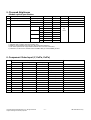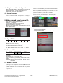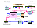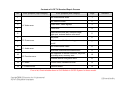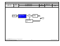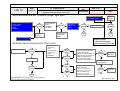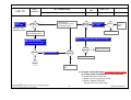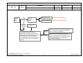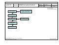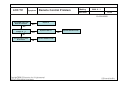
1
Internal Use Only
North/Latin America
Europe/Africa
Asia/Oceania
http://aic.lgservice.com
http://eic.lgservice.com
http://biz.lgservice.com
LCD TV
SERVICE MANUAL
CHASSIS : LD91A
MODEL : 32LG2100
32LG2100-ZA
CAUTION
BEFORE SERVICING THE CHASSIS,
READ THE SAFETY PRECAUTIONS IN THIS MANUAL.
P/NO : MFL50326821 (0904-REV00)
Printed in Korea
CONTENTS
CONTENTS .............................................................................................. 2
PRODUCT SAFETY ................................................................................. 3
SPECIFICATION ....................................................................................... 6
ADJUSTMENT INSTRUCTION ................................................................ 9
EXPLODED VIEW .................................................................................. 14
SVC. SHEET ...............................................................................................
Copyright ©2009 LG Electronics. Inc. All right reserved.
Only for training and service purposes
-2-
LGE Internal Use Only
SAFETY PRECAUTIONS
IMPORTANT SAFETY NOTICE
Many electrical and mechanical parts in this chassis have special safety-related characteristics. These parts are identified by
in the
Schematic Diagram and Exploded View.
It is essential that these special safety parts should be replaced with the same components as recommended in this manual to prevent
Shock, Fire, or other Hazards.
Do not modify the original design without permission of manufacturer.
General Guidance
Leakage Current Hot Check (See below Figure)
Plug the AC cord directly into the AC outlet.
An isolation Transformer should always be used during the
servicing of a receiver whose chassis is not isolated from the AC
power line. Use a transformer of adequate power rating as this
protects the technician from accidents resulting in personal injury
from electrical shocks.
It will also protect the receiver and it's components from being
damaged by accidental shorts of the circuitry that may be
inadvertently introduced during the service operation.
If any fuse (or Fusible Resistor) in this TV receiver is blown,
replace it with the specified.
When replacing a high wattage resistor (Oxide Metal Film Resistor,
over 1W), keep the resistor 10mm away from PCB.
Do not use a line Isolation Transformer during this check.
Connect 1.5K/10watt resistor in parallel with a 0.15uF capacitor
between a known good earth ground (Water Pipe, Conduit, etc.)
and the exposed metallic parts.
Measure the AC voltage across the resistor using AC voltmeter
with 1000 ohms/volt or more sensitivity.
Reverse plug the AC cord into the AC outlet and repeat AC voltage
measurements for each exposed metallic part. Any voltage
measured must not exceed 0.75 volt RMS which is corresponds to
0.5mA.
In case any measurement is out of the limits specified, there is
possibility of shock hazard and the set must be checked and
repaired before it is returned to the customer.
Leakage Current Hot Check circuit
Keep wires away from high voltage or high temperature parts.
AC Volt-meter
Before returning the receiver to the customer,
always perform an AC leakage current check on the exposed
metallic parts of the cabinet, such as antennas, terminals, etc., to
be sure the set is safe to operate without damage of electrical
shock.
Leakage Current Cold Check(Antenna Cold Check)
With the instrument AC plug removed from AC source, connect an
electrical jumper across the two AC plug prongs. Place the AC
switch in the on position, connect one lead of ohm-meter to the AC
plug prongs tied together and touch other ohm-meter lead in turn to
each exposed metallic parts such as antenna terminals, phone
jacks, etc.
If the exposed metallic part has a return path to the chassis, the
measured resistance should be between 1MΩ and 5.2MΩ.
When the exposed metal has no return path to the chassis the
reading must be infinite.
An other abnormality exists that must be corrected before the
receiver is returned to the customer.
Copyright ©2009 LG Electronics. Inc. All right reserved.
Only for training and service purposes
-3-
To Instrument’s
exposed
METALLIC PARTS
0.15uF
Good Earth Ground
such as WATER PIPE,
CONDUIT etc.
1.5 Kohm/10W
When 25A is impressed between Earth and 2nd Ground
for 1 second, Resistance must be less than 0.1 Ω
*Base on Adjustment standard
LGE Internal Use Only
SERVICING PRECAUTIONS
CAUTION: Before servicing receivers covered by this service
manual and its supplements and addenda, read and follow the
SAFETY PRECAUTIONS on page 3 of this publication.
NOTE: If unforeseen circumstances create conflict between the
following servicing precautions and any of the safety precautions on
page 3 of this publication, always follow the safety precautions.
Remember: Safety First.
General Servicing Precautions
1. Always unplug the receiver AC power cord from the AC power
source before;
a. Removing or reinstalling any component, circuit board
module or any other receiver assembly.
b. Disconnecting or reconnecting any receiver electrical plug or
other electrical connection.
c. Connecting a test substitute in parallel with an electrolytic
capacitor in the receiver.
CAUTION: A wrong part substitution or incorrect polarity
installation of electrolytic capacitors may result in an
explosion hazard.
2. Test high voltage only by measuring it with an appropriate high
voltage meter or other voltage measuring device (DVM,
FETVOM, etc) equipped with a suitable high voltage probe.
Do not test high voltage by "drawing an arc".
3. Do not spray chemicals on or near this receiver or any of its
assemblies.
4. Unless specified otherwise in this service manual, clean
electrical contacts only by applying the following mixture to the
contacts with a pipe cleaner, cotton-tipped stick or comparable
non-abrasive applicator; 10% (by volume) Acetone and 90% (by
volume) isopropyl alcohol (90%-99% strength)
CAUTION: This is a flammable mixture.
Unless specified otherwise in this service manual, lubrication of
contacts in not required.
5. Do not defeat any plug/socket B+ voltage interlocks with which
receivers covered by this service manual might be equipped.
6. Do not apply AC power to this instrument and/or any of its
electrical assemblies unless all solid-state device heat sinks are
correctly installed.
7. Always connect the test receiver ground lead to the receiver
chassis ground before connecting the test receiver positive
lead.
Always remove the test receiver ground lead last.
8. Use with this receiver only the test fixtures specified in this
service manual.
CAUTION: Do not connect the test fixture ground strap to any
heat sink in this receiver.
Electrostatically Sensitive (ES) Devices
Some semiconductor (solid-state) devices can be damaged easily
by static electricity. Such components commonly are called
Electrostatically Sensitive (ES) Devices. Examples of typical ES
devices are integrated circuits and some field-effect transistors and
semiconductor "chip" components. The following techniques
should be used to help reduce the incidence of component
damage caused by static by static electricity.
1. Immediately before handling any semiconductor component or
semiconductor-equipped assembly, drain off any electrostatic
charge on your body by touching a known earth ground.
Alternatively, obtain and wear a commercially available
discharging wrist strap device, which should be removed to
prevent potential shock reasons prior to applying power to the
Copyright ©2009 LG Electronics. Inc. All right reserved.
Only for training and service purposes
unit under test.
2. After removing an electrical assembly equipped with ES
devices, place the assembly on a conductive surface such as
aluminum foil, to prevent electrostatic charge buildup or
exposure of the assembly.
3. Use only a grounded-tip soldering iron to solder or unsolder ES
devices.
4. Use only an anti-static type solder removal device. Some solder
removal devices not classified as "anti-static" can generate
electrical charges sufficient to damage ES devices.
5. Do not use freon-propelled chemicals. These can generate
electrical charges sufficient to damage ES devices.
6. Do not remove a replacement ES device from its protective
package until immediately before you are ready to install it.
(Most replacement ES devices are packaged with leads
electrically shorted together by conductive foam, aluminum foil
or comparable conductive material).
7. Immediately before removing the protective material from the
leads of a replacement ES device, touch the protective material
to the chassis or circuit assembly into which the device will be
installed.
CAUTION: Be sure no power is applied to the chassis or circuit,
and observe all other safety precautions.
8. Minimize bodily motions when handling unpackaged
replacement ES devices. (Otherwise harmless motion such as
the brushing together of your clothes fabric or the lifting of your
foot from a carpeted floor can generate static electricity
sufficient to damage an ES device.)
General Soldering Guidelines
1. Use a grounded-tip, low-wattage soldering iron and appropriate
tip size and shape that will maintain tip temperature within the
range or 500°F to 600°F.
2. Use an appropriate gauge of RMA resin-core solder composed
of 60 parts tin/40 parts lead.
3. Keep the soldering iron tip clean and well tinned.
4. Thoroughly clean the surfaces to be soldered. Use a mall wirebristle (0.5 inch, or 1.25cm) brush with a metal handle.
Do not use freon-propelled spray-on cleaners.
5. Use the following unsoldering technique
a. Allow the soldering iron tip to reach normal temperature.
(500°F to 600°F)
b. Heat the component lead until the solder melts.
c. Quickly draw the melted solder with an anti-static, suctiontype solder removal device or with solder braid.
CAUTION: Work quickly to avoid overheating the circuit
board printed foil.
6. Use the following soldering technique.
a. Allow the soldering iron tip to reach a normal temperature
(500°F to 600°F)
b. First, hold the soldering iron tip and solder the strand against
the component lead until the solder melts.
c. Quickly move the soldering iron tip to the junction of the
component lead and the printed circuit foil, and hold it there
only until the solder flows onto and around both the
component lead and the foil.
CAUTION: Work quickly to avoid overheating the circuit
board printed foil.
d. Closely inspect the solder area and remove any excess or
splashed solder with a small wire-bristle brush.
-4-
LGE Internal Use Only
IC Remove/Replacement
Some chassis circuit boards have slotted holes (oblong) through
which the IC leads are inserted and then bent flat against the
circuit foil. When holes are the slotted type, the following technique
should be used to remove and replace the IC. When working with
boards using the familiar round hole, use the standard technique
as outlined in paragraphs 5 and 6 above.
Removal
1. Desolder and straighten each IC lead in one operation by gently
prying up on the lead with the soldering iron tip as the solder
melts.
2. Draw away the melted solder with an anti-static suction-type
solder removal device (or with solder braid) before removing the
IC.
Replacement
1. Carefully insert the replacement IC in the circuit board.
2. Carefully bend each IC lead against the circuit foil pad and
solder it.
3. Clean the soldered areas with a small wire-bristle brush.
(It is not necessary to reapply acrylic coating to the areas).
"Small-Signal" Discrete Transistor
Removal/Replacement
1. Remove the defective transistor by clipping its leads as close as
possible to the component body.
2. Bend into a "U" shape the end of each of three leads remaining
on the circuit board.
3. Bend into a "U" shape the replacement transistor leads.
4. Connect the replacement transistor leads to the corresponding
leads extending from the circuit board and crimp the "U" with
long nose pliers to insure metal to metal contact then solder
each connection.
Power Output, Transistor Device
Removal/Replacement
1. Heat and remove all solder from around the transistor leads.
2. Remove the heat sink mounting screw (if so equipped).
3. Carefully remove the transistor from the heat sink of the circuit
board.
4. Insert new transistor in the circuit board.
5. Solder each transistor lead, and clip off excess lead.
6. Replace heat sink.
Circuit Board Foil Repair
Excessive heat applied to the copper foil of any printed circuit
board will weaken the adhesive that bonds the foil to the circuit
board causing the foil to separate from or "lift-off" the board. The
following guidelines and procedures should be followed whenever
this condition is encountered.
At IC Connections
To repair a defective copper pattern at IC connections use the
following procedure to install a jumper wire on the copper pattern
side of the circuit board. (Use this technique only on IC
connections).
1. Carefully remove the damaged copper pattern with a sharp
knife. (Remove only as much copper as absolutely necessary).
2. carefully scratch away the solder resist and acrylic coating (if
used) from the end of the remaining copper pattern.
3. Bend a small "U" in one end of a small gauge jumper wire and
carefully crimp it around the IC pin. Solder the IC connection.
4. Route the jumper wire along the path of the out-away copper
pattern and let it overlap the previously scraped end of the good
copper pattern. Solder the overlapped area and clip off any
excess jumper wire.
At Other Connections
Use the following technique to repair the defective copper pattern
at connections other than IC Pins. This technique involves the
installation of a jumper wire on the component side of the circuit
board.
1. Remove the defective copper pattern with a sharp knife.
Remove at least 1/4 inch of copper, to ensure that a hazardous
condition will not exist if the jumper wire opens.
2. Trace along the copper pattern from both sides of the pattern
break and locate the nearest component that is directly
connected to the affected copper pattern.
3. Connect insulated 20-gauge jumper wire from the lead of the
nearest component on one side of the pattern break to the lead
of the nearest component on the other side.
Carefully crimp and solder the connections.
CAUTION: Be sure the insulated jumper wire is dressed so the
it does not touch components or sharp edges.
Diode Removal/Replacement
1. Remove defective diode by clipping its leads as close as
possible to diode body.
2. Bend the two remaining leads perpendicular y to the circuit
board.
3. Observing diode polarity, wrap each lead of the new diode
around the corresponding lead on the circuit board.
4. Securely crimp each connection and solder it.
5. Inspect (on the circuit board copper side) the solder joints of
the two "original" leads. If they are not shiny, reheat them and if
necessary, apply additional solder.
Fuse and Conventional Resistor
Removal/Replacement
1. Clip each fuse or resistor lead at top of the circuit board hollow
stake.
2. Securely crimp the leads of replacement component around
notch at stake top.
3. Solder the connections.
CAUTION: Maintain original spacing between the replaced
component and adjacent components and the circuit board to
prevent excessive component temperatures.
Copyright ©2009 LG Electronics. Inc. All right reserved.
Only for training and service purposes
-5-
LGE Internal Use Only
SPECIFICATION
NOTE : Specifications and others are subject to change without notice for improvement.
1. Application range
3. Test method
This specification is applied to the LCD TV used LD91A
chassis.
2. Requirement for Test
1) Performance: LGE TV test method followed
2) Demanded other specification
- Safety: CE, IEC/EN60065
- EMC:CE, IEC
Each part is tested as below without special appointment.
1) Temperature : 25±5ºC (77±9ºF), CST : 40±5ºC
2) Relative Humidity : 65±10%
3) Power Voltage : Standard input voltage (100-240V@50/60Hz)
* Standard Voltage of each products is marked by models.
4) Specification and performance of each parts are followed
each drawing and specification by part number in
accordance with BOM.
5) The receiver must be operated for about 5 minutes prior to
the adjustment.
4. Electrical specification
- Module General Specification
No
Item
Specification
1
Screen Device
32” wide color display module
2
Aspect Ratio
16:9
3
LCD Module
32” TFT LCD HD
4
Storage Environment
Temp. : -20 ~ 60 deg
Remark
LCD
LGD
Humidity : 10 ~ 90 %
5
Input Voltage
AC100-240V~, 50/60Hz
6
Power Consumption
Typ : 87.8
7
Module Size
760.0 (H) x 450.0 (V) x 48.0 (D)
8
Pixel Pitch
0.17025(H) x 0.51075(V)
9
Back Light
12 EEFL
10
Display Colors
1.06Billion(FHD LGD),16.7M (others)
11
Coating
3H, AG
Copyright ©2009 LG Electronics. Inc. All right reserved.
Only for training and service purposes
LCD(Module) + Backlight(Lamp)
-6-
LGE Internal Use Only
5. Chroma& Brightness
- Module optical specification
No. Item
Specification
Min.
1.
Viewing Angle<CR>10>
Right/Left/Up/Down
178
2.
Luminance
Luminance (cd/m2)
400
Typ.
3.
Contrast Ratio
CR
CIE Color Coordinates
White
Remark
Degree
500
Variation
4.
Max.
800
1.3
MAX /MIN
1200
WX
0.279
WY
0.292
Typ
RED
Xr
0.639
±0.03
Yr
0.333
Green
Xg
0.292
Yg
0.604
Blue
Xb
0.145
Yb
0.064
1) Standard Test Condition (The unit has been ‘ON’)
2) Stable for approximately 30 minutes in a dark environment at 25±2ºC.
3) The values specified are at approximate distance 50Cm from the LCD surface
4) Ta=25±2°C, VLCD=12.0V, fV=60Hz, Dclk=74.25MHz VBR_A=1.65V,ExtVBR_B=100%
6. Component Video Input (Y, CB/PB, CR/PR)
No
Specification
Resolution
H-freq(kHz)
Remark
V-freq(Hz)
1.
720x480
15.73
60.00
SDTV,DVD 480i
2.
720x480
15.63
59.94
SDTV,DVD 480i
3.
720x480
31.47
59.94
480p
4.
720x480
31.50
60.00
480p
5.
720x576
15.625
50.00
SDTV,DVD 625 Line
6.
720x576
31.25
50.00
HDTV 576p
7.
1280x720
45.00
50.00
HDTV 720p
8.
1280x720
44.96
59.94
HDTV 720p
9.
1280x720
45.00
60.00
HDTV 720p
10.
1920x1080
31.25
50.00
HDTV 1080i
11.
1920x1080
33.75
60.00
HDTV 1080i
12.
1920x1080
33.72
59.94
HDTV 1080i
13.
1920x1080
56.250
50
HDTV 1080p
14.
1920x1080
67.5
60
HDTV 1080p
Copyright ©2009 LG Electronics. Inc. All right reserved.
Only for training and service purposes
-7-
LGE Internal Use Only
7. RGB (PC)
No
Specification
Resolution
H-freq(kHz)
V-freq(Hz)
Pixel Clock(MHz)
1.
720*400
31.468
70.08
28.321
2.
640*480
31.469
59.94
25.17
Proposed
Remark
For only DOS mode
Input 848*480 60Hz, 852*480 60Hz
VESA
-> 640*480 60Hz Display
3.
800*600
37.879
60.31
40.00
VESA
4.
1024*768
48.363
60.00
65.00
VESA(XGA)
5.
1280*768
47.78
59.87
79.5
WXGA
6.
1360*768
47.72
59.8
84.75
WXGA
7.
1280*1024
63.595
60.0
108.875
SXGA
FHD model
8.
1920*1080
66.587
59.93
138.625
WUXGA
FHD model
8. HDMI Input (PC/DTV)
(1) DTV Mode
No
Resolution
H-freq(kHz)
V-freq.(Hz)
Pixel clock(MHz)
Proposed
1.
720*480
31.469 /31.5
59.94 /60
27.00/27.03
SDTV 480P
2.
720*576
31.25
50
54
SDTV 576P
3.
1280*720
37.500
50
74.25
HDTV 720P
4.
1280*720
44.96 /45
59.94 /60
74.17/74.25
HDTV 720P
5.
1920*1080
33.72 /33.75
59.94 /60
74.17/74.25
HDTV 1080I
6.
1920*1080
28.125
50.00
74.25
HDTV 1080I
7.
1920*1080
26.97 /27
23.97 /24
74.17/74.25
HDTV 1080P
8.
1920*1080
33.716 /33.75
29.976 /30.00
74.25
HDTV 1080P
9.
1920*1080
56.250
50
148.5
HDTV 1080P
10.
1920*1080
67.43 /67.5
59.94 /60
148.35/148.50
HDTV 1080P
Remark
(2) PC Mode
No
Resolution
H-freq(kHz)
V-freq.(Hz)
Pixel clock(MHz)
Proposed
Remark
1.
720*400
31.468
70.08
28.321
2.
640*480
31.469
59.94
25.17
VESA
3.
800*600
37.879
60.31
40.00
VESA
HDCP
4.
1024*768
48.363
60.00
65.00
VESA(XGA)
HDCP
5.
1280*768
47.78
59.87
79.5
WXGA
HDCP
6.
1360*768
47.72
59.8
84.75
WXGA
HDCP
7.
1280*1024
63.595
60.0
108.875
SXGA
HDCP/FHD model
8.
1920*1080
67.5
60.00
138.625
WUXGA
HDCP/FHD model
Copyright ©2009 LG Electronics. Inc. All right reserved.
Only for training and service purposes
-8-
HDCP
HDCP
LGE Internal Use Only
ADJUSTMENT INSTRUCTION
1. Application Range
4) Click “Connect” tab. If “Can’t” is displayed, check
connection between computer, jig, and set.
This specification sheet is applied to all of the LCD TV with
LD91A chassis.
(2)
(3)
2. Designation
1) The adjustment is according to the order which is
designated and which must be followed, according to the
plan which can be changed only on agreeing.
2) Power Adjustment: Free Voltage
3) Magnetic Field Condition: Nil.
4) Input signal Unit: Product Specification Standard
5) Reserve after operation: Above 5 Minutes (Heat Run)
Temperature : at 25±5ºC
Relative humidity : 65±10%
Input voltage : 220V, 60Hz
6) Adjustment equipments: Color Analyzer (CA-210 or CA110), DDC Adjustment Jig equipment, SVC remote
controller
7) Push The “IN STOP KEY” - For memory initialization.
Please Check the Speed :
To use speed between
from 200KHz to 400KHz
5) Click “Auto” tab and set as below
6) Click “Run”.
7) After downloading, check “OK” message.
(4)
filexxx.bin
(5)
(7)
Case1 : Software version up
1. After downloading S/W by USB, TV set will reboot
automatically
2. Push “In-stop” key
3. Push “Power on” key
4. Function inspection
5. After function inspection, Push “I n-stop” key.
Case2 : Function check at the assembly line
1. When TV set is entering on the assembly line, Push
“In-stop” key at first.
2. Push “Power on” key for turning it on.
-> If you push “Power on” key, TV set will recover
channel information by itself.
3. After function inspection, Push “In-stop” key.
.OK
(6)
* USB DOWNLOAD
1) Put the USB Stick to the USB socket
2) Automatically detecting update file in USB Stick
- If your downloaded program version in USB Stick is Low,
it didn’t work. But your downloaded version is High, USB
data is automatically detecting
3) Show the message “Copying files from memory”
3. Main PCB check process
* APC - After Manual-Insult, executing APC
* Boot file Download
1) Execute ISP program “Mstar ISP Utility” and then click
“Config” tab.
2) Set as below, and then click “Auto Detect” and check “OK”
message
If “Error” is displayed, Check connection between
computer, jig, and set.
3) Click “Read” tab, and then load download file (XXXX.bin)
by clicking “Read”
(1)
fi lexxx.bin
Copyright ©2009 LG Electronics. Inc. All right reserved.
Only for training and service purposes
-9-
LGE Internal Use Only
3.1. ADC Process
4) Updating is staring.
(1) ADC
• Input signal : Component 480i
• Signal equipment displays.
Adjustment pattern
- Component 480I
MODEL: 209 in Pattern Generator(480i Mode)
PATTERN : 65 in Pattern Generator(MSPG-925 SERIES)
• After enter Service Mode by pushing “ADJ” key,
• Enter Internal ADC mode by pushing “G” key at “5. ADC
Calibration”
5) Fishing the version uploading, you have to put USB stick
and “AC Power” off.
6) After putting “AC Power” on and check updated version on
your TV.
* If downloading version is more high than your TV have,
TV can lost all channel data. In this case, you have to
channel recover. if all channel data is cleared, you didn’t
have a DTV/ATV test on production line.
<Caution> Using ‘power on’ button of the Adjustment R/C ,
power on TV.
* ADC Calibration Protocol (RS232)
Item
Adjust
‘Mode In’
ADC Adjust
* After downloading, have to adjust Tool Option again.
1) Push "IN-START" key in service remote controller
2) Select “Tool Option 1” and Push “OK” button.
3) Punch in the number. (Each model hax their number)
Module
32LG2100
Adjust Sequence
• aa 00 00 [Enter Adjust Mode]
• xb 00 40 [Component1 Input (480i)]
• ad 00 10 [Adjust 480i Comp1]
• xb 00 60 [RGB Input (1024*768)]
• ad 00 10 [Adjust 1024*768 RGB]
• aa 00 90 End Adjust mode
* Required equipment : Adjustment R/C.
Tool option1 Tool option2 Tool option3 Tool option4
17729
1574
1952
CMD1 CMD2 Data0
A
A
0 0 When transfer the ‘Mode In’,
Carry the command.
A
D
1 0 Automatically adjustment
(The use of a internal pattern)
3584
4) Completed selecting Tool option.
3.2. Function Check
(1) Check display and sound
- Check Input and Signal items. (cf. work instructions)
1) TV
2) AV (SCART1/SCART2/ CVBS)
3) COMPONENT (480i)
4) RGB (PC : 1024 x 768 @ 60hz)
5) HDMI
6) PC Audio In
* Display and sound check is executed by remote control.
Copyright ©2009 LG Electronics. Inc. All right reserved.
Only for training and service purposes
- 10 -
LGE Internal Use Only
4. Total Assembly line process
** Caution **
Color Temperature : COOL, Medium, Warm.
One of R Gain/G Gain/ B Gain should be kept on 0xC0, and
adjust other two lower than C0.
(when R/G/B Gain are all C0, it is the FULL Dynamic Range
of Module)
4.1. Adjustment Preparation
· W/B Equipment condition
CA210 : CH 9, Test signal : Inner pattern (85IRE)
· Above 5 minutes H/run in the inner pattern. (“power on” key
of adjust remote control)
Cool
11,000k
Medium 9,300k
Warm
6,500k
ºK
ºK
ºK
* Manual W/B process using adjusts Remote control.
X=0.276(±0.002)
• After enter Service Mode by pushing “ADJ” key,
• Enter White Balance by pushing “ G ” key at “6. White
Balance”.
Y=0.283(±0.002)
<Test Signal>
X=0.285(±0.002)
Inner pattern
Y=0.293(±0.002)
(216gray,85IRE)
X=0.313(±0.002)
Y=0.329(±0.002)
* Connecting picture of the measuring instrument
(On Automatic control)
Inside PATTERN is used when W/B is controlled. Connect to
auto controller or push Adjustment R/C POWER ON ->
Enter the mode of White-Balance, the pattern will come out.
Full White Pattern
* After done all adjustments, Press “In-start” button and
compare Tool option and Area option value with its BOM, if
it is correctly same then unplug the AC cable. If it is not
same, then correct it same with BOM and unplug AC cable.
For correct it to the model’s module from factory JIG model.
* Push The “IN STOP KEY” after completing the function
inspection.
CA-210
COLOR
ANALYZER
TYPE: CA-210
RS-232C Communication
* Auto-control interface and directions
1) Adjust in the place where the influx of light like floodlight
around is blocked. (illumination is less than 10ux).
2) Adhere closely the Color Analyzer (CA210) to the module
less than 10cm distance, keep it with the surface of the
Module and Color Analyzer’s Prove vertically.(80~100°).
3) Aging time
- After aging start, keep the power on (no suspension of
power supply) and heat-run over 5minutes.
- Using ‘no signal’ or ‘full white pattern’ or the others,
check the back light on.
• Auto adjustment Map(RS-232C)
RS-232C COMMAND
[CMD ID DATA]
Wb 00
00
White Balance Start
Wb 00
ff
White Balance End
RS-232C COMMAND MIN
• Connect D-sub Signal Cable to D-sub Jack.
• Write EDID Data to EEPROM(24C02) by using DDC2B
protocol.
• Check whether written EDID data is correct or not.
* For SVC main Ass’y, EDID have to be downloaded to Insert
Process in advance.
4.3. DDC EDID Write (HDMI 256Byte)
• Connect HDMI Signal Cable to HDMI Jack.
• Write EDID Data to EEPROM(24C02) by using DDC2B
protocol.
• Check whether written EDID data is correct or not.
* For SVC main Ass’y, EDID have to be downloaded to Insert
Process in advance.
4.4. EDID DATA
CENTER
[CMD ID DATA]
4.2. DDC EDID Write (RGB 128Byte )
MAX
(DEFAULT)
Cool
Mid
Warm
R Gain
jg
Ja
jd
G Gain
jh
Jb
je
00
172
B Gain
ji
Jc
jf
00
192
R Cut
64
G Cut
64
B Cut
64
00
Cool
Mid
Warm
172
192
192
255
192
192
255
192
172
255
64
64
128
64
64
128
64
64
128
Copyright ©2009 LG Electronics. Inc. All right reserved.
Only for training and service purposes
- 11 -
1) All Data : HEXA Value
2) Changeable Data :
*: Serial No : Controlled / Data:01
**: Month : Controlled / Data:00
***:Year : Controlled
****:Check sum
LGE Internal Use Only
- Auto Download
1) HD RGB EDID data
• After enter Service Mode by pushing “ADJ” key,
• Enter EDID D/L mode.
• Enter “START” by pushing “OK” key.
00
10
20
30
40
50
60
70
80
90
A0
B0
C0
D0
E0
F0
0
00
1
FF
c
09
01
36
6E
3E
48
01
00
28
1F
2
FF
01
4C
01
7E
55
46
3
FF
03
A1
01
8A
00
10
4
FF
68
08
01
42
7E
00
5
FF
73
00
01
00
8A
0A
6
FF
41
81
66
00
42
20
7
00
78
C0
21
1E
00
20
8
1E
0A
61
50
01
00
20
9
6D
CF
40
B0
1D
1E
20
A
B
C
D
74
45
51
00
00
20
A3
40
00
72
00
20
57
31
1B
51
00
FF
FF
FF
FF
FF
FF
FF
FF
FF
FF
FF
FF
FF
FF
FF
FF
FF
FF
FF
FF
FF
FF
FF
FF
FF
FF
FF
FF
FF
FF
FF
FF
FF
FF
FF
FF
FF
FF
FF
FF
FF
FF
FF
FF
FF
FF
FF
FF
FF
FF
FF
FF
FF
FF
FF
FF
7
00
78
C0
21
1E
00
20
8
1E
0A
61
50
01
00
20
9
6D
CF
40
B0
1D
1E
20
B
C
D
74
45
51
00
00
20
A3
40
00
72
00
20
57
31
1B
51
00
4C
40
30
D0
FD
84
09
20
D0
8A
3A
1E
00
13
57
58
0C
20
80
01
00
05
07
2C
20
E0
18
1D
9E
14
03
02
a
4C
40
30
D0
FD
FF
FF
FF
FF
FF
FF
FF
FF
FF
FF
FF
FF
FF
FF
FF
FF
FF
FF
FF
FF
FF
FF
FF
FF
FF
FF
FF
FF
FF
FF
FF
FF
FF
FF
FF
FF
FF
FF
FF
FF
F
B0
01
40
1E
00
23
01
70
20
3A
00
FF
FF
FF
FF
FF
FF
FF
FF
e
FF
FF
FF
FF
FF
FF
FF
FF
d
d
FF
FF
FF
FF
FF
FF
FF
FF
E
b
FF
FF
FF
FF
FF
FF
FF
FF
2) HD HDMI EDID data
00
10
20
30
40
50
60
70
80
90
A0
B0
C0
D0
E0
F0
* Edid data and Model option download (RS232)
Item
CMD1 CMD2 Data0
Download
A
A
0
A
E
00 10 Automatically Download
‘Mode In’
Download
0 When transfer the ‘Mode In’,
Carry the command.
(The use of a internal pattern)
* Caution
1) Use the proper signal cable for EDID Download
- Analog EDID : Pin3 exists
- Digital EDID : Pin3 exists
2) Never connect HDMI & D-sub Cable at the same time.
3) Use the proper cables below for EDID Writing
4) Download HDMI1, HDMI2, separately because HDMI1 is
different from HDMI3
For HDMI EDID
D-sub to D-sub
DVI-D to HDMI or HDMI to HDMI
1
FF
c
09
01
36
6E
3E
48
01
00
28
1F
02
22
03
15
2
FF
01
4C
01
7E
55
46
3
FF
03
A1
01
8A
00
10
4
FF
80
08
01
42
7E
00
5
FF
73
00
01
00
8A
0A
6
FF
41
81
66
00
42
20
20
01
80
01
00
42
7E
25
F1
26
18
1D
1E
00
8A
80
4E
15
71
00
8C
00
42
7E
10
07
1C
80
0A
18
00
8A
1F
50
16
51
D0
02
00
42
A
E
F
B0
01
40
1E
00
23
01
70
20
3A
12
01
20
e
21
8A
00
3E
40
1C
00
42
7E
96
58
16
00
00
8A
00
2C
20
D5
a
b
d
d
f
00
42
7E
45
10
9E
00
8A
00
2C
f
25
40
2D
71
80
00
00
80
10
38
D0
00
7E
35
10
2D
72
00
* Detail EDID Options are below
ⓐ Product ID
- Manual Download
For Analog EDID
0
00
Model Name
HEX
EDID Table
DDC Function
FHD Model
0001
01 00
Analog/Digital
HD Model
0000
00 00
Analog/Digital
ⓑ Serial No: Controlled on production line.
ⓒ Month, Year: Controlled on production line:
ex) Monthly : ‘02’ -> ‘02’
Year : ‘2009’ -> ‘13’
ⓓ Model Name(Hex):
MODEL
MODEL NAME(HEX)
all
00 00 00 FC 00 4C 47 20 54 56 0A 20 20 20 20 20 20 20
ⓔ Checksum: Changeable by total EDID data.
ⓕ Vendor Specific(HDMI)
INPUT
MODEL NAME(HEX)
Item
Condition
Data(Hex)
HDMI1
67030C001000011D
Manufacturer ID
GSM
1E6D
HDMI2
67030C002000011D
Version
Digital : 1
01
HDMI3
67030C003000011D
Revision
Digital : 3
03
Copyright ©2009 LG Electronics. Inc. All right reserved.
Only for training and service purposes
- 12 -
LGE Internal Use Only
4.5. Outgoing condition Configuration
- When pressing IN-STOP key by SVC remocon, Red LED are
blinked alternatively. And then Automatically turn off.
(Must not AC power OFF during blinking)
4.6. Internal pressure
Confirm whether is normal or not when between power
board’s ac block and GND is impacted on 1.5kV(dc) or
2.2kV(dc) for one second
* Manual Download (Model Name and Serial Number)
If the TV set is downloaded by OTA or Service man, Sometimes
model name or serial number is initialized.(Not always)
There is impossible to download by bar code scan, so It need
Manual download.
1) Press the ‘instart’ key of ADJ remote controller.
2) Go to the menu ‘5.Model Number D/L’ like below photo.
3) Input the Factory model name(ex 42LH4000-ZA) or Serial
number like photo.
5. Model name & Serial number D/L
• press “Power on” key of service remocon.
(Baud rate : 115200 bps)
• Connect RS232 Signal Cable to RS-232 Jack.
• Write Serial number by use RS-232.
• Must check the serial number at the Diagnostics of SET UP
menu. (Refer to below).
4) Check the model name Instart menu -> Factory name
displayed (ex 42LH4000-ZA)
5) Check the Diagnostics (DTV country only) ->s Buyer model
displayed (ex 42LH4000)
5.1. Signal TABLE
CMD
LENGTH
ADH
ADL
DATA_1
...
Data_n
CS
DELAY
CMD : A0h
LENGTH : 85~94h (1~16 bytes)
ADH : EEPROM Sub Address high (00~1F)
ADL : EEPROM Sub Address low (00~FF)
Data : Write data
CS : CMD + LENGTH + ADH + ADL + Data_1 +…+ Data_n
Delay : 20ms
5.2. Command Set
No.
1
Adjust mode
EEPROM WRITE
CMD(hex)
A0h
LENGTH(hex)
Description
84h+n
n-bytes Write (n = 1~16)
* Description
FOS Default write : <7mode data> write
Vtotal, V_Frequency, Sync_Polarity, Htotal, Hstart, Vstart, 0,
Phase
Data write : Model Name and Serial Number write in
EEPROM,.
5.3. Method & notice
1) Serial number D/L is using of scan equipment.
2) Setting of scan equipment operated by Manufacturing
Technology Group.
3) Serial number D/L must be conformed when it is produced
in production line, because serial number D/L is mandatory
by D-book 4.0.
Copyright ©2009 LG Electronics. Inc. All right reserved.
Only for training and service purposes
- 13 -
LGE Internal Use Only
EXPLODED VIEW
IMPORTANT SAFETY NOTICE
900
910
A9
300
510
500
200N
200T
120
122
200
802
801
A10
805
800
550
804
530
821
803
540
LV1
521
A2
400
Many electrical and mechanical parts in this chassis have special safety-related characteristics. These
parts are identified by
in the Schematic Diagram and EXPLODED VIEW.
It is essential that these special safety parts should be replaced with the same components as
recommended in this manual to prevent X-RADIATION, Shock, Fire, or other Hazards.
Do not modify the original design without permission of manufacturer.
Copyright
LG Electronics. Inc. All right reserved.
Only for training and service purposes
- 14 -
LGE Internal Use Only
/F_RB
0
OPT
0
R151
B
+3.3V
/PF_WE
PF_ALE
/PF_CE1
0
R102
B
+3.3V
Q101
KRC103S
OPT
OPT
0
R101
E
C
1
8
10:I12
7:F13;11:AG9
7:F12;11:AG10
11:Q8
11:J8
10:I12
4
3
2
1
4.7K
22
+5V_GENERAL
22
R171
C114
0.1uF
$0.76
R161
+3.3V
GND
WP
DO
NC_9
VSS_1
CLK
HOLD
VCC
SPI_DI
SPI_CK
26~32
R1527
1K
1%
R1529
1.8K
37~47
37~47
R1528
2.7K
1%
+12V/+15V
I
FRC/LVDS_B
2
G
KIA7042AF
1
3
O
R1543
10K
+3.3V
4
3
2
1
$0.418
8
5
6
7
SDA
SCL
WC
VCC
C1501
2.2uF
OPT
PWM0
7:G25;7:R15;9:AI24;9:AI25
GND
LED_ON/LED_R
E16;E20;T19
E16;E19;T19
C3
A7
D6
D7
C4
D6
C4
2
R115
10K
/F_RB
PF_WP
PF_ALE
/PF_WE
/PF_OE
/PF_CE1
/PF_CE0
OUT
SCL0
SDA0
EEPROM_SDA
EEPROM_SCL
22
AR101
R1500
1K
OPT
R199
1K
OPT
PWM1
SDA1
SCL1
SDA0
SCL0
SDA0
SCL0
POWER_DET
AK12
AK12
T21;Y14
T21;Y14
T21;Y14
T21;Y14
EEPROM_SDA E16;E20;Y14
EEPROM_SCL E16;E19;Y13
R1501
1K
R198
1K
PWM_DIM
/FE_RESET
FE_AGC_SPEED_CTL
MEMC_RESET
100
R1611
R1601
R1604
3.3K
HD
100
100
FRC/LVDS_B
R1600
R1603
3.3K
FHD
100
R1544
MODEL OPTION
100
R1545
R1606
3.3K
LED_MOVING
R1608
3.3K
NO_FRC/LVDS_A
R1607
3.3K
FRC/LVDS_B
R1605
3.3K
LED_NORMAL
+3.3V
PWM2
R1610
OPT
R1609
3.3K
MODEL_OPT_3
MODEL_OPT_2
MODEL_OPT_1
MODEL_OPT_0
SB_MUTE
9:AI24
100
MODEL_OPT_3
MODEL_OPT_2
MODEL_OPT_1
MODEL_OPT_0
PIN NAME
R1550
11:AE17
DBG_TX
DBG_RX
ISP_RXD
C1500
1uF
OPT
E19;T19;Y13
C101
0.022uF
16V
10uF
IC101
6.3V
KIA7427F
VCC 1
3
C102
+3.3V_ST
ISP_TXD
A_DIM
22
EEPROM_SCL
EEPROM_SDA E20;T19;Y14
VOLTAGE DETECTOR
*Mstar reset:Active high reset
+3.3V
PWM0
R113
DIMMING
C108
8pF
OPT
22
0IMMRMP008A(MICROCHIP)
R110
C100
0.1uF
+3.3V
IC105: EAN43352801(ATMEL SHRINK)
PCM_A[0-7]
10 : BOOT 51
11 : BOOT RISC
MCU BOOT STRAP
R100
0 VSS
E2
E1
E0
IC105
M24512-WMW6
EEPROM
NC_16
NC_17
NC_18
C107
8pF
OPT
PCM_A[0]
I/O0
22
PCM_A[1]
NC_19
PCM_A[2]
PCM_A[3]
I/O1
AR103
I/O2
I/O3
NC_20
NC_21
NC_22
VSS_2
VCC_2
PRE
NC_23
0.1uF
PCM_A[4]
I/O4
C106
PCM_A[5]
I/O5
22
PCM_A[6]
NC_24
PCM_A[7]
I/O6
AR102
C105
10uF 6.3V
I/O7
NC_25
NC_26
NC_27
NC_28
+3.3V_ST
25
26
27
28
29
30
31
32
33
34
35
36
37
38
39
40
41
42
43
44
45
46
47
48
THE
SYMBOL MARK OF THIS SCHEMETIC DIAGRAM INCORPORATES
SPECIAL FEATURES IMPORTANT FOR PROTECTION FROM X-RADIATION.
FILRE AND ELECTRICAL SHOCK HAZARDS, WHEN SERVICING IF IS
ESSENTIAL THAT ONLY MANUFATURES SPECFIED PARTS BE USED FOR
THE CRITICAL COMPONENTS IN THE
SYMBOL MARK OF THE SCHEMETIC.
R1508
1.8K
19~22
3.6K
19~32
R1521
+24V/+15V
0
0
0
R128
R129
R131
SDA_SUB/AMP
SCL_SUB/AMP
MEMC_SCL
0
R123
0
R130
MEMC_SDA
FE_DEMOD_SCL
IC1500
+3.3V
EEPROM_SDA
E16;T19;Y14
E16;T19;Y13
EEPROM_SCL
0
FRC/LVDS_B
1386 WON
Addr:10101--
DIO
24
23
22
21
20
19
18
17
16
+3.3V_TUNER
5
6
7
8
13
15
14
+3.3V
NC_15
NC_14
NC_13
NC_12
NC_11
WP
WE
ALE
CLE
NC_10
12
11
10
9
8
7
6
5
4
3
IC102
HY27US08121B-TPCB
R122
33
R1530
CS
NC_8
VCC_1
IC103
W25X32VSSIG
C103
0.1uF
NC_7
CE
RE
R/B
NC_6
NC_5
NC_4
NC_3
2
1
FE_DEMOD_SDA
FE_TUNER_SCL
R109
AI13;10:I9
SDA
SCL
WP
FE_TUNER_SDA
5
VCC
AI13;10:I9
6
A2 3
VSS 4
A1 $0.199
2
7
A0
IC107
CAT24WC08W-T
POWER DETECT
I2C
R158
4.7K
SPI_DO
SPI_CS
Q100
KRC103S
OPT
+3.3V
E
C
3.9K
R111
NC_2
4.7K
1K
R1540
1K
R112
/PF_OE
R1509
HDCP EEPROM
Flash_WP_1
Serial FLASH MEMORY
for BOOT
PF_WP
R104
10K
10K
R1533
4.7K
OPT
R1505
4.7K
R103
R105 OPT 1K
R1539
1K
R1504
4.7K
/PF_CE0
R1506
1.2K
L102
R1503
2.2K
R107
470
NC_1
R1502
2.2K
+3.3V
R124
D7
KEY2
PCM_D[7]
OPT
J2
AD12
B9
E11
B9(FHD)
B9(HD)
D6
PIN NO.
FHD
LED_NORMAL
FRC
LVDS_B
LCD
HIGH
MODEL OPTION
DSUB_DET
MODEL_OPT_0
COMP_DET
0
100
100
R126
R148
R147
HD
LED_MOVING
NO_FRC
LVDS_A
PDP
LOW
100
R166
C5
D5
D6
E10
E8
E11
D7
D9
D10
0
100
0
100
R160
R168
R189
100
MODEL_OPT_2
8:C6 ERROR_OUT
7:R15 NTP_MUTE
R157
AC11
C4
E4
F4
B4
A4
AA13
R156
0
100
SCART2_MUTE
R146
R150
AB12
AB13
V5
W5
J1
22
22
R143
22
AC21
0
22
AB21
0
R142
F8
D11
0
AB11
Y14
AC9
AA11
AA12
AF6
AE6
T4
W4
AA5
AC7
AC8
AA10
AB15
Y5
AB18
AA14
AD6
AA7
AB9
Y4
V4
AA4
AB5
AA9
AC13
AB8
AC12
AB14
AC14
AC15
AB16
0
33
33
33
R1519
33
R1516
R1518
33
R1515
R1517
33
33
R1514
33
33
R1513
R1511
R1512
33
R1510
PCM_A[14]
PCM_A[13]
PCM_A[12]
PCM_A[11]
PCM_A[10]
PCM_A[9]
PCM_A[8]
PCM_A[7]
PCM_A[6]
PCM_A[5]
PCM_A[4]
PCM_A[3]
PCM_A[2]
PCM_A[1]
Y13
R140
R141
R164
R165
R162
R163
Y11
Y12
Y10
AC6
AA16
AA15
AC16
D4
PCM_D[5]
PCM_D[6]
IC100
GPIO_PM3/GPIO137
SAR3
GPIO102
GPIO103/I2S_OUT_SD3
GPIO99
GPIO98
GPIO97
GPIO91
GPIO90/I2S_OUT_MUTE
GPIO88
GPIO96
GPIO44
IRIN
GPIO68
GPIO67
ET_COL
ET_MDIO
ET_MDC
ET_TX_EN
ET_RXD1
ET_RXD0
SAR2
ET_TX_CLK
SAR1
ET_TXD1
ET_TXD0
TS1_CLK
TS1_VLD
TS1_SYNC
TS1_D0
TS0_CLK
TS0_VLD
TS0_SYNC
TS0_D7
TS0_D6
TS0_D5
TS0_D4
TS0_D3
TS0_D2
TS0_D1
TS0_D0
GPIO43/PCM2_IRQA_N
GPIO42/PCM2_CE_N
UART1_TX/GPIO87
UART1_RX/GPIO86
UART2_TX/GPIO85
UART2_RX/GPIO84
GPIO79/LVSYNC2/TX1
LVSYNC/GPIO133
LHSYNC2/I2S_OUT_MUTE/RX1
GPIO62/PCM2_CD_N/TX1
GPIO60/PCM2_RESET/RX1
GPIO132/LHSYNC/SPI_WPn
GPIO130/LCK
GPIO131/LDE/SPI_WPn1
GPIO_PM6/INT2/GPIO140
GPIO_PM5/INT1/GPIO139
SAR0
PWM3
PWM2
PWM1
PWM0
UART_TX2
UART_RX2
DDCA_DA
DDCA_CLK
DDCR_CK
DDCR_DA
UART2_RX/SDAM
UART2_TX/SCKM
F_RBZ
PF_AD15
PF_ALE
/PF_WE
/PF_OE
/PF_CE1
/PF_CE0
/PCM_CE
PCM_IOR/CI_RD
PCM_IOWR/CI_WR
/PCM_WE
/PCM_IRQA
GPIO_PM4/GPIO138
PCM_REG/CI_CLK
PCM_WAIT/CI_WACK
GPIO_PM2/GPIO136
GPIO_PM1/GPIO135
PCM_CD/CI_CD
/PCM_OE
GPIO_PM0/GPIO134
PCM_RST/CI_RST
PCM_A14/CI_A14
PCM_A13/CI_A13
PCM_A12/CI_A12
PCM_A11/CI_A11
PCM_A10/CI_A10
PCM_A9/CI_A9
PCM_A8/CI_A8
USB_DP_2
USB_DM_2
PCM_A6/CI_A6
PCM_A7/CI_A7
USB_DM_1
USB_DP_1
PCM_A5/CI_A5
PCM_A4/CI_A4
PCM_A3/CI_A3
PCM_A2/CI_A2
PCM_A1/CI_A1
PCM_A0/CI_A0
SPI_CK
SPI_DO
/SPI_CS
PCMD7/CI_D7
PCMD6/CI_D6
SPI_DI
TESTPIN/GND
XOUT
XIN
PCMD5/CI_D5
PCMD4/CI_D4
PCMD3/CI_D3
PCMD2/CI_D2
PCMD1/CI_D1
PCMD0/CI_D0
HWRESET
LGE3368A (Saturn6 No-DivX)
PCM_D[4]
PCM_D[3]
PCM_D[2]
PCM_D[1]
PCM_D[0]
PCM_A[0]
R116
AMP_RST
7:F6
MODEL_OPT_1
11:X16;11:AD14
IR
KEY1
11:Y9
22
/PCM_CE
/PCM_IORD
/PCM_WE
/PCM_IOWR
/PCM_IRQA
11:Y10
PWM2
PWM1
PWM0
AR100
/PCM_OE
/PCM_REG
PCM_RST
/PCM_CD
0
/PCM_WAIT
PCM_A[0-14]
PCM_D[0-7]
B3
G6
R1537
R1534
R1538
AC18
C6
0
0
0
0
CI_TS_DATA[6]
CI_TS_DATA[7]
CI_TS_DATA[4]
100
B8
A7
A11
B9
A10
B10
R192
R155
R153
R191
R190
100
100
100
100
100
100
100
R177
C11
C9
R183
R154
B11
A9
C10
AA19
AC19
AA20
AB19
AB4
AD5
AC4
CI_TS_DATA[5]
CI_TS_DATA[3]
AC5
AA6
U4
AB7
AB6
CI_TS_DATA[2]
CI_TS_DATA[1]
Y9
CI_TS_DATA[0]
100
22
22
22
22
100
0
0
100
100
100
100
100
100
R132
15K
OPT
33
33
33
+3.3V_ST
SPI_CK
SPI_CS
SPI_DI G12
SPI_DO
SCL1
SCART2_DET
SC_RE2
5:D10
USB_CTL
4:AL4
SCART1_MUTE 9:AI25
SCART1_DET
MODEL_OPT_3
BIT_SEL
SC_RE1
SIDE_HP_MUTE
HP_DET
EDID_WP
7:G26
9:N24
R1523
100
R187 OPT 100
6:AI16;6:AL7;6:AL12
9:AI24
100
R182 OPT100
ISP_TXD
POWER_DET
POWER_DET
DBG_TX
SIDE_USB_DM 4:AJ6
SIDE_USB_DP 4:AJ5
SIDE_USB
REAR_USB_DM4:AJ5
REAR_USB
REAR_USB_DP4:AJ6
CI_TS_DATA[0-7]
11:N20
9:N25
FE_TUNER_SDA
OPC_EN
FE_TUNER_SCL
5:D10
5:V22
8:M10
8:Q8
POWER_ON/OFF1
8:P5
DBG_RX
PANEL_CTL
INV_CTL
8:B11
WARM_LED_ON/LED_W
R1520
5:D10
T22
5:V22
BUF_TS_VAL_ERR 5:V21
BUF_TS_CLK
5:V21
BUF_TS_SYN
BUF_TS_DATA[0]
CI_TS_CLK
CI_TS_VAL
4:M4
5:D24
CI_TS_SYN
AV_CVBS_DET
5V_HDMI_2
PCM_5V_CTL
5V_HDMI_1
4:AG3
R197
15K
OPT
PM GPIO Assignment Recommended by MStar
R196
15K
OPT
10:AA4
FE_BOOSTER_CTL
10:AA4
Flash_WP_1
A11
SDA1
T22
LVDS_SEL
USB_OCD
R152
4.7K
OPT
20pF
C112
20pF
080923_Time Delay
X100
C111
12MHz
R133
15K
OPT
+3.3V
V4
R193
1M
AA8
AF10
0
0
Y8
R127
R170
B6
AF5
R169
A6
F10
F9
E7
R1536
R1535
R167
R159
R188
AA17
AA18
AB17
AF11
AC17
H6
R186
R185
F6
R184
H5
R179
R178
R175
R174
R1526
R1525
R1524
R173
R172
G5
F5
E5
AB10
AC10
A5
B5
AD11
AE12
AF12
AE11
E6
A3
10K
/PF_CE0
H : Serial Flash
L : NAND Flash
/PF_CE1
H : 16 bit
L : 8 bit
R1507
1.2K
0.1uF
C104
4.7K
Copyright © 2009 LG Electronics. Inc. All right reserved.
Only for training and service purposes
R125
R195
NAND FLASH MEMORY
SCHEMATIC DIAGRAM
MAIN 1
LGE Internal Use Only
6:K8
6:K9
0
100
R202
FE_VSCART_OUT
DTV/MNT_VOUT
FE_VMAIN
AV_CVBS_IN
SC2_CVBS_IN
SC1_CVBS_IN
9:P8
COMP_Pb
COMP_Y
COMP_Pr
DSUB_B
DSUB_G
DSUB_R
DSUB_VSYNC
DSUB_HSYNC
SC1_CVBS_IN
SC1_B
SC1_G
SC1_R
SC1_FB
SC1_ID
HDMI_CEC
HPD3
DDC_SCL_3
DDC_SDA_3
D2-_HDMI3
D2+_HDMI3
D1-_HDMI3
D0-_HDMI3
D1+_HDMI3
CK-_HDMI3
SC2_ID
0
100
100
R249
R204
47
47
47
470
47
47
47
R211
R212
R214
R215
R216
47
47
47
470
47
47
47
470
100
47
47
47
47
47
47
100
100
R219
R222
R224
R284
R205
R206
R226
R227
R235
R236
R228
R209
R225
R223
R221
R220
R218
R244
10K
R217
R213
47
R210
R200
0
R248
0.047uF
0.047uF
C222
0.047uF
0.047uF
0.047uF
0.047uF
0.047uF
0.047uF
1000pF
0.047uF
0.047uF
0.047uF
1000pF
0.047uF
0.047uF
22
0.047uF
22
0.047uF
0.047uF
0.047uF
C221
C2019
C2024
C218
C217
C211
C210
C209
C216
C214
C215
C208
C213
C212
C207
R245
R246
C206
C205
C203
C204
1000pF
0.047uF
0.047uF
C201
C202
0.047uF
C200
RIN1P/DSUB_R
VSYNC2
VCOM1
Y2 CVBSOUT0/SC2_MNTOUT
AA2 CVBSOUT1
W1 CVBS0/RF_CVBS
Y3 VCOM0
N3 CVBS5
M3 CVBS7
M1 CVBS4/S-VIDEO_Y
M2 CVBS6/S-VIDEO_C
T2
U3 CVBS1/SC1_CVBS
U2 CVBS2/SC2_CVBS
T1 CVBS3/SIDE_CVBS
J5
U1 BIN2P/COMP_PB+
V3 SOGIN2
V1 RIN2P/COMP_PR+
V2 GIN2P/COMP_Y+
GIN1P/DSUB_G
K1 BIN1P/DSUB_B
L2 SOGIN1
L3
L1
K3 HSYNC1/DSUB_HSYNC
K2 VSYNC1/DSUB_VSYNC
BINM
R2 GINM
T3
P3 SOGIN0/SC1_CVBS
P1 RINM
R3 GIN0P/SC1_G
R1 BIN0P/SC1_B
N2 HSYNC0/SC1_ID
N1 VSYNC0/SC1_FB
P2 RIN0P/SC1_R
AD7 HOTPLUG_C
J3 CEC
AE7 DDCD_C_DA
AF7 DDCD_C_CK
AE10 RXC2P
AD10 RXC2N
AF9 RXC1P
AE9 RXC1N
AD9 RXC0P
AF8 RXC0N
E2 HOTPLUG_B
D1 RXB2N
E1 DDCD_B_DA
F3 DDCD_B_CK
D3 RXB1N
E3 RXB2P
D0+_HDMI3
R203
0
R201
C1 RXB0P
C2 RXB0N
D2 RXB1P
C3 RXBCKP
B1 RXBCKN
B2 DDCD_A_CK
A2 HOTPLUG_A
H2 RXA2N
A1 DDCD_A_DA
G1 RXA1N
H1 RXA2P
CK+_HDMI3
R243
10K
0
100
R208
R247
0
R207
RXACKN
RXACKP
G2 RXA0P
G3 RXA0N
H3 RXA1P
F2
F1
AE8 RXCCKP
AD8 RXCCKN
HPD2
DDC_SCL_2
DDC_SDA_2
D2-_HDMI2
D2+_HDMI2
D1-_HDMI2
D0-_HDMI2
D1+_HDMI2
D0+_HDMI2
CK-_HDMI2
CK+_HDMI2
HPD1
DDC_SCL_1
DDC_SDA_1
D2-_HDMI1
D2+_HDMI1
D1-_HDMI1
D0-_HDMI1
D1+_HDMI1
D0+_HDMI1
CK-_HDMI1
CK+_HDMI1
THE
SYMBOL MARK OF THIS SCHEMETIC DIAGRAM INCORPORATES
SPECIAL FEATURES IMPORTANT FOR PROTECTION FROM X-RADIATION.
FILRE AND ELECTRICAL SHOCK HAZARDS, WHEN SERVICING IF IS
ESSENTIAL THAT ONLY MANUFATURES SPECFIED PARTS BE USED FOR
THE CRITICAL COMPONENTS IN THE
SYMBOL MARK OF THE SCHEMETIC.
9:AL4
10:AA8
4:M2
9:AE2
E17;9:O4
4:K12
4:K11
4:K13
4:C23
4:C24
4:C26
4:C22
4:C22
E21;9:O4
9:J9
9:J8
9:J6
9:O6
9:P8
6:AM25
6:W11
6:X13;6:AL13
6:X13;6:AL14
6:X17
6:X17
6:X16
6:X16
6:X15
6:X15
6:X14
6:X15
6:J16
6:K18;6:AL18
6:K18;6:AL19
6:K22
6:K22
6:K21
6:K21
6:K20
6:K21
6:K19
6:K20
6:J6
6:K7;6:AL9
6:K7;6:AL9
6:K11
6:K12
6:K10
6:K11
6:K9
6:K10
LVA0P
OPT
100
R264
R265
R262
R263
R283
R282
R281
R280
R279
R278
R277
R276
R260
R261
R258
R259
R275
R273
R272
R271
R270
R269
R268
R267
C2007
C2008
AF3
AE3
AUR2
AUL2 AE2
AA1
AUR3
AB1
AUL3
AB2
AUR4
AC2
AUL4
AB3
AUR5
AC3
AUL5
AUR1
AUVAG
AUVRP
AUVRM
AUCOM
REXT
REFM
REFP
VCLAMP
I2S_IN_SD
I2S_OUT_SD
I2S_OUT_BCK
I2S_OUT_WS
I2S_OUT_MCK
AUOUTL2/SC2_LOUT
AUOUTR2/SC2_ROUT
AUOUTL1/SC1_LOUT
AUOUTR1/SC1_ROUT
AUOUTL0/HP_LOUT
AUOUTR0/HP_ROUT
SPDIF_OUT
SPDIF_IN
SIF0M
SIF0P
AUL1
2.2uF
2.2uF
C2013
C232
R240
R250
AD1
AC1
D8
390
0.1uF
0.1uF
1uF
4.7uF
C226
C227
Close to IC
as close as possible
C228
0.1uF
C225
10uF 6.3V
C234
C235
22
22
22
22
100
100
100
100
100
100
100
100
0.1uF
0.1uF
2.2uF
2.2uF
C233
0.1uF
AD4
C224
1% +3.3V
Check
R229
C223
R234
AF4
AE4
AE5
G4
J4
H4
K4
C8
R233
R232
B7
C7
R231
A8
R251
R239
AD3
AD2
R237
R238
AF1
R230
AF2
E9
R266
W2
F11
C231
W3
C2016
C2015
2.2uF
C2012
C2014
2.2uF
2.2uF
2.2uF
2.2uF
2.2uF
2.2uF
2.2uF
C2011
C2009
C230
C2006
AUL0
Y1
C229
R274
22
22
22
22
22
22
22
22
22
22
22
22
22
22
22
22
22
22
22
22
22
22
22
22
AA3
AD18
AE18
AE17
AF17
AF18
AD17
AE19
AF19
AF20
AD19
AD20
AE20
AD14
AE14
AE13
AF13
AF14
AD13
AE15
AF15
AF16
AD15
AD16
AE16
AE1
AUR0
LVBCKM
LVBCKP
LVB4M
LVB4P
LVB3M
LVB3P
LVB2M
LVB2P
LVB1M
LVB1P
LVB0M
LVB0P
LVACKM
LVACKP
LVA4M
LVA4P
LVA3M
LVA3P
LVA2M
LVA2P
LVA1M
LVA1P
LVA0M
R242
R241
0.1uF
0.1uF
47
47
R253
22K
R252
22K
+3.3V
C2004
0.1uF
11:J8
11:J9;11:M15
11:Q15;11:Q9
LVB_4P
LVB_4M
5V_HDMI_3
FE_SIF
PC_L_IN
PC_R_IN
COMP_L_IN
COMP_R_IN
AV_L_IN
AV_R_IN
SC2_L_IN
SC2_R_IN
SC1_L_IN
SC1_R_IN
LVB_CKM
C236
22pF
OPT
C237
22pF
OPT
10:P13
4:Z6
4:Z5
4:K13
4:K15
4:M5
4:M6
9:AE10
9:AE11
9:J10
9:J12
C238
22pF
OPT
C239
22pF
OPT
11:Q15;11:Q9
11:J9;11:M15
11:Q15;11:Q9
LVB_3M
LVB_CKP
11:J9;11:M15
LVB_3P
11:Q16;11:Q10
11:J9;11:M15
11:Q16;11:Q10
11:Q15;11:Q10
11:J10;11:M16
LVB_1M
LVB_2P
LVB_0M
LVB_2M
LVB_1P
11:J10;11:M16
11:Q7
11:J7
11:Q6
11:J6
11:Q7
11:J7
11:Q7
11:J7
11:Q7
11:J7
11:Q8
C277
0.1uF
C281
0.1uF
C241
0.1uF
MS_SCK
MS_LRCH
MS_LRCK
AUDIO_MASTER_CLK
SCART2_Lout
SCART2_Rout
SCART1_Rout
SCART1_Lout
HP_LOUT
HP_ROUT
SPDIF_OUT
C244
0.1uF
7:F12
7:F12
7:F12
7:F7
9:AM13
9:AN15
9:S12
9:T14
7:G19
7:G21
C291
0.1uF
C294
0.1uF
4:T11
C283
0.1uF
C289
0.1uF
+3.3V_VDDP
C266
0.1uF
C275
0.1uF
C247
0.1uF
C259
0.1uF
C264
0.1uF
C250
0.1uF
C254
0.1uF
C257
0.1uF
C253
0.1uF
C251
0.1uF
C252
0.1uF
C258
0.1uF
C248
0.1uF
C249
0.1uF
C265
0.1uF
C245
0.1uF
C276
0.1uF
C242
0.1uF
C246
0.1uF
LVB_0P
LVA_CKM
LVA_CKP
LVA_4M
LVA_4P
LVA_3M
LVA_3P
LVA_2M
LVA_2P
LVA_1M
LVA_1P
LVA_0M
LVA_0P
C2026
0.1uF
L210
BLM18PG121SN1D
R254
22K
IC100
LGE3368A (Saturn6 No-DivX)
C2017
0.01uF
+1.8V_DDR
C2021
0.01uF
C2027
10uF
C2018
0.01uF
C243
0.1uF
C2023
0.01uF
+1.26V_VDDC
R257
22K
C2044
10uF
R255
22K
HDMI
SCART_RGB
DSUB
COMP
CVBS
TV/MNT
AUDIO IN
R256
22K
Copyright © 2009 LG Electronics. Inc. All right reserved.
Only for training and service purposes
C2022
0.01uF
LVDS OUT
C2020
0.01uF
C2043
10uF
C296
0.1uF
C297
0.1uF
C2000
0.1uF
C2001
0.1uF
C2005
0.1uF
C2031
0.1uF
C2032
0.1uF
C2033
0.1uF
AA23
Y21
W13
U5
T18
T17
T16
T15
T14
T13
T12
T11
T10
T9
T5
R18
R17
R16
R15
R14
R13
R12
R11
R10
R9
R4
P18
P17
P16
P15
P14
P13
P12
P11
P10
P9
P4
N18
N17
N16
N15
N14
N13
N12
N11
N10
N9
N4
M18
M17
M16
M15
M14
M13
M12
M11
M10
M9
L18
L17
L16
L15
L14
L13
L12
L11
L10
L9
F7
E18
E17
E16
VDDC_16
VDDP_6
GND_32
AVDD_DDR_6
AVDD_DDR_7
AVDD_DDR_8
AVDD_DDR_9
AVDD_DDR_10
GND_45
GND_46
GND_73
GND_72
GND_71
GND_70
GND_69
GND_68
GND_67
GND_66
GND_65
GND_64
GND_63
GND_62
GND_61
GND_60
GND_59
GND_58
GND_57
GND_56
GND_55
GND_54
GND_53
GND_52
AVDD_USB
AVDD_DM
AVDD_33_5
AVDD_33_4
AVDD_33_3
AVDD_33_2
AVDD_33_1
AVDD_MPLL
AVDD_LPLL
AVDD_MEMPLL_2
AVDD_MEMPLL_3
GND_49
GND_50
GND_51
AVDD_MEMPLL_1
GND_48
AVDD_DDR_11
GND_44
GND_47
GND_42
AVDD_DDR_5
GND_43
AVDD_DDR_4
GND_41
AVDD_DDR_3
AVDD_DDR_2
AVDD_DDR_1
AVDD_AU
VDDP_8
GND_40
GND_39
GND_38
GND_37
GND_36
GND_35
GND_34
VDDP_7
VDDP_5
GND_31
GND_33
VDDP_3
VDDP_4
VDDP_2
GND_29
GND_28
GND_30
VDDP_1
GND_27
GND_26
GND_25
VDDC_26
GND_24
VDDC_27
VDDC_24
VDDC_25
VDDC_23
GND_21
GND_22
VDDC_22
GND_20
GND_23
VDDC_21
VDDC_20
VDDC_19
VDDC_18
H8
W8
N7
M7
L7
K7
J7
H7
R20
V20
T20
H17
W18
W17
W16
W15
W14
H16
H15
H14
H13
G13
G12
W7
W10
W9
P20
N20
H12
H11
H10
H9
Y22
W22
W20
W19
W12
W11
V22
V7
U22
U20
U7
T22
VDDC_14 R7
VDDC_15 T7
VDDC_12 M20
VDDC_13 P7
VDDC_9 J20
VDDC_10 K20
VDDC_11 L20
VDDC_8 H20
VDDC_6 H18
VDDC_7 H19
VDDC_3 D18
VDDC_4 D19
VDDC_5 D20
VDDC_17
C2035
0.1uF
C2036
0.1uF
+1.8V_DDR
0.1uF
C269
C274
0.1uF
C260
C2025
10uF
6.3V
0.1uF
C267
0.1uF
C273
+3.3V_S6
0.1uF
C2030
+3.3V_S6
AVDD_DM : 0.03mA
0.1uF
C286
+3.3V_AVDD
AVDD_33 : 281mA
AVDD_LPLL : 4.69mA
L206
BLM18PG121SN1D
0.1uF
C279
+3.3V_S6
AVDD_MEMPLL : 23.77mA
0.1uF
C2042
0.1uF
AVDD_AU : 36.11mA
C2041
0.1uF
C293
+3.3V
C2040
0.1uF
L209
BLM18PG121SN1D
AVDD_OTG : 22.96mA
0.1uF
C256
C2039
0.1uF
VDDP : 102.3mA
0.1uF 0.1uF
C271
+3.3V_S6
0.1uF
0.1uF
C262
0.1uF
C284
C2029
0.1uF
C263
C2038
0.1uF
+3.3V_AVDD_MPLL
+3.3V_S6
C2037
0.1uF
VDDC : 970mA
+3.3V_VDDP
+1.26V_VDDC
C2034
0.1uF
VDDC_1 D16
VDDC_2 D17
GND_19
GND_18
GND_17
GND_16
GND_15
GND_13
GND_14
GND_12
GND_11
GND_10
GND_9
GND_8
GND_7
GND_6
GND_5
GND_4
GND_3
GND_2
IC100
LGE3368A (Saturn6 No-DivX)
C2003
0.1uF
M
AUDIO OUT
LGE Internal Use Only
DQ10
DQ11
DQ12
DQ13
DQ14
DQ15
SDDR_D[10]
SDDR_D[11]
SDDR_D[12]
SDDR_D[13]
SDDR_D[14]
SDDR_D[15]
VSSQ1
VSSQ2
VSSQ3
VSSQ4
VSSQ5
VSSQ6
VSSQ7
VSSQ8
VSSQ9
VSSQ10
VSS1
VSS2
VSS3
VSS4
VSS5
VDDQ1
VDDQ2
VDDQ3
VDDQ4
VDDQ5
VDDQ6
VDDQ7
VDDQ8
VDDQ9
VDDQ10
VDD1
VDD2
VDD3
VDD4
VDD5
DQ9
SDDR_D[9]
+1.8V_DDR
DQ8
DQ5
SDDR_D[5]
DQ7
DQ4
SDDR_D[4]
DQ6
DQ3
SDDR_D[3]
SDDR_D[8]
DQ2
SDDR_D[2]
SDDR_D[7]
DQ1
SDDR_D[1]
SDDR_D[6]
DQ0
SDDR_D[0]
H8
H2
F8
F2
E7
D8
D2
A7
B8
B2
P9
N1
J3
E3
A3
G9
G7
G3
G1
E9
C9
C7
C3
C1
A9
R1
M9
J9
E1
A1
B9
B1
D9
D1
D3
D7
C2
C8
F9
F1
H9
H1
H3
H7
G2
G8
J2
J1
J7
R8
E2
A2
R7
R3
A8
E8
B3
F3
B7
F7
K3
L7
K7
L8
K9
K2
K8
J8
L1
L3
L2
R2
P7
M2
P3
P8
P2
N7
N3
N8
N2
M7
M3
M8
VREF
SDDR_DQS1_N
VDDL
VSSDL
NC3
NC2
NC1
NC6
+1.8V_DDR
SDDR_DQS0_N
LDQS
UDQS
SDDR_DQM1_P
UDM
SDDR_DQS1_P
56
56
56
56
56
56
56
56
56
R320
R319 56
ADDR2_D[5]
SDDR_D[5]
C318
C319
0.1uF
0.1uF
C317
0.1uF
C316
0.1uF
0.1uF
0.1uF
C315
C313
0.1uF
C314
0.1uF
C12
B23
B12
C23
ADDR2_A[6]
ADDR2_A[7]
ADDR2_A[8]
ADDR2_A[9]
B21
C21
C14
C20
ADDR2_D[3]
ADDR2_D[4]
ADDR2_D[5]
ADDR2_D[6]
ADDR2_D[15]
ADDR2_D[14]
ADDR2_D[13]
ADDR2_D[12]
ADDR2_D[11]
ADDR2_D[10]
ADDR2_D[9]
ADDR2_D[8]
A17
B19
A16
A20
B20
B16
C19
C16
C15
A15
ADDR2_D[1]
ADDR2_D[2]
ADDR2_D[7]
A21
ADDR2_D[0]
B15
B17
A18
A19
C18
C17
B18
D22
D12
D13
D14
D23
A14
B14
D24
B24
C24
ADDR2_A[12] A24
ADDR2_A[10] B22
ADDR2_A[11] A12
C22
A23
B13
A13
ADDR2_A[5]
ADDR2_A[2]
ADDR2_A[4]
A22
ADDR2_A[3]
C13
ADDR2_A[1]
C312
ADDR2_A[0]
D15
B_DDR2_A12
A_DDR2_A12
B_DDR2_DQ2
B_DDR2_DQ3
B_DDR2_DQ4
B_DDR2_DQ5
A_DDR2_DQ2
A_DDR2_DQ3
A_DDR2_DQ4
A_DDR2_DQ5
A_DDR2_DQ15
A_DDR2_DQ14
A_DDR2_DQ13
A_DDR2_DQ12
A_DDR2_DQ11
A_DDR2_DQ10
A_DDR2_DQ9
A_DDR2_DQ8
A_DDR2_DQ7
BDDR2_A[1]
BDDR2_A[2]
BDDR2_A[3]
BDDR2_A[4]
BDDR2_A[5]
BDDR2_A[6]
BDDR2_A[7]
BDDR2_A[8]
BDDR2_A[9]
AF26
T25
AF23
T24
AE23
R26
AD22
R25
AC22
BDDR2_A[11]
BDDR2_D[5]
BDDR2_D[6]
AE25
Y25
AD25
Y26
BDDR2_D[10]
BDDR2_D[9]
BDDR2_D[8]
BDDR2_D[7]
BDDR2_D[4]
V26
W26
AF25
BDDR2_D[2]
W24
BDDR2_D[3]
BDDR2_D[1]
AE26
AF24
BDDR2_D[0]
W25
AA25
AB25
AC26
AC25
AA26
AB26
AB24
U24
U25
U26
AB23
V24
V25
AB22
AC24
AC23
AE22 BDDR2_A[12]
R24
AD23 BDDR2_A[10]
BDDR2_A[0]
T26
0.1uF
AE24 BDDR2_D[11]
B_DDR2_DQ11
AD26 BDDR2_D[12]
B_DDR2_DQ12
Y24
BDDR2_D[13]
B_DDR2_DQ13
AD24 BDDR2_D[14]
B_DDR2_DQ14
AA24 BDDR2_D[15]
B_DDR2_DQ15
B_DDR2_DQ10
B_DDR2_DQ9
B_DDR2_DQ8
B_DDR2_DQ7
B_DDR2_DQ6
B_DDR2_DQ1
A_DDR2_DQ1
A_DDR2_DQ6
B_DDR2_DQ0
B_DDR2_DQSB1
A_DDR2_DQ0
B_DDR2_DQSB0
A_DDR2_DQSB1
B_DDR2_DQM1
A_DDR2_DQM1
A_DDR2_DQSB0
B_DDR2_DQM0
A_DDR2_DQM0
B_DDR2_DQS1
A_DDR2_DQS1
/B_DDR2_WE
/A_DDR2_WE
B_DDR2_DQS0
/B_DDR2_CAS
/A_DDR2_CAS
A_DDR2_DQS0
B_DDR2_ODT
/B_DDR2_RAS
/A_DDR2_RAS
B_DDR2_CKE
/B_DDR2_MCLK
A_DDR2_ODT
A_DDR2_CKE
/A_DDR2_MCLK
B_DDR2_BA2
B_DDR2_A11
A_DDR2_A11
B_DDR2_MCLK
B_DDR2_A10
A_DDR2_A10
A_DDR2_MCLK
B_DDR2_A9
A_DDR2_A9
A_DDR2_BA2
B_DDR2_A8
A_DDR2_A8
B_DDR2_BA0
B_DDR2_A7
A_DDR2_A7
B_DDR2_BA1
B_DDR2_A6
A_DDR2_A6
A_DDR2_BA0
B_DDR2_A5
A_DDR2_BA1
B_DDR2_A3
B_DDR2_A2
B_DDR2_A4
B_DDR2_A1
A_DDR2_A3
A_DDR2_A2
A_DDR2_A4
A_DDR2_A1
A_DDR2_A5
B_DDR2_A0
A_DDR2_A0
A_MVREF
IC100
LGE3368A (Saturn6 No-DivX)
C320
0.1uF
THE
SYMBOL MARK OF THIS SCHEMETIC DIAGRAM INCORPORATES
SPECIAL FEATURES IMPORTANT FOR PROTECTION FROM X-RADIATION.
FILRE AND ELECTRICAL SHOCK HAZARDS, WHEN SERVICING IF IS
ESSENTIAL THAT ONLY MANUFATURES SPECFIED PARTS BE USED FOR
THE CRITICAL COMPONENTS IN THE
SYMBOL MARK OF THE SCHEMETIC.
ADDR2_D[2]
SDDR_D[2]
56
ADDR2_D[0]
ADDR2_D[13]
ADDR2_D[10]
ADDR2_D[8]
ADDR2_D[15]
ADDR2_D[6]
ADDR2_D[1]
ADDR2_D[3]
ADDR2_D[4]
ADDR2_D[14]
ADDR2_D[7]
56
AR309
56
56
AR307
ADDR2_D[9]
ADDR2_D[12]
ADDR2_D[11]
ADDR2_DQS1_N
ADDR2_DQS0_N
ADDR2_DQM1_P
ADDR2_DQM0_P
ADDR2_DQS1_P
ADDR2_DQS0_P
/ADDR2_WE
/ADDR2_CAS
/ADDR2_RAS
ADDR2_ODT
ADDR2_CKE
/ADDR2_MCLK
ADDR2_MCLK
ADDR2_BA[2]
ADDR2_BA[1]
ADDR2_BA[0]
ADDR2_A[8]
ADDR2_A[11]
SDDR_D[0]
AR308
AR306
56
ADDR2_A[6]
SDDR_D[7]
SDDR_D[13]
SDDR_D[10]
SDDR_D[8]
SDDR_D[15]
SDDR_D[6]
SDDR_D[1]
SDDR_D[3]
SDDR_D[4]
SDDR_D[14]
SDDR_D[9]
SDDR_D[12]
SDDR_D[11]
R318
R317
R316
R315
R314
R313
R312
R311
R310
R309
R308
56
+1.8V_DDR
R307
22
SDDR_ODT56
SDDR_DQM0_P
NC5
56
R305
SDDR_A[8]
SDDR_A[11]
SDDR_A[6]
ADDR2_A[4]
SDDR_A[4]
ADDR2_A[0]
ADDR2_A[2]
R306
SDDR_DQS0_P
AR302
SDDR_A[2]
SDDR_A[0]
ADDR2_A[7]
56
LDM
UDQS
LDQS
ADDR2_A[5]
ADDR2_A[10]
ADDR2_A[9]
22
/SDDR_WE
56
ADDR2_A[12]
SDDR_BA[2]
/SDDR_CAS
AR301
AR300
SDDR_A[7]
R304
OPT
4.7K
C303
SDDR_A[12]
56
/SDDR_RAS
R347
0.1uF
SDDR_A[9]
SDDR_BA[1]
CAS
WE
10uF
ADDR2_A[3]
R303
SDDR_CKE
OPT
R346
4.7K
C304
ADDR2_A[1]
SDDR_A[10]
56
/SDDR_CK
0.1uF
SDDR_A[1]
56
C305
SDDR_A[3]
SDDR_A[5]
0.1uF
+1.8V_DDR
0.1uF
1K 1%
+1.8V_DDR
C310
C311
C306
Close to DDR Power Pin
0.1uF
0.1uF
0.1uF
C328
0.1uF
C326
0.1uF
C327
10uF
C325
C324
56
56
R333
R334
R335
R336
R337
R338
R339
R340
R341
R342
BDDR2_ODT
/BDDR2_RAS
/BDDR2_CAS
/BDDR2_WE
BDDR2_DQS0_P
BDDR2_DQS1_P
BDDR2_DQM0_P
BDDR2_DQM1_P
BDDR2_DQS0_N
BDDR2_DQS1_N
BDDR2_D[5]
BDDR2_D[2]
BDDR2_D[0]
BDDR2_D[7]
BDDR2_D[13]
BDDR2_D[10]
BDDR2_D[8]
BDDR2_D[15]
BDDR2_D[6]
BDDR2_D[1]
AR313
TDDR_D[14]
BDDR2_D[14]
56
56
TDDR_D[5]
TDDR_D[2]
TDDR_D[0]
TDDR_D[7]
TDDR_D[13]
TDDR_D[10]
TDDR_D[8]
TDDR_D[15]
TDDR_D[6]
TDDR_D[1]
TDDR_D[3]
TDDR_D[4]
TDDR_D[9]
56
AR312
TDDR_D[12]
BDDR2_D[12]
BDDR2_D[9]
BDDR2_D[3]
TDDR_A[12]
TDDR_A[11]
56
56
56
56
56
56
R349 OPT 4.7K
+1.8V_DDR
TDDR_DQS1_N
TDDR_DQS0_N
TDDR_DQM1_P
TDDR_DQM0_P
TDDR_DQS1_P
TDDR_DQS0_P
/TDDR_WE
/TDDR_CAS
/TDDR_RAS
VDDL
VSSDL
NC3
NC2
NC1
NC6
NC5
UDQS
LDQS
UDM
LDM
UDQS
LDQS
WE
CAS
RAS
CS
ODT
CKE
CK
CK
0
TDDR_MCLK
NC4
BA1
BA0
A12
A11
A10/AP
A9
A8
A7
A6
A5
A4
A3
A2
A1
A0
0.1uF
0.1uF
0.1uF
C341
C342
0.1uF
C340
J1
J7
R8
E2
A2
R7
R3
A8
E8
B3
F3
B7
F7
K3
L7
K7
L8
K9
K2
K8
J8
L1
L3
L2
R2
P7
M2
P3
P8
P2
N7
N3
N8
N2
M7
M3
M8
J2
H8
H2
F8
F2
E7
D8
D2
A7
B8
B2
P9
N1
J3
E3
A3
G9
G7
G3
G1
E9
C9
C7
C3
C1
A9
R1
M9
J9
E1
A1
B9
B1
D9
D1
D3
D7
C2
C8
F9
F1
H9
H1
H3
H7
G2
G8
IC301
H5PS5162FFR-S6C
0.1uF
C339
VREF
0.1uF
C338
/TDDR_MCLK
TDDR_BA[2]
OPT 4.7K
56
C337
TDDR_A[10]
TDDR_A[9]
TDDR_A[8]
TDDR_A[7]
TDDR_A[6]
TDDR_A[5]
TDDR_A[4]
TDDR_A[3]
TDDR_A[2]
TDDR_A[1]
TDDR_BA[1]
R348
0.1uF
TDDR_A[0]
C335
0.1uF
TDDR_BA[0]
C333
0.1uF
+1.8V_DDR
TDDR_D[11]
BDDR2_D[4]
+1.8V_DDR
TDDR_CKE
1%
56
BDDR2_D[11]
56
56
56
R332
BDDR2_CKE
AR311
56
R331
AR310
22
R330
22
56
R329
BDDR2_MCLK
56
/BDDR2_MCLK
BDDR2_BA[2]
R328
56
TDDR_A[8]
TDDR_A[11]
TDDR_A[6]
BDDR2_BA[1]
OPT
56
R327
R326
BDDR2_A[8]
BDDR2_BA[0]
R325
BDDR2_A[11]
BDDR2_A[6]
TDDR_A[4]
BDDR2_A[4]
TDDR_A[0]
TDDR_A[2]
AR305
TDDR_A[7]
BDDR2_A[2]
BDDR2_A[0]
BDDR2_A[7]
TDDR_A[5]
TDDR_A[12]
BDDR2_A[12]
TDDR_A[10]
BDDR2_A[5]
56
56
TDDR_A[3]
TDDR_A[1]
BDDR2_A[10]
TDDR_A[9]
BDDR2_A[1]
0.1uF
C330
BDDR2_A[3]
AR304
0.1uF
C329
BDDR2_A[9]
AR303
Close to DDR Power Pin
C323
0.1uF
0.1uF
C331
R343
1K
+1.8V_DDR
TDDR_A[0-12]
C302
0.1uF
C307
R321
R322
1K 1%
R302 1K 1%
SDDR_BA[0]
SDDR_CK
SDDR_A[12]
SDDR_A[11]
SDDR_A[10]
SDDR_A[9]
SDDR_A[8]
SDDR_A[7]
SDDR_A[6]
SDDR_A[5]
SDDR_A[4]
SDDR_A[3]
SDDR_A[2]
SDDR_A[1]
SDDR_A[0]
C300 0.1uF
RAS
CS
ODT
CKE
CK
CK
BA2
BA1
BA0
A12
A11
A10/AP
A9
A8
A7
A6
A5
A4
A3
A2
A1
A0
OPT
R350
0.1uF
C301
SDDR_A[0-12]
OPT
IC300
HY5PS1G1631CFP-S6
0
R301
150
R300
C308
C309
1%
0.1uF
1K
ADDR2_A[0-12]
ADDR2_D[0-15]
0.1uF
C336
1%
DDR2 1.8V By CAP - Place these Caps near Memory
BDDR2_A[0-12]
BDDR2_D[0-15]
0.1uF
C334
R345
1K
OPT
0.1uF
C332
R344
150
Copyright © 2009 LG Electronics. Inc. All right reserved.
Only for training and service purposes
R351
+1.8V_DDR
TDDR_D[0]
TDDR_D[2]
DQ2
VSSQ1
VSSQ2
VSSQ3
VSSQ4
VSSQ5
VSSQ6
VSSQ7
VSSQ8
VSSQ9
VSSQ10
VSS1
VSS2
VSS3
VSS4
VSS5
VDDQ1
VDDQ2
VDDQ3
VDDQ4
VDDQ5
VDDQ6
VDDQ7
VDDQ8
VDDQ9
VDDQ10
VDD1
VDD2
VDD3
VDD4
VDD5
DQ15
DQ14
DQ13
DQ12
DQ11
DQ10
DQ9
DQ8
DQ7
DQ6
DQ5
DQ4
+1.8V_DDR
TDDR_D[15]
TDDR_D[14]
TDDR_D[13]
TDDR_D[12]
TDDR_D[11]
TDDR_D[10]
TDDR_D[9]
TDDR_D[8]
TDDR_D[7]
TDDR_D[6]
TDDR_D[5]
TDDR_D[4]
TDDR_D[3]
TDDR_D[1]
DQ1
DQ3
DQ0
DDR2
LGE Internal Use Only
TDDR_D[0-15]
SDDR_D[0-15]
[RD]U_CAN
[RD]CONTACT
[RD]O_SPRING
[WH]U_CAN
DSUB_R
2:E19
2:E18
DSUB_G
2:E19
DSUB_HSYNC
2:E18
DSUB_B
DSUB_VSYNC
2:E18
0
0
R440
R437
[ PC ]
+3.3V
[WH]1P_CAN
[WH]C_LUG_L
[RD]1P_CAN2
[RD]CONTACT
[RD]O_SPRING
2D
5D
2E
4E
3E
VSS
A2
A1
A0
4
3
2
1
5
6
7
8
CAT24C02WI-GT3
IC400
D411
AMOTECH
5.6V
D410
AMOTECH
5.6V
30V
AMOTECH
D409
30V
AMOTECH
D408
30V
D407
R419
AMOTECH0
5.6V
AMOTECH
D412
SDA
SCL
WP
VCC
C400
0.1uF
16V
C401
18pF
50V
R430
470K
R429
470K
R428
75
R427
75
R426
75
R425
1K
R431
10K
R406
4.7K
C
R444
22
A2
D400
ENKMC2838-T112
A1
C417
1000pF
50V
JP413
D416
ADUC30S03010L_AMODIODE
30V
JP414
JP412
C419
OPT
D417
ADUC30S03010L_AMODIODE
30V
R432
10K
P400
KCN-DS-1-0089
R413
10K
R414
10K
2:E20
2:S16
2:S16
COMP_Pr
COMP_L_IN
COMP_R_IN
OPT
R446
0
R448
DSUB_DET
ISP_TXD
ISP_RXD
EDID_WP
AV_R_IN
AV_L_IN
AV_CVBS_DET
1K
D420
ADMC5M03200L_AMODIODE
5.6V
R447
4.7K
+3.3V
D419
ADMC5M03200L_AMODIODE
5.6V
R416
100
2:E20
COMP_Pb
+5V_ST
2:E20
1:AA22
COMP_Y
C414
47pF
50V
R445
22
R412
10K
R436
0
R435
0
C412
100pF
50V
C413
100pF
50V
D418
ADMC5M03200L_AMODIODE
5.6V
D415
ADUC30S03010L_AMODIODE
30V
C418
OPT
C420
OPT
R408
470K
R410
470K
C404 1K
0.1uF
16V
R409
R411
75
COMP_DET
C415
1000pF
50V
C402
18pF
50V
R404
4.7K
AMOTECH
D405
5.6V
AMOTECH
D404
5.6V
D414
30V
ADUC30S03010L_AMODIODE
[RD]C_LUG_L
5C
D413
30V
[BL]C_LUG_L
[BL]1P_CAN
2B
[RD]1P_CAN1
[GN]O_SPRING
3A
2C
[GN]CONTACT
4A
5B
[GN]1P_CAN
R418
4.7K
2A
PPJ229-01
JK400
COMPONENT
2C
5C
4C
2B
[WH]C_LUG
R401
4.7K
6
3B
AMOTECH
D403
5.6V
7
[YL]U_CAN
+3.3V
8
2A
R443
75
R441
75
R442
75
R434
12K
AMOTECH
D406
30V
9
R415
12K
[YL]CONTACT
11
1
OPT
R433
12K
12
2
1:AJ19
3
8
6B
7B
5
4
7A
6A
SHIELD_PLATE
T_TERMINAL2
B_TERMINAL2
T_SPRING
R_SPRING
B_TERMINAL1
T_TERMINAL1
E_SPRING
2:X18
SPDIF_OUT
DBG_RX
DBG_TX
C425
0.33uF
16V
R458
6.2K
220pF
220pF
P401
KCN-DS-1-0088
C427
C426
R457
6.2K
C406
0.1uF
16V
+5V_GENERAL
+5V_ST
OPT
ZD403
R462
1K
+5V_GENERAL
50V
FIX_POLE
R450
470K
R449
470K
C428
0.33uF
16V
R459
100
R461
0
OPT
R452
15K
R451
15K
R455
0
R454
10K
C431
0.1uF
16V
PC_L_IN
PC_R_IN
D424 OPT
ADUC30S03010L_AMODIODE
30V
OPT
D423
ADUC30S03010L_AMODIODE
30V
IR_OUT
+5V_ST
R456
0
R453
10K
C430
0.047uF
25V
C429
0.33uF
16V
RS232C
VINPUT
VCC
GND
MAX3232CDR
50V
JK403
JST1223-001
C424
100pF
50V
C422
100pF
50V
IC403
D421
AMOTECH
5.6V
OPT
D422
AMOTECH
5.6V
OPT
SPDIF OPTIC JACK
JK401
PEJ024-01
PC AUDIO
ADMC5M03200L_AMODIODE
[YL]O_SPRING
10
1
2
5A
13
3
DOUT2
4
4A
14
4
C1 -
R417
12K
OPT
V+
PPJ218-01
15
5
OPT
16
RI N2
8
9
ROUT2
V6
11
DI N1
7
10
DI N2
5
12
@maker
1
3
RI N1
C2 ROUT1
6
C2 +
4
13
2
3
14
R460
100
7
DOUT1
3
2
C1 +
1
VCC
2:S16
2:S16
+5V_USB_REAR
UB01123-4HHS-4F
JK404
D402
CDS3C05HDMI1
5.6V
FLAG
OUT_1
D426
CDS3C05HDMI1
5.6V
C407
10uF
OPT
5
6
7
8
4
3
2
1
IC402
MP6211DH
EN
IN_2
IN_1
GND
1:AL8
1:AL7
SIDE_USB_DM
SIDE_USB_DP
USB_CTL
1:AI26
R403
47
USB_OCD
1:AI14
THE
SYMBOL MARK OF THIS SCHEMETIC DIAGRAM INCORPORATES
SPECIAL FEATURES IMPORTANT FOR PROTECTION FROM X-RADIATION.
FILRE AND ELECTRICAL SHOCK HAZARDS, WHEN SERVICING IF IS
ESSENTIAL THAT ONLY MANUFATURES SPECFIED PARTS BE USED FOR
THE CRITICAL COMPONENTS IN THE
SYMBOL MARK OF THE SCHEMETIC.
D425
CDS3C05HDMI1
5.6V
C405
0.1uF
OUT_2
OUT_3
R420
10K
1:AL7
+5V_USB_SIDE
1:AL8
REAR_USB_DP
SIDE USB (OPT:SIDE_USB)
D401
CDS3C05HDMI1
5.6V
REAR_USB_DM
REAR USB (OPT:REAR_USB)
KJA-UB-4-0004
JK405
AV_CVBS_IN
8
16
9
0.1uF
R400
0
10
15
GND
4
1
2
3
4
Copyright © 2009 LG Electronics. Inc. All right reserved.
Only for training and service purposes
Op t i c
5
Fi b e r
5
1
2
3
4
5
C423
JK402
0.1uF
USB DOWN STREAM
C403
AV (OPT:SIDE_AV)
INTERFACE
USB DOWN STREAM
LGE Internal Use Only
R503
33
33
47
PCM_5V_CTL
R501
33K
C500
0.1uF
16V
+5V_ST
R505
1
2
3
B
A
GND
R502
10K
4
5
Y
VCC
B
R529
2.2K
R504
22K
IC500
74LVC1G32GW
10K
E
C
0.1uF
10K
R511
Q500
2SC3052
S
100
C504
10uF
10V
D
Q501
RSR025P03
G
0
16V
GND
+3.3V_CI
100
10K
C502
0.1uF
16V
R510
R509
C503
R508
GND
R506
+5V_GENERAL
AR504
AR503
47
33
CI POWER ENABLE CONTROL
/CI_CD1
D4
E12
/CI_CD2
R500
/CI_CD2
DVB-CI DETECT
CI_MCLKI
CI_MISTRT
CI_MIVAL_ERR
CI_TS_DATA[2]
CI_TS_DATA[3]
CI_TS_DATA[1]
CI_TS_DATA[0]
CI_TS_SYN
CI_TS_CLK
CI_TS_VAL
REG
/PCM_WAIT
PCM_RST
CI_MDI[7]
CI_MDI[6]
CI_MDI[5]
CI_MDI[4]
CI_MDI[3]
CI_MDI[2]
CI_MDI[1]
CI_MDI[0]
CI_IOWR
CI_IORD
CI_TS_DATA[6]
CI_TS_DATA[7]
CI_TS_DATA[5]
R507
CI_TS_DATA[4]
10K
AR500
10K
C501
0.1uF
16V
0. 1uF
/CI_CD1
C5 1 0
OPT
R513
47
R519
GND
R512
C505
10uF
10V
+3.3V_CI
OPT
0
C507
0.1uF
16V
+5V_CI_ON
10K
G2
2
GND
G1
1
1:AA10
R514
0
100
CI_ADDR[7]
CI_ADDR[6]
22
23
56
57
58
CI_DATA[0]
CI_ADDR[12]
29
30
31
32
33
34
63
64
65
66
67
68
47
R524
33K
R521
28
62
/PCM_CD
CI_DET
AB9
27
61
GND
CI_ADDR[4]
A2
AE5;10:J17
FE_TS_SYN
A5
R523
10K
GND
A7
A6
A4
R522
10K
A3
A1
AE5;10:W19
FE_TS_VAL_ERR
AG4;10:J17
FE_TS_DATA[0]
A0
AE5;10:J17
FE_TS_CLK
OE1
CI_ADDR[0]
CI_ADDR[1]
CI_ADDR[2]
DVB-CI SERIAL BUFFER TS
CI_DATA[2]
CI_DATA[1]
CI_ADDR[5]
25
26
CI_ADDR[3]
24
59
60
GND
21
C508
0.1uF
20
55
OPT
19
54
R516
53
15
49
CI_ADDR[14]
18
14
48
CI_ADDR[13]
CI_ADDR[8]
CI_ADDR[9]
CI_ADDR[11]
16
13
47
17
12
46
CI_ADDR[10]
52
11
45
CI_DATA[0-7]
51
10
44
CI_DATA[7]
R517
10K
50
9
43
CI_DATA[5]
47
CI_DATA[6]
R515
6
40
7
5
39
8
4
38
41
CI_DATA[4]
37
42
CI_DATA[3]
3
36
35
10067972-050LF
P500
EAG41860101
10
9
8
7
6
5
4
3
2
1
11
12
13
14
15
16
17
18
19
20
74LVC541A(PW)
IC502
GND
C509
0.1uF
16V
Y1
Y7
Y6
Y5
Y4
Y3
R525
47
R527
47
R528
47
Y2
R526
47
+3.3V_CI
/PCM_IRQA
Y0
OE2
VCC
CI_ADDR[0-14]
CI_WE
+5V_GENERAL
CI_OE
/PCM_CE
10K
0.1uF
BUF_TS_DATA[0]
BUF_TS_SYN
BUF_TS_VAL_ERR
BUF_TS_CLK
CI_MISTRT
CI_MCLKI
CI_MIVAL_ERR
CI_DATA[0-7]
TOSHIBA
33
AR512
33
/PCM_IOWR
/PCM_IORD
/PCM_WE
/PCM_OE
/PCM_REG
PCM_A[14]
PCM_A[13]
PCM_D[0-7]
PCM_A[4]
CI_ADDR[3]
PCM_A[5]
CI_ADDR[2]
PCM_A[6]
CI_ADDR[1]
PCM_A[7]
CI_ADDR[0]
FE_TS_DATA[0-7]
THE
SYMBOL MARK OF THIS SCHEMETIC DIAGRAM INCORPORATES
SPECIAL FEATURES IMPORTANT FOR PROTECTION FROM X-RADIATION.
FILRE AND ELECTRICAL SHOCK HAZARDS, WHEN SERVICING IF IS
ESSENTIAL THAT ONLY MANUFATURES SPECFIED PARTS BE USED FOR
THE CRITICAL COMPONENTS IN THE
SYMBOL MARK OF THE SCHEMETIC.
CI_IOWR
CI_IORD
CI_WE
CI_OE
REG
CI_ADDR[14]
CI_ADDR[13]
PCM_A[12]
PCM_A[11]
CI_ADDR[12]
PCM_A[10]
PCM_A[9]
CI_ADDR[11]
CI_ADDR[9]
CI_ADDR[10]
AR511
PCM_D[7]
FE_TS_DATA[0-7]
+3.3V_CI
C511
0.1uF
16V
PCM_A[8]
PCM_D[6]
CI_DATA[7]
AR510
PCM_D[5]
CI_DATA[6]
PCM_D[4]
PCM_D[3]
CI_DATA[5]
33
PCM_D[2]
CI_DATA[4]
PCM_D[1]
AR509
2A1
1Y4
2A2
1Y3
2A3
1Y2
2A4
1Y1
2OE
VCC
PCM_D[0]
11
12
13
14
15
16
17
18
19
20
CI_DATA[3]
33
0ITO742440D
AR508
10
9
8
7
6
5
4
3
2
1
FE_TS_CLK
FE_TS_SYN
FE_TS_VAL_ERR
FE_TS_DATA[0]
FE_TS_DATA[1]
FE_TS_DATA[2]
FE_TS_DATA[3]
FE_TS_DATA[4]
FE_TS_DATA[5]
FE_TS_DATA[6]
FE_TS_DATA[7]
CI_DATA[2]
33
GND
2Y1
1A4
2Y2
1A3
2Y3
1A2
2Y4
1A1
33
IC501
AR513
AR507
AR506
1OE
33
33
CI_DATA[1]
CI_DATA[0]
CI_ADDR[8]
CI_ADDR[4]
PCM_A[3]
CI_ADDR[5]
PCM_A[2]
CI_ADDR[6]
PCM_A[1]
CI_ADDR[7]
PCM_A[0]
CI_DET
DVB-CI HOST I/F
D14
CI_MDI[0]
CI_MDI[1]
CI_MDI[2]
CI_MDI[3]
CI_MDI[4]
CI_MDI[5]
CI_MDI[6]
CI_MDI[7]
DVB-CI TS INPUT
CI_DATA[0-7]
+5V_GENERAL
BUFFER
Copyright © 2009 LG Electronics. Inc. All right reserved.
Only for training and service purposes
R520
R518
CI_DATA[0-7]
TC74LCX244FT
+5V_CI_ON
PCM_D[0-7]
DVB-CI SLOT
PCMCIA
LGE Internal Use Only
C512
EAG39789402
21
20
1
2
3
4
5
6
7
8
9
11
10
12
13
14
15
16
17
18
4
3
2
1
5
6
7
8
VCC
SDA
SCL
WP
R600
2K
R621
R623
R618
0
GND
0
0
C603
0.1uF
JP606
R607
R611
R610
E
0
R626
4.7K
5V_HDMI_1
C600
0.1uF
16V
22
22
B
4.7K
R629
HPD1
DDC_SDA_1
2:E10;AL9
DDC_SCL_1
2:E10;AL9
DDC_SDA_1
DDC_SCL_1
2:E10;K7
2:E10;K7
EDID_WP 1:AJ20;AI16;AL12
2:E9
D2+_HDMI1
2:E9
D1+_HDMI1
2:E9
D2-_HDMI1
2:E8
D0+_HDMI1
2:E9
D1-_HDMI1
CK+_HDMI1
2:E9
D0-_HDMI1
2:E8
K19;X14;AH25
CEC_REMOTE
2:E8
CK-_HDMI1
ENKMC2838-T112
D600
+5V_ST
JP601
THE SYMBOL MARK OF THIS SCHEMETIC DIAGRAM INCORPORATES
SPECIAL FEATURES IMPORTANT FOR PROTECTION FROM X-RADIATION.
FILRE AND ELECTRICAL SHOCK HAZARDS, WHEN SERVICING IF IS
ESSENTIAL THAT ONLY MANUFATURES SPECFIED PARTS BE USED FOR
THE CRITICAL COMPONENTS IN THE SYMBOL MARK OF THE SCHEMETIC.
VSS
A2
A1
A0
IC600
CAT24C02WI-GT3
D2+
D2_GND
D2-
D1+
D1_GND
D1-
D0+
D0_GND
D0-
CK+
R612
1K
Q601
2SC3052
A1
19
JK600
22
JP600
C
R615
10K
21
20
1
2
3
4
5
6
7
8
9
11
10
12
13
14
15
16
17
18
19
VSS
A2
A1
A0
HDMI_CEC
IC602
D2+
4
3
2
1
5
6
7
8
R601
R613
1K
DRAIN2
GATE1
3
2
1
0
0
C607
0.1uF
JP611
C601
0.1uF
16V
E
C
0
22
22
R646
4.7K
5V_HDMI_2
R605
R604
R603
Q602
2SC3052
B
R627
120K
+3.3V_ST
4.7K
R625
0
OPT
4
5
6
SOURCE2
GATE2
DRAIN1
DDC_SDA_2
2:E12;AL18
DDC_SCL_2
2:E12;AL19
HPD2
GND
OPT
C605
0.1uF
16V
R631
OPT
DDC_SDA_2
DDC_SCL_2
EDID_WP
CEC_REMOTE
2:E12
D2+_HDMI2
2:E11
D1+_HDMI2
2:E12
D2-_HDMI2
2:E11
D0+_HDMI2
2:E11
D1-_HDMI2
2:E10
CK+_HDMI2
2:E11
D0-_HDMI2
CEC_REMOTE
2:E11
CK-_HDMI2
K8;X14;AH25
ENKMC2838-T112
D602
+5V_ST
JP603
JP602
R616
10K
R649
MMBD301LT1G
Q600
SSM6N15FU
D603
30V
R642
R645
SOURCE1
SDA
SCL
WP
2K
R640
0
GND
VCC
D2_GND
D2-
D1+
D1_GND
D1-
D0+
D0_GND
D0-
CK+
CAT24C02WI-GT3
HDMI_CEC
GND
EAG39789402
JK601
22
5V_HDMI_2
A1
C
C
$0.26
20
1
2
3
4
5
6
7
8
9
11
10
12
13
14
15
16
17
18
19
JACK_GND
VSS
A2
A1
D2+
4
3
2
1
5
6
7
8
SDA
SCL
WP
2K
R622
0
E
C
0
22
22
R6 2 8
4. 7K
5V_HDMI_3
R609
R606
R608
Q603
2SC3052
C602
0.1uF
16V
C604
0.1uF
JP607
R620 0
R619
0
R614
1K
5V_HDMI_3
R602
GND
VCC
D2_GND
D2-
D1+
D1_GND
D1-
D0+
D0_GND
D0-
CK+
CAT24C02WI-GT3
IC601
JK602
A0
UI_HW_PORT3
B
R617
10K
SIDE HDMI (OPT:SIDE_HDMI)
EAG42463001
5V_HDMI_1
A2
4.7K
R630
2:E14;AL14
DDC_SDA_3
2:E15;AL13
DDC_SCL_3
HPD3
DDC_SDA_3
DDC_SCL_3
EDID_WP
2:E14
D2+_HDMI3
2:E14
D1+_HDMI3
2:E14
D2-_HDMI3
2:E13
D0+_HDMI3
2:E14
D1-_HDMI3
2:E13
CK+_HDMI3
2:E13
D0-_HDMI3
CEC_REMOTE
2:E13
CK-_HDMI3
K19;K8;AH25
ENKMC2838-T112
D601
+5V_ST
JP605
UI_HW_PORT2
A1
(OPT:REAR_HDMI_2EA)
A2
Copyright © 2009 LG Electronics. Inc. All right reserved.
Only for training and service purposes
A2
JP604
C
UI_HW_PORT1
HDMI
LGE Internal Use Only
Copyright © 2009 LG Electronics. Inc. All right reserved.
Only for training and service purposes
C702
0.1uF
16V
L701
C704
1uF
10V
1:AJ19
1:AA19;R15;9:AI24;9:AI25
SIDE_HP_MUTE
SB_MUTE
A2
C
D708
ENKMC2838-T112
A1
EARPHONE AMP
10K
R741
B
E
C
Q705
2SC3052
R742
10K
+5V_EARPHONE
1:L22;11:AG9
10K
E
C
Q700
2SC3052
R701
10K
+5V_EARPHONE
R700 B
C706
0.1uF
16V
100pF
50V
C705
C707
1000pF
50V
100
100
100
100
R721
R710
100
R720
R709
100
R722
C712
33pF
50V
C714
33pF
50V
C715
0.1uF
16V
+1.8V_AMP
TEST0
DVDD_PLL
AVDD_PLL
LFM
3.3K
VDD_IO
AGND_PLL
CLK_I
VSS_IO
DVSS_1
AD
RESET
VDR1A
BST1A
DGND_PLL
C760
1uF
10V
C7 1 3
0. 1uF
16V
R708
+3.3V
C708
1000pF
50V
C709
0.1uF
R740
0
2:X19
C703
HP_ROUT 0.22uF
16V
C701
1uF
6.3V
2:X19
HP_LOUT
R702
20K
14
13
12
11
10
9
8
7
6
5
4
3
2
1
IN2-
SHUTDOWN
GND
BYPASS
4
3
2
1
R706
20K
5
6
7
8
VO2
VDD
VO1
IN1-
C710
0.1uF
16V
R711
20K
NTP-3100L
EAN60664001
IC701
TPA6110A2DGNRG4
IC700
Monitor0_1_2 TP is necessory
SDA_SUB/AMP
SCL_SUB/AMP
1:L22;11:AG10
MS_SCK
MS_LRCK
2:X21
2:X21
MS_LRCH
2:X21
MCLK SDATA WCK BCK TP is necessory
C700
1uF
10V
L700
+1.8V_AMP
AUDIO_MASTER_CLK
R704
DVSS_2
AMP_RST
PGND1A_2
15
C716
22000pF
50V
PGND1A_1
55
56
16
+1.8V_AMP
BLM18PG121SN1D
OUT1A_2
54
DVDD
2:X21
BLM18PG121SN1D
OUT1A_1
53
SDATA 17
WCK 18
C733
0.1uF
50V
C711
100uF
16V
R712
20K
PGND2A_1
OUT2A_2
OUT2A_1
PVDD2A_2
PVDD2A_1
PVDD2B_2
38
37
36
35
34
33
29
30
31
16V
C717
0.22uF
R717
33K OPT
C721
0.1uF
16V
C7 2 4
0. 1uF
16V
PGND2A_2
R724
10K
Q701
2SC3052
E
C
C719
100uF
16V
1K
R715
1K
R714
C718
100uF 16V
100
C
A2
B
22000pF
50V
+3.3V_ST
C731
C728
0.1uF
50V
C732
22000pF
50V
+5V_GENERAL
D700
ENKMC2838-T112
A1
R718
PGND2B_2
OUT2B_1
OUT2B_2
PVDD2B_1
BST2A
39
32
VDR2A
40
C7 3 0
0. 1uF
16V
NC
41
C725
10uF
35V
42
C727
0.1uF
16V
C726
22000pF
50V
C729
0.1uF
50V
BST1B
+5V_EARPHONE
19
BCK
PVDD1B_2
20
SDA
PVDD1A_1
SCL
PVDD1B_1
51
50
21
OUT1B_2
49
22
MONITOR_0
1:AA21
R703
0
PVDD1A_2
52
48
23
MONITOR_1
PGND1B_1
44
45
OUT1B_1
47
24
PGND1B_2
46
25
FAULT
MONITOR_2
VDR1B
43
26
VDR2B
27
BST2B
28
PGND2B_1
AMP_VCC
C722
0.1uF
C723
0.1uF
10K
R729
C720
0.1uF
50V
0.1uF
50V
0.1uF
50V
A2
D711
5.6V
AMOTECH
D710
5.6V
AMOTECH
C
R705
12
12
12
12
1F
1:AA22
1:AA19;G25;9:AI24;9:AI25
1S
TRANSFER[R]
BREAK[R]
C-LUG-ES
C-LUG-EL
BREAK[L]
TRANSFER[L]
C-LUG-ER
9
8
6
5
4
3
7
JK701
PEJ026-01
10
DJ-S3600LM
JK700
FIX-TER
5
1
2
3
4
TOP_EARPHONE_out_of_stock
R707
10K
1F
L704
DA-8580
EAP38319001
2F
L705
DA-8580
EAP38319001
2S
2F
1S
2S
BOTTOM_EARPHONE
NTP_MUTE
SB_MUTE
12
R719
12
+3.3V
C736
10uF
35V
R728
C744
1000pF
50V
C743
1000pF
50V
R716
12
12
R727
R713
R726
C742
1000pF
50V
C741
1000pF
50V
R725
HP_DET
D709
ENKMC2838-T112
A1
C735
C734
AMP_VCC
D707
1N4148W
100V
OPT
D706
1N4148W
100V
OPT
D705
1N4148W
100V
OPT
D704
1N4148W
100V
OPT
4.7K
SPK_L-
SPK_R+
SPK_R-
AE5
AE7
AE9
SPK_L+
AE3
0.1uF
50V
4.7K
R733
0.1uF
50V
C752
R732
4.7K
R731
C751
C750
0.1uF
50V
4.7K
R730
2A => 5A
L708
120-ohm
L709
120-ohm
L707
120-ohm
L706
120-ohm
C758
0.01uF
50V
3.3
R737
3.3
0.01uF
50V
R736
C757
C756
0.01uF
50V
3.3
R735
3.3
R734
C755
0.01uF
50V
AB12
SPEAKER_R
AB11
AB11
SPEAKER_L
AB10
1
2
3
4
P700
WAFER-ANGLE
SPK_R-
SPK_R+
SPK_L-
SPK_L+
THE SYMBOL MARK OF THIS SCHEMETIC DIAGRAM INCORPORATES
SPECIAL FEATURES IMPORTANT FOR PROTECTION FROM X-RADIATION.
FILRE AND ELECTRICAL SHOCK HAZARDS, WHEN SERVICING IF IS
ESSENTIAL THAT ONLY MANUFATURES SPECFIED PARTS BE USED FOR
THE CRITICAL COMPONENTS IN THE SYMBOL MARK OF THE SCHEMETIC.
C746
0.47uF
50V
C745
0.47uF
50V
C749
0.1uF
50V
AMP
LGE Internal Use Only
Block diagram
Main Block
- 19/22/26/32/37/42LH2000
- 32/37/42/47LH3000
- 32/37/42/47LH4000
74LVC541A
Buffer
IC502
LCD Panel
BUF_TS_CLK/ERR/SYN/DATA[0]
LVDS (10 bit)
CI_TS_DATA[0:7]
Reset
PCM_D[0:7] CI_DATA[0:7]
CI_ADDR[0:7]
74LCX244
Buffer
IC501
CI Slot
(P500)
Tuner
(TDFW-G235D1)
TU1000
FE_TS_DATA[0:7] CI_MDI[0:7]
Block
Block Diagram
Diagram
74LX1G14C
(IC108)
Schmitt Trigger
KIA7027
(IC101)
Voltage Detector
PCM_A[0:7]
FE_VMAIN
FE_ VOUT
F-SCART
SC1_CVBS_IN
H-SCART
DTV/MNT_VOUT
SC2_CVBS_IN
AV3
DDR2 SDRAM
(1Gb)
IC300
SDDR_D[0:15]
SC1_R/G/B
Mstar S6
LGE3368A
Serial Flash
IC103
For Boot
Serial Flash
IC104
For Triton
SDDR_A[0:12]
TDDR_D[0:15]
DDR2 SDRAM
(512Mb)
IC301
TDDR_A[0:12]
AV_CVBS_IN
(No-DVIX)
COMPONENT
COMP_Y/Pb/Pr
RGB
DSUB_ R/G/B
EEPROM
AT24C512
(IC105)
NAND Flash
HYNIX
IC102
PCM_A[0:7]
(IC100)
EEPROM
AT24C512
(HDCP)IC107
I2C
DSUB_H/VSYNC
SC1/2_L/R_IN,
FE_AM_AUDIO,AV_L/R_IN,
COMP_L/R_IN, PC_L/R_IN
Head
Phone
TPA6110A
IC700
RS-232C
MAX3232CDR
IC403
SPDIF
I2S
AUDIO IN
DGB_TX/RX
SPDIF_OUT
HP_L/ROUT
USB_DM/DPUSB
Digital amp
(NTP3100L)
IC701
USB Power
L/R
MP6211DH
USB Power
IC402
HPD1/2/3, HDMI_CEC
5V_HDMI_1/2/3
TMDS[0:7] ( Data, Clock (+/-))
HDMI
1/2/3
Block diagram
M+S T-Con Block
Only for 37LH4000
*M+S : Main B/D + T-con B/D
37
37 GIP
GIP Block
Block Diagram
Diagram
GAMMA
VCOM
POL
SOE
CLK1~6
VDD_ODD
VDD_EVEN
VGL
VST
VGH
VDD
VCC
GAMMA
VCOM
POL
SOE
CLK1~6
VDD_ODD
GAMMA
VDD_EVEN
VGL
VST
VGH
VCOM
VDD
P-Gamma IC
BUF16821
IC402
VCC
mini-LVDS Wafer P
To Right LCD Panel
40
1
To Left LCD Panel
VCC VDD
GVST
Shifted level
(HIGH=VGH/Low=VGL)
FRC_3.3V
FRC_1.26V
FRC IIC
GCLK1~6
Level Shifter
MAX17108
IC403
DDR_A_D[0:15]
FRC_1.8V
LVDS (10Bit)
GVDD_ODD
POL
SOE
GVDD_EVEN
TCON with FRC
MST7327N
IC101
DDR_A_A[0:12]
DDR_B_D[16:31]
DDR_B_A[0:12]
SPI_CZ/CK & DI/DO
FRC Reset
DDR2 SDRAM
(512MB
/ 533MHz)
DDR2 SDRAM
HYNIX
(512MB / 533MHz)
IC201
HYNIX
VST
VDD_EVEN
VDD_ODD
CLK1~6
VDD VGH VGL VGH
IC202
Serial Flash
W25X32VSSIG
IC102
In different
Right mini-LVDS (8Bit)
FRC Reset
LVDS Wafer P
VCC
10
1
FRC IIC
LVDS (10Bit)
Left mini-LVDS (8Bit)
From Main
Board
Panel 12V
Multi Channel
DC/DC Converter
TPS 65161
IC401
VDD
VGH
VGL
VCC
FRC_3.3V
DC/DC Converter FRC_1.26V
BD9130
IC301
LDO
SC4215
IC303
FRC_1.8V
Block diagram
M+S T-Con Block
Only for 42/47LH4000
*M+S : Main B/D + T-con B/D
42/47
42/47 Normal
Normal Block
Block Diagram
Diagram
To Left LCD Panel
DDR_A_D[0:15]
FRC_3.3V
FRC_1.8V
FRC_1.26V
LVDS (10Bit)
FRC IIC
DDR_A_A[0:12]
TCON with FRC
MST7327N
IC101
DDR_B_D[16:31]
DDR2 SDRAM
(512MB
/ 533MHz)
DDR2 SDRAM
HYNIX
(512MB / 533MHz)
IC201
HYNIX
DDR_B_A[0:12]
SPI_CZ/CK & DI/DO
FRC Reset
IC202
Serial Flash
W25X32VSSIG
IC102
Right mini-LVDS
(8Bit)
FRC Reset
FRC IIC
LVDS (10Bit)
Left mini-LVDS (8Bit)
VCC
LVDS Wafer P
10
1
Panel 12V
From Main
Board
Multi Channel
DC/DC Converter
TPS 65162
IC401
VCC
VDD
VGHM
VGL
FRC_3.3V
DC/DC Converter
BD9130
IC301
FRC_1.26V
LDO
SC4215
IC303
FRC_1.8V
GAMMA
VCOM
POL
SOE
GOE
GSC
VGL
GSP
VGHM
VDD
VCC
POL
SOE
GOE
GSC
GAMMA
GAMMA
VCOM
SOE
GOE
GSC
VGL
GSP
VGHM
VDD
VCOM
GSP
P-Gamma IC
BUF16821
IC402
VCC
mini-LVDS Wafer P
To Right LCD Panel
POL
VDD
40
1
VCC
Contents of LCD TV Standard Repair Process
No.
Error symptom (High category)
Error symptom (Mid category)
Page
1
No video/Normal audio
1
2
No video/No audio
2
Video error, video lag/stop
3
4
Color error
4
5
Vertical/Horizontal bar, residual image,
light spot, external device color error
5
6
No power
6
Off when on, off while viewing, power auto
on/off
7
No audio/Normal video
8
9
Wrecked audio/discontinuation/noise
9
10
No response in remote controller, key error,
recording error, memory error
10
External device recognition error
11
3
A. Video error
B. Power error
7
8
C. Audio error
D. Function error
11
12
E. Noise
Circuit noise, mechanical noise
12
13
F. Exterior error
Exterior defect
13
First of all, Check whether there is SVC Bulletin in GCSC System for these model.
Remarks
Standard Repair Process
Error
symptom
LCD TV
A. Video error
Established
date
No video/ Normal audio
Revised date
2008. 3 .05
1/13
First of all, Check whether all of cables between board is inserted properly or not.
(Main B/D
Power B/D, LVDS Cable,Speaker Cable,IR B/D Cable,,,)
Replace Main Board
No video
Normal audio
Normal
audio
Y
Check Back Light
On with naked eye
N
Move to No
video/No audio
Y
On
Check Power
Board
12v,5v etc.
N
OR
N
Check Power Board 20V /12V or 24v output
Normal
voltage
Normal
voltage
Y
Y
Repair Power
Board or parts
Replace Inverter
or module
End
N
Repair Power
Board or parts
Precaution
Always check & record S/W Version and White
Balance value before replacing the Main Board
Replace Main Board
1
Re-enter White Balance value
Replace T-con
Board or module
And Adjust VCOM
Standard Repair Process
LCD TV
Error
symptom
No Video/
No audio
Check various
voltages of Power
Board ( 5V,12V,20V
or 24V…)
A. Video error
Established
date
No video/ No audio
Revised date
Y
Normal
voltage?
N
Check and
replace
MAIN B/D
End
Replace Power
Board and repair
parts
2
2008. 3 .05
2/13
Standard Repair Process
Error
symptom
LCD TV
Check RF Signal level
Normal
Signal?
Y
A. Picture Problem
Established
date
Picture broken/ Freezing
Revised date
Check whether other equipments have problem or not.
(By connecting RF Cable at other equipment)
DVD Player ,Set-Top-Box, Different maker TV etc`
Menu
Normal
Picture?
Y
Check
S/W Version
N
SVC
Bulletin?
N
Y
N
Normal
Picture?
3/13
. By using Digital signal level meter
. By using Diagnostics menu on OSD
( Menu Setup Diagnostic)
- Signal strength (Normal : over 50%)
- Signal Quality (Normal: over 50%)
N
Check RF Cable
Connection
1. Reconnection
2. Install Booster
2008. 3 .05
S/W Upgrade
Y
Y
Close
Close
3
Booster
Booster menu
On Off: Check
Off On: Check
Normal
Picture?
Y
N
Check
Tuner soldering
Contact with signal distributor
or broadcaster (Cable or Air)
Normal
Picture?
Setup
N
Replace
Main B/D
Close
Standard Repair Process
LCD TV
Error
symptom
A. Video error
Established
date
Color error
Revised date
2008. 3 .05
4/13
Other Module
Replace module
Y
Check color by input
-External Input
-COMPONENT
-RGB
-HDMI/DVI
Color
error?
N
Y
Check
and replace
Link Cable
(LVDS) and
contact
condition
Y
Color
error?
Y
Color
error?
Replace Main B/D
N
N
End
Check error
color input
mode
Check Test pattern
External Input/
Component
error
Check
external
device and
cable
External device Y
/Cable
normal
Replace
T-Con
Board
And Adjust
VCOM
LGD Module
Only
Replace Main B/D
N
Request repair
for external
device/cable
N
RGB/
HDMI/DVI
error
Check external
device and
cable
4
External device Y
/Cable
normal
Replace Main B/D
Color
error?
N
Standard Repair Process
LCD TV
Error
symptom
A. Video error
Established
date
Vertical / Horizontal bar, residual image,
light spot, external device color error
Revised date
2008. 3 .05
5/13
LGD Module Only
Vertical/Horizontal bar, residual image, light spot
Other Module
Replace T-Con Board
And Adjust VCOM
Replace
Module
N
Check color condition by input
-External Input
-Component
-RGB
-HDMI/DVI
Screen Y
normal?
Check external
device
connection
condition
Y
Normal?
Check and
replace Link
Cable
N
N
Screen
normal?
Replace Main B/D
Y
Y
Request repair
for external
device
Replace
module
Screen N
normal?
End
End
Check Test pattern
Replace module
in abnormal displaying
after exchanging T-Con B'd
External device screen error-Color error
Check S/W Version
Check N
version
Y
External
Input
error
Component
error
S/W Upgrade
Normal
screen?
Check screen
condition by
input
-External Input
-Component
-RGB
-HDMI/DVI
RGB
error
N
HDMI/
DVI
Y
End
5
Connect other external
device and cable
(Check normal operation of
External Input, Component,
RGB and HDMI/DVI by
connecting Jig, pattern
Generator ,Set-top Box etc.
Connect other external
device and cable
(Check normal operation of
External Input, Component,
RGB and HDMI/DVI by
connecting Jig, pattern
Generator ,Set-top Box etc.
Screen
normal?
N
Replace
Main B/D
Y
Request repair for
external device
Y
Screen N
normal?
Replace
Main B/D
Standard Repair Process
Error
symptom
LCD TV
Check
Power LED
Established
date
No power
Revised date
DC Power on
by pressing Power Key
On Remote control
Y
Power LED
On?
. Stand-By: Red
. Operating: Green
B. Power error
N
Normal N
operation?
6/13
Check Power
On ‘”High”
OK?
Y
Replace
Power
B/D
N
Y
Check Power cord
was inserted properly
Replace Main B/D
Measure voltage of each output of Power B/D
Check & Repair
Mechanical Power switch
on Local control of TV
Y
N
Normal?
2008. 3 .05
Check ST-BY 5V
Normal
Y
voltage?
Normal
voltage?
Y
Replace Main B/D
N
Replace Power B/D
Y
N
Close
Replace Power
B/D
’09 years new model apply mechanical power switch
to reduce power consumption in stand-by status.
If mechanical power switch off
Doesn’t turn on by remote control
Doesn’t appear LED light
Please refer to the A21 Page
6
Standard Repair Process
LCD TV
Error
symptom
B. Power error
Established
date
Off when on, off while viewing, power auto on/off
Revised date
2008. 3 .05
7/13
Check outlet
Check A/C code
Error?
N
Check Power Off
Mode
CPU
Abnormal
Normal?
Replace Main B/D
Y
End
N
Check for 3 wave length
Y
Abnormal
1
Fix A/C code & Outlet
and describe 3 wave
length
(If Power Off mode
is not displayed)
Check Power B/D
voltage
Caution
Check and fix exterior
of Power B/D Part
* Please refer to the all cases which
can be displayed on power off mode.
Status
Replace Power B/D
Normal
voltage?
Replace Main B/D
N
Replace Power B/D
Power off List
"POWEROFF_REMOTEKEY"
"POWEROFF_OFFTIMER"
"POWEROFF_SLEEPTIMER"
"POWEROFF_INSTOP"
"POWEROFF_AUTOOFF"
Normal "POWEROFF_ONTIMER"
"POWEROFF_RS232C"
"POWEROFF_RESREC"
"POWEROFF_RECEND"
"POWEROFF_SWDOWN"
"POWEROFF_UNKNOWN"
"POWEROFF_ABNORMAL1"
Abnormal
"POWEROFF_CPUABNORMAL"
7
Y
Explanation
Power off by REMOTE CONTROL
Power off by OFF TIMER
Power off by SLEEP TIMER
Power off by INSTOP KEY
Power off by AUTO OFF
Power off by ON TIMER
Power off by RS232C
Power off by Reservated Record
Power off by End of Recording
Power off by S/W Download
Power off by unknown status except listed case
Power off by abnormal status except CPU trouble
Power off by CPU Abnormal
Standard Repair Process
LCD TV
No audio
Screen normal
Error
symptom
Check user
menu >
Speaker off
C. Audio error
Established
date
No audio/ Normal video
Revised date
N
Off
Check audio B+
20V or 24V of
Power Board
Normal
voltage
Y
8/13
Y
N
Cancel OFF and describe
Check
Speaker
disconnection
2008. 3 .05
Replace Power Board and repair parts
Disconnection
Y
Replace Speaker
8
N
Replace MAIN Board
End
Standard Repair Process
LCD TV
Error
symptom
C. Audio error
Established
date
Wrecked audio/ discontinuation/noise
Revised date
2008. 3 .05
9/13
Wrecked audio/discontinuation/noise is same after “Check input signal” compared to No audio
Check input
signal
-RF
-External Input
signal
Wrecked audio/
Discontinuation/
Noise for
all audio
Signal
normal?
Check and replace
speaker and
connector
Check audio
B+ Voltage (20V or 24V)
Y
Y
Wrecked audio/
Discontinuation/
Noise only
for D-TV
N
Normal
voltage?
Replace Main B/D
N
Wrecked audio/
Discontinuation/
Noise only
for Analog
(When RF signal is not
received)
Request repair to external
cable/ANT provider
(In case of
External Input
signal error)
Check and fix
external device
Replace Power B/D
Replace Main B/D
Wrecked audio/
Discontinuation/
Noise only
for External Input
Connect and check
other external
device
Normal
audio?
N
Y
Check and fix external device
9
End
Standard Repair Process
Error
symptom
LCD TV
D. General Function Problem
Established
date
Remote control & Local switch checking
Revised date
2008. 3 .05
10/13
1. Remote control (R/C) operating error
Check R/C itself
Operation
Check & Repair
Cable connection
Connector solder
Normal Y
operating?
Replace
Main B/D
N
Normal
operating?
N
Check B+ 5V
On Main B/D
Check & Replace
Baterry of R/C
If R/C operate,
Explain the customer
cause is interference
from light in room.
Normal
operating?
Y
Check IR
Output signal
N
Y
Check R/C Operating
When turn off light
in room
Normal
Voltage?
Close
Normal
Signal?
Y
N
Check 5v on Power B/D
Replace Power B/D or
Replace Main B/D
(Power B/D don’t have problem)
Repair/Replace
IR B/D
Close
N
Replace R/C
2. Local(Mechanical) switch operating error
Replace
Main B/D
Check R/C
Operation
Y
Normal
operating?
N
Move
Power problem
Section
Check & Repair
Cable connection
Connector solder
N
Normal
operating?
Check & Replace
Assembly status
(Key PCB + tool )
Normal N
operating?
Y
Y
Close
Close
10
Check Key
Output signal
Normal
Signal?
Y
N
Repair/Replace
Local switch B/D
Standard Repair Process
LCD TV
Check
input
signal
Error
symptom
Y
Signal
input?
N
Check and fix
external device/cable
D. Function error
Established
date
External device recognition error
Revised date
Check technical
information
- Fix information
- S/W Version
Technical
information?
N
External Input and
Component
Recognition error
2008. 3 .05
11/13
Replace Main B/D
Y
Fix in
accordance
with technical
information
11
RGB,HDMI/
DVI, Optical
Recognition error
Replace Main B/D
Standard Repair Process
LCD TV
Identify
nose
type
Error
symptom
E. Noise
Established
date
Circuit noise, mechanical noise
Revised date
Circuit
noise
Check
location of
noise
Mechanical
noise
Check location
of noise
2008. 3 .05
Replace inverter
<With Inverter Module>
Replace LIPS B/D
<Without Inverter Module>
OR
Mechanical noise is a natural
phenomenon, and apply the 1st level
description. When the customer does not
agree, apply the process by stage.
Describe the basis of the description
in “Part related to nose” in the Owner’s
Manual.
OR
OR
12
When the nose is severe, replace the module
(For models with fix information, upgrade the
S/W or provide the description)
If there is a “Tak Tak” noise from the
cabinet, refer to the KMS fix information and
then proceed as shown in the solution manual
(For models without any fix information,
provide the description)
12/13
Standard Repair Process
LCD TV
F. Exterior defect
Error
symptom
Zoom part with
exterior damage
Exterior defect
Module
damage
Replace module
Cabinet
damage
Replace cabinet
Remote
controller
damage
Stand
dent
Replace remote controller
Replace stand
13
Established
date
Revised date
Adjust VCOM
2008. 3 .05
13/13
LCD TV Repair Process Index
- Trouble shooting by input block (Component level check)
No.
Input Block
Page
Power-up Boot fail
1~2
2
No OSD
3~4
3
Digital TV
5
4
Analog TV
6
AV (Scart / CVBS/ S-Video)
7~12
6
Component
13
7
RGB(D-SUB)
14~15
8
HDMI
16~17
9
All Input
18
10
Digital TV
19
Analog TV
20
12
AV / Component / RGB, HDMI-PC/ HDMI-DTV
21~26
13
AV Audio out / No Audio (Headphone &
SPDIF)
27~30
USB no connect / Remocon
31~33
Intelligent Sensor
34
1
5
11
Symptom (L)
Power Problem
Video Problem
Audio Problem
14
USB / Remocon Problem
15
Intelligent Sensor
Remark
LCD TV
Symptom
P800 Pin #7~#10
Voltage Level = 5V ?
NO
Power-Up Boot Fail
Check Power connector
OK ?
YES
Making
2009. 2 . 1
1/34
Revision
26~42LH2000
32~47LH3000/LH4000
Replace Power Board
YES
P800 Pin #2
Voltage level = 5V ?
Replace MAIN B’D Q801
NO
YES
P800 Pin #13, 14 = 12V
P800 Pin #17, 18 = 24V ?
Replace Power Board
NO
YES
MAIN B’D L803 = 3.3V ?
Replace MAIN B’D IC801
NO
YES
MAIN B’D L813 = 1.26V ?
Replace MAIN B’D IC805
NO
YES
MAIN B’D L805 = 3.3V ?
Replace MAIN B’D IC806
NO
YES
Check MAIN B’D X100 Clock
12MHz
Replace MAIN B’D IC100
NO
YES
Replace MAIN B’D IC102
NAND FLASH
NO
Replace MAIN B’D IC103
Serial Flash
NO
Replace MAIN B’D
IC300, IC301 DDR2 Memory
NO
Replace MAIN B’D IC100
LCD TV
Symptom
Power-Up Boot Fail
Making
2009. 2 . 1
2/34
Revision
19~22LH2000
P801 Pin #5~#6
Voltage Level = 5V ?
NO
Check Power connector
OK ?
Replace Power Board
YES
YES
P801 Pin #1, 2 = 15V?
Replace Power Board
NO
YES
MAIN B’D L803 = 3.3V ?
Replace MAIN B’D IC801
NO
YES
MAIN B’D L813 = 1.26V ?
NO
Replace MAIN B’D IC805
YES
MAIN B’D L805 = 3.3V ?
Replace MAIN B’D IC806
NO
YES
Check MAIN B’D X100 Clock
12MHz
Replace MAIN B’D IC100
NO
YES
Replace MAIN B’D IC102
NAND FLASH
NO
Replace MAIN B’D IC103
Serial Flash
NO
Replace MAIN B’D
IC300, IC301 DDR2 Memory
Replace MAIN B’D IC100
NO
LCD TV
Symptom
Making
No OSD
Revision
2009. 2 . 1
3/34
26~42LH2000
32~47LH3000/LH4000
P800 Pin #13, 14 = 12V
P800 Pin #17, 18 = 24V ?
NO
Check Power connector
OK ?
YES
P800 Pin #20
Voltage level = 2V
Replace MAIN B’D Q802
NO
YES
MAIN B’D L1300 = 12V ?
Replace MAIN B’D Q806
NO
YES
Check LVDS Cable
OK ?
NO
Replace LVDS Cable
Replace Main Board
YES
Replace Power Board
YES
LCD TV
Symptom
Making
No OSD
2009. 2 . 1
4/34
Revision
19~22LH2000
P801 Pin #1, 2 = 15V?
NO
Check Power connector
OK ?
YES
P801 Pin #9
Voltage level = 2V
Replace MAIN B’D Q802
NO
YES
MAIN B’D L1300 = 12V ?
Replace MAIN B’D Q806
NO
YES
Check LVDS Cable
OK ?
NO
Replace LVDS Cable
Replace Main Board
YES
Replace Power Board
YES
LCD TV
Symptom
Digital TV Video Problem
Making
Revision
2009. 2 . 1
5/34
26~42LH2000
32~47LH3000/LH4000
Check RF Cable
YES
MAIN B’D L1201 = 5V ?
Replace MAIN B’D IC808
NO
YES
MAIN B’D L1202 = 3.3V ?
Replace MAIN B’D IC809
NO
YES
MAIN B’D IC804
Pin #2 = 1.2V ?
Replace MAIN B’D IC804
NO
YES
MAIN B’D R1210 Clock ?
Replace MAIN B’D TU1200
NO
LCD TV
Symptom
Analog TV Video Problem
Making
Revision
2009. 2 . 1
6/34
26~42LH2000
32~47LH3000/LH4000
Check RF Cable
YES
MAIN B’D L1201 = 5V ?
Replace MAIN B’D IC808
NO
YES
MAIN B’D L1202 = 3.3V ?
Replace MAIN B’D IC809
NO
YES
MAIN B’D IC804
Pin #2 = 1.2V ?
Replace MAIN B’D IC804
NO
YES
MAIN B’D R1210 Clock ?
Replace MAIN B’D TU1200
NO
LCD TV
Symptom
AV1(Scart CVBS) No Video
Problem
Making
Revision
2009. 2 . 1
7/34
26~42LH2000
32~47LH3000/LH4000
Check Signal format
Is it supported?
YES
Check the SCART Cable
YES
Check MAIN B’D R1117
Video Signal ?
MAIN B’D JK1100 Check
YES
Check MAIN B’D C210
Video Signal ?
YES
Replace MAIN B’D IC 100
NO
Replace MAIN B’D JK1100
NO
NO
Replace
MAIN B’D C210
LCD TV
Symptom
AV1(Scart RGB) No Video
Problem
Making
Revision
2009. 2 . 1
8/34
26~42LH2000
32~47LH3000/LH4000
Check Signal format
Is it supported?
YES
Check the SCART Cable
YES
Check MAIN B’D JK1100
Replace MAIN B’D JK1100
NO
YES
Check MAIN B’D C200 (RED)
C201 (GREEN)
C202 (BLUE)
Video Signal ?
YES
Replace MAIN B’D IC 100
NO
Replace
MAIN B’D C200, C201, C202
LCD TV
Symptom
AV2 No Video Problem
Making
Revision
2009. 2 . 1
9/34
26~42LH2000
32~47LH3000/LH4000
Check Signal format
Is it supported?
YES
Check the SCART Cable
YES
Check MAIN B’D R1133
Video Signal ?
MAIN B’D JK1101 Check
NO
YES
Check MAIN B’D C211
Video Signal ?
YES
Replace MAIN B’D IC 100
NO
Replace MAIN B’D JK1101
NO
Replace MAIN B’D C211
LCD TV
Symptom
AV3(CVBS) No Video Problem
Making
Revision
2009. 2 . 1
10/34
26~42LH2000
32~47LH3000/LH4000
Check Signal format
Is it supported?
YES
Check the CVBS Cable
YES
Check MAIN B’D R400
Video Signal ?
MAIN B’D JK402 Check
YES
Check MAIN B’D C217
Video Signal ?
YES
Replace MAIN B’D IC 100
Replace MAIN B’D C217
NO
Replace MAIN B’D JK402
NO
NO
LCD TV
Symptom
AV1 No Video Out Problem
Making
Revision
2009. 2 . 1
11/34
26~42LH2000
32~47LH3000/LH4000
Check Spec (Refer to User Manual)
Is it supported?
YES
Check the SCART Cable
YES
Check MAIN B’D C1107
Video Signal ?
MAIN B’D JK1100 Check
YES
NO
Check MAIN B’D R1205
Video Signal ?
YES
Replace MAIN B’D Q1205
NO
Check the Trouble Shooting Guide
Analog TV No video
LCD TV
Symptom
AV2 No Video Out Problem
Making
Revision
2009. 2 . 1
12/34
26~42LH2000
32~47LH3000/LH4000
Check Spec (Refer to User Manual)
Is it supported?
YES
Check the SCART Cable
YES
Check MAIN B’D C1122
Video Signal ?
NO
Replace MAIN B’D IC 100
MAIN B’D JK1101 Check
YES
LCD TV
Component No Video/
No Color Problem
Symptom
Making
Revision
2009. 2 . 1
13/34
26~42LH2000
32~47LH3000/LH4000
Check Signal format
Is it supported?
YES
Check the Component Cable
YES
Check MAIN B’D R419
Video Signal ?
MAIN B’D JK400 Check
NO
Replace MAIN B’D JK400
NO
YES
Check MAIN B’D C209, C215 (Y)
C216 (Pb)
C214 (Pr)
Video Signal ?
YES
Replace MAIN B’D IC 100
NO
Replace
MAIN B’D C209 or C214 or C215 or C216
LCD TV
Symptom
RGB No Video Problem
Making
Revision
2009. 2 . 1
14/34
26~42LH2000
32~47LH3000/LH4000
Check Signal format
Is it supported?
YES
Check the RGB Cable
YES
MAIN B’D P400 Pin #2
Video signal ?
R437 has Vsync ?
R440 has Hsync ?
MAIN B’D P400 Check
NO
NO
YES
Check MAIN B’D C208 (Video)
R246 (HSYNC)
R245 (VSYNC)
YES
Replace MAIN B’D IC 100
NO
Replace
MAIN B’D C208 or R246 or R247
Replace MAIN B’D P400
LCD TV
Symptom
RGB No Color Problem
Making
Revision
2009. 2 . 1
15/34
26~42LH2000
32~47LH3000/LH4000
Check Signal format
Is it supported?
YES
Check the RGB Cable
YES
MAIN B’D P400
Pin #3 (BLUE)
Pin #2 (GREEN)
Pin #1 (RED)
Video signal ?
MAIN B’D P400 Check
Replace MAIN B’D P400
NO
NO
YES
Check MAIN B’D C212 (RED)
C207 (GREEN)
C213 (BLUE)
Video Signal ?
YES
Replace MAIN B’D IC 100
NO
Replace
MAIN B’D C212 or C207 or C213
LCD TV
Symptom
HDMI 1~3 All No Video Problem
Making
Revision
2009. 2 . 1
16/34
26~42LH2000
32~47LH3000/LH4000
Check Signal format
Is it supported?
YES
Check the HDMI Cable
YES
Check the ADJUST MENU
EDID OK ?
NO
Download EDID
(Refer to Adjustment Spec)
YES
Replace
MAIN B’D IC107 (HDCP KEY)
NO
Replace MAIN B’D IC 100
HDMI1 – ALL MODELS
HDMI2 – Except for 19/22LH20**
HDMI3 – Except for 19/22LU40**, 19/22LU50**, 19/22LH20**
LCD TV
Symptom
HDMI1 or 2 or 3 No Video
Problem
Making
Revision
2009. 2 . 1
17/34
26~42LH2000
32~47LH3000/LH4000
Check Signal format
Is it supported?
YES
Check the HDMI Cable
YES
MAIN B’D JACK Check
JK600 -> HDMI1
JK601 -> HDMI2
JK602 -> HDMI3
YES
Replace MAIN B’D IC 100
_ This case is that HDMI Video doesn’t display at the some HDMI input, not all.
HDMI1 – ALL MODELS
HDMI2 – Except for 19/22LH20**
HDMI3 – Except for 19/22LU40**, 19/22LU50**, 19/22LH20**
LCD TV
Symptom
Making
All Source no Audio Problem
2009. 2 . 1
18/34
Revision
Check The Speaker
26~42LH2000
32~47LH3000/LH4000
Replace Speaker
NO
YES
Check Speaker Cable
Replace Speaker Cable
NO
YES
CHECK MAIN B’D
JK700 or JK701
NO
Replace MAIN B’D
JK700 or JK701
_ If headphone is connected, Speaker sound doesn’t work.
YES
MAIN B’D
L700 = 1.8V
Replace MAIN B’D IC803
NO
YES
MAIN B’D
Check R720, R721, R722
Signal
Replace MAIN B’D IC100
NO
YES
MAIN B’D
L705 Pin #1
L704 Pin #2
PWM Signal ?
YES
Replace MAIN B’D IC 701
Check P700 Cable
NO
Replace MAIN B’D IC701
NO
LCD TV
Symptom
Digital TV No Audio Problem
Making
Revision
2009. 2 . 1
19/34
26~42LH2000
32~47LH3000/LH4000
Digital TV Video OK ?
YES
Replace MAIN B’D IC 100
LCD TV
Symptom
Analog TV No Audio Problem
Making
Revision
2009. 2 . 1
20/34
26~42LH2000
32~47LH3000/LH4000
Analog TV Video OK ?
YES
Check MAIN B’D
C231 Signal (SIF)
YES
Replace MAIN B’D IC100
NO
MAIN B’D TU1200
Pin #17 Signal (SIF)
NO
Replace MAIN B’D TU1200
LCD TV
Symptom
AV1 No Audio Problem
Making
Revision
2009. 2 . 1
21/34
26~42LH2000
32~47LH3000/LH4000
AV1 Video OK ?
YES
Check the SCART Cable
YES
Check MAIN B’D JK1100
Replace MAIN B’D JK1100
NO
YES
MAIN B’D
C229 (Right Sound)
C230 (Left Sound)
signal ?
NO
Check MAIN B’D
C229, C230
Replace MAIN B’D IC 100
YES
LCD TV
Symptom
AV2 No Audio Problem
Making
Revision
2009. 2 . 1
22/34
26~42LH2000
32~47LH3000/LH4000
AV2 Video OK ?
YES
Check the SCART Cable
YES
Check MAIN B’D JK1101
Replace MAIN B’D JK1101
NO
YES
MAIN B’D
C2008 (Right Sound)
C2009 (Left Sound)
signal ?
NO
Check MAIN B’D
C2008, C2009
Replace MAIN B’D IC 100
YES
LCD TV
Symptom
AV3 No Audio Problem
Making
Revision
2009. 2 . 1
23/34
26~42LH2000
32~47LH3000/LH4000
AV3 Video OK ?
YES
Check the CVBS Cable
YES
Check MAIN B’D JK402
Replace MAIN B’D JK402
NO
YES
MAIN B’D
C2011 (Right Sound)
C2012 (Left Sound)
signal ?
NO
Check MAIN B’D
C2011, C2012
Replace MAIN B’D IC 100
YES
LCD TV
Symptom
Component No Audio Problem
Making
Revision
2009. 2 . 1
24/34
26~42LH2000
32~47LH3000/LH4000
Component Video OK ?
YES
Check the CVBS Cable
YES
Check MAIN B’D JK400
Replace MAIN B’D JK400
NO
YES
MAIN B’D
C2013 (Right Sound)
C2014 (Left Sound)
signal ?
NO
Check MAIN B’D
C2013, C2014
Replace MAIN B’D IC 100
YES
LCD TV
Symptom
RGB, HDMI-PC No Audio Problem
Making
Revision
2009. 2 . 1
25/34
26~42LH2000
32~47LH3000/LH4000
RGB Video OK ?
YES
Check the PC Audio Cable
YES
Check MAIN B’D JK401
Replace MAIN B’D JK401
NO
YES
MAIN B’D
C2015 (Right Sound)
C2016 (Left Sound)
signal ?
NO
Check MAIN B’D
C2015, C2016
Replace MAIN B’D IC 100
YES
LCD TV
Symptom
HDMI-DTV No Audio Problem
Making
Revision
2009. 2 . 1
26/34
26~42LH2000
32~47LH3000/LH4000
HDMI Video OK ?
YES
Check the ADJUST MENU
EDID OK ?
NO
Download EDID
(Refer to Adjustment Spec)
YES
Replace MAIN B’D IC100
Check the HDMI Cable
YES
LCD TV
AV1 No Audio Out Problem
Symptom
Making
Revision
2009. 2 . 1
27/34
26~42LH2000
32~47LH3000/LH4000
Analog TV Audio OK
NO
Check the Trouble Shooting Guide
Analog TV No video
YES
Check the SCART Cable
YES
Check MAIN B’D JK1100
NO
Replace MAIN B’D JK1100
YES
MAIN B’D
R239 (Right Sound)
R240 (Left Sound)
signal ?
YES
Replace MAIN B’D
IC1103
Replace MAIN B’D IC 100
NO
LCD TV
Symptom
AV2 No Audio Out Problem
Making
Revision
2009. 2 . 1
28/34
26~42LH2000
32~47LH3000/LH4000
Speaker Audio OK
NO
Check the Trouble Shooting Guide
Related to Audio Problem
YES
Check the SCART Cable
YES
Check MAIN B’D JK1101
Replace MAIN B’D JK1101
NO
YES
MAIN B’D
R250 (Right Sound)
R251 (Left Sound)
signal ?
YES
Replace MAIN B’D
IC1103
Replace MAIN B’D IC 100
NO
LCD TV
Headphone No Audio Problem
Symptom
Making
Revision
2009. 2 . 1
29/34
26~42LH2000
32~47LH3000/LH4000
Speaker Audio OK
NO
Check the Trouble Shooting Guide
Related to Audio Problem
YES
Check the Headphone Cable
YES
Check MAIN B’D JK700 or JK701
Replace MAIN B’D JK700 or JK701
NO
YES
MAIN B’D
R237 (Right Sound)
R238 (Left Sound)
signal ?
YES
Replace MAIN B’D
IC700
Replace MAIN B’D IC 100
NO
LCD TV
Symptom
SPDIF No Audio Problem
Making
Revision
2009. 2 . 1
30/34
26~42LH2000
32~47LH3000/LH4000
Speaker Audio OK
NO
Check the Trouble Shooting Guide
Related to Audio Problem
YES
Check the SPDIF Cable
YES
Check MAIN B’D JK403
Replace MAIN B’D JK403
NO
YES
Check MAIN B’D R230
PWM Signal ?
NO
Replace MAIN B’D IC 100
LCD TV
Symptom
USB No Connect Problem
Making
Revision
2009. 2 . 1
31/34
32~47LH4000
Check that the USB Memory & HDD are supported by Spec
(Refer to User Manual’s USB cautions)
YES
Check MAIN B’D
JK405 OK ?
Replace MAIN B’D JK405
NO
YES
Check MAIN B’D
JK405 Pin #1 5V ?
Replace MAIN B’D IC 100
YES
NO
Check MAIN B’D
R801 5V ?
Replace MAIN B’D IC402
YES
NO
Check MAIN B’D
R848 12V ?
YES
Replace MAIN B’D IC808
LCD TV
Symptom
Remote Control Problem
Making
Revision
2009. 2 . 1
32/34
26~42LH2000
32~47LH3000/LH4000
Check MAIN B’D P1304
Wafer & Connector
Replace it
NO
YES
Check IR B’D P1 Wafer
& Connector
Replace IR B’D
YES
LCD TV
Symptom
Remote Control Problem
Making
Revision
2009. 2 . 1
33/34
19~22LH2000
Check MAIN B’D P1305
Wafer & Connector
Replace it
NO
YES
IR B’D IC1 Pin #3
Voltage 4V
?
Replace IR B’D IC1
YES
NO
Check IR B’D P1 Wafer
& Connector
Replace MAIN B’D IC100
NO
Replace MAIN B’D IC100
NO
LCD TV
Symptom
Intelligent Sensor Problem
Making
Revision
2009. 2 . 1
34/34
32~47LH4000
Check MAIN B’D P1304
Wafer & Connector
Replace it
NO
YES
Check IR B’D P1 Wafer
& Connector
Replace IR B’D
YES