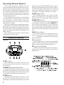
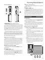
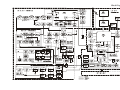
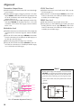
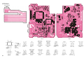
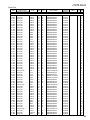
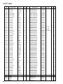
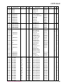
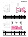
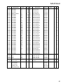
1
UHF Hand-Held Portable Land Mobile Transceiver VERTEX STANDARD CO., LTD. 4-8-8 Nakameguro, Meguro-Ku, Tokyo 153-8644, Japan VERTEX STANDARD US Headquarters 10900 Walker Street, Cypress, CA 90630, U.S.A. International Division 8350 N.W. 52nd Terrace, Suite 201, Miami, FL 33166, U.S.A. VX-520U YAESU EUROPE B.V. P.O. Box 75525, 1118 ZN Schiphol, The Netherlands YAESU UK LTD. Service Manual Unit 12, Sun Valley Business Park, Winnall Close Winchester, Hampshire, SO23 0LB, U.K. VERTEX STANDARD HK LTD. Unit 5, 20/F., Seaview Centre, 139-141 Hoi Bun Road, Kwun Tong, Kowloon, Hong Kong ©2003 VERTEX STANDARD CO., LTD. Introduction The VX-520U is a compact hand portable transceiver for the UHF land mobile band that offers the convenience of small size, light weight, and simple operation. The VX-520U can be simply programmed by your VERTEX STANDARD Dealer with up to 32 channels for single and split frequency operation. The VX-520U provides up to 5 watts of RF output power and includes a flexible quick-connect antenna. The transceiver and Ni-Cd battery packs are constructed of thick high impact polycarbonate plastic, with special attention paid by the designers to tight sealing and ruggedness, assuring years of reliable operation even in harsh environments. The following pages describe the operation, features and accessories of the VX-520U. With proper care and operation, the transceiver will provide many years of reliable communications. Contents Operating Manual Reprint .......................... 2 Specifications ................................................. 8 Exploded View & Miscellaneous Parts .... 9 Block Diagram ............................................. 11 Circuit Description..................................... 13 Alignment ..................................................... 15 Interconnection Diagram ........................... 19 Board Unit (Schematics, Layouts & Parts) CNTL Unit .............................................................. 21 LCD Unit ................................................................. 29 VR & PTT Unit ........................................................ 31 Main Unit ................................................................ 33 APC Unit ................................................................. 39 PLL Unit .................................................................. 41 REG Unit ................................................................. 44 IF Unit ...................................................................... 46 VCO Unit ................................................................. 48 TCXO Unit .............................................................. 50 1 Operating Manual Reprint The VX-520U is a frequency-synthesized, microprocessor-controlled FM hand-held portable transceiver providing up to five watts of power output on up to 32 channels in the UHF Land Mobile Band. Designed specifically for commercial and professional applications, the VX520U is housed in high-strength die-cast aluminum alloy, sealed to MIL-810 C, D & E intrinsically safe (I/S) and weather-tight specifications. User selectable features include a four-mode display with channel name or number, upright or inverted for easy viewing when on your belt; selective channel scanning, adjustable-pause priority scanning, and variable transmitter power output. Other user-selectable features include push-button display illumination, 2-tone decoder enable/disable (with optional F2D-5 Unit installed), and manual squelch override. The VX-520U is easily programmed by your dealer using a Vertex Standard Service Kit with an IBM PC-compatible computer. Please read this manual carefully to become familiar with the features of the VX-520U. CONTROLS & CONNECTORS Top panel requirements (See “PRE-PROGRAMMED FUNCTIONS”, page 6). Pressing and holding this button more than 4 seconds inverts the LCD display to either frontward or backward facing readout (the backward display is convenient for viewing when wearing the transceiver on your belt). (4) A/B Toggle Switch The 32 available channels in the VX-520 can be organized into 2 Groups with up to 16 channels in each. Toggle this switch to select a group “A” or “B” for operation. (5) BUSY/TX Indicator This lamp blinks green when a signal is being received (or the squelch is opened by pressing the MON RES button) and red when transmitting. To avoid interference, do not transmit if the lamp is glowing green. When the battery almost depleted, this lamp blinks red, indicating that the battery needs recharging or replacement very soon. (6) CH Rotary Selector This rotary switch selects the operating channel. If a channel is selected that is not available for operation, “-- -- -- --” is displayed, accompanied by a rapid warning beeper (2 beeps/sec.). (7) Antenna Jack This threaded-type jack accepts the supplied flexible antenna. Any other antenna types used here must be designed for the programmed operating frequencies. (8) Liquid Crystal Display In addition the channel number name, the display includes some operating status symbols, indicated in the diagram below. (1) VOL Control This control adjusts the volume of the receiver, and turns the radio off when rotated fully counterclockwise to the click-stop (2) S/DW Button (Scan/Dual Watch) Pressing and holding this button more than 2 seconds (but less than 4 seconds) turns the channel scanner on and off. Pressing and holding this button more than 4 seconds activates the Dual Watch feature (explained later). (3) DISP Button Pressing and holding this button more than 2 seconds (but less than 4 seconds) activates functions as programmed by your dealer and determined by your system 2 Operating Manual Reprint Side Panel Buttons (4) Battery Release button Slide this button in the direction of the arrow (upward) for battery removal. (5) EAR and MIC Jacks These jacks primarily intended for use with the optional MH-45E2B External Speaker/Microphone. An external earphone can be used in the larger jack, in which case the internal speaker will be disabled. When these jacks are not used, make sure the plastic cap and its two screws are in place to protect the insides of the transceiver. OPERATION Preliminaries (1) MON RES (Monitor/Reset) Button Pressing and holding this button more than 2 seconds (but less than 4 seconds) disables the tone squelch, and permits monitoring of stations transmitting on the selected channel while still keeping your receiver quiet from noise (“MO” will appear at the top right of the LCD). Press it again to only hear calls within your network. Pressing and holding this button more than 4 seconds toggles the tone and noise squelch override, allowing all stations (and noise) on the channel to be heard. This may be used to hear weak stations whose signals would not normally open the squelch. Do this to pre-adjust the VOLume control before receiving calls. (With Selective Calling Option) When the two-tone sequential decoder unit (F2D-5) is installed, and a selective call has been received (“CALL” indicator on), pressing and holding this button more than 2 seconds (but less than 4 seconds) will reset the call function on the current channel and silence the receiver, otherwise pressing and holding this button more than 4 seconds resets the call function on ALL channels. If the transceiver has not been used since leaving the factory, fully charge the battery using VAC-520 Rapid Desktop Charger before using it. Mount the battery on the transceiver as described and shown in the illustration below. Also, install the antenna on the jack on top of the transceiver by screwing the connector into the jack until it is finger-tight. Battery Removal & Replacement Make sure that the VOL control is set into the off click-stop, and remove the protective soft or hard case, if used. Grasp the transceiver with your left hand, so your palm is over the speaker and your thumb is on the Battery Release Button. Move the button in the direction indicated by the arrowhead, while using your right hand to slide the battery pack toward the side with the button. The battery pack should slide smoothly out of its track. To replace the Ni-Cd pack, repeat the second and third steps above, simply sliding the battery case in the other direction after aligning the shorter side of the battery pack with the track below the Battery Release Button. (2) PTT (Push-To-Talk) button Hold this button to transmit (the “BUSY/TX” indicator glows red). (3) LAMP/LOCK button Press this button momentarily to illuminate the display for five seconds. Pressing and holding this button locks top-panel push-buttons (S/DW, DISP, and the optional DTMF keypad); this can be enabled to prevent radio settings from being disturbed. 3 Operating Manual Reprint Preliminary Steps Before operating the transceiver for the first time: Charge the battery pack and connect the supplied helical rubber flex antenna to the antenna jack on the top of the transceiver. Never operate the transceiver without an antenna connected. If you have a Speaker/Mic, we suggest you do not connect it until you are familiar with basic operation. Before proceeding, please review the “Top & Side Panel Controls” outline, if you have not already, to familiarize yourself with the functions of the controls. Basic Operation Switch on the transceiver by rotating the VOL control clockwise out of the click-stop (a momentary beep will sound). For now, adjust the control to about mid-position (12-o’clock), later you can adjust the level to suit the operating environment. Switch the A/B toggle switch to select the channel group "A" or "B" for operation, then rotate the CH knob to select a channel for operation, the LCD will show the currently selected channel. If “-- -- -- --” is displayed, along with a rapid (2 beeps/sec.) beeping tone, the selected channel position is not available for operation. To transmit, wait until the channel is clear (“BUSY/ TX” LED off), then press in the PTT switch on the side of the transceiver while speaking across the face of the radio. A clear normal voice will provide the best quality transmission. For maximum battery life, select low power output (covered later) whenever possible. During transmission the “BUSY/TX” indicator glows red. Release the PTT switch to receive. To receive weak stations better, try positioning the radio as high and far away from your body as possible, or disable the squelch momentarily by holding the MON RES button on the side of the radio for > 4 sec. (until the second low/high beep sounds). With the squelch disabled, the “BUSY/TX” indicator will blinks green and channel noise and weak stations can be heard. To quiet the radio again, press the MON RES button again momentarily. When you are done operating, be certain to turn the VOL control to the off position to conserve battery life. 4 An important note about your radio ! Some of the radio/button functions discussed next will only operate in your radio if so programmed by your dealer, or after the installation of certain internal optional units. In this way, the radio’s operation can be simplified and customized specifically for the user according to network requirements. If pressing a button on your radio does not result in the same function described in this manual, or if you are uncertain of the functions your particular radio is configured with, contact your dealer. See “P RE -P RO GRAMMED FUNCTIONS” on page 6. Scanning Scanning allows you to sequentially check for calls on all or only those channels you select. To start scanning, pressing annd holding the S/DW button more than 2 seconds (but less than 4 seconds). A beep then sounds and the display will clear and show “SCAN”. Scanning will pause when a signal is received, at which time the channel number (or alphanumeric tag) will be displayed. A small “S” will be displayed above the channel, indicating the scanner is still active, but paused. During this pause, you can press the PTT switch and talk to the station. Otherwise, scanning will resume a few seconds after the signal is no longer present. While scanning, if you momentarily press the PTT switch, operation automatically shifts to a default channel. This default channel can be set to the priority channel (both “P” and “S/ DW” are displayed), last-busy channel, or home channel, depending on how your radio was programmed. To stop scanning, simply press S/DW momentarily again. Operation will return to the channel that was last selected when scanning was activated. If enabled by dealer programming, you may select only the channels you want to scan, and have others skippedover by performing the following routine. Turn the radio OFF, then depress the S/DW button while turning the radio back ON again. “PROG” will momentarily appear on the display, after which it will revert to the currently selected channel (this indicates you are in the programming mode). If user-access is disabled “INH” will appear briefly. Use the CH knob to select a channel, then press the S/ DW button to enable the channel for scanning (“E” will appear in the upper left corner of the LCD). Repeat this process for each channel you want the scanner to check. To remove a channel from those to be scanned, press S/DW again, so that “E” no longer appears in the display. After you have enabled all the channels you want to scan, turn the radio off, then on again to return to normal operation. Operating Manual Reprint Priority Scanning Dual Watch Priority scanning allows you to scan and monitor channels while the receiver periodically checks for calls on a pre-selected (“priority”) channel. You may want to use this feature if you want to scan different channels, but don’t want to miss a call for you on a primary dispatch, emergency or tactical frequency. After a call has been received on the priority channel, operation returns to the programmed default channel scheme, as mentioned before. Only one channel at a time can be selected as the priority channel. To assign the priority channel; Turn the radio OFF, then depress the S/DW button while turning the radio back ON again. “PROG” will momentarily appear on the display, after which it will revert to the currently selected channel (this indicates you are in the programming mode). If user-access is disabled “INH” will appear briefly. Use the CH knob to select a channel which you wish to assign the priority status, then press and hold in the S/DW button more than 1 second. A small “P” will now appear at the top left corner of the display whenever this channel is selected, along with an accompanying “beep”. If you wish to change the priority status; 1. Delete the priority status by pressing and holding the S/DW button more than 1 second. 2. Rotate the CH knob to select the new priority channel, then assign the priority status by pressing and holding the S/DW button for more than 1 second. After you have assigned the priority channel, turn the radio off, then on again to return to normal operation. If you need to operate on a non-priority channel while still checking for calls on the priority channel, the Dual Watch feature let’s you to do this without using the scanner. When enabled, operation on any selected non-priority remains normal as before, however, when a signal is received on the priority channel or when you press the PTT switch, operation immediately shifts to the priority channel. The rate at which the Dual Watch feature samples the priority channel can be set by the user. To begin Dual Watch operation, first assign a priority channel as described before, then select the non-priority channel you wish to operate on. Press and hold the S/DW button until the second beep sounds, “DW” (but not “S”) will appear at the top of the display. To manually shift to the priority channel, press the PTT switch. At this time you make transmit, otherwise, if no signal is received within 2 seconds, operation will revert back to the other selected Dual Watch channel. To turn off the Dual Watch Feature, press and hold the S/DW button again (“DW” will disappear in the display). When a priority channel has been selected, the scanner will check the priority channel regularly as you scan the other channels. If a signal appears on the priority channel, the scanner will pause and operation will jump to the priority channel. Otherwise, the scanner will pause on active non-priority signals as previously described. If a call comes in on a non-priority channel that you need to respond to, just press the PTT switch while the scanner is paused on that channel. As long as no call comes in on the priority channel, you can send and receive on the other channel: scanning will resume when you finish and the channel clears. Low Battery Power Indication When the rechargeable Ni-Cd battery pack voltage reaches a low level, the “ ” indicator appears at the lower right corner of the LCD, and the “BUSY/TX” indicator will blinks red. Immediately remove the Ni-Cd pack and install a freshly charged battery pack, or insert the radio into the charging stand for a complete recharge cycle. If you plan to operate your radio for extended periods of time, you may want to keep a spare, fully-charged pack handy. 5 Operating Manual Reprint PRE-PROGRAMMED FUNCTIONS BUTTON FUNCTIONS The function selected by pressing and holding the DISP button more than 2 seconds (but less than 4 seconds) can be customized by dealer programming and your network requirements. A brief explanation of available functions is provided below. However, contact your dealer for details on their use and operation. As mentioned before, button functions can be customized by programming from your Vertex Standard dealer to meet your communications/network requirements. Some features may require the purchase and installation of optional internal accessories for operation. The table below illustrates the possible Top-panel button programming combinations. Functions are explained on the previous page “PRE-PROGRAMMED FUNCTIONS.” For further details contact your nearest Vertex Standard dealer. For future reference, check the box next to the function that has been assigned to the button on your particular radio, and keep it handy. Low Transmit Power This reduces the power output of your radio to approximately one watt to conserve battery life, and when full power is not needed to maintain reliable communications. “LO ” will be displayed at the upper right corner when enabled. Press and Hold (< 2 seconds) Alpha Tag This displays an alpha-numeric channel name, usually describing the channel, rather than merely displaying a channel number. These may be programmed to assist you in recognizing channels by name, rather than by memorizing channel numbers and their assignments. DISP Button Optional Accessory Voice Encryption (FVP-22): When installed, pressing and holding this button more than 2 seconds (but less than 4 seconds) will turn on the optional voice encryption unit for privacy during communications. ENI (Emergency Numbering Identification) Unit (FTE-19): When installed, pressing and holding this button more than 2 seconds (but less than 4 seconds) will turn on the optional ENI Unit, then within 1/2 second, press this button again to transmit the ENI signal. 6 HI/LOW TX Power Alpha Tag Talk Around Accessory (Voice Encryption) Accessory (ENI) Press and Hold (< 2 second) Talk Around This feature enables simplex operation on semi-duplex channels: the transmit frequency becomes the same as the receive frequency (regardless of any programmed offset for the channel). Note: This feature has no effect on simplex channels. S/DW Button Starts/Stops Channel Scanning Press and Hold (> 4 seconds) Toggles the Top Panel LCD display between normal and inverted readout Press and Hold (> 4 second) Starts/Stops Dual-Watch Feature Press and Hold while Power-on 1) User-selectable channel scanning programming (if enabled) 2) Priority channel assigning (if enabled) CUSTOM SETTINGS Below is a table of radio features that can be customized by dealer programming. To change a feature as your requirements change, contact your Vertex Standard dealer. For future reference, check the box next to the option that has been programmed in your particular radio, and keep it handy. Feature Options Explanation Enabled Disabled Channel scanning can be disabled completely for systems not requiring this feature. Scan-Stop Resume 5-seconds Carrier In the 5-seconds mode, scanning pauses on a busy channel for 5 seconds, then resumes. In the Carrier mode, scanning pauses and remains on a busy channel until the station stops transmitting. User-Scan Program Enabled Disabled If enabled, the user can program which channels are to be scanned; otherwise, dealer-programmable only. Dual Watch Enabled Disabled Dual-Watch can be disabled completely for systems not requiring this feature. Channel after PTT Priority Ch. Home Ch. Last-Busy If the PTT is pressed during scanning, determines which default channel the radio returns to : the selected Priority Channel, a designated "Home" Channel, or the channel that was last-busy. Monitor Enabled Disabled Enable/Disable the side-panel MON RES button (See pages 6 & 9). DISP Button See Table Flexible dealer-programming as outlined in the table on the previous page. Channel Scan Operating Manual Reprint INSTALLING CHANNEL-STOPS To simplify operation and prevent selection of unprogrammed/unused channels or channel groups, tiny metal inserts or “stops” can be inserted into the top panel beneath the CH selector knob. A tiny tab protruding from beneath the skirt of the CH knob engages the stop(s) as it is turned, preventing further rotation. To insert a stop, rotate the CH knob to the channel “1” position and use the Allen wrench to loosen the setscrew locate the CH knob, then pull off the CH knob. Insert the stops firmly into the appropriate slot(s) for the desired channels, using a pair of tweezers or fine needle-nose pliers, according to the drawing below. For example, to limit CH selection to channels 1 - 4, insert one metal stop at the slot 16 (channel 1 minus “one position”), and the other at the slot 3 (channel 4 minus “one position”). When done, press the CH selector knob back on the shaft, align the indicator of the CH knob to channel “1,” then tighten the setscrew. Note: The use of mechanical stops should not be used or relied upon as the sole means to prevent selection or transmission on an invalid or unauthorized channel. Channels should be locked-out or TX-inhibited via programming by your Vertex Standard dealer, and stops inserted as a operating convenience to you and your network users. 7 Specifications General Number of Channels: Frequency Range: Channel Spacing: Power Supply Voltage: Current Consmption: Battery Life: Ambient Temperature Range: Frequency Stability: Dimensions: Weight: 32 450-488 MHz 12.5/25 kHz 7.2 VDC Standby (Saver On) 19 mA Standby (Saver Off) 50 mA Receive 200 mA Transmit 2/1 A 11 hrs. (13.3 hrs. w/saver) –22° F to +140° F (–30° C to +60° C) ±2.5 ppm 2.3" (W) x 5.9" (H) x 1.5" (D) inch w/FNB-29A 59 (W) x 149 (H) x 39 (D) mm w/FNB-29A 2.3" (W) x 6.7" (H) x 1.5" (D) inch w/FNB-29AL 59 (W) x 171 (H) x 39 (D) mm w/FNB-29A 1.21 lbs (547 g) w/o ANT w/FNB-29A 1.24 lbs (564 g) w/o ANT w/FNB-29AL Receive Circuit type: Sensitivity: Adjacent Channel Selectivity: Intermodulation: Spurious and Image Rejection: Conducted Spurious: Hum & Noise: Audio Output: Double-conversion Sperheterodyne 0.25 µV (EIA 12 dB SINAD) 0.35 µV (20 dB Quieting) 75 dB/65 dB 72 dB 75 dB –57 dBm 40/45 dB 0.5 W @16 Ohms, 5 % THD Transmit Power Output: Modulation: Conducted Spurious Emmisions: FM Hum & Noise: Audio Distortion (@1 kHz): 5.0/1.0 W 11K0F3E, 16K0F3E 60 dB Below Carrier 45/50 dB <2.5 % Specifications may be subject to change without notice or obligation. 8 RA0277900 CONNECTOR COVER Exploded View & Miscellaneous Parts R3518770 SUB PANEL RA0278400 PACKING SHEET CP7023000 PANEL SUB ASS'Y (w/ NYLON NET (2pcs)) R8141000 NAME PLATE RA0071100 RELEASE KNOB R7145910A RUBBER R0117370 COIL SPRING R7124630A NYLON NET R3130400A HOLDER M3290019 MIC ELEMENT K22174809 CHIP CAP. 0.001µF M4090103 SPEAKER T9206264A WIRE ASS'Y No. VXSTD P/N U20204027 U07240101 U07270127 U07430127 U32450001 U33104001 U43105001 U44204001 U32230127 U32430127 Qty. Description BINDING HEAD SCREW M2.6×4B SUS 2 4 PAN HEAD SCREW M2×4 #1 4 PAN HEAD SCREW M2×7B SUS 2 PAN HEAD SCREW M2.6×3B SUS #1 2 FLAT HEAD SCREW M2.6×5 4 TAPTITE SCREW M2×4 2 TAPTITE SCREW M2×5 10 TAPTITE SCREW M2.6×4 2 FLAT HEAD SCREW M2×3B SUS #1 4 FLAT HEAD SCREW M2.6×3B SUS #1 CNTL Unit PTT UNIT RA0409100 HOLDERPTT (Lot. 10~) VR Unit N0190177 ROTARY SWITCH RA0278500 RUBBER KNOB R3146900 INSULATOR ASS'Y T51005012 WIRE ASS'Y T95102171 JUMPER ASS'Y R0518720A HOLDER MAIN Unit IF Unit PLL Unit VCO Unit REG Unit APC Unit PA Unit R3149660A WASHER (2pcs) U76004001 PLAIN WASHER AW4 LCD Unit S2000054 O RING RA0277700 TOP PANEL ASS'Y R6054387B SPECIAL NUT (2pcs) R6149640 SPECIAL NUT R0149670B CONNECTOR ASS'Y R4900691 REAR PANEL RA0277800 RUBBER KNOB RA0278000 KNOB RA0278100 VOLUME KNOB S2000052 O RING Non-designated parts are available only as part of a designated assembly. 9 Note: 10 Block Diagram 11 Block Diagram Note: 12 Circuit Description Refer to the block diagram when reading this description. For finer details, refer to the schematic diagram. Receiver In coming signals at the antenna are passed through a low pass filter and T/R switching diode on the ANT SW Unit before delivery to the front-end circuitry on the mother board. Here the signal is band-pass filtered again by a 2-stage resonator, amplified by Q3201 (2SC3356-R24), and then further filtered by a 2-stage band-pass resonator befor application first mixer FET Q3202 (SGM2016M) along with the first local signal from Local Amplifier Q2406 (2SC4226-R24) on the VCO Unit. The 47.9 MHz product from the first mixer is delivered through 4-pole monolithic crystal filter XF3201 (± 6.0 kHz BW) to strip away all but the desired signal, which is amplified by Q3203 (2SC2620QB) on the Main Unit. FM receiver sub-system IC Q2302 (BA4116FV) on the IF Unit includes local oscillator, mixer, IF limiter amplifier and FM detector circuits. The amplified first IF signal is applied to mixer section, along with the second local signal generated via 48.355 MHz crystal X2301, which produces the 455 kHz 2nd IF when mixed with the 1st IF signal within Q2302. The 2nd IF passes through ceramic filter CF2301 (4.5 kHz BW) or CF2302 (7.5 kHz BW) to strip away unwanted mixer products, and is then applied to the limiter amp in Q2302, which remove amplitude variations in the 455 kHz IF before detection of the speech by Q2302 via quadrature resonator CD2301. Detected audio is delivered to the CTCSS IC Q1001 (FX165CLH) and then passes through the de-emphasis circuitry consisting of R1033 & C1015, via muting gate Q1011 (2SK160-K6) and volume control to audio power amplifier Q2206 (TDA2822D) and Q2211 (2SC4116GR) on the regulator unit, providing up to 0.5 W to the external speaker jack or 16-Ω loudspeaker. Squelch Control The squelch control circuit consists of noise amplifier Q2304 (2SC4116GR) and band-pass filter and squelch trigger within Q2302 on the IF Unit, and control circuitry within microprocessor Q1017 (M38067MC) on the control unit. When no carrier is received, noise at the output of the detector in Q2302 is amplified by Q2304, and band-pass filtered by the noise amplifier section of Q2302 and then rectified by D2302 to provide a DC control voltage for the squelch switching transistor Q2306 (2SA1586Y). With no carrier, the emitter of Q2306 is high. The signal is buffered by Q1013. This SCAN STOP signal is delivered to the microprocessor on the Control Unit, and microprocessor controlled through Q1003 (FMG5) to the BUSY indicator on the top panel, which remains off until a carrier is received. The microprocessor causes audio mute gate Q2207 (DTC144EU) & Q2202 (2SB1132Q) to open the audio power amplifier power source, thus disabling the au- dio amplifier and silencing the receiver when no signal is being received, and during transmission. When a carrier appears at the discriminator, noise is removed from the output, causing the emitter of Q2306 to go low, then Q1017 controls the signal high, which in turn causes Q1003 to turn on the BUSY indicator. The microprocessor then checks for CTCSS tone information from Q1001, plus Digital Code Squelch information form Q1006 (TA75S393F). If not transmitting and no tone squelch is programmed for the channel, or if the received tone matches that programmed for the channel, the microprocessor switches Q2207 to allow operation of the audio power amplifier. Transmitter When the PTT switch is depressed, audio from the microphone is delivered to the Control Unit, where it is highpass filtered by Q1018 (2SC4116GR), and by one section of microphone audio processing dual opamp IC Q1008 (NJM2904V). After pre-emphasis by C1074 and R1030, another section of Q1008 serves as an IDC (Instantaneous Deviation Control) amplifier to prevent over-deviation from excessive microphone levels, and the two remaining states provide low-pass filtering to suppress out-ofband modulation, and buffering. Processed audio from the IDC Unit is delivered to VCO Unit where it is applied, along with carefully filtered DC from Q2407 (2SC4116), to varactor diode D2403 (1SV230) to modulate (via the TX Line) VCO FET Q2404 (2SK508K52, on the VCO Unit), which oscillates at the transmit frequency. VCO output is buffered and amplified by Q2406 on the VCO Amplifier Unit before returning to the Main Unit. Buffered, modulated VCO output is applied via T/R switch D3202 to driver Q3205 (2SC3356), Q3214 (2SC3357), and the transmit signal is delivered to RF Power Module Q3206 (M68732H). The transmit signal is passed through T/R switching diode D2001 on the APC Unit, and then low-pass filtered by L2003~2005, and C2007, C2011 to suppress spurious harmonics before application to the antenna. Transmitter output is controlled by Q2001 (2SA1586Y) and Q2002 (FMW1) on the APC Unit. When the TX 5V line (from the regulator Unit) is active, bias voltage and driver collector voltage is applied to the RF Power Module via Q2003 and Q2004 , turning it on. A sample of the final transistor collector current in the RF Power Module is taken via R3224 on the mother board, detected by Q3207 (IMZ2), passed through RF Power potentiometer VR3201 on the main unit back to APC switch Q2001 (2SA1586Y) via one half of Q2002 (FMW1) on the APC Unit. Q2002 passes the Automatic Power Control voltage when enabled by the other (transmit sequencer) half of Q2002. This circuit is also used by the PLL to disable the transmitter when the PLL is unlocked, and by the microprocessor to select low power output. 13 Circuit Description PLL Control Unit & Supply Buses The first local signal for the receiver, and the carrier for the transmitter (at the transmitter frequency) are generated by the PLL. This circuit consists two voltage controlled oscillator (VCOs), prescalar, programmable divider, reference oscillator, phase detector, charge pump and low pass filter. The VCO (on the VCO Unit) consists of Q2401, Q2404 and varactor diodes D2401, D2402 and D2403 (mentioned above). The oscillating frequency is controlled primarily by the level of DC voltage fed from the loop filter (lowpass filter) to the varactor diodes. The VCO output is buffered by Q2406 (2SC4226), and then to prescalar within Q2105 (MB1505) on the PLL Unit, which divides the VCO frequency by 64 or 65, according to a control signal from the prescalar control logic section of PLL IC Q2105. The divided signal from the prescalar is fed to the programmable divider section of Q2105, where it is further divided down to 10/12.5 kHz according to data from microprocessor Q1017 on the Control Unit. Meanwhile, the reference oscillator section of Q2105 generates the reference frequency with crystal X2101, which signal is divided by Q2105. The reference and the divided VCO signal are applied together to the phase detector section of Q2105, from which any phase difference between the two signals results in a pulse train from the phase detector. The pulses are applied to the charge pump Q2102 (IMD3) and then through low-pass filter R2101, R2103 ~ R2106, R2122 and C2102, C2104 ~ C2107, to produce a DC voltage at a level corresponding to the difference in phase between the reference and the divided VCO signal. This DC voltage is returned to the varactor diodes on the VCO Unit, locking the frequency of the VCO to the crystal reference oscillator. In the Tx mode, Tx 5 volts applied to inverter Q2106 pulls analog switch Q2101-1/2 off, removing R2106 and R2122 from the PLL loop. Also, the transmitter VCO is modulated by the filtered speech audio applied to modulating varactor diode D2403, as previously described. If Digital Coded Squelch is in operation, the DCS signal modulation is applied to the PLL reference, via varactor D2102 & D2103 (HVU350). Microprocessor Q1017 (M38067MC) on the control unit contains programming in masked ROM to generate serial data to control the Liquid Crystal Display driver IC Q5001 (LC75821E) on the LCD Unit, and the programmable divider in the PLL according to channel frequency data stored in externally programmable EEPROM. Q1017 also includes programming for channel frequency scanning. DCS encode/decode, CTCSS IC Control, option unit control, selectable channel steps and frequency range. The microprocessor receives an indication of the condition of the noise squelch from the FM receiver subsystem IC on the IF Unit, by which scanning is activated or deactivated. Q1017 also controls the power saver function and transmit/receive switching by selecting the supply buses on the regulator unit:Q2209 (D T B 1 2 3 E K ), Q2205 (DTA143XK) and Q2210 (DTC144EU) disables the RX 5V bus when the power saver is active. When the PTT switch is pressed, the impedance change on the microphone line is detected by Q1015 (2SA1586Y) on the control unit, which signals the microprocessor that the transmitter is active. The microprocessor then activates LED indicator D5001 to glow red (TX). Voltage comparator Q1012 (RH5VL45AA) controls power-up resetting of the microprocessor. 14 Alignment UHF Transceiver Required Test Equipment PLL & Transmitter H IBM Set up the test equipment as shown for transmitter alignment. Adjust the supply voltage to 7.2 V for all steps where not specified otherwise. PC compatible computer H Vertex Standard VPL-1 Cable, or FRB-2 Service Kit, with CE37 Channel Programming Diskette Standard CN-1 BNC Adapter plug H RF Signal Generator with calibrated output level at 1 GHz H Deviation Meter (Linear Detector) H AC Voltmeter H SINAD Meter H In-Line wattmeter with 5% accuracy at 1 GHz H Regulated DC Power Supply adjustable from 4 to 10 V, 3 A H 50-Ω Non-reactive Dummy Load: 10 W at 1 GHz H Frequency Counter: ±0.2 ppm accuracy at 1 GHz H AF Signal Generator H DC Voltmeter: high impedance H Vertex Before beginning alignment, connect the transceiver and PC using the VPL-1 Cable or FRB-2 Set as described in the EEPROM Programming chapter, and download the EEPROM data from the transceiver to the computer. Then store this data in a disk file so that it can be uploaded when alignment is finished. You should find the corresponding data file on the computer disk for the transceiver version you are aligning, containing channel settings for the high edge, middle and low edge of the transceiver’s frequency range in channels 1, 2 and 3, respectively. Up-load this file to the transceiver. LOW BAND EDGE CH. (1) 450.0 MHz BAND CENTER CH. (2) 460.0 MHz HIGH BAND EDGE CH. (3) 470.0 MHz 50-ohm Dummy Load Sampling Coupler Inline Wattmeter ANT AF Signal Generator Freq. Counter Deviation Meter AC Voltmeter AC Voltmeter MIC Regulated DC 7.2V PSU PLL & TX Alignment Setup PLL VCV (Varactor Control Voltage) Ë Connect the DC voltmeter between C2105 on the PLL Unit and chassis ground. Ë Set the transceiver to CH 3 (high band edge), and adjust L2402 on the VCO Unit for 3.5 V ± 0.1 V on the voltmeter. Ë Transmit on the high band edge, and adjust L2406 for 3.5 V ± 0.1 V on the voltmeter. Ë Set the transceiver to CH 1 (low band edge), and confirm the low-end VCV is more than 1.3 V while transmitting, and also while receiving. PLL Reference Frequency Ë With CH 2 (band center) selected, key the transmitter and adjust TC2101 on the PLL Unit, if necessary, so the frequency counter displays the band center frequency ±300 Hz (for the version being aligned) when transmitting. L2402 VR3204 VR3201 L2406 VR3202 TC2101 C2105 PLL & Transmitter Alignment Points (I) 15 Alignment Transmitter Output Power CTCSS Tone Level Ë Set the transceiver to band center CH 2, and select high Ë power output. Ë Ensure that the supply voltage is precisely 7.2 V, then adjust VR3201 (while the PTT switch is pressed) for 5.0 W on the wattmeter, and confirm that supply current remains below 2.2 A. Ë Select low power output (“LO” displayed on the LCD), and adjust VR3202 on the Main Unit for 1.1 W on the wattmeter, and confirm that supply current remains below 1.2 A. Modulation Level With the transceiver set to band center CH 2, set the CTCSS encoder on . Ë Press the PTT switch and adjust VR1001 on the CNTL Unit for a deviation of ±0.7 kHz (for 25 kHz steps) or ± 0.35 kHz (for 12.5 kHz steps). DTMF Tone Level Ë Ë With the transceiver set to band center CH 2. Press [1] key on the DTMF keypad while press and holding the PTT switch, adjust VR1003 on the CNTL Unit for a deviation of ±2.5 kHz (for 25 kHz steps) or ± 1.25 kHz (for 12.5 kHz steps). Ë With the transceiver set to band center CH 2, adjust the AF generator for 77 mVrms output at 1 kHz to the MIC jack. Ë Press the PTT switch and adjust VR3204 on the Main Unit for a deviation of ±4.3 kHz (for 25 kHz steps) or ± 2.1 kHz (for 12.5 kHz steps). Ë Reduce the AF generator output to 7.7 mVrms. Ë Press the PTT switch and adjust VR1002 on the Control Unit for a deviation of ± 3.0 kHz (for 25 kHz steps) or ± 1.5 kHz (for 12.5 kHz steps). Note! Because of the bridge audio amplifier circuit used in the VX-520U, it is necessary to construct and use a simple audio load test adapter as shown in the schematic diagram above, when conducting receiver alignment steps. Do not connect either side of the speaker leads to chassis “ground”. 3.5φ PLUG VR1001 VR1003 VR1002 8Ω 1W Attenuated Test Output (1/2) 470µF Ground 8Ω 1W PLL & Transmitter Alignment Points (II) 16 AF Test Adapter Schematic Alignment Receiver Squelch Threshold Set up the test equipment as shown for receiver alignment, and construct the audio test adapter as described in the box on previous page . Ë RF Signal Generator ANT Set the transceiver to CH 2, and turn off the RF signal generator output. Ë Turn VR4002 on the VR Unit clockwise until the squelch just closes, and then counter-clockwise very slightly so that it just opens. AC Voltmeter AF Test Adapter SINAD Meter EAR CV3201 Speaker Regulated DC 7.2V PSU or 8-ohm load resistor CV3202 Receiver Alignment Setup Ë With the transceiver set to band center CH 2, and the RF signal generator tuned to the same frequency, set the generator for ± 3.0 kHz deviation with 1 kHz tone modulation, and set the output level for 40 µV at the antenna jack. Ë Adjust CV3201 and CV3202 on the Main Unit for optimum SINAD, reducing the signal generator output level as necessary for proper meter deflection. Ë After the previous step, final signal generator level should be better than –4 dBµ for 12 dB SINAD. Receiver Alignment Points Using the CN-1N BNC Adapter The VX-520U uses a threaded-type antenna jack to match the supplied helical flex antenna. To connect the VX-520U to test equipment or an external coaxial-fed antenna, the CN-1A adapter should be used to mate the transceiver with standard BNC connector. With the transceiver assembled, the CN-1A adapter can be installed by simply unscrewing the antenna, and installing the CN-1A in its place. When performing the alignment procedure, first disassemble the transceiver case as described, then replace the washer and threaded nut removed from antenna jack. Install the CN-1A adapter by carefully threading the unit on the antenna jack nut, then rotating the black knurled collar clockwise until it is finger-tight. To ensure a sufficient RF ground at the antenna connector during the alignment procedure and when making measurements, install the ground plate by sliding it over the CN-1A connector and then insert and tighten the supplied M2.6 x 3 screw into the rear case (see illustration). PANEL REAR ASS'Y Washer P/N : R6148750 Nut CN-1A Remember to remove the nut and washer again before assembling the transceiver body halves. 17 Alignment Note: 18 Interconnection Diagram 19 Interconnection Diagram Note: 20 CNTL Unit Circuit Diagram 7.2 V 2.5 V LAMP on: 4.2 V LAMP off: 0 V 2.5 V 2.2 V 5.0 V 5.0 V RX: 0.9 V SQL Open: 0 V TX: 0 V LAMP on: 5.0 V LAMP off: 0 V RX: 2.0 V TX: 1.9 V RX: 1.0 V 5.0 V RX: 0.8 V RX: 0 V TX: 5.0 V RX: 0.8 V RX: 0.9 V RX: 5.0 V TX: 0 V W: 0 V N: 5.0 V 5.0 V TX: 1.9 V 5.0 V 0V RX: 0 V TX: 1.9 V 5.0 V 5.0 V TX L: 5.0 V TX H: 0 V RX: 5.0 V TX: 0 V TX: 0.4 V RX: 0.1 V TX: 0.4 V RX: 5.0 V 0V TX: 5.0 V TX: 5.0 V RX: 0 V TX: 0.3 V TX: 1.9 V RX: 0 V TX: 2.0 V 5.0 V RX: 5.0 V TX: 0 V RX: 0 V TX: 5.0 V RX: 0 V TX: 5.0 V TX: 1.9 V 5.0 V SQL Close: 0 V RX: 0 V SQL Open: 4.2 V TX: 1.8 V 5.0 V 5.0 V 5.0 V 2.5 V 2.5 V 5.0 V 5.0 V 5.0 V 5.0 V 21 CNTL Unit Parts Layout Side A M38067ECA M38067MC (Lot. 8~) (Q1017) 22 MX165CLH (Q1001) Side B BR93LC66RF BR93L66RF (Lot. 16~) (Q1002) NJM2904V (Q1005, 1008) TA75S393F (TA) (Q1006) 2SK160 (K6) (Q1011) FMG5 (G5) (Q1003) UMG1 (G1) (Q1020) TC4W53FU (Q1014) TC4W66FU (Q1010) RN5VL45AA (D5) (Q1012) FMG2 (G2) (Q1016) FMW1 (W1) (Q1013) DTC144EU (26) (Q1007, 1021) DTDG23YP (E02) (Q1004) DTA143EU (13) (Q1009) 2SA1586Y (SY) (Q1015) DA204U (K) (D1004, 1006) 2SC4116GR (LG) (Q1018) DAN202U (N) (D1001, 1002, 1005) DA227 (N20) (D1003) CNTL Unit Parts List REF. C 1001 C 1002 C 1003 C 1004 C 1005 C 1006 C 1007 C 1008 C 1009 C 1010 C 1011 C 1012 C 1013 C 1014 C 1015 C 1016 C 1017 C 1018 C 1019 C 1020 C 1021 C 1022 C 1023 C 1024 C 1025 C 1026 C 1027 C 1028 C 1029 C 1030 C 1031 C 1032 C 1033 C 1034 C 1035 C 1036 C 1037 C 1038 C 1039 C 1040 C 1041 C 1042 C 1043 C 1044 C 1045 C 1046 C 1047 C 1048 C 1049 C 1050 C 1051 C 1052 C 1053 C 1054 C 1057 C 1058 C 1059 C 1060 DESCRIPTION PCB with Compornents P.C.B. W/O COMP. CHIP CAP. CHIP CAP. CHIP CAP. CHIP CAP. CHIP CAP. CHIP CAP. CHIP CAP. CHIP CAP. CHIP CAP. CHIP CAP. CHIP CAP. CHIP CAP. CHIP CAP. CHIP CAP. CHIP CAP. CHIP CAP. CHIP CAP. CHIP CAP. CHIP CAP. CHIP CAP. CHIP CAP. CHIP CAP. CHIP CAP. CHIP CAP. CHIP CAP. CHIP CAP. CHIP CAP. CHIP CAP. CHIP CAP. CHIP CAP. CHIP CAP. CHIP CAP. CHIP TA.CAP. CHIP CAP. CHIP CAP. CHIP CAP. CHIP CAP. CHIP CAP. CHIP CAP. CHIP CAP. CHIP TA.CAP. CHIP CAP. CHIP CAP. CHIP CAP. CHIP CAP. CHIP CAP. CHIP CAP. CHIP CAP. CHIP CAP. CHIP CAP. CHIP CAP. CHIP CAP. CHIP CAP. CHIP CAP. CHIP TA.CAP. CHIP CAP. CHIP CAP. CHIP CAP. VALUE 0.001uF 0.001uF 0.001uF 0.001uF 0.001uF 0.001uF 0.001uF 0.001uF 0.001uF 0.001uF 220pF 220pF 220pF 0.01uF 0.1uF 0.001uF 0.001uF 0.01uF 0.001uF 0.001uF 0.001uF 0.001uF 0.001uF 0.001uF 0.001uF 0.001uF 0.001uF 0.001uF 0.001uF 0.001uF 0.001uF 0.001uF 10uF 0.1uF 0.1uF 120pF 100pF 0.01uF 0.1uF 0.01uF 10uF 0.001uF 0.01uF 0.001uF 0.001uF 0.001uF 0.001uF 0.001uF 0.001uF 220pF 220pF 220pF 0.001uF 0.001uF 0.47uF 0.01uF 0.0047uF 0.01uF V/W 50V 50V 50V 50V 50V 50V 50V 50V 50V 50V 50V 50V 50V 25V 16V 50V 50V 25V 50V 50V 50V 50V 50V 50V 50V 50V 50V 50V 50V 50V 50V 50V 6.3V 16V 16V 50V 50V 25V 16V 25V 6.3V 50V 25V 50V 50V 50V 50V 50V 50V 50V 50V 50V 50V 50V 25V 25V 50V 25V TOL. B B B B B B B B B B B B B B B B B B B B B B B B B B B B B B B B B B CH CH B B B B B B B B B B B B B B B B B B B MFR’S DESIG VXSTD P/N GRM39B102K50PT GRM39B102K50PT GRM39B102K50PT GRM39B102K50PT GRM39B102K50PT GRM39B102K50PT GRM39B102K50PT GRM39B102K50PT GRM39B102K50PT GRM39B102K50PT GRM39B221M50PT GRM39B221M50PT GRM39B221M50PT GRM39B103K25PT GRM39B104K16PT GRM39B102K50PT GRM39B102K50PT GRM39B103K25PT GRM39B102K50PT GRM39B102K50PT GRM39B102K50PT GRM39B102K50PT GRM39B102K50PT GRM39B102K50PT GRM39B102K50PT GRM39B102K50PT GRM39B102K50PT GRM39B102K50PT GRM39B102K50PT GRM39B102K50PT GRM39B102K50PT GRM39B102K50PT TEMSVA0J106M-8R GRM39B104K16PT GRM39B104K16PT GRM39CH121J50PT GRM39CH101J50PT GRM39B103K25PT GRM39B104K16PT GRM39B103K25PT TEMSVA0J106M-8R GRM39B102K50PT GRM39B103K25PT GRM39B102K50PT GRM39B102K50PT GRM39B102K50PT GRM39B102K50PT GRM39B102K50PT GRM39B102K50PT GRM39B221M50PT GRM39B221M50PT GRM39B221M50PT GRM39B102K50PT GRM39B102K50PT TESVA1E474M1-8R GRM39B103K25PT GRM39B472K50PT GRM39B103K25PT CB1467001 FR006600D K22174821 K22174821 K22174821 K22174821 K22174821 K22174821 K22174821 K22174821 K22174821 K22174821 K22174801 K22174801 K22174801 K22144803 K22124805 K22174821 K22174821 K22144803 K22174821 K22174821 K22174821 K22174821 K22174821 K22174821 K22174821 K22174821 K22174821 K22174821 K22174821 K22174821 K22174821 K22174821 K78080027 K22124805 K22124805 K22174237 K22174235 K22144803 K22124805 K22144803 K78080027 K22174821 K22144803 K22174821 K22174821 K22174821 K22174821 K22174821 K22174821 K22174801 K22174801 K22174801 K22174821 K22174821 K78140009 K22144803 K22174833 K22144803 VERS. LOT. SIDE 1 1111111111111111111111111111111111111111111111111111111111- A A A A A A A A A A A A A A B A B B A A A A A A A A A A B B B B A A A A A A A B B B B A A B A B B B B B B B A B B B 23 CNTL Unit REF. C 1061 C 1062 C 1063 C 1064 C 1065 C 1066 C 1067 C 1068 C 1069 C 1070 C 1071 C 1072 C 1073 C 1074 C 1075 C 1075 C 1076 C 1076 C 1076 C 1077 C 1078 C 1079 C 1080 C 1081 C 1082 C 1083 C 1084 C 1085 C 1086 C 1087 C 1088 C 1089 C 1092 C 1093 C 1094 C 1095 C 1096 C 1101 C 1102 C 1103 C 1104 C 1105 C 1106 C 1107 C 1108 C 1109 C 1110 C 1111 C 1112 C 1113 C 1114 C 1115 C 1116 C 1117 C 1118 CO1001 D 1001 D 1002 D 1003 D 1004 24 DESCRIPTION CHIP CAP. CHIP CAP. CHIP CAP. CHIP CAP. CHIP TA.CAP. CHIP TA.CAP. CHIP TA.CAP. CHIP TA.CAP. CHIP CAP. CHIP CAP. CHIP CAP. CHIP CAP. CHIP CAP. CHIP CAP. CHIP CAP. CHIP CAP. CHIP CAP. CHIP CAP. CHIP CAP. CHIP TA.CAP. CHIP CAP. CHIP TA.CAP. CHIP CAP. CHIP CAP. CHIP CAP. CHIP CAP. CHIP CAP. CHIP CAP. CHIP CAP. CHIP TA.CAP. CHIP CAP. CHIP CAP. CHIP CAP. CHIP CAP. CHIP CAP. CHIP CAP. CHIP CAP. CHIP CAP. CHIP CAP. CHIP CAP. CHIP CAP. CHIP CAP. CHIP TA.CAP. CHIP CAP. CHIP CAP. CHIP CAP. CHIP CAP. CHIP TA.CAP. CHIP CAP. CHIP CAP. CHIP CAP. CHIP CAP. CHIP CAP. CHIP CAP. CHIP CAP. CERAMIC OSC DIODE DIODE DIODE DIODE VALUE V/W 0.001uF 0.047uF 0.0022uF 0.01uF 0.47uF 1uF 1uF 0.1uF 0.01uF 0.001uF 33pF 0.01uF 0.01uF 0.01uF 0.01uF 0.01uF 0.1uF 0.1uF 0.01uF 2.2uF 0.001uF 2.2uF 0.001uF 0.1uF 22pF 27pF 220pF 220pF 0.001uF 10uF 0.001uF 0.001uF 0.001uF 0.001uF 0.001uF 0.001uF 0.001uF 0.01uF 0.01uF 0.1uF 0.1uF 0.1uF 1uF 0.001uF 22pF 3pF 3pF 10uF 220pF 0.01uF 0.01uF 0.001uF 220pF 0.001uF 0.0047uF 1MHz 50V 16V 50V 25V 25V 16V 16V 35V 25V 50V 50V 25V 25V 25V 25V 25V 16V 16V 25V 6.3V 50V 6.3V 50V 16V 50V 50V 50V 50V 50V 6.3V 50V 50V 50V 50V 50V 50V 50V 25V 25V 16V 16V 16V 16V 50V 50V 50V 50V 6.3V 50V 25V 25V 50V 50V 50V 50V TOL. B B B B B B CH B B B B B B B B B B B CH CH B B B B B B B B B B B B B B B B CH CJ CJ B B B B B B B MFR’S DESIG GRM39B102K50PT GRM39B473K16PT GRM39B222K50PT GRM39B103K25PT TESVA1E474M1-8R TESVA1C105M1-8R TESVA1C105M1-8R TESVA1V104M1-8R GRM39B103K25PT GRM39B102K50PT GRM39CH330J50PT GRM39B103K25PT GRM39B103K25PT GRM39B103K25PT GRM39B103K25PT GRM39B103K25PT GRM39B104K16PT GRM39B104K16PT GRM39B103K25PT TESVA0J225M1-8R GRM39B102K50PT TESVA0J225M1-8R GRM39B102K50PT GRM39B104K16PT GRM39CH220J50PT GRM39CH270J50PT GRM39B221M50PT GRM39B221M50PT GRM39B102K50PT TEMSVA0J106M-8R GRM39B102K50PT GRM39B102K50PT GRM39B102K50PT GRM39B102K50PT GRM39B102K50PT GRM39B102K50PT GRM39B102K50PT GRM39B103K25PT GRM39B103K25PT GRM39B104K16PT GRM39B104K16PT GRM39B104K16PT TESVA1C105M1-8R GRM39B102K50PT GRM39CH220J50PT GRM39CJ030C50PT GRM39CJ030C50PT TEMSVA0J106M-8R GRM39B221M50PT GRM39B103K25PT GRM39B103K25PT GRM39B102K50PT GRM39B221M50PT GRM39B102K50PT GRM39B472K50PT CSB1000J DAN202U T106 DAN202U T106 DA227-TR DA204U T106 VXSTD P/N K22174821 K22124804 K22174822 K22144803 K78140009 K78120009 K78120009 K78160025 K22144803 K22174821 K22174223 K22144803 K22144803 K22144803 K22144803 K22144803 K22124805 K22124805 K22144803 K78080009 K22174821 K78080009 K22174821 K22124805 K22174219 K22174221 K22174801 K22174801 K22174821 K78080027 K22174821 K22174821 K22174821 K22174821 K22174821 K22174821 K22174821 K22144803 K22144803 K22124805 K22124805 K22124805 K78120009 K22174821 K22174219 K22174204 K22174204 K78080027 K22174801 K22144803 K22144803 K22174821 K22174801 K22174821 K22174833 H7901230 G2070162 G2070162 G2070292 G2070242 VERS. VX-520U VX-520U VX-520UN LOT. SIDE 111111111111111-10 111-10 111111111111111111111111111111111111111111111- B B B B B A A B B B B A B A B B A A A A A B B B A A A A B B B A B B B B B B B B B B B B B A A B B A A B B A B A A B B B CNTL Unit REF. DESCRIPTION D 1005 D 1006 D 1007 D 1008 J 1001 J 1002 J 1003 J 1004 J 1005 J 1006 J 1007 J 1008 L 1001 L 1002 L 1003 L 1004 L 1005 Q 1001 Q 1002 Q 1002 Q 1003 Q 1004 Q 1005 Q 1006 Q 1007 Q 1008 Q 1009 Q 1010 Q 1011 Q 1012 Q 1013 Q 1014 Q 1016 Q 1017 Q 1017 Q 1017 Q 1018 Q 1020 Q 1021 Q 1022 R 1001 R 1002 R 1003 R 1004 R 1005 R 1006 R 1007 R 1008 R 1008 R 1009 R 1010 R 1011 R 1012 R 1013 R 1014 R 1015 R 1016 R 1017 R 1018 R 1019 DIODE DIODE DIODE DIODE CONNECTOR CONNECTOR CONNECTOR CONNECTOR CONNECTOR CONNECTOR CONNECTOR CONNECTOR FERRITE BEADS FERRITE BEADS FERRITE BEADS FERRITE BEADS FERRITE BEADS IC IC IC TRANSISTOR TRANSISTOR IC IC TRANSISTOR IC TRANSISTOR IC FET IC TRANSISTOR IC TRANSISTOR IC IC IC TRANSISTOR TRANSISTOR TRANSISTOR TRANSISTOR CHIP RES. CHIP RES. CHIP RES. CHIP RES. CHIP RES. CHIP RES. CHIP RES. CHIP RES. CHIP RES. CHIP RES. CHIP RES. CHIP RES. CHIP RES. CHIP RES. CHIP RES. CHIP RES. CHIP RES. CHIP RES. CHIP RES. CHIP RES. VALUE 1M 1M 330k 33k 12k 1k 120k 220 10 100k 100k 56k 56k 100k 82k 47k 68k 33k 39k 1M Please contact VERTEX STANDARD. V/W 1/16W 1/16W 1/16W 1/16W 1/16W 1/16W 1/16W 1/16W 1/16W 1/16W 1/16W 1/16W 1/16W 1/16W 1/16W 1/16W 1/16W 1/16W 1/16W 1/16W TOL. 5% 5% 5% 5% 5% 5% 5% 5% 5% 5% 5% 5% 5% 5% 5% 5% 5% 5% 5% 5% MFR’S DESIG 1SS355 TE-17 DA204U T106 DA204U T106 MC2846-T11-1 9213B-1-04Z010-T 9213B-1-02Z006-T IL-Z-12PL-SMTY-E1500 53263-1690 53263-1290 9120S-05A 53048-0410 HSJ1468-01-130 BK2125HS121-T BK2125HS121-T BK2125HS121-T BK2125HS121-T BK2125HS121-T MX165CLH-TR BR93LC66RF-E2 BR93L66RF-WE2 FMG5 T148 DTDG23YP T100 NJM2904V-TE1 TA75S393F TE85R DTC144EU T106 NJM2904V-TE1 DTA143EU T106 TC4W66FU TE12L 2SK160-T2B K6 RN5VL45AA-TR FMW1 T98 TC4W53FU TE12L FMG2 T148 M38067ECAGP M38067MC-463GP M38067MC-470GP 2SC4116GR TE85R UMG1 TR DTA144TE TL DTC144EU T106 RMC1/16 105JATP RMC1/16 105JATP RMC1/16 334JATP RMC1/16 333JATP RMC1/16 123JATP RMC1/16 102JATP RMC1/16 124JATP RMC1/16 221JATP RMC1/16 100JATP RMC1/16 104JATP RMC1/16 104JATP RMC1/16 563JATP RMC1/16 563JATP RMC1/16 104JATP RMC1/16 823JATP RMC1/16 473JATP RMC1/16 683JATP RMC1/16 333JATP RMC1/16 393JATP RMC1/16 105JATP VXSTD P/N G2070470 G2070242 G2070242 G2070702 P0091044 P0090974 P0090971 P0091052 P0091051 P1090811 P0090972 P1090916 L9190079 L9190079 L9190079 L9190079 L9190079 G1092010 G1092006 G1093912 G3070021 G3070198 G1091677 G1091589 G3070041 G1091677 G3070110 G1091676 G3801607F G1091552 G3070009 G1091675 G3070015 G3341167G G3070113 G3070209 G3070041 J24185105 J24185105 J24185334 J24185333 J24185123 J24185102 J24185124 J24185221 J24185100 J24185104 J24185104 J24185563 J24185563 J24185104 J24185823 J24185473 J24185683 J24185333 J24185393 J24185105 VERS. LOT. SIDE 31111111111111111111611111111111111813111111111111311111111111- A B B A A A A A A A A A B B B B B A B B A A B B B B B A B B A A B A A A B A B B A A A A A B A B B B B B B B B B A B B B 25 CNTL Unit REF. R 1020 R 1021 R 1022 R 1023 R 1024 R 1025 R 1026 R 1027 R 1028 R 1029 R 1030 R 1031 R 1031 R 1032 R 1032 R 1032 R 1033 R 1034 R 1035 R 1036 R 1037 R 1038 R 1040 R 1041 R 1042 R 1043 R 1044 R 1045 R 1049 R 1051 R 1052 R 1055 R 1057 R 1057 R 1058 R 1059 R 1060 R 1061 R 1062 R 1063 R 1064 R 1065 R 1066 R 1067 R 1068 R 1069 R 1075 R 1076 R 1077 R 1078 R 1079 R 1080 R 1081 R 1082 R 1083 R 1085 R 1086 R 1087 R 1088 R 1089 26 DESCRIPTION CHIP RES. CHIP RES. CHIP RES. CHIP RES. CHIP RES. CHIP RES. CHIP RES. CHIP RES. CHIP RES. CHIP RES. CHIP RES. CHIP RES. CHIP RES. CHIP RES. CHIP RES. CHIP RES. CHIP RES. CHIP RES. CHIP RES. CHIP RES. CHIP RES. CHIP RES. CHIP RES. CHIP RES. CHIP RES. CHIP RES. CHIP RES. CHIP RES. CHIP RES. CHIP RES. CHIP RES. CHIP RES. CHIP RES. CHIP RES. CHIP RES. CHIP RES. CHIP RES. CHIP RES. CHIP RES. CHIP RES. CHIP RES. CHIP RES. CHIP RES. CHIP RES. CHIP RES. CHIP RES. CHIP RES. CHIP RES. CHIP RES. CHIP RES. CHIP RES. CHIP RES. CHIP RES. CHIP RES. CHIP RES. CHIP RES. CHIP RES. CHIP RES. CHIP RES. CHIP RES. VALUE 82k 560k 56k 33k 100k 0 220k 10k 47k 220k 2.2k 15k 15k 180k 180k 15k 4.7k 10k 47k 100k 100k 47k 22k 100k 22k 1k 1.5k 470 0 100 47k 470 0 10k 47k 82k 820 150k 3.3k 820k 4.7k 100k 47k 1k 0 1k 0 5.6k 47k 22k 10k 4.7k 47k 47k 47k 22k 22k 22k 47k 47k V/W 1/16W 1/16W 1/16W 1/16W 1/16W 1/16W 1/16W 1/16W 1/16W 1/16W 1/16W 1/16W 1/16W 1/16W 1/16W 1/16W 1/16W 1/16W 1/16W 1/16W 1/16W 1/16W 1/16W 1/16W 1/16W 1/16W 1/16W 1/16W 1/16W 1/16W 1/16W 1/16W 1/16W 1/16W 1/16W 1/16W 1/16W 1/16W 1/16W 1/16W 1/16W 1/16W 1/16W 1/16W 1/16W 1/16W 1/10W 1/16W 1/16W 1/16W 1/16W 1/16W 1/16W 1/16W 1/16W 1/16W 1/16W 1/16W 1/16W 1/16W TOL. 5% 5% 5% 5% 5% 5% 5% 5% 5% 5% 5% 5% 5% 5% 5% 5% 5% 5% 5% 5% 5% 5% 5% 5% 5% 5% 5% 5% 5% 5% 5% 5% 5% 5% 5% 5% 5% 5% 5% 5% 5% 5% 5% 5% 5% 5% 5% 5% 5% 5% 5% 5% 5% 5% 5% 5% 5% 5% 5% 5% MFR’S DESIG RMC1/16 823JATP RMC1/16 564JATP RMC1/16 563JATP RMC1/16 333JATP RMC1/16 104JATP RMC1/16 000JATP RMC1/16 224JATP RMC1/16 103JATP RMC1/16 473JATP RMC1/16 224JATP RMC1/16 222JATP RMC1/16 153JATP RMC1/16 153JATP RMC1/16 184JATP RMC1/16 184JATP RMC1/16 153JATP RMC1/16 472JATP RMC1/16 103JATP RMC1/16 473JATP RMC1/16 104JATP RMC1/16 104JATP RMC1/16 473JATP RMC1/16 223JATP RMC1/16 104JATP RMC1/16 223JATP RMC1/16 102JATP RMC1/16 152JATP RMC1/16 471JATP RMC1/16 000JATP RMC1/16 101JATP RMC1/16 473JATP RMC1/16 471JATP RMC1/16 000JATP RMC1/16 103JATP RMC1/16 473JATP RMC1/16 823JATP RMC1/16 821JATP RMC1/16 154JATP RMC1/16 332JATP RMC1/16 824JATP RMC1/16 472JATP RMC1/16 104JATP RMC1/16 473JATP RMC1/16 102JATP RMC1/16 000JATP RMC1/16 102JATP RMC1/10T 000J RMC1/16 562JATP RMC1/16 473JATP RMC1/16 223JATP RMC1/16 103JATP RMC1/16 472JATP RMC1/16 473JATP RMC1/16 473JATP RMC1/16 473JATP RMC1/16 223JATP RMC1/16 223JATP RMC1/16 223JATP RMC1/16 473JATP RMC1/16 473JATP VXSTD P/N J24185823 J24185564 J24185563 J24185333 J24185104 J24185000 J24185224 J24185103 J24185473 J24185224 J24185222 J24185153 J24185153 J24185184 J24185184 J24185153 J24185472 J24185103 J24185473 J24185104 J24185104 J24185473 J24185223 J24185104 J24185223 J24185102 J24185152 J24185471 J24185000 J24185101 J24185473 J24185471 J24185000 J24185103 J24185473 J24185823 J24185821 J24185154 J24185332 J24185824 J24185472 J24185104 J24185473 J24185102 J24185000 J24185102 J24205000 J24185562 J24185473 J24185223 J24185103 J24185472 J24185473 J24185473 J24185473 J24185223 J24185223 J24185223 J24185473 J24185473 VERS. VX-520U VX-520U VX-520UN LOT. SIDE 111111111111-10 111-10 111111111111111111111311111111111111111111111111- B B B B B B A A A B A B B A A A A A A B B B A A A A B B B B A A A A B B B B B B B B A B B B B B A A A B A A A B A A A B CNTL Unit REF. R 1090 R 1090 R 1091 R 1093 R 1094 R 1095 R 1096 RB1001 RB1002 RB1004 RB1006 RB1007 RB1008 RB1009 RB1010 RB1012 RB1013 TH1001 VR1001 VR1002 VR1003 X 1002 DESCRIPTION CHIP RES. CHIP RES. CHIP RES. CHIP RES. CHIP RES. CHIP RES. CHIP RES. BLOCK RES. BLOCK RES. BLOCK RES. BLOCK RES. BLOCK RES. BLOCK RES. BLOCK RES. BLOCK RES. BLOCK RES. BLOCK RES. THERMISTOR POT. POT. POT. XTAL FCX-01 SHIELD PLATE VALUE 1k 10k 47k 0 100k 0 100k 47k 10k 47k 3.6864MHz V/W TOL. 1/16W 1/16W 1/16W 1/16W 1/16W 1/16W 1/16W 5% 5% 5% 5% 5% 5% 5% MFR’S DESIG RMC1/16 102JATP RMC1/16 103JATP RMC1/16 473JATP RMC1/16 000JATP RMC1/16 104JATP RMC1/16 000JATP RMC1/16 104JATP RCB8C473J5E5A RCB8C102J5E5A RCB8C102J5E5A RCB8C473J5E5A RCB8C102J5E5A RCB8C473J5E5A RCB8C102J5E5A RCB8C473J5E5A RCB8C473J5E5A RCB8C102J5E5A TBPS1R472K440H5Q RH03A3AS4X 47K RH03A3A14X 10K RH03A3AS4X 47K 3.6864MHZ VXSTD P/N J24185102 J24185103 J24185473 J24185000 J24185104 J24185000 J24185104 J42900006 J42900005 J42900005 J42900006 J42900005 J42900006 J42900005 J42900006 J42900006 J42900005 G9090066 J51807473 J51807103 J51807473 H0103062 R0146880 VERS. LOT. SIDE 13111111111111111111111- B B B B B B A B A B B B B B B A B B A A A A 27 CNTL Unit Note: 28 LCD Unit Circuit Diagram Parts Layout Side A LC75821E (Q5001) Side B LT1ED53A (D5001) FSD-10928 (DS5001) Circuit Diagram 29 LCD Unit Parts List REF. C 5001 C 5002 C 5003 C 5004 C 5005 C 5006 C 5007 C 5008 D 5001 DS5001 J 5001 PL5001 Q 5001 R 5001 R 5002 R 5003 R 5005 S 5001 30 DESCRIPTION PCB with Compornents P.C.B. W/O COMP CHIP CAP. CHIP CAP. CHIP CAP. CHIP CAP. CHIP CAP. CHIP CAP. CHIP CAP. CHIP CAP. LED LCD CONNECTOR LAMP IC CHIP RES. CHIP RES. CHIP RES. CHIP RES. TOGGLE SWITCH LIGHT GUIDE LCD GUIDE RUBBER CONNECTOR REFLECTOR SHEET DIFFUSER SHEET COLOR FILTER VALUE V/W 680pF 0.1uF 47pF 0.01uF 100pF 100pF 100pF 100pF 50V 25V 50V 25V 50V 50V 50V 50V 60mA 5V 330 330 47k 470k 1/16W 1/16W 1/16W 1/16W TOL. B B CH B CH CH CH CH 5% 5% 5% 5% MFR’S DESIG AC021U000 GRM39B681M50PT GRM40B104M25PT GRM39CH470J50PT GRM39B103K25PT GRM39CH101J50PT GRM39CH101J50PT GRM39CH101J50PT GRM39CH101J50PT LT1ED53A FSD-10928 52357-1290 5V60MA T-3/4 #6153 LC75821W RMC1/16 331JATP RMC1/16 331JATP RMC1/16 473JATP RMC1/16 474JATP ATE1D-2M3-10 VXSTD P/N CB1470001 FR006620B K22174807 K22140811 K22174227 K22144803 K22174235 K22174235 K22174235 K22174235 G2070548 G6090093 P1090884 Q1000092 G1093333 J24185331 J24185331 J24185473 J24185474 N2090060 RA0078200 RA0078300 RA0078100 RA0077800 RA0078900 RA0078000 VERS. LOT. SIDE 1 111111111111111111111111- B B B B B B B B A A B B B B B B B A VR & PTT Unit VR Unit Circuit Diagram VR Unit Parts Layout Side A Side B Parts List REF. JP4001 VR4001 VR4002 DESCRIPTION VALUE V/W TOL. PCB with Compornents Printed Circuit Board WIRE ASSY POT. POT. 22k PTT Uni Diagram MFR’S DESIG A0403 RK0971111 20KA/SW RH03A3AJ4X 22K VXSTD P/N VERS. CB1468001 FR006610B T9206360 J60800254 J51807223 LOT. 1111- PTT Unit Parts Layout Side A Side B Parts List DESCRIPTION J 4101 S 4101 S 4102 S 4103 PCB with Compornents Printed Circuit Board CONNECTOR TACT SWITCH TACT SWITCH TACT SWITCH VALUE V/W TOL. MFR’S DESIG 9120B-05 SKQDAB SKQDAB SKQDAB VXSTD P/N CB1469001 F3364101 P0090955 N5090058 N5090058 N5090058 VERS. LOT. 11111- 31 Note: 32 Main Unit Circuit Diagram W: 5.0 V N: 0 V RX: 3.6 V –113.0 dbm 5.0 V RX: 0 V TX: 0.8 V –100.0 dbm RX: 4.6 V SQL Close: 0 V SQL Open: 4.4 V –115.0 dbm –121.0 dbm –111.0 dbm RX: 0 V TX: 0.8 V 1.3 V RX: 0.7 V –114.0 dbm TX L: 5.0 V TX H: 0 V 0V 0V RX: 0.4 V 0V –116.0 dbm 4.7 V 0V TX L: 0.1 V TX H: 0.2 V 0.6 Vpp RX: 0.8 V 0V TX L: 1.4 V TX H: 2.8 V TX L: 1.4 V TX H: 2.7 V SQL Close: 0 V SQL Open: 3.2 V TX L: 2.2 V TX H: 2.7 V RX: 1.1 V –114 dbm TX L: 1.9 V TX H: 2.5 V 4.9 V TX: 1.3 V TX L: 0.3 V TX H: 1.9 V 2.9 V TX: 0.7 V TX: 0.5 V W: 2.1 V N: 5.0 V TX: 4.3 V TX: 2.9 V TX L: 0 V TX H: 2.7 V RX: 6.8 V TX L: 6.4 V TX H: 6.1 V RX: 0.7 V TX: 0.6 V RX: 6.8 V TX: 0 V 0.9 V TX: 4.7 V TX: 1.5 V RX: 1.8 ~ 4.0 V TX: 1.6 ~ 4.0 V 7.2 V TX: 1.8 V 0.8 V TX: 1.7 V TX L: 2.0 V TX H: 0 V 33 Main Unit Parts Layout M5223FP (Q3209) Side A 34 Side B M68732HA (Q3206) DTC124TU (05) (Q3215) RN2305 (YE) (Q3211) 2SC3357 (RK) (Q3214) 1SS184 (B3) (D3202) SGM2016AM (MA) (Q3202) DTC144EU (26) (Q3208, 3210, 3212, 3213, 3216) IMZ2 (Z2) (Q3207) 2SC3356 (R24) (Q3201, 3205) 2SC2620 (QB) (Q3203) 2SC5005 (73) (Q3204) MAIN Unit Parts List REF. C 3201 C 3203 C 3204 C 3205 C 3206 C 3207 C 3208 C 3209 C 3210 C 3211 C 3212 C 3213 C 3214 C 3215 C 3216 C 3217 C 3218 C 3219 C 3220 C 3221 C 3222 C 3223 C 3224 C 3225 C 3226 C 3227 C 3228 C 3229 C 3230 C 3231 C 3232 C 3233 C 3234 C 3236 C 3237 C 3239 C 3240 C 3241 C 3242 C 3243 C 3244 C 3245 C 3246 C 3247 C 3249 C 3250 C 3251 C 3252 C 3253 C 3254 C 3254 C 3255 C 3256 C 3257 C 3258 C 3259 C 3260 C 3261 DESCRIPTION PCB with Compornents P.C.B. W/O COMP. CHIP CAP. CHIP CAP. CHIP CAP. CHIP CAP. CHIP CAP. CHIP CAP. CHIP CAP. CHIP CAP. CHIP CAP. CHIP CAP. CHIP CAP. CHIP CAP. CHIP CAP. CHIP CAP. CHIP CAP. CHIP CAP. CHIP CAP. CHIP CAP. CHIP CAP. CHIP TA.CAP. CHIP CAP. CHIP CAP. CHIP CAP. CHIP TA.CAP. CHIP CAP. CHIP CAP. CHIP CAP. CHIP CAP. CHIP CAP. CHIP CAP. CHIP CAP. CHIP CAP. CHIP CAP. CHIP CAP. CHIP TA.CAP. CHIP CAP. CHIP CAP. CHIP CAP. CHIP CAP. CHIP CAP. CHIP CAP. CHIP CAP. CHIP CAP. CHIP CAP. CHIP CAP. CHIP CAP. CHIP CAP. CHIP CAP. CHIP TA.CAP. CHIP CAP. CHIP CAP. CHIP TA.CAP. CHIP CAP. CHIP CAP. AL.ELECTRO.CAP. CHIP CAP. CHIP CAP. CHIP CAP. VALUE 0.001uF 10pF 47pF 6pF 0.001uF 10pF 0.001uF 27pF 0.001uF 0.001uF 22pF 0.01uF 0.01uF 22pF 0.01uF 0.01uF 0.01uF 0.001uF 0.001uF 10uF 0.001uF 2pF 10pF 1uF 0.001uF 22pF 0.01uF 22pF 5pF 0.001uF 0.001uF 0.001uF 0.001uF 0.001uF 10uF 0.001uF 0.001uF 0.001uF 0.001uF 0.001uF 0.001uF 0.01uF 0.001uF 0.001uF 18pF 0.001uF 270pF 0.001uF 2.2uF 0.0022uF 0.0018uF 1uF 0.001uF 0.001uF 220uF 0.001uF 3pF 0.001uF V/W 50V 50V 50V 50V 50V 50V 50V 50V 50V 50V 50V 25V 25V 50V 25V 25V 25V 50V 50V 6.3V 50V 50V 50V 16V 50V 50V 25V 50V 50V 50V 50V 50V 50V 50V 10V 50V 50V 50V 50V 50V 50V 25V 50V 50V 50V 50V 50V 50V 16V 50V 50V 16V 50V 50V 6.3V 50V 50V 50V TOL. B CH CH CH B CH B CH B B CH B B CH B B B B B B CK CH B CH B CH CH B B B B B B B B B B B B B B CH B CH B B B B B B CJ B MFR’S DESIG GRM39B102K50PT GRM39CH100D50PT GRM39CH470J50PT GRM39CH060D50PT GRM39B102K50PT GRM39CH100D50PT GRM39B102K50PT GRM39CH270J50PT GRM39B102K50PT GRM39B102K50PT GRM39CH220J50PT GRM39B103K25PT GRM39B103K25PT GRM39CH220J50PT GRM39B103K25PT GRM39B103K25PT GRM39B103K25PT GRM39B102K50PT GRM39B102K50PT TEMSVA0J106M-8R GRM39B102K50PT GRM39CK020C50PT GRM39CH100D50PT TESVA1C105M1-8R GRM39B102K50PT GRM39CH220J50PT GRM39B103K25PT GRM39CH220J50PT GRM39CH050C50PT GRM39B102K50PT GRM39B102K50PT GRM39B102K50PT GRM39B102K50PT GRM39B102K50PT TEMSVA1A106M-8R GRM39B102K50PT GRM39B102K50PT GRM39B102K50PT GRM39B102K50PT GRM39B102K50PT GRM39B102K50PT GRM39B103K25PT GRM39B102K50PT GRM39B102K50PT GRM39CH180J50PT GRM39B102K50PT GRM39CH271J50PT GRM39B102K50PT TEMSVA1C225M-8R GRM39B222K50PT GRM39B182K50PT TESVA1C105M1-8R GRM39B102K50PT GRM39B102K50PT RE3-6V221M 220UF GRM39B102K50PT GRM39CJ030C50PT GRM39B102K50PT VXSTD P/N CP7007001 FR002020A K22174821 K22174211 K22174227 K22174207 K22174821 K22174211 K22174821 K22174221 K22174821 K22174821 K22174219 K22144803 K22144803 K22174219 K22144803 K22144803 K22144803 K22174821 K22174821 K78080027 K22174821 K22174203 K22174211 K78120009 K22174821 K22174219 K22144803 K22174219 K22174206 K22174821 K22174821 K22174821 K22174821 K22174821 K78100028 K22174821 K22174821 K22174821 K22174821 K22174821 K22174821 K22144803 K22174821 K22174821 K22174217 K22174821 K22174251 K22174821 K78120015 K22174822 K22174828 K78120009 K22174821 K22174821 K40089029 K22174821 K22174204 K22174821 VERS. LOT. SIDE 1 1111111111111111111111111111111111111111111111111161111111- B B B B B B B B B B B B B B B B B B B B B B B B B B B B B B B B B B B B B B B B B B B B B B B B B B B B B B A B B B 35 MAIN Unit 36 REF. DESCRIPTION C 3262 C 3263 C 3264 C 3265 C 3266 C 3267 C 3268 C 3269 C 3270 C 3271 CV3201 CV3202 D 3202 J 3201 J 3202 JP3201 L 3201 L 3202 L 3203 L 3204 L 3205 L 3206 L 3207 L 3209 L 3212 L 3213 L 3214 Q 3201 Q 3202 Q 3203 Q 3204 Q 3205 Q 3206 Q 3207 Q 3208 Q 3209 Q 3210 Q 3211 Q 3212 Q 3213 Q 3214 Q 3215 Q 3216 R 3201 R 3202 R 3204 R 3205 R 3206 R 3207 R 3208 R 3210 R 3211 R 3212 R 3213 R 3214 R 3215 R 3216 R 3217 R 3218 R 3219 CHIP CAP. CHIP TA.CAP. CHIP CAP. CHIP CAP. CHIP CAP. CHIP CAP. CHIP TA.CAP. CHIP TA.CAP. CHIP CAP. CHIP CAP. HELICAL RESONATOR HELICAL RESONATOR DIODE CONNECTOR CONNECTOR WIRE ASSY M.RFC M.RFC M.RFC M.RFC CHIP COIL CHIP COIL M.RFC M.RFC M.RFC M.RFC M.RFC TRANSISTOR FET TRANSISTOR TRANSISTOR TRANSISTOR IC TRANSISTOR TRANSISTOR IC TRANSISTOR TRANSISTOR TRANSISTOR TRANSISTOR TRANSISTOR TRANSISTOR TRANSISTOR CHIP RES. CHIP RES. CHIP RES. CHIP RES. CHIP RES. CHIP RES. CHIP RES. CHIP RES. CHIP RES. CHIP RES. CHIP RES. CHIP RES. CHIP RES. CHIP RES. CHIP RES. CHIP RES. CHIP RES. VALUE 0.001uF 0.33uF 0.1uF 0.001uF 100pF 0.001uF 10uF 10uF 0.001uF 10pF 460MHz 460MHz V/W TOL. 50V 20V 25V 50V 50V 50V 10V 10V 50V 50V B B CH 1/16W 1/16W 1/16W 1/16W 1/16W 1/16W 1/16W 1/16W 1/16W 1/16W 1/16W 1/16W 1/16W 1/16W 1/16W 1/16W 1/16W 5% 5% 5% 5% 5% 5% 5% 5% 5% 5% 5% 5% 5% 5% 5% 5% 5% B B CH B 0.0068uH 0.015uH 0.039uH 0.033uH 0.47uH 0.47uH 0.018uH 0.01uH 0.22uH 0.033uH 0.022uH 3.9k 100 1k 470 220 82 10 220k 4.7k 1k 47 1k 100k 1k 4.7k 3.3k 5.6k MFR’S DESIG GRM39B102K50PT TEMSVA21D334M-8R GRM40B104M25PT GRM40B102K50PT GRM39CH101J50PT GRM39B102K50PT TEMSVA1A106M-8R TEMSVA1A106M-8R GRM39B102K50PT GRM39CH100D50PT LH-0281 460M LH-0281 460M 1SS184 TE85R 52030-1610 IL-S-2P-S2T2-EF BRN 100 908061/(2) LL2012·F06N LL2012·F15N LL2012·F39N LL2012·F33N LQH1NR47M04 LQH1NR47M04 LL1608-F18NK LL1608-F10NK LK1608 R22K-T LL2012·F33N LL1608-F22NK 2SC3356-T2B R24 3SK320(TE85L) 2SC2620QBTR 2SC5005-T1 2SC3356-T2B R24 M68732HA-22 IMZ2A T108 DTC144EU T106 M5223AFP 600C DTC144EU T106 RN2305 TE85R DTC144EU T106 DTC144EU T106 2SC3357-T2 DTC124TU T106 DTC144EU T106 RMC1/16 392JATP RMC1/16 101JATP RMC1/16 102JATP RMC1/16 471JATP RMC1/16 221JATP RMC1/16 820JATP RMC1/16 100JATP RMC1/16 224JATP RMC1/16 472JATP RMC1/16 102JATP RMC1/16 470JATP RMC1/16 102JATP RMC1/16 104JATP RMC1/16 102JATP RMC1/16 472JATP RMC1/16 332JATP RMC1/16 562JATP VXSTD P/N K22174821 K78130018 K22140811 K22170825 K22174235 K22174821 K78100028 K78100028 K22174821 K22174211 L4020157 L4020157 G2070009 P1090657 P0090973 T9318085 L1690165 L1690168 L1690173 L1690172 L1690142 L1690142 L1690362 L1690359 L1690410 L1690172 L1690363 G3333567D G4803208 G3326207B G3350058 G3333567D G1092836 G3070060 G3070041 G1092955 G3070041 G3070123 G3070041 G3070041 G3333577 G3070065 G3070041 J24185392 J24185101 J24185102 J24185471 J24185221 J24185820 J24185100 J24185224 J24185472 J24185102 J24185470 J24185102 J24185104 J24185102 J24185472 J24185332 J24185562 VERS. LOT. SIDE 111111111111111111111111111111111111111111111111111111111111- B B B B B B B B B B A A B A A A B B B B B B B B B B B B B B B B A B B B B B B B B B B B B B B B B B B B B B B B B B B B MAIN Unit REF. R 3220 R 3221 R 3222 R 3223 R 3224 R 3225 R 3226 R 3227 R 3228 R 3229 R 3230 R 3230 R 3231 R 3231 R 3232 R 3232 R 3233 R 3233 R 3234 R 3234 R 3235 R 3235 R 3236 R 3236 R 3237 R 3238 R 3242 R 3243 R 3243 R 3244 R 3245 R 3246 R 3247 R 3248 R 3249 R 3251 R 3252 R 3253 VR3201 VR3202 VR3203 VR3204 XF3201 XF3202 DESCRIPTION CHIP RES. CHIP RES. CHIP RES. CHIP RES. METAL FILM RES. CHIP RES. CHIP RES. CHIP RES. CHIP RES. CHIP RES. CHIP RES. CHIP RES. CHIP RES. CHIP RES. CHIP RES. CHIP RES. CHIP RES. CHIP RES. CHIP RES. CHIP RES. CHIP RES. CHIP RES. CHIP RES. CHIP RES. CHIP RES. CHIP RES. CHIP RES. CHIP RES. CHIP RES. CHIP RES. CHIP RES. CHIP RES. CHIP RES. CHIP RES. CHIP RES. CHIP RES. CHIP RES. CHIP RES. POT. POT. POT. POT. XTAL FILTER XTAL FILTER LEAF SPRING LEAF SPRING LEAF SPRING SHIELD CASE HEATSINK PLATE VALUE 100 8.2 150 8.2 0.1 10k 330 4.7k 3.3k 1k 10k 10k 6.8k 6.8k 390k 390k 330k 330k 150k 150k 120k 120k 47k 47k 180k 100k 470 5.6k 6.2k 22k 2.2k 5.6k 10 390 10 1k 47k 8.2k 10k 10k 10k 10k V/W TOL. 1/16W 1/10W 1/10W 1/10W 1W 1/16W 1/16W 1/16W 1/16W 1/16W 1/16W 1/16W 1/16W 1/16W 1/16W 1/16W 1/16W 1/16W 1/16W 1/16W 1/16W 1/16W 1/16W 1/16W 1/16W 1/16W 1/16W 1/16W 1/16W 1/16W 1/16W 1/16W 1/16W 1/10W 1/16W 1/16W 1/16W 1/16W 5% 5% 5% 5% 5% 5% 5% 5% 5% 5% 5% 1% 5% 1% 5% 1% 5% 1% 5% 1% 5% 1% 5% 1% 5% 5% 5% 5% 1% 5% 5% 5% 5% 5% 5% 5% 5% 5% MFR’S DESIG RMC1/16 101JATP RMC1/10T 8R2J RMC1/10T 151J RMC1/10T 8R2J ERX-1SZJR10 0.1 RMC1/16 103JATP RMC1/16 331JATP RMC1/16 472JATP RMC1/16 332JATP RMC1/16 102JATP RMC1/16 103JATP RMC1/16 103FTP RMC1/16 682JATP RMC1/16 682FTP RMC1/16 394JATP RMC1/16 394FTP RMC1/16 334JATP RMC1/16 334FTP RMC1/16 154JATP RMC1/16 154FTP RMC1/16 124JATP RMC1/16 124FTP RMC1/16 473JATP RMC1/16 473FTP RMC1/16 184JATP RMC1/16 104JATP RMC1/16 471JATP RMC1/16 562JATP RMC1/16 622FTP RMC1/16 223JATP RMC1/16 222JATP RMC1/16 562JATP RMC1/16 100JATP RMC1/10T 391J RMC1/16 100JATP RMC1/16 102JATP RMC1/16 473JATP RMC1/16 822JATP RH0411C14J 10K RH0411C14J 10K RH0411C14J 10K RH0411C14J 10K 48L10B1-1 48L10B1-1 VXSTD P/N J24185101 J24205829 J24205151 J24205829 J22309036 J24185103 J24185331 J24185472 J24185332 J24185102 J24185103 J24183103 J24185682 J24183682 J24185394 J24183394 J24185334 J24183334 J24185154 J24183154 J24185124 J24183124 J24185473 J24183473 J24185184 J24185104 J24185471 J24185562 J24183622 J24185223 J24185222 J24185562 J24185100 J24205391 J24185100 J24185102 J24185473 J24185822 J51776103 J51776103 J51776103 J51776103 H1102179 H1102179 R0145950 R0145960 R0149980 RA0074400 RA0074300 VERS. LOT. SIDE 1111111111161616161616161111411111111111111111111- B B B B A B B B B B B B B B B B B B B B B B B B B B B B B B B B B B B B B B A A A A A A 37 MAIN Unit Note: 38 APC Unit Circuit Diagram Parts Layout FMW1 (W1) (Q2002) DTC144EU (26) (Q2005, 2006) 2SA1586Y (SY) (Q2001) 2SA1298Y (IY) (Q2003) Side A 2SC4116GR (LG) (Q2004) RD3.6MB1 (361) (D2004) Side B 39 APC Unit Parts List REF. C 2001 C 2002 C 2003 C 2004 C 2005 C 2006 C 2007 C 2009 C 2010 C 2011 C 2012 C 2013 C 2014 C 2015 C 2016 C 2017 C 2018 D 2001 D 2002 D 2003 D 2004 J 2001 J 2002 L 2001 L 2002 L 2003 L 2004 L 2005 L 2006 Q 2001 Q 2002 Q 2003 Q 2004 Q 2005 Q 2006 R 2001 R 2002 R 2003 R 2004 R 2005 R 2006 R 2007 R 2009 R 2010 R 2011 40 DESCRIPTION PCB with Compornents P.C.B. W/O COMP. CHIP CAP. CHIP CAP. CHIP CAP. CHIP CAP. CHIP CAP. CHIP CAP. CHIP CAP. CHIP CAP. CHIP CAP. CHIP CAP. CHIP CAP. CHIP CAP. CHIP CAP. CHIP CAP. CHIP CAP. CHIP TA.CAP. CHIP TA.CAP. DIODE DIODE DIODE DIODE CONNECTOR CONNECTOR M.RFC COIL A1 COIL A1 COIL A1 COIL A1 COIL A1 TRANSISTOR TRANSISTOR TRANSISTOR TRANSISTOR TRANSISTOR TRANSISTOR CHIP RES. CHIP RES. CHIP RES. CHIP RES. CHIP RES. CHIP RES. CHIP RES. CHIP RES. CHIP RES. CHIP RES. SHIELD CASE SHIELD CASE VALUE 0.001uF 0.001uF 0.001uF 0.001uF 0.001uF 220pF 3pF 6pF 1pF 8pF 6pF 5pF 0.001uF 0.001uF 0.001uF 0.47uF 0.47uF V/W TOL. 50V 50V 50V 50V 50V 50V 50V 50V 50V 50V 50V 50V 50V 50V 50V 25V 25V B B B B B CH CJ CH CK CH CH CH B B B 1/16W 1/16W 1/16W 1/16W 1/16W 1/16W 1/16W 1/10W 1/10W 1/10W 5% 5% 5% 5% 5% 5% 5% 5% 5% 5% 0.27uH 4.7k 2.2k 220 220 2.2k 2.2k 22k 150 150 470 MFR’S DESIG GRM39B102K50PT GRM39B102K50PT GRM39B102K50PT GRM39B102K50PT GRM39B102K50PT GRM39CH221J50PT GRM39CJ030C50PT GRM39CH060D50PT GRM39CK010C50PT GRM39CH080D50PT GRM39CH060D50PT GRM39CH050C50PT GRM39B102K50PT GRM39B102K50PT GRM39B102K50PT TESVA1E474M1-8R TESVA1E474M1-8R UM9957F/TR RLS135 TE-11 RLS135 TE-11 RD3.6MB1-T1B 9230B-1-11Z009-T 9230B-1-04Z009-T ELJ-FCR27MF 3.5T2.0D0.5UEW R 2.5T2.0D0.5UEW R 2.5T2.0D0.5UEW R 1.5T2.5D0.5UEW R 3.5T2.0D0.5UEW R 2SA1586Y TE85R FMW1 T98 2SA1298Y TE85R 2SC4116GR TE85R DTC144EU T106 DTC144EU T106 RMC1/16 472JATP RMC1/16 222JATP RMC1/16 221JATP RMC1/16 221JATP RMC1/16 222JATP RMC1/16 222JATP RMC1/16 223JATP RMC1/10T 151J RMC1/10T 151J RMC1/10T 471J S-5LD S-5LD VXSTD P/N CB1462001 FR002020A K22174821 K22174821 K22174821 K22174821 K22174821 K22174243 K22174204 K22174207 K22174202 K22174209 K22174207 K22174206 K22174821 K22174821 K22174821 K78140009 K78140009 G2070562 G2070128 G2070128 G2070392 P0090658 P0090674 L1690341 L0021767A L0021761A L0021761A L0020875B L0021767A G3115867Y G3070009 G3112987Y G3341167G G3070041 G3070041 J24185472 J24185222 J24185221 J24185221 J24185222 J24185222 J24185223 J24205151 J24205151 J24205471 L9190067 L9190067 VERS. LOT. SIDE 1 11111111111111111111111111111111111111111111111- A B A B B B B B B B B B B B B A A A B B A A A B A A A A A A B B B B B A A B B B B B A A A PLL Unit Circuit Diagram Parts Layout MB1505PF (Q2105) TC4W66F (Q2101) Side A IMD3 (D3) (Q2102) Side B DTC144EU (26) (Q2106) DTA144EU (16) (Q2104) DTC114TK (04) (Q2103) DAN202U (N) (D2104) 41 PLL Unit Parts List REF. C 2102 C 2102 C 2104 C 2104 C 2105 C 2105 C 2106 C 2106 C 2107 C 2107 C 2109 C 2109 C 2110 C 2110 C 2111 C 2111 C 2112 C 2112 C 2113 C 2113 C 2114 C 2114 C 2115 C 2115 C 2116 C 2116 C 2117 C 2117 C 2118 C 2118 C 2119 C 2119 C 2120 C 2120 C 2121 C 2121 C 2122 C 2122 C 2123 C 2123 C 2124 C 2124 D 2101 D 2101 D 2102 D 2102 D 2103 D 2103 D 2104 D 2104 J 2101 J 2101 L 2101 L 2101 Q 2101 Q 2101 Q 2102 Q 2102 42 DESCRIPTION PCB with Compornents P.C.B. W/O COMP. CHIP TA.CAP. CHIP TA.CAP. CHIP TA.CAP. CHIP TA.CAP. CHIP TA.CAP. CHIP TA.CAP. CHIP TA.CAP. CHIP TA.CAP. CHIP CAP. CHIP CAP. CHIP CAP. CHIP CAP. CHIP CAP. CHIP CAP. CHIP CAP. CHIP CAP. CHIP TA.CAP. CHIP TA.CAP. CHIP CAP. CHIP CAP. CHIP CAP. CHIP CAP. CHIP CAP. CHIP CAP. CHIP CAP. CHIP CAP. CHIP CAP. CHIP CAP. CHIP CAP. CHIP CAP. CHIP CAP. CHIP CAP. CHIP TA.CAP. CHIP TA.CAP. CHIP CAP. CHIP CAP. CHIP CAP. CHIP CAP. CHIP CAP. CHIP CAP. CHIP CAP. CHIP CAP. DIODE DIODE DIODE DIODE DIODE DIODE DIODE DIODE CONNECTOR CONNECTOR M.RFC M.RFC IC IC TRANSISTOR TRANSISTOR VALUE 0.1uF 0.1uF 2.2uF 2.2uF 0.1uF 0.1uF 0.1uF 0.1uF 0.001uF 0.001uF 100pF 100pF 100pF 100pF 100pF 100pF 1uF 1uF 0.01uF 0.01uF 0.01uF 0.01uF 0.001uF 0.001uF 0.001uF 0.001uF 0.001uF 0.001uF 10pF 22pF 0.001uF 0.001uF 10uF 10uF 4pF 4pF 0.01uF 0.01uF 0.001uF 0.001uF 0.001uF 0.001uF 4.7uH 4.7uH V/W 35V 35V 16V 16V 35V 35V 35V 35V 50V 50V 50V 50V 50V 50V 50V 50V 16V 16V 25V 25V 25V 25V 50V 50V 50V 50V 50V 50V 50V 50V 50V 50V 6.3V 6.3V 50V 50V 25V 25V 50V 50V 50V 50V TOL. B B CH CH CH CH CH CH B B B B B B B B B B CH CH B B CH CH B B B B B B MFR’S DESIG TESVA1V104M1-8R TESVA1V104M1-8R TEMSVA1C225M-8R TEMSVA1C225M-8R TESVA1V104M1-8R TESVA1V104M1-8R TESVA1V104M1-8R TESVA1V104M1-8R GRM39B102K50PT GRM39B102K50PT GRM39CH101J50PT GRM39CH101J50PT GRM39CH101J50PT GRM39CH101J50PT GRM39CH101J50PT GRM39CH101J50PT TESVA1C105M1-8R TESVA1C105M1-8R GRM39B103K25PT GRM39B103K25PT GRM39B103K25PT GRM39B103K25PT GRM39B102K50PT GRM39B102K50PT GRM39B102K50PT GRM39B102K50PT GRM39B102K50PT GRM39B102K50PT GRM39CH100D50PT GRM39CH220J50PT GRM39B102K50PT GRM39B102K50PT TEMSVA0J106M-8R TEMSVA0J106M-8R GRM39CH040C50PT GRM39CH040C50PT GRM39B103K25PT GRM39B103K25PT GRM39B102K50PT GRM39B102K50PT GRM39B102K50PT GRM39B102K50PT MA111-(TX) MA111-(TX) HVU350TRF HVU350TRF HVU350TRF HVU350TRF DAN202U T106 DAN202U T106 9230B-1-12Z009-T 9230B-1-12Z009-T ELJ-FC4R7KF ELJ-FC4R7KF TC4W66F TE12L TC4W66F TE12L IMD3 T108 IMD3 T108 VXSTD P/N CB1463001 FR002030A K78160025 K78160025 K78120015 K78120015 K78160025 K78160025 K78160025 K78160025 K22174821 K22174821 K22174235 K22174235 K22174235 K22174235 K22174235 K22174235 K78120009 K78120009 K22144803 K22144803 K22144803 K22144803 K22174821 K22174821 K22174821 K22174821 K22174821 K22174821 K22174211 K22174219 K22174821 K22174821 K78080027 K78080027 K22174205 K22174205 K22144803 K22144803 K22174821 K22174821 K22174821 K22174821 G2070338 G2070338 G2070380 G2070380 G2070380 G2070380 G2070162 G2070162 P0090677 P0090677 L1690348 L1690348 G1091493 G1091493 G3070053 G3070053 VERS. LOT. SIDE TCO OFF W/O TCXO W/O TCXO W/O TCXO W/O TCXO W/O TCXO W/O TCXO W/O TCXO W/O TCXO W/O TCXO W/O TCXO W/O TCXO W/O TCXO W/O TCXO W/O TCXO W/O TCXO W/O TCXO W/O TCXO W/O TCXO W/O TCXO W/O TCXO W/O TCXO W/O TCXO W/O TCXO W/O TCXO W/O TCXO W/O TCXO W/O TCXO W/O TCXO W/O TCXO 1 1-2 31-2 31-2 31-2 31-2 31-2 31-2 31-2 31-2 31-2 31-2 31-2 31-2 31-2 31-2 31-2 31-2 31-2 31-2 31-2 31-2 31-2 31-2 31-2 31-2 31-2 31-2 31-2 31-2 3- B B B B B B B B B B B B B B B B A A B B B B B B B B B B A A A A A A A A B B B B A A B B B B B B A A A A A A B B A A PLL Unit REF. Q 2103 Q 2103 Q 2104 Q 2104 Q 2105 Q 2105 Q 2106 Q 2106 R 2101 R 2101 R 2103 R 2103 R 2104 R 2104 R 2105 R 2105 R 2106 R 2106 R 2108 R 2108 R 2109 R 2109 R 2110 R 2110 R 2111 R 2111 R 2112 R 2112 R 2113 R 2113 R 2114 R 2114 R 2115 R 2115 R 2116 R 2116 R 2117 R 2117 R 2118 R 2118 R 2120 R 2120 R 2121 R 2121 R 2122 R 2122 R 2123 R 2123 R 2124 R 2124 TC2101 TC2101 TH2101 TH2101 X 2101 X 2101 DESCRIPTION TRANSISTOR TRANSISTOR TRANSISTOR TRANSISTOR IC IC TRANSISTOR TRANSISTOR CHIP RES. CHIP RES. CHIP RES. CHIP RES. CHIP RES. CHIP RES. CHIP RES. CHIP RES. CHIP RES. CHIP RES. CHIP RES. CHIP RES. CHIP RES. CHIP RES. CHIP RES. CHIP RES. CHIP RES. CHIP RES. CHIP RES. CHIP RES. CHIP RES. CHIP RES. CHIP RES. CHIP RES. CHIP RES. CHIP RES. CHIP RES. CHIP RES. CHIP RES. CHIP RES. CHIP RES. CHIP RES. CHIP RES. CHIP RES. CHIP RES. CHIP RES. CHIP RES. CHIP RES. CHIP RES. CHIP RES. CHIP RES. CHIP RES. TRIMMER CAP. TRIMMER CAP. THERMISTOR THERMISTOR XTAL UM-5 XTAL UM-5 VALUE 22k 22k 2.2k 2.2k 1k 1k 1k 1k 1.5k 1.5k 10k 10k 10k 10k 10k 10k 33k 33k 47 47 22k 22k 150k 150k 100k 100k 4.7k 4.7k 47k 47k 47k 47k 22 22 100k 100k 2.2k 2.2k 1k 1k 100k 100k 20pF 10pF 12.8MHz 12.8MHz V/W 1/16W 1/16W 1/16W 1/16W 1/16W 1/16W 1/16W 1/16W 1/16W 1/16W 1/16W 1/16W 1/16W 1/16W 1/16W 1/16W 1/16W 1/16W 1/16W 1/16W 1/16W 1/16W 1/16W 1/16W 1/16W 1/16W 1/16W 1/16W 1/16W 1/16W 1/16W 1/16W 1/16W 1/16W 1/16W 1/16W 1/16W 1/16W 1/16W 1/16W 1/16W 1/16W TOL. 5% 5% 5% 5% 5% 5% 5% 5% 5% 5% 5% 5% 5% 5% 5% 5% 5% 5% 5% 5% 5% 5% 5% 5% 5% 5% 5% 5% 5% 5% 5% 5% 5% 5% 5% 5% 5% 5% 5% 5% 5% 5% MFR’S DESIG DTC114TK T146 DTC114TK T146 DTA144EU T106 DTA144EU T106 MB1505PF-G-BND-TF MB1505PF-G-BND-TF DTC144EU T106 DTC144EU T106 RMC1/16 223JATP RMC1/16 223JATP RMC1/16 222JATP RMC1/16 222JATP RMC1/16 102JATP RMC1/16 102JATP RMC1/16 102JATP RMC1/16 102JATP RMC1/16 152JATP RMC1/16 152JATP RMC1/16 103JATP RMC1/16 103JATP RMC1/16 103JATP RMC1/16 103JATP RMC1/16 103JATP RMC1/16 103JATP RMC1/16 333JATP RMC1/16 333JATP RMC1/16 470JATP RMC1/16 470JATP RMC1/16 223JATP RMC1/16 223JATP RMC1/16 154JATP RMC1/16 154JATP RMC1/16 104JATP RMC1/16 104JATP RMC1/16 472JATP RMC1/16 472JATP RMC1/16 473JATP RMC1/16 473JATP RMC1/16 473JATP RMC1/16 473JATP RMC1/16 220JATP RMC1/16 220JATP RMC1/16 104JATP RMC1/16 104JATP RMC1/16 222JATP RMC1/16 222JATP RMC1/16 102JATP RMC1/16 102JATP RMC1/16 104JATP RMC1/16 104JATP ECR-KN020E61X ECR-KN010C61X TBPS1R472K440H5Q TBPS1R472K440H5Q 12.800MHZ 12.800MHZ VXSTD P/N G3070073 G3070073 G3070079 G3070079 G1091706 G1091706 G3070041 G3070041 J24185223 J24185223 J24185222 J24185222 J24185102 J24185102 J24185102 J24185102 J24185152 J24185152 J24185103 J24185103 J24185103 J24185103 J24185103 J24185103 J24185333 J24185333 J24185470 J24185470 J24185223 J24185223 J24185154 J24185154 J24185104 J24185104 J24185472 J24185472 J24185473 J24185473 J24185473 J24185473 J24185220 J24185220 J24185104 J24185104 J24185222 J24185222 J24185102 J24185102 J24185104 J24185104 K91000213 K91000226 G9090066 G9090066 H0103192 H0103192 VERS. W/O TCXO W/O TCXO W/O TCXO W/O TCXO W/O TCXO W/O TCXO W/O TCXO W/O TCXO W/O TCXO W/O TCXO W/O TCXO W/O TCXO W/O TCXO W/O TCXO W/O TCXO W/O TCXO W/O TCXO W/O TCXO W/O TCXO W/O TCXO W/O TCXO W/O TCXO W/O TCXO W/O TCXO W/O TCXO W/O TCXO W/O TCXO W/O TCXO LOT. SIDE 1-2 31-2 31-2 31-2 31-2 31-2 31-2 31-2 31-2 31-2 31-2 31-2 31-2 31-2 31-2 31-2 31-2 31-2 31-2 31-2 31-2 31-2 31-2 31-2 31-2 31-2 31-2 31-2 3- A A B B A A A A B B B B B B B B B B B B B B B B A A A A B B B B B B A A B B B B A A B B B B B B A A B B B B A A 43 REG Unit Circuit Diagram Parts Layout TDA2822D (Q2206) TK11650UTL (50) (Q2203) DTA143XK (33) (Q2205) Side A DTB123EK (F12) (Q2204, 2209) Side B 44 2SC4116GR (LG) (Q2211) DTC144EU (26) (Q2207, 2208, 2210) 2SB1132Q (BA) (Q2202) 2SA1586Y (SY) (Q2201) REG Unit Parts List REF. C 2201 C 2202 C 2203 C 2204 C 2205 C 2206 C 2207 C 2209 C 2210 C 2211 C 2212 C 2213 C 2214 C 2215 C 2216 C 2217 C 2218 C 2219 C 2220 C 2221 C 2222 C 2223 C 2224 C 2225 C 2226 C 2227 J 2201 J 2202 Q 2201 Q 2202 Q 2203 Q 2204 Q 2205 Q 2206 Q 2207 Q 2208 Q 2209 Q 2210 Q 2211 R 2201 R 2202 R 2203 R 2204 R 2205 R 2206 R 2207 R 2208 R 2209 R 2210 R 2211 R 2212 R 2213 DESCRIPTION PCB with Compornents P.C.B. W/O COMP. CHIP CAP. CHIP CAP. CHIP CAP. CHIP TA.CAP. CHIP CAP. CHIP TA.CAP. CHIP CAP. CHIP TA.CAP. CHIP CAP. CHIP TA.CAP. CHIP CAP. CHIP CAP. CHIP CAP. CHIP CAP. CHIP CAP. CHIP CAP. CHIP CAP. CHIP CAP. CHIP CAP. CHIP CAP. CHIP CAP. CHIP CAP. CHIP CAP. CHIP TA.CAP. CHIP CAP. CHIP TA.CAP. CONNECTOR CONNECTOR TRANSISTOR TRANSISTOR IC TRANSISTOR TRANSISTOR IC TRANSISTOR TRANSISTOR TRANSISTOR TRANSISTOR TRANSISTOR CHIP RES. CHIP RES. CHIP RES. CHIP RES. CHIP RES. CHIP RES. CHIP RES. CHIP RES. CHIP RES. CHIP RES. CHIP RES. CHIP RES. CHIP RES. VALUE V/W TOL. 0.001uF 0.1uF 0.001uF 4.7uF 0.001uF 2.2uF 0.001uF 10uF 0.001uF 10uF 0.01uF 0.1uF 0.1uF 0.001uF 0.001uF 0.001uF 0.001uF 0.001uF 0.001uF 0.001uF 0.1uF 0.001uF 0.001uF 68uF 0.1uF 22uF 50V 16V 50V 16V 50V 16V 50V 6.3V 50V 6.3V 25V 16V 16V 50V 50V 50V 50V 50V 50V 50V 16V 50V 50V 10V 25V 10V B B B 1k 4.7k 4.7 1.5 4.7 4.7 10k 4.7k 22k 3.3k 470k 1.8k 22k 1/16W 1/16W 1/16W 1/4W 1/16W 1/16W 1/16W 1/16W 1/16W 1/16W 1/16W 1/16W 1/16W 5% 5% 5% 5% 5% 5% 5% 5% 5% 5% 5% 5% 5% B B B B B B B B B B B B B B B B B MFR’S DESIG GRM39B102K50PT GRM39B104K16PT GRM39B102K50PT TEMSVA1C475M-8R GRM39B102K50PT TEMSVA1C225M-8R GRM39B102K50PT TEMSVA0J106M-8R GRM39B102K50PT TEMSVA0J106M-8R GRM39B103K25PT GRM39B104K16PT GRM39B104K16PT GRM39B102K50PT GRM39B102K50PT GRM39B102K50PT GRM39B102K50PT GRM39B102K50PT GRM39B102K50PT GRM39B102K50PT GRM39B104K16PT GRM39B102K50PT GRM39B102K50PT TEMSVD21A686M12R GRM40B104M25PT TEMSVB21A226M-8R 9230B-1-06Z009-T 9230B-1-07Z009-T 2SA1586Y TE85R 2SB1132 T100 Q TK11650UTL DTB123EK T146 DTA143XK T146 TDA2822D013TR DTC144EU T106 DTC144EU T106 DTB123EK T146 DTC144EU T106 2SC4116GR TE85R RMC1/16 102JATP RMC1/16 472JATP RMC1/16 4R7JATP RMC1/4 1R5JATP RMC1/16 4R7JATP RMC1/16 4R7JATP RMC1/16 103JATP RMC1/16 472JATP RMC1/16 223JATP RMC1/16 332JATP RMC1/16 474JATP RMC1/16 182JATP RMC1/16 223JATP VXSTD P/N CB1464001 FR002040B K22174821 K22124805 K22174821 K78120031 K22174821 K78120015 K22174821 K78080027 K22174821 K78080027 K22144803 K22124805 K22124805 K22174821 K22174821 K22174821 K22174821 K22174821 K22174821 K22174821 K22124805 K22174821 K22174821 K78100030 K22140811 K78100029 P0090675 P0090676 G3115867Y G3211327Q G1091663 G3070022 G3070032 G1091542 G3070041 G3070041 G3070022 G3070041 G3341167G J24185102 J24185472 J24185479 J24245159 J24185479 J24185479 J24185103 J24185472 J24185223 J24185332 J24185474 J24185182 J24185223 VERS. LOT. SIDE 1 1111111111111111111111111111111111111111111111111111- A A A B B A A A A B B A A A A A A A A A B B B B B B A A B A A B B A A B B B B A A B B A A A B A B B B B 45 IF Unit Circuit Diagram Parts Layout BA4116FV (Q2302) DTA144EE (16) (Q2301) DTC144EU (26) (Q2303) Side A 2SA1586Y (SY) (Q2306) 2SC4116GR (LG) (Q2304) MA142WK (MU) (D2304, 2305) DA221 (K) (D2302) Side B 46 IF Unit Parts List REF. C 2301 C 2302 C 2303 C 2304 C 2305 C 2306 C 2307 C 2308 C 2309 C 2310 C 2311 C 2312 C 2313 C 2314 C 2315 C 2316 C 2317 C 2318 C 2319 C 2320 CD2301 CF2301 CF2302 D 2302 D 2304 D 2305 J 2301 J 2302 L 2301 Q 2301 Q 2302 Q 2303 Q 2304 Q 2306 R 2301 R 2302 R 2303 R 2304 R 2305 R 2306 R 2307 R 2308 R 2309 R 2310 R 2311 R 2312 R 2313 R 2314 R 2315 R 2316 R 2317 R 2318 R 2319 R 2322 X 2301 DESCRIPTION PCB with Compornents P.C.B. W/O COMP. CHIP CAP. CHIP TA.CAP. CHIP CAP. CHIP CAP. CHIP CAP. CHIP CAP. CHIP CAP. CHIP CAP. CHIP CAP. CHIP CAP. CHIP CAP. CHIP CAP. CHIP CAP. CHIP CAP. CHIP TA.CAP. CHIP CAP. CHIP CAP. CHIP CAP. CHIP CAP. CHIP CAP. CERAMIC DISC CERAMIC FILTER CERAMIC FILTER DIODE DIODE DIODE CONNECTOR CONNECTOR M.RFC TRANSISTOR IC TRANSISTOR TRANSISTOR TRANSISTOR CHIP RES. CHIP RES. CHIP RES. CHIP RES. CHIP RES. CHIP RES. CHIP RES. CHIP RES. CHIP RES. CHIP RES. CHIP RES. CHIP RES. CHIP RES. CHIP RES. CHIP RES. CHIP RES. CHIP RES. CHIP RES. CHIP RES. CHIP RES. XTAL UM-5 VALUE 0.1uF 4.7uF 0.001uF 0.1uF 82pF 22pF 68pF 0.001uF 0.1uF 0.001uF 0.001uF 0.1uF 0.01uF 0.022uF 1uF 0.01uF 0.01uF 0.01uF 0.01uF 0.01uF V/W 16V 10V 50V 16V 50V 50V 50V 50V 16V 50V 50V 16V 25V 25V 16V 25V 25V 25V 25V 25V TOL. B B B CH CH CH B B B B B B B B B B B B 0.33uH 3.3k 3.9k 3.3k 22k 150k 470 8.2k 470k 4.7k 220k 22k 22k 2.2k 12k 12k 12k 12k 12k 12k 560 48.355MHz 1/16W 1/16W 1/16W 1/16W 1/16W 1/16W 1/16W 1/16W 1/16W 1/16W 1/16W 1/16W 1/16W 1/16W 1/16W 1/16W 1/16W 1/16W 1/16W 1/16W 5% 5% 5% 5% 5% 5% 5% 5% 5% 5% 5% 5% 5% 5% 5% 5% 5% 5% 5% 5% MFR’S DESIG VXSTD P/N GRM39B104K16PT TEMSVA1A475M-8R GRM39B102K50PT GRM39B104K16PT GRM39CH820J50PT GRM39CH220J50PT GRM39CH680J50PT GRM39B102K50PT GRM39B104K16PT GRM39B102K50PT GRM39B102K50PT GRM39B104K16PT GRM39B103K25PT GRM39B223K25PT TESVA1C105M1-8R GRM39B103K25PT GRM39B103K25PT GRM39B103K25PT GRM39B103K25PT GRM39B103K25PT CDBM455C7 CFWM455G CFWM455E DA221 TL MA142WK-(TX) MA142WK-(TX) 9230B-1-03Z009-T 9230B-1-04Z009-T LK1608 R33K-T DTA144EE TL BA4116FV-E2 DTC144EU T106 2SC4116GR TE85R 2SA1586Y TE85R RMC1/16 332JATP RMC1/16 392JATP RMC1/16 332JATP RMC1/16 223JATP RMC1/16 154JATP RMC1/16 471JATP RMC1/16 822JATP RMC1/16 474JATP RMC1/16 472JATP RMC1/16 224JATP RMC1/16 223JATP RMC1/16 223JATP RMC1/16 222JATP RMC1/16 123JATP RMC1/16 123JATP RMC1/16 123JATP RMC1/16 123JATP RMC1/16 123JATP RMC1/16 123JATP RMC1/16 561JATP 48.355MHZ CB1465001 FR002050A K22124805 K78100022 K22174821 K22124805 K22174233 K22174219 K22174231 K22174821 K22124805 K22174821 K22174821 K22124805 K22144803 K22144807 K78120009 K22144803 K22144803 K22144803 K22144803 K22144803 H7900480 H3900399 H3900400 G2070178 G2070534 G2070534 P0090673 P0090674 L1690412 G3070074 G1092616 G3070041 G3341167G G3115867Y J24185332 J24185392 J24185332 J24185223 J24185154 J24185471 J24185822 J24185474 J24185472 J24185224 J24185223 J24185223 J24185222 J24185123 J24185123 J24185123 J24185123 J24185123 J24185123 J24185561 H0103087 VERS. LOT. SIDE 1 1111111111111111111111111111111111111111111111111111111- A A A A A A A A A A A A B B B B B B B B A A A B B B A A B B A B B B B A A A A A A B B B B B B B B B B B B B A 47 VCO Unit Circuit Diagram Parts Layout Side A Side B 2SK508 (K52) (Q2401, 2404) DTC124EU (25) (Q2402, 2403, 2405) 2SC4116GR (LG) (Q2407) 2SC4226 (R24) (Q2406) DAN202U (N) (D2404) Parts List REF. C 2401 C 2402 C 2403 C 2404 C 2405 C 2406 48 DESCRIPTION PCB with Compornents P.C.B. W/O COMP. CHIP CAP. CHIP CAP. CHIP CAP. CHIP CAP. CHIP CAP. CHIP CAP. VALUE 0.001uF 3pF 220pF 3pF 5pF 7pF V/W 50V 50V 50V 50V 50V 50V TOL. B CJ CH CJ CH CH MFR’S DESIG GRM39B102K50PT GRM39CJ030C50PT GRM39CH221J50PT GRM39CJ030C50PT GRM39CH050C50PT GRM39CH070D50PT VXSTD P/N CB1466001 FR002060B K22174821 K22174204 K22174243 K22174204 K22174206 K22174208 VERS. LOT. SIDE 1 111111- VCO Unit REF. C 2407 C 2408 C 2409 C 2410 C 2411 C 2412 C 2414 C 2415 C 2416 C 2417 C 2418 C 2419 C 2420 C 2422 C 2423 C 2424 C 2425 C 2426 C 2427 C 2428 C 2429 C 2430 D 2401 D 2402 D 2403 D 2404 J 2401 J 2402 L 2401 L 2402 L 2403 L 2404 L 2405 L 2406 L 2407 L 2408 L 2409 L 2410 Q 2401 Q 2402 Q 2403 Q 2404 Q 2405 Q 2406 Q 2407 R 2401 R 2402 R 2403 R 2404 R 2406 R 2407 R 2408 R 2411 R 2412 R 2413 DESCRIPTION CHIP CAP. CHIP CAP. CHIP CAP. CHIP CAP. CHIP CAP. CHIP CAP. CHIP CAP. CHIP CAP. CHIP CAP. CHIP CAP. CHIP TA.CAP. CHIP CAP. CHIP CAP. CHIP CAP. CHIP CAP. CHIP CAP. CHIP TA.CAP. CHIP CAP. CHIP TA.CAP. CHIP TA.CAP. CHIP CAP. CHIP CAP. DIODE DIODE DIODE DIODE CONNECTOR CONNECTOR M.RFC COIL CHIP COIL M.RFC M.RFC COIL CHIP COIL M.RFC M.RFC M.RFC FET TRANSISTOR TRANSISTOR FET TRANSISTOR TRANSISTOR TRANSISTOR CHIP RES. CHIP RES. CHIP RES. CHIP RES. CHIP RES. CHIP RES. CHIP RES. CHIP RES. CHIP RES. CHIP RES. SHIELD CASE SHIELD PLATE VALUE 2pF 0.001uF 8pF 220pF 0.5pF 0.001uF 4pF 8pF 8pF 1pF 10uF 0.001uF 0.001uF 1pF 2pF 4pF 10uF 0.001uF 10uF 10uF 0.001uF 220pF V/W TOL. 50V 50V 50V 50V 50V 50V 50V 50V 50V 50V 6.3V 50V 50V 50V 50V 50V 6.3V 50V 6.3V 6.3V 50V 50V CK B CH CH CK B CH CH CH CK 1/16W 1/16W 1/16W 1/16W 1/16W 1/16W 1/16W 1/16W 1/16W 1/16W 5% 5% 5% 5% 5% 5% 5% 5% 5% 5% B B CK CK CH B B CH 0.22uH 0.22uH 0.22uH 0.22uH 0.22uH 0.22uH 0.047uH 0.033uH 220 10k 33k 180 3.3k 6.8k 150 3.3k 15 33k MFR’S DESIG GRM39CK020C50PT GRM39B102K50PT GRM39CH080D50PT GRM39CH221J50PT GRM39CK0R5C50PT GRM39B102K50PT GRM39CH040C50PT GRM39CH080D50PT GRM39CH080D50PT GRM39CK010C50PT TEMSVA0J106M-8R GRM39B102K50PT GRM39B102K50PT GRM39CK010C50PT GRM39CK020C50PT GRM39CH040C50PT TEMSVA0J106M-8R GRM39B102K50PT TEMSVA0J106M-8R TEMSVA0J106M-8R GRM39B102K50PT GRM39CH221J50PT HVU351TRF HVU351TRF 1SV230 TPH3 DAN202U T106 9210B-1-03Z361-T 9210B-1-04Z361-T ELJ-NDR22JF E558AN-100041=P3 LQN21AR22J04 ELJ-NDR22JF ELJ-NDR22JF E558AN-100040=P3 LQN21AR22J04 ELJ-NDR22JF LL2012-F47N LL2012-F33N 2SK508-T2B K52 DTC124EU T106 DTC124EU T106 2SK508-T2B K52 DTC124EU T106 2SC4226-T2B R24 2SC4116GR TE85R RMC1/16 221JATP RMC1/16 103JATP RMC1/16 333JATP RMC1/16 181JATP RMC1/16 332JATP RMC1/16 682JATP RMC1/16 151JATP RMC1/16 332JATP RMC1/16 150JATP RMC1/16 333JATP VXSTD P/N K22174203 K22174821 K22174209 K22174243 K22174201 K22174821 K22174205 K22174209 K22174209 K22174202 K78080027 K22174821 K22174821 K22174202 K22174203 K22174205 K78080027 K22174821 K78080027 K78080027 K22174821 K22174243 G2070304 G2070304 G2070126 G2070162 P0090986 P0090987 L1690628 L0190214 L1690600 L1690628 L1690628 L0190213 L1690600 L1690628 L1690174 L1690172 G3805087B G3070045 G3070045 G3805087B G3070045 G3342267D G3341167G J24185221 J24185103 J24185333 J24185181 J24185332 J24185682 J24185151 J24185332 J24185150 J24185333 R0145830 R0150300 VERS. LOT. SIDE 111111111111111111111111111111111111111111111111111111111- 49 TCXO Unit Circuit Diagram Parts Layout MB1505PF (Q2505) TC4W66F (Q2501) Side A IMD3 (D3) (Q2502) DTC144EU (26) (Q2506) Side B 50 DTC114TK (04) (Q2503) DTA144EU (16) (Q2504) TA75S01F (SA) (Q2507) DAN202U (N) (D2504) Parts List REF. C 2502 C 2503 C 2504 C 2505 C 2506 C 2507 C 2508 C 2509 C 2510 C 2511 C 2512 C 2513 C 2514 C 2515 C 2516 C 2517 C 2518 C 2519 C 2520 C 2521 C 2522 C 2523 D 2504 J 2501 JP2501 JP2501 L 2501 Q 2501 Q 2502 Q 2503 Q 2504 Q 2505 Q 2506 Q 2507 R 2501 R 2502 R 2503 R 2504 R 2505 R 2506 R 2508 R 2509 R 2510 R 2511 R 2512 R 2513 R 2514 R 2515 R 2516 R 2517 R 2518 R 2520 R 2521 R 2522 VR2501 X 2501 DESCRIPTION PCB with Compornents P.C.B. W/O COMP. CHIP TA.CAP. CHIP CAP. CHIP TA.CAP. CHIP TA.CAP. CHIP TA.CAP. CHIP CAP. CHIP TA.CAP. CHIP CAP. CHIP CAP. CHIP CAP. CHIP TA.CAP. CHIP CAP. CHIP CAP. CHIP CAP. CHIP CAP. CHIP CAP. CHIP CAP. CHIP CAP. CHIP TA.CAP. CHIP CAP. CHIP CAP. CHIP CAP. DIODE CONNECTOR WIRE ASSY WIRE ASSY M.RFC IC TRANSISTOR TRANSISTOR TRANSISTOR IC TRANSISTOR IC CHIP RES. CHIP RES. CHIP RES. CHIP RES. CHIP RES. CHIP RES. CHIP RES. CHIP RES. CHIP RES. CHIP RES. CHIP RES. CHIP RES. CHIP RES. CHIP RES. CHIP RES. CHIP RES. CHIP RES. CHIP RES. CHIP RES. CHIP RES. POT. XTAL OSC VALUE 0.1uF 0.1uF 2.2uF 0.1uF 0.1uF 0.001uF 1uF 100pF 100pF 100pF 1uF 0.01uF 0.01uF 0.001uF 0.001uF 0.1uF 10pF 0.001uF 10uF 4pF 0.01uF 0.001uF V/W 35V 16V 16V 35V 35V 50V 16V 50V 50V 50V 16V 50V 50V 50V 50V 16V 50V 50V 6.3V 50V 50V 50V TOL. B B CH CH CH B B B B B CH B CH B B 4.7uH 22k 8.2k 2.2k 1k 1k 1.5k 10k 10k 10k 33k 47 100k 100k 5.6k 4.7k 10k 10k 22 100k 2.2k 10k 12.8MHz 1/16W 1/16W 1/16W 1/16W 1/16W 1/16W 1/16W 1/16W 1/16W 1/16W 1/16W 1/16W 1/16W 1/16W 1/16W 1/16W 1/16W 1/16W 1/16W 1/16W 5% 5% 5% 5% 5% 5% 5% 5% 5% 5% 5% 5% 5% 5% 5% 5% 5% 5% 5% 5% MFR’S DESIG TESVA1V104M1-8R GRM39B104K16PT TEMSVA1C225M-8R TESVA1V104M1-8R TESVA1V104M1-8R GRM39B102K50PT TESVA1C105M1-8R GRM39CH101J50PT GRM39CH101J50PT GRM39CH101J50PT TESVA1C105M1-8R GRM39B103M50PT GRM39B103M50PT GRM39B102K50PT GRM39B102K50PT GRM39B104K16PT GRM39CH100D50PT GRM39B102K50PT TEMSVA0J106M-8R GRM39CH040C50PT GRM39B103M50PT GRM39B102K50PT DAN202U T106 9230B-1-12Z009-T GRN 120 2/2 GRN 120 (3)/(3) LK1608 4R7K-T TC4W66F TE12L IMD3 T108 DTC114TK T146 DTA144EU T106 MB1505PF-G-BND-TF DTC144EU T106 TA75S01F TE85R RMC1/16 223JATP RMC1/16 822JATP RMC1/16 222JATP RMC1/16 102JATP RMC1/16 102JATP RMC1/16 152JATP RMC1/16 103JATP RMC1/16 103JATP RMC1/16 103JATP RMC1/16 333JATP RMC1/16 470JATP RMC1/16 104JATP RMC1/16 104JATP RMC1/16 562JATP RMC1/16 472JATP RMC1/16 103JATP RMC1/16 103JATP RMC1/16 220JATP RMC1/16 104JATP RMC1/16 222JATP EVM-1XSX50B14 GS43350 12.8MHZ VXSTD P/N VERS. CB1897001 FR007930A K78160025 K22124805 K78120015 K78160025 K78160025 K22174821 K78120009 K22174235 K22174235 K22174235 K78120009 K22174823 K22174823 K22174821 K22174821 K22124805 K22174211 K22174821 K78080027 K22174205 K22174823 K22174821 G2070162 P0090677 T50512000 T51512012 L1690688 G1091493 G3070053 G3070073 G3070079 G1091706 G3070041 G1091593 J24185223 J24185822 J24185222 J24185102 J24185102 J24185152 J24185103 J24185103 J24185103 J24185333 J24185470 J24185104 J24185104 J24185562 J24185472 J24185103 J24185103 J24185220 J24185104 J24185222 J51800103 H9500620 TCO ON LOT. SIDE 1 11111111111111111111111114111111111111111111111111111111- B B B B B B B B B B A A A A A A A A A A A B A A A B A A B A A A B A B B B B B B B A A A A A A A A A B B A B 51 Copyright © 2003 VERTEX STANDARD CO., LTD. All rights reserved No portion of this manual may be reproduced without the permission of VERTEX STANDARD CO., LTD. Printed in Japan. 52