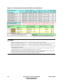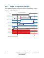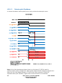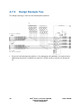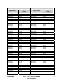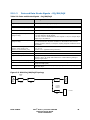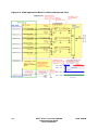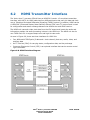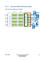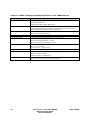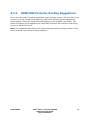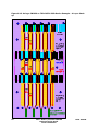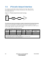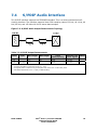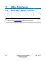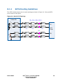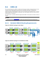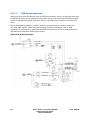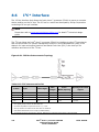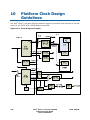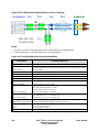
1
Intel® Atom™ processor CE4100
Platform Design Guide
May 2010
Revision 1.5
Intel Confidential
Reference Number: 420826
Legal Statements
INFORMATION IN THIS DOCUMENT IS PROVIDED IN CONNECTION WITH INTEL PRODUCTS. NO
LICENSE, EXPRESS OR IMPLIED, BY ESTOPPEL OR OTHERWISE, TO ANY INTELLECTUAL PROPERTY
RIGHTS IS GRANTED BY THIS DOCUMENT. EXCEPT AS PROVIDED IN INTEL'S TERMS AND CONDITIONS
OF SALE FOR SUCH PRODUCTS, INTEL ASSUMES NO LIABILITY WHATSOEVER, AND INTEL DISCLAIMS
ANY EXPRESS OR IMPLIED WARRANTY, RELATING TO SALE AND/OR USE OF INTEL PRODUCTS
INCLUDING LIABILITY OR WARRANTIES RELATING TO FITNESS FOR A PARTICULAR PURPOSE,
MERCHANTABILITY, OR INFRINGEMENT OF ANY PATENT, COPYRIGHT OR OTHER INTELLECTUAL
PROPERTY RIGHT.
Intel products are not intended for use in medical, life saving, life sustaining applications.
Intel may make changes to specifications and product descriptions at any time, without notice.
Designers must not rely on the absence or characteristics of any features or instructions marked “reserved” or
“undefined.” Intel reserves these for future definition and shall have no responsibility whatsoever for conflicts or
incompatibilities arising from future changes to them.
This manual may contain design defects or errors known as errata, which may cause the product to deviate from
published specifications. Current characterized errata are available on request.
This manual as well as the software, hardware and/or technology described in it, if it is furnished under a license
then it may only be used or copied in accordance with the terms of such license. The information in this document
is furnished for informational use only, is subject to change without notice, and should not be construed as a
commitment by Intel Corporation. Intel Corporation assumes no responsibility or liability for any errors or
inaccuracies that may appear in this document or any software that may be provided in association
with this document.
Except as permitted by any such license that may be provided with any Intel product no part of this document may
be reproduced, stored in a retrieval system, or transmitted in any form or by any means without the express
written consent of Intel Corporation.
I2C is a 2-wire communications bus/protocol developed by Philips. SMBus is a subset of the I2C bus/protocol and
was developed by Intel. Implementations of the I2C bus/protocol may require licenses from various entities,
including Philips Electronics N.V. and North American Philips Corporation.
MPEG is an international standard for video compression/decompression promoted by ISO. Implementations of
MPEG CODECs, or MPEG enabled platforms may require licenses from various entities, including Intel Corporation.
The Intel® Media Processor CE 3100 and Intel® Atom™ processor CE4100 includes graphics functionality based on
the POWERVR™ SGX535 from Imagination Technologies.
BunnyPeople, Celeron, Celeron Inside, Centrino, Centrino logo, Chips, Core Inside, Dialogic, EtherExpress, ETOX,
FlashFile, i386, i486, i960, iCOMP, InstantIP, Intel, Intel logo, Intel386, Intel486, Intel740, Intel® Media Processor
CE 3100, Intel® Atom™ processor CE4100, IntelDX2, IntelDX4, IntelSX2, Intel Core, Intel Inside, Intel Inside logo,
Intel. Leap ahead., Intel. Leap ahead. logo, Intel NetBurst, Intel NetMerge, Intel NetStructure, Intel SingleDriver,
Intel SpeedStep, Intel StrataFlash, Intel Viiv, Intel XScale, IPLink, Itanium, Itanium Inside, MCS, MMX, MMX logo,
Optimizer logo, OverDrive, Paragon, PDCharm, Pentium, Pentium II Xeon, Pentium III Xeon, Performance at Your
Command, Pentium Inside, skoool, Sound Mark, The Computer Inside., The Journey Inside, VTune, Xeon, Xeon
Inside and Xircom are trademarks or registered trademarks of Intel Corporation or its subsidiaries in the United
States and other countries.
Contact your local Intel sales office or your distributor to obtain the latest specifications and before placing your
product order.
Copies of documents which have an ordering number and are referenced in this document, or other Intel literature
may be obtained by calling 1-800-548-4725 or by visiting Intel's website at http://www.intel.com.
*Other names and brands may be claimed as the property of others.
Copyright © 2009-2010, Intel Corporation
2
Intel® Atom™ processor CE4100
Platform Design Guide
Intel Confidential
Ref# 420826
Contents
1
Introduction ..............................................................................11
1.1
Related Documents .................................................................................12
1.2
Acronyms and Terminology ......................................................................15
2
Platform Overview ....................................................................19
3
Platform Stack-up and General Design Considerations..............21
3.1
4
Recommended Board Stack-up .................................................................22
3.1.1
1080 Prepreg .............................................................................25
3.1.2
PCB Technology Considerations ....................................................25
3.1.3
Multiple Impedance Target Considerations......................................26
3.1.4
Break Out Traces ........................................................................26
Platform Power Distribution Guidelines ....................................27
4.1
4.2
Platform Power Rails................................................................................27
General Power Rail Design Guidelines .............................................................28
4.3
Power Decoupling ...................................................................................29
4.4
Power Sequence .....................................................................................31
4.4.1
4.5
Reset Sequence ......................................................................................33
4.5.1
Straps ...................................................................................................37
4.7
Expansion Bus Strapping Design Topology ..................................................39
4.7.1
Design Example One ...................................................................39
4.7.2
Design Example Two ...................................................................40
Debug Port Guidelines .............................................................................41
System Memory Design Guidelines............................................42
5.1
Supported Configurations.........................................................................42
5.2
DDR2/DDR3 Pin Descriptions ....................................................................43
5.3
Decoupling Recommendations ..................................................................43
5.4
Package Length Compensation..................................................................44
5.5
DDR3 Design Topologies and Routing Guidelines .........................................46
5.6
6
Reset Sequence Examples............................................................34
4.6
4.8
5
Power-On Sequence Example .......................................................32
5.5.1
DDR3 Guidelines for x16 Devices ..................................................46
5.5.2
DDR3 Guidelines for x8 Devices ....................................................50
DDR2 Design Topology and Routing Guidelines............................................55
5.6.1
DDR2 Guidelines for x16 Devices ..................................................55
5.6.2
DDR2 Guidelines for x8 Devices ....................................................60
5.7
VREF Circuit ...........................................................................................65
5.8
Miscellaneous Signals Design Guidelines.....................................................66
Video Output Interfaces ............................................................67
6.1
Video DAC Interface ................................................................................67
6.1.1
Ref# 420826
Video DAC Application Model Examples ..........................................68
Intel® Atom™ processor CE4100
Platform Design Guide
Intel Confidential
3
6.1.2
6.2
6.3
HDMI Transmitter Interface ......................................................................74
6.2.1
Detailed HDMI Routing Example....................................................75
6.2.2
HDMI ESD Protector Routing Suggestions.......................................77
Transport Stream Input Ports ...................................................................83
6.3.1
7
8
Video Calibration Circuit ..............................................................73
TS Interface Routing Topology Example .........................................84
Audio Interfaces........................................................................85
7.1
Overview ...............................................................................................85
7.2
I2S Audio Input Interface .........................................................................85
7.3
I2S Audio Output Interface .......................................................................86
7.4
S/PDIF Audio Interface ............................................................................87
Other Interfaces........................................................................88
8.1
8.2
Serial ATA (SATA) Interface......................................................................88
8.1.1
SATA Routing Guidelines..............................................................89
8.1.2
Terminating Unused SATA Signals .................................................93
8.1.3
SATA Test Note ..........................................................................93
USB 2.0.................................................................................................94
8.2.1
Detailed USB2.0 Routing Requirements..........................................94
8.3
Gigabit Ethernet .....................................................................................99
8.4
Expansion Bus Interface Guidelines ......................................................... 103
8.5
8.4.1
Expansion Bus Chip Select ......................................................... 104
8.4.2
Expansion Bus Address, EXP_ALE and EXP_IO_WRB ...................... 105
8.4.3
Data Bus A .............................................................................. 106
8.4.4
Data Bus B and Control Signals................................................... 107
NAND Flash..........................................................................................108
8.5.1
NAND Flash Interface Diagram ................................................... 108
8.5.2
Supported Features .................................................................. 108
8.5.3
NAND_IO Topology ................................................................... 109
8.5.4
NAND_WE_N, NAND_RE_N, NAND_CLE and NAND_ALE Topology .... 110
8.5.5
NAND_CE_N Topology ............................................................... 111
8.5.6
NAND_RY_BY_N Signal Recommendation ..................................... 112
8.5.7
NAND_CLK_X_OUT/IN Topology ................................................. 113
2
8.6
I C* Interface....................................................................................... 114
8.7
UART Interface ..................................................................................... 115
8.7.1
UART0_RXD Signal Recommendation........................................... 116
8.7.2
UART0_DSRB Signal Recommendation......................................... 117
8.8
GPIO Interface ..................................................................................... 118
8.9
SPI Serial Interface ............................................................................... 120
8.9.1
SPI Serial Interface................................................................... 120
8.9.2
SPI_MISO Routing Recommendation ........................................... 121
8.9.3
SPI_MOSI and SPI_SCK Routing Recommendation ........................ 122
8.9.4
SPI_SS Signal Routing Recommendation...................................... 123
8.10 Smart Card Interface............................................................................. 124
8.10.1
4
Smart Card Signal Routing Recommendation ................................ 125
Intel® Atom™ processor CE4100
Platform Design Guide
Intel Confidential
Ref# 420826
9
High Definition Video Capture (HDVCAP) ................................126
9.1
HDVCAP Signals Interface ...................................................................... 126
9.2
HDVCAP Routing Topology...................................................................... 128
9.2.1
HDVCAP Design Topology 1........................................................ 128
9.2.2
HDVCAP Design Topology 2........................................................ 129
10 Platform Clock Design Guidelines ............................................130
10.1 Reference Clock Routing Guidelines ......................................................... 132
10.1.1
CK505 Clock Topology ............................................................... 132
10.1.2
1IDT6V49061 Clock Topology ..................................................... 133
10.2 Audio Reference Clock Output Routing Recommendation ............................ 136
10.3 VCXO Mode Design Guidelines ................................................................ 137
Ref# 420826
Intel® Atom™ processor CE4100
Platform Design Guide
Intel Confidential
5
List of Tables
Table 1-1. Related Documents ................................................................................................................... 12
Table 1-2. Acronyms and Terminology ....................................................................................................... 15
Table 3-1. 4-layer Board Impedance Target Example................................................................................ 26
Table 3-2. Additional Impedance Requirements Example.......................................................................... 26
Table 4-1. Decoupling Example.................................................................................................................. 29
Table 4-2. Layout Recommendations for RESET_INB............................................................................... 33
Table 4-3. Layout Recommendations for SYS_PWR_GOOD .................................................................... 33
Table 5-1. DDR2 DRAMComponent Organization .....................................................................................42
Table 5-2. DDR3 DRAMComponent Organization .....................................................................................42
Table 5-3. DDR2 Pins ................................................................................................................................. 43
Table 5-4. Memory Interface Package Lengths .......................................................................................... 44
Table 5-5. Clock Signals – DDRA_CLK/CLKB, DDRB_CLK/CLKB............................................................ 46
Table 5-6. DDR3 Memory Clock Topology Table ....................................................................................... 47
Table 5-7. Address, Command, and Control .............................................................................................. 47
Table 5-8. DDR3 Address, Command, and Control Topology Table ......................................................... 48
Table 5-9. Data and Strobe Signals – DQ/DM/DQS................................................................................... 49
Table 5-10. DDR3 DQ/DM/DQS Topology Table ....................................................................................... 50
Table 5-11. Clock Signals – DDRA_CLK/CLKB, DDRB_CLK/CLKB ......................................................... 50
Table 5-12. DDR3 Memory Clock Topology Table ..................................................................................... 51
Table 5-13. Address, Command, and Control ............................................................................................ 52
Table 5-14. DDR3 Address, Command, and Control Topology Table ....................................................... 53
Table 5-15. Data and Strobe Signals – DQ/DM/DQS................................................................................. 54
Table 5-16. DDR3 DQ/DM/DQS Topology Table ....................................................................................... 54
Table 5-17. Clock Signals – DDRA_CLK/CLKB, DDRB_CLK/CLKB ......................................................... 55
Table 5-18. DDR2 Memory Clock Topology Table ..................................................................................... 56
Table 5-19. Address, Command, and Control ............................................................................................ 56
Table 5-20. DDR2 Address, Command, and Control Topology Table ....................................................... 57
Table 5-21. Data and Strobe Signals – DQ/DM/DQS................................................................................. 58
Table 5-22. DDR2 DQ/DM/DQS Topology Table ....................................................................................... 59
Table 5-23. Clock Signals – DDRA_CLK/CLKB, DDRB_CLK/CLKB, ........................................................ 60
Table 5-24. DDR2 Memory Clock Topology Table ..................................................................................... 61
Table 5-25. Address, Command, and Control ............................................................................................ 62
Table 5-26. DDR2 Address, Command, and Control Topology Table ....................................................... 63
Table 5-27. Data and Strobe Signals – DQ/DM/DQS................................................................................. 64
Table 5-28. DDR2 DQ/DM/DQS Topology Table ....................................................................................... 64
Table 6-1. Video DAC Signals .................................................................................................................... 67
Table 6-2. HDMI Transmitter Routing Guidelines for the 1080 Stack-up ................................................... 76
Table 7-1. I2S Audio Input Interconnects .................................................................................................... 85
Table 7-2. I2S Audio Input Interconnects.................................................................................................... 86
Table 7-3. S/PDIF Output Interconnects..................................................................................................... 87
Table 8-1. Serial ATA Differential Pair Routing Guidelines for the 1080 Stack-up..................................... 91
Table 8-2. AC Coupling Capacitor .............................................................................................................. 92
Table 8-3. SATA_RBIAS Routing Guidelines for the 1080 Stack-up.......................................................... 92
6
Intel® Atom™ processor CE4100
Platform Design Guide
Intel Confidential
Ref# 420826
Table 8-4. USB Channel Routing Guidelines.............................................................................................. 96
Table 8-5. USBRBIASP/ USBRBIASN Routing Guidelines........................................................................ 97
Table 8-6. GBE Transmitter Routing Guidelines....................................................................................... 101
Table 8-7. GBE RX Routing Guidelines.................................................................................................... 102
Table 8-8. Expansion Bus Topology for EXP_CS[3:0]B ...........................................................................104
Table 8-9. Expansion Address/Data Bus Star Topology ..........................................................................105
Table 8-10. Data Bus_A Topology list ...................................................................................................... 106
Table 8-11. Expansion Bus Topology for EXP_CS[3:0]B .........................................................................107
Table 8-12. I2C interconnection list .......................................................................................................... 114
Table 8-13. UART0_RXD signal Topology ............................................................................................... 116
Table 8-14. UART0_DSRB signal Topology............................................................................................. 117
Table 8-15. GPIO Interface list ................................................................................................................. 119
Table 8-16. SPI Serial Interface Interconnects ......................................................................................... 120
Table 8-17. SPI SPI_MISO signal Topology list ....................................................................................... 121
Table 8-18. SPI_MOSI and SPI_SCK signal Topology list....................................................................... 122
Table 8-19. SPI_SS signal Topology list................................................................................................... 123
Table 8-20. Smart Card Interface External Signals .................................................................................. 124
Table 8-21. SC0_INS_GP[7] and SC1_INS_GAP[11] Signal Topology List ............................................ 125
Table 9-1. Video Input Mode Description.................................................................................................. 127
Table 9-2. HDVCAP Signal Length Table................................................................................................. 128
Table 9-3. HDVCAP Signal Length Table................................................................................................. 129
Table 10-1. CK505 Clock Routing Guidelines .......................................................................................... 133
Table 10-2. IDT6V49061 Clock Routing Guidelines ................................................................................. 134
Table 10-3. IDT6V49061 Clock Routing Guidelines ................................................................................. 135
Table 10-4. Audio_clk Signal Topology List.............................................................................................. 136
Ref# 420826
Intel® Atom™ processor CE4100
Platform Design Guide
Intel Confidential
7
List of Figures
Figure 2-1. Platform Overview .................................................................................................................... 20
Figure 3-1. Recommended 6-layer PCB Stack-up Dimensions.................................................................. 23
Figure 3-2. Recommended 4-layer PCB Stack-up Dimensions.................................................................. 24
Figure 4-1. Power on sequence.................................................................................................................. 32
Figure 5-1. DDR3 Memory Clock Topology ................................................................................................ 46
Figure 5-2. DDR3 Address, Command and Control Topology with Two Loads ......................................... 48
Figure 5-3. DDR3 DQ/DM/DQS Topology .................................................................................................. 49
Figure 5-4. DDR3 Memory Clock Topology ................................................................................................ 50
Figure 5-5. DDR3 Address, Command and Control Topology with Four Loads......................................... 52
Figure 5-6. DDR3 DQ/DM/DQS Topology .................................................................................................. 54
Figure 5-7. DDR2 Memory Clock Topology ................................................................................................ 55
Figure 5-8. DDR2 Address, Command and Control Topology with Two Loads ......................................... 57
Figure 5-9. DDR2 DQ/DM/DQS Topology .................................................................................................. 58
Figure 5-10. DDR2 Memory Clock Topology .............................................................................................. 60
Figure 5-11. DDR2 Address, Command and Control Topology with Four Loads....................................... 62
Figure 5-12. DDR2 DQ/DM/DQS Topology ................................................................................................ 64
Figure 5-13. DDR Vref Circuit Example ...................................................................................................... 65
Figure 5-14. RCOMPPD Connection .......................................................................................................... 66
Figure 5-15. RCOMPPU Connection .......................................................................................................... 66
Figure 6-1. VDAC application Model 1: VDAC with Integrated Filter/Amplifier........................................... 69
Figure 6-2. VDAC application Model 2: VDAC with Discrete Filter............................................................. 70
Figure 6-3. VBG_EXTR_VDAC Resistor Design ........................................................................................ 71
Figure 6-4. VBG_EXTR_VDAC Connection ............................................................................................... 72
Figure 6-5. Illustration of Video DAC Trace Spacing .................................................................................. 72
Figure 6-6. Design Example One................................................................................................................ 73
Figure 6-7. Design Example Two................................................................................................................ 73
Figure 6-8. HDMI Interface Diagram........................................................................................................... 74
Figure 6-9. 4-pair HDMI channel Topology................................................................................................. 75
Figure 6-10. Using an IP4777CZ38 ESD Device Example – 6+ Layer Stack-up. ...................................... 78
Figure 6-11. Using an IP4777CZ38 ESD Device Example – 4 Layer Stack-up. ........................................ 79
Figure 6-12. Using a CM2030 or TPD12S521 ESD Device Example – 6+ Layer Stack-up....................... 81
Figure 6-13. Using a CM2030 or TPD12S521 ESD Device Example – 4 Layer Stack-up......................... 82
Figure 6-14. HDMI TMDS Topology ........................................................................................................... 83
Figure 6-15. TS Interface Routing Topologies ............................................................................................ 84
Figure 7-1. I2S Audio Input Interconnects Topology ................................................................................... 85
Figure 7-2. I2S Audio Output Interconnects Topology ................................................................................ 86
Figure 7-3. S/PDIF Audio Output Interconnects Topology ......................................................................... 87
Figure 8-1. Serial ATA Topology................................................................................................................. 89
Figure 8-2. Illustration of Serial ATA Trace Spacing................................................................................... 90
Figure 8-3. SATARBIAS Connection .......................................................................................................... 92
Figure 8-4. USB2.0 Topology for Back Panel ............................................................................................. 94
Figure 8-5. USB2.0 Topology for Front END Board (FEB) ......................................................................... 94
Figure 8-6. Recommended USB Trace Spacing ........................................................................................ 95
8
Intel® Atom™ processor CE4100
Platform Design Guide
Intel Confidential
Ref# 420826
Figure 8-7. USBRBIAS/USBRBIASN Connection ...................................................................................... 97
Figure 8-8. Design Example........................................................................................................................ 98
Figure 8-9. GBE Interface Clock Signal Design Example......................................................................... 100
Figure 8-10. GBE TX Interface (except GBE_TXCLK) ............................................................................. 100
Figure 8-11. GBE_TXCLK......................................................................................................................... 100
Figure 8-12. GBE_TXCTL......................................................................................................................... 101
Figure 8-13. GBE_REFCLK ...................................................................................................................... 101
Figure 8-14. GBE_RXDATA<0~3> and GBE_RXCLK ............................................................................. 102
Figure 8-15. Expansion Bus Implementation Showing 26-bit Addressing Example................................. 103
Figure 8-16. Expansion Bus Topology for EXP_CS[3:0]B........................................................................ 104
Figure 8-17. Expansion Bus Address ADDR<0, 2-15>, EXP_ALE and EXP_IO_WRB Topology ........... 105
Figure 8-18. Data Bus DA<0-7> Topology................................................................................................ 106
Figure 8-19. Expansion Bus Topology for EXP_DB<0-7>, EXP_RDB, EXP_WRB and EXP_IO_RDB
@25MHz ............................................................................................................................................ 107
Figure 8-20. NAND Flash Controller ......................................................................................................... 108
Figure 8-21. I2C Bus Interconnects Topology .......................................................................................... 114
Figure 8-22. UART0_RXD signal Topology .............................................................................................. 116
Figure 8-23. UART0_DSRB signal Topology............................................................................................ 117
Figure 8-24. GPIO Interface Topology...................................................................................................... 119
Figure 8-25. SPI SPI_MISO signal Topology............................................................................................ 121
Figure 8-26. SPI_MOSI and SPI_SCK signal Topology ........................................................................... 122
Figure 8-27. SPI_SS signal Topology....................................................................................................... 123
Figure 8-28. SC Signal Topology.............................................................................................................. 125
Figure 9-1. HDVCAP Block Diagram ........................................................................................................ 126
Figure 9-2. HDVCAP Signal Topology With NOR Boot ............................................................................128
Figure 9-3. HDVCAP Signal Topology With NAND Boot..........................................................................129
Figure 10-1. Clock Diagram Example. ...................................................................................................... 130
Figure 10-2. Intel Platform Clock Diagram Example................................................................................. 131
Figure 10-3. CK505 Reference Clock Topology ....................................................................................... 132
Figure 10-4. IDT6V49061 HDMI Reference Clock Topology....................................................................134
Figure 10-5. IDT6V49061 Audio and VDC CLK Topology........................................................................ 135
Figure 10-6. Audio_clk Signal Topology ................................................................................................... 136
Ref# 420826
Intel® Atom™ processor CE4100
Platform Design Guide
Intel Confidential
9
Revision History
Date
Revision
Reference #
Description
March, 2009
0.5
26337
Initial version.
May, 2009
0.6
420826
De-classification from “Restricted Secret” to
“Confidential”.
June, 2009
0.8
420826
Update to B stepping. Added Video capture, clock
design recommendation and checklist for schematic and
layout etc.
December, 2009
1.0
420826
Replaced codename “Sodaville” with official name
“Intel® Atom™ processor CE4100”; Many additional
changes throughout.
May, 2010
1.5
420826
Misc updates throughout, based on Falcon Falls Bstep/FAB_C and Golden Beach B-step/Fab_A
10
Intel® Atom™ processor CE4100
Platform Design Guide
Intel Confidential
Ref# 420826
1
Introduction
This Intel® Atom™ processor CE4100 Platform Design Guide (PDG) provides design
recommendations for platform designs using the Intel® Atom™ processor CE4100.
The Intel® Atom™ processor CE4100 Development Platform is a non-form-factor
development board that may be used as a reference design. The Intel® Atom™ processor
CE4100 Development Platform includes the Intel® Atom™ processor CE4100 board, frontend boards (FEBs), and additional connector cards for video and audio interface, software,
and collateral. The platform is not meant as a production-ready board, but as a validated
configuration of the Intel components that a customer can base their design on with
confidence. The development board is also used to validate interfaces that are documented
in the design guide in terms of routing and layout guidelines. The guidelines recommended
in this document are based on simulation work done at Intel while developing the Intel®
Atom™ processor CE4100. The board validation is ongoing and the recommendations are
subject to change.
For input signals routing design guidelines from third-party components, please refer to the
datasheet or guidelines from the third-party component vendor.
Ref# 420826
Intel® Atom™ processor CE4100
Platform Design Guide
Intel Confidential
11
1.1
Related Documents
Table 1-1 provides a list of related documents. The titles listed are available to subscribed
customers with a current CNDA in place and an Intel Business Link (IBL account). For
account subscription and validation or restricted distribution documents, contact your local
Intel field representative.
Note: The Intel® Atom™ processor CE4100 collateral lists and documents listed below are
contained within the Intel® Atom™ processor CE4100 (formerly Sodaville) and Intel® Atom™
processor CE4100 (formerly Sodaville) – based Reference Design and Development Platforms
Electronic Design Kit (EDK) on the Intel Business Portal (IBP – formerly IBL). Please refer to
this EDK for a more up-to-date list of available documents.
Table 1-1. Related Documents
Intel® Atom™ processor CE4100 Documents
Note: The following documents are contained within the Consumer Electronics: Intel® Atom™
processor CE4100 (formerly Sodaville) Collateral List, which is contained within the EDK listed in
the note at the introduction to this section.
IBL Reference
Number
Intel® CE Media Processors– Intel® Consumer Electronics Firmware Development Kit (Intel®
CEFDK) User Guide
Intel® CE Media Processors – EDL Programmer Guide
383826
Intel® CE Media Processors – Integrated Device Library (IDL) Programmer Guide
Intel® CE Media Processors – Graphics Programming Guide for the Linux* Operating System
384411
384529
Intel® CE Media Processors – Graphics - User Guide
Intel® CE Media Processors – DirectFB Drivers Programming Guide
384530
384536
Intel® CE Media Processors – DirectFB – User Guide – Software Drivers
Intel® CE Media Processors – SMD API C Online Help File
384538
384639
Intel® Media Processor CE 3100 (and CE Processor Codenamed Sodaville) – GDL Architecture
Guide / Overview
Intel® CE Media Processors – GDL 2.0 - 3.0 Differences - Software Application Notes
384646
Intel® CE Media Processors – GDL Programmer Guide
Intel® CE Media Processors – GDL 3.0 User Guide
384649
384650
384408
384648
[Canmore] Media Processor – SMD Architecture Guide/Overview
385388
Intel® Media Processor CE 3100 – Integrated Device Library (IDL) Application Programming
Interface (API) Specification
Intel® CE Media Processors – RedBoot User Guide
387829
Intel® Media Processor CE 3100 – Streaming Media Drivers GStreamer* Programmer Guide
Intel® CE Media Processors – SMD Sample Media Player Apps Documentation
391936
396455
Intel® Media Processor CE 3100 – SVEN User Manual
Intel® Media Processor CE 3100 (and CE Processor Codenamed Sodaville) – GDB User
Manual
Intel® CE Media Processors – GDL 3.0 API Online Help File
Intel® Media Processor CE 3100 – Intel® Consumer Electronics Firmware Development Kit
(Intel® CEFDK) Reference Manual
Intel® Media Processor CE 3100 (and CE Processor Codenamed Sodaville) – PIC Interface API
- Online Help Files
397235
398141
Intel® Media Processor CE 3100 (and CE Processor Codenamed Sodaville) – Flash Appdata
API - Online Help Files
Intel® CE Media Processors – AVCAP Reference API - Online Help Files
417417
Intel Media Processor CE 3100 (and CE Processor codenamed Sodaville) XPSM API Reference
Intel® Media Processor CE 3100 (and CE Processor codenamed Sodaville) Cross-Platform
Streaming Media (XPSM) API High-Level Design (HLD) Guide
Intel® Media Processor CE 3100 (and CE processor codenamed Sodaville) – SquashFS and
419536
419546
12
®
Intel Atom™ processor CE4100
Platform Design Guide
Intel Confidential
390840
398453
405445
417416
417765
420421
Ref# 420826
Intel® Atom™ processor CE4100 Documents
Note: The following documents are contained within the Consumer Electronics: Intel® Atom™
processor CE4100 (formerly Sodaville) Collateral List, which is contained within the EDK listed in
the note at the introduction to this section.
JFFS2 Filesystem Application
Intel® CE Media Processors – SMD C-API Programmer’s Guide – Supplemental Material
IBL Reference
Number
424726
Intel® CE Media Processor (codenamed Sodaville) – Sighting/Errata Report and Specification
Update
426684
Intel® CE Media Processors – DDR2 Workbook for Intel® Consumer Electronics Firmware
Development Kit (Intel® CEFDK)
Intel® CE Media Processors – Graphics API Online Help File
426687
RS – Intel® CE Media Processors – Security Controller Driver API Reference
See your local
Intel field
representative
See your local
Intel field
representative
See your local
Intel field
representative
RS - Intel(R) CE Media Processors Trusted Boot Application Note
RS - Sodaville Media Processor External Data Specification (EDS)
RS - Sodaville Media Processor Electrical, Mechanical, and Thermal Specifications
Intel® Atom™ processor CE4100 Platform Documents
Note: The following documents are contained within the Consumer Electronics: Intel® Atom™
processor CE4100 (formerly Sodaville) Development Platform Collateral List, which is contained
within the EDK listed in the note at the introduction to this section.
426692
See your local
Intel field
representative
IBL Reference
Number
Intel® Media Processor CE 3100 (and CE Processor Codenamed Sodaville) Development
Platform – Platform Support Guide
Intel® CE Media Processor Development Platforms – Development Platform Release Notes
Intel® Atom™ processor CE4100 – Platform Design Guide
384637
Intel® CE Processor (codenamed Sodaville) – Falcon Falls B-Step Fab A Development Board
Schematics
421034
Intel® Media Processor CE 3100 (and CE Processor codenamed Sodaville) - IR Remote
Specification
Intel® CE Processor (codenamed Sodaville) - Chesapeake Bay Fab C Development Board
Rework Instructions
Intel® CE Processor (codenamed Sodaville) - Falcon Falls Fab B Development Board Rework
Instructions
Intel® CE Media Processor (codenamed Sodaville) – Thermal Design Guide
421830
Intel® CE Media Processor (codenamed Sodaville) – Getting Started Manual
Intel® CE Media Processor (codenamed Sodaville) – Golden Beach Fab A Development Board
Reword Instructions
Intel® CE Media Processor (codenamed Sodaville) - Chesapeake Bay B-Step Fab A
Development Board Design Files
426797
427192
Intel® CE Media Processor (codenamed Sodaville) - Falcon Falls B-Step Fab B Development
Board Rework Instructions
Intel® CE Media Processor (codenamed Sodaville) - Chesapeake Bay B-Step Fab A
Development Board Rework Instructions
Intel® CE Media Processor (codenamed Sodaville) - Golden Beach B-Step Fab A Development
Board Rework Instructions
431003
Other External References
JEDEC DDR2 Specifications
Ref# 420826
388261
420826
421972
422366
424716
430987
431004
431005
Location
http://www.jedec.org
Intel® Atom™ processor CE4100
Platform Design Guide
Intel Confidential
13
JEDEC DDR3 Specifications
http://www.jedec.org
Low Pin Count Interface Specification, Revision 1.1
(LPC)
http://developer.intel.com/design/chipsets/industry/
lpc.htm
System Management Bus Specification, Version 2.0
(SMBus)
http://www.smbus.org/specs/
PCI Local Bus Specification, Revision 2.3 (PCI)
http://www.pcisig.com/specifications
Universal Serial Bus Revision 2.0 Specification
(USB)
http://www.usb.org
Enhanced Host Controller Interface Specification for
Universal Serial Bus (EHCI)
http://developer.intel.com/technology/usb/ehcispec.htm
Advanced Configuration and Power Interface,
Version 2.0 (ACPI)
http://www.acpi.info/spec.htm
Serial ATA Specification, Revision 1.0
http://www.serialata.org/cgi-bin/SerialATA10gold.zip
HDMI Specification Ver.1.4 and the Compliance
Test Specification Ver.1.4 (CTS 1.4)
http://www.hdmi.org
14
Intel® Atom™ processor CE4100
Platform Design Guide
Intel Confidential
Ref# 420826
1.2
Acronyms and Terminology
Table 1-2. Acronyms and Terminology
Acronym
Definition
ACP
Analog Copy Protection (ACP) is a proprietary system developed and patented by Macrovision*
AES
Advanced Encryption Standard — a state of the art strong encryption algorithm (developed by
Rijndael) and chosen by the United States National Institute of Standards and Technology on
October 2, 2000.
ARIB
ARIB Association of Radio Industries and Business — Designated by the Ministry of Public
Management, Home Affairs, Posts and Telecommunications (MPHPT) in Japan. ARIB members
include broadcasters, radio equipment manufacturers, telecommunication operators, and related
organizations.
ATSC
ATSC Advanced Television Systems Committee — an organization in US that establishes and
promotes technical standards for advanced television systems, such as digital television (DTV).
AV
Short for : Audio – Video, e.g. “AV stream” Also: Audio Visual
CGMS-A
Copy protection capabilities for analog NTSC video by extending the EIA-608 standard to control
Macrovision’s Analog Copy Protection (ACP) anti-copy process at the receiver
CPPM
Content Protection for Pre-recorded Media
CPRM
Content Protection Recordable Media
CSR
Configuration Status Register — common term in SW lingo for “register”
CSS
Content Scramble System (CSS) defines the technology for how DVD movies are encrypted by
manufacturers and the decryption mechanism in hardware or software players
CVBS
CVBS is the acronym designation for composite video — the format of an analog television
(picture only) signal before it is combined with a sound signal and modulated onto an RF carrier.
The CVBS acronym stands for "Color, Video, Blank and Sync", "Composite Video Baseband
Signal", "Composite Video Burst Signal", or "Composite Video with Burst and Sync". It is usually
in a standard format such as NTSC, PAL, or SECAM.
D2D
Digital to Digital converter (voltage regulator).
DAC
Digital-to-Analog Converter.
DDC
Display Data Channel (HDMI)
DDR2
Double Data Rate Synchronous Dynamic Random Access Memory - second generation
DDR3
Double Data Rate Synchronous Dynamic Random Access Memory - third generation
DES
The Data Encryption Standard developed by IBM in co-operation with the American National
Security Agency and published in 1974.
DMA
Direct Memory Access — the hardware function when a peripheral accesses data in the memory in
computer system without CPU intervention.
DRM
DRM includes capabilities such as the acquisition of license, ability to distribute content to other
users, enforcement of viewing windows and other restrictions such as copy control imposed by the
copyright holder.
DSTB
Digital Set Top Box — device designed to receive the compressed digital audiovisual content, and
decompress and display it.
DTCP
Digital Transmission Content Protection (DTCP) — system to prevent the illicit duplication of
copyrighted programming in IEEE1394-based systems. The DTCP system also is known as “5C”
for its five developing companies — Intel, Hitachi, Matsushita, Sony, and Toshiba.
DTCP-IP
DTCP-IP is used for protecting content being transferred between DTCP licensed devices over an
IP Home Network.
Ref# 420826
Intel® Atom™ processor CE4100
Platform Design Guide
Intel Confidential
15
Acronym
Definition
DVB
Digital Video Broadcasting — a set of open worldwide standards that define digital broadcasting
using existing satellite, cable, and terrestrial infrastructures. It uses the MPEG-2 specification as a
universal foundation and expands it with DVB data structures and processes; DVB-compliant
digital broadcasting and equipment is widely available to consumers and is indicated with the DVB
logo.
DVB-CSA
DVB Common Scrambling Algorithm — the streaming encryption algorithm used across all DVB
systems for content protection. The complete conditional access system relies on this common
scrambling unit and proprietary software, which generates and distributes decryption keys for the
stream decryptors.
DVI
Digital Visual Interface standard (EIA/CEA-861A). The standard defines a method for sending
digital video signals over DVI and OpenLDI interface specifications. The standard is fully backward
compatible with earlier DVI standards. New features include carrying auxiliary video information,
such as aspect ratio and native video format information.
DVO
Digital Video Output. The parallel, low voltage signaling interface defined for Intel video chipsets.
GPIO
General Purpose Input Output.
HDCP
High-bandwidth Digital Content Protection standard. A protocol developed by Intel, designed to
protect digital audio and video content as it travels across DVI or HDMI connections. Not part of
the HDMI standard but widely understood to be a necessary complement to the interface. The
HDCP specification is proprietary and implementation of HDCP requires a license.
HDD
Hard Disk Drive – magnetic mass storage device used in media centers for audiovisual program
recording.
HDMI
High Definition Multimedia Interface (HDMI). This interface is used between any audio/ video
source, such as a set-top box, DVD player, or A/V receiver, and an audio or video monitor, such
as a DTV. HDMI supports standard, enhanced or high-definition video, plus multi-channel digital
audio on a single cable. The format transmits all ATSC HDTV standards and supports eightchannel digital audio (at up to a 192-kHz sampling rate), with bandwidth to spare for future
enhancements.
HDTV
High-Definition Television — HDTV specifically refers to the highest-resolution formats of the 18
total DTV formats, true HDTV is generally considered to be 1,080-line interlaced (1080i) or 720line progressive (720p).
I2C*
Inter-IC Control.
I2S*
Integrated Interchip-Sound
IEEE 1394
1394
IEEE 1394 or iLink* or FireWire* An IEEE electronics industry standard for connecting multimedia
and computing. Up to 63 devices can be attached to your PC via a single plug-and-socket
connection.
IEEE 802.11
802.11
The Institute for Electronics and Electrical Engineers (IEEE) wireless network specification.
802.11g and 802.11a networks can transmit payload at rates in excess 34 Mbits/s, and allow for
wireless transmission at distances ranging from several dozen to several hundred feet indoors.
ITP-XDP
In Target Probe - Expanded Debug Port.
JEDEC
Joint Electron Device Engineering Council - solid state technology forum.
LAI
Logic Analyzer Interface.
LPC
Low Pin Count interface.
LVDS
Low Voltage Differential Signaling.
MPEG*
Motion Picture Experts Group — organization that develops standards for digital video and digital
audio compression
MPEG-2*
The designation for a group of AV coding standards agreed upon by MPEG (Motion Pictures
Experts Group), and published as ISO standard 13818. MPEG-2 is typically used to encode audio
and video for broadcast signals, but includes transport systems as well.
MULTI2
A cryptographic method, which partitions signal rows into blocks and then stirs it using key data.
MULTI-2 was developed by Hitachi and is used as a scrambling algorithm for digital television in
Japan. It is defined in ARIB STB B-25.
NAND
A logical operator that consists of an logical AND followed by a logical NOT and returns a false
value only if both operands are true. Used to describe a type of FLASH memory based upon NAND
gates.
16
Intel® Atom™ processor CE4100
Platform Design Guide
Intel Confidential
Ref# 420826
Acronym
Definition
NIM
Network Interface Module — integrated tuner and digital demodulator in (satellite) TV systems.
The DVB NIMs output an MPEG transport stream.
NOR
A logical operator the consists of a logical OR followed by a logical NOT and returns a true value
only if both operands are false. Used to describe a type of FLASH memory based upon NOR gates.
NTSC
National Television System Committee, established North American 525-line analog broadcast TV
standard about 60 years ago.
PAL
Phase Alternation Line — TV standard used in Europe. PAL uses 625 lines per frame, a 25 frames
per second update rate and YUV color encoding. The number of visible pixels for PAL video is 768
x 576.
PCI-E, PCIe
PCI Express* (two way serial connection that carries data in packets) Each of these lanes should
be capable of a 2Gb/s data rate in each direction.
PLL
Phase Locked Loop.
SATA
Serial Advanced Technology Attachment.
SDTV
Standard-Definition Television — a digital television system that is similar to current analog TV
standards in picture resolution and aspect ratio. Typical SDTV resolution is 480i or 480p.
SMBus
System Management Bus.
SMPTE
Society of Motion Picture and Television Engineers
STB
Set Top Box — a device that effectively turns a television set into an interactive Internet device
and/or allows the television to receive and decode digital television (DTV) broadcasts.
SVGA
Super VGA Resolution (800x600).
TDP
Total Design Power.
UART
Universal Asynchronous Receiver-Transmitter.
USB
Universal Serial Bus.
VCXO
Voltage Controlled Crystal Oscillator.
VID
Voltage Identification.
VREF
Voltage Reference.
VSS
Used to signify ground connection.
VTT
Used to signify signal termination voltage.
WVGA
Wide VGA resolution (800x480).
YPrPb
YPBPR is the analog video signal carried by component video cable in consumer electronics. The
green cable carries Y, the blue cable carries PB and the red cable carries PR.
Ref# 420826
Intel® Atom™ processor CE4100
Platform Design Guide
Intel Confidential
17
This page intentionally left blank
18
Intel® Atom™ processor CE4100
Platform Design Guide
Intel Confidential
Ref# 420826
2
Platform Overview
The Intel® Atom™ processor CE4100 is a System-On-Chip (SOC) intended for use in
systems which bring network connectivity into the living room such as connected cable settop boxes, IP set-top boxes, blue-laser disk players/recorders (Blu-Ray), and so on.
The Intel® Atom™ processor CE4100 supports processing of dual high-definition (HD)
audio/video (AV) streams for local TV/display and serving of multiple AV streams for remote
TVs. The Intel® Atom™ processor CE4100 embeds an Intel® Atom™ IA-32 processor, a
capable 3D graphics processor, a high bandwidth memory controller and variety of IO
interfaces, with the high-quality audio and video processing elements required for a living
room media system, all in one chip. The integrated IA-32 processor is provided to enable
advanced networking and internet applications while leveraging the large installed base of
IA-32 software. It can also be used to provide any additional media processing
requirements such as emerging video codecs or security algorithms.
The Intel® Atom™ processor CE4100 is a complex chip with a number of major functional
units. Please refer to the Intel® CE Processor (codenamed Sodaville) Datasheet for more
information about each functional unit.
Ref# 420826
Intel® Atom™ processor CE4100
Platform Design Guide
Intel Confidential
19
Figure 2-1. Platform Overview
20
Intel® Atom™ processor CE4100
Platform Design Guide
Intel Confidential
Ref# 420826
3
Platform Stack-up and
General Design
Considerations
This section documents the Intel® Atom™ processor CE4100 board general layout and
routing guidelines. It does not discuss the functional aspects of any bus, or the layout
guidelines for an add-in device.
Note
If the guidelines listed in this document are not followed, thorough signal integrity and
timing simulations should be completed for each design. Even when the guidelines are
followed, Intel recommends that critical signals be simulated to ensure proper signal
integrity and flight time. Any deviation from the guidelines should be simulated.
The trace impedance typically noted (for example, 55 Ω ± 10%) is the “nominal” impedance
for a recommended nominal trace width (for example, 4-mil). It is based on the nominal
stack-up, similar to that shown in either Figure 3-1 (6-layer), or Figure 3-2 (4-layer), with
sufficient spacing from either edge to the edge of the neighboring trace or poured ground
patch.
The rule of thumb for the spacing from the edge of one signal trace to the closest edge of
the neighboring trace or poured ground patch is at least 2.5 times of the nominal trace
width with the mostly used typical single-ended impedance. For differential pair channel, the
inter-pair space is generally at least 3 times the intra-pair space. In this case, the intra-pair
space is defined as the space between the two inner edges of the two involved traces in a
different pair, while the inter-pair is defined as the space from the outer edge in one
differential pair to the closest outer edge of the neighboring differential pair. The space from
the outer edge of one differential pair to the closet edge of any other signal trace or poured
round patch should not be less than the inter-pair space as well.
To meet the targeted nominal impedance as the first priority, all stack-ups, which result in
the same as (or smaller than) the nominal trace width are acceptable, as soon as the
manufacturing process permits and the cost is not a concern.
Note the trace impedance target assumes that the trace is not subjected to the EM fields
created by changing current in neighboring traces. It is important to consider the minimum
and maximum impedance of a trace based on the switching of neighboring traces when
calculating flight times.
Coupling between two traces is a function of the coupled length, the distance separating the
traces, the signal edge rate, and the degree of mutual capacitance and inductance. Using
wider spaces between the traces can minimize trace-to-trace coupling. In addition, wider
spaces reduce settling time. In order to minimize the effects of trace-to-trace coupling, the
routing guidelines documented in this section should be followed.
Ref# 420826
Intel® Atom™ processor CE4100
Platform Design Guide
Intel Confidential
21
Note
The guidelines recommended in this document are based on Intel® Atom™ processor
CE4100 board development.
3.1
Recommended Board Stack-up
The recommended board stack-up for the Intel® Atom™ processor CE4100 platform is a
board stack-up yielding a target impedance of 55 Ω ± 10% for most single-end traces, with
a nominal 4-mil trace width. The intra-pair space of a differential pair channel will be
worked out respectively according to its targeted differential impedance, either 100 Ω or 90
Ω nominally.
Figure 3-1 and Figure 3-2 illustrate the typical dimensions of the metal and dielectric
material thickness as well as the drawn trace width dimensions prior to lamination,
conductor plating, and etching. After the main board materials are laminated, conductors
plated, and etched, some dimensions will result in somewhat different values. As dielectric
materials become thinner, under/over etching of conductors alters their trace width, and
conductor plating makes them thicker. It is important to note that, for extracting electrical
models from transmission line properties, the final dimensions of signals after lamination,
plating, and etching should be used.
Figure 3-1 demonstrates the stack-up of a 6-layer board, which is recommended for a
platform with 8 bits data width DDR2/3 memory device.
Figure 3-2 demonstrates the stack-up for a 4-layer board, which is recommended for a
platform with 16 bits data width DDR2/3 memory device.
For the Intel® Atom™ processor CE4100 platform to meet the targeted nominal impedance
as the first priority, all the stack-ups, which are able to result in the same as, or smaller
than the recommended nominal trace width, are acceptable, when the manufacturing
process permits and the cost is not a concern.
With a particular stack up, assuming less than 4 mil trace width is used for nominal 55 Ω
single-end trace, the trace with for nominal 37.5 Ω will alter according, as well as the
minimum spacing requirement among all edges of single-end trace, differential pair traces
and poured ground patches. It might require further detailed SI analysis to address the
particular dimensions of both trace width and spacing.
22
Intel® Atom™ processor CE4100
Platform Design Guide
Intel Confidential
Ref# 420826
Figure 3-1. Recommended 6-layer PCB Stack-up Dimensions
Notes
•
•
•
•
•
•
•
•
Signal-end impedance target 37.5 Ω +/- 10% micro-strip routing for VDAC channel.
Signal-end impedance target 55 Ω +/- 10% micro-strip routing for other than VDAC single-end channels.
Differential impedance targets 90 Ω +/- 10% micro-strip routing for USBp/n.
Differential impedance targets 100 Ω +/- 10% micro-strip routing for other differential channel other than
USBp/n differential channel.
The typical trace width could be shrunk down from 4 mil to 3.5 mil for nominal 55-Ω single-end trace by
using different stack up, if the PCB manufacturing cost is not a concern.
2nd Reference is pretty weak for impedance controlled, i.e. the tracing routing on layer 3 with the 2nd
reference to Layer 4, or tracing routing on layer 4 with the 2nd reference to Layer 3, is pretty weak due
to the about 30 mils thick core.
Different PCB vendors will have slightly different stack-up, as soon as the impedance of the trace, within
4 mils trace width, can meet nominal 55-Ω single-end impedance.
This stack up is for reference only, particularly for DDRx8 configure.
Ref# 420826
Intel® Atom™ processor CE4100
Platform Design Guide
Intel Confidential
23
Figure 3-2. Recommended 4-layer PCB Stack-up Dimensions
Notes
•
•
•
•
Signal-end impedance target 37.5 Ω +/- 10% micro-strip routing for VDAC channel.
Signal-end impedance target 55 Ω +/- 10% micro-strip routing for other than VDAC single-end channels.
Differential impedance targets 90 Ω +/- 10% micro-strip routing for USBp/n differential channel.
Differential impedance targets 100 Ω +/- 10% micro-strip routing for other differential channel other than
USBp/n differential channel.
• The typical trace width could be shrunk down from 4 mil to 3.5 mil for nominal 55-Ω single-end trace by
using different stack up, if the PCB manufacturing cost is not a concern.
• Different PCB vendors will have slightly different stack-up, as soon as the impedance of the trace width
with not larger than 4 mils width can meet nominal 55-Ω single-end impedance.
• This stack up is for reference only, particularly for DDRx16 configure.
24
Intel® Atom™ processor CE4100
Platform Design Guide
Intel Confidential
Ref# 420826
3.1.1
1080 Prepreg
To achieve the stack-up described in the previous section, it is recommended that board
designers work closely with their PCB vendor in order to get the best combination of
material/thickness. PCB vendors use a 1080 prepreg material as opposed to 2116. A PCB
stack-up that uses 1080 prepreg allows for a decreased signal-to-reference plane height,
resulting in reduced cross-talk on high speed buses. This stack-up also allows for lower
trace impedances and lower Er which helps improve flight and rise times. With a stack-up
that uses 1080 prepreg material, substitute board designers are able to achieve the same
impedance targets with smaller trace widths when compared to a stack-up using 2116
prepreg. For example, a 5-mil line width on a stack-up that uses 2116 prepreg results in a
60 Ω nominal trace impedance, and a 4-mil line width on a stack-up that uses 1080 prepreg
results in a 50 Ω nominal trace impedance.
Board designers should pay close attention to the core material thickness used to ensure
the overall board thickness meets design for manufacturing specifications.
3.1.2
PCB Technology Considerations
The simulations and reference platform discussed in this design guide are based on the
following technology, and Intel recommends that designers adhere to these guidelines for a
platform based on the Intel® Atom™ processor CE4100 CRB.
It is important to note that variations in the stack-up of a board, such as changes in the
dielectric height, trace widths, and spacing, can impact the impedance, loss, and jitter
characteristics of all the interfaces. Such changes may be intentional, or the result of
variations encountered during the PCB manufacturing process. In either case, they must be
properly considered when designing interconnects.
The nominal stack-up in Figure 3-1 and Figure 3-2 assumes an overall board thickness of
0.057 inches or so. The figure also lists trends in manufacturing variances. Use these as a
guideline. Key aspects of the stack-up are as follows:
•
•
•
Components are typically limited to single-sided placement on the top layer due to
increased manufacturing costs associated with double-sided placement.
Microstrip traces on top-layer and bottom-layer are subject to solder mask and plating
impacts, which can affect impedance targets.
Current High Volume Manufacturing (HVM) technology can support 4-mil minimum trace
width and 5-mil trace spacing dimensions between traces.
Note
Specific trace width and spacing targets for various interconnects can be found later in
this document in their respective chapters, as they reach a compromise between
impedance target, loss impacts, crosstalk immunity, and routing flexibility.
Ref# 420826
Intel® Atom™ processor CE4100
Platform Design Guide
Intel Confidential
25
3.1.3
Multiple Impedance Target Considerations
This platform will include various single-ended and differential impedance targets for the
various bus interfaces. Traditional methods of PCB impedance control focused on one,
single-ended target such as “4-mil line equals 55 Ω ±10%,” but there are multiple, singleended and differential impedance targets for this platform.
Table 3-1. 4-layer Board Impedance Target Example
Table 3-2. Additional Impedance Requirements Example
Target
Impedance
Tolerance
Trace
Width (in
mils)
Differential
Spacing (in
mils)
Notes
100 Ω, Differential
± 10%,
Reference Only
4
7
Fab vendor to provide detailed info. This
impedance is required for both outer
layers and inner layers.
90 Ω, Differential
± 10%,
Reference Only
4
4
Fab vendor to provide detailed info. This
impedance is required for both outer
layers and inner layers.
55 Ω, Single-ended
± 10%,
Reference Only
4
NA
Fab vendor to provide detailed info. This
impedance is required for both outer
layers and inner layers.
50 Ω, Single-ended
± 10%,
Reference Only
5
NA
Fab vendor to provide detailed info. This
impedance is required for both outer
layers and inner layers.
37.5 Ω, Single-ended
± 10%,
Reference Only
8
NA
Fab vendor to provide detailed info. This
impedance is required for both outer
layers and inner layers.
3.1.4
Break Out Traces
In order to breakout all signals on the Intel® Atom™ processor CE4100 in a 6-layer or 4layer board, “break out” traces are used in the BGA section. The use of break out traces
allows for tighter signal-to-via spacing for brief periods when normal spacing requirements
aren’t possible. In the BGA region of the Intel® Atom™ processor CE4100, trace-to-trace or
trace-to-via spacing can be 4 mils minimum.
26
Intel® Atom™ processor CE4100
Platform Design Guide
Intel Confidential
Ref# 420826
4
Platform Power Distribution
Guidelines
This chapter provides an example for board power delivery of an Intel® Atom™ processor
CE4100-based platform. There are many power distribution methods that achieve similar
results. It is critical to completely analyze the effects of any changes, and design
accordingly if deviating from this example.
4.1
Platform Power Rails
The Intel® Atom™ processor CE4100 requires up to 5 externally supplied voltages, 3.3V,
1.8V, and 1.5V, 1.05V and core power 0.95V – 1.05V.
•
•
Power planes or shapes are recommended for the major voltages rails on board.
More power rails (such as 5V for HDMI and USB and 3.3STANDBY for PIC24 chip on
board) might be needed based on the platform design requirements.
Power rails on the Intel® Atom™ processor CE4100 Development Platform:
o
o
DDR2 based platform:
• Core Power 0.95V - 1.05V
• 0.9V VTT
• Fixed I/O 1.05V
• Core PLL 1.5V
• 5V
• 3.3V
• 1.8V (including DDR2 DRAM 1.8V)
• 3.3VSTANDBY
DDR3 based platform:
• Core Power 0.95V - 1.05V
• 0.75V VTT
• Fixed I/O 1.05V
• Core PLL 1.5V (including DDR3 DRAM 1.5V)
• 5V
• 3.3V
• 1.8V
• 3.3VSTANDBY
Ref# 420826
Intel® Atom™ processor CE4100
Platform Design Guide
Intel Confidential
27
4.2
•
•
•
•
•
•
•
•
•
28
General Power Rail Design Guidelines
Place edge decoupling capacitors on bottom layer underneath the processor package
shadow, if there is not enough space on top layer
Use the bulk and decoupling capacitors close to voltage regulator or power supply
module where the power is originated.
Use sufficient Vias for connecting Power planes to carry the required current and with
inductance low enough to mitigate high di/dt currents impact.
Use stitching capacitors wherever critical signals reference plane is changed.
Use short and wide traces with at least two vias for connecting Bulk capacitors to power
and ground planes respectively.
Check the Layout placement for components and Vias to ensure that copper area is not
degraded by overlapping of anti-pads, to avoid the return path and current capacity
issues.
Reduce the inductance of Decoupling capacitors by reducing the distance from the pads
to the plane vias. Additionally use short, wide trace from Outer power VCC/VSS balls to
reduce the loop inductance.
Use enough Decoupling capacitors for Termination power supplies close to Resistors /
Resistor Packs.
In case of forced routing over the split plane (not recommended), use enough stitching
capacitor over the gap to mitigate the impedance discontinuity.
Intel® Atom™ processor CE4100
Platform Design Guide
Intel Confidential
Ref# 420826
4.3
Power Decoupling
Table 4-1. Decoupling Example
Note: A “yes” in the “Isolation” column means that additional filtering may be required in
some product configurations.
Interface
Voltage Isolation
SC, SPI,UART, I2S,
TS
V3P3
No
Size Voltage/
Type
Value
Qty
0.1uF
5
0402 16V/Y5V
1.0uF
3
0402 6.3V/Y5V
4.7uF
1
0603 10V/Y5V
120 0hmFB
1
2
120 0hmFB
1
2
0.1uF
1
0402 16V/Y5V
1.0uF
1
0402 6.3V/X5R
0.1uF
2
0402 16V/Y5V
1.0uF
2
0402 6.3V/Y5V
4.7uF
1
0805 10V/Y5V
UART, EXP, NAND
I2C, GMAC
USB
HDMI
VDAC
V3P3
V3P3
Yes
Yes
USB
USB_PLL
DDR
SATA
V1P8
No
HDMI_PLL
HDMI
VCC3P3N
VCC3P3S
VCC3P3W
VCC3P3_USB_SUS
VCCA3P3_VDAC
VCC1P8_USB_SUS
VCCA1P8_USB_PLL
VCC1P8_DDR_SFR
VCC1P8_SATA_SFR
VCCA1P8_HPLL
VCCA1P8_HDMI_PLL
V1P8
V1P8
V1P8
Yes
Yes
No
USB
V1P8
Yes
DDR
V1P8
(DDR2
Yes
V1P5
(DDR3)
Ref# 420826
VCC3P3IN
VCC1P8_HDMI
HPLL
VDAC
VCC3P3E
VCCA3P3_HDMI
HDMI
VDAC
NETs in Package
120 0hmFB
1
0.1uF
1
0402 16V/Y5V
1.0uF
1
0402 6.3V/Y5V
120 0hmFB
1
0.1uF
1
0402 16V/Y5V
1.0uF
1
0402 6.3V/Y5V
4.7uH
1
22uF
1
0805 6.3V/X5R
0402 16V/Y5V
0.1uf
2
120 0hmFB
1
0.1uF
1
0402 16V/Y5V
0.1uF
6
0402 16V/Y5V
1.0uF
2
0402 6.3V/Y5V
4.7uF
2
0603 10V/Y5V
10uF
2
0805 6.3V/X7R
470uF
1
RDL
VCC1P8_VDAC
VCC1P8_VDAC_BG
VCCA1P8_HDMI_BG
VCCA1P8_USB_BG
VCC1P8_DDR
10V/ALUM
Intel® Atom™ processor CE4100
Platform Design Guide
Intel Confidential
29
Interface
Voltage Isolation
Value
Qty
Size Voltage/
Type
NETs in Package
680uF
1
7343 4V/TANT
1000uF
1
RDL
330 Ω FB
1
22UF
1
0805 6.3V/X5R
VCC1P8_DDR_CK
CORE
0.1uF
3
0402 16V/Y5V
VCC1P05_HPLL_CORE
USB
560uF
4
RDL
4V/ALUM
VCC1P05_USB_CORE
HDMI_PLL
4.7uF
1
0603 16V/Y5V
VCCA1P05_HDMI_PLL
0.1uF
2
0603 25V/Y5V
VCCA1P05_HPLL
IA
10uF
2
0805 6.3V/X5R
VCC1P05_IA
LCC
1.0uF
2
0402 6.3V/Y5V
VCC1P05_LCC_PC6
FUSE
10uF
1
0805
120 Ω FB
1
120 Ω FB
1
10uF
2
0805 6.3V/X5R
0.1uF
1
0402 16V/Y5V
0.1uF
8
0402 16V/Y5V
1.0uF
2
0402 6.3V/X5R
4.7uF
2
0603 10V/Y5V
0Ω
3
0603
0.1UF
2
0402 16V/Y5V
0.1uF
2
0603 25V/Y5V
10uF
2
0805 6.3V/X5R
4.7uF
1
1206 16V/Y5V
560uF
4
RDL
1.0uF
2
0402 6.3V/Y5V
V1P8
(DDR2)
DDR
Yes
16V/ALUM
V1P5
(DDR3)
HPLL
SATA
DDR
DDR
CORE
30
V1P05
V1P05
V1P05
V1P05
V0P95 &
V1P05
NO
Yes
Yes
No
No
6.3V/X5R VCCFUSE_ VE
VCCA1P05_SATA
VCC1P05_DDR_PWRC
VCCA1P05_DDR
VCC0P95_CORE &
VCC1P05_CORE
4V/ALUM
Intel® Atom™ processor CE4100
Platform Design Guide
Intel Confidential
Ref# 420826
4.4
Power Sequence
From a power management point of view, the Intel® Atom™ processor CE4100 only
supports on/off. There is no special power-sequencing requirement for the third party ICs
used on the platform boards. However, the following two requirements for the Intel®
Atom™ processor CE4100 need to be met at the board level.
Power Supply Sequencing Rule 1
If USB 1.8V comes up prior to USB 3.3V supply, the 3.3V supply must trail within 0.7V of
the 1.8V supply. The same 0.7V restriction applies if USB 3.3V powers down first and
followed by the 1.8V supply.
This is to prevent forward-bias of the on-die diffusion junction of the thick-gate PMOS
(drain-to-bulk) in the pre-driver circuit.
This can be achieved by adding a Schottky diode from V1P8_SOC to V3P3_SOC on the
board.
Power Supply Sequencing Rule 2
The VBUS 5V for downstream peripherals can only be enabled once all the USB on-die
supplies are up, including the 3.3V supply used by the OC buffer.
This is to prevent the USB data pins and the OC pins from being pulled to 3.3V prior to their
supplies being good. Proper supplies must be available to protect against any high-voltage
presented to the buffers.
The VBUS output from the platform is under PIC24 control on the Intel development board.
Ref# 420826
Intel® Atom™ processor CE4100
Platform Design Guide
Intel Confidential
31
4.4.1
Power-On Sequence Example
On the development platform, an external microcontroller (PIC24FJ64GA004) is used to
control platform level power up/off sequence.
Figure 4-1. Power on sequence
S5 (Soft Off) to S0 (Full On)
PWROK
USB_ENB_PIC# (PIC)
RA4
SYS_PWR_GD (PIC)
RA1
RSTWARN (PIC)
RB9
UART1_MC_RX (PIC)
RB3
150 - 200ms
1 ms
> 100us
PS_ON_PIC (PIC)
RB13
RESET_INB (PIC)
RB12
PWR Button/IR/CEC Event
>5 ms
RSMRST# (PIC)
RB11
SMI# (PIC)
RB6
>5 ms
3.3V Stand-by
VDD
RSTRDYB (SOC)
RB10
Not Valid
SLPRDYB (SOC)
RB8
Not Valid
SLPMODE (SOC)
RSMRST# remains High – No transition
Not Valid
RB7
S0
S5
NOTE: External µController (EC) is always powered on
32
Intel® Atom™ processor CE4100
Platform Design Guide
Intel Confidential
Ref# 420826
4.5
Reset Sequence
RESET_INB and SYS_PWR_GOOD signals are all 3.3V power well input signals and used to
initiate a reset sequence for the Intel® Atom™ processor CE4100. The Intel® Atom™
processor CE4100 releases RESET_OUTB to show IA core is out of reset.
PWROK signal is not used on the Intel® Atom™ processor CE4100. This signal can be
connected to ground directly.
RESET_INB
RESET_INB is an active low chip reset signal. This signal must be driven to 3.3 V for a logic
1. This signal should still be driven when in standby mode.
Table 4-2. Layout Recommendations for RESET_INB
Signal
Name
RESET_INB
Impedance
55 Ω ±10%
Width (W) / Spacing (S)
W = 4 mils S = 12 mils
Layer
Figure
Microstrip
Figure 5-1
Notes
1
Note: 1. W represents width of signal; S represents spacing to any other signal.
SYS_PWR_GOOD
SYS_PWR_GOOD is a 3.3V input signal to indicate that all the power rails and clocks are
valid. The Rising edge of this signal is used to latch values of the strap inputs.
Table 4-3. Layout Recommendations for SYS_PWR_GOOD
Signal Name
SYS_PWR_GOOD
Impedance
55 Ω ±10%
Width (W) / Spacing (S)
W = 4 mils S = 12 mils
Layer
Figure 5-1
Notes
1
Note: 1. W represents width of signal; S represents spacing to any other signal
Ref# 420826
Intel® Atom™ processor CE4100
Platform Design Guide
Intel Confidential
33
4.5.1
Reset Sequence Examples
The section lists the warm reset, cold reset, and catastrophic shut down sequence diagrams.
4.5.1.1
34
Warm Reset Sequence
Intel® Atom™ processor CE4100
Platform Design Guide
Intel Confidential
Ref# 420826
4.5.1.2
Cold Reset Sequence
Cold Reset
S0 to S5 Sequence Start
3.3V stand-by
CoreVR_EN (PIC)
SysVR_EN (PIC)
VDD
RA8, RA10
RA7, RA9
CK505 Clock
CLOCK_EN (PIC)
SYS_PWR_GOOD (PIC)
PS_ON_PIC (PIC)
S5 to S0 Sequence Start
Clocks Valid
RB6
RC1
3 to 5 sec
RB13
>2 ms
RSMRST# (PIC)
RB11
RESET_INB (PIC)
RB12
1 ms
S0 to S5 Sequence Start
S5 to S0 Sequence Start
1 ms
RSTWARN (PIC)
RB9
RSTRDYB (SOC)
RB10
SLPMODE (SOC)
RB7
SLPRDYB (SOC)
RB8
Not Valid
1 ms
Not Valid
Not Valid
S0
S0 to S5 Sequence Start
1. De-assert SYS_PWR_GOOD
2. De-assert PS_ON_PIC
3. Reset the rest of PIC signal in any order to prepare
for the next power on
Ref# 420826
Intel® Atom™ processor CE4100
Platform Design Guide
Intel Confidential
S5 to S0 Sequence Start
NOTE: External µController (EC) is always powered on
35
4.5.1.3
Catastrophic Shutdown
An internal shutdown would typically occur during a thermal catastrophic event.
Note: On the Intel development board, there is a third party IC (PIC24) used for
platform/system power management. Above power sequence/reset sequence examples are
taken from the Intel Media Processor CE 3100 & Intel Atom processor CE4100 PIC
Application Note (Ref #397803). Please refer to this document for more details.
36
Intel® Atom™ processor CE4100
Platform Design Guide
Intel Confidential
Ref# 420826
4.6
Straps
The following table lists all of the straps, grouped into two categories.
•
Miscellaneous Straps:
The DDR_X8, I2C_LED and TRUST_BOOT straps both have a weak internal pull-down for a
default value of ‘0’, and require a 1.0~1.1-KΩ pull-up to obtain the non-default value of
‘1’.
•
Expansion Bus Straps:
The EXP_ADDR[15:0] straps each have a weak internal pull-up for a default value of ‘1’,
and require a 4.7-KΩ pull-down resistor to obtain the non-default value of ‘0’;
The EXP_DB[0] strap has a weak internal pull-down for a default value of ‘0’, and
requires a 7.5-KΩ pull-up resistor to obtain the non-default value of ‘1’.
The pull-up and pull-down resistor values will vary depending upon the loading on the
expansion bus, so external pull-up and pull-down resistors may be required to obtain the
default values. If there is significant bus loading on these straps causing signal integrity
issues, buffers controlled by the reset logic may be required to isolate the straps for
proper expansion bus operation.
Strap Name
Pin Name
Description
Miscellaneous Straps
DDR_X8 (AW33)
DDR_X8
Sets the DDR data width
0: DDR is configured for x16 parts, 2 per channel
1: DDR is configured for x8 parts, 4 per channel
I2C_LED (AV34)
I2C_LED
Enable the LED display on board
0: I2C_LED display disable
1: I2C_LED display enable
TRUST_BOOT (AU36)
TRUST_BOOT
This is only for debug of trusted boot. When the Trusted
Boot fuses are programmed, this strap will have no effect.
For parts without the Trusted Boot fuse being
programmed, pulling this strap high will allow for trusted
boot operation.
0: Normal Boot Operation
1: Trusted Boot Operation
FSB_RATIO_SEL
EXP_ADDR[3:0]
Selects ratio between FSB clock and Core clock speed.
Minimum ratio is 1:6:
others: Reserved
1001: 1:12 Only supported ratio
FSB_OVERRIDE
EXP_ADDR[5:4]
Define FSB frequency: Part must be fused at same speed.
00: Reserved
01: Reserved
10: Reserved
11: 100MHz Only supported frequency
Expansion Bus Straps
Ref# 420826
Intel® Atom™ processor CE4100
Platform Design Guide
Intel Confidential
37
Strap Name
Pin Name
Description
DDR_SPEED
EXP_ADDR[8:6]
Define DDR2/3 Frequency:
000: DDR3-800 Supported
001: DDR3-1066 Supported
010: DDR3-1333 Supported
011: Reserved
100: DDR2-800 Supported
101: Reserved
110: Reserved
111: Reserved
BOOT_WIDTH
EXP_ADDR[9]
Defines width of flash
0: x8 flash
1: x16 flash
NAND_BOOT
EXP_ADDR[10]
Enable boot from NAND flash
0: Normal operation
1: Boot from NAND flash
NAND_NUM_ADDR_CYCLES
EXP_ADDR[11]
Determines whether NAND requires 4-cycle or 5-cycle
addressing
0: four address cycles
1: five address cycles
GBE_CLK_SRC_SEL
EXP_ADDR[12]
Select between external GBE clock from GBE PHY and
internal GBE clock from HPLL:
0: Select external clock from GBE PHY
1: Select internal clock
27M_DIR_SEL
EXP_ADDR[13]
Define pin direction for CLK_27M pin
0: 27M Clock pin is output (driven from internal DDS)
1: 27M Clock pin is input (driven from external PLL)
EXP_BOOT_ACCEL_DIS
EXP_ADDR[14]
Control caching of NOR flash during boot:
0: Enable NOR caching feature (boot acceleration)
1: Disable NOR caching feature
RST_OUT_CFG
EXP_ADDR[15]
Define Reset out pin behavior:
0: Reset out will deassert when SW writes to
CP_CNTL_STS register bit
1: Reset out will deassert when IA is out of reset
AVCAP Enable
EXP_DB[0]
Selects whether or not to mux AVCAP pins onto EXP, I2S,
and SC1 pins (B-step only):
0: Normal EXP, I2S, and SC1 bus operation (default)
1: AVCAP pins muxed onto EXP, I2S, and SC1 pins
These pins are normally outputs during functional mode, but implemented as bidirectional
I/O buffers. While RESET_INB is asserted, the outputs are forced tristate. EXP_ADDR pins
have a weak internal pull-up buffer, which will provide a default value of logic ‘1’ for all
functional straps. All other strap pins have a weak internal pull-down buffer which will
provide a default value of logic ‘0’. A strong external pull-up or pull-down resistor must be
present in order to override internal defaults.
All strap values are latched internally using the rising edge of SYS_PWR_GOOD, and then
distributed to the internal logic.
38
Intel® Atom™ processor CE4100
Platform Design Guide
Intel Confidential
Ref# 420826
4.7
Expansion Bus Strapping Design
Topology
The Expansion bus interface needs to be designed for strapping purposes at the beginning
of system power up. During system power up, this interface can be used as a
communication interface between the SOC and NOR flash or between the SOC and high
definition video capture.
4.7.1
Design Example One
•
•
NOR or
other
devices
CE4100 PKG
This design topology is used on the Intel innovation model reference design board.
Based on the design request, usingRpu or Rpd is to set the strap value to be “1” or “0”;
Rpu = 7.5KΩ, Rpd = 4.7KΩ.
This topology was simulated and determined that there was no significant effect to
signal quality during normal signal switching.
Ref# 420826
Intel® Atom™ processor CE4100
Platform Design Guide
Intel Confidential
39
4.7.2
Design Example Two
This design topology is used on Intel development platform.
•
40
Since the Intel development platform is for debugging and validation, the switch chip is
added and the switch is available on board for turning on/off to achieve pull down/pull
up.
Intel® Atom™ processor CE4100
Platform Design Guide
Intel Confidential
Ref# 420826
4.8
Debug Port Guidelines
Please refer to the latest revision of the Debug Port Design Guide –External Version
(document #374175) for details on the implementation of the debug port. Intel
recommends implementing this port on all development platforms design, if at all possible,
since it greatly speeds up the initial board power-on and debug processes.
For debugger tool information and support, please visit www.arium.com.
Ref# 420826
Intel® Atom™ processor CE4100
Platform Design Guide
Intel Confidential
41
5
System Memory Design
Guidelines
The Intel® Atom™ processor CE4100 supports two DDR2/DDR3 SDRAM channels supporting
up to 1GB memory per channel. The design will support 512-Mb, 1-Gb or 2-Gb devices in a
single rank configuration. In support of the design guide, one channel may support one
device density and the other channel may support another configuration. The Intel® Atom™
processor CE4100 does not provide support for ECC memory and does not provide support
for DIMM, which means all memory devices are soldered down on the main board. The
Intel® Atom™ processor CE4100also does not provide support for registered memory
configurations. Both DDR2/DDR3 channels abide by the JEDEC standard.
This design guide is based upon the 1080 stack-up specification in Section 3.1. Only trace
width, trace length and isolation is emphasized. Timing is not guaranteed if the
recommended stack-up requirements are not met. Customers should perform a detailed
timing analysis when deviating from the recommended stack-up. Spacing given throughout
the recommendations is edge to edge from any other signal.
5.1
Supported Configurations
The memory controller supports a total memory capacity up to 2 GB (across 2 channels).
For DDR2, the controller can support from 128 MB to 1 GB per channel.
Table 5-1. DDR2 DRAMComponent Organization
DRAM Capacity in 1
Channel
128 MB
256 MB
512 MB
1 GB
DRAM Component
Density
Component Width
Numbers of
components (per
channel)
256 Mb
x8
512 Mb
x16
4
2
512 Mb
x8
4
2
1 Gb
x16
1 Gb
x8
4
2 Gb
x16
2
2 Gb
x8
4
For DDR3, the controller can support from 128MB to 1 GB per channel
Table 5-2. DDR3 DRAMComponent Organization
DRAM Capacity in 1
Channel
128MB
256 MB
512 MB
1 GB
42
DRAM Component
Density
Component Width
Numbers of
components (per
channel)
512Mb
x16
2
512Mb
x8
4
2
1 Gb
x16
1 Gb
x8
4
2 Gb
x16
2
x8
4
2 Gb
®
Intel Atom™ processor CE4100
Platform Design Guide
Intel Confidential
Ref# 420826
5.2
DDR2/DDR3 Pin Descriptions
Table 5-3 provides a summary of the signal pins specified by the DDR2/DDR3 protocol. For
detailed description of pins and DDR2/DDR3 protocol, refer to the JESD79-2/3 DDR2/DDR3
SDRAM specification.
Table 5-3. DDR2 Pins
Pin Name
Direction
Number
of pins
DDR_CK[1:0]
O
2
DDR_CKB[1:0]
O
2
DDR_MA[14:0]
O
15
Description
Differential Clock
Address (multiplexed row and column address)
DDR_BS[2:0]
O
3
Bank Select
DDR_RASB
O
1
Row Address Strobe
DDR_CASB
O
1
Column Address Strobe
DDR_WEB
O
1
Write Enable
Chip Select (used for selecting a rank)
DDR_CSB
O
1
DDR_CKE
O
1
Clock Enable
DDR_ODT
O
1
On Die Termination
DDR_DQ[31:0]
I/O
32
Data
DDR_DM[3:0]
O
8
Data Mask
DDR_DQS[3:0]
I/O
4
DDR_DQSB[3:0]
I/O
4
DDR_RESETB
O
1
5.3
Differential Data Strobe
Active Low Asynchronous Reset
Decoupling Recommendations
When designing a board, the following decoupling recommendations should be followed.
Note
These decoupling recommendations are for the Intel® Atom™ processor CE4100 pins.
•
•
•
Place the multiple capacitors in parallel to get the desired value of capacitance and ESL.
Capacitors should be mounted as close to the processor as possible. They should be no
further than 10mm from the edge of the processor package for each DDR2 channel.
Decoupling capacitors should be placed near Memory Clock reference layer changes.
This can be done by adding a 0.1μF capacitor between DDR Power and Ground where
each Memory Clock trace changes reference layers.
Ref# 420826
Intel® Atom™ processor CE4100
Platform Design Guide
Intel Confidential
43
5.4
Package Length Compensation
Package length compensation is required for DDR3 based platform DDR section length
match. Package length information is shown in Table 5-4.
Table 5-4. Memory Interface Package Lengths
Channel A
Signal Name
Channel B
Package Length
(mils)
Signal Name
Package Length
(mils)
DDRA_WEB
377.99
DDRB_WEB
456.84
DDRA_RASB
491.67
DDRB_RASB
464.11
DDRA_ODT
512.07
DDRB_ODT
521.56
DDRA_MA[9]
513.96
DDRB_MA[9]
439.88
DDRA_MA[8]
405.03
DDRB_MA[8]
490.70
DDRA_MA[7]
559.46
DDRB_MA[7]
528.70
DDRA_MA[6]
546.44
DDRB_MA[6]
477.79
DDRA_MA[5]
557.71
DDRB_MA[5]
588.21
DDRA_MA[4]
456.50
DDRB_MA[4]
609.97
DDRA_MA[3]
520.35
DDRB_MA[3]
494.94
DDRA_MA[2]
474.61
DDRB_MA[2]
452.64
DDRA_MA[14]
426.44
DDRB_MA[14]
433.91
DDRA_MA[13]
549.26
DDRB_MA[13]
442.87
DDRA_MA[12]
419.53
DDRB_MA[12]
375.34
DDRA_MA[11]
442.58
DDRB_MA[11]
431.10
DDRA_MA[10]
424.23
DDRB_MA[10]
505.28
DDRA_MA[1]
461.66
DDRB_MA[1]
673.96
DDRA_MA[0]
413.47
DDRB_MA[0]
506.73
DDRA_DQSB[3]
488.15
DDRB_DQSB[3]
520.23
DDRA_DQSB[2]
274.26
DDRB_DQSB[2]
463.50
DDRA_DQSB[1]
639.19
DDRB_DQSB[1]
571.44
DDRA_DQSB[0]
403.33
DDRB_DQSB[0]
282.14
DDRA_DQS[3]
486.57
DDRB_DQS[3]
520.84
DDRA_DQS[2]
274.79
DDRB_DQS[2]
463.63
DDRA_DQS[1]
639.37
DDRB_DQS[1]
572.08
DDRA_DQS[0]
401.52
DDRB_DQS[0]
284.07
DDRA_DQ[9]
541.18
DDRB_DQ[9]
527.18
DDRA_DQ[8]
650.84
DDRB_DQ[8]
491.91
DDRA_DQ[7]
352.28
DDRB_DQ[7]
436.97
DDRA_DQ[6]
459.56
DDRB_DQ[6]
305.25
DDRA_DQ[5]
398.60
DDRB_DQ[5]
474.42
DDRA_DQ[4]
363.02
DDRB_DQ[4]
356.30
DDRA_DQ[31]
399.16
DDRB_DQ[31]
565.00
DDRA_DQ[30]
405.30
DDRB_DQ[30]
449.85
44
®
Intel Atom™ processor CE4100
Platform Design Guide
Intel Confidential
Ref# 420826
Channel A
Signal Name
Channel B
Package Length
(mils)
Signal Name
Package Length
(mils)
DDRA_DQ[3]
351.79
DDRB_DQ[3]
353.90
DDRA_DQ[29]
482.03
DDRB_DQ[29]
587.89
DDRA_DQ[28]
472.59
DDRB_DQ[28]
420.46
DDRA_DQ[27]
385.52
DDRB_DQ[27]
524.57
DDRA_DQ[26]
364.55
DDRB_DQ[26]
434.76
DDRA_DQ[25]
481.65
DDRB_DQ[25]
529.19
DDRA_DQ[24]
385.38
DDRB_DQ[24]
447.34
DDRA_DQ[23]
237.05
DDRB_DQ[23]
325.16
DDRA_DQ[22]
364.80
DDRB_DQ[22]
380.25
DDRA_DQ[21]
315.79
DDRB_DQ[21]
412.32
DDRA_DQ[20]
270.49
DDRB_DQ[20]
423.28
DDRA_DQ[2]
388.09
DDRB_DQ[2]
451.62
DDRA_DQ[19]
274.52
DDRB_DQ[19]
353.30
DDRA_DQ[18]
436.98
DDRB_DQ[18]
439.63
DDRA_DQ[17]
326.38
DDRB_DQ[17]
410.34
DDRA_DQ[16]
310.86
DDRB_DQ[16]
375.11
DDRA_DQ[15]
521.67
DDRB_DQ[15]
587.18
DDRA_DQ[14]
538.44
DDRB_DQ[14]
462.88
DDRA_DQ[13]
545.80
DDRB_DQ[13]
547.18
DDRA_DQ[12]
618.66
DDRB_DQ[12]
434.84
DDRA_DQ[11]
541.08
DDRB_DQ[11]
498.79
DDRA_DQ[10]
607.53
DDRB_DQ[10]
450.62
DDRA_DQ[1]
404.03
DDRB_DQ[1]
340.68
DDRA_DQ[0]
412.32
DDRB_DQ[0]
283.88
DDRA_DM[3]
363.55
DDRB_DM[3]
569.20
DDRA_DM[2]
375.11
DDRB_DM[2]
454.95
DDRA_DM[1]
479.75
DDRB_DM[1]
561.17
DDRA_DM[0]
335.37
DDRB_DM[0]
331.57
DDRA_CSB
552.54
DDRB_CSB
504.74
DDRA_CLKB
244.09
DDRB_CLKB
227.14
DDRA_CLK
245.01
DDRB_CLK
225.20
DDRA_CKE
415.71
DDRB_CKE
582.31
DDRA_CASB
367.72
DDRB_CASB
555.85
DDRA_BS[2]
538.20
DDRB_BS[2]
540.20
DDRA_BS[1]
467.41
DDRB_BS[1]
513.00
DDRA_BS[0]
572.53
DDRB_BS[0]
587.30
DDR3_A_DRAMRSTB
315.19
DDR3_B_DRAMRSTB
397.69
DDR_SMREF
278.24
DDR_RCOMPPU
272.13
DDR_RCOMPPD
310.92
Ref# 420826
Intel® Atom™ processor CE4100
Platform Design Guide
Intel Confidential
45
5.5
DDR3 Design Topologies and
Routing Guidelines
5.5.1
DDR3 Guidelines for x16 Devices
5.5.1.1
Clock Signals – CLK, CLK_B
Table 5-5. Clock Signals – DDRA_CLK/CLKB, DDRB_CLK/CLKB
Parameter
Routing Guidelines
Signal Group
CLK
Reference Plane
Recommended Layer
Route over unbroken power plane or ground plane
Micro-strip
Breakout Trace Width and spacing
4 mils x 3.5 mils
Trace Impedance
100 Ω +/- 10%
Trace Spacing (trace edge to edge)
Parallel Termination
CLK to CLKB length match
Number of Vias
Routing Notes:
• Within pair =7 mils, which might be different based on different stackup
• > 20 mils from any other signals.
50 Ω +/- 5% single ended terminal to Vtt from CLK and CLKB respectively.
Note: if there is no Vtt, then parallel termination is 100 Ω.
Match within +/- 0.025” . All length match data is for overall Platform
(package + board) length match.
• Maximum of 3
Route as a differential Pair
• Use the LA or other debug headers of type SMD pads if needed. LA
headers can be on the FLY nets.
Figure 5-1. DDR3 Memory Clock Topology
46
Intel® Atom™ processor CE4100
Platform Design Guide
Intel Confidential
Ref# 420826
Table 5-6. DDR3 Memory Clock Topology Table
Traces
TL1
Description
Breakout
Layer
Min
Length
Max
Length
Trace
Width
Spacing
Micro strip
0.05"
0.5"
4 Mils
3.5 Mils
TL2
Lead-in
Micro strip
1"
2.5"
4 Mils
7 Mils
TL3
Device 1 stub
Micro strip
0.05"
0.25"
4 Mils
3.5 Mils
TL4
T line
Micro strip
0.05"
1"
4 Mils
7 Mils
TL5
Device 2 stub
Micro strip
0.05"
0.25"
4 Mils
3.5 Mils
TL6
T line
Micro strip
0.05"
1"
4 Mils
7 Mils
5.5.1.2
Spacing
to
nearest
signals
>20 Mils
>20 Mils
> 20 Mils
Address, Command and Control
Table 5-7. Address, Command, and Control
Parameter
Routing Guidelines
Signal Group
Address / Command / Control
Reference Plane
Recommended Layer
Route over unbroken power plane or ground plane
Micro-strip
Breakout Trace Width and spacing
4 mils x 4 mils
Trace Impedance
55 Ω +/- 10%
Trace Spacing (trace edge to
edge)
• Within group >10 mils
• > 20 mils from any other Clock/DQ/DQS groups
Termination Resistance
DDR3: 90 Ω for CMD/ADDR
90 Ω for CKE/ODT/RST
Length Matching To CLK
Match Address, Command, and Control to CLK signals within +/- 0.5”/0.6”. All
length match data is for overall Platform (package + board) length match.
Number of Vias
• Maximum of 3
Routing Notes:
• Use the LA or other debug headers of type SMD pads. LA headers can be
on the FLY nets.
Note: Within +/-0.5” is an Intel preference rule to guarantee enough margin for different
DDR3 brands. If the designer finds it difficult to satisfy the 0.5” rule, due to board
compatibility and manufactory limitation, a tolerance within +/- 0.6” is acceptable. The
designer must make sure the total trace length (Package + Board) is within +/- 0.6”.
Ref# 420826
Intel® Atom™ processor CE4100
Platform Design Guide
Intel Confidential
47
The VREF, which is 1/2 of VCC1P5_DDR (VCC1P5_DDR for DDR2), termination stubs can be
placed either on the stubs or on the fly traces. Termination packs should be either individual
or X4 resistor packs. Resistor packs, like X8 or more, should not be used.
Figure 5-2. DDR3 Address, Command and Control Topology with Two Loads
Table 5-8. DDR3 Address, Command, and Control Topology Table
Traces Description
Layer
Min
Length
Max
Length
Trace
Width
Spacing within Group
TL1
Micro strip
0.05"
0.5"
4 Mils
>=4 Mils
Breakout
TL2
Lead-in
Micro strip
0.5"
2"
4 Mils
>=10 Mils
TL3
Breakout
Micro strip
0.05"
0.5"
4 Mils
>=4 Mils
TL4
T branch
Micro strip
0.1"
0.2"
4 Mils
>=10 Mils
TL5
Device Breakout
Micro strip
0.05"
0.15"
4 Mils
>=4 Mils
Notes:
• CMD/ADDR routing should be length matched to CLK_P/N routing within +/-0.5-to-0.6” for DDR3.
• T branches should be length matched within 5mils.
• Length of T branch should not exceed 0.25” for DDR3.
48
Intel® Atom™ processor CE4100
Platform Design Guide
Intel Confidential
Ref# 420826
5.5.1.3
Data and Data Strobe Signals – DQ/DM/DQS
Table 5-9. Data and Strobe Signals – DQ/DM/DQS
Parameter
Routing Guidelines
Signal Group
Source Synchronous [ DQ/DM/DQS ]
Reference Plane
Micro-strip routing: Route over unbroken ground plane.
Breakout width and spacing
4 mils width on 4mils spacing
Trace Impedance
55 Ω +/- 10%
Trace Spacing within byte lane
(Edge to edge)
4 mils spacing in breakout regions.
>16 mils. Between all DQ Signals.
>20 mils. must be maintained from other signals or vias, for example DQ to
DQS, DQ to CLK/CMD etc.
Trace Spacing between byte lanes
(Edge to edge)
Trace spacing > 20mils, and coupling trace length < 0.5”. This requirement
is to avoid excessive all-phase crosstalk. For the breakout area, 20-mils
spacing is hard to achieve, so keep the coupling length at breakout as short
as possible.
Breakout Trace Length (TL1)
Lead-in Trace Length (TL2)
Lead-in to LA Connector (TL3)
≤ 0.5”
1.0” to 3.5”
0.025” to 0.1” (Optional Debug connector)
Termination
No External Termination required. Internal ODT
DQS intra pair Length Match
with-in +/- 0.025”
DQS to CLK Length Match
DQS pairs being routed within +/- 1.35” of its reference CLK for each
memory device. All length match data is for overall Platform (package +
board) length match.
DQ/DM to DQS within byte group
+/- 100mils
Number of Vias
3 (There must be an equal number of vias between DQ/DM and its
respective DQS signal)
Routing Recommendations
Route all signals within a byte group (DQS, DQ / DM of one byte group) on
the same layer.
Figure 5-3. DDR3 DQ/DM/DQS Topology
Break
Out
Lead in
TL1
TL2
Memory
Break out
TL3
LA Probe
Connector
Breakout
LA Probe
TL4
Ref# 420826
Intel® Atom™ processor CE4100
Platform Design Guide
Intel Confidential
49
Table 5-10. DDR3 DQ/DM/DQS Topology Table
Traces Description
TL1
Breakout
Layer
Min
Length
Max
Length
Trace
Width
Spacing
Micro strip
0.05”
0.5”
4 Mils
>=4 Mils
Micro strip
1”
3.5”
4 Mils
>=16 Mils
TL2
Lead-in
TL3
Memory Breakout Micro strip
0.05”
0.5”
4 Mils
>=4 Mils
TL4*
LA Breakout
0”
0.1”
4 Mils
>=16 Mils
Micro strip
5.5.2
DDR3 Guidelines for x8 Devices
5.5.2.1
Clock Signals – CLK, CLKB
Notes
OPTIONAL*
Table 5-11. Clock Signals – DDRA_CLK/CLKB, DDRB_CLK/CLKB
Parameter
Routing Guidelines
Signal Group
CLK
Reference Plane
Recommended Layer
Route over unbroken power plane or ground plane
Micro-strip
Breakout Trace Width and spacing
4 mils x 3.5 mils
Trace Impedance
100 Ω +/- 10%
Trace Spacing (trace edge to edge)
• Within pair =7 mils, which might be different based on different stackup
• > 20 mils from any other signals
Parallel Termination
50 Ω +/- 5% single ended terminal to Vtt from CLKand ClkB respectively.
CLK/CLKB Length Matching
Match CLK intra pair within +/- 0.025”. All length match data is for overall
Platform (package + board) length match.
Number of Vias
• Maximum of 2 per trace
Routing Notes:
Route as a differential Pair
• Use the LA or other debug headers of type SMD pads if needed. LA
headers can be on the FLY nets.
Figure 5-4. DDR3 Memory Clock Topology
SDRAM1
SDRAM2
SDRAM3
SDRAM4
TL4
TL4
TL4
Termination
LAI
SDV
TL4
TL1
50
TL2
TL3
TL3
Intel® Atom™ processor CE4100
Platform Design Guide
Intel Confidential
TL3
TL3
Ref# 420826
Table 5-12. DDR3 Memory Clock Topology Table
Traces
TL1
Description
Breakout
Layer
Min
Length
Maximum
Length
Trace Width
Spacing
Micro strip
0.05"
0.5"
4 Mils
>= 3.5 Mils
Spacing
to nearest
signals
TL2
Lead-in
Micro strip
0.5"
1.8"
4 Mils
>=7 Mils
>= 20 mils
TL3
Between Devices
Micro strip
0.1"
0.8"
4 Mils
>=7 Mils
>= 20 mils
TL4
Device Breakout
Micro strip
0.05"
0.2"
4 Mils
>= 3.5 Mils
Ref# 420826
Intel® Atom™ processor CE4100
Platform Design Guide
Intel Confidential
51
5.5.2.2
Address, Command and Control
Table 5-13. Address, Command, and Control
Parameter
Routing Guidelines
Signal Group
Address / Command / Control
Reference Plane
Recommended Layer
Route over unbroken power plane or ground plane
Micro-strip
Breakout Trace Width and
spacing
4 mils x 4 mils
Trace Impedance
55 Ω +/- 10%
Trace Spacing (trace edge to
edge)
• Within group >10 mils
• > 20 mils from any other Clock/DQ/DQS groups
Parallel Termination
60 Ω +/-5% terminated to Vtt (recommended termination scheme)
OR
Split Termination of 100 Ω +/-10% terminated to Vcc & 100 Ω +/- 10%
terminated to ground
Termination Resistance
DDR3: 60 Ω for CMD/ADDR
90 Ω for CKE/ODT/RST
Length Matching to CLK
Match CLK/CLKB signals within +/- 0.25”. All length match data is for overall
Platform (package + board) length match.
Number of Vias
• Maximum of 6 per trace
Routing Notes:
• Use the LA or other debug headers of type SMD pads. LA headers can be
on the FLY nets.
The VREF, which is 1/2 of VCC1P5_DDR (VCC1P8_DDR for DDR2), termination stubs can be
placed either on the stubs or on the fly traces. Termination packs should be either
individual or X4 resistor packs. Resistor packs, like X8 or more, should not be used.
Figure 5-5. DDR3 Address, Command and Control Topology with Four Loads
SDRAM1 SDRAM2
SDRAM3
SDRAM4
TL5
TL5
Termination
LAI
SDV
TL1
52
TL5
TL5
TL2
TL3
TL4
TL4
Intel® Atom™ processor CE4100
Platform Design Guide
Intel Confidential
TL4
TL4
Ref# 420826
Table 5-14. DDR3 Address, Command, and Control Topology Table
Traces Description
TL1
Breakout
Layer
Min
Length
Maximum
Length
Trace
Width
Spacing
Micro strip
0.05"
0.5"
4 Mils
>=4 Mils
TL2
Lead-in
Micro strip
0.5"
1.3"
4 Mils
>=10 Mils
TL3
Breakout
Micro strip
0.05"
0.5"
4 Mils
>=4 Mils
TL4
Between Devices
Micro strip
0.1"
0.8"
4 Mils
>=10 Mils
TL5
Device Breakout
Micro strip
0.05"
0.2"
4 Mils
>=4 Mils
Notes:
• CMD/ADDR routing should be length matched to CLK routing within +/-0.25” at each device.
• LAI header could be placed closer to the first memory device
Ref# 420826
Intel® Atom™ processor CE4100
Platform Design Guide
Intel Confidential
53
5.5.2.3
Data and Data Strobe Signals – DQ/DM/DQS
Table 5-15. Data and Strobe Signals – DQ/DM/DQS
Parameter
Routing Guidelines
Signal Group
DQ/DM/ DQS
Reference Plane
Recommended layer
Route over unbroken ground plane.
Micro-strip routing.
Breakout width and spacing
4 mils width on 4mils spacing
Trace Impedance
55 Ω +/- 10%
Trace Spacing (Edge to edge)
Within group (byte lane) >=16 mils for DDR3-1333.
>20 mils from any other clock/CMD/Control/DQ/DQS groups
Termination
No External Termination required.
Recommended ODT = 60Ω
DQ to DQS length match
Match all DQs within same group (byte lane) to its DQS pair within +/0.1”.
DQS intra pair length match
Match DQSpositive to negative within 0.025”.
DQS to CLK length match
Match within +/-1.35”. All length match data is for overall Platform
(package + board) length match.
Number of Vias
Maximum of 3
Routing notes
Use the LA or other debug headers of type SMD pads. LA headers can
be on the FLY nets.
Figure 5-6. DDR3 DQ/DM/DQS Topology
LAI
SDV
TL2
TL1
SDRAM1
TL3
Table 5-16. DDR3 DQ/DM/DQS Topology Table
Traces Description
TL1
Breakout
Layer
Min
Length
Maximum
Length
Trace
Width
Spacing
Micro strip
0.05"
0.5"
4 Mils
>=4 Mils
TL2
Lead-in
Micro strip
0.5"
3.3"
4 Mils
>=16 Mils
TL3
Breakout
Micro strip
0.05"
0.5"
4 Mils
>=4 Mils
Notes:
DQ/DQS is point to point topology, needs to be matched within same byte, and LAI header should be placed
closer to memory chip for better writing signal quality.
54
Intel® Atom™ processor CE4100
Platform Design Guide
Intel Confidential
Ref# 420826
5.6
DDR2 Design Topology and
Routing Guidelines
5.6.1
DDR2 Guidelines for x16 Devices
5.6.1.1
Clock Signals – CLK, CLKB
Table 5-17. Clock Signals – DDRA_CLK/CLKB, DDRB_CLK/CLKB
Parameter
Routing Guidelines
Signal Group
CLK
Reference Plane
Recommended Layer
Route over unbroken power plane or ground plane
Micro-strip
Breakout Trace Width and spacing
4 mils x 3.5 mils
Trace Impedance
100 Ω +/- 10%
Trace Spacing (trace edge to edge)
Parallel Termination
CLK/CLKB Length Matching
Number of Vias
Routing Notes:
• Within pair =7 mils, which might be different based on different stackup
• > 20 mils from any other signals.
50 Ω +/- 5% single ended terminal to Vtt from CLK_P and Clk_N
respectively.
Match CLK intra pair within +/- 0.025”. All the length matching is for board
only. Package length does not need be considered.
• Maximum of 3
Route as a differential Pair
• Use the LA or other debug headers of type SMD pads if needed. LA
headers can be on the FLY nets.
Figure 5-7. DDR2 Memory Clock Topology
Ref# 420826
Intel® Atom™ processor CE4100
Platform Design Guide
Intel Confidential
55
Table 5-18. DDR2 Memory Clock Topology Table
Traces
TL1
Description
Min
Length
Max
Length
Trace
Width
Spacing
Micro strip
0.05"
0.5"
4 Mils
3.5 Mils
Lead-in
Micro strip
1"
2.5"
4 Mils
7 Mils
TL3
Device 1 stub
Micro strip
0.05"
0.25"
4 Mils
3.5 Mils
TL4
T line
Micro strip
0.05"
1"
4 Mils
7 Mils
TL5
Device 2 stub
Micro strip
0.05"
0.25"
4 Mils
3.5 Mils
TL6
T line
Micro strip
0.05"
1"
4 Mils
7 Mils
TL2
Breakout
Layer
5.6.1.2
Spacing
to
nearest
signals
>20 Mils
>20 Mils
> 20 Mils
Address, Command and Control
Table 5-19. Address, Command, and Control
Parameter
Routing Guidelines
Signal Group
Address / Command / Control
Reference Plane
Recommended Layer
Route over unbroken power plane or ground plane
Micro-strip
Breakout Trace Width and spacing
4 mils x 4 mils
Trace Impedance
55 Ω +/- 10%
Trace Spacing (trace edge to
edge)
Parallel Termination
• Within group >10 mils
• > 20 mils from any other Clock/DQ/DQS groups
60 Ω +/-5% terminated to Vtt (recommended termination scheme)
OR
Split Termination of 100 Ω +/-10% terminated to Vcc & 100 Ω +/- 10%
terminated to ground.
Termination Resistance
DDR2: 120 Ω for CKE/ODT/RST
90 Ω for CMD/ADDR
Trace Length Matching
Match CLK signals within +/- 0.75”. All the length matching is for board only.
Package length does not need be considered.
Number of Vias
• Maximum of 4
Routing Notes:
• Use the LA or other debug headers of type SMD pads. LA headers can be
on the FLY nets.
The VREF, which is 1/2 of VCC1P8_DDR, termination stubs can be placed either on the stubs
or on the fly traces. Termination packs should be either individual or X4 resistor packs.
Resistor packs, like X8 or more, should not be used.
56
Intel® Atom™ processor CE4100
Platform Design Guide
Intel Confidential
Ref# 420826
Figure 5-8. DDR2 Address, Command and Control Topology with Two Loads
Table 5-20. DDR2 Address, Command, and Control Topology Table
Traces Description
Layer
Min
Length
MaxLength
Trace Width
Spacing
TL1
Micro strip
0.05"
0.5"
4 Mils
>=4 Mils
Breakout
TL2
Lead-in
Micro strip
0.5"
2"
4 Mils
>=10 Mils
TL3
Breakout
Micro strip
0.05"
0.5"
4 Mils
>=4 Mils
TL4
T branch
Micro strip
0.1"
0.6"
4 Mils
>=10 Mils
TL5
Device Breakout
Micro strip
0.05"
0.15"
4 Mils
>=4 Mils
Notes:
• CMD/ADDR routing should be length matched to CLK within +/-0.75”.
• T branches should be length matched within 5mils.
• Length of T branch should not exceed 0.75”
Ref# 420826
Intel® Atom™ processor CE4100
Platform Design Guide
Intel Confidential
57
5.6.1.3
Data and Data Strobe Signals – DQ/DM/DQS
Table 5-21. Data and Strobe Signals – DQ/DM/DQS
Parameter
Routing Guidelines
Signal Group
Source Synchronous [ DQ/DM/ DQS ]
Reference Plane
Micro-strip routing: Route over unbroken ground plane
Breakout width and spacing
4 mils width on 4mils spacing
Trace Impedance
55 Ω +/- 10%
Trace Spacing within byte lane
(Edge to edge)
4 mils spacing in breakout regions
>10 mils. Between all DQ Signals
>20 mils. must be maintained from other signals or vias, for example
DQ to DQS, DQ to CLK/CMD etc.
Trace Spacing between byte lanes
(Edge to edge)
Trace spacing > 20mils, and coupling trace length < 0.5”. This
requirement is to avoid excessive all-phase crosstalk. For the breakout
area, 20 mils spacing is hard to achieve, so keep the coupling length at
breakout as short as possible.
Breakout Trace Length (TL1)
Lead-in Trace Length (TL2)
Lead-in to LA Connector (TL3)
≤ 0.5”
1.0” to 3.5”
0.025” to 0.1” (Optional Debug connector)
Termination
No External Termination required. Internal ODT
DQS intra pair
with-in +/- 0.025”
DQS to CLK
DQS pairs being routed within +/- 1.5” of its reference CLK for each
memory device. All the length matching is for board only. Package
length does not need be considered.
DQ/DM to DQS within byte group
+/- 100mils
Number of Vias
4 (There must be an equal number of vias between DQ/DM and its
respective DQS signal)
Routing Recommendations
Route all signals within a byte group (DQS, DQ / DM of one byte group)
on the same layer.
Figure 5-9. DDR2 DQ/DM/DQS Topology
Break
Out
Lead in
TL1
TL2
Memory
Break out
TL3
LA Probe
Connector
Breakout
LA Probe
TL4
58
Intel® Atom™ processor CE4100
Platform Design Guide
Intel Confidential
Ref# 420826
Table 5-22. DDR2 DQ/DM/DQS Topology Table
Traces Description
TL1
Breakout
Layer
Min
Length
Max
Length
Trace
Width
Spacing
Micro strip
0.05”
0.5”
4 Mils
>=4 Mils
Micro strip
1”
3.5”
4 Mils
>=10 Mils
TL2
Lead-in
TL3
Memory Breakout Micro strip
0.05”
0.5”
4 Mils
>=4 Mils
TL4*
LA Breakout
0”
0.1”
4 Mils
>=10 Mils
Ref# 420826
Micro strip
Intel® Atom™ processor CE4100
Platform Design Guide
Intel Confidential
Notes
OPTIONAL*
59
5.6.2
DDR2 Guidelines for x8 Devices
5.6.2.1
Clock Signals – CLK, CLKB
Table 5-23. Clock Signals – DDRA_CLK/CLKB, DDRB_CLK/CLKB,
Parameter
Routing Guidelines
Signal Group
CLK
Reference Plane
Recommended Layer
Route over unbroken power plane or ground plane
Micro-strip
Breakout Trace Width and spacing
4 mils x 3.5 mils
Trace Impedance
100 Ω +/- 10%
Trace Spacing (trace edge to edge)
• Within pair =7 mils, which might be different based on different stackup
• > 20 mils from any other signals
Parallel Termination
50 Ω +/- 5% single ended terminal to Vtt from CLK_P and Clk_N
respectively
CLK/CLKB Length Matching
Match within +/- 0.025”. All the length matching is for board only. Package
length does not need be considered
Number of Vias
• Maximum of 2 per trace
Routing Notes:
Route as a differential Pair
• Use the LA or other debug headers of type SMD pads if needed. LA
headers can be on the FLY nets.
Figure 5-10. DDR2 Memory Clock Topology
SDRAM1
SDRAM2
SDRAM3
SDRAM4
TL4
TL4
TL4
Termination
LAI
SDV
TL4
TL1
60
TL2
TL3
TL3
Intel® Atom™ processor CE4100
Platform Design Guide
Intel Confidential
TL3
TL3
Ref# 420826
Table 5-24. DDR2 Memory Clock Topology Table
Traces
TL1
Description
Breakout
Layer
Min
Length
Maximum
Length
Trace Width
Spacing
Micro strip
0.05"
0.5"
4 Mils
>=3.5 Mils
Spacing
to nearest
signals
TL2
Lead-in
Micro strip
0.5"
1.8"
4 Mils
>=7 Mils
>= 20 mils
TL3
Between Devices
Micro strip
0.1"
0.8"
4 Mils
>=7 Mils
>= 20 mils
TL4
Device Breakout
Micro strip
0.05"
0.2"
4 Mils
>=3.5 Mils
Ref# 420826
Intel® Atom™ processor CE4100
Platform Design Guide
Intel Confidential
61
5.6.2.2
Address, Command and Control
Table 5-25. Address, Command, and Control
Parameter
Routing Guidelines
Signal Group
Address / Command / Control
Reference Plane
Recommended Layer
Route over unbroken power plane or ground plane
Micro-strip
Breakout Trace Width and
spacing
4 mils x 4 mils
Trace Impedance
55 Ω +/- 10%
Trace Spacing (trace edge to
edge)
• Within group >10 mils
• > 20 mils from any other Clock/DQ/DQS groups
Parallel Termination
60 Ω +/-5% terminated to Vtt (recommended termination scheme)
OR
Split Termination of 100 Ω +/-10% terminated to Vcc & 100 Ω +/- 10%
terminated to ground
Place the Vtt terminations in a Vtt Island, place the termination resistor close
to branch point if “T” topology.
Termination Resistance
120 Ω for CKE/ODT/RST
90 Ω for CMD/ADDR
Length Matching
Match CLK signals within +/- 0.75”. All the length matching is for board only.
Package length does not need be considered
Number of Vias
• Maximum of 6 per trace
Routing Notes:
• Use the LA or other debug headers of type SMD pads. LA headers can be
on the FLY nets.
The VREF, which is 1/2 of VCC1P8_DDR, termination stubs can be placed either on the stubs
or on the fly traces. Termination packs should be either individual or X4 resistor packs.
Resistor packs, like X8 or more, should not be used.
Figure 5-11. DDR2 Address, Command and Control Topology with Four Loads
SDRAM1 SDRAM2
SDRAM3
SDRAM4
TL5
TL5
Termination
LAI
SDV
TL1
62
TL5
TL5
TL2
TL3
TL4
TL4
Intel® Atom™ processor CE4100
Platform Design Guide
Intel Confidential
TL4
TL4
Ref# 420826
Table 5-26. DDR2 Address, Command, and Control Topology Table
Traces Description
TL1
Breakout
Layer
Min
Length
Maximum
Length
Trace
Width
Spacing
Micro strip
0.05"
0.5"
4 Mils
>=4 Mils
TL2
Lead-in
Micro strip
0.5"
1.3"
4 Mils
>=10 Mils
TL3
Breakout
Micro strip
0.05"
0.5"
4 Mils
>=4 Mils
TL4
Between Devices
Micro strip
0.1"
0.8"
4 Mils
>=10 Mils
TL5
Device Breakout
Micro strip
0.05"
0.2"
4 Mils
>=4 Mils
Notes:
• CMD/ADDR routing should be length matched to CLK routing within +/-0.75” at each device.
• LAI header could be placed closer to the first memory device
Ref# 420826
Intel® Atom™ processor CE4100
Platform Design Guide
Intel Confidential
63
5.6.2.3
Data and Data Strobe Signals – DQ/DM/DQS
Table 5-27. Data and Strobe Signals – DQ/DM/DQS
Parameter
Routing Guidelines
Signal Group
DQ/DM/ DQS
Reference Plane
Recommended layer
Route over unbroken ground plane.
Micro-strip routing.
Breakout width and spacing
4 mils width on 4mils spacing
Trace Impedance
55 Ω +/- 10%
Trace Spacing (Edge to edge)
Within group (byte lane) >=10 mils.
>20 mils from any other clock/CMD/Control/DQ/DQS groups
Termination
No External Termination required.
Recommended ODT = 60Ω
DQ to DQS length match
Match all DQs within same group (byte lane) to its DQS pair within +/-0.1”.
DQS Intra Pair length match
Match DQS positive to negative within 0.025”.
DQS to CLK length match
Match DQS to CLK within +/-0.75”. All the length matching is for board
only. Package length does not need be considered.
Number of Vias
Maximum of 3 (There must be an equal number of vias between DQ/DM
and its respective DQS signal)
Routing notes
Use the LA or other debug headers of type SMD pads. LA headers can be on
the FLY nets.
Figure 5-12. DDR2 DQ/DM/DQS Topology
LAI
SDV
TL2
TL1
SDRAM1
TL3
Table 5-28. DDR2 DQ/DM/DQS Topology Table
Traces Description
TL1
Breakout
Layer
Min
Length
Maximum
Length
Trace
Width
Spacing
Micro strip
0.05"
0.5"
4 Mils
>=4 Mils
TL2
Lead-in
Micro strip
0.5"
3.3"
4 Mils
>=10mils
TL3
Breakout
Micro strip
0.05"
0.5"
4 Mils
>=4 Mils
Notes:
DQ/DQS is point to point topology, needs to be matched within same byte, and LAI header should be placed
closer to memory chip for better writing signal quality.
64
Intel® Atom™ processor CE4100
Platform Design Guide
Intel Confidential
Ref# 420826
5.7
VREF Circuit
Figure 5-13 shows the DDR2/3 VREF circuit. A simple resistor divider with one percent or
better accuracy is used to generate DDR2/3 VREF power. The DDR2/3 VREF is a low-current
source (supplying input leakage and small transients). It must track 50 percent of DDR
power well over voltage, temperature, and noise. A single source will be used for VREF to
eliminate any variation and tracking of multiple generators.
Figure 5-13. DDR Vref Circuit Example
DDR Power Well
Intel® Atom™
processor
CE4100
1KΩ +/-1%
VREF
DDR Vref
1KΩ +/- 1%
Ref# 420826
0.1uF
0.1uF
0.1uF
Intel® Atom™ processor CE4100
Platform Design Guide
Intel Confidential
65
5.8
Miscellaneous Signals Design
Guidelines
The DDR2/3 interface has two calibration balls: RCOMPPU, RCOMPPD.
RCOMPPD should be connected through external 80.6 Ω ± 1% calibration resistors to GND.
RCOMPPU must be connected through external 80.6 Ω ± 1% calibration resistors to DDR
power well.
Please match RCOMPPU and RCOMPPD traces inter and intra channel to 3mm. Please keep
the trace length under 30mm to minimize the added resistance.
The Intel® Atom™ processor CE4100 monitors the outputs of these balls to dynamically
adjust the slew rate and drive strength to compensate for temperature and voltage
variation. The circuits should be located close to the processor package.
Figure 5-14. RCOMPPD Connection
Figure 5-15. RCOMPPU Connection
66
Intel® Atom™ processor CE4100
Platform Design Guide
Intel Confidential
Ref# 420826
6
Video Output Interfaces
This chapter provides major video interfaces design guidelines on Intel® Atom™ processor
CE4100-based board.
•
•
•
VDAC analog Interfaces
One HDMI/DDC transmitter Interfaces
Multiple Transport Stream Interfaces
6.1
Video DAC Interface
The Video encoder unit supports the traditional analog interfaces (Composite Video,
Component Video and S-Video). The component video can support up to 1080P resolution
with YPrPb format. This video encoder unit supports various analog formats (NTSC/PA), VBI
and close-caption support, as well as the control/compensation logic for 4 video DACs.
Table 6-1. Video DAC Signals
Signal Name
Type1
Description
VDACOUTA_P, [Pb]
VDACOUTB_P, [Y]
VDACOUTC_P, [Pr]
VDACOUTD_P, [CVBS]
AO
Video DAC current outputs. Connected to a 37.4 Ω loads for fastest
response time.
VDACOUTA_N, VDACOUTB_N,
VDACOUTC_N, VDACOUTD_N
AO
Video DAC Complementary Outputs. Used for calibration. Connected
to VSS via 1.1-KΩ resistor or through 1:2 switches (SPDT). During
calibration mode, the pin is connected to a 1.1-kΩ resistor and in
functional mode, the pin is connected to ground directly.
VDAC_CAL
O
3.3V output buffer to control switches on the complementary outputs
of the 4 channels during calibration sequence.
Since the DAC operates at high pixel frequencies, special attention should be paid to signal
integrity and EMI. RGB routing, component placement, component selection, cable and load
impedance (monitor) all play a large role in the analog display’s quality and robustness. This
holds true for all resolutions.
Ref# 420826
Intel® Atom™ processor CE4100
Platform Design Guide
Intel Confidential
67
General layout design guide
•
•
•
•
•
•
•
•
•
Dedicatedly isolated analog Ground reference plane is required for the whole VDAC
interface.
Achievable shortest on-board VDAC trace length is preferred.
All trace impedance is 55 Ω +/- 10% after the buffer/amplifier.
Keep transmission lines as short as possible.
Connect all the DAC grounds (analog) together by wide traces close to Video Buffer /
Connector.
Do not place any extra stubs or probe points on the Video DAC section. Instead, use
component pads for any debug / probe purpose to minimize stubs.
Place 37.5Ω Termination Resistor before and close to Integrated Filter/ Amplifier
Shielding GND trace might be required for long trace length.
Match / Balance All routing from the processor package bumps to Mini DIN 7 Connector
within 0.5”.
Split 75 Ω video termination into two series 55 Ω and 20 Ω resistors to match the board
transmission line (55 Ω) after the filter side and the rest (20 Ω) at the connector side. A
single 75 Ω resistor can be used if the board trace is less than 1”.
6.1.1
Video DAC Application Model Examples
There are two possible configurations for the DAC output: Active filter, and Passive filter.
Each of these is discussed below.
6.1.1.1
Active Filter Configuration
In the active filter configuration, a buffer/amplifier (Gain=2 with on-chip LPF) protects the
chip from any transients on the connecter/cable. This configuration requires 75Ω
termination at the TV.
This configuration is shown on in Figure 6-1. Leave the VDAC terminations set to their
default values of 37.5Ω and retain VBG_EXTR_VDAC at 1.1KΩ + 60.4Ω (1%) , as follows:
•
•
•
•
•
VBG_EXTR_VDAC @ 1.1KΩ + 60.4Ω (default value)
VDACOUTA_P @ 37.5Ω (default value)
VDACOUTB_P @ 37.5Ω (default value)
VDACOUTC_P @ 37.5Ω (default value)
VDACOUTD_P @ 37.5Ω (default value)
Notes:
•
•
•
68
This configuration has validated and the signal quality requirements are met with this
setup.
The video buffer protects the Intel® Atom™ processor CE4100 from any current
transients on the connectors/cables.
This can be recommended as a best possible configuration for customers.
Intel® Atom™ processor CE4100
Platform Design Guide
Intel Confidential
Ref# 420826
Figure 6-1. VDAC application Model 1: VDAC with Integrated Filter/Amplifier
* Split 75OHM video termination to match the
board transmission line at the filter side and
the rest at the connector side. A single 75OHM
can be used if the board trace is less than 1”.
VDACDOUT_P/M
1.1k
6.1.1.2
Passive Filter Configuration
In this configuration, an analog reconstruction filter is used instead of a buffer (see Figure
6-2). This configuration requires the following changes:
•
•
•
•
•
•
VBG_EXTR_VDAC @ 1.1KΩ + 60.4Ω (default value)
VDACOUTA_P @ 75Ω (default value)
VDACOUTB_P @ 75Ω (default value)
VDACOUTC_P @ 75Ω (default value)
VDACOUTD_P @ 75Ω (default value)
Remove the buffer/amplifier and replace it with the reconstruction filter, as shown in
Figure 6-2.
Ref# 420826
Intel® Atom™ processor CE4100
Platform Design Guide
Intel Confidential
69
Figure 6-2. VDAC application Model 2: VDAC with Discrete Filter
VDACDOUT_P/M
1.1k
70
Intel® Atom™ processor CE4100
Platform Design Guide
Intel Confidential
Ref# 420826
The passive configuration has not been validated, but is documented here as a possible
cost-saving solution with the following caveats:
•
•
•
•
This configuration also requires a 75 Ω termination in the TVs that require a standard 75
Ω video cable for connecting to the TV.
There is a possibility of damage to the chip when the power supply’s connection to
ground is removed, because of transients on the connecter/cable (due to the removal of
the isolation buffer/amplifier).
Place the 75Ω Termination Resistor before the 75Ω trace.
Minimize the route length after the termination resistor. Max length = 0.5 ”
Caution!
Removing the buffer/amplifier can result in damage to the processor when the power
supply’s connection to ground is removed, because of transients on the
connecter/cable.
6.1.1.3
VBG_EXTR_VDAC Connection
This signal is extremely sensitive.
•
•
•
•
The package ball should connect to a 1.1KΩ + 60.4Ω precision resistor as close as
possible to the processor and should be as short as possible to prevent noise coupling
and to reduce IP drop.
Shield route on board with VSSA_VDAC on each side and on top & bottom if possible.
Keep any toggling signal route on the board at least 4 mil away from VBG_EXTR_VDAC
package route if possible.
Shield VSSA_VDAC route width should be 3x the thickness of the dielectric thickness.
The VBG_EXTR_VDAC route should be shielded with VSSA_VDAC on the board. The
termination resistor on the board should be surrounded with a ground floor or shield
routes.
Figure 6-3. VBG_EXTR_VDAC Resistor Design
VBG_EXTR_VDAC
Ref# 420826
1.1KΩ +/- 1%
60.4Ω +/- 1%
Intel® Atom™ processor CE4100
Platform Design Guide
Intel Confidential
71
Figure 6-4. VBG_EXTR_VDAC Connection
Figure 6-4 provides an illustration of the recommended shielding trace connection. 75 Ω is
achievable by routing microstrip on layer 1 while referring to layer 3.
6.1.1.4
Video DAC Trace Separation
Use the following separation guidelines for the Video DAC interface. Figure 6-5 provides an
illustration of the recommended trace spacing.
•
•
•
•
•
Maintain parallelism between VDAC_P and VDAC_N signals with the trace spacing
needed to achieve 37.5 Ω ± 10% single-end impedance from the processor to the
termination resistor.
It is not necessary to maintain parallelism, while trying to keep as big space as possible
between _P and _N.
Deviations will normally occur due to package breakout and routing to connector pins.
Ensure that the amount and length of the deviations are kept to the minimum possible.
Use an impedance calculator to determine the trace width and spacing required for the
specific board stack-up being used.
Based on simulation data, use 108-mil minimum spacing between the Video DAC
signals, and other signal traces for optimal signal quality. This helps to prevent
crosstalk.
Figure 6-5. Illustration of Video DAC Trace Spacing
72
Intel® Atom™ processor CE4100
Platform Design Guide
Intel Confidential
Ref# 420826
6.1.2
Video Calibration Circuit
The Intel® Atom™ processor CE4100 includes an integrated Video Calibration function.
Calibration is done to counteract the process related mismatches in the VDAC circuits so
that the full scale voltage can meet the +/- 5% tolerance.
The video calibration function asks for different termination on the platform. When the
calibration function is enabled, the termination is 1.1K Ω for VDAC_OUT A/B/C; When the
calibration function is disabled, the termination is 0 Ω for VDAC_OUT A/B/C.
Figure 6-6. Design Example One
Figure 6-7. Design Example Two
Note: The customer might prefer to disable the video calibration based on design factors.
With the calibration circuit disabled, the video quality will be affected. Intel is working on a
validation process with the calibration circuit disabled.
Ref# 420826
Intel® Atom™ processor CE4100
Platform Design Guide
Intel Confidential
73
6.2
HDMI Transmitter Interface
The Intel® Atom™ processor CE4100 has an HDMI/DVI version 1.3 compliant transmitter
interface, with HDCP. An HDMI cable has four differential pairs that carry AV data and clock
over a Transition Minimized Differential Signaling (TMDS) protocol. In addition, HDMI carries
a VESA DDC (Enhanced Display Data Channel) channel. DDC uses I2C protocol and is used
for configuration and status exchange between the HDMI driver and HDMI receiver.
The HDMI unit transmits video pixel data from the VDC output and inserts the audio and
information packets. No audio processing is done in the HDMI unit. The HDMI unit has its
own TMDS clock PLL to support deep-color and high-bit rate audio.
As seen in Figure 6-8, there are three interfaces for HDMI link.
•
•
•
Four differential TMDS pairs (3 data and 1 clock channel) that carry audio, video, and
auxiliary data
2
An I C-like bus (DDC) for carrying status, configuration data, and key exchange
Consumer Electronics Control (CEC) is an optional interface that carries remote control
type commands.
Figure 6-8. HDMI Interface Diagram
74
Intel® Atom™ processor CE4100
Platform Design Guide
Intel Confidential
Ref# 420826
6.2.1
Detailed HDMI Routing Example
Figure 6-9. 4-pair HDMI channel Topology
AVcc
50 ohm
ESD Protector
Sodaville Package
AVcc
out0p
out0n
out1p
out1n
out2p
out2n
out3p
out3n
AVcc
50 ohm
AVcc
Ref# 420826
Intel® Atom™ processor CE4100
Platform Design Guide
Intel Confidential
75
Table 6-2. HDMI Transmitter Routing Guidelines for the 1080 Stack-up
Parameter
Routing Guidelines
Signal Group
HDMI_TDMS_DP[0:2],
HDMI_TDMS_DN[0:2]
HDMI_TDMS_CLKP, HDMI_TDMS_CLKN
Reference Plane
Solid Gnd Referenced,
Accompanying GND via is required for each signal net at layer transition,
though signal layer transition should be avoided.
Layer Assignment
MicroStrip (top or bottom layer)
(top layer routing is preferred)
Trace Impedance (Z0)
100 Ω +/-10% (differential)
nominal Trace width
4.0 mils –microstrip (nominal 55 Ω, if it is single-end)
Nominal Trace Spacing
Intra-pair Trace Spacing (fixed): 7 mils
Inter-pair spacing (minimum): 21 mils
To other signal space (minimum): 21 mils
nominal Trace Length
Keep all lengths as short as possible.
TL1: 0.1 to 0.5 inches
TLT=TL1+TL2 --- 2 to 7 inches.
Length Matching requirements
Length matching over TLT within a differential is within 50 mils or less.
Breakout
4 mils width with 14+ mils inter-pair spacing up to 0.5inch,
Minimize breakout length.
Breakout length is included in TLT.
Via
Maximum 2 vias in each net, for routing partly on bottom layer. Ground vias
are required when signal net has layer transition.
76
Intel® Atom™ processor CE4100
Platform Design Guide
Intel Confidential
Ref# 420826
6.2.2
HDMI ESD Protector Routing Suggestions
Due to the extra load of parasitic capacitance Cload (typically around 0.1pF from each Io pin
to ground), a large impedance discontinuity might occur that significantly degrades the
signal integrity of the high–speed differential channels, such as HDMI video quality. This
section introduces layout suggestions for HDMI ESD protection and connector area routing
to improve HDMI ESD issues.
Note: The suggestions described in this section might be subject to change, based on bestknown methods improved upon during validation.
Ref# 420826
Intel® Atom™ processor CE4100
Platform Design Guide
Intel Confidential
77
Figure 6-10. Using an IP4777CZ38 ESD Device Example – 6+ Layer Stack-up.
HDMI
Connector
S0
S1
Ha ~= 250mil,
or about 1/10
wavelength @
2.5GHz
IP4777CZ38
S0
S1
S1
S1
S1=S0
S0~= 25.5mil
S0
S1
Hb ~= 250mil,
or about 1/10
wavelength @
2.5GHz
Nominal 100 ohm
Differential HDMI TMDS
Channels
78
Intel® Atom™ processor CE4100
Platform Design Guide
Intel Confidential
Ref# 420826
Figure 6-11. Using an IP4777CZ38 ESD Device Example – 4 Layer Stack-up.
HDMI
Connector
S0
S1
Ha ~= 250mil,
or about 1/10
wavelength @
2.5GHz
IP4777CZ38
S0
S1
S1
S1
S1=S0
S0~= 25.5mil
S0
S1
Hb ~= 250mil,
or about 1/10
wavelength @
2.5GHz
Nominal 100 ohm
Differential HDMI TMDS
Channels
Ref# 420826
Intel® Atom™ processor CE4100
Platform Design Guide
Intel Confidential
79
Notes:
•
•
•
There is a GND trench on layer 2 as indicated in the purple dot rectangle. Layer 3 is also
GND. All Blue dots are GND through vias connecting the GND locally among all layers.
The length of two segments (Ha and Hb) is around 1/10 wavelength @ 2.5GHz, which is
about 150 Ω differential HDMI TMDS signal traces above and below the ESD protection
pins. The purpose for these two segments is to compensate the parasitic capacitance
introduced by each ESD protection device pins.
Ha and Hb might be changed depending on ESD devices used.
The IP4777CZ38 is designed for HDMI transmitter host interface protection. The
IP4777CZ38 includes DDC buffering and decoupling, hot plug detect, back drivep protection,
CEC slew rate control, and high-level ESD protection diodes for the TMDS lines. All TMDS
intra-pairs are protected by a special diode configuration offering a low line capacitance of
0.7 pF only (to ground) and 0.05 pF between the TMDS pairs. These diodes provide
protection to components downstream from ESD voltages of up to 8 kV contact in
accordance with the IEC 61000-4-2, level 4 standard.
For more information, see the IP4777CZ38 datasheet, located at www.nxp.com.
80
Intel® Atom™ processor CE4100
Platform Design Guide
Intel Confidential
Ref# 420826
Figure 6-12. Using a CM2030 or TPD12S521 ESD Device Example – 6+ Layer Stackup.
Ref# 420826
Intel® Atom™ processor CE4100
Platform Design Guide
Intel Confidential
81
Figure 6-13. Using a CM2030 or TPD12S521 ESD Device Example – 4 Layer Stackup.
82
Intel® Atom™ processor CE4100
Platform Design Guide
Intel Confidential
Ref# 420826
Notes:
•
•
•
There is a GND trench on layer 2 as indicated in the purple dot rectangle. Layer 3 is also
GND. All Blue dots are GND through vias connecting the GND locally among all layers
The length of two segments (Ha and Hb) is around 1/10 wavelength @ 2.5GHz, which is
about 150 Ω differential HDMI TMDS signal traces above and below the ESD protection
pins. The purpose for these two segments is to compensate the parasitic capacitance
introduced by each ESD protection device pins.
Ha and Hb might be changed depending on ESD devices used.
The CM2030 HDMI Transmitter Port Protection is designed for next generation HDMI Host
interface protection.
An integrated package provides all ESD, slew rate limiting on CEC line, level
shifting/isolation, overcurrent output protection and backdrive protection for an HDMI port
in a single 38-Pin TSSOP package.
The CM2030 also incorporates a silicon overcurrent protection device for +5V supply voltage
output to the connector.
HDMI
CONN
Figure 6-14. HDMI TMDS Topology
For more information, see the CM2030 datasheet, located at www.cmd.com.
6.3
Transport Stream Input Ports
The Intel® Atom™ processor CE4100 has two Transport Stream (TS) ports, TS0 and TS1.
The interface accepts serial MPEG-2 transport streams. Supported input formats from the
NIM are MPEG-2 Transport Stream (TS) formatted as either DirecTV or DVB. The Intel®
Atom™ processor CE4100 supports up to two serial external Transport Stream sources
running at the same time.
Note: These two TS ports have same signal interfaces shown in Figure 6-15. If any port is
unused, all the signals in that port should be left unconnected.
Ref# 420826
Intel® Atom™ processor CE4100
Platform Design Guide
Intel Confidential
83
6.3.1
TS Interface Routing Topology Example
The topology shown in Figure 6-15 is the same for the input transport stream clock,
transport stream data [D0:D1], and the associated control signals. The trace widths
provided here assume all the trace impedances are 55 Ω +/- 10% (4 mile trace).
Figure 6-15. TS Interface Routing Topologies
Traces
TL1
Description
Layer
Min
Length
Max
Length
Trace
Width
Spacing
3384 breakout
Micro strip
0.1”
0.5”
4 Mils
>=10Mils
TL2
Lead in
Micro strip
1.0”
8.0”
4 Mils
>=10 Mils
TL3
Intel® Atom™ processor
CE4100 Break out
Micro strip
0.1”
0.5”
4 Mils
>=14Mils
Routing Guidelines
•
•
•
•
•
84
All trace impedance required to be 55 Ω +/- 10%.
Trace widths provided here are targeted only for 55 Ω.
TS interface are preferred to have Ground referenced.
Minimize the vias to be used.
Match trace length of all data lines within +/-0.25” to clock line in “TL1+TL2+TL3”
Intel® Atom™ processor CE4100
Platform Design Guide
Intel Confidential
Ref# 420826
7
Audio Interfaces
7.1
Overview
The Intel® Atom™ processor CE4100 supports one 7.1 I2S output, one stereo I2S output,
and one S/PDIF output. All of these outputs can be functioning simultaneously. On the input
side, it will support one stereo I2S input.
7.2
I2S Audio Input Interface
The I2S audio capture port provides the bit clock and the WS sample rate clock derived from
the Fs*768=36.864 MHz I2S system clock (AUDIO_CLOCK). This interface includes
I2S_BCK_IN, I2S_LRW_IN and I2S_SDATA_IN. The AUDIO_CLOCK is generated by the
audio PLL and supplied to the I2S interface clock input. The audio demodulator/decoder or
ADC must supply data synchronously with this clock for proper system operation.
Figure 7-1. I2S Audio Input Interconnects Topology
I2S signals should be routed over unbroken reference planes, and should have no more than three
vias per device on average. Length matching is not required for the I2S_BCK_IN, I2S_LRWS_IN,
I2S_SDATA_IN signals.
Table 7-1. I2S Audio Input Interconnects
Traces
Layer
Min Length
Max
Length
Trace:
Width/Spacing
Spacing from other
signals
W_TL1
break out
0.1”
0.5”
4 mils
>=8 mils
W_TL2
Micro strip
0.5”
9”
4 mils
>=8 mils
Notes:
• All trace impedance required to be 55 Ω +/- 10%.
• All signals prefer to reference to ground plane and routed over a continuous plane.
• Simulation data based on Cin = 10pF (no IBIS models).
Ref# 420826
Intel® Atom™ processor CE4100
Platform Design Guide
Intel Confidential
85
7.3
I2S Audio Output Interface
This interface includes I2S0 interface (I2S0_BCK_OUT, I2S0_LRWS_OUT and
I2S0_SDATA_OUT) and I2S1 interface (I2S1_BCK_OUT, I2S1_LRWS_OUT and
I2S1_SDATA_OUT0~3).
Figure 7-2. I2S Audio Output Interconnects Topology
The Audio Output channels are designed to transfer the decoded audio samples between the
unified memory buffers and audio digital-to-analog converters with I2S interfaces. They take
data from the circular buffers in unified memory and convert the samples to serial bit
streams sent to the DACs. Port I2S0 supports Stereo or Mono mode only. Port I2S1 has four
pins i2s_sdata_out[3:0] to support up to 7.1 audio.
Table 7-2. I2S Audio Input Interconnects
Traces
Layer
Min Length
Max
Length
Trace:
Width/Spacing
Spacing from other
signals
W_TL1
CM Breakout
0.1”
0.5”
4 mils
>=8 mils
W_TL2
Micro strip
0.5”
9”
4 mils
>=8 mils
Notes:
• All trace impedance required to be 55 Ω +/- 10%.
• All signals prefer to reference to ground plane and routed over a continuous plane.
• Simulation data based on Cin = 10pF (no IBIS models).
86
Intel® Atom™ processor CE4100
Platform Design Guide
Intel Confidential
Ref# 420826
7.4
S/PDIF Audio Interface
This S/PDIF interface supports the IEC60958 standard. This is a serial unidirectional selfclocking interface. The interface supports linear PCM sampling rates of 32 kHz, 44.1 kHz, 48
kHz, 96 kHz, and 192 kHz with 24-bit stereo data samples.
Figure 7-3. S/PDIF Audio Output Interconnects Topology
Table 7-3. S/PDIF Output Interconnects
Traces
Layer
Min Length
Max Length
Trace:
Width/Spacing
Spacing from
other signals
w_TL1
Break out
0.1”
0.5”
4 mils
>=8 mils
w_TL2
Micro Strip
0.5”
9”
4 mils
>=8 mils
Notes
Notes:
• All traces impedance required to be 55 Ω+/- 10%.
• All signals prefer to reference to ground plane and routed over a continuous plane.
• Simulation data based on Cin = 10pF (no IBIS models).
Ref# 420826
Intel® Atom™ processor CE4100
Platform Design Guide
Intel Confidential
87
8
Other Interfaces
8.1
Serial ATA (SATA) Interface
The Intel® Atom™ processor CE4100 contains two SATA ports capable of independent DMA
operation. The SATA controllers are completely software transparent with the IDE interface,
while providing a lower pin count and higher performance. The SATA interface supports data
transfer rates up to 3.0 Gb/s.
Note
Please also refer to www.serialata.org for detail SATA design guides.
88
Intel® Atom™ processor CE4100
Platform Design Guide
Intel Confidential
Ref# 420826
8.1.1
SATA Routing Guidelines
The SATA interface has a point-to-point topology as shown in Figure 8-1. Only one SATA
port is shown in the figure.
Figure 8-1. Serial ATA Topology
Sodaville
Tx
Package
TL=TL1+TL2+TL3
Via
Break out
(MS)
Board
(MS
Board
Via
(MS
AC Cap
Tx
Package
Via
Break out
(MS
TL1
Board
(MS
TX
Board
Via
(MS
TL2
TL3
SATA
CONN.
12nF
Package
Vi
Break out
(MS)
Board
(MS
50
ohm
Ref# 420826
(MS
RX
AC Cap
Package
50
ohm
Board
Via
Vi
Break out
(MS
Board
(MS
Via
Intel® Atom™ processor CE4100
Platform Design Guide
Intel Confidential
Board
(MS
89
8.1.1.1
Serial ATA Trace Separation
Use the following separation guidelines for the SATA interface. Figure 8-2 provides an
illustration of the recommended trace spacing.
•
•
•
Maintain parallelism between SATA differential signals with the trace spacing needed to
achieve 100-Ω ± 10% differential impedance. Deviations will normally occur due to
package breakout and routing to connector pins. Ensure that the amount and length of
the deviations are kept to the minimum possible.
Use an impedance calculator to determine the trace width and spacing required for the
specific board stack-up being used, keeping in mind that the target is a 100 Ω ±10%
differential impedance.
Based on simulation data, use 21-mil minimum spacing between Serial ATA signal pairs,
and use other signal traces for optimal signal quality. This helps to prevent crosstalk.
Figure 8-2. Illustration of Serial ATA Trace Spacing
90
Intel® Atom™ processor CE4100
Platform Design Guide
Intel Confidential
Ref# 420826
8.1.1.2
Serial ATA Trace Length Guidelines
Table 8-1. Serial ATA Differential Pair Routing Guidelines for the 1080 Stack-up
Parameter
Routing Guidelines
Signal Group
SATA[0:1]_Txp, SATA[0:1]_Txn
SATA[0:1]_Rxp, SATA[0:1]_Rxn
Reference Plane
Gnd Referenced,
Ground vias are required when signal net has layer transition.
Layer Assignment
Micro Strip (top or bottom layer)
Trace Impedance (Z0)
100 Ω +/-10% (differential)
(nominal 55 Ω, if it is single-end)
nominal Trace width
(W)4.0 mils –micro strip
Nominal Trace Spacing
(S)Intra-pair Trace Spacing (fixed):7.0 mils - microstrip
(S1)Inter-pair spacing (minimum): 21 mils
(S2)To Other signal space (minimum): 21 mils
nominal Trace Length
Keep all lengths as short as possible.
TL1: 0.1” to 0.5”
TLT=TL1+TL2 +TL3--- 2” to 6”.
Length Matching
requirements
Length matching over TLT within a differential is within 50 mils or
less.
Breakout
4 mils width with 14 mils inter-pair spacing up to 0.5”Minimize
breakout length.
Breakout length is included in TLT.
Vias
Maximum 2 vias in each net.
Ground vias are required when signal net has layer transition
Ref# 420826
Intel® Atom™ processor CE4100
Platform Design Guide
Intel Confidential
Figure
91
8.1.1.3
Serial ATA AC Coupling Requirements
The Intel® Atom™ processor CE4100 requires AC coupling capacitors for both the Tx and Rx
SATA differential pairs, see Figure 8-1. The series capacitors may be placed at any point on
the traces between the processor and the Serial ATA connector. The general place for these
AC capacitors is about 1 inch to the SATA. The distance between the processor and the
capacitor on the ‘P’ signal should be identical to the distance between the processor and the
capacitor on the ‘N’ signal for the same pair.
Table 8-2. AC Coupling Capacitor
Signal Name
Capacitor
Figure
Notes
SATA_RXP SATA_RXN
C = 12 nF ± 10%
Figure 8-1
1
SATA_TXP SATA_TXN
C = 12 nF ± 10%
Figure 8-1
1
Note: It is recommended to use 402-size capacitors.
8.1.1.4
SATA_RBIAS Connection
It is recommended that the SATARBIAS pin be routed on the top layer to one end of a 750Ω ±1% resistor to ground. Place the resistor within 500 mils of the processor. Avoid routing
next to clock pins.
Figure 8-3. SATARBIAS Connection
Table 8-3. SATA_RBIAS Routing Guidelines for the 1080 Stack-up
Signal
Name
SATA_RBIAS
92
Impedance
Width (W)
55 Ω ±10%
4 mils
Layer
Micro strip
Length
Length
Matching
within Diff
Pair
0–0.5”
Intel® Atom™ processor CE4100
Platform Design Guide
Intel Confidential
NA
Figure
Notes
Figure 8-3
Ref# 420826
8.1.2
Terminating Unused SATA Signals
If the SATA port(s) will not be implemented on the platform, SATAx_RX[P/N] and
SATAx_TX[P/N] signals may be left unconnected (where ‘x’ is the port number left as no
connect).
If the Serial ATA interface will not be implemented on the platform at all, designers must
take the following actions:
•
Tie the following signals to ground:
o SATA[1:0]_RX[P/N], SATA_RBIAS, SATA_CLK[P/N]
•
The following signals can be left as no connects:
o SATA[1:0]_TX[P/N]
•
VCCA1P05_SATA should be connected directly to VCC1.05, but the filter capacitors are
not required.
8.1.3
SATA Test Note
Due to changes provided by the latest Serial ATA Interoperability Program Revision 1.4
Unified Test Document Version 1.00, the following testing specs are now obsolete:
•
•
•
•
TSG-05
TSG-06
TSG-07
TSG-08
(Rise/Fall Imbalance)
(Amplitude Imbalance)
(Gen1 -1.5Gb/s TJ at Connector, Clock to Data fbaud/10)
(Gen1-1.5Gb/s DJ at Connector, Clock to Data fbaud/10)
Please refer to www.sata-io.org for more information.
Ref# 420826
Intel® Atom™ processor CE4100
Platform Design Guide
Intel Confidential
93
8.2
USB 2.0
The Universal Serial Bus (USB) is a cable bus that supports data exchange between a host
computer and a wide range of simultaneously accessible peripherals. The attached
peripherals share USB bandwidth through a host-scheduled, token-based protocol. The bus
allows peripherals to be attached, configured, used, and detached while the host and other
peripherals are in operation.
The Intel® Atom™ processor CE4100 supports dual USB 2.0 host ports to connect variety of
devices.
Note
Please also refer to www.usb.org for detail high speed USB electrical design guide.
8.2.1
Detailed USB2.0 Routing Requirements
Figure 8-4. USB2.0 Topology for Back Panel
Vcc
Via
Via
Via
Via
Via
Via
Via
Via
Via
Via
Via
Via
SD
TL2
TL1
USB common
mode Choke
Testing
fixture
out2p
TL3
out2n
Gnd
out1p
out1n
45 ohm
TP2
Figure 8-5. USB2.0 Topology for Front END Board (FEB)
Via
Via
Via
Via
Via
Via
Via
Via
Via
Via
Via
Via
Via
Via
Via
Via
SDV
94
TL1
TL2
TL41
Intel® Atom™ processor CE4100
Platform Design Guide
Intel Confidential
TL42
Ref# 420826
8.2.1.1
USB 2.0 Trace Separation
Use the following separation guidelines.
•
•
•
•
Maintain parallelism between USB differential signals with the trace spacing needed to
achieve 90-Ω differential impedance. Deviations will normally occur due to package
breakout and routing to connector pins. Just ensure the amount and length of the
deviations is kept to the minimum possible.
Use an impedance calculator to determine the trace width and spacing required for the
specific board stack-up being used. 4-mil traces with 4-mil spacing results in
approximately 90 Ω differential trace impedance.
Minimize the length of high-speed clock and periodic signal traces that run parallel to
high-speed USB signal lines, to minimize crosstalk. Based on EMI testing experience, the
minimum suggested spacing to clock signals is 50 mils.
Based on simulation data, use 20-mil minimum spacing between high-speed USB signal
pairs and use other signal traces for optimal signal quality. This helps to prevent
crosstalk.
Figure 8-6. Recommended USB Trace Spacing
Ref# 420826
Intel® Atom™ processor CE4100
Platform Design Guide
Intel Confidential
95
Table 8-4. USB Channel Routing Guidelines
Parameter
Routing Guidelines
Figure
Signal Group
USB[1:0]P_P, and USB[1:0]P_N
Reference Plane
Ground Referenced,
Ground vias are required when signal net has layer transition.
Layer Assignment
Top layer or bottom layer (Micro Strip)
Trace Impedance (Z0)
90 Ω +/-10% (differential)
nominal Trace width
(W) 4 mil –micro strip
Nominal Trace Spacing
Intra-pair Trace Spacing (fixed):4.0 mils – micro strip
Inter-pair spacing (minimum): 20 mils
To Other signal spacing (minimum): 20 mils
(which is preferred)
nominal Trace Length
Keep all lengths as short as possible.
Length TL2 must be as short as possible to keep the choke as
close to the connector as possible.
Back Panel: TLT1=TL1+TL2 +TL3 --- 2” to 8”.
FEB: TLT2=TL1+TL2+TL41+TL42 --- up to 20”
while TL1 +TL2 --- 2” to 6”
Length Matching requirements
Length matching over TLT within a differential is within 60 mils or
less.
Breakout
4 mils width with 4 mils spacing for maximum length of 500 mils,
minimize this length.
Breakout length: 0.1” to 1.0” included in TL1.
Vias
Maximum 4 vias in each net for routing partly on bottom layer.
Ground vias are required when signal net has layer transition.
96
Intel® Atom™ processor CE4100
Platform Design Guide
Intel Confidential
Figure 8-6
Figure 8-6
Figure 8-4
Figure 8-5
Ref# 420826
8.2.1.2
USBRBIAS/USBRBIASN Connection
Intel recommends that designers short the USBRBIASP and the USBRBIASN pins at the
package, and then rout the shorted pins to one end of a 22.6 Ω ±1% resistor to ground.
Place the resistor within 500 mils of the processor. Avoid routing next to clock pins.
Figure 8-7. USBRBIAS/USBRBIASN Connection
Table 8-5. USBRBIASP/ USBRBIASN Routing Guidelines
Signal
Name
USBRBIASP
USBRBIASN
Impedance
55 Ω±10%
Width
4 mils
Layer
Micro strip
Length
Length
Matching
within
Diff Pair
0 – 0.5”
N/A
Figure
Figure 8-7
Notes
1
Notes:
1. W represents width of signal; S represents spacing to any other signal.
Ref# 420826
Intel® Atom™ processor CE4100
Platform Design Guide
Intel Confidential
97
8.2.1.3
USB Power Sequence
With more and more USB devices used for different purposes, there is a potential issue that
a USB device might not be detected during power cycles. Intel recommends adding a delay
circuit or designing the power sequence circuit in the USB power interface to prevent this
issue.
On the development platform, the PIC (external microcontroller) is used to control the
PIC_USB_EN# signals, which are used to enable 5V VBUS_USB power rails on USB
connectors. The design is to make sure the USB controller core power is ready before the
USB devices connected to USB port are active.
Figure 8-8. Design Example
98
Intel® Atom™ processor CE4100
Platform Design Guide
Intel Confidential
Ref# 420826
8.3
Gigabit Ethernet
The Gigabit Ethernet Media Access Controller (GbE MAC) is based on Intel’s fourth
generation gigabit MAC. The GbE MAC provides a standard IEEE 802.3 Ethernet interface for
1000BASE-T, 100BASE-TX, and 10BASE-T applications. The controller is capable of
transmitting and receiving data rates of 10/100/1000 Mbps.
Through the GbE MAC interface, the Intel® Atom™ processor CE4100 can be connected to
an external PHY, which can support Reduced Ethernet (RMII) and Reduced GMII (RGMII).
The GbE MAC includes a single Management Data Interface (MDI), Management Data
Input/Output (MDIO) and Management Data Clock (MDC). The single Management Data
Interface is used to communicate, control, and configure the PHY device interfacing to the
GbE port.
Ref# 420826
Intel® Atom™ processor CE4100
Platform Design Guide
Intel Confidential
99
Figure 8-9. GBE Interface Clock Signal Design Example
RMII
RGMII
25MHz
25MHz
RMII PHY
RGMII PHY
(RTL8201n)
(RTL8211b)
125MHz
GBE_REFCLK
Not Used
1000/100/10
125/25/2.5MHz
GBE_REFCLK
GBE_TXCLK
GBE_TXCLK
Intel® Atom™ processor CE4100
Intel® Atom™ processor CE4100
RGMII: Strapping must be set to use
external clock mode
50MHz
RMII: Strapping is set as internal clock
mode
Note: The Intel® Atom™ processor CE4100 can provide a 50-MHz clock source to RMII PHY
by GBE_TXCLK signal. However, for RGMII PHY support, the Intel® Atom™ processor
CE4100 must obtain an external 125-MHz clock source via GBE_REFCLK
Figure 8-10. GBE TX Interface (except GBE_TXCLK)
Figure 8-11. GBE_TXCLK
100
Intel® Atom™ processor CE4100
Platform Design Guide
Intel Confidential
Ref# 420826
Figure 8-12. GBE_TXCTL
Figure 8-13. GBE_REFCLK
Table 8-6. GBE Transmitter Routing Guidelines
Traces
Description
Layer
Min
Length
Max
Length
Trace
Width
Spacing
SDV Breakout
Micro
strip
0.1”
0.5”
4 Mils
>=4 Mils
TL2
Lead-in
Micro
strip
0.5”
6.5”
4 Mils
>=10 Mils
TL3
breakin
Micro
strip
0.5”
1”
4 Mils
>=4 Mils
TL1
Length
match
±0.25”
Notes
TL1+TL2+TL3
Notes:
• GBE TX signal group: GBE_TXCLK, and GBE_TXDATA<0-3>. Match all signals with in +/- 0.25” respect to its
clock.
• All trace impedance required to be 55 Ω +/- 10%.
• Trace widths provided here are targeted only for 55 Ω.
• All signals should be referenced to ground. Reference to unbroken power plane is also accepted.
• No additional probe points to be used. Minimize the vias to be used.
• Spacing among GBE_TXCLK, GBE_REFCLK and GBE_RXCLK should be larger than 20 mils.
Ref# 420826
Intel® Atom™ processor CE4100
Platform Design Guide
Intel Confidential
101
Figure 8-14. GBE_RXDATA<0~3> and GBE_RXCLK
Table 8-7. GBE RX Routing Guidelines
Traces
TL1
TL2
TL3
Length
match
Description
Layer
Min
Length
Max
Length
Trace
Width
Spacing
SDV Breakout
Micro
strip
0.1”
0.5”
4 Mils
>=4 Mils
Lead-in 1
Micro
strip
0.5”
6.5”
4 Mils
>=10 Mils
GBE Breakout
Micro
strip
0.1”
0.5”
4 Mils
>=4 Mils
±0.25”
Notes
TL1+TL2+TL3
Notes:
• GBE RX signal group: GBE_RXCLK, GBE_RXCTL, and GBE_RXDATA<0-3>. Match all signals with in +/0.25”respect to its clock.
• All trace impedance required to be 55 Ω +/- 10%.
• Trace widths provided here are targeted only for 55 Ω.
• All signals should be referenced to ground. Reference to unbroken power plane is also accepted.
• No additional probe points to be used. Minimize the vias to be used.
• This guides is based on RTL8211 PHY used on Intel development board. For PHY devices other than
RTL8211, refer to the Vendor’s routing guideline.
102
Intel® Atom™ processor CE4100
Platform Design Guide
Intel Confidential
Ref# 420826
8.4
Expansion Bus Interface
Guidelines
The expansion bus is a general-purpose synchronous bus that can host 16-bit and 8-bit
memory devices or peripherals such as NOR flash and other peripherals such as Cable Cards
and front panel controllers. The expansion bus includes a 26-bit address bus and two 8-bit
wide data paths. It maps transfers between the internal backbone bus and the external
devices. The bus controller has an address decoder, which generates up to four device
select strobes. The expansion bus also provides a fixed reference clock frequency of 62.5 or
66.6 MHz.
AHB Bus
CSB
CSB
External Device 1
CSB
EXP_CS1B
EXP_CS2B
EXP_CS3B
Expansion Bus Interface
AHB Bridge
Scalable Agent Port (SAP)
SAP-BI Gasket
Backbone
CSB
Flash Memory
Bank 1
Flash Memory
Bank 0
Internal
Peripherals
APB Contoller
EXP_CS0B
External Device 0
Figure 8-15. Expansion Bus Implementation Showing 26-bit Addressing Example
WRB
RDB
EXP_Data_A[7:0]
.
EXP_Data_B[7:0]
EXP_ADDR[15:0]
LATCH
IOWRB
IORDB
EXP_ADDR[25:16]
EXP_ALE
The Expansion bus can support several different topologies. Topologies and specifics for
interfacing to peripherals are denoted in this section. It is recommended that simulations be
done for peripherals that may have differing characteristics not detailed in this platform
design guide.
Ref# 420826
Intel® Atom™ processor CE4100
Platform Design Guide
Intel Confidential
103
8.4.1
Expansion Bus Chip Select
The Expansion Bus includes a 26-bit address bus and two 8-bit wide data paths. It maps
transfers between the internal Backbone bus and the external devices. The bus controller
has an address decoder that generates up to four device select strobes. The four devices
together take 256 MB of contiguous IA-32 address space. The start address of these blocks
is hard-coded on the 64-MB boundaries, and no other device may be inserted into the 64MB address space occupied by this EXP_CSnB.
The typical application of the chip can have the following EXP_CSnB pin connections for the
signals EXP_CS[3:0]B.
•
•
EXP_CS0B - Boot Flash Memory device
EXP_CS1B - Second Flash Memory device, front panel interface, miscellaneous interface
devices
The Intel® Atom™ processor CE4100 always boots from the Expansion Bus. The EXP_CS0B
output is predefined to drive a NOR flash memory chip that is used for bootstrapping. The
boot flash must be connected to EXP_CS0B. Additional flash memory devices may be
connected to EXP_CS1B, EXP_CS2B, and so on if greater storage capacity is needed.
Figure 8-16. Expansion Bus Topology for EXP_CS[3:0]B
Table 8-8. Expansion Bus Topology for EXP_CS[3:0]B
Traces
Max
Length
Trace:
Width/Spacing
Spacing from other
signals
Layer
Min Length
w_TL0
Breakout
0.1”
0.5”
4 mils
>=4 mils
w_TL1+w_TL2
Micro strip
0.1”
8.5”
4 mils
>=8 mils
Notes:
• Match all signals within 0.25”.
• All trace impedance required to be 55 Ω+/- 10%.
• All signals should be referenced to ground. Reference to unbroken power plane is also accepted.
104
Intel® Atom™ processor CE4100
Platform Design Guide
Intel Confidential
Ref# 420826
8.4.2
Expansion Bus Address, EXP_ALE and
EXP_IO_WRB
The address bus is multiplexed. Address bus bits [15:0] are dedicated; address bits [23:15]
are multiplexed onto EXP_DATA_A[7:0] and must be captured using an external address
latch controlled by EXP_ALE; address bits [25] and [24] are multiplexed onto EXP_IO_WRB
and EXP_IO_RDB, respectively, and must also be latched externally.
Figure 8-17 shows the topology for the Address bus.
Figure 8-17. Expansion Bus Address ADDR<0, 2-15>, EXP_ALE and EXP_IO_WRB
Topology
Table 8-9. Expansion Address/Data Bus Star Topology
Traces
Max
Length
Trace:
Width/Spacing
Spacing from other
signals
Layer
Min Length
w_TL0
Breakout
0.1”
0.5”
4 mils
>=4 mils
w_TL1+w_TL2
Micro strip
0.1”
7”
4 mils
>=8 mils
w_TL3/4
Micro strip
0
2
4 mils
>=8 mils
Notes:
• Topology signal names are: EXP_ADDR[0…15], EXP_IO_WRB and EXP_ALE
• Match all signals within 0.25 inch, besides match routing for EXP_ADDR[0…15] within 0.1”
• All trace impedance required to be 55 Ω +/- 10%.
• All signals should be referenced to ground. Reference to unbroken power plane is also accepted.
Ref# 420826
Intel® Atom™ processor CE4100
Platform Design Guide
Intel Confidential
105
8.4.3
Data Bus A
EXP_DATA_A and EXP_DATA_B, EXP_DATA_A is intended for access to “insecure” devices,
and no special measures are taken to prevent the access to its lines on the PCB. For
instance, this bus may be used to communicate with the boot PROM or any other external
flash devices, LEDs, front panel controls.
Figure 8-18. Data Bus DA<0-7> Topology
Table 8-10. Data Bus_A Topology list
Traces
Max
Length
Trace:
Width/Spacing
Spacing from other
signals
Layer
Min Length
w_TL0
Breakout
0.1”
0.5”
4 mils
>=4 mils
w_TL1+w_TL2
Micro strip
0.1”
2.5”
4 mils
>=8 mils
w_TL3
Micro strip
0.1”
0.5”
4 mils
>=8 mils
w_TL4/5/6/7
Micro strip
0.1”
1”
4 mils
>=8 mils
Notes:
• Match all signals within 0.2”.
• All trace impedance required to be 55 Ω +/- 10%.
• All signals should be referenced to ground. Reference to unbroken power plane is also accepted.
106
Intel® Atom™ processor CE4100
Platform Design Guide
Intel Confidential
Ref# 420826
8.4.4
Data Bus B and Control Signals
Data bus B has a different topology than data bus A. The second bus (EXP_DATA_B) section
may be used, if desired, to access “secure” devices, like an external ROM which contains
sensitive code. This data bus is isolated from the EXP_DATA_A bus. The ROM should be
packaged in BGA, and the data lines may be buried in internal layers of the PCB to deter
access and data logging. The SECURE bit in the Expansion Bus configuration register
controls the bus section through which the access is performed.
Figure 8-19. Expansion Bus Topology for EXP_DB<0-7>, EXP_RDB, EXP_WRB and
EXP_IO_RDB @25MHz
Table 8-11. Expansion Bus Topology for EXP_CS[3:0]B
Traces
Max
Length
Trace:
Width/Spacing
Spacing from other
signals
Layer
Min Length
w_TL0
Breakout
0.1”
0.5”
4 mils
>=4 mils
w_TL1+w_TL2
Micro strip
0.1”
8.5”
4 mils
>=8 mils
Notes:
• Match all signals within 0.25”.
• All trace impedance required to be 55 Ω+/- 10%.
• All signals should be referenced to ground. Reference to unbroken power plane is also accepted.
Ref# 420826
Intel® Atom™ processor CE4100
Platform Design Guide
Intel Confidential
107
8.5
NAND Flash
The NAND Flash Controller used in the Intel® Atom™ processor CE4100 is licensed from
Denali Corporation.
8.5.1
NAND Flash Interface Diagram
Figure 8-20. NAND Flash Controller
NAND_CE_N[3:0]
NAND_ALE
NAND_CLE
NAND Controller Core
NAND
PADS
NAND_WE_N
NAND_RE_N
NAND_IO[7:0]
NAND_RY_BY_N
NAND_CLK_X_OUT
NAND_CLK_X_IN
8.5.2
•
•
•
•
•
•
•
•
•
•
•
•
Supported Features
32-bit data path
Support for x8 devices
Both SLC (Single Level Cell) and MLC (Multi Level Cell) NAND flash support
Support for NAND boot
Support for 2048 and 4096 byte page sizes
Up to one bank (device)
BCH ECC with eight bit error correction
Multiplane device support
Support for devices from multiple vendors (Samsung, Toshiba, Micron, Hynix)
Device sizes of up to 32 Gb*
ONFI 1.0 support (up to mode 1 timings)
Integrated DMA controller
* Note: Intel only tested and validated NAND devices up to 32 Gb. The NAND controller
inside the silicon might be able to support up to 128 Gb. If the designer prefers to choose a
NAND part beyond 32 Gb, please check with your local FAE (Field Application Engineer) for
advice.
108
Intel® Atom™ processor CE4100
Platform Design Guide
Intel Confidential
Ref# 420826
8.5.3
Traces
NAND_IO Topology
Max
Length
Trace:
Width/Spacing
Spacing from other
signals
Layer
Min Length
w_TL0
Breakout
0.1”
0.5”
4 mils
>=4 mils
w_TL1+w_TL2
Micro strip
0.5”
6.5”
4 mils
>=8 mils
Notes:
• Match all signals within 0.25”, including NAND_WE_N, NAND_RE_N, NAND_CLE and NAND_ALE signals.
• All traces impedance required to be 55 Ω+/- 10%.
• All signals should be referenced to ground. Reference to unbroken power plane is also accepted.
• Rtt_rcv: 1.8 KΩ +/-5%.
Ref# 420826
Intel® Atom™ processor CE4100
Platform Design Guide
Intel Confidential
109
8.5.4
Traces
NAND_WE_N, NAND_RE_N, NAND_CLE and
NAND_ALE Topology
Max
Length
Trace:
Width/Spacing
Spacing from other
signals
Layer
Min Length
w_TL0
Breakout
0.1”
0.5”
4 mils
>=4 mils
w_TL1+w_TL2
Micro strip
0.5”
6.5”
4 mils
>=8 mils
Notes:
• Match all signals within 0.25”, including all NAND_IO signals.
• Keep NAND_WE_N and NAND_RE_N signal min 2X spacing (> 16 mils) from the other nets.
• All traces impedance required to be 55 Ω+/- 10%.
• All signals should be referenced to ground. Reference to unbroken power plane is also accepted.
110
Intel® Atom™ processor CE4100
Platform Design Guide
Intel Confidential
Ref# 420826
8.5.5
Traces
NAND_CE_N Topology
Max
Length
Trace:
Width/Spacing
Spacing from other
signals
Layer
Min Length
w_TL0
Breakout
0.1”
0.5”
4 mils
>=4 mils
w_TL1+w_TL2
Micro strip
0.5”
10”
4 mils
>=8 mils
Notes:
• All trace impedance required to be 55 Ω+/- 10%.
• All signals should be referenced to ground. Reference to unbroken power plane is also accepted.
Ref# 420826
Intel® Atom™ processor CE4100
Platform Design Guide
Intel Confidential
111
8.5.6
NAND_RY_BY_N Signal Recommendation
NAND1
Sodaville
Traces
Layer
Min Length
Max
Length
Trace:
Width/Spacing
Spacing from other
signals
w_TL0
Breakout
0.1”
0.5”
4 mils
>=4 mils
w_TL1
Micro strip
0.5”
5.0”
4 mils
>=8 mils
w_TL2
Micro strip
0.1”
1.0”
4 mils
>=8 mils
w_TL3
Micro strip
0.1”
0.5”
4 mils
>=8 mils
Notes:
• Topology shown is for NAND_RY_BY_N between SDV and the first NAND (in socket) only.
• All trace impedance required to be 55 Ω +/- 10%.
• Pull-up resistors are 5% tolerance, Rpu= 453 Ω +/- 1%.
• All signals should be referenced to ground. Reference to unbroken power plane is also accepted.
112
Intel® Atom™ processor CE4100
Platform Design Guide
Intel Confidential
Ref# 420826
8.5.7
NAND_CLK_X_OUT/IN Topology
Traces
Layer
Param
Min
Length
Max
Length
Trace:
Width/Spacing
Spacing from
other signals
w_TL0
Breakout
Len0
0.1”
0.5”
4 mils
>=4 mils
w_TL1
Micro
strip
Len1
0.5”
4.5”
4 mils
>=10 mils
w_TL2
Micro
strip
Len2
0.5”
5”
4 mils
>=10mils
Notes
1, 2, 3
1, 2, 3
1, 2, 3
Notes:
• All trace impedance required to be 55Ω +/- 10%.
• All signals should be referenced to ground. Reference to unbroken power plane is also accepted.
• Total trace length of NAND_CLK_X_OUT/IN should be twice of the trace length of NAND_IO signals.
Note: Intel maintains a list of NAND parts that pass the Intel boot sequence validation
testing as a reference for the designer. If the designer prefers to choose a NAND part not
included in the list, be aware that the part could potentially fail Intel validation testing.
Please check with Intel FAE (Field Application Engineer) for special NAND vendor parts. For
a list of validated NAND parts, refer to the Intel® Atom™ processor CE4100 Sighting/Errata
Report and Specification Update (Reference Number: 426684).
Ref# 420826
Intel® Atom™ processor CE4100
Platform Design Guide
Intel Confidential
113
8.6
I2C* Interface
The I2C Bus Interface Unit allows the Intel® Atom™ processor CE4100 to serve as a master
device residing on the I2C bus. The I2C bus is a serial bus developed by Philips Corporation
consisting of a two-pin interface.
Note
Please also refer to www.semiconductors.philips.com for detail I2C electrical design
guide.
The I2C bus allows the Intel® Atom™ processor CE4100 to interface to other I2C peripherals
and microcontrollers for system management functions. Serial Data/Address (SDA) is the
data pin for input and output functions and Serial Clock Line (SCL) is the clock pin for
reference and control of the I2C bus.
Figure 8-21. I2C Bus Interconnects Topology
Table 8-12. I2C interconnection list
Traces
Max
Length
Trace:
Width/Spacing
Spacing from other
signals
Layer
Min Length
w_TL0
Breakout
0.1”
0.5”
4 mils
>=4 mils
w_TL1+w_TL2
Micro strip
0.1”
4”
4 mils
>=8 mils
w_TL3
Micro strip
0”
1.0”
4 mils
>=8 mils
w_TL4
Micro strip
0.1”
5”
4 mils
>=8 mils
Notes:
• The signal group is shown for SDA and SCL.
• All traces impedance required to be 55 Ω +/- 10%.
• Pull-up resistors is 2.2KΩ for I2C bus with 5% variation.
• Simulation data based on Cin=10pF (no IBIS models).
• All signals should be referenced to ground. Reference to unbroken power plane is also accepted.
114
Intel® Atom™ processor CE4100
Platform Design Guide
Intel Confidential
Ref# 420826
8.7
UART Interface
There are two high-speed UART interfaces in the Intel® Atom™ processor CE4100. One is
used for debug purposes, and another may be used to drive the external low-speed modem
chip, which will transmit the billing information in STB applications. UART0 is full function
UART port, and may be connected to an external modem chip. UART1 is not full function;
only the RXD and TXD pins are bonded out.
The maximum baud rate supported in the UART is 921.6 Kbps.
I/O Name
Type
Description
UART0_RXD
in
Serial Data Input
UART0_TXD
out
Serial Data Output
UART0_CTS
in
Clear To Send
out
Request To Send
UART0_RTS
UART0_DSR
in
Data Set Ready
UART0_DCD
in
Data Carrier Detect
UART0_RI
in
Ring Indicator
UART0_DTR
out
Data Terminal Ready
UART1_RXD
In
Serial Data Input
UART1_TXD
Out
Serial Data Output
Ref# 420826
Intel® Atom™ processor CE4100
Platform Design Guide
Intel Confidential
115
8.7.1
UART0_RXD Signal Recommendation
Figure 8-22. UART0_RXD signal Topology
Table 8-13. UART0_RXD signal Topology
Traces
Max
Length
Trace:
Width/Spacing
Spacing from other
signals
Layer
Min Length
w_TL0
Breakout
0.1”
0.5”
4 mils
>=4 mils
w_TL1+w_TL2
Micro strip
1”
15”
4 mils
>=8 mils
Notes:
• All traces impedance required to be 55 Ω +/- 10%.
• Simulation data based on the Intel® Atom™ processor CE4100 IBIS model.
• All signals should be referenced to ground. Reference to unbroken power plane is also accepted.
116
Intel® Atom™ processor CE4100
Platform Design Guide
Intel Confidential
Ref# 420826
8.7.2
UART0_DSRB Signal Recommendation
Figure 8-23. UART0_DSRB signal Topology
Table 8-14. UART0_DSRB signal Topology
Traces
Max
Length
Trace:
Width/Spacing
Spacing from other
signals
Layer
Min Length
w_TL0
Breakout
0.1”
0.5”
4 mils
>=4 mils
w_TL1+w_TL2
Micro strip
0.5”
20”
4 mils
>=8 mils
Notes:
• All traces impedance required to be 55 Ω +/- 10%.
• Simulation data based on Cin=10pF (no IBIS models).
• All signals should be referenced to ground. Reference to unbroken power plane is also accepted.
Ref# 420826
Intel® Atom™ processor CE4100
Platform Design Guide
Intel Confidential
117
8.8
GPIO Interface
The General Purpose I/O interface provides additional flexibility to system designers.
GPIO[4:0] and GP_9 are dedicated GPIO pins and are not multiplexed with any other
function. The remaining GPIO pins are multiplexed with various functions. The MUX
function is controlled by the GPIO_MUXCNTL register in this unit.
SC0_VEN_GP_5
SC0_VSEL_GP_6
SC0_INS_GP_7
GBE_LINK_GP_8
UART0_DSRB_GPA_0
UART0_DTRB_GPA_1
UART0_DCDB_GPA_2
UART0_RIB_GPA_3
UART0_RTSB_GPA_4
UART0_CTSB_GPA_5
UART1_TXD_GPA_6
UART1_RXD_GPA_7
SC1_RST_GPA_8
DVSD2/SC1_VEN_GPA_9
SC1_VSEL_GPA_10
SC1_INS_GPA_11
All pins default to GPIO upon power up.
Note: GPIO signals GPA(11:8) can not be used as GPIOs when the AVCAP mode is enabled
by the AVCAP enable strap.
AVCAP Enable
118
EXP_DB[0]
Selects whether or not to mux AVCAP pins onto EXP, I2S,
and SC1 pins (B-step only):
0: Normal EXP, I2S and SC1 bus operation (default)
1: AVCAP pins muxed onto EXP, I2S, and SC1 pins
Intel® Atom™ processor CE4100
Platform Design Guide
Intel Confidential
Ref# 420826
Figure 8-24. GPIO Interface Topology
Table 8-15. GPIO Interface list
Traces
Max
Length
Trace:
Width/Spacing
Spacing from other
signals
Layer
Min Length
w_TL0
Breakout
0.1”
0.5”
4 mils
>=4 mils
w_TL1+w_TL2
Micro strip
1”
15”
4 mils
>=8 mils
Notes:
• Match W_TL1 within 0.25 inch.
• All traces impedance required to be 55 Ω+/- 10%.
• Simulation data based on IBIS model.
• All signals should be referenced to ground. Reference to unbroken power plane is also accepted.
Ref# 420826
Intel® Atom™ processor CE4100
Platform Design Guide
Intel Confidential
119
8.9
SPI Serial Interface
The SPI serial interface on the Intel® Atom™ processor CE4100V provides two-channel (two
chip selects), 3wire serial input/output interface to connect to SPI-compatible devices
directly, such as audio DACs and frequency synthesizers in television tuners.
The SPI interface can support up to 16 bits. The 4-bit data size register (DSS) is used to
select the size of the data transmitted and received by the Synchronous Serial Port (SSP).
The data can be set from 4 bits to 16 bits. The FIFO is used to transfer serial data between
the system and an external peripheral. The FIFO buffer is four words deep by 16 bits wide.
The host CPU can load up to four 16-bit words, then it has to wait for the FIFO to empty to
reload.
The data frame may contain from 4 bits to 16 bits based on SPI_SSCR0 setting. The baud
rate is from 7.2Kbps to 1.8432Mbps.
8.9.1
SPI Serial Interface
Table 8-16. SPI Serial Interface Interconnects
Signal
Description
SPI_MOSI
SPI DATA OUT: Output levels are 3.3 V CMOS
compatible; input is 5V tolerant.
SPI_MISO
SPI DATA INPUT: Output levels are 3.3 V CMOS
compatible; input is 5V tolerant.
SPI_SS[3:0]
SPI SELECT SIGNAL: When asserted low, the SPI
peripheral is selected. Four SPI devices can be
connected.
SPI_SCK
SPI CLOCK OUPUT: Serial Clock accompanying data
Note: SPI pins can be left unconnected if not used.
120
Intel® Atom™ processor CE4100
Platform Design Guide
Intel Confidential
Ref# 420826
8.9.2
SPI_MISO Routing Recommendation
Figure 8-25. SPI SPI_MISO signal Topology
Sodaville
Table 8-17. SPI SPI_MISO signal Topology list
Traces
Layer
Min Length
Max
Length
Trace:
Width/Spacing
Spacing from other
signals
w_TL0
Breakout
0.1”
w_TL1
Micro strip
0.5”
10.0”
4 mils
>=8 mils
w_TL2
Micro strip
0.5”
5.0”
4 mils
>=8 mils
w_TL3/4
Micro strip
0.5”
5.0”
4 mils
>=8 mils
0.5”
4 mils
>=4 mils
Notes:
• All traces impedance required to be 55 Ω+/- 10%.
• w_TL2+w_TL3 is shorter than w_TL1 in the routing.
• All signals should be referenced to ground. Reference to unbroken power plane is also accept.
Ref# 420826
Intel® Atom™ processor CE4100
Platform Design Guide
Intel Confidential
121
8.9.3
SPI_MOSI and SPI_SCK Routing
Recommendation
Figure 8-26. SPI_MOSI and SPI_SCK signal Topology
Load 1
Load 2
Load 3
1K
Table 8-18. SPI_MOSI and SPI_SCK signal Topology list
Traces
Max
Length
Trace:
Width/Spacing
Spacing from other
signals
Layer
Min Length
w_TL0
Breakout
0.1”
0.5”
4 mils
>=4 mils
w_TL1+w_TL2
Micro strip
0.1”
9”
4 mils
>=8 mils
w_TL3/4/5
Micro strip
0.1”
6.0”
4 mils
>=8 mils
Notes:
• All traces impedance required to be 55 Ω+/- 10%.
• All signals should be referenced to ground. Reference to unbroken power plane is also accepted.
• Rpu is 1KΩ with 5% variation.
122
Intel® Atom™ processor CE4100
Platform Design Guide
Intel Confidential
Ref# 420826
8.9.4
SPI_SS Signal Routing Recommendation
Figure 8-27. SPI_SS signal Topology
Table 8-19. SPI_SS signal Topology list
Traces
Max
Length
Trace:
Width/Spacing
Spacing from other
signals
Layer
Min Length
w_TL0
Breakout
0.1”
0.5”
4 mils
>=4 mils
w_TL1+w_TL2
Micro strip
0.5”
20”
4 mils
>=8 mils
Notes:
• All traces impedance required to be 55 Ω+/- 10%.
• Simulation data based on Cin=5pF (no IBIS models).
• All signals should be referenced to ground. Reference to unbroken power plane is also accepted.
• Match w_TL0+w_TL1+w_TL2 within 0.1” for the 4 nets SPI_SS [3:0].
Ref# 420826
Intel® Atom™ processor CE4100
Platform Design Guide
Intel Confidential
123
8.10
Smart Card Interface
The Intel® Atom™ processor CE4100 has two identical and independent smart card
interfaces. The smart card connector can be directly connected to the Intel® Atom™
processor CE4100.
When the card is inserted, it activates the card presence switch in the card socket, which is
periodically polled by the software via the SC_INSERT pin. If insertion is detected, the
software may apply the power supply voltage to the card by toggling SC_VEN and SC_VSEL,
and initiate the reset sequence according to ISO7816-3. During this phase, the card type,
protocol and data polarity is detected. When the card is removed, the power supply is
immediately disabled to avoid potential card damage by the hardware, and the CARD_DET
interrupt is generated to notify the software.
Table 8-20. Smart Card Interface External Signals
Signal
Name
Npins
I/O
Description
SCn_CLK
1
O
Card Clock Signal: When the card is inserted, this pin outputs the
programmable clock frequency for the card. The output levels are 3.3V
CMOS compatible.
SCn_DIO
1
I/O
Card Data I/O: This bidirectional pin is used to transfer serial data to
and from the smart card. Although its output levels are 3.3V CMOS
compatible, this input is 5V tolerant.
SCn_RST
1
O
Card Reset Signal: The reset pin initiates the process of reset and card
type discovery. The pin can be set and cleared by software to support
both positive and negative reset polarity. When the card is removed,
reset signal goes low.
SCn_VSEL
1
O
Card Voltage Select: This pin controls the power supply voltage
applied to the smart card.
SCn_VEN
1
O
Card Power Enable: When high, this pin enables the power supply for
the smart card, and the 3.3V or 5V power is applied depending on the
state of SCn_PWR_CTRL pin.
SCn_INSERT
1
I
Card Insertion Detect: This pin senses the card insertion detect switch,
which can be normally closed or normally open. The active state of the
switch is configurable by INSERT_POL bit in Card Control Register
(CCR). When the card is removed, the power supply is immediately
disabled.
The smart card communicates with the host via a serial bidirectional interface in byte mode
(T=0) or block mode (T=1), according to ISO 7816-3 protocol.
124
Intel® Atom™ processor CE4100
Platform Design Guide
Intel Confidential
Ref# 420826
8.10.1 Smart Card Signal Routing
Recommendation
Figure 8-28. SC Signal Topology
Table 8-21. SC0_INS_GP[7] and SC1_INS_GAP[11] Signal Topology List
Traces
Max
Length
Trace:
Width/Spacing
Spacing from other
signals
Layer
Min Length
w_TL0
Breakout
0.1”
0.5”
4 mils
>=4 mils
w_TL1+w_TL2
Micro strip
1”
20”
4 mils
>=8 mils
Notes:
• Simulation data based on Cin=10pF (no IBIS models)
• All traces impedance required to be 55 Ω+/- 10%.
• All signals should be referenced to ground. Reference to unbroken power plane is also accepted.
Ref# 420826
Intel® Atom™ processor CE4100
Platform Design Guide
Intel Confidential
125
9
High Definition Video
Capture (HDVCAP)
The High Definition Video Capture (HDVCAP) unit is capable of real-time capturing of digital
component video that complies with three industry-accepted standards for digital video
interfaces. These include EIA/CEA-861-D, ITU-R BT.656-4 and ITU-R BT.1120-5.
In addition, 8-bit, 10-bit and 12-bit YCbCr and RGB are supported. Please refer to the
EIA/CEA-861-D standard for a complete description of the resolutions and timing. There is
no support for frame rate timing greater than 60Hz.
9.1
HDVCAP Signals Interface
The High Definition Video Capture Interface is comprised of a 36-pin video component data
interface, a 3-pin video sync interface, and a 1-pin video interface clock.
A, B and C. The PAD_HDVCAP_PD_A/B/C[1:11] are mapped to DVDATA[35:0]. The HDVCAP
front end has video/sync steering to allow define each of the channels.
Figure 9-1. HDVCAP Block Diagram
126
Intel® Atom™ processor CE4100
Platform Design Guide
Intel Confidential
Ref# 420826
Table 9-1. Video Input Mode Description
Ref# 420826
Intel® Atom™ processor CE4100
Platform Design Guide
Intel Confidential
127
9.2
HDVCAP Routing Topology
9.2.1
HDVCAP Design Topology 1
Figure 9-2. HDVCAP Signal Topology With NOR Boot
NOR FLASH
TL4
Strap SW
Sodaville
Break Out
TL1
TL5
TL3
MUX
HDMI RX
TL2
33
TL6
TL7
Table 9-2. HDVCAP Signal Length Table
Traces
Min
Length
Max
Length
Description
Layer
TL1
SDV Breakout
Micro strip
0.3”
0.7”
TL2
Lead-in
Micro strip
2.5”
TL3
Lead-in
Micro strip
0.1”
TL4
Lead-in
Micro strip
TL5
Lead-in
TL6
Lead-in
TL7
Lead-in
Trace
Width
Spacing
4 Mils
>=4 Mils
4”
4 Mils
>=8Mils
1.5”
4 Mils
>=8Mils
0.1”
1.0”
4 Mils
>=8Mils
Micro strip
0.1”
1.0”
4 Mils
>=8Mils
Micro strip
0.1”
1.5”
4 Mils
>=8Mils
Micro strip
0.1”
0.75”
4 Mils
>=8Mils
Notes:
•
•
•
Length matching between TL3+TL4 and TL6+TL7, within 0.25”.
All trace impedance required to be 55Ω +/- 10%.
All signals should be referenced to ground. Reference to unbroken power plane is also
accepted.
128
Intel® Atom™ processor CE4100
Platform Design Guide
Intel Confidential
Ref# 420826
9.2.2
HDVCAP Design Topology 2
Figure 9-3. HDVCAP Signal Topology With NAND Boot
Table 9-3. HDVCAP Signal Length Table
Traces
Min
Length
Max
Length
Trace
Width
Description
Layer
Spacing
TL1
SDV Breakout
Micro strip
0.3”
0.7”
4 Mils
>=4 Mils
TL2 +TL1
Lead-in
Micro strip
1”
2.5”
4 Mils
>=8Mils
Notes:
•
•
•
•
33 Ω resistor should be close to HDMI Rx Chip ( TL2 << TL1) . Please double check the
HDMI Rx chip datasheet for this design requirement.
TL3 routing should follow the datasheet of the HDMI RX chip.
All routing use 4x8 or 4x10 mil nominal trace impedance 55 Ω +/- 10%.
All signals should be referenced to ground. Reference to unbroken power plane is also
accepted.
Ref# 420826
Intel® Atom™ processor CE4100
Platform Design Guide
Intel Confidential
129
10
Platform Clock Design
Guidelines
The Intel® Atom™ processor CE4100 needs an external (on-board) clock resource to provide
clocks for AV, SATA, HPLL, RGMII Ethernet and USB.
Figure 10-1. Clock Diagram Example.
130
Intel® Atom™ processor CE4100
Platform Design Guide
Intel Confidential
Ref# 420826
The diagram below shows the clocking scheme example on the development platform.
Figure 10-2. Intel Platform Clock Diagram Example
Ref# 420826
Intel® Atom™ processor CE4100
Platform Design Guide
Intel Confidential
131
10.1
Reference Clock Routing
Guidelines
10.1.1 CK505 Clock Topology
The HPLL, SATA, and USB reference clocks generate from CK505. The diagram below shows
the CK505 to the Intel® Atom™ processor CE4100 clock channel Topology.
CK505 Clock Routing Guideline
The HDMI, VDC_CLK2, CLK27M and Audio reference clocks generate from IDT6V49061.
Only the HDMI Clock is differential signal. Others are single-ended signals .The diagram
below shows the IDT6V49061 HDMI Clock to the Intel® Atom™ processor CE4100 clock
channel Topology.
Figure 10-3. CK505 Reference Clock Topology
CK505
TL1
TL2
via
TL3
Sodaville
RS=33+/-5%
Notes:
•
•
At least 3 times of inter-pair space to the other signals to mitigate Xtalk.
Trace length skew in the differential pair is within 50mils.
132
Intel® Atom™ processor CE4100
Platform Design Guide
Intel Confidential
Ref# 420826
Table 10-1. CK505 Clock Routing Guidelines
Parameters
Routing Guidelines
Signal Group
HPLL_REF_CLKP/N, SATA_CLKP/N, USB_CLKP/N
Reference Plane
Solid Ground Referenced. Accompanying GND via is required for each signal net, if
signal net layer transition is not avoidable.
Layer Assignment
MicroStrip (Top or Bottom layer)
Trace Impedance (Z0)
100 Ω +/-10% (Differential)
Serial Terminal Rs
33 Ω +/-5%
Nominal Trace width
4.0 mils (single) & 4.0x7.0 (Diff.)
Nominal Trace Spacing
Intra-pair Trace Spacing: 7.0 mil
Inter-pair spacing (minimum): 21mils
To Other signal (minimum): 21 mils
(28 mils, if other signal is > 600MHz)
Nominal Trace Length
Keep all lengths as short as possible.
TL1: maximum 0.5”
TL1+TL2+TL3: maximum 6.0”
Length Matching requirements
Length matching from pin to pin, or within the differential segment is within +/-50
mils.
Breakout
Minimize Breakout into the Intel® Atom™ processor CE4100:
0.1” to 0.5” included in TL3
Inter-pair space >15 mils
Vias number
Maximum 4 vias from CK505 (IDT) to the Intel® Atom™ processor CE4100
10.1.2 1IDT6V49061 Clock Topology
The HDMI, VDC_CLK2, CLK27M and Audio reference clocks generate from IDT6V49061.
Only the HDMI Clock is differential signal. Others are single-ended signals.
10.1.2.1
HDMI Clock Input Design Example
The diagram below shows the IDT6V49061 HDMI Clock to the Intel® Atom™ processor
CE4100 clock channel Topology.
Ref# 420826
Intel® Atom™ processor CE4100
Platform Design Guide
Intel Confidential
133
Figure 10-4. IDT6V49061 HDMI Reference Clock Topology
IDT6V49601
TL1
TL2
RS=33+/-5%
RT=55+/-5%
via
TL3
Sodaville
TL0
Notes:
•
•
At least 3 times of inter-pair space to the other signals to mitigate Xtalk.
Trace length skew in the differential pair is within 50mils.
Table 10-2. IDT6V49061 Clock Routing Guidelines
Parameters
Routing Guidelines
Signal Group
HDMI_REF_CLKP/N
Reference Plane
Solid Ground Referenced.
Accompanying GND via is required for each signal net, if signal net layer transition
is not avoidable.
Layer Assignment
MicroStrip (Top or Bottom layer)
Trace Impedance (Z0)
100 Ω +/-10%
Parallel Terminal Rt
55 Ω +/-5%
Serial Terminal Rs
33 Ω +/-5%
Nominal Trace width
4.0 mils (single) & 4.0x7.0 (Diff.)
Nominal Trace Spacing
Intra-pair Trace Spacing: 7.0 mil
Inter-pair spacing (minimum): 21mils
To Other signal (minimum): 21 mils
(28 mils, if other signal is > 600MHz)
Nominal Trace Length
Keep all lengths as short as possible.
TL0: maximum 0.2”; TL1: maximum 0.5”;
TL2: maximum 0.2”; TL3: maximum 5.5”.
Length matching from pin to pin,
Length Matching requirements or within the differential segment is within +/-50 mils.
Breakout
Minimize Lead-in into the Intel® Atom™ processor CE4100:
0.1” to 0.5” included in TL3
Inter-pair space >15 mils
Vias number
Maximum 4 vias from IDT6V49061 to the Intel® Atom™ processor CE4100
134
Intel® Atom™ processor CE4100
Platform Design Guide
Intel Confidential
Ref# 420826
10.1.2.2
Audio and VDC Clock Input Design Example
The HDMI, VDC_CLK2, CLK27M and Audio reference clocks generate from IDT6V49061.
Only the HDMI Clock is differential signal. Others are single-ended signals .The diagram
below shows the IDT6V49061 HDMI Clock to the Intel® Atom™ processor CE4100 clock
channel Topology.
Figure 10-5. IDT6V49061 Audio and VDC CLK Topology
IDT6V49601
TL1
TL2
via
TL3
Sodaville
Table 10-3. IDT6V49061 Clock Routing Guidelines
Parameters
Routing Guidelines
Signal Group
AUDIO_CLK and VDC_CLK
Reference Plane
Solid Ground Referenced.
Accompanying GND via is required for each signal net, if signal net layer transition
is not avoidable.
Layer Assignment
MicroStrip (Top or Bottom layer)
Trace Impedance (Z0)
55 Ω +/-10% (Single-ended)
Parallel Terminal Rt
55 Ω +/-5%
Serial Terminal Rs
33 Ω +/-5%
Nominal Trace width
4.0 mils (single) & 4.0x7.0 (Diff.)
Nominal Trace Spacing
Intra-pair Trace Spacing: 7.0 mil
Inter-pair spacing (minimum): 21mils
To Other signal (minimum): 21 mils
(28 mils, if other signal is > 600MHz)
Nominal Trace Length
Keep all lengths as short as possible.
TL0: maximum 0.2”; TL1: maximum 0.5”;
TL2: maximum 0.2”; TL3: maximum 5.5”.
Length matching from pin to pin,
Length Matching requirements or within the differential segment is within +/-50 mils.
Breakout
Minimize Lead-in into the Intel® Atom™ processor CE4100:
0.1” to 0.5” included in TL3
Inter-pair space >15 mils
Vias number
Maximum 4 vias from IDT6V49061 to the Intel® Atom™ processor CE4100
Ref# 420826
Intel® Atom™ processor CE4100
Platform Design Guide
Intel Confidential
135
10.2
Audio Reference Clock Output
Routing Recommendation
Clock Name
au_ref_clk
Unit
Frequency
Audio reference
clock for internal
clock generation in
AU
Notes
36.8640, 33.8688,
24.576, 22.5792
MHz
Figure 10-6. Audio_clk Signal Topology
Table 10-4. Audio_clk Signal Topology List
Traces
Max
Length
Trace:
Width/Spacing
Spacing from other
signals
Layer
Min Length
w_TL0
Breakout
0.1”
0.5”
4 mils
>=4 mils
w_TL1+w_TL2
Micro strip
0.1”
12”
4 mils
>=8 mils
Notes:
• The signal groups are for audio_clk.
• All traces impedance required to be 55 Ω+/- 10%.
• All signals prefer to reference to ground plane and routed over a continuous plane.
136
Intel® Atom™ processor CE4100
Platform Design Guide
Intel Confidential
Ref# 420826
10.3
VCXO Mode Design Guidelines
The Voltage-controlled Crystal Oscillator’s (VCXO) output frequency changes in proportion to
the application of any input control voltage. The VCXO is used to provide synchronization of
the input Transport Stream (TS) to the AV output. The rendered frame rate of the AV must
match the frame rate of the input TS to prevent frame drops or duplications and the audio
and video defects associated with them. This VCXO must have sufficient accuracy and pull
ability to be able to lock to the reference, and Absolute Pull Range is the measure of that
ability.
This kind of VCXO has internal tunable shunt capacitors. On-board capacitors should be
unusually small or completely absent to let the internal capacitors do the tuning. The typical
range of tuning from VCXO_CNTL software control should be around +/- 120ppm.
Intel strongly recommends using a pullable crystal for the VCXO clock source. The board
must be voided out underneath the crystal in order to get the VCXO frequency above 27MHz.
The crystal traces should include pads for small fixed capacitors, one between X1 pin and
ground, and another between X2 pin and ground. Stuffing of these capacitors on the PCB
might be optional. The typical value might be 1pf to 4pf. The need for these capacitors is
determined by the system prototype evaluation and is influenced by the particular crystal
used and PCB layout. Intel recommends removing the shunt capacitors on the crystal at the
first testing.
Note
The crystal used should be pullable. If the crystal type is not correct, the tuning range
might be substantially lower than expected (+/-100PPM). As MEMS oscillators may be
very difficult to pull.
The VCXO_CNTL is the signal used by software to tune 27MHz AVPLL input. This pin has an
internal digital sigma-delta DAC implementation and need to have an external filter before
connecting to an external VCXO.
•
•
•
3.3 KΩ Resistor, 1%
C1/C2/C3 capacitors, ESR<0.3, ESL<25nH
C1= 1uF; C2 = 0.1uF; C3= 0.01uF
Ref# 420826
Intel® Atom™ processor CE4100
Platform Design Guide
Intel Confidential
137
How to test this VCXO tuning on board:
1. The VCXO should generate 27MHz with the control voltage in the midpoint of control
range.
2. While Sigma-delta register with half of the maximum range is programmed, the voltage
on the VCXO control pin should be +1.6V.
3. Check the waveform on the modulator’s output. Clock divider register might be needed
to appropriately program VCXO to meet correct frequency.
4. Check the control voltage at 90% and 10% of full scale, which should be around +2.8V
and +0.35V respectively.
5. Verify the oscillator’s output frequency is changing by at least 100ppm from nominal
frequency in both directions with a frequency counter and the tuning range is symmetric
around the nominal.
Note
When performing the measurement, never attempt to connect a probe to the pins of the
crystal. The right way is to probe and measure clock frequency with clock outputs from
the oscillator chip.
138
Intel® Atom™ processor CE4100
Platform Design Guide
Intel Confidential
Ref# 420826