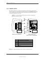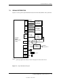
1
Technical Reference Guide For the Compaq iPAQ Internet Device This hardcopy is designed to be placed into a standard 3-ring binder. Provided below is a title block that can be copied and cut out and placed into the slip or taped onto the edge of the binder. iPAQ Internet Device TRG Reader Feedback Please feel free to send any questions, suggestions, corrections, or comments regarding this document please to the following email address: [email protected] When responding, please state the title of the referenced document. Technical Reference Guide NOTICE The information in this document is subject to change without notice. COMPAQ COMPUTER CORPORATION SHALL NOT BE LIABLE FOR TECHNICAL OR EDITORIAL ERRORS OR OMISSIONS HEREIN; NOR FOR INCIDENTAL OR CONSEQUENTIAL DAMAGES RESULTING FROM THE FURNISHING, PERFORMANCE, OR USE OF THIS MATERIAL. IT IS THE RESPONSIBILITY OF MANUFACTURERS TO ENSURE THAT DEVICES DESIGNED TO BE USED WITH COMPAQ PRODUCTS COMPLY WITH FCC CLASS B EMISSIONS REQUIREMENTS. This guide contains information protected by copyright. Except for use as a reference for the described Compaq product, no part of this document may be photocopied or reproduced in any form without prior written consent from Compaq Computer Corporation. 2000 Compaq Computer Corporation All rights reserved. Compaq and the Compaq logo are regiserted in the U.S. Patent and Trademark Office. iPAQ is a trademark of Compaq Information Technologies Group, L.P. Microsoft, Windows, Windows NT, and other names of Microsoft products referenced herein are trademarks or registered trademarks of Microsoft Corporation. Intel and Pentium are registered trademarks of Intel Corporation. Celeron and MMX are trademarks of Intel Corporation. Product names mentioned in this document may be trademarks and/or registered trademarks of other companies. For more information regarding specifications and Compaq-specific parts please contact Compaq Computer Corporation at http://www.compaq.com . Technical Reference Guide For the Compaq iPAQ Internet Device First Edition – March 2000 Document Number 127M-0300A-WWEN Compaq iPAQ Family of Internet Devices First Edition - March 2000 i Technical Reference Guide ii Compaq iPAQ Family of Internet Devices First Edition –- March 2000 Technical Reference Guide TABLE OF CONTENTS CHAPTER 1 INTRODUCTION............................................................................................................. 1.1 ABOUT THIS GUIDE ........................................................................................................... 1-1 1.1.1 USING THIS GUIDE ..................................................................................................... 1-1 1.1.2 ADDITIONAL INFORMATION SOURCES.................................................................. 1-1 MODEL NUMBERING CONVENTION........................................................................................... 1-1 1.3 NOTATIONAL CONVENTIONS.......................................................................................... 1-2 1.3.1 VALUES........................................................................................................................ 1-2 1.3.2 RANGES........................................................................................................................ 1-2 1.3.3 SIGNAL LABELS.......................................................................................................... 1-2 1.3.4 REGISTER NOTATION AND USAGE ......................................................................... 1-2 1.3.5 BIT NOTATION ............................................................................................................ 1-2 1.4 COMMON ACRONYMS AND ABBREVIATIONS.............................................................. 1-3 CHAPTER 2 SYSTEM OVERVIEW..................................................................................................... 2.1 INTRODUCTION.................................................................................................................. 2-1 2.2 FEATURES AND OPTIONS ................................................................................................. 2-2 2.2.1 STANDARD FEATURES .............................................................................................. 2-2 2.2.2 OPTIONS....................................................................................................................... 2-3 2.3 MECHANICAL DESIGN ...................................................................................................... 2-4 2.3.1 CABINET LAYOUTS.................................................................................................... 2-4 2.3.2 CHASSIS LAYOUT....................................................................................................... 2-6 2.3.3 SYSTEM BOARD LAYOUTS ....................................................................................... 2-7 2.4 SYSTEM ARCHITECTURE.................................................................................................. 2-8 2.4.1 PROCESSORS ............................................................................................................. 2-10 2.4.2 CHIPSET ..................................................................................................................... 2-12 2.4.3 SUPPORT COMPONENTS.......................................................................................... 2-13 2.4.4 SYSTEM MEMORY.................................................................................................... 2-13 2.4.5 MASS STORAGE ........................................................................................................ 2-14 2.4.6 SERIAL AND PARALLEL INTERFACES .................................................................. 2-14 2.4.7 UNIVERSAL SERIAL BUS INTERFACE ................................................................... 2-14 2.4.8 GRAPHICS SUBSYSTEM ........................................................................................... 2-14 2.4.9 AUDIO SUBSYSTEM ................................................................................................. 2-15 2.5 SPECIFICATIONS .............................................................................................................. 2-15 CHAPTER 3 PROCESSOR/MEMORY SUBSYSTEM ........................................................................ 3.1 INTRODUCTION.................................................................................................................. 3-1 3.2 PROCESSOR......................................................................................................................... 3-2 3.2.1 CELERON PROCESSOR............................................................................................... 3-2 3.2.2 PENTIUM III PROCESSOR........................................................................................... 3-3 3.2.3 PROCESSOR UPGRADING .......................................................................................... 3-4 3.3 MEMORY SUBSYSTEM ...................................................................................................... 3-5 3.4 SUBSYSTEM CONFIGURATION ........................................................................................ 3-8 Compaq iPAQ Family of Internet Devices First Edition - March 2000 iii Technical Reference Guide CHAPTER 4 SYSTEM SUPPORT......................................................................................................... 4.1 INTRODUCTION.................................................................................................................. 4-1 4.2 PCI BUS OVERVIEW ........................................................................................................... 4-2 4.2.1 PCI BUS TRANSACTIONS........................................................................................... 4-3 4.2.2 PCI INTERRUPT MAPPING ......................................................................................... 4-6 4.2.3 PCI POWER MANAGEMENT SUPPORT..................................................................... 4-6 4.2.4 PCI SUB-BUSSES.......................................................................................................... 4-6 4.2.5 PCI CONFIGURATION................................................................................................. 4-7 4.3 AGP BUS OVERVIEW ......................................................................................................... 4-8 4.3.1 BUS TRANSACTIONS.................................................................................................. 4-8 4.3.2 AGP CONFIGURATION ............................................................................................. 4-11 4.4 INTERRUPTS ..................................................................................................................... 4-12 4.4.1 MASKABLE INTERRUPTS ........................................................................................ 4-12 4.4.2 NON-MASKABLE INTERRUPTS............................................................................... 4-14 4.5 INTERVAL TIMER............................................................................................................. 4-16 4.6 SYSTEM CLOCK DISTRIBUTION .................................................................................... 4-16 4.7 REAL-TIME CLOCK AND CONFIGURATION MEMORY............................................... 4-17 4.7.1 CMOS ARCHIVE ........................................................................................................ 4-18 4.7.2 STANDARD CMOS LOCATIONS .............................................................................. 4-18 4.7.3 CMOS FEATURE BITS............................................................................................... 4-26 4.8 SYSTEM MANAGEMENT................................................................................................. 4-27 4.8.1 SECURITY FUNCTIONS ............................................................................................ 4-27 4.8.2 POWER MANAGEMENT ........................................................................................... 4-28 4.8.3 THERMAL SENSING AND COOLING ...................................................................... 4-28 4.9 SYSTEM I/O MAP .............................................................................................................. 4-29 CHAPTER 5 INPUT/OUTPUT INTERFACES ..................................................................................... 5.1 INTRODUCTION.................................................................................................................. 5-1 5.2 ENHANCED IDE INTERFACE ............................................................................................ 5-1 5.2.1 IDE PROGRAMMING................................................................................................... 5-1 5.2.2 IDE CONNECTOR ........................................................................................................ 5-3 5.3 DISKETTE DRIVE INTERFACE.......................................................................................... 5-4 5.4 SERIAL INTERFACE ........................................................................................................... 5-5 5.4.1 RS-232 INTERFACE ..................................................................................................... 5-5 5.4.2 SERIAL TEST INTERFACE ........................................................................................ 5-6 5.4.3 SERIAL INTERFACE PROGRAMMING ...................................................................... 5-6 5.5 PARALLEL INTERFACE ..................................................................................................... 5-8 5.5.1 STANDARD PARALLEL PORT MODE ....................................................................... 5-8 5.5.2 ENHANCED PARALLEL PORT MODE ....................................................................... 5-9 5.5.3 EXTENDED CAPABILITIES PORT MODE ................................................................. 5-9 5.5.4 PARALLEL INTERFACE PROGRAMMING .............................................................. 5-10 5.5.5 PARALLEL INTERFACE CONNECTOR ................................................................... 5-14 5.6 KEYBOARD/POINTING DEVICE INTERFACE ............................................................... 5-15 5.6.1 KEYBOARD INTERFACE OPERATION ................................................................... 5-15 5.6.2 POINTING DEVICE INTERFACE OPERATION ....................................................... 5-17 5.6.3 KEYBOARD/POINTING DEVICE INTERFACE PROGRAMMING ......................... 5-17 5.6.4 KEYBOARD/POINTING DEVICE INTERFACE CONNECTOR................................ 5-21 iv Compaq iPAQ Family of Internet Devices First Edition –- March 2000 Technical Reference Guide 5.7 UNIVERSAL SERIAL BUS INTERFACE........................................................................... 5-22 5.7.1 USB DATA FORMATS ............................................................................................... 5-22 5.7.2 USB PROGRAMMING................................................................................................ 5-24 5.7.3 USB CONNECTOR ..................................................................................................... 5-25 5.7.4 USB CABLE DATA..................................................................................................... 5-25 5.8 AUDIO SUBSYSTEM ......................................................................................................... 5-26 5.8.1 FUNCTIONAL ANALYSIS ......................................................................................... 5-26 5.8.2 AC97 AUDIO CONTROLLER..................................................................................... 5-28 5.8.3 AC97 LINK BUS ......................................................................................................... 5-28 5.8.4 AUDIO CODEC........................................................................................................... 5-29 5.8.5 AUDIO PROGRAMMING ........................................................................................... 5-30 5.8.6 AUDIO SPECIFICATIONS ......................................................................................... 5-31 5.9 NETWORK INTERFACE CONTROLLER.......................................................................... 5-32 5.9.1 WAKE ON LAN .......................................................................................................... 5-33 5.9.2 ALERT ON LAN ......................................................................................................... 5-33 5.9.3 POWER MANAGEMENT SUPPORT.......................................................................... 5-34 5.9.4 NIC PROGRAMMING................................................................................................. 5-35 CHAPTER 6 GRAPHICS SUBSYSTEM............................................................................................... 6.1 INTRODUCTION.................................................................................................................. 6-1 6.2 FUNCTIONAL DESCRIPTION............................................................................................. 6-2 6.2.1 FEATURE SUMMARY ................................................................................................. 6-3 6.3 DISPLAY MODES ................................................................................................................ 6-4 6.4 UPGRADING ........................................................................................................................ 6-4 6.5 PROGRAMMING.................................................................................................................. 6-5 6.5.1 CONFIGURATION........................................................................................................ 6-5 6.5.2 CONTROL..................................................................................................................... 6-5 6.6 MONITOR POWER MANAGEMENT CONTROL ............................................................... 6-6 6.7 MONITOR CONNECTOR .................................................................................................... 6-6 CHAPTER 7 POWER SUPPLY AND DISTRIBUTION....................................................................... 7.1 INTRODUCTION.................................................................................................................. 7-1 7.2 POWER SUPPLY ASSEMBLY/CONTROL .......................................................................... 7-1 7.2.1 POWER SUPPLY ASSEMBLY...................................................................................... 7-2 7.2.2 POWER CONTROL....................................................................................................... 7-3 7.3 POWER DISTRIBUTION...................................................................................................... 7-4 7.3.1 3.3/5/12 VDC DISTRIBUTION...................................................................................... 7-4 7.3.2 LOW VOLTAGE DISTRIBUTION................................................................................ 7-4 7.4 SIGNAL DISTRIBUTION ..................................................................................................... 7-5 Compaq iPAQ Family of Internet Devices First Edition - March 2000 v Technical Reference Guide CHAPTER 8 BIOS ROM ....................................................................................................................... 8.1 INTRODUCTION.................................................................................................................. 8-1 8.2 DESKTOP MANAGEMENT SUPPORT ............................................................................... 8-2 8.2.1 SYSTEM ID................................................................................................................... 8-4 8.2.2 SYSTEM INFORMATION TABLE ............................................................................... 8-4 8.2.3 EDID RETRIEVE .......................................................................................................... 8-5 8.2.4 DRIVE FAULT PREDICTION....................................................................................... 8-5 8.2.5 SYSTEM MAP RETRIEVAL......................................................................................... 8-6 8.2.6 FLASH ROM FUNCTIONS ........................................................................................... 8-7 8.2.7 POWER BUTTON FUNCTIONS ................................................................................... 8-7 8.2.8 ACCESSING CMOS...................................................................................................... 8-8 8.2.9 ACCESSING CMOS FEATURE BITS........................................................................... 8-8 8.2.10 SECURITY FUNCTIONS ............................................................................................ 8-10 8.3 MEMORY DETECTION AND CONFIGURATION............................................................ 8-11 8.4 PNP SUPPORT .................................................................................................................... 8-12 8.4.1 SMBIOS....................................................................................................................... 8-13 8.5 POWER MANAGEMENT FUNCTIONS ............................................................................ 8-14 8.5.1 INDEPENDENT PM SUPPORT .................................................................................. 8-14 8.5.2 ACPI SUPPORT........................................................................................................... 8-15 8.5.3 APM 1.2 SUPPORT ..................................................................................................... 8-15 8.6 USB LEGACY SUPPORT ................................................................................................... 8-17 8.7 BIOS UPGRADING............................................................................................................. 8-18 APPENDIX A ERROR MESSAGES AND CODES............................................................................... A.1 A.2 A.3 A.4 A.5 A.6 A.7 A.8 A.9 A.10 A.11 A.12 A.13 A.14 A.15 A.16 A.17 A.18 A.19 A.20 A.21 A.22 A.23 vi INTRODUCTION................................................................................................................. A-1 POWER-ON MESSAGES..................................................................................................... A-1 BEEP/KEYBOARD LED CODES ........................................................................................ A-1 POWER-ON SELF TEST (POST) MESSAGES.................................................................... A-2 PROCESSOR ERROR MESSAGES (1XX-XX) ...................................................................... A-3 MEMORY ERROR MESSAGES (2XX-XX)........................................................................... A-4 KEYBOARD ERROR MESSAGES (30X-XX) ....................................................................... A-4 PRINTER ERROR MESSAGES (4XX-XX) ............................................................................ A-5 VIDEO (GRAPHICS) ERROR MESSAGES (5XX-XX) .......................................................... A-5 DISKETTE DRIVE ERROR MESSAGES (6XX-XX) ......................................................... A-6 SERIAL INTERFACE ERROR MESSAGES (11XX-XX) ................................................... A-6 MODEM COMMUNICATIONS ERROR MESSAGES (12XX-XX).................................... A-7 SYSTEM STATUS ERROR MESSAGES (16XX-XX) ........................................................ A-8 HARD DRIVE ERROR MESSAGES (17XX-XX) ............................................................... A-8 HARD DRIVE ERROR MESSAGES (19XX-XX) ............................................................... A-9 VIDEO (GRAPHICS) ERROR MESSAGES (24XX-XX) .................................................... A-9 AUDIO ERROR MESSAGES (3206-XX)......................................................................... A-10 DVD/CD-ROM ERROR MESSAGES (33XX-XX)............................................................ A-10 NETWORK INTERFACE ERROR MESSAGES (60XX-XX) ........................................... A-10 SCSI INTERFACE ERROR MESSAGES (65XX-XX, 66XX-XX, 67XX-XX) ....................... A-11 POINTING DEVICE INTERFACE ERROR MESSAGES (8601-XX).............................. A-11 CEMM PRIVILEDGED OPS ERROR MESSAGES........................................................ A-12 CEMM EXCEPTION ERROR MESSAGES ................................................................... A-12 Compaq iPAQ Family of Internet Devices First Edition –- March 2000 Technical Reference Guide APPENDIX B ASCII CHARACTER SET ............................................................................................. B.1 INTRODUCTION..................................................................................................................B-1 APPENDIX C KEYBOARD ................................................................................................................... C.1 INTRODUCTION..................................................................................................................C-1 C.2 KEYSTROKE PROCESSING................................................................................................C-2 C.2.1 PS/2-TYPE KEYBOARD TRANSMISSIONS................................................................C-3 C.2.2 USB-TYPE KEYBOARD TRANSMISSIONS................................................................C-4 C.2.3 KEYBOARD LAYOUTS ...............................................................................................C-5 C.2.4 KEYS.............................................................................................................................C-8 C.2.5 KEYBOARD COMMANDS.........................................................................................C-11 C.2.6 SCAN CODES .............................................................................................................C-11 C.3 CONNECTORS ...................................................................................................................C-15 Compaq iPAQ Family of Internet Devices First Edition - March 2000 vii Technical Reference Guide LIST OF FIGURES FIGURE 2–1. FIGURE 2–2. FIGURE 2–3. FIGURE 2–4. FIGURE 2–5. FIGURE 2–6. FIGURE 2–7. COMPAQ IPAQ INTERNET DEVICE WITH MONITOR ............................................................. 2-1 COMPAQ IPAQ INTERNET DEVICE, FRONT VIEW................................................................ 2-4 COMPAQ IPAQ INTERNET DEVICE, REAR VIEWS ................................................................ 2-5 COMPAQ IPAQ INTERNET DEVICE CHASSIS LAYOUT, RIDE SIDE VIEW ................................ 2-6 COMPAQ IPAQ SYSTEM BOARD LAYOUTS ......................................................................... 2-7 COMPAQ IPAQ ARCHITECTURE, BLOCK DIAGRAM .............................................................. 2-9 PROCESSOR ASSEMBLY AND MOUNTING .......................................................................... 2-11 FIGURE 3–1. FIGURE 3–2. FIGURE 3–3. FIGURE 3–4. PROCESSOR/MEMORY SUBSYSTEM ARCHITECTURE ............................................................ 3-1 CELERON PROCESSOR INTERNAL ARCHITECTURE ............................................................... 3-2 PENTIUM III PROCESSOR INTERNAL ARCHITECTURE ........................................................... 3-3 SYSTEM MEMORY MAP ..................................................................................................... 3-7 FIGURE 4-1. FIGURE 4-2. FIGURE 4-3. FIGURE 4-4. FIGURE 4-5. FIGURE 4-6. FIGURE 4-7. PCI BUS DEVICES AND FUNCTIONS ..................................................................................... 4-2 TYPE 0 CONFIGURATION CYCLE......................................................................................... 4-4 PCI CONFIGURATION SPACE MAP ...................................................................................... 4-5 AGP 1X DATA TRANSFER (PEAK TRANSFER RATE: 266 MB/S)........................................... 4-9 AGP 2X DATA TRANSFER (PEAK TRANSFER RATE: 532 MB/S)......................................... 4-10 MASKABLE INTERRUPT PROCESSING, BLOCK DIAGRAM..................................................... 4-12 CONFIGURATION MEMORY MAP....................................................................................... 4-17 FIGURE 5-1. 40-PIN PRIMARY IDE CONNECTOR (ON SYSTEM BOARD)...................................................... 5-3 FIGURE 5-2. 50-PIN SECONDARY IDE CONNECTOR (ON SYSTEM AND DAUGHTER BOARDS). ...................... 5-4 FIGURE 5-3. SERIAL INTERFACE CONNECTOR (MALE DB-9 AS VIEWED FROM REAR OF CHASSIS) ............... 5-5 FIGURE 5-4. SERIAL INTERFACE HEADER (ON LEGACY-FREE SYSTEM BOARD) ........................................... 5-6 FIGURE 5-5. PARALLEL INTERFACE CONNECTOR (FEMALE DB-25 AS VIEWED FROM REAR OF CHASSIS).... 5-14 FIGURE 5-6. 8042-TO-KEYBOARD TRANSMISSION OF CODE EDH, TIMING DIAGRAM ............................. 5-15 FIGURE 5-7. KEYBOARD OR POINTING DEVICE INTERFACE CONNECTOR ................................................ 5-21 FIGURE 5-8. USB I/F, BLOCK DIAGRAM............................................................................................... 5-22 FIGURE 5-9. USB PACKET FORMATS .................................................................................................... 5-23 FIGURE 5-10. UNIVERSAL SERIAL BUS CONNECTOR .............................................................................. 5-25 FIGURE 5-11. AUDIO SUBSYSTEM FUNCTIONAL BLOCK DIAGRAM ......................................................... 5-27 FIGURE 5-12. AC’97 LINK BUS PROTOCOL .......................................................................................... 5-28 FIGURE 5-13. AD1881 AUDIO CODEC FUNCTIONAL BLOCK DIAGRAM................................................... 5-29 FIGURE 5-14. 10/100 TX NETWORK INTERFACE CONTROLLER BLOCK DIAGRAM ................................... 5-32 FIGURE 5-15. ETHERNET TPE CONNECTOR (RJ-45, VIEWED FROM CARD EDGE)..................................... 5-36 FIGURE 6-1. GRAPHICS SUBSYSTEM BLOCK DIAGRAM ............................................................................ 6-2 FIGURE 6-2. 82810E/DC-100 INTEGRATED GRAPHICS CONTROLLER ....................................................... 6-3 FIGURE 7–1. FIGURE 7–2. FIGURE 7–3. FIGURE 7–4. POWER DISTRIBUTION AND CONTROL, BLOCK DIAGRAM..................................................... 7-1 POWER CABLE DIAGRAM .................................................................................................. 7-4 SIGNAL DISTRIBUTION DIAGRAM....................................................................................... 7-5 HEADER PINOUTS ............................................................................................................. 7-6 FIGURE B–1. ASCII CHARACTER SET ...................................................................................................B-1 viii Compaq iPAQ Family of Internet Devices First Edition –- March 2000 Technical Reference Guide FIGURE C–1. FIGURE C–2. FIGURE C–3. FIGURE C–4. FIGURE C–5. FIGURE C–6. FIGURE C–7. FIGURE C–8. FIGURE C–9. KEYSTROKE PROCESSING ELEMENTS, BLOCK DIAGRAM ....................................................C-2 PS/2 KEYBOARD-TO-SYSTEM TRANSMISSION, TIMING DIAGRAM ......................................C-3 U.S. ENGLISH (101-KEY) KEYBOARD KEY POSITIONS .......................................................C-5 NATIONAL (102-KEY) KEYBOARD KEY POSITIONS ............................................................C-5 U.S. ENGLISH WINDOWS (101W-KEY) KEYBOARD KEY POSITIONS ...................................C-6 NATIONAL WINDOWS (102W-KEY) KEYBOARD KEY POSITIONS ........................................C-6 EASY ACCESS KEY POSITIONS ..........................................................................................C-7 PS/2 KEYBOARD CABLE CONNECTOR (MALE).................................................................C-15 USB KEYBOARD CABLE CONNECTOR (MALE).................................................................C-15 Compaq iPAQ Family of Internet Devices First Edition - March 2000 ix Technical Reference Guide LIST OF TABLES TABLE 1–1. ACRONYMS AND ABBREVIATIONS ....................................................................................... 1-3 TABLE 2-1. FEATURE DIFFERENCE MATRIX ........................................................................................... 2-2 TABLE 2-2. ARCHITECTURAL COMPARISON ............................................................................................. 2-8 TABLE 2-3. INTEL 810E CHIPSET COMPARISON .................................................................................... 2-12 TABLE 2-4. SUPPORT COMPONENT FUNCTIONS .................................................................................... 2-13 TABLE 2-5. ENVIRONMENTAL SPECIFICATIONS .................................................................................... 2-15 TABLE 2-6. ELECTRICAL SPECIFICATIONS ............................................................................................ 2-15 TABLE 2-7. PHYSICAL SPECIFICATIONS................................................................................................ 2-16 TABLE 2-8. MULTIBAY 24X CD-ROM DRIVE SPECIFICATIONS............................................................. 2-16 TABLE 2-9. MULTIBAY 24X CD-ROM DRIVE SPECIFICATIONS............................................................. 2-17 TABLE 2-10. HARD DRIVE SPECIFICATIONS ......................................................................................... 2-17 TABLE 3–1. CELERON PROCESSOR STATISTICAL COMPARISON ............................................................... 3-2 TABLE 3–2. PENTIUM III PROCESSOR STATISTICAL COMPARISON ........................................................... 3-3 TABLE 3–3. SPD ADDRESS MAP (SDRAM DIMM)................................................................................. 3-6 TABLE 3–4. HOST/PCI BRIDGE CONFIGURATION REGISTERS (GMCH, FUNCTION 0) ................................ 3-8 TABLE 4-1. PCI DEVICE CONFIGURATION ACCESS ................................................................................. 4-4 TABLE 4-2. SYSTEM BOARD PCI DEVICE IDENTIFICATION ..................................................................... 4-5 TABLE 4-3. LPC BRIDGE CONFIGURATION REGISTERS (ICH, FUNCTION 0).............................................. 4-7 TABLE 4-4. PCI/AGP BRIDGE CONFIGURATION REGISTERS (MCH, FUNCTION 1) .................................. 4-11 TABLE 4-5. MASKABLE INTERRUPT PRIORITIES AND ASSIGNMENTS ...................................................... 4-13 TABLE 4-6. MASKABLE INTERRUPT CONTROL REGISTERS .................................................................... 4-13 TABLE 4-7. INTERVAL TIMER FUNCTIONS ............................................................................................ 4-16 TABLE 4-8. INTERVAL TIMER CONTROL REGISTERS ............................................................................. 4-16 TABLE 4-9. CLOCK GENERATION AND DISTRIBUTION ........................................................................... 4-16 TABLE 4-10. CONFIGURATION MEMORY (CMOS) MAP ....................................................................... 4-18 TABLE 4-11. SYSTEM I/O MAP ........................................................................................................... 4-29 TABLE 5–1. IDE PCI CONFIGURATION REGISTERS ................................................................................ 5-2 TABLE 5–2. IDE BUS MASTER CONTROL REGISTERS .............................................................................. 5-2 TABLE 5–3. 40-PIN PRIMARY IDE CONNECTOR PINOUT......................................................................... 5-3 TABLE 5–4. 50-PIN SECONDARY IDE CONNECTOR PINOUT .................................................................... 5-4 TABLE 5–5. DB-9 SERIAL CONNECTOR PINOUT ...................................................................................... 5-5 TABLE 5–6. SERIAL INTERFACE CONFIGURATION REGISTERS.................................................................. 5-6 TABLE 5–7. SERIAL INTERFACE CONTROL REGISTERS ............................................................................ 5-7 TABLE 5–8. PARALLEL INTERFACE CONFIGURATION REGISTERS ........................................................... 5-10 TABLE 5–9. PARALLEL INTERFACE CONTROL REGISTERS ...................................................................... 5-11 TABLE 5–10. DB-25 PARALLEL CONNECTOR PINOUT .......................................................................... 5-14 TABLE 5–11. 8042-TO-KEYBOARD COMMANDS .................................................................................. 5-16 TABLE 5–12. KEYBOARD INTERFACE CONFIGURATION REGISTERS ....................................................... 5-17 TABLE 5–13. CPU COMMANDS TO THE 8042...................................................................................... 5-19 TABLE 5–14. KEYBOARD/POINTING DEVICE CONNECTOR PINOUT ........................................................ 5-21 TABLE 5–15. USB INTERFACE CONFIGURATION REGISTERS ................................................................. 5-24 TABLE 5–16. USB CONTROL REGISTERS ............................................................................................. 5-24 TABLE 5–17. USB CONNECTOR PINOUT .............................................................................................. 5-25 TABLE 5–18. USB CABLE LENGTH DATA............................................................................................ 5-25 x Compaq iPAQ Family of Internet Devices First Edition –- March 2000 Technical Reference Guide TABLE 5–19. TABLE 5–20. TABLE 5–21. TABLE 5–22. TABLE 5–23. TABLE 5–24. TABLE 5–25. AC’97 AUDIO CONTROLLER PCI CONFIGURATION REGISTERS ........................................ 5-30 AC’97 AUDIO CODEC CONTROL REGISTERS ................................................................... 5-30 AUDIO SUBSYSTEM SPECIFICATIONS ............................................................................... 5-31 AOL EVENTS ................................................................................................................ 5-33 NIC CONTROLLER PCI CONFIGURATION REGISTERS ....................................................... 5-35 NIC CONTROL REGISTERS ............................................................................................. 5-35 82559 NIC OPERATING SPECIFICATIONS ........................................................................ 5-36 TABLE 6-1. TABLE 6-2. TABLE 6-3. TABLE 6-4. TABLE 6-5. INTEL GRAPHICS DISPLAY MODES ....................................................................................... 6-4 PCI CONFIGURATION SPACE REGISTERS .............................................................................. 6-5 STANDARD VGA MODE I/O MAPPING ................................................................................ 6-5 MONITOR POWER MANAGEMENT CONDITIONS .................................................................... 6-6 DB-15 MONITOR CONNECTOR PINOUT................................................................................ 6-6 TABLE 8-1. TABLE 8-2. TABLE 8-3. TABLE 8-4. DESKTOP MANAGEMENT FUNCTIONS (INT15) ..................................................................... 8-2 CMOS FEATURE BITS ........................................................................................................ 8-9 PNP BIOS FUNCTIONS ..................................................................................................... 8-12 APM BIOS FUNCTIONS (INT15) ...................................................................................... 8-17 TABLE A–1. POWER-ON MESSAGES ..................................................................................................... A-1 TABLE A–2. BEEP/KEYBOARD LED CODES.......................................................................................... A-1 TABLE A–3. POWER-ON SELF TEST (POST) MESSAGES ........................................................................ A-2 TABLE A–4. SYSTEM ERROR MESSAGES............................................................................................... A-3 TABLE A–5. MEMORY ERROR MESSAGES ............................................................................................. A-4 TABLE A–6. KEYBOARD ERROR MESSAGES .......................................................................................... A-4 TABLE A–7. PRINTER ERROR MESSAGES .............................................................................................. A-5 TABLE A–8. VIDEO (GRAPHICS) ERROR MESSAGES .............................................................................. A-5 TABLE A–9. DISKETTE DRIVE ERROR MESSAGES.................................................................................. A-6 TABLE A–10. SERIAL INTERFACE ERROR MESSAGES ............................................................................. A-6 TABLE A–11. SERIAL INTERFACE ERROR MESSAGES ............................................................................. A-7 TABLE A–12. SYSTEM STATUS ERROR MESSAGES ................................................................................ A-8 TABLE A–13. HARD DRIVE ERROR MESSAGES ...................................................................................... A-8 TABLE A–14. HARD DRIVE ERROR MESSAGES ...................................................................................... A-9 TABLE A–15. HARD DRIVE MESSAGES ................................................................................................. A-9 TABLE A–16. AUDIO ERROR MESSAGES ............................................................................................. A-10 TABLE A–17. DVD/CD-ROM DRIVE ERROR MESSAGES .................................................................... A-10 TABLE A–18. NETWORK INTERFACE ERROR MESSAGES ...................................................................... A-10 TABLE A–19. SCSI INTERFACE ERROR MESSAGES ............................................................................. A-11 TABLE A–20. POINTING DEVICE INTERFACE ERROR MESSAGES........................................................... A-11 TABLE A–21. CEMM PRIVILEGED OPS ERROR MESSAGES.................................................................. A-12 TABLE A–22. CEMM EXCEPTION ERROR MESSAGES ......................................................................... A-12 TABLE C–1. KEYBOARD-TO-SYSTEM COMMANDS ...............................................................................C-11 TABLE C–2. KEYBOARD SCAN CODES .................................................................................................C-12 Compaq iPAQ Family of Internet Devices First Edition - March 2000 xi Technical Reference Guide xii Compaq iPAQ Family of Internet Devices First Edition –- March 2000 Technical Reference Guide Chapter 1 INTRODUCTION 1. Chapter 1 INTRODUCTION 1.1 ABOUT THIS GUIDE This guide provides technical information about the Compaq iPAQ Family of Internet Devices. This document includes information regarding system design, function, and features that can be used by programmers, engineers, technicians, and system administrators. This guide and any applicable addendum are available online at the following location: http://www.compaq.com/support/techpubs/technical_reference_guides/index.html 1.1.1 USING THIS GUIDE The chapters of this guide primarily describe the hardware and firmware elements and primarily deal with the system board and the power supply assembly. The appendices contain general information about standard peripheral devices such as the keyboard. 1.1.2 ADDITIONAL INFORMATION SOURCES For more information on chipset components mentioned in this guide refer to the indicated manufacturers’ documentation, which may be available at the following online sources: ♦ ♦ ♦ 1.2 Compaq Computer Corporation: http://www.compaq.com Intel Corporation: http://www.intel.com Standard Microsystems Corporation: http://www.smsc.com MODEL NUMBERING CONVENTION The model numbering convention for Compaq iPAQ units is as follows: iPAQ/XNNN/Nb/N/NNN Memory (in MB) Operating system: 4 = Win NT 4.0; 9 = Win95/98 Chipset type (b = 810e) Hard drive size (in GB) Processor speed (in MHz) Processor type: C = Celeron; P = Pentium Compaq iPAQ Family of Internet Devices First Edition - March 2000 1-1 Chapter 1 Introduction 1.3 NOTATIONAL CONVENTIONS 1.3.1 VALUES Hexadecimal values are indicated by a numerical or alpha-numerical value followed by the letter “h.” Binary values are indicated by a value of ones and zeros followed by the letter “b.” Numerical values that have no succeeding letter can be assumed to be decimal. 1.3.2 RANGES Ranges or limits for a parameter are shown using the following methods: Example A: Example B: Bits <7..4> = bits 7, 6, 5, and 4. IRQ3-7, 9 = IRQ signals 3 through 7, and IRQ signal 9 1.3.3 SIGNAL LABELS Signal names are indicated using abbreviations, acronyms, or, if possible, the full signal name in all capital letters. Signals that are meant to be active (asserted) low are indicated with a dash immediately following the name. 1.3.4 REGISTER NOTATION AND USAGE This guide uses standard Intel naming conventions in discussing the microprocessor’s (CPU) internal registers. Registers that are accessed through programmable I/O using an indexing scheme are indicated using the following format: 03C5.17h Index port Data port In the example above, register 03C5.17h is accessed by writing the index port value 17h to the index address (03C4h), followed by a write to or a read from port 03C5h. 1.3.5 BIT NOTATION Bit values are labeled with bit <0> representing the least-significant bit (LSb) and bit <7> representing the most-significant bit (MSb) of a byte. Bytes, words, double words, and quad words are typically shown with most-significant portions on the left or top and the leastsignificant portions on the right or bottom respectively. 1-2 Compaq iPAQ Family of Internet Devices First Edition – March 2000 Technical Reference Guide 1.4 COMMON ACRONYMS AND ABBREVIATIONS Table 1-1 lists the acronyms and abbreviations used in this guide. Table 1–1. Acronyms and Abbreviations Table 1-1. Acronyms and Abbreviations Acronym/Abbreviation A AC ACPI A/D AGP API APM AOL ASIC AT ATA ATAPI AVI AVGA BAT BCD BIOS bis BitBLT BNC bps or b/s BSP BTO CAS CD CD-ROM CDS CF CGA Ch cm CMC CMOS Cntlr Cntrl codec CPQ CPU CRT CSM CTO DAA DAC DC DCH DDC DF Description ampere alternating current Advanced Configuration and Power Interface analog-to-digital Accelerated graphics port application programming interface advanced power management Alert-ON-LAN application-specific integrated circuit 1) attention (modem commands) 2) 286-based PC architecture AT attachment (IDE protocol) AT attachment w/packet interface extensions audio-video interleaved Advanced VGA Basic assurance test binary-coded decimal basic input/output system second/new revision bit block transfer Bayonet Neill-Concelman (connector) bits per second Bootstrap processor Built to order column address strobe compact disk compact disk read-only memory compact disk system carry flag color graphics adapter channel centimeter cache/memory controller complimentary metal-oxide semiconductor (configuration memory) controller control compressor/decompressor Compaq central processing unit cathode ray tube Compaq system management / Compaq server management Configure to order direct access arrangement digital-to-analog converter direct current DOS compatibility hole Display Data Channel direction flag Continued Compaq iPAQ Family of Internet Devices First Edition - March 2000 1-3 Chapter 1 Introduction Table 1-1. Acronyms and Abbreviations Continued Acronym/Abbreviation DIMM DIN DIP DMA DMI dpi DRAM DRQ EDID EDO EEPROM EGA EIA EISA EPP EIDE ESCD EV ExCA FIFO FL FM FPM FPU FPS ft GB GMCH GND GPIO GPOC GART GUI h HW hex Hz ICH IDE IEEE IF I/F in INT I/O IPL IrDA IRQ ISA JEDEC Kb / KB Kb/s kg KHz kv Description dual inline memory module Deutche IndustriNorm (connector standard) dual inline package direct memory access Desktop management interface dots per inch dynamic random access memory data request extended display identification data extended data out (RAM type) electrically eraseable PROM enhanced graphics adapter Electronic Industry Association extended ISA enhanced parallel port enhanced IDE Extended System Configuration Data (format) Environmental Variable (data) Exchangeable Card Architecture first in / first out flag (register) frequency modulation fast page mode (RAM type) Floating point unit (numeric or math coprocessor) Frames per second foot gigabyte Graphics/memory controller hub ground general purpose I/O general purpose open-collector Graphics address re-mapping table graphics user interface hexadecimal hardware hexadecimal hertz I/O controller hub integrated drive element Institute of Electrical and Electronic Engineers interrupt flag interface inch interrupt input/output initial program loader InfraRed Data Association interrupt request industry standard architecture Joint Electron Device Engineering Council kilobits / kilobytes (x 1024 bits / x 1024 bytes) kilobits per second kilogram kilohertz kilovolt Continued 1-4 Compaq iPAQ Family of Internet Devices First Edition – March 2000 Technical Reference Guide Table 1-1. Acronyms and Abbreviations Continued Acronym/Abbreviation lb LAN LCD LED LIF LPC LSI LSb / LSB LUN MCH MMX MPEG ms MSb / MSB mux MVA MVW n NIC NiCad NiMH NMI NRZI ns NT NTSC NVRAM OEM OS PAL PC PCI PCM PCMCIA PF PIN PIO POST PROM PTR RAM RAS rcvr RF RGB RH RIMM RMS ROM RPM RTC R/W Description pound local area network liquid crystal display light-emitting diode low insertion force (socket) Low pin count large scale integration least significant bit / least significant byte logical unit (SCSI) Memory controller hub multimedia extensions Motion Picture Experts Group millisecond most significant bit / most significant byte multiplex motion video acceleration motion video window variable parameter/value network interface card/controller nickel cadmium nickel-metal hydride non-maskable interrupt Non-return-to-zero inverted nanosecond nested task flag National Television Standards Committee non-volatile random access memory original equipment manufacturer operating system 1. programmable array logic 2. phase altering line Internet Device peripheral component interconnect pulse code modulation Internet Device Memory Card International Association parity flag personal identification number Programmed I/O power-on self test programmable read-only memory pointer random access memory row address strobe receiver resume flag red/green/blue (monitor input) Relative humidity RDRAM inline memory module root mean square read-only memory revolutions per minute real time clock read/write Continued Compaq iPAQ Family of Internet Devices First Edition - March 2000 1-5 Chapter 1 Introduction 1-6 Compaq iPAQ Family of Internet Devices First Edition – March 2000 Technical Reference Guide Table 1-1. Acronyms and Abbreviations Continued Acronym/Abbreviation SCSI SDRAM SEC SECAM SF SGRAM SIMD SIMM SIT SMART SMI SMM SMRAM SPD SPP SRAM SSE STN SVGA SW TAD TAFI TAM TCP TF TFT TIA TPE TPI TTL TV TX UART UDMA URL us / µs USB UTP V VESA VGA vib VLSI VRAM W WOL WRAM ZF ZIF Description small computer system interface Synchronous Dynamic RAM Single Edge-Connector sequential colour avec memoire (sequential color with memory) sign flag Synchronous Graphics RAM Single instruction multiple data single in-line memory module system information table Self Monitor Analysis Report Technology system management interrupt system management mode system management RAM serial presence detect standard parallel port static RAM Streaming SIMD extensions super twist pneumatic super VGA software telephone answering device Temperature-sensing And Fan control Integrated circuit telephone answering machine tape carrier package trap flag thin-film transistor Telecommunications Information Administration twisted pair ethernet track per inch transistor-transistor logic television transmit universal asynchronous receiver/transmitter Ultra DMA Uniform resource locator microsecond Universal Serial Bus unshielded twisted pair volt Video Electronic Standards Association video graphics adapter vibrato very large scale integration Video RAM watt Wake on LAN Windows RAM zero flag zero insertion force (socket) Compaq iPAQ Family of Internet Devices First Edition - March 2000 1-7 Technical Reference Guide Chapter 2 SYSTEM OVERVIEW 2. Chapter 2 SYSTEM OVERVIEW 2.1 INTRODUCTION The Compaq iPAQ Family of Internet Devices provides affordable business solutions with the focus on internet access and mainstream performance. Based on an Intel Celeron or Pentium III processor with the Intel 810e chipset, these systems are designed to maximize the effectiveness of internet and intranet usage while simplifying system management. Figure 2–1. Compaq iPAQ Internet Device with Monitor This chapter includes the following topics: ♦ ♦ ♦ ♦ Features and options (2.2) Mechanical design (2.3) System architecture (2.4) Specifications (2.5) page 2-2 page 2-4 page 2-8 page 2-13 Compaq iPAQ Family of Internet Devices First Edition - March 2000 2-1 Chapter 2 System Overview 2.2 FEATURES AND OPTIONS This section describes the standard features and available options. 2.2.1 STANDARD FEATURES The following standard features are available on all models: ♦ ♦ ♦ ♦ ♦ ♦ ♦ ♦ ♦ ♦ ♦ ♦ ♦ ♦ ♦ ♦ ♦ Celeron or Pentium III processor 810e Chipset Two DIMM sockets for system memory AC’97 audio subsystem w/Compaq Premier Sound and front panel mic and headphone jacks MuliBay device mount w/hot-swap support Extended IDE controller supporting UATA/66 mode Hard drive fault prediction Two USB ports on front panel Network interface controller VGA analog output (1600 x 1200 max resolution) APM 1.2 power management support Plug ’n Play compatible (with ESCD support) Intelligent Manageability support Energy Star compliant Security features including: • Setup and power-on passwords • DriveLock for MultiBay hard drive • I/O interface disabling • Administrator password • Network service boot • Asset tracking tag • UUID • Cable lock provision Compaq Easy-Access keyboard w/Windows support Mouse Table 2-1 shows the differences in features between the iPAQ models: Table 2-1. Feature Difference Matrix Table 2-1. iPAQ Feature Difference Matrix 4-MB Display cache Rear panel USB ports Serial port Parallel port Keyboard/mouse connection 2-2 Legacy-Free Celeron-Based Pentium-based No Yes 3 3 0 0 0 0 USB USB Compaq iPAQ Family of Internet Devices First Edition – March 2000 Legacy-Light Celeron-Based Pentium-Based No Yes 0 0 1 1 1 1 PS/2 PS/2 Technical Reference Guide 2.2.2 OPTIONS The following items are available as options for all models and may be included in the standard configuration of some models: ♦ System Memory: 32-MB DIMM (non-ECC) 64-MB DIMM (non-ECC) 128-MB DIMM (non-ECC) 256-MB DIMM (non-ECC) ♦ Hard drives: 4.3 or 8.4 GB UATA/66 hard drive ♦ MultiBay drives: 24x CD-ROM drive 4x DVD-ROM drive Super Disk LS-120 Power Drive 6.0 GB hard drive Compaq iPAQ Family of Internet Devices First Edition - March 2000 2-3 Chapter 2 System Overview 2.3 MECHANICAL DESIGN The Compaq iPAQ Internet Device uses a minitower form factor featuring a smaller footprint and reduced height than previous minitowers, allowing easy floor or desktop positioning. Commonly used audio and USB connections are accessible from the front panel. There are slight differences between the legacy-light and legacy-free models, most notably in the rear panel layouts. NOTE: For detailed information on servicing the Internet Device refer to the applicable Maintenance and Service Guide. 2.3.1 CABINET LAYOUTS 2.3.1.1 Front View 1 2 3 4 5 6 7 8 Item 1 2 3 4 5 6 7 8 Description Power Button Power LED Hard drive activity LED MultiBay device bay (accepts 5.25”/12.7 mm storage device) Microphone In Jack Headphone Out Jack USB port 3 jack USB port 4 jack Figure 2–2. Compaq iPAQ Internet Device, Front View 2-4 Compaq iPAQ Family of Internet Devices First Edition – March 2000 Technical Reference Guide 2.3.1.2 Rear Views 2 1 2 1 4 4 3 3 6 6 5 5 8 7 10 10 9 12 11 13 13 14 Legacy-Light Item 1 3 5 7 9 11 13 14 Legacy-Free Description Audio line output Network activity LED indicator Network speed LED indicator Parallel I/F connector USB port connectors (left-to-right; 0,1, 2) PS/2 mouse connector AC line in connector Item 2 4 6 8 10 12 14 Description Audio line input Network I/F jack VGA monitor connector Serial I/F connector MultiBay device eject button PS/2 keyboard connector Line voltage select switch Figure 2–3. Compaq iPAQ Internet Device, Rear Views Compaq iPAQ Family of Internet Devices First Edition - March 2000 2-5 Chapter 2 System Overview 2.3.2 CHASSIS LAYOUT The internal assemblies are accessible from the right side of the system unit. The right side (carbon-colored) cover is easily removable allowing quick access to the DIMM sockets through an access opening and to the hard drive. Access to the system board and processor requires removing the right chassis access panel. NOTE: For a detailed description on servicing the unit refer to the applicable Maintenance and Service Guide. 1 2 3 4 5 6 7 8 Right Side Cover Removed Item 1 2 3 4 5 6 7 8 Right Side Cover and Chassis Access Panel Removed Description Power button/LED board (PCA# 010647) DIMM socket access Hard drive in 3.5” 1/3 height bay Audio I/O board (PCA# 010650) System board (PCA# 161014 or 161015) Power supply assembly Processor Speaker Figure 2–4. Compaq iPAQ Internet Device Chassis Layout, Ride Side View 2-6 Compaq iPAQ Family of Internet Devices First Edition – March 2000 Technical Reference Guide 2.3.3 SYSTEM BOARD LAYOUTS The Compaq iPAQ Internet Device uses a FlexATX-type (9.0 x 7.5 inch) system board. Two variations are available; a legacy-light board and a legacy-free board. 1 2 3 4 5 1 22 2 3 4 5 22 6 21 6 21 7 20 8 7 20 8 9 19 10 9 19 11 12 13 18 17 16 15 18 Legacy Light (PCA# 161014) 17 16 15 14 Legacy Free (PCA# 161015) Item Description 1 USB ports 3 and 4 (front panel) header 2 Battery 3 BIOS ROM configuration jumper 4 Speaker connector 5 Audio microphone/headphone header 6 Audio line out jack 7 Audio line in jack 8 Network connector 9 VGA monitor connector 10 Parallel I/F connector 11 Serial I/F connector 12 USB ports 0, 1, 2 connectors 13 PS/2 mouse connector (top), PS/2 keyboard connector (bottom) 14 Serial I/F header 15 PGA370 processor socket 16 DIMM sockets 17 Processor (boxed) fan header 18 IDE (primary) 40-pin connector 19 IDE (secondary) 50-pin connector 20 Power button/LED indicator connector 21 CD audio header 22 Power supply connector NOTE: Refer to Chapter 7 “Power and Signal Distribution” for header pinouts. Figure 2–5. Compaq iPAQ System Board Layouts Compaq iPAQ Family of Internet Devices First Edition - March 2000 2-7 Chapter 2 System Overview 2.4 SYSTEM ARCHITECTURE The Compaq iPAQ Internet Device features an Intel Celeron or Pentium III processor and the 810e chipset. As indicated in the following table and shown in Figure 2-6, four architectural configurations are available: ♦ ♦ ♦ ♦ Legacy-free with Celeron processor Legacy-free with Pentium III processor Legacy-light with Celeron processor Legacy-light with Pentium III processor Legacy-free systems provide five Universal Serial Bus (USB) ports for connecting peripherals (including the supplied USB mouse and USB keyboard). Legacy light systems provide two USB ports along with the traditional PS/2 connectors for the supplied mouse and keyboard as well as parallel and serial port connectors. All systems use the 810e chipset. The 810e chipset includes the 82810e-DC100 GMCH designed to provide control for SDRAM and also integrates an AGP 2X graphics controller. Pentium IIIbased systems come with an additional 4-MB display cache to compliment the graphics controller. The 810e chipset also includes an 82801 I/O Controller Hub (ICH) that provides two IDE interfaces, two USB interfaces, and a PCI bus controller. The 82802 Firmware Hub (FWH) component is loaded with Compaq BIOS Table 2-1 lists differences between system architectures: Table 2-2. Architectural Comparison Table 2-2. Architectural Comparison Legacy Free Celeron-Based Pentium III-Based 66 MHz 100 MHz No Yes No No No No No No 5 5 Host bus (FSB)speed [1] 4-MB Display Cache? PS/2 Mouse/Keyboard? Serial port? Parallel port? # of USB ports NOTES: [1] As configured with 500-MHz processor. 2-8 Compaq iPAQ Family of Internet Devices First Edition – March 2000 Legacy Light Celeron-Based Pentium III-Based 66 MHz 100 MHz No Yes Yes Yes Yes Yes Yes Yes 2 2 Technical Reference Guide Celeron or Pentium III Processor 66-/100-/133- MHz FSB 810e Chipset Monitor RGB AGP 2X Cntlr. 4-MB Display Cache PC100 Memory Bus 82810e-DC100 GMCH SDRAM Cntlr. SDRAM System Memory Hub Link Bus IDE Hard Drive MultiBay Device Pri. IDE I/F Sec. IDE I/F USB Hub USB Port 0 USB I/F 82801 ICH LPC Bus 82802 FWH Audio Subsystem USB Port 2 USB Port 3 Keyboard/ Mouse I/F LPC47B277 I/O Controller Serial I/F Beep Audio USB Port 1 Parallel I/F 33-MHz 32-Bit PCI Bus AC’97 Audio Bus 82559 Ethernet Controller Power Supply .................. LEGEND: Legacy-light systems only. Legacy-free systems only. Pentium III-based systems only. Figure 2–6. Compaq iPAQ Architecture, Block diagram Compaq iPAQ Family of Internet Devices First Edition - March 2000 2-9 USB Port 4 Chapter 2 System Overview 2.4.1 PROCESSORS The Compaq iPAQ family includes models based on Celeron and Pentium III processors. These processors are backward-compatible with software written for the Pentium II, Pentium MMX, Pentium Pro, Pentium, and x86 microprocessors. Both processor architectures include a floatingpoint unit and first and secondary caches providing enhanced performance for multimedia applications. 2.4.1.1 Celeron Processor Select Compaq iPAQ systems use the Intel Celeron processor. The Celeron processor provides economical performance and is compatible with software written for previous generation processors such as Pentium II, Pentium MMX, Pentium, and x86 processors. Featuring a Pentium-type core architecture, the Celeron processor integrates a dual-ALU CPU with a floating-point unit, 32-KB first-level cache, and 128-KB second level cache, all of which operate at full processing (CPU) speed. The Celeron processor includes MMX technology for enhanced multimedia performance. The Celeron processor uses a PGA370 package with a heat sink. 2.4.1.2 Pentium III Processor The Intel Pentium III processor used on select systems represents the maximum performance processor for Compaq iPAQs. The Pentium III processor is compatible with software written for Celeron, Pentium II, Pentium MMX, Pentium, and x86 processors. The Pentium III processor core integrates a dual-ALU CPU with a floating-point unit and 32-KB first-level cache operating at processing (CPU) speed. Featuring .18-micron technology, the Pentium III processor features 256 kilobytes of secondary cache included on the CPU die and operating at full processor speed. The Pentium III processor includes MMX technology for enhanced multimedia performance. Also included are 70 additional streaming SIMD extensions (SSE) for enhancing 3D graphics and speech processing performance and a serial number function useful for asset tracking. The Pentium III processor employed in these systems uses a Flip-Chip (FC) PGA370 package and heat sink. 2-10 Compaq iPAQ Family of Internet Devices First Edition – March 2000 Technical Reference Guide 2.4.1.3 Processor Upgrading All models of the Compaq iPAQ use the PGA370 zero-insertion force (ZIF) socket for processor mounting as shown in Figure 2-7. Raising the Lock/Unlock handle of the socket in the vertical position allows the processor to be removed or inserted into the socket. Lowering the Lock/Unlock handle in the down (horizontal) position locks the processor in place. Factory configurations use processors fitted with passive heat sinks. Upgrade (boxed) processors may be fitted with a heat sink/fan assembly with a power cable that attaches to the fan power header provided on the system board. Heat Sink Heat Sink Retaining Clip Processor Lock/Unlock Handle PPGA370 Socket Figure 2–7. Processor Assembly and Mounting The processor clock frequency is automatically set by chipset logic, eliminating the need for setting DIP switches when upgrading the processor. ! WARNING: The system board is designed handle a maximum processor current load of 18 amps. Installing a replacement processor that draws more than 18 amps of current may damage the processor and/or the system board. Compaq iPAQ Family of Internet Devices 2-11 First Edition - March 2000 Chapter 2 System Overview 2.4.2 CHIPSET The Compaq iPAQ employs the Intel 810e chipset, which is designed to compliment the processor and provide the central point for the system’s data transactions. The chipset is composed of a graphics memory controller hub (GMCH), an I/O controller hub (ICH), and a firmware hub (FWH). Table 2-3 shows the functions provided by the components of the chipset. Table 2-3. Intel 810e Chipset Comparison Table 2-3. Intel 810e Chipset Components Component Type 82810e-DC100 Graphics/Memory Controller Hub(GMCH) 82801AA I/O Controller Hub (ICH) 82802 Firmware Controller Hub (FWH) Function AGP 2X graphics controller (i740 equivalent) SDRAM controller supporting 2 PC100 DIMMs 66-/100-/133-MHz FSB PCI bus I/F LPC bus I/F SMBus I/F IDE I/F with UATA/66 support AC ’97 audio controller RTC/CMOS IRQ controller Power management logic USB I/F (2) Loaded with Compaq BIOS Random number generator 2-12 Compaq iPAQ Family of Internet Devices First Edition – March 2000 Technical Reference Guide 2.4.3 SUPPORT COMPONENTS Input/output functions not provided by the chipset are handled by other support components. Some of these components also provide “housekeeping” and various other functions as well. Table 2-4 shows the functions provided by the support components. Table 2-4. Support Component Functions Table 2-4. Support Component Functions Component Name LPC47B277 I/O Controller AD1881 Audio Codec 82559 Ethernet Controller [1] Function Keyboard and pointing device I/F Diskette I/F Serial I/F Parallel I/F AGP, PCI reset generation ISA serial IRQ converter Power button logic Slow speed detection S3 regulator controller GPIO ports Audio mixer Digital-to-analog converter Analog-to-digital converter Analog I/O: Mic input Line input CD input Line output Network interface controller PHY interface Notes [1] [2] [1] [1] NOTE: [1] Implemented on legacy-light models only. [2] Not available for actual use but may be enabled to satisfy OS requirements. 2.4.4 SYSTEM MEMORY These systems utilize Synchronous DRAM (PC100 SDRAM, non-ECC only). Two DIMM sockets are provided and accessible through an access opening once the right side cover has been removed. Compaq iPAQ Family of Internet Devices 2-13 First Edition - March 2000 Chapter 2 System Overview 2.4.5 MASS STORAGE In a standard configuration the Compaq iPAQ supports two mass storage devices; one internal IDE hard drive mounted on the right side and a removeable-media IDE device (CD-ROM, DVD, or LS-120 Power Drive, etc.) mounted in the MultiBay on the left side. This system uses SMART drives for the internal IDE device. An adapter is available that allows a secondary IDE hard drive to be installed in the MultiBay. The MultiBay supports hot-swapping of mass storage devices except for hard drives. The Compaq iPAQ supports the DriveLock feature for MultiBay hard drives, providing enhanced security for removeable hard drives. 2.4.6 SERIAL AND PARALLEL INTERFACES The legacy-light models include a serial port and a parallel port accessible at the rear of the chassis. The serial port is RS-232-C/16550-compatible and supports standard baud rates up to 115,200 as well as two high-speed baud rates of 230K and 460K , and utilize a DB-9 connector. The parallel interface is Enhanced Parallel Port (EPP1.9) and Enhanced Capability Port (ECP) compatible, and supports bi-directional data transfers through a DB-25 connector. These interfaces may be disabled through Setup for enhanced security 2.4.7 UNIVERSAL SERIAL BUS INTERFACE Legacy-light models feature two front panel-accessible Universal Serial Bus (USB) ports that provide a 12Mb/s interface for peripherals. Legacy-free models also include three additional USB ports on the rear panel to accommodate the USB keyboard and mouse supplied with those models. The USB provides hot plugging/unplugging (Plug ’n Play) functionality. 2.4.8 GRAPHICS SUBSYSTEM All models use the graphics controller integrated into the 82810e/DC-100 GMCH component of the 810e chipset. This graphics controller is the equivalent of the Intel i740 controller and provides up to 1600 x 1200 2D resolution using the AGP 2X interface. Pentium III-based systems also include 4 megabytes of local display cache for higher 3D performance. 2-14 Compaq iPAQ Family of Internet Devices First Edition – March 2000 Technical Reference Guide 2.4.9 AUDIO SUBSYSTEM The audio subsystem features an AC’97 specification-based design and uses the integrated AC97 audio controller of the chipset and an AC’97-compliant audio codec. Microphone and headphone jacks are accessible on the front panel and line input and output jacks are provided on the rear panel. A low-distortion 5-watt amplifier drives a long-excursion speaker for optimum sound. 2.5 SPECIFICATIONS This section includes the environmental, electrical, and physical specifications for the Compaq iPAQ Series Internet Devices. Where provided, metric statistics are given in parenthesis. All specifications subject to change without notice. Table 2-5. Environmental Specifications Table 2-5. Environmental Specifications Parameter Operating o o o o Air Temperature 50 to 95 F (10 to 35 C) Shock N/A Vibration 0.000215g^ 2/Hz, 10-300 Hz [1] o Humidity 90% RH @ 36 C (no hard drive) Maximum Altitude 10,000 ft (3048 m) NOTE: [1] 0.5 grms nominal Nonoperating o o o o -24 to 140 F (-30 to 60 C) 60.0 g for 2 ms half-sine pulse 0.0005g^ 2/Hz, 10-500 Hz [1] o 95% RH @ 36 C 30,000 ft (9,144 m) Table 2-6. Electrical Specifications Table 2-6. Electrical Specifications Parameter Input Line Voltage: Nominal: Maximum: Input Line Frequency Range: Nominal: Maximum: Power Supply: Maximum Continuous Power Maximum Line Current Draw U.S. International 110 - 120 VAC 90 - 132 VAC 200 - 240 VAC 180 - 264 VAC 50 - 60 Hz 47 - 63 Hz 50 - 60 Hz 47 - 63 Hz 90 watts 2.5 amps 90 watts 1.25 amps Compaq iPAQ Family of Internet Devices 2-15 First Edition - March 2000 Chapter 2 System Overview Table 2-7. Physical Specifications Table 2-7. Physical Specifications Parameter Height Width Depth Weight Standard 11.80 in 5.66 in 9.44 in 10.7 lb Metric 29.97 cm 14.38 cm 23.98 cm 4.8 kg Table 2-8. MultiBay 24x CD-ROM Drive Specifications Table 2-8. MultiBay 24x CD-ROM Drive Specifications (SP# 161685-B21) Parameter Interface Type / Protocol Transfer Rate: Max. Sustained Burst Media Type Measurement IDE / ATAPI 3.6 MB/s 16.6 MB/s Mode 1,2, Mixed Mode, CD-DA, Photo CD, Cdi, CD-XA Capacity: Mode 1, 12 cm Mode 2, 12 cm 8 cm Center Hole Diameter Disc Diameter Disc Thickness Track Pitch Laser Beam Divergence Output Power Type Wave Length Average Access Time: Random Full Stroke Audio Output Level Cache Buffer 550 MB 640 MB 180 MB 15 mm 8/12 cm 1.2 mm 1.6 um 53.5 +/- 1.5 ° 53.6 0.14 mW GaAs 790 +/- 25 nm 140 ms 300 ms 0.7 Vrms 128 KB 2-16 Compaq iPAQ Family of Internet Devices First Edition – March 2000 Technical Reference Guide Table 2-9. MultiBay 24x CD-ROM Drive Specifications Table 2-9. MultiBay 4x DVD-ROM Drive Specifications (SP# 161685-B21) Parameter Interface Type / Protocol Transfer Rate: Max. Sustained (off disk) Data Bus Burst Media Types Measurement IDE / ATAPI 5.41 MB/s 16.6 MB/s DVD (single/double layer), DVD-5, DVD-9, DVD-10, CD-ROM Modes 1 or 2, CD-DA, Photo CD, Cdi, CD-XA Capacity: Mode 1, 12 cm Mode 2, 12 cm 8 cm Center Hole Diameter Disc Diameter Disc Thickness Track Pitch Average Access Time: DVD: Random Full Stroke CD: Random Full stroke Audio Output Level Cache Buffer 550 MB 640 MB 180 MB 15 mm 8 or 12 cm 1.2 mm 1.6 um <170 ms <280 ms <130 ms <225 ms 0.7 Vrms 512 KB Table 2-10. Hard Drive Specifications Table 2-10. Hard Drive Specifications Parameter P/N Interface / Protocol Type Drive Type Drive Size Interface Transfer Rate (max.) Max. Seek Time (w/settling) Single Track Average Full Stroke (max) Disk Format (logical): # of Cylinders # of Data Heads # of Sectors per Track Rotation Speed Drive Fault Prediction NOTE: [1] For use in MultiBay. 4.3 GB 158738 IDE / UATA-4 65 3.5/5.25 in 66.6 MB/s 6.0 GB [1] 161684 IDE / UATA-4 65 2.5/5.25 in 66.6 MB/s 8.4 GB 158739 IDE / UATA-4 65 5.25 in 66.6 MB/s 2.0 ms 9.5 ms 19.0 ms 4.0 ms 12.0 ms 23.0 ms 4.75 ms 14.9 ms 27 ms 8419 15 63 5400 RPM SMART II 13424 15 63 4200 RPM SMART II 16383 16 63 5400 RPM SMART III Compaq iPAQ Family of Internet Devices 2-17 First Edition - March 2000 Chapter 2 System Overview This page is intentionally blank. 2-18 Compaq iPAQ Family of Internet Devices First Edition – March 2000 Technical Reference Guide Chapter 3 PROCESSOR/ MEMORY SUBSYSTEM 3. Chapter 3 PROCESSOR/MEMORY SUBSYSTEM 3.1 INTRODUCTION This chapter describes the processor/cache memory subsystem of the Compaq iPAQ Internet Device featuring a Celeron or Pentium III processor and the 810e chipset (Figure 3-1). The 810e chipset supports up to two SDRAM DIMMs and integrates an i740 3D graphics controller (covered in Chapter 6). System Memory J1 J2 Processor 64-Bit FSB 32-MB DIMM In Socket Cntl Socket FSB I/F i740 82810e-DC100 Graphics GMCH Cntlr. SDRAM Cntlr. 100-MHz Memory Bus Hub I/F May be populated with optional DIMM Covered in Chapter 6 Covered in Chapter 4 Figure 3–1. Processor/Memory Subsystem Architecture This chapter includes the following topics: ♦ ♦ ♦ Processor [3.2] page 3-2 Memory subsystem [3.3] page 3-5 Subsystem configuration {3.4] page 3-8 Compaq iPAQ Family of Internet Devices First Edition - March 2000 3-1 Chapter 3 Processor/Memory Subsystem 3.2 PROCESSOR The Compaq iPAQ is configured as either a Celeron-based or Pentium III-based system. 3.2.1 CELERON PROCESSOR The Celeron processor (Figure 3-2) uses a dual-ALU CPU with branch prediction and MMX support, floating point unit (FPU) for math coprocessing, a 32-KB primary (L1) cache, and a 128-KB secondary (L2) cache. All internal functions, except for the front side bus interface (FSB I/F), operate at processor speed. Celeron Processor FPU CPU FSB I/F Core processing speed 32-KB L1 Cache 128-KB L2 Cache Host bus speed Figure 3–2. Celeron Processor Internal Architecture The Celeron processor is software-compatible with earlier generation Pentium II, Pentium MMX, Pentium, and x86 processors. The MMX support provided by the Celeron consists of 57 special instructions for accelerating multimedia communications applications. Such applications often involve computing-intensive loops that can take up as much as 90 percent of the CPU’s execution time. Using a parallel-processing technique called single-instruction multiple-data (SIMD), MMX logic processes data 64 bits at a time. Specific applications that can benefit from MMX technology include 2D/3D graphics, audio, speech recognition, video codecs, and data compression. The Celeron-based systems ship with a Celeron 500 installed. The 82810-DC100 GMCH supports the processors listed in the following table: Table 3–1. Celeron Processor Statistical Comparison Table 3-1. Celeron Processor Statistical Comparison Processor Celeron 500 Celeron 533 3-2 Core/L1/L2 Freq. 500 MHz 533 MHz FSB Freq. 66 MHz 66 MHz Core Voltage 2.0 v 2.0 v Power Consumption Na Na Compaq iPAQ Family of Internet Devices First Edition - March 2000 Technical Reference Guide 3.2.2 PENTIUM III PROCESSOR The Pentium III processor’s architecture (Figure 3-3) includes the same core functionality as described previously for the Celeron processor but includes a larger L2 cache and additional processing features. Pentium III 500E FPU 32-KB L1 Cache CPU FSB I/F Full processing speed 256-KB L2 or Cache Host bus speed Figure 3–3. Pentium III Processor Internal Architecture Table 3–2. Pentium III Processor Statistical Comparison Table 3-2. Pentium III Processor Statistical Comparison Processor Pentium III 500E Pentium III 533 Pentium III 533B Pentium III 533EB Pentium III 550 Pentium III 550E Pentium III 600 Pentium III 600B Pentium III 600E Pentium III 600EB Pentium III 667 Pentium III 700 Pentium III 733 CPU/L1 Speed 500 MHz 533 MHz 533 MHz 533 MHz 550 MHz 550 MHz 600 MHz 600 MHz 600 MHz 600 MHz 667 MHz 700 MHz 733 MHz L2 Size / Speed 256 KB @ 500 MHz 512 KB @ 266 MHz 512 KB @ 266 MHz 256 KB @ 533 MHz 512 KB @ 275 MHz 256 KB @ 550 MHz 512 KB @ 300 MHz 512 KB @ 300 MHz 256 KB @ 600 MHz 256 KB @ 600 MHz 256 KB @ 667 MHz 256 KB @ 700 MHz 256 KB @ 733 MHz Core Voltage 1.60 VDC 2.00 VDC 2.05 VDC 1.65 VDC 2.00 VDC 1.60 VDC 2.05 VDC 2.05 VDC 1.65 VDC 1.65 VDC 1.65 VDC 1.65 VDC 1.65 VDC FSB Speed 100 MHz 100 MHz 133 MHz 133 MHz 100 MHz 100 MHz 100 MHz 133 MHz 100 MHz 133 MHz 133 MHz 100 MHz 133 MHz The Pentium III processor is software-compatible with Celeron, Pentium II, Pentium MMX, Pentium, and x86 processors. The Pentium III processor also features 70 FPU-based streaming SIMD extensions (SSE) that, when implemented by appropriate software, can enhance 3D transforming and speech processing operations. Operating system requirements for SSE support are as follows: Operating System Windows 95 Windows 98, OSR0 Windows 98, OSR1 Windows 2000 Windows NT 4.0 Level of SSE Support No SSE support SSE support though ISV and OpenGL 6.1 applications only SSE support though ISV, OpenGL, and DirectX applications SSE support with ISV, OpenGL, and DirectX applications SSE support requires driver and Service Pack 4 (SP5 recommended) Compaq iPAQ Family of Internet Devices First Edition - March 2000 3-3 Chapter 3 Processor/Memory Subsystem 3.2.3 PROCESSOR UPGRADING All units use the PGA370 ZIF mounting socket and ship with either a Celeron 500E or a Pentium III 500E installed. To replace the processor, use the following procedure: 1. 2. 3. 4. 5. 6. 7. Power down the system and disconnect the power cord. Remove the right outer (carbon) panel. Disconnect and remove the hard drive. Remove the right chassis access panel. After insuring that you have been properly grounded, remove the heatsink retaining clip and then the heatsink itself. Lift the release arm of the PGA370 socket to the upright position. Lift the processor package from the socket. Replacement of the new processor is a reversal of steps 1-7. The use of “boxed” processors may also require the connection of a power cable from the processor’s heatsink-mounted fan to a header on the system board. When replacing the processor it is recommended that the replacement processor be of the same family as the existing processor (i.e., Celeron for Celeron, or Pentium for Pentium). ! WARNING: Upgrading to a faster processor is possible provided that the new processor does not draw more than 18 amps of current. Using a processor that draws in excess of 18 amps may create a thermal condition and damage the system board The processor core voltage and operating frequency are automatically set early in power cycle process. No DIP switch settings are involved in replacing the processor. 3-4 Compaq iPAQ Family of Internet Devices First Edition - March 2000 Technical Reference Guide 3.3 MEMORY SUBSYSTEM The 810e chipset supports PC100 SDRAM for system memory. The memory interface consists of a 64-bit data bus operating at 100 MHz providing a maximum throughput rate of 800 MB/s. The system board provides two 168-pin SDRAM DIMM sockets that accommodate single- or doublesided DIMMs. This system is designed for using non-ECC DIMMs only. If using memory modules from third party suppliers the following DIMM type is recommended: 100-MHz unbuffered RAM supporting CAS latency (CL) 2 or 3 with a data access time (clock-to-data out) of 9.0 ns or less @ CL=2 or CL=3. NOTE: The 82810/82810e GMCH performs memory accesses at 100 MHz regardless of the FSB frequency. The RAM type and operating parameters are detected during POST by the system BIOS using the serial presence detect (SPD) method. This method employs an I2C bus to communicate with an EEPROM on each installed DIMM. The EEPROM holds the type and operating parameter data. The supported format complies with the JEDEC specification for 128-byte EEPROMs. This system also provides support for 256-byte EEPROMs to include additional Compaq-added features such as part number and serial number. The SPD format as supported in this system is shown in Table 3-3. The key SPD bytes that BIOS checks for compatibility are 2, 9, 10, 18, 23, and 24. If BIOS detects EDO DIMMs a “memory incompatible” message will be displayed and the system will halt. If ECC DIMMs are used, all DIMMs installed must be ECC for ECC benefits (error logging) to be realized. Once BIOS determines the DIMM type the DRAM speed and CAS latency is checked based on the following criteria: Bus Speed 100 MHz Cycle Time 10 ns Access from Clock 6 ns @ 50 pf loading NOTE: Refer to chapter 8 for a description of the BIOS procedure of interrogating DIMMs. Only CAS latencies of 2 or 3 are supported. If DIMMs with unequal CAS latencies are installed then operation will occur based on the DIMM with the greatest latency. If an incompatible DIMM is detected the NUM LOCK will blink for a short period of time during POST and an error message may or may not be displayed before the system hangs. Compaq iPAQ Family of Internet Devices First Edition - March 2000 3-5 Chapter 3 Processor/Memory Subsystem The SPD address map is shown below. Table 3–3. SPD Address Map (SDRAM DIMM) Table 3-3. SPD Address Map (SDRAM DIMM) Byte 0 1 2 3 4 5 6, 7 8 9 10 11 12 13 14 15 16 17 18 19 20 21 22 23 24 25 26 NOTES: Description No. of Bytes Written Into EEPROM Total Bytes (#) In EEPROM Memory Type No. of Row Addresses On DIMM No. of Column Addresses On DIMM No. of Module Banks On DIMM Data Width of Module Voltage Interface Standard of DIMM Cycletime @ Max CAS Latency (CL) Access From Clock Config. Type (Parity, Nonparity, etc.) Refresh Rate/Type Width, Primary DRAM Error Checking Data Width Min. Clock Delay Burst Lengths Supported No. of Banks For Each Mem. Device CAS Latencies Supported CS# Latency Write Latency DIMM Attributes Memory Device Attributes Min. CLK Cycle Time at CL X-1 Max. Acc. Time From CLK @ CL X-1 Min. CLK Cycle Time at CL X-2 Max. Acc. Time From CLK @ CL X-2 Notes [1] [2] [3] [4] [4] [4] [5] [6] [4] [4] [4] [4] Byte 27 28 29 30, 31 32..61 62 63 64-71 72 73-90 91, 92 93, 94 95-98 99-125 126, 127 128-131 132 133-145 146 147 148-255 Description Min. Row Prechge. Time Min. Row Active to Delay Min. RAS to CAS Delay Reserved Superset Data SPD Revision Checksum Bytes 0-62 JEP-106E ID Code DIMM OEM Location OEM’s Part Number OEM’s Rev. Code Manufacture Date OEM’s Assembly S/N OEM Specific Data Reserved Compaq header “CPQ1” Header checksum Unit serial number DIMM ID Checksum Reserved Notes [7] [7] [7] [7] [7] [8] [8] [8] [8] [8] [8] [8] [9] [9] [9] [10] [9] [11] [9] [9] [7] [7] [7] [7] [1] Programmed as 128 bytes by the DIMM OEM [2] Must be programmed to 256 bytes. [3] High order bit defines redundant addressing: if set (1), highest order RAS# address must be re-sent as highest order CAS# address. [4] Refer to memory manufacturer’s datasheet [5] MSb is Self Refresh flag. If set (1), assembly supports self refresh. [6] Back-to-back random column addresses. [7] Field format proposed to JEDEC but not defined as standard at publication time. [8] Field specified as optional by JEDEC but required by this system. [9] Compaq usage. This system requires that the DIMM EEPROM have this space available for reads/writes. [10] Serial # in ASCII format (MSB is 133). Intended as backup identifier in case vender data is invalid. Can also be used to indicate s/n mismatch and flag system adminstrator of possible system Tampering. [11] Contains the socket # of the module (first module is “1”). Intended as backup identifier (refer to note [10]). 3-6 Compaq iPAQ Family of Internet Devices First Edition - March 2000 Technical Reference Guide Figure 3-4 shows the system memory map. FFFF FFFFh FFE0 0000h FFDF FFFFh FEC1 0000h FEC0 FFFFh FEC0 0000h FEBF FFFFh Host, PCI, AGP Area 4 GB High BIOS Area (2 MB) PCI Memory (18 MB) APIC Config. Space (64 KB) PCI Memory Expansion (2548 MB) 4000 0000h 3FFF FFFFh 1 GB Host/PCI Memory Expansion (1008 MB) Host, PCI, ISA Area 0100 0000h 00FF FFFFh 0010 0000h 000F FFFFh 000F 0000h 000E FFFFh 000E 0000h 000D FFFFh 16 MB Extended Memory (15 MB) System BIOS Area (64 KB) 1 MB Extended BIOS Area (64 KB) Option ROM (128 KB) 000C 0000h 000B FFFFh Graphics/SMRAM RAM (128 KB) DOS Compatibility Area 000A 0000h 0009 FFFFh 640 KB Fixed Mem. Area (128 KB) 512 KB 0008 0000h 0007 FFFFh Base Memory (512 KB) 0000 0000h NOTE: All locations in memory are cacheable. Base memory is always mapped to DRAM. The next 128 KB fixed memory area can, through the north bridge, be mapped to DRAM or to PCI space. Graphics RAM area is mapped to PCI or AGP locations. Figure 3–4. System Memory Map Compaq iPAQ Family of Internet Devices First Edition - March 2000 3-7 Chapter 3 Processor/Memory Subsystem 3.4 SUBSYSTEM CONFIGURATION The 82810e-DC100 GMCH component provides the configuration function for the processor/memory subsystem. Table 3-4 lists the configuration registers used for setting and checking such parameters as memory control and PCI bus operation. These registers reside in the PCI Configuration Space and accessed using the methods described in Chapter 4, section 4.2. Table 3–4. Host/PCI Bridge Configuration Registers (GMCH, Function 0) Table 3-4. Host/PCI Bridge Configuration Registers (GMCH, Function 0) PCI Config. Addr. 00, 01h 02, 03h 04, 05h 06, 07h 08h 09..0Bh 0Dh 0Eh 10..13h 50, 51h 53h 55..56h 57h 58h 59..5Fh 60..67h 68h Register Vender ID Device ID Command Status Revision ID Class Code Latency Timer Header Type Aperture Base Config. PAC Config. Reg. Data Buffer Control DRAM Row Type DRAM Control DRAM Timing PAM 0..6 Registers DRAM Row Boundary Fixed DRAM Hole Reset Value 8086h 7190h 0006h 0210h --00h 00h 8 00h 83h 00h 01h 00h 00h 01h 00h PCI Config. Addr. 6A, 6Bh 6C..6Fh 70h 71h 72h 90h 91h 92h 93h A0..A3h A4..A7h A8..ABh B0..B3h B4h B8..BBh BCh BDh Register DRAM Control Reg. Memory Buffer Strength Multi-Transaction Timer CPU Latency Timer SMRAM Control Error Command Error Status Register 0 Error Status Register 1 Reset Control AGP Capability Identifier AGP Status AGP Command AGP Control Aperture Size Aperture Translation Table Aperture I/F Timer Low Priority Timer NOTES: Refer to Intel Inc. documentation for detailed description of registers. Assume unmarked locations/gaps as reserved. 3-8 Compaq iPAQ Family of Internet Devices First Edition - March 2000 Reset Value 00h 55h 00h 10h 02h 00h 00h 00h 00h N/A N/A 00h 00h 0000h 0000h 00h 00h Technical Reference Guide Chapter 4 SYSTEM SUPPORT 4. Chapter 4 SYSTEM SUPPORT 4.1 INTRODUCTION This chapter covers subjects dealing with basic system architecture and support functions. Topics covered are: ♦ ♦ ♦ ♦ ♦ ♦ ♦ ♦ PCI bus overview (4.2) page 4-2 AGP bus overview (4.3) page 4-10 Interrupts (4.4) page 4-13 Interval timer (4.5) page 4-16 System clock distribution (4.6) page 4-16 Real-time clock and configuration memory (4.7) page 4-17 System management (4.8) page 4-27 System I/O map (4.9) page 4-29 This chapter covers functions provided by off-the-shelf chipsets and therefore describes only basic aspects of these functions as well as information unique to Compaq iPAQ Internet Devices. For detailed information on specific components, refer to the applicable manufacturer’s documentation. Compaq iPAQ Family of Internet Devices First Edition - March 2000 4-1 Chapter 4 System Support 4.2 PCI BUS OVERVIEW NOTE: This section describes the PCI bus in general and highlights bus implementation in this particular system. For detailed information regarding PCI bus operation, refer to the PCI Local Bus Specification Revision 2.2. This system implements a 32-bit Peripheral Component Interconnect (PCI) bus (spec. 2.2) operating at 33 MHz. The PCI bus handles address/data transfers through the identification of devices and functions on the bus. A device is typically defined as a component that resides on the PCI bus (although some components such as the GMCH and ICH are organized as multiple devices). A function is defined as the end source or target of the bus transaction. A device may contain one or more functions. This system use two PCI buses. The PCI bus #0 is internal to the 810e chipset and divided by the hub link bus. The PCI bus #1 is used by the NIC function (Figure 4-1). As this system is designed for simplicity of system management, the PCI buses are not available for expansion purposes. 82810e GMCH Component Memory Controller Function PCI Bus #0 AGP Bridge Function Hub Link Bus 82801 ICH Component PCI Bus #0 Hub Link/PCI Bridge Function EIDE Controller Function USB I/F Function PCI Bus #1 82559 NIC I/F Function Figure 4-1. PCI Bus Devices and Functions 4-2 Compaq iPAQ Family of Internet Devices First Edition - March 2000 SMBus Controller Function LPC Bridge Function AC97 Audio Function Technical Reference Guide 4.2.1 PCI BUS TRANSACTIONS The PCI bus consists of a 32-bit path (AD31-00 lines) that uses a multiplexed scheme for handling both address and data transfers. A bus transaction consists of an address cycle and one or more data cycles, with each cycle requiring a clock (PCICLK) cycle. High performance is realized during burst modes in which a transaction with contiguous memory locations requires that only one address cycle be conducted and subsequent data cycles are completed using autoincremented addressing. Four types of address cycles can take place on the PCI bus; I/O, memory, configuration, and special. Address decoding is distributed (left up to each device on the PCI bus). 4.2.1.1 I/O and Memory Cycles For I/O and memory cycles, a standard 32-bit address decode (AD31..0) for byte-level addressing is handled by the appropriate PCI device. For memory addressing, PCI devices decode the AD31..2 lines for dword-level addressing and check the AD1,0 lines for burst (linearincrementing) mode. In burst mode, subsequent data phases are conducted a dword at a time with addressing assumed to increment accordingly (four bytes at a time). 4.2.1.2 Configuration Cycles Devices on the PCI bus must comply with PCI protocol that allows configuration of that device by software. In this system, configuration mechanism #1 (as described in the PCI Local Bus specification Rev. 2.1) is employed. This method uses two 32-bit registers for initiating a configuration cycle for accessing the configuration space of a PCI device. The configuration address register (CONFIG_ADDRESS) at 0CF8h holds a value that specifies the PCI bus, PCI device, and specific register to be accessed. The configuration data register (CONFIG_DATA) at 0CFCh contains the configuration data. PCI Configuration Address Register I/O Port 0CF8h, R/W, (32-bit access only) Bit Function 31 Configuration Enable 0 = Disabled 1 = Enable 30..24 Reserved - read/write 0s 23..16 Bus Number. Selects PCI bus 15..11 PCI Device Number. Selects PCI device for access 10..8 Function Number. Selects function of selected PCI device. 7..2 Register Index. Specifies config. reg. 1,0 Configuration Cycle Type ID. 00 = Type 0 01 = Type 1 PCI Configuration Data Register I/O Port 0CFCh, R/W, (8-, 16-, 32-bit access) Bit Function 31..0 Configuration Data. Compaq iPAQ Family of Internet Devices First Edition - March 2000 4-3 Chapter 4 System Support Figure 4-2 shows how the loading of 0CF8h results in a Type 0 configuration cycle on the PCI bus. The Device Number (bits <15..11> determines which one of the AD31..11 lines is to be asserted high for the IDSEL signal, which acts as a “chip select” function for the PCI device to be configured. The function number (CF8h, bits <10..8>) is used to select a particular function within a PCI component. 31 30 24 23 Reserved Register 0CF8h 16 15 11 10 8 7 2 1 0 Bus Device Function Register 0 0 Number Number Number Index Results in: 31 AD31..0 w/Type 0 Config. Cycle IDSEL (only one signal line asserted) 11 10 8 7 2 1 0 Function Register Number Index Figure 4-2. Type 0 Configuration Cycle Type 0 configuration cycles are used for configuring devices on PCI bus # 0. Type 1 configuration cycles (reg. 0CF8h bits <1,0> = 01b) are passed on to PCI bus # 1. Table 4-1 shows the standard configuration of device numbers for components and slots residing on a PCI bus. Table 4-1. PCI Device Configuration Access Table 4-1. PCI Component Configuration Access PCI Component 82810e GMCH: Memory Controller AGP Bridge AGP slot 82801 ICH: PCI Bridge LPC Bridge EIDE Controller USB I/F SMBus Controller AC97 Audio Controller AC97 Modem Controller 82559 Network I/F Controller NOTES: Not implemented. 4-4 Function # Device # PCI Bus # 0 0 0 0 (00h) 1(01h) 0 (00h) 0 0 2 0 0 1 2 3 5 6 0 30 (1Eh) 31 (1Fh) 31 (1Fh) 31 (1Fh) 31 (1Fh) 31 (1Fh) 31 (1Fh) 2 (02h) 0 0 0 0 0 0 0 1 Compaq iPAQ Family of Internet Devices First Edition - March 2000 Technical Reference Guide The register index (CF8h, bits <7..2>) identifies the 32-bit location within the configuration space of the PCI device to be accessed. All PCI devices can contain up to 256 bytes of configuration data (Figure 4-3), of which the first 64 bytes comprise the configuration space header. 31 24 23 16 15 8 7 0 Register Index FCh Device-Specific Area Min_Lat Min_GNT Interrupt Pin Interrupt Line 40h 3Ch Base Address Registers and Exp. ROM Address Configuration Space Header Latency Timer Cache Line Size Revision ID Command Vender ID Header Type Class Code BIST Status Device ID Data required by PCI protocol 0Ch 08h 04h 00h Not required Figure 4-3. PCI Configuration Space Map Each PCI device is identified with a vender ID (assigned to the vender by the PCI Special Interest Group) and a device ID (assigned by the vender). The device and vender IDs for the devices on the system board are listed in Table 4-2. Table 4-2. System Board PCI Device Identification Table 4-2. System Board PCI Device Identification PCI Device 82810e GMCH: Memory Controller AGP Bridge 82801 ICH: PCI Bridge LPC Bridge EIDE Controller USB I/F SMBus Controller AC97 Audio Controller 82559 Network I/F Controller Vender ID Device ID 8086h 8086h 2500h 2501h 8086h 8086h 8086h 8086h 8086h 8086h 8086h 2418h 2410h 2411h 2412h 2413h 2415h 1229h Compaq iPAQ Family of Internet Devices First Edition - March 2000 4-5 Chapter 4 System Support 4.2.2 PCI INTERRUPT MAPPING The PCI bus provides for four interrupt signals; INTA-, INTB-, INTC-, and INTD-. These signals may be generated by on-board PCI devices or by devices installed in the PCI slots. In order to minimize latency, INTx- signal routing from the interrupt controller of the ICH to PCI slots/devices is distributed evenly as shown below: Intr. Cntlr. INTAINTBINTCINTD- AGP Cntlr. INTAINTB--- Audio Cntlr. -INTB--- NIC I/F USB I/F ---INTA- ---INTD- NOTE: Interrupts generated by PCI devices can be configured to share the standard AT (IRQn) interrupt lines. Two devices that share a single PCI interrupt must also share the corresponding AT interrupt. 4.2.3 PCI POWER MANAGEMENT SUPPORT This system complies with the PCI Power Management Interface Specification (rev 1.0). The PCI Power Management Enable (PME-) signal is supported by the 810 and 820 chipsets and allows compliant PCI and AGP peripherals to initiate the power management routine. 4.2.4 PCI SUB-BUSSES The 810e chipset implements two data busses that supplement the PCI bus: ♦ ♦ 4.2.4.1 Hub Link Bus LPC Bus Hub Link Bus The 810e chipset implements a Hub Link bus between the GMCH and the ICH. The Hub Link bus handles transactions at a 66-MHz rate using PCI-type protocol. This bus is transparent to software and not accessible for expansion purposes. 4.2.4.2 LPC Bus The 82801 ICH implements a Low Pin Count (LPC) bus for handling transactions to and from the 47B277 Super I/O Controller as well as the 82802 FWH. The LPC bus transfers data a nibble (4 bits) at a time at a 33-MHz rate. This bus is transparent to software and not accessible for expansion purposes. 4-6 Compaq iPAQ Family of Internet Devices First Edition - March 2000 Technical Reference Guide 4.2.5 PCI CONFIGURATION PCI bus operations, especially those that involve ISA bus interaction, require the configuration of certain parameters such as PCI IRQ routing, DMA channel configuration, RTC control, port decode ranges, and firmware hub (FWH) access control. These parameters are handled by the LPC I/F bridge function (PCI function #0, device 31) of the ICH component and configured through the PCI configuration space registers listed in Table 4-3. Configuration is provided by BIOS at power-up but re-configurable by software. Table 4-3. LPC Bridge Configuration Registers (ICH, Function 0) Table 4-3. LPC Bridge Configuration Registers (ICH, Function 0, Device 31) PCI Config. Addr. 00, 01h 02, 03h 04, 05h 06, 07h 08h 09-0Bh 0Eh 40-43hh 44h 4E, 4Fh 54h 58-5Bh 5Ch 60-63h 64h Register Vender ID Device ID Command Status Revision ID Class Code Header Type ACPI Base Address ACPI Control BIOS Control TCO Control GPIO Base Address GPIO Control PCI IRQ Routing Cntrl. Serial IRQ Control Reset Value 8086h 2410h 000Fh 0280h 00h 00h 01h 1 00h 0000h 80h 1 00h 80h 10h PCI Config. Addr. 88h 8Ah 90, 91h A0-CFh D0-D3h D4-D7h D8h E1h E2h E3h E4, E5h E6, E7h E8h EC, EDh F2, F3h Register Device 31 Error Config. Device 31 Error Status PCI DMA Configuration Power Management General Control General Status RTC Configuration COM Port Decode Range DD & LPT Port Dec. Range FWH Decode Enable LPC I/F Decode Range 1 LPC I/F Enables FWH Select LPC I/F Decode Range 2 Functions Disable Reset Value 00h 00h 0000h 0’s F00h 00h 00h 00h 80h 0000h 0000h 0000h 00 NOTE: Assume unmarked locations/gaps as reserved. Compaq iPAQ Family of Internet Devices First Edition - March 2000 4-7 Chapter 4 System Support 4.3 AGP BUS OVERVIEW NOTE: This section provides a brief overview of AGP bus operation. For a detailed description of AGP bus operations refer to the AGP Interface Specification available at the following AGP forum web site: http://www.agpforum.org/index.htm The Accelerated Graphics Port (AGP) bus is specifically designed as an economical yet highperformance interface for graphics adapters, especially those designed for 3D operations. The AGP interface is designed to give graphics adapters dedicated pipelined access to system memory for the purpose of off-loading texturing, z-buffering, and alpha blending used in 3D graphics operations. By off-loading a large portion of 3D data to system memory the AGP graphics adapter only requires enough memory for frame buffer (display image) refreshing. As this system is designed for simplicity of system management, the AGP bus is not available for expansion purposes. 4.3.1 BUS TRANSACTIONS The operation of the AGP bus is based on the 66-MHz PCI specification but includes additional mechanisms to increase bandwidth. During the configuration phase the AGP bus acts in accordance with PCI protocol. Once graphics data handling operation is initiated, AGP-defined protocols take effect. The AGP graphics adapter acts generally as the AGP master, but can also behave as a “PCI” target during fast writes from the GMCH or MCH. Key differences between the AGP interface and the PCI interface are as follows: ♦ ♦ ♦ ♦ Address phase and associated data transfer phase are disconnected transactions. Addressing and data transferring occur as contiguous actions on the PCI bus. On the AGP bus a request for data and the transfer of data may be separated by other operations. Commands on the AGP bus specify system memory accesses only. Unlike the PCI bus, commands involving I/O and configuration are not required or allowed. The system memory address space used in AGP operations is the same linear space used by PCI memory space commands, but is further specified by the graphics address re-mapping table (GART) of the north bridge component. Data transactions on the AGP bus involve eight bytes or multiples of eight bytes. The AGP memory addressing protocol uses 8-byte boundaries as opposed to PCI’s 4-byte boundaries. If a transfer of less than eight bytes is needed, the remaining bytes are filled with arbitrary data that is discarded by the target. Pipelined requests are defined by length or size on the AGP bus. The PCI bus defines transfer lengths with the FRAME- signal. There are two basic types of transactions on the AGP bus: data requests (addressing) and data transfers. These actions are separate from each other. 4-8 Compaq iPAQ Family of Internet Devices First Edition - March 2000 Technical Reference Guide 4.3.1.1 Data Request Requesting data is accomplished in one of two ways; either multiplexed addressing (using the AD lines for addressing/data) or demultiplexed (“sideband”) addressing (using the SBA lines for addressing only and the AD lines for data only). Even though there are only eight SBA lines (as opposed to the 32 AD lines) sideband addressing maximizes efficiency and throughput by allowing the AD lines to be exclusively used for data transfers. Sideband addressing occurs at the same rate (1X or 2X) as data transfers. The differences in rates will be discussed in the next section describing data transfers. Note also that sideband addressing is limited to 48 bits (address bits 48-63 are assumed zero). The GMCH and MCH components support both SBA and AD addressing, but the method and rate is selected by the AGP graphics adapter. 4.3.1.2 Data Transfers Data transfers use the AD lines and occur as the result of data requests described previously. Each transaction resulting from a request involves at least eight bytes, requiring the 32 AD lines to handle at least two transfers per request. The 82810e MCH supports two transfer rates: 1X and 2X. Regardless of the rate used, the speed of the bus clock is constant at 66 MHz. The following subsections describe how the use of additional strobe signals makes possible higher transfer rates. AGP 1X Transfers During a AGP 1X transfer the 66-MHz CLK signal is used to qualify the control and data signals. Each 4-byte data transfer is synchronous with one CLK cycle so it takes two CLK cycles for a minimum 8-byte transfer (Figure 4-4 shows two 8-byte transfers). The GNT- and TRDYsignals retain their traditional PCI functions. The ST0..3 signals are used for priority encoding, with “000” for low priority and “001” indicating high priority. The signal level for AGP 1X transfers may be 3.3 or 1.5 VDC. T1 T2 T3 T4 T5 T6 T7 CLK AD D1A D1B D2A D2B xxx xxx xxx xxx GNTTRDYST0..2 00x xxx Figure 4-4. AGP 1X Data Transfer (Peak Transfer Rate: 266 MB/s) Compaq iPAQ Family of Internet Devices First Edition - March 2000 4-9 Chapter 4 System Support AGP 2X Transfers During AGP 2X transfers, clocking is basically the same as in 1X transfers except that the 66MHz CLK signal is used to qualify only the control signals. The data bytes are latched by an additional strobe (AD_STBx) signal so that an 8-byte transfer occurs in one CLK cycle (Figure 45). The first four bytes (DnA) are latched by the receiving agent on the falling edge of AD_STBx and the second four bytes (DnB) are latched on the rising edge of AD_STBx. The signal level for AGP 2X transfers may be 3.3 or 1.5 VDC. T1 T2 T3 T4 T5 T6 T7 CLK AD D1A D1B D2A D2B D3A D3B D4A D4B AD_STBx GNTTRDYST0..2 00x xxx xxx xxx xxx Figure 4-5. AGP 2X Data Transfer (Peak Transfer Rate: 532 MB/s) 4-10 Compaq iPAQ Family of Internet Devices First Edition - March 2000 xxx Technical Reference Guide 4.3.2 AGP CONFIGURATION AGP bus operations require the configuration of certain parameters involving system memory access by the AGP graphics adapter. The AGP bus interface is configured as a PCI device integrated within the north bridge (MCH, device 1) component. The AGP function is, from the PCI bus perspective, treated essentially as a PCI/PCI bridge and configured through PCI configuration registers (Table 4-4). Configuration is accomplished by BIOS during POST. NOTE: Configuration of the AGP bus interface involves functions 0 and 1 of the MCH. Function 0 registers (listed in Table 3-4) include functions that affect basic control (GART) of the AGP. Table 4-4. PCI/AGP Bridge Configuration Registers (MCH, Function 1) Table 4-4. PCI/AGP Bridge Function Configuration Registers (GMCH, Function 1) PCI Config. Addr. 00, 01h 02, 03h 04, 05h 06, 07h 08h 0A, 0Bh 0Eh 18h 19h 1Ah Register Vender ID Device ID Command Status Revision ID Class Code Header Type Primary Bus Number Secondary Bus Number Subordinate Bus Number Reset Value 8086h 7191h 0000h 0220h 00h 0406h 01h 00h 00h 00h PCI Config. Addr. 1Bh 1Ch 1Dh 1E, 1Fh 20, 21h 22, 23h 24, 25h 26, 27h 3Eh 3F-FFh Register Sec. Master Latency Timer I/O Base Address I/O Limit Address Sec. PCI/PCI Status Memory Base Address Memory Limit Address Prefetch Mem. Base Addr. Prefetch Mem. Limit Addr. PCI/PCI Bridge Control Reserved Reset Value 00h F0h 00h 02A0h FFF0h 0000h FFF0h 0000h 80h 00h NOTE: Assume unmarked locations/gaps as reserved. Refer to Intel documentation for detailed register descriptions. The AGP graphics adapter (actually its resident controller) is configured as a standard PCI device. Compaq iPAQ Family of Internet Devices 4-11 First Edition - March 2000 Chapter 4 System Support 4.4 INTERRUPTS The microprocessor uses two types of interrupts; maskable and nonmaskable. A maskable interrupt can be enabled or disabled within the microprocessor by the use of the STI and CLI instructions. A nonmaskable interrupt cannot be masked off within the microprocessor but may be inhibited by hardware or software means external to the microprocessor. 4.4.1 MASKABLE INTERRUPTS The maskable interrupt is a hardware-generated signal used by peripheral functions within the system to get the attention of the microprocessor. Peripheral functions produce a unique INTA-D (PCI) or IRQ0-15 (ISA) signal that is routed to interrupt processing logic that asserts the interrupt (INTR-) input to the microprocessor. The microprocessor halts execution to determine the source of the interrupt and then services the peripheral as appropriate. Figure 4-6 shows the routing of PCI and ISA interrupts. Most IRQs are routed through the I/O controller, which contains a serializing function. A serialized interrupt stream is applied to the 82801 ICH. I/O and SM Functions IDE Hard Drive PCI Peripherals IRQ3..7, 9..12, 14,15 LPC47B277 I/O Cntlr. Interrupt Serializer Serial IRQ IRQ14,15 82801 ICH Interrupt Processing INTA-..D- INTR- Microprocessor Figure 4-6. Maskable Interrupt Processing, Block Diagram The 82801 ICH component, which includes the equivalent of two 8259 interrupt controllers cascaded together, handles the decoding of the serial interrupt stream (Serial IRQ signal) as well as interrupts IRQ14 and 15 from the IDE hard drives. The ICH also receives the PCI interrupt signals (INTA-..INTD-) from PCI devices. The PCI interrupts can be configured by PCI Configuration Registers 60h..63h to share the standard ISA interrupts (IRQn). The power-up default configuration has the PIRQn disabled. Table 4-13 lists the standard source configuration for maskable interrupts and their priorities. If more than one interrupt is pending, the highest priority (lowest number) is processed first. The 82801 ICH is configured to handle interrupts in 8259-mode. 4-12 Compaq iPAQ Family of Internet Devices First Edition - March 2000 Technical Reference Guide Table 4-5. Maskable Interrupt Priorities and Assignments Table 4-5. Maskable Interrupt Priorities and Assignments Priority 1 2 3 4 5 6 7 8 9 10 11 12 13 14 15 -NOTE: Signal Label IRQ0 IRQ1 IRQ8IRQ9 IRQ10 IRQ11 IRQ12 IRQ13 IRQ14 IRQ15 IRQ3 IRQ4 IRQ5 IRQ6 IRQ7 IRQ2 Source (Typical) Interval timer 1, counter 0 PS/2 Keyboard Real-time clock Unused Unused Unused PS/2 Mouse Coprocessor (math) IDE primary I/F IDE secondary I/F Unused Serial port (COM1) Unused Unused Parallel port (LPT1) NOT AVAILABLE (Cascade from interrupt controller 2) Notes [1] [1] [1] [1] [1] Legacy-light models only Interrupts generated by PCI devices can be configured to share the standard AT (IRQn) interrupt lines. Also, PCI interrupts are hardwired for even distribution to minimize latency (see section 4.2.2 “PCI Interrupt Mapping”). Maskable Interrupt processing is controlled and monitored through standard AT-type I/Omapped registers. These registers are listed in Table 4-6. Table 4-6. Maskable Interrupt Control Registers Table 4-6. Maskable Interrupt Control Registers I/O Port 020h 021h 0A0h 0A1h Register Base Address, Int. Cntlr. 1 Initialization Command Word 2-4, Int. Cntlr. 1 Base Address, Int. Cntlr. 2 Initialization Command Word 2-4, Int. Cntlr. 2 The initialization and operation of the interrupt control registers follows standard AT-type protocol. Compaq iPAQ Family of Internet Devices 4-13 First Edition - March 2000 Chapter 4 System Support 4.4.2 NON-MASKABLE INTERRUPTS Non-maskable interrupts cannot be masked (inhibited) within the microprocessor itself but may be maskable by software using logic external to the microprocessor. There are two non-maskable interrupt signals: the NMI- and the SMI-. These signals have service priority over all maskable interrupts, with the SMI- having top priority over all interrupts including the NMI-. 4.4.2.1 NMI- Generation The Non-Maskable Interrupt (NMI-) signal can be generated by one of the following actions: ♦ ♦ ♦ Parity errors detected on the ISA bus (activating IOCHK-). Parity errors detected on a PCI bus (activating SERR- or PERR-). Microprocessor internal error (activating IERRA or IERRB) The IOCHK-, SERR-, and PERR- signals are routed through the ICH component, which in turn activates the NMI to the microprocessor. The NMI Status Register at I/O port 061h contains NMI source and status data as follows: NMI Status Register 61h Bit 7 6 5 4 3 2 1 0 Function NMI Status: 0 = No NMI from system board parity error. 1 = NMI requested, read only IOCHK- NMI: 0 = No NMI from IOCHK1 = IOCHK- is active (low), NMI requested, read only Interval Timer 1, Counter 2 (Speaker) Status Refresh Indicator (toggles with every refresh) IOCHK- NMI Enable/Disable: 0 = NMI from IOCHK- enabled 1 = NMI from IOCHK- disabled and cleared (R/W) System Board Parity Error (PERR/SERR) NMI Enable: 0 = Parity error NMI enabled 1 = Parity error NMI disabled and cleared (R/W) Speaker Data (R/W) Inteval Timer 1, Counter 2 Gate Signal (R/W) 0 = Counter 2 disabled 1 = Counter 2 enabled Functions not related to NMI activity. After the active NMI has been processed, status bits <7> or <6> are cleared by pulsing bits <2> or <3> respectively. The NMI Enable Register (070h, <7>) is used to enable/disable the NMI signal. Writing 80h to this register masks generation of the NMI-. Note that the lower six bits of register at I/O port 70h affect RTC operation and should be considered when changing NMI- generation status. 4-14 Compaq iPAQ Family of Internet Devices First Edition - March 2000 Technical Reference Guide 4.4.2.2 SMI- Generation The SMI- (System Management Interrupt) is typically used for power management functions. When power management is enabled, inactivity timers are monitored. When a timer times out, SMI- is asserted and invokes the microprocessor’s SMI handler. The SMI- handler works with the APM BIOS to service the SMI- according to the cause of the timeout. Although the SMI- is primarily used for power managment the interrupt is also employed for the QuickLock/QuickBlank functions as well. Compaq iPAQ Family of Internet Devices 4-15 First Edition - March 2000 Chapter 4 System Support 4.5 INTERVAL TIMER The interval timer generates pulses at software (programmable) intervals. A 8254-compatible timer is integrated into the 82801 component. The timer function provides three counters, the functions of which are listed in Table 4-7. Table 4-7. Interval Timer Functions Table 4-7. Interval Timer Functions Counter 0 1 2 Function System Clock Refresh Speaker Tone Gate Always on Always on Port 61, bit<0> Clock In 1.193 MHz 1.193 MHz 1.193 MHz Clock Out IRQ0 Refresh Req. Speaker Input The interval timer is controlled through the I/O mapped registers listed in Table 4-8. Table 4-8. Interval Timer Control Registers Table 4-8. Interval Timer Control Registers I/O Port 040h 041h 042h 043h 4.6 Register Read or write value, counter 0 Read or write value, counter 1 Read or write value, counter 2 Control Word SYSTEM CLOCK DISTRIBUTION These systems use a CK133 clock generator (for 820-based systems) or a CK Whitney or ICS92250-16 clock generator (for 810/810e-based systems). Table 4-9 lists the system board clock signals and how they are distributed. Table 4-9. Clock Generation and Distribution Table 4-9. Clock Generation and Distribution Frequncy/Signal Source Destination 66, 100, or 133 MHz CLK Gen. Processor, GMCH (CPUCLK) [1] 100 MHz CK DIMM sockets 48 MHz “ 82801 ICH, 47B277 I/O Cntlr. 33 MHz (PCICLK) “ 82801 ICH 14.31818 MHz Crystal CK133 14.31818 MHz CLK Gen 82801 ICH NOTE: [1] Depending on processor speed. 4-16 Compaq iPAQ Family of Internet Devices First Edition - March 2000 Technical Reference Guide 4.7 REAL-TIME CLOCK AND CONFIGURATION MEMORY The Real-time clock (RTC) and configuration memory (also referred to as “CMOS”) functions are provided by the 82801 ICH component and is MC146818-compatible. As shown in the following figure, the 82801 ICH component provides 256 bytes of battery-backed RAM divided into two 128-byte configuration memory areas. The RTC uses the first 14 bytes (00-0Dh) of the standard memory area. All locations of the standard memory area (00-7Fh) can be directly accessed using conventional OUT and IN assembly language instructions through I/O ports 70h/71h, although the suggested method is to use the INT15 AX=E823h BIOS call. Also note that CMOS locations above 3Fh are used for the control and status of features that should be handled through BIOS function INT15h, AX=E845h. 0Dh 0Ch 0Bh 0Ah 09h 08h 07h 06h 05h 04h 03h 02h 01h 00h Register D Register C Register B Register A Year Month Date of Month Day of Week Hours (Alarm) Hours (Timer) Minutes (Alarm) Minutes (Timer) Seconds (Alarm) Seconds (Timer) 82801 FFh Extended Config. Memory Area (128 bytes) 80h 7Fh Standard Config. Memory Area (114 bytes) RTC Area (14 bytes) 0Eh 0Dh 00h CMOS Figure 4-7. Configuration Memory Map A lithium 3-VDC battery is used for maintaining the RTC and configuration memory while the system is powered down. During system operation a wire-Ored circuit allows the RTC and configuration memory to draw power from the power supply. The battery is located in a battery holder on the system board and has a life expectancy of four to eight years. When the battery has expired it is replaced with a Renata CR2032 or equivalent 3-VDC lithium battery. Compaq iPAQ Family of Internet Devices 4-17 First Edition - March 2000 Chapter 4 System Support Table 4-10 lists the mapping of the configuration memory. Table 4-10. Configuration Memory (CMOS) Map Table 4-10. Configuration Memory (CMOS) Map Location Function Location Function 00-0Dh Real-time clock 24h System board ID 0Eh Diagnostic status 25h System architecture data 0Fh System reset code 26h Auxiliary peripheral configuration 10h Diskette drive type 27h Speed control external drive 11h Reserved 28h Expanded/base mem. size, IRQ12 12h Hard drive type 29h Miscellaneous configuration 13h Security functions 2Ah Hard drive timeout 14h Equipment installed 2Bh System inactivity timeout 15h Base memory size, low byte/KB 2Ch Monitor timeout, Num Lock Cntrl 16h Base memory size, high byte/KB 2Dh Additional flags 17h Extended memory, low byte/KB 2Eh-2Fh Checksum of locations 10h-2Dh 18h Extended memory, high byte/KB 30h-31h Total extended memory tested 19h Hard drive 1, primary controller 32h Century 1Ah Hard drive 2, primary controller 33h Miscellaneous flags set by BIOS 1Bh Hard drive 1, secondary controller 34h International language 1Ch Hard drive 2, secondary controller 35h APM status flags 1Dh Enhanced hard drive support 36h ECC POST test single bit 1Eh Reserved 37h-3Fh Power-on password 1Fh Power management functions 40-FFh Feature Control/Status NOTES: Assume unmarked gaps are reserved. Higher locations (>3Fh) contain information that should be accessed using the INT15, AX=E845h BIOS function (refer to Chapter 8 for BIOS function descriptions). 4.7.1 CMOS ARCHIVE There is no provision for clearing the contents of the configuration memory (CMOS). During POST, a copy of the CMOS data is written to a sector of the 82802 FWH. This means that changes to CMOS will be stored on the following boot. Should the system hang during boot as the result of corrupted CMOS data, then a Power Button Override boot should be invoked with the following procedure: 1. 2. 3. Initiate a power cycle by pressing and releasing the Power button, then pressing and holding the power button for about four seconds so that the system should record a power button override event. Power down the system. Press and release the power button, initiating a boot sequence. The system should detect the occurrence of a power button override event and will load the CMOS archive data stored in the FWH allowing a successful boot. All passwords and settings used in the previous successful boot would be restored. 4.7.2 STANDARD CMOS LOCATIONS The following paragraphs describe standard configuration memory locations 0Ah-3Fh. These locations are accessible through using OUT/IN assembly language instructions using port 70/71h or BIOS function INT15, AX=E823h. 4-18 Compaq iPAQ Family of Internet Devices First Edition - March 2000 Technical Reference Guide RTC Control Register A, Byte 0Ah Bit 7 6..4 3..0 Function Update in Progress. Read only. 0 = Time update will not occur before 2444 us 1 = Time update will occur within 2444 us Divider Chain Control. R/W. 00x = Oscillator disabled. 010 = Normal operation (time base frequency = 32.768 KHz). 11x = Divider chain reset. Periodic Interrupt Control. R/W. Specifies the periodic interrupt interval. 0000 = none 1000 = 3.90625 ms 0001 = 3.90625 ms 1001 = 7.8125 ms 0010 = 7.8125 ms 1010 = 15. 625 ms 0011 = 122.070 us 1011 = 31.25 ms 0100 = 244.141 us 1100 = 62.50 ms 0101 = 488.281 us 1101 = 125 ms 0110 = 976.562 us 1110 = 250 ms 0111 = 1.953125 ms 1111 = 500 ms RTC Control Register B, Byte 0Bh Bit 7 6 5 4 3 2 1 0 Function Time Update Enable/disable 0 = Normal operation, 1 = Disable time updating for time set Periodic Interrupt Enable/Disable. 0 = Disable, 1 = Enable interval specified by Register A Alarm Interrupt Enable/disable 0 = Disabled, 1 = Enabled End-of-Update Interrupt Enable/Disable 0 = Disabled, 1 = Enabled Reserved (read 0) Time/Date Format Select 0 = BCD format, 1 = Binary format Time Mode 0 = 12-hour mode, 1 = 24-hour mode Automatic Daylight Savings Time Enable/Disable 0 = Disable st 1 = Enable (Advance 1 hour on 1 Sunday in April, retreat 1 hour on last Sunday in October). RTC Status Register C, Byte 0Ch Bit 7 6 5 4 3..0 Function If set, interrupt output signal active (read only) If set, indicates periodic interrupt flag If set, indicates alarm interrupt If set, indicates end-of-update interrupt Reserved RTC Status Register D, Byte 0Dh Bit 7 6..0 Function RTC Power Status 0 = RTC has lost power 1 = RTC has not lost power Reserved Compaq iPAQ Family of Internet Devices 4-19 First Edition - March 2000 Chapter 4 System Support Configuration Byte 0Eh, Diagnostic Status Default Value = 00h This byte contains diagnostic status data. Configuration Byte 0Fh, System Reset Code Default Value = 00h This byte contains the system reset code. Configuration Byte 10h, Diskette Drive Type Bit Function 7..4 Primary (Drive A) Diskette Drive Type 3..0 Secondary (Drive B) Diskette Drive Type Valid values for bits <7..4> and bits <3..0>: 0000 = Not installed 0001 = 360-KB drive 0010 = 1.2-MB drive 0011 = 720-KB drive 0100 = 1.44-MB/1.25-MB drive 0110 = 2.88-MB drive (all other values reserved) Configuration Byte 12h, Hard Drive Type Bit 7..4 3..0 Function Primary Controller 1, Hard Drive 1 Type: 0000 = none 1000 = Type 8 0001 = Type 1 1001 = Type 9 0010 = Type 2 1010 = Type 10 0011 = Type 3 1011 = Type 11 0100 = Type 4 1100 = Type 12 0101 = Type 5 1101 = Type 13 0110 = Type 6 1110 = Type 14 0111 = Type 7 1111 = other (use bytes 19h) Primary Controller 1, Hard Drive 2 Type: 0000 = none 1000 = Type 8 0001 = Type 1 1001 = Type 9 0010 = Type 2 1010 = Type 10 0011 = Type 3 1011 = Type 11 0100 = Type 4 1100 = Type 12 0101 = Type 5 1101 = Type 13 0110 = Type 6 1110 = Type 14 0111 = Type 7 1111 = other (use bytes 1Ah) 4-20 Compaq iPAQ Family of Internet Devices First Edition - March 2000 Technical Reference Guide Configuration Byte 13h, Security Functions Default Value = 00h Bit Function 7 Reserved 6 QuickBlank Enable After Standby: 0 = Disable 1 = Enable 5 Administrator Password: 0 = Not present 1 = Present 4 Reserved 3 Diskette Boot Enable: 0 = Enable 1 = Disable 2 QuickLock Enable: 0 = Disable 1 = Enable 1 Network Server Mode/Security Lock Override: 0 = Disable 1 = Enable 0 Password State (Set by BIOS at Power-up) 0 = Not set 1 = Set Configuration Byte 14h, Equipment Installed Default Value (standard configuration) = 03h Bit Function 7,6 No. of Diskette Drives Installed: 00 = 1 drive 10 = 3 drives 01 = 2 drives 11 = 4 drives 5..2 Reserved 1 Coprocessor Present 0 = Coprocessor not installed 1 = Coprocessor installed 0 Diskette Drives Present 0 = No diskette drives installed 1 = Diskette drive(s) installed Configuration Bytes 15h and 16h, Base Memory Size Default Value = 280h Bytes 15h and 16h hold a 16-bit value that specifies the base memory size in 1-KB (1024) increments. Valid base memory sizes are 512 and 640 kilobytes . Configuration Bytes 17h and 18h, Extended Memory Size Bytes 17h and 18h hold a 16-bit value that specifies the extended memory size in 1-KB increments. Compaq iPAQ Family of Internet Devices 4-21 First Edition - March 2000 Chapter 4 System Support Configuration Bytes 19h-1Ch, Hard Drive Types Byte 19h contains the hard drive type for drive 1 of the primary controller if byte 12h bits <7..4> hold 1111b. Byte 1Ah contains the hard drive type for drive 2 of the primary controller if byte 12h bits <3..0> hold 1111b. Bytes1Bh and 1Ch contain the hard drive types for hard drives 1 and 2 of the secondary controller. Configuration Byte 1Dh, Enhanced IDE Hard Drive Support Default Value = F0h Bit Function 7 EIDE - Drive C (83h) 6 EIDE - Drive D (82h) 5 EIDE - Drive E (81h) 4 EIDE - Drive F (80h) 3..0 Reserved Values for bits <7..4> : 0 = Disable 1 = Enable for auto-configure Configuration Byte 1Fh, Power Management Functions Default Value = 00h Bit Function 7..4 Reserved 3 Slow Processor Clock for Low Power Mode 0 = Processor runs at full speed 1 = Processor runs at slow speed 2 Reserved 1 Monitor Off Mode 0 = Turn monitor power off after 45 minutes in standby 1 = Leave monitor power on 0 Energy Saver Mode Indicator (Blinking LED) 0 = Disable 1 = Enable Configuration Byte 24h, System Board Identification Default Value = 7Eh Configuration memory location 24h holds the system board ID. Configuration Byte 25h, System Architecture Data Default Value = 0Bh Bit Function 7..4 Reserved 3 Unmapping of ROM: 0 = Allowed 1 = Not allowed 2 Reserved 1,0 Diagnostic Status Byte Address 00 = Memory locations 80C00000h-80C00004h 01 = I/O ports 878h-87Ch 11 = neither place 4-22 Compaq iPAQ Family of Internet Devices First Edition - March 2000 Technical Reference Guide Configuration Byte 26h, Auxiliary Peripheral Configuration Default Value = 00h Bit Function 7,6 I/O Delay Select 00 = 420 ns (default) 01 = 300 ns 10 = 2600 ns 11 = 540 ns 5 Alternative A20 Switching 0 = Disable port 92 mode 1 = Enable port 92 mode 4 Bi-directional Print Port Mode 0 = Disabled 1 = Enabled 3 Graphics Type 0 = Color 1 = Monochrome 2 Hard Drive Primary/Secondary Address Select: 0 = Primary 1 = Secondary 1 Diskette I/O Port 0 = Primary 1 = Secondary 0 Diskette I/O Port Enable 0 = Primary 1 = Secondary Configuration Byte 27h, Speed Control/External Drive Default Value = 00h Bit Function 7 Boot Speed 0 = Max MHz 1 = Fast speed 6..0 Reserved Configuration Byte 28h, Expanded and Base Memory, IRQ12 Select Default Value = 00h Bit Function 7 IRQ12 Select 0 = Mouse 1 = Expansion bus 6,5 Base Memory Size: 00 = 640 KB 01 = 512 KB 10 = 256 KB 11 = Invalid 4..0 Internal Compaq Memory: 00000 = None 00001 = 512 KB 00010 = 1 MB 00011 = 1.5 MB . . 11111 = 15.5 MB Compaq iPAQ Family of Internet Devices 4-23 First Edition - March 2000 Chapter 4 System Support Configuration Byte 29h, Miscellaneous Configuration Data Default Value = 00h Bit Function 7..5 Reserved 4 Primary Hard Drive Enable (Non-PCI IDE Controllers) 0 = Disable 1 = Enable 3..0 Reserved Configuration Byte 2Ah, Hard Drive Timeout Default Value = 02h Bit Function 7..5 Reserved 4..0 Hard Drive Timeout (index to SIT timeout record) Configuration Byte 2Bh, System Inactivity Timeout Default Value = 23h Bit Function 7 Reserved 6,5 Power Conservation Boot 00 = Reserved 01 = PC on 10 = PC off 11 = Reserved 4..0 System Inactive Timeout. (Index to SIT system timeout record) 00000 = Disabled Configuration Byte 2Ch, ScreenSave and NUMLOCK Control Default Value = 00h Bit Function 7 Reserved 6 Numlock Control 0 = Numlock off at power on 1 = Numlock on at power on 5 Screen Blank Control: 0 = No screen blank 1 = Screen blank w/QuickLock 4..0 ScreenSave Timeout. (Index to SIT monitor timeout record) 000000 = Disabled 4-24 Compaq iPAQ Family of Internet Devices First Edition - March 2000 Technical Reference Guide Configuration Byte 2Dh, Additional Flags Default Value = 00h Bit Function 7..5 Reserved 4 Memory Test 0 = Test memory on power up only 1 = Test memory on warm boot 3 POST Error Handling (BIOS Defined) 0 = Display “Press F1 to Continue” on error 1 = Skip F1 message 2..0 Reserved Configuration Byte 2Eh, 2Fh, Checksum These bytes hold the checksum of bytes 10h to 2Dh. Configuration Byte 30h, 31h, Total Extended Memory Tested This location holds the amount of system memory that checked good during the POST. Configuration Byte 32h, Century This location holds the Century value in a binary coded decimal (BCD) format. Configuration Byte 33h, Miscellaneous Flags Default Value = 80h Bit Function 7 Memory Above 640 KB 0 = No, 1 = Yes 6 Reserved 5 Weitek Numeric Coprocessor Present: 0 = Not installed, 1 = Installed 4 Standard Numeric Coprocessor Present: 0 = Not installed, 1 = Installed 3..0 Reserved Configuration Byte 34h, International Language Support Default Value = 00h Compaq iPAQ Family of Internet Devices 4-25 First Edition - March 2000 Chapter 4 System Support Configuration Byte 35h, APM Status Flags Default Value = 11h Bit Function 7..6 Power Conservation State: 00 = Ready 01 = Standby 10 = Suspend 11 = Off 5,4 Reserved 3 32-bit Connection: 0 = Disconnected, 1 = Connected 2 16-bit Connection 0 = Disconnected, 1 = Connected 1 Real Mode Connection 0 = Disconnected, 1 = Connected 0 Power Management Enable: 0 = Disabled 1 = Enabled Configuration Byte 36h, ECC POST Test Single Bit Errors Default Value = 01h Bit Function 7 Row 7 Error Detect 6 Row 6 Error Detect 5 Row 5 Error Detect 4 Row 4 Error Detect 3 Row 3 Error Detect 2 Row 2 Error Detect 1 Row 1 Error Detect 0 Row 0 Error Detect 0 = No single bit error detected. 1 = Single bit error detected. Configuration Byte 37h-3Fh, Power-On Password These eight locations hold the power-on password. 4.7.3 CMOS FEATURE BITS Configuration memory above location 3Fh is used for storing special features that are accessed using BIOS function INT15, AX=E845h. Refer to Chapter 8 for more information on accessing the feature bits with BIOS. 4-26 Compaq iPAQ Family of Internet Devices First Edition - March 2000 Technical Reference Guide 4.8 SYSTEM MANAGEMENT This section describes functions having to do with security, power management, temperature, and overall status. These functions are handled by hardware and firmware (BIOS) and generally configured through the Setup utility. 4.8.1 SECURITY FUNCTIONS These systems include various features that provide different levels of security. Note that this subsection describes only the hardware/firmware functionality (including that supported by Setup) and does not describe security features that may be provided by Setup and/or the operating system and application software. 4.8.1.1 System Passwords This system supports two passwords; Setup and Power-On, either or both of which may be enabled through Setup. NOTE: The system hardware does not provide a CMOS-clearing feature, therefore should both the Setup and Power-On password be lost or forgotten then a special utility and BIOS function is required, allowing the use of a service password based on the unit serial number and date. The utility can be invoked only as a network application through Compaq Customer Support. Setup Password The Setup password is enabled and entered through the Setup utility. Once set, any changes affected through Setup require the Setup password to be entered. Should the Setup password be forgotten the Setup utility will be un-accessible for changes. Should the Power On password be enabled but forgotten, the Setup password may be used to access the Setup utility and a new Power On password be set. Power On Password The Power On password is enabled and set through the Setup utility. Once set, the boot sequence can be completed only when the correct Power On password is entered. Compaq iPAQ Family of Internet Devices 4-27 First Edition - March 2000 Chapter 4 System Support 4.8.1.2 DriveLock Passwords This system supports the DriveLock security feature for a compatible hard drive installed in the Multibay. DriveLock, when enabled, prevents unauthorized access to hard drive data by requiring a master and/or user password to be entered for access to data on the hard drive. Although this function is configured through the Setup utility, the password information is stored in a reserved area on the hard drive (i.e., the password(s) move(s) with the hard drive). NOTE: The DriveLock feature is designed primarily for business environments, especially where a removable Multibay hard drive(s) may be shared between several systems. Since the loss of (forgetting) both DriveLock passwords to a drive will result in that drive being unusable, it is strongly advised that this feature be invoked and managed by a system administrator. For detailed user information consult the appropriate user/reference guide for this system. 4.8.2 POWER MANAGEMENT This system provides baseline hardware support of ACPI- and APM-compliant firmware and software. Key power-consuming components (processor, chipset, I/O controller, and fan) can be placed into a reduced power mode either automatically or by user control. The system can then be brought back up (“wake-up”) by events defined by the ACPI specification. The ACPI wake-up events supported by this system are listed as follows: ACPI Wake-Up Event Power Button RTC Alarm Wake On LAN (w/NIC) PME Serial Port Ring USB Keyboard Mouse System Wakes From Suspend or soft-off Suspend or soft-off Suspend or soft-off Suspend or soft-off Suspend or soft-off Suspend only Suspend only Suspend only 4.8.3 THERMAL SENSING AND COOLING All systems feature a variable-speed fan (mounted as a part of the power supply assembly) controlled by thermal sensing logic. All systems also include a header for connection to a fan that may be included in some processor upgrade kits (known as “boxed processors”). The system should be operated with all covers in place to ensure proper cooling of the system board components. 4-28 Compaq iPAQ Family of Internet Devices First Edition - March 2000 Technical Reference Guide 4.9 SYSTEM I/O MAP Table 4-20 lists the fixed addresses of the input/output (I/O) ports. Table 4-11. System I/O Map Table 4-20. System I/O Map I/O Port Function 0000..000Fh DMA Controller 1 0020..0021h Interrupt Controller 1 0040..0043h Timer 1 0060h Keyboard Controller Data Byte 0061h NMI, Speaker Control 0064h Keyboard Controller Command/Status Byte 0070h NMI Enable, RTC/Lower CMOS Index 0071h RTC Data 0080..008Fh DMA Page Registers 0092h Port A, Fast A20/Reset 00A0..00A1h Interrupt Controller 2 00B2h, 00B3h APM Control/Status Ports 00C0..00DFh DMA Controller 2 0170..0177h Hard Drive (IDE) Controller 2 01F0..01FFh Hard Drive (IDE) Controller 1 0201..024Fh Audio subsystem control (primary & secondary addresses) 0278..027Bh Parallel Port (LPT2) 02F8..02FFh Serial Port (COM2) 0371.. 0375h Diskette Drive Controller Alternate Addresses 0376h IDE Controller Alternate Address 0377h IDE Controller Alternate Address, Diskette Drive Controller Alternate Address 0378..037Fh Parallel Port (LPT1) 0388..038Bh FM synthesizer (alias addresses) 03B0..03DFh Graphics Controller 03E8..03EFh Serial Port (COM3) 03F0..03F5h Diskette Drive Controller Primary Addresses 03F6, 03F7h Diskette Drive Controller Primary Addresses, Hard Drive Controller Primary Addresses 03F8..03FFh Serial Port (COM1) 04D0, 04D1h Master, Slave Edge/Level INTR Control Register 0C00, 0C01h PCI IRQ Mapping Index, Data 0C06, 0C07h Reserved - Compaq proprietary use only 0C50, 0C51h System Management Configuration Registers (Index, Data) 0C52h General Purpose Port 0C7Ch Machine ID 0CF8h PCI Configuration Address (dword access only) 0CF9h Reset Control Register 0CFCh PCI Configuration Data (byte, word, or dword access) FF00..FF07h IDE Bus Master Register NOTE: Assume unmarked gaps are reserved/unused. Compaq iPAQ Family of Internet Devices 4-29 First Edition - March 2000 Chapter 4 System Support This page is intentionally blank. 4-30 Compaq iPAQ Family of Internet Devices First Edition - March 2000 Technical Reference Guide Chapter 5 INPUT/OUTPUT INTERFACES 5. Chapter 5 INPUT/OUTPUT INTERFACES 5.1 INTRODUCTION This chapter describes the standard (i.e., system board) interfaces that provide input and output (I/O) porting of data and specifically discusses interfaces that are controlled through I/O-mapped registers. The following I/O interfaces are covered in this chapter: ♦ ♦ ♦ ♦ ♦ ♦ ♦ ♦ 5.2 Enhanced IDE interface (5.2) Diskette drive interface (5.3) Serial interfaces (5.4) Parallel interface (5.5) Keyboard/pointing device interface (5.6) Universal serial bus interface (5.7) Audio subsystem (5.8) Network support (5.9) page 5-1 page 5-4 page 5-5 page 5-8 page 5-15 page 5-22 page 5-26 page 5-32 ENHANCED IDE INTERFACE The enhanced IDE (EIDE) interface consists of primary and secondary controllers integrated into the 82801 ICH component of the chipset. The system board includes two IDE connectors, a 40pin connector that is associated with the primary controller that controls the internal hard drive and a 50-pin connector associated with the secondary controller that controls the device in the Multibay. Each controller can be configured independently for the following modes of operation: ♦ ♦ ♦ Programmed I/O (PIO) mode – CPU controls drive transactions through standard I/O mapped registers of the IDE drive. 8237 DMA mode – CPU offloads drive transactions using DMA protocol with transfer rates up to 16 MB/s. Ultra ATA/33 and /66 modes – Preferred bus mastering source-synchronous protocol providing transfer rates of 33 and 66 MB/s respectively. NOTE: Although the EIDE interface can electrically handle four EIDE devices, the form factor of the unit chassis allows only two devices to be installed. 5.2.1 IDE PROGRAMMING The IDE interface is configured as a PCI device during POST and controlled through I/Omapped registers at runtime. Compaq iPAQ Family of Internet Devices First Edition - March 2000 5-1 Chapter 5 Input/Output Interfaces Hard drives types not found in the ROM’s parameter table are automatically configured as to (soft)type by DOS as follows: Primary controller: drive 0, type 65; drive 1, type 66 Secondary controller: drive 0, type 68; drive 1, type 15 Non-DOS (non-Windows) operating systems may require using Setup (F10) for drive configuration. 5.2.1.1 IDE Configuration Registers The IDE controller is configured as a PCI device with bus mastering capability. The PCI configuration registers for the IDE controller function (PCI device #31, function #1) are listed in Table 5-1. Table 5–1. IDE PCI Configuration Registers Table 5-1. EIDE PCI Configuration Registers (82801, Device 31/Function 1) PCI Conf. Reset PCI Conf. Addr. Register Value Addr. 00-01h Vender ID 8086h 24-2Bh 02-03h Device ID 2411h 2C, 2Dh 04-05h PCI Command 0000h 2E, 2Fh 06-07h PCI Status 0280h 30-3Fh 08h Revision ID 00h 40-43h 09h Programming 80h 44h 0Ah Sub-Class 01h 48h 0Bh Base Class Code 01h 4A-4Bh 0Dh Master Latency Timer 0000h 54h 0Eh Header Type 80h F8-FBh 0F-1Fh Reserved 00h FC-FFh 20-23h BMIDE Base Address 1h -NOTE: Assume unmarked gaps are reserved and/or not used. Register Reserved Subsystem Vender ID Subsystem ID Reserved Primary IDE Timing Secondary IDE Timing Sync. DMA Control Sync. DMA Timing EIDE I/O Config.Register Manufacturer’s ID Reserved -- Reset Value 0’s 8086h 2411h 0’s 0000h 00h 00h 0000h 00h -- 5.2.1.2 IDE Bus Master Control Registers The IDE interface can perform PCI bus master operations using the registers listed in Table 5-2. These registers occupy 16 bytes of variable I/O space set by software and indicated by PCI configuration register 20h in the previous table. Table 5–2. IDE Bus Master Control Registers Table 5-2. IDE Bus Master Control Registers I/O Addr. Size Default Offset (Bytes) Register Value 00h 1 Bus Master IDE Command (Primary) 00h 02h 1 Bus Master IDE Status (Primary) 00h 04h 4 Bus Master IDE Descriptor Pointer (Pri.) 0000 0000h 08h 1 Bus Master IDE Command (Secondary) 00h 0Ah 2 Bus Master IDE Status (Secondary) 00h 0Ch 4 Bus Master IDE Descriptor Pointer (Sec.) 0000 0000h NOTE: Unspecified gaps are reserved, will return indeterminate data, and should not be written to. 5-2 Compaq iPAQ Family of Internet Devices First Edition – March 2000 Technical Reference Guide 5.2.2 IDE CONNECTOR This system uses a standard 40-pin connector for the primary IDE device and connects (via a cable) to the hard drive installed in the right side drive bay. Note that some signals are re-defined for UATA/33 and UATA/66 modes, which require a special 80-conductor cable (supplied) designed to reduce cross-talk. Device power is supplied through a separate connector. Figure 5-1. 40-Pin Primary IDE Connector (on system board). Table 5–3. 40-Pin Primary IDE Connector Pinout Table 5-3. 40-Pin Primary IDE Connector Pinout Pin 1 2 3 4 5 6 7 8 9 10 11 12 13 14 15 16 17 18 19 20 NOTES: Signal RESETGND DD7 DD8 DD6 DD9 DD5 DD10 DD4 DD11 DD3 DD12 DD2 DD13 DD1 DD14 DD0 DD15 GND -- Description Reset Ground Data Bit <7> Data Bit <8> Data Bit <6> Data Bit <9> Data Bit <5> Data Bit <10> Data Bit <4> Data Bit <11> Data Bit <3> Data Bit <12> Data Bit <2> Data Bit <13> Data Bit <1> Data Bit <14> Data Bit <0> Data Bit <15> Ground Key Pin 21 22 23 24 25 26 27 28 29 30 31 32 33 34 35 36 37 38 39 40 Signal DRQ GND IOWGND IORGND IORDY CSEL DAKGND IRQn IO16DA1 DSKPDIAG DA0 DA2 CS0CS1HDACTIVEGND Description DMA Request Ground I/O Write [1] Ground I/O Read [2] Ground I/O Channel Ready [3] Cable Select DMA Acknowledge Ground Interrupt Request [4] 16-bit I/O Address 1 Pass Diagnostics Address 0 Address 2 Chip Select Chip Select Drive Active (front panel LED) [5] Ground [1] On UATA/33 and /66 modes, re-defined as STOP. [2] On UATA/33 and /66 mode reads, re-defined as DMARDY-. On UATA/33 and /66 mode writes, re-defined as STROBE. [3] On UATA/33 and /66 mode reads, re-defined as STROBE-. On UATA/33 and /66 mode writes, re-defined as DMARDY-. [4] Primary connector wired to IRQ14, secondary connector wired to IRQ15. [5] Pin 39 is used for spindle sync and drive activity (becomes SPSYNC/DACT-) when synchronous drives are connected. Compaq iPAQ Family of Internet Devices First Edition - March 2000 5-3 Chapter 5 Input/Output Interfaces The system board includes a 50-pin connector for the secondary IDE drive that is installed in the MultiBay mounting position on the left side of the chassis. This interface includes power and audio signals. The 50-pin system/daughter board connector is illustrated below followed by the pinout. P2 P50 P1 P49 Figure 5-2. 50-Pin Secondary IDE Connector (on system and daughter boards). Table 5–4. 50-Pin Secondary IDE Connector Pinout Table 5-4. 50-Pin Secondary IDE Connector Pinout Pin 1 3 5 7 9 11 13 15 17 19 21 23 25 27 29 31 33 35 37 39 41 43 45 47 49 5.3 Signal AUD L AUD RTN NC RST D7 D6 D5 D4 D3 D2 D1 D0 GND DDRQ1 I/O WI/O RI/OCHRDY ACK1IRQ15 AD1 AD0 CS1 ACTVcc GND Description Left channel audio Audio return Not connected Reset Data Bit <7> Data Bit <6> Data Bit <5> Data Bit <4> Data Bit <3> Data Bit <2> Data Bit <1> Data Bit <0> Ground Data request I/O write I/O read I/O channel ready Acknowledge Interrupt request 15 Address bit <1> Address bit <0> Chip select <1> Activity +5 VDC Ground Pin 2 4 6 8 10 12 14 16 18 20 22 24 26 28 30 32 34 36 38 40 42 44 46 48 50 Signal AUD R AUD RTN MBAY GND D8 D9 D10 D11 D12 D13 D14 D15 -GND GND GND P_ALE GND IO16 PDIAG AD2 CS3 GND Vcc NC Description Right channel audio Audio return Multibay device sense Ground Data Bit <8> Data Bit <9> Data Bit <10> Data Bit <11> Data Bit <12> Data Bit <13> Data Bit <14> Data Bit <15> (Key Space) Ground Ground Ground Cable select Ground 16-bit I/O transfer Diagnostic Address bit <2> Chip select <3> Ground +5 VDC logic power Not connected DISKETTE DRIVE INTERFACE NOTE: The Compaq iPAQ does not support a diskette drive. However, the LPC47B277 I/O controller contains a diskette drive controller that may need to be enabled (with Setup) to satisfy the requirements of some operating systems. This will result in device manager applications indicating the presence of a diskette drive that in fact is not available. 5-4 Compaq iPAQ Family of Internet Devices First Edition – March 2000 Technical Reference Guide 5.4 SERIAL INTERFACE The legacy-light models include a serial interface to transmit and receive asynchronous serial data with external devices. The serial interface function is provided by the LPC47B277 I/O controller component that includes a NS16C550-compatible UART. NOTE: Legacy-free models do not have an externally accessible serial port, but do have an internal serial header to satisfy the serial port requirements of some operating systems. The UART supports the standard baud rates up through 115200, and also special high speed rates of 239400 and 460800 baud. The baud rate of the UART is typically set to match the capability of the connected device. While most baud rates may be set at runtime, baud rates 230400 and 460800 must be set during the configuration phase. 5.4.1 RS-232 INTERFACE On the legacy-light system, the UART is associated with a DB-9 connector that complies with EIA standard RS-232-C. The DB-9 connector is shown in the following figure and the pinout of the connector is listed in Table 5-5. Figure 5-3. Serial Interface Connector (Male DB-9 as viewed from rear of chassis) Table 5–5. DB-9 Serial Connector Pinout Table 5-5. DB-9 Serial Connector Pinout Pin 1 2 3 4 5 Signal CD RX Data TX Data DTR GND Description Carrier Detect Receive Data Transmit Data Data Terminal Ready Ground Pin 6 7 8 9 -- Signal DSR RTS CTS RI -- Description Data Set Ready Request To Send Clear To Send Ring Indicator -- The standard RS-232-C limitation of 50 feet (or less) of cable between the DTE (computer) and DCE (modem) should be followed to minimize transmission errors. Higher baud rates may require shorter cables. Compaq iPAQ Family of Internet Devices First Edition - March 2000 5-5 Chapter 5 Input/Output Interfaces 5.4.2 SERIAL TEST INTERFACE Legacy-free systems do not provide an externally accessible serial port but do include a serial header connector on the system board to satisfy some the requirements of some operating systems. The test header and pinout is shown in the following figure: CD 1 2 DSR RX Data 3 TX Data 5 4 RTS 6 CTS DTR 7 8 RI Gnd 9 Figure 5-4. Serial Interface Header (on legacy-free system board) 5.4.3 SERIAL INTERFACE PROGRAMMING Programming the serial interfaces consists of configuration, which occurs during POST, and control, which occurs during runtime. 5.4.3.1 Serial Interface Configuration The serial interface must be configured for a specific address range (COM1, COM2, etc.) and also must be activated before it can be used. Address selection and activation of the serial interface are affected through the PnP configuration registers of the LPC47B277 I/O controller. The serial interface configuration registers are listed in the following table: Table 5–6. Serial Interface Configuration Registers Table 5-6. Serial Interface Configuration Registers Index Address Function 30h Activate 60h Base Address MSB 61h Base Address LSB 70h Interrupt Select F0h Mode Register NOTE: Refer to LPC47B277 data sheet for detailed register information. R/W R/W R/W R/W R/W R/W 5.4.3.2 Serial Interface Control The BIOS function INT 14 provides basic control of the serial interface. The serial interface can be directly controlled by software through the I/O-mapped registers listed in Table 5-7. 5-6 Compaq iPAQ Family of Internet Devices First Edition – March 2000 Technical Reference Guide Table 5–7. Serial Interface Control Registers Table 5-7. Serial Interface Control Registers COM1 Addr. 3F8h COM2 Addr. 2F8h 3F9h 2F9h 3FAh 2FAh 3FBh 2FBh 3FCh 2FCh 3FDh 2FDh 3FEh 2FEh Register Receive Data Buffer Transmit Data Buffer Baud Rate Divisor Register 0 (when bit 7 of Line Control Reg. Is set) Baud Rate Divisor Register 1 (when bit 7 of Line Control Reg. Is set) Interrupt Enable Register: <7..4> Reserved (always 0’s) <3> Modem status interrupt enable (active high) (CTS, DSR, RI, CD) <2> Rx line status interrupt enable (active high) (Overrun, parity, framing error) <1> Tx holding register empty interrupt enable (active high) <0> Baud rate divisor interrupt enable (active high) Interrupt ID Register: <7,6> FIFO Enable/Disable: 0 = disable, 1 = enable <5,4> Reserved <3..1> Interrupt Source: 000 = Modem status 100,101 = Reserved 001 = TX holding reg. Empty 110 = Character time-out 010 = RX data available 111 = Reserved 011 = RX line status <0> Interrupt pending (if cleared) FIFO Control Register: <7,6> RX Trigger Level: 00 = 1 byte, 01 = 4 bytes, 10 = 8 bytes, 11 = 14 bytes <5..3> Rerserved <2> TX FIFO reset (active high) <1> RX FIFO reset (active high) <0> FIFO Enable/Disable: 0 = Disable TX/RX FIFO’s, 1 = Enable TX/RX FIFO’s Line Control Register: <7> Register acces control: 0 = RX buffer, TX holding, divisor rate registers are accessable. 1 = Divisor rate register is accessable <6> Break control (forces SOUT singla low if set) <5> Stick parity (if set, even parity bit is 0, odd parity bit is 1) <4> Parity type: 0 = odd, 1 = even <3> Parity enable: 0 = disabled, 1 = enabled <2> Stop bit: 0 = 1 stop bit, 1 = 2 stop bits <1,0> Word size: 00 = 5 bits, 01 = 6 bits, 10 = 7 bits, 11 = 8 bits Modem Control Register: <7..5> Reserved <4> Internal loopback enabled (if set) <3> Serial I/F interrupts enabled (if set) <2> Reserved <1> RTS signal active (if set) <0> DTR signal active (if set) Line Status Register: <7> Parity error, framing error, or Break condition (if set) <6> TX holding and TX shift registers are empty (if set) <5> TX holding register is empty (if set) <4> Break interrupt has occurred (if set) <3> Framing error has occurred (if set) <2> Parity error has occurred (if set) <1> Overrun error has occurred (if set) <0> Data register ready to be read (if set) Modem Status: <7..4> DCD-, RI-, DSR, CTS (respectively) active (if set) <3..0> DCD-, RI-, DSR, CTS (respectively) changed state since last read (if set) Compaq iPAQ Family of Internet Devices First Edition - March 2000 R/W R W W W R/W R W R/W R/W R R 5-7 Chapter 5 Input/Output Interfaces 5.5 PARALLEL INTERFACE The legacy-light models include a parallel interface for connection to a peripheral device that has a compatible interface, the most common being a printer. The parallel interface function is integrated into theLPC47B277 I/O controller component and provides bi-directional 8-bit parallel data transfers with a peripheral device. The parallel interface supports three main modes of operation: ♦ ♦ ♦ Standard Parallel Port (SPP) mode Enhanced Parallel Port (EPP) mode Extended Capabilities Port (ECP) mode These three modes (and their submodes) provide complete support as specified for an IEEE 1284 parallel port. 5.5.1 STANDARD PARALLEL PORT MODE The Standard Parallel Port (SPP) mode uses software-based protocol and includes two sub-modes of operation, compatible and extended, both of which can provide data transfers up to 150 KB/s. In the compatible mode, CPU write data is simply presented on the eight data lines. A CPU read of the parallel port yields the last data byte that was written. The following steps define the standard procedure for communicating with a printing device: 1. 2. 3. The system checks the Printer Status register. If the Busy, Paper Out, or Printer Fault signals are indicated as being active, the system either waits for a status change or generates an error message. The system sends a byte of data to the Printer Data register, then pulses the printer STROBE signal (through the Printer Control register) for at least 500 ns. The system then monitors the Printer Status register for acknowledgment of the data byte before sending the next byte. In extended mode, a direction control bit (CTR 37Ah, bit <5>) controls the latching of output data while allowing a CPU read to fetch data present on the data lines, thereby providing bidirectional parallel transfers to occur. The SPP mode uses three registers for operation: the Data register (DTR), the Status register (STR) and the Control register (CTR). Address decoding in SPP mode includes address lines A0 and A1. 5-8 Compaq iPAQ Family of Internet Devices First Edition – March 2000 Technical Reference Guide 5.5.2 ENHANCED PARALLEL PORT MODE In Enhanced Parallel Port (EPP) mode, increased data transfers are possible (up to 2 MB/s) due to a hardware protocol that provides automatic address and strobe generation. EPP revisions 1.7 and 1.9 are both supported. For the parallel interface to be initialized for EPP mode, a negotiation phase is entered to detect whether or not the connected peripheral is compatible with EPP mode. If compatible, then EPP mode can be used. In EPP mode, system timing is closely coupled to EPP timing. A watchdog timer is used to prevent system lockup. Five additional registers are available in EPP mode to handle 16- and 32-bit CPU accesses with the parallel interface. Address decoding includes address lines A0, A1, and A2. 5.5.3 EXTENDED CAPABILITIES PORT MODE The Extended Capabilities Port (ECP) mode, like EPP, also uses a hardware protocol-based design that supports transfers up to 2 MB/s. Automatic generation of addresses and strobes as well as Run Length Encoding (RLE) decompression is supported by ECP mode. The ECP mode includes a bi-directional FIFO buffer that can be accessed by the CPU using DMA or programmed I/O. For the parallel interface to be initialized for ECP mode, a negotiation phase is entered to detect whether or not the connected peripheral is compatible with ECP mode. If compatible, then ECP mode can be used. Ten control registers are available in ECP mode to handle transfer operations. In accessing the control registers, the base address is determined by address lines A2-A9, with lines A0, A1, and A10 defining the offset address of the control register. Registers used for FIFO operations are accessed at their base address + 400h (i.e., if configured for LPT1, then 378h + 400h = 778h). The ECP mode includes several sub-modes as determined by the Extended Control register. Two submodes of ECP allow the parallel port to be controlled by software. In these modes, the FIFO is cleared and not used, and DMA and RLE are inhibited. Compaq iPAQ Family of Internet Devices First Edition - March 2000 5-9 Chapter 5 Input/Output Interfaces 5.5.4 PARALLEL INTERFACE PROGRAMMING Programming the parallel interface consists of configuration, which typically occurs during POST, and control, which occurs during runtime. 5.5.4.1 Parallel Interface Configuration The parallel interface must be configured for a specific address range (LPT1, LPT2, etc.) and also must be enabled before it can be used. When configured for EPP or ECP mode, additional considerations must be taken into account. Address selection, enabling, and EPP/ECP mode parameters of the parallel interface are affected through the PnP configuration registers of the LPC47B347 I/O controller. Address selection and enabling are automatically done by the BIOS during POST but can also be accomplished with the Setup utility and other software. The parallel interface configuration registers are listed in the following table: Table 5–8. Parallel Interface Configuration Registers Table 5-8. Parallel Interface Configuration Registers Index Address 30h 60h 61h 70h 74h F0h F1h Function Activate Base Address MSB Base Address LSB Interrupt Select DMA Channel Select Mode Register Mode Register 2 R/W R/W R/W R/W R/W R/W R/W R/W 5-10 Compaq iPAQ Family of Internet Devices First Edition – March 2000 Reset Value 00h 00h 00h 00h 04h 00h 00h Technical Reference Guide 5.5.4.2 Parallel Interface Control The BIOS function INT 17 provides simplified control of the parallel interface. Basic functions such as initialization, character printing, and printer status are provide by subfunctions of INT 17. The parallel interface is controllable by software through a set of I/O mapped registers. The number and type of registers available depends on the mode used (SPP, EPP, or ECP). Table 5-9 lists the parallel registers and associated functions based on mode. Table 5–9. Parallel Interface Control Registers Table 5-9. Parallel Interface Control Registers I/O Address Base Base + 1h Base + 2h Base + 3h Base + 4h Base + 5h Base + 6h Base + 7h Base + 400h Base + 400h Base + 400h Base + 400h Base + 401h Base + 402h SPP Mode Ports LPT1,2,3 LPT1,2,3 LPT1,2,3 ------------ Register Data Printer Status Control Address Data Port 0 Data Port 1 Data Port 2 Data Port 3 Parallel Data FIFO ECP Data FIFO Test FIFO Configuration Register A Configuration Register B Extended Control Register EPP Mode Ports LPT1,2 LPT1,2 LPT1,2 LPT1,2 LPT1,2 LPT1,2 LPT1,2 LPT1,2 ------- ECP Mode Ports LPT1,2,3 LPT1,2,3 LPT1,2,3 -----LPT1,2,3 LPT1,2,3 LPT1,2,3 LPT1,2,3 LPT1,2,3 LPT1,2,3 Base Address: LPT1 = 378h LPT2 = 278h LPT3 = 3BCh The following paragraphs describe the individual registers. Note that only the LPT1-based addresses are given in these descriptions. Data Register, I/O Port 378h Data written to this register is presented to the data lines D0-D7. A read of this register when in SPP-compatible mode yields the last byte written. A read while in SPP-extended or ECP mode yields the status of data lines D0-D7 (i.e., receive data). In ECP mode in the forward (output) direction, a write to this location places a tagged command byte into the FIFO and reads have no effect. Compaq iPAQ Family of Internet Devices 5-11 First Edition - March 2000 Chapter 5 Input/Output Interfaces Status Register, I/O Port 379h, Read Only This register contains the current printer status. Reading this register clears the interrupt condition of the parallel port. Bit 7 6 5 4 3 2 1 0 Function Printer Busy (if 0) Printer Acknowledgment Of Data Byte (if 0) Printer Out Of Paper (if 1) Printer Selected/Online (if 1) Printer Error (if 0) Reserved EPP Interrupt Occurred (if set while in EPP mode) EPP Timeout Occurred (if set while in EPP mode) Control Register, I/O Port 37Ah This register provides the printer control functions. Bit 7,6 5 4 3 2 1 0 Function Reserved Direction Control for PS/2 and ECP Modes: 0 = Forward. Drivers enabled. Port writes to peripheral (default) 1 = Backward. Tristates drivers and data is read from peripheral Acknowledge Interrupt Enable 0 = Disable ACK interrupt 1 = Enable interrupt on rising edge of ACK Printer Select (if 0) Printer Initialize (if 1) Printer Auto Line Feed (if 0) Printer Strobe (if 0) Address Register, I/O Port 37Bh (EPP Mode Only) This register is used for selecting the EPP register to be accessed. Data Port Registers 0-3, I/O Ports 37C-Fh (EPP Mode Only) These registers are used for reading/writing data. Port 0 is used for all transfers. Ports 1-3 are used for transferring the additional bytes of 16- or 32-bit transfers through port 0. 5-12 Compaq iPAQ Family of Internet Devices First Edition – March 2000 Technical Reference Guide FIFO Register, I/O Port 7F8h (ECP Mode Only) While in ECP/forward mode, this location is used for filling the 16-byte FIFO with data bytes. Reads have no effect (except when used in Test mode). While in ECP/backward mode, reads yield data bytes from the FIFO. Configuration Register A, I/O Port 7F8h (ECP Mode Only) A read of this location yields 10h, while writes have no effect. Configuration Register B, I/O Port 7F9h (ECP Mode, Read Only) A read of this location yields the status defined as follows: Bit 7 6 5,4 3 2..0 Function Reserved (always 0) Status of Selected IRQn. Selected IRQ Indicator: 00 = IRQ7 11 = IRQ5 All other values invalid. Reserved (always 1) Reserved (always 000) Extended Control Register B, I/O Port 7FAh (ECP ModeOnly) This register defines the ECP mode functions. Bit 7..5 4 3 2 1 0 Function ECP Submode Select: 000 = Standard forward mode (37Ah <5> forced to 0). Writes are controlled by software and FIFO is reset. 001 = PS/2 mode. Reads and writes are software controlled and FIFO is reset. 010 = Parallel Port FIFO forward mode (37Ah <5> forced to 0). Writes are hardware controlled. 011 = ECP FIFO mode. Direction determined by 37Ah, <5>. Reads and writes are hardware controlled. ECP Interrupt Mask: 0 = Interrupt is generated on ERR- assertion. 1 = Interrupt is inhibited. ECP DMA Enable/Disable. 0 = Disabled 1 = Enabled ECP Interrupt Generation with DMA 0 = Enabled 1 = Disabled FIFO Full Status (Read Only) 0 = Not full (at least 1 empty byte) 1 = Full FIFO Empty Status (Read Only) 0 = Not empty (contains at least 1 byte) 1 = Empty Compaq iPAQ Family of Internet Devices 5-13 First Edition - March 2000 Chapter 5 Input/Output Interfaces 5.5.5 PARALLEL INTERFACE CONNECTOR Figure 5-5 and Table 5-10 show the connector and pinout of the parallel interface connector. Note that some signals are redefined depending on the port’s operational mode. Figure 5-5. Parallel Interface Connector (Female DB-25 as viewed from rear of chassis) Table 5–10. DB-25 Parallel Connector Pinout Table 5-10. DB-25 Parallel Connector Pinout Pin Signal Function Pin Signal 1 STBStrobe / Write [1] 14 LF2 D0 Data 0 15 ERR3 D1 Data 1 16 INIT4 D2 Data 2 17 SLCTIN5 D3 Data 3 18 GND 6 D4 Data 4 19 GND 7 D5 Data 5 20 GND 8 D6 Data 6 21 GND 9 D7 Data 7 22 GND 10 ACKAcknowledge / Interrupt [1] 23 GND 11 BSY Busy / Wait [1] 24 GND 12 PE Paper End / User defined [1] 25 GND 13 SLCT Select / User defined [1] --NOTES: [1] Standard and ECP mode function / EPP mode function [2] EPP mode function: Data Strobe ECP modes: Auto Feed or Host Acknowledge [3] EPP mode: user defined ECP modes:Fault or Peripheral Req. [4] EPP mode: Reset ECP modes: Initialize or Reverse Req. 5-14 Compaq iPAQ Family of Internet Devices First Edition – March 2000 Function Line Feed [2] Error [3] Initialize Paper [4] Select In / Address. Strobe [1] Ground Ground Ground Ground Ground Ground Ground Ground -- Technical Reference Guide 5.6 KEYBOARD/POINTING DEVICE INTERFACE The legacy-light models include PS/2-type keyboard/pointing device interfaces for the connection of a standard enhanced keyboard and a mouse. (Legacy-free models use USB ports for keyboard/mouse connections.) The keyboard/pointing device interface function is provided by the LPC47B277 I/O controller component, which integrates 8042-compatible keyboard controller logic (hereafter referred to as simply the “8042”) to communicate with the keyboard and pointing device using bi-directional serial data transfers. The 8042 handles scan code translation and password lock protection for the keyboard as well as communications with the pointing device. This section describes the interface itself. The keyboard is discussed in the Appendix C. 5.6.1 KEYBOARD INTERFACE OPERATION The data/clock link between the 8042 and the keyboard is uni-directional for Keyboard Mode 1 and bi-directional for Keyboard Modes 2 and 3. (These modes are discussed in detail in Appendix C). This section describes Mode 2 (the default) mode of operation. Communication between the keyboard and the 8042 consists of commands (originated by either the keyboard or the 8042) and scan codes from the keyboard. A command can request an action or indicate status. The keyboard interface uses IRQ1 to get the attention of the CPU. The 8042 can send a command to the keyboard at any time. When the 8042 wants to send a command, the 8042 clamps the clock signal from the keyboard for a minimum of 60 us. If the keyboard is transmitting data at that time, the transmission is allowed to finish. When the 8042 is ready to transmit to the keyboard, the 8042 pulls the data line low, causing the keyboard to respond by pulling the clock line low as well, allowing the start bit to be clocked out of the 8042. The data is then transferred serially, LSb first, to the keyboard (Figure 5-6). An odd parity bit is sent following the eighth data bit. After the parity bit is received, the keyboard pulls the data line low and clocks this condition to the 8042. When the keyboard receives the stop bit, the clock line is pulled low to inhibit the keyboard and allow it to process the data. Start Bit 0 D0 (LSb) 1 D1 D2 D3 D4 D5 D6 0 1 1 0 1 1 D7 (MSb) 1 Parity 1 Stop Bit 0 Data Clock Th Tcy Tcl Tch Tss Parameter Minimum Tcy (Cycle Time) 0 us Tcl (Clock Low) 25 us Tch (Clock High) 25 us Th (Data Hold) 0 us Tss (Stop Bit Setup) 8 us Tsh (Stop Bit Hold) 15 us Tsh Maximum 80 us 35 us 45 us 25 us 20 us 25 us Figure 5-6. 8042-To-Keyboard Transmission of Code EDh, Timing Diagram Compaq iPAQ Family of Internet Devices 5-15 First Edition - March 2000 Chapter 5 Input/Output Interfaces Control of the data and clock signals is shared by the 8042and the keyboard depending on the originator of the transferred data. Note that the clock signal is always generated by the keyboard. After the keyboard receives a command from the 8042, the keyboard returns an ACK code. If a parity error or timeout occurs, a Resend command is sent to the 8042. Table 5-11 lists and describes commands that can be issued by the 8042 to the keyboard. Table 5–11. 8042-To-Keyboard Commands Table 5-11. 8042-To-Keyboard Commands Command Set/Reset Status Indicators Echo Invalid Command Select Alternate Scan Codes Value EDh EEh EFh/F1h F0h Read ID F2h Set Typematic Rate/Display F3h Enable F4h Default Disable F5h Set Default F6h Set Keys - Typematic Set Keys - Make/Brake Set Keys - Make Set Keys - Typematic/Make/Brake Set Type Key - Typematic Set Type Key - Make/Brake Set Type Key - Make Resend Reset Note: [1] Used in Mode 3 only. F7h F8h F9h FAh FBh FCh FDh FEh FFh Description Enables LED indicators. Value EDh is followed by an option byte that specifies the indicator as follows: Bits <7..3> not used Bit <2>, Caps Lock (0 = off, 1 = on) Bit <1>, NUM Lock (0 = off, 1 = on) Bit <0>, Scroll Lock (0 = off, 1 = on) Keyboard returns EEh when previously enabled. These commands are not acknowledged. Instructs the keyboard to select another set of scan codes and sends an option byte after ACK is received: 01h = Mode 1 02h = Mode 2 03h = Mode 3 Instructs the keyboard to stop scanning and return two keyboard ID bytes. Instructs the keyboard to change typematic rate and delay to specified values: Bit <7>, Reserved - 0 Bits <6,5>, Delay Time 00 = 250 ms 01 = 500 ms 10 = 750 ms 11 = 1000 ms Bits <4..0>, Transmission Rate: 00000 = 30.0 ms 00001 = 26.6 ms 00010 = 24.0 ms 00011 = 21.8 ms : 11111 = 2.0 ms Instructs keyboard to clear output buffer and last typematic key and begin key scanning. Resets keyboard to power-on default state and halts scanning pending next 8042 command. Resets keyboard to power-on default state and enable scanning. Clears keyboard buffer and sets default scan code set. [1] Clears keyboard buffer and sets default scan code set. [1] Clears keyboard buffer and sets default scan code set. [1] Clears keyboard buffer and sets default scan code set. [1] Clears keyboard buffer and prepares to receive key ID. [1] Clears keyboard buffer and prepares to receive key ID. [1] Clears keyboard buffer and prepares to receive key ID. [1] 8042 detected error in keyboard transmission. Resets program, runs keyboard BAT, defaults to Mode 2. 5-16 Compaq iPAQ Family of Internet Devices First Edition – March 2000 Technical Reference Guide 5.6.2 POINTING DEVICE INTERFACE OPERATION The pointing device (typically a mouse) connects to a 6-pin DIN-type connector that is identical to the keyboard connector both physically and electrically. The operation of the interface (clock and data signal control) is the same as for the keyboard. The pointing device interface uses the IRQ12 interrupt. 5.6.3 KEYBOARD/POINTING DEVICE INTERFACE PROGRAMMING Programming the keyboard interface consists of configuration, which occurs during POST, and control, which occurs during runtime. 5.6.3.1 8042 Configuration The keyboard/pointing device interface must be enabled and configured for a particular speed before it can be used. Enabling and speed parameters of the 8042 logic are affected through the PnP configuration registers of the LPC47B347 I/O controller. Enabling and speed control are automatically set by the BIOS during POST but can also be accomplished with the Setup utility and other software. The keyboard interface configuration registers are listed in the following table: Table 5–12. Keyboard Interface Configuration Registers Table 5-12. Keyboard Interface Configuration Registers Index Address 30h 70h 72h F0h Function Activate Primary Interrupt Select Secondary Interrupt Select Reset and A20 Select R/W R/W R/W R/W R/W Compaq iPAQ Family of Internet Devices 5-17 First Edition - March 2000 Chapter 5 Input/Output Interfaces 5.6.3.2 8042 Control The BIOS function INT 16 is typically used for controlling interaction with the keyboard. Subfunctions of INT 16 conduct the basic routines of handling keyboard data (i.e., translating the keyboard’s scan codes into ASCII codes). The keyboard/pointing device interface is accessed by the CPU through I/O mapped ports 60h and 64h, which provide the following functions: ♦ ♦ ♦ ♦ Output buffer reads Input buffer writes Status reads Command writes Ports 60h and 64h can be accessed using the IN instruction for a read and the OUT instruction for a write. Prior to reading data from port 60h, the “Output Buffer Full” status bit (64h, bit <0>) should be checked to ensure data is available. Likewise, before writing a command or data, the “Input Buffer Empty” status bit (64h, bit <1>) should also be checked to ensure space is available. I/O Port 60h I/O port 60h is used for accessing the input and output buffers. This register is used to send and receive data from the keyboard and the pointing device. This register is also used to send the second byte of multi-byte commands to the 8042 and to receive responses from the 8042 for commands that require a response. A read of 60h by the CPU yields the byte held in the output buffer. The output buffer holds data that has been received from the keyboard and is to be transferred to the system. A CPU write to 60h places a data byte in the input byte buffer and sets the CMD/ DATA bit of the Status register to DATA. The input buffer is used for transferring data from the system to the keyboard. All data written to this port by the CPU will be transferred to the keyboard except bytes that follow a multibyte command that was written to 64h I/O Port 64h I/O port 64h is used for reading the status register and for writing commands. A read of 64h by the CPU will yield the status byte defined as follows: Bit 7..4 3 2 1 0 Function General Purpose Flags. CMD/DATA Flag (reflects the state of A2 during a CPU write). 0 = Data 1 = Command General Purpose Flag. Input Buffer Full. Set (to 1) upon a CPU write. Cleared by IN A, DBB instruction. Output Buffer Full (if set). Cleared by a CPU read of the buffer. A CPU write to I/O port 64h places a command value into the input buffer and sets the CMD/DATA bit of the status register (bit <3>) to CMD. 5-18 Compaq iPAQ Family of Internet Devices First Edition – March 2000 Technical Reference Guide Table 5-13 lists the commands that can be sent to the 8042 by the CPU. The 8042 uses IRQ1 for gaining the attention of the CPU. Table 5–13. CPU Commands To The 8042 Table 5-13. CPU Commands To The 8042 Value 20h 60h A4h A5h A6h A7h A8h A9h AAh ABh ADh AEh Command Description Put current command byte in port 60h. Load new command byte. This is a two-byte operation described as follows: 1. Write 60h to port 64h. 2. Write the command byte to port 60h as follows: Bit <7> Reserved <6> Keyboard Code Conversion 0 = Do not convert codes 1 = Convert codes to 9-bit 8088/8086-compatible format Bit <5> Pointing Device Enable 0 = Enable pointing device 1 = Disable pointing device Bit <4> Keyboard Enable 0 = Enable keyboard 1 = Disable keyboard Bit <3> Reserved Bit <2> System Flag 0 = Cold boot 1 = CPU reset (exit from protected mode) Bit <1> Pointing Device Interrupt Enable 0 = Disable interrupt 1 = Enable interrupt Bit <0> Keyboard Interrupt Enable 0 = Disable interrupt 1 = Enable interrupt Test password installed. Tests whether or not a password is installed in the 8042: If FAh is returned, password is installed. If F1h is returned, no password is installed. Load password. This multi-byte operation places a password in the 8042 using the following manner: 1. Write A5h to port 64h. 2. Write each character of the password in 9-bit scan code (translated) format to port 60h. 3. Write 00h to port 60h. Enable security. This command places the 8042 in password lock mode following the A5h command. The correct password must then be entered before further communication with the 8042 is allowed. Disable pointing device. This command sets bit <5> of the 8042 command byte, pulling the clock line of the pointing device interface low. Enable pointing device. This command clears bit <5> of the 8042 command byte, activating the clock line of the pointing device interface. Test the clock and data lines of the pointing device interface and place test results in the output buffer. 00h = No error detected 01h = Clock line stuck low 02h = Clock line stuck high 03h = Data line stuck low 04h = Data line stuck high Initialization. This command causes the 8042 to inhibit the keyboard and pointing device and places 55h into the output buffer. Test the clock and data lines of the keyboard interface and place test results in the output buffer. 00h = No error detected 01h = Clock line stuck low 02h = Clock line stuck high 03h = Data line stuck low 04h = Data line stuck high Disable keyboard command (sets bit <4> of the 8042 command byte). Enable keyboard command (clears bit <4> of the 8042 command byte). Continued Compaq iPAQ Family of Internet Devices 5-19 First Edition - March 2000 Chapter 5 Input/Output Interfaces Table 5-13. CPU Commands To The 8042 (Continued) Value C0h C2h C3h D0h D1h D2h D3h D4h E0h F0hFFh Command Description Read input port of the 8042. This command directs the 8042 to transfer the contents of the input port to the output buffer so that they can be read at port 60h. The contents are as follows: Bit <7> Password Enable: 0 = Disabled 1 = Enabled Bit <6> External Boot Enable: 0 = Enabled 1 = Disabled Bit <5> Setup Enable: 0 = Enabled 1 = Disabled Bit <4> VGA Enable: 0 = Enabled 1 = Disabled Bit <3> Diskette Writes: 0 = Disabled 1 = Enabled Bit <2> Reserved Bit <1> Pointing Device Data Input Line Bit <0> Keyboard Data Input Line Poll Input Port High. This command directs the 8042 to place bits <7..4> of the input port into the upper half of the status byte on a continous basis until another command is received. Poll Input Port Low. This command directs the 8042 to place bits <3..0> of the input port into the lower half of the status byte on a continous basis until another command is received. Read output port. This command directs the 8042 to transfer the contents of the output port to the output buffer so that they can be read at port 60h. The contents are as follows: Bit <7> Keyboard data stream Bit <6> Keyboard clock Bit <5> IRQ12 (pointing device interrupt) Bit <4> IRQ1 (keyboard interrupt) Bit <3> Pointing device clock Bit <2> Pointing device data Bit <1> A20 Control: 0 = Hold A20 low 1 = Enable A20 Bit <0> Reset Line Status; 0 = Inactive 1 = Active Write output port. This command directs the 8042 to place the next byte written to port 60h into the output port (only bit <1> can be changed). Echo keyboard data. Directs the 8042 to send back to the CPU the next byte written to port 60h as if it originated from the keyboard. No 11-to-9 bit translation takes place but an interrupt (IRQ1) is generated if enabled. Echo pointing device data. Directs the 8042 to send back to the CPU the next byte written to port 60h as if it originated from the pointing device. An interrupt (IRQ12) is generated if enabled. Write to pointing device. Directs the 8042 to send the next byte written to 60h to the pointing device. Read test inputs. Directs the 8042 to transfer the test bits 1 and 0 into bits <1,0> of the output buffer. Pulse output port. Controls the pulsing of bits <3..0> of the output port (0 = pulse, 1 = don’t pulse). Note that pulsing bit <0> will reset the system. 5-20 Compaq iPAQ Family of Internet Devices First Edition – March 2000 Technical Reference Guide 5.6.4 KEYBOARD/POINTING DEVICE INTERFACE CONNECTOR The legacy-light model provides separate PS/2 connectors for the keyboard and pointing device. Both connectors are identical both physically and electrically. Figure 5-7 and Table 5-14 show the connector and pinout of the keyboard/pointing device interface connectors. Figure 5-7. Keyboard or Pointing Device Interface Connector (as viewed from rear of chassis) Table 5–14. Keyboard/Pointing Device Connector Pinout Table 5-17. Keyboard/Pointing Device Connector Pinout Pin 1 2 3 Signal DATA NC GND Description Data Not Connected Ground Pin 4 5 6 Signal + 5 VDC CLK NC Description Power Clock Not Connected Compaq iPAQ Family of Internet Devices 5-21 First Edition - March 2000 Chapter 5 Input/Output Interfaces 5.7 UNIVERSAL SERIAL BUS INTERFACE The Universal Serial Bus (USB) interface provides asynchronous/isochronous data transfers of up to 12 Mb/s with compatible peripherals such as keyboards, printers, or modems. This high-speed interface supports hot-plugging of compatible devices, making possible system configuration changes without powering down or even rebooting systems. NOTE: It is recommended to run the Windows 98 (or later) operating system when using USB peripherals, especially a USB keyboard and USB mouse. Problems may be encountered when using USB devices with a system running Windows 95, although some peripherals (such as a modem and/or a camera) may operate satisfactorily. As shown in Figure 5-8, the USB interface is provided by the 82801 ICH component and a USB hub component. All models provide two front-panel accessible series-A USB ports. The legacyfree system provides three additional series-A USB ports on the rear panel. NOTE: For more information on the USB interface refer to the following web site: http://www.usb.org Rear Panel Tx/Rx Data USB Port 1 82801 ICH USB I/F USB Port 0 USB Port 2 Tx/Rx Data USB Hub Front Panel USB Port 3 USB Port 4 Legacy-free systems only Figure 5-8. USB I/F, Block Diagram 5.7.1 USB DATA FORMATS The USB I/F uses non-return-to-zero inverted (NRZI) encoding for data transmissions, in which a 1 is represented by no change (between bit times) in signal level and a 0 is represented by a change in signal level. Bit stuffing is employed prior to NRZ1 encoding so that in the event a string of 1’s is transmitted (normally resulting in a steady signal level) a 0 is inserted after every six consecutive 1’s to ensure adequate signal transitions in the data stream. 5-22 Compaq iPAQ Family of Internet Devices First Edition – March 2000 Technical Reference Guide The USB transmissions consist of packets using one of four types of formats (Figure 5-9) that include two or more of seven field types. ♦ Sync Field – 8-bit field that starts every packet and is used by the receiver to align the incoming signal with the local clock. ♦ Packet Identifier (PID) Field – 8-bit field sent with every packet to identify the attributes (in. out, start-of-frame (SOF), setup, data, acknowledge, stall, preamble) and the degree of error correction to be applied. ♦ Address and Endpint Fields – 7- and 4-bit fields (respectively) that provide source/destination information required in token packets. ♦ Frame Field – 11-bit field sent in Start-of-Frame (SOF) packets that are incremented by the host and sent only at the start of each frame. ♦ Data Field – 0-1023-byte field of data. ♦ Cyclic Redundancy Check (CRC) Field – 5- or 16-bit field used to check transmission integrity. Token Packet Sync Field (8 bits) PID Field (8 bits) SOF Packet Sync Field (8 bits) PID Field (8 bits) Data Packet Sync Field (8 bits) PID Field (8 bits) Handshake Packet Sync Field (8 bits) PID Field (8 bits) Addr. Field (7 bits) ENDP. Field (4 bits) Frame Field (11 bits) Data Field (0-1023 bytes) CRC Field (5 bits) CRC Field (5 bits) CRC Field (16 bits) Figure 5-9. USB Packet Formats Data is transferred LSb first. A cyclic redundancy check (CRC) is applied to all packets (except a handshake packet). A packet causing a CRC error is generally completely ignored by the receiver. Compaq iPAQ Family of Internet Devices 5-23 First Edition - March 2000 Chapter 5 Input/Output Interfaces 5.7.2 USB PROGRAMMING Programming the USB interface consists of configuration, which typically occurs during POST, and control, which occurs at runtime. 5.7.2.1 USB Configuration The USB interface functions as a PCI device (31) within the 82801 component (function 2) and is configured using PCI Configuration Registers as listed in Table 5-15. Table 5–15. USB Interface Configuration Registers Table 5-15. USB Interface Configuration Registers PCI Config. Addr. 00, 01h 02, 03h 04, 05h 06, 07h 08h 09h 0Ah 0Bh Reset Value 8086h 2412h 0000h 0280h 00h 00h 03h 0Ch Register Vender ID Device ID PCI Command PCI Status Revision ID Programming I/F Sub Class Code Base Class Code PCI Config. Addr. 0Dh 0Eh 20-23h 3Ch 3Dh 60h C0, C1h C4h Register Latency Timer Header Type I/O Space Base Address Interrupt Line Interrupt Pin Miscellaneous Control 1 Miscellaneous Control 2 USB Resume Enable 5.7.2.2 USB Control The USB is controlled through I/O registers as listed in table 5-16. Table 5–16. USB Control Registers Table 5-16. USB Control Registers I/O Addr. 00, 01h 02, 03h 04, 05h 06, 07 08, 0B 0Ch 10, 11h 12, 13h 18h Register Command Status Interupt Enable Frame Number Frame List Base Address Start of Frame Modify Port 1 Status/Control Port 2 Status/Control Test Data 5-24 Compaq iPAQ Family of Internet Devices First Edition – March 2000 Default Value 0000h 0000h 0000h 0000h 0000h 40h 0080h 0080h 00h Reset Value 00h 00h 1h 00h 04h 10h 2000h 00h Technical Reference Guide 5.7.3 USB CONNECTOR The USB interface provides two series-A connectors on the front panel and, on legacy-free models, three series-A USB connectors on the rear panel. 1 2 3 4 Figure 5-10. Universal Serial Bus Connector Table 5–17. USB Connector Pinout Table 5-17. USB Connector Pinout Pin 1 2 Signal Vcc USB- Description +5 VDC Data (minus) Pin 3 4 Signal USB+ GND Description Data (plus) Ground 5.7.4 USB CABLE DATA The recommended cable length between the host and the USB device should be no longer than sixteen feet for full-channel (12 MB/s) operation, depending on cable specification (see following table). Table 5–18. USB Cable Length Data Table 5-18. USB Cable Length Data Conductor Size Resistance Maximum Length 20 AWG 0.036 Ω 16.4 ft (5.00 m) 22 AWG 0.057 Ω 9.94 ft (3.03 m) 24 AWG 0.091 Ω 6.82 ft (2.08 m) 26 AWG 0.145 Ω 4.30 ft (1.31 m) 28 AWG 0.232 Ω 2.66 ft (0.81 m) NOTE: For sub-channel (1.5 MB/s) operation and/or when using sub-standard cable shorter lengths may be allowable and/or necessary. The shield, chassis ground, and power ground should be tied together at the host end but left unconnected at the device end to avoid ground loops. Color code: Signal Data + Data Vcc Ground Insulation color Green White Red Black Compaq iPAQ Family of Internet Devices 5-25 First Edition - March 2000 Chapter 5 Input/Output Interfaces 5.8 AUDIO SUBSYSTEM A PCI audio subsystem is integrated onto the system board of the Compaq iPAQ. Implementing AC’97 design guidelines, the audio subsystem is designed to provide optimum sound. Key features of the audio subsystem include: ♦ ♦ ♦ ♦ ♦ ♦ AC’97 ver. 2.1 compliance Multiple audio channel streaming Soft CD, DVD/AC-3 processing Wavetable synthesis utilizing system memory Acoustic echo cancellation 16-bit stereo PCM input and output w/ up to 48 KHz sampling 5.8.1 FUNCTIONAL ANALYSIS A block diagram of the audio subsystem is shown in Figure 5-11. The architecture uses the AC’97 Audio Controller of the 82801 ICH component to access and control an Analog Devices AD1881 Audio Codec, which provides the analog-to-digital (ADC) and digital-to-analog (DAC) conversions as well as the mixing functions. All control functions such as volume, audio source selection, and sampling rate are controlled through software over the PCI bus through the AC97 Audio Controller of the 82801 ICH. Control data and digital audio streams (record and playback) are transferred between the Audio Controller and the Audio Codec over the AC97 Link Bus. Playback audio from the Audio Codec is routed to a 5-watt low-distortion amplifier (TDA7056A) that drives a long-excursion largemagnet speaker for optimum sound. The analog interfaces allowing connection to external audio devices are discussed in the following paragraphs. Mic In - This front panel-accessible input uses a three-conductor (stereo) mini-jack that is specifically designed for connection of a condenser microphone with an impedance of 10-K ohms. This is the default recording input after a system reset. Line In - This input uses a three-conductor (stereo) mini-jack that is specifically designed for connection of a high-impedance (10k-ohm) audio source such as a tape deck. Headphones Out - This front panel-accessible input uses a three-conductor (stereo) mini-jack that is specifically designed for connecting a set of 16-ohm (nom.) stereo headphones. Plugging into the Headphones jack mutes the signal to the internal speaker and the Line Out jack. Line Out - This output uses a three-conductor (stereo) mini-jack for connecting left and right channel line-level signals (20-K ohm impedance). A typical connection would be to a tape recorder’s Line In (Record In) jacks, an amplifier’s Line In jacks, or to “powered” speakers that contain amplifiers. Plugging into the Line Out mutes the internal speaker. 5-26 Compaq iPAQ Family of Internet Devices First Edition – March 2000 Technical Reference Guide 82801 ICH PC Beep Audio Reset PCI Bus SD OUT AC’97 Audio Cntlr. SD IN SYNC BIT_CLK AC97 Link Bus Mic In Audio Bias Internal Speaker (L) Line In (R) AD1881 Audio Codec PB Audio (L/R) TDA 7056 + - CD Audio (L) CD ROM CD Audio (R) (L) (R) (L) (R) Line Out Headphones Out Figure 5-11. Audio Subsystem Functional Block Diagram Legacy beep audio originates from the 82801 ICH and is applied to the output amplifier, bypassing the audio codec so that basic support of beep codes produced during POST is maintained. Compaq iPAQ Family of Internet Devices 5-27 First Edition - March 2000 Chapter 5 Input/Output Interfaces 5.8.2 AC97 AUDIO CONTROLLER The AC97 Audio Controller is a PCI device (device 31/function 5) that is integrated into the 82801 ICH component and supports the following functions: ♦ ♦ ♦ ♦ ♦ ♦ Read/write access to audio codec registers 16-bit stereo PCM output @ up to 48 KHz sampling 16-bit stereo PCM input @ up to 48 KHz sampling Acoustic echo correction for microphone AC’97 Link Bus ACPI power management 5.8.3 AC97 LINK BUS The audio controller and the audio codec communicate over a five-signal AC97 Link Bus (Figure 5-12). The AC97 Link Bus includes two serial data lines (SD OUT/SD IN) that transfer control and PCM audio data serially to and from the audio codec using a time-division multiplexed (TDM) protocol. The data lines are qualified by a 12.288 MHz BIT_CLK signal driven by the audio codec. Data is transferred in frames synchronized by the 48-KHz SYNC signal, which is derived from the clock signal and driven by the audio controller. The SYNC signal is high during the frame’s tag phase then falls during T17and remains low during the data phase. A frame consists of one 16-bit tag slot followed by twelve 20-bit data slots. When asserted (typically during a power cycle), the RESET- signal (not shown) will reset all audio registers to their default values. T1 T2 T3 T18 T19 T38 T39 T58 BIT_CLK (12.288 MHz) SYNC (48 KHz) Codec Bit 15 Bit 14 Ready SD OUT or SD IN Bit 0 Slot 0 (Tag) Slot 0 1 2 3 4 5 6-11 12 Bit 19 Bit 18 Slot 1 (Data) Bit 0 Bit 19 Bit 18 Bit 0 Slot 2 (Data) Description Bit 15: Frame valid bit Bits 14-3: Slots 1-12 valid bits Bits 2-0: Codec ID Command address: Bit 19, R/W; Bits 18..12, reg. Index; Bits 11..0, reserved. Command data Bits 19-4: PCM audio data, left channel (SD OUT, playback; SD IN, record) Bits 3-0 all zeros Bits 19-4: PCM audio data, right channel (SD OUT, playback; SD IN, record) Bits 3-0 all zeros Modem codec data (not used in this system) Reserved I/O control Figure 5-12. AC’97 Link Bus Protocol 5-28 Compaq iPAQ Family of Internet Devices First Edition – March 2000 Bit 19 Technical Reference Guide 5.8.4 AUDIO CODEC The audio codec provides pulse code modulation (PCM) coding and decoding of audio information as well as the selection and/or mixing of analog channels. As shown in Figure 5-13, analog audio from a microphone, tape, or CD can be selected and, if to be recorded (saved) onto a disk drive, routed through an analog-to-digital converter (ADC). The resulting left and right PCM record data are muxed into a time-division-multiplexed (TDM) data stream (SD IN signal) that is routed to the audio controller. Playback (PB) audio takes the reverse path from the audio controller to the audio codec as SD OUT data and is decoded and processed by the digital-toanalog converter (DAC). The codec supports simultaneous record and playback of stereo (left and right) audio. The Sample Rate Generator may be set for sampling frequencies up to 48 KHz. Analog audio may then be routed through 3D stereo enhancement processor or bypassed to the output selector (SEL). The integrated analog mixer provides the computer control-console functionality handling multiple audio inputs. Audio Format Mic In S e l e c t o r Line In (L) Line In (R) CD In (L) CD In (R) Left Audio Right Audio Rec Gain Rec Gain ADC ADC Compaq Premier Sound Components S (R) E L 3D Proc. 3D Proc. (L) (L) SW PB Gain DAC (R) (R) PB Gain DAC SD IN Rec Data (R) Sample Rate Gen. Σ/Mixer (L) Rec Data (L) AC97 Link I/F Audio Controller PB Data (L) PB Data (R) SD Out Figure 5-13. AD1881 Audio Codec Functional Block Diagram All inputs and outputs are two-channel stereo except for the microphone input, which is inputted as a single-channel but mixed internally onto both left and right channels. The microphone input is the default active input. All block functions are controlled through index-addressed registers of the codec. Compaq iPAQ Family of Internet Devices 5-29 First Edition - March 2000 Chapter 5 Input/Output Interfaces 5.8.5 AUDIO PROGRAMMING Audio subsystem programming consists configuration, typically accomplished during POST, and control, which occurs during runtime. The register maps are described in the following subsections. 5.8.5.1 Audio Configuration The audio subsystem is configured according to PCI protocol through the AC’97 audio controller function of the 82801 ICH. Table 5-19 lists the PCI configuration registers of the audio subsystem. Table 5–19. AC’97 Audio Controller PCI Configuration Registers Table 5-19. AC’97 Audio Controller PCI Configuration Registers (82801 Device 31/Function 5) PCI Conf. Addr. 00-01h 02-03h 04-05h 06-07h 08h 09h 0Ah 0Bh 0Eh 10-13h Register Vender ID Device ID PCI Command PCI Status Revision ID Programming Sub-Class Base Class Code Header Type Native Audio Mixer Base Addr. Value on Reset 8086h 2415h 0000h 0280h xxh 01h 01h 04h 00h 1h PCI Conf. Addr. 14-17h 18-1Bh 1C-2Bh 2C-2Dh 2E-2Fh 30-3Bh 3Ch 3Dh 3E-FFh -- Register Native Audio Bus Mstr. Addr. Reserved Reserved Subsystem Vender ID Subsystem ID Reserved Interrupt Line Interrupt Pin Reserved -- Value on Reset 1h 1h 1h 0000h 0000h 0’s 00h 03h 0’s -- 5.8.5.2 Audio Control The audio subsystem is controlled through a set of indexed registers that physically reside in the audio codec . The register addresses are decoded by the audio controller and forwarded to the audio codec over the AC97 Link Bus previously described. The audio codec’s control registers (Table 5-20) are mapped into 64 kilobytes of variable I/O space. Table 5–20. AC’97 Audio Codec Control Registers Table 5-20. AC’97 Audio Codec Control Registers Offset Addr. / Register 00h Reset 02h Master Vol. 04h Reserved 06h Mono Mstr. Vol. 08h Reserved 0Ah PC Beep Vol. 0Ch Phone In Vol. 0Eh Mic Vol. 10h Line In Vol. 12h CD Vol. Value On Reset 0100h 8000h X 8000h X 8000h 8008h 8008h 8808h 8808h Offset Addr. / Register 14h Video Vol. 16h Aux Vol. 18h PCM Out Vol. 1Ah Record Sel. 1Ch Record Gain 1Eh Reserved 20h Gen. Purpose 22h 3D Control 24h Reserved 26h Pwr Mgnt. 5-30 Compaq iPAQ Family of Internet Devices First Edition – March 2000 Value On Reset 8808h 8808h 8808h 0000h 8000h X 0000h 0000h X 000xh Offset Addr. / Register 28h Ext. Audio ID. 2Ah Ext. Audio Ctrl/Sts 2Ch PCM DAC SRate 32h PCM ADC SRate 34h Reserved 72h Reserved 74h Serial Config. 76h Misc. Control Bits 7Ch Vender ID1 7Eh Vender ID2 Value On Reset 0001h 0000h BB80h BB80h X X 7x0xh 0404h 4144h 5340h Technical Reference Guide 5.8.6 AUDIO SPECIFICATIONS The specifications of the audio subsystem are listed in Table 5-21. Table 5–21. Audio Subsystem Specifications Table 5-21. Audio Subsystem Specifications Paramemter Sampling Rate Resolution Nominal Input Voltage: Mic In (w/+20 db gain Line In Impedance: Mic In Line In Line Out Signal-to-Noise Ratio (input to Line Out) Max. Power Output (into 8 ohms) Total Harmonic Distortion (THD) (to int. spkr): @ 0.5 watts @ max. power output Headphone Output Power (into 32 ohms) Input Gain Attenuation Range Master Volume Range Frequency Response: Codec Speaker Measurement 5.51 KHz to 44 KHz 16 bit .283 Vp-p 2.83 Vp-p 1 K ohms (nom) 10 K ohms (min) 800 ohms 90 db (nom) 5.2 watts 1% 10 % 60 mW 46.5 db -94.5 db 20-20 KHz 450 - 4000 Hz Compaq iPAQ Family of Internet Devices 5-31 First Edition - March 2000 Chapter 5 Input/Output Interfaces 5.9 NETWORK INTERFACE CONTROLLER The Compaq iPAQ includes a network interface controller (NIC) resident on the system board. The NIC (Figure 5-14) includes the 82559 controller, two LED indicators, and support firmware. The support firmware is contained in the system (BIOS) ROM. The NIC can operate in half- or full-duplex modes, and provides auto-negotiation of both mode and speed. Half-duplex operation features an Intel-proprietary collision reduction mechanism while full-duplex operation follows the IEEE 802.3x flow control specification. Transmit and receive FIFOs of 3 kilobytes each reduce the chance of overrun while waiting for bus access. 25 MHz Clock Circuitry EEP/ ROM CLK PCI Bus #1 82801 ICH SMBus LED Green Yellow 82559 Ethernet Controller RJ-45 Connector Active/ Link (Green) TX/RX Speed (Yellow) Function Activity/Link: Indicates network activity and link pulse reception. Speed: Indicates link detection in 100 MB/s mode (always on if 100Base-Tx is forced). Figure 5-14. 10/100 TX Network Interface Controller Block Diagram The Intel 82559 Fast Ethernet Controller includes the following features: ♦ ♦ ♦ ♦ ♦ ♦ Intel 82559 Fast Ethernet controller with 32-bit architecture and 3-KB TX/RX buffers. Dual-mode support with auto-switching between 10BASE-T and 100BASE-TX. Power down and Wake up support in both APM and ACPI environments (PME- and WOL). Alert-on-LAN (AOL v1.0) support. Dual control (PCI and SM bus interfaces). Link and Activity LED indicator drivers The 82559 controller features high and low priority queues and provides priority-packet processing for networks that can support that feature. The controller’s micro-machine processes transmit and receive frames independently and concurrently. Receive runt (under-sized) frames are not passed on as faulty data but discarded by the controller, which also directly handles such errors as collision detection or data under-run. An EEPROM, accessed by the 82559 controller over a serial interface, is used to store identification, configuration and connection parameters. The NIC uses 3.3 VDC auxiliary power, which allows the 82559 controller to support Wake-OnLAN (WOL) and Alert-On-LAN (AOL) functions while the main system is powered down. 5-32 Compaq iPAQ Family of Internet Devices First Edition – March 2000 Technical Reference Guide NOTE: For the WOL and AOL features to function as described in the following paragraphs, the system unit must be plugged into a live AC outlet. Controlling unit power through a switchable power strip will, with the strip turned off, disable WOL and AOL functionality. 5.9.1 WAKE ON LAN The 82559 NIC supports the Wired-for-Management (WfM) standard of Wake-On-LAN (WOL) that allows the system to be booted up from a powered down condition upon the detection of special packets received over a network. The NIC component receives 3.3 VDC auxiliary power while the system unit is powered down in order to process special packets. The detection of a Magic Packet by the 82559 NIC results in the PME- signal on the PCI bus to be asserted, initiating system wake-up from an ACPI S1 or S3 state. 5.9.2 ALERT ON LAN Alert-On-LAN (AOL) support allows the NIC to communicate the occurrence of certain events over a network even while the system unit is powered off. In a system-off (powered down) condition the 82801 ICH and the 82559 NIC components receive auxiliary +3.3 VDC power (derived from the +5 VDC auxiliary power from the power supply assembly). Certain events (listed in Table 5-22) detected by the 82801 ICH will result in the ICH generating an alert message over the SMBus to the 82559 NIC. Upon receiving the alert message from the ICH the NIC transmits the appropriate pre-constructed message over the network to a system management console. Reportable AOL events are listed in the following table: Table 5–22. AOL Events Table 5-22. AOL Events Event Description BIOS Failure OS Problem Missing/Faulty Processor Thermal Condition Heartbeat System fails to boot successfully. System fails to load operating system after POST. Processor fails to fetch first instruction. Thermal ASIC reports high temperature. Indication of system’s network presence (sent approximately every 30 seconds in normal operation). The AOL implementation requirements are as follows: 1. Intel PRO/100+ Management Adapter driver 3.1x or later (available from Compaq). 2. Client-side utility agent software (available from Compaq). 3. Management console running one of the following: a. HP OpenView Network Node Manager 6.x b. Intel LANDesk Client Manager c. Compaq Insight Manager Compaq iPAQ Family of Internet Devices 5-33 First Edition - March 2000 Chapter 5 Input/Output Interfaces 5.9.3 POWER MANAGEMENT SUPPORT The 82559 controller features Wired-for-Management (WfM) support providing system wake up from network events (WOL) as well as generating system status messages (AOL) and supports both APM and ACPI power management environments. The controller receives 3.3 VDC (auxiliary) power as long as the system is plugged into a live AC receptacle, allowing support of wake-up events occuring over a network while the system is powered down or in a low-power state. 5.9.3.1 APM Environment The Advanced Power Management (APM) functionality of system wake up is implemented through the system’s APM-compliant BIOS and the controller’s Magic Packet-compliant hardware. This environment bypasses operating system (OS) intervention allowing a plugged in unit to be turned on remotely over the network (i.e., “remote wake up”). In APM mode the controller, will respond upon receiving a Magic Packet, which is a packet where the node’s address is repeated 16 times. Upon Magic packet detection, the controller intitiates the boot sequence. 5.9.3.2 ACPI Environment The Advanced Configuration and Power Interface (ACPI) functionality of system wake up is implemented through an ACPI-compliant OS and is the default power management mode. The following wakeup events may be individually enabled/disabled through the supplied software driver: ♦ Magic Packet – Packet with node address repeated 16 times in data portion NOTE: The following functions are supported in NDIS5 drivers but implemented through remote management software applications (such as LanDesk). ♦ ♦ ♦ ♦ Individual address match – Packet with matching user-defined byte mask Multicast address match – Packet with matching user-defined sample frame ARP (address resolution protocol) packet Flexible packet filtering – Packets that match defined CRC signature 5-34 Compaq iPAQ Family of Internet Devices First Edition – March 2000 Technical Reference Guide 5.9.4 NIC PROGRAMMING Programming the 82559 NIC controller consists of configuration, which occurs during POST, and control, which occurs at runtime. 5.9.4.1 Configuration The 82559 controller is a PCI device and configured though PCI configuration space registers using PCI protocol described in chapter 4. The PCI configuration registers are listed in the following table: Table 5–23. NIC Controller PCI Configuration Registers Table 5-23. NIC Controller PCI Configuration Registers (82559 Device 2/Function 0) PCI Conf. Addr. 00-01h 02-03h 04-05h 06-07h 08h 09-0Bh 0Ch 0Dh 0Eh 0Fh NOTE: Value on Reset 8086h 1229h 0000h 0280h xxh 01h 01h 04h 00h 00h Register Vender ID Device ID PCI Command PCI Status Revision ID Class Code Cache Line Size Latency Timer Header Type BIST PCI Conf. Addr. 10-13h 14-17h 18-1Bh 2C-2Dh 2E-2Fh 30-33h 34h 3C-3D 3E-3Fh DC-E3h Register Cntrl. Reg. Base Addr. (Mem) Cntrl. Reg. Base Addr. (I/O) Flash Mem. Base Addr. Subsystem Vender ID Subsystem ID Expansion ROM Base Addr. Cap-Ptr Interrupt Line/Pin Min Gnt/Max Lat Power Mgmt. Functions Value on Reset 0000h 00h 00h Assume unmarked gaps are reserved and/or not used. 5.9.4.2 Control The 82559 controller is controlled though registers that may be mapped in system memory space or variable I/O space. The registers are listed in the following table: Table 5–24. NIC Control Registers Table 5-24. NIC Control Registers Offset Addr. / Register 00h SCB Status 02h SCB Command 04h SCB General Pointer 08h PORT 0Ch Flash Control Reg. 0Eh EEPROM Control Reg. 10h Mgmt. Data I/F Cntrl. Reg. 14h Rx Direct Mem. Access Byte Cnt. 18h Early Receive Interrupt No. of Bytes 2 2 4 4 2 2 4 4 1 Offset Addr. / Register 19h Flow Control Register 1Bh PMDR 1Ch General Control 1Dh General Status 1E-2Fh Reserved 30h Function Event Register 34h Function Event Mask Register 38h Function Present State Register 20h Force Event Register No. of Bytes 2 1 1 1 10 4 4 4 4 Not implemented in these systems (CardBus registers). Compaq iPAQ Family of Internet Devices 5-35 First Edition - March 2000 Chapter 5 Input/Output Interfaces 5.9.4.3 RJ-45 Connector Figure 5-15 shows the RJ-45 connector used for the NIC interface. This connector includes the two status LEDs as part of the connector assembly. Activity LED Speed LED Pin 1 2 3 6 Description Transmit+ TransmitReceive+ Receive- 8 7 6 5 4 3 2 1 Figure 5-15. Ethernet TPE Connector (RJ-45, viewed from card edge) 5.9.4.4 82559 NIC Specifications Table 5–25. 82559 NIC Operating Specifications Table 5-25. 82559 NIC Specifications Parameter Modes Supported 10BASE-T half duplex @ 10 MB/s 10Base-T full duplex @ 20 MB/s 100BASE-TX half duplex @ 100 MB/s 100Base-TX full duplex @ 200 MB/s IEEE VLAN (802.1A) IEEE 802.2 IEEE 802.3 & 802.3u IEEE Intel priority packet (801.1p) MS Windows 95,98, and 2000 beta MS Windows NT 3.51 & 4.0 Novell Netware 3.11, 3.12, & 4.1x; 5 Server Sunsoft Solaris SCO UnixWare Open Desktop OpenServer Intel PRO/100 Boot Agent (PXE 2.0, RPL) Yes PCI 2.2 APM, ACPI, PCI Power Management Spec. Standards Compliance OS Driver Support Boot ROM Support F12 BIOS Support Bus Inteface Power Management Support 5-36 Compaq iPAQ Family of Internet Devices First Edition – March 2000 Technical Reference Guide Chapter 6 GRAPHICS SUBSYSTEM 6. Chapter 6 Graphics Subsystem 6.1 INTRODUCTION This chapter describes the graphics subsystem of the Compaq iPAQ Internet Device. The 82810e/DC-100 GMCH component integrates the equivalent of the Intel i740 graphics controller, which employs the AGP interface allowing the use of system memory to provide efficient, economical 2D and 3D performance. This chapter covers the following subjects: ♦ ♦ ♦ ♦ ♦ ♦ Functional description (6.2) Display modes (6.3) Upgrading (6.4) Programming (6.5) Monitor power mangement (6.6) Monitor connector (6.7) page 6-2 page 6-4 page 6-4 page 6-5 page 6-6 page 6-7 Compaq iPAQ Family of Internet Devices First Edition - March 2000 6-1 Chapter 6 Graphics Subsystem 6.2 FUNCTIONAL DESCRIPTION The Intel 810e chipset integrates the equivalent of an Intel i740 graphics controller into the GMCH component (Figure 6-1). 82810e/DC-100 GMCH FSB I/F 4 MB SDRAM Display Cache Monitor RGB i740 Graphics Controller SDRAM Controller Hub Link I/F Pentium III-based system only. Figure 6-1. Graphics Subsystem Block diagram The Intel graphics controller (Figure 6-2) integrated into the GMCH component includes 2D and 3D accelerator engines working with a deeply-pipelined pre-processor. The controller supports perspective-correct texture mapping, bilinear and anisotropic Mip-mapping, Alpha blending, Gouraud shading, and fogging. The controller uses the AGP 2X interface and supports Type 1, Type 2, and Type 3 sideband cycles for a peak transfer rate of 533 MB/s. The AGP interface also allows the Intel graphics controller to use a portion of system memory for instructions, textures, and frame (display) buffering. Either a 32- or 64-MB block of system memory may be configured for use by the graphics controller for graphics use. Another 512-KB block (fixed) is used for memory-mapped control and status registers. In Pentium III-based systems the controller also uses four megabytes of SDRAM (soldered down) as a display cache especially suited for 3D operation. This additional display cache allows the graphics controller to simultaneously render graphics to the Z-buffer (in the display cache) while processing textures in a portion of system memory. The 4-MB SDRAM Display Cache is accessed through a 32-bit 100-MHz interface. 6-2 Compaq iPAQ Family of Internet Devices First Edition - March 2000 Technical Reference Guide 82810e/DC-100 GMCH i740-Equiv. Graphics Controller 4 MB SDRAM Display Cache DC I/F 2D Engine 3D Engine HSync Monitor Connector HSync RGB RAM DAC Pipelined Preprocessor AGP I/F FSB I/F & SDRAM Cntlr. Pentium III-based system only. Figure 6-2. 82810e/DC-100 Integrated Graphics Controller The Intel graphics controller includes special enhancements for 2D operations. Motion compensation logic is included to improve performance during software decoding of MPEG2 video. Hardware cursor and overlay engines relieve software processing and provide independent gamma correction, saturation, and brightness control. The 230-MHz RAMDAC can support a variable-scan rate monitor up to a maximum resolution of 1600 x 1200 with 256 colors. Video BIOS for the controller is held in the system BIOS ROM and copied into systems memory at runtime for maximum performance. 6.2.1 FEATURE SUMMARY ♦ ♦ ♦ ♦ ♦ ♦ ♦ Accelerated driver support for Windows 3.1/95/98/2000, Windows NT 4.0, OS/2 MS ActiveMovie and Media Player support for Win95 Direct 3D support MS Direct Draw 5/6 support AGP 2X interface DDC2B compliant Accelerator engine support for: • 3-ROP BitBLT • Line Draw • Color expansion • Video color conversion/scaling • Motion video • Triangle setup Compaq iPAQ Family of Internet Devices First Edition - March 2000 6-3 Chapter 6 Graphics Subsystem 6.3 DISPLAY MODES The Intel graphics controller supports the following 2D display modes: Table 6-1. Intel Graphics Display Modes Table 6-1. Intel 2D Graphics Display Modes Resolution 640 x 480 640 x 480 640 x 480 720 x 480 720 x 480 720 x 480 720 x 576 720 x 576 720 x 576 800 x 600 800 x 600 800 x 600 1024 x 768 1024 x 768 1024 x 768 1152 x 864 1152 x 864 1152 x 864 1280 x 720 1280 x 720 1280 x 720 1280 x 960 1280 x 960 1280 x 960 1280 x 1024 1280 x 1024 1280 x 1024 1600 x 900 1600 x 900 1600 x 1200 6.4 Bits per pixel 8 16 24 8 16 24 8 16 24 8 16 24 8 16 24 8 16 24 8 16 24 8 16 24 8 16 24 8 16 8 Color Depth 256 65K 16.7M 256 65K 16.7M 256 65K 16.7M 256 65K 16.7M 256 65K 16.7M 256 65K 16.7M 256 65K 16.7M 256 65K 16.7M 256 65K 16.7M 256 65K 256 UPGRADING The graphics controller is not upgradable. 6-4 Compaq iPAQ Family of Internet Devices First Edition - March 2000 Refresh Rate 60, 70, 72, 75, 85 60, 70, 72, 75, 85 60, 70, 72, 75, 85 75, 85 75, 85 75, 85 60, 75, 85 60, 75, 85 60, 75, 85 60, 70, 72, 75, 85 60, 70, 72, 75, 85 60, 70, 72, 75, 85 60, 70, 72, 75, 85 60, 70, 72, 75, 85 60, 70, 72, 75, 85 60, 70, 72, 75, 85 60, 70, 72, 75, 85 60, 70, 72, 75, 85 60, 75, 85 60, 75, 85 60, 75, 85 60, 75, 85 60, 75, 85 60, 75, 85 60, 70, 72, 75, 85 60, 70, 72, 75, 85 60, 70, 75, 85 60, 75, 85 60, 75, 85 60, 70, 72, 75, 85 Technical Reference Guide 6.5 PROGRAMMING 6.5.1 CONFIGURATION The graphics subsystem works off the AGP bus and is configured through PCI configuration space registers using PCI protocol. These registers (Table 6-3) are configured by BIOS during POST. Table 6-2. PCI Configuration Space Registers Table 6-3. PCI Configuration Space Registers PCI Config. Address 00h 04h 08h 10h Function Vender ID/Device ID PCI Command Status Display Memory Base Address PCI Config. Address 14h 30h 3Ch -- Function Relocateable I/O Base Address Expansion ROM Base Address Interrupt Line / Interrupt Pin -- For a discussion of accessing PCI configuration space registers refer to chapter 4. For a detailed description of registers refer to applicable ATI Technologies, Inc. documentation. 6.5.2 CONTROL 6.5.2.1 Standard VGA Modes Table 6-4 list the control registers used for operating in standard VGA mode. No special drivers are required for VGA, EGA, and CGA modes. For a detailed description of the registers refer to applicable ATI Technologies, Inc. documentation. Table 6-3. Standard VGA Mode I/O Mapping Table 6-4. Standard VGA Mode I/O Mapping I/O I/O Address Function Address 3B5.00..26h* CRT Controller (mono) 3C6h..3C9h 3BAh VSYNC Control, Display Status 3CAh 3C1.00..14h* Attribute Controller 3CCh 3C2h Misc. Control / Status 3CF.00..08h 3C5h.00..04h* Sequencer 3D5.00..26h* --3DAh * Index at base minus 1 (i.e., if base is 3B5h, index is at 3B4h. Function RAMDAC Read VSYNC Status Misc. Control, Read Graphics Controller CRT Controller (color) VSYNC Control, Display Status (color) 6.5.2.2 Extended VGA Modes Extended modes use the video BIOS (contained in the system flash ROM) and the supplied driver. Compaq iPAQ Family of Internet Devices First Edition - March 2000 6-5 Chapter 6 Graphics Subsystem 6.6 MONITOR POWER MANAGEMENT CONTROL This controller provides monitor power control for monitors that conform to the VESA display power management signaling (DPMS) protocol. This protocol defines different power consumption conditions and uses the HSYNC and VSYNC signals to select a monitor’s power condition. Table 6-5 lists the monitor power conditions. Table 6-4. Monitor Power Management Conditions Table 6-5. Monitor Power Management Conditions 6.7 HSYNC Active VSYNC Active Power Mode On Active Inactive Suspend Inactive Inactive Off Description Monitor is completely powered up. If activated, the inactivity counter counts down during system inactivity and if allowed to tiemout, generates an SMI to initiate the Suspend mode. Monitor’s high voltage section is turned off and CRT heater (filament) voltage is reduced from 6.6 to 4.4 VDC. The Off mode inactivity timer counts down from the preset value and if allowed to timeout, another SMI is generated and serviced, resulting in the monitor being placed into the Off mode. Wake up from Suspend mode is typically a few seconds. Monitor’s high voltage section and heater circuitry is turned off. Wake up from Off mode is a little longer than from Suspend. MONITOR CONNECTOR The Deskpro EN SFF models provide a DB-15 connector on the rear chassis panel for connection to an analog monitor. The pinout for this connector is shown in Figure 6-3 and Table 6-6. 9 Figure 6-3. VGA Monitor Connector, (Female DB-15, as viewed from rear). Table 6-5. DB-15 Monitor Connector Pinout Table 6-6. DB-15 Monitor Connector Pinout Pin Signal Description Pin Signal 1 R Red Analog 9 PWR 2 G Blue Analog 10 GND 3 B Green Analog 11 NC 4 NC Not Connected 12 SDA 5 GND Ground 13 HSync 6 R GND Red Analog Ground 14 VSync 7 G GND Blue Analog Ground 15 SCL 8 B GND Green Analog Ground --NOTES: [1] Fuse automatically resets when excessive load is removed. 6-6 Compaq iPAQ Family of Internet Devices First Edition - March 2000 Description +5 VDC (fused) [1] Ground Not Connected DDC2-B Data Horizontal Sync Vertical Sync DDC2-B Clock -- Technical Reference Guide Chapter 7 POWER and SIGNAL DISTRIBUTION 7. Chapter 7 POWER SUPPLY AND DISTRIBUTION 7.1 INTRODUCTION This chapter describes the power supply and method of general power and signal distribution. Topics covered in this chapter include: ♦ ♦ ♦ 7.2 Power supply assembly/control (7.2) Power distribution (7.3) Signal distribution (7.4) page 7-1 page 7-5 page 7-7 POWER SUPPLY ASSEMBLY/CONTROL This system features a power supply assembly that is controlled through programmable logic (Figure 7-1). Pwr Btn Board System/Backplane Board Power On/Off Logic & Voltage Regulators Power On +3.3 VDC PS On AC Outlet +5 AUX Fan Off 110/220 VAC +5 VDC 110 VAC -5 VDC Power Supply Assembly 110/220 VAC Select SW +12 VDC Drives -12 VDC 220 VAC Figure 7–1. Power Distribution and Control, Block Diagram Compaq iPAQ Family of Internet Devices 7-1 First Edition - March 2000 Chapter 7 Power and Signal Distribution 7.2.1 POWER SUPPLY ASSEMBLY The power supply assembly is contained in a single unit that features a selectable input voltage: 90-132 VAC and 180-264 VAC. The system uses a 90-watt supply with specifications listed in Table 7-1. Table 7–1. 90-Watt Power Supply Assembly Specifications Table 7-1. 90-Watt Power Supply Assembly Specifications (P/N 159447) Range/ Tolerance Min. Current Loading [1] Max. Current Surge Current [2] Input Line Voltage: 110 VAC Setting 90 - 132 VAC ---220 VAC Setting 180-264 VAC ---Line Frequency 47 - 63 Hz ---Steady State Input (VAC) Current --3.0 A -+3.3 VDC Output +/- 5% 0.50 A 6.00 A 6.00 A +5 VDC Output +/- 5 % 0.70 A 10.0 A 12.0 A +5 AUX Output +/- 4 % 0.00 A 2.50 A 2.50 A +12 VDC Output +/- 5 % 0.05 A 1.50 A 3.50 A -12 VDC Output +/- 10 % 0.00 A 0.30 A 0.30 A NOTES: [1] Minimum loading requirements must be met at all times to ensure normal operation and specification compliance. [2] Surge duration no longer than 10 seconds and +12 tolerance +/- 10%. Max. Ripple ----50 mV 50 mV 50 mV 120 mV 200 mV The power supply assembly features power line surge protection, withstanding brief surges of up to 2000 VAC without damage. 7-2 Compaq iPAQ Family of Internet Devices First Edition - March 2000 Technical Reference Guide 7.2.2 POWER CONTROL The power supply assembly is controlled digitally by the PS On signal (Figure 7-1). When PS On is asserted, the Power Supply Assembly is activated and all voltage outputs are produced. When PS On is de-asserted, the Power Supply Assembly is off and no voltages (except +5 AUX) are generated. Note that the +5 AUX voltage is always produced as long as the system is connected to a live AC source. The PS On signal can be controlled either by the Power Button or by the operating system (OS). 7.2.2.1 Power Button Control The PS On signal is typically controlled through the Power Button which, when pressed and released, applies a negative (grounding) pulse to the power control logic. The resultant action of pressing the power button depends on the state and mode of the system at that time and is described as follows: System State Off On, ACPI Disabled Full On, ACPI Enabled Suspend, ACPI Enabled Pressed Power Button Results In: Negative pulse, of which the falling edge results in power control logic asserting PS On signal to Power Supply Assembly, which then initializes. ACPI four-second counter is not active. Negative pulse, of which the falling edge causes power control logic to de-assert the PS On signal. ACPI four-second counter is not active. (Pressed and Released in Under Four Seconds): Negative pulse, of which the falling edge causes power control logic to generate SMI-, set a bit in the SMI source register, set a bit for button status, and start four-second counter. Software should clear the button status bit within four seconds and the Suspend state is entered. If the status bit is not cleared by software in four seconds PS On is de-asserted and the power supply assembly shuts down (this operation is meant as a guard if the OS is hung). (Pressed and Held At least Four Seconds Before Release): PS On is negated, de-activating the power supply. (Pressed and Released in Under Four Seconds): System wakes up to Full On. (Pressed and Held At least Four Seconds Before Release): System powers off. 7.2.2.2 OS Power Control The PS On signal can be de-asserted by the ACPI-compliant operating system such as Windows 95. This system uses ACPI mode as the default power management mode, allowing the operating system to shut off the system (once the user has selected that decision) without further user intervention. Compaq iPAQ Family of Internet Devices 7-3 First Edition - March 2000 Chapter 7 Power and Signal Distribution 7.3 POWER DISTRIBUTION 7.3.1 3.3/5/12 VDC DISTRIBUTION The power supply assembly includes a multi-connector cable assembly that routes +3.3 VDC, +5 VDC, -5 VDC, +12 VC, and -12 VDC to the system board as well as to the individual drive assemblies. Figure 7-2 shows the power supply cabling. P3 P3 1 Power Supply Assembly (SP# 159447) 2 3 4 P1 P1 11 12 13 14 15 16 17 18 19 20 1 2 3 4 5 6 7 8 9 10 Conn. # Pin 1 Pin 2 Pin 3 Pin 4 Pin 5 Pin 6 P1 +3.3 +3.3 RTN +5 RTN +5 P1 [1] +3.3 -12 RTN PS On RTN RTN P3 +5 GND GND +12 NOTES: [1] This row represents pins 11-20 of connector P1. All + and - values are VDC. RTN = Return (signal ground) GND = Power ground PwrGd = Power Good FO = Fan off Pin 7 RTN RTN Pin 8 PwrGd FO Pin 9 +5 Aux +5 Pin 10 +12 +5 Figure 7–2. Power Cable Diagram 7.3.2 LOW VOLTAGE DISTRIBUTION Voltages less than 3.3 VDC (including processor core (VccP) voltage) are produced through regulator circuitry on the system board. An on-board regulator produces the VccP (processor core) voltage according to the strapping of signals VID3..0 by the processor. The possible voltages available are listed as follows: VID 3..0 0000 0001 0010 0011 0100 0101 0110 0111 7-4 VccP 2.05 VDC 2.00 VDC 1.95 VDC 1.90 VDC 1.85 VDC 1.80 VDC 1.75 VDC 1.70 VDC VID 3..0 1000 1001 1010 1011 1100 1101 1110 1111 Compaq iPAQ Family of Internet Devices First Edition - March 2000 VccP 1.65 VDC 1.60 VDC 1.55 VDC 1.50 VDC 1.45 VDC 1.40 VDC 1.35 VDC 1.30 VDC Technical Reference Guide 7.4 SIGNAL DISTRIBUTION Figures 7-4 shows general signal distribution between the main subassemblies of the system unit. PWR Btn Conn J8C1 Power ButtonLED Board (PCA# 010647) PWR LED HD LED Mic Audio In Conn J2D1 HP Audio Out Audio-USB I/F Board (PCA# 010650) Line Out Audio USB Tx/Rx 3 Conn J7A1 Conn J8B1 USB Tx/Rx 4 +3.5, +/- 5, +/- 12 VDC Power Supply Assembly System Board (PCA # 161014 or 161015) Pri. IDE J7E1 Sec. IDE J8E1 IDE I/F IDE I/F, +5 VDC, Audio Mouse Conn [1] Daughter Card (PCA #010644) Multibay Storage Device Mouse Kybd Conn [1] Speaker Conn 5, 12 VDC IDE Hard Drive Keyboard Audio NOTE: [1] On legacy-light models, PS/2-type connector. On legacy-free models, USB connector. Figure 7–3. Signal Distribution Diagram Compaq iPAQ Family of Internet Devices 7-5 First Edition - March 2000 Chapter 7 Power and Signal Distribution Audio Header J2D1 Power Button/LED Header J8C1 HD LED + 1 2 Pwr LED + HD LED - 3 Gnd 5 4 NC 6 Pwr Btn Reset 7 Mic Audio 1 Mic Bias 3 Gnd 5 10 ICH Service NC 11 HP Audio L 7 8 Line Audio R 10 HP Audio R 12 Gnd Gnd 13 NC 15 16 NC +5 Vcc 17 Not implemented USB Header J7A2 Gnd 1 2 Gnd Port 3 Data + 3 +5 Vcc 5 4 Port 3 Data 6 +5 Vcc Port 4 Data + 7 8 Port 4 Data - Gnd 9 CD Audio Header P7 1 Ground 2 Audio (left channel) 3 Ground 4 Audio (right channel) Serial Port A/COM1 Header J1G2 (Legacy-free system board only) Carrier Detect 1 7 Request to Send TX Data 3 8 Clear to Send Data Terminal Ready 4 9 Ring Indicate Figure 7–4. Header Pinouts 7-6 6 Data Set Ready RX Data 2 Ground 5 Compaq iPAQ Family of Internet Devices First Edition - March 2000 4 NC Line Audio L 9 8 Gnd +5 Vcc 9 2 Gnd Technical Reference Guide Chapter 8 BIOS ROM 8. Chapter 8 BIOS ROM 8.1 INTRODUCTION The Compaq iPAQ Internet Device uses Compaq BIOS firmware loaded into the 82802 FWH component. The BIOS ROM includes such functions as Power-On Self Test (POST), PCI device initialization, Plug ‘n Play support, power management activities, and Setup. This chapter includes the following topics: ♦ ♦ ♦ ♦ ♦ ♦ Boot/reset functions (8.2) Memory detection and configuration (8.3) PnP support (8.5) Power management functions (8.6) USB legacy support (8.7) BIOS upgrading (8.8) page 8-2 page 8-11 page 8-12 page 8-15 page 8-17 page 8-18 The firmware contained in the BIOS ROM supports the following operating systems and specifications: ♦ ♦ ♦ ♦ ♦ ♦ ♦ ♦ ♦ ♦ ♦ ♦ ♦ ♦ ♦ ♦ ♦ DOS 6.2 Windows for Workgroups 3.11 Windows 95 Windows 98 Windows NT 3.5 and 4.0 OS/2 ver 2.1 OS/2 Warp SCO Unix DMI 2.1 Intel Wired for Management (WfM) ver. 2.2 SMBIOS 2.3.1 Alert-On-LAN (AOL) Wake-On-LAN (WOL) ACPI/WHIIG and OnNow APM 1.2 Phoenix PMM PC98/99 and NetPC The microprocessor accesses the BIOS ROM as a 128-KB block from E0000h to FFFFFh. The BIOS data is shadowed in a 64-KB block in the upper memory area. The BIOS segments are dynamically paged in and out of the 64-KB block as they are needed. NOTE: This chapter describes BIOS in general and focuses only on aspects of BIOS unique to this particular system.. Compaq iPAQ Family of Internet Devices First Edition - March 2000 8-1 Chapter 8 BIOS ROM 8.2 DESKTOP MANAGEMENT SUPPORT Desktop Management deals with issues of security, identification, and system management functions. Desktop Management is provided by BIOS INT 15 functions listed Table 8-1. Table 8-1. Desktop Management Functions (INT15) Table 8-1. Desktop Management Functions (INT15) AX E800h E807h E813h E814h E816h E817h E818h E819h E81Ah E81Bh E81Eh E820h E822h E827h E828h E845h E846h Function Get system ID Get System Information Table Get monitor information Get system revision Get temperature status Get drive attribute Get drive off-line test Get chassis serial number Write chassis serial number Get drive threshold Get drive ID System Memory Map Flash ROM/Sys. Admin. Fnc. DIMM EEPROM Access Inhibit power button Access CMOS Feature Bits Security Functions Mode Real, 16-, & 32-bit Prot. Real, 16-, & 32-bit Prot. Real, 16-, & 32-bit Prot. Real, 16-, & 32-bit Prot. Real, 16-, & 32-bit Prot. Real Real Real, 16-, & 32-bit Prot. Real Real Real Real Real, 16-, & 32-bit Prot. Real, 16-, & 32-bit Prot. Real, 16-, & 32-bit Prot. Real, 16-, & 32-bit Prot. Real, 16-, & 32-bit Prot. All 32-bit protected mode calls are accessed by using the industry-standard BIOS32 Service Directory. Using the service directory involves three steps: 1. 2. 3. Locating the service directory. Using the service directory to obtain the entry point for the client management functions. Calling the client management service to perform the desired function. The BIOS32 Service Directory is a 16-byte block that begins on a 16-byte boundary between the physical address range of 0E0000h-0FFFFFh. The format is as follows: Offset 00h 04h 08h 09h 0Ah 0Bh 8-2 No. Bytes 4 4 1 1 1 5 Description Service identifier (four ASCII characters) Entry point for the BIOS32 Service Directory Revision level Length of data structure (no. of 16-byte units) Checksum (should add up to 00h) Reserved (all 0s) Compaq iPAQ Family of Internet Devices First Edition - March 2000 Technical Reference Guide To support Windows NT an additional table to the BIOS32 table has been defined to contain 32bit pointers for the DDC and SIT locations. The Windows NT extension table is as follows: ; Extension to BIOS SERVICE directory table (next paragraph) db db db dd dw db dd dw db dd dw “32OS” 2 “$DDC” ? ? “$SIT” ? ? “$ERB” ? ? ; sig ; number of entries in table ; DDC POST buffer sig ; 32-bit pointer ; byte size ; SIT sig ; 32-bit pointer ; byte size ; ESCD sig ; 32-bit pointer ; bytes size The service identifier for Desktop Management functions is “$CLM.” Once the service identifier is found and the checksum verified, a FAR call is invoked using the value specified at offset 04h to retrieve the CM services entry point. The following entry conditions are used for calling the Desktop Management service directory: INPUT: EAX EBX (31..8) EBX (7..0) CS = Service Identifier [$CLM] = Reserved = Must be set to 00h = Code selector set to encompass the physical page holding entry point as well as the immediately following physical page. It must have the same base. CS is execute/read. DS = Data selector set to encompass the physical page holding entry point as well as the immediately following physical page. It must have the same base. DS is read only. SS = Stack selector must provide at least 1K of stack space and be 32-bit. (I/O permissions must be provided so that the BIOS can support as necessary) OUTPUT: AL EBX ECX EDX = Return code: 00h, requested service is present 80h, requested service is not present 81h, un-implemented function specified in BL 86h and CF=1, function not supported = Physical address to use as the selector BASE for the service = Value to use as the selector LIMIT for the service = Entry point for the service relative to the BASE returned in EBX Compaq iPAQ Family of Internet Devices First Edition - March 2000 8-3 Chapter 8 BIOS ROM 8.2.1 SYSTEM ID The INT 15, AX=E800h BIOS function can be used to identify the type of system. This function will return the system ID in the BX register. System Compaq iPAQ ROM Type 686J1 PnP ID CPQB1A0 System ID 0630h 8.2.2 SYSTEM INFORMATION TABLE The System Information Table (SIT) is a comprehensive list of fixed configuration information arranged into records. The INT 15 AX=E807h BIOS function accesses the SIT by returning a pointer in ES:BX to indicate the location of the SIT. This system includes the following SIT records: Record # 01h 02h 03h 04h 05h 06h 07h 08h 09h 0Ah 0Eh 0Fh 10h 12h Function Power conservation System standby Display screensave Hard drive timeout counter Security features Processor, memory, cache attributes General peripheral & input device information Memory module information Timeout default value CMOS information Extended disks information System information Product name header Processor micro-code patch data The SIT records are used by Compaq applications such as Diagnostics, Inspect, and Insight Manager. Other applications may use SMBIOS firmware to obtain system data. 8-4 Compaq iPAQ Family of Internet Devices First Edition - March 2000 Technical Reference Guide 8.2.3 EDID RETRIEVE The BIOS function INT 15, AX=E813h is a tri-modal call that retrieves the VESA extended display identification data (EDID). Two subfunctions are provided: AX=E813h BH=00h retrieves the EDID information while AX=E813h BX=01h determines the level of DDC support. Input: AX BH BH = E813h = 00 Get EDID . = 01 Get DDC support level If BH = 00 then DS:(E)SI = Pointer to a buffer (128 bytes) where ROM will return block If 32-bit protected mode then DS:(E)SI = Pointer to $DDC location Output: (Successful) If BH CX CF AH If BH BH BL = 0: DS:SI=Buffer with EDID file. = Number of bytes written =0 =00h Completion of command = 1: = System DDC support <0>=1 DDC1 support <1>=1 DDC2 support = Monitor DDC support <0>=1 DDC1 support <1>=1 DDC2 support <2>=1 Screen blanked during transfer (Failure) CF AH =1 = 86h or 87h 8.2.4 DRIVE FAULT PREDICTION The Compaq BIOS provides direct Drive Fault Prediction support for IDE-type hard drives. This feature is provided through two BIOS calls. Function INT 15, AX=E817h is used to retrieve a 512-byte block of drive attribute data while the INT 15, AX=E81Bh is used to retrieve the drive’s warranty threshold data. If data is returned indicating possible failure then the following message is displayed: “1720-Intellisafe Hard Drive detects imminent failure” Compaq iPAQ Family of Internet Devices First Edition - March 2000 8-5 Chapter 8 BIOS ROM 8.2.5 SYSTEM MAP RETRIEVAL The BIOS function INT 15, AX=E820h will return base memory and ISA/PCI memory contiguous with base memory as normal memory ranges. This real mode call will indicate chipset-defined address holes that are not in use, motherboard memory-mapped devices, and all occurrences of the system BIOS as reserved. Standard PC address ranges will not be reported. Input: EBX ECX EDX ES:DI = continuation value or 00000000h to start at beginning of map = number of bytes to copy (>=20) = 534D4150h ('SMAP') = buffer for result (see below) Offset Size Description 00h QWORD base address 08h QWORD length in bytes 10h DWORD type of address range 01h memory, available to OS 02h reserved, not available (e.g. system ROM, memory-mapped device) other: not defined Output: If CF=0 (success) EAX EBX ECX ES:DI = 534D4150h ('SMAP') = next offset from which to copy or 00000000h if finished = actual length returned in bytes buffer filled If CF=1 (failure) AH = Error Code (86h) In order to determine the entire memory map, multiple calls must be made. For example, the first call would be: Input: EDX = 534D4150h EBX = 00h ECX = 14h ES:DI = some buffer to store information. Output: EAX = 534D4150h EBX = 01h ECX = 14h ES:DI = 00 00 00 00 00 00 00 00 00 FC 09 00 (indicates 0-639k is available to the OS) 00 00 00 00 01 00 00 00 Consecutive calls would continue until EBX returns with 0, indicating that the memory map is complete. 8-6 Compaq iPAQ Family of Internet Devices First Edition - March 2000 Technical Reference Guide 8.2.6 FLASH ROM FUNCTIONS The system BIOS may be upgraded by flashing the ROM using the INT 15, AX=E822h BIOS interface, which includes the necessary subfunctions. An upgrade utility is provided on a ROMPAQ diskette. 8.2.7 POWER BUTTON FUNCTIONS The BIOS includes an interface for controlling the system unit’s power button. The power button can be disabled and enabled. The INT 15, AX=E822h, BL=08h function can be invoked to disable the power button, preventing a user from inadvertently powering down the system. This tri-modal function is typically used in the ROM flashing procedure to reduce the chance of an accidental power down while the BIOS is being upgraded. Entry: AX BL Return: (Successful) CF AH = E822h = 08h =0 = 00 (Failure) CF AH =1 = 86, not supported NOTE: With the Disable function invoked the system can still be powered down by holding the power button in for four seconds or more. The INT 15, AX=E822h, BL=09h function is used to restore the power button to the state it was in prior to invoking the Disable (BL=08h) function. Entry: AX BL Return: (Successful) CF AH = E822h = 09h =0 = 00 (Failure) CF AH =1 = 86, call not supported Compaq iPAQ Family of Internet Devices First Edition - March 2000 8-7 Chapter 8 BIOS ROM 8.2.8 ACCESSING CMOS Configuration memory data can be retrieved with the BIOS call INT 15, AX=E823h. This trimodal function retrieves a specific byte from the CMOS map described in Chapter 4. The function is described as follows: INPUT: EAX BH BL CX OUTPUT: (Successful) CF AH AL (Failure) CF AH = E823h = 0, Read = 1, Write = Value to write (if a write is specified) = Bytes number (zero-based) =0 = 00h = Byte value (on a read) =1 = 86h, Function not supported = FFh, byte does not exist 8.2.9 ACCESSING CMOS FEATURE BITS The BIOS function INT 15, AX=E845h is a tri-modal call for accessing areas in non-volatile memory (CMOS) used for storing variables for various features. Note that this function differs from the previously discussed call since data blocks of varying lengths are retrieved. INPUT: EAX BL BH CX DS:SI OUTPUT: (Successful) CF EAX BH (Failure) CF AH 8-8 = E845h = 0, Read = 1, Write = Value Read/to Write = Feature Bits Number (refer to Table 8-2) = Pointer to buffer passing multiple byte features =0 = Reserved = Value read (on a read) =1 = 86h, Function not supported Compaq iPAQ Family of Internet Devices First Edition - March 2000 Technical Reference Guide Table 8-2. CMOS Feature Bits Table 8-2. CMOS Feature Bits CX 0000h 0001h 0002h 0003h 0004h 0005h 0006h 0007h 0008h 0009h 000Ah 000Bh 000Ch 000Dh 000Eh 000Fh 0010h 0011h 0012h 0013h 0014h 0015h 0016h 0017h 0018h 0019h 001Ah 001Bh 001Ch 001Dh 001Eh 001Fh 0020h 0021h 0022h 0023h 0024h NOTE: Function PCI 2.1 Mode Enable Erase Eaze Kybd COM/IR Port Select PnP Rejects SET PCI VGA Snoop PCI Bus Mastering Auto Prompt Setup Mode 2 Config. Enable Sec. IDE Cntlr, En. Sec. IDE Cntlr. IRQ Custom Drive Type 1 Custom Drive Type 2 Custom Drive Type 3 Custom Drive Type 4 POST Verbose/Terse Translate SCSI Drive Mfg. Process no. Admin. Password Pwr-On Password Ownership Tag Warm Boot Pswrd En. Hood Lock Enable Hood Removal En. USB Security Enable Power Supply Mode QuickBoot Mode Onbd NIC Enable Onbd. SCSI Enable Onbd. Pri. IDE Enable Ultra SCSI Md. Enable QuickLock Enable QuickBlank Enable Serial I/F 1 Security [2] Serial I/F 2 Security Printer I/F Security [2] CD/Diskette Boot CD/Diskette Write Default Value 01h 03h 00h 00h 00h 00h 00h 01h 01h 03h 00h 00h 00h 00h 01h 00h [1] [1] [1] [1] 00h 00h 00h 01h 01h 1Fh 01h 01h 01h 00h 00h 00h 01h 01h 01h 00h 00h Default Setting Yes Ign. COM Yes No Yes Yes Yes Yes IRQ15 [1] [1] [1] [1] Terse Yes [1] [1] [1] [1] Yes Yes No Yes ACPI Fast Yes Yes Yes No No No No No No Yes Yes CX 0025h 0026h 0027h 0028h 0029h 002Ah 002Bh 002Ch 002Dh 002Eh 002Fh 0030h 0031h 0032h 0033h 0034h 0035h 0036h 0037h 0038h 0039h 003Ah 003Bh 003Ch 003Dh 003Eh 003Fh 0040h 0041h 0042h 0043h 0044h 0045h 0046h 0047h 0048h -- Function Asset Tag Bck-to-bck I/O Delay CMOS 10-2Fh BU QuickLock after Stby Audio Chip Enable Audio IRQ Audio DMA Audio Addr. ECP DMA Config. COM1 Base Addr. COM1 IRQ COM2 Base Addr. COM2 IRQ UDMA33 Enable Net Server Md En. CIA BOM No. Bytes Copy Std. CMOS AGP Adapter Srch. APM Fan Throttle Mfg. Diags. Enable RIPL ROM Boot En. Exit CleanBoot Scrn. Ethernet Speed Sel. Ethernet Mode Sel. Ethernet Conn. Type ACPI Enable S/W BOM S/N ECP Mode Selected NT Shutdown Dvr. Em. SCSI Priority Factor Boot Sel. Product Name UUID Processor # Enable After G3 State UUID Enable -- Default Value [1] 00h [1] 00h 01h 01h 02h 00h 03h 3Fh 00h 1Fh 00h 0Fh 00h [1] [1] 01h 00h 00h 01h [1] 00h 00h 01h 01h Default Setting [1] Norm [1] No Yes IRQ5 DMA1 22xh DMA3 3F8h Rsrvd 2F8h Rsrvd Yes No [1] [1] Yes Auto No Yes [1] Auto Auto UTP Yes 01h 00h 00h 00h 00h 00h 01h 00h 01h -- Yes No Lowest [1] [1] Yes Off Yes -- [0] Not applicable to these systems. [1] Default Value will be pointer to buffer DS:SI (16-bit mode) or DS:(E)SI (32-bit mode) where actual data is held. Default Setting will be unique for each system. [2] Legacy-light system only. Compaq iPAQ Family of Internet Devices First Edition - March 2000 8-9 Chapter 8 BIOS ROM 8.2.10 SECURITY FUNCTIONS The INT 15 AX=E846h BIOS function is used to control various security features of the system. This function may be issued by a remote system (over a network). The issuing driver must build a request buffer for each security feature prior to making the call. This system supports the following security features: ♦ ♦ ♦ ♦ ♦ ♦ ♦ ♦ QuickLock IDE controller disable Serial port disable (legacy-light only) Parallel port disable (legacy-light only) Change administrator password QuickLock on suspend Ownership tag USB disable (legacy-light only) The write-protect function that determines diskette write control is extended to cover all drives that use removable read/write media (i.e., if diskette write protect is invoked, then any diskette drive, power drive (SCSI and/or ATAPI), and floptical drive installed will be inaccessible for (protected from) writes). Client management software should check the following bytes of SIT record 07h for the location and access method for this bit: System Information Table, Peripheral and Input Device Record (07h) (partial listing) Byte Bit Function 1Fh 7-0 Removable Read/Write Media Write Protect Enable Byte Offset (0-255) 20h Removable Read/Write Media Write Protect Enable Bit Location: 7..4 CMOS Type: 0000 = CMOS 0001 = High CMOS 0010 = NVRAM 0011 = Flat model NVRAM Bit Location: 3..0 0000 = Bit 0 0100 = Bit 4 0001 = Bit 1 0101 = Bit 5 0010 = Bit 2 0110 = Bit 6 0011 = Bit 3 0111 = Bit 7 8-10 Compaq iPAQ Family of Internet Devices First Edition - March 2000 Technical Reference Guide 8.3 MEMORY DETECTION AND CONFIGURATION This system uses the Serial Presence Detect (SPD) method of determining the installed DIMM configuration. The BIOS communicates with an EEPROM on each DIMM through an I2C-type bus to obtain data on the following DIMM parameters: ♦ ♦ ♦ ♦ Presence Size Type Timing/CAS latency NOTE: Refer to Chapter 3, “Processor/Memory Subsystem” for the SPD format and DIMM data specific to this system. The BIOS performs memory detection and configuration with the following steps: 1. 2. 3. 4. 5. Set Memory Buffer Strength – The memory controller must be configured for correct buffer drive strength. The BIOS provides this function by reading the number of module banks, ECC enable/disable status, and SDRAM width data from the DIMMs and transferring that data to the memory controller. SPD bytes checked: 5, 11, 13 Determine DIMM Presence/Type – The BIOS checks each memory socket for DIMM presence. If present, the DIMM type and CAS latency is determined. SPD bytes checked: 2, 9, 10, 18, 23, 24. Check Sequence: a. SPD byte 2 is read for all slots first. A failed read or returned value of other than 02h (EDO) or 04h (SDRAM) results in the slot marked as empty. If mixed types are detected then only SDRAMs are used (see chapter 3 for details). b. SPD byte 18 is read for maximum CAS latency, followed by reads of bytes 9 and 10 for bus speed compatibility. A DIMM detected as too-slow results in an error. c. If the DIMM can handle the memory bus speed at maximum CAS latency then bytes 23 and 24 are checked to see if the DIMM can work maximum CAS latency minus 1. Once all slots are checked, the greatest CAS latency (2 or 3) is used. A DIMM detected as incompatible will result in a bit in CMOS being set and the Num Lock LED on the keyboard will blink for a short time. Depending on the progress of the BIOS routine a POST message may be displayed before the system locks up. Initialize SDRAM – If SDRAM are installed then each row containing SDRAM will be initialized. This step includes pre-charging all banks, sending a CAS-before-RAS command, sending a Mode-Register-Set-Enable command, reading DIMM location/CAS latency data, and sending a Normal Op command. Memory Sizing – The SPD bytes 3, 4, and 17 are checked for number of row and column addresses and (for SDRAM) the number of internal banks. Memory Timing – For SDRAM, the memory controller requires the RAS pre-charge time and the RAS-to-CAS delay time. SPD bytes checked: 27and 29. Compaq iPAQ Family of Internet Devices 8-11 First Edition - March 2000 Chapter 8 BIOS ROM 8.4 PNP SUPPORT The BIOS includes Plug ’n Play (PnP) support for PnP version 1.0A. NOTE: For full PnP functionality to be realized, all peripherals used in the system must be designed as “PnP ready.” Any installed ISA peripherals that are not “PnP ready” can still be used in the system, although configuration parameters may need to be considered (and require intervention) by the user. Table 8-2 shows the PnP functions supported (for detailed PnP information refer to the Compaq BIOS Technical Reference Guide): Table 8-3. PnP BIOS Functions Table 8-2. PnP BIOS Functions Function Register 00h Get number of system device nodes 01h Get system device node 02h Set system device node 03h Get event 04h Send message 40h Get ISA configuration [1] 50h Get SMBIOS Structure Information 51h Get Specific SMBIOS Structure NOTE: [1] Since no ISA slots are present, this function will return 0 for the max. CSN. The BIOS call INT 15, AX=E841h, BH=01h can be used by an application to retrieve the default settings of PnP devices for the user. The application should use the following steps for the display function: 1. 2. 3. 4. Call PnP function 01(get System Device Node) for each devnode with bit 1 of the control flag set (get static configuration) and save the results. Call INT 15, AX=E841h, BH=01h. Call PnP “Get Static Configuration” for each devnode and display the defaults. If the user chooses to save the configuration, no further action is required. The system board devices will be configured at the next boot. If the user wants to abandon the changes, then the application must call PnP function 02 (Set System Device Node) for each devnode (with bit 1 of the control flag set for static configuration) with the results from the calls made prior to invoking this function. 8-12 Compaq iPAQ Family of Internet Devices First Edition - March 2000 Technical Reference Guide 8.4.1 SMBIOS This system supports System Management BIOS (SMBIOS) version 2.3.1, which is compliant with the Desktop Management Interface (DMI) specification. The PnP functions 50h and 51h are used to retrieve the SMBIOS data, which is stored using management information format (MIF) structures. Function 50h retrieves the number of structures, size of the largest structure, and SMBIOS version. Function 51h retrieves a specific structure. This system the following structure types: Type 0 1 3 4 5 6 7 8 9 10 12 13 16 17 18 19 20 Data BIOS Information System Information System Enclosure or Chassis Processor Information Memory Controller Information Memory Module Information Cache Information Port Connector Information System Slots On Board Device Information System Configuration Options BIOS Language Information Physical Memory Array Memory Devices Memory Error Information Memory Array Mapped Addresses Memory Device Mapped Addresses Compaq iPAQ Family of Internet Devices 8-13 First Edition - March 2000 Chapter 8 BIOS ROM 8.5 POWER MANAGEMENT FUNCTIONS The BIOS provides three types of power management support: independent PM support; ACPI support, and APM support. These power management interfaces share a common goal of reducing energy consumption during periods of system inactivity. The following table compares and describes the different system states identified by the various power management interfaces. Global State G0 Sleep State -- G1 S1 S2/S3 S4 G2 S5 G3 -- System Condition Fully on. OS and application software is running, all devices are active, responsive, and maintaining context. On, with CPU executing and data held in memory, but peripheral devices (display output, some I/O) may be disabled/low power. On, but CPU not executing and cache context lost. Memory is maintained. Display and I/O devices disabled or under low power. Off. CPU and most other devices powered off. No data held in RAM, but memory image from lower state has been saved to disk for recall upon wake up. Soft Off. OS has completed shutdown. Some devices may be powered to allow for “wake up” to occur resulting in a full boot sequence. Mechanical off. Power to unit has been switched off (or unit has been unplugged). Only internal RTC battery power is being consumed. Unit may be disassembled/serviced safely. Power Consumption Maximum OS Restart Required No Low No Low No Low Yes Minimum Yes None Yes 8.5.1 INDEPENDENT PM SUPPORT The BIOS ROM can provide power management of the system independently from any software (OS or application) that is running on the system. In this mode the BIOS uses a timer to determine when to switch the system to a different power state. State switching is not reported to the OS and occurs as follows: On – The computer is running normally and is drawing full power. Standby – The computer is in a low power state. In this state the processor and chipset are still running and the VSYNC signal to the monitor is turned off. Returning to the On state requires very little time and will be initiated by any of the following actions: a. b. key stroke mouse movement Off – The computer is not running and drawing practically no power at all. 8-14 Compaq iPAQ Family of Internet Devices First Edition - March 2000 Technical Reference Guide 8.5.2 ACPI SUPPORT This system meets the hardware and firmware requirements for being ACPI compliant. The BIOS function INT 15 AX=E845h can be used to check or set the ACPI enable/disable status of the system, which defaults to the “ACPI enabled” state. The setup option for ACPI should be disabled if APM/PnP is to be used with Windows 98 or when disabling power management and PnP support for NT5.0. A hardware redetection should be made with Windows 98 and a reinstall of Windows NT5.0 should be performed when an ACPI switch is made. This system supports the following ACPI functions: ♦ ♦ ♦ ♦ ♦ ♦ ♦ ♦ ♦ ♦ PM timer Power button Power button override RTC alarm Sleep/Wake logic (S1, S4 (NT), S5 Legacy/ACPI select C1 state (Halt) C2 state (STOPGRANT) C3 state (no clock) PCI PME 8.5.3 APM 1.2 SUPPORT Advanced Power Management (APM) BIOS support provides interaction between the BIOS ROM and the operating system (OS). The BIOS advises the OS when a power state transition should occur. The OS then notifies the appropriate driver(s) and reports back to the BIOS. For maximum energy-conservation benefit, APM functionality should be implemented using the following three layers: ♦ ♦ ♦ BIOS layer (APM BIOS (ver. 1.2, 1.1, 1.0)) Operating system (OS) layer (APM driver) Application layer (APM-aware application or device driver) The process starts with the OS or driver making a connection with the BIOS through an APM BIOS call. In a DOS environment POWER.EXE makes a Real mode connection. In Windows 3.1 and in Windows 95, a 32-bit connection is made. Currently Windows NT does not make an APM connection. With power management enabled, inactivity timers are monitored. When an inactivity timer times out, an SMI is sent to the microprocessor to invoke the SMI handler. The SMI handler works with the APM driver and APM BIOS to take appropriate action based on which inactivity timer timed out. Compaq iPAQ Family of Internet Devices 8-15 First Edition - March 2000 Chapter 8 BIOS ROM Three power states are defined under power management: On - The computer is running, all subsystems are on and drawing full power. Any activity in the following subsystems will reset the activity timer, which has a default setting of 15 minutes before Standby entered: a. Keyboard (PS/2 only) b. Mouse (PS/2 only) c. Serial port d. Hard drive Standby - The computer is in a low power state: video is off, some subsystems may be drawing less power, and the microprocessor is halted except for servicing interrupts. Video graphics controller is under driver control and/or VSYNC is off and the power supply fan is turned off. Any of the following activities will generate a wake-up SMI and return the system to On: a. Keyboard (PS/2 only) b. Mouse (PS/2 only) c. Serial port d. Hard drive e. RTC Alarm f. Power Button If no APM connection is present, the BIOS will set an APM timer to 45 minutes, at which time the Suspend will be entered if no activity has occurred. This function can be defeated (so that Suspend will not be achieved). If an APM connection is present, the BIOS APM timer is not used and Suspend is entered only by user request either through an icon in Windows 95 or by pressing and releasing the power button under 4 seconds. Suspend - The computer is in a low power state: video graphics controller is under driver control and/or HSYNC and VSYNC are off, some subsystems may be drawing less power, and the microprocessor is halted except for servicing interrupts. Any of the following activities will generate a wake-up SMI and return the system to On: a. b. c. d. e. f. g. Keyboard (PS/2 only) Mouse (PS/2 only) Serial port Diskette drive Hard drive RTC Alarm Network interface controller 8-16 Compaq iPAQ Family of Internet Devices First Edition - March 2000 Technical Reference Guide The APM BIOS for this system supports APM 1.2 as well as previous versions 1.1 and 1.0. The APM BIOS functions are listed in Table 8-3. Table 8-4. APM BIOS Functions (INT15) Table 8-3. APM BIOS Functions (INT15) AX 5300h 5301h 5302h 5303h 5304h 5305h 5306h 5307h 5308h 5309h 530Ah 530Bh 530Ch 530Dh 530Eh 530Fh 5380h 8.6 Function APM Installation Check APM Connect (Real Mode) APM Connect (16-bit Protected Mode) APM Connect (32-bit Protected Mode) Interface Disconnect CPU Idle CPU Busy Set Power State [1] Enable/Disable Power Management Restore Power On Defaults Get Power Status Get PM Event Get Power State Enable/Disable Device Power Management APM Driver Version Engage/Disengage Power Management OEM (Compaq) Specific APM Function USB LEGACY SUPPORT The BIOS ROM checks the USB port, during POST, for the presence of a USB keyboard. This allows a system with only a USB keyboard to be used during ROM-based setup and also on a system with an OS that does not include a USB driver. On such a system a keystroke will generate an SMI and the SMI handler will retrieve the data from the device and convert it to PS/2 data. The data will be passed to the keyboard controller and processed as in the PS/2 interface. Changing the delay and/or typematic rate of a USB keyboard though BIOS function INT 16 is not supported. The system does not support hot-plugging of a USB keyboard, nor is a keyboard attached to a USB hub supported. A PS/2 keyboard and a USB keyboard can, however, be connected and used simultaneously. Compaq iPAQ Family of Internet Devices 8-17 First Edition - March 2000 Chapter 8 BIOS ROM 8.7 BIOS UPGRADING The flash ROM device can be re-written with updated BIOS code if necessary. The flashing procedure is as follows: 1. 2. 3. 4. 5. 6. 7. 8. 9. 10. 11. 12. 13. Create a system (bootable) diskette using the FORMAT A: /S command in DOS. Download the appropriate BIOS firmware from the Compaq web site. Copy the downloaded BIOS file and the flash utility file onto the boot diskette. Unzip the BIOS and flash utility files, which should result in an .exe file and a .bin file. Place the boot diskette into drive A: and reboot the system. At the A: prompt, type in “filename.exe filename.bin” (there is a space between the file names) and press Enter. At the Flash Memory Write menu, to the question “Do you want to save BIOS?” select Y. If you want to save the current BIOS then type the current BIOS name and the extension after “File name to save” (example: type in 613j900.bin). Alternately, select N if you do not want to save the current BIOS. To the question “Are you sure to program?” select Y. Wait until the message “Power Off or Reset the system,” indicating the BIOS has been loaded successfully. Then remove the boot diskette. Should power be lost or the system reset during this time (before the message is displayed) the BIOS code in ROM will likely be corrupted and the procedure will have to be repeated (starting at step 5). Turn off (power down) the system. While holding the End key down, turn on (power up) the system, making sure the End key is held down until the Setup utility is entered. Complete the Setup utility as appropriate. Re-boot the system. 8-18 Compaq iPAQ Family of Internet Devices First Edition - March 2000 Technical Reference Guide Appendix A ERROR MESSAGES AND CODES A. Appendix A ERROR MESSAGES AND CODES A.1 INTRODUCTION This appendix lists the error codes and a brief description of the probable cause of the error. Note that not all errors listed in this appendix may be applicable to a particular system depending on the model and/or configuration. A.2 POWER-ON MESSAGES Table A–1. Power-On Messages Table A-1. Power-On Messages Message CMOS Time and Date Not Set (none) Run Setup A.3 Beeps (None) 2 short (None) Probable Cause Invalid time or date Power-On successful Any failure BEEP/KEYBOARD LED CODES Table A–2. Beep/Keyboard LED Codes Table A-2. Beep/Keyboard LED Codes Beeps LED [1] 1 short, 2 long NUM lock blinking 1 long, 2 short CAP lock blinking 2 long, 1 short Scroll lock blinking None All three blink in sequence None NUM lock steady on None CAP lock steady on None All three blink together None All three steady on NOTE: [1] PS/2 keyboard only. Probable Cause Base memory failure. Video/graphics controller failure. System failure (prior to video initialization). Keyboard locked in network mode. ROMPAQ diskette not present, bad, or drive not ready. Password prompt. ROM flash failed. Successful ROM flash. Compaq Personal Computers Changed – January 2000 A-1 Appendix A Error Messages and Codes A.4 POWER-ON SELF TEST (POST) MESSAGES Table A–3. Power-On Self Test (POST) Messages Table A-3. Power-On Self Test (POST) Messages Error Message Bad PnP Serial ID Checksum Address Lines Short! Cache Memory Failure, Do Not Enable Cache! CMOS Battery Failed CMOS Checksum Invalid CMOS System Options Not Set CMOS Display Type Mismatch CMOS Memory Size Mismatch CMOS Time and Date Not Set Diskette Boot Failure DMA Bus Timeout DMA Controller Error Drive Not Ready Error Diskette Drive Controller Failure Diskette Drive Controller Resource Conflict Diskette Drive A: Failure Diskette Drive B: Failure Gate A20 Failure Invalid Boot Diskette Keyboard Controller Error Keyboard is Locked…Please Unlock It Keyboard Stuck Key Detected Master DMA Controller Error Master Interrupt Controller Error Memory Size Decreased NVRAM Checksum Error, NVRAM Cleared NVRAM Cleared By Jumper NVRAM Data Invalid, NVRAM Cleared Off Board Parity Error Addr. (HEX) = X Parallel Port Resource Conflict PCI Error Log is Full PCI I/O Port Conflict PCI Memory Conflict Primary Boot Device Not Found Primary IDE Cntrl. Resource Conflict Primary Input Device Not Found Secondary IDE Controller Resource Serial Port 1 Resource Conflict Serial Port 2 Resource Conflict Slave DMA Controller Error Slave Interrupt Controller Error Static Device Resource Conflict System Board Device Resource Conflict System Memory Size Mismatch Probable Cause Serial ID checksum of PnP card was invalid. Error in address decoding circuitry on system board. Defective cache memory, CPU has failed. Low RTC/CMOS battery Previous and current checksum value mismatch. Corrupt or non-existant CMOS values. Graphics/video type in CMOS does not match type detected by BIOS. Memory amount detected does not match value stored in CMOS. Time and date are invalid. Boot disk in drive A: is corrupt. Bus driven by device for more than 7.8 us Error in one or both DMA controllers. BIOS cannot access the diskette drive. BIOS cannot communicate with diskette drive controller. Diskette drive controller has requested a resource already in use. BIOS cannot access drive A:. BIOS cannot access drive B: Gate A20 of keyboard controller not working. BIOS can read but cannot boot system from drive A:. Keyboard controller failure. Locked keyboard. Key pressed down. Error exists in master DMA controller. Master interrupt controller failure. Amount of memory detected is less than stated value in CMOS. ESCD data was re-initialized due to NVRAM checksum error. NVRAM has been cleared by removal of jumper. Invalid entry in ESCD. Parity error occurred in expansion memory, x= address of error. Parallel port has requested a resource already in use. PCI conflict error limit (15) has been reached. Two devices requested the same resource. Two devices requested the same resource. Designated primary boot device could not be found. Primary IDE controller requested a resource already in use. Designated primary input device could not be found. Secondary IDE controller has requested a resource already in use. Serial port 1 requested a resource already in use. Serial port 2 requested a resource already in use. Error exists in slave DMA controller. Slave interrupt controller failure. A non-PnP ISA card has requested a resource already in use. A non-PnP ISA card has requested a resource already in use. Amount of memory detected on system board is different from amount indicated in CMOS. NOTE: PCI and PnP messages are displayed with bus, device, and function information. A-2 Compaq Personal Computers Changed - January 2000 Technical Reference Guide A.5 PROCESSOR ERROR MESSAGES (1xx-xx) Table A–4. System Error Messages Table A-4. System Error Messages Message 101 102 103 104-01 104-02 104-03 105-01 105-02 105-03 105-04 105-05 105-06 105-07 105-08 105-09 105-10 105-11 105-12 105-13 105-14 106-01 107-01 108-02 108-03 109-01 109-02 109-03 Probable Cause Option ROM error System board failure (see note) System board failure Master int. cntlr. test fialed Slave int. cntlr. test failed Int. cntlr. SW RTC inoperative Port 61 bit <6> not at zero Port 61 bit <5> not at zero Port 61 bit <3> not at zero Port 61 bit <1> not at zero Port 61 bit <0> not at zero Port 61 bit <5> not at one Port 61 bit <3> not at one Port 61 bit <1> not at one Port 61 bit <0> not at one Port 61 I/O test failed Port 61 bit <7> not at zero Port 61 bit <2> not at zero No int. generated by failsafe timer NMI not triggered by failsafe timer Keyboard controller test failed CMOS RAM test failed CMOS interrupt test failed CMOS not properly initialized (int.test) CMOS clock load data test failed CMOS clock rollover test failed CMOS not properly initialized (clk test) Message 110-01 110-02 110-03 111-01 112-01 112-02 112-03 112-04 112-05 112-06 112-07 112-08 112-09 112-10 112-11 112-12 113-01 114-01 116-xx 162-xx 163-xx 164-xx 199-00 Probable Cause Programmable timer load data test failed Programmable timer dynamic test failed Program timer 2 load data test failed Refresh detect test failed Speed test Slow mode out of range Speed test Mixed mode out of range Speed test Fast mode out of range Speed test unable to enter Slow mode Speed test unable to enter Mixed mode Speed test unable to enter Fast mode Speed test system error Unable to enter Auto mode in speed test Unable to enter High mode in speed test Speed test High mode out of range Speed test Auto mode out of range Speed test variable speed mode inop. Protected mode test failed Speaker test failed Way 0 read/write test failed Sys. options failed (mismatch in drive type) Time and date not set Memory size Installed devices test failed NOTE: A 102 message code may be caused by one of a variety of processor-related problems that may be solved by replacing the processor, although system board replacement may be needed. Compaq Personal Computers Changed – January 2000 A-3 Appendix A Error Messages and Codes A.6 MEMORY ERROR MESSAGES (2xx-xx) Table A–5. Memory Error Messages Table A-5. Memory Error Messages Message 200-04 200-05 200-06 200-07 200-08 201-01 202-01 202-02 202-03 203-01 203-02 203-03 204-01 204-02 204-03 204-04 204-05 205-01 205-02 205-03 206-xx 207-xx 210-01 210-02 210-03 211-01 211-02 211-03 213-xx 214-xx 215-xx A.7 Probable Cause Real memory size changed Extended memory size changed Invalid memory configuration Extended memory size changed CLIM memory size changed Memory machine ID test failed Memory system ROM checksum failed Failed RAM/ROM map test Failed RAM/ROM protect test Memory read/write test failed Error while saving block in read/write test Error while restoring block in read/write test Memory address test failed Error while saving block in address test Error while restoring block in address test A20 address test failed Page hit address test failed Walking I/O test failed Error while saving block in walking I/O test Error while restoring block in walking I/O test Increment pattern test failed ECC failure Memory increment pattern test Error while saving memory during increment pattern test Error while restoring memory during increment pattern test Memory random pattern test Error while saving memory during random memory pattern test Error while restoring memory during random memory pattern test Incompatible DIMM in slot x Noise test failed Random address test KEYBOARD ERROR MESSAGES (30x-xx) Table A–6. Keyboard Error Messages Table A-6. Keyboard Error Messages Message 300-xx 301-01 301-02 301-03 301-04 301-05 302-xx 302-01 303-01 303-02 303-03 303-04 A-4 Probable Cause Failed ID test Kybd short test, 8042 self-test failed Kybd short test, interface test failed Kybd short test, echo test failed Kybd short test, kybd reset failed Kybd short test, kybd reset failed Failed individual key test Kybd long test failed LED test, 8042 self-test failed LED test, reset test failed LED test, reset failed LED test, LED command test failed Message 303-05 303-06 303-07 303-08 303-09 304-01 304-02 304-03 304-04 304-05 304-06 -- Compaq Personal Computers Changed - January 2000 Probable Cause LED test, LED command test failed LED test, LED command test failed LED test, LED command test failed LED test, command byte restore test failed LED test, LEDs failed to light Keyboard repeat key test failed Unable to enter mode 3 Incorrect scan code from keyboard No Make code observed Cannot /disable repeat key feature Unable to return to Normal mode -- Technical Reference Guide A.8 PRINTER ERROR MESSAGES (4xx-xx) Table A–7. Printer Error Messages Table A-7. Printer Error Messages Message 401-01 402-01 402-02 402-03 402-04 402-05 402-06 402-07 402-08 402-09 402-10 A.9 Probable Cause Printer failed or not connected Printer data register failed Printer control register failed Data and control registers failed Loopback test failed Loopback test and data reg. failed Loopback test and cntrl. reg. failed Loopback tst, data/cntrl. reg. failed Interrupt test failed Interrupt test and data reg. failed Interrupt test and control reg. failed Message 402-11 402-12 402-13 402-14 402-15 402-16 402-01 403-xx 404-xx 498-00 -- Probable Cause Interrupt test, data/cntrl. reg. failed Interrupt test and loopback test failed Int. test, LpBk. test., and data register failed Int. test, LpBk. test., and cntrl. register failed Int. test, LpBk. test., and data/cntrl. reg. failed Unexpected interrupt received Printer pattern test failed Printer pattern test failed Parallel port address conflict Printer failed or not connected -- VIDEO (GRAPHICS) ERROR MESSAGES (5xx-xx) Table A–8. Video (Graphics) Error Messages Table A-8. Video (Graphics) Error Messages Message Probable Cause 501-01 Video controller test failed 502-01 Video memory test failed 503-01 Video attribute test failed 504-01 Video character set test failed 505-01 80x25 mode, 9x14 cell test failed 506-01 80x25 mode, 8x8 cell test failed 507-01 40x25 mode test failed See Table A-14 for additional graphics messages. Message 508-01 509-01 510-01 511-01 512-01 514-01 516-01 Probable Cause 320x200 mode, color set 0 test failed 320x200 mode, color set 1 test failed 640x200 mode test failed Screen memory page test failed Gray scale test failed White screen test failed Noise pattern test failed Compaq Personal Computers Changed – January 2000 A-5 Appendix A Error Messages and Codes A.10 DISKETTE DRIVE ERROR MESSAGES (6xx-xx) Table A–9. Diskette Drive Error Messages Table A-9. Diskette Drive Error Messages Message Probable Cause 6xx-01 Exceeded maximum soft error limit 6xx-02 Exceeded maximum hard error limit 6xx-03 Previously exceeded max soft limit 6xx-04 Previously exceeded max hard limit 6xx-05 Failed to reset controller 6xx-06 Fatal error while reading 6xx-07 Fatal error while writing 6xx-08 Failed compare of R/W buffers 6xx-09 Failed to format a tract 6xx-10 Failed sector wrap test 600-xx = Diskette drive ID test 601-xx = Diskette drive format 602-xx = Diskette read test 603-xx = Diskette drive R/W compare test 604-xx = Diskette drive random seek test 605-xx = Diskette drive ID media 606-xx = Diskette drive speed test 607-xx = Diskette drive wrap test 608-xx = Diskette drive write-protect test Message Probable Cause 6xx-20 Failed to get drive type 6xx-21 Failed to get change line status 6xx-22 Failed to clear change line status 6xx-23 Failed to set drive type in ID media 6xx-24 Failed to read diskette media 6xx-25 Failed to verify diskette media 6xx-26 Failed to read media in speed test 6xx-27 Failed speed limits 6xx-28 Failed write-protect test --609-xx = Diskette drive reset controller test 610-xx = Diskette drive change line test 611-xx = Pri. diskette drive port addr. conflict 612-xx = Sec. diskette drive port addr. conflict 694-00 = Pin 34 not cut on 360-KB drive 697-00 = Diskette type error 698-00 = Drive speed not within limits 699-00 = Drive/media ID error (run Setup) A.11 SERIAL INTERFACE ERROR MESSAGES (11xx-xx) Table A–10. Serial Interface Error Messages Table A-10. Serial Interface Error Messages Message 1101-01 1101-02 1101-03 1101-04 1101-05 1101-06 1101-07 1101-08 1101-09 1101-10 1101-11 1101-12 A-6 Probable Cause UART DLAB bit failure Line input or UART fault Address line fault Data line fault UART cntrl. signal failure UART THRE bit failure UART Data RDY bit failure UART TX/RX buffer failure Interrupt circuit failure COM1 set to invalid INT COM2 set to invalid INT DRVR/RCVR cntrl. signal failure Message 1101-13 1101-14 1109-01 1109-02 1109-03 1109-04 1109-05 1109-06 1150-xx 1151-xx 1152-xx 1155-xx Compaq Personal Computers Changed - January 2000 Probable Cause UART cntrl. signal interrupt failure DRVR/RCVR data failure Clock register initialization failure Clock register rollover failure Clock reset failure Input line or clock failure Address line fault Data line fault Comm port setup error (run Setup) COM1 address conflict COM2 address conflict COM port address conflict Technical Reference Guide A.12 MODEM COMMUNICATIONS ERROR MESSAGES (12xx-xx) Table A–11. Serial Interface Error Messages Table A-11. Serial Interface Error Messages Message Probable Cause 1201-XX Modem internal loopback test 1201-01 UART DLAB bit failure 1201-02 Line input or UART failure 1201-03 Address line failure 1201-04 Data line fault 1201-05 UART control signal failure 1201-06 UART THRE bit failure 1201-07 UART DATA READY bit failure 1201-08 UART TX/RX buffer failure 1201-09 Interrupt circuit failure 1201-10 COM1 set to invalid inturrupt 1201-11 COM2 set to invalid 1201-12 DRVR/RCVR control signal failure 1201-13 UART control signal interrupt failure 1201-14 DRVR/RCVR data failure 1201-15 Modem detection failure 1201-16 Modem ROM, checksum failure 1201-17 Tone detect failure 1202-XX Modem internal test 1202-01 Time-out waiting for SYNC [1] 1202-02 Time-out waiting for response [1] 1202-03 Data block retry limit reached [1] 1202-11 Time-out waiting for SYNC [2] 1202-12 Time-out waiting for response [2] 1202-13 Data block retry limit reached [2] 1202-21 Time-out waiting for SYNC [3] 1202-22 Time-out waiting for response [3] 1202-23 Data block retry limit reached [3] 1203-XX Modem external termination test 1203-01 Modem external TIP/RING failure 1203-02 Modem external data TIP/RING fail 1203-03 Modem line termination failure 1204-XX Modem auto originate test 1204-01 Time-out waiting for SYNC [4] 1204-02 Time-out waiting for response [4] NOTES: [1] Local loopback mode [2] Analog loopback originate mode [3] Analog loopback answer mode [4] Modem auto originate test [5] Modem auto answer test [6] Modem direct connect test Message 1204-03 1204-04 1204-05 1204-06 1204-07 1204-08 1204-09 1204-10 1204-11 1205-XX 1205-01 1205-02 1205-03 1205-04 1205-05 1205-06 1205-07 1205-08 1205-09 1205-10 1205-11 1206-XX 1206-17 1210-XX 1210-01 1210-02 1210-03 1210-04 1210-05 1210-06 1210-07 1210-08 1210-09 1210-10 1210-11 Probable Cause Data block retry limit reached [4] RX exceeded carrier lost limit TX exceeded carrier lost limit Time-out waiting for dial tone Dial number string too long Modem time-out waiting for remote response Modem exceeded maximum redial limit Line quality prevented remote response Modem time-out waiting for remote connection Modem auto answer test Time-out waiting for SYNC [5] Time-out waiting for response [5] Data block retry limit reached [5] RX exceeded carrier lost limit TX exceeded carrier lost limit Time-out waiting for dial tone Dial number string too long Modem time-out waiting for remote response Modem exceeded maximum redial limit Line quality prevented remote response Modem time-out waiting for remote connection Dial multi-frequency tone test Tone detection failure Modem direct connect test Time-out waiting for SYNC [6] Time-out waiting for response [6] Data block retry limit reached [6] RX exceeded carrier lost limit TX exceeded carrier lost limit Time-out waiting for dial tone Dial number string too long Modem time-out waiting for remote response Modem exceeded maximum redial limit Line quality prevented remote response Modem time-out waiting for remote connection Compaq Personal Computers Changed – January 2000 A-7 Appendix A Error Messages and Codes A.13 SYSTEM STATUS ERROR MESSAGES (16xx-xx) Table A–12. System Status Error Messages Table A-12. System Status Error Messages Message Probable Cause 1601-xx Temperature violation 1611-xx Fan failure See Table A-18 for additional messages. A.14 HARD DRIVE ERROR MESSAGES (17xx-xx) Table A–13. Hard Drive Error Messages Table A-13. Hard Drive Error Messages Message Probable Cause 17xx-01 Exceeded max. soft error limit 17xx-02 Exceeded max. Hard error limit 17xx-03 Previously exceeded max. soft error limit 17xx-04 Previously exceeded max.hard error limit 17xx-05 Failed to reset controller 17xx-06 Fatal error while reading 17xx-07 Fatal error while writing 17xx-08 Failed compare of R/W buffers 17xx-09 Failed to format a track 17xx-10 Failed diskette sector wrap during read 17xx-19 Cntlr. failed to deallocate bad sectors 17xx-40 Cylinder 0 error 17xx-41 Drive not ready 17xx-42 Failed to recalibrate drive 17xx-43 Failed to format a bad track 17xx-44 Failed controller diagnostics 17xx-45 Failed to get drive parameters from ROM 17xx-46 Invalid drive parameters from ROM 17xx-47 Failed to park heads 17xx-48 Failed to move hard drive table to RAM 17xx-49 Failed to read media in file write test 17xx-50 Failed I/O write test 1700-xx = Hard drive ID test 1701-xx = Hard drive format test 1702-xx = Hard drive read test 1703-xx = Hard drive read/write compare test 1704-xx = Hard drive random seek test 1705-xx = Hard drive controller test 1706-xx = Hard drive ready test 1707-xx = Hard drive recalibrate test 1708-xx = Hard drive format bad track test 1709-xx = Hard drive reset controller test 1710-xx = Hard drive park head test 1714-xx = Hard drive file write test 1715-xx = Hard drive head select test 1716-xx = Hard drive conditional format test 1717-xx = Hard drive ECC test A-8 Message Probable Cause 17xx-51 Failed I/O read test 17xx-52 Failed file I/O compare test 17xx-53 Failed drive/head register test 17xx-54 Failed digital input register test 17xx-55 Cylinder 1 error 17xx-56 Failed controller RAM diagnostics 17xx-57 Failed controller-to-drive diagnostics 17xx-58 Failed to write sector buffer 17xx-59 Failed to read sector buffer 17xx-60 Failed uncorrectable ECC error 17xx-62 Failed correctable ECC error 17xx-63 Failed soft error rate 17xx-65 Exceeded max. bad sectors per track 17xx-66 Failed to initialize drive parameter 17xx-67 Failed to write long 17xx-68 Failed to read long 17xx-69 Failed to read drive size 17xx-70 Failed translate mode 17xx-71 Failed non-translate mode 17xx-72 Bad track limit exceeded 17xx-73 Previously exceeded bad track limit --1719-xx = Hard drive power mode test 1720-xx = SMART drive detects imminent failure 1721-xx = SCSI hard drive imminent failure 1724-xx = Net work preparation test 1736-xx = Drive monitoring test 1771-xx = Pri. IDE controller address conflict 1772-xx = Sec. IDE controller address conflict 1780-xx = Disk 0 failure 1781-xx = Disk 1 failure 1782-xx = Pri. IDE controller failure 1790-xx = Disk 0 failure 1791-xx = Disk 1 failure 1792-xx = Se. controller failure 1793-xx = Sec. Controller or disk failure 1799-xx = Invalid hard drive type Compaq Personal Computers Changed - January 2000 Technical Reference Guide A.15 HARD DRIVE ERROR MESSAGES (19xx-xx) Table A–14. Hard Drive Error Messages Table A-14. Hard Drive Error Messages Message Probable Cause 19xx-01 Drive not installed 19xx-02 Cartridge not installed 19xx-03 Tape motion error 19xx-04 Drive busy erro 19xx-05 Track seek error 19xx-06 Tape write-protect error 19xx-07 Tape already Servo Written 19xx-08 Unable to Servo Write 19xx-09 Unable to format 19xx-10 Format mode error 19xx-11 Drive recalibration error 19xx-12 Tape not Servo Written 19xx-13 Tape not formatted 19xx-14 Drive time-out error 19xx-15 Sensor error flag 19xx-16 Block locate (block ID) error 19xx-17 Soft error limit exceeded 19xx-18 Hard error limit exceeded 19xx-19 Write (probably ID ) error 19xx-20 NEC fatal error 1900-xx = Tape ID test failed 1901-xx = Tape servo write failed 1902-xx = Tape format failed 1903-xx = Tape drive sensor test failed Message Probable Cause 19xx-21 Got servo pulses second time but not first 19xx-22 Never got to EOT after servo check 19xx-23 Change line unset 19xx-24 Write-protect error 19xx-25 Unable to erase cartridge 19xx-26 Cannot identify drive 19xx-27 Drive not compatible with controller 19xx-28 Format gap error 19xx-30 Exception bit not set 19xx-31 Unexpected drive status 19xx-32 Device fault 19xx-33 Illegal command 19xx-34 No data detected 19xx-35 Power-on reset occurred 19xx-36 Failed to set FLEX format mode 19xx-37 Failed to reset FLEX format mode 19xx-38 Data mismatch on directory track 19xx-39 Data mismatch on track 0 19xx-40 Failed self-test 19xx-91 Power lost during test 1904-xx = Tape BOT/EOT test failed 1905-xx = Tape read test failed 1906-xx = Tape R/W compare test failed 1907-xx = Tape write-protect failed A.16 VIDEO (GRAPHICS) ERROR MESSAGES (24xx-xx) Table A–15. Hard Drive Messages Table A-15. Video (Graphics) Error Messages Message 2402-01 2403-01 2404-01 2405-01 2406-01 2407-01 2408-01 2409-01 2410-01 2411-01 2412-01 2414-01 2416-01 2417-01 2417-02 2417-03 2417-04 2418-01 Probable Cause Video memory test failed Video attribute test failed Video character set test failed 80x25 mode, 9x14 cell test failed 80x25 mode, 8x8 cell test failed 40x25 mode test failed 320x200 mode color set 0 test failed 320x200 mode color set 1 test failed 640x200 mode test failed Screen memory page test failed Gray scale test failed White screen test failed Noise pattern test failed Lightpen text test failed, no response Lightpen text test failed, invalid response Lightpen graphics test failed, no resp. Lightpen graphics test failed, invalid resp. EGA memory test failed Message 2418-02 2419-01 2420-01 2421-01 2422-01 2423-01 2424-01 2425-01 2431-01 2432-01 2448-01 2451-01 2456-01 2458-xx 2468-xx 2477-xx 2478-xx 2480-xx Probable Cause EGA shadow RAM test failed EGA ROM checksum test failed EGA attribute test failed 640x200 mode test failed 640x350 16-color set test failed 640x350 64-color set test failed EGA Mono. text mode test failed EGA Mono. graphics mode test failed 640x480 graphics mode test failed 320x200 256-color set test failed Advanced VGA controller test failed 132-column AVGA test failed AVGA 256-color test failed AVGA BitBLT test failed AVGA DAC test failed AVGA data path test failed AVGA BitBLT test failed AVGA linedraw test failed Compaq Personal Computers Changed – January 2000 A-9 Appendix A Error Messages and Codes A.17 AUDIO ERROR MESSAGES (3206-xx) Table A–16. Audio Error Messages Table A-16. Audio Error Message Message 3206-xx Probable Cause Audio subsystem internal error A.18 DVD/CD-ROM ERROR MESSAGES (33xx-xx) Table A–17. DVD/CD-ROM Drive Error Messages Table A-17. DVD/CD-ROM Drive Error Messages Message Probable Cause 3301-xx Drive test failed 3305-XX Seek test failed See Table A-18 for additional messages. A.19 NETWORK INTERFACE ERROR MESSAGES (60xx-xx) Table A–18. Network Interface Error Messages Table A-18. Network Interface Error Messages Message 6000-xx 6014-xx 6016-xx 6028-xx 6029-xx Probable Cause Pointing device interface error Ethernet configuration test failed Ethernet reset test failed Ethernet int. loopback test failed Ethernet ext. loopback test failed Message 6054-xx 6056-xx 6068-xx 6069-xx 6089-xx A-10 Compaq Personal Computers Changed - January 2000 Probable Cause Token ring configuration test failed Token ring reset test failed Token ring int. loopback test failed Token ring ext. loopback test failed Token ring open Technical Reference Guide A.20 SCSI INTERFACE ERROR MESSAGES (65xx-xx, 66xx-xx, 67xx-xx) Table A–19. SCSI Interface Error Messages Table A-19. SCSI Interface Error Messages Message Probable Cause Message 6nyy-02 Drive not installed 6nyy-33 6nyy-03 Media not installed 6nyy-34 6nyy-05 Seek failure 6nyy-35 6nyy-06 Drive timed out 6nyy-36 6nyy-07 Drive busy 6nyy-39 6nyy-08 Drive already reserved 6nyy-40 6nyy-09 Reserved 6nyy-41 6nyy-10 Reserved 6nyy-42 6nyy-11 Media soft error 6nyy-43 6nyy-12 Drive not ready 6nyy-44 6nyy-13 Media error 6nyy-50 6nyy-14 Drive hardware error 6nyy-51 6nyy-15 Illegal drive command 6nyy-52 6nyy-16 Media was changed 6nyy-53 6nyy-17 Tape write-protected 6nyy-54 6nyy-18 No data detected 6nyy-60 6nyy-21 Drive command aborted 6nyy-61 6nyy-24 Media hard error 6nyy-65 6nyy-25 Reserved 6nyy-90 6nyy-30 Controller timed out 6nyy-91 6nyy-31 Unrecoverable error 6nyy-92 6nyy-32 Controller/drive not connected 6nyy-99 n = 5, Hard drive yy = 00, ID = 6, CD-ROM drive = 03, Power check = 7, Tape drive. = 05, Read = 06, SA/Media = 08, Controller = 23, Random read = 28, Media load/unload Probable Cause Illegal controller command Invalid SCSI bus phase Invalid SCSI bus phase Invalid SCSI bus phase Error status from drive Drive timed out SSI bus stayed busy ACK/REQ lines bad ACK did not deassert Parity error Data pins bad Data line 7 bad MSG, C/D, or I/O lines bad BSY never went busy BSY stayed busy Controller CONFIG-1 register fault Controller CONFIG-2 register fault Media not unloaded Fan failure Over temperature condition Side panel not installed Autoloader reported tape not loaded properly A.21 POINTING DEVICE INTERFACE ERROR MESSAGES (8601-xx) Table A–20. Pointing Device Interface Error Messages Table A-20. Pointing Device Interface Error Messages Message 8601-01 8601-02 8601-03 8601-04 8601-05 8601-06 Probable Cause Mouse ID fails Left mouse button is inoperative Left mouse button is stuck closed Right mouse button is inoperative Right mouse button is stuck closed Left block not selected Message 8601-07 8601-08 8601-09 8601-10 8602-xx -- Probable Cause Right block not selected Timeout occurred Mouse loopback test failed Pointing device is inoperative I/F test failed -- Compaq Personal Computers A-11 Changed – January 2000 Appendix A Error Messages and Codes A.22 CEMM PRIVILEDGED OPS ERROR MESSAGES Table A–21. CEMM Privileged Ops Error Messages Table A-21. CEMM Privileged Ops Error Messages Message 00 01 02 03 Probable Cause LGDT instruction LIDT instruction LMSW instruction LL2 instruction Message 04 05 06 07 Probable Cause LL3 instruction MOV CRx instruction MOV DRx instruction MOV TRx instruction A.23 CEMM EXCEPTION ERROR MESSAGES Table A–22. CEMM Exception Error Messages Table A-22. CEMM Exception Error Messages Message 00 01 02 03 04 05 06 07 08 09 Probable Cause Divide Debug NMI or parity INT 0 (arithmetic overflow) INT 3 Array bounds check Invalid opcode Coprocessor device not available Double fault Coprocessor segment overrun Message 10 11 12 13 14 16 32 33 34 -- A-12 Compaq Personal Computers Changed - January 2000 Probable Cause Invalid TSS Segment not present Stack full General protection fault Page fault Coprocessor Attempt to write to protected area Reserved Invalid software interrupt -- Technical Reference Guide Appendix B ASCII CHARACTER SET B. Appendix B ASCII CHARACTER SET B.1 INTRODUCTION This appendix lists, in Table B-1, the 256-character ASCII code set including the decimal and hexadecimal values. All ASCII symbols may be called while in DOS or using standard textmode editors by using the combination keystroke of holding the Alt key and using the Numeric Keypad to enter the decimal value of the symbol. The extended ASCII characters (decimals 128255) can only be called using the Alt + Numeric Keypad keys. NOTE: Regarding keystrokes, refer to notes at the end of the table. Applications may interpret multiple keystroke accesses differently or ignore them completely. Figure B–1. ASCII Character Set Table B-1. ASCII Character Set Dec 0 1 2 3 4 5 6 7 8 9 10 11 12 13 14 15 16 17 18 19 20 21 22 23 24 25 26 27 28 29 30 31 Hex 00 01 02 03 04 05 06 07 08 09 0A 0B 0C 0D 0E 0F 10 11 12 13 14 15 16 17 18 19 1A 1B 1C 1D 1E 1F Symbol Blank ♥ ♦ ♣ ♠ ● ❍ ↕ !! ¶ § ↕ ↑ ↓ → ← ↔ ▲ ▼ Dec 32 33 34 35 36 37 38 39 40 41 42 43 44 45 46 47 48 49 50 51 52 53 54 55 56 57 58 59 60 61 62 63 Hex 20 21 22 23 24 25 26 27 28 29 2A 2B 2C 2D 2E 2F 30 31 32 33 34 35 36 37 38 39 3A 3B 3C 3D 3E 3F Symbol Space ! “ # $ % & ‘ ( ) * + ` . / 0 1 2 3 4 5 6 7 8 9 : ; < = > ? Dec 64 65 66 67 68 69 70 71 72 73 74 75 76 77 78 79 80 81 82 83 84 85 86 87 88 89 90 91 92 93 94 95 Hex 40 41 42 43 44 45 46 47 48 49 4A 4B 4C 4D 4E 4F 50 51 52 53 54 55 56 57 58 59 5A 5B 5C 5D 5E 5F Symbol @ A B C D E F G H I J K L M N O P Q R S T U V W X Y Z [ \ ] ^ _ Dec 96 97 98 99 100 101 102 103 104 105 106 107 108 109 110 111 112 113 114 115 116 117 118 119 120 121 122 123 124 125 126 127 Hex 60 61 62 63 64 65 66 67 68 69 6A 6B 6C 6D 6E 6F 70 71 72 73 74 75 76 77 78 79 7A 7B 7C 7D 7E 7F Symbol ‘ a b c d e f g h I j k l m n o p q r s t u v w x y z { | } ~ [1] Continued Compaq Personal Computers Original - July 1996 B-1 Appendix B ASCII Character Set Table B-1. ASCII Code Set (Continued) Dec Hex Symbol Dec Hex Symbol Dec Hex Symbol Dec Hex Symbol Ç á J . 128 80 160 A0 192 C0 224 E0 ü í O ß 129 81 161 A1 193 C1 225 E1 é ó N + 130 82 162 A2 194 C2 226 E2 â ú L 131 83 163 A3 195 C3 227 E3 ä ñ F 132 84 164 A4 196 C4 228 E4 à Ñ P 1 133 85 165 A5 197 C5 229 E5 å ª _ µ 134 86 166 A6 198 C6 230 E6 ç º ` 2 135 87 167 A7 199 C7 231 E7 ê ¿ [ 136 88 168 A8 200 C8 232 E8 ë C U , 137 89 169 A9 201 C9 233 E9 è ¬ j 138 8A 170 AA 202 CA 234 EA ï ½ g / 139 8B 171 AB 203 CB 235 EB î ¼ a 140 8C 172 AC 204 CC 236 EC ì ¡ Q 3 141 8D 173 AD 205 CD 237 ED Ä « m 0 142 8E 174 AE 206 CE 238 EE Å » h @ 143 8F 175 AF 207 CF 239 EF É s i A 144 90 176 B0 208 D0 240 F0 æ t e ± 145 91 177 B1 209 D1 241 F1 Æ u f 146 92 178 B2 210 D2 242 F2 ô G Z 147 93 179 B3 211 D3 243 F3 ö M Y D 148 94 180 B4 212 D4 244 F4 ò b S E 149 95 181 B5 213 D5 245 F5 û c T ÷ 150 96 182 B6 214 D6 246 F6 ù W l § 151 97 183 B7 215 D7 247 F7 ÿ V k ° 152 98 184 B8 216 D8 248 F8 Ö d K Â 153 99 185 B9 217 D9 249 F9 Ü R H · 154 9A 186 BA 218 DA 250 FA ¢ X p ¥ 155 9B 187 BB 219 DB 251 FB £ ^ o 6 156 9C 188 BC 220 DC 252 FC ¥ ] q ² 157 9D 189 BD 221 DD 253 FD 7 \ r v 158 9E 190 BE 222 DE 254 FE ƒ I n 159 9F 191 BF 223 DF 255 FF Blank NOTES: [1] Symbol not displayed. Keystroke Guide: Dec # Keystroke(s) 0 Ctrl 2 1-26 Ctrl A thru Z respectively 27 Ctrl [ 28 Ctrl 29 Ctrl ] 30 Ctrl 6 31 Ctrl 32 Space Bar 33-43 Shift and key w/corresponding symbol 44-47 Key w/corresponding symbol 48-57 Key w/corresponding symbol, numerical keypad w/Num Lock active 58 Shift and key w/corresponding symbol 59 Key w/corresponding symbol 60 Shift and key w/corresponding symbol 61 Key w/corresponding symbol 62-64 Shift and key w/corresponding symbol 65-90 Shift and key w/corresponding symbol or key w/corresponding symbol and Caps Lock active 91-93 Key w/corresponding symbol 94, 95 Shift and key w/corresponding symbol 96 Key w/corresponding symbol 97-126 Key w/corresponding symbol or Shift and key w/corresponding symbol and Caps Lock active 127 Ctrl 128-255 Alt and decimal digit(s) of desired character B-2 Compaq Personal Computers Original - July 1996 Technical Reference Guide Appendix C KEYBOARD C. Appendix C KEYBOARD C.1 INTRODUCTION This appendix describes the Compaq keyboard that is included as standard with the system unit. The keyboard complies with the industry-standard classification of an “enhanced keyboard” and includes a separate cursor control key cluster, twelve “function” keys, and enhanced programmability for additional functions. This appendix covers the following keyboard types: ♦ Standard enhanced keyboard. ♦ Space-Saver Windows-version keyboard featuring additional keys for specific support of the Windows operating system. ♦ Easy Access keyboard with additional buttons for internet accessibility functions. Only one type of keyboard is supplied with each system. Other types may be available as an option. NOTE: This appendix discusses only the keyboard unit. The keyboard interface is a function of the system unit and is discussed in Chapter 5, Input/Output Interfaces. Topics covered in this appendix include the following: ♦ ♦ Keystroke processing (C.2) Connectors (C.3) page C-2 page C-15 Compaq Personal Computers Changed –- March 2000 C-1 Appendix C Keyboard C.2 KEYSTROKE PROCESSING A functional block diagram of the keystroke processing elements is shown in Figure C-1. Power (+5 VDC) is obtained from the system through the PS/2-type interface. The keyboard uses a Z86C14 (or equivalent) microprocessor. The Z86C14 scans the key matrix drivers every 10 ms for pressed keys while at the same time monitoring communications with the keyboard interface of the system unit. When a key is pressed, a Make code is generated. A Break code is generated when the key is released. The Make and Break codes are collectively referred to as scan codes. All keys generate Make and Break codes with the exception of the Pause key, which generates a Make code only. Num Lock Keyswitch Matrix Caps Lock Matrix Drivers Matrix Receivers Keyboard Processor Scroll Lock Data/ CLK Keyboard Interface (System Unit) Figure C–1. Keystroke Processing Elements, Block Diagram When the system is turned on, the keyboard processor generates a Power-On Reset (POR) signal after a period of 150 ms to 2 seconds. The keyboard undergoes a Basic Assurance Test (BAT) that checks for shorted keys and basic operation of the keyboard processor. The BAT takes from 300 to 500 ms to complete. If the keyboard fails the BAT, an error code is sent to the CPU and the keyboard is disabled until an input command is received. After successful completion of the POR and BAT, a completion code (AAh) is sent to the CPU and the scanning process begins. The keyboard processor includes a 16-byte FIFO buffer for holding scan codes until the system is ready to receive them. Response and typematic codes are not buffered. If the buffer is full (16 bytes held) a 17th byte of a successive scan code results in an overrun condition and the overrun code replaces the scan code byte and any additional scan code data (and the respective key strokes) are lost. Multi-byte sequences must fit entirely into the buffer before the respective keystroke can be registered. C-2 Compaq Personal Computers Changed - March 2000 Technical Reference Guide C.2.1 PS/2-TYPE KEYBOARD TRANSMISSIONS The PS/2-type keyboard sends two main types of data to the system; commands (or responses to system commands) and keystroke scan codes. Before the keyboard sends data to the system (specifically, to the 8042-type logic within the system), the keyboard verifies the clock and data lines to the system. If the clock signal is low (0), the keyboard recognizes the inhibited state and loads the data into a buffer. Once the inhibited state is removed, the data is sent to the system. Keyboard-to-system transfers (in the default mode) consist of 11 bits as shown in Figure C-2. Tcy Tcl Tch Clock Th-b-t (LSb) Data Start Bit Data 0 (MSb) Data 1 Data 2 Parameter Tcy (clock cycle) Tcl (clock low) Tch (clock high) Th-t-t (high-before-transmit) Data 3 Data 4 Minimum 60 us 30 us 30 us -- Data 5 Data 5 Nominal -41 us -20 us Data 7 Parity Bit Stop Bit Maximum 80 us 50 us 40 us -- Figure C–2. PS/2 Keyboard-To-System Transmission, Timing Diagram The system can halt keyboard transmission by setting the clock signal low. The keyboard checks the clock line every 60 us to verify the state of the signal. If a low is detected, the keyboard will finish the current transmission if the rising edge of the clock pulse for the parity bit has not occurred. The system uses the same timing relationships during reads (typically with slightly reduced time periods). The enhanced keyboard has three operating modes: ♦ ♦ ♦ Mode 1 - PC-XT compatible Mode 2 - PC-AT compatible (default) Mode 3 - Select mode (keys are programmable as to make-only, break-only, typematic) Modes can be selected by the user or set by the system. Mode 2 is the default mode. Each mode produces a different set of scan codes. When a key is pressed, the keyboard processor sends that key’s make code to the 8042 logic of the system unit. The When the key is released, a release code is transmitted as well (except for the Pause key, which produces only a make code). The 8042-type logic of the system unit responds to scan code reception by asserting IRQ1, which is processed by the interrupt logic and serviced by the CPU with an interrupt service routine. The service routine takes the appropriate action based on which key was pressed. Compaq Personal Computers Changed –- March 2000 C-3 Appendix C Keyboard C.2.2 USB-TYPE KEYBOARD TRANSMISSIONS The USB-type keyboard sends essentially the same information to the system that the PS/2 keyboard does, except that the data receives additional NRZI encoding and formatting (prior to leaving the keyboard) to comply with the USB I/F specification (discussed in chapter 5 of this guide). Packets received at the system’s USB I/F and decoded as originating from the keyboard result in an SMI being generated. An SMI handler routine is invoked that decodes the data and transfers the information to the 8042 keyboard controller where normal (legacy) keyboard processing takes place. C-4 Compaq Personal Computers Changed - March 2000 Technical Reference Guide C.2.3 KEYBOARD LAYOUTS Figures C-3 through C-8 show the key layouts for keyboards shipped with Compaq systems. Actual styling details including location of the Compaq logo as well as the numbers lock, caps lock, and scroll lock LEDs may vary. C.2.3.1 Standard Enhanced Keyboards 1 18 17 2 3 4 5 19 20 21 22 40 39 59 41 60 75 61 76 92 42 43 62 77 6 23 44 63 78 24 45 64 79 7 25 46 65 80 93 8 26 47 66 81 9 27 48 67 82 11 28 29 50 49 68 83 10 30 51 14 15 16 32 33 34 35 36 37 52 53 54 55 56 57 72 73 74 88 89 90 71 85 94 13 31 70 69 84 12 87 86 95 96 100 38 58 91 97 98 99 14 15 16 32 33 34 35 36 37 52 53 54 55 56 57 72 73 74 88 89 90 101 Figure C–3. U.S. English (101-Key) Keyboard Key Positions 1 17 39 59 75 92 18 2 3 4 5 19 20 21 22 40 41 60 42 61 104 76 77 93 43 62 78 6 23 44 63 79 7 24 45 64 80 8 25 46 65 81 94 9 26 47 66 27 48 67 82 83 10 11 28 29 50 49 68 84 69 12 13 31 51 70 103 85 95 71 87 86 96 97 98 99 100 38 58 91 101 Figure C–4. National (102-Key) Keyboard Key Positions Compaq Personal Computers Changed –- March 2000 C-5 Appendix C Keyboard C.2.3.2 Windows Enhanced Keyboards 1 18 17 2 3 4 5 19 20 21 22 40 39 59 60 75 92 41 42 61 76 43 62 77 6 23 44 63 78 24 45 64 79 8 25 46 65 80 93 110 7 26 47 66 81 9 27 48 67 82 94 11 28 29 50 49 68 83 10 95 13 31 30 51 70 69 84 12 14 15 16 32 33 34 35 36 37 52 53 54 55 56 57 72 73 74 88 89 90 71 85 87 86 96 111 112 97 98 99 100 38 58 91 101 Figure C–5. U.S. English Windows (101W-Key) Keyboard Key Positions 1 17 39 18 2 3 4 5 19 20 21 22 40 41 42 43 6 7 23 44 24 45 8 25 46 9 26 47 27 48 10 11 28 29 50 49 12 13 31 51 14 15 16 32 33 34 35 36 37 52 53 54 55 56 57 72 73 74 88 89 90 71 59 75 92 60 104 76 110 61 77 93 62 78 63 79 64 65 80 94 81 66 67 82 83 68 84 95 69 70 103 85 111 112 87 86 96 97 98 Figure C–6. National Windows (102W-Key) Keyboard Key Positions C-6 Compaq Personal Computers Changed - March 2000 99 100 38 58 91 101 Technical Reference Guide C.2.3.3 Easy Access Keyboards The Easy Access keyboard, such as that shipped with the Compaq iPaq system, is a Windows Enhanced-type keyboard that includes special buttons (Figure C-7) allowing quick internet navigation. Depending on the system, either a legacy PS/2-type keyboard or a Universal Serial Bus (USB) type keyboard may be employed. Either type uses the layout shown in the following figure. Btn 1 Btn 2 Btn 3 Btn 4 Btn 5 Btn 6 Btn 7 NOTE: Main key positions same as Windows Enhanced (Figures C-5 or C-6). Figure C–7. Easy Access Key Positions Compaq Personal Computers Changed –- March 2000 C-7 Appendix C Keyboard C.2.4 KEYS All keys generate a make code (when pressed) and a break code (when released) with the exception of the Pause key (pos. 16), which produces a make code only. All keys with the exception of the Pause and Easy Access keys are also typematic, although the typematic action of the Shift, Ctrl, Alt, Num Lock, Scroll Lock, Caps Lock, and Ins keys is suppressed by the BIOS. Typematic keys, when held down longer than 500 ms, send the make code repetitively at a 10-12 Hz rate until the key is released. If more than one key is held down, the last key pressed will be typematic. C.2.4.1 Special Single-Keystroke Functions The following keys provide the intended function in most applications and environments. Caps Lock - The Caps Lock key (pos. 59), when pressed and released, invokes a BIOS routine that turns on the caps lock LED and shifts into upper case key positions 40-49, 60-68, and 76-82. When pressed and released again, these keys revert to the lower case state and the LED is turned off. Use of the Shift key will reverse which state these keys are in based on the Caps Lock key. Num Lock - The Num Lock key (pos. 32), when pressed and released, invokes a BIOS routine that turns on the num lock LED and shifts into upper case key positions 55-57, 72-74, 88-90, 100, and 101. When pressed and released again, these keys revert to the lower case state and the LED is turned off. The following keys provide special functions that require specific support by the application. Print Scrn - The Print Scrn (pos. 14) key can, when pressed, generate an interrupt that initiates a print routine. This function may be inhibited by the application. Scroll Lock - The Scroll Lock key (pos. 15) when pressed and released, , invokes a BIOS routine that turns on the scroll lock LED and inhibits movement of the cursor. When pressed and released again, the LED is turned off and the function is removed. This keystroke is always serviced by the BIOS (as indicated by the LED) but may be inhibited or ignored by the application. Pause - The Pause (pos. 16) key, when pressed, can be used to cause the keyboard interrupt to loop, i.e., wait for another key to be pressed. This can be used to momentarily suspend an operation. The key that is pressed to resume operation is discarded. This function may be ignored by the application. The Esc, Fn (function), Insert, Home, Page Up/Down, Delete, and End keys operate at the discretion of the application software. C-8 Compaq Personal Computers Changed - March 2000 Technical Reference Guide C.2.4.2 Multi-Keystroke Functions Shift - The Shift key (pos. 75/86), when held down, produces a shift state (upper case) for keys in positions 17-29, 30, 39-51, 60-70, and 76-85 as long as the Caps Lock key (pos. 59) is toggled off. If the Caps Lock key is toggled on, then a held Shift key produces the lower (normal) case for the identified pressed keys. The Shift key also reverses the Num Lock state of key positions 55-57, 72, 74, 88-90, 100, and 101. Ctrl - The Ctrl keys (pos. 92/96) can be used in conjunction with keys in positions 1-13, 16, 1734, 39-54, 60-71, and 76-84. The application determines the actual function. Both Ctrl key positions provide identical functionality. The pressed combination of Ctrl and Break (pos. 16) results in the generation of BIOS function INT 1Bh. This software interrupt provides a method of exiting an application and generally halts execution of the current program. Alt - The Alt keys (pos. 93/95) can be used in conjunction with the same keys available for use with the Ctrl keys with the exception that position 14 (SysRq) is available instead of position 16 (Break). The Alt key can also be used in conjunction with the numeric keypad keys (pos. 5557, 72-74, and 88-90) to enter the decimal value of an ASCII character code from 1-255. The application determines the actual function of the keystrokes. Both Alt key positions provide identical functionality. The combination keystroke of Alt and SysRq results in software interrupt 15h, AX=8500h being executed. It is up to the application to use or not use this BIOS function. The Ctrl and Alt keys can be used together in conjunction with keys in positions 1-13, 17-34, 3954, 60-71, and 76-84. The Ctrl and Alt key positions used and the sequence in which they are pressed make no difference as long as they are held down at the time the third key is pressed. The Ctrl, Alt, and Delete keystroke combination (required twice if in the Windows environment) initiates a system reset (warm boot) that is handled by the BIOS. C.2.4.3 Windows Keystrokes Windows-enhanced keyboards include three additional key positions. Key positions 110 and 111 (marked with the Windows logo ) have the same functionality and are used by themselves or in combination with other keys to perform specific “hot-key” type functions for the Windows operating system. The defined functions of the Windows logo keys are listed as follows: Keystroke Window Logo Window Logo + F1 Window Logo + TAB Window Logo + E Window Logo + F Window Logo + CTRL + F Window Logo + M Shift + Window Logo + M Window Logo + R Window Logo + PAUSE Window Logo + 0-9 Function Open Start menu Display pop-up menu for the selected object Activate next task bar button Explore my computer Find document Find computer Minimize all Undo minimize all Display Run dialog box Perform system function Reserved for OEM use (see following text) The combination keystroke of the Window Logo + 1-0 keys are reserved for OEM use for auxiliary functions (speaker volume, monitor brightness, password, etc.). Key position 112 (marked with an application window icon other keys for invoking Windows application functions. ) is used in combination with Compaq Personal Computers Changed –- March 2000 C-9 Appendix C Keyboard C.2.4.4 Easy Access Keystrokes The Easy Access keyboard (Figure C-7) includes additional keys (also referred to as buttons) used to streamline internet navigation. These buttons have the default functionality described below: Button # 1 2 3 4 5 6 7 Description Check email Go to community Extra web site Go to favorite web site Internet search Instant answer E-commerce Default Function Email Emoney Compaq web site AltaVista web site Search Travel expenses Shopping All buttons may be re-programmed by the user through the Easy Access utility. C-10 Compaq Personal Computers Changed - March 2000 Technical Reference Guide C.2.5 KEYBOARD COMMANDS Table C-1 lists the commands that the keyboard can send to the system (specifically, to the 8042type logic). Table C–1. Keyboard-to-System Commands Table C-1. Keyboard-to-System Commands Command Key Detection Error/Over/run BAT Completion BAT Failure Echo Acknowledge (ACK) Resend Keyboard ID Value 00h [1] FFh [2] AAh FCh EEh FAh FEh 83ABh Description Indicates to the system that a switch closure couldn’t be identified. Indicates to the system that the BAT has been successful. Indicates failure of the BAT by the keyboard. Indicates that the Echo command was received by the keyboard. Issued by the keyboard as a response to valid system inputs (except the Echo and Resend commands). Issued by the keyboard following an invalid input. Upon receipt of the Read ID command from the system, the keyboard issues the ACK command followed by the two IDS bytes. Note: [1] Modes 2 and 3. [2] Mode 1 only. C.2.6 SCAN CODES The scan codes generated by the keyboard processor are determined by the mode the keyboard is operating in. ♦ Mode 1: In Mode 1 operation, the keyboard generates scan codes compatible with 8088/8086-based systems. To enter Mode 1, the scan code translation function of the keyboard controller must be disabled. Since translation is not performed, the scan codes generated in Mode 1 are identical to the codes required by BIOS. Mode 1 is initiated by sending command F0h with the 01h option byte. Applications can obtain system codes and status information by using BIOS function INT 16h with AH=00h, 01h, and 02h. ♦ Mode 2: Mode 2 is the default mode for keyboard operation. In this mode, the 8042 logic translates the make codes from the keyboard processor into the codes required by the BIOS. This mode was made necessary with the development of the Enhanced III keyboard, which includes additional functions over earlier standard keyboards. Applications should use BIOS function INT 16h, with AH=10h, 11h, and 12h for obtaining codes and status data. In Mode 2, the keyboard generates the Break code, a two-byte sequence that consists of a Make code immediately preceded by F0h (i.e., Break code for 0Eh is “F0h 0Eh”). ♦ Mode 3: Mode 3 generates a different scan code set from Modes 1 and 2. Code translation must be disabled since translation for this mode cannot be done. Compaq Personal Computers Changed –- March 2000 C-11 Appendix C Keyboard Table C–2. Keyboard Scan Codes Table C-2. Keyboard Scan Codes Key Pos. 1 2 3 4 5 6 7 8 9 10 11 12 13 14 Legend Esc F1 F2 F3 F4 F5 F6 F7 F8 F9 F10 F11 F12 Print Scrn 15 16 Scroll Lock Pause 17 18 19 20 21 22 23 24 25 26 27 28 29 30 31 32 ` 1 2 3 4 5 6 7 8 9 0 = \ Backspace Insert 33 Home 34 Page Up 35 36 Num Lock / 37 38 39 40 * Tab Q Mode 1 01/81 3B/BB 3C/BC 3D/BD 3E/BE 3F/BF 40/C0 41/C1 42/C2 43/C3 44/C4 57/D7 58/D8 E0 2A E0 37/E0 B7 E0 AA E0 37/E0 B7 [1] [2] 54/84 [3] 46/C6 E1 1D 45 E1 9D C5/na E0 46 E0 C6/na [3] 29/A9 02/82 03/83 04/84 05/85 06/86 07/87 08/88 09/89 0A/8A 0B/8B 0C/8C 0D/8D 2B/AB 0E/8E E0 52/E0 D2 E0 AA E0 52/E0 D2 E0 2A [4] E0 2A E0 52/E0 D2 E0 AA [6] E0 47/E0 D2 E0 AA E0 52/E0 D2 E0 2A [4] E0 2A E0 47/E0 C7 E0 AA [6] E0 49/E0 C7 E0 AA E0 49/E0 C9 E0 2A [4] E0 2A E0 49/E0 C9 E0 AA [6] 45/C5 E0 35/E0 B5 E0 AA E0 35/E0 B5 E0 2A [1] 37/B7 4A/CA 0F/8F 10/90 Make / Break Codes (Hex) Mode 2 76/F0 76 05/F0 05 06/F0 06 04/F0 04 0C/F0 0C 03/F0 03 0B/F0 0B 83/F0 83 0A/F0 0A 01/FO 01 09/F0 09 78/F0 78 07/F0 07 E0 2A E0 7C/E0 F0 7C E0 F0 12 E0 7C/E0 F0 7C [1] [2] 84/F0 84 [3] 7E/F0 7E E1 14 77 E1 F0 14 F0 77/na E0 7E E0 F0 7E/na [3] 0E/F0 E0 16/F0 16 1E/F0 1E 26/F0 26 25/F0 25 2E/F0 2E 36/F0 36 3D/F0 3D 3E/F0 3E 46/F0 46 45/F0 45 4E/F0 4E 55/F0 55 5D/F0 5D 66/F0 66 E0 70/E0 F0 70 E0 F0 12 E0 70/E0 F0 70 E0 12 [5] E0 12 E0 70/E0 F0 70 E0 F0 12 [6] E0 6C/E0 F0 6C E0 F0 12 E0 6C/E0 F0 6C E0 12 [5] E0 12 E0 6C/E0 F0 6C E0 F0 12 [6] E0 7D/E0 F0 7D E0 F0 12 E0 7D/E0 F0 7D E0 12 [5] E0 12 E0 7D/E0 F0 7D E0 F0 12 [6] 77/F0 77 E0 4A/E0 F0 4A E0 F0 12 E0 4A/E0 F0 4A E0 12 [1] 7C/F0 7C 7B/F0 7B 0D/F0 0D 15/F0 15 Mode 3 08/na 07/na 0F/na 17/na 1F/na 27/na 2F/na 37/na 3F/na 47/na 4F/na 56/na 5E/na 57/na 5F/na 62/na 0E/F0 0E 46/F0 46 1E/F0 1E 26/F0 26 25/F0 25 2E/F0 2E 36/F0 36 3D/F0 3D 3E/F0 3E 46/F0 46 45/F0 45 4E/F0 4E 55/F0 55 5C/F0 5C 66/F0 66 67/na 6E/na 6F/na 76/na 77/na 7E/na 84/na 0D/na 15/na Continued ([x] Notes listed at end of table.) C-12 Compaq Personal Computers Changed - March 2000 Technical Reference Guide Table C-2. Keyboard Scan Codes (Continued) Key Pos 41 42 43 44 45 46 47 48 49 50 51 52 Legend W E R T Y U I O P [ ] Delete 53 End 54 Page Down 55 56 57 58 59 60 61 62 63 64 65 66 67 68 69 70 71 72 73 74 75 76 77 78 79 80 7 8 9 + Caps Lock A S D F G H J K L ; ‘ Enter 4 5 6 Shift (left) Z X C V B Make / Break Codes (Hex) Mode 1 Mode 2 11/91 1D/F0 1D 12/92 24/F0 24 13/93 2D/F0 2D 14/94 2C/F0 2C 15/95 35/F0 35 16/96 3C/F0 3C 17/97 43/F0 43 18/98 44/F0 44 19/99 4D/F0 4D 1A/9A 54/F0 54 1B/9B 5B/F0 5B E0 53/E0 D3 E0 71/E0 F0 71 E0 AA E0 53/E0 D3 E0 2A [4] E0 F0 12 E0 71/E0 F0 71 E0 12 [5] E0 2A E0 53/E0 D3 E0 AA [6] E0 12 E0 71/E0 F0 71 E0 F0 12 [6] E0 69/E0 F0 69 E0 4F/E0 CF E0 F0 12 E0 69/E0 F0 69 E0 12 [5] E0 AA E0 4F/E0 CF E0 2A [4] E0 12 E0 69/E0 F0 69 E0 F0 12 [6] E0 2A E0 4F/E0 CF E0 AA [6] E0 51/E0 D1 E0 7A/E0 F0 7A E0 AA E0 51/E0 D1 E0 2A [4] E0 F0 12 E0 7A/E0 F0 7A E0 12 [5] E0 @a E0 51/E0 D1 E0 AA [6] E0 12 E0 7A/E0 F0 7A E0 F0 12 [6] 47/C7 [6] 6C/F0 6C [6] 48/C8 [6] 75/F0 75 [6] 49/C9 [6] 7D/F0 7D [6] 4E/CE [6] 79/F0 79 [6] 3A/BA 58/F0 58 1E/9E 1C/F0 1C 1F/9F 1B/F0 1B 20/A0 23/F0 23 21/A1 2B/F0 2B 22/A2 34/F0 34 23/A3 33/F0 33 24/A4 3B/F0 3B 25/A5 42/F0 42 26/A6 4B/F0 4B 27/A7 4C/F0 4C 28/A8 52/F0 52 1C/9C 5A/F0 5A 4B/CB [6] 6B/F0 6B [6] 4C/CC [6] 73/F0 73 [6] 4D/CD [6] 74/F0 74 [6] 2A/AA 12/F0 12 2C/AC 1A/F0 1A 2D/AD 22/F0 22 2E/AE 21/F0 21 2F/AF 2A/F0 2A 30/B0 32/F0 32 Mode 3 1D/F0 1D 24/F0 24 2D/F0 2D 2C/F0 2C 35/F0 35 3C/F0 3C 43/F0 43 44/F0 44 4D/F0 4D 54/F0 54 5B/F0 5B 64/F0 64 65/F0 65 6D/F0 6D 6C/na [6] 75/na [6] 7D/na [6] 7C/F0 7C 14/F0 14 1C/F0 1C 1B/F0 1B 23/F0 23 2B/F0 2B 34/F0 34 33/F0 33 3B/F0 3B 42/F0 42 4B/F0 4B 4C/F0 4C 52/F0 52 5A/F0 5A 6B/na [6] 73/na [6] 74/na [6] 12/F0 12 1A/F0 1A 22/F0 22 21/F0 21 2A/F0 2A 32/F0 32 Continued ([x] Notes listed at end of table.) Compaq Personal Computers Changed –- March 2000 C-13 Appendix C Keyboard Table C-2. Keyboard Scan Codes (Continued) Key Pos. 81 82 83 84 85 86 87 88 89 90 91 92 93 94 95 96 97 Legend N M , . / Shift (right) 1 2 3 Enter Ctrl (left) Alt (left) (Space) Alt (right) Ctrl (right) 98 99 100 101 102 103 104 110 0 . na na na (Win95) [7] 111 (Win95) [7] 112 (Win Apps) [7] Btn 1 Btn 2 Btn 3 Btn 4 Btn 5 Btn 6 Btn 7 NOTES: [8] [8] [8] [8] [8] [8] [8] Make / Break Codes (Hex) Mode 1 Mode 2 31/B1 31/F0 31 32/B2 3A/F0 3A 33/B3 41/F0 41 34/B4 49/F0 49 35/B5 4A/F0 4A 36/B6 59/F0 59 E0 48/E0 C8 E0 75/E0 F0 75 E0 AA E0 48/E0 C8 E0 2A [4] E0 F0 12 E0 75/E0 F0 75 E0 12 [5] E0 2A E0 48/E0 C8 E0 AA [6] E0 12 E0 75/E0 F0 75 E0 F0 12 [6] 4F/CF [6] 69/F0 69 [6] 50/D0 [6] 72/F0 72 [6] 51/D1 [6] 7A/F0 7A [6] E0 1C/E0 9C E0 5A/F0 E0 5A 1D/9D 14/F0 14 38/B8 11/F0 11 39/B9 29/F0 29 E0 38/E0 B8 E0 11/F0 E0 11 E0 1D/E0 9D E0 14/F0 E0 14 E0 6B/Eo F0 6B E0 4B/E0 CB E0 F0 12 E0 6B/E0 F0 6B E0 12[5] E0 AA E0 4B/E0 CB E0 2A [4] E0 12 E0 6B/E0 F0 6B E0 F0 12[6] E0 2A E0 4B/E0 CB E0 AA [6] E0 72/E0 F0 72 E0 50/E0 D0 E0 F0 12 E0 72/E0 F0 72 E0 12[5] E0 AA E0 50/E0 D0 E0 2A [4] E0 12 E0 72/E0 F0 72 E0 F0 12[6] E0 2A E0 50/E0 D0 E0 AA [6] E0 4D/E0 CD E0 74/E0 F0 74 E0 AA E0 4D/E0 CD E0 2A [4] E0 F0 12 E0 74/E0 F0 74 E0 12[5] E0 2A E0 4D/E0 CD E0 AA [6] E0 12 E0 74/E0 F0 74 E0 F0 12[6] 52/D2 [6] 70/F0 70 [6] 53/D3 [6] 71/F0 71 [6] 7E/FE 6D/F0 6D 2B/AB 5D/F0 5D 36/D6 61/F0 61 E0 5B/E0 DB E0 1F/E0 F0 1F E0 AA E0 5B/E0 DB E0 2A [4] E0 F0 12 E0 1F/E0 F0 1F E0 12 [5] E0 2A E0 5B/E0 DB E0 AA [6] E0 12 E0 1F/E0 F0 1F E0 F0 12 [6] E0 2F/E0 F0 27 E0 5C/E0 DC E0 F0 12 E0 27/E0 F0 27 E0 12 [5] E0 AA E0 5C/E0 DC E0 2A [4] E0 12 E0 27/E0 F0 27 E0 F0 12 [6] E0 2A E0 5C/E0 DC E0 AA [6] E0 5D/E0 DD E0 2F/E0 F0 2F E0 AA E0 5D/E0 DD E0 2A [4] E0 F0 12 E0 2F/E0 F0 2F E0 12 [5] E0 2A E0 5D E0 DD E0 AA [6] E0 12 E0 2F/E0 F0 2F E0 F0 12 [6 E0 1E/E0 9E E0 1C/E0 F0 1C E0 26/E0 A6 E0 4B/E0 F0 4B E0 25/E0 A5 E0 42/E0 F0 42 E0 23/E0 A3 E0 33/E0 F0 33 E0 21/E0 A1 E0 2B/E0 F0 2B E0 12/E0 92 E0 24/E0 F0 24 E0 32/E0 B2 E0 3A/E0 F0 3A Mode 3 31/F0 31 3A/F0 3A 41/F0 41 49/F0 49 4A/F0 4A 59/F0 59 63/F0 63 69/na [6] 72/na [6] 7A/na [6] 79/F0 79[6] 11/F0 11 19/F0 19 29/F0 29 39/na 58/na 61/F0 61 60/F0 60 6A/F0 6A 70/na [6] 71/na [6] 7B/F0 7B 53/F0 53 13/F0 13 8B/F0 8B 8C/F0 8C 8D/F0 8D 95/F0 95 9C/F0 9C 9D/F0 9D 9A/F0 9A 99/F0 99 96/F0 96 97/F0 97 All codes assume Shift, Ctrl, and Alt keys inactive unless otherwise noted. NA = Not applicable [1] Shift (left) key active. [2] Ctrl key active. [3] Alt key active. [4] Left Shift key active. For active right Shift key, substitute AA/2A make/break codes for B6/36 codes. [5] Left Shift key active. For active right Shift key, substitute F0 12/12 make/break codes for F0 59/59 codes. [6] Num Lock key active. [7] Windows keyboards only. [8] Easy Access keyboards only. C-14 Compaq Personal Computers Changed - March 2000 Technical Reference Guide C.3 CONNECTORS Two types of keyboard interfaces are used in Compaq systems: PS/2-type and USB-type. Systems that provide a PS/2 connector will ship with a PS/2-type keyboard but may also support simultaneous connection of a USB keyboard. Systems that do not provide a PS/2 interface will ship with a USB keyboard. For a detailed description of the PS/2 and USB interfaces refer to the Input/Output chapter of this guide. The keyboard cable connectors and their pinouts are described in the following figures: Pin 1 2 3 4 5 6 Function Data Not connected Ground +5 VDC Clock Not connected 5 6 3 4 1 2 Figure C–8. PS/2 Keyboard Cable Connector (Male) Pin 1 2 3 4 Function +5 VDC Data (+) Data (-) Ground 4 3 2 1 Figure C–9. USB Keyboard Cable Connector (Male) Compaq Personal Computers Changed –- March 2000 C-15 Appendix C Keyboard This page is intentionally blank. C-16 Compaq Personal Computers Changed - March 2000 INDEX I. abbreviations, 1-3 AC97 link bus, 5-28 Accelerated Graphics Port (AGP), 4-8 ACPI, 5-34 acronyms, 1-3 AGP, 4-8, 6-2 AOL requirements, 5-33 APM, 5-34 APM BIOS functions, 8-17 APM BIOS support, 8-15 ASCII character set, B-1 audio, 5-26 audio controller (AC97), 5-28 audio subsystem, 2-15 battery replacement, 4-17 BIOS upgrading, 8-18 BIOS, ROM, 8-1 BIOS, video (graphics), 6-3 bus, hub link, 4-6 bus, LPC, 4-6 cable lock, 4-28 CAS latency, 3-5 Celeron processor, 2-10, 2-11, 3-2 chipset, 2-12 CMOS, 4-17 CMOS, clearing, 4-18 codec, audio, 5-29 Configuration Cycle, 4-4 configuration cycle (PCI), 4-4 configuration memory, 4-17 configuration space (PCI), 4-5 Connector Audio, CD, 5-27 audio, headphones out, 5-26 audio, line in, 5-26 audio, line out, 5-26 Audio, Mic In, 5-26 Audio, Speaker, 5-27 display (VGA monitor), 6-6 IDE interface, 5-3 IDE interface (CD-ROM), 5-4 keyboard/pointing device interface, 5-21 Network RJ-45, 5-36 parallel interface, 5-14 serial interface (RS-232), 5-5, 5-6 Connector (cont) Universal Serial Bus interface, 5-25 cooling, 4-28 core voltage, 3-2, 3-3 Desktop Management, 8-2 DIMM, 3-5 DIMM detection, 8-11 DIMM support, 8-5 diskette drive interface, 5-4 display cache, 6-2 display modes, 6-4 DMI, 8-13 drive fault prediction, 8-5, 8-6 East Access keys, C-10 EIDE interface, 5-1 Enhanced Parallel Port (EPP), 5-9 error codes, A-1 error messages, A-1 events, wake up, 7-3 Extended Capabilities Port (ECP), 5-9 fault prediction, drive, 8-6 features, standard, 2-2 FlexATX, 2-7 GPIO, 3-2, 3-3 graphics subsystem, 2-14, 6-1 graphics, 810e embedded, 6-2 heat sink (processor), 2-11 Hub link bus, 4-6 I/O map, 4-29, 8-9 IDE interface, 5-1 IDSEL, 4-4 index addressing, 1-2 interface audio, 2-15, 5-26 diskette drive, 5-4 IDE, 5-1 keyboard/pointing device, 5-15 parallel, 2-14, 5-8 serial, 2-14, 5-5 USB, 2-14, 5-22 interrupts maskable (IRQn), 4-12 nonmaskable (NMI, SMI), 4-14 interrupts, PCI, 4-6 interval timer, 4-16 key (keyboard) functions, C-8 keyboard, C-1 keyboard (micro)processor, C-2 keyboard layouts, C-5 keyboard, USB, C-4 keyboard/pointing device interface, 5-15 keys, Easy Access, C-10 low voltages, 7-4 LPC bus, 4-6 Magic Packet, 5-34 mass storage, 2-14 media write protect function (BIOS), 8-10 memory detection, 8-11 memory map, 3-7 memory, system, 3-5 memory, system (RAM), 2-13 MMX, 3-2 monitor power control, 6-6 motherboard, 2-7 mouse interface, 5-17 MultiBay, 2-14 network interface controller (NIC), 5-33 network support, 5-32 notational conventions, 1-1, 1-2 NUM lock, 3-5 options, 2-3 parallel interface, 2-14, 5-8 password, clearing, 4-18 password, power-on, 4-27, 4-28 PCI bus, 4-2 PCI Configuration Space, 4-5 PCI interrupts, 4-6 Pentium II, 2-12 Pentium II processor, 2-11 Pentium III processor, 2-10, 3-3 pinouts, header (connector), 7-6 Plug ’n Play, 2-2, 2-14, 8-12 Plug 'n Play BIOS function, 8-12 power button, 7-3 power distribution, 7-4 power management ACPI, 4-28 network interface controller (NIC), 5-34 PCI, 4-6 power management BIOS function, 8-14 power states, system, 8-14 power supply, 7-1 power supply assembly, 7-2 power-on password, 4-27, 4-28 PPGA370, 3-2 processor Celeron, 2-10, 3-2 Pentium III, 2-10, 3-3 processor upgrading, 2-11, 3-4 processor, Celeron, 2-11, 3-2 processor, Pentium II, 2-11 RAM, 2-13 RAMDAC, 6-3 reference sources, 1-1 remote wake up, 5-34 ROM BIOS, 8-1 RS-232, 5-5, 5-6 RTC, 4-17 scan codes (keyboard), C-11 SDRAM, 3-5 security functions (BIOS), 8-10 sensor, thermal, 4-28 serial interface, 2-14, 5-5 sideband addressing, 4-9 signal distribution, 7-5 SIMD, 3-2, 3-3 SMBIOS, 8-13 SMI, 4-15 specifications electrical, 2-16 environmental, 2-15 power supply, 7-5 Specifications 24x CD-ROM Drive, 2-16, 2-17 Audio subsystem, 5-31 Hard Drive, 2-18 specifications, system, 2-15 SSE, 3-3 system board, 2-7 system ID, 8-4 system information table (SIT), 8-4 system memory, 2-13, 3-5 system ROM, 8-1 thermal sensing, 4-28 timer, interval, 4-16 typematic, C-8 UART, 5-5 Universal Serial Bus (USB) interface, 5-22 upggrading BIOS, 8-18 upgrading embedded graphics, 6-4 upgrading, processor, 2-11, 3-4 USB interface, 5-22 USB keyboard, C-4 USB legacy support, 8-17 USB ports, 2-14 video BIOS, 6-3 voltage, core, 3-2, 3-3 wake up events, 7-3 wake up, remote, 5-34 WOL, 7-3 ZIF socket, 2-10