1
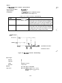
EPSON TERMINAL PRINTER
LQ-860/1060
TECHNICAL MANUAL
NOTICE
‘ All rights reserved. Reproduction of any part of this manual in any form
whatsoever without SEIKO EPSON’s express written permission is forbidden.
‘ The contents of this manual are subject to change without notice.
“ All efforts have been made to ensure the accuracy of the contents of this manual.
However, should any errors be detected, SEIKO EPSON would greatly appreciate
being informed of them.
“ The above notwithstanding SEIKO EPSON can assume no responsibility for any
errors in this manual or the consequences thereof.
@ Copyright 1989 by SEIKO EPSON CORPORATION
Nagano, Japan
-i-
REV.-A
PRECAUTIONS
Precautionary notations throughout the text are categorized relative to 1) personal injury, and 2) damage
to equipment:
DANGER
Signals a precaution which, if ignored, could result in serious or fatal personal
injury. Great caution should be exercised in performing procedures preceded by
a DANGER headings.
WARNING
Signals a precaution which, if ignored, could result in damage to equipment.
The precautionary measures itemized below should always be observed when performing repair/maintenance procedures.
DANGER
1. ALWAYS DISCONNECT THE PRODUCT FROM BOTH THE POWER SOURCE AND THE
HOST COMPUTER BEFORE PERFORMING ANY MAINTENANCE OR REPAIR
PROCEDURE.
2. NO WORK SHOULD BE PERFORMED ON THE UNIT BY PERSONS UNFAMILIAR WITH
BASIC SAFETY MEASURES AS DICTATED FOR ALL ELECTRONICS TECHNICIANS IN
THEIR LINE OF WORK.
3. WHEN PERFORMING TESTING AS DICTATED WITHIN THIS MANUAL, DO NOT
CONNECT THE UNIT TO A POWER SOURCE UNTIL INSTRUCTED TO DO SO. WHEN
THE POWER SUPPLY CABLE MUST BE CONNECTED, USE EXTREME CAUTION IN
WORKING ON POWER SUPPLY AND OTHER ELECTRONIC COMPONENTS.
WARNING
1. REPAIRS ON EPSON PRODUCT SHOULD BE PERFORMED ONLY BY AN EPSON
CERTIFIED REPAIR TECHNICIAN.
2. MAKE CERTAIN THAT THE SOURCE VOLTAGE IS THE SAME AS THE RATED
VOLTAGE, LISTED ON THE SE:RIAL NUMBER/RATING PLATE. IF THE EPSON PRODUCT HAS A PRIMARY-AC RATING DIFFERENT FROM THE AVAILABLE POWER
SOURCE, DO NOT CONNECT IT TO THE POWER SOURCE.
3. ALWAYS VERIFY THAT THE EPSON PRODUCT HAS BEEN DISCONNECTED FROM THE
POWER SOURCE BEFORE REMOVING OR REPLACING PRINTED CIRCUIT BOARDS
AND/OR INDIVIDUAL CHIPS.
4. IN ORDER TO PROTECT SENSITIVE pP CHIPS AND CIRCUITRY, USE STATIC
DISCHARGE EQUIPMENT, SUCH AS ANTI-STATIC WRIST STRAPS, WHEN ACCESSING INTERNAL COMPONENTS.
5. REPLACE MALFUNCTIONING COMPONENTS ONLY WITH THOSE COMPONENTS
RECOMMENDED BY THE MANUFACTURER; INTRODUCTION OF SECOND-SOURCE
ICS OR OTHER NONAPPROVED COMPONENTS MAY DAMAGE THE PRODUCT AND
VOID ANY APPLICABLE EPSC)N WARRANTY.
- ii -
REV.-A
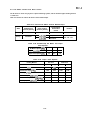
PREFACE
This manual describes functions, theory of electrical and mechanical
operations, maintenance, and repair of the LQ-860/l 060.
The instructions and procedures included herein are intended for the
experienced repair technician, and attention should be given to the
precautions on the preceding page. The chapters are organized as follows:
Chapter 1 -
Provides a general product overview, lists specifications,
and illustrates the main components of the printer.
Chapter 2 -
Describes the theory of printer operation.
Chapter 3 -
Discusses the options
Chapter 4 -
Includes a step-by-step guide for product disassembly,
assembly, and adjustment.
Chapter 5 Chapter 6 -
Provides Epson-approved techniques for troubleshooting.
Describes preventive maintenance techniques and lists
lubricants and adhesives required to service the equipment.
‘ The contents of this manual are subject to change without notice.
- iv -
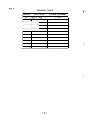
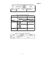
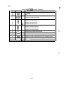
REVISION TABLE
REVISION
DATE ISSUED
=)=
-v-
I
CHANGE DOCUMENT
I
I
1st issue
I
REV.-A
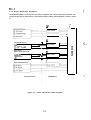
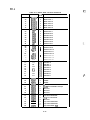
TABLE OF CONTENTS
CHAPTER
1.
GENERAL
DESCRIPTION
CHAPTER
2.
OPERATING
CHAPTER
3.
OPTIONAL
CHAPTER
4.
DISASSEMBLY, ASSEMBLY, A N D
PRINCIPLES
EQUIPMENTS
CHAPTER 5.
TROUBLESHOOTING
CHAPTER 6.
APPENDIX
MAINTENANCE
- vi –
ADJUSTMENT
REV.-A
CHAPTER 1
GENERAL DESCRIPTION
1.1
FEATURES-=M~.”H..H..-M..M
.-.~..H.H”.UM.-.-.~.M.-.-Ho ...-.---.-.Hu.-.M1..1-1
1.2
SPECIFICATIONS .fl.-..-~..-.~.~.-..-..-tiuu. ‘iHu.o.u..-ttio.-.--.-.-tio.- .~.-l-3
1.2.1 Hardware Specifications”... . . . . . . . . . . . . . . . . . . . . . . . . . . . . . . . . . . . . . . ..........................1-3
1.2.2 Firmware Specifications -.-.-ti.m.-.o.tito.-.tim.-.ti .-.~--.~.~-.~’~-..l-9
1.3
INTERFACE OVERVIEW ----- C.~..~-..-..M~MU.6fiM-H..fi.- .m-.fi.-fifHM-.HM-.ml-13
1.3.1 8-Bit Parallel interface Specifications - - - - - - - - - - - - - - - - - - - - - - - - - - -
-..-1-13
1.3.2 RS-232C Serial interface Specifications -.-.H.,,-.-.-.MHHM.HH.M.-H. M-1-16
1.4
DIP SWITCH ANDJUMPERSETTINGS ...-.’fi..-.=.HH.H...-M-.H.H-.-.~.~~-.-19l9
.....
1.4.1 DIP Switch Settings . . . . . . . . . . . . . . . . . . . . . . . . . . . . . . . . . . . . . . . . . . . . . . . . . . . . . . . . . . . . . . . . . . . . 1-19
1.4.2 Jumper Settings -..”~..-.m.M..-.-.-.H.H.fiH..- .~.~-.~.=.~~~..~~~..~.l-21
1.5
SELF-TEST OPERATION ~--.H.-.-.H...-M-..-.fi.mo.H .~.~.~.~.~-.~.~-.~-l.2222
1.6
HEXADECIMAL DUMP FUNCTION ...H.-..Hu..-.H.--.-..~.-M----M-.H.u.-M.1.2323
1.7
PRINTER INITIALIZATION ..H.=..MM-~.-.H.-.M.-.-.~.-. -.-uu..-H-.H.H.~--.ul-24
1.7.1 Hardware Initialization ~.-.-..~.-.H.H.-.-..-H.M---- H.”~-.-.~.HH.H-.-l-24
1.7.2 Software Initialization .~~.~..~.~..--..H.u.uH.-.H..~~.H.--M.H.-H.~.M.l-24
1.7.3 Default Values- . . . . . . . . . . . . . . . . . . . . . . . . . . . . . -..-.---..--.-.--.--.-..1-24
1.8
BUZZER OPERATION AND ERROR CONDITIONS ,MH...H..-.-...H.M - - - - - - - - - - - .1-25
1.8.1 Buzzer Operation ~-..-.-.~H.-...o..M.H.M ----- H.H.H-.-.-H.-..-..HH.M.1-25
1.8.2 Error Conditions ...~.-...H---.-.H.-.-.-..-H.- .-.-u.H..~H-.-H.u.-25.l-25
1.9
MAIN COMPONENTS -.~..-.~.M..M-..-..-M.-..M.- H.M..~.MH-.-.-H.Hl-.oH-.Hl -26
1.9.1 Printer Mechanism ..~~..~-.~..~.H.M.-.~.-.H.M.- ..--M..-~.~.~~.l~.-l-27
1.9.1.1 Printer Mechanism Features - - - - - - - - - - - - - - - - - - - - - - - - - - -
-.-.1-27
..
1.9.1.2 Paper Feed Operations . . . . . . . . . . . . . . . . . . . . . . . . . . . . . . . . . . . . ................1-28
1.9.2 JUNMMBoard (Main Board) .-M-.H.~.M.H.u.H.H.M.-H.H.. M--..H.-29.-1-29
1.9.3 MONPS/MONPSE Board (Power Supply Circuit Board) .-.-.~-.~..~1.-~l-3o
1.9.4 Control Panel ...=..~.-.~.~..f~.-~...~-.~..-.~~.~.-..-~-.-.-~”~.-.=.-.l -31
l-i
REV.-A
LIST OF FIGURES
Figure 1-1.
LQ-860/1060 Exterior Views ““””””””””””””””””””””””””””””””””””””” ““”””””””””””””””””””l-1
Figure 1-2. Printheacf Pin Configuration -.--”-””””””””””””””””””””””””””””””””
““”””””””””””””””””””””l-3
Figure 1-3. Cut Sheet Paper Printable Area ““”””-”””””””””””””””””””””””””””””””” ““”””””””””””””””l-5
Figure 1-4.
Fanfold Paper Printable Area .“”.””H””””.”-.”.””””””.”””””o”””””.”. s“”..””.”””.””4”””””1-6
Figure 1-5. Head Adjustment Lever Positioning ““””””””””””””””””””””””””””””””””””””” ““””””””””””l-7
Figure 1-6. Character Matrix ‘s..”....””””.””””””””””””””””””””””””” ““””””””””””””””””””””””””””””””””””l-1
1
Figure 1-7. 8-Bit Parallel interface Data Transmission Timing .....”.”””””””””””””””””””””1-13
Figure 1-8.
36 Pin Printer Side tinnector”-””.”-”..””””. c.”.”””.”.”””.””””.”.””.”””””.”.””0”. .“”1-13
Figure 1-9. RS-232Clnterface Handshaking,”-””.-”.”””...””..” .“”.”””””.....-”””””””””.”””.”.””.1-1 6
Figure 1-10. Serial Data Transmission Timing ““””””.”””””””””””””””””””””””””””””””” ““”””””””””””1-17
Figure 1-11. Serial Interface Connector ‘.””””.”””””””.”””””””””””””””’””””””””
““”””””””””””””””””””1-17
Figure 1-12. Self-Test Printing .......”””””””””””””””””””””””””””””””” ““”””””””””””””””””””””””””””’”””””l-22
Figure 1-13. Hexadecimal Dump List”.””.”-””””.””-”....”..”.”.”””.”” ““”””””””.”.”.””-””””””””s””.”1-23
.-’.,
.~:.
.,.
Figure 1-14. LQ-860/1060 Component Locations “-00”.””..00”.””.o.o””-””.”””-””cc”””.” .“s””..””1-26
Figure 1-15. Model-5810/5860 Printer Mechanism OOC..””.....””””””..O”.....””””..””U”. “..-..1-27
Figure 1-16. JUNMM Board Do.....”..-”.”-.-...”..”....”....”....” .......................””....”.........l-29
Figure 1-17. MONPS Board . . . . . . . . . . . . . . . . . . . . . . . . . . . . . . . . . . . . . . . .......................................l-30
Figure 1-18. Control Panel . . . . . . . . . . . . . . . . . . . . . . . . . . . . . . . . . . . . . . . . . . . . . . . . . . . . . . . . . . . . . . . . . . . . . . . . . . . . . . . 1-31
,:.:.,. .
l-ii
REV.-A
LIST OF TABLES
Table 1-1.
Table 1-2.
Table 1-3.
Table 1-4.
Table 1-5.
O
Optional Units ........ ’......., . . . . . . . . .......... ..... ”... ””..’” ““”””””””””””””””””””””””” ““” ””l-2
Optional Interface Bc~ards -..-.~..~.~..uH”-..-.uH”-o- ““~-~”~”--”~”~””fll-2
.....
Line Feed Speeds . . . . . . . . . . . . . . . . . . . . . . . . . . . . . . . . . . . . . . . . . . . . . . . . . . . . . . . . . . . . . . . . . . . . . . . . 1-4
Cut Sheet Paper Specified Conditions -.....m.oo”-”m’ti”-”ti-””o-”ti”- “-”-”1-4
Continuous Paper Specified Conditions -.-.-.-..--.-.”-.--”-”--”- “-”-””1-5
Table 1-7.
Lever Adjustment..””...’”””.” ““””.”””””-------”------s-”-”--”””””-””” ‘--””-””-””-”””””--””””-1-7
Ribbon Cartridge Specification -..~-...--..-....-tio-o.H.-HM “-””~~”~-””~1-7
Table 1-8.
Dimensions and Weight -....-.~..-.~.M..--.-.o-.uM” -“”u”-~”u”M-”H.H”M”l-8
Table 1-9.
Electrical Specifications .~.-..-..-~..-.Hu..-.~”-H”su. -“Mu.-”o-u”uc-.1.8-8
Table 1-6.
Table 1-10. Environmental Conditions .-.-...--..-.-.-.-.-..--.-”” -.--.-”---”-”-”-1-8
Table l-11. Printing Mode . . . . . . . . . . . . . . . . . . . . . . . . . . . . . . . . . . . . . . . .................”..”””.”””””””””””””””” “l-lo
Table 1-12. Character Matrix and Character Size .~.-.oH-.H..co”u”.”u-H”ti”M”
--”-”1-12
Table 1-13. 8-bit Parallel l/F Connector Pin Assignments ......-.....”...””.”””””””””””””””””1-1 4
Table l-14. Select/Deselect Control ..~~...-.-.~.~.-..ti-.ti.M.ti’o“-””-~”~”~”-~-”-l-15
Table l-15. Serial Interface Handshaking ...---.-..M.M.-.H”~.M”MCOCO
-oH”-o-”HM”u1-16
Table l-16. RS-232CSerial l/F Connector Pin Assignments ........-””””...”.-””-”””s””””.””1-18
Table l-17. DIP Switch lSettings .~.~~..-..~.-.~.~.-..-..-”..-“-~”~”-”-”~”~”--”~”l-l9
Table l-18. International Character Set Designation ................””..””.”””””””””””””””” ““””””1-19
Table l-19. DlPSwitch2 Settings .-.-.~.~...-~..M.n”MM-.n”M.” --”-”~-”~””~~”~-”-l-20
Table l-20. Interface Selection ~...-..f~o..~...-~H”..ti.tio.H” “~”~~””-”---”~”~~”~”1”202o
Table l-21. Baud Rate Selection ..-.-.~...-.ti.ti..-..ti-ti.uo““~~~””-”--”-”-”-~”-”l-2o
Table l-22. Jumper Setting ~.~.-.-..~~..-..-.~~..~--.oH -.~.~”-.~”~”-~”~”~”-~”~””l-2 1
.....
Table l-23. Self-Test Operation . . . . . . . . . . . . . . . . . . . . . . . . . . . . . . . . . . . . . . . . . . . . . . . . . . . . . . . . . . . . . . . . . . . . 1-22
Table l-24. Hexadecimal Dump Operation . . . . . . . . . . . . . . . . . . . . . . . . . . . . . . . . . . . . . .““”.””.”.”-”.””””””1-23
l-iii
REV.-A
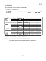
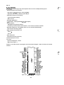
1.1 FEATURES
The LQ-860/1080 printerS a r e multifunction~ll,
features of the these printers
24-pin printhead, impact dotmatrix printers. The main
are:
. Upward compatibility with the LQ-850/1050
. ~ maximum print speed of 290 cps in super draft mode at 10 CPI, of 270 Cps in draft mode at 12 CP1’
and of 90 CPS in LQ mode at 12 CPI
o Direct selection of font and pitch in SelecT’YPe feature from the contrOl panel
. Both 8-bit parallel and RS-232C serial interfaces
. Color printing capability
. Push and (optional) pull tractor feeding
. Advanced paper handling:
AUtomatiC paper-loadin9/ejectin9 function
Tear-off funCtiOn
Printing of fanfold paper without removal of the cut sheet feeder (option)
. Low-noise acoustics
. Optional interface for the EPSON 8100 series
cut sheet feeders which contains enveloPe feedin9
. Optional low-priced, single-bin and double-bin
capability
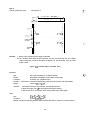
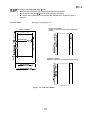
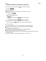
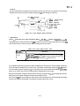
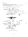
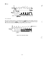
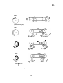
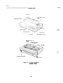
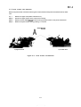
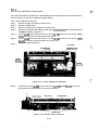
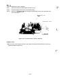
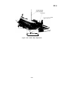
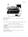
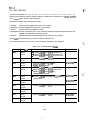
Figure 1-1 shows exterior views of the printers,
Table 1-1 lists optional units available, and Table 1-2 lists
the optional interface boards (refer to Chapt[?r 3 for more detailed information) for the LQ-8W106O.
LQ-860
LQ-106O
Figure 1-1. LQ-860/1060 Exterior Views
1-1
REV.-A
r..,.+.-.. ,
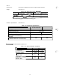
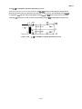
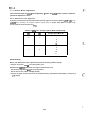
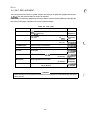
Table 1-1. Optional Units
I
No.
I
Name
LQ-860
o
Pull tractor unit
C800071
1LQ-106O
~
–
!
o
Pull tractor unit
C800101
C806141 I Cut sheet feeder (single-bin)
C806181
Cut sheet feeder (single-bin)
C806151
o
;
–
~
Cut sheet feeder (double-bin)
C806191
Cut sheet feeder (clouble-bin)
#7762
Ribbon cartridge (black)
o
87763
Ribbon cartridge (color)
o
ff7764
Ribbon cartridge (film)
o
#7407
Multi font module
o
I
-
0
!
—
o
Table 1-2. Optional Interface Boards
I
No.
/
Name
1#8143 I Newserial i n t e r f a c e
1#8145 IRS-232C
c u r r e n t loopinterfacetypell
#8148
Intelligent serial interface
#8149
Intelligent serial interface type II
#8149M
Intelligent serial interface type Ill
#8161
IEEE-488 interface
I
I
I
l=-+---
Intelligent IEEE-488 interface
32K-byte buffer parallel interface
#8172M
128K-buffer parallel interface
1-2
I
REV.-A
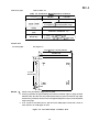
1.2 SPECIFICATIONS
This section describes the specifications for the printer without the Identity Module option.
Specifications not affected by firmware (hardware specifications) are the same whether or not the Identity
Module is installed.
1.2.1 Hardware Specifications
Printing Method
Serial, impact dot matrix
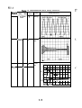
Pin Configuration
See Figure ‘I-2 (12x2 staggered, diameter: 0.2 mm).
—
-dz-
0
y
r
om
I
T
3
4
6
8
10
12
14
15
16
17
18
19
20
21
22
23
[~
24
[
1/60”
‘ i/60’ “
Figure 1-2. Printhead Pin Configuration
Feeding Method
Friction feed
Tractor feed (push: standard, pull : optional)
NOTES :
1. When using friction feed :
Adjust the paper release lever at rear position.
Use the paper tension unit.
Do not use continuous paper.
Do not use a single sheet paper shorter than 182 mm or longer than 257 mm (LQ-860),
364 mm (LQ-106O).
Do not perform any reverse paper feed operations within the top 8.5 mm and bottom 22
mm area of the paper.
Do not perform reverse feed beyond than 1/6 “ after the paper end has been detected.
Do not use multi-part single sheet forms.
2. When using tractor feed:
. Multiple copies for printing must be finished by pasting them together at the line or dots.
. Copy paper must be a carbonless multi-part paper.
a) When using push tractor feed:
. Adjust the paper release lever at center position.
“ Use the paper tension unit.
1-3
REV.-A
“ Do not perform reverse feeding for more than 1/6 “.
“ Because accuracy of paper feed cannot be assured, do not perform reverse feeding
after the paper end has been detected.
b) When using pull tractor feed :
“ Adjust the paper release lever at front position.
“ Remove the paper tension unit and mount the pull tractor unit.
o Use the paper path when a single sheet is inserted.
WV I 1~1
I U~ll Iy-’~UW
l-~Ull‘---”-”
11 cX,LUl ‘---A
IGC7J “.
c) ‘A’’--“ “-’-‘-L -’‘“
Adjust the paper release lever at front position.
Remove the paper tension unit and mount the pull tractor unit.
Do not loosen the paper between the platen and the pull sprocket.
Precisely the horizontal position of the pull sprocket and push tractor.
Do not perform reverse feeding for more than 1/6”.
Do not perform reverse feeding after the paper end has been detected.
Paper Loading Directions
Inserted from the rear side
Line Spacing
1/6” or programmable (min. 1/360”)
Line Feed Speed
See Table 1-3.
Table 1-3. Line Feed Speeds
[ins/line]
Friction without CSF
56.4
Friction with CSF
67.3
I
Tractor
I
1 /6” line spacing
Feeding Method
Continuous
IIPS]
3.1
I
64.1
Paper specifications
Cut sheet paper
Refer to Table 1-4.
Table 1-4. Cut Sheet Paper Specified Conditions
l--=%-l
LQ-860
LQ-106O
182-257 (7.2 -10.1 “)
182-364 (7.2- 14.3”)
182-364 (7.2-14.3”)
0.065-0.10
(0.0025-0.004”)
14-22 (52-82 9/m2)
*
Quality
Plain paper
Copies
Not available
1-4
1
REV.-A
Refer to Table 1-5.
Continuous paper
Table 1-5. Continuous Paper Specified Conditions
LQ-860
I
LQ-I 060
1
I
Width
I 101-254 (4.0-10.0”) I 101-408 (4.0-16.0”) I
[mm]
H
4 (1 original +3) at normal temperature
3 (1 original +2) at all temperature range
Plain paper
Quality
Total Thickness
0.085-0.32 (0.0025-0.01 2“)
[mm]
1 sheet” .”14-22 (52-82 g/m2)
Weight [lb]
4 sheets” ””12-15 (40-58.2 g/m2) for each
I
Printable Area
Cut sheet paper
See Figure 1-3.
7.2–10.1 *1 (14.4)”, 182–257 (364) mm
t* 3
=
i
Printable area
i
m
* 3
—
--TY’
0.33”, 8.5 mm
I
or I
—I
I
‘r
ABC
T
.J-
-1
XYZ
7.2–14.3”,
182–364 mm
XYZ
ABC
1
7
0.53”, 13.5 mm
or more
+L
1NOTES : 1.
2.
I
Values in the parentheses apply to the LQ-106O.
Printing is possible for approximately 42 mm after the bottom edge of a page has been
detected. Thus, the value 13,5 mm (lowest print position) is given for reference only. Paper
feed accuracy cannot be assured in the area approximately 22 mm (0.87”) from the bottom
edge of the page.
3.
0.12”, 3.0 mm or more when the 12”, 305 mm or less width paper is used. 0.58”, 15 mm or
more when the 13” width paper is used.
Figure 1-3. Cut Sheet Paper Printable Area
1-5
REV.-A
See Figure 1-4.
Fanfold (continuous) paper
- 10*1(1 6)”,
4!
101 - 254 (406) m m
Printable area
*2
&
4
I
*2
0
0
Printable
area
i
0.35”, 9 mm
or more
+
0.35”, 9 mm
or more
t
Printable
area
0
0
0
0
0
0
0
0
0
0
0
o
o
L
0
XYZ
i
AE&
0
0
0
0
- -
0
-
-
-
-
0
- - - - - - — . — - - - - - - - - - - - — —
0
o
0
0
0
o
o
0
T
T
X’fz
AE~
0
o
0
0
0
0
0
0
0
0
0
0
0
0
NOTES : 1. Values in the parentheses are apply to LQ-106O.
2. 0.47”, 12 mm or more when the 101 to 242 mm, 4 to 9.5” (101 to 378 mm, 4 to 14.9”) width
paper is used. 0.98”, 25 mm or more when the 254 mm, 10”, (381 to 406 mm, 15 to 16”) width
paper is used.
Figure 14. Fanfold Paper Printable Area
Envelopes
Size
No. 6 (166 x 92 mm), No. 10 (240 x 104 mm)
Quality
Bond paper, xerographic copier paper, airmail paper
Thickness
0.16-0.52 mm (0.0063-0.0197”)
NOTES :
Weight
NOTES :
Differences in thickness within printing area must be less than 0.25 mm (0.0098”).
12-24 lb (4!5-91 g/m2)
1. Envelope printing is only available at normal temperature.
2. Keep the longer side of the envelope horizontally at setting.
3. Set the left of No. 6 envelope at the setting mark of the sheet guide.
Label
Size
2% X 1%’s”, 4 x %“, 4 X 1 %“
Thickness
0.19 mm (0.C075”) max.
NOTES: Thickness excluding the base paper must be less than or equal to 0.12 mm (0.0075”).
1-6
f .-..;,
,-,,
REV.-A
NOTES : 1. Printing of Iabes is only available at normal temperature.
2. Labels must be fanfold.
3. Labels with pressure-sensitive paper must be jointed by pasting along the dots or lines, and
the total thickness must be less than or equal to 0.3 mm (0.0118”) to be printed out under
conditions that must be between 5 to 35-C and 10 to
4. Examples of Iavels:
80°/0
RH.
AVERY CONTINUOUS FORM LABELS
AVERY MINI-LINE LABELS
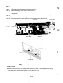
Lever Adjustment
See Figure 1-5 and l-able 1-6.
Table 1-6. Lever Adjustment
Paper Thickness [mm]
Lever Position
0.06-0.1:1
2nd
3nd
I
0.13-0.17
~
I
4th
0.1 8-0.:!5
5th
0.26-0.32
+
u
Figure 1-5. Head Adjustment Lever Positioning
NOTES : 1.
When printing density becomes lighter, set the head adjustment lever one position lower.
2. When using thicker paper than shown in the above table, set the head adjustment lever to
the 6th or higher appropriate position by performing the self-test operation.
Ribbon Cartridge
See Table 1-7.
Table 1-7. Ribbon Cartridge Specification
Ribbon Model No.
I
#7762
I
#7764
I
#7763
w%k’i’m :ii:;:nMagenta7and
1-7
REV.-A
Dimensions
See Table 1-8 (Details are shown in Figures A-36 and A-39.)
Weight
See Table 1-8.
Table 1-8. Dimensions and Weinght
I
I
I
LQ-860
Width [mm]
Height [mm]
469
194
I
I
LQ-106O
I 609 i
194
Weight [Kg]
Depth [mm]
II
399
I
399
I
10
I
13
1
I
I
I
I
NOTE : Excluding paper feed knob and sheet guide.
Electrical Specifications
See Table 1-9.
Table 1-9. Electrical Specifications
Voltage [V AC]
100-120 V Version
220-240 V Version
108-132
198-264
~. .:,,
“ -,
49.5 -60.5
Frequency Range [Hz]
1
2
Rating Current [A]
Insulation Resistance [M ohm] min.
10
Oitween AC line and chassis)
Dielectric Strength [V AC, rms]
3750
1250
(1 minute, between AC line and chassis)
Conditions Refer to Table 1-10.
Table 1-10. Environmental Conditions
Storage
I
Operating
(“;,
Resistance to shock [G]
(within 1 ms)
L@_
Resistance to Vibration [G]
1-8
2
1
0.50
0.25
REV.-A
Reliability
5 million lines (excluding printhead)
MCBF
(MCBF . . . Mean Cycles Between Failure)
MTBF
LQ-860 :
4000 POFI (duty 25
LQ-106O :
6000 POI-I (duty 25
0
/0)
0
/0)
(POH . . . . F)ower On Hours)
Printhead life
200 milion strokes/wire
Safety Approvals
Safety standards
UL478 (U.S.A. version)
CSA22.2#f54
VDE0806 (TUV) (European version)
Radio Frequency (RFI)
FCC class B (U.S.A. version)
Interference
VDE0871 (self-certification)
(Europe version)
1.2.2 Firmware Specifications
Control Code
ESC/P-84C
Printing Direction
Bidirectional with logic seeking
Input Data Buffer
6 K-byte or none ( DIP SW 1-8 selectable)
Character Code
8 bits
Character Set
96 ASCII, 14 international, and 1 Legal charactersets
Family
Font
Printing Mode
Roman:
No. O
Sansserif:
No. 1
Roman:
10, 12, 15, Proportional
Sansserif:
10, 12, 15, Proportional
Draft:
10, 12, 15
Printing quality (Draft/LQ)
Character pitch (10, 12, 15 CPI or Proportional)
Condensed
Double-width
Double-height
Emphasized
Double-strike
It:alic
Lhderlined
Double-underlined
C)verscore
Strike-through
Shadow/Outline
NOTES :
A condensed mode for 15 CPI characters is not available.
Print Speed
Refer to l-able 1-11.
Print Columns
Refer to l-able 1-11.
1-9
.....
REV.-A
Table 1-11. Printing Mode
Print
Pitch
10
Conden-
Emphas-
sed
ized
0
0
1
1
12
0
x
0
1
1
15
0
x
0
1
%oporticmal
Double
Character
Printing Speed
Width
Pitch
[CPS]
[cPI]
Draft
LQ
0
10
225”’
75
80
136
1
5
113
38
40
68
0
10
113
75
80
136
1
5
56
38
40
68
o
17.1
193
129
137
233
1
8.5
96
64
69
117
0
12
270
90
96
164
1
6
135
45
48
82
0
12
135
90
96
164
1
6
68
45
48
82
o
20
225
150
160
272
1
10
113
75
80
136
0
15
338
113
120
204
1
15
169
56
60
102
0
7,5
169
113
120
204
1
7.5
84
56
60
102
64
Max. 69
Max. 117
150
Min. 160
Min. 272
32
Max. 34
Max. 59
75
Min. 80
Min. 136
1
x
x
o
x
o
8.6
—
4.3
1
x
o
1
o
x
—
17.1
—
129
Max. 137
40
—
300
Min. 320
Max. 233
—
Min. 544
8.6
—
64
Max. 69
Max. 117
150
Min. 160
Min. 272
96
Max. 103
Max. 175
225
Min. 240
Min. 408
12.8
o
—
30
1
1
x
LQ-1060
10
20
‘proportional
Super/
subscript
LQ-860
Ignored
20
1
Printable Columns
o
1
1-10
6.4
—
48
Max. 51
Max. 87
15
—
113
Min. 120
Min. 204
25.7
–
193
Max. 206
Max. 349
60
—
450
Min. 480
Min. 816
12.8
—
96
Max. 103
Max. 175
30
—
225
Min. 240
Min. 408
..
r’
,
REV.-A
* 1 : 290 CPS at super draft printing (DIP SVV 1-6 is off).
NOTES : 1. Max. means the value when t:he maximum width characters are printed.
2.
3.
Min. means the value when the minimum width characters are printed.
“
—“ means that LQ character set is automatically selected when proportional pitch is
specified.
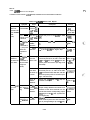
Character Matrix
See Figure 1-6 and Table 1-12.
(Superscript Character)
Pin Nos. 17 to 24 are not used when superscript
printing.
(Normal Character)
1
—
Ascender Area
2
3
4
R
5
I
6
G
7 r
Ascender Area (15pitch ) H
8
T
9 ;
10 >
s
II
i
P
12 .,
A
13
c
14 10.
E
15
(a 2
16
/7
18
19
20
21
22
23
24
2 L
3 E
4 F
5T
6
7s
Eip
9 A
10 c
II E
12
13
14
15
16
[
R
A
H
T
s
P
A
c
E
—
Descender Area
(Subscript Character)
Pin Nos. 1 to 8 are not used when subscript printing
9
10
II
12
13
14
15
16
17
18
19
Face Width (al )
Character Width (CW)
J
—
L
E
F
T
s
p
A
c
E
20
21
22
23
24
[
Figure 1-6. Character Matrix
1-11
R
;
H
T
s
P
A
c
E
—
REV.-A
Character Size
P.: .: ,
See Table I-12.
Table 1-12. Character Matrix and Character Size
Printing Mode
Face Matrix
HDD
Character Size
H. XV. (mm)
Unit
ESC
Sp
DRAFT, 10 pitch
9 X 23
120
1.9x 3.2
120
DRAFT, 12 pitch
9 X 23
120
1.9x 3.2
120
DRAFT, 15 pitch
9X 1 6
120
1.0 X 2.3
120
DRAFT, 10 pitch, condensed
...
240
...
120
DRAFT, 12 pitch, condensed
...
240
...
120
LQ, 10 pitch
29X 23
360
2.0x 3.2
180
LQ. 12 pitch
29X 23
360
2.0 x3.2
180
LQ, 15 pitch
15X 16
360
1.0X 2.3
180
LQ, 10 pitch, condensed
...
360
...
180
LQ, 12 pitch, condensed
...
360
...
180
max. 37X 23
360
2.6X 3.2
min. 18X 23
360
1.0x 3.2
...
360
...
...
360
...
max. 28X 16
360
1.8x 2.3
-Q, proportional
.-,:. . . . .
*
“=-. +
180
.Q, proportional, condensed
180
.Q, proportional, super/subscropt
160
min. 12x 16
360
0.7X 2.3
...
360
...
360
...
-Q, proportional, super/subscript, condensed
180
...
NOTES : 1. “HDD” means the Horizontid dot density, and the “Unit” shows the number of dots per inch.
2.
“Face matrix” and “character size” indicate the size of maximum characters and this value
will be changed condition of paper, ribbon, and etc.
3.
“Unit ESC SP” indicates the minimum length which is added to the right of the character that
can be specified with ESC) sp control code.
4.
“.. .“ indicated that the character matrix is reformed by firmware. Character width becomes
haJf of a non-condensed character.
1-12
.,.... %
f ‘“’
.“”
REV.-A
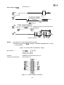
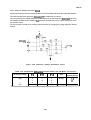
1.3 INTERFACE OVERVIEW
The LQ-860/1060 has both 8-bit parallel interface and RS-232C serial interface as standard. They can be
selected by DIP switches 2-3 and 2-4 respectively. (This detail of DIP switch settings, refer to Table 1-20.)
1.3.1 8-bit Parallel Interface Specifications
Data Transmission Mode
8-bit pallarel
Synchronization
By STROB= pulse
Hand Shaking
By BUSY and ACKNLG (either or both)
Logic Level
TTL compatible
Data Transmission Timing
See Figure 1-7.
57-30360 (AMPHENOL) or equivalent
Adaptable Connector
(See Figure 1-8.)
Connector Pin Assignment
Refer to Table 1-13.
Select/Deselect (DC1/DC3)
Refer to Table 1-14.
Control
BUSY
ACKNLG
DATA
STROBE
~**,~
w
NOTES : Transmission time (rising and falling time) of evev input signal must be less than 0.2 IAS.
Figure 1-7. 8-bit Parallel Interface Data Transmission Timing
Pair witn 1.)
1.
19. GNO (
2.
2 0 . GNO (
3.
21. GND ( Pair with 3.)
4.
22.
Pair w;th2.)
G?4D [ Pair
w;ti14.)
5.
23. GND (
Pair w;tn5. )
6.
24. GND (
Pair w;th6.)
7.
25. GND ( Pair w;th7.)
8.
26. GNO (
Pair “:t~s.)
9.
27. GNO (
Pair w,th9.)
10.
28. GNO ( Pair with 10. )
I 1.
29. GNO ( Pair w;th I 1.)
12.
30. GNO ( Pair w;tn 12. )
13.
31. ~T
I 4.
32. ERROR
15.
33. GNO
16.
34. NC
17.
35. +5V
18.
36. 5LCTIN
Figure 1-8.
36-Pin Printer Side Connector
1-13
Table 1-13. 8-bit Parallel l/F Connector Pin Assignments
Pin No.
Signal
Return
1/0
Description
1
STROBE
19
I
Strobe pulse to read the input data. Pulse width must
be more than 0.5 ,US. input data is latched after
falling edge of this signal.
2
DATA1
20
I
Parallel input data to the printer.
3
DATA2
21
I
“HIGH” level means data “1”.
4
DATA3
22
I
“LOW” level means data “O”.
5
DATA4
23
I
6
DATA5
24
I
7
DATA6
25
I
8
DATA?
26
I
9
DATA8
27
I
10
ACKNLG
28
0
This pulse indicates data are received and the
printer is ready to accept next data. Pulse width is
approx. 11 /s.
11
BUSY
29
0
“HIGH” indicates printer can not accept data.
12
PE
30
0
“HIGH’ ’indicates paper-out.
This signal is effective only when ERROR signal is
“LOW”.
13
SLCT
—
o
Always “HIGH”. (Pulled up to +5V through 3.3 K
ohms resistor.)
14
AUTOFEED-XT
I
–
If this signal is “LOW” when the printer is initialized,
a line feed is automatically performed by input of
“CR” code (Auto LF).
15
NC
—
16
GND
—
—
—
—
—
Not
Ground for twisted-pair.
USed.
17
Chassis GND
18
NC
—
—
Not used.
19 to 30
GND
—
—
Ground for twisted-pair.
31
INIT
16
i
Printer chassis ground.
Pulse (width : 50 ,US min., active “LOW”) input for
printer initialization.
32
ERROR
.
0
“LOW indicates that some error has occurred in the
printer.
33
GND
—
.
Ground for twisted-pair.
34
NC
—
—
Not
35
+5V
—
o
Always “HIGH”. (Pulled up to +5V through 3.3 K
SLECT-IN
—
USed.
ohms resistor.)
36
I
If the signal is “LOW” when printer is initialized, the
DC1/DC3 control is disabled.
NOTES : 1.
2.
“Direction” of signal flow is as viewed from the printer.
“Return” denotes “TWISTED PAIR RETURN” and is to be connected at signal ground level.
1-14
f’;’.
REV.-A
As to the wiring for the interface, be sure to use a twisted-pair cable for each signal and
never fail to connect the return side. To prevent noise, cables should be shielded and
connected to the chassis of the host computer and the printer.
Table 1-14. Select/Deaelect
ON-LINE
SLCT-IN
DCI /DC3
BUSY
ERROR
Control
ACKNLG
DATA
ENTRY
Sw
OFF-LINE
HIGH/LOW
DCI /DC3
LOW
HIGH
ON-LINE
HIGH
DC1
HIGH
LOW/HIGH (During Pulse output after Enable
(Normal
data entry)
entry
No pulse
Disable
Process)
DC3
HIGH
LOW/HIGH (During Pulse output after Enable
(Waits
entry
data entry)
DC1 . See
NOTE 2)
LOW
DC1
HIGH
LOW/HIGH (During Pulse output after Enable
(Normal
entry
data entry)
Process)
DC3
HIGH
LOW/HIGH (During Pulse output after
data entry)
-
entry
NOTES : 1. In Table 1-14, it is assumed that no ERROR status exists other than that attributable to the
OFF-LINE mode.
2. Once the printer is deselected by the DC3 code, the printer will not revert to the selected
state until the DC1 code is input. (In the deselected state, input data is ignored until DC1
is received.)
3. The DC1 and DC3 codes are enabled only when the SLCT-IN signal (Input Connecter Pin
No. 36 when the parallel interface unit is used) is HIGH and the printer is initialized.
4. The SLCT-IN signal is “LOW” when the printer is initialized. At this time the DC1/DC3
printer select/deselect control is invalidated, and these control codes are ignored.
1-15
REV.-A
1.3.2 RS-232C
Serial Interface Specifications
Data Transmission Mode
RS-232C serial
Synchronization
Asynchronous
Handshaking
(By DTR (FIEV) signal or X-ON/OFF Protocol
(Refer to Table 1-15 and Figure 1-9.)
Table 1-15. Serial Interface Handshaking
DTR Signal
X-ON/OFF protocol
Description
MARK
X-OFF (DC3/13H)
When the number of bytes remaining in the input buffer
reaches 256 or less, the signal level goes to MARK, or
and X-OFF code is sent to the host computer. This
indicates that the printer is not ready to receive data.
When the number of bytes remaining in the input buffer
X-ON (DC1/11 H)
SPACE
reaches 528 or more, the signal level goes to SPACE, or
an X-ON code is sent to the host computer. This indicates that the priter is ready to receive data.
DTR (REV) Signal
M A R K
I
(–12V) - - - - - - - - - - -
SPASE ( +12V) ~, ~
6Kbyte
Eq
:
,
~
1
:
!j28byte 256byte
1
1
1
[
1
X-ON
X-OFF
[
:
Obyte
Input Buffer Vacant Area
X-ON/X-OFF Protocol
>,. ,-,
Figure 1-9. RS-232C
Interface Handshaking
Word Length
Start bit:
1
Data bits:
8
Parity:
Odd, Even, or none
Stop bits:
1 bit or more
Bit Rate
300, 1200, 9600, or 19200 BPS
Logic Level
EIA level, IMARK: logical 1 (–3- –27 V)
!SPACE : logical O (+3- +27 V)
1-16
REV.-A
Data Transmission Timing
See Figure 1-10.
‘T”
~
s
[ +V)
DTR
( – VI
( + v]
RXD
( -v)
r
- - - - - - - - - - - - - - - - - - - - y :!S!12131:15-FF::;
Data Bit
P~rlty
Start
Elit
DTR Handshake
( + v]
g:F[<[[[iFEE3
RXD
Data Elit
[ -v)
,+apB,+/—
‘T “
P\ri~y
Start
Blt
+
-- -- i~ 4
*
-- -- ik
( + v)
- - - [ - - [ if 4+
TXD
( -v]
D a t a Bit
Bit (X-OFF)
Start
–
. - - [ - -[ IF’ 4+
S;;;t D~t:OB;t
x-ON/X-OFF Protocol
NOTES :
1. The value of “T” varies according to the input data.
2. The word structure of serialclata is 1 start bit + 8 data bits+ parity (Odd, Even, or none)+
1 or more stop bits.
Figure 1-10. Serial Data Transmission Timing
Error Detection
Parity errcr:
“x” is printed.
Overrun error:
Ignored
Framing error: Ignored
Connector
D-SUB 25-pin connector (See Figure 1-11.)
Connector Pin Assignments
Refer to Table 1-16.
LCHASSI
2. TxD-—
3.RXD—
4,NC—
5.NC—
6.Nc-—7. SGNAL
8. Nc—-
t4. NC
i5. NC
16. NC
17, NC
16 NC
19. NC
20.QTR
21.NC
22.NC
23.NC
24.NC
25NC
9.NC—
tO. NC —
I l, REv —
f2.NC—
13. NC —-
Figure 1-11. Serial Interface Connector
1-17
REV.-A
Table 1-16. RS-232C Serial l/F Connector Pin Assignments
Pin No.
Signal
Dir.
2
TXD
o
20
DTR
o
Description
Transmit data.
Indicates when printer is ready to receive data. “MARK”
level indictes printer is not ready to receive data.
11
REV (=2nd RTS)
o
Same as DTR.
3
RXD
I
Receive data.
7
SIGNAL GND
–
Signal (Logic) ground level.
1
CHASSIS GND
–
Printer chassis ground.
NOTE : “Direction” of signal flow is as viewed from the printer.
f ‘:,
.,
1-18
REV.-A
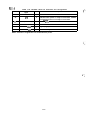
1.4 DIP SWITCH AND JUMPER SEITINGS
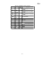
This section describes DIP switch settings and jumper settings on the JUNMM board.
1.4.1 DIP Switch Settings
The DIP switches that users can set are SW”I and SW2. These switches are positioned at the left side of
the control panel, and have the functions as :>hown in Tables 1-17 through 1-21, (note that the status of the
DIP switches are read only when the printer power on or an INIT signal is input.)
Table “I-17. DIP Switch 1 Settings
OFF
ON
Function
DIP SW.
Factory Setting
See Table 1-18.
ON
ON
ON
1-1
1-2
1-3
International
chacter set
1-4
Code table select
Graphic
Italic
OFF
1-5
1-6
1-7
1-8
Graphic print direction”’
Super draft
CSF mode
Input buffer
Uni-d.
off
Valid
Bi-d.
On
Invalid
OFF
OFF
OFF
None
6K-byte
OFF
* 1 : “Graphic print” means follows
a) Bit image printing
b) Multi pass printing
“ 30 dots graphics
. Orator/Orator-S font
“ Double height character
. Double-strike
o Double overscore/underline
. Violet, Orange, Green color printing
Table 1-18. International Character Set Designation
Country
1-1
1-2
1-3
U. S. A.
ON
ON
ON
France
ON
ON
Germany
ON
OFF
OFF
ON
U. K.
ON
OFF
OFF
Demarkl
OFF
ON
ON
Sweden
OFF
ON
OFF
Italy
OFF
OFF
ON
Spainl
OFF
OFF
OFF
NOTE : The above settings can be changed to any country’s characters set by inputting ESC R control
codes.
1-19
REV.-A
q
Table 1-19. DIP Switch 2 Settings
‘g
Function
ON
OFF
Factory Setting
2-1
Page length
12”
11 “
OFF
2-2
1“ skip-over perforation
Valid
Invalid
OFF
2-3
Interface selection
DIP SW.
OFF
See Table 1-20.
OFF
2-4
2-5
OFF
See Table 1-21.
Baud rate selecton
OFF
2-6
2-7
Auto fear-off mode
Valid
Invalid
OFF
2-8
Auto LF
Valid
Invalid
OFF
Table 1-20. Interface Selection
Table 1-21. Baud Rate Selection
-%.*-
2-3
2-4
Function
OFF
OFF
8-bit Parallel
OFF
OFF
19,200
ON
OFF
Serial, Even parity
ON
OFF
9,600
OFF
ON
Serial, Odd parity
OFF
ON
1,200
ON
ON
Serial, None parity
ON
ON
300
1
1
1-20
REV.-A
1.4.2 Jumper Settings
Table 1-22 shows the jumper settings.
Table 1-22. Jumper Settings
No. /
) Location
Type
27256
27512
6A
512
256
JI
4M/2M-BIT
IM-BIT
512K/256K-BIT
3A
ROM
MASK-ROM
J2
B4
+5
+5
J3
RD
A16
RD
4M/2M-BIT
1 M-BIT’
(CG1)
512K/256K-BIT
256K-BIT
ROM
RAM
+5
MASK-ROM
J4
B4
+5
+5
J5
RD
A16
RD
RD
J6
B1
B1
B2
WR
SLCT-IN inable
SLCT-IN disable
SLIN
GND
LQ-860
LQ-106O
J8
Close
Open
J9
Open
Open
J7
NOTE : Bold indicates the factotw settings.
1-21
4A
(CG2)
REV.-A
1.5 SELF-TEST OPERATION
The LQ-860/1060 printer has the following self-test operation. The control ROM version No. and the DIP
switch settings also printout when the self-test is performed.
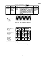
Table 1-23 lists the self-test operating instructions and Figure 1-12 shows the self-test printing.
Table 1-23. Self-Test Operation
Type-face
Draft
,-
Lu
stop
Start
Turn the power ON while
Push the ON LINE switch, and turn the
pressing the LINE FEED switch.
power OFF.
Turn the power ON While
pressing the FORM FEED switch.
Draft mode
! “ #$%& ‘ ( )*+ , – . /0123456789: ; < = >?@~8CDEFGl_i IJKL
f “ #$%& ‘ ( )*+ , - . /01 23456789: ; < =>?@46cDEFGti1JKLP
“ #$%&‘ ( )*+, -. /C)12345676g : ; ~ = >?@~BcDEFGH IJKLM~
#$%& ‘ ( )x+, -. /01.23456789 : ; < = >~@~BCDEFGHIJKLmNC
$%& ‘ ( )*+, - . /012’ 3456789 : ; < = >?@ ABcDEFGH IJ KLMNOF
.,< =>?@ABCDEFGHIJKLMNOpc
= ‘ ( )%+ ,-. /0123; 456789 -& “ ( )*+, -- /0123456789: ; < = >~@ABCDEFGH IJKLMNOPQR
‘ ( )*+, -. /0123456789: ; < = > ?@AB cD E FGH I J K LMN () PQR:
()*+, -./,oI234567B9, ; <=>?@~BCDEFGHIJKLMNopQRST
)*+, -./olz3456789:; <=>?@ABcDEFGHIJKLMNOP9RSTL
*+,-./ol234567~9: -,<=>?@A6CDEFGHIJKLMNOPQRSTUV
+ - /n17745A7RQ.. < =>91aQ RCITFI=C14T.TKI MNnDC)!2qTllVk
High-speed draft mode
!“#$%&”( )*+, -./Ol23Zi56789: ;<=>?@6BCDEFGHIJKL
“’#$%&’()*+,-. /0123456789: ;<=>?@ABC0EFGHIJKLtIt
‘-’#$%&”()*+,-. /0123456789: ;<=>?@iM3CDEFGHIJKLMN4
#S%&”(j*+=-./O123456789: ;<=>?@A8COEffiHIJKLMN0
$%&”(j*t>–. !01234567EW: :<=> ?@~~C~~f=GHIJKLMN~p
;~=>~@ABCDEffil+lJKLM~
A“()*+,–-/012W%T89--.<=>~@~mDEffitilJK~~
-
%&”c)*+,–-/0lZ5ASA78g:
“()*+,–.,/o1234+<6789: ;<=> ?@ ABCDE FC; H13KLMNOPQRS
()*+,–-/ol23456T8S ::<=? ‘?@ABCOEFGtilJKLMNOPQRST
)*+,--jo~~~456789: ;<=>?@ABCDEFGHIJKLMNC)PQRSTLJ
*+.–./olZ34s698’9 :;<=>?@A~DE~HIJK~~sTuv
+. - /f1177A<A7FlQ- - < =>~~r2RCIlFFFiHT.TK I MN(~PC)f?STllVW
L(2 mode
!“#$%&) ( )x+,-./OI23456789 : ;<=>?@ABCDEFGHIJK’
!“#$%&y( )*+,-# /0123456789 :;<=>?@ABcDEFGHIJKLI
“#$%&’( )*+,-./Ol23456789 :;<=>?@ABCDEFGHIJKLMl
#$%&’ ()*+, -./ol23456789 :;<=>?@ABCDEFGHIJKLMNi
$%&’( )*+, -./Ol23456789: ;<=>?@ABCDEFGHIJKLMNO]
%&’ ()*+, -./Ol23456789: ;<=>?@ABCDEFGHIJKLMNOPt
&’()*+, -./Ol23456789 : ;<=>?@ABCDEFGHIJKLMNOPQl
‘( )*+,-./ol23456789 : ;<=>?@ABCDEFGHIJKLMNOPQRl
()*+,-. /0123456789:; <=>?@ABCDEFGHIJKLMNOPQRS’
)*+, -./ol23456789: ;<=>?@ABCDEFGHIJKLMNOPQRSTI
*+,-./Ol23456789 : ;<=>?@ABCDEFGHIJKLMNOPQRSTLP
.+.-. /0123456789: :<=>?@ARC~RFRHTJKTIMNOPORSTlrV~
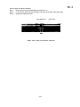
Figure l-12. Self-Test Printing
1-22
REV.-A
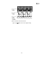
1.6 HEXADECIMAL DUMP FUNCTION
In hexadecimal dump mode, the printer prints out the data it receives in hexadecimal format. The printer
prints a column of 16 hexadecimal values, followed by a column containing the 16 corresponding ASCII
characters. If there is no corresponding printable character for a value (e.g., a control code, such as a
carriage return or line feed), a period (.) is printed in the ASCII column in the position of the code.
Each line of the dump contains 16 values, printed in the order they were received, and
any remaining data
(less than 16 values on the final line) can be printed by operating the ON LINE switch. Table 1-24 shows
the hexadecimal dump operation and Figure 1-13 shows printout of the operation.
Figure 1-13. Hexadecimal Dump List
Table 1-24. Hexadecimal Dump Operation
IR.mction
I
I
Operation
Hexadecimal
Turn the power on while pressing both the LINE FEED and
dump mode
FORM FEED switches.
stop
Turn the power off.
I
I
Data Dump Mode
31
54
70
74
2D
69
72
65
6F
6E
20
69
51
6D
65
6E
2E
68
72
69
70
6D
69
20
66
74
55
6C
2D
61
65
20
31 20 46 45 41 54 55 52 45 53 OD 0/4 00
65 20 4C 51 2D 38 35 30 2F 31 30 35 30
69 6E 74 65 72 73 20 61 72 65 20 6D 75
66 75 6E 63 74 69 6F 6E 61 6C 2C 20 32
69 6E 20 70 72 69 6E 74 68 65 61 64 2C
70 61 63 74 20 64 6F 74 2D OD 0#1 6D 61
78 20 70 72 69 6E 74 65 72 73 2E 20 54
6D 61 69 6E 20 66 65 61 74 75 72 65 73
20 74 68 65 20 74 68 65 73 65 20 70 72
65 72 73 20 61 72 65 3G 20 OD 09 OD OA
70 77 61 72 64 20 63 6F 60 70 61 74 69
69 74 79 2G 77 69 74 68 20 74 68 65 20
38 30 30 2F 31 30 30 30 OD OA 2E 20 41
78 69 6D 75 6D 20 70 72 69 6E 74 20 73
64 20 6F 66 20 32 36 34 20 43 50 53 20
64 72 61 66 74 20 6D 6F 64 65 20 61 74
Ofl
20
6C
34
20
74
68
20
69
2E
62
4C
20
70
69
20
Figure 1-13. Hexadecimal Dump List
1-23
1.1 FEATURES. . . .
The LQ-850/ 1050
printers are mul
tifunctional, 2 4
-pin print head.
impact dot- . . mat
rix printers. Th
e main features
o f t h e t h e s e pri
nters are: . . . . .
U p w a r d compatib
i 1 i ty with t h e L
Q-800/1000. . . A
maximum print sp
eed of 264 CPS i
n draft mode at
REV.-A
#-:;,,
x,
1.7 PRINTER INITIALIZATION
There are two initialization methods: hardware initialization and software initialization.
1.7.1 Hardware Initialization
This type of initialization occurs when printer power is turned on or when the printer receives the INIT signal
from the host via the 8-bit parallel interface.
When printer is initialized in this way, it perfc)rms the following actions :
. Initializes printer mechanism
- Clears downloaded character set
. Clears the input data buffer
. Clears the print buffer
. Sets printer selections to their default values
1.7.2 Software Initialization
. ,-..
This type of initialization occurs when the printer receives command (ESC @) via software.
When the printer is initialized in this way, it performes the following actions :
. Clears the print buffer
. Sets printer selections to their default values.
1.7.3 Default Values
The printer’s default values are as follows:
Page Position
Preset paper position becomes top of form position
Left and Right Margin
Released
Line Spacing
1/6”
Vertical Tab Position
Cleared
Horizontal Tab Position
Every 8 characters (relative)
VFU Channel
Channel O
Family Number of Type Style
Last selected font by the control panel
Downloaded Characters
Deselected: Software initialization
Cleared: t+ardware initialization
Justification
Left justification
Character Per Inch
Last selected pitch by the control panel
Bit Image Mode Assignment
ESC K = ESC *O, ESC L = ESC xl, ESC Y = ESC *2, ESC Z =
ESC *3
Color
Black
1-24
4..,
REV.-A
REV.-A
1.8 BUZZER OPERATION AND ERROR CONDITIONS
This section describes the buzzer operation and error conditions of the printer.
1.8.1 Buzzer Opeartion
The buzzer ring as follows:
●
When a BEL code is sent to the printer, the buzzer sounds for 0.5 seconds
●
When an error has occured
. Carriage mechanism trouble
o Color select mechanism trouble
. C.G. ROM error
Sounds 5 times (rings for 0.5 sescmds with 0.5 seconds interval.)
. Paper end
Sounds 3 times (rings for 0.1 seccmds with 0.1 second interval.)
● When
a panel setting is accepted, the buzzer sounds for 0.1 seconds
(Refer to Section 1.9.4 for firther information concerning control panel settings.)
1.8.2 Error Conditions
If any of the following errors occur, the printer automatically enters the OFF-LINE mode.
“ Carriage and color home positions are not detected at printer mechanism initialization.
. Home position is detected during printing.
. The OFF-LINE switch is pressed, causing the printer to enter OFF-LINE mode.
“ A paper-out signal is detected and formes-override is finished.
. A paper-out signal is detected after the printer has performed a paper loading operation with the cut
sheet feeder enabled.
For information concerning the status of the interface signals, refer to Table 1-14.
1-25
REV.-A
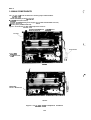
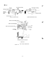
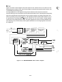
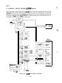
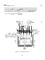
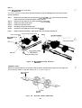
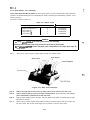
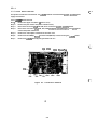
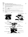
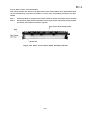
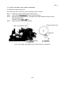
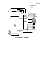
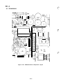
1.9 MAIN COMPONENTS
The LQ-860/1060 printer includes the following major subassemblies:
. Model-5810/5860 printer machanism
“ JUNMM board (main board)
. MONPS/MONPSE board (power supply board, 120V and 220/240V versions)
“ Control panel (JUNPNL-W board)
Figure 1-14 shows the LQ-860/1060 component locations.
MONPS/MONPSE Board
JUNMM Board
Fan Unit
\
‘%.: , ’
I
Control Panel
Mlodel-5810
PI‘inter Mechanism
LQ-860
,. .,
~:
Model-5860
Printer Mechanism .
LQ-106O
Figure 1-14. LQ-860/1060 Component Locations
1-26
REV.-A
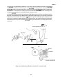
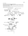
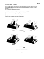
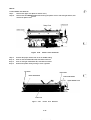
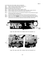
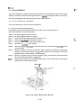
1.9.1 Printer Mechanism
This section describes features and paper feed operations of the printermachanism.
1.9.1.1 Printer Mechanism Features
The printer mechanism is composed of three stepper motorsused in carriage move, paper feed, and color
select/ribbon feed, a 24-pin printhead, five sensors (home position, paper end, friction/traCtOr, platen gap,
and color position sensors), and metal frames.
Model-5810
Model-5860
Figure 1-15. Model-5810/5860 Printer Mechanism
1-27
REV.-A
f!,,
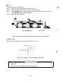
1.9.1.2 Paper Feed Operations
Paper Loading and Paper Ejection
The paper release lever has a disengage capability for the optional pull tractor unit’s drive mechanism.
Therefore, these printers provide some improved paper handling functions that can be performed by using
a combination of the paper release lever and LOAD/EJECT switch on the control panel.
Single Sheet Loading and Ejection
To load a sheet of paper, adjust the paper release lever at friction feed position, place the page along the
sheet guide, and press the LOAD/EJECT switch. This loads the paper at the top-of-form position. If
LOAD/ EJECT switch is pressed after paper has been loaded, it causes the paper to be ejected.
Continuous Paper Loading and Ejection (Back Out)
To load continuous paper, adjust the paper release lever at tractor feed position, and insert the paper into
the push tractor. Pressing the LOAD/EJECl- switch loads the paper automatically to the top-of-form
position. If LOAD/EJECT switch is pressed after the continuous paper has been loaded, the printer ejects
the paper backward to the push tractor. To,back out several pages, press the LOAD/EJECT switch several
times, since reverce feed is performed on a page-by-page basis.
The MULTI-PART LED blinks only after the paper has been loaded and the ON LINE switch has been
pressed. After ON-LINE has been pressed, the user can adjust the paper loading position for the next sheet
loaded into the printer and the top-of-form position for the currently loaded sheet. Pressing the FORM FEED
switch advances the paper forward continuously for as long as the switch is held down, and pressing the
LINE FEED switch moves the paper in reverse.
Moving the paper with these switches is called “Top-Of-Form adjust”. After the paper has been adjusted
in this way, the printer uses that position as the loading position for each subsequent page. When the
printer is initialized, the loading position for a, single sheet returns to the default value.
Tear-Off Function
The paper is advanced to the tear-off position by pressing the TEAR OFF switch or auto tear-off function
(depend on DIP SW 2-7 setting) when the tractor feed is selected. Auto tear-off function is enabled and the
paper release lever is at the tractor position, the paper will be fed to the tear-off position automatically if
the input data buffer is empty and the printer is ON-LINE. At this time, MULTI-PART LED will blink to
indicate that the FORM FEED and LINE FEED switches can be used for forward and backword micro feed
adjustment. Using the micro feed, adjust the paper to meet the tear-off edge. Once the tear-off position is
set, the setting remains valid even after the printer is turned off, reset or initialized. If subsequent data is
input to the printer, the paper will be released to the original position automatically and printing will start.
[f the ON LINE switch is pressed (printer becomes OFF LINE) while the paper is advanced to the tear-off
position, then the paper will be released to the original position.
Tear-off function is also valid in the cut sheet feeder mode when the tractor feed is selected.
1-28
“+. ‘-..
g:
‘u.
REV.-A
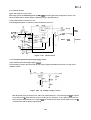
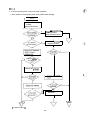
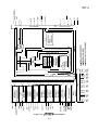
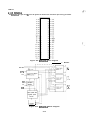
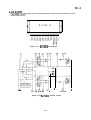
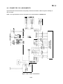
1.9.2 JUNMM Board (Main Board)
Figure 1-16 shows the JUNMM board, which contains a 8-bit one chip CPU ~PD78213 (4B) to control the
operation of the printer.
Driver circuits for the motors, sensors, and printhead are also included on this board. Other main ICS on the
JUNMM board are:
Gate Array IC
“ EO5A1OAA (8B) .............. Memory management unit (MMU) IC
o E05A24GA (5A) ............&bit parallel I/F’, port expansion IC
“ E05A02LA (2A) ............ ”.. Printhead data control IC
Memory IC
“ EP-ROM (6A)”””””””””””””.”Used for program 256K-bit
“ MASK-ROM (3A) ..........,.Used for character generator, IM-bit
o PS-RAM (5A)
...............256K-bit
“ ST-RAM*’ (7A).”””.”.””””””.”UK-bit
x 1 : The data is held by the lithium battery while power is turned off.
Universal IC
“ S17300A (1A) .................. Carriage motor driver IC
MASK-ROM (C. G.)
PS-RAM
Lithium Battery
E05A02LA
\
\
I
EP-ROM
ST-RAM
/
/
S17‘300A
\
E05A24GA
(’jpu
EO5A1OAA
Figure 1-16. JUNMM Board
1-29
REV.-A
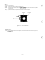
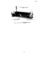
1.9.3 MONPS/MONPSE Board (Power Supply Circuit Board)
The power supply circuit board is located on one of two boards, the MONPS for 120 V AC operation and
the MONPSE for 220/240 V operation. The basic construction of the two board is the same: each board
contains a power switch, fuses, line filter circuit, and switching regulator circuit. Compactness of the
circuitly is made possible by use of a DC-to-13C converter.
.{ ‘“
... ,
Figure 1-17.
MONPS Board
!.
~.
.
1-30
REV.-A
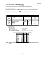
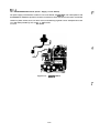
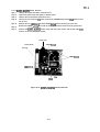
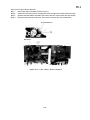
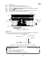
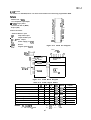
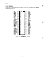
1.9.4 Control Panel
[n the control panel, seven switches and seventeen LEDs, as shown in Figure 1-18. The functions of the
switches and indicators are given immediately below the illustration.
Figure 1-18. Control Panel
ON LINE Switch
This switch toggles the printer between ON-LINE and OFF-LINE modes. The printer is automatically set to
ON-LINE mode and becomes ready at power on. If the printer is set to OFF-LINE mode, printing is stopped
and the printer becomes BUSY.
FORM FEED Switch
Pressing this switch once while the printer is in the OFF-LINE mode advances the paper vertically to the
next top-of-form position. This switch is also used as the micro forward adjust, refer to Section 1.9.1.2 for
details.
LINE FEED Switch
Pressing this switch within 0.5 seconds while the printer is in the OFF-LINE state advances the paper one
line at a time. And pressing more than 0.5 seconds performs continuous feeding until this switch is
released.
This switch is also used as the micro reverse adjust, refer to Section 1.9.1.2 for details.
LOAD/EJECT Switch
Pressing this switch loads or ejects the paper. Details of the paper loading and ejection process are
described in Section 1.9.1.2.
When this switch is pressed in the CSF mode and ON-LINE state, printer beeps once (pi) and selects bin
1, or beeps twice (Pi-, pi-) and selects bin 2 alternately.
FONT Switch
Pressing this switch selects a font, and continuing to press the switch for more than 0.5seconds select
the next font, sequentially. The FONT indicator lights beside the currently selected font.
1-31
REV.-A
PITCH Switch
Pressing this switch selects the character pitch, and continuing to press the switch for more than 0.5
seconds select the next character pitch, seq~lencially.
The PITCH indicator lights beside the currently selected character pitch to confirm its status.
NOTE : Settings by FONT and PITCH switches are stored as defaults. So that the last FONT, PITCH
settings becomes effective when the printer is initialized.
TEAR OFF Switch
Advance the paper to the tear-off position. This switch is only effective in the tractor feed.
This switch is effective in both of ON-LINE and OFF-LINE states, refer to Section 1.9.1.2 for details.
POWER LED (Green)
Lights when power is ON.
:$, .’
.-.
’
READY LED (Green)
Lights when printer can receive the data.
PAPER OUT LED (Red)
Lights when the paper is end.
ON LINE LED (Green)
Lights in the ON-LINE mode.
MULTI-PART LED (Orange)
Lights when the head adjustment lever is set for 4th or higher.
FONT (DRAFT, ROMAN, SANS SERIF, SLOT A, SLOT B) LEDs (Orange)
These LEDs indicate the currently selected font. If slots A and B contain font modules, they each may be
selected using the FONT switch, and the indicator beside either SLOT A or SLOT B will be lit. If no font
module is installed in the slot when the FONT switch is pressed, SLOT A and SLOT B selections will be
skipped.
PITCH (1OCPI, 12CPI, 15CPI, 17CPI, 20CPI, PROPORTIONAL) LEDs (Orange)
These LEDs indicate the currently selected character pitch.
TEAR OFF LED (Orange)
This indicator the paper is advanced to a tear off position.
1-32
,,.. “;
REV.-A
CHAPTER 2
OPERATING PRINCIPLES
......
2.1 GENERAL . . . . . . . . . . . . . . . . . . . . . . . . . . . . . . . . . . . . . . . . . . . . . . . . . . . . . . . . . . . . . . . . . . . . . . . . . . . . . . . . . . . . . . . . . . . .2-1
.
2.1.1 Connector Descriptions . . . . . . . . . . . . . . . . . . . ... . . . . . . . . . . . . . . . . . . . .●.. . . . . . . . . . . . . . . . . . . . . . . .2-1
.
2.1.2 Printer Mechanism Operations . . . . . . . . . . . . . . . . . . . . . . . . . . . . . . . . . . . . . . . . .● . . . . . . . . . . . . . . 2-2
....
2.1.2.1 Printing Mechanism . . . . . . . . . . . . . . . . . . . . . . . . . . . . . . . . . . . . . . . . . . . . . . . . . . . . . . . . . 2-3
...
2.1.2.2 Carriage Movement Mechanism . . . . . . . . . . . . . . . . . . . . . . . . . . . . . . . . . . . . . . . . . 2-6
..
2.1.2.3 Ribbon Feed,/Color Select Mechanism . . . . . . . . . . . . . . . . . . . . . . . . . . . . . . . . . .2-8
...
2.1.2.4 Paper Feed Mechanism . . . . . . . . . . . . . . . . . . . . . . . . . . . . . . . . . . . . . . . . . . . . . . . . . . .2-13
2.2 POWER SUPPLY CIRCUIT OPERATION (MONPS/MONPSE board) ● 0.000 .”osoooo”oo02-17
2.2.1 MONPS/MONPSE
...
Boards . . . . . . . . . . . . . . . . . . . ... . . . . . . . . . . . . . . . . . . . . . . . . . . . . . . . . . . . . . . . . 2-17
.....
2.2.2 Input Filter Circuit . . . . . . . . . . . . . . . . . . . . . . . . . . . . . . . . . . . . . . . . . . . . . . . . . . . . . . . . . . . . . . . . . . . . . . 2-19
.
2.2.3 Rectifier, Smoothing, and Surge-Suppression Circuit . . . . . . . . . . . . . . . . . . . . . . . . . .2-19
....
2.2.4 Main Switching Circuit . . . . . . . . . . . . . . . . . . . . . . . . . . . . . . . . . . . . . . . . . . . . . . . . . . . . . . . . . . . . . . . . .2-20
2.2.4.1 Circuit Operation . . . . . . . . . . . . . . . . . . . . . . . . . . . . . . . . . . . . . . . . . . . . . . . . . . . . . . . . . . . 2. .-.2. 0
...
2.2.5 +35 V Voltage Regurator Circuit . . . . . . . . . . . . . . . . . . . . . . . . . . . . . . . . . . . . . . . . . . . . . . . . . . .2-23
..
2.2.6 Over Voltage Protection Circuit . . . . . . . . . . . . . . . . . . . . . . . . . . . . . . . . . . . . . . . . . . . . . . . . . . . .. .2-24
...
2.2.7 +5 V Switching Regulator Circuit . . . . . . . . . . . . . . . . . . . . . . . . . . . . . . . . . . . . . . . . . . . . . . . . . .2-25
.....
2.2.7.1 Activation . . . . . . . . . . . . . . . . . . . . . . . . . . . . . . . . . . . . . . . . . . . . . . . . . . . . . . . . . . . . . . . . . . . . 2-25
...
2.2.7.2 Voltage Regulator Circuit . . . . . . . . . . . . . . . . . . . . . . . . . . . . . . . . . . . . . . . . . . . . . . . . .2-25
....
2.2.7.3 Soff Start . . . . . . . . . . . . . . . . . . . . . . . . . . . . . . . . . . . . . . . . . . . . . . . . . . . . . . . . . . . . . . . . . . . . .2-26
..
2.2.8 +12 V Half-Wave Rec:tifier-Smoothing Circuit . . . . . . . . . . . . . . . . . . . . . . . . . . . . . . . . . .2-27
...
2.3 CONTROL CIRCUIT BOARD (JUNMM BOARD) . . . . . . . . . . . . . . . . . . . . . . . . . . . . . . . . . . . . . . . . . . . . 2-28
.....
2.3.1 Reset Circuit . . . . . . . . . . . . . . . . . . . . . . . . . . . . . . . . . . . . . . . . . . . . . . . . . . . . . . . . . . . . . . . . . . . . . . . . . . . . .2-29
2.3.1.1 Vx (Drive System Pull-up) Voltage Supply Circufi*.**”””* ”*-”-c-o*e*2-29
. 0
2.3.1.2 Power ON/C)FF Reset . . . . . . . . . . . . . . . . . . . . . . . . . . . . . . . . . . . . . . . . . . . . . . . . . . . . . .2. -. 3
2.3.1.3 Font/Identity Module Installation and Removal Reset”* ””* ”**** ””** ”*2-31
..
2.3.1.4 ST-RAM (7A) Battery Backup Circuit . . . . . . . . . . . . . . . . . . . . . . . . . . . . . . . . . .2-33
....
2.3.2 Interface . . . . . . . . . . . . . . . . . . . . . . . . . . .. . . . . . . . . . . . . . . . . . . . . . . . . . . . . . . . . . . . . . . . . . . . . . . . . . . . . . . .2-34
...
2.3.2.1 8-Bit Parallel Interface . . . . . . . . . . . . . . . . . . . . . . . . . . . . . . . . . . . . . . . . . . . . . . . . . . . .2-34
2.3.2.2 RC-232C
...
Serial Interface . . . . . . . . . . . . . . . . . . . . . . . . . . . . . . . . . . . . . . . . . . . . . . . .2-38
...
2.3.3 Control Panel Interface Circuit . . . . . . . . . . . . . . . . . . . . . . . . . . . . . . . . . . . . . . . . . . . . . . . . . . . . . .2-41
....
2.3.3.1 LED Drive Section . . . . . . . . . . . . . . . . . . . . . . . . . . . . . . . . . . . . . . . . . . . . . . . . . . . . . . . . . 2-42
2. i
REV.-A
...
2.3.3.2 Switch Status Read Section . . . . . . . . . . . . . . . . . . . . . . . . . . . . . . . . . . . . . . . . . . . . . 2-43
..
2.3.4 State Detection and Sensor Signal Input Circuits . . . . . . . . . . . . . . . . . . . . . . . . . . . . . . 2-44
..
2.3.4.1 Reference Voltage Supply Circuit . . . . . . . . . . . . . . . . . . . . . . . . . . . . . . . . . . . . . .2-45
..
2.3.4.2 35 V Line Voltage Detection Circuit . . . . . . . . . . . . . . . . . . . . . . . . . . . . . . . . . . .2-46
...
2.3.4.3 VR1/VR2 Reading Circuit . . . . . . . . . . . . . . . . . . . . . . . . . . . . . . . . . . . . . . . . . . . . . . . . .2-47
..
2.3.4.4 Printhead Temperature Detection Circuit . . . . . . . . . . . . . . . . . . . . . . . . . . . . 2-48
...
2.3.4.5 CR HP Sensor Circuit . . . . . . . . . . . . . . . . . . . . . . . . . . . . . . . . . . . . . . . . . . . . . . . . . . . . . .2-50
....
2.3.4.6 CS Sensor Circuit . . . . . . . . . . . . . . . . . . . . . . . . . . . . . . . . . . . . . . . . . . . . . . . . . . . . . . . . . .2-51
....
2.3.4.7 PG Sensor Circuit . . . . . . . . . . . . . . . . . . . . . . . . . . . . . . . . . . . . . . . . . . . . . . . . . . . . . . . . . .2-52
....
2.3.4.8 PE Sensor Circuit . . . . . . . . . . . . . . . . . . . . . . . . . . . . . . . . . . . . . . . . . . . . . . . . . . . . . . . . . .2-53
2.3.4.9 F/T Sensor Circuit . . . . . . . . . . . . . . . . . . . . . . . . . . . . . . . . . . . . . . . . . . . . . . . . . . . . . . . . . 2. .-. 5. 4
...
2.3.5 Printhead Control and Drive Circuit . . . . . . . . . . . . . . . . . . . . . . . . . . . . . . . . . . . . . . . . . . . . . . . . .2-55
2.3.5.1 Relationship Between Paper Thickness and Print Mode ”...* ...562-56
2.3.5.2 Relationship Between Printhead Drive Pulse Width and
....
+35 V Line Voltage . . . . . . . . . . . . . . . . . . . . . . . . . . . . . . . . . . . . . . . . . . . . . . . . . . . . . . . 2-57
...
2.3.6 CR Motor Control and Drive Circuit . . . . . . . . . . . . . . . . . . . . . . . . . . . . . . . . . . . . . . . . . . . . . . . .2-58
..
2.3.6.1 Reference Voltage Generation Circuit . . . . . . . . . . . . . . . . . . . . . . . . . . . . . . . . 2-59
...
2.3.6.2 CR Motor Drive Circuit . . . . . . . . . . . . . . . . . . . . . . . . . . . . . . . . . . . . . . . . . . . . . . . . . . . .2-60
....
2.3.6.3 CR Motor Control . . . . . . . . . . . . . . . . . . . . . . . . . . . . . . . . . . . . . . . . . . . . . . . . . . . . . . . . . . . 2-63
...
2.3.7 PF Motor Control and Drive Circuit . . . . . . . . . . . . . . . . . . . . . . . . . . . . . . . . . . . . . . . . . . . . . . . .2-67
...
2.3.7.1 PF Motor Drive Circuit . . . . . . . . . . . . . . . . . . . . . . . . . . . . . . . . . . . . . . . . . . . . . . . . . . . . .2-68
..
2.3.7.2 PF Motor Phase Switching Timing . . . . . . . . . . . . . . . . . . . . . . . . . . . . . . . . . . . . .2-69
2.3.8 CS/RF Motor Control and Drive Circuit . . . . . . . . . . . . . . . . . . . . . . . . . . . . . . . . . . . . . . . . . . . 2. .-. 7 0
...
2.3.8.1 CS/RF Motor Drive Circuit . . . . . . . . . . . . . . . . . . . . . . . . . . . . . . . . . . . . . . . . . . . . . . .2-71
..
2.3.8.2 CS/RF Motor Phase Switching Timing . . . . . . . . . . . . . . . . . . . . . . . . . . . . . . . .2-72
z-ii
j.
i ...
REV.-A
LIST OF FIGURES
Figure 2-1.
...
Printer Mechanism Block Diagram . . . . . . . . . . . . . . . . . . . . . . . . . . . . . . . . . . . . . . . . . . . . . . . . .2-2
Figure 2-2.
....
Printing Mechanism . . . . . . . . . . . . . . . . . . . . . . . . . . . . . . . . . . . . . . . . . . . . . . . . . . . . . . . . . . . . . . . . . . . .2-3
Figure 2-3.
..
Relationship Between PG Sensor and Platen Gap . . . . . . . . . . . . . . . . . . . . . . . . . . . . . 2-5
Figure 2-4.
...
Carriage Movement Mechanism . . . . . . . . . . . . . . . . . . . . . . . . . . . . . . . . . . . . . . . . . . . . . . . . . . . .2-6
Figure 2-5.
...
Ribbon Feed Mechanism . . . . . . . . . . . . . . . . . . . .. . . . . . . . . . . . . . . . . . . . . . . . . . . . . . . . . . . . . . . . . . 2-9
Figure 2-6.
....
Color Ribbon Strip Selection . . . . . . . . . . . . . . . . . . . . . . . . . . . . . . . . . . . . . . . . . . . . . . . . . . . . . . 2-11
Figure 2-7.
....
Color Select Mechanism . . . . . . . . . . . . . . . . . . . . . . . . . . . . . . . . . . . . . . . . . . . . . . . . . . . . . . . . . . . . 2-12
Figure 2-8.
....
Friction Feeding . . . . . . . . . . . . . . . . . . . . . . . . . . . . . . . . . . . . . . . . . . . . . . . . . . . . . . . . . . . . . . . . . . . . . . .2-15
Figure 2-9.
....
Push Tractor Feeding . . . . . . . . . . . . . . . . . . . . . . . . . . . . . . . . . . . . . . . . . . . . . . . . . . . . . . . . . . . . . . . .2-16
Figure 2-10.
..
MONPS/MONPSE Board Block Diagram . . . . . . . . . . . . . . . . . . . . . . . . . . . . . . . . . . . . . . . .2-18
Figure 2-11.
....
Input Filter Circuit . . . . . . . . . . . . . . . . . . . . . . . . . . . . . . . . . . . . . . . . . . . . . . . . . . . . . . . . . . . . . . . . . . . .2-19
Figure 2-12.
..
Rectifier-Smoothing-Surge Suppression Circuit . . . . . . . . . . . . . . . . . . . . . . . . . . . . . . . 2-19
Figure 2-13.
.....
Surge Current . . . . . . . . . . . . . . . . . . . . . . . . . . . . . . . . . . . . . . . . . . . . . . . . . . . . . . . . . . . . . . . . . . . . . . . . . 2-19
Figure 2-14.
....
Main Switching Circuit . . . . . . . . . . . . . . . . . . . . . . . . . . . . . . . . . . . . . . . . . . . . . . . . . . . . . . . . . . . . . .2-21
Figure 2-15.
..
Waveforms at Primary and Secondary Side of T1 . . . . . . . . . . . . . . . . . . . . . . . . . . . 2-22
Figure 2-16.
...
RCC System Switch!ng Operation . . . . . . . . . . . . . . . . . . . . . . . . . . . . . . . . . . . . . . . . . . . . . . . .2-22
Figure 2-17.
...
+35 V Voltage Regulator Circuit . . . . . . . . . . . . . . . . . . . . . . . . . . . . . . . . . . . . . . . . . . . . . . . .2-23
Figure 2-18.
...
Over Voltage Protection Circuit . . . . . . . . . . . . . . . . . . . . . . . . . . . . . . . . . . . . . . . . . . . . . . . . . . .2-24
Figure 2-19.
...
+5 V Switching Regulator Circuit . . . . . . . . . . . . . . . . . . . . . . . . . . . . . . . . . . . . . . . . . . . . . . .2-25
Figure 2-20.
..
CMP Input and Output Voltage Comparison . . . . . . . . . . . . . . . . . . . . . . . . . . . . . . . . . . .2-26
Figure 2-21.
...
Soft Start Timing . . . . . . . . . . . . . . . . . . . .. . . . . . . . . . . . . . . . . . . . . . . . . . . . . . . . . . . . . . . . . . . . . . . . . .2-26
Figure 2-22.
..
+12 V Half-Wave Rectifier-Smoothing Circuit . . . . . . . . . . . . . . . . . . . . . . . . . . . . . . . . 2-27
Figure 2-23.
...
JUNMM Board Block Diagram . . . . . . . . . . . . . . . . . . . . . . . . . . . . . . . . . . . . . . . . . . . . . . . . . . . . .2-28
Figure 2-24.
.....
Reset Circuit . . . . . . . . . . . . . . . . . . . . . . . . . . . . . . . . . . . . . . . . . . . . . . . . . . . . . . . . . . . . . . . . . . . . . . . . . . 2-29
Figure 2-25.
....
Vx Voltage Supply Circuit . . . . . . . . . . . . . . . . . . . . . . . . . . . . . . . . . . . . . . . . . . . . . . . . . . . . . . . . . . 2-29
Figure 2-26.
. 0
Power ON/OFF Reset Timing . . . . . . . . . . . . . . . . . . . . . . . . . . . . . . . . . . . . . . . . . . . . . . . . . . . . . .2. -. 3
Figure 2-27.
..
Module Installed/Removed Reset Timing . . . . . . . . . . . . . . . . . . . . . . . . . . . . . . . . . . . . . . .2-31
Figure 2-28.
....
Battery Backup Circ:uit . . . . . . . . . . . . . . . . . . . . . . . . . . . . . . . . . . . . . . . . . . . . . . . . . . . . . . . . . . . . . .2-33
Figure 2-29.
.
8-bit Parallel Interface Data Transmission Timing . . . . . . . . . . . . . . . . . . . . . . . . . . .2-34
Figure 2-30.
..
8-Bit Parellel Interface Circuit . . . . . . . . . . . . . . . . . . . . ●.. . . . . . . . . . . . . . . . . . . . . . . . . . . . . . . . 2-35
Figure 2-31.
.
8-Bit Parallel Interface Circuit Operation . . . . . . . . . . . . . . . . . . . ... . . . . . . . . . . . . . . . . . . 2-36
Figure 2-32.
....
INIT Signal Proseccing . . . . . . . . . . . . . . . . . . . . . . . . . . . . . . . . . . . . . . . . . . . . . . . . . . . . . . . . . . . . . .2-37
z-iii
REV.-A
Figure 2-33.
...
Handshaking with DTR Signal . . . . . . . . . . . . . . . . . . . . . . . . . . . . . . . . . . . . . . . . . . . . . . . . . . . . .2-38
Figure 2-34.
...
Handshaking with X-ON/X-OFF Protocol . . . . . . . . . . . . . . . . . . . . . . . . . . . . . . . . . . . . . . . 2-38
Figure 2-35.
...
RS-232C Serial Interface Circuit . . . . . . . . . . . . . . . . . . . . . . . . . . . . . . . . . . . . . . . . . . . . . . . . .2-39
Figure 2-36.
..
RS-232C Serial Interface Circuit Operation . . . . . . . . . . . . . . . . . . . . . . . . . . . . . . . . . . .2-40
Figure 2-37.
...
RS-232C Data Transmission Timing . . . . . . . . . . . . . . . . . . . . . . . . . . . . . . . . . . . . . . . . . . . . 2-40
Figure 2-38.
...
Control Panel Interface Circuit . . . . . . . . . . . . . . . . . . . . . . . . . . . . . . . . . . . . . . . . . . . . . . . . . . . .2-41
Figure 2-39.
...
MSM58371 Data Transfer Timing . . . . . . . . . . . . . . . . . . . . . . . . . . . . . . . . . . . . . . . . . . . . . . . .2-42
Figure 2-40.
....
MSM58371 Block Diagram . . . . . . . . . . . . . . . . . . . . . . . . . . . . . . . . . . . . . . . . . . . . . . . . . . . . . . . . 2-42
Figure 2-41.
...
Reference Voltage Supply Circuit . . . . . . . . . . . . . . . . . . . . . . . . . . . . . . . . . . . . . . . . . . . . . . . .2-45
Figure 2-42.
...
35 V Line Voltage Detection Circuit . . . . . . . . . . . . . . . . . . . . . . . . . . . . . . . . . . . . . . . . . . . . 2-46
Figure 2-43.
....
35 V Line Protection . . . . . . . . . . . . . . . . . . . . . . . . . . . . . . . . . . . . . . . . . . . . . . . . . . . . . . . . . . . . . . . .2-46
Figure 2-44.
....
VR1/VR2 Reading Circuit . . . . . . . . . . . . . . . . . . . . . . . . . . . . . . . . . . . . . . . . . . . . . . . . . . . . . . . . . . .2-47
Figure 2-45.
..
Printhead Temperat~e Detection Circuit . . . . . . . . . . . . . . . . . . . . . . . . . . . . . . . . . . . . . .2-48
Figure 2-46.
Relationship Printhead Temperature and Printing Operation ......o.”....48-48
Figure 2-47.
....
CR HP Sensor Circuit . . . . . . . . . . . . . . . . . . . . . . . . . . . . . . . . . . . . . . . . . . . . . . . . . . . . . . . . . . . . . . .2-50
Figure 2-48.
.....
CS Sensor Circuit . . . . . . . . . . . . . . . . . . . . . . . . . . . . . . . . . . . . . . . . . . . . . . . . . . . . . . . . . . . . . . . . . . . 2-51
Figure 2-49.
.....
PG Sensor Circuit . . . . . . . . . . . . . . . . . . . . . . . . . . . . . . . . . . . . . . . . . . . . . . . . . . . . . . . . . . . . . . . . . . . 2-52
Figure 2-50.
.....
PE Sensor Circuit . . . . . . . . . . . . . . . . . . . . . . . . . . . . . . . . . . . . . . . . . . . . . . . . . . . . . . . . . . . . . . . . . . . 2-53
Figure 2-51.
.....
F/T Sensor Circuit . . . . . . . . . . . . . . . . . . . . . . . . . . . . . . . . . . . . . . . . . . . . . . . . . . . . . . . . . . . . . . . . . . 2-54
Figure 2-52.
..
Printhead Control/Drive Circuit Block Diagram . . . . . . . . . . . . . . . . . . . . . . . . . . . . . . 2-55
Figure 2-53.
Relationship Printhead Drive Pulse Width and +35 V Line Voltage ...2-57
Figure 2-54.
....
Printhead Drive Pulse Timing . . . . . . . . . . . . . . . . . . . . . . . . . . . . . . . . . . . . . . . . . . . . . . . . . . . . . 2-57
Figure 2-55.
..
CR Motor Control/Drive Circuit Block Diagram . . . . . . . . . . . . . . . . . . . . . . . . . . . . . . .2-58
Figure 2-56.
...
Reference Voltage Generation Circuit . . . . . . . . . . . . . . . . . . . . . . . . . . . . . . . . . . . . . . . . . . 2-59
Figure 2-57.
....
CR Motor Drive Circuit . . . . . . . . . . . . . . . . . . . . . . . . . . . . . . . . . . . . . . . . . . . . . . . . . . . . . . . . . . . . . .2-60
Figure 2-58.
...
CR Motor Drive Circuit Signal Timing . . . . . . . . . . . . . . . . . . . . . . . . . . . . . . . . . . . . . . . . . . 2-61
Figure 2-59.
...
CR Motor Phase Switching Timing . . . . . . . . . . . . . . . . . . . . . . . . . . . . . . . . . . . . . . . . . . . . . .2-63
Figure 2-60.
....
Carriage Motion Area . . . . . . . . . . . . . . . . . . . . . . . . . . . . . . . . . . . . . . . . . . . . . . . . . . . . . . . . . . . . . . .2-65
Figure 2-61.
.....
High Speed Skip . . . . . . . . . . . . . . . . . . . . . . . . . . . . . . . . . . . . . . . . . . . . . . . . . . . . . . . . . . . . . . . . . . . . . 2-66
Figure 2-62.
Figure 2-63.
....
PF Motor Drive Circuit . . . . . . . . . . . . . . . . . . . . . . . . . . . . . . . . . . . . . . . . . . . . . . . . . . . . . . . . . . . . . .2-68
...
PF Motor Drive Circuit Signal Timing . . . . . . . . . . . . . . . . . . . . . . . . . . . . . . . . . . . . . . . . . . . 2-68
Figure 2-64.
...
PF Motor Phase Switching Timing . . . . . . . . . . . . . . . . . . . . . . . . . . . . . . . . . . . . . . . . . . . . . . .2-69
Figure 2-65.
....
CS/RF Motor Drive Circuit . . . . . . . . . . . . . . . . . . . . . . . . . . . . . . . . . . . . . . . . . . . . . . . . . . . . . . . . . 2-71
Figure 2-66.
..
CS/RF Motor Drive Circuit Signal Timing . . . . . . . . . . . . . . . . . . . . . . . . . . . . . . . . . . . . . .2-71
Figure 2-67.
...
CS/RF Motor Phase Switching Timing . . . . . . . . . . . . . . . . . . . . . . . . . . . . . . . . . . . . . . . . . 2-72
2-iv
e:
““”
$:;
~n.
f ~
‘ .’
REV.-A
LIST OF TABLES
Table 2-1.
....
Printhead Specifications . . . . . . . . . . . . . . . . . . . . . . . . . . . . . . . . . . . . . . . . . . . . . . . . . . . . . . . . . . . . . . .2-4
Table 2-2.
PG Sensor Specifications . . . . . . . . . . . . . . . . . . . . . . . . . . . . . . . . . . . . . . .. .. .. . . . . . . . . . . . . . . . . . . . .2. - 4
Table 2-3.
..
Carriage Movement Mechanism Specifications . . . . . . . . . . . . . . . . . . . . . . . . . . . . . . . . . .2-7
Table 2-4.
....
CR Motor Specifications . . . . . . . . . . . . . . . . . . . . . . . . . . . . . . . . . . . . . . . . . . . . . . . . . . . . . . . . . . . . . . .2-7
Table 2-5.
....
CR HP Sensor Specifications . . . . . . . . . . . . . . . . . . . . . . . . . . . . . . . . . . . . . . . . . . . . . . . . . . . . . . . . 2-7
Table 2-6.
...
Ribbon Feed Mechanism Specifications . . . . . . . . . . . . . . . . . . . . . . . . . . . . . . . . . . . . . . . . . . . 2-8
Table 2-7.
....
CS/RF Motor Specifications . . . . . . . . . . . . . . . . . . . . . . . . . . . . . . . . . . . . . . . . . . . . . . . . . . . . . . . . . . 2-8
Table 2-8.
Ribbon Feed Gear Train . . . . . . . . . . . . . . . . . . . . . . . . . . . . . . . . . . . . . . . . . . . . . . . . . . . . . . . . . . . . . . ....2-9
.
Table 2-9.
...
Color Select Mechanism Specifications . . . . . . . . . . . . . . . . . . . . . . . . . . . . . . . . . . . . . . . . . 2-1o
Table 2-10.
.....
Color Select . . . . . . . . . . . . . . . . . . . . . . . . . . . . . . . . . . . . . . . . . . . . . . . . . . . . . . . . . . . . . . . . . . . . . . . . . . . . 2-1o
Table 2-11.
....
CS Sensor Specifications . . . . . . . . . . . . . . . . . . . . . . . . . . . . . . . . . . . . . . . . . . . . . . . . . . . . . . . . . . .2-1o
Table 2-12.
color Select Gear Train .................................................................2.l1
Table 2-13.
...
Paper Feed Mechanism Specifications . . . . . . . . . . . . . . . . . . . . . . . . . . . . . . . . . . . . . . . . . . 2-13
Table 2-14.
....
PF Motor Specifications . . . . . . . . . . . . . . . . . . . . . . . . . . . . . . . . . . . . . . . . . . . . . . . . . . . . . . . . . . . . .2-13
Table 2-15.
PE Sensor Specifications . . . . . . . . . . . . . . . . . . . . . . . . . . . . . . . . . . . . . . . . . . . . . . . . . . . . . . . . . . .2. .-.1. 3
Table 2-16.
..
F/T Sensor Specifications . . . . . . . . . . . . . . . . . . . ... . . . . . . . . . . . . . . . . . . . . . . . . . . . . . . . . . . . . . .2-13
Table 2-17.
.
Paper Feeding Method . . . . . . . . . . . . . . . . . . . . . . . . . . . . . . . . . . . . . . . . . . . . . . . . . . . . . . . . . . . . .. .. ..2-14
Table 2-18.
....
Power Supply Voltages . . . . . . . . . . . . . . . . . . . . . . . . . . . . . . . . . . . . . . . . . . . . . . . . . . . . . . . . . . . . . .2-17
Table 2-19.
....
Voltages and Applications ● . . . . . . . . . . . . . . . . . . . . . . . . . . . . . . . . . . . . . . . . . . . . . . . . . . . . . . . . . 2-17
Table 2-20.
State of Module . . . . . . . . . . . . . . . . . . . . . . . . . . . . . . . . . . . . . . . . . . . . . . . . . . . . . . . . . . . . . . . . ●.......... . .2-32
Table 2-21.
.
ST-RAM Conditions ‘with Power On/Off . . . . . . . . . . . . . . . . . . . . . . . . . . . . . . . . . . . . . . . . . 2-33
Table 2-22.
....
8-Bit Parallel l/F Signals . . . . . . . . . . . . . . . . . . . . . . . . . . . . . . . . . . . . . . . . . . . . . . . . . . . . . . . . . . . .2-37
Table 2-23.
....
Switch Status Reading . . . . . . . . . . . . . . . . . . . . . . . . . . . . . . . . . . . . . . . . . . . . . . . . . . . . . . . . . . . . . . .2-43
Table 2-24.
State Detection Circuits . . . . . . . . . . . . . . . . . . . . . . . . . . . . . . . . . . . . . . . . . . . . . . . . . . . . . . . . . . . . .2. .-.4. 4
Table 2-25.
....
Sensors . . . . . . . . . . . . . . . . . . .. . . . . . . . . . . . . . . . . . . . . . . . . . . . . . . . . . . . . . . . . . . . . . . . . . . . . . . . . . . . . . . 2-44
Table 2-26.
..
Relationship 35 V Line and ANl Voltages . . . . . . . . . . . . . . . . . . . . . . . . . . . . . . . . . . . . . . .2-46
Table 2-27.
Relationship VR1/VR2 Values and AN3/AN2 Voltages s**** *””** ** ””*** *””** **2-47
Table 2-28.
Relationship Printhead Temperature and ANO Voltage ● *”*o****c”o*””* ooo*”**249
Table 2-29.
...
Relationship Flag and P22 Voltage . . . . . . . . . . . . . . . . . . . . . . . . . . . . . . . . . . . . . . . . . . . . . . .2-50
Table 2-30.
...
Relationship Flag and P23 Voltage . . . . . . . . . . . . . . . . . . . . . . . . . . . . . . . . . . . . . . . . . . . . . . . 2-51
Table 2-31.
Relationship Head Adjustment Lever Position and P37 Voyage”*””””””* **2-52
Table 2-32.
..
Relationship Paper State and P21 Voltage . . . . . . . . . . . . . . . . . . . . . . . . . . . . . . . . . . . . . .2-53
2-v
REV.-A
Table 2-33.
Relationship Paper Release Lever Position and P35 Voltage”””””””””””””-”2 -54
Table 2-34.
Relationship Printhead Coil Drive Cycle and Print Mode o“””oo””o”s”oo”*”.0”02-56
Table 2-35.
Relationship E05A24CiA Terminal States and CR Motor Coil Current* ””~2-59
Table 2-36.
Relationship CR Motor Speed and Phase Switching System ”””””””””* *””. ””2-64
Table 2-37.
...
Various PF Motor Control Relationships . . . . . . . . . . . . . . . . . . . . . . . . . . . . . . . . . . . . . . . . . 2-67
Table 2-38.
..
Relationship PF Motor and Paper Feed Speeds . . . . . . . . . . . . . . . . . . . . . . . . . . . . . . . 2-67
Table 2-39.
....
Paper Feed Speeds . . . . . . . . . . . . . . . . . . . . . . . . . . . . . . . . . . . . . . . . . . . . . . . . . . . . . . . . . . . . . . . . . . .2-67
Table 2-40.
...
Relationships PF Motc~r Control Factors . . . . . . . . . . . . . . . . . . . . . . . . . . . . . . . . . . . . . . . . . 2-68
Table 2-41.
..
Various CS/RF Motor Control Relationships . . . . . . . . . . . . . . . . . . . . . . . . . . . . . . . . . . . .2-70
Table 2-42.
....
Ribbon Feed Speeds . . . . . . . . . . . . . . . . . . . . . . . . . . . . . . . . . . . . . . . . . . . . . . . . . . . . . . . . . . . . . . . . . .2-70
Table 2-43.
..
Relationships CS/RF Motor Control Factors . . . . . . . . . . . . . . . . . . . . . . . . . . . . . . . . . . . .2-71
. . . >.
.
2-VI
REV.-A
2.1 GENERAL
This chapter will describe features and operations of the Model-5810/5860 Printer mechanism! MONpS/
MONPSE power circuit board, JUNMM control circuit board, and control panel.
In this section, the following abbreviations ate used :
CR : Carriage
CS: Color select
F/T: Friction/tractor
HP: Home position
PE : Paper end
PF: Paper feed
PG : Platen gap
RF: Ribbon feed
2.1.1 Connector Descriptions
Figure A-26 shows the connection between the JUNMM board and other units. Table A-12 gives general
descriptions of the connectors.
2-1
REV.-A
.
f’
2.1.2 Printer Mechanism Operations
The Model-5810/5860 is a serial printer mechanism equipped with a 24-pin impact dot printhead. This
mechanism has various new features to reduce manual paper handling. A block diagram is shown in Figure
2-1.
I
35V
t
+
Printing Mechanism
ei”
~
~5v
35”
@
Driver Circuit
CR Motor
Color Select
Ribbon Feed Mechanism
@
7.?. ,,/.
I
@CR HP S.,]sor
@
,.,.-
I
Carriage Mechanism
I
I
I
I
I
I
I
I
.=
~
G
35”
q
E
6
Driver Circuit
CSIRF Motor
1
1
CS Sensor
1
1
I
I
.
35”
Paper Feed Mechanism
Printer Mechanism
I
JUNMM Board
I
I
I
I
I
Figure 2-1. Printer Mechanism Block Diagram
REV.-A
2.1.2.1 Printing Mechanism
Figure 2-2 shows the printing mechanism and Table 2-1 lists theprinthead specifications.
The printhead has 24 wires arranged in twcl staggered lines (12 wires for each line). These wires are
connected to their own wire drive coils.
The basic printing operations are as follows:
1.
The drive signal is sent from the control circuit to the printhead drive circuit and converted to the
printhead drive voltage (+35 V DC), which causes current to flow through the assigned head driving coil
in the printhead. This magnetizes the coIIl and the iron core.
2.
This magnetism pulls the actuating plate to the iron core, and the dot wire attached to the plate is
pushed toward the platen.
3.
The dot wire strikes the inked ribbon anci paper against the platen to print a dot on the paper.
4.
When the coil is de-energized, the iron cclre loses it magnetic force so that the actuating plate returns
to its initial position under the action of the actuating plate spring. After having struck the platen, the dot
wire also returns to its initial position under the action of impact energy and the wire resetting spring, and
is held in contact with the actuating plat:e until it is driven again.
This is the sequence used to print a dot on tthe paper.
Platen
Ribbon Mask
Dot Wire
Wire Resetting Spring
Stopper
Actuating Plate
\
\
b
/
-
~
G-lro’’core
‘a”r
Actu;ting Plate Spring
Figure Z-2. Printing Mechanism
2-3
/
REV.-A
Table 2-1. Printhead Specifications
Item
Remarks
Description
Type
Impact dot
Pin Diameter
0.2mm
Refer to Section 1.2. 1.
Pin Configuration
12 line x 2 COI.
Dot Pitch
1 /180”
Drive Voltage
35 VDC
* 1 00/0
Coil Resistance
29 ohmst2 ohms
25°C, for one coil
Drive Frequency
Drive Mode
Normal mode
Copy mode
Normal
Paper thickness* to : 0.06mm StOS0.25mm
copy
Paper thichness” tl : 0.25mm Stl SO.32mm
Built-in
,— . - . - - .
detected by the PG sensor (Heter to I at)le Z-Z.).
Thermal Sensor
* : It is
1.37 KHz (Max.)
1.02 KHz (Max.)
Thermistor
.
;,;,
Table 2-2. PG Sensor Specifications
I
Description
Item
Type
Mechanical switch
Rated Voltage
5 VDC
Remarks
* 50/0
u
2-4
REV.-A
The printhead is equipped with a thermistor as an element which continuously monitors the printhead
temperature to prevent the head driving coil in the printhead from being burnt or deteriorated when the
printhead temperature rises abnormally due to continuous printing. The printhead temperature monitored by
the thermistor is converted into a voltage signal, and is fed back to the control circuit. According to the
result, the printhead protection is performed. (Refer to Section 2.3.4.4.)
The platen gap should be adjusted by changing the head adjustment lever position in accordance with the
thickness of the paper being used. When printing is performed on thick paper (ex. a post card), set the head
adjustment lever at the 4th or latter position. T’he adjust lever position is detected by the PG sensor (when
the lever is set at the 4th or latter position, the PG sensor closes). The control circuit receives the value
detected by the PG sensor, and controls printhead drive cycle. (At this time, the carriage speed is also
control led.)
-q
Head Adjustment Lever n
‘~
-
u
Platen Gap
d
Platen
rinthead
o
Thermistor
=wGuidesha..
Figure 2-3. Relationship Between PG Sensor and Platen Gap
2-5
REV.-A
2.1.2.2 Carriage Movement Mechanism
Figure 2-4 shows the carriage movement mechanism and Table 2-3 lists its specifications. The printhead
is mounted on the carriage, and the entire unit is supported by the two carriage guide shafts. The carriage
is fixed to the timing belt on one side and is moved when the CR motor drives the timing belt. Printing is
accomplished by the combination of printhead and carriage mechanism operations.
The print start position is determined by the CR HP sensor when the mechanism is initialized.
Figure 2-4. Carriage Movement Mechanism
~...,- :
~. ..“’
2-6
REV.-A
Table 2-3. Carriage Movement Mechanism Specifications
=:=
(MIN.)
Refer to Table
Refer to Table 2-5.
2-4.
Table 2-4. CR Motor Specifications
Type
Coil
Remarks
Description
Item
I Four-phase 200-pole HB type I
Rsisitance I 2.8ohms +70/0
Driving Frequency
I 25”C, for one coil
2-2 phase excitation
3600 PPS
2700 PPS
1-2 phase excitation
1600 PPS
1350 PPS
900 PPS
600 PPS
Driving Method
Constant current chopper
drive
Table 2-5, CR HP Sensor Specifications
2-7
REV.-A
2.1.2.3 Ribbon Feed/Color Select Mechanism
The mechanism consists of a ribbon feed mechanism which feeds up the ink ribbon of the ribbon cartridge
and the color select mechanism which switches colors of the color ink ribbon. Switching between the
above two mechanisms is performed in accordance with the rotational direction of the CS/RF motor.
. When the CS/RF motor
rotates in
the foiward direction (C. W.) : Color select mechanism
. When the CS/RF motor rotates
in
the reverse direction (C. C. W.) : Ribbon feed mechanism
Ribbon Feed Mechanism
The ribbon feed mechanism consists of the ribbon feed mechanism on the carriage and ribbon cartridge.
Figure 2-11 shows the ribbon feed mechanism and Table 2-6 lists its specifications.
Table 2-6. Ribbon feed Mechanism Specifications
ERk-llD:::” ‘:b;windingDirec’iOn
Table 2-7. CS/RF Motor Specifications
+:i~’:’’”vpe ‘emarks “
-~vms.loohms
1-
25”C, for one coil
2-2 phase excitation
Driving Frequency 500 PPS
700, 830, 1200 PPS
Driving Method
i-l,%
Constant voltage drive
1-2 phase excitation
I
g--’:
.-, .,
2-8
REV.-A
, Ribbon Breaking Spring
Inked Ribbon
–
\
Cartridge
c
~
+
‘,
&
h
Ribbon Feed Roller
Ribbon PressureRoller
Planetary
Ribbon Drive Gear
7
Motor
Ribbon Feed Transmission Gear
\
Figure 2-5I.
Ribbon Feed Mechanism
The ribbon feed mechanism is mounted on the carriage. As the CS/RF motor rotates counterclockwise (C.
C.W.), the ribbon drive pulley rotates to feed the ribbon (Refer to see Table 2-8).
Table 2-8. Ribbon Feed Gear Train
I
CS/RF Motor
Rotation
I
c. c. w.
I CS/RF motor pinion gear ~ Ribbon fed transmission gear ~ I
Gear Train
I
Ribbon feed planetary gear + Ribbon Drive gear
The inked ribbon is a loop contained in the ci~tiridgp case, and is held between the ribbon feed and ribbon
pressure rollers. When the ribbon feed roller mounted on the ribbon drive gear is driven by the movement
of the gear, the inked ribbon is fed. A spring is attached at the exit of the carriage case to prevent the
ribbon from slackening.
2-9
REV.-A
Color Select Mechanism
If the color ribbon cartridge is mounted on the carriage, the color select mechanism operates to allow
seven-color printing.
Table 2-9 shows the specifications of the color ribbon select mechanism.
Table 2-9. Coler Select Mechanism Specifications
Motor
Driving Method
Ribbon Shift
Direction
Black*2
CS/RF motor ;
Crank gear
Refer to
transmission
Color
Select*’
Refer to
Table 2-10.
J
Cyan
Table 2-7.
1
Magenta
1
1
Yellow
*1 : Three of sevsen colors are printed by mixing the three
,- ,.,
.,-.
-.
ribbon colors.
*.2 : Color home ms.ition
Table 2-10. Color Select
Print ribbon
Print color
1st time
2nd time
Black
Black
—
Magenta
Magenta
—
Cyan
Cyan
—
Violet*’
Magenta
Cyan
Yellow
Yellow
—
Orange*’
Yellow
Magenta
Green*’
Yellow
Cyan
t
x 1 : When the black ribbcm cartridge is installed at printing, then the printer
prints characters as double-strike.
NOTE: The printer prints in sequence from bright colors to dark colors so as
to minimize ribbon smearing due to mixed color printing.
Table 2-11. CS Sensor Specifications
Item
1
Description
Type
Photo-interrupter
Drive Voltage
5 VDC
Remarks
1
*5Yo
2-10
,-.
. .
REV.-A
1. Outline
The color-inked ribbon is divided into four strips as shown in Figure 2-6. One strip can be selected by
vertically moving the color ribbon cartridge using point @ of the carriage as a fulcrum.
0$
Color Ribbon Cartridge
/
;;1
— -_—
. -—
[Selected Color]
[deg]
6.075 Yellow
2.025 ..,. Magenta
-— Printing Point
Carriage
P’?~
——-Q-— “- ~:’’:~:”’::::
Down
Figure 2-6. Color Ribbon Strip Selection
2. Operations
Figure 2-7 shows the color select mechanism. When the CS/RF motor rotates, its rotational movement is
converted to up or down movement of the CS drive lever via the various gears (see Table 2-12). As the CS
drive lever moves up or down, the color ribbon cartridge moves up or down.
Table 2-12. Color Select Gear Train
CS/RF Motor
Rotation
1
Gear Train
m
CS/RF motor pinion gear ~ Ribbon feed transmission gear A ~
Ribbon feed Iplanetary gear ~ Ribbon feed transmission gear B ~
I
CS reduction gear - CS drive cam ~ CS drive Lever
The cartridge location spring pushes the ribbon cartridge to the CS drive lever via the cartridge location pin
to lock the ribbon cartridge. A color section of the color ribbon is selected by moving the CS/RF motor to
the color ribbon position using point o as a start point (color home position: black ribbon position)(See
Figure 2-7 a). At this time, the color home position is detected by the CS sensor.
When the black ribbon cartridge is mounted at the carriage, the projection @of the carriage prevents the
bottom face of the ribbon cartridge from touching the CS driver lever.
As a result, the CS drive lever going up or down never touches the bottom face of the black ribbon cartridge,
and the color selection mechanism is functionally canceled. (See Figure 2-7 b).).
2-11
REV.-A
Color Ribbon Cartridge
Carriage
Black Ribbon Cartridge
1
E%ck —
Cyan
~a9enta
yellow
b) When a black ribbon is used
a) When a color ribbon is used
Ribbon Feed Transmi
.,. .. , ..
+..,, .
Ribbon Feed Planetary
ever
Ribbon Feed Transmission Gear
am
r
CSIRF M
II
1
‘ —
.
— B –— C — M— ‘f—
—.—’—’—
/)c
-
CS Reduction Gear Cross Section
c) Gear Train
Figure 2-7.
Color Select Mechanism
2-12
- . . ..
$.
... .
~ .., ,.
REV.-A
2.1.2.4 Paper Feed Mechanism
The PF motor drives the platen and tractor via the paper feed transmission gear, and feeds the paper.
If the paper runs out, the PE sensor detects it.
The kind of the paper being used (cut sheet or fan-fold paper) is detected by the F/T sensor (interlocked
with the paper release lever).
Table 2-13. Paper Feed Mechanism Specifications
Motor
Dirving
Method
1
Paper Feeding
per Step
Sensor
l/360r/step IPESensor
PF motor ;
Gear
Refer to
transmission
Table 2-14.
IF/T
Sensor
Refer to
Refer to
Table 2-15.
Table 2-16.
Table 2-14. PF Motor Specifications
Remarks
Description
Item
,
I Four-phase 96-pole HB type I
Type
stepper motor
Drive Voltage
35 VDC
* 1 Oyo
Hold Voltage
5
V[)c
f 50/0
Coil Resistance
59 c~hms t3 ohms
=
Driving Frequency I 1620 PPS (MAX.)
Driving Method
25°C, for one coil
I 2-2 phase excitation
Constant voltage drive
Table 2-15. PE sensor Specifications
Table 2-”16. F/T Sensor Specifications
2-13
REV.-A
Push tractor feeding and friction feeding are ciescribed below.
The paper feeding methods consist of push
tri~ctor
feeding (for continuous paper) and friction feeding (for
cut sheet paper). Refer to Table 2-17.
Table 2-17. Paper Feeding Method
Paper Release
Lever State
Rear
Paper
Cut sheet
Continuous
Push Tractor
Invalid
Valid
Paper Feeding
Friction
Tractor
‘ethod
Paper Tension Unit
Standard
o
Front
Center
Cut sheet
Standard
feeder*
(push)
x
o
* : Optional
Pull*
Push & PUII*
x
x
**..~ ::,
.“-
2-14
REV.-A
Friction Feeding
Figure 2-8 shows the friction feed system paper feed mechanism.
Insert the paper from the paper entrance with, the paper release lever being turned backwards. The paper
is pushed to the platen by the paper feed roller, and is pulled into the printer due to friction generated
between the paper and the platen.
At this time, the tractor gear is released from the tractor transmission gear as the paper release lever shift.
Therefore, no power is conveyed to the push tractor.
Paper Release Lever (rear side)
F’aperTensionRollerGear
~“
\
%
‘:=~::::::::~:i:[JT’Or:
.~$pbg<seLeverEdge
F/T Sensor (open)
4+
Platen Gear
/
Paoer
—r. Feed Reduction Gear
‘
0
*,
@
PF Motor ”Pinion Gear
(i) Side View
‘“3w“’’’’””
b,
(ii) Top View
a) Gear Arrangement
a
‘ *
r
Tens on
’
‘“”er 7 +“’
Cut Sh$?et
Paper Tension Support Roller
.$6
t;
I
11
o J
&
/n—
s
I
I
1
Ribbon Mask Holder
Pape Tension Front Cover
to /’ / / , /
/
//
//
/
/
l!
/
Y~yA
PE Sensor
Platen
F. Paper Feed Roller * -~
R. Paper Feed Roller (friction)
(fiction)
b) Paper Path
Figure 2-8. Friction Feeding
2-15
REV.-A
Push Tractor Feeding
Figure 2-9 shows the push tractor feed system paper feed mechanism.
This mechanism feeds paper when the PF rector is driven with the paper release lever being turned center
and the fan-fold paper being set at the tractor unit.
Paper Release Lever (center)
Tractor Transmission Gear
\
Paper Tension Roller Gear
\
---35?
Paper Tension Roller
Transmission Gear
r % ’
lb
>-
I
-7/%
,.
“3
Platen Ge;
/
Paper Feed Reduction Gear
-y
pF Motor Pinion Gear
‘i)sidevi’ew II II
W!, h h
I , , [ ,
I1
!U
I
1 I
m
(ii) Top
o
0
P
u
I I II h i l l I I I I [la
View
a) Gear Arrangement
‘aperTensiOn’ ’!5ij i? f”’” :@”us
Pape Tension Front Cover
Ribbon Mask Holder
/
$ o
/0
/
/
/
/
PE Sensor
Y~7fl
%
“’”
Platen
- CQ
F. Paper Feed Roller *
R. Paper Feed Roller (release)
(friction)
b) Paper Path
Figure 2-9. Push Tractor Feeding
2-16
PaDer
,,:...,: .:;,,:
:.
REV.-A
2.2 POWER SUPPLY CIRCUIT OPERATION (MONPS/MONPSE
board)
The DC voltages required to operate the mechanisms and control circuits are supplied from the supply
board in this unit. There are two kinds of power supply boards, the MONPS board for 100 V or 120 V
operation and the MONPSE board for 220 V or 240 V operation. Refer to Table 2-18.
Since the MONPS board has almost the same structure as the MONPSE board, this section will describe
the MONPS board.
Table 2.,18. Power Supply Voltages
E=
2.2.1 MONPS/MONPSE
Boards
The MONPS and MONPSE boards generate the DC voltages shown in Table 2-19 to supply the circuits and
operate the mechanisms.
. Refer to Figure A-29 and Figure A-30 in Appendix for the entire circuit of the MONPS and MONPSE
boards.
Table 2-19. Vottages and Applications
Application
Power Voltage (DC)
+35V–GP
o CR motor drive
. PF motor drive
- Printhead solenoid drive
o CS/RF motor drive
“ Fan motor drive
+5V– GL
o JUNMM board Logic circuit power
. Power for various sensors
o Control panel power
. PF motor hold
o CS/RF motor hold
“ Optional interface board power
“ Optional cartridge power
lx (5 V)– GL
“ Reset circuit
f 12 V–GND
“ Optional l/F board power
.
Pull-Up
H1 to H24 of IC 2A
NOTE : The voltage Vx is generated on the JUNMM board. Refer to Section 2.3.1.1.
2-17
REV.-A
~“!>.,
Y ,..
Figure 2-10 shows a block diagram of the power supPlY circuit. External noise on the AC line is first
attenuated by the input filter circuit. Then the AC voltage is converted to DC by the full-wave rectifier, and
is smoothed by the smoothing circuit.
The surge-suppression circuit suppresses surge current that flows when the power is turned on.
The main switching circuit is activated so that an induced electromotive force is developed from the primary
side to the secondary side of the transformer clue to inductive coupling. This voltage is delivered to the +
35 V line (including +5 V) and the +12 V line, and separately full-wave rectified and smoothed. The +5
V is generated by a switching regulator IC from the +35 VDC. The +35 V line includes a voltage regulator
circuit and an over voltage protection circuit. The former regulates the +35 V line and the feed back to the
main switching circuit, and the latter protects against malfunctions of the voltage regulator circuit and +
5 V regulator IC.
II
L====
L
L
SECONDARY SIDE
RECTIFIER
VOLTAGE REGULAAND
TOR AND OVER
SMOOTHING
VOLTAGE PROTECIRCUllf: CTION CIRCUIT
?IMARY SID
MAIN
SWITHING
CIRCUIT
T c:
I
RECTIFIER
AND
SMOOTHING
clRcurr
-
I
CONSTANT VOLTAGE CONTROL
I
N
0 +35V
T
REGULATOR
Ic
/
o+ 5V
~Gp
\
OVER VOLTAGE 13 ROTECTION
Figure 2-10. MONPS/MONPSE Board Block Diagram
2-18
T
o +12V
-0 –12V
REV.-A
2.2.2 Input Filter Circuit
Figure 2-11 shows the input filter circuit. The filter circuit attenuates external noise and inhibits noise
generated in the printer from going out over t:he AC line. The coils and capacitors employed in this filter
are able to handle ‘fluctuations of the AC input line. Frame ground (F. G.) is connected between C4 and C5,
which handle leakage current from the frame to the AC line.
b
*
t%
A C IN
C3
L-——.
TO DB I
J
Figure 2-11. Input Filter Circuit
2.2.3 Rectifier, Smoothing, and Surge-Suppression Circuit
As shown in Figure 2-12, the AC input voltage filtered by the input filter is full-wave rectified by diode bridge
DBI, and is smoothed by C6. The voltage across C6 is normally O [V] before the power is turned on.
Therefore, the initial input current is shorted by C6 via DB1 and a large charging current (called a surge
current) flows when the power is turned on. Figure 2-13 shows the surge current.
The largest surge current flows if the power supply is turned on at the peak of the input voltage.
SURGE cURRENT~
I
FILTER
CIRCUIT o
1L
+
v
+MA*N SWITCHING
CIRCUIT
INPUT VOLTAGE
Y
T2
TY I
TI
G
POWER
ON
IG
Figure 2-12. Rectifier-Smoothing-Surge Suppression Circuit
Figure 2-13. Surge Current
The voltage across C6 increases after the pc)wer is applied, and the current is accordingly stabilized. Until
the voltage across C6 becomes stable, the surge current is limited by a resistor RI in series with capacitor
C6.
When 120 VAC is applied, the voltage across C6 increases to about 160 VDC. In this circuit, the surge
current is limited to around 23 A, based on the formula: 160 / R1 = 23.5 [A] .
After C6 is fully charged, resistor RI is shorted to keep its temperature low. The circuit includes TRIAC TYl
for this purpose, which shorts TI to T2 by passing current IG to the gate. (When C6 is charged, power is
applied to coil T14-12 of transformer T1 so that a voltage is induced in coil T9-10. When this voltage reaches
1.5 V, IG flows to switch on TY1.)
2-19
+t
REV.-A
2.2.4 Main Switching Circuit
This circuit uses a ringing choke converter (RCC) AC input switching power circuit. This system has the
merits of using fewer parts and a smaller trarlsformer, and is often used when a smaller power supply is
required.
2.2.4.1 Circuit Operation
Figure 2-14 shows the main switching
circuit.
When the power is applied, drive current Is flows to the base
of switching transistor QI via starting resistor R14. Diodes D20, D21, D22 on the secondary side of TI
prevent current flow in the secondary side. Therefore, as shown in Figure 2-15, collector current IL from Q1
reaches the same level of current which flows in the coils, and starts from O [A] so that a small base
current can switch Q1 on. C)nce Q1 is turned on, the primary side of transformer coil T14-12 receives an input
voltage which induces voltages in windings 1-11-8 and T9-10 (represented by es and eG respectively).
eG releases current IG in the direction which causes the gate of the TRIAC (Refer to 2.2.3) to conduct, and
eE releases base current 1~ in the direction which causes Q1 to remain on. The value of iE is constant as
shown in the following formula :
i-
,~ = (T1l-8 / “T14-12) “
VI
N
– (VDZ + VOIBE)
134 + R5 “ (1 +
hFE)
Therefore, when collector current IC increases as shown in Figure 2-16, the relationship between 16 and DC
current amplification rate hFE can be expressed by the
fOWWla,
hFE x IB = Ic, where IB is fixed and hFE is
insufficient because of carrier saturation so Ql is turned off. As a result, the voltage at T14-12 and T1l-8
drops and base current runs out, and QI is qldickly switched off.
When QI is switched
off, the
back electromotive force which has the opposite polarity from the previous
momentarily flows through the windings of the transformer. Since the amount of energy P [W] is equal to
that stored in the transformer before Q1 is turned off, P is :
L1 : Liactance of Coil T14-12
ILp : Peak
CUrr@lt Of IL
.. *%,
2-20
cc
REV.-A
o
N
N
,n
1=
u)
cc
-b
co’
n4
2
%1--
I
Figure 2!-14. Main Switching
2-21
al
cc
REV.-A
f?”
-..
l(A),
Icof Q1
o
h_P
(
~
A
)
Icof Q1
- . —._—
— k=i’L
low
I__._z
t
10+
o
E-==
t
I t on I t off I
~ T
P
(
L
I
=ton +t.aff) I
Figure 2-16. RCC System Switching
Operation
Figure 2-15. Waveforms at Primary and
Secondary Sides of T1
.+“. ““’”
,.
2-22
REV.-A
2.2.5 +35 V Voltage Regurator Circuit
The back electromotive described in Section 2.2.4.1 causes diode D20 on the secondary side of transformer
TI to conduct, which supplies power. Consequently, the amount of energy stored by the transformer during
a unit period of time becomes equal to the power output. That is:
p
=
+
”L1”(*”ton)2”f=v””t”
‘::;witchingfrequency
ton : on-time of Q1
O f
Q1
The output voltage is detected by R22 and f?23. In an AC input switching power circuit, the AC line and
switching circuit are not isolated, but the transformer isolates the DC output (secondary side). Therefore,
photo-coupler PCI is used to feedback the fluctuating output voltage to the switching circuit while still
isolating it. Refer to Figure 2-17,
This circuit employs a programmable shunt regulatorTL431 (Q20) as a constant voltage element to keep
the output voltage (Vo) at 35 V. When Vo goes up, cathode current k in Q20 increases so that the
photo-diode receives more current. This action produces an increase in the collector current in the
photo-transistor side which becomes a constant voltage signal for Q4, and then the current from TII-18 to
the base of QI is shorted to the O V line to tum off switching transistor Q1. Consequently, the period of time
that VIN is applied to winding T14-12 on the primary side is cut down, and the voltage induced in winding
T1-3 on the secondary side is reduced.
The switching circuit includes C26 between the cathode terminal and gate terminal for phase correction
(of the amplifier in the TL431, in this case), and prevents an inductance element from entering the feed back
loop and making it oscillate.
iA
T1 + D213
1
12
●
VIN
D2
R4
v“
,1
Q1
C7
R5
04
8
●
(
El
I
R23
Figure 2-17. Output Voltage Stability Circuit
2-23
4
REV.-A
2.2.6 Over Voltage Protection Circuit
As described in 2.2.5, the power supply circuit of this unit not only uses the voltage regulator circuit to
stabilize the output voltage (VO) and provide feedback to the switching circuit, but it also contains an over
voltage protection circuit to protect against malfunctions of the voltage regulator circuit.
Figure 2-18 shows the over voltage protection circuit.
If the voltage regulator circuit malfunctions and the output voltage (Vo) goes over the limit:
VO > VZD20 + VZD21 = 4 0 [ V ] ,
then the photodiode in PC2 receives current. Consequently, the gate of the thyristor (SCR) on the receiver
side conducts to pass the base current of
QI (1s) to wound. Q1 is cut off so that the Potential at T14-12
reduces to O [V] and no voltage is induced in the secondary side winding T1-3. The power supply must
be switched off to reset the protection circuit.
In the same way, over voltage protection is petiormed for the output
(V05)
of the +5 VDC regulator IC (Refer
to Section 2.2.5.). When the VOS reaches 6 V or more, the volta9e limitin9 is Performed.
14 T2
o
T
~“
I
,
●
+ -.,.
D20
+
4
+
C20 z z
VIN
L
TY1
Q“
22
R!=, r
R7
;
ZD20
?
4
ZD21
Vo
R24’
I
C14
m
3
—
->$“” !
.. . .
Figure 2-18. Over Voltage Protection Circuit
2-24
REV.-A
2.2.7 +5 V Switching Regulator Circuit
Figure 2-19 shows the +5 VDC switching regulator. This circuit employs a hybrid type switching regulator
IC STR20005 (IC20) which consists of a voltage regulator circuit along with coilL20 and capacitor C25 at
the external output section.
To over Voltage
Protection Circuit
+35V
t
ST R
20005
[ Ic 20)
4
-
+5 v
-++-4 + - - - - 1
R3
I
I
I START
I
T
, CIRCUIT
I
I
– Reference AC ,
I
Voltoge
I
I
i
I
I
J
L
L
1
I
R2
R4
+
d
! C25
D 23
●
T’‘
R5
020
GL
Figure 2-19.
+5 V Switching Regulator Circuit
2.2.7.1 Activation
When the +35 VDC rises, the start circuit OF IC20 is activated, and a reference voltage is applied to the
positive terminal of comparator CMP in IC20. Since the negative side of CMP still remains at O [V] at this
time, the CMP output goes HIGH, Trf is turned on so that current flows from the emitter to the collector,
and the +5 V line turns on.
2.2.7.2 Voltage Regulator Circuit
Resistors R4 and R5 in IC20 regulate the +-5 V output voltage. L20 and C25 compose a differentiation
circuit and prevent noise and abnormal oscillation.
The output voltage is fed back from two pin:; of IC20 and is delivered to R4 and R5 and then input to the
negative side of CMP.
The voltage input to the negative side regulates the output voltage by controlling the on-time of Trl. It is
compared with the reference voltage, and if it is larger than +5 V, it switches on the CMP output so as
to turn on Ttl.
This operation is called Pulse Width Modulation (PWM) control. Figure 2-20 shows the PWM sequence.
2-25
REV.-A
IV) ,
E!%‘:‘:;;“
+of CMP
,
‘of
~
’
tI I 3 3JI s ;
1;
CMP
o
[v]
Collecfor
of Trl
o
t—
Figure 2-20. CMP input and Output Voltage Comparison
2.2.7.3 Soft Start
When power is supplied capacitor Cl, connected between the CMP negative side and GND, increases the
Tri output at time constant R3
x C2 so that
the
on-time of Trl gradually becomes longer (Refer to Figure
2-21). This circuit smoothes the rising of output voltage Vo and prevents overshoot.
!
(v)
o
COLLECTOR
of TR 1
0
HflfFff‘7’““
II
--i
t—
I
i--l
ON OFF’
Figure 2-21. Soft Start Timing
2-26
VOLTAGE of C 1
REV.-A
2.2.8 ~12 V Half-Wave Rectifier-Smoothing Circuit
The power from this circuit is mainly supplied to the RS-232C Interface on the optional interface board.
Both the +12 V and –12 V lines have their own half-wave rectifier circuits. The smoothing circuits cosist
of capacitors C23 and C24, and include dummy resistors R27 and R28 which control the rise of voltage
when the +12 V lines have no load, as well as current limiting resistors R25 and R26. (Refer to Figure 2-22.)
14
D21
T1
, II %~, +12V
Figure 2-22.
+12 V Half-Wave Rectifier-Smoothing Circuit
2-27
REV.-A
2.3 CONTROL CIRCUIT BOARD (JUNMM Board)
Figure 2-23 shows a block diagram of the JUNMM board. The printer employs 8-bit one-chip CPU
.cPD78213 of which functions and performance are better than those of conventional 8-bit one-chip CPU
,uPD781O, to control all of the printer operaticm. The printer is driven with a 9.83 MHz clock. Moreover,
various gate array ICS and hybrid ICS are employed to lighten load to the CPU, so that the CPU circuit can
be simplified and data can be processed at high speed.
, RESET ‘“”;=-
L “x”” I d I I I *
Tll JJ_4i2_ II
II
Ilfi
I
I
,. . .
%
.-.
AO–1
BO-5
,,
#2J-iiiq
[F
E
I
C.G.’ (3A)
IM-BIT
PRINTER
MECHANISM
T==T--PENsOR
I
PS-RAM (5A)
256K-BIT
4
RAM
W
4
CSIRF MOTOR
DRIVER
n.>
?cJ
ST-RAM (7A)
B4K-BIT
5E
$2
m
CR MOTOR
DRIVER (1A)
I
1
Iii+
m
~--
- - -
~ IDENTllY/FUNT
I
-
L
I
MODULE
L-––--–-_I~
~–––– – – - ,m
!FO”MODuLE
W
L - - - - - _ .J ~
PF MOTOR
DRIvER
SENSOR
PRINTHEAD
THERMISTOR
PRINTHEAD
I
I
PF MOTOR
H
—----iF”sENsOR
HOST #81D0
l/F BOARD
Figure 2-23. JUNMM Board Block Diagram
2-28
CR MOTOR
I PG
H
4
CR HP SENSOR
H
J
PRINTHEAD
DRIVER
S-BIT PAFiALLEL l/F
PORT EX13WJSION
G/A (llB)
CS/RF MOTOR
REV.-A
2.3.1 Reset Circuit
Figure 2-24 shows the reset circuit.
After being input to the E05AIOAA gate array (MMU :8B), the reset signal resets the gate array, then is sent
out to the other devices. Reset operation (hardware reset) is performed when:
●
The printer power is turned on or off.
●A
identity/font module is installed or removed with the power on.
SLOTB
P
,.7QA.77 r“m=
CPU (46)
JUNMM
BOARD
of E05A24GA
(116)
SLOTA
#
RESET
of
EXTERNAL
CN2
)
h
IV THLD
Figure 2-24.
Reset Circuit
2.3.1.1 Vx (Drive System Pull-up) Voltage Supply Circuit
Figure 2-25 shows the Vx voltage supply circ:uit.
The Vx voltage is used to pull up the bus for the control signals transmitted to the power on reset circuit
and drive circuits.
+5
t
/+7
t
GP
Figure 2-25. Vx Voltage Supply Circuit
After the printer power is turned on, the -t35 V line reaches about 27.7 V, and then Q5 and Q48 are turned
on so that current iG flows from the +5 V line to the Vx line. Therefore, +5 V is applied to the Vx line.
If the +35 V line drops below 27.7 V, Q5 and Q48 are turned off so that the Vx line drops to O V. The IC
is threfore reset and the printer stops printing.
2-29
REV.-A
2.3.1.2 Power ON/OFF Reset
Figure 2-24 shows the reset circuit and Figure 2-26 shows the waveform the this operation.
When the power is switched on and Vx rises, voltage is applied to the integration circuit (composed of R47,
C23, D32). The voltage at C23 increases and when VTHLD reaches
(Schmitt trigger), and the reset circuit in
V P the output switches from low to high
the MMU sets the ROUT signal high (Figure 2-26,
TRI). The reset
(ROUT) signal is sent to the IC’S on the JUNMM board and to the outside.
When the power is switched off, the voltage at
switches from high to low, and the reset circuit
C23 decreases and, when
VTHLD reaches VN the outPut
in the MMU sets the ROUT signal low. (D32 is a diode used
to discharge C23.)
AT POWER OFF
AT POWER ON
(v)
Vx
I-E=
I
I
Y
1,
51
THLD
VP
VN
0
L
.-.
4- – –
’
-–.––––
–––
–’~__––_
– – – – – – – ––+
I
1 i
11
II
I T~~
y-
ROUT
--1
l——~
CPU OPERATES
RESET
RESET
Figure 2-26. Power ON/OFF Reset Timing
=:””’-),
z’
-. .,-,.
2-30
REV.-A
2.3.1.3 Font/Identity Module Installation and Removal Reset
Figure 2-24 shows the reset circuit and Figure 2-27 shows the module installed/removed reset timin9.
The font and identity modules should not be installed or removed while the power is on. If this is done, the
ROUT signal must be set low to prevent a JIJNMM board circuit malfunction.
After reset, the CPU starts execution and selnds a RD signal to the memory devices. The reset circuit in
the MMU counts 32 x RD pulses and then generates a RDCLK pulse. When a module is installed or
removed, the exclusive OR value of CAR1 and CAR2 changes from the reset default value, and the DISC
signal is set low by the rising edge of the sec:ond pulse of the synchronized RDCLK signal. Consequently,
the THLD voltage begins decreasing. When the THLD voltage drops to VN, the DISC signal goes high and
then begins increasing. When it rises to VP, the ROUT signal goes high and the CPU restart.
——
Also, Table 2-20 shows the relationship between the input at CARI and CAR2 of MMU (8B) and the state
of the mudule.
1
(f
-
-
-
-
DISC
II
II
II
THLD
I
I
I@
I
II
(
-BP’ ‘$
,
I
;
II
--
(
ROUT
a
N
I
I
I
‘-%’~
“
I
I
CAR1“CAR2
+CAR1. CAR2
I
I
1
I
II
1
I
/
01
I
I
RD CLK
~;
‘ 1 1 1 1 1 - &
1 2
A CARTRIDGE: IS
INSTALLE:D/REMOVED
r:l~ ‘
A CARTRIDGE IS REMOVED/
INSTALLED
Figure 2-27. Module Installed/Removed Reset Timing
2-31
REV.-A
Table 2-20. State of Module
1
1
,
I
%!!W
E:= H
H
‘“’stay
*’L.H.-.d
=“O’s’”’ H
H
4“”
%.*..,.
2-32
,,
REV.-A
2.3.1.4 ST-RAM (7A) Battery Backup Circuil
The ST-RAM (7A) employs a lithium battery (3.00 to 3.35 VDC) for backup, and is used to maintain the initial
data for the printer mechanism and settings for the control panel when the printer power is turned off.
Figure 2-28 shows the ST-RAM (7A) battery backup circuit, and Table 2-21 shows the ST-RAM conditions
when the power is turned on or off.
mBT1
3 C1:L-F--Z$
H
J
R58
Q42
R59.
/
Vss
(7A)
Figure 2-28. Battery Backup Circuit
When the power is turned on under normal conditions, +5 V is applied to V~. of the ST-RAM, and the CPU
starts read/write operations. When the power is turned off, and the voltage on the +5 V line drops to about
3.3 V or less, transistors Q42 and Q43 turn off, and the voltage from the lithium battery (BTI) is applied to
the v~~ terminal of the ST-RAM. In this way, the data in the ST-RAM is maintained.
When the voltage from the lithium battery drclps, the initial data for the printer mechanism and settings for
the control panel are cleared, and default values are set at power is turned on.
Table 2-21. ST--RAM Conditions with Power On/Off
Printer Power
+5 V Line
CS2 (Pin 26)
VDD [V]
ST-RAM Mode
OFF
L
L
2.4- 2.7
Data holding
ON
H
H
+5
2-33
Normal
I
REV.-A
#....l
,%:.. 1
2.3.2 Interface
--,
This printer has both an 8-bit parallel interface and an RS-232C serial interface.
2.3.2.1 8-Bit Parallel Interface
Operating Principles
Figure 2-29 shows the 8-bit parallel interface data transmission timing. Data is transferred between a host
computer and the printer using the following sequence:
BUSY
fl[a)
ACKNLG
/4
FZ!3i=
DATA
))
[(
STROBE
[(
Figure 2-29. 8-bit Parallel Interface Data Transmission Timing
a)
First, the host computer confirms that the BUSY signal from the printer is low or that the ACKNLG
signal from the printer is high. When the BUSY signal is low, the printer is ready to receive data. When
it is high, the printer can not receive data from the host computer since the printer is proseccing data.
Therefore, the host computer does not transfer data until the BUSY signal changes from high to low.
(Some host computers check both the BUSY and ACKNLG signals, and others just check either the
BUSY or ACKNLG signal.)
b)
After the host computer has confirmed that the BUSY signal is low, it places data (8 bits per word) in
parallel on the data bus (DO-D7), and the printer reads the data at the falling edge of the STROBE
pulse.
c)
After receiving a data word from the host computer, the printer sets the BUSY signal high to inform the
host computer that the printer is proseccing data and is not ready to receive any more data.
d)
After proseccing the data, the printer sets the ACKNLG signal low, allowing the host computer to
transfer data again. The printer sets the BUSY signal low approximately 5 ,us after setting the ACKNLG
signal low, then sets the ACKNLG signal high after approximately 5 ,us, informing that the host
computer that the printer is ready to receive data.
2-34
,:--% . ... .
REV.-A
8-bit Parallel Inteface Circuit
Figure 2-30 shows the 8-bit parallel interface circuit.
Address mapping. for the E05A24GA (llB) is performed by the CPU via the MMU (8B). The gate array IC
E05A24GA (llB) is employed to simplify the control required from the CPU.
●
Refer to Appendix A.1.1.7 for the details of the E05A24GA.
+5
CNI \
DATAO–7
l\
RM1O
8
E05A24GA (llB
R65–72
DINO-7
r’
AIC
–
CPU (4B)
======@+
b +5
I
STB
STROBE
+,NTF’4
d
RI
WI
BUSY
BUSY
ACK
ACKNLG
PE
PE
ERR
ERROR
INIT
/
+5
77%
R76
SLCT IN ~ -,mr——
1,
,!
R8”I
,1
A
4 AA
AUTOFEEDXT = : = :
.-, ,+5
r t 7RM9 J7
I
Ev>
w
MMU(8B)
MMIOO
SLCT
I
* 1 : IBF ; It become low when STROBE signal changes from high to low.
x 2 : ITO ; it become low when INIT signal changes from high to low.
Figure 2-30, 8-Bit Parellel Interface Circuit
Figures 2-31 and 2-32 show the processing sequence for these signals and the interface signal timing.
Table 2-22 shows the control signals used between the printer and host computer.
2-35
f-.,,.
:
1
I
7
1
Set default values on
DC1 is sent.
GI’A (llB).
I_
I
4
I
1
I
Set initial values on
STROBE is sent.
control terminals.
I
f--=--n
—
●
&bit
data is latched and
BUSY is sent.
● IBF
goes low and CPU
recognize the data is input.
—
●
CPU
read the data.
5=
● IBF
goes high.
$
.-- q>,.
1
J
CPU process the data.
...
~,:’.,
. ..
. .
w
I
] ACKNLG goes high. I
I
I
o
A
Circuit Operation
Figure 2-31. 8-Bit Parallel
,
,,
REV.-A
. INIT goes low.
● ITO
goes low and CPU
(4B) recognizes host
computer sends INIT
signal.
1
CPU performs initialize oper
-ation. (Refer to section 1.7.)
CPU write the data G/A
[
(llB) to change ~ from
IOW to high.
Figure 2-32. INIT Signal Proseccing
Table 2-22. 8-Bit Parallel l/F Signals
BUSY
READY/ERROR PE
—
1
H
Disable
Gose high, when
.—
STROSE pulse is
I
PRINTE
HOST
(acknowledge)
ON-LINE
READY
OFF-LINE
NOT READY
sent from host.
L
L
H
An error has occurred. (for error
conditions, refer to
Section 1, 7. 1.)
H
OFF-LINE
Paper end has
occured.
2-37
PAPER END
REV.-A
2.3.2.2 RC-232C Serial Interface
Operating Principles
The two handshaking methods are as follows :
1. Status flag . . . DTR (REV) signal
The DTR signal is set to SPACE (+V) when the printer can accept data and is set to MARK (–V) when
the printer is in an error state or when the empty area in the input buffer reaches 256 bytes or less. In this
way, handshaking with the host is accomplished by setting the DTR signal to either SPACE or MARK.
(Refer to Figure 2-33.)
F-i
[ + v) __--.DTR
[ -v)
( +V)
RXD
[ -v)
,,
- - - ’- - - - - - - ~~oJ-~q-~+j-4~5~6~j$:~ Data
Bit
I
Stoo 8 it
P;ri\ty
Start
Bit
NOTES: 1. The value of “T” veries according to the input data.
2. The word structure of the serial data is :
1 start bit + 8 data bits + parity (Odd, Even, or none) + 1 or more stop bits.
Figure 2-33. Handshaking with DTR Signal
2. X-ON/X-OFF protocol . . . Sent over the TXD line
Handshaking is accomplished by sending either X-ON (IIH) or X-OFF (13H) over the TXD line to the host.
When the printer can accept data, the printer sends an X-ON code. When the printer becomes busy, it
sends, an X-OFF code to the host computer. “The X-OFF code is sent to the host when the empty area in
the printer input buffer reaches 256 bytes or less, or when the printer is in an error state (Refer to Figure
,x.
.-
?..?. ,
.:.
2-34.).
+<:+FEE[!EIO
Start
Bit
+’
Stop
Bit
--
( + v)
.T .
Parity
Bit
--
it
*
4
--
--- [ -- [ {F 4+ “
TXD
--
IF
. -- [ -- [ IF ’ 4+
[ -v)
S t a r t D a t a Bit
Bit
S;~f D~t:o:/t
(X-OFF]
NOTES : 1. The value of “T” veries according to the input data.
2. The word structure of the serial data is :
1 start bit + 8 data bits -t parity (Odd, Even, or none) 1 or more stop bits,
Figure 2-34. Handshaking with X-ON/X-OFF Protocol
2-38
,:
REV.-A
Circuit
Description
Figure 2-35 shows the RS-232C serial interface circuit. Data transmitted from the host computer is
converted from EIA (+3 to +27 V, –3 to –27’ V) to TTL O V, +5 V voltage levels by the RS-232C line driver
75189 (1OA). The converted data is sent to the CPU via buffers in the E05A24GA (llB). On the contrary, data
transmitted from the CPU is sent to the 75188 (9A), converted from TTL to EIA voltage levels, and
transmitted to the host computer.
The sequence for the serial interface operaticm is shown in Figure 2-38, and that for handshaking in Figure
2-37.
+12
–12
D36
D35
C27
C26
Lll 75188 (9A)
I
I
I
VCC G N D -VCC
1
I@
CN13
I
1
E05AZ4GA (llB)
6
DTR &2
a
REV
1
TxD
—-— . - .- .
/
~BUSy
~
)
2—
3
4
:
CPU(4B)
1
I
\
I
I
I
I
I
I
75189 (1OA) 9
C:38
RxD 63
v.. 14
‘Gh’”
F G
I
44 RxD
45
TxD
(:28
& @
=@----l
Figure 2-35. RS-232C
Serial Interface Circuit
2-39
f’:!
..
I
Serial data are sent on RXD.
I
I
line data buffer vacant
area reach 256 byte or
1
.BUSY’”H” (DTR=MARK).
-Send X-OFF (13H).
[
I
t-
line data buffer vacant
Figure 2-36. RS-232C Serial Interface Circuit Operation
4
From
CPU
INITIALIZE
1A
OPERATION
P
BUSY
[
‘-+~
k’st~::-+;DA
SPACE
~~~~
RXD
MARK
[
INPUT BUFFER
VACANT AREA
M
X-OFF
TA
----:
;;
———————+
*
!+
S256byte Z528 byte
t
8K byte
Figure 2-37. RS-232C Data Transmission Timing
2-40
REV.-A
2.3.3 Control Panel Interface Circuit
Figure 2-38 shows the control panel interface circuit.
This circuit is mainly divided into the following two blocks:
. LED drive section
●
Switch status read section
Descriptions of the above sections will now be given.
●
Refer to Figure A-33 for the detailed circ:uits on the JUNPNL board.
+5
L
$OWER
I
“ix%
READY
+5
READY
E05A24GA
(llB)
P13
G=z
R69
RW
ONLSW
IIN
PORT
’25%
MMU
(8B)
‘;7B
LDLED— ~
EXR4NSl-
FANEL LED
PORTO
DTLED
(x8)
ON DRlPORT1
CKLED
VER IC
PORT2 *=A ‘f
3
F1
P60
P61
P62
RESET
CIRCUIT
P63
P66
CPU
(4B)
+5
~
ON LINEsw
P67
P26
P27
P74
P75
Rs4
R91
=
s m ~
S D 2
R92
SD3
R66
S M
~
w
4J:438r
Figure 2-38. Control Panel Interface Circuit
2-41
,-c.,.,\
REV.-A
2.3.3.1 LED Drive Section
Each LED is controlled and driven by port expander driver IC MSM58371, which includes a 12-bit shift
register and LED drivers.
Figure 2-39 shows the data transfer timing fc,r the MSM58371, and Figure 2-40 shows a block diagram of
the MSM58371.
.—
The MSM58371 converts 12-bit serial data (CITLED) from the CPU into parallel data using a synchronous
clock (CKLED) and trigger signal (LDLED), then outputs the data to the output ports (01 to 012). Output ports
01 to 08 are used to drive the LEDs, and 09 to 012 are not used.
ON
DTLED
D12
Dll
D1O
D9
Da
D7
D6
D5
D4
D3
D2
D1
“JJlnJLn.----u-“- -
OFF
n
LDLED
t
Indicates a current value
State
Im&ictes a new
-
t
NOTE : An LED turns on when the data bit is 1.
Figure 2-39. MSM58371 Data Transfer Timing
—
DTLED
D1
D2
D3
D4
D5
D6
D7
Da
---- -~ ---– ~ _–-_,.–– - 1
I
I
D9 : D1O ~ Dll ~ D12 ;
,=, -$
!,.
.::,
CKLED
RESET
12-BIT LATCHES WITH RESET
LDLED
01
02
03
04
05 06 07 08 09
Figure 2-40. MSM58371 Block Diagram
2-42
010
011
012
REV.-A
2.3.3.2 Switch Status Read Section
The state of each switch is read periodically by the CPU through five ports (P67, P26, P27, P74, and P75).
When the state of a switch is found to be different from the previous value, the new value is transferred
to the LED drive section as data to rewrite the switch status.
Since the states of 23 switches and 2 jumper settings must be read using only the five input ports (P67,
P26, P27, P74, and P75), a matrix circuit is constructed using five control signals (See Table 2-23).
Table 2-23. Switch Status Reading
CPU
Switches Read
(direction : in)
Control Signal Status
(direction : out)
P60
(SBO)
P61
(SBI)
P62
(SB2)
P63
(SB3)
P66
(SB4)
P67
(SDO)
P26
(SDI)
P27
(SD2)
P74
(SD3)
P75
(SD4)
1
o
o
0
1
0
0
0
1
0
0
0
0
0
0
SW7
SW8
SW9
SW3
SWI-4
SW1-5
SW2-1
SW2-2
SW2-6
SW2-7
S W 1 O
o
0
0
1
0
SW5
SW1-2
SW1-7
SW2-4
[J8]
o
0
0
0
1
SW4
SWI-3
SWI-8
SW2-5
[J9]
SW1 - 1 SW1 - 6 SW2-3 SW2-8
3TES: 1. The parenthesized names are the signal names from connector CN16
2. The names enclosed in [ ] are jumpers.
2-43
REV.-A
2.3.4 State Detection and Sensor Signal Input Circuits
This section describes the state detection circuits on the JUNMM board and sensor signal input circuits.
Table 2-24 lists the state detection circuits on the JUNMM board. Table 2-25 lists the sensors connected
to the JUNMM board.
Table 2-24. State Detection Circuits
CPU Signal
Reading Port
Description
Name
35V Line Voltage
Monitors the 35 V
Detection Circuit
line voltage
VR1 Reading Circuit
Reference Section
AN1
Reads the correct-
2. 3.4.2
AN2
tion value for
bidirecticmal
printing in the
.*., ,
*%, ; ,:
Draft mode
2. 3.4.3
VR2 Reading Circuit
AN3
Reads the correction value for
bidirecticmal
printing in the
LQ mode
Table 2-25. Sensors
Name
Printhead
Positon
Printhead
Type
Description
Detects the
Thermistor
temperature
printhead
sensor
temperature
CR HP sensor
Printer
Photo
Detects the
mechanism
interrupter
carriage home
CPU Signal
Reading Port
Reference
Section
ANO
2. 3.4.4
P22
2. 3.4.5
P23
2. 3.4.6
P37
2. 3.4.7
P21
2. 3.4.8
P35
2. 3.4.9
position
CS sensor
Printer
Photo
Detects the
mechanism
interrupter
coior ribbon
position
PG sensor
Printer
Mechanical
mechanism
switch
Detects
head adjustment lever
position
PE sensor
Printer
Mechanical
Detects
mechanism
switch
whether paper
exists or not
F/T sensor
Printer
Mechanical
Detects
mechanism
switch
paper feeding
meted
2-44
REV.-A
2.3.4.1 Reference Voltage Supply Circuit
Figure 2-41 shows the circuit that supplies reference voltage AVREF (4.75 VDC) to the A/D conve~er in the
CPU. In this circuit, programmable shunt a regulator TL431 (5B) is used to output the reference voltage.
+12
R30
+5
D30
AVREF 51
Vr~f
C17
R29
C16 +
CPU (4B)
@
/
0+ :(5B)
G
R28
!
VG
A
AVss 5 0
b:‘--’
c
J
77$-
0) : Ifef
@ : 1.
Figure 2-41. Reference Voltage Supply Circuit
Reference voltage AVREF for the A/D converter is determined by the combination of resistors R28 and R29
connected in parallel with the TL431.
(
AVREF = Vref = VCi “ 1 + ~ + Iref x R29 = 4.75 [V]
)
where, Iref = 2 [PA]
v. =
2.50 [V]
As shown by the above expression, AVREF is regulated to approximately 4.75 [V].
2-45
REV.-A
2.3.4.2 35 V Line Voltage Detection Circuit
As shown in Figure 2-42, this circuit detects t:he voltage on the 35 V line. The detected voltage is divided
by R51 and R52, and the voltage at point (~ is input to the AN1 terminal of the CPU.
AVSS
t
50
GP
/H
Figure 2-42. 35 V Line Voltage Detection Circuit
in
Figure 2-43 and Table 2-26, if the +35 V line drops to +31.7 V or less during high-duty cycle printing,
the printer is protected as follows:
1. Printing is performed at normal speed.
2. If the +35 V line voltage drops to 31.7 V or less, the printing is stopped (no-load state).
3. If the voltage is higher than 31.7 V, the remainder of the printing line is printed at half-speed.
Corriage
Return
M
———— — -- —————— — —
35
a
c
.-
Limit Value
:
c1 31.7
>
m
m
o
1
-
3
2
One Line Printing
Figure 2-43.
Process
t—
35 V Line Protection
Table 2-26 shows the relationship between the 35 V line voltage and the input voltage at AN1.
Table 2-26. Relationship 35 V Line and AN1 Voltages
* 1 : Lower limit
2-46
REV.-A
2.3.4.3 VR11VR2 Reading Circuit
Figure 2-44 shows the VR1/VR2 reading circuit. The values (voltages) set by VRI and VR2 are used to
control the corrections for bidirectional printing in the Draft and LQ modes.
VR1 is used for bidirectional printing in the LCI mode, and VR2 is used for bidirectional printing in the Draft
mode.
Vr~f
\
VR2
AN2 5 5
CPU (4B)
*
AN:3 5 4
AVS3 5 0
/
NOTE: Refer to Section 4.3.3.1 for adjustment of VR1 and VR2.
Relationship
Figure 2-44. VR1/VR2 Reading Circuit
Table 2-27 shows the relationship between the VR1/VR2 values and the terminal voltages at AN3/AN2.
Table 2-27. Relationship VR1 /VR2 Values and AN3/AN2 Voltages
VR1 /VR2 value
MAX. -MIN. [V]
AN3/AN2 terminal voltage
4.75-o
2-47
REV.-A
2.3.4.4 Printhead Temperature Detection Circuit
Figure 2-45 shows the printhead temperature detection circuit. This circuit detects the temperature using
a thermistor in the printhead.
Vret
R27
R26
57
ANO
CN8
I
I
116
(-
PRINTHEAD
I
THERMISTOR
c8 ;
,;:
C14
r}
CPU (4B)
[15
I
50
AVSS 1
I
\
J
,. . . .
Figure 2-45. Printhead Temperature Detection Circuit
The temperature of the printhead rises as the solenoids in the printhead continue to be driven. To prevent
the solenoids from burning, printer operates as shown in Figure 2-46.
Normal Speed Printing
--------–– Rest for Printing
—
—
.—
II
100°c
Half Speed Printing
.-.
t~
//
,-. %
\
al
~
z
s
;
u
(u
:
E
.2
‘\\
,’”
--=
90”C
Upper Limit Value
\
‘\
\
Lower Limit Value
..
t. .
Figure 2-46. Relationship Printhead Temperature and Printing Operation
If the printhead temperature exceeds the upper limit (1 OO”C), printing is automatically stopped. In this state,
the ON LINE LED blinks.
When the printhead temperature drops to the upper limit or less, printing is resumed at half speed.
When the printhead temperature drops 1:0 the lower limit (90”C) or less, the normal printing speed is
automatically resumed.
NOTE :
“Half speed” actually means to drop down to the next lower print speed.
2-48
REV.-A
Table 2-28 shows the relationship between the upper/lower limit values for printhead temperature, and the
voltage at the ANO terminal of the CPU.
Table 2-28. Relationship Printhead Temperature and ANO Voltage
=’npe’~[oc]
2-49
‘NOTermi:~:tige[v]
REV.-A
2.3.4.5 CR HP Sensor Circuit
Figure 2-47 shows the CR HP sensor circuit, This circuit determines the home position of the carriage.
CARRIAGE
FLAG
CN1O
11
r ---- ~ - - - — - ~ ---- - ~ ;
R49
!
1
1
1A
IY
+5
R42
R35
38
P22
IY’
CPU
(4B)
2’
IP”3-:
L ---- ~“~Kti
~ -__–- ~ __.. _ _ ~ [
Figure 2-47. CR HP Sensor Circuit
Table 2-29 shows the relaticmship between the carriage flag and the voltage at
the P22 terminal of the CPU
Table 2-29. Relationship Flag and P22 Voltage
I
Carriage Flag Position
I
2-50
P22 Terminal Voltage [V]
REV.-A
2.3.4.6 CS Sensor Circuit
Figure 2-46 shows the CS sensor circuit. When the color printing is executed, the circuit detects the color
home position (black) and each color ribbon section (cyan, magenta, and yellow) of the color ribbon.
CS DRIVE CAM
FLAG
CPU
(4B)
Figure 2-48. CS Sensor Circuit
Table 2-30 shows the relationship between the CS drive cam flag and the voltage at the P23 terminal of
the CPU.
Table 2-30. Relationship Flag and P23 Voltage
I
CS Drive Cam Flag Position
P23 Terminal Voltage [V]
Flag
5
Slit
o
2-51
I
REV.-A
2.3.4.7 PG Sensor Circuit
Figure 2-49 shows the PG sensor circuit.
The circuit detects the position (platen gap) of the head
adjustment lever of the printer mechanism, and selects either normal or
COPY
mode at printing.
+5
1
F’G
I
““sO’ L_L,
/
.
.~,
-..-
Figure 2-49. PG Sensor Circuit
Table 2-31 shows the relationship between the head adjustment lever position and the voltage at the P37
terminal of the CPU.
Table 2-31. Relationship Head Adjustment Lever Position and P37 Voltage
1
1
Head Adjustment Lever Position
P37 Terminal Voltage [V]
1-3
5
4-8
0
1
2-52
I
REV.-A
2.3.4.8 PE Sensor Circuit
Figure 2-50 shows the PE sensor circuit. This circuit determines whether paper exists in the printer or not.
/
CN1l
1
R43
R36
37
~ P21 :4::
I
PE
\
I
I
I
A
Figure 2-50. PE Sensor Circuit
Table 2-32 shows the relationship between the paper state and the voltage at
the P21 terminal of the CPU.
.
Table 2-32. Relationship Paper State and P21 Voltage
Paper State
P21 Terminal Voltage [V]
Loading (Paper exists)
5
Ejecting (Paper out)
o
2-53
REV.-A
2.3.4.9 FIT Sensor Circuit
Figure 2-51 shows the F/T sensor circuit.
The circuit detects the paPer release lever position (paper feed
system) of the printer mechanism.
/
CN15
!
R79
R37
f :
59 ~35 CPU
(4B)
FIT’
\
I
I
7)7
Figure 2-51. F/T Sensor Circuit
Table 2-33 shows the relationship between the paper release lever position and signals at the CPU port
P35.
Table 2-33. Relationship Paper Release Lever Position and P35 Voltage
Paper Release Lever Position
P35 CPU Terminal Voltage [V]
Friction
5
Tractor
o
I
.+.
-s ;.
2-54
REV.-A
2.3.5 Printhead Control and Drive Circuit
Figure 2-52 shows the printhead control/driv~? circuit block diagram.
The CPU (4B) transmits print data for one line in three steps (8-bit data x 3 =24 dots) and stores the data
in control gate array E05A02LA (2A), then CP[J outputs the printhead trigger pulse (HPW) to the E05A02LA.
When the HPW signal is low, the drive transisi:ors which drive the printhead coils are activated, and printing
is executed.
The CPU monitors the printhead internal temperature to prevent the printhead coil from burning, and also
monitors platen gap (depend on the head adjustment lever position) and +35 V line voltage in order to apply
the correct print energy to the printhead coil:> in accordance with the paper thickness.
●
Refer to Appendix A.1.I.5 for the details of the E05A02LA.
P37 *
PG SENSOR
CIRCUIT
1HEAD ADJUSTMENT
I LEVER
L
4
+35
PRINTHEAD
TEMPERATURE ~
MONITORING
CIRCUIT
ANO 4
$
SURGE
VOLTAGE
ABSORVING *
CIRCUIT
CPU (46)
AN1 +
+35v VOLTAGE
MONITORING d
CIRCUIT
DRIVER X24
I
TOO 3
MMU (86)
HPW
f
J PRINTHEAD TEMPERATURE
I
f)
PRINTHEAD COIL
X8
c HPW
HI
E05A02LA
(2A)
,/8
PRINTHEAD COIL
MMIO1 ~ Cs
AOO -
* AO
xf3
ADO–7
INO-7 H 2 4
L
Figure 2-52. Printhead Control/Drive Circuit Block Diagram
2-55
REV. -A
#-,!,
*., ,
2.3.5.1 Relationship Between Paper Thickness and Print Mode
a.
The CPU detects a platen gap value (head adjustment lever position : Ist to 3rd position/4th to 8th position)
via the F/T sensor. With this value, the CPU
printing energy
controls the printhead drive cycle and drive pulse so that
will be appropriate. (See Table 2-34.)
Table 2-34. Relationship Printhead Coil Drive Cycle and Print Mode
Carriage
Print Mode
Print Mode
Normal
Xl [Hz]
x2 [#s]
DPI*l
o
1350
210
90
1
1350
210
120
Text” z
Bit Image
Speed
[PPS]
Super draft
—
3600
Draft
8-dot normal-density,
2700
double-speed double-density,
24-dot normal-density
2
1350
210
—
180
8-dot CRT graphics 11,
1800
?’
24-dot CRT graphics II
3
1300
210
8-dot double-density,
240
“;.., . . .
1350
quadruple-density,
24-dot double-density
copy
LQ
900
4
1350
210
2160
24-dot triple-density
5
675
230
90
Normal O copy mode
1800
6
900
230
120
Normal 1 copy mode
1800
7
675
230
180
Normal 2 copy mode
900
8
900
230
2’40
Normal 3 copy mode
900
9
900
230
360
Normal 4
600
24-dot quadruple-density
copy mode
x 1 : including half dots. V/hen number of dots. are counted in dots, the value becomes a half.
x 2 : This column shows main printing modes executed at normal pitch.
NOTES : 1. Xl and X2 are values when the +35 V line is at 35 VDC. (For Xl and X2, see Figure
‘,/...,
.:.
2-54.)
.- ....,
2. When the head adjustment lever is set at any of 4th to 8th position, the printing mode
becomes the copy mode, in this mode, carriage speed and printhead drive cycle change
when compared to the normal mode (lst to 3rd position).
2-56
:
REV.-A
2.3.5.2 Relationship Between Printhead Drive Pulse Width and +35 V Line Voltage
As described in Section 2.3.5.1, this printer has two kinds of printhead drive pulse widths depending on the
head adjustment lever position. Figure 2-53 shows the relationship between the printhead drive pulse width
and +35 V line voltage.
To keep the energy (WOS [J]) applied to the printhead coil constant, the drive pulse width of the HPW signal
(see Figure 2-54) is controlled by the CPU internal clock depending on the +35 V line voltage.
al Mode (Head adjustment lever position: 1 –3)
Mode (Head adjustment lever position: 4 - 8 )
I
31.5
~
3!5
Powe~g;~pldO_imits
38.5 [VI
,
+35V Line voltage ~]
Figure 2-53. Relationship Printhead Drive Pulse Width and +35 V Line Voltage
HPW
:
HDn
(1 Gn~24)
1:
+L‘
Collector output of the
transistor which
( corresponds to HDn
)
-
xl
4
x2
X1......l dot printing cycle
X2...... Printhead drive pulse width
Figure 2-54. Printhead Drive Pulse Timing
2-57
REV.-A
g:.:,,
2.3.6 CR Motor Control and Drive Circuit
Figure 2-55 shows the CR motor controlldrive circuit block diagram.
The CR motor is controlled by the CPU (46). Phase switching signals are output from the CPU ports (POO
to P03) which have the real time output function.
The phase switching signal output from the CF)U is sent to the constant current drive IC (1A). In order to drive
the carriage motor at constant speed, the IC inputs the reference voltage which corresponds to the motor
speed. The reference voltage is controlled by the CPU via the gate array IC (lIB) for extended ports.
+35
I
L_-
CR
MOTOR
A
{
~ - J - - - - l
1A
I
ID
CR MOTOR
DRIVER (1A)
SURGE
VOLTAGE
ABSORVING “
CIRCUIT II
I
0.J
4
1----------BUFFER (16)
. .
::-,
..”
Poo
CPU (4B)
PHASE
PULSES
‘
P;3
L
T
‘P
Figure 2-55. CR Motor Control/Drive Circuit Block Diagram
~e-,
?.
‘ ...,..
2-58
REV.-A
2.3.6.1 Reference Voltage Generation Circ!uit
Figure 2-56 shows the reference voltage generation circuit and Table 2-35 shows the relationship between
each terminal state of the gate array E05A24GA (IIB) and CR motor coil current.
This circuit changes the voltage applied to ‘the RX terminal of the CR motor driver IC S1730(5A (1A) using
the combination of R5, R6, R7, and R8 so thi~t the current limiting value for the current flowing to a coil of
the CR motor varies.
The current limit is raised as the carriage speed increases by changing the voltage applied to the RX
terminal.
+5
t
Fii32
E05A24GA
(llB)
Plo
S17300A
(1A)
x
Pll
P12
ti
i
GP
Figure 2-56. Reference Voltage Generation Circuit
Table 2-35. Relationship E05A24GA Terminal States and CR Motor Coil Current
CR Motor Coil
Current [A/Coil]
RX Terminal Voltage
Plo
P11
P12
State
High
H
H
L
H
H
H
Driving
I
H
L
H
1.2
0.8
0.6
Low
H
H
L
Holding
0.15
2-59
REV.-A
2.3.6.2 CR Motor Drive Circuit
Figure 2-57 shows the CR motor drive circuit. Figure 2-58 shows the CR motor drive circuit signal timing.
This circuit employs unipolar stepper motor driver IC S17300A (1A), and drives the CR motor using constant
current chopper type control. The chopper type control is performed by a separately-excited system. The +
35 V power supply voltage is applied intermittently to the CR motor coil from COMAB and COMCD so that
a mean voltage is applied to the CR motor cclil, which keeps the CR motor current constant.
. Refer to Appendix A.1.1.8 for details of the S17300A.
GP SURGE VOLTJ%E
SURGE VC)LTAGE
—— -- 1
r -f-l=’RBINGc’Rcu’T
,1
-R?!’.=F:l$.
I
D1
COMAB
—
I —
DAB1
)
,5
SURGE VOLTAGE
ABSORBING CIRCUIT I
~ – – – – - –- .-7
~ ,DCD1
DD1
cc
w“
DA1
CPU (
, 7 COMCD
,.11
, ,9
.7
, ,5
,
4
m+”
~ –~D~ –– –– – ;
DB1
-bL=k—4—
–t——t—1
I
—
m
T
Pt};t~RA PHASE B
DRIVER
—
+35
I
1
i
—
REFERENCE
VOLTAGE
GENERATION
CIRCUIT
Figure 2-57.
CR Motor Drive Circuit
2-60
.{.-.
...
REV.-A
POO (4B : Pin 62)
5 V/DIV.
OA (1A: Pin 5)
50 V/DIV.
RSA (1A: Pin 3)
1 V/DIV.
0.5 ms/DIV.
NOTE: In the Draft, normal self test mode:
Figure 2-58. CR Motor Drive Circuit Signal Timing
2-61
REV.-A
The blocks are as follows.
Phase Drivers (A to D)
These drivers are turned on and off upon receiving the drive pulses POO to P03 from the CPU (4B) via
inverter (l B). When the drive pulse is LOW, the corresponding phase driver turns on.
CMPl and CMP2
CMP1 or CMP2 compares the reference voltage at the minus terminal with the voltage applied to the plus
terminal, which is from the current detection resistor (R96 or R2). When the reference voltage is lower than
the voltage across the current detection resistor, the CR motor power switch turms off, and the voltage
applied to COMAB or COMCD is shut off.
CR Motor Power Switches (A/B phase and C2D phase)
This switch is turned on and off upon receiving the output from CMP1 (CMP2). When the output from CMP1
(CMP2) is LOW, +35 V is applied to COMAEI (COMCD).
o. s.
c.
The O. S. C. generates a square wave which is used as the reference for chopper type driving (Pulse Width
Modulation control).
Current Detection Resistors (R96 and R2)
Voltage is induced across the current detection resistor in proportion to the current that flows to the CR
motor coil. This voltage is input to the plus terminal of CMP1 (CMP2).
Reference Voltage Generation Circuit
The current applied to the CR motor coil is determined by the reference voltage applied to the minus
terminal of CMPI (CMP2). (Refer to Section 2!.3.6.1 Reference Voltage Generation Circuit.)
Surge Voltage Absorbing Circuit 1
When the phase A driver or phase B driver (phase C driver or phase D driver) turns off, positive surge voltage
is induced at the CR motor coil. This voltage is absorbed by ZD6 via flywheel diode DA1 or DB1 (DC1 or
DDI).
Surge Voltage Absorbing Circuit II (11’)
When the phase A driver or phase B driver (phase C driver or phase D driver) turns on, negative surge
voltage is induced at the CR motor coil. This voltage is absorbed by ZD2 (ZDI) via flywheel diode DABI
(DCD1).
2-62
REV.-A
2.3.6.3 CR Motor Control
CR Motor Phase Switching System
The CR motor is a 4-phase stepper motor, and each phase is controlled by the corresponding terminal (POO
to P03) of the CPU (4B) via the inverter (16). Two phase switching systems are used; 2-2 phase switching
and 1-2 phase switching.
One step of the 2-2 phase switching system corresponds to two steps of the 1-2 system. Figure 2-59 shows
the CR motor phase switching timing. Table 2-36 shows the relationship between the CR motor speed and
the phase switching system.
/
1A
IB
S17300A
(1A)
ON
I
I
OFF t
I
ON
OFF
Ic
ID
\
ON
‘N
OFF
1
I
Step
1
I
I
I
I
415
r-
I
1
I
1
1
I
Z3
1
I
I
I
[
OFF
I
I
6
7
1
1
1
8
C.c. w ~ C.w
Rotat ion
(Carriage moves left to right. )
a)
IB
S17300A
(1A)
2-2 Phase Excitation
ON
OFF
Ic
ON
ID
ON
I
I
Steo
1
f?otat ion
1
1
1
OFF
\
I
I
I
OFF
I
2
I
3
I
4
I
5
1
6
1
7
I
I
I
I
811
C.c. w ~ C.w
(Carriage moves left to right. )
b) 1-2 Phase Excitation
Figure 2-59. CR Motor Phase Switching Timing
2-63
REV. -A
.:-’.
,
Table 2-36. Relationship CR Motor Speed and Phase Switching System
Driving
State
Speed No.
o
Phase Switching System
Carriage Speed [PPS]
Cycle [~s/step]
CR Motor
Constant Speed,
Coil Current
Deceleration
[A/COiIl I A c c e l e r a t i o n
NOTE : The carriage speed ar
Holding
1
2
3
4
5
1-2
2-2
2-2
3600
2700
1800
1350
900
600
278
370
556
741
1111
1667
0.8
0.8
0.6
0.6
0.6
0.6
1.2
1.2
0.8
0.6
0.6
0.6
—
0.15
cycle in the 1-2 phase switching system are converted to
those in the 2-2 phase switching system.
$*., .
~.-,.,
. . ,. -
2-64
REV.-A
Carriage Motion Area and Speed Control
The carriage motion area is shown in Figure 2-60. This is mainly divided into three areas: 1) acceleration
area, 2) printable area, and 3) deceleration area.
The printer has six carriage speeds (Refer to Table 2-36.).
Printable area
Acceleration area
48(’
I
I
120
I
I
8“ (13.6”)*
Deceleration area
~
I
I
120
--i
I
I
I
I
I
I
:
Speed I
I
I
I
I
*
48 Pulse
960 pulse (1,632 Pulse)*
H:P.
~
* : ( ) means LQ-106O.
Figure 2-60. Carriage Motion Area
1. Acceleration Control
When the carriage speed is O, the carriage is accelerated for 60 steps using 2-2 phase switching.
When the speed is 1 or 2, the carriage is accelerated for 48 steps using 2-2 phase switching.
When the speed is 3, 4, or 5, the carriage is accelerated for 48 steps using 1-2 phase switching.
2. Constant Speed Control
Within the printable area, the carriage moves at a constant speed except when the logic seeking function
is active.
3. Deceleration Control
When the speed is O, the carriage is decelerated for 60 steps using 2-2 phase switching.
When the speed is 1 or 2, the carriage is decelerated for 48 steps using 2-2 phase switching.
When the speed is 3, 4, or 5, the carriage is decelerated for 48 steps using 1-2 phase switching.
4. High Speed Skip (constant speed + high speed skip)
When spaces (20H) continue for 9 characters or more during text printing (IOCPI), high speed skipping will
be performed. This function is shown in Figure 2-61 a) and is used to shorten the printing time.
a) Acceleration control : 2-2 phase switching is performed for four characters so that the carriage speed
changes from each speed to the constant speed (3600 PPS).
b) Constant speed control : The carriage is moved at 3600 PPS.
c) Deceleration control : Margin for one character is set so that the carriage speed changes from 3600
PPS to each stable speed while printing four characters.
5. High speed skip (stop ~ high speed skip)
When spaces (20H) continue for 11 characters or more during text printing (1 OCPI), high speed skipping will
be performed. This function is shown in Figure 2-61 b) and is used to shorten the printing time.
a) Acceleration control : 2-2 phase swiching is performed for five characters so that the carriage speed
changes from stop to the costant speed (3600 PPS).
b) Constant speed control : The carriage is moved at 3600 PPS.
c) Deceleration control : The carriage speed changes from 3600 PPS to stop while five characters.
2-65
REV.-A
Speed O —
Speed 1
—
Speed 2
—
Speed 3 ————
Speed 4 —
%eed 5
—
v
Printable
:
1 High Spaed
High Speed Skip
ntable
4rea
- .1-
4
Hiah Soeed Skip Control Range
I
-1
min. 8CH
Non-printable Area min. 9CH
a)
.
.,..
*
..
.
,”’
Constant Speed -+ High Speed Skip
Speed O
\
stop
y’ -,,
I
l’-----
High Spaad Skip
Acceleration Area
5CH
--
High Speed Skip
Constant Spaed
Area min. ICH
*
High Speed Skip
Deceleration Aree
5CH
4
m ●
High Speed Skip Control Range min. IICH
b) Stop - High Speed Skip
Figure 2-61. High Speed Skip
m
.,
REV.-A
2.3.7 PF Motor Control and Drive Circuit
The PF motor is driven only by the 2-2 phase switching system, and the minimum paper feeding amount
is 1/360 inch.
Table 2-37 shows the various PF motor control relationships.
Table 2-37. Various PF Motor Control Relationships
PF Motor Coil
Current [A/Coil]
State
1
1
Holding
0.08 MAX.
Driving
0.95 MAX.
Acceleration/
Deceleration
Control
Paper Feeding
Amount [Inches]
1
Remarks
1
—
.
—
~25/360
Not performed.
Refer to Tables
~25/360
Performed.
2-38 and 2-39.
Table 2-38. Relationship PF Motor and Paper
Feed Speeds
1300
1200
1100
Cycle [,us/stepl
769
833
909
Paper Feed Speed IIPS]
3.6
3.3
3.0
PF Motor Speed [PPS]
Table 2-39. Paper Feed Speeds
Feeding Method
One Line
Continuous
Normal
copy
Normal
copy
Cut Sheet [PPS]
1300
1100
1300
1300
Continuous Paper [PPS]
1300
1000
1300
1300
1300
–
1300
Mode
Envelope [PPS]
Cut Sheet (with CSF) [PPS]
1000
1200
1300
1300
Continuous Paper (with CSF) [PPS]
1000
1000
1300
1300
1000
—
1300
Envelope (with CSF) [PPS]
2-67
REV.-A
2.3.7.1 PF Motor Drive Circuit
.’. .
The PF motor is driven using only 2-2 phase switching and regulated +35 VDC.
Figure 2-62 shows the PF motor drive circuit and Figure 2-63 shows the pulse timing. Table 2-40 lists the
relationships between various PF motor control factors.
+5
+35
P14
5~;4
I 6 I COMCD
I I
; 5 ] COMAB
I“;
R78
63
ZD9
E05A24GA
(IIB)
P20
P21
R53
30
ZD1O
R54
31
;“”
ZD1l
P22
.,.
R55
32
ZD12
P23
R56
33
I
t
GP
Figure 2-62.
PF Motor Drive Circuit
P20 (llB : Pin 30)
5 V/DIV.
.“.
;.
Q38 Collector
50 V\DIV.
2 ms/DIV.
NOTE: Tractor feed, at form feed
Figure 2-63. PF Motor Drive Circuit Signal
Timing
Table 2-40. Relationships PF Motor Control Factors
PF motor
E05A24GA (11 B) P14
Applied Voltage [V]
State
High
5
Holding
Low
35
Driving
2-68
I
... ,
REV.-A
2.3.7.2 PF Motor Phase Switching Timing
The PF motor is a 4-phase stepper motor, and the phases are controlled by E05A24GA (11 B) terminals P20
to P23. 2-2 phase switching is used for this motor.
Figure 2-64 shows the PF motor phase switching timing.
P20
:; I——L___
E05A24GA
(llB)
1
Rotation
1
I
Step
2
1
3
C.c. w ~ C.w
1
4
(Paper feed forward direction)
Figure 2-64. PF Motor Phase Switching Timing
2-69
REV.-A
.@ ,.,
2.3.8 CS/RF Motor Control and Drive Circuit
$’
.
.
The CS/RF motor is directly controlled by the CPU (4B), and is driven by a constant voltage.
The CS/RF motor has two functions (color select and ribbon feed). Switching between the two functions
is performed in accordance with the rotational direction (forward (C. W.) or reverse (C. W)) of the CS/RF
motor.
Table 2-41 shows relationships between the various CS/RF motor controls.
Table 2-41. Various CS/RF Motor Control Relationships
CS/RF Motor
Rotation
Function
CS/RF Motor
Speed [PPS]
Phase Switching
System
c. w.
Color select
500
2-2
c. c. w.
Ribbon feed
Refer to
Table 2-42.
1-2
2
,~.
. , ;
,,.
-*
Table 2-42. Ribbon Feed Speeds
Normal Mode
CR Speed
No
Copy Mode
Ribbon Feed
CR Speed No.
Speed [PPS]
2
Speed Down
Ribbon Feed
Ribbon Feed
Speed [PPS]
speed [PPS]
830
830
o
1200
1
1200
2
830
830
2
830
4
830
830
3
830
4
830
830
4
830
5
830
700
2-70
,
4
REV.-A
2.3.8.1 CS/RF Motor Drive Circuit
,The CS/RF motor is driven using 2-2 and 1-2 phases switching and regulated +35 VDC.
Figure 2-65 shows the CS/RF motor drive circuit and Figure 2-66 shows the pulse timing. Table 2-43 lists
the relationships between various CS/RF motor control factors.
+5
+35
4
P33
CPU (4B)
P04
P05
P06
P07
J
t
GP
Figure 2-65. CS/RF Motor Drive Circuit
P04 (46: Pin 2)
5VIDIV.
Q24 Collector
50VIDIV.
5ms/DIV.
NOTE : draft normal self-test, at ribbon feed
Figure 2-66. CS/RF Motor Drive Circuit signal Timing
Table 2-43. Relationships CS/RF Motor Control Factors
CS/RF Motor
CPU (4B) P33
State
Applied Voltage [V]
Holding
5
High
1
Low
35
2-71
Driving
I
REV.-A
.= ,
.,<
2.3.8.2 CS/RF Motor Phase Switching Timing
The CS/RF motor is a 4-phase stepper motor, and the phases are controlled by CPU (4B) terminals P04
to P07. 2-2 and 1-2 phase stitchings are used for this motor. Figure 2-67 shows the CS/RF motor phase
switching timing.
Step
~ C,W (Color select)
a)
[
1
4
3
2
Rotation
P04
I
I
I
1
2-2 Phase Excitation
ON
OFF
I
P05
CPU (4B)
‘N
OFF
I
I
ON
’06 O F F
I
I
I
I
I
I
I
1
I
I
I
Step
2
5
6
I
I
I
I
I
4
3
I
I
7
8
~ C.C.W (Ribbon feed)
b) 1-2 Phase Excitation
Figure 2-67. CS/RF Motor Phase Switching Timing
2-72
’
I
1
.,-.
&
REV.-A
CHAPTER 3
OPTIONAL EQUIPMENTS
3.1 GENERAL ~””c--””-.’u”u~””u”- ““uu”M””.-M”H’”u~”u”cH”MH”-” .HSMH”-..--U”3”--”3-1
3.2 OPTIONAL INTERFACES-”.-”- ““Hu”.H””-u””-”-”MoH”u”-.uc~”” ~“-~”H”MHH.M”~-”3-l
3.2.1 81431nterface
Board ““.--”.-”-.”--””-”--.”-”---- “.-”-.--”-.--”--”--”3-2
3.3 PULL TRACTOR UNIT””-M””--- “c-”~”H.u”-””~”M”H”M”H””HHsM “H”-.~”-”uH”~.~cc”H3~4
3.3.1 Paper Feed Operations “--”-”-”-”-”””--””-”-”--”-””- -“-”-””---”--””’-3-5
...
3.3.1.1 Pull Sproket Feed Operation . . . . . . . . . . . . . . . . . . . . . . . . . . . . . . . . . . . . . . . . . . . . . .3-5
3.3.1.2 Push-Pull Feed Operation ““mti”-””m”mm””-”-ti”m””m”-ti” -“-”~~3-5
3.3.2 Dissasembly and Assembly~.~ “-”oH”M””MM”H.-”o~M”-””uH”M” H“-oHu”u.-M3-6
3.4 CUT SHEET FEEDER “-”-”----”-””-”-”-””-””--”” -“-”--””-”-”-”--””---”-”-”-
“3-7
3.4.1
Specifications “--.”-”-.-”-”””--”-””-””--”- .“-”--”-””--”-”-”--”-.--.-”3-8
3.4.2
CSF Operating Principles,.” .“”””.””.”””-....”.””.”””.””””-.”...”.”. ““..”..’”..”””..””..”3-11
3.4.2.1 Paper Path and Gear Train “-.H””M””-”~”-”.uou”H”.-”uu .-H.-3-12
3.4.2.2 Bin Switch Operation ‘“-”ti””mm””-”-”-”-”u”-”u”ti” -“~~~”~”~””3-14
3.4.3
Disassembly and Assembly”.”.”””.”.”””..-..”..-””””” ““’”””””.”.””.”..””-...”-...”.”””””3-16
3.4.4
Preventive Maintenance
“...--”.-””-”-”-”-.-”-”-”-”- -“-.”-’--”-”-..”3-18
3.4.4.1 Cleaning ““-”-””-”-”-””-””--”-””-”--- -“.-.--”-”-”-.-”-”--”-”3-18
LIST OF FIGURES
Figure 3-1.
LQ-860/1060 with Pull Tractor Unit ““””””””””””””””””””””””” ““” ”” ”” ”” ”” ”” ”” ”” ”” ”” ”” ”’”3-4
Figure 3-2.
Pul” Sprocket Feeding Gear Arrangement and Paper Path ““. ””. ””... ”” ”” ””” ”3-5
Figure 3-3.
Pu!;h-Pull Feeding Gear Arrangemnet and Paper Path ““” ”” ”” ”” ”” ”” ”” ”” ”” ”” ”” ””3-5
Figure 3-4.
Figure 3-5.
Sproket Assembly Removal ““””.”.””...”””.””””””. .“””...”””....””””.”””..” .“” ””. ”. ”” ”...3-6
....
Sprocket Wheel Attachment . . . . . . . . . . . . . . . . . . . . . . . . . . . . . . . . . . . . . . . . . . . . . . . . . . . . . . . . . .3-6
Figure 3-6.
Cut Sheet Feeders “.””..-””.”””. ““. ”””--”””””-..””””””.” ““”.””””-”.”c””.””””””0” ““-. ”. ””. ”.. ”3-7
Figure 3-7.
Paper Path””””..””-”””” ““.”..””..”...”.””””””.”” c“”.”””””.””c””.””c”””””. “.....””...””””..”.” .3-12
Figure 3-8.
Gear Train”””-””””.”..”.”””””.” ““”””.0”””-.00””””.”c”-””””c.”.””o””-o ““””””””.””””.”..””””””””3-13
Figure 3-9.
Binl Selection “ti”-”-”-”-””-””uti”””ti”n-””-”ti “~”-”~’~”~”~”~”~~~”~”~””3-14
Figure 3-10. Bin2 Selection ‘“”””--””-”-””-””m””-”H-”-””
~“--”~””-~”-””~”-~~”~~””3-1
5
Figure 3-11. Side Cover Removal ““uM.-”.u”H””~”H””~-”u”H”M”H” -“H”-.H”-”uHsM.Hc”c3-16
Figure 3-12. Paper Support Shaft Holder Removal “-”m”-””ti”-ti””u”tin’ti”m”-u”-” ~“””3-17
Figure 3-13. Hopper Unit Removal’”””””” “..””c””.o”c-.””””””C””””OO””O”C””.”C”” “...””....””””.”.”s...”3-17
s-i
REV.-A
LIST OF TABLES
Table 3-1. Optional Interfaces ..fl~.-.-.-..”o”.oH.”o--””H’”- ““~-”~~~~-””~”~-””=~”-””3-l
Table 3-2. 8143 Jumper Settings . . . . . . . . . . . . . . . . . . . . . . . . . . . “-----””--”-”--”---3-2
Table 3-3. DIP Switch Settings .--..--.--....-...-.-.-””-.”” --”-”-”----”-”-”-”””-”-3-3
Table 3-4. Bit Rate Selection .-.--.--.-..-...-..---..-’-.” .---”------”--”-”-”--3-3
Table 3-5. 8143 Handshaking Control --.-.....-...-.-.-....-.-”---- -“-.--”--”-”---3-3
Table 3-6. Dimensions and Weight fi-fi~...~...tioo--”.tioo.m.-”- .-.~--~”--”~”~~”~~9-9
Table 3-7. Size, Paper Thickness, Paper Weigh4 and Angular Deviation”””.~..””-”.” .“.3-10
Tabie 3-8. CSFMode Setting with DIP SW--....H.~.H”.~..H ..-..-.. --U..-ti--ti-.t3m.M.3-ll
Table 3-9. Repair Tools ---.-~.--..V..~..-.....V..U.H .u...-..H-.HH..-..-.-...H.u..- 3-16
Table 3-10. CSF Maintenance Tools . . . . . . . . . . . . . . . . . . . . . . . . . . .. .-.--.-.-..--.-.-.3-18
i.,.
.*.-.. >..
s-ii
,
REV.-A
3.1 GENERAL
This chapter describes the options available for the LQ-860/1060.
3.2 OPTIONAL INTERFACES
The LQ-860/1060 uses the 8100 series optional interlaces. The main oPtional interfaces are listed in Table 3-1.
Table 3-1. Optional Interfaces
~
I
Cat.
No.
Description
I
Function
Buffer Size
Standard
Parallel
Interfaces
#81 72
#81 72M
RS-232C
Current Loop
I
32K
I
128K
32 K-byte buffer parallel interface
128 K-byte buffer parallel interface
Buffer Size
Flag Control
X-O N\OFF
Control
Max. Bit Rates
(BPS)
#8143*
None
o
0
19200
#8 145
2K
o
x
9600
#8 148
2K\8K
o
0
19200
#8 149
32K
o
0
19200
#8 149M
128K
o
0
19200
Buffer Size
Function
Listen Only
Operation
Address
Operation
EEE-488
#816 1
None
L
x/o
o
,GP-IB)
#8 165
2K\8K
AH,L,DC
o
0
O... Available
X... Not available x... Refer to section 3.2.1.
NOTES: 1. Refer to the “Optional Interfaces Technical Manual” for details.
2. When optional interface is used, set the printer interface to the parallel interface.
3-1
REV.-A
3.2.1 8143 Interface Board
When the RS-232C and 20 mA neutral current loop are in use, the printer will also support the 8143 new serial
interface.
Specifications
Synchronization
Asynchronous
Bit rate
75 to 19,200 BPS
Word length
Start bit
1 bit
Data bit
7 or 8 bit*
Parity bit
Odd, Even or Non-parity’
Stop bit
1 bit or more
Signal level (EIA level)
MARK
RS-232C
=
logical “1“ (–3 to –27
V)
SPACE = logical “O” (+3 to +27 V)
MARK = logical “1” (current ON)
Current loop
SPACE = logical “O” (current OFF)
By REV (DTR) signal or X-ON/X-OFF code
Handshaking
(Signal polarity can be inverted by jumper setting.)
* Can be selected by DIP switch setting on the 8143 board.
NOTE : The parallel interface cable, if connected, should be disconnected before using the 8143 board because
parallel interface input is used to read jumper settings and DIP switch status.
Jumper Settings
Table 3-2 shows the 8143 interface jumper settings.
Table 3-2. 8143 Jumper Settings
‘-----1
J1
Function
r--i
,--
J2
ON: “TTY TXD RET” is connected to signal ground.
J3
ON: “TTY RXD” is pulled up to + 12V through 470 ohm resistor.
J 4
.!. .,
,.,
I ON: ‘TTY TXD” is pulled up to + 12V through 470 ohm resistor.
ION: ‘TTYRXDR ET’’i.sc onnectedt ~signalgro”nd.
J5
ON: “DTR and DCD” are pulled up to + 12V through 4.7K ohm resistor.
JRS
ON
Selects input signal level
JC
------!
OFF
JNOR
JREV
I
‘s-232c’eve’
E’eve’
OFF
MARK (RS-232C)
SPACE (RS-232C)
Selects polarity to disable ‘ N
MARK (Current loop)
data entry
SPACE
(Current
loop)
OFF
H
t - ON
- - - i
I
I
l--i
–— ~——-
+ Selects TTY TXD function
t--i
OFF O u t p u t s
ON
Outputs DTR flag
ON
OFF
3-2
signal
X - O N/ X - O F F
REV.-A
DIP Switch Settings
Table 3-3 shows the 8143 DIP switch settings, and Table 3-4 lists the bit rates selected by theDIP switch settings.
When a standard 8-bit parallel interface is used instead of the 8143 l/F board, DIP switch 1-8 should be turned off.
Table 3-3. DIP Switch Settings
DIP SW
Function
No.
OFF
ON
1-1 (JB3)
Bit rate selection
See Table 3-4.
1-2 (J8/7)
Data length selection
7 bits
8 bits
1-3 (JB 1)
I Bit rate selection
I See Table 3-4.
1-4 (JB2)
Bit rate selection
See Table 3-4.
1-5 (JO/E)
Parity selection
Even
Odd
1-6 (JPDS)
Parity selection
Enabled
Disabled
I See Table 3-4.
I Bit rate selection
I 1-7 (JB4)
Disabled
Enabled
# 8143 l/F selection
1-8 (P/S)
Table 3-4. Bit Rate Selection
Bit Rate
SW1-7
Swl-1
SW1-4
SW1-3
(BPS)
(JB4)
(JB3)
(JB2)
(JB1)
1,800
OFF
ON
ON
ON
2,400
OFF
ON
ON
OFF
ON
4,800
OFF
ON
OFF
ON
OFF
.—
ON
9,600
O;F
ON
OFF
OFF
19,200
OFF
OFF
ON
ON
19,200
OFF
OFF
ON
OFF
19,200
OFF
OFF
OFF
ON
19,200
OFF
‘OFF
OFF
OFF
Bit Rate
(BPS)
SW1-7
(JB4)
Swl-1
(JB3)
SW1-4
(JB2)
SW1-3
(JB1 )
75
ON
ON
ON
ON
110
ON
O
134.5
ON
ON
150
.—
2clo
.
300
‘ON
600
ON
1,200
ON
N
ON
OF;
———
OFF
ON
–
ON
-
ON
-
OFF “
-
O N
OFF
——. .———.
OFF
OFF
ON
—.-——-——
OFF
OFF
ON
OFF
OFF
OFF
-
NOTE: In the current looP operation, normal data transfer cannot be guaranteed at a bit rate greater than 1200 BPS.
Handshaking Timing
The handshake controls are shown in Table 3-5.
Table 3-5. 8143 Handshaking Control
Transmission
Possible
Impossible
X-ONIOFF Control
Flag
Resets when the vacant area of the input
buffer is over 528 bytes.
Sends X-ON when the vacant area of the input
buffer reaches 528 bytes.
.—.—. .
Sets when the vacant area of the input buffer Sends X-OFF when the vacant area of the
is 256 bytes or less.
1 input buffer reaches 256 bytes.
Error Handling
Errors are processed as follows :
Parity error:
an asterisk “ x” is printed.
Overrun error :
ignored.
Framing error:
ignored.
3-3
REV.-A
3.3 PULL TRAcTOR UNIT
available
The C80007t and C800~Ol
for the LQ-860 and LQ-106(1. PuII
are optional pull tractor units,
sproCkd feeding and push-PUll feedin9
er
are possible by mounting the Pull tractor unit ins@ad of the PaP
~~~~~~n3~:1;h0ws the exterior views of the LQ-860/1060 with pull tractor unit.
LQ4315Q with C8W071
f-::
LQ-1060 with C8OO1O1
Figure 3-I.
LQ-860/1060 with Pull Tractor Unit
3-4
REV.-A
3.3.1 Paper Feed Operations
The operational differences between the standard push tractor and the CmO070/C800090 Pull tractor unit
are described in below.
3.3.1.1 Pull Sproket Feed Operation
Figure 3-2 shows the gear arrangement and paper path used with pull sproket feeding.
Sproket
Paper H
Ribbon
aper Feed Reduction Gear
Feed Motor Pinion Gear
/
\-
Platen Gear
Paper Feed Roller (release)
Figure 3-2. Pull Sprocket Feeding Gear Arrangement and Paper Path
3.3.1.2 Push-Pull Feed Operation
Figure 3-3 shows the gear arrangement and paper path used with push-pull sproket feeding.
Sproket Continuous paper
Sproket Transmission Gear
Paper Holding Roller=
Ribbon Mask Holder
/flH’d/J/
,.
/\7<\::::’::;i;::::on
/
Platen Gear
Paper Feed Roller (release)
Figure 3-3. Push-Pull Feeding Gear Arrangemnet and Paper Path
3-5
REV.-A
3.3.2 Dissasembly
and Assembly
This section describes the pull tractor sprocket assembly L (Left) and R (Right) removal, which requires
special explanation.
Step 1 :
Remove the E-ring RE (2.3) from sprocket mountin9 plate L (Left), then remove the sprocket
paper holding lever and sprocket paper holding spring L.
Step 2:
Remove the two HNO (4) nuts from sprocket mountin9 Plate L.
Step 3:
Remove the platen shaft holder.
Step 4:
Remove the sprocket frame L.
Step 5:
Disengage the sprocket holding lever.
Step 6:
Remove the E-ring RE (5) from the sprocket shaft.
Step 7:
Remove sprocket assembly L, paper guide roller, and sprocket assembly R.
Platen Shaft Holder
Sprocket Paper Holding Lever
Sproket Mounting \A
+
Plate L
/i
//[
\
RE (2.3) /-
RE (5)
~A
,.
,.
‘+_
\
&;”;pri&”-L””-”-””-
Sprocket Holding Lever
~
\\S!’
Figure 3-4. Sproket Assembly Removal
ASSEMBLY POINT :
Attach each sprocket wheel to the sprocket shaft, so that the sprocket wheel marks are on the same side
and so that the marks on the two wheels line,
SDrocket
up as shown in Figure 3-5.
Shaft
Left
a
Right
Sproket
Wheel
Figure 3-5. Sprocket Wheel Attachment
3-6
:?.?.
REV.-A
3.4 CUT SHEET FEEDER
For the LQ-860/1060, both the single-bin cut sheet feeder C606141 /C806181 and double-bin cut sheet
feeder C806151 /C806191 are available. Both cut sheet feeders are controlled by the firmware included in
the printer.
The cut sheet feeder has the following features :
. Can handle cut sheets and envelopes in the same manner as fanfold paper.
● Can
●
use fanfold paper without dismounting the cut sheet feeder.
Allows user to load a sheet by control panel operation.
● Requires
● Is
no electrical connection to and from the printer.
easy to mount onto or dismount from the printer.
Figure 3-6 shows the exterior views of the cut sheet feeders.
a) Single Bin CSF
C806151
C806191
b) Double Bin CSF
Figure 3-6. Cut Sheet Feeders
3-7
REV.-A
,.....[ ::,
3.4.1 Specifications
Cut Sheet Feeder
Hopper Capacity
Cut sheets: 150 sheets.........82 g/m2 paper
185 sheets......,..64 g/m2 paper
Envelopes: (only for bin 1 of the double bin cut sheet feeder)
25 sheets, maximum...... xerographic or bond paper
30 sheets, maximum...... airmail paper
NOTE : For the double-bin CSF, only bin 1 can be used for envelopes.
NOTE : If the weight of paper differs from above values, total thickness of sheets must be less than O.
59” (15 mm).
Stacker Capacity
Cut sheets : 150 sheets .............82
g/m2 paper
.:,
-_. ,,;
180 sheets .............64 g/m2 paper
Envelopes: 25 sheets, maximum ..... xerographic or bond paper
30 sheets, maximum ..... airmail paper
Print accuracy
Accuracy for the top of paper position (variation in the position of the top center of a printed character
with respect to the top of the paper) :
Within t 1 mm
NOTES : 1.
The value is guaranteed only for the cut sheet of which weight is about 64 to 82 g/mm 2.
2. Envelopes: within ~ 2 mm
Skew accuracy (difference between the right and left top of page positions) :
+ 0.3” (Equivalent to f 1.1 mm when a A4 paper is used lengthwise)
NOTES : 1.
The above value is guaranteed only for the cut sheet of which weight is about 64to829/
mmz.
2. Envelopes : + 0.5”
Pitch deviation :
(4.23 mm) + 0.25 mm
Reliability
Mean Cycle Between Failure (MCBF) 100,000 cycles
NOTE : For the double-bin CSF, it is assumed that both bins are used equally.
Environmental Conditions
Temperature: operating
storage
Humidity:
+5 to +35°C
–30 to +65°C
operating 15 to 80°/0 (no condensation)
storage
5 to 85°\o (no condensation)
NOTE: Use the fan-fold type 4-copy (1 original + 3 copies) slip only at a normal room temperature.
3-8
,..
f “
REV.-A
Dimensions and Weight
Refer to Table 3-6.
Table 3-6. Dimensions and Weight
CSF
Width [mm]
Depth [mm]
Height [mm]
Weight [Kg]
C806141
384
440
408
Approx. 2.5
C806151
364
548
408
Approx. 3.8
C806181
525
440
408
Approx. 3.2
C806191
525
548
408
Approx. 4.8
NOTE : Dimensions are the measured values with the CSF being mounted on the printer.
3-9
REV.-A
Paper
NOTES: 1.
All other paper with medium or high wood content and very light or very heavy paper must
be operationally tested prior to regular use. Paper with a textured, embossed, glossy, or
hammered surface also must be tested individually to prior to regular use.
2.
The cut sheet feeder may not feed smoothly with some kinds of paper.
3.
Using curled or curved paper causes the paper to jam. Therefore, paper should always be
removed from the platen when the printer is not in use.
Type
Cut sheet, enverope
Size, Paper Thickness, Paper Weight, and Angular Deviation
Refer to Table 3-7.
Table 3-7. Size, Paper Thickness, Paper Weight, and Angular Deviation
CSF
Width
[mm]
Length
[mm]
Thickness
[mm]
Paper
Weight
[9/mm21
Angular
Deviation
[mm]
Cut sheet
182-257
210-364
0.07-0.10
64-82
0.5 MAX.
Envelope
166-241
92-104
0.16-0.52”’
12-24[lb]
Cut sheet
182-257
210-364
0.07-0.10
64-82
0.5 MAX.
Envelope*2
166-241
92-104
0.16-0.52”’
12-24[lb]
1.0 MAX.
Cut sheet
182-364
210-364
0.07-0.10
64-82
0.5 MAX.
Envelope
166-241
92-104
0.16-0.52”’
12-24[lb]
1.0 MAX.
Cut sheet
182-364
210-364
0.07-0.10
64-82
0.5 MAX.
Envelope*2
166-241
0.16-0.52”’
12-24[lb]
1.0 MAX.
Paper
Type
C806141
1.0 MAX.
C806151
C806181
C806191
92-104
x 1 : Envelopes must not have a difference of more than 0.25 mm (0.010”) in thickness throughout the printable area.
x 2 : It can be used only for the bin 1.
Recommended Paper Storage Conditions
Temperature:
+18 to +22°C
Humidity :
40 to 600/0
Continuous Paper
Refer to Table 1-5.
Printable Area
Cut sheet :
Refer to Table 1-4.
Envelope:
Refer to Table 1-6.
3-10
,
‘$ ...,
REV.-A
3.4.2 CSF Operating Principles
The printer can be set to the cut sheet feeder mode by either the hardware or software setting.
Hardware Setting
The cut sheet feeder mode can be set with the DIP SW2-8 at the left side of the control panel. See Table
3-8.
Table 3-8. CSF Mode Setting with DIP SW
DIP SW
Fubction
ON
OFF
2-8
Cut sheet feeder mode
ON
OFF
Software Setting
The cut sheet feeder can be controlled from the host computer by using the following software commands*’.
x 1 : only when the ESC/P protocol is used.
Command : ESC EM
Format:
Where:
CHR$(27) ;CHR$ (25) ;“n”
n = () Cancels the CSF mode
n
= 1 specifies bin 1
n = 2 Specifies bin 2
n = 4 Specifies the CSF mode
n = R
Ejects a sheet
NOTE: This command should be input when paper is loaded.
3-11
REV.-A
3.4.2.1 Paper Path and Gear Train
Figure 3-7 shows the paper path when the cut sheet feeder is mounted. The LQ-860/1060 with the cut
sheet feeder being mounted can handle the fan-fold paper as it is. It is not necessary to dismount the cut
sheet feeder.
However, the following operation is required to make the printer handle the fan- fold paper:
●
Position the paper release lever at the center.
●
Turn the paper switch cover downward, and turn the continuous paper guide plate upward.
Bin 1
Stacker
r—————m~
~ Bin 2* I
:1————
$;,..
Cut Sheet Paper
Continuous Paper
Paper Feed Roller
Continuous Paper Guide Plate
,,/
Paper
Switch
7
1,
o
Cover
II
‘1
‘1
Tear Off Position ~
1,
,-” ;7“ -1,”,;-:
:0
;:,- r-.
,-; ii p
0
‘w ~ !
( ;
(
‘\
~
~.. -----\\
Paper Release Lever
,,(’
,,
*
1:
Only for the
double-bin CSF
‘o;
“
F&
Figure 3-7. Paper Path
3-12
REV.-A
Figure 3-8 shows the gear train.
When the continuous paper is used, the paper release lever pushes up the friction/tractor switch lever. At
this time, the drive switch gear is in the release state and cancels the power conveyed from the paper
ejecting gear. Therefore, the cut sheet feeder does not perform paper loading but paper ejection.
~~
Drive Gear D
Drive Gear ~
\
Paper Loading Drive Gear
.
Paper Loading Gear
Paper
sion
Driv
Paper
Select Cam S
Platen
Transmiss
Gear
xl :
Only for the double-bin
CSF
Figure 3-8. Gear Train
3-13
REV.-A
,$--”’:,
3.4.2.2 Bin Switch Operation
Selection between bin 1 and bin 2 of the cut sheet feeder (double-bin model) is performed by the panel
setting or the software command. How the paper is loaded by the selected bin is illustrated in Figures 3-9
and 3-10.
Bin 1 or 2 is selected depending on the number of steps for driving the paper feed motor in the reverse
direction at Step 1
NOTE : Bin selection for the single-bin CSF is performed in the same way as bin 1 selection for the
double-bin CSF.
START:
. ..
Platen
(Rotates with platen gear)
STEP 1:
+
STEP 2:
o
.~. . -, ,
Q
Rotation:
●
Forward
@ Reverse
Figure 3-9.
Bin 1 Selection
3-14
REV.-A
START:
Platen
(Rotates with platen gear)
STEP 1:
4
STEP 2:
0
0
\
STEP 3:
o
0
q:...
. ..-~ -----
Rotation: @ Forward
@ Reverse
Figure 3-10. Bin 2 Selection
3-15
REV.-A
,: ””’ ,
3.4.3 Disassembly and Assembly
+
This section describes the procedure for removing the hopper unit of the cut sheet feeder. Unless otherwise
specified, the disassembled parts are reassembled by simply performing the disassembly operation in the
reverse sequence.
The tools are listed in Table 3-9.
Table 3-9. Repair Tools
I
Designation
I
Availability
Part NO.
I
Phillips screwdriver No. 2
0
B743800200
E-ring holder #3
o
B740800500
E-ring holder ~4
o
B740800600
E-ring holder $6
0
6740800800
0 : Commercially available tool
DANGER
. For safety, gloves should be worn during disassembly and assembly.
i*:.,
● Dismount
the cut sheet feeder from the printer before starting disassembly.
. DO not allow oil and grease to smear the paper path. If they adhere to the paper path, wipe off
using alcohol.
Step 1 :
Remove the center supports, hopper paper stands, and stacker stands.
Center Support
/
Stacker Stand
Stand
Left Side Cover \
.. . . ,:,
~: .,
Figure 3-11. Side Cover Removal
Step 2:
Remove the right and left side covers by pulling out the seven tabs for each side cover.
Step 3:
Take off the E-ring RE (6) securing the paper loading shaft to the left side frame, then remove
platen shaft holder A outward from the left side frame.
Step 4:
Shift the paper loading shaft to the right, and push platen shaft holder A outward from the right
side frame to remove.
Step 5:
Remove the two paper support shaft holders securing the paper support shaft to the right and
left side frames, then lift the whole hopper unit to remove it from the side frames.
3-16
REV.-A
Paper Support Shaft Holder
Side Frame
Figure 3-12. Paper Support Shaft Holder Removal
ng
Shaft Holder
Paf>e
Platen s
Figure 3-13. Hopper Unit Removal
WARNING
When required to replace one paper loading roller, both right and left rolers must be replaced at the
same time.
ASEMBLY POINT:
. When installing the paper loading roller, be sure to verify the direction of the roller on its surface. (Refer
to Figure 3-13.)
. Before fixing the paper support shaft holders, confirm that the projections of the right and left paper
supports are inserted into the groove of the rear frame. (Refer to Figure 3-13.)
3-17
REV.-A
3.4.4 Preventive Maintenance
Due to their proven design, cut sheet feeder requires a minimum of preventive maintenance. Required
preventive maintenance includes :
●
General cleaning of the device.
●
Checking the mechanical functions.
Cleaning of the paper loading rollers and the paper ejecting rollers is necessary at regular intervals and can
be carried out after instruction. Intervals are determined by the time in operation and the paper type being
used. (Paper-dust accumulation varies with the quality of paper). Table 3-10 shows cut sheet feeder
maintenance tools.
Table 3-10. CSF Maintenance Tools
[
Designation
Availability
Part No.
Cleaning brush
o
B741 600100
Brush No. 1
0
B741 400200
Brush No. 2
0
B741 400100
0 : Commercially available tool
3.4.4.1 Cleaning
. Brush off all paper dust.
● Check
the surface of the paper loading rollers and the paper ejecting rollers.
NOTE : If one of the paper loading rollers is damaged or worn unevenly, both rollers must be
replaced.
. Clean all rubber rollers using a neutral detergent liquid.
rwARN’NG
●
Regularly ch~k the paper loading roller shaft and paper ejecting roller shaft.
. If the paper IS not pulled by the printer, open the right side cover, and check the gear wheels for
3-18
.
..,-
REV.-A
CHAPTER 4
DISASSEMBLY, ASSEMBLY, AND ADJUSTMENT
4.1 GENERAL REPAIR INFORMATIONC “..u.,””-.”HSM”M”H”MU”M””H””H “xMco’~-.Hou”oH.4-l
4.2 DISASSEMBLY AND ASSEMBLY”””--””H””-~””U”~M” -“OH”--.”~”~MOM”UOUH””””-4-5-5
4.2.1 Upper Case and Control Panel Removal ““”-.-”~”~”~”~~”.”~~””~.-”~
4.2.2 Push Tractor Unit Removal .“-”””.-”-.-””--”-”-””--”-””-
““-.4-6
-“-”-”--”-”-”-”4-7
4.2.3 Circuit Board Removal””””.”””.””””.””.””.”””.” c“”.”””””0””.”.”.”.c””.”c”o.”0”.””-c. “.”””’”4-8
4.2.3.1 JUNNIM Board Removal -“”cH””-”H”-”H”.--””=”UM”H”H “H-.usuo”H4-8
....
4.2.3.2 Fan Unit Removal . . . . . . . . . . . . . . . . . . . . . . . . . . . . . . . . . . . . . . . . . . . . . . . . . . . . . . . . . . 4-1o
4.2.3.3 MONPS/MONPSE Board Removal ““-”-””fl”~-”~””-~”-”~”~-”-”4-l 1
4.2.4 Printer Mechanism Disassembly .---.”.-.--”.-”-””--”-””--- -“-.--”-”.4-12
4.2.4.1 Printer Mechanism Removal”””.””.””...”-”.”””””.”,.” ““””.””.””.””””.”””.412
4.2.4.2 Printhead Removal “H””---””o”m””mo”u”u””om””ti “~~”~”fi”-~””~”4-13
4.2.4.3 Head Cables (Fand R)and
Color Select Cable Board Removal”.”.”””””.”””””.””” ..4-14
4.2.4.4 Carriage Motor Removal ““””””””””””””””””””””””””””””””””””””” ““””””””””””””4-15
. . -. 1. 6
4.2.4.5 Timing Belt Removal . . . . . . . . . . . . . . . . . . . . . . . . . . . . . . . . . . . . . . . . . . . . . . . . . . . . . . 4
4.2.4.6 Home Position Sensor Removal ---””-”-””--””-”--”-”-”-”-” -4-17
4.2.4.7 Platen Gap Sensor Removal ~“”H””-”~””u”-”~”~”H”uc-”~”~ HH”.c4-18
4.2.4.8 Paper Feed Motor Removal ‘ititi’”-u’”ti”-””n-”o”-”o”-”ti “-~”-”4-19
4.2.4.9 Friction/Tractor Sensor Removal ““--”-..--”.-”--”-”-”.---.-4-20
4.2.4.10
Paper End Sensor Removal “H-H”~.H””-”MHS”M”-M”-”0-.U -“-”4-21
4.2.4.11
Platen Unit Removal -.”-”-”-”-””--”-.”.--”-”--- -“-”.-”--”-4-22
4.2.4.12
Color Select Sensor Removal ..”.”””.”””.....””””.”””””””””””S”””S”” ...””4-23
4.2.4.13
Color Select/Ribbon Feed Motor Removal “-.-”M”M”OHOUHOM4M2424
4.2.4.14
Paper Release Lever and
Sub Paper Release Lever Removal ””””-.”.””.””.”””””.”4-26
4.2.4.15
Mainframe Unit and
Base Frame Unit Separation ..”.”.”.”.””””...”s”.”..”.””.”4-27
4.2.4.16
Carriage Removal -.”H””H-.”c~”MH”.~”Mo”-u”-cu OUC-”U”-U”=.C4-29
4.2.4.17
Paper Guide Plate Removal ““tiotin”u””-””--”-”-”ti”-”ti”u
4.2.4.18
Paper Feed Roller Unit Removal ~“”~””””-~””-”-~””-”~”~~~”-4-31
4.2.4.19
Push Tractor Unit Disassembly “u~”M””u”o--oH.-M”.-.M”-uo- “4-32
~“~”4-30
4.2.4.20 Paper Tension Unit Disassembly ---””””--””-”--”-””-”---”-4-33
4.3 ADJUSTMENT . . . . . . . . . . . . . . . . . . . . . . . . . . . . . . . . . . . . . . . . . . . . . . . . . . . . . . . . . . . . . . . . . . . . . . . . . . . . . . . . . . . . . 4. .-. 3. .4.
4.3.1 Printer Mechanism Adjustment -“”H-””H”M””oti”u”””oti-””m”M ~“~””-”~-”-4-34
4.3.1.1 Platen Gap Parallelism Adjustment ““~fi””~”~”~”~~””~”~”~-”fi””4-34
4.3.1.2 Platen Gap Adjustment MOH”CH”-”H.U”-”-.”M-OM””-~” H“Ho-H.”-4-36
4.3.2 Paper Feed Motor Gear Backlash Adjustment ““”-”~-””~”-~”~””-”~~”~””4-39
A-i
REV.-A
4.3.3 Electric Board Adjustment ““”””” ““”””””””””” ““”””””” ““” “ ““” ““”’””””-”” ““”” ““” “ ““”””””””””4-40
g:,..,
4.3.3.1 Bidirectional Value Adjustment ~“”~”””~”-----”-”~”””f”””=wo”=wo
LIST OF FIGURES
Figure 4-1.
LQ-860/1060 Parts . . . . . . . . . . . . . . ..“.. . . . . . . . . . . . . . . . . .“.”””””.. ““””””.”” .“. .“.””” ““” ”” ”” ”-4-2
Figure 4-2.
Transport Locking Brackets Installation . . . . . . . . . . . . . . . . . . . . . . . . . . . . . . . . . . . . . . . . .... -.4-3
Figure 4-3.
.
. . . . . . . .,....4-5
Printer Disassembly Procedures . . . . . . . . . . . .. . . . . . . . . . . . . . . . . . .......”...
Figure 4-4.
. ..................4-6
Upper Case Removal . . . . . . . . . . . . . . . . . . . . . . . . . . . . . . . . . . . . . . . . . . . . . . ...”.
Figure 4-5.
Control Panel Removal . . . . . . . . . . . . . . . . . . . . . . . . . . . . . . . . . . . . . . . . . . . . . . . . . . . . . ...............4-6
Figure 4-6.
..
Push Tractor unit Removal ... ...”.... . . . . . . . . . . . . . . . . . . . . . . . . . . . . . . . . . . . . . . ...........4-7
Figure 4-7.
Connectors Removal...” . . . . . . . . . . . . . . . . . . . . . . . . . . . . . . . . . . . . . . . . . ....................--4-8
...
Figure 4-8.
.
JUNMM Board Removal . . . . . . . . . . . . . . . . . . . . . . . . . . . . . . . . . . . . . ..........................”..4-9
Figure 4-9.
Fan Unit Removal .HHM.uH”.-....H.H...ti.--H...~“fl.-..--=.~..-..~-..-4-lo
Figure 4-10.
MONPS/MONPSE Board Removal ...ti.-..tuH.u..-tH--.HH-..H... .--~..-.4-ll
Figure 4-11.
Printer Mechanism Removal .“.~..-..-.-.-.-H..-.=.wHux .H.H..H.M...--4-12
Figure 4-12.
Ground Plates Removal -u...~...~H-.-u.-~H.~..-u-- -.-HH..H.-.-..u4-12
Figure 4-13.
Printhead Removal .“.ou.ti...”...-tiH.ti..-tiH..- .-fi.-~~=~~..~.~.4...4-13
Figure 4-14.
Disconnecting Head Cables ‘.””-””.H.-..HH..H.tvum.vu.-ti -.~..-.--..~.4-l3
Figure 4-15.
Color Select Cable Board Removal .-ti----.”..-.ti-.MH-mo.-..H -..-.4-14
Figure 4-16.
Head Cables (Fand R)and
Color Select Cable Removal (bottom view) ..........”......,...........4-14
Figure 4-17.
Carriage Motor Removal . . . . . . . . . . . . . . . . . . . . . . . . . . . ..----.’-..-..-..-.4-15
Figure 4-18.
..
Timing Belt Removal (top view) . . . . . . . . . . . . . . . . . . . . . . . . . . . . . . . . . . . . ...”........”...4-16
Figure 4-19.
Timing Belt Removal (bottom view) ...-””~H.u..~Mu..-.HH-H..-.H .--..4-16
Figure 4-20.
..
Home Position Sensor Removal . . . . . . . . . . . . . . . . . . . . . . . . . . . . . . . . . . . . ...............4-17
4-21.
.
Platen Gap Sensor Removal . . . . . . . . . . . . . . . . . . . . . . . . . . . . . . . . . . . . . .......”......-....4l8
Figure 4-22.
.
Paper Feed Motor Removal . . . . . . . . . . . . . . . . . . . . . . . . . . . . . . . . . . . . . ..,..................4-19
Figure 4-23.
Friction/Tractor Sensor Removal ........”.............”....c......................,4-20
Figure 4-24.
..
Paper End Sensor Removal . . . . . . . . . . . . . . . . . . . . . . . . . . . . . . . . . . . . . ...................-4-21
Figure 4-25.
.
Platen Cover Removal . . . . . . . . . . . . . . . . . . . . . . . . . . . . . . . . . . . . . ......................”.....4-22
Figure 4-26.
Platen Unit Removal . . . . . . . . . . . . . . . . . . . . . . . . . . . . . . . . . . . . . . . ..............................4-22
Figure 4-27.
Coior Select Sensor Removal .....-..-,-..--.-----.-.-”-. -.-.--..-.4-23
Figure 4-28.
Ribbon Drive Base and
Figure
Color Select/Ribbon Feed Motor Removal ...........”..................4-24
Figure 4-29.
Ribbon Transmission Gear Train Removal .............,...............,.....-.-.4-24
Figure 4-30.
Ribbon Drive Gear Setting -......-.-...-.M-.u..M.HH.HH --..H.M..--..M4-25
Figure 4-31.
Paper Release Lever and
.
Sub Paper Release Lever Removal . . . . . . . . . . . . . . . . . . . . . . . . . . . . . . . . . . . . . ..4-26
Figure 4-32.
Main Frame Unit and Base Frame Unit Separation (l)wH-....M.HH...M4-27
Figure 4-33.
Main Frame Unit and Base Frame Unit Separation(2) “=-.=..4.--....4-27
o-ii
,,
-.:.,*
f
..
.....
REV.-A
Figure 4-34.
Mainframe Unit ““-””---””-”-””--.”-”-”--”- ““-”--”-””--”-.-.---”-4-28
Figure 4-35.
BaseFrameUnit .“”””-”......””””””””””””””””””””””””””
Figure 4-36.
Carriage Removal “u””-M”-”-u”~”H”~”u”-.uoHo-” H“-.~o~”--o~H-.-H-294-29
Figure 4-37.
Leaf Spring and
.“”””.”””””””.”.”.”-”...””””””””””.4-28
Parallel Adjustment Bush lnstatlation -u-”.”-M”-.u-”-”M”--”Moc2929
Figure 4-38.
Paper Guide Plate Spring and
Paper Guide Plate Removal “tiH”HoM”-””M”tiou”””-MM”o”m “~~”~”4-30
Figure 4-39.
Paper Guide Plate Mounting Direction ‘“””””””””””””””””””””””””””””””””””””” ““”””4-30
Figure 4-40.
Paper Feed Roller Unit Removal ““n”ti”””ti”ti”o”-”H”-”M”ti-M”H “--”~”--”3131
Figure 4-41.
Tractor Assembly (left) Removal -“”-.-””--””-..”-”-”-”--”-”” --”--”-4-32
Figure 4-42.
Tractor Assembly Phases .....”””-..”””””..”””-”.””s”””...”.”””- .“.”-”-””..””-”...”””.4-32
Figure 4-43.
Paper Tension Roller Shaft Assembly Removal “-”-””-”--””-”-”---”-4-33
Figure 4-44.
Ribbon Mask Holder Removal ““”’””””””””””””””””””””””””””””””””””” ““”””””””””””””””4-34
Figure 4-45.
Platen Gap Parallelism Adjustment -“”-”-”-”-”-””--”-”--”-”-”-
Figure 4-46.
Platen Gap Adjustment””.”” “.-..””.””””.”””””-..””.””””..”””.””””” .“-””””””””””s”””””.”4-37
Figure 4-47.
Carriage Guide Shaft B Eccentric ““---”-.-”-””.---”-”--”-”-” --”--4-38
Figure 4-48.
Platen Gap “-”-”--”.-””--.”-”-”.--””-- ““--...-”---.-”--”-.”--”--” “4-38
Figure 4-49.
Paper Feed Motor Pinion Gear Backlash Adjustment ~“”--”~”-”-~-”~4-39
Figure 4-50.
Print Position Alignment Sequence “-”-””ti”u”ti”m”-””tin”-”tim”o” -“-~”4-41
Figure 4-51.
Positions of Switches andVRs ‘i-”-”m”-mm-”””ti”titi-”-”ti-””ti
Figure 4-52.
Test Printing for Printing Alignment “ti”-””MH”””M”tioo”H”H”ti”H”-- “~”-”4-43
-“--4-35
“~-”~”~”4-43
LIST OF TABLES
Table 4-1.
Repair Tools ““” ”””””””””””””””””””””””” ““” ””””””””””””””””””””””””” ““” ””””””””””””””””””””””””” ““4-1
Table 4-2.
Measuring Instruments ““”””””””””o””””””””””””” ““”””””””””””””””””””””””” ““” ”” ”” ”” ”” ”” ”” ”” ””4-1
Table 4-3.
Lubricants and Adhesive ““”””””””””””””””””””””” ““””””””””””””””””””””””” ‘“ ”” ”” ”” ”” ”” ”” ”” ””’4-1
Table 4-4.
Small Parts Abbreviations List -“”””0.””””..”o””””””oc” “0”””0”””””””””””..”o””””. .. ”” ””. ””.4-4
Table 4-5.
Table 4-6.
Screw Forms and Abbreviated Part Names ““”””””””””””””””””””””” ““” ”” ”” ”” ”” ”” ”” ”””4-4
VRS and Carriage Speed Mode Relationship ““””””””””””””””””””””’” ““”””””””””””””4-40
A-iii
REV.-A
4.1 GENERAL REPAIR INFORMATION
This chapter describes the disassembly procedures to be used for replacing any of the main components
of the LQ-860/1060.
Required and helpful tools, measuring instruments, and lubricants and adhesive listed in Tables 4-1 through
4-3.
Table 4-1. Repair Tools
Designation
Necessary
Part. No.
Convenient
Philips screw driver #2
Box driver (7 mm across)
o
B743800200
o
B741700200
Thickness gauge (0.40 mm)
o
B7767OO1O1
Round nose pliers
o
B7404OO1OO
Diagonal cutting nipper
o
B7405OO1OO
Tweezers
o
B641OOO1OO
E-ring holder #2.5
o
6740900400
E-ring holder #3
o
B740800500
E-ring holder #4
o
B740800600
E-ring holder #5
o
B740800700
Alcohol
o
Electric soldering iron
B740200100
o
Brush No. 1
0
B741400200
Brush No. 2
0
B7414OO1OO
Creaning brush
o
B741600100
O : Commercially available product
E : EPSON exclusive tool
Table 4-2. Measuring Instruments
Designation
Specification
Convenient
Necessary
Muitimeter
o
Oscilloscope
o
20 MHz or more
Table 4-3. Lubricants and Adhesive
Classification
oil
Designation
Capacity
Availability
Part No.
o-2
40 cc
E
B7102OOOOI
Grease
G-26
40 gr
E
B702600001
Grease
G-27
40 gr
E
B702700001
Adhesive tape
Single side
o
Adhesive tape
Double side
o
0 : Commercially available product
E : EPSON exclusive product
4-1
REV.-A
,7..
“!.
Figure 4-1 shows some of the parts found on the LQ-880/1080.
Sheet
\
Guide
I
‘heetGuidecover247!2%A
Option Board Cover
‘rin’er;:;covex,a’ nK”ob
Control
paper
I
Panel
Paper Release Lever
Tension Unit
Push Tractor Unit
I
Power Switch
Figure 4-1. LQ-860/1060 Parts
4-2
*.. . . . .
‘%.,
REV.-A
WARNING
There are several precautions you should take after performing troubleshooting and when packing
the printer for transport:
1. Slide the printhead to the middle of the printer. Then remove the paper tension unit.
2. Remove the sheet guide, ribbon cartridge, and platen knob.
3. Using a philips screw driver #2, reattach the two transport locking brackets.
w
rt Locking Brakets
Figure 4-2. Transport Locking Brackets Installation
4. Repack the printer using the original box and packing materials.
●
Also, before disassemble or checking the printer, remove the protective materials described
above by reversing the sequence used for packing procedures.
After printer disassembly, assembly, and adjustment, be sure to perform lubrication, cleaning, and
maintenance as indicated in Chapter 6 to maintain optimal printer performance.
4-3
REV.-A
Screws, washers, nuts, etc. are abbreviated using the conventions below.
Table 4-4. Small Parts Abbreviations List
Part Name
Abbreviation
Cs
Cup Screw
C13B
(CTBB)
Cross-Bind-head
B-tight
CBS
(CTBS)
Cross-Bind-head S-tight
CCB
Cross-Cup-head B-tight
CBS (0) (CTB(0))
Cross-Bind-head S-tight with Outside-toothed washer
CBNS
Cross-Bind-Notch-head S-tight
(CTBS(N))
CPS (0) (CTPS(0))
Cross-Pan-head S-tight with Outside-toothed washer
CPS (P) (CTPS(P))
Cross-Pan-head S-tight with Plain washer
CTB (0)
Cross-Truss-head B-tight with Outside-toothed washer
HNO
Hexagon Nut with Outside toothed lock washer
RE
Retaining E-ring
Pw
Plain Washer
LS
Leaf Spring
Table 4-5 illustrates the relationship between a screw’s physical characteristics and its abbreviated part
name.
Table 4-5. Screw Forms and Abbreviated Part Names
Heed
[aasembled)
Side
ToP
\
@
@
2.
slotted head
1 plain washer
1 ,~ormal
~ross–recessed head 1.6ind
—
e
Waeher
Body
(with f! Otch)
I
@J@
‘“
~-tight
,,,,,,,,,
,, :,, ,’, ,, ,, ,,
,, ,,, ‘, l:.
ma
2. Qutside toothed
lock washer
2.~an
—
—.
@
3s
Q
Q@
3,QJP
4.~apping
3.~pring washer
l—
@
4. Truss
‘0
IJ \, ,~,,1 \
I!!!!!J9
@
4-4
Q@
~-y.
*. :’
REV.-A
4.2 DISASSEMBLY AND ASSEMBLY
Components of the LQ-860/1060 may be assembled simply by performing the disassembly operation in
reverse sequence. Assemboly procedures, therfore, have been omitted.
The sequence of this disassembly in this section is grouped into three parts:
(1) removal of the upper case, (2) removal of the push tractor unit, (3) removal of the circuit boards, and (4)
disassembly of the printer mechanism. This sequence is shown in Figure 4-3.
4.2.2
4-7
Push Tractor Unit
Removal
4.2.3.3
4-1o
Fan Unit Removal
e
Figure 4-3. Printer Disassembly Procedures
4-5
REV.-A
,<:,,
*.
4.2.1 Upper Case and Control Panel Removal
To check the interior of this printer, first remove the upper case using the steps listed in the paragraphs
below.
DANGER
Prior to beginning the following procedures, be sure to disconnect the power cord and interface cable,
and remove the paper installed in the printer.
Step 1 :
Remove the CBB (M4x25) screw securing the upper and lower cases.
Step 2:
Open the tab at the left rear side of the control panel, then remove the control panel from the
upper case.
Step 3:
Detach the upper case by pressing ;n on the two
Step 4:
Pass the control panel through the hole in the upper case, then remove the upper case.
Step 5:
Disconnect CN16 on the JUNMM board, then remove the control panel.
retaining tabs inside the front of the printer.
1’ “‘I!__?L’
Ta;
CB~ (M4x25)
‘Tab
Figure 4-4. Upper Case Removal
Tab
Figure 4-5.
Control Panel Removal
ASSEMBLY POINT :
. Before setting the upper case back onto the lower case, adjust the paper release lever toward the
back.
● When
installing the upper case, confirm that the cables from the control paneI run as shown in Figure
4-5.
4-6
*-”
.f.
REV.-A
4.2.2 Push Tractor Unit Removal
Remove the push tractor unit before removing the circuit boards and the printer mechanism from the lower
case.
Step 1 :
Remove the upper case (Refer to Section 4.2.1.).
Step 2:
Position the paper release lever at the its front setting.
Step 3:
Remove the two CBS(0) (M3x6) screws securing the push tractor to the printer mechanism.
Step 4:
Remove the push tractor unit by pushing
it to the
back.
CBS(0) (M3x6)
A
b) Left Side View
a) Right Side View
Figure 4-6.
Push Tractor unit Removal
4-7
REV.-A
[,.
.. .
4.2.3 Circuit Board Removal
This printer includes two circuit boards : the JUNMM controller circuit board and MONPS/MONPSE power
supply circuit board.
4.2.3.1 JUNMM Board Removal
Step 1 :
Remove the upper case (Refer to Section 4.2.1.).
Step 2:
Remove the push tractor unit (Refer to Section 4.2.2.).
Step 3:
Disconnect connectors CN5 and CN9, which connect the MONPS/MONPSE board.
Step 4:
Disconnect connectors CN4, CN6, CN7, CN8, CN1O, CN1l, CN12, CN13, CN14, and CN15, which
connect the printer mechanism.
Step 5:
Remove the shield plate at the back of the lower case.
Step 6:
Remove the two CBS(0) (M3x6) and three CCB (M3x1O) screws securing the JUNMM board.
Step 7:
Remove the JUNMM board by lifting the back side of it.
CN9
CN13
\
CN1O
/
Shield plate
/
CN4—
Figure 4-7. Connectors Removal
4-8
REV.-A
CBS(0) (M3x6)
– Lithium Battery
CCB (M3xIO)
Figure 4-8. JUNMM Board Removal
DANGER
●
A lithium battery is mounted on the JUNMM board. Be careful not to lay the board down on a
conductive surface, nor let any metal chips fall on to the board. It is very dangerous to allow the
lithium battery to short, because it could burst.
● Danger
of explosion if the battery is incorrectly replaced. Replace only with same or equivalent
type recommended by Seiko Epson Corp.. Discard used batteries according to goverment’s
safety instruction.
4-9
REV.-A
4.2.3.2 Fan Unit Removal
Step 1 :
Remove the upper case (Refer to Section 4.2.1.).
Step 2 :
Disconnect the connector CN2 on the MONPS/MONPSE board, then remove the fan unit (Refer
to Figure 4-Io.).
Step 3:
Open the bent tab, then separate the fan motor from the fan adapter.
Fan Motor
I
Fan Adaptor
/
/
Tab
‘..
.
Figure 4-9.
Fan Unit Removal
ASSEMBLY POINT :
. When
connecting the
fan motor to the fan adapter, confirm that the cable runs as shown in Figure 4-9,
4-1o
$;”
REV.-A
4.2.3.3 MONPS/MONPSE Board Removal
Step 1 :
Remove the upper case (Refer
Step 2:
Remove the push tractor unit (Refer to Section 4,2.2.).
Step 3:
Remove the fan unit (Refer to Section 4.2.3.2.).
Step 4:
to Section
4.2.1.).
Disconnect the connector CN1 which connect the JUNMM board and the CN2 which connect
the fan unit.
Step 5:
Remove the two CBB (M3x12) and two CBS(0) (M3x8) screws securing to lower case.
Step 6:
Remove the CBS(0) (M4x8) screw with the fixing ground which secures the AC ground wire.
Step 7:
Remove the MONPS/MONPSE board, along with the power switch and the AC cable (120V
version) or AC inlet (220/240V version).
Power Code
Power Switch
Fan Unit
CBS(0) (M4x8)
\
\
CBS(0) (M3x8)
CBB (M3x12)
I
CN1
CN2
Figure 4-10. MONPS/MONPSE Board Removal
4-11
REV.-A
4.2.4 Printer Mechanism Disassembly
This section describes the procedures for disassembling the main components of the printer mechanism.
Refer to Figures A-36 and A-37 in Appendix during assembly.
4.2.4.1 Printer Mechanism Removal
Step 1 :
Remove the upper case (Refer to Section 4.2.1.).
Step 2:
Remove the platen knob.
Step 3:
Remove the push tractor unit (Refer to Section 4.2.2.).
Step 4:
Disconnect connectors CN4, CN6, CN7, CN8, CN1O, CN1l, CN12, CN13, CN14, and CN15 from the
JUNMM board (Refer to Figure 4-7.)
Step 5:
For the LQ-860 remove the three screws, or for the LQ-106O remove the four screws, CBS(0)
(M3x6), which attach the ground plates to base frame.
Step 6:
For the LQ-860 remove the four screws, or for the LQ-106O remove the five screws, CBB(P)
(M4x25), securing the printer mechanism to the lower case.
Step 7:
Remove the printer mechanism.
PW(4.3XIX4),
CBB(P) (M4x25)
CBS(0) (M3x6)
CBB(P)
(M4x25)<
CBB(P)
‘(M4x25)
Figure 4-11. Printer Mechanism Removal
Step 8:
Remove three for the LQ-860 or four screws for the LQ-1060, CBS(O) (M3x6), securing the
ground plates to the base frame of the printer mechanism.
Ground Plate
Figure 4-12. Ground Plates Removal
4-12
,,
REV.-A
4.2.4.2 Printhead Removal
Step 1 :
Remove the printer cover A.
Step 2:
Slide the carriage to the left, then remove the ribbon cartridge.
Step 3:
Move the head lock levers to the outside.
Step 4:
Shift the printhead slightly toward the platen side, pull it upward, slide it to the right, and remove
from the carriage.
Step 5:
Disconnect the two head cables (F and R) from the connectors at the printhead.
Head Lock Lever
Carriage
Pri;thead
Figure 4-13. Printhead R e m o v a l
inthead
Head Cable R
Head Cable Board
Head Cable F
‘4
l-lead Cable Connector
Figure 4-14. Disconnecting Head Cables
WARNING
o When disconnecting or connecting the head cable, be sure to hold the head cable connector to
prevent the head cable connector board from being bent or damaged.
4-13
REV.-A
Head Cables (F and R) and Color Select Cable Board Removal
4.2.4.3
Step 1 :
Remove the
Step 2:
Remove the printhead (Refer to Section 4.2.4.2.).
Step 3:
Disconnect the connector of the color select/ribbon
Step 4:
Disconnect the connector of the color select sensor.
Step 5:
Open the four tabs securing the color select cable board to the carriage, then remove the color
printer mechanism (Refer to Section 4.2.4.1.).
feed motor.
select cable board from the carriage.
Step 6:
Slide the carriage to the left.
Step 7:
Peel off the adhesive tape, which fixes the head cables (F and R) and color select cable to the
rear of the base frame, then detach the cables from the base frame.
Step 8:
Press the two tabs for the head cable holder at the bottom of the base frame, and remove the
head cable holder.
Step 9:
Remove the head cables (F and R) and Color select cable from the base frame.
Color Select/Ribbon Feed
Motor Connector
\
Tab
co’ors~ectca~~~~~~ectsensorconn~tor
a) Top
\
Color Select Cable Board
Tab
/
A
b) Bottom View
View
Figure 4-15. Color Select Cable Board Removal
Head Cable F,
Head Cable Holder
Head Cable R,
I AdhesiveTape
Tab
/ Color Select Cable
Figure 4-16. Head Cables (F and R) and Color Select Cable Removal (bottom view)
ASSEMBLY POINT :
● The
cables are taped to the base frame with a double-sided adhesive tape. Before retaping the cables
to the base frame, use alcohol to clean the area where the adhesive stuck the cables to the base
frame.
4-14
REV.-A
4.2.4.4 Carriage Motor Removal
Step 1 :
Remove the printer mechanism (Refer to Section 4.2.4.1.).
Step 2:
Cut the wire clamp, then remove the carriage motor lead wire from the base frame. (See Figure
4-12.)
Step 3:
Remove the belt tension spring.
Step 4:
Remove the four CBS(0) (M3x6) screws securing the carriage motor to the base frame.
Step 5:
Remove the carriage motor.
CBS(0) (M3x6)
Carriage
Motor
Beit Tension Spring
Figure 4-17. Carriage Motor Removal
ASSEMBY POINT:
. When binding the lead wires with the wire clamp, attach the wire clamp around the protective tube.
4-15
REV.-A
f:.
.
4.2.4.5 Timing Belt Removal
Step 1 :
Remove the printer mechanism (Refer to Section 4.2.4.1.).
Step 2:
Remove the carriage motor (Refer to Section 4.2.4.4.).
At this time, it is not necessary to cut the wire clamp, which binds the lead wires from the
NOTE :
carriage motor.
Place the carriage over the notch in middle of the base frame, and release the two engaged
Step 3:
parts of the timing belt and carriage from the bottom side of the base frame.
Remove the belt driven pulley by moving it to the left, and remove the timing belt.
Step 4:
Carriage Motor
Timing Belt
Belt Driven
P u l l e y
~U
‘e
‘“
“’~
8
>
& ‘
L“
\
/
Base Frame
Carriage
Figure 4-18. Timing Belt Removal (top view)
Carriage
2-3
Te
Timing Belt
Figure 4-19. Timing Belt Removal (bottom view)
ASSEMBLY POINT :
● When
fixing the timing belt to the carriage, set the carriage so that two or three timing-belt teeth timing
belt can be seen at the left of the carriage, as shown in Figure 4-19.
4-16
REV.-A
4.2.4.6 Home Position Sensor Removal
Step 1 :
Remove the printer mechanism (Refer to Section 4.2.4.1.).
Step 2:
Press the two tabs of the home position sensor on the bottom of the base frame.
Step 3:
Remove the home position sensor.
Step 4:
Disconnect the connector from the home position sensor.
Home Position Sensor Cable
Home Position Sensor
a)
Top View
b) Botom View
Figure 4-20. Home Position Sensor Removal
4-17
REV.-A
4.2.4.7 Platen Gap Sensor Removal
Step 1 :
Remove the printer mechanism (Refer to Section 4.2.4.1.).
Step 2:
Cut the wire clamp, then remove the carriage lead wires, from the base frame. (See Figure 4-12.)
Step 3:
Position the head adjustment lever at a setting between the 1st and 2nd positions.
Step 4:
Remove the two tabs securing the platen gap sensor to the left frame, then remove the sensor.
Tab
Head Adjustment
Lever
Platen
(.-
u
a)
b) Inside Left
Outside Left
Figure 4-21. Platen Gap Sensor Removal
4-18
,,
REV.-A
4.2.4.8 Paper Feed Motor Removal
Step 1 :
Remove the printer mechanism (Refer to Section 4.2.4.1.).
Step 2:
Remove the two CBS(0) (M3x6) screws.
Step 3:
Remove the paper feed motor.
Paper Feed Motor
CBS(0) (M3x6)
Figure 4-22. Paper Feed Motor Removal
FADJ”STMENTRE”U’RED
● When
the paper feed motor is replaced or the fixing screws are loosened, perform the following
Section 4.3.1.3 Paper Feed Motor Gear Backlash Adjustment
4-19
REV.-A
4.2.4.9 Friction/Tractor Sensor Removal
Step 1 :
Remove the printer mechanism (Refer to Section 4.2.4.1.).
Step 2 :
Position the paper release lever at the its back setting.
Step 3:
Remove the CPS(P) (M3x1O) screw securing the friction/tractor sensor to the right frame, then
remove the sensor.
PaDer
Release Lever
,/’
/
/
Friction/Tractor
Sensor
(M3x1O)
Figure 4-23. Friction/Tractor Sensor Removal
ASSEMBLY POINT :
. Make sure of the sensor direction and set in place before mounting the friction/tractor sensor on the
right frame (Refer to Figure 4-23.).
{,?.
4-20
REV.-A
4.2.4.10 Paper End Sensor Removal
Step 1 :
Remove the printer mechanism (Refer to Section 4.2.4.1.).
Step 2:
Loosen the two bends securing the paper end sensor to the back of the paper guide.
Step 3:
Remove the paper end sensor.
Paper End Sensor
Paper Guide
B&d
Figure 4-24. Paper End Sensor Removal
4-21
REV.-A
4.2.4.11 Platen Unit Removal
Step 1 :
Remove the upper case (Refer to Section 4.2.1.).
Step 2:
Remove the two CBNS (M3x6) screws securing the platen cover to left and right frames, then
remove the platen cover.
i,.;
Figure 4-25.
Platen Cover Removal
Step 3:
Position the paper release lever at the its middle setting.
Step 4:
Push on the left shaft holder tab, and rotate it forward.
Step 4:
Push on the right shaft holder tab, and rotate it forward.
Step 5:
Remove the platen unit by moving it to the right side.
Left Frame
I
Right Frame
Platen Shaft Holder
/
/
/
/
Platen Unit
Figure 4-26.
Platen Unit Removal
4-22
Platen Shaft Holder
I
REV.-A
4.2.4.12 Color Select Sensor Removal
Step 1 :
Remove the upper case (Refer to Section 4.2.4.1.).
Step 2:
Position the color select sensor mounting part of the carriage at the cutout in the base frame.
Step 3:
Open the tab of the ribbon drive base, then remove the color select sensor from the carriage.
Step 4:
Disconnect the connector of the color select sensor from the color select cable board.
Color Select Sensor
/
Base Frame
\*
Figure 4-27. Color Select Sensor Removal
4-23
REV.-A
4.2.4.13
Color Select/Ribbon Feed Motor Removal
Step 1 :
Remove the printer mechanism (Refer to Section 4.2.4.1.).
Step 2 :
Remove the printhead and head cable from the carriage. (Refer to Section 4.2.4.2.)
Step 3:
Disconnect the color select/ribbon feed motor and color select sensor connectors from the
cable board. (Refer to Section 4.2.4.3.)
Step 4:
Remove the head cable holder, then
remove the cable board from the carriage. (Refer to Section
4.2.4.3.)
Step 5:
R e m o v e t h e C S (M3 x 6) screw.
Step 6:
Open the six tabs securing the ribbon drive base to the carriage, then remove the ribbon drive
base from the carriage.
Step 7 :
Remove the ribbon planetary lever assembly and ribbon transmission gear.
Step 8:
Position the color select/ribbon
feed motor mounting area of the carriage at the cutout in the
base frame.
Step 9:
Remove the two CTB (0)
screws (M3
x 6), then remove the color select/ribbon feed motor from
the carriage.
Color Select/Ribbon Feed Motor
Carriage
Tab
I
Ribbon Drive Base
Tab
,
cl”
CBS(0) (M3x6)
CS”(M3X6)
b) Bottom View
a) Top View
Figure 4-28. Ribbon Drive Base and Color Select/Ribbon Feed Motor Removal
Planetary Lever Assembly
&
1
Sw (3.4X0.06X11)
\
-
Ribbon Transmission Gear
(&
.-
LS (3.4x0.06x11)
-,
gn~~
Color Select/Ribbon Feed Motor
—
Ribbon Drive Gear
= Ribbon Drive Base
\
Color Select Reduction Gear
Ribbon Transmission Gear—
Color Select Drive Cam
Figure 4-29. Ribbon Transmission Gear Train Removal
4-24
iii,’
REV.-A
ASSEMBLY POINT :
. When installing the ribbon drive gear, set it as shown in Figure 4-30.
I
&
I I
Ribbon Drive Gear
1111
LS (3.4x0.06x11)
~
/
+Carriage
Figure 4-30. Ribbon Drive Gear Setting
4-25
REV.-A
4.2.4.14
Paper Release Lever and Sub Paper Release Lever Removal
Step 1 :
Remove the printer mechanism (Refer to Section 4.2.4.1.).
Step 2:
Remove the paper feed motor (Refer to Section 4.2.4.8.).
Step 3:
Remove the tractor transmission gear spring, washer PW (5.2xO.3X1O), paper feed reduction gear,
and tractor transmission gear.
Step 4:
Remove the platen unit (Refer to Section 4.2.4.11.).
Step 5:
Press the paper release lever tab at the inside of the right frame, then remove the lever.
Step 6 :
Press the sub paper release lever tab at the inside of the right frame, then remove the lever.
Paper Release Lever
Right Frame
/
’
”
/ Paper Feed Reduction Gear
I
m
PW (5.2xO,3X1O)
htk”> , Tractor Transmission Gear
;
, , .s<, . , :,
v.
.,,, . . ‘* ~’:d”
.,
g%4,$*;:-4:..: .,’,, :..
L
\ Sub
,.
%,, ,,
\
--- > T r a c t o r T r a n s m i ssion
Gear Spring
PaDer Release Lever
Figure 4-31. Paper Release Lever and Sub Paper Release Lever Removal
FADJ”STMENTREQ”’RED● When
the paper feed motor is replaced or the fixing screws are loosened, perform the following
Section 4.3.1.3 Paper Feed Motor Gear Backlash Adjustment
$:.,
...
,4-26
,,
REV.-A
4.2.4.15 Main Frame Unit and Base Frame Unit Separation
Step 1 :
Remove the printer mechanism (Refer to Section 4.2.4.1.).
Step 2:
Remove the timing belt (Refer to Section 4.2.4.5.).
NOTE: The carriage motor need not be removed.
Step 3:
Remove the paper feed motor (Refer to Section 4.3.4.8.).
Step 4:
Remove the paper release lever and sub paper release lever (Refer to Section 4.2.4.14.).
Step 5:
Remove the platen gap sensor from left frame. (Refer to Section 4.2.4.7.)
Step 6:
Remove the head cable and color select cable from the bottom of the base frame, then remove
the head cable holder. (See Figure 4-16.)
Step 7:
Cut the wire clamp, then remove each lead wire from the base frame. (See Figure 4-12.)
Step 8:
Remove four two CBS(0) (M3x6) screws securing the left and right frames to the base frame.
Step 9:
Slide the main frame unit (upper portion of the mechanism) backward and the base frame unit
(lower portion of the mechanism) frontward, then disconnect the tab to separate them.
Figure 4-32. Main Frame Unit and Baae Frame Unit Separation (1)
Tab
Tab
Figure 4-33. Main Frame Unit and Base Frame Unit Separation (2)
4-27
REV.-A
Figure 4-34. Main Frame Unit
n-- Figure 4-35. Base Frame Unit
ADJUSTMENT REQUIRED
● When
the paper feed motor is replaced or the fixing screws are loosened, perform the following
adjustment:
Section 4.3.1.3 Paper Feed Motor Gear Backlash Adjustment
,“
,.,
4-28
,,
REV.-A
4,.2.4.16
Carriage Removal
Step 1 :
Remove the printer mechanism (Refer to Section 4.2.4.1.).
Step 2 :
Separate the main and the base frame units (Refer to Section 4.2.4.15.).
Step 3:
Remove the two HNO (4) nuts from left frame, which secure carriage guide shafts A and B.
Step 4:
Remove the HNO (4) nut from the right frame.
Step 5:
Spread both left and right frames apart, and remove the carriage guide shafts A and B.
Step 6:
Pull the carriage out from the carriage guide shafts A and B.
LS (6x0.15x11)
I
carriageGuideshafiB
I
Carriage
\
Carriage
Guide Shaft A
Figure 4-36. Carriage Removal
ASSEMBLY POINT :
●
When installing leaf spring LS (6 x 0.15 x 11) and the parallel adjustment bush at the right side of
carriage guide shaft B, be careful of their orientations. (See Figure 4-37.)
LS (6x0.15x11)
Parallel Adjustment Bush
—.— — L~
41J
Carriage Guide Shaft B
\
/
/
Right Frame
.—
Figure 4-37. Leaf Spring and Parallel Adjustment Bush Installation
ADJUSTMENT REQUIRED
● when
1
the carriage is removed, the following adjustment is required during the assembly proce-
I
dure:
Section 4.3.1.1 Platen Gap Parallelism Adjustment
Section 4.3.1.2 Platen Gap Adjustment
Section 4.3.1.3 Paper Feed Motor Gear Backlash Adjustment
4-29
REV.-A
4.2.4.17 Paper Guide PIate Removal
Step 1 :
Remove the printer mechanism (Refer to Section 4.2.4.1.).
Step 2:
Separate the main and base frame units (Refer to Section 4.2.4.15.).
Step 3:
For the LQ-860, remove three paper guide plate springs or for the LQ-106O remove four paper
guide plate springs with the mechanism status.
Step 4:
Remove the paper guide plate.
@
L
o
Plate
Paper Guide Plate Spring
Figure 4-38. Paper Guide Plate Spring and Paper Guide Plate Removal
ASSEMBLY POINT :
● When
setting the paper guide plate, verify that its direction is correct.
P
Platen
+
Paper Guide Plate
f+,
Figure 4-39. Paper Guide Plate Mounting Direction
ADJUSTMENT REQUIRED
● When
the paper feed motor is replaced or the fixing screws are loosened, perform the following
adjustment:
Section 4.3,1.3 Paper Feed Motor Gear Backlash Adjustment
4-30
1
I
REV.-A
4.2.4.18 Paper Feed Roller Unit Removal
Step 1 :
Remove the printer mechanism (Refer to Section 4.2.4.1.).
Step 2 :
Separate the main and base frame units (Referr to Section 4.2.4.15.).
Step 3:
Remove three paper feed springs for the LQ-860 or four for LQ-106O from the hook on the base
frame.
Step 4;
Remove the paper feed roller unit.
ASSEMBLY POINT :
●
When installing the paper feed roller unit, check that the stopper at the bottom edge of the unit is
placed in the groove of the base frame.
FADJUSTMENTRE”U’RED1
● When
the paper feed motor is replaced or the fixing screws are loosened, perform the following
Section 4.3.1.3 Paper Feed Motor Gear Backlash Adjustment
4-31
,,
REV.-A
4.2.4.19 Push Tractor Unit Disassembly
This section describes the removal of the tractor assembly (left). Since disassembled Patis can be
assembly procedures have been omitted.
reassembled by using the removal procedures in reverce order,
Step 1 :
Remove the shaft holder from the tractor left frame.
Step 2:
Remove the CBS(0) (M3x6) screw securing tractor left frame to the tractor base frame.
Step 3:
Remove the HNO (4) nut securing the tractor guide shaft
Step 4:
Remove the tractor left frame.
Step 5 :
Push the tractor lock lever upward, and remove the left tractor assembly from the shafts.
ctor
Assembly (left)
Tractor
Figure
4-41. Tractor Assembly (left) Removal
ASSEMBLIY POINT:
● When
mounting the tractor assemblies to the shafts, set them so that the marks on the right and left
tractor frames are at the same position. Make sure that the pins on the right and left tractor belts are
aligned in parallel.
Pin
\
v. /
Mark
Figure 4-42. Tractor Assembly Phases
4-32
~.-,
,.
REV.-A
4.2.4.20 Paper Tension Unit Disassembly
This section describes the removal of the paper tension roller shaft assembly. Since disassembled parts
can be reassembled by using these procedures in reverse order, the assembly procedures have been
omitted.
Step 1 :
Remove the RE (4) on the paper tension roller shaft at the outside of the paper tension left frame.
Step 2:
Disconnect the paper tension shaft holder from the paper tension left frame by sliding it toward
the outside, then remove it toward the right side.
Paper Tension Roller Shaft Assembly
/
\
1 Shaft Holder
Figure 4-43. Paper Tension Roller Shaft Assembly Removal
4-33
REV.-A
q?,
4.3 ADJUSTMENT
This section describes the adjustment procedures required when reassembling this printer. When disassembly or replacement is performed during maintenance or repaires of the parts described in this section,
the following adjustments should be performed to ensure proper operation.
4.3.1 Printer Mechanism Adjustment
This section describes the printer mechanism adjustment.
4.3.1.1 Platen Gap Parallelism Adjustment
This adjustment corrects the parallelism between the platen and carriage guide shaft B.
Perform this adjustment in the following cases :
●
W h e n the parallel adjustment bush is moved.
●
W h e n the parallel adjustment bush is removed.
Step 1 :
Remove the printer mechanism (Refer to Section 4.2.4.1.).
Step 2:
Remove the printhead (Refer to Section 4.2.4.2.).
Step 3:
Remove the ribbon mask holder with the ribbon mask.
Step 4:
Reinstall the printhead on the carriage.
NOTES :
.< . .
.$,2
When reinstalling the printhead, lock the head lock levers while pushing the printhead forward
and downwoard.
Step 5:
Move the carriage to the left, set the thickness gauge in position, and rotate the carriage guide
shaft B so that the gap becomes 0.41 + 0.02 mm. (At this time, temporarily set the head
adjustment lever at the 2nd position from the bottom.)
Step 6:
Move the carriage to the right, insect the thickness gauge, and rotate the parallel adjustment
bush so that the gap becomes 0.41 f 0.02mm.
Step 7:
Repeat steps 5 and 6 until the left and right platen gaps become the same (until carriage guide
shaft B and the platen become parallel).
Ribbon Mask
I
Holder
.
Carriage
Figure 4-44. Ribbon Mask Holder Removal
4-34
REV.-A
I
/’”
Thicknes s Gau9e (0.41 AO.02 mm)
/ ’ ”
I
Cafria9e’Guide Shafi B
Figure 4-45. Platen
- -
Pa{allel Adjustment Bush
Gap Parallelism Adjustment
4-35
REV. -A
4.3.1.2 Platen Gap Adjustment
Adjust the gap between the platen and the printhead when :
●
When the mounting
positions of carriage guide shaft B and the head adjustment lever are changed.
Step 1 :
Remove the printer mechanism (Refer to Section 4.2.4.1.).
Step 2:
Remove the printhead (Refer to Section 4.2.4.2.).
Step 3:
Remove the Ribbon mask holder with the ribbon mask (Refer to Figure 4-44.).
Step 4:
Reinstall the printhead on the carriage.
NOTE :
When reinstalling the printhead, lock the head lock levers while pushing the printhead forward
Step 5:
Move the carriage to center.
Step 6:
Lighty loosen the HNO (4) nut securing the head adjustment lever.
Step 7:
Turn the chamfered edge of carriage guide shaft B so that if faces up.
Step 8:
insert the blade of a screw driver (a diameter is approx. 3 mm) into the countersink of carriage
and downwoard.
guide shaft B.
Step 9:
Set the head adjustment lever at the 2nd position.
Step 10:
Position the paper release lever at the its backward setting.
Step 11 :
Adjust the platen gap using a thickness gage while rotating carriage guide shaft B in the
direction of the arrow in Figures 4-47 and A-48.
Gap value: 0.41 ~ 0.02mm
Step 12:
Fix the carriage guide shaft B, and tighten the HNO (4) nut.
Step 13:
Move the carriage to the left end, and measure the gap value again to confirm that it is correct.
Step 14:
Move the carriage to the right end, and measure the gap value again to confirm that it is correct.
WARNING
●
Before adjusting the platen gap, confirm that the paper release lever is in the friction position
(turned backward).
f?,
..
,”,,
4-36
,’
REV.-A
I1/
Thicknss Gauge
, (0.41+0.02 mm)
Screwdriver
Lever
I
I
‘“
I
I Carriage Guide Shaft B[
1
I
Figure 4-46. Platen Gap Adjustment
4-37
REV.-A
Screwdriver
0.41 tO.02 mm
d
1=
Screw
a
a>b
up
b
,, . ,
%..
Figure 4-47. Carriage Guide Shaft B Eccentric
4-38
1
Figure 4-48. Platen Gap
REV.-A
4.3.2 Paper Feed Motor Gear Backlash Adjustment
This adjustment is required either when:
● The
paper feed motor is replaced or when its mounting position is shifted.
Step 1 :
Remove the printer mechanism (Refer to Section 4.2.4.1.).
Step 2:
Loosen the two CPS(0) (M3x6) screws on the paper feed motor.
Step 3:
Manually rotate the paper feed motor, and adjust the gear backlash between the pinion and the
paper feed reduction gear.
Allowable backlash: 0.10+0.05 mm
Step 4:
Tighten the screws on the paper feed motor.
,,
,,
Paper Feed Reduction Gear
Paper Feed Reduction Gear
\
‘
,“T
0:
, ‘.
“=-----
[
Pinion Gear
,, 0
+_.:;/
4
CPS(Oj (M3x6)
O.lOi O.05mm
Figure 4-49. Paper Feed Motor Pinion Gear Backlash Adjustment
4-39
REV.-A
4.3.3 Electric Board Adjustment
This section describes the JUNMM board adjustment. if replace the JUNMM board or printer mechanism,
perform the adjustment in below.
4.3.3.1 Bidirectional Value Adjustment
If printing is misaligned in during bidirectional printing, align the printer by adjusting
JUNMM board, according to the alignment sequence flowchart shown
VRI and VR2 on the
in Figure 4-50 (Refer to Figure 4-51
for the positions of the switches and VRS).
Table 4-6. VRS and Carriage Speed Mode Relationship
VRI
VR2
0
—
Carriage Speed Mode No.
o
1
4
8
12
2
3
—
9
o
10
11
Initialize Settings
Before enter bidirectional value adjustment, perform the following initialize settings.
. Remove the printer
● Remove
cover B
and sheet guide cover.
the CBB (M3 X1O) screw securing the option board cover.
. Set the head adjustment lever at the 2nd position.
. Set the mono color ribbon cartridge (#7762).
. Position the paper release lever at the its backward setting, and load the fanfold paper (1 sheet, 64 g/
mz, 2 pages).
,’.’
4-40
REV.-A
(
(
)
START
e
as
*
Align the printing position.
Feed the paper backward
VR2 Adjustment
Feed the paper backward
for 1000 steps.
Y
Depress the ON LINE.
1
I
1
I
I
Initialize
the
I
printer.
Depress the TEAR OFF.
I
I
1
Pef-formthetestprint.
I
I
I
I
END
(
Figure 4-50. Print Position Alignment Sequence
4-41
I
REV.-A
A
I
1
Print character “l” for three
lines at mode =3.
I
I
Feed the paper forward
for 1060 steps.
I
w
I
Adjust the VR2.
1
[
1
Depress LINE FEED.
I
I
I
-A
I
Which mode
select VR1 adjust or enter
VR1 Adjustment
1
J’it *
(5
B
Figure 4-50. Print Position Alignment Sequence
4-42
$-””+,.
REV.-A
Figure 4-51. Positions of Switches and VRS
Printing Position Alignment Check
Figure 4-52 shows three lines of test printing with characters “1”. Using this printout, check the following:
Odd Line......... Reference
Even Line.........Move
Figure 4-52. Test Printing for Printing Alignment
Check which directionof the even-numbered line (2’nd) is shifted as compared tothe odd-numbered lines
(lstand3’rd)
●
To shift the even-numbered iinetothe left, press the TEAR OFF switch. Atthis time, confirm thatthe
buzzer ring once.
● Toshift
theeven-numbered line to the right, press the LOAD/EJECT switch. At this time, confirm that
the buzzer ring once.
VR (Variable Resistor) Adjustment
Turn VRn to the left most position (n=l or 2). turn the VRn( n=l or 2) slowly and carefully, and adjust to
a position where the buzzer rings continuously.
4-43
REV.-A
CHAPTER 5
TROUBLESHOOTING
5.3.1
5.3.2
JUNMM Board Unit Repair H“.MO”.H-.”-”H”.~-”-.”-”H”H” -“uu”H””u”--”u.5-2O
5.3.3
Printer Mechanism Unit Repair .“--””-..-”-.-”-”-.”--”-.”- -“-”-”--”-”5-22
MONPS/MONPSE Board Unit Repair “’”U”-””H”-”-””U-”-””-U”H”-”U ~“-””5-14
LIST OF FIGURES
Figure 5-1.
Troubleshooting Procedure ““” ”””””””””””””””””””””””””””””” ““” ”” ”” ”” ”” ”” ”” ”” ”” ”” ”” ”” ”” ”””5-1
Figure 5-2.
Printhead Coil Resistance ““” ““”””””””””” ““” ““” ””””””””””””””””””””””””””””””””””” ““”” ““”5-1 1
Figure 5-3.
Extension Cable Connections ““”””””ti”””fl”ti-””fl”ti””--”-””- ~“~”-”~~””~”5-13
Figure 5-4.
MONPS/MONPSE Board Block Separation -~””-””~”-”-””--”~”~”~~””-”5-1
Figure 5-5.
AC Connector for Measuring Instruments ““””-””n”-”ti”H””titi”H””m”-ti”ti “5-14
Figure 5-6.
MONPS/MONPSE Board Voltage Waveforms “c-H.”~H”.u”H-”~””M”-~”-”5-l 6
Figure 5-7.
CPU Clock Signal Waveform “u””uuu-”u.”~H”u.”-”-.H”M”~ u“”--.~M”u”5”212l
Figure 5-8.
Print Timing “MU”CN”-””~”-.~O.~””-.~”-~.~ “-~.~””~-~”~”-.~”~”~”~”-~.~ “5-21
4
LIST OF TABLES
Table 5-1.
Measuring Instruments “.-. ”. ”. ”. ””. ””. ”” ”” ””.””.”” “.”. ”””.”””..”.””-”..”....”””””””” “-” ”.. ””5-1
Table 5-2.
Unit Lists “.” ””.””.”””””””.”””.””.”””””””.””” ““” ”””.”””””....”””””...”””””.”.”.” ““.. ”. ”.s-. ”” ””. ””.5-2
Table 5-3.
Symptoms and Reference Pages ““””””””””””””””” ““” ““”””” ““” ”” ”” ”” ”” ”” ”” ”” ”- ”” ”” ”” ””- ””5-3
Table5-4.
MONPS Board Environmental Condition ““” ”””’”””””””””””””””””””””””’””””” ““” ”” ”” ””5-1 1
Table 5-5.
MONPSE Board Environmental Condition ““” ””””””””””””””””””’”””””””””””””” ““” ”” ”””5-1 1
Table 5-6.
Troubleshooting Tools ““” ”””””””””””””””””””’””””””””””””” ““” ”” ”” ”” ”” ”” ”” ”” ”” ”” ”” ”” ”” ”” ”” ””5-1 2
Table 5-7.
MONPS/MONPSE Board Unit Repair ““”’””””’”””””””””””””””” ““’ ”” ”” ”” ”” ”” ”” ”” ”” ”” ”” ””5-1 5
Table 5-8.
JUNMM Board Unit Repair ““c”.””””..”o”.. “.” O“.. ”co ””..””””””””.””””””” .... ”” ”. ”” ””. ”.. ””5-20
Table 5-9.
Printer Mechanism Unit Repair “.. ““.””. .“”. ”””...””””””””””””””.. ““. ”. ”” ”” ”” ”” ”” ”.... ”.5-22
5-i
REV.-A
5.1 GENERAL
Because various types of trouble can occur, trouble shooting is not easy to perform. Here, a simple
procedure is provided to perform trouble shooting, as shown
5,2
in Figure 5-1.
5-2
Unit Replacement
Figure 5-1. Troubleshooting Procedure
First, perform repair by unit replacement to determine defective units. Then replace the defective components in the defective unit. In the unit repair procedure section, possible defective components are
indicated for each symptom, and normal waveforms and resistance values are noted in order to help find
the defective elements. After replacing the defective components, perform adjustment or lubrication by
referring to Chapters 4 and 6.
Table 5-1 shows measuring instruments required for troubleshooting.
Table 5-1. Measuring Instruments
Necessity
Description
Specification
Unit Replacement
Unit Repair
o
0
50 MHz or more
—
o
50 MHz or more
—
o
Multi meter
Oscilloscope
Logic Analizer
Necessity : 0>0
5-1
REV.-A
5.2 UNIT REPLACEMENT
The unit replacement is based on system analysis. According to the particular symptom found by the
multimeter, the units listed in Table 5-2 need to be replaced.
First, find the corresponding symptom by referring to Table 5-3, then check the problem by referring to the
flow charts on the pages indicated in the column “Reference Pages.”
Table 5-2. Unit Lists
Fuse (Fl)
MONPS BOARD
MONPSE BOARD
Unit No.
Description
Unit Name
120V 3.15A UL, CSA
X502O61O6O
250V 2.OA Time rug
X50206301 O
100/120V AC
(for 100V)
Y571202000
(for 120V)
Y571 202100
(for U. K.)
Y571203100
Y571203000
220/240V AC
JUNMM BOARD
Control and drive circuit board
Y571201000
Panel Unit
Control panel (JUNPNL-W BOARD)
Y57I501OOO
Fan Unit
Cooling fan
Y571503000
Y571504000
Model-5810
Y571590000
Printer Mechanism for LQ-860
(for Europe)
Model-5860
Y572590000
Printer Mechanism for LC)-106O
(for Europe)
Printhead
Y571 590100
Y572590100
F416400000
24-pin dot head C
CA (for Europe)
F41 6500000
WARNING
Before starting any unit replacement confirm that all connectors are connected firmly, and that no
cables are cut.
5-2
%&,-..
REV.-A
Table 5-3. Symptoms
and Reference pa9es
-.
Referel
Problem Indicators
Symptom
printer does not oper-
● NO LEDs
ate at all with power
● Fan
switch on
● Printer
Carriage mechanism
is not initialized
Pag(
are lit on the control panel.
5-4
unit does not operate.
mechanism is not initialized.
● Carriage
does not stop at the home position after the power is
5-5
turned on.
. The buzzer rings ( J x 5) indicating for an error.
Incorrect printing with
normal carriage operation
a)when using a black
ribbon (in the self
test or normal print-
●A
specific dot is missing.
5-6
● No
●
printing is executed.
Vertical lines (ruled lines) are misaligned.
ing mode)
........
b)when using a color
● Printing
colors are not switched correctly.
ribbon (in the self
● Printing
positions are misaligned during color printing (violet,
5-7
orange, and green).
test mode)
● NO
Abnormal paper feed
paper is fed.
● The paper feeding system and the paper being used do not
match.
● Line feeding is not uniform during printing.
4bnormal control
● Printer
Sanel operation
●
ncorrect printing in
● The
does not respond to switches.
NO LEDs are lit.
rusult of the self test is correct, however, the data from the
computer is not printed correctly.
3N LINE mode
The flowcharts on the subsequent pages use the following symbols.
(ED
..
“a’
o
Decision
u ‘recessing o ‘ranching
END
T7
v
End
Returning to the
start of the item
5-3
5-8
5-9
5-1o
REV.-A
f’:....
...
1. Printer does not operate at all with power switch on.
I
Measure
the
AC
input
voltage.
I
N
Use correct AC input
voltage.
voltage normal ?
Replace the fuse Fl, and
disconnect connector CN1
on the MONPS/MONPSE
board.
Y
oA
Disconnect connector CNI
on the MONPS/MONPSE
board, turn the printer
power on, and measure
the output voltage’1
I
‘t
N
voltage
-
normal ?
r
Connect CN1 on the
MONPS/MONPSE board.
Dscomect connectors on
the JUNMM board, except
CN5, CN9 and CN16.
1
I
Replace the JUNMM board. -
on, does the buzzer ring
F?eplace the MONPS/
MONPSE board.
m
f-.
.;
N
[
1
Replace the fan unit.
●
Replace the printer
mechanism.
m
Connect all the connectors
on the JUNMM board.
turned on, does the fan
Y
v
END
+
* 1 : Refer to Tables 5-4 and 5-5.
5-4
1
1
REV.-A
2. Printer mechanism is not initialized
v
turned on, is the mechanism
I
Replace the printer
mechanism.
N
Replace the JUNMM
board.
Confirm that the
C.G. ROM (3A) is
inserted correctly.
*
I
*
5-5
REV.-A
3. Incorrect printing with normal carriage operation
a) In the self-test or normal printing mode: Using a black ribbon cartridge.
START
I
● Install
the black ribbon
cartridge.
● Perform
the self-test.
Y
Align the bi-directional
printing positions.
(Refer to Section 4.3.2.1.)
I
I
r
I
Check the printhead
thermistor not open.
v
Y
m
+
u
Are the resista-
Y
Replace the printhead.
... ....
f:,
d
perform
the
self-test.
~“”
Replace the printer
mechanism.
T/
E
x 1 : Refer to Figure 5-2
5-6
REV.-A
b) In the self-test: Using a color ribbon cartridge
u
Replace the printer
mechanism.
color ribbon cartridge move
I
Perform the self-test.
I
JUNMM board.
I
*V
I
L
Align the bi-directional
printing positions. (Refer
to Section 4.3.2.1.)
color printing (violet, orange,
and green), are printing positions
/7
‘f
END
5-7
REV.-A
4. Abnormal paper feed
Select the corresponding
paper feeding method by
N
feeding method and the
‘:::’:’;:’paper
A
T
N
rotate smoothly when turned
Replace the printer
mechanism.
,fi..
q
I
Is the fault
corrected’?
N
+
N
I Replace the
I
I
printer
mechanism
Repluce the
JUNMM board
*
I
END
*
Y
*
5-8
’ ,
_
REV.-A
5. Abnormal control panel oper
loading operation when push the
FORM FEED, LINE FEED, and
N
d=
Y
Load the paper and push
the ON LINE switch.
N
9
Operate each switch and confirm that
the corresponding LED is lit with beep.
I
I
I
switch and LED operate
Y
Replace the panel
unit.
I
Y
N
Replace the
JUNMM board.
v
v
El ID
END
5-9
REV. -A
~:,,,
<.. . ..,,
6. Incorrect printing in ON LINE mode
s
Refer to other troubleshooting
Check the
settings of the interface
between the printer and host
wnlcn Inremace
:- !-- :-- .--..I
n
I
Check the interface cable between the
printer and host computer as follows:
I
I
Change the settings.
● Are
the signal connections correct ?
● Is the interface cable connected firmly ?
I
Is the fault corrected ?
1
T7
END
Are the settings correct ?
Replace the JUNMM board.
T7
5-10
I
REV.-A
Table 5-4. MONPS Board Environmental Condition
w
‘owersupp’y’ine
+35–GP
35.5
35.5
35.4
+12– GND
9.7
9.7
9.8
–12– GND
–9.9
–10.0
–10.0
+5–GND
5.1
5.1
5.1
NOTES : 1. These voltage are measured when printer is in waiting mode.
2. Input voltage is 120V AC.
Table 5-5. MONPSE Board Environmental Condition
Output Voltage [V]
Power Supply Line
O“c
25°C
4o”c
+35–G,
35.4
35.4
35.4
+12– GND
11.8
11.8
11.8
–12–GND
–12.1
–12.1
–12.2
+5–GND
5.1
5.1
5.1
NOTES : 1. These voltage are measured when printer is in waiting mode.
2. Input Voltage is 240V AC.
o
CN7
(Head Cable R)
Uuuuuuuuuuuuuy
1
2
3
4
5
6
7
8
9101112131415
m
111111111111111
0
CN8
(Head Cable F)
Ill
1
I
● HDn
“N
,“ Q &
z “’
)
F-------i
/
I
55 “’
)
w
I
Printer Mechanism Rear side
(n = 1 to 24) corresponds to the pins in the printhead. The resistance of COM-HDn is measured
to check whether the printhead coil is normal or not. The resistance value of the head coil is
29A2.O ohms under normal conditions (at 25”C).
Figure 5-2.
Printhead Coil Resistance
5-11
REV.-A
5.2 UNIT REPAIR
This section describes unit
repair procedure of the defective unit isolated in the former section. The
following pages describe repair by replacing defective components or elements in the MONPS/MONPSE
board, JUNMM board, and the printer mechanism.
Each section consists of the following five portion :
1. Problem:
Check problems against those given in this column.
2. Symptom : Compare symptoms to those given in this column.
3. Cause:
Possible causes by symptom are listed.
4. Checkpoint: Use the instructions given in this column to measure the portions that might cause the
problem, and determine the defective portion.
5. Solution :
Replace the defective element/component by referring to this column.
Service tooLs for troubleshooting are listed in Table 5-6 and Figure 5-3.
● For
detailed operation of the electric circuit and printer mechanism, see Chapter 2.
Table 5-6. Troubleshooting Toois
Tool No.
E594
Description
Hem
Cable
“ Between JUNMM board (CNII) and PE sensor
(2 pin)
“ Between JUNMM board (CN12) and PG sensor
Part No.
B7651054O1
“ Between JUNMM board (CN15) and F/T sensor
E625
Cable
. Between JUNMM board (CNIO) and CR HP sensor
B765108OO1
- Between JUNMM board (CN5) and
B765109901
(3 pin)
E650
Cable
(4 pin)
E512
MONPS/MONPSE board
Cable
. Between JUNMM board (CN4) and CR motor
(6 pin)
“ Between JUNMM board (CN14) and PF motor
B7651027O1
. Between JUNMM board (CN9) and
MONPS/NOMPSE board
E696
Cable
(8 pin)
E697
- Between JUNMM board (CN6 and CS/RF motor,
B765113401
and CS sensor
B765113501
Connector
(8 pin)
E636
Cable
. Between JUNMM board (CN7) and printhead cable
B765109OO1
(15 pin)
E637
B765109IOI
Connector
(15 pin)
E601
Cable
- Between JUNMM board (CN8) and printhead cable
B765105801
(17 pin)
E602
B7651056OI
Connector
(17 pin)
5-12
,
1
JUNMM BOARD
E512
o
z
(o
‘n
-.
L
-
I
I
mw
1
.—— m—n
m
cn
C9
.@
-u
m
PRINTER MECHANISM
NOTE : These cables and connectors are longer than the distance between the JUNMM board and the
printer mechanism, and MONPS/MONPSE board to make troubleshooting easier.
Figure 5-3.
Extension Cable Connections
5-13
,
REV.-A
f,...
5.3.1 MONPS/MONPSE Board Unit Repair
y’
The power supply circuit (MONPS/MONPSE board) is divided into three blocks: (1) Input filter circuit, (2)
Secondary side, and (3) Main switching circuit.
+ 35 v
AC
IN
+5V
Q
+ 12V
[
Figure
I
I
5-4. MONPS/MONPSE
I
Board Block Separation
< “,
*
.-”, ’
If trouble occurs, first determine the faulty block and then find the bad component, referring to Table 5-7
and Figure 5-6.
DANGER
1. Since this power supply is an isoloated switching regulator, do not use a grounded measuring
instrument such as a multimeter or oscilloscope. If a grounded instrument is used, fuse F1 may
burn out. Be sure that the measuring instrument is not connected to ground before using it on this
power supply circuit. In most cases, the line plug shown in Figure 5-5 will avoid this problem.
-..
‘f ~ -•
-,. . . . . .
NOTE: For Japan
Figure 5-5. AC Connector for Measuring Instruments
2. Measure the resistance values on the circuit board afterturn the power off.
5-14
REV.-A
Table 5-7. MONPS/MONPSE Board Unit Repair
Symptom
+5 V line
is
dead.
Caus
Checkpoint
IC20
Solution
/
.’
/
Replace IC20.
malfunction.
+35 V line is
Refer to the checkpoint list for the +35
dead.
V line.
+35 V line is
Input filter circuit
Check the input voltage waveform at
dead.
malfunction.
the DBI input terminal.
Check whether the
input filter circuit is
partly shorted or open.
. Q1 is open
between the
“ Check the voltage waveform at the
“ Replace Q1.
Tl,,-,, terminals.
collector and
emitter.
. R5 is open.
. Check the resistance across R5.
o Replace R5.
Approx. 0.5 [Q]
. Check the resistance across R14.
. R14 is open.
o Replace R14.
Approx. 9.2K [Q]
The voltage at
Malfunction in
Voltage at each terminal under normal
Replace the defective
the +35 V line is
the over voltage
conditions.
part.
less than normal.
protection circuit
Normal voltage :
for the transformer
+35 V&loo/o.
secondary side.
“ Pin 1 of PC1-GP :
Approx. 29.9 [V]
“ Cathode-Anode of Q20 :
Approx. 32.6 [V]
Current flowing
through the base
of Q1 is less than
normal.
“ Check the resistance value across
R4.
Approx. 27 [Q]
. Check whether D2 is open.
. Check whether Q2 is shorted.
5-15
Fiaure 5-6. MONPS/MONPSE Board Voltage Waveforms
Masuring
Position
DB1
Q2
EtE
Channel
(AVn)
1
Inwt Side
;ollecto
Emitter 1
Voltage Waveform
Condition
Storage
Power
OFF
OFF
C6
1
+
Power
ON
TYl
T2
TI
2 (lNV.)
+
50V
5-16
i Iov
Q2 s
Figure 5-6. MONPS/MONPSE Board Voltage Waveforms
5-17
REV.-A
Fiaure 5-6. MONPS MONPSE Board Voltage Waveforms
. ...
z’
L.”.
$..
?
:
.:, -.,
5-18
Figure 5-6. MONPS/MONPSE
5-19
Board Voltage Waveforms
REV.-A
,.*: . \,
5.3.2 JUNMM Board Unit Repair
If trouble occurs with the JUNMM board, troubleshoot it as described in Table 5-8.
Table 5-8. JUNMM Board Unit Repair
Problem
Symptom
Cause
The printer
VX does not
The VX gen-
does not
reach 5 VDC.
eration cir-
operate at all.
cuit is defec-
(The POWER
tive.
LED
is lit.)
Checkpoint
Check that transistor Q5 is on.
Solution
ON : Replace
Q48.
OFF: Replace
Q5 or ZD8.
The RESET
The reset cir-
Check that pin 21 of the IC (8B) is HIGH
Replace the
signal is not
canceled.
cuit is defec-
(5V).
Ic (8B).
No mecha-
The program
nism is
ROM is
Check that the IC (6A) is inserted correctIy.
Replace the
Ic (6A).
Observe the waveforms at pins 16 (+) and
15 (–) of the IC (4B) (see Figure 5-7).
Replace the
initialized at
all
(the printer
does not
tive.
defective.
T he Cpu is
defective.
operate at
IC (4B)
or
CR1.
all).
The printer is
No mecha-
The carriage
initialized,
nism is
does not
but enters an
initialized at
move at all.
error state.
all (the buzzer
printer power is turned on (see Figs. 2-58
rings five
and 2-59).
Check that phase switching signals are Replace
sent from pins 62, 63, 64, and 1 of the CPU either the IC
(4B) to the IC (1A) via the IC (IB) when the (lB), IC (1A),
or IC (4B).
times).
The CS drive
Check that phase switching signals are
Replace the
lever does
sent from pins 2, 3, 4, and 5 of the CPU
correspond-
not move up
(4B) to transistors Q24, Q25, Q26, and Q27
ing element.
or down.
when the printer power is turned on (see
Figs. 2-66 and 2-67).
The C. G.
Check that the IC (3A) and IC (4A) are
Replace the
ROM is
inserted correctly.
IC (3A) or IC
(4A).
defective.
Printing qual-
A specific
ity is not
dot is miss-
good.
ing.
The IC (2A)
Observe the waveforms to check that the
Replace the
or drive tran-
output voltage between the emitter and
correspond-
sister is
collector of the drive transistor for the
ing defective
specific dot and the corresponding output
element.
defective.
(HDn) signal of the IC (2A) synchronize
(see Figure 5-8).
Printing is
The IC (2A) is
Obsewe the waveform to check that the
Replace the
not execut-
defective.
head coil drive pulses are sent from HPW
IC (2A).
ed.
(pin 31) through VSS (pin 9) of the IC (2A).
5-20
REV.-A
Table 5-8. JUNMM Board Unit ReDair
.
Problem
Symptom
Paper is not
The paper
Drive
fed normally.
feed motor
transistor
operates
defective.
Cause
Solution
Checkpoint
is
abnormally.
Observe the waveforms to check that the
Replace the
output signals (at pins 30, 31, 32, and 33)
correspond-
of the IC (lIB) and the output voltages
ing defective
between collectors and emitters of the
element.
corresponding drive transistors (Q30
through Q41) synchronize (see Figs. 2-57
and 2-58).
IC (46) (Xl : Pin 16)
2 V/DIV.
0.1 ps/DIV.
Figure 5-7. CPU Clock Signal Waveform
1
IC (2A) (HPW: Pin 31)
5 V/DIV.
IC(2A) (HD20 : Pin 37)
I
—
.1
1 m—
1 I 1 I “L L
r7
5 V/DIV.
Y —
n_
Q21 Collector
50 V/DIV.
—
0.2 ms/DIV.
NOTE: At normal self-test printing
Figure 5-8. Print Timing
5-21
n
Js
REV.-A
;f-?
--
5.3.3 Printer Mechanism Unit Repair
If trouble occurs with the printer mechanism, troubleshoot it as described in Table 5-9.
Refer to Sections 4.2 DISASSEMBLY AND ASSEMBLY and 4.3 ADJUSTMENT for replacement and
adjustment of parts.
Table 5-9. Printer Mechanism Unit Repair
Problem
Checkpoint
Symptom
Cause
When the
The carriage
The carriage
printer mech-
operates
~ motor
anism is
abnormally.
defective.
Solution
. Measure each coil resistance of the
is
carriage motor.
Resistance value : 2.8 Q ~7°/o
initialized at
power on, the
(at 25 ”C/coil)
. Turn the carriage motor shaft manually,
home position
and check if the motor rotates smoothly.
error
occurs.
. Check that the timing belt is inserted
The timing
belt is defective.
Check the
correctly into the bottom of the carriage
portions
(see Section 4.2.4. 5).
the timing belt for any abnormal-
timing belt
● Check
around the
for any
ity.
abnormality,
or replace
the timing
bit.
The CR HP
Connect the CR HP sensor to the JUNMM
Replace the
sensor is
board, turn the printer power on, and
CR HP sen-
defective.
check that the buzzer indicates the home
ser.
position error (See Section 1.9),
Color select
The CS/RF
Measure each coil resistance of the
Replace
operation is
motor is
CS/RF motor.
the CS/RF
abnormal.
defective.
Resistance value : 158 Q ?5°/. (at 25”C/
motor.
coil)
The CS sen-
Connect the CS sensor to the JUNMM
Replace the
sor is defec-
board, turn the power on, and check that
CS sensor.
tive.
the buzzer indicates the home position
error (see Section 1.9).
%inting is
A specific
The printh-
. Measure each coil resistance of the
Replace the
~bnormal.
dot is miss-
ead coil is
defective.
printhead (see page 5-11).
. Check the printhead wires for any
printhead.
ing.
abonrmality.
Printing color
The platen
density is not and the caruniform.
riage guide
. Check the platen surface smoothly.
Replace the
. Adgust the parallelism of the pleten
platen.
gap (see Section 4.3.1.1).
shaft are not ,
parallel.
I
5-22
REV.-A
Table 5-9. Printer Mechanism Unit Repair
Problem
Solutic
Symptom
Cause
Checkpoint
Printing is
Printing pressure does
The PG sen-
Check that the PG sensor opens
Replace
abnormal.
not change after the
sor is defec-
when the head adjustment lever
PG sens{
head adjustment lever
tive.
is set to any of the Ist to 3rd
is set to the copy mode
position, and it closes when set
position (the carriage
at any of the 4th to 8th position.
speed is not decelerated).
Paper feed-
Paper is not fed
The paper
ing is abnor-
smoothly.
feed motor is
nal.
● Measure
defective.
each coil resistance
Replace
of the paper feed motor.
paper fe(
Resistance value : 59 Q k3°/0
motor.
(at 25”C/coil)
. Turn the paper feed motor
shaft manually, and check if
the motor rotates smoothly.
Paper feed pitch is
Adjust the gear backlash of the
not uniform.
paper feed motor pinion (see
Section 4.3.1. 3).
The platen and car-
Adjust the parallelism of the
riage guide shaft B
platen gap (see Section 4.3.1. 1).
are not parallel.
The platen surface is
Replace
not flat.
platen.
Although the printer is
The FI’T sen-
Check that the F/T sensor opens
Replace
set to the pull tractor
sor is defec-
when the paper release lever is
F/T sens
feed mode and the
tive.
set to the friction feed mode, and
paper is loaded, the
it closes when set to the tractor
paper is not ejected
feed mode.
by pressing the
LOAD/EJECT switch.
The printer enters ON
The PE sen-
Check that the PE sensor closes
Replace 1
LINE at power on
sor is defec-
when the paper is ejected, and it
PE senso
without the paper
tive.
opens when the paper is loaded.
being loaded (DIP
SW2-8 : OFF).
5-23
REV.-A
CHAPTER 6
MAINTENANCE
LIST OF FIGURES
Figure &l. LQ-106o(LQ-MO) Lubrication Application Points Diagram -”- ”. ”””. ””’’ ”” ”” ”. ””6-2
LIST OF TABLES
Table 6-1. Lubricants" -."".... ".... """"" "". """"... ""-. "."" -."". "o."."""- ... ”. ””. ”” ”” ””. ”” ””. ””. ”. ”” ”” ””. ””
”””6-1
Table 6-2. Lubrication Points (Refer to Figure 6-l.) o“.”” ““” ”-o O“”O”-” ””O” ”.s ””o ”” ”. ””c ””.” ““”s ”” ”””6-1
6-i
REV.-A
6.1 PREVENTIVE MAINTENANCE
Proper maintenance is essential to maintain optimal printer performance for the longest possibly period and
to minimize malfunction frequency. Preventive maintenance includes regular cleaning of the case exterior,
using neutral detergent, and occasional vacuuming of the mechanism interior to remove dust and paper
particles.
Following cleaning, refer to Section 6.2 LUBRICATING APPLICATION to verify that the unit is adequatery
lubricated. Before returning the serviced printer to the consumer, inspect the springs, paper feed rollers, and
rwARNING
the basic operation of the unit.
Disconnect the printer from the powe supply before performing maintenance.
2. Do not use thinner, trlchloroethylene, or ketone-based solvents on the plastic components of the
6.2 LUBRICATION APPLICATION
EPSON recommends that the points illustrated in Figures 6-1 and 6-2 be lubricated, according to the
schedule listed in Table 6-2, with EPSON O-2, G-26, and G-27, which have been extensively tested and
found to comply with needs of this priter. (Refer to Table 6-1 for details.) Be sure that the parts to be
lubricated are clean before applying lubricant, and avoid excessive application, which may damage related
parts.
Table 6-1. Lubricants
Classification
Designation
Capacity
Availability
Part No.
Oil
o-2
40 cc
E
B710200001
Grease
G-26
40 gr
E
B702600001
Grease
G-27
40 gr
E
B702700001
E : EPSON exclusive product
Table 6-2. Lubrication Points (Refer to Figure 6-l.)
Ref. No.
(l)*
Lubrication Point
(2)*
Oil pad inside of Carriage
Contact portion of CS drive cam and carriage
(3)*
Contact portion of paper feed rollers F and R and paper feed roller holder
(4)*
Contact portion of paper feed lever and paper feed roller holder
Lubricant
o-2
G-26
G-27
G-27
(5)*
Contact portion of sub paper release lever and paper release lever
G-27
(6)*
Contact portion of tractor transmission gear and paper release lever
G-27
(7)*
Contact portion of head adjustment lever tab and holes of side frame L
G-27
x : Lubrication is necessary in the proces of assembly.
6-1
1
REV.-A
APPENDIX
A.1 PRINCIPLE IC SPECIFICATIONS -..-”-””.-”--.”-”-”-”-.-””-- .-”-.-”-.-.-”---.-A-I
A.1.l JUNMM Board “-~uo.”H”.~.”-”u””-””~-””-.~H .“~”-”o”H”M.~”-M.o-o-.--o-lA-l
A.1.l.l
~PD78213” -.”.-”””-””-”-””--””-.-”-”-”- --”-”-.-””-.-””-”--”-.A-2
A.1.1.2
2 7 2 5 6 “---”--.”---”.-”.-.”--.-.-.-” --”-.--””-”-”--”-.”--7-”-A-7
A.1.1.3
HM65256BLSP-12 ““-””--””--”””---””-””--””-”-
A.1.1.4
HM6264ALP42 -“”-s””-.””--””-”--”.-.-”-”--- “-”-”-.-.-”--”-”-A-9
A.1.1.5 E05A02LAMoH””-..-H...u””Hu
“--””-”-”-”-””-A-8
““-”u”M-”M”.H”u.-”-”~-”-”Mo-
“H.A-10
A.1.1.6 EO5A1OAA “--””-”.-”.-”-””--..-”----””- .-.”--”-”--.”-”-”--”A-I2
A.1.1.7
E05A24GA -“mn”””n””ti”m””tiu””-”ti”’o-”ti ““-”~-”~””~-”~”~”~~”A-16
A.1.1.8
SI-7300A ““-..---..-.”-””-”-”---.”---- .“-..--”-”.---.-.”-”--A-19
A.1.1.9 TL431”H”-”0.M.M”.M”H””uo”~”-- 0“”-”-H”-”c-”-.~”H-Hu-””Ho.-
--A-21
A.1.1.1O 7406 -“”-.--..-””--””-””-”--...-”- -..-”-o-”-”-”.--”-”-A.--.A-22
A.1.l.11 7 4 8 6 ““--”-.-”-””-”-””-..--””-”.- “--”-.”-”--.”-.--A-22””--.A-22
A.1.1.12 75188 .“”-””--.-.””--.””-”-”-.-.”-” --.”-”-””--.-”-”-.-”22--”A-22
A.1.1.13 75189 ““”-””-.-”-..-”.-”-””--..-”-””- .“”-””-”--””-”--”-.-”--”A-22
A.1.2 MONPS/MONPSE Board .“.--””-””---”-”-.-.”--””-””- --.”.----”-A-23-A-23
A.I.2.1 S T R 2 0 0 0 5 ““--.””-.-”-””-.”--.-.””---””” -“-”-s-”--”-”.-.---A-24
A.2 CONNECTOR PIN ASSIGNMENTS ---”-””-””--s”-..--”-”.-”-”- “-”--””-.-.--”-A-25
A.3 DRAWINGS ““--”-.”--””-..-”-””-””--”.-’” -.--”””-.--.”-”-”-”-”-”-”---- -“--””A-34
LIST OF FIGURES
Figure A-l.
KPD78213 Pin Diagram “-”---.””--.”-””--”-””-.--””- “-”-.-”-.-”-”--A-2
Figure A-2.
~PD78213 Block Diagram “-”--”-”-””-”--”-””-.-”-”-”- ““--”-”-”--”-”A-3
Figure A-3.
Memory Read Timing -“”m”ti”””-””uti””-”tim””=”ti””flti “~””-”~~”-””~”-=”-A-6
Figure A-4.
MemoryWriteTiming -“”-”o”””-””--””-”--””-”-””-- ““-””---”-”-””--”-A-6
Figure A-5.
27256 Pin Diagram”.”””..”” ““”.”””””””0..”””””””.”””””o”.o”””””o”
Figure A-6.
27256 Block Diagram ““-”-.-”-””--””-””--”-”””--”- “.-”--””””-A---.-A-7
Figure A-7.
HM65256BLSP-12
Figure A-8.
HM65256BLSP-12
Figure A-9.
HM6264ALP-12 Pin Diagram -“.-”-.”-”-”-”-”-””--””-”-”-- ““-”----”-”A-9
Figure A-10.
HM6264ALP-12 Block Diagram “-.--””-”-.-.-..--”.-”--”--”-
Figure A-11.
E05A02LA Pin Diagram “-.~c”--””u”..u”U”-”WO”UWO”U -“..---”u~A.-u~A-lO
Figure A-12.
E05A02LA Block Diagram “-.”.-””~”~”MO”HHH~””~MO-MO- ““uM””H”H.-~uA-lO
Figure A-13.
E05A10AA Pin Diagram .“-”.-”-”.--””-””-”-”-”.-”-”- “-”--”-.-.---A-12
Figure A-14.
E05A10AA Block Diagram .--”-..--””-””-”-..-”-”-”-”- .-”-.-”-”---A-13
Figure A-15.
E05A24GA Pin Diagram ‘H””m””m””=-”””-”ti”m”-””m”-ti” ~“”-~”~”~”-”~”A-16
Figure A-16.
E05A24GA Block Diagram ““ti””u””m”-””m””-ti”m””u”tim”m ““~~’~”~”~”~”A-16
c.””...”””.”-””0””o-”.””7A-7
Pin Diagram -“”--”-””--”-”””--”-””-”-”-”- “-”--”-””A-8
...
Block Diagram . . . . . . . . . . . . . . . . . . . . . . . . . . . . . . . . . . . . . . . . . . . . . . . . .A-8
A-i
-.-.--”-A-9
REV.-A
p),
Figure A-1 7.
Figure A-18.
Figure A-1 9.
Figure A-20.
Figure A-21.
Figure A-22.
Figure A-23.
Figure A-24.
Figure A-25.
Figure A-26.
Figure A-27.
Figure A-28.
Figure A-29.
Figure A-30.
Figure A-31.
Figure A-32.
Figure A-33.
Figure A-34.
Figure A-35.
Figure A-36.
SI-7300A Pin Diagram . . . . . . . . . . . . . . . . . . . . . . . . . . . .. .... ””....””...”””..”-.”””.””””””. ““A-1 9
SI-7300A Internal Circuit . . . . . . . . . . . . . . . . . . . . . . ...... <“......““ ...””” .“ ““”. ““-.”””o””-”A-19
. . ““ “. .“ .. .“” . .“” .- ”-.-A-21
TL431 Pin Diagram . . . . . . . . . . . . . . . . . . . . . . . . . . . . . . . . . . . . . . . . .““”..,
7406 Pin Assignment . . . . . . . . . . . . . . . . . . . . . . . . . . .. ----”.-””-””--A--A-22
7486 Pin Assignment . . . . . . . . . . . . . . . . . . . . . . . . . . . . . . . . . . . . . ............”..”s””.”...”””A.22-22
75188 Pin Assignment . . . . . . . . . . . . . . . . . . . . . . . . . . .. ---..-.-”-.””---A-22
.
75189 Pin Assignment . . . . . . . . . . . . . . . . . . . . . . . . . . . .. ------.”-..-”--”A-22
STR20005 Pin Diagram - - - - - - - - - - - - - - - - - - - - - - - - - - - --”---”””-”---A-24
STR20005 Equivalent Circuit ...-.-.-...-.-.-...--.--”--- -“”--.--A-24
Cable Connections . . . . . . . . . . . . . . . . . . . . . . . . . . . .. -.----.”-.-””-A”---A-25
.
MONPS Board Component Layout . . . . . . . . . . . . . . . . . . . . . . . . . . . . . . . . . . ... ..”””s”””.”A-34
.
MONPSE Board Component Layout . . . . . . . . . . . . . . . . . . . . . . . . . . . . . . . . . . .. ..“”..”””.A-35
MONPS Board Circuit Diagram -..-.-...-..--....-.-”-”-”--- “-.”-”--”3636
MONPSE Board Circuit Diagram .................-......s””””.”””””.”” “.”””””..”.”.A-37
JUNMM Board Component Layout ......-...,...-...-...........””””””””“.””..”””.”A-38
JUNMM Board Circuit Diagram ...-.-.-..-..-...-.-----.”-”- .---”---A-39
JUNPNL-W Board Circuit Diagram -.~.-...-.ucuCH””-.U-UCH””- “u”-~”A-41
LQ-860 Exploded Diagram . . . . . . . . . . . . . . . . . . . . . . . . . . . . . . . . . . . . .. ....””.””””..”””””””.”A-42
LQ-1060 Exploded Diagram . . . . . . . . . . . . . . . . . . . . . . . . . . . .. ---”-”-”--”A-43
Model-5810 Exploded Diagram ...............s......”..””””..”.”””””- .“”””””””.””.”.A-44
Figure A-38.
Model-5860 Exploded Diagram - - - - - - - - - - - - - - - - - - - - - - - - - - “-””-”--A-45
LQ-8600utline Drawing .--....-...-~-.-..~...Ho.Hu~--..-.M.”-””-M-A-46
Figure A-39.
LQ-10600utline Drawing . . . . . . . . . . . . . . . . . . . . . . . . . . . ..-----.-.-”-.-A-47
Figure A-37.
LIST OF TABLES
Table A-1.
JUNMM Board Primary ICs .-”””- ..””””””” ““””” .“” ““.” . .“”””. .. ““””.” ..”””. .“” .“” -“ ””. ”. ”” A-l
Table A-2.
pPD78213 Terminal Functions ““””” ““”. ““””” .“”””. . “ ““””””””””.”””.”.””” “.. .“”””.””.’.”4-4
Table A-3.
27256 Signal Status .s” ””-” “.””-””. “.””””.”” ““””” ““” ,“ ““. ““””””””””.””. ““””””. “...””””””A.7-7
Table A-4.
HM65256BLSP-12 Signal Status “““ ““””” “ ““”” ““”“““““““ ““”” ““””” ““””””””” ““” ”” ”” ”” ”” ”” ”” A-8
Table A-5.
HM6264ALP-12 Signal Status .“””..”””””.”””””””””””. “.”.”.”””””””””.””.””””””” .“-”..””A-9
Table A-6.
E05A02LA Terminal Functions “ ““”-” “. .“” ”” ““” “ ‘“” ““ ““”“““ ““”””. ““””””””” .“””.””””o””A-1 1
Table A-7.
EO5A1OAA Terminal Functions” ”.” o“””.””..”” “..” ““”” ““”” O. ““”””” .“””..””. ..””””. ““o-cA-14
Table A-8.
E05A24GA Terminal Functions- ”””--.-” c .“. ““-”.”<”. ““”””-...”.” .“””..”.””””””””c”””oA-l 7
Table A-9.
SI-7300A Terminal Functions ““” .“”””””. . .“” “ ““”. ““” “ ““--”””””.”””. ““”.”.””.”””””.”””sA-20
Table A-1 O.
MONPS/MONPSE Board Primary ICS ““””” .“.””” .“” “ .“”.””.”.”””-”””””.”””””.. ““””””A-23
Table A-1 1.
STR20005 Specification ““” ... ““”” ““””””””” . ““””. .-” .“” ”” .“.”””” ““ ““-””-”.”” “.”-”” .“” ”” ”A-24
Table A-1 2.
Connector Summary ““” ““ .“”. ”” ”” ”” “.“““ ”.”” . .“”. “ ““”“.““““ .. ““.””” ““”” ““” “. “-.”””” “...””2626
Table A-1 3.
CN2 Pin Assignments ““”””””””” . .“” “““ .“” ““..“..““ ““”” “ ““”” ““” “.-. “. ~ ““ ..” ““. ““” .“” ““.-A-28
Table A-1 4.
CN4 Pin Assignments”-””””” ““.””.”” ““ .“” ““.”” ““”” ““”” ““ ““” ““ ““.”””””.” .“” ””” .“” “.” O“. -” ”A-28
Table A-1 5.
CN5 Pin Assignments ““””. .“ .“””.”””““““..“““““““““ “ .- ““. .“ “ “.””””” .“ ““ ““” “ .“”””” ““””.-A-28
A-ii
+ ,
REV.-A
Table
A-1 6.
CN6 Pin Assignments .“..” .” ”” ”. ”” ”” ””... ””””..”” ““”.. ””. ”” ”” ””. ”... ””””-”.”. .“.””.””””.”A-29
Table A-1 7.
Table A-1 8.
CN7 Pin Assignments””-”””” .“” ” .... ””””.””..”..”...--.”””.”-- “.”.””-”.””.-”..”””-..”.” “A-29
....
CN8 Pin Assignments . . . . . . . . . . . . . . . . . . . . . . . . . . . . . . . . . . . . . . . . . . . . . . . . . . . . . . . . . . . . . . . .A-29
Table A-1 9.
CN9 Pin Assignments u..-”M””H”””~”U”~”””.””-”-”-. -“u”M”H-”M””-”HuoA-30
Table A-20.
CNIO Pin Assignments “..-~””-U”U”H”H0”--O”-~”-”H. “uH”M”~-..u”u~uA-303O
Table A-21.
CNll Pin Assignments “-”HH.”c-”-ou”-.~”””uu-”.u”. HMM”-””-H”-.u”-MoA-3O
Table A-22.
CN12 Pin Assignments -“-”H””u”~.”-~””-..uO”H”HUHUH -“”H”-M”~”-.uH”A-3O
Table A-23.
CN14 Pin Assignments -“”-~””-.~.”-~.”-”.~~”~”~”- M“H”-.--”MUOA-30A-3O
Table A-24.
CN15 Pin Assignments -.-”-””-”-.”-”--.-”--.-.”--- -.-”.---”---30-”A-3O
Table A-25.
CN16 Pin Assignments -“”-”-”-””.--””-”-”--..-”-”- “-.-”--.-”-”.---A-3I
Table A-26.
CN17 Pin Assignments -“-”--””-.”--.”-”-””--”-”-””- -“-”-”-”-.-”---A-32
Table A-27.
CN18 Pin Assignments -“..---”.-”-.-”-”-.”--”-”-”.- -“-”-”--”.-.---A-33
Table A-28.
CNI Pin Assignments “-.--””-””-””-.-.-.-”-”---- ““--””-”--”-”-”---A-33
Table A-29.
CN2 Pin Assignments “.””-”-””-”-”.--”-””-”--”-””-- -“-”-”--”-”-”-.-A-33
Table A-30.
Parts Name Reference Sheet ~“”M.~-””M”--M.u”-.M””Hu”H” H“M”-”M”~M”A-40
A-il;
REV.-A
A.1 PRINCIPLE IC SPECIFICATIONS
This chapter describes the principal ICS used in this printer.
A.1.l JUNMM B o a r d
Table A-1 shows the primary ICS used on the JUNMM board.
Table A-1. JUNMM Board Primary ICS
Location
IC Name
Type
Description
Reference
Section
4B
gPD78213 GQ36
CPU
NMOS 8-Bit
A.1 .1.1
6A
27512-20
EP-ROM
Program ROM
A.1.1.2
3 A I M 1 O A 2O
Y A
IMask-ROM llM-Bit C .
G.
1 -
5A
HM65256BLSP-12
PS-RAM
32K x 8-Bit 120 ns
A.1 .1.3
7A
HM6264ALP-I 2
ST-RAM
8K x 8-Bit 120 ns
A.1 .1.4
2A
E05A02LA
Gate Array
A.1.I.5
8B
E05AI OAA
Gate Array
Printhead Data Control
Memory Management Unit
IIB
E05A24GA
Gate Array
Parallel I/F, Port Expansion
A.1 .1.7
1A
S17300A
Hybrid IC
CR Motor Drive
A.1 .1.8
5B
TL431 CLPB
Ic
Adjustable Precision Shunt Regulator
A.1 .1.9
A.1 .1.6
IB
74LS06
TTL
Hex. O. C. Inverters
A.1 .1.10
7B
74LS86
TTL
Quad 2 Input EX-OR
A.1.1.11
9A
SN75188N
Ic
Quad Line Drivers
A.1 .1.12
10A
SN75189N
Ic
Quad Line Receivers
A.1 .1.13
A-1
REV.-A
A.1.l.l
,f?.
,uPD78213
,uPD78213 is an 8-bit single chip microcomputer that can access a IM byte memory space.
The main functions are as follows :
. High speed : 0.40YS instruction cycle (9.83 MHz)
. Expanded data memory: Memory space IM byte
● Interrupt
controller: 2 level priority
Vectored interrupt handling
Macro service
● 512-Byte
● 1/0
RAM built-in
terminals : 54 (Programmable PUIIUPS ; 34 inputs)
● Serial
interface
UART (Baud rate generator built-in)
Clocked synchronous mode serial interface : 3-line serial i/0, serial bus interface
● Real-time
output port: TWO stepping motors can be controlled independently
. A/D converter (8 analog inputs)
● High
capacity timer/counter unit
16 bit x 1
8 bit x 3
● Two
8-bit timers
. Interrupts (3 external, 8 internal)
● General
●
purpose serial l/F
l/O lines
Input and output ports : 28 bits
Edge sensor inputs : 4
Figures A-1 and A-2 show the pin diagram and internal block diagram . Table A-2 shows the terminal
functions.
——
P03 ~
P04 ~
P05 ~
P08 c - - - P07 ~
P671REFRQIAN7 o - - P66/wAlT/AN6@-P65/WR ~
P641~D c———
P63/A19 ~
P621A18 o——
P611A17 c - - - P60/A16 c - - - RESET o - - - X2 ~
xl ~
Vss
P571A15
P56/A14
P55/A13
P541A12
P53/All
P52/AIO
P511A9
P501A8
P471AD7
P461AD6
P45/AD5
P441AD4
P431AD3
P421AD2
Vss
~
o---~
c---~
~
o————
o——
&—
~
_ ~
~—
c- -‘o--*-–
1
2
3
4
5
6
7
8
9
10
11
12
13
14
15
16
17
18
19
20
21
22
23
24
25
26
27
28
29
30
31
32
u
k
q
m
m
G
64b P02
~ Pol
~ Poo
~ P371T03
~ P36/T02
~ P35/TO1
~ P34/TOO
~ P70/ANo
~ P71/ANl
~ P721AN2
~ P731AN3
~ P741AN4
~ P751AN5
~ AVFW
~ AVW
~ Vcm
~ ~A
~ P33/SO/SBO
~ P321SCK
---+ P311TXD
~ P301RXD
--A P27/Sl
42 - -+ P26/lNTP5
41 — - C P25/lNTP4/ASCK
40 — + P24/lNTP3
39 - + P23/lNTP2/Cl
38 - 4 P22/lNTPl
+ P21/lNTPo
37 -
63
62
61
60
59
56
57
56
55
54
53
52
51
50
49
48
47
46
45
44
43
36
35
34
33
- P20/NMl
- @ ASTB
- - - - c P40/ADo
-–+ P41/ADl
Figure A-1. ~P078213 Pin Diagram
A-2
f.~,~,
.L. -
II
BUS CONTROL
.
SYSTEM CONTROL
I
}
I
L
I
1
LJ
Pc
(n
3
m
1
.
.
.
u’~
(lJ**
I
PERIPHERAL BUS IIF
Figure A-2. ~PD78213 Block Diagram
A-3
REV.-A
Tahk
Functions
. ---- A-2.
. . -- IIPD78213
~. — - —— - Terminal
—
Pin No.
Terminal
1/0 I Signal Name
Description
+5 VDC
49
VDD
17, 32
Vss
I
—
48
1. c.
–
13
P60
o
SBO
12
P61
o
SB1
Switch bank 1
11
P62
o
SB2
Switch bank 2
10
P63
o
P66
o
SB3
—.
SB4
Switch bank 3
7
Ground
Ground
I
Switch bank O
Switch bank 4
6
P67
I
SDO
Switch data O
42
P26
I
SD1
Switch data 1
43
P27
I
I SD2
Switch data 2
53
P74
i
SD3
Switch data 3
52
P75
I
SD4
Switch data 4
62
Poo
o
CRA
CR motor coil A drive pulse
63
Pol
o
CRB
CR motor coil B drive pulse
64
P02
o
CRC
CR motor coil C drive pulse
1
P03
o
CRD
CR motor coil D drive pulse
2
P04
o
CSRBA
CS/RF
3
P05
o
CSRBB
CS/RF motor coil B drive pulse
4
P06
CS/RF
P07
o
o
CSRBC
5
CSRBD
CS/RF motor coil D drive pulse
47
P33
o
CSRBENB
CS/RF motor drive/hold switch s
39
P23
i
CSHOM
CS sensor signal
motor coil A drive pulse
motor coil C drive pulse
37
P21
I
PESW
PE sensor signal
61
P37
I
GAPSW
PG sensor signal
59
P35
I
F/TSW
F/T sensor signal
38
P22
I
CRHOM
CR HP sensor signal
51
AVREF
I
Analog port reference voltage
50
AVSS
57
ANO
I
56
AN1
I
HDVLT
+35 V line voltage detection
55
AN2
I
VR2
VR2 adjustment value detection
54
AN3
I
VRI
VR1 adjustment value detection
16
xl
15
x2
I
—
58
TOO/P34
o
HPW
Printhead coil trigger pulse
46
P32
o
P512
P-ROM (6A) address bus 15
9
RD
o
8
WR
o
ASTB
o
35
Analog port ground
Printhead temperature detection
TEMP
External oscillator (9.83 MHz)
Read strobe
Write strobe
Address latch enable
ALE
A-4
REV.-A
Table A-2. ,uPD78213 Terminal Functions
Pin No.
34
Terminal
A8
1/0
Description
Signal Name
Address bus 8
o
33
A9
o
Address bus 9
31
AlO
o
Address bus 10
30
Al 1
0
Address bus 11
29
Al 2
0
Address bus 12
28
A13
o
Address bus 13
27
A14
o
Address bus 14
26
A15
o
Address bus 15
34
ADO
1/0
Address/data bus O
33
AD1
1/0
Address/data bus 1
31
AD2
1/0
Address/data bus 2
30
AD3
1/0
Address/data bus 3
29
AD4
1/0
Address/data bus 4
28
AD5
1/0
Address/data bus 5
27
AD6
1/0
Address/data bus 6
26
AD7
1/0
Address/data bus 7
45
TXD
o
Transmit serial data
44
RXD
I
Receive serial data
14
RESET
I
36
NMI
I
Non-maskable interrupt signal
60
T02
o
Clock pulse
40
INTP3
I
Interrupt signal 3
41
INTP4
I
Interrupt signal 4
Reset signal
RST
A-5
REV.-A
Figures A-3 and A-4 show bus interface timing for the basic ,uPD78213
ICLK*l
A8– A15
(out)
ADO– AD7
Upper Address
“’@ii@---i’z’cEi@ -cEi@--’ ’’--c
ASTB (out)
\
RD (out)
*I: System clwk
frequency
Figure A-3. Memory Read Timing
ICLK*l
A8–A15
ADO-AD7
(out)
Upper Address
“-’c@D’i’z-<
tii-Z
- }{
Oata
ASTB(out)
\
\
m (out)
/
/
*1: System clock frequency
.. .-,
. . . ‘,
., ,.
Figure A-4. Memory Write Timing
A.1.1.2 2 7 2 5 6
The 27256 is an EP-ROM, which is an ultra-violet erasable and electrically programmable ROM.
Fertures
.32768 words x 8bits
VPF
,,
4 !2
2
27 At4
3
26 A13
. TTL compatible input/output
A?
28
Vcc
p
!2j A 8
“ +5 VDC single power
A6 [{
. Access time 200 ns (MAX.)
As
24 A 9
b
5
A4
.28 pins (DIP)
A3
Terminal Functions
A2
A$
. AO-A14 Address input
. CE
“ OE
AO
Chip enable input
0 0
Output enable input
0 1
0 2
. DO-D7 Data output
GNO
. Vcc
Power supply (+5 VDC)
. GND
Ground
. VW:
Program power Supplly
I-_ _l
8
21 A!O
9
20 E
10
19 07
11
18 o~
12
17 0s
13
16 04
14
15 D 3
Figure A-5. 27256 Pin Diagram
Vcc
~
GND
~
VPP
o-----
D a t a Out pUt
D O w D7
>
r
IIllltll
m— Output Enable
OutpuT Buffer
=—
Address
Input
AON A14
Chip Enable
Y- Oecode
Y- Select
X - Oecode
Memory
Ce I I
Mat rix
262144 bit
‘-
E‘
y~
Figure A-6. 27256 Block Diagram
Table A-3. 27256 Signal Status
Mode
Read
CE
OE
A9
VPP
Vcc
L
L
x
Vcc
Vcc
D out
High Z
outputs
Output Disable
L
H
x
Vcc
Vcc
Standby
H
x
x
Vcc
Vcc
High Z
High Performance Program
L
H
x
VPP
Vcc
D in
Program Verify
H
L
x
VPP
VPP
D out
Optional Verify
L
L
x
VPP
VPP
D out
Program Inhibit
H
H
x
VPP
Vcc
High Z
Identifier
L
L
VH
Vcc
Vcc
Code
=
3 . VCC – 0 . 6
4 . VPP = – 0 . 6
NOTES : 1. x...DOt’t Care
2. VH = 12.OV t 0.5V
A-i’
-
-
+7V
+
14V
REV.-A
A.1.1.3
f,---
‘.
HM65256BLSP-12
This is a 8K-byte CMOS static RAM which has low power consumption, and itS inPut/outPut level is
compatible with the TTL ICS.
Fertures
.32768 words x 8 bits
.
TTL compatible input/output
.
+5 VDC single power
- CS access time 120 ns
.28
A14
I
2 8 Vcc
A12
2
27 ~
A7
2 6 A13
3
2s AO
A6 4
(MAX.)
pins (DIP)
As
s
24
A4
6
23 AI I
Al
A9
22 R
7
Ill
Terminal Functions
o AO-A14
. WE
Address input
Write
19
1/07
18
]/06
1/01 12
17 1/0s
1/02 13
16 1 / 0 4
Ao
e n a b l e input
. OE
Output
. CE
Chip enable input
enable
10
1/00 11
input
.,.
%.. . . .
15 1/03
GNO 14
l-l
o 1/00-1/07 Data input/output
. Vcc
Power supply (+5 VDC)
. GND
Ground
Figure A-7. HM65256BLSP-12
Pin Diagram
A.
A,
1/00
1/07
.-. .,
~,
!:. .
%
FE
iiz
Figure A-8. HM65256BLSP-12
Block Diagram
Table A-4. HM65256BLSP-12 Signal Status
E
1/0 Terminal
CE
OE
WE
L
L
H
Low impedance
L
X
L
High impedance
L
H
H
High impedance
H
L
x
High impedance
H
H
x
High impedance
NOTE : X“” Don’t care
A-8
7
Function
Read
Write
Refresh
Standby
REV.-A
A.1.1.4
HM6264ALP-12
This is a 8K-byte CMOS static RAM which has low power consumption, and its input/outPut level is
compatible with the TTL ICS.
1
z VDO
A12 2
27 m
A? 3
26
A6
Ii
25 A8
A5
5
24 A9
NC
Features
.8192 words x 8 bits
. TTL compatible input/output
“ +5 VDC single power
. CS access time . . . 120ns (MAX.)
A4 6
.28 pins (DIP)
Terminal Functions
. AO-A12 Address input
A2 8
21 AIO
Al
20 xl
9
AO 10
. OE
Output enable input
D o 11
1
D 1 12
. DO-D7 Data input/output
D 2 13
VDD
Ground
. NC
No connection
19 07
[
. CSI,CS2 Chip select input
.
All
22 m
Write enable input
Power supply (+5 VDC)
23
A3 7
. WE
. Vss
2064
CS2
18 06
Bb
17 05
16 D4
15 D3
Vss 14
Figure A-9.
HM6264ALP-12 Pin Diagram
Ao
Memory
Al
42
A3
A4
Cell
A.r.y
S.t2 X 16 X8
A5
A6
Al
b9
4f~
A!2
CS1
aI
lo
Cs! CS2
Cmwol
CS2
Log(c
‘
00
D! 02 03 04
Figure A-10. HM6264ALP-12
05
-
D6
07
Block Diagram
Table A-5. HM6264ALP-12 Signal Status
1/0 Terminal
Mode
WE
Csl
CS2
OE
x
H
x
x
High impedance
Power down
H
L
H
H
High impedance
Output disable
H
L
H
L
Data out
Read cycle
L
L
H
H
Data in
Write cycle (1)
L
L
H
L
Data in
Write cycle (2)
NOTE : X“” Don’t care
A-9
REV.-A
A.1.1.5
E05A02LA
The E05A02LA is a gate array IC used to lighten the load on the CPU when processing print data.
Figure A-Il. E05A02LA Pin Diagram
r — — — — — — ”
DO-D7
—
REDY
H I
\
Ha
HPW
R ST
CT
AO
H17
\
H24
Im
1
I
Figure A-12. E05A02LA Block Diagram
A-10
Table A-6. E05A02LA Terminal Functions
Pin No.
Terminal
1
HI
A
d8
13
H9
Jo
H;6
34
\
41
H17
1/0
Description
o
Printhead solenoids (1 -8)
o
Printhead solenoids (9--16) ON/OFF
o
Printhead solenoids (17--24) ON/OFF
I
Print data/command
O N/OFF
H~4
22
f
29
DO
11
AO
I
Address bit O
12
CE
I
Chip enable
10
WR
I
Write strobe
30
RST
I
Reset signal
31
HPW
I
Printhead solenoid trigger pulse
32
REDY
o
42
VDD
I
9,21,33
Vss
—
;7
Ready signal
+5 VDC
Ground
A-1 1
REV.-A
A.1,1.6
g’”
EO5A1OAA
The gate array is a memory management unit iC which contains reset circuit, address latch, memory
management unit, and so on.
GND
680
mo
BANK
MMI03
MLT
AB 15
A814
AB 1’ i
jl:o
Vcc
CPU
w:
m
m
A88
OBI
060
ABO
AB2
AB 3
~D
BANKO
AB i
DB2
AB7
CAR2
m
AB4
A 66
BANKI
CSBEO
DB6
AB13
AB12
AB9
DB3
DB4
DB5
DB7
Vcc
CSBOO
BANK4
BANK5
BANK3
ROUT
DISC
THLD
A85
CS13F0
CSB40
MM1OI
PORT2
PORT I
PORTO
m
GND
;’
“i—:
1
L
Figure A-13. EO5A1OAA Pin Diagram
$,’”:.
A-12
GNO VOD (+5V)
$!
AB I 5- 8 I
1
“ ADDRESS
ALE
DB 7 - 0
c
LATC I-i
LOWER
ADDREsS
DATA
AB 15-0
MAN AGEMENT
D87*0
m
w?
m
R-6
T
PO RTO’-2
BIT DATA
PROCESSING
7
1/32
I
w
*
e
-
EXTERNAL
MEMORY
MANAGEMENT
E=
COUNTE
CAR
1/0 DEVICE
MANAGEMENT
I
.
MM1OO
MMIO I
MMJ02
MMI03
MMI04
CSBOO
CSB40
CSBCO
CSBDO
CSBEO
CSBFO
RAM
_OL
PROe
B80
m
BANKS-O
‘ANKDEcODER-
CAR2
*
THL D
DI SC
w
RESET
cIRCUIT
MLT
c Pu
Figure A-14. EO5A1OAA Block Diagram
A-13
- ROUT
REV.-A
Table A-7. E05A1 OAA Terminal Functions
f%
-.. .
Function
Pin No.
Name
1/0
51
BANKO
o
Bank select O
43
BANK1
o
Bank select 1
18
BANK2
o
Bank select 2
17
BANK3
o
Bank select 3
15
BANK4
o
Bank select 4
16
BANK5
o
Bank select 5
55
ABO
o
Address bus O
50
AB1
o
Address bus 1
54
AB2
o
Address bus 2
53
AB3
o
Address bus 3
45
AB4
o
Address bus 4
24
AB5
o
Address bus 5
44
AB6
o
Address bus 6
48
AB7
o
Address bus 7
58
AB8
I
Address bus 8
38
AB9
I
Address bus 9
10
AB1O
I
Address bus 10
9
AB11
I
Address bus 11
39
AB12
I
Address bus 12
40
AB13
I
Address bus 13
8
AB14
I
Address bus 14
7
AB15
I
Address bus 15
56
DO
57
D1
1/0
1/0
Data bus 1
49
D2
1/0
Data bus 2
37
D3
Data bus 3
36
C)4
1/0
1/0
Data bus 4
35
D5
1/0
Data bus 5
41
D6
1/0
Data bus 6
Data bus O
34
D7
1/0
Data bus 7
30
RORTO
o
LDLED
29
PORT1
o
OTLED
28
PORT2
o
CKLED
19
MMIOO
o
IC (11 B) select
27
MMIO1
o
IC (4B) non-maskable interrupt
20
MMI02
o
Not used
5
MMI03
o
Not used
59
MMI04
–
Not used
12
CSBOO
Chip select bank OOH
26
CSB40
o
o
3
CSBCO
o
Not used
60
CSBDO
o
Chip select bank DOH
42
CSBEO
o
Chip select bank EOH
25
CSBFO
o
Chip select bank FOH
Chip select bank 40H
A-14
-... . .
1.. . ,
REV.-A
Table A-7. EO5A1OAA Terminal Functions
Function
Pin No.
Name
1/0
52
RD
I
Read strobe
46
WR
I
Write strobe
11
ALE
I
Address latch enable
13
RAM
o
IC (5A) select
14
PROi
o
IC (6A) select
IC (SLOT-A) select
PROe
o
2
B80
o
Not used
4
BANK
o
Not used
31
m
I
ON LINE switch
33,64
VDD
I
+5 VDC power
1,32
Vss
62
GND
23
THLD
I
21
ROUT
o
Power on reset
22
DISC
o
Discharge
6
MLT
I
Pulled down
63
CPU
I
Power on reset
Reset signal
61
CAR1
I
R (CN17)
47
CAR2
I
R (CN18)
A-15
REV.-A
A.1.1.7
E05A24GA
This gate array IC has an 8-bit parallel l/F circuit and an expanded port function.
GND
P14
P13
P12
PIT
Plo
GND
AFXT
D7
D6
D5
D4
D3
D2
D1
DO
GND
CLK
TESTEN
DINO
DIN1
DIN2
DIN3
DIN4
Vcc
DIN5
DIN6
CIIN7
STE
RXD
INIT
GND
IOUT
m
m
RST
N.C.
SLCT
m
SOUT
WDOG
m
m
m
A2
Vcc
Al
AO
SLCT IN
PI%
GND
P23
RDY
N.C.
BUSY
ACK
N.C.
ERROR
N.C.
PE
GND
P20
P21
P22
Figure A-15. E05A24GA Pin Diagram
DIN7-O
—
S T B
—
ACK
P
B U S Y
—
P
E
—
E R R O R
—
SLCT
~
INIT
—
—
AFXT
S L I N
—
PIT
—
TEii=—
I T O
—
IOUT
—
RDY
—
Vcc
—
—
—
General
—
—
—
T M
P1O-P13
P14
—
—
—
CLK
WDOG
TESTENB
—
—
D 7 –
A 7 –
1/0
R X D
SOUT
Port
Parallel
IIF
Watch
Dog
Timer
System
Bus
System
Power
GND
Serial
VF
—E
—
RD
—
—
W
R
RST
I
Figure A-16.
E05A24GA Block Diagram
A-1 6
O
O
f?..,
-..,
REV.-A
Table A-8. E05A24GA Terminal Functions
Pin No.
Name
1/0
11
35
9
8
7
5
4
3
2
1
RXD (IN)
P/s
DIN7
DIN6
DIN5
DIN4
DIN3
DIN2
DIN1
DINO
STB
ACK
BUSY
PE
ERR
INIT
SLIN
AFXT
SLCT
Vcc
ENSTENB
GND
I
I
I
I
I
I
I
I
I
I
I
o
o
o
o
I
I
I
I
I
–
P14
P20
P21
P22
P23
TM
P12
P11
Plo
P13
READY
IBF
ITO
CLK
RD
WR
DO
D1
D2
D3
D4
D5
D6
D7
AO
Al
A2
WDOG
o
o
o
o
o
I
o
o
o
o
o
o
o
I
I
I
1/0
1/0
1/0
1/0
1/0
1/0
1/0
1/0
I
I
I
o
10
24
23
28
26
12
36
57
19
6,39
46
13,29,
34,48,
58, 64
63
30
31
32
33
16
61
60
59
62
21
20
15
47
42
43
49
50
51
52
53
54
55
56
37
38
40
44
Function
Receive serial data
Parallel/serial select
Data bus 7
Data bus 6
Data bus 5
Data bus 4
Data bus 3
Data bus 2
Data bus 1
Data bus O
STROBE signal
ACKNLG signal
BUSY signal
PE signal
ERROR signal
INIT signal
SLCTIN signal
AUTO FEED XT signal
SLCT signal
+5 VDC
Pulled down
Ground
PF motor drive/hold switch signal
PF motor coil A drive pulse
PF motor coil B drive pulse
PF motor coil C drive pulse
PF motor coil D drive pulse
Not used (open)
IC (1A) reference voltage #O
IC (1A) reference voltage #1
IC (1A) reference voltage #2
Buzzer
READY LED
BUSY Latch signal
INIT Latch signal
Watch-dog timer clock
Read strobe
Write strobe
Data bus O
Data bus 1
Data bus 2
Data bus 3
Data bus 4
Data bus 5
Data bus 6
Data bus 7
Address bus O
Address bus 1
Address bus 2
Watch-dog timer
A-17
Table A-8. E05A24GA Terminal Functions
Pin
27,22,
25, 18
14
41
17
45
No.
I
Name
I
10 I
NC
o
IOUT
Cs
RST
SOUT
I
I
o
Function
Not used
Not used
Chip select signal
Reset signal
Output Serial data
....
.4.,,
A-18
REV.-A
A.1.1.8
SI-7300A
The SI-7300A is a unipolar constant current chopper type driver IC, and includes a control/drive circuit for
a 4-phase stepper motor.
n
0
S1-730 O
n
n
Figure A-17. SI-7300A Pin Diagram
(
78
GND
7
V:c
R~A
A!N
B?N
BOUT 1
JT
:
Figure A-18. SI-7300A Internal Circuit
A-19
)
I
P
REV.-A
Table A-9. SI-7300A Terminal Functions
Description
Pin No.
Terminal
14
16
Vcc
I
GND
–
15
COMAE
o
CR motor coil A/B drive voltage
17
COMCD
o
CR motor coil C/D drive voltage
4
1A
I
CR motor coil A drive pulse
6
IB
I
CR motor coil B drive pulse
1/0
+35 VDC
GP
10
Ic
I
CR motor coil C drive pulse
12
ID
I
CR motor coil D drive pulse
5
OA
o
CR motor coil A drive terminal
7
OB
o
CR motor coil B drive terminal
9
Oc
o
CR motor coil C drive terminal
11
OD
o
CR motor coil D drive terminal
8
ZD
o
CR motor surge voltage output terminal
18
GND
–
Ground
3
RSA
I
CR motor coil A/B current detection resistor mounting terminal
13
RSB
I
CR motor coil C/D current detection resistor mounting terminal
2
RX
I
Constant current control reference voltage
1
VCC2
I
+5 VDC
A-20
REV.-A
A.I.1.9
TL431
The TL431 is a high accuracy temperature compensated shunt regulator. The output voltage can be
changed between 2.5 to 36V by adding two external resistors. The TL431 has high stability and outputs a
large current so that it can replace various zener diodes.
Features
. Temperature compensated reference voltage (50PPM/”C TYP.)
. Low zener current (400,uA TYP.)
“ High response speed
“ Low dynamic output impedance
“ Low noise
a
r.
u
R
.J
.19.
L.
CATHODE
ANODE
REF
Figure A-19. TL431 Pin Diagram
A-2 1
REV.-A
gn
...
A.1.l.11 7486
A.1.1.1O 7406
Vcc 4B
14
13
4A
12
4y
11
30
3A
3Y
10
9
8
w
w
I
Figure A-20. 7406 Pin Assignment
Figure A-21. 7486 Pin Assignment
A.1.1.12 75188
A.1.1.13 75189
. ..
Vcc
INPUT A
OUTPUT A
INPUT A
Vcc
RESPONSE
CONTROL A
INPUT D1
INPUT
D2
OUTPUT A
INPUT BI
OUTPUT D
INPUT B2
INPUT CI
RESPONSE
CONTROL B
OUTPUT B
INPUT C2
OUTPUT B
GND
INPUT B
OUTPUT C
GND
$, .Vcc
INPUT D
RESPONSE
CONTROL D
OUTPUT D
INPUT C
RESPONSE
CONTROL C
OUTPUT C
Figure A-23. 75189 Pin Assignment
Figure A-22. 75188 Pin Assignment
*..-,.
?..-,
A-22
REV.-A
A.1.2 MONPS/MONPSE
Board
Table A-10 shows the primary ICS used on the MONPS/MONPSE board.
Table A-10. MONPS/MONPSE
Board Primary ICS
Description
Reference
Section
Location
IC Name
Type
Q5. Q20
TL431 CLPB
Ic
Adjustable Precision Shunt Regulator
A. 1. 1.9
IC20
STR20005
Ic
+5 V DC Chopper-type Switching Regulator
A. 1. 2.1
A-23
REV.-A
A.1.2.1 STR20005
The STR20005 is a chopper type switching regulator IC which obtains a stable output voltage of +5V.
2 3 4 5
1
000==
Figure A-24. STR20005 Pin Diagram
4
3
o
TR I
0
T
2
;R3
R2
~ R4
MIC I
k
r–-‘ I
I START
I
–
<
‘+–-<‘ - - – – l ,
,4.
h
i
I
CIRCUIT
I
I
I
o
I
REFER=
I
“
I
I
vOLTAGE
I
;
—cl
R5
I
I
~
1- ————— > k. — — ———
‘
‘T
105
!
Figure A-25. STR20005 Equivalent Circuit
Table A-1 1. STR20005 Specification
Electric Characteristic
Maximum Rating (Ta=25”C)
VIN
[v]
VOUT
[A]
TOP
[“C]
VOUT
[v]
VIN
[v]
Ripple Atteneter
hD]
45
2.0
75
–20 to 100
5.1 to.1
11-40
45
A-24
[dB]
REV.-A
A.2 CONNECTOR PIN ASSIGNMENTS
Figure A-26 shows interconnections of the primary connectors and cables. Table A-12 gives a summary of
each connector.
NOTE : The signal directions for the connectors are as viewed from the JUNMM board,
~ –– – --7 ~ . –– .- 7
L
w
1
-1
b
+
i?
z
o
v
tg
k=
~– – –
5
v
1
I
-7
, # 8100
SERIES [
I I IF BOARD I
kd
L– –––––J
#8E4 or #8E5
g%
.%
U5E
cf~
D-SUB
25 PIN
CONNEC
-TOR
rY
2
v
‘-’ ‘=’F’i-
)
Ii’
I
CN9
I
w
II
F=+=5=4
u
z s
CJu
#8BJV/#8BX
I
Figure A-26. Cable Connections
A-25
I
&.-&
..... ..
>
Table A-1 2. Connector Summary
JUNMM
Description
Destination
Board
Cable
Reference
Table
CN1
1
CN2 I
36
26
CN3 I
44
CN4
6
CN5
4
Host
computer
.
l/F
1-13
(8-bit parallel)
#81 XX l/F board
l/F
—
Not used
Printer
1-
(option)
A-13
l–
I —
CR motor
A-14
mechanism
A-15
MONPS/MONPSE
board
Printer
CS/RF motor
—
A-16
—
A-17
-
A-18
mechanism
CN7
15
Printer
Printhead (R)
1
...
A
%.
mechanism
CN8
17
==TT
CNIO
3
I
Printer
Printhead (F)
1
mechanism
A-19
MONPS/MONPSE
board
Printer
CR HP sensor
.
A-20
PE sensor
—
A-21
PG sensor
—
A-22
mechanism
Printer
mechanism
CN12
2
CN13 j
25
CN14
6
CN15
2
mechanism
Host computer
Printer
. -.. .
A-24
mechanism
I
—
l—
A-25
mechanism
Printer
F/~ sensor
CN16
18
Control panel
CN17
32
Font module
SLOT B
1 -
A-26
Identity/font
SLOT A
—
A-27
CN18
MONPS/
Printer
1
32
I
CN1
module
JUNMM board
A-28
MONPSE
CN2
I
2
Fan unit
—
l–
A-29
REV.-A
x I : LQ.1060 uses #8BX.
x 2 : Metric screws are used. Inch screws are used in #8E5.
NOTE : In this section, the following abbreviations are used:
CR: Carriage
PF: Paper feed
CS: Color select
PG: Platen gap
F/T : Friction/tractor
RF: Ribbon feed
PE : Paper end
A-27
REV.-A
Table A-13. CN2 Pin Assignments
Pin No.
Signal
Description
1/0
1
ERROR
o
Error
2
PE
o
Paper end
3
D6 (B4)
I
Data bit 6
4
BUSY
o
Busy
5
D5 (B3)
I
Data bit 5
6
ACKNLG
o
Acknowledge
7
D4 (Par-dis)
I
Data bit 4 (Parity disable)
8
INIT
I
Initialize
9
D3 (0/E)
I
Data bit 3 (Odd/Even parity select)
10
STROBE
I
Strobe pulse
11
D7 (RXD)
Signal Ground
12
GND
I
—
Data bit 7 (Serial signal input)
13
RESET
o
Reset
14
–12V
o
–12 VDC
15
D2 (B2)
I
Data bit 2 (Bit rate select)
16
+5V
o
+5 VDC
17
D1 (Bl)
18
NC
I
—
Data bit 1 (Bit rate select)
No connected
19
DO (8/7)
I
20
+ 12V
o
Data bit O (8-bit/7-bit
+12 VDC
21
22
P/s
—
I
—
Parallel/Serial select
—
23
SLCT IN
GND
I
—
Select in
24
25
TXD
Tramsnit data
26
GND
o
—
. . .
L
select)
Signal Ground
Signal Ground
NOTE : The parenthesized descriptions in the “signal” column are for the 8143 interface board.
Table A-14. CN4 Pin Assignments
Pin No.
Signal
1/0
Description
1
CRA
o
Phase A drive pulse
2
CRB
o
Phase B drive pulse
3
CRC
o
Phase C drive pulse
4
CRD
o
Phase D drive pulse
5
ABCOM
o
Common phases A and B
6
CDCOM
o
Common phases C and D
Table A-15. CN5 Pin Assignments
Pin No.
Name
1/0
1. 2
+35
3. 4
GP
I
—
Description
+35 VDC
Power ground
A-28
g-.
REV.-A
Table A-16. CN6 Pin Assignments
Pin No.
Name
1/0
Description
1
CSRBA
o
Phase A drive pulse
2
CSRBB
o
Phase B drive pulse
3
CSRBC
o
Phase C drive pulse
4
CSRBD
o
Phase D drive pulse
5
COM
o
Common phases A to D
6
GND
Ground
7
CSLED
o
+5 VDC
8
CSHOME
I
Color select sensor signal
Table A-1 7. CN7
Pin No.
Name
1/0
1
2
3
4
5
9
10
11
12
13
14
15
6. 7. 8
HD3
HDI 1
HD2
HD19
HD7
HD22
HD15
HD18
HD23
HDIO
HD14
HD6
COM
o
0
o
o
o
o
o
o
o
o
o
o
o
Pin Assignments
Description
Printhead solenoid #3
Printhead solenoid #1 I
Printhead solenoid #2
Printhead solenoid #19
Printhead solenoid #7
Printhead solenoid #22
Printhead solenoid #15
Printhead solenoid #18
Printhead solenoid #23
Printhead solenoid #lo
Printhead solenoid #14
Printhead solenoid #6
+35 VDC
Table A-18. CN8 Pin Assignments
Description
Pin No.
Name
1/0
1
2
3
4
5
6
10
11
12
13
14
17
7. 8. 9
HD5
HDI
HD13
HD9
HD21
HD17
HD24
HD20
HD12
HD8
HD16
HD4
COM
o
o
o
o
o
o
o
o
o
o
o
o
o
Printhead solenoid #5
Printhead solenoid #1
Printhead solenoid #13
Printhead solenoid #9
Printhead solenoid #21
Printhead solenoid #17
Printhead solenoid #24
Printhead solenoid #2o
Printhead solenoid #12
Printhead solenoid #8
Printhead solenoid #16
Printhead solenoid #4
+35 VDC
15
16
TEMPI
TEMP2
I
Printhead temperature detection
Ground
A-29
REV.-A
Table A-1 9. CN9 Pin Assignments
Description
Pin No.
Name
1/0
1. 2
GND
—
3. 4
+5
I
+5 VDC
5
+12
I
+12 VDC
6
–12
I
–12 VDC
Ground
Table A-20. CN1 O Pin Assignments
Pin No.
Signal
1/0
1
CRLED
2
GND
o
—
3
CRHOME
I
Description
+5 VDC
Ground
Carriage home position signal
T a b l e A - 2 1 . CN11 P i n A s s i g n m e n t s “ .
Description
Pin No.
Signal
1/0
1
PELED
—
Not used
2
GND
—
Ground
3
PE
I
Paper end signal
Table A-22. CN12 Pin Assignments
Pin No.
Signai
1/0
1
2
GAP
GND
I
—
Description
Head adjustment lever position (1 -3/4-8)
Ground
Table A-23. CN14 Pin Assignments
Description
Pin No.
Signal
1/0
1
PFA
o
Phase A drive pulse
2
PFB
o
Phase B drive pulse
3
PFC
o
Phase C drive pulse
..+
‘E,. ,.
4
PFD
o
Phase D drive pulse
5
COMAB
o
Common phases A and B
6
COMCD
o
Common phases C and D
Table A-24. CN15 Pin Assignments
Pin No.
Signal
1/0
1
F/~
2
GND
I
—
Description
Friction/Tracter
Ground
A-30
REV.-A
Table A-25. CN16 Pin Assignments
Pin No.
Signal
1/0
1
RYLED
o
Description
READY LED
2
BUZZER
o
Buzzer
3
ONLSW
I
ON LINE switch
4
DTLED
o
Serial data
5
LDLED
o
Parallel data output trigger pulse
6
CKLED
o
Serial data synchronous clock
7
S60
o
Switch bank O
8
S61
o
Switch bank 1
9
S62
o
Switch bank 2
10
S63
o
Switch bank 3
11
SB4
o
Switch bank 4
12
SDO
I
Switch data O
13
SD1
I
Switch data 1
14
SD2
I
Switch data 2
15
SD3
I
Switch data 3
16
SD4
I
Switch data 4
17
+5
I
+5 VDC
18
GND
Ground
A-3 1
REV.-A
Table A-26. CN17 Pin Assignments
Description
1/0
Pin No.
Signal
1
D5
1/0
Data bus 5
2
D4
1/0
Data bus 4
3
D7
1/0
Data bus 7
4
ABI
o
Bank 1
5
A5
o
Address bus 5
6
7
A6
o
Address bus 6
AlO
o
Address bus 10
8
R
Reset signal
9
GND
I
—
Ground
10
A9
o
Address bus 9
A8
o
Address bus 8
11
12
D2
1/0
Data bus 2
13
D1
1/0
Data bus 1
14
m
o
Read strobe
15
DO
1/0
Data bus O
16
AO
o
17
D3
1/0
Data bus 3
CG select
Data bus 6
Address bus O
CG
o
19
D6
1/0
20
A14
o
Address bus 14
21
A4
o
Address bus 4
22
WR
o
Write strobe
23
A7
o
Address bus 7
24
+5
o
+5 VDC
25
Al 1
0
Address bus 11
26
PROG
I
Program select
27
A12
o
Address bus 12
18
28
A13
o
Address bus 13
29
Al
o
Address bus 1
30
ABO
o
Bank O
31
A2
o
Address bus 2
32
A3
o
Address bus 3
A-32
REV.-A
Table A-27. CN18 Pin Assignments
Pin No.
Signal
1/0
1
2
3
4
5
6
7
8
9
10
11
12
13
14
15
16
17
18
19
20
21
22
23
24
25
26
27
28
29
30
31
32
D5
D4
D7
AB1
A5
A6
A1O
R
GND
A9
A8
D2
D1
RD
DO
AO
D3
CG
D6
A14
A4
1/0
1/0
1/0
o
0
0
0
I
o
0
1/0
1/0
o
1/0
o
Description
Data bus 5
Data bus 4
Data bus 7
Bank 1
Address bus 5
Address bus 6
Address bus 10
Reset signal
GND
Address bus 9
Address bus 8
Data bus”2
Data bus 1
Read strobe
Data bus O
Address bus O
1/0
Data bus 3
o
CG select
1/0
Data bus 6
o
Address bus 14
0
Address bus 4
WR
0
Write strobe
Address bus 7
A7
0
+5
0
+5 VDC
Al 1
0
Address bus 11
PROG
I
Program select
A12
o
Address bus 12
A13
0
Address bus 13
Al
0
Address bus 1
ABO
0
Bank O
A2
0
Address bus 2
A3
0
Address bus 3
Table A-28. CN1 Pin Assignments
Pin No.
I
Function
Name
1. 2
+35V
3. 4
GP
Power ground
5. 6
GL
Logic ground
7. 8
+5V
+5 VDC power sourse
9
+ 12V
+12 VDC power sourse
10
–12V
–12 VDC power sourse
+35 VDC power sourse
Table A-29. CN2 Pin Assignments
Pin No.
Name
1
+35V
2
GP
Function
+35 VDC power sourse
Power ground
A-33
REV.-A
A.3 DRAWINGS
----
-
; 3 : - - J32
J
.,
$
TI
g-:
4
Figure A-27. MONPS Board Component Layout
A-34
--—.
J30
-
- 33r
--J32
-
d
IC20
r
-m
b 13
-
G
a
TI
El
m
C2
J24
●
L
cl
mow’
BLUE
u
7“
Figure A-28. MONPSE Board Component Layout
A-35
,# .
.2,;
1
.
1
1
-
“1
A
I
b
-:’2” ‘
Ozaz
1202
UOEE
vu
C-O ZZH’Z
.
I
●
————
Figure A-29. MONPS Board Circuit Diagram
1
“’
REV.-A
...
“.
818
%1 UXZO*
A..*.
N
xl
8M
,“,,,
. 93
OX*9*
118
xl Onz(b
en
J
T
Figure A-30. MONPSE Board Circuit Diagram
A-37
t,,
L
— --
g,-. ,.. ..,.
- . . . . ,.. ,.
‘+
;;
Figure A-31. JUNMM Board Component Layout
A-38
EPSON
SEIKO EPSON CORPORATION
PRINTER DIVISION
EPSON OVERSEAS MARKETING LOCATIONS
EPSON AMERICA, INC
2780 Lomita 81vd.,
Torrance, Calif. 90505, U.S.A
Phone: (21 3) 539-9140
Fax: (21 3) 539-0953
EPSON DEUTSCH LAND GmbH
Zulpicher StraBe 6,4000 Dtisseldorf 11
F. R. Germany
Phone: (021 1 ) 56030
Fax: (21 1 ) 504-7787
EPSON UK LTD.
Campus 100, Maylands Ave,
EPSON FRANCE S.A.
68 bis, rue Marjolin 92300.
Hemel Hempstead
Hertfordshire, HP2 7EZ U.K.
Phone: (442) 61144
Fax: 442-227227
Levallois-Perret, France
Phone: (1) 47-373333
Fax: (1) 47-371510
EPSON AUSTRALIA PTY. LTD.
17 Rodborough Road,
Frenchs Forest, NSW 2086, Australia
Phone: (02) 452-5222
Fax: (02) 975-1409
EPSON SINGAPORE PTE. LTD.
No. 1 Raffles Place #26-00
Oub Centre, Singapore 0104
Phone: 5330477
Fax: 5338119
EPSON ELECTRONICS TRADING LTD.
25/F, Harbour Centre,
25 Harbour Road, Wanchai,
Hong Kong
Phone: 5-8314600
Fax: 5-725792
EPSON ELECTRONICS TRADING LTD.
(TAIWAN BRANCH)
10F, No. 287 Nanking E. Road Sec. 3,
Taipei, Taipei, Taiwan,R.O. C.
Phone: (02) 717-7360
Fax: 02-7129164
EPSON ITALIA S.P. A.
V.le F, Ili Casiraghi, 427
20099 SESTO S. GIOVANNI MlIANO, ITALY
Phone: 2-26233
Fax: 2-2440750
EPSON-STI S.A.
Paris. 152, 08036 8arcelona, Spain
Phone: 410-3400
Fax: 3-2399517
SEIKO EPSON CORPORATION
(Hirooka Office)
80 Harashinden, Hirooka
Shiojiri-shi, Nagano-ken
399-07 Japan
Phone: (0263) 52-2552
Telex: 3342-214 (SEPSON J)
1989 March. ~
.,