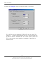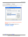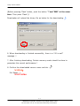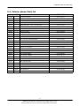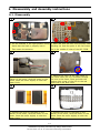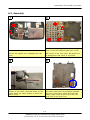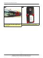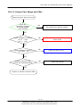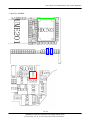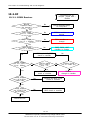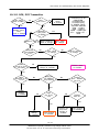
1
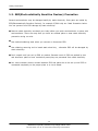
GSM TELEPHONE
SGH-i320
GSM TELEPHONE
CONTENTS
1. Safety Precautions
2. Specification
3. Product Function
4. Array course control
5. Exploded View and Parts list
6. Disassembly and Assembly
instructions
7. MAIN Electrical Parts List
8. Block Diagrams
9. PCB Diagrams
10. Flow Chart of Troubleshooting
11. Reference data
Contents
1. Safety Precautions
1-1. Repair Precaution ...........................................................................1-1
1-2. ESD(Electrostatically Sensitive Devices) Precaution ...........................1-2
2. Specification
2-1. GSM General Specification ..............................................................2-1
2-2. GSM TX power Level ......................................................................2-2
3. Product Function
4. Array course control
4-1. Downloading Binary Files .............................................................4-2
4-2. Pre-requsite for Downloading .......................................................4-2
4-3. S/W Downloader Program ............................................................4-3
5. Exploded View and Parts list
5-1. Cellular phone Exploded View ......................................................5-1
5-2. Cellular phone Parts list ...............................................................5-6
6. Disassembly and Assembly instructions
6-1. Disassembly .............................................................................6-1
6-2. Assembly .................................................................................6-4
7. MAIN Electrical Parts List
8. Block Diagrams
9. PCB Diagrams
Contents
10. Flow Chart of Troubleshooting
10-1. Baseband .............................................................................10-1
10-1-1. Power ON .......................................................................10-1
10-1-2. Initial .............................................................................10-4
10-1-3. SIM Part ........................................................................10-6
10-1-4. Microphone Part ..............................................................10-7
10-1-5. Speaker Part_1(MP3, SPEAKER PHONE) ............................10-8
10-1-6. Speaker Part_2(RECEIVER) .............................................10-10
10-1-7. Charging Part ................................................................10-11
10-2. RF .....................................................................................10-13
10-2-1. EGSM RX ......................................................................10-13
10-2-2. DCS RX ........................................................................10-15
10-2-3. PCS RX ........................................................................10-16
10-2-4. EGSM TX ......................................................................10-17
10-2-5. DCS TX ........................................................................10-18
10-2-6. PCS TX ........................................................................10-19
11. Reference data
1. Safety Precautions
1-1. Repair Precaution
● Repair in Shield Box, during detailed tuning.
Take specially care of tuning or test,
because specipicty of cellular phone is sensitive for surrounding interference(RF noise).
● Be careful to use a kind of magnetic object or tool,
because performance of parts is damaged by the influence of manetic force.
● Surely use a standard screwdriver when you disassemble this product,
otherwise screw will be worn away.
● Use a thicken twisted wire when you measure level.
A thicken twisted wire has low resistance, therefore error of measurement is few.
● Repair after separate Test Pack and Set because for short danger (for example an
overcurrent and furious flames of parts etc) when you repair board in condition of
connecting Test Pack and tuning on.
● Take specially care of soldering, because Land of PCB is small and weak in heat.
● Surely tune on/off while using AC power plug, because a repair of battery charger is
dangerous when tuning ON/OFF PBA and Connector after disassembing charger.
● Don't use as you pleases after change other material than replacement registered on SEC
System.
Otherwise engineer in charge isn't charged with problem that you don't keep this rules.
1-1
SAMSUNG Proprietary-Contents may change without notice
This Document can not be used without Samsung's authorization
Safety Precautions
1-2. ESD(Electrostatically Sensitive Devices) Precaution
Several semiconductor may be damaged easilly by static electricity. Such parts are called by
ESD(Electrostatically Sensitive Devices), for example IC,BGA chip etc. Read Precaution below.
You can prevent from ESD damage by static electricity.
● Remove static electricity remained your body before you touch semiconductor or parts with
semiconductor. There are ways that you touch an earthed place or wear static electricity
prevention string on wrist.
● Use earthed soldering steel when you connect or disconnect ESD.
● Use soldering removing tool to break static electricity. , otherwise ESD will be damaged by
static electricity.
● Don't unpack until you set up ESD on product. Because most of ESD are packed by box
and aluminum plate to have conductive power,they are prevented from static electricity.
● You must maintain electric contact between ESD and place due to be set up until ESD is
connected completely to the proper place or a circuit board.
1-2
SAMSUNG Proprietary-Contents may change without notice
This Document can not be used without Samsung's authorization
2. Specification
2-1. GSM/WCDMA General Specification
EGSM 900
Phase 2
DC S1800
Phase 1
PCS1900
Freq .
Band[MHz]
Upli nk/ Dow nl in k
8 80 ~ 9 15
9 25 ~ 9 60
17 10 ~1 78 5
18 05 ~1 88 0
18 50 ~1 91 0
19 30 ~1 99 0
AR FC N r a ng e
0~ 12 4 & 97 5~1 02 3
5 12 ~8 85
5 12 ~8 10
Tx/Rx spacing
45 MHz
9 5 M Hz
80 MHz
Mod. Bit rate/
Bit Period
27 0. 83 3 kb p s
3. 69 2 u s
27 0. 83 3 kb p s
3. 69 2 u s
27 0. 83 3 kb p s
3. 69 2 u s
T im e S lo t
P er io d /F ram e
P e ri od
57 6. 9 u s
4. 61 5 ms
57 6. 9 u s
4. 61 5 ms
57 6. 9 u s
4. 61 5 ms
M od u la ti on
0 .3 GMS K
0. 3 G MS K
0. 3 GMS K
M S P ow er
33 d Bm ~5 d Bm
30 d Bm~0 dBm
30 d Bm~0 dBm
P ow er Cl as s
5 pcl ~ 19 pcl
0 pcl ~ 15 pcl
0 pcl ~ 15 pcl
Sen si ti vit y
-102 dBm
-100 dBm
-100 d Bm
TDM A M ux
8
8
8
C ell Rad iu s
35 Km
2 Km
-
2-1
SAMSUNG Proprietary-Contents may change without notice
This Document can not be used without Samsung's authorization
Specification
2-2. GSM TX power class
TX Power
control level
EGSM900
TX Power
control level
DCS1800
TX Power
control level
PCS1900
5
33±2 dBm
0
30±3 dBm
0
30±3 dBm
6
31±2 dBm
1
28±3 dBm
1
28±3 dBm
7
29±2 dBm
2
26±3 dBm
2
26±3 dBm
8
27±2 dBm
3
24±3 dBm
3
24±3 dBm
9
25±2 dBm
4
22±3 dBm
4
22±3 dBm
10
23±2 dBm
5
20±3 dBm
5
20±3 dBm
11
21±2 dBm
6
18±3 dBm
6
18±3 dBm
12
19±2 dBm
7
16±3 dBm
7
16±3 dBm
13
17±2 dBm
8
14±3 dBm
8
14±3 dBm
14
15±2 dBm
9
12±4 dBm
9
12±4 dBm
15
13±2 dBm
10
10±4 dBm
10
10±4 dBm
16
11±3 dBm
11
8±4 dBm
11
8±4 dBm
17
9± 3dBm
12
6±4 dBm
12
6±4 dBm
18
7±3 dBm
13
4±4 dBm
13
4±4 dBm
19
5±3 dBm
14
2±5 dBm
14
2±5 dBm
15
0±5 dBm
15
0±5 dBm
2-2
SAMSUNG Proprietary-Contents may change without notice
This Document can not be used without Samsung's authorization
3. Product Function
Main Function
-Camera and camcorder
-Image editor
-MP3 player
-Phonebook
-Name card
-Multimedia Message Service (MMS)
-E-mail
-Voice recorder
-Bluetooth
-Get personal with photo caller ID
-Web browser
-Java
-Calendar
3-1
SAMSUNG Proprietary-Contents may change without notice
This Document can not be used without Samsung's authorization
4. Array course control
Test Jig (GH80-03311A)
Test Cable (GH39-00582A)
RF Test Cable (GH39-00397A)
4-1
SAMSUNG Proprietary-Contents may change without notice
This Document can not be used without Samsung's authorization
Array course control
Software Downloading
4-1. Downloading Binary Files
• binary file for downloading I320.
– I320XXYY.s3 : Main source code binary.
4-2. Pre-requsite for Downloading
• Downloader Program(OptiFlash.exe)
• I320 Mobile Phone
• Data Cable
• Binary file
4-2
SAMSUNG Proprietary-Contents may change without notice
This Document can not be used without Samsung's authorization
Array course control
4-3. S/W Downloader Program
1. Load the binary download programby executing the “OptiFlash.exe”
2. Select the “Options” -> “Settings” -> “Generic” -> “Specify hardware
platform”.
Choose hardware platform for the downloader file setting.
Set the everything else as the default values which are shown below
4-3
SAMSUNG Proprietary-Contents may change without notice
This Document can not be used without Samsung's authorization
Array course control
3. Select the COM port when the download cable is connected
Up to twelve ports are supported. Additionally you can select the
maximum
transfer speed OptiFlash will use to communicate with
the phone. However, OptiFlash will use a slower speed if either the
PC’s or the phone’s serial hardware is incapable of handling the
selected speed
4-4
SAMSUNG Proprietary-Contents may change without notice
This Document can not be used without Samsung's authorization
Array course control
4. Select the“Flash&Verify” -> “Browse”
Set the directory path and choose the latest s/w binary, for example
“I320XXYY.s3”,for the downloader binary setting.
Make sure that not to change the reserved memory
regions.
In case of I320 the reserved regions are :
-0x20000000 – 0x2000ffff
-0x21fe0000– 0x21ffffff
5. Click “OK” button then press “Flash”.
4-5
SAMSUNG Proprietary-Contents may change without notice
This Document can not be used without Samsung's authorization
Array course control
(Before pressing ‘Flash’ button, push the button ‘*’and ‘END’ at the same
time. Then press ‘Flash’.)
Downloader will upload the binary file as below for the downloading.
6. When downloading is finished successfully, there is a “All is well”
message. 7. After finishing downloading, Certain memory resets should be done to
guarantee the normal performance.
8. Confirm the downloaded version name and etc. :
*#1234#
Full Reset : *2767*2878#
4-6
SAMSUNG Proprietary-Contents may change without notice
This Document can not be used without Samsung's authorization
5. Exploded View and Parts List
5-1. Cellular phone Exploded View
QCK01
QRF03
QMW02
QIF01
QFR01
QVO01
QKP02
QLC01
QKP01
QME01
QSH01
QCR12
QMI01
QMO01
QMI03
QCR32
QCA01
QAR01
QAN10
QMP01
QBR05
QSP02
QCR04
QAN02
QRE01
QRF01
QCR12
QCR04
QBA01
QBA00
5-1
SAMSUNG Proprietary-Contents may change without notice
This Document can not be used without Samsung's authorization
Exploded View and Parts List
5-2. Cellular phone Parts list
Design LOC
Discription
SEC CODE
QAN02
INTENNA-SGHI320
GH42-00812A
QAN10
ASSY-CUSHION-ANT CONTACT RUBBE
GH98-01218A
QAR01
AUDIO-RECEIVER
3009-001162
QBA00
PMO-COVER BATT
GH72-28172A
QBA01
INNER BATTERY PACK-1000MAH,BLA
GH43-02424A
QBR05
ASSY-BRACKET-SPK SHIELD FRAME
GH98-01310A
QCA01
UNIT-CAMERA
GH59-02955A
QCK01
MEC-Q CA KEY
GH75-08945A
QCR04
SCREW-MACHINE
6001-001479
QCR12
SCREW-MACHINE
6001-001530
QCR32
SCREW-MACHINE
6001-001700
QKP01
MEC-KEYPAD MAIN(OPEN/BLK
GH75-08942A
QKP02
ASSY-KEY-KEYPAD SUB
GH98-00984A
QLC01
LCD-SGHI320
GH07-00838A
QMI03
RMO-CUSHION MIC
GH73-06180A
QMO01
MOTOR DC-SGHI320
GH31-00237A
QMP01
PBA MAIN-SGHI320
GH92-02504A
QMW02
PMO-COVER MAIN WINDOW
GH72-28151A
QRE01
MEC-COVER REAR
GH75-08944A
QRF01
PMO-COVER MOBILE
GH72-28171A
QSH01
ASSY-BRACKET-SHIELD BRAKET MAI
GH98-00749A
QSP02
UNIT-SPK FPCB ASSY
GH59-02867A
QVO01
MEC-VOLUME KEY
GH75-08946A
QME01
UNIT-KEY FPCB
GH59-02846A
QMI01
QFR01
AS-MIC
GH81-04513A
MEC-COVER FRONT
GH75-08941A
QIF01
PMO-COVER IF
GH72-28148A
QRF03
PMO-COVER EAR
GH72-28147A
5-2
SAMSUNG Proprietary-Contents may change without notice
This Document can not be used without Samsung's authorization
Exploded View and Parts List
Discription
SEC CODE
BAG PE
6902-000634
CBF INTERFACE-DATA LINK CABLE
GH39-00564A
CHARGER-SGHE880 TC,EU,BLACK
GH44-00998A
CHARGER-SGHI320,BTH
GH44-01238A
S/W CD-SGH-I320 MS COMPANION C
GH46-00233A
S/W CD-USER MANUAL
GH46-00235A
UNIT-EARPHONE
GH59-02166A
LABEL(P)-IMEI
GH68-01335D
LABEL(P)-WATER SOAK
GH68-02026A
LABEL(R)-WATER SOAK T_MOBILE
GH68-05914A
MANUAL USERS-QSG FRENCH
GH68-09802A
LABEL(R)-MAIN(EU)
GH68-09839C
BOX(P)-UNIT MAIN(XET)
GH69-03861C
CUSHION-CASE TA2 MA2
GH69-03864A
PMO-COVER FRONT
GH72-28143A
RMO-CUSHION BGA A
GH73-06184A
RMO-CUSHION BGA B
GH73-06185A
RMO-CUSHION BGA D
GH73-06187A
RMO-CUSHION BGA E
GH73-06188A
RMO-CUSHION PCB
GH73-07056A
MPR-DUMMY SHORT TAPE F
GH74-11815A
MPR-CUSHION MAIN KEY CON
GH74-20153A
MPR-CUSHION MAIN LCD CON
GH74-20154A
MPR-CUSHION CAMERA CONN
GH74-20156A
MPR-CUSHION SPK CONN
GH74-20157A
MPR-CUSHION CAMERA
GH74-22450A
MPR-VINYL BOHO MAIN WINDOW A
GH74-22788A
MPR-VINYL BOHO MAIN WINDOW B
GH74-22789A
MPR-VINYL BOHO KEYPAD
GH74-22790A
MPR-SHEET MIC FPCB
GH74-23937A
MPR-TAPE IF COVER
GH74-23939A
MPR-VINYL BOHO MAIN WINDOW
GH74-23940A
MPR-VINYL BOHO BATT COVER
GH74-24694A
5-3
SAMSUNG Proprietary-Contents may change without notice
This Document can not be used without Samsung's authorization
6. Disassembly and Assembly instructions
6-1. Disassembly
1
2
1) Put the antenna in the right position caring 1) Place and stick the KEY FPCB properly with
about that the hook is properly lock it.
checking out that four poles in the red circles
Then screw the antenna.
are in the middle of holes of the KEY FPCB.
3
4
1) Remove the cover of the tape on the
bottom of the motor, stick the motor on the
frame. Press the motor slightly to stick the
motor firmly.
1) Remove the cover on the tape stuck on
the frame insert the LCD connector through
the hole in the frame. Place and stick the
bottom right corner of the LCD to the red
guide line in the blue circle.
5
6
1) Remove the cover of the tape on the
bottom of the motor, stick the motor on the
frame. Press the motor slightly to stick the
motor firmly.
1) Remove the cover of the tape on the
bottom of the motor, stick the motor on the
frame. Press the motor slightly to stick the
motor firmly.
6-1
SAMSUNG Proprietary-Contents may change without notice
This Document can not be used without Samsung's authorization
Disassembly and Assembly instructions
5
6
1) Pull out the receiver and the motor
connector first. the LCD connector and the
key connector later.
1) Push out two red circled hooks slightly to
lift the PBA.
7
8
1) Remove the sponge on the LCD connector
1) Get rid of the screw in the A red circle.
You can lift the shield frame with pushing out first, then you can detach the LCD from the
frame.
three hooks slightly.
9
10
...
1) Insert tweezers between the bottom of the 1) Take off the KEY FPCB with care not to
motor and the frame to the direction that the damage KEY FPCB.
red arrow directs.
6-2
SAMSUNG Proprietary-Contents may change without notice
This Document can not be used without Samsung's authorization
Disassembly and Assembly instructions
11
...
1) Remove two screws in the red circles and
take out the antenna with care not to damage
the hook..
6-3
SAMSUNG Proprietary-Contents may change without notice
This Document can not be used without Samsung's authorization
Disassembly and Assembly instructions
6-2. Assembly
1
2
1) Lift the rear cover slightly and unlock the
1) Get rid of 4 screws in the red circled
hook on the left side(the upper part of ear
corners. Be careful not to damage the rear
jack cover) of the rear cover. Be careful not
cover.
to damage the rear cover or the hook.
3
4
1) Remove the cover of the tape on the
bottom of the motor, stick the motor on the
frame. Press the motor slightly to stick the
motor firmly.
1) Remove the cover on the tape stuck on
the frame insert the LCD connector through
the hole in the frame. Place and stick the
bottom right corner of the LCD to the red
guide line in the blue circle.
6-4
SAMSUNG Proprietary-Contents may change without notice
This Document can not be used without Samsung's authorization
Disassembly and Assembly instructions
5
6
1) Stick the sponge in the guideline oh the
LCD connector with care.
1) Place the key pad properly minding guide
poles on the front cover.
7
8
A
1) Place the frame on the right position and
lock three hooks in the red circle. Screw the
frame in the red A circle.
9
1) Solder the receiver on the PCB minding
silk marks of soldering pads on the PCB. Be
careful not to cause a short-circuit when you
solder.
10
...
1) Insert a rubber into the antenna contact
1) Put together the speaker assembly and
with care not to damage antenna contact with screw in the right red circle. Then put the
a pair of tweezers.
speaker connector on the connector on the
PBA.
6-5
SAMSUNG Proprietary-Contents may change without notice
This Document can not be used without Samsung's authorization
Disassembly and Assembly instructions
11
12
1) Put some adhesive on the soldered motor
wire. Be careful not to get an adhesives on
the antenna contact or the flash LED near the 1) Put the camera connector on the connector
motor wire.
on the PBA firmly.
13
14
1) Place the PBA pushing out two hooks in
the red circles slightly.
1) Put on the receiver into the hole of the
front cover, the receiver connector, the motor
connector, the LCD connector, and the key
connector on the right positions firmly.
15
16
1) Put side keys on the right directions, then
lock two hooks on the top of the rear cover.
After locking two hooks, press the rear cover
slightly to assemble two covers.
1) Press the rear cover part around the red
circle area slightly to lock the left hook on
the rear cover.
6-6
SAMSUNG Proprietary-Contents may change without notice
This Document can not be used without Samsung's authorization
Disassembly and Assembly instructions
18
17
1) Press the rear cover part around the red
circle area slightly to lock the rightt hook on
the rear cover.
1) Screw four positions in the red circles.
6-7
SAMSUNG Proprietary-Contents may change without notice
This Document can not be used without Samsung's authorization
7. MAIN Electrical Parts List
SEC CODE
4202-001131
GH71-06419A
GH71-06419A
4302-001158
3711-006003
2203-006423
2203-006824
2203-006048
2203-006048
2203-006423
2203-006257
2203-006562
2203-000254
2203-006423
2203-000438
2203-006305
2203-006423
2203-006423
2203-000386
2203-006121
2203-000425
2203-006423
2203-006423
2203-006423
2203-006423
2203-006423
2203-006423
2203-006423
2203-006423
2203-006423
2203-006423
2203-006423
2203-006423
2203-006423
2203-006423
2203-006423
2203-006423
2203-006423
2203-006423
2203-006423
2203-006423
2203-006423
2203-006423
2203-006423
Design LOC
ANT1001
ANT1800
ANT900
BAT701
BTC301
C1001
C1003
C1004
C1005
C101
C1012
C1013
C1014
C102
C1027
C1028
C103
C1031
C1034
C1036
C1038
C104
C105
C106
C107
C108
C109
C110
C111
C112
C113
C114
C115
C117
C118
C119
C120
C121
C122
C123
C124
C125
C126
C127
Discription
ANTENNA-CHIP
NPR-ANTENNA CONTACT
NPR-ANTENNA CONTACT
BATTERY-LI(2ND)
CONNECTOR-BATTERY
C-CER,CHIP
C-CER,CHIP
C-CER,CHIP
C-CER,CHIP
C-CER,CHIP
C-CER,CHIP
C-CER,CHIP
C-CER,CHIP
C-CER,CHIP
C-CER,CHIP
C-CER,CHIP
C-CER,CHIP
C-CER,CHIP
C-CER,CHIP
C-CER,CHIP
C-CER,CHIP
C-CER,CHIP
C-CER,CHIP
C-CER,CHIP
C-CER,CHIP
C-CER,CHIP
C-CER,CHIP
C-CER,CHIP
C-CER,CHIP
C-CER,CHIP
C-CER,CHIP
C-CER,CHIP
C-CER,CHIP
C-CER,CHIP
C-CER,CHIP
C-CER,CHIP
C-CER,CHIP
C-CER,CHIP
C-CER,CHIP
C-CER,CHIP
C-CER,CHIP
C-CER,CHIP
C-CER,CHIP
C-CER,CHIP
7-1
SAMSUNG Proprietary-Contents may change without notice
This Document can not be used without Samsung's authorization
STATUS
SA
SA
SA
SA
SA
SA
SA
SA
SA
SA
SA
SA
SA
SA
SA
SA
SA
SA
SA
SA
SA
SA
SA
SA
SA
SA
SA
SA
SA
SA
SA
SA
SA
SA
SA
SA
SA
SA
SA
SA
SA
SA
SA
SA
Main Electrical Parts List
SEC CODE
2203-006423
2203-006423
2203-006423
2203-006423
2203-006423
2203-006423
2203-006423
2203-006348
2203-006562
2203-006423
2203-006423
2203-006423
2203-006423
2203-006423
2203-006048
2203-006423
2203-006423
2203-005806
2203-005806
2203-006423
2203-005806
2203-005806
2203-005806
2203-005806
2203-006423
2203-005806
2203-006423
2203-005806
2203-006423
2203-006423
2203-000995
2203-000995
2203-006423
2203-006423
2203-006423
2203-006423
2203-006562
2203-006121
2203-006423
2203-006423
2203-006423
2203-006423
2203-006423
2203-006423
Design LOC
C128
C129
C130
C131
C132
C133
C134
C135
C137
C139
C140
C141
C142
C143
C144
C145
C146
C147
C148
C149
C150
C151
C152
C153
C154
C155
C156
C157
C158
C159
C160
C161
C162
C165
C166
C201
C202
C203
C204
C205
C206
C209
C210
C211
Discription
C-CER,CHIP
C-CER,CHIP
C-CER,CHIP
C-CER,CHIP
C-CER,CHIP
C-CER,CHIP
C-CER,CHIP
C-CER,CHIP
C-CER,CHIP
C-CER,CHIP
C-CER,CHIP
C-CER,CHIP
C-CER,CHIP
C-CER,CHIP
C-CER,CHIP
C-CER,CHIP
C-CER,CHIP
C-CER,CHIP
C-CER,CHIP
C-CER,CHIP
C-CER,CHIP
C-CER,CHIP
C-CER,CHIP
C-CER,CHIP
C-CER,CHIP
C-CER,CHIP
C-CER,CHIP
C-CER,CHIP
C-CER,CHIP
C-CER,CHIP
C-CER,CHIP
C-CER,CHIP
C-CER,CHIP
C-CER,CHIP
C-CER,CHIP
C-CER,CHIP
C-CER,CHIP
C-CER,CHIP
C-CER,CHIP
C-CER,CHIP
C-CER,CHIP
C-CER,CHIP
C-CER,CHIP
C-CER,CHIP
7-2
SAMSUNG Proprietary-Contents may change without notice
This Document can not be used without Samsung's authorization
STATUS
SA
SA
SA
SA
SA
SA
SA
SA
SA
SA
SA
SA
SA
SA
SA
SA
SA
SA
SA
SA
SA
SA
SA
SA
SA
SA
SA
SA
SA
SA
SA
SA
SA
SA
SA
SA
SA
SA
SA
SA
SA
SA
SA
SA
Main Electrical Parts List
SEC CODE
2203-006423
2203-006423
2203-006423
2203-006423
2203-006423
2203-006423
2203-006423
2203-006423
2203-006423
2203-006423
2203-006423
2203-006423
2203-006423
2203-006423
2203-006423
2203-006562
2203-006562
2203-006825
2203-000940
2203-006423
2203-006423
2203-006562
2203-006562
2203-006121
2203-006120
2203-000550
2203-006121
2203-006423
2203-006423
2203-006048
2203-006423
2203-006423
2203-006423
2203-006423
2203-006048
2203-006048
2203-006423
2203-006121
2203-006423
2203-006562
2203-005659
2203-000995
2203-006562
2203-006626
Design LOC
C212
C213
C214
C215
C216
C217
C218
C219
C220
C221
C222
C223
C224
C225
C226
C227
C228
C301
C302
C303
C304
C305
C306
C307
C308
C309
C310
C311
C312
C401
C402
C404
C405
C407
C409
C410
C411
C413
C414
C415
C416
C417
C418
C419
Discription
C-CER,CHIP
C-CER,CHIP
C-CER,CHIP
C-CER,CHIP
C-CER,CHIP
C-CER,CHIP
C-CER,CHIP
C-CER,CHIP
C-CER,CHIP
C-CER,CHIP
C-CER,CHIP
C-CER,CHIP
C-CER,CHIP
C-CER,CHIP
C-CER,CHIP
C-CER,CHIP
C-CER,CHIP
C-CER,CHIP
C-CER,CHIP
C-CER,CHIP
C-CER,CHIP
C-CER,CHIP
C-CER,CHIP
C-CER,CHIP
C-CER,CHIP
C-CER,CHIP
C-CER,CHIP
C-CER,CHIP
C-CER,CHIP
C-CER,CHIP
C-CER,CHIP
C-CER,CHIP
C-CER,CHIP
C-CER,CHIP
C-CER,CHIP
C-CER,CHIP
C-CER,CHIP
C-CER,CHIP
C-CER,CHIP
C-CER,CHIP
C-CER,CHIP
C-CER,CHIP
C-CER,CHIP
C-CER,CHIP
7-3
SAMSUNG Proprietary-Contents may change without notice
This Document can not be used without Samsung's authorization
STATUS
SA
SA
SA
SA
SA
SA
SA
SA
SA
SA
SA
SA
SA
SA
SA
SA
SA
SA
SA
SA
SA
SA
SA
SA
SA
SA
SA
SA
SA
SA
SA
SA
SA
SA
SA
SA
SA
SA
SA
SA
SA
SA
SA
SA
Main Electrical Parts List
SEC CODE
2203-005659
2203-006423
2203-006423
2203-006423
2203-000995
2203-006562
2203-006423
2203-006048
2203-006585
2203-006585
2203-006585
2203-006585
2203-006562
2203-006423
2203-000812
2203-006562
2203-002443
2203-002443
2203-000438
2203-006423
2203-000438
2203-002443
2203-002443
2203-006562
2203-000812
2203-006562
2203-000438
2203-000438
2203-001405
2203-006260
2203-006260
2203-005682
2203-005682
2203-005682
2203-005682
2203-005682
2203-005682
2203-000233
2203-000812
2203-000812
2203-005682
2203-005682
2203-005736
2203-005806
Design LOC
C421
C422
C423
C424
C425
C426
C427
C428
C430
C431
C432
C433
C434
C435
C436
C437
C438
C439
C440
C442
C443
C444
C445
C448
C451
C452
C453
C454
C456
C458
C459
C501
C502
C503
C504
C505
C506
C507
C508
C509
C510
C511
C512
C513
Discription
C-CER,CHIP
C-CER,CHIP
C-CER,CHIP
C-CER,CHIP
C-CER,CHIP
C-CER,CHIP
C-CER,CHIP
C-CER,CHIP
C-CER,CHIP
C-CER,CHIP
C-CER,CHIP
C-CER,CHIP
C-CER,CHIP
C-CER,CHIP
C-CER,CHIP
C-CER,CHIP
C-CER,CHIP
C-CER,CHIP
C-CER,CHIP
C-CER,CHIP
C-CER,CHIP
C-CER,CHIP
C-CER,CHIP
C-CER,CHIP
C-CER,CHIP
C-CER,CHIP
C-CER,CHIP
C-CER,CHIP
C-CER,CHIP
C-CER,CHIP
C-CER,CHIP
C-CER,CHIP
C-CER,CHIP
C-CER,CHIP
C-CER,CHIP
C-CER,CHIP
C-CER,CHIP
C-CER,CHIP
C-CER,CHIP
C-CER,CHIP
C-CER,CHIP
C-CER,CHIP
C-CER,CHIP
C-CER,CHIP
7-4
SAMSUNG Proprietary-Contents may change without notice
This Document can not be used without Samsung's authorization
STATUS
SA
SA
SA
SA
SA
SA
SA
SA
SA
SA
SA
SA
SA
SA
SA
SA
SA
SA
SA
SA
SA
SA
SA
SA
SA
SA
SA
SA
SA
SA
SA
SA
SA
SA
SA
SA
SA
SA
SA
SA
SA
SA
SA
SA
Main Electrical Parts List
SEC CODE
2203-006457
2203-000311
2203-006423
2203-006324
2203-006562
2203-006183
2203-000854
2203-000854
2203-005682
2203-005682
2203-005682
2203-005682
2203-005682
2203-005682
2203-005682
2203-000854
2203-005682
2203-005682
2203-005682
2203-005682
2203-005682
2203-005682
2203-005682
2203-005682
2203-002687
2203-000854
2203-000854
2203-006048
2203-000854
2203-000438
2203-006048
2203-000254
2203-001072
2203-006423
2203-006423
2203-006048
2203-000812
2203-006825
2203-006324
2203-006825
2203-006562
2203-006562
2203-006562
2203-006562
Design LOC
C514
C515
C516
C517
C518
C519
C520
C521
C522
C523
C525
C526
C527
C528
C529
C530
C531
C532
C533
C534
C535
C536
C537
C538
C539
C601
C602
C603
C605
C608
C619
C701
C702
C703
C704
C705
C706
C707
C709
C710
C712
C713
C714
C716
Discription
C-CER,CHIP
C-CER,CHIP
C-CER,CHIP
C-CER,CHIP
C-CER,CHIP
C-CER,CHIP
C-CER,CHIP
C-CER,CHIP
C-CER,CHIP
C-CER,CHIP
C-CER,CHIP
C-CER,CHIP
C-CER,CHIP
C-CER,CHIP
C-CER,CHIP
C-CER,CHIP
C-CER,CHIP
C-CER,CHIP
C-CER,CHIP
C-CER,CHIP
C-CER,CHIP
C-CER,CHIP
C-CER,CHIP
C-CER,CHIP
C-CER,CHIP
C-CER,CHIP
C-CER,CHIP
C-CER,CHIP
C-CER,CHIP
C-CER,CHIP
C-CER,CHIP
C-CER,CHIP
C-CER,CHIP
C-CER,CHIP
C-CER,CHIP
C-CER,CHIP
C-CER,CHIP
C-CER,CHIP
C-CER,CHIP
C-CER,CHIP
C-CER,CHIP
C-CER,CHIP
C-CER,CHIP
C-CER,CHIP
7-5
SAMSUNG Proprietary-Contents may change without notice
This Document can not be used without Samsung's authorization
STATUS
SA
SA
SA
SA
SA
SA
SA
SA
SA
SA
SA
SA
SA
SA
SA
SA
SA
SA
SA
SA
SA
SA
SA
SA
SA
SA
SA
SA
SA
SA
SA
SA
SA
SA
SA
SA
SA
SA
SA
SA
SA
SA
SA
SA
Main Electrical Parts List
SEC CODE
2203-005736
2203-006257
2203-001405
2203-005736
2203-005736
2203-005736
2203-006423
2203-000254
2203-006423
2203-006562
2203-000812
2203-006257
2203-000812
2203-005171
2203-006562
2203-006423
2203-006423
2203-006423
2203-006423
2203-006423
2203-006423
2203-006423
2203-006423
2203-006194
2203-006194
2203-006194
2203-006194
2203-006194
2203-006194
2203-006194
2203-001405
2203-000278
2203-000278
2203-000254
2203-006423
2203-006194
2203-006423
2203-006048
2203-000438
2203-000254
2203-000254
2203-000254
2203-006048
2203-000278
Design LOC
C717
C718
C719
C720
C721
C722
C723
C724
C725
C726
C731
C732
C733
C735
C736
C801
C802
C803
C804
C805
C806
C807
C808
C809
C810
C811
C812
C813
C814
C815
C816
C817
C818
C819
C821
C822
C823
C903
C904
C905
C907
C908
C910
C911
Discription
C-CER,CHIP
C-CER,CHIP
C-CER,CHIP
C-CER,CHIP
C-CER,CHIP
C-CER,CHIP
C-CER,CHIP
C-CER,CHIP
C-CER,CHIP
C-CER,CHIP
C-CER,CHIP
C-CER,CHIP
C-CER,CHIP
C-CER,CHIP
C-CER,CHIP
C-CER,CHIP
C-CER,CHIP
C-CER,CHIP
C-CER,CHIP
C-CER,CHIP
C-CER,CHIP
C-CER,CHIP
C-CER,CHIP
C-CER,CHIP
C-CER,CHIP
C-CER,CHIP
C-CER,CHIP
C-CER,CHIP
C-CER,CHIP
C-CER,CHIP
C-CER,CHIP
C-CER,CHIP
C-CER,CHIP
C-CER,CHIP
C-CER,CHIP
C-CER,CHIP
C-CER,CHIP
C-CER,CHIP
C-CER,CHIP
C-CER,CHIP
C-CER,CHIP
C-CER,CHIP
C-CER,CHIP
C-CER,CHIP
7-6
SAMSUNG Proprietary-Contents may change without notice
This Document can not be used without Samsung's authorization
STATUS
SA
SA
SA
SA
SA
SA
SA
SA
SA
SA
SA
SA
SA
SA
SA
SA
SA
SA
SA
SA
SA
SA
SA
SA
SA
SA
SA
SA
SA
SA
SA
SA
SA
SA
SA
SA
SA
SA
SA
SA
SA
SA
SA
SA
Main Electrical Parts List
SEC CODE
2203-001412
2203-006638
2203-000836
2203-006562
2203-000995
2203-006562
2203-005138
2203-005138
2203-002677
2203-006562
2203-002668
2203-005682
2203-006847
2203-005054
2203-005054
2203-006562
2203-000254
2203-000654
2203-000489
2203-000628
2203-000940
2203-005446
2203-000438
2203-000654
2203-002759
2203-000995
2203-000254
2203-000254
2203-006562
2203-000138
2203-006562
2203-000233
2203-000628
2203-000812
2203-000812
2203-000812
2203-002677
3709-001344
4709-001415
0407-000115
0401-001110
0401-001110
3722-002010
3301-001342
Design LOC
C912
C913
C914
C915
C916
C917
C918
C919
C920
C921
C922
C923
C924
C925
C926
C927
C928
C929
C930
C932
C933
C935
C936
C937
C938
C939
C940
C943
C944
C945
C946
C947
C948
C949
C950
C951
C953
CD601
CPL1001
D601
D602
D603
EAR401
F301
Discription
C-CER,CHIP
C-CER,CHIP
C-CER,CHIP
C-CER,CHIP
C-CER,CHIP
C-CER,CHIP
C-CER,CHIP
C-CER,CHIP
C-CER,CHIP
C-CER,CHIP
C-CER,CHIP
C-CER,CHIP
C-CER,CHIP
C-CER,CHIP
C-CER,CHIP
C-CER,CHIP
C-CER,CHIP
C-CER,CHIP
C-CER,CHIP
C-CER,CHIP
C-CER,CHIP
C-CER,CHIP
C-CER,CHIP
C-CER,CHIP
C-CER,CHIP
C-CER,CHIP
C-CER,CHIP
C-CER,CHIP
C-CER,CHIP
C-CER,CHIP
C-CER,CHIP
C-CER,CHIP
C-CER,CHIP
C-CER,CHIP
C-CER,CHIP
C-CER,CHIP
C-CER,CHIP
CONNECTOR-CARD EDGE
BALUN
DIODE-ARRAY
DIODE-SWITCHING
DIODE-SWITCHING
JACK-EAR PHONE
BEAD-SMD
7-7
SAMSUNG Proprietary-Contents may change without notice
This Document can not be used without Samsung's authorization
STATUS
SA
SA
SA
SA
SA
SA
SA
SA
SA
SA
SA
SA
SA
SA
SA
SA
SA
SA
SA
SA
SA
SA
SA
SA
SA
SA
SA
SA
SA
SA
SA
SA
SA
SA
SA
SA
SA
SA
SA
SA
SA
SA
SA
SA
Main Electrical Parts List
SEC CODE
3301-001844
3301-001844
3301-001844
3301-001844
2901-001308
2901-001308
2901-001308
2901-001308
2911-000010
3711-005793
3711-005578
3711-005954
3711-006119
3710-002324
0604-001304
2703-001242
2703-002734
2703-002768
2703-001876
2703-000403
2703-002734
2703-002734
2703-002314
2703-002367
2703-002367
2703-001749
2703-001749
2703-002612
2703-002170
2703-001750
2703-001750
2801-004189
2801-004466
2801-004189
2804-001591
2801-004466
1201-002267
2007-008542
2007-008542
2007-008542
2007-001290
2007-000171
2007-000171
2007-001290
Design LOC
F401
F402
F403
F404
F501
F502
F503
F504
F901
HDC501
HDC502
HDC503
HDC601
IFC601
IRD101
L101
L302
L303
L401
L501
L701
L702
L901
L903
L904
L905
L906
L907
L909
L911
L912
OSC1002
OSC101
OSC102
OSC401
OSC801
PAM901
R1006
R1008
R1009
R101
R1014
R102
R103
Discription
BEAD-SMD
BEAD-SMD
BEAD-SMD
BEAD-SMD
FILTER-EMI SMD
FILTER-EMI SMD
FILTER-EMI SMD
FILTER-EMI SMD
DUPLEXER-FEM
HEADER-BOARD TO BOARD
HEADER-BOARD TO BOARD
HEADER-BOARD TO BOARD
HEADER-BOARD TO BOARD
SOCKET-INTERFACE
PHOTO-IRDA
INDUCTOR-SMD
INDUCTOR-SMD
INDUCTOR-SMD
INDUCTOR-SMD
INDUCTOR-SMD
INDUCTOR-SMD
INDUCTOR-SMD
INDUCTOR-SMD
INDUCTOR-SMD
INDUCTOR-SMD
INDUCTOR-SMD
INDUCTOR-SMD
INDUCTOR-SMD
INDUCTOR-SMD
INDUCTOR-SMD
INDUCTOR-SMD
CRYSTAL-SMD
CRYSTAL-SMD
CRYSTAL-SMD
OSCILLATOR-CLOCK
CRYSTAL-SMD
IC-POWER AMP
R-CHIP
R-CHIP
R-CHIP
R-CHIP
R-CHIP
R-CHIP
R-CHIP
7-8
SAMSUNG Proprietary-Contents may change without notice
This Document can not be used without Samsung's authorization
STATUS
SA
SA
SA
SA
SA
SA
SA
SA
SA
SA
SA
SA
SA
SA
SA
SA
SA
SA
SA
SA
SA
SA
SA
SA
SA
SA
SA
SA
SA
SA
SA
SA
SA
SA
SA
SA
SA
SA
SA
SA
SA
SA
SA
SA
Main Electrical Parts List
SEC CODE
2007-008055
2007-008516
2007-008419
2007-008516
2007-008419
2007-008516
2007-008478
2007-008478
2007-008516
2007-008419
2007-008419
2007-008516
2007-008419
2007-008516
2007-008516
2007-008516
2007-008419
2007-008516
2007-008516
2007-008516
2007-008516
2007-008516
2007-008419
2007-008516
2007-008516
2007-000148
2007-008516
2007-008055
2007-000171
2007-008516
2007-008516
2007-008516
2007-008516
2007-008516
2007-000171
2007-000143
2007-008055
2007-008516
2007-000171
2007-000171
2007-008055
2007-000171
2007-000171
2007-000171
Design LOC
R104
R105
R106
R107
R108
R109
R110
R111
R112
R113
R115
R116
R117
R118
R119
R120
R121
R122
R123
R124
R125
R126
R127
R128
R129
R130
R131
R132
R133
R134
R135
R136
R137
R138
R139
R140
R141
R145
R146
R149
R202
R204
R205
R206
Discription
R-CHIP
R-CHIP
R-CHIP
R-CHIP
R-CHIP
R-CHIP
R-CHIP
R-CHIP
R-CHIP
R-CHIP
R-CHIP
R-CHIP
R-CHIP
R-CHIP
R-CHIP
R-CHIP
R-CHIP
R-CHIP
R-CHIP
R-CHIP
R-CHIP
R-CHIP
R-CHIP
R-CHIP
R-CHIP
R-CHIP
R-CHIP
R-CHIP
R-CHIP
R-CHIP
R-CHIP
R-CHIP
R-CHIP
R-CHIP
R-CHIP
R-CHIP
R-CHIP
R-CHIP
R-CHIP
R-CHIP
R-CHIP
R-CHIP
R-CHIP
R-CHIP
7-9
SAMSUNG Proprietary-Contents may change without notice
This Document can not be used without Samsung's authorization
STATUS
SA
SA
SA
SA
SA
SA
SA
SA
SA
SA
SA
SA
SA
SA
SA
SA
SA
SA
SA
SA
SA
SA
SA
SA
SA
SA
SA
SA
SA
SA
SA
SA
SA
SA
SA
SA
SA
SA
SA
SA
SA
SA
SA
SA
Main Electrical Parts List
SEC CODE
2007-008055
2007-008055
2007-008055
2007-008055
2007-008055
2007-008055
2007-008055
2007-000171
2007-008542
2007-008516
2007-000566
2007-000566
2007-008542
2007-008354
2007-000168
2007-008055
2007-008516
2007-000172
2007-007009
2007-003029
2007-008516
2007-008542
2007-008542
2007-000171
2007-000171
2007-008542
2007-007142
2007-007132
2007-007308
2007-007142
2007-007308
2007-007132
2007-000148
2007-007132
2007-007132
2007-007132
2007-007132
2007-008516
2007-008542
2007-007001
2007-007528
2007-000139
2007-000139
2007-007528
Design LOC
R207
R208
R212
R213
R214
R215
R216
R218
R219
R301
R302
R303
R305
R306
R307
R310
R311
R312
R313
R315
R401
R402
R403
R404
R405
R406
R407
R408
R410
R411
R412
R413
R415
R416
R417
R418
R419
R424
R425
R426
R427
R429
R430
R431
Discription
R-CHIP
R-CHIP
R-CHIP
R-CHIP
R-CHIP
R-CHIP
R-CHIP
R-CHIP
R-CHIP
R-CHIP
R-CHIP
R-CHIP
R-CHIP
R-CHIP
R-CHIP
R-CHIP
R-CHIP
R-CHIP
R-CHIP
R-CHIP
R-CHIP
R-CHIP
R-CHIP
R-CHIP
R-CHIP
R-CHIP
R-CHIP
R-CHIP
R-CHIP
R-CHIP
R-CHIP
R-CHIP
R-CHIP
R-CHIP
R-CHIP
R-CHIP
R-CHIP
R-CHIP
R-CHIP
R-CHIP
R-CHIP
R-CHIP
R-CHIP
R-CHIP
7-10
SAMSUNG Proprietary-Contents may change without notice
This Document can not be used without Samsung's authorization
STATUS
SA
SA
SA
SA
SA
SA
SA
SA
SA
SA
SA
SA
SA
SA
SA
SA
SA
SA
SA
SA
SA
SA
SA
SA
SA
SA
SA
SA
SA
SA
SA
SA
SA
SA
SA
SA
SA
SA
SA
SA
SA
SA
SA
SA
Main Electrical Parts List
SEC CODE
2007-000143
2007-003001
2007-008419
2007-000171
2007-008055
2007-003001
2007-008483
2007-008542
2007-000148
2007-000148
2007-008419
2007-008531
2007-008516
2007-003112
2007-008542
2007-008542
2007-008542
2007-000171
2007-000171
2007-007107
2007-001339
2007-000163
2007-000163
2007-000163
2007-000163
2007-000163
2007-000171
2007-000171
2007-009171
2007-008419
2007-008419
2007-008419
2007-000166
2007-008419
2007-008419
2007-008516
2007-000157
2007-008419
2007-008419
2007-008419
2007-008419
2007-008531
2007-000148
2007-008516
Design LOC
R432
R434
R435
R436
R437
R438
R440
R444
R445
R446
R501
R502
R503
R505
R506
R507
R508
R509
R510
R601
R602
R603
R604
R606
R607
R608
R609
R610
R611
R612
R613
R614
R615
R616
R617
R618
R619
R621
R622
R623
R624
R629
R701
R702
Discription
R-CHIP
R-CHIP
R-CHIP
R-CHIP
R-CHIP
R-CHIP
R-CHIP
R-CHIP
R-CHIP
R-CHIP
R-CHIP
R-CHIP
R-CHIP
R-CHIP
R-CHIP
R-CHIP
R-CHIP
R-CHIP
R-CHIP
R-CHIP
R-CHIP
R-CHIP
R-CHIP
R-CHIP
R-CHIP
R-CHIP
R-CHIP
R-CHIP
R-CHIP
R-CHIP
R-CHIP
R-CHIP
R-CHIP
R-CHIP
R-CHIP
R-CHIP
R-CHIP
R-CHIP
R-CHIP
R-CHIP
R-CHIP
R-CHIP
R-CHIP
R-CHIP
7-11
SAMSUNG Proprietary-Contents may change without notice
This Document can not be used without Samsung's authorization
STATUS
SA
SA
SA
SA
SA
SA
SA
SA
SA
SA
SA
SA
SA
SA
SA
SA
SA
SA
SA
SA
SA
SA
SA
SA
SA
SA
SA
SA
SA
SA
SA
SA
SA
SA
SA
SA
SA
SA
SA
SA
SA
SA
SA
SA
Main Electrical Parts List
SEC CODE
2007-000171
2007-000143
2007-007132
2007-000142
2007-000159
2007-008045
2007-000157
2007-009084
2007-009084
2007-009084
2007-009084
2007-008542
2007-008516
2007-008542
2007-008542
2007-000171
2007-008542
2007-008542
2007-008542
2007-008542
2007-008542
2007-000171
2007-000172
2007-000148
2007-000138
2007-000758
2007-002797
2007-000138
2007-007310
2007-007310
2007-000141
2007-001298
2007-001298
2007-000143
2007-001217
2007-007586
2007-001292
2007-001290
2007-003006
2007-000139
2007-000139
2007-003006
2007-007307
2007-003006
Design LOC
R703
R704
R705
R707
R710
R711
R712
R714
R715
R716
R717
R718
R802
R805
R806
R808
R810
R813
R819
R820
R823
R901
R902
R903
R904
R905
R906
R907
R908
R909
R910
R911
R912
R913
R914
R916
R917
R918
R919
R920
R921
R922
R923
R924
Discription
R-CHIP
R-CHIP
R-CHIP
R-CHIP
R-CHIP
R-CHIP
R-CHIP
R-CHIP
R-CHIP
R-CHIP
R-CHIP
R-CHIP
R-CHIP
R-CHIP
R-CHIP
R-CHIP
R-CHIP
R-CHIP
R-CHIP
R-CHIP
R-CHIP
R-CHIP
R-CHIP
R-CHIP
R-CHIP
R-CHIP
R-CHIP
R-CHIP
R-CHIP
R-CHIP
R-CHIP
R-CHIP
R-CHIP
R-CHIP
R-CHIP
R-CHIP
R-CHIP
R-CHIP
R-CHIP
R-CHIP
R-CHIP
R-CHIP
R-CHIP
R-CHIP
7-12
SAMSUNG Proprietary-Contents may change without notice
This Document can not be used without Samsung's authorization
STATUS
SA
SA
SA
SNA
SA
SA
SA
SA
SA
SA
SA
SA
SA
SA
SA
SA
SA
SA
SA
SA
SA
SA
SA
SA
SA
SA
SA
SA
SA
SA
SA
SA
SA
SA
SA
SA
SA
SA
SA
SA
SA
SA
SA
SA
Main Electrical Parts List
SEC CODE
2007-007189
2007-002797
2007-002797
2007-001288
2007-007008
2007-007008
2007-001288
2007-007008
2007-007008
2007-007318
2007-000171
2007-000171
2007-000171
3705-001358
3709-001391
3710-002081
2404-001381
2404-001381
2404-001381
2404-001395
2404-001386
2404-001381
2404-001381
2404-001381
2404-001381
2404-001381
2404-001381
2404-001381
2404-001381
2404-001381
2404-001406
2404-001381
2404-001381
2404-001422
2404-001422
2404-001381
2404-001381
2404-001381
2404-001381
2404-001381
2404-001381
2404-001406
2404-001381
2404-001381
Design LOC
R925
R926
R927
R928
R929
R930
R931
R932
R933
R934
R935
R937
R938
RFS901
SIM701
SLC601
TA1001
TA1002
TA101
TA102
TA104
TA201
TA202
TA301
TA303
TA304
TA305
TA306
TA307
TA308
TA309
TA311
TA312
TA313
TA314
TA315
TA316
TA317
TA401
TA402
TA403
TA404
TA405
TA406
Discription
R-CHIP
R-CHIP
R-CHIP
R-CHIP
R-CHIP
R-CHIP
R-CHIP
R-CHIP
R-CHIP
R-CHIP
R-CHIP
R-CHIP
R-CHIP
CONNECTOR-COAXIAL
CONNECTOR-CARD EDGE
SOCKET-BOARD TO BOARD
C-TA,CHIP
C-TA,CHIP
C-TA,CHIP
C-TA,CHIP
C-TA,CHIP
C-TA,CHIP
C-TA,CHIP
C-TA,CHIP
C-TA,CHIP
C-TA,CHIP
C-TA,CHIP
C-TA,CHIP
C-TA,CHIP
C-TA,CHIP
C-TA,CHIP
C-TA,CHIP
C-TA,CHIP
C-TA,CHIP
C-TA,CHIP
C-TA,CHIP
C-TA,CHIP
C-TA,CHIP
C-TA,CHIP
C-TA,CHIP
C-TA,CHIP
C-TA,CHIP
C-TA,CHIP
C-TA,CHIP
7-13
SAMSUNG Proprietary-Contents may change without notice
This Document can not be used without Samsung's authorization
STATUS
SA
SA
SA
SA
SA
SA
SA
SA
SA
SA
SA
SA
SA
SA
SA
SA
SA
SA
SA
SA
SA
SA
SA
SA
SA
SA
SA
SA
SA
SA
SA
SA
SA
SA
SA
SA
SA
SA
SA
SA
SA
SA
SA
SA
Main Electrical Parts List
SEC CODE
2404-001151
2404-001151
2404-001353
2404-001353
2404-001374
2404-001381
2404-001381
2404-001381
2404-001381
2404-001381
2404-001352
2404-001406
2404-001406
2809-001302
0501-002202
0505-001217
0505-001524
0504-000167
0501-000225
0504-000168
1205-002696
1203-001720
0801-000796
0801-003016
0801-003016
0801-002294
1203-002895
0801-002896
1203-002690
0801-002975
1203-001720
1203-001720
1203-003643
0801-000794
1203-003428
1203-003253
1203-002155
1203-001720
1203-002999
1201-002241
1203-001720
1209-001658
1001-001152
1001-001152
Design LOC
TA407
TA408
TA409
TA410
TA601
TA602
TA603
TA604
TA703
TA704
TA901
TA902
TA903
TCX901
TR101
TR301
TR302
TR401
TR402
TR702
U1001
U1002
U101
U102
U103
U104
U105
U106
U201
U202
U301
U302
U303
U304
U305
U306
U307
U308
U310
U401
U402
U403
U407
U408
Discription
C-TA,CHIP
C-TA,CHIP
C-TA,CHIP
C-TA,CHIP
C-TA,CHIP
C-TA,CHIP
C-TA,CHIP
C-TA,CHIP
C-TA,CHIP
C-TA,CHIP
C-TA,CHIP
C-TA,CHIP
C-TA,CHIP
OSCILLATOR-VCTCXO
TR-SMALL SIGNAL
FET-GAAS
FET-SILICON
TR-DIGITAL
TR-SMALL SIGNAL
TR-DIGITAL
IC-DATA COMM./GEN.
IC-POSI.FIXED REG.
IC-CMOS LOGIC
IC-CMOS LOGIC
IC-CMOS LOGIC
IC-CMOS LOGIC
IC-RESET
IC-CMOS LOGIC
IC-POSI.FIXED REG.
IC-CMOS LOGIC
IC-POSI.FIXED REG.
IC-POSI.FIXED REG.
IC-MULTI REG.
IC-CMOS LOGIC
IC-DC/DC CONVERTER
IC-BATTERY
IC-DC/DC CONVERTER
IC-POSI.FIXED REG.
IC-VOL. DETECTOR
IC-AUDIO AMP
IC-POSI.FIXED REG.
IC-SENSOR
IC-ANALOG MULTIPLEX
IC-ANALOG MULTIPLEX
7-14
SAMSUNG Proprietary-Contents may change without notice
This Document can not be used without Samsung's authorization
STATUS
SA
SA
SA
SA
SA
SA
SA
SA
SA
SA
SA
SA
SA
SA
SA
SA
SA
SA
SA
SA
SA
SA
SA
SA
SA
SA
SA
SA
SA
SA
SA
SA
SA
SA
SA
SA
SA
SA
SA
SA
SA
SA
SA
SA
Main Electrical Parts List
SEC CODE
1001-001183
1203-002850
1203-003474
1203-003531
1203-003768
1203-002250
0407-001038
1203-003428
1203-003434
0801-003016
0801-002958
0801-002993
1205-002652
1205-002720
1203-003565
0902-001900
GH09-00038A
1106-001519
1108-000054
1108-000036
1405-001093
1405-001093
1404-001165
0403-001547
0406-001210
0406-001167
0406-001210
0406-001210
0403-001446
0406-001210
0406-001210
0406-001210
0406-001210
0406-001190
0406-001167
0406-001167
0406-001167
0406-001167
0406-001210
0406-001104
0406-001201
0406-001201
0406-001201
0406-001201
Design LOC
U409
U501
U502
U602
U604
U605
U606
U702
U703
U801
U901
U902
U903
UCD401
UCD701
UCP101
UCP801
UME201
UME202
UME801
VR601
VR602
VR701
ZD301
ZD401
ZD402
ZD403
ZD404
ZD501
ZD502
ZD503
ZD505
ZD506
ZD601
ZD602
ZD603
ZD604
ZD605
ZD606
ZD608
ZD609
ZD610
ZD611
ZD612
Discription
IC-ANALOG SWITCH
IC-DC/DC CONVERTER
IC-SWITCH REG.
IC-POSI.FIXED REG.
IC-POSI.FIXED REG.
IC-VOL. DETECTOR
DIODE-ARRAY
IC-DC/DC CONVERTER
IC-DC/DC CONVERTER
IC-CMOS LOGIC
IC-CMOS LOGIC
IC-CMOS LOGIC
IC-TRANSCEIVER
IC-CODEC
IC-POWER SUPERVISOR
IC-MICROPROCESSOR
IC MICOM
IC-SRAM
IC-MCP
IC-MCP
VARISTOR
VARISTOR
THERMISTOR-NTC
DIODE-ZENER
DIODE-TVS
DIODE-TVS
DIODE-TVS
DIODE-TVS
DIODE-ZENER
DIODE-TVS
DIODE-TVS
DIODE-TVS
DIODE-TVS
DIODE-TVS
DIODE-TVS
DIODE-TVS
DIODE-TVS
DIODE-TVS
DIODE-TVS
DIODE-TVS
DIODE-TVS
DIODE-TVS
DIODE-TVS
DIODE-TVS
7-15
SAMSUNG Proprietary-Contents may change without notice
This Document can not be used without Samsung's authorization
STATUS
SA
SA
SA
SA
SA
SA
SA
SA
SA
SA
SA
SA
SA
SA
SA
SA
SA
SA
SA
SA
SA
SA
SA
SA
SA
SA
SA
SA
SA
SA
SA
SA
SA
SA
SA
SA
SA
SA
SA
SA
SA
SA
SA
SA
Main Electrical Parts List
SEC CODE
0406-001201
0406-001201
0406-001201
0406-001201
Design LOC
ZD613
ZD614
ZD615
ZD616
Discription
DIODE-TVS
DIODE-TVS
DIODE-TVS
DIODE-TVS
7-16
SAMSUNG Proprietary-Contents may change without notice
This Document can not be used without Samsung's authorization
STATUS
SA
SA
SA
SA
8. Block Diagrams
8-1
SAMSUNG Proprietary-Contents may change without notice
This Document can not be used without Samsung's authorization
Block Diagrams
8-2
SAMSUNG Proprietary-Contents may change without notice
This Document can not be used without Samsung's authorization
Block Diagrams
8-3
SAMSUNG Proprietary-Contents may change without notice
This Document can not be used without Samsung's authorization
Block Diagrams
8-4
SAMSUNG Proprietary-Contents may change without notice
This Document can not be used without Samsung's authorization
Block Diagrams
8-5
SAMSUNG Proprietary-Contents may change without notice
This Document can not be used without Samsung's authorization
Block Diagrams
8-6
SAMSUNG Proprietary-Contents may change without notice
This Document can not be used without Samsung's authorization
Block Diagrams
8-7
SAMSUNG Proprietary-Contents may change without notice
This Document can not be used without Samsung's authorization
9. PCB Diagrams
IRD101
TA104
TA102
G3
U 101
U 106
ROM1_CS
ROM2_CS
TP209
U102U103
U M E2 0 1
TCX901
HDC503
TP201 nWR
TP207 SPFS1
DSP_TMSDSP_TCKIOBIT0DSP_TDI
U902
U901
T A9 0 3
PAM901
TA902
UCP801
RAM1_CS
OE
OSC801
DSP_TDO
IOBIT1
D(0)
U801
TA901
C519 ZD501
U502 U201
U 903
F 901
TP801
UME801
UCP101
UCD701
TR702
U104
HP_GND
HP_WE
HP_TDI
U703
TA704
HP_TDO
HP_RST
VR701
TP701
TP704
HP_TMS
HP_TCK
OSC102
BAT701
G5
U605
TA409
U 407
ZD402
TR402
ZD 4 0 3
EAR 4 0 1
TA101OSC101 TA410
ZD301
TA309
U 702
TA703
BTC301
U M E2 0 2
TA301
TP208
U 305
VR603
VR604
TA407
VR607
VR608
TP1002 TP1005 TP1003 TP1004
D603
VR609
U606TR101
IFC601
TA1002TA1001
U1002
VR605
VR606
D602
VR610
G1
9-1
SAMSUNG Proprietary-Contents may change without notice
This Document can not be used without Samsung's authorization
TP401
ANT1800 ANT900
PCB Diagrams
TP402
RFS901
ZD401ZD404
TP206
F501 F502
F503 F504
TA602
TA306
TA305
TA404
TA308
U310TR301
TA316
U303
U306
TA307
HDC501
F3 0 1
ZD606
SLC601
U301
F_WE3
U602
TA315 U402
TA313
U 307
SIM701
TR302
U304
OSC401
U 501
ZD502ZD503
U105
TA406
D601
TA311
TA314TA317 TA312
TRST3
TA601
U409
TA303
HDC502
U 308
UCD401
TA402
TA304
U401
U408 TA403
U302
TDI3
TCK3
TA405TA401
U 403
TR401
TMS3
TA408
ZD505ZD506
HDC602
TDO3
GND3
TP204
U604TA603
TA604
ZD602ZD603U202
CD601
ZD601
TP202TP203
ZD604
HDC601
ZD605
VR602
OSC1002
VR601
TP1001
U1001
CPL1001
ANT1001
9-2
SAMSUNG Proprietary-Contents may change without notice
This Document can not be used without Samsung's authorization
10. Flow Chart of Troubleshooting and Circuit Diagrams
10-1.Baseband
10-1-1. Power ON
'Power ON' Does not work
NO
battery voltage > 3.6V
Charge the battery
YES
NO
Voltage of Pin 5 of U301
> 3.3V
Pin 3 of U301 is high?
If not, solder U301 again
or replace.
YES
NO
Voltage of TA314
>1.35V
Pin 1 of U307 is high?
If not, solder U307 again
or replace.
YES
NO
Voltage of Pin 5 of U302
> 3V
Pin 3 of U302 is high?
If not, solder U302 again
or replace.
YES
Check the initial operation
10-1
SAMSUNG Proprietary-Contents may change without notice
This Document can not be used without Samsung's authorization
Flow Chart of Troubleshooting and Circuit Diagrams
- Schematic for Power on
VBAT
VBAT
VBAT
U306
8 HOLE
7
SW
6
SENSE
5
DEN
PDA_PWR_KEEP
END_PWR
nPWR_SNS
PWR 1
2
DC
3
FET
4
GND
R302
AUTO_PWR
C303
C304
2S
0505-001464 check 1G
3D
3.0V
BAT33
VBAT
FDN338P
TR301
U301
1
5
C305
C306
1
IN
OUT
5
2 GND
4
3 EN
REF_BYP
4
2
POWER_DET
3
R303
U304
C307
C312
TA311
VBAT
1.35V
CORE12
R304
U307
1
PWR_EN
2
C308
3
4
RUN
ITH
PLLLPF
S/MODE
VFB
VIN
GND
SW
8
7
TA312
R305
6
5
L303
TA313
R315
R306
D
TR302
VCORE_EN
R307
G
C309
S
10-2
SAMSUNG Proprietary-Contents may change without notice
This Document can not be used without Samsung's authorization
TA314
Flow Chart of Troubleshooting and Circuit Diagrams
3.0V
VCC_CPU
VBAT
U302
1
2
3
SYS_EN
IN
OUT
5
GND
EN
TA303
REF_BYP
4
C302
- Layout for Power on
10-3
SAMSUNG Proprietary-Contents may change without notice
This Document can not be used without Samsung's authorization
TA304
Flow Chart of Troubleshooting and Circuit Diagrams
10-1-2. System Initial
Initial Failure
Voltage of Pin 5 of U301
> 3.3V
NO
Pin 3 of U301 is high?
If not, solder U301 again
or replace.
NO
Pin 1 of U307 is high?
If not, solder U307 again
or replace.
NO
Pin 3 of U302 is high?
If not, solder U302 again
or replace.
NO
Pin 3 of U305 is high?
If not, solder U305 again
or replace.
YES
Voltage of TA314
>1.35V
YES
Voltage of Pin 5 of U302
> 3V
YES
Voltage of Pin 5 of L302
=1.8V
YES
NO
LCD Display OK ?
Check the LCD part
YES
NO
Sound operation OK ?
Check the Audio part
YES
END
10-4
SAMSUNG Proprietary-Contents may change without notice
This Document can not be used without Samsung's authorization
Flow Chart of Troubleshooting and Circuit Diagrams
10-5
SAMSUNG Proprietary-Contents may change without notice
This Document can not be used without Samsung's authorization
Flow Chart of Troubleshooting and Circuit Diagrams
10-1-3. SIM Part
"Please insert SIM card "
Check the SIM701's
NO
Solder SIM701 again or change
Connection to SIM card
SIM701
YES
Check the voltage
at SIM701 pin #1 ≒ 2.8
NO
Check the UCD701
YES
Check the SIM Card
END
** Check SIM's signal
when you see SIM checking display
10-6
SAMSUNG Proprietary-Contents may change without notice
This Document can not be used without Samsung's authorization
Flow Chart of Troubleshooting and Circuit Diagrams
- Schematic for SIM connection
R718
SIM_DET
SIM701
1
2
3
VBAT
1
2
3
6 6
5 5
4 4
G G G G
10 9 8 7
GNDQ E8
VDD67 B13
VDD5 C10
C731
C732
C705
C733
C706
C709
VDD34 C11
VDD12 J13
UP_CLK
UP_RST
UP_IO
SIM_IO
SIM_RST
SIM_CLK
N9
R10
P10
J11
K11
K14
SIMCLK
SIMRST
SIMDATA
VSIM K12
VRTC H11
- Layout for SIM connection
10-7
SAMSUNG Proprietary-Contents may change without notice
This Document can not be used without Samsung's authorization
Flow Chart of Troubleshooting and Circuit Diagrams
10-1-4. Charging Part
Abnormal charging operation
NO
Check the voltage of pin 23,24
Replace TC
of IFC601 = 4.2V
YES
NO
Check the voltage of BTC301
= 4.2V
Check the path from
BTC301
YES
Charging
YES
END
10-8
SAMSUNG Proprietary-Contents may change without notice
This Document can not be used without Samsung's authorization
Flow Chart of Troubleshooting and Circuit Diagrams
- Schematic for Charging
VCC_CPU VCC_1.8V
R619
R620
IFC601
R623
R624
R629
R621
R622
FFTXD
FFRXD
AUTO_PWR
SDS_TXD
SDS_RXD
PWR_GND
R612
R613
R614
R616
PDA_TDO
PDA_TDI
PDA_TCK
PDA_TMS
D603
VBUS
USB_D+
USB_DVBAT
VBAT
R609
R610
D602
ZD614
ZD616
4
3
1
ZD615
5
2
ZD613
ZD612
ZD611
ZD610
ZD609
6
CHARGE_DET
1
2
3
4
5
6
7
8
9
10
11
12
13
14
15
16
17
18
19
20
21
22
23
24
25
26
27
28
ZD608
VBAT
BTC301
1
2
3
NC
NC
NC
NC
1
2
3
4
5
6
7
PWR_GND
ZD301
TA309
10-9
SAMSUNG Proprietary-Contents may change without notice
This Document can not be used without Samsung's authorization
1
2
3
4
5
6
7
8
9
10
11
12
13
14
15
16
17
18
19
20
21
22
23
24
NC
NC
NC
NC
Flow Chart of Troubleshooting and Circuit Diagrams
- Layout for charging
10-10
SAMSUNG Proprietary-Contents may change without notice
This Document can not be used without Samsung's authorization
Flow Chart of Troubleshooting and Circuit Diagrams
10-1-5. Microphone Part
Microphone does not work
Yes
Is there signal on the
C434,C437 during input signal
playing
No
Change Microphone or
Check Mic path soldering or
Download Image
If E/P = OFF
Check the
Pin 1 of U408 is High
No
Check U408 or Resolder
Yes
Check the
Pin 23,30 of UCD401=
some signal on
No
Chech UCD401 or Resolder
Yes
END
If E/P = ON
Check the
Pin 1 of U408 is Low
No
Check U408 or Resolder
Yes
Check the
Pin 29,23 of UCD401=
some signal on
No
Check UCD401 or Resolder
Yes
END
10-11
SAMSUNG Proprietary-Contents may change without notice
This Document can not be used without Samsung's authorization
Flow Chart of Troubleshooting and Circuit Diagrams
- Schematic for Microphone
C434
MICINP
MIC+
C436
C437
MICINN
MIC-
AUDIO30
R426
R427
R429
AUDIO30
TA407
R430
BAT33
TA408
R431
R432
R433
EAR401
C448
AUXINP
TA409
EAR_SPKR
C451
TA410
EAR_SPKL
C452
1
P_GND
2
MIC_P
3
MIC_N
4
SPK_P
5
SPK_COM
6
SPK_N
7
N.C
8
INT
9
ADC
G 17
P_BAT
G G
G 18
10
AUXINN
G
G
G
11 12 13 14
6
1
BAT33
C453
ZD403
BAT33
C454
2
5
3
4
R435
R436
ZD402
NC_GND
SEND_END
R437
JACK_S
R439
3
2
C456
1
TR402
R440
- Layout for Speaker Part
10-12
SAMSUNG Proprietary-Contents may change without notice
This Document can not be used without Samsung's authorization
15
G 16
Flow Chart of Troubleshooting and Circuit Diagrams
10-1-6. Speaker Part
Speaker does not work
Yes
Is there sinewave
signal on the UCD401 pin 39,
41
during window
media playing?
No
Check UCD401 or Resolder
Yes
Check the
Pin 1,13 of U401 is High
No
Check U401 or Resolder
Yes
Is there signal
on the U401 Pin 4,6,16,18
during window media playing
No
Check U401 or Resolder
Yes
Check the speaker
= out of order or not
No
Replace the speaker
Yes
END
10-13
SAMSUNG Proprietary-Contents may change without notice
This Document can not be used without Samsung's authorization
Flow Chart of Troubleshooting and Circuit Diagrams
- Schematic for Speak part
VBAT
U401
SAPA_EN
LOUD_SPKL
LOUD_GNDL
13
1
C430
R416
24
22
C432
MSPKLP
MSPKLN
R418
R420
R422
23
18
16
3
7
9
15
19
21
EN_R
EN_L
VIPL
VIPR
VIML
VIMR
VREFL
VREFR
VOPL
VOPR
VOML
VOMR
VDD
VSS
VDD
VSS
VDD
VSS
VDD
VSS
VDD
VSS
VDD
VSS
GND
NC
NC
C438
C439
C440
TA406
C442
R417
R419
12
10
C431
11
C433
R421
R423
6
4
SAPA_EN
LOUD_SPKR
LOUD_GNDR
MSPKRP
MSPKRN
2
5
8
14
17
20
25
26
27
C443
C444
C445
HDC502
C511
2
4
6
8
10
12
MSPKRN
MSPKRP
14
16
ZD503
ZD502
C510
2
4
6
8
10
12
14
16
ZD505
FLASH_LED+
FLASH_LED-
1
3
5
7
9
11
13 13
15 15
10-14
SAMSUNG Proprietary-Contents may change without notice
This Document can not be used without Samsung's authorization
ZD506
1
3
5
7
9
11
MSPKLP
MSPKLN
Flow Chart of Troubleshooting and Circuit Diagrams
- Layout for Speaker Part
10-15
SAMSUNG Proprietary-Contents may change without notice
This Document can not be used without Samsung's authorization
Flow Chart of Troubleshooting and Circuit Diagrams
10-1-7. Receiver Part
Receiver does not work
Check the
Pin 23,24 of UCD401 = some
signal on
No
Check UCD401 or Resolder
Yes
Check the
Pin 35,36 of UCD401=
some signal on
No
Check UCD401 or Resolder
Yes
Check the
Pin 2,10 of U409=
some signal on
No
Check U409 or Resolder
Yes
Check the
R434,R438 =
some signal on
No
Resoldering R434,R438
Yes
Check the
Receiver = Out of order or
not
No
Replace the Receiver
Yes
END
10-16
SAMSUNG Proprietary-Contents may change without notice
This Document can not be used without Samsung's authorization
Flow Chart of Troubleshooting and Circuit Diagrams
- Schematic for Receiver part
EAR_POP
MIC_WM_OUTN
MAIN RCV
EAR RCV
EAR MP3
EAR_RCVN
MAIN MP3
LOUD_SPKL
OUT3
SPKVDD
OUT4 32
CAP2
31
MONO 30
39 38 37
MIC_WM_OUTP
SPKR 35
SPKL
34
SPKGND 33
36
EAR_RCVP
HPL
AUDIO30
C402
U409
1
RCVN
EAR_RCVN
JACK_S
EAR_SPKL
2
3
4
5
V+
NO2
NO1
COM2
IN2
COM1
NC2
IN1
NC1
GND
10
9
8
7
6
10-17
SAMSUNG Proprietary-Contents may change without notice
This Document can not be used without Samsung's authorization
RCVP
EAR_RCVP
JACK_S
EAR_SPKR
Flow Chart of Troubleshooting and Circuit Diagrams
RCVN
TP401
R434
C455
RCVP
ZD401
TP402
R438
C457
ZD404
- Layout for Receiver Part
10-18
SAMSUNG Proprietary-Contents may change without notice
This Document can not be used without Samsung's authorization
Flow Chart of Troubleshooting and Circuit Diagrams
10-1-8. Headset Part
Headset Function does not work
Check the
Pin 20,21 of UCD401 = some
signal on
No
Check UCD401 or Resolder
Yes
Check the
Pin 35,36 of UCD401=
some signal on
No
Check UCD401 or Resolder
Yes
Check the
Pin 5,7 of U409 = some
signal on
No
Check U409 or Resolder
Yes
Check the
TA409,TA410 =
some signal on
No
Resoldering TA409,TA410
Yes
Check the
Ear401 connection = Out of
order or not
No
Resoldering Ear401
Yes
Check the Ear mic
= Out of order or not
No
Use other Ear mic
Yes
END
10-19
SAMSUNG Proprietary-Contents may change without notice
This Document can not be used without Samsung's authorization
Flow Chart of Troubleshooting and Circuit Diagrams
10-1-9. Camera Part (Mega and VGA)
Camera function does not work
Check the
connection between
a camera module
and HDC503
NO
Re-connect the camera module
YES
Check voltages of HDC503
pin 11 : 2.8V
pin 2 : 1.8V
NO
Check U303
YES
Check voltages of HDC503
pin 23,24 : 3V
NO
Check the R110, R111
YES
Examine the HDC 503
to find any soldering defect.
NO
Check the UCP100
YES
Replace a Camera module & END
10-20
SAMSUNG Proprietary-Contents may change without notice
This Document can not be used without Samsung's authorization
Flow Chart of Troubleshooting and Circuit Diagrams
- Schematic for CAMERA
CAM_AVDD_H28
CAM_DVDD_H28
CAM_DVDD_H18
HDC503
1
3
5
7
9
11
13
15
17
19
21
23
Y(7)
Y(5)
Y(3)
Y(1)
R504
CAM_VSYNC
CAM_PCLK
CAM_ENB
CAM_SCLK
C523
C524
C525
C526
C527
C528
C529
2
4
6
8
10
12
14
16
18
20
22
24
C520
R507
C522
1
3
5
7
9
11
13
15
17
19
21
23
2
4
6
8
10
12
14
16
18
20
22
24
Y(6)
Y(4)
Y(2)
Y(0)
CAM_HSYNC
CAM_MCLK
CAM_RESETB
CAM_SDA
C521
C530
C531
C532
C533
C534
C535
C536
C537
C538
CAMAGND
1.8V
VBAT
CAM_DVDD_H18
2.8V
2.8V
CAM_DVDD_H28
F301
U303
CAM_EN
2
3
EN2 VOUT2
6
VIN VOUT1 5
EN1
GN D
1
CAM_AVDD_H28
VSS 4
7
TA306
TA305
TA307
R301
MA2
MA3
MA4
MA5
MA6
MA7
MA8
MA9
MA10
MA11
MA12
MA13
MA14
MA15
MA16
MA17
MA18
MA19
MA20
MA21
MA22
MA23
MA24
MA25
PU
PU
SCL_GPIO117
SDA_GPIO118
P6
R7
W8
N5
R6
T7
P5
P4
W7
T6
U6
V6
R5
T5
W6
P2
R4
T4
W5
Y4
W4
W2
V2
TA308
MA(3)
MA(4)
MA(5)
MA(6)
MA(7)
MA(8)
MA(9)
MA(10)
MA(11)
MA(12)
MA(13)
MA(14)
MA(15)
MA(16)
MA(17)
MA(18)
MA(19)
MA(20)
MA(21)
MA(22)
MA(23)
MA(24)
MA(25)
VCC_CPU
VCC_CPU
R110
R111
E2
B1
CAM_SCLK
CAM_SDA
10-21
SAMSUNG Proprietary-Contents may change without notice
This Document can not be used without Samsung's authorization
Flow Chart of Troubleshooting and Circuit Diagrams
- Layout for CAMERA
10-22
SAMSUNG Proprietary-Contents may change without notice
This Document can not be used without Samsung's authorization
Flow Chart of Troubleshooting and Circuit Diagrams
10-2.RF
Continuous RX on
RFinput : 62CH AMP :
-50dBm
10-2-1. EGSM Receiver
Normal
Condition catch
the channel?
No
Check soldered status
of C916,L901
No
RFS901 resolder or
change
No
F901 resolder or
change
No
C925, C926, L907
resolder or change
Yes
F901 check
pin13 = -65dBm
Yes
F901 check
pin 1,2 = -65dBm
Yes
U903 check
pin 6,7 = -65dBm
No
UCD701 pin A13, C735
check or resolder
Yes
U903 check
pin 35 = 26M ?
Vp-p : 860mV
TCX701 check
pin3 = 26M ?
Vp-p : 1V
No
No
TCX901 check
pin 4 = clean 3V?
Yes
Yes
C907, R902
check or resolder
U903 check
pin 1,8,31,36,41
clean 2.8V
No
Yes
TCX901
change or resolder
UCD701 pin B10, C736
Check or resolder
Yes
U903 check
pin 25,26,27,28
Vp-p:100mV
No
U903 check or resolder
Yes
Check UCD701
10-23
SAMSUNG Proprietary-Contents may change without notice
This Document can not be used without Samsung's authorization
Flow Chart of Troubleshooting and Circuit Diagrams
10-2-2. EGSM Transmitter
F901
pin11=2.8V?
No
F901 pin10
about 2-3dBm?
Yes
Continuous TX on
CONDITION TX POWER
UCD701 check DAC500 CODE APPLIED
CH62
or change
RBW : 100KHz
VBW : 100KHz
SPAN : 10MHz REF
LEV : 10dBm ATT :
20dB
Yes
No
Yes
RFS901,C933,L901
check or change
Between
F901,C923
≒4~5dBm?
No
No
Battery,UCD701
TA902:3.7V
check or change
F901 check
or change
Yes
No
Between
F901,PAM901
1.2V?
F901 check
or change
UCD701
check or
change
No
Yes
U903
pin1,8,31,36,41=
2.8V?
UCD701
pinA13,C735
cgange or resolder
No
TCX901 check
or resolder
No
Yes
U903
pin25,26,27,28=
1.7V?
U903 pin
35:26MHz?
Vp-p:860mV
No
Yes
PAM901
change
or resolder
TCX901
pin3 : 26MHz?
Vp-p:1V
No
Yes
No
U903 pin
32,33
=3V?
Yes
No
Yes
UCD701
change
or resolder
U903 change
or resolder
TCX901
Pin4:3V?
Yes
UCD701 pin
A13,C735
change or
resolder
10-24
SAMSUNG Proprietary-Contents may change without notice
This Document can not be used without Samsung's authorization
U903 change
or resolder
Flow Chart of Troubleshooting and Circuit Diagrams
10-2-3. DCS Receiver
Continuous RX on
RFinput : 698CH AMP :
-50dBm
Normal
Condition catch
the channel?
No
Check soldered status
of C916,L901
No
RFS901 resolder or
change
No
F901 resolder or
change
No
C922, L905, L906
resolder or change
Yes
F901 check
pin13 = -65dBm
Yes
F901 check
pin 3,4 = -65dBm
Yes
U903 check
pin 4,5 = -65dBm
No
UCD701 pin A13,C735
check or resolder
Yes
U903 check
pin 35 = 26M ?
Vp-p : 860mV
TCX901 check
pin3 = 26M ?
Vp-p : 1V
No
No
TCX901 check
pin 4 = clean 3V?
Yes
Yes
Yes
C907, R902
check or resolder
U903 check
pin 1,8,31,36,41
clean 2.8V
No
TCX901 change or resolder
UCD701 pin B10, C736
Check or resolder
Yes
U903 check
pin 25,26,27,28
Vp-p : 100mV
No
U903 check or resolder
Yes
Check UCD701
10-25
SAMSUNG Proprietary-Contents may change without notice
This Document can not be used without Samsung's authorization
Flow Chart of Troubleshooting and Circuit Diagrams
10-2-4. PCS Receiver
Continuous RX on
RFinput : 660CH AMP :
-50dBm
Normal
Condition catch
the channel?
No
Check soldered status
of C916,L901
No
RFS901 resolder or
change
No
F901 resolder or
change
No
C920, L903, L904
resolder or change
Yes
F901 check
pin13 = -65dBm
Yes
F901 check
pin 5,6 = -65dBm
Yes
U903 check
pin 2,3 = -65dBm
No
UCD701 pin A13, C735,
C710
check or resolder
Yes
U903 check
pin 35 = 26M ?
Vp-p : 860mV
TCX901 check
pin3 = 26M ?
Vp-p : 1V
No
No
TCX901 check
pin 4 = clean 3V?
Yes
Yes
C907, R902
check or resolder
U903 check
pin 1,8,31,36,41
clean 2.8V
No
Yes
TCX901 change or resolder
UCD701 pin B10, C736
Check or resolder
Yes
U903 check
pin 25,26,27,28
Vp-p : 100mV
No
U903 check or resolder
Yes
Check UCD701
10-26
SAMSUNG Proprietary-Contents may change without notice
This Document can not be used without Samsung's authorization
Flow Chart of Troubleshooting and Circuit Diagrams
10-2-5. DCS, PCS Transmitter
No
F901 pin10
about 2-3dBm?
F901
pin2=2.8V?
Yes
Continuous TX on
CONDITION
CH:698CH(DCS)
CH:660CH(PCS)
TX POWER CODE :
350CODE APPLIED
RBW : 100KHz
VBW : 100KHz
SPAN : 10MHz REF
LEV : 10dBm ATT :
20dB
UCD701
check
or change
No
Yes
RFS901,C933,
L901
check or change
Between
F901,C924
≒4~5dBm?
No
TA902:3.7V
No
Yes
Battery,UCD701
check or change
F901 check
or change
Yes
No
Between
F901,PAM901
1.2V?
F901 check
or change
No
UCD701 check
or change
Yes
U903
pin1,8,31,36,41
32=2.8V?
No
TCX901 check
or resolder
UCD701 pinA13,C735
change or resolder
Yes
U903
pin25,26,27,28
=1.7V?
U903 pin
35:26MHz?
Vp-p:860mV
No
TCX901
pin3 : 26MHz?
Vp-p:1V
No
Yes
Yes
Yes
PAM901
change
or resolder
No
U903
pin 32,33
=3V?
No
TCX901
Pin4:3V?
Yes
Yes
UCD701
change
or resolder
U903 change
or resolder
UCD701 pin
A13,C735
change or
resolder
10-27
SAMSUNG Proprietary-Contents may change without notice
This Document can not be used without Samsung's authorization
U903 change
or resolder
This Document can not be used without Samsung's authorization
SAMSUNG Proprietary-Contents may change without notice
C927
VSYN_2.8V
C929
R913
C930
TA901
C937
SERDAT
SERCLK
SERLE
C908
VCC
1
VCON
2
GND
C952
R917
C938
RXTXIP_G
RXTXIN_G
RXTXQP_G
RXTXQN_G
C921
4
3
OUT
VRF_2.8V
R910
C914
CLK
SDATA
VCXOOUT1
VCXOB
VCCVCXO
39
38
22
23
24
QOUTB/QINB
QOUT/QIN
IOUTB/IINB
IOUT/IIN
VCCIFSYN
C944
VPAC_2.8V
25
26
27
28
29
30 CPIFSYN
18
19
20
21
BIASDAC
DMIXINB
DMIXIN
VCCTX1
R933
R929
13
R934
R931
R932
TXP
VRF_2.8V
C939
R930
R928
R916
C936
12
11
10
9
8
C945
LDO_CONT
C951
5
4
3
GSMLNAI 6
DCSLNAIB
DCSLNAI
2
GSMLNAIB 7
14
C949
PCSLNAI
PCSLNAIB
15
C946
16
C917
52
G
53
NC
54
NC
1
VCCLNA
48 49 50 51
47
46
C919
VRF_2.8V
17
U903
45
44
43
42
41
C918
C915
40
VSYN_2.8V
R904
37
R909
R908
C913
31 VCCBB
32
33
34
35
36
R914
C907
C905
CPRFSYN
R903
LE
PMDETO
VCCRFSYN
TXVCOG
L911
FLOCK
PMBW
VCCRFVCO
TXVCOGB
TXON
L912
VCXOOUT2
VCCTX2
CAPQ
CAPQB
TXOUTG
AFC
RAMPDAC
R902
C933
R912
C910
C904
R911
VBAT
C928
VRF_2.8V
TA902
C932
4
C948
R923
TA903
C926
C925
L906
L904
L903
U902
8
VCC
1
7
_PR
CK
2
6
_CLR
D
3
5
Q
_Q
GND
R905
Y4
NC 5
VCC 6
U901
3 GND
2 A
1 NC
C943
C947
VPAC_2.8V
R901
L907
C922
C920
1
7
3
5
6
16
17
R906
C940
10NF
VREG
VRAMP
VTXON
VDD_IC
VBAT
C911
PAM901
C912
CLK13M_TR
13
19
12
20
2
15
CLK13M_CSP
POUT_GSM
POUT_DCS|PCS
COUPLEROUT_GSM
COUPLEROUT_DCS|PCS
VBAND
VIDO
PIN_DCS|PCS
PIN_GSM
R907
C903
R915
R926
R925
R918
L908
R921
ANT
R927
F901
13
R924
R919
L909
16 15 12 14 7
L902
R922
ANT
GSM1900_RX1
VC1 11
GSM1900_RX2
GSM1800_RX1
VC2 9
GSM1800_RX2
GSM900_RX1 GSM900_TX 10
8
GSM900_RX2
GSM1800/1900_TX
G G G G G
L910
R920
C935
R938
5
6
3
4
1
2
ANT900
1
1
2
2
3
3
4
4
5
5
6
6
R935
C923
C916
BANDSEL
L901
L913
R936
C909
C924
TX_GSM_EN
TX_DPCS_EN
RFS901
G
1
TCX901
AMDETO
VCCRFLO
TXOUTD
CAPI
CAPIB
VCCTXVCO
VCCMIX
G
G
G
AM_CONT
A
2
VRF_2.8V
G
G
G
G
G
G
G
G
GND1
8
10
11
21
22
23
24
25
4
10-28
9 NC1
14 G11
18 G10
G
4
VRF_2.8V
C950
C
3
ANT1800
1
1
2
2
3
3
4
4
5
5
6
6
Flow Chart of Troubleshooting and Circuit Diagrams
**If you check the tx chain,
Check the not only RF Device but also resistor, inductor and capacitor.
-schematic for RF part
Flow Chart of Troubleshooting and Circuit Diagrams
-Layout for RF part
10-29
SAMSUNG Proprietary-Contents may change without notice
This Document can not be used without Samsung's authorization
Flow Chart of Troubleshooting and Circuit Diagrams
10-2-6. BLUETOOTH
Bluetooth Activation
Has the BT Ant
no crack?
NO
BT Ant
Resolder or Change
YES
Check U1002
Pin #5 = 3V?
NO
Check the R1006
YES
Check OSC1002
Pin #3 has 13MHz
signal?
NO
Resolder OSC1002
YES
Check CPL1001's
Pin #3 output > -6dBm
NO
Change CPL1001
YES
The End
10-30
SAMSUNG Proprietary-Contents may change without notice
This Document can not be used without Samsung's authorization
Flow Chart of Troubleshooting and Circuit Diagrams
VBT
U1001
E4
E5
E7
E8
BTRXD
BTTXD
BTRTS
BTCTS
CPU_WAKEUP
TP1002
TP1003
TP1004
TP1005
PCM_FSYNC
PCM_CLK
PCM_IN
PCM_OUT
R1008
HCI_RX
HCI_TX
HCI_RTS
HCI_CTS
A7
AUD_FSYNC
B6
AUD_CLK
C5
AUD_IN
C7
AUD_OUT
B5
JTAG_TMS
D4
JTAG_TCK
E6
JTAG_TDO
C3
JTAG_TDI
A8
TP1001
C1001
H6
VBAT
G7
VDD_IO2_1
D8
VDD_IO1
A3
VDD_IO2_2
H8
VDD_IO_SF1
B3
VDD_IO_SF2
F8
BB_LDO_OUT1
H5
BB_LDO_OUT2
A4
BB_LDO_OUT3
D2
ANA_LDO_OUT
F2
RFIO_LDO_OUT
G3
OSC_LDO_OUT
G4
TL_LDO_OUT
F1
VDD_IN_RFIO
C2
VDD_IN_ANA
H3
VDD_IN_OSC
BGAP_V B1
A1
BGAP_I
TX_DBG
RFIO_LDO_OUT
C1003
C1004
R1009
F6
SLOW_CLK_IN
IO0|EXT_CLK_REQ_OUT
XTALM E1
IO1|EXT_CLK_REQ_IN
E2
XTALP|FAST_CLK_IN
IO2|SCL
IO3|SDA
EMRST D6
IO4
H1
RFP
IO5
H2
RFM
IO7
B2
IO14
ANATEST1
C1
IO15
ANATEST2
D7
C6
B7
D5
A6
C4
C8
B4
F7
1
2
BT_CLK32
XTALINM
XTALINP
VBT
G5
VLDO_OUT
F5
VDD_IN_BB
G6
KA_OUT
E3
NSHUT_DOWN
VSS1
VSS2
VSS3
VSS4
VSS5
VSSA1
VSSA2
VSSA3
VSSA4
VSSA5
VSSA6
NC1
NC2
C1005
B8
G8
H7
A5
A2
F4
H4
D1
G1
G2
F3
BT_RESET
C1013
C1012
C1014
ANT1001
1
2
3
CPL1001
2
4
BAL
BAL 5
3 UNBAL
G G G NC
R1014
DC
87 61
RFIO_LDO_OUT
3.0V
VBT
VBAT
SYS_EN
R1005
2
R1006
3
OUT
5
2
IN
HOT GND2
3
4
1
U1002
1
BT_PWREN
GND1 HOT
OSC1002
C1027
XTALINP
GND
EN
4
TA1001
C1028
C1031
C1034
C1036
XTALINM
TA1002
C1038
10-31
SAMSUNG Proprietary-Contents may change without notice
This Document can not be used without Samsung's authorization
11. Reference data
11-1. Reference Abbreviate
AAC: Advanced Audio Coding.
AVC : Advanced Video Coding.
BER : Bit Error Rate
BPSK: Binary Phase Shift Keying
CA : Conditional Access
CDM : Code Division Multiplexing
C/I : Carrier to Interference
DMB : Digital Multimedia Broadcasting
EN : European Standard
ES : Elementary Stream
ETSI: European Telecommunications Standards Institute
MPEG: Moving Picture Experts Group
PN : Pseudo-random Noise
PS : Pilot Symbol
QPSK: Quadrature Phase Shift Keying
RS : Reed-Solomon
SI : Service Information
TDM : Time Division Multiplexing
TS : Transport Stream
11-1
SAMSUNG Proprietary-Contents may change without notice
This Document can not be used without Samsung's authorization
This Service Manual is a property of Samsung Electronics Co.,Ltd.
Any unauthorized use of Manual can be punished under applicable
International and/or domestic law.
ⓒ Samsung Electronics Co.,Ltd.
Code No.: GH68-10798A
2006. 05. Rev.1.0