1
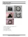
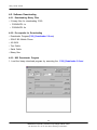
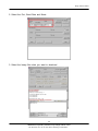
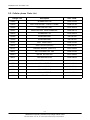
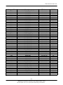
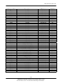
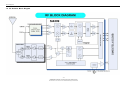
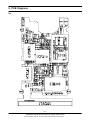
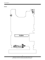
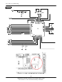
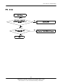
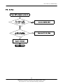
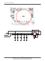
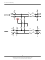
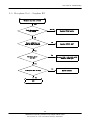
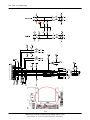
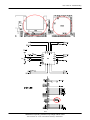
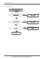
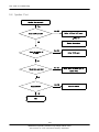
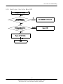
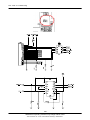
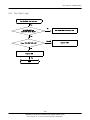
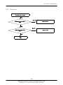
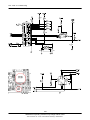
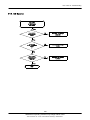
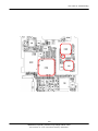
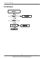
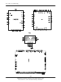
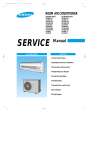
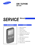
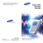
GSM TELEPHONE
SGH-C180
GSM TELEPHONE
CONTENTS
1.
Safety Precautions
2.
Specification
3.
Product Function
4.
Array course control
5.
Exploded View and Parts List
6.
MAIN Electrical Parts List
7.
Block Diagrams
8.
PCB Diagrams
9.
Flow Chart of Troubleshooting
10.
Reference data
11.
Disassembly and Assembly
Instructions
GSPN (Global Service Partner Network)
Country
North America
Latin America
CIS
Europe
China
Asia
Mideast & Africa
Web Site
service.samsungportal.com
latin.samsungportal.com
cis.samsungportal.com
europe.samsungportal.com
china.samsungportal.com
asia.samsungportal.com
mea.samsungportal.com
This Service Manual is a property of Samsung Electronics Co.,Ltd.
Any unauthorized use of Manual can be punished under applicable
International and/or domestic law.
ⓒ Samsung Electronics Co.,Ltd.
2007. 08 Rev.1.0
1. Safety Precautions
1-1. Repair Precaution
● Repair in Shield Box, during detailed tuning.
Take specially care of tuning or test, because the specification of cellular phone is sensitive for
surrounding interference(RF noise).
● Be careful to use a kind of magnetic object or tool, because performance of parts is damaged by
the influence of magnetic force.
● Surely use a standard screwdriver when you disassemble this product, otherwise screw will be
worn away.
● Use a thicken twisted wire when you measure level.
A thicken twisted wire has low resistance, therefore error of measurement is few.
● Repair after separate Test Pack and Set because for short danger (for example an
overcurrent and furious flames of parts etc) when you repair board in condition of
connecting Test Pack and tuning on.
● Take specially care of soldering, because Land of PCB is small and weak in heat.
● Surely tune on/off while using AC power plug, because a repair of battery charger is
dangerous when tuning ON/OFF PBA and Connector after disassembling charger.
● Don't use as you pleases after change other material than replacement registered on SEC System.
Otherwise engineer in charge isn't charged with problem that you don't keep this rules.
1-1
SAMSUNG Proprietary-Contents may change without notice
This Document can not be used without Samsung's authorization
Safety Precautions
1-2. ESD(Electrostatically Sensitive Devices) Precaution
Several semiconductor may be damaged easily by static electricity. Such parts are called by ESD
(Electrostatically Sensitive Devices), for example IC,BGA chip etc. Read Precaution below.
You can prevent from ESD damage by static electricity.
● Remove static electricity remained your body before you touch semiconductor or parts with
semiconductor. There are ways that you touch an earthed place or wear static electricity
prevention string on wrist.
● Use earthed soldering steel when you connect or disconnect ESD.
● Use soldering removing tool to break static electricity. , otherwise ESD will be damaged by
static electricity.
● Don't unpack until you set up ESD on product. Because most of ESD are packed by box and
aluminum plate to have conductive power,they are prevented from static electricity.
● You must maintain electric contact between ESD and place due to be set up until ESD is
connected completely to the proper place or a circuit board.
1-2
SAMSUNG Proprietary-Contents may change without notice
This Document can not be used without Samsung's authorization
2. Specification
2-1. GSM General Specification
EGSM 900
DCS1800
Fr eq. Band [MHz]
Up link/ Do wnl ink
880 ~915
925 ~960
1710~1 785
1805~1 880
ARFCN ran ge
0~124 & 975 ~1023
512~8 85
Tx/Rx spacin g
45 MHz
95MHz
Mod . Bit r ate/
Bi t Peri od
270. 833kbps
3. 692us
270.8 33kbps
3.69 2us
Time Slot Per iod /Fr ame
Per iod
576 .9us
4.61 5ms
576. 9us
4 .615ms
Mo dulat ion
0. 3GMSK
0.3G MSK
MS Power
33dBm~5dBm
30dBm~ 0dBm
Po wer Class
4
(max +33dBm)
1
(max +30dBm)
Sen sitivity
- 102d Bm
- 100dBm
TDM A M ux
8
8
Cell Radius
35 Km
2Km
2-1
SAMSUNG Proprietary-Contents may change without notice
This Document can not be used without Samsung's authorization
Specification
2-2. GSM TX power class
TX Power
control level
TX Power
GSM900
control level
DCS1800
5
33±2 dBm
0
30±3 dBm
6
31±2 dBm
1
28±3 dBm
7
29±2 dBm
2
26±3 dBm
8
27±2 dBm
3
24±3 dBm
9
25±2 dBm
4
22±3 dBm
10
23±2 dBm
5
20±3 dBm
11
21±2 dBm
6
18±3 dBm
12
19±2 dBm
7
16±3 dBm
13
17±2 dBm
8
14±3 dBm
14
15±2 dBm
9
12±4 dBm
15
13±2 dBm
10
10±4 dBm
16
11±3 dBm
11
8±4dBm
17
9±3dBm
12
6±4 dBm
18
7±3 dBm
13
4±4 dBm
19
5±3 dBm
14
2±5 dBm
15
0±5 dBm
2-2
SAMSUNG Proprietary-Contents may change without notice
This Document can not be used without Samsung's authorization
3. Operation Instruction and Installation
Main Function
S20 PIN TA
No Java
No MMS
WAP 2.0
16 Poly S/W MIDI
Dual band(900/1800MHz)
GPRS Class 10
Bluetooth
3-1
SAMSUNG Proprietary-Contents may change without notice
This Document can not be used without Samsung's authorization
Operation Instruction and Installation
3-2
SAMSUNG Proprietary-Contents may change without notice
This Document can not be used without Samsung's authorization
4. Array course control
4-1. Software Adjustments
1.
2.
3.
4.
5.
JIG Box: Download, Trace, Calibration, etc
RF test cable: RF test
TA (Travel Adaptor)
Serial cable: PC to JIG
Test cable: JIG to phone
4-1
SAMSUNG Proprietary-Contents may change without notice
This Document can not be used without Samsung's authorization
Array course control
4-2. Software Downloading
4-2-1. Downloading Binary Files
• 2 binary files for downloading C180.
– C180XAGD1.cla
– C180XAGD1..tfs
4-2-2. Pre-requsite for Downloading
• Downloader Program(C180_Downloader 2.0.exe)
• SGH-C180 Mobile Phone
• JIG BOX
• Test Cable
• Serial Cable
• Binary files
4-2-3. S/W Downloader Program
1. Load the binary download program by executing the “C180_Downloader 2.0.exe”.
4-2
SAMSUNG Proprietary-Contents may change without notice
This Document can not be used without Samsung's authorization
Array course control
2. Select the Port, Baud Rate and Mode.
3. Select the binary files what you want to download
4-3
SAMSUNG Proprietary-Contents may change without notice
This Document can not be used without Samsung's authorization
Array course control
4. Press the "Start" button and connect the Handset
5. When downloading is complete, automatically the small window was showed up..
4-4
SAMSUNG Proprietary-Contents may change without notice
This Document can not be used without Samsung's authorization
5. Exploded View and Parts List
5-1. Cellular phone Exploded View
QMW02
QFR01
QKP01
QME01
QSH08
QMO01
QSP01
QCR04
QMP01
QLC01
QAN10
QBR16
QAN02
QRE01
QRF01
QCR04
QSC01
QBA01
QBA00
5-1
SAMSUNG Proprietary-Contents may change without notice
This Document can not be used without Samsung's authorization
Exploded View and Parts List
5-2. Cellular phone Parts List
Design LOC
Description
SEC CODE
QAN02
INTENNA-SGHC180
GH42-01322A
QAN10
ASSY-CUSHION-ANT CONTACT RUBBE
GH98-01218A
QBA00
PMO-CASE BATTERY
GH72-39741A
QBA01
INNER BATTERY PACK-730MAH,BLK,
GH43-02811A
QBR16
IPR-BRACKET LID
GH70-02201A
QCR04
SCREW-MACHINE
6001-001479
QCR04
SCREW-MACHINE
6001-001479
QFR01
ASSY CASE-FRONT
GH98-04709A
QKP01
ASSY KEYPAD-(XEN/ZK)
GH98-04674C
QLC01
LCD-MAIN MODULE (SGHC170)
GH07-01085A
QME01
KEY FPCB-MAIN KEY PBA
GH59-04724A
QMO01
MOTOR DC-SGHC180
GH31-00383A
QMP01
PBA MAIN-SGHC180
GH92-03825A
QMW02
PCT-COVER MAIN WINDOW
GH72-39742A
QRE01
ASSY CASE-REAR
GH98-04711A
QRF01
PMO-COVER RF
GH72-38552A
QSC01
RMO-SCREW CAP
GH73-09347A
QSH08
ASSY CASE-BELT
GH98-04710A
QSP01
SPEAKER
3001-002214
5-2
SAMSUNG Proprietary-Contents may change without notice
This Document can not be used without Samsung's authorization
Exploded View and Parts List
Description
SEC CODE
BAG PE
ADAPTOR-ATADS10EBE,BLK,EU
LABEL(P)-UNIT SEAL
LABEL(P)-IMEI
LABEL(R)-WATER SOAK
LABEL(R)-MAIN(EU)
MANUAL USERS-EU FRENCH
BOX-UNIT(EU)
PMO COVER-EAR
TAPE INSU-PCB CONN
TAPE INSU
TAPE INSU-PCB
TAPE GASK-KEY FPCB 1
TAPE GASK-KEY FPCB 2
6902-000634
GH44-01702A
GH68-00518B
GH68-01335D
GH68-09361A
GH68-15413A
GH68-15639A
GH69-05639A
GH72-42756A
GH74-33536A
GH74-33822A
GH74-33994A
GH74-34731A
GH74-34732A
5-3
SAMSUNG Proprietary-Contents may change without notice
This Document can not be used without Samsung's authorization
Exploded View and Parts List
5-4
SAMSUNG Proprietary-Contents may change without notice
This Document can not be used without Samsung's authorization
6. MAIN Electrical Parts List
Design LOC
Description
SEC Code
STATUS
ANT100
ANT101
ANT102
BTC300
C100
C101
C103
C104
C105
C106
C107
C108
C109
C110
C111
C112
C113
C114
C115
C116
C117
C118
C119
C120
C121
C122
C123
C124
C126
C127
C128
C129
C130
C131
C132
C133
C134
C136
C200
C201
C202
C203
C204
C205
C206
C207
C208
C209
C210
C211
C212
C214
C215
NPR-ANTENNA CONTACT
NPR-ANTENNA CONTACT
ANTENNA-CHIP
HEADER-BATTERY
R-CHIP
C-CER,CHIP
C-CER,CHIP
C-CER,CHIP
C-CER,CHIP
C-CER,CHIP
C-CER,CHIP
C-CER,CHIP
C-CER,CHIP
C-CER,CHIP
C-CER,CHIP
C-TA,CHIP
C-CER,CHIP
C-CER,CHIP
C-CER,CHIP
C-CER,CHIP
C-CER,CHIP
C-CER,CHIP
C-CER,CHIP
C-CER,CHIP
C-CER,CHIP
C-CER,CHIP
C-CER,CHIP
C-CER,CHIP
C-CER,CHIP
C-CER,CHIP
C-CER,CHIP
C-CER,CHIP
C-CER,CHIP
C-CER,CHIP
C-CER,CHIP
C-CER,CHIP
INDUCTOR-SMD
C-CER,CHIP
C-CER,CHIP
C-CER,CHIP
C-CER,CHIP
C-CER,CHIP
C-CER,CHIP
C-CER,CHIP
C-CER,CHIP
C-CER,CHIP
C-CER,CHIP
C-CER,CHIP
C-CER,CHIP
C-CER,CHIP
C-CER,CHIP
C-CER,CHIP
C-CER,CHIP
GH71-06419A
GH71-06419A
4202-001366
3711-006217
2007-000171
2203-000995
2203-005234
2203-006048
2203-006194
2203-006194
2203-006194
2203-006194
2203-005729
2203-005052
2203-006048
2404-001496
2203-006423
2203-006620
2203-000359
2203-005682
2203-005682
2203-005052
2203-000278
2203-006423
2203-000278
2203-005482
2203-005234
2203-005234
2203-002677
2203-000278
2203-000254
2203-002677
2203-005482
2203-000278
2203-006681
2203-006562
2703-001178
2203-005393
2203-005482
2203-005482
2203-005482
2203-005482
2203-000254
2203-005482
2203-005482
2203-000254
2203-000254
2203-005482
2203-000854
2203-000679
2203-005482
2203-005482
2203-005482
SA
SA
SA
SA
SA
SA
SA
SA
SA
SA
SA
SA
SA
SA
SA
SA
SA
SNA
SA
SA
SA
SA
SA
SA
SA
SA
SA
SA
SA
SA
SA
SA
SA
SA
SA
SA
SA
SA
SA
SA
SA
SA
SA
SA
SA
SA
SA
SA
SA
SA
SA
SA
SA
6-1
SAMSUNG Proprietary-Contents may change without notice
This Document can not be used without Samsung's authorization
Main Electrical Parts List
Design LOC
Description
SEC Code
STATUS
C216
C219
C300
C301
C302
C303
C304
C306
C307
C308
C310
C311
C312
C313
C314
C315
C316
C317
C318
C319
C320
C321
C322
C323
C324
C325
C327
C401
C402
C403
C407
C409
C410
C411
C413
C414
C417
C418
C420
C423
C424
C425
C426
C500
C501
C502
C503
C504
C505
C506
C507
C508
CAN100
C-CER,CHIP
C-CER,CHIP
C-CER,CHIP
C-CER,CHIP
C-CER,CHIP
C-CER,CHIP
C-CER,CHIP
C-CER,CHIP
C-CER,CHIP
C-CER,CHIP
C-CER,CHIP
C-CER,CHIP
C-CER,CHIP
C-CER,CHIP
C-CER,CHIP
C-CER,CHIP
C-CER,CHIP
C-CER,CHIP
C-CER,CHIP
C-CER,CHIP
C-CER,CHIP
C-CER,CHIP
C-CER,CHIP
C-CER,CHIP
C-CER,CHIP
C-CER,CHIP
C-CER,CHIP
C-CER,CHIP
C-CER,CHIP
C-CER,CHIP
C-CER,CHIP
C-CER,CHIP
C-CER,CHIP
C-CER,CHIP
C-CER,CHIP
C-CER,CHIP
C-CER,CHIP
C-CER,CHIP
C-CER,CHIP
C-CER,CHIP
C-CER,CHIP
C-CER,CHIP
C-CER,CHIP
C-CER,CHIP
C-CER,CHIP
C-CER,CHIP
C-CER,CHIP
C-CER,CHIP
C-CER,CHIP
C-CER,CHIP
C-CER,CHIP
C-CER,CHIP
IPR-BRACKET FRAME
2203-006048
2203-005482
2203-000425
2203-006681
2203-006348
2203-000425
2203-000679
2203-000812
2203-005482
2203-006348
2203-007165
2203-006257
2203-006562
2203-007165
2203-006257
2203-006556
2203-007165
2203-006839
2203-005682
2203-005682
2203-006257
2203-006257
2203-007165
2203-006257
2203-006257
2203-005482
2203-002709
2203-005482
2203-000854
2203-005482
2203-000679
2203-005482
2203-000386
2203-006562
2203-000550
2203-000995
2203-005482
2203-000386
2203-000425
2203-000425
2203-006562
2203-006562
2203-006260
2203-006562
2203-006562
2203-000812
2203-000311
2203-006562
2203-006562
2203-006377
2203-006562
2203-006562
GH70-02200A
SA
SA
SA
SA
SA
SA
SA
SA
SA
SA
SA
SA
SA
SA
SA
SA
SA
SA
SA
SA
SA
SA
SA
SA
SA
SA
SA
SA
SA
SA
SA
SA
SA
SA
SA
SA
SA
SA
SA
SA
SA
SA
SA
SA
SA
SA
SA
SA
SA
SA
SA
SA
SA
6-2
SAMSUNG Proprietary-Contents may change without notice
This Document can not be used without Samsung's authorization
Main Electrical Parts List
Design LOC
Description
SEC Code
STATUS
CN500
D200
D300
D400
D401
D402
D403
D404
D500
D501
D502
D503
D504
D505
F100
F101
F500
F501
F502
IFC400
L101
L102
L104
L105
L107
L108
L109
L110
L111
L112
L113
L400
L401
L402
L403
L404
L405
L406
L407
L408
L409
L501
L502
L503
OSC100
OSC101
OSC300
PAM100
Q300
Q401
R100
R103
R104
CONNECTOR-FPC/FFC/PIC
DIODE-TVS
DIODE-TVS
DIODE-TVS
DIODE-TVS
DIODE-TVS
DIODE-TVS
DIODE-TVS
DIODE-ARRAY
DIODE-TVS
DIODE-TVS
DIODE-TVS
DIODE-TVS
DIODE-TVS
FILTER-SAW
FILTER-LC
FILTER-EMI SMD
FILTER-EMI/ESD
FILTER-EMI/ESD
SOCKET-INTERFACE
INDUCTOR-SMD
INDUCTOR-SMD
INDUCTOR-SMD
INDUCTOR-SMD
INDUCTOR-SMD
INDUCTOR-SMD
INDUCTOR-SMD
INDUCTOR-SMD
INDUCTOR-SMD
INDUCTOR-SMD
INDUCTOR-SMD
INDUCTOR-SMD
INDUCTOR-SMD
BEAD-SMD
BEAD-SMD
BEAD-SMD
BEAD-SMD
BEAD-SMD
BEAD-SMD
BEAD-SMD
BEAD-SMD
BEAD-SMD
INDUCTOR-SMD
BEAD-SMD
CRYSTAL-SMD
CRYSTAL-SMD
CRYSTAL-SMD
IC-POWER AMP
TR-SMALL SIGNAL
TR-DIGITAL
C-CER,CHIP
R-CHIP
R-CHIP
3708-002222
0406-001231
0406-001231
0406-001231
0406-001231
0406-001231
0406-001231
0406-001231
0407-001002
0406-001231
0406-001231
0406-001231
0406-001231
0406-001231
2904-001731
2909-001283
2901-001329
2901-001450
2901-001450
3710-002534
2703-001750
2703-001750
2703-002203
2703-002313
2703-002204
2703-002558
2703-002198
2703-002558
2703-003277
2703-002281
2703-002170
2703-002206
2703-002206
3301-001729
3301-001729
3301-001729
3301-001729
3301-001729
3301-001729
3301-001729
3301-001729
3301-001729
2703-002308
3301-001729
2801-004455
2801-004560
2801-004339
1201-002364
0501-002571
0504-001197
2203-005393
2007-003015
2007-001339
SA
SA
SA
SA
SA
SA
SA
SA
SA
SA
SA
SA
SA
SA
SA
SA
SA
SA
SA
SA
SA
SA
SA
SA
SA
SA
SA
SA
SA
SA
SA
SA
SA
SA
SA
SA
SA
SA
SA
SA
SA
SA
SA
SA
SA
SA
SA
SA
SA
SA
SA
SA
SA
6-3
SAMSUNG Proprietary-Contents may change without notice
This Document can not be used without Samsung's authorization
Main Electrical Parts List
Design LOC
Description
SEC Code
STATUS
R105
R107
R108
R111
R123
R128
R130
R131
R133
R200
R201
R202
R203
R204
R205
R206
R207
R208
R209
R210
R211
R212
R213
R214
R215
R216
R217
R218
R219
R220
R222
R223
R226
R227
R300
R301
R305
R306
R307
R309
R310
R311
R400
R401
R402
R405
R406
R419
R422
R423
R425
R426
R427
R-CHIP
C-CER,CHIP
R-CHIP
R-CHIP
R-CHIP
R-CHIP
R-CHIP
R-CHIP
INDUCTOR-SMD
R-CHIP
R-CHIP
R-CHIP
R-CHIP
R-CHIP
R-CHIP
R-CHIP
R-CHIP
R-CHIP
R-CHIP
R-CHIP
R-CHIP
R-CHIP
R-CHIP
R-CHIP
R-CHIP
R-CHIP
R-CHIP
R-CHIP
R-CHIP
R-CHIP
R-CHIP
R-CHIP
R-CHIP
R-CHIP
R-CHIP
R-CHIP
R-CHIP
R-CHIP
R-CHIP
R-CHIP
R-CHIP
R-CHIP
R-CHIP
R-CHIP
R-CHIP
R-CHIP
R-CHIP
R-CHIP
R-CHIP
R-CHIP
R-CHIP
R-CHIP
R-CHIP
2007-000157
2203-002668
2007-000155
2007-008052
2007-000171
2007-003025
2007-001316
2007-001316
2703-002207
2007-000174
2007-000171
2007-000162
2007-007141
2007-007107
2007-000159
2007-008055
2007-008055
2007-008055
2007-008055
2007-007142
2007-000171
2007-000162
2007-000162
2007-000162
2007-007107
2007-000162
2007-007001
2007-000141
2007-000141
2007-000143
2007-000157
2007-000162
2007-000162
2007-000162
2007-007100
2007-007869
2007-000162
2007-001339
2007-000758
2007-007573
2007-007334
2007-000170
2007-000148
2007-000141
2007-000141
2007-000141
2007-000141
2007-000159
2007-007107
2007-001339
2007-001339
2007-007142
2007-008531
SA
SA
SA
SA
SA
SA
SA
SA
SA
SA
SA
SA
SA
SA
SA
SA
SA
SA
SA
SA
SA
SA
SA
SA
SA
SA
SA
SA
SA
SA
SA
SA
SA
SA
SA
SA
SA
SA
SA
SA
SA
SA
SA
SA
SA
SA
SA
SA
SA
SA
SA
SA
SA
6-4
SAMSUNG Proprietary-Contents may change without notice
This Document can not be used without Samsung's authorization
Main Electrical Parts List
Design LOC
Description
SEC Code
STATUS
R428
R429
R430
R433
R434
R437
R438
R439
R440
R442
R444
R446
R448
R449
R500
R501
R502
R503
R504
R507
RFS400
SIM300
TA300
TA301
TA302
TA400
TA401
TA500
TH200
U100
U101
U102
U300
U401
U402
U403
U404
U500
U501
U502
U503
U504
UCP200
UME200
ZD300
ZD301
ZD400
ZD401
ZD403
ZD500
ZD503
ZD504
R-CHIP
R-CHIP
R-CHIP
R-CHIP
R-CHIP
R-CHIP
R-CHIP
R-CHIP
R-CHIP
R-CHIP
R-CHIP
R-CHIP
R-CHIP
R-CHIP
R-CHIP
R-CHIP
R-CHIP
R-CHIP
R-CHIP
R-CHIP
CONNECTOR-COAXIAL
CONNECTOR-CARD EDGE
C-TA,CHIP
C-TA,CHIP
C-TA,CHIP
C-TA,CHIP
C-TA,CHIP
C-TA,CHIP
THERMISTOR-NTC
IC-DATA COMM./GEN.
IC-ANALOG MULTIPLEX
IC-TRANSCEIVER
IC-POWER SUPERVISOR
IC-ANALOG MULTIPLEX
FET-SILICON
IC-AUDIO AMP
FILTER-EMI/ESD
IC-POSI.FIXED REG.
IC-DC/DC CONVERTER
FET-SILICON
C-CER,CHIP
C-CER,CHIP
IC-COMM. CONTROLLER
IC-MCP
DIODE-ZENER
DIODE-ZENER
DIODE-TVS
DIODE-TVS
DIODE-TVS
DIODE-TVS
DIODE-TVS
DIODE-TVS
2007-007142
2007-000162
2007-000171
2007-000159
2007-008531
2007-007107
2007-001339
2007-000171
2007-000171
2007-001217
2007-001217
2007-000172
2007-000172
2007-007107
2007-000157
2007-000162
2007-000140
2007-000171
2007-000157
2007-000148
3705-001358
3709-001391
2404-001381
2404-001381
2404-001381
2404-001377
2404-001396
2404-001381
1404-001221
1205-003064
1001-001447
1205-003278
1203-004550
1001-001349
0505-001923
1201-002494
2901-001349
1203-003737
1203-003708
0505-001469
2203-000854
2203-000995
1205-003192
1108-000059
0403-001340
0403-001547
0406-001197
0406-001231
0406-001231
0406-001267
0406-001241
0406-001241
SA
SA
SA
SA
SA
SA
SA
SA
SA
SA
SA
SA
SA
SA
SA
SA
SA
SA
SA
SA
SA
SA
SA
SA
SA
SA
SA
SA
SA
SA
SA
SA
SA
SA
SA
SA
SA
SA
SA
SA
SA
SA
SA
SA
SA
SA
SA
SA
SA
SA
SA
SA
6-5
SAMSUNG Proprietary-Contents may change without notice
This Document can not be used without Samsung's authorization
Main Electrical Parts List
6-6
SAMSUNG Proprietary-Contents may change without notice
This Document can not be used without Samsung's authorization
7. Block Diagrams
7-1. Main Block Diagram
7-1
SAMSUNG Proprietary-Contents may change without notice
This Document can not be used without Samsung's authorization
Block Diagrams
7-2. RF Solution Block Diagram
7-2
SAMSUNG Proprietary-Contents may change without notice
This Document can not be used without Samsung's authorization
8. PCB Diagrams
Top
8-1
SAMSUNG Proprietary-Contents may change without notice
This Document can not be used without Samsung's authorization
PCB Diagrams
Bottom
8-2
SAMSUNG Proprietary-Contents may change without notice
This Document can not be used without Samsung's authorization
9. Flow Chart of Troubleshooting
9-1. Power On
Power on does not work
Yes
Not OK
Check battery voltage
is more than 3.3
Change battery
OK
No
Check the 'Vcc_SYN' of
U102 = 2.8V
Resolder PMIC or U102
Yes
Not OK
Check the pin 1, 3 of
OSC100 are clock signals.
Resolder OSC100
OK
Not OK
Check the pin 7 of
U102 is 13M pluse signal
Resolder OSC100, U102, C128
OK
No
Is Power On working?
Repeat sequence
Yes
END
9-1
SAMSUNG Proprietary-Contents may change without notice
This Document can not be used without Samsung's authorization
Flow Chart of Troubleshooting
Power On
9-2
SAMSUNG Proprietary-Contents may change without notice
This Document can not be used without Samsung's authorization
Flow Chart of Troubleshooting
9-2. Initial
Initial Failure
Yes
Check VDD1, VDD3=1.8V,
VDD2=2.9V and AVDD=2.6V of
UCP 200
No
Check the U300
Yes
No
Check the 'D_REF_13M'
of UCP 200
Check the U102, POWER ON Sequence
Yes
END
9-3
SAMSUNG Proprietary-Contents may change without notice
This Document can not be used without Samsung's authorization
Flow Chart of Troubleshooting
9-4
SAMSUNG Proprietary-Contents may change without notice
This Document can not be used without Samsung's authorization
Flow Chart of Troubleshooting
9-3. Sim Part
"Insert SIM" is displayed on the LCD
The voltage is 2.8V
No
at the pin#1 SIM300
Check the UCP200, C316
Yes
Is there any signal
pin #2,3,4 of SIM300?
No
Check the UCP 200, U300
Yes
Check the SIM Card
END
9-5
SAMSUNG Proprietary-Contents may change without notice
This Document can not be used without Samsung's authorization
Flow Chart of Troubleshooting
9-6
SAMSUNG Proprietary-Contents may change without notice
This Document can not be used without Samsung's authorization
Flow Chart of Troubleshooting
9-4. Microphone Part - Phone MIC
Phone mic. does not work
Yes
Not OK
Check the connection
from MIC
Resolder MIC
OK
Not OK
Check the circuit
OF MIC_BIAS part
Resolder TA400, R405, R406
OK
Not OK
Check the circuit
of MIC part
Resolder C413, C409, C417, L404,
L405, R407
OK
No
Is Phone MIC working?
Replace MIC
Yes
END
9-7
SAMSUNG Proprietary-Contents may change without notice
This Document can not be used without Samsung's authorization
Flow Chart of Troubleshooting
9-8
SAMSUNG Proprietary-Contents may change without notice
This Document can not be used without Samsung's authorization
Flow Chart of Troubleshooting
9-5. Microphone Part - Earphone MIC
Earphone mic. does not work
Yes
Not OK
Check the connection
from IFC400
Resolder IFC400 pin 3,4
OK
No
Check JACK IN is low
when ear jack is inserted.
Resolder IFC400, R427
Yes
No
Check the circuit
EAR MIC
Resolder C401, C403, L402, L403,
R400 and C402 again
Yes
No
Is Earphone MIC working?
Repeat sequence
Yes
END
9-9
SAMSUNG Proprietary-Contents may change without notice
This Document can not be used without Samsung's authorization
Flow Chart of Troubleshooting
9-10
SAMSUNG Proprietary-Contents may change without notice
This Document can not be used without Samsung's authorization
Flow Chart of Troubleshooting
9-6. Earphone Part
Earphone does not work
Yes
Not OK
Check the circuit
of IFC400
Solder pin 5,6 of IFC400
, L408, L409 again
OK
Not OK
Check the voltages of
R422, R423, R424, R438
and R449 are 2.9V
Solder R422, R423, R424, R438 and
R449 again
OK
Not OK
Check the circuit
U401
Check R444
No
OK
Check UCP200 or Change UCP200
Is JACK_INT signal
LOW?
(When UCP200 operates)
No
Solder R427 again
Yes
Not OK
Solder U404 again
Check EAR SW
Ok
END
9-11
SAMSUNG Proprietary-Contents may change without notice
This Document can not be used without Samsung's authorization
Flow Chart of Troubleshooting
9-12
SAMSUNG Proprietary-Contents may change without notice
This Document can not be used without Samsung's authorization
Flow Chart of Troubleshooting
9-13
SAMSUNG Proprietary-Contents may change without notice
This Document can not be used without Samsung's authorization
Flow Chart of Troubleshooting
9-7. Charging Part
Abnormal charging operation
Yes
Not OK
Check the 32 Pin and
33 Pin of U300
Replace the U300
OK
Not OK
Check Q300 (E,B,C)
Replace the Q300
OK
Not OK
Check R301
Solder R301 again or change a
battery
OK
END
9-14
SAMSUNG Proprietary-Contents may change without notice
This Document can not be used without Samsung's authorization
Flow Chart of Troubleshooting
9-15
SAMSUNG Proprietary-Contents may change without notice
This Document can not be used without Samsung's authorization
Flow Chart of Troubleshooting
9-8. Speaker Part
Speaker does not work
Yes
Not OK
Solder L400 and L401 again
Check L400 and L401
Not OK
OK
Replace the speaker
Not OK
Check the pin #5, #8
of U403
Solder U403 again
OK
Not OK
Check R444 and R446
Solder R444 and R446 again or
replace U401
OK
Not OK
Replace UCP200
Check UCP200
OK
END
9-16
SAMSUNG Proprietary-Contents may change without notice
This Document can not be used without Samsung's authorization
Flow Chart of Troubleshooting
9-17
SAMSUNG Proprietary-Contents may change without notice
This Document can not be used without Samsung's authorization
Flow Chart of Troubleshooting
9-9. Key Data Input
Check Initial Operation
Yes
No
When one of the keys is
pushed,
is it displayed on LCD?
Check the Dome sheet & Key FPCB
Yes
No
When one of the keys is
pushed,
KEYSENSE(0)~(4),KYPD9~1
7
Replace the PBA
Yes
END
9-18
SAMSUNG Proprietary-Contents may change without notice
This Document can not be used without Samsung's authorization
Flow Chart of Troubleshooting
9-10. Back Light (for Color Main LCD)
Backlight does not work
Yes
No
Is BACKLIGHT set
AlwaysON in the Menu?
Set BACKLIGHT on Always ON
Yes
Check the outflow voltage
of U501 (PIN 5)
Not OK
Replace U501
OK
Replace the LCD Module
Yes
END
9-19
SAMSUNG Proprietary-Contents may change without notice
This Document can not be used without Samsung's authorization
Flow Chart of Troubleshooting
9-20
SAMSUNG Proprietary-Contents may change without notice
This Document can not be used without Samsung's authorization
Flow Chart of Troubleshooting
9-11. Key Back Light
key Backlight does not work
Yes
No
Is BACKLIGHT set
AlwaysON in the Menu?
Set BACKLIGHT on Always ON
Yes
Not OK
Replace U300
Check VCC_KEY_LED_3.2V
OK
Replace LED
Yes
END
9-21
SAMSUNG Proprietary-Contents may change without notice
This Document can not be used without Samsung's authorization
Flow Chart of Troubleshooting
9-22
SAMSUNG Proprietary-Contents may change without notice
This Document can not be used without Samsung's authorization
Flow Chart of Troubleshooting
9-12. Bluetooth
Bluetooth does not work
Yes
Not OK
Check the pin D4, B5 of
U100
Replace U100
OK
Not OK
Check the pin #2, 10 of
U101
Replace U101
OK
END
9-23
SAMSUNG Proprietary-Contents may change without notice
This Document can not be used without Samsung's authorization
Flow Chart of Troubleshooting
9-24
SAMSUNG Proprietary-Contents may change without notice
This Document can not be used without Samsung's authorization
Flow Chart of Troubleshooting
9-15. GSM Receiver
RX ON
RF INPUT=62CH
AMP=-50dBm
Yes
Check PAM100
pin 20(EGSMRX)
≥-65dBm
No
Resolder or Change
PAM100
No
Resolder or Change
F100
No
Resolder or Change
UCP200
Yes
Check U102
pin 17, 18 (EGSMRX)
≥-65dBm
>
Yes
Check UCP200
MOD_STANDBY=HIGH
PON_PA=LOW
BAND=LOW
Yes
END
9-25
SAMSUNG Proprietary-Contents may change without notice
This Document can not be used without Samsung's authorization
Flow Chart of Troubleshooting
9-26
SAMSUNG Proprietary-Contents may change without notice
This Document can not be used without Samsung's authorization
Flow Chart of Troubleshooting
9-27
SAMSUNG Proprietary-Contents may change without notice
This Document can not be used without Samsung's authorization
Flow Chart of Troubleshooting
9-15. GSM Transmitter
TX ON (5Level)
Yes
No
PAM100 Pin16
Resolder PAM100
(TX MODULE)
≥ 30dBm
Yes
PAM100 pin11
≥ 20dBm
Yes
Check UCP200
No
Resolder U102
(TRANSCEIVER)
Yes
END
9-28
SAMSUNG Proprietary-Contents may change without notice
This Document can not be used without Samsung's authorization
Flow Chart of Troubleshooting
9-29
SAMSUNG Proprietary-Contents may change without notice
This Document can not be used without Samsung's authorization
Flow Chart of Troubleshooting
9-30
SAMSUNG Proprietary-Contents may change without notice
This Document can not be used without Samsung's authorization
Flow Chart of Troubleshooting
9-16. DCS Receiver
RX ON
RF INPUT=698CH
AMP=-50dBm
Yes
Check PAM100
pin 16(DCSRX)
≥-65dBm
No
Resolder or Change
PAM100
No
Resolder or Change
F100
No
Resolder or Change
UCP200
Yes
Check U102
pin 15, 16 (DCSRX)
≥-65dBm
>
Yes
Check UCP200
MOD_STANDBY= "HIGH"
PON_PA= "LOW"
BAND= "HIGH"
Yes
END
9-31
SAMSUNG Proprietary-Contents may change without notice
This Document can not be used without Samsung's authorization
Flow Chart of Troubleshooting
9-32
SAMSUNG Proprietary-Contents may change without notice
This Document can not be used without Samsung's authorization
Flow Chart of Troubleshooting
9-33
SAMSUNG Proprietary-Contents may change without notice
This Document can not be used without Samsung's authorization
Flow Chart of Troubleshooting
9-17. DCS Transmitter
TX ON (5Level)
Resolder PAM100
(TX MODULE)
PAM100 Pin12
≥ 30dBm
PAM100 pin1
≥ 20dBm
Check UCP200
Resolder U100
(TRANSCEIVER)
END
9-34
SAMSUNG Proprietary-Contents may change without notice
This Document can not be used without Samsung's authorization
Flow Chart of Troubleshooting
9-35
SAMSUNG Proprietary-Contents may change without notice
This Document can not be used without Samsung's authorization
Flow Chart of Troubleshooting
9-36
SAMSUNG Proprietary-Contents may change without notice
This Document can not be used without Samsung's authorization
10. Reference data
Reference Abbreviate
― ARFCN : Absolute Radio Frequency Channel Number
― BER : Bit Error Rate
― BPSK: Binary Phase Shift Keying
― ESD : Electrostatically Sensitive Devices
― ETSI: European Telecommunications Standards Institute
― MS: Mobile Station
― QPSK: Quadrature Phase Shift Keying
― RF : Radio Frequency
― TDMA : Time Division Multiple Access
10-1
SAMSUNG Proprietary-Contents may change without notice
This Document can not be used without Samsung's authorization
Reference data
10-2
SAMSUNG Proprietary-Contents may change without notice
This Document can not be used without Samsung's authorization