1
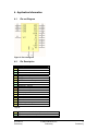
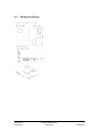
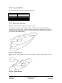
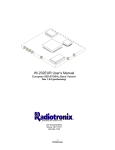
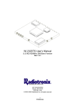
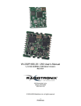
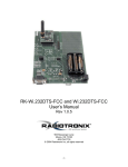
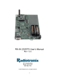
Wi.232DTS User’s Manual
Rev 1.0
Embedding the wireless
207 Industrial Blvd
Moore, OK 73170
405-794-7730
© 2002 Radiotronix Inc, all rights reserved
-i–
Preliminary
1. Document Control
Steve Montgomery
Created By
12/9/03
Engineering Review
Marketing Review
Approved Engineering
Approved - Marketing
Revision
1.0
1.1
Author
SJM
SJM
Date
12/9/03
12/11/03
Description
Document Created
-Updated DATARATE table to include 38.4kbit/sec
-Corrected 4.10 – CMD should be held high to force factory
defaults after reset
- ii –
Preliminary
2. Introduction
Module Overview
TRANSMITTER
BASEBAND DSP
ANTENNA SWITCH
COMBINER
UART
CONTROL
ANTENNA
VCO
PROTOCOL
CONTROLLER
2.1.
ANALOG IN
DIGITAL I/O
DATA
RECEIVER
LEGEND
HARDWARE IN WISE
Wi.232 APPLICATION
SOFTWARE IN WISE
WiSE MAC
SERIAL INTERFACE
WiSE PACKET
I/O INTERFACE
HAL
Figure 1: Wi.232DTS Block Diagram
2.2.
•
•
•
•
•
•
•
•
•
Features
True UART to antenna solution
16-bit CRC error checking
Data encryption/encoding for PGP
152.34kbit/sec maximum RF data rate
32 channels in DTS mode
84 channels in low-power mode
Small size – .8” x .935” .08”
Low power active standby mode
PHY and MAC layer protocol built in
2.3.
•
•
•
•
•
•
•
•
CSMA medium access control
Channel QOS indicator
114dB link budget in DTS mode
2 mode allow user to optimize power/range
Command mode
48-bit unique MAC address
5 volt tolerant I/O
Under $20 in production quantities
Applications
•
Direct RS-232/422/485 wire
replacement
•
Industrial/Home Automation
•
•
RFID
Asset Tracking
•
•
Wireless Sensors
Automated Meter Reading
•
Remote Data Logging
Wi.232DTS
Preliminary
© 2003 Radiotronix Inc.
Preliminary
2
Preliminary
Table of Contents
Document Control................................................................................................................. 2
Introduction ........................................................................................................................... 2
2.1. Module Overview .............................................................................................................. 2
2.2. Features ............................................................................................................................ 2
2.3. Applications....................................................................................................................... 2
Table of Contents ............................................................................................................................ 3
Table of Figures............................................................................................................................... 3
3.
Theory of Operation.............................................................................................................. 4
4.
Application Information ......................................................................................................... 6
4.1. Pin-out Diagram ................................................................................................................ 6
4.2. Pin Description .................................................................................................................. 6
4.3. Mechanical Drawing.......................................................................................................... 7
4.4. Example Circuit ................................................................................................................. 8
4.5. Power Supply .................................................................................................................... 8
4.6. UART Interface ................................................................................................................. 8
4.7. Operating Mode ................................................................................................................ 9
4.7.1. DTS Mode.................................................................................................................. 9
4.7.2. Low power Mode...................................................................................................... 10
4.7.3. Active state operation .............................................................................................. 10
4.7.4. Active Standby Mode ............................................................................................... 11
4.8. Link budget, transmit power, and range performance .................................................... 12
4.9. Channel settings ............................................................................................................. 13
4.10.
UART Data Rate.......................................................................................................... 13
4.11.
RF Data Rate............................................................................................................... 14
4.12.
Transmit Wait Timeout ................................................................................................ 14
4.13.
Data Encoding ............................................................................................................. 15
4.14.
QOS............................................................................................................................. 15
4.15.
Programming Registers............................................................................................... 15
4.16.
Antenna ....................................................................................................................... 17
5.
Electrical Specifications ...................................................................................................... 18
5.1. Absolute Maximum Ratings ............................................................................................ 18
5.2. Detailed Electrical Specifications .................................................................................... 18
5.2.1. AC Specifications – RX............................................................................................ 18
5.2.2. AC Specifications – TX ............................................................................................ 19
5.2.3. DC Specifications..................................................................................................... 19
6.
Custom Applications ........................................................................................................... 19
7.
Ordering Information........................................................................................................... 20
8.
Contact Us .......................................................................................................................... 20
8.1. Technical Support ........................................................................................................... 20
8.2. Sales Support.................................................................................................................. 20
1.
2.
Table of Figures
Figure 1: Wi.232DTS Block Diagram............................................................................................... 2
Figure 3: Pin-out diagram ................................................................................................................ 6
Figure 4: Example Circuit ................................................................................................................ 8
Wi.232DTS
Preliminary
© 2003 Radiotronix Inc.
Preliminary
3
Preliminary
3. Theory of Operation
The Wi.232 module combines a state-of-the-art DTS/FSK data transceiver and a highperformance protocol controller to create a transparent UART-to-antenna wireless solution
capable of direct wire replacement in any embedded application.
The module is designed to interface directly to a host UART. Three signals are used to transfer
data between the module and the host UART: TXD, RXD, and CTS. TXD is the data output from
the module RXD is the data input to the module. CTS is an output that indicates the status of the
module’s data interface. If CTS is low, the module is ready to accept data. If CTS is high, the
module is busy and the host UART should not send any further data.
When data transfers are small (<20 bytes) and infrequent (<1 transmission/second), the CTS line
does not need to be monitored. However, if these conditions are not met, the host UART should
strictly monitor the CTS line.
Internally, the module has a 64 byte buffer for incoming characters from the host UART. When
the buffer has reached 62 characters, the CTS line goes high, indicating to the host UART not to
send any more characters. Once that buffer level is reached, the data is sent to the WiSE™ MAC
layer so that it can be transmitted over the wireless link.
When the first character of the input buffer is received, the module will start a timer. The timer is
preloaded with the value of regTXTO and counts down once every millisecond. If that timer counts
to 0 before the buffer is full, the module will send whatever is the buffer to the MAC layer for
transmission. The countdown value should be set to the time it takes to send the amount of data
required by the application plus 2 bytes. For example, if the application only needs to send 10
bytes of information per transmission, and the UART data rate is 1200 bits/second, the timeout
should be set to 80 mSec (see section 3.12 for details on how to calculate regTXTO).
Internally, two alternating buffers are used to receive incoming UART data and to transmit the
data over the wireless link. Therefore, the module can continue to receive data from the UART
interface even when the module is transmitting a packet.
When the MAC layer has a packet to send, it will use a carrier-sense-multiple-access (CSMA)
protocol to determine if another
module is already transmitting. If
another module is transmitting, the
module will receive that data before
attempting to transmit its data again.
If, during this process, the UART
receive buffer gets full, the CTS line
will go high to prevent the host
UART from over-running the receive
buffer.
DATA OUT
Wi.232
Module
Wi.232
Module
DATA OUT
DATA IN
DATA OUT
Wi.232
Module
DATA OUT
DATA OUT
Wi.232
Module
DATA OUT
DATA IN
Figure 2: Wi.232 Network Concept
Wi.232DTS
Preliminary
© 2003 Radiotronix Inc.
Preliminary
The MAC layer prefixes the data
with a packet header and postfixes
the data with a 16-bit CRC. Data is
encoded using a proprietary
algorithm to spread the RF energy
equally within the transmission
bandwidth. Additionally, a 256-bit
key can be used to further encrypt
the data. The encryption algorithm
4
Preliminary
is simple and is good for PGP. If a higher level of security is required, it is recommended that the
user encrypt the data with an appropriate algorithm before it is sent to the module.
When a module transmits a packet, all other modules on the same channel will receive the
packet, check the packet for errors, decrypt the data if necessary, and send the error free data
their host UARTs for processing. The modules only implement the ISO reference network stack
up to the MAC layer, so they do not recognize any addressing schemes. Therefore, the modules
can work with any link-layer and higher protocols in existing today.
Certain features of the module are controlled through programmable volatile and non-volatile
registers. Registers are access by bringing CMD high. When CMD is high, all data transfers
from the host UART are considered to be register access commands. When CMD is low, all data
transfers from the host UART are considered to be raw data that needs to be transparently
transmitted across the wireless link.
The UART interface is capable of operating in full duplex at baud rates from 1.2 kbit/sec to 115.2
kbit/sec.
The module has three modes of operation: DTS, low-power, and active standby.
The Wi.232DTS module is the first module in the world to take advantage of the DTS provision in
FCC part 15 rules. Under this provision, transmitters can operate at a higher output power if the
transmission bandwidth is at least 500kHz. Through an encoding technique we call
DirectSPREAD™, the Wi.232DTS module is able to operate at +12dBm and meet the
requirements of this provision.
In DTS mode, the module’s channel bandwidth is set to 600kHz and the transmit power is set to
+12dBm. In this mode, the module can operate on 32 channels and support a maximum RF data
rate of 152.34kbit/second. The receiver sensitivity at the max data rate is –102dBm, yielding a
link budget of 114dB. This mode is an excellent alternative to frequency hopping spread
spectrum. It has very fast synchronization, allowing it to operate in a duty-cycle mode for
extended battery life.
In low-power mode, the module’s channel bandwidth is set to 200kHz and the transmit power is
set to 0dBm. In this mode, the module can operate on 84 channels and support a maximum data
rate of 38.4 kbit/second. The receiver sensitivity at the maximum data rate is –107, yielding a link
budget of 107dB. This mode reduces transmit current consumption, allowing use with batteries
than cannot supply the pulse currents required for DTS mode. The range in this mode will be a
little less than half of the range in DTS mode.
In active-standby mode, the module spends most of its time sleeping. It will wake up when there
is data to transmit or when a sleep timeout has occurred. The time-out is programmable; the
longer the time-out, the lower the current consumption. When the module wakes, it will be in lowpower or DTS mode, depending on the register programming.
All modules in a network must have the same mode configuration to ensure interoperability.
When the module is active (low-power or DTS mode), it is monitoring the receive channel for
quality of service. An algorithm that monitors RSSI, packet starts, and packet errors
accomplishes this.
Every Wi.232 module has read-only internal registers that contain factory programmed
information that includes calibration data and a 48-bit IEEE MAC address that can be used by the
host application for higher level, connection oriented protocols.
Wi.232DTS
Preliminary
© 2003 Radiotronix Inc.
Preliminary
5
Preliminary
4. Application Information
4.1.
Pin-out Diagram
Figure 3: Pin-out diagram
4.2.
No.
1
2
3
4
5
6
7
8
9
10
11
12
13
14
15
16
17
18
19
Pin Description
Description
Ground
No connect – reserved
No connect – reserved
Command input – active high
UART receive input
UART transmit output
UART clear to send output – active low
No connect – reserved
No connect – reserved
Reserved – ISP pin
Reserved – ISP pin
Ground
Antenna port – 50 ohm
Ground
Ground
Ground
Ground
Ground
VCC – 2.7 to 3.6 VDC
Legend:
Signals that are used in this implementation
Signals not used in this implementation –do not connect
Signals used for in-system programming
Wi.232DTS
Preliminary
© 2003 Radiotronix Inc.
Preliminary
6
Preliminary
4.3.
Mechanical Drawing
Wi.232DTS
Preliminary
© 2003 Radiotronix Inc.
Preliminary
7
Preliminary
4.4.
Example Circuit
Figure 4: Example Circuit
4.5.
Power Supply
Although the Wi.232DTS module is very easy to use, care must be given to the design of the
power supply circuit. It is important for the power supply to be free of digital noise generated by
other parts of the application circuit, such as the RS-232 converter. If noise is a problem, it can
usually be eliminated by using a dedicated LDO regulator for the module and/or by separating the
grounds for the module and the other circuits.
4.6.
UART Interface
The UART interface is very simple; it is comprised of four CMOS compatible digital lines.
Line
Direction
Description
CTS
Out
CMD
In
Clear to send – this pin indicates to the host micro when it is ok to send data.
When CTS is high, the host micro should stop sending data to the module until
CTS returns to the low state.
Command – the host micro will bring this pin high to put the module in
command mode. Command mode is used to set and read the internal registers
that control the operation of the module. When CMD0 is low, the module will
transparently transfer data to and from other modules on the same channel.
NOTE: If this pin is high when the module comes out of reset, the registers will
be reset to their factory programmed defaults. It is important to ensure that
Wi.232DTS
Preliminary
© 2003 Radiotronix Inc.
Preliminary
8
Preliminary
RXD
TXD
4.7.
CMD is held low during power-up under normal conditions.
Receive data input.
Transmit data output
In
Out
Operating Mode
The operating mode of the module is determined by the settings of the regMODE register.
R/W
SB4
7
R/W
SB3
6
R/W
SB2
5
R/W
SB1
4
R/W
SB0
3
R/W
MODE
2
R/W
STBY1
1
R/W
STBY0
0
Bit 0-1: STBY: Standby Mode Select
These bit controls the standby mode of the module.
00: The module is in sleep mode
01: The module is in active standby mode. The sleep time is controlled by SB0-SB5.
When the module is awake, the mode is controlled by bit 2.
11: The module is active. The mode is controlled by bit 2.
Bit 2: MODE: Active Mode Select
This bit controls the active mode of the module.
0: The module is in low-power mode
1: The module is in DTS mode
Bit 3-7: SB0-SB4
These bits control the sleep time in active standby mode.
00000: Duty cycle = 10:1
00001: Duty cycle = 25:1
00010: Duty cycle = 50:1
00011: Duty cycle = 100:1
00100: Duty cycle = 150:1
00101: Duty cycle = 200:1
00110: Duty cycle = 300:1
00111: Duty cycle = 400:1
01000: Duty cycle = 500:1
01001: Duty cycle = 600:1
01010: Duty cycle = 700:1
01011: Duty cycle = 800:1
01100: Duty cycle = 900:1
01101: Duty cycle = 1000:1
4.7.1. DTS Mode
In DTS mode, the module is configured as follows:
TX Power
Deviation
TX Current
RX Current
RX Bandwidth
Wi.232DTS
Preliminary
+12dBm
+/-235kHz
70mA
22mA
600kHz
© 2003 Radiotronix Inc.
Preliminary
9
Preliminary
4.7.2. Low power Mode
In low-power mode, the module is configured as follows:
TX Power
Deviation
TX Current
RX Current
RX Bandwidth
+0dBm
+/-50kHz
41mA
22mA
200kHz
4.7.3. Active state operation
When the module is in DTS or low-power mode, it is active.
The primary active state is the IDLE state. When the module is not actively transmitting or
receiving data, it is in this state. While in this state, the receiver is enabled and the module is
continuously listening for incoming data. If the module detects a pre-amble and valid start-code,
it will enter the RX_HEADER state.
IS R
R F
ER
AD
HE
E O U T
R X T IM
R X H E A D E R
D A TA LE N <40
B
CCR
AD
P
A
C
K
E
T
Q
U
E
D
RX
DO
NE
R X D A TA
OK
ID L E M O D E
RF
ISR
C R C
U A R T TX
Figure 5: RX State Machine
If the module is in the IDLE state and a byte is received by the UART, it will enter the TX_WAIT
state.
RX HEADER
RF
R
IS
T
UAR
0
=4
EN
L
T
TA OR OU
E
DA
M
I
T
TX
TX WAIT
RX
IDLE MODE
DATALEN<40
TE
PLE
COM
TX
CSMA
Figure 6: TX State Machine
Wi.232DTS
Preliminary
© 2003 Radiotronix Inc.
Preliminary
10
Preliminary
4.7.4. Active Standby Mode
In active standby mode, the module spends most of its time in sleep mode. The sleep time is
programmed as a function of the minimum on time, which is a function of the data rate and state
timing of the transceiver.
Minimum On Time (mS)
16.0000
14.0000
12.0000
10.0000
Series1
8.0000
6.0000
4.0000
2.0000
0.0000
4800
9600
19200
38400 76800 152340
Data Rate (bit/sec)
Figure 7: Minimum on time versus data rate
As the data rate goes up, it contributes less to the minimum on time, giving the curve in figure 5
its shape.
The minimum on time is calculated according the following formula:
Ton(m sec) = 3.8 + 48 / BR *1000
The average on current is calculated by:
Iavgon = 2.74e −5 + 48 / BR * 25e −3
The sleep time is figured by multiplying the on time times the duty cycle set in regMODE. The
current draw in sleep mode is 21uA.
Active stand-by average current consumption can then be calculated using the following formula:
Istby =
Ton * Iavgon + Tslp * 21e −6
Ton + Tslp
The following table shows the active standby current for a data rate of 152.34kbit/sec.
Wi.232DTS
Preliminary
© 2003 Radiotronix Inc.
Preliminary
11
Preliminary
Duty Cycle (X:1)
10
25
50
100
150
200
300
400
500
600
700
800
900
1000
Sleep Time (mSec)
41
103
206
412
617
823
1235
1646
2058
2469
2881
3292
3704
4115
Istby (mA)
0.789
0.346
0.187
0.105
0.077
0.063
0.049
0.042
0.038
0.035
0.033
0.032
0.030
0.029
Latency (mSec)
45
107
210
416
621
827
1239
1650
2062
2473
2885
3296
3708
4119
Active standby mode introduces latency. The transmitting module must transmit a pre-amble
equal to the length of the sleep time plus the start-up time of the receiver to ensure that all of the
other modules will be receiving when the transmission is sent. In effect the latency grows as the
average standby current shrinks. Other than the end-to-end transmission delay, the operation in
active standby mode, including the preamble transmission, is completely transparent and handled
within the module.
4.8.
Link budget, transmit power, and range performance
A link budget is the best figure of merit for comparing wireless solutions and determining how
they will perform in the field.
In general, the solution with the best link budget will deliver the best line-of-sight range
performance. Improving the link budget by increasing the receiver sensitivity will result in lower
power consumption while improving the link budget by increasing the transmit power will result in
more robust performance in the presence of an on-channel interferer or multi-path interference.
MYTH REVEALED: You will never reduce the performance of a wireless link by increasing the
sensitivity.
It has been proposed that less sensitive receiver’s will perform better in a noisy environment. That
simply is not true. It is the equivalent of saying that someone who is hard of hearing can hear
better in a noisy room than in a quiet room. The real solution is to make the talker speak louder
to get over the noise in the room. The same is true for a wireless link. In real-world, noisy
environments, increased output power is generally the best way to improve range performance.
The transmit power on unlicensed devices is regulated by the FCC. For transmitters that are not
spread-spectrum, the output power is limited to 0dBm (1mW) when a standard ¼ wave whip
antenna is used. If the transmitter operates under the spread-spectrum rules, however, the
transmit power can be increased; up to 1W depending on the spread-spectrum technique and
antennas that are used.
MYTH REVEALED: Frequency hopping spread spectrum only provides marginal performance
improvements in a noisy environment. Increasing output power is far more effective. Spread
spectrum is generally chosen to allow the transmitter higher output power under the FCC rules.
Wi.232DTS
Preliminary
© 2003 Radiotronix Inc.
Preliminary
12
Preliminary
Most people think that frequency hopping spread spectrum and direct-sequence spread spectrum
are used because the technique itself improves performance in the presence of interference. In
fact, neither of these techniques is effective at combating multi-path and is only marginally
effective at combating in-channel interference. The only reason that the techniques are used, in
most cases, is to allow the use of higher output power, which does effectively combat both types
of interference.
To calculate the link budget for a wireless link, simply add the transmit power, the antenna gains,
and the receiver sensitivity:
LB = Ptx + Gtxa − SENSrx + Grxa
For example, the link budget for a pair of Wi.232 modules in DTS mode at the maximum data rate
and using 3dBi whips antennas would be:
+12dBm + 3dB – (-102dBm) + 3dB = 120dB
which could yield range performance of close to a mile LOS outdoors assuming no interference.
This is a well-balanced link budget. More than 10dB of the budget is achieved through transmit
power, which will allow good performance indoors in the presence of multi-path while keeping the
overall operating current low, making the module suitable for primary battery powered
applications such as RFID and automated meter reading.
4.9.
Channel settings
The Wi.232DTS supports 32 channels in DTS mode and 84 channels in low power mode.
Transmit and receive channels are set in regTXCHAN and regRXCHAN respectively.
When the module is in DTS mode, the channel registers are masked so that only the lower 6-bits
determine the channel.
The following equations can be used to calculate transmit center frequency in LP and DTS
modes.
Fc = 902.3 + chan * .3MHz ( LP)
Fc = 903.0 + chan * .75MHz ( DTS )
All modules in a network must be in the same mode (LP or DTS) and must have the same
transmit and receive channels programmed.
4.10. UART Data Rate
R/W
RES
7
R/W
RES
6
R/W
RES
5
R/W
RES
4
R/W
RES
3
regDATARATE (0x03)
R/W
R/W
R/W
BR2
BR1
BR0
2
1
0
By default, the UART data rate is set to 38.4 kbit/second at the factory. This data rate can be
changed by setting the regDATARATE register. Valid settings are:
Wi.232DTS
Preliminary
© 2003 Radiotronix Inc.
Preliminary
13
Preliminary
Baudrate
1200
4800
9600
14400
28800
38400
57600
115200
Setting
0x01
0x02
0x03
0x04
0x05
0x06
0x07
0x08
TROUBLSHOOING HINT: Baud Rate Problems. If you lose track of the baud rate setting of the
module, it will be impossible to program the module. You can either try every possible baud rate
to discover the setting, or force a power-on reset with CMD held high to set the baud rate to its
default: 38.4kbit/second.
4.11. RF Data Rate
R/W
RES
7
R/W
BR6
6
R/W
BR5
5
R/W
BR4
4
R/W
BR3
3
regRFDATARATE (0x04)
R/W
R/W
R/W
BR2
BR1
BR0
2
1
0
The RF data rate is programmable (regRFDATARATE). It determines the maximum data
throughput of the module and affects the minimum sensitivity of the receiver. The following table
shows the relationship between the RF data rate setting, actual throughput, and typical receiver
sensitivity (BER=10-4)
Data Rate
regRFDATARATE
Effective Data Rate
Sensitivity (dBm)
4800
31
3216
-109
32700
4
21909
-104
152340
1
102067.8
-102
This table only shows a few of the possible baud rates possible. The formula for calculating data
rate using the regRFDATARATE setting is:
152.34e 3
BR =
regRFDATARATE + 1
The MSB is masked, so the lower seven bits actually determine the bit rate.
4.12. Transmit Wait Timeout
R/W
D7
7
R/W
D6
6
R/W
D5
5
R/W
D4
4
R/W
D3
3
R/W
D2
2
regTXTO (0x05)
R/W
R/W
D1
D0
1
0
When a byte is received by the UART, the module will start a timer that will countdown every
millisecond. The module will start an RF transmission when either the UART receive buffer is full
or when the transmit timer reaches 0.
Wi.232DTS
Preliminary
© 2003 Radiotronix Inc.
Preliminary
14
Preliminary
The transmit timeout is programmable to allow the module to work efficiently in applications
where the maximum transmit packet size is less than the buffer size, which is 64 bytes. The
correct value for regTXTO can be calculated by:
regTXTO =
( Nbyte + 2) * 8
*1000
DRuart
4.13. Data Encoding
R/W
RES
7
R/W
RES
6
R/W
RES
5
R/W
RES
4
R/W
RES
3
R/W
RES
2
regOPTIONS (0x66)
R/W
R/W
RES
ENC
1
0
If bit 0 is set to a 1, the data will be encrypted using the key found in regCRYPT0:regCRYPT7.
Encryption is based on a proprietary algorithm and should be used only for applications that
require “pretty good privacy”. If an application requires greater security, we recommend that the
data be encrypted using 128-bit DES before it is sent to the module.
If bit 0 is set to a 0, the data will not be encrypted. However, the data is still encoded using our
DirectSPREAD™ encoder, which provides a marginal amount of security. Of course, any
Wi.232DTS module would be able to decode the DirectSPREAD™ encoding, so if privacy is
required, encryption should be turned on.
4.14. QOS
R/O
RES
7
R/O
RES
6
R/O
RES
5
R/O
RES
4
R/O
RES
3
R/O
RES
2
regQOS (0x75)
R/O
R/O
D1
D0
1
0
When active, the module continuously monitors the receive channel, determining the quality of
service on that channel using a proprietary algorithm developed by Radiotronix. The following
table describes the QOS measurements
D1
0
0
1
1
D0
0
1
0
1
DESCRIPTION
No signal
Weak signal – data quality good
Strong signal – low quality (interference present)
Strong signal – high quality
4.15. Programming Registers
The Wi.232DTS module contains several volatile and non-volatile registers that control its
configuration and operation.
Placing the module in the command mode using the CMD pin allows these registers to be
programmed.
The following table shows the byte sequence for writing a register:
Wi.232DTS
Preliminary
© 2003 Radiotronix Inc.
Preliminary
15
Preliminary
Byte 0 – Sync Byte
7
6
5
4
3
2
Byte 1 – Register Number
1
0
0xFF
7
6
5
4
3
2
1
Register Number
1
0
Byte 2 – Value to be written
7
6
5
4
3
2
1
0
Register Value (write only)
The module will respond to this command with an ACK (0x06). If an ACK is not received, the
command should be resent. If a write is attempted to a read-only register, the module will
respond with a NAK.
The following table shows the byte sequence for reading a register:
Byte 0 – Sync Byte
7
6
5
4
0xFF
3
2
Byte 1 – Register Number
1
0
7
6
0
Register Number
5
4
3
2
1
0
The module will respond to this command by sending an ACK (0x06) followed by the register
value.
Wi.232DTS
Preliminary
© 2003 Radiotronix Inc.
Preliminary
16
Preliminary
Name
regTXCHANNEL
regRXCHANNEL
regMODE
regDATARATE
regRFDATARATE
regTXTO
Name
regMAC0
regMAC1
regMAC2
regOUI0
regOUI1
regOUI2
Name
regOPTIONS
regCRYPT0
regCRYPT1
regCRYPT2
regCRYPT3
regCRYPT4
regCRYPT5
regCRYPT6
regCRYPT7
RegQOS
Non-volatile Read/Write Registers
Description
Transmit channel setting
Receive channel setting
Operating mode settings
UART data rate
RF data rate
Transmit wait timeout
Non-volatile Read Only Registers
Address
Description
0x32
These registers form the unique 48-bit MAC address. The
IEEE sets the OUI portion.
0x33
0x34
0x35
0x36
0x37
Volatile Registers
Address
Description
0x66
Sets the data encoding options.
0x67
If encryption is enabled, these registers form the encryption
key. The same key must be used FOR all modules on the
0x68
same network. Encryption is based on a proprietary algorithm
0x69
and is suitable for applications requiring PGP. If an application
0x70
requires more security, we recommend encrypting the data
0x71
with 128-bit DES encryption before it is sent to the module.
0x72
0x73
0x74
0x75
This is a read-only register that indicates channel QOS
Address
0x00
0x01
0x02
0x03
0x04
0x05
4.16. Antenna
The module is designed to work with any 50-ohm antenna, including PCB trace antennas.
We are often asked: “ What is the best antenna to use with your module?” Actually, the selection
of an antenna is based on a particular application, not the module used.
As a rule, a ¼ wave whip antenna with a good, solid ground plane is the best choice. However,
many embedded applications cannot support an externally mounted antenna. If this is the case,
a PCB antenna must be used. The designer can either use an off-of-the-shelf PCB antenna,
such as the Splatch from Linx Technologies, or design a trace antenna. There are several good
antenna tutorials and references on the Internet and we encourage the designer to use these
resources.
Antenna design is difficult and can be impossible without the proper test equipment. As such, we
strongly encourage all of our customers to use off-of-the-shelf antennas whenever possible.
Wi.232DTS
Preliminary
© 2003 Radiotronix Inc.
Preliminary
17
Preliminary
5. Electrical Specifications
5.1.
Absolute Maximum Ratings
Parameter
VCC – Power Supply
Voltage on any pin
Input RF Level
Storage Temperature
Operating Temperature
5.2.
Min
Max
Units
-0.3
-0.3
5.0
5.2
10
150
70
VDC
VDC
dBm
°C
°C
-50
0
Detailed Electrical Specifications
5.2.1. AC Specifications – RX
Parameter
Receive frequency - US
Min
Typ.
902.2
Max
Units
Notes
927.8
MHz
At antenna pin
Channels – DTS
84
Channels – LP Mode
32
Channel spacing – DTS Mode
750
kHz
Channel spacing – LP Mode
300
kHz
Receiver sensitivity – DTS MODE
-102
dBm
152.34 kbit/sec
Receiver sensitivity – DTS MODE
-104
dBm
32.7 kbit/sec
Receiver sensitivity – DTS MODE
-109
dBm
4.8 kbit/sec
Receiver sensitivity – LP MODE
-109
dBm
32.7 kbit/sec
Receiver sensitivity – LP MODE
-115
dBm
4.8 kbit/sec
Input IP3
-40
dBm
Flo+1MHz and
Flo+1.945MHz
Input Impedance
50
Ohms
No matching required
LO Leakage
-65
dBm
50-ohm termination at
ANT
Adjacent channel rejection
-48
dBc
Fc +/-650kHz
dBc
IF Bandwidth – DTS Mode
600
KHz
IF Bandwidth – LP Mode
200
KHz
Wi.232DTS
Preliminary
© 2003 Radiotronix Inc.
Preliminary
18
Preliminary
5.2.2. AC Specifications – TX
Parameter
Min
Transmit Frequency -US
Typ.
902.2
Center frequency error
2
Max
Units
927.8
MHz
3
ppm
Frequency Deviation – DTS Mode
+/-235
kHz
Frequency Deviation – LP Mode
+/-50
kHz
Output Power
0
2
Notes
915 MHz @ 25°C
dBm
915 MHz
Into 50 ohm load
Output Power
12
14
dBm
915 MHz
Into 50 ohm load
Output Impedance
50
Ohms
Carrier phase noise
TBD
dBc
Into 50 ohm load
Harmonic Output
-50
dBc
Into 50 ohm load
5.2.3. DC Specifications
Parameter
Min
Typ.
Max
Units
Notes
Supply voltage
2.7
3.0
3.6
VDC
Operating limits
Receive current consumption
Transmit current consumption
22
mA
Continuous operation
DTS Mode
LP Mode
70
41
mA
mA
Output into 50 ohm load
Active standby consumption
See section 3.7.4
Vih – Logic high level input
0.7*Vcc
5.2
VDC
Vil – Logic low level input
0
0.3*Vcc
VDC
Voh – Logic high level output
2.5
Vcc
VDC
Vol – Logic low level output
0
.4
VDC
6. Custom Applications
For cost-sensitive applications, such as wireless sensors and AMR, Radiotronix can embed the
application software directly into the microcontroller built into the module. For more information
on this service, please contact Radiotronix.
Wi.232DTS
Preliminary
© 2003 Radiotronix Inc.
Preliminary
19
Preliminary
7. Ordering Information
Wi.232DTS modules can be ordered on-line 24/7 from Mouser Electronics at
www.mouser.com/radiotronix.
8. Contact Us
8.1.
Technical Support
Radiotronix has built a solid technical support infrastructure so that you can get answers to your
questions when you need them.
Our primary technical support tools is the support forum and knowledge base found on our
website. We are continuously updating these tools. To find the latest information about these
technical support tools, please visit www.radiotronix.com/support.asp.
Our technical support engineers are available Mon-Fri between 9:30 am and 4:30 pm central
standard time. The best way to reach a technical support engineer is through email:
[email protected]. E-mail support requests are given priority because we can handle
them more efficiently that phone support requests.
For customers that would prefer to talk directly to a support engineer, we do offer phone support
free of charge. All support requests are placed in a queue and returned in the order that they are
received.
8.2.
Sales Support
Our sales department can be reached via e-mail at [email protected] or by phone at 405794-7730.
Our sales department is available Mon-Fri between 8:30 am and 5:00 pm. In addition, Mouser
Electronics, our exclusive distributor, can answer many sales questions. Mouser is available 24/7
at www.mouser.com or call 1-800-346-6873.
Wi.232DTS
Preliminary
© 2003 Radiotronix Inc.
Preliminary
20
Preliminary