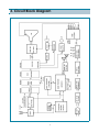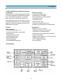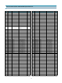
1
S/M No: CP810P-010
Service Manual
66 Cm STEREO Colour Television
CHASSIS : CP-810
MODEL : DTJ - 28A6F
DTJ - 28A7F
DTJ - 28B1F
DTJ - 28G6F
DTJ - 28G7F
DTJ - 28G8F
DAEWOO ELECTRONICS CO., LTD.
http://svc.dwe.co.kr
MAR,2000
TABLE OF CONTENTS
1. Safety Instruction ........................................................................................................................ 2
2. Specifications .............................................................................................................................. 3
3. Circuit block Diagram ................................................................................................................. 5
4. Alignment Instructions ............................................................................................................... 6
5. IC Description .............................................................................................................................. 12
6. IC DC Voltage Charts .................................................................................................................. 32
7. Service Parts List/Recommendable Spare Parts List .............................................................. 35
8. Mechanical Exploded View ......................................................................................................... 45
9. Printed Circuit Board .................................................................................................................. 51
10. Schematic Diagram ..................................................................................................................... 52
1
1. Safety Instruction
WARNING : Only competent service personnel may carry out work involving the testing or repair of this equipment
X-RAY RADIATION PRECAUTION
1. Excessive high voltage can prodece potentially hazardous X-RAY RADIATION. To avoid such hazards,
the high voltage must not exceed the specified limit.
The nominal value of the high voltage of this receiver is
23-24kv at max beam current. The high voltage must
not, under any circumstances, exceed 30kv.
Each time a receiver require servicing, the high voltage should be checked. It is imprortant to use an accurate and reliable high voltage meter.
2. The only source of X-RAY Radiation in this TV receiver
is the picture tube. For continued X-RAY RADIATION
protection, the replacement tube must be exactly the
same type tube as specified in the parts list.
SAFETY PRECAUTION
1. Potentials of high voltage are present when this
receiver is operating. Operation of the receiver outside
the cabinet or with the back board removed involves a
shock hazard from the receiver.
1) Servicing should not be attempted by anyone who is
not thoroughly familiar with the precautions necessary when working on high-voltage equipment.
2) Dischange the high potential of the picture tube
before handling the tube. The picture tube is highly
evacuated and if broken, glass fragments will be
violently expelled.
2. If any Fuse in this TV receiver is blown, replace it with
the FUSE specified in the Replacement Parts List.
3. When replacing a high wattage resistor ( oxide metal
film resistor ) in circuit board, keep the resistor 10mm
away from circuit board.
4. Keep wires away from high voltage or high temperature components.
5. This receiver must operate under AC230 volts, 50Hz.
NEVER connect to DC supply or any other power or
frequency.
PRODUCT SAFETY NOTICE
Many electrical and mechanical parts in this have
special safety-related characteristics. These characteristics are often passed unnoticed by a visual
inspection and the X-RAY RADIATION protection
afforded by them cannot necessarily be obtained by
using replacement components rated for higher voltage, wattage, etc. Replacement parts which have
these special safety characteristics are identified in
this manual and its supplements, electrical compo-
nents having such features are identified designated
symbol on the parts list.
Before replacing any of these components, read the
parts list in this manual carefully. The use of substitute
replacement parts which do not have the same safety
characterisitics as specifide in the parts list may create
X-RAY Radiation.
2
2. Specifications
CRT
28" : A66EAK071X54 ( PHILIPS )
System
PAL/SECAM-B/G, D/K, PAL-I/I’, SECAM-L/L’, NTSC-3.58/4.43 (Play back )
Main Voltage
230V AC, 50Hz
Power Consumption
Stand-by mode : 2.0 Watts
Normal operating mode : 80 Watts
Sound output
10 + 10 Watts, 10% THD at RF 60% mod. ( 1 kHz )
Speaker
12W 8ohm x 2 EA
Antenna Impedance
75 ohm unbalanced input (Din Standard )
Tuning system
Frequency Synthesize(FS) Tuning System
Tuner
DT5-BF14D, EL2782-105-B
Number of Program
100 programs
Aux. Terminal
21 pin EURO-SCART jack ( AV input, TV output, RGB input )
21 pin EURO-SCART jack ( AV input, S-VHS input )
RCA type AV input jack
Headphone jack ( 3.5 mm Ol )
JACK AUDIO TERMINAL (AUDIO OUT L, R)
Remote controller
R-22D05 with 2 "AAA" type batteries
Teletext
TOP(5 Page memory) & FLOF(7 Page memory)
- West option : English, German/Dutch/Flemish, French, Italian, Spanish/Portuguese,
Swedish/Finnish/Danish, Hungarian, Rumanian, Turkish
- East option : Polish, Czech/Slovak, Rumanian, Servo-croat, German/Dutch/Flemish,
French, Estonian, Lettish
OSD language
- West : English, German, French, Italian, Spanish, Nethelands, Swedish
- East : English, Russian, Polish, Rumanian, Czech, Hungarian
3
Specifications
PIN
Signal Designation
Matching Value
1
Audio Out (linked with 3)
0.5Vrms, Imp < 1 k (RF 60% MOD)
2
Audio In (linked with 6)
0.5Vrms, Imp < 10 k
3
Audio Out (linked with 1)
0.5Vrms, Imp < 1 k (RF 60% MOD)
4
Audio Earth
5
Blue Earth
6
Audio in (linked with 2)
0.5Vrms, Imp < 10 k (RF 60% MOD)
7
Blue in
0.7Vpp +
- 2dB, Imp 75
8
Slow (Function) Switching
TV : 0-2V, PERI : 9.5 - 12V, Imp > 10 k
9
Green Earth
10
NC
11
Green In
12
NC
13
Red Earth
14
Rapid(Blanking) Switching Earth
15
Red In, C In
0.7Vpp +- 2dB, Imp 75
16
Rapid(Blanking) switching
Logic 0 : 0 - 0.4V, Logic 1 : 1 - 3V, Imp 75
17
Video Earth
18
Rapid Blanking Earth
19
Video Out
1Vpp +- 2dB, Imp 75
20
Video In, Y In
1Vpp +
- 2dB, Imp 75
21
Common Earth
0.7Vpp +
- 2dB, Imp 75
4
3. Circuit Block Diagram
5
4. Alignment Instructions
4-1. User Remocon
R-22D05
6
Alignment Instructions
R-23D05
7
Alignment Instructions
* How to Enter the "Service Mode" with user remocon.
1) Set the TV Pr 91
2) Sharpness " MIN " control.
3) Press the Red, Green, Menu buttons in regular sequency within 5 seconds after setting TV power off.
4) You can see the Menu of " Srvice Mode" on the screen.
5) The PR UP/DOWN buttons on the remote controller are used to move the selection bar up or down the Menus.
6) The VOL UP/DOWN buttons on the remote controller are used to adjust levels.
7) If you want to exit from " Service Mode" then power the TV off.
SVC
v1
- You can see the SVC Menu by OSD in TV set.
8
V. Slope
005
V. Center
V. Size
S. Curve
H. Center
H. Width
EW. Para
EW. Cor T
EW. CB
EW.Sym
R. bias
G. b
B. b
R. drive
G. d
B. d
G2
Sub Bri
DT
995
220
019
-190
510
382
028
500
021
370
311
311
330
315
330
330
021
048
Alignment Instructions
4-2. AFT
Standard B/G, D/K, I and L
1) Set a Signal Generator with
- RF FREQUENCY = 38.9 MHz,
- RF OUTPUT LEVEL = 80 +
- 5dBuV
- Pattern = Color Bar
- System = PAL-B/G
2) Connect the Signal Generator RF Output to TP2 (Tuner IF Output).
There must be no signal input to the tuner.
3) Set the L109 to TP1(I101, #22) with DC Voltage to 2.5V +
-0.1V
4-3. AGC
1) Set a Pattern Generator with RF LEVEL 60 +
-3dBuV, RF Frequency 210. 25MHz(10CH), Pattern Color Bar.
2) Connect a OSCILLOSCOPE PROBE to P101 (TUNER AGC INPUT).
3) Set the RBOI to P101(Tuner AGC Input) with DC Voltage to 2.8V +
0.2V
-
4-4. SCREEN (G2)
1) Set a Pattern Generator with - RF Frequency : 210.25MHz (10CH)
- Pattern : RETMA
2) Select the “G2” in Menu
3) And a Horizontal Line will appear on the screen.
4) Adjust the SCREEN VOLUME on FBT barely to see the Horizontal Line.
5) Press the PR UP/DOWN keys to finish the SCREEN adjustment.
4-5. FOCUS
1) Apply a RETMA PATTERN signal.
2) Adjust the FOCUS VOLUME on FBT to obtain optimal resolution.
4-6. GEOMETRY
4-6-1 VERTICAL SLOPE ( Fixed : Adjust if need be )
1) Apply a RETMA PATTERN Signal.
2) Set the TV to Normal I mode.
3) Adjust the higher semicircle and the lower semicircle to be the same, with the V.Slope by volume
Up/Down keys.
4-6-2 VERTICAL CENTER
1) Apply a RETMA PATTERN Signal.
2) Set the TV to Normal I mode.
3) Adjust the center of the picture with the V.Center by volume Up/Down keys.
9
Alignment Instructions
4-6-3 VERTICAL SIZE
* The VERTICAL CENTER adjustment has to be done in advance.
1) Apply a RETMA PATTERN Signal.
2) Set the TV to Normal I mode.
3) Adjust the VERTICAL SIZE of the picture with the select V.size by
volume UP/DOWN keys.
4-6-4 VERTICAL S-CORRECTION ( Fixed : Adjust if need be )
1) Apply a CROSSHATCH PATTERN Signal.
2) Adjust the S-CORRECTION to obtain the same distance between
horizontal lines with the S.Curve by volume UP/DOWN keys.
4-6-5 HORIZONTAL CENTER
1) Apply a RETMA PATTERN Signal.
2) Adjust picture centering with the select H.Center by volume UP/DOWN keys.
4-7. EW
4-7-1 WIDTH
1) Apply a RETMA PATTERN Signal.
2) Adjust the horizontal width to make a perfect circle with the select H.Width
by volume UP/DOWN keys.
4-7-2 PARA
1) Apply a CROSSHATCH PATTERN Signal.
2) Adjust the vertical line to straight with the select E.W Para by volume
UP/DOWN keys.
4-7-3 CORNER ( Fixed : Adjust if need be )
1) Apply a CROSSHATCH PATTERN Signal.
2) Adjust the vertical line to straight with the select EW.Cor T by volume
UP/DOWN keys.
4-7-4 SYMMETRY ( Fixed : Adjust if need be )
1) Apply a CROSSHATCH PATTERN Signal.
2) Adjust the symmetrical balance to be suitable with the select EW Sym by
volume UP/DOWN keys.
10
Alignment Instructions
4-8. WHITE BALANCE
4-8-1 RGB Reference R
2
4-8-2 Beam Reference LOW ( 288, 301 : 10Cd/ m )
HIGH ( 288, 301 : 10Cd/ m2 )
4-8-3 Adjust G, B Gain with select Menu G,B of BIAS, DRIVE of select Menu so that R, G, B Bars
are on the center position of the analog meter. If R Analog meter is not on center, control
the Brightness +/- of user Remocon so as R Analog meter to be on the center position.
4-9. SUB BRIGHT
4-9-1 Pattern : Retma
4-9-2 Adjust the SUB BRIGHT with the select Sub Bri by volume UP/DOWN keys.
so that only H-Center parts of picture can be seen.
4-10. DOUBLE TEXT CENTER
4-10-1 Pattern : Pattern RED
4-10-2 Select Menu
4-10-3 Select DT in SVC menu time to see the Double Text Picture.
( Left : RF Picture, Right : Text Picture )
4-10-4 Change the Double Text control keys volume UP/DOWN keys so that the left edge of text
picture concur with the right edge of RF picture.
11
5. IC description
5-1. ST92195
(1) General Description
1.1 INTRODUCTION
The ST92195 microcnontoller is developed and manufactured by STMicroelecrtonics using a proprietary n-well
HCMOS process. Its performance derives from the use of
a flexible 256-register programming model for ultra-fast
context switching and real-time event response. The intelligent onchip peripherals offload the ST9 core from I/O
and data management processing tasks allowing critical
application tasks to get the maximum use off core
resources. The ST92195 MCU supports low power consumption and low voltage operation for power-efficient
and low-cost embedded systems.
1.1.1 ST9+Core
The advanced Core consists of the Central Processing
Unit (CPU), the Register File and the Interrupt controller.
The general-purpose registers can be used as accumulator, Index register, or address pointers. Adjacent register
pairs make up 16-bit registers for addressing or 16-bit
processing. Although the ST9 has an 8-bit ALU, the chip
handles 16-bit operations, including arithmetic, loads/
stores, and memory/register and memory/memory
exchanges. Two basic memory spaces are available :
Program Memory and the Register File, Which includes
the control and status registers of the on-chip peripherals.
1.1.2 Power Saving Modes
To optimize performance versus power consumption, a
range of operating modes can be dynamically selected.
Run Mode. This is the full speed execution mode with
CPU and peripherals running at the maximum clock
speed delivered by the phase Locked Loop(PLL) of the
Clock Control Unit(CCU).
Wait For Interrupt Mode. The Wait For Interrupt(WFI) instruction suspends program execution until
an interrupt request is acknowledged. During WFI, the
CPU clock is halted while the peripheral and interrupt
controller keep running at a frequency programmable via
the CCU. In this mode, the power consumption of the
device can be reduced by more than 95%(LP WFI).
Wait For Interrupt Mode. The Wait For Interrupt(WFI) instruction, and if the Watchdog is not enable,
the CPU and its peripherals stop operation and the I/O
ports enter high impedance mode. A reset is necessary to
exit from Halt mode.
1.1.3 I/O Ports
Up to 28 I/O lines are dedicated to digital Input/Output.
These lines are grouped into up to five I/O Ports and can
be configureed on a bit basis under software control to provide timing, status signals, timer and output, analog inputs,
external interrupts and serial or parallel I/O.
1.1.4 TV Peripherals
A set of on-chip peripherals form a complete system for TV
set and VCR applications:
- Voltage Synthesis
- VPS/WSS Slicer
- Teletext Slicer
- Teletext Display RAM
- OSD
1.1.5 On Screen Display
The human interface is provided by the On Screen Display
module, this can produce up to 26 lines of up to 80 characters from a ROM defined 512 character set. The character
resolution is 10x10 dot. Four character sizes are supported. Serial attributes allow the user to select foreground
and background. Parallel attributes can be used to select
additional foreground and background colors and underline
on a character by character basis.
1.1.6 Teletext and Display RAM
The internal 8k Teletext and Display storage RAM can be
used to store Teletext pages as well as Display parameters.
1.1.7 Teletext, VPS and WSS Data Slicers
The three on-board data slicers using a single external
crystal are used to extract the Teletext, VPS and WSS
information from the video signal. Hardware Hamming
decoding is provided.
1.1.8 Voltage Synthesis Tuning Control
14-bit Voltage Synthesis using the PWM (Pulse Width
Modulation)/BRM (Bit Rate Modulation) technique can be
used to genetate tuning voltages for TV set applications.
The tuning voltage is output on one of two separate output
pins.
12
IC description
1.1.9 PWM Output
- Rounding, fringe, double width, double height,
scrolling, cursor, full background colour,
semitransparent mode and reduced intensity colour
supported
Teletext unit, including Data slicer, Acquisition Unit and
up to 8K Bytes RAM for Data Storage
VPS and Wode Screen Signalling slicer
Integrated Sync Extractor and Sync Controller
14-bit Voltage Synthesis for tuning reference voltage
Up to 6 external interrupts plus 1 non-maskable interrupt
8x8-bit programmable PWM outputs with 5V opendrain or push-pull capability
16-bit Watchdog timer with 8-bit prescale
16-bit standard timer with 8-bit prescaler usable as a
Watchdog timer
3-channel Analog-to-Digital converter ; 6-bit guaranteed
Rich instruction set and 14-Addressing modes
Versatile Development Tools, including Assembler,
Linker, C-compiler, Archiver, Source Level Debugger
and Hardware Emulators with Real-Time Operating
System available from third parties
Piggyback board available for prototyping
Control of TV settings is able to be made with up to eight
8-bit PWM outputs, with a frequency maximum of
23,437Hz at 8-bit resolution(INTCLK=12 MHz). Low resolutions with higher frequency operation can be programmed.
1.1.10 Serial Peripheral Interface (SPI)
The SPI bus is used to communicate with external
devices via the SPI, or I 2C bus communication standards. The SPI uses one or two lines for serial data and a
synchronous clock signal.
1.1.11 Standard Timer (STIM)
The Standard Timer includes a programmable 16-bit
down counter and an associated 8-bit prescaler with Single and Continuous counting modes.
1.1.12 Analog/Digital Converter (ADC)
In addition there is a 3 channel Analog to Digital Converter with integral sample and hold, fast 5.7us conversion timer and 6-bit guaranteed resolution.
(2) Feature
Register File based 8/16 bit Core Architecture with
RUN, WFI, SLOW and HALT modes
0OC to 70O Coperating temperature range
_10%
Up to 24 MHz Operation @5V +
Minimum instruction cycle time : 375ns at 16MHz internal clock
64K Bytes ROM
256 Bytes RAM of Register file(accumulator or index
registers)
256 Bytes of on-chip static RAM
8K Bytes of TDSRAM(Teletext and Display RAM)
56-lead Shrink DIP package
28 fully programmable I/O pins
Serial Peripheral Interface
Flexible Clock controller for OSD, Data Slicer and Core
clocks running from one single low frequency external
crystal.
Enhanced Display Controller with 26 rows of 40/80
characters
- Serial and Parallel attributes
- 10x10 dot Matrix, 512 ROM characters, definable by
user
- 4/3 and 16/9 supported
13
IC description
(3) Block Diagram
14
IC description
(4) PIN DESCRIPTION
RESET Reset (input, active low). The ST9+ is initialised
by the Reset signal. With the deactivation of RESET,
program execution begins from the Program memory
location pointed to by the vector contained in program
memory locations 00h and 01h.
R/G/B Red/Green/Blue. Video color analog DAC outputs
FB Fast Blanking. Video analog DAC output.
VOD Main power supply voltage(5V 10%, digital)
WSCF, WSCR Analog pins for the VPS/WPP slicer line
PLL.
MCFM Analog pin for the display pixel frequency multiplier.
OSCIN, OSCOUT Oscillator (input and output).
These pins connect a parallel-resonant crystal(24MHz
maximum), or an external source to the on-chip clock
oscillator and buffer. OSCIN is the input of the oscilltor
inverter and internal clock generator; OSCOUT is the
output of the oscillator inverter.
VSYNC Vertical Sync. Vertical video synchronisation
input to OSD. Positive or negative polarity.
HYNC/CSYNC Horizontal/Composite sync. Horizontal
or composite video synchronisation input to OSD. Positive or negativety.
PXFM Analog pin for the Display Pixel Frequency Multiplier
AVDD Analog VDD of PLL. This pin must be tied to
VDD externally to the ST92195.
GND Digital circuit ground.
AGND Analog circuit ground(must be tied externally to
digital GND).
CVBS1 Composite video input signal for the Teletext
slicer and sync extraction.
CVBS2 Composite video input signal for the VPS/WSS
slicer. Pin AC coupled.
AVDD1, AVDD2 Analog power supplies(must be tied
externally to AVDD).
TXCF Analog pin for the VPS/WSS line PLL.
CVBSO, JTDO, JTCK Test pins : leave floating.
JTMS, TEST0 Test pins : must be tied to AVDD2.
JTRST0 Test pin : must be tied to GND.
Figure 2. Pin Description
15
IC description
5-2. VPS 3215C(Video Processor)
(1) Description
including all substandards
- 4 composite, 1 S-VHS input, 1 composite output
- integrated high-quality A/D converters and associated
clamp and AGC circuits
- multi-standard sync processing
- linear horizontal scaling (0.25 ... 4), as well as non-linear
horizontal scaling ‘panorama vision’
- PAL + preprocessing (VPC 3215)
- submicron CMOS technology
The VPC 3215C is a high-quality, single-chip video frontend, which is targeted for 4:3 and 16:9, 100/120Hz TV
sets.
It can be conbined with other members of the DIGIT3000
IC family (such as CIP 3250A, DDP 3300A, TPU 3040)
and/or it can be used with 3rd-party products.
(2) Features
- all-digital video processing
- high-performance adaptive 4H comb filter Y/C separator
with adjustable vertical peaking
- multi-standard color decoder PAL/NTSC/SECAM
(3) Block Diagram
(4) Pin Descriptions
These pins are connected to an 20.25MHz crystal oscillator which is digitally tuned by integrated shunt capacitances. The CLK20 and CLK5 clock signals are derived
from this oscillator. An external clock can be fed into
XTAL1. In this case, clock frequency adjustment must be
switched off.
Pin 7 - Ground, Analog Front-End GND F
Pin 9 - Ground, Output Pad Circuitry GND P
Pin 10 - Interlace Output, INTLC
This pin supplies the interlace information, 0 indicates first
field, 1 indicates second field.
Pin 1 - Ground, Analog Front-End GND F
Pin 2 - Ground, Analog Front-End GND F
Pin 3 - CCU 5 MHz Clock Output CLK5
This pin provides a clock frequency for the TV microcontroller, e.g. a CCU 3000 controller, It is also used by the
DDP 3300A display controller as a standby clock.
Pin 4 - Standby Supply Voltage V STDBY
In standby mode, only the clock oscillator is active, GNDF
should be ground reference. Please activate RESQ before
powering-up other supplies Pins 6 and 5-XTAL1 Crystal
Input
16
IC description
Pin 12 - Vertical Sync Pulse, VS
This pin supplies the vertical sync signal.
Pin 13 - Front Sync Pulse, FSY
This pin supplies the front sync information.
Pin 14 - Main Sync/Horizontal Sync Pulse MSY/HS
This pin supplies the horizontal sync pulse information in
line-locked mode. In DIGIT3000 mode, this pin is the main
sync input.
Pin 15 - Helper Line Output, Helper
This signal indicated a helper line in PAL + mode.
Pin 16 - Horizontal Clamp Pulse, HC
2
This signal can be used to clamp
an external video signal,
that is synchronous to the input signal. The timing is programmable.
Pin 17 - Active Video Output, AVO
This pin indicates the active video output data. The signal
is clocked with the LLC1 clock.
Pin 18 - Double Output Clock, LLC2
Pin 19 - Output Clock, LLC1
This is the clock reference for the luma, chroma, and status outputs.
Pin 26 - Ground, Output Pad Circuitry GND P
Pin 20 to 25,28,29 - Luma Output Y0-Y7
These output pins carry the digital luminance data. The
data are clocked with the LLC1 clock.
Pin 30 - Main Clock Output CLK20
This is the 20.25MHz main clock output.
Pin 31 - Supply Voltage, Digital Circuitry V SUPD
Pin 34 - Ground, Digital Circuitry GND D
Pin 35 - Ground, Output Pad Circuitry GND P
Pin 36 - Supply Voltage, Output Pad Supply V SUPP
Pin 38 to 43,46,47 - Chroma Outputs C0-C7
These outputs carry the digital CrCb chrominance data.
The data are clocked with the LL1 clock. The data are
sampled at half the clock rate and multiplexed. The CrCb
multiplex is reset for each TV line.
Pin 48 to 50 - Picture Bus Priority PR0-PR2
The Picture Bus Priority lines carry the digital priority
selection signals. The priority interface allows digital
switching of up to 8 sources to the back-end processor.
Switching for different sources is prioritized and can be on
a per pixel basis.
Pin 51 - Ground, Output Pad Circuitry GND P
Pin 52 - VGAV-Input.
This pin is connected to the vertical sync signal of a VGA
signal.
Pin 53 - Front-End/Back-End Data FPDAT
This pin interfaces to the DDP 3300A back-end processor.
The information for the deflection drives and for the white
drive control, i.e. the beam current limiter, is transmitted by
this pin.
Pin 54 - Reset Input RESQ
A low level on this pin resets the VPC 32xx.
Pin 55 - I2CBus Data SDA
The pin connects to the I2Cbus data line.
Pin 57 - Test Input TEST
This pin enables factory test modes. For normal operation,
it must be connected to ground.
Pin 59 - Ground, Analog Front-End GND
Pins 62,61,60,58 - Video 1-4
These are the analog video inputs. A CVBS or S-VHS
luma signal is converted using the luma (Video 1) AD converter. The VIN1 input can also be switched to the chroma
(Video 2) ADC. The input signal must be AC-coupled.
Pin 63 - Chroma Input CIN
This pin is connected to the S-VHS chroma signal. A resistive divider is used to bias the input signal to the middle of
the converter input range. CIN can only be connected to
the chroma (Video 2) A/D converter. The signal must be
AC-coupled.
Pin 64 - Analog Video Output, VOUT
The analog video signal that is selected for the main
(luma, CVBS) ADC is output at this pin. An emitter follower
is required at this pin.
Pin 65 - Ground, Analog Shield Front-End GND
Pin 66 - Supply Voltage, Analog Front-End V
Pin 67 - Signal GND for Analog Input ISGND
This is the high quality ground reference for the video
input signals.
Pin 68 - Reference Voltage Top VRT
Via this pin, the reference voltage for the A/D converters is
decoupled. The pin is connected with 10uF/47nF to the
Signal Ground Pin.
17
IC description
5-3. CIP3250A (Component Interface Processor)
(1) Description
- digital matrix RGB => YUV (Y, B-Y, R-Y)
- luma contrast and brightness correction for signals from
analog input
- color saturation and hue correction for signals from
analog input
- digital input for DIGIT 2000 or DIGIT 3000 formats
- digital interpolation to 4:4:4 format
- high quality soft mixer controlled by Fast Blank signal
- programmable delays to match digital YUV in and analog
RGB/YUV
- variable low pass filters for YUV output
- digital output in DIGIT 2000 and DIGIT 3000 formats, as
well as RGB 4:4:4
- I2C bus interface
- clock frequency 13.5...20.25 MHz
The CIP 3250A is a new CMOS IC that contains on a single chip the entire circuitry to interface analog YUV/RGB/
Fast Blank to a digital YUV system. The Fast Blank signal
is used to control a soft mixer between the digitized RGB
and an external digital YUV source. The CIP supports various output formats such as YUV 4:1:1/4:2:2 or RGB 4:4:4.
Together with the DIGIT 3000 (e.g. VPC 32xxA) or DIGIT
2000 (e.g. DTI 2250), an interface to a TV-scanrate conversion circuit and/or multi-media frame buffer can be
obtained.
(2) Feature
- analog input for RGB or YUV and Fast Blank
- triple 8 bit analog to digital converters for RGB/YUV with
internal programmable clamping
- single 6 bit analog to digital converter for Fast Blank
singnal
(3) Block Diagram
18
IC description
(4) Pin Description
nal(pure binary) or the digital chroma V signal (2’s component). Leave vacant if not used.
Pin 1 - STANDBY Input
Via this input pin, the standby mode of the CIP 3250A is
enabled. A high level voltage switches all outputs to
tristate mode, and power consumption is signigicantly
reduced. When the IC IS returned to active mode, a reset
is generated internally. Connect to VSS if not used.
Pin 29 - AVI Active Video Input
In a DIGIT 2000 application, this input can be connected
to ground. In a DIGIT 3000 application, this input expects
the DIGIT 3000 AVI signal. In a stand alone application,
this input expects the VSYNC vertical sync pulse. Connect
ground if not used.
Pins 2 to 9 - B7 to B0 Blue Output
In a stand alone application, where the CIP 3250A serces
as an A/D-converter, these are the output for the digital
Blue signal (pure binary) or the digital U signal (2’s complement). Leave vacant if not used.
Pin 30 - FSY Front Sync Input
In a DIGIT 2000 application, this input pin expects the
DIGIT 2000 SKEW protocol. In a DIGIT 3000 application,
this input expects the DIGIT 3000 FSY protocol. In a stand
alone application, this unput expects the HSYNC horizontal sync pulse. Connect to ground if not used.
Pin 10 to 17 - GL7 to GL0 Green/Luma Output
At these outputs, the digital luminance signal is received in
pure binary cided format for DIGIT 2000 and DIGIT 3000
applications. In a stand alone application, where the CIP
3250A serves as an A/D-converter, these are the outputs
for the digital Green signal(pure binary) or the digital luma
signal(pure binary). Leave vacant if not used.
2
Pin 31 to 32 - SDA and SCL of I C-Bus
2
These pins connect to the I Cbus, which takes over the
control of the CIP 3250A via the internal registers. The
SDA pin is the data input/output, and the SCL pin is the
2
clock input/output of I Cbus control interface. All registers
are writerable(except address hex27) and readable.
Pin 18 - PVSS Output Pin Ground
This is the common ground connection of all output stages
and must be connected to ground.
Note : All ground pins of the chip (i.e.
18,52,58,60,62,64,66 and 68) must be connected together
low resistive. The layout of the PCB must take into consideration the need for a low-noise ground.
Pin 33 to 35 - PRIO0 to PRIO2 Priority Bus
These pins connect to the Priority Bus of a DIGIT 3000
application. The Picture Bus Priority lines carry the digital
priority selection signals. The priority interface allows digital switching of up to 8 sources to the backend processor.
Switching for different sources is prioritized and can be on
a per pixel basis. In all other applications, they must not be
connected.
Pin 19 - PVDD Output Pin Supply + 5V/+3.3V
This pin supplies all output stages and must be connected
to a positive supply voltage.
Note : The layout of the PCB must take into consideration
the need for a low-noise supply. A bypass capacitor has to
be connected between ground and PVDD
Pin 36 to 43 - C0 to C7 Chroma Input
These are the inputs for the digital chroma signal which
can be received in binary offset or 2’s complement coded
format. In a DIGIT 2000(4:1:1) system, C3 to C0 take the
halfbyte (nibble) multiplex format. C7 to C4 have to be
connected to ground. Within the DIGIT 3000(4:2:2) system, U and V are multiplexed bytewise. Connect to ground
if not used.
Pins 20 to 27 - RC7 to RC0 Red/Chroma Output
These are the outputs for the digital chroma signal in the
DIGIT 3000 system, where U and V are multiplexed bytewise. In a DIGIT 2000 system, RC3 to RC0 and RC7 to
RC4 carry the halfbyte(nibble) multiplex format. In a stand
alone application, where the CIP 3250A serces as an ADconverter, these are the outputs for the digital Red sig-
19
IC description
Pin 44 to 51 - L0 to L7 Luma Input
These are the inputs for the digital luma signal which must
be in pure binary coded format. Connect to ground if not
used.
66, and 68) must be connected together low resistive. The
layout of the PCB must take into consideration the need
for a low-noise ground.
Pin 59 - ADREF Connect External Capacitor
This pin should be connected to ground over a 10uF and a
100nF capacitor in parallel.
Pin 52 - DVSS Digital Ground
This is the common ground connection of all digital stages
and must be connected to ground.
Note : All ground pins of the chip(i.e. 18, 52, 58, 60, 62,
64, 66, and 68) must be connected together low resistive.
The layout of the PCB must take into consideration the
need for a low-noise ground.
Pin 60 - SUBSTRATE
This is connected to the platform which carries the “die”
and must be cvonnected to the ground.
Note : All ground pins of the chip(i.e.
18,52,58,60,62,64,66, and 68) must be connected
together low resistive. The layout of the PCB must take
into consideration the need for a low-noise ground.
Pin 53 - DVDD Digital Supply +5V
This pin supplies all digital stages and must be connected
to a positive supply voltage.
Note : The layout of the PCB must take into consideration
the need for a low-noise supply. A bypass capacitor has to
be connected between ground and DVDD.
Pin 61 - FB Analog Fast Blank Input
This input takes the DC-coupled analog Fast Blank signal.
The amplitude is 1.0V maximum at 75 Ohms. Connect to
ground if not used.
Pin 54 - CLK Main Clock Input
This is the input for the clock signal. The frequency and
vary in the range from 13.5MHz to 20.25MHz.
Pin 62 - GNDFB Analod Ground
This is the ground pin for the AD converter of the Fast
Blank signal and has to be connected to ground.
Note : All ground pins of the chip (i.e. 18,52,58,60,62,64,
62,64,66 and 68) must be connected together low resistive. The layout of the PCB must take into consideration
the need for a low-noise ground.
Pin 55 - RESQ Input
A low signal at this input pin generates a reset. The low-tohigh transition of this signal should occur when the supply
voltage is stable(power-on reset).
Pin 56 - TMODE Input
This pin is for test purposes only and must be connected
to ground in normal operation.
Pin 63 - BU Analog Blue/U Chroma Input
The input pin takes the AC-coupled analog compont signal
Blue or U Chroma. The amplitude is 1.0V maximum at 75
Ohms and a coupling capacitor of 220 nF. Internally, the
DC-offset of the input signal is adjusted via the programmable internal clamping circuit. Connect to ground if not
used.
Pin 57 - AVDD Analog Supply +5V
This is the supply voltage pin for the A/D converters and
must be connected to a positive supply voltage.
Note : The layout of the PCB must take into consideration
the need for a low-noise supply. A bypass capacitor has to
be connected between ground and AVDD.
Pin 64 - GNDBU Analog Ground
This is the ground pin for the A/D converter of the Blue or
U Chroma signal and must be connected to ground.
Note : All ground pins of the chip(i.e.
18,52,58,60,62,64,66, and 68) must be connected
together low resistive. The layout of the PCB must take
into consideration the need for a low-noise ground.
Pin 58 - AVSS Analog Ground
This is the ground pin for the A/D converters and must be
connected to ground.
Note : All ground pins of the chip (i.e. 18,52,58,60,62,64,
20
IC description
Pin 65 - GY Analog Green/Luma Input
This input pin takes the AC-coupled analog compinent signal Green or Luma. The amplitude is 1.0V maximum at 75
Ohms and a couplign capacitor of 220nF. Internally, the
DC-offset of the input signal is adjusted via the programmable internal clamping circuit. Connect to ground if not
used.
Pin 66 - GNDGY Analog Ground
This is the ground pin for the A/D converter of the Green
or Luma signal and must be connected to ground.
Note : All ground pins of the chip(i.e. 18,52,58,60,62,64,
66, and 68) must be connected together low rresistive.
The layout of the PCB must take into consideration the
need for a low-noise ground.
Pin 67 - RV Analog Red/V Chroma Input
This input pin takes the AC-coupled analog component
signal Red or V Chroma. The amplitude is 1.0V maximum
at 75ohms and a coupling capacitor of 220nF. Internally,
the DC-offset of the input signal is adjusted via the programmable internal clamping circuit. Connect to ground if
not used.
Pin 68 - GNDRY Analog Ground
This is the ground pin for the A/D converter of the Red or V
Chroma signal and must be connected to ground.
Note : All ground pins of the chip (i.e. 18,52,58,62,64,66,
and 68) must be connected together low resistive. The layout of the PCB must take into consideration the need for a
low-noise ground.
21
IC description
5-4. SDA9255 (Scan Rate Converter )
(1) Features
•
•
•
•
•
•
•
•
•
•
•
•
•
100/120 Hz interlaced scan conbersion
Data format 4:1:1
On chip field memory
Digital vertical zooming
Digital vertical panning]
Motion adaptive temporal noise reduction, field based
Still field
Color difference input data representation 2’s complement or unsigned
Color difference output data representation 2’s complement or unsigned
Sync Generation for backend IC
2
I C - Bus control (400 kHz)
P-MQFP-64 package
5V +_ 5% supply voltage
(2) General Description
The SDA 9255 is a new component of the Siemens MEGAVISION IC set. The SDA 9255 comprises some of the functionalities of the MEGAVISION IC’s SDA 9220 (Memory Sync Controller) and SDA 9254 (Triple TV-SAM plus Noise
Reduction) and can therefore be used as a low cost digital featurebox.
R
R
22
IC description
(3) Block Diagram
23
IC description
(4) Pin Description
Pin No.
Name
Type
Description
2,8,24,26,41,55
,57
V SS
S
Supply voltage ( VSS = 0V)
9,25,40,56
V DD
S
Supply voltage ( V DD = 5V)
42,...,49
YIN0 ... 7
I/TTL
Data input Y (see data format)
36,...,39
UVIN4 ... 7
I/TTL
Data input UV (see data format)
30
SYNCEN
I/TTL
Synchronizarion enable input
31
RESET
I/TTL
System reset. The RESET input is low active.
In order to ensure correct operation a “Power On Reset” must be performed. The
RESET pulse must have a minimum duration of two clock periods of the system
clock (LL2CLK).
23
HIN
I/TTL
H-Sync input
22
VIN
I/TTL
V-Sync input
21
SDA
I/O
I C - Bus data line
20
SCL
I
I 2 C - Bus clock line
19
TESTIN
I/TTL
Test input, connect to V SS for normal operation
18
TESTEN
I/TTL
Test enable input, connect to V SS for normal operation
13,...10
UVOUT4
O/TTL
Data output UV (see data format)
7,...,3,1,64,63
YOUT0 ... 7
O/TTL
Data output Y (see data format)
62
HREF
O/TTL
Horizontal active video output
61
VOUT
O/TTL
V-Sync output
60
HOUT
O/TTL
H-Sync output
59
INTERLACED
O/TTL
Interlace signal for AC coupled vertical deflection
58,51
LL2CLK
I/TTL
System clock
50
TEST
I/TTL
Test input, connect to V SS for normal operation
27,28,,29,52,53
,54
TESTO 4 ... 9
O
Do not connect, Pin have to be left open
14,15,16,17
TESTO 0 ... 3
O
Not used output stages, do not connect to any other driver, VSS or VDD ; Pins can be
left open
32, 33, 34, 35
TESTIO...3
I
Input stages (internal pull-down) ; Pins can be left open
S : supply,
I : input,
O : output,
2
TTL : digital (TTL)
24
IC description
5-5. DDP 3310B (Display and Deflection Processor)
(1) Description
Deflection processing
The DDP 3310B is a single-chip digital Display and Deflection Processor designed for high-quality backend applications in 100/120MHz TV sets with 4:3- or 16:9 picture
tubes. The IC can be combined with members of the
DIGIT 3000 IC family (VPC 32xx, TPU 3040), or it can be
used with third-party products. The IC contains the entire
digital video component and deflection processing and all
analog interface components.
- scan velocity modulation output
- high-performance H/V deflection
- EHT compensation for vertical / East/West
- soft start/stop of H-Drive
- vertical angle and bow
- differential vertical output
- horizontal and vertical protection circuit
- adjustable horizontal frequency for VGA/SVGA dislay
(2) Feature
Video processing
Miscellaneous
- selectable 4:1:1/4:2:2 YC rC binput
- selectable 27/32-MHz line-locked clock input
- crystal oscillator for horizontal protection
- automatic picture tube adjustment(cutoff, whitedrive)
- single 5-V power supply
- hardware for simple 50/60-Hz to 100/120-Hz conversion
(display frequency doubling)
- two I2C -controlled PWM outputs
- beam current limiter
- linear horizontal scaling (0.25 ... 4)
- non-linear horizontal scaling “panoramavision”
- dynamic peaking
- soft limiter (gamma correction)
- color transient improvement
- programmable RGB matrix
- picture frame generator
- two analog RGB/Fast-Blank inputs
(3) Block Diagram
25
IC description
The vertical protection circuitry prevents the picture tube
from burn-in in the event of a malfunction of the vertical
deflection stage. If the peak-to-peak value of the vertical
sawtooth signal is too small, the RGB output signals are
blanked.
(4) Pin Description
Pin 1 - Supply Voltage, Output Pin Driver VSUPP*
This pin is used as supply for the following digital output
pins : FIFORRD, FIFORD, FIFOWR, FIFORWR.
Pin 12 - H-Drive Frequency Range Select FREQSEL
This pin selects the frequency range for the horizontal
drive signal.
Pin 2 - Ground, Output Pin Driver GNDP*
Output Pin Driver Reference
Pin 3 - Sync Signal Input VS2
Additional pin for the vertical sync information. Via I2C
Register the used vertical sync can be switched between
the inputs VS2 and VS(Pin 64)
Pin 13 - Clock Select 40.5 or 27/32 MHzCM1
Low level selects 27/32 MHz, High level selects 40.5 MHz
Pin 14 - Clock Select 40.5 or 27/32 MHzCM0
Low level selects 27 MHz, High level selects 32 MHz
Pin 4 - Reset for FIFO Read Counter FIFORRD
This signal is active-High and resets the read counter in
the display frequency doubling FIFO.
Pin 15 - Range Switch2 for Measuring ADC RSW2
This pin is an open-drain pull-down output. During cutoff
measurement the switch is off. During white drive measurement the switch is on. Also during the rest of time it is
on.
Pin 5 - Read Enable for FIFO FIFORD
This signal is active-High and enabels the read counter in
the display frequency doubling FIFO.
Pin 16 - Range Switch 1 or Second Input for Measuring
ADC RSW1
This pin is an open-drain pull-down output. During cutoff
and white-drive measurement, the switch is off. During
the rest of time it is on. The RSW1 pin can be used as
second measurement ADC input.
Pin 6 - Write Enable for FIFO FIFOWR
This signal is active-High and enables the write counter in
the display frequency doubling FIFO.
Pin 7 - Reset for FIFO Write Counter FIFOWR
This signal is active-High and enables the write counter in
the display frequency doubling FIFO.
Pin 17 - Measurement ADC Input SENSE
This is the input of the analog to digital converter for the
picture and tube measurement. Three measurement
ranges are selectable with RSW1 and RSW2
Pin 8 - Horizontal Drive HOUT
This open-drain output supplies the drive pulse for the horizontal output stage. A pull-up resistor has to be used.
Pin 18 - Measurement ADC Reference Input MGND
This is the ground reference for the measurement A/D
converter.
Pin 9 - Horizontal Flyback Input HFLB
Via this pin, the horizontal flyback pulse is supplied to the
DDP 3310B.
Pin 19 - Vertical Sawtooth Output VERT+(19)
This pin supplies the drive signal for the vertical output
stage. The drive signal is generated with 15-bit precision.
The analog voltage is generated by a 4-bit current DAC
with external resistor (6 k§
Ù for proper operation) and
uses digital noise-shaping.
Pin 10 - Safety Input SAFETY
This input has two thresholds. A signal between the lower
and upper threshold means normal function. Other signals
are detected as malfunction.
Pin 20 - Vertical Sawtooth Output inverted VERTThis pin supplies the inverted signal of VERT+.
Pin 11 - Vertical Protection Input VPROT
26
IC description
These pins are used to switch the RGB outputs to the
external analog RGB inputs. FBLIN1 switches the RIN1,
GIN1 and BIN1 inputs, FBLIN2 switches the RIN2, GIN2
and BIN2 inputs. The active level (Low or High) can be
selected by software.
Together with this pin, it can be used to drive symmetrical
deflection amplifiers.
Pin 21 - East/West Parabola Output EW
This pin supplies the parabola signal for the East/West
correction. The drive signal is generated with 15-bit precision. The analog voltage is generated by a 4-bit current
DAC with external resistor and uses digital noise-shaping.
Pin 31, 32, 33 - Analog RGB Input1 RIN1, GIN1, BIN1
These pin are used to insert an external analog RGB signal, e.g. from a SCART connector which can by switched
to the analog RGB outputs with the Fast-Blank signal.
The analog back-end provides separate brightness and
contrast settings for the external analog RGB signals.
Pin 22 - DAC Current Reference XREF
External reference resistor for DAC output currents, typical
10 k§
Ù , to adjust the output current of the D/A converters.
(see recommended operation conditions).
This resistor has to be connected to analog fround as
closely as possible to the pin.
Pin 35, 36, 37 - Analog RGB Input2 RIN2, GIN2, BIN2
These pins are used to insert an external analog RGB signal, e.g. from a SCART connector which can by switched
to the analog RGB outputs with the Fast-Blank signal.
The analog back-end provides separate brightness and
contrast settings for the external analog RGB signals.
Pin 23 - Scan Velocity Modulation Output SVM
This output delivers the analog SVM signal. The D/A converters. At zero signal the output current is 50% of the
maximum output current.
Pin 38 - Test Input TEST
This pin enables factory test modes. For normal operation
it must be connected to ground.
Pin 24,25,26 - Analog RGB Output ROUT, GOUT, BOUT
These pins are the analog Red/Green/Blue outputs of the
back-end. The outputs are current sinks.
Pin 39 - Reset Input RESQ
A low level on this pin resets the DDP 3310B.
Pin 27 - Ground, Analog Back-end GNDO*
This pin has to be connected to the analog supply voltage.
No supply current for the digital stages should flow through
this line.
Pin 40 - Adjustable DC Output 1 PWM1
This output delivers a DC voltage with a resolution of 8
bit, adjustable over the I2Cbus. The output is driven by a
push-pull stage. The PWM frequency is appr 79.4MHz.
For a ripple-free voltage a first order lowpass filter with a
corner frequency < 120 Hz should be applied.
Pin 28 - Supply Voltage, Analog Back-end VSUPO*
This pin has to be connected to the analog supply voltage.
No supply current for the digital stages should flow through
this line.
Pin 41 - Adjustable DC Output 2 PWM2
See pin 40.
Pin 29 - DAC Reference Decouplign/Beam Current Safety
VRD/BCS
Via this pin, the DAC reference voltage is decoupled by an
external capacitor. The DAC output currents depend on
this voltage, therefore a pull-down transistor can be used
to shut off all beam currents. A decoupling capacitor of
4.7uF in parallel to 100uF (low inductance) is required.
Pin 42 - Half-Contrast Input HCS
Via this input pin the output level of the D/A-converted
internal RGB signals can be reduced by 6dB. Inserted
external analog RGB signals remain unchanged.
Pin 43...50 - Picture Bus Chroma C0...C7
The Picture Bus Chroma lines carry the multiplexed color
component data. For the 4:1:1 input signal (4-bit chroma)
the pins C4...C7 are used.
Pin 30, 34 - Fast-Blank Input FBLIN1/2
27
IC description
Pin 52 - Ground, Digital Circuitry GNDD*
Digital Circuitry Input Reference
Pin 65, 66 - Crystal Output / Input XTAL2 / XTAL1
These pins are connectecd to an 5-MHz crystal oscillator.
The security unit for the HOUT signal uses this clock signal as reference.
Pin 53 - Main Clock Input LLC2(53)
This is the input for the line-locked clock signal. The frequency can be 27, 32, or 40.5 MHz.
Pin 67 - I C Data Input/Output SDA
Via this pin the I2C - bus data are written to or read from
the DDP 3310B.
Pin 54...61 - Picture Bus Luma Y0...Y7
The Picture Bus Luma lines carry the digital luminance
data.
Pin 68 - I2C Clock Input SCL
Via this pin, the clock signal for the I2C-bus will be supplied. The signal can be pulled down by an internal transistor.
Pin 62 - Line-Locked Clock Input LLC1
This is the reference clock for the single frequency input
sync signals required in a FIFO application. The frequency
can be 13.5, 16, or 20.25 MHz.
* Application Note :
All ground pins should be connected separeately with
short and low-resistive lines to a central power supply
ground. Accordingly, all supply pins should be connected
separately with short and low-resistive lines to the power
supply. Decoupling capacitors from VSUPP to GNDP,
VSUPD to GNDD, and VSUPO to GNDO are recommended to be placed as closely as possible to the pins.
Pin 51 - Supply Voltage, Digital Circuitry VSUPD*
2
Pin 63 - Sync Signal Input HS
This pin gets the horizontal sync information. Either single
or double horizontal frequency or VGA horizontal sync signal.
Pin 64 - Sync Signal Input VS
This pin gets the vertical sync informatoion. Either single
or double vertical frequency or VGA vertical sync signal.
28
IC description
5-6. DPL 3519A (Dolby Pro Logic Processor)
(1) General Description
The DPL 3519A is designed as a coprocessor to the MSP family but has analog output channels in addition to the features of the DPL 3518A. Together with the MSP, a TV set with up to six outputs (L, R, C, SUB, SL, SR)can be developed
together with headphones and several line outputs.
(2) Features
- Full Dolby Surround Pro Logic Adative Matrix
- Pseudo-surround mode for signals not encoded in dolby Surround
- PANORAMA sound mode(3-D Surround sound via 2 loudspeakers)
- Noise sequencer
- Automatic input balance control
- 7 kHz low-pass filter
- 100 Hz low-pass filter for subwoofer
- Modified Dolby B-type NR decoder
- 30 ms surround delay according to table created by Dolby Labortories (1 ms steps)
2
- 2 I S input channels (e.g. MSP and DRPA)
2
- 2 I S output channels, freely programmable with sound channels L/R ( resp. L+C/R+C), C/S, Sub or I2S input
- Mode control : normal/phantom/wide/three channel/center off/panorama sound/stereo bypass
- Surround matrix mode control : adaptive/passive/effect
- Additional surround basswidth effect
- Reverberation of surround signals
- 2 digital input/output pins
- 1 digital input pin
- Master volume control in dB units
_12dB
- Level Trim for L, C, R, S in dB units, +
- Identical treble/bass/loudness function for L, C, R, S
- 5-band equalizer for C channel
- Separate volume control for two surround outputs
- Additional line output for HIFI receiver connection (SCART output). Volume for this output is in dB units.
- 3 pairs of D/A converters
- Scart switches
29
IC description
(3) Block Diagram
(4) Pin Description
Pin No.
PIN Name
1
D_CTR_IN
2
AUD_CL_OUT
3
Type
Description
IN
Digital control input
OUT
Audio clock output
D_CTR_IO1
IN/OUT
Digital control IO1
4
D_CTR_IO1
IN/OUT
Digital control IO 0
5
ADR_SEL
IN
I 2 C -Bus address select
6
STANDBYQ
IN
Standby (low-active)
7
I2C_CL
IN
I 2 C clock
8
I2C_DA
IN/OUT
I 2 C data
9
I2C_CL
OUT
I2 C clock
10
I2C_WS
OUT
I 2 C wordstrobe
11
I2C_DA_OUT1
OUT
I 2 C data output
12
I2C_DA_IN1
IN
I 2 C data input
13
NC
Not connected
14
NC
Not connected
15
NC
Not connected
16
DVSUP
Digital power supply +5V
17
DVSS
Digital ground
18
I2S_DA_IN2
IN
I 2 S 2 - data input
30
IC description
Pin No.
PIN Name
Type
OUT
Description
2-
19
I2S_DA_OUT
20
RESETQ
21
20/19:DACC2_R 18:NC
OUT
Analog output Channel2, right
22
20/19:DACC2_R 18:NC
OUT
Analog output Channel2, left
23
20/19:VREF2 18:NC
24
20/19:DACC1_R 18:NC
OUT
Analog output Channel1, right
25
20/19:DACC1_L 18:NC
OUT
Analog output Channel1, left
26
NC
27
20/19:SC2_OUT_R 18:NC
OUT
Scart output2, right
28
20/19:SC2_OUT_L 18:NC
OUT
Scart output2, left
29
20/19:VREF1 18:NC
30
20/19:SC1_OUT-R 18:NC
OUT
Scart output1, right
31
20/19:SC1_OUT-L 18:NC
OUT
Scart output1, left
32
20/19:CAPL_C2 18:NC
Volume capacitor Channel2
33
20/19:AHVSUP 18:NC
Analog power supply +8V
34
20/19:CAPL_C1 18:NC
Volume capacitor Channel1
35
20/19:AHVSS 18:NC
Analog ground
36
20/19:AGNDC 18:NC
Analog reference voltage high voltage part
37
20/19:SC3_IN_L 18:NC
IN
Scart input3 in, left
38
20/19:SC3_IN_R 18:NC
IN
Scart input3 in, right
39
20/19:SC2_IN_L 18:NC
IN
Scart input2 in, left
40
20/19:SC2_IN_R 18:NC
IN
Scart input2 in, right
41
20/19:SC1_IN_L 18:NC
IN
Scart input1 in, left
42
20/19:SC1_IN_R 18:NC
IN
Scart input1 in, right
43
VREFTOP
44
20/19:MONO_IN 18:NC
45
AVSS
Analog ground
46
AVSUP
Analog power supply +5V
47
NC
Not connected
48
NC
Not connected
49
NC
Not connected
50
TESTEN
IN
Test pin
51
XTAL_IN
IN
Crystal oscillator
52
XTAL_OUT
OUT
Crystal oscillator
IN
I S data output
Power-on-reset
2
Reference ground2 high voltage part
Not connected
Reference ground1 high voltage part
Reference voltage
IN
Mono input
31
6. IC DC Voltage Charts
* Input signal
PAL/CH5 - Video : 8 step colour bar ( 87% AM )
Audio : 1KHz sinewave ( 60% FM )
* User’s control condition
Contrast, Brightness, Colour, Volume Controls-max.
* Line voltage
AC 230V, 50Hz
* All the voltage in each point are measured with Multimeter.
1. TDA 8172 (I301)
Pin No.
1
2
3
4
5
6
7
V(DC)
0.4
+10.7
-8.7
-10.6
0
11.1
0.4
2. MSP 3415D (I606)
Pin No.
1
2
3
4
5
6
7
8
9
10
V(DC)
2.5
0
0
0
0
0
5.0
0
5.0
5.0
Pin No.
11
12
13
14
15
16
17
18
19
20
V(DC)
2.4
2.4
2.4
0.5
0.6
0.6
0.5
4.9
0
1.3
Pin No.
21
22
23
24
25
26
27
28
29
30
V(DC)
0.4
0.4
0.3
4.9
0.7
0.7
0
0.08
0.08
0
Pin No.
31
32
33
34
35
36
37
38
39
40
V(DC)
0.08
1.0
3.8
3.8
0
3.8
3.8
7.2
8.0
7.2
Pin No.
41
42
43
44
45
46
47
48
49
50
V(DC)
0
3.7
0
0
0
3.7
3.7
0
3.7
3.7
Pin No.
51
52
53
54
55
56
57
58
59
60
V(DC)
0
3.7
3.7
2.6
1.1
0
4.9
1.5
1.5
0
Pin No.
61
62
63
64
V(DC)
0
2.4
2.4
0.5
3. TDA 4470-M (I101)
Pin No.
1
2
3
4
5
6
7
8
9
10
V(DC)
3.2
3.2
3.5
0
1.1
2.4
2.4
2.0
0
1.2
Pin No.
11
12
13
14
15
16
17
18
19
20
V(DC)
1.7
2.1
4.4
3.9
2.6
0
4.2
2.2
3.5
3.3
Pin No.
21
22
23
24
25
26
27
28
V(DC)
3.3
2.3
4.8
2.1
2.0
0.7
0.1
0.1
32
IC DC Voltage Charts
4. TDA 7269 (I601)
Pin No.
1
2
3
4
5
6
7
8
9
10
11
V(DC)
-14.2
0
+14.2
0
0
-14.2
0
0
5.0
5.0
0
5. ST92195 (I701)
Pin No.
1
2
3
4
5
6
7
8
9
10
V(DC)
3.1
4.8
0
0
0
0
0
0
0
0.5
Pin No.
11
12
13
14
15
16
17
18
19
20
V(DC)
5.0
0
0
0
0.4
0.4
0.4
0
5.0
5.0
Pin No.
21
22
23
24
25
26
27
28
29
30
V(DC)
5
0.7
0
0
5.0
0
1.8
0.6
2.1
0.8
Pin No.
31
32
33
34
35
36
37
38
39
40
V(DC)
5.0
5.0
0.8
1.6
0
0
0
2.0
5.0
0.6
Pin No.
41
42
43
44
45
46
47
48
49
50
V(DC)
0
0
0
0.1
5.0
0
0
0
0
2.3
Pin No.
51
52
53
54
55
56
V(DC)
2.3
5.0
5.0
0.6
2.3
0
6. AT24C16-10PC (I702)
Pin No.
1
2
3
4
5
6
7
8
V(DC)
0
0
5.0
0
5.0
5.0
0
5.0
7. STR-F6654 (I801)
Pin No.
1
2
3
4
5
V(DC)
2.0
0
254.0
18.0
0
Pin No.
1
2
3
4
5
6
7
8
9
10
V(DC)
0.5
2.7
0.5
0.5
3.8
4.9
5.0
5.0
2.4
2.4
Pin No.
11
12
13
14
15
16
17
18
19
20
V(DC)
0.5
2.4
0.5
0.5
0.5
4.9
0
0.4
0
3.7
Pin No.
21
22
23
24
25
26
27
28
29
30
V(DC)
0.1
0.1
0
0.1
0.1
0
3.7
3.7
0
3.7
8. DPL 3519A
33
IC DC Voltage Charts
Pin No.
31
32
33
34
35
36
37
38
39
40
V(DC)
3.7
6.8
7.8
6.8
0
3.7
3.7
3.7
3.7
3.7
Pin No.
41
42
43
44
45
46
47
48
49
50
V(DC)
3.7
3.7
2.6
3.7
0
5.0
1.5
1.5
0.4
0
Pin No.
51
52
V(DC)
2.2
2.1
9. TEA5101B (I901)
Pin No.
1
2
3
4
5
6
7
8
9
10
V(DC)
3.2
12.2
3.2
3.2
210.0
0.6
172.0
0
115.0
177.0
Pin No.
11
12
13
14
15
V(DC)
0.6
119.0
168.0
0.6
116.0
Pin No.
1
2
3
4
5
6
7
8
9
10
V(DC)
0
5.0
1.0
1.0
0
1.9
0
0
0
0.6
Pin No.
11
12
13
14
15
16
17
18
V(DC)
-0.3
0
4.9
0.6
0.4
0.4
0.4
12.1
Pin No.
1
2
3
4
5
6
7
8
9
10
V(DC)
0.9
0
0
0.8
0
0
1.2
0
0
0
Pin No.
11
12
13
14
15
16
17
18
V(DC)
5
5
70
0.6
0
3
3
3
10. P503
11. P504
34
7. Service Parts List/Recommendable Spare Parts List
Caution
LOC
R
is recommendable spare part.
is safety component, so it must be used the same component.
PART CODE
ZZ100
48B3822D05
ZZ110
PTACPWD228
PART NAME
TRANSMITTER
DESCRIPTION
R-22D05
REMARK
LOC
R
PART CODE
PART NAME
P601A
4850704S30
CONNECTOR
REMOCON
DESCRIPTION
REMARK
YH02504+35098+ULW=700
ACCESSORY AS
DTJ-28G6F
SP01
4858311110
SPEAKER
12W 8 OHM SP-58126F
10 4850Q00910
BATTERY
R03/NN
SP02
4858311110
SPEAKER
12W 8 OHM SP-58126F
20 4859102620
JACK ANT
3104.308.73221
ZZ290
PTMPMSD228
PCB MAIN MANUAL
DTJ-28G6F
M821
4858213800
BAG INSTRUCTION
L.D.P.E T0.05X250X400
AS
ZZ120
PTBCSHD310
COVER BACK AS
DTJ-28A6F
DIODE
FML-G12S
M211
4852156501
COVER BACK
HIPS BK
0000A
4857026900
HEAT SINK
AL EX
M211D
4857817611
CLOTH BLACK
FELT 200X20X0.7
0000B
7174301011
SCREW TAPPTITE
TT2 RND 3X10 MFZN
M541
4855415800
SPEC PLATE
150ART P/E FILM (C/TV)
C100
CXRH1H150J
C CERA
RH 50V 15PF J (TAPPING)
ZZ130
PTPKCPD310
PACKING AS
DTJ-28A6F
C101
CEXF1E470V
C ELECTRO
25V RSS 47MF (5X11) TP
M641
6520010100
STAPLE PIN
18M/M J D O
C102
CEXF1H100V
C ELECTRO
50V RSS 10MF (5X11) TP
M681
4856812400
BAND
18MM X 3M
C103
CEXF1E330V
C ELECTRO
25V RSS 33MF (5X11) TP
M801
4858054600
BOX CARTON
SW-2
C104
CXCH1H220J
C CERA
50V CH 22PF J (TAPPING)
M811
4858193801
PAD
EPS 28A6
C107
CEXF1H100V
C ELECTRO
50V RSS 10MF (5X11) TP
M822
4858215600
BAG P.E
PE FOAM T0.5X1600X1270
C109
CEXF1E470V
C ELECTRO
25V RSS 47MF (5X11) TP
ZZ131
58G0000103
COIL DEGAUSSING
DC-2701
C117
CEXF1H229V
C ELECTRO
50V RSS 2.2MF (5X11) TP
ZZ132
48519A5510
CRT GROUND NET
2801H-1015-2P
C303
CMXM2A683J
C MYLAR
100V 0.068MF J (TP)
ZZ140
PTCACAD310
CABINET AS
DTJ-28A6F
C305
CEXF1V101C
C ELECTRO
35V RUS 100MF (8X11.5)
M201A
4857818701
CLOTH BLACK
FELT T0.7 L=250 W=15
M201B
4857818702
CLOTH BLACK
FELT T0.7 L=350 W=15
M211A
7172401612
SCREW TAPPTITE
TT2 TRS 4X16 MFZN BK
M211B
7178301212
SCREW TAPPTITE
M281
4852822401
M352
97P4602700
M391A
M481
1 DFMLG12S--
TP
C401
CEXF1E101V
C ELECTRO
25V RSS 100MF (6.3X11)
TT2 WAS 3X12 MFZN BK
C402
CMYH3C432J
C MYLAR
1.6KV BUP 4300PF J
DOOR
PC CL
C403
CEXF1C102C
C ELECTRO
16V RUS 1000MF (10X20)
CLAMP CORD
NYLON 66 BLK 5280N
7172401612
SCREW TAPPTITE
TT2 TRS 4X16 MFZN BK
C404
CMYH3C622J
C MYLAR
1.6KV BUP 6200PF J
4854856801
BUTTON POWER
HIPS BK
C405
CMYE2J223J
C MYLAR
630V PU 0.022MF J
M481A
4856716000
SPRING
SWPA PIE0.5
C406
CEXF1E471C
C ELECTRO
25V RUS 470MF (10X16)
M491A
7178301011
SCREW TAPPTITE
TT2 WAS 3X10 MFZN
M501
4855059601
DECO CTRL
PVC T0.25
C407
CEXF1H100C
C ELECTRO
50V RUS 10MF (5X11) TP
M561
4855617401
MARK BRAND
AL (SILVER)
C408
CMYE2G334J
C MYLAR
400V PU 0.33MF J
M681
4856812001
TIE CABLE
NYLON66 DA100
C409
CMXB1H273J
C MYLAR
50V EU 0.027MF J (TP)
M682
4856816300
CLAMP WIRE
NYLON 6 (V0)
C411
CEXF2C109V
C ELECTRO
160V RSS 1MF (6.3X11) TP
M791
4857923300
DOOR LOCK
LA701(KIFCO)
C412
CEXF1E101V
C ELECTRO
25V RSS 100MF (6.3X11)
P405
4850704N07
CONNECTOR
SE100J+172792+USW=500
SP01A
7172401212
SCREW TAPPTITE
TT2 TRS 4X12 MFZNCK
SP02A
7172401212
SCREW TAPPTITE
TT2 TRS 4X12 MFZNCK
V901
4859625760
CRT
A66EAK071X54
V901A
4856215402
WASHER RUBBER
CR T2.0
V901B
4856015820
SCREW CRT FIX
SWRM+SK5 L=35
ZZ200
PTFMSJD310
MASK FRONT AS
DTJ-28A6F
M201
4852074501
MASK FRONT
M251
4852540601
GRILL L
M252
4852538401
GRILL R
PS SHEET
ZZ220
PTSPPWD228
SPEAKER AS
DTJ-28G6F
TP
TP
TP
TP
C413
CEXF1C102V
C ELECTRO
16V RSS 1000MF (10X20)
TP
C415
CEXF2E100V
C ELECTRO
250V RSS 10MF (10X20) TP
C416
CCXB3D471K
C CERA
2KV B 470PF K (TAPPING)
C417
CMXM2A222J
C MYLAR
100V 2200PF J (TP)
C418
CEYD1H689W
C ELECTRO
50V RHD 6.8MF (16X35.5)
HIPS BK
C420
CCXB1H472K
C CERA
50V B 4700PF K (TAPPING)
PS SHEET
C501
CEXF1E101V
C ELECTRO
25V RSS 100MF (6.3X11)
C601
CBZF1H104Z
C CERA SEMI
R
R
TP
R
35
50V F 0.1MF Z
R
Service Parts List/Recommendable Spare Parts List
LOC
PART CODE
C602
CBZF1H104Z
C CERA SEMI
PART NAME
50V F 0.1MF Z
DESCRIPTION
C603
CEXF1H100V
C ELECTRO
50V RSS 10MF (5X11) TP
C605
CEXF1E471C
C ELECTRO
25V RUS 470MF (10X16)
C606
CEXF1E471C
C ELECTRO
C619
CEXF1E470V
C ELECTRO
25V RSS 47MF (5X11) TP
C620
CEXF1E470V
C ELECTRO
25V RSS 47MF (5X11) TP
C625
CEXF1H479C
C ELECTRO
50V RUS 4.7MF (5X11) TP
C626
CEXF1H479C
C ELECTRO
50V RUS 4.7MF (5X11) TP
C627
CEXF1H100V
C ELECTRO
50V RSS 10MF (5X11) TP
C628
CEXF1E470V
C ELECTRO
25V RSS 47MF (5X11) TP
C655
CEXF1H100V
C ELECTRO
50V RSS 10MF (5X11) TP
C656
CEXF1H100V
C ELECTRO
50V RSS 10MF (5X11) TP
C658
CEXF1H100V
C ELECTRO
C674
CEXF1H479C
C675
CEXF1H479C
C701
C702
REMARK
LOC
PART CODE
C826
CEXF1E101V
C ELECTRO
PART NAME
C827
CEXF1E471C
C ELECTRO
C830
CEXF1E101V
C ELECTRO
C831
CEXF1E222V
C ELECTRO
C832
CEXF1E222V
C ELECTRO
C836
CEXF1E471C
C ELECTRO
C837
CEXF1E101V
C ELECTRO
50V RSS 10MF (5X11) TP
C840
CXSL2H470J
C CERA
500V SL 47PF J (TAPPING)
C ELECTRO
50V RUS 4.7MF (5X11) TP
C841
CBZF1H104Z
C CERA SEMI
50V F 0.1MF Z
C ELECTRO
50V RUS 4.7MF (5X11) TP
C842
CEXF1E471C
C ELECTRO
25V RUS 470MF (10X16)
CEXF1H109V
C ELECTRO
50V RSS 1MF (5X11) TP
CEXF1H100V
C ELECTRO
50V RSS 10MF (5X11) TP
C843
CEXF1E471C
C ELECTRO
C703
CEXF1E470V
C ELECTRO
25V RSS 47MF (5X11) TP
C705
CEXF1E470V
C ELECTRO
25V RSS 47MF (5X11) TP
C910
CEXF2E100V
C ELECTRO
250V RSS 10MF (10X20) TP
C731
CEXF1H100V
C ELECTRO
50V RSS 10MF (5X11) TP
C911
CEXF2E100V
C ELECTRO
250V RSS 10MF (10X20) TP
C801
CL1JB3474K
C LINE ACROSS
AC250V 0.47MF U/C/SNDF/
C912
CCXB3D102K
C CERA
2KV B 1000PF K (TAPPING)
SV
C913
CEXF1H100V
C ELECTRO
50V RSS 10MF (5X11) TP
AC250V 0.47MF U/C/SNDF/
CC101
HCBK102KCA
C CHIP CERA
50V X7R 1000PF K 2012
SV
CC102
HCBK102KCA
C CHIP CERA
50V X7R 1000PF K 2012
TP
TP
CL1JB3474K
C LINE ACROSS
25V RUS 470MF (10X16)
TP
25V RUS 470MF (10X16)
TP
C802
DESCRIPTION
25V RSS 100MF (6.3X11)
25V RSS 100MF (6.3X11)
TP
25V RSS 2200MF (16X25)
TP
25V RSS 2200MF (16X25)
TP
25V RUS 470MF (10X16)
TP
25V RSS 100MF (6.3X11)
TP
TP
25V RUS 470MF (10X16)
TP
C805
CCXF3A472Z
C CERA
1KV F 4700PF Z (T)
CC103
HCBK102KCA
C CHIP CERA
50V X7R 1000PF K 2012
C806
CCXF3A472Z
C CERA
1KV F 4700PF Z (T)
CC104
HCQK220JCA
C CHIP CERA
50V CH 22PF J 2012
C808
CCZB1H681K
C CERA
50V B 680PF K (AXIAL)
CC105
HCTAD100MB
C CHIP TANTAL
10V 10MF M 3216
C809
CEYA2G221G
C ELECTRO
400V LSS 220MF (30X40)
CC106
HCFK103ZCA
C CHIP CERA
50V Y5V 0.01MF Z 2012
C810
CBYB3D152K
C CERA SEMI
2KV BL(N) 1500PF K
CC107
HCFK104ZCA
C CHIP CERA
50V Y5V 0.1MF Z 2012
C812
CEXF1H220V
C ELECTRO
50V RSS 22MF (5X11) TP
CC108
HCFK103ZCA
C CHIP CERA
50V Y5V 0.01MF Z 2012
C813
CCXB3A471K
C CERA
1KV B 470PF K (T)
CC109
HCFK104ZCA
C CHIP CERA
50V Y5V 0.1MF Z 2012
C814
CEXF1H100V
C ELECTRO
50V RSS 10MF (5X11) TP
CC110
HCFK103ZCA
C CHIP CERA
50V Y5V 0.01MF Z 2012
C815
CEYF2D101V
C ELECTRO
200V RSS 100MF (16X31.5)
CC112
HCFK103ZCA
C CHIP CERA
50V Y5V 0.01MF Z 2012
C816
CEYF2D101V
C ELECTRO
200V RSS 100MF (16X31.5)
CC114
HCFK103ZCA
C CHIP CERA
50V Y5V 0.01MF Z 2012
C817
CEXF1H470V
C ELECTRO
50V RSS 47MF (6.3X11) TP
CC115
HCBK102KCA
C CHIP CERA
50V X7R 1000PF K 2012
C818
CEXF1H100V
C ELECTRO
50V RSS 10MF (5X11) TP
CC116
HCTAF229MB
C CHIP TANTAL
16V 2.2MF M 3216
C819
CEXF2A100V
C ELECTRO
100V RSS 10MF (6.3X11)
CC118
HCFK474ZCA
C CHIP CERA
Y5V 50V 0.47MF Z 2012
TP
CC120
HCFK103ZCA
C CHIP CERA
50V Y5V 0.01MF Z 2012
16V RSS 3300MF (16X25)
CC302
HCBK223KCA
C CHIP CERA
50V X7R 0.022MF K 2012
TP
CC303
HCBK223KCA
C CHIP CERA
50V X7R 0.022MF K 2012
C820
CEXF1C332V
C ELECTRO
C821
CCXB3D681K
C CERA
2KV B 680PF K (TAPPING)
CC306
HCBK333KCA
C CHIP CERA
50V X7R 0.033MF K 2012
C822
CH1AFE472M
C CERA AC
4KV 4700PF M KX DE1610
CC401
HCBK223KCA
C CHIP CERA
50V X7R 0.022MF K 2012
C823
CEXF1E101V
C ELECTRO
25V RSS 100MF (6.3X11)
CC601
HCQK470JCA
C CHIP CERA
50V CH 47PF J 2012
TP
CC603
HCFK105ZCA
C CHIP CERA
50V Y5V 1MF Z 2012
36
REMARK
Service Parts List/Recommendable Spare Parts List
LOC
PART CODE
LOC
PART CODE
CC604
HCFK103ZCA
C CHIP CERA
PART NAME
50V Y5V 0.01MF Z 2012
DESCRIPTION
REMARK
CC701
HCBK102KCA
C CHIP CERA
50V X7R 1000PF K 2012
CC609
HCBK102KCA
C CHIP CERA
50V X7R 1000PF K 2012
CC702
HCFK103ZCA
C CHIP CERA
50V Y5V 0.01MF Z 2012
CC610
HCBK102KCA
C CHIP CERA
50V X7R 1000PF K 2012
CC704
HCBK472KCA
C CHIP CERA
50V X7R 4700PF K 2012
CC611
HCTAD100MB
C CHIP TANTAL
10V 10MF M 3216
CC705
HCBK222KCA
C CHIP CERA
50V X7R 2200PF K 2012
CC612
HCBK102KCA
C CHIP CERA
50V X7R 1000PF K 2012
CC706
HCQK220JCA
C CHIP CERA
50V CH 22PF J 2012
CC614
HCFK104ZCA
C CHIP CERA
50V Y5V 0.1MF Z 2012
CC707
HCFK103ZCA
C CHIP CERA
50V Y5V 0.01MF Z 2012
CC617
HCFK105ZCA
C CHIP CERA
50V Y5V 1MF Z 2012
CC708
HCFK474ZCA
C CHIP CERA
Y5V 50V 0.47MF Z 2012
CC618
HCFK105ZCA
C CHIP CERA
50V Y5V 1MF Z 2012
CC709
HCQK820JCA
C CHIP CERA
50V CH 82PF J 2012
CC619
HCFK104ZCA
C CHIP CERA
50V Y5V 0.1MF Z 2012
CC710
HCBK222KCA
C CHIP CERA
50V X7R 2200PF K 2012
CC620
HCBK223KCA
C CHIP CERA
50V X7R 0.022MF K 2012
CC711
HCBK102KCA
C CHIP CERA
50V X7R 1000PF K 2012
CC621
HCQK509DCA
C CHIP CERA
50V CH 5PF D 2012
CC713
HCQK820JCA
C CHIP CERA
50V CH 82PF J 2012
CC622
HCQK509DCA
C CHIP CERA
50V CH 5PF D 2012
CC715
HCFK103ZCA
C CHIP CERA
50V Y5V 0.01MF Z 2012
CC623
HCBK102KCA
C CHIP CERA
50V X7R 1000PF K 2012
CC716
HCBK102KCA
C CHIP CERA
50V X7R 1000PF K 2012
CC624
HCBK102KCA
C CHIP CERA
50V X7R 1000PF K 2012
CC717
HCBK102KCA
C CHIP CERA
50V X7R 1000PF K 2012
CC628
HCTAD100MB
C CHIP TANTAL
10V 10MF M 3216
CC719
HCQK220JCA
C CHIP CERA
50V CH 22PF J 2012
CC629
HCFK104ZCA
C CHIP CERA
50V Y5V 0.1MF Z 2012
CC720
HCFK105ZCA
C CHIP CERA
50V Y5V 1MF Z 2012
CC630
HCTAF339MB
C CHIP TANTAL
16V 3.3MF M 3216
CC721
HCBK102KCA
C CHIP CERA
50V X7R 1000PF K 2012
CC631
HCTAD100MB
C CHIP TANTAL
10V 10MF M 3216
CC801
HCFK104ZCA
C CHIP CERA
50V Y5V 0.1MF Z 2012
CC632
HCTAD100MB
C CHIP TANTAL
10V 10MF M 3216
CC802
HCFK104ZCA
C CHIP CERA
50V Y5V 0.1MF Z 2012
CC633
HCTAD100MB
C CHIP TANTAL
10V 10MF M 3216
CC803
HCFK104ZCA
C CHIP CERA
50V Y5V 0.1MF Z 2012
CC634
HCBK472KCA
C CHIP CERA
50V X7R 4700PF K 2012
CC804
HCBK152KCA
C CHIP CERA
50V X7R 1500PF K 2012
CC635
HCBK472KCA
C CHIP CERA
50V X7R 4700PF K 2012
CC834
HCFK104ZCA
C CHIP CERA
50V Y5V 0.1MF Z 2012
CC636
HCFK103ZCA
C CHIP CERA
50V Y5V 0.01MF Z 2012
CC904
HCBK102KCA
C CHIP CERA
50V X7R 1000PF K 2012
CC637
HCFK103ZCA
C CHIP CERA
50V Y5V 0.01MF Z 2012
CC905
HCBK102KCA
C CHIP CERA
50V X7R 1000PF K 2012
CC638
HCFK105ZCA
C CHIP CERA
50V Y5V 1MF Z 2012
CC906
HCBK102KCA
C CHIP CERA
50V X7R 1000PF K 2012
CC639
HCFK105ZCA
C CHIP CERA
50V Y5V 1MF Z 2012
CC907
HCFK104ZCA
C CHIP CERA
50V Y5V 0.1MF Z 2012
CC640
HCBK102KCA
C CHIP CERA
50V X7R 1000PF K 2012
CCA10
HCBK331KCA
C CHIP CERA
50V X7R 330PF K 2012
CC641
HCBK102KCA
C CHIP CERA
50V X7R 1000PF K 2012
CCA20
HCBK331KCA
C CHIP CERA
50V X7R 330PF K 2012
CC644
HCFK104ZCA
C CHIP CERA
50V Y5V 0.1MF Z 2012
D101
D1N4148---
DIODE
1N4148 (TAPPING)
CC645
HCFK103ZCA
C CHIP CERA
50V Y5V 0.01MF Z 2012
D102
D1SS85TA--
DIODE
1SS85TA
CC646
HCFK103ZCA
C CHIP CERA
50V Y5V 0.01MF Z 2012
D301
D1N4936GP-
DIODE
1N4936GP (TAPPING)
CC653
HCBK102KCA
C CHIP CERA
50V X7R 1000PF K 2012
D302
DUZ5R1B---
DIODE ZENER
UZ-5.1B UNIZON
CC654
HCBK102KCA
C CHIP CERA
50V X7R 1000PF K 2012
D404
DDMV32F5--
DIODE
DMV32F5
CC656
HCQK471JCA
C CHIP CERA
50V CH 470PF J 2012
D404A
7174300811
SCREW TAPPTITE
TT2 RND 3X8 MFZN
CC660
HCBK333KCA
C CHIP CERA
50V X7R 0.033MF K 2012
D405
D1N4936GP-
DIODE
1N4936GP (TAPPING)
CC662
HCTAD100MB
C CHIP TANTAL
10V 10MF M 3216
D407
D1N4936GP-
DIODE
1N4936GP (TAPPING)
CC663
HCBK102KCA
C CHIP CERA
50V X7R 1000PF K 2012
D408
D1N4936GP-
DIODE
1N4936GP (TAPPING)
CC665
HCFK105ZCA
C CHIP CERA
50V Y5V 1MF Z 2012
D410
D1N4937G--
DIODE
1N4937G
CC666
HCFK105ZCA
C CHIP CERA
50V Y5V 1MF Z 2012
D411
D1N4148---
DIODE
1N4148 (TAPPING)
CC669
HCTAH109MB
C CHIP TANTAL
25V 1MF M 3216
D412
D1N4148---
DIODE
1N4148 (TAPPING)
CC670
HCTAH109MB
C CHIP TANTAL
25V 1MF M 3216
D413
D1N4148---
DIODE
1N4148 (TAPPING)
CC671
HCTAF339MB
C CHIP TANTAL
16V 3.3MF M 3216
D414
D1N4148---
DIODE
1N4148 (TAPPING)
CC672
HCTAD100MB
C CHIP TANTAL
10V 10MF M 3216
D415
D1N4937G--
DIODE
1N4937G
CC673
HCTAD100MB
C CHIP TANTAL
10V 10MF M 3216
D501
DUZ8R2BM--
DIODE ZENER
UZ-8.2B (8.2V)
CC676
HCTAD479MB
C CHIP TANTAL
10V 4.7MF M 3216
D502
DUZ8R2BM--
DIODE ZENER
UZ-8.2B (8.2V)
CC677
HCTAD479MB
C CHIP TANTAL
10V 4.7MF M 3216
D503
DUZ8R2BM--
DIODE ZENER
UZ-8.2B (8.2V)
37
PART NAME
DESCRIPTION
REMARK
Service Parts List/Recommendable Spare Parts List
LOC
PART CODE
D701
LOC
D1N4148---
PART CODE
DIODE
PART NAME
1N4148 (TAPPING)
DESCRIPTION
REMARK
DA20
DUZ5R6BM--
DIODE ZENER
PART NAME
UZ-5.6BM(TAPPING)
DESCRIPTION
D703
DUZ5R1B---
DIODE ZENER
UZ-5.1B UNIZON
DA21
DUZ5R6BM--
DIODE ZENER
UZ-5.6BM(TAPPING)
D705
D1N4148---
DIODE
1N4148 (TAPPING)
DA22
DUZ5R6BM--
DIODE ZENER
UZ-5.6BM(TAPPING)
D706
DUZ5R6BM--
DIODE ZENER
UZ-5.6BM(TAPPING)
DA23
DUZ5R6BM--
DIODE ZENER
UZ-5.6BM(TAPPING)
D707
DSR54MVW3-
LED
SPR54 MVW RED/GREEN
DA24
DUZ5R6BM--
DIODE ZENER
UZ-5.6BM(TAPPING)
D707A
4853533600
HOLDER LED
P.P BK
DA25
DUZ5R6BM--
DIODE ZENER
UZ-5.6BM(TAPPING)
D708
D1N4148---
DIODE
1N4148 (TAPPING)
DA27
DUZ5R6BM--
DIODE ZENER
UZ-5.6BM(TAPPING)
D801
DLT2A05G--
DIODE
LT2A05G (TP)
DA30
DUZ5R1B---
DIODE ZENER
UZ-5.1B UNIZON
D802
DLT2A05G--
DIODE
LT2A05G (TP)
DA31
DUZ5R1B---
DIODE ZENER
UZ-5.1B UNIZON
D803
DLT2A05G--
DIODE
LT2A05G (TP)
DA32
DUZ5R1B---
DIODE ZENER
UZ-5.1B UNIZON
D804
DLT2A05G--
DIODE
LT2A05G (TP)
F801
5FSCB4022R
FUSE CERA
SEMKO F4AH 4A 250V
D805
DEU1Z-----
DIODE
EU1Z (HIGH SPEED)
D806
DEU1Z-----
DIODE
EU1Z (HIGH SPEED)
F801A
4857415001
CLIP FUSE
PFC5000-0702
D807
DEU1Z-----
DIODE
EU1Z (HIGH SPEED)
F801B
4857415001
CLIP FUSE
PFC5000-0702
D808
D1N4937G--
DIODE
1N4937G
G901
4SG0D00103
SPARK GAP
S-23 900V-1.5KV
D809
DRGP30J---
DIODE
RGP30J
G902
4SG0D00103
SPARK GAP
S-23 900V-1.5KV
D810
D1N4936GP-
DIODE
1N4936GP (TAPPING)
G903
4SG0D00103
SPARK GAP
S-23 900V-1.5KV
D811
DUZ7R5BM--
DIODE ZENER
UZ-7.5BM 7.5V
HP01
4859102130
JACK EARPHONE
YSC-1537
D812
PTP2SW6900
HEAT SINK ASS`Y
DFMLG12S-- + 7174301011
I101
1TDA4470M-
IC IF
TDA4470-M
D813
D1N4936GP-
DIODE
1N4936GP (TAPPING)
I301
PTB2SW8205
HEAT SINK ASS`Y
1TDA8172-- + 7174300811
D814
PTP2SW6900
HEAT SINK ASS`Y
DFMLG12S-- + 7174301011
I301
1TDA8172--
IC V-OUT
TDA8172
D815
DUZ5R6BM--
DIODE ZENER
UZ-5.6BM(TAPPING)
I301A
4857028205
HEAT SINK
AL EX BK
D816
D1N4936GP-
DIODE
1N4936GP (TAPPING)
I301B
7174300811
SCREW TAPPTITE
TT2 RND 3X8 MFZN
D817
D1N4148---
DIODE
1N4148 (TAPPING)
I601
PTA2SW7534
HEAT SINK ASS`Y
1TDA7269-- + 7174300811
D818
DEU1Z-----
DIODE
EU1Z (HIGH SPEED)
I601
1TDA7269--
IC AUDIO
TDA7269
D819
DEU1Z-----
DIODE
EU1Z (HIGH SPEED)
I601A
4857027534
HEAT SINK
AL EXBK
D820
PTP2SW6900
HEAT SINK ASS`Y
DFMLG12S-- + 7174301011
I601B
7174300811
SCREW TAPPTITE
TT2 RND 3X8 MFZN
D822
D1N4936GP-
DIODE
1N4936GP (TAPPING)
I604
1DP3519AA2
IC AUDIO DOLBY
DPL3519A-A2
D824
D1N4936GP-
DIODE
1N4936GP (TAPPING)
I605
1KA4558---
IC AMP
KA4558
D825
D1N4936GP-
DIODE
1N4936GP (TAPPING)
I606
1MSP3410D-
IC AUDIO
MSP3410D
D904
DLT2A05G--
DIODE
LT2A05G (TP)
I701
1ST195EPM-
IC MICOM OTP
ST92T195B1/EPM
D905
D1N4936GP-
DIODE
1N4936GP (TAPPING)
I702
1AT24C16PC
IC
AT24C16-10PC
DA01
DUZ5R6BM--
DIODE ZENER
UZ-5.6BM(TAPPING)
I703
1TS0P1238W
IC PREAMP
TS0P1238WI1
DA02
DUZ5R1B---
DIODE ZENER
UZ-5.1B UNIZON
I704
1K1A7042AP
IC REGULATOR
KIA7042AP
DA03
DUZ5R6BM--
DIODE ZENER
UZ-5.6BM(TAPPING)
I801
PTA2SW7910
HEAT SINK ASS`Y
1STRF6654- + 7171300811
DA04
DUZ5R6BM--
DIODE ZENER
UZ-5.6BM(TAPPING)
I801
1STRF6654-
IC SMPS
STR-F6654
DA05
DUZ5R6BM--
DIODE ZENER
UZ-5.6BM(TAPPING)
I801A
4857027910
HEAT SINK
AL EX
DA07
DUZ5R6BM--
DIODE ZENER
UZ-5.6BM(TAPPING)
I801B
7174300811
SCREW TAPPTITE
TT2 RND 3X8 MFZN
DA11
DUZ5R6BM--
DIODE ZENER
UZ-5.6BM(TAPPING)
I802
1LTV817C--
IC PHOTO COUPLER
LTV-817C
DA12
DUZ5R1B---
DIODE ZENER
UZ-5.1B UNIZON
I803
1SE140N---
IC AMP
SE140N
DA13
DUZ5R1B---
DIODE ZENER
UZ-5.1B UNIZON
I804
1KA7805---
IC REGULATOR
KA7805
DA15
DUZ5R6BM--
DIODE ZENER
UZ-5.6BM(TAPPING)
I805
PTA2SW7710
HEAT SINK ASS`Y
1PR05RF11- + 7174300811
DA16
DUZ5R1B---
DIODE ZENER
UZ-5.1B UNIZON
I805
1PQ05RF11-
IC REGULATOR
PQ05RF11
DA17
DUZ5R1B---
DIODE ZENER
UZ-5.1B UNIZON
I805A
4857027710
HEAT SINK
AL EX
DA18
DUZ5R1B---
DIODE ZENER
UZ-5.1B UNIZON
I805B
7174300811
SCREW TAPPTITE
TT2 RND 3X8 MFZN
DA19
DUZ5R1B---
DIODE ZENER
UZ-5.1B UNIZON
I807
1MC7812---
IC REGULATOR
MC7812 12V 1A (KA7812)
REMARK
MF51
38
R
R
R
R
R
Service Parts List/Recommendable Spare Parts List
LOC
PART CODE
PART NAME
DESCRIPTION
REMARK
LOC
PART CODE
PART NAME
DESCRIPTION
I808
1KA7808---
IC REGULATOR
KA7808
L610
58C0000116
COIL BEAD
HC-3550R
I809
1UPC574J--
IC
UPC574J
L620
5CPX100K04
COIL PEAKING
10UH K ELC0607RA
I810
TX0202DA--
THYRISTOR
X0202DA1BA2
L621
5CPX100K04
COIL PEAKING
10UH K ELC0607RA
I901
PTB2SW5403
HEAT SINK ASS`Y
1TEA5101B- + 7174300811
L625
5CPZ569K02
COIL PEAKING
5.6UH K (AXIAL 3.5MM)
I901
1TEA5101B-
IC VIDEO AMP
TEA5101B
L626
5CPZ569K02
COIL PEAKING
5.6UH K (AXIAL 3.5MM)
I901A
4857025403
HEAT SINK
AL050P-H24 T=2
L801
5MC0000100
COIL BEAD
HC-3550
I901B
7174300811
SCREW TAPPTITE
TT2 RND 3X8 MFZN
L802
58C0000096
COIL CHOKE
610G0233(470K)
JC100
HRFT000-CA
R CHIP
1/10 0 OHM 2012
L821
5PLF24A1--
FILTER LINE
LF-24A1
JC101
HRFT000-CA
R CHIP
1/10 0 OHM 2012
LA10
5MC0000100
COIL BEAD
HC-3550
JC103
HRFT000-CA
R CHIP
1/10 0 OHM 2012
LA20
5MC0000100
COIL BEAD
HC-3550
JC107
HRFT000-CA
R CHIP
1/10 0 OHM 2012
P101
485923162S
CONN WAFER
YW025-03 (STICK)
JC108
HRFT000-CA
R CHIP
1/10 0 OHM 2012
P102
485923162S
CONN WAFER
YW025-03 (STICK)
JC110
HRFT000-CA
R CHIP
1/10 0 OHM 2012
P104
485923162S
CONN WAFER
YW025-03 (STICK)
JC120
HRFT000-CA
R CHIP
1/10 0 OHM 2012
P401
485923172S
CONN WAFER
YW025-04 (STICK)
JC123
HRFT000-CA
R CHIP
1/10 0 OHM 2012
P401A
4850704S04
CONNECTOR
YH025-
JC306
HRFT000-CA
R CHIP
1/10 0 OHM 2012
JC606
HRFT000-CA
R CHIP
1/10 0 OHM 2012
P501
485923202S
CONN WAFER
YW025-07 (STICK)
JC702
HRFT000-CA
R CHIP
1/10 0 OHM 2012
P501A
4850707S02
CONNECTOR
YH025-
JC704
HRFT000-CA
R CHIP
1/10 0 OHM 2012
JC705
HRFT000-CA
R CHIP
1/10 0 OHM 2012
P503
4859281320
CONN WAFER
TAC-L18X-A1
JC706
HRFT000-CA
R CHIP
1/10 0 OHM 2012
P504
4859281320
CONN WAFER
TAC-L18X-A1
JC803
HRFT000-CA
R CHIP
1/10 0 OHM 2012
P601
485923172S
CONN WAFER
YW025-04 (STICK)
JC806
HRFT000-CA
R CHIP
1/10 0 OHM 2012
P801
4859242220
CONN WAFER
YFW800-02
JCA02
HRFT000-CA
R CHIP
1/10 0 OHM 2012
P802
4859242220
CONN WAFER
YFW800-02
JCA03
HRFT000-CA
R CHIP
1/10 0 OHM 2012
P903
4859238620
CONN WAFER
YPW500-02
JPA01
4859200401
SOCKET RGB
YRS21-R1
PD03A
4850703S29
CONNECTOR
YH025-
JPA02
4859200401
SOCKET RGB
YRS21-R1
JPA03
4859108450
JACK PIN BOARD
YSC03P-4120-14A
PWC1
PTWBSW7410 CORD POWER ASS`Y
JPA05
4859100680
JACK AUDIO
SI-T55220P 4P
Q101
TKTC3197--
TR
KTC3197 (TP)
REMARK
04+YST025+ULW=400
07+YST025+ULW=400
03+YST025+USW=300
906111+HOUS
ING+TUBE+17700
TERMINAL
L101
5CPZ479K02
COIL PEAKING
4.7UH K (AXIAL 3.5MM)
Q401
PTA3SW1000
HEAT SINK ASS`Y
TBUH1015H1 + 7174300811
L103
5.80E+42
COIL AFT
TRF-A005
Q401
TBUH1015H1
TR
BUH1015HI
L301
5MC0000100
COIL BEAD
HC-3550
Q401A
4857031000
HEAT SINK
AL EX
L302
5CPZ479K02
COIL PEAKING
4.7UH K (AXIAL 3.5MM)
Q401B
7174300811
SCREW TAPPTITE
TT2 RND 3X8 MFZN
L303
5MC0000100
COIL BEAD
HC-3550
Q402
TBD709----
TR
BD709
L401
58H0000054
COIL H-LINEARITY
TRL-040F
Q403
PTQ2SW7800
HEAT SINK ASS`Y
TKTD2058Y-+ 7174300811
L402
5MC0000100
COIL BEAD
HC-3550
Q403
TKTD2058Y-
TR
KTD 2058-Y
L403
58C0000118
COIL CHOKE
CH-191A
Q403A
4857027800
HEAT SINK
AL EX
L404
5MC0000100
COIL BEAD
HC-3550
Q403B
7174300811
SCREW TAPPTITE
TT2 RND 3X8 MFZN
L601
5CPZ109M02
COIL PEAKING
1UH M (AXIAL 3.5MM)
QC101
T2SC2412KB
TR CHIP
2SC2412K-T146-BR
L602
5CPZ109M02
COIL PEAKING
1UH M (AXIAL 3.5MM)
QC102
T2SC2412KB
TR CHIP
2SC2412K-T146-BR
L605
5CPZ109M02
COIL PEAKING
1UH M (AXIAL 3.5MM)
QC103
T2SC2412KB
TR CHIP
2SC2412K-T146-BR
L606
5CPZ479K02
COIL PEAKING
4.7UH K (AXIAL 3.5MM)
QC104
T2SC2412KB
TR CHIP
2SC2412K-T146-BR
L607
5CPZ479K02
COIL PEAKING
4.7UH K (AXIAL 3.5MM)
QC107
T2SC2412KB
TR CHIP
2SC2412K-T146-BR
L608
5CPZ109M02
COIL PEAKING
1UH M (AXIAL 3.5MM)
QC108
T2SC2412KB
TR CHIP
2SC2412K-T146-BR
L609
5MC0000100
COIL BEAD
HC-3550
QC401
T2SC2412KB
TR CHIP
2SC2412K-T146-BR
39
R
Service Parts List/Recommendable Spare Parts List
LOC
PART CODE
PART NAME
DESCRIPTION
REMARK
LOC
PART CODE
PART NAME
DESCRIPTION
QC402
T2SC2412KB
TR CHIP
2SC2412K-T146-BR
R417
RF-4Y228K-
R FUSIBLE
1/4 0.22 OHM K
QC405
T2SA812T2B
TR CHIP
2SA812-T2B
R418
RF01Z188K-
R FUSIBLE
1W 0.18 OHM K (TAPPING)
QC501
T2SC2412KB
TR CHIP
2SC2412K-T146-BR
R420
RN02B473JS
R METAL FILM
2W 47K OHM J SMALL
QC502
T2SC2412KB
TR CHIP
2SC2412K-T146-BR
R502
RD-AZ103J-
R CARBON FILM
1/6 10K OHM J
QC601
T2SC2412KB
TR CHIP
2SC2412K-T146-BR
R601
RD-4Z479J-
R CARBON FILM
1/4 4.7 OHM J
QC602
T2SC2412KB
TR CHIP
2SC2412K-T146-BR
R602
RD-4Z479J-
R CARBON FILM
1/4 4.7 OHM J
QC610
T2SC2412KB
TR CHIP
2SC2412K-T146-BR
R605
RD-AZ101J-
R CARBON FILM
1/6 100 OHM J
QC611
T2SA812T2B
TR CHIP
2SA812-T2B
R606
RD-AZ101J-
R CARBON FILM
1/6 100 OHM J
QC612
T2SC2412KB
TR CHIP
2SC2412K-T146-BR
R607
RD-AZ101J-
R CARBON FILM
1/6 100 OHM J
QC613
T2SA812T2B
TR CHIP
2SA812-T2B
R608
RD-AZ101J-
R CARBON FILM
1/6 100 OHM J
QC701
T2SC2412KB
TR CHIP
2SC2412K-T146-BR
R611
RD-AZ183J-
R CARBON FILM
1/6 18K OHM J
QC703
T2SC2412KB
TR CHIP
2SC2412K-T146-BR
R624
RD-AZ101J-
R CARBON FILM
1/6 100 OHM J
QC704
T2SA812T2B
TR CHIP
2SA812-T2B
R625
RD-AZ101J-
R CARBON FILM
1/6 100 OHM J
QC801
T2SC2412KB
TR CHIP
2SC2412K-T146-BR
R704
RD-AZ472J-
R CARBON FILM
1/6 4.7K OHM J
QC802
T2SC2412KB
TR CHIP
2SC2412K-T146-BR
R705
RD-AZ103J-
R CARBON FILM
1/6 10K OHM J
QC803
T2SC2412KB
TR CHIP
2SC2412K-T146-BR
R706
RD-AZ472J-
R CARBON FILM
1/6 4.7K OHM J
QC804
T2SC2412KB
TR CHIP
2SC2412K-T146-BR
R711
RD-AZ103J-
R CARBON FILM
1/6 10K OHM J
QC805
T2SC2412KB
TR CHIP
2SC2412K-T146-BR
R712
RD-AZ103J-
R CARBON FILM
1/6 10K OHM J
QC806
T2SA812T2B
TR CHIP
2SA812-T2B
R713
RD-AZ622J-
R CARBON FILM
1/6 6.2K OHM J
QC807
T2SA812T2B
TR CHIP
2SA812-T2B
R801
DEC140M290
POSISTOR
ECPCC140M290
R101
RD-AZ750J-
R CARBON FILM
1/6 75 OHM J
R802
RS02Z683JS
R M-OXIDE FILM
2W 68K OHM J SMALL
R102
RD-AZ472J-
R CARBON FILM
1/6 4.7K OHM J
R803
RC-2Z225KP
R CARBON COMP
1/2 2.2M OHM K
R104
RN-AZ1502F
R METAL FILM
1/6 15K OHM F
R805
RD-2Z100J-
R CARBON FILM
1/2 10 OHM J
R105
RN-AZ3600F
R METAL FILM
1/6 360.0 OHM F
R809
RF01Z158K-
R FUSIBLE
1W 0.15 OHM K (TAPPING)
R106
RD-AZ682J-
R CARBON FILM
1/6 6.8K OHM J
R810
RD-4Z102J-
R CARBON FILM
1/4 1K OHM J
R110
RD-AZ333J-
R CARBON FILM
1/6 33K OHM J
R811
RS01Z102J-
R M-OXIDE FILM
1W 1K OHM J (TAPPING)
R111
RD-AZ183J-
R CARBON FILM
1/6 18K OHM J
R812
RD-AZ103J-
R CARBON FILM
1/6 10K OHM J
R301
RN-AZ1202F
R METAL FILM
1/6 12K OHM F
R813
RD-AZ203J-
R CARBON FILM
1/6 20K OHM J
R302
RD-2Z229J-
R CARBON FILM
1/2 2.2 OHM J
R815
RD-AZ102J-
R CARBON FILM
1/6 1K OHM J
R303
RN-4Z2401F
R METAL FILM
1/4 2.40K OHM F
R816
RF02Z228K-
R FUSIBLE
2W 0.22 OHM K (TAPPING)
R304
RN-AZ2201F
R METAL FILM
1/6 2.2K OHM F
R817
RF02Z228K-
R FUSIBLE
2W 0.22 OHM K (TAPPING)
R305
RD-2Z151J-
R CARBON FILM
1/2 150 OHM J
R818
RC-2Z565KP
R CARBON COMP
1/2 5.6M OHM K
R306
RW01Y228F-
R WIRE WOUND
1W 0.22 OHM F
R819
RX10T339J-
R CEMENT
10W 3.3 OHM J TRIPOD
R307
RD-AZ103J-
R CARBON FILM
1/6 10K OHM J
R820
RD-2Z222J-
R CARBON FILM
1/2 2.2K OHM J
R308
RD-AZ103J-
R CARBON FILM
1/6 10K OHM J
R822
RD-AZ202J-
R CARBON FILM
1/6 2K OHM J
R401
RS02Z220JS
R M-OXIDE FILM
2W 22 0HM J SMALL
R823
RD-4Z153J-
R CARBON FILM
1/4 15K OHM J
R403
RF01Z689J-
R FUSIBLE
1W 6.8 OHM J (TAPPING)
R824
RD-AZ332J-
R CARBON FILM
1/6 3.3K OHM J
R404
RD-AZ472J-
R CARBON FILM
1/6 4.7K OHM J
R825
RS02Z100JS
R M-OXIDE FILM
2W 10 OHM J SMALL
R405
RD-AZ472J-
R CARBON FILM
1/6 4.7K OHM J
R826
RS02Z103JS
R M-OXIDE FILM
2W 10K OHM J SMALL
R406
RF01Z228K-
R FUSIBLE
1W 0.22 OHM K (TAPPING)
R827
RD-4Z102J-
R CARBON FILM
1/4 1K OHM J
R407
RN-4Z2003F
R METAL FILM
1/4 200K OHM F
R828
RD-AZ102J-
R CARBON FILM
1/6 1K OHM J
R408
RD-4Z479J-
R CARBON FILM
1/4 4.7 OHM J
R829
RD-AZ152J-
R CARBON FILM
1/6 1.5K OHM J
R409
RD-4Z689J-
R CARBON FILM
1/4 6.8 OHM J
R830
RD-AZ102J-
R CARBON FILM
1/6 1K OHM J
R411
RD-AZ220J-
R CARBON FILM
1/6 22 OHM J
R902
RD-AZ242J-
R CARBON FILM
1/6 2.4K OHM J
R415
RS02Z561JS
R M-OXIDE FILM
2W 560 OHM J SMALL
R903
RS01Z683J-
R M-OXIDE FILM
1W 68K OHM J (TAPPING)
R416
RF01Z188K-
R FUSIBLE
1W 0.18 OHM K (TAPPING)
R905
RC-2Z102K-
R CARBON COMP
1/2 1K OHM K
40
REMARK
Service Parts List/Recommendable Spare Parts List
LOC
PART CODE
PART NAME
DESCRIPTION
REMARK
LOC
PART CODE
PART NAME
DESCRIPTION
R907
RD-AZ242J-
R CARBON FILM
1/6 2.4K OHM J
RC411
HRFT123JCA
R CHIP
1/10 12K OHM J 2012
R908
RS01Z683J-
R M-OXIDE FILM
1W 68K OHM J (TAPPING)
RC412
HRFT101JCA
R CHIP
1/10 100 OHM J 2012
R910
RC-2Z102K-
R CARBON COMP
1/2 1K OHM K
RC413
HRFT101JCA
R CHIP
1/10 100 OHM J 2012
R912
RD-AZ242J-
R CARBON FILM
1/6 2.4K OHM J
RC414
HRFT152JCA
R CHIP
1/10 1.5K OHM J 2012
R913
RS01Z683J-
R M-OXIDE FILM
1W 68K OHM J (TAPPING)
RC415
HRFT682JCA
R CHIP
1/10 6.8K OHM J 2012
R915
RC-2Z102K-
R CARBON COMP
1/2 1K OHM K
RC544
HRFT102JCA
R CHIP
1/10 1K OHM J 2012
R920
RD-2Z105J-
R CARBON FILM
1/2 1M OHM J
RC546
HRFT202JCA
R CHIP
1/10 2K OHM J 2012
R921
RD-2Z102J-
R CARBON FILM
1/2 1K OHM J
RC603
HRFT512JCA
R CHIP
1/10 5.1K OHM J 2012
RA02
RD-AZ750J-
R CARBON FILM
1/6 75 OHM J
RC604
HRFT512JCA
R CHIP
1/10 5.1K OHM J 2012
RA03
RD-AZ750J-
R CARBON FILM
1/6 75 OHM J
RC605
HRFT303JCA
R CHIP
1/10 30K OHM J 2012
RB02
RV5426103P
R SEMI FIXED
ENV-DJAA03B14 10K
RC606
HRFT303JCA
R CHIP
1/10 30K OHM J 2012
OHM B
RC607
HRFT272JCA
R CHIP
1/10 2.7K OHM J 2012
RC101
HRFT103JCA
R CHIP
1/10 10K OHM J 2012
RC608
HRFT332JCA
R CHIP
1/10 3.3K OHM J 2012
RC102
HRFT103JCA
R CHIP
1/10 10K OHM J 2012
RC618
HRFT103JCA
R CHIP
1/10 10K OHM J 2012
RC108
HRFT153JCA
R CHIP
1/10 15K OHM J 2012
RC619
HRFT101JCA
R CHIP
1/10 100 OHM J 2012
RC109
HRFT222JCA
R CHIP
1/10 2.2K OHM J 2012
RC620
HRFT101JCA
R CHIP
1/10 100 OHM J 2012
RC110
HRFT472JCA
R CHIP
1/10 4.7K OHM J 2012
RC621
HRFT103JCA
R CHIP
1/10 10K OHM J 2012
RC111
HRFT103JCA
R CHIP
1/10 10K OHM J 2012
RC622
HRFT103JCA
R CHIP
1/10 10K OHM J 2012
RC112
HRFT562JCA
R CHIP
1/10 5.6K OHM J 2012
RC623
HRFT153JCA
R CHIP
1/10 15K OHM J 2012
RC113
HRFT563JCA
R CHIP
1/10 56K OHM J 2012
RC624
HRFT561JCA
R CHIP
1/10 560 OHM J 2012
RC116
HRFT223JCA
R CHIP
1/10 22K OHM J 2012
RC625
HRFT561JCA
R CHIP
1/10 560 OHM J 2012
RC120
HRFT102JCA
R CHIP
1/10 1K OHM J 2012
RC628
HRFT183JCA
R CHIP
1/10 18K OHM J 2012
RC128
HRFT472JCA
R CHIP
1/10 4.7K OHM J 2012
RC701
HRFT102JCA
R CHIP
1/10 1K OHM J 2012
RC129
HRFT472JCA
R CHIP
1/10 4.7K OHM J 2012
RC702
HRFT101JCA
R CHIP
1/10 100 OHM J 2012
RC130
HRFT151JCA
R CHIP
1/10 150 OHM J 2012
RC703
HRFT101JCA
R CHIP
1/10 100 OHM J 2012
RC131
HRFT153JCA
R CHIP
1/10 15K OHM J 2012
RC704
HRFT101JCA
R CHIP
1/10 100 OHM J 2012
RC132
HRFT153JCA
R CHIP
1/10 15K OHM J 2012
RC705
HRFT101JCA
R CHIP
1/10 100 OHM J 2012
RC133
HRFT102JCA
R CHIP
1/10 1K OHM J 2012
RC706
HRFT101JCA
R CHIP
1/10 100 OHM J 2012
RC136
HRFT751JCA
R CHIP
1/10 750 OHM J 2012
RC707
HRFT471JCA
R CHIP
1/10 470 OHM J 2012
RC137
HRFT101JCA
R CHIP
1/10 100 OHM J 2012
RC708
HRFT222JCA
R CHIP
1/10 2.2K OHM J 2012
RC138
HRFT682JCA
R CHIP
1/10 6.8K OHM J 2012
RC709
HRFT222JCA
R CHIP
1/10 2.2K OHM J 2012
RC139
HRFT222JCA
R CHIP
1/10 2.2K OHM J 2012
RC712
HRFT562JCA
R CHIP
1/10 5.6K OHM J 2012
RC140
HRFT470JCA
R CHIP
1/10 47 OHM J 2012
RC714
HRFT223JCA
R CHIP
1/10 22K OHM J 2012
RC141
HRFT470JCA
R CHIP
1/10 47 OHM J 2012
RC715
HRFT153JCA
R CHIP
1/10 15K OHM J 2012
RC142
HRFT470JCA
R CHIP
1/10 47 OHM J 2012
RC716
HRFT103JCA
R CHIP
1/10 10K OHM J 2012
RC303
HRFT752JCA
R CHIP
1/10 7.5K OHM J 2012
RC717
HRFT103JCA
R CHIP
1/10 10K OHM J 2012
RC304
HRFT912JCA
R CHIP
1/10 9.1K OHM J 2012
RC719
HRFT562JCA
R CHIP
1/10 5.6K OHM J 2012
RC305
HRFT682JCA
R CHIP
1/10 6.8K OHM J 2012
RC720
HRFT472JCA
R CHIP
1/10 4.7K OHM J 2012
RC306
HRFT471JCA
R CHIP
1/10 470 OHM J 2012
RC722
HRFT332JCA
R CHIP
1/10 3.3K OHM J 2012
RC307
HRFT682JCA
R CHIP
1/10 6.8K OHM J 2012
RC723
HRFT132JCA
R CHIP
1/10 1.3K OHM J 2012
RC401
HRFT102JCA
R CHIP
1/10 1K OHM J 2012
RC724
HRFT182JCA
R CHIP
1/10 1.8K OHM J 2012
RC402
HRFT202JCA
R CHIP
1/10 2K OHM J 2012
RC725
HRFT392JCA
R CHIP
1/10 3.9K OHM J 2012
RC404
HRFT471JCA
R CHIP
1/10 470 OHM J 2012
RC726
HRFT153JCA
R CHIP
1/10 15K OHM J 2012
RC405
HRFT433JCA
R CHIP
1/10 43K OHM J 2012
RC727
HRFT103JCA
R CHIP
1/10 10K OHM J 2012
RC406
HRFT751JCA
R CHIP
1/10 750 OHM J 2012
RC728
HRFT124JCA
R CHIP
1/10 120K OHM J 2012
RC407
HRFT471JCA
R CHIP
1/10 470 OHM J 2012
RC729
HRFT101JCA
R CHIP
1/10 100 OHM J 2012
41
REMARK
Service Parts List/Recommendable Spare Parts List
LOC
PART CODE
PART NAME
DESCRIPTION
REMARK
LOC
PART CODE
PART NAME
DESCRIPTION
RC730
HRFT101JCA
R CHIP
1/10 100 OHM J 2012
SW704
5S50101090
SW TACT
SKHV17910A
RC731
HRFT161JCA
R CHIP
1/10 160 OHM J 2012
SW801
5S40101143
SW POWER PUSH
PS3-22SP (P.C.B)
RC732
HRFT151JCA
R CHIP
1/10 150 OHM J 2012
T401
50D25A1---
TRANS DRIVE
TD-25A1
RC733
HRFT102JCA
R CHIP
1/10 1K OHM J 2012
T402
50H0000200
FBT
RC734
HRFT102JCA
R CHIP
1/10 1K OHM J 2012
T801
50M4936A9-
TRANS SMPS
TSM-4936A9
RC735
HRFT101JCA
R CHIP
1/10 100 OHM J 2012
TU01
4859719430
TUNER VARACTOR
EL2782/105-B
RC802
HRFT103JCA
R CHIP
1/10 10K OHM J 2012
W101
4851900130
GROUND TUNER AS
DS-W1015-S
RC804
HRFT100JCA
R CHIP
1/10 10 OHM J 2012
X601
5XE18R432E
CRYSTAL QUARTZ
HC-49/U 18.43200MHZ
RC901
HRFT821JCA
R CHIP
1/10 820 OHM J 2012
RC902
HRFT821JCA
R CHIP
1/10 820 OHM J 2012
X701
5XEX4R000C
CRYSTAL QUARTZ
HC-49U 4.0000MHZ (TP)
RC903
HRFT821JCA
R CHIP
1/10 820 OHM J 2012
Y801
5SC0101003
SW RELAY
DG12D1-0(M)-II 1C-1P
RC904
HRFT751JCA
R CHIP
1/10 750 OHM J 2012
Z101
5PMKT40MA-
FILTER CERA
MKT40MA100P
RC905
HRFT751JCA
R CHIP
1/10 750 OHM J 2012
ZA01
5PXF1B471M
FILTER EMI
CFI 06 B 1H 470PF
RC906
HRFT751JCA
R CHIP
1/10 750 OHM J 2012
ZA02
5PXF1B471M
FILTER EMI
CFI 06 B 1H 470PF
RC907
HRFT101JCA
R CHIP
1/10 100 OHM J 2012
ZA03
5PXF1B471M
FILTER EMI
CFI 06 B 1H 470PF
RC908
HRFT101JCA
R CHIP
1/10 100 OHM J 2012
ZA04
5PXF1B471M
FILTER EMI
CFI 06 B 1H 470PF
RC909
HRFT101JCA
R CHIP
1/10 100 OHM J 2012
ZA05
5PXF1B471M
FILTER EMI
CFI 06 B 1H 470PF
RC910
HRFT471JCA
R CHIP
1/10 470 OHM J 2012
ZA06
5PXF1B471M
FILTER EMI
CFI 06 B 1H 470PF
RC911
HRFT471JCA
R CHIP
1/10 470 OHM J 2012
ZA07
5PXF1B471M
FILTER EMI
CFI 06 B 1H 470PF
RC912
HRFT471JCA
R CHIP
1/10 470 OHM J 2012
ZA08
5PXF1B471M
FILTER EMI
CFI 06 B 1H 470PF
RCA01
HRFT750JCA
R CHIP
1/10 75 OHM J 2012
ZA09
5PXF1B471M
FILTER EMI
CFI 06 B 1H 470PF
RCA02
HRFT750JCA
R CHIP
1/10 75 OHM J 2012
ZA10
5PXF1B471M
FILTER EMI
CFI 06 B 1H 470PF
RCA03
HRFT750JCA
R CHIP
1/10 75 OHM J 2012
ZZ400
PTMAMSD228
PCB MAIN MODULE
DTJ-28G6F
RCA04
HRFT101JCA
R CHIP
1/10 100 OHM J 2012
RCA05
HRFT101JCA
R CHIP
1/10 100 OHM J 2012
PD01
4859279820
CONN WAFER
TAC-L18P-A1 (ANGLE)
RCA06
HRFT101JCA
R CHIP
1/10 100 OHM J 2012
PD02
4859279820
CONN WAFER
TAC-L18P-A1 (ANGLE)
RCA07
HRFT103JCA
R CHIP
1/10 10K OHM J 2012
PD03
4859231620
CONN WAFER
YW025-03
RCA10
HRFT102JCA
R CHIP
1/10 1K OHM J 2012
PD04
4853946000
BRKT JUMPER A
SECC T1.0 (VCR-63DB)
RCA11
HRFT102JCA
R CHIP
1/10 1K OHM J 2012
PD05
4853946000
BRKT JUMPER A
SECC T1.0 (VCR-63DB)
RCA12
HRFT102JCA
R CHIP
1/10 1K OHM J 2012
PS01
4850702N07
CONNECTOR
YH500D-
RCA13
HRFT102JCA
R CHIP
1/10 1K OHM J 2012
RCA14
HRFT102JCA
R CHIP
1/10 1K OHM J 2012
QS01
TKTA1659Y-
TR
KTA 1659-Y
RCA15
HRFT102JCA
R CHIP
1/10 1K OHM J 2012
QS02
TKTC4370Y-
TR
KTC 4370-Y
RCA16
HRFT102JCA
R CHIP
1/10 1K OHM J 2012
XD01
5XE20R250E
CRYSTAL QUARTZ
HC-49/U 20.2500MHZ
RCA17
HRFT102JCA
R CHIP
1/10 1K OHM J 2012
RCA26
HRFT473JCA
R CHIP
1/10 47K OHM J 2012
CCD01
HCFK105ZCA
C CHIP CERA
50V Y5V 1MF Z 2012
RCA27
HRFT473JCA
R CHIP
1/10 47K OHM J 2012
CCD02
HCFK105ZCA
C CHIP CERA
50V Y5V 1MF Z 2012
RCA29
HRFT124JCA
R CHIP
1/10 120K OHM J 2012
CCD03
HCFK105ZCA
C CHIP CERA
50V Y5V 1MF Z 2012
SCT1
4859302930
SOCKET CRT
ISHS-09S
CCD04
HCFK105ZCA
C CHIP CERA
50V Y5V 1MF Z 2012
SF01
5PG3962M--
FILTER SAW
G 3962-M
CCD05
HCFK105ZCA
C CHIP CERA
50V Y5V 1MF Z 2012
SF02
5PK9650M--
FILTER SAW
K9650M
CCD06
HCQK101JCA
C CHIP CERA
50V CH 100PF J 2012
SW601
5S30202033
SW SLIDE
KSA-2273S
CCD07
HCQK121JCA
C CHIP CERA
50V CH 120PF J 2012
SW700
5S50101090
SW TACT
SKHV17910A
CCD08
HCTAD100MB
C CHIP TANTAL
10V 10MF M 3216
SW701
5S50101090
SW TACT
SKHV17910A
CCD09
HCQK309CCA
C CHIP CERA
50V CH 3PF C 2012
SW702
5S50101090
SW TACT
SKHV17910A
CCD10
HCQK309CCA
C CHIP CERA
50V CH 3PF C 2012
SW703
5S50101090
SW TACT
SKHV17910A
CCD11
HCFK105ZCA
C CHIP CERA
50V Y5V 1MF Z 2012
REMARK
R
1372.0036
R
R
30PPM
MANU
02+YBNH250+USW=400
30PPM
42
R
Service Parts List/Recommendable Spare Parts List
LOC
PART CODE
CCD12
HCBK473KCA
C CHIP CERA
PART NAME
50V X7R 0.047MF K 2012
DESCRIPTION
REMARK
JCD03
LOC
HRFT000-CA
R CHIP
1/10 0 OHM 2012
CCD13
HCBH224KCA
C CHIP CERA
25V X7R 0.22MF K 2012
JCD04
HRFT000-CA
R CHIP
1/10 0 OHM 2012
CCD14
HCBH224KCA
C CHIP CERA
25V X7R 0.22MF K 2012
JCD05
HRFT000-CA
R CHIP
1/10 0 OHM 2012
CCD15
HCBH224KCA
C CHIP CERA
25V X7R 0.22MF K 2012
JCD06
HRFT000-CA
R CHIP
1/10 0 OHM 2012
CCD16
HCBH104KCA
C CHIP CERA
25V X7R 0.1MF K 2012
JCD07
HRFT000-CA
R CHIP
1/10 0 OHM 2012
CCD17
HCBK122KCA
C CHIP CERA
50V X7R 1200PF K 2012
JCD08
HRFT000-CA
R CHIP
1/10 0 OHM 2012
CCD19
HCBH104KCA
C CHIP CERA
25V X7R 0.1MF K 2012
JCD09
HRFT000-CA
R CHIP
1/10 0 OHM 2012
CCD20
HCTAD100MB
C CHIP TANTAL
10V 10MF M 3216
JCD10
HRFT000-CA
R CHIP
1/10 0 OHM 2012
CCD21
HCBH104KCA
C CHIP CERA
25V X7R 0.1MF K 2012
JCD11
HRFT000-CA
R CHIP
1/10 0 OHM 2012
CCD22
HCTAD100MB
C CHIP TANTAL
10V 10MF M 3216
QCD01 TKTC3875GB
TR CHIP
KTC3875-GR
CCD23
HCBH104KCA
C CHIP CERA
25V X7R 0.1MF K 2012
QCD50 TKTC3875GB
TR CHIP
KTC3875-GR
CCD24
HCTAD100MB
C CHIP TANTAL
10V 10MF M 3216
QCD51 TKTC3875GB
TR CHIP
KTC3875-GR
CCD25
HCBH104KCA
C CHIP CERA
25V X7R 0.1MF K 2012
QCD52 TKTC3875GB
TR CHIP
KTC3875-GR
CCD26
HCTAD100MB
C CHIP TANTAL
10V 10MF M 3216
QCD53 TKTC3875GB
TR CHIP
KTC3875-GR
CCD27
HCFK105ZCA
C CHIP CERA
50V Y5V 1MF Z 2012
QCD57 TKTC3875GB
TR CHIP
KTC3875-GR
CCD28
HCFK105ZCA
C CHIP CERA
50V Y5V 1MF Z 2012
QCD58 T2SA812T2B
TR CHIP
2SA812-T2B
CCD29
HCFK104ZCA
C CHIP CERA
50V Y5V 0.1MF Z 2012
QCD59 T2SA812T2B
TR CHIP
2SA812-T2B
CCD30
HCBH104KCA
C CHIP CERA
25V X7R 0.1MF K 2012
QCD60 T2SA812T2B
TR CHIP
2SA812-T2B
CCD31
HCQK101JCA
C CHIP CERA
50V CH 100PF J 2012
QCD61 T2SA812T2B
TR CHIP
2SA812-T2B
CCD32
HCQK101JCA
C CHIP CERA
50V CH 100PF J 2012
QCS01
TKTC3875GB
TR CHIP
KTC3875-GR
CCD33
HCBK153KCA
C CHIP CERA
50V X7R 0.015MF K 2012
QCS02
TKTC3875GB
TR CHIP
KTC3875-GR
CCD34
HCBK153KCA
C CHIP CERA
50V X7R 0.015MF K 2012
QCS03
TKTC3875GB
TR CHIP
KTC3875-GR
CCD35
HCBK153KCA
C CHIP CERA
50V X7R 0.015MF K 2012
QCS04
TKTC3875GB
TR CHIP
KTC3875-GR
CCD36
HCFK105ZCA
C CHIP CERA
50V Y5V 1MF Z 2012
QCS05
TKTC3875GB
TR CHIP
KTC3875-GR
CCD37
HCQK101JCA
C CHIP CERA
50V CH 100PF J 2012
QCS06
T2SA812T2B
TR CHIP
2SA812-T2B
CCD38
HCFK105ZCA
C CHIP CERA
50V Y5V 1MF Z 2012
QCS07
TKTC3875GB
TR CHIP
KTC3875-GR
CCD40
HCBH104KCA
C CHIP CERA
25V X7R 0.1MF K 2012
QCS08
TKTC3875GB
TR CHIP
KTC3875-GR
CCD41
HCBH104KCA
C CHIP CERA
25V X7R 0.1MF K 2012
QCS09
TKTC3875GB
TR CHIP
KTC3875-GR
CCD42
HCBH104KCA
C CHIP CERA
25V X7R 0.1MF K 2012
QCS10
TKTC3875GB
TR CHIP
KTC3875-GR
CCD43
HCBH104KCA
C CHIP CERA
25V X7R 0.1MF K 2012
QCS11
TKTC3875GB
TR CHIP
KTC3875-GR
CCD44
HCBH104KCA
C CHIP CERA
25V X7R 0.1MF K 2012
RCD01
HRFT750JCA
R CHIP
1/10 75 OHM J 2012
CCD45
HCFK105ZCA
C CHIP CERA
50V Y5V 1MF Z 2012
RCD02
HRFT103JCA
R CHIP
1/10 10K OHM J 2012
CCD46
HCFK105ZCA
C CHIP CERA
50V Y5V 1MF Z 2012
RCD03
HRFT103JCA
R CHIP
1/10 10K OHM J 2012
CCD48
HCBH104KCA
C CHIP CERA
25V X7R 0.1MF K 2012
RCD04
HRFT101JCA
R CHIP
1/10 100 OHM J 2012
CCD50
HCBH104KCA
C CHIP CERA
25V X7R 0.1MF K 2012
RCD05
HRFT470JCA
R CHIP
1/10 47 OHM J 2012
CCD51
HCFK105ZCA
C CHIP CERA
50V Y5V 1MF Z 2012
RCD06
HRFT102JCA
R CHIP
1/10 1K OHM J 2012
CCD52
HCFK105ZCA
C CHIP CERA
50V Y5V 1MF Z 2012
RCD07
HRFT103JCA
R CHIP
1/10 10K OHM J 2012
CCD53
HCBH104KCA
C CHIP CERA
25V X7R 0.1MF K 2012
RCD08
HRFT103JCA
R CHIP
1/10 10K OHM J 2012
CCS01
HCFK103ZCA
C CHIP CERA
50V Y5V 0.01MF Z 2012
RCD09
HRFT101JCA
R CHIP
1/10 100 OHM J 2012
CCS02
HCFK103ZCA
C CHIP CERA
50V Y5V 0.01MF Z 2012
RCD10
HRFT101JCA
R CHIP
1/10 100 OHM J 2012
CCS04
HCBK122KCA
C CHIP CERA
50V X7R 1200PF K 2012
RCD14
HRFT101JCA
R CHIP
1/10 100 OHM J 2012
CCS06
HCBK472KCA
C CHIP CERA
50V X7R 4700PF K 2012
RCD15
HRFT271JCA
R CHIP
1/10 270 OHM J 2012
CCS07
HCQK101JCA
C CHIP CERA
50V CH 100PF J 2012
RCD16
HRFT162JCA
R CHIP
1/10 1.6K OHM J 2012
CCS08
HCQK101JCA
C CHIP CERA
50V CH 100PF J 2012
RCD17
HRFT363JCA
R CHIP
1/10 36K OHM J 2012
JCD01
HRFT000-CA
R CHIP
1/10 0 OHM 2012
RCD18
HRFT101JCA
R CHIP
1/10 100 OHM J 2012
JCD02
HRFT000-CA
R CHIP
1/10 0 OHM 2012
RCD19
HRFT750JCA
R CHIP
1/10 75 OHM J 2012
43
PART CODE
PART NAME
DESCRIPTION
REMARK
Service Parts List/Recommendable Spare Parts List
LOC
PART CODE
PART NAME
DESCRIPTION
REMARK
LOC
PART CODE
PART NAME
DESCRIPTION
RCD20
HRFT750JCA
R CHIP
1/10 75 OHM J 2012
RCS24
HRFT122JCA
R CHIP
1/10 1.2K OHM J 2012
RCD21
HRFT750JCA
R CHIP
1/10 75 OHM J 2012
RCS25
HRFT152JCA
R CHIP
1/10 1.5K OHM J 2012
RCD22
HRFT750JCA
R CHIP
1/10 75 OHM J 2012
RCS27
HRFT229JCA
R CHIP
1/10 2.2 OHM J 2012
RCD23
HRFT750JCA
R CHIP
1/10 75 OHM J 2012
RCS28
HRFT123JCA
R CHIP
1/10 12K OHM J 2012
RCD27
HRFT101JCA
R CHIP
1/10 100 OHM J 2012
RCS29
HRFT100JCA
R CHIP
1/10 10 OHM J 2012
RCD28
HRFT101JCA
R CHIP
1/10 100 OHM J 2012
CD01
CEXD1E100F
C ELECTRO
25V RND 10MF (5X11) TP
RCD29
HRFT101JCA
R CHIP
1/10 100 OHM J 2012
CD02
CEXD1E100F
C ELECTRO
25V RND 10MF (5X11) TP
RCD30
HRFT101JCA
R CHIP
1/10 100 OHM J 2012
CD03
CEXD1E100F
C ELECTRO
25V RND 10MF (5X11) TP
RCD31
HRFT101JCA
R CHIP
1/10 100 OHM J 2012
CD04
CEXD1H339F
C ELECTRO
50V RND 3.3MF (5X11) TP
RCD32
HRFT161JCA
R CHIP
1/10 160 OHM J 2012
CS01
CEXF1C470V
C ELECTRO
16V RSS 47MF (5X11) TP
RCD33
HRFT161JCA
R CHIP
1/10 160 OHM J 2012
CS02
CEXF1C470V
C ELECTRO
16V RSS 47MF (5X11) TP
RCD50
HRFT431JCA
R CHIP
1/10 430 OHM J 2012
CS03
CEXF1H100V
C ELECTRO
50V RSS 10MF (5X11) TP
RCD51
HRFT431JCA
R CHIP
1/10 430 OHM J 2012
CS04
CEXF1C470V
C ELECTRO
16V RSS 47MF (5X11) TP
RCD52
HRFT431JCA
R CHIP
1/10 430 OHM J 2012
CS05
CEXE2A100C
C ELECTRO
100V RU 10MF (8X11.5) TP
RCD53
HRFT431JCA
R CHIP
1/10 430 OHM J 2012
CS06
CCXB2H472K
C CERA
500V B 4700PF K
RCD54
HRFT101JCA
R CHIP
1/10 100 OHM J 2012
RCD55
HRFT101JCA
R CHIP
1/10 100 OHM J 2012
LD01
5CPX100K04
COIL PEAKING
10UH K ELC0607RA
RCD56
HRFT101JCA
R CHIP
1/10 100 OHM J 2012
LS01
5MC0000100
COIL BEAD
HC-3550
RCD57
HRFT101JCA
R CHIP
1/10 100 OHM J 2012
LS02
5MC0000100
COIL BEAD
HC-3550
RCD61
HRFT152JCA
R CHIP
1/10 1.5K OHM J 2012
LS03
5MC0000100
COIL BEAD
HC-3550
RCD62
HRFT151JCA
R CHIP
1/10 150 OHM J 2012
RS01
RD-4Z200J-
R CARBON FILM
1/4 20 OHM J
RCD63
HRFT151JCA
R CHIP
1/10 150 OHM J 2012
RS02
RD-4Z200J-
R CARBON FILM
1/4 20 OHM J
RCD64
HRFT151JCA
R CHIP
1/10 150 OHM J 2012
RS03
RD-4Z471J-
R CARBON FILM
1/4 470 OHM J
RCD65
HRFT151JCA
R CHIP
1/10 150 OHM J 2012
RS05
RD-4Z331J-
R CARBON FILM
1/4 330 OHM J
RCS01
HRFT223JCA
R CHIP
1/10 22K OHM J 2012
ID01
1VPC3215CT
IC CHIP VIDEO
VPC3215C
RCS02
HRFT621JCA
R CHIP
1/10 620 OHM J 2012
ID02
1C1P3250AT
IC CHIP VIDEO
CIP3250A
RCS03
HRFT471JCA
R CHIP
1/10 470 OHM J 2012
ID03
1SDA9255EQ
IC CHIP
SDA9255E+
RCS04
HRFT273JCA
R CHIP
1/10 27K OHM J 2012
ID04
1DDP3310BT
IC CHIP
DDP3310B
RCS05
HRFT333JCA
R CHIP
1/10 33K OHM J 2012
RCS06
HRFT103JCA
R CHIP
1/10 10K OHM J 2012
RCS07
HRFT201JCA
R CHIP
1/10 200 OHM J 2012
RCS08
HRFT471JCA
R CHIP
1/10 470 OHM J 2012
RCS09
HRFT471JCA
R CHIP
1/10 470 OHM J 2012
RCS10
HRFT182JCA
R CHIP
1/10 1.8K OHM J 2012
RCS11
HRFT392JCA
R CHIP
1/10 3.9K OHM J 2012
RCS12
HRFT392JCA
R CHIP
1/10 3.9K OHM J 2012
RCS13
HRFT273JCA
R CHIP
1/10 27K OHM J 2012
RCS14
HRFT563JCA
R CHIP
1/10 56K OHM J 2012
RCS15
HRFT100JCA
R CHIP
1/10 10 OHM J 2012
RCS16
HRFT820JCA
R CHIP
1/10 82 OHM J
RCS17
HRFT820JCA
R CHIP
1/10 82 OHM J
RCS19
HRFT000-CA
R CHIP
1/10 0 OHM 2012
RCS20
HRFT122JCA
R CHIP
1/10 1.2K OHM J 2012
RCS21
HRFT152JCA
R CHIP
1/10 1.5K OHM J 2012
RCS22
HRFT473JCA
R CHIP
1/10 47K OHM J 2012
RCS23
HRFT683JCA
R CHIP
1/10 68K OHM J 2012
(TAPPING)
44
REMARK
4 11
7
5
8
1
17
45
3
12 13
16
10
9
CP-810
7122401612
7122401011
4858311110
4856716000
4856215402
4856015820
4855059501
4854856801
4853535600
4852822401
4852540601
4852538401
4852156501
4852074501
14
13
12
11
10
9
8
7
6
5
4
3
2
1
NO PAR T C ODE
7128301412
PART N AM E
QTY
1
1
COVER BACK
MASK FRONT
1
1
GRILL L
GRILL R
1
1
CLAMP CORD
DOOR
1
1
DECO C TRL
BUTT ON POWER
4
4
WASHER RU BBER
SCREW_CRT _F IX
1
2
SPEAKER
SPRING
8
9
SCREW TAPPIN G
SCREW TAPPIN G
2
1
1
SCREW TAPPIN G
A66ECY13X_26V CR T
15
16
17
MATERIAL
HIPS BK
HIPS BK
PS T0.5
PS T0.5
PC
PE
HIPS BK
PVC
SW RM+SK-5 YL
CR
SW PA
12W8OHMSP-58126F
SW RM
SW RM BK
SW RM BK
GLASS
EU ROPE C HASSIS
2
15
6
14
R EM ARKS
8. Mechanical Exploded View
1. DTJ-28A6F
16
5
10
11
7
46
3
6
17
1
12
15
9
8
4854856701
4853526600
4852822300
4852156311
4852074301
PART CODE
NO
A66ECY13X_26V
7128301212
7122401612
7122401212
4857923300
4856716000
4856215402
4856015820
4855617401
4855059700
4858311110
4852540300
4852540200
10
9
8
7
6
5
4
3
2
1
17
16
15
14
13
12
11
19
18
18
PART NAME
1
1
1
1
1
1
1
4
4
QTY
SPRING
WASHER RUBBER
SCREW_CRT_FIX
MARK BRAND
DECO CTRL
BUTTON POWER
HOLDER CORD
DOOR
COVER BACK
MASK FRONT
1
GRILL R
CRT
SCREW TAPPING
SCREW TAPPING
SCREW TAPPING
DOOR LOCK
1
10
8
1
1
1
2
1
CP-810
SPEAKER
GRILL L
MATERIAL
HIPS BK
NYLON66
PC SMOG
HIPS BK
HIPS BK
GLASS
SWRM BK
SWRM BK
SWRM BK
POM+N6+N66(G30)
SWPA
CR T2.0
SWRM+SK-5 L=35
A1050P-H24
PVC T0.25
EUROPE CHASSIS
12W8OHM SP-58126F
PS T0.45
PS T0.45
2
13
14
REMARKS
4
Mechanical Exploded View
2. DTJ-28A7F
12
13
14
15
1
2
3
4
5
6
7
8
9
10
47
16 17
19 21 23 25 27 29
20 22 24 26 28
30
18
31
48 5 6 21 5 40 2
48 5 4 94 6 60 1
71 2 8 30 1 01 1
71 2 8 30 1 01 1
48 5 5 54 1 70 0
71 7 2 40 1 21 2
6
5
4
3
2
1
No
S CR E W C RT F IX
WA SH E R R U BB ER 4
B UTT ON C H
1
S CR E W TAP PIN G 2
48 5 6 01 5 82 0
8
7
48 5 8 31 1 11 0
48 5 2 07 5 00 1
P AR T C OD E
1
1
4
GR IL L S PK R L
CRT
48 5 2 54 0 90 0
11
10
9
M ASK FR ON T
P AR T N AM E
Q'ty
1
S CR E W TAP PIN G 1
D EC O S EN SO R
1
S CR E W TAP PTITE 8
S PEA KE R
2
1
1
S PR IN G
B UTT ON P OWE R
48 5 6 71 6 00 0
48 5 4 85 7 20 1
13
12
1
1
GR IL L S PK R R
M AR K B R AN D
48 5 2 54 1 00 0
48 5 5 61 7 40 1
1
1
C H AS SIS
H OL D ER L ED
15
14
2
1
H EA T SIN K
1
S CR E W TAP PTITE 2
H EA T SIN K
1
S CR E W TAP PTITE 2
H EA T SIN K
1
H EA T SIN K
1
S CR E W TAP PTITE 1
H EA T SIN K
1
S CR E W TAP PTITE 1
1
S PEC P LA TE
1
S CR E W TAP PTITE 1 0
C OV ER BA CK
1
S CR E W TAP PTITE 1
C L AM P C OR D
C L IP FU SE
S CR E W TAP PIN G
48 5 3 53 3 60 0
71 7 4 30 1 01 1
48 5 7 02 4 42 2
23
22
17
16
71 7 4 30 1 01 1
48 5 7 03 1 10 0
25
24
48 5 7 41 5 00 1
71 2 8 30 1 01 1
71 7 4 30 0 81 1
48 5 7 02 4 60 0
27
26
19
18
48 5 2 15 7 00 1
71 7 4 30 0 81 1
48 5 7 02 4 50 0
30
29
28
71 7 4 30 1 01 1
48 5 7 02 4 42 2
48 5 5 41 5 80 0
71 7 2 40 1 61 2
21
20
97 P 46 0 27 0 0
32
31
33
33
32
H IP S GY
M AT ER IAL
T T2 TR S 4 X 12 M FZN CK
1 2 W 8 OH M S P-5 8 12 6 F
T 2S WAS 3X 1 0 M FZN
P M MA
A BS GY
T 2S WAS 3X 1 0 M FZN
S WR M +SK5 L =35
C R T2 .0
PS
P H ILIP S 2 8"
A L (SIL VE R )
S WP A P IE 0.5
A BS GY
P .P B K
PS
T 2S WAS 3X 1 0 M FZN
C P -8 10
A L EX
P FC 5 00 0 -0 70 2
A L EX
T T2 R N D 3X 10 M FZN
A 1 05 0 P- H2 4 T2.0
T T2 R N D 3X 10 M FZN
A L EX B /K
T T2 R N D 3X 10 M FZN
A L EX B /K
T T2 R N D 3X 8 M FZN
H IP S GY
T T2 R N D 3X 8 M FZN
1 5 0 AR T P/E FIL M (C /TV)
T T2 TR S 4 X 16 M FZN B K
N Y LO N 6 6 BL K 5 2 80 N
R EM AR K S
1 +2
1 +7
1 +4
1 +1 0
1 7 +30
1 +30
Mechanical Exploded View
3. DTJ-28B1F
48
4
3
2
1
13
14
15
5
6
7
8
9
10
11
12
NO
2
1
4
3
5
7
6
9
8
11
10
12
14
13
16
15
18
17
20
19
P ART CODE
7121301212
4854939901
4855059001
485 2821501
4855617400
485 4854001
4856716001
485206 7901
4857818702
7122401412
712 2401612
485 2151900
4857817611
485 6015800
A66ECY13X_26V
485 6215402
PART NAME
QTY
MATERIAL
SCREW TAPPING 10 SWRM BK
COVER BACK
HIPS BK
1
CLOTH BLACK
2 FELT T0.7 L=200
SCREW_CRT_FIX 4 SWRM+SK-5 BK
CRT A'ssy
1 GLASS
WASHER RUBBER 4
CR
1
cp-775
PCB A'ssy
CLOTH BLACK
2 FELT T0.7 L=250 W=1 5
SCREW TAPPING
8 SWRM BK
SPEA KER
2
SCREW TAPPING
2 SWRM BK
BUTTON CTRL
1 ABS BK
DECO_CRTL
1 PS
DOOR
1 PC
MARK BRAND
1 A1050P-H24
BUTTON_P OWER
1 ABS
SPRING
1 SWPA
MASK FRONT
1 HIPS BK
16
17
18
REMARKS
Mechanical Exploded View
4. DTJ-28G6F
Mechanical Exploded View
5. DTJ-28G7F
49
22
50
2
5
4
3
1
6
14
15
16
7
8
12
9
10
11
17
23
18
13
1
COVER BACK
CLOTH BLACK
PART CODE
NO
4852326101
2
4852073001
4852326101
3
1
4854855900
4
48556161SD
4855540400
6
5
4854944500
7121301212
7122401212
7
8
9
10
PCB A’ss
4857818702
PART NAME
MASK FRONT
PANEL CONTROL
SPRING
BUTTON POWER
MARK BRAND
DECO SENSOR
BUTTON CTRL
SCREW TAPPING
SPEAKER
SCREW TAPPING
CLOTH BLACK
CLOTH BLACK
4857818701
11
WASHER RUBBER
CRT A’ss
SCREW CRT FIX
BKRT
SCREW TAPPING
12
4856215402
14
1
QTY
1
1
1
1
1
1
1
2
2
8
2
2
1
4
1
4
4
8
3
1
8
GRILL SPKR L
SCREW TAPPING
GRILL SPKR R
13
4856015800
15
4853951200
A66EAK071X11
16
17
4857817610
19
7122401612
4852155001
20
18
7122401612
4852539301
4852539201
22
21
23
19
20
21
PS SHEET
PS SHEET
ABS BK
MATERIAL
HIPS BK
HIPS BK
SWPA PIE0.5
HIPS BK
SILVER DIA-CUTTING
PMMA CL
T2S WAS 3X12 MFZN BK
T2S TRS 4X12 MFZN BK
FELT T0.7 L=250 W=15
FELT T0.7 L=350 W=15
cp-776
CR T2.0
GLASS
L=27mm
EGI T1.0+CLOTH BLACK
T2S TRS 4X16 MFZN BK
FELT 300X20X0.7
HIPS BK
T2S TRS 4X16 MFZN BK
REMARKS
Mechanical Exploded View
6. DTJ-28G8F
10. Printed Circuit Board
51
DAEWOO ELECTRONICS CO., LTD
686, AHYEON-DONG MAPO-GU
SEOUL, KOREA
C.P.O. BOX 8003 SEOUL, KOREA
TELEX : DWELEC K28177-8
CABLE : “DAEWOOELEC”