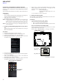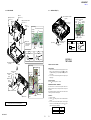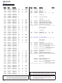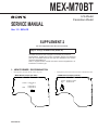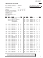
1
MEX-M70BT SERVICE MANUAL US Model Canadian Model Ver. 1.3 2014.12 Note: This service manual is also applicable to areas other than the US and Canadian. The service manual of the mechanism deck, used in this model, has been issued in a separate volume. Please refer to the service manual of the MG-101 series for the mechanism deck information. • The tuner and CD sections have no adjustments. Model Name Using Similar Mechanism CDX-G3000UP Mechanism Type MG-101CF-188 Optical Pick-up Name DAX-25A SPECIFICATIONS FOR THE CUSTOMERS IN THE USA. NOT APPLICABLE IN CANADA, INCLUDING IN THE PROVINCE OF QUEBEC. POUR LES CLIENTS AUX ÉTATS-UNIS. NON APPLICABLE AU CANADA, Y COMPRIS LA PROVINCE DE QUÉBEC. AUDIO POWER SPECIFICATIONS CEA2006 Standard Power Output: 17 Watts RMS × 4 at 4 Ohms < 1% THD+N SN Ratio: 80 dBA (reference: 1 Watt into 4 Ohms) Tuner section FM Tuning range: 87.5 – 108.0 MHz (at 50 kHz step) 87.5 – 108.0 MHz (at 100 kHz step) 87.5 – 107.9 MHz (at 200 kHz step) Antenna (aerial) terminal: External antenna (aerial) connector Intermediate frequency: 25 kHz Usable sensitivity: 8 dBf Selectivity: 75 dB at 400 kHz Signal-to-noise ratio: 80 dB (stereo) Separation: 50 dB at 1 kHz Frequency response: 20 – 15,000 Hz AM Tuning range: 531 – 1,602 kHz (at 9 kHz step) 530 – 1,710 kHz (at 10 kHz step) AM tuning step: 9 kHz/10 kHz switchable Antenna (aerial) terminal: External antenna (aerial) connector Intermediate frequency: 9,124.5 kHz or 9,115.5 kHz/4.5 kHz (at 9 kHz step) 9,115 kHz or 9,125 kHz/5 kHz (at 10 kHz step) Sensitivity: 26 μV CD Player section Signal-to-noise ratio: 120 dB Frequency response: 10 – 20,000 Hz Wow and flutter: Below measurable limit Corresponding codec: MP3 (.mp3) and WMA (.wma) USB Player section Interface: USB (High-speed) Maximum current: 1 A (front), 2.1 A (rear) The maximum number of recognizable tracks: 10,000 Corresponding codec: MP3 (.mp3), WMA (.wma) and WAV (.wav) Wireless Communication General Communication System: BLUETOOTH Standard version 3.1 Output: BLUETOOTH Standard Power Class 2 (Max. +4 dBm) Maximum communication range: Line of sight approx. 10 m (33 ft)*1 Frequency band: 2.4 GHz band (2.4000 – 2.4835 GHz) Modulation method: FHSS Compatible BLUETOOTH Profiles*2: A2DP (Advanced Audio Distribution Profile) 1.3 AVRCP (Audio Video Remote Control Profile) 1.5 HFP (Handsfree Profile) 1.6 PBAP (Phone Book Access Profile) SPP (Serial Port Profile) MAP (Message Access Profile) HID (Human Interface Device Profile) Outputs: Audio outputs terminal (front, rear, sub) Power antenna (aerial)/Power amplifier control terminal (REM OUT) Inputs: SiriusXM input terminal Remote controller input terminal Antenna (aerial) input terminal MIC input terminal AUX input jack (stereo mini jack) USB port: front, rear Power requirements: 12 V DC boat battery (negative ground (earth)) Dimensions: Approx. 178 mm × 50 mm × 177 mm (7 1/ 8 in × 2 in × 7 in) (w/h/d) Mounting dimensions: Approx. 182 mm × 53 mm × 160 mm (7 1/ 4 in × 2 1/ 8 in × 6 5/ 16 in) (w/h/d) Mass: Approx. 1.2 kg (2 lb 11 oz) Package contents: Remote commander (1): RM-X231 Microphone (1) Parts for installation and connections (1 set) Marine remote commander: RM-X11M *1 The actual range will vary depending on factors such as obstacles between devices, magnetic fields around a microwave oven, static electricity, reception sensitivity, antenna (aerial)’s performance, operating system, software application, etc. *2 BLUETOOTH standard profiles indicate the purpose of BLUETOOTH communication between devices. Power amplifier section Output: Speaker outputs Speaker impedance: 4 – 8 ohms Maximum power output: 55 W × 4 (at 4 ohms) * Accessories/equipment other than the marine remote commander RM-X11M are not waterproof. Do not subject them to water. Design and specifications are subject to change without notice. AUDIO SYSTEM 9-893-929-04 2014L33-1 © 2014.12 Sony Corporation Published by Sony Techno Create Corporation MEX-M70BT Copyrights SiriusXM Connect Vehicle Tuner and Subscription sold separately. www.siriusxm.com Sirius, XM and all related marks and logos are trademarks of Sirius XM Radio Inc. All rights reserved. The Bluetooth® word mark and logos are registered trademarks owned by Bluetooth SIG, Inc. and any use of such marks by Sony Corporation is under license. Other trademarks and trade names are those of their respective owners. The N-Mark is a trademark or registered trademark of NFC Forum, Inc. in the United States and in other countries. Windows Media is either a registered trademark or trademark of Microsoft Corporation in the United States and/or other countries. This product is protected by certain intellectual property rights of Microsoft Corporation. Use or distribution of such technology outside of this product is prohibited without a license from Microsoft or an authorized Microsoft subsidiary. iPhone, iPod, iPod classic, iPod nano, and iPod touch are trademarks of Apple Inc., registered in the U.S. and other countries. App Store is a service mark of Apple Inc. MPEG Layer-3 audio coding technology and patents licensed from Fraunhofer IIS and Thomson. Pandora, the Pandora logo, and the Pandora trade dress are trademarks or registered trademarks of Pandora Media, Inc., used with permission. Google, Google Play and Android are trademarks of Google Inc. BlackBerry® is the property of Research In Motion Limited and is registered and/or used in the U.S. and countries around the world. Used under license from Research In Motion Limited. NOTES ON CHIP COMPONENT REPLACEMENT • Never reuse a disconnected chip component. • Notice that the minus side of a tantalum capacitor may be damaged by heat. FLEXIBLE CIRCUIT BOARD REPAIRING • Keep the temperature of soldering iron around 270 °C during repairing. • Do not touch the soldering iron on the same conductor of the circuit board (within 3 times). • Be careful not to apply force on the conductor when soldering or unsoldering. CAUTION The use of optical instruments with this product will increase eye hazard. CAUTION Use of controls or adjustments or performance of procedures other than those specified herein may result in hazardous radiation exposure. 2 SAFETY-RELATED COMPONENT WARNING! COMPONENTS IDENTIFIED BY MARK 0 OR DOTTED LINE WITH MARK 0 ON THE SCHEMATIC DIAGRAMS AND IN THE PARTS LIST ARE CRITICAL TO SAFE OPERATION. REPLACE THESE COMPONENTS WITH SONY PARTS WHOSE PART NUMBERS APPEAR AS SHOWN IN THIS MANUAL OR IN SUPPLEMENTS PUBLISHED BY SONY. ATTENTION AU COMPOSANT AYANT RAPPORT À LA SÉCURITÉ! LES COMPOSANTS IDENTIFIÉS PAR UNE MARQUE 0 SUR LES DIAGRAMMES SCHÉMATIQUES ET LA LISTE DES PIÈCES SONT CRITIQUES POUR LA SÉCURITÉ DE FONCTIONNEMENT. NE REMPLACER CES COMPOSANTS QUE PAR DES PIÈCES SONY DONT LES NUMÉROS SONT DONNÉS DANS CE MANUEL OU DANS LES SUPPLÉMENTS PUBLIÉS PAR SONY. MEX-M70BT SECTION 1 SERVICING NOTES TABLE OF CONTENTS 1. SERVICING NOTES ............................................. 2. GENERAL .................................................................. 16 3. DISASSEMBLY 3-1. Disassembly Flow ........................................................... 3-2. Mini Fuse (Blade Type) (10A/32V) (FU1), Cover Block .................................................................... 3-3. CD Mechanism Deck (MG-101CF-188) ........................ 3-4. Sub Panel Complete Assy ............................................... 3-5. Connection Cable (Automobile) ( ) (CNC1) ................ 3-6. MAIN Board ................................................................... 3-7. Antenna BT (BT1) .......................................................... 3 18 18 19 20 20 21 21 4. TEST MODE ............................................................ 21 5. DIAGRAMS 5-1. Block Diagram - SERVO/BT/USB Section - ................. 5-2. Block Diagram - MAIN Section -................................... 5-3. Block Diagram - PANEL/POWER SUPPLY Section - ............................ 5-4. Printed Wiring Boards - MAIN Section (1/2) - .............. 5-5. Printed Wiring Boards - MAIN Section (2/2) - .............. 5-6. Schematic Diagram - MAIN Section (1/4) - ................... 5-7. Schematic Diagram - MAIN Section (2/4) - ................... 5-8. Schematic Diagram - MAIN Section (3/4) - ................... 5-9. Schematic Diagram - MAIN Section (4/4) - ................... 6. 22 23 NOTES ON HANDLING THE OPTICAL PICK-UP BLOCK OR BASE UNIT The laser diode in the optical pick-up block may suffer electrostatic break-down because of the potential difference generated by the charged electrostatic load, etc. on clothing and the human body. During repair, pay attention to electrostatic break-down and also use the procedure in the printed matter which is included in the repair parts. The flexible board is easily damaged and should be handled with care. NOTES ON LASER DIODE EMISSION CHECK Never look into the laser diode emission from right above when checking it for adjustment. It is feared that you will lose your sight. If the optical pick-up block is defective, please replace the whole optical pick-up block. Never turn the semi-fixed resistor located at the side of optical pick-up block. optical pick-up 24 26 27 28 29 30 31 EXPLODED VIEWS 6-1. Sub Panel Section ........................................................... 41 6-2. Chassis Section ............................................................... 42 7. ELECTRICAL PARTS LIST .............................. 43 Accessories are given in the last of the electrical parts list. semi-fixed resistor UNLEADED SOLDER Boards requiring use of unleaded solder are printed with the leadfree mark (LF) indicating the solder contains no lead. (Caution: Some printed circuit boards may not come printed with the lead free mark due to their particular size) : LEAD FREE MARK Unleaded solder has the following characteristics. • Unleaded solder melts at a temperature about 40 °C higher than ordinary solder. Ordinary soldering irons can be used but the iron tip has to be applied to the solder joint for a slightly longer time. Soldering irons using a temperature regulator should be set to about 350 °C. Caution: The printed pattern (copper foil) may peel away if the heated tip is applied for too long, so be careful! • Strong viscosity Unleaded solder is more viscous (sticky, less prone to flow) than ordinary solder so use caution not to let solder bridges occur such as on IC pins, etc. • Usable with ordinary solder It is best to use only unleaded solder but unleaded solder may also be added to ordinary solder. 3 MEX-M70BT DESTINATION SETTING METHOD When the complete MAIN board or IC502 on the MAIN board is replaced, the destination setting is necessary. 1-3. Entering the Destination Code • Method of operation by main unit 1. Destination Setting Set destination according to the procedure below. 1-1. Setting the Destination Code 1. In the state of source off (the clock is displayed), enter the test mode by pressing the buttons in order of the [ 4] t [MIC 5] t [PAUSE 6] (press only the [PAUSE 6] button for two seconds). 2. In the state in which the software main version is displayed on the liquid crystal display (refer to following figure), enter the destination setting mode by pressing the buttons in order of the [> M SEEK+] t [SEEK– m .] t [PUSH ENTER/ VOICE/ APP]. (Displayed characters/values in the following figure are example) Software main version 1. Rotate the control dial, and select the alphanumeric character of “0 to F”. 2. The digit advances by pressing the [PUSH ENTER/VOICE/ APP] or [> M SEEK+] button. The digit returns by pressing the [MODE ] or [SEEK– m .] button. 3. The setting is completed by pressing the [PUSH ENTER/ VOICE/ APP] button, and the initialization operation is done. • Method of operation by remote commander 3. Input the alphanumeric character of 12 digits of “F XXXXXX” displayed on the liquid crystal display, and execute the destination setting. Note: Refer to following “1-3. Entering the Destination Code” for operation method. 4. The resetting operation is executed by pressing the [ OFF SRC] button for 1 second after the setting ends, and the unit returns to the normal condition. 1-2. Display in Destination Setting Mode (Displayed characters/values in the following figure are example) Destination code OP5 OP4 OP3 OP2 OP1 OP0 12 digits 4 1. Press the [V] or [v] button, and select the alphanumeric character of “0 to F”. 2. The digit advances by pressing the [b] button. The digit returns by pressing the [B] button. 3. The setting is completed by pressing the [ENTER] button, and the initialization operation is done. – Continued on next page – MEX-M70BT Ver. 1.2 1-4. Destination Code OP5 F OP4 2 OP3 4 OP2 2 OP1 E OP0 0 2. Confirmation After Destination Setting Execute the following operation after completing the destination setting, and confirm a correct destination was set. Destination setting checking method: 1. In the state of source off (the clock is displayed on the liquid crystal display), enter the test mode by pressing the buttons in order of the [ 4] t [MIC 5] t [PAUSE 6] (press only the [PAUSE 6] button for two seconds). 2. In the state in which the software main version is displayed on the liquid crystal display (refer to following figure), enter the destination setting value display mode by pressing the [ DSPL MENU] button twice. (Displayed characters/values in the following figure are example) Software main version 3. Confirm the alphanumeric character of 12 digits in liquid crystal display is a value correctly input. (Displayed characters/values in the following figure are example) Destination code OP5 OP4 OP3 OP2 OP1 OP0 12 digits 4. The resetting operation is executed by pressing the [ OFF SRC] button for 1 second after the confirming ends, and the unit returns to the normal condition. TEST DISCS Use following TEST DISC (for CD) when this unit confirms the operation and checks it. Part No. Description 3-702-101-01 4-225-203-01 DISC (YEDS-18), TEST DISC (PATD-012), TEST NOTE OF REPLACING THE KEY BOARD When the KEY board is defective, replace the FRONT PANEL (SV) (ASSY) (Ref. No. FP1). NOTE OF REPLACING THE IC804 AND IC1002 ON THE MAIN BOARD IC804 and IC1002 on the MAIN board cannot replace with single. When these parts are damaged, replace the complete mounted board. IMPORTANT NOTE OF “INITIALIZING” The purpose of “Bluetooth Initialize” is to initialize the Bluetooth connection history (HF/Audio Streaming). (To delete the device information for the devices that you connected to when searching, etc.) When complete MAIN board is replaced, it is necessary to initialize this unit. Refer to the following, initialize this unit. Note: Phonebook data and dialed/received call history can be deleted by executing “Bluetooth Initialize”. Procedure: 1. In the state of source off (the clock is displayed), press the [ DSPL MENU] button. 2. Rotate the control dial, and select the “SET BT”. 3. Press the [PUSH ENTER/VOICE/ APP] button. 4. Rotate the control dial, and select the “SET BT INIT”. 5. Press the [PUSH ENTER/VOICE/ APP] button, and the message “SET INIT-NO” is displayed on the liquid crystal display. 6. Rotate the control dial clockwise, and the message “SET INITYES” is displayed on the liquid crystal display. 7. Press the [PUSH ENTER/VOICE/ APP] button, and the message “INITIAL” is blinked on the liquid crystal display. 8. When “Bluetooth Initialize” is completed, the message “COMPLETE” is displayed on the liquid crystal display for a moment. 9. Press the [MODE ] button, and return to the state of source off (the clock is displayed) mode. 5 MEX-M70BT OPERATION CHECK OF THE NFC AFTER COMPLETING THE REPAIRS After completing the repairs of this unit, follow the procedure below to check normal operation of the NFC. Note: After checking of NFC operation, be sure to delete the pairing information before returning this unit to the customer. REPLACING THE LITHIUM BATTERY OF THE REMOTE COMMANDER When the battery becomes weak, the range of the remote commander becomes shorter. Replace the battery with a new CR2025 lithium battery. Use of any other battery may present a risk of fire or explosion. Connecting with a Smartphone by One touch (NFC) + side up By touching the control dial on the unit with an NFC* compatible smartphone, the unit is paired and connected with the smartphone automatically. * NFC (Near Field Communication) is a technology enabling short-range wireless communication between various devices, such as mobile phones and IC tags. Thanks to the NFC function, data communication can be achieved easily just by touching the relevant symbol or designated location on NFC compatible devices. For a smartphone with Android OS 4.0 or lower installed, downloading the app “NFC Easy Connect” available at Google Play™ is required. The app may not be downloadable in some countries/regions. 1 Activate the NFC function on the smartphone. For details, refer to the operating instructions supplied with the smartphone. 2 Touch the N-Mark part of the unit with the N-Mark part of the smartphone. Notes on the lithium battery ˎ Keep the lithium battery out of the reach of children. Should the battery be swallowed, immediately consult a doctor. ˎ Wipe the battery with a dry cloth to assure a good contact. ˎ Be sure to observe the correct polarity when installing the battery. ˎ Do not hold the battery with metallic tweezers, otherwise a short-circuit may occur. WARNING Battery may explode if mistreated. Do not recharge, disassemble, or dispose of in fire. CLEANING THE CONNECTORS The unit may not function properly if the connectors between the unit and the front panel are not clean. In order to prevent this, detach the and clean theclean connectors with front panel (page 8) and the connectors with a cotton swab. Do not apply too much force. Otherwise, the connectors may be damaged. Make sure that unit. lights up on the display of the To disconnect by One touch Touch the N-Mark part of the unit with the N-Mark part of the smartphone again. Notes ˎ When making the connection, handle the smartphone carefully to prevent scratches. ˎ One touch connection is not possible when the unit is already connected to another NFC compatible device. In this case, disconnect the other device, and make connection with the smartphone again. Notes ˎ For safety, turn off the ignition before cleaning the connectors, and remove the key from the ignition switch. ˎ Never touch the connectors directly with your fingers or with any metal device. CANCELING THE DEMO MODE You can cancel the demonstration display which appears while this unit is turned off. 1 Press MENU, rotate the control dial to select [DISPLAY], then press it. 2 Rotate the control dial to select [DEMO], then press it. 3 Rotate the control dial to select [DEMOOFF], then press it. The setting is complete. 4 Press (back) twice. The display returns to normal reception/play mode. 6 MEX-M70BT BLUETOOTH FUNCTION CHECKING METHOD USING A CELLULAR PHONE 1. Required Equipment • This unit to be tested, external microphone of attachment if necessary • Cellular phone (Recommended SEMC W880 or W910i, or select from connectable cellular phones list) • Bluetooth audio devices (SONY NWZ-A826, or select from connectable cellular phones/audio devices list) • Speaker connection (at least Front L/R ch) • DC power supply (12 V) 2. Preparation • Confirm the setting of this unit and note down it. • Press the [CALL ] button and rotate the control dial until “SET PAIRING” appears, then press it, confirm that the Bluetooth signal icon ( ) is flashing. • Turn on the Bluetooth function of the cellular phone. 3. Test Environment • No other Bluetooth device is making a communication in the periphery (within 20 m). • No other this unit are supplied with electric power. • There are no two or more wireless LAN access points in the periphery (with 50 m) (one is OK). • The set should be tested in a place such as a meeting room, free from ambient noise. • The speaker at the far end should be in a place such as another meeting room separated acoustically. 4. Setting Install this unit on the desktop. Approx. 50 cm Speaker Unit 6. Bluetooth Phone (Hands Free) Function Check Note: Depending on the connecting device, Signal-strength/Battery-remaining indications might not be displayed. Or, depending on the connecting device, the levels of indications are shown incorrectly. Even if you see no indications or wrong indications, they are not failures of this unit. 1. Search for this unit from the Bluetooth device (cellular phone), and confirm whether this unit (“Sony Car Audio”) is displayed. 2. Search for the distance of this unit and the Bluetooth device (cellular phone) about 5 m apart. Confirm whether the Bluetooth device (or this unit) is displayed after it searches. 3. Do the pairing of the cellular phone and this unit (input of passkey). 4. Connect the cellular phone with this unit, and confirm the “HF” icon ( ) lights. 5. Confirm the connection continues even if the distance of the cellular phone and this unit is separated by about 5 m. 6. Set this unit besides the “BT PHONE” source, and call the cellular phone connected with this unit. Confirm the automatic change of this unit into “BT PHONE” source, and the change into the screen for incoming calls. Confirm the ring tone is heard from the front speaker. 7. Take a phone call (press the [CALL ] button), and start a conversation. Confirm the other person voice is heard from the speaker. Speak toward the microphone of this unit, and confirm whether the other party hears its voice (At the external microphone noncontact). Compare the sound quality with a normal set. Confirm that there is no big difference. 8. Speak toward an external microphone at the following condition, and confirm the other party hears its voice. • An external microphone is connected. 9. Turn on ACC from off, and confirm whether this unit connects Bluetooth with the cellular phone again. Note: Depending on the cellular phone, it might not reconnect automatically when ACC is turned on. 7. Bluetooth Audio Function Check Approx. 80 cm Note: Depending on the connecting BT Audio device, track information (e.g. track name, playback time) can be on display. If the device doesn’t support AVRCP1.3, or, if AVRCP1.3 feature of the device has not been validated with this unit; the track information won't be shown. Even if there is no track information on display during playback of an AVRCP1.3 device, it is not a failure of this unit. Tester 5. Precautions Beware of the following points when conducting the talking test: • There is no fault if a talking can be made by adjusting appropriately the volume of the telephone of the other party and the cellular phone connected through the Bluetooth, besides the setup of this unit. • The speaker’s voice will become loud naturally if the periphery is noisy, or become low if quiet (even though the speaker intents to talk on the same volume level). • The speaker’s voice will become loud naturally if the other party’s voice is loud. 1. Connect the Bluetooth audio device (or cellular phone with Bluetooth audio function) with this unit, and confirm the “Audio Streaming” icon ( ) lights. 2. Playback Bluetooth audio. Confirm the sound is emitted from this unit when this unit is switched to “Bluetooth Audio” source. 3. Confirm whether Bluetooth audio can be controlled by operating this unit (the [> M SEEK+], [SEEK– m .] and [PAUSE 6] buttons operation). Note: Varies depending on the connected Bluetooth audio device. 8. What to Do after Checking • After checking, select “SET BT INIT” from the menu list of this unit to execute initialization. (Connected device information is deleted) 7 MEX-M70BT Ver. 1.3 BLUETOOTH INFORMATION WRITING METHOD When the complete MAIN board, knob (VOL) (SV) assy or front panel (SV) (assy) is replaced, the writing of Bluetooth information is necessary. Write the Bluetooth information according to the procedure below. Preparation: • Windows PC • NFC compatible smartphone that installed the file manager application (ASTRO File Manager, File Expert, etc.) • USB cable for the smartphone • NFCtagWriter.apk (ver.1.0.2 and above) Note 1: The NFCtagWriter.apk is updated. When the NFCtagWriter.apk is prepared already, be sure to refer to the “6. Version Check Method of the NFC Tag Data Writing Application for the Servicing” on the page 12, and check the version of NFCtagWriter.apk. Note 2: Confirm the method of obtaining the NFCtagWriter.apk to the service headquarters. 1. Installing the NFC Writing Application for the Servicing Install the NFCtagWriter.apk on the smartphone for writing of Bluetooth information. 9. Refer to the “6. Version Check Method of the NFC Tag Data Writing Application for the Servicing” on the page 12, and check the version of NFCtagWriter.apk. ver.0.9.0 : The use is not allowed. Install the NFCtagWriter.apk of ver.1.0.2 and above. ver.1.0.2 and above : The use is allowed. 2. Writing the NFC Tag Data Write the NFC tag data (Bluetooth information) to the NFC module in the knob (VOL) (SV) assy. Procedure: 1. Check the Bluetooth address (BD_ADDR). There are following two checking methods. • How to read from the BT module label • How to display on the liquid crystal display by the test mode How to read from the BT module label: Set the unit to the state where the BT module (Ref. No. IC1002 on the MAIN board) can be seen. (Refer to the “3. DISASSEMBLY” on the page 18 and after) – MAIN board top view – Procedure: 1. Prepare the NFCtagWriter.apk file on the PC. 2. Connect the smartphone to the PC with the USB cable. 3. Transfer the NFCtagWriter.apk to the smartphone. 4. When tapping the “Settings” → “Security” on the screen of the smartphone, check the box “Unknown sources”. BD_ADDR (Barcode) 5. Disconnect the smartphone from the PC. 6. Use the file manager application to explore the NFCtagWriter. apk on the smartphone. 7. Click on the NFCtagWriter.apk to open it, and install the NFCtagWriter.apk to the smartphone. 8. When tapping the “Settings” → “Security” on the screen of the smartphone, uncheck the box “Unknown sources”. – Screen after the installation for reference – 8 Movies Settings WALKMAN Album YouTube Media Player Play Store Camera Chrome NFCtagWriter Maps Browser NFCtagWriter application 48D2242F241A BD_ADDR BT module label – Continued on next page – MEX-M70BT Ver. 1.3 How to display on the liquid crystal display by the test mode: 1. In the state of source off (the clock is displayed on the liquid crystal display), enter the test mode by pressing the buttons in order of the [ 4] t [MIC 5] t [PAUSE 6] (press only the [PAUSE 6] button for two seconds). 6. Input the Bluetooth address (BD_ADDR). (Input the Bluetooth address (BD_ADDR) that written on the BT module label with the keyboard on the smartphone, or tap the “QR” on the screen of the smartphone and read the barcode with the camera of the smartphone) Software main version Sony Car Audio 2. In the state in which the software main version is displayed on the liquid crystal display, enter the Bluetooth address (BD_ADDR) display mode by pressing the [ DSPL MENU] button. (Displayed characters/values in the following figure are example) Bluetooth Device Addres Bluetooth address (BD_ADDR) 7. Tap the “Write” on the screen of the smartphone, in the state that unchecked the box “Read-only”. Note 1: When pressing the [ DSPL MENU] button again, the destination code is displayed on the liquid crystal display, but it is not necessary to display in this step. 3. The resetting operation is executed by pressing the [ OFF SRC] button for 1 second after the confirming ends, and the unit returns to the normal condition. Sony Car Audio 2. Turn on the NFC function of the smartphone. 3. Start the NFCtagWriter application on the smartphone. 4. Tap the “Write” on the screen of the smartphone. 48D2242F241A 8. Touch the N-mark part of the smartphone to the N-mark part of the unit. 5. Input the Bluetooth Local Name (BL_NAME). (Input the “Sony Car Audio” with the keyboard on the smartphone, or tap the “List” on the screen of the smartphone and select the “Sony Car Audio”) 9 Check that “Completed!” is displayed on the screen of the smartphone. Note 2: When “Completed!” is not displayed on the screen of the smartphone, refer to “3. Error Display” on the page 10. Bluetooth Local Name Bluetooth Device Addres – Continued on next page – 9 MEX-M70BT Ver. 1.3 10. End the NFCtagWriter application on the smartphone. 11. Check the operation of connecting with the smartphone by one touch (NFC). (Refer to the “OPERATION CHECK OF THE NFC AFTER COMPLETING THE REPAIRS” on the page 6) 12. Start the NFCtagWriter application on the smartphone. 13. Tap the “Write” on the screen of the smartphone. 17. Tap the “Read” on the screen of the smartphone. 18. Check that “BD_ADDR” on the screen of the smartphone accords with BD_ADDR written on the BT module label and “MODE” on the screen of the smartphone is “00 00 (Readonly)”. 14. Check the box “Read-only” on the screen of the smartphone, and tap the “Write” on the screen of the smartphone. Sony Car Audio 48D2242F241A 15. Touch the N-mark part of the smartphone to the N-mark part of the unit. 19. End the NFCtagWriter application on the smartphone. 20. Check the operation of connecting with the smartphone by one touch (NFC). (Refer to the “OPERATION CHECK OF THE NFC AFTER COMPLETING THE REPAIRS” on the page 6) 3. Error Display When the writing of the NFC tag data has failed, “Error” is displayed on the screen of the smartphone. When “Error” is displayed on the screen of the smartphone, operate according to the procedure below. 16. Check that “Completed!” is displayed on the screen of the smartphone. Note 3: When “Completed!” is not displayed on the screen of the smartphone, refer to “3. Error Display”. Procedure: 1. Tap the “Write” on the screen of the smartphone to write of the NFC tag data again. 2. When “Error” is displayed on the screen of the smartphone again, tap the “Read” on the screen of the smartphone. 3. Check that “MODE” on the screen of the smartphone is not “00 00 (Read-only)”. 4. When “MODE” on the screen of the smartphone is “00 00 (Read-only)”, execute the writing of the NFC tag data again after replacing the knob (VOL) (SV) assy. (When “MODE” on the screen of the smartphone is “00 00 (Read-only)”, the writing of the NFC tag data cannot execute) 10 MEX-M70BT Ver. 1.3 4. Check Method of the NFC Tag Data Check the NFC tag data according to the procedure below. 2. Turn on the NFC function of the smartphone. 3. Start the NFCtagWriter application on the smartphone. 4. Tap the “Read” on the screen of the smartphone. Procedure: 1. Check the Bluetooth address (BD_ADDR). There are following two checking methods. • How to read from the BT module label • How to display on the liquid crystal display by the test mode How to read from the BT module label: Set the unit to the state where the BT module (Ref. No. IC1002 on the MAIN board) can be seen. (Refer to the “3. DISASSEMBLY” on the page 18 and after) – MAIN board top view – 5. Check that “BD_ADDR” on the screen of the smartphone accords with BD_ADDR written on the BT module label and “MODE” on the screen of the smartphone is “00 00 (Readonly)”. BD_ADDR (Barcode) 6. End the NFCtagWriter application on the smartphone. 48D2242F241A BD_ADDR BT module label How to display on the liquid crystal display by the test mode: 1. In the state of source off (the clock is displayed on the liquid crystal display), enter the test mode by pressing the buttons in order of the [ 4] t [MIC 5] t [PAUSE 6] (press only the [PAUSE 6] button for two seconds). Software main version 2. In the state in which the software main version is displayed on the liquid crystal display, enter the Bluetooth address (BD_ADDR) display mode by pressing the [ DSPL MENU] button. (Displayed characters/values in the following figure are example) Bluetooth address (BD_ADDR) Note: When pressing the [ DSPL MENU] button again, the destination code is displayed on the liquid crystal display, but it is not necessary to display in this step. 3. The resetting operation is executed by pressing the [ OFF SRC] button for 1 second after the confirming ends, and the unit returns to the normal condition. 11 MEX-M70BT Ver. 1.3 5. The Factor that One Touch Connection is Impossible The four following factors are considered as the factor that one touch connection is impossible. Guess and check the defective factor by each checking result. Note: The four following factors are examples. Factor 1 BT module defect Knob (VOL) (SV) 2 assy defect NFC tag data 3 writing failure 4 Smartphone Bluetooth manual connection check by user NG NFC tag data check ― Bluetooth manual connec- NFC one touch connection tion check by servicing check with smartphone NG NG OK NG OK NG OK NG OK NG OK OK OK NG 6. Version Check Method of the NFC Tag Data Writing Application for the Servicing Check the version of the NFC tag data writing application (NFCtagWriter application) for the servicing according to the procedure below. Procedure: 1. Start the NFCtagWriter application on the smartphone. 2. Tap the “ ” (menu button) or “ ” of the screen of the smartphone, then tap the “About” that is displayed on the screen of the smartphone. AFFIXING OF LABEL (SERIAL NUMBER) When the front panel (SV) (assy) is replaced, it is necessary to affix the label (serial number). 2 labels (serial number) are included with a new front panel (SV) (assy). Affix 1 label to the rear side of the front panel (SV) (assy). Affix the other one to the bottom side of main unit. Be sure to perform this procedure, as Bluetooth will not operate correctly if the serial number of the front panel (SV) (assy) and main unit do not match. Also, since the serial number has changed, print page 13 and hand the tear-off with the product to the customer when returning the product after repairs are complete. or label (serial number) – Front panel (SV) (assy) rear view – label (serial number) 3. Check that version of the NFC tag data writing application for the servicing is displayed on the screen of the smartphone. – Main unit bottom view – ver.0.9.0 The use is not allowed (Use the ver.1.0.2 and above) 12 ver.1.0.2 The use is allowed MEX-M70BT • Please cut out along the dotted line and use it. Notice about the serial number change on the back side of the front panel: The serial number on the back of the front panel has changed due to repairs. For details, refer to the “Detaching the Front Panel” section of “Getting Started” in the instruction manual. Notice about the serial number change on the back side of the front panel: The serial number on the back of the front panel has changed due to repairs. For details, refer to the “Detaching the Front Panel” section of “Getting Started” in the instruction manual. Notice about the serial number change on the back side of the front panel: The serial number on the back of the front panel has changed due to repairs. For details, refer to the “Detaching the Front Panel” section of “Getting Started” in the instruction manual. Notice about the serial number change on the back side of the front panel: The serial number on the back of the front panel has changed due to repairs. For details, refer to the “Detaching the Front Panel” section of “Getting Started” in the instruction manual. Notice about the serial number change on the back side of the front panel: The serial number on the back of the front panel has changed due to repairs. For details, refer to the “Detaching the Front Panel” section of “Getting Started” in the instruction manual. Notice about the serial number change on the back side of the front panel: The serial number on the back of the front panel has changed due to repairs. For details, refer to the “Detaching the Front Panel” section of “Getting Started” in the instruction manual. Notice about the serial number change on the back side of the front panel: The serial number on the back of the front panel has changed due to repairs. For details, refer to the “Detaching the Front Panel” section of “Getting Started” in the instruction manual. Notice about the serial number change on the back side of the front panel: The serial number on the back of the front panel has changed due to repairs. For details, refer to the “Detaching the Front Panel” section of “Getting Started” in the instruction manual. Notice about the serial number change on the back side of the front panel: The serial number on the back of the front panel has changed due to repairs. For details, refer to the “Detaching the Front Panel” section of “Getting Started” in the instruction manual. Notice about the serial number change on the back side of the front panel: The serial number on the back of the front panel has changed due to repairs. For details, refer to the “Detaching the Front Panel” section of “Getting Started” in the instruction manual. Notice about the serial number change on the back side of the front panel: The serial number on the back of the front panel has changed due to repairs. For details, refer to the “Detaching the Front Panel” section of “Getting Started” in the instruction manual. Notice about the serial number change on the back side of the front panel: The serial number on the back of the front panel has changed due to repairs. For details, refer to the “Detaching the Front Panel” section of “Getting Started” in the instruction manual. Notice about the serial number change on the back side of the front panel: The serial number on the back of the front panel has changed due to repairs. For details, refer to the “Detaching the Front Panel” section of “Getting Started” in the instruction manual. Notice about the serial number change on the back side of the front panel: The serial number on the back of the front panel has changed due to repairs. For details, refer to the “Detaching the Front Panel” section of “Getting Started” in the instruction manual. Notice about the serial number change on the back side of the front panel: The serial number on the back of the front panel has changed due to repairs. For details, refer to the “Detaching the Front Panel” section of “Getting Started” in the instruction manual. Notice about the serial number change on the back side of the front panel: The serial number on the back of the front panel has changed due to repairs. For details, refer to the “Detaching the Front Panel” section of “Getting Started” in the instruction manual. 13 MEX-M70BT MEMO 14 MEX-M70BT Ver. 1.3 SERVICE POSITION Note: The length of cable flexible flat (27 core) has been changed from 150 mm to 80 mm in the midway of production. When the length of cable flexible flat (27 core) is 80 mm, cannot performing the operation check in the state that is removed the CD mechanism deck from the main unit. When performing the operation check, use following flexible flat cable. Part No. Descrimination 1-846-819-31 CABLE FLEXIBLE FLAT (27 CORE) (Length: 150 mm) OK OK CD mechanism deck CD mechanism deck insulating sheet insulating sheet stand stand cable flexible flat (27 core) Note: Do not cable flexible flat (27 core) is damaged by the edge of the chassis. main unit main unit NG NG CD mechanism deck Note: CD mechanical deck should not be placed vertically. cable flexible flat (27 core) cable flexible flat (27 core) Note: Do not cable flexible flat (27 core) is damaged by the edge of the chassis. main unit CD mechanism deck Note: CD mechanical deck should not be placed vertically. main unit cable flexible flat (27 core) NG CD mechanism deck Note: CD mechanical deck should not be placed upside down. cable flexible flat (27 core) main unit 15 MEX-M70BT SECTION 2 GENERAL This section is extracted from instruction manual. A Smartphone, iPod/iPhone, USB device Téléphone intelligent, iPod/iPhone, périphérique USB Teléfono inteligente, iPod/iPhone, dispositivo USB Ferrite sleeve Gaine en ferrite Casquillo de ferrita *1 Smartphone*6, iPod/iPhone*7, USB device Téléphone intelligent*6, iPod/ iPhone*7, périphérique USB Teléfono inteligente*6, iPod/ iPhone*7, dispositivo USB Equipment used in illustrations (not supplied) Appareils utilisés dans les illustrations (non fournis) Equipo utilizado en las ilustraciones (no suministrado) *9 *9 Front speaker Haut-parleur avant Altavoz frontal Subwoofer Caisson de graves Altavoz potenciador de graves *9 Satellite radio tuner (SiriusXM)*3 Syntoniseur radio satellite (SiriusXM)*3 Sintonizador de radio por satélite (SiriusXM)*3 Fuse (10 A) Fusible (10 A) Fusible (10 A) *1 B *9 Rear speaker Haut-parleur arrière Altavoz posterior RM-X11M *8 from boat antenna (aerial) à partir de l’antenne du bateau desde la antena del barco Satellite radio tuner (SiriusXM)*1 Syntoniseur radio satellite (SiriusXM)*1 Sintonizador de radio por satélite (SiriusXM)*1 ʛ* 4 *1 RCA pin cord (not supplied). *2 Separate adaptor may be required. *3 not supplied *4 For details on installing the microphone, see “Installing the microphone (˳)” on the reverse side. *5 Whether in use or not, route the microphone input cord such that it does not interfere with driving. Secure the cord with a clamp, etc., if it is installed around your feet. *6 To connect a smartphone to the main unit, an appropriate cable (not supplied) is required. *7 To connect an iPod/iPhone, use the USB connection cable for iPod (not supplied). *8 Supplied with the marine remote commander. *9 not waterproof *10Speaker impedance: 4 – 8 ohms × 4 Blue/white striped Rayé bleu/blanc Con rayas azules y blancas REM OUT *2 Marine remote commander Télécommande marine Mando a distancia subacuático ʔ C Max. supply current 0.4 A Courant max. fourni 0,4 A Corriente máx. de alimentación de 0,4 A White Blanc Blanco Left Gauche Izquierdo White/black striped Rayé blanc/noir Con rayas blancas y negras Gray Gris Gris Right Droit Derecho *10 Left Gauche Izquierdo Right Droit Derecho Black Noir Negro Orange/white striped Rayé orange/blanc Con rayas naranjas/blancas Gray/black striped Rayé gris/noir Con rayas grises y negras Green Vert Verde Red Rouge Rojo Green/black striped Rayé vert/noir Con rayas verdes y negras Purple Violet Morado Yellow Jaune Amarillo ILLUMINATION ACC BATTERY Purple/black striped Rayé violet/noir Con rayas moradas y negras English Cautions Be sure to install this unit in the dashboard of the boat as the rear side of the unit becomes hot during use. ˎThis unit is designed for negative ground (earth) 12 V DC operation only. ˎDo not get the leads under a screw, or caught in moving parts (e.g. seat railing). ˎBefore making connections, turn the boat’s ignition off to avoid short circuits. ˎConnect the yellow and red power supply leads only after all other leads have been connected. ˎRun all ground (earth) leads to a common ground (earth) point. ˎBe sure to insulate any loose unconnected leads with electrical tape for safety. ˎUnder the environment of potential water splash, Sony highly recommends to protect the unit with Waterproof Car Stereo Cover (not supplied). While an iPod or USB device is connected, the Waterproof Car Stereo Cover cannot be fully closed. Avoid splashing water on the unit. ˎThe use of optical instruments with this product will increase eye hazard. Notes on the power supply lead (yellow) ˎWhen connecting this unit in combination with other stereo components, the connected boat circuit’s rating must be higher than the sum of each component’s fuse. ˎWhen no boat circuits are rated high enough, connect the unit directly to the battery. Connection example ( ) Subwoofer Easy Connection (ǵ-C) You can use a subwoofer without a power amplifier when it is connected to a rear speaker cord. *1 not supplied (ǵ-B) *2 Do not connect a speaker in this connection (ǵ-C). Notes ˎBe sure to connect the ground (earth) lead before connecting the amplifier (ǵ-A). ˎThe alarm will only sound if the built-in amplifier is used (ǵ-A). ˎBe sure to connect a 4 - 8 ohm subwoofer. Do not connect a speaker to the other rear speaker cord (ǵ-C). 16 Power amplifier Amplificateur de puissance Amplificador de potencia Connection diagram ( ) ɞ To battery or distribution block ground First connect the black ground (earth) lead, then connect the yellow and red power supply leads. ɟ To the power antenna (aerial) control lead or power supply lead of antenna (aerial) booster Notes ˎIt is not necessary to connect this lead if there is no power antenna (aerial) or antenna (aerial) booster, or with a manually-operated telescopic antenna (aerial). ˎWhen your boat has a built-in FM/AM antenna (aerial) in the rear/side glass, see “Notes on the control and power supply leads.” To AMP REMOTE IN of an optional power amplifier This connection is only for amplifiers and a power antenna (aerial). Connecting any other system may damage the unit. ɠ To a boat’s illumination signal Be sure to connect the black ground (earth) lead to the battery or distribution block ground first. ɡ To the +12 V power terminal which is energized in the accessory position of the ignition switch Notes ˎIf there is no accessory position, connect to the +12 V power (battery) terminal which is energized at all times. Be sure to connect the black ground (earth) lead to the battery or distribution block ground first. ˎWhen your boat has a built-in FM/AM antenna (aerial) in the rear/side glass, see “Notes on the control and power supply leads.” ɢ To the +12 V power terminal which is energized at all times Be sure to connect the black ground (earth) lead to the battery or distribution block ground first. Notes on the control and power supply leads ˎREM OUT lead (blue/white striped) supplies +12 V DC when you turn on the unit. ˎWhen your boat has built-in FM/AM antenna (aerial) in the rear/ side glass, connect REM OUT lead (blue/white striped) or the accessory power supply lead (red) to the power terminal of the existing antenna (aerial) booster. For details, consult your dealer. ˎA power antenna (aerial) without a relay box cannot be used with this unit. Memory hold connection When the yellow power supply lead is connected, power will always be supplied to the memory circuit even when the ignition switch is turned off. Notes on speaker connection ˎBefore connecting the speakers, turn the unit off. ˎUse speakers with an impedance of 4 to 8 ohms, and with adequate power handling capacities to avoid its damage. ˎDo not connect the speaker terminals to the boat chassis, or connect the terminals of the right speakers with those of the left speaker. ˎDo not connect the ground (earth) lead of this unit to the negative (–) terminal of the speaker. ˎDo not attempt to connect the speakers in parallel. ˎConnect only passive speakers. Connecting active speakers (with built-in amplifiers) to the speaker terminals may damage the unit. ˎTo avoid a malfunction, do not use the built-in speaker leads installed in your boat if the unit shares a common negative (–) lead for the right and left speakers. ˎDo not connect the unit’s speaker leads to each other. Français Mises en garde Installez cet appareil sur le tableau de bord du bateau, car l’arrière de l’appareil chauffe en cours d’utilisation. ˎCet appareil est exclusivement conçu pour fonctionner sur une tension de 12 V CC avec masse négative. ˎÉvitez de fixer des vis sur les câbles ou de coincer ceux-ci dans des pièces mobiles (par exemple, armature de siège). ˎAvant d’effectuer les raccordements, coupez le contact du bateau pour éviter les courts-circuits. ˎRaccordez les câbles d’alimentation jaune et rouge seulement après avoir terminé tous les autres raccordements. ˎRassemblez tous les câbles de mise à la masse en un point de masse commun. ˎPour des raisons de sécurité, veillez à isoler avec du ruban isolant tout câble libre non raccordé. ˎSi l’appareil risque d’être exposé à des éclaboussures d’eau, Sony recommande fortement de le protéger avec une housse imperméable pour chaîne stéréo de voiture (non fournie). Lorsqu’un iPod ou un périphérique USB est raccordé, la housse imperméable pour chaîne stéréo de voiture ne peut pas se fermer complètement. Évitez d’exposer l’appareil à des éclaboussures d’eau. ˎL’utilisation d’instruments optiques avec ce produit augmente les risques pour les yeux. Remarques sur le câble d’alimentation (jaune) ˎLorsque cet appareil est raccordé à d’autres éléments stéréo, la valeur nominale du circuit du bateau raccordé doit être supérieure à la somme des fusibles de chaque élément. ˎSi aucun circuit du bateau n’est assez puissant, raccordez directement l’appareil à la batterie. Exemple de raccordement ( ) Raccordement facile d’un caisson de graves (ǵ-C) Vous pouvez utiliser un caisson de graves sans amplificateur de puissance lorsque vous effectuez le raccordement à un cordon de haut-parleur arrière. *1 non fourni (ǵ-B) *2 Ne raccordez pas un haut-parleur avec cette connexion (ǵ-C). Remarques ˎRaccordez d’abord le câble de mise à la masse avant de raccorder l’amplificateur (ǵ-A). ˎL’alarme est émise uniquement lorsque l’amplificateur intégré est utilisé (ǵ-A). ˎAssurez-vous de raccorder un caisson de graves de 4 - 8 ohms. Ne raccordez pas de haut-parleur à l’autre cordon de haut-parleur arrière (ǵ-C). Schéma de raccordement ( ) Español *1 Cordon à broche RCA (non fourni). *2 L’utilisation d’un adaptateur pourrait être nécessaire. *3 non fourni *4 Pour les détails sur l’installation du microphone, référez-vous à « Installation du microphone (Ǽ) » au verso. *5 Qu’il soit en usage ou non, acheminez le cordon d’entrée du microphone de telle sorte qu’il ne gêne pas votre conduite. Fixez le cordon à l’aide d’une attache, etc., s’il est installé autour de vos pieds. *6 Pour raccorder un téléphone intelligent à l’appareil principal, un câble approprié (non fourni) est requis. *7 Pour raccorder un iPod/iPhone, utilisez le câble de raccordement USB pour iPod (non fourni). *8 Fourni avec la télécommande marine. *9 non étanche *10Impédance des haut-parleurs : 4 – 8 ohms × 4 *1 Cable con terminales RCA (no suministrado). *2 Puede requerirse un adaptador independiente. *3 no suministrado *4 Para obtener detalles sobre la instalación del micrófono, consulte “Instalación del micrófono (Ǽ)” al reverso. *5 Se esté utilizando o no, coloque el cable de entrada del micrófono de modo que no interfiera en el manejo del automóvil. Si instala los cables cerca de la zona de los pies, fíjelos con una abrazadera, etc. *6 Para conectar un teléfono inteligente a la unidad principal, es necesario utilizar un cable adecuado (no suministrado). *7 Para conectar un iPod/iPhone, use el cable de conexión USB para iPod (no suministrado). *8 Suministrado con el mando a distancia subacuático. *9 no es resistente al agua *10Impedancia del altavoz: 4 – 8 Ω × 4 Diagrama de conexión ( ) ɞ Vers la batterie ou le répartiteur de terre Precauciones ɞ A la conexión a masa de la batería o del bloque ɟ Au câble de commande d’antenne électrique ou Asegúrese de instalar la unidad en el tablero del barco, ya que la parte posterior de la unidad se calienta durante el uso. ɟ Al cable de control de la antena motorizada o al Branchez d’abord le câble de mise à la masse noir et, ensuite, les câbles d’alimentation jaune et rouge. au câble d’alimentation de l’amplificateur d’antenne Remarques ˎIl n’est pas nécessaire de raccorder ce câble s’il n’y a pas d’antenne électrique ni d’amplificateur d’antenne, ou avec une antenne télescopique manuelle. ˎSi votre bateau est équipé d’une antenne FM/AM intégrée dans la vitre arrière/latérale, voir « Remarques sur les câbles de commande et d’alimentation ». Au niveau de AMP REMOTE IN de l’amplificateur de puissance en option Ce raccordement s’applique uniquement aux amplificateurs et à une antenne électrique. Le branchement de tout autre système risque d’endommager l’appareil. ɠ Vers le connecteur du signal d’éclairage du bateau Commencez par raccorder le câble de mise à la masse noir à la batterie ou au répartiteur de terre. ɡ À la borne d’alimentation +12 V qui est alimentée quand la clé de contact est sur la position accessoires Remarques ˎS’il n’y a pas de position accessoires, raccordez la borne d’alimentation (batterie) +12 V qui est alimentée en permanence. Commencez par raccorder le câble de mise à la masse noir à la batterie ou au répartiteur de terre. ˎSi votre bateau est équipé d’une antenne FM/AM intégrée dans la vitre arrière/latérale, voir « Remarques sur les câbles de commande et d’alimentation ». ɢ À la borne d’alimentation +12 V qui est alimentée en permanence Commencez par raccorder le câble de mise à la masse noir à la batterie ou au répartiteur de terre. Remarques sur les câbles de commande et d’alimentation ˎLe câble REM OUT (rayé bleu/blanc) fournit une alimentation de +12 V CC lorsque vous mettez l’appareil en marche. ˎLorsque votre bateau est équipé d’une antenne FM/AM intégrée dans la vitre arrière/latérale, raccordez le câble REM OUT (rayé bleu/blanc) ou le câble d’alimentation des accessoires (rouge) à la borne d’alimentation de l’amplificateur d’antenne existant. Pour plus de détails, consultez votre détaillant. ˎUne antenne électrique sans boîtier de relais ne peut pas être utilisée avec cet appareil. Raccordement pour la conservation de la mémoire Lorsque le câble d’alimentation jaune est raccordé, le circuit de la mémoire est alimenté en permanence même si la clé de contact est sur la position d’arrêt. Remarques sur le raccordement des haut-parleurs ˎAvant de raccorder les haut-parleurs, éteignez l'appareil. ˎUtilisez des haut-parleurs ayant une impédance de 4 à 8 ohms avec une capacité électrique adéquate pour éviter de les endommager. ˎNe raccordez pas les bornes du système de haut-parleurs au châssis du bateau et ne raccordez pas les bornes du haut-parleur droit à celles du haut-parleur gauche. ˎNe raccordez pas le câble de mise à la masse de cet appareil à la borne négative (–) du haut-parleur. ˎN’essayez pas de raccorder les haut-parleurs en parallèle. ˎRaccordez uniquement des haut-parleurs passifs. Le raccordement de haut-parleurs actifs (avec amplificateurs intégrés) aux bornes des haut-parleurs peut endommager l’appareil. ˎPour éviter tout problème de fonctionnement, n’utilisez pas les câbles des haut-parleurs intégrés installés dans votre bateau si l’appareil possède un câble négatif commun (–) pour les haut-parleurs droit et gauche. ˎNe raccordez pas entre eux les câbles des haut-parleurs de l’appareil. ˎEsta unidad ha sido diseñada para alimentarse sólo con cc de 12 V de masa negativa. ˎNo coloque los cables debajo de ningún tornillo, ni los aprisione con partes móviles (p. ej. los rieles del asiento). ˎAntes de realizar las conexiones, desactive el encendido del barco para evitar cortocircuitos. ˎConecte los cables de fuente de alimentación amarillo y rojo solamente después de haber conectado los demás. ˎConecte todos los cables de conexión a masa a un punto común. ˎPor razones de seguridad, asegúrese de aislar con cinta aislante los cables sueltos que no estén conectados. ˎEn caso de riesgo accidental de salpicaduras de agua, Sony recomienda encarecidamente proteger la unidad con una Cubierta resistente al agua para el reproductor estéreo (no suministrado). Mientras el iPod o el dispositivo USB está conectado, la Cubierta resistente al agua para el reproductor estéreo no puede cerrarse por completo. Evite tirar agua sobre la unidad. ˎEl uso de instrumentos ópticos con este producto aumenta el riesgo de sufrir daños oculares. Notas sobre el cable de fuente de alimentación (amarillo) ˎCuando conecte esta unidad en combinación con otros componentes estéreo, la capacidad nominal del circuito conectado del barco debe ser superior a la suma del fusible de cada componente. ˎSi no hay circuitos del barco con capacidad nominal suficientemente alta, conecte la unidad directamente a la batería. Ejemplo de conexiones ( ) Conexión sencilla del altavoz potenciador de graves (ǵ-C) Cuando el altavoz potenciador de graves está conectado al cable de altavoz posterior, puede usarlo sin un amplificador de potencia. *1 no suministrado (ǵ-B) *2 No conecte un altavoz a esta conexión (ǵ-C). Notas ˎAsegúrese de conectar primero el cable de conexión a masa antes de realizar la conexión del amplificador (ǵ-A). ˎLa alarma sonará únicamente si se utiliza el amplificador incorporado (ǵ-A). ˎAsegúrese de conectar un altavoz potenciador de graves de 4 a 8 Ω. No conecte un altavoz al otro cable de altavoz posterior (ǵ-C). de distribución Conecte primero el cable de conexión a masa negro, y después los cables amarillo y rojo de fuente de alimentación. cable de fuente de alimentación del amplificador de señal de la antena Notas ˎSi no se dispone de antena motorizada ni de amplificador de señal de la antena, o se utiliza una antena telescópica accionada manualmente, no será necesario conectar este cable. ˎSi el barco tiene una antena de FM/AM incorporada en el cristal trasero o lateral, consulte “Notas sobre los cables de control y de fuente de alimentación”. A AMP REMOTE IN de un amplificador de potencia opcional Esta conexión es sólo para amplificadores y una antena motorizada. La conexión de cualquier otro sistema puede dañar la unidad. ɠ Una señal de iluminación del bote Asegúrese de conectar primero el cable de conexión a masa negro a la batería o a la toma a masa del bloque de distribución. ɡ Al terminal de alimentación de +12 V que recibe energía en la posición de accesorio del interruptor de encendido Notas ˎSi no hay posición de accesorio, conéctelo al terminal de alimentación (batería) de +12 V que recibe energía sin interrupción. Asegúrese de conectar primero el cable de conexión a masa negro a la batería o a la toma a masa del bloque de distribución. ˎSi el barco tiene una antena de FM/AM incorporada en el cristal trasero o lateral, consulte “Notas sobre los cables de control y de fuente de alimentación”. ɢ Al terminal de alimentación de +12 V que recibe energía sin interrupción Asegúrese de conectar primero el cable de conexión a masa negro a la batería o a la toma a masa del bloque de distribución. Notas sobre los cables de control y de fuente de alimentación ˎEl cable REM OUT (rayado azul y blanco) suministra cc de +12 V al encender la unidad. ˎSi el barco tiene una antena FM/AM integrada en el cristal posterior o lateral, conecte el cable REM OUT (rayado azul y blanco) o el cable de fuente de alimentación auxiliar (rojo) al terminal de alimentación del amplificador de señal de la antena existente. Para obtener más detalles, consulte a su distribuidor. ˎCon esta unidad no es posible utilizar una antena motorizada sin caja de relé. Conexión para protección de la memoria Si conecta el cable de fuente de alimentación amarillo, el circuito de la memoria recibirá siempre alimentación, aunque apague el interruptor de encendido. Notas sobre la conexión de los altavoces ˎAntes de conectar los altavoces, desconecte la alimentación de la unidad. ˎUtilice altavoces con una impedancia de 4 a 8 Ω, con la capacidad de potencia adecuada para evitar que se dañen. ˎNo conecte los terminales de altavoz al chasis del barco, ni conecte los terminales del altavoz derecho con los del izquierdo. ˎNo conecte el cable de conexión a masa de esta unidad al terminal negativo (–) del altavoz. ˎNo intente conectar los altavoces en paralelo. ˎConecte solamente altavoces pasivos. Si conecta altavoces activos (con amplificadores incorporados) a los terminales de altavoz, puede dañar la unidad. ˎPara evitar fallas de funcionamiento, no utilice los cables de altavoz incorporados instalados en el barco si la unidad comparte un cable negativo común (–) para los altavoces derecho e izquierdo. ˎNo conecte los cables de altavoz de la unidad entre sí. MEX-M70BT English 1 Unit: mm (in) Unité : mm (po) Unidad: mm 1 182 (7 1/4) 53 (2 1/8) ʖ Catch Loquet Enganche ʓ q Mounting angle adjustment 2 Français Precautions ˎChoose the installation location carefully so that the unit will not interfere with normal boating or car driving operations. ˎAvoid installing the unit in areas subject to dust, dirt, excessive vibration, or high temperatures, such as in direct sunlight or near heater ducts. ˎSelect carefully the mounting location to avoid internal damage by water entering the unit. Areas subject to water splashes should be avoided. The Waterproof Car Stereo Cover (not supplied) is recommended. ˎUse only the supplied mounting hardware for a safe and secure installation. Adjust the mounting angle to less than 45°. Removing the protection collar and the bracket ( ) Remove the protection collar ʖ. Pinch both edges of the protection collar ʖ, then pull it out. 2 Remove the bracket ʓ. ɞ Insert both release keys ʕ together between the unit and the bracket ʓ until they click. ɟ Pull down the bracket ʓ, then pull up the unit to separate. Claws Griffes Uñas 2 3 Inner console panel Panneau de console interne Panel interno de la consola ʕ q ʙ* ʓ q ʚ ʖ ʓ * Max. size M4 × 6 mm (1/4 in) Dimension max. M4 × 6 mm (1/4 po) Tamaño máx. M4 × 6 mm Face the hook inwards. Tournez le crochet vers l’intérieur. Gire el gancho hacia la parte interior Mounting example ( ) Notes ˎBefore installing, make sure that the catches on both sides of the bracket ʓ are bent inwards 2 mm (3/32 in). If the catches are straight or bent outwards, the unit will not be installed securely and may spring out (Ǹ-1). ˎBend these claws outward for a tight fit, if necessary (Ǹ-2). ˎMake sure that the 4 catches on the protection collar ʖ are properly engaged in the slots of the unit (Ǹ-3). Mounting the unit in a Japanese car ( ) You may not be able to install this unit in some makes of Japanese cars. In such a case, consult your Sony dealer. Note To prevent malfunction, install only with the supplied screws ʗ. How to detach and attach the front panel ( ) A TOYOTA Before detaching the front panel, be sure to press and hold OFF. Press the front panel release button, and pull it off towards you. A ʗ Ǻ-B To attach size 5 × max. 8 mm (7/32 × max. 5/16 in) dimension 5 × max. 8 mm (7/32 × 5/16 po max.) tamaño 5 × 8 mm máx. to dashboard/center console vers le tableau de bord/la console centrale al salpicadero o consola central Warning if your boat’s ignition has no ACC position size 5 × max. 8 mm (7/32 × max. 5/ 16 in) dimension 5 × max. 8 mm (7/32 × 5/ 16 po max.) tamaño 5 × 8 mm máx. Bracket Support Soporte Engage part ʭ of the front panel with part ʮ of the unit, as illustrated, and push the left side into position until it clicks. Be sure to set the Auto Off function. For details, see the supplied Operating Instructions. The unit will shut off completely and automatically in the set time after the unit is turned off, which prevents battery drain. If you do not set the Auto Off function, press and hold OFF until the display disappears each time you turn the ignition off. ʗ Bracket Support Soporte OFF Fuse replacement ( ) B Existing parts supplied with your car Pièces existantes fournies avec la voiture Piezas existentes suministradas con su automóvil B Front panel release button Touche de déverrouillage de la façade Botón de liberación del panel frontal When replacing the fuse, be sure to use one matching the amperage rating stated on the original fuse. If the fuse blows, check the power connection and replace the fuse. If the fuse blows again after replacement, there may be an internal malfunction. In such a case, consult your nearest Sony dealer. NISSAN Installing the microphone ( ) ʗ size 5 × max. 8 mm (7/32 × max. 5/16 in) dimension 5 × max. 8 mm (7/32 × 5/16 po max.) tamaño 5 × 8 mm máx. ʗ Bracket Support Soporte size 5 × max. 8 mm (7/32 × max. 5/ 16 in) dimension 5 × max. 8 mm (7/32 × 5/ 16 po max.) tamaño 5 × 8 mm máx. Bracket Support Soporte Existing parts supplied with your car Pièces existantes fournies avec la voiture Piezas existentes suministradas con su automóvil q to dashboard/center console vers le tableau de bord/la console centrale al salpicadero o consola central Installing on the dashboard To capture your voice during handsfree calling, you need to install the microphone ͮ. The microphone is not waterproof. Select a location for the microphone which is dry and protected from water; for example, near the windshield. Install a clip (not supplied) and adjust the length and position of the cord so that it does not obstruct your driving. Cautions ˎKeep the microphone away from extremely high temperatures and humidity. ˎIt is extremely dangerous if the cord becomes wound around the steering column or gear stick. Be sure to keep it and other parts from obstructing your driving. ˎIf airbags or any other shock-absorbing equipment is in your boat, contact the store where you purchased this unit, or the boat dealer, before installation. Notes ˎBefore attaching the double-sided tape , clean the surface of the dashboard with a dry cloth. ˎAdjust the microphone angle to the proper position. Notes on the tuning step Fuse (10 A) Fusible (10 A) Fusible (10 A) ˎFor how to set the tuning step, see the supplied Operating Instructions. ˎIf replacing the boat battery or changing the connections, the tuning step setting will be erased. Extracción del marco de protección y del soporte ( ) Retrait du tour de protection et du support ( ) Avant d’installer l’appareil, retirez le tour de protection ʖ et le support ʓ de l’appareil. Retirez le tour de protection ʖ. Pincez les deux bords du tour de protection ʖ, puis sortez-le. 1 2 Retirez le support ʓ. ɞ Insérez les clés de déblocage ʕ en même temps entre l’appareil et le support ʓ jusqu’au déclic. ɟ Tirez le support ʓ vers le bas, puis tirez sur l’appareil vers le haut pour les séparer. Exemple de montage ( ) Installation dans l’orifice prédécoupé sur le bateau Remarques ˎAvant l’installation, assurez-vous que les loquets des deux côtés du support ʓ sont bien pliés de 2 mm (3/32 po) vers l’intérieur. Si les loquets sont droits ou pliés vers l’extérieur, l’appareil ne peut pas être fixé solidement et peut se détacher (Ǹ-1). ˎSi nécessaire, pliez ces griffes vers l’extérieur pour assurer une prise correcte (Ǹ-2). ˎAssurez-vous que les 4 loquets situés sur le tour de protection ʖ sont correctement engagés dans les fentes de l’appareil (Ǹ-3). Montage de l’appareil dans une voiture japonaise ( ) Cet appareil ne peut pas être installé dans certaines voitures japonaises. Consultez, dans ce cas, votre détaillant Sony. Remarque Pour éviter tout problème de fonctionnement, utilisez uniquement les vis ʗ fournies pour le montage. Before installing the unit, detach the front panel. Ǻ-A To detach Ajuste el ángulo de montaje a menos de 45°. Réglez l’inclinaison à un angle inférieur à 45°. Installation in the cutout hole on boat ʘ Precauciones ˎElija cuidadosamente el lugar de montaje de forma que la unidad no interfiera con las funciones normales de conducción del automóvil o del barco. ˎEvite instalar la unidad donde pueda quedar expuesta a polvo, suciedad, vibraciones excesivas o altas temperaturas, por ejemplo, a la luz solar directa o cerca de conductos de calefacción. ˎSeleccione cuidadosamente el lugar de montaje para evitar que el agua provoque daños internos. Deben evitarse las zonas expuestas a salpicaduras de agua. Se recomienda utilizar la cubierta resistente al agua para el reproductor estéreo para automóviles (no suministrada). ˎPara realizar una instalación segura y firme, utilice solamente elementos de instalación suministrados. Ajuste del ángulo de montaje Réglage de l’angle de montage Before installing the unit, remove the protection collar ʖ and the bracket ʓ from the unit. 1 Español Précautions ˎChoisissez soigneusement l’emplacement d’installation pour que l’appareil ne gêne pas la conduite du bateau ou de la voiture. ˎÉvitez d’installer l’appareil dans un endroit exposé à la poussière, à la saleté, à des vibrations excessives ou à des températures élevées comme en plein soleil ou à proximité de conduits de chauffage. ˎSélectionnez soigneusement l’emplacement d’installation afin d’éviter que l’eau ne pénètre à l’intérieur de l’appareil et n’entraîne des problèmes de fonctionnement. Évitez les zones sujettes aux projections d’eau. L’utilisation de la housse imperméable pour chaîne stéréo de voiture (non fournie) est recommandée. ˎPour garantir un montage sûr, n’utilisez que le matériel fourni. Retrait et fixation de la façade ( ) Antes de instalar la unidad, retire el marco de protección ʖ y el soporte ʓ de la misma. 1 Retire el marco de protección ʖ. Apriete ambos bordes del marco de protección ʖ y, a continuación, tire de él hacia fuera. 2 Retire el soporte ʓ. ɞ Inserte ambas llaves de liberación ʕ entre la unidad y el soporte ʓ hasta que encajen. ɟ Presione el soporte ʓ y, a continuación, levante la unidad para separar ambos elementos. Ejemplo de montaje ( ) Instalación en el orificio de corte del barco Notas ˎAntes de instalar la unidad, compruebe que los enganches de ambos lados del soporte ʓ estén doblados hacia adentro 2 mm. Si no lo están o están doblados hacia afuera, la unidad no se instalará correctamente y puede saltar (Ǹ-1). ˎSi es necesario, doble las uñas hacia fuera para que encaje firmemente (Ǹ-2). ˎCompruebe que los 4 enganches del marco de protección ʖ estén bien fijados en las ranuras de la unidad (Ǹ-3). Montaje de la unidad en un automóvil japonés ( ) Es posible que no pueda instalar esta unidad en algunos automóviles japoneses. En tal caso, consulte a su distribuidor Sony. Nota Para evitar que se produzcan fallas de funcionamiento, realice la instalación solamente con los tornillos suministrados ʗ. Forma de extraer e instalar el panel frontal ( ) Antes de instalar la unidad, extraiga el panel frontal. Avant d’installer l’appareil, retirez la façade. Ǻ-A Pour la retirer Avant de retirer la façade, n’oubliez pas de maintenir enfoncée la touche OFF. Appuyez sur la touche de déverrouillage de la façade, puis faites glisser la façade vers vous. Ǻ-B Pour la fixer Engagez la partie ʭ de la façade dans la partie ʮ de l’appareil, comme illustré, puis appuyez sur le côté gauche jusqu’au déclic indiquant que la façade est en position. Avertissement si le contact de votre bateau ne comporte pas de position ACC Veillez à régler la fonction Auto Off. Pour obtenir davantage d’informations, reportez-vous au mode d’emploi fourni. L’appareil s’éteint complètement et automatiquement après le laps de temps choisi une fois l’appareil arrêté afin d’éviter que la batterie ne se décharge. Si vous ne réglez pas la fonction Auto Off, appuyez sur la touche OFF et maintenez-la enfoncée jusqu’à ce que l’affichage disparaisse à chaque fois que vous coupez le contact. Remplacement du fusible ( ) Lorsque vous remplacez le fusible, veillez à utiliser un fusible dont l’intensité, en ampères, correspond à la valeur indiquée sur le fusible usagé. Si le fusible grille, vérifiez le branchement de l’alimentation et remplacez le fusible. Si le nouveau fusible grille également, il est possible que l’appareil soit défectueux. Dans ce cas, consultez votre détaillant Sony le plus proche. Installation du microphone ( ) Fixation sur le tableau de bord Pour capturer votre voix durant les appels mains libres, vous devez installer le microphone ͮ. Le microphone n’est pas étanche. Choisissez un endroit sec et à l’abri de l’eau pour le microphone; par exemple, près du pare-brise. Installez un clip (non fourni) et ajustez la longueur et la position du cordon de façon à ce qu’il ne gêne pas la conduite. Mises en garde ˎN’exposez pas le microphone à des températures extrêmement élevées et à l’humidité. ˎVeillez à ce que le cordon ne soit pas enroulé autour du volant ou du levier de vitesses. Ceci peut s’avérer extrêmement dangereux. Veillez à ce que le cordon et les autres pièces ne gênent pas votre conduite. ˎSi un système de coussins de sécurité gonflables ou tout autre équipement absorbant les chocs est présent dans votre bateau, contactez le magasin où vous avez acheté cet appareil ou votre concessionnaire avant l’installation. Remarques ˎAvant de fixer l’adhésif double face , nettoyez la surface du tableau de bord avec un chiffon sec. ˎRéglez l’angle du microphone afin de le positionner correctement. Remarques sur l’intervalle de syntonisation ˎPour savoir comment régler l’intervalle de syntonisation, consultez le mode d’emploi fourni. ˎSi vous remplacez la batterie du bateau ou modifiez les raccordements, le réglage de l’intervalle de syntonisation sera effacé. Ǻ-A Para extraerlo Antes de extraer el panel frontal, asegúrese de mantener presionado OFF. Presione el botón de liberación del panel frontal y extraiga el panel frontal hacia usted. Ǻ-B Para instalarlo Coloque la parte ʭ del panel frontal en la parte ʮ de la unidad, como se muestra en la ilustración, y después presione la parte izquierda hasta que encaje. Advertencia: si el encendido del barco no dispone de una posición ACC Asegúrese de ajustar la función de desconexión automática. Para obtener más información, consulte el manual de instrucciones suministrado. La unidad se apagará completa y automáticamente en el tiempo establecido después de que se desconecte la unidad, lo que evita que se desgaste la batería. Si no ha ajustado la función de desconexión automática, mantenga presionado OFF cada vez que apague el interruptor de encendido, hasta que la pantalla desaparezca. Sustitución del fusible ( ) Al sustituir el fusible, asegúrese de utilizar uno cuyo amperaje coincida con el especificado en el original. Si el fusible se funde, verifique la conexión de alimentación y sustitúyalo. Si el fusible vuelve a fundirse después de sustituirlo, es posible que exista alguna falla de funcionamiento interno. En tal caso, consulte con el distribuidor Sony más cercano. Instalación del micrófono ( ) Instalación en el salpicadero Para capturar la voz durante llamadas con manos libres, debe instalar el micrófono ͮ. El micrófono no es resistente al agua. Seleccione un lugar para el micrófono que esté seco y protegido del agua, por ejemplo, cerca del parabrisas. Instale un clip (no suministrado) y ajuste la longitud y la posición del cable de modo que no obstruya la conducción. Precauciones ˎMantenga el micrófono alejado de lugares con humedad y temperaturas muy altas. ˎQue el cable se enrolle alrededor del volante o de la palanca de cambios es extremadamente peligroso. Asegúrese de impedir que el cable y otros componentes obstruyan la conducción. ˎSi el bote dispone de airbags u otros dispositivos de amortiguación de impactos, póngase en contacto con el establecimiento donde ha adquirido esta unidad o con el distribuidor de embarcaciones antes de llevar a cabo la instalación. Notas ˎAntes de colocar la cinta adhesiva de doble cara , limpie la superficie del tablero con un paño seco. ˎAjuste el ángulo del micrófono en la posición adecuada. Notas acerca de la sintonización ˎPara obtener información sobre cómo ajustar la sintonización, consulte el manual de instrucciones suministrado. ˎSi se reemplaza la batería del barco o se cambian las conexiones, la configuración de la sintonización se borrará. Clip (not supplied) Clip (non fourni) Clip (no suministrado) 17 MEX-M70BT SECTION 3 DISASSEMBLY • This set can be disassembled in the order shown below. 3-1. DISASSEMBLY FLOW SET FRONT PANEL SECTION Note: Illustration of disassembly is omitted. 3-2. MINI FUSE (BLADE TYPE) (10A/32V) (FU1), COVER BLOCK (Page 18) 3-3. CD MECHANISM DECK (MG-101CF-188) (Page 19) 3-4. SUB PANEL COMPLETE ASSY (Page 20) 3-5. CONNECTION CABLE (AUTOMOBILE) ( (Page 20) ) (CNC1) 3-7. ANTENNA BT (BT1) (Page 21) 3-6. MAIN BOARD (Page 21) Note: Follow the disassembly procedure in the numerical order given. 3-2. MINI FUSE (BLADE TYPE) (10A/32V) (FU1), COVER BLOCK 4 cover block Note: When installing the cover, check that four bosses are all locked. OK 2 two bosses Boss is locked. NG 3 three claws 2 two bosses Boss is unlocked. 1 mini fuse (blade type) (10A/32V) (FU1) 18 MEX-M70BT Ver. 1.3 3-3. CD MECHANISM DECK (MG-101CF-188) Note 1: The service manual of the mechanism deck, used in this model has been issued in a separate volume. Please refer to the service manual of the MG-101 series for the mechanism deck information. Note 2: When installing the CD mechanism block, align the rib and the slot. 6 bracket (CD) 5 two screws (PTT2.6 u 4) Note 2: When installing the CD mechanism block, align the rib and the slot. 7 CD mechanism deck (MG-101CF-188) 4 cable flexible flat (27 core) (Length: 150 mm) (FFC1) (CN401) (See Note 4) 1 screw (PTT2.6 u 6) 2 Remove the CD mechanism block in the direction of the arrow. slot slot 1 two screws (PTT2.6 u 6) 3 connector (CN701) 1 screw (PTT2.6 u 6) +RZWRLQVWDOOWKH&'PHFKDQLVPGHFN Note 4: The length of cable flexible flat (27 core) (FFC1) has been changed from 150 mm to 80 mm in the midway of production. When the length of cable flexible flat (27 core) (FFC1) is 80 mm, install the CD mechanism deck in the following procedures. CD mechanism deck (MG-101CF-188) 2 cable flexible flat (27 core) (Length: 80 mm) (FFC1) (CN701) 3 1 cable flexible flat (27 core) (Length: 80 mm) (FFC1) (CN401) Note 3: When installing the cable flexible flat (27 core) (FFC1), insert straight to the connector and lock a connector completely. No slanting after insertion. OK Insert is straight to the interior. cable flexible flat (27 core) (FFC1) connector NG Connector is unlock. cable flexible flat (27 core) (FFC1) connector NG Insert is incline cable flexible flat (27 core) (FFC1) connector NG Insert is shallow cable flexible flat (27 core) (FFC1) connector 19 MEX-M70BT Ver. 1.1 3-4. SUB PANEL COMPLETE ASSY 1 filament tape :LUHVHWWLQJ MAIN board connector (CN1004) 3 two claws lead wire from microphone filament tape hole hole 3 two claws rib rib 2 connector (CN1004) 4 sub panel complete assy Note: When installing the sub panel complete assy, align two ribs and two holes. 3-5. front side CONNECTION CABLE (AUTOMOBILE) ( ) (CNC1) Note 1: When the complete MAIN board is replaced, it is necessary to replace knob (VOL) (SV) assy simultaneously. Also, the destination setting, Bluetooth operation check and Bluetooth information writing is necessary. Refer to “DESTINATION SETTING METHOD” on page 4, “BLUETOOTH FUNCTION CHECKING METHOD USING A CELLULAR PHONE” on page 7 and “BLUETOOTH INFORMATION WRITING METHOD” on page 8. 5 connection cable (automobile) ( (CNC1) Note 2: REGULATOR board has been deleted in the midway of production. For details, please refer to service manual supplement-1. 4 screw (PTT2.6 u 8) 1 filament tape 3 connector (CN1300) :LUHVHWWLQJ lead pin lead pin 2 Remove the cable from lead pin. Note 3: Connection cable (automobile) do not touch with REGULATOR board. MAIN board connector (CN1300) REGULATOR front side board 20 filament tape lead pin 2 Remove the cable from two lead pins. ) MEX-M70BT Ver. 1.1 3-6. MAIN BOARD 3 ground point screw (PTT2.6 u 6) 3-7. ANTENNA BT (BT1) 4 screw (PTT2.6 u 8) 3 lead wire with connector (CN1002) 3 two ground point screws (PTT2.6 u 6) 2 filament tape 2 connector (CN1300) 4 screw (PTT2.6 u 8) :LUHVHWWLQJ lead wire from antenna BT MAIN connector board connector (CN1002) (CN1300) :LUHVHWWLQJ connector (CN1002) lead wire from antenna BT MAIN board antenna BT front side 6 Remove the MAIN board block in the direction of the arrow. 5 claw 4 screw (T) 1 Remove the cable from lead pin. 5 antenna BT (BT1) OK lead wire with connector connector NG lead wire with connector connector 1 lead wire with connector (CN1002) 5 claw 7 Remove the solder. [black] SECTION 4 TEST MODE connector SETTING THE TEST MODE :LUHVHWWLQJ C848 7 Remove the solder. 9 filament [red] tape [black] MAIN board Setting method: 1. In the state of source off (the clock is displayed), enter the test mode by pressing the buttons in order of the [ 4] t [MIC 5] t [V ALBUM 1] (press only the [V ALBUM 1] button for two seconds). 2. It is set to the test mode, and all segments of the liquid crystal display light. [red] C848 7 Remove the solder. [blue] C501 [blue] Releasing method: Press the [ OFF SRC] button for 1 second. C501 MICROPHONE AUDIO LOOPBACK To confirm the state of the external microphone used when a handsfree function is used, the microphone audio is output from the speaker. The breakdown judgment of the microphone can be done without connecting H/F with the cellular phone. filament tape 8 REGULATOR board block 0 MAIN board REGULATOR board front side filament tape Procedure: 1. Enter the test mode. 2. Press the [ OFF SRC] button to select the Bluetooth Phone function. 3. On/off of the microphone audio loopback function changes whenever the [ALBUM v 2] button is pressed (“ ” is displayed on the liquid crystal display). Note: REGULATOR board has been deleted in the midway of production. For details, please refer to service manual supplement-1. LOOPBACK MEX-M70BT NG lead wire with connector antenna BT front side OK lead wire with connector lead pin 21 21 ON Lit OFF None connector MEX-M70BT SECTION 5 DIAGRAMS 5-1. BLOCK DIAGRAM - SERVO/BT/USB Section - CD MECHANISM DECK BLOCK (MG-101CF-188) A 18 FPI1 C 17 FPI2 DAO2 (F_R-CH) 54 16 FNI1 DAO4 (R_L-CH) 59 B 22 VRO PD 24 MDI AUTOMATIC POWER CONTROL Q701 AU_IN_LCH, AU_IN_RCH AU_IN_LCH C (Page 23) AU_IN_RCH XO 67 X701 16.9344MHz LRCK_OUT LRCK_IN_R DEC_INT DEC_XMUTE SP_DATA SP_CLK CD_BUS2 CD_BUS3 CD_BUCK CD_XCCE ZDET /SRAMSTB /RST XI 66 BSIF_GATE BSIF_INT SDIN_R SDOUT_CH0 BCK_OUT BCK_IN_R FOO TRO FMO DMO SUB ADIN2 (IN_R-CH) 74 BSIF_DATA BCK_IN_F LRCK_IN_F 31 32 34 35 R-CH ADIN1 (IN_L-CH) 70 25 LDO FOCUS TRACK SL SP B (Page 23) RL DAO1 (R_R-CH) 52 RF AMP, DIGITAL SERVO PROCESSOR, AUDIO DSP IC705 FL, RL, SUB R-CH DAO5 (SUB-CH) 61 20 TPI 21 TNI 1/2VCC FL DAO3 (F_L-CH) 57 15 FNI2 F E LD 27 RFZI RFRP 28 90 91 92 89 88 42 45 49 43 48 44 87 93 95 96 79 80 81 82 94 37 85 R-ch is omitted due to same as L-ch. SIGNAL PATH : AUDIO : CD PLAY BUFFER IC504 91 30 13 8 6 5 22 20 17 19 10 15 14 AUDIO_X1 DEC_LRCK_IN DEC_INT DEC_XMUTE SP_DATA SP_CLK CD_SDI CD_SDO CD_BUSCLK CD_XCCE CD_ZDET DSP_SSTBY DSP_RST DRV_ON MEC_LOAD MEC_EJECT MEC_LIMIT MEC_DSW MEC_INSW MEC_SELFSW 27 24 26 44 12 16 32 33 29 BSIF_DO BSIF_BCK BSIF_LR LRCK_INT BSIF_GATE BSIF_ST_REQ DEC_SDOUT_F DEC_SDIN_CH0 DEC_BCK_IN 47 60 41 57 124 51 137 DRV_ON LOAD EJECT L_SW D_SW IN_SW SELF : USB : Bluetooth SERIAL FLASH IC502 BT1 BT ANTENNA SF1_D1 SF1_D0 SF1_CLK SF1_CE SF1_D2 SF1_D3 IC1002 BT MODULE PATTERN ANTENNA 39 RF PCM2_IN PCM2_OUT PCM_CLK PCM2_SYNC UART_TX UART_RX RESET 25 26 23 24 13 14 12 54 55 52 53 65 133 114 BT_DOUT BT_DIN BT_CLK BT_SYNC BT_RX BT_TX BT_RST SYSTEM CONTROLLER IC503 (1/3) 2 5 6 1 3 7 172 170 168 169 166 167 DO DI CLK CS WP HOLD 2 SDA 6 SCL I2C0_SDA 126 I2C0_SCL 125 D501 RESET EEPROM IC1009 I2C0_SDA I2C0_SCL (Page 24) A CNC1 4 D+ 3 D– 139 71 70 68 67 X1 10 35 DP4 34 DM4 22 22 X501 48MHz X502 13.333MHz X503 32.768kHz I2C0_SDA I2C0_SCL 140 X1300 30MHz USB CONTROLLER IC1301 MEX-M70BT RTC_X1 X2 11 RTC_X2 151 DP0 150 DM0 EXTAL DPU 22 DMU 21 XTAL 26 DP1 25 DM1 USB_X1 D+ D– USB_X2 KEY BOARD (1/3) (Page 23) I2C0_SDA, I2C0_SCL I2C0_SDA, I2C0_SCL D E (Page 24) MEX-M70BT 5-2. BLOCK DIAGRAM - MAIN Section INPUT SELECTOR, ELECTRICAL VOLUME IC402 FL, RL, SUB B FL 33 AU_IN_FL J401 L AU_OUT_FL 36 FRONT (Page 22) R R-CH RL 31 AU_IN_RL L AU_OUT_RL 38 REAR R R-CH SUB 30 AU_IN_SUB AU_OUT_SL 40 SUB AU_OUT_SR 39 KEY BOARD (2/3) 8 AUX_LCH AUX_L AUX_GND R-CH AUX_R AU_OUT_LCH 28 AU_OUT_RCH 27 MIC1001 MIC INPUT SELECTOR IC1051 MIC AMP IC1003 1 BUS_LCH 2 BUS_RCH I2C_SDA 23 I2C_SCL 22 AU_IN_LCH AU_IN_RCH I2C0_SDA I2C0_SCL AU_IN_LCH, AU_IN_RCH (Page 22) I2C0_SDA, I2C0_SCL MUTING Q404 C MUTING Q406 MUTING Q408 MUTING Q407 POWER AMP IC301 6 MUTING CONTROL Q401, 402, 808 FL+ 5 R-CH FL+ 12 IN_FL 8 FL– 3 D FL– 5 FR+ (Page 22) R-CH 7 FR– J1001 MIC 2 RL+ 9 AUDIO_OUT_L AUDIO_OUT_R RL– 7 5 TU_LCH R-CH SDA SCL RSTN RL– 1 RR+ R-CH 3 RR– 16 22 4 R-ch is omitted due to same as L-ch. SIGNAL PATH CN801 (SIRIUSXM IN) : AUDIO 1 : TUNER 11 XM_LCH : SIRIUSXM 4 R-CH : AUX 1 BT_MIC_DET ATT 175 128 I2C1_SDA 127 I2C1_SCL 176 HIT2_RESET BEEP 28 AMP_ATT 2 AMPSTB 3 : MIC 2 63 XM_RX 6 BUFFER IC801, 802 10 48 XM_TX 96 XM_PWR 9 4 AC_GND (BEEP) MUTE STBY RF_ANT_IN J001 (ANTENNA IN) RL+ 11 IN_RL TU01 TUX-DSP03 (TUNER UNIT) MEX-M70BT CN301 (1/2) F801 VCC SYSTEM CONTROLLER IC503 (2/3) 23 23 AUDIO OUT MEX-M70BT Ver. 1.1 5-3. BLOCK DIAGRAM - PANEL/POWER SUPPLY Section RESET SYSTEM CONTROLLER IC503 (3/3) RES 76 +1.2V REGULATOR IC001 (Former type) IC805 (New type) P-COM_1.2V KEY BOARD (3/3) 40 LCD_DO 35 LCD_CLK 38 LCD_CE D502 SIRC KEY_1 KEY_0 RE_1 RE_0 PANEL_SW BU_3.3V 136 SIRCS 83 KEY_IN1 82 KEY_IN0 49 KEY_ACK1 132 RE_IN1 131 RE_IN0 REGULATOR IC803 +1.5V REGULATOR IC703 BU_1.5V SDA 7 33 VOUT0 36 SW2 32 VIN1 SCL 8 BT_3.3V E (Page 22) 15 TU_5V 13 VOUT3 HSW1 38 VBUS_5V 20 VOUT4 VIN3 15 AU_8.5V 28 VOUT2 REGULATOR IC401 IC402 B+ I2C0_SCL VCC VIN0 43 VIN2 26 VINSW 41 BT_PWR 112 135 DOOR_SW I2C0_SDA, I2C0_SCL I2C0_SDA CN301 (2/2) +3.3V REGULATOR IC1001 9 AMP_REM D816 VIN4 16 GATE1 GATE5 LCD_DATA LCD_CLK LCD_CE SYNC EN LD4EN ECO ERR2 120 RC_IN1 81 RC_IN0 59 KEY_ACK0 J801 (REMOTE IN) A (Page 22) RESET SIGNAL GENERATOR IC501 9 2 3 4 6 23 44 USB_ON 118 PWR_ECO 106 USB_OVR 108 DR_1.5V DR_3.3V +1.5V REGULATOR IC704 +3.3V REGULATOR IC702 SERVO_ON 4 +6V REGULATOR IC804 DR_6V B+ SWITCH Q803 REGULATOR Q810, 811 D802 POWER CONTROL Q801, 802 VBUSIN0 152 REGULATOR Q805 FP_B+ +3.3V REGULATOR IC1302 USB_VBUS USBIN 7 FLT_USB EN_USB 5 USBOUT 9 12 USB_OVR2 USB_ON2 SYNC_OUT EN_SYS 2 LX VIN 3 DC/DC CONVERTER IC1300 SYNC EN_SYS IC1301 +3.3V 8 4 111 110 42 104 VCC D817 BACK UP VOLTAGE DETECT Q812, 814 BU_IN 56 D818 BATTERY CHECK Q813 ACCESSORY CHECK Q806 ACC_IN 45 DIMMER DETECT Q807 ILL_IN 103 13 ACC D814 11 ILL Note: Refer to “NEW/FORMER DISCRIMINATION” on page 1 on service manual supplement-1 for how to distinguish New/Former types. MEX-M70BT 24 24 MEX-M70BT THIS NOTE IS COMMON FOR PRINTED WIRING BOARDS AND SCHEMATIC DIAGRAMS. (In addition to this, the necessary note is printed in each block.) For Printed Wiring Boards. For Schematic Diagrams. Note: • X : Parts extracted from the component side. • Y : Parts extracted from the conductor side. • f : Internal component. • : Pattern from the side which enables seeing. (The other layers’ patterns are not indicated.) Note: • All capacitors are in μF unless otherwise noted. (p: pF) 50 WV or less are not indicated except for electrolytics and tantalums. • All resistors are in Ω and 1/4 W or less unless otherwise specified. • f : Internal component. • C : Panel designation. Caution: Pattern face side: (Conductor Side) Parts face side: (Component Side) Caution: Pattern face side: (SIDE B) Parts face side: (SIDE A) Parts on the pattern face side seen from the pattern face are indicated. Parts on the parts face side seen from the parts face are indicated. Parts on the pattern face side seen from the pattern face are indicated. Parts on the parts face side seen from the parts face are indicated. • Indication of transistor. C Q These are omitted. B E Note: When the complete MAIN board is replaced, it is necessary to replace knob (VOL) (SV) assy simultaneously. Also, the destination setting, Bluetooth operation check and Bluetooth information writing is necessary. Refer to “DESTINATION SETTING METHOD” on page 4, “BLUETOOTH FUNCTION CHECKING METHOD USING A CELLULAR PHONE” on page 7 and “BLUETOOTH INFORMATION WRITING METHOD” on page 8. Note: The components identified by mark 0 or dotted line with mark 0 are critical for safety. Replace only with part number specified. • Waveforms – MAIN Board – 1 IC705 rk (LRCK_OUT) 74.8 ns 22.7 Ps Note: Les composants identifiés par une marque 0 sont critiques pour la sécurité. Ne les remplacer que par une pièce portant le numéro spécifié. 1 V/DIV, 10 Ps/DIV 2 • A : B+ Line. • Power voltages is dc 14.4V and fed with regulated dc power supply from ACC and BATT cords. • Voltages and waveforms are dc with respect to ground under no-signal (detuned) conditions. no mark : TUNER (FM) ( ): CD PLAY • Voltages are taken with VOM (Input impedance 10 M). Voltage variations may be noted due to normal production tolerances. • Waveforms are taken with a oscilloscope. Voltage variations may be noted due to normal production tolerances. • Circled numbers refer to waveforms. • Signal path. F : AUDIO f : TUNER h : SIRIUS/XM J : CD PLAY d : USB E : AUX a : Bluetooth N : MIC IC705 rl (BCK_OUT) IC503 ua (XTAL) 3.4 Vp-p 3.4 Vp-p 1 V/DIV, 20 ns/DIV 8 IC503 <zv/ (USB_X2) 3.4 Vp-p 352 ns 3 IC705 yj (XO) 3.9 Vp-p 59.2 ns 1 V/DIV, 20 ns/DIV 4 IC1301 qa (X2) 1.3 Vp-p 33.4 ns 500 mV/DIV, 20 ns/DIV 5 IC1300 1 (BST) 15.6 Vp-p 2.6 Ps 5 V/DIV, 2 Ps/DIV 6 IC503 yk (RTC_X2) 1 Vp-p 30.4 Ps 500 mV/DIV, 20 Ps/DIV 25 25 0.7 Vp-p 21.2 ns 1 V/DIV, 200 ns/DIV Note: When the complete MAIN board is replaced, it is necessary to replace knob (VOL) (SV) assy simultaneously. Also, the destination setting, Bluetooth operation check and Bluetooth information writing is necessary. Refer to “DESTINATION SETTING METHOD” on page 4, “BLUETOOTH FUNCTION CHECKING METHOD USING A CELLULAR PHONE” on page 7 and “BLUETOOTH INFORMATION WRITING METHOD” on page 8. MEX-M70BT 7 200 mV/DIV, 10 ns/DIV MEX-M70BT Ver. 1.1 5-4. PRINTED WIRING BOARDS - MAIN Section (1/2) 1 2 3 • : Uses unleaded solder. 4 5 6 7 8 9 10 11 A MAIN BOARD (COMPONENT SIDE) C310 D805 A K C811 R834 C816 5 R831 8 C825 R821 A K D809 C832 R836 1 5 R817 R841 3 4 R850 R814 R818 R849 1 JL002 BLU C003 C002 JL001 R1033 R1031 IC1003 R638 R639 FB505 R1032 R656 C014 L505 C568 R519 R509 132 C511 C507 R534 R660 R535 R560 133 CL530 R558 C503 R1117 A K C015 R576 R540 R544 C1016 R1019 R1001 CN1001 (11) 6 REGULATOR BOARD (SIDE B) 11 21 10 R1004 R1005 C1332 C1329 C1322 IC1002 BT MODULE (WB113C) R1035 (NC) R1023 R1025 20 R1011 R1013 11 1-893-423- 8 C536 R583 L502 R525 6 H C443 C535 (NC) C559 R566 CL511 R556 BLK RED 4 R601 R604 R603 C530 C537 MIC1001 CN502 R602 3 R571 27 (CHASSIS) C567 CL525 R665 CL524 C570 C521 C524 C523 R572 88 R567 1 2 C519 CL521 CL522 89 C517 CL509 C516 R681 R542 R541 CL510 CL508 R548 C508 R545 R731 JL003 R613 R1006 C1334 C1321 C1342 C1336 C1333 C1341 1 R012 1 30 I R1010 R1012 CN1002 C1353 R1040 CL1332 L1307 5 CL1331 R108 CAM101 CL112 C104 C109 C106 K CNC1 CN1300 L1303 40 BT1 BT ANTENNA PATTERN ANTENNA L1302 1 31 1 1 R593 R594 4 1 IC001 3 C010 176 CL528 IC503 C09 1 R104 FB101 A001 CD MECHANISM DECK BLOCK (MG-101CF-188) OPTICAL PICK-UP BLOCK (DAX-25A) R641 C533 C531 R551 G C549 1 X503 R680 REGULATOR BOARD (SIDE A) R646 R625 R633 45 R579 IC501 CN701 FFC1 R616 R592 R640 C547 R658 X502 SERVO BOARD R632 R627 R635 R651 CL513 R666 SENSOR BOARD D1003 2 L501 C705 IC1051 R1052 R552 R703 E R706 F 44 C564 C719 R712 K FB02 R619 R650 Q701 R714 C1313 C402 R743 FB501 R637 C504 D502 C1312 IC401 R634 R653 R622 R629 R643 C720 3 1 R21 1 C404 R510 R511 R553 R1358 C747 C502 R1312 R1306 9 IC1300 R557 JL709 C501 C1310 R1309 R1310 4 6 R655 R718 R721 C722 C749 R407 R408 C1317 8 BLU R1030 4 C1011 C1010 1 C1012 C1013 CN1004 R683 R1333 C723 C729 C846 R1307 C1304 FB404 4 K C400 1 R416 JL721 C786 R720 4 (CHASSIS) A D1306 A 5 C407 8 R538 R539 IC804 1 FB703 R719 CL702 8 R1090 C1050 R630 R528 C1316 R722 5 5 C1019 C1014 C1052 R1056 R415 C755 R760 R756 C787 C553 L1301 C759 C446 R412 CL529 GS S S 8 C814 C1318 R1311 16 C772 R513 E Q802 C874 1 R723 R1037 C746 R516 R517 C878 Q803 C442 C748 R741 C781 R745 C845 R808 R809 C1309 C1306 C765 C861 C441 R1036 C1017 C528 A CAM01 C425 C744 R410 R684 CL507 D802 R1355 R1354 CL703 R420 R404 R411 R715 3 R701 C702 R702 R502 R501 1 C750 C560 C866 C416 C444 R409 R711 R631 R624 C711 R662 R708 IC702 5 4 R512 5 C716 C731 C780 4 R526 C865 L801 E R307 R318 C318 R319 C319 R320 C321 C320 R322 R309 C324 R305 C316 1 R574 C801 E C417 C401 C541 E C867 C410 C409 E R434 R438 R433 C1018 3 C782 DD D D E C335 R727 R806 Q801 R812 R890 E R422 C406 D401 C743 RED R846 K Q405 E R421 C013 JL820 R840 JL310 Q403 Q404 E C334 R892 R835 R838 C830 R401 A R435 C414 R440 C418 C419 R436 R432 Q408 Q407 Q406 C337 IC704 C831 JL823 R413 C336 C411 R417 R742 E R317 C408 R414 R323 R744 R858 C341 C707 R707 C704 C840 JL308 Q806 C837 C835 C323 JL307 R860 R306 R321 C325 C326 K R312 C571 C848 A R861 E C322 C712 L802 BLK A R857 C841 C843 C833 C844 K D813 D811 R888 D814 K Q807 C317 R878 A K R862 R308 R406 R705 FB804 C D C314 R304 C343 C342 FB302 C340 C339 R315 R316 C308 C305 C309 C333 C331 C311 C330 C313 C338 JL306 R439 C405 D304 C328 R423 A IC802 R848 FB803 C803 C804 FB801 FB802 C332 C307 R303 R813 5 F801 C329 C315 C807 R597 R659 1 IC801 4 D808 K 8 A R829 B A (CHASSIS) D114 C1337 C1339 22 J C1338 11 1-893-423- (11) Note 1: IC804 and IC1002 on the MAIN board cannot replace with single. When these parts are damaged, replace the complete mounted board. MEX-M70BT 1-889-479- (22) CL110 26 26 Note 2: The service manual of the mechanism deck, used in this model, has been issued in a separate volume. Please refer to the service manual of the MG-101 series for the mechanism deck information. MEX-M70BT 5-5. PRINTED WIRING BOARDS - MAIN Section (2/2) 1 2 3 • : Uses unleaded solder. 4 5 6 7 8 9 10 11 12 MAIN BOARD (CONDUCTOR SIDE) J401 J1001 REAR A SUB FRONT L (FRONT VIEW) CN301 AUDIO OUT R L 1 MIC FU1 4 R 2 J801 (REMOTE IN) 3 5 8 6 9 7 10 R302 J001 (ANTENNA IN) PW1 CL301 CL302 CN801 (SIRIUSXM IN) IC301 B 24 2 25 2 14 1 13 8 9 10 7 1 5 2 6 3 5 6 7 8 9 10 11 12 13 14 15 16 TO CN301 JL801 1 JL301 C302 E C525 R505 4 5 24 C1344 FB1300 R1353 L1304 36 JL1300 C1323 C1324 R1316 R1350 4 ACC GND BATT JL802 C809 JL720 C847 A R805 R863 C828 C818 C821 C839 C819 GS S Q805 DDD D R853 K C876 C306 R851 C875 R852 R854 C817 G S S S G R811 D801 A Q810 Q811 D D K C1303 C1301 C1307 K R1303 JL713 C717 23 R803 C805 R870 A R894 R839 C829 R816 22 R1304 C1308 R1301 JL712 C834 C838 C850 R826 C810 R810 D1300 R618 R617 R832 R822 R825 R815 C813 C812 D303 K R865 C823 R823 C815 R827 R830 C738 JL724 C734 C718 C721 JL719 R726 C761 C760 C758 C768 R740 YEL ILL R1300 R1334 JL715 JL716 JL1030 JL805 1-889-479- JL727 (22) JL732 JL731 JL1012 3 JL1001 4 R1002 1 5 JL1007 R1015 R1055 R871 R1007 JL1002 C1005 R872 JL1011 CL1001 JL1003 IC1302 5 C1330 C1325 C764 R606 IC10013 JL1008 R1029 48 R1317 I R1320 C1320 C1009 R1028 C1314 1 IC1301 37 C1006 C1008 X1300 12 25 A JL1020 C1315 C1328 13 L1305 C1331 R547 R546 R549 D501 JL1019 FB1301 R1313 C1326 R1318 BLK REM OUT MAX 0.4A JL701 IC1009 C1327 H RED FRONT RCH (–) JL702 K R1361 ORG/WHT FRONT LCH (–) JL729 C1004 8 BLU/WHT FRONT RCH (+) JL733 R520 R522 R521 R1017 1 R591 C512 R1014 R561 R523 R515 R514 C1094 R527 GRY/BLK FRONT LCH (+) C509 R524 R506 R578 R503 R504 R559 R529 CL504 CL501 CL502 JL538 JL730 JL710 R554 R563 C505 C510 C506 CL503 G C540 CL523 C526 C518 WHT/BLK REAR RCH (–) 22 JL708 JL717 C515 GRY REAR LCH (–) JL711 JL707 JL706 JL539 CL519 JL704 JL705 C529 R573 CL518 CL517 R608 R555 R507 JL1018 C522 C527 C520 R565 JL703 R585 R582 5 C569 X501 R598 R605 4 R562 R600 R586 R728 JL714 C827 A C806 D806 A C872 R833 IC803 C822 FB805 JL718 25 R709 C745 C714 IC504 C532 C539 C538 C566 3 1 CL520 L504 C534 CL535 CL537 C762 C736 C767 FB702 R657 R609 C543 R599 JL540 R568 R623 JL726 JL725 R607 JL723 JL722 C766 WHT REAR RCH (+) K R837 R1359 C735 26 R750 1 R748 C783 C793 C770 C771 R590 K JL804 JL808 R717 R550 R682 JL526 JL528 CL505 IC502 4 R628 CL536 R626 R642 R649 5 R652 JL529 R612 C548 C544 8 IC705 JL1010 1 IC703 5 C715 C728 CL701 C732 C727 R751 100 C546 R621 R610 R615 C550 JL1016 R611 C551 JL530 1 4 C730 R734 C725 R654 R587 R644 CL512 CL539 R1024 JL527 R533 R648 JL524 FB504 JL525 R614 JL1102 CL02 3 R753 R752 JL534 JL522 JL523 8 C545 CL01 R733 R842 R845 JL806 R704 51 R757 R1003 R647 L01 C754 JL533 JL1014 R11 R02 JL803 R301 R869 JL807 D816 50 C790 C788 E K D818 R819 C742 R758 76 R749 JL532 JL531 R10 C05 R725 R737 A E C737 R724 R762 R754 JL402 JL01 R09 C756 75 R747 R763 L401 E C773 R105 C03 C763 R738 R739 C775 VIO/BLK REAR LCH (+) L301 44 R856 R868 R807 JL403 C777 C779 CL1000 R103 TU01 TUX-DSP03 (TUNER UNIT) R735 C751 C769 Q814 C706 C107 C105 C103 R732 X701 C420 C421 C422 R107 C1358 D817 Q812 Q813 A K E C741 C740 C739 20 R437 1 R859 1 R431 R424 1 R310 C415 R761 R755 C423 C424 D1002 C1054 21 IC402 D A C412 C413 C445 40 GRN/BLK D301 R311 R729 R430 R425 R426 R427 R428 R429 JL1021 K VIO JL305 JL304 A JL309 D1001 A K GRN C303 D812 C820 E A FB1005 R828 FB1004 Q402 FB1003 K C F JL311 JL303 C304 C301 R1302 Q401 4 4 JL302 E 2 3 15 16 JL401 Q808 1 JL1004 JL1005 R1314 1 JL1006 JL1017 R1021 JL1015 JL1013 R1016 R1020 R1018 JL1009 R1145 JL108 JL105 JL107 JL106 JL104 JL109 JL110 JL111 JL113 JL114 JL101 2 JL112 JL118 JL115 JL102 R1173 JL119 R102 JL103 JL116 C102 20 JL117 1 J 19 CN101 KEY BOARD MEX-M70BT Note 1: When IC502 on the MAIN board is replaced, the destination setting is necessary. Refer to “DESTINATION SETTING METHOD” on page 4. 27 27 Note 2: When the KEY board is defective, replace the FRONT PANEL (SV) (ASSY) (Ref. No. FP1). MEX-M70BT 5-6. SCHEMATIC DIAGRAM - MAIN Section (1/4) - • See page 25 for Waveforms. • See page 32 for IC Block Diagrams. • See page 35 for IC Pin Function Description. 1 2 3 4 5 6 7 8 9 10 11 12 13 14 15 16 MAIN BOARD (1/4) IC702 C745 0.1 +3.3V REGULATOR IC702 BU33TD3WG-TR C771 0.1 C767 0.1 C749 1 C764 0.01 JL724 C770 0.01 C766 0.0022 C793 47p FB702 R751 47k CL702 IC704 OPTICAL PICK-UP BLOCK (DAX-25A) H SELF 16 IN_SW 17 LOAD 18 SL 19 SP 20 BU_GND 21 D_SW 22 L_SW 23 DRV_GND 24 DRV_GND 25 DRV_6V 26 DRV_6V 27 JL730 MEC_INSW JL731 MEC_LOAD R715 0 JL715 JL732 MEC_DSW JL733 MEC_LIMIT JL701 R706 0 R740 100 C761 0.1 (1.5) LPFO (1.7) VCOF PVREF RVSS3 (1) (1.7) VCOI (3.3) RVDD3 LRCK_IN_R PIO17 CD_XCCE 82 45 SDOUT_CH0 LRCK_OUT CD_BUCK 81 46 PIO16 BCK_OUT CD_BUS3 80 PIO20 CD_BUS2 79 VDD3-2 83 47 CD_BUS1 78 49 CD_BUS0 77 MS 76 C728 0.1 C747 0.1 C731 1 C754 0.1 (0.1) CD_ZDET (3.4) DEC_XMUTE (0.4) R733 0 LRCK_IN (0) R734 0 BSIF_BCK (0) BSIF_DO (0) BSIF_GATE (0) BSIF_ST_REQ (0) DEC_INT (1.5) R749 100k (3.3) (3.3) C790 0.1 DSP_RST (3.1) R756 100 (3.3) R757 100 (0.1) R754 100 CD_SDI (0.3) R755 100 CD_SDO CD_XCCE CD_BUSCLK (3.3) R758 100k (0) R760 100k R747 100k R761 100k R762 100k C782 0.1 R737 0 R724 330 R727 0 R725 330 R729 330 R732 330 R735 330 R763 100k 3 SERVO_ON C756 12p C772 2.2 C750 4.7 50V C712 0.1 C777 2.2 C780 0.0022 R744 10k C763 12p C781 0.0022 FB703 C748 4.7 50V C730 0.1 R743 10k C759 0.1 C746 4.7 50V C787 0.1 C779 2.2 C765 2.2 R738 2.2k C744 4.7 50V C786 1 C775 2.2 R739 1M C741 0.0033 (Page 31) SP_DATA C788 0.1 C740 0.0033 R702 0 SP_CLK R753 100 C742 0.1 C739 0.0033 AU_GND R752 100 (2.9) R745 0 X701 16.9344MHz C725 0.001 (3.4) 51 52 53 54 55 56 57 58 59 60 61 62 63 64 65 66 67 68 69 70 71 72 73 74 75 C743 22 6.3V R701 0 R707 0 (1.7) ADVSS3 48 C705 0.1 (Page 29) BUS1 (1.7) BCK_IN_R 44 C755 0.001 C723 0.01 JL702 A_GND BUS2 (1.7) 43 VSS-3 84 D_GND 3 SLCO SDIN_R (1.6) CL703 C716 2.2 R731 0 DR_GND MAIN BOARD (4/4) (1.7) PIO11 C738 0.0033 J RFI /RST 85 41 42 JL716 I 2 RFEQO DCOFC RFO AGCI RVSS3 FNI2 FNI1 FPI2 FPI1 TPI VDD1-4 86 C737 0.0033 MAIN BOARD (2/4) RFRPI (1.7) (1.7) (1.7) (1.5) (1.9) (1.9) (1.9) (1.9) (1.5) (1.9) (1.9) (1.7) PIO10 2 C729 1 TNI DEC_INT 87 40 ADIN2 (IN_R-CH) DRV_ON MEC_SELFSW BSIF_INT 88 IC705 TC94A99FG-003 (SYCH 50 1 JL713 RF AMP, DIGITAL SERVO PROCESSOR, AUDIO DSP VDD3-1 ADVREFH (1.7) R723 100 C727 0.1 JL712 JL729 (1.7) DEC_BCK_IN VDD1-2 39 BSIF_GATE 89 ADVCM 14 15 DEC_LRCK_IN MEC_EJECT 38 BSIF_DATA 90 IC705 (1.7) (1.6) G 13 TRACK JL727 /SRAMSTB (2.7) FOCUS DRV_ON JL711 VDDM1 37 ADVREFL 12 JL710 R722 100 36 ADIN1 (IN_L-CH) EJECT R703 0 BCK_IN_F 91 (1.7) 11 JL714 LRCK_IN_F 92 DMO (0.7) 10 JL709 FMO (1.6) LD DRV_VREF (0.9) 34 35 ADVDD3 FFC1 SERVO BOARD (1.7) R721 100 R748 330k ZDET 94 XVDD3 9 R720 0 1 DEC_XMUTE 93 XO 8 PD DEC_SDIN_CH0 (1.7) VSS-1 (3.3) OP_GND JL708 (0.9) R719 100 TRO 33 (3.3) 7 R718 100 DEC_SDOUT_F JL707 32 (1.5) 1/2VCC JL706 DSP_SSTBY 2 SP_CLK 96 XI 6 C722 0.1 JL705 3 SP_DATA 95 (1.5) 5 (3.3) FOO XVSS3 C732 0.1 JL704 AVDD3 VSS-2 F OP_VCC (1.5) 30 31 VDD1-3 (3.4) 4 TEST 97 DVSS5 (1.5) TEI (1.5) 4 (1.7) (US, CND) C715 2.2 29 DAO5 (SUB-CH) 4 5 PDO 98 (1.7) 3 E (2.1) (1.7) RFRP DVDD12 SENSOR BOARD C (1.6) RFZI DVDD5 CL701 6 TMAX 99 27 28 DAO4 (R_L-CH) (1.5) (1.7) 7 LPFN 100 (3.3) CD MECHANISM DECK BLOCK (MG-101CF-188) 2 (3.3) 8 FSMONIT (3.3) NC 5 JL721 F A (1.7) 9 26 DVSS34 VOUT JL703 1 JL723 R717 0 CN701 27P B C720 47 JL718 GND STBY (1.7) (2.2) C719 0.1 R711 0 JL722 (1.7) IC703 C735 0.033 VDD1-1 (1.8) DAO3 (F_L-CH) 3 VIN Q701 2SA2119K AUTOMATIC POWER CONTROL (1.7) (3.3) C706 1 E 1 2 R704 0 25 24 23 22 21 20 19 18 17 16 15 14 13 12 11 10 (2.1) DVDD34 (3.3) BU_3.3V (Page 30) (2.8) +1.5V REGULATOR IC703 BU15TD3WG-TR DR_6V MAIN BOARD (3/4) C734 0.0056 JL719 C704 1 C702 0.1 1 R712 1 C714 0.047 4 C711 0.1 IC B/D D NC C717 0.047 VRO STBY C721 470p (1.5) DVREF GND 5 DAO2 (F_R-CH) 3 C718 470p VOUT (3.3) 2 (3.3) R705 0 VIN LDO 1 R750 15k R709 1k IC704 BU15TD3WG-TR (3.3) C783 0.015 JL720 +1.5V REGULATOR C C762 0.0056 22k (1.7) IC B/D JL726 R726 R708 0 C736 0.001 R728 22k C758 0.1 R714 12 4 C760 0.015 NC (0.2) STBY (3.3) AVSS3 B GND 5 DVSS12 3 VOUT MDI 2 (3.3) VIN DAO1 (R_R-CH) 1 (1.7) (6) C707 1 18 JL725 IC B/D C768 0.01 A 17 C751 2.2 AU_RR_CH K 4 MAIN BOARD (2/4) (Page 29) R741 2.7k AU_FR_CH R742 2.7k AU_FL_CH AU_RL_CH C769 2.2 AU_SUB_CH C773 2.2 AU_IN_LCH AU_IN_RCH Note: The service manual of the mechanism deck, used in this model, has been issued in a separate volume. Please refer to the service manual of the MG-101 series for the mechanism deck information. MEX-M70BT 28 28 MEX-M70BT 5-7. SCHEMATIC DIAGRAM - MAIN Section (2/4) - • See page 25 for Waveforms. • See page 32 for IC Block Diagrams. • See page 35 for IC Pin Function Description. 1 2 3 4 5 6 7 8 9 10 11 12 13 14 15 16 17 18 19 20 21 22 MAIN BOARD (2/4) A 23 J401 6P R FRONT JL401 L JL402 R416 0 R420 10k 0.7 Q401 LTC014EUBFS8TL 45 ON/OFF 7 3 V+ CLK 6 4 C– GND 5 IN_FL C409 10 16V R421 220 IN_FR C406 10 16V R413 220 C443 47p R436 47k AU_IN_LCH R411 10k R425 0 C417 2.2 R434 220 C425 2.2 R438 220 (Page 28) J001 0 0 8.4 8.4 8.4 8.4 8.4 8.4 4.2 4.2 4.2 4.2 4.2 4.2 4.2 8.8 4.2 3.4 16.4 3.4 C404 0.1 40 4 MAIN BOARD (1/4) AU_FR_CH C407 0.1 0 0 R302 0 C013 0.1 0 0 (ANTENNA IN) R21 0 32 33 34 35 36 37 38 39 40 XM_LCH AU_IN_SUB AUX_RCH AU_IN_RL AUX_GND AU_IN_RR AUX_LCH AU_IN_FL TU_RCH AU_IN_FR TU_GND AU_OUT_FR TU_LCH AU_OUT_FL NCO AU_OUT_RR NCO AU_OUT_RL BUS_RCH AU_OUT_SR BUS_LCH AU_OUT_SL 14 13 11 10 JL1007 3 2 0 Q406 LTC914TUBFS8TL 0 Q407 LTC914TUBFS8TL 0 Q408 LTC914TUBFS8TL MUTING MUTING MUTING MUTING C405 47p 1 C408 47p C411 47p C414 47p C418 47p FB02 TU01 TUX-DSP03 (TUNER UNIT) C419 47p 4.2 4 4.2 5 4.1 4.1 4.1 4.1 6 0 Q405 LTC914TUBFS8TL MUTING C420 1 C421 1 C422 1 JL1018 JL1016 C1005 47 G 7 0 Q404 LTC914TUBFS8TL MUTING 1 2 R437 1k JL1001 R409 0 8 XM_LCH JL1019 R1145 0 9 0 Q403 LTC914TUBFS8TL 0 XM_RCH R1361 5.6k 17 12 4.1 15 4.1 16 4.1 31 NCO FN2 30 IC402 22 18 29 INPUT SELECTOR, ELECTRICAL VOLUME IC402 BD3468FV 23 19 28 IC B/D 24 20 17 27 XM_GND GND 18 0.1 19 26 XM_RCH AU_OUT_LCH I2C_SDA 20 FP2 HIVOLB R1173 0 25 4.1 24 FP1 AU_OUT_RCH 23 FIL FN1 VCCL(8.5V) 22 VCCH 37 NCO 21 I2C_SCL C400 10 39 38 R102 0 (Page 31) R435 47k R432 47k 1.1 34 F R423 47k AU_RR_CH 33 MAIN BOARD (4/4) R417 47k AU_RL_CH 35 6 SUB R414 47k AU_FL_CH 36 E L AU_SUB_CH 3.5 41 (Page 30) REAR AU_IN_RCH NCO 5 R R415 6.8k 42 MAIN BOARD (3/4) AUDIO OUT 0 0 R439 C441 47p C442 47p 43 D R440 16.4 C402 1 44 R422 220 R426 0 8.8 0 46 C+ 8 C410 10 16V R427 0 13.7 47 2 VOUT C444 47p C445 47p IN_RR R428 0 9.4 FB R431 0 C413 0.1 R433 220 R429 0 1 I2C0_SCL C446 10 35V C416 10 16V R430 0 1.3 R424 0 IN_RL JL403 0 0 I2C0_SDA C412 10 ATT 0 13.9 C REGULATOR IC401 NJW4190R-A Q808 LTA014EUBFS8TL Q402 LTA014EUBFS8TL R404 150k IC401 IC B/D Q401, 402, 808 MUTING CONTROL L401 2.2uH C415 10 B L01 4.7uH R02 0 C03 1 C424 0.022 4.1 3 4.1 4 R09 1k 2.4 5 I2C1_SCL R10 0 2.8 6 I2C1_SDA R11 2.8 7 4.9 8 100 C423 0.022 C09 47 C010 1 JL1102 RF_ANT_IN RF_GND_B AUDIO_OUT_L AUDIO_OUT_R RSTN SCL SDA +5V CL01 R1055 0 FB404 R1003 100k A_GND 3 STBY NC R1013 0 JL1014 R1019 100 3.3 C05 0.1 R1023 100 5 JL1010 JL1008 VOUT GND R1017 22 VIN R1011 0 1 2 3.4 R1025 100 R1024 100k C1006 0.1 11 R1029 0 C1353 0.1 C1323 4.7 R1320 1k C1331 1 5 2 MIC_SIGNAL 1 MIC_GND 2 CNC1 O 1.5 0 MIC INPUT SELECTOR 2.4 2 1 6 3.3 2 5 3.3 4 1.5 3 VCC GND R1090 0 D1002 DZ2J06800L C1010 1 2.7 3 1.3 4 NOISE REG STBY IN+ 1 USB_GND 2 D– 3 D+ 4 V_BUS 5 3.3 3.3 3.3 3.3 C106 0.001 32 2.6 GND V+ OUT IN– 7 6 1.3 5 1.3 R1030 100 30 29 28 3.3 27 PPB4 PPB3 CSB3 VSS PPB2 CSB2 PPB1 CSB1 CSB4 DP2 29 26 R1031 2.2k VSS 27 DP1 26 VDD25 DM1 25 0 JL118 0 JL119 L1305 15nH VDD25 X2 12 VSS X1 11 C1332 0.1 JL102 JL101 L1304 15nH JL115 C1333 0.1 JL114 JL113 C1017 0.001 C1334 0.1 R1036 680 C1013 0.047 C1012 1 C1011 1 C1018 4.7 C1019 0.47 RE_IN0 JL112 RE_IN1 JL111 KEY_IN1 JL110 R1313 0 R1353 1M X1300 30MHz D1001 DZ2J06800L C1315 10p (Page 31) CN101 20P JL109 KEY_IN0 D1306 RB751V40,115 MAIN BOARD (4/4) DM2 28 3.3 R1033 15k 7 31 L1303 15nH DM3 31 10 4 R1037 47 8 33 0 13 14 15 16 17 18 19 20 21 22 23 24 C1314 10p USB_SHIELD C104 0.001 L1302 15nH 0 2.6 1 C109 0.1 DP3 32 VDD33 30 0 0.5 USB CONTROLLER IC1301 PPD720114GA-YEU-AT-SAK 0 IC1051 C1052 0.1 C1054 0.001 MIC CN1300 5P VDD33 IC1003 NJM2781RB1 IC1051 NLASB3157DFT2G FB1003 J1001 AMBER MIC AMP FB1004 N IC1003 R1052 0 C1050 0.001 2.6 C1014 1 GREEN 9 DPU 1.2 IC B/D 7 8 3.3 D1003 DZ2J06800L MIC1001 1.2 JL1021 LED1 DMU R1056 0 R1032 10k CN1004 2P 0 6 IC1301 VDD33 3.3 LED2 VDD25 33 AVDD 0 R1021 100 5 VSSREG AVSS R1016 100 JL1017 6 M R1012 0 R1020 100 JL1011 LED3 DP4 35 DM4 34 AVDD GND JL1015 4 VSS 36 VDD25OUT 2.6 5 LED4 2.6 4 3 AVSS(R) 3 SPI_CS R108 470 D114 DZ2J06800L SYSRSTB 1 RREF SPI_CLK SPI_MISO R1001 0 VBUSM VDD33REG 2.6 BUS_B 2 R103 2.2k R107 12k 48 47 46 45 44 43 42 41 40 39 38 37 C1320 22 3.3 SPI_MOSI C107 1 FB101 C1321 0.1 1 R1018 100 JL1013 C105 2.2 R105 12k R104 470 R1318 2.43k 1 C103 1 3 JL1009 L VCC C1342 0.001 4 2 R1010 0 CN1001 6P C1341 0.001 R1317 0 6 CN1002 K R1040 18k R1316 10k 7 C1324 1 3.3 GND_1 R1028 0 8 TEST 32 IC1002 BT MODULE (WB113C) GND_40 GPIO[3] 9 3.3 GND_2 C1008 2.2 1.3 RESET VREG_IN_USB 12 13 UART_TX 15 14 UART_RX 16 17 USB_DP UART_RTS GND_3 GPIO[1] 31 PATTERN ANTENNA 18 GPIO[2] WP 30 NC PCM_CLK RF 29 GND_5 GPIO[5] GPIO[4] 10 40 28 SPI_PCM_SEL PCM2_OUT GND_38 JL1006 BT1 BT ANTENNA 27 39 JL1005 26 38 J JL1004 VREG_EN GND_6 SPI_CS 25 JL1003 PCM2_IN SPI_CLK R1006 100 USB_DN USB/UART 24 VREG_IN_HV PCM2_SYNC 37 CL1001 R1035 0 R1350 0 C1009 2.2 VREG_OUT_HV 36 BT_DIN 23 SPI_MOSI CL1000 VREG_OUT_USB 22 SPI_MISO BT_DOUT JL1002 35 R1005 100 34 R1004 100 BT_SYNC UART_CTS 20 BT_CLK 21 GPIO[0] JL717 VDD_HOST R1007 0 R412 0 VDD_PADS R410 0 AU_GND 19 R407 0 DR_GND (Page 28) (NC) JL01 4 33 2 MAIN BOARD (1/4) I 5 D_GND R1014 100 C1004 1 R406 0 H R1015 22 +3.3V REGULATOR IC1001 BU33TD3WG-TR JL1012 IC B/D IC1001 C1016 10 C1326 0.1 C1329 0.1 FB1301 FB1300 C1327 4.7 C1322 0.1 C1328 4.7 LCD_DATA JL107 LCD_CE JL106 LCD_CLK JL105 JL104 JL108 SIRCS C1339 2.2 JL116 JL117 FB1005 JL103 NOSE_SW C102 1 C1338 47p 1 USB_VBUS 2 USB_GND 3 D– 4 D+ 5 GND 6 AUX_L 7 AUX_R 8 AUX_GND 9 RE_0 10 RE_1 11 KEY_1 12 KEY_0 13 LCD_DATA 14 LCD_CE 15 LCD_CLK 16 ILL(FP+B) 17 SIRC 18 KEY_GND 19 GND 20 PANEL_SW KEY BOARD C1337 0.1 L1307 C015 0.001 C014 1 R012 0 C1336 47p CAM101 (CHASSIS) CAM01 (CHASSIS) MEX-M70BT 29 29 Note 1: IC1002 on the MAIN board cannot replace with single. When this part is damaged, replace the complete mounted board. Note 2: When the KEY board is defective, replace the FRONT PANEL (SV) (ASSY) (Ref. No. FP1). MEX-M70BT Ver. 1.1 5-8. SCHEMATIC DIAGRAM - MAIN Section (3/4) - • See page 25 for Waveforms. • See page 32 for IC Block Diagrams. 1 2 3 4 8 10 9 11 12 13 14 15 16 17 18 20 19 21 22 23 CN301 16P ACC 13 14 BATT 15 16 ILL 11 NC 12 ACC 13 TELL_ATT 14 VCC 15 GND 16 C301 47p C305 47p C304 47p C302 47p R878 0 R301 4.7k PW_GND4(FR) OD FR– 23 7.2 25 22 3.7 24 VCC1 21 7.2 FR+ MUTE PW_GND3(RR) 20 14.1 RR+ RR– 19 17 7.2 7.2 AC_GND(BEEP) 16 3.7 18 IN_RR 15 3.7 IN_FL PRE_GND IN_FR 14 13 12 3.7 3.7 RIPPLE 11 3.7 IN_RL PW_GND1(RL) 10 3.7 RL– RL+ 9 8 7.2 FL+ VCC2 7 FL_N FL_P JL311 RL_N JL303 RL_P JL304 RR_N JL305 RR_P IN_FL 10 POWER AMP IC301 PURE5001H-4WX C337 4.7 50V IN_RL 9 NC GND FL_N 8 AMP_REM 12 FR_N IN_FR 11 FL_P 7.2 FL– FR_P STBY 7 6 6 14.1 5 FL+ FR– IC B/D IC301 IN_RR ILL FR+ RL_P RL_N FL– 10 FRONT LCH (–) REM OUT MAX0.4A 4 5 9 TO CN301 RL– RR_P RR_N 4 8 3 3 6 2 7.2 5 7 FRONT LCH (+) FRONT RCH (–) 1 RL+ RR– 3.4 REAR LCH (–) FRONT RCH (+) RR+ 7.2 4 TAB 2 3 PW_GND2(FL) 1 REAR LCH (+) REAR RCH (–) 2 REAR RCH (+) 1 PW1 C 7 MAIN BOARD (3/4) A B 6 5 C336 4.7 50V C335 4.7 50V C334 4.7 50V FR_N FR_P FU1 10A 32V J801 CN801 (SIRIUSXM IN) (REMOTE IN) 1 D 2 4 5 3 6 8 9 R305 1k C316 1 C317 1 R306 1k C318 1 C319 1 R307 1k C320 1 C321 1 R308 1k C322 1 C323 1 R322 10k R320 10k R317 10k R315 10k JL307 JL309 7 10 JL310 L301 C340 47p D303 GN1G F801 2A 36V 5 4 GND R841 100k C832 0.1 R312 47k D304 DA2J10100L D401 DA2J10100L C343 47p 4.9 0 R849 39k R848 22 R309 150 C303 4700 16V C310 0.1 C306 0.1 C329 0.1 C308 47p C331 47p R311 0 C324 47p C315 47p R401 22 R323 0 C326 1 C328 47p C804 0.001 VCC R304 0 2 3 C825 0.1 NC R869 1k C314 10 1 0 3.3 5 GND R836 100 4.9 6 4 R868 1k C313 47p 3 IC802 74LVC1G17GW-125 C311 47p 4.8 R831 100k 4.9 7 C325 1 C309 47p FB804 8 VCC 2 C803 0.001 FB302 BUFFER D301 DB2441600L 1 3.3 R818 12k C338 47p IC802 4.9 D818 DZ2J18000L 4.9 D817 DZ2J07500L R814 12k F R821 1k R817 0 D809 DZ2J18000L R813 1k R859 10k BUFFER IC801 TC7WH126FK FB803 FB802 R856 10k D808 DZ2J18000L FB801 IC801 R829 100 C816 100p R834 100 C1358 2200p C811 100p C332 0.1 C307 1 D805 DZ2J18000L JL308 C342 47p C339 47p C807 0.001 E C341 47p C330 47p R321 6.8k C401 47 25V C333 47p R319 6.8k R318 6.8k R316 6.8k 47 46 XM_LCH XM_RCH 45 G R850 68k JL301 JL302 R310 47k CL302 CL301 43 42 D811 DZ2J18000L C840 0.47 D812 GN1G D813 DZ2J18000L XM_PWR 9 RC_IN0 8 Q812, 814 BACK UP VOLTAGE DETECT JL806 16 ECO C843 0.001 BATTERY CHECK 3.3 R888 0 0 0 IC1009 39 EEPROM IC1009 MFI337S3959 37 1 1.7 36 35 3 R862 100k NC VCC 3.3 5 3.4 2 1.7 4 GND 1 GND VCC 8 2 SDA RST 7 3 NC SCL 6 4 NC NC 5 34 3.3 3.4 C566 0.1 Q806 LSCR523UBFS8TL R1117 0 (Page 29) 33 Q807 LSCR523UBFS8TL DIMMER DETECT R830 39k 3.3 MAIN BOARD (2/4) C1094 0.1 0 ACCESSORY CHECK 5 38 IC504 74LVC1G17GW-125 C844 4.7 25V R861 22k 0.6 0 Q812 LTC044EUBFS8TL Q814 LSCR523UBFS8TL R842 0 15 EN_SYS FB805 USB_ON D816 RSX051VA-30 14 R860 47k R858 4.7k 6.5 Q813 LTC014EUBFS8TL 6.5 40 BUFFER D814 DA2J10100L C841 0.47 R845 0 12 USB_OVR SYNC_OUT 11 13 I 0 10 R827 390k (Page 31) RC_IN1 8 MAIN BOARD (4/4) 7 BU_IN 6 41 IC504 STB 5 I2C0_SDA I2C0_SCL 3 4 AMP_ATT 2 R857 47k BEEP 1 H 44 R303 10k R1002 0 JL802 J R871 0.068 1/2W R872 0.047 1/2W R809 10k R808 10k C814 100 16V C813 22 C827 1 C812 1 R828 82k C839 150p C822 10 BU_3.3V DR_6V K R837 33k R822 270 C806 0.1 C820 0.47 C809 0.0068 R823 4.7k IC B/D R854 100k C810 10p R810 15k O C805 680p R835 75k R865 360k C848 47 GATE5 C837 470 16V C867 470 16V C834 10 C876 10 C838 0.1 R852 10k C875 10 R819 100k R894 56k C1301 10 C831 470 16V C821 10 R826 300k R890 0 C1304 1 C861 10 R1355 0 R1358 0 R838 120k R840 120k C830 470p R846 1k 6.4 R806 100k D802 DZ2J09100L Q801 LTC014EUBFS8TL Q802 LTA014EUBFS8TL 6.4 C878 2.2 C1306 47 R1300 1k R1334 1k C1307 22 C845 1 JL803 14.1 3 3.3 4 5.2 5 1 6 5.2 7 1.1 8 VREF BST LX RT VIN GNDA EN_SYS SS_SYS USBOUT EN_USB FB_USB VIC_USB USBIN ISET_USB SYNC FLT_USB 16 6 15 1.6 C1318 2.2 R1311 100k 14 C1316 0.01 13 6 12 3.3 11 0 R1307 10k 10 1 C1317 0.1 9 3.3 R1303 100 Q801, 802 POWER CONTROL 0 R1301 10k R1302 150k C1310 100 16V R1309 82k R1310 82k C1325 1 C1312 0.01 C1313 22 R1306 1k R1312 1k JL807 IC B/D 0 6.4 7 6.4 6.4 8 6 S Q803 NTTFS5116PLTWG B+ SWITCH 5 VCC IC804 IC1302 +6V REGULATOR +3.3V REGULATOR C874 47p C1330 47 C846 10 IC1302 BU33TD3WG-TR VO NC_7 VO_S NC_6 GND EN R1359 0 IC B/D IC804 BD60HA5WEFJ-E2 R812 100 6.4 6.4 R870 1k C1303 10 D1300 RSX205L-30TE25 VIN0 C835 470 16V 0 C829 470p 2 JL1030 R863 0 JL823 R892 0 1 5.2 R851 0 JL808 C828 1 R1304 39k 10.5 44 43 14.1 C1308 680p 12.1 VINSW BCAP 42 41 14.1 14.1 14.1 NC HSW1 HSW2 39 40 C847 22 C850 10 R805 100k R807 27k 38 GND4 37 36 SW2 3.3 14.1 FB2 INV2 34 1.5 0.9 C872 470p D806 RSX205L-30TE25 C833 0.1 R839 680k R833 1k C819 10 R825 33k L801 22uH JL805 R803 18k C817 0.1 L802 47uH C866 47 D801 RB050L-60 C865 47 C818 10 C823 1 C815 10 JL820 R815 0.039 1/2W R832 1k R811 0 R816 0.039 1/2W 35 VOUT0 3.3 33 VIN1 ADJ1 31 3.3 0.7 32 VOUT1 30 1.2 0.9 29 ADJ2 VOUT2 28 GND3 8.8 26 VIN2 14.1 27 SNSH 25 GATE1 SNSL 24 23 11.5 14.1 M 14.1 6.4 C801 47 L1301 47uH REGULATOR IC803 BD49100RFS-E2 11.5 JL801 12.1 IC803 Q811 RSD046P05TL N 14.1 1 0.9 EN 2 3.3 9.1 IC B/D ADJ5 3.4 3.4 3 4 ECO LD4EN 3.4 5 6 ERR1 SDA ERR2 7 3.4 1.1 3.4 8 9 SYNC SCL 10 0.6 RT 11 12 GND2 GND1 0.9 5 13 14 15 ADJ3 VOUT3 6.2 VIN3 16 6.4 VIN4 0 0 0 17 CLCAL 18 19 TIMER VOCAL 5.2 0.9 S 6.4 20 VOUT4 14.1 21 1.7 FB1 11.5 INV1 22 S NC_4 1 6 2 6 5.2 2 5.1 3 4 1 R1314 100k 3 VIN VOUT GND STBY NC 5 4 3.3 JL1300 R408 0 JL804 P Q R1354 0 S 14.1 Q810 RSD046P05TL IC1300 OZ539IGN-A1-0-TR REGULATOR (Page 28) R1333 100k DC/DC CONVERTER 5 C1309 0.01 Q805 NVTFS5124PLTWG Q810, 811 REGULATOR L IC1300 R853 2.7k 1 MAIN BOARD (1/4) REGULATOR BOARD IC B/D IC001 +1.2V REGULATOR IC001 S-13A1A12-E6T1U3 R 4 3.3 C003 4.7 5 6 SSC VSS_5 VIN ON/OFF VSS_2 VOUT JL003 3.3 3 2 1 JL002 1.2 Note: IC804 on the MAIN board cannot replace with single. When this part is damaged, replace the complete mounted board. C002 4.7 JL001 MEX-M70BT 30 30 MEX-M70BT 5-9. SCHEMATIC DIAGRAM - MAIN Section (4/4) - • See page 25 for Waveforms. • See page 32 for IC Block Diagrams. • See page 35 for IC Pin Function Description. 1 2 3 4 5 6 7 8 9 10 11 12 13 14 15 16 17 18 STB BEEP AMP_ATT ACC_IN BU_IN B SYNC_OUT MAIN BOARD (4/4) A 115 NC 0 116 Vss R578 100 3.3 117 C539 0.1 M C1344 1 BT_CLK BT_SYNC C520 0.1 C526 22 C527 0.1 C569 0.1 C544 0.1 R657 100k (3.3) 3.3 JL538 R605 100k R606 100k 0 C567 1 45 ACC_IN R609 100 R590 100 DRV_ON 47 Vss 46 R608 0 (3.3) 0 3.3 PVcc 50 KEY_ACK1 49 XM_TX 48 BT_CLK 52 MEC_INSW 51 BT_DOUT 54 BT_SYNC 53 0 1.2 34 1.2 (0.9) 33 1.3 (0.9) HIT2_RESET DEC_SDOUT_F 1.7 R631 10k DEC_LRCK_IN 30 1.7 R632 10k DEC_BCK_IN 29 0 R557 100 28 0 R624 100 27 0.4 26 3.3 25 0 R642 100 20 NOSE_SW 22 SIRCS 23 24 R552 470 R559 100k D502 RB751V40,115 R558 100k R576 100k R565 470 8 R561 100 C522 8p X501 48MHz L504 4.7uH BSIF_BCK JL532 R646 10k CD_SDO 23 0.3 22 1.2 21 0.1 R627 100 JL531 CD_SDI 20 3.1 R634 100 JL533 CD_XCCE 18 3.3 R625 100 JL534 17 0 R533 0 R616 0 3.3 R630 100 DSP_SSTBY DSP_RST 0 DEC_INT R528 0 0 BSIF_GATE 3.3 R637 100k 0.1 CD_ZDET R683 0 0 (3.4) DEC_XMUTE 1.2 R647 100k 3.3 (2.9) SP_DATA R648 100k 3.4 SP_CLK R638 100 (3.3) SERVO_ON 0 R592 100k R639 100 R650 100 3 3.4 R640 100k 2 3.3 R641 100k 1 FB505 FB504 R619 100 R651 100 JL530 R615 100k R614 100k R612 100 R602 100 MEC_SELFSW R626 100k C568 0.001 3.3 0 3.3 L502 15nH R652 100 CS 1 HOLD DO 2 CLK WP 3 GND 4 8 VCC 7 6 5 DI IC502 ATT R611 100 CN502 8P JL522 R601 100 JL523 R604 100 JL524 R603 100 JL525 R665 100 JL526 R656 100 JL527 R600 100 JL528 JL529 1 SF_SI 2 SF_CE 3 SF_SO 4 SF_CLK 5 WP 6 HOLD 7 RESET 8 GND SERIAL FLASH (NC) 0 0 0 BUS1 BUS2 IC502 MX25L3235EM2I-10G MEX-M70BT (Page 29) BSIF_ST_REQ R610 100 C536 22 26 MAIN BOARD (2/4) CD_BUSCLK R635 100k 3.4 L505 4.7uH C535 0.1 29 19 3.3 C534 22 30 28 27 R633 10k 7 31 CL512 CL539 R613 100k 19 32 BSIF_DO C545 0.1 R649 100 33 24 176 ATT 175 100 C553 10k 31 3.4 174 PVcc 3.3 0 SF1_D1 Vss USB_CHG_MOD1 173 172 171 0 R629 R622 100 32 CL528 3.3 170 SF1_D0 SF_CLK SF1_D3 SF_CE 169 167 168 0 0 SF1_D2 166 3.3 DEC_SDIN_CH0 L501 15nH N LCD_CLK R662 10k 18 C537 0.1 (Page 29) 3.3 R598 100k R599 100 0 BU_IN 56 BT_DIN 55 NC 0 165 NC 164 Vss 163 Vss 162 161 USBUVss USBUVcc USBAVss R583 5.6k C525 0.1 C518 7p 6 0 35 R553 100 17 MAIN BOARD (2/4) DRV_ON MEC_INSW BT_DIN R568 0 MEC_LIMIT R597 220k CL513 3.3 (3.3) 0 R594 0 3.3 R659 10k R593 100 (0) 1.2 Vcc 58 MEC_LIMIT 57 PVcc 62 Vss 61 MEC_LOAD 60 KEY_ACK0 59 DEBUG_RX 64 XM_RX 63 TBD 66 BT_RX 65 RTC_X1 67 1.4 RTC_X2 68 1.6 1.7 1.7 3.3 PLLVcc 69 70 Vss 72 XTAL 71 EXTAL Vss 73 NMI 74 RES 76 Vss 75 3.3 CL521 3.3 77 3.3 NC 78 PVcc 3.3 CL522 CL523 R658 100 CL525 C504 0.01 CL524 C530 22 CL530 C503 0.01 3.3 R544 33k C532 0.1 160 BT_TX RE_IN1 159 RE_IN0 1.2 NC 133 L CL537 36 SERVO_ON 4 USBAVcc 132 R540 33k R623 1k MEC_EJECT CL529 37 BT_MIC_DET NC USBAPVcc R511 1k LCD_CE R643 100k 38 SP_CLK 5 158 0 131 CL536 AMP_ATT 157 0 130 RE_IN1 R628 1k I2C1_SDA 3.3 3.3 129 0 SP_DATA 6 3.3 R539 2.2k LCD_DATA 39 AMPSTB USBAPVss R510 1k 3.3 128 CL535 I2C1_SCL REFRIN RE_IN0 R538 2.2k R621 1k 3.3 Vcc 7 I2C0_SDA USBDVss 2.8 127 3.4 125 R535 2.2k R504 100 156 2.8 126 R506 100 155 R505 100 CL504 R587 100 0 40 DEC_XMUTE 8 I2C0_SCL 154 CL503 I2C1_SDA (0) 41 Vss 9 1.3 CL502 I2C1_SCL 42 CD_ZDET 10 MEC_DSW USBDVcc I2C0_SDA R534 2.2k R503 100 PVcc 153 I2C0_SCL 1.1 PVcc 11 RE_ON LRCK_IN 2.8 BSIF_GATE 12 Vss VBUSIN0 K 3.4 124 RC_IN1 C549 0.1 FB501 43 DSP_RST 14 DEC_INT 13 Vcc 152 (0) 123 R655 0 44 DSP_SSTBY 15 USB_ON 1.2 3.3 122 CL501 Vss CD_BUSCLK 4.5 3.3 121 C551 0.1 0.3 BSIF_ST_REQ 16 NC DP0 120 CD_XCCE DM0 3.3 119 C507 0.1 CD_SDO BT_RST R660 100 R560 100k Vcc NC 114 1.2 118 R556 100 RC_IN1 Vss CD_SDI IC503 R7S7200022CFP BT_PWR USBDPVss J BSIF_BCK SYSTEM CONTROLLER USB_OVR2 151 USB_ON USB_ON2 150 CL505 C511 0.1 IC503 PVcc 149 3.3 113 PVcc 0 112 R517 100 BSIF_LR USB_OVR 0 3.4 111 R516 100 Vss USBDPVcc 3.3 110 R529 100k I BSIF_DO USBDVss 3.3 109 R514 100 PWR_ECO 148 R515 100 BEEP Vcc 147 3.3 108 DEC_BCK_IN EN_SYS 3.3 3.4 107 R523 100k DEC_LRCK_IN USBDVcc R524 100 Vss NC 106 D501 RB751V40,115 CL510 103 ILL_IN 3.4 105 0 3.3 DEC_SDOUT_F Vss 146 R550 KEY_IN0 82 RC_IN0 81 NC 80 NC 79 DEC_SDIN_CH0 TCK 102 145 R682 100k USB_OVR 3.3 TMS 101 1.2 104 ECO KEY_IN1 83 100 1.2 3.3 Vcc 144 R522 100 LCD_CLK TDI NC R521 100k EN_SYS 99 Vss TDO NC 3.3 TRST 98 143 0 97 NC USBDPVss R548 10k R549 100k XM_PWR 142 3.3 Vcc 96 USBDPVcc H R520 100 R547 10k LCD_CE 95 USB_X2 R501 100 0 3.3 PVcc 141 SYNC_OUT R542 100 SYNC_ON 140 R546 10k LCD_DO 139 R502 100 SYNC_OUT 3.3 R509 100 0 LRCK_INT MEC_EJECT 1.7 16 I2C0_SCL 3.3 C550 0.1 C548 0.1 R644 100 Vss USB_X1 R545 10k C546 0.1 R526 100 NC 1.7 15 3.3 CL511 R525 100 R512 100 94 R654 0 R653 2.2k AUDIO_X1 Vss I2C0_SDA 93 MEC_SELFSW 3.3 1.2 13 14 92 138 0 137 CL508 R527 C543 0.1 C547 0.1 DEBUG_TX (3.3) 11 PVcc 91 R507 0 10 12 BSCANP 90 SIRCS G (Page 30) C510 0.1 89 DOOR_SW 9 8 1.7 136 7 3.3 CL507 135 DEC_BCK_IN 6 8 0 3.3 5 CL509 USB_CHG_MOD2 R541 100k ACC_IN 134 4 MAIN BOARD (3/4) AVref 88 Vss 87 AVcc 86 NC 85 NC 84 XM_PWR 3 0 F 3.3 C506 0.1 2 MEC_LOAD R519 100 R555 100 C505 0.1 1 C541 1 C531 15p X503 32.768kHz JL539 JL540 3.3 C515 0.1 R591 100k C512 0.1 R586 100k E C508 0.001 0 KEY_IN1 3.3 R554 100 R582 100k KEY_IN0 CL517 RC_IN0 R617 100k C540 0.1 C523 0.1 C517 0.1 R551 100 C509 0.1 R607 100 R618 100 R585 100k C516 1 C538 0.1 6 R579 270k CL520 C560 47 C521 0.1 C528 10p R681 100k CL518 R684 0 R562 10k C559 0.0033 R571 0 CL519 R563 10k C519 0.1 R567 0 3.3 R566 10k C501 100 10V 7 1.6 0 C564 220 6.3V 3.3 R666 0 CT 3 X502 13.333MHz VOUT 4 2 VDD C533 15p C570 2.2 C502 100 10V D 1 GND R573 100k 3.3 R513 100 R574 0 R572 100k C C571 0.1 C524 10p RESET SIGNAL GENERATOR IC501 BU4228F-STR C529 0.1 IC B/D IC501 BT_DOUT MEC_DSW R680 100 3 MAIN BOARD (1/4) (Page 28) Note: When IC502 on the MAIN board is replaced, the destination setting is necessary. Refer to “DESTINATION SETTING METHOD” on page 4. 31 31 MEX-M70BT • IC Block Diagrams – MAIN Board – IC301 PURE5001H-4WX IC402 BD3468FV-E2 FADER BOOST FADER ATT LEVEL SHIFT 40 OUTC LEVEL SHIFT 39 OUTS FADER ATT LEVEL SHIFT 38 OUTR1 FADER ATT LEVEL SHIFT 37 OUTR2 SUB SELECTION A1 1 A2 2 6 7 8 9 10 11 12 13 14 15 16 17 18 19 20 21 TAB ST-BY OUT2+ VCC2 OUT1– PW-GND1 OUT1+ SVR IN1 IN2 S-GND IN4 IN3 AC-GND OUT3+ PW-GND3 OUT3– VCC1 OUT4+ 22 23 24 25 BP2 4 CP1 5 FADER BOOST ISO GND AMP REAR SELECTION FADER BOOST ISO GND AMP ISO GND AMP CP2 7 DP1 8 DP2 10 VREF 8 VOUT – + DIVIDER INTERNAL CLK: 1/2 EXTERNAL CLK: 1/4 EP1 11 6 CLK EP2 13 LEVEL SHIFT FADER ATT + LEVEL SHIFT 36 OUTF1 FADER BOOST FADER ATT + LEVEL SHIFT 35 OUTF2 FRONT SELECTION 34 INF2 33 INF1 32 INR2 ISO GND AMP 31 INR1 V+ 3 C– 4 ISO GND AMP EN 12 7 ON/OFF CLOCK GENERATOR ISO GND AMP FADER BOOST FP1 14 THERMAL SHUT DOWN ISO GND AMP FN1 15 LEVEL SHIFT FN2 16 30 INS SUB GAIN ADJUST LEVEL SHIFT C+ 2 ISO GND AMP DN 9 IC401 NJW4190R-A (TE2) FB 1 ISO GND AMP INPUT SELECTOR (1 SINGLE-END AND 5 STEREO ISO) CN 6 INPUT GAIN 5 HSD 4 MUTE 2 3 OUT4– PW-GND4 1 PW-GND2 OUT2– BP1 3 MAIN GAIN ADJUST HIGH SIDE DRIVER FADER ATT 2ND ORDER LOW-PASS FILTER FADER BOOST 29 INC ISO GND AMP 5 GND FP2 17 28 IG1 27 IG2 MIN 18 REG (4.15V) BN 19 IC501 BU4228F-STR IC702, 1001, 1302 BU33TD3WG-TR IC703, 704 BU15TD3WG-TR HIVOLB 20 I2C BUS LOGIC GND 1 VOLTAGE REFERENCE + – OVER CURRENT PROTECTION 4 VOUT 3 CT GND 2 VDD 2 STBY 3 MEX-M70BT 23 SDA 22 SCL 21 VCCH VIN 1 VREF 26 VCCL 25 VREF 24 GND THERMAL SHUTDOWN – + 5 VOUT 4 NC STANDBY 32 32 MEX-M70BT IC803 BD49100RFS-E2 ADJ5 1 LDO5 (CONTROLLER) 44 GATE5 INTERNAL REGULATOR EN 2 BU_SW LD4EN 3 43 VIN0 UVLO BU_CONT L_DET OVP ECO 4 42 BCAP ERR1 5 41 VINSW ERR2 6 SDA 7 SCL 8 40 N.C. I2C I/F TSD HSIDE SW2 39 HSW2 HSIDE SW1 38 HSW1 SYNC 9 GND1 10 RT 11 37 GND4 OSC GND2 12 VOUT3 13 ADJ3 14 VIN3 15 VIN4 16 CLCAL 17 VOCAL 18 TIMER 19 DCDC2 LDO3 STB_LDO LDO4 (CALIBRATE) TIMER LATCH 32 VIN1 31 ADJ1 30 VOUT1 LDO2 29 28 27 26 DCDC1 (CONTROLLER) ADJ2 VOUT2 GND3 VIN2 25 SNSH 24 SNSL 23 GATE1 N.C. N.C. EN IC1003 NJM2781RB1 VCC IC804 BD60HA5WEFJ-E2 SW2 FB2 INV2 VOUT0 LDO1 VOUT4 20 INV1 21 FB1 22 36 35 34 33 8 7 6 5 NOISE 1 8 GND REG 2 REGULATOR STBY 3 OVER CURRENT PRORECITON IN+ 4 SOFT START – – + 7 V+ + – 6 OUT 5 IN– 1 2 3 4 VO VO_S GND N.C. THERMAL SHUTDOWN 33 MEX-M70BT IC1300 OZ539IGN-A1-0-TR 16 VREF BST 1 S Q R HDR OSCILLATOR LX 2 15 RT REFERENCE GENERATOR OVER CURRENT PROTECTION 14 GNDA + – + VIN 3 EN_SYS 4 USBOUT 5 VS SEL + – FB_USB 6 ADJUSTMENT GENERATOR CHARGE PUMP 13 SS_SYS 12 EN_USB + – 11 VIC_USB USBIN 7 VOUT_SYS (USBIN) FAULT PROTECTION 2V UVLS + – OVER-CURRENT LIMIT 10 ISET_USB USB FAULT PROTECITON 9 FLT_USB SYNC 8 – REGULATOR Board – IC001 S-13A1A12-E6T1U3 VOUT 1 6 VIN OVERCURRENT PROTECTION THERMAL SHUTDOWN + – ON/OFF CONTROL REFERENCE VOLTAGE 5 VSS VSS 2 ON/OFF 3 INRUSH CURRENT LIMITING 34 4 SSC MEX-M70BT • IC Pin Function Description MAIN BOARD IC503 R7S7200022CFP (SYSTEM CONTROLLER) Pin No. 1 2 3 4 5 6 7 8 9 10 11 12 13 14 15 16 17 18 19 20 21 22 23 24 25 26 27 28 29 30 31 32 33 34 35 36 37 38 39 40 41 42 43 44 45 46 47 48 49 50 51 52 53 54 55 56 Pin Name BT_MIC_DET AMP_ATT AMPSTB SERVO_ON SP_CLK SP_DATA Vcc DEC_XMUTE Vss CD_ZDET PVcc BSIF_GATE DEC_INT DSP_RST DSP_SSTBY BSIF_ST_REQ CD_BUSCLK Vss CD_XCCE CD_SDO Vcc CD_SDI Vss BSIF_BCK PVcc BSIF_LR BSIF_DO BEEP DEC_BCK_IN DEC_LRCK_IN Vss DEC_SDOUT_F DEC_SDIN_CH0 Vcc LCD_CLK Vss NC LCD_CE PVcc LCD_DO MEC_EJECT SYNC_OUT DEBUG_TX LRCK_INT ACC_IN Vss DRV_ON XM_TX KEY_ACK1 PVcc MEC_INSW BT_CLK BT_SYNC BT_DOUT BT_DIN BU_IN I/O I O O O O I O I O I O O I O O O I O O O O I I O I O O O O O O I I O O I I I I O I I Description External microphone plug insert detection signal input terminal for the Bluetooth Amplifier muting on/off control signal output to the power amplifier “L”: muting on Standby signal output to the power amplifier “L”: standby Power on/off control signal output to the servo section “H”: power on Serial data transfer clock signal output to the audio DSP Serial data input from the audio DSP Power supply terminal (+1.18V) (for internal) Muting on/off control signal output to the audio DSP “L”: muting on Ground terminal Zero data detection signal input from the audio DSP Power supply terminal (+3.3V) (for I/O) Gate signal output to the audio DSP Interrupt signal input from the audio DSP Reset signal output to the audio DSP “L”: reset Standby signal output to the audio DSP “L”: standby Request signal input from the audio DSP Serial data transfer clock signal output to the audio DSP Ground terminal Chip enable signal output to the audio DSP Serial data output to the audio DSP Power supply terminal (+1.18V) (for internal) Serial data input from the audio DSP Ground terminal Bit clock signal output to the audio DSP Power supply terminal (+3.3V) (for I/O) L/R sampling clock signal output to the audio DSP Audio data output to the audio DSP Beep sound drive signal output to the power amplifier Bit clock signal input from the audio DSP L/R sampling clock signal input from the audio DSP Ground terminal Audio data output to the audio DSP Audio data input from the audio DSP Power supply terminal (+1.18V) (for internal) Serial data transfer clock signal output to the front panel block Ground terminal Not used Chip enable signal output to the front panel block Power supply terminal (+3.3V) (for I/O) Serial data output to the front panel block Loading motor drive signal (eject direction) output terminal “H”: motor on Frequency control signal output to the regulator and DC/DC converter Transmit data output terminal for the debug Not used L/R sampling clock signal input from the pin 26 (BSIF_LR) Accessory power detection signal input terminal “L”: accessory power on Ground terminal Driver control signal output to the CD mechanism deck block Serial data output to the SIRIUSXM in connector Key acknowledge signal (wake up signal) input from the front panel block Power supply terminal (+3.3V) (for I/O) Disc insert detection switch input terminal Serial data transfer clock signal input from the BT module Sync signal input from the BT module Audio data output to the BT module Audio data input from the BT module Back-up power detection signal input terminal “L” is input at low voltage 35 MEX-M70BT Pin No. 57 58 59 60 61 62 63 64 65 66 67 68 69 70 71 72, 73 74 75 Pin Name MEC_LIMIT Vcc KEY_ACK0 MEC_LOAD Vss PVcc XM_RX DEBUG_RX BT_RX TBD RTC_X1 RTC_X2 PLLVcc EXTAL XTAL Vss NMI Vss I/O I I O I I I I I O I O I - 76 RES I 77 78 to 80 81 82, 83 84, 85 86 87 88 89 90 91 92 93 94 95 96 97 98 99 100 101 102 103 104 105 106 107 108 109 110 111 112 113 114 115 116 117 118 119 120 PVcc NC RC_IN0 KEY_IN0, KEY_IN1 NC AVcc Vss AVref BSCANP PVcc AUDIO_X1 NC Vss SYNC_ON Vcc XM_PWR TRST TDO TDI TMS TCK Vss ILL_IN EN_SYS Vcc PWR_ECO Vss USB_OVR PVcc USB_ON2 USB_OVR2 BT_PWR NC BT_RST NC Vss NC USB_ON Vcc RC_IN1 I I I I O O I O I I I I O O I O I O O O I 36 Description Limit in detection switch input terminal Power supply terminal (+1.18V) (for internal) Key acknowledge signal (wake up signal) input from the rotary commander Loading motor drive signal (loading direction) output terminal “H”: motor on Ground terminal Power supply terminal (+3.3V) (for I/O) Serial data input from the SIRIUSXM in connector Receive data input terminal for the debug Not used Serial data input from the BT module Fixed at “L” in this unit System clock input terminal (32.768 kHz) System clock output terminal (32.768 kHz) Power supply terminal (+1.18V) (for PLL) System clock input terminal (13.333 MHz) System clock output terminal (13.333 MHz) Ground terminal Fixed at “H” in this unit Ground terminal System reset signal input from the reset signal generator “L”: reset For several hundreds msec. after the power supply rises, “L” is input, then it change to “H” Power supply terminal (+3.3V) (for I/O) Not used Rotary commander key input terminal Front panel key input terminal Not used Power supply terminal (+3.3V) (analog system) Ground terminal Reference power supply (+3.3V) input terminal (analog system) Fixed at “L” in this unit Power supply terminal (+3.3V) (for I/O) Audio clock signal input terminal Not used Ground terminal Not used Power supply terminal (+1.18V) (for internal) Power supply on/off control signal output to the SIRIUSXM in connector “H”: power on Reset signal input terminal for the JTAG Not used Data output terminal for the JTAG Not used Data input terminal for the JTAG Not used Mode selection signal input terminal for the JTAG Not used Clock signal input terminal for the JTAG Not used Ground terminal Illuminate line detection signal input terminal Power on/off control signal output to the regulator and DC/DC converter “H”: power on Power supply terminal (+1.18V) (for internal) Low power mode selection signal output to the regulator “L”: low power mode Ground terminal USB over current detection signal input from the regulator “L”: over current Power supply terminal (+3.3V) (for I/O) USB power on/off control signal output to the DC/DC converter “H”: power on USB over current detection signal input from the DC/DC converter “L”: over current Power on/off control signal output terminal for the Bluetooth section “H”: power on Not used Reset signal output to the BT module “L”: reset Not used Ground terminal Not used USB power on/off control signal output to the regulator “H”: power on Power supply terminal (+1.18V) (for internal) Rotary commander shift key input terminal MEX-M70BT Pin No. 121 122 123 124 125 126 127 128 129, 130 131, 132 133 134 135 136 137 138 139 140 141 142 143 to 145 146 147 148 149 150 151 152 153 154 155 156 157 158 159 160 161 162, 163 164, 165 166 167 168 169 170 171 172 173 174 175 176 Pin Name Vss RE_ON PVcc MEC_DSW I2C0_SCL I2C0_SDA I2C1_SCL I2C1_SDA NC RE_IN0, RE_IN1 BT_TX USB_CHG_MOD2 DOOR_SW SIRCS MEC_SELFSW Vss USB_X1 USB_X2 USBDPVcc USBDPVss I/O O I O I/O O I/O I O O I I I I O - NC - USBDVcc USBDVss USBDPVcc USBDPVss DM0 DP0 VBUSIN0 USBDVcc USBDVss REFRIN USBAPVss USBAPVcc USBAVcc USBAVss USBUVcc USBUVss Vss NC SF1_D2 SF1_D3 SF1_CLK SF1_CE SF1_D0 Vss SF1_D1 USB_CHG_MOD1 PVcc ATT HIT2_RESET I/O I/O I I O O O O O I O O O Description Ground terminal Jog dial pulse pull-up signal output terminal Power supply terminal (+3.3V) (for I/O) Chucking end detection switch input terminal Serial data transfer clock signal output to the electrical volume, regulator and EEPROM Two-way data bus with the electrical volume, regulator and EEPROM Serial data transfer clock signal output to the tuner unit Two-way data bus with the tuner unit Not used Jog dial pulse input from the rotary encoder Serial data output to the BT module USB charge control signal output terminal Not used Front panel remove/attach detection signal input terminal “L”: Front panel is attached Remote control signal input from the front panel block Self loading position detection switch input terminal Ground terminal System clock input terminal (48 MHz) System clock output terminal (48 MHz) Power supply terminal (+3.3V) (for USB digital) Ground terminal (for USB digital) Not used Power supply terminal (+1.18V) (for USB digital) Ground terminal (for USB digital) Power supply terminal (+3.3V) (for USB digital) Ground terminal (for USB digital) Two-way USB data (–) bus with the USB controller Two-way USB data (+) bus with the USB controller VBUS power detection signal input terminal “H”: VBUS power is detected Power supply terminal (+1.18V) (for USB digital) Ground terminal (for USB digital) External resistor connection terminal Ground terminal (for USB analog) Power supply terminal (+3.3V) (for USB analog) Power supply terminal (+1.18V) (for USB analog) Ground terminal (for USB analog) Power supply terminal (+1.18V) (for USB 48 MHz) Ground terminal (for USB 48 MHz) Ground terminal Not used Write protect signal output to the serial flash Hold signal output to the serial flash Serial data transfer clock signal output to the serial flash Chip select signal output to the serial flash Serial data output to the serial flash Ground terminal Serial data input from the serial flash USB charge control signal output terminal Not used Power supply terminal (+3.3V) (for I/O) Audio muting on/off control signal output terminal “H”: muting on Reset signal output to the tuner unit “L”: reset 37 MEX-M70BT MAIN BOARD IC705 TC94A99FG-003 (SYCH (RF AMP, DIGITAL SERVO PROCESSOR, AUDIO DSP) Pin No. 1 2 3 4 5 6 7 8 9 10 11 12 13 14 15 16, 17 18 19 20 21 22 23 24 25 26 27 28 29 30 31 32 33 34 35 36 37 38 39 40, 41 42 43 44 45 46, 47 48 49 50 51 52 53 54 55 56 57 58 59 60 61 38 Pin Name LPFO PVREF VCOF RVSS3 VCOI RVDD3 SLCO RFI RFRPI RFEQO DCOFC AGCI RFO RVSS3 FNI2 FNI1, FPI2 FPI1 VDD1-1 TPI TNI VRO AVSS3 MDI LDO FSMONIT RFZI RFRP TEI AVDD3 FOO TRO VSS-1 FMO DMO VDDM1 /SRAMSTB VDD1-2 VDD3-1 PIO10, PIO11 SDIN_R BCK_IN_R LRCK_IN_R SDOUT_CH0 PIO16, PIO17 LRCK_OUT BCK_OUT PIO20 DVDD12 DAO1 (R_R-CH) DVSS12 DAO2 (F_R-CH) DVREF DVDD34 DAO3 (F_L-CH) DVSS34 DAO4 (R_L-CH) DVDD5 DAO5 (SUB-CH) I/O O O I O I I O O I O I I I I I O I O O I O O O O O O I I/O I I I O I/O O O I/O O O O O O Description PLL circuit low-pass filter amplifier output terminal PLL circuit reference voltage (+1.65V) terminal VCO filter terminal Ground terminal DSP VCO control voltage input terminal Power supply terminal (+3.3V) EFM slice level output terminal RF signal input terminal RF ripple signal input terminal RF equalizer circuit output terminal RF equalizer offset compensation low-pass filter output terminal RF signal auto gain control amplifier input terminal RF signal generation amplifier output terminal Ground terminal Main beam (B) input from the CD mechanism deck block Main beam (C) input from the CD mechanism deck block Main beam (A) input from the CD mechanism deck block Power supply terminal (+1.5V) Sub beam (F) input from the CD mechanism deck block Sub beam (E) input from the CD mechanism deck block Reference voltage (+1.65V) output to the CD mechanism deck block Ground terminal Laser power detection signal input from the CD mechanism deck block Laser power control signal output the CD mechanism deck block Not used RF ripple zero-cross signal input terminal RF ripple signal output terminal Tracking error signal output terminal Power supply terminal (+3.3V) Focus coil control signal output to the CD mechanism deck block Tracking coil control signal output to the CD mechanism deck block Ground terminal Sled motor control signal output to the CD mechanism deck block Spindle motor control signal output to the CD mechanism deck block Power supply terminal (+1.5V) Standby signal input from the system controller “L”: standby Power supply terminal (+1.5V) Power supply terminal (+3.3V) Not used Audio data input from the system controller Bit clock signal input from the pin 49 (BCK_OUT) L/R sampling clock signal input from the pin 48 (LRCK_OUT) Audio data output to the system controller Not used L/R sampling clock signal output to the system controller Bit clock signal output to the system controller Not used Power supply terminal (+3.3V) Audio signal (rear R-ch) output to the electrical volume Ground terminal Audio signal (front R-ch) output to the electrical volume Reference voltage terminal Power supply terminal (+3.3V) Audio signal (front L-ch) output to the electrical volume Ground terminal Audio signal (rear L-ch) output to the electrical volume Power supply terminal (+3.3V) Audio signal (sub-ch) output to the electrical volume MEX-M70BT Pin No. 62 63 64 65 66 67 68 69 70 71 72 73 74 75 Pin Name DVSS5 VDD1-3 VSS-2 XVSS3 XI XO XVDD3 ADVDD3 ADIN1 (IN_L-CH) ADVREFL ADVCM ADVREFH ADIN2 (IN_R-CH) ADVSS3 I/O I O I O O O I - 76 MS I 77, 78 79 80 81 82 83 84 85 86 87 88 89 90 91 92 93 94 95 96 97 98 99 100 CD_BUS0, CD_BUS1 CD_BUS2 CD_BUS3 CD_BUCK CD_XCCE VDD3-2 VSS-3 /RST VDD1-4 DEC_INT BSIF_INT BSIF_GATE BSIF_DATA BCK_IN_F LRCK_IN_F DEC_XMUTE ZDET SP_DATA SP_CLK TEST PDO TMAX LPFN I/O O I I I I O O I I I I I O O I I O O I Description Ground terminal Power supply terminal (+1.5V) Ground terminal Ground terminal System clock input terminal (16.9344 MHz) System clock output terminal (16.9344 MHz) Power supply terminal (+3.3V) Power supply terminal (+3.3V) Audio signal (L-ch) input from the electrical volume Reference voltage output terminal Reference voltage output terminal Reference voltage output terminal Audio signal (R-ch) input from the electrical volume Ground terminal Microprocessor interface mode selection signal input terminal “L”: serial interface, “H”: parallel interface Fixed at “L” in this unit Serial data input/output terminal Not used Serial data output to the system controller Serial data input from the system controller Serial data transfer clock signal input from the system controller Chip enable signal input from the system controller Power supply terminal (+3.3V) Ground terminal Reset signal input from the system controller “L”: reset Power supply terminal (+1.5V) Interrupt signal output to the system controller Request signal output to the system controller Gate signal input from the system controller Audio data input from the system controller Bit clock signal input from the system controller L/R sampling clock signal input from the system controller Muting on/off control signal input from the system controller “L”: muting on Zero data detection signal output to the system controller Serial data output to the system controller Serial data transfer clock signal input from the system controller Test mode setting terminal Normally fixed at “L” EFM and PLCK phase difference signal output terminal TMAX detection result output terminal PLL circuit low-pass filter amplifier inversion input terminal 39 MEX-M70BT MAIN BOARD IC1301 PD720114GA-YEU-AT-SAK (USB CONTROLLER) Pin No. 1 2 3 to 6 7 8 9 10 11 12 13 14 15 16 17 18 19 20 21 22 23 24 25 26 27 28 29 30 31 32 33 34 35 36 37 38 39 40 41 42 43 44 45 46 47 48 40 Pin Name VDD25OUT VSSREG LED4 to LED1 GREEN AMBER VDD33 X1 X2 VDD25 BUS_B TEST RREF AVSS (R) AVDD AVSS AVDD VDD33 DMU DPU VSS VDD25 DM1 DP1 VSS DM2 DP2 VDD33 DM3 DP3 VDD25 DM4 DP4 VSS SYSRSTB PPB4 CSB4 PPB3 CSB3 VSS PPB2 CSB2 PPB1 CSB1 VBUSM VDD33REG I/O O O O O I O I I I/O I/O I/O I/O I/O I/O I/O I/O I/O I/O I I/O I I/O I I/O I I/O I I I Description Internal regulator power supply voltage (+2.5V) output terminal Ground terminal (for internal regulator) LED drive signal output terminal Not used LED (green color) control signal output terminal Not used LED (amber color) control signal output terminal Not used Power supply terminal (+3.3V) System clock input terminal (30 MHz) System clock output terminal (30 MHz) Power supply terminal (+2.5V) Power supply setting terminal Fixed at “H” in this unit Test mode control signal input terminal Fixed at “L” in this unit Reference resistor connection terminal Ground terminal Power supply terminal (+2.5V) Ground terminal Power supply terminal (+2.5V) Power supply terminal (+3.3V) Two-way USB data (–) bus with the system controller Two-way USB data (+) bus with the system controller Ground terminal Power supply terminal (+2.5V) Two-way USB data (–) bus with the USB connector Two-way USB data (+) bus with the USB connector Ground terminal Two-way USB data (–) bus terminal Not used Two-way USB data (+) bus terminal Not used Power supply terminal (+3.3V) Two-way USB data (–) bus terminal Not used Two-way USB data (+) bus terminal Not used Power supply terminal (+2.5V) Two-way USB data (–) bus with the USB cable connector Two-way USB data (+) bus with the USB cable connector Ground terminal Reset signal input terminal “L”: reset Fixed at “H” in this unit Power control signal input/output terminal Not used Over current detection signal input terminal Not used Power control signal input/output terminal Not used Over current detection signal input terminal Not used Ground terminal Power control signal input/output terminal Not used Over current detection signal input terminal Not used Power control signal input/output terminal Not used Over current detection signal input terminal Not used VBUS power monitor terminal Internal regulator power supply voltage (+3.3V) input terminal MEX-M70BT Ver. 1.3 SECTION 6 EXPLODED VIEWS Note: • -XX and -X mean standardized parts, so they may have some difference from the original one. • Items marked “*” are not stocked since they are seldom required for routine service. Some delay should be anticipated when ordering these items. 6-1. • The mechanical parts with no reference number in the exploded views are not supplied. • Color Indication of Appearance Parts Example: KNOB, BALANCE (WHITE) . . . (RED) Parts Color Cabinet’s Color SUB PANEL SECTION 1 not supplied C #2 B CD mechanism deck section (MG-101CF-188) not supplied #2 A FU1 FFC1 PW1 #1 B A not supplied NFC1 D C 3 MIC1001 D chassis section #1 FP1 #1 5 4 Note 1: The service manual of the mechanism deck, used in this model has been issued in a separate volume. Please refer to the service manual of the MG-101 series for the mechanism deck information. Note 2: When the knob (VOL) (SV) assy (Ref. No. NFC1) is replaced, Bluetooth information writing is necessary. Refer to “BLUETOOTH INFORMATION WRITING METHOD” on page 8. Ref. No. #1 Part No. Description Remark 1 2 3 4 5 2-590-307-03 X-2587-191-1 2-898-980-02 3-250-543-21 2-683-516-01 SHEET, COVER PANEL ASSY, SUB HOLDER (MIC SLOT) SCREW (+B P-TITE M2) CAP (AUX) FFC1 1-846-819-31 FFC1 1-846-819-41 CABLE FLEXIBLE FLAT (27 CORE) (Length: 150 mm) (See Note 4) CABLE FLEXIBLE FLAT (27 CORE) (Length: 80 mm) (See Note 4) 2 Note 3: When the front panel (SV) (assy) (Ref. No. FP1) is replaced, the Bluetooth information writing and affixing of label (serial number) is necessary. Refer to “AFFIXING OF LABEL (SERIAL NUMBER)” and “BLUETOOTH INFORMATION WRITING METHOD” on page 8. Note 4: The length of cable flexible flat (27 core) has been changed from 150 mm to 80 mm in the midway of production. When replacing the part of Ref. No. FFC1, use the part of the same length as before replacing. Ref. No. Part No. Description Remark FP1 A-2037-605-A FU1 1-523-227-11 MIC1001 1-542-919-11 PANEL (SV) (ASSY) FRONT (See Note 3) MINI FUSE (BLADE TYPE) (10 A/32 V) MICROPHONE NFC1 PW1 #1 #2 KNOB (VOL) (SV) ASSY (See Note 2) CONNECTION CABLE, AUTOMOBILE (POWER) SCREW +PTT 2.6X6 (S) SCREW +PTT 2.6X4 (S) X-2588-698-1 1-846-979-11 7-685-792-09 7-685-790-01 41 MEX-M70BT Ver. 1.3 6-2. CHASSIS SECTION Note 1: REGULATOR board has been deleted in the midway of production. For details, please refer to service manual supplement-1. CNC1 #3 #3 not supplied 54 #4 #5 #4 not supplied not supplied #4 MAIN board E #5 #4 not supplied not supplied #3 53 D E 53 not supplied (REGULATOR board) (See Note 1) not supplied #5 TU01 53 not supplied 52 not supplied D BT1 51 Note 2: When the complete MAIN board (Ref No. 54) is replaced, it is necessary to replace knob (VOL) (SV) assy (Ref. No. NFC1: page 41) simultaneously. Also, the destination setting, Bluetooth operation check and Bluetooth information writing is necessary. Refer to “DESTINATION SETTING METHOD” on page 4, “BLUETOOTH FUNCTION CHECKING METHOD USING A CELLULAR PHONE” on page 7 and “BLUETOOTH INFORMATION WRITING METHOD” on page 8. Ref. No. Part No. Description 51 52 53 54 3-042-244-01 4-548-823-01 4-410-504-01 A-2033-096-A 54 A-2033-096-B SCREW (T) SHEET HEAT TRANSFER SCREW (+PTT 2.6X6), GROUND POINT MAIN BOARD, COMPLETE (Former type) (See Note 2, 3) MAIN BOARD, COMPLETE (New type) (See Note 2, 3) 42 Remark Ref. No. Note 3: Refer to “NEW/FORMER DISCRIMINATION” on page 1 on service manual supplement-1 for how to distinguish New/Former types. Part No. Description BT1 CNC1 TU01 #3 #4 1-754-894-21 1-846-892-21 A-1946-531-A 7-685-793-01 7-685-794-01 BT, ANTENNA CONNECTION CABLE (AUTOMOBILE) ( TUX-DSP03 (TUNER UNIT) SCREW +PTT 2.6X8 (S) SCREW +PTT 2.6X10 (S) #5 7-685-134-19 SCREW +P 2.6X8 TYPE2 NON-SLIT Remark ) MEX-M70BT SECTION 7 ELECTRICAL PARTS LIST Note: • Due to standardization, replacements in the parts list may be different from the parts specified in the diagrams or the components used on the set. • -XX and -X mean standardized parts, so they may have some difference from the original one. • Items marked “*” are not stocked since they are seldom required for routine service. Some delay should be anticipated when ordering these items. • RESISTORS All resistors are in ohms. METAL: Metal-film resistor. METAL OXIDE: Metal oxide-film resistor. F: nonflammable Ref. No. Part No. • CAPACITORS uF: μF • COILS uH: μH • SEMICONDUCTORS In each case, u: μ, for example: uA. . : μA. . , uPA. . , μPA. . , uPB. . : μPB. . , uPC. . , μPC. . , uPD. . : μPD. . Description Remark KEY BOARD ********** When the KEY board is defective, replace the FRONT PANEL (SV) (ASSY) (Ref. No. FP1). ************************************************************* A-2033-096-A MAIN BOARD, COMPLETE (See Note) ******************** 7-685-134-19 7-685-794-01 SCREW +P 2.6X8 TYPE2 NON-SLIT SCREW +PTT 2.6X10 (S) < CAPACITOR/RESISTOR > Ref. No. KEY MAIN When indicating parts by reference number, please include the board name. Part No. Description Remark C321 C322 1-114-813-11 1-114-813-11 CERAMIC CHIP 1uF CERAMIC CHIP 1uF 10% 10% 16V 16V C323 C324 C325 C326 C328 1-114-813-11 1-164-866-11 1-114-813-11 1-114-813-11 1-164-866-11 CERAMIC CHIP CERAMIC CHIP CERAMIC CHIP CERAMIC CHIP CERAMIC CHIP 1uF 47PF 1uF 1uF 47PF 10% 5% 10% 10% 5% 16V 50V 16V 16V 50V C329 C330 C331 C332 C333 1-118-347-11 1-164-866-11 1-164-866-11 1-118-361-11 1-164-866-11 CERAMIC CHIP CERAMIC CHIP CERAMIC CHIP CERAMIC CHIP CERAMIC CHIP 0.1uF 47PF 47PF 0.1uF 47PF 10% 5% 5% 10% 5% 25V 50V 50V 50V 50V * C03 C05 C09 C010 C013 1-116-738-11 1-118-386-11 1-116-707-11 1-114-813-11 1-118-361-11 CERAMIC CHIP CERAMIC CHIP CERAMIC CHIP CERAMIC CHIP CERAMIC CHIP 1uF 0.1uF 47uF 1uF 0.1uF 10% 10% 20% 10% 10% 6.3V 16V 10V 16V 50V C334 C335 C336 C337 C338 1-128-996-11 1-128-996-11 1-128-996-11 1-128-996-11 1-162-923-11 ELECT CHIP ELECT CHIP ELECT CHIP ELECT CHIP CERAMIC CHIP 4.7uF 4.7uF 4.7uF 4.7uF 47PF 20% 20% 20% 20% 5% 50V 50V 50V 50V 50V C014 C015 C102 * C103 C104 1-114-813-11 1-115-416-11 1-116-733-11 1-116-738-11 1-118-290-11 CERAMIC CHIP CERAMIC CHIP CERAMIC CHIP CERAMIC CHIP CERAMIC CHIP 1uF 0.001uF 1uF 1uF 0.001uF 10% 5% 10% 10% 10% 16V 25V 25V 6.3V 50V C339 C340 C341 C342 C343 1-162-923-11 1-162-923-11 1-162-923-11 1-162-923-11 1-162-923-11 CERAMIC CHIP CERAMIC CHIP CERAMIC CHIP CERAMIC CHIP CERAMIC CHIP 47PF 47PF 47PF 47PF 47PF 5% 5% 5% 5% 5% 50V 50V 50V 50V 50V C105 C106 * C107 C109 C301 1-118-477-11 1-118-290-11 1-116-738-11 1-118-347-11 1-164-866-11 CERAMIC CHIP CERAMIC CHIP CERAMIC CHIP CERAMIC CHIP CERAMIC CHIP 2.2uF 0.001uF 1uF 0.1uF 47PF 10% 10% 10% 10% 5% 6.3V 50V 6.3V 25V 50V C400 C401 C402 C404 C405 1-118-047-11 1-128-992-21 1-114-813-11 1-118-386-11 1-162-923-11 CERAMIC CHIP ELECT CHIP CERAMIC CHIP CERAMIC CHIP CERAMIC CHIP 10uF 47uF 1uF 0.1uF 47PF 10% 20% 10% 10% 5% 16V 25V 16V 16V 50V C302 C303 C304 C305 C306 1-164-866-11 1-112-839-11 1-164-866-11 1-164-866-11 1-118-361-11 CERAMIC CHIP ELECT CERAMIC CHIP CERAMIC CHIP CERAMIC CHIP 47PF 4700uF 47PF 47PF 0.1uF 5% 20% 5% 5% 10% 50V 16V 50V 50V 50V C406 * C407 C408 C409 C410 1-124-779-00 1-118-035-11 1-162-923-11 1-124-779-00 1-124-779-00 ELECT CHIP CERAMIC CHIP CERAMIC CHIP ELECT CHIP ELECT CHIP 10uF 0.1uF 47PF 10uF 10uF 20% 10% 5% 20% 20% 16V 25V 50V 16V 16V C307 C308 C309 C310 C311 1-114-813-11 1-164-866-11 1-164-866-11 1-118-347-11 1-164-866-11 CERAMIC CHIP CERAMIC CHIP CERAMIC CHIP CERAMIC CHIP CERAMIC CHIP 1uF 47PF 47PF 0.1uF 47PF 10% 5% 5% 10% 5% 16V 50V 50V 25V 50V C411 C412 C413 C414 C415 1-162-923-11 1-100-966-91 1-118-386-11 1-162-923-11 1-116-865-11 CERAMIC CHIP CERAMIC CHIP CERAMIC CHIP CERAMIC CHIP CERAMIC CHIP 47PF 10uF 0.1uF 47PF 10uF 5% 20% 10% 5% 10% 50V 10V 16V 50V 25V C313 C314 C315 C316 C317 1-164-866-11 1-118-930-11 1-164-866-11 1-114-813-11 1-114-813-11 CERAMIC CHIP CERAMIC CHIP CERAMIC CHIP CERAMIC CHIP CERAMIC CHIP 47PF 10uF 47PF 1uF 1uF 5% 10% 5% 10% 10% 50V 10V 50V 16V 16V C416 C417 C418 C419 * C420 1-124-779-00 1-116-728-11 1-162-923-11 1-162-923-11 1-116-738-11 ELECT CHIP CERAMIC CHIP CERAMIC CHIP CERAMIC CHIP CERAMIC CHIP 10uF 2.2uF 47PF 47PF 1uF 20% 10% 5% 5% 10% 16V 10V 50V 50V 6.3V C318 C319 C320 1-114-813-11 1-114-813-11 1-114-813-11 CERAMIC CHIP 1uF CERAMIC CHIP 1uF CERAMIC CHIP 1uF 10% 10% 10% 16V 16V 16V * C421 * C422 C423 1-116-738-11 1-116-738-11 1-118-389-11 CERAMIC CHIP 1uF CERAMIC CHIP 1uF CERAMIC CHIP 0.022uF 10% 10% 10% 6.3V 6.3V 25V Note: When the complete MAIN board is replaced, it is necessary to replace knob (VOL) (SV) assy simultaneously. Also, the destination setting, Bluetooth operation check and Bluetooth information writing is necessary. Refer to “DESTINATION SETTING METHOD” on page 4, “BLUETOOTH FUNCTION CHECKING METHOD USING A CELLULAR PHONE” on page 7 and “BLUETOOTH INFORMATION WRITING METHOD” on page 8. 43 MEX-M70BT MAIN Ref. No. Part No. Description Part No. Description C424 C425 1-118-389-11 1-116-728-11 CERAMIC CHIP 0.022uF CERAMIC CHIP 2.2uF 10% 10% 25V 10V C566 * C567 1-118-386-11 1-116-738-11 CERAMIC CHIP 0.1uF CERAMIC CHIP 1uF 10% 10% 16V 6.3V C441 C442 C443 C444 C445 1-164-866-11 1-164-866-11 1-164-866-11 1-164-866-11 1-164-866-11 CERAMIC CHIP CERAMIC CHIP CERAMIC CHIP CERAMIC CHIP CERAMIC CHIP 47PF 47PF 47PF 47PF 47PF 5% 5% 5% 5% 5% 50V 50V 50V 50V 50V C568 C569 C570 C571 C702 1-115-416-11 1-118-361-11 1-118-477-11 1-118-361-11 1-118-386-11 CERAMIC CHIP CERAMIC CHIP CERAMIC CHIP CERAMIC CHIP CERAMIC CHIP 0.001uF 0.1uF 2.2uF 0.1uF 0.1uF 5% 10% 10% 10% 10% 25V 50V 6.3V 50V 16V C446 C501 C502 C503 C504 1-114-599-21 1-165-492-21 1-165-492-21 1-118-345-11 1-118-459-11 ELECT CHIP ELECT CHIP ELECT CHIP CERAMIC CHIP CERAMIC CHIP 10uF 100uF 100uF 0.01uF 0.01uF 20% 20% 20% 10% 10% 35V 10V 10V 25V 25V * C704 C705 * C706 * C707 C711 1-116-738-11 1-118-386-11 1-116-738-11 1-116-738-11 1-118-386-11 CERAMIC CHIP CERAMIC CHIP CERAMIC CHIP CERAMIC CHIP CERAMIC CHIP 1uF 0.1uF 1uF 1uF 0.1uF 10% 10% 10% 10% 10% 6.3V 16V 6.3V 6.3V 16V C505 C506 C507 C508 C509 1-118-386-11 1-118-386-11 1-118-386-11 1-118-290-11 1-118-386-11 CERAMIC CHIP CERAMIC CHIP CERAMIC CHIP CERAMIC CHIP CERAMIC CHIP 0.1uF 0.1uF 0.1uF 0.001uF 0.1uF 10% 10% 10% 10% 10% 16V 16V 16V 50V 16V C712 C714 C715 C716 C717 1-118-386-11 1-118-388-11 1-118-477-11 1-118-477-11 1-118-388-11 CERAMIC CHIP CERAMIC CHIP CERAMIC CHIP CERAMIC CHIP CERAMIC CHIP 0.1uF 0.047uF 2.2uF 2.2uF 0.047uF 10% 10% 10% 10% 10% 16V 25V 6.3V 6.3V 25V C510 C511 C512 C515 C516 1-118-386-11 1-118-386-11 1-118-386-11 1-118-386-11 1-165-908-11 CERAMIC CHIP CERAMIC CHIP CERAMIC CHIP CERAMIC CHIP CERAMIC CHIP 0.1uF 0.1uF 0.1uF 0.1uF 1uF 10% 10% 10% 10% 10% 16V 16V 16V 16V 10V * C718 C719 C720 * C721 C722 1-118-407-11 1-118-386-11 1-116-707-11 1-118-407-11 1-118-386-11 CERAMIC CHIP CERAMIC CHIP CERAMIC CHIP CERAMIC CHIP CERAMIC CHIP 470PF 0.1uF 47uF 470PF 0.1uF 10% 10% 20% 10% 10% 50V 16V 10V 50V 16V C517 C518 C519 C520 C521 1-118-386-11 1-164-847-11 1-118-386-11 1-118-386-11 1-118-386-11 CERAMIC CHIP CERAMIC CHIP CERAMIC CHIP CERAMIC CHIP CERAMIC CHIP 0.1uF 7PF 0.1uF 0.1uF 0.1uF 10% 0.5PF 10% 10% 10% 16V 50V 16V 16V 16V C723 C725 C727 C728 C729 1-118-459-11 1-118-403-11 1-118-386-11 1-118-386-11 1-165-908-11 CERAMIC CHIP CERAMIC CHIP CERAMIC CHIP CERAMIC CHIP CERAMIC CHIP 0.01uF 0.001uF 0.1uF 0.1uF 1uF 10% 10% 10% 10% 10% 25V 50V 16V 16V 10V C522 C523 C524 C525 C526 1-164-848-11 1-118-386-11 1-164-850-11 1-118-386-11 1-116-711-11 CERAMIC CHIP CERAMIC CHIP CERAMIC CHIP CERAMIC CHIP CERAMIC CHIP 8PF 0.1uF 10PF 0.1uF 22uF 0.5PF 10% 0.5PF 10% 20% 50V 16V 50V 16V 16V C730 C731 C732 C734 C735 1-118-386-11 1-116-733-11 1-118-386-11 1-118-394-11 1-127-772-81 CERAMIC CHIP CERAMIC CHIP CERAMIC CHIP CERAMIC CHIP CERAMIC CHIP 0.1uF 1uF 0.1uF 0.0056uF 0.033uF 10% 10% 10% 10% 10% 16V 25V 16V 50V 10V C527 C528 C529 C530 C531 1-118-386-11 1-164-850-11 1-118-386-11 1-116-711-11 1-164-854-11 CERAMIC CHIP CERAMIC CHIP CERAMIC CHIP CERAMIC CHIP CERAMIC CHIP 0.1uF 10PF 0.1uF 22uF 15PF 10% 0.5PF 10% 20% 5% 16V 50V 16V 16V 50V C736 C737 C738 C739 C740 1-115-416-11 1-118-397-11 1-118-397-11 1-118-397-11 1-118-397-11 CERAMIC CHIP CERAMIC CHIP CERAMIC CHIP CERAMIC CHIP CERAMIC CHIP 0.001uF 0.0033uF 0.0033uF 0.0033uF 0.0033uF 5% 10% 10% 10% 10% 25V 50V 50V 50V 50V C532 C533 C534 C535 C536 1-118-386-11 1-164-854-11 1-116-711-11 1-118-386-11 1-116-711-11 CERAMIC CHIP CERAMIC CHIP CERAMIC CHIP CERAMIC CHIP CERAMIC CHIP 0.1uF 15PF 22uF 0.1uF 22uF 10% 5% 20% 10% 20% 16V 50V 16V 16V 16V C741 C742 C743 C744 C745 1-118-397-11 1-118-386-11 1-124-778-00 1-128-996-11 1-118-386-11 CERAMIC CHIP CERAMIC CHIP ELECT CHIP ELECT CHIP CERAMIC CHIP 0.0033uF 0.1uF 22uF 4.7uF 0.1uF 10% 10% 20% 20% 10% 50V 16V 6.3V 50V 16V C537 C538 C539 C540 C541 1-118-386-11 1-118-386-11 1-118-386-11 1-118-386-11 1-116-737-11 CERAMIC CHIP CERAMIC CHIP CERAMIC CHIP CERAMIC CHIP CERAMIC CHIP 0.1uF 0.1uF 0.1uF 0.1uF 1uF 10% 10% 10% 10% 20% 16V 16V 16V 16V 10V C746 C747 C748 C749 C750 1-128-996-11 1-118-386-11 1-128-996-11 1-165-908-11 1-128-996-11 ELECT CHIP CERAMIC CHIP ELECT CHIP CERAMIC CHIP ELECT CHIP 4.7uF 0.1uF 4.7uF 1uF 4.7uF 20% 10% 20% 10% 20% 50V 16V 50V 10V 50V C543 C544 C545 C546 C547 1-118-386-11 1-118-386-11 1-118-386-11 1-118-386-11 1-118-386-11 CERAMIC CHIP CERAMIC CHIP CERAMIC CHIP CERAMIC CHIP CERAMIC CHIP 0.1uF 0.1uF 0.1uF 0.1uF 0.1uF 10% 10% 10% 10% 10% 16V 16V 16V 16V 16V C751 C754 C755 C756 C758 1-116-728-11 1-118-386-11 1-118-403-11 1-164-852-11 1-118-386-11 CERAMIC CHIP CERAMIC CHIP CERAMIC CHIP CERAMIC CHIP CERAMIC CHIP 2.2uF 0.1uF 0.001uF 12PF 0.1uF 10% 10% 10% 5% 10% 10V 16V 50V 50V 16V C548 C549 C550 C551 C553 1-118-386-11 1-118-386-11 1-118-386-11 1-118-386-11 1-216-833-11 CERAMIC CHIP CERAMIC CHIP CERAMIC CHIP CERAMIC CHIP METAL CHIP 0.1uF 0.1uF 0.1uF 0.1uF 10K 10% 10% 10% 10% 5% 16V 16V 16V 16V 1/10W C759 C760 C761 C762 C763 1-118-386-11 1-127-988-81 1-118-386-11 1-100-579-81 1-164-852-11 CERAMIC CHIP CERAMIC CHIP CERAMIC CHIP CERAMIC CHIP CERAMIC CHIP 0.1uF 0.015uF 0.1uF 0.0056uF 12PF 10% 10% 10% 10% 5% 16V 16V 16V 25V 50V C559 C560 C564 1-164-940-11 1-116-707-11 1-100-354-21 CERAMIC CHIP 0.0033uF CERAMIC CHIP 47uF ELECT CHIP 220uF 10% 20% 20% 16V 10V 6.3V C764 C765 C766 1-118-345-11 1-118-477-11 1-118-399-11 CERAMIC CHIP 0.01uF CERAMIC CHIP 2.2uF CERAMIC CHIP 0.0022uF 10% 10% 10% 25V 6.3V 50V 44 Remark Ref. No. Remark MEX-M70BT MAIN Ref. No. Part No. Description Part No. Description C767 C768 1-118-386-11 1-118-459-11 CERAMIC CHIP 0.1uF CERAMIC CHIP 0.01uF 10% 10% 16V 25V Remark Ref. No. C848 C850 1-118-929-11 1-118-359-11 CERAMIC CHIP 47uF CERAMIC CHIP 10uF 10% 10% 16V 16V Remark C769 C770 C771 C772 C773 1-116-728-11 1-118-459-11 1-118-386-11 1-118-477-11 1-116-728-11 CERAMIC CHIP CERAMIC CHIP CERAMIC CHIP CERAMIC CHIP CERAMIC CHIP 2.2uF 0.01uF 0.1uF 2.2uF 2.2uF 10% 10% 10% 10% 10% 10V 25V 16V 6.3V 10V C861 C865 C866 C867 * C872 1-116-716-11 1-118-929-11 1-118-929-11 1-100-769-21 1-118-407-11 CERAMIC CHIP CERAMIC CHIP CERAMIC CHIP ELECT CHIP CERAMIC CHIP 10uF 47uF 47uF 470uF 470PF 10% 10% 10% 20% 10% 16V 16V 16V 16V 50V C775 C777 C779 C780 C781 1-116-728-11 1-116-728-11 1-116-728-11 1-118-399-11 1-118-399-11 CERAMIC CHIP CERAMIC CHIP CERAMIC CHIP CERAMIC CHIP CERAMIC CHIP 2.2uF 2.2uF 2.2uF 0.0022uF 0.0022uF 10% 10% 10% 10% 10% 10V 10V 10V 50V 50V C874 C875 C876 C878 C1004 1-162-923-11 1-116-716-11 1-118-359-11 1-116-728-11 1-116-737-11 CERAMIC CHIP CERAMIC CHIP CERAMIC CHIP CERAMIC CHIP CERAMIC CHIP 47PF 10uF 10uF 2.2uF 1uF 5% 10% 10% 10% 20% 50V 16V 16V 10V 10V C782 C783 C786 C787 C788 1-118-386-11 1-127-988-81 1-165-908-11 1-118-386-11 1-118-386-11 CERAMIC CHIP CERAMIC CHIP CERAMIC CHIP CERAMIC CHIP CERAMIC CHIP 0.1uF 0.015uF 1uF 0.1uF 0.1uF 10% 10% 10% 10% 10% 16V 16V 10V 16V 16V C1005 C1006 C1008 C1009 * C1010 1-116-707-11 1-118-386-11 1-118-040-11 1-118-040-11 1-116-738-11 CERAMIC CHIP CERAMIC CHIP CERAMIC CHIP CERAMIC CHIP CERAMIC CHIP 47uF 0.1uF 2.2uF 2.2uF 1uF 20% 10% 10% 10% 10% 10V 16V 16V 16V 6.3V C790 C793 C801 C803 C804 1-118-386-11 1-164-866-11 1-118-929-11 1-118-290-11 1-118-290-11 CERAMIC CHIP CERAMIC CHIP CERAMIC CHIP CERAMIC CHIP CERAMIC CHIP 0.1uF 47PF 47uF 0.001uF 0.001uF 10% 5% 10% 10% 10% 16V 50V 16V 50V 50V * C1011 * C1012 C1013 * C1014 C1016 1-116-738-11 1-116-738-11 1-118-388-11 1-116-738-11 1-116-716-11 CERAMIC CHIP CERAMIC CHIP CERAMIC CHIP CERAMIC CHIP CERAMIC CHIP 1uF 1uF 0.047uF 1uF 10uF 10% 10% 10% 10% 10% 6.3V 6.3V 25V 6.3V 16V C805 C806 C807 C809 C810 1-118-405-11 1-118-386-11 1-118-403-11 1-118-393-11 1-164-850-11 CERAMIC CHIP CERAMIC CHIP CERAMIC CHIP CERAMIC CHIP CERAMIC CHIP 680PF 0.1uF 0.001uF 0.0068uF 10PF 10% 10% 10% 10% 0.5PF 50V 16V 50V 50V 50V C1017 C1018 C1019 C1050 C1052 1-118-403-11 1-116-724-11 1-116-741-11 1-118-290-11 1-118-386-11 CERAMIC CHIP CERAMIC CHIP CERAMIC CHIP CERAMIC CHIP CERAMIC CHIP 0.001uF 4.7uF 0.47uF 0.001uF 0.1uF 10% 20% 20% 10% 10% 50V 6.3V 10V 50V 16V C811 C812 C813 C814 C815 1-164-874-11 1-114-813-11 1-116-712-11 1-135-366-11 1-118-359-11 CERAMIC CHIP CERAMIC CHIP CERAMIC CHIP ELECT CHIP CERAMIC CHIP 100PF 1uF 22uF 100uF 10uF 5% 10% 10% 20% 10% 50V 16V 10V 16V 16V C1054 C1094 C1301 C1303 C1304 1-118-290-11 1-118-386-11 1-118-932-11 1-118-932-11 1-116-733-11 CERAMIC CHIP CERAMIC CHIP CERAMIC CHIP CERAMIC CHIP CERAMIC CHIP 0.001uF 0.1uF 10uF 10uF 1uF 10% 10% 10% 10% 10% 50V 16V 16V 16V 25V C816 C817 C818 C819 C820 1-164-874-11 1-118-386-11 1-118-359-11 1-118-359-11 1-116-740-11 CERAMIC CHIP CERAMIC CHIP CERAMIC CHIP CERAMIC CHIP CERAMIC CHIP 100PF 0.1uF 10uF 10uF 0.47uF 5% 10% 10% 10% 10% 50V 16V 16V 16V 16V C1306 C1307 C1308 C1309 C1310 1-118-929-11 1-118-931-11 1-162-963-11 1-118-391-11 1-135-366-11 CERAMIC CHIP CERAMIC CHIP CERAMIC CHIP CERAMIC CHIP ELECT CHIP 47uF 22uF 680PF 0.01uF 100uF 10% 10% 10% 10% 20% 16V 10V 50V 50V 16V C821 C822 * C823 C825 C827 1-116-716-11 1-116-716-11 1-116-738-11 1-118-386-11 1-114-813-11 CERAMIC CHIP CERAMIC CHIP CERAMIC CHIP CERAMIC CHIP CERAMIC CHIP 10uF 10uF 1uF 0.1uF 1uF 10% 10% 10% 10% 10% 16V 16V 6.3V 16V 16V C1312 C1313 C1314 C1315 C1316 1-118-459-11 1-100-055-21 1-162-915-11 1-162-915-11 1-118-391-11 CERAMIC CHIP CERAMIC CHIP CERAMIC CHIP CERAMIC CHIP CERAMIC CHIP 0.01uF 22uF 10PF 10PF 0.01uF 10% 20% 0.5PF 0.5PF 10% 25V 16V 50V 50V 50V C828 * C829 * C830 C831 C832 1-114-813-11 1-118-407-11 1-118-407-11 1-100-769-21 1-118-386-11 CERAMIC CHIP CERAMIC CHIP CERAMIC CHIP ELECT CHIP CERAMIC CHIP 1uF 470PF 470PF 470uF 0.1uF 10% 10% 10% 20% 10% 16V 50V 50V 16V 16V C1317 C1318 C1320 C1321 C1322 1-118-386-11 1-118-278-91 1-100-159-91 1-118-386-11 1-118-386-11 CERAMIC CHIP CERAMIC CHIP CERAMIC CHIP CERAMIC CHIP CERAMIC CHIP 0.1uF 2.2uF 22uF 0.1uF 0.1uF 10% 10% 10% 10% 10% 16V 10V 6.3V 16V 16V C833 C834 C835 C837 C838 1-118-386-11 1-118-359-11 1-100-769-21 1-100-769-21 1-118-386-11 CERAMIC CHIP CERAMIC CHIP ELECT CHIP ELECT CHIP CERAMIC CHIP 0.1uF 10uF 470uF 470uF 0.1uF 10% 10% 20% 20% 10% 16V 16V 16V 16V 16V C1323 C1324 * C1325 C1326 C1327 1-118-480-11 1-116-737-11 1-116-738-11 1-118-386-11 1-118-480-11 CERAMIC CHIP CERAMIC CHIP CERAMIC CHIP CERAMIC CHIP CERAMIC CHIP 4.7uF 1uF 1uF 0.1uF 4.7uF 10% 20% 10% 10% 10% 6.3V 10V 6.3V 16V 6.3V C839 C840 C841 C843 C844 1-164-878-11 1-116-739-11 1-116-739-11 1-118-403-11 1-100-764-21 CERAMIC CHIP CERAMIC CHIP CERAMIC CHIP CERAMIC CHIP ELECT CHIP 150PF 0.47uF 0.47uF 0.001uF 4.7uF 5% 10% 10% 10% 20% 50V 50V 50V 50V 25V C1328 C1329 C1330 C1331 C1332 1-118-480-11 1-118-386-11 1-116-707-11 1-116-737-11 1-118-386-11 CERAMIC CHIP CERAMIC CHIP CERAMIC CHIP CERAMIC CHIP CERAMIC CHIP 4.7uF 0.1uF 47uF 1uF 0.1uF 10% 10% 20% 20% 10% 6.3V 16V 10V 10V 16V C845 C846 C847 1-114-813-11 1-116-716-11 1-118-955-11 CERAMIC CHIP 1uF CERAMIC CHIP 10uF CERAMIC CHIP 22uF 10% 10% 20% 16V 16V 16V C1333 C1334 C1336 1-118-386-11 1-118-386-11 1-162-923-11 CERAMIC CHIP 0.1uF CERAMIC CHIP 0.1uF CERAMIC CHIP 47PF 10% 10% 5% 16V 16V 50V 45 MEX-M70BT Ver. 1.1 MAIN Ref. No. Part No. Description Part No. Description C1337 C1338 1-118-386-11 1-162-923-11 CERAMIC CHIP 0.1uF CERAMIC CHIP 47PF 10% 5% 16V 50V Remark FB703 FB801 1-469-084-21 1-500-113-22 INDUCTOR, FERRITE BEAD (1005) BEAD, FERRITE (CHIP) (1608) C1339 C1341 C1342 * C1344 C1353 1-118-045-11 1-118-403-11 1-118-403-11 1-116-738-11 1-118-361-11 CERAMIC CHIP CERAMIC CHIP CERAMIC CHIP CERAMIC CHIP CERAMIC CHIP 10% 10% 10% 10% 10% 25V 50V 50V 6.3V 50V FB802 FB803 FB804 FB805 FB1003 1-500-113-22 1-500-113-22 1-500-113-22 1-500-113-22 1-500-113-22 BEAD, FERRITE (CHIP) (1608) BEAD, FERRITE (CHIP) (1608) BEAD, FERRITE (CHIP) (1608) BEAD, FERRITE (CHIP) (1608) BEAD, FERRITE (CHIP) (1608) C1358 1-162-966-91 CERAMIC CHIP 0.0022uF 10% 50V FB1004 FB1005 FB1300 FB1301 1-500-113-22 1-500-113-22 1-469-094-21 1-469-094-21 BEAD, FERRITE (CHIP) (1608) BEAD, FERRITE (CHIP) (1608) FERRITE, EMI (SMD) (1608) FERRITE, EMI (SMD) (1608) 2.2uF 0.001uF 0.001uF 1uF 0.1uF < CONNECTOR > CN101 CN301 CN502 CN701 CN801 1-842-266-22 1-843-330-11 1-779-806-21 1-843-775-11 1-779-886-11 SOCKET, CONNECTOR 20P PIN, CONNECTOR 16P CONNECTOR 8P CONNECTOR, FFC/FPC (ZIF) 27P SOCKET, MINIATURE DIN CONNECTOR (SIRIUSXM IN) CN1001 CN1002 CN1004 CN1300 1-785-125-21 1-821-559-11 1-784-650-21 1-779-993-11 CONNECTOR 6P CONNECTOR, COAXIAL (SMT TYPE) CONNECTOR 2P PIN, CONNECTOR (PWB) 5P < DIODE > D114 D301 D303 D304 D401 6-502-969-01 6-503-548-01 6-503-238-01 6-502-961-01 6-502-961-01 DIODE DIODE DIODE DIODE DIODE DZ2J06800L DB2441600L GN1G DA2J10100L DA2J10100L D501 D502 D801 D802 D805 6-503-759-01 6-503-759-01 6-504-041-01 6-502-972-01 6-503-031-01 DIODE DIODE DIODE DIODE DIODE RB751V40, 115 RB751V40, 115 RB050L-60 DZ2J09100L DZ2J18000L * D806 D808 D809 D811 D812 6-503-973-01 6-503-031-01 6-503-031-01 6-503-031-01 6-503-238-01 DIODE DIODE DIODE DIODE DIODE RSX205L-30TE25 DZ2J18000L DZ2J18000L DZ2J18000L GN1G D813 D814 D816 D817 D818 6-503-031-01 6-502-961-01 6-504-047-01 6-503-016-01 6-503-031-01 DIODE DIODE DIODE DIODE DIODE DZ2J18000L DA2J10100L RSX051VA-30 DZ2J07500L DZ2J18000L 6-502-969-01 6-502-969-01 6-502-969-01 6-503-973-01 6-503-759-01 DIODE DIODE DIODE DIODE DIODE DZ2J06800L DZ2J06800L DZ2J06800L RSX205L-30TE25 RB751V40, 115 D1001 D1002 D1003 * D1300 D1306 < FUSE > F801 1-576-415-11 Ref. No. < IC/BT MODULE > IC301 IC401 IC402 IC501 IC502 6-720-774-01 6-721-140-01 6-721-168-01 6-719-855-01 6-721-462-01 IC IC IC IC IC PURE5001H-4WX NJW4190R-A (TE2) BD3468FV-E2 BU4228F-STR MX25L3235EM2I-10G-A01 (for SERVICE) (See Note 1) IC503 IC504 IC702 IC703 IC704 6-721-336-01 6-710-376-01 6-717-694-01 6-716-355-01 6-716-355-01 IC IC IC IC IC R7S7200022CFP 74LVC1G17GW-125 BU33TD3WG-TR BU15TD3WG-TR BU15TD3WG-TR IC705 IC801 IC802 IC803 IC804 6-715-712-11 6-709-182-01 6-710-376-01 6-721-184-01 (Not supplied) IC IC IC IC IC TC94A99FG-003 (SYCH TC7WH126FK 74LVC1G17GW-125 BD49100RFS-E2 BD60HA5WEFJ-E2 (See Note 2) IC1001 IC1002 IC1003 IC1009 IC1051 6-717-694-01 (Not supplied) 6-703-863-01 6-718-324-01 6-716-858-01 IC BU33TD3WG-TR BT MODULE (WB113C) (See Note 2) IC NJM2781RB1 IC MFI337S3959 IC NLASB3157DFT2G IC1300 IC1301 IC1302 6-718-913-01 6-718-416-01 6-717-694-01 IC OZ539IGN-A1-0-TR IC uPD720114GA-YEU-AT-SAK IC BU33TD3WG-TR < JACK > J001 J401 J801 J1001 1-843-791-11 1-822-714-21 1-566-822-81 1-566-822-91 JACK (ANT) (ANTENNA IN) JACK, PIN 6P (FRONT/REAR/SUB AUDIO OUT) JACK (REMOTE IN) JACK (MIC) < COIL > L01 L301 L401 L501 L502 1-400-073-21 1-456-617-11 1-469-844-11 1-414-842-21 1-414-842-21 INDUCTOR COIL, CHOKE INDUCTOR INDUCTOR INDUCTOR 4.7uH L504 L505 L801 L802 L1301 1-400-073-21 1-400-073-21 1-460-704-11 1-481-904-11 1-481-904-11 INDUCTOR INDUCTOR COIL, CHOKE INDUCTOR INDUCTOR 4.7uH 4.7uH 22uH 47uH 47uH L1302 L1303 L1304 L1305 L1307 1-414-842-21 1-414-842-21 1-414-842-21 1-414-842-21 1-457-223-11 INDUCTOR 15nH INDUCTOR 15nH INDUCTOR 15nH INDUCTOR 15nH COMMON MODE CHOKE COIL 2.2uH 15nH 15nH FUSE (2 A/32 V) < FERRITE BEAD > FB02 FB101 FB302 FB404 FB501 1-400-334-21 1-500-113-22 1-481-746-11 1-500-113-22 1-500-113-22 FERRITE, EMI (SMD) (1608) BEAD, FERRITE (CHIP) (1608) SDM EMI FERRITE BEAD, FERRITE (CHIP) (1608) BEAD, FERRITE (CHIP) (1608) FB504 FB505 FB702 1-500-113-22 1-400-823-11 1-469-084-21 BEAD, FERRITE (CHIP) (1608) EMI FERRITE (SMD) (1005) INDUCTOR, FERRITE BEAD (1005) Note 1: When IC502 on the MAIN board is replaced, the destination setting is necessary. Refer to “DESTINATION SETTING METHOD” on page 4. 46 Remark Note 2: IC804 and IC1002 on the MAIN board cannot replace with single. When these parts are damaged, replace the complete mounted board. MEX-M70BT MAIN Ref. No. Part No. Description Remark < TRANSISTOR > Q401 Q402 Q403 Q404 Q405 6-552-936-01 6-552-922-01 6-552-856-01 6-552-856-01 6-552-856-01 TRANSISTOR TRANSISTOR TRANSISTOR TRANSISTOR TRANSISTOR LTC014EUBFS8TL LTA014EUBFS8TL LTC914TUBFS8TL LTC914TUBFS8TL LTC914TUBFS8TL Q406 Q407 Q408 Q701 Q801 6-552-856-01 6-552-856-01 6-552-856-01 6-551-120-01 6-552-936-01 TRANSISTOR TRANSISTOR TRANSISTOR TRANSISTOR TRANSISTOR LTC914TUBFS8TL LTC914TUBFS8TL LTC914TUBFS8TL 2SA2119K LTC014EUBFS8TL Q802 Q803 Q805 Q806 Q807 6-552-922-01 6-553-498-01 6-553-497-01 6-552-892-01 6-552-892-01 TRANSISTOR FET FET TRANSISTOR TRANSISTOR LTA014EUBFS8TL NTTFS5116PLTWG NVTFS5124PLTWG LSCR523UBFS8TL LSCR523UBFS8TL Q808 Q810 Q811 Q812 Q813 6-552-922-01 6-553-496-01 6-553-496-01 6-552-949-01 6-552-936-01 TRANSISTOR FET FET TRANSISTOR TRANSISTOR LTA014EUBFS8TL RSD046P05TL RSD046P05TL LTC044EUBFS8TL LTC014EUBFS8TL Q814 6-552-892-01 TRANSISTOR LSCR523UBFS8TL < RESISTOR > R02 R09 R10 R11 R012 1-216-864-11 1-218-953-11 1-218-990-81 1-218-941-81 1-216-864-11 SHORT CHIP METAL CHIP SHORT CHIP METAL CHIP SHORT CHIP 0 1K 0 100 0 R21 R102 R103 R104 R105 1-216-864-11 1-216-864-11 1-216-825-11 1-216-817-11 1-218-966-11 SHORT CHIP SHORT CHIP METAL CHIP METAL CHIP METAL CHIP 0 0 2.2K 470 12K R107 R108 R301 R302 R303 1-218-966-11 1-216-817-11 1-216-214-00 1-216-864-11 1-218-965-11 METAL CHIP METAL CHIP METAL CHIP SHORT CHIP METAL CHIP 12K 470 4.7K 0 10K R304 R305 R306 R307 R308 1-216-864-11 1-218-953-11 1-218-953-11 1-218-953-11 1-218-953-11 SHORT CHIP METAL CHIP METAL CHIP METAL CHIP METAL CHIP 0 1K 1K 1K 1K R309 R310 R311 R312 R315 1-218-943-11 1-218-973-11 1-216-864-11 1-218-973-11 1-216-833-11 METAL CHIP METAL CHIP SHORT CHIP METAL CHIP METAL CHIP R316 R317 R318 R319 R320 1-250-515-11 1-216-833-11 1-250-515-11 1-250-515-11 1-216-833-11 R321 R322 R323 R401 R404 1-250-515-11 1-216-833-11 1-218-990-81 1-218-933-11 1-208-939-11 5% 1/16W 5% 1/16W Ref. No. Part No. Description R406 R407 R408 R409 R410 1-216-864-11 1-216-296-11 1-216-296-11 1-216-296-11 1-216-295-91 SHORT CHIP SHORT CHIP SHORT CHIP SHORT CHIP SHORT CHIP 0 0 0 0 0 Remark R411 R412 R413 R414 R415 1-250-519-11 1-216-296-11 1-250-600-11 1-250-656-11 1-250-515-11 METAL CHIP SHORT CHIP METAL CHIP METAL CHIP METAL CHIP 10K 0 220 47K 6.8K R416 R417 R420 R421 R422 1-216-864-11 1-250-656-11 1-250-519-11 1-250-600-11 1-250-600-11 SHORT CHIP METAL CHIP METAL CHIP METAL CHIP METAL CHIP 0 47K 10K 220 220 R423 R424 R425 R426 R427 1-250-656-11 1-218-990-81 1-218-990-81 1-218-990-81 1-218-990-81 METAL CHIP SHORT CHIP SHORT CHIP SHORT CHIP SHORT CHIP 47K 0 0 0 0 R428 R429 R430 R431 R432 1-218-990-81 1-218-990-81 1-218-990-81 1-218-990-81 1-250-656-11 SHORT CHIP SHORT CHIP SHORT CHIP SHORT CHIP METAL CHIP R433 R434 R435 R436 R437 1-250-600-11 1-250-600-11 1-250-656-11 1-250-656-11 1-218-953-11 R438 R439 R440 R501 R502 1% 1/16W 1% 1% 1% 1/10W 1/10W 1/16W 1% 1% 1% 1% 1/10W 1/16W 1/10W 1/10W 1% 1/10W 0 0 0 0 47K 1% 1/10W METAL CHIP METAL CHIP METAL CHIP METAL CHIP METAL CHIP 220 220 47K 47K 1K 1% 1% 1% 1% 5% 1/10W 1/10W 1/10W 1/10W 1/16W 1-250-600-11 1-218-990-81 1-218-990-81 1-218-941-81 1-218-941-81 METAL CHIP SHORT CHIP SHORT CHIP METAL CHIP METAL CHIP 220 0 0 100 100 1% 1/10W 5% 5% 1/16W 1/16W 1-218-941-81 1-218-941-81 1-218-941-81 1-218-941-81 1-216-864-11 METAL CHIP METAL CHIP METAL CHIP METAL CHIP SHORT CHIP 100 100 100 100 0 5% 5% 5% 5% 1/16W 1/16W 1/16W 1/16W 5% 5% 5% 1/10W 1/10W 1/16W 5% 5% 5% 1/16W 1/10W 1/8W 5% 1/16W R503 R504 R505 R506 R507 5% 5% 5% 5% 1/16W 1/16W 1/16W 1/16W R509 R510 R511 R512 R513 1-218-941-81 1-218-953-11 1-218-953-11 1-218-941-81 1-218-941-81 METAL CHIP METAL CHIP METAL CHIP METAL CHIP METAL CHIP 100 1K 1K 100 100 5% 5% 5% 5% 5% 1/16W 1/16W 1/16W 1/16W 1/16W 150 47K 0 47K 10K 5% 5% 1/16W 1/16W 5% 5% 1/16W 1/10W R514 R515 R516 R517 R519 1-218-941-81 1-218-941-81 1-218-941-81 1-218-941-81 1-218-941-81 METAL CHIP METAL CHIP METAL CHIP METAL CHIP METAL CHIP 100 100 100 100 100 5% 5% 5% 5% 5% 1/16W 1/16W 1/16W 1/16W 1/16W METAL CHIP METAL CHIP METAL CHIP METAL CHIP METAL CHIP 6.8K 10K 6.8K 6.8K 10K 1% 5% 1% 1% 5% 1/16W 1/10W 1/16W 1/16W 1/10W R520 R521 R522 R523 R524 1-218-941-81 1-218-977-11 1-218-941-81 1-218-977-11 1-218-941-81 METAL CHIP METAL CHIP METAL CHIP METAL CHIP METAL CHIP 100 100K 100 100K 100 5% 5% 5% 5% 5% 1/16W 1/16W 1/16W 1/16W 1/16W METAL CHIP METAL CHIP SHORT CHIP METAL CHIP METAL CHIP 6.8K 10K 0 22 150K 1% 5% 1/16W 1/10W METAL CHIP METAL CHIP SHORT CHIP SHORT CHIP METAL CHIP 100 100 0 0 100K 1/16W 1/16W 1/16W 1/16W 1-218-941-81 1-218-941-81 1-218-990-81 1-218-990-81 1-218-977-11 5% 5% 5% 0.5% R525 R526 R527 R528 R529 5% 1/16W 47 MEX-M70BT MAIN Ref. No. Part No. Description R533 R534 R535 R538 R539 1-218-990-81 1-218-957-11 1-218-957-11 1-218-957-11 1-218-957-11 SHORT CHIP METAL CHIP METAL CHIP METAL CHIP METAL CHIP 0 2.2K 2.2K 2.2K 2.2K Remark 5% 5% 5% 5% R540 R541 R542 R544 R545 1-218-971-81 1-218-977-11 1-218-941-81 1-218-971-81 1-218-965-11 METAL CHIP METAL CHIP METAL CHIP METAL CHIP METAL CHIP 33K 100K 100 33K 10K R546 R547 R548 R549 R550 1-218-965-11 1-218-965-11 1-218-965-11 1-218-977-11 1-218-990-81 METAL CHIP METAL CHIP METAL CHIP METAL CHIP SHORT CHIP R551 R552 R553 R554 R555 1-216-809-11 1-218-949-11 1-218-941-81 1-216-809-11 1-216-809-11 R556 R557 R558 R559 R560 Ref. No. Part No. Description 1/16W 1/16W 1/16W 1/16W R608 R609 R610 R611 R612 1-218-990-81 1-218-941-81 1-218-941-81 1-218-941-81 1-218-941-81 SHORT CHIP METAL CHIP METAL CHIP METAL CHIP METAL CHIP 0 100 100 100 100 Remark 5% 5% 5% 5% 5% 1/16W 1/16W 1/16W 1/16W 1/16W R613 R614 R615 R616 R617 1-218-977-11 1-218-977-11 1-218-977-11 1-218-990-81 1-218-977-11 METAL CHIP METAL CHIP METAL CHIP SHORT CHIP METAL CHIP 10K 10K 10K 100K 0 5% 5% 5% 5% 1/16W 1/16W 1/16W 1/16W R618 R619 R621 R622 R623 1-218-941-81 1-218-941-81 1-218-953-11 1-218-941-81 1-218-953-11 METAL CHIP METAL CHIP METAL CHIP METAL CHIP METAL CHIP 100 470 100 100 100 5% 5% 5% 5% 5% 1/10W 1/16W 1/16W 1/10W 1/10W R624 R625 R626 R627 R628 1-216-809-11 1-218-941-81 1-218-977-11 1-218-977-11 1-216-845-11 METAL CHIP METAL CHIP METAL CHIP METAL CHIP METAL CHIP 100 100 100K 100K 100K 5% 5% 5% 5% 5% 1/10W 1/16W 1/16W 1/16W 1/10W R561 R562 R563 R565 R566 1-218-941-81 1-250-519-11 1-250-519-11 1-218-949-11 1-250-519-11 METAL CHIP METAL CHIP METAL CHIP METAL CHIP METAL CHIP 100 10K 10K 470 10K 5% 1% 1% 5% 1% R567 R568 R571 R572 R573 1-218-990-81 1-218-990-81 1-218-990-81 1-218-977-11 1-218-977-11 SHORT CHIP SHORT CHIP SHORT CHIP METAL CHIP METAL CHIP 0 0 0 100K 100K R574 R576 R578 R579 R582 1-218-990-81 1-218-977-11 1-218-941-81 1-250-553-11 1-218-977-11 SHORT CHIP METAL CHIP METAL CHIP METAL CHIP METAL CHIP * R583 R585 R586 R587 R590 1-250-513-11 1-218-977-11 1-218-977-11 1-218-941-81 1-218-941-81 R591 R592 R593 R594 R597 5% 5% 5% 5% 1/16W 1/16W 1/16W 1/16W 100K 100K 100K 0 100K 5% 5% 5% 1/16W 1/16W 1/16W 5% 1/16W METAL CHIP METAL CHIP METAL CHIP METAL CHIP METAL CHIP 100 100 1K 100 1K 5% 5% 5% 5% 5% 1/16W 1/16W 1/16W 1/16W 1/16W 1-218-941-81 1-218-941-81 1-218-977-11 1-218-941-81 1-218-953-11 METAL CHIP METAL CHIP METAL CHIP METAL CHIP METAL CHIP 100 100 100K 100 1K 5% 5% 5% 5% 5% 1/16W 1/16W 1/16W 1/16W 1/16W R629 R630 R631 R632 R633 1-218-941-81 1-218-941-81 1-218-965-11 1-218-965-11 1-218-965-11 METAL CHIP METAL CHIP METAL CHIP METAL CHIP METAL CHIP 100 100 10K 10K 10K 5% 5% 5% 5% 5% 1/16W 1/16W 1/16W 1/16W 1/16W 1/16W 1/16W 1/16W 1/16W 1/16W R634 R635 R637 R638 R639 1-218-941-81 1-218-977-11 1-218-977-11 1-218-941-81 1-218-941-81 METAL CHIP METAL CHIP METAL CHIP METAL CHIP METAL CHIP 100 100K 100K 100 100 5% 5% 5% 5% 5% 1/16W 1/16W 1/16W 1/16W 1/16W 5% 5% 1/16W 1/16W R640 R641 R642 R643 R644 1-218-977-11 1-218-977-11 1-218-941-81 1-218-977-11 1-218-941-81 METAL CHIP METAL CHIP METAL CHIP METAL CHIP METAL CHIP 100K 100K 100 100K 100 5% 5% 5% 5% 5% 1/16W 1/16W 1/16W 1/16W 1/16W 0 100K 100 270K 100K 5% 5% 1% 5% 1/16W 1/16W 1/16W 1/16W R646 R647 R648 R649 R650 1-218-965-11 1-218-977-11 1-218-977-11 1-218-941-81 1-218-941-81 METAL CHIP METAL CHIP METAL CHIP METAL CHIP METAL CHIP 10K 100K 100K 100 100 5% 5% 5% 5% 5% 1/16W 1/16W 1/16W 1/16W 1/16W METAL CHIP METAL CHIP METAL CHIP METAL CHIP METAL CHIP 5.6K 100K 100K 100 100 1% 5% 5% 5% 5% 1/16W 1/16W 1/16W 1/16W 1/16W R651 R652 R653 R654 R655 1-218-941-81 1-218-941-81 1-218-957-11 1-218-990-81 1-216-864-11 METAL CHIP METAL CHIP METAL CHIP SHORT CHIP SHORT CHIP 100 100 2.2K 0 0 5% 5% 5% 1/16W 1/16W 1/16W 1-218-977-11 1-218-977-11 1-218-941-81 1-218-990-81 1-218-981-81 METAL CHIP METAL CHIP METAL CHIP SHORT CHIP METAL CHIP 100K 100K 100 0 220K 5% 5% 5% 1/16W 1/16W 1/16W 5% 1/16W R656 R657 R658 R659 R660 1-218-941-81 1-218-977-11 1-218-941-81 1-216-833-11 1-218-941-81 METAL CHIP METAL CHIP METAL CHIP METAL CHIP METAL CHIP 100 100K 100 10K 100 5% 5% 5% 5% 5% 1/16W 1/16W 1/16W 1/10W 1/16W R598 R599 R600 R601 R602 1-218-977-11 1-218-941-81 1-218-941-81 1-218-941-81 1-218-941-81 METAL CHIP METAL CHIP METAL CHIP METAL CHIP METAL CHIP 100K 100 100 100 100 5% 5% 5% 5% 5% 1/16W 1/16W 1/16W 1/16W 1/16W R662 R665 R666 R680 R681 1-218-965-11 1-218-941-81 1-216-296-11 1-218-941-81 1-218-977-11 METAL CHIP METAL CHIP SHORT CHIP METAL CHIP METAL CHIP 10K 100 0 100 100K 5% 5% 1/16W 1/16W 5% 5% 1/16W 1/16W R603 R604 R605 R606 R607 1-218-941-81 1-218-941-81 1-218-977-11 1-218-977-11 1-218-941-81 METAL CHIP METAL CHIP METAL CHIP METAL CHIP METAL CHIP 100 100 100K 100K 100 5% 5% 5% 5% 5% 1/16W 1/16W 1/16W 1/16W 1/16W R682 R683 R684 R701 R702 1-218-977-11 1-218-990-81 1-216-295-91 1-216-864-11 1-218-990-81 METAL CHIP SHORT CHIP SHORT CHIP SHORT CHIP SHORT CHIP 100K 0 0 0 0 5% 1/16W 48 MEX-M70BT MAIN Ref. No. Part No. Description R703 R704 R705 R706 R707 1-216-864-11 1-216-864-11 1-218-990-81 1-216-864-11 1-216-864-11 SHORT CHIP SHORT CHIP SHORT CHIP SHORT CHIP SHORT CHIP 0 0 0 0 0 Remark R708 R709 R711 R712 R714 1-216-864-11 1-218-953-11 1-216-864-11 1-242-967-11 1-208-637-11 SHORT CHIP METAL CHIP SHORT CHIP METAL CHIP METAL CHIP 0 1K 0 1 12 R715 R717 R718 R719 R720 1-216-864-11 1-218-990-81 1-218-941-81 1-218-941-81 1-218-990-81 SHORT CHIP SHORT CHIP METAL CHIP METAL CHIP SHORT CHIP 0 0 100 100 0 R721 R722 R723 R724 R725 1-218-941-81 1-218-941-81 1-218-941-81 1-218-947-11 1-218-947-11 METAL CHIP METAL CHIP METAL CHIP METAL CHIP METAL CHIP R726 R727 R728 R729 R731 1-218-969-11 1-218-990-81 1-218-969-11 1-218-947-11 1-216-864-11 R732 R733 R734 R735 R737 5% 1/16W 5% 0.5% 1/16W 1/16W Part No. Description * R810 R811 R812 R813 R814 Ref. No. 1-250-523-11 1-218-990-81 1-218-941-81 1-216-821-11 1-218-966-11 METAL CHIP SHORT CHIP METAL CHIP METAL CHIP METAL CHIP 15K 0 100 1K 12K Remark R815 R816 R817 R818 R819 1-257-321-11 1-257-321-11 1-216-864-11 1-218-966-11 1-216-845-11 METAL CHIP METAL CHIP SHORT CHIP METAL CHIP METAL CHIP 0.039 0.039 0 12K 100K R821 R822 R823 R825 R826 1-216-821-11 1-250-602-11 1-250-632-11 1-208-923-11 1-208-946-81 METAL CHIP METAL CHIP METAL CHIP METAL CHIP METAL CHIP 1% 1/16W 5% 5% 5% 1/16W 1/10W 1/16W 1% 1% 1/2W 1/2W 5% 5% 1/16W 1/10W 1K 270 4.7K 33K 300K 5% 1% 1% 0.5% 0.5% 1/10W 1/10W 1/10W 1/16W 1/16W 5% 5% 1/16W 1/16W 100 100 100 330 330 5% 5% 5% 5% 5% 1/16W 1/16W 1/16W 1/16W 1/16W R827 R828 R829 R830 R831 1-250-557-11 1-250-541-11 1-216-809-11 1-250-533-11 1-218-977-11 METAL CHIP METAL CHIP METAL CHIP METAL CHIP METAL CHIP 390K 82K 100 39K 100K 1% 1% 5% 1% 5% 1/16W 1/16W 1/10W 1/16W 1/16W METAL CHIP SHORT CHIP METAL CHIP METAL CHIP SHORT CHIP 22K 0 22K 330 0 5% 1/16W 5% 5% 1/16W 1/16W R832 R833 R834 * R835 R836 1-250-495-11 1-250-495-11 1-216-809-11 1-250-540-11 1-216-809-11 METAL CHIP METAL CHIP METAL CHIP METAL CHIP METAL CHIP 1K 1K 100 75K 100 1% 1% 5% 1% 5% 1/16W 1/16W 1/10W 1/16W 1/10W 1-218-947-11 1-218-990-81 1-218-990-81 1-218-947-11 1-218-990-81 METAL CHIP SHORT CHIP SHORT CHIP METAL CHIP SHORT CHIP 330 0 0 330 0 5% 1/16W 5% 1/16W R837 * R838 R839 * R840 R841 1-216-839-11 1-250-545-11 1-250-563-11 1-250-545-11 1-218-977-11 METAL CHIP METAL CHIP METAL CHIP METAL CHIP METAL CHIP 33K 120K 680K 120K 100K 5% 1% 1% 1% 5% 1/10W 1/16W 1/16W 1/16W 1/16W * R738 R739 R740 R741 R742 1-250-503-11 1-218-989-11 1-218-941-81 1-218-958-11 1-218-958-11 METAL CHIP METAL CHIP METAL CHIP METAL CHIP METAL CHIP 2.2K 1M 100 2.7K 2.7K 1% 5% 5% 5% 5% 1/16W 1/16W 1/16W 1/16W 1/16W R842 R845 R846 R848 R849 1-218-990-81 1-218-990-81 1-250-495-11 1-216-801-11 1-218-972-11 SHORT CHIP SHORT CHIP METAL CHIP METAL CHIP METAL CHIP 0 0 1K 22 39K 1% 5% 5% 1/16W 1/10W 1/16W R743 R744 R745 R747 R748 1-218-965-11 1-218-965-11 1-218-990-81 1-218-977-11 1-218-983-11 METAL CHIP METAL CHIP SHORT CHIP METAL CHIP METAL CHIP 10K 10K 0 100K 330K 5% 5% 1/16W 1/16W METAL CHIP SHORT CHIP METAL CHIP METAL CHIP METAL CHIP 68K 0 10K 2.7K 100K 1/16W 1/16W 1/16W 1-218-975-11 1-218-990-81 1-250-519-11 1-208-897-81 1-250-543-11 5% 5% 5% R850 R851 R852 R853 * R854 1% 0.5% 1% 1/16W 1/16W 1/16W R749 R750 R751 R752 R753 1-218-977-11 1-218-967-11 1-216-841-11 1-218-941-81 1-218-941-81 METAL CHIP METAL CHIP METAL CHIP METAL CHIP METAL CHIP 100K 15K 47K 100 100 5% 5% 5% 5% 5% 1/16W 1/16W 1/10W 1/16W 1/16W R856 R857 R858 R859 R860 1-216-073-91 1-218-973-11 1-218-961-11 1-216-073-91 1-218-973-11 METAL CHIP METAL CHIP METAL CHIP METAL CHIP METAL CHIP 10K 47K 4.7K 10K 47K 5% 5% 5% 5% 5% 1/10W 1/16W 1/16W 1/10W 1/16W R754 R755 R756 R757 R758 1-218-941-81 1-218-941-81 1-218-941-81 1-218-941-81 1-218-977-11 METAL CHIP METAL CHIP METAL CHIP METAL CHIP METAL CHIP 100 100 100 100 100K 5% 5% 5% 5% 5% 1/16W 1/16W 1/16W 1/16W 1/16W R861 R862 R863 R865 R868 1-218-969-11 1-218-977-11 1-218-990-81 1-208-948-11 1-216-821-11 METAL CHIP METAL CHIP SHORT CHIP METAL CHIP METAL CHIP 22K 100K 0 360K 1K 5% 5% 1/16W 1/16W 0.5% 5% 1/16W 1/10W R760 R761 R762 R763 R803 1-218-977-11 1-218-977-11 1-216-845-11 1-218-977-11 1-250-525-11 METAL CHIP METAL CHIP METAL CHIP METAL CHIP METAL CHIP 100K 100K 100K 100K 18K 5% 5% 5% 5% 1% 1/16W 1/16W 1/10W 1/16W 1/16W R869 R870 R871 R872 R878 1-216-821-11 1-250-495-11 1-248-473-11 1-245-453-11 1-216-296-11 METAL CHIP METAL CHIP METAL CHIP METAL CHIP SHORT CHIP 1K 1K 0.068 0.047 0 5% 1% 1% 1% 1/10W 1/16W 1/2W 1/2W * R805 R806 * R807 R808 R809 1-250-543-11 1-218-977-11 1-250-529-11 1-250-640-11 1-250-640-11 METAL CHIP METAL CHIP METAL CHIP METAL CHIP METAL CHIP 100K 100K 27K 10K 10K 1% 5% 1% 1% 1% 1/16W 1/16W 1/16W 1/10W 1/10W R888 R890 R892 R894 R1001 1-216-864-11 1-216-864-11 1-216-864-11 1-218-974-11 1-216-296-11 SHORT CHIP SHORT CHIP SHORT CHIP METAL CHIP SHORT CHIP 0 0 0 56K 0 5% 1/16W 49 MEX-M70BT Ver. 1.3 MAIN REGULATOR Ref. No. Part No. Description R1002 R1003 R1004 R1005 R1006 1-216-296-11 1-218-977-11 1-218-941-81 1-218-941-81 1-218-941-81 SHORT CHIP METAL CHIP METAL CHIP METAL CHIP METAL CHIP 0 100K 100 100 100 Remark R1007 R1010 R1011 R1012 R1013 1-218-990-81 1-218-990-81 1-218-990-81 1-216-864-11 1-218-990-81 SHORT CHIP SHORT CHIP SHORT CHIP SHORT CHIP SHORT CHIP 0 0 0 0 0 R1014 R1015 R1016 R1017 R1018 1-218-941-81 1-218-933-11 1-216-809-11 1-218-933-11 1-216-809-11 METAL CHIP METAL CHIP METAL CHIP METAL CHIP METAL CHIP 100 22 100 22 100 5% 5% 5% 5% 5% 1/16W 1/16W 1/10W 1/16W 1/10W R1019 R1020 R1021 R1023 R1024 1-218-941-81 1-216-809-11 1-216-809-11 1-218-941-81 1-218-977-11 METAL CHIP METAL CHIP METAL CHIP METAL CHIP METAL CHIP 100 100 100 100 100K 5% 5% 5% 5% 5% 1/16W 1/10W 1/10W 1/16W 1/16W R1025 R1028 R1029 R1030 R1031 1-218-941-81 1-218-990-81 1-218-990-81 1-218-941-81 1-218-957-11 METAL CHIP SHORT CHIP SHORT CHIP METAL CHIP METAL CHIP 100 0 0 100 2.2K 5% 1/16W R1032 R1033 R1035 R1036 R1037 1-218-965-11 1-218-967-11 1-218-990-81 1-218-951-11 1-218-937-11 METAL CHIP METAL CHIP SHORT CHIP METAL CHIP METAL CHIP 10K 15K 0 680 47 R1040 R1052 R1055 R1056 R1090 1-250-525-11 1-216-864-11 1-216-864-11 1-216-864-11 1-218-990-81 METAL CHIP SHORT CHIP SHORT CHIP SHORT CHIP SHORT CHIP 18K 0 0 0 0 R1117 R1145 R1173 R1300 R1301 1-218-990-81 1-216-296-11 1-216-296-11 1-218-953-11 1-250-640-11 SHORT CHIP SHORT CHIP SHORT CHIP METAL CHIP METAL CHIP 0 0 0 1K 10K 5% 1% 1/16W 1/10W R1302 R1303 R1304 R1306 R1307 1-250-668-11 1-216-809-11 1-250-654-11 1-216-821-11 1-250-519-11 METAL CHIP METAL CHIP METAL CHIP METAL CHIP METAL CHIP 150K 100 39K 1K 10K 1% 5% 1% 5% 1% 1/10W 1/10W 1/10W 1/10W 1/16W R1309 R1310 R1311 R1312 R1313 1-250-541-11 1-250-541-11 1-250-664-11 1-216-821-11 1-216-864-11 METAL CHIP METAL CHIP METAL CHIP METAL CHIP SHORT CHIP 82K 82K 100K 1K 0 1% 1% 1% 5% 1/16W 1/16W 1/10W 1/10W R1314 R1316 R1317 R1318 R1320 1-218-977-11 1-216-833-11 1-216-864-11 1-246-184-81 1-216-821-11 METAL CHIP METAL CHIP SHORT CHIP METAL CHIP METAL CHIP 100K 10K 0 2.43K 1K 5% 5% 1/16W 1/10W 0.5% 5% 1/16W 1/10W R1333 R1334 R1350 R1353 1-218-977-11 1-218-953-11 1-216-864-11 1-218-989-11 METAL CHIP METAL CHIP SHORT CHIP METAL CHIP 100K 1K 0 1M 5% 5% 1/16W 1/16W 5% 1/16W 5% 5% 5% 5% 1/16W 1/16W 1/16W 1/16W Ref. No. Part No. Description R1354 1-216-296-11 SHORT CHIP 0 Remark R1355 R1358 R1359 * R1361 1-216-864-11 1-216-864-11 1-216-864-11 1-250-513-11 SHORT CHIP SHORT CHIP SHORT CHIP METAL CHIP 0 0 0 5.6K 1% 1/16W < TUNER UNIT > TU01 A-1946-531-A TUX-DSP03 (TUNER UNIT) < VIBRATOR > X501 1-814-485-11 QUARTZ CRYSTAL UNIT (48 MHz) X502 1-814-767-11 QUARTZ CRYSTAL UNITS (13.333 MHz) X503 1-814-777-11 QUARTZ CRYSTAL UNITS (32.768 kHz) X701 1-814-778-11 QUARTZ CRYSTAL UNITS (16.9344 MHz) X1300 1-814-367-11 QUARTZ CRYSTAL UNITS (30 MHz) ************************************************************* REGULATOR BOARD **************** < CAPACITOR > C002 C003 CERAMIC CHIP 4.7uF CERAMIC CHIP 4.7uF 10% 10% 6.3V 6.3V 5% 5% 1/16W 1/16W 5% 5% 1/16W 1/16W IC001 6-719-012-01 IC S-13A1A12-E6T1U3 ************************************************************* 5% 5% 1/16W 1/16W MISCELLANEOUS ************** 1% 1/16W Note 1: When the front panel (SV) (assy) (Ref. No. FP1) is replaced, the Bluetooth information writing and affixing of label (serial number) is necessary. Refer to “AFFIXING OF LABEL (SERIAL NUMBER)” and “BLUETOOTH INFORMATION WRITING METHOD” on page 8. 50 1-112-746-11 1-112-746-11 < IC > BT1 CNC1 FFC1 1-754-894-21 1-846-892-21 1-846-819-31 FFC1 1-846-819-41 FP1 A-2037-605-A BT, ANTENNA CONNECTION CABLE (AUTOMOBILE) ( ) CABLE FLEXIBLE FLAT (27 CORE) (Length: 150 mm) (See Note 3) CABLE FLEXIBLE FLAT (27 CORE) (Length: 80 mm) (See Note 3) PANEL (SV) (ASSY) FRONT (See Note 1) FU1 1-523-227-11 MINI FUSE (BLADE TYPE) (10 A/32 V) MIC1001 1-542-919-11 MICROPHONE NFC1 X-2588-698-1 KNOB (VOL) (SV) ASSY (See Note 2) PW1 1-846-979-11 CONNECTION CABLE, AUTOMOBILE (POWER) ************************************************************* ACCESSORIES ************ 1-489-810-42 4-489-404-14 REMOTE COMMANDER (RM-X231) MANUAL, INSTRUCTION (ENGLISH, FRENCH, SPANISH) 4-489-405-12 MANUAL, INSTRUCTION, INSTALL (ENGLISH, FRENCH, SPANISH) ************************************************************* Note 2: When the knob (VOL) (SV) assy (Ref. No. NPC1) is replaced, Bluetooth information writing is necessary. Refer to “BLUETOOTH INFORMATION WRITING METHOD” on page 8. Note 3: The length of cable flexible flat (27 core) has been changed from 150 mm to 80 mm in the midway of production. When replacing the part of Ref. No. FFC1, use the part of the same length as before replacing. MEX-M70BT Ver. 1.3 Ref. No. Part No. Description Remark PARTS FOR INSTALLATION AND CONNECTIONS ************************************** 501 502 503 504 505 X-2583-962-1 4-276-003-02 4-461-753-01 1-846-979-11 2-889-508-01 FRAME ASSY, FITTING KEY (FRAME) (1 piece) COLLAR CONNECTION CABLE, AUTOMOBILE (POWER) PLATE (FITTING) 506 507 508 7-682-160-01 3-915-917-01 1-542-986-11 509 510 3-934-325-21 2-683-516-01 SCREW +P 4X6 SCREW, +T 4X12 MICROPHONE UNIT (Including DOUBLE-SIDED TAPE) SCREW, +K (5X8) TAPPING (1 piece) CAP (AUX) 501 502 KEY (FRAME) u2 FITTING FRAME ASSY u1 503 504 POWER CORD u1 COLLAR u1 505 506 PLATE (FITTING) u1 507 +P4 u6 u1 508 +T4 u12 u1 509 MICROPHONE u1 DOUBLE-SIDED TAPE u1 +K5 u8 u4 MICROPHONE UNIT u1 510 CAP (AUX) u1 51 MEX-M70BT MEMO 52 MEX-M70BT US Model Canadian Model SERVICE MANUAL Ver. 1.1 2014.04 SUPPLEMENT-1 File this supplement with the service manual. Subject: Change of MAIN board (Suffix-41) Deletion of REGULATOR board The MAIN board has been changed in the midway of production. Moreover, REGULATOR board has been deleted with change of MAIN board. Discrimination, printed wiring board, schematic diagram and electrical parts list of the MAIN board of New type are described in this service manual SUPPLEMENT-1. Refer to original service manual for information of Former type. 1. NEW/FORMER DISCRIMINATION • Distinguish by the part number of the silk print. – MAIN Board (Component Side) – • Distinguish by the availability of the REGULATOR board. – Top view – Former : 1-889-479-22 New : 1-889-479-41 REGULATOR board Available : Former type Not available : New type 9-893-929-81 MEX-M70BT 2. DIAGRAMS THIS NOTE IS COMMON FOR PRINTED WIRING BOARDS AND SCHEMATIC DIAGRAMS. (In addition to this, the necessary note is printed in each block.) For Printed Wiring Boards. For Schematic Diagrams. Note: • X : Parts extracted from the component side. • Y : Parts extracted from the conductor side. • f : Internal component. • : Pattern from the side which enables seeing. (The other layers’ patterns are not indicated.) Note: • All capacitors are in μF unless otherwise noted. (p: pF) 50 WV or less are not indicated except for electrolytics and tantalums. • All resistors are in Ω and 1/4 W or less unless otherwise specified. • f : Internal component. • C : Panel designation. Caution: Pattern face side: (Conductor Side) Parts face side: (Component Side) Parts on the pattern face side seen from the pattern face are indicated. Parts on the parts face side seen from the parts face are indicated. • Indication of transistor. C Q These are omitted. B E Note: When the complete MAIN board is replaced, it is necessary to replace knob (VOL) (SV) assy simultaneously. Also, the destination setting, Bluetooth operation check and Bluetooth information writing is necessary. Refer to “DESTINATION SETTING METHOD” on page 4, “BLUETOOTH FUNCTION CHECKING METHOD USING A CELLULAR PHONE” on page 7 and “BLUETOOTH INFORMATION WRITING METHOD” on page 8 on original service manual. Note: The components identified by mark 0 or dotted line with mark 0 are critical for safety. Replace only with part number specified. Note: Les composants identifiés par une marque 0 sont critiques pour la sécurité. Ne les remplacer que par une pièce portant le numéro spécifié. • A : B+ Line. • Power voltages is dc 14.4V and fed with regulated dc power supply from ACC and BATT cords. • Voltages are dc with respect to ground under no-signal (detuned) conditions. no mark : TUNER (FM) ( ): CD PLAY • Voltages are taken with VOM (Input impedance 10 M). Voltage variations may be noted due to normal production tolerances. • Signal path. F : AUDIO f : TUNER h : SIRIUS/XM J : CD PLAY d : USB E : AUX a : Bluetooth N : MIC Note: When the complete MAIN board is replaced, it is necessary to replace knob (VOL) (SV) assy simultaneously. Also, the destination setting, Bluetooth operation check and Bluetooth information writing is necessary. Refer to “DESTINATION SETTING METHOD” on page 4, “BLUETOOTH FUNCTION CHECKING METHOD USING A CELLULAR PHONE” on page 7 and “BLUETOOTH INFORMATION WRITING METHOD” on page 8 on original service manual. 2 MEX-M70BT Ver. 1.3 2-1. PRINTED WIRING BOARD - MAIN Board (Component Side) 1 2 3 • 4 : Uses unleaded solder. 5 6 7 8 9 10 11 A MAIN BOARD (COMPONENT SIDE) C310 D805 A K C811 R834 C816 5 R831 8 C825 R821 A K D809 C832 R836 1 5 R817 R841 3 4 R850 R814 R818 R849 JL308 1 R593 R594 R630 R528 C402 R1033 R1031 IC1003 R638 R639 R683 R613 MIC1001 C567 R602 R601 R604 R603 CL525 R665 R656 CL524 IC503 C530 C537 C533 C531 C535 L502 C014 L505 C536 R583 C570 C568 3 R571 R551 R731 R1032 C443 R420 R404 R411 R631 R624 C010 176 CL528 C521 C524 C523 4 R572 88 R567 1 2 C519 CL521 CL522 89 C517 CL509 C516 R681 R542 R541 CL510 CL508 R548 C508 R545 C09 C559 OPTICAL PICK-UP BLOCK (DAX-25A) R641 1 X503 R680 CD MECHANISM DECK BLOCK (MG-101CF-188) C549 45 R579 IC501 CN701 FFC1 G R646 R625 R633 C547 R658 X502 SERVO BOARD R616 R651 R592 R640 CL513 R666 SENSOR BOARD R632 R627 R635 L501 R706 F R619 R650 FB505 C564 R703 E C705 C1313 44 R637 Q701 C719 R712 2 R566 CL511 R556 R519 132 R509 C511 C507 R534 R660 R535 R560 R1117 A K C015 R576 R540 R544 R525 27 133 CL530 R558 C503 R552 R714 IC401 C504 D502 C502 C1312 R21 1 C404 R538 R539 R1309 R1310 R742 R743 C720 D1003 CN1004 1 R634 R653 R622 R629 R643 FB501 C1310 IC1051 R1052 C400 R510 R511 R553 9 IC1300 C747 R407 R1312 R1306 8 R557 JL709 R516 R517 C1317 K FB02 R655 R718 R721 C722 C749 C501 R408 4 R416 R502 R501 R1333 C723 C729 C846 R1307 C1304 FB404 4 5 C407 8 JL721 C786 R720 C553 IC804 1 FB703 R719 CL702 R662 C1316 R722 5 3 1 A R415 C755 R760 R756 C787 CL529 L1301 C759 4 6 R1090 C1050 K R1030 4 C1011 C1010 1 C1012 C1013 8 C1019 C1014 C1052 R1056 (CHASSIS) A D1306 5 C746 C446 R412 R512 GS S S 8 C814 C1318 R1311 16 C772 R513 E Q802 C874 1 R723 C845 R1036 C1017 R1037 C748 R741 C781 R745 C878 C441 C442 C744 R410 C765 C861 Q803 CAM01 C425 C528 A R808 R809 C1309 C1306 CL703 R684 CL507 D802 R1355 E R307 R318 C318 R319 R715 3 R701 C702 R702 C560 C866 L801 R1358 1 C750 R526 C865 DD D D E C417 C416 C444 R409 R711 R574 C801 R1354 C711 C541 E C867 R708 IC702 5 4 C782 R806 Q801 C410 C409 E R434 R438 R433 C401 C780 5 C716 C731 R744 4 R727 R890 E C335 C743 R812 R846 E R422 C406 D401 C707 R707 C704 1 JL820 R840 JL310 K Q405 E R421 C1018 3 R892 R835 R838 C830 R401 A Q403 Q404 E R435 C414 R440 C418 C419 R436 R432 Q408 Q407 Q406 C013 IC704 C831 JL823 R413 C336 C411 R417 C334 C712 E R317 C408 R414 R323 C337 Q806 R858 C341 C319 R320 C321 C320 C323 JL307 R860 R306 R321 C325 C326 R322 R309 C324 R305 C316 Q807 C317 C322 K R312 R597 R659 D C848 A R861 E C837 C835 L802 A C840 R878 C843 C833 C844 K D813 D811 R888 D814 K R857 C841 C A K R862 R308 R406 R705 FB804 C314 R304 C343 C342 FB302 C340 C339 R315 R316 C308 C305 C309 C333 C331 C311 C330 C313 C338 JL306 R439 C405 D304 C328 R423 A C312 IC802 R848 FB803 C803 C804 FB801 FB802 C332 C307 R303 R813 5 F801 C329 C315 C807 C571 1 IC801 4 D808 K 8 A R829 B C1016 R1019 R1001 R1023 R1025 20 11 21 10 C1332 R1004 R1005 C1329 C1322 IC1002 BT MODULE (WB113C) R1035 R1006 R1010 R1012 CN1002 L1303 C1353 L1307 CNC1 5 CL1331 R108 CAM101 C106 K R012 CL1332 CL112 C104 C109 R1040 C1341 1 CN1300 40 BT1 BT ANTENNA PATTERN ANTENNA L1302 1 31 C1342 C1336 C1333 30 I C1334 C1321 1 R1011 R1013 R104 FB101 H A (CHASSIS) D114 C1337 C1339 41 C1338 J Note 1: IC804 and IC1002 on the MAIN board cannot replace with single. When these parts are damaged, replace the complete mounted board. MEX-M70BT 1-889-479- (41) CL110 3 Note 2: The service manual of the mechanism deck, used in this model, has been issued in a separate volume. Please refer to the service manual of the MG-101 series for the mechanism deck information. 3 MEX-M70BT Ver. 1.3 2-2. PRINTED WIRING BOARD - MAIN Board (Conductor Side) - • 1 2 3 4 : Uses unleaded solder. 5 6 7 8 9 10 11 12 MAIN BOARD (CONDUCTOR SIDE) J401 J1001 REAR A SUB FRONT L (FRONT VIEW) CN301 AUDIO OUT R L 1 MIC FU1 4 R 2 J801 (REMOTE IN) 3 5 8 6 9 7 10 R302 J001 (ANTENNA IN) PW1 CL301 CL302 CN801 (SIRIUSXM IN) IC301 B 24 2 25 2 14 1 13 4 8 9 10 7 1 5 2 6 3 TO CN301 JL801 1 JL302 JL301 C302 E C525 CL523 C526 R515 R514 C1094 24 C1326 R1318 IC1301 37 X1300 1 C1320 JL1300 C1323 C1324 FB1300 4 BLK YEL REM OUT MAX 0.4A ILL ACC GND BATT C852 JL802 JL723 JL724 C717 C847 C834 23 R803 C805 R870 A R805 C828 R863 C838 C850 C809 22 C818 C821 C839 C819 GS S Q805 DDD D R853 K C876 C306 R851 R852 R854 C817 G S S S G R811 D801 D1300 R618 R617 R832 R827 C738 R830 C812 R847 R810 A R894 R839 C829 R816 3 C813 R825 R815 6 R823 R826 C827 JL804 D303 K R865 C823 C815 1 IC803 C822 FB805 A C806 D806 A C872 R833 C810 JL806 A Q810 Q811 D D K C1303 C1301 C1307 K R1303 JL719 R726 16 FRONT RCH (–) R1300 R1334 JL715 C714 JL716 JL1030 JL805 JL727 1-889-479- (41) JL732 JL731 JL1012 3 JL1001 4 R1002 1 5 JL1007 R1015 R1055 R871 R1007 JL1002 C1005 R872 JL1011 CL1001 JL1003 IC1302 5 C1330 C1325 K C761 C760 C758 C768 R740 C764 R606 IC10013 JL1008 R1029 C1314 R1350 C1009 R1028 48 R1316 I R1320 R1317 C1331 R547 R546 C1344 12 L1304 36 C1006 C1008 C1315 R1353 25 A JL1020 C1328 13 L1305 15 RED FRONT LCH (–) JL702 K D501 JL1019 FB1301 R1313 C1327 H 14 ORG/WHT FRONT RCH (+) JL701 IC1009 R1361 13 BLU/WHT FRONT LCH (+) JL729 C1004 5 12 GRY/BLK JL733 CL1000 8 R591 C512 R1017 1 4 JL538 JL730 JL710 R520 R522 R521 R1014 R561 11 WHT/BLK REAR RCH (–) 41 JL708 R1003 R505 R503 R504 R559 10 GRY REAR LCH (–) JL711 JL707 JL706 R554 R563 C505 R527 9 WHT REAR RCH (+) C509 R524 R506 R578 R549 CL504 CL501 CL502 R529 G JL705 JL539 CL519 JL714 JL704 R585 JL717 C510 C506 CL503 R728 JL703 C529 R573 CL518 CL517 R608 C515 C518 R657 R609 C543 R599 JL540 R582 5 R555 R507 JL1018 C522 C527 C520 R565 R586 R562 4 C569 X501 R598 R605 1 CL520 IC504 3 C532 C539 R600 C538 C566 L504 C534 CL535 R568 R623 CL537 26 JL722 R750 JL718 1 25 R748 JL726 R709 C734 C783 C745 C718 C793 C721 C766 C770 C762 JL712 C771 R590 JL720 JL713 C736 JL725 C767 FB702 R607 JL1010 IC502 R621 CL536 R626 R642 R649 5 R652 JL1016 8 R628 R523 JL526 JL528 CL505 C548 C544 C735 R751 100 C546 C540 JL530 1 4 C550 8 VIO/BLK REAR LCH (+) K R837 R1359 R717 R550 R682 R615 C851 5 JL808 C715 C728 CL701 C732 C727 IC705 4 JL807 D816 IC805 IC703 R301 R869 R842 R845 1 4 C730 R734 C725 R654 R587 R644 R1024 R611 C551 JL529 R612 R533 CL512 CL539 R610 3 R753 R752 JL1014 JL527 50 C790 C788 R733 R648 JL524 FB504 JL525 R614 JL1102 CL02 R704 51 R757 R749 JL534 JL522 JL523 8 C545 CL01 C754 75 JL803 C742 R758 76 D818 R819 JL533 R647 L01 C756 E K R1304 C1308 R1301 JL402 JL532 JL531 R10 R11 R02 R725 R737 E C737 R724 R762 R754 L401 C05 C763 R738 R739 C775 C773 R747 R763 JL01 R09 C777 A R868 R822 JL403 C779 7 GRN/BLK L301 44 R856 R807 C769 R105 C03 E R735 C751 Q814 C706 C107 C105 C103 R103 TU01 TUX-DSP03 (TUNER UNIT) R732 X701 C420 C421 C422 R107 C1358 D817 K E Q812 Q813 A C741 C740 C739 20 R437 1 R859 1 R431 R424 1 R310 C415 R761 R755 C423 C424 D1002 C1054 21 IC402 D A C412 C413 C445 40 6 VIO D301 R311 R729 R430 R425 R426 R427 R428 R429 JL1021 K 5 GRN JL305 JL304 A JL309 D1001 A K 4 C303 D812 C820 E A FB1005 R828 FB1004 Q402 FB1003 K C F JL311 JL303 C304 C301 R1302 Q401 E 2 3 15 16 JL401 Q808 1 JL1017 JL1004 JL1005 R1314 1 JL1006 R1021 JL1015 JL1013 R1016 R1020 R1018 JL1009 R1145 JL108 JL105 JL107 JL106 JL104 JL111 JL109 JL110 JL113 JL114 JL101 2 JL112 JL118 JL115 JL102 R1173 JL119 R102 JL103 JL116 C102 20 JL117 1 J 19 CN101 KEY BOARD MEX-M70BT Note: When IC502 on the MAIN board is replaced, the destination setting is necessary. Refer to “DESTINATION SETTING METHOD” on page 4 on original service manual. Refer to page 27 on original service manual 4 4 MEX-M70BT SCHEMATIC DIAGRAM - MAIN Board (1/4) 1 2 3 4 5 6 7 8 9 10 11 12 13 14 15 16 MAIN BOARD (1/4) A 17 C745 0.1 +3.3V REGULATOR IC702 BU33TD3WG-TR C771 0.1 C767 0.1 C749 1 C764 0.01 JL724 C770 0.01 C766 0.0022 C793 47p FB702 R751 47k CL702 IC704 G SELF 16 IN_SW 17 LOAD 18 SL 19 SP 20 BU_GND 21 D_SW 22 L_SW 23 DRV_GND 24 DRV_GND 25 DRV_6V 26 DRV_6V 27 JL730 MEC_INSW JL731 MEC_LOAD JL732 MEC_DSW JL733 MEC_LIMIT JL701 R740 100 C761 0.1 (1.5) LPFO (1.7) VCOF PVREF RVSS3 (1) (1.7) VCOI (3.3) RVDD3 PIO17 CD_XCCE 82 45 SDOUT_CH0 LRCK_OUT CD_BUCK 81 46 PIO16 BCK_OUT CD_BUS3 80 PIO20 CD_BUS2 79 VDD3-2 83 47 CD_BUS1 78 48 49 CD_BUS0 77 MS 76 R706 0 C728 0.1 C747 0.1 C731 1 C754 0.1 R724 330 R727 0 R725 330 R729 330 R732 330 R735 330 CD_ZDET (3.4) DEC_XMUTE (0.4) R733 0 LRCK_IN (0) R734 0 BSIF_BCK (0) BSIF_DO (0) BSIF_GATE (0) BSIF_ST_REQ (0) DEC_INT (1.5) R749 100k (3.3) (3.3) C790 0.1 DSP_RST (3.1) R756 100 (3.3) R757 100 (0.1) R754 100 CD_SDI (0.3) R755 100 CD_SDO CD_XCCE CD_BUSCLK (3.3) R758 100k (0) R760 100k R747 100k R761 100k R763 100k C772 2.2 C780 0.0022 R744 10k C763 12p C781 0.0022 FB703 C750 4.7 50V C712 0.1 R743 10k X701 16.9344MHz SERVO_ON C756 12p C748 4.7 50V C730 0.1 C779 2.2 C765 2.2 C759 0.1 C746 4.7 50V C787 0.1 C777 2.2 R738 2.2k C744 4.7 50V C786 1 C775 2.2 R739 1M C741 0.0033 (Page 8) (0.1) R762 100k C782 0.1 R737 0 C740 0.0033 R702 0 SP_DATA C788 0.1 C739 0.0033 AU_GND SP_CLK R753 100 C742 0.1 C743 22 6.3V C725 0.001 R752 100 (2.9) R745 0 C705 0.1 R701 0 (3.4) CL703 C755 0.001 C723 0.01 JL702 (Page 6) BUS1 (1.7) LRCK_IN_R R707 0 (1.7) 51 52 53 54 55 56 57 58 59 60 61 62 63 64 65 66 67 68 69 70 71 72 73 74 75 C716 2.2 R731 0 A_GND BUS2 (1.7) BCK_IN_R 44 D_GND 3 RFI 43 VSS-3 84 50 R715 0 DR_GND MAIN BOARD (4/4) SLCO SDIN_R C738 0.0033 J RFRPI PIO11 JL716 I 2 RFEQO DCOFC RFO AGCI RVSS3 FNI2 FNI1 FPI2 FPI1 VDD1-1 /RST 85 41 42 C737 0.0033 MAIN BOARD (2/4) (1.7) (1.7) (1.7) (1.7) (1.5) (1.9) (1.9) (1.9) (1.9) (1.5) (1.9) (1.9) VDD1-4 86 C729 1 JL715 TPI PIO10 (1.6) ADVSS3 DRV_ON MEC_SELFSW (1.7) DEC_INT 87 40 JL713 JL729 (0.2) BSIF_INT 88 IC705 TC94A99FG-003 (SYCH ADIN2 (IN_R-CH) C727 0.1 JL712 RF AMP, DIGITAL SERVO PROCESSOR, AUDIO DSP VDD3-1 ADVREFH (1.7) R723 100 VDD1-2 39 BSIF_GATE 89 ADVCM 14 15 OPTICAL PICK-UP BLOCK (DAX-25A) H 13 TRACK (1.7) DEC_BCK_IN MEC_EJECT 38 BSIF_DATA 90 IC705 (1.7) (1.6) FOCUS DRV_ON JL727 /SRAMSTB (2.7) 12 DEC_LRCK_IN JL711 VDDM1 37 ADVREFL EJECT JL710 R722 100 36 ADIN1 (IN_L-CH) 11 R703 0 BCK_IN_F 91 (1.7) 10 JL714 LRCK_IN_F 92 DMO (0.7) LD DRV_VREF JL709 FMO (1.6) FFC1 SERVO BOARD (0.9) 34 35 ADVDD3 9 (1.7) R721 100 R748 330k ZDET 94 XVDD3 8 PD R720 0 1 DEC_XMUTE 93 XO OP_GND DEC_SDIN_CH0 (1.7) VSS-1 (3.3) 7 JL708 (0.9) R719 100 TRO 33 (3.3) 1/2VCC R718 100 DEC_SDOUT_F JL707 32 XI 6 JL706 2 SP_CLK 96 (1.5) 5 DSP_SSTBY 3 SP_DATA 95 (1.5) F OP_VCC C722 0.1 JL705 FOO (1.5) 4 (3.3) AVDD3 XVSS3 C732 0.1 JL704 30 31 (1.7) 3 E (1.5) 4 TEST 97 VSS-2 (3.4) TEI VDD1-3 (1.5) 29 DVDD12 SENSOR BOARD C (1.7) (US, CND) 5 PDO 98 DVSS5 4 RFRP DAO5 (SUB-CH) (1.7) RFZI (3.3) CD MECHANISM DECK BLOCK (MG-101CF-188) 2 (1.6) 6 TMAX 99 27 28 DVDD5 CL701 7 LPFN 100 (3.3) (1.5) (1.7) 8 FSMONIT DAO4 (R_L-CH) NC 5 JL721 F A (3.3) 9 26 DVSS34 VOUT JL703 1 (1.7) R717 0 CN701 27P B JL723 JL718 GND STBY C720 47 C715 2.2 C706 1 E 3 (1.7) (2.2) C719 0.1 R711 0 JL722 (1.7) (3.3) VIN C735 0.033 DAO3 (F_L-CH) (1.8) (1.7) (Page 7) 1 2 R704 0 Q701 2SA2119K AUTOMATIC POWER CONTROL DVDD34 C704 1 (3.3) BU_3.3V 25 24 23 22 21 20 19 18 17 16 15 14 13 12 11 10 (2.1) +1.5V REGULATOR IC703 BU15TD3WG-TR DR_6V MAIN BOARD (3/4) (2.1) (2.8) 4 C711 0.1 C702 0.1 1 C734 0.0056 JL719 IC703 D R712 1 C714 0.047 (3.3) NC C717 0.047 TNI STBY C721 470p (1.5) VRO GND 5 DVREF 3 C718 470p VOUT DAO2 (F_R-CH) 2 (3.3) R705 0 VIN LDO 1 R750 15k R709 1k IC704 BU15TD3WG-TR (3.3) C783 0.015 JL720 +1.5V REGULATOR C C762 0.0056 22k JL726 R726 R708 0 C736 0.001 R728 22k C758 0.1 R714 12 4 C760 0.015 NC AVSS3 STBY (3.3) DVSS12 B GND 5 (1.7) 3 VOUT MDI 2 (3.3) VIN DAO1 (R_R-CH) 1 (1.7) (6) C707 1 18 JL725 IC702 C768 0.01 2-3. C751 2.2 AU_RR_CH K 4 MAIN BOARD (2/4) (Page 6) R741 2.7k AU_FR_CH R742 2.7k AU_FL_CH AU_RL_CH C769 2.2 AU_SUB_CH C773 2.2 AU_IN_LCH AU_IN_RCH Note: The service manual of the mechanism deck, used in this model, has been issued in a separate volume. Please refer to the service manual of the MG-101 series for the mechanism deck information. MEX-M70BT 5 5 MEX-M70BT Ver. 1.3 2-4. SCHEMATIC DIAGRAM - MAIN Board (2/4) 1 2 3 4 5 6 7 8 9 10 11 12 13 14 15 16 17 18 19 20 21 22 MAIN BOARD (2/4) A 23 J401 6P R FRONT JL401 L JL402 R416 0 R420 10k 0.7 Q401 LTC014EUBFS8TL 45 ON/OFF 7 3 V+ CLK 6 4 GND 5 C+ C– IN_FL C409 10 16V R421 220 IN_FR C406 10 16V R413 220 C443 47p R411 10k R425 0 C425 2.2 R438 220 J001 0 0 8.4 8.4 8.4 8.4 8.4 8.4 4.2 4.2 4.2 4.2 4.2 4.2 4.2 8.8 4.2 31 32 33 34 35 36 37 38 39 40 XM_LCH AU_IN_SUB AUX_RCH AU_IN_RL AUX_GND AU_IN_RR AUX_LCH AU_IN_FL TU_RCH AU_IN_FR TU_GND AU_OUT_FR TU_LCH AU_OUT_FL NCO AU_OUT_RR NCO AU_OUT_RL BUS_RCH AU_OUT_SR BUS_LCH AU_OUT_SL 14 13 11 10 0 0 R302 0 C013 0.1 0 0 C421 1 R437 1k JL1016 R1145 0 JL1018 JL1001 17 R409 0 (ANTENNA IN) R21 0 R1003 100k A_GND 3 STBY NC 3.3 R1013 0 2 0 Q408 LTC914TUBFS8TL MUTING MUTING C405 47p 1 C408 47p C411 47p C414 47p C418 47p FB02 TU01 TUX-DSP03 (TUNER UNIT) C419 47p 4.2 3 4.2 4.1 4.1 4.1 4 C03 1 C424 0.022 1 4.1 3 4.1 4 R09 1k 2.4 5 I2C1_SCL R10 0 2.8 6 I2C1_SDA R11 2.8 7 4.9 8 100 C423 0.022 JL1012 JL1010 JL1014 R1023 100 5 5 0 Q407 LTC914TUBFS8TL MUTING C09 47 C05 0.1 R1019 100 VOUT GND R1011 0 VIN R1014 100 1 2 3.4 R1015 22 5 D_GND FB404 JL1008 IC1001 +3.3V REGULATOR IC1001 BU33TD3WG-TR C1004 1 6 0 Q406 LTC914TUBFS8TL MUTING C010 1 JL1102 RF_ANT_IN RF_GND_B AUDIO_OUT_L AUDIO_OUT_R RSTN SCL SDA +5V CL01 R1055 0 R1017 22 JL1007 XM_LCH 18 XM_RCH JL1019 7 0 Q405 LTC914TUBFS8TL MUTING C422 1 R1361 5.6k 19 8 0 Q404 LTC914TUBFS8TL MUTING 2 22 20 9 0 Q403 LTC914TUBFS8TL 0 INPUT SELECTOR, ELECTRICAL VOLUME IC402 BD3468FV 23 12 4.1 15 4.1 16 IC402 4.1 30 NCO FN2 FP2 17 29 4.1 18 28 XM_GND GND 0.1 19 27 XM_RCH AU_OUT_LCH I2C_SDA 20 26 4.1 VCCH HIVOLB R1173 0 25 C420 1 24 FP1 AU_OUT_RCH 23 FIL FN1 VCCL(8.5V) 22 NCO 21 I2C_SCL 37 R406 0 R1025 100 R1024 100k JL01 C1006 0.1 4 11 C1353 0.1 C1323 4.7 R1320 1k C1331 1 5 2 CN1004 2P MIC1001 MIC_SIGNAL 1 MIC_GND 2 C1050 0.001 1.5 0 C1054 0.001 USB_SHIELD 1 USB_GND 2 O D– 3 D+ 4 V_BUS 5 AMBER VDD33 4 1 6 3.3 2 5 3.3 4 1.5 3 VCC GND R1090 0 D1002 DZ2J06800L C1010 1 STBY IN+ 3.3 3.3 3.3 27 26 PPB4 CSB4 VSS PPB3 CSB3 PPB2 CSB2 PPB1 CSB1 VSS 27 DM1 25 0 IN– 3.3 6 1.3 5 1.3 R1033 15k R1030 100 JL119 L1305 15nH C1332 0.1 JL102 JL101 L1304 15nH JL115 C1333 0.1 JL114 JL113 C1017 0.001 C1334 0.1 R1036 680 RE_IN0 JL112 RE_IN1 JL111 KEY_IN1 JL110 JL109 KEY_IN0 R1031 2.2k D1306 RB751V40,115 C1013 0.047 C1012 1 C1011 1 C1018 4.7 C1019 0.47 R1313 0 R1353 1M X1300 30MHz D1001 DZ2J06800L C1315 10p (Page 8) JL118 0 VDD25 DP1 26 VDD25 VSS X2 BUS_B V+ OUT 7 MAIN BOARD (4/4) CN101 20P 2.6 1.3 REG GND 30 DP2 29 0 3 VDD33 30 7 31 L1303 15nH 28 X1 0 2.7 32 2.6 29 12 R1037 47 8 33 0 DM3 31 11 3.3 IC1051 NLASB3157DFT2G NOISE C106 0.001 DP3 32 10 2.6 2 C104 0.001 DM2 28 2.6 2.4 USB CONTROLLER IC1301 PPD720114GA-YEU-AT-SAK 3.3 MIC INPUT SELECTOR C109 0.1 L1302 15nH 0 13 14 15 16 17 18 19 20 21 22 23 24 C1314 10p MIC CN1300 5P GREEN 9 IC1003 NJM2781RB1 C1052 0.1 FB1003 J1001 IC1003 7 8 MIC AMP FB1004 N 2.6 LED1 DPU 1.2 C1014 1 6 IC1301 R1318 2.43k D1003 DZ2J06800L M 1.2 JL1021 LED2 DMU R1056 0 5 VDD25 33 VDD33 0 LED3 DP4 35 DM4 34 AVDD 3.3 4 VSS 36 VDD25OUT VSSREG AVSS 0 R1021 100 LED4 AVDD R1016 100 JL1017 3 AVSS(R) R1012 0 R1020 100 JL1011 1 R108 470 D114 DZ2J06800L SYSRSTB 1 VBUSM VDD33REG 2.6 JL1015 0.5 R103 2.2k R107 12k 48 47 46 45 44 43 42 41 40 39 38 37 R1018 100 IC1051 3.3 C1321 0.1 1 R1001 0 R1052 0 C107 1 R105 12k R104 470 C1320 22 R1032 10k C105 2.2 FB101 RREF L C103 1 3 JL1009 JL1013 C1342 0.001 4 2 R1010 0 C1341 0.001 R1317 0 6 CN1002 K R1040 18k R1316 10k 7 C1324 1 3.3 GND_40 RF GND_1 R1029 0 TEST IC1002 BT MODULE (WB113C) 32 WP GPIO[3] R1028 0 8 3.3 GND_2 9 3.3 GND_3 GPIO[1] C1008 2.2 1.3 RESET VREG_IN_USB 12 13 UART_TX 15 14 UART_RX UART_RTS 16 USB_DP 17 18 PCM_CLK GPIO[2] 31 PATTERN ANTENNA NC 10 40 30 GND_5 GND_38 29 JL1006 BT1 BT ANTENNA GND_6 GPIO[5] GPIO[4] 39 28 JL1005 VREG_EN SPI_PCM_SEL PCM2_OUT 38 27 JL1004 PCM2_IN SPI_CS 26 SPI_CLK 25 J USB_DN USB/UART 24 JL1003 37 R1006 100 VREG_IN_HV PCM2_SYNC 36 CL1001 R1350 0 C1009 2.2 VREG_OUT_HV SPI_MOSI BT_DIN 23 SPI_MISO R1035 0 VREG_OUT_USB 22 35 BT_DOUT CL1000 JL1002 34 R1005 100 UART_CTS 20 R1004 100 BT_SYNC GPIO[0] BT_CLK 21 VDD_PADS JL717 VDD_HOST R1007 0 R412 0 33 R410 0 AU_GND 19 R407 0 DR_GND (Page 5) CNC1 (Page 5) C400 10 39 C1016 10 I 3.4 3.4 16.4 40 38 C1005 47 2 R434 220 C404 0.1 G MAIN BOARD (1/4) C417 2.2 4 MAIN BOARD (1/4) AU_FR_CH C407 0.1 24 H R436 47k AU_IN_LCH R102 0 (Page 8) R435 47k R432 47k 1.1 34 F R423 47k AU_RR_CH 33 MAIN BOARD (4/4) R417 47k AU_RL_CH 35 6 SUB R414 47k AU_FL_CH 36 E L AU_SUB_CH 3.5 41 (Page 7) REAR AU_IN_RCH NCO 5 R R415 6.8k 42 MAIN BOARD (3/4) AUDIO OUT 0 0 R439 C441 47p C442 47p 43 D R440 16.4 C402 1 44 R422 220 R426 0 8.8 0 46 8 C410 10 16V R427 0 13.7 47 2 VOUT C444 47p C445 47p IN_RR R428 0 9.4 FB R431 0 C413 0.1 R433 220 R429 0 1 I2C0_SCL C446 10 35V C416 10 16V R430 0 1.3 R424 0 IN_RL JL403 0 0 I2C0_SDA C412 10 ATT 0 13.9 C REGULATOR IC401 NJW4190R-A Q808 LTA014EUBFS8TL Q402 LTA014EUBFS8TL R404 150k IC401 Q401, 402, 808 MUTING CONTROL L401 2.2uH C415 10 B L01 4.7uH R02 0 C1326 0.1 C1329 0.1 FB1301 FB1300 C1327 4.7 C1322 0.1 C1328 4.7 LCD_DATA JL107 LCD_CE JL106 LCD_CLK JL105 JL104 JL108 SIRCS C1339 2.2 JL116 JL117 FB1005 JL103 NOSE_SW C102 10 C1338 47p 1 USB_VBUS 2 USB_GND 3 D– 4 D+ 5 GND 6 AUX_L 7 AUX_R 8 AUX_GND 9 RE_0 10 RE_1 11 KEY_1 12 KEY_0 13 LCD_DATA 14 LCD_CE 15 LCD_CLK 16 ILL(FP+B) 17 SIRC 18 KEY_GND 19 GND 20 PANEL_SW KEY BOARD Refer to page 29 on original service manual C1337 0.1 L1307 C015 0.001 C1336 47p C014 1 R012 0 CAM101 (CHASSIS) CAM01 (CHASSIS) MEX-M70BT 6 6 Note: IC1002 on the MAIN board cannot replace with single. When this part is damaged, replace the complete mounted board. MEX-M70BT Ver. 1.3 2-5. SCHEMATIC DIAGRAM - MAIN Board (3/4) 1 2 3 4 6 5 7 8 10 9 11 12 13 14 15 16 17 18 20 19 21 22 23 MAIN BOARD (3/4) A CN301 16P 11 12 C ACC BATT 13 15 NC 10 ILL 11 NC 12 ACC 13 TELL_ATT 14 VCC 15 GND 16 14 16 GND C305 47p C304 47p C302 47p R878 0 R301 4.7k PW_GND4(FR) OD 25 23 7.2 FR– 22 3.7 24 VCC1 21 7.2 FR+ MUTE PW_GND3(RR) 20 14.1 RR+ RR– 19 7.2 AC_GND(BEEP) 17 7.2 18 16 3.7 IN_FR IN_RR 15 3.7 IN_FL PRE_GND 14 12 3.7 13 11 3.7 3.7 RIPPLE 10 3.7 FL_N C301 47p IN_RL PW_GND1(RL) RL+ RL– 8 FL+ STBY VCC2 FR_N FL_N FL_P JL311 IN_FL ILL 9 IN_RL 10 8 IN_FR 9 7 FL– IC301 POWER AMP IC301 PURE5001H-4WX IN_RR REM OUT MAX0.4A FR– AMP_REM FL_P 9 TO CN301 FR_P 7.2 8 6 7 7 FRONT LCH (–) 5 FL+ 7.2 FRONT LCH (+) FRONT RCH (–) FR+ 6 6 14.1 B 5 FL– FRONT RCH (+) RL_P RL_N 5 4 4 3 RL– 7.2 RR– REAR LCH (–) RR_P RR_N 3.4 4 2 TAB 3 1 RL+ PW_GND2(FL) REAR RCH (–) RR+ 3 2 2 1 REAR LCH (+) 7.2 REAR RCH (+) 1 PW1 RL_N JL303 C337 4.7 50V RL_P C312 0.1 JL304 RR_N JL305 C336 4.7 50V C335 4.7 50V C334 4.7 50V RR_P FR_N FR_P J801 (REMOTE IN) FU1 10A 32V CN801 (SIRIUSXM IN) 1 D 2 4 5 3 6 8 9 R305 1k C316 1 C317 1 R306 1k C318 1 C319 1 R307 1k C320 1 C321 1 R308 1k C322 1 C323 1 R322 10k R320 10k R317 10k R315 10k JL307 JL309 7 10 JL310 L301 C340 47p D303 GN1G F801 2A 36V 6 4 R836 100 4.9 1 0 3.3 5 GND R312 47k D304 DA2J10100L C804 0.001 VCC 5 4 GND R841 100k C832 0.1 C326 1 C343 47p 4.9 2 3 C825 0.1 NC R304 0 D401 DA2J10100L 0 R849 39k R848 22 R309 150 C303 4700 16V C310 0.1 C306 0.1 C329 0.1 C308 47p C331 47p R311 0 C324 47p C315 47p R401 22 R323 0 7 3 R869 1k C328 47p 2 R868 1k C314 10 4.8 4.9 C313 47p FB804 C325 1 IC802 74LVC1G17GW-125 C311 47p R818 12k C803 0.001 FB302 BUFFER R831 100k C309 47p 3.3 C338 47p IC802 4.9 8 VCC D301 DB2441600L 1 D818 DZ2J18000L 4.9 D817 DZ2J07500L R814 12k F R821 1k R817 0 D809 DZ2J18000L R813 1k R859 10k BUFFER IC801 TC7WH126FK FB803 FB802 R856 10k D808 DZ2J18000L FB801 IC801 R829 100 C816 100p R834 100 C1358 2200p C811 100p C332 0.1 C307 1 D805 DZ2J18000L JL308 C342 47p C339 47p C807 0.001 E C341 47p C330 47p R321 6.8k C401 47 25V C333 47p R319 6.8k R318 6.8k R316 6.8k 47 46 XM_LCH XM_RCH 45 G R850 68k JL301 JL302 R310 47k CL302 CL301 43 42 D811 DZ2J18000L C840 0.47 D812 GN1G R303 10k D813 DZ2J18000L XM_PWR 9 RC_IN0 8 JL806 15 ECO EN_SYS 6.5 16 R860 47k C843 0.001 BATTERY CHECK 3.3 R888 0 0 0 Q806 LSCR523UBFS8TL ACCESSORY CHECK 40 BUFFER IC1009 39 EEPROM IC1009 MFI337S3959 37 1 1.7 VCC 36 35 3.3 5 3.4 2 3 R862 100k NC 1.7 4 GND 1 GND VCC 8 2 SDA RST 7 3 NC SCL 6 4 NC NC 5 34 3.3 MAIN BOARD (2/4) (Page 6) 3.4 C566 0.1 R1117 0 C1094 0.1 0 33 Q807 LSCR523UBFS8TL DIMMER DETECT R830 39k 3.3 5 38 IC504 74LVC1G17GW-125 C844 4.7 25V R861 22k 0.6 0 Q812 LTC044EUBFS8TL Q814 LSCR523UBFS8TL R842 0 14 FB805 USB_ON D816 RSX051VA-30 C841 0.47 41 IC504 D814 DA2J10100L R858 4.7k 6.5 Q813 LTC014EUBFS8TL R845 0 12 USB_OVR SYNC_OUT 11 13 I 0 Q812, 814 BACK UP VOLTAGE DETECT 10 R827 390k (Page 8) 7 RC_IN1 8 MAIN BOARD (4/4) BU_IN 6 STB 5 I2C0_SDA I2C0_SCL 3 4 AMP_ATT 2 R857 47k BEEP 1 H 44 R1002 0 JL802 C814 100 16V C813 22 C827 1 C812 1 C820 0.47 C809 0.0068 R828 82k C839 150p C822 10 BU_3.3V DR_6V R837 33k R808 10k R823 4.7k R809 10k R822 270 R871 0.068 1/2W R872 0.047 1/2W C806 0.1 J R854 100k (Page 5) IC1300 R853 2.7k R1333 100k DC/DC CONVERTER K C810 10p R810 15k REGULATOR R1354 0 0.9 1 IC803 O C805 680p C819 10 R835 75k R865 360k C848 47 R838 120k GATE5 VIN0 43 12.1 42 14.1 R892 0 C835 470 16V C837 470 16V C867 470 16V C834 10 C876 10 C838 0.1 R852 10k R894 100k R819 100k C1301 10 C831 470 16V C821 10 R826 300k C830 470p R890 0 C1303 10 C1304 1 C861 10 R1355 0 R1358 0 6.4 R806 100k D802 DZ2J09100L JL803 R846 1k 14.1 3 3.3 4 5.2 5 1 6 5.2 7 1.1 8 VREF BST LX RT VIN GNDA EN_SYS SS_SYS USBOUT EN_USB FB_USB VIC_USB USBIN ISET_USB SYNC FLT_USB C1318 2.2 16 6 15 1.6 R1311 100k 13 6 C1316 0.01 12 3.3 11 0 R1307 10k 10 1 C1317 0.1 9 3.3 14 R1303 100 R1309 82k R1310 82k C878 2.2 C1306 47 R1300 1k R1334 1k C1307 22 Q801 LTC014EUBFS8TL Q802 LTA014EUBFS8TL Q801, 802 POWER CONTROL R1301 10k R1302 220k C1310 100 16V C845 1 C1325 1 C1312 0.01 C1313 22 R1306 1k R1312 1k 0 6.4 6 S 6.4 Q803 NTTFS5116PLTWG B+ SWITCH 0 8 7 6.4 6.4 6.4 R1359 0 C874 47p C1330 47 JL807 IC804 IC1302 +6V REGULATOR +3.3V REGULATOR IC1302 BU33TD3WG-TR IC804 BD60HC0WEFJ-E2 R812 100 6.4 R870 1k 2 JL1030 R863 0 JL823 R840 120k 1 5.2 R851 0 0 C829 470p R1304 39k 10.5 44 BCAP VINSW 41 40 14.1 14.1 14.1 NC HSW2 39 HSW1 14.1 38 GND4 SW2 3.3 36 FB2 INV2 34 1.5 0.9 C872 470p D806 RSX205L-30TE25 37 C828 1 R805 100k R807 27k C847 22 C850 10 R839 680k C817 0.1 R833 1k C818 10 R825 33k L801 22uH JL805 R803 18k C833 0.1 C1308 680p JL808 L802 47uH C866 47 C823 1 C815 10 C865 47 D801 RB050L-60 C801 47 JL820 R815 0.039 1/2W R832 1k R811 0 R816 0.039 1/2W 35 VOUT0 VIN1 32 3.3 31 3.3 0.7 33 ADJ1 VOUT1 30 1.2 29 ADJ2 VOUT2 27 28 0.9 GND3 8.8 26 25 14.1 14.1 VIN2 SNSH SNSL GATE1 23 11.5 14.1 M 24 6.4 JL801 L1301 47uH REGULATOR IC803 BD49100RFS-E2 11.5 Q811 RSD046P05TL N 14.1 12.1 ADJ5 EN 2 3.3 3.4 3.4 3 4 5 ECO LD4EN 3.4 6 ERR2 ERR1 3.4 7 SDA 1.1 3.4 8 9 SYNC SCL 0.6 10 11 12 RT GND1 VOUT3 GND2 13 5 0.9 ADJ3 14 15 6.2 VIN3 16 6.4 0 17 18 CLCAL VIN4 0 0 19 20 9.1 D1300 RSX205L-30TE25 6.4 TIMER S VOCAL 5.2 VOUT4 14.1 21 1.7 Q810 RSD046P05TL FB1 11.5 INV1 22 S 0.9 S 14.1 L IC1300 OZ539IGN-A1-0-TR C1309 0.01 Q805 NVTFS5124PLTWG Q810, 811 REGULATOR 1 MAIN BOARD (1/4) 5 VCC VO NC_7 VO_S NC_6 GND EN NC_4 1 6 2 6 5.2 4 1 2 3 5.1 R1314 100k 3 VIN VOUT GND STBY NC 5 4 C846 10 3.3 JL1300 R408 0 JL804 P IC805 Q +1.2V REGULATOR IC805 S-13A1A12-E6T1U3 4 3.3 R MEX-M70BT C851 4.7 5 6 SSC VSS_5 VIN ON/OFF VSS_2 VOUT 3.3 3 2 1 R847 0 1.2 C852 4.7 7 7 Note: IC804 on the MAIN board cannot replace with single. When this part is damaged, replace the complete mounted board. MEX-M70BT Ver. 1.3 2-6. SCHEMATIC DIAGRAM - MAIN Board (4/4) 1 2 3 4 5 6 7 8 9 10 11 12 13 14 15 16 17 18 STB BEEP AMP_ATT ACC_IN BU_IN B SYNC_OUT MAIN BOARD (4/4) A 115 NC 0 116 Vss R578 100 3.3 117 C539 0.1 M C1344 1 C520 0.1 C526 22 C527 0.1 C569 0.1 C544 0.1 BT_CLK BT_SYNC DRV_ON MEC_INSW BT_DIN R568 0 R657 100k (3.3) 3.3 JL538 R605 100k R606 100k 0 45 R590 100 0 ACC_IN R609 100 (3.3) DRV_ON 47 Vss 46 R608 0 3.3 PVcc 50 KEY_ACK1 49 XM_TX 48 MEC_INSW 51 0 BT_DOUT 54 BT_SYNC 53 BT_CLK 52 R599 100 0 3.3 R598 100k R597 220k CL513 3.3 BU_IN 56 BT_DIN 55 0 R594 0 1.2 Vcc 58 MEC_LIMIT 57 MEC_LOAD 60 KEY_ACK0 59 (3.3) R658 100 3.3 R659 10k R591 100k R593 100 (0) PVcc 62 Vss 61 DEBUG_RX 64 XM_RX 63 TBD 66 BT_RX 65 1.4 RTC_X1 67 RTC_X2 68 1.6 1.7 3.3 PLLVcc 69 1.7 Vss 72 XTAL 71 EXTAL 70 3.3 Vss 73 NMI 74 3.3 RES 76 Vss 75 CL522 CL523 3.3 NC 78 PVcc 77 3.3 CL521 1.2 (0.9) 33 1.3 (0.9) DEC_SDIN_CH0 R629 R622 100 100 DEC_SDOUT_F C553 10k 31 1.7 R631 10k DEC_LRCK_IN 30 1.7 R632 10k DEC_BCK_IN 29 0 R557 100 28 0 R624 100 27 0.4 26 3.3 25 0 33 32 30 29 BSIF_DO 28 CL512 27 CL539 R633 10k BSIF_BCK JL532 R646 10k CD_SDO 7 31 26 MAIN BOARD (2/4) (Page 6) 24 23 0.3 22 1.2 21 0.1 R627 100 JL531 CD_SDI 20 3.1 R634 100 JL533 CD_XCCE 18 3.3 R625 100 JL534 17 0 19 CD_BUSCLK R635 100k 3.4 R533 0 3.3 R630 100 BSIF_ST_REQ DSP_SSTBY DSP_RST 0 DEC_INT R528 0 0 BSIF_GATE 3.3 R637 100k 0.1 CD_ZDET R683 0 0 (3.4) DEC_XMUTE 1.2 R647 100k 3.3 (2.9) SP_DATA R648 100k 3.4 SP_CLK R638 100 (3.3) SERVO_ON 0 R592 100k R639 100 R650 100 3 3.4 R640 100k 2 3.3 R641 100k 1 FB505 176 HIT2_RESET ATT FB504 R619 100 R651 100 JL530 3.4 175 174 PVcc 3.3 LCD_CLK R662 10k 32 R615 100k CL528 0 SF1_D1 Vss USB_CHG_MOD1 173 172 171 0 SF1_D0 170 SF_CLK SF1_D3 SF_CE 169 167 168 0 0 3.3 SF1_D2 166 3.3 0 165 NC NC 164 163 Vss USBUVss Vss 162 161 USBUVcc USBAVcc USBAVss 159 C567 1 R614 100k R612 100 R602 100 R642 100 C545 0.1 R649 100 R613 100k R604 100 JL524 JL522 R603 100 JL525 R656 100 JL527 R601 100 R665 100 MEC_SELFSW JL526 18 19 20 NOSE_SW 22 SIRCS 23 24 R552 470 R559 100k D502 RB751V40,115 R558 100k R576 100k R565 470 R561 100 C522 8p L504 4.7uH R610 100 3.3 C534 22 X501 48MHz L505 4.7uH C535 0.1 C537 0.1 (Page 6) 1.2 34 JL523 R583 5.6k C525 0.1 C518 7p 6 0 35 R553 100 17 MAIN BOARD (2/4) CL525 C504 0.01 CL524 C530 22 CL530 C503 0.01 3.3 R544 33k C532 0.1 158 BT_TX RE_IN1 1.2 RE_IN0 USBAPVcc NC 133 L CL537 36 SERVO_ON 4 157 132 R540 33k R623 1k MEC_EJECT CL529 37 BT_MIC_DET NC 3.3 R511 1k LCD_CE R643 100k 38 SP_CLK 5 USBAPVss 0 131 CL536 AMP_ATT REFRIN 0 130 RE_IN1 R628 1k I2C1_SDA 156 3.3 129 0 SP_DATA 6 155 R539 2.2k LCD_DATA 39 AMPSTB 154 R510 1k 3.3 128 CL535 I2C1_SCL 3.3 RE_IN0 R538 2.2k R621 1k 3.3 Vcc 7 I2C0_SDA 1.3 2.8 127 3.4 125 R535 2.2k R504 100 USBDVss 2.8 126 R506 100 USBDVcc R505 100 CL504 R587 100 0 40 DEC_XMUTE 8 I2C0_SCL 153 CL503 I2C1_SDA (0) 41 Vss 9 VBUSIN0 CL502 I2C1_SCL 42 CD_ZDET 10 MEC_DSW 152 I2C0_SDA R534 2.2k R503 100 PVcc 1.2 I2C0_SCL 1.1 PVcc 11 RE_ON LRCK_IN 2.8 BSIF_GATE 12 Vss 4.5 3.4 124 RC_IN1 C549 0.1 FB501 43 DSP_RST 14 DEC_INT 13 Vcc DP0 K (0) 123 R655 0 44 DSP_SSTBY 15 USB_ON DM0 3.3 122 JL528 CL501 Vss CD_BUSCLK USBDPVss 3.3 121 C507 0.1 C551 0.1 0.3 BSIF_ST_REQ 16 NC 151 R600 100 CD_SDO CD_XCCE 150 120 Vcc NC BT_RST 3.3 119 Vss CD_SDI IC503 R7S7200022CFP BT_PWR R660 100 R560 100k BSIF_BCK SYSTEM CONTROLLER USB_OVR2 114 1.2 118 R556 100 RC_IN1 USB_ON2 149 J IC503 PVcc 0 USB_ON PVcc 0 CL505 C511 0.1 BSIF_LR USB_OVR USBDPVcc 3.3 113 Vss USBDVss 112 R517 100 BSIF_DO 148 3.4 111 R516 100 PWR_ECO 147 3.3 110 R529 100k I BEEP Vcc 3.3 3.3 109 R514 100 DEC_BCK_IN EN_SYS USBDVcc R515 100 DEC_LRCK_IN 146 3.3 108 Vss 145 3.4 107 R523 100k D501 RB751V40,115 CL510 103 ILL_IN 3.4 105 0 3.3 DEC_SDOUT_F Vss 106 R524 100 USB_OVR R550 KEY_IN0 82 RC_IN0 81 NC 80 NC 79 DEC_SDIN_CH0 TCK 102 1.2 R682 100k KEY_IN1 83 TMS 101 1.2 104 ECO 3.3 100 NC 3.3 Vcc NC R522 100 LCD_CLK TDI 144 R521 100k EN_SYS 99 Vss TDO 143 3.3 TRST 98 NC 0 97 NC USBDPVss R548 10k R549 100k XM_PWR 142 3.3 Vcc 96 USBDPVcc H R520 100 R547 10k LCD_CE 95 USB_X2 R501 100 0 3.3 PVcc 141 SYNC_OUT R542 100 SYNC_ON 140 R546 10k LCD_DO 139 R502 100 SYNC_OUT 3.3 16 I2C0_SCL LRCK_INT MEC_EJECT 1.7 R509 100 0 C550 0.1 C548 0.1 R644 100 Vss USB_X1 15 3.3 C546 0.1 R526 100 NC Vss R545 10k 94 R654 0 R653 2.2k AUDIO_X1 138 R525 100 R512 100 93 1.7 I2C0_SDA 3.3 CL511 3.3 1.2 13 14 92 MEC_SELFSW 0 137 CL508 R527 C543 0.1 C547 0.1 DEBUG_TX SIRCS 11 PVcc 91 R507 0 10 12 BSCANP 90 DOOR_SW G (Page 7) C510 0.1 89 136 9 8 1.7 135 7 3.3 CL507 3.3 DEC_BCK_IN 6 8 0 (3.3) 5 CL509 USB_CHG_MOD2 R541 100k ACC_IN 134 4 MAIN BOARD (3/4) AVref 88 Vss 87 AVcc 86 NC 85 NC 84 XM_PWR 3 0 F 3.3 C506 0.1 2 MEC_LIMIT MEC_LOAD R519 100 R555 100 C505 0.1 1 C541 1 C531 15p JL539 JL540 R582 100k 3.3 C515 0.1 160 C512 0.1 R586 100k E C508 0.001 0 KEY_IN1 R585 100k R554 100 CL520 KEY_IN0 CL517 RC_IN0 R617 100k C540 0.1 C523 0.1 C517 0.1 R551 100 C509 0.1 R607 100 R618 100 CL518 C516 1 C538 0.1 CL519 C560 47 C521 0.1 R579 270k R681 100k 3.3 R684 0 R562 10k C559 0.0033 R571 0 3.3 R563 10k C519 0.1 R567 0 0 R566 10k C501 100 10V C528 10p 1.6 C529 0.1 C564 220 6.3V 3.3 R666 0 CT 3 X502 13.333MHz VOUT 4 2 VDD C533 15p C570 2.2 C502 100 10V D 1 GND R573 100k 3.3 R513 100 R574 0 R572 100k C C571 0.1 C524 10p X503 32.768kHz IC501 RESET SIGNAL GENERATOR IC501 BU4228F-STR BT_DOUT MEC_DSW R680 100 C536 22 R616 0 R626 100k C568 0.001 3.3 0 L501 15nH 3.3 L502 15nH N R652 100 CS 1 HOLD DO 2 CLK WP 3 GND 4 8 VCC 7 6 5 DI 0 0 JL529 BUS1 BUS2 IC502 ATT R611 100 0 SERIAL FLASH 3 MAIN BOARD (1/4) (Page 5) IC502 MX25L3235EM2I-10G MEX-M70BT Note: When IC502 on the MAIN board is replaced, the destination setting is necessary. Refer to “DESTINATION SETTING METHOD” on page 4 on original service manual. 8 8 MEX-M70BT Ver. 1.3 MAIN 3. ELECTRICAL PARTS LIST Note: • Due to standardization, replacements in the parts list may be different from the parts specified in the diagrams or the components used on the set. • -XX and -X mean standardized parts, so they may have some difference from the original one. • Items marked “*” are not stocked since they are seldom required for routine service. Some delay should be anticipated when ordering these items. • RESISTORS All resistors are in ohms. METAL: Metal-film resistor. METAL OXIDE: Metal oxide-film resistor. F: nonflammable Ref. No. • CAPACITORS uF: μF • COILS uH: μH • SEMICONDUCTORS In each case, u: μ, for example: uA. . : μA. . , uPA. . , μPA. . , uPB. . : μPB. . , uPC. . , μPC. . , uPD. . : μPD. . Part No. Description Remark A-2033-096-B MAIN BOARD, COMPLETE (See Note) ******************** 7-685-134-19 7-685-794-01 SCREW +P 2.6X8 TYPE2 NON-SLIT SCREW +PTT 2.6X10 (S) < CAPACITOR/RESISTOR > Ref. No. When indicating parts by reference number, please include the board name. Part No. Description Remark C326 1-114-813-11 CERAMIC CHIP 1uF 10% 16V C328 C329 C330 C331 C332 1-164-866-11 1-118-347-11 1-164-866-11 1-164-866-11 1-118-361-11 CERAMIC CHIP CERAMIC CHIP CERAMIC CHIP CERAMIC CHIP CERAMIC CHIP 47PF 0.1uF 47PF 47PF 0.1uF 5% 10% 5% 5% 10% 50V 25V 50V 50V 50V * C03 C05 C09 C010 C013 1-116-738-11 1-118-386-11 1-116-707-11 1-114-813-11 1-118-361-11 CERAMIC CHIP CERAMIC CHIP CERAMIC CHIP CERAMIC CHIP CERAMIC CHIP 1uF 0.1uF 47uF 1uF 0.1uF 10% 10% 20% 10% 10% 6.3V 16V 10V 16V 50V C333 C334 C335 C336 C337 1-164-866-11 1-128-996-11 1-128-996-11 1-128-996-11 1-128-996-11 CERAMIC CHIP ELECT CHIP ELECT CHIP ELECT CHIP ELECT CHIP 47PF 4.7uF 4.7uF 4.7uF 4.7uF 5% 20% 20% 20% 20% 50V 50V 50V 50V 50V C014 C015 C102 * C103 C104 1-114-813-11 1-115-416-11 1-116-716-11 1-116-738-11 1-118-290-11 CERAMIC CHIP CERAMIC CHIP CERAMIC CHIP CERAMIC CHIP CERAMIC CHIP 1uF 0.001uF 10uF 1uF 0.001uF 10% 5% 10% 10% 10% 16V 25V 16V 6.3V 50V C338 C339 C340 C341 C342 1-162-923-11 1-162-923-11 1-162-923-11 1-162-923-11 1-162-923-11 CERAMIC CHIP CERAMIC CHIP CERAMIC CHIP CERAMIC CHIP CERAMIC CHIP 47PF 47PF 47PF 47PF 47PF 5% 5% 5% 5% 5% 50V 50V 50V 50V 50V C105 C106 * C107 C109 C301 1-118-477-11 1-118-290-11 1-116-738-11 1-118-347-11 1-164-866-11 CERAMIC CHIP CERAMIC CHIP CERAMIC CHIP CERAMIC CHIP CERAMIC CHIP 2.2uF 0.001uF 1uF 0.1uF 47PF 10% 10% 10% 10% 5% 6.3V 50V 6.3V 25V 50V C343 C400 C401 C402 C404 1-162-923-11 1-118-047-11 1-128-992-21 1-114-813-11 1-118-386-11 CERAMIC CHIP CERAMIC CHIP ELECT CHIP CERAMIC CHIP CERAMIC CHIP 47PF 10uF 47uF 1uF 0.1uF 5% 10% 20% 10% 10% 50V 16V 25V 16V 16V C302 C303 C304 C305 C306 1-164-866-11 1-112-839-11 1-164-866-11 1-164-866-11 1-118-361-11 CERAMIC CHIP ELECT CERAMIC CHIP CERAMIC CHIP CERAMIC CHIP 47PF 4700uF 47PF 47PF 0.1uF 5% 20% 5% 5% 10% 50V 16V 50V 50V 50V C405 C406 * C407 C408 C409 1-162-923-11 1-124-779-00 1-118-035-11 1-162-923-11 1-124-779-00 CERAMIC CHIP ELECT CHIP CERAMIC CHIP CERAMIC CHIP ELECT CHIP 47PF 10uF 0.1uF 47PF 10uF 5% 20% 10% 5% 20% 50V 16V 25V 50V 16V C307 C308 C309 C310 C311 1-114-813-11 1-164-866-11 1-164-866-11 1-118-347-11 1-164-866-11 CERAMIC CHIP CERAMIC CHIP CERAMIC CHIP CERAMIC CHIP CERAMIC CHIP 1uF 47PF 47PF 0.1uF 47PF 10% 5% 5% 10% 5% 16V 50V 50V 25V 50V C410 C411 C412 C413 C414 1-124-779-00 1-162-923-11 1-100-966-91 1-118-386-11 1-162-923-11 ELECT CHIP CERAMIC CHIP CERAMIC CHIP CERAMIC CHIP CERAMIC CHIP 10uF 47PF 10uF 0.1uF 47PF 20% 5% 20% 10% 5% 16V 50V 10V 16V 50V C312 C313 C314 C315 C316 1-118-347-11 1-164-866-11 1-118-930-11 1-164-866-11 1-114-813-11 CERAMIC CHIP CERAMIC CHIP CERAMIC CHIP CERAMIC CHIP CERAMIC CHIP 0.1uF 47PF 10uF 47PF 1uF 10% 5% 10% 5% 10% 25V 50V 10V 50V 16V C415 C416 C417 C418 C419 1-116-865-11 1-124-779-00 1-116-728-11 1-162-923-11 1-162-923-11 CERAMIC CHIP ELECT CHIP CERAMIC CHIP CERAMIC CHIP CERAMIC CHIP 10uF 10uF 2.2uF 47PF 47PF 10% 20% 10% 5% 5% 25V 16V 10V 50V 50V C317 C318 C319 C320 C321 1-114-813-11 1-114-813-11 1-114-813-11 1-114-813-11 1-114-813-11 CERAMIC CHIP CERAMIC CHIP CERAMIC CHIP CERAMIC CHIP CERAMIC CHIP 1uF 1uF 1uF 1uF 1uF 10% 10% 10% 10% 10% 16V 16V 16V 16V 16V * C420 * C421 * C422 C423 C424 1-116-738-11 1-116-738-11 1-116-738-11 1-118-389-11 1-118-389-11 CERAMIC CHIP CERAMIC CHIP CERAMIC CHIP CERAMIC CHIP CERAMIC CHIP 1uF 1uF 1uF 0.022uF 0.022uF 10% 10% 10% 10% 10% 6.3V 6.3V 6.3V 25V 25V C322 C323 C324 C325 1-114-813-11 1-114-813-11 1-164-866-11 1-114-813-11 CERAMIC CHIP CERAMIC CHIP CERAMIC CHIP CERAMIC CHIP 1uF 1uF 47PF 1uF 10% 10% 5% 10% 16V 16V 50V 16V C425 C441 C442 C443 1-116-728-11 1-164-866-11 1-164-866-11 1-164-866-11 CERAMIC CHIP CERAMIC CHIP CERAMIC CHIP CERAMIC CHIP 2.2uF 47PF 47PF 47PF 10% 5% 5% 5% 10V 50V 50V 50V Note: When the complete MAIN board is replaced, it is necessary to replace knob (VOL) (SV) assy simultaneously. Also, the destination setting, Bluetooth operation check and Bluetooth information writing is necessary. Refer to “DESTINATION SETTING METHOD” on page 4, “BLUETOOTH FUNCTION CHECKING METHOD USING A CELLULAR PHONE” on page 7 and “BLUETOOTH INFORMATION WRITING METHOD” on page 8 on original service manual. 9 MEX-M70BT MAIN Ref. No. Part No. Description Part No. Description C444 1-164-866-11 CERAMIC CHIP 47PF 5% 50V C571 1-118-361-11 CERAMIC CHIP 0.1uF 10% 50V C445 C446 C501 C502 C503 1-164-866-11 1-114-599-21 1-165-492-21 1-165-492-21 1-118-345-11 CERAMIC CHIP ELECT CHIP ELECT CHIP ELECT CHIP CERAMIC CHIP 47PF 10uF 100uF 100uF 0.01uF 5% 20% 20% 20% 10% 50V 35V 10V 10V 25V C702 * C704 C705 * C706 * C707 1-118-386-11 1-116-738-11 1-118-386-11 1-116-738-11 1-116-738-11 CERAMIC CHIP CERAMIC CHIP CERAMIC CHIP CERAMIC CHIP CERAMIC CHIP 0.1uF 1uF 0.1uF 1uF 1uF 10% 10% 10% 10% 10% 16V 6.3V 16V 6.3V 6.3V C504 C505 C506 C507 C508 1-118-459-11 1-118-386-11 1-118-386-11 1-118-386-11 1-118-290-11 CERAMIC CHIP CERAMIC CHIP CERAMIC CHIP CERAMIC CHIP CERAMIC CHIP 0.01uF 0.1uF 0.1uF 0.1uF 0.001uF 10% 10% 10% 10% 10% 25V 16V 16V 16V 50V C711 C712 C714 C715 C716 1-118-386-11 1-118-386-11 1-118-388-11 1-118-477-11 1-118-477-11 CERAMIC CHIP CERAMIC CHIP CERAMIC CHIP CERAMIC CHIP CERAMIC CHIP 0.1uF 0.1uF 0.047uF 2.2uF 2.2uF 10% 10% 10% 10% 10% 16V 16V 25V 6.3V 6.3V C509 C510 C511 C512 C515 1-118-386-11 1-118-386-11 1-118-386-11 1-118-386-11 1-118-386-11 CERAMIC CHIP CERAMIC CHIP CERAMIC CHIP CERAMIC CHIP CERAMIC CHIP 0.1uF 0.1uF 0.1uF 0.1uF 0.1uF 10% 10% 10% 10% 10% 16V 16V 16V 16V 16V C717 * C718 C719 C720 * C721 1-118-388-11 1-118-407-11 1-118-386-11 1-116-707-11 1-118-407-11 CERAMIC CHIP CERAMIC CHIP CERAMIC CHIP CERAMIC CHIP CERAMIC CHIP 0.047uF 470PF 0.1uF 47uF 470PF 10% 10% 10% 20% 10% 25V 50V 16V 10V 50V C516 C517 C518 C519 C520 1-165-908-11 1-118-386-11 1-164-847-11 1-118-386-11 1-118-386-11 CERAMIC CHIP CERAMIC CHIP CERAMIC CHIP CERAMIC CHIP CERAMIC CHIP 1uF 0.1uF 7PF 0.1uF 0.1uF 10% 10% 0.5PF 10% 10% 10V 16V 50V 16V 16V C722 C723 C725 C727 C728 1-118-386-11 1-118-459-11 1-118-403-11 1-118-386-11 1-118-386-11 CERAMIC CHIP CERAMIC CHIP CERAMIC CHIP CERAMIC CHIP CERAMIC CHIP 0.1uF 0.01uF 0.001uF 0.1uF 0.1uF 10% 10% 10% 10% 10% 16V 25V 50V 16V 16V C521 C522 C523 C524 C525 1-118-386-11 1-164-848-11 1-118-386-11 1-164-850-11 1-118-386-11 CERAMIC CHIP CERAMIC CHIP CERAMIC CHIP CERAMIC CHIP CERAMIC CHIP 0.1uF 8PF 0.1uF 10PF 0.1uF 10% 0.5PF 10% 0.5PF 10% 16V 50V 16V 50V 16V C729 C730 C731 C732 C734 1-165-908-11 1-118-386-11 1-116-733-11 1-118-386-11 1-118-394-11 CERAMIC CHIP CERAMIC CHIP CERAMIC CHIP CERAMIC CHIP CERAMIC CHIP 1uF 0.1uF 1uF 0.1uF 0.0056uF 10% 10% 10% 10% 10% 10V 16V 25V 16V 50V C526 C527 C528 C529 C530 1-116-711-11 1-118-386-11 1-164-850-11 1-118-386-11 1-116-711-11 CERAMIC CHIP CERAMIC CHIP CERAMIC CHIP CERAMIC CHIP CERAMIC CHIP 22uF 0.1uF 10PF 0.1uF 22uF 20% 10% 0.5PF 10% 20% 16V 16V 50V 16V 16V C735 C736 C737 C738 C739 1-127-772-81 1-115-416-11 1-118-397-11 1-118-397-11 1-118-397-11 CERAMIC CHIP CERAMIC CHIP CERAMIC CHIP CERAMIC CHIP CERAMIC CHIP 0.033uF 0.001uF 0.0033uF 0.0033uF 0.0033uF 10% 5% 10% 10% 10% 10V 25V 50V 50V 50V C531 C532 C533 C534 C535 1-164-854-11 1-118-386-11 1-164-854-11 1-116-711-11 1-118-386-11 CERAMIC CHIP CERAMIC CHIP CERAMIC CHIP CERAMIC CHIP CERAMIC CHIP 15PF 0.1uF 15PF 22uF 0.1uF 5% 10% 5% 20% 10% 50V 16V 50V 16V 16V C740 C741 C742 C743 C744 1-118-397-11 1-118-397-11 1-118-386-11 1-124-778-00 1-128-996-11 CERAMIC CHIP CERAMIC CHIP CERAMIC CHIP ELECT CHIP ELECT CHIP 0.0033uF 0.0033uF 0.1uF 22uF 4.7uF 10% 10% 10% 20% 20% 50V 50V 16V 6.3V 50V C536 C537 C538 C539 C540 1-116-711-11 1-118-386-11 1-118-386-11 1-118-386-11 1-118-386-11 CERAMIC CHIP CERAMIC CHIP CERAMIC CHIP CERAMIC CHIP CERAMIC CHIP 22uF 0.1uF 0.1uF 0.1uF 0.1uF 20% 10% 10% 10% 10% 16V 16V 16V 16V 16V C745 C746 C747 C748 C749 1-118-386-11 1-128-996-11 1-118-386-11 1-128-996-11 1-165-908-11 CERAMIC CHIP ELECT CHIP CERAMIC CHIP ELECT CHIP CERAMIC CHIP 0.1uF 4.7uF 0.1uF 4.7uF 1uF 10% 20% 10% 20% 10% 16V 50V 16V 50V 10V C541 C543 C544 C545 C546 1-116-737-11 1-118-386-11 1-118-386-11 1-118-386-11 1-118-386-11 CERAMIC CHIP CERAMIC CHIP CERAMIC CHIP CERAMIC CHIP CERAMIC CHIP 1uF 0.1uF 0.1uF 0.1uF 0.1uF 20% 10% 10% 10% 10% 10V 16V 16V 16V 16V C750 C751 C754 C755 C756 1-128-996-11 1-116-728-11 1-118-386-11 1-118-403-11 1-164-852-11 ELECT CHIP CERAMIC CHIP CERAMIC CHIP CERAMIC CHIP CERAMIC CHIP 4.7uF 2.2uF 0.1uF 0.001uF 12PF 20% 10% 10% 10% 5% 50V 10V 16V 50V 50V C547 C548 C549 C550 C551 1-118-386-11 1-118-386-11 1-118-386-11 1-118-386-11 1-118-386-11 CERAMIC CHIP CERAMIC CHIP CERAMIC CHIP CERAMIC CHIP CERAMIC CHIP 0.1uF 0.1uF 0.1uF 0.1uF 0.1uF 10% 10% 10% 10% 10% 16V 16V 16V 16V 16V C758 C759 C760 C761 C762 1-118-386-11 1-118-386-11 1-127-988-81 1-118-386-11 1-100-579-81 CERAMIC CHIP CERAMIC CHIP CERAMIC CHIP CERAMIC CHIP CERAMIC CHIP 0.1uF 0.1uF 0.015uF 0.1uF 0.0056uF 10% 10% 10% 10% 10% 16V 16V 16V 16V 25V C553 C559 C560 C564 C566 1-216-833-11 1-164-940-11 1-116-707-11 1-100-354-21 1-118-386-11 METAL CHIP CERAMIC CHIP CERAMIC CHIP ELECT CHIP CERAMIC CHIP 10K 0.0033uF 47uF 220uF 0.1uF 5% 10% 20% 20% 10% 1/10W 16V 10V 6.3V 16V C763 C764 C765 C766 C767 1-164-852-11 1-118-345-11 1-118-477-11 1-118-399-11 1-118-386-11 CERAMIC CHIP CERAMIC CHIP CERAMIC CHIP CERAMIC CHIP CERAMIC CHIP 12PF 0.01uF 2.2uF 0.0022uF 0.1uF 5% 10% 10% 10% 10% 50V 25V 6.3V 50V 16V * C567 C568 C569 C570 1-116-738-11 1-115-416-11 1-118-361-11 1-118-477-11 CERAMIC CHIP CERAMIC CHIP CERAMIC CHIP CERAMIC CHIP 1uF 0.001uF 0.1uF 2.2uF 10% 5% 10% 10% 6.3V 25V 50V 6.3V C768 C769 C770 C771 1-118-459-11 1-116-728-11 1-118-459-11 1-118-386-11 CERAMIC CHIP CERAMIC CHIP CERAMIC CHIP CERAMIC CHIP 0.01uF 2.2uF 0.01uF 0.1uF 10% 10% 10% 10% 25V 10V 25V 16V 10 Remark Ref. No. Remark MEX-M70BT Ver. 1.3 MAIN Ref. No. Part No. Description Part No. Description C772 1-118-477-11 CERAMIC CHIP 2.2uF 10% 6.3V Remark Ref. No. C865 1-118-929-11 CERAMIC CHIP 47uF 10% 16V Remark C773 C775 C777 C779 C780 1-116-728-11 1-116-728-11 1-116-728-11 1-116-728-11 1-118-399-11 CERAMIC CHIP CERAMIC CHIP CERAMIC CHIP CERAMIC CHIP CERAMIC CHIP 2.2uF 2.2uF 2.2uF 2.2uF 0.0022uF 10% 10% 10% 10% 10% 10V 10V 10V 10V 50V C866 C867 * C872 C874 C876 1-118-929-11 1-100-769-21 1-118-407-11 1-162-923-11 1-118-359-11 CERAMIC CHIP ELECT CHIP CERAMIC CHIP CERAMIC CHIP CERAMIC CHIP 47uF 470uF 470PF 47PF 10uF 10% 20% 10% 5% 10% 16V 16V 50V 50V 16V C781 C782 C783 C786 C787 1-118-399-11 1-118-386-11 1-127-988-81 1-165-908-11 1-118-386-11 CERAMIC CHIP CERAMIC CHIP CERAMIC CHIP CERAMIC CHIP CERAMIC CHIP 0.0022uF 0.1uF 0.015uF 1uF 0.1uF 10% 10% 10% 10% 10% 50V 16V 16V 10V 16V C878 C1004 C1005 C1006 C1008 1-116-728-11 1-116-737-11 1-116-707-11 1-118-386-11 1-118-040-11 CERAMIC CHIP CERAMIC CHIP CERAMIC CHIP CERAMIC CHIP CERAMIC CHIP 2.2uF 1uF 47uF 0.1uF 2.2uF 10% 20% 20% 10% 10% 10V 10V 10V 16V 16V C788 C790 C793 C801 C803 1-118-386-11 1-118-386-11 1-164-866-11 1-118-929-11 1-118-290-11 CERAMIC CHIP CERAMIC CHIP CERAMIC CHIP CERAMIC CHIP CERAMIC CHIP 0.1uF 0.1uF 47PF 47uF 0.001uF 10% 10% 5% 10% 10% 16V 16V 50V 16V 50V C1009 * C1010 * C1011 * C1012 C1013 1-118-040-11 1-116-738-11 1-116-738-11 1-116-738-11 1-118-388-11 CERAMIC CHIP CERAMIC CHIP CERAMIC CHIP CERAMIC CHIP CERAMIC CHIP 2.2uF 1uF 1uF 1uF 0.047uF 10% 10% 10% 10% 10% 16V 6.3V 6.3V 6.3V 25V C804 C805 C806 C807 C809 1-118-290-11 1-118-405-11 1-118-386-11 1-118-403-11 1-118-393-11 CERAMIC CHIP CERAMIC CHIP CERAMIC CHIP CERAMIC CHIP CERAMIC CHIP 0.001uF 680PF 0.1uF 0.001uF 0.0068uF 10% 10% 10% 10% 10% 50V 50V 16V 50V 50V * C1014 C1016 C1017 C1018 C1019 1-116-738-11 1-116-716-11 1-118-403-11 1-116-724-11 1-116-741-11 CERAMIC CHIP CERAMIC CHIP CERAMIC CHIP CERAMIC CHIP CERAMIC CHIP 1uF 10uF 0.001uF 4.7uF 0.47uF 10% 10% 10% 20% 20% 6.3V 16V 50V 6.3V 10V C810 C811 C812 C813 C814 1-164-850-11 1-164-874-11 1-114-813-11 1-116-712-11 1-135-366-11 CERAMIC CHIP CERAMIC CHIP CERAMIC CHIP CERAMIC CHIP ELECT CHIP 10PF 100PF 1uF 22uF 100uF 0.5PF 5% 10% 10% 20% 50V 50V 16V 10V 16V C1050 C1052 C1054 C1094 C1301 1-118-290-11 1-118-386-11 1-118-290-11 1-118-386-11 1-118-932-11 CERAMIC CHIP CERAMIC CHIP CERAMIC CHIP CERAMIC CHIP CERAMIC CHIP 0.001uF 0.1uF 0.001uF 0.1uF 10uF 10% 10% 10% 10% 10% 50V 16V 50V 16V 16V C815 C816 C817 C818 C819 1-118-359-11 1-164-874-11 1-118-386-11 1-118-359-11 1-118-359-11 CERAMIC CHIP CERAMIC CHIP CERAMIC CHIP CERAMIC CHIP CERAMIC CHIP 10uF 100PF 0.1uF 10uF 10uF 10% 5% 10% 10% 10% 16V 50V 16V 16V 16V C1303 C1304 C1306 C1307 C1308 1-118-932-11 1-116-733-11 1-118-929-11 1-118-931-11 1-162-963-11 CERAMIC CHIP CERAMIC CHIP CERAMIC CHIP CERAMIC CHIP CERAMIC CHIP 10uF 1uF 47uF 22uF 680PF 10% 10% 10% 10% 10% 16V 25V 16V 10V 50V C820 C821 C822 * C823 C825 1-116-740-11 1-116-716-11 1-116-716-11 1-116-738-11 1-118-386-11 CERAMIC CHIP CERAMIC CHIP CERAMIC CHIP CERAMIC CHIP CERAMIC CHIP 0.47uF 10uF 10uF 1uF 0.1uF 10% 10% 10% 10% 10% 16V 16V 16V 6.3V 16V C1309 C1310 C1312 C1313 C1314 1-118-391-11 1-135-366-11 1-118-459-11 1-100-055-21 1-162-915-11 CERAMIC CHIP ELECT CHIP CERAMIC CHIP CERAMIC CHIP CERAMIC CHIP 0.01uF 100uF 0.01uF 22uF 10PF 10% 20% 10% 20% 0.5PF 50V 16V 25V 16V 50V C827 C828 * C829 * C830 C831 1-114-813-11 1-114-813-11 1-118-407-11 1-118-407-11 1-100-769-21 CERAMIC CHIP CERAMIC CHIP CERAMIC CHIP CERAMIC CHIP ELECT CHIP 1uF 1uF 470PF 470PF 470uF 10% 10% 10% 10% 20% 16V 16V 50V 50V 16V C1315 C1316 C1317 C1318 C1320 1-162-915-11 1-118-391-11 1-118-386-11 1-118-278-91 1-100-159-91 CERAMIC CHIP CERAMIC CHIP CERAMIC CHIP CERAMIC CHIP CERAMIC CHIP 10PF 0.01uF 0.1uF 2.2uF 22uF 0.5PF 10% 10% 10% 10% 50V 50V 16V 10V 6.3V C832 C833 C834 C835 C837 1-118-386-11 1-118-386-11 1-118-359-11 1-100-769-21 1-100-769-21 CERAMIC CHIP CERAMIC CHIP CERAMIC CHIP ELECT CHIP ELECT CHIP 0.1uF 0.1uF 10uF 470uF 470uF 10% 10% 10% 20% 20% 16V 16V 16V 16V 16V C1321 C1322 C1323 C1324 * C1325 1-118-386-11 1-118-386-11 1-118-480-11 1-116-737-11 1-116-738-11 CERAMIC CHIP CERAMIC CHIP CERAMIC CHIP CERAMIC CHIP CERAMIC CHIP 0.1uF 0.1uF 4.7uF 1uF 1uF 10% 10% 10% 20% 10% 16V 16V 6.3V 10V 6.3V C838 C839 C840 C841 C843 1-118-386-11 1-164-878-11 1-116-739-11 1-116-739-11 1-118-403-11 CERAMIC CHIP CERAMIC CHIP CERAMIC CHIP CERAMIC CHIP CERAMIC CHIP 0.1uF 150PF 0.47uF 0.47uF 0.001uF 10% 5% 10% 10% 10% 16V 50V 50V 50V 50V C1326 C1327 C1328 C1329 C1330 1-118-386-11 1-118-480-11 1-118-480-11 1-118-386-11 1-116-707-11 CERAMIC CHIP CERAMIC CHIP CERAMIC CHIP CERAMIC CHIP CERAMIC CHIP 0.1uF 4.7uF 4.7uF 0.1uF 47uF 10% 10% 10% 10% 20% 16V 6.3V 6.3V 16V 10V C844 C845 C846 C847 C848 1-100-764-21 1-114-813-11 1-116-716-11 1-118-955-11 1-118-929-11 ELECT CHIP CERAMIC CHIP CERAMIC CHIP CERAMIC CHIP CERAMIC CHIP 4.7uF 1uF 10uF 22uF 47uF 20% 10% 10% 20% 10% 25V 16V 16V 16V 16V C1331 C1332 C1333 C1334 C1336 1-116-737-11 1-118-386-11 1-118-386-11 1-118-386-11 1-162-923-11 CERAMIC CHIP CERAMIC CHIP CERAMIC CHIP CERAMIC CHIP CERAMIC CHIP 1uF 0.1uF 0.1uF 0.1uF 47PF 20% 10% 10% 10% 5% 10V 16V 16V 16V 50V C850 C851 C852 C861 1-118-359-11 1-112-746-11 1-112-746-11 1-116-716-11 CERAMIC CHIP CERAMIC CHIP CERAMIC CHIP CERAMIC CHIP 10uF 4.7uF 4.7uF 10uF 10% 10% 10% 10% 16V 6.3V 6.3V 16V C1337 C1338 C1339 C1341 1-118-386-11 1-162-923-11 1-118-045-11 1-118-403-11 CERAMIC CHIP CERAMIC CHIP CERAMIC CHIP CERAMIC CHIP 0.1uF 47PF 2.2uF 0.001uF 10% 5% 10% 10% 16V 50V 25V 50V 11 MEX-M70BT Ver. 1.3 MAIN Ref. No. Part No. Description Part No. Description C1342 1-118-403-11 CERAMIC CHIP 0.001uF 10% 50V Remark Ref. No. FB1003 1-500-113-22 BEAD, FERRITE (CHIP) (1608) Remark * C1344 C1353 C1358 1-116-738-11 1-118-361-11 1-162-966-91 CERAMIC CHIP 1uF CERAMIC CHIP 0.1uF CERAMIC CHIP 0.0022uF 10% 10% 10% 6.3V 50V 50V FB1004 FB1005 FB1300 FB1301 1-500-113-22 1-500-113-22 1-469-094-21 1-469-094-21 BEAD, FERRITE (CHIP) (1608) BEAD, FERRITE (CHIP) (1608) FERRITE, EMI (SMD) (1608) FERRITE, EMI (SMD) (1608) < CONNECTOR > < IC/BT MODULE > CN101 CN301 CN701 CN801 1-842-266-22 1-843-330-11 1-843-775-11 1-779-886-11 CN1002 1-821-559-11 SOCKET, CONNECTOR 20P PIN, CONNECTOR 16P CONNECTOR, FFC/FPC (ZIF) 27P SOCKET, MINIATURE DIN CONNECTOR (SIRIUSXM IN) CONNECTOR, COAXIAL (SMT TYPE) CN1004 CN1300 1-784-650-21 1-779-993-11 CONNECTOR 2P PIN, CONNECTOR (PWB) 5P < DIODE > D114 D301 D303 D304 D401 6-502-969-01 6-503-548-01 6-503-238-01 6-502-961-01 6-502-961-01 DIODE DIODE DIODE DIODE DIODE DZ2J06800L DB2441600L GN1G DA2J10100L DA2J10100L D501 D502 D801 D802 D805 6-503-759-01 6-503-759-01 6-504-041-01 6-502-972-01 6-503-031-01 DIODE DIODE DIODE DIODE DIODE RB751V40, 115 RB751V40, 115 RB050L-60 DZ2J09100L DZ2J18000L * D806 D808 D809 D811 D812 6-503-973-01 6-503-031-01 6-503-031-01 6-503-031-01 6-503-238-01 DIODE DIODE DIODE DIODE DIODE RSX205L-30TE25 DZ2J18000L DZ2J18000L DZ2J18000L GN1G D813 D814 D816 D817 D818 6-503-031-01 6-502-961-01 6-504-047-01 6-503-016-01 6-503-031-01 DIODE DIODE DIODE DIODE DIODE DZ2J18000L DA2J10100L RSX051VA-30 DZ2J07500L DZ2J18000L 6-502-969-01 6-502-969-01 6-502-969-01 6-503-973-01 6-503-759-01 DIODE DIODE DIODE DIODE DIODE DZ2J06800L DZ2J06800L DZ2J06800L RSX205L-30TE25 RB751V40, 115 D1001 D1002 D1003 * D1300 D1306 < FUSE > F801 1-576-415-11 FUSE (2 A/32 V) < FERRITE BEAD > FB02 FB101 FB302 FB404 FB501 1-400-334-21 1-500-113-22 1-481-746-11 1-500-113-22 1-500-113-22 FERRITE, EMI (SMD) (1608) BEAD, FERRITE (CHIP) (1608) SDM EMI FERRITE BEAD, FERRITE (CHIP) (1608) BEAD, FERRITE (CHIP) (1608) FB504 FB505 FB702 FB703 FB801 1-500-113-22 1-400-823-11 1-469-084-21 1-469-084-21 1-500-113-22 BEAD, FERRITE (CHIP) (1608) EMI FERRITE (SMD) (1005) INDUCTOR, FERRITE BEAD (1005) INDUCTOR, FERRITE BEAD (1005) BEAD, FERRITE (CHIP) (1608) FB802 FB803 FB804 FB805 1-500-113-22 1-500-113-22 1-500-113-22 1-500-113-22 BEAD, FERRITE (CHIP) (1608) BEAD, FERRITE (CHIP) (1608) BEAD, FERRITE (CHIP) (1608) BEAD, FERRITE (CHIP) (1608) IC301 IC401 IC402 IC501 IC502 6-720-774-01 6-721-140-01 6-721-168-01 6-719-855-01 6-721-462-01 IC IC IC IC IC PURE5001H-4WX NJW4190R-A (TE2) BD3468FV-E2 BU4228F-STR MX25L3235EM2I-10G-A01 (for SERVICE) (See Note 1) IC503 IC504 IC702 IC703 IC704 6-721-336-01 6-710-376-01 6-717-694-01 6-716-355-01 6-716-355-01 IC IC IC IC IC R7S7200022CFP 74LVC1G17GW-125 BU33TD3WG-TR BU15TD3WG-TR BU15TD3WG-TR IC705 IC801 IC802 IC803 IC804 6-715-712-11 6-709-182-01 6-710-376-01 6-721-184-01 (Not supplied) IC IC IC IC IC TC94A99FG-003 (SYCH TC7WH126FK 74LVC1G17GW-125 BD49100RFS-E2 BD60HC0WEFJ-E2 (See Note 2) IC805 IC1001 IC1002 IC1003 IC1009 6-719-012-01 6-717-694-01 (Not supplied) 6-703-863-01 6-718-324-01 IC S-13A1A12-E6T1U3 IC BU33TD3WG-TR BT MODULE (WB113C) (See Note 2) IC NJM2781RB1 IC MFI337S3959 IC1051 IC1300 IC1301 IC1302 6-716-858-01 6-718-913-01 6-718-416-01 6-717-694-01 IC IC IC IC < JACK > J001 J401 J801 J1001 1-843-791-11 1-822-714-21 1-566-822-81 1-566-822-91 JACK (ANT) (ANTENNA IN) JACK, PIN 6P (FRONT/REAR/SUB AUDIO OUT) JACK (REMOTE IN) JACK (MIC) < COIL > L01 L301 L401 L501 L502 1-400-073-21 1-456-617-11 1-469-844-11 1-414-842-21 1-414-842-21 INDUCTOR COIL, CHOKE INDUCTOR INDUCTOR INDUCTOR 4.7uH L504 L505 L801 L802 L1301 1-400-073-21 1-400-073-21 1-460-704-11 1-481-904-11 1-481-904-11 INDUCTOR INDUCTOR COIL, CHOKE INDUCTOR INDUCTOR 4.7uH 4.7uH 22uH 47uH 47uH L1302 L1303 L1304 L1305 L1307 1-414-842-21 1-414-842-21 1-414-842-21 1-414-842-21 1-457-223-11 INDUCTOR 15nH INDUCTOR 15nH INDUCTOR 15nH INDUCTOR 15nH COMMON MODE CHOKE COIL 2.2uH 15nH 15nH < TRANSISTOR > Q401 Q402 Q403 Q404 Note 1: When IC502 on the MAIN board is replaced, the destination setting is necessary. Refer to “DESTINATION SETTING METHOD” on page 4 on original service manual. 12 NLASB3157DFT2G OZ539IGN-A1-0-TR uPD720114GA-YEU-AT-SAK BU33TD3WG-TR 6-552-936-01 6-552-922-01 6-552-856-01 6-552-856-01 TRANSISTOR TRANSISTOR TRANSISTOR TRANSISTOR LTC014EUBFS8TL LTA014EUBFS8TL LTC914TUBFS8TL LTC914TUBFS8TL Note 2: IC804 and IC1002 on the MAIN board cannot replace with single. When these parts are damaged, replace the complete mounted board. MEX-M70BT MAIN Ref. No. Part No. Description Q405 6-552-856-01 TRANSISTOR LTC914TUBFS8TL Remark Q406 Q407 Q408 Q701 Q801 6-552-856-01 6-552-856-01 6-552-856-01 6-551-120-01 6-552-936-01 TRANSISTOR TRANSISTOR TRANSISTOR TRANSISTOR TRANSISTOR LTC914TUBFS8TL LTC914TUBFS8TL LTC914TUBFS8TL 2SA2119K LTC014EUBFS8TL Q802 Q803 Q805 Q806 Q807 6-552-922-01 6-553-498-01 6-553-497-01 6-552-892-01 6-552-892-01 TRANSISTOR FET FET TRANSISTOR TRANSISTOR LTA014EUBFS8TL NTTFS5116PLTWG NVTFS5124PLTWG LSCR523UBFS8TL LSCR523UBFS8TL Q808 Q810 Q811 Q812 Q813 6-552-922-01 6-553-496-01 6-553-496-01 6-552-949-01 6-552-936-01 TRANSISTOR FET FET TRANSISTOR TRANSISTOR LTA014EUBFS8TL RSD046P05TL RSD046P05TL LTC044EUBFS8TL LTC014EUBFS8TL Q814 6-552-892-01 TRANSISTOR LSCR523UBFS8TL < RESISTOR > R02 R09 R10 R11 R012 1-216-864-11 1-218-953-11 1-218-990-81 1-218-941-81 1-216-864-11 SHORT CHIP METAL CHIP SHORT CHIP METAL CHIP SHORT CHIP 0 1K 0 100 0 R21 R102 R103 R104 R105 1-216-864-11 1-216-864-11 1-216-825-11 1-216-817-11 1-218-966-11 SHORT CHIP SHORT CHIP METAL CHIP METAL CHIP METAL CHIP 0 0 2.2K 470 12K R107 R108 R301 R302 R303 1-218-966-11 1-216-817-11 1-216-214-00 1-216-864-11 1-218-965-11 METAL CHIP METAL CHIP METAL CHIP SHORT CHIP METAL CHIP 12K 470 4.7K 0 10K R304 R305 R306 R307 R308 1-216-864-11 1-218-953-11 1-218-953-11 1-218-953-11 1-218-953-11 SHORT CHIP METAL CHIP METAL CHIP METAL CHIP METAL CHIP 0 1K 1K 1K 1K R309 R310 R311 R312 R315 1-218-943-11 1-218-973-11 1-216-864-11 1-218-973-11 1-216-833-11 METAL CHIP METAL CHIP SHORT CHIP METAL CHIP METAL CHIP R316 R317 R318 R319 R320 1-250-515-11 1-216-833-11 1-250-515-11 1-250-515-11 1-216-833-11 R321 R322 R323 R401 R404 R406 R407 R408 R409 R410 5% 1/16W 5% 1/16W Ref. No. Part No. Description R411 R412 R413 R414 R415 1-250-519-11 1-216-296-11 1-250-600-11 1-250-656-11 1-250-515-11 METAL CHIP SHORT CHIP METAL CHIP METAL CHIP METAL CHIP 10K 0 220 47K 6.8K Remark R416 R417 R420 R421 R422 1-216-864-11 1-250-656-11 1-250-519-11 1-250-600-11 1-250-600-11 SHORT CHIP METAL CHIP METAL CHIP METAL CHIP METAL CHIP 0 47K 10K 220 220 R423 R424 R425 R426 R427 1-250-656-11 1-218-990-81 1-218-990-81 1-218-990-81 1-218-990-81 METAL CHIP SHORT CHIP SHORT CHIP SHORT CHIP SHORT CHIP 47K 0 0 0 0 R428 R429 R430 R431 R432 1-218-990-81 1-218-990-81 1-218-990-81 1-218-990-81 1-250-656-11 SHORT CHIP SHORT CHIP SHORT CHIP SHORT CHIP METAL CHIP R433 R434 R435 R436 R437 1-250-600-11 1-250-600-11 1-250-656-11 1-250-656-11 1-218-953-11 R438 R439 R440 R501 R502 1% 1/16W 1% 1% 1% 1/10W 1/10W 1/16W 1% 1% 1% 1% 1/10W 1/16W 1/10W 1/10W 1% 1/10W 0 0 0 0 47K 1% 1/10W METAL CHIP METAL CHIP METAL CHIP METAL CHIP METAL CHIP 220 220 47K 47K 1K 1% 1% 1% 1% 5% 1/10W 1/10W 1/10W 1/10W 1/16W 1-250-600-11 1-218-990-81 1-218-990-81 1-218-941-81 1-218-941-81 METAL CHIP SHORT CHIP SHORT CHIP METAL CHIP METAL CHIP 220 0 0 100 100 1% 1/10W 5% 5% 1/16W 1/16W 1-218-941-81 1-218-941-81 1-218-941-81 1-218-941-81 1-216-864-11 METAL CHIP METAL CHIP METAL CHIP METAL CHIP SHORT CHIP 100 100 100 100 0 5% 5% 5% 5% 1/16W 1/16W 1/16W 1/16W 5% 5% 5% 1/10W 1/10W 1/16W 5% 5% 5% 1/16W 1/10W 1/8W 5% 1/16W R503 R504 R505 R506 R507 5% 5% 5% 5% 1/16W 1/16W 1/16W 1/16W R509 R510 R511 R512 R513 1-218-941-81 1-218-953-11 1-218-953-11 1-218-941-81 1-218-941-81 METAL CHIP METAL CHIP METAL CHIP METAL CHIP METAL CHIP 100 1K 1K 100 100 5% 5% 5% 5% 5% 1/16W 1/16W 1/16W 1/16W 1/16W 150 47K 0 47K 10K 5% 5% 1/16W 1/16W 5% 5% 1/16W 1/10W R514 R515 R516 R517 R519 1-218-941-81 1-218-941-81 1-218-941-81 1-218-941-81 1-218-941-81 METAL CHIP METAL CHIP METAL CHIP METAL CHIP METAL CHIP 100 100 100 100 100 5% 5% 5% 5% 5% 1/16W 1/16W 1/16W 1/16W 1/16W METAL CHIP METAL CHIP METAL CHIP METAL CHIP METAL CHIP 6.8K 10K 6.8K 6.8K 10K 1% 5% 1% 1% 5% 1/16W 1/10W 1/16W 1/16W 1/10W R520 R521 R522 R523 R524 1-218-941-81 1-218-977-11 1-218-941-81 1-218-977-11 1-218-941-81 METAL CHIP METAL CHIP METAL CHIP METAL CHIP METAL CHIP 100 100K 100 100K 100 5% 5% 5% 5% 5% 1/16W 1/16W 1/16W 1/16W 1/16W 1-250-515-11 1-216-833-11 1-218-990-81 1-218-933-11 1-208-939-11 METAL CHIP METAL CHIP SHORT CHIP METAL CHIP METAL CHIP 6.8K 10K 0 22 150K 1% 5% 1/16W 1/10W METAL CHIP METAL CHIP SHORT CHIP SHORT CHIP METAL CHIP 100 100 0 0 100K 1/16W 1/16W 1/16W 1/16W 1-218-941-81 1-218-941-81 1-218-990-81 1-218-990-81 1-218-977-11 5% 5% 5% 0.5% R525 R526 R527 R528 R529 5% 1/16W 1-216-864-11 1-216-296-11 1-216-296-11 1-216-296-11 1-216-295-91 SHORT CHIP SHORT CHIP SHORT CHIP SHORT CHIP SHORT CHIP 0 0 0 0 0 R533 R534 R535 R538 R539 1-218-990-81 1-218-957-11 1-218-957-11 1-218-957-11 1-218-957-11 SHORT CHIP METAL CHIP METAL CHIP METAL CHIP METAL CHIP 0 2.2K 2.2K 2.2K 2.2K 5% 5% 5% 5% 1/16W 1/16W 1/16W 1/16W 13 MEX-M70BT MAIN Ref. No. Part No. Description Part No. Description R540 R541 R542 R544 R545 1-218-971-81 1-218-977-11 1-218-941-81 1-218-971-81 1-218-965-11 METAL CHIP METAL CHIP METAL CHIP METAL CHIP METAL CHIP 33K 100K 100 33K 10K 5% 5% 5% 5% 5% 1/16W 1/16W 1/16W 1/16W 1/16W R613 R614 R615 R616 R617 1-218-977-11 1-218-977-11 1-218-977-11 1-218-990-81 1-218-977-11 METAL CHIP METAL CHIP METAL CHIP SHORT CHIP METAL CHIP 100K 100K 100K 0 100K 5% 5% 5% 1/16W 1/16W 1/16W 5% 1/16W R546 R547 R548 R549 R550 1-218-965-11 1-218-965-11 1-218-965-11 1-218-977-11 1-218-990-81 METAL CHIP METAL CHIP METAL CHIP METAL CHIP SHORT CHIP 10K 10K 10K 100K 0 5% 5% 5% 5% 1/16W 1/16W 1/16W 1/16W R618 R619 R621 R622 R623 1-218-941-81 1-218-941-81 1-218-953-11 1-218-941-81 1-218-953-11 METAL CHIP METAL CHIP METAL CHIP METAL CHIP METAL CHIP 100 100 1K 100 1K 5% 5% 5% 5% 5% 1/16W 1/16W 1/16W 1/16W 1/16W R551 R552 R553 R554 R555 1-216-809-11 1-218-949-11 1-218-941-81 1-216-809-11 1-216-809-11 METAL CHIP METAL CHIP METAL CHIP METAL CHIP METAL CHIP 100 470 100 100 100 5% 5% 5% 5% 5% 1/10W 1/16W 1/16W 1/10W 1/10W R624 R625 R626 R627 R628 1-218-941-81 1-218-941-81 1-218-977-11 1-218-941-81 1-218-953-11 METAL CHIP METAL CHIP METAL CHIP METAL CHIP METAL CHIP 100 100 100K 100 1K 5% 5% 5% 5% 5% 1/16W 1/16W 1/16W 1/16W 1/16W R556 R557 R558 R559 R560 1-216-809-11 1-218-941-81 1-218-977-11 1-218-977-11 1-216-845-11 METAL CHIP METAL CHIP METAL CHIP METAL CHIP METAL CHIP 100 100 100K 100K 100K 5% 5% 5% 5% 5% 1/10W 1/16W 1/16W 1/16W 1/10W R629 R630 R631 R632 R633 1-218-941-81 1-218-941-81 1-218-965-11 1-218-965-11 1-218-965-11 METAL CHIP METAL CHIP METAL CHIP METAL CHIP METAL CHIP 100 100 10K 10K 10K 5% 5% 5% 5% 5% 1/16W 1/16W 1/16W 1/16W 1/16W R561 R562 R563 R565 R566 1-218-941-81 1-250-519-11 1-250-519-11 1-218-949-11 1-250-519-11 METAL CHIP METAL CHIP METAL CHIP METAL CHIP METAL CHIP 100 10K 10K 470 10K 5% 1% 1% 5% 1% 1/16W 1/16W 1/16W 1/16W 1/16W R634 R635 R637 R638 R639 1-218-941-81 1-218-977-11 1-218-977-11 1-218-941-81 1-218-941-81 METAL CHIP METAL CHIP METAL CHIP METAL CHIP METAL CHIP 100 100K 100K 100 100 5% 5% 5% 5% 5% 1/16W 1/16W 1/16W 1/16W 1/16W R567 R568 R571 R572 R573 1-218-990-81 1-218-990-81 1-218-990-81 1-218-977-11 1-218-977-11 SHORT CHIP SHORT CHIP SHORT CHIP METAL CHIP METAL CHIP 0 0 0 100K 100K 5% 5% 1/16W 1/16W R640 R641 R642 R643 R644 1-218-977-11 1-218-977-11 1-218-941-81 1-218-977-11 1-218-941-81 METAL CHIP METAL CHIP METAL CHIP METAL CHIP METAL CHIP 100K 100K 100 100K 100 5% 5% 5% 5% 5% 1/16W 1/16W 1/16W 1/16W 1/16W R574 R576 R578 R579 R582 1-218-990-81 1-218-977-11 1-218-941-81 1-250-553-11 1-218-977-11 SHORT CHIP METAL CHIP METAL CHIP METAL CHIP METAL CHIP 0 100K 100 270K 100K 5% 5% 1% 5% 1/16W 1/16W 1/16W 1/16W R646 R647 R648 R649 R650 1-218-965-11 1-218-977-11 1-218-977-11 1-218-941-81 1-218-941-81 METAL CHIP METAL CHIP METAL CHIP METAL CHIP METAL CHIP 10K 100K 100K 100 100 5% 5% 5% 5% 5% 1/16W 1/16W 1/16W 1/16W 1/16W * R583 R585 R586 R587 R590 1-250-513-11 1-218-977-11 1-218-977-11 1-218-941-81 1-218-941-81 METAL CHIP METAL CHIP METAL CHIP METAL CHIP METAL CHIP 5.6K 100K 100K 100 100 1% 5% 5% 5% 5% 1/16W 1/16W 1/16W 1/16W 1/16W R651 R652 R653 R654 R655 1-218-941-81 1-218-941-81 1-218-957-11 1-218-990-81 1-216-864-11 METAL CHIP METAL CHIP METAL CHIP SHORT CHIP SHORT CHIP 100 100 2.2K 0 0 5% 5% 5% 1/16W 1/16W 1/16W R591 R592 R593 R594 R597 1-218-977-11 1-218-977-11 1-218-941-81 1-218-990-81 1-218-981-81 METAL CHIP METAL CHIP METAL CHIP SHORT CHIP METAL CHIP 100K 100K 100 0 220K 5% 5% 5% 1/16W 1/16W 1/16W 5% 1/16W R656 R657 R658 R659 R660 1-218-941-81 1-218-977-11 1-218-941-81 1-216-833-11 1-218-941-81 METAL CHIP METAL CHIP METAL CHIP METAL CHIP METAL CHIP 100 100K 100 10K 100 5% 5% 5% 5% 5% 1/16W 1/16W 1/16W 1/10W 1/16W R598 R599 R600 R601 R602 1-218-977-11 1-218-941-81 1-218-941-81 1-218-941-81 1-218-941-81 METAL CHIP METAL CHIP METAL CHIP METAL CHIP METAL CHIP 100K 100 100 100 100 5% 5% 5% 5% 5% 1/16W 1/16W 1/16W 1/16W 1/16W R662 R665 R666 R680 R681 1-218-965-11 1-218-941-81 1-216-296-11 1-218-941-81 1-218-977-11 METAL CHIP METAL CHIP SHORT CHIP METAL CHIP METAL CHIP 10K 100 0 100 100K 5% 5% 1/16W 1/16W 5% 5% 1/16W 1/16W R603 R604 R605 R606 R607 1-218-941-81 1-218-941-81 1-218-977-11 1-218-977-11 1-218-941-81 METAL CHIP METAL CHIP METAL CHIP METAL CHIP METAL CHIP 100 100 100K 100K 100 5% 5% 5% 5% 5% 1/16W 1/16W 1/16W 1/16W 1/16W R682 R683 R684 R701 R702 1-218-977-11 1-218-990-81 1-216-295-91 1-216-864-11 1-218-990-81 METAL CHIP SHORT CHIP SHORT CHIP SHORT CHIP SHORT CHIP 100K 0 0 0 0 5% 1/16W R608 R609 R610 R611 R612 1-218-990-81 1-218-941-81 1-218-941-81 1-218-941-81 1-218-941-81 SHORT CHIP METAL CHIP METAL CHIP METAL CHIP METAL CHIP 0 100 100 100 100 5% 5% 5% 5% 1/16W 1/16W 1/16W 1/16W R703 R704 R705 R706 R707 1-216-864-11 1-216-864-11 1-218-990-81 1-216-864-11 1-216-864-11 SHORT CHIP SHORT CHIP SHORT CHIP SHORT CHIP SHORT CHIP 0 0 0 0 0 14 Remark Ref. No. Remark MEX-M70BT Ver. 1.3 MAIN Ref. No. Part No. Description R708 R709 R711 R712 R714 1-216-864-11 1-218-953-11 1-216-864-11 1-242-967-11 1-208-637-11 SHORT CHIP METAL CHIP SHORT CHIP METAL CHIP METAL CHIP 0 1K 0 1 12 Remark R715 R717 R718 R719 R720 1-216-864-11 1-218-990-81 1-218-941-81 1-218-941-81 1-218-990-81 SHORT CHIP SHORT CHIP METAL CHIP METAL CHIP SHORT CHIP 0 0 100 100 0 R721 R722 R723 R724 R725 1-218-941-81 1-218-941-81 1-218-941-81 1-218-947-11 1-218-947-11 METAL CHIP METAL CHIP METAL CHIP METAL CHIP METAL CHIP R726 R727 R728 R729 R731 1-218-969-11 1-218-990-81 1-218-969-11 1-218-947-11 1-216-864-11 R732 R733 R734 R735 R737 5% 1/16W 5% 0.5% 1/16W 1/16W Ref. No. Part No. Description R815 R816 R817 R818 R819 1-257-321-11 1-257-321-11 1-216-864-11 1-218-966-11 1-216-845-11 METAL CHIP METAL CHIP SHORT CHIP METAL CHIP METAL CHIP 0.039 0.039 0 12K 100K 1% 1% 1/2W 1/2W Remark 5% 5% 1/16W 1/10W R821 R822 R823 R825 R826 1-216-821-11 1-250-602-11 1-250-632-11 1-208-923-11 1-208-946-81 METAL CHIP METAL CHIP METAL CHIP METAL CHIP METAL CHIP 1K 270 4.7K 33K 300K 5% 1% 1% 0.5% 0.5% 1/10W 1/10W 1/10W 1/16W 1/16W 5% 5% 1/16W 1/16W 100 100 100 330 330 5% 5% 5% 5% 5% 1/16W 1/16W 1/16W 1/16W 1/16W R827 R828 R829 R830 R831 1-250-557-11 1-250-541-11 1-216-809-11 1-250-533-11 1-218-977-11 METAL CHIP METAL CHIP METAL CHIP METAL CHIP METAL CHIP 390K 82K 100 39K 100K 1% 1% 5% 1% 5% 1/16W 1/16W 1/10W 1/16W 1/16W METAL CHIP SHORT CHIP METAL CHIP METAL CHIP SHORT CHIP 22K 0 22K 330 0 5% 1/16W 5% 5% 1/16W 1/16W R832 R833 R834 * R835 R836 1-250-495-11 1-250-495-11 1-216-809-11 1-250-540-11 1-216-809-11 METAL CHIP METAL CHIP METAL CHIP METAL CHIP METAL CHIP 1K 1K 100 75K 100 1% 1% 5% 1% 5% 1/16W 1/16W 1/10W 1/16W 1/10W 1-218-947-11 1-218-990-81 1-218-990-81 1-218-947-11 1-218-990-81 METAL CHIP SHORT CHIP SHORT CHIP METAL CHIP SHORT CHIP 330 0 0 330 0 5% 1/16W 5% 1/16W R837 * R838 R839 * R840 R841 1-216-839-11 1-250-545-11 1-250-563-11 1-250-545-11 1-218-977-11 METAL CHIP METAL CHIP METAL CHIP METAL CHIP METAL CHIP 33K 120K 680K 120K 100K 5% 1% 1% 1% 5% 1/10W 1/16W 1/16W 1/16W 1/16W * R738 R739 R740 R741 R742 1-250-503-11 1-218-989-11 1-218-941-81 1-218-958-11 1-218-958-11 METAL CHIP METAL CHIP METAL CHIP METAL CHIP METAL CHIP 2.2K 1M 100 2.7K 2.7K 1% 5% 5% 5% 5% 1/16W 1/16W 1/16W 1/16W 1/16W R842 R845 R846 R847 R848 1-218-990-81 1-218-990-81 1-250-495-11 1-216-864-11 1-216-801-11 SHORT CHIP SHORT CHIP METAL CHIP SHORT CHIP METAL CHIP 0 0 1K 0 22 1% 1/16W 5% 1/10W R743 R744 R745 R747 R748 1-218-965-11 1-218-965-11 1-218-990-81 1-218-977-11 1-218-983-11 METAL CHIP METAL CHIP SHORT CHIP METAL CHIP METAL CHIP 10K 10K 0 100K 330K 5% 5% 1/16W 1/16W METAL CHIP METAL CHIP SHORT CHIP METAL CHIP METAL CHIP 39K 68K 0 10K 2.7K 1/16W 1/16W 1/16W 1/16W 1-218-972-11 1-218-975-11 1-218-990-81 1-250-519-11 1-208-897-81 5% 5% 5% 5% R849 R850 R851 R852 R853 1% 0.5% 1/16W 1/16W R749 R750 R751 R752 R753 1-218-977-11 1-218-967-11 1-216-841-11 1-218-941-81 1-218-941-81 METAL CHIP METAL CHIP METAL CHIP METAL CHIP METAL CHIP 100K 15K 47K 100 100 5% 5% 5% 5% 5% 1/16W 1/16W 1/10W 1/16W 1/16W * R854 R856 R857 R858 R859 1-250-543-11 1-216-073-91 1-218-973-11 1-218-961-11 1-216-073-91 METAL CHIP METAL CHIP METAL CHIP METAL CHIP METAL CHIP 100K 10K 47K 4.7K 10K 1% 5% 5% 5% 5% 1/16W 1/10W 1/16W 1/16W 1/10W R754 R755 R756 R757 R758 1-218-941-81 1-218-941-81 1-218-941-81 1-218-941-81 1-218-977-11 METAL CHIP METAL CHIP METAL CHIP METAL CHIP METAL CHIP 100 100 100 100 100K 5% 5% 5% 5% 5% 1/16W 1/16W 1/16W 1/16W 1/16W R860 R861 R862 R863 R865 1-218-973-11 1-218-969-11 1-218-977-11 1-218-990-81 1-208-948-11 METAL CHIP METAL CHIP METAL CHIP SHORT CHIP METAL CHIP 47K 22K 100K 0 360K 5% 5% 5% 1/16W 1/16W 1/16W 0.5% 1/16W R760 R761 R762 R763 R803 1-218-977-11 1-218-977-11 1-216-845-11 1-218-977-11 1-250-525-11 METAL CHIP METAL CHIP METAL CHIP METAL CHIP METAL CHIP 100K 100K 100K 100K 18K 5% 5% 5% 5% 1% 1/16W 1/16W 1/10W 1/16W 1/16W R868 R869 R870 R871 R872 1-216-821-11 1-216-821-11 1-250-495-11 1-248-473-11 1-245-453-11 METAL CHIP METAL CHIP METAL CHIP METAL CHIP METAL CHIP 1K 1K 1K 0.068 0.047 5% 5% 1% 1% 1% 1/10W 1/10W 1/16W 1/2W 1/2W * R805 R806 * R807 R808 R809 1-250-543-11 1-218-977-11 1-250-529-11 1-250-640-11 1-250-640-11 METAL CHIP METAL CHIP METAL CHIP METAL CHIP METAL CHIP 100K 100K 27K 10K 10K 1% 5% 1% 1% 1% 1/16W 1/16W 1/16W 1/10W 1/10W R878 R888 R890 R892 R894 1-216-296-11 1-216-864-11 1-216-864-11 1-216-864-11 1-218-977-11 SHORT CHIP SHORT CHIP SHORT CHIP SHORT CHIP METAL CHIP 0 0 0 0 100K 5% 1/16W * R810 R811 R812 R813 R814 1-250-523-11 1-218-990-81 1-218-941-81 1-216-821-11 1-218-966-11 METAL CHIP SHORT CHIP METAL CHIP METAL CHIP METAL CHIP 15K 0 100 1K 12K 1% 1/16W 5% 5% 5% 1/16W 1/10W 1/16W R1001 R1002 R1003 R1004 R1005 1-216-296-11 1-216-296-11 1-218-977-11 1-218-941-81 1-218-941-81 SHORT CHIP SHORT CHIP METAL CHIP METAL CHIP METAL CHIP 0 0 100K 100 100 5% 5% 5% 1/16W 1/16W 1/16W 15 MEX-M70BT Ver. 1.3 MAIN Ref. No. Part No. Description R1006 R1007 R1010 R1011 R1012 1-218-941-81 1-218-990-81 1-218-990-81 1-218-990-81 1-216-864-11 METAL CHIP SHORT CHIP SHORT CHIP SHORT CHIP SHORT CHIP 100 0 0 0 0 R1013 R1014 R1015 R1016 R1017 1-218-990-81 1-218-941-81 1-218-933-11 1-216-809-11 1-218-933-11 SHORT CHIP METAL CHIP METAL CHIP METAL CHIP METAL CHIP 0 100 22 100 22 5% 5% 5% 5% 1/16W 1/16W 1/10W 1/16W R1018 R1019 R1020 R1021 R1023 1-216-809-11 1-218-941-81 1-216-809-11 1-216-809-11 1-218-941-81 METAL CHIP METAL CHIP METAL CHIP METAL CHIP METAL CHIP 100 100 100 100 100 5% 5% 5% 5% 5% 1/10W 1/16W 1/10W 1/10W 1/16W R1024 R1025 R1028 R1029 R1030 1-218-977-11 1-218-941-81 1-218-990-81 1-218-990-81 1-218-941-81 METAL CHIP METAL CHIP SHORT CHIP SHORT CHIP METAL CHIP 100K 100 0 0 100 5% 5% 1/16W 1/16W 5% 1/16W R1031 R1032 R1033 R1035 R1036 1-218-957-11 1-218-965-11 1-218-967-11 1-218-990-81 1-218-951-11 METAL CHIP METAL CHIP METAL CHIP SHORT CHIP METAL CHIP 2.2K 10K 15K 0 680 5% 5% 5% 1/16W 1/16W 1/16W 5% 1/16W R1037 R1040 R1052 R1055 R1056 1-218-937-11 1-250-525-11 1-216-864-11 1-216-864-11 1-216-864-11 METAL CHIP METAL CHIP SHORT CHIP SHORT CHIP SHORT CHIP 47 18K 0 0 0 5% 1% 1/16W 1/16W R1090 R1117 R1145 R1173 R1300 1-218-990-81 1-218-990-81 1-216-296-11 1-216-296-11 1-218-953-11 SHORT CHIP SHORT CHIP SHORT CHIP SHORT CHIP METAL CHIP 0 0 0 0 1K 5% 1/16W R1301 R1302 R1303 R1304 R1306 1-218-871-11 1-216-849-11 1-216-809-11 1-218-885-11 1-216-821-11 METAL CHIP METAL CHIP METAL CHIP METAL CHIP METAL CHIP 10K 220K 100 39K 1K 0.5% 5% 5% 0.5% 5% 1/10W 1/10W 1/10W 1/10W 1/10W R1307 R1309 R1310 R1311 R1312 1-208-911-11 1-250-541-11 1-250-541-11 1-250-664-11 1-216-821-11 METAL CHIP METAL CHIP METAL CHIP METAL CHIP METAL CHIP 10K 82K 82K 100K 1K 0.5% 1% 1% 1% 5% 1/16W 1/16W 1/16W 1/10W 1/10W R1313 R1314 R1316 R1317 R1318 1-216-864-11 1-218-977-11 1-216-833-11 1-216-864-11 1-246-184-81 SHORT CHIP METAL CHIP METAL CHIP SHORT CHIP METAL CHIP 0 100K 10K 0 2.43K 5% 5% 1/16W 1/10W 0.5% 1/16W R1320 R1333 R1334 R1350 R1353 1-216-821-11 1-218-977-11 1-218-953-11 1-216-864-11 1-218-989-11 METAL CHIP METAL CHIP METAL CHIP SHORT CHIP METAL CHIP 1K 100K 1K 0 1M 5% 5% 5% 1/10W 1/16W 1/16W 5% 1/16W R1354 R1355 R1358 R1359 * R1361 1-216-296-11 1-216-864-11 1-216-864-11 1-216-864-11 1-250-513-11 SHORT CHIP SHORT CHIP SHORT CHIP SHORT CHIP METAL CHIP 0 0 0 0 5.6K 1% 1/16W 16 Remark 5% Ref. No. Part No. 1/16W Description Remark < TUNER UNIT > TU01 A-1946-531-A TUX-DSP03 (TUNER UNIT) < VIBRATOR > X501 X502 X503 X701 X1300 1-814-485-11 1-814-767-11 1-814-777-11 1-814-778-11 1-814-367-11 QUARTZ CRYSTAL UNIT (48 MHz) QUARTZ CRYSTAL UNITS (13.333 MHz) QUARTZ CRYSTAL UNITS (32.768 kHz) QUARTZ CRYSTAL UNITS (16.9344 MHz) QUARTZ CRYSTAL UNITS (30 MHz) MEX-M70BT US Model Canadian Model SERVICE MANUAL Ver. 1.3 2014.12 SUPPLEMENT-2 File this supplement with the service manual. Subject: Change of MAIN board (Suffix-42) The MAIN board has been changed in the midway of production. Discrimination, printed wiring board, schematic diagram and electrical parts list of the MAIN board of New type are described in this service manual SUPPLEMENT-2. Refer to original service manual and service manual supplement-1 for information of Former type. 1. NEW/FORMER DISCRIMINATION • Distinguish by the part number of the silk print. – MAIN Board (Component Side) – Former : 1-889-479-31 or 1-889-479-41 New : 1-889-479-42 9-893-929-82 • Distinguish by the mount state of D1309 on the MAIN board. – MAIN Board (Component Side) – Former : D1309 no mount New : D1309 mount MEX-M70BT 2. DIAGRAMS THIS NOTE IS COMMON FOR PRINTED WIRING BOARDS AND SCHEMATIC DIAGRAMS. (In addition to this, the necessary note is printed in each block.) For Printed Wiring Boards. For Schematic Diagrams. Note: • X : Parts extracted from the component side. • Y : Parts extracted from the conductor side. • f : Internal component. • : Pattern from the side which enables seeing. (The other layers’ patterns are not indicated.) Note: • All capacitors are in μF unless otherwise noted. (p: pF) 50 WV or less are not indicated except for electrolytics and tantalums. • All resistors are in Ω and 1/4 W or less unless otherwise specified. • f : Internal component. • C : Panel designation. Caution: Pattern face side: (Conductor Side) Parts face side: (Component Side) Parts on the pattern face side seen from the pattern face are indicated. Parts on the parts face side seen from the parts face are indicated. • Indication of transistor. C Q These are omitted. B E Note: When the complete MAIN board is replaced, it is necessary to replace knob (VOL) (SV) assy simultaneously. Also, the destination setting, Bluetooth operation check and Bluetooth information writing is necessary. Refer to “DESTINATION SETTING METHOD” on page 4, “BLUETOOTH FUNCTION CHECKING METHOD USING A CELLULAR PHONE” on page 7 and “BLUETOOTH INFORMATION WRITING METHOD” on page 8 on original service manual. Note: The components identified by mark 0 or dotted line with mark 0 are critical for safety. Replace only with part number specified. Note: Les composants identifiés par une marque 0 sont critiques pour la sécurité. Ne les remplacer que par une pièce portant le numéro spécifié. • A : B+ Line. • Power voltages is dc 14.4V and fed with regulated dc power supply from ACC and BATT cords. • Voltages are dc with respect to ground under no-signal (detuned) conditions. no mark : TUNER (FM) ( ): CD PLAY • Voltages are taken with VOM (Input impedance 10 M). Voltage variations may be noted due to normal production tolerances. • Signal path. F : AUDIO f : TUNER h : SIRIUS/XM J : CD PLAY d : USB E : AUX a : Bluetooth N : MIC Note: When the complete MAIN board is replaced, it is necessary to replace knob (VOL) (SV) assy simultaneously. Also, the destination setting, Bluetooth operation check and Bluetooth information writing is necessary. Refer to “DESTINATION SETTING METHOD” on page 4, “BLUETOOTH FUNCTION CHECKING METHOD USING A CELLULAR PHONE” on page 7 and “BLUETOOTH INFORMATION WRITING METHOD” on page 8 on original service manual. 2 MEX-M70BT 2-1. PRINTED WIRING BOARD - MAIN Board (Component Side) 1 2 3 4 • : Uses unleaded solder. 5 6 7 8 9 10 11 A MAIN BOARD (COMPONENT SIDE) C310 D805 A K C811 R834 C816 5 R831 8 C825 R821 A K D809 C832 R836 1 5 R817 R841 3 4 R850 R814 R818 R849 R706 F 1 R593 R594 R1031 IC1003 R638 R639 R683 R613 R1032 MIC1001 C567 R602 R601 R604 R603 CL525 R665 R656 CL524 IC503 C530 C537 C533 C531 C535 L502 C014 L505 C536 R583 C570 C568 3 R571 R551 R731 R1033 C443 R420 R404 R411 R630 R528 C010 176 CL528 C521 C524 C523 4 R572 88 R567 1 2 C519 CL521 CL522 89 C517 CL509 C516 R681 R542 R541 CL510 CL508 R548 C508 R545 C09 C559 OPTICAL PICK-UP BLOCK (DAX-25A) R641 1 X503 R680 CD MECHANISM DECK BLOCK (MG-101CF-188) C549 45 R579 IC501 CN701 FFC1 G R646 R625 R633 C547 R658 X502 SERVO BOARD R616 R651 R592 R640 CL513 R666 SENSOR BOARD R627 R635 L501 C564 R703 E C705 C1313 R619 R650 Q701 C719 R712 2 R566 CL511 R556 R519 132 C511 C507 R509 R534 R660 R535 R560 R1117 A K C015 R576 R540 R544 R525 27 133 CL530 R558 C503 R552 R714 44 R632 R637 FB505 C502 C1312 IC401 R510 R511 R553 R1309 R1310 D1003 R21 1 C404 C504 D502 C720 IC1051 R1052 CN1004 R538 R539 9 IC1300 FB501 C1310 K FB02 C400 1 R634 R653 R622 R629 R643 R407 R1312 R1306 8 C747 C501 R408 C1317 R557 JL709 R516 R517 R1333 3 1 R655 R718 R721 C722 C749 C729 C846 R1307 C1304 C723 R631 R624 C1316 FB404 4 4 R416 JL721 C786 R720 5 C407 8 R502 R501 IC804 1 FB703 R719 CL702 C553 L1301 R722 5 4 6 A R415 C755 R760 R756 C787 R662 GS S S 8 C746 C446 R412 CL529 E Q802 C814 C1318 R1311 16 C772 K R1030 4 C1011 C1010 1 C1012 C1013 8 R1090 C1050 (CHASSIS) A D1306 5 C1019 C1014 C1052 R1056 C748 R741 C781 R513 1 C759 R1036 C1017 R1037 C402 R743 C765 R723 C845 C441 C442 C744 R410 R745 C878 C874 C1306 CL703 C861 Q803 CAM01 C425 C528 A R808 R809 R1355 E R307 R318 C318 R319 C319 R320 C321 C320 R715 3 R701 C702 R702 R512 1 C750 R684 CL507 D802 E C417 C416 C444 R409 R711 C560 C866 C1309 R1358 C711 R526 C865 L801 R1354 R708 IC702 5 4 R742 5 C716 C731 C780 4 R574 C801 DD D D C410 C409 E R434 R438 R433 C401 C541 E C867 C707 R707 C704 1 C782 R806 Q801 E C335 R727 R890 C406 D401 C743 R812 R846 E R422 C1018 3 JL820 R840 JL310 K Q405 E R421 C013 IC704 C831 JL823 R401 A Q403 Q404 E R435 C414 R440 C418 C419 R436 R432 Q408 Q407 Q406 C334 R892 R835 R838 C830 R322 R309 C324 R305 C316 Q807 C317 E R317 R413 C336 C411 R417 C337 Q806 R858 C341 C408 R414 R323 R744 C848 JL308 K R312 C571 D L802 R306 R321 C325 C326 C323 JL307 R860 C837 C835 K A R861 E C322 C712 C833 A C840 R878 C843 D1309 C844 K D813 D811 R888 A D814 K R857 C841 C A K R862 R308 R406 R705 FB804 C314 R304 C343 C342 FB302 C340 C339 R315 R316 C308 C305 C309 C333 C331 C311 C330 C313 C338 JL306 R439 C405 D304 C328 R423 A C312 IC802 R848 FB803 C803 C804 FB801 FB802 C332 C307 R303 R813 5 F801 C329 C315 C807 R597 R659 1 IC801 4 D808 K 8 A R829 B C1016 R1019 R1001 R1023 R1025 20 R1011 R1013 11 21 10 C1332 R1004 R1005 C1329 C1322 IC1002 BT MODULE (WB113C) R1035 R1006 R1012 CN1002 PATTERN ANTENNA C1353 BT1 BT ANTENNA L1303 L1307 CNC1 5 CL1331 R108 CAM101 C106 K R012 CL1332 CL112 C104 C109 R1040 C1341 1 CN1300 40 R104 FB101 R1010 L1302 1 31 C1342 C1336 C1333 30 I C1334 C1321 1 H A (CHASSIS) D114 C1337 C1339 42 C1338 J Note 1: IC804 and IC1002 on the MAIN board cannot replace with single. When these parts are damaged, replace the complete mounted board. MEX-M70BT 1-889-479- (42) CL110 3 Note 2: The service manual of the mechanism deck, used in this model, has been issued in a separate volume. Please refer to the service manual of the MG-101 series for the mechanism deck information. 3 MEX-M70BT 2-2. PRINTED WIRING BOARD - MAIN Board (Conductor Side) - • 1 2 3 4 : Uses unleaded solder. 5 6 7 8 9 10 11 12 MAIN BOARD (CONDUCTOR SIDE) J401 J1001 REAR A SUB FRONT L (FRONT VIEW) CN301 AUDIO OUT R L 1 MIC FU1 4 R 2 J801 (REMOTE IN) 3 5 8 6 9 7 10 R302 J001 (ANTENNA IN) PW1 CL301 CL302 CN801 (SIRIUSXM IN) IC301 B 24 2 25 2 14 1 13 4 8 9 10 7 1 5 2 6 3 TO CN301 JL801 1 JL302 JL301 C302 E C525 CL523 C526 R515 R514 C1094 24 C1326 R1318 IC1301 37 X1300 1 C1320 JL1300 C1323 C1324 FB1300 4 BLK YEL REM OUT MAX 0.4A ILL ACC GND BATT C812 JL802 JL723 R810 C809 22 JL724 C717 23 R803 C805 R870 C847 A R805 C828 R863 C839 C818 C821 A R894 R839 C829 R816 C810 R826 R825 C819 GS S Q805 DDD D R853 K C876 C306 R851 R852 R854 C817 G S S S G R811 D801 D1300 R618 R617 C834 C838 C850 R823 R815 C852 R832 R827 C738 R830 C813 D303 K R865 C823 C815 3 R847 A Q810 Q811 D D K C1303 C1301 C1307 K R1303 JL719 R726 16 FRONT RCH (–) R1300 R1334 JL715 C714 JL716 JL1030 JL805 1-889-479- JL727 (42) JL732 JL731 C1004 JL1012 3 JL1001 4 R1002 1 5 JL1007 R1015 R1055 R871 R1007 JL1002 C1005 R872 JL1011 CL1001 JL1003 IC1302 5 C1330 C1325 C827 A C806 D806 A C872 R833 IC803 C822 FB805 C761 C760 C758 C768 R740 C764 R606 IC10013 JL1008 R1029 C1314 R1350 C1009 R1028 48 R1316 I R1320 R1317 C1331 R547 R546 C1344 12 L1304 36 C1006 C1008 C1315 R1353 25 A JL1020 C1328 13 L1305 15 RED FRONT LCH (–) JL702 K D501 JL1019 FB1301 R1313 C1327 H 14 ORG/WHT FRONT RCH (+) JL701 IC1009 R1361 13 BLU/WHT FRONT LCH (+) JL733 CL1000 5 12 GRY/BLK JL729 R1017 8 R591 C512 R520 R522 R521 R1014 1 4 JL538 JL730 JL710 JL1010 R561 11 WHT/BLK REAR RCH (–) 42 JL708 R1003 R505 R503 R504 R559 10 GRY REAR LCH (–) JL711 JL707 JL706 R554 R563 C505 R527 9 WHT REAR RCH (+) C509 R524 R506 R578 R549 CL504 CL501 CL502 R529 G JL705 JL539 CL519 JL714 JL704 R585 JL717 C510 C506 CL503 R728 JL703 C529 R573 CL518 CL517 R608 C515 C518 C735 26 R657 R609 C543 R599 JL540 R582 5 R555 R507 JL1018 C522 C527 C520 R565 R586 R562 4 C569 X501 R598 R605 1 CL520 IC504 3 C532 C539 R600 C538 C566 L504 C534 CL535 R568 R623 CL537 R523 JL526 JL528 CL505 IC502 4 CL536 R626 R642 R649 5 R652 R621 8 R628 JL1016 1 C548 C544 C540 JL530 8 VIO/BLK REAR LCH (+) K R837 R1359 JL722 R750 JL718 1 25 R748 JL726 R709 C734 C783 C745 C718 C793 C721 C766 C770 C762 JL712 C771 R590 JL720 JL713 C736 JL725 C767 FB702 R607 C546 JL806 1 6 R717 R751 100 K JL804 C851 5 JL808 C715 C728 CL701 C732 C727 IC705 R550 R682 R615 C550 4 JL807 D816 IC805 IC703 R301 R869 R842 R845 1 4 C730 R734 C725 R654 R587 R644 R1024 R611 C551 JL529 R612 R533 CL512 CL539 R610 3 R753 R752 JL1014 JL527 50 C790 C788 R733 R648 JL524 FB504 JL525 R614 JL1102 CL02 R704 51 R757 R749 JL534 JL522 JL523 8 C545 CL01 C754 75 JL803 C742 R758 76 D818 R819 JL533 R647 L01 C756 E K R1304 C1308 R1301 JL402 JL532 JL531 R10 R11 R02 R725 R737 E C737 R724 R762 R754 L401 C05 C763 R738 R739 C775 C773 R747 R763 JL01 R09 C777 A R868 R822 JL403 C779 7 GRN/BLK L301 44 R856 R807 C769 R105 C03 E R735 C751 Q814 C706 C107 C105 C103 R103 TU01 TUX-DSP03 (TUNER UNIT) R732 X701 C420 C421 C422 R107 C1358 D817 K E Q812 Q813 A C741 C740 C739 20 R437 1 R859 1 R431 R424 1 R310 C415 R761 R755 C423 C424 D1002 C1054 21 IC402 D A C412 C413 C445 40 6 VIO D301 R311 R729 R430 R425 R426 R427 R428 R429 JL1021 K 5 GRN JL305 JL304 A JL309 D1001 A K 4 C303 D812 C820 E A FB1005 R828 FB1004 Q402 FB1003 K C F JL311 JL303 C304 C301 R1302 Q401 E 2 3 15 16 JL401 Q808 1 JL1017 JL1004 JL1005 R1314 1 JL1006 R1021 JL1015 JL1013 R1016 R1020 R1018 JL1009 R1145 JL108 JL105 JL107 JL106 JL104 JL111 JL109 JL110 JL113 JL114 JL101 2 JL112 JL118 JL115 JL102 R1173 JL119 R102 JL103 JL116 C102 20 JL117 1 J 19 CN101 KEY BOARD MEX-M70BT Note 1: When IC502 on the MAIN board is replaced, the destination setting is necessary. Refer to “DESTINATION SETTING METHOD” on page 4 on original service manual. Refer to page 27 on original service manual 4 4 Note 2: IC1009 on the MAIN board cannot replace with single. When this part is damaged, replace the complete mounted board. MEX-M70BT SCHEMATIC DIAGRAM - MAIN Board (1/4) 1 2 3 4 5 6 7 8 9 10 11 12 13 14 15 16 MAIN BOARD (1/4) A 17 C745 0.1 +3.3V REGULATOR IC702 BU33TD3WG-TR C771 0.1 C767 0.1 C749 1 C764 0.01 JL724 C770 0.01 C766 0.0022 C793 47p FB702 R751 47k CL702 IC704 G SELF 16 IN_SW 17 LOAD 18 SL 19 SP 20 BU_GND 21 D_SW 22 L_SW 23 DRV_GND 24 DRV_GND 25 DRV_6V 26 DRV_6V 27 JL730 MEC_INSW JL731 MEC_LOAD JL732 MEC_DSW JL733 MEC_LIMIT JL701 R740 100 C761 0.1 (1.5) LPFO (1.7) VCOF PVREF RVSS3 (1) (1.7) VCOI (3.3) RVDD3 PIO17 CD_XCCE 82 45 SDOUT_CH0 LRCK_OUT CD_BUCK 81 46 PIO16 BCK_OUT CD_BUS3 80 PIO20 CD_BUS2 79 VDD3-2 83 47 CD_BUS1 78 48 49 CD_BUS0 77 MS 76 R706 0 C728 0.1 C747 0.1 C731 1 C754 0.1 R724 330 R727 0 R725 330 R729 330 R732 330 R735 330 CD_ZDET (3.4) DEC_XMUTE (0.4) R733 0 LRCK_IN (0) R734 0 BSIF_BCK (0) BSIF_DO (0) BSIF_GATE (0) BSIF_ST_REQ (0) DEC_INT (1.5) R749 100k (3.3) (3.3) C790 0.1 DSP_RST (3.1) R756 100 (3.3) R757 100 (0.1) R754 100 CD_SDI (0.3) R755 100 CD_SDO CD_XCCE CD_BUSCLK (3.3) R758 100k (0) R760 100k R747 100k R761 100k R763 100k C772 2.2 C780 0.0022 R744 10k C763 12p C781 0.0022 FB703 C750 4.7 50V C712 0.1 R743 10k X701 16.9344MHz SERVO_ON C756 12p C748 4.7 50V C730 0.1 C779 2.2 C765 2.2 C759 0.1 C746 4.7 50V C787 0.1 C777 2.2 R738 2.2k C744 4.7 50V C786 1 C775 2.2 R739 1M C741 0.0033 (Page 8) (0.1) R762 100k C782 0.1 R737 0 C740 0.0033 R702 0 SP_DATA C788 0.1 C739 0.0033 AU_GND SP_CLK R753 100 C742 0.1 C743 22 6.3V C725 0.001 R752 100 (2.9) R745 0 C705 0.1 R701 0 (3.4) CL703 C755 0.001 C723 0.01 JL702 (Page 6) BUS1 (1.7) LRCK_IN_R R707 0 (1.7) 51 52 53 54 55 56 57 58 59 60 61 62 63 64 65 66 67 68 69 70 71 72 73 74 75 C716 2.2 R731 0 A_GND BUS2 (1.7) BCK_IN_R 44 D_GND 3 RFI 43 VSS-3 84 50 R715 0 DR_GND MAIN BOARD (4/4) SLCO SDIN_R C738 0.0033 J RFRPI PIO11 JL716 I 2 RFEQO DCOFC RFO AGCI RVSS3 FNI2 FNI1 FPI2 FPI1 VDD1-1 /RST 85 41 42 C737 0.0033 MAIN BOARD (2/4) (1.7) (1.7) (1.7) (1.7) (1.5) (1.9) (1.9) (1.9) (1.9) (1.5) (1.9) (1.9) VDD1-4 86 C729 1 JL715 TPI PIO10 (1.6) ADVSS3 DRV_ON MEC_SELFSW (1.7) DEC_INT 87 40 JL713 JL729 (0.2) BSIF_INT 88 IC705 TC94A99FG-003 (SYCH ADIN2 (IN_R-CH) C727 0.1 JL712 RF AMP, DIGITAL SERVO PROCESSOR, AUDIO DSP VDD3-1 ADVREFH (1.7) R723 100 VDD1-2 39 BSIF_GATE 89 ADVCM 14 15 OPTICAL PICK-UP BLOCK (DAX-25A) H 13 TRACK (1.7) DEC_BCK_IN MEC_EJECT 38 BSIF_DATA 90 IC705 (1.7) (1.6) FOCUS DRV_ON JL727 /SRAMSTB (2.7) 12 DEC_LRCK_IN JL711 VDDM1 37 ADVREFL EJECT JL710 R722 100 36 ADIN1 (IN_L-CH) 11 R703 0 BCK_IN_F 91 (1.7) 10 JL714 LRCK_IN_F 92 DMO (0.7) LD DRV_VREF JL709 FMO (1.6) FFC1 SERVO BOARD (0.9) 34 35 ADVDD3 9 (1.7) R721 100 R748 330k ZDET 94 XVDD3 8 PD R720 0 1 DEC_XMUTE 93 XO OP_GND DEC_SDIN_CH0 (1.7) VSS-1 (3.3) 7 JL708 (0.9) R719 100 TRO 33 (3.3) 1/2VCC R718 100 DEC_SDOUT_F JL707 32 XI 6 JL706 2 SP_CLK 96 (1.5) 5 DSP_SSTBY 3 SP_DATA 95 (1.5) F OP_VCC C722 0.1 JL705 FOO (1.5) 4 (3.3) AVDD3 XVSS3 C732 0.1 JL704 30 31 (1.7) 3 E (1.5) 4 TEST 97 VSS-2 (3.4) TEI VDD1-3 (1.5) 29 DVDD12 SENSOR BOARD C (1.7) (US, CND) 5 PDO 98 DVSS5 4 RFRP DAO5 (SUB-CH) (1.7) RFZI (3.3) CD MECHANISM DECK BLOCK (MG-101CF-188) 2 (1.6) 6 TMAX 99 27 28 DVDD5 CL701 7 LPFN 100 (3.3) (1.5) (1.7) 8 FSMONIT DAO4 (R_L-CH) NC 5 JL721 F A (3.3) 9 26 DVSS34 VOUT JL703 1 (1.7) R717 0 CN701 27P B JL723 JL718 GND STBY C720 47 C715 2.2 C706 1 E 3 (1.7) (2.2) C719 0.1 R711 0 JL722 (1.7) (3.3) VIN C735 0.033 DAO3 (F_L-CH) (1.8) (1.7) (Page 7) 1 2 R704 0 Q701 2SA2119K AUTOMATIC POWER CONTROL DVDD34 C704 1 (3.3) BU_3.3V 25 24 23 22 21 20 19 18 17 16 15 14 13 12 11 10 (2.1) +1.5V REGULATOR IC703 BU15TD3WG-TR DR_6V MAIN BOARD (3/4) (2.1) (2.8) 4 C711 0.1 C702 0.1 1 C734 0.0056 JL719 IC703 D R712 1 C714 0.047 (3.3) NC C717 0.047 TNI STBY C721 470p (1.5) VRO GND 5 DVREF 3 C718 470p VOUT DAO2 (F_R-CH) 2 (3.3) R705 0 VIN LDO 1 R750 15k R709 1k IC704 BU15TD3WG-TR (3.3) C783 0.015 JL720 +1.5V REGULATOR C C762 0.0056 22k JL726 R726 R708 0 C736 0.001 R728 22k C758 0.1 R714 12 4 C760 0.015 NC AVSS3 STBY (3.3) DVSS12 B GND 5 (1.7) 3 VOUT MDI 2 (3.3) VIN DAO1 (R_R-CH) 1 (1.7) (6) C707 1 18 JL725 IC702 C768 0.01 2-3. C751 2.2 AU_RR_CH K 4 MAIN BOARD (2/4) (Page 6) R741 2.7k AU_FR_CH R742 2.7k AU_FL_CH AU_RL_CH C769 2.2 AU_SUB_CH C773 2.2 AU_IN_LCH AU_IN_RCH Note: The service manual of the mechanism deck, used in this model, has been issued in a separate volume. Please refer to the service manual of the MG-101 series for the mechanism deck information. MEX-M70BT 5 5 MEX-M70BT 2-4. SCHEMATIC DIAGRAM - MAIN Board (2/4) 1 2 3 4 5 6 7 8 9 10 11 12 13 14 15 16 17 18 19 20 21 22 MAIN BOARD (2/4) A 23 J401 6P R FRONT JL401 L JL402 R416 0 R420 10k 0.7 Q401 LTC014EUBFS8TL 45 ON/OFF 7 3 V+ CLK 6 4 GND 5 C+ C– IN_FL C409 10 16V R421 220 IN_FR C406 10 16V R413 220 C443 47p R411 10k R425 0 C425 2.2 R438 220 J001 0 0 8.4 8.4 8.4 8.4 8.4 8.4 4.2 4.2 4.2 4.2 4.2 4.2 4.2 8.8 4.2 31 32 33 34 35 36 37 38 39 40 XM_LCH AU_IN_SUB AUX_RCH AU_IN_RL AUX_GND AU_IN_RR AUX_LCH AU_IN_FL TU_RCH AU_IN_FR TU_GND AU_OUT_FR TU_LCH AU_OUT_FL NCO AU_OUT_RR NCO AU_OUT_RL BUS_RCH AU_OUT_SR BUS_LCH AU_OUT_SL 14 13 11 10 0 0 R302 0 C013 0.1 0 0 C421 1 R437 1k JL1016 R1145 0 JL1018 JL1001 17 R409 0 (ANTENNA IN) R21 0 R1003 100k A_GND 3 STBY NC 3.3 R1013 0 2 0 Q408 LTC914TUBFS8TL MUTING MUTING C405 47p 1 C408 47p C411 47p C414 47p C418 47p FB02 TU01 TUX-DSP03 (TUNER UNIT) C419 47p 4.2 3 4.2 4.1 4.1 4.1 4 C03 1 C424 0.022 1 4.1 3 4.1 4 R09 1k 2.4 5 I2C1_SCL R10 0 2.8 6 I2C1_SDA R11 2.8 7 4.9 8 100 C423 0.022 JL1012 JL1010 JL1014 R1023 100 5 5 0 Q407 LTC914TUBFS8TL MUTING C09 47 C05 0.1 R1019 100 VOUT GND R1011 0 VIN R1014 100 1 2 3.4 R1015 22 5 D_GND FB404 JL1008 IC1001 +3.3V REGULATOR IC1001 BU33TD3WG-TR C1004 1 6 0 Q406 LTC914TUBFS8TL MUTING C010 1 JL1102 RF_ANT_IN RF_GND_B AUDIO_OUT_L AUDIO_OUT_R RSTN SCL SDA +5V CL01 R1055 0 R1017 22 JL1007 XM_LCH 18 XM_RCH JL1019 7 0 Q405 LTC914TUBFS8TL MUTING C422 1 R1361 5.6k 19 8 0 Q404 LTC914TUBFS8TL MUTING 2 22 20 9 0 Q403 LTC914TUBFS8TL 0 INPUT SELECTOR, ELECTRICAL VOLUME IC402 BD3468FV 23 12 4.1 15 4.1 16 IC402 4.1 30 NCO FN2 FP2 17 29 4.1 18 28 XM_GND GND 0.1 19 27 XM_RCH AU_OUT_LCH I2C_SDA 20 26 4.1 VCCH HIVOLB R1173 0 25 C420 1 24 FP1 AU_OUT_RCH 23 FIL FN1 VCCL(8.5V) 22 NCO 21 I2C_SCL 37 R406 0 R1025 100 R1024 100k JL01 C1006 0.1 4 11 R1028 0 8 R1029 0 C1353 0.1 C1323 4.7 R1320 1k C1331 1 5 2 CN1004 2P MIC1001 MIC_SIGNAL 1 MIC_GND 2 1.5 0 USB_SHIELD 1 USB_GND 2 O D– 3 D+ 4 V_BUS 5 VDD33 1 6 3.3 2 5 3.3 4 1.5 3 VCC GND R1090 0 D1002 DZ2J06800L C1010 1 2.7 3 1.3 4 NOISE REG STBY IN+ 3.3 3.3 3.3 3.3 3.3 32 2.6 3.3 27 PPB4 VSS PPB3 CSB3 PPB2 CSB2 PPB1 CSB1 CSB4 DP2 29 VSS 27 26 V+ OUT IN– 7 X2 DP1 26 VDD25 DM1 25 0 6 1.3 5 1.3 R1030 100 C1332 0.1 2.6 0 0 JL119 L1305 15nH JL102 JL101 L1304 15nH JL115 C1333 0.1 JL114 JL113 C1017 0.001 C1334 0.1 R1036 680 RE_IN0 JL112 RE_IN1 JL111 KEY_IN1 JL110 JL109 KEY_IN0 R1031 2.2k D1306 RB751V40,115 C1013 0.047 C1012 1 C1011 1 C1018 4.7 C1019 0.47 R1313 0 R1353 1M X1300 30MHz D1001 DZ2J06800L C1315 10p (Page 8) JL118 0 3.3 R1033 15k MAIN BOARD (4/4) CN101 20P VDD25 X1 BUS_B GND 30 28 VDD33 30 7 31 L1303 15nH 29 12 R1037 47 8 33 0 DM3 31 11 3.3 2 C106 0.001 DP3 32 10 2.6 2.4 C104 0.001 DM2 28 2.6 MIC INPUT SELECTOR USB CONTROLLER IC1301 PPD720114GA-YEU-AT-SAK 3.3 1 C109 0.1 L1302 15nH 0 13 14 15 16 17 18 19 20 21 22 23 24 C1314 10p MIC CN1300 5P AMBER IC1003 NJM2781RB1 C1052 0.1 C1054 0.001 FB1003 J1001 GREEN 9 MIC AMP FB1004 N IC1003 IC1051 NLASB3157DFT2G C1050 0.001 2.6 7 8 VSS 1.2 C1014 1 LED1 R1318 2.43k D1003 DZ2J06800L M 1.2 JL1021 6 IC1301 DPU R1056 0 LED2 VDD25 33 DMU 0 5 VSSREG VDD33 3.3 LED3 DP4 35 DM4 34 AVDD 0 R1021 100 4 VSS 36 VDD25OUT AVSS R1016 100 JL1017 LED4 AVDD R1020 100 JL1011 3 AVSS(R) R1012 0 JL1015 0.5 R108 470 D114 DZ2J06800L SYSRSTB 1 VBUSM VDD33REG 2.6 R1018 100 IC1051 R103 2.2k R107 12k 48 47 46 45 44 43 42 41 40 39 38 37 R1001 0 R1052 0 C107 1 FB101 C1321 0.1 1 C1320 22 R1032 10k C105 2.2 R105 12k R104 470 RREF L C103 1 3 JL1009 JL1013 C1342 0.001 4 2 R1010 0 C1341 0.001 R1317 0 6 CN1002 K R1040 18k R1316 10k 7 C1324 1 3.3 GND_40 GND_1 9 TEST IC1002 BT MODULE (WB113C) 32 WP GPIO[3] C1008 2.2 1.3 RESET VREG_IN_USB 12 13 UART_TX 15 14 UART_RX UART_RTS 16 USB_DP 17 18 GND_2 GPIO[1] 31 PATTERN ANTENNA GND_3 RF 30 GPIO[2] 10 40 29 JL1006 BT1 BT ANTENNA NC PCM_CLK GND_38 JL1005 GND_5 GPIO[5] GPIO[4] 39 28 SPI_PCM_SEL PCM2_OUT 38 27 VREG_EN GND_6 SPI_CS 26 JL1004 SPI_CLK 25 JL1003 PCM2_IN 37 R1006 100 J USB_DN USB/UART 24 VREG_IN_HV PCM2_SYNC 36 CL1001 R1035 0 R1350 0 C1009 2.2 VREG_OUT_HV SPI_MOSI BT_DIN 23 SPI_MISO CL1000 VREG_OUT_USB 22 35 BT_DOUT JL1002 34 R1005 100 UART_CTS 20 R1004 100 BT_SYNC GPIO[0] BT_CLK 21 VDD_PADS JL717 VDD_HOST R1007 0 R412 0 33 R410 0 AU_GND 19 R407 0 DR_GND (Page 5) CNC1 (Page 5) C400 10 39 C1016 10 I 3.4 3.4 16.4 40 38 C1005 47 2 R434 220 C404 0.1 G MAIN BOARD (1/4) C417 2.2 4 MAIN BOARD (1/4) AU_FR_CH C407 0.1 24 H R436 47k AU_IN_LCH R102 0 (Page 8) R435 47k R432 47k 1.1 34 F R423 47k AU_RR_CH 33 MAIN BOARD (4/4) R417 47k AU_RL_CH 35 6 SUB R414 47k AU_FL_CH 36 E L AU_SUB_CH 3.5 41 (Page 7) REAR AU_IN_RCH NCO 5 R R415 6.8k 42 MAIN BOARD (3/4) AUDIO OUT 0 0 R439 C441 47p C442 47p 43 D R440 16.4 C402 1 44 R422 220 R426 0 8.8 0 46 8 C410 10 16V R427 0 13.7 47 2 VOUT C444 47p C445 47p IN_RR R428 0 9.4 FB R431 0 C413 0.1 R433 220 R429 0 1 I2C0_SCL C446 10 35V C416 10 16V R430 0 1.3 R424 0 IN_RL JL403 0 0 I2C0_SDA C412 10 ATT 0 13.9 C REGULATOR IC401 NJW4190R-A Q808 LTA014EUBFS8TL Q402 LTA014EUBFS8TL R404 150k IC401 Q401, 402, 808 MUTING CONTROL L401 2.2uH C415 10 B L01 4.7uH R02 0 C1326 0.1 C1329 0.1 FB1301 FB1300 C1327 4.7 C1322 0.1 C1328 4.7 LCD_DATA JL107 LCD_CE JL106 LCD_CLK JL105 JL104 JL108 SIRCS C1339 2.2 JL116 JL117 FB1005 JL103 NOSE_SW C102 10 C1338 47p 1 USB_VBUS 2 USB_GND 3 D– 4 D+ 5 GND 6 AUX_L 7 AUX_R 8 AUX_GND 9 RE_0 10 RE_1 11 KEY_1 12 KEY_0 13 LCD_DATA 14 LCD_CE 15 LCD_CLK 16 ILL(FP+B) 17 SIRC 18 KEY_GND 19 GND 20 PANEL_SW KEY BOARD Refer to page 29 on original service manual C1337 0.1 L1307 C015 0.001 C1336 47p C014 1 R012 0 CAM101 (CHASSIS) CAM01 (CHASSIS) MEX-M70BT 6 6 Note: IC1002 on the MAIN board cannot replace with single. When this part is damaged, replace the complete mounted board. MEX-M70BT 2-5. SCHEMATIC DIAGRAM - MAIN Board (3/4) 1 2 3 4 6 5 7 8 10 9 11 12 13 14 15 16 17 18 20 19 21 22 23 MAIN BOARD (3/4) A CN301 16P 11 12 C ACC BATT 13 15 NC 10 ILL 11 NC 12 ACC 13 TELL_ATT 14 VCC 15 GND 16 14 16 GND C305 47p C304 47p C302 47p R878 0 R301 4.7k PW_GND4(FR) OD 25 23 7.2 FR– 22 3.7 24 VCC1 21 7.2 FR+ MUTE PW_GND3(RR) 20 14.1 RR+ RR– 19 7.2 AC_GND(BEEP) 17 7.2 18 16 3.7 IN_FR IN_RR 15 3.7 IN_FL PRE_GND 14 12 3.7 13 11 3.7 3.7 RIPPLE 10 3.7 FL_N C301 47p IN_RL PW_GND1(RL) RL+ RL– 8 FL+ STBY VCC2 FR_N FL_N FL_P JL311 IN_FL ILL 9 IN_RL 10 8 IN_FR 9 7 FL– IC301 POWER AMP IC301 PURE5001H-4WX IN_RR REM OUT MAX0.4A FR– AMP_REM FL_P 9 TO CN301 FR_P 7.2 8 6 7 7 FRONT LCH (–) 5 FL+ 7.2 FRONT LCH (+) FRONT RCH (–) FR+ 6 6 14.1 B 5 FL– FRONT RCH (+) RL_P RL_N 5 4 4 3 RL– 7.2 RR– REAR LCH (–) RR_P RR_N 3.4 4 2 TAB 3 1 RL+ PW_GND2(FL) REAR RCH (–) RR+ 3 2 2 1 REAR LCH (+) 7.2 REAR RCH (+) 1 PW1 RL_N JL303 C337 4.7 50V RL_P C312 0.1 JL304 RR_N JL305 C336 4.7 50V C335 4.7 50V C334 4.7 50V RR_P FR_N FR_P J801 (REMOTE IN) FU1 10A 32V CN801 (SIRIUSXM IN) 1 D 2 4 5 3 6 8 9 R305 1k C316 1 C317 1 R306 1k C318 1 C319 1 R307 1k C320 1 C321 1 R308 1k C322 1 C323 1 R322 10k R320 10k R317 10k R315 10k JL307 JL309 7 10 JL310 L301 C340 47p D303 GN1G F801 2A 36V 6 4 R836 100 4.9 1 0 3.3 5 GND R312 47k D304 DA2J10100L C804 0.001 VCC 5 4 GND R841 100k C832 0.1 C326 1 C343 47p 4.9 2 3 C825 0.1 NC R304 0 D401 DA2J10100L 0 R849 39k R848 22 R309 150 C303 4700 16V C310 0.1 C306 0.1 C329 0.1 C308 47p C331 47p R311 0 C324 47p C315 47p R401 22 R323 0 7 3 R869 1k C328 47p 2 R868 1k C314 10 4.8 4.9 C313 47p FB804 C325 1 IC802 74LVC1G17GW-125 C311 47p R818 12k C803 0.001 FB302 BUFFER R831 100k C309 47p 3.3 C338 47p IC802 4.9 8 VCC D301 DB2441600L 1 D818 DZ2J18000L 4.9 D817 DZ2J07500L R814 12k F R821 1k R817 0 D809 DZ2J18000L R813 1k R859 10k BUFFER IC801 TC7WH126FK FB803 FB802 R856 10k D808 DZ2J18000L FB801 IC801 R829 100 C816 100p R834 100 C1358 2200p C811 100p C332 0.1 C307 1 D805 DZ2J18000L JL308 C342 47p C339 47p C807 0.001 E C341 47p C330 47p R321 6.8k C401 47 25V C333 47p R319 6.8k R318 6.8k R316 6.8k 47 46 XM_LCH XM_RCH 45 G R850 68k JL301 JL302 R310 47k CL302 CL301 43 42 D811 DZ2J18000L C840 0.47 D812 GN1G R303 10k D813 DZ2J18000L XM_PWR 9 RC_IN0 8 JL806 15 ECO EN_SYS 6.5 16 R860 47k C843 0.001 BATTERY CHECK 3.3 R888 0 0 0 Q806 LSCR523UBFS8TL ACCESSORY CHECK 40 BUFFER IC1009 39 EEPROM IC1009 MFI337S3959 37 1 1.7 VCC 36 35 3.3 5 3.4 2 3 R862 100k NC 1.7 4 GND 1 GND VCC 8 2 SDA RST 7 3 NC SCL 6 4 NC NC 5 34 3.3 MAIN BOARD (2/4) (Page 6) 3.4 C566 0.1 R1117 0 C1094 0.1 0 33 Q807 LSCR523UBFS8TL DIMMER DETECT R830 39k 3.3 5 38 IC504 74LVC1G17GW-125 C844 4.7 25V R861 22k 0.6 0 Q812 LTC044EUBFS8TL Q814 LSCR523UBFS8TL R842 0 14 FB805 USB_ON D816 RSX051VA-30 C841 0.47 41 IC504 D814 DA2J10100L R858 4.7k 6.5 Q813 LTC014EUBFS8TL R845 0 12 USB_OVR SYNC_OUT 11 13 I 0 Q812, 814 BACK UP VOLTAGE DETECT 10 R827 390k (Page 8) 7 RC_IN1 8 MAIN BOARD (4/4) BU_IN 6 STB 5 I2C0_SDA I2C0_SCL 3 4 AMP_ATT 2 R857 47k BEEP 1 H 44 R1002 0 JL802 C814 100 16V C813 22 C827 1 C812 1 C820 0.47 C809 0.0068 R828 82k C839 150p C822 10 BU_3.3V DR_6V R837 33k R808 10k R823 4.7k R809 10k R822 270 R871 0.068 1/2W R872 0.047 1/2W C806 0.1 J R854 100k (Page 5) IC1300 R853 2.7k R1333 100k DC/DC CONVERTER K C810 10p R810 15k REGULATOR R1354 0 0.9 1 IC803 O C805 680p C819 10 R835 75k R865 360k C848 47 R838 120k GATE5 VIN0 43 12.1 42 14.1 R892 0 C835 470 16V C837 470 16V C867 470 16V C834 10 C876 10 C838 0.1 R852 10k R894 100k R819 100k C1301 10 D1309 DB2441600L C831 470 16V C821 10 R826 300k C830 470p R890 0 C1303 10 C1304 1 C861 10 R1355 0 R1358 0 6.4 R806 100k D802 DZ2J09100L JL803 R846 1k 14.1 3 3.3 4 5.2 5 1 6 5.2 7 1.1 8 VREF BST LX RT VIN GNDA EN_SYS SS_SYS USBOUT EN_USB FB_USB VIC_USB USBIN ISET_USB SYNC FLT_USB C1318 2.2 16 6 15 1.6 R1311 100k 13 6 C1316 0.01 12 3.3 11 0 R1307 10k 10 1 C1317 0.1 9 3.3 14 R1303 100 R1309 82k R1310 82k C878 2.2 C1306 47 R1300 1k R1334 1k C1307 22 Q801 LTC014EUBFS8TL Q802 LTA014EUBFS8TL Q801, 802 POWER CONTROL R1301 10k R1302 220k C1310 100 16V C845 1 C1325 1 C1312 0.01 C1313 22 R1306 1k R1312 1k 0 6.4 6 S 6.4 Q803 NTTFS5116PLTWG B+ SWITCH 0 8 7 6.4 6.4 6.4 R1359 0 C874 47p C1330 47 JL807 IC804 IC1302 +6V REGULATOR +3.3V REGULATOR IC1302 BU33TD3WG-TR IC804 BD60HC0WEFJ-E2 R812 100 6.4 R870 1k 2 JL1030 R863 0 JL823 R840 120k 1 5.2 R851 0 0 C829 470p R1304 39k 10.5 44 BCAP VINSW 41 40 14.1 14.1 14.1 NC HSW2 39 HSW1 14.1 38 GND4 SW2 3.3 36 FB2 INV2 34 1.5 0.9 C872 470p D806 RSX205L-30TE25 37 C828 1 R805 100k R807 27k C847 22 C850 10 R839 680k C817 0.1 R833 1k C818 10 R825 33k L801 22uH JL805 R803 18k C833 0.1 C1308 680p JL808 L802 47uH C866 47 C823 1 C815 10 C865 47 D801 RB050L-60 C801 47 JL820 R815 0.039 1/2W R832 1k R811 0 R816 0.039 1/2W 35 VOUT0 VIN1 32 3.3 31 3.3 0.7 33 ADJ1 VOUT1 30 1.2 29 ADJ2 VOUT2 27 28 0.9 GND3 8.8 26 25 14.1 14.1 VIN2 SNSH SNSL GATE1 23 11.5 14.1 M 24 6.4 JL801 L1301 47uH REGULATOR IC803 BD49100RFS-E2 11.5 Q811 RSD046P05TL N 14.1 12.1 ADJ5 EN 2 3.3 3.4 3.4 3 4 5 ECO LD4EN 3.4 6 ERR2 ERR1 3.4 7 SDA 1.1 3.4 8 9 SYNC SCL 0.6 10 11 12 RT GND1 VOUT3 GND2 13 5 0.9 ADJ3 14 15 6.2 VIN3 16 6.4 0 17 18 CLCAL VIN4 0 0 19 20 9.1 D1300 RSX205L-30TE25 6.4 TIMER S VOCAL 5.2 VOUT4 14.1 21 1.7 Q810 RSD046P05TL FB1 11.5 INV1 22 S 0.9 S 14.1 L IC1300 OZ539IGN-A1-0-TR C1309 0.01 Q805 NVTFS5124PLTWG Q810, 811 REGULATOR 1 MAIN BOARD (1/4) 5 VCC VO NC_7 VO_S NC_6 GND EN NC_4 1 6 2 6 5.2 4 1 2 3 5.1 R1314 100k 3 VIN VOUT GND STBY NC 5 4 C846 10 3.3 JL1300 R408 0 JL804 P IC805 Q +1.2V REGULATOR IC805 S-13A1A12-E6T1U3 4 3.3 R MEX-M70BT C851 4.7 5 6 SSC VSS_5 VIN ON/OFF VSS_2 VOUT 3.3 3 2 1 R847 0 1.2 C852 4.7 7 7 Note: IC804 and IC1009 on the MAIN board cannot replace with single. When these parts are damaged, replace the complete mounted board. MEX-M70BT 2-6. SCHEMATIC DIAGRAM - MAIN Board (4/4) 1 2 3 4 5 6 7 8 9 10 11 12 13 14 15 16 17 18 STB BEEP AMP_ATT ACC_IN BU_IN B SYNC_OUT MAIN BOARD (4/4) A 115 NC 0 116 Vss R578 100 3.3 117 C539 0.1 M C1344 1 C520 0.1 C526 22 C527 0.1 C569 0.1 C544 0.1 BT_CLK BT_SYNC DRV_ON MEC_INSW BT_DIN R568 0 R657 100k (3.3) 3.3 JL538 R605 100k R606 100k 0 45 R590 100 0 ACC_IN R609 100 (3.3) DRV_ON 47 Vss 46 R608 0 3.3 PVcc 50 KEY_ACK1 49 XM_TX 48 MEC_INSW 51 0 BT_DOUT 54 BT_SYNC 53 BT_CLK 52 R599 100 0 3.3 R598 100k R597 220k CL513 3.3 BU_IN 56 BT_DIN 55 0 R594 0 1.2 Vcc 58 MEC_LIMIT 57 MEC_LOAD 60 KEY_ACK0 59 (3.3) R658 100 3.3 R659 10k R591 100k R593 100 (0) PVcc 62 Vss 61 DEBUG_RX 64 XM_RX 63 TBD 66 BT_RX 65 1.4 RTC_X1 67 RTC_X2 68 1.6 1.7 3.3 PLLVcc 69 1.7 Vss 72 XTAL 71 EXTAL 70 3.3 Vss 73 NMI 74 3.3 RES 76 Vss 75 CL522 CL523 3.3 NC 78 PVcc 77 3.3 CL521 1.2 (0.9) 33 1.3 (0.9) DEC_SDIN_CH0 R629 R622 100 100 DEC_SDOUT_F C553 10k 31 1.7 R631 10k DEC_LRCK_IN 30 1.7 R632 10k DEC_BCK_IN 29 0 R557 100 28 0 R624 100 27 0.4 26 3.3 25 0 33 32 30 29 BSIF_DO 28 CL512 27 CL539 R633 10k BSIF_BCK JL532 R646 10k CD_SDO 7 31 26 MAIN BOARD (2/4) (Page 6) 24 23 0.3 22 1.2 21 0.1 R627 100 JL531 CD_SDI 20 3.1 R634 100 JL533 CD_XCCE 18 3.3 R625 100 JL534 17 0 19 CD_BUSCLK R635 100k 3.4 R533 0 3.3 R630 100 BSIF_ST_REQ DSP_SSTBY DSP_RST 0 DEC_INT R528 0 0 BSIF_GATE 3.3 R637 100k 0.1 CD_ZDET R683 0 0 (3.4) DEC_XMUTE 1.2 R647 100k 3.3 (2.9) SP_DATA R648 100k 3.4 SP_CLK R638 100 (3.3) SERVO_ON 0 R592 100k R639 100 R650 100 3 3.4 R640 100k 2 3.3 R641 100k 1 FB505 176 HIT2_RESET ATT FB504 R619 100 R651 100 JL530 3.4 175 174 PVcc 3.3 LCD_CLK R662 10k 32 R615 100k CL528 0 SF1_D1 Vss USB_CHG_MOD1 173 172 171 0 SF1_D0 170 SF_CLK SF1_D3 SF_CE 169 167 168 0 0 3.3 SF1_D2 166 3.3 0 165 NC NC 164 163 Vss USBUVss Vss 162 161 USBUVcc USBAVcc USBAVss 159 C567 1 R614 100k R612 100 R602 100 R642 100 C545 0.1 R649 100 R613 100k R604 100 JL524 JL522 R603 100 JL525 R656 100 JL527 R601 100 R665 100 MEC_SELFSW JL526 18 19 20 NOSE_SW 22 SIRCS 23 24 R552 470 R559 100k D502 RB751V40,115 R558 100k R576 100k R565 470 R561 100 C522 8p L504 4.7uH R610 100 3.3 C534 22 X501 48MHz L505 4.7uH C535 0.1 C537 0.1 (Page 6) 1.2 34 JL523 R583 5.6k C525 0.1 C518 7p 6 0 35 R553 100 17 MAIN BOARD (2/4) CL525 C504 0.01 CL524 C530 22 CL530 C503 0.01 3.3 R544 33k C532 0.1 158 BT_TX RE_IN1 1.2 RE_IN0 USBAPVcc NC 133 L CL537 36 SERVO_ON 4 157 132 R540 33k R623 1k MEC_EJECT CL529 37 BT_MIC_DET NC 3.3 R511 1k LCD_CE R643 100k 38 SP_CLK 5 USBAPVss 0 131 CL536 AMP_ATT REFRIN 0 130 RE_IN1 R628 1k I2C1_SDA 156 3.3 129 0 SP_DATA 6 155 R539 2.2k LCD_DATA 39 AMPSTB 154 R510 1k 3.3 128 CL535 I2C1_SCL 3.3 RE_IN0 R538 2.2k R621 1k 3.3 Vcc 7 I2C0_SDA 1.3 2.8 127 3.4 125 R535 2.2k R504 100 USBDVss 2.8 126 R506 100 USBDVcc R505 100 CL504 R587 100 0 40 DEC_XMUTE 8 I2C0_SCL 153 CL503 I2C1_SDA (0) 41 Vss 9 VBUSIN0 CL502 I2C1_SCL 42 CD_ZDET 10 MEC_DSW 152 I2C0_SDA R534 2.2k R503 100 PVcc 1.2 I2C0_SCL 1.1 PVcc 11 RE_ON LRCK_IN 2.8 BSIF_GATE 12 Vss 4.5 3.4 124 RC_IN1 C549 0.1 FB501 43 DSP_RST 14 DEC_INT 13 Vcc DP0 K (0) 123 R655 0 44 DSP_SSTBY 15 USB_ON DM0 3.3 122 JL528 CL501 Vss CD_BUSCLK USBDPVss 3.3 121 C507 0.1 C551 0.1 0.3 BSIF_ST_REQ 16 NC 151 R600 100 CD_SDO CD_XCCE 150 120 Vcc NC BT_RST 3.3 119 Vss CD_SDI IC503 R7S7200022CFP BT_PWR R660 100 R560 100k BSIF_BCK SYSTEM CONTROLLER USB_OVR2 114 1.2 118 R556 100 RC_IN1 USB_ON2 149 J IC503 PVcc 0 USB_ON PVcc 0 CL505 C511 0.1 BSIF_LR USB_OVR USBDPVcc 3.3 113 Vss USBDVss 112 R517 100 BSIF_DO 148 3.4 111 R516 100 PWR_ECO 147 3.3 110 R529 100k I BEEP Vcc 3.3 3.3 109 R514 100 DEC_BCK_IN EN_SYS USBDVcc R515 100 DEC_LRCK_IN 146 3.3 108 Vss 145 3.4 107 R523 100k D501 RB751V40,115 CL510 103 ILL_IN 3.4 105 0 3.3 DEC_SDOUT_F Vss 106 R524 100 USB_OVR R550 KEY_IN0 82 RC_IN0 81 NC 80 NC 79 DEC_SDIN_CH0 TCK 102 1.2 R682 100k KEY_IN1 83 TMS 101 1.2 104 ECO 3.3 100 NC 3.3 Vcc NC R522 100 LCD_CLK TDI 144 R521 100k EN_SYS 99 Vss TDO 143 3.3 TRST 98 NC 0 97 NC USBDPVss R548 10k R549 100k XM_PWR 142 3.3 Vcc 96 USBDPVcc H R520 100 R547 10k LCD_CE 95 USB_X2 R501 100 0 3.3 PVcc 141 SYNC_OUT R542 100 SYNC_ON 140 R546 10k LCD_DO 139 R502 100 SYNC_OUT 3.3 16 I2C0_SCL LRCK_INT MEC_EJECT 1.7 R509 100 0 C550 0.1 C548 0.1 R644 100 Vss USB_X1 15 3.3 C546 0.1 R526 100 NC Vss R545 10k 94 R654 0 R653 2.2k AUDIO_X1 138 R525 100 R512 100 93 1.7 I2C0_SDA 3.3 CL511 3.3 1.2 13 14 92 MEC_SELFSW 0 137 CL508 R527 C543 0.1 C547 0.1 DEBUG_TX SIRCS 11 PVcc 91 R507 0 10 12 BSCANP 90 DOOR_SW G (Page 7) C510 0.1 89 136 9 8 1.7 135 7 3.3 CL507 3.3 DEC_BCK_IN 6 8 0 (3.3) 5 CL509 USB_CHG_MOD2 R541 100k ACC_IN 134 4 MAIN BOARD (3/4) AVref 88 Vss 87 AVcc 86 NC 85 NC 84 XM_PWR 3 0 F 3.3 C506 0.1 2 MEC_LIMIT MEC_LOAD R519 100 R555 100 C505 0.1 1 C541 1 C531 15p JL539 JL540 R582 100k 3.3 C515 0.1 160 C512 0.1 R586 100k E C508 0.001 0 KEY_IN1 R585 100k R554 100 CL520 KEY_IN0 CL517 RC_IN0 R617 100k C540 0.1 C523 0.1 C517 0.1 R551 100 C509 0.1 R607 100 R618 100 CL518 C516 1 C538 0.1 CL519 C560 47 C521 0.1 R579 270k R681 100k 3.3 R684 0 R562 10k C559 0.0033 R571 0 3.3 R563 10k C519 0.1 R567 0 0 R566 10k C501 100 10V C528 10p 1.6 C529 0.1 C564 220 6.3V 3.3 R666 0 CT 3 X502 13.333MHz VOUT 4 2 VDD C533 15p C570 2.2 C502 100 10V D 1 GND R573 100k 3.3 R513 100 R574 0 R572 100k C C571 0.1 C524 10p X503 32.768kHz IC501 RESET SIGNAL GENERATOR IC501 BU4228F-STR BT_DOUT MEC_DSW R680 100 C536 22 R616 0 R626 100k C568 0.001 3.3 0 L501 15nH 3.3 L502 15nH N R652 100 CS 1 HOLD DO 2 CLK WP 3 GND 4 8 VCC 7 6 5 DI 0 0 JL529 BUS1 BUS2 IC502 ATT R611 100 0 SERIAL FLASH 3 MAIN BOARD (1/4) (Page 5) IC502 MX25L3235EM2I-10G MEX-M70BT Note: When IC502 on the MAIN board is replaced, the destination setting is necessary. Refer to “DESTINATION SETTING METHOD” on page 4 on original service manual. 8 8 MEX-M70BT MAIN 3. ELECTRICAL PARTS LIST Note: • Due to standardization, replacements in the parts list may be different from the parts specified in the diagrams or the components used on the set. • -XX and -X mean standardized parts, so they may have some difference from the original one. • Items marked “*” are not stocked since they are seldom required for routine service. Some delay should be anticipated when ordering these items. • RESISTORS All resistors are in ohms. METAL: Metal-film resistor. METAL OXIDE: Metal oxide-film resistor. F: nonflammable Ref. No. • CAPACITORS uF: μF • COILS uH: μH • SEMICONDUCTORS In each case, u: μ, for example: uA. . : μA. . , uPA. . , μPA. . , uPB. . : μPB. . , uPC. . , μPC. . , uPD. . : μPD. . Part No. Description Remark A-2033-096-B MAIN BOARD, COMPLETE (See Note) ******************** 7-685-134-19 7-685-794-01 SCREW +P 2.6X8 TYPE2 NON-SLIT SCREW +PTT 2.6X10 (S) < CAPACITOR/RESISTOR > Ref. No. When indicating parts by reference number, please include the board name. Part No. Description Remark C326 1-114-813-11 CERAMIC CHIP 1uF 10% 16V C328 C329 C330 C331 C332 1-164-866-11 1-118-347-11 1-164-866-11 1-164-866-11 1-118-361-11 CERAMIC CHIP CERAMIC CHIP CERAMIC CHIP CERAMIC CHIP CERAMIC CHIP 47PF 0.1uF 47PF 47PF 0.1uF 5% 10% 5% 5% 10% 50V 25V 50V 50V 50V * C03 C05 C09 C010 C013 1-116-738-11 1-118-386-11 1-116-707-11 1-114-813-11 1-118-361-11 CERAMIC CHIP CERAMIC CHIP CERAMIC CHIP CERAMIC CHIP CERAMIC CHIP 1uF 0.1uF 47uF 1uF 0.1uF 10% 10% 20% 10% 10% 6.3V 16V 10V 16V 50V C333 C334 C335 C336 C337 1-164-866-11 1-128-996-11 1-128-996-11 1-128-996-11 1-128-996-11 CERAMIC CHIP ELECT CHIP ELECT CHIP ELECT CHIP ELECT CHIP 47PF 4.7uF 4.7uF 4.7uF 4.7uF 5% 20% 20% 20% 20% 50V 50V 50V 50V 50V C014 C015 C102 * C103 C104 1-114-813-11 1-115-416-11 1-116-716-11 1-116-738-11 1-118-290-11 CERAMIC CHIP CERAMIC CHIP CERAMIC CHIP CERAMIC CHIP CERAMIC CHIP 1uF 0.001uF 10uF 1uF 0.001uF 10% 5% 10% 10% 10% 16V 25V 16V 6.3V 50V C338 C339 C340 C341 C342 1-162-923-11 1-162-923-11 1-162-923-11 1-162-923-11 1-162-923-11 CERAMIC CHIP CERAMIC CHIP CERAMIC CHIP CERAMIC CHIP CERAMIC CHIP 47PF 47PF 47PF 47PF 47PF 5% 5% 5% 5% 5% 50V 50V 50V 50V 50V C105 C106 * C107 C109 C301 1-118-477-11 1-118-290-11 1-116-738-11 1-118-347-11 1-164-866-11 CERAMIC CHIP CERAMIC CHIP CERAMIC CHIP CERAMIC CHIP CERAMIC CHIP 2.2uF 0.001uF 1uF 0.1uF 47PF 10% 10% 10% 10% 5% 6.3V 50V 6.3V 25V 50V C343 C400 C401 C402 C404 1-162-923-11 1-118-047-11 1-128-992-21 1-114-813-11 1-118-386-11 CERAMIC CHIP CERAMIC CHIP ELECT CHIP CERAMIC CHIP CERAMIC CHIP 47PF 10uF 47uF 1uF 0.1uF 5% 10% 20% 10% 10% 50V 16V 25V 16V 16V C302 C303 C304 C305 C306 1-164-866-11 1-112-839-11 1-164-866-11 1-164-866-11 1-118-361-11 CERAMIC CHIP ELECT CERAMIC CHIP CERAMIC CHIP CERAMIC CHIP 47PF 4700uF 47PF 47PF 0.1uF 5% 20% 5% 5% 10% 50V 16V 50V 50V 50V C405 C406 * C407 C408 C409 1-162-923-11 1-124-779-00 1-118-035-11 1-162-923-11 1-124-779-00 CERAMIC CHIP ELECT CHIP CERAMIC CHIP CERAMIC CHIP ELECT CHIP 47PF 10uF 0.1uF 47PF 10uF 5% 20% 10% 5% 20% 50V 16V 25V 50V 16V C307 C308 C309 C310 C311 1-114-813-11 1-164-866-11 1-164-866-11 1-118-347-11 1-164-866-11 CERAMIC CHIP CERAMIC CHIP CERAMIC CHIP CERAMIC CHIP CERAMIC CHIP 1uF 47PF 47PF 0.1uF 47PF 10% 5% 5% 10% 5% 16V 50V 50V 25V 50V C410 C411 C412 C413 C414 1-124-779-00 1-162-923-11 1-100-966-91 1-118-386-11 1-162-923-11 ELECT CHIP CERAMIC CHIP CERAMIC CHIP CERAMIC CHIP CERAMIC CHIP 10uF 47PF 10uF 0.1uF 47PF 20% 5% 20% 10% 5% 16V 50V 10V 16V 50V C312 C313 C314 C315 C316 1-118-347-11 1-164-866-11 1-118-930-11 1-164-866-11 1-114-813-11 CERAMIC CHIP CERAMIC CHIP CERAMIC CHIP CERAMIC CHIP CERAMIC CHIP 0.1uF 47PF 10uF 47PF 1uF 10% 5% 10% 5% 10% 25V 50V 10V 50V 16V C415 C416 C417 C418 C419 1-116-865-11 1-124-779-00 1-116-728-11 1-162-923-11 1-162-923-11 CERAMIC CHIP ELECT CHIP CERAMIC CHIP CERAMIC CHIP CERAMIC CHIP 10uF 10uF 2.2uF 47PF 47PF 10% 20% 10% 5% 5% 25V 16V 10V 50V 50V C317 C318 C319 C320 C321 1-114-813-11 1-114-813-11 1-114-813-11 1-114-813-11 1-114-813-11 CERAMIC CHIP CERAMIC CHIP CERAMIC CHIP CERAMIC CHIP CERAMIC CHIP 1uF 1uF 1uF 1uF 1uF 10% 10% 10% 10% 10% 16V 16V 16V 16V 16V * C420 * C421 * C422 C423 C424 1-116-738-11 1-116-738-11 1-116-738-11 1-118-389-11 1-118-389-11 CERAMIC CHIP CERAMIC CHIP CERAMIC CHIP CERAMIC CHIP CERAMIC CHIP 1uF 1uF 1uF 0.022uF 0.022uF 10% 10% 10% 10% 10% 6.3V 6.3V 6.3V 25V 25V C322 C323 C324 C325 1-114-813-11 1-114-813-11 1-164-866-11 1-114-813-11 CERAMIC CHIP CERAMIC CHIP CERAMIC CHIP CERAMIC CHIP 1uF 1uF 47PF 1uF 10% 10% 5% 10% 16V 16V 50V 16V C425 C441 C442 C443 1-116-728-11 1-164-866-11 1-164-866-11 1-164-866-11 CERAMIC CHIP CERAMIC CHIP CERAMIC CHIP CERAMIC CHIP 2.2uF 47PF 47PF 47PF 10% 5% 5% 5% 10V 50V 50V 50V Note: When the complete MAIN board is replaced, it is necessary to replace knob (VOL) (SV) assy simultaneously. Also, the destination setting, Bluetooth operation check and Bluetooth information writing is necessary. Refer to “DESTINATION SETTING METHOD” on page 4, “BLUETOOTH FUNCTION CHECKING METHOD USING A CELLULAR PHONE” on page 7 and “BLUETOOTH INFORMATION WRITING METHOD” on page 8 on original service manual. 9 MEX-M70BT MAIN Ref. No. Part No. Description Part No. Description C444 1-164-866-11 CERAMIC CHIP 47PF 5% 50V C571 1-118-361-11 CERAMIC CHIP 0.1uF 10% 50V C445 C446 C501 C502 C503 1-164-866-11 1-114-599-21 1-165-492-21 1-165-492-21 1-118-345-11 CERAMIC CHIP ELECT CHIP ELECT CHIP ELECT CHIP CERAMIC CHIP 47PF 10uF 100uF 100uF 0.01uF 5% 20% 20% 20% 10% 50V 35V 10V 10V 25V C702 * C704 C705 * C706 * C707 1-118-386-11 1-116-738-11 1-118-386-11 1-116-738-11 1-116-738-11 CERAMIC CHIP CERAMIC CHIP CERAMIC CHIP CERAMIC CHIP CERAMIC CHIP 0.1uF 1uF 0.1uF 1uF 1uF 10% 10% 10% 10% 10% 16V 6.3V 16V 6.3V 6.3V C504 C505 C506 C507 C508 1-118-459-11 1-118-386-11 1-118-386-11 1-118-386-11 1-118-290-11 CERAMIC CHIP CERAMIC CHIP CERAMIC CHIP CERAMIC CHIP CERAMIC CHIP 0.01uF 0.1uF 0.1uF 0.1uF 0.001uF 10% 10% 10% 10% 10% 25V 16V 16V 16V 50V C711 C712 C714 C715 C716 1-118-386-11 1-118-386-11 1-118-388-11 1-118-477-11 1-118-477-11 CERAMIC CHIP CERAMIC CHIP CERAMIC CHIP CERAMIC CHIP CERAMIC CHIP 0.1uF 0.1uF 0.047uF 2.2uF 2.2uF 10% 10% 10% 10% 10% 16V 16V 25V 6.3V 6.3V C509 C510 C511 C512 C515 1-118-386-11 1-118-386-11 1-118-386-11 1-118-386-11 1-118-386-11 CERAMIC CHIP CERAMIC CHIP CERAMIC CHIP CERAMIC CHIP CERAMIC CHIP 0.1uF 0.1uF 0.1uF 0.1uF 0.1uF 10% 10% 10% 10% 10% 16V 16V 16V 16V 16V C717 * C718 C719 C720 * C721 1-118-388-11 1-118-407-11 1-118-386-11 1-116-707-11 1-118-407-11 CERAMIC CHIP CERAMIC CHIP CERAMIC CHIP CERAMIC CHIP CERAMIC CHIP 0.047uF 470PF 0.1uF 47uF 470PF 10% 10% 10% 20% 10% 25V 50V 16V 10V 50V C516 C517 C518 C519 C520 1-165-908-11 1-118-386-11 1-164-847-11 1-118-386-11 1-118-386-11 CERAMIC CHIP CERAMIC CHIP CERAMIC CHIP CERAMIC CHIP CERAMIC CHIP 1uF 0.1uF 7PF 0.1uF 0.1uF 10% 10% 0.5PF 10% 10% 10V 16V 50V 16V 16V C722 C723 C725 C727 C728 1-118-386-11 1-118-459-11 1-118-403-11 1-118-386-11 1-118-386-11 CERAMIC CHIP CERAMIC CHIP CERAMIC CHIP CERAMIC CHIP CERAMIC CHIP 0.1uF 0.01uF 0.001uF 0.1uF 0.1uF 10% 10% 10% 10% 10% 16V 25V 50V 16V 16V C521 C522 C523 C524 C525 1-118-386-11 1-164-848-11 1-118-386-11 1-164-850-11 1-118-386-11 CERAMIC CHIP CERAMIC CHIP CERAMIC CHIP CERAMIC CHIP CERAMIC CHIP 0.1uF 8PF 0.1uF 10PF 0.1uF 10% 0.5PF 10% 0.5PF 10% 16V 50V 16V 50V 16V C729 C730 C731 C732 C734 1-165-908-11 1-118-386-11 1-116-733-11 1-118-386-11 1-118-394-11 CERAMIC CHIP CERAMIC CHIP CERAMIC CHIP CERAMIC CHIP CERAMIC CHIP 1uF 0.1uF 1uF 0.1uF 0.0056uF 10% 10% 10% 10% 10% 10V 16V 25V 16V 50V C526 C527 C528 C529 C530 1-116-711-11 1-118-386-11 1-164-850-11 1-118-386-11 1-116-711-11 CERAMIC CHIP CERAMIC CHIP CERAMIC CHIP CERAMIC CHIP CERAMIC CHIP 22uF 0.1uF 10PF 0.1uF 22uF 20% 10% 0.5PF 10% 20% 16V 16V 50V 16V 16V C735 C736 C737 C738 C739 1-127-772-81 1-115-416-11 1-118-397-11 1-118-397-11 1-118-397-11 CERAMIC CHIP CERAMIC CHIP CERAMIC CHIP CERAMIC CHIP CERAMIC CHIP 0.033uF 0.001uF 0.0033uF 0.0033uF 0.0033uF 10% 5% 10% 10% 10% 10V 25V 50V 50V 50V C531 C532 C533 C534 C535 1-164-854-11 1-118-386-11 1-164-854-11 1-116-711-11 1-118-386-11 CERAMIC CHIP CERAMIC CHIP CERAMIC CHIP CERAMIC CHIP CERAMIC CHIP 15PF 0.1uF 15PF 22uF 0.1uF 5% 10% 5% 20% 10% 50V 16V 50V 16V 16V C740 C741 C742 C743 C744 1-118-397-11 1-118-397-11 1-118-386-11 1-124-778-00 1-128-996-11 CERAMIC CHIP CERAMIC CHIP CERAMIC CHIP ELECT CHIP ELECT CHIP 0.0033uF 0.0033uF 0.1uF 22uF 4.7uF 10% 10% 10% 20% 20% 50V 50V 16V 6.3V 50V C536 C537 C538 C539 C540 1-116-711-11 1-118-386-11 1-118-386-11 1-118-386-11 1-118-386-11 CERAMIC CHIP CERAMIC CHIP CERAMIC CHIP CERAMIC CHIP CERAMIC CHIP 22uF 0.1uF 0.1uF 0.1uF 0.1uF 20% 10% 10% 10% 10% 16V 16V 16V 16V 16V C745 C746 C747 C748 C749 1-118-386-11 1-128-996-11 1-118-386-11 1-128-996-11 1-165-908-11 CERAMIC CHIP ELECT CHIP CERAMIC CHIP ELECT CHIP CERAMIC CHIP 0.1uF 4.7uF 0.1uF 4.7uF 1uF 10% 20% 10% 20% 10% 16V 50V 16V 50V 10V C541 C543 C544 C545 C546 1-116-737-11 1-118-386-11 1-118-386-11 1-118-386-11 1-118-386-11 CERAMIC CHIP CERAMIC CHIP CERAMIC CHIP CERAMIC CHIP CERAMIC CHIP 1uF 0.1uF 0.1uF 0.1uF 0.1uF 20% 10% 10% 10% 10% 10V 16V 16V 16V 16V C750 C751 C754 C755 C756 1-128-996-11 1-116-728-11 1-118-386-11 1-118-403-11 1-164-852-11 ELECT CHIP CERAMIC CHIP CERAMIC CHIP CERAMIC CHIP CERAMIC CHIP 4.7uF 2.2uF 0.1uF 0.001uF 12PF 20% 10% 10% 10% 5% 50V 10V 16V 50V 50V C547 C548 C549 C550 C551 1-118-386-11 1-118-386-11 1-118-386-11 1-118-386-11 1-118-386-11 CERAMIC CHIP CERAMIC CHIP CERAMIC CHIP CERAMIC CHIP CERAMIC CHIP 0.1uF 0.1uF 0.1uF 0.1uF 0.1uF 10% 10% 10% 10% 10% 16V 16V 16V 16V 16V C758 C759 C760 C761 C762 1-118-386-11 1-118-386-11 1-127-988-81 1-118-386-11 1-100-579-81 CERAMIC CHIP CERAMIC CHIP CERAMIC CHIP CERAMIC CHIP CERAMIC CHIP 0.1uF 0.1uF 0.015uF 0.1uF 0.0056uF 10% 10% 10% 10% 10% 16V 16V 16V 16V 25V C553 C559 C560 C564 C566 1-216-833-11 1-164-940-11 1-116-707-11 1-100-354-21 1-118-386-11 METAL CHIP CERAMIC CHIP CERAMIC CHIP ELECT CHIP CERAMIC CHIP 10K 0.0033uF 47uF 220uF 0.1uF 5% 10% 20% 20% 10% 1/10W 16V 10V 6.3V 16V C763 C764 C765 C766 C767 1-164-852-11 1-118-345-11 1-118-477-11 1-118-399-11 1-118-386-11 CERAMIC CHIP CERAMIC CHIP CERAMIC CHIP CERAMIC CHIP CERAMIC CHIP 12PF 0.01uF 2.2uF 0.0022uF 0.1uF 5% 10% 10% 10% 10% 50V 25V 6.3V 50V 16V * C567 C568 C569 C570 1-116-738-11 1-115-416-11 1-118-361-11 1-118-477-11 CERAMIC CHIP CERAMIC CHIP CERAMIC CHIP CERAMIC CHIP 1uF 0.001uF 0.1uF 2.2uF 10% 5% 10% 10% 6.3V 25V 50V 6.3V C768 C769 C770 C771 1-118-459-11 1-116-728-11 1-118-459-11 1-118-386-11 CERAMIC CHIP CERAMIC CHIP CERAMIC CHIP CERAMIC CHIP 0.01uF 2.2uF 0.01uF 0.1uF 10% 10% 10% 10% 25V 10V 25V 16V 10 Remark Ref. No. Remark MEX-M70BT MAIN Ref. No. Part No. Description Part No. Description C772 1-118-477-11 CERAMIC CHIP 2.2uF 10% 6.3V Remark Ref. No. C865 1-118-929-11 CERAMIC CHIP 47uF 10% 16V Remark C773 C775 C777 C779 C780 1-116-728-11 1-116-728-11 1-116-728-11 1-116-728-11 1-118-399-11 CERAMIC CHIP CERAMIC CHIP CERAMIC CHIP CERAMIC CHIP CERAMIC CHIP 2.2uF 2.2uF 2.2uF 2.2uF 0.0022uF 10% 10% 10% 10% 10% 10V 10V 10V 10V 50V C866 C867 * C872 C874 C876 1-118-929-11 1-100-769-21 1-118-407-11 1-162-923-11 1-118-359-11 CERAMIC CHIP ELECT CHIP CERAMIC CHIP CERAMIC CHIP CERAMIC CHIP 47uF 470uF 470PF 47PF 10uF 10% 20% 10% 5% 10% 16V 16V 50V 50V 16V C781 C782 C783 C786 C787 1-118-399-11 1-118-386-11 1-127-988-81 1-165-908-11 1-118-386-11 CERAMIC CHIP CERAMIC CHIP CERAMIC CHIP CERAMIC CHIP CERAMIC CHIP 0.0022uF 0.1uF 0.015uF 1uF 0.1uF 10% 10% 10% 10% 10% 50V 16V 16V 10V 16V C878 C1004 C1005 C1006 C1008 1-116-728-11 1-116-737-11 1-116-707-11 1-118-386-11 1-118-040-11 CERAMIC CHIP CERAMIC CHIP CERAMIC CHIP CERAMIC CHIP CERAMIC CHIP 2.2uF 1uF 47uF 0.1uF 2.2uF 10% 20% 20% 10% 10% 10V 10V 10V 16V 16V C788 C790 C793 C801 C803 1-118-386-11 1-118-386-11 1-164-866-11 1-118-929-11 1-118-290-11 CERAMIC CHIP CERAMIC CHIP CERAMIC CHIP CERAMIC CHIP CERAMIC CHIP 0.1uF 0.1uF 47PF 47uF 0.001uF 10% 10% 5% 10% 10% 16V 16V 50V 16V 50V C1009 * C1010 * C1011 * C1012 C1013 1-118-040-11 1-116-738-11 1-116-738-11 1-116-738-11 1-118-388-11 CERAMIC CHIP CERAMIC CHIP CERAMIC CHIP CERAMIC CHIP CERAMIC CHIP 2.2uF 1uF 1uF 1uF 0.047uF 10% 10% 10% 10% 10% 16V 6.3V 6.3V 6.3V 25V C804 C805 C806 C807 C809 1-118-290-11 1-118-405-11 1-118-386-11 1-118-403-11 1-118-393-11 CERAMIC CHIP CERAMIC CHIP CERAMIC CHIP CERAMIC CHIP CERAMIC CHIP 0.001uF 680PF 0.1uF 0.001uF 0.0068uF 10% 10% 10% 10% 10% 50V 50V 16V 50V 50V * C1014 C1016 C1017 C1018 C1019 1-116-738-11 1-116-716-11 1-118-403-11 1-116-724-11 1-116-741-11 CERAMIC CHIP CERAMIC CHIP CERAMIC CHIP CERAMIC CHIP CERAMIC CHIP 1uF 10uF 0.001uF 4.7uF 0.47uF 10% 10% 10% 20% 20% 6.3V 16V 50V 6.3V 10V C810 C811 C812 C813 C814 1-164-850-11 1-164-874-11 1-114-813-11 1-116-712-11 1-135-366-11 CERAMIC CHIP CERAMIC CHIP CERAMIC CHIP CERAMIC CHIP ELECT CHIP 10PF 100PF 1uF 22uF 100uF 0.5PF 5% 10% 10% 20% 50V 50V 16V 10V 16V C1050 C1052 C1054 C1094 C1301 1-118-290-11 1-118-386-11 1-118-290-11 1-118-386-11 1-118-932-11 CERAMIC CHIP CERAMIC CHIP CERAMIC CHIP CERAMIC CHIP CERAMIC CHIP 0.001uF 0.1uF 0.001uF 0.1uF 10uF 10% 10% 10% 10% 10% 50V 16V 50V 16V 16V C815 C816 C817 C818 C819 1-118-359-11 1-164-874-11 1-118-386-11 1-118-359-11 1-118-359-11 CERAMIC CHIP CERAMIC CHIP CERAMIC CHIP CERAMIC CHIP CERAMIC CHIP 10uF 100PF 0.1uF 10uF 10uF 10% 5% 10% 10% 10% 16V 50V 16V 16V 16V C1303 C1304 C1306 C1307 C1308 1-118-932-11 1-116-733-11 1-118-929-11 1-118-931-11 1-162-963-11 CERAMIC CHIP CERAMIC CHIP CERAMIC CHIP CERAMIC CHIP CERAMIC CHIP 10uF 1uF 47uF 22uF 680PF 10% 10% 10% 10% 10% 16V 25V 16V 10V 50V C820 C821 C822 * C823 C825 1-116-740-11 1-116-716-11 1-116-716-11 1-116-738-11 1-118-386-11 CERAMIC CHIP CERAMIC CHIP CERAMIC CHIP CERAMIC CHIP CERAMIC CHIP 0.47uF 10uF 10uF 1uF 0.1uF 10% 10% 10% 10% 10% 16V 16V 16V 6.3V 16V C1309 C1310 C1312 C1313 C1314 1-118-391-11 1-135-366-11 1-118-459-11 1-100-055-21 1-162-915-11 CERAMIC CHIP ELECT CHIP CERAMIC CHIP CERAMIC CHIP CERAMIC CHIP 0.01uF 100uF 0.01uF 22uF 10PF 10% 20% 10% 20% 0.5PF 50V 16V 25V 16V 50V C827 C828 * C829 * C830 C831 1-114-813-11 1-114-813-11 1-118-407-11 1-118-407-11 1-100-769-21 CERAMIC CHIP CERAMIC CHIP CERAMIC CHIP CERAMIC CHIP ELECT CHIP 1uF 1uF 470PF 470PF 470uF 10% 10% 10% 10% 20% 16V 16V 50V 50V 16V C1315 C1316 C1317 C1318 C1320 1-162-915-11 1-118-391-11 1-118-386-11 1-118-278-91 1-100-159-91 CERAMIC CHIP CERAMIC CHIP CERAMIC CHIP CERAMIC CHIP CERAMIC CHIP 10PF 0.01uF 0.1uF 2.2uF 22uF 0.5PF 10% 10% 10% 10% 50V 50V 16V 10V 6.3V C832 C833 C834 C835 C837 1-118-386-11 1-118-386-11 1-118-359-11 1-100-769-21 1-100-769-21 CERAMIC CHIP CERAMIC CHIP CERAMIC CHIP ELECT CHIP ELECT CHIP 0.1uF 0.1uF 10uF 470uF 470uF 10% 10% 10% 20% 20% 16V 16V 16V 16V 16V C1321 C1322 C1323 C1324 * C1325 1-118-386-11 1-118-386-11 1-118-480-11 1-116-737-11 1-116-738-11 CERAMIC CHIP CERAMIC CHIP CERAMIC CHIP CERAMIC CHIP CERAMIC CHIP 0.1uF 0.1uF 4.7uF 1uF 1uF 10% 10% 10% 20% 10% 16V 16V 6.3V 10V 6.3V C838 C839 C840 C841 C843 1-118-386-11 1-164-878-11 1-116-739-11 1-116-739-11 1-118-403-11 CERAMIC CHIP CERAMIC CHIP CERAMIC CHIP CERAMIC CHIP CERAMIC CHIP 0.1uF 150PF 0.47uF 0.47uF 0.001uF 10% 5% 10% 10% 10% 16V 50V 50V 50V 50V C1326 C1327 C1328 C1329 C1330 1-118-386-11 1-118-480-11 1-118-480-11 1-118-386-11 1-116-707-11 CERAMIC CHIP CERAMIC CHIP CERAMIC CHIP CERAMIC CHIP CERAMIC CHIP 0.1uF 4.7uF 4.7uF 0.1uF 47uF 10% 10% 10% 10% 20% 16V 6.3V 6.3V 16V 10V C844 C845 C846 C847 C848 1-100-764-21 1-114-813-11 1-116-716-11 1-118-955-11 1-118-929-11 ELECT CHIP CERAMIC CHIP CERAMIC CHIP CERAMIC CHIP CERAMIC CHIP 4.7uF 1uF 10uF 22uF 47uF 20% 10% 10% 20% 10% 25V 16V 16V 16V 16V C1331 C1332 C1333 C1334 C1336 1-116-737-11 1-118-386-11 1-118-386-11 1-118-386-11 1-162-923-11 CERAMIC CHIP CERAMIC CHIP CERAMIC CHIP CERAMIC CHIP CERAMIC CHIP 1uF 0.1uF 0.1uF 0.1uF 47PF 20% 10% 10% 10% 5% 10V 16V 16V 16V 50V C850 C851 C852 C861 1-118-359-11 1-112-746-11 1-112-746-11 1-116-716-11 CERAMIC CHIP CERAMIC CHIP CERAMIC CHIP CERAMIC CHIP 10uF 4.7uF 4.7uF 10uF 10% 10% 10% 10% 16V 6.3V 6.3V 16V C1337 C1338 C1339 C1341 1-118-386-11 1-162-923-11 1-118-045-11 1-118-403-11 CERAMIC CHIP CERAMIC CHIP CERAMIC CHIP CERAMIC CHIP 0.1uF 47PF 2.2uF 0.001uF 10% 5% 10% 10% 16V 50V 25V 50V 11 MEX-M70BT MAIN Ref. No. Part No. Description C1342 1-118-403-11 CERAMIC CHIP 0.001uF 10% 50V Remark * C1344 C1353 C1358 1-116-738-11 1-118-361-11 1-162-966-91 CERAMIC CHIP 1uF CERAMIC CHIP 0.1uF CERAMIC CHIP 0.0022uF 10% 10% 10% 6.3V 50V 50V < CONNECTOR > CN101 CN301 CN701 CN801 1-842-266-22 1-843-330-11 1-843-775-11 1-779-886-11 CN1002 1-821-559-11 SOCKET, CONNECTOR 20P PIN, CONNECTOR 16P CONNECTOR, FFC/FPC (ZIF) 27P SOCKET, MINIATURE DIN CONNECTOR (SIRIUSXM IN) CONNECTOR, COAXIAL (SMT TYPE) CN1004 CN1300 1-784-650-21 1-779-993-11 CONNECTOR 2P PIN, CONNECTOR (PWB) 5P < DIODE > D114 D301 D303 D304 D401 6-502-969-01 6-503-548-01 6-503-238-01 6-502-961-01 6-502-961-01 DIODE DIODE DIODE DIODE DIODE DZ2J06800L DB2441600L GN1G DA2J10100L DA2J10100L D501 D502 D801 D802 D805 6-503-759-01 6-503-759-01 6-504-041-01 6-502-972-01 6-503-031-01 DIODE DIODE DIODE DIODE DIODE RB751V40, 115 RB751V40, 115 RB050L-60 DZ2J09100L DZ2J18000L * D806 D808 D809 D811 D812 6-503-973-01 6-503-031-01 6-503-031-01 6-503-031-01 6-503-238-01 DIODE DIODE DIODE DIODE DIODE RSX205L-30TE25 DZ2J18000L DZ2J18000L DZ2J18000L GN1G D813 D814 D816 D817 D818 6-503-031-01 6-502-961-01 6-504-047-01 6-503-016-01 6-503-031-01 DIODE DIODE DIODE DIODE DIODE DZ2J18000L DA2J10100L RSX051VA-30 DZ2J07500L DZ2J18000L D1001 D1002 D1003 * D1300 D1306 6-502-969-01 6-502-969-01 6-502-969-01 6-503-973-01 6-503-759-01 DIODE DIODE DIODE DIODE DIODE DZ2J06800L DZ2J06800L DZ2J06800L RSX205L-30TE25 RB751V40, 115 D1309 6-503-548-01 DIODE DB2441600L < FUSE > F801 1-576-415-11 FUSE (2 A/32 V) < FERRITE BEAD > FB02 FB101 FB302 FB404 FB501 1-400-334-21 1-500-113-22 1-481-746-11 1-500-113-22 1-500-113-22 FERRITE, EMI (SMD) (1608) BEAD, FERRITE (CHIP) (1608) SDM EMI FERRITE BEAD, FERRITE (CHIP) (1608) BEAD, FERRITE (CHIP) (1608) FB504 FB505 FB702 FB703 FB801 1-500-113-22 1-400-823-11 1-469-084-21 1-469-084-21 1-500-113-22 BEAD, FERRITE (CHIP) (1608) EMI FERRITE (SMD) (1005) INDUCTOR, FERRITE BEAD (1005) INDUCTOR, FERRITE BEAD (1005) BEAD, FERRITE (CHIP) (1608) FB802 FB803 1-500-113-22 1-500-113-22 BEAD, FERRITE (CHIP) (1608) BEAD, FERRITE (CHIP) (1608) Ref. No. Part No. Description FB804 FB805 FB1003 1-500-113-22 1-500-113-22 1-500-113-22 BEAD, FERRITE (CHIP) (1608) BEAD, FERRITE (CHIP) (1608) BEAD, FERRITE (CHIP) (1608) FB1004 FB1005 FB1300 FB1301 1-500-113-22 1-500-113-22 1-469-094-21 1-469-094-21 BEAD, FERRITE (CHIP) (1608) BEAD, FERRITE (CHIP) (1608) FERRITE, EMI (SMD) (1608) FERRITE, EMI (SMD) (1608) < IC/BT MODULE > IC301 IC401 IC402 IC501 IC502 6-720-774-01 6-721-140-01 6-721-168-01 6-719-855-01 6-721-462-01 IC IC IC IC IC PURE5001H-4WX NJW4190R-A (TE2) BD3468FV-E2 BU4228F-STR MX25L3235EM2I-10G-A01 (for SERVICE) (See Note 1) IC503 IC504 IC702 IC703 IC704 6-721-336-01 6-710-376-01 6-717-694-01 6-716-355-01 6-716-355-01 IC IC IC IC IC R7S7200022CFP 74LVC1G17GW-125 BU33TD3WG-TR BU15TD3WG-TR BU15TD3WG-TR IC705 IC801 IC802 IC803 IC804 6-715-712-11 6-709-182-01 6-710-376-01 6-721-184-01 (Not supplied) IC IC IC IC IC TC94A99FG-003 (SYCH TC7WH126FK 74LVC1G17GW-125 BD49100RFS-E2 BD60HC0WEFJ-E2 (See Note 2) IC805 IC1001 IC1002 IC1003 IC1009 6-719-012-01 6-717-694-01 (Not supplied) 6-703-863-01 (Not supplied) IC S-13A1A12-E6T1U3 IC BU33TD3WG-TR BT MODULE (WB113C) (See Note 2) IC NJM2781RB1 IC MFI337S3959 (See Note 2) IC1051 IC1300 IC1301 IC1302 6-716-858-01 6-718-913-01 6-718-416-01 6-717-694-01 IC IC IC IC NLASB3157DFT2G OZ539IGN-A1-0-TR uPD720114GA-YEU-AT-SAK BU33TD3WG-TR < JACK > J001 J401 J801 J1001 1-843-791-11 1-822-714-21 1-566-822-81 1-566-822-91 JACK (ANT) (ANTENNA IN) JACK, PIN 6P (FRONT/REAR/SUB AUDIO OUT) JACK (REMOTE IN) JACK (MIC) < COIL > L01 L301 L401 L501 L502 1-400-073-21 1-456-617-11 1-469-844-11 1-414-842-21 1-414-842-21 INDUCTOR COIL, CHOKE INDUCTOR INDUCTOR INDUCTOR 4.7uH L504 L505 L801 L802 L1301 1-400-073-21 1-400-073-21 1-460-704-11 1-481-904-11 1-481-904-11 INDUCTOR INDUCTOR COIL, CHOKE INDUCTOR INDUCTOR 4.7uH 4.7uH 22uH 47uH 47uH L1302 L1303 L1304 L1305 L1307 1-414-842-21 1-414-842-21 1-414-842-21 1-414-842-21 1-457-223-11 INDUCTOR 15nH INDUCTOR 15nH INDUCTOR 15nH INDUCTOR 15nH COMMON MODE CHOKE COIL 2.2uH 15nH 15nH < TRANSISTOR > Q401 Q402 Note 1: When IC502 on the MAIN board is replaced, the destination setting is necessary. Refer to “DESTINATION SETTING METHOD” on page 4 on original service manual. 12 Remark 6-552-936-01 6-552-922-01 TRANSISTOR TRANSISTOR LTC014EUBFS8TL LTA014EUBFS8TL Note 2: IC804, IC1002 and IC1009 on the MAIN board cannot replace with single. When these parts are damaged, replace the complete mounted board. MEX-M70BT MAIN Ref. No. Part No. Description Q403 Q404 Q405 6-552-856-01 6-552-856-01 6-552-856-01 TRANSISTOR TRANSISTOR TRANSISTOR LTC914TUBFS8TL LTC914TUBFS8TL LTC914TUBFS8TL Remark Q406 Q407 Q408 Q701 Q801 6-552-856-01 6-552-856-01 6-552-856-01 6-551-120-01 6-552-936-01 TRANSISTOR TRANSISTOR TRANSISTOR TRANSISTOR TRANSISTOR LTC914TUBFS8TL LTC914TUBFS8TL LTC914TUBFS8TL 2SA2119K LTC014EUBFS8TL Q802 Q803 Q805 Q806 Q807 6-552-922-01 6-553-498-01 6-553-497-01 6-552-892-01 6-552-892-01 TRANSISTOR FET FET TRANSISTOR TRANSISTOR LTA014EUBFS8TL NTTFS5116PLTWG NVTFS5124PLTWG LSCR523UBFS8TL LSCR523UBFS8TL Q808 Q810 Q811 Q812 Q813 6-552-922-01 6-553-496-01 6-553-496-01 6-552-949-01 6-552-936-01 TRANSISTOR FET FET TRANSISTOR TRANSISTOR LTA014EUBFS8TL RSD046P05TL RSD046P05TL LTC044EUBFS8TL LTC014EUBFS8TL Q814 6-552-892-01 TRANSISTOR LSCR523UBFS8TL < RESISTOR > R02 R09 R10 R11 R012 1-216-864-11 1-218-953-11 1-218-990-81 1-218-941-81 1-216-864-11 SHORT CHIP METAL CHIP SHORT CHIP METAL CHIP SHORT CHIP 0 1K 0 100 0 R21 R102 R103 R104 R105 1-216-864-11 1-216-864-11 1-216-825-11 1-216-817-11 1-218-966-11 SHORT CHIP SHORT CHIP METAL CHIP METAL CHIP METAL CHIP 0 0 2.2K 470 12K R107 R108 R301 R302 R303 1-218-966-11 1-216-817-11 1-216-214-00 1-216-864-11 1-218-965-11 METAL CHIP METAL CHIP METAL CHIP SHORT CHIP METAL CHIP 12K 470 4.7K 0 10K R304 R305 R306 R307 R308 1-216-864-11 1-218-953-11 1-218-953-11 1-218-953-11 1-218-953-11 SHORT CHIP METAL CHIP METAL CHIP METAL CHIP METAL CHIP 0 1K 1K 1K 1K R309 R310 R311 R312 R315 1-218-943-11 1-218-973-11 1-216-864-11 1-218-973-11 1-216-833-11 METAL CHIP METAL CHIP SHORT CHIP METAL CHIP METAL CHIP R316 R317 R318 R319 R320 1-250-515-11 1-216-833-11 1-250-515-11 1-250-515-11 1-216-833-11 R321 R322 R323 R401 R404 R406 R407 R408 R409 5% 1/16W 5% 1/16W Ref. No. Part No. Description R410 1-216-295-91 SHORT CHIP 0 Remark R411 R412 R413 R414 R415 1-250-519-11 1-216-296-11 1-250-600-11 1-250-656-11 1-250-515-11 METAL CHIP SHORT CHIP METAL CHIP METAL CHIP METAL CHIP 10K 0 220 47K 6.8K R416 R417 R420 R421 R422 1-216-864-11 1-250-656-11 1-250-519-11 1-250-600-11 1-250-600-11 SHORT CHIP METAL CHIP METAL CHIP METAL CHIP METAL CHIP 0 47K 10K 220 220 R423 R424 R425 R426 R427 1-250-656-11 1-218-990-81 1-218-990-81 1-218-990-81 1-218-990-81 METAL CHIP SHORT CHIP SHORT CHIP SHORT CHIP SHORT CHIP 47K 0 0 0 0 R428 R429 R430 R431 R432 1-218-990-81 1-218-990-81 1-218-990-81 1-218-990-81 1-250-656-11 SHORT CHIP SHORT CHIP SHORT CHIP SHORT CHIP METAL CHIP R433 R434 R435 R436 R437 1-250-600-11 1-250-600-11 1-250-656-11 1-250-656-11 1-218-953-11 R438 R439 R440 R501 R502 1% 1/16W 1% 1% 1% 1/10W 1/10W 1/16W 1% 1% 1% 1% 1/10W 1/16W 1/10W 1/10W 1% 1/10W 0 0 0 0 47K 1% 1/10W METAL CHIP METAL CHIP METAL CHIP METAL CHIP METAL CHIP 220 220 47K 47K 1K 1% 1% 1% 1% 5% 1/10W 1/10W 1/10W 1/10W 1/16W 1-250-600-11 1-218-990-81 1-218-990-81 1-218-941-81 1-218-941-81 METAL CHIP SHORT CHIP SHORT CHIP METAL CHIP METAL CHIP 220 0 0 100 100 1% 1/10W 5% 5% 1/16W 1/16W 1-218-941-81 1-218-941-81 1-218-941-81 1-218-941-81 1-216-864-11 METAL CHIP METAL CHIP METAL CHIP METAL CHIP SHORT CHIP 100 100 100 100 0 5% 5% 5% 5% 1/16W 1/16W 1/16W 1/16W 5% 5% 5% 1/10W 1/10W 1/16W 5% 5% 5% 1/16W 1/10W 1/8W 5% 1/16W R503 R504 R505 R506 R507 5% 5% 5% 5% 1/16W 1/16W 1/16W 1/16W R509 R510 R511 R512 R513 1-218-941-81 1-218-953-11 1-218-953-11 1-218-941-81 1-218-941-81 METAL CHIP METAL CHIP METAL CHIP METAL CHIP METAL CHIP 100 1K 1K 100 100 5% 5% 5% 5% 5% 1/16W 1/16W 1/16W 1/16W 1/16W 150 47K 0 47K 10K 5% 5% 1/16W 1/16W 5% 5% 1/16W 1/10W R514 R515 R516 R517 R519 1-218-941-81 1-218-941-81 1-218-941-81 1-218-941-81 1-218-941-81 METAL CHIP METAL CHIP METAL CHIP METAL CHIP METAL CHIP 100 100 100 100 100 5% 5% 5% 5% 5% 1/16W 1/16W 1/16W 1/16W 1/16W METAL CHIP METAL CHIP METAL CHIP METAL CHIP METAL CHIP 6.8K 10K 6.8K 6.8K 10K 1% 5% 1% 1% 5% 1/16W 1/10W 1/16W 1/16W 1/10W R520 R521 R522 R523 R524 1-218-941-81 1-218-977-11 1-218-941-81 1-218-977-11 1-218-941-81 METAL CHIP METAL CHIP METAL CHIP METAL CHIP METAL CHIP 100 100K 100 100K 100 5% 5% 5% 5% 5% 1/16W 1/16W 1/16W 1/16W 1/16W 1-250-515-11 1-216-833-11 1-218-990-81 1-218-933-11 1-208-939-11 METAL CHIP METAL CHIP SHORT CHIP METAL CHIP METAL CHIP 6.8K 10K 0 22 150K 1% 5% 1/16W 1/10W METAL CHIP METAL CHIP SHORT CHIP SHORT CHIP METAL CHIP 100 100 0 0 100K 1/16W 1/16W 1/16W 1/16W 1-218-941-81 1-218-941-81 1-218-990-81 1-218-990-81 1-218-977-11 5% 5% 5% 0.5% R525 R526 R527 R528 R529 5% 1/16W 1-216-864-11 1-216-296-11 1-216-296-11 1-216-296-11 SHORT CHIP SHORT CHIP SHORT CHIP SHORT CHIP 0 0 0 0 R533 R534 R535 R538 1-218-990-81 1-218-957-11 1-218-957-11 1-218-957-11 SHORT CHIP METAL CHIP METAL CHIP METAL CHIP 0 2.2K 2.2K 2.2K 5% 5% 5% 1/16W 1/16W 1/16W 13 MEX-M70BT MAIN Ref. No. Part No. Description Part No. Description R539 1-218-957-11 METAL CHIP 2.2K 5% 1/16W R612 1-218-941-81 METAL CHIP 100 5% 1/16W R540 R541 R542 R544 R545 1-218-971-81 1-218-977-11 1-218-941-81 1-218-971-81 1-218-965-11 METAL CHIP METAL CHIP METAL CHIP METAL CHIP METAL CHIP 33K 100K 100 33K 10K 5% 5% 5% 5% 5% 1/16W 1/16W 1/16W 1/16W 1/16W R613 R614 R615 R616 R617 1-218-977-11 1-218-977-11 1-218-977-11 1-218-990-81 1-218-977-11 METAL CHIP METAL CHIP METAL CHIP SHORT CHIP METAL CHIP 100K 100K 100K 0 100K 5% 5% 5% 1/16W 1/16W 1/16W 5% 1/16W R546 R547 R548 R549 R550 1-218-965-11 1-218-965-11 1-218-965-11 1-218-977-11 1-218-990-81 METAL CHIP METAL CHIP METAL CHIP METAL CHIP SHORT CHIP 10K 10K 10K 100K 0 5% 5% 5% 5% 1/16W 1/16W 1/16W 1/16W R618 R619 R621 R622 R623 1-218-941-81 1-218-941-81 1-218-953-11 1-218-941-81 1-218-953-11 METAL CHIP METAL CHIP METAL CHIP METAL CHIP METAL CHIP 100 100 1K 100 1K 5% 5% 5% 5% 5% 1/16W 1/16W 1/16W 1/16W 1/16W R551 R552 R553 R554 R555 1-216-809-11 1-218-949-11 1-218-941-81 1-216-809-11 1-216-809-11 METAL CHIP METAL CHIP METAL CHIP METAL CHIP METAL CHIP 100 470 100 100 100 5% 5% 5% 5% 5% 1/10W 1/16W 1/16W 1/10W 1/10W R624 R625 R626 R627 R628 1-218-941-81 1-218-941-81 1-218-977-11 1-218-941-81 1-218-953-11 METAL CHIP METAL CHIP METAL CHIP METAL CHIP METAL CHIP 100 100 100K 100 1K 5% 5% 5% 5% 5% 1/16W 1/16W 1/16W 1/16W 1/16W R556 R557 R558 R559 R560 1-216-809-11 1-218-941-81 1-218-977-11 1-218-977-11 1-216-845-11 METAL CHIP METAL CHIP METAL CHIP METAL CHIP METAL CHIP 100 100 100K 100K 100K 5% 5% 5% 5% 5% 1/10W 1/16W 1/16W 1/16W 1/10W R629 R630 R631 R632 R633 1-218-941-81 1-218-941-81 1-218-965-11 1-218-965-11 1-218-965-11 METAL CHIP METAL CHIP METAL CHIP METAL CHIP METAL CHIP 100 100 10K 10K 10K 5% 5% 5% 5% 5% 1/16W 1/16W 1/16W 1/16W 1/16W R561 R562 R563 R565 R566 1-218-941-81 1-250-519-11 1-250-519-11 1-218-949-11 1-250-519-11 METAL CHIP METAL CHIP METAL CHIP METAL CHIP METAL CHIP 100 10K 10K 470 10K 5% 1% 1% 5% 1% 1/16W 1/16W 1/16W 1/16W 1/16W R634 R635 R637 R638 R639 1-218-941-81 1-218-977-11 1-218-977-11 1-218-941-81 1-218-941-81 METAL CHIP METAL CHIP METAL CHIP METAL CHIP METAL CHIP 100 100K 100K 100 100 5% 5% 5% 5% 5% 1/16W 1/16W 1/16W 1/16W 1/16W R567 R568 R571 R572 R573 1-218-990-81 1-218-990-81 1-218-990-81 1-218-977-11 1-218-977-11 SHORT CHIP SHORT CHIP SHORT CHIP METAL CHIP METAL CHIP 0 0 0 100K 100K 5% 5% 1/16W 1/16W R640 R641 R642 R643 R644 1-218-977-11 1-218-977-11 1-218-941-81 1-218-977-11 1-218-941-81 METAL CHIP METAL CHIP METAL CHIP METAL CHIP METAL CHIP 100K 100K 100 100K 100 5% 5% 5% 5% 5% 1/16W 1/16W 1/16W 1/16W 1/16W R574 R576 R578 R579 R582 1-218-990-81 1-218-977-11 1-218-941-81 1-250-553-11 1-218-977-11 SHORT CHIP METAL CHIP METAL CHIP METAL CHIP METAL CHIP 0 100K 100 270K 100K 5% 5% 1% 5% 1/16W 1/16W 1/16W 1/16W R646 R647 R648 R649 R650 1-218-965-11 1-218-977-11 1-218-977-11 1-218-941-81 1-218-941-81 METAL CHIP METAL CHIP METAL CHIP METAL CHIP METAL CHIP 10K 100K 100K 100 100 5% 5% 5% 5% 5% 1/16W 1/16W 1/16W 1/16W 1/16W * R583 R585 R586 R587 R590 1-250-513-11 1-218-977-11 1-218-977-11 1-218-941-81 1-218-941-81 METAL CHIP METAL CHIP METAL CHIP METAL CHIP METAL CHIP 5.6K 100K 100K 100 100 1% 5% 5% 5% 5% 1/16W 1/16W 1/16W 1/16W 1/16W R651 R652 R653 R654 R655 1-218-941-81 1-218-941-81 1-218-957-11 1-218-990-81 1-216-864-11 METAL CHIP METAL CHIP METAL CHIP SHORT CHIP SHORT CHIP 100 100 2.2K 0 0 5% 5% 5% 1/16W 1/16W 1/16W R591 R592 R593 R594 R597 1-218-977-11 1-218-977-11 1-218-941-81 1-218-990-81 1-218-981-81 METAL CHIP METAL CHIP METAL CHIP SHORT CHIP METAL CHIP 100K 100K 100 0 220K 5% 5% 5% 1/16W 1/16W 1/16W 5% 1/16W R656 R657 R658 R659 R660 1-218-941-81 1-218-977-11 1-218-941-81 1-216-833-11 1-218-941-81 METAL CHIP METAL CHIP METAL CHIP METAL CHIP METAL CHIP 100 100K 100 10K 100 5% 5% 5% 5% 5% 1/16W 1/16W 1/16W 1/10W 1/16W R598 R599 R600 R601 R602 1-218-977-11 1-218-941-81 1-218-941-81 1-218-941-81 1-218-941-81 METAL CHIP METAL CHIP METAL CHIP METAL CHIP METAL CHIP 100K 100 100 100 100 5% 5% 5% 5% 5% 1/16W 1/16W 1/16W 1/16W 1/16W R662 R665 R666 R680 R681 1-218-965-11 1-218-941-81 1-216-296-11 1-218-941-81 1-218-977-11 METAL CHIP METAL CHIP SHORT CHIP METAL CHIP METAL CHIP 10K 100 0 100 100K 5% 5% 1/16W 1/16W 5% 5% 1/16W 1/16W R603 R604 R605 R606 R607 1-218-941-81 1-218-941-81 1-218-977-11 1-218-977-11 1-218-941-81 METAL CHIP METAL CHIP METAL CHIP METAL CHIP METAL CHIP 100 100 100K 100K 100 5% 5% 5% 5% 5% 1/16W 1/16W 1/16W 1/16W 1/16W R682 R683 R684 R701 R702 1-218-977-11 1-218-990-81 1-216-295-91 1-216-864-11 1-218-990-81 METAL CHIP SHORT CHIP SHORT CHIP SHORT CHIP SHORT CHIP 100K 0 0 0 0 5% 1/16W R608 R609 R610 R611 1-218-990-81 1-218-941-81 1-218-941-81 1-218-941-81 SHORT CHIP METAL CHIP METAL CHIP METAL CHIP 0 100 100 100 5% 5% 5% 1/16W 1/16W 1/16W R703 R704 R705 R706 1-216-864-11 1-216-864-11 1-218-990-81 1-216-864-11 SHORT CHIP SHORT CHIP SHORT CHIP SHORT CHIP 0 0 0 0 14 Remark Ref. No. Remark MEX-M70BT MAIN Ref. No. Part No. Description R707 1-216-864-11 SHORT CHIP 0 Remark R708 R709 R711 R712 R714 1-216-864-11 1-218-953-11 1-216-864-11 1-242-967-11 1-208-637-11 SHORT CHIP METAL CHIP SHORT CHIP METAL CHIP METAL CHIP 0 1K 0 1 12 R715 R717 R718 R719 R720 1-216-864-11 1-218-990-81 1-218-941-81 1-218-941-81 1-218-990-81 SHORT CHIP SHORT CHIP METAL CHIP METAL CHIP SHORT CHIP 0 0 100 100 0 R721 R722 R723 R724 R725 1-218-941-81 1-218-941-81 1-218-941-81 1-218-947-11 1-218-947-11 METAL CHIP METAL CHIP METAL CHIP METAL CHIP METAL CHIP R726 R727 R728 R729 R731 1-218-969-11 1-218-990-81 1-218-969-11 1-218-947-11 1-216-864-11 R732 R733 R734 R735 R737 5% 1/16W 5% 0.5% 1/16W 1/16W Ref. No. Part No. Description R814 1-218-966-11 METAL CHIP 12K 5% 1/16W Remark R815 R816 R817 R818 R819 1-257-321-11 1-257-321-11 1-216-864-11 1-218-966-11 1-216-845-11 METAL CHIP METAL CHIP SHORT CHIP METAL CHIP METAL CHIP 0.039 0.039 0 12K 100K 1% 1% 1/2W 1/2W 5% 5% 1/16W 1/10W R821 R822 R823 R825 R826 1-216-821-11 1-250-602-11 1-250-632-11 1-208-923-11 1-208-946-81 METAL CHIP METAL CHIP METAL CHIP METAL CHIP METAL CHIP 1K 270 4.7K 33K 300K 5% 1% 1% 0.5% 0.5% 1/10W 1/10W 1/10W 1/16W 1/16W 5% 5% 1/16W 1/16W 100 100 100 330 330 5% 5% 5% 5% 5% 1/16W 1/16W 1/16W 1/16W 1/16W R827 R828 R829 R830 R831 1-250-557-11 1-250-541-11 1-216-809-11 1-250-533-11 1-218-977-11 METAL CHIP METAL CHIP METAL CHIP METAL CHIP METAL CHIP 390K 82K 100 39K 100K 1% 1% 5% 1% 5% 1/16W 1/16W 1/10W 1/16W 1/16W METAL CHIP SHORT CHIP METAL CHIP METAL CHIP SHORT CHIP 22K 0 22K 330 0 5% 1/16W 5% 5% 1/16W 1/16W R832 R833 R834 * R835 R836 1-250-495-11 1-250-495-11 1-216-809-11 1-250-540-11 1-216-809-11 METAL CHIP METAL CHIP METAL CHIP METAL CHIP METAL CHIP 1K 1K 100 75K 100 1% 1% 5% 1% 5% 1/16W 1/16W 1/10W 1/16W 1/10W 1-218-947-11 1-218-990-81 1-218-990-81 1-218-947-11 1-218-990-81 METAL CHIP SHORT CHIP SHORT CHIP METAL CHIP SHORT CHIP 330 0 0 330 0 5% 1/16W 5% 1/16W R837 * R838 R839 * R840 R841 1-216-839-11 1-250-545-11 1-250-563-11 1-250-545-11 1-218-977-11 METAL CHIP METAL CHIP METAL CHIP METAL CHIP METAL CHIP 33K 120K 680K 120K 100K 5% 1% 1% 1% 5% 1/10W 1/16W 1/16W 1/16W 1/16W * R738 R739 R740 R741 R742 1-250-503-11 1-218-989-11 1-218-941-81 1-218-958-11 1-218-958-11 METAL CHIP METAL CHIP METAL CHIP METAL CHIP METAL CHIP 2.2K 1M 100 2.7K 2.7K 1% 5% 5% 5% 5% 1/16W 1/16W 1/16W 1/16W 1/16W R842 R845 R846 R847 R848 1-218-990-81 1-218-990-81 1-250-495-11 1-216-864-11 1-216-801-11 SHORT CHIP SHORT CHIP METAL CHIP SHORT CHIP METAL CHIP 0 0 1K 0 22 1% 1/16W 5% 1/10W R743 R744 R745 R747 R748 1-218-965-11 1-218-965-11 1-218-990-81 1-218-977-11 1-218-983-11 METAL CHIP METAL CHIP SHORT CHIP METAL CHIP METAL CHIP 10K 10K 0 100K 330K 5% 5% 1/16W 1/16W METAL CHIP METAL CHIP SHORT CHIP METAL CHIP METAL CHIP 39K 68K 0 10K 2.7K 1/16W 1/16W 1/16W 1/16W 1-218-972-11 1-218-975-11 1-218-990-81 1-250-519-11 1-208-897-81 5% 5% 5% 5% R849 R850 R851 R852 R853 1% 0.5% 1/16W 1/16W R749 R750 R751 R752 R753 1-218-977-11 1-218-967-11 1-216-841-11 1-218-941-81 1-218-941-81 METAL CHIP METAL CHIP METAL CHIP METAL CHIP METAL CHIP 100K 15K 47K 100 100 5% 5% 5% 5% 5% 1/16W 1/16W 1/10W 1/16W 1/16W * R854 R856 R857 R858 R859 1-250-543-11 1-216-073-91 1-218-973-11 1-218-961-11 1-216-073-91 METAL CHIP METAL CHIP METAL CHIP METAL CHIP METAL CHIP 100K 10K 47K 4.7K 10K 1% 5% 5% 5% 5% 1/16W 1/10W 1/16W 1/16W 1/10W R754 R755 R756 R757 R758 1-218-941-81 1-218-941-81 1-218-941-81 1-218-941-81 1-218-977-11 METAL CHIP METAL CHIP METAL CHIP METAL CHIP METAL CHIP 100 100 100 100 100K 5% 5% 5% 5% 5% 1/16W 1/16W 1/16W 1/16W 1/16W R860 R861 R862 R863 R865 1-218-973-11 1-218-969-11 1-218-977-11 1-218-990-81 1-208-948-11 METAL CHIP METAL CHIP METAL CHIP SHORT CHIP METAL CHIP 47K 22K 100K 0 360K 5% 5% 5% 1/16W 1/16W 1/16W 0.5% 1/16W R760 R761 R762 R763 R803 1-218-977-11 1-218-977-11 1-216-845-11 1-218-977-11 1-250-525-11 METAL CHIP METAL CHIP METAL CHIP METAL CHIP METAL CHIP 100K 100K 100K 100K 18K 5% 5% 5% 5% 1% 1/16W 1/16W 1/10W 1/16W 1/16W R868 R869 R870 R871 R872 1-216-821-11 1-216-821-11 1-250-495-11 1-248-473-11 1-245-453-11 METAL CHIP METAL CHIP METAL CHIP METAL CHIP METAL CHIP 1K 1K 1K 0.068 0.047 5% 5% 1% 1% 1% 1/10W 1/10W 1/16W 1/2W 1/2W * R805 R806 * R807 R808 R809 1-250-543-11 1-218-977-11 1-250-529-11 1-250-640-11 1-250-640-11 METAL CHIP METAL CHIP METAL CHIP METAL CHIP METAL CHIP 100K 100K 27K 10K 10K 1% 5% 1% 1% 1% 1/16W 1/16W 1/16W 1/10W 1/10W R878 R888 R890 R892 R894 1-216-296-11 1-216-864-11 1-216-864-11 1-216-864-11 1-218-977-11 SHORT CHIP SHORT CHIP SHORT CHIP SHORT CHIP METAL CHIP 0 0 0 0 100K 5% 1/16W * R810 R811 R812 R813 1-250-523-11 1-218-990-81 1-218-941-81 1-216-821-11 METAL CHIP SHORT CHIP METAL CHIP METAL CHIP 15K 0 100 1K 1% 1/16W 5% 5% 1/16W 1/10W R1001 R1002 R1003 R1004 1-216-296-11 1-216-296-11 1-218-977-11 1-218-941-81 SHORT CHIP SHORT CHIP METAL CHIP METAL CHIP 0 0 100K 100 5% 5% 1/16W 1/16W 15 MEX-M70BT MAIN Ref. No. Part No. Description R1005 1-218-941-81 METAL CHIP 100 5% 1/16W R1006 R1007 R1010 R1011 R1012 1-218-941-81 1-218-990-81 1-218-990-81 1-218-990-81 1-216-864-11 METAL CHIP SHORT CHIP SHORT CHIP SHORT CHIP SHORT CHIP 100 0 0 0 0 5% 1/16W R1013 R1014 R1015 R1016 R1017 1-218-990-81 1-218-941-81 1-218-933-11 1-216-809-11 1-218-933-11 SHORT CHIP METAL CHIP METAL CHIP METAL CHIP METAL CHIP 0 100 22 100 22 5% 5% 5% 5% 1/16W 1/16W 1/10W 1/16W R1018 R1019 R1020 R1021 R1023 1-216-809-11 1-218-941-81 1-216-809-11 1-216-809-11 1-218-941-81 METAL CHIP METAL CHIP METAL CHIP METAL CHIP METAL CHIP 100 100 100 100 100 5% 5% 5% 5% 5% 1/10W 1/16W 1/10W 1/10W 1/16W R1024 R1025 R1028 R1029 R1030 1-218-977-11 1-218-941-81 1-218-990-81 1-218-990-81 1-218-941-81 METAL CHIP METAL CHIP SHORT CHIP SHORT CHIP METAL CHIP 100K 100 0 0 100 5% 5% 1/16W 1/16W 5% 1/16W R1031 R1032 R1033 R1035 R1036 1-218-957-11 1-218-965-11 1-218-967-11 1-218-990-81 1-218-951-11 METAL CHIP METAL CHIP METAL CHIP SHORT CHIP METAL CHIP 2.2K 10K 15K 0 680 5% 5% 5% 1/16W 1/16W 1/16W 5% 1/16W R1037 R1040 R1052 R1055 R1056 1-218-937-11 1-250-525-11 1-216-864-11 1-216-864-11 1-216-864-11 METAL CHIP METAL CHIP SHORT CHIP SHORT CHIP SHORT CHIP 47 18K 0 0 0 5% 1% 1/16W 1/16W R1090 R1117 R1145 R1173 R1300 1-218-990-81 1-218-990-81 1-216-296-11 1-216-296-11 1-218-953-11 SHORT CHIP SHORT CHIP SHORT CHIP SHORT CHIP METAL CHIP 0 0 0 0 1K 5% 1/16W R1301 R1302 R1303 R1304 R1306 1-218-871-11 1-216-849-11 1-216-809-11 1-218-885-11 1-216-821-11 METAL CHIP METAL CHIP METAL CHIP METAL CHIP METAL CHIP 10K 220K 100 39K 1K 0.5% 5% 5% 0.5% 5% 1/10W 1/10W 1/10W 1/10W 1/10W R1307 R1309 R1310 R1311 R1312 1-208-911-11 1-250-541-11 1-250-541-11 1-250-664-11 1-216-821-11 METAL CHIP METAL CHIP METAL CHIP METAL CHIP METAL CHIP 10K 82K 82K 100K 1K 0.5% 1% 1% 1% 5% 1/16W 1/16W 1/16W 1/10W 1/10W R1313 R1314 R1316 R1317 R1318 1-216-864-11 1-218-977-11 1-216-833-11 1-216-864-11 1-246-184-81 SHORT CHIP METAL CHIP METAL CHIP SHORT CHIP METAL CHIP 0 100K 10K 0 2.43K 5% 5% 1/16W 1/10W 0.5% 1/16W R1320 R1333 R1334 R1350 R1353 1-216-821-11 1-218-977-11 1-218-953-11 1-216-864-11 1-218-989-11 METAL CHIP METAL CHIP METAL CHIP SHORT CHIP METAL CHIP 1K 100K 1K 0 1M 5% 5% 5% 1/10W 1/16W 1/16W 5% 1/16W R1354 R1355 R1358 R1359 1-216-296-11 1-216-864-11 1-216-864-11 1-216-864-11 SHORT CHIP SHORT CHIP SHORT CHIP SHORT CHIP 0 0 0 0 16 Remark Ref. No. * R1361 Part No. Description 1-250-513-11 METAL CHIP Remark 5.6K 1% 1/16W < TUNER UNIT > TU01 A-1946-531-A TUX-DSP03 (TUNER UNIT) < VIBRATOR > X501 X502 X503 X701 X1300 1-814-485-11 1-814-767-11 1-814-777-11 1-814-778-11 1-814-367-11 QUARTZ CRYSTAL UNIT (48 MHz) QUARTZ CRYSTAL UNITS (13.333 MHz) QUARTZ CRYSTAL UNITS (32.768 kHz) QUARTZ CRYSTAL UNITS (16.9344 MHz) QUARTZ CRYSTAL UNITS (30 MHz) MEX-M70BT MEMO 17 MEX-M70BT REVISION HISTORY Checking the version allows you to jump to the revised page. Also, clicking the version at the top of the revised page allows you to jump to the next revised page. Ver. Date Description of Revision 1.0 2014.01 New 1.1 2014.04 Deletion of Part No. for Ref. No. IC804 (Not supplied) Change of Part No. for INSTRUCTION MANUAL and INSTALL INSTRUCTION MANUAL Change of MAIN board (Suffix-41) and Deletion of REGULATOR board (SUPPLEMENT-1) (SMR-13058) (SMR-14027) 1.2 2014.10 Applicable to areas other than the US and Canadian 1.3 2014.12 Applicable to the NFCtagWriter of ver. 1.0.2 Change of CABLE FLEXIBLE FLAT (27 CORE) (Ref. No. FFC1) Change of SHEET HEAT TRANSFER (Ref. No. 52) Change of Part No. for INSTRUCTION MANUAL and KEY (FRAME) (Ref. No. 502) Change of Part for Ref. No. C102, R894, R1301, R1302, R1304 and R1307 on the MAIN board (SUPPLEMENT-1) Deletion of Part for Ref. No. C875, CN502 and CN1001 on the MAIN board (SUPPLEMENT-1) Change of MAIN board (Suffix-42) (SUPPLEMENT-2) (SMR-14043)