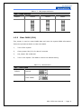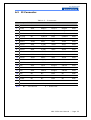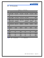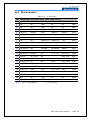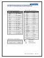
1
U
SER’S
USER’
M
anual
Manual
MIC-3000 Series
MIC-3359
6U CompactPCI® Intel®
Desktop Pentium® 4 &
Mobile
Pentium®
4-M
Processor Board with VGA
on Board
Advantech CompactPCI®
Modular Industrial Computer
Copyright Notice
This document is copyrighted, 2005. All rights are reserved. The original
manufacturer reserves the right to make improvements to the products described in
this manual at any time without notice. No part of this manual may be reproduced,
copied, translated or transmitted in any form or by any means without the prior
written permission of the original manufacturer. Information provided in this manual
is intended to be accurate and reliable. However, the original manufacturer assumes
no responsibility for its use, nor for any infringements upon the rights of third parties
which may result from its use.
Acknowledgements
PICMG™, CompactPCI® and the PICMG™, CompactPCI® logos are trademarks of the
PCI Industrial Computers Manufacturers Group. All other product names or
trademarks are properties of their respective owners.
CE Notification
The MIC-3359, developed by Advantech Co., Ltd., has passed the CE test for
environment specifications when shielded cables are used for external wiring. We
recommend the use of shielded cables.
FCC
This device complies with the requirements in part 15 of the FCC rule: Operation is
subject to be following two conditions:
(1) This device may not cause harmful interference.
(2) This device must accept any interference received, including interference that may
cause undesired operation.
CAUTION!!
Danger of explosion if battery in correctly replaced. The battery need not to be
charged. Replace only with Advantech-specified batteries.
MIC-3359 User Manual --- Page I
Product warranty
Advantech warrants to you, the original purchaser, that each of its products will be
free from defects in materials and workmanship for one year from the date of
purchase.
This warranty does not apply to any products which have been repaired or altered by
persons other than repair personnel authorized by Advantech, or which have been
subject to misuse, abuse, accident or improper installation. Advantech assumes no
liability under the terms of this warranty as a consequence of such events.
Because of Advantech’s high quality-control standards and rigorous testing, most of
our customers never need to use our repair service. If an Advantech product is
defective, it will be repaired or replaced at no charge during the warranty period. For
out-of-warranty repairs, you will be billed according to the cost of replacement
materials, service time and freight. Please consult your dealer for more details.
If you think you have a defective product, follow these steps:
1、
Collect all the information about the problem encountered. For example, CPU
speed, Advantech products used, other hardware and software used, etc. Note
anything abnormal and list any on-screen messages you get when the problem
occurs.
2、
Call your dealer and describe the problem. Please have your manual, product,
and any helpful information readily available.
3、
If your product is diagnosed as defective, obtain an RMA (return merchandise
authorization) number from your dealer. This allows us to process your return
more quickly.
4、
Carefully pack the defective product, a fully-completed Repair and Replacement
Order Board and a photocopy proof of purchase date (such as your sales receipt)
in a shippable container. A product returned without proof of the purchase date
is not eligible for warranty service.
5、
Write the RMA number visibly on the outside of the package and ship it prepaid
to your dealer.
MIC-3359 User Manual --- Page II
Packing List
Before installation, ensure that the following materials have been received:
• 1 MIC-3359 all-in-one single board computer
• 1 Utility and user manual (PDF file) CD-ROM disc
• 1 CPU Heat sink (Assembled)
• 1 Thermal pad for Pentium 4-M CPU
• 1 Solder-side cover (Assembled)
• Several screws
• 1 warranty certificate document
If any of these items are missing or damaged, contact your distributor or sales
representative immediately.
Technical Support and Sales Assistance
If you have any technical questions about the MIC-3359 or any other Advantech
products, please visit our support website at:
!
http://www.advantech.com.tw/support
For more information about Advantech's products and sales information, please visit:
!
http://www.advantech.com
MIC-3359 User Manual --- Page III
Contents
Contents................................................................................ IV
Tables ................................................................................... VI
Figures .................................................................................VII
1. Hardware Configuration ...................................................... 2
1.1 Introduction ..................................................................... 2
Single P2P Bridge.................................................................... 3
1.2 Specifications ................................................................... 4
1.3 Jumpers and Switches ....................................................... 7
1.3.1 Jumper Setting ............................................................ 7
1.3.2 Clear CMOS (JP4)......................................................... 9
1.3.3 Switch Setting ............................................................10
1.4 Connector Setting ............................................................12
1.5 Safety Precautions ...........................................................12
1.6 Installing the CPU and Heatsink..........................................13
1.7 Software Support .............................................................14
2. AWARD BIOS Setup ........................................................... 16
2.1 Entering Setup.................................................................16
2.1.1 Standard CMOS Setup .................................................17
2.1.2 Advanced BIOS Features Setup .....................................17
2.1.3 Advanced Chipset Features Setup..................................21
2.1.4 Integrated Peripherals .................................................24
2.1.5 Power Management Setup ............................................27
MIC-3359 User Manual --- Page IV
2.1.6 PNP/PCI Configuration Setup ........................................27
2.1.7 PC Health Status .........................................................29
2.1.8 Load Optimized Defaults ..............................................30
2.1.9 Set Password..............................................................30
2.1.10 Save and Exit Setup ..................................................30
2.1.11 Exit Without Saving ...................................................30
Appendix A Pin Assignments ............................................... 32
A.1 J1 Connector ...................................................................32
A.2 J2 Connector ...................................................................33
A.3 J3 Connector ...................................................................34
A.4 J5 Connector ...................................................................35
A.5~A.7 On board jumpers and connectors ...............................36
A.8~A11 On board jumpers and connectors ..............................34
A.12~A16 On board jumper and connectors ..............................35
MIC-3359 User Manual --- Page V
Tables
Table 1-1 MIC-3359 jumper descriptions..................................... 7
Table 1-2 MIC-3359 switch descriptions...................................... 7
Table 1-3 JP2 jumper definition ................................................. 7
Table 1-4 JP3 jumper definition ................................................. 8
Table 1-5 JP5 jumper definition ................................................. 8
Table 1-6 JP7 jumper definition ................................................. 8
Table 1-7 JP8 jumper definition ................................................. 9
Table 1-8 JP4 definition ............................................................ 9
Table 1-9 SW1 & SW3 definition ...............................................10
Table 1-10 SW2 definition........................................................10
Table 1-11 MIC-3359 connector descriptions ..............................12
Table A. 1 J1 connector ...........................................................32
Table A. 2 J2 connector ...........................................................33
Table A. 3 J3 connector ...........................................................34
Table A. 4 J5 connector ...........................................................35
Tables A. 5 ~ A. 7
On board jumpers and connectors ..................36
Tables A. 8 ~ A.11 On board jumpers and connectors .................37
Tables A.12 ~ A.16 On board jumpers and connectors .................38
MIC-3359 User Manual --- Page VI
Figures
Figure 1-1 MIC-3359 functional block diagram............................. 6
Figure 1-2 MIC-3359 jumper, switch and connector locations........11
Figure 1-3 Complete assembly CPU and heatsink ........................14
Figure 2-1 Setup program initial screen.....................................16
Figure 2-2 Standard CMOS setup screen....................................17
Figure 2-3 Advanced BIOS features setup screen........................18
Figure 2-4 Advanced Chipset features setup screen.....................21
Figure 2-5 Integrated Peripherals setup screen...........................24
Figure 2-6 Power management setup screen ..............................27
Figure 2-7 PNP/PCI configuration screen....................................28
Figure 2-8 PC Health setup screen ............................................29
MIC-3359 User Manual --- Page VII
Chapter
1
Hardware Configuration
MIC-3359 User Manual --- Page 1
1. Hardware Configuration
1.1
Introduction
The MIC-3359 is a 6U 8HP CompactPCI® SBC ideal for mission critical, demanding
industrial or military applications which require high performance as well as
endurance in harsh operating environments.
The MIC-3359 CompactPCI® CPU board is optimized for Intel® 845GV chipset. It
supports both the Intel Desktop Celeron® and Pentium® 4 processor up to 2.8 GHz,
and the mobile Pentium® 4 -M processor. The VGA is integrated in the Intel® 845GV
chipset, and there are two DDR DIMM slots which can support system memory up to
2GB. The MIC-3359 uses the Intel 82562ET for 10/100 Mb Fast Ethernet, with an
option for the Intel® 82551ER for 10/100 Mb Fast Ethernet which is pin-to-pin
compatible with the Intel® 82540EM for Giga Ethernet. The Pericom PI7C8150MA MHz
PCI-to-PCI Bridge is designed for bus expansions, programmable data transfer rate
control, and frequency conversions.
To achieve the most cost effective combination for entry-level CT applications or entry
to mid-level industrial applications, you can use a MIC-3041L enclosure with a
MIC-3359 6U CPCI board and Intel Pentium IV processor without a rear I/O transition
board. This gives the best performance-price balance and produces the most
cost-effective solution.
High Performance Intel® Pentium® 4 Processor-M, Intel® Desktop Pentium®
4 Processor, and Celeron® Processor
The MIC-3359 supports the Intel® Pentium® 4 processor-M 1.7 GHz and 2.2 GHz, the
Desktop Pentium® 4 Processor, and the Celeron® Processor with either u-FCPGA
package or u-FCBGA package. Both Intel® Pentium® processor-M and Intel® Pentium®
processor have on-chip 512 KB L2 cache providing high performance. The Intel®
Celeron® processor has an on-chip 256KB L2 cache providing high performance. With
the support of a 400 MHz and 533 MHz front-side bus, the MIC-3359 can fulfill
customer’s expectations of price-performance computing capability.
MIC-3359 User Manual --- Page 2
Compact Mechanical Design
The MIC-3359 has a CPU heatsink specially designed for the mobile Intel® Pentium®
4-M and Intel® Pentium®4 processor, enabling the MIC-3359 to operate without a
cooling fan on the heat sink. It needs only cooled air from the chassis fans for
ventilation.
Single P2P Bridge
The MIC uses the Pericom PI7C8150MA MHz PCI-to-PCI Bridge, which designed for
bus expansions, programmable data transfer rate control, and frequency conversions.
The Pericom Bridge can drive up to seven PCI slots in master mode, including those
using bus master cards. Up to eight MIC-3359 units can be installed in one enclosure.
Complete I/O Functions
The MIC-3359 offers all the I/O functions of an industrial computer with the rugged
Euroboard form factor. Output cables are fully connected to the rear I/O module via
user-define connectors (J3 and J5) on the backplane. The I/O panel contains two
10/100 base Ethernet ports (one of them is optional ), two COM ports, two USB 2.0
ports, one VGA connector, one PS/2 keyboard port, one PS/2 mouse port, and one
parallel port. The front panel also has a reset button and LEDs for power status and
HDD operation. The built-in high speed IDE controller provides two separate IDE
channels with Ultra DMA/33/66/100 mode. One is for CF on board, and the other one
is for IDE devices. The user-defined J3 connector is designed to support one IDE
device, one floppy drive, one printer device, and one or two Ethernet networks. These
drives can simply be connected to the backplane or to the rear transition board for
easy service and maintenance.
MIC-3359 User Manual --- Page 3
1.2
Specifications
Standard SBC Functions
•CompactPCI Bus Interface
PICMG 2.0 Rev. 3.0 compatible, 5V signaling; 32 bit/33 MHz, REQ/GNT for 7 slots;
Operates in system slot as system master
• CPU: Intel® Pentium® 4 / Intel® Celeron®, 478-pin package FC-PGA
Mobile Pentium 4 Processor-M from 1.2 GHz up to 2.2 GHz for low power
dissipation (higher frequencies on request), Desktop Pentium 4 from 2 GHz up to 2.8
GHz for high performance, 512 KB full speed L2 on-die cache, 400 MHz and 533 MHz
processor front-side bus, passive heat sink for the processor, at least 300 LFM forced
air cooling required in the chassis.
• BIOS: 4 Mb Firmware Hub (FWH) using Award BIOS
• Chipset: Intel® 845GV/ICH4 Chipset
Host Interface Support for Intel processor in an mPGA478 package
Hyper-Threading Technology support
Support Hub Interface 1.5 (266 MB/s point-to-point Hub Interface to the ICH4)
Integrated Graphics, core frequency of 200 MHz, resolution up to 2048 x 1536 x 60Hz
x 8 bit, shared memory up to 64MB
• Front Side Bus: 400MHz/533 MHz (Intel® Pentium® 4 processor-M Processor)
• Bus Interface: 32-bit/33 MHz, PICMG 2.16 compliant
• Memory: Double Data Rate (DDR) SDRAM Configuration
Up to 2.0 GB of 200 MHz or 266 MHz DDR SDRAM
Two DDR DIMMs, single-sided and/or double-sided, DDR 200/266 unregistered,
184-pin non-ECC DDR
• Ethernet: the MIC-3359 uses the Intel@82562ET LAN chip for 10/100 Mb Fast
Ethernet, with an option for the Intel® 82551ER 10/100 Mb for Fast Ethernet which is
pin-to-pin compatible with the Intel® 82540EM 10/100/1000 Mb for Giga Ethernet.
MIC-3359 supports one 10/100Mb LAN; MIC-3359-A supports two 10/100Mb LANs;
MIC-3359-B supports one 10/100Mb LAN, and one Gb LAN.
• Enhanced IDE interface: The IDE interface supports two channels. The master for
the primary channel is reserved for the Compact Flash. The secondary IDE channel
can be connected to a RIO module via the J3 connector. The interface supports PIO
mode 4 and ATA 33/66/100 mode.
MIC-3359 User Manual --- Page 4
• Serial ports: COM1 and COM2 port (support RS-232/422/485 interface)
• USB port: Supports up to six USB channels: two front, two rear, and two on board
for internal devices; USB specification 2.0/1.1 compatible
• CompactFlash® socket: one CompactFlash® type II socket on board.
• AC97’ Audio Interface: Mic-in, Line-in, Line-out
•LEDs: Indicate LAN activity and speed, one green LED for power status, one yellow
LED for IDE HDD status.
• FDD Connector
• Parallel Port
• PS/2 Port: One for keyboard and one for mouse
•Watchdog timer: Provides system reset, interrupt and NMI support via software
control. Time interval is from 1 to 255 seconds.
MIC-3359 User Manual --- Page 5
Bypass
resistor
(Reserved)
LED
PS/2
J1
J2
RJ45
RJ45
FDD
LAN1
82562ET
(10/100)
LAN2
82551ER(10/100)
or
82540EM (10/100/1000)
PCI 32bit
PCI to PCI Bridge
PI7C8150MA
VGA
Switch
Intel MCH
845GV
J3
LPT
USB
CPLD &
PORT 80
SpeedStep
LPC
LPT
J5
VGA
USB
Secondary IDE
Primary IDE (CF)
USB PORTS * 2
DDR POWER
+2.5V
+1.25V
+1.5V
DDR DIMM * 2
RJ1
LAN1 & 2
RJ2
AUDIO
COM1 & 2
FDD
FWH
(BIOS)
ATA 33/66/100
USB 2.0
DDR 266/333
COM1 & 2
(RS232/422/485)
Sec. IDE
PS/2
SUPER I/O
Winbond
W83627HF
Intel
82801DB
ICH4
HUB 1.5
VGA
FSB 100/133 MHz
Intel P4
Intel P4-M
Celeron
PARALELL COM1
VCORE & 1.2V
COM2
PCI 32bits 33MHz
VGA CON.
(Front Panel)
CLK GENERATOR
ICS950211
Reset
SW
Functional Block Diagram
Figure 1-1 MIC-3359 functional block diagram
MIC-3359 User Manual --- Page 6
1.3
Jumpers and Switches
Table 1-1 and Table 1-2 list the jumper and switch functions. Figure 1-2 illustrates the
jumper and switch locations. Read this section carefully before changing the jumper
and switch settings on your MIC-3359 board.
Table 1-1 MIC-3359 jumper descriptions
Number
Function
JP2
VGA Output Setting
JP3
CPU Speed Setting
JP4
Clear CMOS
JP5
CF Mode Setting
JP7
COM2 Setting
JP8
COM1 Setting
Table 1-2 MIC-3359 switch descriptions
Number
Function
SW1 & SW3
CPU setting
SW2
Reset Button
1.3.1
Jumper Settings
Table 1-3 JP2 jumper definition
JP2 - VGA Output Settings
Default
Front Panel
Rear I/O
MIC-3359 User Manual --- Page 7
Table 1-4 JP3 jumper definitions
JP3 - CPU Speed Settings
Default
CPU Select
100MHz
133MHz
Table 1-5 JP5 jumper definition
JP5 - CF Mode Settings
Default
Master
Slave
Table 1-6 JP7 jumper definition
JP7 – COM2 Settings
Default
RS232
RS422
RS485
MIC-3359 User Manual --- Page 8
Table 1-7 JP8 jumper definition
JP8 – COM1 Settings
Default
1.3.2
RS232
RS422
RS485
Clear CMOS (JP4)
This jumper is used to erase CMOS data and reset the system BIOS information.
Follow the procedures below to clear the CMOS.
1、
Turn off the system.
2、
Close jumper JP4 (2-3) for about 3 seconds.
3、
Set jumper JP4 as Normal.
4、
Turn on the system. The BIOS is reset to its default setting.
Table 1-8 JP4 definition
JP4 – Clear CMOS
Default
Normal
Clear CMOS
MIC-3359 User Manual --- Page 9
1.3.3
Switch Settings
Table 1-9 SW1 & SW3 definition
SW1 & SW3 – CPU Settings
Default
SW3
SW1
SW3
SW1
P4、Celeron
P4-M
Table 1-10 SW2 definition
SW2 – Reset Button
PUSH
Reset System
MIC-3359 User Manual --- Page 10
Figure 1-2 MIC-3359 jumper, switch, and connector locations
MIC-3359 User Manual --- Page 11
1.4
Connector Setting
On-board connectors link to external devices such as hard disk drives, keyboards, or
floppy drives, etc. Table 1-11 lists the function of each connector and Figure 1-2
illustrates each connector location.
Table 1-11 MIC-3359 connector descriptions
Number
Function
CN1
FDD Connector
CN2
V(I/O) Setting
CN3
IDE Connector (Secondary IDE)
CN4
CompactFlash™ Connector (Primary IDE)
CN6
USB Port (Internal)
CN7
Internal COM2 Connector
CN8
LPT Connector
CN9
PS/2 Mouse/Keyboard Connector
CN10
USB Port*2
CN12
VGA Connector
CN13
COM1 Connector
CN14
COM2 Connector
JP10
AC’97 Connector
RJ1
LAN1 Connector
RJ2
LAN2 Connector (82551ER)
RJ2
LAN2 Connector (82540EM)
J1/J2
Primary CompactPCI® bus
J3/J5
Rear I/O transition
LED
IDE LED and Power LED
1.5
Safety Precautions
Follow these simple precautions to protect yourself from harm and the products from
damage.
1、
To avoid electric shock, always disconnect the power from your PC chassis
before you work on it. Don’t touch any components on the CPU board or other
boards while the PC is on.
2、
Disconnect power before making any configuration changes. The sudden rush
MIC-3359 User Manual --- Page 12
of power as you connect a jumper or install a board may damage sensitive
electronic components.
3、
Always ground yourself to remove any static charge before you touch your CPU
board. Be particularly careful not to touch the chip connectors.
Modern integrated electronic devices, especially CPUs and memory chips, are
extremely sensitive to static electric discharges and fields. Keep the board in its
antistatic packaging when it is not installed in the PC, and place it on a static
dissipative mat when you are working with it. Wear a grounding wrist strap for
continuous protection.
1.6
Installing CPU and Heatsink
The MIC-3359 supports the Intel® Pentium-4, the 478-pin package FCPGA, and the
Mobile Pentium-4 Processor. In order to meet critical environmental conditions and
size limitations, Advantech designed a heat sink to fulfill the primary requirements of
the MIC-3359. Please refer to Figure 1-3 for an illustration of the heat-sink and
thermal pad used for the MIC-3359.
The MIC-3359 should be fastened to a heat sink supporting Intel Pentium 4 in the
factory. When the user installs the CPU, the following steps should be followed:
1、
Remove the screws from the solder side cover. During this step, the front panel
should also become loose. Be careful about any improper disassembly
procedure that could cause any damage of SBC.
2、
Remove the last four screws from the heat-sink, and then lossen the heat sink
for CPU installation. Apply the silicone heat sink compound, found in the
accessory bag, to the CPU.
3、
Follow the reverse procedure to replace the heat-sink and solder side cover.
Note: If you use a Mobile Pentium 4 processor, please don’t use the silicone
heat sink compound. You need to insert a heat pad between the processor
and the heat-sink. The heat pad is in the accessory bag. The heat pad should
be positioned between the heat-sink and the CPU. It is fragile, so please be
careful during disassembly. If you are using a heat pad other than the one
issued by Advantech, be aware that it may not absorb a sufficient amount of
heat.
MIC-3359 User Manual --- Page 13
Figure 1-3 Complete assembly of CPU and heat sink
1.7
Software Support
Windows® XP/2000/NT 4.0, Red Hat Linux 9.0,
MIC-3359 User Manual --- Page 14
Chapter
2
AWARD BIOS Setup
MIC-3359 User Manual --- Page 15
2. AWARD BIOS Setup
Once you enter Award® BIOS CMOS Setup Utility, the Main Menu (Figure 2-1) will
appear on the screen. The Main Menu allows you to select from nine setup functions
and two exit choices. Use arrow keys to select among the items and press <Enter> to
accept or enter the sub-menu.
Figure 2-1 Setup program initial screen
Award's BIOS ROM has a built-in Setup program that allows users to modify the basic
system configuration. This type of information is stored in battery-backed up CMOS so
it retains the Setup information when the power is turned off.
2.1
Entering Setup
Turn on the computer and check for the "patch” code. If there is a number assigned to
the patch code, it means that BIOS supports your CPU. If there is no number assigned
to the patch code, please contact an Advantech application engineer to obtain an
up-to-date patch code file. This will ensure that your CPU's system status is valid.
After ensuring that you have a number assigned to the patch code, press <DEL> and
you will immediately be allowed to enter Setup.
MIC-3359 User Manual --- Page 16
2.1.1
Standard CMOS Setup
The items in Standard CMOS Setup Menu are divided into 11 categories. Each
category includes one or more setup items, or none. Use the arrow keys to highlight
the item and then use the <PgUp> or <PgDn> keys to select the value you want for
each item.
Figure 2-2 Standard CMOS setup screen.
Primary Master/Primary Slave/Secondary Master/Secondary Slave: Press PgUp/<+>
or PgDn/<-> to select Manual, None, Auto type. Note that the specifications of your
drive must match with the drive table. The hard disk will not work properly if you enter
improper information for this category. If your hard disk drive type is not matched or
listed, you can use Manual to define your own drive type manually. If you select
Manual, the system will prompt for related information for the following items. Enter
the information directly from the keyboard. This information should be provided in the
documentation from your hard disk vendor or the system manufacturer.
2.1.2
Advanced BIOS Features Setup
The "Advanced BIOS FEATURES" screen will appear after the BIOS FEATURES SETUP
item from the CMOS SETUP UTILITY Menu was chosen. This screen allows the user to
MIC-3359 User Manual --- Page 17
configure the board according to his particular requirements. Below are some major
items that are provided in the BIOS FEATURES SETUP screen:
Figure 2-3 Advanced BIOS features setup screen
Virus Warning
During and after the system boot, any attempt to write to the boot sector or partition
table of the hard disk drive will halt the system. If this happens, a warning message
will be displayed. You can run the anti-virus program to locate the problem. If Virus
Warning is disabled, no warning message will appear if anything attempts to access
the boot sector or hard disk partition.
CPU L1 & L2 Cache
Default
Enabled
Enable cache
Disabled
Disable cache
Note: The internal cache is built into the processor.
MIC-3359 User Manual --- Page 18
Quick Power On Self Test
This category shortens the Power On Self Test (POST) after you power on the
computer. If this is set to Enabled, BIOS will shorten or skip some check items during
POST.
Default
Enabled
Enable quick POST
Disabled
Normal POST
First/Second/Third Boot Device and Boot Other Device
The BIOS attempts to load the operating system from the devices in the sequence
selected in these items. The settings are Floppy, LS120, HDD-0, SCSI, CDROM,
HDD-1, HDD-2, HDD-3, ZIP100, USB-FDD, USB-ZIP, USB-CDROM, USB-HDD, LAN
and Disabled.
Default
First boot device
CDROM
Second boot device
HDD-0
Third boot device
HDD-1
NOTE: When you boot by USB CD-ROM, please install WinXP with SP1 or Win 2000
with SP3.
Boot Up NumLock Status
Default
On
Keypad: numeric keys
Off
Keypad: arrow keys
Gate A20 Option
Default
Fast
Normal
The A20 signal is controlled by port 92 or chipset specific
method.
The A20 signal is controlled by keyboard controller or
chipset hardware.
MIC-3359 User Manual --- Page 19
Typematic Rate Setting
Key strokes repeat at a rate determined by the keyboard controller. When enabled,
the typematic rate and typematic delay can be selected. The settings are:
Enabled/Disabled. The default setting is Disabled.
Typematic Rate (Chars/Sec)
Set the number of times a second to repeat a key stroke when you hold the key down.
The settings are: 6, 8, 10, 12, 15, 20, 24, 30.
Typematic Delay (Msec)
Sets the delay time after the key is held down before it begins to repeat the keystroke.
The settings are: 250, 500, 750, 1000.
Security Option
This category allows you to limit access to the system and/or to Setup.
Default
Setup
System
The system will boot, but access to Setup will be denied if
the correct password is not entered at the prompt.
The system will not boot and access to Setup will be denied
if the correct password is not entered at the prompt.
APIC Mode (Advanced Programmable Interrupt Controller)
Default is Enabled.
MPS Version Control For OS
The options include 1.1 and 1.4. The default setting is 1.4
MIC-3359 User Manual --- Page 20
OS Select For DRAM > 64MB
Allows OS2® to be used with > 64 MB of DRAM. Settings are Non-OS/2 (default) and
OS2. Set to OS/2 if using more than 64MB and running OS/2®.
Small Logo (EPA) show
The default setting is Disabled.
Max Performance
Default is Enabled.
2.1.3
Advanced Chipset Features Setup
The Advanced Chipset Features Setup option is used to change the values in the
chipset registers. These registers control most of the system options in the computer.
Choose the "ADVANCED CHIPSET FEATURES" from the Main Menu and the following
screen will appear.
Figure 2-4 AdvancedS Chipset features setup screen
MIC-3359 User Manual --- Page 21
DRAM Timing Selectable
This field lets you select system memory timing data. Manual and BY SPD are two
options. The default setting is BY SPD.
CAS Latency Time
When synchronous DRAM is installed, the number of clock cycles of CAS latency
depends on the DRAM timing. The settings are: 1.5, 2 and 2.5.
Active to Precharge Delay
This field let you set Active to Precharge Delay. The settings are: 7, 6 and 5.
DRAM RAS# to CAS# Delay
This field lets you insert a timing delay between the CAS and RAS strobe signals, used
when DRAM is written to, read from, or refreshed. Fast gives faster performance; and
Slow gives more stable performance. This field applies only when synchronous DRAM
is installed in the system. The settings are: 2 and 3.
DRAM RAS# Precharge
If an insufficient number of cycles are allowed for the RAS to accumulate its charge
before DRAM refresh, the refresh may be incomplete and the DRAM may fail to retain
data. Fast gives faster performance; and Slow gives more stable performance. This
field applies only when synchronous DRAM is installed in the system. The settings are:
2 and 3.
Memory Frequency For
Default is Auto.
MIC-3359 User Manual --- Page 22
System BIOS Cacheable
Selecting Enabled allows caching of the system BIOS ROM at F0000h-FFFFFh,
resulting in better system performance. However, if any program writes to this
memory area, a system error may result. The settings are: Enabled (Default) and
Disabled.
Video BIOS Cacheable
Select Enabled allows caching of the video BIOS, resulting in better system
performance. However, if any program writes to this memory area, a system error
may result. The settings are: Enabled and Disabled (Default).
Memory Hole At 15M-16M
You can reserve this area of system memory for ISA adapter ROM. When this area is
reserved, it cannot be cached. The user information of peripherals that need to use
this area of system memory usually discusses their memory requirements. The
settings are: Enabled and Disabled (Default).
Delayed Transaction
The chipset has an embedded 32-bit posted write buffer to support delay transactions
cycles. Select Enabled to support compliance with PCI specification version 2.1. The
settings are: Enabled (Default) and Disabled.
AGP Aperture Size (MB)
This field lets you select the AGP aperture size. The settings are: 4, 8, 16, 32, 64, 128
and 256.
On-Chip Frame Buffer Size (MB)
This field let you select On-Chip buffer size. The settings are: 1 and 8.
MIC-3359 User Manual --- Page 23
2.1.4
Integrated Peripherals
Figure 2-5 Integrated Peripherals setup screen
On-Chip Primary/Secondary PCI IDE
The integrated peripheral controller contains an IDE interface with support for two IDE
channels. Select Enabled to activate each channel separately. The settings are:
Enabled (Default) and Disabled.
IDE Primary/Secondary Master/Slave PIO
The four IDE PIO (Programmed Input/Output) fields let you set a PIO mode (1-4) for
each of the four IDE devices that the onboard IDE interface supports. Modes 0 through
4 provide successively increased performance. In Auto mode, the system
automatically determines the best mode for each device. The settings are: Auto
(Default), Mode 0, Mode 1, Mode 2, Mode 3, Mode 4.
IDE Primary/Secondary Master/Slave UDMA
Ultra DMA/33 implementation is possible only if your IDE hard drive supports it and
the operating environment includes a DMA driver (Windows 95 OSR2 or a third-party
MIC-3359 User Manual --- Page 24
IDE bus master driver). If your hard drive and your system software both support
Ultra DMA/33 and Ultra DMA/66 and Ultra DMA/100, select Auto to enable BIOS
support. The settings are: Auto (Default), Disabled.
USB Controller
Select Enabled if your system contains a Universal Serial Bus (USB) 1.1 controller.
The settings are: Enabled (Default), Disabled.
USB 2.0 Controller
Select Enabled if your system contains a Universal Serial Bus (USB) 1.1/2.0 controller.
The settings are: Enabled (Default), Disabled.
USB Keyboard/Mouse Support
Select Enabled if you use USB KB/Mouse in DOS mode. Default is Disabled.
AC 97 Audio
Default is Auto.
Init Display First
User can choose display priority on either peripheral PCI slot or on board VGA chip.
There are 2 options: PCI slot (Default) and On board.
LAN1 Front Panel Controller
The item allows you to choice LAN1 connective way. There are 3 options: Front
(Default), 2.16 and Rear
IDE HDD Block Mode
Block mode is also called block transfer, multiple commands, or multiple sector
MIC-3359 User Manual --- Page 25
read/write. If your IDE hard drive supports block mode (most new drives do), select
Enabled for automatic detection of the optimal number of block read/writes per sector
the drive can support. The settings are: Enabled (Default), Disabled.
Onboard FDC Controller
Select Enabled if your system has a floppy disk controller (FDD) installed on the
system board and you wish to use it. If you install add-on FDC or the system has no
floppy drive, select Disabled in this field. The settings are: Enabled (Default) and
Disabled.
Onboard Serial Port 1/Port 2
Select an address and corresponding interrupt for the first and second serial ports.
The Serial Port 1 settings are: 3F8/IRQ4 (Default), 2F8/IRQ3, 3E8/IRQ4, 2E8/ IRQ3,
Disabled, Auto. The Serial Port 2 settings are: 3F8/IRQ4, 2F8/IRQ3 (Default),
3E8/IRQ4, 2E8/ IRQ3, Disabled, Auto.
Onboard Parallel Port
There is a built-in parallel port on the on-board Super I/O chipset that provides
Standard, ECP, and EPP features. It has the following options: Disabled, 378/IRQ7
(Default), 278/IRQ5, 3BC/IRQ7 and Disabled.
Parallel Port Mode
Default
Spp
Standard Parallel Port
EPP1.9+SPP
Support both the SPP and EPP1.9 modes.
ECP
Extended Capability Port
EPP Mode Select
Default is EPP 1.7.
MIC-3359 User Manual --- Page 26
ECP Mode Use DMA
The options: 1 and 3 (Default)
2.1.5
Power Management Setup
The Power Management Setup allows you to configure you system to most effectively
save energy while operating in a manner consistent with your own style of computer
use.
Figure 2-6 Power management setup screen
ACPI Function
This category allows you to select ACPI power management effective or not. The
options: Enabled and Disabled (Default).
2.1.6
PNP/PCI Configuration Setup
This section describes configuring the PCI bus system. PCI, or Personal Computer
Interconnect, is a system which allows I/O devices to operate at speeds nearing the
MIC-3359 User Manual --- Page 27
speed the CPU itself uses when communicating with its own special components. This
section covers some very technical items and it is strongly recommended that only
experienced users should make any changes to the default settings.
Figure 2-7 PNP/PCI configuration screen
Reset Configuration Data
Normally, you leave this field Disabled. Select Enabled to reset Extended System
Configuration Data (ESCD) when you exit Setup if you have installed a new add-on
and the system reconfiguration has caused such a serious conflict that the operating
system can not boot. The settings are: Enabled and Disabled (Default).
Resource Controlled By
The Award Plug and Play BIOS has the capacity to automatically configure all the boot
and Plug and Play compatible devices. However, this capability means absolutely
nothing unless you are using a Plug and Play operating system such as Windows®
95/98. If you set this field to "manual," choose specific resources by going into each
of the sub menus that follow this field (a sub menu is preceded by a "Y"). The settings
are: Auto (ESCD) (Default), Manual.
MIC-3359 User Manual --- Page 28
IRQ Resources
When resources are controlled manually, assign each system interrupt a type,
depending on the type of device using the interrupt.
DMA Resources
When resources are controlled manually, assign each system interrupt a type,
depending on the type of device using the interrupt.
PCI/VGA Palette Snoop
Leave this field at Disabled. The settings are Enabled, Disabled (Default).
2.1.7
PC Health Status
This section shows the Status of the CPU, Fan, and gives a warning for overall system
status. This is only available if there is a hardware monitor on board.
Figure 2-8 PC Health setup screen
MIC-3359 User Manual --- Page 29
Current System Temp./ CPU Temp./ Vcore/ Vtt/ +3.3V/ +5V/ +12V
This screen shows system health status.
2.1.8
Load Optimized Defaults
When you press <Enter> on this item, you get a confirmation dialog box with a
message similar to:
Load Optimized Defaults (Y/N) ? N
Pressing 'Y' loads the default values that are factory settings for optimal performance
system operations.
2.1.9
Set Password
To change, confirm, or disable the password, choose the "PASSWORD SETTING"
option from the Setup main menu and press Enter. The password can be at most 8
characters long. Remember, to enable this feature. You must first select the Security
Option in the Advance BIOS FEATURES SETUP to be either "Setup" or "System."
Pressing Enter again without typing any characters can disable the password setting
function.
2.1.10
Save & Exit Setup
If you select this and press the [Enter] key, the values entered in the setup utilities will
be recorded in the CMOS memory of the chipset. The microprocessor will check this
every time you turn your system on and com-pare this to what it finds as it checks the
system. This record is required for the system to operate.
2.1.11
Exit Without Saving
Selecting this option and pressing the Enter key lets you exit the Setup program
without recording any new values or changing old ones.
MIC-3359 User Manual --- Page 30
Appendix
A
Pin Assignments
MIC-3359 User Manual --- Page 31
Appendix A、 Pin Assignments
A.1
J1 Connector
Table A. 1 J1 connector
J1 - CompactPCI I/O
Row A
Row B
Row C
Row D
Row E
Row F
1
+5V
-12V
TRST#
+12V
+5V
GND
2
TCK
+5V
TMS
NC
TDI
GND
3
INTA#
INTB#
INTC#
+5V
INTD#
GND
4
NC
HEALTHY#
V(I/O)
INTP
INTS
GND
5
NC
NC
PCI_RST#
GND
GNT0#
GND
6
REQ0#
PCI_PRESENT#
+3.3V
CLK0
AD31
GND
7
AD30
AD29
AD28
GND
AD27
GND
8
AD26
GND
V(I/O)
AD25
AD24
GND
9
C/BE3#
NC
AD23
GND
AD22
GND
10
AD21
GND
+3.3V
AD20
AD19
GND
11
AD18
AD17
AD16
GND
C/BE2#
GND
12
13
GND
14
15
+3.3V
FRAME#
IRDY#
BD_SEL#
TRDY#
GND
16
DEVSEL#
PCIXCAP
V(I/O)
STOP#
LOCK#
GND
17
+3.3V
IPMB_SCL
IPMB_SDA
GND
PERR#
GND
18
SERR#
GND
+3.3V
PAR
C/BE1#
GND
19
+3.3V
AD15
AD14
GND
AD13
GND
20
AD12
GND
V(I/O)
AD11
AD10
GND
21
+3.3V
AD9
AD8
M66EN
C/BE0#
GND
22
AD7
GND
+3.3V
AD6
AD5
GND
23
+3.3V
AD4
AD3
+5V
AD2
GND
24
AD1
+5V
V(I/O)
AD0
ACK64#
GND
25
+5V
REQ64#
ENUM#
+3.3V
+5V
GND
Note:
NC → No Connect
# → Active Low
MIC-3359 User Manual --- Page 32
A.2
J2 Connector
Table A. 2 J2 connector
J2 - CompactPCI I/O
Row A
Row B
Row C
Row D
Row E
Row F
1
CLK1
GND
REQ1#
GNT1#
REQ2#
GND
2
CLK2
CLK3
SYSEN#
GNT2#
REQ3#
GND
3
CLK4
GND
GNT3#
REQ4#
GNT4#
GND
4
V(I/O)
NC
C/BE7#
GND
C/BE6#
GND
5
C/BE5#
GND
V(I/O)
C/BE4#
PAR64
GND
6
AD63
AD62
AD61
GND
AD60
GND
7
AD59
GND
V(I/O)
AD58
AD57
GND
8
AD56
AD55
AD54
GND
AD53
GND
9
AD52
GND
V(I/O)
AD51
AD50
GND
10
AD49
AD48
AD47
GND
AD46
GND
11
AD45
GND
V(I/O)
AD44
AD43
GND
12
AD42
AD41
AD40
GND
AD39
GND
13
AD38
GND
V(I/O)
AD37
AD36
GND
14
AD35
AD34
AD33
GND
AD32
GND
15
NC
GND
FAL#
REQ5#
GNT5#
GND
16
NC
NC
DEG#
GND
NC
GND
17
NC
GND
PRST#
REQ6#
GNT6#
GND
18
NC
NC
NC
GND
NC
GND
19
NC
GND
NC
NC
NC
GND
20
CLK5
NC
NC
GND
NC
GND
21
CLK6
GND
NC
NC
NC
GND
22
GA4
GA3
GA2
GA1
GA0
GND
Note:
NC → No Connect
# → Active Low
MIC-3359 User Manual --- Page 33
A.3
J3 Connector
Table A. 3 J3 connector
J3 - CompactPCI I/O (LPT、FDD、Secondary IDE)
Row A
Row B
Row C
Row D
Row E
1
LPT_PD0
LPT_PD1
LPT_PD2
LPT_PD3
LPT_PD4
GND
2
LPT_PD5
LPT_PD6
LPT_PD7
LPT_BUSY
FDD_DRVEN1
GND
3
LPT_STB#
LPT_AFD#
FDD_DRVEN0
FDD_INDEX#
FDD_DSKCHG#
GND
4
LPT_ERR#
LPT_ACK#
FDD_RDATA#
FDD_WP#
FDD_TRACK0#
GND
5
LPT_PE
LPT_SLCT
FDD_STEP#
FDD_MTR0#
FDD_WD#
GND
6
LPT_SLIN#
LPT_INIT#
FDD_WE#
FDD_HEAD#
FDD_DSA#
GND
7
FDD_DIR#
SDDACK#
IDE_RESET#
SDIORDY
SDCS#1
GND
8
IRQ15
S66DET
SDA0
SDA1
SDA2
GND
9
SECHDDLED#
RIO_CLK
SDIOW#
SDDREQ
SDCS#3
GND
10
SDD15
SDD14
SDIOR#
SDD10
SDD11
GND
11
SDD5
SDD9
SDD13
SDD6
SDD8
GND
12
SDD1
SDD3
SDD12
SDD4
SDD7
GND
13
SDD0
SDD2
NC
NC
NC
GND
14
NC
NC
NC
NC
NC
GND
15
NC
NC
GND
NC
NC
GND
16
NC
NC
GND
NC
NC
GND
17
NC
NC
GND
NC
NC
GND
18
NC
NC
GND
NC
NC
GND
19
NC
NC
NC
NC
NC
GND
Note:
NC → No Connect
Row F
# → Active Low
MIC-3359 User Manual --- Page 34
A.4
J5 Connector
Table A. 4 J5 connector
J5 - CompactPCI I/O (VGA、LAN、COM、USB、PS/2)
Row A
Row B
Row C
Row D
Row E
Row F
1
NC
NC
GND
NC
NC
GND
2
NC
NC
GND
NC
NC
GND
3
MDIB0+
MDIB0-
GND
MDIB1+
MDIB1-
GND
4
MDIB2+
MDIB2-
GND
MDIB3+
MDIB3-
GND
5
GND
GND
+5V
GND
GND
GND
6
NC
NC
LINK1000-2#
ACTLED-2#
+5V
GND
7
NC
NC
LINK100-2#
LNKLED-2#
+5V
GND
8
IO-NRX2
NC
IO-NTX2
IO-NRTS2
KBDAT
GND
9
2RXD232
RX2
IO-NDTR2
IO-NOTS2
KBCLK
GND
10
IO-NDCD2
NC
IO-NRI2
IO-NDSR2
MSDAT
GND
11
IO_SIN1
NCTS1
NC
NC
MSCLK
GND
12
IO_SOUT1
NDSR1
NC
LAN1-ACT-LED#
DDC_DAT
GND
13
NRTS1
IO_DTR#
NC
LAN1-LINK-LED#
DDC_CLK
GND
14
IO_DCD#
NRI1
NC
LAN1-SPD-LED#
GND
GND
15
USB_OC5#
NC
NC
GND
REAR_BLUE
GND
16
USB_OC4#
S_GNT7
GND
REAR_VSYNC
GND
GND
17
GND
S_REQ7
NC
GND
REAR_GREEN
GND
18
USB_P4+
GND
GND
REAR_HSYNC
GND
GND
19
USB_P4-
GND
USB_P5+
GND
REAR_RED
GND
20
GND
GND
USB_P5-
GND
GND
GND
21
NC
NC
GND
NC
NC
GND
22
LAN1RD+
LAN1RD-
GND
LAN1TD+
LAN1TD-
GND
Note:
NC → No Connect
# → Active Low
MIC-3359 User Manual --- Page 35
A.5~A.7 On board Jumpers and Connectors
Table A.5 CN1 – FDD Connector
Table A.7 CN3 – IDE Connector
CN3 - IDE Connector
CN1 - FDD Connector
1
GND
2
FDD_DRVEN0
1
RESET#
2 GND
3
GND
4
NC
3
SDD7
4 SDD8
5
NC
6
FDD_DRVEN1
5
SDD6
6 SDD9
7
GND
8
FDD_INDEX#
7
SDD5
8 SDD10
9
GND
10
FDD_MTR0#
9
SDD4
10 SDD11
11
GND
12
FDD_DSB#
11
SDD3
12 SDD12
13
GND
14
FDD_DSA#
13
SDD2
14 SDD13
15
GND
16
FDD_MOB#
15
SDD1
16 SDD14
17
GND
18
FDD_DIR#
19
GND
20
FDD_STEP#
17
SDD0
18 SDD15
21
GND
22
FDD_WD#
19
GND
23
GND
24
FDD_WE#
21
SDDREQ
22 GND
25
GND
26
FDD_TRACK0#
23
SDIOW#
24 GND
27
GND
28
FDD_WP#
25
SDIOR#
26 GND
29
GND
30
FDD_RDATA#
27
SDIORDY
28 CSEL
31
GND
32
FDD_HEAD#
29
SDDACK#
30 GND
33
GND
34
FDD_DSKCHG#
31
IRQ15
32 NC
33
SDA1
34 S66DET
35
SDA0
36 SDA2
37
SDCS#1
38 SDCS#3
39
SECHDDLED# 40 GND
Table A.6 CN2 – V (I/O) Setting
CN2 – V(I/O) Setting
★
V(I/O) = +5V
Insert
V(I/O) = +3.3V
Remove
NC
:No Connect
#
:Active Low
★
:Default Setting
MIC-3359 User Manual --- Page 36
A.8~A.11 On board Jumpers and Connectors
Table A.8 CN4 – CommpactFlash
Table A.9 CN6 – USB Port (Internal)
CN6 - USB Port (Internal)
CN4 – CompactFlash
1
GND
2
D3
1
+5V
6
+5V
3
D4
4
D5
2
USBD3-
7
USBD2-
5
D6
6
D7
3
USBD3+
8
USBD2+
7
CS1#
8
GND
4
GND
9
GND
9
GND
10
GND
5
NC
11
GND
12
GND
13
+5V
14
GND
15
GND
16
GND
17
GND
18
A2
19
A1
20
A0
21
D0
22
D1
23
D2
24
NC
25
GND
26
GND
27
D11
28
D12
29
D13
30
D14
31
D15
32
CS3#
1
LPT_STB#
14
LPT_AFD#
33
NC
34
IORD#
2
LPT_PD0
15
LPT_ERR#
35
IOWR#
36
WE#
3
LPT_PD1
16
LPT_INIT#
37
IRQ14
38
+5V
4
LPT_PD2
17
LPT_SLIN#
39
CSEL#
40
NC
5
LPT_PD3
18
GND
41
RESET#
42
IORDY#
6
LPT_PD4
19
GND
43
NC
44
REG#
7
LPT_PD5
20
GND
45
DASP#
46
NC
8
LPT_PD6
21
GND
47
D8
48
D9
9
LPT_PD7
22
GND
49
D10
50
GND
10
LPT_ACK#
23
GND
11
LPT_BUSY
24
GND
12
LPT_PE
25
GND
13
LPT_SLCT
Table A.10 CN7 – Internal COM2
CN7 – Internal COM2
1
DCD#
6
DSR#
2
SIN
7
RTS#
3
SOUT
8
CTS#
4
DTR#
9
RI#
5
GND
Table A.11 CN8 – LPT Connector
CN8 - LPT Connector
MIC-3359 User Manual --- Page 37
A.12~A.16 On board Jump and Connector
Table A.12 CN9 – PS/2 Connector
Table A.15 CN13、CN14 – COM1、COM2
CN9 - PS/2 Connector
CN13、CN14 - COM1、COM2
1
KBDATA
7
MSDATA
1
DCD#
6
DSR#
2
NC
8
NC
2
SIN
7
RTS#
3
GND
9
GND
3
SOUT
8
CTS#
4
+5V
10
+5V
4
DTR#
9
RI#
5
KBCLK
11
MSCLK
5
GND
6
NC
12
NC
NC :No Connect
Table A.13 CN10 – USB Port
Table A.16 JP10 – AC`97 Connector
CN10 - USB Port
JP10 - AC’97 Connector
1
+5V
5
+5V
1 AC97_SDIN0
2 AC97_SDOUT
2
USBD0-
6
USBD1-
3 AC97_SYNC
4 AC97_RST#
3
USBD0+
7
USBD1+
5 SPKR
6 GND
4
GND
8
GND
7 +5V
8 AC97_BITCLK
9 +5V
#
10 GND
:Active Low
Table A.14 CN12 – VGA Connector
CN12 - VGA Connector
1
RED
9
+5V
2
GREEN
10
GND
3
BLUE
11
NC
4
NC
12
DDC_DATA
5
GND
13
HSYNC
6
GND
14
VSYNC
7
GND
15
DDC_CLK
8
GND
MIC-3359 User Manual --- Page 38
A.17~A.19 On board Jumpers and Connectors
Table A.17 RJ1 – LAN1 Connector (LED)
RJ1 – LAN1 Connector
1
TD+
7
RD+
2
TD-
8
RD-
3
NC
9
+3.3V
4
NC
10
SPEED_LED#
5
NC
11
LINK_LED#
6
NC
12
ACT_LED#
RJ1 – LAN1 LED Indicator
Table A.18 RJ2 – LAN2 Connector (82551ER)
RJ2 – LAN2 Connector
(82551ER)
1
D+
7
RD+
2
TD-
8
RD-
3
NC
9
+3.3V
4
NC
10
SPEED_LED#
5
NC
11
LINK_LED#
6
NC
12
ACT_LED#
RJ2 – LAN2 Indicator
(82551ER)
Table A.19 RJ2 – LAN2 Connector (82540em)
RJ2 – LAN2 Connector
(82540EM)
1
MDI_2+
8
MDI_1+
2
MDI_0+
9
MDI_1-
3
MDI_0-
10
MDI_3-
4
+2.5V
11
LINK1000#
5
MDI_2-
12
LINK100#
6
MDI_3+
13
LINK_LED#
7
+2.5V
14
ACT_LED#
RJ2 – LAN2 Indicator
(82540EM)
MIC-3359 User Manual --- Page 39