1
Agilent N4962A
Serial BERT 12.5 Gb/s
User Guide
Notices
© Agilent Technologies, Inc. 2012
No part of this manual may be reproduced in
any form or by any means (including electronic
storage and retrieval or translation into a
foreign language) without prior agreement and
written consent from Agilent Technologies,
Inc. as governed by United States and
international copyright laws.
Manual Part Number
N4962-91021
Edition
Fourth edition, April 2014
Agilent Technologies, Deutschland GmbH
Herrenberger Str. 130
71034 Böblingen, Germany
For Assistance and Support
http://www.agilent.com/find/assist
Limitation of Warranty
The foregoing warranty shall not apply to
defects resulting from improper or inadequate
maintenance by Buyer, Buyer-supplied
software or interfacing, unauthorized
modification or misuse, operation outside of
the environmental specifications for the
product, or improper site preparation or
maintenance. No other warranty is expressed
or implied. Agilent Technologies specifically
disclaims the implied warranties of
Merchantability and Fitness for a Particular
Purpose.
Warranty
The material contained in this document is
provided “as is,” and is subject to being
changed, without notice, in future editions.
Further, to the maximum extent permitted by
applicable law, Agilent disclaims all warranties,
either express or implied, with regard to this
manual and any information contained herein,
including but not limited to the implied
warranties of merchantability and fitness for a
particular purpose. Agilent shall not be liable
for errors or for incidental or consequential
damages in connection with the furnishing,
use, or performance of this document or of any
information contained herein. Should Agilent
and the user have a separate written
agreement with warranty terms covering the
material in this document that conflict with
these terms, the warranty terms in the
separate agreement shall control.
Technology Licenses
The hardware and/or software described in
this document are furnished under a license
and may be used or copied only in accordance
with the terms of such license.
Restricted Rights Legend
If software is for use in the performance of a
U.S. Government prime contract or
subcontract, Software is delivered and licensed
as “Commercial computer software” as
defined in DFAR 252.227-7014 (June 1995), or
as a “commercial item” as defined in FAR
2.101(a) or as “Restricted computer software”
as defined in FAR 52.227-19 (June 1987) or any
equivalent agency regulation or contract
clause. Use, duplication or disclosure of
Software is subject to Agilent Technologies’
standard commercial license terms, and nonDOD Departments and Agencies of the U.S.
Government will receive no greater than
Restricted Rights as defined in FAR 52.22719(c)(1-2) (June 1987). U.S. Government users
will receive no greater than Limited Rights as
defined in FAR 52.227-14 (June 1987) or DFAR
252.227-7015 (b)(2) (November 1995), as
applicable in any technical data.
Safety Notices
A CAUTION notice denotes a hazard. It calls
attention to an operating procedure, practice,
or the like that, if not correctly performed or
adhered to, could result in damage to the
product or loss of important data. Do not
proceed beyond a CAUTION notice until the
indicated conditions are fully understood and
met.
A WARNING notice denotes a hazard. It calls
attention to an operating procedure, practice,
or the like that, if not correctly performed or
adhered to, could result in personal injury or
death. Do not proceed beyond a WARNING
notice until the indicated conditions are fully
understood and met.
Safety Summary
General Safety Precautions
The following general safety precautions
must be observed during all phases of
operation of this instrument. Failure to
comply with these precautions or with
specific warnings elsewhere in this
manual violates safety standards of
design, manufacture, and intended use of
the instrument.
Agilent Technologies Inc. assumes no
liability for the customer's failure to
comply with these requirements.
Before operation, review the instrument
and manual for safety markings and
instructions. You must follow these to
ensure safe operation and to maintain the
instrument in safe condition.
Initial Inspection
Inspect the shipping container for
damage. If there is damage to the
container or cushioning, keep them until
you have checked the contents of the
shipment for completeness and verified
the instrument both mechanically and
electrically. The Performance Tests give
procedures for checking the operation of
the instrument. If the contents are
incomplete, mechanical damage or defect
is apparent, or if an instrument does not
pass the operator’s checks, notify the
nearest Agilent Technologies
Sales/Service Office.
WARNING To avoid hazardous electrical
shock, do not perform electrical tests
when there are signs of shipping
damage to any portion of the outer
enclosure (covers, panels, etc.).
General
This product is a Safety Class 1 product
(provided with a protective earthing
ground incorporated in the power cord).
The mains plug shall only be inserted in a
socket outlet provided with a protective
earth contact. Any interruption of the
protective conductor, inside or outside of
the instrument, will make the instrument
dangerous. Intentional interruption is
prohibited.
Environment Conditions
This instrument is intended for indoor use
in an installation category II, pollution
degree 2 environment per IEC 61010
Second Edition and 664 respectively. It is
designed to operate within a temperature
range of 10 to 40 °C at a maximum
relative humidity of 80% for temperatures
up to 31 °C, decreasing linearly to 50%
relative humidity at 40 °C at an altitude of
2000 meters.
This module can be stored or shipped at
temperatures between -40°C and +70°C.
Protect the module from temperature
extremes that may cause condensation
within it.
Before Applying Power
Verify that all safety precautions are
taken. The power cable inlet of the
instrument serves as a device to
disconnect from the mains in case of
hazard. The instrument must be
positioned so that the operator can easily
access the power cable inlet. When the
instrument is rack mounted the rack must
be provided with an easily accessible
mains switch.
Ground the Instrument
Install the instrument so that the ON /
OFF switch is readily identifiable and is
easily reached by the operator. The ON /
OFF switch is the instrument
disconnecting device. It disconnects the
mains circuits from the mains supply
before other parts of the instrument. Or
the detachable power cord can be
removed from the electrical supply.
Alternately, an externally installed switch
or circuit breaker which is readily
identifiable and is easily reached by the
operator may be used as a disconnecting
device.
Do Not Operate in an
Explosive Atmosphere
Do not operate the instrument in the
presence of flammable gases or fumes.
Do Not Remove the
Instrument Cover
Operating personnel must not remove
instrument covers. Component
replacement and internal adjustments
must be made only by qualified
personnel.
Instruments that appear damaged or
defective should be made inoperative and
secured against unintended operation
until they can be repaired by qualified
service personnel.
Symbols on Instruments
Indicates warning or caution. If you see this
symbol on a product, you must refer to the
manuals for specific Warning or Caution
information to avoid personal injury or damage
to the product.
This mark indicates compliance with the
Canadian EMC regulations.
The Korean Certification (KC) mark is required
for products that are subject to legally
compulsory certification.
ISM 1-A
The KC mark includes the marking’s identifier
code that has up to 26 digits and follows this
format: KCC-VWX-YYY-ZZZZZZZZZZZZZ.
This text denotes the instrument is an
Industrial Scientific and Medical Group 1 Class
A product.
This symbol indicates that the instrument
requires alternating current (AC) input.
C-Tick Conformity Mark of the Australian ACA
for EMC compliance.
The CSA mark is a registered trademark of the
CSA International. This instrument complies
with Canada: CSA 22.2 No. 61010-1 -04.
Indicates that protective earthing ground is
incorporated in the power cord.
This symbol indicates that internal circuits can
be damaged by electrostatic discharge (ESD),
therefore, avoid applying static discharges to
the panel input connectors.
CE Marking to state compliance within the
European Community: This product is in
conformity with the relevant European
Directives: EMC Directive 2004/108/EC and
Low Voltage Directive 2006/95/EC.
China RoHS regulations include requirements
related to packaging, and require compliance
to China standard GB18455-2001. This symbol
indicates compliance with the China RoHS
regulations for paper/fiberboard packaging.
Indicates the time period during which no
hazardous or toxic substance elements are
expected to leak or deteriorate during normal
use. Forty years is the expected useful life of
the product.
This symbol indicates that the power line
switch is in the ON position.
This symbol indicates that the power line
switch is in the OFF position.
Environmental Information
This product complies with the WEEE Directive (2002/96/EC) marketing
requirements. The affixed label indicates that you must not discard this
electrical/electronic product in domestic household waste.
Product category: With reference to the equipment types in the WEEE
Directive Annexure I, this product is classed as a “Monitoring and Control
instrumentation” product.
Do not dispose in domestic household waste.
To return unwanted products, contact your local Agilent office, or see
www.agilent.com/environment/product/ for more information.
Contents
1
Getting Started ......................................................................................................... 9
1.1
General .............................................................................................................. 9
1.1.1
1.1.2
1.1.3
1.1.4
1.1.5
1.1.6
1.1.7
1.2
N4962A Operation Overview ....................................................................... 11
1.3
Getting Started with the N4962A Serial BERT 12.5 Gb/s ...................... 12
1.3.1
1.3.2
1.3.3
1.3.4
1.3.5
2
3
Key Features ...................................................................................... 9
Internal clock system ....................................................................... 9
PRBS generator .............................................................................. 10
Error detector .................................................................................. 10
Operating modes ............................................................................ 10
Display .............................................................................................. 10
Data entry / interface .................................................................... 10
Unpacking and Installation ........................................................... 12
Safety and Regulatory.................................................................... 13
Declaration of Conformity ............................................................. 13
Important Notes.............................................................................. 13
Performance Recommendations.................................................. 14
1.4
Connect the Hardware.................................................................................. 14
1.5
Turn It On ........................................................................................................ 14
1.6
Align Clock and Data .................................................................................... 15
1.7
Make the Measurement ............................................................................... 15
N4962A System Overview ..................................................................................... 17
2.1
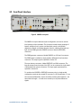
Front Panel Quick Reference ....................................................................... 18
2.2
Rear Panel Quick Reference ........................................................................ 21
2.3
Connector Care .............................................................................................. 22
System Details and Performance Specifications............................................... 23
3.1
General ............................................................................................................ 23
3.2
Safety and Regulatory................................................................................... 24
3.3
Internal Clock ................................................................................................. 24
3.4
PRBS Generator ............................................................................................. 27
3.5
Error Detector ................................................................................................. 29
Serial BERT 12.5 Gb/s User Guide
7
3.6
4
Data Path ........................................................................................................ 32
Operation ................................................................................................................. 33
4.1
General Information ...................................................................................... 33
4.1.1
4.1.2
4.2
Front Panel Interface .................................................................................... 35
4.2.1
4.2.2
4.2.3
4.2.4
Rear Panel Interface ..................................................................................... 46
4.4
Power-On State.............................................................................................. 48
4.5
System Verification ....................................................................................... 49
BER Detector Clock Phase Adjustment ..................................................... 51
4.7
Basic BER Measurement ............................................................................. 53
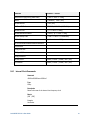
Remote GPIB Interface .......................................................................................... 55
5.1
GPIB Capabilities ........................................................................................... 56
5.2
GPIB Command Syntax ................................................................................ 57
Command Structure ....................................................................... 58
5.3
IEEE Common Commands ............................................................................ 59
5.4
SCPI Mandated Commands ......................................................................... 60
5.5
N4962A Device Commands ......................................................................... 60
5.5.1
5.5.2
5.5.3
5.6
8
Self Test Mode................................................................................ 49
Error Free Test................................................................................. 50
High BER Test ................................................................................. 50
Low BER Test .................................................................................. 51
4.6
5.2.1
6
Front Panel – Display Panel.......................................................... 36
Front Panel – Local, Receiver, and Data Path Controls ........... 37
Front Panel – Configuration Adjustment Controls.................... 39
Front Panel – Display Selection Controls ................................... 44
4.3
4.5.1
4.5.2
4.5.3
4.5.4
5
Performance Recommendations.................................................. 34
Connector Care ............................................................................... 34
Internal Clock Commands ............................................................. 61
PRBS Pattern Commands ............................................................. 65
Measurement Commands ............................................................. 70
Examples ......................................................................................................... 80
Returning the N4962A Serial BERT to Agilent Technologies ......................... 85
Serial BERT 12.5 Gb/s User Guide
Getting Started
1 Getting Started
1.1 General
The N4962A serial BERT 12.5 Gb/s operates from 500 Mb/s – 12.5 Gb/s
referencing an external clock, and from 9.85 – 11.35 Gb/s with the programmable
internal clock.
The N4962A includes:
• Internal clock system
• PRBS generator
• Error detector
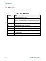
1.1.1 Key Features
•
•
•
•
•
•
•
•
Low cost, high performance
Programmable output amplitude control
Electronic receiver clock phase adjust
Differential inputs and outputs
Synchronous clock & pattern triggers
Selectable pattern lengths, mark density
Data Thru switch on Receiver for use with Oscilloscope on received data
Controlled with GPIB control bus format
1.1.2 Internal clock system
•
•
Serial BERT 12.5 Gb/s User Guide
Internal clock 9.85 to 11.35 GHz
External clock input for 0.5 to 12.5 GHz operation
9
Getting Started
1.1.3 PRBS generator
•
•
Selectable PRBS patterns:
o Lengths: 27-1, 210-1, 215-1, 223-1, 231-1
o Mark densities: 1/2, 1/4, 1/8
Adjustable PRBS amplitude:
o Voltage: 0.3 - 1.8 V pp per output
o Step size: 10 mV
1.1.4 Error detector
•
•
•
Automatic sampling point adjustment
Elapsed time BER measurements
Manual threshold adjustment)
•
•
•
Disabled ('safe mode': no output)
Enabled (PRBS output enabled)
Thru (no detector; inputs connected to Data Thru connectors on back
panel)
•
•
LED indicators
Multifunction alphanumeric display
1.1.5 Operating modes
1.1.6 Display
1.1.7 Data entry / interface
•
•
•
10
Push-button control (local)
Remote GPIB (IEEE 488.2-1992)
Compatible with N4980A multi-instrument BERT software user interface
Serial BERT 12.5 Gb/s User Guide
Getting Started
1.2 N4962A Operation Overview
The Agilent Technologies N4962A is a cost-effective serial BERT 12.5 Gb/s,
consisting of an internal clock system, PRBS generator, and error detector. It is
designed for automated production-line testing, manufacturing, characterization,
and R&D lab use. The N4962A features high-UI jitter injection and programmable
output amplitude.
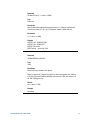
Figure 1. Eye waveform
The N4962A generates a continuous bit pattern that is applied to the DUT then
fed back into the error detector. The input is automatically synchronized and
compared with the original bit stream. The bit error rate is calculated by
comparing the number of bit errors to the total number of bits transmitted. The
BER can be shown on the display and can be captured through the remote GPIB
interface.
Serial BERT 12.5 Gb/s User Guide
11
Getting Started
1.3 Getting Started with the N4962A Serial BERT 12.5 Gb/s
1.3.1 Unpacking and Installation
The N4962A serial BERT 12.5 Gb/s is shipped with all the accessories required
for the self-test mode and verification. The contents includes:
• N4962A serial BERT 12.5 Gb/s
• Two coax cables to connect rear-panel clocks (TX CKO, RX CKO to TX
CKI, RX CKI)
• Two phase balanced 50 Ω coaxial cables for self-test mode (IN, ¯¯
IN to
OUT, OUT
¯¯¯)
• Four 2.92 mm male-female adapters
• AC power converter module
• AC power cord
• CD containing the N4962A User Guide and N4962A Data Sheet
Refer to the N4960-90030 N495xA through N498xA Connector Care Reference
Guide at www.agilent.com/find/N4962A.
If this product is not used as specified, the protection provided by the
equipment could be impaired. This product must be used in a normal
condition (in which all means for protection are intact) only.
Before switching on this instrument, make sure the supply voltage is in the
specified range.
This instrument has autoranging line voltage input. Be sure the supply
voltage is within the specified range.
In an ESD-safe environment, carefully remove the N4962A. Install on a flat
surface with unobstructed air flow to the back panel. Plug the AC power cord into
the power converter module and a wall socket, then plug the converter module
into the N4962A.
12
Serial BERT 12.5 Gb/s User Guide
Getting Started
1.3.2 Safety and Regulatory
This product has been designed and tested in accordance with accepted industry
standards, and has been supplied in a safe condition. The documentation
contains information and warnings that must be followed by the user to ensure
safe operation and to maintain the product in a safe condition.
Do not remove instrument covers. There are no user serviceable parts
within. Operation of the instrument in a manner not specified by Agilent
Technologies may result in personal injury or loss of life.
For continued protection against fire hazard, replace fuses, and or circuit
breakers only with same type and ratings. The use of other fuses, circuit
breakers or materials is prohibited.
To prevent electrical shock, disconnect instrument from mains before
cleaning. Use a dry cloth or one slightly dampened with water to clean the
external case parts. Do not attempt to clean internally.
The Mains wiring and connectors shall be compatible with the connector
used in the premise electrical system. Failure, to ensure adequate earth
grounding by not using the correct components may cause product damage,
and serious injury.
1.3.3 Declaration of Conformity
A EU declaration of conformity is available at
http://regulations.corporate.agilent.com/doc/search.htm
1.3.4 Important Notes
•
•
•
•
•
•
Serial BERT 12.5 Gb/s User Guide
Use ESD protection at all times when using the instrument
Review min/max specifications before applying input signals
Use only K-connectors on the OUT and OUT
¯¯¯ ports
Handle the pair of self-test and clock loop coaxial cables with care
Leave dust jackets on unused back panel connectors
Situate the instrument away from heat sources, do not block the fan
13
Getting Started
1.3.5 Performance Recommendations
•
•
•
•
•
•
When using differential-mode connections, ensure the cables are phase
balanced
Differential connectors may be used single-ended if unused ports are
terminated in 50 Ω
Use high quality cables and connector savers (or adaptors)
Keep cable lengths short and minimize number of cable bends
Use a 7-10 in-lbs torque wrench when attaching connectors
Terminate all unused RF connectors with 50 Ω terminations
1.4 Connect the Hardware
•
•
•
•
•
Connect power cord to adaptor to N4962A; plug in the power cord
Connect TX CKO to TX CKI with included coaxial cable
Connect RX CKO to RX CKI with included coaxial cable
Connect the OUT (and optionally OUT
¯¯¯ to your DUT input
Connect your DUT output to IN (and optionally ¯¯)
IN
•
•
Turn on the power switch from the back panel
Press the Data Path > Select Path button and select Enabled
o This will turn on the PRBS output; when Disabled is selected, the
instrument is in a 'safe mode' and no output is generated
Press the Display > Scroll ↓ button and select Ampl (V)
Press the Adjust > Ampl +/- buttons to set the single-ended output
voltage
1.5 Turn It On
•
•
14
Serial BERT 12.5 Gb/s User Guide
Getting Started
1.6 Align Clock and Data
•
•
•
•
Press the Data Path > PRBS
¯¯¯¯ button only if the DUT is inverting
o When on, the PRBS will generate an inverted output signal
Press the Display > Scroll ↓ button and select Ø
Press the Adjust > Config State + button to auto-set the detector phase
Observe the Error ε light
o The light indicates errors are being measured by the error detector, if
the light is on, no error-free sampling point could be found
1.7 Make the Measurement
•
•
•
•
•
Serial BERT 12.5 Gb/s User Guide
Press the Receiver > On button and ensure the light is on
Press the Display > Scroll ↓ button and view Err (error counter)
Press the Display > Scroll ↓ button and view BER
Press the Display > Scroll ↓ button and view є time (sec)
Press the Receiver > On button to end the measurement
15
Getting Started
16
Serial BERT 12.5 Gb/s User Guide
N4962A System Overview
2 N4962A System Overview
The N4962A consists of three functional blocks:
• Internal/external clock system with analog jitter injection
• PRBS generator (TX) with variable output amplitude control
• Error detector (RX) with electronic clock phase adjustment
The N4962A is controlled by front-panel buttons and remote GPIB (IEEE 488.2)
commands; information is conveyed with LED indicators and a display on the
front panel, along with GPIB data communication.
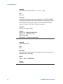
Figure 2. N4962A simplified block diagram; system overview
The clock system features an internal generator that creates a 9.85 to
11.35 GHz system clock from an internal 1/16th-rate clock generator. The
internal clock/16 can also be phase locked to an external 1/16th clock if
desired. The high-frequency TX clock and trigger output can be FM-modulated
with an optional external jitter signal. Alternatively, external 500 Mb/s to
12.5 Gb/s clocks can be used in place of the internal high-frequency clocks for
the PRBS generator and error detector.
Serial BERT 12.5 Gb/s User Guide
17
N4962A System Overview
The PRBS generator creates a continuous bit stream triggered by the input
clock rate, configured by the selectable pattern length, mark space density,
data inversion, and error injection settings. The output is amplified by a
programmable gain stage.
The error detector compares the input to an automatically-synchronized bit
stream generated with the same system settings. The clock input features an
electronic phase adjuster to correctly align the clock and data sampling point.
The system settings can be set by the local push-button interface or remote
GPIB (IEEE 488.2) interface. All settings can be accessed through the menu
system or through GPIB commands. The N4962A is compatible with the
N4980A multi-instrument BERT software which is available through Agilent
Technologies to help speed up programming time.
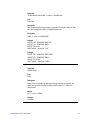
2.1 Front Panel Quick Reference
Figure 3. N4962A front panel
18
Connectors
RECEIVER: IN, ¯¯
IN (SMA) – input to error detector (differential or single-ended)
SOURCE: OUT, OUT
¯¯¯ (2.92 mm K) – PRBS generator output (differential or
single-ended)
Display
(display panel) – eight-character display to show display status and configure
system
Error ε (light) – indicates errors are being detected by the error detector
Serial BERT 12.5 Gb/s User Guide
N4962A System Overview
Controls
Local (button & light) – indicates local (vs. remote) control; button selects local
control
Receiver >
On (button & light) – indicates detector state; button toggles & resets BER
Data Path >
PRBS
¯¯¯¯ (button & light) – indicates inversion of PRBS signal; button toggles
Select Path (button & 3 lights) – data path (disabled, enabled, thru); button
cycles
Adjust >
Freq (2 buttons) – adjust the internal clock frequency up or down (shown on
display)
Ampl (2 buttons) – adjust the PRBS output amplitude up or down (shown on
display)
ø (2 buttons) – adjust the detector clock phase up or down (shown on display)
Config State (2 buttons) – change value of the currently-displayed
configuration state.
Display >
Scroll (2 buttons & 6 lights) – select which feature is shown on the display
panel:
• BER – measured BER (# bit errors / total # bits)
• ε time (sec) – elapsed time of BER measurement, in seconds
• Ampl (V) – single-ended PRBS generator output amplitude, in volts per
side
• Freq (GHz) – internal clock frequency, in GHz (10 GHz corresponds to
10 Gb/s)
• Ø – BER clock phase adjustment, in degrees (360-degrees = 1 UI)
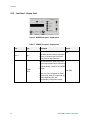
• Config State– selects one of the configuration states shown in Table 1.
Serial BERT 12.5 Gb/s User Guide
19
N4962A System Overview
Table 1. Configuration state details (shown on display panel, default in BOLD)
Config State
Description
Options
PAT 2E31
PRBS generator pattern length
2E31, 2E23, 2E15, 2E10, 2E7
MS 0.500
PRBS generator mark space density
0.500 (1/2), 0.250 (1/4), 0.125 (1/8)
Jitter 0
Jitter injection mode
0 (low-jitter mode), 1 (external jitter
on)
Synth 1
Internal clock mode
0 (internal clock off), 1 (Internal clock
on)
Err00000
Lowest digits of error counter
ErAd OFF
PRBS digital error injection
OFF, 1E0, 1E1, …, 1E7 (errors per
second)
NoData 0
Error detector data sense
0 (data sense off), 1 (data sense on)
TD= 0010
Time delay for measurement start (for 10-9999 (1/10th of a microsecond)
long length DUT)
APT=0010
Autophase procedure measurement
time
1234R567
Serial number and FW revision (only none
the last four digits of the serial number
are shown on the front panel display)
0-5000 (1/10th of a millisecond per
phase step; default 10 (1ms time per
step))
(Display > Scroll to select state; Adjust > Config State to change value)
20
Serial BERT 12.5 Gb/s User Guide
N4962A System Overview
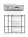
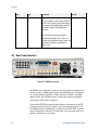
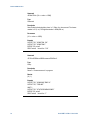
2.2 Rear Panel Quick Reference
Figure 4. N4962A rear panel
Connectors
DataThru
¯¯¯¯¯¯ , DataThru (SMA) – connected to ¯¯,
IN IN when ‘thru’ data path
selected.
PatTrigO (SMA) – PRBS pattern trigger output
TX CKI (SMA) – PRBS generator clock input (default connected to TX CKO)
RX CKI (SMA) – error detector clock input (default connected to RX CKO)
RX CKO (SMA) – internal clock output for error detector
TX CKO (SMA) – internal clock output for PRBS generator
HF TrigO (SMA) – high-frequency (9.85 – 11.35 GHz) clock output
LF TrigO (SMA) – low-frequency (616 – 709 MHz) clock output
Ext CKI (SMA) – low-frequency (616 – 709 MHz) clock input; used to phase
lock with external clock source
JitterI (SMA) – jitter signal input (DC-100 MHz); turn jitter mode on before use
(GPIB) – GPIB connector, conforms to IEEE 488.1 mechanical specification
Label
SN (white area) – N4962A serial number
Controls
GPIB (switch panel) – N4962A GPIB address (down is ‘0’, up is ‘1’, LSB is on
the left)
(Default GPIB address as shipped from the factory is 25)
Power (switch) – N4962A is powered when switch is toggled up towards
‘Power’ label
Power connector – connects with AC/DC adapter. Use only the supplied
AC/DC adapter.
Serial BERT 12.5 Gb/s User Guide
21
N4962A System Overview
2.3 Connector Care
Refer to the N4960-90030 N495xA through N498xA Connector Care Reference
Guide at www.agilent.com/find/N4962A.
Inspect the connectors for the following:
• Worn or damaged threads
• Scratches to mating surface
• Burrs and loose metal particles
• Dust or foreign material in the space surrounding the center pin (type K
only)
• Ensure that female contacts are straight and aligned
Clean the connectors as described in the following procedure. Cleaning
connectors with alcohol shall only be done with the instruments power cord
removed, and in a well-ventilated area. Allow all residual alcohol moisture to
evaporate, and the fumes to dissipate prior to energizing the instrument.
1. Remove any dust or loose particles using a low-pressure air source.
2. Moisten a lint-free swab with isopropyl alcohol. Do not saturate the
swab.
3. Minimize the wicking of the alcohol into the connector structure.
4. Clean the mating plane surfaces and threads.
5. Allow alcohol to evaporate, and then use a low-pressure air source to
blow surfaces clean.
6. Make sure no particles or residue remains.
7. Inspect connector for damage.
22
Serial BERT 12.5 Gb/s User Guide
System Details and Performance Specifications
3 System Details and Performance
Specifications
Specifications describe the instrument’s warranted performance. Nonwarranted values are stated as typical. All specifications are valid in a range
from 10°C to 40°C ambient temperature after a 30 minute warm-up phase. If
not otherwise stated, all unused RF inputs and outputs must be terminated
with the included 50 Ω-terminated connectors.
3.1 General
Table 2. General and mechanical parameters of N4962A
Operating Temperature
+10°C to +40°C
Storage Temperature
–40°C to +70°C
Power Requirements
42 W External AC Adaptor (included)
• 100 to 240 VAC, 47 to 63 Hz
Physical Dimensions
Width: 254 mm (10 in), Height: 63.5 mm (2.5 in), Depth: 254 mm (10 in)
Weight
3.4 kg (7.5 lbs)
EMC
Complies with European EMC Directive 2004/108/EC
• IEC/EN 61326-1
• CISPR Pub 11 Group 1, class A
• AS/NZS CISPR 11
• ICES/NMB-001
This ISM device complies with Canadian ICES-001.
Cet appareil ISM est conforme a la norme NMB-001 du Canada.
Serial BERT 12.5 Gb/s User Guide
23
System Details and Performance Specifications
3.2 Safety and Regulatory
Do not remove instrument covers. There are no user serviceable parts
within. Operation of the instrument in a manner not specified by Agilent
Technologies may result in personal injury or loss of life.
To prevent electrical shock, disconnect instrument from mains before
cleaning. Use a dry cloth or one slightly dampened with water to clean the
external case parts. Do not attempt to clean internally.
For continued protection against fire hazard, replace fuses, and or circuit
breakers only with same type and ratings. The use of other fuses, circuit
breakers or materials is prohibited.
The Mains wiring and connectors shall be compatible with the connector
used in the premise electrical system. Failure, to ensure adequate earth
grounding by not using the correct components may cause product damage,
and serious injury.
3.3 Internal Clock
The internal clock is generated from a low-frequency (LF) 1/16th-rate clock
signal that is multiplied up to the high-frequency (HF) clock rate, 9.85 to 11.35
GHz. The internal HF clock or an external 500 MHz to 12.5 GHz clock is required
to trigger the PRBS generator and error detector. The generator and detector
operate at 1 bit per clock cycle (10 Gb/s at a clock speed of 10 GHz).
24
Serial BERT 12.5 Gb/s User Guide
System Details and Performance Specifications
Figure 5. N4962A block diagram – internal clock system
The internal LF 1/16th-rate clock can be phase locked to an external source in
order to synchronize the N4962A with the external device. To synchronize the
clocks, follow the procedure detailed below. The internal or external LF clock is
available from the buffered LF TrigO connector.
To ensure phase lock of an external LF clock applied to the ExtCKI port, the
following procedure must be used:
1.
2.
3.
4.
5.
Turn off the external signal generator RF output
Set external signal generator to new 1/16th-rate RF frequency
Set N4962A to new HF frequency value (or nearest value)
Turn on the external signal generator RF output
Turn off the N4962A internal synthesizer (change "synth" to 0)
Users wanting to change frequency from this condition should:
1.
2.
3.
4.
5.
6.
Turn on the internal synthesizer (synth to 1)
Turn off the external signal generator RF output
Set the external signal generator to the new 1/16th-rate frequency
Set the N4962A to new HF frequency value (or nearest value)
Turn on the external signal generator RF output
Turn off the N4962A internal synthesizer (synth to 0)
The clocks should now be phase locked to the new frequency.
Serial BERT 12.5 Gb/s User Guide
25
System Details and Performance Specifications
Table 3. Parameters for N4962A internal low-frequency clock (LF TrigO, Ext CKI)
Frequency
615.625 to 709.375 MHz
Max input amplitude
Ext CKI: 2.0 Vpp (+10 dBm)
Output power
LF TrigO, 0.5 V pp typical
Connector
Female SMA, single-ended, AC coupled, 50 Ω impedance
The LF 1/16th rate clock must phase lock to the data rate clock.
The LF clock is multiplied up to HF clock frequencies and is split into two
output paths: a transmit clock for the PRBS generator, TX CKO, which can be
modulated with an external jitter input signal, and a receive clock for the error
detector, RX CKO. Both outputs are buffered. The clock outputs are connected
by default to the input clock connectors for the PRBS generator and error
detector, TX CKI and RX CKI, with a pair of coaxial cable loops.
To trigger the PRBS generator and error detector with an external 500 MHz to
12.5 GHz clock, remove the coax loops and apply the external source to TX CKI
and RX CKI. The generator and detector must be triggered with the same
phase-synchronous clock. Ensure that at least 0 dBm (630 mV pp) is applied to
the TXCKI input and at least +4 dBm (1 V pp) is applied to the RXCKI input. Do
not apply more than +10 dBm (2 V pp) to these inputs.
Table 4. Parameters for N4962A internal clock (TX CKO, RX CKO, HF TrigO)
26
Frequency
9.85 to 11.35 GHz
Resolution
10 MHz front-panel, 1 MHz GPIB
Output power
TX CKO, Typ: +4 dBm (1 V pp)
RX CKO, Typ: +4 dBm (1 V pp)
HF TrigO, Typ: +6 dBm (1.3 V pp)
Connector
Female SMA, single-ended, AC coupled, 50 Ω impedance
Serial BERT 12.5 Gb/s User Guide
System Details and Performance Specifications
The TX clock, available from the buffered HF TrigO and TX CKO connectors,
features the optional addition of an external jitter signal.
To add jitter to the PRBS clock, and therefore to the PRBS output signal, switch
into jitter-injection mode by changing the Config State “Jitter” setting to 1, and
apply a DC to 100 MHz sinusoid to the JitterI connector. The jitter input signal
will be FM modulated onto the clock; the amount of added jitter corresponds to
the amplitude of the input signal.
The Jitter setting of 0 will still FM modulate any signal under 100 kHz. To
properly ensure no jitter is added, disconnect any source from the JitterI
connector.
Table 5. Parameters for N4962A internal clock jitter injection (JitterI)
Frequency
Typ: DC to 100 MHz
Input Voltage
2 V pp max
Jitter Added
Up to 5 UI ≤ 2 MHz, up to 0.15 UI ≥ 10 MHz
Connector
Female SMA, single-ended, DC coupled, 50 Ω impedance
Switch to jitter-injection mode before applying a signal to JitterI
3.4 PRBS Generator
The PRBS generator creates a continuous bit stream based on the
configuration settings and the TX CKI input clock rate. The internal clock can
be used for 9.85 to 11.35 Gb/s operation, or an external clock can be used for
500 Mb/s to 12.5 Gb/s operation. The PRBS generator and error detector must
be clocked at the same rate.
The PRBS generator configuration includes selectable pattern length, mark
space density ratio, and digital error injection settings. The PRBS also features
polarity control to allow for both inverting and non-inverting DUTs. These
configuration settings are detailed in Section 4.2.
Serial BERT 12.5 Gb/s User Guide
27
System Details and Performance Specifications
Figure 6. N4962A block diagram – PRBS generator
The PRBS output bit stream is amplified by an adjustable gain stage. The
output amplitude ranges from 300 mV pp to 1800 mV pp per output (0.6 V pp to
3.6 V pp differential) in 10 mV pp increments.
The amplified PRBS output signal is available from the single-ended or
differential 2.92 mm K-connector OUT/OUT
¯¯¯connectors on the front panel. The
PRBS generator also generates a pattern trigger output, available from Pat
TrigO on the back panel, which changes state after 32 complete PRBS bit
streams have been generated. Pat TrigO has a frequency equal to
(clock_rate) / (32 * bit_pattern_length). Users of Pat TrigO should verify that its
output is a square wave in order to ensure proper pattern triggering.
Table 6. Parameters for N4962A PRBS generator (OUT, OUT
¯¯¯)
28
Data rate
0.5 to 12.5 Gb/s
PRBS patterns
2n – 1, n=7, 10, 15, 23, 31
Mark space density
1/2, 1/4, 1/8
Pattern invert
available for all patterns
Error injection
selectable uniform rate
Error injection rates
1 x10n errors per second, n = 1, 2, 3, 4, 5, 6, 7
Data output amplitude
300 to 1800 mV pp (single-ended)
Data output amplitude resolution
10 mV
Data output jitter
1.1 ps rms typical at 10 Gb/s
Data output rise/fall time (20% to 80%)
18 ps typical, 23 ps maximum
Data output external interface
(May be operated single end without unused output
terminated into 50 Ω.)
TXCKI Clock input frequency range
0.5 to 12.5 GHz
TXCKI Clock input amplitude range
0 to +10 dBm (630 mV pp to 2 V pp)
TXCKI Clock input external interface
AC coupled, 50 Ω nominal, female SMA
Serial BERT 12.5 Gb/s User Guide
System Details and Performance Specifications
The PRBS bit stream consists of data generated by one of five patterns, listed
in Table 7. The pattern length is a system configuration setting, selected by
changing the Config State “PAT xxxx” setting, detailed in Section 4.2.3.
Table 7. N4962A PRBS generator patterns
Pattern
Config State
Polynomial
231 – 1
2E31
X31 + X28 + 1 = 0 4.67 Hz
ITU-T 0.150
223 – 1
2E23
X23 + X18 + 1 = 0 1.19 kHz
ITU-T 0.150
2 –1
2E15
X + X + 1 = 0 305 kHz
ITU-T 0.150
27 – 1
2E7
X7 + X6 + 1 = 0
ITU-T V.29
15
15
Tone Spacing (10Gb/s) ITU Standard
14
78.7 MHz
3.5 Error Detector
The error detector counts errors in the input bit stream, based on the
configuration settings and the RX CKI input clock rate. The internal clock can
be used for 9.85 to 11.35 Gb/s operation, or an external clock can be used for
500 Mb/s to 12.5 Gb/s operation. The PRBS generator and error detector must
be clocked at the same rate.
The error detector samples the input bit stream on the rising edge of the clock.
If the clock transition occurs near the data transition – that is, if the clock and
the data are changing at the same time – the sampled data value is uncertain,
which may result in high BER. This is illustrated in Figure 13.
To ensure the clock and data transition points are correctly offset, the error
detector features a user-adjustable 360-degree electronic phase shifter. The
phase shifter delays the clock input to the detector, allowing the user to select
the optimal sampling point. The N4962A can automatically adjust the receiver
phase to the best sampling point, detailed in Section 4.6.
Serial BERT 12.5 Gb/s User Guide
29
System Details and Performance Specifications
Figure 7. N4962A block diagram – error detector
The error detector compares the sampled input bit stream to a separate
internal PRBS signal generated with the same configuration settings as the
PRBS generator. The error detector automatically synchronizes its internal
PRBS with the incoming bit stream, in a process called ‘training’. The error
detector is in training mode when off, and switches to error-counting mode
when the detector is turned on. Assuming the training was successful, and the
error detector was able to synchronize with the input bit stream, the detector
starts counting errors less than 1us after turning on.
Training the error detector takes approximately 50 us, and requires a somewhat
error-free input bit stream. If the detector is unable to synchronize with the
incoming bit stream, the measured BER will be very high. This is only an issue
for bit error rates higher than 5E-01 (50% of incoming bits are errors); for most
applications with high BER, the detector will auto-synchronize very rapidly.
The phase adjustment offers 2 degree resolution capability from 5 Gb/s to
12.5 Gb/s. The linearity accuracy of phase is limited to 10 degree steps for
operation from 5 Gb/s to 12.5 Gb/s. For external clock rates below 5 GHz the
specific values of 0, 90, 180 or 270 degrees are required for the receiver clock
phase alignment in order to obtain correct BER results. Employing the
receiver’s auto-phase feature or manual adjustment to the receiver phase
resulting in any other phase values may lead to receive errors. Users requiring
greater precision in receiver clock and data alignment below 5 GHz can achieve
this result using external means such as a mechanical phase-shifter.
30
Serial BERT 12.5 Gb/s User Guide
System Details and Performance Specifications
Table 8. Parameters for N4962A error detector (IN, ¯¯)
IN
Data rate
0.5 to 12.5 Gb/s
PRBS patterns
2n – 1, n=7, 10, 15, 23, 31
Data input sensitivity (single ended)
0.1 V pp typical
Data input voltage range
2 Vpp max (single-ended)
± 0.5 V DC common mode voltage max
Data input phase adjust
0 to 360°
Data input phase adjust resolution
2° for data rates ≥ 5 Gb/s
90° for data rates < 5 Gb/s
Data input external interface
Differential. DC coupled, 50 Ω nominal, female SMA
(May be operated single end without unused input
terminated into 50 Ω)
RXCKI Clock input frequency range
0.5 to 12.5 GHz
RXCKI Clock input amplitude range
+4 to +10 dBm (1 to 2 V pp)
RXCKI Clock input external interface
AC coupled, 50 Ω nominal, female SMA
After the error detector synchronizes with the incoming bit stream, and is
turned on, it compares the sampled input bit stream against the synchronized
comparison signal. The detector counts the number of bit errors and the total
number of bits, and generates the BER measurement (# bit errors / total #
bits). The error detector counter sizes have been selected to enable long-term
BER measurements without counter overflow, detailed in Table 9. The
measurement will stop if one of these counters reaches the maximum value.
Table 9. N4962A error detector counter specifications
Counter
Counter Size
Overflow Time at 12.5 Gb/s
Bit errors
48 bits
~12.5 hours (0.5 BER), 2606 days (1E-4 BER)
Total bits
56 bits
1601 hours (67 days)
Elapsed time bits
22 bits
4194304 seconds (48.5 days)
Serial BERT 12.5 Gb/s User Guide
31
System Details and Performance Specifications
3.6 Data Path
The N4962A can operate in one of three data path configurations. The data
path can be set from the front panel, detailed in Section 4.2.2, or through GPIB
remote commands.
The current data path is indicated with the front panel lights. One of the three
lights will be lit. The lights are labeled Disabled, Enabled, and Thru.
The Disabled data path is selected by default; this disables the PRBS output
and can be considered a ‘safe mode’ to be used to avoid DUT damage. The
Enabled data path turns on the PRBS output. The Thru data path connects the
IN/IN
¯¯ signals directly to the DataThru/DataThru
¯¯¯¯¯¯ output connectors on the
back panel, with an associated switching loss in the data path. Errors are not
counted. The data path configurations are summarized in Table 10.
The Thru feature allows users to ensure the quality and amplitude of the
received signal is measured with a sampling scope without disconnecting the
cables from the N4962A. Once the path loss is determined, an accurate
estimate of the eye quality and amplitude can be determined for every test.
Table 10. N4962A data path configurations
32
Data Path light
Configuration
PRBS generator
Disabled
IN/IN
¯¯ connected to error
detector, default
Disabled
Enabled
IN/IN
¯¯ connected to error
detector
Enabled
Thru
IN/IN
¯¯ connected to
DataThru/DataThru
¯¯¯¯¯¯
Enabled
Additional path loss
Typ. 4 dB
Serial BERT 12.5 Gb/s User Guide
Operation
4 Operation
The following section provides detailed information regarding the use of the
N4962A serial BERT 12.5 Gb/s. Please refer to the front and rear panel quick
reference, in Section 2, for abbreviated information.
4.1 General Information
The N4962A serial BERT 12.5 Gb/s should be used in accordance with the
following:
• Read and follow operating instructions; do not exceed min/max
specifications.
• Use ESD protection at all times, but especially when handling RF
input/outputs; ground coaxial cable conductor pins before use to
remove static buildup.
• Situate the instrument away from heat sources.
• Do not block airflow to the fan; do not allow foreign material into
enclosure.
• Always use provided AC adaptor. Do not power the unit with a
different adaptor. Do not modify the power plug or wall outlet to
remove the third (ground) pin.
• Do not drop or shake the instrument; minimize vibration; handle with
care.
• There are no user-serviceable parts within. Return damaged
instruments for factory-authorized repair. Refer to instrument warranty
for more information.
Serial BERT 12.5 Gb/s User Guide
33
Operation
4.1.1 Performance Recommendations
Follow the following recommendations for best performance:
• When using differential mode connection for IN/IN
¯¯, OUT/OUT
¯¯¯, or
DataThru/DataThru
¯¯¯¯¯¯ , ensure the cables are phase balanced. If the
electrical length of one cable is a significant fraction of a unit interval
longer than the other, the quality of the differential signal will be
degraded and BER will increase.
• Keep cable lengths short and minimize number of cable bends.
• Terminate all unused RF connectors with 50 Ω terminations.
4.1.2 Connector Care
The N4962A serial BERT 12.5 Gb/s features high-quality SMA connectors, and
two 2.92 mm K-connectors for the front-panel OUT/OUT
¯¯¯ interface. Agilent
Technologies does not recommend using male SMA connectors with the
female K-connectors; the male SMA pin has looser tolerances than the female
K sleeve, and may damage the connector. Connector damage will degrade
signal fidelity.
Refer to the N4960-90030 N495xA through N498xA Connector Care Reference
Guide at www.agilent.com/find/N4962A.
Agilent Technologies also recommends the following:
• Use a 7-10 in-lbs torque wrench when attaching connectors.
• Consider using connector savers to prolong performance and minimize
damage.
• Differential connectors may be used single-ended if second end
terminated in 50 Ω.
• Terminate all unused RF connectors with 50 Ω terminations.
34
Serial BERT 12.5 Gb/s User Guide
Operation
4.2 Front Panel Interface
Figure 8. N4962A front panel
The N4962A front panel indicates system configuration, and can be used for
local operation of the instrument. The front panel contains three groupings of
buttons and lights (local, receiver, and data path controls; configuration
adjustment controls; and display selection controls), a display panel and error
light, and the PRBS generator (SOURCE) and error detector (RECEIVER)
connectors.
The PRBS generator connectors, labeled SOURCE, are 2.92 mm K-connectors.
The PRBS output is available in single-ended or differential form from these
connectors. The output signal is specified in Section 3.3.
The error detector connectors, labeled RECEIVER, are SMA connectors. The
input bit stream (from the output of the DUT) can be connected in single-ended
or differential form to these connectors. The input signal requirements are
specified in Section 3.4.
To use either the SOURCE or RECEIVER connector pairs in a single-ended
configuration, terminate the unused RF connector in a 50 Ω termination. To use
the connectors differentially, ensure the cables used are phase balanced – the
same electrical length – to avoid errors caused by out-of-phase differential
signals.
Serial BERT 12.5 Gb/s User Guide
35
Operation
4.2.2 Front Panel – Display Panel
Figure 9. N4962A front panel – display panel
Table 11. N4962A front panel – display panel
Text
Error ε
Type
Description
light
The error light is lit for a short period of N/A
time when the error detector identifies a
bit error. If the error light is solid red,
many errors are being detected.
display
panel
36
Default
The eight-character display shows the
current configuration option selected by
using the Display->Scroll UP and DOWN
buttons.
Freq (GHz)
When one of the configuration Adjust
buttons (Freq, Ampl, Ø) are pressed, the
display will briefly show the
corresponding configuration setting.
Serial BERT 12.5 Gb/s User Guide
Operation
4.2.3 Front Panel – Local, Receiver, and Data Path Controls
Figure 10. N4962A front panel – local, receiver, and data path controls
Table 12. N4962A front panel – local, receiver, and data path controls
Text
Local
Receiver
->
On
Type
Description
button
& light
Light indicates local control:
• ON when front-panel control is
enabled;
ON
• OFF when remote GPIB interface
is in use.
Button switches to local control.
button
& light
Light indicates error detector is ON, and:
• Elapsed time is accumulating;
• Total bits and errors are being
counted;
• BER measurement is being
calculated.
If detector is ON, pressing button:
• Saves state (# bits, errors, &
OFF
seconds);
• Turns off detector;
• Puts detector into training mode
(for auto-synchronization of
incoming bit stream).
If detector is OFF, pressing button:
• Resets state (# bits, errors, &
seconds);
• Turns on detector.
Serial BERT 12.5 Gb/s User Guide
Default
37
Operation
Data Path
->
PRBS
¯¯¯¯
Invert
button
& light
Light indicates inverted PRBS generator
output:
• OFF when PRBS bit stream is not
inverted;
• ON when PRBS bit stream is
inverted.
Button toggles the output inversion ON
and OFF.
OFF
Inverting the bit stream after training and
turning on the detector will result in a
BER measurement approaching 1E0.
Data Path
->
Disabled
Enabled
Thru
(none)
button
&3
lights
Light indicates which data path is
selected:
• Disabled: IN/IN
¯¯ connected to
error detector, PRBS generator is
disabled;
• Enabled: IN/IN
¯¯ connected to
error detector, PRBS generator is
enabled;
Disabled
• Thru: IN/IN
¯¯ connected to
DataThru/DataThru
¯¯¯¯¯¯ with some
path loss, PRBS generator is
enabled;
Button cycles between the data path
options.
38
Serial BERT 12.5 Gb/s User Guide
Operation
4.2.3 Front Panel – Configuration Adjustment Controls
Figure 11. N4962A front panel – configuration adjustment controls
Table 13. N4962A front panel – configuration adjustment controls
Text
Type
Description
Default
Buttons adjust internal clock frequency by 0.01
GHz:
• UP increases frequency (max 11.35 GHz);
• DOWN decreases frequency (min 9.85
GHz).
Adjust
->
Freq
Adjust
->
Ampl
UP and DOWN
buttons
UP and DOWN
buttons
Serial BERT 12.5 Gb/s User Guide
Display will briefly show new frequency setting
after pressing either button, and then switches
back to previously-displayed setting.
When using an external clock (Synth = 0), the
Freq adjust range is increased to 500 MHz min,
12.5 GHz max. The N4962A frequency setting
should be set to the frequency of the external
clock so that the N4962A frequency dependent
parameters are correctly set.
Buttons adjust PRBS output amplitude by 10 mV:
• UP increases amplitude (max 1800 mV);
• DOWN decreases amplitude (min 300
mV).
10.0 GHz
500 mV
Display will briefly show new amplitude setting
after pressing either button, and then switches
back to previously-displayed setting.
39
Operation
Text
Adjust
->
Ø
Type
Description
Default
UP and DOWN
buttons
Buttons adjust BER clock phase by 2 degrees
from 5 to 12.5 GHz, and in 90-degree increments
below 5 GHz:
• UP increases phase offset (max 358,
min 0)
0 degrees
• DOWN decreases phase offset
Display will briefly show new clock phase setting
after pressing either button, and then switches
back to previously-displayed setting.
Buttons adjust the value of the currentlydisplayed Config State (use the Display->Scroll
buttons to select the current state):
PAT 2E31
o options: 2E31, 2E23, 2E15, 2E10, 2E7
PRBS output pattern length setting, where
pattern lengths are 2n-1, and n has a value in [31,
23, 15, 10, 7]. 231-1 is the longest pattern, and
repeats every 0.2 seconds at a clock speed of
10 GHz.
PAT 2E31
MS 0.500
• MS 0.500
Jitter 0
o options: 0.500, 0.250, 0.125
Synth 1
PLUS and MINUS
Err00000
buttons
PRBS output mark space density setting, which is ErAd OFF
the ratio of logic 1’s to the total of logic 1’s and
NoData 0
logic 0’s. A mark space density of 0.5 (1/2)
1234R567
indicates an equal number of 1’s and 0’s.
• Jitter 0
o options: 0, 1
Jitter injection mode setting: 0 for normal
operation, 1 for jittered operation. This setting is
for optionally applying the DC-100 MHz jitter
input signal. When 1, the modulator bandwidth is
increased to allow the jitter input to be FM
modulated onto the clock signals. The jitter added
is proportional to the amplitude of the jitter input
signal. For low jitter operation, set the Jitter
command to 0, and remove any signal from the
•
Adjust
->
Config
State
40
Serial BERT 12.5 Gb/s User Guide
Operation
Text
Type
Description
Default
JitterI port.
•
Synth 1
o options: 0, 1
Internal clock setting: 0 = use external clock
(internal clock turned off); 1 = use internal clock.
•
Err00000
Five-digit error detector error counter, included
for low BER applications, or for testing external
error injection. The counter accumulates errors
since the detector was reset, and wraps around
99999. This counter should not be used as the
authoritative number of errors counted.
•
ErAd OFF
o options: OFF, 1E0, 1E1, 1E2, …, 1E7
Digital error injection setting, which indicates
how many bit inversions occur per second. OFF
indicates no bit errors are injected, 1E0 indicates
1 error per second, 1E7 indicates 10 million errors
per second. To find the injected BER, divide by
the clock frequency. For example, at a setting of
1E2 (100) errors per second, the BER will be 1E-8
at a clock rate of 10 GHz, or 8E-9 at 12.5 GHz. See
Table 14.
When Display->Ø is selected from the display
selector, pressing the Adjust->Config State PLUS
button will prompt the N4962A to automatically
determine the optimum detector clock phase.
This is detailed further in Section 4.6.
•
NoData 0
o options: 0, 1
NoData option helps with the initialization
Serial BERT 12.5 Gb/s User Guide
41
Operation
Text
Type
Description
Default
sequence. When the source is used with the
error detector, this value should be set to 1. This
helps with a condition when all zeros are loaded
into the error detector’s input, which can
erroneously cause bad error rate numbers. This
should be set to 0 when using a different
manufacturer’s pattern generator, or a known
good signal is used with the N4962A source.
•
TD= 0010
o Min 0010 (1 µs), max 6500 (650 µs)
The TD (“Training Delay”) option delays the start
of the error detector after the BER measurement
has been initiated. This feature is used in
conjunction with the NoData function. This delay,
listed in 1/10th microseconds (default 1us),
allows the PRBS pattern time to transition
through the DUT before measurement start. This
can be very important for DUTs containing a long
electrical length or an optical loop.
•
APT=0010
o Min 0001 (0.1 ms), max 5000 (500
ms)
The APT (“Autophase Time”) option specifies the
autophase search algorithm measurement time at
each 2-degree phase point. This option allows the
user to specify the measurement depth of the
autophase algorithm.
APT allows a tradeoff between the search time
and positioning accuracy of the autophase
algorithm. Because 180 phase points are
measured, this option may increase the
autophase time to a total of 90+ seconds.
The confidence interval of a BER measurement,
with frequency (GHz), gate time (seconds), and
42
Serial BERT 12.5 Gb/s User Guide
Operation
Text
Type
Description
Default
measurement depth (BER) is:
CI = 1 − e − Freq (GHz )×time ( s )×MeasDepth ( BER )
•
1234R111
o options: none
This is the serial number and firmware revision
code of the instrument (only the last four digits of
the serial number are shown on the front panel
display).
Table 14. ErAd settings and expected BER measurements for 10 Gb/s operation
ErAd Setting
Expected BER
Expected BER
(added errors
(10 GHz clock;
(12.5 GHz clock;
per second)
no other errors)
no other errors)
OFF
0
0
1E0
1E-10
8E-11
1E1
1E-9
8E-10
1E2
1E-8
8E-9
1E3
1E-7
8E-8
1E4
1E-6
8E-7
1E5
1E-5
8E-6
1E6
1E-4
8E-5
1E7
1E-3
8E-4
Serial BERT 12.5 Gb/s User Guide
43
Operation
4.2.5 Front Panel – Display Selection Controls
Figure 12. N4962A front panel – display selection controls
Table 15. N4962A front panel – display selection controls
Text
Type
Description
Default
Buttons select the measurement or
configuration option to display on the
display panel:
• UP selects the previous display
item;
• DOWN selects the next display
item.
Display
->
Scroll
UP and DOWN
buttons
and 6 lights
The selection process wraps around the
display options (pressing DOWN at the last
item selects the first item).
The display options are:
Freq (GHz)
• BER
Displays the current measured bit error rate
(BER), defined as the total number of bit
errors divided by the total number of bits
(bit counters detailed in Table 9).
If the error detector is on (Receiver->On
light is ON), the BER shown is a
measurement that is being calculated in
real time. If the detector is off, the BER
shown is from the previous session
(captured while the detector was
previously on).
44
Serial BERT 12.5 Gb/s User Guide
Operation
Text
Type
Description
Default
• ε time (sec)
Displays the elapsed time of the BER
measurement, in seconds. If the error
detector is on, the elapsed time will
increment in real time. If the error detector
is off, the elapsed time shown is from the
previous session.
• Ampl (V)
Displays the single-ended PRBS output
amplitude, in volts. This voltage is per side,
multiply by 2 when the output is used
differentially.
• Freq (GHz)
Displays the internal clock frequency, in
GHz. When using an external clock (Synth
= 0), then the Freq adjust range is
increased to 500 MHz min, 12.5 GHz max.
The N4962A Frequency setting should be
set to the frequency of the external clock
so that the N4962A frequency dependent
parameters are correctly set.
• Ø
Displays the error detector electronic clock
phase shift setting, in degrees. The phase
shift amount ranges from 0 to +358
degrees (one unit interval).
When Ø is shown on the display, pressing
the Adjust->Config State PLUS button will
prompt the N4962A to automatically
determine the optimum detector clock
phase. This is detailed in Section 4.6.
• Config State
Displays one of ten configuration states
that can be modified with the Adjust>Config State PLUS or MINUS buttons.
Different state can be selected with the
Scroll UP or DOWN buttons, but the light
Serial BERT 12.5 Gb/s User Guide
45
Operation
Text
Type
Description
Default
will remain on the Config State display
item. For example, the first state shown is
the PAT 2Exx, and the Config State light is
lit. Pressing Scroll DOWN selects the MS
0.xxx state, and the Config State light
remains lit.
The Config State currently selected is
indicated by the display text. There is no
indicator for the different states. States are
described in Table 13, and detailed in
Section 4.2.3.
4.3 Rear Panel Interface
Figure 13. N4962A rear panel
The N4962A rear panel features connectors for the internal and external clock
system, as well as a PRBS pattern trigger, and a differential pair of connectors
for a unique data path (DataThru). The rear panel also includes a 5-bit GPIB
address switch, and a GPIB connector. The panel also features the N4962A
power switch, and a built-in cooling fan.
The DataThru/DataThru
¯¯¯¯¯¯ connectors (both SMA) are connected to the IN/IN
¯¯
connectors when the Data Path option is set to Thru (detailed in Section 2.5).
The PRBS generator is enabled and is available from the OUT/OUT
¯¯¯ connectors
when this data path is selected. The input signal is not processed by the error
detector, and errors are not counted.
46
Serial BERT 12.5 Gb/s User Guide
Operation
The Pat TrigO connector is an output pattern trigger from the PRBS generator.
The Pat TrigO signal changes state after 32 complete PRBS bit streams have
been generated. Pat TrigO has a frequency equal to (clock_rate) / (32 *
bit_pattern_length); With a clock speed of 10 GHz, the Pat TrigO frequency is
2.4 MHz with a pattern length of 27-1, and 0.15 Hz with a pattern length of
231-1.
TX CKI and RX CKI are the transmit (PRBS generator) and receiver (error
detector) clock inputs. To use an external 500 Mb/s to 12.5 Gb/s clock signal,
connect the external clock to both TX CKI and RX CKI, as described in Sections
3.4 and 3.5, respectively.
TX CKO and RX CKO are the internal clock output ports. These are connected to
TX CKI and RX CKI when the internal clock is used to trigger the PRBS
generator and error detector. The clock output ports are detailed in
Section 3.3.
HF TrigO and LF TrigO are clock trigger outputs from the internal clock system,
detailed in Section 3.3.
Ext CKI is a low-frequency 1/16th-rate clock input used when synchronizing
the internal clock system with a LF external signal. The Ext CKI port is detailed
in Section 3.3.
JitterI is a DC-100 MHz input that is FM modulated onto the TX CKO and HF
TrigO clock. A sinusoid should be applied to the input port, and the resulting
PRBS output jitter will be proportional to the sinusoid amplitude. This is
detailed in Section 3.3.
The GPIB connector and 5-bit address switch is accessible from the rear panel.
All GPIB devices on the same GPIB bus must have different addresses to
function together. GPIB devices are programmed by referencing the address of
the device, as well as the bus type. This is detailed in Section 5. The factory
default address is 25.
Serial BERT 12.5 Gb/s User Guide
47
Operation
4.4 Power-On State
The power-on state of the N4962A is set after turning the rear Power switch
on. The internal clock is active and generates a 10.0 GHz clock. The PRBS
generator is off. The error detector is off, in training mode, and will not
accumulate errors. The error detector light may indicate errors if the default
sampling position is incompatible with the cable length, or if the OUT/OUT
¯¯¯
port(s) are not connected to the IN/IN
¯¯port(s).
Table 16. N4962A power-on state
48
Setting
Display
Description
Value
Local
Light
Local push-button (vs GPIB) control
On
Receiver On
Light
Error detector
Off
PRBS
¯¯¯¯
Light
PRBS output inverted
Off
Data Path
3 lights
Data path
Disabled
Error ε
Light
Bit error detected
Undetermined
Freq
Display
Internal clock speed
10.0 GHz
Ampl
Not shown
PRBS output amplitude
0.500 V
Ø
Not shown
Error detector clock phase adjustment
0 (degrees)
PAT 2E31
Not shown
PRBS pattern length
231-1
MS 0.500
Not shown
PRBS mark space density
0.500
Jitter 0
Not shown
Jitter-injection mode
Off (0)
Synth 1
Not shown
Internal clock
On (1)
Err00000
Not shown
Measured BER errors
0
ErAd OFF
Not shown
PRBS errors added per second
Off (none)
NoData
Not shown
Error detector data sense
0 (off)
Serial BERT 12.5 Gb/s User Guide
Operation
4.5 System Verification
When first using the N4962A and before using the machine to test an external
DUT, first confirm that the system is generating a PRBS bit stream and can
detect bit errors.
4.5.1 Self Test Mode
Verify the PRBS generator and error detector are both functioning by
configuring the system in self-test mode as follows: connect the OUT/OUT
¯¯¯
ports directly to the IN/IN
¯¯ ports with the Agilent Technologies-supplied phase
balanced 50 Ω coaxial cables, use the internal clock at the default setting,
power the system, turn on the PRBS output, and adjust the error detector clock
phase, as follows:
•
•
•
•
•
•
•
•
•
•
Serial BERT 12.5 Gb/s User Guide
Connect TX CKO to TX CKI with coaxial cable (included; default)
Connect RX CKO to RX CKI with coaxial cable (included; default)
Connect OUT to IN with phase-balanced coax cable (included)
Optionally connect OUT
¯¯¯to ¯¯
IN with phase-balanced coax cable
(included)
Terminate all unused RF connectors with 50 Ω terminations
Turn on the power switch from the back panel
Press the Data Path->Select Path button and select Enabled
Press the Display->Scroll ↓ button and select Ø
Press the Adjust->Config State + button to auto-select the detector
phase
Observe the Error ε light (should remain off, indicating no errors
detected)
49
Operation
4.5.2 Error Free Test
When the error detector clock phase is correctly adjusted, the default settings
will result in error-free operation. The Error ε light will be off, and the measured
BER will be zero. Check the error-free operation as follows:
• Put the system in self test mode, described in Section 4.5.1.
• Press the Receiver > On button and ensure the light is on
• Press the Display > Scroll ↓ button and select Err (should show zero
errors)
• Press the Display > Scroll ↓ button and select BER (should show zero)
• Press the Display > Scroll ↓ button and select ε time (sec) (should be
increasing)
4.5.3 High BER Test
To verify that the error detector can correctly count a large number of errors,
first allow the detector to synchronize with a clear input signal by adjusting the
detector clock phase to an error-free operating point. Once the detector has
been trained, turn the detector on and invert the PRBS signal to generate 100%
errors, as follows:
• Put the system in self test mode, described in Section 4.5.1.
• Press the Receiver > On button and ensure the light is on
• Press the Data Path > PRBS
¯¯¯¯ button and ensure the light is on
• Press the Display > Scroll ↓ button and select Err (should show many
errors)
• Press the Display > Scroll ↓ button and select BER (should show high
BER)
• Press the Display > Scroll ↓ button and select ε time (sec) (should be
increasing)
50
Serial BERT 12.5 Gb/s User Guide
Operation
4.5.4 Low BER Test
To verify that the error detector can correctly count a small number of errors,
use the PRBS error injection capability to insert a known number of errors into
the bit stream, as follows:
• Put the system in self test mode, described in Section 4.5.1.
• Press the Display > Scroll ↓ button and select ErAd OFF
• Press the Adjust > Config State + button and select ErAd 1E0
• Press the Receiver > On button and ensure the light is on
• Observe the Error ε light (should blink once per second)
• Press the Display > Scroll ↑ button and select Err (should show 1 per
second)
• Press the Display > Scroll ↓ button and select BER (should show
1E-10)
• Press the Display > Scroll ↓ button and select ε time (sec) (should be
increasing)
4.6 BER Detector Clock Phase Adjustment
The error detector clock phase can be electronically controlled to adjust the
detector sampling point; the periodic point at which the detector interprets the
incoming bit stream. Due to the unknown delay associated with cables and the
DUT in the data path, the incoming bit stream may not be sampled at the
optimal point.
The detector must be adjusted to find the optimal sampling point; an incorrect
sampling point will yield an artificially-high BER measurement, shown in Figure
14.
IN, notIN
IN, notIN
RX CKI
RX CKI
good
uncertain
Figure 14. Sampling uncertainty due to clock phase misadjustment
Serial BERT 12.5 Gb/s User Guide
51
Operation
If the sampling point occurs near the PRBS transition point, the sampled value
is uncertain and many bit errors will be measured by the detector. Adjusting
the phase away from the transition point will optimally position the sampling
point and allow the best chance of measuring error-free operation.
The N4962A can automatically detect and set the detector clock phase for the
best sampling point. It requires that the system settings and data path allow
error-free operation. This is best achieved by putting the system into self-test
mode, described in Section 4.5.1.
If the configuration settings result in high errors (eg: PRBS output amplitude
set low), or the cabling or DUT result in poor eye quality, the automatic
detector clock phase adjustment will not work. It will also be difficult to set the
clock phase adjustment manually.
To automatically set the detector clock phase adjustment:
With the N4962A powered, clocks connected, and data path connected:
• Ensure the Data Path > Enabled option is selected (PRBS output must
be on)
• Ensure the Receiver > On is not selected (the error detector must be
off)
• Press the Display > Scroll ↓ button and select Ø
• Press the Adjust > Config State + button to auto-select the detector
phase
• Observe the Error ε light (should remain off, indicating no errors
detected)
To manually set the detector clock phase adjustment:
With the N4962A powered, clocks connected, and data path connected:
• Ensure the Data Path > Enabled option is selected (PRBS output must
be on)
• Ensure the Receiver > On is not selected (the error detector must be
off)
• Press the Display > Scroll ↓ button and select Ø
Find the optimal sampling point as follows:
• If the Error ε light is off, press the Adjust > Ø + button until the light is
on
• Press the Adjust > Ø + button until the Error ε light remains off
• Record the clock phase adjustment value
• Press the Adjust > Ø + button until the Error ε light remains on
52
Serial BERT 12.5 Gb/s User Guide
Operation
•
•
•
Record the second phase value; the optimum point is halfway between
the two values
Press the Adjust > Ø - button and adjust the phase offset to the
optimal point
Observe the Error ε light (should remain off, indicating no errors
detected)
Depending on the DUT characteristics, the optimal sampling point may occur at
different detector phase adjustment values. You may need to repeat the phase
adjustment procedure when changing the DUT use characteristics, or if you
change the operating frequency.
4.7 Basic BER Measurement
The N4962A can quickly be used for basic BER measurements as follows:
connect the OUT/OUT
¯¯¯ ports to the DUT input, connect the IN/IN
¯¯ ports to the
DUT output, use the internal clock, power the system, enable the PRBS output,
adjust the detector clock phase, and turn on the error detector.
When connecting the OUT/OUT
¯¯¯, and IN/IN
¯¯ ports, use a short 50 Ω coaxial
cable. To test single-ended DUTs, terminate the OUT
¯¯¯ and ¯¯
IN ports with 50 Ω
terminations.
• Connect TX CKO to TX CKI with coaxial cable (included; default)
• Connect RX CKO to RX CKI with coaxial cable (included; default)
• Connect OUT to DUT input with short 50 Ω coax cable
• Optionally connect OUT
¯¯¯to DUT input
¯¯¯¯ with short phase-balanced 50 Ω
coax cable
• Connect DUT output to IN with short 50 Ω coax cable
• Optionally connect DUT output
¯¯¯¯ to ¯¯
IN with short phase-balanced 50 Ω
coax cable
Add appropriate attenuation or gain to DUT output, output
¯¯¯¯ signals
•
•
•
•
•
Serial BERT 12.5 Gb/s User Guide
Terminate all unused RF connectors with 50 Ω terminations
Turn on the power switch from the back panel
Adjust the DUT for the best chance for error-free operation (turn
attenuators off, etc)
Press the Data Path > Select Path button and select Enabled
If the DUT is inverting, press the Data Path > PRBS
¯¯¯¯ button to invert the
output
53
Operation
•
•
•
•
•
•
•
54
Press the Display > Scroll ↓ button and select Ø
Press the Adjust > Config State + button to auto-select the detector
phase
Observe the Error ε light (should remain off, indicating no errors
detected)
Press the Receiver > On button and ensure the light is on
Press the Display > Scroll ↑ button and select ε time (sec) (should be
increasing)
Press the Display > Scroll ↑ button and select BER
Press the Receiver > On button and ensure the light is off when
complete
Serial BERT 12.5 Gb/s User Guide
Remote GPIB Interface
5 Remote GPIB Interface
The N4962A can be controlled and queried with the rear-panel GPIB interface.
The GPIB interface complies with IEEE standard 488.2-1992. To learn more
about the GPIB interface, consult the following books from the IEEE:
•
•
The International Institute of Electrical and Electronic Engineers. IEEE
Standard 488.1-1987, IEEE Standard Digital Interface for Programmable
Instrumentation. New York, NY, 1987.
.The International Institute of Electrical and Electronic Engineers. IEEE
Standard 488.2-1987, IEEE Stand Codes, Formats, Protocols and
Communication Commands for Use with ANSI/IEEE Std 488.1-1987.
New York, NY, 1987.
A GPIB interface requires that all devices on a common bus have different
addresses; the 5-bit address control switch is located on the back panel next to
the GPIB connector. The factory default address is 25. The address uses a
three digit format. The first digit is always set to “7”, and the last two digits are
programmed by the 5 bit control switch located on the back of the instrument.
The N4980A multi-instrument BERT software is available from Agilent
Technologies for fast GPIB programming of the N4962A.
Serial BERT 12.5 Gb/s User Guide
55
Remote GPIB Interface
5.1 GPIB Capabilities
The GPIB interface capabilities are described in Table 17.
Table 17. N4962A GPIB capabilities
56
Mnemonic
Function
SH1
Complete source handshake capability
AH1
Complete acceptor handshake capability
T6
Basic talker; serial poll; unaddressed to talk if addressed to listen; no talk only
L4
Basic listener; unaddressed to listen if addressed to talk; no listen only
SR1
Complete service request capability
RL2
Remote/local capability with local lockout (LLO)
PP0
No parallel port capability
DC1
Device clear capability
DT1
Device trigger capability (accepted but ignored)
C0
No controller capability
E2
Tristate outputs (except the handshake line)
Serial BERT 12.5 Gb/s User Guide
5.2 GPIB Command Syntax
The N4962A can be controlled through the GPIB interface using commands and
queries. The commands and queries are documented in the Backus-Naur Form
notation, detailed in Table 18.
Table 18. N4962A GPIB command and query syntax
Symbol
Meaning
<>
Defined element (eg: <arg>)
::=
Is defined as (eg: <arg> ::= argument)
|
Exclusive OR
{}
One of this group is required
[]
Optional item
…
Previous elements may be repeated
Serial BERT 12.5 Gb/s User Guide
57
Remote GPIB Interface
5.2.1 Command Structure
The GPIB interface allows commands, which tell the instrument to take a
specific action, and queries, which ask the instrument to return information.
Commands are composed of syntactic elements:
•
•
•
•
Header – the command name; if it ends with a question mark, the
command is a query.
Delimiter – a space, colon (:), comma (,), or semi-colon (;) which breaks
the message into segments for the instrument to process.
Link – a command sub-function. Not all commands have links.
Argument – a quantity, quality, restriction, or limit associated with the
header or link.
Commands are case insensitive, although they are documented in an
uppercase and lowercase manner that indicates which minimum characters are
required to make the command. The commands can be shortened to the
minimum length illustrated by the uppercase letters in the documentation.
•
•
•
58
The command
o :SOURce:PRBS:INVert ON
Can be written in lowercase
o :source:prbs:invert on
And it can be shortened
o :sour:prbs:inv ON
Serial BERT 12.5 Gb/s User Guide
5.3 IEEE Common Commands
The IEEE 488.2 standard has a list of reserved commands that must be
implemented by all instruments using the standard. The N4962A implements all
of the required commands, listed in Table 19.
Table 19. N4962A IEEE common commands
Command
Function
*CLS
Clear status command
*RST
Reset command
*WAI
Wait to continue
*TRG
Trigger
*IDN?
Identification Query
*STB?
Status Byte Query
*TST?
Self Test Query
*ESR?
Event Status Register Query
*ESE
Event Status Enable Register Set
*ESE?
Event Status Enable Register Query
*OPC
Operation Complete clear flag
*OPC?
Operation Complete Query
*SRE
Service Request Enable Set
*SRE?
Service Request Enable Query
IEEE optional commands
*SAV
Save
*RCL
Recall
Serial BERT 12.5 Gb/s User Guide
59
Remote GPIB Interface
5.4 SCPI Mandated Commands
The N4962A also conforms to the Standard Commands for Programmable
Instrumentation (SCPI 1999.0) command set. Two SCPI mandated commands
are implemented, listed in Table 20.
Table 20. N4962A SCPI mandated commands
Command
Function
:SYSTEM:ERROR?
Returns event/error number and message from error queue
:SYSTEM:VERSION? Returns SCPI protocol version number (1999.0)
5.5 N4962A Device Commands
The N4962A device commands are summarized in Table 21. The following
descriptions and examples assume the user is programming with Agilent
BASIC, a simple interpretative language that is convenient for instrument
programming.
For the examples below, the device being programmed is located at GPIB
device address 725. The actual address varies according to how you have
configured the GPIB bus for your own application. For information to change
the bus address see Section 5.
Table 21. N4962A device commands
60
Command
Parameters / Results
:SOURce:ROSCillator:SOURce
{? | INTernal | EXTernal}
:SOURce:ROSCillator:[INTernal]:FREQuency
{? | {9850 <= value <= 11350}}
:SOURce:ROSCillator:JITTer
{? | ON | OFF}
:SOURce:PATTern
{? | PRBS{7 | 10 | 15 | 23 | 31}}
:SOURce:PRBS:MARKspace
{? | MS{2 | 4 | 8}}
:SOURce:PRBS:INVert
{? | ON | OFF}
:SOURce:PRBS:IERR:RATe
{? | OFF | ERR1E{0 <= value <= 7}}
Serial BERT 12.5 Gb/s User Guide
Command
Parameters / Results
:SOURce:VOLTage:[LEVel]:[AMPLitude]
{? | {300 <= value <= 1800}}
:MODe
{? | NORMal | THRU | OFF}
:SENSe:NOData
{? | ON | OFF}
:SYSTem:STATus?
{BITERROR | NODATA | NORXCLK}
:SENSe:APTime
{? | {1 <= value <= 5000}}
:SENSe:ROSCillator:PHASe
{? | AUTO | {0 <= value <= 360}}
:SENSe:SWEep:TIME
{? | 0.001 <= value <= 4194303.999}
:SENSe:TRAIn
{? | {10 <= value <= 6500}}
:STATus:OPERation:MEASurement:CONDition?
:INITiate:BER
:TRIGger:INITiate
:TRIGger:ABORt
:TRIGger:SAMPle
:SENSe:DATA?
[BCOunt | ECOunt | ETIMe | BER | ALL]
:FETCh:BER?
[BCOunt | ECOunt | ETIMe | BER | ALL]
5.5.1 Internal Clock Commands
Command
:SOURce:ROSCillator:SOURce?
Type
Query
Description
Returns the state of the internal low-frequency clock.
Result
{INT | EXT}
Example
See Below
Serial BERT 12.5 Gb/s User Guide
61
Remote GPIB Interface
Command
:SOURce:ROSCillator:SOURce {INTernal | EXTernal}
Type
Command
Description
Selects the low-frequency clock to be used. INTernal selects and powers the
internally-generated clock, EXTernal selects the external clock connected to Ext
CKI, and powers down the internal clock.
Parameters
{INTernal | EXTernal}
Example
OUTPUT 725; ":SOUR:ROSC:SOUR INT"
OUTPUT 725; ":SOUR:ROSC:SOUR?"
ENTER 725; value$
PRINT value$ ! should be “INT”
Command
:SOURce:ROSCillator:[INTernal]:FREQuency?
Type
Query
Description
Returns the current value of the programmable high-frequency clock, in MHz.
Results
{9850 <= value <= 11350} (if INT clock selected)
{500 to 12500} (if EXT clock selected)
Example
See below
62
Serial BERT 12.5 Gb/s User Guide
Command
:SOURce:ROSCillator:[INTernal]:FREQuency {9850 <= value <= 11350}
Type
Command
Description
Sets the frequency of the internal high-frequency clock, in MHz. The internal
clock source must be selected for this feature to work.
Parameters
{9850 <= value <= 11350} (if INT clock selected)
{500 to 12500} (if EXT clock selected)
Example
OUTPUT 725; ":SOUR:ROSC:SOUR INT"
OUTPUT 725; ":SOUR:ROSC:INT:FREQ 10500”
OUTPUT 725; ":SOUR:ROSC:FREQ?"
ENTER 725; value$
PRINT value$ ! should be “10500”
Command
:SOURce:ROSCillator:JITTer?
Type
Query
Description
Returns the current jitter injection mode.
Results
{ON | OFF}
Example
See below
Serial BERT 12.5 Gb/s User Guide
63
Remote GPIB Interface
Command
:SOURce:ROSCillator:JITTer {ON| OFF}
Type
Command
Description
Sets the jitter injection mode. If 1, the high-jitter mode will be enabled and the
jitter input signal JitterI will be FM modulated onto the TX CKO and HF TrigO
outputs. This feature requires the internal clock be selected. On Jitter 0, a low
bandwidth modulator mode is selected, lowering the noise floor, and filtering
jitter above 100 kHz.
Parameters
{ON | OFF}
Example
OUTPUT 725; ":SOUR:ROSC:SOUR INT"
OUTPUT 725; ":SOUR:ROSC:JITT ON”
OUTPUT 725; ":SOUR:ROSC:JITT?"
ENTER 725; value$
PRINT value$ ! should be “ON”
64
Serial BERT 12.5 Gb/s User Guide
5.5.2 PRBS Pattern Commands
Command
:SOURce:PATTern?
Type
Query
Description
Returns the current PRBS pattern length.
Results
PRBS{7 | 10 | 15 | 23 | 31}
Example
See below
Command
:SOURce:PATTern {PRBS{7 | 10 | 15 | 23 | 31}}
Type
Command
Description
Sets PRBS pattern length to the value indicated in the command line. PRBSn
selects a pattern with length 2^n-1.
Parameters
PRBS{7 | 10 | 15 | 23 | 31}
Example
OUTPUT 725; ":SOUR:PATT PRBS10"
OUTPUT 725; ":SOUR:PATT?"
ENTER 725; value$
PRINT value$ ! should be “PRBS10”
Serial BERT 12.5 Gb/s User Guide
65
Remote GPIB Interface
Command
:SOURce:PRBS:MARKspace?
Type
Query
Description
Returns the current PRBS pattern mark space density.
Results
MS{2 | 4 | 8}
Example
See below
Command
:SOURce:PRBS:MARKspace {MS{2 | 4 | 8}}
Type
Command
Description
Sets PRBS pattern mark space density to the value indicated in the command
line. MSn selects a pattern with mark space density of 1/n.
Parameters
MS{2 | 4 | 8}
Example
OUTPUT 725; ":SOUR:PRBS:MARK MS2"
OUTPUT 725; ":SOUR:PRBS:MARK?"
ENTER 725; value$
PRINT value$ ! should be “MS2”
66
Serial BERT 12.5 Gb/s User Guide
Command
:SOURce:PRBS:INVert?
Type
Query
Description
Returns the current PRBS invert setting.
Results
{ON | OFF}
Example
See below
Command
:SOURce:PRBS:INVert {ON | OFF}
Type
Command
Description
Sets PRBS invert setting to the value indicated in the command line. If ON, the
PRBS signal is inverted.
Parameters
{ON | OFF}
Example
OUTPUT 725; ":SOUR:PRBS:INV ON"
OUTPUT 725; ":SOUR:PRBS:INV?"
ENTER 725; value$
PRINT value$ ! should be “ON”
Serial BERT 12.5 Gb/s User Guide
67
Remote GPIB Interface
Command
:SOURce:PRBS:IERR:RATe?
Type
Query
Description
Returns the current error injection rate
Results
{OFF | ERR1E{0 <= value <= 7}}
Example
See below
Command
:SOURce:PRBS:IERR:RATe {OFF | ERR1E{0 <= value <= 7}}
Type
Command
Description
Sets the digital error injection rate to 10^n errors injected per second. If OFF, no
errors are injected.
Parameters
{OFF | ERR1E{0 <= value <= 7}}
Example
OUTPUT 725; ":SOUR:PRBS:IERR:RAT ERR1E3"
OUTPUT 725; ":SOUR:PRBS:IERR:RAT?"
ENTER 725; value$
PRINT value$ ! should be “ERR1E3”
68
Serial BERT 12.5 Gb/s User Guide
Command
:SOURce:VOLTage:AMPLitude?
Type
Query
Description
Returns the current single-ended PRBS output amplitude, in mVpp per side.
(double this number for differential)
Results
{300 <= value <= 1800}
Example
See below
Command
:SOURce:VOLTage:AMPLitude {300 <= value <= 1800}
Type
Command
Description
Sets the single-ended PRBS output amplitude, in mVpp per side.
Parameters
{300 <= value <= 1800}
Example
OUTPUT 725; ":SOUR:VOLT:LEV:AMPL 350"
OUTPUT 725; ":SOUR:VOLT:AMPL?"
ENTER 725; value$
PRINT value$ ! should be “350”
Serial BERT 12.5 Gb/s User Guide
69
Remote GPIB Interface
5.5.3 Measurement Commands
Command
:MODe?
Type
Query
Description
Returns the current data path.
Results
{NORM | THRU | OFF}
Example
See below
Command
:MODe {NORMal | THRU | OFF}
Type
Command
Description
Sets the instrument data path:
NORMal
Normal operation, IN/IN
¯¯connected to error detector, PRBS
generator enabled.
THRU
Input through, IN/IN
¯¯ connected to DataThru/DataThru
¯¯¯¯¯¯ PRBS
generator enabled.
OFF
Disabled, IN/IN
¯¯connected to the error detector, only the PRBS
generator disabled.
Parameters
{NORM | THRU | OFF}
Example
OUTPUT 725; ":MOD THRU"
OUTPUT 725; ":MOD?"
ENTER 725; value$
PRINT value$ ! should be “THRU”
70
Serial BERT 12.5 Gb/s User Guide
Command
:SENSe:NOData?
Type
Query
Description
Returns the state of the data sense option.
Results
{ON | OFF}
Example
See below
Command
:SENSe:NOData {ON | OFF}
Type
Command
Description
Sets the NoData sense function. When used with the N4962A source, helps to
detect all-zeros' data.
Parameters
{ON | OFF}
Example
OUTPUT 725; ":SENS:NOData OFF"
OUTPUT 725; ":SENS:NOData?"
ENTER 725; value$
PRINT value$ ! should be “OFF”
Serial BERT 12.5 Gb/s User Guide
71
Remote GPIB Interface
Command
:SYSTem:STATus? {BITERROR | NODATA | NORXCLK}
Type
Query
Description
Returns the state of the output indicator:
BITERROR
Indicates the current status of the BERT error light; the light is
lit when errors are counted; the query returns 0 when the light
is lit
NODATA
Indicates the current status of the NoData flag determined by
the instrument (only if NODATA is turned on, see above); the
query returns 0 when the NoData condition is met
NORXCLK
Indicates the current status of the NoRXClk flag; the query
returns 0 when no clock input is detected at the RX CKI port
Results
{0 | 1}
Example
None
Command
:SENSe:APTime?
Type
Query
Description
Returns the current autophase measurement time setting; how long to
measure BER at each of the 180 phase points when performing an autophase
alignment, in 1/10ths of a millisecond.
Results
{1 <= value <= 5000}
Example
See below
72
Serial BERT 12.5 Gb/s User Guide
Command
:SENSe:APTime {1 <= value <= 5000}
Type
Command
Description
Sets the desired autophase measurement time, in 1/10ths of a millisecond.
The lowest number is 1 (0.1 ms). The highest number is 5000 (500 ms).
Parameters
{1 <= value <= 5000}
Example
OUTPUT 725; ":SENS:APT 300"
OUTPUT 725; ":SENS:APT?"
ENTER 725; value$
PRINT value$ ! should be “300”
Command
:SENSe:ROSCillator:PHASe?
Type
Query
Description
Returns the error detector clock phase.
Phase is selected in 2 degree increments for data rates greater then 5 GHz to
12.5 GHz. Data rates between 500 MHz and less than 5 GHz offer values of 0,
90, 180, 270 degrees only.
Results
{0 <= value <= 358}
Example
See below
Serial BERT 12.5 Gb/s User Guide
73
Remote GPIB Interface
Command
:SENSe:ROSCillator:PHASe {AUTO | {0 <= value <= 360}}
Type
Command
Description
Sets the error detector clock phase for sampling point. If AUTO, the N4962A
will automatically determine the optimum phase for best sampling point once,
and set the phase to that value. For data rates less than 5 GHz, the phase
detector is limited to 0, 90, 180, or 270 degree increments.
Parameters
{AUTO | {0 <= value <= 358}}
Example
OUTPUT 725; ":SENS:ROSC:PHAS AUTO"
OUTPUT 725; ":SENS:ROSC:PHAS?"
ENTER 725; value$
PRINT value$ ! should be a number 0-360
Command
:SENSe:SWEep:TIME?
Type
Query
Description
Returns the current measurement time setting; how long the measurement is
intended to run for, in seconds.
Results
{0.001 <= value <= 4194303.999}
Example
See below
74
Serial BERT 12.5 Gb/s User Guide
Command
:SENSe:SWEep:TIME {0.001 <= value <= 4194303.999}
Type
Command
Description
Sets the desired measurement time, in seconds. The lowest number is 0.001
seconds. The highest number is 4194303.999 seconds.
Parameters
{0.001 <= value <= 4194303.999}
Example
OUTPUT 725; ":SENS:SWE:TIME 120"
OUTPUT 725; ":SENS:SWE:TIME?"
ENTER 725; value$
PRINT value$ ! should be “120”
Example
OUTPUT 725; ":SENS:SWE:TIME 10550"
OUTPUT 725; ":SENS:SWE:TIME?"
ENTER 725; value$
PRINT value$ ! should be “10550”
Command
:SENSe:TRAIn?
Type
Query
Description
Returns the current training delay time setting; how long to pause for the
transit time of the DUT before the measurement starts, in 1/10ths of a
microsecond.
Results
{10 <= value <= 6500}
Example
See below
Serial BERT 12.5 Gb/s User Guide
75
Remote GPIB Interface
Command
:SENSe:TRAIn {10 <= value <= 6500}
Type
Command
Description
Sets the desired training delay time, in 1/10ths of a microsecond. The lowest
number is 10 (1 us). The highest number is 6500 (650 us).
Parameters
{10 <= value <= 6500}
Example
OUTPUT 725; ":SENS:TRAI 120"
OUTPUT 725; ":SENS:TRAI?"
ENTER 725; value$
PRINT value$ ! should be “120”
Command
:STATus:OPERation:MEASurement:CONDition?
Type
Query
Description
Returns 1 if measurement is in progress.
Results
{0 | 1}
Example
OUTPUT 725; ":SENS:SWE:TIME 10"
OUTPUT 725; ":TRIG:INIT"
WAIT 2
OUTPUT 725; ":STAT:OPER:MEAS:COND?”
ENTER 725; value$
PRINT value$ ! should be “1”
76
Serial BERT 12.5 Gb/s User Guide
Command
:INITiate:BER
Type
Command
Description
Latches data on BERT board; equivalent to turning on the receiver.
Results
none
Example
none
Command
:TRIGger:INITiate
Type
Command
Description
Initiates data acquisition (begins testing); equivalent to turning on the receiver.
Example
See below
Command
:TRIGger:ABORt
Type
Command
Description
Aborts data acquisition (ends testing); equivalent to turning off the receiver.
Example
See below
Serial BERT 12.5 Gb/s User Guide
77
Remote GPIB Interface
Command
:TRIGger:SAMPle
Type
Command
Description
Takes sample of current measurement. Does not return any values, but allows
the values to be queried by other commands.
Example
See below
Command
:SENSe:DATA? [BCOunt | ECOunt | ETIMe | BER | ALL]
Type
Querry
Description
Returns the selected parameter from the current instrument sample, or returns
all parameters as a vector if ALL or no parameter is specified.
BCOunt
Total number of bits counted
ECOunt
Total number of errors counted
ETIMe
Elapsed time (seconds)
BER
Calculated Bit Error Rate
The vector is as follows: BCOunt,ECOunt,ETIMe,BER
Parameters
[BCOunt | ECOunt | ETIMe | BER | ALL]
Note
Need to run ":TRIG:INIT" and ":TRIG:SAMPLE” first.
Result
Described above
78
Serial BERT 12.5 Gb/s User Guide
Example
OUTPUT 725; ":SENS:SWE:TIME 10"
OUTPUT 725; ":TRIG:INIT"
WAIT 2
OUTPUT 725; ":TRIG:SAMPLE”
OUTPUT 725; ":SENS:DATA? BER”
ENTER 725; value$
PRINT value$ ! BER value after 2 seconds
Command
:FETCh:BER? [BCOunt | ECOunt | ETIMe | BER | ALL]
Type
Querry
Description
Returns the selected parameter from the memory stored on the FPGA, or
returns all parameters as a vector if ALL or no parameter is specified. Does not
require the measurement to currently be running. This command can only be
used if the set-up measurement time from the command “:SENSe:SWEep:TIME
value” is completed. See examples 470-580.
BCOunt
Total number of bits counted
ECOunt
Total number of errors counted
ETIMe
Elapsed time (seconds)
BER Calculated Bit Error Rate, or NAN if measurement not ready
The vector is as follows: BCOunt,ECOunt,ETIMe,BER
Parameters
[BCOunt | ECOunt | ETIMe | BER | ALL]
Result
Described above
Serial BERT 12.5 Gb/s User Guide
79
Remote GPIB Interface
Example
OUTPUT 725; ":SENS:SWE:TIME 10"
OUTPUT 725; ":TRIG:INIT"
WAIT 2
OUTPUT 725; ":TRIG:SAMPLE”
OUTPUT 725; ":SENS:DATA? BER”
ENTER 725; value$
PRINT value$ ! BER value after 2 seconds
WAIT 3
OUTPUT 725; ":TRIG:ABOR"
OUTPUT 725; ":FETC:BER?"
ENTER 725; result$
PRINT result$ ! BER value after 5 seconds
5.6 Examples
The following programming example assumes the user is programming with
Agilent BASIC, a simple interpretative language that is convenient for
instrument programming.
For the example programs below, the device being programmed is located at
GPIB device address 725. The actual address varies according to how you have
configured the GPIB bus for your own application. For information to change
the bus address see Section 5.
This first block of code shows how to initialize the instrument and check the
GPIB subsystem for errors.
10 OUTPUT 725; "*IDN?"
20 ENTER 725; result$
30 PRINT result$
30 OUTPUT 725; ":SYSTEM:ERROR?"
40 OUTPUT 725; "*RST"
80
! request the instrument ID string
! read the return string
! print the results to stdout
! check for errors
! reset the BERT
Serial BERT 12.5 Gb/s User Guide
The next block of code shows how to save the instrument state in one of the
save/recall registers (0-9), how to change the value of the internal HF clock,
and how to restore the previous instrument state saved in the save/recall
register.
50 OUTPUT 725; "*SAV 1"
60 OUTPUT 725; ":SOURCE:ROSC:FREQ 11111"
70 OUTPUT 725; ":SOURCE:ROSC:INT:FREQ?"
80 ENTER 725; freq$
90 PRINT freq$
100 OUTPUT 725; "*RCL 1"
! save current inst. state in reg 1
! change the BERT freq to 11111MHz
! query the source frequency
! read the result
! print the frequency results
! recall the prior state (frequency)
The next block of code shows how to get the SCPI version number.
110 OUTPUT 725; ":SYSTEM:VERSION?"
120 ENTER 725; version$
130 PRINT version$
! query the control version
! read the result
! print the version
This block shows how to manually set the error detector phase, and how to
use the automatic detector phase adjust feature via GPIB control.
140 OUTPUT 725; ":SENSE:ROSC:PHASE 100"
150 OUTPUT 725; ":SENSE:ROSC:PHASE?"
160 ENTER 725; phase$
170 PRINT phase$
! set detector phase to 100 degrees
! query the value of detector phase
! read the result
! print the phase value
180 OUTPUT 725; ":SENSE:ROSC:PHASE AUTO"
190 OUTPUT 725; ":SENSE:ROSC:PHASE?"
200 ENTER 725; phase$
200 PRINT phase$
! auto-select the best phase
! query the value of detector phase
! read the result
! print the optimum phase value
Serial BERT 12.5 Gb/s User Guide
81
Remote GPIB Interface
This block of code shows how to change system configuration settings, such
as the PRBS pattern length, PRBS mark space density, internal clock power,
and jitter injection mode.
210 OUTPUT 725; ":SOURCE:PATTERN PRBS31"
220 OUTPUT 725; ":SOURCE:PATTERN?"
230 ENTER 725; pattern$
240 PRINT pattern$
! set the PRBS pattern to 2^31-1
! query the value of the pattern
! read the result
! print the pattern value
250 OUTPUT 725; ":SOURCE:ROSC:SOURCE EXT"
260 OUTPUT 725; ":SOURCE:ROSC:SOURCE INT"
270 OUTPUT 725; ":SOURCE:ROSC:SOURCE?"
280 ENTER 725; source$
290 PRINT source$
! use an external source as clock
! use the internal 10GHz source
! query the current source setting
! read the result
! print the source value
300 OUTPUT 725; ":SOURCE:ROSC:JITT ON"
310 OUTPUT 725; ":SOURCE:ROSC:JITT?"
320 ENTER 725; jit$
330 PRINT jit$
! turn jitter injection on
! query the jitter injection mode
! read the result
! print the jitter mode
340 OUTPUT 725; ":SOURCE:PRBS:MARK MS8"
350 OUTPUT 725; ":SOURCE:PRBS:MARK MS2"
360 OUTPUT 725; ":SOURCE:PRBS:MARK?"
370 ENTER 725; mrk$
380 PRINT mrk$
! set the mark-space density to 1/8
! reset to 1/2
! query the density setting
! read the result
! print "markspace density" setting
The N4962A has a programmable PRBS output level which can be set from 300
mv to 1800 mv in 10 mV steps. This block of code demonstrates how to
program this feature.
390 OUTPUT 725; ":SOURCE:VOLTAGE:AMPLITUDE 500"
400 OUTPUT 725; ":SOURCE:VOLTAGE:AMPLITUDE?"
410 ENTER 725; vamp$
420 PRINT vamp$
82
! set PRBS amplitude to 500mV
! query the amplitude
! read the result
! print the amplitude value
Serial BERT 12.5 Gb/s User Guide
The N4962A has a programmable error injection that can be set from
1error/sec to 1E7 errors/sec in logarithmic steps of 10. This is detailed in Table
14.
430 OUTPUT 725; ":SOURCE:PRBS:IERR:RATE ERR1E3"
430 OUTPUT 725; ":SOURCE:PRBS:IERR:RATE OFF"
440 OUTPUT 725; ":SOURCE:PRBS:IERR:RATE?"
450 ENTER 725; result$
460 PRINT result$
! set err inject rate=1E3/sec
! turn error injection OFF
! query the result
! read the result
! print the query result
The next block of code shows how to set up a timed Bit Error Measurement of
5 seconds and report the BER at the end of the measurement interval.
470 OUTPUT 725; ":SENSE:SWEEP:TIME 5"
480 OUTPUT 725; ":SENSE:SWEEP:TIME?"
490 ENTER 725; result$
500 PRINT result$
! set up a 5 second BER measurement
! query the measurement time
! read the result
! print the query result
510 OUTPUT 725; ":TRIGGER:INITIATE"
! start the 5 sec measurement
520 PRINT "Starting 5s measurement"
! display
530 OUTPUT 725; ":STATUS:OPERATION:MEASUREMENT:CONDITION?" ! check if done
540 ENTER 725; result$
! read the result
550 PRINT result$
! print the query result
560 OUTPUT 725; ":FETCH:BER?"
! query BER statistics
570 ENTER 725; result$
! read the result
580 PRINT result$
! print the query result
Serial BERT 12.5 Gb/s User Guide
83
Remote GPIB Interface
After running for 5 seconds, the program outputs a string with TOTAL-BITS,
TOTAL-ERRORS, ELAPSED-SECONDS, BIT-ERROR-RATE.
An alternative method of measuring BER is to use the sample command. The
SAMPLE command allows the user to "sample" the Bit Error Rate any number
of times during a measurement period.
590 OUTPUT 725; ":SENSE:SWEEP:TIME 10"
600 OUTPUT 725; ":TRIGGER:INITIATE"
610 WAIT 2
610 OUTPUT 725; ":TRIGGER:SAMPLE"
620 OUTPUT 725; ":SENSE:DATA?"
630 ENTER 725; result$
640 PRINT result$
650 WAIT 3
660 OUTPUT 725; ":TRIGGER:ABORT"
670 OUTPUT 725; ":FETCH:BER?"
680 ENTER 725; result$
690 PRINT result$
84
! set up a 10s BER measurement
! start the 10s measurement
! wait 2 seconds
! trigger BER sample
! query a sample of the BER data
! read the result
! print the BER sample result
! wait 3 seconds
! cancel the measurement
! query the final BER data
! read the result
! print the BER sample result
Serial BERT 12.5 Gb/s User Guide
Returning the N4962A
Serial BERT to Agilent Technologies
6 Returning the N4962A
Serial BERT to Agilent Technologies
If the N4962A serial BERT 12.5 Gb/s fails system verification and you cannot
correct the problem, return it to Agilent Technologies for repair following the
steps shown below.
1. Record all symptoms.
2. Contact Agilent Technologies using the “Request an RMA” form at
http://www.agilent.com/find/assist.
3. Use the original packing material or comparable packing material to
ship the instrument to Agilent Technologies.
Serial BERT 12.5 Gb/s User Guide
85
Returning the N4962A
Serial BERT to Agilent Technologies
86
Serial BERT 12.5 Gb/s User Guide
© Copyright Agilent Technologies 2012
Fourth edition, April 2014
Printed in Germany