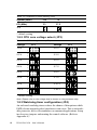
1
PCA-6154/6154L
Half-size all-in-one Pentium® CPU
card with VGA and fast Ethernet
interface
Copyright Notice
This document is copyrighted, 1998. All rights are reserved. The
original manufacturer reserves the right to make improvements to the
products described in this manual at any time without notice.
No part of this manual may be reproduced, copied, translated or
transmitted in any form or by any means without the prior written
permission of the original manufacturer. Information provided in this
manual is intended to be accurate and reliable. However, the original
manufacturer assumes no responsibility for its use, nor for any
infringements upon the rights of third parties which may result from
its use.
Acknowledgements
AMD is a trademark of Advanced Micro Devices, Inc.
Award is a trademark of Award Software International, Inc.
Cyrix is a trademark of Cyrix Corporation.
IBM, PC/AT, PS/2 and VGA are trademarks of International Business
Machines Corporation.
Intel and Pentium are trademarks of Intel Corporation.
Microsoft Windows® is a registered trademark of Microsoft Corp.
RTL is a trademark of Realtek Semi-Conductor Co., Ltd.
SiS is a trademark of Silicon Integration Systems Corporation.
UMC is a trademark of United Microelectronics Corporation.
ITE is a trademark of Integrated Technology Express, Inc.
All other product names or trademarks are properties of their
respective owners.
For more information on this and other Advantech products please
visit our website at: http://www.advantech.com
http://www.advantech.com/epc
For technical support and service for please visit our support website
at: http://support.advantech.com
This manual is for the PCA-6154/PCA-6154L Rev. A3
Part No. 2006615403
Printed in Taiwan
PCA-6154/6154L User's Manual
3rd Edition
Jan 1999
Packing List
Before installing your board, ensure that the following materials have
been received:
• 1 PCA-6154/6154L all-in-one single board computer
• 2 utility disk with Ethernet utility programs (PCA-6154 only)
• 1 utility disk with IDE utility programs
• 6 utility disks with SVGA utility programs and drivers for
Windows 3.1/95/NT and OS/2
• 1 hard disk drive (IDE) interface cable (40 pin)
• 1 floppy disk drive interface cable (34 pin)
• 1 parallel port adapter (26 pin) and COM2 adapter (9 pin) kit
• 1 USB cable
• 1 CPU fan with heatsink
• 1 6-pin mini-DIN keyboard & PS/2 mouse adapter
• 1 warranty certificate
If any of these items are missing or damaged, contact your distributor
or sales representative immediately.
Optional Devices
• IrdA adapter (part#: 968900042)
Preface and Table of Contents
Contents
Chapter 1 Hardware Configuration ......................... 1
1.1
1.2
1.3
1.4
1.6
1.5
1.7
1.8
Introduction .................................................................... 2
Specifications .................................................................. 3
Board Layout: Dimensions .......................................... 5
Jumpers and Connectors ............................................. 6
Board Layout: Connector Locations .......................... 8
Board Layout: Jumper Locations ............................... 9
Safety Precautions ....................................................... 10
Jumper Settings ........................................................... 10
1.8.1 CPU clock ratio select (JP2) .................................... 11
1.8.2 CPU core voltage select (JP3) ................................. 12
1.8.3 Watchdog timer configuration (JP4) ........................ 12
1.8.4 COM2 settings for RS-232/422/485 (JP8) .............. 13
1.8.5 DOC2000 address setting (JP7) .............................. 14
1.8.6 CMOS backup select (JP5) .................................... 14
1.8.7 DLL circiut for CPU clock optimization (JP10) ...... 14
1.8.8 Buzzer enable/disable (CN16) ................................. 15
1.9
Installing DRAM (SIMMs) ................................... 15
1.9.1 Installing SIMMs .....................................................15
Chapter 2 Connecting Peripherals ........................ 17
2.1
2.2
2.3
2.4
2.5
2.6
2.7
Enhanced IDE Connector (CN1) ............................. 19
VGA Display Connector (CN7) ................................ 20
Floppy Drive Connector (CN2) ................................ 20
Parallel Port Connector (CN3) ................................. 20
Keyboard & PS/2 Mouse Connector (CN15) ........ 21
Front Panel Connector (CN16) ................................ 21
Hard Disk Drive LED (CN17) ................................. 22
PCA-6154/6154L User's Manual
2.8 Serial Ports (CN11: COM1; CN10: COM2) ......... 22
2.8.1 RS-232 connection (COM1-CN11) .......................... 22
2.8.2 RS-232/422/485 connection (COM2-CN10) ............ 23
2.9 Power Connectors ...................................................... 23
2.9.1 Main power connector +5 V, +12 V, -12 V (CN6) ... 23
2.9.2 CPU fan power supply connector (CN4) .................23
2.10 Ethernet Configuration (PCA-6154 Only) .............. 24
RJ-45A connector (CN8) ............................................................ 24
Network boot .............................................................................. 24
2.11 USB Connector (CN9) ............................................... 24
2.12 IR Connector (CN5) .................................................. 24
Chapter 3 VGA Display & Ethernet Software
Configuration....................................... 25
3.1
3.2
3.3
3.4
Introduction ................................................................. 26
Utility Disk .................................................................. 26
VGA Display Software Configuration ...................... 27
Ethernet Software Configuration ............................. 27
Chapter 4 Award BIOS Setup ................................ 29
4.1 AWARD BIOS Setup .................................................. 30
4.1.1 Entering setup ........................................................... 30
4.1.2 Standard CMOS setup ............................................. 31
4.1.3 BIOS features setup ................................................. 32
4.1.4 CHIPSET features setup .........................................36
4.1.5 Power management setup ........................................37
4.1.6 PCI configuration setup ............................................ 38
4.1.7 Load BIOS defaults .................................................. 38
4.1.8 Load setup defaults .................................................. 38
4.1.9 Integrated Peripherals .............................................. 39
4.1.10 Password setting .....................................................39
4.1.11 IDE HDD auto detection ........................................39
4.1.12 Save & exit setup ................................................... 40
4.1.13 Exit without saving .................................................. 40
Preface and Table of Contents
Chapter 5 PCI SVGA Setup .................................... 41
5.1 Before You Begin ....................................................... 42
5.2 Installation ................................................................... 42
5.3 Driver Installation ...................................................... 43
5.3.1 Windows setup ......................................................... 43
5.3.2 DOS setup ................................................................ 44
5.4 Windows 95 Drivers Setup Procedure .................... 46
5.5 Windows NT Drivers Setup Procedure .................. 46
5.6 OS/2 Drivers Setup Procedure ................................ 47
Preliminary steps ......................................................................... 47
Installing from diskette ................................................................ 47
Selecting monitor type ................................................................. 49
Selecting screen resolution/refresh rate ........................................ 49
Installation notes ......................................................................... 50
Appendix A Programming the Watchdog Timer ... 51
A.1 Programming the watchdog timer ........................... 52
Appendix B Installing PC/104 Modules ................. 55
B.1 Installing PC/104 modules ........................................ 56
Appendix C Pin Assignments ................................ 59
C.1 CRT Display Connector (CN7) ................................ 60
C.2 COM1 RS-232 Serial Port (CN11) .......................... 60
C.3 COM2 RS-232/422/485 Serial Port (CN10) ........... 61
C.4 Keyboard and Mouse Connnector (CN15) ............ 61
C.5 External Keyboard Connnector (CN14) ................. 62
C.6 Main Power Connector (CN6) ................................. 62
C.7 IDE Hard Drive Connector (CN1) .......................... 63
C.8 USB Connector (CN9) ............................................... 64
C.9 CPU Fan Power Connector (CN4) .......................... 64
C.10Front Panel Connector (CN16) ................................ 65
C.11 Ethernet RJ-45 Connector (CN8) ........................... 65
C.12Floppy Drive Connector (CN2) ................................ 66
PCA-6154/6154L User's Manual
C.13Parallel Port Connector (CN3) ................................. 67
C.14IR Connector (CN5) .................................................. 68
C.15HDD LED Connector (CN17) .................................. 68
C.16System I/O Ports ........................................................ 69
C.17DMA Channel Assignments .................................... 70
C.18Interrupt Assignments .............................................. 71
C.191st MB Memory Map ............................................... 71
Appendix D DOC® 2000 Installation Guide............ 73
D.1 DiskOnChip® 2000 Quick Installation Guide ........ 74
DiskOnChip® 2000 installation instructions ............................... 74
Additional information and assistance ......................................... 75
Preface and Table of Contents
Tables
Table 1-1: PCA-6154/6154L jumpers ....................................... 6
Table 1-2: PCA-6154/6154L connectors .................................. 7
Table 1-3: CPU clock ratio select (JP2) ................................ 11
Table 1-4: CPU speed reference table .................................... 11
Table 1-5: System/PCI clock setting (JP9) ............................. 12
Table 1-6: CPU voltage select (JP3) ...................................... 12
Table 1-7: Watchdog timer system reset select (JP4) ............. 13
Table 1-8: COM2 settings for RS-232/422/485 (JP8) ............. 13
Table 1-9: DOC2000 address setting (JP7)............................ 14
Table 1-10: RTC power and CMOS clear (JP5) .................... 14
Table 1-11: DLL circiut for CPU clock optimization (JP10) ... 14
Table 1-12: Buzzer enable/disable (CN16) ............................. 15
Table 2-1: Connectors ............................................................. 18
Table 2-2: Serial port connections (COM1, COM2) ............... 22
Table 2-3: PCA-6154/L serial port default settings ................. 23
Table C-1: PCA-6154/L CRT display connector .................... 60
Table C-2: PCA-6154/L COM1 RS-232 serial port ................ 60
Table C-3: PCA-6154/L COM2 RS-232/422/485 series port . 61
Table C-4: PCA-6154/L keyboard and mouse connector ....... 61
Table C-5: PCA-6154/L external keyboard connector ........... 62
Table C-6: PCA-6154/L main power connector ..................... 62
Table C-7: PCA-6154/L IDE hard drive connector ................ 63
Table C-8: USB1/USB2 connector ......................................... 64
Table C-9: PCA-6154/L CPU fan power connector .............. 64
Table C-10: PCA-6154/L front panel connector ..................... 65
Table C-11: PCA-6154/L Ethernet RJ-45 connector .............. 65
Table C-12: PCA-6154/L floppy drive connector ................... 66
Table C-13: PCA-6154/L parallel port connector ................... 67
Table C-14: PCA-6154/L IR connector .................................. 68
Table C-15: PCA-6154/L HDD LED connector .................... 68
Table C-16: System I/O ports .................................................. 69
Table C-17: DMA channel assignments.................................. 70
Table C-18: Interrupt assignments........................................... 71
Table C-19: 1st MB memory map ........................................... 71
PCA-6154/6154L User's Manual
Figures
Figure 1-1: PCA-6154/6154L board layout: Dimensions .......... 5
Figure 1-2: PCA-6154/6154L board layout: Jumper locations.. 9
Figure 1-3: PCA-6154/6154L board layout: Connector locations8
Figure 4-1: Setup program initial screen .................................. 30
Figure 4-2: CMOS setup screen.............................................. 31
Figure 4-3: BIOS features setup screen.................................. 32
Figure 4-4: CHIPSET features setup screen .......................... 36
Figure 4-5: Power management setup screen ......................... 37
Figure 4-6: PCI configuration screen ...................................... 38
Figure 4-7: Integrated peripherals ........................................... 39
Figure B-1: PC/104 module mounting diagram ....................... 57
Figure B-2: PC/104 module dimensions (inches) (±5 %) ........ 57
Preface and Table of Contents
PCA-6154/6154L User's Manual
CHAPTER
1
Hardware
Configuration
This chapter gives background
information on the PCA-6154/6154L. It
then shows you how to configure the card
to match your application and prepare it
for installation into your PC.
Sections include:
• Card specifications
• Board layout: dimensions
• Board layout: jumper locations
• Board layout: connector locations
• Safety precautions
• Jumper settings
• Installing DRAM (SIMMs)
1.1
Introduction
The PCA-6154/6154L is a cost-effective, all-in-one single board
Pentium® processor-based CPU card which can release the Pentium
processor's full potential and provide unprecedented performance
compared to current 64-bit processor board. The PCA-6154/6154L
offers all the functions of an industrial computer on a single board,
half-size CPU card. This card uses an Intel Pentium, Pentium MMX,
AMD K5, AMD K6, AMD K6-2, Cyrix M1 or Cyrix M2 processor. The
card accepts up to 128 MB DRAM. It is also equipped with 512 KB
PB-SRAM 2nd level cache.
The PCA-6154/6154L uses a single-chip solution, allowing on-board
DRAM to be shared with the built-in VGA controller. In this configuration, the chipset always acts as the arbiter between memory bus
masters. This system ensures efficient memory allocation while
substantially reducing the overall system cost.
On-board features include 512 KB 2nd level cache memory,
100/10 Mbps fast Ethernet interface (PCA-6154 only), one RS-232 port,
one RS-232/422/485 port, one multi-mode parallel (ECP/EPP/SPP) port,
a floppy drive controller and a keyboard and PS/2 mouse interface. The
built-in high speed PCI IDE controller supports both PIO and bus
master modes. Up to two IDE devices can be connected, including
large hard disks, CD-ROM drives, tape backup drives and other IDE
devices. The PCA-6154/6154L also supports two USB ports and one
fast infrared port.
The PCA-6154/6154L also features power management to minimize
power consumption. It complies with the "Green Function" standard
and supports three types of power saving features: Doze mode,
Standby mode and Suspend mode. A watchdog timer can automatically reset the system or generate an interrupt should the system stop
due to a program bug or EMI.
2
PCA-6154/6154L User's Manual
1.2
Specifications
Standard SBC functions
• CPU: Intel Pentium® 100 ~ 233 MHz, Pentium MMX, AMD K5,
AMD K6 200 / 266 MHz, AMD K6-2 266 ~ 300 MHz, Cyrix M1, Cyrix
M2 up to PR-300 MHz, or IDT Win Chip C6 upto 200 MHz
• BIOS: Award 256 KB (2Mbit) memory; supports plug and play,
suspend to disk
• Chipset: SiS5598
• L2 cache: On-board 512 KB synchronous (pipeline burst) SRAM
• Green function: Features power management option via BIOS,
activated by keyboard or mouse activity. Supports doze, sleep and
suspend modes. APM 1.1 compliant
• RAM: Two 72-pin SIMM sockets. Supports 32-bit FPM or EDO
DRAM with memory capacity from 8 ~ 128 MB.
• EIDE interface: Handles up to two IDE HDDs or other IDE devices.
Supports PIO mode 4 and Ultra DMA mode
• FDD interface: Supports up to two floppy disk drives.
• Parallel port: Configured to LPT1, LPT2, LPT3 or disabled.
Supports multi-mode parallel port (SPP/ECP/EPP)
• Serial ports: Two 16C550 UARTs, one RS-232, one RS-232/422/485
interface
• Watchdog timer: Can generate a system reset. Software enabled/
disabled. Time interval is from 1 to 63 seconds, jumperless with runtime setup
• Keyboard/mouse connector: 6-pin mini-DIN connector on the
mounting bracket eases connection to a keyboard or PS/2 mouse.
An on-board keyboard pin header connector is also available.
• I/O bus expansion: PC/104 connector with face-up installation
• USB interface: Two USB connectors with fuse protection. Complies
with USB specification 1.0
• Infrared port: Fast IrDA. Transfer rate up to 4 Mbps. I/O port
programmable to COM1 (3F8), COM2 (2F8), COM3 (3E8) or COM4
(2E8).
Chapter 1 Hardware Configuration
3
VGA interface
• Chipset: SiS5598 built-in VGA function
• Architecture: Universal memory architecture
• Display memory: Share system RAM 1 MB ~ 4 MB
100Base-T Ethernet interface (PCA-6154 only)
• Chipset: REALTEK RTL8139. PCI bus 100/10 Mbps Ethernet
controller
• I/O Address jumperless setting
• Built-in boot ROM
SSD function
• Supports M-System's DiskOnChip® 2000 Flash Disk up to
72 MB
Mechanical and environmental specifications
• Board size: 185 x 122 mm
• Max. power requirements: +5 V @ 5.5 A, +12 v @ 100 mA
• Operating temperature: 0 ~ 60° C (32 ~ 140° F)
• Board weight: 0.5 kg (1.2 lb)
4
PCA-6154/6154L User's Manual
1.3
Board Layout: Dimensions
Unit: mm
Figure 1-1: PCA-6154/6154L board layout: Dimensions
Chapter 1 Hardware Configuration
5
1.4 Jumpers and Connectors
On-board connectors link it to external devices such as hard disk
drives, a keyboard, or floppy drives. In addition, the board has jumpers
for configuring your board for specific applications.
The table below lists the function of each of the board's jumpers and
connectors. Later sections in this chapter give instructions on setting
jumpers and detailed information on each jumper setting. Chapter 2
gives instructions for connecting external devices to your card.
Table 1-1: PCA-6154/6154L jumpers
Number Function
6
JP2
CPU clock ratio select
JP3
CPU core voltage select
JP4
Watchdog timer select
JP5
Real-time clock (RTC) power and CMOS select
JP7
DiskOnChip® 2000 Flash disk memory segment
JP8
COM2 RS-232/422/485 selection
JP9
CPU clock select
JP10
CPU clock optimize enable
PCA-6154/6154L User's Manual
Table 1-2: PCA-6154/6154L connectors
Number Function
CN1
IDE port
CN2
Floppy disk connector
CN3
Parallel port
CN4
CPU fan power connector
CN5
Infra red port
CN6
Main power connector
CN7
VGA connector
CN8
100/10 Mbps network connection (PCA6154 only)
CN9
USB 1 and USB 2 ports
CN10
COM2 port
CN11
COM1 port
CN12
PC/104 A1 ~ A32, B1 ~ B32
CN13
PC/104 C1 ~ C20, D1 ~ D20
CN14
External keyboard
CN15
Keyboard and PS/2 mouse
CN16
Front panel connector
CN17
HDD LED
Please refer to Appendix C for pin assignments.
Chapter 1 Hardware Configuration
7
1.5 Board Layout: Jumper Locations
JP2 JP3
JP5 JP4
JP7
JP8
JP10
JP9
Figure 1-2: PCA-6154/6154L board layout: Jumper locations
8
PCA-6154/6154L User's Manual
1.6 Board Layout: Connector Locations
IDE hard
CPU
disk
socket
(CN1)
CPU fan Floppy DOC
power
disk
2000
(CN4)
(CN2) socket
Front Parallel
panel
port
(CN16) (CN3)
Main Power
(CN6)
HDD LED
(CN17)
FIR (CN5)
SIMM
(Bank 0)
VGA (CN7)
SIMM
(Bank 1)
Ethernet
(CN8)
COM2 (CN10)
USB (CN9)
COM1 (CN11)
Keyboard
PS/2 mouse
(CN15)
PC/104
(CN12)
PC/104
(CN13)
External
keyboard
(CN14)
Figure 1-3: PCA-6154/6154L board layout: Connector locations
Chapter 1 Hardware Configuration
9
1.7 Safety Precautions
Follow these simple precautions to protect yourself from harm and your
PC from damage.
1. To avoid electric shock, always disconnect the power from your PC
chassis before you work on it. Don't touch any components on the
CPU card or other cards while the PC is on.
2. Disconnect power before making any configuration changes. The
sudden rush of power as you connect a jumper or install a card may
damage sensitive electronic components.
3. Always ground yourself to remove any static charge before you touch
your CPU card. Be particularly careful not to touch the chip connectors.
Modern integrated electronic devices, especially CPUs and memory chips,
are extremely sensitive to static electric discharges and fields. Keep the
card in its antistatic packaging when it is not installed in the PC, and place
it on a static dissipative mat when you are working with it. Wear a
grounding wrist strap for continuous protection.
1.8 Jumper Settings
This section tells how to set the jumpers to configure your card. It
gives the card default configuration and your options for each jumper.
After you set the jumpers and install the card, you will also need to run
the BIOS Setup program (discussed in Chapter 3) to configure the serial
port addresses, floppy/hard disk drive types and system operating
parameters. Connections, such as hard disk cables, appear in Chapter 2.
For the locations of each jumper, see the board layout diagram depicted
earlier in this chapter.
You configure your card to match the needs of your application by
setting jumpers. A jumper is the simplest kind of electric switch. It
consists of two metal pins and a small metal cap (often protected by a
plastic cover) that slides over the pins to connect them. To "close" a
jumper you connect the pins with the cap. To "open" a jumper you
remove the cap. Sometimes a jumper will have three pins, labeled 1, 2 and
3. In this case you connect either pins 1 and 2 or 2 and 3.
10
PCA-6154/6154L User's Manual
1
Open
Closed
2
3
Closed 2-3
You may find a pair of needle-nose pliers useful for setting the jumpers.
If you have any doubts about the best hardware configuration for your
application, contact your local distributor or sales representative before
you make any changes.
1.8.1 CPU clock ratio select (JP2)
In order for the system to function properly, the jumpers must be set to
accommodate the CPU installed on the CPU card.
Table 1-3: CPU clock ratio select (JP2)
Pentium CPU, AMD K5, Cyrix M1, IDT C6
100 MHz
1.5 x 66
166 MHz
2.5 x 66
2
2
1
*133 MHz
2 x 66
1
200 MHz
3 x 66
2
2
1
150 MHz
2 x 75
1
233 MHz
3.5 x 66
2
2
1
266 MHz
4 x 66
1
300 MHz
4.5 x 66
2
2
1
1
* default setting
Refer to the CPU speed reference table (below) for instructions on
adjusting the internal clocks according to the base CPU speed.
Table 1-4: CPU speed reference table
CPU Speed (MHz) 100 *133
150
166
200
233
266 300
Clock setting
66
66
75
66
66
66
66
66
Frequency ratio
1.5
2
2
2.5
3
3.5
4
4.5
* default setting
Chapter 1 Hardware Configuration
11
Table 1-5: System/PCI clock setting (JP9)
System (MHz)
*66
75
PCI (MHz)
33
37.5
JP9
* default setting
1.8.2 CPU core voltage select (JP3)
Table 1-6: CPU voltage select (JP3)
Voltage
1.9 V
JP3
2
Voltage
2.0 V
1
2.2 V
2
1
2.3 V
2
2.5 V
1
2.6 V
2
2
2.7 V
2
2.9 V
2
3.1 V
2
1
2
1
3.27 V
1
*3.3 V
2
1
1
3.2 V
2
1
1
3.0 V
2
1
1
2.8 V
2
1
1
2.4 V
JP3
2
2
1
3.45 V
2
1
* default setting
Note: Please refer to the voltage that is shown on the processor chip.
1.8.3 Watchdog timer configuration (JP4)
An on-board watchdog timer reduces the chance of disruptions which
EMP (electro-magnetic pulse) interference can cause. This is an invaluable protective device for standalone or unmanned applications. Setup
involves two jumpers and running the control software. (Refer to
Appendix A.)
12
PCA-6154/6154L User's Manual
Watchdog timer action (JP4)
When the watchdog timer activates (CPU processing has come to a
halt), it can reset the system. This can be set via setting JP4 as shown
below:
Table 1-7: Watchdog timer system reset select (JP4)
*System Reset
JP4
1
2
3
* default setting
1.8.4 COM2 settings for RS-232/422/485 (JP8)
Table 1-8: COM2 settings for RS-232/422/485 (JP8)
Pins closed
*RS-232
RS-422
RS-485
1-2
on
off
off
3-4
off
on
off
5-6
off
off
on
7-8
off
on
on
7-9
on
-
-
10 - 12
-
on
on
11 - 12
on
-
-
13 - 14
-
on
-
13 - 15
on
-
-
16 - 18
-
on
-
17 - 18
on
-
-
* default setting
Chapter 1 Hardware Configuration
13
1.8.5 DOC2000 address setting (JP7)
Table 1-9: DOC2000 address setting (JP7)
Address
*OFF
JP7
Address
2
1
D800 ~
D9FF
2
D000 ~
D1FF
2
E000 ~
E1FF
2
1
1
JP7
CC00 ~
CDFF
2
DC00 ~
DDFF
2
D400 ~
D5FF
2
1
1
1
1
* default setting
1.8.6 CMOS backup select (JP5)
Warning:
To avoid damaging the computer, always turn off the
power supply before setting "Clear CMOS". Set the
jumper back to "3.0 V Battery On" before turning on
the power supply.
Table 1-10: RTC power and CMOS clear (JP5)
*Normal
JP5
1
CMOS data clear
2
1
2
* default setting
1.8.7 DLL circiut for CPU clock optimization (JP10)
Table 1-11: DLL circiut for CPU clock optimization (JP10)
Disable
JP10
14
1
2
3
PCA-6154/6154L User's Manual
*Enable
1
2
3
1.8.8Buzzer enable/disable (CN16)
Table 1-12: Buzzer enable/disable (CN16)
*Enable
Disable
2
14
2
14
1
13
1
13
CN16
* default setting
1.9
Installing DRAM (SIMMs)
You can install anywhere from 8 to 128 MB of DRAM into your
PCA-6154/6154L. The card provides two 72-pin SIMM (Single In-line
Memory Module) sockets. Each socket accepts 4, 8, 16, 32 or 64 MB
SIMMs. DRAM access time ≤ 60 ns.
Note: For higher system stability two SIMM should be installed
when operating the PCA-6154/PCA-6154L
1.9.1 Installing SIMMs
NOTE:
The modules can only fit into a socket one way. Their
gold pins must point down into the SIMM socket.
The procedure for installing SIMMs appears below. Please follow
these steps carefully.
1. Ensure that all power supplies to the system are switched Off.
2. Install the SIMM card. Install the SIMM so that its gold pins point
down into the SIMM socket.
3. Slip the SIMM into the socket at a 45 degree angle and carefully fit
the bottom of the card against the connectors.
4. Gently push the SIMM into a perpendicular position until the clips
on the ends of the SIMM sockets snap into place.
5. Check to ensure that the SIMM is correctly seated and all connector
contacts touch. The SIMM should not move around in its socket.
Chapter 1 Hardware Configuration
15
16
PCA-6154/6154L User's Manual
CHAPTER
2
Connecting
Peripherals
This chapter tells how to connect
peripherals, switches and indicators to the
PCA-6154/6154L board. You can access
most of the connectors from the top of the
board while it is installed in the chassis. If
you have a number of cards installed, or
your chassis is very tight, you may need
to partially remove the card to make all
the connections.
The following table lists the connectors on the PCA-6154/6154L.
Table 2-1: Connectors
Number Function
CN1
IDE connector
CN2
FDD connector
CN3
Parallel port connector
CN4
CPU fan power connector
CN5
IR connector
CN6
Main power connector
CN7
VGA connector
CN8
Ethernet RJ-45A connector
CN9
USB connector
CN10
COM2 connector
CN11
COM1 connector
CN12
PC/104 Con. A, B
CN13
PC/104 Con. C, D
CN14
External keyboard connector
CN15
Keyboard and PS/2 mouse connector
CN16
Front panel connector
CN17
HDD LED
The following sections tell how to make each connection. In most
cases, you will simply need to connect a standard cable. All of the
connector pin assignments are shown in Appendix C.
Warning! Always completely disconnect the power cord from
your chassis whenever you are working on it. Do not
make connections while the power is on. Sensitive
electronic components can be damaged by a
sudden rush of power. Only experienced electronics
personnel should open the PC chassis.
18
PCA-6154/6154L User's Manual
Caution!
2.1
Always ground yourself to remove any static charge
before touching the CPU card. Modern electronic
devices are very sensitive to static electric charges.
Use a grounding wrist strap at all times. Place all
electronic components on a static-dissipative
surface or in a static-shielded bag when they are not
in the chassis.
Enhanced IDE Connector (CN1)
You can attach two IDE (Integrated Device Electronics) drives to the
PCA-6154/6154L’s internal controller. The PCA-6154/6154L CPU
card has an EIDE connector, CN1.
Wire number 1 on the cable is red or blue, the other wires are gray.
Connect one end to connector CN1 on the CPU card. Make sure that
the red (or blue) wire corresponds to pin 1 on the connector (on the
right side). See Chapter 1 for help finding the connector.
Unlike floppy drives, IDE hard drives can connect in either position
on the cable. If you install two drives, you will need to set one as the
master and one as the slave. You do this by setting the jumpers on the
drives. If you use just one drive, you should set it as the master. See
the documentation that came with your drive for more information.
Connect the first hard drive to the other end of the cable. Wire 1 on
the cable should also connect to pin 1 on the hard drive connector,
which is labeled on the drive circuit board. Check the documentation
that came with the drive for more information.
Connect the second drive as described above on CN1.
Note:
We don't recommend connecting to a Seagate
ST-31010A, ST-31011A, ST-1277A, ST-31720A,
ST-31721A, ST-32120A, ST-32121A, ST-32531A,
33230A, ST-33240A, ST-34340A, or ST-3852A IDE
HDD. This is an incompatibility issue and not a fault
of either device.
Chapter 2 Connecting Peripherals
19
2.2
VGA Display Connector (CN7)
The PCA-6154/6154L provides a VGA controller for a high resolution VGA interface. The PCA-6154/6154L's CN7 is a DB-15 connector for VGA monitor input. Pin assignments for the CRT display are
detailed in Appendix D. Share memory architecture supports 0.5 MB,
1 MB, 1.5 MB, 2 MB, 2.5 MB, 3 MB, 3.5 MB and 4 MB system
memory. The memory is configured in the system BIOS setup.
2.3
Floppy Drive Connector (CN2)
You can attach up to two floppy disk drives to the PCA-6154/6154L’s
on-board controller. You can use any combination of 5.25"
(360 KB/1.2 MB) and/or 3.5" (720 KB/1.44/2.88 MB) drives.
The card comes with a 34-pin daisy-chain drive connector cable. On
one end of the cable is a 34-pin flat-cable connector. On the other end
are two sets of floppy disk drive connectors. Each set consists of a 34pin flat-cable connector (usually used for 3.5" drives) and a printedcircuit-board connector (usually used for 5.25" drives). You can use
only one connector in each set. The set on the end (after the twist in
the cable) connects to the A: floppy. The set in the middle connects to
the B: floppy.
2.4
Parallel Port Connector (CN3)
The parallel port is normally used to connect the CPU card to a
printer. The PCA-6154/6154L includes an on-board parallel port,
accessed through a 26-pin flat-cable connector, CN3. The card comes
with an adapter cable which lets you use a traditional DB-25 connector. The cable has a 26-pin connector on one end and a DB-25
connector on the other, mounted on a retaining bracket. The bracket
installs at the end of an empty slot in your chassis, giving you access
to the connector.
The parallel port is designated as LPT1 and can be disabled or
changed to LPT2 or LPT3 in the system BIOS setup.
20
PCA-6154/6154L User's Manual
To install the bracket, find an empty slot in your chassis. Unscrew the
plate that covers the end of the slot. Screw in the bracket in place of
the plate. Next, attach the flat-cable connector to CN3 on the CPU
card. Wire 1 of the cable is red or blue, and the other wires are gray.
Make sure that wire 1 corresponds to pin 1 of CN3. Pin 1 is on the
right side of CN3.
2.5
Keyboard & PS/2 Mouse Connector (CN15)
The PCA-6154/6154L board provides a keyboard connector. A 6-pin
mini-DIN connector (CN15) on the card mounting bracket supports
single-board computer applications. The card comes with an adapter
to convert from the 6-pin mini-DIN connector to a standard DIN
connector and to a PS/2 mouse connector.
2.6
Front Panel Connector (CN16)
Next, you may want to install external switches to monitor and control
the PCA-6154/6154L. These features are optional - install them only
if you need them. The front panel connector (CN16) is a 14-pin male,
dual in-line header and provides connections for a speaker, hard disk
access indicator, power on indicator, turbo indicator and an input
switch for resetting the card.
2
1
4
6
14
13
LED interface
The front panel LED indicator for power on is an active high signal.
Reset switch
If you install a reset switch, it should be a open single pole switch.
Momentarily pressing the switch will activate a reset. The switch
should be rated for 10 mA, 5 V.
If you need to make your own cable, you can find the pin assignments
for the card’s connector in Appendix C.
2
12 14
1
11 13
Chapter 2 Connecting Peripherals
21
2.7
Hard Disk Drive LED (CN17)
You can connect a LED to connector CN17 to indicate when the HDD
is active. Marks on the circuit board indicate LED polarity.
2.8
Serial Ports (CN11: COM1; CN10: COM2)
The PCA-6154/6154L offers two serial ports: COM1 in RS-232,
COM2 in RS-232/422/485. These ports let you connect to serial
devices (a mouse, printers, etc.) or a communication network.
You can select the address for each port ( For example,3F8H
[COM1], 2F8H [COM2]) or disable it, using the BIOS Advanced
Setup program, covered in Chapter 4.
The card mounting bracket holds the serial port connector for the one
port, and the parallel port and serial port adapter kit (supplied with the
card) holds the connector for the other port. This lets you connect and
disconnect cables after you install the card. The DB-9 connector on
the bottom of the bracket is the first RS-232 port, COM1. The DB-9
connector on the adapter kit is the second serial port, COM2.
Table 2-2: Serial port connections (COM1, COM2)
Connector
Function
COM1
RS-232
COM2
RS-232/422/485
2.8.1 RS-232 connection (COM1-CN11)
Different devices implement the RS-232 standard in different ways. If
you are having problems with a serial device, be sure to check the pin
assignments for the connector.
22
PCA-6154/6154L User's Manual
2.8.2 RS-232/422/485 connection (COM2-CN10)
COM2 is an RS-232/422/485 serial port. The specific port type is
determined by jumper settings, as detailed in Chapter 1.
The IRQ and address range for both ports are fixed. However, if you
wish to disable the port or change these parameters later, you can do
this in the system BIOS setup. The table below shows the settings for
the PCA-6154/6154L board's ports:
Table 2-3: PCA-6154/6154L serial port default settings
2.9
Port
Address
Interrupt
Default
COM1
3F8, 3E8
IRQ4
3F8
COM2
2F8, 2E8
IRQ3
2F8
Power Connectors
2.9.1 Main power connector +5 V, -12 V, +12 V (CN6)
If you prefer not to acquire power through PCA-6154/6154L’s
backplane via the gold H-connectors, CN6 also provides power input
connectors for +5 V, -12 V and +12 V. Pin 8 of the PS/2 power
supply can be used, too.
2.9.2 CPU fan power supply connector (CN4)
This provides power supply to the optional CPU cooling fan. This
connector is only available when +5 V, -12 V and +12 V power is
supplied to the board.
Warning! Before making the connection, make sure the
voltage is absolutely correct and matched with the
correct connector.
Chapter 2 Connecting Peripherals
23
2.10 Ethernet Configuration (PCA-6154 Only)
The PCA-6154 is equipped with a high performance 32-bit PCI-bus
Fast Ethernet interface which is fully compliant with IEEE 802.3u
100/10Base-T specifications. It is supported by all major network
operating systems and is 100% Novell NE-2000 compatible.
The medium type can be configured via the RSET8139.EXE program
included on the utility disk. (See Chapter 3 for detailed information.)
RJ-45A connector (CN8)
100/10BASE-T connects to the PCA-6154 via an adapter cable to the
RJ-45 standard jack.
Network boot
The Network Boot feature is built into the BIOS. It can be enabled/
disabled in the chipset setup of the CMOS configuration. Refer to
"BIOS Setting" in Chapter 4 for more information.
2.11 USB Connector (CN9)
The PCA-6154/6154L board provides two USB (Universal Serial
Bus) interfaces, which give complete plug and play, hot attach/detach
for up to 127 external devices.The USB interfaces comply with USB
specification rev. 1.0 and are fuse protected.
The USB interfaces are accessed through a 10-pin flat-cable connector, CN9. The adapter cable has a 10-pin connector on one end and a
USB connector on the bracket.
The USB interfaces can be disabled in the system BIOS setup.
2.12 IR Connector (CN5)
This connector supports the optional wireless infrared transmitting
and receiving module. This module mounts on the system case. You
must configure the setting through BIOS setup.
24
PCA-6154/6154L User's Manual
CHAPTER
3
VGA Display & Ethernet
Software Configuration
This chapter details the software
configuration information. It shows you
how to configure the board to match your
application requirements. AWARD
System BIOS is covered in Chapter 4.
Sections include:
• VGA display configuration
• Ethernet interface configuration
3.1
Introduction
The PCA-6154/6154L system BIOS and custom drivers are located in a
256 Kbyte, 32-pin (JEDEC spec.) Flash ROM device, designated U11.
A single Flash chip holds the system BIOS, VGA BIOS, and Back-up
CMOS Data. The display can be configured via software. This method
minimizes the number of chips and eases configuration. You can
change the display BIOS simply by
reprogramming the Flash chip.
3.2
Utility Disk
The PCA-6154/6154L is supplied with a software utility disk that
holds the necessary file for setting up the VGA display and Ethernet
and Windows controller. The disks' definition is as follows:
26
Disk 1:
VGA/LCD utility for Windows NT
Disk 2:
VGA/LCD utility for Windows 3.1 English version
Disk 3:
VGA/LCD utility for OS2 3.0 #1
Disk 4:
VGA/LCD utility for OS2 3.0 #2
Disk 5:
LAN driver #1 (PCA-6154 only)
Disk 6:
LAN driver #2(PCA-6154 only)
Disk 7:
IDE driver
Disk 8:
VGA/LCD utility for Windows 95
Disk 9 :
VGA/LCD utility for Windows 3.1 Chinese version
Total:
9 disks
PCA-6154/6154L User's Manual
3.3
VGA Display Software Configuration
The PCA-6154/6154L’s on-board VGA interface supports traditional
analog CRT monitors. The VGA controller is built into the system's
chip (SIS5598). It can support 1 to 4 MB of video memory share with
the system memory. The interface can drive CRT displays with
resolutions up to 1024 x 768 in 256 colors at 1 MB share memory,
and up to 1280 x 1024 in 64 K colors at 4 MB share memory. The
VGA interface is configured completely via the software utility, so
you do not have to set any jumpers.
3.4
Ethernet Software Configuration
(PCA-6154 only)
The PCA-6154’s on-board Ethernet interface supports all major
network operating systems. To configure the medium type, to view
the current configuration, or to run diagnostics:
1. Power the PCA-6154 on. Ensure that the RSET8139.EXE file is
located in the working drive (Disk 5 & 6, LAN driver).
2. At the prompt type RSET8139.EXE and press <Enter>. The
Ethernet configuration program will then be displayed.
3. This simple screen shows all the available options for the Ethernet
interface. Just highlight the option you wish to change by using the
Up and Down keys. To change a selected item, press <Enter>, and
a screen will appear with the available options. Highlight your
option and press <Enter>. Each highlighted option has a helpful
message guide displayed at the bottom of the screen for additional
information.
4. After you have made your selections and are certain it is the
Chapter 3 VGA Display & Ethernet Software Configuration
27
configuration that you want, press ESC. A prompt will appear
asking if you want to save the configuration. Press Y if you want
to save.
The Ethernet Setup Menu also offers three very useful diagnostic
functions:
1. Run EEPROM test.
2. Run Diagnostics on Board.
3. Run Diagnostics on Network.
Each option has its own display screen which shows the format and
result of any diagnostic tests undertaken.
28
PCA-6154/6154L User's Manual
CHAPTER
4
Award BIOS Setup
This chapter describes how to set the
card’s BIOS configuration data.
4.1 AWARD BIOS Setup
Figure 4-1: Setup program initial screen
Award’s BIOS ROM has a built-in Setup program that allows users to
modify the basic system configuration. This type of information is
stored in battery-backed RAM so that it retains the Setup information
when the power is turned off.
4.1.1 Entering setup
Turning on the computer and pressing <DEL> immediately will allow
you to enter Setup.
30
PCA-6154/6154L User's Manual
4.1.2 Standard CMOS setup
Choose the “STANDARD CMOS SETUP” option from the INITIAL
SETUP SCREEN Menu, and the screen below is displayed. This
standard Setup Menu allows users to configure system components
such as date, time, hard disk drive, floppy drive, display, and memory.
ROM PCI/ISA BIOS (2A5IIAKB)
CMOS SETUP UTILITY
AWARD SOFTWARE, INC.
Date <mm:dd:yy>
Time <hh:mm:ss>
HARD DISKS
Primary Master
Primary Slave
: Mon. Oct 7 1996
: 16 : 52 : 38
TYPE SIZE CYLS
:Auto 0
0
:None 0
0
Drive A: 1.44M. 3.5 in.
Drive B: None
Video: EGA/VGA
Halt On : All Errors
ESC: Quit
F1: Help
HEAD
0
0
PRECOMP
0
0
LANDZ
0
0
SECTOR
0
0
MODE
Auto
------
Base Memory:
640K
Extended Memory: 15360K
Other Memory:
384K
Total Memory:
↑↓→←: Select Item
<Shift> F2: Change Color
16384K
PU/PD/+/-: Modify
Figure 4-2: CMOS setup screen
Chapter 4 Award BIOS Setup
31
4.1.3 BIOS features setup
The “BIOS FEATURES SETUP” screen appears when choosing the
BIOS FEATURES SETUP item from the CMOS SETUP UTILITY
Menu. It allows the user to configure the PCA-6154/6154L according
to his particular requirements.
Below are some major items that are provided in the BIOS FEATURES SETUP screen:
ROM PCI/ISA BIOS (2A5IIAKB)
CMOS SETUP UTILITY
AWARD SOFTWARE, INC.
Virus Warning
:
CPU Internal Cache
:
External Cache
:
Quick Power On Self Test :
Boot Sequence
:
Swap Floppy Drive
:
Boot Up Floppy Seek
:
Boot Up NumLock Status :
Boot Up System Speed
:
Gate A20 Option
:
Memory Parity Check
:
Typematic Rate Setting
:
Typematic Rate (Char/sec):
Typematic Delay (Msec) :
Security Option
:
PCI/VGA Palette Snoop
:
OS Select for DRAM >64M :
Disabled
Enabled
Enabled
Enabled
C, A
Disabled
Enabled
On
High
Fast
Disabled
Disabled
6
250
Setup
Disabled
Non-OS2
Video Bios Shadow
C8000-CBFFF Shadow
CC000-CFFFF Shadow
D0000-D3FFF Shadow
D4000-D7FFF Shadow
D8000-DBFFF Shadow
DC000-DFFFF Shadow
Esc :
F1 :
F5 :
F6 :
F7 :
:
:
:
:
:
:
:
Enabled
Disabled
Disabled
Disabled
Disabled
Disabled
Disabled
Quit
↑↓→←: Select Item
Help
PU/PD/+/- : Modify
Old Values <Shift>F2 : Color
Load BIOS Defaults
Load Setup Defaults
Figure 4-3: BIOS features setup screen
32
PCA-6154/6154L User's Manual
Virus Warning
During and after the system boots up, any attempt to write to the boot
sector or partition table of the hard disk drive will halt the system. In
this case, a warning message will be displayed. You can run the antivirus program to locate the problem.
If Virus Warning is Disabled, no warning message will appear if
anything attempts to access the boot sector or hard disk partition.
CPU Internal Cache/External Cache
Depending on the CPU/chipset design, these options can speed up
memory access when enabled.
Quick Power On Self Test
This option speeds up the Power-On Self Test (POST) conducted as
soon as the computer is turned on. When enabled, BIOS shortens or
skips some of the items during the test. When disabled, normal POST
procedures assumes.
Boot Sequence
This function determines the sequence in which the computer will
search the drives for the disk operating system (i.e. DOS). The default
value is “C, A”.
A,C
System will first search the FDD, then the HDD.
C,A
System will first search the HDD, then the FDD.
C only
System will only search the HDD.
Boot Up Floppy Seek
During POST, BIOS will determine if the floppy disk drive installed is
40 or 80 tracks. 360 KB type is 40 tracks while 720 KB, 1.2 MB, and
1.44 MB are all 80 tracks.
Enabled
BIOS searches the floppy drive to determine if it is 40 or 80
tracks. Note that BIOS cannot differentiate 720 KB, 1.2 MB,
and 1.44 MB type drives as they are all 80 tracks.
Disabled
BIOS will not search for the floppy drive type by track
number. Note that there will not be any warning message if
the drive installed is 360 KB.
Chapter 4 Award BIOS Setup
33
Boot Up NumLock Status
The default is “On”.
On
Keypad boots up to number keys.
Off
Keypad boots up to arrow keys.
Boot Up System Speed
High
Sets the speed to high
Low
Sets the speed to low
IDE HDD Block Mode
Enabled
Enable IDE HDD Block Mode. BIOS will detect the block size
of the HDD and send a block command automatically.
Disabled
Disable IDE HDD Block Mode
Gate A20 option
Normal
The A20 signal is controlled by the keyboard controller or
chipset hardware
Fast
Default: Fast. The A20 signal is controlled by Port 92 or
chipset specific method.
Typematic Rate Setting
The typematic rate determines the characters per second accepted by
the computer. Typematic Rate setting enables or disables the typematic rate.
Typematic Rate (Char/Sec)
BIOS accepts the following input values (character/second) for
Typematic Rate: 6, 8, 10, 12, 15, 20, 24, 30.
34
PCA-6154/6154L User's Manual
Typematic Delay (msec)
When holding down a key, the Typematic Delay is the time interval
between the appearance of the first and second characters. The input
values (msec) for this category are: 250, 500, 750, 1000.
Security Option
This setting determines whether the system will boot if the password
is denied, while limiting access to Setup.
System
The system will not boot, and access to Setup will be
denied if the correct password is not entered at the prompt.
Setup
The system will boot, but access to Setup will be
denied if the correct password is not entered at the prompt.
Note: To disable security, select PASSWORD SETTING in the main
menu. At this point, you will be asked to enter a password. Simply hit
the <ENTER> key to disable security. When security is disabled, the
system will boot, and you can enter Setup freely.
OS Select for DRAM>64 MB
This setting is under OS/2 system.
Video BIOS Shadow
This determines whether video BIOS will be copied to RAM, which is
optional according to the chipset design. When enabled, Video
Shadow increases the video speed.
C8000 - CFFFF Shadow/DC000-DFFFF Shadow
These determine whether optional ROM will be copied to RAM in
blocks of 16 KB.
Enabled
Optional shadow is enabled
Disabled
Optional shadow is disabled
Chapter 4 Award BIOS Setup
35
4.1.4 CHIPSET features setup
By choosing the “CHIPSET FEATURES SETUP” option from the
INITIAL SETUP SCREEN Menu, the screen below is displayed. This
sample screen contains the manufacturer’s default values for the
PCA-6154/6154L.
ROM PCI/ISA BIOS (2A5IIAKB)
CHIPSET FEATURES SETUP
AWARD SOFTWARE, INC.
Auto
Auto Configuration
Configuration
:: Enabled
Enabled
L2 (WB) Tag
L2 Cache
Bit Length
Update Mode:
: 8 bitsWB
SRAM
L2 (WB)
Back
Tagto
BitBack
Length :: Enabled
7bits
NA
SRAM
# Enable
Back to Back
:: Enabled
Enabled
Starting
SRAM Leadoff
Point of
Timing
Paging :: 1T
3 Ck
Refresh
DRAM Leadoff
Cycle Time
Timing
(US) :: 15.6
6 Ck
RAS
MDLE
Pulse
Delay
Width
Timing
Refresh
(ns) :: 4T
4
RAS
RAS Precharge
Active When
Time
Refresh:: 2T
5 Ck
RAS
CAS to
Delay
CASinDelay
Posted-WR :: 2T
1 Ck
CAS
FP DRAM
# Pulse
CAS
Width
Pr. Timing
(FP) :: 2T
1 Ck
CAS # Pulse Width (EDO) : 1T
FP DRAM
RAS Pr. Timing
3 Ck
RAMW#
Assertion
Timing :: 3T
EDOPrecharge
CAS PulseTime
Width(FP) :: 1T/2T
R1 W2 Ck
CAS
EDOPrecharge
CAS Precharge
: 11T/2T
Ck
CAS
Time Time
(EDO):
EDO MDLE Timing
: 1 Ck
EDO BRDY#
TimingWrite :: Disabled
1 Ck
Enhanced
Memory
EDO RAS
Prech.
TimingRD:: Enabled
3 Ck
Read
Prefetch
Memory
EDO
RAMW#
Pwr
Saving
:
Disabled
CPU to PCI Post Write
: 4T
ISA Bus Clock Frequency : PCICLK/4
CPU-PCI Burst Mem.WR : Disabled
ISA Bus Clock Frequence: 7.159 MHz
System BIOS Cacheable : Enabled
Video BIOS Cacheable
: Enabled
Memory Hole at 15M-16M : Disabled
VGA Shared Memory Size: 1 MB
VGA Mem Clock (MHz)
: 55
Linear Mode SRAM Support: Disabled
Esc :
F1 :
F5 :
F6 :
F7 :
Quit
↑↓→←: Select Item
Help
PU/PD/+/- : Modify
Old Values <Shift>F2 : Color
Load BIOS Defaults
Load Setup Defaults
Figure 4-4: CHIPSET features setup screen
VGA Shared Memory Size
Share memory architecture can support 0.5 MB, 1MB, 1.5 MB, 2 MB,
3 MB, 3.5 MB and 4 MB of system memory.
36
PCA-6154/6154L User's Manual
4.1.5 Power management setup
The power management setup controls the CPU cards’ “green”
features. The following screen shows the manufacturer’s default.
ROM PCI/ISA BIOS (2A5IIAKB)
CMOS SETUP UTILITY
AWARD SOFTWARE, INC.
Power Management
PM Control by APM
Video Off Option
Video Off Meathod
Switch Function
Doze Speed (div by)
Stdby Speed (div by)
Modem Use IRQ
Hot Key Power Off
**PM Timers**
HDD Off After
Doze Mode
Standby Mode
Suspend Mode
**PM Events**
COM Ports Activity
LPT Ports Activity
HDD Ports Activity
:
:
:
:
:
:
:
:
:
Disable
Yes
Susp,Stby → Off
V/H SYNC+Blank
Break/Wake
2
3
3
Disabled
:
:
:
:
Disable
Disable
Disable
Disable
: Enable
: Enable
: Enable
VGA Activity
IRQ3 (COM2)
IRQ4 (COM1)
IRQ5 (LPT2)
IRQ6 (Floppy Disk)
IRQ7 (LPT1)
IRQ8 (RTC Alarm)
IRQ9 (IRQ2 Redir)
IRQ10 (Reserved)
IRQ11 (Reserved)
IRQ12 (PS/2 Mouse)
IRQ13 (Coprocessor)
IRQ14 (Hard Disk)
IRQ15 (Reserved)
Esc :
F1 :
F5 :
F6 :
F7 :
:
:
:
:
:
:
:
:
:
:
:
:
:
:
Disable
Enable
Enable
Enable
Enable
Enable
Disable
Enable
Enable
Enable
Enable
Enable
Enable
Enable
Quit
↑↓→←: Select Item
Help
PU/PD/+/- : Modify
Old Values <Shift>F2 : Color
Load BIOS Defaults
Load Setup Defaults
Figure 4-5: Power management setup screen
Power Management
This option allows you to determine if the values in power management are disabled, user-defined, or predefined.
HDD Power Management
You can choose to turn the HDD off after a one of the time interval
listed, or when the system is in Suspend mode. If in a power saving
mode, any access to the HDD will wake it up.
Note:
HDD will not power down if the Power Management
option is disabled.
IRQ Activity
IRQ can be set independently. Activity on any enabled IRQ will wake
up the system.
Chapter 4 Award BIOS Setup
37
4.1.6 PCI configuration setup
ROM PCI/ISA BIOS (2A5IIAKB)
CMOS SETUP UTILITY
AWARD SOFTWARE, INC.
Resources Controlled By : Manual
Reset Config. Data
: Disabled
IRQ-3 assigned to
IRQ-4 assigned to
IRQ-5 assigned to
IRQ-7 assigned to
IRQ-9 assigned to
IRQ-10 assigned to
IRQ-11 assigned to
IRQ-12 assigned to
IRQ-14 assigned to
IRQ-15 assigned to
DMA-0 assigned to
DMA-1 assigned to
DMA-3 assigned to
DMA-5 assigned to
DMA-6 assigned to
DMA-7 assigned to
:
:
:
:
:
:
:
:
:
:
:
:
:
:
:
:
Legacy ISA
Legacy ISA
PCI/ISA PnP
Legacy ISA
PCI/ISA PnP
PCI/ISA PnP
PCI/ISA PnP
PCI/ISA PnP
Legacy ISA
Legacy ISA
PCI/ISA PnP
PCI/ISA PnP
PCI/ISA PnP
PCI/ISA PnP
PCI/ISA PnP
PCI/ISA PnP
PCI IRQ Activated By : Level
PCI IDE 2nd Channel : Enabled
PCI IDE IRQ Map To
: PCI-AUTO
Primary IDE INT#
: A
Secondary IDE INT#
: B
Esc :
F1 :
F5 :
F6 :
F7 :
Quit
↑↓→←: Select Item
Help
PU/PD/+/- : Modify
Old Values <Shift>F2 : Color
Load BIOS Defaults
Load Setup Default
Figure 4-6: PCI configuration screen
4.1.7 Load BIOS defaults
“LOAD BIOS DEFAULTS” indicates the most appropriate values for
the system parameters for minimum performance. These default
values are loaded automatically if the stored record created by the
Setup program becomes corrupted (and therefore unusable).
4.1.8 Load setup defaults
“LOAD SETUP DEFAULTS” loads the values required by the system
for maximum performance.
38
PCA-6154/6154L User's Manual
4.1.9 Integrated Peripherals
ROM PCI/ISA BIOS (2A5IIAKB)
CMOS SETUP UTILITY
AWARD SOFTWARE, INC.
Internal PC/IDE
IDE Primary Master PIO
IDE Primary Slave PIO
Primary Master Ultra DMA
Primary Slaver Ultra DMA
IDE Burst Mode
IDE Data Port Post Write
IDE HDD Block Mode
:
:
:
:
:
:
:
:
Primary
Auto
Auto
Auto
Auto
Disabled
Enabled
Enabled
Onboard FDC Controller
Onboard Serial Port 1
Onboard Serial Port 2
IR Address Select
:
:
:
:
Enabled
3F8/IRQ4
2F8/IRQ3
Disable
Onboard Parallel Port
Onboard Parallel Mode
ECP Mode Use DMA
: 378/IRQ7
: ECP+EPP
: 3
PS/2 mouse function
Ethernet Boot ROM
USB Controller
Esc :
F1 :
F5 :
F6 :
F7 :
: Disabled
: Disabled
: Disabled
Quit
↑↓→←: Select Item
Help
PU/PD/+/- : Modify
Old Values <Shift>F2 : Color
Load BIOS Defaults
Load Setup Default
Figure 4-7: Integrated peripherals
Note:
If you enable the IDE HDD block mode, the enhanced IDE driver will be enabled.
4.1.10 Password setting
To change, confirm, or disable the password, choose the “PASSWORD SETTING” option form the Setup main menu and press
[Enter]. The password can be at most 8 characters long.
Remember, to enable this feature. You must first select the Security
Option in the BIOS FEATURES SETUP to be either “Setup” or
“System.” Pressing [Enter] again without typing any characters can
disable the password setting function.
4.1.11 IDE HDD auto detection
“IDE HDD AUTO DETECTION” automatically self-detect for the
correct hard disk type.
Chapter 4 Award BIOS Setup
39
4.1.12 Save & exit setup
If you select this and press the [Enter] key, the values entered in the
setup utilities will be recorded in the CMOS memory of the chipset.
The microprocessor will check this every time you turn your system
on and compare this to what it finds as it checks the system. This
record is required for the system to operate.
4.1.13 Exit without saving
Selecting this option and pressing the [Enter] key lets you exit the
Setup program without recording any new values or changing old
ones.
40
PCA-6154/6154L User's Manual
CHAPTER
5
PCI SVGA Setup
The PCA-6154/6154L features an
on-board VGA interface. This chapter
provides instructions for installing and
operating the software drivers on the
included display driver diskette.
Chapter 5 PCI SVGA Setup
41
5.1
Before you begin
To facilitate the installation of the enhanced display device drivers
and utility software, you should read the instructions in this chapter
carefully before you attempt installation. The enhanced display
drivers for the PCA-6154/6154L board are located on the software
installation diskette. You must install the drivers and utility software
by using the supplied SETUP program for DOS drivers.
Note:
The files on the software installation diskette are
compressed. Do not attempt to install the drivers by
copying the files manually. You must use the
supplied SETUP program to install the drivers.
Before you begin, it is important to note that most display drivers
need to have the relevant software application already installed in the
system prior to installing the enhanced display drivers. In addition,
many of the installation procedures assume that you are familiar with
both the relevant software applications and operating system commands. Review the relevant operating system commands and the
pertinent sections of your application software's user's manual before
performing the installation.
5.2
42
Installation
Disk 1:
Windows NT driver
Disk 2:
Windows 3.1, Windows 95 drivers
Disk 3:
OS2 3.0 driver #1
Disk 4:
OS2 3.0 driver #2
PCA-6154/6154L User's Manual
5.3
Driver installation
Necessary prerequisites
The instructions in this manual assume that you understand elementary concepts of MS-DOS and the IBM Personal Computer. Before you
attempt to install any driver or utility you should: know how to copy
files from a floppy disk to a directory on the hard disk, understand the
MS-DOS directory structure, and know how to format a floppy disk.
If you are uncertain about any of these concepts, please refer to the
DOS or Windows user reference guides for more information before
you proceed with the installation.
Before you begin
Before you begin installing software drivers, you should make a
backup copy of the display driver diskette and store the original in a
safe place. The display driver diskette contains drivers for several
versions of certain applications. You must install the correct version
in order for the driver to work properly, so make sure you know
which version of the application you have.
5.3.1 Windows setup
These drivers are designed to work with Microsoft Windows 3.1. You
may install these drivers through Windows or in DOS.
Step 1: Install Windows as you normally would for a VGA display.
Run Windows to make sure that it is working correctly.
Step 2: Place the display driver diskette in drive A. In Windows
Program Manager, choose File from the Options Menu. Then from
the pull-down menu, choose Run . . . . At the command line prompt,
type A:\WINSETUP. Press the <ENTER> key or click OK to begin
the installation. At this point the setup program locates the directory
where Windows is installed. For proper operation, the drivers must be
installed in the Windows subdirectory. Press <ENTER> to complete
the installation. Once completed, the Display Driver Control Panel
appears on the screen. This Control Panel allows you to select and
load the installed drivers.
Chapter 5 PCI SVGA Setup
43
Another method of installing these drivers is through the File Manager. Click on Drive A:. Then double-click on WINSETUP.EXE to
begin installation.
Changing Display Drivers in Windows
To change display drivers in Windows, select the Windows Setup icon
from the Main window. You will be shown the current setup configuration. Select Change System Settings from the Option menu. Click
on the arrow at the end of the Display line. You will be shown a list of
display drivers. Click on the driver you want. Then click on the OK
button. Follow the directions to complete the setup.
Changing Color Schemes
After you change display drivers, you may notice that the color
scheme used by Windows looks strange. This is because different
drivers have different default colors. To change the color scheme,
select the Control Panel from the Main window. Select the Color
icon. You will be shown the current color scheme. Choose a new
color scheme and click the OK button.
5.3.2 DOS Setup
Step 1: Install Windows as you normally would for a VGA display.
Run Windows to make sure that it is working correctly. Then exit
Windows.
Step 2: Place the display driver diskette in drive A. Type A: <ENTER> to make this the default drive. Type SETUP <ENTER> to run
the driver SETUP program. Press any key to get to the applications
list. Using the arrow keys, select Windows Version 3.1 and press the
<ENTER> key. Press the <ENTER> key to select All Resolutions,
and then press <END> to begin the installation. At this point you will
be asked for the path to your Windows System directory (default
C:\WINDOWS). When the installation is complete, press any key to
continue. Press <ESC> followed by Y to exit to DOS.
Step 3: Change to the directory where you installed Windows (usually
C:\WINDOWS).
44
PCA-6154/6154L User's Manual
Step 4: Type SETUP <ENTER> to run the Windows Setup program.
It will show the current Windows configuration. Use the up arrow key
to move to the Display line and press <ENTER>. A list of display
drivers will be shown. Use the arrow keys to select one of the drivers
starting with an asterisk (*) and press <ENTER>.
Step 5: Follow the directions on the screen to complete the setup. In
most cases, you may press <ENTER> to accept the suggested option.
When Setup is done, it will return to DOS. Type WIN <ENTER> to
start Windows with the new display driver.
Changing Display Drivers in DOS
To change display drivers from DOS, change to the Windows
directory and run Setup, repeating steps 4 and 5 from the previous
page. Besides the special display drivers marked by an asterisk (*),
you should be able to use the following standard drivers:
VGA
640x480, 16 colors
Super VGA
800x600, 16 colors
Panning Drivers
Special panning drivers are provided to allow high-resolution modes
to be displayed on a flat panel or CRT. These drivers will show a
section of a larger screen and will automatically pan, or scroll, the
screen horizontally and vertically when the mouse reaches the edge of
the display.
Linear Acceleration Drivers
A special high-performance linear acceleration driver is provided for
256-color modes. This driver may require special hardware and may
not be supported on all systems. It is only available for Windows 3.1.
Chapter 5 PCI SVGA Setup
45
5.4
Windows 95 Drivers Setup Procedure
1. Boot system with VGA or SuperVGA driver.
2. Select properties from a menu after right button press.
3. Select Display.
4. Select Change Display.
5. Select Change Monitor.
6. Select Change Adapter.
7. Select Have Disk.
5.5
Windows NT Drivers Setup Procedure
Step 1
1. Install Windows NT as you normally would for a VGA display.
2. First click the Start button, choose Settings and click on the
Control Panel.
3. Choose the Display icon and click on the icon.
4. In the Display Properties window, click on the Settings tab.
5. Click on Change Display Type. In the Change Display Type
window, click on the Change button under Adapter Type. This
will bring up the Select Device window.
Step 2
1. In the Select Device window, click on the Other button. Enter
source directory where the Windows NT driver files are located.
2. Press <ENTER> and the name of the Chips and Technologies
Video Accelerator driver will appear at the end of Models list box.
Scroll to the end of the list box and double click on the driver.
3. Once the installation is complete, the system must be shut down
and restarted.
46
PCA-6154/6154L User's Manual
Step 3
1. Upon restarting your computer, select the desired display settings
from the Display Property dialog box.
2. Click on Test to test the newly selected graphics mode. A color
test screen should appear, followed by the Testing Mode window.
3. Click on Yes to continue. The Display Settings Change window
will appear.
4. Click on Restart Now for the new settings to take effect.
5.6
OS/2 Drivers Setup Procedure
Preliminary Steps
The following steps must be performed before you install the SIS5598
display driver:
1. OS/2 DOS Support must be installed.
2. If you previously installed SVGA support, you must reset the
system to VGA mode. VGA is the default video mode enabled
when OS/2 is installed.
To restore VGA mode, use Selective Install and select VGA for
Primary Display. For more information on this procedure, see the
section on Changing Display Adapter Support in the OS/2 User's
Guide.
Installing from Diskette
To install this driver:
1. Open an OS/2 full screen or windowed session.
2. Place the SIS5598 Display Driver Diskette in Drive A.
3. At the OS/2 command prompt, type the following commands to
copy the files to the OS/2 drive:
Chapter 5 PCI SVGA Setup
47
A:
<ENTER> to make this the default drive.
SETUP A:
C:
<ENTER>
where A: is the floppy disk drive, and
C: is the hard disk partition containing \OS2
When the setup program is completed, you will need to perform a
shutdown and then restart the system in order for changes to take
effect.
A log of the information output during the install can be found in
<root>:\OS2\INSTALL\DISPLAY.LOG
4. After restarting the system:
a) Open the OS/2 System folder.
b) Open the System Setup folder.
c) Open the Display Driver Install Object.
Steps a), b) and c) will execute the Display Driver Installation
(DSPINSTL) utility program to finish installation of the new
drivers.
d) When the Display Driver Install window appears, select
Primary Display and then select OK.
e) When the Primary Display Driver List window appears,
select “Chips and Technologies 65550/554” from the list of
adapter types. Then select OK to install the video driver.
f) When the installation is complete, you will need to shut
down and then restart the system for the changes to take
effect. Make sure you remove the install diskette before
restarting the system.
When the system has restarted, the display driver will be initialized
for 640 x 480 x 256 color, 60 Hz refresh. To switch to a different
video resolution color depth or a different refresh rate, see the
following sections.
48
PCA-6154/6154L User's Manual
Selecting Monitor Type
Monitor type is initially set to DEFAULT. This DEFAULT setting
may not allow you to select all resolution/refresh combinations that
are available for your monitor. The following steps can be done to
select monitor type. This section applies only after installation, or
when a different monitor is used.
1. Open the OS/2 System folder.
2. Open the System Setup folder.
3. Open the System object.
4. When the System-Settings notebook appears, select the Screen tab.
This will take you to page 2 of the settings.
5. On Screen page 2, select your monitor type from the Display
Name list. If your monitor is not listed, select DEFAULT.
It may be necessary to restart your system to have all refresh rate
options available.
Selecting Screen Resolution/Refresh Rate
To switch to a different video resolution, color depth or refresh rate,
follow the steps below.
1. Open the OS/2 System folder.
2. Open the System Setup folder.
3. Open the System object.
4. From the selection windows provided, select a new screen
resolution and screen refresh rate.
Note that refresh rates other than 60 Hz are only valid when the
display is switched to CRT Only display mode.
5. Close the System-Settings notebook.
6. Perform a shutdown and restart for the changes to take effect.
Chapter 5 PCI SVGA Setup
49
Installation Notes
1. During the installation of this driver, DISPLAY.LOG and
DSPINSTL.LOG files are created in the \OS2\INSTALL directory.
These files identify the OS/2 system files that were updated, and
indicate whether the installation was successful. The
DISPLAY.LOG file also contains a string that identifies the
version of driver that was installed. This information may be
important when reporting an installation problem.
2. During installation, DSPINSTL will invoke the SVGA Configuration program SVGA.EXE to determine the hardware configuration, and create the file \OS2\INSTALL\SVGADATA.PMI. If this
file is not created, the adapter will not be supported. When this
step is done, the display will be blanked out. You may see a series
of flashes on the display and/or what appears to be a “corrupted”
display. This is normal, as the configuration process is performing
Video BIOS mode sets to determine which screen resolutions
BIOS supports. This configuration information is then used to
provide the System-Settings Resolution and Refresh selections.
50
PCA-6154/6154L User's Manual
APPENDIX
A
Programming
the Watchdog
Timer
The PCA-6154/6154L is equipped
with a watchdog timer that resets
the CPU or generates an interrupt
if processing comes to a standstill
for any reason. This feature
ensures system reliability in
industrial standalone or unmanned
environments.
A.1
Programming the Watchdog Timer
To program the watchdog timer, you must write a program which
writes I/O port address 443 (hex). The output data is a value of time
interval. The value range is from 01 (hex) to 3F (hex), and the related
time interval is 1 sec. to 63 sec.
52
Data
Time Interval
01
1 sec.
02
2 sec.
03
3 sec.
04
4 sec.
•
•
•
•
•
•
3F
63 sec.
PCA-6154/6154L User's Manual
After data entry, your program must refresh the watchdog timer by
rewriting the I/O port 443 (hex) while simultaneously setting it. When
you want to disable the watchdog timer, your program should read I/O
port 443 (hex).
The following example shows how you might program the watchdog
timer in BASIC:
10
20
30
40
50
60
70
80
REM Watchdog timer example program
OUT &H443, data REM Start and restart the watchdog
GOSUB 1000 REM Your application task #1,
OUT &H443, data REM Reset the timer
GOSUB 2000 REM Your application task #2,
OUT &H443, data REM Reset the timer
X=INP (&H443) REM, Disable the watchdog timer
END
1000
•
•
•
1070
2000
•
•
•
2090
REM Subroutine #1, your application task
•
•
•
RETURN
REM Subroutine #2, your application task
•
•
•
RETURN
Appendix A Programming the Watchdog Timer
53
54
PCA-6154/6154L User's Manual
APPENDIX
B
Installing PC/104
Modules
This appendix gives instructions for
installing PC/104 modules.
B.1
Installing PC/104 modules
The PCA-6154/6154L's PC/104 connectors give you the flexibility to
attach PC/104 modules.
Installing these modules on the PCA-6154/6154L is quick and simple.
The following steps show how to mount the PC/104 modules:
1. Remove the PCA-6154/6154L from your system paying particular
attention to the safety instructions already mentioned above.
2. Make any jumper or link changes required to the CPU card now.
Once the PC/104 module is mounted you may have difficulty in
accessing these.
3. Normal PC/104 modules have male connectors and mount directly
onto the main card. (Refer to the diagram on the following page.)
4. Mount the PC/104 module onto the CPU card by pressing the
module firmly but carefully onto the mounting connectors.
5. Secure the PC/104 module onto the CPU card using the four
mounting spacers and screws.
56
PCA-6154/6154L User's Manual
PC/104
Mounting Support
Male
Female
PC/104 module
PCA-6154/L
Figure B-1: PC/104 module mounting diagram
8.9
95.9
90.8
82.5
φ 6.4
90.8
φ 3.2
5.1
5.1
0
5.1
0
85.1
90.2
Figure B-2: PC/104 module dimensions (mm) (±0.1)
Appendix B Installing PC/104 Modules
57
Table B-1: PCA-6154/6154L PC/104 connectors (CN12, CN13)
Pin
Number
Signal (CN12)
Row A
Row B
Signal (CN13)
Row C
Row D
0
1
2
3
4
5
6
7
8
9
10
11
12
13
14
15
16
17
18
19
20
21
22
23
24
25
26
27
28
29
30
31
32
—
IOCHCHK*
SD7
SD6
SD5
SD4
SD3
SD2
SD1
SD0
IOCHRDY
AEN
SA19
SA18
SA17
SA16
SA15
SA14
SA13
SA12
SA11
SA10
SA9
SA8
SA7
SA6
SA5
SA4
SA3
SA2
SA1
SA0
0V
0V
SBHE*
LA23
LA22
LA21
LA20
LA19
LA18
LA17
MEMR*
MEMW*
SD8
SD9
SD10
SD11
SD12
SD13
SD14
SD15
KEY
—
—
—
—
—
—
—
—
—
—
—
—
—
—
0V
RESETDRV
+5 V
IRQ9
-5 V
DRQ2
-12 V
ENDXFR*
+12 V
N/C
SMEMW*
SMEMR*
IOW*
IOR*
DACK3*
DRQ3
DACK1*
DRQ1
REFRESH*
SYSCLK
IRQ7
IRQ6
IRQ5
IRQ4
IRQ3
DACK2*
TC
BALE
+5 V
OSC
0V
0V
*active low
58
PCA-6154/6154L User's Manual
0V
MEMCS16*
IOCS16*
IRQ10
IRQ11
IRQ12
IRQ15
IRQ14
DACK0*
DRQ0
DACK5*
DRQ5
DACK6*
DRQ6
DACK7*
DRQ7
+5 V
MASTER*
0V
0V
—
—
—
—
—
—
—
—
—
—
—
—
—
APPENDIX
C
Pin Assignments
This appendix contains information of a
detailed or specialized nature. It includes:
• CRT display connector
• RS-232/422/485 serial port connector
• Keyboard and mouse connector
• External keyboard connector
• Main power connector
• IDE connector
• RS-232 serial port connector
• Ethernet RJ-45 connector
• Floppy connector
• Parallel connector
• IR connector
• HDD LED connector
C.1
CRT Display Connector (CN7)
Table C-1: PCA-6154/6154L CRT display connector
Pin
1
2
3
4
5
6
7
8
Pin
9
10
11
12
13
14
15
Signal
N/C
GND
N/C
N/C
H-SYNC
V-SYNC
N/C
9
6
5
4
3
2
1
5
COM1 RS-232 Serial Port (CN11)
9
8
7
6
1
C.2
Signal
RED
GREEN
BLUE
N/C
GND
GND
GND
GND
Table C-2: PCA-6154/6154L COM1 RS-232 serial port
Pin
1
2
3
4
5
6
7
8
9
60
Signal
DCD
RXD
TXD
DTR
GND
DSR
RTS
CTS
RI
PCA-6154/6154L User's Manual
C.3
COM2 RS-232/422/485 Serial Port (CN10)
1
2
9
10
Table C-3: PCA-6154/6154L COM2 RS-232/422/485 series port
Pin
1
2
3
4
5
6
7
8
9
10
C.4
RS-232 port
DCD
DSR
RxD
RTS
TxD
CTS
DTR
RI
GND
N/C
RS-422 port
TXDN/C
TXD+
N/C
RXD+
N/C
RXDN/C
GND
N/C
RS-485 port
DATAN/C
DATA+
N/C
N/C
N/C
N/C
N/C
GND
N/C
Keyboard and Mouse Connnector (CN15)
Table C-4: PCA-6154/6154L keyboard and mouse connector
Pin
Signal
1
2
3
4
5
6
KB DATA
MS DATA
GND
VCC
KB CLOCK
MS CLOCK
Appendix C Pin Assignments
61
C.5
External Keyboard Connector (CN14)
Table C-5: PCA-6154/6154L external keyboard connector
Pin
1
2
3
4
5
C.6
Signal
CLK
DATA
NC
GND
VCC
Main Power Connector (CN6)
Table C-6: PCA-6154/6154L main power connector
62
Pin
Signal
1
2
3
4
5
6
PGD (power good)
+5 V
+12 V
-12 V
GND
GND
PCA-6154/6154L User's Manual
C.7
IDE Hard Drive Connector (CN1)
39 37 ....
3
1
40 38 ....
4
2
Table C-7: PCA-6154/6154L IDE hard drive connector
Pin
1
3
5
7
9
11
13
15
17
19
21
23
25
27
29
31
33
35
37
39
Signal
IDE RESET*
DATA 7
DATA 6
DATA 5
DATA 4
DATA 3
DATA 2
DATA 1
DATA 0
SIGNAL GND
N/C
IO WRITE
IO READ
IO CHANNEL READY
HDACKO*
IRQ14
ADDR 1
ADDR 0
Pin
2
4
6
8
10
12
14
16
18
20
22
24
26
28
30
32
34
36
HARD DISK SELECT 0* 38
IDE ACTIVE*
40
Signal
GND
DATA 8
DATA 9
DATA 10
DATA 11
DATA 12
DATA 13
DATA 14
DATA 15
N/C
GND
GND
GND
N/C
GND
IOCS16
N/C
ADDR 2
HARD DISK SELECT 1*
GND
* Low active
Appendix C Pin Assignments
63
C.8
USB Connector (CN9)
1
2
9
10
Table C-8: USB1/USB2 connector
Pin
1
3
5
7
9
C.9
USB1
Signal
+5 V
UVUV+
GND
Chassis GND
Pin
2
4
6
8
10
USB2
Signal
+5 V
UVUV+
GND
N/C
CPU Fan Power Connector (CN4)
1
2
3
Table C-9: PCA-6154/6154L CPU fan power connector
Pin
1
2
3
64
Signal
+5 V
GND
+12 V
PCA-6154/6154L User's Manual
C.10 Front Panel Connector (CN16)
2
4 ....
12 14
1
3 ....
11 13
Table C-10: PCA-6154/6154L front panel connector
Pin
1
3
5
7
9
11
13
Signal
VCC
N/C
BUZZER
SPEAKER
N/C
WATCHDOG OUT
(HWD RESET)
N/C
Pin
2
4
6
8
10
12
Signal
POWER LED
N/C
GND
KB_LCK
GND
GND
14
GND
C.11 Ethernet RJ-45 Connector (CN8)
Table C-11: PCA-6154/6154L Ethernet RJ-45 connector
Pin
1
3
5
7
Signal
TD+
RD+
N/C
N/C
Pin
2
4
6
8
Signal
TDN/C
RDN/C
Appendix C Pin Assignments
65
C.12 Floppy Drive Connector (CN2)
33 31 ....
3
1
34 32 ....
4
2
Table C-12: PCA-6154/6154L floppy drive connector
Pin
1
3
5
7
9
11
13
15
17
19
21
23
25
27
29
31
33
Signal
GND
GND
GND
GND
GND
GND
GND
GND
GND
GND
GND
GND
GND
GND
GND
GND
GND
* Low active
66
PCA-6154/6154L User's Manual
Pin
2
4
6
8
10
12
14
16
18
20
22
24
26
28
30
32
34
Signal
DENSITY SELECT*
N/C
N/C
INDEX*
MOTOR 0*
DRIVE SELECT 1*
DRIVE SELECT 0*
MOTOR 1*
DIRECTION*
STEP*
WRITE DATA*
WRITE GATE*
TRACK 0*
WRITE PROTECT*
READ DATA*
HEAD SELECT*
DISK CHANGE*
C.13 Parallel Port Connector (CN3)
13 12 ....
2
1
26 25 .... 15 14
Table C-13: PCA-6154/6154L parallel port connector
Pin
1
2
3
4
5
6
7
8
9
10
11
12
13
14
15
16
17
18
19
20
21
22
23
24
25
26
Signal
\STROBE
\AUTOFD
D0
ERR
D1
\INIT
D2
\SLCTINI
D3
GND
D4
GND
D5
GND
D6
GND
D7
GND
\ACK
GND
BUSY
GND
PE
GND
SLCT
N/C
Appendix C Pin Assignments
67
C.14 IR Connector (CN5)
Table C-14: PCA-6154/6154L IR connector
Pin
1
2
3
4
5
Signal
+5 V
N/C
IR_RX
GND
IR_TX
C.15 HDD LED Connector (CN17)
Table C-15: PCA-6154/6154L HDD LED connector
Pin
1
2
68
Signal
VCC
LED
PCA-6154/6154L User's Manual
C.16 System I/O Ports
Table C-16: System I/O ports
Addr. range (Hex) Device
000-01F
DMA controller
020-021
Interrupt controller 1, master
022-023
Chipset address
040-05F
8254 timer
060-06F
8042 (keyboard controller)
070-07F
Real-time clock, non-maskable interrupt (NMI)
mask
080-09F
DMA page register,
0A0-0BF
Interrupt controller 2
0C0-0DF
DMA controller
0F0
Clear math co-processor
0F1
Reset math co-processor
0F8-0FF
Math co-processor
1F0-1F8
Fixed disk
200-207
Game I/O
278-27F
Parallel printer port 2 (LPT 3)
2F8-2FF
Serial port 2
300-31F
Prototype card
360-36F
Reserved
378-37F
Parallel printer port 1 (LPT 2)
380-38F
SDLC, bisynchronous 2
3A0-3AF
Bisynchronous 1
3B0-3BF
Monochrome display and printer adapter (LPT1)
3C0-3CF
Reserved
3D0-3DF
Color/graphics monitor adapter
3F0-3F7
Diskette controller
3F8-3FF
Serial port 1
* PNP audio I/O map range from 220 ~ 250H (16 bytes)
MPU-401 select from 300 ~ 330H (2 bytes)
Appendix C Pin Assignments
69
C.17 DMA Channel Assignments
Table C-17: DMA channel assignments
Channel
0
1
2
3
4
5
6
7
Function
Available
Available
Floppy disk (8-bit transfer)
Available
Cascade for DMA controller 1
Available
Available
Available
* Audio DMA select 0, 1 or 3
70
PCA-6154/6154L User's Manual
C.18 Interrupt Assignments
Table C-18: Interrupt assignments
Interrupt#
IRQ 0
IRQ 1
IRQ 2
IRQ 8
IRQ 9
IRQ 10
IRQ 11
IRQ 12
IRQ 13
IRQ 14
IRQ 15
IRQ 3
IRQ 4
IRQ 5
IRQ 6
IRQ 7
Interrupt source
Interval timer
Keyboard
Interrupt from controller 2 (cascade)
Real-time clock
Cascaded to INT 0A (IRQ 2)
Available
Available
PS/2 mouse (non-releasable)
INT from co-processor
Fixed disk controller
Not available
Serial communication port 2
Serial communication port 1
Parallel port 2
Diskette controller (FDC)
Parallel port 1 (print port)
* PNP audio IRQ select: 5, 7, 9, 10, 11 or 12
* Ethernet function is auto-sensing
C.19 1st MB Memory Map
Table C-19:1st MB memory map
Addr. range (Hex)
F000h - FFFFh
C800h - EFFFh
C000h - C7FFh
B800h - BFFFh
B000h - B7FFh
A000h - AFFFh
0000h - 9FFFh
Device
System ROM
Unused
Expansion ROM
CGA/EGA/VGA text
Unused
EGA/VGA graphics
Base memory
* D000 - D400H DOC® 2000
Appendix C Pin Assignments
71
72
PCA-6154/6154L User's Manual
APPENDIX
D
DOC® 2000
Installation Guide
This appendix contains information on the
DiskOnChip® 2000 quick installation
guide. It includes:
• DiskOnChip® 2000 installation
instructions
• Additional information and assistance
DiskOnChip® 2000 Quick Installation Guide
DiskOnChip® 2000 installation instructions
1. Make sure the target platform is powered OFF.
2. Plug the DiskOnChip® 2000 device into its socket. Verify the
direction is correct (pin 1 of the DiskOnChip® 2000 is aligned with
pin 1 of the socket).
3. Power up the system.
4. During power up you may observe the messages displayed by the
DiskOnChip® 2000 when its drivers are automatically loaded into
the system's memory.
5. At this stage the DiskOnChip® 2000 can be accessed as any disk in
the system.
6. If the DiskOnChip® 2000 is the only disk in the system, it will
appear as the first disk (drive C: in DOS).
7. If there are more disks besides the DiskOnChip 2000, the DiskOnChip® 2000 will appear by default as the last drive, unless it was
programmed as the first drive. (Please refer to the DiskOnChip®
2000 utilities user manual.)
8. If you want the DiskOnChip® 2000 to be bootable:
a . Copy the operating system files into the DiskOnChip® by using
the standard DOS command (for example: sys d:).
b . The DiskOnChip® should be the only disk in the systems or
would be configured as the first disk in the system (c:) using the
DUPDATE utility.
DUPDATE D /S: DOC104.EXB /FIRST
DUPDATE C /S: DOC104.EXB
74
PCA-6154/6154L User's Manual
(set as c:)
(set as d:)
Additional information and assistance
1. Visit M-Systems' Web site at www.m-sys.com where you can
find Utilities Manual, Data Sheet and Application Notes. In
addition, you can find the latest DiskOnChip® 2000 S/W
Utilities.
2. Contact your dealer for technical support if you need additional
assistance, and have the following information ready:
•
Product name and serial number.
•
Description of your computer hardware (manufacturer, model,
attached devices, etc.)
•
Description of your software (operating system, version,
application software, etc.)
•
A complete description of the problem.
•
The exact wording of any error messages.
Appendix D DOC® 2000 Installation Guide
75
76
PCA-6154/6154L User's Manual