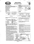
1
OPERATING
AND
SERVICE
MANUAL
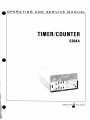
TIMER/COUNTER
5304A
w.0«
(iOtl
HEWLETT M
PACKARD
CERTIFICATION
The Hewlett-Packard Company certifies that this instrument
was
thoroughly tested and inspected and found to meet its published
specifications when it was shipped from the factory.
The HewlettPackard Company further certifies that its calibration measurements are traceable to the U.S. National Bureau of Standards to
the extent allowed by the Bureau's calibration facility.
WARRANTY A N D A S S I S T A N C E
This Hewlett-Packard product is warranted against defects in
materials and workmanship. This warranty applies for one year
from the date of delivery, or, in the case of certain major components listed in the manual, for the specified period.
We will repair or replace products which prove to be defective
during the warranty period provided they are returned to HewlettPackard. No other warranty is expressed or implied. We are not
liable for consequential damages.
Service contracts or customer assistance agreements are available
for Hewlett-Packard products that require maintenance and repair
on-site.
For any assistance, contact your nearest Hewlett-Packard Sales and
Service Office.
III' M< >1 >EL5;MMA TIMER colINTER
Reeord of Revisions (Manual Change I'ages)
REVISION
NUMBER
DATE
ISSUED
DATE
INSERTED
INSERTED
BY
HI' MODEL :">;{( M A TIM E R CO IJNTK K
Record of Revisions (Manual Change Pages)
REVISION
NUMBER
I
DATE
ISSUED
DATE
INSERTED
INSERTED
BY
it
SECTION IX D
TIMER/COUNTER
5304A
SERIAL PREFIX: 1212A00467
This section applies directly to HP Model f>H()lA, Timer
Counters having serial prefix number l2P2A004ti7, and
must he inserted into the 5300A Measuring System M uiual.
NEWER INSTRUMENTS
This Section with enclosed "Manual Changes Pages"
applies directly to HP Model 5.'U)4A Timer C o u n t e r s having
prefix numbers above 1212A00467.
OLDER INSTRUMENTS
Changes re(|uired to back-date this Section for older instruments arc in Section IX I), Subsection VII.
Copyright
HEWLETT-PACKARD COMPANY
1973
5301 S T E V E N S C R E E K B L V D . . S A N T A C L A R A . C A L I F . 9 5 0 5 0
Printed: AUG 1973
HP PART NO.
MANUAL 05304-90006
I
I
HEWLETT
Jjjf
M, PACKARD
Model 5304 A
Table of Contents
TABLE OF CONTENTS
Section
IX I)
i'age
5304A Timer/Counter
Subsection
ii
I
GENERAL INFORMATION
91)-1-1.
Introduction
91)-1-2.
Description
91)-1-4.
Purpose and Use of Section IX I)
91)1-6.
Instrument Identification
91)1-8.
Manual Changes and Options
91)1-1
9D-1-1
9D-1-1
91)-1-1
91)1-1
91)1-1
II
INSTALLATION
9D-2-1.
Unpacking and Inspection
9D-2-3.
Storage and Shipment
9D-2-5.
Installation and Removal of Plug-On
9D-2-8.
Portable Operation
9D-2-1
9D-2-1
9D-2-1
9D-2-1
9D-2-1
III
OPERATION
9D-3-1.
Operating Information
9D-3-1
91) 3-1
IV
THEORY O F OPERATION
9D-4-1.
Introduction
9D-4-4.
Input Amplifiers
9D-4-1
9D-4-1
9D-4-1
V
MAINTENANCE
9D-5-1.
Introduction
9D-5-3.
Recommended Test Equipment
9D-5-5.
Instrument Access
9D-5-7.
Periodic Maintenance
9D-5-9.
Maintenance and Repair
9D-5-13.
Instrument Troubleshooting
9D-5-16.
DC Balance Adjustment
9D-5-1
9D-5-1
9D-5-1
9D-5-1
9D-5-1
9D-5-1
9D-5-1
9D-5-3
VI
REPLACEABLE PARTS
9D-6-1.
Introduction
9I)-o-3.
Ordering Information
9D-6-1
9D-6-1
9D-6-1
VII
MANUAL CHANGES AND OPTIONS
9D-7-1.
Manual Changes
9D-7-3.
Newer Instruments
9D-7-5.
Older Instruments
9D-7-7.
Options
9D-7-1
9D-7-1
9D-7-1
9D-7-1
9D-7-1
VIII
CIRCUIT DIAGRAMS
9D-8-1.
General
91) 8-1
9D-8-1
Model 5304A
List of Figures
List of Tables
LIST OF F I G U R E S
Figure
Page
91)1-1.
5304A Timer/Counter
9D-1-0
9D-3-1
9D-3-2.
9D-3-3.
9D-3-4.
9D-3-5.
9D-3-6.
9D-3-7.
9D-3-8.
Signal Conditioning Using Attenuator, Level and
Slope Controls
Front-Panel Controls and Connectors
Rear-Panel Connectors
Making Self-Check Measurement
Making Frequency A Measurements
Making Period Average Measurements
Making Time Interval Measurements
Totalizing
9D-3-1
9D-3-2
9D-3-4
9D-3-5
9D-3-H
9D-3-7
9D-3-8
9D-3-10
9D-5-1.
9D-5-2.
9D-5-3.
9D-5-4.
9D-5-5.
9D-5-6.
Separation Procedure
Frequency A Troubleshooting Diagram
Period Average A Troubleshooting Diagram
Time Interval Troubleshooting Diagram
Open/Close Troubleshooting Diagram
('heck Troubleshooting Diagram
9D-5-2
9D-5-5
9D-5-7
9D-3-11
9D-5-13
9D-5-I5
9D-8-1.
Al Time Interval Board Assembly,
A2 Attenuator Board Assembly
9D-8-5
LIST OF T A B L E S
1 able
Page
9D-1-1.
5304A Timer/Counter Specifications
9D-1-2
9D-5-1.
In-Cabinet Performance Checks
9D-6-1.
9D-6-2.
Replaceable Parts
Manufacturers Code List
9D-6-2
9D-6-5
9D-8-1.
Instrument Interconnection List
9D-8-2
9D-5-16
in
Model 5304A
General Information
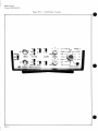
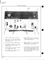
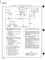
Figure 91)-1-1. 5304A Timer/Counter
^
:»::i :t w
XIOO ®
PSET^»*»
FREQ A
AUTO
-
ATTEN
w
9D-1-0
xioo a i
oc ^
5304A TIMER/COUNTER
OPEN/CLOSE A
Model 5.'{(MA
( ieneral Informatinn
S E C T I O N IX D
5304A TIMER/COUNTER
SUBSECTION I
GENERAL INFORMATION
9 D - 1 - 1 . INTRODUCTION
9D-1-6. INSTRUMENT IDENTIFICATION
9 D - 1 - 2 . Description
91)1 -7. Hewlett-Packard uses a two-section, ninedigit serial number (0000A00000) mounted on the
rear panel to identify the instrument. The first four
digits are the serial prefix and the last five digits
refer to the specific instrument. If the serial prefix
on your instrument differs from that listed on the
title page of this section, there are differences
between the manual and your instrument. Iiower
serial prefixes are documented in Section IX I),
Subsection VII and higher serial prefixes are covered
by a manual change sheet included with the manual.
9D-1-3. The Hewlett-Packard Model 5304A Timer
Counter, when plugged onto an HP Model 5300A
Measuring System, is capable of: Measuring frequencies up to 10 MHz, Time Interval measurements
from 500 nsec to 10,000 seconds, Period Average
over a range of 10 Hz to 1 MHz, and Totalizing.
The electrical and mechanical specifications are listed
in Table 9D-1-1.
9 D - 1 - 8 . M a n u a l C h a n g e s a n d Options
9 D - 1 - 4 . P u r p o s e a n d U s e of S e c t i o n IX D
9D-1-5. Section IX I) contains the documentation
necessary to operate, maintain, and repair the HP
Model 5304A Timer Counter plug-on. Also included
are parts lists, component locators, and schematics.
This information is intended to be inserted into the
5300A Measuring System manual as part of Section
IX of that manual.
9D-1-9. The title page lists the serial prefix number
to which this information directly applies. If the
serial prefix is different from the one listed, a
change sheet is included describing the required
changes. If this change sheet is missing, the information can be supplied by any Hewlett-Packard
Sales and Service office listed in Section VI of the
5300A Measuring System Manual. Options are listed
in Section IX I), Subsection VII.
9D I I
Model 5304A
General Information
Table 91)1-1. 5304 A Timer/Counter Specifications
INPUT CHANNELS A ANI) B
R a n g e : DC coupled; 0 to 10 MHz.
AC coupled; 100 Hz to 10 MHz.
PERIOD AVERAGE
R a n g e : 10 Hz to 1 MHz.
I n p u t : Channel A.
S e n s i t i v i t y (min):
25 mV rms sine wave
to I MHz. 50 mV rms sine wave to 10
MHz.
150 mV p-p pulse at minimum
pulse width, 40 nsec. Sensitivity can be
decreased by 10 or 100 times using
ATTENUATOR switch.
+
Accuracy:
1 count + time base accuracy
+ trigger error.**
I m p e d a n c e : 1 Mil shunted by less than 30 pK
D i s p l a y : /JS, ms with positioned decimal point.
Overload Protection:
250 V rms on Xl()
and XI00 attenuator settings.
On XI
attenuator setting 120 V rms up to 1 kHz,
decreasing to 10 V rms at 10 MHz.
T r i g g e r Level:
PRESET position centers
triggering about 0 volts ±25 mV, or continuously variable over the range of 1 V to
+
1 V times attenuator settings.
Slope:
Independent selection of triggering
on positive or negative slope.
Period Averaged:
1 to 10' automatically
selected for maximum resolution.
F r e q u e n c y C o u n t e d : 10 MHz.
FREQUENCY
R a n g e : 0 to 10 MHz.
I n p u t : Channel A.
G a t e T i m e s : Manually selected 0.1, 1, or 10
seconds. AUTO position selects gate time
to fill display for maximum resolution within a 1-second measurement time.
C h a n n e l I n p u t s : Common or separate lines.
A c c u r a c y : +1 count + time base accuracy.
Gate Output:
Rear panel BNC. TTL low
level while gate is open.
May be used
to intensity modulate an HP oscilloscope.
D i s p l a y : Hz, kHz, and MHz with positioned
decimal point.
TIME INTERVAL
R a n g e : 500 nsec to 10 • sec.
O P E N / C L O S E (Totalizing)
R a n g e : 10 MHz maximum.
I n p u t : Channels A and B; can be common
or separate
I n p u t : Channel A
F u n c t i o n : Input signal totalized while gate
open. Opening and closing of gate initiated
by front panel pushbutton switch.
O v e r l o a d : Maximum recommended levels for
pulse signals is 2 V p-p. Clipping occurs
at 3 V p-p.
GENERAL
Resolution:
steps.
100 nsec to 10 ms in decade
Accuracy:
+1 count + time base accuracy
+ trigger error.*
D i s p l a y : fjs, ms, or s (seconds) with positioned
decimal point.
Time Interval Holdoff:
Front panel concentric knob which inserts variable delay
of approximately 100 /jsec to 100 msec between START (Channel A) and enabling
STOP (Channel B); may be disabled. Electrical inputs during delay time are ignored.
Delay may be digitally measured in CHECK
position. Delay Output: rear panel BNC.
TTL low level during delay time. May be
used to intensity
modulate an
HP
oscilloscope.
91)1-2
Check:
Inserts internal 10 MHz reference
frequency into Channels A and B. Time
Interval Holdoff may be digitally measured
by switching to CHECK and TIME IN
TERVAL positions.
O p e r a t i n g T e m p e r a t u r e : 0° to 50°C.
Power Requirements:
Including 5300A
mainframe, nominally 10 watts. Minimum
of 3 hours operation (typically 5 hrs) at 20 C
to 30°C operating and charging temperatures.
Weight: Net, 1 lb (0.9 kg).
lbs (1.5 kg).
Shipping, 314
"For any waveshape, trigger error is less than
±
0.005
Signal Slope (V/ ps) /js
**Trigger error is less than ±0.3% of one
period, i periods averaged for signal with
40 dB or better signal-to-noise ratio.
Model 5304 A
Installation
S E C T I O N IX D
5304A TIMER/COUNTER
S U B S E C T I O N II
INSTALLATION
9D-2-1. UNPACKING A N D INSPECTION
9D-2-2. If the shipping carton is damaged ask that
the carrier's agent be present when the instrument
is unpacked. Inspect the instruments for damage
such as scratches, dents, broken knobs, etc. If the
instrument is damaged or fails to meet performance
tests when used with the 5300A Measuring System
notify the carrier and the nearest Hewlett-Packard
Sales and Service office immediately. Performance
check procedures are located in Section IX D-5,
and Sales and Service offices are listed in Section VI
Retain the
of the 53(H)A portion of the manual.
shipping carton and the padding material for the
earner's inspection. The Sales and Service office
will arrange for the repair or replacement of the
instrument without waiting for the claim against
the carrier to be settled.
9D-2-5. INSTALLATION ANI) REMOVAL
OF PLUG-ON
9I)-2-(>. The 5304A Timer/Counter must be used with
a mating 5300A Measuring System before any
measurements can be made. To mate the 5304A
Timer/Counter with the 53(H)A Measuring System, see
Figure 2-1 and Paragraph 2-1 of the 5300A portion
of the manual.
9D-2-7.
ENVIRONMENT.
Conditions during
storage and shipment should be normally limited
as follows:
a.
Maximum altitude: 25,000 feet
b.
Minimum temperature: -40°F ( 40°C).
c.
Maximum temperature: +167"F(+75°C).
9 D - 2 - 3 . STORAGE A N D S H I P M E N T
9D-2-4. PACKAGING. To protect valuable electronic
equipment during storage or shipment always use
the best packaging methods available. Your HewlettPackard Sales and Service office can provide
packaging material such as that used for original
factory packaging. Contract packaging companies in
many cities can provide dependable customer
packaging on short notice. Here is one recommended
packaging method:
a. The original container is a corrugated cardboard box with 200 lbs. burst test (HP No. 9211-1620).
The instrument is secured and protected, while in
the box by a top and bottom molded form of
polystyrene foam (HP No. 9220-1545). Also included
with the instrument is a plastic dust-protection cover
HP Part No. 05300-80004.
9 D - 2 - 8 . PORTABLE OPERATION
9D-2-9. The use of the HP Model 531 OA Battery
Pack enables the 5300A Measuring System and 5304 A
Timer Counter to be used in areas removed from ac
power sources. The 531 OA Battery Pack provides a
minimum of 3 hours operation (typically 5 hours) at
20°C to 30°C operating and charging temperature.
Tables 1-2 and 1-4 of 5300A portion of the manual
list the HP 5310A Battery Pack as an available
accessory.
Documentation on the 531 OA is also
included in Section IV through VIII ol the 5300A
portion of the manual. To prepare the 5300A 5304A
for portable operation, refer to Paragraph 2-15 and
Figure 2-2, steps a to c of 5300A portion of manual.
9D-2-1
OPERATO
IN
(
j
Model 5304A
Operation
S E C T I O N IX D
5304A TIMER/COUNTER
S U B S E C T I O N III
OPERATION
9 D - 3 - 1 . OPERATING INFORMATION
9D-3-2. The 5300A/5304A Timer/Counter measures
frequencies up to 10 MHz, period average to 1 MHz,
time interval from 500 nsec to 10,000 seconds; or
totalizes input signals.
Figure 9D-3-1. Signal Conditioning Using
Attenuator, Level and Slope Controls
9D-3-3. There are four basic signal conditioning
controls used in Channel A or Channel B (the effect
of these controls is shown in Figure 9D-3-1).
These are:
a.
ATTEN switches for Channel A and B.
b. SLOPE switches for Channel A and B.
c.
LEVEL controls for Channel A and B.
d. AC-DC switches for Channel A and B.
TRIGGER
VOLTAGE
NOTE ?
RECOVERY
VOLTAGE
+ SLOPE
HYSTERESIS
(NOTE I )
0
LEVEL
PSET
- SLOPE
I.
HYSTERESIS (NOISE REJECTION) VO. TAGE IS CONSTANT FOR
EACH ATTENUATOR SETTING AND DOES NOT VARY WITH
TRIGGER LEVEL
2
THIS ALLOWS ZERO VOLTS TRIGGERING WITH GOOD NOISE
REJECTION
3
ATTENUATOR: x i , x i o . x i o o CHANGES TRIGGER LEVEL AND
HYSTERESIS VOLTAGES BY FACTORS OF I . I O . I O O
9D-3-4. ATTEN.
XI, X10, XI00 switches (both
Channels. Large amplitude signals can be attenuated
by using the ATTEN switches. Setting the attenuator
switches increases the trigger levels and the
hysteresis voltages by factors of 1, 10, 100. If input
signal levels are unknown, the initial measurements
should be made with the attenuator switches set
to XI00. The attenuator settings are then reduced
until a stable, useable measurement is obtained.
9D-3-5. SLOPE Switches (both Channels).
The
slope switches allow the selection of triggering on
the positive (+) or negative (-) slope of the input
signals (see Figure 9D-3-1).
9D-3-6. LEVEL Controls (both Channels).
The
level controls allow adjustment of the triggering
point on the input signal waveform. With the LEVEL
controls set to PSET or "0", triggering is centered
about zero volts. The voltage range over which
triggering may be set is -1 volt to +1 volt times
the ATTEN switch settings (±1 V to +100 V).
9D-3-7.
AC-DC Switches (both Channels).
The
AC-DC switches select ac or dc coupling. In AC
position and PSET, triggering is centered about
ac-zero, and dc components on the signal have no
effect. In DC position and PSET, triggering is
centered about 0 volts dc on the signal.
9D-3-1
Model 5304A
Operation
Figure 9D-3-2. Front-Panel Controls and Connectors
T.I. A TO B
10 m«
/
PEP,
v AVO/A
FREQ A
\
XlOO
PUT
LEVE
AYTEN
0 0 ^
.1 ms
DO
OPEN.XCLOSE A
K g ] 5304A TII/ER/COUNTER
1.
COM-SEP-CHK.
Three position switch
enables selection of input signal from
separate or common sources or enables the
selection of a Self-Check position.
a.
COM: Connects INPUT A and
INPUT B i n parallel.
b. SEP: Channel A and Channel B
inputs are from separate sources.
c. CHK:
Self-Check verifies that
5300A 10 MHz crystal oscillator and
counting logic and the 5304A
gating
logic
is
functioning
correctly.
9D-3-2
2.
INPUT A and B. Input signal frequencies
to be measured are connected to INPUT
A. INPUT B is used in time interval
measurements.
3.
ATTEN.
Three-position input
attenuator for both channels.
a.
signal
XI: Connects input signals directly
to input amplifiers.
b. X10: Attenuates input signals by
factor of 10.
c.
XlOO:
Attenuates input signals
by factor of 100.
Model 5304A
Operation
Figure 9D-3-2. Front-Panel Controls and Connectors (Continued)
4.
AC-DC.
Two-position switch allows
selection of ac-coupling or direct-coupling
to input amplifiers.
5.
SLOPE +, -. Selects the triggering on
positive or negative slope of the input
signals.
6.
LEVEL. Adjusts the input trigger levels.
Preset to trigger at 0 volts.
7.
FUNCTION.
Twelve-position switch
enables 4 modes of operations to be
selected. The modes are:
c.
1) AUTO:
matically
play for
the signal
overflow,
1 second.
PER AVG A: Enables multiple
period averages to be made from
Channel A with frequencies of 10
Hz to 1 MHz. Periods averaged
are automatically selected from
1 to 10\
Gate time is autoselected to fill the dismaximum resolution of
being measured, without
up to a maximum, of
2) .IS, IS, 10S: Counter gate time
is manually selected for .1 seconu,
1 second or 10 seconds.
d. OPEN/CLOSE A (Totalize): Enables input signals to Channel A to
be totalized. Totalizing is initiated
by pressing OPEN/CLOSE A switch
and terminated by pressing the
switch a second time.
a. T.I. A to B: Enables time interval
measurements to be made from
500 nsec to
10,000 seconds.
Resolution is adjustable from .1 /JS
to 10 ms in six decade steps.
b.
FREQ A:
Enables frequency
measurements from 0 to 10 MHz
when dc coupled and 100 Hz to
10 MHz when ac coupled.
8.
DELAY. Adjustment inserts a time interval
delay of 100 /jsec to 100 msec between
Start (Channel A) signal and Stop (Channel B) signal; when disabled, there is a
residual delay of about 4200 nsec.
9D-3-3
Model 5304A
Operation
Figure 9D-3-3 Rear-Panel Connectors
GATE OUT
DELAY OUT
1.
GATE OUT: A TTL-LOW level signal
while the 5300A main gate is open.
2.
DELAY OUT: A TTL-LOW level signal
during the delay time selected by frontpanel DELAY control (in T.I. A to B
mode only).
Model 5304A
Operation
Figure 9D-3-4. Making Self-Check Measurements
l(REAR)
/
I
A TO B
FREQ A
PER
XIO
10 m s
xioo I
INPUT
PSE
ATTEN
SLOPE
I ms
LEVEL
10 p s
XIO
I MS
XiOC »
mi
.1 m s
0
XI
DC
PSET**
l us
5 3 0 4 A TIMER/COUNTER
1
Connect ac power to 5300A ac receptacle.
2.
Turn ac power "on" with 5300A SAMPLE
KATE control. Adjust SAMPLE KATE
for desired display time.
3.
Set 5304A COM SEP-CHK switch to CHK.
4.
Set 5304A "Function" switch to FREQ A,
AUTO. Display should he 10.0000 MHz,
+ 1 count.
5.
The time interval hold-off may be measured by selecting on of the T.I. A to B
positions of the "Function" switch.
NVCLOSE
9D-3-5
Model 5304A
Operation
Figure 9D-3-5. Making Frequency A Measurements
I (REAR)
/
T . I . A TO B
PER
10 ms
v AVG '
t ms
PSET^
INPUT
ATTEN
SLOPE
LEVEL
Q
+
—^
\
•
FREQ A
AUTO
It
.1 ms
I s
10 |iS
10 8
I ps
MS
XIOO
—
OPEN
IMER/
1.
Connect ac power to 5300A ac receptacle.
2.
Turn ac power "on" with 5300A SAMPLE
KATE control and adjust sample rate for
desired display time.
3.
Set COM-SEP-CHK to SEP.
4.
Connect input signal to INPUT A jack.
5.
Set ATTEN to XI00; AC-DC U> coupling
desired and SLOPE to polaritv desired.
Set LEVEL to PSET.
(>.
Set "Function" to FREQ A, AUTO and
adjust the ATTEN switch until a stable
display is obtained. The gate time may
be adjusted for .Is, Is, or 10 sec.
OSE A
Model 5304A
Operation
Figure 9D-3-6. Making Period Average Measurements
I (REAR)
FREQ A
NPUT
xioo m
DC •
53/4A TIMER/COUN/
1.
Connect tic power to 5300A ac receptacle.
2.
Turn ac power "on" with 5300A SAMPLE
KATE control.
Adjust sample rate for
desired display time.
3.
Set COM-SEP-CHK to SEP.
4.
Connect input signal to INPUT A jack.
5.
Set A I T EN to XI00, AC-DC to coupling
desired and SLOPE to polarity desired.
Set LEVEL to PSET.
().
Set "Function" to PER AVG A; adjust
A'lTEN switch until a stable display is
obtained. The number of periods averaged
is automatically selected.
9D-3-7
Model 5304 \
Operation
Figure 9D-3-7. Making Time Interval Measurements
l(REAR)
AUTO
1.
Connect ac power to 5300A ac receptacle.
2.
Turn ac power "on" with 5300A SAMPLE
RATE control. Adjust sample rate for
desired display time.
3.
Set "Function" switch to T.I. A to B,
with desired resolution. Ensure DELAY
control is full ccw.
4.
Set ATTEN switches for both channels to
XI00; AC-DC switches and SLOPE controls
switches to settings desired; set LEVEL
controls to PSET.
5.
If Start and Stop signals are from separate
sources, connect the Start signal to INPUT
A connector and the Stop signal to INPUT
B connector, then set the COM-SEP-CHK
switch to SEP.
If the Start and Stop
signals are from a common source, connect
the signal input to INPUT A and set the
COM-SEP-CHK switch to COM.
9D-3-8
6.
Adjust ATTEN switches until a stable display is obtained.
Time Interval Holdoff (DELAY).
The
I)p]LAY control inserts a delay of about
100 psec to 100 msec between the triggering
of the START Channel "A" and the enabling of the STOP Channel "B" (see
Figure B). This delay may be used to
measure relay or other mechanical
switch timing sequences without error
due to contact bounce. It may also be
used for measurements on pulse trains;
for example from the start pulse to a later
pulse, in the presence of intervening pulses.
To use the DELAY, proceed as follows:
a.
If the desired delay is known, it
may be set and measured by
selecting T.I. A to B and CHK and
setting DELAY control to the desired
delay time. The measurement may
then be made by switching COMSEP-CHK in step 5.
Model 5304A
Operation
Figure 9D-3-7. Making Time Interval Measurements (Continued)
b.
If the input signals are pulse trains,
it is possible to select a pulse out of
the train by increasing the DP]LAY
from full ccw; the measured time
interval will increase in steps as the
delay falls after successive pulses
in the train.
HP 182!A: Set TRIGGER to EXT.
SLOPE to -.
Coupling to ACF.
SWEEP MODE to NORM.
Time/CM for one cycle of measured
Time Interval.
c.
For maximum flexibility and ease of
interpretation, an oscilloscope may be
used to set up the measurement (as
shown in Figure A). The DELAY
OUTPUT is used to trigger (he time
base and intensity modulate the display (see Figure A). For a repetitive
waveform, the Channel A input may
fall during the display cycle, and
therefore might not initiate a measurement. The GATE output may be
substituted for the DELAY OUTPUT;
this allows intensifying the actual
measurement rather than the delay.
If the inputs are common, the GATE
OUTPUT or DELAY O U T P U T can
be displayed on the second channel
(or a third channel of a four-channel
scope), and the other of these two
used to intensity modulate.
e. Set DELAY slightly out of full ccw
and selcct the time interval delay.
The SWEEP TIME may have to be
readjusted.
f. Adjust INTENSITY to view only the
time interval measured.
g. Oscilloscope time display and 5300A
time readout should be the same.
Figure B: Example of Delay Control
CH A
INPUT
SIGNAL
CH B
INPUT
SIGNAL
JUL
'
{
'
GATE
SIGNAL
I
I
I
d. Set oscilloscope controls as follows:
DELAY
OUT
SIGNAL
HP 1801 A: Set A and B Channel
controls for a display of both input
signal. Set DISPI AY to A+B.
. T I M E INTERVAL
HOLDOFF DELAY
TIME
INTERVAL DELAY
SETTING
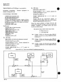
Figure A: Delay Control Setup
1
'DELAY OUT i
HPI80A
OSCILLOSCOPE
SIGNAL
SOURCE
EXT
INPUT
5 0 OHM
TERMINATIONS
T I STOP SIGNAL
T. 1. START SIGNAL
9! KM)
Model 5304A
Operation
Figure 9D-3-8. Totalizing
l(REAR)
SAMPLE RATE
GSD 5300A MEASURING SYSTEM
HEWLETT • PACKARD'
"1
0
PSET'
INPUT
ATTEN
SLOPE
*
T.I. A TO 8
10 m s
FREQ A
PER
AVG A ,
\ ' V
4*
AUTO
LEVEL
XI00
[Mi
OPEN
OPENXCLOSE
5 3 0 4 * TIMER
1.
Connect ac power to 5300A ac receptacle.
2.
Turn ac power "on" with 5300A SAMPLE
RATE control. Adjust sample rate for
desired display time.
3.
Set "Function" switch to OPEN ' CLOSE A.
4.
Set Channel A ATTEN to X100; AC-DC
and SLOPE to desired positions.
Set
LEVEL to PSET.
5.
Connect signal to be totalized to INPUT
A; set COM SEP-CHK to SEP.
6.
Press RESET; press O P E N / C L O S E
switch; C lamp should come on.
9D-3-10
A
7.
Reduce ATTEN A until counting occurs.
Display will accumulate at a rate dependent on input signal frequency.
8.
When the display has accumulated the
desired number of counts, press OPEN
CLOSE A switch to stop totalizing.
9.
If the operator wants to totalize starting
from the number accumulated in the display, press the OPEN/CLOSE A switch.
If a new totalizing measurement is to he
made, press RESET before pressing
OPEN CLOSE A switch.
THY
Model 5304A
Theory of Operation
S E C T I O N IX D
5304A TIMER/COUNTER
S U B S E C T I O N IV
THEORY OF OPERATION
9 D - 4 - 1 . INTRODUCTION
9D-4-2.
This subsection describes the theory of
operation for the 5304A Timer/Counter. Basic operation of gates, certain amplifiers and integrated
circuits is found in Section IV of the 5300A portion
of the manual.
9D-4-3. To simplify measurement making refer to
operating information starting with Paragraph 9D-3-1
for optimum adjustment of various controls.
9 D - 4 - 4 . I N P U T AMPLIFIERS A N I ) MODES
O F OPERATION
9D-4-5. CHANNEL A. The Channel A input signal
is applied to front-panel INPUT A jack and attenuated by A2 attenuator assembly (XI, X10, X100)
and sent to Al Channel A input amplifier. The
A2 Attenuator Board Assembly also contains the
AC-DC switches, SLOPE switches, and the LEVEL
controls for both channels. The input signal is sent
through A2 to the input of matched FET sourcefollower pair, Q2 and Q4. Diodes CR2, CR4 are
limiters for Q2 inputs.
9D-4-6. One side of the FET source-follower pair
(Q2) receives the input signal from A2J2 and the
other side (Q4) is connected to LEVEL A triggerlevel control A2R9. Q2 and Q4 are connected to
differential amplifier Q6 and Q8 respectively and
provides level shifting and gain of approximately
.3 for Channel A signals. Resistor R20 is a dc
balance for differential amplifier Q6 and Q8.
9D-4-7. The output from Q6, Q8 drives another
differential amplifier, U24B. The U24B output is
shaped by Schmitt-Trigger U24A and level-shifted
(ECL to TTL) through U21B, Q12 combination.
The U21B expander output is used to obtain sufficient signal swing to drive Q12.
9D-4-8. CHANNEL B. The Channel B input signal
is applied to front-panel INPUT B jack and attenuated by A2 Attenuator Assembly (Xl, X10, XI00)
and sent to Al Channel B input amplifier. The A2
Attenuator assembly also contains the Channel B
coupling switches, slope switches and the Channel
B level control. The Channel B signal is routed
through A2 to the input of matched F E T sourcefollower pair Ql and Q3. Diodes CRl, CR3 are
limiters for Ql inputs.
9D-4-9. One side of the Channel B FET sourcefollower pair (Ql) receives the input signal from
A2J1 and the other side (Q3) is connected to LEVEL
B trigger level control A2R10. Q5 and Q7 are connected to differential amplifiers Qf> and Q7 respectively and provide level-shifting and gain of
approximately .3 for Channel B signals. Resistor
R19 is a dc balance for differential amplifier Q5
and Q7.
9D-4-10. The output from Q5, Q7 drives another
differential amplifier U23B. The U23B output is
shaped bv Schmitt-Trigger U23A and level-shifted
(ECL to TTL) through U21A, Q l l combination. The
U21A expander output is used to obtain sufficient
signal swing to drive Q l l .
9D-4-11. VOLTAGE REGULATION. Transistors Q9,
Q10 provide regulated, low-ripple dc power to the
amplifiers and time interval hold-off circuits.
9D-4-12. SLOPE SELECTION. Slope selection for
Channel A is accomplished by using U19C, U20C,
and U20I) in conjunction with A2S7. Slope selection
for Channel B is accomplished by using U19I),
U20D, and U20A in conjunction with A2S(>.
9D-4-13. CHECK MODE.
In the CHECK mode,
the operation of the 5300A 10 MHz crystal oscillator
and counting logic and the 5304A gating logic is
verified. When A2S1 is in CHK mode, ground is
applied to U18A(2), U18I)(12), and U13C(5). The
10 MHz clock from the 5300A A1J1(16) is routed
through the 5304A AlPl(16) and sent to U12D(12).
The Channel A switch (U18B) and Channel B switch
(U18C), gate the 10 MHz clock signal through. The
Channel A switch output is also gated through U12B
and U16B and is available as the Fl signal at
A1P1(5).
9D-4-14.
FREQ A MODE.
In the frequency
measuring mode, with the "Function" switch S2 in
any of its four frequency measuring positions
(FREQ AUTO, .IS, IS, 10S) the Channel A input
signal is gated through "Channel A Slope Selection"
switch comprised of U19C, U20C, and U20B. The
input signal is then routed through another "Channel
A" switch made up of U18A and U18B.
From
U18B(6) the Channel A input signal is gated through
U12B and U16B as the Fl signal to the 5300A
mainframe which controls the opening and closing
of the main gate. The 10 MHz clock signal from
9D-4-1
Model 5304A
Theory of Operation
the 5300A m a i n f r a m e at A1 Pi(16) is routed through
U12C as the F2 signal to control the time base,
which clocks the opening and closing of the main
gate.
9D-4-15. The positive-going edge of a negative pulse
from U17E is the MAX TIME signal. The MAX
TIME signal a t A1 Pi(17) triggers a display cycle in
the 5300A mainframe. This negative-going pulse
can be generated from one of two sources.
One
of the sources is the positive-going edge of the
MGFF line at A1P1(12) which indicates the closing
of the 5300A main gate. This signal is inverted
through U17D and differentiated l>y CI4 and R69.
CR18 is a clamping diode to shorten the differentiation
recovery time.
The negative pulse
of the differentiated waveform, gates U16A " o n "
and the narrow positive-going pulse is inverted
through U17E as the MAX TIME signal.
9D-4-16. The TIME BASE O U T signal at AlPl(18)
comes from the 5300A m a i n f r a m e and is buffered
by Q18 then gated through U14C, U1HA, and inverted
through U17E as the MAX TIME signal.
9D-4-17. The positive-going edge of the negative
pulse at A1PK17), indicates the display cycle h a s
been triggered.
9D-4-18. PERIOD AVG A MODE. In period a v e r a g e
mode the "function" switch S2 enables U l A , U6D,
U12C, and U14A. The Channel A signal is routed
through "Channel A Slope Selection" and " C h a n n e l
A Switch" at U18B(6). The signal is then gated
through U16C and is available at AlPl(21) a s the 1
MHz TIME BASE. The CLOCK signal at A1P1(16)
is gated through U12A, U16B a s the F l signal to
be counted.
9D4-19. Flip-flop U4A prevents very narrow pulses
from triggering the time base but not the main
gate. The first Channel A pulse after the I N H I B I T
signal goes high at the end of the display cycle
"clocks" U4A(5) to a high state and enables U16C.
The next positive-going edge of the Channel A signal
is gated through U16C a s the 1 MHz T I M E BASE
INPUT signal. The main gate is then closed by
one of two events. The first event is: The 9 signal
line from 5300A, U3 COUNTER, goes low, and
enables the main gate in the 5300A, U5 CONTROL,
to close on the next LOG pulse. When the 9 line
goes low it indicates t h a t the display is 9% full.
The main gate closes at the end of the next decademultiple of the input signal to prevent overflow. The
second event is:
The TIME BASE O U T signal
(A1P1(18)) from the 5300A, U4 TIME BASE goes
9D-4-2
low indicating the I0 a periods have been counted.
The main gate closes because no more counts can
be stored in the 5304A exponent counter U8A and U8B.
The exponent counter counts the number of decadetransitions of the input signal t h a t have been
counted (1, 10, 100, 1000 input transitions or exponent counts of 1, 2, 3, 4).
9D-4-20. The LOG O U T P U T signal (generated by
5300A, U4 TIME BASE) is active in Frequency and
Period Average Modes and provides pulses to open
and close the main gate. Following a display cycle
and reset, the first LOG pulse opens the main gate
and a following LOG pulse will close the gate only
after a 9 or MAX TIME low signal enables the
closing of the main gate flip-flop.
9D-4-21. O P E N / C L O S E A MODE. In open/close
mode, with the "function" switch S2 in O P E N /
CLOSE position the main gate is opened and closed
by successive actuations of pushbutton switch SI.
The Channel A input signal is gated through "Slope
Selection" switch U19C, U20B, and U20C to " C h a n nel A Switch" U18A and U18B.
9D-4-22.
T h e Channel A input signal is gated
through U12B, U16B to be counted. U4B "clocks"
on successive actuations of the SI O P E N / C L O S E
switch.
When U8B(9) output is low the 5300A
main gate is opened (through U19B).
When
U4B(8) output is low the 5300A main gate is closed
(through U14D and U22A). When the "Function"
switch S2 is in a position other t h a n O P E N / C L O S E ,
the U4B Preset and Clear lines (U4B pins 10 and 13
respectively) are set through U10A and B, so that
IJ4B, Q and Q output (U4 pins 9 and 8) are high.
9D-4-23. TIME INTERVAL A-B MODE.
In the
time interval mode, the "function" switch S2 may
be set to a n y one of six time-interval positions
(.1 /Jsec to 10 msec). The 5300A main gate is opened
by a Channel A transition and closed by a Channel B
transition. Switch A2S1 enables the input signals
to be taken from separate sources or from a
common source.
9D-4-24.
The Channel A signal, after passing
through A2 Attenuator Assembly, is processed
through Channel A amplifier, Q2 Q4 and differntial
amplifiers Q6, Q8, and U24B. T h e U24B output is
shaped through U24A Schmitt-Trigger and sent
through an ECL-to-TTL level-shifter (U21B, Q21)
to the Channel A Slope Selection circuits (U19C,
U20C, U20B).
9D-4-25. The output from U20B(4) is gated through
Channel A switch, comprised of U18A and B. The
Channel A signal "clocks" U15B which is gated
through U9C, U19B, and opens the 5300A main gate.
During the gate-open time, the TIME BASE O U T
Model 5304A
Theory of Operation
signal from the 5300A A1J 1(18) is gated through
Q18, U17F, U9B, and U16B to be counted (except
in the .1 fjsec position, where the 10 MHz clock is
gated through U12A and U16B). The TIME BASE
OUTPUT signal is a 10 MHz clock signal divided
down by the time base to allow counting in increments of 1 fjsec, 10 fjsec etc.
9D-4-26. The main gate closes when Channel B
"clocks" U15A and a display cycle is initiated by
the positive-going edge of the M G F F signal at
A1P1(12). This signal is inverted through U17I)
and differentiated by C14 and R69. The negative
pulse of the differentiated waveform gates U16A
"on" and the narrow positive-going pulse is inverted
through U17E as the MAX TIME signal.
9D-4-27.
At the end of the display cycle, the
RESET signal at AlPl(15) is inverted through
U13E and sets U15B(9) low. U15A(5) is set high by
the PRESET signal a t U15A(4). The INHIBIT signal
goes "high" and sets U15B(12) so that U15B changes
states on the positive-going transition from U18B(6).
This produces two results:
1. U9C(8) goes low which set the OPEN signal
at A1P1(10) low through U19B and opens
the 5300A main gate.
2. Q16 turns off and allows C12 to charge
through R43 and R61.
9D-4-28. Transistor Q15 is an emitter-follower input to Schmitt-Trigger Q13, Q14. The output from
Q13 is level-shifted by CR15 and inverted by Q17.
Q15, 14, 13, and 17 form a one-shot multivibrator
with a very wide timing range. U15A cannot change
states until Q17 output goes low; then U15A(3) is
clocked to its opposite state by the positive transition of U18C (Channel B switch output).
The
U15A(5) output is gated and inverted through U14I)
and U22A. This causes the CLOSE signal line to
go low which in turn closes the 5300A main gate.
9D-4-29. The 5300A main gate cannot be re-opened
until U15B is cleared by the RESET signal at
A1PK15) and until the INHIBIT signal at AlPl(8)
sets U15B(12) high. U15B(8) goes high a t RESET
and turns on QI8 which discharges C12.
When
R43(S2) is open (full ccw), CI2 is not charged
up and the one-shot time-interval is very short
(about 200 nsec). The time-interval is the interval
from the time U15B(8) goes low and Q17 collector
goes low.
9D-4-30. A buffered DELAY OUT signal is provided
at J 3 and may be used for intensifying the oscilloscope Z axis which permits observing the start
and stop period in a time interval measurement.
A buffered GATE OUT signal is also provided at J4
which permits observing the gate signal duration
in a time interval measurement
9D-4-31.
EXPONENT COUNTER; EXPONENT
STORAGE. Outputs from the 5300A, U5 EXP line
are appli< J to exponent counter U8A, U8B "Clock
input". The RESET signal at A1 Pi(15) clears USA
and presets U8B for another measurement.
Exponent signals "clocked" into U8 indicate length
of measurements (10 ms, 100 ms, or 1 sec in
FREQ AUTO mode; 1, 10, 100, 1000 periods in
PERIOD AVG mode).
During the measurement
cycle, information is transferred into U7A, B
exponent storage by the TRANSFER signal. Therefore, the displayed measurement, the decimal point
and the units, change simultaneously.
9D-4-32. Exponent storage U7A, B is disabled (both
flip-flops are cleared), except in AUTO measurements, by U6I). Manual reset also clears U7A, U7B,
the decimal point and measurement units.
9D-4-33.
The remainder of the gates with the
exception of U5B provide time base, decimal point,
annunciator, and function decoding. The U3A output is high in any of the four frequency-measuring
positions. U5B locks out the LOG OUTPUT signal
in OPEN CLOSE A and TIME INTERVAL A B,
when the open and closing of the main gate is controlled by OPEN and CLOSE.
9D-4-34. Q19 normally turns off the 9 line except
during frequency Auto or Period Average; this
allows overflow to occur, if desired, in manual frequency position.
9D-4-3
MAN
I TENANCE
Model 5304A
Maintenance
S E C T I O N IX D
5304A TIMER/COUNTER
SUBSECTION V
MAINTENANCE
9 D - 5 - 1 . INTRODUCTION
9D-5-2.
This section contains maintenance and
service information for Model 5300A/5304A Timer/
Counter. Included are performance check procedures
and tests to localize, isolate, and locate defective
components.
9 D - 5 - 3 . RECOMMENDED TEST E Q U I P M E N T
9D-5-4. Test equipment recommended for performance checks, maintaining, troubleshooting and
servicing the 5300A/5304A Timer/Counter is listed
in Table 5-1 of 5300A portion of the manual. Test
equipment with equivalent characteristics may be
substituted for equipment listed.
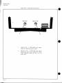
9D-5-5. INSTRUMENT ACCESS
9D-5-6. For access to plug-on assembly, separate
the 5300A from the 5304 A as follows:
a. Turn ac power OFF and disconnect power
cord.
b. Pull the two-side casting latches fully rearward (it is necessary to press the latch handles
gently away from the center of the instrument to
unlock them).
c. When latches are fully extended rearward, the
5300A and 5304A castings should be separated by
cbout '/g-inch.
d.
Lift the 5300A gently away from the 5304A.
e. Separate 5304A Al BOARD ASSEMBLY from
5304A casting as follows (refer to Figure 9D-5-1):
1.
Press rear, plastic-nylon retaining clips on
each side of 5304A casting and lift the rear
of the Al Board Assembly to release it
from the casting.
2.
Press front plastic-nylon retaining clips on
each side of 5304A casting and lift the front
of the Al Board Assembly to release it
from the casting.
3.
Lift Al Board Assembly from the casting.
f. Mate the 5304A, Al Board Assembly to 5300A
and reapply ac power.
g. To reinstall the Al Board Assembly into the
casting reverse procedure of steps d through f.
9 D - 5 - 7 . PERIODIC MAINTENANCE
9D-5-8. To determine if the 53O0A/53O4A is operating properly within specifications, perform the InCabinet Performance Checks listed in Table 9D-5-1.
These checks may also be used for the 5300A performance checks when the 5300A/5304A combination
is used.
9 D - 5 - 9 . MAINTENANCE A N D REPAIR
9D-5-10. BOARD REMOVAL. When removing the
printed circuit board for replacement, repair, or
servicing, always remove ac power and separate
the board from the casting using Paragraph 9D-5-6
steps a to e.
9D-5-11. COMPONENT REPLACEMENT. When
replacing a circuit board component use a low heat
soldering iron. Heat must be used sparingly as
damage to the circuit foil may result. Mounting
holes may be cleaned out with a toothpick while
heat is applied. Connection should be cleaned with a
cleaning solution after component removal and
replacement.
9D-5-12. INTEGRATED CIRCUIT REPLACEMENT.
Two methods are recommended for removing
integrated circuits:
a. Solder Gobbler.
Solder is removed from
board by a soldering iron with a hollow tip con
nected to a vacuum source. The IC is removed
intact so it may be reinstalled if diagnosis is
wrong.
b. Clip-Out. This method is used when an IC
is proven defective. Clip leads close to case, apply
heat and remove leads with long nose pliers.
Clean board holes with a toothpick and cleaning
solution.
9 D - 5 - 1 3 . I N S T R U M E N T TROUBLESHOOTING
9D-5-14.
Trouble isolation can best be accomplished by first obtaining all possible information
from the controls, connectors, and indicators on the
5300A and 5304A, then logically using this information to locate the defective component.
If the
9D-5-1
Model 5304A
Maintenance
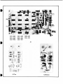
Figure 9D-5-1. Separation Procedure
Model 5304 A
Maintenance
performance checks indicate a malfunction or if
instrument operation is suspect, perform the SelfCheck procedures in Table 9D-5-1. For further tests,
separate the 5304A from the casting and reconnect
to 5300A using Paragraph 9D-5-6 steps a to e as
a guide. Operating procedures in Subsection 9D-3
can be used to help understand operation. To test
the 5304A, obtain the test equipment listed in
Table 5-1 of the 5300A portion of the manual.
9D-5-15. Figure 9D-5-2 to Figure 9D-5-6 are troubleshooting flow diagrams for each of the five modes
of operation. Signal flow is outlined for each mode
and waveform test points and voltage test points
are indicated.
The waveforms or voltage level
for each mode is included with the figures. To
obtain the waveforms a n d / o r levels for each mode,
follow the directions for instrument connections
which are listed with the troubleshooting flow diagrams of each respective mode.
9 D - 5 - 1 6 . DC BALANCE A D J U S T M E N T
9D-5-17. If Channel A or Channel B fail to operate with their respective LEVEL controls in PSET
position when measuring sine wave signals, or when
periodic maintenance/calibration is performed, the
dc balance may be adjusted as follows:
a. Connect an HP 651B Oscillator, set to 10
MHz, 50 mV rms/5012, through a 50 OHM BNC Feedthru Termination, to Channel A input.
b. Set the 5304 A controls as follows;
ATTEN to XI (both channels).
AC-DC to AC (both channels).
+, - to + (both channels).
LEVEL to PSET (both channels).
SEP-CHK to SEP
"Function" to FREQ A, AUTO
c. Connect an HP 180A oscilloscope through
a 10 Mi) pi obe to U18(6).
d. Adjust the oscilloscope controls to monitor
a useable signal.
e. Adjust A1R20 for a symmetrical waveform
with minimum or no change in duty-cycle when
SLOPE switch is changed from + to - and minimum
or no change when AC-DC switch is set to AC
or DC.
f. Connect the oscilloscope probe to U18(8)
and the 651B input signal to Channel B.
g. Adjust A1R19 for a similar display observed
in step e.
9D-5-3
Model 5304A
Maintenance
FREQ A, AUTO MODE.
Test points using HP 10525A Logic Probe
H = High (lamp on)
5304A controls:
L = Low (lamp off)
Channel A, SEP, XI, AC, +, PSET, AUTO
INPUT:
TPl
H (dim).
Flash rate decreases as
SAMPLE RATE control is truned cw.
TP2
H (dim).
Flash rate decreases as 5300
SAMPLE RATE control is turned cw.
I^evel goes Low when 5300A RESET is
pressed.
TP3
H (dim).
Flash rate decreases as 5300A
SAMPLE RATE control is turned cw.
Level goes Low when 5300A RESET is
pressed.
TP4
H (dim).
H a s h rate decreases as 5300A
SAMPLE RATP] control is turned cw.
Level goes High when 5300A RESET is
pressed.
TP5
H (dim).
Flash rate decreases as 5300A
SAMPLE RATE control is turned cw.
Level goes High when 5300A RESET is
pressed.
TP6
L.
Goes
pressed.
High
TP7
L.
Goes
pressed.
High
HP 651B set to 10 MHz, 100 mV rms/50S2.
Oscilloscope:
HP 180A, 1801A Vert. Amp. 1821A T.B. through
a 10:1 probe.
Settings:
AC coupled (except as noted).
NORM sweep mode.
+ SLOPE (except as noted).
ACF (except as noted).
Channel A.
5300A SAMPLE RATE ccw out of O F F (except as
noted). 5300 Display should be approximately the
same as the HP 651B setting.
9D-5-4
TP8
when
when
5300
53(H)
R&SET
is
5300A
RESET
is
O
O
.01 V/cm
.1 \i sec/cm
o
.2 V/cm
.1 (isec/cm
dc coupled
1 V/cm
lfisec/cm
.01 V/cm
O
.l|J.sec/cm
.2 V/cm
. 1 (isec/cm
dc coupled
©
. 1 V/cm
lOmsec/cm
dc coupled
- slope
.01 V/cm
O
. lfisec/cm
.1 V/cm
.1 fj-sec/cm
©
.2 V/cm
10 msec cm
dc coupled
- slope
.2 V/cm
.2fj.sec/cm
dc coupled
- slope
.2 V/cm
. 1 fJ-sec/cm
dc coupled
®
©
.1 V/cm
.1 fisec/cm
.2 V/cm
.5fisec cm
dc coupled
- slope
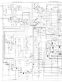
A2 ATTENUATOR BOARD ASSEMBLY
QD
Ai TIME INTERVAL BOARD ASSEMBLY OSKX-SOOQI:
60CQ?I
JD
016
013
Qtva *j
j
B1
• 0 0 B 0 •
017
PA) AlPI
1
OlO
03
1"
09
2 r
02
<0 0
06
06
" CM) _5i5
&TQR BOARD ASSfMBlY ">M04 «oc
fuse) 6 —f>"
i»"53TW
•>9
<5»T*t
410 enw
>
O
OiAKtCL B
SLOPE a E C T O H
[j^»> * j
B
;• U ' 4 A
j Lt<i
r~~iP^cV
(PSET) ^
[PSTT]
1
Tj|ui9o)
Eopl Jo
*
TIME BASE 0 0 1
'—!->*> S'
D>G'T A0CWES5
"*"!)7
Jr- o :>
• [§3 0 0 0 0
0047
a
0 SfLECl
I—[->»' OiGlT
51G
'I
O MMi CLOCK
.
OUU#«L
SLOPE SELECTION
I OPEN 'CLOSE * 1
C A N S T v. » SWITCH
6
12 UI2C
•^|2'
TIME BASE W
J_V „
OlG'T SELECT
-L>
V
MAN Of Sf
4
?4
TB SELECT *C
P/0 AlPI
< ? r i
~
'
C«i?i I
CHANXCI
y— EXPONENT COUNT E H - - ,
1115l
"i^S
B
S»ITC>-
I K P O N f N T STORAGE
*5V
7 1 J6fl
? ' * E»r)
3W,!
iO U2C
VOL TAG!
.
RfGUtATOPS
c
4
» » f EKtNTlAi
AMPLIFIERS
0 » f ' l " I NTiAt
AMPli'lERS
1 )
' vuT EfM ""s
L>€>
J ?
^jur
'
4
*
E?IB) imS
OPS
OPS
l^oS.1 I - -fc)^
E2<2) 37?
l6
E H ' ) ft
LEVEL
SHIFTED
klu*
4 l
10 UllC
I
i ? l m io
SCMM'T'
4«
•>46
.
£214)
ioS
E.O)
0/C
—
1
DIGIT SELECT
4C 0 , c , r *a*ES5
• > 23
TB SELECT "B"
r . i ? <91
4lU"B
- ) y
F i g u r e 9D-5-2. F r e q u e n c y A T r o u b l e s h o o t i n g D i a g r a m
9D-5-5
Model 5304A
Maintenance
HP 10525A Logic Probe
PERIOD AVERAGE A MODE
Test points using
5304A Controls:
H = High (lamp on)
Channel A, SEP, XI, AC, +, PSET, PER AVG A.
INPUT:
L = Low (lamp off)
TPl
651B set to 1 kHz, 100 mV rms/5012.
H (dim). Flash rate decreases when 5300 SAMPLE
RATE is turned cw. Goes Low when RESET is
pressed.
Oscilloscope:
HP 180A, 1801A Vert Amp, 1821A T.B. through
a 10:1 probe.
Settings:
AC coupled (except as noted).
NORM sweep mode.
+ slope (except as noted).
Channel A.
5300A
SAMPLE RATE ccw out of O F F (except as
noted). 5300 Display should be approximately
1.00000 MS, C.
9D-5-6
H (dim). Flash rate decreases when 5300 SAMPLE
RATE is turned cw. Goes Ix>w when RESET is
pressed.
TP3 H (dim). Flash rate decreases when 5300 SAMPLE
RATE is turned cw. Goes High (bright) when
RESET is pressed.
TP2
TP4
H (dim). Flash rate decreases when 5300 SAMPLE
RATE is turned cw. Goes High (bright) when
RESET is pressed.
TPS
L. Goes High when RESET is pressed.
TP6
H
TP7
H
O
.01 V/cm
1 msec/cm
®
.01 V/cm
1 msec /cm
0
.05 V/cm
50 jisec/cm
dc coupled
O
.2 V/cm
.5 msec/cm
dc coupled
O
.2 V/cm
.5 msec/cm
dc coupled
©
.2 V/cm
. 1 fjLsec cm
dc coupled
.2 V/cm
.1 |.isec/cm
dc coupled
O
.2 V/cm
10 msec/cm
dc coupled
- slope
.2 V/cm
.2fj.sec/cm
dc coupled
- slope
0
.2 V/cm
.2 fxseccm
dc coupled
- slope
.2 V/cm
10 msec cm
dc coupled
slope
A
5 msec/cm
dc coupled
- slope
10 msec cm
dc coupled
O
n
.2 V/cm
.5 msec/cm
dc coupled
1 msec cm
dc coupled
- slope
Ai TIME INTERVAL BOARD ASSEMBLY iosw< toooM
A2 ATTENUATOR BOARD ASSEMBLY u m o * 6000?)
-4 DraQ tm
•D
O
O
J
®
^
*-0
o-
015
QJ
013
016
014
f Ll vT. «"1 rtevtL 8 1
©
CD
• 0 0 0 0 0
sis
P/O AlPI
0I0 1
03
05
a>s~, ; »
Zp~
09
02
* ^tasi
<5*?
~u^
|
04
06
Q8
012
A>
A S S E M B L Y (09J04 6000?!
TIME I N T E R V A L
BOARD
ASSEMBLE
•-coo
;_OIT
.015
016
01
oie
[ LtVU" * "1 | LEVU • 1
Q 0 Q Q 0 0
@ , S ls£3 !o2
•Qi7
f * t «.:.
si * j
P / 0 AlPI
010
©6
V 6 r])
+sv—
09
OH
• w. T
*
t«8l
TS1
«
fiw rs
(
08
PCSCT
Model 5304A
Maintenance
No. 2 HP 222A:
TIME INTERVAL A TO B Mode, .1 (isec position.
Connect
Equipment connections:
shown in Figure 9D-5-4A.
equipment
REP RATE to MAN/EXT +.
as
PULSE WIDTH to .05-.5. Vernier adjusted for
oscilloscope display of .1 fisec.
Control Settings: 5300/5304A.
PULSE POLARITY to +.
PULSE AMPLITUDE for a
oscilloscope.
ATTEN (both channels) to XI.
AC-DC (both channels) to DC.
SLOPE (both channels) to +.
LEVEL. Set Channel A LEVEL slightly positive
(+) until the "C" lamp comes on. Set Channel B
LEVEL cw until a stable 5300 display is obtained.
Function to .1 fosec.
C O M / S E P / C H K to SEP.
+2 V pulse on
PULSE DELAY for approximate display, on
oscilloscope and 5300A, of 10 fj.sec (5300 display
should be approximately 00010.0(is C).
From the set-up outlined in Figure 9D-5-4A, disconnect the Channel A input to the HP 180A Oscilloscope. Connect a 10:1 divider probe and check
for the waveforms listed.
Oscilloscope:
VOLTS/CM to 2 (both channels).
DISPLAY to A + B.
INPUT (both channels) to DC.
T I M E / C M to 1 }j^ec.
SWEEP MODE to NORM.
TRIGGER to INT.
SLOPE to +.
Coupling to ACF or AC.
Test points using an HP 10525A I»gic Probe
H = High (lamp on)
L = Low (lamp off)
TPl
H (dim). Flash rate decreases when DELAY
control is turned cw or when SAMPLE RATE
is turned cw.
TP2
H (dim). Flash rate decreases when DELAY
control is turned cw or when SAMPLE RATE
is turned cw.
TP3
H (dim). Flash rate decreases when DELAY
control is turned cw or when SAMPLE RATE
turned cw
No. 1 HP 222A:
REP RATE to 1K-10K with adjustment centered.
PULSE DELAY h a s no effect.
PULSE WIDTH to .05 .5. Vernier adjusted for
oscilloscope display o f . 1 fisec.
PULSE POLARITY to +.
PULSE AMPLITUDE for a +2 V pulse on
oscilloscope.
Figure 9D-5-4A. Time Interval Mode Troubleshooting Set-Up
HPISOA
I80IA
PULSE
OUTPUT
INPUT
182 lA
HP 5304A
soft
INPUT
FEEOTHRU
50 A
FEEOTHRU
BNC TEE
BNC TEE
No 2
OELAYED
PULSE
EXT TRIG
INPUT
9D-5-8
HP 5300A
PULSE
OUTPUT
BNC TEE
Model 5304A
Maintenance
Part of Figure 9D-5-4. Time Interval Troubleshooting Diagram
.1 V/cm
.1 [isec/cm
.2 V/cm
.1 jisec/em
dc coupled
- Slope
.05 V/cm
. 1 fisec/cm
dc coupled
- Slope
o
.2 V/cm
. 1 fisec/cm
dc coupled
.2 V/cm
.1 fisec/cm
dc coupled
- Slope
.05 V/cm
. 1 |j.8ec/cm
- Slope
.05 V/cm
. 1 fisec/cm
dc coupled
- Slope
.1 V/cm
.1 fj.sec/cm
.05 V/cm
. 1 fisec/cm
.2 V/cm
. 1 p. sec/cm
dc coupled
.2 V/cm
. 1 fisec/cm
dc coupled
9D-5-9
Model 5304A
Maintenance
Part of Figure 9D-5-4. Time Interval Troubleshooting Diagram
©
.2 V/cm
. 1 (isec/cm
dc coupled
Q A
©
.2 V/cm
.2fjisec/cin
dc coupled
- Slope
.2 V/cm
.1 fisec. <-m
dc coupled
Q H
.2 V / c n
5(i8ec/cm
dc coupled
- Slope
(DELAY IN DETENT)
9D-5-10
o
0
.2 V/cm
.1 jj.8ec/cm
dc coupled
.2 V/cm
.1 msec/cm
dc coupled
- Slope
(DELAY just out of
DETENT. 5300 Display and waveform
should be the same)
® A
Q B
.2 V/cm
5p.sec/cm
dc coupled
- Slope
(DELAY IN DETENT)
.2 V/cm
.1 msec/cm
dc cdoupled
- Slope
(DELAY just out of
DETENT. 5300A Display and waveform
should be the same)
.2 V/cm
. 1 [iHeccm
dc coupled
- Slope
.5 V/cm
)() usee/cm
dc coupled
(DELAY IN DETENT)
© H
.5 V/cm
50 |j.sec/cm
dc coupled
(I)BLAY just out of
DETENT. .5300A Display time should be
approximately onehalf the oscilloscope
waveform time)
©
© A
.5 V/cm
50 fisec/cm
dc coupled
(DELAY IN DETENT)
©
.1 V/cm
50 fj.sec/cm
dc coupled
.5 V/cm
50 jisec/cm
dc coupled
(DELAY just out <>f
DETENT. 5300A Display should be approximately
200 > to
240|isec)
© A
.2 V/cm
.1 [isec/cm
dc coupled
• Slope
©
© A
.2 V/cm
20 fisec/cm
dc coupled
- Slope
(DELAY just out of
DETENT. 5300A Display should be approximately 200 to
240jasec)
.2 V/cm
.1 /-tsec/cm
dc coupled
- Slope
(DELAY IN DETENT)
.2 V/cm
. 1 fisec/cm
dc coupled
- Slope
(DELAY IN DETENT)
© H
.2 V cm
50 fisec/cm
dc coupled
- Slope
(DELAY just out of
DETENT. 5300A Display should be
approximately
the
total time of waveform pulse)
.2 V cm
. 1 f j sec cm
dc coupled
A! TIME INTERVAL BOARD ASSEMBLY tos*
A2 ATTENUATOR BOARD ASSEMBLY <oao* tooo?)
m
J
016
E3
QD
Q 0 B Q 0 0
E*3.8
i s m fog
017
P/0 AlPl
<?6
010
05
07
09
2 7
*
" E?(S)
7K
ImS
£212) 51?
en?) a
02
04
06
08
Al
TIME I N T E R V A L HOAHD A S S t M b L Y
(0S304-60000
|
^
cuts'*, B
SlDPt St- ECTlON
1
] 1 ^*1 * I
] B 0 0
• )
'
tOC Ol/TPOT
^ <*
OPT*I
• iO
K55E
O 1 i ) J6 J'011 400Ht5s
1—rr_l^s
f 16
ri
>0 UHl CLOCK
OVU#«l A
SLOW S£LECTiON
<0
,
[ 0P1N/CLOSE * 1
S f S W
E2I9
- j
JK
<#H
8
INHIBIT
CHANNEL A S W U C H
1
7.
? l
TIME BASE INPUT
131 u z o
6
.2 U I 2 D
DIGIT SELECT
P/0 AlPl
DIGIT A O O H t i i
13
• \*in\
J
00
C"
l 7
i
PfllNT
I
CHANNEL B SWITCH
20
TRANS'CR
EXPONENT COUNTER
tT" *
J),3
0«N
7V
>.s i &
^>4
mo
?
7
Xj^o
« £2(7)
} 48 cx>5
10 u?C
* " • £2(3)
TmS
£2(21
OiS
? 7 » £2(6, ft
? 46
DPS
*13
Of-
DiGiT S I L E C
io uiic
SCHMIT I
TRIGG£»
2 7« t ,
o t
0
*
[ - * 23
TB SCLECT *B*
Figure 9D-5-4. Time Interval Troubleshooting Diagram
9D-5-11
Modei 5304A
Maintenance
OPEN/CLOSE MODE
5300A Sample
as noted).
Rate
ccw
out
of
OFF
(except
5304A Controls:
Channel
A,
SEP,
XI,
DC,
+,
PSET
OPEN/CLOSE
A.
Press
RESET,
then
OPEN/CLOSE;
display
should
be
accumulating at a 10 Hz rate.
INPUT:
5304A: OPEN/CLOSE Mode
TPl
651B set to 10 Hz, 100 mV rms/50<2.
Oscilloscope:
HP 180A, HP 1801A Vert Amp, HP 1821A T.B.
through a 10:1 probe.
Settings:
AC coupled (except as noted).
NORM sweep mode.
+ slope (except as noted)
AC (except as noted)
Channel A
9D-5-12
H. Goes Low when OPEN/CLOSE switch is
pressed. Reamains Ix>w if this switch is
held depressed.
TP2
L. Goes High when RESET is pressed. Remains High if this switch is held depressed.
TP3 L
TP4
L. Goes High when OPEN/CLOSE is pressed
to stop accumulation or when RESET is
pressed during accumulation.
TP5
H. Goes Ix)w when OPEN/CLOSE is pressed
to stop accumulation or when RESET is
pressed during accumulation.
o
.01 V/cm
20 msec/cm
®
.02 V/cm
20 msec/cm
O
.05 V/cm
50 msec/cm
dc coupled
®
.2 V/cm
50 msec
dc coupled
©
.2 V/cm
50 msec/cm
dc coupled
O
.2 V/cm
50 msec/cm
dc coupled
O
.2 V/cm
50 msec/cm
dc coupled
AI TIME INTERVAL BOARD ASSEMBLY it
A? ATTENUATOR BOARD ASSEMBLE « m 0 4 6Qoo?i
015
El
ED >
C2;
m
• •
014
016
I LtVtl * | I ItVCL B 1
• 0 • • 0 Q
E«D,5 ® " »
017
P/0 AlPl
-r-<?6 + I7V
010
OOljiF
€5 <>
1
J)
7V
05
—
06
08
012
Al
TIME I N T E R V A L
BOARD ASSEMBLY
IOSSO*-6000.:
,DELA*
Or
^9
(5PTSi
^ 10
5.T55T
}
a
TIME BASE OUT
DIGIT SELECT
OANNEL e
SLOPE SELECTION
I LEVEL * |
9 £V
I LEVEL B |
• 0 0 • 0 0
@ , g S D go
l u ' W
)i2
OAW«I
M5R
*
SLOPE SELECTION
SI
•HI ( / • ,
, — CHANNEL
*
SWITCH-
—' \ ,, "
1
6
12 UIZO
P/C A l P I
I
CHANNlL
EXPONENT C O U N T E H
Ei(51
TiMJ BASE INPUT
•V
M
DIGIT SELECT
\
M
DIGIT AOOBESS
® rr*t
IIUtMJ
-;^3
' •, *
B SWITCH
EXPONENT STOWAGE — .
19
WIST
4 5? MAN RESE
"M5
C M
J) /<> J V
24 TB SELECT *C
E2(7)
r,T? j o
? * E?I8I
«'
OM
^
48
DPS
^
«6
DP i
4I
OIGIT SELECT
5»5
10
»v
7
•
L<?C
imS
w
? ">
EK7I
FA
; uio
„
*sv
| ^
iOlU"C
I
! v m ° l G " *«»«ss
SCHMi'
ftiGCEft
± J2
EVEL
SHir'f
.
[?(«!
o
1O5
——*E>n
&y?
1
TB SELECT "A*
Model 5304A
Maintenance
CHECK MODE
5304A Controls:
C O M / S E P / C H K to CHK; "Function"
to AUTO
5300A
count.
Display
should
be
10.0000
MHz
C
±1
Oscilloscope:
HP 180A, HP 1801A Vert Amp, HP 1821A T.B.
through a 10:1 probe
Settings:
AC coupled (except as noted).
NORM sweep mode.
+ Slope (except as noted).
AC (except as noted).
Channel A.
9D-5-14
o
•
.2 V/cm
• * M-8ec/cm
decoupled
O
.2 V/cm
. 1 fj.sec/cm
dc coupled
.2 V/cm
1 fisec/cm
decoupled
.2 V/cm
. 1 fjLsec/cm
dc coupled
A2 ATTENUATOR BOARD ASSEMBLY COSJO*-coooz)
Al TIME INTERVAL BOARD ASSEMBLE
EJ
y0'5
fl-n
016
014
013^
• 00 00B
Isp.5
v **
oio 1
; [5^D
El IS) "i>IS
iP Oh
05
07
Mv 09
'wouLArmis
Oil
-2ULL
- ten
02
lo
*
|o
5
04
5
m o *"T *•"
06
06
012
T
Al TIME INTERVAL BOARD ASSEMBLY <OSJO4
1
SJ U3* / '
11
}
LOG OUTPfT
^ 9
&rh
••CMMNEL M
E O K
I t t v u * 1 I LEVEL » I
DIGIT SELECT
SELECTION
DIGIT AOORfSS
• 00 0 0 0
~3.8 S3182
o um
f 16
KJ UHi CLOCK
OPEN/CLOSET)
ry-a
INHIBIT
CHANNEL * SWITCH
1
r / o AIPI
flME BASE INPUT
DIGIT SELECT
•»; (HZD
M
OlGlT AOORESS
CHI7
•
EXPONENT COUNTER
CRI4
WWT
CHANNCL • SWITCH
EXPONENT STORAGE
(2 TV
IZ»T] o ~ T
t
* 4 7
ClKI
<S»
r>s« M
> *6 S3
I ^ I T I U I
REGULATORS
h>4€
2(2)
Oil
» U
LEVEL
SHtfTf*
6S5
f »
KTj n
SCHMlTT
|TRIG««I
Hp-.,,
/ 5 k
DIGIT SELECT
j o j ^ ) i —
DIGIT AOORESS
lEvEi.
E2H) « i
>OI
CI. C 2 M
SK
)
~l(gv
1
22
TB SELECT " »
> 23 TB SELECT *B
Model 5304A
Maintenance
Table 9D-5-1. In-Cabinet Performance Checks
1. CHK mode and Time Interval Holdoff.
2. FREQ A Mode.
RANGE: dc coupled: 0 to 10 MHz.
a.
Set 5300A OSC switch to INT.
b.
Mate 5300A to 5304A and ensure
ie
casting latches at rear of 5300A are
latched.
Sensitivity as in Table 9D-1-1.
c.
Connect ac power to 5300A ac receptacle.
Obtain following test Equipment:
d.
Turn ac power "on" with 5300A SAMPLE
RATE slightly cw out of OFF.
HP 651B Test Oscillator
HP 11048B 50-0hm Feed-Thru
Termination
e.
Set COM-SEP-CHK to CHK; "Function"
switch to FREQ A, AUTO.
Display
should be 10.0000 MHz +1 count.
f.
Set "Function switch to T. I. A to B,
.1 psec. Press 5300A RESET switch; the
5300A display should be about .2 psec
(200 nsec residual holdoff). It may also
be .0/jsec.
g.
Set the DELAY slightly cw out of the detent position. Display should be approximately 100/jsec.
h.
Adjust the DELAY control cw until
maximum setting is reached. Display
should be about * OOOOO.O /JS (* = OVERFLOW) (100,000.0 jL/sec).
i.
Repeat steps g and h for the following
ranges; display should be as listed.
T. I. A to B
Approximate 5300A Display with
DELAY control:
ccw out of Detent
max. cw
1 [j.sec
000100 p.sec
100000 jjisec
lOjosec
0000.10 MS
0100.00 MS
1 ms
00000.0 MS
00100.0 MS
1 ms
000000 MS
000100 MS
0000.00 s
0000.10 S
10 ms
ac coupled: 100 Hz to 10 MHz.
Table 5-1 in the 5300A portion of the manual
and Table 9D-5-1 lists equipment used;
equipment with equivalent characteristics
may be used.
a.
Connect 651B 50-0hm OUTPUT through
the 50-0hm feed-thru to 5304A "A
INPUT" connector. Set 5304A "Function" switch to FREQ A, AUTO; set
COM-SEP-CHK to SEP, ATTEN to XI,
AC-DC to AC, SLOPE to +, LEVEL to
PSET or adjusted until a stable count
is displayed.
b.
Set 65IB to frequencies and output
levels listed below: Display should be
as listed.
3. FREQ A Mode, Pulse Measurements.
RANGE: decoupled: 0 to 10 MHz
Sensitivity as in Table 9D-1-1.
Pulse Width: 40 nsec minimum
Obtain the following test equipment:
HP Model 222A Pulse Generator
HP Model 11048B 50-ohm Feedthru Termination
HP Model 180A Oscilloscope
BNC Tee Connector
a.
9D-5-16
Connect equipment as in Figure A.
651B OUTPUT
mV rms
65IB FREQ Hz
Approximate
"Function"
(sec)
Approximate Display
+ 1 Count ± Accuracy
of source
25
10 Hz
10
00010.0 Hz
25
10 kHz
10
10000.0 Hz
25
100 kHz
1
100000 Hz
25
1 MHz
.1
1000.00 kHz
50
10 MHz
AUTO
10.0000 MHz
Model 5304A
Maintenance
Table 9D-5-1. In-Cabinet Performance Checks (Continued)
Figure A
Figure H
HP S300A
HP 2??A
HP iBuA
HP 5300A
HP 6510
HP i BOA
HP 5304A
CHAN A
V t R T IN
PULSE
OUTPUT
H P 5304A
TO C H A N A
CHAN A
VERT IN
NPUT
10MHz
soft
FEEDTHRU
FEEDTHRU
oNC TEE
b.
BNC TEE
Set 222A for "+" PULSE POLARITY;
40 nsec pulse width; 150 mV p-p as
monitored on oscilloscope.
c.
Monitor 222A pulse output with oscilloscope and set REP RATE for 10 Hz.
d.
Set 5304A Channel A controls as follows:
ATT EN switch to XI
AC-DC to DC
SLOPE to +.
LEVEL to PSET or adjust until a
stable count is displayed.
e.
5300A display should be approximately
10 Hz.
f.
Repeat step c with 222A repetition rates
of 10 kHz, 100 kHz, 1 MHz and 10 MHz.
The 5300A display should be the same
as the 222A repetition rate setting.
g.
4. SLOPE to +.
5. LEVEL to PSET or adjusted until a
stable display is obtained.
c.
Monitor the oscilloscope and set 651B controls for 10 Hz, 100 mV rms output.
d.
Display should be approximately * 00.0000
MS, C <* = OVERFLOW) (100 msec).
e.
Monitor the oscilloscope and set 651B for
the following frequencies; display should
be as listed.
Set 222A PULSE POLARITY to
Set 5304A Channel A SLOPE to -.
Repeat steps b through f.
65 IB
5300A/5304A
10 kHz
100.000/isC
100 kHz
10.0000 f j s C
I MHz
01.0000 M s C
NOTE
Periods averaged are automatically selected to provide maximum resolution.
4. PER AVG A Mode.
RANGE: 10 Hz(.l sec) to 1 MHz (I /jsec).
5. T. I. A to B (Time Interval) Mode.
Obtain the following test equipment:
RANGE: 500 nsec to 10,000 seconds.
HP Model 651B Test Oscillator.
HP Model 11048B 50 OHM
Termination.
Obtain the following test equipment:
Feed-thru
a.
Connect equipment as shown in Figure B.
b.
Set 5304A Channel A controls as follows:
HP Model
required).
222A
Pulse
Generator
HP Model 11048B 50-0hm
Termination (2 required).
Feed-thru
1. "Function" switch to PER AVG A.
HP Model 180A Oscilloscope.
2. ATTEN to XL
BNC Tee Connectors, (3 required).
3. AC-DC to AC.
a.
(2
Connect equipment as shown in Figure C.
9D-5-17
Model 5304A
Maintenance
Table 9D-5-1. In-Cabinet Performance Checks (Continued)
,
n
. Z AXIS .
INPUT i
Figure C
*
1
L
pJ
I DELAY •
• OUT l
l
HPM30A
HP ??2A
I80IA
30IA
AT
PULSE
OUTPUT
50A
FEEOTHRUS
1
INPUT
182 IA
182IA
,
f
BED
T
INPUT
A
INPUT
D
SOft
FEEOTHRUS
fl
II
BNC TEE
HP 222A
EXT TRIG
INPUT
b.
DELAYED
PULSE
PULSE
OUTPUT
A
BNC TEE
While monitoring generator No. 1 output
with oscilloscope, set No. 1 generator
controls as follows:
f.
5304A should display 00000.5
psec;
verify time interval with oscilloscope.
1. REP RATE to Ik-10k with adjustment centered.
g.
While monitoring oscilloscope, adjust No.
2 generator PULSE DELAY for time
intervals from .5 /jsec to 150 /jsec. 5300A
Display should be the same as oscilloscope display.
3. PULSE POLARITY to +.
h.
Set No. 1 generator REP RATE to 100lk and adjustment centered.
While monitoring generator No.2 output
with oscilloscope, set No. 2 generator
controls as follows:
i.
While monitoring oscilloscope, adjust
No. 2 generator PULSE DELAY for time
intervals from 150 /jsec to 2000 /jsec.
5300A display should be the same as
oscilloscope display.
3. PULSE WIDTH for .2 A/sec pulse at
2 V amplitude.
j.
Set No. 1 generator REP RATE to 10-100
and adjustment full ccw.
4. PULSE DELAY for .5 /jsec.
k.
While monitoring oscilloscope, adjust
No. 2 generator PULSE DELAY for time
intervals from 2000 /jsec to 6000 /jsec.
5300A display and oscilloscope display
should indicate the same time intervals.
2. PULSE WIDTH for .2 /^sec pulse a t
2 V amplitude.
c.
1. REP RATE to MAN/EXT +.
2. PULSE POLARITY to +.
d.
Set Oscilloscope DISPLAY control to
A + B to monitor No.2 pulse position.
e.
Set 5304A control as follows:
1. ATTEN (both channels) to XI.
2. AC-DC (both channels) to DC.
3. SLOPE (both channels) to +.
4. LEVEL (both channels to PSET.
5. COM-SEP-CHK to SEP.
9D-5-18
NOTE
Measurement resolution may be
adjusted from .1 |j.sec to 1 msec
with the T.I. \ to B switch.
Model 5.J04A
Maintenance
Table 9D-5-1. In-Cabinet Perfomrance Checks (Continued)
6. Totalizing (OPEN/CLOSE A) Measurements.
Obtain the following test equipment:
c.
Set "Function" switch to OPEN/CLOSE
A.
d.
Instrument gate is controlled by operator when OPEN/CLOSE A pushbutton
is pressed.
e.
Press OPEN/CLOSE A switch; ft MX)A C
lamp will tum on; adjust Channel A
ATTEN to Xl; 5300A display should
accumulate.
f.
To stop 5300A from accumulating, press
OPEN/CLOSE A. To continue accumulation from the number displayed press
OPEN/CLOSE A, otherwise press
RESET to clear display.
HP Model 65IB Test Oscillator.
HP Model U048B
Termination.
a.
b.
50-0hm
Feed-thru
Connect 651B 50-0hm output, set to
10 Hz at 100 mV rms, to 5304A Channel A INPUT connector.
Set Channel A ATTEN switch to X100,
AC-DC to AC; SLOPE to • and LEVEL
toPSET.
90-5-19
Model 5304A
Maintenance
PERFORMANCE CHECK TEST CARD
Hewlett-Packard Model 5300A/5304A
TIMER/COUNTER
Serial No
-
Test Performed by
Date
Description
1. CHECK Mode and Time Interval Holdoff.
Check
•
Display is 10 MHz ±1 Count.
Hold off as in Table 9D-5-1, item 1, step i.
2. F R E Q A M o d e .
•
0 to 10 MHz dc coupled.
100 Hz to 10 MHz ac coupled.
3.
FREQ A Pulse Measurement Mode.
•
Channel A; 0 to 10 MHz
40 nsec minimum.
4. P E R A V G A M o d e .
•
10 Hz (.1 sec) to 1 MHz (1 |j.sec).
5. TIME INTERVAL Mode
•
500 nsec to 10,000 seconds.
(tested to 6000|osec).
6. Totalizing ( O P E N / C L O S E A).
•
Controlled accumulation.
9D-5-19a
PARTS
LIST
Model 5304A
Replaceable Farts
SECTION IX I)
5304A TIMER/COUNTER
SUBSECTION VI
REPLACEABLE P A R T S
9D-6-1. INTRODUCTION
9D-6-2. This subsection contains information for
ordering replacement parts. Table 9D-6-1 lists parts
used in the HP 5304A.
Service Office (see lists in Section VI, 5300A Manual
for addresses). Identify parts by their HewlettPackard part number. To obtain a part that is not
listed, include:
a. Instrument model number.
9D-6-3. ORDERING INFORMATION
b. Instrument s ?rial number.
9D-6-4. To obtain replacement parts address order
or inquiry to your local Hewlett-Packard Sales and
c. Description of the part.
d. Function and location of the part.
HI F l HKNCK DKSIGNATOHS
assembly
m o t ii i
iui(> I V
i-apacitor
i Duplet
diode
((•-lay Inn
I11ISC • U 11 "III. }>.«11
F
Fl.
IC
.1
K
1.
I>
M
MK
1 Use
lllter
integrated circuit
jack
i elay
inductor
loud speaker
meter
unciophone
A
AFC
AMI'I
ampe r e»
automatic l i i t j i n ' i i c y c o n t r o l
amplilier
II
HDW
III X
HFO
UK C I
BH
HI'
Uh.S
itwo
in .ii 11 H|ui iu \ o s c i l l a t o r
In i v I l i u m copper
1)1 Hill I 1)1.1(1
iMhdpass
brass
liai k w a r d w a v e o s n l l a t o i
ii/
henries
ha i d v. a n
hexagonal
mercury
hour(s)
In r t / .
c i
CKH
('.Mil
COt F
COM
COM I '
COM I ' l
CONN
CI'
CUT
> o u n t c r - d o c k w isi
••••ramie
cabinet mount only
coefficient
c o i n mon
lompi iMlion
complete
iniimi'loi
c a d m i u m plat<
i .itliodi -1 ay l u l u
clockwist
IF
IMPC.
INCI)
INC!
INS
INT
intermediate I n i |
impregnate <1
incandescent
Hit ludc(s)
insulatioli(ed)
internal
DKPC
I)H
d« posited cat lmn
drive
I LKCT
I NCAP
I XT
. I. c l r o l y t i c
encapsulated
• \ i i i nal
F
FH
K l l . II
FXI)
laiads
l l . i t In ad
l l l l i s l e r In ad
fiM-d
G
GF
til.
OKI)
giga
germanium
glass
ground(ed)
(It
| i « .-.ll'.ll.l l l n ,
MP
P
W
It
KT
S
r
TB
TP
m e c h a n i c a l part
plug
transistor
resistor
thermistor
switch
transform!!
t e r m i n a l board
test point
U
V
VH
vy
X
Y
/.
integrated circuit
v a c u u m , tube, neon
Imllt, photoi e | | , etc.
voltage r e g u l a t o i
cable
socket
crystal
tuned c a v i t y .
network
AHBHKVIATIONS
lie;
iii<
kil.
KHHI
1.11
I.IN
I K U ASH
UM,
LPF
I' l l hand
linear taper
lock washer
l o g a r i t h m i c taper
low pass 11 I t e r
M
MM.
Ml I FKM
M K T OX
MFK
Mil/
MINAT
MOM
MOS
MTG
MY
m i 111 10 3
nieu
I0' 1
metal h i m
metallic oxide
manulactui <r
mega h e r t z
miniatui <
inonientary
m e t a l o/.idi- .suhstiat)
mounting
"mylai"
NK
M PI.
iiano ( I 0 ' 9 )
normally closed
neon
nickel plati
N 'O
Nt)M
NPO
NPN
NH FH
NSH
n o r m a l l y open
nominal
negativi p o s i t i v e / i n
(/.ero t e m p c t atui •
coefficient)
ncgative-positiv< negative
not r e c o m m e n d e d l o i
I n Id replacement
not separately
replaceable
OBI)
(III
OX
o r d e r liy d e s c r i p t i o n
o v a l head
oxide
I'
PC
I'F
peak
printed circuit
picolarads
10' 12
farads
phosphor b r o n / i
Phillips
peak inver.se v o l t a i c
p o s i t i v i - negative
pohitivc
p a r t of
p o l v s t y ri'iu
porcelain
p o s i t ioii(s)
potent l o m e t e l
peak-to-peak
point
peak w o i k i n g voltage
I'll Biti
PHI
PIV
I'NP
P O
POLY
POKC
PUS
POT
PT
PWV
H I CT
HF
HII
• • ctifier
r a d i o I i et|ueiicy
r o u n d head m
r i g h t hand
HMO
HMS
HWV
i ack mount only
i. M ii mi .in squai 1
r e v e r s e w o i king
voltage
S B
SCH
St
SKCT
SKMICON
SI
Sll.
SI
SPG
SPI
SST
SH
STL
slow -lilow
.sci i «
selenium
se.'tionfs)
semiconductor
silicon
silver
slide
spring
special
s t a i n l e s s steel
split r i n g
sleel
TA
Tl)
TGI
rill)
Tl
TOL
TH1M
T\V I
tantalum
t i m e delay
toggle
t i n cad
titanium
tolerance
ti immi r
t i a v e l i n g wave tu
I0-6
i;
micro
VAH
VI)C\V
vari.ilih
dc * o i k t l i t ; volts
yy
yy
with
waits
working i ivcrse
volfagi
wirewound
w itliout
uiv
\y\y
\y o
9D-6-1
Model 5304 A
Replaceable Parts
Table 9D-6-1. Replace Parts
Reference HP Part Number
Designation
Qty
A1
05304 60001
i
A1C1
A1C2
A1C3
A1C*
01 w-ooso
2
0150-0050
0150-0075
0150-0075
6
AIC5
A1C6
AIC7
A1C8
A1C9
0180-0106
0180-0106
0180-0197
0180-0197
0 1 5 0 - 0 0 75
A1C10
A1C11
A1C12
AIC13
A1C1*
0150-0C75
0180-0106
0160-0168
0160-2204
01*0-0198
A1CI5
AICRI
AICR2
A1CR3
A1CR*
0180-1702
1901-0376
1901-0376
1901-0376
1901-0376
*
AICR5
A1CR6
A1CR7
A1CR8
A1CR9
1901-00*0
1901-00*0
1901-00*0
1901-00*0
1901-00*0
10
AICR10
A ICR 11
A1CR12
A1CR13
AIC4I*
1901-00*0
1901-00*0
1901-00*0
1902-0031
1902-0031
A1CR15
A1C4I6
A1CR1 7
A1CR1 8
A1E1
1902-31*9
1901-00*0
1901-00*0
1901-0*60
1810-00*1
A1E2
A1P1
A101
i810-00*1
1 2 5 1 - 2 *56
0530*-»0001
0530*-8000I
Aia?
3
2
I
1
19
I
2
1
1
2
1
2
A183
A13*
A105
A1Q6
A137
A108
1853-0036
1853-0036
1853-0036
1853-0036
A109
A 1U10
A1Q11
A1012
A1QI3
1853 0036
1854 0246
185*-009*
185*-009*
185*~0071
A1Q1*
A1915
A1Q16
A1Q17
AIQ18
185*-0071
IB 5 * - O 0 71
IB5*-0071
185*-009*
185*-009*
A1Q19
AIR 1
A1R2
A1R3
AIR*
• 1853-0036
0683-10*5
0683-1 0*5
0683-2215
0683-2215
A1R5
A1R6
A1R 7
AU8
A1R9
0698-3159
0698-3159
0698-3159
0698-3159
0683-1055
AIR 1 0
A1R11
AIR I 2
A1R13
AIR1*
C683-1055
0683-5125
0683-5125
0683-5125
0683-5125
AIR 1 5
A I R 16
AIR 1 7
AIR 1 8
A1R19
0757-0280
0698-3***
0757-0280
0698-3***
2100-1768
6
1
*
*
3
2
*
5
12
*
*
2
Mfr
Code
Description
BOAHD ASSY TIMR INTERVAL (Not available for field
replacement or vile)
(Includes A2. 05304 6000?)
C : F K 0 CER 1000 PF * 8 0 - 2 0 * 1000VDCW
CsFXD CER 1000 PF * 8 0 - 2 0 1 1000V0CW
CsFXD CER * 7 0 0 PF * 1 0 0 - 2 0 * 500V0CW
CsFXO CER * 7 0 0 PF * 1 0 0 - 2 0 * 500VDCW
28480
05304 60001
562 * 9
56289
72982
*2982
C 06 7 B 1 ^ 2 f 1 0 2 / S 2 6 - C D H
C06 7 B 1 0 2 F 1 0 2 / S 2 6 - C D H
851 - O Q O - X 5 U O - * 72*7
8 5 1 - 0 1 0 - X 5 U 0 - * 72/
CsFXD
C:FXD
C : FXO
CsFXD
CsFXO
ELECT 6 0 UF 2 0 * 6VDCW
ELECT 6 0 UF 2 0 * 6VDCW
ELECT 2 . 2 UF 1 0 * 20VDCW
FLECT 2 . 2 UF 1 0 * 20V0CW
CER * 7 0 0 PF * 1 0 0 - 2 0 * 500V0CW
28*80
28*80
562 H9
56289
72982
01P0-0106
O180-0106
150D225X9Q20A2-0VS
150D225X«»020A2-OVS
8 5 1 - 0 0 0 - x 5 u 0 - * 72/
CsFXO
C : FXO
C:FXD
CsFXO
CSFXO
CEP * 7 0 0 PF * 1 0 0 - 2 0 * SOOVOCW
ELECT 6 0 UF 2 0 * 6VDCW
MY 0 . 1 UF 1 0 * 200V0CW
MICA 100PF 5 *
MICA 2 0 0 PF 5 *
72982
2 8*80
56289
721 * 6
721 36
8 5 1 - 0 0 0 - X 5 0 0 - * 72/
0180-0106
1°2P10*92-PT S
PDM15F10IJ3C
RDM1SI 201 J3C
562 89
2«*80
2 8*80
28*80
2 8*. 8 0
150018/X0006R2-OYS
1901 - 0 4 76
1 9 0 1 - 0 3 76
1 9 0 1 - 1 3 76
1901-0376
0 7261
0 72 6 1
0/261
07263
07263
FOG1088
FOG!188
FDG10 88
FDG1088
F DG10 88
O I O O E S S I L I C O N 30MA 30WV
O I O O E : S 1 L I CON 30MA 30WV
U I O O E S S I L I C O N 30MA 30WV
OIOOE BREAKDOWNS 1 2 . 7 V 5 *
DIOOE BREAKDOWNS 1 2 . 7 V 5 *
07263
07263
0 72 63
28*80
2 8*80
» 0G1O88
FDG10B8
F0G10 8B
I 9 0 2 - 0 0 31
I 902-0011
OlOOf BREAKDOWNS9.09V 5 *
O I O O E S S I L I C O N 30MA 30WV
0 1 O O F S S I L I C O N 30MA 30WV
D I O O F S S I L I C O N 3-JUNCT1UN STABISTOR
RsNETWORK,8 R E S . 2 . 7 K OHM 5 *
28*80
0 7263
07263
03508
28*80
1 9 0 2 - 31 *•)
» D r .10HH
FDG1088
STBS ' 3
1B10-00*!
Is S NF T WORK , 8 R E S . 2 . 7 K OHM 5 *
CONNECTORsR t P , 5 0 CONTACT
TR ANSISTORsFET MATCHED
TRANS I STOP sFET MATCHED
(PART OF A1Q1)
28*80
7*868
28*80
28*80
1810-00*1
5 7 - 2 0 5 0 0 - 31
0 5 3 0 * - 80001
0 5 3 0 * - 80001
(PART OF A 1 0 2 )
T S T P s S I PNP
T S T R s S I PNP
T S T R s S I PNP
T S T R s S I PNP
8 0 1 31
80131
80PI
80131
2N < 9 0 h
2N3906
2N3906
?N1906
TSTR SI NPN
TSTR SI NPN
T S T R s S I NPN
I S T R s S I NPN
T S T R s S I NPN(SELECTED FROM 2 N 3 7 0 * )
80131
80131
8 0 1 <1
80 m
28*80
2N3906
2N3643
2N'6*6
2N36*6
1 8 * ) * - 0 0 71
TSTRsSI
TSTRSSI
TSTRsSI
TSTRsSI
TSTRsSI
28*80
28*H0
28*80
80 i n
8 0 1 31
1 8S*-0O71
185*-"07I
1 8 5 * - O n 71
2N16* b
2N36*6
TSTRSSI PNP
RSFXD COMP 100 K OHMS 5 * 1/*W
R S FXO COMP 100K OHMS 5 * 1 / * W
RSFXD COMP 220 OHM 5 * l / * W
R SFXO COMP 220 OHM 5 * 1 / * W
80111
01121
01121
01 121
01121
2N390b
CB 1 0 * 5
f B 10*5
CB 2 2 1 5
CB 2 2 1 5
RSFXO
RSFXD
RSFXD
f. S FXO
RSFXD
MET FLM 2 6 . I K
MET FLM 2 6 . I K
MET FLM 2 6 . 1 K
MET FLM 2 6 . I K
COMP 1 MEGOHM
OHM 1 *
OHM 1 *
OHM 1 *
OHM 1<
5* l/*W
28*«0
28*80
28*80
28*80
01121
0698-315Q
0698-31SQ
0 6 9 8 - 31 5«)
0698-3159
CB 1 0 5 5
RSFXD
RsFXO
RSFXO
RSFXO
RSFXD
COMP
COMP
COMP
COMP
COMP
5*
5*
5*
5*
5*
01121
01121
01121
01 1 2 1
01121
fB
CB
Cr
C«
CB
RSFXO
RSFXO
RSFXO
RSFXD
RsVAR
MET FLM IK OHM 1 * 1/8W
MET FLM 316 OHM 1* 1/HM
MET FLM IK OHM 1 * 1/8W
MET FLM 3 1 6 OHM 1* 1/RW
WW 70 OHM 5 * TYPE H 1W
28*80
28*80
28*80
28*80
28*80
0 75 7 - 0 2 8 0
0698-3***
0 75 7 - 0 2 8 0
0698-1***
2100-1768
CSFXO ELECT 180 UF 2 0 *
1)1 OOFs 5 I I IC IN 35 V
OIOOE s S I L I C O N 35V
DIODE S S I L I C O N 35W
OIOOE s S I I ICON 35V
OIOOE:SILICON
OIOOEsSILICON
OIOOESSILICON
OIOOE sS I L I C O N
OlOOEsSILICnN
30MA
30MA
30 MA
30MA
30HA
6VDCW
30WV
3CWV
30WV
30WV
»OWV
'
NPNISELECTFD FROM 2 N 3 7 0 * )
NPN(SELECTED FROM 2 N 3 7 0 * )
NPNt SELECT FO FROM 2 N 3 7 0 * )
NPN
NPN
I MEGOHM
5 1 0 0 OHM
M O O OHM
5 1 0 0 OHM
5 1 0 0 OHM
1/8W
1/8W
1/8W
1/RW
1/*W
l/*W
1/*«
1/*W
1/*M
See introduction to this section for ordering information
9D-6-2
Mfr Part Number
1055
5125
5125
5125
5125
Model 5304A
Replaceable Parts
Table 9D-6-1. Replaceable Parts (Continued)
Reference
HP Part Number
Designation
A1R20
AM2I
AM22
Al)<> »
AM24
2100-1768
0757-028C
06 <>8-1444
•5757-0? 80
-#,•>8-3444
AIS/^,
AM26
AU/7
AIR28
Al^7
06P 3 - I 00*>
068 3 - 1 0 0 5
0 6 8 3 - 680**
06P3-6805
068 3 - ? 7 1 5
A M JO
A M 31
A |R 32
A H U
A H 34
C6 8 3 - 2 71 5
*683-5105
C6P3-5I15
0683-51 I 5
P6P3-5105
AM35
A13 36
AM 37
A M 3t)
A M 39
OG83-4715
069 3-1025
0683-4715
06*3-10?5
0683 2425
A|R<iJ
A1UI
A1HV
AlUf
AM4«.
C6B3-5125
P6P 3 - 5 1 2 5
0 6 9 3 - 2 4 35
0683-1055
0683-5125
AM<.i
AM<ib
A1RW
AM4BI
AM60f
n
PART OF
E l , E2
6 8 3-512 5
068 1 - 3 0 7 5
0693-1045
1801-0041
Qty
2
2
2
2
2
2
3
1
1
3
AMSl
AM62
AM6 i
A M 64
AM65
0693-1025
0683-3025
0683-51?5
0683-1035
0683-S125
A M 66
AM6 7
AM6B
A1R69
A M 70
0683-5125
0683-5125
069 3 - 1 0 3 5
0683-1035
f 683-3025
A 1J I
j?
A1 J 3
A l dV
AIJ5
1820-044!
1 8?0-00*<4
1P20-0C61
1820-C077
1820-0273
A1U6
A 1J 7
A1UB
A1 JH
A1U10
1820-0014
19 2 0 - 0 0 7 7
I 8 ' 0 - P 0 77
1820-006 8
1820-^307
A1JI1
AJJ12
A1J 1 i
A1 I I I <i
A1J15
1820-0273
1820-0370
1820-0174
18 2 0 - 0 0 5 4
l«?0-0077
A1 J 1 6
A1J1 7
A1JI 4
A IJ 1 9
A1J2 0
1820-0068
1820-0174
18 2 0 - 0 - 1 5 4
1820-051 I
18 * 0 - 0 32 8
A 1 J 21
A1 J ? ?
A1J2 3
A1D24
A2
1820-057H
1820-057'
1820-0253
192P-0253
05304-00003
1
1
2
A2XA Mis>c
".5 3 0 0 - 2 0 0 0 7
1
A2C 1
A2C2
A2: •
0160-2250
"l6^-2250
C140-02C«
2
A2t'«
A2C 5
A2Ct>
A2C 7
A2C8
0 1 4 0 - 0 "'Of
0160-2!^''
0 1 6 0 - 2 !«<>
-> | «;<• - r p J r015C-CC7S
AI
3
1
2
I
4
2
2
1
1
2
2
1
1
1
2
2
Description
Mfr
Code
Mfr Part Number
PSVAS
P:FX()
rt:FXf)
P : f X0
R: F X0
WW 20 OHM 5 * T VPF H 1W
MKT »LM IK OHM 1 * 1/RW
MET » I H 3 1 6 OHM I f I / 8 W
MI T FLM IK OHM 1 * 1 / 8W
MFT FLM 3 1 6 OHM 1 * I / 8 W
28480
284 8r
2 84 ° 0
284 8 0
28480
2100- 1 '68
r757-P?»0
n»,q8- 3444
075 7-028"^
0608-3444
o;FXl)
R:»X0
RtEXO
R:FXD
n:rxn
COMP
COMP
COMP
COMP
COMP
10 OHM 5 t
10 OHM 5 ?
6 8 OHM 5 *
6 8 OHM 5 *
270 OHM 5 *
1/4W
|/4W
I/4W
I/4W
i/4w
O i l 21
O l 121
0 1 1 21
01121
01121
cn
CR
CB
CB
CO
i005
10C«,
6805
6805
2715
R:FX0
R:FX0
PlFXO
Birxo
P : f XO
COMP
COMP
COMP
COMP
COMP
2 7 0 OHM 5 * 1/4W
5 1 OHM 5T 1 / 4 W
5 1 0 OHM 5 * 1/4W
5 10 OHM 5 * 1/4W
5 1 OHM 5T 1/4W
01 1 21
0 1 121
01121
0 1 121
01121
CB
CB
CB
CB
CB
2 715
5105
51 I S
M 15
51 n s
R l F X O COMP
P : F X D COMP
R : F X D COMP
R: F X 0 COMP
R FXD COMP
470
OHM
1/4W
1 0 0 0 OHM 5? I / 4 W
4 7 0 OHM 5 * 1/4W
10O0 OHM 5 * 1/4W
2400 OHM 5% 1 4W FACTORY SELECT
0 ! 121
01121
01121
01 1 2 1
01 1 21
CB
CB
CB
CB
C8
4715
1025
4 7 15
1325
24 .' 5
»:FXD
R:FXD
":rxn
R : F XD
R: FX D
COMP
COMP
COMP
COMP
COMP
5 1 *>" OHM 5T 1/4W
5 1 0 0 OHM 5 * 1/4W
?4K OHM 5 * | / 4 W
1 MFC,OHM 5 * 1/4W
5 1 0 0 OHM 5 * | / 4 W
CI 121
0 1 1 21
ri U i
01121
01 1 2 1
CB
CB
f B
CB
CB
512*.
51 2 t>
24 35
1055
5125
P : 1 XO
OJFXI)
PlF-XC)
RFXD2
COMP 5 1 0 0 OHM 5 * 1/4W
COMP 3 0 0 0 OHM 5 * 1/4W
COMP 100K OHMS 5 * 1/4W
7K PART OFE1.E2
•>1121
O H 21
•1 121
28480
r « 5125
CB
'>
I B 1045
1801-01)41
P:IXD
RtlXD
R:FXD
R:FXI)
R: FX 0
COMP
COMP
COMP
COMP
COMP
IO0O OHM * * 1/4W
3 0 0 0 OHM 5 * 1/4W
5 1 0 0 OHM 5 * 1/4W
1 OK OHM 5 * 1/4W
S l f O OM* 5 t 1/4W
02121
n
l 1 21
"1121
" 1 1 21
01 1 2 1
CB
CB
CB
CB
CB
1025
3025
5125
l'MS
5|2'
R:FXD
H:FX0
R:FX0
RlFXO
o:FXO
C0MO
COMP
COMP
COMP
COMP
5jpo
5100
1 OK
1 OK
<000
01121
01121
01121
CI 121
01121
CB
CB
CB
CH
CB
5125
512 5
10 35
10 35
3025
IC :DUAL 5 - I N P U T NANO GATF
I C : 0 T L JIJAI) 2 - I N P T GAT F
IC : T T L DUAL 4 - I N P T POS NANO GAFF
IC : T T I OUAL 0 I F (LATCH1
! C : O T L 'OUAl) 2 - I N P T ANO GATF
04 ' 1 1
2 8480
312«»f
" 1 205
28480
SC. 81 ' 1 PK
1820-0004
c
N4344
SN4354
182°-0?73
I C t O T L QUAD 2 - I N P T GATE
1C : TTl. HUAL 0 F F I L A I C H 1
t C : T TL DUAL 0 I F 1 L A T C H !
IC : T TI T R I P L E 3 - I N P U T POS NANI) GATT
I C : D 1 G I T A L OTL HEX INVEPTFR
2 84 8 0
31 2'''0129*
12^40
2848f
| »?0-C0f»4
SN43S4
"•-N4
SN ' 4 | 0*j
1820-0307
I C M 1 T I QUAD 2 - I N P T ANO GATF
IC :T TL UUAI) ?- INPT NANO GATF
INTEGRATED C I R C U I T : T I L H r x 1NVE RTER
IC : T T L OUAO 2 - I N P U T NANO GATE
IC : T TL OUAl 0 FT 1 LATCH)
28480
11295
295
0 1 2«>5
H )o«>
I 8_>0-"2 ' <
SN44
SN"111
r
N4»4 '
IC : 1 TL T R I P L E 3 - I N P U T POS NANO GATE
1NTEGRAT 1 0 C I R C U I T : T T l ' " F X 1 N V I R T I P
IC 3T TL OUAO 2 - I N P U T NANO GATE
IC : TTl OUAO 2 - I N P T F . / A T I
IC : T T I QUAD 2 - I N P T NOW GAT I
1 2040
012^5
ni
01 2 ° 5
0 1 ?«»5
ru\
SN8199
* N434?
SN2C572
r
N4«». 7
1C:01G1T Al
1C:0IGITAL
INTIGRATFO
INTEGRATED
IIOARD ASSY:
04
n i
04
04
OHM 5 t 1/4W
OHM 5 * J/4W
OHM 5 * 1/4W
OHM '<T 1/4W
OH* bt | / 4 W
OUAl 2 - I N P T OR/NUR GATE
TTL HEX 1NVERFFR
C IRCU1T : |) | . I T Al ECL OUAl
C I R C U I T : O I G I T A l ECL OUAl
ATTENUATOR
71 3
?«»«.
71 3
71 «
•=N4 »«<4
SC. 7 38 ?PK
SN22 7 •«;
i r t'-p
Mf 1
MC.
2 84H f
05304-60003
PIN CONNECTOR GROUP PC Contains 36 pc right angle
CONNECTORS Only 14 are used
C : l XO O R 5 . 1 PF 500VDCW
C : F X D CI R 5 . 1 PF 500V0CW
C t F X D M|CA 6 8 0 PF * T
2 8 4 PO
0 5 3 00 - 2 n 0 0 7
72982
72 9 8 2
721 16
3 0 1 - 0 0 0 -COHP- *'• 191
101 - o o o - r f H t i
0f)M15f t-Ml J V
C:F X 0
C: F X 0
( :»X0
C : F XD
ClFXD
721
'8480
28480
72982
7298?
RDM15I »>«l 1 «(
r 16P - .
0160-.!•'>
«•-1 - T ( - *• u(i-<, t>;
H51
11
MICA 6 8 0 PI" •>*
MICA
PI 5 * 300VDCW
MICA "<0 PF 5 * 300VOCW
CER 4 ' n o PI * t C 3 - 2 0 T 5Q0VDCW
CFP 4 7O0 PI • 1 C 7 - 2 0 * 50CVDCW
Sff introduction to llns section l«»r ordi-rinu information *
9D-6-3
Model 5.304A
Replaceable Parts
Table 9D-6-1. Replaceable Parts (Continued)
Reference
HP Part Number
Designation
Qty
Description
Mfr
Code
Mfr Part Number
A2J1
A2J2
A2SU
A2R2
A21 3
1250-1163
1250-1163
06*13-91 * 5
C6P3-9145
06B3-9125
CONNf CTDP : R F 8NT. INPUT
CONNf C T 0 R : R r RNC INPUT
R : I X D COMP 9 1 OK OHM 5 *
R : F X 0 COMP 9 1 0 K OHM 5 *
R : f X 0 COMP 9 1 0 0 OHM 5 *
1/4H
1/4H
1/4H
2B4H0
28480
01121
01 121
01121
1250-1163
1250-1163
CH 0 | 4 5
f.B 9 1 4 5
CB 11 25
A2R4
A2«5
A2^ 6
A24 7
A2R8
06B3-9125
06 9 8 - 3 5 76
C6 9 8 - 3 5 7 6
0683-1055
0683-1055
R:FXD
R:FXD
R : FXO
P:FXD
R:FXD
1/4W
1/4H
I/4H
1/4H
I/4H
01121
28480
284 80
01 121
01 171
CH 9 1 2 5
0 6 0 8 - 3 5 76
0 6 9 8 - 3 5 76
CB 1 0 5 5
CB 1 0 5 5
A2*9
A2R10
A2S2
A2S3
A2S4
2100-3228
2100-3228
3101 1598
3101 1598
3101 1596
K:VAR CERMET
R:VAR CERMET
SH|TCH:SLIDF
SH1TCH:SLIDE
SW1TCH:SLIDE
28480
28480
28480
28480
28480
2100-3228
2100-3228
3101 1598
3101 1598
3101 1596
A2S5
A2S6
A2S7
3101 1596
3101 1596
3101 1596
28480
28480
28480
3101 1596
3101 1596
3101 1596
J2
RAJ
1250-0083
0160-0182
1250-0083
2 1 0 0 - 3 0 78
S M I T C H : S L I O E DPOT 0 . 5 A 125V AC/OC
SHIT C H : SL IDE OPDT 0 . 5 A 1 2 5 V AC/DC
SW I T C H : SL 1 OF. DPOT • -5A 125V AC/OC
C H A S S I S PAPTS
CO:NFCTOP:BNC
C : F X D 47 pf, 5%, 3 0 0 V
CONNECTOR:BNC
R:VAR COMP 1 MEGOHM 2 0 *
I PART OF S 2 >
SHITCH:PUSHBUTTON SPOT
SHITCH:RCTAKY
02660
28480
31-221-1020
2 1 0 0 - 30 78
82389
28480
1 OS-1051
3 1 0 0 - 2*>22
(PAOT OF R4 31
CABLE ASSY
MISCELLANEOUS PARTS
K N O B : J A D F GREY
K N O B : J A D E GREY
284 80
28480
03 7 0 - 1 0 0 5
0370-lino
KNOB
COUPLER
SUPPORT:BOARD
GUIDE:SLIDE
STAND:I ILT
COVER PLASTIC DUST PROTECTION
28480
78480
28480
28480
28480
28480
0370-210?
05245-2016
05 300-4C003
05 300-40004
05301-20005
05300 80004
05304-00001
05 304-00004
0624 0 2 0 8
PANEI.: FRONT
PANEL:REAR
284HU
284 80
28480
05 3 0 4 - 0 0 0 0 1
05304-00004
0624 0 2 0 8
05300-20010
CASE: ALUMINIUM
3101-1159
3100-2922
05304-60004
03 70-1005
0370-1100
03 70-2102
05245-2016
05 3 0 0 - 4 0 0 0 3
05300-40004
05301-20005
05300 80004
5 0 4 0 7032
COMP
COMP
COMP
COMP
COMP
9 1 0 0 OHM
11OK OHM
110K OHM
1 MEGOHM
1 MFGOHM
5*
5*
5t
5*
5*
1 OK OHM 1 0 * I I N
10K OHM 1 0 * I I N
0 P 3 T 0 . 5A 12 SV AC/DC
0P3T 0 . 5 A 125V AC/DC
DPOT 0 . 5 A 12 5V AC/OC
SCREW SELF TAP. CAD PLATE. 6/32 * 1/2"
FOOT
CAST
02660
31-221-1020
14655
0 5304 60004
05300-20010
REAR
5 0 4 0 7032
See introduction to this section for ordering information
9D-6-4
Model 5304A
Manual Changes and Options
S E C T I O N IX D
5304A T I M E R / C O U N T E R
S U B S E C T I O N VII
MANUAL CHANGES AND OPTIONS
9D-7-1. MANUAL CHANGES
9D-7-2. Section IX I) applies directly to Models
5304A Timer/Counter having serial prefix number
1212A00467.
9D-7-3. NEWER
INSTRUMENTS
9D-7-4. As changes are made, newer instruments may
have serial prefix numbers not listed in Section IX I).
The manuals for these instruments will be supplied
with "manual changes" pages containing the required
information; replace the affected pages with the
"replacement manual changes" pages. Contact the
nearest Hewlett-Packard Sales and Service Office for
information if this sheet is missing.
9D-7-5. OLDER INSTRUMENTS
9D-7-6. Changes for 5304A instruments with serial
numbers 111(>A()0466 and below are listed as replacement pages in Table 9D-7-1, 7-2, 7-3, and Figure
9D-7-1.
To back date the manual, do the following:
Replace the 5304A Title Page with the replacement
page containing Tables 9D-7-1 and 7-2. Replace page
9D-6-3 and 9D-6-4 with replacement page containing
Table 9D-7-3 and 7-4. Replace page 9D-8-5 with
replacement page containing Figure 9D-7-1.
9D-7-7. OPTIONS
9D-7-8. No options at time of printing.
90-7-1
Model 5304A
Manual Changes and Options
Table 9D-7-1. 5304A Section IX I) Timer/ Counter Title Page
SECTION IX D
TIMER/COUNTER
5304A
S E R I A L P R E F I X : 1116A
This section applies directly to HP Model 5304A, Timer/
Counters having serial prefix number 1116A, and must
be inserted into the 5300A Measuring System Manual.
NEWER INSTRUMENTS
This Section with enclosed
"Manual Changes Sheet(s)"
applies directly to HP Model 5304A Timer/Counters
having prefix numbers above 1118A.
OLDER INSTRUMENTS
Changes required to back-date this Section for older
instruments are in Section IX 1), Subsection VII.
Copyright
HEWLETT-PACKARD COMPANY
5301 STEVENS CREEK BLVD . SANTA CLARA. CALIF
1971
9505,0
Model r»:wMA
Manual Changes and Options
Table 9D-7-2. Table of Contents
TABLE OF C O N T E N T S
Section
IX D
Page
5304A Timer/Counter
Subsection
9D-7-4
I
GENERAL INFORMATION
91)1-1.
Introduction
9D-1-2.
Description
91)1-4.
Purpose and Use of Section IX I)
91)1-6.
Instrument Identification
91)1-8.
Manual Changes and Options
91) 11
91)1-1
91)1-1
91)1-1
91)1-1
91)1-1
II
INSTALLATION
9D-2-1.
Unpacking and Inspection
9D-2-3.
Storage and Shipment
9D-2-5.
Installation and Removal of Plug-On
9D-2-8.
Portable Operation
9D-2-1
9D-2-1
9D-2-1
9D-2-1
9D-2-1
III
OPERATION
9D-3-1.
Operating Information
9D-3-1
9D-3-1
IV
THEORY OF OPERATION
9D-4-1.
Introduction
9D-4-4.
Input Amplifiers
9D-4-1
9D-4-1
9D-4-1
V
MAINTENANCE
9D-5-1.
Introduction
9D-5-3.
Recommended Test Equipment
9D-5-5.
Instrument Access
9D-5-7.
Periodic Maintenance
9D-5-9.
Maintenance and Repair
9D-5-13.
Instrument Troubleshooting
9D-5-16.
DC Balance Adjustment
9D-5-1
9D-5-1
9D-5-1
9D-5-1
9D-5-1
9D-5-1
9D-5-1
9D-5-3
VI
REPLACEABLE PARTS
9D-6-1.
Introduction
9D-6-3.
Ordering Information
9D-6-1
9D-6-1
9D-6-1
VII
MANUAL CHANGES AND OPTIONS
9D-7-1.
Manual Changes
9D-7-3.
Newer Instruments
9D-7-5.
Older Instruments
9D-7-7.
Options
9D-7-1
9D-7-1
9D-7-1
9D-7-1
9D-7-1
VIII
CIRCUIT DIAGRAMS
9D-8-1.
General
9D-8-1
9D-8-1
Model 5304A
Manual Changes and Options
Table 9]>-7-8. Replaceable Parts
Reference HP Part Number
Designation
A1R24
7100-1768
0757-0280
0698-3444
3757-028C
?698-3444
Al»25
A1R26
AIR? 7
A1R28
AIA29
0683-1005
0683-1005
0683-6805
0683-6805
0683-2715
AIR 30
AlUt
A I R 32
A1R33
A1R34
C683-27I5
O683-5105
C6e3-5115
0683-5115
06B3-5105
A1R35
AIR 3b
A1R37
A1R38
A1R39
0683 4715
0683-1025
0683-4715
0683-1025
0683-2425
AIR 40
C683-5125
0683-5125
0683-7435
0683-1055
0683-5125
A1K20
A1X21
A1R22
»
Aim
A1R42
AIR43
AIR44
A1R45
AIR <.6
AIR W
A1R4BI
A1R60I
PART OF
E1.E2
0683-5175
0683-3025
06 8 3-1045
1801-0041
Description
Qty
2
2
2
7
7
2
3
1
1
3
AlRbl
AIR ^ 2
A1R63
A1R64
A1R65
0683-102S
06P3-3025
0683-5125
0683-1035
0683-5125
A1R66
AIR67
AH66
A lRb9
AIR TO
0683- 5125
0683-5125
0683-1035
0683-1035
C683-3025
A1J 1
A1U2
A1U3
A1UV
A1J5
1820-0441
1820-0014
ie20-0C61
1820-0077
1870-0773
A l Uf>
All)/
A1U8
AIJ9
A1U10
1870-0091.
1820-0077
1870-0077
1820-0068
1820-1307
A1U11
A1U12
A1JI 3
A1U14
A 1J 1 l>
1820-0273
18 7 0 - 0 3 70
1820-0174
1870-0054
1870-007 7
A1J16
A 1J1 7
A1JI 8
A 1J19
A1U20
1870-0068
1870-0174
1870-0054
1P20-0511
1870-0378
A1J21
A1J22
A1U2J
A1U 2 <>
A2
18 7 0 - O S 7 8
1820-0577
1870-0253
1870-0753
05304-60007
1
1
7
A?XA MlSC
05300-70007
1
A2C1
A2C2
A2C3
0160-2750
0160-2750
CI 4 0 - 0 2 0 8
2
A2C%
A2C5
A2C6
A2C7
A2C8
0140-0708
0160-7199
01 60-71 99
0150-0075
01 SC-0C75
3
Mfr
Code
Mfr Part Number
: VAF
P:FXD
RtFXO
R:F*0
R:FX0
MM 70 OHM 5 * TVPF H 1M
MET FLM IK OHM 1* 1 / 8 M
MFT FLM 3 1 h OHM I t I / 8 M
MFT F t M IK OHM 1 * I / 8 M
MFT FLM 3 1 6 OHM 1 * 1 / 8 M
28*80
284 80
7 8 4 80
78480
784 80
7100-1768
O757-P780
0698-3444
075 7 - 0 7 8 0
0 6 t > 8 - 3444
PtFXD
RtFXD
RtFXD
9:FXO
RtFXO
COMP
COMP
COMP
COMP
COMP
10 (JHM 5 *
10 OHM 5 *
6 8 OHM S t
6 8 OHM ST
7 70 OH" 5 *
1 MM
1/4M
1MM
1 MM
1MM
01171
01121
01171
01171
01121
CB
C8
CB
CB
CB
1oos
1005
680S
6805
271S
RtFXD
RtFXO
RtTXO
RtFXO
RtFXO
COMP
COMP
COMP
COMP
COMP
2 7 0 OHM 5 * 1 M M
5 1 OHM 5 t 1 M M
510 OHM 5 ? 1/4M
5 1 0 OHM 5 * 1 M M
51 OHM 5T I M M
0117!
01121
01121
01121
01171
CB
CB
CB
CB
CB
2 7 IS
51"S
5115
SI 1S
5105
RtFXD
PtFXD
RtFXD
RtFXD
R FXD
COMP
COMP
COMP
COMP
COMP
01171
01171
01171
01171
01171
CB
CB
CB
CB
CB
4715
1025
4715
1025
2425
RtFXO
RtFXO
PtFXD
RtFXO
RtFXO
COMP
COMP
COMP
COMP
COMP
01121
01171
C1171
01171
01121
CB
CB
CB
CB
CB
512S
SI 25
24 35
105S
5125
P t F X D COMP 5 1 0 0 OHM 5 t 1 M M
P t F X D COMP 3 0 0 0 OHM i»t 1 M M
P t FXO COMP 100K OHMS 5 * 1 / 4 M
RFXD2.7K PART OFE1.E2
01121
f>l 1 7 1
01171
28480
f B 5125
CB 3 0 2 5
CB 1 0 4 5
1801 0041
RtFXD
RtFXD
PtFXD
RtFXD
RtFXO
COMP
COMr
COMP
COMP
COMP
1000
3000
S100
1 OK
S1O0
OHM 5T I M M
OHM 5 t 1 M M
OHM 5 t 1 M M
OHM 5 t 1 M M
OHM 5 t I M M
01171
01171
HI 1 7 1
11171
01171
CB
CB
CB
CB
CB
1025
3075
SI 75
10 35
si2«,
RtFXD
RtJXO
RtFXD
RtFXD
PtFXD
COMP
COMP
COMP
COMP
COMP
5 1 0 0 OHM 5 t 1 M M
5 1 0 0 OHM 5 * 1 M M
10K OHM 5 t t M M
1CK OHM S t 1/4M
iOOO OHM 5 t 1 M M
01121
01121
01121
01121
01171
CO
CB
CB
CB
CH
5175
SI 7 5
103S
1035
3075
5 - I N P U T NANO GATF
QUAD 2--INPT C AT F
DUAL 4 - I N P T POS NAND GATF
DUAL 0 FF ( L A T C H !
QUAD 2 - I N P T AND GATF
04713
28480
01 2 Q 5
0129«
78480
SC8171PK
1870-0094
SN4 344
SN43S4
18 7 0 - 0 7 7 3
470
OHM 5 t 1 M M
1 0 0 0 OHM S t I M M
470 OHM 5 * 1 / 4 M
1 0 0 0 OHM 5 * 1 M M
2400 OHM 5% 1/4W FACTORY SELECT
5 1 0 0 OHM 5T 1 M M
5 1 0 0 OHM 5 * 1 / 4 M
74K OHM SX 1 M M
1 MFC,OHM S t 1 M M
5 1 0 0 OHM 5 * I M M
1
2
1
4
2
ICiDUAL
ICtOTl
ICsTTL
IC t T T I
ICtOTL
2
1
I C t O T l QUAD 7 - 1 N P T GATE
I C t T T L DUAL 0 FF ( L A T C H I
I C t T T L DUAL 0 FF ( L A T C H )
I C t T T L T R I P L E 3 - I N P U T POS NAND GATF
I f t D I G I T A t DTL HFX INVERTER
78480
0129S
0129*12«40
28480
1*70-0094
SN4354
SN43S4
SN74ION
1820-0307
I C t O T l QUAD 7 - I N P T AND GATF
I C t T T L QUAD ' - 1 N P I NAND GATE
INTEGRATED C I R f . U I T t T T L HFX INVFRTER
I C t T T L QUAD 2 - I N P U T NAND GATE
I C t T T L DUAL 0 FF ( L A T C H )
28480
0129S
01795
0 1 ?9*>
m ?<>s
1 8 - > 0 - o ? 7<
SN447P
SN8 | 9 9
rN414 7
•-N4 354
I C t T T L T P I P L F 3 - I N P U T PUS NANO GATF
INTEGRATED C I P C U I T t T T L HEX INVE RTF R
I C t T T L OUAD 2 - I N P U T NAND GATE
I C t T T L QUAD 7 - I N P T G GATE
I C t T T l QUAD 2 - I N P T NOR GATE
17040
01 ?9S
01295
01 295
1 ,>95
SN 741 ON
SN8I99
*>N4 <4?
SN205 77
*°> N4 4 6 7
ICtOIGITAL
ICtOIGITAL
INTEGRATED
IMTEGPAT FD
BOARD ASSY t
04713
o 1 795
04 71 3
04713
78480
SC 738 <PK
SN727 79
MC1035P
MCI 0 3 5 P
05304-60002
PIN CONNECTOR GROUP PC Contains 36 pc ught angle
CONNECTORS Only 14 are used
C t F X D CER 5 . 1 PF 500VDCM
C t F X D CER 5 . 1 PF SOOVOCM
C t F X D MICA 6 8 0 PF S *
78480
05300-20007
72987
77982
72136
3OI-OOO-COHO-5191
3 0 1 - 0 0 0 - C H H 0 - S 1 91
R0M15F * 8 1 J3C
CtFXD
CtFXD
CtFXD
CtFXD
CtFXD
771 J6
'8480
28480
77987
77987
8DM15F681 J3C
0160-2199
0160-2199
8S1-OCO-XSUO-4 72Z
8 5 1 - 0 C 0 - X 5 U 0 - 4 727
1
7
2
1
1
I
7
2
DUAL 7 - I N P T OR/NOR GATE
TTL HEX INVERTFR
C I R C U I T t D I G I T A l ECL DUAL
C I R C U I T t D I G I T A l ECL OUAl
AT T(NUATOR
MICA 6 8 0 PF S t
MICA 3 0 PF S t 300V0CM
MICA 30 PF 5 * 300VDCM
CEP 47O0 PF * 1 0 0 - 2 0 7 SOOVOCM
CER 4 7 0 0 Pt * 1 0 3 - 7 0 ^ SOOVDCM
St»e introduction to this section for ordering information
9D-7-5
Model 5304A
Manual Changes and Options
Table 90-7-4. Replaceable Parts
Reference HP Part Number
Designation
Qty
Description
A2J 1
A2J2
A2RI
A2R2
A2R3
1250-1163
1250-1163
0693-9145
C6P3-9145
068 3 - 9 1 2 5
A2R4
A2R5
A216
A247
A2R8
0683-9125
0698-^576
C698-3576
0683-1055
06P3-1055
A2R9
A2RI0
A2S2
A2S3
A2S4
2100-2905
2100-2905
3101-1313
3101-1313
3101 1596
A2S5
A2S6
A2S7
3101 1596
3101 1596
3101 1596
,U
1250-0083
J2
R43
1250-0083
2100-3078
1
si
S2
3101-1159
3100-2922
1
1
S3
HI
05 3 0 4 - 6 0 0 0 4
1
03 70-1005
0370-1100
2
1
IP APT OF R4 3)
CABLF ASSY
MISCELLANEOUS PARTS
KNOBSJADF GREY
KNOBS JADE GREY
0370-2102
05245-2016
05 3 0 0 - 4 0 0 0 3
05300-40004
05301-20005
05300 80004
05 3 0 1 - 4 0 0 0 1
0 304-00001
1r304-00004
'40208
1
I
4
4
1
1
2
1
1
KNOB
COUPLER
SU°POPT sBOARD
GUIDES S I IDE
STANDsTILT
COVER PLASTIC OUST PROTECTION
F001
PANFLSFRONT
PANELsREAR
8
SCREW SELF TAP. CAD PLATE. 6 / 3 2 * 1 / 2 "
Cl
0160-0182
2
2
2
2
1/4*
1/4W
1/4W
28480
28480
01121
01121
01121
1250-1163
1250-1163
CH 9 1 4 5
CB 9 1 4 5
CB 9 1 2 5
R:FXD
R:FX0
RSFXD
RSFXD
RSFXD
1/4W
1/4M
1/4W
1/4W
1/4W
01121
284 " 0
28480
01121
01 1 2 1
CB 9 1 2 5
0 6 9 8 - 3 5 76
0 6 9 8 - 35 76
CB 10S5
CB 105*'
28480
28480
79 72 7
79727
28480
21 0 0 - 2 9 0 * >
2100-290S
G128S-0034
G128S-0004
3101 1596
28480
28480
W80
3101 1596
3101 1596
3101 1596
COMP
COMP
COMP
CONP
COMP
9 1 0 0 OHM
l l O K OHM
110K OHM
1 MEGOHM
1 MFGOHM
5*
5*
5*
5*
5*
4
2
S W I T C H S S U U E DPDT 0 . 5 A
SW IT CHS S I IDE DPDT 0 . 5 A
SWITCHSSLIDE DPDT 0 . 5 A
CHASSIS PARTS
CONNFCTOPsBNt
1
1 OK OHM 10T L I N
10K OHM 1 0 * t I N
0 P 3 T 0 . 5 A 125V AC/OC
DP3T 0 . 5 A 125V AC/DC
DPDT 0 . 5 A 125V AC/DC
125V AC/DC
125V AC/DC
125V AC/DC
C:FXD 47 pf, 5%, 300V
CONNECT OR S BNC
RSVAP COMP I MEGOHM 2 0 *
IPART OF S 2 I
SMITCHsPUSHBUTTON SPOT
SM ITCHSROT ARV
See introduction to this section for ordering information
9D-7-6
Mfr Part Number
CONNECTOR sRF BNC INPUT
CONNFCTORsRF BNC INPUT
RsFXD COMP 91OK OHM 5 *
R : F X 0 COMP 9 1 0 K 0HH 5 *
RSFXD COUP 9 1 0 0 OHM 5 f
RSVAR CERMET
RSVAR CERMET
SWITCHsSlIOF
SWITCHSSLIDE
SUITCHSSLIDE
2
Mfr
Code
02660
31-221-1020
14655
02660
28480
31-221-1020
2 1 0 0 - 3 0 78
82389
28480
1 OS-1051
3100-2922
28480
05304-60004
28480
28480
03 7 0 - 1 0 0 5
0370-11*0
28480
28480
23480
28480
28480
28480
28480
28480
28480
28480
0370-210?
05245-2016
05300-4010^
05 3 0 0 - 4 0 0 0 4
05301-20005
05300 80004
05301-40001
05304-00001
05304-00004
0624 0208
»
El(6) — R50
EU7)— R56
El(8) — R58
E2( I) — R48 E2(6) — R55
E2(2) — R54 E2(7)— R5 I
E2(3)—R52
E2(8)—R53
E2(4)—R59
E2(5) — R57
A1
»
i
A2 Bottom
NOTES
1
REFERENCE DESIGNATIONS WITHIN THIS
ASSEMBLY AWE ABBREVIATED ADD
ASSEMBLY NUMBER TO ABBREVIATION
EOR COMPLETE DESCRIPTION
2
UNLESS OTHERWISE INDICATED
RESISTANCE IN OHMS.
CAPACITANCE IN PICOFARADS
A2 ATTENUATOR BOARD ASSEMBLY ioiJO« sooo?.
REFERENCE DESIGNATIONS
NO
PREFIX
CI 15
CRI-IB
El.?
01-19
R4 5
Rl - 70
SI.?
[ LCVtL A I I i C V t l •
00E0l2]B
5*3 £
IAHIE OF ACTIVE COMPONENTS
PART NUMBERS
CRI 4
1901 0 3 7 6
CRVIZ.I6.I7
1901 - 0 0 4 0
CRlS. 14
1902-0031
CRI5
190? 3149
01 - 4
1855-0081
05.9.19
1853-0036
010
1854 0 2 4 6
QII.I2.I7,18
1854 0 0 9 4
013 16
1854-0071
Ul
1820 0441
U?.6
1820 0 0 9 4
U3
1820 0 0 6 9
U4.7.8.I5
1820 0 0 7 7
U5.ll
1820-0273
U9.I6
1820-0068
1110
1820-0307
UI2
1820-0370
UI3.I7
1820-0174
UI4, IB
1820 0054
roHHXMi
P / 0 AlPI
!J O
z-.mB
JJ It rv
1820 051 i
l8?0-03?8
1820-0578
U??
1820-0577
U?3. 24
1820 0253
£2181 l-5
' " twi
3
' 7 " ciin
I
3TS
*' »
•»rp(
u
©o
\ WHT-VIQ
I WHT-OWA
S?'R43
R» AH Vlf W
Mil OX
YEL
Ai
TiME
N T E P V A L BOARD ASbEMBLY
<0530« - 6000 •
016
0 0 0 0 0 0
m
P/Q A I P l
oxr
0 Oh
- > 3 3 fir
012
Figure 9D-7-1. Al Time Interval Board Assembly
A2 Attenuator Board Assembly
o n 7 7
1
SCHEMATC
I
DA
IGRAMS
SECTION IX D
5304A TIMER/COUNTER
S U B S E C T I O N VIII
CIRCUIT DIAGRAMS
9D-8-1. GENERAL
9D-8-2. Subsection VIII contains:
a. Schematic diagram notes are contained in
Section V III of the 5300A portion of the manual.
b. Instrument interconnection pin list of signals
listing where they originate and where the go.
c. Component locators,
diagrams of assemblies.
circuit
and
block
Model 5304A
Circuit Diagrams
Table 9D-8-1. Instrument Interconnection List
PIN NO.
SIGNAL NAME
1
+5 V
2
-5 V
3
-17 V
4
GROUND
DESCRIPTION
Input DC from 5300A
5 *
Fl
6 *
7 *
"9"
Goes low when the counter reaches 9% full scale.
F2
The input signal to the time base gated by the control circuit.
8
9 *
10 *
11
INHIBIT
Low signal forces the main gate flip-flop to the open position.
CLOSE
Ix)w signal forces the main gate flip-flop to the close position
LOG
MGFF
13
EXPONENT
14
NO CONNECTION
15
RESET
16
CLOCK
MAX TIME
18
TIME BASE OUTPUT
r19
TRANSFER
^20
High during the measurement cycle, low during the display cycle.
OPEN
12
17 *
This is the signal to be accumulated in the counter after gating
by the control circuit.
PRINT
logarithmic output pulse train from time base triggers main gate
flip-flop on rising edge.
Main gate flip-flop signal is low when gate is open.
Inverted log pulses while main gate is open indicates number
of auto ranging steps.
High signal resets all registers.
10 MHz reference signal from crystal oscillator.
Low signal enables closing of the gate on next log pulse.
Rising edge initiates display cycle.
Output from the time base decade position selected by the time
base select code on pins 22, 23, and 24.
Ix)W signal provides print command to rear panel connector.
I>ow signal transfers data to display. High signal stores data.
21 *
1 MHz TIME BASE INPUT
22 *
TIME BASE SELECT A
23 *
TIME BASE SELECT B
r
TIME BASE SELECT C
27 *
28 *
H7
"M
Pins 27 through 31 provide the drive to the annunciator lights.
29 *
s
on the front panel. A low signal lights the corresponding indicator.
30 *
K
31 *
71
24 *
+22 V
Input direct from plug-on bypasses control circuit.
Time base select code A. B, and C selects the time base
division factor of the signal a t the time base output
at pin 18.
Full wave rectified voltage from the power transformer secondary.
Provides power to charge the battery pack. If no battery pack is
used, pin 2ft is connected via the plug-on to pin 50.
*\50
26
32
MANUAL RESET
Ixjw signal from front panel pushbutton switch on rear panel
input clears the system to zero.
33 *
DPT
lx)w signal activates decimal point 1.
34 *
DP2
Ix)w signal activates decimal point 2.
* - Source
9D-8-2
+ 17 V
Model 5304A
Circuit Diagrams
Table 9D-8-1. Instrument Interconnection List
PIN NO.
SIGNAL NAME
35
NO CONNECTION
p-36
DIGIT ADDRESS X
^37
DIGIT SELECT X
[•*38
^39
DIGIT ADDRESS Y
p-40
DIGIT ADDRESS Z
DIGIT SELECT Y
*•41
DIGIT SELECT Z
42
NO CONNECTION
43
44
NO CONNECTION
NO CONNECTION
44
45
NO CONNECTION
NO CONNECTION
DESCRIPTION
Digit address code X, Y, Z from the display scanner indicates
a digit being displayed.
DIGIT select code X, Y, Z is the corresponding code which selectes
the digit at the output of the counter. If the main frame
counter is displayed directly the corresponding lines of the digit
address code and the digit select code are connected together.
46 *
DP3
47 *
48 *
DF4
Low signal activates decimal point 4
I)P5
Low signal activates decimal point 5.
49
j^50
Ix)W signal activates decimal point 3.
NO CONNECTION
DC IN
DC power to power supply from battery pack or from 22 volt input
power from pin 25.
L25
*=Source
9D-8-U
Model 5304A
Circuit Diagram
Part of Figure 91) 8-1. 5304A Block Diagram
PER AVERAGE FREO AUTO
EXPONEN.CONTROL
A INPUT
EXP
USA/B
EXPONENT
COUNTER
TRANS
U7A/B
EXPONENT
STORAGE
T.I. A TO
ANNUNC..
TB SELECT
S2
FUNCTION
SWITCH
CHA
AMP
AUTO
DECODERS
D P I . 2 . 3.4.5
U24A
SCHMITT
TB
OUTPUT
012
LEVEL
SHIFTER
INHIBIT
U12B-U16B
F1 GATED
I M H 2 T B INPUT
CHA
SLOPE
SWITCH
PA/TB
TRIGGER
DELAY
CONTROL
CHA
U18
CHA'B
SWITCH
CHECK
U16C
TB GATED
OUT
FF
CH
CHB
SLOPE
SWITCH
011
LEVEL
SHIFTER
U23A
SCHMITT
GATE CONTROL
U12C
U15A
GATE CLOSE
AND DELAY
CONTROL
U14D-U22D
CLOSE GATE
CONTROL
U1SB
GATE OPEN
AND DELAY
CONTROL
U9C
OPEN & DELA,
OUT SWITCH
013.14.15.16.17
U13B-F
DELAY
INVERTERS
•
CLOSE
OPEN
CHB
AMP
INPUT
DELAY
HOLD OFF
CONTROL
OPEN/CLOSE
SWITCH
U4B
OPEN CLOSE
FF CONTROL
DELAY OUT
J3BNC
U17D. U16A.
U17E
MAX TIME
MGFF
9D-8-4
EfflEI
H*
•^yywA.
El (3) — R60
EI (5) — R49
EU6) — R50
El (7) — R56
El (8) — R58
E2( I) — R48
E2 (2) — R54
E2(3) — R52
E2(4)—R59
E2(5) — R57
E2(6)—R55
E2(7)-R5I
E2(8) — R 5 3
A1
RIO
R9
RIO
R9
1
S6
S7
,A_
R7
R8
* Re
S4
R4
^ |! £7
k
S5
R6
S2
S3
R2
Rl
Jl
J2
m? - \\
SI
A2 T o p
A2 Bottom
NOTES
1
REFERENCE DESIGNATIONS WITHIN THIS
ASSEMBLY ARE ABBREVIATED ADD
ASSEMBt* NUMBER TO ABBREVIATION
FOR COMPUTE DESCRIPTION
2
UNLESS OTHERWISE INDICATED
RESISTANCE IN OHMS.
CAPACITANCE IN PICOFARADS
A2
A T T E N U A T O R BOARD ASSEMBLY
3»JO« - s o o o i )
R l f FRENCt DESIGNATIONS
CI - i s
CRI-18
El. 2
Hi 10
SI-7
| HVIL A I
TAHl f OF ACTryf
-Hi
COMPONENTS
CART
I LlVtL > I
• 0 0 3 0 0
Si 1EI3
NUMBERS
1901 - 0 3 7 6
1901
0040
190? 0031
CRI5
1902 - 3 < 4 9
01 4
1855 OOBl
05,9,19
1853 0 0 3 6
010
IBM-0246
Oil. 12.1 7, 18
1854 0 0 9 4
013 If.
1854 0 0 7 1
Ul
:B?0 0441
P/0 AlPl
1820 0 0 9 4
1820 00fc9
•• : ( ^ 3
>820 0 0 n
1820-0273
1820 0 0 6 8
I820-0307
1820 0 3 7 0
1820 0 1 7 4
.•820 0 0 5 4
C»»i : n
©o
i820 0 5 "
1820-0328
I820 057B
U22
1820-0577
U23, 24
1820-0253
©o
\*MT
t",RA
HT ORN
(° r\ v- 3}L 7,
Y
. y
\/
iSEMBLY
35S04-6000?>
Ai TiME INTERVAL BOARD ASSEMBLY iOSJ04-60(X>o
f >0 C55T
| ItVtL
i
|
| LtVtL
» |
I—&»' «
• E E • 13 0
& 5*3
I
4ium
S.CH* SCLCCTlO*
LA y, OKJ'T
tluix
[OPf K C . 0 5 C t |
<*"• tan
P/O AlPt
j ui»o
^
?4
*4«
* B J C U C t "C*
0 *
>4*
2
' * EM)
• "
[ M l
3>5
5i
* '• run H
77^^--
©o
r—+>- r "
1
L> 40 ?*"
A ?? re sfLtcT v
l«4>
555
rr>M °**
Figure 9D-8-1. Al Time Interval Board Assembly
A2 Attenuator Board Assembly
9D-8-5
I
MANUAL
CHANCES
MANUAL CHANGES
CHANGE DATE: December 15, 1981
This change supersedes all earlie*
dated changes.
*** Make all corrections listed
under ERRATA before making
other changes.
MANUAL DESCRIPTION
« « « * « « « « « « * * « * * « « » «
* INSTRUMENT:
5304A
*
Timer-Counter Module
*
Operating and Service Manual
*
*
* SERIAL PREFIX:
*** Check following table for your
instrument's serial prefix or
series number and make listed
change(s) to manual.
1212A
ft
* DATE PRINTED:
* HP PART NO:
* MICROFICHE NO:
AUG 1973
05304-90006
05304-90009
ftftftftftftftftft**********
0 INDICATES NEW OR REVISED ITEM
> INDICATES ACTION TO BE TAKEN
NPC = NO PREFIX CHANGE
SERIAL PREFIX OR
SERIES NUMBER
MANUAL
CHANGE(S)
1704A
1716A
1804A
1940A
2024A
1
1,2
1,2,3
1,2,3,4
1,2,3.4,5
2148A
#(NPC)
1 thru 6
1 thru 7
SERIAL PREFIX OR
SERIES NUMBER
MANUAL
CHANGE(S)
Information for any optional circuit boards described in this manual agrees
with the series numbers on the circuit board(s) for the option, which may
not be the same as the Serial Prefix Number on the rear of the instrument.
(C5304AS)7061-7096/7485/9455/7080E/6=12160/7=13167
ma| HEWLETT
ll'iZJ PACKARD
MANUAL CHANGES MODEL 5304A (05304-90006) Page 1
ERRATA
Page 9D-2-1, 9D-3-2, 9D-3-6, and 9D-3-10:
>Add the following:
WARNING
TO AVOID POSSIBILITY OF BODILY INJURY AND/OR EQUIPMENT
DAMAGE, DO NOT CONNECT "HOT" SIDE OF POWER LINE TO
INSTRUMENT CHASSIS GROUND.
HEWLETT-PACKARD RECOMMENDS
USING AN ISOLATION TRANSFORMER WHEN MEASURING AC LINE
FREQUENCIES. ADDITIONALLY, DO NOT EXCEED THE INPUT VOLTAGE
LIMITATIONS SPECIFIED IN TABLE 9D-1-1.
Page 9D-3-8, Figure 9D-3-7. Paragraph 6:
>Change to read as follows:
Adjust ATTEN switches and LEVEL controls until a stable display is obtained.
Page 9D-5-18, Table 9D-5-1, In-Cabinet Performance Checks:
>Change step e.4. to "COM-SEP-CHK to SEP."
>Change step e.5. to "i-EVEL (both channels) to position giving most stable
display."
Page 9D-8-5, Figure 9D-8-1, A1 (05304-60001) Schematic Diagram:
>Add "NOTE 3" just above line showing connection between A1U12D(13) and
junction of A1U12A(2) and A1U12C(9).
>Add the following under NOTES:
3. IN "REV D" CKT BOARDS, A1U12D(13) IS CONNECTED TO A1U12C(8); NOT TO
THE JUNCTION OF A1U12A(2) AND A1U12C(9).
Page 9D-6-4, Table 9D-6-1, Replaceable Parts:
>Add A2S1; 3101-1598; SWITCH-SLIDE DP3T 0.5A 125V AC/DC; 28480; 3101-1598.
//Page 9D-6-4, Table 9D-6-1, Miscellaneous Replaceable Parts:
>Change CASE part number from 05300-20010 to 05300-20006 in HP and Mfr Part
Number columns.
MANUAL CHANGES MODEL 5304A (05304-90006) Page 2
CHANGE 1 (1704A)
Page 9D-6-2, Table 9D-6-1, A1 (05304-60001) Replaceable Parts:
>Add "SERIES 1704" to Description for A1 circuit board.
>Change A1Q1 and A1Q2 from 05304-80001 to 1855-0213; DUAL JFET N-CHANNEL
2N5912; 28480; 1855-0213.
>Change A1R19 and A1R20 from 2100-1768 (20-ohm) to 2100-2010; RESISTOR-VAR
COMP 10-ohm 20%; 32997; 3329H-1-10R.
. .•
Page 9D-8-5, A1 (05304-60001) Schematic Diagram:
>Add "SERIES 1704" at top of A1 (05304-60001) schematic.
>Add "NOTE 4" between A1Q1/A1Q3 and A1Q2/A1Q4.
>Add the following under NOTES:
"4. A1Q1/A1Q3 AND A1Q2/A1Q4 ARE DUAL JFET N-CHAN UNITS WITH.CENTER LEAD TO
CASE CJJT OFF."
>Change Q1-4 in TABLE OF ACTIVE COMPONENTS to Q1/Q3, Q2/Q4; and HP PART
NUMBER to 1855-0213.
>Change the values of A1R19 and A1R20 from 20 to 10-ohm..
CHANGE 2 (1716A)
Page 9D-6-2, Table 9D-6-1, A1 (05304-60001) Replaceable Parts:
>Change A1 from series 1704 to 1716.
>Change A1U15 from 1820-0077 (3N7474N) to 1820-1112; IC TTL LS DUAL-D FLIPFLOP; 01295; SN74LS74N.
Page 9D-8-5. Figure 9D-8-1, A1 (05304-60001) Schematic Diagram:
>Change series number, at top of diagram, from 1704 to 1716.
>Change A1U15 in TABLE OF ACTIVE COMPONENTS to 1820-1112.
>Change A1 schematic by disconnecting A1U15B(13) from the junction of
U13E(10) and U8(1,10).
>Add a connection between A1U15B pins 12 and 13.
CHANGE 3 (1804A)
Page 9D-6-2, Table 9D-6-1, A1 (05304-60001) Replaceable Parts:
>Change A1 series number from 1716 to 1804.
>Change A1R19 and A1R20 from 2100-2010 (10-ohm) to 2100-1985; RESISTOR-TRMR
20-ohm 20% C TOP-ADJ 1-TURN; 32997; 33294-1-20R.
Page 9D-8-5* Figure 9D-8-1, A1 (05304-60001) Schematic Diagram:
>Change A1 series number from 1716 to 1804.
>Change the values of A1R19 and A1R20 from 10 to 20-ohm.
CHANGE 4 (Serial Prefix 1940A)
Page 9D-6-3, Table 9D-6-1, A2 (05304-60003) Replaceable Parts:
>Add (SERIES 1940) to A2 Description.
>Change A2S1, S2 and S3 from 3101-1598 to 3101-2383 in HP and Mfr Part Number
columns.
>Change A2S4 thru S7 from 3101-1596 to 3101-2334 in HP and Mfr Part Number
columns.
Page 9D-8-5, Figure 9D-8-1, A2 Schematic Diagram:
>Add (SERIES 1940) at top of A2 schematic diagram.
MANUAL CHANGES MODEL 5304A (05304-90006) Page 3
CHANGE 5 (Serial Prefix No. 2024A)
Page 9D-6-3 A2 (05304-60003), Replaceable Parts:
>Change A2 (05304-60003) Series Number to 2024A.
Page 9D-6-4 A2 (05304-60003)* Replaceable Parts:
>Change A2S1, S2 and S3 from 3101-2383 to 3101-1313;SWITCH-SLIDE DPDT 0.5A
125V 28480; 3101-1313.
CHANGE 6
Pages 90-6-3 and 9D-6-4, Table 9D-6-1. A2 (05304-60003) Replaceable Parts:
>Change A2 SERIES number to 2148.
>Change A2S1, S2 and S3 to 3101-2383; SWITCH-SLIDE DP3T MINTR ,5A 125VAC PC
Page 9D-8-5# Figure 90-8-1. A2 Attenuator Board Assembly Schematic Diagram:
>Change A2 SERIES number to 2148, at top of schematic.
//CHANGE 7
Page 9D-6-3, Table 9D-6-1. A1 (05304-60001) Replaceable Parts:
>Change A1U21 to 05300-80013; IC GATE ECL 0R-N0R, DUAL 2-INP
Page 9D-8-5, Figure 9D-8-1. A1 Time Interval Board Assembly Schematic Diagram:
>Change A1U21 part number to 05300-80013 in TABLE OF ACTIVE COMPONENTS.
•*
<1
MANUAL
CHANGES
MANUAL IDENTIFICATION ~
Model Number: 5 3 0 4 A
Date Printed: A u g u s t 1 9 7 3
Part Number: 0 5 3 0 4 - 9 0 0 0 6
This supplement contains important information for correcting manual errors and for adapting the manual to
instruments containing improvements made after the printing of the manual.
To use this supplement:
Make all ERRATA corrections.
Make all appropriate serial number related changes indicated in the tables below.
— Serial I ' r c f i x o r N u m b e r
132311-01151
1632U
Make Manual Changes
—
Serial Prefix or Number
Make Manual Changes
1
1-2
1-3
1714U
# NEW ITEM
ERRATA
Pages 9D-2-1, 9D-3-2, 9D-3-6 and 9D-3-10:
Add the following:
WARNING
TO AVOID POSSIBILITY OF BODILY INJURY AND/OR EQUIPMENT DAMAGE> DO
NOT CONNECT "HOT" SIDE OF POWER LINE TO INSTRUMENT CHASSIS GROUND.
HEWLETT-PACKARD RECOMMENDS USING AN ISOLATION TRANSFORMER WHEN
MEASURING AC LINE FREQUENCIES. ADDITIONALLY, DO NOT EXCEED THE
INPUT VOLTAGE LIMITATIONS AS SPECIFIED IN TABLE 9D-1-1.
Page 9D-3-8, Figure 9D-3-7, Paragraph 6:
Change to read as follows:
"Adjust ATTEN switches and LEVEL controls until a stable display
is obtained".
NOTE
Manual change supplements are revised as often as necessary to keep manuals as current ?nd accurate as
possible. Hewlett-Packard recommends that you periodically request the latest edition of the supplement. Free
copies are available from all IIP offices. When requesting copies quote the manual identification infoimation
from your supplement or the model number and print date from the title page of the manual.
15-9-77
Page 1 of 3
P n n t f i d «n U K
HEWLETT ihp, PACKARD
]
Model No. 5304A
05304-90006
ERRATA (Cont'd):
Page 9D-5-18, Table 9D-5-1, In Cabinet Performance Checks:
Change Step e.4. to "COM'SEP-CHK to SEP".
Change Step e.5. to "LEVEL (both channels) to position giving most
stable display".
Page 9D-6-2/3, Table 9D-6-1:
*
Change A1R19/20 to 2100-1985.
Add MP 1 Part Number 1460-1312 Spring Clip.
Add MP1 Part Number 0905-0479 Gasket.
CHANGE 1
Page 9D-6-2, Table 9D-6-1:
Add A1 Part Number 05304-20001 Board Blank RevD.
Page 9D-8-5, Figure 9D-8-1, A1 (05304-60001) Schematic Diagram:
Add "NOTE 3" j u s t above l i n e showing connection between A1U12D (13) and
junction of A1U12A (2) and A1U12C (9).
Add the following under NOTES:
3.
IN "REV D" CKT BOARDS, A1U12D (13) IS CONNECTED TO A1U12 (8);
NOT TO JUNCTION OF A1U12A (2) AND A1U12C (9).
Page 9D-6-4, Table 9D-6-1:
Under Miscellaneous Parts:
Change 05300-20010 to 05300-20025.
CHANGE 2
Page 9D-6-2, Table 9D-6-1:
Change A1Q13/A14 to Part Number 1854-0094 XSTR NPN SI.
Page 9D-7-7, Figure 9D-7-1:
In Table of active components:
Change A1Q13/14 to 1854-0094.
Page 9D-8-5, Figure 9D-8-1:
In Table of active components:
Change A1Q13/14 to 1854-0094.
CHANGE 3
Page 9D-6-2, Table 9D-6-1, A1 (05304-60001) Replaceable Parts:
Change A1Q1 and A1Q2 from 05304-80001 to 1855-0213; DUAL JFET N-CHANNEL
2N592.
Page
Model No. 5304A
05304-90006
CHANGE 3 (Cont'd):
Page 9D-6-3, Table 9D-6-1:
Change A1U15 to 1820-1112 INT CCT SN74LS74.
Page 9D-8-5, A1 (05304-60001) Schematic Diagram:
Add "NOTE 4" between A1Q1/A1Q3 and A1Q2/A1Q4.
Add the following under NOTES:
4.
"A1Q1/A1Q3 and A1Q2/A1Q4 ARE DUAL JFET N-CHAN UNITS WITH
CENTER LEAD TO CASE CUT OFF".
Change Ql-4 in TABLE OF ACTIVE COMPONENTS to Ql/q3, Q2/Q4 and HP
PART NUMBER to 1855-0213.
Page 9D-8-5:
In table of active components:
Change U15 to 1820-1112.
Alter Schematic to show change of wiring:
a)
b)
Connect Pins 12 and 13 of U15 together.
Remove track from U13 Pin 10 to U15 Pin 13.
Page 3.