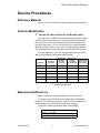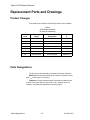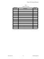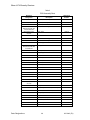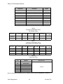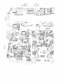
1
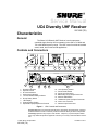
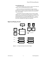
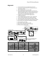
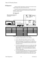
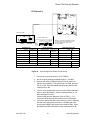
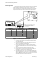
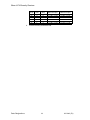
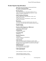
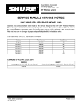
Shure Incorporated
222 Hartrey Avenue
Evanston IL 60202-3696 U.S.A.
UC UHF Wireless System
SERVICE MANUAL CHANGE NOTICE
UC4 DIVERSITY RECEIVER
Changes or corrections have been made to this service manual. Update your service manual by replacing
the pages listed in the table below with the ones attached to this change notice.
CHANGES EFFECTIVE [DATE]
REMOVE
these pages from
your current manual
INSERT
the following revised pages
attached to this notice
Revision 1 pages: ALL
Revision 2 pages: ALL
Revision 2 pages: 14,15,19,20,21,22,26,27 and 30
Revision 3 pages:14,15,19,20,21,22,26,27 and 30
SERVICE MANUAL REVISION HISTORY
Release
Part Number
Date Code
Original
25A1045
RI
Revision 1
25B1045
SB
Revision 2
25C1045
TB
Revision 3
25C1045
TK
E1999, Shure Incorporated
Printed in U.S.A.
Service Manual
UC4 Diversity UHF Receiver
25C1045 (TK)
Characteristics
General
The Shure UC4 Diversity UHF Receiver is a microprocessorcontrolled single diversity receiver operating in the 692 to 716 MHz and
774 to 862 MHz frequency range. The UC4 is used in mid-level installed
sound, rental, and concert sound applications.
Controls and Connectors
A
R
B
1
2
3
4
5
6
7
9
8
10
11
12
13
1.
2.
3.
4.
5.
6.
7.
8.
9.
14
15
17
16
Diversity Indicators
Squelch Control
Rf Level Indicators
Audio Level Indicators
Low Transmitter Battery Indicator
Group Rotary Switch
LED Display
Channel Rotary Switch
Equalization (EQ) Adjustment Controls
10.
11.
12.
13.
14.
15.
16.
17.
Level (Volume) Control
Power On/Off Switch
Power Input Connector
Balanced (LOW Z) Output Connector
MIC/LINE Side Switch
Unbalanced (HIGH Z) Output Connector
LOGIC OUT Connector
Antenna Input Connectors
Figure 1. UC4 Controls and Connectors
Service Note: Shure recommends that all service procedures be performed by a FactoryAuthorized Service Center or that the product be returned directly to Shure Incorporated.
Licensing: Operation may require a user license. Frequency or power-output modifications may violate this product’s approvals. Contact your country’s communications authorities.
E1999, Shure Incorporated
25C1045 (TK)
Printed in U.S.A.
Shure UC4 Diversity Receiver
Circuit Description
The audio circuit and rf circuit description will describe only one
channel because the other channel is identical for both. The local
oscillator (LO) section is common for both channels and will be
described separately.
Audio Section
AUDIO A
4-POLE
AUDIO B
FILTER
LP
COMPANDER
DE-EMPHASIS
TONE
CONTROL
OUTPUT
STAGE
XLR OUT
1/4” OUT
TO AUDIO LEVEL BAR DISPLAY
NOISE A
NOISE B
MARCAD
TONE KEY
DETECTOR
DIVERSITY
CIRCUIT
LOW BATTERY
DETECTOR
MUTING
CIRCUIT
TTL
CIRCUIT
SQUELCH
TTL OUT
Figure 2. UC4 Audio Section Block Diagram
The audio for each channel comes from the appropriate channel
detector output of the rf section. Each channel’s audio then enters its
own adjustable gain stage.
This adjustable gain stage is used to match the audio levels coming
from each rf channel, as well as to set the correct level necessary for the
compander.
From the gain stages, each channel enters an analog switch. Noise
outputs also come from each channel detector outputs. Each noise
output enters a bandpass noise filter that measures the 50 kHz noise
present in the audio signal. The noise level is proportional to the signalto-noise ratio of the channel.
In the MARCAD diversity system, a rectified version of the noise is
sent to a bank of comparators. A version of the channel noise that is 6
dB less also enters the comparators.
The noise from one channel is compared to the noise from the other
to make sure they are within 6 dB of each other. If the noise levels are
within 6 dB of each other, the comparators send a logic high signal to the
control of each channel’s analog switch, allowing the audio to pass
through.
Parts Designations
2
25C1045 (TK)
Shure UC4 Diversity Receiver
If the noise levels are not within 6 dB of each other, the channel with
a noise voltage 6 dB greater than the other channel is not allowed to
pass through the analog switch; that is, the comparator puts a logic
low signal on the control line for the analog switch.
Each channel’s noise is also compared to an adjustable squelch
level; a dc level. If either noise voltage is greater than the squelch
threshold, it is shut off.
The outputs from the analog switches are connected together at the
audio combining stage, a unity gain buffer stage where the audio from
Channel A is combined with the audio from Channel B.
The output from this stage splits into three paths. The first path goes
to a high Q tone key detection circuit. This is a crystal filter in which the
level of tone key is converted to dc and compared against a fixed dc voltage.
The second path enters a low Q bandpass filter centered around 32
kHz. This filter is for low battery detection in the receiver. The lower Q
allows for small frequency variation of tone key from various transmitters,
without the large amplitude variations that the crystal filter would have.
The filtered signal is then rectified and averaged. The dc that is obtained
from this is amplified, triggering a comparator for the low battery LED
display.
The third path is into the compander via a 24 kHz low-pass filter with
a 32 kHz notch. The audio is expanded and de-emphasized here. The
compander output then goes off the board to a high and low frequency
equalization circuit.
A user-adjustable gain stage follows. The signal is then brought
back to the main audio board, where it enters a balanced and unbalanced output stage. The balanced output can be set for either mic or
line level, where the mic level is 30 dB down from the line level.
For the audio level meter, audio is tapped off from the 24 kHz filter’s
output and goes through a full wave precision rectifier and averaging circuit. This dc signal then enters a dc amplifier stage used to adjust levels
for the LEDs.
The output from this stage drives the audio level meter on the front
panel board. For the rf level meters, a dc voltage from the detector chip
for the received signal strength indicator (RSSI) drives the bargraph IC
on the front board.
25C1045 (TK)
3
Parts Designations
Shure UC4 Diversity Receiver
Rf Section
RF CHANNEL A
SECOND
MIXER
FIRST
MIXER
AUDIO A
DIELECTRIC
FILTER
FIRST IF
FILTER
DIELECTRIC
FILTER
LNA
SECOND IF
FILTER
FM
DETECTOR
NOISE A
RSSI A
SECOND LO
FIRST LO
FROM
MICROPROCESSOR
SYNTHESIZER
VCO
LOW PASS
FILTER
AUDIO B
DIELECTRIC
FILTER
LNA
DIELECTRIC
FILTER
FIRST IF
FILTER
SECOND IF
FILTER
FM
DETECTOR
NOISE B
RSSI B
SECOND
MIXER
FIRST
MIXER
RF CHANNEL B
Figure 3. UC4 Rf Section Block Diagram
The rf input signal is provided from the antenna ports to the receiver
by BNC connectors. Antenna port A is connected to J101 (channel A),
and antenna port B is connected to J201 (channel B).
The rf circuit description will describe only one channel because the
other rf channel is identical. The local oscillator (LO) section is common
for both channels and will be described separately.
Rf Channel
The rf signal is pre-selected to the 782 – 806 MHz frequency range
with two dielectric filters. The first dielectric filter is located between the
antenna port and the low noise amplifier (LNA). The second filter is
located between the LNA block and mixer input.
The LNA and the first mixer consist of a dual gate GaAs MOSFET.
The first conversion gives the first intermediate frequency (IF) signal at
50 MHz.
The first IF signal is amplified with MMIC, band limited with a SAW
filter, and then down-converted to the second intermediate frequency (IF)
at 10.7 MHz with a second down-converter.
The second IF signal is filtered by 10.7 MHz ceramic filters and
amplified by a 10.7 MHz pre-amp (Q105).
The 10.7 MHz signal goes to the second IF gain block with a
detector. The audio output is buffered and then processed as stated in
the audio section circuit description. The noise output is amplified to provide signal for the noise squelch circuitry. The Received Signal Strength
Indication (RSSI) output of the detector drives the LEDs that are located
on the receiver’s front panel.
Parts Designations
4
25C1045 (TK)
Shure UC4 Diversity Receiver
Local Oscillator (LO)
The first local oscillator (LO) is common for channel A and channel B
rf strips. The LO is a phase-locked loop (PLL) system.
The PLL consists of a prescaler/synthesizer, voltage-controlled
oscillator (VCO), a loop filter, a VCO, an rf power divider, and a bandpass
filter. The PLL limits the LO signal before injection to the first down converter, Q102 and Q202.
The prescaler receives the rf signal from the VCO via the coupling
capacitor, C333. The output from the phase detector is connected to an
external loop filter that controls the tuning voltage input to the VCO. The
prescaler/synthesizer IC is a serial-programmable input IC. It receives
the frequency programming data from the microprocessor, which is set
by the user, as described in the digital circuit description.
Digital and Display Section
EEPROM
SHIFT
REGISTER
ROTARY
SWITCH
(CH)
SHIFT
REGISTER
MICROPROCESSOR
ROTARY
SWITCH
(FREQ)
TO SYNTHESIZER
AUDIO
LED DRIVER
7 LED BAR
RSSI A
LED DRIVER
5 LED BAR
RSSI B
LED DRIVER
5 LED BAR
Figure 4. UC4 Digital and Display Section Block Diagram
25C1045 (TK)
5
Parts Designations
Shure UC4 Diversity Receiver
Microcontroller
The microcontroller section consists of a U703 microcontroller and a
two digit, seven segment, LED display.
The LED display indicates frequency in terms of compatible channels
in a group. The LED display on the left indicates the current group. The
LED display on the right indicates the channel. Each LED is capable of
displaying digits 0 – 9. However, the channel LED also displays alpha
letters A – F.
Serial shift registers, U705 and U705, latch the current LED display.
A serial Load Enable (LE) signal of the display driver section is also
shared with the rf interface section.
A 4.0 MHz oscillator, Y701, provides the operating frequency to the
microcontroller. The oscillator circuit includes capacitors C702, C703,
with the crystal oscillator, Y701.
Resistor R704, C704, and U702 make up the reset circuit. The
microcontroller is reset if the supply voltage to it drops below 4.3 Vdc.
Memory
The memory section consists of U701, a non-volatile Electrically
Erasable and Programmable Read Only Memory (EEPROM). The
EEPROM stores the mapping of the compatible groups and channels
with respect to rotary switch positions.
The microcontroller serially communicates with the memory via data
and clock lines to read the frequency corresponding to the group and
channel position. Write to the memory only occurs during factory programming. During normal usage, this memory is used as a look-up table
only.
Resistors R702 and R703 allow in-circuit programming of the U701
EEPROM by letting data and clock lines be driven independently of the
microcontroller port pin states. R701 is the pull-up resistor for the data
line.
Audio / Rf Interface
The OUT ENAB signal gives the microcontroller the ability to mute
the audio during turn on and off, and frequency changes.
The microcontroller sets the phase-lock loop (PLL) to the required
signal using the DATA signal (U703, pin 12) to send the frequency initialization and set-up data. This data is clocked into the PLL by the microcontroller through the CLOCK signal (U703, pin 12) and the Load
Enable (LE) signal (U703, pin 10). The LE signal loads the clocked data
into a PLL’s internal registers to initialize and set the frequency.
Parts Designations
6
25C1045 (TK)
Shure UC4 Diversity Receiver
Rotary Switches for Frequency Selection
A 10-position group switch (S701) and a 16-position channel switch
(S702) select the receiver frequency. The current position of these
switches is displayed on the 7-segment LED display. Both rotary
switches share the same U703 microcontroller port pins (3 through 6)
for a multiplexed switch read operation.
The individual switches are selected by pins 7 and 8 of the U703
microcontroller. Resistors R705 through R708 are the pull-ups for switch
position read. Dual diodes D701 through D704 isolate the switches during multiplexed read operation.
The multiplexed scheme to read switches does not allow switch
change detection based on interrupts. Also, the switches cannot be
constantly scanned to determine changes because the scanning frequency is in audio range, which makes it hard to filter out.
In a steady state, the switch common pins are inputs to pins 7 and 8
of the U703 microcontroller, while pins 3 through 6 of the microcontroller
are outputs In this state, pins 4, 5, and 6 are held low which pin 3 is held
high. This forces the logic high level on switch common pins if the
switches are set on odd positions. For even position settings, the contact
on pin 1 is open from the switch common pin, and the internal pull-down
resistors force logic low to the U703 microcontroller, pins 7 and 8.
Any switch change is done by state toggle from odd to even, or vice
versa. Only this change is detected and followed by a multiplexed switch
read. In this case, U703 microcontroller pins 7 and 8 selectively become
grounded outputs to read the selected switch’s state on pins 3 through 6.
A multiplexed switch read is preceded by an audio mute. The
receiver audio is muted to allow a quiet change to another frequency.
Power Switch Interface
When a receiver is switched off, the MT signal goes to logic low on
U703, pin 19. This interrupts the microcontroller to immediately mute the
audio so that the receiver turns off without any audio pop.
25C1045 (TK)
7
Parts Designations
Shure UC4 Diversity Receiver
Notes
This page intentionally left blank.
Parts Designations
8
25C1045 (TK)
Shure UC4 Diversity Receiver
Functional Test
Verify operation and reported malfunction, referring to the product
User’s Guide for a description of the unit as well as information on its
operation, troubleshooting, and technical data.
Disassembly and Assembly
! CAUTION !
Observe precautions when handling this static-sensitive device.
Disassembly
Top Cover Removal
1. Remove two screws and washers each from the top, left, and
right sides of the receiver (6 screws).
2. Slide the top cover off of the receiver to expose the circuit
boards.
Front Panel Removal
1. Pull up on the top two tabs to partially release the front panel
from the chassis.
2. With a thin tool and the unit upside down, pry the front panel
away from the chassis at the two slots located on the bottom
of the front panel.
3. With the front panel disengaged from the chassis, carefully pull
the front panel away from the chassis.
Printed Circuit Board Removal
1. Pull the power knob off the power switch.
2. Disengage the front four standoffs from the chassis by pinching
the standoff ends, which will free the front circuit board.
3. Except for the dc power receptacle, remove all screws, nuts, and
washers from the back of the unit.
4. Unplug the connector between the dc power receptacle and the
circuit board.
5. Remove the remaining five screws that secure the circuit board.
6. Raise the front of the circuit board to clear the chassis; then
move the circuit board forward to free the rear components and
lift the circuit board out.
25C1045 (TK)
9
Parts Designations
Shure UC4 Diversity Receiver
Reassembly
1. Insert the rear circuit board components into their mating chassis
holes, and lower the circuit board into its correct position.
2. Secure the circuit board with the previously removed screws.
3. Plug in the connector between the dc power receptacle and the
circuit board.
4. Replace all previously removed screws, nuts, and washers to the
back of the unit.
5. Snap the front circuit board with standoffs into the chassis front.
6. Push the power knob in to snap it back onto the power knob
shaft.
7. Line up the front panel, and push the front panel toward the
chassis. Make sure the ribbon cables are positioned to clear
light pipes.
8. Latch both bottom and top tabs to the front of the chassis.
9. Slide the top cover onto the chassis until the cover is tight
against the front panel.
10. Secure the top cover with the previously removed screws.
Parts Designations
10
25C1045 (TK)
Shure UC4 Diversity Receiver
Service Procedures
Reference Material
Refer to the Service Equipment Manual for standard test equipment.
Optional Modification
“F” Version (Or Later) Printed Circuit Boards (pcbs)
The UC4 can be modified to match different gain structures required
by different Shure UHF transmitters. There are two types of gain structure in the UC4 in which one has more gain in the output stage and in
the audio LED circuitry. The UC4 can work with a U-series transmitter,
although the battery meter circuitry is not compatible between systems.
The modification in the table below alters the UC4 audio and LED gain.
To modify different UC receivers, check the label on the UC4 and
add or remove parts according to the following table:
PCB Label
Reference
Designator
Place for Use
with UC
Transmitter
Group A
Place for Use
with UC
Transmitter
Group B,C,D,E
LED
R602
X
LED
R647
X
GAIN
R651
X
GAIN
R648
X
GAIN
R649
X
GAIN
D604
X
Place for Use
with U-series
Transmitters
X
These modifications can only be done on
“F” version (or later) pcbs.
Measurement Reference
dBu is a measure of voltage, and dBm is a measure of power.
For example, the HP8903 should be labeled dBu instead of dBm
because it is a voltage measurement. These two terms are often used
interchangeably even though they have different meanings.
Audio levels in dBu are marked as dBm on the HP8903.
dB Conversion Chart
0 dBV = 2.2 dBu
0 dBu = 0 dBm, assuming the load = 600 Ω
25C1045 (TK)
11
Parts Designations
Shure UC4 Diversity Receiver
Test Equipment
Most test equipment needed is described in the Shure Wireless
Service Equipment Manual. The following test equipment (or approved
equivalent) is also needed.
Table 1
Test Equipment
Equipment Type
Model
Audio analyzer
*Hewlett-Packard 8903B
Digital multimeter
Fluke 87
Rf signal generator
Hewlett-Packard 8656B
Frequency counter
Hewlett-Packard 53181A
Spectrum analyzer
Hewlett-Packard 8591
Shure UC transmitter
Shure UC1 / UC2
*Audio levels in dBu are marked as dBm on the HP8903B.
Test Equipment Set-Up
The alignment procedure is sequential and does not change,
unless specified.
1. Use RG58 or any low loss, 50 Ω cables for all rf connections.
2. Keep the test cables as short as possible.
3. Include the insertion loss of the cables and connectors for all rf
measurements.
4. Dc voltages may be present at rf test points. As a precaution,
use dc blocks to protect the test equipment
Parts Designations
12
25C1045 (TK)
Shure UC4 Diversity Receiver
Test Set-Up
J501
S601
J201
J601
J101
TPRF3
TPRF2
FL201
J602
C622
C624 C623
FL101
LABEL
J901
C621
C627
C605
U605
C610
C611
D901
U601
C319
C618
TK ON
C318
TK OFF
U603
S501
C601 C602
C513
FL205
FL105
TP36
C504
C603
U406
U403
TPB6
U501
U405
TPA6
C418
D402
C502
C316
U404
C509
TPRF1
U301
C147
U402
FL116
C3301
FL216
R125
C239
C330
C606
C403
FL115
FL218
R405
C401
FL119
U101
U703
+
Y701
U902
+
FL117
U701
*
C908
*
C904
C236
C139
C906
U602
+ 10 V**
FL217
Y302
C607
FL219
U201
C903
TPA5
R406
U901
C323
U401
+ 5 V**
J402
R225
Y301
FL215
TPB5
FL112
J401
C336
D902
Y501
U303
FL212
C404
FL118
C136
C905
S901
* F version and earlier
** G version and later
Figure 5. UC4 Major Test Component Locations
1. Install the receiver antennas.
2. Set the receiver to any unused frequency in the area. Select a
television channel that is inactive in the area and then scan for a
frequency at which the yellow LEDs are not lit. Note this as the
operating frequency, “f 0”.
3. Remove the top cover from the receiver.
25C1045 (TK)
13
Parts Designations
Shure UC4 Diversity Receiver
Table 2 lists the group and channel switches, and the
operating frequencies for all the tests that follow.
Table 2
Group Carrier Frequencies
(in order by carrier frequency)
Parts Designations
Group
Group
Code
Group
Switch
(S302)
Channel
Switch
(S301)
Operating
Frequency
“f 0” (MHz)
UA
A
8
8
798.125
UB
G
8
8
707.625
MB
B
8
8
808.375
MC
F
8
8
779.500
MD
B
8
8
808.500
JB
D
3
3
807.375
KK
E
8
8
847.500
14
25C1045 (TK)
Shure UC4 Diversity Receiver
Alignment
1. Connect the UC4 receiver as shown below in Figure 6.
2. Connect the rf signal generator EXT modulation input to the
audio analyzer output.
3. Set the rf signal generator for external FM.
4. Set the audio analyzer’s output impedance to 50 ohms and
adjust audio signal amplitude in small increments until both the
HI EXT and LO EXT lights on the rf signal generator turn off.
This should occur at an amplitude of about 1.43 V.
5. Engage the audio analyzer’s 400 Hz high-pass and
30 kHz low-pass filters.
6. Set the rf signal generator deviation as given in table below.
7. Turn the volume potentiometer full clockwise (maximum).
8. Set the Group select switch (red knob) according to Table 2.
9. Set the Channel select switch (black knob) according to Table 2.
10. Set the low EQ full clockwise and set high EQ to mid-range.
11. Set the squelch to mid-range.
12. Set the MIC / LINE output switch to LINE.
13. Apply 15 Vdc to the power input of the receiver.
14. Turn the tone key switch to OFF.
UC4 RECEIVER (FRONT)
A
B
SQUELCH
UC4 RECEIVER (BACK)
S501
(TONE KEY SWITCH)
TK ON
TK OFF
AUDIO ANALYZER
RF SIGNAL GENERATOR
NOTE: DC VOLTAGES ARE PRESENT AT MOST
RF TEST POINTS. USE A DC BLOCK ON THE
RF SIGNAL GENERATOR TO PROTECT
TEST EQUIPMENT.
UC4 Receiver
Audio Analyzer
Output: Unbalanced
Gain: Maximum
Squelch: Mid
Measurement: AC level
Output amplitude: 1.43 V
Frequency: 1 kHz
Tone Key (S501): OFF
Filters:
Group switch: See Table 2
Low-Pass (30 kHz): ON
Channel switch: See Table 2
High-Pass (400 Hz): ON
Rf Signal Generator
EXT: FM
INT: OFF
Output amplitude: –108 dBm
Frequency: See Table 2
Deviation:
UA,UB,MB,MC,MD: 45 kHz
JB: 27.7 kHz
KK: 15 kHz
Figure 6. Alignment Test Set-Up
25C1045 (TK)
15
Parts Designations
Shure UC4 Diversity Receiver
Power Section
Checking the dc power will insure the correct dc biasing
is applied to the operating circuits.
AUDIO ANALYZER
+10 V
C904
CHASSIS GND
C908
UC4 Receiver
Power: ON (+15 Vdc)
Operating freq: See Table 2
Audio Analyzer
Connect + : F version and earlier:
C904 (+ side)
C908 (+ side)
G version and later:
+10 V
+5 V
Connect – : GND (chassis)
Figure 7. UC4 Power Section Test Set-Up
1. For “F” and earlier pcb versions, measure +10.0 Vdc ± 0.2 Vdc at
the + side of C904 (10 V regulator out).
For “G” and later pcb versions, measure +10.0 Vdc ± 0.2 Vdc at
the test pad labeled + 10 V.
2. For “F” and earlier pcb versions, measure +5.0 Vdc ± 0.2 Vdc at
the + side of C908 (5 V regulator out).
For “G” and later pcb versions, measure +5.0 Vdc ± 0.2 Vdc at
the test pad labeled + 5 V.
3. Measure the dc current drain from +15 V supply with the amp
meter. It should be less than 500 mV.
Parts Designations
16
25C1045 (TK)
Shure UC4 Diversity Receiver
Local Oscillator
Performing the local oscillator alignment insures that the unit is finetuned to the operating frequency selected by the user. Adjusting C3301
controls the voltage-controlled oscillator (VCO) tuning voltage and the
synthesizer reference frequency.
TPRF1
FREQUENCY COUNTER
CH 2
C3301
CH 1
UC4 Receiver
Frequency Counter
Power: ON (+15 Vdc)
Operating freq: See Table 2
Operating freq: See Table 2
Connect CH 2: TPRF1 and GND
Channel switch: See Table 2
Group switch: See Table 2
Figure 8. UC4 Local Oscillator Test Set-Up
1. Use a BNC to rocket cable or a shield test lead to attach a spectrum analyzer or frequency counter to TPRF1. (Remove sheild
top cover to access test point TPRF1.)
2. Adjust C3301 for (f 0 + 50 MHz) ± 5.0 kHz. If using a spectrum
analyzer, adjust the span so the frequency accuracy measurement is better than 5 kHz. (Refer to the instrument manual.)
25C1045 (TK)
17
Parts Designations
Shure UC4 Diversity Receiver
Rf Alignment
Channel A and B rf alignments are performed to increase the input
signal strength of the receiver and filter out noise.
Tuning FL115 and FL215 maximizes the rf sensitivity (input signal
strength). Tuning FL119 and FL219 minimizes the fm detector’s total
harmonic distortion (THD).
Rf Channel B
NOTE: DC VOLTAGES ARE PRESENT AT MOST
RF TEST POINTS. USE A DC BLOCK ON THE
RF SIGNAL GENERATOR TO PROTECT
TEST EQUIPMENT.
J101
TPRF3
AUDIO ANALYZER
TPA5
RF SIGNAL GENERATOR
FL119
FL115
UC4 Receiver
Audio Analyzer
Output: Unbalanced
Gain: Maximum
Squelch: Mid
Tone Key (S501): OFF
Measurement:
Rf Signal Generator
EXT: FM
SINAD/LOG-LIN
DISTN/RATIO
Output amplitude: 1.43 V
Frequency: 1 kHz
Filters:
INT: OFF
Output amplitude: –106 dBm
Frequency: See Table 2
Low-Pass (30 kHz): OFF
High-Pass (400 Hz): OFF
A weighting ON
Figure 9. UC4 Rf Alignment Channel B Test Set-Up
1. Connect the rf signal generator to J101 (TPRF3).
2. Set the rf signal generator amplitude output to –106 dBm.
3. Measure the audio at TPA5 and adjust FL115 for maximum
signal-to-noise (SINAD). The typical level is 12.0 dB; the lower
limit is 8.0 dB. Press the SINAD and LOG-LIN buttons for this
measurement in dB.
4. Turn off the A weighting filter and turn on the 30KHz and 400Hz
filters on the audio analyzer. Set the rf signal generator to –60
dBm and adjust FL119 for minimum total harmonic distortion
(THD) at TPA5 (≤ .7%). Press the DISTN button for this measurement in percentage.
5. Turn off the 30KHz and 400Hz filters and turn on the A weighting
filter. Set the rf signal generator back to –106 dBm and make
sure that the SINAD is still greater than 8.0 dB at TPA5. Press
the SINAD and LOG-LIN buttons for this measurement in dB.
Parts Designations
18
25C1045 (TK)
Shure UC4 Diversity Receiver
Rf Channel A
J201
TPRF2
TPB5
FL219
FL215
AUDIO ANALYZER
RF SIGNAL GENERATOR
NOTE: DC VOLTAGES ARE PRESENT AT MOST
RF TEST POINTS. USE A DC BLOCK ON THE
RF SIGNAL GENERATOR TO PROTECT
TEST EQUIPMENT.
UC4 Receiver
Audio Analyzer
Output: Unbalanced
Gain: Maximum
Squelch: Mid
Measurement:
Rf Signal Generator
EXT: FM
SINAD/LOG-LIN
DISTN/RATIO
Output amplitude: 1.43 V
Frequency: 1 kHz
Tone Key (S501): OFF
Filters:
Frequency: See Table 2
Group switch: See Table 2
Low-Pass (30 kHz): ON
Channel switch: See Table 2
High-Pass (400 Hz): ON
A weighting:
INT: OFF
Output amplitude: –106 dBm
Deviation:
UA,UB,MB,MC,MD: 45 kHz
ON
JB: 27.7 kHz
KK: 15 kHz
Figure 10. UC4 Rf Alignment Channel A Test Set-Up
1. Connect the rf signal generator to J201 (TPRF2).
2. Set the rf signal generator amplitude output to –106 dBm.
3. Measure the audio at TPB5 and adjust FL215 for maximum
signal-to-noise (SINAD). The typical level is 12.0 dB; the lower
limit is 8.0 dB. Press the SINAD and LOG-LIN buttons for this
measurement in dB.
4. Turn off the A weighting filter and turn on the 30KHz and 400Hz
filters on the audio analyzer. Set the rf signal generator to –60
dBm and adjust FL219 for
minimum total harmonic distortion (THD) at TPB5 ( .7%).
Press the DISTN button for this measurement in percentage.
5. Turn off the 30KHz and 400Hz filters and turn on the A weighting
filter.Set the rf signal generator back to –106 dBm and make
sure that the SINAD is still greater than 8.0 dB at TPB5. Press
the SINAD and LOG-LIN buttons for this measurement in dB.
25C1045 (TK)
19
Parts Designations
Shure UC4 Diversity Receiver
Audio Alignment
Audio alignment insures that the compressor output in the transmitter
exactly matches the expander input in the receiver. If these do not
match, mistracking occurs and the audio signal between the transmitter
output and the receiver input does not have the same characteristics.
J201
J101
TPA6
CHASSIS
GND
TPB6
R406
R225
R405
R125
AUDIO ANALYZER
RF SIGNAL GENERATOR
NOTE: DC VOLTAGES ARE PRESENT AT MOST
RF TEST POINTS. USE A DC BLOCK ON THE
RF SIGNAL GENERATOR TO PROTECT
TEST EQUIPMENT.
UC4 Receiver
Audio Analyzer
Output: Unbalanced
Gain: Maximum
Squelch: Mid
Frequency: 50 kHz
Tone Key (S501): OFF
Rf Signal Generator
Measurement: DC level,
dB or mV
Output amplitude: 1.43 V
Filters:
Group switch: See Table 2
Low-Pass (30 kHz): ON
Channel switch: See Table 2
High-Pass (400 Hz): ON
EXT: FM
INT: OFF
Output amplitude: –60 dBm
Frequency: See Table 2
Deviation:
UA,UB,MB,MC,MD: 45 kHz
JB: 27.7 kHz
KK: 15 kHz
Figure 11. UC4 Audio Alignment Test Set-Up, part 1
1. Connect the audio analyzer to the external modulation input of
the rf signal generator.
2. Set the input measurement of the audio analyzer for AC level
and turn on the 30KHz and 400Hz filters.
3. Set the rf signal generator to –60 dBm and 45 kHz deviation
externally modulated with 50 kHz tone from the audio analyzer
output.
4. Apply an rf signal to the channel A antenna port (J201).
5. Put the positive (+) terminal of the dc voltmeter on TPB6, and
the negative (–) terminal to any rf chassis ground.
6. Adjust R225 for 6.00 Vdc ± 0.03 V for raw PCB 34A8580G and
earlier. Adjust R225 for 2.5 Vdc ±0.03 V for raw PCB 34A8580H
and later. Note this raw PCB number is printed on the rear of the
main PCB between the the antenna connectors.
Parts Designations
20
25C1045 (TK)
Shure UC4 Diversity Receiver
7. Apply the rf signal to the antenna port of channel B (J101).
8. Put the positive (+) terminal of the dc voltmeter on TPA6, and
the negative (–) terminal to any rf chassis ground.
9. Adjust R125 for 6.00 Vdc ± 0.03 V for raw PCB 34A8580G and
earlier. Adjust R125 for 2.5 Vdc ±0.03 V for raw PCB 34A8580H
and later. Note: this raw PCB number is printed on the rear of
the main PCB between the the antenna connectors.
NOTE: DC VOLTAGES ARE PRESENT
AT MOST RF TEST POINTS. USE A
DC BLOCK ON THE RF SIGNAL
GENERATOR TO PROTECT
TEST EQUIPMENT.
J201
J101
CHASSIS
GND
J602
TP36
TPA6
AUDIO ANALYZER
TPB6
R406
R225
RF SIGNAL GENERATOR
R405
UC4 Receiver
Audio Analyzer
Output: Unbalanced
Rf Signal Generator
Measurement: AC level,
dB or mV
Output amplitude: 1.43 V
Gain: Maximum
Squelch: Mid
EXT: FM
INT: OFF
Frequency: 1 kHz
Tone Key (S501): OFF
R125
Output amplitude: –60 dBm
Filters:
Frequency: See Table 2
Group switch: See Table 2
Low-Pass (30 kHz): ON
Channel switch: See Table 2
High-Pass (400 Hz): ON
Group
UA
Group Code
A
Tuning Deviation
(kHz)
45
TP36
(dBu ± 0.1 dB (mV) )
–6.8 (354)
UB
G
45
–6.8 (354)
MB / MD
B
45
–6.8 (354)
MC
F
45
–6.8 (354)
JB
D
27.7
–8.5 (292)
KK
E
15
–15.3 (133)
Figure 12. UC4 Audio Alignment Test Set-Up, part 2
1. Set the audio analyzer frequency to 1 kHz and readjust the
amplitude to the reading given in the table above.
2. Put the positive (+) terminal of an RMS ac voltmeter in the audio
analyzer on TP36, and the negative (–) terminal to any rf chassis
ground.
3. Adjust R405 for the reading given in the table above.
4. Apply the rf signal back to channel A.
5. Adjust R406 until the ac voltmeter gives the reading in the table
above.
6. Set the UC4 balanced output to line level using the Mic/Line switch.
7. Measure the audio level at the balanced line–level output using
the following table:
25C1045 (TK)
21
Parts Designations
Shure UC4 Diversity Receiver
Group
UA
UB
Group
Code
A
G
Deviation
(kHz)
30
30
1 kHz Audio
Balanced Output
+6.7 dBu ± 2.0 dB
+6.7 dBu ± 2.0 dB
1 kHz Audio
Unbalanced Output
+0.2 dBu ± 2.0 dB
+0.2 dBu ± 2.0 dB
MB, MD
MC
JB
KK
B
F
D
E
10
10
10
10
–11.6 dBu ± 2.0 dB
–11.6 dBu ± 2.0 dB
+7.3 dBu ± 2.0 dB
–9.7 dBu ± 2.0 dB
–18.1 dBu ± 2.0 dB
–18.1 dBu ± 2.0 dB
+0.8 dBu ± 2.0 dB
–16.2 dBu ± 2.0 dB
8. Turn the tone key switch back ON.
Parts Designations
22
25C1045 (TK)
Shure UC4 Diversity Receiver
Product System Specifications
After tuning, the unit should meet the following specifications.
RF Carrier Frequency Range
774–862 MHz (782–806 MHz for U.S. models).
Working Range
152.4 m (500 ft), minimum, under typical conditions; 487.6 m
(1600 ft ) line of sight. Actual working range depends on rf signal
absorption, reflection, and interference
Audio Frequency Response
The audio output level at 100 Hz should be + 8.5 dB ± 2 dB
relative to the 1 kHz level.
The audio output level at 10 kHz should be – 18.5 dB ± 2 dB
relative to the 1 kHz level.
Modulation
±45 kHz deviation compressor-expander system with pre-and
de-emphasis (domestic models only; international models may vary).
Dynamic Range
>100 dB, A-weighted
Receiver Audio Output Level (Maximum)
+5 dBu typical, unbalanced output
+14 dBu typical, balanced output
Rf Sensitivity
–108 dBm at 12 dB SINAD
Image Rejection
90 dB typical
Spurious Rejection
70 dB typical
Ultimate Quieting (ref. 45 kHz deviation)
>100 dB, A-weighted
Audio Polarity
Positive pressure on microphone diaphragm (or positive voltage
applied to tip of WA302 phone plug) produces positive voltage on pin 2
with respect to pin 3 of low impedance output and the tip of the high
impedance 1/4-inch output
System Distortion
(ref. ±45 kHz deviation, 1 kHz modulation)
0.4% Total Harmonic Distortion typical
Power Requirements
15 Vdc , 600 mA 50/60 Hz
Power consumption: 600 mA x 15 V, maximum
Transmitter battery life (typical): 8 hours
(with Duracell MN1604 9V alkaline battery)
25C1045 (TK)
23
Parts Designations
Shure UC4 Diversity Receiver
Bench Checks
Set-Up
Dc voltages are present at most rf test points. Use dc blocks to
protect the test equipment, if necessary.
Use RG58 or any other low loss 50 Ω cables for all rf connections.
Keep the test cables as short as possible. Include insertion loss of
cables and connectors when making rf measurements. The following is
an example of a bench check procedure for the UC4–UA. For all other
UC4 models substitue respective settings and measurement values
found in the alignment procedures.
786.250 MHz will be used as the operating frequency
(“f 0”) in the following procedures.
n Set the Group and Channel switches to 0.
n Use the following settings:
Squelch:
Center
Low Frequency Control:
Maximum
High Frequency Control:
Center
Volume:
Maximum
n Set the MIC / LINE switch to LINE position.
n Set the tone key switch (S501) to OFF.
n Apply an rf signal of 786.250 MHz to J201 (CHA antenna jack) at
a level of –60 dBm. FM modulate the carrier 45 kHz with 1 kHz
audio.
No Power
n With the power supply connected, verify +15 V ± 1 V, as labeled
on the pcb. If this voltage is incorrect, try another power supply.
n If +15 V is correct, verify regulated +10 V and +5 V. If these are
incorrect, check the surrounding regulator circuitry for solder
shorts, solder deficiencies, backward diodes and capacitors.
If this is inconclusive, replace the corresponding regulator.
No Audio
n Check for audio at the detector output, U201, pin 15. If there is
no audio there, the problem is in the rf section.
n If audio is detected and the audio LEDs are lit, the problem is
occurring after the expander, U601. Follow the audio path from
this point until the point of discontinuity is found and replace the
corresponding part (s).
Parts Designations
24
25C1045 (TK)
Shure UC4 Diversity Receiver
n If audio is detected and the audio LEDs are NOT lit, there are
two possibilities. Either there is a break in the audio chain somewhere between the detector (U201) and the expander (U601), or
the audio muting circuitry is engaged.
No Rf
n Check for the first intermediate frequency (IF) signal at the output
of the SAW filter (FL112/FL212, pin 1). If there is no 50 MHz IF
signal, check to see if the first LO frequency at TPRF1 Is f 0 ±
50 MHz.
n If the first LO frequency at TPRF1 is NOT correct, there are three
possibilities: the voltage controlled oscillator (VCO) is bad;
synthesizer failure; or a microprocessor problem.
n If the first LO frequency at TPRF1 is correct, trace the front–end
amplifier (Q101/Q201), the first mixer (Q102/Q202), and the first
IF amplifier (U103/U203).
n If the 50 MHz first IF signal is present, check the 10.7 MHz
second IF at the input of the FM detector (U101/U201, pin 1).
n If there is no 10.7 MHz signal, check the second LO frequency at
TPA9/TPB9.
n If the second LO frequency is NOT present, check the crystal,
Y302, and the second LO circuitry.
n If the second LO frequency is correct, check the second mixer
(Q104/Q204) and the second IF amplifier (Q105/Q205).
n If there is a 10.7 MHz signal at the input of the FM detector,
check the FM detector IC (U101/U201) and the surrounding
parts. Replace them, if necessary.
25C1045 (TK)
25
Parts Designations
Shure UC4 Diversity Receiver
Replacement Parts and Drawings
Product Changes
Five variations of the Shure UC4 Diversity Receiver are available.
Table 3
UC4 Model Variations
(in order by frequency)
Country
Code
Frequency
Range
Country
Designation
PCB
#
UA
782–806 MHz
U.S.A. and Canada
90UA8793
UB
692–716 MHz
U.S.A.
90UB8793
MB
800–830 MHz
Europe
90MB8793
MC
774–782 MHz
Netherlands
90MC8793
MD
800–820 MHz
Scandanavia
90MD8793
JB
806–810 MHz
Japan
90JB8793
KK
838–862 MHz
United Kingdom
90KK8793
Parts Designations
The following comments apply to the parts list and the schematic:
Resistors: Unless otherwise noted, all resistors are surface-mount
with 1/10 W rating and 1% tolerance.
Capacitors: Unless otherwise noted, non-polarized capacitors are
surface-mount NPO dielectric types with a 100 V capacity and a 5%
tolerance, and polarized capacitors are tantalum types.
Parts Designations
26
25C1045 (TK)
Shure UC4 Diversity Receiver
Table 4
Replacement Parts
Reference
Designation
25C1045 (TK)
Description
Shure Part
Number
A1
Cable/connector assembly, dc
90B8688
A2
Front panel assembly
90A8765
A3
Front panel and lens assembly
90A8810
MP1
Metal chassis
53A8506
MP3
Top Cover
53A8474
MP4
Front panel
65A8305
MP5
Gasket
36A8076
MP6
Knob, power
65A8302
MP7
Knob, volume
90A8764
MP8
Lens
65A8309
MP9
Light pipe
65A8306
MP10
RF cover shield
53A8467
MP11
Screws, hardware
RPW626
MP12
Long rack mounting bracket
53A8481
MP13
Short rack mounting bracket
53A8459
MP14
Link bar (for mounting two UC4’s togather)
31A8138
27
Parts Designations
Shure UC4 Diversity Receiver
Table 5
PCB Assembly Parts
Reference
Designation
C333
C623,624,627
C3301
Description
Capacitor, 100 V, 8.2 pF
Capacitor, electrolytic, 47 x 63 V
Shure Part
Number
150DB828CA
86BE629
Capacitor, trim
152D02
Diode, dual switching
184A08
LED, green
184E18
LED, red
184A18
Diode, dual switching, SMD, SOT-23, 1 V
184A07
Diode, dual switching
184A07
D705
LED display
86A8442
D801,802,803,804,
805,806,807,808,809,
810,815,816
LED, yellow
184D18
Diode, power, rectifier, silicon, 1.1 V
184A20
Surge suppressor
184A34
D401,402,403,404,407,
408,409,410,501,502,
503,601,602,905
D405,406,811,812,
813,814
D504,817
D603,701,702,703,704
D701,702,703,704
D901,902
DZ999
FL101,105,201,205
Filter, dielectric
(See table 6)
*140–07
FL102,107,202,302,303
Inductor, 15 nH SM
162N06
FL103,108,203,207,208
Inductor, 22 nH SM
162S06
FL104,204
Inductor, 8.2 nH SM
162W10
FL106,206
Inductor, 18 nH SM
162M06
FL109,209
Inductor, 470 nH SM
162V06
FL111,211
Inductor, 330 nH SM
162W06
FL112,212
Filter, saw
80A8195
FL113,213,305,306
Inductor, 220 nH SM
162C06
FL114,214
Inductor, 390 nH SM
162Y06
FL115,215
Coil, tunable
82A8005
Filter, ceramic
86A8971
FL119,219
Coil, quadrature
82A8004
FL301
Filter, low pass
FL304
Inductor, 150 nH SM
162E06
J101,201
BNC jack, pcb mount, 50 Ω
95A8631
J401,402
Pin jack
95A8278
J501
Header, block, 3 pin
95A8579
J601
Connector, XLR
95A8598
J602
1/4”Jack, phone
95A8104
J901
Header
95A8272
FL116,117,118,216,
217,218
Parts Designations
28
(See table 7)
*162–17
25C1045 (TK)
Shure UC4 Diversity Receiver
Reference
Designation
Description
L101,102,103,104,105,
Ferrite Bead
201,202,203,204,205,301,
302,303,304,305,306,307,
308,501,502,601,602,603,
604,903
162A12
L152,252,352,353
Inductor
162N06
L153
Inductor
162L06
L154,254
Inductor
162W10
L156,256
Inductor
162M06
L157,253,257
Inductor
162S06
L159,259
Inductor
162V06
L163,263
Inductor
162W06
L164,264
Inductor
162Y06
Ferrite Bead
162A30
Transistor, Dual Gate GaAs MESFET N
183A12
Microwave Isolator
183A37
Q105,205,301,302
Transistor, NPN
183A17
Q303,304,305
Transistor, NPN
183A14
Q306,502,503,504
Transistor, NPN
183A24
Q603,604,605,606
Transistor, SMD, SOT-34, FET, TMOS
183A30
R125,225,405,406
Potentiometer, trim, 5 k
146D02
R4401,6602
Potentiometer, 100 k
46D8048
R6601
Potentiometer, 10 k
46A8048
R6603
Potentiometer, 10 k
46A8069
S501
Tone key Switch, slide
55A168
S601
Mic/Line Switch, slide, DPST
55A8061
S701
Group Switch
55B8121
S702
Channel Switch
55A8121
S901
Power Switch
55A8062
U101,201
Quad Detector, SMT, FM, IF
188A190
U103,203
IC amp, monolithic microwave
183A37
VCO
*187–04
LF901,902
Q101,102,104,
201,202,204
Q103,203
U301
U302,602
(See table 6)
Regulator, 5 V 180 mA
188A115
Serial Input PLL Freq Synthesizer
188A265
U401,402
IC Quad Op Amp
188A49
U403,501
IC Quad Comparator, ultra-low power
188A123
IC quad switch / multiplexer
188A19
IC amp, dual op
188A18
U601
IC Compandor, low voltage
188A126
U702
Under Voltage Reset
188C210
U303
U404
U405,406.603,604,605
25C1045 (TK)
Shure Part
Number
29
Parts Designations
Shure UC4 Diversity Receiver
Reference
Designation
Shure Part
Number
Description
U704,705
8 Bit Serial in Parallel Out Shift Register
188A216
Bargraph, Linear Display Driver
188A86
U804
Comparator, Dual Voltage SM
188A136
U901
Voltage Regulator, 10 V, 1 A
86A8918
U902
Voltage Regulator, IC
86B8930
Y301
Crystal, 24.0 MHz, XTAL
40A8016
Y302
Crystal, 60.7 MHz, XTAL
40A8013
Y501
Crystal, 32.768 kHz, XTAL
40A8010
Y701
Crystal, 4.0 MHz
140A005
U801,802,803
*See Frequency Dependent Table, below.
Table 6
Frequency Dependent Parts,
By Country Code
Reference
Designation
MC
774–782 MHz
UA
782–810 MHz
MB/MD
800–830 MHz
JB
806–810 MHz
KK
838–862 MHz
UB
692–716 MHz
FL101,105,
201,205
140E07
140A07
140D07
140C07
140F07
140G07
U301
187A04
187A04
187C04
187A04
187B04
187D04
Table 7
Frequency Dependent Parts,
By Printed Circuit Board Code
Reference
Designation
F
774–782 MHz
A
782–810 MHz
B
800–830 MHz
D
806–810 MHz
E
838–862 MHz
G
692–716 MHz
FL301
162A26
162A26
162B26
162A26
162B26
162A06
R602
not placed
145BJ000
not placed
145BJ000
not placed
145BJ000
R647
145BJ000
not placed
145BJ000
not placed
145BJ000
not placed
R651
145BJ000
not placed
145BJ000
not placed
145BJ000
not placed
Table 8
Programed Parts
Country
Code
U701
EEPROM
UA
188UCR131UA
UB
188UCR131UB
MB
188UCR131MB
MC
188UCR131MC
MD
188UCR131MD
JB
188UCR131JB
KK
188UCR131KK
U703
Microprocessor
188C238F
* Note: For replacement of U703 Microprocessor 188C238C you must replace the EEPROM U701 (188UCR131**)
Parts Designations
30
25C1045 (TK)
Shure UC4 Diversity UHF Receiver
UC4 Diversity UHF Receiver: Printed Circuit Board Legend