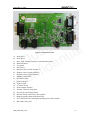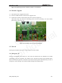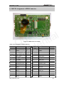
1
M33
Quectel Cellular Engine
EVB User Guide
M33_EVB_UGD_V1.0
M33 EVB User Guide
Document Title
M33 EVB User Guide
Version
1.0
Date
2010-06-28
Status
Release
Document Control ID
M33_EVB_UGD_V1.0
l
e
t
c
l
e
a
i
t
u
Q den
i
f
n
o
C
General Notes
Quectel offers this information as a service to its customers, to support application and
engineering efforts that use the products designed by Quectel. The information provided is
based upon requirements specifically provided to Quectel by the customers. Quectel has not
undertaken any independent search for additional relevant information, including any
information that may be in the customer’s possession. Furthermore, system validation of this
product designed by Quectel within a larger electronic system remains the responsibility of
the customer or the customer’s system integrator. All specifications supplied herein are
subject to change.
Copyright
This document contains proprietary technical information which is the property of Quectel
Limited., copying of this document and giving it to others and the using or communication of
the contents thereof, are forbidden without express authority. Offenders are liable to the
payment of damages. All rights reserved in the event of grant of a patent or the registration of
a utility model or design. All specification supplied herein are subject to change without
notice at any time.
Copyright © Quectel Wireless Solutions Co., Ltd. 2010
M33_EVB_UGD_V1.0
-1-
M33 EVB User Guide
Contents
0. Revision History ...........................................................................................................................5
1. Introduction...................................................................................................................................6
1.1. Related Documents .............................................................................................................6
1.2. Safety Caution .....................................................................................................................6
2. EVB Kit Introduction....................................................................................................................8
2.1. EVB Top and Bottom View ................................................................................................8
2.2. EVB Accessories ...............................................................................................................10
3. Interface Application...................................................................................................................12
3.1. Power Interface .................................................................................................................12
3.2. Audio Interface..................................................................................................................12
3.3. SIM Card Interface............................................................................................................13
3.4. Antenna Interface ..............................................................................................................14
3.5. Serial Ports ........................................................................................................................15
3.6. Switches and Buttons ........................................................................................................17
3.7. Operating Status LED .......................................................................................................18
3.8. Test Points.........................................................................................................................19
3.8.1 J104 Test Points.......................................................................................................19
3.8.2 J105 Test Points.......................................................................................................20
3.8.3 J102 Test Points.......................................................................................................20
3.8.4 J108 Test Points.......................................................................................................21
3.8.5 J103 Test Points.......................................................................................................22
3.8.6 VDD_EXT and VBAT Test points ..........................................................................23
3.8.7 EVB_TE Board Interface ........................................................................................24
4. EVB and Accessories..................................................................................................................26
5. Illustration ...................................................................................................................................28
5.1. Power on Operations .........................................................................................................28
5.2. Communicate with the Module .........................................................................................28
5.3. Use Camera Function of the Module ................................................................................28
5.4. Firmware Upgrade.............................................................................................................29
5.5. Turn off..............................................................................................................................29
5.6. Emergency off ...................................................................................................................29
6. 100 PIN Assignment of B2B Connector .....................................................................................30
l
e
t
c
l
e
a
i
t
u
Q den
i
f
n
o
C
M33_EVB_UGD_V1.0
-2-
M33 EVB User Guide
Table Index
TABLE 1: RELATED DOCUMENTS.....................................................................................................6
TABLE 2: PIN OF POWER INTERFACE ............................................................................................12
TABLE 3: PINS OF AUDIO CHANNEL 1 ...........................................................................................13
TABLE 4: PINS OF AUDIO CHANNEL 2 ...........................................................................................13
TABLE 5: PINS OF SIM CARD INTERFACE .....................................................................................13
TABLE 6: PINS OF SERIAL PORT 1 ...................................................................................................16
l
e
t
c
l
e
a
i
t
u
Q den
i
f
n
o
C
TABLE 7: PINS OF SERIAL PORT 2 ...................................................................................................16
TABLE 8: PINS OF SERIAL PORT 3 ...................................................................................................16
TABLE 9: SWITCHES AND BUTTONS..............................................................................................17
TABLE 10: OPERATING STATUS INDICATION LEDS ....................................................................18
TABLE 11: PINS OF J104 .....................................................................................................................19
TABLE 12: PINS OF J105 .....................................................................................................................20
TABLE 13: PINS OF J102 .....................................................................................................................21
TABLE 14: PINS OF J108 .....................................................................................................................21
TABLE 15: PINS OF J103 .....................................................................................................................22
TABLE 16: PINS OF VBAT,VDD_EXT TEST POINTS ......................................................................23
TABLE 17: PINS OF TE BOARD INTERFACE X101.........................................................................24
TABLE 18: PINS OF TE BOARD INTERFACE X102.........................................................................25
TABLE 19: PIN DEFINITION OF B2B CONNECTOR.......................................................................30
M33_EVB_UGD_V1.0
-3-
M33 EVB User Guide
Figure Index
FIGURE 1: EVB TOP VIEW (UNINSTALL M33-TE BOARD) ............................................................8
FIGURE 2: EVB TOP VIEW (INSTALLED M33_EVB_TE BOARD)..................................................8
FIGURE 3: EVB BOTTOM VIEW..........................................................................................................9
FIGURE 4: ACCESSORY INTRODUCTION.......................................................................................10
FIGURE 5: M33 EVB TE BOARD ACCESSORY INTRODUCTION.................................................10
l
e
t
c
l
e
a
i
t
u
Q den
i
f
n
o
C
FIGURE 6: POWER INTERFACE ........................................................................................................12
FIGURE 7: AUDIO INTERFACE .........................................................................................................13
FIGURE 8: SIM CARD INTERFACE...................................................................................................13
FIGURE 9: RF INTERFACE .................................................................................................................14
FIGURE 10: ANTENNA INSTALLATION...........................................................................................14
FIGURE 11: SERIAL PORT 1& SERIAL PORT 2 ...............................................................................15
FIGURE 12: SERIAL PORT 3...............................................................................................................15
FIGURE 13: SWITCHES AND BUTTONS ..........................................................................................17
FIGURE 14: OPERATING STATUS INDICATION LEDS ..................................................................18
FIGURE 15: TEST POINTS OVERVIEW ............................................................................................19
FIGURE 16: J104 TEST POINTS..........................................................................................................19
FIGURE 17: J105 TEST POINTS..........................................................................................................20
FIGURE 18: J102 TEST POINTS..........................................................................................................20
FIGURE 19: J108 TEST POINTS..........................................................................................................21
FIGURE 20: J103 TEST POINTS..........................................................................................................22
FIGURE 21: VDD_EXT AND VBAT TEST POINTS ..........................................................................23
FIGURE 22: EVB_TE BOARD INTERFACE ......................................................................................24
FIGURE 23: EVB AND ACCESSORIES..............................................................................................26
FIGURE 24: EVB_TE BOARD ACCESSORIES ASSEMBLY ............................................................27
FIGURE 25: SWITCHES STATE FOR FIRMWARE UPGRADE........................................................29
FIGURE 26: B2B CONNECTOR OF EVB ...........................................................................................30
M33_EVB_UGD_V1.0
-4-
M33 EVB User Guide
0. Revision History
Revision
Date
Author
Description of change
1.0
2010-06-28
Roy Chen
Initial
l
e
t
c
l
e
a
i
t
u
Q den
i
f
n
o
C
M33_EVB_UGD_V1.0
-5-
M33 EVB User Guide
1. Introduction
This document defines and specifies the usage of M33 EVB.
1.1. Related Documents
Table 1: Related documents
l
e
t
c
l
e
a
i
t
u
Q den
i
f
n
o
C
SN
Document name
Remark
[1]
M33_ATC
AT commands set
[2]
GSM_UART_AN
GSM UART port application notes
[3]
M33_HD
M33 hardware design document
[4]
Upgrade_FW_Tools_UGD
User guide of firmware upgrade tool
[5]
M33_Camera_ATC
M33 AT Command set for camera function
1.2. Safety Caution
The following safety precautions must be observed during all phases of the operation, e.g. usage,
service or repair of cellular terminal incorporating M33 module. Manufactures of the cellular
terminal is recommended to pass the following safety information to users, operating personnel. If
customer fails to do so, Quectel couldn’t bear any liability for customer’s failure to comply with
these precautions.
When in a hospital or other health care facility, observe the restrictions about
the use of mobiles. Switch the cellular terminal or mobile off, medical
equipment may be sensitive to RF interference.
Switch off the cellular terminal or mobile before boarding an aircraft. The
operation of wireless equipment in an aircraft is forbidden to prevent
interference to communication system. Failing to think enough of these
instructions could lead to endanger flight safety or offend against local legal
action, or both.
Do not operate the cellular terminal or mobile in the presence of flammable gas
or fume. Switch off the cellular terminal when you are near petrol station, fuel
depot, chemical plant or anywhere blasting operation is in progress. Operation
of electronic equipment in potentially explosive atmosphere could constitute a
safety hazard.
M33_EVB_UGD_V1.0
-6-
M33 EVB User Guide
Cellular terminal or mobile receives and transmits radio frequency energy
while switched on. RF interference could occur if it is close to TV set, radio,
computer or other electronic equipments.
Road safety comes first! Do not use a hand-held cellular terminal or mobile
while driving a vehicle, unless it is securely mounted in a holder for hands-free
operation. Park the vehicle before making a call with a hand-held terminal or
mobile.
l
e
t
c
l
e
a
i
t
u
Q den
i
f
n
o
C
GSM cellular terminals or mobiles operate over radio frequency signal and
cellular network and cannot be guaranteed to connect in all conditions, for
example no mobile fee or an invalid SIM card. While you are in this condition
and need emergent help, Please Remember using emergency call. In order to
make or receive call, the cellular terminal or mobile must be switched on and in
a service area with adequate cellular signal strength.
Some networks do not allow for emergency call if certain network services or
phone features are in use (e.g. lock functions, fixed dialing etc.). You may have
to deactivate those features before you can make an emergency call.
Also, some networks require that a valid SIM card be properly inserted in
cellular terminal or mobile.
M33_EVB_UGD_V1.0
-7-
M33 EVB User Guide
2. EVB Kit Introduction
2.1. EVB Top and Bottom View
l
e
t
c
l
e
a
i
t
u
Q den
i
f
n
o
C
Figure 1: EVB top view (Uninstall M33-TE board)
Figure 2: EVB top view (Installed M33_EVB_TE board)
M33_EVB_UGD_V1.0
-8-
M33 EVB User Guide
l
e
t
c
l
e
a
i
t
u
Q den
i
f
n
o
C
Figure 3: EVB bottom view
A:
B:
C:
D:
E:
F:
G:
H:
I:
J:
K:
L:
M:
N:
O:
P:
Q:
R:
T:
S:
U:
Serial Port 1
Serial Port 2
M33_EVB_TE Board interface (with indication mark)
SIM card socket
Test points
Serial Port 3
Handset socket of audio channel 1
Headset socket of audio channel 2
Handset socket of PCM channel
EMERG_OFF button
Download switch
ON/OFF button
VCHG switch
5V power switch
Power adapter interface
Antenna connector fixing hole
Screw holes for EVB placement
Board-to-board connector for M33 module
Module operating status indication LEDs
Four GND holes for soldering the shielding pins of M33 module
Micro SD-Card socket
M33_EVB_UGD_V1.0
-9-
M33 EVB User Guide
2.2. EVB Accessories
l
e
t
c
l
e
a
i
t
u
Q den
i
f
n
o
C
Figure 4: Accessory introduction
Figure 5: M33 EVB TE Board Accessory introduction
A:
B:
C:
D:
5V DC switching power supply
USB to UART converter cable
Antenna
RF cable
M33_EVB_UGD_V1.0
- 10 -
M33 EVB User Guide
E:
F:
G:
H:
Headset
Screws for EVB placement
M33 EVB TE Board
Recommended camera module (OV7725 sensor, part number: CN003VEF2052 from
Global Optics Limited)
Note: Contact information of the camera module vendor is as follows:
Global Optics Limited
E-mail: [email protected]
http://www.globaloptics.cn
l
e
t
c
l
e
a
i
t
u
Q den
i
f
n
o
C
M33_EVB_UGD_V1.0
- 11 -
M33 EVB User Guide
3. Interface Application
3.1. Power Interface
l
e
t
c
l
e
a
i
t
u
Q den
i
f
n
o
C
Figure 6: Power interface
Table 2: Pin of power interface
Pin
1
Signal
I/O
Adapter input
I
Description
5V/2.5A DC source input
3.2. Audio Interface
M33_EVB_UGD_V1.0
- 12 -
M33 EVB User Guide
Figure 7: Audio interface
Table 3: Pins of audio channel 1
Pin
Signal
I/O
Description
1
MIC1N
I
Negative microphone input
2
SPK1N
O
Negative receiver output
3
SPK1P
O
Positive receiver output
4
MIC1P
I
Positive microphone input
l
e
t
c
l
e
a
i
t
u
Q den
i
f
n
o
C
Table 4: Pins of audio channel 2
Pin
1
2
3
4
Signal
I/O
AGND
Description
AGND of audio circuits
AGND
SPK2P
O
Positive receiver output
MIC2P
I
Positive microphone input
3.3. SIM Card Interface
Figure 8: SIM card interface
Table 5: Pins of SIM card interface
Pin
Signal
1
SIM_GND
M33_EVB_UGD_V1.0
I/O
Description
GND, dedicated for SIM card
- 13 -
M33 EVB User Guide
2
RESERVE
3
SIM_IO
I/O
4
SIM_CLK
O
SIM card clock
5
SIM_RST
O
SIM card reset
6
SIM_VDD
O
SIM card power output
8
SIM_PRESENCE
I
SIM card detection
SIM card data I/O
3.4. Antenna Interface
l
e
t
c
l
e
a
i
t
u
Q den
i
f
n
o
C
Figure 9: RF interface
Figure 10: Antenna installation
M33_EVB_UGD_V1.0
- 14 -
M33 EVB User Guide
3.5. Serial Ports
l
e
t
c
l
e
a
i
t
u
Q den
i
f
n
o
C
Figure 11: Serial Port 1& Serial Port 2
Figure 12: Serial Port 3
M33_EVB_UGD_V1.0
- 15 -
M33 EVB User Guide
Table 6: Pins of Serial Port 1
Pin
Signal
I/O
1_1
RS232_DCD1
O
Data carrier detection
1_2
RS232_TXD1
O
Transmit data
1_3
RS232_RXD1
I
Receive data
1_4
RS232_DTR1
I
Data terminal ready
1_5
GND
1_7
RS232_RTS1
I
Request to send
1_8
RS232_CTS1
O
Clear to send
RS232_RI1
O
Ring indicator
1_9
Description
GND
l
e
t
c
l
e
a
i
t
u
Q den
i
f
n
o
C
Note: The voltage level of the module’s Serial Ports signals has been shifted to RS-232 level, so
it can be directly connect to PC by USB to UART converter cable.
Serial Port 1 is used for AT command, GPRS data, CSD FAX, multiplexing function and
firmware upgrade.
Table 7: Pins of Serial Port 2
Pin
2_2
2_3
2_5
Signal
I/O
RS232_TXD2
O
Transmit data
RS232_RXD2
I
Receive data
GND
Description
GND
Note: Customer can debug software through Serial Port 2, which is not for AT command,
GPRS service, CSD call or FAX call.
Table 8: Pins of Serial Port 3
Pin
3_2
3_3
3_5
Signal
I/O
RS232_TXD3
O
Transmit data
RS232_RXD3
I
Receive data
GND
Description
GND
Note: This port is designed for AT command only.
M33_EVB_UGD_V1.0
- 16 -
M33 EVB User Guide
3.6. Switches and Buttons
l
e
t
c
l
e
a
i
t
u
Q den
i
f
n
o
C
Figure 13: Switches and buttons
Table 9: Switches and buttons
Part
S1
S2
S3
K1
K2
Name
I/O
5V_ ON/OFF switch
I
VCHG
I
Control charge to a Li-ion or Li Polymer
battery by the module.
D/L
I
Place to ON when downloading firmware
ON/OFF
I
Press this button for 2 seconds to turn
on/off the module
EMERG_OFF
M33_EVB_UGD_V1.0
I
Description
Switch on/off the power supply from the
power adaptor
Shutdown the module in case of
emergency. Hardware power off
operation. Press this button will
immediately turn off the module.
- 17 -
M33 EVB User Guide
3.7. Operating Status LED
l
e
t
c
l
e
a
i
t
u
Q den
i
f
n
o
C
Figure 14: Operating status indication LEDs
Table 10: Operating status indication LEDs
Part
L1
L2
L3
Name
I/O
Description
5V ON/OFF indicator
O
On: VBAT ON
Off: VBAT OFF
Module Status indicator
O
On: module in power-on
Off: module in power-off
GSM_NET status indicator
O
Blinking differently to indicate
various GSM network status
M33_EVB_UGD_V1.0
- 18 -
M33 EVB User Guide
3.8. Test Points
l
e
t
c
l
e
a
i
t
u
Q den
i
f
n
o
C
Figure 15: Test points overview
3.8.1
J104 Test Points
Figure 16: J104 test points
Table 11: Pins of J104
Pin
Signal
I/O
Description
DCD1
O
Data carrier detection of Serial Port 1
RI1
O
Ring indicator of Serial Port 1
RXD1
I
Receive data of Serial Port 1
DSR1
O
Data set ready of Serial Port 1
TXD1
O
Transmit data of Serial Port 1
RTS1
I
Request to send of Serial Port1
7
CTS1
O
Clear to send of Serial Port 1
8
DTR1
I
Data terminal ready of Serial Port 1
9
SIM_PRESENCE
I
SIM card detection. Pulled down
internally.
10
BUZZER_OUT
O
Open drain output. Use to drive
buzzer.
1
2
3
4
5
6
M33_EVB_UGD_V1.0
- 19 -
M33 EVB User Guide
3.8.2
J105 Test Points
l
e
t
c
l
e
a
i
t
u
Q den
i
f
n
o
C
Figure 17: J105 test points
Table 12: Pins of J105
Pin
1
2
3
4
5
6
7
8
9
10
3.8.3
Signal
I/O
Description
EINT0
I
External interrupt input 0
EINT1
I
External interrupt input 1
STATUS
O
Indicate module status. High level
indicates module power-on and low
level indicates power-down.
LIGHT_MOS
O
Open drain output port
RESERVE
RESERVE
VIB
O
LED_B
O
LED_R
O
Open drain output port
GND
J102 Test Points
Figure 18: J102 test points
M33_EVB_UGD_V1.0
- 20 -
M33 EVB User Guide
Table 13: Pins of J102
Pin
Signal
I/O
1
KCOL0
I
2
KROW0
O
3
KCOL1
I
4
KROW1
O
5
KCOL2
I
6
KROW2
O
7
KCOL3
I
KROW3
O
KCOL4
I
KROW4
O
8
9
10
3.8.4
Description
Keypad interface
l
e
t
c
l
e
a
i
t
u
Q den
i
f
n
o
C
J108 Test Points
Figure 19: J108 test points
Table 14: Pins of J108
Pin
1
2
3
4
5
Signal
I/O
Description
RXD2
I
Receive data of Serial Port 2
RXD3
I
Receive data of Serial Port 3
TXD3
O
Transmit data of Serial Port 3
TXD2
O
Transmit data of Serial Port 2
O
Serial bit clock of PCM interface
RESERVE
6
PCM_CLK
7
RESERVE
8
PCM_IN
I
Digital audio data input of PCM interface
9
PCM_SYNC
O
Frame synchronization of PCM interface
10
PCM_OUT
O
Digital audio data output of PCM
interface
M33_EVB_UGD_V1.0
- 21 -
M33 EVB User Guide
3.8.5
J103 Test Points
l
e
t
c
l
e
a
i
t
u
Q den
i
f
n
o
C
Figure 20: J103 test points
Table 15: Pins of J103
Pin
1
2
3
4
5
6
7
8
9
10
Signal
I/O
Description
RESERVE
SPI_CS
O
Chip select of SD interface
SPI_CLK
O
Serial clock of SD interface
SPI_I
I
Data input of SD interface
SPI_O
O
Data output of SD interface
ADC0
I
ADC input channel 0
RESERVE
M33_EVB_UGD_V1.0
- 22 -
M33 EVB User Guide
3.8.6
VDD_EXT and VBAT Test points
l
e
t
c
l
e
a
i
t
u
Q den
i
f
n
o
C
Figure 21: VDD_EXT and VBAT test points
Table 16: Pins of VBAT,VDD_EXT test points
NET NAME
VBAT
VDD_EXT
Description
VBAT is the power supply of module
Supply 2.8V voltage for external circuit.
Note: Customer can test two test points to judge whether the power supply to the module or the
VDD_EXT voltage from the module is correct or not.
M33_EVB_UGD_V1.0
- 23 -
M33 EVB User Guide
3.8.7
EVB_TE Board Interface
l
e
t
c
l
e
a
i
t
u
Q den
i
f
n
o
C
Figure 22: EVB_TE Board Interface
Table 17: Pins of TE Board interface X101
Pin
1
2
3
4
5
6
7
8
9
10
11
12
13
14
Signal
I/O
Description
RESERVE
SDA
I/O
I2C serial data
RXD3
I
Receives data of Serial Port 3
TXD3
O
Transmit data of Serial Port 3
O
Supply 2.8V voltage for external circuit.
I
Power Input
RESERVE
VDD_EXT
GND
VBAT
GND
15
NETLIGHT_OUT
O
Network status indication light driver
16
ADC1
I
ADC input Chanel 1
17
RESERVE
18
VIB
O
Open drain output port
19
SCL
O
I2C serial clock
20
RESERVE
M33_EVB_UGD_V1.0
- 24 -
M33 EVB User Guide
Table 18: Pins of TE Board interface X102
Pin
Signal
1
RESERVE
2
RESERVE
3
CS_SDA
I/O
I2C serial data of camera interface
4
CS_SCL
O
I2C serial clock of camera interface
5
CS_PIXCLK
I
Pixel clock input
6
CS_HSYNC
I
Horizontal synchronizing
7
CS_D6
8
9
10
11
12
13
14
15
16
17
18
19
20
I/O
Description
l
e
t
c
l
e
a
i
t
u
Q den
i
f
n
o
C
CS_D4
CS_D2
CS_D0
I
YUV video data bus input
CS_VSYNC
I
Vertical synchronizing
CS_RESET
O
Reset camera module
CS_PWDN
O
Power down mode control
CS_ECLK
O
Clock output
CS_D1
CS_D3
CS_D5
CS_D7
RESERVE
RESERVE
Note: Both the EVB board and the EVB_TE board have assembly indication mark. Please
install them in right direction.
M33_EVB_UGD_V1.0
- 25 -
M33 EVB User Guide
4. EVB and Accessories
The EVB and its accessories are shown as Figure 23.
l
e
t
c
l
e
a
i
t
u
Q den
i
f
n
o
C
Figure 23: EVB and accessories
(1)
(2)
(3)
(4)
(5)
(6)
(7)
(8)
Connect the RF cable to the RF connector of the module.
Assembly the M33 module to the 100-pin connector on the M33 EVB.
Fix the SMA connector of the RF cable in the connector fixing hole.
Assembly SIM card to SIM card socket
Assembly the M33_EVB_TE board on the M33 EVB. (Refer to Figure 24 for details)
Connect Serial Port 1 on EVB to PC’s USB port with the USB to UART converter cable.
Insert headset into J302 connector
Insert AC adaptor into J202 connector
M33_EVB_UGD_V1.0
- 26 -
M33 EVB User Guide
l
e
t
c
l
e
a
i
t
u
Q den
i
f
n
o
C
Figure 24: EVB_TE Board accessories assembly
A.
B.
X101 and X102 connectors of M33_EVB_TE board mark the direction of assembly. Install
as instructed by Figure 24.
The FPC cable of the camera module must be assembled in the way shown in Figure 24.
M33_EVB_UGD_V1.0
- 27 -
M33 EVB User Guide
5. Illustration
5.1. Power on Operations
(1) Assembly the M33 module to the 100-pin connector on the M33 EVB. Put Switch S1 to ON
state. Put Switch S2 to OFF position and Switch S3 to OFF position. Plug in 5V DC adapter.
The LED L1 on the EVB will go bright.
(2) Press the ON/OFF button for more than 2 seconds. When the STATUS_LED is lightened, and
NET_LED is blinked , the module is working fine.
l
e
t
c
l
e
a
i
t
u
Q den
i
f
n
o
C
5.2. Communicate with the Module
(1) Connect the Serial Port 1 on EVB to PC’s USB port with the USB to UART converter cable.
(2) Open the HyperTerminal (AT command window) in the PC. The location of the
HyperTerminal in Windows XP is START →program →accessory →communication
→HyperTerminal. Set appropriate Baud Rate (such as 115200 bps) and COM port number
which can be checked by the Device Manager in the PC.
(3) Connect an antenna to the M33 with an RF cable.
(4) Insert SIM card into the SIM card socket.
(5) Insert earphone or handset into audio interface.
(6) Power on the module by pressing the ON/OFF button.
(7) After waiting for 2~3 seconds, customer should firstly input “AT” or “at” string once or more
until receiving “OK” from the module in the HyperTerminal.
The module is set to autobauding mode in default configuration. This operation is to
synchronize the baud rate between the computer and the module.
(8) Input AT command and the module will execute its corresponding function.
Customer can refer to Document [1] for details of AT commands. For instance, typing
“ATD112;” makes a call to the emergency number 112.
5.3. Use Camera Function of the Module
(1) Before powering on the module, assemble M33_EVB_TE board to M33_EVB board, and put
camera module onto M33_EVB_TE board.
(2) Power on the module by pressing the ON/OFF button.
(3) Sending “AT+QCAMSEL="OV7725"” and “AT+QCAMON” can drive the module enter
camera standby mode.
(4) Sending “AT+QCAMSOT”, “AT+QCAMMSOT” or “AT+QCAMAVI” can take photo and
video.
(5) M33_EVB_TE Board comes with a bunch of infrared LEDs around the Camera. These can
be used to emit infrared light for object in dark environment. Customer can manually set the
Infrared Lights Switch (refer to Figure 24.) to ON or OFF state.
M33_EVB_UGD_V1.0
- 28 -
M33 EVB User Guide
Refer to Document [5] for more details of camera AT commands.
5.4. Firmware Upgrade
(1) Start the Firmware Upgrade Tool in PC.
(2) Press the START button in the Firmware Upgrade Tool.
(3) Switch the S3 and S1 in the EVB to ON state as shown in Figure 25.
After these steps, the firmware refreshing process will be proceeding. For more details,
please refer to Document [4].
l
e
t
c
l
e
a
i
t
u
Q den
i
f
n
o
C
Figure 25: Switches state for firmware upgrade
5.5. Turn off
Pressing the ON/OFF button for 2 seconds will turn off the module.
5.6. Emergency off
Pressing the EMERG_OFF button for more than 20 milliseconds will shutdown the module
immediately. After this operation, the module can be restarted by pressing the ON/OFF button.
Please note that the operation is harmful to the whole module system and should only be done in
emergency such as failing to turn off the module through the ON/OFF button.
M33_EVB_UGD_V1.0
- 29 -
M33 EVB User Guide
6. 100 PIN Assignment of B2B Connector
l
e
t
c
l
e
a
i
t
u
Q den
i
f
n
o
C
Figure 26: B2B connector of EVB
Table 19: Pin definition of B2B connector
PIN NO.
PIN NAME
I/O
PIN NO.
PIN NAME
I/O
1
VBAT
I
2
VBAT
I
VBAT
I
4
VBAT
I
VDD_EXT
O
6
VCHG
I
VRTC
I/O
8
VCHG
I
SIM_VDD
O
10
VDD_EXT
O
SIM_DATA
I/O
12
SIM_PRESENCE
I
SIM_RST
O
14
SIM_CLK
O
BUZZER_OUT
O
16
RESERVE
NETLIGHT_OUT
O
18
EMERG_OFF
I
ON/OFF
I
20
ADC1
I
21
ADC0
I
22
SPI_CS
O
23
SPI_CLK
O
24
SPI_I
I
25
SPI_O
O
26
PCM_IN
I
27
PCM_SYNC
O
28
PCM_OUT
O
29
PCM_CLK
O
30
TXD2
O
31
RXD2
I
32
RXD3
I
3
5
7
9
11
13
15
17
19
M33_EVB_UGD_V1.0
- 30 -
M33 EVB User Guide
33
TXD3
O
34
MIC2N
I
35
SPK1P
O
36
MIC2P
I
37
SPK1N
O
38
MIC1N
I
39
SPK2P
O
40
MIC1P
I
41
AGND
42
RESERVE
43
RESERVE
44
SCL
O
45
STATUS
46
SDA
I/O
47
RESERVE
48
GPIO3
I/O
49
EINT1
I
50
EINT0
I
LIGHT_MOS
O
52
RESERVE
LED_B
O
54
RESERVE
56
RESERVE
51
53
55
57
59
61
63
65
67
69
71
73
75
77
79
81
83
85
87
89
91
93
95
97
99
O
l
e
t
c
l
e
a
i
t
u
Q den
i
f
n
o
C
RESERVE
VIB
O
58
LED_R
O
KCOL0
I
60
KCOL1
I
KCOL2
I
62
KCOL3
I
KCOL4
I
64
KROW4
O
KROW3
O
66
KROW2
O
KROW1
O
68
KROW0
O
RI1
O
70
DCD1
O
RXD1
I
72
RTS1
I
TXD1
O
74
DSR1
O
CTS1
O
76
DTR1
I
CS_D0
I
78
CS_D1
I
CS_D2
I
80
CS_D3
I
CS_D4
I
82
CS_D5
I
CS_D6
I
84
CS_D7
I
CS_HSYNC
I
86
CS_VSYNC
I
CS_PIXCLK
I
88
CS_RESET
O
CS_SCL
O
90
CS_PWDN
O
CS_SDA
I/O
92
CS_ECLK
O
RESERVE
94
RESERVE
GND
96
SIM_GND
GND
98
GND
GND
100
GND
M33_EVB_UGD_V1.0
- 31 -
Quectel Wireless Solutions Co., Ltd.
Room 501, Building 9, No. 99, Tianzhou Road, Shanghai, China 200233
Tel: +86 21 5108 2965
Mail: [email protected]