1
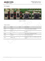
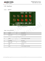
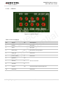
M10 EVB User Guide
GSM/GPRS Module Series
Rev. M10_EVB_User_Guide_V3.2
Date: 2014-01-14
www.quectel.com
GSM/GPRS Module Series
M10 EVB User Guide
Our aim is to provide customers with timely and comprehensive service. For any
assistance, please contact our company headquarters:
Quectel Wireless Solutions Co., Ltd.
Room 501, Building 13, No.99, Tianzhou Road, Shanghai, China, 200233
Tel: +86 21 5108 6236
Mail:[email protected]
Or our local office, for more information, please visit:
l
e
t
l
c
a
i
e
t
u
n
Q fide
n
o
C
http://www.quectel.com/support/salesupport.aspx
For technical support, to report documentation errors, please visit:
http://www.quectel.com/support/techsupport.aspx
GENERAL NOTES
QUECTEL OFFERS THIS INFORMATION AS A SERVICE TO ITS CUSTOMERS. THE INFORMATION
PROVIDED IS BASED UPON CUSTOMERS’ REQUIREMENTS. QUECTEL MAKES EVERY EFFORT
TO ENSURE THE QUALITY OF THE INFORMATION IT MAKES AVAILABLE. QUECTEL DOES NOT
MAKE ANY WARRANTY AS TO THE INFORMATION CONTAINED HEREIN, AND DOES NOT ACCEPT
ANY LIABILITY FOR ANY INJURY, LOSS OR DAMAGE OF ANY KIND INCURRED BY USE OF OR
RELIANCE UPON THE INFORMATION. ALL INFORMATION SUPPLIED HEREIN ARE SUBJECT TO
CHANGE WITHOUT PRIOR NOTICE.
COPYRIGHT
THIS INFORMATION CONTAINED HERE IS PROPRIETARY TECHNICAL INFORMATION OF
QUECTEL CO., LTD. TRANSMITTABLE, REPRODUCTION, DISSEMINATION AND EDITING OF THIS
DOCUMENT AS WELL AS UTILIZATION OF THIS CONTENTS ARE FORBIDDEN WITHOUT
PERMISSION. OFFENDERS WILL BE HELD LIABLE FOR PAYMENT OF DAMAGES. ALL RIGHTS
ARE RESERVED IN THE EVENT OF A PATENT GRANT OR REGISTRATION OF A UTILITY MODEL
OR DESIGN.
Copyright © Quectel Wireless Solutions Co., Ltd. 2014. All rights reserved.
M10_EVB_User_Guide
Confidential / Released
1 / 33
GSM/GPRS Module Series
M10 EVB User Guide
About the Document
History
Revision
1.0
l
e
t
l
c
a
i
e
t
u
n
Q fide
n
o
C
Date
Author
Description
2009-06-17
Tracy ZHANG
Initial
1.
2.
1.1
2.0
3.0
3.1
3.2
Modified Figure5, 6, 7 and 10.
Added some contents on how to better
operate module for customers when
module is set to autobaudingby default
in Chapter 5.2.
2009-11-12
Yong AN
2011-04-15
Roy CHEN
Added Introduction to UART in Section 5.6.
2013-05-03
Tony WU
Added SD card connector instead of LCD
display connector.
2013-09-23
Tony WU
Optimized Introduction description.
2014-01-14
Vivian WANG
Added introduction to SD interface.
M10_EVB_User_Guide
Confidential / Released
2 / 33
GSM/GPRS Module Series
M10 EVB User Guide
Contents
About the Document ................................................................................................................................... 2
Contents ....................................................................................................................................................... 3
Table Index ................................................................................................................................................... 4
Figure Index ................................................................................................................................................. 5
1
Introduction .......................................................................................................................................... 6
1.1.
Safety Information ................................................................................................................... 6
2
Product Concept .................................................................................................................................. 8
2.1.
EVB Top and Bottom View ...................................................................................................... 8
3
Interface Application ......................................................................................................................... 11
3.1.
Power Interface ..................................................................................................................... 11
3.2.
Audio Interface ...................................................................................................................... 12
3.3.
SIM Card Interface ................................................................................................................ 13
3.4.
Antenna Interface .................................................................................................................. 14
3.5.
SD Interface........................................................................................................................... 15
3.6.
Main Port and Debug Port ..................................................................................................... 16
3.7.
UART3 ................................................................................................................................... 17
3.8.
Switch .................................................................................................................................... 18
3.9.
Indicator LED ......................................................................................................................... 19
3.10.
Test Point ............................................................................................................................... 20
3.10.1. CON103 ......................................................................................................................... 20
3.10.2. CON101 ......................................................................................................................... 21
3.10.3. CON102 ......................................................................................................................... 22
3.10.4. CON401 ......................................................................................................................... 23
3.10.5. CON501 ......................................................................................................................... 24
4
EVB Accessories Assembly ............................................................................................................. 25
5
Illustration ........................................................................................................................................... 26
5.1.
Power On ............................................................................................................................... 26
5.2.
Communicate with Module .................................................................................................... 26
5.3.
Firmware Upgrade through Main Port ................................................................................... 27
5.4.
Turn Off .................................................................................................................................. 27
5.5.
Emergency Off ....................................................................................................................... 28
5.6.
UART3 ................................................................................................................................... 28
5.7.
Useful Application .................................................................................................................. 28
6
7
60-pin Assignment ............................................................................................................................. 30
Appendix A Reference....................................................................................................................... 33
l
e
t
l
c
a
i
e
t
u
n
Q fide
n
o
C
M10_EVB_User_Guide
Confidential / Released
3 / 33
GSM/GPRS Module Series
M10 EVB User Guide
Table Index
TABLE 1: PIN DESCRIPTION ............................................................................................................................ 11
TABLE 2: PINS OF AUDIO CHANNEL 2 ........................................................................................................... 12
TABLE 3: PINS OF AUDIO CHANNEL 1 ........................................................................................................... 12
TABLE 4: PINS OF SIM CARD INTERFACE .................................................................................................... 13
TABLE 5: PINS OF SD CARD INTERFACE...................................................................................................... 15
TABLE 6: PINS OF MAIN PORT ....................................................................................................................... 16
TABLE 7: PINS OF DEBUG PORT ................................................................................................................... 16
TABLE 8: PINS OF UART3 ............................................................................................................................... 17
l
e
t
l
c
a
i
e
t
u
n
Q fide
n
o
C
TABLE 9: SWITCH ............................................................................................................................................ 18
TABLE 10: INDICATOR LED ............................................................................................................................. 19
TABLE 11: PINS OF CON103 ........................................................................................................................... 20
TABLE 12: PINS OF CON101 ........................................................................................................................... 21
TABLE 13: PINS OF CON102 ........................................................................................................................... 22
TABLE 14: PINS OF CON401 ........................................................................................................................... 23
TABLE 15: PINS OF CON401 ........................................................................................................................... 24
TABLE 16: PIN DEFINITION OF THE 60-PIN DIP CONNECTOR ................................................................... 31
TABLE 17: RELATED DOCUMENTS ................................................................................................................ 33
M10_EVB_User_Guide
Confidential / Released
4 / 33
GSM/GPRS Module Series
M10 EVB User Guide
Figure Index
FIGURE 1: EVB TOP VIEW ................................................................................................................................ 8
FIGURE 2: EVB BOTTOM VIEW ........................................................................................................................ 9
FIGURE 3: ACCESSORIES INTRODUCTION ................................................................................................. 10
FIGURE 4: POWER INTERFACE ...................................................................................................................... 11
FIGURE 5: AUDIO INTERFACE ........................................................................................................................ 12
FIGURE 6: SIM CARD INTERFACE ................................................................................................................. 13
FIGURE 7: ANTENNA INTERFACE .................................................................................................................. 14
FIGURE 8: SD INTERFACE .............................................................................................................................. 15
l
e
t
l
c
a
i
e
t
u
n
Q fide
n
o
C
FIGURE 9: MAIN PORT AND DEBUG PORT .................................................................................................. 16
FIGURE 10: UART3 .......................................................................................................................................... 17
FIGURE 11: SWITCH ........................................................................................................................................ 18
FIGURE 12: INDICATOR LED........................................................................................................................... 19
FIGURE 13: CON103 POINTS.......................................................................................................................... 20
FIGURE 14: CON101 POINTS.......................................................................................................................... 21
FIGURE 15: CON102 POINTS.......................................................................................................................... 22
FIGURE 16: CON401 POINTS.......................................................................................................................... 23
FIGURE 17: CON501 POINTS.......................................................................................................................... 24
FIGURE 18: EVB AND ACCESSORIES............................................................................................................ 25
FIGURE 19: SWITCHES STATE FOR FIRMWARE DOWNLOAD ................................................................... 27
FIGURE 20: CHANGE THE POWER SUPPLY ................................................................................................. 28
FIGURE 21: RUN THE MODULE ...................................................................................................................... 29
FIGURE 22: DIP CONNECTOR OF EVB .......................................................................................................... 30
M10_EVB_User_Guide
Confidential / Released
5 / 33
GSM/GPRS Module Series
M10 EVB User Guide
1
Introduction
In order to help you to develop applications with Quectel modules, Quectel supplies evaluation board
(EVB) for you to test our modules. This document can help you quickly understand the EVB interface
specifications, electrical and mechanical details and know how to use it.
l
e
t
l
c
a
i
e
t
u
n
Q fide
n
o
C
1.1. Safety Information
The following safety precautions must be observed during all phases of the operation, such as usage,
service or repair of any cellular terminal or mobile incorporating M10 module. Manufacturers of the cellular
terminal should send the following safety information to users and operating personnel and to incorporate
these guidelines into all manuals supplied with the product. If not so, Quectel does not take on any liability
for customer failure to comply with these precautions.
Full attention must be given to driving at all times in order to reduce the risk of an
accident. Using a mobie while driving (even with a handsfree kit) cause distraction
and can lead to an accident. You must comply with laws and regulations restrcting
the use of wireless devices while driving.
Switch off the cellular terminal or mobile before boarding an aircraft. Make sure it
switched off. The operation of wireless appliances in an aircraft is forbidden to
prevent interference with communication systems. Consult the airline staff about
the use of wireless devices on boarding the aircraft. If your device offers a Flight
Mode which must be enabled prior to boarding an aircraft.
Switch off your wireless device when in hospitals or clinics or other health care
facilities. These requests are desinged to prevent possible interference with
sentitive medical equipment.
GSM cellular terminals or mobiles operate over radio frequency signal and cellular
network and cannot be guaranteed to connect in all conditions, for example no
mobile fee or an invalid SIM card. While you are in this condition and need
emergent help, please remember using emergency call. In order to make or
receive call, the cellular terminal or mobile must be switched on and in a service
area with adequate cellular signal strength.
M10_EVB_User_Guide
Confidential / Released
6 / 33
GSM/GPRS Module Series
M10 EVB User Guide
Your cellular terminal or mobile contains a transmitter and receiver. When it is ON ,
it receives and transmits radio frequency energy. RF interference can occur if it is
used close to TV set, radio, computer or other electric equipment.
In locations with potencially explosive atmospheres, obey all posted signs to turn
off wireless devices such as your phone or other cellular terminals. Areas with
potencially exposive atmospheres including fuelling areas, below decks on boats,
fuel or chemical transfer or storage facilities, areas where the air contains
chemicals or particles such as grain, dust or metal powders.
l
e
t
l
c
a
i
e
t
u
n
Q fide
n
o
C
M10_EVB_User_Guide
Confidential / Released
7 / 33
GSM/GPRS Module Series
M10 EVB User Guide
2
Product Concept
2.1. EVB Top and Bottom View
l
e
t
l
c
a
i
e
t
u
n
Q fide
n
o
C
Figure 1: EVB Top View
NOTES
1.
2.
Some interfaces and test pins are reserved only for engineers to debug some functions which are not
used for customer.
Some functions are only supported in certain software versions.
M10_EVB_User_Guide
Confidential / Released
8 / 33
GSM/GPRS Module Series
M10 EVB User Guide
l
e
t
l
c
a
i
e
t
u
n
Q fide
n
o
C
Figure 2: EVB Bottom View
A:
B:
C:
D:
E:
F:
G:
H:
I:
J:
K:
L:
M:
N:
O:
P:
Q:
R:
S:
T:
U:
V:
Debug port
Main port
UART port 3
Adapter interface
POWER switch
VCHG switch (Not used)
D/L switch
PWKEY button
EMERG_OFF button
Loudspeaker interface (Not used)
Earphone interface
Handset interface of audio channel 2
Handset interface of audio channel 1
Test points
LED indicator (D203&D204 Not used)
60 pins M10-TE-A interface
Battery interface (Not used)
Fixture hole for RF cable connector
SIM card interface
Fixture holes for EVB poles
Screw holes for fixing the module
T-Flash card interface
M10_EVB_User_Guide
Confidential / Released
9 / 33
GSM/GPRS Module Series
M10 EVB User Guide
l
e
t
l
c
a
i
e
t
u
n
Q fide
n
o
C
Figure 3: Accessories Introduction
A:
B:
C:
D:
E:
F:
5V DC switching adapter
USB to UART converter cable
Antenna
RF cable
Earphone
Bolts and nuts for fixing module and EVB
M10_EVB_User_Guide
Confidential / Released
10 / 33
GSM/GPRS Module Series
M10 EVB User Guide
3
Interface Application
3.1. Power Interface
l
e
t
l
c
a
i
e
t
u
n
Q fide
n
o
C
Figure 4: Power Interface
Table 1: Pin Description
Pin
Signal
I/O
Description
1
Adapter input
I
5V/2A DC source input
2
GND
M10_EVB_User_Guide
Ground
Confidential / Released
11 / 33
GSM/GPRS Module Series
M10 EVB User Guide
3.2. Audio Interface
l
e
t
l
c
a
i
e
t
u
n
Q fide
n
o
C
Figure 5: Audio Interface
Table 2: Pins of Audio Channel 2
Interface
AIN2/AOUT2
Signal
Pin NO.
Description
MIC2N
1
Channel 2 for Negative microphone input
AGND
2
AGND of audio circuits
SPK2P
3
Channel 2 for Positive receiver output
MIC2P
4
Channel 2 for Positive microphone input
Table 3: Pins of Audio Channel 1
Interface
Signal
Pin NO.
Description
MIC1N
1
Channel 1 for Negative microphone input
SPK1N
2
Channel 1for Negative receiver output
SPK1P
3
Channel 1Positive receiver output
MIC1P
4
Channel 1Positive microphone input
AIN1/AOUT1
M10_EVB_User_Guide
Confidential / Released
12 / 33
GSM/GPRS Module Series
M10 EVB User Guide
3.3. SIM Card Interface
l
e
t
l
c
a
i
e
t
u
n
Q fide
n
o
C
Figure 6: SIM Card Interface
Table 4: Pins of SIM Card Interface
Pin
Signal
1
GND
Ground
2
VPP
Not connected
3
SIM_DATA
I/O
SIM card data I/O
4
SIM_CLK
O
SIM card clock
5
SIM_RST
O
SIM card reset
6
SIM_VDD
M10_EVB_User_Guide
I/O
Description
Power supply for SIM card
Confidential / Released
13 / 33
GSM/GPRS Module Series
M10 EVB User Guide
3.4. Antenna Interface
l
e
t
l
c
a
i
e
t
u
n
Q fide
n
o
C
Figure 7: Antenna Interface
M10_EVB_User_Guide
Confidential / Released
14 / 33
GSM/GPRS Module Series
M10 EVB User Guide
3.5. SD Interface
l
e
t
l
c
a
i
e
t
u
n
Q fide
n
o
C
Figure 8: SD Interface
Table 5: Pins of SD Card Interface
Pin
Name
I/O
Description
1
SD_CMD
O
Command signal of SD card output
2
SD_CLK
O
Clock signal of SD card output
3
SD_DATA
I/O
Data output and input signal of SD card
4
SD_VDD
Power supply for SD Card
5
SD_VSS
Ground
The EVB board provides Micro SD card interface, but only supports 1-bit SD mode.
For furthermore details, please refer to the document of M10_Hardware_Design.
M10_EVB_User_Guide
Confidential / Released
15 / 33
GSM/GPRS Module Series
M10 EVB User Guide
3.6. Main Port and Debug Port
l
e
t
l
c
a
i
e
t
u
n
Q fide
n
o
C
Figure 9: Main Port and Debug Port
Table 6: Pins of Main Port
Pin
1_1
1_2
1_3
1_4
1_5
1_7
1_8
1_9
Signal
I/O
Description
DCD
O
Data carrier detection
TXD
O
Transmit data
RXD
I
Receive data
DTR
I
Data terminal ready
GND
Ground
RTS
I
Request to send
CTS
O
Clear to send
RI
O
Ring indicator
Table 7: Pins of Debug Port
Pin
Signal
I/O
Description
2_2
DBG_TXD
O
Transmit data
2_3
DBG_RXD
I
Receive data
2_5
GND
M10_EVB_User_Guide
Ground
Confidential / Released
16 / 33
GSM/GPRS Module Series
M10 EVB User Guide
3.7. UART3
l
e
t
l
c
a
i
e
t
u
n
Q fide
n
o
C
Figure 10: UART3
Table 8: Pins of UART3
Pin
3_2
3_3
3_5
Signal
I/O
Description
UART3_TXD
O
Transmit data
UART3_RXD
I
Receive data
GND
M10_EVB_User_Guide
Ground
Confidential / Released
17 / 33
GSM/GPRS Module Series
M10 EVB User Guide
3.8. Switch
l
e
t
l
c
a
i
e
t
u
n
Q fide
n
o
C
Figure 11: Switch
Table 9: Switch
Part
S202
S203
S201
S204
S101
Name
I/O
Description
POWER
I
Control power supply via adaptor
VCHG
I
Control charging if module has charging
function
D/L
I
Pull to “ON” to download firmware
PWRKEY
I
Turn on/off the module
EMERG_OFF
I
Emergency button for shutting down the
system
M10_EVB_User_Guide
Confidential / Released
18 / 33
GSM/GPRS Module Series
M10 EVB User Guide
3.9. Indicator LED
l
e
t
l
c
a
i
e
t
u
n
Q fide
n
o
C
Figure 12: Indicator LED
Table 10: Indicator LED
Part
Name
I/O
Description
D503
VBAT ON/OFF indicator
O
Lighten: VBAT ON
Extinguish : VBAT OFF
D502
GSM_NET status indicator
O
Flash with different frequency according to
different GSM network status
D504
LIGHT_MOS indicator
O
Specially for LIGHT_MOS demo
D101
Module status indicator
O
Indication of module operating status
M10_EVB_User_Guide
Confidential / Released
19 / 33
GSM/GPRS Module Series
M10 EVB User Guide
3.10. Test Point
3.10.1.
CON103
l
e
t
l
c
a
i
e
t
u
n
Q fide
n
o
C
Figure 13: CON103 Points
Table 11: Pins of CON103
Pin
Signal
I/O
Description
1
DBG_RXD
I
Receive data
2
GND
3
VBAT
4
STANDBY
5
DBG_TXD
6
GND
7
VBAT
M10_EVB_User_Guide
Ground
I
Power supply for module
Not used
O
Transmit data
Ground
I
Power supply for module
Confidential / Released
20 / 33
GSM/GPRS Module Series
M10 EVB User Guide
3.10.2.
CON101
l
e
t
l
c
a
i
e
t
u
n
Q fide
n
o
C
Figure 14: CON101 Points
Table 12: Pins of CON101
Pin
Signal
1
RES5
Not used
2
ADC1
Not used
3
NETLIGHT
4
DISP_A0
5
LIGHT_MOS
O
6
SDDATA
I/O
7
SDCLK
O
8
SDCMD
O
9
GPIO0
I/O
10
DISPRST
M10_EVB_User_Guide
I/O
O
Description
NETLIGHT driving output
Reserved
Reserved
SD card interface
General purpose input/output port
Reserved
Confidential / Released
21 / 33
GSM/GPRS Module Series
M10 EVB User Guide
3.10.3.
CON102
l
e
t
l
c
a
i
e
t
u
n
Q fide
n
o
C
Figure 15: CON102 Points
Table 13: Pins of CON102
Pin
Signal
I/O
Description
1
ADC0
I
Analog to digital converter
2
GPIO101_KBC5
I/O
3
KBR1
O
4
KBC0
I
5
KBC2
I
7
KBR0
O
8
KBR2
O
9
KBC1
I
6
VRTC
I/O
RTC supply
10
SIM_PRESENCE
I
SIM card detection
M10_EVB_User_Guide
Keyboard interface
Confidential / Released
22 / 33
GSM/GPRS Module Series
M10 EVB User Guide
3.10.4.
CON401
l
e
t
l
c
a
i
e
t
u
n
Q fide
n
o
C
Figure 16: CON401 Points
Table 14: Pins of CON401
Pin
1
2
3
4
5
6
7
8
9
10
Signal
I/O
Description
RXD
I
Receive data
RI
O
Ring indicator
GND
Ground
TXD3
O
UART3 Transmit data
RXD3
I
UART3 Receive data
TXD
O
Transmit data
DCD
O
Data carrier detection
CTS
O
Clear to send
DTR
I
Data terminal ready
RTS
I
Request to send
M10_EVB_User_Guide
Confidential / Released
23 / 33
GSM/GPRS Module Series
M10 EVB User Guide
3.10.5.
CON501
l
e
t
l
c
a
i
e
t
u
n
Q fide
n
o
C
Figure 17: CON501 Points
Table 15: Pins of CON501
Pin
1
2
3
4
5
6
7
8
9
10
Signal
I/O
Description
VCHG
I
Voltage input for the charging circuit
I
Reserved
STATUS
O
Module operating status
MCU_CL
O
Reserved
PWR_EN
O
Power enable control
PWRKEY
I
Turn on/off the module
EMERGE
I
Shut down the module in emergency.
RES1
RES2
RES3
RES4
M10_EVB_User_Guide
Confidential / Released
24 / 33
GSM/GPRS Module Series
M10 EVB User Guide
4
EVB Accessories Assembly
l
e
t
l
c
a
i
e
t
u
n
Q fide
n
o
C
Figure 18: EVB and Accessories
M10_EVB_User_Guide
Confidential / Released
25 / 33
GSM/GPRS Module Series
M10 EVB User Guide
5
Illustration
5.1. Power On
l
e
t
l
c
a
i
e
t
u
n
Q fide
n
o
C
(1) Connect the M10-TE-A to the 60 pins connector on M10 EVB.
(2) Insert the plug of the 5V power adapter.
(3) Turn the Switch S202 to ON state, Switch S203 to OFF state, and Switch S201 to OFF state. The LED
D503 on the EVB will be lighted.
(4) Press the PWRKEY for about 2 seconds. The LED D101 will be lighted which indicates the module in
working status. With LED D101 is on, the module begins running. Otherwise, please check the circuit.
(5) The LED D502 will be flashing at a certain frequency. The GSM working status of the module can be
judged by the LED status.
Please refer to chapter 7 in document [3] for detailed network status indication.
5.2. Communicate with Module
(1) Connect the main port of EVB to PC’s USB port with the USB to UART converter cable.
(2) Open the HyperTerminal (AT command window) on PC. The location of the HyperTerminal in windows
XP is: START→program→accessory→communication→HyperTerminal. Set appropriate Baud Rate
(such as 115200 bps) and COM number which can be checked by the Device Manager on PC.
(3) Connect an antenna to M10-TE-A with an RF cable.
(4) Insert SIM card into the SIM card socket.
(5) Insert earphone or handset into audio interface.
(6) For power on operation, please refer to chapter 5.1.
(7) After waiting for 2~3 seconds, customer should first input “AT” or “at” string once or more until
receiving “OK” from the module in the HyperTerminal.
The module is set to autobauding mode in default configuration. This operation is to synchronize the baud
rate between the computer and the module.
M10_EVB_User_Guide
Confidential / Released
26 / 33
GSM/GPRS Module Series
M10 EVB User Guide
(8) Input AT command and the module will execute its corresponding function.
Customer can refer to chapter 7 in document [5] for the details of AT commands. For instance, when input
“ATD112;”, an emergency call will be established.
5.3. Firmware Upgrade through Main Port
(1) Start the Firmware Upgrade Tool in the PC.
(2) Press the START button in the Firmware Upgrade Tool.
l
e
t
l
c
a
i
e
t
u
n
Q fide
n
o
C
(3) Switch the S201 and S202 in the EVB to ON state as shown in Figure 18.
After these steps, the firmware refreshing process will be proceeding. For more details, please refer to
chapter 7 in document [4].
Figure 19: Switches State for Firmware Download
5.4. Turn Off
Press the PWRKEY button less than 1 second, the module will be turned off.
M10_EVB_User_Guide
Confidential / Released
27 / 33
GSM/GPRS Module Series
M10 EVB User Guide
5.5. Emergency Off
Press the EMERG_OFF button for more than 0.1 second, the module will be shut down immediately. After
that, the module can be restarted by pressing the PWRKEY button. Please pay attention that this
operation is harmful to the whole module system and should only be done in emergency such as failing to
turn off the module through the PWRKEY button.
5.6. UART3
l
e
t
l
c
a
i
e
t
u
n
Q fide
n
o
C
Module provides two UART ports for achieving Dual UART. One is UART1 which is the main UART; the
other is UART 3 which is the assisted UART.
AT+QEAUART=1 is used to enable UART3. For more details, please refer tochapter 7 in document [5].
5.7. Useful Application
If the module has been welded on your PCB, you can follow the steps below to connect the module with
our EVB. After that, URAT communication is ready.
Remove the resistance R102 to the place of the resistance R224 to change the power supply.
Figure 20: Change the Power Supply
M10_EVB_User_Guide
Confidential / Released
28 / 33
GSM/GPRS Module Series
M10 EVB User Guide
Pull out the module pins of TXD, RXD, VBAT, and GND to the EVB pins of TXD, RXD, VBAT, and GND
with 4 wires. Short-circuit the power key to GND for 1s and cut down the connection to run the module.
l
e
t
l
c
a
i
e
t
u
n
Q fide
n
o
C
Figure 21: Run the Module
M10_EVB_User_Guide
Confidential / Released
29 / 33
GSM/GPRS Module Series
M10 EVB User Guide
6
60-pin Assignment
l
e
t
l
c
a
i
e
t
u
n
Q fide
n
o
C
Figure 22: DIP Connector of EVB
M10_EVB_User_Guide
Confidential / Released
30 / 33
GSM/GPRS Module Series
M10 EVB User Guide
Table 16: Pin Definition of the 60-pin DIP Connector
Pin NO.
Pin Name
I/O
Pin NO.
Pin Name
1
VBAT
I
2
GND
3
VBAT
I
4
GND
5
VBAT
I
6
GND
7
VBAT
I
8
GND
9
I/O
l
e
t
l
c
a
i
e
t
u
n
Q fide
n
o
C
VBAT
I
10
GND
VCHG
I
12
ADC0
I
ADC1
I
14
VRTC
I/O
VDD_EXT
O
16
NETLIGHT
O
PWRKEY
I
18
KBR0
O
STATUS
O
20
KBR1
O
GPIO0
I/O
22
KBR2
O
BUZZER
Reserved
24
TXD3
O
SIM_VDD
O
26
RXD3
I
SIM_RST
O
28
KBC0
I
SIM_DATA
I/O
30
KBC1
I
SIM_CLK
O
32
KBC2
I
SIM_PRESENCE
I
34
LIGHT_MOS
O
GPIO1_KBC5
I/O
36
EMERG_OFF
I
DCD
O
38
SD_CMD
O
DTR
I
40
SD_CLK
O
RXD
I
42
SD_DATA
I/O
TXD
O
44
DISP_A0
Reserved
45
RTS
I
46
DISP_RST
Reserved
47
CTS
O
48
DBG_RXD
I
49
RI
O
50
DBG_TXD
O
51
AGND
52
AGND
11
13
15
17
19
21
23
25
27
29
31
33
35
37
39
41
43
M10_EVB_User_Guide
Confidential / Released
31 / 33
GSM/GPRS Module Series
M10 EVB User Guide
53
SPK1P
O
54
MIC1P
I
55
SPK1N
O
56
MIC1N
I
57
SPK2P
O
58
MIC2P
I
59
AGND
60
MIC2N
I
l
e
t
l
c
a
i
e
t
u
n
Q fide
n
o
C
M10_EVB_User_Guide
Confidential / Released
32 / 33
GSM/GPRS Module Series
M10 EVB User Guide
7
Appendix A Reference
Table 17: Related Documents
SN
Document Name
Remark
[1]
M10_AT_Commands Manual
AT commands manual
[2]
GSM_UART_Application_Note
The document of serial port application note
[3]
M10_Hareware_Design
Hardware design
[4]
GSM_FW_UPGRADE_AN01
Firmware upgrade application notes
[5]
GSM_DUAL_UART_Application_Note
GSMDUALUART application note
l
e
t
l
c
a
i
e
t
u
n
Q fide
n
o
C
M10_EVB_User_Guide
Confidential / Released
33 / 33